researcharticle a low power voltage controlled...
TRANSCRIPT

Hindawi Publishing CorporationISRN ElectronicsVolume 2013, Article ID 987179, 6 pageshttp://dx.doi.org/10.1155/2013/987179
Research ArticleA Low Power Voltage Controlled Oscillator Design
Manoj Kumar
Department of Electronics & Communication Engineering, Guru Jambheshwar University of Science & Technology, Hisar 125001, India
Correspondence should be addressed to Manoj Kumar; [email protected]
Received 5 April 2013; Accepted 25 April 2013
Academic Editors: S. Hall, R. Luzzi, V. McGahay, P. Wachulak, and X. Yang
Copyright © 2013 Manoj Kumar.This is an open access article distributed under the Creative Commons Attribution License, whichpermits unrestricted use, distribution, and reproduction in any medium, provided the original work is properly cited.
The performance of voltage controlled oscillator (VCO) is of great importance for any telecommunication or data transmissionnetwork. Here, voltage controlled oscillators (VCOs) using three-transistor NAND gates have been designed. New delay cell withthree-transistorNANDgate has been used for designing the ring basedVCOcircuits.Three-, five-, and seven-stageVCOs have beenproposed. Output frequency has been controlled with supply voltage variation from 1.8V to 2.4V. Three stage VCO shows outputfrequency variation in the range of 3.2909GHz to 4.2280GHz whereas power consumption varies in the range of 335.4071 𝜇Wto 486.1816 𝜇W. Five-stage VCO depicts frequency in the range of 1.9406GHz to 2.5769GHz with power consumption variationfrom 559.0118 𝜇W to 810.3027 𝜇W.Moreover a seven-stage VCO shows frequency variation from 1.3984GHz to 1.8077GHz. Powerconsumption of seven-stage VCO varies from 782.6165 𝜇W to 1134.400 𝜇W. Phase noise results for these VCOs have also beenobtained. Power consumption, output frequency, and phase noise results of proposed circuits have been compared with earlierreported circuits, and the proposed circuits show significant improvements.
1. Introduction
Oscillators are the most fundamental blocks in various com-munication systems. With each generation of communica-tion and microprocessor technology data rates are increasingat a very fast pace. In modern high performance systemsphase-locked loops (PLLs) are the commonly used circuitcomponent with wide application in frequency synthesis,clock, and data recovery [1–3]. PLL block contains a phasedetector, a charge pump, a loop filter, and voltage controlledoscillator circuit. VCO is the major part of PLL circuit and itaffects the system performance in terms of power consump-tion and noise performance. In modern VCO designs powerconsumption and high output frequency range have becomeimportant performancemetrics. Two widely used VCO typesare LC tank and CMOS ring based circuits. Combinationof capacitor and inductor on integrated circuits consumeslarge layout area in LC tank based VCO designs [4–6].CMOS ring based oscillators show advantages due to ease ofcontrolling the output frequency and nonrequirement for onchip inductors [7, 8]. With the beginning of very large scaleintegration (VLSI) technology CMOS based VCOs are moreaccepted in PLL systems. These are also easier to integrateand provide wide tuning range. Further, with the risingdemand of portable devices like cellular phones, notebooks,
and personal communication devices, the need for powersaving has also increased many times. Power consumption invery large scale integration (VLSI) systems includes dynamic,static power and leakage power consumption. Total powerconsumption in any CMOS circuit is given as
𝑃total = 𝛼𝐶𝐿𝑉2
𝑑𝑑𝑓 + 𝐼sc𝑉𝑑𝑑 + 𝐼sub𝑉𝑑𝑑 + 𝐼gateleakage𝑉𝑑𝑑, (1)
𝛼 is the switching activity, 𝐶𝐿is the capacitance of the load,
𝑓 is the clock frequency, and 𝑉𝑑𝑑
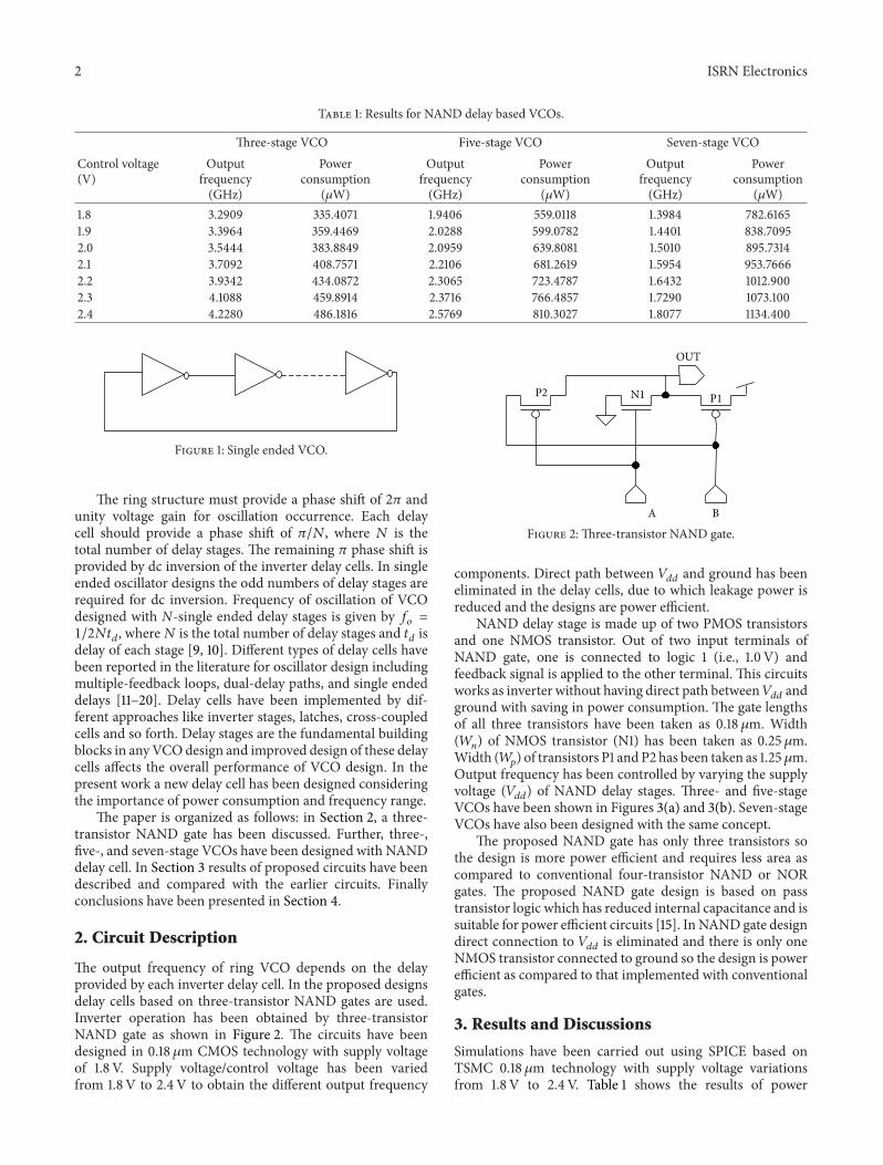
is the supply voltage. 𝐼scis the short circuit current, which flows directly from thepower supply to ground terminal when NMOS subnetworkand PMOS subnetwork conduct simultaneously. 𝐼sub is theleakage current which results from substrate injection andsubthreshold effects. The reverse biased p-n junction currentis the static dissipation due to reverse biased diode leakagebetween the diffusion regions, wells, and substrate. 𝐼gateleakageis the gate leakage current which arises from gate oxidewhich is mostly dependant on gate oxide thickness. Thefirst two components in (1) represent the dynamic powerconsumption and the remaining two components show staticpower consumption. In ring based oscillator design outputof last stage is fed back to input of first stage. A VCO blockdiagram with single ended N-delay inverter stages is shownin Figure 1.
2 ISRN Electronics
Table 1: Results for NAND delay based VCOs.
Control voltage(V)
Three-stage VCO Five-stage VCO Seven-stage VCOOutput
frequency(GHz)
Powerconsumption
(𝜇W)
Outputfrequency(GHz)
Powerconsumption
(𝜇W)
Outputfrequency(GHz)
Powerconsumption
(𝜇W)1.8 3.2909 335.4071 1.9406 559.0118 1.3984 782.61651.9 3.3964 359.4469 2.0288 599.0782 1.4401 838.70952.0 3.5444 383.8849 2.0959 639.8081 1.5010 895.73142.1 3.7092 408.7571 2.2106 681.2619 1.5954 953.76662.2 3.9342 434.0872 2.3065 723.4787 1.6432 1012.9002.3 4.1088 459.8914 2.3716 766.4857 1.7290 1073.1002.4 4.2280 486.1816 2.5769 810.3027 1.8077 1134.400
Figure 1: Single ended VCO.
The ring structure must provide a phase shift of 2𝜋 andunity voltage gain for oscillation occurrence. Each delaycell should provide a phase shift of 𝜋/𝑁, where 𝑁 is thetotal number of delay stages. The remaining 𝜋 phase shift isprovided by dc inversion of the inverter delay cells. In singleended oscillator designs the odd numbers of delay stages arerequired for dc inversion. Frequency of oscillation of VCOdesigned with N-single ended delay stages is given by 𝑓
𝑜=
1/2𝑁𝑡𝑑, where𝑁 is the total number of delay stages and 𝑡
𝑑is
delay of each stage [9, 10]. Different types of delay cells havebeen reported in the literature for oscillator design includingmultiple-feedback loops, dual-delay paths, and single endeddelays [11–20]. Delay cells have been implemented by dif-ferent approaches like inverter stages, latches, cross-coupledcells and so forth. Delay stages are the fundamental buildingblocks in anyVCOdesign and improved design of these delaycells affects the overall performance of VCO design. In thepresent work a new delay cell has been designed consideringthe importance of power consumption and frequency range.
The paper is organized as follows: in Section 2, a three-transistor NAND gate has been discussed. Further, three-,five-, and seven-stage VCOs have been designed with NANDdelay cell. In Section 3 results of proposed circuits have beendescribed and compared with the earlier circuits. Finallyconclusions have been presented in Section 4.
2. Circuit Description
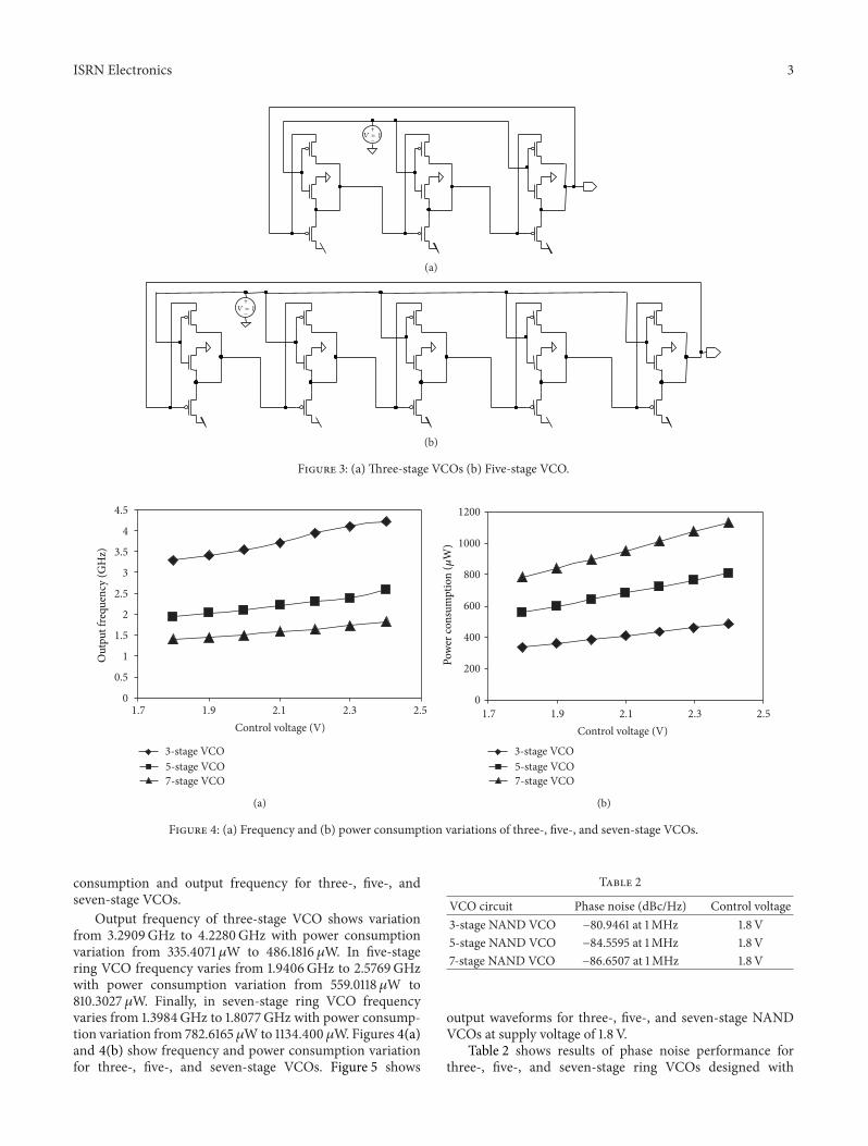
The output frequency of ring VCO depends on the delayprovided by each inverter delay cell. In the proposed designsdelay cells based on three-transistor NAND gates are used.Inverter operation has been obtained by three-transistorNAND gate as shown in Figure 2. The circuits have beendesigned in 0.18 𝜇m CMOS technology with supply voltageof 1.8 V. Supply voltage/control voltage has been variedfrom 1.8V to 2.4V to obtain the different output frequency
A B
P1
OUT
P2 N1
Figure 2: Three-transistor NAND gate.
components. Direct path between 𝑉𝑑𝑑
and ground has beeneliminated in the delay cells, due to which leakage power isreduced and the designs are power efficient.
NAND delay stage is made up of two PMOS transistorsand one NMOS transistor. Out of two input terminals ofNAND gate, one is connected to logic 1 (i.e., 1.0 V) andfeedback signal is applied to the other terminal. This circuitsworks as inverter without having direct path between𝑉
𝑑𝑑and
ground with saving in power consumption. The gate lengthsof all three transistors have been taken as 0.18 𝜇m. Width(𝑊𝑛) of NMOS transistor (N1) has been taken as 0.25 𝜇m.
Width (𝑊𝑝) of transistors P1 andP2 has been taken as 1.25𝜇m.
Output frequency has been controlled by varying the supplyvoltage (𝑉
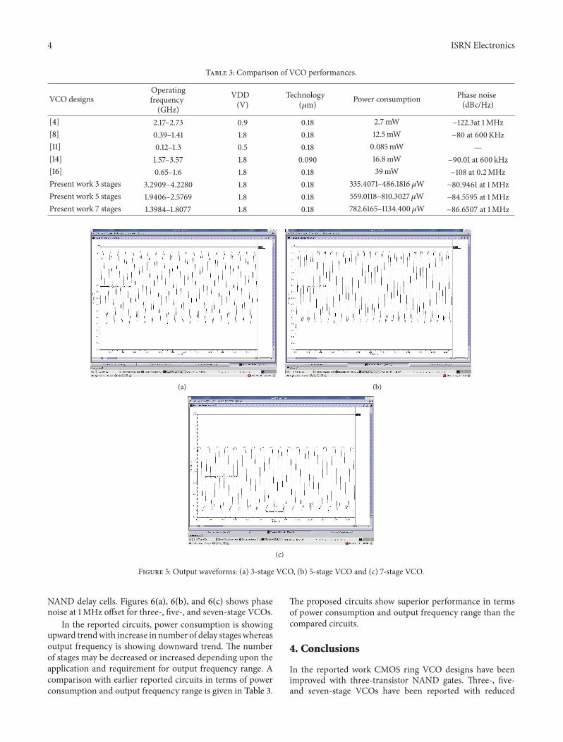
𝑑𝑑) of NAND delay stages. Three- and five-stage
VCOs have been shown in Figures 3(a) and 3(b). Seven-stageVCOs have also been designed with the same concept.
The proposed NAND gate has only three transistors sothe design is more power efficient and requires less area ascompared to conventional four-transistor NAND or NORgates. The proposed NAND gate design is based on passtransistor logic which has reduced internal capacitance and issuitable for power efficient circuits [15]. In NANDgate designdirect connection to 𝑉
𝑑𝑑is eliminated and there is only one
NMOS transistor connected to ground so the design is powerefficient as compared to that implemented with conventionalgates.
3. Results and Discussions
Simulations have been carried out using SPICE based onTSMC 0.18 𝜇m technology with supply voltage variationsfrom 1.8V to 2.4V. Table 1 shows the results of power
ISRN Electronics 3
𝑉 = 1+
−
(a)
𝑉 = 1+
−
(b)
Figure 3: (a) Three-stage VCOs (b) Five-stage VCO.
02.3 2.5
4.5
4
3.5
3
2.5
2
1.5
1
0.5
2.11.91.7Control voltage (V)
3-stage VCO5-stage VCO7-stage VCO
Out
put f
requ
ency
(GH
z)
(a)
0
200
400
600
800
1000
1200
2.3 2.52.11.91.7Control voltage (V)
3-stage VCO5-stage VCO7-stage VCO
Pow
er co
nsum
ptio
n (𝜇
W)
(b)
Figure 4: (a) Frequency and (b) power consumption variations of three-, five-, and seven-stage VCOs.
consumption and output frequency for three-, five-, andseven-stage VCOs.
Output frequency of three-stage VCO shows variationfrom 3.2909GHz to 4.2280GHz with power consumptionvariation from 335.4071 𝜇W to 486.1816 𝜇W. In five-stagering VCO frequency varies from 1.9406GHz to 2.5769GHzwith power consumption variation from 559.0118𝜇W to810.3027 𝜇W. Finally, in seven-stage ring VCO frequencyvaries from 1.3984GHz to 1.8077GHz with power consump-tion variation from 782.6165 𝜇Wto 1134.400 𝜇W. Figures 4(a)and 4(b) show frequency and power consumption variationfor three-, five-, and seven-stage VCOs. Figure 5 shows
Table 2
VCO circuit Phase noise (dBc/Hz) Control voltage3-stage NAND VCO −80.9461 at 1MHz 1.8 V5-stage NAND VCO −84.5595 at 1MHz 1.8 V7-stage NAND VCO −86.6507 at 1MHz 1.8 V
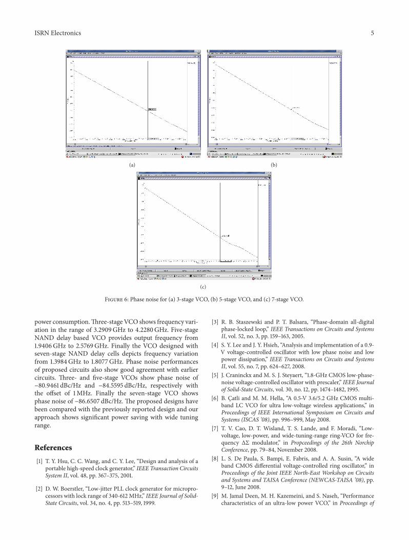
output waveforms for three-, five-, and seven-stage NANDVCOs at supply voltage of 1.8 V.
Table 2 shows results of phase noise performance forthree-, five-, and seven-stage ring VCOs designed with
4 ISRN Electronics
Table 3: Comparison of VCO performances.
VCO designsOperatingfrequency(GHz)
VDD(V)
Technology(𝜇m) Power consumption Phase noise
(dBc/Hz)
[4] 2.17–2.73 0.9 0.18 2.7mW −122.3at 1MHz[8] 0.39–1.41 1.8 0.18 12.5mW −80 at 600KHz[11] 0.12–1.3 0.5 0.18 0.085mW —[14] 1.57–3.57 1.8 0.090 16.8mW −90.01 at 600 kHz[16] 0.65–1.6 1.8 0.18 39mW −108 at 0.2MHzPresent work 3 stages 3.2909–4.2280 1.8 0.18 335.4071–486.1816 𝜇W −80.9461 at 1MHzPresent work 5 stages 1.9406–2.5769 1.8 0.18 559.0118–810.3027 𝜇W −84.5595 at 1MHzPresent work 7 stages 1.3984–1.8077 1.8 0.18 782.6165–1134.400 𝜇W −86.6507 at 1MHz
(a) (b)
(c)
Figure 5: Output waveforms: (a) 3-stage VCO, (b) 5-stage VCO and (c) 7-stage VCO.
NAND delay cells. Figures 6(a), 6(b), and 6(c) shows phasenoise at 1MHz offset for three-, five-, and seven-stage VCOs.
In the reported circuits, power consumption is showingupward trendwith increase in number of delay stageswhereasoutput frequency is showing downward trend. The numberof stages may be decreased or increased depending upon theapplication and requirement for output frequency range. Acomparison with earlier reported circuits in terms of powerconsumption and output frequency range is given in Table 3.
The proposed circuits show superior performance in termsof power consumption and output frequency range than thecompared circuits.
4. Conclusions
In the reported work CMOS ring VCO designs have beenimproved with three-transistor NAND gates. Three-, five-and seven-stage VCOs have been reported with reduced
ISRN Electronics 5
(a) (b)
(c)
Figure 6: Phase noise for (a) 3-stage VCO, (b) 5-stage VCO, and (c) 7-stage VCO.
power consumption.Three-stage VCO shows frequency vari-ation in the range of 3.2909GHz to 4.2280GHz. Five-stageNAND delay based VCO provides output frequency from1.9406GHz to 2.5769GHz. Finally the VCO designed withseven-stage NAND delay cells depicts frequency variationfrom 1.3984GHz to 1.8077GHz. Phase noise performancesof proposed circuits also show good agreement with earliercircuits. Three- and five-stage VCOs show phase noise of−80.9461 dBc/Hz and −84.5595 dBc/Hz, respectively withthe offset of 1MHz. Finally the seven-stage VCO showsphase noise of −86.6507 dBc/Hz. The proposed designs havebeen compared with the previously reported design and ourapproach shows significant power saving with wide tuningrange.
References
[1] T. Y. Hsu, C. C. Wang, and C. Y. Lee, “Design and analysis of aportable high-speed clock generator,” IEEE Transaction CircuitsSystem II, vol. 48, pp. 367–375, 2001.
[2] D. W. Boerstler, “Low-jitter PLL clock generator for micropro-cessors with lock range of 340-612 MHz,” IEEE Journal of Solid-State Circuits, vol. 34, no. 4, pp. 513–519, 1999.
[3] R. B. Staszewski and P. T. Balsara, “Phase-domain all-digitalphase-locked loop,” IEEE Transactions on Circuits and SystemsII, vol. 52, no. 3, pp. 159–163, 2005.
[4] S. Y. Lee and J. Y. Hsieh, “Analysis and implementation of a 0.9-V voltage-controlled oscillator with low phase noise and lowpower dissipation,” IEEE Transactions on Circuits and SystemsII, vol. 55, no. 7, pp. 624–627, 2008.
[5] J. Craninckx and M. S. J. Steyaert, “1.8-GHz CMOS low-phase-noise voltage-controlled oscillator with prescaler,” IEEE Journalof Solid-State Circuits, vol. 30, no. 12, pp. 1474–1482, 1995.
[6] B. Catli and M. M. Hella, “A 0.5-V 3.6/5.2 GHz CMOS multi-band LC VCO for ultra low-voltage wireless applications,” inProceedings of IEEE International Symposium on Circuits andSystems (ISCAS ’08), pp. 996–999, May 2008.
[7] T. V. Cao, D. T. Wisland, T. S. Lande, and F. Moradi, “Low-voltage, low-power, and wide-tuning-range ring-VCO for fre-quency ΔΣ modulator,” in Propceedings of the 26th NorchipConference, pp. 79–84, November 2008.
[8] L. S. De Paula, S. Bampi, E. Fabris, and A. A. Susin, “A wideband CMOS differential voltage-controlled ring oscillator,” inProceedings of the Joint IEEE North-East Workshop on Circuitsand Systems and TAISA Conference (NEWCAS-TAISA ’08), pp.9–12, June 2008.
[9] M. Jamal Deen, M. H. Kazemeini, and S. Naseh, “Performancecharacteristics of an ultra-low power VCO,” in Proceedings of

6 ISRN Electronics
IEEE International Symposium on Circuits and Systems, pp. 697–700, May 2003.
[10] A. Hajimiri, S. Limotyrakis, and T. H. Lee, “Jitter and phasenoise in ring oscillators,” IEEE Journal of Solid-State Circuits,vol. 34, no. 6, pp. 790–804, 1999.
[11] T. Li, B. Ye, and J. Jiang, “0.5V 1.3 GHz voltage controlledring oscillator,” in Proceedings of the 8th IEEE InternationalConference on ASIC (ASICON ’09), pp. 1181–1184, October 2009.
[12] S. K. Enam and A. A. Abidi, “300-MHz CMOS voltage-controlled ring oscillator,” IEEE Journal of Solid-State Circuits,vol. 25, no. 1, pp. 312–315, 1990.
[13] B. Fahs, W. Y. Ali-Ahmad, and P. Gamand, “A two-stage ringoscillator in 0.13-𝜇m CMOS for UWB impulse radio,” IEEETransactions on Microwave Theory and Techniques, vol. 57, no.5, pp. 1074–1082, 2009.
[14] J. K. Panigrahi and D. P. Acharya, “Performance analysis anddesign of wideband CMOS voltage controlled ring oscillator,” inProceedings of IEEE International Conference on Industrial andInformation Systems, pp. 234–238, August2010.
[15] H. Q. Liu, W. L. Goh, and L. Siek, “A 0.18-𝜇m 10-GHz CMOSring oscillator for optical transceivers,” in Proceedings of IEEEInternational Symposium on Circuits and Systems (ISCAS ’05),pp. 1525–1528, May 2005.
[16] S. -Y. L. Amakawa, S. Ishihara, andN.MasuK, “Lowphase noisewide frequency range ring VCO based scalable PLL with subharmonic injection locking in 0.18 𝜇mCMOS,” in Proceedings ofIEEE International Microwave Symposium Digest, pp. 1178–1181,May 2010.
[17] C. H. Park and B. Kim, “A low-noise, 900-MHz VCO in 0.6-𝜇mCMOS,” IEEE Journal of Solid-State Circuits, vol. 34, no. 5, pp.586–591, 1999.
[18] Y. A. Eken and J. P. Uyemura, “A 5.9-GHz voltage-controlledring oscillator in 0.18-𝜇m CMOS,” IEEE Journal of Solid-StateCircuits, vol. 39, no. 1, pp. 230–233, 2004.
[19] H. R. Kim, C. Y. Cha, S. M. Oh, M. S. Yang, and S. G. Lee,“A very low-power quadrature VCO with back-gate coupling,”IEEE Journal of Solid-State Circuits, vol. 39, no. 6, pp. 952–955,2004.
[20] M. Kumar, S. K. Arya, and S. Pandey, “Digitally controlledoscillator design with variable capacitance XOR gate,” Journalof Semiconductor, vol. 32, no. 10, pp. 105001–105007, 2011.

Submit your manuscripts athttp://www.hindawi.com
VLSI Design
Hindawi Publishing Corporationhttp://www.hindawi.com Volume 2014
International Journal of
RotatingMachinery
Hindawi Publishing Corporationhttp://www.hindawi.com Volume 2014
Hindawi Publishing Corporation http://www.hindawi.com
Journal ofEngineeringVolume 2014
Hindawi Publishing Corporationhttp://www.hindawi.com Volume 2014
Shock and Vibration
Hindawi Publishing Corporationhttp://www.hindawi.com Volume 2014
Mechanical Engineering
Advances in
Hindawi Publishing Corporationhttp://www.hindawi.com Volume 2014
Civil EngineeringAdvances in
Acoustics and VibrationAdvances in
Hindawi Publishing Corporationhttp://www.hindawi.com Volume 2014
Hindawi Publishing Corporationhttp://www.hindawi.com Volume 2014
Electrical and Computer Engineering
Journal of
Hindawi Publishing Corporationhttp://www.hindawi.com Volume 2014
Distributed Sensor Networks
International Journal of
The Scientific World JournalHindawi Publishing Corporation http://www.hindawi.com Volume 2014
SensorsJournal of
Hindawi Publishing Corporationhttp://www.hindawi.com Volume 2014
Modelling & Simulation in EngineeringHindawi Publishing Corporation http://www.hindawi.com Volume 2014
Hindawi Publishing Corporationhttp://www.hindawi.com Volume 2014
Active and Passive Electronic Components
Hindawi Publishing Corporationhttp://www.hindawi.com Volume 2014
Chemical EngineeringInternational Journal of
Control Scienceand Engineering
Journal of
Hindawi Publishing Corporationhttp://www.hindawi.com Volume 2014
Antennas andPropagation
International Journal of
Hindawi Publishing Corporationhttp://www.hindawi.com Volume 2014
Hindawi Publishing Corporationhttp://www.hindawi.com Volume 2014
Navigation and Observation
International Journal of
Advances inOptoElectronics
Hindawi Publishing Corporation http://www.hindawi.com
Volume 2014
RoboticsJournal of
Hindawi Publishing Corporationhttp://www.hindawi.com Volume 2014