research on design points of semiconductor lighting driven pcb
TRANSCRIPT
Research on Design Points of Semiconductor Lighting Driven PCB
Wenjie Zhang1,a*, Jinfeng Li1,b and Renbo Xu1,2,c 1Nanchang Institute of Science and Technology, Nanchang, 330108, China
2Physics and Microelectronics Institute, Central South University, Changsha 410083 china.
[email protected], [email protected], [email protected] *The Corresponding author
Keywords: Semiconductor lighting; Printed circuit board; Design; Optoelectronic hole machine
Abstract. In this paper, the design points of a kind of semiconductor lighting driven PCB are studied. With the development of semiconductor technology, the market demand of PCB has been
improved rapidly. The processing quality of PCB is constantly upgrading, and its online detection accuracy and speed requirements are also improving. Improving the passing rate of products has
become an important means to enhance the market competitiveness of enterprises. Because foreign PCB products are expensive, China's PCB high-end detection products are few, so the quality of
PCB products in China is limited. PCB photoelectric inspection machine is a highly intelligent PCB drilling automatic testing equipment. The equipment provides two standard information making
methods; it can automatically report a variety of defects in the PCB drilling; it has high detection precision and very fast processing speed. It can make a comprehensive test for each PCB hole out of
the factory. Based on the principle of modularity, low cost and high performance, the design and implementation of the PCB photoelectric inspection machine system are carried out in this paper.
Main Features of Printed Circuit Boards Driven by Semiconductor Lighting
The semiconductor lighting driven printed circuit board (PCB) is processed into a certain size with
an insulating board as the substrate. There are conductive graphics and all designed holes on which the electrical interconnection between components can be realized. In electronic equipment, the
main function of the semiconductor lighting driver PCB is: as the support of the components and devices in the circuit, the circuit connection between the circuit elements and the devices is
provided, and the components and devices installed on the circuit board are clearly marked out through the marking symbols, and the devices and devices are inserted and maintained at a glance
and test. The advantage of using semiconductor lighting to drive PCB is that the consistency and reproducibility of the product are good, and the errors in wiring and assembly can be greatly
reduced. The lines of the same shape are formed according to the original design manuscripts. In stable production conditions, the precision of the configuration of the components, the evaporation
technique of the film and the processing technology of the semiconductor can be realized. Chemical production, improve product yield, and easy to achieve automatic production, greatly reducing the
cost of electronic equipment production. When electronic equipment is assembled, it is beneficial to realize mechanization and automation production, significantly save assembly and repair work
hours, improve production efficiency, and have small size. It is easy to realize the miniaturization, light quantification and thinning of electronic equipment and products, easy to use and carry, so that
the design standardization and unit combination of electronic design are realized. The printing methods used in mass production of PCB with semiconductor lighting are printing,
flexo, intaglio and so on. The most commonly used is screen printing. It has the advantages of good quality, low production cost and less investment in equipment. With the development of printing
and printing technology, the new type of mesh printing materials, technology and testing equipment used in the PCB industry of semiconductor lighting drive have become more and more perfect, so
that the current printing technology can adapt to high density semiconductor lighting to drive PCB production. In recent years, with the appearance of automatic screen printing machine with the
function of image recognition and the perfection of high precision screen plate making technology,
Copyright © 2018, the Authors. Published by Atlantis Press. This is an open access article under the CC BY-NC license (http://creativecommons.org/licenses/by-nc/4.0/).
328
8th International Conference on Mechatronics, Computer and Education Informationization (MCEI 2018)Advances in Computer Science Research (ACSR), volume 83

the technology of printing and printing can not only print high precision products, but also have
high degree of automation, which is very good for mass production, and it is well received by people. Screen printing semiconductor lighting driven PCB is mainly printed conductive parts,
resist, electroplating, insulating medium, adhesives and so on.
Semiconductor Lighting Drives Common Defects in PCB Drilling
Semiconductor lighting drive PCB drilling defects include Kong Du, Kong Shao, Kong Da, Kong Xiao, Kong Pian and foreign objects in the hole. Because the processing technology of
semiconductor lighting driven PCB is very complex, it takes hundreds of processes to produce a semiconductor lighting driver PCB, so the cause of defect is more complicated. Generally, the two
cases of many holes and few holes are relatively rare. For most defects, they are hole deviation, foreign matter in the hole, big hole and small hole. The main reason for Kong Pian's formation is
the need for electroplating on bare boards and the metallization of multilayer plates, which leads to the thickness of metal precipitation which does not meet the requirements. Fig. 1 is a diagram of
metal plating thickness, in which d1 is the aperture of the PCB bare plate driven by semiconductor lighting, and the size of the d2 is the size of the electroplated metal. If the thickness of the metal is
not uniform in the inner wall of the inner wall, the defect of the foreign body in the hole will be caused.
Figure 1. Schematic diagram of electroplating thickness
Among it, D1 is the diameter of the weld plate, h1 is the thickness of printed circuit board, h2 is
copper foil thickness. The cause of the foreign body in the hole is that there is no polishing on the edge of the hole.
This situation is more common on the bare plate without green oil and electroplating. Some are due to the uneven plating in the process of multi-layer electroplating, or the problems of the adhesive
force of the copper plating. The error types of Kong Da and Kong Xiao are mostly due to the wrong selection of the drill knife, the defect of the drill knife and the depth of the knife's lower knife. In
addition, when the metal is electroplated, the thickness of the electroplating is too thick or too thin. Due to the defect on the edge of the drill bit, the semiconductor drilling and driving PCB drilling is
also prone to produce defects. Nowadays, a variety of new type of semiconductor lighting drives PCB plates constantly, and their physical and chemical properties are not the same or even different.
This requires that the semiconductor lighting driver PCB micro drill manufacturers have to launch the new products in time.
In short, according to the defect mechanism of PCB hole driven by semiconductor lighting, there are material defects and process defects. Most defects are defects in processing technology. Because
the processing completed a semiconductor lighting drive PCB needs hundreds of processes, the defects of the main holes of the bare plate are manifested in the "burr" on the edge of the hole, even
with the hole plug phenomenon. The solution is the polishing process of the bare plate and the clean production of the semiconductor lighting driven by the PCB; the hole metallization process is a
semiconductor illumination. The most critical process in the manufacturing process of PCB is
329
Advances in Computer Science Research (ACSR), volume 83
driven by the Ming, and the defects in the PCB drilling driven by the finished semiconductor
lighting are mainly manifested in the uneven thickness of the coating.
Research and Application Status of PCB Hole Defect Detection Technology Driven by
Semiconductor Lighting
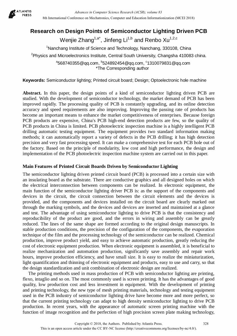
Process and Process of Processing Technology. The whole process of PCB processing by
semiconductor lighting includes many processes. The processing technology is very complicated. From process review to production to final inspection, the monitoring and control of process quality
and production quality must be taken into account. Scientific and reasonable steps must be followed in the processing. First, process review and preparation; Second, numerical control drilling,
numerical control drilling is based on the data provided by the computer in accordance with the human provisions to drill, in the process of drilling, must be strictly according to the process
requirements, drilling holes must be checked to ensure the quality of the products processed. Third, hole metallization process, hole metallization process is the most important process in the
manufacturing of semiconductor lighting driven PCB. Fourth, electroplating thickness control, tin lead alloy is electroplating corrosion resistance metal, must strictly control the coating thickness, in
order to ensure the etching process can effectively protect the matrix metal; Fifth, the quality of tin lead alloy coating is eliminated, and the quality of tin tin alloy plating is absolutely high and low.
Sixth, the technology of screen printing resistance flux, the main purpose of screen printing resistance flux is to avoid the disordered flow of welding solder and cause the "bridge" of two wires,
and to ensure the quality of electrical loading. Seventh, screen printing process, the main purpose of the screen printing process is to make the two sides of the whole plate evenly coated with a layer of
liquid photosensitive resistance welding agent, through the exposure, development and other processes to become a high reliability and permanent protection layer on the substrate surface;
Eighth, the hot air leveling process, the main purpose of the hot air leveling process is to make the semiconductor lighting drive the PCB surface weld plate and the required solder in the hole, and
provide reliable welding performance; Ninth, the main purpose of thickening copper plating and thickening copper plating is to ensure that there is enough thick copper plating in the hole to ensure
that the resistance value is within the range of process requirements. As a fixed position and to ensure the strength of the connection, as a device for surface encapsulation, some holes only act as a
conducting hole and play the role of two sides; Tenth, mechanical processing and mechanical processing are the last working procedure of semiconductor lighting driven PCB manufacturing.
When machining, we should pay special attention to ensure the surface quality of substrates. Fig. 2 is a block diagram of PCB process for semiconductor lighting.
Figure 2. Block diagram of semiconductor lighting driven PCB process
330
Advances in Computer Science Research (ACSR), volume 83

The Main Problems to be Solved in Defect Detection. As a product development to market, it
is necessary to ensure the stability of the inspection, the real-time detection, and the strong competitiveness of various technical indicators and similar products in the market. Semiconductor
lighting driven PCB photoelectric inspection machine needs to solve some key problems.
System Technical Index
The semiconductor lighting driver PCB photoelectric hole machine is a product to the market. Its technical specifications refer to the latest generation of PCB aperture number testing machine
driven by the Japan World Federation Electronics Co., Ltd. and the Taiwan Asia Asia technology company, which can not be lower than the latest products of the same kind. Table 1 is the basic
technical index of PCB photoelectric inspection machine driven by semiconductor lighting. Table 1 Basic technical index of PCB photoelectric inspection machine driven by semiconductor
lighting
Measurable PCB size 80x150-600x600(mm2)
Measurable PCB thickness 0.01-10mm
Measurable aperture range 0.15-20mm
Maximum number of detection holes 600,000
Detection speed 1,2,3,5,7,10m/min
check the accuracy 20μm
Repetition precision 20μm
Maximum allowable deflection angle ±30℃
Funded projects: Science and technology research project of Jiangxi Provincial Department of education in 2016. Project name: Application and research of dynamic reconfiguration in
multiprocessor embedded system. Project number: GJJ161225.
Summary
The production process must pass through many processes such as fillin output, net plate making and so on, and the process is more complex. For semiconductor lighting drive PCB amateur
production and small batch production, it seems cumbersome, equipment and production costs are too high to carry out. Therefore, it is necessary to make another shortcut to find the simple and
convenient production process and low cost. Of course, the production method of the semiconductor lighting driver PCB will be reduced accordingly. According to practical experience,
making use of heat transfer to produce semiconductor lighting drive PCB is the best choice for amateur production of electronic enthusiasts or small batch production of semiconductor lighting. It
is not only easy to make, but also convenient to take material, low price, no need to output Phil and make net plate, and do not have to expose the sun sun plate, etc. The printed circuit board will be
printed on the thermal transfer paper, and the semiconductor lighting driver PCB can be made.
Acknowledgements
Project supported: Nanchang Key Laboratory of Applied Research of DME Optoelectronic Engineering (Nanchang Institute of Technology), No. NCZDSY—004.
Reference
[1] F. Wu, X. M. Zhang, Y. Kuan, et al. An AOI algorithm for PCB based on feature extraction.
Proceedings of the 7th World Congress on intelligent and automation, Chongqing, China, 2008,
7: 25-27.
331
Advances in Computer Science Research (ACSR), volume 83

[2] H. H. Loh, M. S. Lu. Printed circuit board inspection using image analysis. IEEE Trans. on
Industry Applications,2009,35(2): 426-432.
[3] M. Moganti, F. Ercal, C. H. Dagli. Automatic PCB inspection algorithms. Computer Vision
and Image Understanding, 2016, 63(2): 287-313.
[4] F. C. Tien, C. H. Yeh, K. H. Hiesh. Automated visual inspection for microdrills in printed
circuit board production. International Journal of Production Research, 2014, 42(12):
2477-2495.
[5] A. Kusiak, C.Kurasek. Data mining of printed-circuit board defects. IEEE Transactions on
Robotics and Automation, 2011, 17(2):191-196.
[6] S. Oprea, I. Lita, I. B. Cioc. Determination of misplaced drill holes on a PCB. 30th
International Spring Seminar on Electronics Technology, 2007, 7: 406-409.
[7] C. J. Chen, S. H. Lai, S. W. Liu, et al. Optical PCB inspection system based on Hausdorff
distance. Machine Vision Applications in Industrial Inspection. 2015, 5679: 53-61.
[8] N. Talbot. The use of automated optical testing (AOT) in statistical process control (SPC) for
printed circuit board (PCB) production. Circuit World, 2003, 29(4): 19-22.
[9] D. Craig. The Maturing PCB Industry. Printed Circuit Design and Manufacture,
2015,22(1):17-21.
[10] M. Gallant. Guide to Rigid-flex Design. Printed Circuit Design and Manufacture,
2016,23(10):30-33.
332
Advances in Computer Science Research (ACSR), volume 83