research.utwente.nl · the research described in this thesis was performed with the inorganic...
TRANSCRIPT

TEMPLATE-ELECTRODEPOSITED NANOWIRES: SYNTHESIS, MANIPULATION AND APPLICATION

Ph. D. committee Dean Prof. dr. G van der Steenhoven (University of Twente) Chairman and secretary
Prof. dr. ir. H.J.W. Zandvliet (University of Twente) Supervisor Prof. dr. ing. D.H.A. Blank (University of Twente) Assistant supervisor Dr. ir. J.E. ten Elshof (University of Twente) Referent Dr. A. Hovestad (TNO Science & Industry) Members: Prof. dr. S.J.G. Lemay (University of Twente) Prof. dr. G. Mul (University of Twente) Prof. dr. M. Steinhart (University of Osnabrück) Cover: Scanning electron microscope image of a folded golden foil with protruding template-electrodeposited nickel nanowires. The template was removed before imaging. The research described in this thesis was performed with the Inorganic Materials Science (IMS) group and the MESA+ Institute for Nanotechnology at the university of Twente, the Netherlands, as a part of the Nanofluidics flagship (TSF.7137) of the Dutch NanoNed national nanotechnology R&D initiative. This research was supported by NanoNed, a national nanotechnology program coordinated by the Dutch Ministry of Economic Affairs M.G. Maas Template-electrodeposited nanowires: synthesis, manipulation and application Ph. D. Thesis University of Twente, Enschede, The Netherlands ISBN: 978-90-8570-703-5 Printed by Wöhrmann Print Service, Zutphen, The Netherlands Copyright © M.G. Maas, 2010

TEMPLATE-ELECTRODEPOSITED NANOWIRES: SYNTHESIS, MANIPULATION AND APPLICATION
PROEFSCHRIFT
ter verkrijging van de graad van doctor aan de Universiteit Twente,
op gezag van de rector magnificus, prof. dr. H. Brinksma,
volgens besluit van het College voor Promoties in het openbaar te verdedigen
op woensdag 15 december 2010 om 16:45 uur
door
Michiel Gerard Maas
geboren op 27 juni 1981 te Enschede

Dit proefschrift is goedgekeurd door de promotor Prof. dr. ing. D.H.A. Blank
en de assistent-promotor
Dr. ir. J.E. ten Elshof

-Wie nimmer dwaalt, wordt nooit verstandig-


TABLE OF CONTENTS Page CHAPTER 1 Motivation & Outline 1.1 Motivation 1 1.2 Outline 2 1.3 References 4 CHAPTER 2 General theory 2.1 Introduction 2.1.1 A brief History 5 2.1.2 Definition of electrodes 6 2.2 Equilibrium 2.2.1 The electrode 7 2.2.2 The electrode-electrolyte interface 8 2.3 Deposition 2.3.1 Current at high overpotential 10 2.3.2 Determination of optimal overpotential 11 2.4 References 13 CHAPTER 3 Experimental details 3.1 Introduction 14 3.2 Electrodeposition preparations 3.2.1 The Polycarbonate Track-Etched (PCTE) Membrane 14 3.2.2 Preparation of the PCTE membrane 16 3.2.3 Electrodeposition 18 3.3 Dielectrophoresis preparations 3.3.1 Photolithography mask design 20 3.4 References 24

CHAPTER 4 Template electrodeposited zinc oxide nanowires and template directed electrochemically induced iron(III) hydroxide gel formation: A comparative growth study 4.1 Introduction 25 4.2 Theoretical Background 4.2.1 Chemistry 27 4.2.2 Growth and sol-gel 27 4.3 Experimental 30 4.4 Results and Discussion 4.4.1 Zinc oxide nanowire growth 31 4.4.2 Electrochemically induced iron(III) hydroxide sol-gel formation and Fe2O3 nanotube formation 38 4.5 Conclusions 42 4.6 References 44 CHAPTER 5 Dielectrophoresis of electrochemically synthesized nanowires: A universal set of parameters for the alignment of various types of nanowire materials 5.1 Introduction 46 5.2 Theoretical Background 47 5.2.1 The Clausius-Mosotti factor 48 5.2.2 Electro-osmotic flow 49 5.2.3 Electric field distribution 50 5.3 Experimental 5.3.1 Nanowire synthesis 51 5.3.2 Substrate treatment and alignment procedure 52 5.3.3 Analyses 53 5.4 Results and Discussion 5.4.1 Dielectrophoretic force and electro-osmotic flow 54 5.4.2 Electric field distribution 55 5.4.3 Aligning nanowires 58 5.5 Conclusions 60 5.6 References 61

CHAPTER 6 Hydrogen evolution by photocatalytic Silver/Zinc Oxide segmented nanowires from a Water/Methanol mixture under the influence of UV-radiation 6.1 Introduction 64 6.2 Theoretical Background 6.2.1 General principles 66 6.2.2 Band structure of Ag/ZnO segmented nanowires 68 6.2.3 Chemistry at the Ag/ZnO segmented nanowire surface 69 6.3 Experimental 6.3.1 Segmented nanowire synthesis and isolation 70 6.3.2 Segmented nanowire analyses 70 6.3.3 Hydrogen evolution and detection 71 6.4 Results and Discussion 72 6.5 Conclusions 78 6.6 References 79 CHAPTER 7 Templated electrochemical deposition of argentic oxysalt Ag7NO11 7.1 Introduction 83 7.2 Theoretical Background 84 7.3 Experimental 85 7.4 Results and Discussion 85 7.5 Conclusions 88 7.6 References 89 CHAPTER 8 General Conclusions and Outlook 8.1 General conclusions 90 8.2 Outlook 92 SUMMARY 94 SAMENVATTING 96 DANKWOORD 98


1
Chapter 1
Motivation & Outline 1.1 MOTIVATION Nanotechnology is not a single industry but could be considered as a scale of engineering between 1 and 100 nm. Instead of one new phenomenon, it offers new possibilities for thousands of materials that already exist. Familiar materials, from gold to soot, behave very differently at the nanometer scale and display useful new properties. Some nanoparticles transmit light or electricity, others turn into potent chemical catalysts. Because nanotechnology is a scale of engineering, it often brings together different areas of science and benefits from an interdisciplinary or ‘converging’ approach. Expectations of nanotechnological innovations are high in many areas [1]: medical applications; information technologies; energy production and storage; materials science; manufacturing (‘top-down’ and ‘bottom-up’); instrumentation; food, water and environment, and security. On the other hand, it is difficult to estimate a timescale when potential nanotechnological products and applications will be realized in these areas. Moreover, these products and applications will not be developed unless there is a market for them [2,3]; nanotechnologies will not be incorporated into products and devices without the development of scalable, cost-effective manufacturing techniques that retain and preserve the properties of the nanoscalar material in the final product [2,4,5]. The market-driven preconditions mentioned above seem to set a narrow window of opportunity for nanotechnological products. Nonetheless, nanowires and nanotubes can meet those demands with ease. Recent advances show a wide variety of possible (functional) sensors [6-8] for the medical, environmental, and security markets. Because the nanowires and nanotubes are the actual building blocks used to construct these sensors, the properties of the nanoscalar material are retained by default. Regarding a cost-effective manufacturing technique, nanowires and nanotubes can easily be synthesized by templated electrodeposition, which has been noted for its scalability and cost-effectiveness since its introduction in 1994 [9]. However, at an industrial level, control over, for example, nanowire or nanotube size distribution, crystallinity and functionality are paramount. To guarantee knowledge transfer from the lab to industry, a precise and reliable post-assembly process of nanowires and nanotubes in sensors is necessary [6]. Here, it is demonstrated that

2
these demands can be met with even a minimum of capital investment: growth processes of nanowires and nanotubes during templated electrodeposition can be monitored to asses crystallinity and quality; dielectrophoresis with uniform parameters can be used for a precise alignment of nanowires and nanotubes of different materials on macroscale electrodes. Besides the development of a cost-effective generally applicable post-assembly process combined with templated electrodeposition, a direct application of nanowires or nanotubes combined with templated electrodeposition would truly indicate the high market potential. To illustrate this potential, the functionality of nanowires has been engineered to demonstrate hydrogen evolution by nanowires under UV-irradiation. This offers a unique opportunity to put nanotechnological progress not only in an economical perspective, but in a social perspective as well. It can add to the ongoing discussion about sustainable energy sources and nanotechnology [10]. 1.2 OUTLINE The scope of this thesis is threefold. At the heart of this thesis is understanding of the synthesis of (exotic) oxide nanowires and nanotubes by templated electrodeposition. To show that these synthesized nanowires or nanotubes can be integrated in micro- and macro circuitry, the insertion of these wires and tubes was manipulated by dielectrophoresis. Finally, a direct application of nanowires is demonstrated by giving a proof-of-principle of hydrogen evolution by segmented nanowires. The experimental chapters concerning synthesis, manipulation and application of nanowires and nanotubes were written in such way to enable the reader to read them in no particular order. This thesis is comprised out of eight chapters: Chapter 2 is a short treatment of the general theory of electrochemistry. A three-electrode set-up is defined and factors influencing the set-up in a practical sense are discussed. The origin of a potential at an electrode/electrolyte interface and the resulting double layer is discussed. Lastly, the determination of an optimal overpotential is touched; Chapter 3 discusses the experimental operations before an electrodeposition and can be considered as a so-called tips & tricks chapter; Chapter 4 treats the growth of zinc oxide nanowires and the formation of a iron(III) hydroxide sol-gel which dries inside the polycarbonate membrane pores resulting in nanotubes. Both processes are characterized by logging the current response in time and are explained by a growth and diffusion model; Chapter 5 is about the manipulation of nanowires and nanotubes by dielectrophoresis. On the basis of theory, a universal set of dielectrophoresis-parameters is made which can be applied to a variety of materials. This set of parameters is illustrated by oxide

3
nanowires which are aligned on parallel electrodes and characterized by their electrical responses; Chapter 6 gives the proof-of-principle of a direct application of nanowires, namely hydrogen evolution under the influence of ultraviolet radiation. The wires are composed out of a metallic silver segment and a zinc oxide segment. At the interface a space-charge layer, i.e. an accumulation of electrons at a finite length scale, is present and characterized by an electrical rectifying behavior. The functioning at the macroscale is demonstrated by measuring a rise in hydrogen concentration in time during ultraviolet radiation. Chapter 7 is an example of the versatility of templated electrodeposition. It shows the first successful attempt of producing nanowires of the silver oxysalt Ag7NO11. Because the material is silver based, it has antifungal and antibacterial properties. Also, the instability of the material in air and moisture is prevented by coating it by a galvanic replacement reaction with gold. Chapter 8 will summarize the conclusions of the previous chapters and gives an outlook of the possibilities of nanowires, nanotubes and templated electrodeposition.

4
1.3 REFERENCES [1] Communication from the European Commission, ‘Towards a European strategy for nanotechnology’, © European Communities 2004, ISBN 92-894-7686-9. [2] The Royal Society & The Royal Academy of Engineering, ‘Nanoscience and nanotechnologies: opportunities and uncertainties’, © The Royal Society 2004, ISBN 0-85403-604-0. [3] A. Hullmann, ‘Measuring and assessing the development of nanotechnology’, Scientometrics 70 (3), 739 (2007). [4] B. Bozemann, J. Hardin, A.N. Link, ‘Barriers to the diffusion of nanotechnology’, Economics of Innovation and new Technology 17 (7), 749 (2008). [5] O. Vaughan, ‘A golden opportunity’, Nat. Nanotechnol. 5, 5 (2010). [6] S. Barth, F. Hernandez-Ramirez, J.D. Holmes, A. Romano-Rodriguez, ‘Synthesis and applications of one-dimensional semiconductors’, Prog. Mater. Sci. 55, 563 (2010). [7] K.J. Choi, H.W. Jang, ‘One-dimensional oxide nanostructures as gas-sensing materials: review and issues’, Sensors 10, 4083 (2010). [8] E. Comini, G. Sberveglieri, ‘Metal oxide nanowires as chemical sensors’, Mater. Today 13 (7-8), 36 (2010). [9] C.R. Martin, ‘Nanomaterials: A membrane-based synthetic approach’, Science 266, 1961 (1994). [10] E. Serrano, G. Rus, J. García-Martínez, ‘Nanotechnology for sustainable energy’, Renew. Sust. Energ. Rev. 13, 2373 (2009).

5
Chapter 2
General theory 2.1 INTRODUCTION This chapter treats the basics of electrochemistry and provides an introduction to the following chapters. A complete treatise of electrochemistry is outside the scope of this chapter. Only processes in equilibrium and during electrodeposition at the cathode are treated theoretically and qualitatively. Current-time curves can give useful information on the mechanism and other deposition characteristics, see for example Chapter 4. A reader who is interested in further reading about electrochemistry is referred to Refs. [1-4]. 2.1.1 A brief history Modern electrodeposition was invented by the Italian chemist Luigi Brugnatelli in 1805. He used the invention of Alessandro Volta, the voltaic pile, to facilitate the first electrodeposition process: a silver medal gilded with gold. Unfortunately, his invention was repressed by the leading scientific body of Europe at that time -the French Academy of Sciences- and he could not publish his work. For almost thirty years the technique was not used in general industry. However, by 1839, scientists in Britain and Russia had independently devised metal deposition processes similar to Brugnatelli's. Both countries used copper electrodeposition of printing press plates. Soon after, in England, John Wright discovered that potassium cyanide was a suitable electrolyte for gold and silver electrodeposition. His associates George and Henry Elkington were awarded the first patents for electrodeposition in 1840. From then on, the deposition of gold and silver spread through Europe and later the United States. With the growing knowledge and understanding of the subject of electrochemistry and electrodeposition processes came the possibility to deposit other metals. By the 1850’s bright nickel, brass, tin, and zinc were applied for engineering and specific commercial purposes. The period between 1870 and 1940(!) was a quiet period concerning electrodeposition. During the last part of the 1940’s gold deposition was ‘rediscovered’ for electronic components. In the 1950’s more “user-friendly” deposition baths were formulated -acid based baths, instead of poisonous cyanide baths- for large scale commercial use.
Nowadays, with a deeper understanding of the electrochemical principles of electrodeposition and large progress, sophisticated electrolytes have been developed.

6
Those provide a strict control over layer thickness and performance of electroplated finishes. New developments enable the deposition of platinum, osmium, and ruthenium for electronic connectors, circuit boards, contacts etc. 2.1.2 Definition of electrodes A deposition starts from an equilibrium position where no current is flowing through the electrochemical cell. When a potential is applied, thus deviating from this equilibrium state, it is done in such a way that the cathode -Working Electrode, WE- will have an electron surplus. In other words, it is negatively charged. The anode -Counter Electrode, CE- will have an electron deficiency and is positively charged to maintain charge neutrality within the electrochemical cell. The applied potential is determined with respect to a third electrode with a constant potential. This is called the reference electrode, REF.
It suffices to mention that the anode is made of the inert material platinum and electrons to the anode are provided by the reaction
2𝐻2𝑂 → 𝑂2 + 4𝐻+ + 4𝑒− The electrochemical cell (WE and REF) can be described by an equivalent circuit as depicted in figure 2.1. ΔΦ represents the electrode-electrolyte interface, C represents the double layer capacitance, and ZF is an impedance representing the finite rate of mass transport and electron transfer at the electrode surface. This is also called the faradaic impedance and has both a resistive and a capacitive component. R is the resistance of the electrolyte. The resistance of the electrolyte is increased as the distance between WE and REF increases. This also called the iR-drop.
Figure 2.1 Equivalent circuit of the electrochemical cell (WE and REF).

7
2.2 EQUILIBRIUM 2.2.1 The electrode When a piece of metal is dipped into a solution containing ions with different affinities to the metal atoms, charges cross the interface. Electrons near the Fermi level of the free electron gas of the metal flow to the Fermi level of the solution to equalize both Fermi levels (or vice versa). When both Fermi levels are equal, an equilibrium state is achieved and an equilibrium potential exists, see figure 2.2.
On the other hand a semiconductor does not possess a free electron gas with a continuous band of orbitals. It has a band gap that splits the orbitals into a valence band and a conduction band. Therefore, electron exchange can either come from the conduction band or the valence band. In the example shown here, the semiconductor is an n-type where the electrons flow from the conduction band. For the theoretical treatment of electrochemical phenomena it has no consequences whether the conductor is a semiconductor or a metal. Although it is noted that in the n-type semiconductor the surface charge is not equal to the bulk charge as it is in the metal. The band edges are higher in energy in equilibrium state and can be lower during fast cathodic electron transfer, see figure 2.2.
In equilibrium the potential of the WE (half-cell potential) is determined by the Nernst equation. For the equilibrium reaction 𝑀𝑠𝑜𝑙𝑢𝑡𝑖𝑜𝑛
𝑛+ + 𝑛𝑒− ↔ 𝑀𝑙𝑎𝑡𝑡𝑖𝑐𝑒 (2.1) The Nernst equation is 𝐸𝑒 = 𝐸𝑀𝑛+
0 + 𝑅𝑇𝑛𝐹
ln 𝑎𝑀𝑛+ (2.2) Where 𝐸𝑒 is the electrode potential of the reaction at the cathode in equilibrium; 𝐸𝑀𝑛+
0 is the standard potential for reduction of 𝑀𝑠𝑜𝑙𝑢𝑡𝑖𝑜𝑛
𝑛+ to 𝑀𝑙𝑎𝑡𝑡𝑖𝑐𝑒 at 298K and 1 bar pressure versus hydrogen electrode; 𝑅 is the gas constant; 𝑇 is the absolute temperature; 𝐹 is the Faraday constant; 𝑛 is the formal charge of the ion; and 𝑎𝑀𝑛+ the activity of the metal ion in solution. The activity of 𝑀𝑙𝑎𝑡𝑡𝑖𝑐𝑒 is unity by definition. In practical sense the electrode potential in equilibrium is determined at the voltage versus REF where no current is measured. A deviation of the half-cell potential from the equilibrium value 𝐸𝑒 (at zero current) occurs when current is running and is called the overpotential (or overvoltage) η. It is applied by, for example, a potentiostat. The resulting band structures are shown in figure 2.2. 𝐸 = 𝐸𝑒 + 𝜂 (2.3)

8
Figure 2.2: a) Band structure of a metal with its Fermi-level EF and overpotential η. If the overpotential is sufficiently large electrons flow from the metal to the electrolyte with quantity iwe. In equilibrium state i0 is the exchange current. b) Band structure of a semiconductor with its Fermi-level EF and overpotential η. Similar to metal but electrons flow from the conduction band of n-type semiconductor. Adapted from Ref. [3]. 2.2.2 The electrode-electrolyte interface Helmholtz considered the problem of a flat charged interface in contact with an electrolyte [5]. He assumed that a layer of counter ions immobilizes on the surface due to electrostatic interaction and neutralizes the surface charge. Gouy and Chapman considered that the ions are subject to random thermal motion and would not be immobilized on the surface but spread out into the electrolyte: a diffuse double layer [6-8]. Stern realized that both theories do not account for the properties of the double layer and that a combination of the two is necessary [9]. Finally, Grahame divided the double layer into an Inner Helmholtz Plane (IHP) with irreversibly adsorbed specific ions, an Outer Helmholtz Plane (OHP) of adsorbed hydrated ions, and the diffuse double layer [4]. See figure 2.3.

9
Figure 2.3: The Grahame triple layer model and the electric potential as a function of distance from the electrode surface, as calculated by Gouy-Chapman theory. A theoretical description can be derived for the Gouy-Chapman model (as modified by Nernst) giving the electric potential as a function of the distance from the surface. Although this model has its imperfections, the theoretical description is adequate for understanding double layer phenomena. The Poisson-Boltzmann equation describes the double layer and its diffusive character
∇2Φ = − 𝐹𝜀𝜀0
∑ 𝑧𝑖𝑖 𝐶𝑖0𝑒𝑥𝑝 −𝑧𝑖𝐹𝐸𝑅𝑇
(2.4)
where, 𝜀0 is the permittivity of vacuum (8.854 10-12 F m-1), 𝜀 is the relative dielectric constant of the medium (for water ε = 78.54), 𝑧𝑖 is the charge on ion 𝑖, 𝐶𝑖0 the concentration of ion 𝑖 in the bulk solution (mol m-3) and Φ the electric potential at some location in the electrolyte. The potential is a function of distance x from the electrode surface. A solution of equation 2.4 is the linearized Poisson-Boltzmann equation 𝑑2Φ𝑑𝑥2
= Φ(𝑥)𝑥𝐴2 (2.5)
where 𝑥𝐴 is the Debye length, or ion thickness at a charged surface
𝑥𝐴 = 𝜀𝜀0𝑅𝑇𝐹2𝐼
(2.6)
and 𝐼 is the ionic strength 𝐼 = 1
2∑ 𝑛𝑖2𝑖 𝐶𝑖0 (2.7)

10
In reality the electrode surface is not flat and has peak and valleys. The double layer does not exactly follow this contour but is thicker in valleys and thinner near the peaks [10,11], as shown in figure 2.4. The potential is equal at peaks and in valleys. Thus, the growth speed is determined by the diffusion rate through the double layer. Whether or not these height differences are leveled depends on the behavior of certain additives or the characteristics of the metal deposition process, or both [12,13]. The capacity of an electrolyte to level peaks and valleys is called the throwing power of the electrolyte.
Figure 2.4: Microroughness of the electrode. The double layer is thicker in valleys (V) than near peaks (P). Adapted from Ref. [10] 2.3 DEPOSITION
2.3.1 Current at high overpotential By applying overpotential, reaction 2.1 is forced towards the right, see also reaction 2.8. As a result, current is flowing from the WE to the electrolyte to deposit 𝑀𝑙𝑎𝑡𝑡𝑖𝑐𝑒. The charge transfer rate of the reaction is dependent on the flux of ions according to equation 2.9. [𝑀𝑠𝑜𝑙𝑢𝑡𝑖𝑜𝑛
𝑛+ ] + 𝑛𝑒− → 𝑀𝑙𝑎𝑡𝑡𝑖𝑐𝑒 (2.8) 𝑖𝑊𝐸 = 𝐹𝑘𝑊𝐸[𝑀𝑠𝑜𝑙𝑢𝑡𝑖𝑜𝑛
𝑛+ ] (2.9) where 𝑖𝑊𝐸 is the charge transfer current at the working electrode, 𝑘𝑤𝑒 is the rate constant of the reaction (L s-1) and 𝑀𝑠𝑜𝑙𝑢𝑡𝑖𝑜𝑛
𝑛+ the concentration of 𝑀𝑛+ in mol L-1. 𝑘𝑤𝑒 is related to the Gibbs free energy by an Arrhenius-type equation

11
𝑘𝑊𝐸 = 𝐴 𝑒𝑥𝑝 −∆𝐺𝑅𝑇 (2.10)
and ∆𝐺 = ∆𝐺0 + 𝑛𝐹𝐸 (2.11) In equation 2.11, the transfer coefficient of the Butler-Volmer equation is left out for the sake of simplicity. At constant potential [𝑀𝑠𝑜𝑙𝑢𝑡𝑖𝑜𝑛
𝑛+ ] in equation 2.9 will change with time because of diffusion of the species towards the electrode surface. In case the electrode is planar with surface area 𝐴 and the initial [𝑀𝑠𝑜𝑙𝑢𝑡𝑖𝑜𝑛
𝑛+ ] concentration, [𝑀𝑠𝑜𝑙𝑢𝑡𝑖𝑜𝑛𝑛+ ] is the bulk value
𝐶𝑀(𝑥, 𝑡). 𝐶𝑀(𝑥, 0) that is constant in time, then 𝑖𝑊𝐸 is related to the flux of species 𝑀 by 𝑖𝑊𝐸 = 𝑛𝐹𝐴𝐷𝑀
𝜕𝐶𝑀(𝑥,𝑡)𝜕𝑥
(2.12) Where 𝐷𝑀 is the diffusion constant of the ion 𝑀𝑛+. A particular solution of equation 2.12 is of interest here. When at high overpotentials all [𝑀𝑠𝑜𝑙𝑢𝑡𝑖𝑜𝑛
𝑛+ ] is incorporated in 𝑀𝑙𝑎𝑡𝑡𝑖𝑐𝑒 directly and further increasing the potential cannot make the current any larger, the process is entirely diffusion controlled. Equation 2.13 gives the diffusion limited current for this case and is called the Cottrell equation
𝑖𝐷 = 𝑛𝐹𝐴𝐶𝑀(𝑥, 0)𝐷𝑀𝜋𝑡
(2.13)
Writing equation 2.13 as a function of a diffusion layer thickness starting at 𝑥 = 0, we find that the diffusion layer thickness increases in time according to 𝑥𝐷 = 𝜋𝐷𝑀𝑡 (2.14) 2.3.2 Determination of optimal overpotential In order to get a qualitative interpretation of the different processes that occur at an electrode a cyclic voltammogram can be a very helpful tool. The basic idea is that a potential sweep is applied from one to another potential and vice versa with a certain constant speed (mV/s), resulting in a potential triangle (saw tooth) in time. Because the sign of the potential is changed, oxidative and reductive processes can be distinguished. In addition, varying the scan rate i.e. triangle slope, different processes at the electrode can be measured. Figure 2.5 shows the triangle slope and the current flowing through the cathode as function of applied potential.

12
Figure 2.5: A triangular shaped potential scan and the resulting current response at a stagnant electrode. Consider the working electrode with a stagnant electrolyte over the course of a single cycle, as shown in the IV curve of Figure 2.5. As the potential is swept past the reduction potential 𝐸𝑒 of 𝑀𝑠𝑜𝑙𝑢𝑡𝑖𝑜𝑛
𝑛+ , it is reduced to 𝑀𝑙𝑎𝑡𝑡𝑖𝑐𝑒 in proportions that are consistent with the Nernst equation. However, if the scanning speed is fast relative to the rate of diffusion of material towards the working electrode, 𝑀𝑠𝑜𝑙𝑢𝑡𝑖𝑜𝑛
𝑛+ is depleted near the surface of the working electrode. As a consequence, a cyclic voltammogram has a peak shape. This is called the cathodic peak (by convention, it is positive). When the direction of the sweep is reversed half a period later, a negative anodic peak is observed past 𝐸𝑒 (electron transfer in the opposite direction). The corresponding concentration profiles of a reversible reaction at a stagnant electrode at points A to F in the IV curve of figure 2.5 are shown in figure 2.6. The smooth line represents 𝑀𝑠𝑜𝑙𝑢𝑡𝑖𝑜𝑛
𝑛+ ; the dotted line show the concentration profile after reduction.
Figure 2.6: Concentration profiles of 𝑀𝑠𝑜𝑙𝑢𝑡𝑖𝑜𝑛
𝑛+ and its product during a oxidation-reduction cycle as shown in figure 2.5. 𝑀𝑠𝑜𝑙𝑢𝑡𝑖𝑜𝑛
𝑛+ is being reduced from situation A to C, resulting in a depletion of 𝑀𝑠𝑜𝑙𝑢𝑡𝑖𝑜𝑛
𝑛+ . Changing sign (reverse scan) therefore results in the oxidation of the product in situations D to F. The letters refer to the situations shown in figure 2.5.

13
2.4 REFERENCES [1] P.H. Rieger, ‘Electrochemistry’, Prentice-Hall Inc., 1987, ISBN 0-13-249138-9. [2] M. Paunovic, M. Schlesinger, ‘Fundamentals of electrochemical deposition’, John Wiley & Sons Inc., 1998, ISBN 0-471-16820-3. [3] P.J. Gellings, H.J.M. Bouwmeester, ‘The CRC handbook of solid state electrochemistry’, CRC Press, 1997, ISBN 0-8493-8956-9, Chapter 1. [4] D.C. Grahame, ‘The electrical double layer and the theory of electrocapillarity’, Chem. Rev. 41 (3), 441 (1947). [5] H.L.F. von Helmholtz, ‘Studies on electrical boundary layers’, Ann. Phys. Chem. 7, 331 (1879). [6] M. Gouy, ‘Sur la constitution de la charge électrique à la surface d’un électrolyte’, Cr. Hebd. Acad. Sci. 149, 654 (1909). [7] M. Gouy, ‘Sur la constitution de la charge électrique à la surface d’un électrolyte’ J. Phys. 9, 457 (1910). [8] D.L. Chapman, ‘A contribution to the theory of electrocapillarity’, Phil. Mag. 25 (148), 475 (1913). [9] O. Stern, ‘Zur Theorie der Elektrolytischen Doppelschicht’, Z. Elektrochem. 30, 508 (1924). [10] F.A. Lowenheim, ‘Modern Electroplating’, John Wiley & Sons, 1974, ISBN 0-471-54968-1, pp.31-34. [11] M. Paunovic, M. Schlesinger, ‘Fundamentals of electrochemical deposition’, John Wiley & Sons Inc., 1998, ISBN 0-471-16820-3, pp 200-202. [12] C. Madore, D. Landolt, ‘Blocking inhibitors in cathodic leveling’, J. Electrochem. Soc. 143 (12), 3936 (1996). [13] J.O. Dukovic, C.W. Tobias, ‘Simulation of leveling in electrodeposition’, J. Electrochem. Soc. 137 (12), 3748 (1990).

14
Chapter 3
Experimental details 3.1 INTRODUCTION Firstly, this chapter gives a detailed outline of the experimental procedures that are necessary for templated electrodeposition. The chapters hereafter each give sufficient experimental details to allow reproducing the experiments described in the respective chapters, but the line of reasoning behind the choice for certain process parameters are described here.
Secondly, pre-patterned electrodes were used in the dielectrophoretic alignment experiments. The design and fabrication of these electrodes is described here, as well as the substrate preparation procedure prior to the dielectrophoretic alignment experiments. 3.2 ELECTRODEPOSITION PREPARATIONS During the templated electrodeposition process, commercially available Nuclepore® polycarbonate track-etched (PCTE) membranes were used. The pore diameters in this research used were 50 nm and 200 nm. The membrane thickness was 6 µm. The membranes determine the final shape, length, and quantity of the nanowires and nanotubes after an electrodeposition process. Therefore a good understanding of these membranes and its preparation is justified. 3.2.1 The Polycarbonate Track-Etched (PCTE) membrane Here, track etching involves the irradiation of a polymer film with energetic heavy ions, leading to the formation of linear damaged tracks across the irradiated surface of the film. Figure 3.1 shows the general process for track-etching polymer based films.

15
Figure 3.1: General track etch process for the production of polymer based track-etched membranes. Heavy ions bombard the polymer film, which is pulled through the ion beam, and leave a latent track behind where they hit the film. Because the ions do not always hit the film perpendicular to its surface, the damaged tracks vary in direction and angle. The angle can vary up to 34° in respect to the film surface. After the film has been bombarded with heavy ions the latent tracks can be etched because the damaged tracks have a higher chemical reactivity [2]. The film is pulled through an etchant bath, an etchant-stop bath and a rinsing bath, respectively. The membranes used in this research were coated with a poly(vinylpyrrolidone) (PVP) layer, to make them hydrophilic.
In literature, the nominal pore diameter given by the manufacturer is frequently disputed [3-6]. It was our experience that the pores were not uniform but had a cigar-like shape. This is a possible side effect of the etching procedure or PVP coating [5] and is illustrated by nickel nanowire grown in 50 nm diameter pores in figure 3.2. This image also indicates that the pore walls of the Nuclepore® membranes are relatively smooth. The pore wall can influence the roughness of a nanowire dramatically [7].
Figure 3.2: SEM image of cigar-shaped nickel nanowires as a result of the etching process during PCTE manufacturing. A Scanning Electron Microscopy (SEM) study was performed in order to determine the pore densities of the membranes used in this research, namely 50 nm and 200 nm diameter pores. To estimate the pore density, multiple SEM images were divided into quadrants. The size of the quadrants and the number of pores in each quadrant were determined. Figure 3.3 shows a typical SEM image divided into quadrants.

16
Figure 3.3: SEM image of the surface of the PCTE membrane. Determination of the pore density was done by counting the number of pores per quadrant. Calculations show a pore density of ~6x10⁸/cm2 for 50 nm diameter pore membranes and ~3x10⁸/cm2 for 200 nm diameter pore membranes. 3.2.2 Preparation of the PCTE membrane In order to electrodeposit material inside the pores of the PCTE membrane, it should function as a cathode in an electrochemical set-up. Therefore, it needs a conducting layer attached to one of the faces of the membrane to start a reduction reaction. Typically, 50 nm of gold was sputtered through a mask on one side of the PCTE membrane with a rate of ~26 nm/min. The slow deposition rate is important to enable the membrane to relax structurally under the stress of the depositing layer, and to prevent deformation during deposition. The mask contains templates designed to produce uniformly shaped electrodes, i.e. surface area (18x10 mm) and to enable the membrane and electrode to be clamped. Figure 3.4 shows a picture of the mask used.
Figure 3.4: The mask used for sputtering a 50 nm gold layer on 13 PCTE membranes in parallel. The rectangles are 18x10 mm. The small protrusions are the areas used for clamping.

17
To ensure that the reaction proceeds inwards into the membrane pores, the electrode is covered with a glass slide. This glass slide is taped to the membrane with double-sided tape around the edges, see figure 3.5. The membrane should be smooth. An extra piece of tape can be applied to give the protrusion extra stiffness.
Figure 3.5: A smooth and sealed membrane, ready for deposition. A small piece of tape was applied to give the protrusion extra stiffness. The PCTE membrane and glass combination is used as cathode. It is connected to a potentiostat (Bank Electronik POS 73) that maintains a potential between the cathode and the reference electrode (Radio Analytical, REF321). The anode is a platinum mesh dipped in the electrolyte. Its surface area in contact with the electrolyte is constant. See also figure 3.6.
Figure 3.6: Schematic overview of the electrochemical cell and the circuit connected to the electrochemical cell.

18
3.2.3 Electrodeposition To ensure proper deposition, a suitable potential has to be applied to the cathode (the PCTE membrane and glass combination). To determine the most suitable potential, a range of potentials is scanned while the current is monitored. If the current peaks at a certain potential, the reduction rate peaks.
The benefit of such a scan is that it can take into account several parameters without having to determine the influences of these parameters separately. For example, the iR-drop between cathode and reference electrode (the iR-drop is the potential drop created by the electrolyte depending on the distance between cathode and reference electrode), the temperature dependence of the reaction potential and the reference electrode potential, reversibility of the reaction, and shape dependent factors. In addition, any possible side reactions can be identified. A typical potential scan and current peak of a gold reduction reaction (equation 3.1) is shown in figure 3.7. 𝐴𝑢𝐶𝑙4− + 3𝑒− → 𝐴𝑢(𝑠) + 4𝐶𝑙− (3.1) The reaction rate peaks at -0.56 V. No side reactions are identified between +1.00 V and 0.00 V at a scan speed of 10 mV/s. The potential range between +0.40 to 0.00 V shows a diffusion limited current.
Figure 3.7: A potential scan of a 5mM HAuCl4 solution from +1.00 V to 0.00 V and vice versa. Scan speed is 10 mV/s. The reduction rate at the electrode surface is highest at -0.56 V, as indicated by the vertical line. When the correct potential has been determined, the electrodeposition process is performed at that potential. During the deposition, the membrane fills up with a metal or sol-gel, as shown in figure 3.8.

19
Figure 3.8: Schematic representation of the deposition of material inside the PCTE membrane pores. In the case of deposition of a segmented nanowire, the reaction is stopped after a certain amount of time, and the electrolyte is changed. Then the deposition process is continued with the new electrolyte, resulting in a segment of another material. It should be taken into account that a new potential sweep should be done in advance to determine the optimal deposition potential of the new electrolyte/electrode interface.
After the deposition process is completed, the membrane is dissolved in water free dichloromethane (SeccoSolv®, Merck). To release the nanowires, the solution can be sonicated and/or swerved as in the case of segmented nanowires.
If it is necessary to remove the dissolved polycarbonate from the solution, the solution can be centrifuged. After centrifuging, usually at 9,500 – 11,500 rpm, the nanowires are concentrated at the bottom of the centrifuge tube. The solution can then be decanted and fresh solution can be added to the nanowires. Repeating these steps will remove the polycarbonate residue completely.

20
3.3 DIELECTROPHORESIS PREPARATIONS During the dielectrophoresis experiments pre-patterned electrodes were used, which were fabricated by Lionix BV, Enschede, The Netherlands. A standard lithography process was used to deposit electrodes which were composed of a 100 nm chromium thick attachment layer and a 300 nm thick gold electrode. 3.3.1 Photolithography mask design Figure 3.9 and figure 3.10 show two electrode designs of the mask used for the lithography process as made by Clewin® 3.0 software. In the middle an optical microscope image shows the result of the lithography process.
Figure 3.9: Lithography mask design with Clewin® 3.0 software. The optical microscope image in the middle shows a 2 µm gap between the electrodes.
Figure 3.10: Lithography mask design with Clewin® 3.0 software. The optical microscope image in the middle shows a 2 µm gap between the electrodes.

21
Sample ‘I’ has electrode patches of 1 mm2 and the sample size including electrodes is 4x4 mm2. The narrowest electrode spacing is 2 µm made by 3 µm wide electrodes. Sample ‘M’ has electrode patches of 1 mm2 and the sample size including electrodes is 4x5 mm2. The narrowest electrode gap is 2 µm made by 2 µm wide electrodes. The design of the mask was made on the basis of a few limiting conditions. Firstly, the lithography process has a photoresist lift-off limit of 2 µm. This means that the width of the electrodes should at least be 2 µm to ensure good lift-off of the photoresist. The spacing between the electrodes should also be 2 µm or more. Secondly, nanowires should not make contact to the electrodes at any other location than in the region were the electric field is strongest, i.e. at the narrowest gap between the electrodes. When nanowires descend onto the substrate from the bulk solution outside the electric field, the spacing between the electrodes should be larger than the maximum length of the nanowires. Since the PCTE membrane has a thickness of 6 µm, the maximum length of a nanowire is 6 µm. The minimum spacing between electrodes outside the strongest region of the electric field should therefore be 6 µm or more. Thirdly, the electrode patches in the corners should be large enough to be contacted with external electrical equipment used for dielectrophoresis. Figure 3.11 shows schematically the contacting of samples with a copper wire that is sandwiched between two small pieces of indium. The electrode patches that were used were in all cases on the side that has the letter ‘I’ or ‘M’.
Figure 3.11: Schematic representation of the method for contacting the electrode patches of the dielectrophoresis samples with copper wires and indium.

22
To prevent damage to the electrodes during photoresist lift-off, the silicon oxide layer was pre-etched before deposition in order to embed the electrodes and ensure a good lift-off of the photoresist. Figure 3.12 shows a SEM image of a tilted ‘M’ sample. Here, it is clear that the electrodes are indeed embedded in the silicon dioxide. A side effect of the process is that the spacing between the surfaces of the electrodes has increased to 2.5 µm instead of 2 µm in the original mask design.
Figure 3.12: SEM image of gold electrodes embedded in silicon dioxide. Although embedding the gold electrodes ensures a good photoresist lift-off without damaging the electrodes, it can prevent nanowires from making contact to both electrodes at the same time. Figure 3.13 shows an illustrative case of a gold nanowire with nickel ends contacting only one embedded electrode due to the fact that the oxide layer is higher than the gold electrodes.
Figure 3.13: SEM image of a gold nanowire with nickel ends aligned by dielectrophoresis. The surfaces of the gold electrodes are positioned below the silicon oxide surface, causing the nanowire to attach to only one electrode thereby protruding from the surface. To ensure good nanowire contact, an etch step is necessary before the dielectrophoresis experiments. The etchant used was a 7:1 NH4F : HF buffer solution. To determine its etch rate, an Atomic Force Microscopy (AFM) study was performed: the height of protruding electrodes was measured relative to the height of the silicon oxide surface.

23
Figure 3.14 shows a linear trend and the etch rate was determined to be ~78 nm/min. The etch time was set at 4.5 min., so that the electrodes protrude ~75 nm.
Figure 3.14: Determination of the etch rate of a 7:1 NH4F : HF solution etching silicon dioxide.

24
3.4 REFERENCES [1] http://www.it4ip.be/en_US/technology/process.html [2] B.E. Fischer, R. Spohr, ‘Production and use of nuclear tracks: imprinting structure on solids’, Rev. Mod. Phys. 55 (4), 907 (1983). [3] I. Chlebny, B. Doudin, J.-Ph. Ansermet, ‘Pore size distributions of nanoporous track-etched membranes’, Nano-Struct. Mater. 2, 637 (1993). [4] E. Ferain, R. Legras, ‘Characterisation of nanoporous particle track etched membrane’, Nucl. Instrum. Methods Phys. Res. B 131, 97 (1997). [5] C. Shöneberger, B.M.I. van der Zande, L.G.J. Fokkink, M. Henny, C. Schmid, M. Krüger, A. Bachtold, R. Huber, H. Birk, U. Staufer, ‘Template synthesis of nanowires in porous polycarbonate membranes: Electrochemistry and morphology’, J. Phys. Chem. B 101, 5497 (1997). [6] J. Duchet, R. Legras, S. Demoustier-Champagne, ‘Chemical synthesis of polypyrrole: structure-properties relationship’, Synth. Met. 98, 113 (1998). [7] E. Ferain, R. Legras, ‘Pore shape control in nanoporous particle track etched membrane’, Nucl. Instrum. Meth. B 174, 116 (2001).

25
Chapter 4
Template electrodeposited zinc oxide nanowires and template directed electrochemically induced iron(III) hydroxide gel formation:
A comparative growth study 4.1 INTRODUCTION One-dimensional nanostructures such as nanowires and nanotubes have been the focus of extensive research in nanotechnology [1]. Because of their large surface to volume ratio, they are important building blocks for nanotechnological applications, e.g. when surface sensitivity is required. For example, nanowires and nanotubes are the active component in nanosensors [2-5] measuring molecules or gases in concentrations of nanomolars or lower, optical or molecular tags [6-8] for cell tracking applications, and even self-propelling nanomotors [9-11]. Nanowires and nanotubes can also be a valuable addition to new developments in energy conversion or battery technology [12]. Because of this technological relevance a variety of synthesis techniques was developed, such as vapor based growth techniques, e.g. Vapor-Liquid-Solid (VLS) [13-14] and templated based growth techniques [15].
Despite their technological relevance, questions remain about how nanowires grow. An example is the controversy during VLS growth of semiconductor nanowires [16], namely whether the growth of semiconductor nanowires below a certain temperature involves a liquid droplet or a solid particle of the catalytic material. This question was resolved 43(!) years after its discovery [13, 17]. On the other hand, the majority of template-based techniques are described by well-known electrochemical phenomena. For example, the nucleation and growth of electrodeposited materials can be monitored by measuring the current versus time in order to construct a chronoamperogram. The majority of reported studies applies to electrodeposition processes of metals on flat electrodes and not per se to nanowire or nanotube oxide deposition that takes place in confined geometries. Here, two electrochemical depositions of materials with technological relevance are compared: zinc oxide (ZnO) and iron(III) oxide (Fe2O3). Both depositions start with the reduction of nitrate ions. By reducing nitrates, hydroxyl ions are formed which in turn can form zinc hydroxide (Zn(OH)2) and iron hydroxide (Fe(OH)3) species due to the high pH. Zinc hydroxide reacts directly to zinc oxide at elevated temperatures (60°C -

26
90°C) and is able to grow in the form of nanowires inside a template. Iron hydroxide species made by this method remain stable at room temperature in the form of an electrochemically induced sol-gel. The gel can fill the entire template without directly transforming into a nanowire or nanotube. Since both processes start with the reduction of nitrates, the systems can be compared. It is also practical to be able to evaluate the quality of grown zinc oxide nanowires without expensive analysis equipment, for example scanning electron microscopy (SEM). A comparison is made between zinc oxide nanowires grown under different conditions and their corresponding chronoamperograms. The technique used in this chapter is templated electrodeposition: nitrate ions are reduced at an electrode in an aqueous electrolyte. The electrode is not a flat surface but a thin gold layer sputtered on one side of a polycarbonate track-etched (PCTE) membrane. This PCTE membrane acts as a template. The electrode covers the edges of the pore mouth at which growth (in the case of zinc oxide) or gel formation (in the case of iron(III) oxide) starts. The pores in the membrane determine the final shape of the nanowire or nanotube. To produce nanotubes, the iron(III) oxide sol-gel filled PCTE membranes were dried in air. A capillary phenomenon, which will be described later, is responsible for the eventual nanotube formation. The processes of growth and electrochemically induced sol-gel formation were monitored by logging current responses, i.e. chronoamperograms, at the working electrode as function of time. This chapter describes the processes involved in zinc oxide nanowire growth and the formation of iron(III) oxide nanotubes theoretically and compares and discusses the practical results.

27
4.2 THEORETICAL BACKGROUND 4.2.1 Chemistry Both nanowire growth and sol-gel formation start with the reduction of nitrate ions to hydroxyl ions. Electrons necessary for this process are available at the back electrode that was sputtered on one side of a polycarbonate track-etched (PCTE) membrane.
In general, when a voltage is applied to the back electrode, a double layer forms that contains adsorbed nitrate ions (amongst other ionic species and water) at the surface and accepts electrons from the electrode. This process creates hydroxyl ions very locally and increases the pH to such values that zinc ions and iron(III) ions can form zinc hydroxide and iron(III) hydroxide species following reactions 4.1 and 4.2a and 4.3a. 𝑁𝑂3− + 𝐻2𝑂 + 2𝑒− → 𝑁𝑂2− + 2𝑂𝐻− (4.1) 𝑍𝑛2+ + 2𝑂𝐻− → 𝑍𝑛(𝑂𝐻)2 (4.2a)
𝑍𝑛(𝑂𝐻)2∆→ 𝑍𝑛𝑂 + 𝐻2𝑂 (4.2b)
𝐹𝑒3+ + 3𝑂𝐻− → 𝐹𝑒(𝑂𝐻)3 (4.3a) 2𝐹𝑒(𝑂𝐻)3 → 𝐹𝑒2𝑂3 + 3𝐻2𝑂 (4.3b) The zinc hydroxide species decompose above 60°C forming zinc oxide (reaction 4.2b). Because the zinc oxide phase is deposited as a natural n-type semiconductor, the main charge carriers are electrons and reaction 4.1 can be continued at the zinc oxide/electrolyte interface forming a nanowire in the course of time. On the other hand, iron(III) oxide is an insulating material. If iron(III) hydroxide species would decompose into iron(III) oxide directly, the process would stop since the electrode would be covered and no charge carriers would be available for further reaction. In order to form nanowires or nanotubes, reaction 4.3b should therefore be avoided during the filling of the PCTE membrane pores and will only be facilitated in a later stage by drying the sol-gel. 4.2.2 Growth and sol-gel The main difference between zinc oxide formation and iron(III) oxide formation is the moment of decomposition of the hydroxide species. Zinc oxide decomposes directly at the back electrode, and grows inwards forming a nanowire. As a consequence, randomly oriented grains form at the pore mouth in the initial stages of the process. Each grain forms a diffusive layer around itself, i.e. a concentration gradient with finite length, and increases its pH locally. Following zinc hydroxide decomposition the grain increases its surface area. This process is called free growth and can be monitored by measuring the current at a constant voltage. A rising current is expected when the surface area available for nitrate reduction increases upon growth. A typical current-time response is shown in

28
figure 4.1. Phase I represents the period of double layer charging and adsorption of ions. Phase II shows the increase of current due to free growth. The corresponding randomly oriented centers of growth on the back electrode at the pore mouth are shown schematically at the right side of figure 4.1.
As the surface area of these grains increases, the thickness of the diffusive layer will increase as well, when the growth rate surpasses the diffusional supply of nitrate ions through the pore. Eventually, the diffusive layers of growing centers start to overlap, and this results in the formation of a region with strongly depleted nitrate ion concentration. As a result the hydroxyl formation rate decreases and growth stops in the direction of the depleted layer. The current response will decrease gradually because of the overlap and decreased growth speed [18-19]. This is indicated in phase III of figure 4.1. On the right side of figure 4.1 phase III is schematically depicted; the darker regions resemble overlap regions of diffusive layers, inhibiting growth.
The fastest growing grains (usually the most thermodynamically favored) will have the upper hand in time and result in a preferentially oriented zinc oxide nanowire. This is a typical result of diffusion controlled growth and is characterized by a stable current flow as shown in phase IV in figure 4.1.
Figure 4.1: Left) A chronoamperogram divided into four phases of current response during zinc oxide deposition at constant applied voltage versus a reference electrode. I) Double layer charging and adsorption of ions on the back electrode. II) Current increase as a result of free growth at the back electrode. In the middle a schematic drawing of the free growth at the pore mouth is shown. The outer line represents the diffusive layer with decreasing nitrate concentration, the inner line the locally increased pH region. III) Decreasing current due to overlapping diffusive layers, as shown schematically in the middle. IV) Diffusion controlled growth. Right) Schematic side view of the respective nucleation and growth process illustrating diffusion of nitrate species towards formed growth centers. The main feature of the chronoamperogram of a zinc oxide wire growing in a pore is the rise in current during free growth. If iron(III) oxide is to be deposited at room

29
temperature (preventing reaction 4.3b from occurring), a current increase should not be present during the initial stages of sol-gel formation. After double layer formation and adsorption of ionic species, the sol-gel process should enter a diffusion controlled regime. Figure 4.2 shows a typical chronoamperogram which is expected during the sol-gel formation process.
Figure 4.2: Left) A chronoamperogram divided in two phases of current response during iron(III) hydroxide sol-gel formation at constant applied voltage versus a reference electrode. I) Double layer charging and adsorption of ions on the back electrode. II) Diffusion controlled sol-gel formation. Right) Locally induced high pH region followed by a hydroxyl/iron(III) hydroxide diffusion front. At the end the pore is filled/saturated with iron hydroxide(III) sol-gel and nitrate ions diffuse through the full length of the membrane pore. A schematic representation of the sol-gel formation process in time is shown at the right side of figure 4.2. At the back electrode a small local pH increase develops and nitrate species diffuse easily towards the back electrode and become reduced [20]. In time, these hydroxyl species form a diffusive front in which the direction of diffusion is opposite to that of the nitrate species. Once the pH reaches a critical value any dissolved iron(III) ions turn into iron(III) hydroxide and suppress further nucleation and growth to iron(III) oxide by maintaining a pH above a critical value at room temperature. Because the nitrate ions are reduced only at the back electrode, they have to diffuse through the iron-hydroxide sol-gel, as have the hydroxyl ions in the reverse direction. Although this seems to be a rather intricate process, hydroxyl diffusion through the gel is crucial to maintain a sufficiently high pH in the pore of the membrane.. After filling/saturation the pores of the PCTE membrane with sol-gel, it is dried to initiate reaction 4.3b. The formation of the nanotube during this drying stage is by a collapse of the sol-gel. During drying the solvent evaporates resulting in a volume loss of the gel and simultaneous interaction of the gel and the hydrophilic pore wall results in a nanotube. Because of the small dimensions of the PCTE membrane pores, this process can continue very regularly without large influences of the surrounding, for example

30
fluctuations in concentration or temperature over a larger distance. Figure 4.3 shows a schematic representation of a possible collapse and pore wall interaction during drying.
Figure 4.3: Schematic illustration of nanotube formation during drying. I) A iron(III) hydroxide saturated PCTE membrane pore; II) Collapse of the sol-gel; III) Simultaneous volume loss and pore wall interaction of the iron(III) hydroxide gel. 4.3 EXPERIMENTAL Templated electrodeposition was used for ZnO nanowire and iron(III) oxide nanotube synthesis. As a template, commercially available Nuclepore® (Whatman Inc.) polycarbonate track-etched (PCTE) membranes were used. Membrane pore sizes are 50 and 200 nm and membrane pore densities are ~6x10⁸ pores/cm2 and ~3x10⁸ pores/cm2 respectively. Prior to deposition, a gold layer with a thickness of ~50 nm was sputtered on one side of the membrane. After sputtering, the gold coated side of the membrane was attached to a glass slide with double-sided tape. The membrane/glass combination was attached as working electrode in a 3-electrode setup using a Bank Elektronik POS 73 potentiostat. As counter electrode a small piece of platinum mesh was used. The reference potential was set by a 3M KCl Ag/AgCl reference electrode (REF 321, Radio Analytical). Zinc nanowires were deposited from an electrolyte containing 0.10M Zn(NO3)2⋅6H2O (98%, Sigma-Aldrich) at 62°C and 70°C at -1.00 V. The electrolyte used for the iron sol-gel process was made by adding a solution of 100 ml deionised water (18.2 MΩ cm), 5.1 gram of NaOH (pellets, Sigma Aldrich) and 9 ml of HNO3 (65% solution, Acros Organics) to 200 ml 0.03 M Fe(NO3)3·9H2O (Sigma Aldrich). The potential was set at -1.00 V versus the reference electrode. Deposition time was 20 minutes after which the membrane was removed from the electrolyte and dried in air for at least 3 h. After deposition, the PCTE membranes were dissolved in dichloromethane (SeccoSolv®, Merck). To isolate segmented nanowires on a substrate for analysis, a droplet of dichloromethane containing wires and dissolved polycarbonate was placed on

31
the substrate and dried. After drying, the substrate was rinsed with fresh dichloromethane by holding it for 15 s in the solvent. X-Ray diffraction (XRD) was performed with a Philips PanAnalytical PW1830 with a copper x-ray source and a wavelength of 1.54 Ångström. Analysis of isolated zinc oxide nanowires and iron(III) oxide nanotubes was performed with a Zeiss HR-LEO 1550 FEF Scanning Electron Microscope (SEM) and an analytical Transmission Electron Microscope (TEM) from FEI instruments. X-ray photoelectron spectroscopy (XPS) was performed with an OMICRON system using a monochromatic X-ray source (Aluminum, 1486 eV) and a EA 125 series analyzer. 4.4 RESULTS AND DISCUSSION The growth process of zinc oxide and the electrochemically induced sol-gel process of iron(III) hydroxide and iron(III) oxide tube formation are compared in this section. 4.4.1 Zinc oxide nanowire growth Zinc oxide nanowire growth was monitored by measuring the current during deposition at a constant voltage (with respect to the reference electrode) applied to the back electrode of PCTE membranes. A typical X-ray diffraction (XRD) pattern of the as-deposited zinc oxide nanowires is shown in figure 4.4
Figure 4.4: An X-ray diffraction pattern of electrochemically deposited nanowires at 62°C. Investigation of the growth process was done during zinc oxide deposition at 62°C in 50 nm pores and 70°C in 200 nm pores. The logged current of both processes during the first 200 s are presented in chronoamperograms shown in figure 4.5 A and B. Both chronoamperograms show a current increase, which can indicate free growth as mentioned in paragraph 4.2.2. A notable difference between the two processes on this time scale is the rate at which they proceed. Two reasons seem most apparent: 1) due to a

32
higher temperature the reduction rate of nitrate ions and/or the decomposition of zinc hydroxide is increased resulting in increased growth rate; 2) smaller pore diameter suggests a smaller flux of nitrate ions towards the back electrode in the initial stage.
Figure 4.5: Chronoamperograms measured during the first 100 s of zinc oxide growth. A) Growth at 62°C; B) Growth at 70°C. Furthermore, if the zinc oxide growth rate, i.e. the rate of consumption of nitrate ions, exceeds the flux of nitrate ions the process becomes diffusion limited. Figure 4.6 A and B show two chronoamperograms over a period of 1200 s of such processes.
Figure 4.6: Chronoamperograms of zinc oxide growth measured for 1200 s. A) Growth in a 50 nm pore at 62°C. B) Growth in a 200 nm pore at 70°C. At 70°C in 200 nm diameter pores, the chronoamperogram shows a flat curve (Figure 4.5B). This behavior is in agreement with theory and is an indication that the growth process is diffusion limited. However, at 62°C in 50 nm diameter pores (Figure 4.5A) the chronoamperogram shows a different trend. The current increase after 600 s may indicate that a rise in reduction rate of nitrate ions occurred during deposition, thus an increase in flux. These measurements can indicate that the pore diameter and possibly its shape is of importance when growing nanowires, because the influence of temperature is more profound on growth rate than on diffusion. This anomalous behavior was investigated

33
further by scanning electron microscopy (SEM) and transmission electron microscopy (TEM). Figure 4.7 shows two SEM images of a gold back electrode after 300 s of zinc oxide deposition. The PCTE membrane was removed by dissolution in dichloromethane. Figure 4.7A shows the back side of the Au electrode. The image reveals a number of pores in the electrode which contain tubular-like structures. The individual grains of which these structures are composed can be observed. In conjunction with the chronoamperogram during the first 100 s at 62°C, it is plausible that free growth of grains occurs. Figure 4.7B shows the structures that have grown in the PCTE membrane pores in the same time interval. It reveals that tubular structures are formed. This is in agreement with reports in literature, which often indicate tubular growth in the initial stages of electrochemical deposition processes [19,21,22].
Figure 4.7: A) Scanning electron microscopy (SEM) image showing initial zinc oxide growth at the back electrode at 62°C after 300 s. B) SEM image showing tubular growth during the first 300 seconds of zinc oxide nanowire growth. In both cases the PCTE membrane was dissolved in dichloromethane. In time, these growing tubular structures usually fill up on the inside and continue to grow in longitudinal direction as a nanowire. To investigate whether or not the tubular structures formed during the first 300 seconds are subjected to a such transition, SEM images were taken after 600 s (at the moment of minimum current in the chronoamperogram in figure 4.6A) and 800 s (increasing current in figure 4.6A).

34
Figure 4.8: Scanning electron microscopy (SEM) image showing both tubular and nanowire growth at 600 seconds at 62°C. The SEM image (figure 4.8) at 600 seconds shows both tubular and clogged structures. This can be an indication that the turn-over point between tubular and wire like growth is at the minimum of the current. During the growth of a wire, the contact area of zinc oxide growth front with the electrolyte is likely larger in comparison to tubular growth.
After 800 s of deposition all tubular structures were filled and continued to grow as nanowires (figure 4.9A). The close-up shown in figure 4.9B shows a clear inward growth direction perpendicular to the pore wall, and a more or less smooth exterior. It is possible that the diffusion profile of nitrate ions as depicted in figure 4.1 and figure 4.8 persists throughout the growth process at 62°C. To test this hypothesis, the growth process was prolonged to 45 min to investigate if the interior of fully grown nanowires resembles the nanowire shown in figure 4.9B. The result is shown in figure 4.10. From this SEM image it can be concluded that the nanowires has a smooth mantle and a coarse interior. Thus, it is likely the growth of zinc oxide is faster at the pore wall and the deposition of zinc oxide was ‘lagging behind’.
In addition, the nanowires were investigated by TEM. Particularly interesting are the side of the nanowires were zinc oxide deposition started. The TEM image in figure 4.11 shows a lighter end of the nanowires, indicating a hollow structure.

35
Figure 4.9: A) Scanning electron microscopy (SEM) image showing nanowires grown during 800 s at 62°C; B) Grains grown perpendicularly to pore wall after 800 s of deposition at 62°C. The proposed diffusion profile during zinc oxide nanowire growth at 62°C is shown on the right of the figure.
Figure 4.10: Scanning electron microscopy SEM image showing zinc oxide nanowires after 45 minutes of deposition at 62°C in 50 nm wide pores of a PCTE membrane. The PCTE membrane was dissolved in dichloromethane. Inward growth direction of the zinc oxide grains is still visible.

36
Figure 4.11: A) Transmission electron microscopy (TEM) image of zinc oxide nanowires. The outer ends of the nanowires illustrate the tubular growth process (lighter areas) during the initial stages of growth at 62°C. Scale bar is 200 nm; B) TEM image of an overview of zinc oxide nanowires grown at 62°C. Darker areas represent denser structures. Scale bar is 500 nm. To summarize the previous data, it seems that the growth process at 62°C is not governed by diffusion, but rather growth itself is the limiting factor by the small pore diameter. The low current measured during this growth can be an indication, as well as mantle/core structures found during the SEM study. The low current measured during growth are an indication, as are the mantle/core structures found in the SEM study. If the assumption is correct, wires grown at 70°C should show a different and denser structure. If the growth is diffusion limited, the grain or grains that grow fastest should get the upper hand. Figure 4.12 shows two SEM images of zinc oxide nanowires grown at 70°C. Figure 4.12A depicts broken zinc oxide wires with a uniform structure at the cross section. Figure 4.12B shows a close-up of the initial growth of zinc oxide at 70°C. It is significantly denser than the nanowires grown at 62°C. Figure 4.12C and D show two nanowires grown at 70°C. Both are straight and uniform, indicating that diffusion-controlled growth produced smooth and better quality zinc oxide nanowires.

37
Figure 4.12: Scanning electron microscopy (SEM) image of zinc oxide nanowires grown at 70°C in 200 nm diameter pores for 1200 s; A) broken zinc oxide nanowires reveal a compact uniform interior structure; B) Close-up of the initial stage of zinc oxide growth; C) Single zinc oxide nanowire reflecting the typical shape of a PCTE membrane pore. The wires have a flat end; D) Uniform zinc oxide nanowire with straight beginning and end. This could be the result of diffusion controlled growth.

38
4.4.2 Electrochemically induced iron(III) hydroxide sol-gel formation and Fe2O3 nanotube formation To gather further support in favor of the hypothesis that zinc oxide nanowires are subjected to free growth in the initial stages of deposition, a comparison is made with a system that should lack free growth. Essentially, the current increase measured during zinc oxide growth should be absent as depicted in section 4.2.2. By adding an excess of nitrate ions, a quick local pH increase can be realized without reducing iron(III) ions directly at the start of the process. To test that neither free growth nor side reactions took place during the initial stages of sol-gel formation, chronoamperometry and an XPS measurement were performed. Figure 4.13 shows two chronoamperograms of iron(III) hydroxide gel formation on a flat gold electrode. The graphs do not show the typical current increase that is expected during free growth. After double layer charging and adsorption of ions, gel formation is immediately governed by a diffusion controlled process. Because the chronoamperogram does not give information about the occurrence of side reactions -for example, the reduction of iron(III) to iron (II) that might result in FeO or Fe3O4 upon drying- XPS was performed on the dried sol-gel layer. The iron oxide phase was detached from the gold back electrode in order to expose the initially formed layers. The measured XPS spectrum is shown in figure 4.14 and compared with data from literature [23]. The presence of a small satellite peak between binding energies 721 eV and 716 eV indicates the formation of Fe2O3 without presence of Fe+ or Fe2+ species. This supports the hypothesis that no side reactions occur at the electrode interface that involve iron ions.
Figure 4.13: Chronoamperograms recorded during iron(III) hydroxide formation on a planar gold electrode. A) Diffusion controlled iron(III) hydroxide formation during the first 100 s. B) Continuation to 1200 s.

39
Figure 4.14: X-ray photoelectron spectroscopy (XPS) spectrum of iron(III) oxide layer compared to literature data [23]. The satellite peak indicated by the arrow in the left graph is characteristic for Fe3+, indicating pure Fe2O3 and no side reactions at the beginning of the gel formation process. To compare the zinc oxide system and the iron(III) oxide system, they should be tested in the same PCTE membranes. As mentioned earlier, iron(III) oxide nanotube formation was carried out at room temperature to prevent instability of the gel and eventual growth inside PCTE membrane pores. Figure 4.15 and 4.16 show typical examples of chronoamperograms of electrochemically induced iron(III) sol-gel formation in 50 and 200 nm PCTE membrane pores, respectively. In comparison with the chronoamperograms recorded during zinc oxide growth in 50 and 200 nm pores, the current increase in the first 100 s of the sol-gel formation process is lacking. This is a strong indication that zinc oxide nanowire growth is indeed subjected to free growth, since it is known that iron oxide does not form at room temperature, nor do any side reactions happen, as was proven by the XPS data. However, on a larger time scale of 1200 s, figures 4.15B and 4.16B show a current increase. It is more pronounced and occurs on a shorter time scale in the 50 nm pores than in the 200 nm pores. The same effect can be observed in figure 4.13B, during deposition on a flat electrode. Probably the increase of current is due to buildup of a hydroxide diffusion zone and diffusion front (see figure 4.2) [24]. This process occurs faster in smaller pores and the process enters the diffusion controlled stage earlier. Larger pores implies a slower hydroxide buildup of the diffusion zone. Eventually the effect disappears almost completely on a flat electrode in the absence of a spatial confinement of the hydroxide diffusion zone that leads to exclusively one-dimensional transport.

40
Figure 4.15: Chronoamperograms of iron(III) hydroxide formation in a PCTE membrane with 50 nm diameter pores. A) Diffusion controlled iron hydroxide gel formation during the first 100 s; B) Continuation to 1200 s. The chronoamperogram shows a current increase after about 80 s. This may be due to the buildup of a hydroxide diffusion front.
Figure 4.16: Chronoamperograms measured during iron(III) hydroxide formation in a PCTE membrane with 200 nm diameter pores. A) Diffusion controlled iron hydroxide gel formation during the first 100 s; B) Continuation to 1200 s. The chronoamperogram shows a current increase after about 120 s. This can be due to the buildup of a hydroxide diffusion front. In comparison with 50 nm diameter pores the process is slower. After filling the membrane pores with the sol-gel and drying in air, the formed nanotubes were investigated by SEM, TEM and selected area electron diffraction (SAED) to check for the presence of crystallinity. Figure 4.17A and B show two SEM images of iron(III) oxide nanotubes. Figure 4.17A shows a cross section of a formed structure after drying. The picture reveals a tubular structure with a hollow interior and a very regular wall thickness. Figure 4.17B shows the back electrode of a PCTE membrane with 50 nm diameter pores. The pore walls of the membrane are coated with iron(III) oxide, indicating the presence of nanotubes in the pores. Furthermore, as shown in figure 4.6A

41
no granular structures can be detected at the pore mouths, in contrast to the case of zinc oxide.
Although both pictures indicate that possibly nanotubes have formed, this cannot be concluded with certainty. Therefore TEM analysis was performed on isolated iron(III) oxide nanostructures.
Figure 4.17: Scanning electron microscopy (SEM) images taken after drying an iron(III) hydroxide gel in 50 nm diameter PCTE membrane pores. A) Hollow interior of a Fe2O3 nanotube. B) Back electrode of a PCTE membrane. The pores walls are coated with a layer of Fe2O3. No Fe2O3 grains can be detected. Figure 4.18A shows two TEM pictures that clearly prove the formation of hollow nanotubes with a length of up to 3.5 µm. Only a few tubular structures did not fully opened during drying. Instead, a low angle V-shaped interface is observed in those cases. The typical shape is a strong indication that nanotubes/tubular structures are formed via an interaction of the pore wall and the gel. The V-shape depicts a stop during drying. It is estimated from TEM analyses that 70% of the nanostructures is tubular.
Figure 4.18B shows a complex X-shaped tubular structure due to crossed pores in the PCTE membrane. Note that the object is a completely tubular structure that cannot be ascertained without the gel formation step. The SAED in figure 4.19 shows that the nanotubes are completely amorphous, indicating that the sol-gel process and drying proceeded without occurrence of iron(III) oxide growth.

42
Figure 4.18: Transmission electron microscopy (TEM) images of Fe2O3 nanotubes. A) Image of a complete nanotube of ~3.5 µm length. Some structures did not open and show a low-angle V-shape, indicated by the arrow. B) Nanotubes, including an X-shaped hollow Fe2O3 double-tubular structure.
Figure 4.19: Selected area electron diffraction (SAED) spot and electron diffraction pattern of the nanotube. The diffraction pattern does not show any spots or rings, indicating a fully amorphous structure. 4.5 CONCLUSIONS The difference in current response between zinc oxide nanowire deposition at 62°C and 70°C in 50 and 200 nm diameter pores, respectively, was investigated. Both chronoamperograms showed clear indications of free growth during the first 100 s. SEM and TEM images revealed a tubular growth at 62°C, which may be due to a slower formation rate of zinc oxide. Nevertheless, in agreement with the trends in the chronoamperogram, the SEM images indicated granular growth at the start of the

43
process. Growth of similar wires at 70°C was faster and diffusion controlled, and this mode of growth resulted in uniform zinc oxide nanowires. Electrochemically induced formation of iron(III) hydroxide gel indicated that the current increase during zinc oxide growth indeed originated from a free growth mechanism. There was no indication of a side reaction, e.g., reduction of Fe3+, during nitrate reduction and the growth rate was governed by diffusional limitations. Tube formation was caused by an pore wall and gel interaction resulting in 70% tubular structures. TEM indicated uniquely shaped nanotubes and more complex X-shaped tubular structures, which can be accomplished via a sol-gel drying process only. Selected area electron diffraction (SEAD) revealed that the resulting structure was completely amorphous.

44
4.6 REFERENCES [1] C.M. Lieber, Z.L. Wang, ‘Functional nanowires’, MRS. Bull. 32, 99 (2007). [2] Y.W. Heo, D.P. Norton, L.C. Tien, Y. Kwon, B.S. Kang, F. ren, S.J. Pearton, J.R. LaRoche, ‘ZnO nanowire growth and devices’, Mat. Sci. Eng. R 47, 1 (2004). [3] R. Fan, R. Karnik, M. Yue, D. Li, A. Majumdar, P. Yang, ‘DNA translocation in inorganic nanotubes’, Nano Lett. 5 (9), 1633 (2005). [4] F. Patolsky, G. Zheng, C.M. Lieber, ‘Nanowire-based biosensors’, Anal. Chem. 78, 4260 (2006). [5] G. Shen, P-C. Chen, K. Ryu, C. Zhou, ‘Devices and chemical sensing applications of metal oxide nanowires’, J. Mater. Chem. 19, 828 (2009). [6] C.D. Keating, M.J. Natan, ‘Striped metal nanowires as building blocks and optical tags’, Adv. Mater. 15 (5), 451 (2003). [7] L.A. Bauer, D.H. Reich, G.J. Meyer, ‘Selective functionalization of two-component magnetic nanowires’, Langmuir 19, 7043 (2003). [8] J. Wang, ‘Barcoded metal nanowires’, J. Mater. Chem. 18, 4017 (2008). [9] Y. Wang, R.H. Hernandez, D.J. Bartlett Jr., J.M. Bingham, T.R. Kline, A. Sen, T.E. Mallouk, ‘Bipolar electrochemical mechanism for the propulsion of catalytic nanomotors in hydrogen peroxide solutions’, Langmuir 22, 10451 (2006). [10] W.F. Paxton, S. Sundarajam, T.E. Mallouk, A. Sen, ‘Chemical locomotion’, Angew. Chem. Int. Ed. 45, 5420 (2006). [11] J. Wang, ‘Can man-made nanomachines compete with nature biomotors?’, ACS Nano 3 (1), 4 (2009). [12] J. Chen, F. Cheng, ‘Combination of lightweight elements and nanostructured materials for batteries’, Accounts Chem. Res. 42 (6), 713 (2009). [13] R.S. Wagner, W.C. Ellis, ‘Vapor-liquid mechanism of single crystal growth’, Appl. Phys. Lett. 4 (5), 89 (1964). [14] A.M. Morales, C.M. Lieber, ‘A laser ablation method for the synthesis of crystalline semiconductor nanowires’, Science 279, 208 (1998).

45
[15] C.R. Martin, ‘Nanomaterials: A membrane-based synthetic approach’, Science 266, 1961 (1994). [16] V. Schmidt, U. Gösele, ‘How nanowires grow’, Science 316, 698 (2007). [17] S. Kodambaka, J. Tersoff, M.C. Reuter, F.M. Ross, ‘Germanium nanowire growth below the eutectic temperature’, Science 316, 729 (2007). [18] H. Bort, K. Jüttner, W.J. Lorenz, G. Staitkov, E. Budevski, ‘Underpotential-overpotential transition phenomena in metal deposition processes’, Electrochim. Acta 28 (7), 985 (1983). [19] S. Cherevko, J. Fu, N. Kulyk, S.M. Cho, S. Haam, C-H Chung, ‘Electrodeposition of palladium nanotube and nanowire arrays’, J. Nanosci. Nanotechno. 9, 3154 (2009). [20] Z. Miao, D. Xu, J. Ouyang, G. Guo, X. Zhao, Y. Tang, ‘Electrochemically induced sol-gel preparation of single-crystalline TiO2 nanowires’, Nano Lett. 2 (7), 717 (2002). [21] Y. Konishi, M. Motoyama, H. Matsushima, Y. Fukunaka, R. Ishii, Y. Ito, ‘Electrodeposition of Cu nanowire arrays with a template’, J. Electroanal. Chem. 599, 149 (2003). [22] M. Motoyama, Y. Fukunaka, T. Sakka, Y.H. Ogata, ‘Initial stages of electrodeposition of metal nanowires in nanoporous templates’, Electrochim. Acta 53, 205 (2007). [23] S. Gota, J-B. Moussy, M. Henriot, M-J. Guittet, M. Gautier-Soyer, ‘Atomic-oxygen-assisted MBE growth of Fe3O4 (111) on α-Al2O3 (0001)’, Surf. Sci. 482-485, 809 (2001). [24] M.G. Maas, E.J.B. Rodijk, W. Maijenburg, J.E. ten Elshof, D.H.A. Blank, ‘Photocatalytic segmented nanowires and single-step iron oxide nanotube synthesis: templated electrodeposition as all-round tool’, in Multifunction at the Nanoscale through Nanowires, edited by K. Nielsch, A.Fontcuberta i Morral, J.K. Holt, C.V. Thompson (Mater. Res. Soc. Symp. Proc. Volume 1206E, Warrendale, PA, 2010), 1206-M01-08.

46
Chapter 5
Dielectrophoresis of electrochemically synthesized nanowires: A universal set of parameters for the alignment of various types of nanowire materials
5.1 INTRODUCTION The unique physical and chemical properties of nanowires -and nanotubes- make them promising building blocks for various kinds of future applications, such as nanosensors [1-3], cell trackers [4-6] and self-propelling nanomotors [7-9]. Synthesis methods for various types of nanowires include vapor-phase techniques and liquid phase techniques. Because of the increasing emphasis on low cost, high throughput, high volume and ease of production of nanowires, template-directed electrodeposition emerges as a promising process. It is a wet-chemical -i.e. liquid phase- technique that can be carried out near room temperature and at ambient pressure. Template-directed electrodeposition also has the ability to deposit various types of materials, such as metals, conducting polymers and semiconductors. To integrate nanowires -and nanotubes- in devices, an important and challenging step is the alignment of a nanowire between two (or more) electrodes. This is paramount for a good nanowire electrical signal and response when incorporated in a device. Several techniques are reported in literature to align nanowires between electrodes. Examples are in situ micromanipulation [10], Focused Ion Beam [10,11], Electron Beam Lithography [10], drop casting of wires from a solution onto pre-patterned electrodes [10], dielectrophoresis [12-17] and magnetic alignment [18-23]. In this chapter, dielectrophoresis was chosen as alignment technique. Advantageous features are its capability to be used under ambient conditions, and the low capital investment costs. On the other hand, the dielectrophoresis technique encompasses many parameters: the working principle is based on an alternating electric field between (two) electrodes trapping nanowires from a medium in that alternating electric field. As a consequence typical parameters are the potential between the electrodes (Volt), frequency of the alternating field (Hertz), the distance between the electrodes (µm), the nanowire material, and the medium that the nanowires are dispensed in. In literature, widely varying parameter values are used, as shown in Table 5.1.

47
Table 5.1: Dielectrophoretic parameters used in the literature. Nanowire material
Medium Potential (peak-to- peak) (V)
Frequency (kHz)
Electrode gap (μm)
Electric field (V/μm)
Reference
Au Au Au-biotin ZnO ZnO Ag Ag or Au Rh rods CNT* p-Si Si
Methanol Methanol Methanol Ethanol Ethanol Ethanol H2O or EtOH Acetone Acetone Benzyl alcohol IPA and H2O
0.97 10 0.18 5 5 0.1 0.2 10 45 110 0.35
150 > 100 1000 1000 1000 5 100 Unknown Unknown 10 0.5
2 2 2 6 - 10 4 4 ± 30 5 - 30 5 - 30 40 2
0.485 5 0.09 0.833 - 0.5 1.25 0.025 ± 0.00667 2 - 0.333 9 - 1.5 2.75 0.175
[12] [12] [12] [13] [14] [14] [15] [16] [16] [17] [24]
* CNT = carbon nanotubes.
From Table 5.1, it seems that there is no systematic motivation for the choice of a specific set of parameters used for dielectrophoretic alignment of nanowires. This chapter aims at finding boundary conditions for nanowire alignment and applying these boundary conditions to derive a universal set of parameters for the alignment of nanowires, regardless of the nature of the materials that they consist of. In this way, the reproducibility of the method may be improved, which would add another advantageous feature to the ones already mentioned. 5.2 THEORETICAL BACKGROUND The basic principle of nanowire alignment by dielectrophoresis is trapping a nanowire in an alternating current (AC) electric field from a medium onto two parallel plate electrodes, as depicted in figure 5.1.
Figure 5.1: Schematic representation of dielectrophoretic alignment of nanowires in between two parallel plate electrodes as viewed along the electrodes. Distance between the electrodes is 2.5 µm.

48
The dielectrophoretic force between the electrodes can be calculated with equation 5.1:
∝ 𝜀𝑚𝑅𝑒(𝐾𝛼)∇ 𝐸 2 (5.1)
where 𝜀𝑚 is the dielectric constant of the medium, the local dielectrophoretic force, 𝑅𝑒(𝐾𝛼) the Clausius-Mosotti factor, and 𝐸 the electric field strength.
In the next sections, the effect of the AC electric field on the nanowires (Clausius-Mosotti factor) and the medium (electro-osmotic flow) will be discussed theoretically. Also the distribution of the electric field in the medium will be discussed. 5.2.1 The Clausius-Mosotti factor Here, the Clausius-Mosotti factor for nanowires is defined as
𝐾𝛼 = 𝜀𝑝∗−𝜀𝑚∗
𝜀𝑝∗−𝜀𝑚∗ 𝐴𝛼+𝜀𝑚∗ (5.2)
where 𝜀𝑚∗ is the complex dielectric constant of the solvent medium and 𝜀𝑝∗ is the complex dielectric constant of a particle, i.e. nanowire. The complex dielectric constants 𝜀𝑚∗ and 𝜀𝑝∗ can be calculated with 𝜀𝑚∗ = 𝜀𝑚 − 𝑗𝜎𝑚
𝜔 (5.3a)
𝜀𝑝∗ = 𝜀𝑝 −𝑗𝜎𝑝𝜔
(5.3b) where 𝜀𝑚∗ and 𝜀𝑝∗ are the complex dielectric constants of the medium and particle respectively, 𝜀𝑚 and 𝜀𝑝 are the real parts of the dielectric constants, 𝑗 is the square root of -1, 𝜎𝑚 and 𝜎𝑝 are the electrical conductivities and 𝜔 (2𝜋𝑓) is the angular frequency of the applied electric field. The index 𝛼 in equation 5.2 indicates the value of the Clausius-Mosotti factor in the long axis (α=L) or in the short axis of the nanowire (α=S). The shape dependent factor 𝐴𝐿 or 𝐴𝑆 can be calculated by
𝐴𝐿 = 1−𝑒2
2𝑒3𝑙𝑛 1+𝑒
1−𝑒 − 2𝑒 (5.4)
𝐴𝑠 = (1−𝐴𝐿)2
(5.5)

49
where e expresses the eccentricity:
𝑒2 = 1 − 𝑏2
𝑎2 (5.6)
Here 𝑎 is the radius of the ellipsoid in the long direction and 𝑏 in the short direction, as illustrated in figure 5.2.
Figure 5.2: Ellipsoid approximating the shape of a nanowire. For dielectric (non-conducting) nanowires, the Clausius-Mosotti factor depends on frequency and can change sign at low frequencies. When conductivity and permittivity of the nanowire material are much higher than that of the medium, 𝐾𝛼 does not change sign. When 𝐾𝛼 is positive, the dielectrophoretic force drives the nanowires to regions with higher field strengths, and this is called positive dielectrophoresis. The opposite phenomenon, negative dielectrophoresis, occurs when either the permittivity or the conductivity of the medium exceeds that of the nanowire material. 5.2.2 Electro-osmotic flow In addition to the dielectrophoretic force acting on a nanowire, the alternating electric field between electrodes also exerts force on the medium by alternating current (AC) electro-osmosis. This phenomenon is responsible for a fluid flow between the electrodes that is directed away from the center of the electrode gap. Its force can hinder the alignment of nanowires by dragging them away along with the fluid. Therefore it is important to know the fluid velocity near the electrode surfaces. This can be calculated with equation 5.7 [25]
⟨𝑣⟩ = 18
𝜀𝑚𝑉02Ω2
𝜂𝑥(1+Ω2)2 (5.7)
Here, 𝑉0 is the peak-to-peak potential, i.e. two times the amplitude of the applied alternating current. 𝜂 is the viscosity of the medium, 𝑥 is the radius of the nanowire, and Ω is a dimensionless frequency which is defined by the following equation: Ω = 𝜔𝑥 𝜀𝑚
𝜎𝑚
𝜋2𝜅 (5.8)
𝜎𝑚 is the electrical conductivity of the medium and 𝜅 is the inverse Debye-Hückel length, described by

50
𝜅 = 𝑞2 ∑𝑛𝑖0𝑧𝑖
2
𝜀𝑚𝑘𝑇 (5.9)
Where 𝑛𝑖0 and 𝑧𝑖 are the number concentration and charge of all ionic species i in the solvent phase, respectively, 𝑞 is the elementary charge (1.602⋅10-19 C), 𝑘 is Boltzmann’s constant (1.381⋅10-23 J K-1) and T the temperature in Kelvin. From equation 5.8 it follows that at high frequencies and at very low frequencies the fluid flow rate is very small. The very small fluid flow at high frequencies is caused by the fact that the dipoles in the fluid cannot change direction fast enough to follow the change of the electrode polarities in time. At low frequencies the dielectrophoretic force is too small to align the nanowires effectively, because the Clausius-Mosotti factor can change sign under those conditions. 5.2.3 Electric field distribution For a geometry of parallel plate electrodes the electric field strength and the electric field gradient are the highest near the electrodes. At larger distances away from an electrode, both field strength and field gradient decrease. The field strength can be calculated with the Poisson-Boltzmann equation
∇2𝐸 = − 𝐹𝜀𝜀0
∑ 𝑧𝑖𝑖 𝐶𝑖0𝑒𝑥𝑝 −𝑧𝑖𝐹𝐸𝑅𝑇
(5.10)
Where 𝜀0 is the permittivity of vacuum (8.85⋅10-12 F m-1), 𝜀 the dielectric constant of the medium, 𝐶𝑖0 the ion concentration at infinite distance of the solute, 𝑧𝑖 the charge number of the ion, F the Faraday constant (9.65⋅104 C mol-1), R the gas constant (8.31 J mol-1 K-1) and T the temperature in Kelvin. When it is assumed that the length of the electrodes is much larger than their width, thickness or distance from each other, the z-component (along the electrodes) in the term ∇2𝐸 can be ignored. Thus, only the directions parallel and perpendicular to the electrode gap have to be considered. In order to determine the direction in which the electric field exerts its force, the electric field gradients are defined in the x-direction (parallel to the substrate) and y-direction (perpendicular to the substrate), see also figure 5.3:
𝑑𝐸𝑦 = 𝜕|𝐸|2
𝜕𝑦 (5.11)
𝑑𝐸𝑥 = 𝜕|𝐸|2
𝜕𝑥 (5.12)

51
Figure 5.3: Electric field gradients and their direction. To estimate both electric field strength and gradients, a simulation using the finite element method was used. It is important to note that the simulation represents a static situation: it does not take into account effects of medium evaporation. Also, double layer effects were not taken into consideration since the solvent medium has a very low ion concentration and the applied potential was identical to the electrode potential. Possible potential drops due to the set-up or other factors are therefore ignored. 5.3 EXPERIMENTAL 5.3.1 Nanowire synthesis Templated electrodeposition was used for the synthesis of ZnO and Fe2O3/Ni core shell nanowires. As a template, commercially available Nuclepore® (Whatman Inc.) polycarbonate track-etched (PCTE) membranes were used. Membrane pore sizes were 50 nm and 200 nm, and corresponding membrane pore densities were ~6x10⁸ pores/cm2 and ~3x10⁸ pores/cm2, respectively. Prior to deposition, a gold layer with a thickness of ~50 nm was sputtered on one side of the membrane. After sputtering, the gold coated side of the membrane was attached to a glass slide with double-sided tape. The membrane/glass combination was attached as working electrode in a 3-electrode setup using a Bank Elektronik POS 73 potentiostat. As counter electrode a small piece of platinum mesh was used. The reference potential was set by a 3M KCl Ag/AgCl reference electrode (REF 321, Radio Analytical). Zinc oxide nanowires were deposited from an electrolyte containing 0.10M ZnO(NO3)2⋅6H2O (98%, Sigma-Aldrich) at 70°C and -1.00 V versus reference. Iron oxide nanotubes were formed by a electrochemically assisted sol-gel process followed by drying. The electrolyte used for the iron sol-gel proves was made by adding a solution of 100 ml deionised water (ρ=18.2 MΩ cm), 5.1 g of NaOH (pellets, Sigma Aldrich) and 9 ml of HNO3 (65% solution, Acros Organics) to 200 ml 0.03M Fe(NO3)3⋅9H2O (Sigma Aldrich). The potential was set at -1.00 V versus the reference electrode. Deposition time was 20 minutes after which the membrane was removed from the electrolyte and dried in air for at least 3 h. After drying the glass was removed from

52
the membrane and nickel was deposited inside the as-formed iron(III) oxide nanotubes. The electrolyte for nickel deposition contained 0.23M NiSO4⋅6H2O and 0.15M H3BO3. The potential was set at -1.00 V versus reference. Similar conditions were used for nickel nanowire deposition. After deposition, the PCTE membranes were dissolved in dichloromethane (SeccoSolv®, Merck). The solution containing nanowires, dissolved membrane and dichloromethane was used for dielectrophoresis on a substrate with pre-patterned electrodes. After dielectrophoresis, the substrate was rinsed with fresh dichloromethane by holding it for 15 s in the solvent. 5.3.2 Substrate treatment and alignment procedure The nanowires were aligned using dielectrophoresis on pre-patterned silicon wafers made by LioniX BV, Enschede, The Netherlands. A 100 nm chromium attachment layer and 300 nm gold were sputtered in pre-etched patterns in a thermally grown silicon dioxide layer to prevent ‘mushrooming’.
As a result, the pre-patterned gold microelectrodes were completely embedded in the thermally grown silicon oxide layer. Before dielectrophoresis experiments, a 300 nm of thermally grown silicon dioxide was etched away to elevate the gold surface of the pre-patterned electrodes approximately 75 nm above the surrounding oxide surface. The etchant used was an ammonium fluoride (NH4F) buffered hydrofluoric acid (HF) solution in a 7:1 molar ratio. Figure 5.4 shows a schematic representation of the dielectrophoresis setup, similar to previous experiments by Gierhart [25] and Ahmed [26]. A sinusoidal AC voltage (Vin, figure 5.4) was applied to one of the gold electrodes using a sweep generator (Wavetek 11 MHz Stabilised Sweep Generator model 22). At the opposite electrode (Vmeas, figure 5.4), the potential was measured using an oscilloscope (Hameg Instruments 35 MHz analogue oscilloscope HM 303-6). Both the sweep generator and the oscilloscope were connected to an amplifier (Techron 7570 power supply amplifier). A resistance of 14.5 kΩ (R1, figure 5.4) was added in series to limit the current flowing through aligned nanowires. A resistance of 9.5 kΩ (R2, figure 5.4) was added in parallel to prevent the potential across the electrodes from being sensitive to impedance changes in the solution during nanowire alignment. The gold electrodes were connected to an external circuit using copper wires connected to the micro-electrodes via indium contacts. Electrophoresis experiments consisted of placing a droplet of the nanowire-containing solution over the electrodes while applying an AC voltage during the drying of the liquid medium. Typical applied frequencies are in the range 5⋅104 and 2⋅105 Hz. The experiment was ended after the medium was completely evaporated.

53
Figure 5.4: Schematic representation of the dielectrophoresis setup Reprinted with permission from Ref. [25]. 5.3.3 Analyses Images of dielectrophoresis samples were taken by a Nikon Eclipse ME600 optical microscope. Scanning Electron (SEM) images were taken using a Zeiss HR-LEO 1550 FEF SEM. Electrical characterization of aligned nanowires was done using a Karl Suss PM8 low leakage Manual Probe Station connected to a Keithley 4200 power source.

54
5.4 RESULTS AND DISCUSSION 5.4.1 Dielectrophoretic force and electro-osmotic flow It follows from the theory that the applied frequency is the common denominator regarding the dielectrophoretic force and the electro-osmotic flow. For proper nanowire alignment, the osmotic flow should be absent (or negligible), while a considerable dielectrophoretic force should act on the long axis of the nanowire. Calculations were performed on a gold nanowire and an iron(III) oxide nanotube for comparison. The electro-osmotic fluid velocities can be calculated from equation 5.7. A comparison was made between water and dichloromethane. As parameters, a constant peak-to-peak potential 𝑉0 of 2.1 V was used. This means the amplitude of the potential applied is 1.05 V and below the decomposition potential of water. Estimated Debye-Hückel lengths of 50 nm-1 [25] for water and ~0.8 nm-1 for dichloromethane were used. The relative dielectric constant of water is 78.32 and of dichloromethane is 8.93 [27]. Furthermore, the electrical conductivity of deionised water is 1⋅10-4 S/m [25], and of dichloromethane 0.8⋅10-4 S/m [28]. The viscosity used for both media was 8.9⋅10-3 Poise [25]. The results of the calculations are shown in figures 5.5A and 5.5B. Both media show an electro-osmotic fluid flow in the lower frequency range (water <106 Hz and dichloromethane <5⋅104 Hz; note the difference of a factor of 10 between the two y-axes).
In order to determine whether or not the higher frequency ranges lead to positive or negative dielectrophoresis, the real part of the Clausius-Mosotti factor was calculated. The sign of the Clausius-Mosotti factor should be positive in the long axis of the nanowire. The average length of both a gold nanowire and the iron(III) oxide nanotube were about 3 µm (long axis radius is 1.5 µm). The average thickness of the gold wire was 150 nm (short axis radius is 75 nm) and the average thickness of the iron(III) oxide nanotube was 100 nm (short axis radius is 50 nm). A dielectric constant of 6.9 (real value) and a conductivity of 4.5⋅109 S/m [25] was used for gold; a dielectric constant of 14.2 and a conductivity of 1⋅10-12 S/m [29] was used for iron(III) oxide.
Figure 5.5C and 5.5D show a gold nanowire in water and in dichloromethane as media, respectively. The gold wire shows positive dielectrophoresis along its long axis (blue line) up to a frequency of 1012 Hz in water and even up to ~1014 Hz in dichloromethane. On the other hand, the iron(III) oxide nanotube shows a completely different behavior in water and dichloromethane in figure 5.5E and 5.5F. The iron(III) oxide nanotube experiences negative dielectrophoresis over the whole frequency range in water. In dichloromethane, the dielectrophoresis becomes positive just under 105 Hz and remains positive at higher frequencies. However, the dielectrophoretic force works on the short axis above 106 Hz. So in a small region between ~105 Hz and 106 Hz there is positive dielectrophoresis with an attractive force acting on the long axis. From these calculations we can conclude there is a small frequency range between ~105 Hz and 106 Hz which is suited for both gold and iron(III) oxide, although

55
only in dichloromethane. This preferred frequency range is indicated in figure 5.5B, 5.5D and 5.5F by a narrow rectangular.
Figure 5.5: A) Water fluid velocity as a result of electro-osmotic flow. B) Dichloromethane fluid velocity as a result of electro-osmotic flow. C) Real part of the Clausius-Mosotti factor of a gold nanowire in water. Blue line: long axis; red line: short axis. D) Real part of the Clausius-Mosotti factor of a gold nanowire in dichloromethane. Blue line: long axis; red line: short axis. E) Real part of the Clausius-Mosotti factor of a iron(III) oxide nanotube in water. Blue line: long axis; red line: short axis. F) Real part of the Clausius-Mosotti factor of an iron(III) oxide nanotube in dichloromethane. Blue line: long axis; red line: short axis. 5.4.2 Electric field distribution During the experiments it was observed that the substrate had a profound influence on the alignment procedures, although it was earthed. If the native silicon oxide layer is too thin, i.e. the distance between the embedded electrodes and the underlying silicon phase,

56
the silicon becomes electrostatically charged. In our experiments, the charging resulted in a positive electric field gradient 𝑑𝐸𝑦, as defined in equation 5.11, which prevented the nanowires from aligning in between the smallest electrode gap.
Figure 5.6A and 5.6B show the results of solving the Poisson-Boltzmann equation for parallel electrodes in water with a thermally grown silicon oxide layer thickness of 1 µm, 2.5 µm and 8 µm, respectively. Figure 5.6D depicts the 𝑑𝐸𝑦 of the electric field. The gap size between the electrodes is 2.5 µm.
Figure 5.6: (a,b,c) Simulated local electric fields (V/m) and (d) electric field gradients 𝑑𝐸𝑦; (a) silicon oxide layer thickness of 1 µm minus the electrode thickness of 400 nm, and green curve in (d); (b) silicon oxide layer thickness of 2.5 µm minus the electrode thickness, and red curve in (d); (c) silicon oxide layer thickness of 8 µm minus the electrode thickness, and blue curve in (d); The arrows in a, b and c indicate the direction and strength 𝑑𝐸𝑦 component. The simulations show a more negative 𝑑𝐸𝑦 electric field gradient near the gold electrodes, even when the gradient is predominantly positive between the electrodes, for example with a silicon dioxide layer of 1 µm. Simple experimental tests were done to verify the negative gradient near the electrodes. Figure 5.7 shows nickel nanowires in dichloromethane aligned perpendicularly to the electrodes. The insulating silicon oxide layer was 1 µm thick, the appied frequency was 120 kHz and the peak-to-peak voltage

57
was 2.1 V. The test reveals a negative gradient near the electrodes because the nanowire aligned only partly on the electrode. Another experiment at a relatively high voltage of 20 V with iron(III) oxide nanotubes shows that a positive 𝑑𝐸𝑦 can even occur in the electrodes themselves, but a negative gradient remains at the edges. Consequently, the iron(III) oxide nanotubes cover the complete electrode as shown in figure 5.8, but do not align between the electrodes.
Figure 5.7: SEM picture of aligned nickel nanowires aligned perpendicularly to the surface of a gold electrode, indicating a negative electric field gradient near the electrode.
Figure 5.8: Optical microscope image of the concentration of iron(III) oxide nanotubes at the edges of the electrodes. A brighter color indicates a higher iron(III) oxide nanotube concentration. The positive 𝑑𝐸𝑦 on the electrodes is clearly visible. Magnification 200x. From these finite element simulations and experiments, it can be concluded that a silicon dioxide layer thinner than 2.5 µm beneath the electrodes can result in a positive 𝑑𝐸𝑦 and nanowires will effectively be pushed away from the electrodes. For practical reasons, a silicon dioxide layer of 8 µm is therefore favorable.

58
5.4.3 Aligning nanowires On the basis of the calculations, an applied frequency of at least 100 kHz and less than 1 MHz at 2.1 V (peak-to-peak) in dichloromethane should work for nanowires made of metals and oxides with a dielectric constant close to that of iron(III) oxide. Figure 5.9 shows an example of an aligned iron(III) oxide nanotube at 120 kHz. Surprisingly, the structure broke in the middle. It seems as if the structure was pulled apart by the dielectrophoretic field. This might indeed be possible since the electric field is strongest at the electrode edges.
Figure 5.9: SEM image of aligned iron(III) oxide nanotube that broke in the middle during the alignment procedure. A universal set of parameters was used. To prevent this curious feature and try to gather useful data from aligned nanowires, the iron(III) oxide nanotubes were filled with nickel. A nickel filled iron(III) oxide nanotube is shown in figure 5.10. The nickel/iron core-shell structures were aligned under the same conditions as the iron(III) oxide nanotubes.
Figure 5.10: SEM image of a nickel/iron oxide core-shell structure. The nickel is protruding from the iron(III) oxide shell for several nanometers, as indicated by the circle.

59
Figure 5.11: SEM image of an aligned nickel/iron oxide core-shell structure. Universal set of parameters was used for dielectrophoretic alignment. The I-V characteristic reveals a semiconductor behavior. In figure 5.11, it is shown that the nickel/iron oxide core-shell structure was aligned very well and it made proper contact to the electrodes. This may be an indication that the Clausius-Mosotti factor of the iron(III) oxide tubes and the core-shell structures are similar. Typical semiconductor behavior was measured, indicating that at least one side of the core-shell structure made contact with the gold electrode through iron(III) oxide. Further testing of the parameters for universal alignment was done by aligning zinc oxide nanowires. Figure 5.12 shows the aligned zinc oxide and its I-V characteristic.
Figure 5.12: SEM image of an aligned zinc oxide nanowire. Universal set of parameters was used for dielectrophoretic alignment. The I-V characteristic reveals near-Ohmic behavior. Interestingly, according to theory undoped zinc oxide nanowires should experience negative dielectrophoresis because their dielectric constant is lower than that of the medium dichloromethane. However, the positive dielectrophoresis that was experimentally observed is possible because we used naturally n-type doped zinc oxide nanowires with a dielectric constant that is higher than that of pure zinc oxide. Makino et al. [30] measured a dielectric constant of 8.1 for n-type doped zinc oxide thin films, which value is already very close to dichloromethane (ε = 9.1). Even higher dielectric constants have been reported for lithium doped zinc oxide films by Dhananjay et al. [31], namely ε = 15.5 at a 15% lithium doping level.
From the measured zinc oxide I-V characteristic a resistivity of 2.2⋅10-3 – 3.4⋅10-3 Ωm was estimated. This is considerably lower than previous obtained values of

60
electrochemical deposited zinc oxide nanowires by Postels et al. (10 Ωm) [32] and Molecular Beam Epitaxy (MBE) grown nanowires by Heo et al. (500 Ωm) [33]. The high conductivity is in qualitative agreement with the observed positive dielectrophoresis –as it suggests the presence of substantial concentration of defects that would explain the high conductivity. 5.5 CONCLUSIONS A low-cost and versatile technique for the alignment of nanowires is dielectrophoresis. The applicability of the technique is mainly determined by a small set of crucial parameters. From the boundary conditions described in this chapter, a universal set of parameters for the alignment of metallic and metal oxide nanowires was determined, based on theory and experiment: A peak-to-peak potential of 2.1 V at a frequency of 1.2⋅105 Hz, using an insulating layer of 8 µm thick thermally grown silicon oxide with an earthed silicon layer and the use of dichloromethane as the medium. Electrical characterization of a ZnO nanowire indicates that good ohmic contacts between the electrodes and the nanowire are possible. Also, the as-grown ZnO may have a high concentration of defects.

61
5.6 REFERENCES [1] Y.W. Heo, D.P. Norton, L.C. Tien, Y. Kwon, B.S. Kang, F. Ren, S.J. Pearton, J.R. LaRoche, ‘ZnO nanowire growth and devices’, Mat. Sci. Eng. R, 47, 1 (2004). [2] R. Fan, R. Karnik, M. Yue, D. Li, A. Majumdar, P. Yang, ‘DNA translocation in inorganic nanotubes’, Nano Lett. 5 (9), 1633 (2005). [3] F. Patolsky, G. Zheng, C.M. Lieber, ‘Nanowire-based biosensors’, Anal. Chem. 78 (13), 4260 (2006). [4] C.D. Keating, M.J. Natan, ‘Striped metal nanowires as building blocks and optical tags’, Adv. Mater. 15 (5), 451 (2003). [5] L. Bauer, D.H. Reich, G.J. Meyer, ‘Selective functionalization of two component magnetic nanowires’, Langmuir 19 (17), 7043 (2003). [6] J. Wang, ‘Barcoded metal nanowires’, J. Mater. Chem. 18 (34), 4017 (2008). [7] W.F. Paxton, S. Sundararajan, T.E. Mallouk, A. Sen, ‘Chemical locomotion’, Angew. Chem. Int. Ed. 45 (33), 5420 (2006). [8] Y. Wang, R.M. Hernandez, D.J. Bartlett Jr, J.M. Bingham, T.R. Kline, A. Sen, T.E. Mallouk, ‘Bipolar electrochemical mechanism for the propulsion of catalytic nanomotors in hydrogen peroxide solutions’, Langmuir 22 (25), 10451 (2006). [9] J. Wang, ‘Can man-made nanomachines compete with nature biomotors?’, ACS Nano 3 (1), 4 (2009). [10] R.M. Langford, T.X. Wang, M. Thornton, A. Heidelberg, J.G. Sheridan, W. Blau, R. Leahy, ‘Comparison of different methods to contact nanowires’, J. Vac. Sci. Technol. B 24 (5), 2306 (2006). [11] G. De Marzi, D. Lacopino, A.J. Quinn, G. Redmond, ‘Probing intrinsic transpor properties of single metal nanowires: Direct-write contact formation using a focused ion beam’, J. Appl. Phys. 96 (6), 3458 (2004). [12] J.J. Boote, S.D. Evans, ‘Dielectrophoretic manipulation and electrical charactarization of gold nanowires’, Nanotechnology 16 (9), 1500 (2005).

62
[13] A. Yoon, W.K. Hong, T. Lee, ‘Fabrication and characterization of directly-assembled ZnO nanowire field effect transistors with polymer gate dielectrics’, J. Nanosci. Nanotechno. 7 (11), 4101 (2007).
[14] C.S. Lao, J. Liu, P. Gao, L.Zhang, D. Davidovic, R. Tummula, Z.L. Wang, ‘ZnO nanobelt/nanowire schottky diodes formed by dielectrophoresis alignment across Au electrodes’, Nano Lett. 6 (2), 263 (2006).
[15] S.J. Papadakis, Z. Gu, D.H. Gracias, ‘Dielectrophoretic assembly of reversible and irreversible metal nanowire networks and vertically aligned arrays’, App. Phys. Lett. 88 (23), 233118 (2006). [16] S. Evoy, N. DiLello, V. Deshpande, A. Narayanan, H. Liu, M. Riegelman, B.R. Martin, B. Hailer, J.C. Bradley, W. Weiss, T.S. Mayer, Y. Gogotsi, H.H. Bau, T.E. Mallouk, S. Raman, ‘Dielectrophoretic assembly and intergration of nanowire devices with functional CMOS operating circuitry’, Microelectron. Eng. 75 (1), 31 (2004). [17] A.D. Wissner-Gross, ‘Dielectrophoretic reconfiguration of nanowire interconnects’, Nanotechnology 17 (19), 4986 (2006). [18] Y. Rheem, C.M. Hangarter, E.H. Yang, D.Y. Park, N.V. Myung, B. Yoo, ‘Site-specific magentic assembly of nanowires for sensor arrays fabrication’, IEEE T. Nanotechnol. 197 (19), 4986 (2006). [19] C.M. Hangarter, N.V. Myung, ‘Magnetic alignment of nanowires’, Chem. Mater. 17 (6), 1320 (2005). [20] L. Clime, T. Veres, ‘Magnetically controlled dielectrophoresis of metallic colloids’, J. Colloid Interf. Sci. 326 (2), 326 (2008). [21] M.Tanase, L.A. Bauer, A. Hultrgren, D.M. Silevitch, L. Sun, D.H. Reich, P.C. Serason, G.J. Meyer, ‘Magnetic alignment of fluorescent nanowires’, Nano Lett. 1 (3), 155 (2001). [22] M. Tanase, D.M. Silevitch, A. Hultgren, L.A. Bauer, P.C. Searson, G.J. Meyer, D.H. Reich, ‘Magnetic trapping and self-assembly of multicomponent nanowires’, J. Appl. Phys. 91 (10 III), 8549 (2002). [23] D.H. Reich, M. Tanase, A. Hultgren, L.A. Bauer, C.S. Chen, G.J. Meyer, ‘Biological applications of multifunctional magnetic nanowires’, J. Appl. Phys. 93 (102), 7275 (2003).

63
[24] E.M. Freer, O. Grachev, D.P. Stumbo, ‘High-yield self-limiting single-nanowire assembly with dielectrophoresis’, Nat. Nanotechnol. Advance online publication (2010). [25] B.C Gierhart, D.G. Howitt, S.J. Chen, R.L. Smith, S.D. Collins, ‘Frequency dependence of gold nanoparticle superassembly by dielectrophoresis’, Langmuir 23 (24), 12450 (2007). [26] W. Ahmed, E.S. Kooij, A. Van Silfhout, B. Poelsema, ‘Quantitative analysis of gold nanorod alignment after electric field-assisted deposition’, Nano Let. 9 (11), 3786 (2009) [27] D. R. Lide, ed., CRC Handbook of Chemistry and Physics, 90th Edition (Internet version 2010), CRC Press/Taylor and Francis, Boca Raton, FL. [28] G. Lindsten, ‘Electrically conductive fluids’, US5104582, 14 April 1992 [29] F. Morin, ‘Oxides of the 3D transition metals’, AT&T Tech. J. 37 (4), 1047 (1958). [30] T. Makino, Y. Segawa, A. Tsukazaki, A. Ohtomo, M. Kawasaki, ‘Electron transport in ZnO thin films’, Appl. Phys. Lett. 87 (2), 1 (2005). [31] Dhananjay, S. Singh, J. Nagaraju, S.B. Krupanidhi, ‘Dielectric anomaly in Li-doped zinc oxide thin films grown by sol-gel route’, Appl. Phys. A-Mater. 88 (2), 421, (2007). [32] B. Postels, A. Bakin, H.H. Wehmann, M. Suleiman, T. Weimann, P. Hinze, A. Waag, ‘Electrodeposition of ZnO nanorods for device application’, Appl. Phys. A-Mater. 91 (4), 595 (2008). [33] Y.W. Heo, L.C. Tien, D.P. Norton, B.S. Kang, F. Ren, B.P. Gila, S.J. Pearton, ‘Electrical transport properties of single ZnO nanorods’, Apl.Phys. Lett. 85 (11), 2002 (2004).

64
Chapter 6
Hydrogen evolution by photocatalytic Silver/Zinc Oxide segmented nanowires from a Water/Methanol mixture under the influence of UV-radiation
6.1 INTRODUCTION Concerns over the costs of fossil fuels to the environment have become paramount. Air quality and global climate impact -thought to be largely caused by the release of carbon dioxide- are two major problems with our reliance on fossil energy sources. The ever increasing percentage of the world population seeking a higher standard of living, burning more carbon rich fuels every year, adds to the environmental pressure. Alternate energy systems have to be established to relieve environmental pressure, ideally pollution free alternatives. Recent interest in hydrogen (H2) as a clean fuel has surged, because of its pollution-free nature: hydrogen combustion generates no carbon dioxide (CO2), no sulfur and no nitrogen compounds. It can be stored in appropriate media, such as metal-organic-frameworks [1] or be incorporated in a molecule to be released at a given time [2-3] and transported to places in need of energy. However, unlike fossil fuels, it is not an energy source but an energy carrier. It almost never occurs in nature by itself, thus an energy source must be used to produce it.
Nowadays, most H2 comes from the steam reforming of methane, but significant amounts of CO2 are generated during the process. Other options are biomass fermentation or gasification, which are carbon neutral processes but use up large parts of agricultural land just for biomass production. A third option would be the electrolysis of water using power generated by nuclear energy or renewable energy sources, such as wind and solar radiation. Although hydrogen production by nuclear power is economically attractive [4-6], it cannot meet the anticipated energy demands in 2050 [7]. Using wind energy to meet these demands would cover the total land mass with windmills in 2050 [8]. Solar radiation, on the other hand, is abundant and every hour more energy is reaching the earth than is consumed in one year. The most logical option would be combining solar energy and the electrolysis of water. For example, in 1972 Fujishima and Honda showed that water can be split under the influence of solar energy by a rutile phased titanium dioxide electrode coupled to a platinum electrode [9,10]. This discovery of photocatalytic properties of an inorganic semiconductor prompted a new research field. Since its publication in 1972,

65
over 130 types of semiconductors have been identified as photocatalytic [11-13]. Attempts to improve the low photocatalytic efficiencies [12,14] of a large number of these semiconductors, diverted attention to a small group of simple oxides. Amongst the most intensively studied are titanium dioxide [14-18], zinc oxide [19-22] and iron oxide [23,24]. With recent nanotechnological developments the photocatalytic efficiency can be improved further, i.e. by the formation of nanoparticles and other related nanostructures. Surface to volume ratios can then be improved dramatically [12,13,25-31]. In this chapter, the photocatalytic property of zinc oxide has been combined with silver to form a new photocatalytic nanoparticle -a segmented nanowire- to produce hydrogen from a water/methanol mixture under the influence of ultraviolet (UV) radiation, see figure 6.1. The segmented nanowires were synthesized by electrodeposition [32]. This is a simple, scalable, low temperature and cheap technique, without the need for a clean-room or vacuum. Zinc oxide has the advantage it can be electrodeposited at relatively low temperatures (60 to 90°C) in the correct wurtzite phase needed for photocatalytic purposes. This is in contrast to titanium dioxide: rutile titanium dioxide is formed at temperatures in excess of 400°C; anatase titanium dioxide can be formed at lower temperatures via titanium hydroxide but have to be annealed and sintered making the process more elaborate. In addition, silver is also less costly then platinum. Furthermore, with the use of nanowires an external circuit is not necessary. This aids in increasing efficiency, by reducing Ohmic components, and simplifies device architecture and ease of construction dramatically by templated electrodeposition. In the next paragraphs the photocatalytic working principle of the segmented silver/zinc oxide nanowire will be discussed followed by experimental procedures, results and discussion and conclusions.
Figure 6.1: A segmented silver/zinc oxide nanowire. Ultraviolet radiation is absorbed by the zinc oxide segment thereby creating an electron-hole pair. The electron flows to the silver segment and used by a reductive reaction. The holes in the zinc oxide segment are used by an oxidative reaction.

66
6.2 THEORETICAL BACKGROUND 6.2.1 General principles Direct splitting of water under the influence of light energy -photoelectrolysis of water- involves several processes. A brief discussion of these processes and the consequences thereof to understand the specific design of the silver/zinc oxide segmented nanowires and choice of electrolyte is given here. As an example, Fujishima and Honda’s [9] macroscale photoelectrochemical cell for direct water splitting is used, comprised of a titanium dioxide photoanode and a platinum photocathode and an external circuit as shown in figure 6.2.
Figure 6.2: A photoelectrochemical cell comprised of a photoanode (semiconductor, TiO2) and a photocathode (metal, Pt) as used by Fujishima and Honda. With kind permission of Springer Science+Business Media Two types of processes can be distinguished: processes within the photoanode, and processes at the photoanode-electrolyte interface. They are: (1) Absorption of light energy at or above the band gap. (2) Excitation of electrons from the valence band (VB) to the conduction band (CB), creating electron-hole pairs. (3) Separation of charge and migration of charge at the same time. Electrons passing through the photoanode to an electrical contact and holes to the surface of the photoanode, see also figure 6.1. (4) Oxidation of water at the photoanode-electrolyte interface by holes. (5) Transport of H+ ions from the photoanode to the cathode through the electrolyte. (6) Transport of electrons from the photoanode to the cathode, reducing H+ ions at the cathode. The overall reaction of the photoelectrochemical cell is 𝐻2𝑂 + ℎ𝑣 → 𝐻2 + 1
2𝑂2 (6.1) Reaction 6.1 takes place when the energy of the photon is equal to or larger than 1.23 eV, which is the threshold for water splitting at standard temperature (298 K) and

67
pressure (1 bar). Thus the potential between the photoanode and photocathode should be 1.23 V. Important to note is that sustained electrolysis generally requires ~1.5 V to overcome the impedance of the photoelectrochemical cell. In the case of Fujishima and Honda a bias had to be applied. Regarding the scheme of figure 6.2, an important improvement would be the removal of the external circuit, i.e. combining the photoanode and photocathode in a single electrode without external resistance to overcome. Also, the reactions at the photoanode and photocathode only take place at the surface which means a large part of the formed electrons and holes recombine under the surface thwarting efficiency. Improving the surface to volume ratio of the proposed single electrode will boost efficiency by making more electrons and holes available for reaction (improving step 2 and 3 as mentioned above). Nanoparticles have the highest surface to volume ratios available and can be suspended in a liquid. However, combining titanium oxide and platinum in a nanoparticle with a single TiO2/Pt interface would not give any result [33]. The theory of metal/semiconductor predicts that, under radiation, holes would flow to the platinum and electrons accumulate in the titanium dioxide. An energy barrier would occur at the metal/semiconductor interface given by the difference between the platinum work function (~5.2 eV) and the titanium dioxide electron affinity (~4.0 eV). The existence of this barrier prevents electron flow from the TiO2 to the Pt. A different materials combination is necessary which is exactly opposite of the Pt/TiO2 couple. Nozik [34] described a photochemical diode without such a barrier (paragraph 6.2.2). Furthermore, the band gap of TiO2 is not optimal if it is used as a water-suspended nanoparticle [17]. It has the inability to utilize visible light (which contributes about 50% of the solar radiation energy) because of its bandgap of ~3.2 eV; UV-radiation only contributes about 4% of the solar energy. Water is transparent for wavelengths in the visible spectrum but it absorbs ultraviolet wavelengths: hence a material with a wider band-gap is desirable. A wider band-gap can increase efficiency when particles are suspended in water. Following the photochemical diode design by Nozik [34] and the need for a material with a wider band-gap a combination of n-type ZnO (electron affinity ~4.35 eV, band gap ~3.25 eV) and Ag (work function ~4.25 eV) in a single interfaced nanoparticle should (in theory) work.

68
6.2.2 Band structure of Ag/ZnO segmented nanowires In 1977 Nozik [34] described two simple device configurations to convert optical energy into chemical energy which he designated as photochemical diodes. i) A Schottky-type photochemical diode and ii) p-n type photochemical diode, as showed in figure 6.3.
Figure 6.3: Photochemical diodes as described by Nozik. Reprinted with permission from Ref. [34]. Left) A Schottky-type photochemical diode; Right) A p-n type photochemical diode. The Schottky-type photochemical diode is directly applicable to the Ag/ZnO segmented nanowires and important design parameters can be concluded.
Firstly, a n-type semiconductor is needed and the conduction band (CB) of this n-type semiconductor (n-ZnO) should have a higher energy level than the Fermi-level of the connected metal (Ag). At connection, the CB of the semiconductor immediately equilibrates with the Fermi-level of the metal resulting in band bending at the metal/semiconductor interface. This band bending has a finite size and is called the space-charge layer. In the particular case of Ag and n-ZnO, electrons accumulate in the space-charge layer. Under irradiation, light energy (hν) equal or greater than the band gap of n-ZnO (Eg) excites an electron from the valence band (VB) to the CB [19]. This process creates positive holes in the VB and free electrons in the CB. The free electrons in the CB of the zinc oxide segment are then ‘scavenged’ by the silver segment to prevent quick electron-hole recombination [35]. The free electrons are used in a reduction reaction at the silver segment surface and the holes are used in an oxidation reaction at the zinc oxide segment surface.
Secondly, the contact between the metal segment and the semiconductor segment should be Ohmic. From a practical point of view, this means that the contact between the space-charge layer and the metal does not significantly influence the performance of the segmented Ag/ZnO nanowire. In other words, the required current density has a voltage drop that is small enough compared to the voltage drop of the active region of the segmented nanowire [36].

69
Thirdly, the energy levels of the reduction and oxidation reaction should be bracketed by the Fermi level of silver and the VB energy level of zinc oxide, respectively. Analogous to the Ag/ZnO interface, the electrolyte equilibrates with the surface of the nanowire (figure 6.3). At the ZnO/electrolyte interface band bending results in a depletion of electrons (an accumulation of holes) to accept electrons from an oxidative half-reaction: B- + h+ B. At the Ag/electrolyte surface electrons are accepted by a reductive half-reaction: A+ + e- A. 6.2.3 Chemistry at the Ag/ZnO segmented nanowire surface As mentioned, Fujishima and Honda applied a bias to split water, overcoming the Schottky barrier and energy losses of their system, i.e. applying an overpotential. The designed Ag/ZnO segmented nanowire cannot rely on an external circuit to overcome energy barriers. The energy needed for the half-reactions depend solely on the excited electron with an energy determined by the difference between the CB and VB of the semiconductor. Taking into account several energy losses a much larger band-gap than 1.5 eV is needed: Ohmic losses during electron flow due to non-ideal interface between Ag and ZnO; absorption of the electron by the reducing species through the Ag/electrolyte interface; absorption of the hole by the oxidative species through the ZnO/electrolyte interface; recombination of electrons and holes in ZnO, which can significantly influence efficiency. A band gap of 2.5 eV or larger would be optimal [37]. Although ZnO has a large band-gap of 3.2 eV, it is possible the electron-hole recombination is too fast or energy losses are responsible for not reaching the required 1.23 eV to start reaction 6.1. Both phenomena can be overcome/counteracted by adding methanol to water. Methanol acts as a hole scavenger at the ZnO surface and lowers the energy needed for reaction from 1.23 eV to 0.7 eV [18]. By the methanol addition an alternative reaction pathway is created: 𝐶𝐻3𝑂𝐻(𝑙) ↔ 𝐻𝐶𝐻𝑂(𝑔) + 𝐻2 (6.2) 𝐻𝐶𝐻𝑂(𝑔) + 𝐻2𝑂(𝑙) ↔ 𝐻𝐶𝑂2(𝑙) + 𝐻2(𝑔) (6.3) 𝐻𝐶𝑂2𝐻(𝑙) ↔ 𝐶𝑂2(𝑔) + 𝐻2(𝑔) (6.4) This results in the overall reaction: 𝐶𝐻3𝑂𝐻(𝑙) + 𝐻2𝑂(𝑙) ↔ 𝐶𝑂2(𝑔) + 3𝐻2(𝑔) (6.5) A remark should be made here. The overall reaction does not show direct splitting of water, therefore this process is called photocatalysis rather than photo-electrolysis.

70
6.3 EXPERIMENTAL 6.3.1 Segmented nanowire synthesis and isolation Templated electrodeposition was used for Ag/ZnO nanowire synthesis. As a template, commercially available Nuclepore® (Whatman Inc.) polycarbonate track-etched (PCTE) membranes were used. Membrane pore size is 200 nm and membrane pore density is ~3x10⁸ pores/cm2. Prior to deposition, a gold layer with a thickness of ~50 nm was sputtered on one side of the membrane. After sputtering the gold coated side of the membrane was attached to a glass slide with double-sided tape. The membrane/glass combination was attached as working electrode in a 3-electrode setup using a Bank Elektronik POS 73 potentiostat. As counter electrode a small piece of platinum mesh was used. The reference potential was set by a 3M KCl Ag/AgCl reference electrode (REF 321, Radio Analytical). Silver segments were deposited from an electrolyte containing 0.20M AgNO3 (99+%, Acros) and 0.10M H3BO3 (99.99%, Sigma-Aldrich). The pH was adjusted to 1.5 with nitric acid. Silver deposition was done potentiostatically at +0.10V. Zinc oxide segments were deposited from an aqueous electrolyte containing 0.10M Zn(NO3)2⋅6H2O (98%, Sigma-Aldrich) at 70°C at -1.00 V. After deposition, the PCTE membranes were dissolved in dichloromethane (Merck). To isolate segmented nanowires on a substrate for analysis, a droplet of dichloromethane containing wires and dissolved polycarbonate was placed on the substrate and dried. After drying, the substrate was rinsed with fresh dichloromethane by holding it for 15 s in the solvent. For the photocatalytic experiments the dichloromethane/membrane/wire solution was centrifuged and decanted and rinsed three times with fresh dichloromethane before adding the wires to a water/methanol solution. 6.3.2 Segmented nanowire analyses Isolated Ag/ZnO nanowires were characterized by a Zeiss HR-LEO 1550 FEF Scanning Electron Microscope (SEM), before and after photocatalytic experiments. PCTE membranes containing nanowires were used for X-Ray Diffraction (XRD) and qualitative electrical characterization. For XRD a Philips Pananlytical PW 1830 X-Ray Diffractometer was used with a copper X-ray source and a wavelength of 1.54 Ångström. The electrical properties of segmented nanowires were studied collectively by sputtering a small top electrode on top of a PCTE membrane containing segmented nanowires (see figure 6.4). The electrodes of the as-formed nanowire ensemble (NE) were contacted by a Karl Suss PM8 low leakage Manual Probe Station and a Keithley 4200 power source.

71
Figure 6.4: Top and back electrode configuration for electrical characterization of Ag/ZnO segmented nanowires. Ag segments are shown at the bottom and ZnO segments are shown at the top. 6.3.3 Hydrogen evolution and detection Segmented nanowires were suspended in a 4:1 v/v methanol/water mixture in a quartz tube. The quartz tube was sealed with a glass plug. Trough the glass plug a, hole was drilled and the Kebaili KHS-100 hydrogen sensor was placed in the plug and properly sealed. This sensor is based on a palladium/nickel alloy which is highly selective for hydrogen. The hydrogen sensor was connected to a standard Wheatstone bridge. The voltage response was logged every second with a Peaktech multimeter connected to a computer. A UV-source of 60 W was used. The setup is shown in figure 6.5.
Figure 6.5: Measurement set-up for hydrogen detection. The quartz tube is irradiated with a UV source and is sealed by a plug containing the hydrogen sensor. The hydrogen sensor is connected to a Wheatstone bridge (R) with independent power supply. The voltage response during UV-irradiation of the quartz tube was logged every second with a Peaktech multimeter connected to a personal computer with corresponding software.

72
6.4 RESULTS AND DISCUSSION Figure 6.6 shows a SEM picture of a small bundle of deposited Ag/ZnO segmented nanowires after removal of the template. The smooth and darker colored segment is Ag and the rougher lighter colored segment is ZnO.
Figure 6.6: SEM image of a bundle a silver/zinc oxide segmented nanowires. The smooth darker segment consists of silver. The light and coarser segment consists of zinc oxide. Figure 6.6 shows that the interface between Ag and ZnO is not necessarily a flat cross-sectional plane that is oriented perpendicular to the pore direction. It may possibly influence the interface characteristics and nanowire efficiency. Gaining more insight in the Ag/ZnO interface and nanowire growth process is important. By logging the current during ZnO segment-growth starting at an Ag segment and comparing it with ZnO nanowire-growth from a gold back electrode, information of the initial growth processes can be gathered. The measured data were plotted in a so-called chronoamperogram. The surface area provided for ZnO nucleation at a Ag segment is much larger than at a back electrode. The diameter of the Ag segment is as large as the width of the pore. This is in contrast to the thin back electrode, which does not cover the pore completely but only the edge. It may be assumed that with a larger surface, more (random) growth centers are available.
On the other hand, overlap of diffusion zones will occur rapidly if a large number growth centers are available. This should lead to diffusion controlled growth in an earlier stage of the process than in a situation with a smaller number of available centers. The chronoamperogram of ZnO nanowire growth has been discussed and compared with an iron oxide system that does not show any growth centers (chapter 4). In figure 6.7 two chronoamperograms are shown comparing the initial ZnO growth at a silver segment and at a gold back electrode. Both depositions were performed with a 200 nm pore size PCTE membrane at 70°C and -1.00 V versus a 3M

73
KCl Ag/AgCl reference electrode. Figure 6.7A shows the current response during the first 100 seconds of ZnO nanowire deposition. As expected, the graph shows a large peak at the beginning due to the double layer charging and adsorption of ions. Then free growth sets in and shifts relatively slowly to the overlap region because of the limited nucleation sites available. This is followed by a diffusion controlled regime in which ZnO grows in its thermodynamically most favorable (0001) direction. Figure 6.7B shows the current response during the first 100 seconds of a ZnO segment deposition on a silver segment. It can be seen that after the double layer charging and adsorption of ions on the silver segment, there is a much shorter period of free growth. However, the current is increasing rapidly and exceeds the double layer charging peak. This implies the formation of numerous (random) growth centers on the silver segment. Consequently, the overlap of diffusion zones starts relatively early in the process, but the high current involved and the slower transition to a steady diffusion controlled growth regime suggests the formation of large grains on the silver surface.
Figure 6.7: Chronoamperogram comparing two initial zinc oxide growth processes in a polycarbonate membrane with a pore size of 200 nanometer. A) Nucleation and growth on a gold back electrode; B) Nucleation and growth on a silver segment. As a consequence, the crystallographic orientations of the grains at the Ag/ZnO interface will be randomly distributed. XRD measurements can confirm these random orientations. Figure 6.8A shows the XRD pattern of a PCTE membrane containing Ag/ZnO nanowires and a gold back electrode. The highest intensity is measured around a 2θ value of 35°, which coincides with a dominant growth direction of the (0001) plane of the wurtzite ZnO crystal. The (0001) plane is hexagonally close packed and thermodynamically the most favorable growth direction. The relatively high intensity shows that the larger part of the ZnO segment was formed by a diffusion limited process. However, the peak at 35° is accompanied by two smaller peaks around 2θ values of 33° and 37°, respectively. These peaks represent the (10-10) and (10-11) planes of the ZnO crystal, respectively. These data suggests multiple crystal orientations of grains at the Ag/ZnO surface. This is in accordance with the measured chronoamperogram, which suggests formation of grains with random crystal orientations from the start of the

74
growth process. At 38.4° degrees a larger peak is visible which can be the result of the gold back electrode present on the sample or the silver segments in the sample. These metals cannot be distinguished in this measurement because the difference in dimensions of the cubic gold and silver crystal lattices is too small. Figure 6.8: A) X-ray diffraction (XRD) pattern of silver/zinc oxide segmented nanowires; B) Proposed granular structure of the silver/zinc oxide interface derived from chronoamaperogram and XRD data. To electrically characterize the Ag/ZnO nanowires made in this study, the I-V characteristics were determined of nanowire ensembles (NEs), as described in detail in section 6.3.2. Silver, zinc oxide and Ag/ZnO ensembles were characterized. It was important that the bottom and top electrode contacts were Ohmic in these experiments. Figure 6.9 shows the current response of a voltage sweep of a NE of Ag nanowires (A) and a NE of ZnO nanowires (B).
Figure 6.9: I-V curves of ohmically contacted NEs. A) silver nanowires; B) Zinc oxide nanowires.

75
The contacts to the NE of silver nanowires are ohmic, as is expected for metal-metal contacts. The current response of the NE containing ZnO nanowires shows a semi-conductor-like behavior. Since the response is symmetrical and does not show any rectifying behavior, these contacts can be considered ohmic as well. Thus, the NE of Ag/ZnO segmented nanowires may be assumed to have ohmic contacts with the external electrodes. Figure 6.10 shows the current response during a voltage sweep of such a NE of Ag/ZnO wires. The shape of the curve seems to be that of a semiconductor, just as the ZnO curve shown previously. This would suggest that the ZnO segment is indeed ohmically contacted to the gold electrode and the silver segment. However, the curve is not symmetrical around 0 V, like the ZnO NE, but rather around V = 0.20 V. This indicates a small energy barrier between silver and zinc oxide, just as theory predicts. Since it takes more effort to inject ZnO with electrons via the silver segment, the symmetry point is expected to move to positive values under a forward bias before current flows, indicating the presence of a space charge layer.
Figure 6.10: I-V curve of a nanowire ensemble containing silver/zinc oxide segmented nanowires. These measurements show that Ag/ZnO segmented nanowires behave as theory predicts. Although the interface of ZnO with silver may consist of multiple grains with different orientations, the electrical contact is very good and shows ohmic behavior.
The photocatalytic properties of Ag/ZnO nanowires were investigated under UV irradiation. Tests with silver nanowires or zinc oxide nanowires in a methanol/water filled quartz tube gave no indications for the formation of hydrogen under UV-irradiation. No evolution of small gas bubbles from the bottom of the quartz tube was observed, and the hydrogen sensor gave no response (not shown here). The absence of bubble formation indicates that there are no side processes during irradiation of the nanowires. Since the temperature of the 4:1 v/v methanol/water solution may increase slightly during irradiation, it is possible that gases adsorb on the nanowire surface and nucleate into bubbles that have enough buoyancy to rise to the surface. This is an indication that zinc oxide nanowires cannot create hydrogen in detectable quantities. The
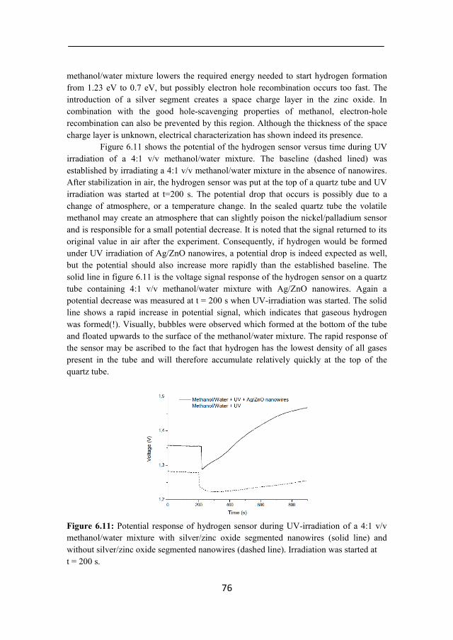
76
methanol/water mixture lowers the required energy needed to start hydrogen formation from 1.23 eV to 0.7 eV, but possibly electron hole recombination occurs too fast. The introduction of a silver segment creates a space charge layer in the zinc oxide. In combination with the good hole-scavenging properties of methanol, electron-hole recombination can also be prevented by this region. Although the thickness of the space charge layer is unknown, electrical characterization has shown indeed its presence.
Figure 6.11 shows the potential of the hydrogen sensor versus time during UV irradiation of a 4:1 v/v methanol/water mixture. The baseline (dashed lined) was established by irradiating a 4:1 v/v methanol/water mixture in the absence of nanowires. After stabilization in air, the hydrogen sensor was put at the top of a quartz tube and UV irradiation was started at t=200 s. The potential drop that occurs is possibly due to a change of atmosphere, or a temperature change. In the sealed quartz tube the volatile methanol may create an atmosphere that can slightly poison the nickel/palladium sensor and is responsible for a small potential decrease. It is noted that the signal returned to its original value in air after the experiment. Consequently, if hydrogen would be formed under UV irradiation of Ag/ZnO nanowires, a potential drop is indeed expected as well, but the potential should also increase more rapidly than the established baseline. The solid line in figure 6.11 is the voltage signal response of the hydrogen sensor on a quartz tube containing 4:1 v/v methanol/water mixture with Ag/ZnO nanowires. Again a potential decrease was measured at t = 200 s when UV-irradiation was started. The solid line shows a rapid increase in potential signal, which indicates that gaseous hydrogen was formed(!). Visually, bubbles were observed which formed at the bottom of the tube and floated upwards to the surface of the methanol/water mixture. The rapid response of the sensor may be ascribed to the fact that hydrogen has the lowest density of all gases present in the tube and will therefore accumulate relatively quickly at the top of the quartz tube.
Figure 6.11: Potential response of hydrogen sensor during UV-irradiation of a 4:1 v/v methanol/water mixture with silver/zinc oxide segmented nanowires (solid line) and without silver/zinc oxide segmented nanowires (dashed line). Irradiation was started at t = 200 s.

77
Visually, the formation of gas bubbles typically ended after ~48 h of UV irradiation. The reason for the loss of activity can be ascribed to photocorrosion of ZnO [38-45]. Non-recombined holes are either scavenged by methanol, or lead to corrosion of the ZnO surface in the water phase via reaction 6.6 [38,40,44,45]. 𝑍𝑛𝑂 + 2ℎ+ → 𝑍𝑛2+ + 1
2𝑂2 (6.6) Figure 6.12 shows SEM pictures of Ag/ZnO segmented nanowires after 48 h of exposure to UV radiation. It is clear from those pictures that the surface of the ZnO segment is heavily corroded and does not correspond with the relative smoothness of the segmented nanowires before photocatalytic testing. To verify that the corrosion is in fact the result of photocorrosion and not of electrolytic corrosion, segmented nanowires were suspended in the mixture in darkness for 48 h before UV irradiation. During UV irradiation the nanowires showed activity as much as ‘fresh’ segmented nanowires.
Although photocorrosion shortens the lifetime of photocatalytic segmented nanowires, it strongly suggests the fomation of electron holes in ZnO, thereby giving proof of actual photocatalytic activity of the Ag/ZnO segmented nanowires.
Figure 6.12: Scanning electron microscopy images of silver/zinc oxide nanowires after 48 hours of UV-irradiation. Photocorrosion of the zinc oxide segment can be seen.

78
6.5 CONCLUSIONS Silver/zinc oxide segmented nanowires were successfully deposited by templated electrodeposition using 200 nm pore sized PCTE membranes. Based on current responses during deposition of the ZnO segment and XRD analyses, the interface of ZnO with silver consists of multiple grains with multiple crystal orientations (0001), (10-10) and (10-11). Electrical characterizations revealed, however, that this interface structure does not necessarily influence the Ohmic behavior of the Ag/ZnO interface. In fact the space-charge layer is present, which is paramount to nanowire functionality. Silver/zinc oxide segmented nanowires were suspended in a 4:1 v/v methanol/water mixture and irradiates with an UV-source. During UV-irradiation, floating bubbles could be observed and hydrogen was detected by the hydrogen sensor. The typical lifetime of the segmented nanowires is 48 hours, which indicates photocorrosion. SEM analyses of the segmented nanowires after UV-irradiation showed indeed a degraded ZnO surface, which strongly indicates hole formation in the ZnO segment. Improvements to avoid photocorrosion could be that the n-type zinc oxide is not a segment, but rather small particles on a silver nanowire. The idea is that a small zinc oxide particle on the wire is less susceptible to reaction 6.6 through an increased surface to volume ratio. This allows the methanol to scavenge the holes more effectively. Other improvements are the replacement of the n-type zinc oxide segment by a more stable oxide, such as iron oxide or titanium oxide. Also the design can be altered by introducing a core/shell nanowire, where the oxide is its shell and the metal its core and thereby improving the interface area of the metal and the oxide. In conclusion, one of the first proof-of-principles of photocatalytic nanoparticles is reported here.

79
6.6 REFERENCES [1] R.J. Kuppler, D.J. Timmons, Q-R Fang, J-R Li, T.A. Makal, M.D. Young, D. Yuan, D. Zhao, W Zhuang, H-C Zhou, ‘Potential applications of metal-organic frameworks’, Coordin. Chem. Rev. 253, 3042 (2009). [2] G.J. Kubas, ‘Hydrogen activation on organometallic complexes and H2 production, utilization, and storage for future energy’, J. Organomet. Chem. 694, 2648 (2009). [3] H-L Jiang, S.K. Singh, J-M Yan, X-B Zhang, Q. Xu, ‘Liquid-phase chemical hydrogen storage: Catalytic hydrogen generation under ambient conditions’, ChemSusChem 3, 541 (2010). [4] J. Turner, G. Sverdrup, M.K. Mann, P-C Maness, B. Kroposki, M. Ghirardi, R.J. Evans, D. Blake, ‘Renewable hydrogen production’, Int. J. Energy Res 32, 379 (2008) [5] M. Yamawaki, ‘Application of nuclear energy for environmentally friendly hydrogen generation’, Int. J. Hydrogen Energ. 32, 2719 (2007). [6] R. Elder, R. Allen, ‘Nuclear heat for hydrogen production: Coupling a very high/high temperature reactor to a hydrogen production plant’, Prog. Nucl. Energ. 51, 500 (2009). [7] M.I. Hoffert et al., ‘Energy implications of future stabilization of atmospheric CO2 content’, Nature 395, 881 (1998). [8] K. Rajeshwar, R. McConnell, S. Licht, ‘Solar hydrogen generation. Toward a renewable energy future’, Springer Science + Business Media LLC, New York 2008, ISBN 978-0-387-72809-4, pp 10. [9] A. Fujishima, K. Honda, ‘Electrochemical photolysis of water at a semiconductor electrode’, Nature 238, 37 (1972). [10] A. Fujishima, K. Kohayakawa, K. Honda, ‘Hydrogen production under sunlight with an electrochemical cell’, J. Electrochem. Soc. 122 (11), 1487 (1975). [11] F.E. Osterloh, ‘Inorganic materials as catalysts for photochemical splitting of water’, Chem. Mater. 20, 35 (2008). [12] R.F. Navarro Yerga, M. Consuelo Álvarez Galván, F. del Valle, J.A. Villoria de la Mano, J.L.G. Fierro, ChemSusChem 2, 471 (2009).

80
[13] A. Kudo, Y. Miseki, ‘Heterogeneous photocatalyst materials for water splitting’, Chem. Soc. Rev. 38, 253 (2009). [14] R.F. Service, ‘Catalyst boosts hopes for hydrogen bonanza’, Science 297, 2189 (2002). [15] S.U.M. Khan, M Al-Shahry, W.B. Ingler Jr., ‘Efficient photochemical water splitting by a chemically modified n-TiO2’, Science 297, 2243 (2002). [16] K. Rajeshwar, ‘Hydrogen generation at irradiated oxide semiconductor-solution interfaces’, J. Appl. Electrochem. 37, 765 (2007). [17] M. Ni, M.K.H. Leung, D.Y.C. Leung, K. Sumathy, ‘A review and recent developments in photocatalytic water-splitting using TiO2 for hydrogen production’, Renew. Sust. Energ. Rev. 11, 401 (2007). [18] W-C Lin, W-D Yang, I-L Huang, T-S Wu, Z-J Chung, ‘Hydrogen production from methanol/water photocatalytic decomposition using Pt/TiO2-XNX catalyst’, Energ. Fuel. 23, 2192 (2009). [19] Jr. H. He, S.T. Ho, T.B. Wu, L.J. Chen, Z.L. Wang, ‘Electrical and photoelectrical performances of nano-photodiode based on ZnO nanowires’, Chem. Phys. Lett. 435, 119 (2007). [20] M. Gupta, V. Sharma, J. Shrivastava, A. Solanki, A.P. Singh, V.R. Satsangi, S. Dass, R. Shrivastav, ‘Preparation and characterization of nanostructured ZnO thin films for photoelectrochemical splitting of water’, Bull. Mater. Sci. 32 (1), 23 (2009). [21] X. Yang, A. Wolcott, G. Wang, A. Sobo, R.C. Fitzmorris, F. Qian, J.Z. Zhang, Y. Li, ‘Nitrogen-doped ZnO nanowire arrays for photoelectrochemical water splitting’, Nano Lett. 9 (6), 2331 (2009). [22] K. Maeda, K. Domen, ‘Solid solution of GaN and ZnO as a stable photocatalyst for overall water splitting under visible light’, Chem. Mater. 22, 612 (2010). [23] S. Ekambaram, ‘Photoproduction of clean H2 or O2 from water using oxide semiconductors in presence of sacrificial reagent’, J. Alloy. Compd. 448, 238 (2008). [24] S.K. Mohaptra, S.E. John, S. Banerjee, M. Misra, ‘Water photooxidation by smooth and ultrathin α-Fe2O3 nanotube arrays’, Chem. Mater. 21, 3048 (2009).

81
[25] M. Zäch, C. Hägglund, D. Chakarov, B. Kasemo, ‘Nanoscience and nanotechnology for advanced energy systems’, Curr. Opin. Solid St. M. 10, 132 (2006). [26] A. Kudo, ‘Recent progress in the development of visible light-driven powdered photocatalysts for water splitting’, Int. J. Hydrogen Energ. 32, 2673 (2007). [27] H. Yi, T. Peng, D. Ke, D. Ke, L. Zan, C. Yan, ‘Photocatalytic H2 production from methanol aqueous solution over titania nanoparticles with mesostructures’, Int. J. Hydrogen Energ. 33, 672 (2008). [28] J. Zhu, M. Zäch, ‘Nanostructured materials for photocatalytic hydrogen production’, Curr. Opin. Colloid In. 14, 260 (2009). [29] J. Li, J.Z. Zhang, ‘Optical properties and applications of hybrid semiconductor nanomaterials’, Coordin. Chem. Rev. 253, 3015 (2009). [30] J.P. Best, D.E. Dunstan, ‘Nanotechnology for photolytic hydrogen production: Colloidal anodic oxidation’, Int. J. Hydrogen Energ. 34, 7562 (2009). [31] A. I. Hochbaum, P. Yang, ‘Semiconductor nanowires for energy conversion’, Chem. Rev. 110, 527 (2010). [32] C.R. Martin, ‘Nanomaterials: A membrane-based synthetic approach’, Science 266, 1961 (1994). [33] G.A. Hope, A.J. Bard, ‘Platium/titanium dioxide (rutile) interface. Formation of Ohmic and rectifying junctions’, J. Phys. Chem. 87, 1979 (1983). [34] A.J. Nozik, ‘Photochemical diodes’, Appl. Phys. Lett. 30 (11), 567 (1977). [35] D.W. Bahnemann, C. Kormann, M.R. Hoffmann, ‘Preparation and characterization of quantum size zinc oxides: A detailed spectroscopic study’, J. Phys. Chem. 91, 3789 (1987). [36] V.L. Rideout, ‘A review of the theory and technology for Ohmic contacts to group III-IV compound semiconductors’, Solid State Electron. 18, 541 (1975). [37] K. Rajeshwar, R. McConnell, S. Licht, ‘Solar hydrogen generation. Toward a renewable energy future’, Springer Science + Business Media LLC, New York 2008, ISBN 978-0-387-72809-4, pp 174.

82
[38] J. Doménech, A. Prieto, ‘Stability of ZnO particles in aqueous suspensions under UV illumination’, J. Phys. Chem. 90, 1123 (1986). [39] P. Stathis, I. Poulios, ‘The corrosion and photocorrosion of zinc and zinc oxide coatings’, Corros. Sci. 37(5), 673 (1995). [40] H. Fu, T. Xu, S. Zhu, Y. Zhu, ‘Photocorrosion and enhancement of photocatalytic activity for ZnO via hybridization with C60’, Environ. Sci. Technol. 42, 8064 (2008). [41] H. Zhang, R. Zong, Y. Zhu, ‘Photocorrosion inhibition and photoactivity enhancement dofor zinc oxide via hybridization with monolayer polyaniline’, J. Phys. Chem. C 113, 4605 (2009). [42] Y. Lei, G. Zhao, M. Liu, Z. Zhang, X. Tong, T. Cao, ‘Fabrication, characterization, and photoelectrocatalytic application of ZnO nanorods grafted on vertically aligned TiO2 nanotubes’, J. Phys. Chem. C 113, 19067 (2009). [43] Y. Yang, D.S. Kim, Y. Qin, A. Berger, R. Scholz, H. Kim, M. Knez, U. Gösele, ‘Unexpected long-term instability of ZnO nanowires “protected” by a TiO2 shell’, J. Am. Chem. Soc. 131, 13920 (2009). [44] N. Kislov, J. Lahiri, H. Verma, D. Y. Goswami, E. Stefanakos, M. Batzill, ‘Photocatalytic degradation of methyl orange over single crystalline ZnO : Orientation dependence of photoactivity and photostability of ZnO’, Langmuir 25, 3310 (2009). [45] X. Chen, Y. he, Q. Zhang, L. Li, D. Hu, T. Yin, ‘Fabrication of sandwich-structured ZnO/reduced graphite oxide composite and its photocatalytic properties’, J. Mater. Sci. 45, 953 (2010).

83
Chapter 7
Templated electrodeposition of argentic oxysalt Ag7NO11 7.1 INTRODUCTION Attention for (templated) electrodeposition has increased over the past years, particularly due to its simplicity, scalability and low cost. As a result, the number of options to deposit a wider variety of materials of higher quality increased. Amongst these materials, metal oxides occupy a prominent position. These materials can combine several properties, for example, chemical stability, semiconductivity (in combination with band-gap engineering or otherwise), magnetism and superconductivity. Efforts to combine such properties in a material led to the rediscovery of some exotic oxides. An example of that is the argentic oxysalt Ag7NO11.
Studies on this material are relatively scarce. Illustrative is the fact that its chemical formula and crystal structure had been disputed up to 1900 since its discovery in 1804. Later studies revealed its formula to be Ag7NO11 [1]. It is superconductive below 1.04 K [2] and has antibacterial and antifungal properties [3]. The silver oxysalt is grown by polarizing a platinum electrode in an aqueous solution of AgNO3 [4]. The process takes place at the anode in conjunction with silver deposition at the cathode. It grows in the form of dark grey cubo-octahedral crystals, as shown in figure 7.1. To demonstrate the capabilities and simplicity of templated electrodeposition, the platinum anode was replaced by a PCTE membrane with gold back electrode to fabricate silver oxysalt nanowires. The results of this first attempt to grow silver oxysalt nanowires in a template are reported in this chapter.
Figure 7.1: Silver oxysalt grown at a platinum electrode in cubo-octahedral crystals. Magnification is 500x. Adapted from ref. [4].

84
7.2 THEORETICAL BACKGROUND Silver oxysalt is grown at a polarized anode in conjunction with silver at a cathode. The proposed half-reaction and overall reaction for argentic oxysalt are presented in reaction 7.1 and 7.2 respectively [3-7]. 7𝐴𝑔+ + 𝑁𝑂3− + 8𝐻2𝑂 → 𝐴𝑔7𝑁𝑂11 + 16𝐻+ + 10𝑒− (7.1) 17𝐴𝑔+ + 𝑁𝑂3− + 8𝐻2𝑂 → 𝐴𝑔7𝑁𝑂11 + 10𝐴𝑔 + 16𝐻+ (7.2) Figure 7.2 shows a representation of the crystal structure of Ag7NO11. The crystal structure has two characteristic features [8]. Firstly, the ‘building blocks’ of the crystal are Ag6O8 cages which actually contain an anion in their centers, in this case the NO3
- anion. These cages are connected with AgO4 units forming the surfaces of the Ag6O8 cages. The AgO4 units are suspected to be responsible for the superconductivity of the silver oxysalts. Secondly, the Ag6O8 cages force Ag atoms to realize high valence states that are seldomly seen. Ag2+ and even Ag3+ are present in the crystal structure. The reason is that each silver atom has an average 2.67 net positive charge in a Ag6O8 cage. Therefore, the silver oxysalt formula is also written as Ag+[(Ag2+)2(Ag3+)4O8](NO3)- or Ag6O8AgNO3.
Figure 7.2: Crystal structure of Ag7NO11 showing three Ag6O8 cages connected with AgO4 cubes. Adapted from ref. [8]. Once Ag7NO11 has been synthesized, it is very sensitive to moisture. It loses oxygen from its crystal lattice forming Ag2O2. Reaction 7.3 represent this equation. 𝐴𝑔7𝑁𝑂11 → 𝐴𝑔𝑁𝑂3 + 3𝐴𝑔2𝑂2 + 𝑂2 (7.3)

85
Ag2O2 (Ag(I)Ag(III)O2) has been reported to be a grayish black powder. At temperatures above 100°C it releases oxygen and leaves a residue of metallic silver. Known solvents of Ag7NO11 are ammonium hydroxide and nitric acid [9]. 7.3 EXPERIMENTAL Templated electrodeposition was used for silver oxysalt (Ag7NO11) deposition. As a template, commercially available Nuclepore® (Whatman Inc.) polycarbonate track-etched membranes were used. The membrane pore diameter is 200 nm and the pore densitiy is ~3x10⁸ pores/cm2. Prior to deposition a gold layer with a thickness of ~250 nanometer was sputtered on one side of the membrane. After sputtering, the gold coated side of the membrane was attached to a glass slide with double-sided tape. Two of these membrane/glass combinations were used as cathode and anode in a 3-electrode setup using a Bank Elektronik POS 73 potentiostat. The reference potential was set by a 3M KCl Ag/AgCl reference electrode (REF 321, Radio Analytical). Ag7NO11 nanowires were deposited from an aqueous electrolyte solution containing 0.2 M AgNO3 and 0.1 M H3BO3. The pH was adjusted to 1.5 with HNO3. The voltage was set to 1.7 V versus the reference electrode. An aqueous solution of 0.005 M HAuCl4 was used to coat Ag7NO11 crystallites by a galvanic replacement reaction. Analysis of Ag7NO11 crystals was performed with a Nikon Eclipse ME600 optical microscope. Analysis of isolated Ag7NO11 nanowires was performed with a Zeiss HR-LEO 1550 FEF Scanning Electron Microscope (SEM). X-Ray diffraction (XRD) was performed with a Philips PanAnalytical PW1830 with a copper x-ray source and a wavelength of 1.54 Ångström. 7.4 RESULTS AND DISCUSSION The PCTE membrane uses a gold back electrode and it was initially not known whether or not silver oxysalt can grow on a gold surface. A simple growth test on a gold electrode was required. Figure 7.3 shows an optical microscope image of Ag7NO11 crystals on a gold electrode. The crystals are comparable with the crystals shown in figure 7.1. This can be an indication that silver oxysalt growth on gold electrodes is possible and nanowires can be grown.

86
Figure 7.3: Ag7NO11 crystals grown on a gold electrode. Magnification is 200x. To get more indications that Ag7NO11 had indeed been synthesized, some previously reported features can be used in a very practical manner. Crystals grown on gold were isolated from the electrode and heated on a stainless steel spoon with an open flame in air. The crystals combusted spontaneously after a short heating period, indicating the presence of Ag2O2. Another test involved dissolving isolated crystals in ammonium hydroxide, which gave a violent reaction releasing a large number of gas bubbles (see figure 7.4). These findings are in agreement with previously reported tests [9].
Figure 7.4: Screenshot of Ag7NO11 reacting in a 25% w/w ammonium hydroxide solution. Nanowires that had been in the template were analysed by SEM and XRD. Figure 7.5 shows SEM images of a Ag7NO11 crystal grown on a platinum electrode (A) and nanowires grown in a PCTE membrane with a gold electrode (B). The crystals which grew on the platinum electrode were shaped as needles with small protrusions that were detectable by the naked eye, as depicted in figure 7.5A. These crystals reached maximum dimensions of ~3 cm.

87
Figure 7.5: A) SEM image of a large Ag7NO11 crystal grown on a Pt electrode. B) SEM image of two Ag7NO11 nanowires grown in a track-etched polycarbonate membrane with 200 nm diameter pores. To measure the influence of a confined space on the Ag7NO11 growth in, i.e. membrane pores, XRD spectra were recorded. Figure 7.6 shows 2θ scans of a silver oxysalt powder of ground crystals grown on a platinum electrode and nanowires embedded inside a PCTE membrane. The XRD pattern suggests a strong preferential growth direction of the silver oxysalt in the (222) direction in the PCTE membranes. This can be concluded from the comparison with the powder XRD spectrum, which functions as the (random oriented) base. This may indicate that the mechanism of growth changes from a reaction-controlled growth to a diffusion limited process, as indicated in chapter 4. However, the silver oxysalt powder is unstable in air, and may have changed its composition and crystal structure under the influence of the XRD measurement, while the silver oxysalt in the PCTE membrane is protected from air by the membrane.
Figure 7.6: X-ray diffraction pattern of a Ag7NO11 powder (blue line) and Ag7NO11 nanowires (red line) in a track-etched polycarbonate membrane.

88
Due to the instability of silver oxysalt in air due to the presence of moisture, some means of shielding is required to stabilize the Ag7NO11 phase. A possible way to protect the large crystals grown on the platinum electrode is to provide them with a thin protective layer. A galvanic replacement reaction with chloroauric acid (HAuCl4)* was opted and tested. Large silver oxysalt crystals were immersed in a 0.005M HAuCl4 solution and left there for at least 12 hours. After isolating the crystals from the solution, they had a gold luster, indicating that the galvanic replacement reaction had taken place. Then, the coated crystals were immersed in an ammonium hydroxide solution but no reaction occurred. After crushing the crystals in the ammonium hydroxide solution, they showed a violent reaction and released gas. The crystals before and after cracking are shown in figure 7.7.
Figure 7.7: Screenshots of a gold coated Ag7NO11 crystal in a 25% w/w ammonium hydroxide solution. Upper left) Prior to reaction. Upper right) Breaking the crystal with a spatula. Lower middle) Reaction at both cross sections after breaking the crystal. 7.5 CONCLUSIONS Ag7NO11 crystals and nanowires were synthesized by electrodeposition. The nanowires showed a preferential growth in the (222) direction due to the confined space of the membrane pores. The instability in air of the Ag7NO11 crystals is circumvented by coating the crystals via a galvanic replacement reaction with gold.
*The exact chemistry of the galvanic replacement reaction is unclear.

89
7.6 REFERENCES [1] C.H. Wong, T.H. Lu, C.N. Chen, T.J. Lee, ‘A precise redetermination of the crystal structure of Ag7NO11’, J. Inorg. Nucl. Chem. 34, 3253 (1972). [2] M.B. Robin, K. Andres, T.H. Geballe, N.A. Kuebler, D.B. McWhan, ‘Metallic conductivity and superconductivity in some silver clathrate salts’, Phys. Rev. Lett. 17 (17), 917 (1966). [3] S.S. Djokic, ‘Deposition of silver oxysalts and their antimicrobial properties’, J. Electrochem. Soc. 151 (6), C359 (2004). [4] E. Michailova, A. Milchev, ‘Nucleation and growth kinetics of Ag7NO11 on a platinum single crystal electrode’, J. App. Electrochem. 18, 614 (1988). [5] J.A. McMillan, ‘Higher oxidation states of silver’, Chem. Rev. 62 (1), 65 (1962). [6] B.E. Breyfolge, R.J. Phillips, J.A. Switzer, ‘Epitaxial electrodeposition of Ag(Ag3O4)2NO3 onto highly oriented conducting metal oxides in the Pb-Tl-O system’, Chem. Mater. 4, 1356 (1992). [7] G.I.N. Waterhouse, J.B. Metson, G.A. Bowmaker, ‘Synthesis, vibrational spectra and thermal stability of Ag3O4 and related Ag7O8X salts (X = NO3
-, ClO4-, HSO4
-)’, Polyhedron 26, 3310 (2007). [8] K. Kawashima, M. Ishi, H. Okabe, J. Akimitsu, M. Kriener, H. Takatsu, S. Yonezawa, Y. Maeno, ‘Superconducting state of silver-oxide clathrate Ag6O8AgNO3’, J. Phys. Soc. Jpn. 77 (2), 024707 (2008). [9] M.J. Brown, ‘A new method for the study of silver peroxynitrate’, J. Phys. Chem. 20 (8), 680 (1916).

90
Chapter 8
General Conclusions and Outlook 8.1 GENERAL CONCLUSIONS Templated electrodeposition has emerged as one of the most promising tools to synthesize nanowires and nanotubes. Because of its scalability and cost-effectiveness it can transfer nanotechnological knowledge from laboratories to the industrial level. It can comply with the demands that the commercial markets demand in combination with a reliable post-assembly or alignment technique. It was an underlying motive of the work that was carried out in this thesis: to find solutions to current commercial challenges in the ‘nanowire and nanotube research field’ with a minimum of capital investment. All experiments were carried out in a normal laboratory environment without the need for a clean-room or vacuum. Although the pre-patterned gold electrode samples used during this research could be regarded as an exception. They were fabricated using conventional photolithography techniques. Well established foundry services were employed for this. Secondly, with the combination of a metal and an oxide in a single (functional) nanowire, it was shown that the possibilities of template electrodeposited nanowires can reach even beyond buildings blocks for sensors -arguably the most obvious reason for nanowire and nanotube research. The growth of zinc oxide nanowires and the formation of iron(III) hydroxide gel was investigated: with only a single template different structures could be synthesized. By comparing nanowire growth processes, the quality of zinc oxide nanowires can be assessed in situ. Direct assessment of nanowire quality is a major advantage for usage in the industrial environment. By changing the composition of the electrolyte bath, iron(III) oxide nanotubes could be synthesized by drying a polycarbonate membrane which contained iron(III) hydroxide gel. Because of the gel formation which can saturate pores and conforms itself to any shape, even three-dimensional structures are possible. From a commercial point of view, templated electrodeposition is versatile tool which can synthesize various materials and shapes by a ‘flick-of-a-switch’. More important, this thesis gives and insight in the critical stages of zinc oxide nanowire growth and compares it with a system were growth is absent in order to give a firm base for later research.

91
Because of the large variety of materials which can be synthesized with electrodeposition, a uniform alignment procedure is desired. Dielectrophoresis was chosen as the best candidate for alignment: it is cost-effective and does not require a clean-room or vacuum. On the basis of theory, boundary conditions could be established to align nanowires on pre-patterned gold electrodes. This ability to asses positive or negative dielectrophoresis can increase the success-rate of alignment dramatically. However 100% reproducibility was not obtained using the from theory derived settings of a frequency of 120.000 Hz, a peak-to-peak potential of 2.1 V and an insulating silicon oxide layer of 8 µm to prevent charging of the sample. Lower reproducibility of the dielectrophoresis can influence the usage in industry, if it would demand 100% reproducibility. On the other hand, Ohmic contacts, i.e. the potential drop between electrode and nanowire is small enough not to influence its behavior, are much needed. Also a relation between the creation of an opposite electric field through the insulating silicon oxide layer is addressed -rarely found in literature- but necessary to acknowledge if industry and laboratory want to form a steady platform for knowledge transfer. Templated electrodeposition offers the possibility to combine materials in a single nanowire. By combining the right materials, new functionalities can be added. Here, the combination of a metal (Ag) and n-type semiconductor (ZnO) resulted in a UV-sensitive segmented nanowire. By creating a space-charge layer in the segmented nanowire, hydrogen evolution from a methanol/water solution was enabled under the influence of UV-irradiation. This is a good example of nanotechnology directly applied on a macroscale, showing that the gap between laboratory and application is being bridged. It offers new opportunities for sustainable energy production and the envisioned hydrogen economy, since this system is mobile and does not need new infrastructure to transport hydrogen to a central fueling point. Also, this example can put nanotechnological progress in a -much needed?- positive social framework. Another example of a direct application of nanotechnology can be found in external care products: for example small silver particles in deodorant. The silver is lethal to bacteria and fungi. Silver oxysalt (Ag7NO11) was easily synthesized by templated electrodeposition in the previously unreported form of nanowires. Particles of Ag7NO11 could be isolated from oxygen or moisture by coating them with gold via a galvanic replacement reaction.

92
8.2 OUTLOOK Expectations of nanotechnological innovations are high; the timescale at which these innovations will trickle trough in our households is unclear and depends on market conditions and public awareness. Likely not all innovations find their way to industry, because of non-profitability or a hampered exchange of knowledge between laboratory and industry.
Undoubtedly, the future for nanowire or nanotube applications will be bright, whether or not synthesized by templated electrodeposition. Fundamental research will help understanding the processes in nanowires and nanotubes thereby improving, e.g. long-term stability, gas selectivity, and photo sensitivity. Further improvements in the manipulation of nanowires will enable the production of sensors with a competitive price. However, the impact of nanowires and nanotubes on the environment and public health should be investigated. This is an essential benchmark of the public awareness of nanotechnological developments. Here, templated electrodeposition was used to synthesize nanowires and nanotubes using a polycarbonate track-etched (PCTE) membrane as a template. Next to membranes, a whole range of templates can be used. New research has started with conductive samples and poly-dimethylsiloxane (PDMS) stamps. Material can be electrodeposited in patterns by pressing the PDMS stamps on the samples, resulting in channels. The channels are filled with electrolyte and a potential is applied to the sample. Figure 8.1 A and B show the results of nickel deposited in the channels of a PDMS stamp pressed on a gold coated silicon sample.
Figure 8.1: SEM images of nickel patterns deposited in PDMS channels on a gold coated silicon substrate. A) Honeycomb structures; B) 200 nm wide lines. Honeycomb structures and lines down to a width of 200 nm (!) could easily be deposited. Circuitry, solar cells or even solar panels could be deposited this way, to name a few examples. In combination with the sol-gel formation in this thesis, even three-dimensional templates can be filled.

93
Development of electrolytes can also improve the quality of the materials deposited and the dimensions thereof. Additives can be responsible for controlled layer-by-layer deposition with nanometer thickness. Ionic liquids could enable the deposition of new materials with more complex chemistry. On the other hand, one critical issue should be addressed: templated electrodeposition will only function if the material deposited is conductive. The deposited materials functions as the electrode for the next layer to be deposited. The electrode should not per se supply electrons for a chemical reactions, it can also withdraw electrons to start a reaction, as showed here with the deposition of the silver oxysalt Ag7NO11.

94
Summary Nanotechnology could be considered as a scale of engineering between 1 and 100 nm. Instead of one phenomenon, it offers possibilities for thousands of materials that already exist. Familiar materials behave very differently at the nanometer scale and can display useful new properties. Because it is a scale of engineering, it often brings together different areas of science and benefits from an interdisciplinary approach. Expectations of the future are high, although it is difficult to estimate when nanotechnological products and applications will be realized: nanotechnologies will not be incorporated into products and devices without the development of scalable, cost-effective manufacturing techniques that retain and preserve the properties of the nanoscalar material in the final product.
Because nanowires and nanotubes can be the actual building blocks to construct future nanotechnological products and devices, the properties of the nanoscalar material are retained by default. Here, templated electrodeposition was used as a scalable and cost-effective manufacturing technique for nanowires and nanotubes. Also, first steps were taken towards a low-cost and effective incorporation of nanowires and nanotubes on electrodes by dielectrophoresis -in our opinion an important step for industry to recognize the numerous possibilities for nanowire and nanotube applications. Furthermore, a direct application of nanowires is demonstrated: the functionality of nanowires has been engineered to demonstrate hydrogen evolution by nanowires under UV-irradiation.
During templated electrodeposition, zinc hydroxide and iron(III) hydroxide formation, decomposition, and the following growth processes of zinc oxide nanowires and iron(III) oxide nanotubes were investigated by chronoamperometry. All processes proceeded in the confined space of membrane pores: the template. As a template, a polycarbonate track-etched membrane (PCTE) was used with different pore sizes: 50 nm and 200 nm. The temperature during zinc hydroxide formation and immediate decomposition plays an important role. At 62°C and at 70°C, the growth processes of zinc oxide nanowires are significantly different. At 70°C, a better quality nanowire was produced, which was suited for further applications. To verify the growth processes of zinc oxide, a system without nucleation and growth was used, namely an electrochemically induced sol-gel process forming an iron(III) oxide gel. During drying of this gel at room temperature inside PCTE membrane pores, nanotubes were formed. An interaction of the gel with the pore wall and volume loss during drying are responsible for this phenomenon.

95
Dielectrophoresis was used to align nanowires of different materials. Its working principle is based on an alternating electric field between (two) electrodes trapping nanowires from a medium in that alternating field. Parameters are potential, frequency and distance between the electrodes, nanowire material and medium. To increase reproducibility, a set of boundary conditions were used to derive a set of parameters, based on theoretical calculations. These parameters can be applied for any nanowire, regardless of the material it is made of. The electrodes were made by photolithography after own design. The electrode gap varied between 2 and 3 µm. After aligning nickel/iron(III) core/shell and zinc oxide nanowires, it was found that the nanowires made Ohmic contact to the gold electrodes. The nanowires were aligned using a peak-to-peak voltage of 2.1 V at a frequency of 1.2⋅105 Hz. Also, the thickness of the insulating layer beneath the electrodes is of influence. In theory and in practice, a too thin insulating layer will create an opposite electric field which prevents nanowires from aligning between the electrodes. Therefore, a 8 µm thick insulating layer with grounding was used. The functionality of nanowires can be engineered. Here, a segmented nanowire consisting of a silver segment and an n-type zinc oxide segment was made photocatalytic. Under the influence of UV-irradiation it could produce hydrogen and carbon dioxide from a 4:1 methanol/water v/v mixture. A space charge layer at the interface between silver and zinc oxide is responsible for the activity. During UV-irradiation an electron and a hole is created in the space charge layer by the zinc oxide. The electron is in the conduction band of the zinc oxide and moves towards the silver, because of the lower energy level of the silver Fermi-level. Here it used for a reduction reaction. The hole remains in the zinc oxide to be scavenged by the methanol for a oxidative reaction. The overall reaction creates hydrogen and carbon dioxide. Lastly, nanowires were synthesized of silver oxysalt (Ag7NO11). This is a rather exotic material paid little attention to. On the other hand, it is known that is superconductive below 1.04 K, it has antibacterial and antifungal properties, and is instable in air or moisture. Because of the little attention, no nanowires existed previously of this material. Here, silver oxysalt nanowires were synthesized using a gold electrode.

96
Samenvatting Nanotechnologie kan gezien worden als ontwerpen op een schaal tussen de 1 en 100 nm. Het biedt nieuwe mogelijkheden voor duizenden materialen die reeds bestaan, in plaats van zich the richten op één fenomeen. Materialen waar wij allemaal bekend mee zijn, kunnen zich heel verschillend gedragen op de nanometerschaal en dus nieuwe eigenschappen vertonen. Het ontwerpen op nanoschaal brengt veel wetenschappelijke disciplines samen en profiteert daarom van een interdisciplinaire aanpak. Verwachtingen voor de toekomst zijn dan ook hoog. Het is moeilijk in te schatten wanneer nanotechnologische producten en toepassingen worden gerealiseerd: nanotechnologie zal alleen worden gebruikt als er opschaling van productietechnieken mogelijk is en dat deze productietechnieken goedkoop zijn. Daarbij moeten die productietechnieken de eigenschappen van de materialen op nanoschaal niet beïnvloeden. Omdat nanodraden en nanobuisjes bouwelementen zijn voor toekomstige nanotechnologische producten en toepassingen, worden de eigenschappen van deze elementen niet aangetast. ‘Templated electrodeposition’ werd hier gebruikt als techniek om nanodraden en nanobuisjes te synthetiseren omdat deze techniek zich uistekend leent voor opschaling en goedkoop is. ‘Dielectrophorese’ werd gebruikt om de nanodraden en nanobuisjes goedkoop en effectief te integreren op elektrodes; in onze optiek een belangrijke stap om de industrie te attenderen op de legio toepassingsmogelijkheden van de nanodraden en nanobuisjes. Ook werd een demonstratie gegeven van een directe toepassing van nandoraden: de functionaliteit van de nanodraden werd aangepast zodat ze waterstof produceren onder invloed van ultraviolette straling. Tijdens ‘templated electrodeposition’, werden zinkhydroxide en ijzer(III)hydroxide formatie, decompositie en de daaropvolgende groeiprocessen van zinkoxide nanodraden en ijzeroxide nanobuisjes onderzocht met behulp van chronoamperometrie. Alle processen vonden plaats in de poriën van een membraan: het ‘template’. Het gebruikte template is een polycarbonaat ‘track etched’ membraan (PCTE) met poriën van 50 of 200 nm. De temperatuur tijdens zinkhydroxide formatie en de direct daaropvolgende decompositie speelt een belangrijke rol. Bij 62°C en 70°C verschillen de groeiprocessen significant. Bij 70°C is de kwaliteit van de zinkoxide nanodraad goed genoeg voor verdere applicaties. Om dit zinkoxide groeiproces te verifiëren werd er een systeem zonder nucleatie en groei gebruikt, namelijk een elektrochemisch geïnduceerd sol-gel proces van ijzer(III)hydroxide. Tijdens het drogen van deze gel bij kamertemperatuur in het PCTE membraan ontstonden er nanobuisjes door volumeverlies en poriewand interacties.

97
Dielectrophorese werd gebruikt om nanodraden van verschillende materialen te integreren. Het werkingsprincipe is een wisselend elektrisch veld tussen (twee) elektrodes waarin de nanodraden vanuit een medium worden gevangen. Parameters zijn voltage, frequentie, afstand tussen de elektrodes, materiaal van de nanodraad en medium. Om de reproduceerbaarheid van deze techniek te verbeteren werd een set van randvoorwaarden gemaakt waaruit, op basis van theorie, bruikbare parameters werden verschaft. Deze parameters kunnen dan worden toegepast op elk materiaal in nanodraad vorm. De elektrodes werden gemaakt door fotolithografie naar eigen ontwerp. De elektrodeafstanden zijn 2 en 3 µm. Na het integreren van nikkel/ijzeroxide kern/mantel nanodraden en zinkoxide nanodraden werd er een Ohms contact gerealiseerd. De nanodraden werden geïntegreerd door een voltage van 2,1 V en een frequentie van 1.2⋅105 Hz. Ook de dikte van de isolerende laag onder de elektrodes is van invloed. Zowel in theorie als in de praktijk leidt een te dunne isolerende laag tot een tegengesteld elektrisch veld tussen de electrodes die voorkomt dat nanodraden kunenn worden geïntegreerd. Daarom werd een isolerende laagdikte van 8 µm gebruikt in combinatie met aarde. De functionaliteit van nanodraden kan worden aangepast. Een gesegmenteerde nanodraad bestaande uit een zilver en een n-type zinkoxide segment wordt fotokatalytisch. Onder invloed van UV-straling kon het waterstof een koolstofdioxide produceren in een 4:1 methanol/water v/v oplossing. Een ‘space charge layer’ op het grensvlak van zilver en zinkoxide is verantwoordelijk voor deze activiteit. Tijdens de bestraling met UV worden er een elektron en een gat geproduceerd in de ‘space charge layer’ door de zinkoxide. Het elektron is in de geleidingsband van het zinkoxide en verplaatst zich naar het zilver dat een lager Fermi-niveau heeft. Daar wordt het gebruikt voor een reductiereactie. Het gat blijft in het zinkoxide en wordt opgevangen door de methanol voor een oxidatiereactie. De uitgangsreactie produceert dan waterstof en koolstofdioxide. Ten slotte werden nanodraden gesynthetiseerd van een zilver oxyzout (Ag7NO11). Dit exotische materiaal heeft niet veel aandacht gehad. Echter, het is wel bekend dat het een supergeleider is onder de 1,04 K, dat het een antibacteriële en antischimmel werking heeft en dat het instabiel is in lucht en vocht. Vanwege de geringe aandacht bestonden er nog geen nanodraden van dit materiaal. Hier werden wel nanodraden van het zilver oxyzout gesynthetiseerd met een goud elektrode.

98
Dankwoord Een onderzoek doe je niet alleen, daarom dit woord van dank en waardering. Allereerst wil ik André en Dave bedanken voor de gegeven kansen tijdens een bewogen periode. Vertrouwen komt te voet en gaat te paard, zegt men. Gelukkig was de ratio sneller.
Ook moet er een woord van dank naar Eddy (M.G.) en Wouter, die dit proefschrift mede mogelijk hebben gemaakt door hun afstuderen en Eddy zelfs, naar mijn inzicht, ‘beyond the call of duty’ een jaartje is gebleven.
Mijn kamergenoten mag ik natuurlijk ook niet vergeten: Sajid, Vittorio, Nicolas (dinsdagavond Stek-avond), Tomasz en Sjoerd (Stawski en Hutch), Ole, Frank!, Ronald en Rogier. Zoveel kansen om zoveel mensen op hun zenuwen te werken krijg je zelden. Bedankt allen!
Heel IMS wil ik bedanken voor de koffiepauzes, discussies, karten (waarom moet Dekkers altijd winnen?!) en uitstapjes en eigenlijk te veel om op te noemen. Maar ik probeer het toch: Peter (bedankt voor de wedstrijden bij FC Twente), Jeroen (duikcursus was erg leuk. Vergeet de kaartjes niet!), Hans, Ruud, Josée (bedankt voor de XPS), Bouwe, Antony (brilliant PDMS patterning ideas), Xin, Oktay, Michelle, Rik, Maarten, Arjen, Bernard, Guus, Gertjan, Mark, Marion, José, Henk, Gerrit, Evert. Buiten IMS wil ik graag bedanken Mark (SEM), Rico (TEM), Vishwas (FIB), Gerard (XPS, SEM), Frank en Dick (Perkin Elmer). Mocht ik mensen zijn vergeten te bedanken, dan doe ik dat niet omdat ik ben vergeten. Bedankt!! Michiel Gerard Maas December 2010