research article shear-force sensors on flexible
TRANSCRIPT

Research ArticleShear-Force Sensors on Flexible Substrates Using Inkjet Printing
Andreas Albrecht ,1 Mauriz Trautmann,1 Markus Becherer,1 Paolo Lugli,2
and Almudena Rivadeneyra 2
1Institute for Nanoelectronics, Technical University of Munich, Arcisstraße 21, 80333 Munich, Germany2Free University of Bozen-Bolzano, Universitätsplatz 1 39100 Bozen-Bolzano, Italy
Correspondence should be addressed to Andreas Albrecht; [email protected]
Received 10 August 2018; Accepted 24 December 2018; Published 3 March 2019
Academic Editor: Franz L. Dickert
Copyright © 2019 Andreas Albrecht et al. This is an open access article distributed under the Creative Commons AttributionLicense, which permits unrestricted use, distribution, and reproduction in any medium, provided the original work isproperly cited.
Printing techniques are a promising way of fabricating low-cost electronics without the need for masking and etching. In recentyears, additive printing techniques, such as inkjet and screen printing, have been adopted to fabricate low-cost and large-areaelectronics on flexible substrates. In this work, a three-axial normal and shear force sensor was designed and printed thatconsists of four miniaturized, printed capacitors. The partially overlapping electrodes are arranged in a manner, so that forcesensitivity in orthogonal directions is achieved. A silicone rubber is used as an elastic dielectric and spacer between the twoelectrodes. The base unit of this sensor has been fabricated using inkjet printing and characterized for normal and shear forces.The force response was investigated in a force range from 0.1N to 8N, the normal-force sensitivity was determined to be Sz =5 2 fF/N, and the shear-force sensitivity was Sy = 13 1 fF/N. Due to its sensing range, this sensor could be applicable in tactilesensing systems like wearables and artificial electronic skins.
1. Introduction
Printed electronics possess the advantage of reducing thenumber of production steps by applying several componentswith similar process technologies. In contrast to conven-tional electronics manufacturing, sensors can be printedinstead of assembled [1–3]. The present work deals withthe development, fabrication, and characterization of acapacitive normal and shear force sensor. Such sensors couldbe used for basic force and pressure measurements [4, 5].They could also be part of a tactile sensing system in robot-ics. Advanced robotic systems need reliable informationabout friction and strain when interacting with the environ-ment and while handling objects [6–9]. Additionally, theability of printed electronics to fabricate devices on flexiblesubstrates could bring us a step closer to an artificial skin,which can be wrapped around the robot’s surface [9–14].
In a previous work, we studied inkjet printing andphotonic sintering for low-cost printing of electrodes andwiring [15]. Inkjet printing is able to print lines down toabout 60μm in width and can be conducted on a large
range of flexible and low-cost substrates. Photonic sinter-ing is a method that allows achieving highly conductivethin films on temperature-sensitive substrates with con-ductivities of up to 40% of the bulk conductivity [15]Therefore, these two technologies are well suited for theproduction of electrodes for sensors.
In this work, we want to focus on a capacitivethree-axial shear-force sensor as an alternative to resistiveforce sensors [16, 17] that is applicable in an artificial skin.A common approach for building capacitive flat force sen-sors are the use of two parallel plates that change theirdistance upon pressure [9, 18, 19]. The gap can beair-filled [20] or consist of an elastic dielectric [21]. Leeet al. [20] have modified this principle to additionally rec-ognize shear forces by introducing several capacitors.
Several research groups have tried to produce thin-filmthree-axial force sensors. Chase and Luo [22] showed a par-allel plate capacitor approach with four capacitances thatchange in the overlapping area for exposure to shear forcesand in distance for normal forces. Khan et al. [23] presentedan all-screen printed flexible pressure (normal force) sensor
HindawiJournal of SensorsVolume 2019, Article ID 1864239, 11 pageshttps://doi.org/10.1155/2019/1864239
with a piezoelectric sensing principle. In their work, silver-(Ag-) based paste serves as a conductor for the electrodes.The piezoelectric material was polyvinylidene fluoride tri-fluoroethylene (P(VDF-TrFE)), which is a ferroelectric poly-mer that exhibits efficient piezoelectric and pyroelectricproperties. The force response was characterized by the volt-age readout.
A thin-filmnormal and shear force sensorwas designedbyViry et al. [24] as well as Chase and Luo [22]. Their capacitivedevice senses normal and shear forces simultaneously. Theoperation is based on the deflection of a compressible fillermaterial, which is sandwiched between two electrodes of aplate capacitor. Making a few adjustments, this design couldbe implemented using printing technologies.
A more advanced sensor design was reported by Dobr-zynska and Gijs [25] using conventional semiconductortechnology. Their capacitive approach is based on the deflec-tion of an elastic dielectric spacer. They used multiple smallcapacitor areas leading to a higher sensitivity especially forshear force sensing. However, the fabrication of similarlysmall features is a challenging task using printed electron-ics techniques. A similar approach was used by Surapaneniet al. [26] who also developed a portable readout device.
In the present work, the basic idea of their sensor wasadopted for printed electronics. The rest of the paper isstructured as follows: in Section 2, we present the materials,the printing process, the elastic dielectric, and its applicationas well as the characterization tools used to produce the pre-sented results. Section 3 discusses the design, a theoreticalmodel thereof as well as the evaluation of the print qualityand the measured electromechanical behavior of out sensors.In Section 4, we summarize the main findings and concludethe paper.
2. Materials and Methods
The shear-force sensors were fabricated on the transparent,coated Polyethylene Terephthalate (PET) film ScreenfilmWaterbased (ColorGATE Digital Output Solutions GmbH,Germany). The film was developed for inkjet printing andhas a nanoporous surface coating, a grammage of 210 gm-2,and a thickness of 170μm.
For inkjet printing, we used the nanoparticle-based silverink DGP 40LT-15C (ANP Co., South Korea). The inkcontains 35% silver nanoparticles dispersed in TGME(C8H18O4), which is a polar solvent. The dispersion was care-fully shaken by hand prior to filling into the cartridge. Thecuring temperature is indicated with 120-150°C, and thespecific resistivity is 11-12μΩcm. As the dielectric spacerof our sensor, we used a two-component screen-printablesilicone paste, Alpatec 30191 (CHT R. Beitlich GmbH).The two components were mixed equally (1 : 1) in a smalldish. After mixing, the paste can be used for one hourbefore hardening. Both components are highly transparent.
2.1. Inkjet-Printed Electrodes. The printer used in this work isa Dimatix DMP-2850 (Fujifilm Dimatix Inc., Santa Clara,USA). The cartridge and plate temperature was set to 55°Cwith a drop-spacing of 30μm. This value guarantees a yieldrate higher than 90% while the distance between consecutiveelectrodes is close enough. Reducing this spacing willincrease the capacitance and sensitivity of our sensors, butit would reduce the reproducibility of the fabrication. Withthese settings, the fabrication of one electrode took aboutten minutes. By using more than one nozzle, the printingtime can be reduced, but the probability of a failure due toa blocking in one of the nozzles is much higher. Throughthe heat of the platen, the pattern was quickly dried. Tomake sure that all the solvents evaporated, the samples wereadditionally cured in an oven for 60min at 60°C. The sub-strate limited the temperature as it started to buckle athigher values.
To improve the conductivity of the electrodes, weemployed Intense Pulsed Light (IPL) sintering using a Sin-teron 2010 (Xenon, US). A double pulse (period of 3 s) at2.5 kV was used. The pulse lengths were 500μs for the firstpulse and 1000μs for the second pulse, which were identifiedas good values in previous work [15]. The manufacturermeasured a light intensity of 2.6-3.9 Jcm-2 for a single pulseat 830 J of electrical power. Our light intensity for bothpulses is assumed to be approximately in this range as theemployed pulses are about 300 J and 600 J, respectively.
2.2. Elastic Spacer. The Polydimethylsiloxane (PDMS) spacerwas applied onto the inkjet-printed silver layer on the PET
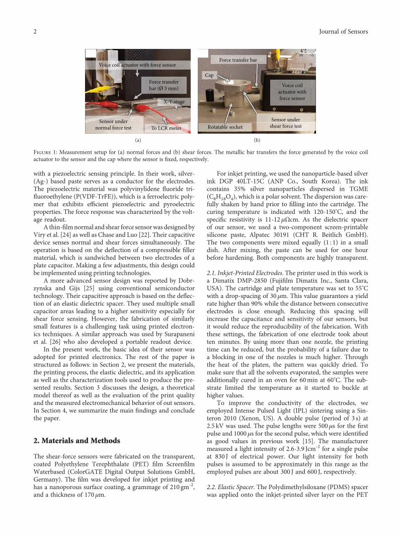
Voice coil actuator with force sensor
Force transferbar (Ø 3 mm)
X-Y-stage
To LCR meterSensor under
normal force test
(a)
Cap
Force transfer bar
Rotatable socket
Voice coilactuator withforce sensor
Sensor undershear force test
(b)
Figure 1: Measurement setup for (a) normal forces and (b) shear forces. The metallic bar transfers the force generated by the voice coilactuator to the sensor and the cap where the sensor is fixed, respectively.
2 Journal of Sensors

film using a stencil made of 75μm thick Kapton film. Afterapplying PDMS on both electrodes, they were placed on eachother, aligned using dedicated marks, and baked on a hotplate at 60°C for about 30min. To make sure that the elec-trodes did not detach, a slight pressure was exerted on thesample using a glass slide. In this way, we effectively usedthe PDMS as both an adhesive as well as a dielectric spacerof our sensor.
2.3. Characterization. Optical microscope images weretaken with a Zeiss Germany Axio Lab.A1, equipped witha digital camera Axiocam 105. These images were usedto assess the quality of the printed electrodes and to deter-mine their lateral and longitudinal dimensions. Further,the drop diameter of the silver ink on the PET and Kap-ton substrates was identified.
The thickness of our printed electrodes and PDMSlayer were measured with a DektakXT stylus surface pro-filer (Bruker Corporation, USA).
To generate the normal and shear force, we used thevoice coil linear actuator V-275 PIMag (Physik Instrumente,Germany) with an integrated force sensor. Figure 1(a) showsthe actuator mounted to a movable stage for the normalforce application. The fabricated sensor was fastened to thetable using double-sided adhesive tape. To reduce parasiticcapacitive coupling, a 2 5mm × 2 5mm glass slide was putbetween the metallic bar of the motor and the sensor. Thecapacitance of a fabricated sensor was continuously recordedusing an Agilent E4980A Precision LCR Meter (100 kHz, 0Vbias, and 1V AC voltage). The characterization was auto-mated by a LabVIEW program.
For the shear-force characterization, a different setupwas developed and built using the same voice coil actuator.Figure 1(b) shows the measurement setup. The force isapplied precisely on the sensor plane, thus parasitic forcesare minimized. To characterize the samples from all direc-tions, the socket can be rotated from -90 to +90. One sideof the sensor is fixed with a double-sided tape to the socketand the other side to the cap. To route the wiring out, smallgrooves are milled into the bottom of the cap.
For the electromechanical characterization, we loadedthe sensors with forces from 0.1N to 8N with incrementalsteps of 20% every five seconds, and subsequently, the forcewas reduced by the same factor. This was repeated threetimes. The time-force signal is shown in Figure 2. For theevaluation of the hysteresis, we differentiated between therising and the declining edges of the profile. In Figure 2,the rising edges are labeled with R and the declining edgesare denoted with D.
3. Results and Discussion
3.1. Sensor Design. The design of the sensor was defined bythe requirements and technical capabilities described in theprevious sections. Thus, we were looking for a sensor, whichcan be fabricated on flexible substrates, like Kapton andPET, using inkjet and screen printing.
In literature, different capacitive sensors were demon-strated. For example, Chase and Luo [22] presented a shearand normal force sensor where four squared electrodes formthe bottom and a single squared electrode the top of the sen-sor. The operation was based on the deflection and compres-sion of the filler layer between top and bottom electrodes.
The shear force and direction were then determined bycalculating the ratios of the four single capacities. The down-side of this configuration is that one only obtains very smalldelta in the capacitance, especially when measuring shearforce. Therefore, the basic principles of the four individualcapacitors had to be modified to achieve an improvementin sensitivity.
So, instead of using square electrodes, we chose an“E”-shaped pattern for both the top and the bottom elec-trode. This approach was presented by Dobrzynka and Gijsin 2013 [25]. Figure 3 shows the proposed design of our sen-sor that consists of four parallel-plate capacitors C1–C4.Each of them is formed between a finger structure at the bot-tom that has the size of one of the four squares plus a wiring.The bottom prints are shown in red and the top print isshown in yellow. The overlapping area of the top and thebottom print is shown in orange and the dielectric spacer(PDMS) is shown in beige. The contact pads on the rightside are connected to each of the electrodes. They are allon one side and as far away from the sensing area as neces-sary to be able to contact them outside of our shear-forcesetup. The central one is connected to another contact padthat exists on both print patterns and links the top and bot-tom print next to the dielectric layer. We decided to numberthe capacitance values with the location of the contact padsfrom top to bottom. Thus, the counting starts with C1 inthe top right corner and continues counterclockwise.
Figure 3 shows a magnification of a part of all electrodeson the right side and allows a closer look at the design of theelectrodes. Again, the bottom electrodes are shown in red,the top electrodes in yellow, and the overlapping areas inorange. The top right and bottom left electrodes changethe overlapping area of the fingers, if a force in the positiveor negative x-direction is applied. For positive forces in thex-direction, the overlapping area increases for C1 anddecreases for C3 and vice versa for negative forces. The
104
103
Forc
e (m
N)
1020 50 100
R D
150Time (s)
200 250
Figure 2: Force profile for normal and shear responsemeasurements with increasing (R) force from 100mN in steps of20% up to 8N and decreasing (D) force with the same values.
3Journal of Sensors

maximum allowable shift in the x-direction is half of theelectrode width. For shear forces in the positive or negativey-direction, the overlapping area does not change until thesame limits because the bottom electrodes are larger thanthe top ones. The top left (C2) and bottom right (C4) elec-trodes increase and decrease their overlapping area for apositive force in the y-direction. The tip of the fingers ascan be seen in the magnification of C2 is extended for thebottom layer to allow a movement in x-direction withoutaltering the overlap area.
The benefit of these “E”-shaped structures is that oneobtains multiple edges, so that a deflection leads to alarger change in the parallel area of the capacitor. Thetop and bottom electrode are displaced by half of the fin-ger width, so the initial capacitance amounts to 50% of themaximum capacitance. Two of the capacitors are x-axis--sensitive, and the other two are y-axis sensitive.
3.2. Theoretical Model. The sensor was modelled using a sim-ple approach with a parallel-plate capacitor formed by thetop and bottom electrodes. An exactly 50% overlap area forthe fingers, a 100% overlap of the connection wires betweenthe electrodes, and no influence of the wiring and the padswere assumed. The areas of all four squares were designedidentically with the area A = A1 = A2 = A3 = A4. For the the-oretical model, it is assumed that the dielectric is equallythick across the entire sensor with a thickness of d. There-fore, the basic parallel plate capacitor formula (1) can beemployed for the initial capacitance C0:
C0 = ε0εrAd
1
A force in z-direction reduces the distance by Δdz ,which increases the capacitance of all four capacitors. Aforce in x-direction increases the area of the capacitor C1by ΔAx and decreases the area of C3 to the same extentwhile not influencing C2 and C4. The resulting capacitancevalues are shown in the first equation in (2). Similarly, aforce in y-direction increases the overlap area of capacitor C2
by ΔAy and decreases the area of C4 to the same extent anddoes not alter C1 and C3 as shown in the second equation:
C1/3 = ε0εrA ± ΔAx
d − Δdz,
−C2/4 = ε0εrA ± ΔAy
d − Δdz
2
The average value of all four capacitances cancels out allarea changes caused by the x- and y-forces because weassumed that an area increase of one capacitor is equally com-pensated by an area decrease of another. The average valueonly depends on the distance between the parallel platesaccording to the normal force. This force in the z-directioncan be determined by the change of the calculated averagecapacitance Cz divided by the initial capacitance C0 as shownin (3). An approximation for small deflection of the top elec-trodes is given so it shows that for small forces, the behavior isalmost linear:
Cz =14〠
4
n=1Cn = C0 ⋅
dd − Δdz
≈ C0 ⋅ 1 + Δdzd
3
The increase or decrease of C1 and C3 for a shear force inthe positive direction can be expressed in relation to Cz asshown in (4). Similarly, the expression for C2 and C4 is tobe calculated.
C1/3 = 1 ± ΔAx
A⋅ Cz 4
A subtraction of each pair of capacitance leads to anexpression that reduces the z-dependence and can serve asindicators for the applied shear forces in the x- and y-direc-tion as shown in (5). Each value remains constant for a forcein the perpendicular direction because it is only depending onthe changes in the area. If the subtraction of the pairs isdivided by Cz, the z-direction dependence can be eliminated.
C223
14
10×
y
z x
C3
C4
C1
Bottom electrodeOverlapping area
Top electrodeSilicone rubber
Figure 3: Design of our sensor with the four sectors that form the four capacitances C1 … C4 that allow the differentiation of forces in x-, y-,and z-direction. In every sector, the top and bottom electrode is shifted in a different direction.
4 Journal of Sensors

It has to be noted that the typical changes of the capaci-tance are low. A small noise caused by the measurementof the capacitance can introduce a large error when calcu-lating this division.
Cx =C1 − C32 ⋅ Cz
= ΔAx
A,
Cy =C2 − C42 ⋅ Cz
=ΔAy
A
5
A numerical simulation was conducted to estimate theamount of the capacitance change and the influence of dis-tance reduction to the difference of the capacitance pairs.One capacitor consists of 31 fingers with a width of about60μm and a length of 5.95mm. The connecting bridge hasan area of 1.22μm2. For the calculations, we took a 40μmthick dielectric in idle position, and the relative dielectric per-mittivity of PDMS was taken as 2.5 [27]. The relative changeof the capacitance due to a displacement of the top electrodeby a certain distance on the impact of a normal force in the z-direction is depicted in Figure 4(a). It can be seen that thechange for the capacitance is about linear for a small displace-ment until about 4μm, which is 10% of the total dielectric’sthickness. At a higher displacement, the capacitance changesat a higher rate according to (4) and is not linear anymore.As PDMS is hardly compressible, we assume that it is a rea-sonable assumption that the displacement is small enoughto still follow a linear curve. Figure 4(b) shows the capacitancenormalized to the initial capacitance C0 for a shear force inthe x-direction. As shown in (4), these are linearly dependenton the force-induced area change, which in turn is linear tothe displacement. The slope of C1 is positive with the sameabsolute slope than C3, but C3 is decreasing. A subtractionof C3 from C1 results in a linear relation, too.
A change in the normal force affects the change of theshown shear-force behavior. Figure 5 highlights the influ-ence of the normal displacement on the individual capacitor
values. Previous work by Dobrzynka and Gijs [25] neglectedthis effect. However, already small normal forces that com-press the dielectric layer by a few percent can lead to a largeerror, especially when measuring small shear forces. Thiswork suggests calculating the Cx and Cy values accordingto (5) to reduce this effect.
3.3. Print Characterization. We decided to employ inkjetprinting as the manufacturing technique for the sensor elec-trodes because the layer thickness is approximately oneorder of magnitude smaller than for screen printing.Figure 6 shows the inkjet-printed finger structures for twodifferent finger geometries. On the left, fingers with a widthof two drops to ensure the electrical connection even thoughone drop would not be correctly printed. A gap of three dotswas necessary to achieve a suitable distance between the
1.4
1.3Ca
paci
tanc
e C/C
0
1.2
1.1
11 2 4 6
Normal displacement (�휇m)8 10
(a)
1.5
1.25
C/C
0
1
0.75
0.51
C1C3C2,4
5Δx (�휇m)
10 15
(b)
Figure 4: Theoretical model of the sensor’s response on a displacement due to (a) normal force (z-direction) and (b) shear force in x-direction.
0.6
0.4
0.2
0ΔC/C
0
−0.2
−0.4
0 5 10Δx (�휇m)
15
C1
C2/C4
C3
0 �휇m1 �휇m2 �휇m
4 �휇m8 �휇m
Figure 5: Calculated capacitance values for the individualcapacitances for a shear load in x-direction at different constantz-forces.
5Journal of Sensors

fingers. A drop spacing of 20μm was chosen to be ideal forthe repro film (T6). Due to the drop gain of theinkjet-printed drops, the final finger width is about 60μmand a gap of 40μm. Still, inkjet printing of the pattern wasnot reproducible, and we obtained broken fingers on a regu-lar basis. Furthermore, the alignment of the top and bottomelectrodes turned out to be more difficult than initiallyassumed. These were the reasons why we decided to con-tinue the work with larger fingers as shown in Figure 6(b).The finger width is 210μm and the not perfectly printedareas on the fingers are of minor importance. To stillreach relatively high capacitance values, we increased thelength of the 22 fingers to 8.8mm. The average thicknessof the thin film forming the electrodes was 412nm. It isabout 1% of the thickness of the 40μm thick dielectricthat was applied by stencil printing on top of the fingersand can be neglected.
The profile measurement shown in Figure 7 wasrecorded perpendicular to the printing direction. We mea-sured an average thickness of 412nm. The green markersindicate drop rows where nozzle failure occurred and thethickness of the film is much lower. Since these gaps onlyappear locally, we expect them to have a small influence onthe conductivity of the electrodes. However, the thicknessof the silver layer greatly affects the conductivity of the elec-trodes. At this point, we were not aware of the fact that theconductivity could be a problem for the performance ofthe sensor.
The top electrode was then aligned on top of the bot-tom electrode and pressed with the help of a glass slideonto the still wet stencil-printed PDMS without squeezingit out of the defined area. For the first investigation, webuilt a sensor that only uses one-quarter of the final sen-sor. Figure 8 shows the assembled quarter of the sensorwith the dielectric print across the entire area, except theleft side of the photo where a white shadow is perceivable.Especially, the upper electrode, which is the bottom elec-trode, is shown milky because the employed PET film ismilky. On contact with PET, it turns transparent and bothelectrodes can be clearly seen. The fabricated sensor wasthen contacted at the rectangular contact pads. Therefore,the overhanging PET foil was cut off, and the contact pads
were uncovered. To plug the sensor to the LCR meter, twosmall wires were attached by conductive epoxy.
3.4. Electromechanical Characterization. The results of thenormal force sensing experiments are depicted in Figure 9.The data is collected from one characterization cycle, includ-ing three rising and declining force ramps. The blue linesrepresent the reference force signal and the red lines repre-sent the capacitance signal. It can be seen that the capaci-tance signal follows the force signal accurately and reachesabout 40 fF to 45 fF. A small delay between both signalswas found that indicates a hysteresis. Furthermore, the sen-sor shows a small drift of several femtofarads. This is causedby the viscoelastic behavior of PDMS.
200 �휇m
(a)
200 �휇m
(b)
Figure 6: Inkjet-printed electrodes with different finger width of (a) 60 μm and (b) 210 μm. The silver can be seen bright while the substrate isdark. The individual droplets form small bulges on the edges.
0
600
400
200
Thic
knes
s (nm
)
−200
0
0.5 1Lateral profile (mm)
1.5 2
Figure 7: Profile of an inkjet-printed electrode. An averagethickness of 412 nm was measured within the red marked areas.The spikes marked by green arrows may lead to an interruption ofthe conductive path.
2 mm
Figure 8: Optical image of one-quarter of the sensor including wiring.
6 Journal of Sensors

The sensor was characterized with our custom-madeshear-force setup. The sensor was put below the cap andcharacterized for shear forces in one direction. Then, thetable was turned by 180° and the sensor could be character-ized for the opposite force without removing it from thesetup. In Figure 9(b), the solid line represents a shear forcein -x-direction and the dashed lines a shear force in +x-direction. The negative direction was conducted first andshowed a very different behavior to the following cycles.Therefore, we aligned this signal according to the measuredcapacitance after finishing the first-force ramp. Then, thesensor responses were repeatable for the consecutive tworamps in the negative and three ramps in the positive x-direction. The sensor responses occur almost simulta-neously with the application of a shear force, and the ampli-tudes for both directions are very similar (up to 110 fF and105 fF for the negative and positive x-direction, respectively).
Due to the viscoelastic relaxation of the PDMS, thecapacitance during unloading of the force is slightly higherthan at loading. Furthermore, a permanent part is remainingthat takes more time to vanish. This viscoelastic behavior ismore pronounced for shear forces, for which the capacitancesignal shows a small delay to the force signal. Especially forthe unloading, the capacitance follows tens of seconds afterthe force signal. Again, a remaining part of the capacitancesignal can be observed.
The response of the capacitance to different forces isinvestigated. For all the following plots, the solid lines repre-sent the loading of the sensor and the dashed lines show theunloading response. To minimize errors in measurementsand reduce noise, the 16 capacitance values which were mea-sured immediately before a change in applied force havebeen considered in the analysis. Figure 10 shows that theresponse of the sensor is linear to the normal force, and itcan be seen that the hysteresis is small. The sensitivity isapproximately 5 2 ± 0 3 fF/N, which is rather small. The rea-son lies at the large area of the sensor. The area where the
PDMS was printed is approximately 2 5 × 2 5 cm2 large, sothat the maximal pressure was only about 12.8 kPa. Thus,the sensitivity to pressure is about 3.25 fF/kPa. As we onlycharacterized one quarter of the sensor, the sensitivity forthe full sensor would be four times higher, meaning 20 8 ±0 6 fF/N or 13 fF/kPa. These values are slightly higher thanin the work of Dobrzynska and Gijs [25], which achievedabout 11 fF/kPa. The measured curve indicates that higherpressures would still produce higher changes in capacitance,but we were limited by our setup. Especially towards thehigher force region, out sensor is linear in comparison toother sensors presented in the literature [25], and we expectthat the linear region extends to a much higher force. Even-tually, however, the sensor’s capacitance values will saturate.The sensor’s response is small and allows an accurate force
8 70
60
50
40
30 ΔC (f
F)
20
10
0
7
6
5
4
F (N
)
3
2
1
00 2 4 6
Time (min)8 10 12
(a)
100
50
0
−50
−100
ΔC (f
F)
5
0
−5
FS (
N)
0 2 4 6Time (min)
F
C +xC −x
8 10 12
(b)
Figure 9: (a) Shows the capacitance response (red) to a normal force (blue) over time. (b) The solid red line corresponds to the capacitancechange due to a force in –x-direction and the dashed line to the +x-direction.
50
40
30
ΔC (f
F)
20
10
01 2 3 4 5
Normal force (N)
R1R2R3
D1D2D3
6 7 8
Figure 10: Characteristic of the sensor to three increasing (R: solid)and decreasing (D: dashed) cycles of normal force. A linear behaviorwas found. The drift of the signal can be explained by viscoelasticbehavior of the PDMS and is reversed after a longer resting time.
7Journal of Sensors
measurement with a temporal resolution in the order of sec-onds. The overall size in capacitance can be increased byincreasing the area or lowering the thickness of the dielectric.
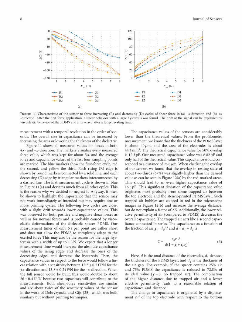
Figure 11 shows all measured values for forces in both+x- and –x-direction. The markers visualize every measuredforce value, which was kept for about 5 s, and the averageforce and capacitance values of the last four sampling pointsare marked. The blue markers show the first-force cycle, redthe second, and yellow the third. Each rising (R) edge isshown by round markers connected by a solid line, and eachdecreasing (D) edge by triangular markers interconnected bya dashed line. The first measurement cycle is shown in bluein Figure 11(a) and deviates much from all other cycles. Thisis the reason why we decided to neglect it. Anyway, it mustbe shown to highlight the importance that the sensor maynot work immediately as intended but may require one ormore priming cycles. The following two cycles are close,with a slight drift towards lower capacitance values. Thiswas observed for both positive and negative shear forces aswell as for normal forces and is probably caused by visco-elastic deformations of the dielectric spacer PDMS. Ourmeasurement times of only 5 s per point are rather shortand does not allow the PDMS to completely adapt to theexerted force This may also be the reason for the large hys-teresis with a width of up to 1.5N. We expect that a longermeasurement time would increase the absolute capacitancevalues of the rising edges and decrease the ones of thedecreasing edges and decrease the hysteresis. Then, thecapacitance values in respect to the force would follow a lin-ear relation with a sensitivity between 12 3 ± 0 2 fF/N for the+x-direction and 13 8 ± 0 2 fF/N for the –x-direction. Whenthe full sensor would be built, this would double to about26 ± 0 4 fF/N because two capacitors will contribute to themeasurements. Both shear-force sensitivities are similarand are about twice of the sensitivity values of the sensorin the work of Dobryzynska and Gijs [25], which was builtsimilarly but without printing techniques.
The capacitance values of the sensors are considerablylower than the theoretical values. From the profilometermeasurement, we know that the thickness of the PDMS layeris about 40μm, and the area of the electrodes is about44.4mm2. The theoretical capacitance value for 50% overlapis 12.3 pF. Our measured capacitance value was 6.82 pF andonly half of the theoretical value. This capacitance would cor-respond to a distance of 96.8μm. When checking the overlapof our sensor, we found that the overlap in resting state ofabout two-thirds (67%) was slightly higher than the desiredvalue as can be seen in Figure 12(a) by the red-marked areas.This should lead to an even higher capacitance value of16.5 pF. This significant deviation of the capacitance valueoriginates most probably from some trapped air betweenthe top electrode and the stencil-printed PDMS layer. Suchtrapped air bubbles are colored in red in the microscopeimages in Figure 12(b) and increase the average distance,but do not explain a factor of 2.5. Additionally, the lower rel-ative permittivity of air (compared to PDMS) decreases theoverall capacitance. The trapped air acts like a second capac-itance connected in series. The capacitance as a function ofthe fraction of air χ = d2/d and d = d1 + d2 is
C = ε0εrAd 1 − χ + εrχ
6
Here, d is the total distance of the electrodes, d1 denotesthe thickness of the PDMS layer, and d2 is the thickness ofthe air gap. For example, if the spacer contains 25% airand 75% PDMS the capacitance is reduced to 72.8% ofits ideal value (χ = 0, no trapped air). The combinationof the higher distance due to trapped air and a lowereffective permittivity leads to a reasonable relation ofcapacitance and distance.
The change in capacitance is originated by a displace-ment Δd of the top electrode with respect to the bottom
0
−20
−40
−60
ΔC (f
F)
−80
−100
−1201 2 3 4 5
F−x (N)6 7 8
R1R2R3
D1D2D3
(a)
120
100
80
60
40
20
0
ΔC (f
F)
1 2 3 4 5F+x (N)
6 7 8
R1R2R3
D1D2D3
(b)
Figure 11: Characteristic of the sensor to three increasing (R) and decreasing (D) cycles of shear force in (a) –x-direction and (b) +x-direction. After the first force application, a linear behavior with a large hysteresis was found. The drift of the signal can be explained byviscoelastic behavior of the PDMS and is reversed after a longer resting time.
8 Journal of Sensors

electrode. Using the distances in Table 1, we calculated thechange in distance for each of the four possibilities thatresults in the measured change in capacitance of about45 fF. The range of the calculated distance changes of lessthan a micrometer is reasonable since PDMS has a Poisson’sratio of almost 0.5 [28]. Therefore, the PDMS is only a littlecompressible as the lateral expansion is limited.
4. Discussion
In this work, a fully flexible, capacitive force sensor fortwo-axial force measurements has been developed by apply-ing printed electronic technologies on a polymeric film. Wesuccessfully fabricated structured silver electrodes on PETfoil by inkjet printing. We achieved a resolution with linesbelow 60μm and an average thickness of about 500nm.For a conducting layer, the inkjet-printed samples requiredan additional postproduction treatment. With photonic sin-tering, an ultrafast, selective, and cheap method was used tofunctionalize the thin films. PDMS, which was chosen for itsgood process ability and elastic properties, was found unsuit-able for direct inkjet printing. Oxygen plasma treatmentcould be an effective way to overcome the hydrophobic sur-face properties of PDMS. Further research is required here.The most challenging task was to fabricate the stacked struc-ture of a printed bottom electrode, a dielectric spacer, and aprinted top electrode. The method of gluing the two printedsheets together to solve the problem was the best available.The main objective of this report to fabricate a printed nor-mal and shear force sensor was achieved. By integrating thissensor into a 2-by-2 arrangement of four sensors, simulta-neous normal and shear forces (three-axial) can be mea-sured. Due to trapped air in the dielectric spacer, theexperimental capacitance values were distinctly lower thanthe theoretical predictions.
In the force range of 0.1 to 8N, we could find a linearrelationship between the capacitance values and the exertednormal and shear forces. For normal forces, a sensitivity of5.2 fF/N was determined and for shear forces, it was13.1 fF/N. These values were measured only for one-quarterof the sensor of an area of about 80mm2. When employingfour of the sensors in a different orientation, the shear forcesensitivity can be doubled to 26.2 fF/N, and the normal force
sensitivity quadrupled to 20.8 fF/N. These are comparable toother sensors in literature and have the main advantage thatonly printing techniques are employed. Only additive depo-sition techniques were used and the only difficult step is thealignment of both electrodes. The reduction of the fingerwidth to the planned 60μm or eventually 40μm wouldeither allow more fingers or a smaller sensor. The first wouldhave an approximate increase of the sensitivity closer to thepicofarad region. The second would decrease the area andincrease the sensitivity with respect to forces as the localpressures are higher. Another improvement could be theuse of structured dielectrics as in the previous section toreduce the stiffness of the dielectric. All of the materialsand methods used here are low-cost and cause a very smallamount of chemical waste, especially when compared toconventional semiconductor processes. This allows the pro-duction of sensors on large and flexible substrates as they areneeded for artificial skins. Such skins may be employed inadvanced humanoids as well as for patients without sensingcapabilities on parts of their body.
Data Availability
The data used to support the findings of this study are avail-able from the corresponding author upon request.
Conflicts of Interest
The authors declare no conflict of interest.
200 �휇m
(a)
200 �휇m
(b)
Figure 12: (a) Overlapping area of the electrodes colored in red onto an optical microscope picture and (b) trapped air in the PDMS layercolored in red as well as for better visibility.
Table 1: Comparison of the theoretical and measured capacitancevalues C0 and their change ΔC0, the thickness of the dielectricspacer d0 , and the deflection Δd. Bold values are calculated fromthe other columns.
C0 (pF) ΔC0 (fF) Overlap εr d0 (μm) Δd (nm)
Ideal 50% 12.3 45 50% 2.5 40.0 146
Ideal 67% 16.5 45 67% 2.5 40.0 109
Sensor 6.82 45 67% 2.5 96.8 635
S (25% air) 6.82 45 67% 1.8 69.7 457
9Journal of Sensors

Authors’ Contributions
A. Albrecht and P. Lugli contributed in the conceptualizationof the study. A. Albrecht created the methodology, wrote andprepared the original draft, and did the visualization of thestudy. P. Lugli, M. Becherer, and M. Trautmann gatheredresources. A. Rivadeneyra, P. Lugli, and M. Becherer wrote,reviewed, and edited the paper. P. Lugli and A. Rivadeneyrasupervised the study. P. Lugli and M. Becherer acquired thefunds for the study.
Acknowledgments
The authors want to thank Prof. Cheng of the TechnicalUniversity of Munich (TUM) for the use of their lab toproduce the inkjet-printed patterns used in this workand Prof. Wagner of the same university for the use oftheir workshop to build the two force setups. This workwas partially supported by the Deutsche Forschungsge-meinschaft (DFG) within the German Excellence Initiativethrough the cluster of excellence “Nanosystems InitiativeMunich” (NIM) and the Technical University of Munich(TUM) Graduate School.
References
[1] D. Lupo, W. Clemens, S. Breitung, and K. Hecker, “OE-Aroadmap for organic and printed electronics,” in Applicationsof Organic and Printed Electronics, Integrated Circuits andSystems, E. Cantatore, Ed., Springer, Boston, MA, USA, 2013.
[2] G. Nisato, D. Lupo, and S. Ganz,Organic and Printed Electron-ics: Fundamentals and Applications, CRC Press, 2016.
[3] M. Nir, D. Zamir, I. Haymov, and L. Ben-Asher, “Electricallyconductive inks for inkjet printing,” in The Chemistry of InkjetInks, S. Magdassi, Ed., pp. 225–254, 2010.
[4] A. Albrecht, M. Trautmann, M. Becherer, P. Lugli, andA. Rivadeneyra, “Multi-layer printed shear force sensor onflexible substrates,” in ALLSENSORS 2018, The Third Interna-tional Conference on Advances in Sensors, Actuators, Meteringand Sensing, pp. 70–75, Rome, Italy, 2018.
[5] A. Albrecht, Printed Sensors for the Internet of Things, Tech-nische Universität München, 2018.
[6] E. S. Hwang, J. H. Seo, and Y. J. Kim, “A polymer-based flexi-ble tactile sensor for both normal and shear load detectionsand its application for robotics,” Journal of Microelectromecha-nical Systems, vol. 16, no. 3, pp. 556–563, 2007.
[7] R. Pfeifer, M. Lungarella, and F. Iida, “The challenges ahead forbio-inspired ‘soft’ robotics,” Communications of the ACM,vol. 55, no. 11, p. 76, 2012.
[8] N. Lu and D.-H. Kim, “Flexible and stretchable electronicspaving the way for soft robotics,” Soft Robotics, vol. 1, no. 1,pp. 53–62, 2014.
[9] R. S. Dahiya, P. Mittendorfer, M. Valle, G. Cheng, and V. J.Lumelsky, “Directions toward effective utilization of tactileskin: a review,” IEEE Sensors Journal, vol. 13, no. 11,pp. 4121–4138, 2013.
[10] R. S. Dahiya, G. Metta, M. Valle, and G. Sandini, “Tactilesensing-from humans to humanoids,” IEEE Transactions onRobotics, vol. 26, no. 1, pp. 1–20, 2010.
[11] J. A. Rogers, T. Someya, and Y. Huang, “Materials andmechanics for stretchable electronics,” Science, vol. 327,no. 5973, pp. 1603–1607, 2010.
[12] T. Sekitani and T. Someya, “Stretchable organic integrated cir-cuits for large-area electronic skin surfaces,” MRS Bulletin,vol. 37, no. 3, pp. 236–245, 2012.
[13] G. Schwartz, B. C. K. Tee, J. Mei et al., “Flexible polymer tran-sistors with high pressure sensitivity for application in elec-tronic skin and health monitoring,” Nature Communications,vol. 4, no. 1, p. 1859, 2013.
[14] M. Kaltenbrunner, T. Sekitani, J. Reeder et al., “Anultra-lightweight design for imperceptible plastic electronics,”Nature, vol. 499, no. 7459, pp. 458–463, 2013.
[15] A. Albrecht, A. Rivadeneyra Torres, J. F. Salmerón,A. Abdellah, and P. Lugli, “Inkjet printing and photonic sinter-ing of silver and copper oxide nanoparticles for ultra-low-costconductive patterns,” Journal of Materials Chemistry C, vol. 4,no. 16, pp. 3546–3554, 2016.
[16] W. Y. Chang, T. H. Fang, H. J. Lin, Y. T. Shen, and Y. C. Lin,“A large area flexible array sensors using screen printingtechnology,” IEEE/OSA Journal of Display Technology, vol. 5,no. 6, pp. 178–183, 2009.
[17] C. L. Choong, M. B. Shim, B. S. Lee et al., “Highly stretchableresistive pressure sensors using a conductive elastomeric com-posite on a micropyramid array,” Advanced Materials, vol. 26,no. 21, pp. 3451–3458, 2014.
[18] R. S. Dahiya and M. Valle, Robotic Tactile Sensing : Technolo-gies and System, Springer, 2013.
[19] M. R. Cutkosky, R. D. Howe, and W. R. Provancher, “Forceand tactile sensors,” in Springer Handbook of Robotics, B.Siciliano and O. Khatib, Eds., pp. 455–476, Springer, Berlin,Heidelberg, 2008.
[20] H.-K. Lee, J. Chung, S.-I. Chang, and E. Yoon, “Normal andshear force measurement using a flexible polymer tactilesensor with embedded multiple capacitors,” Journal ofMicroelectromechanical Systems, vol. 17, no. 4, pp. 934–942, 2008.
[21] S. C. B. Mannsfeld, B. C. K. Tee, R. M. Stoltenberg et al.,“Highly sensitive flexible pressure sensors with microstruc-tured rubber dielectric layers,” Nature Materials, vol. 9,no. 10, pp. 859–864, 2010.
[22] T. A. T. A. Chase and R. C. R. C. Luo, “A thin-film flexiblecapacitive tactile normal/shear force array sensor,” inProceedings of IECON ‘95-21st Annual Conference on IEEEIndustrial Electronics, pp. 1196–1201, Orlando, FL, USA,1995.
[23] S. Khan, L. Lorenzelli, and R. S. Dahiya, “Screen printed flexi-ble pressure sensors skin,” in 25th Annual SEMI AdvancedSemiconductor Manufacturing Conference (ASMC 2014),pp. 219–224, Saratoga Springs, NY, USA, 2014.
[24] L. Viry, A. Levi, M. Totaro et al., “Flexible three-axialforce sensor for soft and highly sensitive artificialtouch,” Advanced Materials, vol. 26, no. 17, pp. 2659–2664, 2014.
[25] J. A. Dobrzynska and M. A. M. Gijs, “Polymer-based flexiblecapacitive sensor for three-axial force measurements,” Journalof Micromechanics and Microengineering, vol. 23, no. 1, article015009, 2013.
[26] R. Surapaneni, Q. Guo, Y. Xie, D. J. Young, and C. H.Mastrangelo, “A three-axis high-resolution capacitive tactileimager system based on floating comb electrodes,” Journal
10 Journal of Sensors

of Micromechanics and Microengineering, vol. 23, no. 7,article 075004, 2013.
[27] J. E. Mark, Polymer Data Handbook, Oxford University Press,2009.
[28] S. Yao and Y. Zhu, “Nanomaterial-enabled stretchable con-ductors: strategies, materials and devices,” Advanced Mate-rials, vol. 27, no. 9, pp. 1480–1511, 2015.
11Journal of Sensors

International Journal of
AerospaceEngineeringHindawiwww.hindawi.com Volume 2018
RoboticsJournal of
Hindawiwww.hindawi.com Volume 2018
Hindawiwww.hindawi.com Volume 2018
Active and Passive Electronic Components
VLSI Design
Hindawiwww.hindawi.com Volume 2018
Hindawiwww.hindawi.com Volume 2018
Shock and Vibration
Hindawiwww.hindawi.com Volume 2018
Civil EngineeringAdvances in
Acoustics and VibrationAdvances in
Hindawiwww.hindawi.com Volume 2018
Hindawiwww.hindawi.com Volume 2018
Electrical and Computer Engineering
Journal of
Advances inOptoElectronics
Hindawiwww.hindawi.com
Volume 2018
Hindawi Publishing Corporation http://www.hindawi.com Volume 2013Hindawiwww.hindawi.com
The Scientific World Journal
Volume 2018
Control Scienceand Engineering
Journal of
Hindawiwww.hindawi.com Volume 2018
Hindawiwww.hindawi.com
Journal ofEngineeringVolume 2018
SensorsJournal of
Hindawiwww.hindawi.com Volume 2018
International Journal of
RotatingMachinery
Hindawiwww.hindawi.com Volume 2018
Modelling &Simulationin EngineeringHindawiwww.hindawi.com Volume 2018
Hindawiwww.hindawi.com Volume 2018
Chemical EngineeringInternational Journal of Antennas and
Propagation
International Journal of
Hindawiwww.hindawi.com Volume 2018
Hindawiwww.hindawi.com Volume 2018
Navigation and Observation
International Journal of
Hindawi
www.hindawi.com Volume 2018
Advances in
Multimedia
Submit your manuscripts atwww.hindawi.com