renovating the vibrato driver preamp - hammondx66.com€¦ · renovating the vibrato driver preamp...
TRANSCRIPT

X66 Vibrato Driver Preamp Dec.2010 dan.vigin
Page 1
Hammond X-66
Renovating the
Vibrato Driver Preamp
by Dan.Vigin
Hammond ® and Leslie ® are registered trademarks of Suzuki Musical Instru ment Manufacturing Co. Ltd.
Binche / Belgium Dec.2010
X66 Vibrato Driver Preamp Dec.2010 dan.vigin
Page 2
TABLE OF CONTENTS - Forewords & Purpose of this project P. 3 - General Description P. 4 Original V ibrato D river P reamp circuit - X-66 Headroom concept P. 6 - New VDP circuit P. 8 - Transistor MJE340 P. 9 - Emitter resistor P. 10 - Schematic Diagram of new VDP P. 11
- Output levels P. 12
- Realization P. 12 - Conclusions P. 12 - PCB Layouts P. 13 - Datasheet MJE340 P. 14

X66 Vibrato Driver Preamp Dec.2010 dan.vigin
Page 3
Renovating the Vibrato Driver Preamp on Hammond X-6 6. Forewords – Purpose of this Project Several weeks ago, when playing an abnormal level of background noise and hiss was detected and this excessive noise made me nervous enough to start investigations in order to reduce this annoying noise. This background noise was mostly audible in Drawbars use while being less significant with either Tabs or Percussions. Even with no key depressed, by checking the outputs of the Vibrato Driver Preamp board, with the help of an oscilloscope, I found at once that one channel exhibited much more noise than the two others. This faulty channel was the Drawbar channel. So, I decided to pursue my investigations. Measured voltages were normal, capacitors were previously replaced by new ones. The conclusion is rather simple, the driver transistor creates this inherent noise in the Drawbar channel. The first reaction is to find and replace this faulty component by a new one. Unfortunately, this driver transistor labelled 21221 in the Hammond parts list is the equivalent of RCA 39699. This transistor was produced in the early 60's and is in the line with the first generation of Si NPN transistors launched at that time by RCA, about 50 years ago !. Needless to say that this component is now unobtainable, at least in Europe. In view of this situation, I decided to redesign this board and re-install much updated transistors providing better performances than the former RCA 396999. This is exactly the purpose of this chapter.

X66 Vibrato Driver Preamp Dec.2010 dan.vigin
Page 4
General Description. Original Vibrato Driver Preamp circuit. The board AO-32297-1 is located at the back side of the scanner block, under the Upper keyboard. Personnaly, I don't like at all the way this board has been engineered. This is the kind of board commonly used to create prototypes in lab's but not for production units. This is a personal opinion. Top view
Bottom view

X66 Vibrato Driver Preamp Dec.2010 dan.vigin
Page 5
The three Vibrato Driver Preamp's ( VDP's for short ) are located on the same board. The concept of each VDP is the same however they all have some slight differences that have to be taken into consideration. In fact, the role of each VDP is to procure enought amplitude to 'drive' its corresponding vibrato phase shift line that is linked directly to the scanner. The VDP board is then composed of three sections: - on the left, the TREBLE VIBRATO DRIVE PPREAMP - in the center, the TAB VOICE VIBRATO DRIVE PREAMP - on the right, the CELESTE VIBRATO DRIVE PREAMP There is no so much to tell about the circuitry. Basic 'Common Emitter' configuration is used with a partial decoupling in the emitter resistors. Refer to original schematic diagram hereunder.
Fig 5-7 (partial) of X-66 Service Manual.

X66 Vibrato Driver Preamp Dec.2010 dan.vigin
Page 6
X-66 Headroom concept We can notice on the diagram that those preamp's are fed by a voltage of +250 Vdc which is totally unusual for a conventional audio preamp. In the X-66 console, this voltage is even more, +265 Vdc were measured ! When looking on the original schematic diagram Fig 5-7, we can see that the incoming voltage at the Treble Vibrato Drive Preamp (Drawbars) is only 0.05 Vpp (Pt. E from Flute Filter) and the output voltage is 3.5 Vpp. So the amplification factor is 70. Then the question is: " Why to feed this circuit with such a high voltage of +250Vdc ? " After invesitigations, I came to the conclusion that one reason of feeding this circuit with +250 Vdc is to procure very high "headroom" to the outgoing signal. Headroom can be defined as ' the difference between the normal operating level and the clipping level (or undistorted value) of an audio device'. During tests, I found that the announced 3.5 Vpp level as indicated on Fig 5-7 can be easily obtained with a supply voltage of +25 Vdc. However, if we increase the level of the incoming signal, distortion appears rapidly (mostly clipping). If the same circuit is powered with +250 Vdc (i.e. 10 times more), then clipping (distortion) only appears when the outgoing signal reaches 115 Vpp i.s.o. 3.5 Vpp ! This way of doing provides an 'headroom' of 115 Vpp – 3.5 Vpp = 111.5 Vpp. Generally, headroom value is expressed in dB. In this case, the headroom is + 29,8 dB, unusually high. Extensive measurements were conducted on workbench and as an issue the next graphic was outlined.
X66 Vibrato Driver Preamp
0,00
20,00
40,00
60,00
80,00
100,00
120,00
140,00
24 48 100 150 200 250
Vcc (+Vdc)
Vou
t (V
pp)
Vout with constant inputVoltage of 50 mVpp
Vout with Vin adjusted before clipping (Max Vout)
Headroom (+ 29.8 dB)

X66 Vibrato Driver Preamp Dec.2010 dan.vigin
Page 7
The purpose of having sufficient headroom above normal operating signal is to avoid clipping and hence audible distortion. It is evident that when Percussion signals carrying very sharp transients are in use, sufficient headroom is needed in order to avoid clipping. For Tabs Voice signals, it is less needed since levels are quite constant while 'spikes' with Kinura tab depressed f.i. may justify some adequate headroom. For Drawbars signals issued from the flute filters, then such amount of headroom is not at all required because signals driving this VDP are almost pure sine waves or harmonics components of them. The X-66 designers of this VDP do have certainly other good technical reasons which remain unclear to me up to now.

X66 Vibrato Driver Preamp Dec.2010 dan.vigin
Page 8
New VDP circuit. Since very few information as far as the specifications of this VDP board are available in the X-66 Service Manual, the original board AO-32297-1 board was dismounted and put on the workbench for test. As stated earlier, only one channel was defective (noisy), so the two others were workable for measurements. The original board AO-32297-1 was powered by +250 Vdc with an incoming signal of 50 mVpp @ 1Khz . The collector of transistor 21221 (RCA 39699) was loaded by a 12K/1W resistor to ground via one 1µF/400Vdc capacitor. See simplified schematic herafter. The three sections of the AO-32297-1 board were configurated so and results of measurements were recorded in order to redesign a new VDP board. With the help of a workbench simulator software, a new VDP circuit was redesigned based on MJE340 transistor having much superior performances than RCA 36699.
VIBRATODRIVE PREAMP
12 K
/5 W
82 O
33 O
22 K
E
C
B
+
-
- + MJE340
100 µF63 V
1 µF63 V
1 nF
220 K
T1
EBC
21
3TO-126
MJE340
Test-Point
1 µF400 V
GND
50 mVpp@ 1KHz
12K
/1W
+ 250 Vdc
Load resistor applied during measurements
IN
OUT
To Vibrato Phase Shift Line
Foot emitter resistor

X66 Vibrato Driver Preamp Dec.2010 dan.vigin
Page 9
The overall new schematic diagram can be found on the next page. This new schematic diagram is almost identical to the original one. Beside the replacement of the old RCA transistor by MJE340, only the collector resistor has been changed from 10K/5W into 12K/5W to slightly decrease the collector current and reduce to a certain extend the power dissipation that is not negligeable due to high B+ voltage involved. Dale 12K / 5W – 1% resistors were installed. Here is the new VDP board.
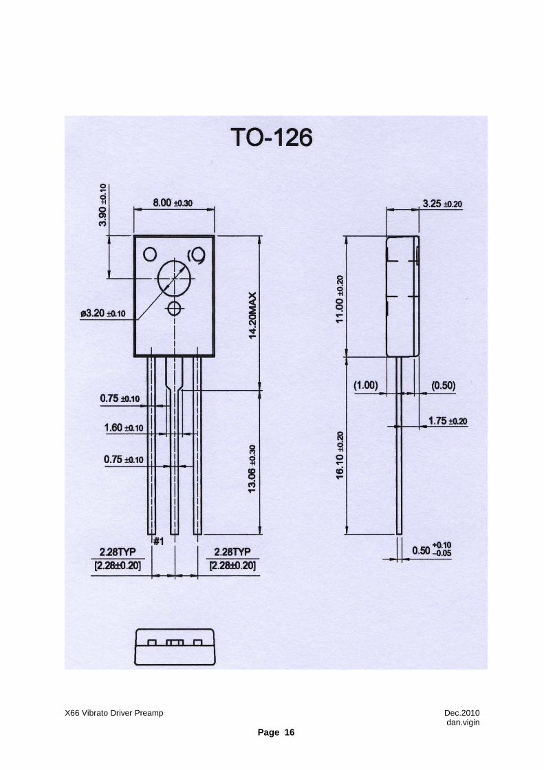
Transistors MJE340. While not necessary by calculation, for reliability purpose, the transistors MJE340 were mounted on heatsink. Silicon compound was used for better heat transfert. It is strongly recommended to select hFE values (DC current gain) of those transistors. hFE may vary from 30 up to 240 according to datasheet of the transistor supplier which is indeed a very wide range. The correct hFE value for each MJE340 transistor should remain in the range of min. 70 to max. 85. In my case, the three transistors had an hFE value of 83. Datasheet of MJE340 are also provided in the next pages. Simplified characteristics RCA 39699 MJE340 NPN Technology Early generation Si Transistor Planar Epitaxial Silicon transistor VCB0 400 V 300 V VCE0 300 V 300 V VEB0 6 V 5 V Collector Dissip. 8 W 20 W hFE 40 ~ 80 30 ~ 240

X66 Vibrato Driver Preamp Dec.2010 dan.vigin
Page 10
33 ΩΩΩΩ Emitter resistors. In addition to that, if one wants to keep an equivalent output level at each section of the VDP board, it is also important to carefully select the foot emitter resistor of 33 Ω. Higher value of this 33Ω resistor will decrease the overall gain while lower value will increase the overall gain. Note: during life-tests, for reliability purpose, the voltage supply was increased from +250 Vdc up to +270 Vdc. No breakdown was recorded.

X66 Vibrato Driver Preamp Dec.2010 dan.vigin
Page 11
TR
EB
LE V
IBR
AT
OD
RIV
E P
RE
AM
P
12 K /5 W 82 O 33 O
22 K
EC
B
+ -
-+
MJE
340
20 µ
F6
3 V
1 µ
F63
V
12 K /5 W 82 O 33 O
22 K
EC
B
+ -
-+
MJE
340
100
µF
63 V
10 µ
F63
V
12 K /5 W 82 O 33 O
22 K
EC
B
+ -
-+
MJE
340
100
µF
63 V
10 µ
F6
3 V
1 nF
1 nF
1 nF
+ 25
0 V
dc
TA
B V
OIC
E V
IBR
AT
OD
RIV
E P
RE
AM
P
To
Exp
ress
ion
Pre
amp
Boa
rd
CE
LES
TE
DR
IVE
P
RE
AM
P
GN
D
220
K22
0 K
220
K
20
nF40
0V
T1
W46
T2
T3
0.1
µF
400
V1
µF
400
V1
µF40
0 V
+ 2
50 V
dc
33 K
47 K
W55
W65
W64
W57
To
Dra
wba
r V
ibra
to P
hase
S
hift
Line
To
Tab
Voi
ce
Vib
rato
Pha
se
Shi
ft Li
ne
To
Cel
este
V
ibra
to P
hase
S
hift
Line
E
Fro
m P
edal
Pre
amp
Fig
5-7
, X-1
82
G
Fro
m P
ercu
ssio
n S
ectio
nF
ig 5
-4, X
-76
Fro
m D
raw
bar
Sec
tion
Fig
5-1
, T-6
4
Circ
uit D
iagr
am –
Hammond
X-6
6 R
e-de
sign
ed V
ibra
to D
river
Pre
amp
File
: Vib
rato
_Driv
er_V
1.vs
d
Dat
e : 3
0/11
/201
0
Issu
ed b
y : D
an.V
igin
Ham
mon
d®
and
Les
lie®
are
reg
iste
red
trade
mar
ks o
f Suz
uki M
usic
al
Inst
rum
ent M
anuf
actu
ring
Co.
Ltd
.
EB
C2
13
TO
-126
MJE
340
+ 60
.5
Vdc
+ 2.
4 V
dc
+ 1.
8 V
dc
+ 0
.5 V
dc
8.1
Vpp
(1)
(@ 1
KH
z)
DALE
50 m
Vpp
(@ 1
KH
z)
16 m
Adc
48 m
Adc
WH
T/B
LUY
EL
BLK
Shi
elde
d ca
ble
GN
D
BR
N
2x B
LKRE
D
RE
DO
RG
YE
L
47 K
Not
es.
- (1
) R
esis
tor
of 1
2 K
/ 1W
is u
sed
betw
een
T
est-
poin
ts A
, B, C
and
GN
D d
urin
g
mea
sure
men
ts o
n th
e w
orkb
ench
.-
(2)
Car
eful
ly s
elec
ted
to a
djus
t out
put l
evel
nea
r 8.
0 V
pp.
-
hFE o
f T1,
T2,
T3
to b
e se
lect
ed b
etw
een
>70
and
<85
.-
T1,
T2
& T
3 m
ount
ed e
ach
on h
eats
ink.
12
K/1
W
Load
res
isto
r du
ring
test
s
AO
-322
97-1
Tes
t-P
oint
AT
est-
Poi
nt B
Tes
t-P
oint
C
(2)
(2)
(2)

X66 Vibrato Driver Preamp Dec.2010 dan.vigin
Page 12
Output levels. During measurements of the original board AO-32297-1, output levels of 7.2 Vpp were recorded with an input sine wave signal of 50 mVpp @ 1KHz. As already stated, those values are measured with a load resistor of 12K / 1W on each section. With the new VDP board, I have intentionally selected the transistors MJE340 and the foot resistors of 33 Ω to obtain a value of 8.0 Vpp (i.s.o. 7.2 Vpp as on original one). Limits for new VDP should remain around +/- 0.2 Vpp i.e. 7.8 Vpp ~ 8.2 Vpp. This difference gives some 'voltage boost' that was positively evaluated during final listening tests. By altering the value of this emitter resistor of 33 Ω, it is possible to refind exactly the value of 7.2 Vpp as on the original board. It's a matter of choice. There is no indication whatsoever in the X-66 Service Manual as far as the effective load composed by the vibrato phase line circuits. When analysing the structure of those circuits, it seemed to me that this load should fall in the range of 12 K. It's a my pure guess. Measurements at no-load condition makes no sense and since the same load value of 12 K / 1W was used for both original board and new one, the conditions of measurements remain identical and trustworthy. Realization. A shown on the picture, a new board was redesigned keeping the same external dimension of the original one. The position of the terminals was also kept for easiness of rewiring. The three output capacitors ( 0.1 µF/400 Vdc and 2x 1 µF/400 Vdc ) were found perfect and hence were left in their initial position on the scanner chassis. Negative and components sides of this PCB are provided in the next pages for those who envisage to realize this VDP board. There is no so much to tell about the board itself, quite basic for any qualified technician. Conclusion. Initially, I had no intention to redesign this board AO-32297-1. This was caused by the excessive 'inherent noise and hiss' that suddenly appeared in the Drawbar channel. In fact, since I was forced to resolve that failure, from there came the idea of redesigning this board. At the end, it was a good decision because the replacement of old RCA transistors by MJE340's provides to the X-66 console a real 'boost' while reducing to some extend the overall inherent background noise (rather subjective). This is only my personal feeling. Dan. Vigin

X66 Vibrato Driver Preamp Dec.2010 dan.vigin
Page 13
PCB Layouts Components side Copper side

X66 Vibrato Driver Preamp Dec.2010 dan.vigin
Page 14
DATASHEET MJE340.

X66 Vibrato Driver Preamp Dec.2010 dan.vigin
Page 15
X66 Vibrato Driver Preamp Dec.2010 dan.vigin
Page 16