reference design quad-sfp host adapter · reference design hfrd-32.0 (rev. 2; 11/08) maxim...
TRANSCRIPT

AVAILABLE
Functional Diagrams
Pin Configurations appear at end of data sheet.Functional Diagrams continued at end of data sheet.UCSP is a trademark of Maxim Integrated Products, Inc.
Reference Design:
HFRD-32.0 Rev. 2; 11/08
REFERENCE DESIGN
Quad-SFP Host Adapter

Reference Design HFRD-32.0 (Rev. 2; 11/08) Maxim Integrated Page 2 of 24
Quad-SFP Host Adapter Table of Contents 1 Overview ..........................................................2 2 Obtaining Additional Information ....................2 3 Typical Use.......................................................3 4 Control Interface...............................................4 5 Getting Started..................................................5 6 Evaluation.......................................................15 7 Supporting Documentation.............................17
1 Overview High Frequency Reference Design 32.0 (HFRD-32.0) is a host adapter board that supports Quad-SFP (QSFP) modules. HFRD-32.0 routes power and I2C serial-communication support, and translates the high-speed, QSFP interconnect to SMA connectors.
HFRD-32.0 is suitable for evaluating QSFP modules operating from 1Gbps to 10Gbps. The material used in the construction of the board is inexpensive and lossy FR-4 with a loss tangent of approximately 0.02. The differential data lines are lightly coupled 6mil-wide microstrip lines. These lines are located on the back of the board to eliminate the stub effect of the through-hole vias needed to connect to the QSFP interface connector. Host-side monitoring of VCC_TX and VCC_RX supply currents and voltages provides additional confidence that the external supply is adequate and that the module is not drawing excessive current. The landing area for the QSFP module meets the mechanical requirements described in the QSFP specification version 1.0 and is, therefore, compatible with QSFP cages, latches, and housings. The software that supports the host adapter board relies on a Microsoft Windows®-based personal computer equipped with USB.
HFRD-32.0 reduces the risk associated with experimenting with QSFP modules by supplying the user-interface software and the necessary hardware interface to support QSFP module development.
Microsoft Windows is a registered mark of Microsoft Corporation.
1.1 Features
• Schematics
• Bill of Materials
• Gerber plot files available
• Single 3.3V supply
• USB
• Serial interface to QSFP
• Graphic user interface (GUI) software
• Assembled and tested
2 Obtaining Additional Information
Limited quantities of the Quad-SFP Host Adapter (HFRD-32.0) are available. For more information about this reference design or to obtain a board, please email your request to: https://support.maxim-ic.com/.

Reference Design HFRD-32.0 (Rev. 2; 11/08) Maxim Integrated Page 3 of 24
3 Typical Use Figure 1 shows a typical testing configuration for a QSFP module. Two HFRD-32.0 boards are used in this example.
The test apparatus shows an Agilent ParBERT™ pattern generator which fills the channels and
introduces aggressor signals for crosstalk evaluation. The Agilent 70843B supplies the “victim” signal. The HFRD-32.0 host adapter board provides the interface between the lab equipment and the module. The Tektronix CSA8000 oscilloscope produces eye diagrams. Not shown is a personal computer needed to monitor and control the QSFP modules.
Figure 1. Typical test apparatus fills all channels to evaluate performance in the presence of interfering aggressor signals.
ParBERT is a trademark of the Agilent Technologies Inc
Host Adapter Board (HFRD-32.0)
Active Copper QSFP
Agilent Par BERT E4803A Mainframe E4861A Pat Gen
4
HFRD-31.0
44
4
4
Tek CSA8000 Oscilloscope with 80E04
Eye Diagrams
3
1
50
50
3
1
4 3
HPE3631A Power Supply
3.3V 3.3V
Victim Signal
1VP-P Near-End Aggressor
Signals
Agilent 70843B Pattern Generator
Agilent 83752A Synthesizer (clock source)
Host Adapter Board (HFRD-32.0)

Reference Design HFRD-32.0 (Rev. 2; 11/08) Maxim Integrated Page 4 of 24
4 Control Interface Access to QSFP functions is provided by the HFRD-32.0 host adapter board and its associated graphic user interface (GUI) software. Combined, they allow access through a Microsoft Windows-based personal computer equipped with USB. Figures 2 through 10 are examples of the GUI.
4.1 User Interface
The user interface display is divided into two major regions. The uppermost region pertains exclusively to the host board. See Figures 2 and 3. This region includes advisory messages about the status of the communication link with the module, the current and voltage supplied to the module, and the Initialize button. The lower region pertains exclusively to module operation. See Figures 4 through 10. Module functions and features are accessed through the tab boxes. A mouse click on a tab reveals the relevant controls.
Monitor Tab–This page displays measurements, alarm flags, warning flags, and other channels’ status flags such as LOS and TX Fault. This information is updated based on the selected Flag Update Method. The method can be set to update when the Hardware Interrupt Line is asserted, the Software Interrupt Bit is asserted, or by asynchronously polling at two times per second. The flag history can be enabled or disabled to aid in observations. When set to ON, asserted flags are retained and can be erased using the Clear. When set to OFF, the history is not retained. The state of the flags is cleared automatically with each new update.
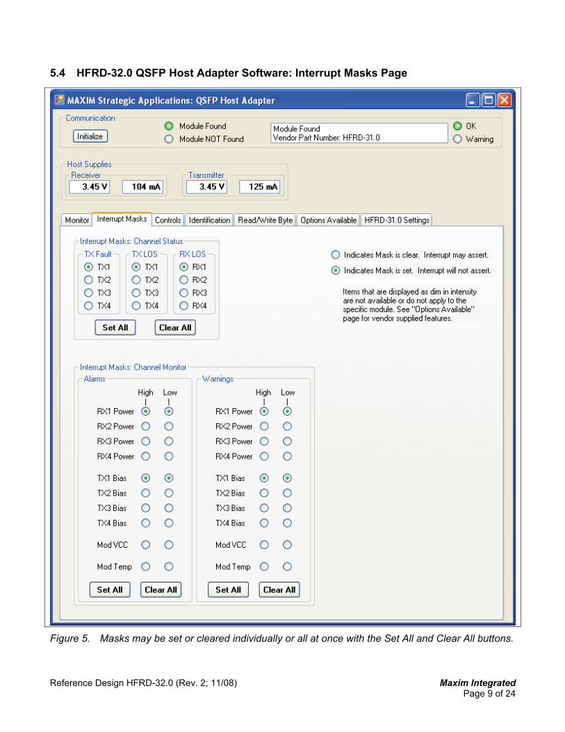
Interrupt Masks Tab–This page allows the user to prevent (i.e., mask) individual events from generating interrupts. Each event can be masked by clicking the associated radio button beside the event description. Each radio button is an alternate-action function; each click alternates from a masked to an unmasked condition. For convenience, Set All and Clear All buttons set or clear the entire group. Clicking Set All masks the entire group. Clear All clears and enables all of the events within the group.
Controls Tab–This page presents the superset of module functions that are defined in the QSFP specification. This does not mean that all modules must implement all functions. Depending on the vendor’s implementation, control over TX and RX outputs, squelch, and rate selection are made using this page. The availability of these functions is, finally, determined by a list provided by the module. See Options Available Tab to view this list.
Identification Tab–A multitude of identification fields are designated for QSFP modules. This page presents them, as well as the check-sum values stipulated by the QSFP specification.
Read/Write Byte Tab–This page allows the user to access specific locations within the module’s memory. QSFP has designated four different Upper Pages to its memory map with addresses (i.e., byte numbers) ranging from 128 through 255. Single-byte reading and writing is available in the Single Byte group. The data can be entered as hexadecimal, binary, or ASCII. As the data is typed into one box, its equivalent appears in the other boxes. The Multi-Byte Read group requires a starting address and a byte count, and displays the data sequence in hexadecimal, binary, and ASCII formats. When necessary, use the Password Entry group to write into protected regions of the module’s memory.
Options Available Tab–This page presents the list of optional features available for the installed module. These features are selected by the vendor and determine which functions are relevant to the specific module. For example, a copper cable transceiver will not support optical functions such as TX Bias and RX Power.
HFRD31 Settings Tab–This page only appears if the HFRD-31.0 module from Maxim is detected. The module must have the ASCII characters “HFRD-31.0” as the first nine characters starting at decimal address 168. These controls determine the power-on settings of HFRD-31.0 such as pre-emphasis settings and output enable. This page is also where one can change calibration constants associated with the temperature and voltage monitors.

Reference Design HFRD-32.0 (Rev. 2; 11/08) Maxim Integrated Page 5 of 24
5 Getting Started The software is designed to operate on Microsoft Windows 2000 or Windows XP operating systems. The software can also be used on Windows 98, but unstable software operation can occur if the USB cable is unplugged without first stopping the device from windows. This software was built on the Microsoft.NET platform. If the current version of this platform is not already installed on your computer, an internet connection will be needed to download the components and complete the installation.
HFRD-32.0, the QSFP Host Adapter board, can be used with any QSFP module; however, software testing has been limited to Maxim’s HFRD-31.0 Quad-SFP Active Copper Cable Assembly reference design. The software that supports HFRD-32.0 is available on CD or from the Maxim web-site at:
http://www.maxim-ic.com/products/fiber/reference_designs.cfm
Instructions for getting started with the QSFP host board are listed below.
Step:
1. Install the reference design software:
a. Maxim web site - Download the software (HFRD_32p0_rev1.zip), “unzip” or extract all files and run Setup.exe.
b. CD-ROM - Insert the CD-ROM. If the software does not install automatically, run Setup.exe.
2. Connect HFRD-32.0 to the computer using the provided USB cable. When the cable is inserted, a green LED on the board labeled USB_PWR should be illuminated.
3. Apply +3.3V across J2 (+3.3V) and J3 (GND) from an external power supply. This supply must be capable of supplying 1.2A at +3.3V to support QSFP modules. If equipped, set the current limit of the external supply to approximately 150mA above the
current required by the module. Turn on the supply. If using HFRD-31.0 as the module, set the current limit to 600mA. The host board will filter the +3.3V supply and route it to the QSFP module as VCCTX, VCCRX, and VCC1.
4. Run the HFRD-32.0 software from the Windows operating system:
start All Programs Maxim Integrated Products QSFP Host
5. The application should start and appear similar to the top picture in Figure 2.
6. Click Initialize in the upper left portion of the display.
7. The display should appear similar to the middle picture of Figure 2. Verify that the two host supply voltages are between +3.2V and +3.4V. The voltage values will be displayed with red text if the supplies are below +3.0V or above +3.6V. Similarly, the supply current values change to red when above 500mA or below 5mA. If the supply current is above 50mA with no module installed, then turn off the supply, check connections, and return to step 3.
8. Install the QSFP module. The software will detect the module’s presence and initiate communication. The display should be similar to the bottom picture of Figure 2. The vendor’s part number, if available, will appear in the message box. In this example, Vendor Part Number: HFRD-31.0 is shown.
9. After establishing communication with the QSFP module, the remainder of the QSFP functions will be enabled and accessible. The display should be similar to Figure 4.
10. You are now ready to examine and explore the various pages of monitoring, identification, and control features.

Reference Design HFRD-32.0 (Rev. 2; 11/08) Maxim Integrated Page 6 of 24
5.1 HFRD-32.0 QSFP Host Adapter Software: Initialization
Figure 2. The first three steps to successful operation. Top screen shows the message when the application software is launched; message advises “Press” or click the Initialize button at the upper left. Middle screen shows a typical message after initialization and passing the external power-supply test. Bottom screen shows that a module was detected and its vendor part number retrieved.

Reference Design HFRD-32.0 (Rev. 2; 11/08) Maxim Integrated Page 7 of 24
5.2 HFRD-32.0 QSFP Host Adapter Software: Supply Monitoring
Figure 3. Host supply monitoring advises when the external power supply is out of range. The external supply should be between +3.0V and +3.6V. Supply voltage measurements change color to red when above +3.6V and below +3.0. Similarly, the supply current changes to red text when above 500mA and below 5mA.

Reference Design HFRD-32.0 (Rev. 2; 11/08) Maxim Integrated Page 8 of 24
5.3 HFRD-32.0 QSFP Host Adapter Software: Monitor Page
Figure 4. Monitoring includes flag history, measurements and choice of event that forces the update.
Reference Design HFRD-32.0 (Rev. 2; 11/08) Maxim Integrated Page 9 of 24
5.4 HFRD-32.0 QSFP Host Adapter Software: Interrupt Masks Page
Figure 5. Masks may be set or cleared individually or all at once with the Set All and Clear All buttons.

Reference Design HFRD-32.0 (Rev. 2; 11/08) Maxim Integrated Page 10 of 24
5.5 HFRD-32.0 QSFP Host Adapter Software: Controls Page
Figure 6. Controls and module power.

Reference Design HFRD-32.0 (Rev. 2; 11/08) Maxim Integrated Page 11 of 24
5.6 HFRD-32.0 QSFP Host Adapter Software: Identification Page
Figure 7. The numerous QSFP identification fields are shown. When modules report multiple arguments for a given trait, pop-up boxes display a complete list of characteristics.

Reference Design HFRD-32.0 (Rev. 2; 11/08) Maxim Integrated Page 12 of 24
5.7 HFRD-32.0 QSFP Host Adapter Software: Bit and Byte Level Read/Write
Figure 8. The Read/Write page gives bit and byte-level access to all QSFP memory locations and contents.

Reference Design HFRD-32.0 (Rev. 2; 11/08) Maxim Integrated Page 13 of 24
5.8 HFRD-32.0 QSFP Host Adapter Software: Options Available Page
Figure 9. Optional QSFP features are reported by the module and displayed.

Reference Design HFRD-32.0 (Rev. 2; 11/08) Maxim Integrated Page 14 of 24
5.9 HFRD-32.0 QSFP Host Adapter Software: HFRD-31.0 Specific Controls
Figure 10. Vendor-specific controls for HFRD-31.0. This menu is present only when the host adapter detects HFRD-31.0.

Reference Design HFRD-32.0 (Rev. 2; 11/08) Maxim Integrated Page 15 of 24
6 Evaluation The differential return loss (SDD11) for the board is shown in Figures 11 and 12. Figure 11 shows the SDD11 for all ports, TX and RX, with a 100Ω differential termination in place of the QSFP connector. The QSFP specification does not include a return-loss limit. For this example, the limit from the SFP+ specification is plotted for reference. Compared to this limit, the board offers significant margin, but it does not include the QSFP connector and module. The return-loss requirements will vary depending on the application for a given module. This renders a single return-loss limit
meaningless. For example, a module made for operation at 2.125Gbps should not have to support a return loss of 10dB at 5GHz. The data shown in Figure 12 indicates that HFRD32.0 is adequate for operation at 10Gbps. SDD11 in Figure 12 was acquired with a dummy-load board intended for a maximum rate of 5Gbps. The active devices were removed from the module and 100Ω resistors soldered across the differential lines in the module. Given more care in the layout, it is possible that some improvements could be made. Nonetheless, the current design offers a realistic environment created from practical materials.
Return Loss of HFRD32.0Without QSFP Connector
-30
-27
-24
-21
-18
-15
-12
-9
-6
-3
0
0.E+00 1.E+09 2.E+09 3.E+09 4.E+09 5.E+09 6.E+09 7.E+09 8.E+09 9.E+09 1.E+10
Freq(Hz)
SDD
11(d
B)
RX1RX2RX3RX4TX1TX2TX3TX4SFP+ Limit
SFP+ Tolerance Limit
Figure 11. Return loss of HFRD-32.0 without the QSFP connector. The transmission lines were differentially terminated with 100Ω resistors at the QSFP connector landing pads. The SFP+ tolerance limit is included for reference. The QSFP specification does not include a return-loss limit.

Reference Design HFRD-32.0 (Rev. 2; 11/08) Maxim Integrated Page 16 of 24
Return Loss of HFRD32.0with Dummy Module Load
-30
-27
-24
-21
-18
-15
-12
-9
-6
-3
0
0.E+00 1.E+09 2.E+09 3.E+09 4.E+09 5.E+09 6.E+09 7.E+09 8.E+09 9.E+09 1.E+10
Freq(Hz)
SDD
11(d
B)
RX1RX2RX3RX4TX1TX2TX3TX4SFP+ Limit
SFP+ Tolerance Limit
Figure 12. Return loss of HFRD-32.0 including the QSFP connector and a dummy-load module. All active components were removed from the module and the transmission lines were differentially terminated with 100Ω resistors on the module board. The SFP+ tolerance limit is included for reference. The QSFP specification does not include a return-loss limit.

Reference Design HFRD-32.0 (Rev. 2; 11/08) Maxim Integrated Page 17 of 24
7 Supporting Documentation
7.1 HFRD-32.0 Schematic, Sheet 1 of 2
Figure 13. Schematic for HFRD-32.0 showing high-speed data path and supply filters.

Reference Design HFRD-32.0 (Rev. 2; 11/08) Maxim Integrated Page 18 of 24
7.2 HFRD-32.0 Schematic, Sheet 2 of 2
Figure 14. Schematic for HFRD-32.0 showing USB, supply monitors, and micro controller.

Reference Design HFRD-32.0 (Rev. 2; 11/08) Maxim Integrated Page 19 of 24
7.3 Artwork, HFRD-32.0, Layers 1 and 2
Figure 15. Layer 1 (top), high-speed transmission lines.
Figure 16. Layer 2, ground and reference plane for layer 1.

Reference Design HFRD-32.0 (Rev. 2; 11/08) Maxim Integrated Page 20 of 24
7.4 Artwork, HFRD-32.0, Layers 3 and 4
Figure 17. Layer 3, supply routing
Figure 18. Layer 4, QSFP connector and landing area.

Reference Design HFRD-32.0 (Rev. 2; 11/08) Maxim Integrated Page 21 of 24
7.5 Component Placement, Front Side HFRD32.0
Figure 19. Top (front) layer, transmission lines for high-speed data.

Reference Design HFRD-32.0 (Rev. 2; 11/08) Maxim Integrated Page 22 of 24
7.6 Component Placement, Back Side HFRD32.0
Figure 20. Bottom layer, as viewed from the bottom.
Attach External Supply Between +3.3V and GND
Voltage Monitoring Test Points. Do not attach to
supply or GND.
J23 is for Factory Use Only. Do not attach anything to these pins.

Reference Design HFRD-32.0 (Rev. 2; 11/08) Maxim Integrated Page 23 of 24
7.7 Mechanical Dimensions, HFRD-32.0
Figure 21. Dimensioned drawing and FR-4 board stackup (loss tangent = 0.02).

Reference Design HFRD-32.0 (Rev. 2; 11/08) Maxim Integrated Page 24 of 24
7.8 Bill of Materials
Qty BOM
Option Reference Value Tolerance Description
1 L6 1.0µH Taiyo-Yuden 1.0uH, CBC3225T1R0M
2 L1 L5 22µH Taiyo-Yuden 22uH CBC3225T220MR or CBC3225T220KR
5 J2-4 J21-22 TESTPOINT DIGI-KEY® 5000K-ND
1 U10 Microchip PIC16C745-I/SO
1 J23
1 Y2 CRYSTAL, ECS INC. XC679CT
1 J1 38-pin iPass SMT Connector, female. Molex number 75586-0011
1 J25 USB CONNECTOR, TYCO 440247-1
19
C2 C6-9 C11 C13 C24-27 C49-50 C58-59 C63-64
C90-91
0.1µF 10% CERAMIC CAPACITOR (0402)
2 C18 C22 33pF 10% CERAMIC CAPACITOR (0402)
6 C17 C19-20 C34 C51 C57 1µF 10% CERAMIC CAPACITOR (0603)
1 C10 10µF 10% CERAMIC CAPACITOR (0805)
3 C21 C23 C37 4.7µF 10% CERAMIC CAPACITOR (0805)
4 C1 C3-5 22µF 10% TANTALUM CAPACITOR 1206
3 L2-4 4.7µH Coilcraft Power Inductor DS1608-472MLB
1 D2 GREEN LED
2 U14 U19 MAX1362EUB
1 U21 MAX3373EEKA-T
2 U20 U22 MAX4070AUA
4 Do Not Install R89 R94 R97 R98 0 RESISTOR (0402)
2 R93 R90 0 RESISTOR (0402)
1 R24 1.5k 1% RESISTOR (0402)
12 R3-5 R7 R9-10
R25 R49-51 R92 R107
10k 1% RESISTOR (0402)
2 R87-88 24.9k 1% RESISTOR (0402)
7 R11-14 R52 R55 R86 49.9 1% RESISTOR (0402)
1 R91 680 1% RESISTOR (0402)
2 R1-2 0.025 1% RESISTOR (1206) 0.125W
16 J5-20 SMA SIDE MOUNT TAB CONTACT JOHNSON 142-0701-851
2 TP13-14 TESTPOINT DIGI-KEY 5000K-ND
Digi-Key is a registered trademark of Digi-Key Corporation.