recommendations for control of radiated emissions with ... · radiated emissions and conducted...
TRANSCRIPT
AN-0971 APPLICATION NOTE
One Technology Way • P.O. Box 9106 • Norwood, MA 02062-9106, U.S.A. • Tel: 781.329.4700 • Fax: 781.461.3113 • www.analog.com
Recommendations for Control of Radiated Emissions with isoPower Devices
by Mark Cantrell
Rev. C | Page 1 of 20
INTRODUCTION iCoupler® digital isolators with integrated isolated power (isoPower®) employ isolated dc-to-dc converters that switch currents of ~700 mA at frequencies as high as 300 MHz. Operation at these high frequencies raises concerns about radiated emissions and conducted noise. PCB layout and construction is a very important tool for controlling radiated emissions and noise from applications containing isoPower components. This application note identifies the radiation mechanisms and offers specific guidance on addressing them.
Several standards for radiated emissions exist. In the U.S., the Federal Communications Commission (FCC) controls the standards and test methods. In Europe, the International Electrotechnical Commission (IEC) generates standards, and CISPR test methods are used for evaluating emissions. The methods and pass/fail limits are slightly different under the two standards. Although this application note is written with reference to CISPR standards, all results are applicable to both standards.
With proper design choices, isoPower devices can easily meet CISPR Class A (FCC Class A) emissions standards. With care, these products can also meet CISPR Class B and FCC Part 15, Subpart B, Class B (FCC Class B) standards in an unshielded environment. This application note examines PCB-related EMI mitigation techniques, including board layout and stack-up issues.
The techniques, example layouts, and measurements described in this application note are highly dependent on the options available in PCB construction. A 4-layer PCB is required to implement the evaluated EMI control techniques. Availability of more internal PCB layers offers the same EMI reductions within smaller geome-try PCBs. For the purposes of this application note, a 4-layer board was designed and manufactured using materials and structures well within industry norms.
Control of emissions from signal cables and chassis shielding techniques are outside of the scope of this application note.
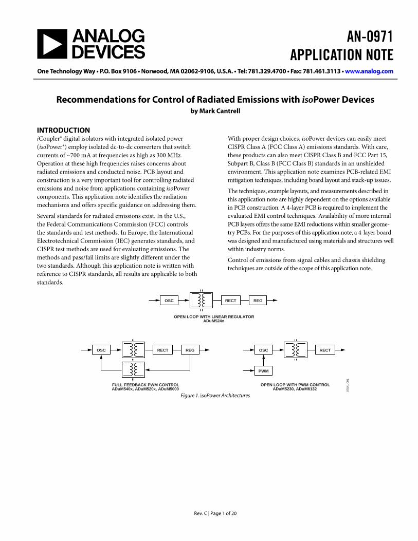
OSC REGRECT
OPEN LOOP WITH LINEAR REGULATORADuM524x
OSC REGRECT
FULL FEEDBACK PWM CONTROLADuM540x, ADuM520x, ADuM5000
OSC
PWM
RECT
OPEN LOOP WITH PWM CONTROLADuM5230, ADuM6132 07
541-
001
Figure 1. isoPower Architectures
AN-0971 Application Note
Rev. C | Page 2 of 20
TABLE OF CONTENTS Introduction ...................................................................................... 1 Revision History ............................................................................... 2 isoPower Overview ........................................................................... 3 Sources of Radiated Emissions ....................................................... 4
Edge Emissions ............................................................................. 4 Input-to-Output Dipole Emissions ............................................ 4
Sources of Conducted Noise ........................................................... 6 EMI Mitigation Techniques ............................................................ 7
Input-to-Output Stitching ........................................................... 7 Edge Guarding .............................................................................. 8 Interplane Capacitive Bypassing ................................................ 9 Power Reduction ........................................................................ 10 Operating Voltage ....................................................................... 10
Recommended Design Practices .................................................. 11 Meeting Isolation Standards ......................................................... 12 Evaluating PCB Structures for EMI ............................................. 13
Edge Guarding Results .............................................................. 15 Operating Load and Voltage Dependence .............................. 16 Interplane Capacitance .............................................................. 16
Integrating Techniques .................................................................. 17 Example 1—Basic Insulation Board ........................................ 17 Example 2—Reinforced Insulation Board .............................. 18 Additional Layout Considerations ........................................... 19
Conclusions ..................................................................................... 20 References .................................................................................... 20
REVISION HISTORY 1/14—Rev. B to Rev. C Added Table 1 and changes to and moved isoPower Overview Section ................................................................................................ 3 Change to Edge Emissions Section ................................................ 4 Changes to EMI Mitigation Techniques Section .......................... 7 Change to Equation 2 ....................................................................... 8 Changes to Interplane Capacitive Bypassing Section .................. 9 6/11—Rev. A to Rev. B Changes to Introduction Section, isoPower Overview Section, and Figure 1 ....................................................................................... 1 Changes to Edge Emissions Section and Input-to-Output Dipole Emissions Section ................................................................ 3 Added Figure 3; Renumbered Sequentially .................................. 3 Changes to Sources of Conducted Noise Section ........................ 5 Deleted Figure 9; Renumbered Sequentially ................................. 5 Changes to EMI Mitigation Techniques Section and Input-to-Output Stitching Section ................................................................. 6 Added Safety Rated Capacitor Section and Stitching Capacitance Built into the PCB Section ........................................ 6 Added Floating Capacitive Structure Section and Gap Overlap Stitching Section ............................................................................... 7 Replaced Figure 6 and Figure 7 ...................................................... 7 Changes to Edge Guarding Section ................................................ 7 Deleted Figure 13 .............................................................................. 7 Deleted Table 2; Renumbered Sequentially................................... 8 Deleted Figure 15 .............................................................................. 8 Changes to Figure 9 and Figure 10 ................................................. 8 Replaced Buried Capacitance Bypassing Section with Interplane Capacitive Bypassing Section .......................................................... 8 Added Figure 11 ................................................................................ 8
Changes to Figure 12 and Power Reduction Section .................... 9 Replaced Figure 13 ............................................................................ 9 Deleted Appendix A—A Design Example Section, Figure 16, and Figure 17 ...................................................................................... 9 Added Operating Voltage Section ................................................... 9 Changes to Recommended Design Practices Section ............... 10 Changes to Meeting Isolation Standards Section ....................... 11 Added Figure 14 ............................................................................. 11 Added Table 1; Renumbered Sequentially .................................. 11 Replaced Example Board Section with Evaluating PCB Structures for EMI Section ............................................................ 12 Changes to Figure 15 ...................................................................... 12 Added Figure 16 and Figure 17 .................................................... 12 Changes to Table 2 .......................................................................... 13 Added Stitching Capacitance Results Section, Figure 18, and Figure 19 .......................................................................................... 13 Added Figure 20, Edge Guarding Results Section, Table 3, and Figure 21 .......................................................................................... 14 Added Operating Load and Voltage Dependence Section, Figure 22, Figure 23, and Interplane Capacitance Section ....... 15 Added Integrating Techniques Section, Figure 24, Example 1—Basic Insulation Board Section, Table 4, and Figure 25 ............ 16 Added Figure 26 Through Figure 30, Example 2—Reinforced Insulation Section, and Table 5 ..................................................... 17 Added Additional Layout Considerations Section and Figure 31 .......................................................................................... 18 Changes to Conclusions Section and References Section ......... 19 3/09—Rev. 0 to Rev. A
6/08—Revision 0: Initial Version
Application Note AN-0971
Rev. C | Page 3 of 20
isoPOWER OVERVIEW The isoPower products shown in Table 1 represent a significant step forward in isolation technology. Analog Devices, Inc., has leveraged their experience in micro-transformer design to create chip scale dc-to-dc power converters. These power converters are incorporated into Analog Devices signal isolation products. Power levels of up to one-half watt are available, at output voltages ranging from 3.3 V to 15 V. isoPower is used to power the secondary side of the iCoupler data channels as well as to provide power to off-chip loads.
Because the Analog Devices standard data couplers use a similar magnetic technology, EMI can be an issue in data-only iCouplers and the data channels of isoPower devices. Emissions from data channels are addressed in the AN-1109 Application Note, Control of Radiated Emissions in iCoupler Devices.
Analog Devices uses several power architectures to achieve desired design goals, such as efficiency, small size, and high output voltage (see Figure 1).
These architectures have three common elements: a transformer to couple power to the secondary side of the iCoupler, an oscillator tank circuit that switches current into the transformer at an optimum frequency for efficient power transfer, and a rectifier that recreates a dc level on the secondary side. Several regulation methods are used in these products.
The physics of the transformer requires that the oscillator circuit switch current into the transformer at a rate ranging from between 180 MHz and 300 MHz. The rectifier circuit on the secondary side effectively doubles this frequency during the rectification process.
These functions are common in switching power supplies; however, the operating frequency is three orders of magnitude higher than a standard dc-to-dc converter. Noise generated by the operation of the converter into the 30 MHz to 1 GHz range is of concern for radiated emissions.
Table 1. isoPower Products that may Require Steps to Control Radiated Emissions Open-Loop with Linear Regulator
Open-Loop with Primary Side PWM Control
High Power Full Feedback PWM Control
Low Power Full Feedback PWM Control
ADuM5240 ADuM5230 ADuM5000 ADuM5010 ADuM5241 ADuM6132 ADuM5200 ADuM5210 ADuM5242 ADuM5201 ADuM5211 ADuM5202 ADuM5212 ADuM5400 ADuM6010 ADuM5401 ADuM6210 ADuM5402 ADuM6211 ADuM5403 ADuM6212 ADuM5404 ADuM6000 ADuM6200 ADuM6201 ADuM6202 ADuM6400 ADuM6401 ADuM6402 ADuM6403 ADuM6404
AN-0971 Application Note
Rev. C | Page 4 of 20
SOURCES OF RADIATED EMISSIONS There are two sources of emissions in PCBs where isoPower is used: edge emissions and input-to-output dipole emissions.
EDGE EMISSIONS Edge emissions occur when unintended currents meet the edges of ground and power planes. These unintended currents can originate from
• Ground and power noise generated by inadequate bypass of high power current sinks.
• Cylindrically radiated magnetic fields coming from inductive via penetrations radiated out between board layers eventually meeting the board edge.
• Strip line image charge currents spreading from high frequency signal lines routed too close to the edge of the board.
Edge emissions are generated (see Figure 2) where differential noise from many sources meets the edge of the board, leaking out of a plane-to-plane space and acting as a wave guide.
GROUNDPOWER
0754
1-00
2
Figure 2. Edge Radiation From an Edge Matched Ground Power Pair
0754
1-00
3
GROUND
POWER
SIGNAL20h
h
Figure 3. Edge Radiation From an Edge Mismatched Power Ground Pair
At the edge boundary, there are two limiting conditions. The edges of the ground and power planes are lined up, as shown in Figure 2, or one edge is pulled back by some amount, as shown in Figure 3. In the first case of lined up edges, there is some reflection back into the PCB and some transmission of the fields out of the PCB. In the second case, the edge of the boards makes a structure similar to the edge of a patch antenna. When the edges mismatch by >20h, where h is the plane to plane spacing, the fields couple out of the PCB very efficiently, resulting in very high emissions. These two limiting cases become important to discussions of edge treatment of the PCB.
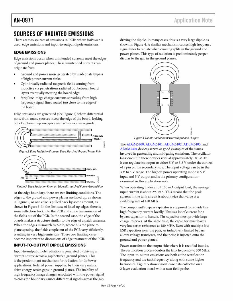
INPUT-TO-OUTPUT DIPOLE EMISSIONS Input-to-output dipole radiation is generated by driving a current source across a gap between ground planes. This is the predominant mechanism for radiation for isoPower applications. Isolated power supplies, by their very nature, drive energy across gaps in ground planes. The inability of high frequency image charges associated with the power signal to cross the boundary causes differential signals across the gap
driving the dipole. In many cases, this is a very large dipole as shown in Figure 4. A similar mechanism causes high frequency signal lines to radiate when crossing splits in the ground and power planes. This type of radiation is predominantly perpen-dicular to the gap in the ground planes.
0754
1-00
4
1 16
8 9
Figure 4. Dipole Radiation Between Input and Output
The ADuM5400, ADuM5401, ADuM5402, ADuM5403, and ADuM5404 devices serves as good examples of the issues involved in generating and mitigating emissions. The oscillator tank circuit in these devices runs at approximately 180 MHz. It can regulate its output to either 5 V or 3.3 V under the control of a pin on the secondary side. The input voltage can be in the 3 V to 5 V range. The highest power operating mode is 5 V input and 5 V output and is the primary configuration examined in this application note.
When operating under a full 100 mA output load, the average input current is about 290 mA. This means that the peak current in the tank circuit is about twice that value at a switching rate of 180 MHz.
The component’s bypass capacitor is supposed to provide this high frequency current locally. This is a lot of current for a bypass capacitor to handle. The capacitor must provide large charge reserves. At the same time, the capacitor must have a very low series resistance at 180 MHz. Even with multiple low ESR capacitors near the pins, an inductively limited bypass allows voltage transients, and the noise is injected onto the ground and power planes.
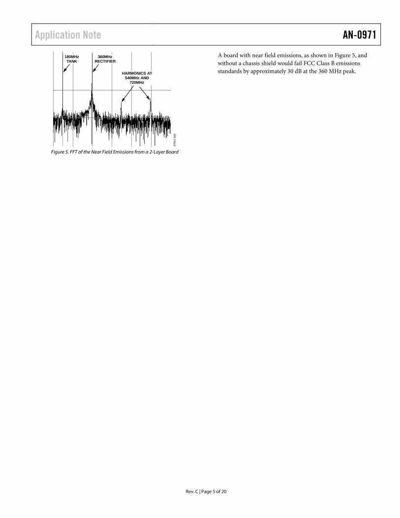
Power transfers to the output side where it is rectified into dc. The rectification process doubles the tank frequency to 360 MHz. The input-to-output emissions are both at the rectification frequency and the tank frequency, along with some higher harmonics. Figure 5 shows worst-case data collected on a 2-layer evaluation board with a near field probe.
Application Note AN-0971
Rev. C | Page 5 of 20
0754
1-00
5
180MHzTANK
360MHzRECTIFIER
HARMONICS AT540MHz AND
720MHz
Figure 5. FFT of the Near Field Emissions from a 2-Layer Board
A board with near field emissions, as shown in Figure 5, and without a chassis shield would fail FCC Class B emissions standards by approximately 30 dB at the 360 MHz peak.
AN-0971 Application Note
Rev. C | Page 6 of 20
SOURCES OF CONDUCTED NOISE The large currents and frequencies also generate conducted noise on the ground and power planes. This issue is addressed along with radiated emissions because the causes and remedies for both types of EMI are addressed with the same PCB ground and power structures.
The inability of the bypass capacitors and ground/power planes to provide adequate high frequency current to the isoPower dc-to-dc converter causes VDD noise. The dc-to-dc converter switches power in bursts of 2.5 ns pulses with an amplitude of ~700 mA.
An ideal bypass capacitor of a few microfarads should be ade-quate to supply the ac component of the current. Real world bypass capacitors are not ideal, and they connect to one or, more likely, both of the power planes by an inductive via. In addition, a large distance between ground and power planes creates a large inductance between them, restricting their ability to supply current quickly. These factors contribute to a large fraction of a volt of high frequency noise on the VDD plane.
Application Note AN-0971
Rev. C | Page 7 of 20
EMI MITIGATION TECHNIQUES Many mitigation techniques are available to the designer. Several techniques that apply directly to the isoPower devices are identified in this section. The choice of how aggressively EMI must be addressed for a design to pass FCC/CISPR emissions levels depends on the requirements of the design as well as cost and performance tradeoffs. The easiest radiated EMI mitigation technique to implement is to place the PCB in a grounded chassis with filter elements limiting noise escaping on cable shields. Although this application note does not describe this option, note that, where PCB related techniques are impractical, this method remains available.
The EMI mitigation practices rely on having relatively continuous ground and power planes and the ability to specify their relative positions and distances in the stack-up. This dictates that the minimum total number of planes is three: ground, power, and signal planes.
For practical considerations in board manufacture, a 4-layer board is the minimum stack-up. More layers are acceptable and can be used to greatly enhance the effectiveness of the recom-mended techniques.
The following techniques are effective in reducing EMI radiation and on-board noise:
• Input-to-output ground plane stitching capacitance • Power control • Edge guarding • Interplane capacitive bypass
Circuit boards with test structures were prepared to evaluate each of these EMI mitigation techniques utilizing the ADuM5400, ADuM5401, ADuM5402, ADuM5403, and ADuM5404. The layout of each board was varied as little as possible to allow meaningful comparison of results. Testing was conducted at an EMI test facility in a shielded chamber. As expected, during EMI testing, it was determined that the emissions at the tank frequency (180 MHz) were predominantly in the plane of the board, suggesting that the primary mechanism for radiation is from the PCB edges. The rectification emissions (360 MHz) are primarily perpendicular to the isolation gap in the board, suggesting input-to-output dipole radiation.
INPUT-TO-OUTPUT STITCHING When current flows along PCB traces, an image charge follows along the ground plane beneath the trace. If the trace crosses a gap in the ground plane, the image charge cannot follow along. This creates differential currents and voltages in the PCB leading to radiated and conducted emissions. The solution is to provide a path for the image charge to follow along with the signal. Standard practice is to place a stitching capacitor in proximity to the signal across the split in the ground plane (see PCB Design for Real-World EMI Control by Archambeault and Drewniak in the References section). This same technique
works to minimize radiation between ground planes due to the operation of isoPower.
There are at least three options to form a stitching capacitance.
• A safety rated capacitor applied across the barrier. • A floating metal plane spanning the gap between the
isolated and nonisolated sides on an interior layer, as shown in Figure 6.
• Extending the ground and power planes on an interior layer into the isolation gap of the PCB to form a capacitor, as shown in Figure 7.
Each of these options has its advantages and disadvantages in effectiveness and area required to implement.
Safety Rated Capacitor
A stitching capacitance can be implemented with a simple ceramic capacitor across the barrier. Capacitors with guaranteed creep-age, clearance, and withstand voltage can be obtained from many major capacitor manufacturers, such as Murata, Johansen, Hitano, and Vishay. Safety rated capacitors are available in several grades depending on their intended use. The Y2 grade is used in line-to-ground applications where there is danger of electric shock and is the recommended safety capacitor type for a stitching capacitor in a safety rated application. This type of capacitor is available in surface-mount and radial leaded disk versions.
Because safety capacitors are discrete components, they must be attached to the PCB with pads or through holes. This adds inductance to the capacitor on top of its intrinsic inductance. It also makes the stitching capacitor localized, demanding that currents flow to the capacitor, which can create asymmetrical image charge paths and added noise. These factors limit the effectiveness of discrete capacitors to frequencies below about 200 MHz.
Stitching Capacitance Built into the PCB
The PCB itself can be designed to create a stitching capacitor structure in several ways. A capacitor is formed when two planes in a PCB overlap. In this type of capacitor, the inductance of the parallel plate capacitor formed is extremely low, and the capacitance is distributed over a large area.
These structures must be constructed on internal layers of a PCB. The surface layers have minimum creepage and clearance requirements; therefore, it is not practical to use surface layers for this type of structure. This requires a minimum of four board layers.
A good option is to use a floating metal structure on an interior layer of the board to bridge between the primary and secondary power planes. Note that, hereafter, planes dedicated to ground or power are referred to as reference planes because, from an ac noise point of view, they behave the same and can be used for stitching capacitance interchangeably.
AN-0971 Application Note
Rev. C | Page 8 of 20
Floating Capacitive Structure
An example of a floating stitching capacitance is shown in Figure 6. The reference planes are shown in blue and green, and the floating coupling plane is shown in yellow. The capaci-tance of this structure creates two capacitive regions (shown with shading) linked by the nonoverlapping portion of the structure. To ensure that optimum capacitance is created for the area of the structure, the overlap areas of the primary and secondary sides should be equal.
0754
1-00
6
w1 w2
I
d
Figure 6. Floating Stitching Capacitance
The capacitive coupling of the structure in Figure 6 is calculated with the following basic relationships for parallel plate capacitors:
21
21
CCCC
C+×
= , d
CC xA21
ε== , and ε = ε0 × εr
where: C is the total stitching capacitance. AX is the overlap area of the stitching capacitance to each reference plane. d is the thickness of the insulation layer in the PCB (see Figure 6). ε0 is the permittivity of free space, 8.854 × 10⁻¹² F/m. εr is the relative permittivity of the PCB insulation material, which is about 4.5 for FR4.
+×
×=21
21
wwww
dlC ε (1)
where w1, w2, d, and l are the dimensions of the overlapping portions of the floating plane and the primary and secondary reference planes, as shown in Figure 6.
If w1 = w2, the equation simplifies to
dlw
C2
1ε= (2)
There are advantages and disadvantages of this structure in real applications. The major advantage is that there are two isolation gaps, one at the primary and one at the secondary. These gaps are called cemented joints, where the bonding between layers of FR4 provides the isolation. There are also two sequential paths through the thickness of the PCB material. The presence of these gaps and thicknesses is advantageous when creating a reinforced isolation barrier under some isolation standards. The disadvantage of this type of structure is that the capacitance is formed under active circuit area so there can be via penetra-tions and traces that run across the gaps. Equation 2 also shows that the capacitance formed is half as effective per unit area used compared to a simple parallel plate capacitor.
This architecture is best suited to applications where a larger amount of board area is available or where reinforced insulation is required.
Gap Overlap Stitching
A simple method of achieving a good stitching capacitance is to extend a reference plane from the primary and secondary sides into the area that is used for creepage on the PCB surface.
0754
1-00
7
w
I
d
Figure 7. Overlapping Plane Stitching Capacitance
The capacitive coupling of the structure in Figure 7 is calculated with the following basic relationships for parallel plate capacitors:
dAC ε
= and ε = ε0 × εr (3)
where: C is the total stitching capacitance. d is the thickness of the insulation layer in the PCB, ε0 is the permittivity of free space, 8.854 × 10⁻¹² F/m. εr is the relative permittivity of the PCB insulation material, which is about 4.5 for FR4.
dlwC ε
= (4)
where w, d, and l are the dimensions of the overlapping portion of the primary and secondary reference planes, as shown in Figure 7.
The major advantage if this structure is that the capacitance is created in the gap beneath the isolator, where the top and bottom layers must remain clear for creepage and clearance reasons. This board area is not utilized at all in most designs. The capacitance created is also twice as efficient per unit area as the floating plane.
This architecture has only a single cemented joint and a single layer of FR4 between the primary and secondary reference planes. It is well suited to smaller boards where only basic insulation is required.
EDGE GUARDING Noise on the power and ground planes that reaches the edge of a circuit board can radiate as shown in Figure 2 and Figure 3. If the edge is treated with a shielding structure, the noise is reflected back into the interplane space (see Archambeault and Drewniak in the References section). This can increase the voltage noise on the planes but reduces edge radiation.
Making a solid conductive edge treatment on a PCB is possible, but the process is expensive. A less expensive solution that
Application Note AN-0971
Rev. C | Page 9 of 20
works well is to treat the edges of the board with a guard ring structure laced together by vias. The structure is shown in Figure 8 for a typical 4-layer board. Figure 9 shows how this structure can be implemented on the power and ground layers of the primary side of a circuit board.
GROUND
GROUND VIA EDGE FENCEAND GUARD RINGS 07
541-
008
POWER
Figure 8. Via Fence Structure, Side View
0754
1-00
9
Figure 9. Via Fence and Guard Ring,
Shown on the Primary Power Plane Layers
There are two goals in creating edge guarding. The first is to reflect cylindrical emissions from vias back into the interplane space, not allowing it to escape from the edge. The second is to shield any edge currents flowing on internal planes due to noise or large currents.
The spacing of the vias used to create the edge guard is difficult to determine without extensive modeling. Analog Devices test boards used 4 mm via spacing for the evaluation boards. This spacing is small enough to provide attenuation to signals less than 18 GHz, and it conformed to general guidance from other sources. The number of vias required is reasonable. Further investigation into the via density was not conducted.
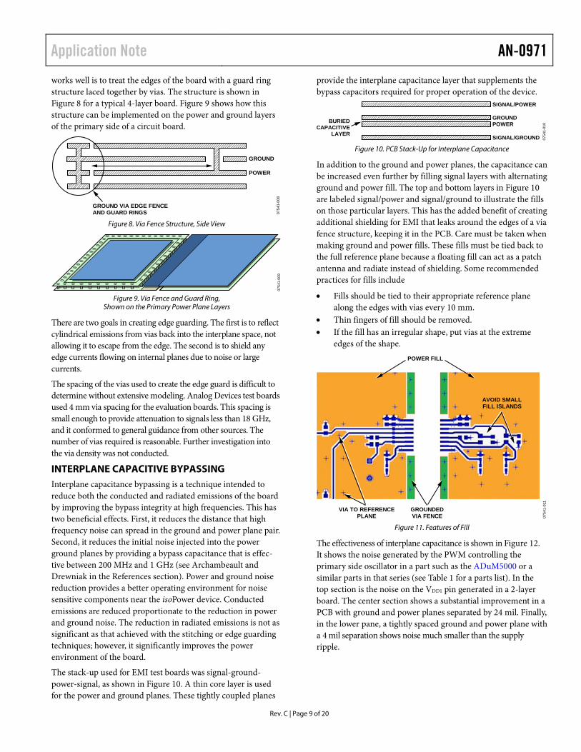
INTERPLANE CAPACITIVE BYPASSING Interplane capacitance bypassing is a technique intended to reduce both the conducted and radiated emissions of the board by improving the bypass integrity at high frequencies. This has two beneficial effects. First, it reduces the distance that high frequency noise can spread in the ground and power plane pair. Second, it reduces the initial noise injected into the power ground planes by providing a bypass capacitance that is effec-tive between 200 MHz and 1 GHz (see Archambeault and Drewniak in the References section). Power and ground noise reduction provides a better operating environment for noise sensitive components near the isoPower device. Conducted emissions are reduced proportionate to the reduction in power and ground noise. The reduction in radiated emissions is not as significant as that achieved with the stitching or edge guarding techniques; however, it significantly improves the power environment of the board.
The stack-up used for EMI test boards was signal-ground-power-signal, as shown in Figure 10. A thin core layer is used for the power and ground planes. These tightly coupled planes
provide the interplane capacitance layer that supplements the bypass capacitors required for proper operation of the device.
GROUNDPOWER
SIGNAL/POWER
BURIEDCAPACITIVE
LAYER SIGNAL/GROUND 0754
1-01
0
Figure 10. PCB Stack-Up for Interplane Capacitance
In addition to the ground and power planes, the capacitance can be increased even further by filling signal layers with alternating ground and power fill. The top and bottom layers in Figure 10 are labeled signal/power and signal/ground to illustrate the fills on those particular layers. This has the added benefit of creating additional shielding for EMI that leaks around the edges of a via fence structure, keeping it in the PCB. Care must be taken when making ground and power fills. These fills must be tied back to the full reference plane because a floating fill can act as a patch antenna and radiate instead of shielding. Some recommended practices for fills include
• Fills should be tied to their appropriate reference plane along the edges with vias every 10 mm.
• Thin fingers of fill should be removed. • If the fill has an irregular shape, put vias at the extreme
edges of the shape.
0754
1-01
1
POWER FILL
GROUNDEDVIA FENCE
VIA TO REFERENCEPLANE
AVOID SMALLFILL ISLANDS
Figure 11. Features of Fill
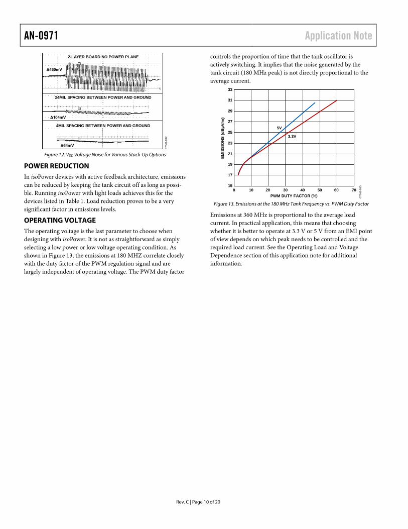
The effectiveness of interplane capacitance is shown in Figure 12. It shows the noise generated by the PWM controlling the primary side oscillator in a part such as the ADuM5000 or a similar parts in that series (see Table 1 for a parts list). In the top section is the noise on the VDD1 pin generated in a 2-layer board. The center section shows a substantial improvement in a PCB with ground and power planes separated by 24 mil. Finally, in the lower pane, a tightly spaced ground and power plane with a 4 mil separation shows noise much smaller than the supply ripple.
AN-0971 Application Note
Rev. C | Page 10 of 20
2-LAYER BOARD NO POWER PLANE
24MIL SPACING BETWEEN POWER AND GROUND
4MIL SPACING BETWEEN POWER AND GROUND
Δ460mV
Δ104mV
Δ64mV
0754
1-01
2
Figure 12. VDD Voltage Noise for Various Stack-Up Options
POWER REDUCTION In isoPower devices with active feedback architecture, emissions can be reduced by keeping the tank circuit off as long as possi-ble. Running isoPower with light loads achieves this for the devices listed in Table 1. Load reduction proves to be a very significant factor in emissions levels.
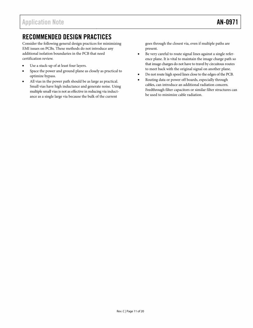
OPERATING VOLTAGE The operating voltage is the last parameter to choose when designing with isoPower. It is not as straightforward as simply selecting a low power or low voltage operating condition. As shown in Figure 13, the emissions at 180 MHZ correlate closely with the duty factor of the PWM regulation signal and are largely independent of operating voltage. The PWM duty factor
controls the proportion of time that the tank oscillator is actively switching. It implies that the noise generated by the tank circuit (180 MHz peak) is not directly proportional to the average current.
33
5V
3.3V
31
29
27
25
23
21
19
17
150 10 20 30 40 50 60 70
PWM DUTY FACTOR (%)
EMIS
SIO
NS
(dB
µV/m
)
0754
1-01
3
Figure 13. Emissions at the 180 MHz Tank Frequency vs. PWM Duty Factor
Emissions at 360 MHz is proportional to the average load current. In practical application, this means that choosing whether it is better to operate at 3.3 V or 5 V from an EMI point of view depends on which peak needs to be controlled and the required load current. See the Operating Load and Voltage Dependence section of this application note for additional information.
Application Note AN-0971
Rev. C | Page 11 of 20
RECOMMENDED DESIGN PRACTICES Consider the following general design practices for minimizing EMI issues on PCBs. These methods do not introduce any additional isolation boundaries in the PCB that need certification review.
• Use a stack-up of at least four layers. • Space the power and ground plane as closely as practical to
optimize bypass. • All vias in the power path should be as large as practical.
Small vias have high inductance and generate noise. Using multiple small vias is not as effective in reducing via induct-ance as a single large via because the bulk of the current
goes through the closest via, even if multiple paths are present.
• Be very careful to route signal lines against a single refer-ence plane. It is vital to maintain the image charge path so that image charges do not have to travel by circuitous routes to meet back with the original signal on another plane.
• Do not route high speed lines close to the edges of the PCB. • Routing data or power off boards, especially through
cables, can introduce an additional radiation concern. Feedthrough filter capacitors or similar filter structures can be used to minimize cable radiation.
AN-0971 Application Note
Rev. C | Page 12 of 20
MEETING ISOLATION STANDARDS The techniques described in this application note do not affect board isolation, with the exception of input-to-output coupling through a stitching capacitance. When stitching is implemented with a safety capacitor, the capacitor has rated working and transient voltages, as well as specified creepage and clearance. This makes the safety capacitor relatively easy to deal with from a certification point of view. However, its performance as an EMI suppression element is limited.
The PCB stitching capacitor, by its nature, is most effective when conductors are located as close to each other as possible. To obtain maximum performance from these elements, it is neces-sary to push the internal spacing requirements as close to the limit as possible, while maintaining safety. Different standards can have completely different approaches to PCB construction and the applicable standard must be applied.
Certification agencies treat the surface layers of a multilayer PCB differently than interior layers. The surface has creepage and clearance requirements that are driven by air ionization and breakdown along dirty surfaces. Interior layers are treated as solid insulation or permanently cemented joints between solid insulation.
CREEPAGE/CLEARANCE
CEMENTEDJOINT 07
541-
014
THROUGHINSULATION
Figure 14. Critical Distances in PCB Design
In PCB insulation, it is important to certification agencies that materials have an adequate dielectric breakdown to pass the transient test requirements and that they are constructed in a way that the insulation does not break down over time. Table 2 compares four standards to what is required to make a basic or reinforced insulation barrier inside a PCB.
In the case of basic insulation in printed circuit boards, there is no minimum specification for distance through the insulation. Thus, the designer has a great deal of flexibility in board layout. Materials such as FR4 must be thick enough to withstand the required overvoltage for the life of the product.
Reinforced insulation requires a minimum distance of 0.4 mm (about 16 mil) of insulation along a bonded surface, such as the gap between copper structures on an internal PCB layer or directly through the insulation from layer to layer in most cases. In addition, there can be type testing requirements for circuit boards unless multiple layers of insulation are used between active structures. Although this requirement necessitates careful board design and possibly more than four layers, it should not be burdensome if taken into account at the start of a design.
Capacitive coupling across the isolation barrier allows ac leakage and transients to couple from one ground plane to the other. Although 300 pF seems small, high voltage, high speed transients can inject significant currents across the barrier through this capacitance. Take this into account if the application is to be subjected to these environments.
Table 2. Comparison of Isolation Creepage in Isolation Standards IEC 60950 IEC 61010 2nd Edition IEC 61010 3rd Edition IEC 60601
Type of Insulation
Through Insulation (2.10.6.4)
Along a Cemented Joint (2.10.6.3)
Through Insulation (6.7.2.2.3)
Along a Cemented Joint (6.7.2.2.3)
Through Insulation (6.7)
Along a Cemented Joint (6.7)
Cemented and Solid Insulation
Functional Insulation
No requirement No requirement
No requirement
No requirement 0.4 mm minimum 0.4 mm minimum
Verified by test
Basic Insulation No requirement No requirement
No requirement
No requirement 0.4 mm minimum 0.4 mm minimum
Verified by test
Supplemental/ Reinforced insulation
0.4 mm minimum or multiple layers of insulation, precured
0.4 mm minimum (2.10.5.2)
No requirement
No requirement 0.4 mm minimum or multiple layers of insulation, precured
0.4 mm minimum
Verified by test
Application Note AN-0971
Rev. C | Page 13 of 20
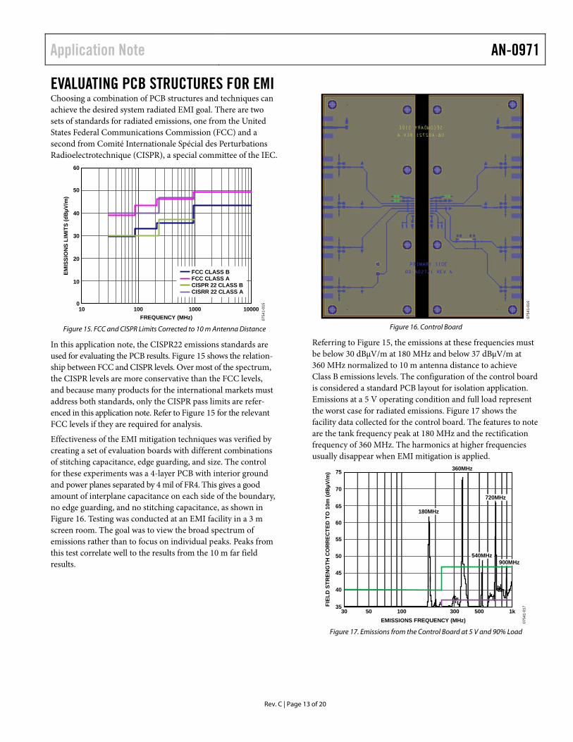
EVALUATING PCB STRUCTURES FOR EMI Choosing a combination of PCB structures and techniques can achieve the desired system radiated EMI goal. There are two sets of standards for radiated emissions, one from the United States Federal Communications Commission (FCC) and a second from Comité Internationale Spécial des Perturbations Radioelectrotechnique (CISPR), a special committee of the IEC.
60
50
40
30
20
10
010 100 1000 10000
FREQUENCY (MHz)
EMIS
SIO
NS
LIM
ITS
(dB
µV/m
)
0754
1-01
5
FCC CLASS BFCC CLASS ACISPR 22 CLASS BCISRR 22 CLASS A
Figure 15. FCC and CISPR Limits Corrected to 10 m Antenna Distance
In this application note, the CISPR22 emissions standards are used for evaluating the PCB results. Figure 15 shows the relation-ship between FCC and CISPR levels. Over most of the spectrum, the CISPR levels are more conservative than the FCC levels, and because many products for the international markets must address both standards, only the CISPR pass limits are refer-enced in this application note. Refer to Figure 15 for the relevant FCC levels if they are required for analysis.
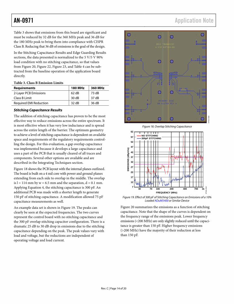
Effectiveness of the EMI mitigation techniques was verified by creating a set of evaluation boards with different combinations of stitching capacitance, edge guarding, and size. The control for these experiments was a 4-layer PCB with interior ground and power planes separated by 4 mil of FR4. This gives a good amount of interplane capacitance on each side of the boundary, no edge guarding, and no stitching capacitance, as shown in Figure 16. Testing was conducted at an EMI facility in a 3 m screen room. The goal was to view the broad spectrum of emissions rather than to focus on individual peaks. Peaks from this test correlate well to the results from the 10 m far field results.
0754
1-01
6
75
Figure 16. Control Board
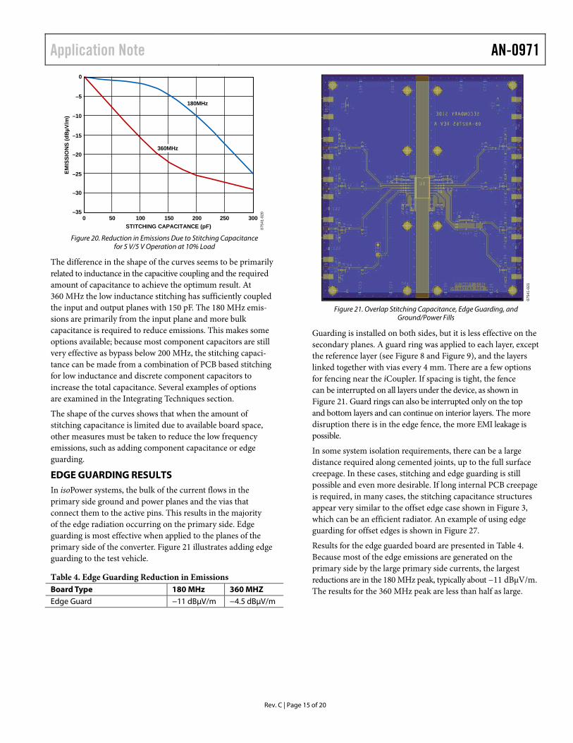
Referring to Figure 15, the emissions at these frequencies must be below 30 dBµV/m at 180 MHz and below 37 dBµV/m at 360 MHz normalized to 10 m antenna distance to achieve Class B emissions levels. The configuration of the control board is considered a standard PCB layout for isolation application. Emissions at a 5 V operating condition and full load represent the worst case for radiated emissions. Figure 17 shows the facility data collected for the control board. The features to note are the tank frequency peak at 180 MHz and the rectification frequency of 360 MHz. The harmonics at higher frequencies usually disappear when EMI mitigation is applied.
0754
1-01
7
55
FIEL
D S
TREN
GTH
CO
RR
ECTE
D T
O 1
0m (d
BµV
/m) 75
65
70
60
50
45
40
35
360MHz
180MHz
720MHz
540MHz
EMISSIONS FREQUENCY (MHz)30 50 100 300 500 1k
900MHz
Figure 17. Emissions from the Control Board at 5 V and 90% Load
AN-0971 Application Note
Rev. C | Page 14 of 20
Table 3 shows that emissions from this board are significant and must be reduced by 32 dB for the 360 MHz peak and 36 dB for the 180 MHz peak to bring them into compliance with CISPR Class B. Reducing that 36 dB of emissions is the goal of the design.
In the Stitching Capacitance Results and Edge Guarding Results sections, the data presented is normalized to the 5 V/5 V 90% load condition with no stitching capacitance, so that values from Figure 20, Figure 22, Figure 23, and Table 4 can be sub-tracted from the baseline operation of the application board directly.
Table 3. Class B Emission Limits Requirements 180 MHz 360 MHz
2-Layer PCB Emissions 62 dB 73 dB Class B Limit 30 dB 37 dB
Required EMI Reduction 32 dB 36 dB
Stitching Capacitance Results
The addition of stitching capacitance has proven to be the most effective way to reduce emissions across the entire spectrum. It is most effective when it has very low inductance and is spread across the entire length of the barrier. The optimum geometry to achieve a level of stitching capacitance is dependent on available space and requirements of the regulatory requirements control-ling the design. For this evaluation, a gap overlap capacitance was implemented because it develops a large capacitance and uses a part of the PCB that is usually cleared of all traces and components. Several other options are available and are described in the Integrating Techniques section.
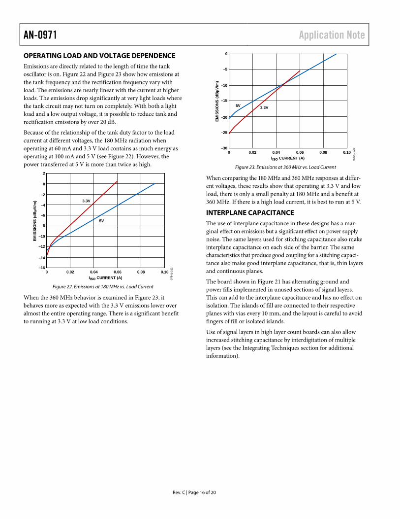
Figure 18 shows the PCB layout with the internal planes outlined. The board is built on a 4 mil core with power and ground planes extending from each side to overlap in the middle. The overlap is l = 114 mm by w = 6.5 mm and the separation, d = 0.1 mm. Applying Equation 4, the stitching capacitance is 300 pF. An additional PCB was made with a shorter length to generate 150 pF of stitching capacitance. A modification allowed 75 pF capacitance measurements as well.
An example data set is shown in Figure 19. The peaks can clearly be seen at the expected frequencies. The two curves represent the control board with no stitching capacitance and the 300 pF overlap stitching capacitor configuration. There is a dramatic 25 dB to 30 dB drop in emissions due to the stitching capacitance depending on the peak. The peak values vary with load and voltage, but the reductions are independent of operating voltage and load current.
0754
1-01
8
Figure 18. Overlap Stitching Capacitance
0754
1-01
9
EMIS
SIO
NS
(dB
µV/m
)62
57
52
47
42
37
32
27
22
17
12
7
FREQUENCY (MHz)40 70 100 200 400 700 1k
NO STITCHING300pF STITCHING
Figure 19. Effect of 300 pF of Stitching Capacitance on Emissions of a 10%
Loaded ADuM5400 or Similar Device
Figure 20 summarizes the emissions as a function of stitching capacitance. Note that the shape of the curves is dependent on the frequency range of the emissions peak. Lower frequency emissions (<200 MHz) are only slightly reduced until the capaci-tance is greater than 150 pF. Higher frequency emissions (>200 MHz) have the majority of their reduction at less than 150 pF.
Application Note AN-0971
Rev. C | Page 15 of 20
0
–5
–10
–15
–20
–25
–30
–350 50 100 150 200 250 300
STITCHING CAPACITANCE (pF)
EMIS
SIO
NS
(dB
µV/m
)
0754
1-02
0
180MHz
360MHz
Figure 20. Reduction in Emissions Due to Stitching Capacitance
for 5 V/5 V Operation at 10% Load
The difference in the shape of the curves seems to be primarily related to inductance in the capacitive coupling and the required amount of capacitance to achieve the optimum result. At 360 MHz the low inductance stitching has sufficiently coupled the input and output planes with 150 pF. The 180 MHz emis-sions are primarily from the input plane and more bulk capacitance is required to reduce emissions. This makes some options available; because most component capacitors are still very effective as bypass below 200 MHz, the stitching capaci-tance can be made from a combination of PCB based stitching for low inductance and discrete component capacitors to increase the total capacitance. Several examples of options are examined in the Integrating Techniques section.
The shape of the curves shows that when the amount of stitching capacitance is limited due to available board space, other measures must be taken to reduce the low frequency emissions, such as adding component capacitance or edge guarding.
EDGE GUARDING RESULTS In isoPower systems, the bulk of the current flows in the primary side ground and power planes and the vias that connect them to the active pins. This results in the majority of the edge radiation occurring on the primary side. Edge guarding is most effective when applied to the planes of the primary side of the converter. Figure 21 illustrates adding edge guarding to the test vehicle.
Table 4. Edge Guarding Reduction in Emissions Board Type 180 MHz 360 MHZ Edge Guard −11 dBµV/m −4.5 dBµV/m
0754
1-02
1
Figure 21. Overlap Stitching Capacitance, Edge Guarding, and
Ground/Power Fills
Guarding is installed on both sides, but it is less effective on the secondary planes. A guard ring was applied to each layer, except the reference layer (see Figure 8 and Figure 9), and the layers linked together with vias every 4 mm. There are a few options for fencing near the iCoupler. If spacing is tight, the fence can be interrupted on all layers under the device, as shown in Figure 21. Guard rings can also be interrupted only on the top and bottom layers and can continue on interior layers. The more disruption there is in the edge fence, the more EMI leakage is possible.
In some system isolation requirements, there can be a large distance required along cemented joints, up to the full surface creepage. In these cases, stitching and edge guarding is still possible and even more desirable. If long internal PCB creepage is required, in many cases, the stitching capacitance structures appear very similar to the offset edge case shown in Figure 3, which can be an efficient radiator. An example of using edge guarding for offset edges is shown in Figure 27.
Results for the edge guarded board are presented in Table 4. Because most of the edge emissions are generated on the primary side by the large primary side currents, the largest reductions are in the 180 MHz peak, typically about −11 dBµV/m. The results for the 360 MHz peak are less than half as large.
AN-0971 Application Note
Rev. C | Page 16 of 20
OPERATING LOAD AND VOLTAGE DEPENDENCE Emissions are directly related to the length of time the tank oscillator is on. Figure 22 and Figure 23 show how emissions at the tank frequency and the rectification frequency vary with load. The emissions are nearly linear with the current at higher loads. The emissions drop significantly at very light loads where the tank circuit may not turn on completely. With both a light load and a low output voltage, it is possible to reduce tank and rectification emissions by over 20 dB.
Because of the relationship of the tank duty factor to the load current at different voltages, the 180 MHz radiation when operating at 60 mA and 3.3 V load contains as much energy as operating at 100 mA and 5 V (see Figure 22). However, the power transferred at 5 V is more than twice as high.
2
0
–2
–10
–4
–8
–6
–12
–14
–160 0.02 0.04 0.06 0.08 0.10
IISO CURRENT (A)
EMIS
SIO
NS
(dB
µV/m
)
0754
1-02
2
5V
3.3V
Figure 22. Emissions at 180 MHz vs. Load Current
When the 360 MHz behavior is examined in Figure 23, it behaves more as expected with the 3.3 V emissions lower over almost the entire operating range. There is a significant benefit to running at 3.3 V at low load conditions.
0
–5
–10
–15
–20
–25
–300 0.02 0.04 0.06 0.08 0.10
IISO CURRENT (A)
EMIS
SIO
NS
(dB
µV/m
)
0754
1-02
3
5V 3.3V
Figure 23. Emissions at 360 MHz vs. Load Current
When comparing the 180 MHz and 360 MHz responses at differ-ent voltages, these results show that operating at 3.3 V and low load, there is only a small penalty at 180 MHz and a benefit at 360 MHz. If there is a high load current, it is best to run at 5 V.
INTERPLANE CAPACITANCE The use of interplane capacitance in these designs has a mar-ginal effect on emissions but a significant effect on power supply noise. The same layers used for stitching capacitance also make interplane capacitance on each side of the barrier. The same characteristics that produce good coupling for a stitching capaci-tance also make good interplane capacitance, that is, thin layers and continuous planes.
The board shown in Figure 21 has alternating ground and power fills implemented in unused sections of signal layers. This can add to the interplane capacitance and has no effect on isolation. The islands of fill are connected to their respective planes with vias every 10 mm, and the layout is careful to avoid fingers of fill or isolated islands.
Use of signal layers in high layer count boards can also allow increased stitching capacitance by interdigitation of multiple layers (see the Integrating Techniques section for additional information).

Application Note AN-0971
Rev. C | Page 17 of 20
INTEGRATING TECHNIQUES Determining exactly which of the methods described in this application note should be combined to achieve the emissions target requires an expected baseline emissions measurement. The behavior of the control board can be used if no other esti-mate is available. Many of the options do not have a large impact on cost or area and can be implemented on any multilayer PCB. The process of choosing the PCB layout and application tech-niques to minimize EMI is illustrated in Figure 24. This breaks the process down into three categories: items that do not affect isolation, items that have isolation impacts, and, finally, a system level approach, such as shielding.
0754
1-02
4
STEPS TO MINIMIZEisoPOWER EMI
MINIMIZE LOAD
YES
REINFORCED BASIC
NO
EDGE GUARDING
3.3V OPERATION
BURIEDCAPACITANCE
SYSTEMSHIELDING
FLOATINGSTITCHINGCAPACITOR
OVERLAPPINGSTITCHINGCAPACITOR
SAFETYSTITCHINGCAPACITOR
SAFETYSTITCHINGCAPACITOR
MEDICALAPPLICATION?
PROTECTIONLEVEL
THESE FEATURESCAN BE
IMPLEMENTEDWITH MINIMAL
COST AND BOARDSPACE AND NO
IMPACT ONISOLATION.
THESE FEATURESCAN IMPACT
ISOLATIONRATINGS.
SYSTEMSHIELDING
IS UNDESIRABLEIN MOSTCASES.
Figure 24. Selecting EMI Mitigation Options
To illustrate this process, two examples are examined, which cover most aspects of the process. To start with, create two types of application boards.
• A PCB capable of 60 mA of average current that must meet basic insulation
• A PCB that supplies less than 10 mA of current, but is capable of reinforced insulation
The control board is used as the baseline. Its emissions at full load are shown in Table 3 along with the CISPR Class B limits.
EXAMPLE 1—BASIC INSULATION BOARD For the first layout example, the 60 mA load is assumed to be the maximum load required for the application. This reduces the emissions by several decibels without any design effort. However, because this is still a relatively heavy current applica-tion from an isoPower perspective, edge guarding of the primary side is recommended. Edge guarding reduces the 180 MHz peak by 10 dB and provides some reduction of the 360 MHz peak as well. In addition, with the large power requirement, choosing a 5 V/5 V operating condition gives the lowest emissions (see Figure 22). Optimizing interplane capacitance should be consid-ered if there are sensitive analog circuits or long cables attached to the application PCB, but it is optional.
The emissions have been reduced to 11 dB to 15 dB from the baseline with the methods already used, but to obtain the 32 dB and 36 dB reductions required for Class B, stitching capacitance must be employed. Because this is not a medical application, the user has the flexibility to add cross barrier capacitance. Only basic insulation is required; therefore, the smallest size of the stitching capacitor is the single overlap option. Adding up the reductions thus far yields 15 dB in the 180 MHz peak and 11 dB in the 360 MHz peak. This leaves 17 dB in the lower frequency and 21 dB at the higher frequency to obtain. As shown in Figure 20, 140 pF of stitching is required to achieve the goal for the 360 MHz peak, but 250 pF is required to make the 180 MHz peak meet the desired level. Using Equation 4, assuming a 4 mil dielectric and an 8 mm overlap, a 77 mm long capacitor structure is required to produce a 250 pF capacitance.
Table 5. Basic Insulation 4-Layer Board Relative Change
Parameter Value 180 MHz Peak
360 MHz Peak
Power Level 60 mA at 5 V −4 dBµV/m −7 dBµV/m Edge Guarding N/A −11 dBµV/m −4 dBµV/m Stitching 250 pF −17 dBµV/m −27 dBµV/m Total −32 dBµV/m −38 dBµV/m
Table 5 shows a summary of the reductions achieved with a 250 pF stitching capacitance with edge guarding and 60 mA of current at 5 V. The capacitive stitch is built as shown in Figure 25. Note that, with a 4-layer board, the full PCB creepage must be observed on the top and bottom layers, but the spacing can be much smaller on the internal layers.
0754
1-02
5
SIGNAL/GND FILL
SURFACE CREEPAGE
PWRGNDSIGNAL/PWR FILL
CEMENTED JOINTS
Figure 25. Basic Insulation Single Overlap Stitching Capacitor

AN-0971 Application Note
Rev. C | Page 18 of 20
This design may be acceptable if 77 mm of overlap length is available. If space is at a premium, an additional option is shown in Figure 26. Because the required capacitance for the 360 MHz peak is smaller than what is required at 180 MHz, design the PCB for the 140 pF stitching capacitance and supplement with a safety rated capacitor. This reduces the length of the stitching capacitor to 44 mm and adds a 160 pF safety capacitor.
0754
1-02
6
SIGNAL/GND FILLPWRGNDSIGNAL/PWR FILL
Figure 26. Augmented Stitching with Safety Capacitor
Finally, Figure 27 shows the basic insulation structure with edge guards in place. Note that the ground planes used for the edge guard are also used for the stitching capacitor. This avoids the 20h patch antenna effect.
0754
1-02
7SIGNAL/PWR FILLGNDPWRSIGNAL/GND FILL
SIGNAL/GND FILLPWRGND
SIGNAL/PWR FILL Figure 27. Edge Guarding Added to the Basic Capacitive Stitching
An additional technique to increase capacitance without large PCB space is to use interdigitated stitching capacitors, as shown in Figure 28. Because the extra layers that overlap are connected to the primary planes with vias, the extra planes are more induc-tive than the primary overlap. This is not typically a problem because the lower frequency peak requires the largest capacitance and more inductance can be tolerated. As noted previously, when edge guarding is used, it works best to use the edge guard ground planes for coupling.
0754
1-03
0
SIGNAL/PWR FILLSIGNAL/GND FILLPWRGNDSIGNAL/PWR FILLSIGNAL/GND FILL
SIGNAL/PWR FILLSIGNAL/GND FILLPWRGNDSIGNAL/PWR FILLSIGNAL/GND FILL
SIGNAL/PWR FILLSIGNAL/GND FILL
PWRGND
SIGNAL/PWR FILLSIGNAL/GND FILL
SIGNAL/GND FILLSIGNAL/PWR FILL
GNDPWR
SIGNAL/GND FILLSIGNAL/PWR FILL
Figure 28. Different Methods of Interdigitating Stitching Capacitance to Maximize Coupling
EXAMPLE 2—REINFORCED INSULATION BOARD The second board requires reinforced insulation. The analysis of edge guarding remains the same. Because the current level is low, there is an advantage in the 360 MHz peak to run the supply at 3.3 V/3.3 V (see Figure 23).
0754
1-02
8
SIGNAL/GND FILLPWRGNDSIGNAL/PWR FILL
SURFACE CREEPAGE 2-LAYER BARRIER
CEMENTED JOINTS
Figure 29. Minimum Reinforced Insulation, Floating Stitching Capacitor
If the standards for this example allow a 2-layer reinforced structure, a stitching capacitor can be constructed as shown in Figure 29. Performing a calculation similar to the previous example, the minimum stitching capacitance is 210 pF. Because the floating stitch in reinforced applications uses twice the area as the single overlap, this results in the capacitor being very large (see Equation 2).
Table 6. Reinforced 4-Layer Board Emissions Relative Change
Parameter Value 180 MHz Peak
360 MHz Peak
Power Level 10 mA at 3.3 V −10 dBµV/m −22 dBµV/m Edge Guarding N/A −11 dBµV/m −4 dBµV/m Stitching 210 pF −11 dBµV/m −26 dBµV/m Total −32 dBµV/m −52 dBµV/m
In Example 1, a safety capacitor was used to supplement stitching at low frequencies so that the PCB stitching capacitor can be reduced. This can be done in this context as well, but high voltage safety capacitors are relatively expensive, and there may be regulatory restrictions; therefore, it is undesirable to use safety capacitors. There are, however, alternatives for both safety and size.
If more layers are available, a safety rated stitching capacitor can be constructed, as shown in Figure 30. This structure places at least four layers of PCB material between the active input and output structures. For most agencies, it is acceptable without test or certification. The capacitance can be complicated to calculate because there can be coupling to several layers, but the spacing is larger as well. Usually, this highly reinforced PCB has the largest area requirements.
0754
1-02
9
SIGNAL/GND FILLPWRSIGNALGNDSIGNAL/PWR FILLSIGNAL/GND FILL
SURFACECREEPAGE
4-LAYER BARRIER
CEMENTED JOINTS Figure 30. Reinforced Insulation, Floating Stitching Capacitor
Application Note AN-0971
Rev. C | Page 19 of 20
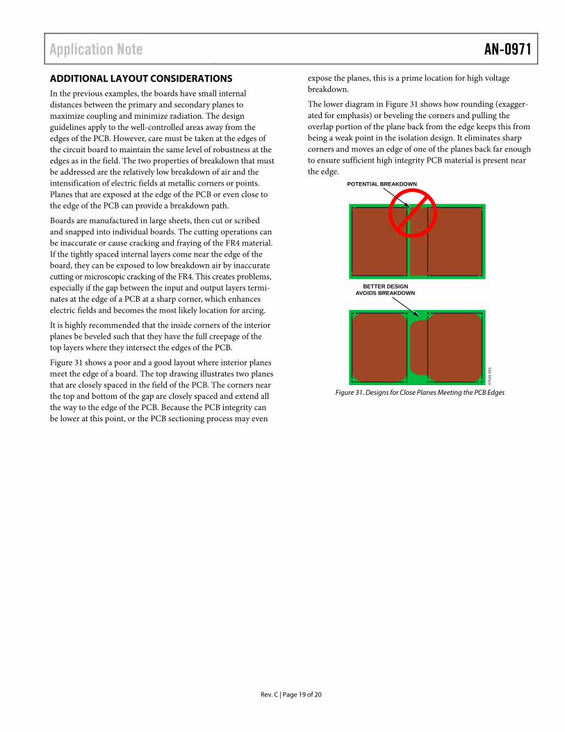
ADDITIONAL LAYOUT CONSIDERATIONS In the previous examples, the boards have small internal distances between the primary and secondary planes to maximize coupling and minimize radiation. The design guidelines apply to the well-controlled areas away from the edges of the PCB. However, care must be taken at the edges of the circuit board to maintain the same level of robustness at the edges as in the field. The two properties of breakdown that must be addressed are the relatively low breakdown of air and the intensification of electric fields at metallic corners or points. Planes that are exposed at the edge of the PCB or even close to the edge of the PCB can provide a breakdown path.
Boards are manufactured in large sheets, then cut or scribed and snapped into individual boards. The cutting operations can be inaccurate or cause cracking and fraying of the FR4 material. If the tightly spaced internal layers come near the edge of the board, they can be exposed to low breakdown air by inaccurate cutting or microscopic cracking of the FR4. This creates problems, especially if the gap between the input and output layers termi-nates at the edge of a PCB at a sharp corner, which enhances electric fields and becomes the most likely location for arcing.
It is highly recommended that the inside corners of the interior planes be beveled such that they have the full creepage of the top layers where they intersect the edges of the PCB.
Figure 31 shows a poor and a good layout where interior planes meet the edge of a board. The top drawing illustrates two planes that are closely spaced in the field of the PCB. The corners near the top and bottom of the gap are closely spaced and extend all the way to the edge of the PCB. Because the PCB integrity can be lower at this point, or the PCB sectioning process may even
expose the planes, this is a prime location for high voltage breakdown.
The lower diagram in Figure 31 shows how rounding (exagger-ated for emphasis) or beveling the corners and pulling the overlap portion of the plane back from the edge keeps this from being a weak point in the isolation design. It eliminates sharp corners and moves an edge of one of the planes back far enough to ensure sufficient high integrity PCB material is present near the edge.
0754
1-03
1
POTENTIAL BREAKDOWN
BETTER DESIGNAVOIDS BREAKDOWN
Figure 31. Designs for Close Planes Meeting the PCB Edges
AN-0971 Application Note
Rev. C | Page 20 of 20
CONCLUSIONS Each method outlined in this application note addresses specific radiation sources and can be combined with the other techniques described to achieve the desired reductions in the associated emissions. Test boards easily meet CISPR or FCC Class B standards with no external shielding by using interplane stitching capacitors and edge fencing. In addition, use of interplane decoupling capacitance in the ground and power planes produces a very quiet environment for precision measurement applications.
Although this application note relies on data collected on an ADuM5400 or similar device, the techniques are applicable across the isoPower line. All isoPower products contain similar tank and rectification circuits. The largest currents flow on the primary side of the devices, causing these devices to behave in a similar manner from a radiated emissions point of view.
Where low ac leakage is required, as in some medical applications, stitching capacitance may not be a viable solution. In these applications, grounded metallic chassis enclosures may be the most practical solution for minimizing emissions.
REFERENCES Archambeault, Bruce R. and James Drewniak. 2002. PCB
Design for Real-World EMI Control. Boston: Kluwer Academic Publishers.
Gisin, Franz and Pantic-Tannr, Zoric, 2001. Minimizing EMI Caused by Radially Propagating Waves Inside High Speed Digital Logic PCBs, Mikrotalasna Revija (December).
©2008–2014 Analog Devices, Inc. All rights reserved. Trademarks and registered trademarks are the property of their respective owners. AN07541-0-1/14(C)