recent advances in two-dimensional materials beyond graphene · bhimanapati et al. vol. 9 ’ no....
TRANSCRIPT

BHIMANAPATI ET AL. VOL. 9 ’ NO. 12 ’ 11509–11539 ’ 2015
www.acsnano.org
11509
November 06, 2015
C 2015 American Chemical Society
Recent Advances in Two-DimensionalMaterials beyond GrapheneGanesh R. Bhimanapati,† Zhong Lin,‡ Vincent Meunier, ),9 Yeonwoong Jung,§ Judy Cha,^ Saptarshi Das,#
Di Xiao,r Youngwoo Son,X Michael S. Strano,X Valentino R. Cooper,O Liangbo Liang, ),9 Steven G. Louie,z,b
Emilie Ringe,1 Wu Zhou,O Steve S. Kim,¥,¥ Rajesh R. Naik,¥ Bobby G. Sumpter,O Humberto Terrones, ),9
Fengnian Xia,( Yeliang Wang,þ Jun Zhu,‡ Deji Akinwande,[ Nasim Alem,† Jon A. Schuller,]
Raymond E. Schaak,� Mauricio Terrones,†,‡,� and Joshua A. Robinson*,†
†Department of Materials Science and Engineering, Center for Two-Dimensional and Layered Materials, Pennsylvania State University, University Park, Pennsylvania16802, United States, ‡Department of Physics, Center for Two-Dimensional and Layered Materials, Pennsylvania State University, University Park, Pennsylvania16802, United States, §Nanoscience Technology Center, Department of Materials Science and Engineering, University of Central Florida, Orlando, Florida 32826,United States, ^Department of Mechanical Engineering and Material Science, Yale School of Engineering and Applied Sciences, New Haven, Connecticut 06520,United States, )Department of Physics, Applied Physics, and Astronomy, Rensselaer Polytechnic Institute, Troy, New York 12180, United States, 9Center forNanophase Materials Sciences, Oak Ridge National Laboratory, Oak Ridge, Tennessee 37831, United States, #Birck Nanotechnology Center & Department of ECE,Purdue University, West Lafayette, Indiana 47907, United States, rDepartment of Physics, Carnegie Mellon University, Pittsburgh, Pennsylvania 15213,United States, XDepartment of Chemical Engineering, Massachusetts Institute of Technology, Cambridge, Massachusetts 02139, United States, OCenter forNanophase Materials Sciences and Computer Science & Mathematics Division, Oak Ridge National Laboratory, Oak Ridge, Tennessee 37831, United States,zDepartment of Physics, University of California at Berkeley, Berkeley, California 94720, United States, ¥Air Force Laboratory, Materials & Manufacturing directorate,Wright-Patterson AFB, Dayton, Ohio 45433, United States, ¥UES Inc., Beavercreek, Ohio 45432, United States, (Department of Electrical Engineering,Yale University, New Haven, Connecticut 06511, United States, bLawrence Berkeley National Lab, Berkeley, California 94720, United States, þBeijing NationalLaboratory for Condensed Matter Physics, Institute of Physics, Chinese Academy of Sciences, Beijing 100190, China, 1Department of Materials Science & NanoEngineering, Rice University, Houston, Texas 77005, United States, [Microelectronics Research Centre, The University of Texas at Austin, Austin, Texas 78758,United States, ]Electrical and Computer Engineering Department, University of California at Santa Barbara, Santa Barbara, California 93106, United States, and�Department of Chemistry and Materials Research Institute, Pennsylvania State University, University Park, Pennsylvania 16802, United States,
Layered materials have existed foreons,1 and have been studied scienti-fically for more than 150 years.2 How-
ever, only recently3 havewebegun to realizethe true potential of these systems foradvanced technological applications. Eachlayered material, when thinned to its physi-cal limits, exhibits novel properties different
from its bulk counterpart. Therefore, at thephysical limit these materials are referredto as two-dimensional (2D) materials. Themost highly studied 2Dmaterial is graphenebecause of its exceptional electronic, opto-electronic, electrochemical and biomedicalapplications. Beyondgraphene, there is a verywide spectrum of 2D electronic materials
* Address correspondence [email protected].
Received for review September 3, 2015and accepted November 6, 2015.
Published online10.1021/acsnano.5b05556
ABSTRACT The isolation of graphene in 2004 from graphite was a defining moment for
the “birth” of a field: two-dimensional (2D) materials. In recent years, there has been a rapidly
increasing number of papers focusing on non-graphene layered materials, including transition-
metal dichalcogenides (TMDs), because of the new properties and applications that emerge
upon 2D confinement. Here, we review significant recent advances and important new
developments in 2D materials “beyond graphene”. We provide insight into the theoretical
modeling and understanding of the van der Waals (vdW) forces that hold together the 2D
layers in bulk solids, as well as their excitonic properties and growth morphologies.
Additionally, we highlight recent breakthroughs in TMD synthesis and characterization and
discuss the newest families of 2D materials, including monoelement 2D materials (i.e., silicene, phosphorene, etc.) and transition metal carbide- and carbon
nitride-based MXenes. We then discuss the doping and functionalization of 2D materials beyond graphene that enable device applications, followed by
advances in electronic, optoelectronic, and magnetic devices and theory. Finally, we provide perspectives on the future of 2D materials beyond graphene.
KEYWORDS: two-dimensional materials . graphene . heterostructures . transition metal dichalcogenide . phospherene . silicene .germanene . stanene . van der Waals epitaxy . van der Waals solid
REVIEW

BHIMANAPATI ET AL. VOL. 9 ’ NO. 12 ’ 11509–11539 ’ 2015
www.acsnano.org
11510
that range from insulators to semiconductors to metalsand even to superconductors. 2D materials researchinitially focused ongraphene following the seminal paperby Novoselov and Geim,3 but it was also demonstratedvery early on that other 2Dmaterials also possess excitingproperties.4 Following graphene, 2D hexagonal boronnitride (hBN) was theoretically predicted to induce abandgap in graphene when graphene was depositedonto it.5 This led to a significant increase in hBN experi-mental research, and ultimately to an understanding thathBNmay be an ideal substrate for graphene electronics.6
Rapidly following graphene and hBN, research on semi-conducting 2D layers provided evidence that the bandstructure of a subset of the 2D materials family changesdrastically as they are thinned to monolayer thickness.7
Device fabrication further ignited the interest of many inthe electronics community.8 Thesenovel semiconducting2D materials, known as transition-metal dichalcogenides(TMDs), are now a primary focus of many researchers, asclearly evidenced by the publication record devoted tosuchmaterials (Figure 1). There are many layered materi-als that go beyond TMDs, including monochalcogenides(GaSe, etc.), monoelemental 2D semiconductors (silicene,phosphorene, germanene), and MXenes (Figure 1).Finally, the true potential of these layered materials mayemerge from the ability to stack them, layer-by-layer in
Figure 1. Publication trends in 2D materials beyond gra-phene. Source: Web of Science. Search index: [Title search(x) or title (y) and topic (z), where x = graphene, boronnitride, transition metal chalcogenides, molybdenum disul-fide or monoelements (silicene, germanene, phosphorene,stanene or borophene), y = graphene or BN or TMDs orMoS2) and z = graphene or boron nitride or transitionmetalchalcogenides (TMDs: MoS2, WS2, MoSe2, WSe2, TaS2, TaSe2,NbS2), MoS2 or monoelement 2D: silicene, germanene,stanene, borophene, phosphorene.].
VOCABULARY: (NH4)2MoS4� - ammonia tetra thiomo-
lybdate;2D - two-dimensional; 3D - three-dimensional;
ADF - annular dark field;Ag - silver;AHM,
(NH4)6Mo7O24 34H2O - ammonium heptamolybdate;
ALD - atomic layer deposition;ARPES - angle resolved
photoemission spectroscopy;Au - gold;AuCl3 - gold
chloride;BP - black phosphorus;BV - benxyl viologen;
C - carbon;CF3 - carbon tetrafluoride radical;CH3 - methyl
radical;CL - cathodoluminescence;Cl - chlorine atom;
Cl2 - chlorine;Co - cobalt;CrI3 - chromium iodide;
CrSiTe3 - chromium silicon telluride;Cs2CO3 - cesium
carbonate;CVD - chemical vapor deposition;DCE - 1,2-
dichloroethane;DF - density functional;DFPT - density
functional perturbation theory;DFT - density functional
theory;DMC - diffusion quantum Monte Carlo;DNA -
deoxy ribonucleic acid; EELS - electron energy loss spec-
troscopy; EG - epitaxial graphene; FET - field effect tran-
sistor;GaAlAs - gallium aluminum arsenide;GaAs -
gallium arsenide;GaN - gallium nitride;GaSe - gallium
selenide;Ge - germanium;GW-BSE - GW plus Bethe Salp-
eter equation;H2O - water;H2S - hydrogen sulfide;hBN -
hexagonal boron nitride;HF - hydrogen fluoride;HfSe2 -
halfnium selenide;HRTEM - high resolution transmission
electron microscopy; In2Se3 - indium selenide;K - potas-
sium; LED - light emitting diodes; Li - lithium; LSPR -
localized surface plasmon resonance; LSPR - localized sur-
face plasmon resonance;MBE - molecular beam epitaxy;
Mn - manganese;Mo - molybdenum;MoCl5 - molybde-
num chloride;MOCVD - metal organic chemical vapor
deposition;MoO3 - molybdenum(VI) oxide;MoS2 - molyb-
denum disulfide;MoSe2 - molybdenum diselenide;Na -
sodium;NADH - nicotinamide adenine dinucleotide;
NbS2 - niobium disulfide;NH2 - ammonia radical;NO2 -
nitrogen dioxide;O2 - Oxygen;OLED - organic light emit-
ting diode;OTS - Octadecyltrichlorosilane;PDMS -
polydimethylsiloxane;PEI - polyethylenimine;PL - Photo-
luminescence; PMMA - poly methyl methacrylate;PTAS -
perylene-3,4,9,10- tetracarboxylic acid tetrapotassium
salt;p-TSA - p-toluene sulfonic acid;PVA - poly vinyl
alcohol;QC - quantum chemical;QFEG - quasi-free-stand-
ing epitaxial graphene;QSHE - quantum spin hall effect;
S - sulfur; SAMs - self-assembledmonolayers; SBs - Schott-
ky barriers; Sc - scandium; Se - selenium; SERS - surface
enhanced Raman spectroscopy; Si - silicon; SiC - silicon
carbide; SiO2 - silicon dioxide; Sn - tin;SnS2 - tin sulfide;
SnSe2 - tin diselenide; SO - spin orbit; SPR - surface plas-
mon resonance; STEM - scanning transmission electron
microscopy; STM - scanning tunneling microscopy;
STMDs - semiconducting transition metal dichalcogen-
ides; STS - scanning tunneling spectroscopy; TaSe2 -
tantalum diselenide; TCNQ - 7,7,8,8- tetracyanoquinodi-
methane; TEM - transmission electron microscopy; TFT -
thin film transistors; TMDs - transition metal dichalcogen-
ides;TOF-SIMS - time-of-flight- secondary ion mass spec-
troscopy;UHV - ultra high vacuum; vdW - van der
Waals;W - tungsten;WO3 - tungsten(VI) oxide;WS2 - tung-
sten disulfide;WSe2 - tungsten diselenide;
REVIEW
BHIMANAPATI ET AL. VOL. 9 ’ NO. 12 ’ 11509–11539 ’ 2015
www.acsnano.org
11511
any desired sequence, to create novel three-dimensional(3D) architectures with entirely new functions.In the following pages, we present a forward-looking
review of recent advances in the field of 2D materialsbeyond graphene. Because the field is developing veryrapidly, this review aims to summarize only the mostrecent advances in 2D theory, synthesis, characteriza-tion, and devices. Earlier developments were capturedin prior reviews.9�19
MODELING GROWTH MORPHOLOGY
Growth of single-layer materials typically yieldssmall (few to hundreds of micrometers) single crystalswith well-defined shapes, typically triangular. At suchlength scales, the particle morphology can influencemany of their properties; hence morphology becomesa key factor in engineering new nanostructures withcontrollable functions. In this section, tools that helpunderstand, describe and potentially predict shapebased on thermodynamic and kinetic arguments arediscussed.Analogous to the highly size- and shape-dependent
localized surface plasmon resonance (LSPR) phenom-enon in metallic nanostructures, the photolumines-cence of graphene quantum dots has been shown tovary with size20 and shape.21 Also, analogous to metalnanocrystals, a number of approaches exist to under-stand morphology in terms of thermodynamic proper-ties and/or growth kinetics. In crystals, the famousWulff construction22�24 and its twinned,25 alloyed,26
supported,27,28 and kinetic29,30 derivatives provide afull toolbox to understand the origin of the overallparticle shape. Such constructions relate the relativeexpression of each crystallographic facet to its surfaceenergy or growth velocity: the higher the surfaceenergy, the least a facet is expressed, resulting inthe dominant facet being that with the lowest energy.The direct analogue for 2D materials uses the edgeenergy or edge growth velocity. The higher the edgeenergy, the least likely it is to be present. Becausethese constructs relate easily observable and quantifi-able values (relative surface expression) to importantyet often intractable parameters (growth velocity,surface/interface energy), Wulff constructions areextremely helpful for interpreting and predictingexperimental outcomes.A number of novel 2D materials are generally more
complex than graphene, and chemical terminationnow plays a significant role. In hBN, for example, zigzagedges canbe B- or N-terminatedwhile the compositionof the armchair edge is stoichiometric. Controlling thechemical potential in the reaction leads to a contin-uous crystal shape transition from triangle to hexagonto inverted triangle, and a concurrent change of mag-netic properties in embedded systems.31 Preferentialedge orientation and composition are also critical inthe design of functional TMDs, where edges have been
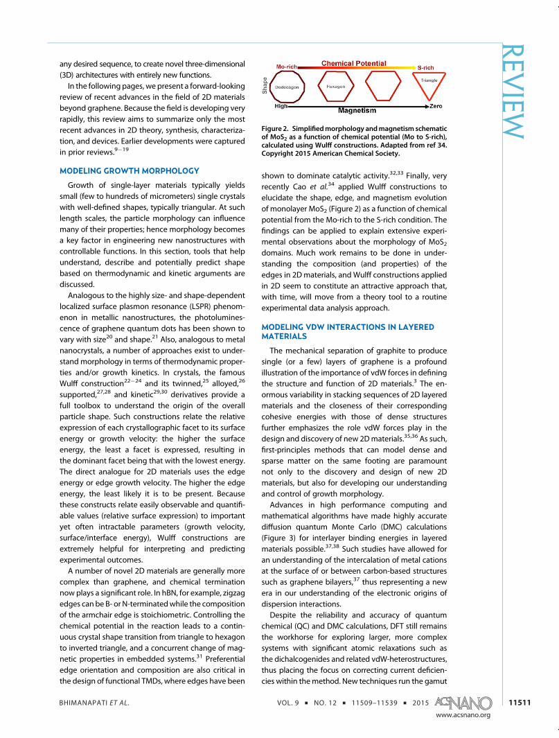
shown to dominate catalytic activity.32,33 Finally, veryrecently Cao et al.34 applied Wulff constructions toelucidate the shape, edge, and magnetism evolutionof monolayer MoS2 (Figure 2) as a function of chemicalpotential from the Mo-rich to the S-rich condition. Thefindings can be applied to explain extensive experi-mental observations about the morphology of MoS2domains. Much work remains to be done in under-standing the composition (and properties) of theedges in 2Dmaterials, and Wulff constructions appliedin 2D seem to constitute an attractive approach that,with time, will move from a theory tool to a routineexperimental data analysis approach.
MODELING VDW INTERACTIONS IN LAYEREDMATERIALS
The mechanical separation of graphite to producesingle (or a few) layers of graphene is a profoundillustration of the importance of vdW forces in definingthe structure and function of 2D materials.3 The en-ormous variability in stacking sequences of 2D layeredmaterials and the closeness of their correspondingcohesive energies with those of dense structuresfurther emphasizes the role vdW forces play in thedesign and discovery of new 2Dmaterials.35,36 As such,first-principles methods that can model dense andsparse matter on the same footing are paramountnot only to the discovery and design of new 2Dmaterials, but also for developing our understandingand control of growth morphology.Advances in high performance computing and
mathematical algorithms have made highly accuratediffusion quantum Monte Carlo (DMC) calculations(Figure 3) for interlayer binding energies in layeredmaterials possible.37,38 Such studies have allowed foran understanding of the intercalation of metal cationsat the surface of or between carbon-based structuressuch as graphene bilayers,37 thus representing a newera in our understanding of the electronic origins ofdispersion interactions.Despite the reliability and accuracy of quantum
chemical (QC) and DMC calculations, DFT still remainsthe workhorse for exploring larger, more complexsystems with significant atomic relaxations such asthe dichalcogenides and related vdW-heterostructures,thus placing the focus on correcting current deficien-cies within themethod. New techniques run the gamut
Figure 2. Simplifiedmorphology andmagnetism schematicof MoS2 as a function of chemical potential (Mo to S-rich),calculated using Wulff constructions. Adapted from ref 34.Copyright 2015 American Chemical Society.
REVIEW

BHIMANAPATI ET AL. VOL. 9 ’ NO. 12 ’ 11509–11539 ’ 2015
www.acsnano.org
11512
from postprocessing, semiempirical, pairwise correc-tions39�44 to the development of new, self-consistent,correlation functionals45�52 and many-body appro-aches,53�55 each having varying degrees of computa-tional demands and transferability and with successivedevelopments approaching chemical accuracy.56�63
These modern DFT-based approaches are now ma-ture enough, that with proper caution, it is possible touse theory to explore the classes of layered materialswhere vdW interactions are intrinsically important,and thereby placing us on the verge of a new era incomputational aided materials research. Such methodsprovide tools for the discovery of new 2Dmaterials thathave yet to be synthesized. Of fundamental importanceis the ability to assess the energetic and dynamicstability of candidate materials. Recent efforts havedemonstrated that the inclusion of dispersion interac-tions through a nonlocal correlation term (as is donein the Rutgers-Chalmers vdW density functional;vdW-DF46�49) can be critical in assessing these energiesrelative to bulk materials and can guide the discoveryof novel 2D materials.64�66 Related to this is the clea-vability of a material, i.e., the ability to separate/isolateindividual layers of a material. In most 2D materials,this is solely defined through the vdW interactions thatoccur between layers. Again, such methods are funda-mental in computing the relevant energy scales involvedin this interaction,67,68 thus leading to the prediction of acandidate material for realizing 2D magnetism.68
As discussed in this review, the ability to grow novel2D materials has seen tremendous progress over thepast decade. In many cases, the substrate may have
significant effects on the fundamental properties of the2D materials. The incorporation of dispersion interac-tions with DFT has made it possible not only to moreaccurately study these effects, but also to discernwhich substrates can be used to control materialsproperties. A profound example of the effects of sub-strate on 2D material properties is silicene and germa-nene. Free standing silicene, like graphene, is predictedto have a Dirac cone band structure. Early angleresolved photoemission spectroscopy (ARPES) resultsfor silicene on Ag(111)69 suggested that the Dirac conewould remain despite the buckling of Si atoms. Sub-sequent theory was fundamental in demonstratingthat in fact the linear bands were due to new statesarising due to hybridization between Ag and silicene.70
Since then, much effort has been placed on under-standing the effects of different substrates on theelectronic structure of 2D materials. Such efforts haverelied on the inclusion of dispersion interactions in DFTapproaches either through self-consistent methods (asin vdW-DF) or through additive terms (e.g., the DFT-D2assumes that the interactions between molecules oratoms are through the addition of semiempirical pair-wise corrections (e.g., Lennard-Jones type potentials)based on molecular C6 coefficients).39�42,52 Thesemethods have identifiedanumber of suitable substratesfor the growth of 2D materials that allow for bettercontrol of material properties.71�73 In all cases, it hasbeen demonstrated that growth on a vdW bondedmaterialmay be fruitful for truly retaining a 2Dmaterials'free-standing properties. Furthermore, the role of dis-persion interactions is invaluable. Not only is it useful forunderstanding the stability of a layered material ad-sorbed onto a substrate by dispersion interactions, butDFT methods which include dispersion interactions arenow being employed to understand the fundamentalinteractions of precursor materials.74,75 These can beused to optimize the growth process thus allowing forthe controlled growth of new and interesting materials.Regardless of which method is used for treating
intermolecular vdW interactions, one thing is certain,the inclusion of vdW interactions is paramount to ourability to properly simulate and understand layeredmaterials. Not only is this important for understand-ing binding, adsorption, and intercalation tin, but alsowhen trying to understand relevant experimentalsignatures76 due to interlayer lattice vibrationalmodes.77�84 Thus, with continued progress in thedevelopment of first-principles methods that can ac-curately account for vdW interactions, it may be pos-sible to truly discover and design novel 2D materialsthat may be experimentally realizable.
MODELING ELECTRON INTERACTIONS ANDEXCITONIC EFFECTS IN 2D TMDS
An exciton describes a two-particle excitation withsimultaneous creation of both an electron and a hole.
Figure 3. Calculated binding energies of AA stacked gra-phite as a functionof interplanar lattice separationobtainedfrom different density functionals and for DMC simulations.The self-consistent vdW functional vdw-DF2 shows goodaccuracy. Adapted with permission from ref 57, Copyright2010 Materials Research Society.
REVIEW

BHIMANAPATI ET AL. VOL. 9 ’ NO. 12 ’ 11509–11539 ’ 2015
www.acsnano.org
11513
Semiconducting TMD layers exhibit dramatically stronglight-exciton interactions and greatly enhanced elec-tron�electron interactions. Exciton binding energiesin monolayer TMD materials can be hundreds of milli-electronvolts (meV),85�90 orders of magnitude largerthan what is seen in typical bulk semiconductors. Suchexcitonic effects dominate the optical response in TMDmono- and few-layers, and create new opportunitiesfor basic science studies and novel optoelectronicapplications.First-principles calculations based on the GW
and GW plus Bethe Salpeter equation (GW-BSE)methods91,92 on various quasi-2D TMDs (such asMoS2, MoSe2, and WSe2) predicted that TMD mono-layers can havemultiple series of excitons, arising fromdifferent regions of the Brillouin zone, with bindingenergies in excess of 0.6 eV and unusual excitationspectra (optically bright and dark excited states ofnovel energy level and orbital-angular-momentumdependence) that cannot be explained by the usual2D hydrogenic model (Figure 4a,b).85,89,90 These extra-ordinary features originate from enhanced Coulombinteractions owing to reduced dimensionality and,importantly, an incomplete and strongly spatial-dependent screening in quasi-2D systems.85,86,89,90
The ab initio calculations further revealed that, despitetheir large binding energies, the TMD excitons are ofthe Wannier type with wave functions that are veryextended in real-space, but localized in k-space.85
The large exciton binding energy in monolayerMoSe2 has been confirmed by combining scanningtunneling spectroscopy (STS), optical spectroscopy,and GW-BSE theory.90 The electronic band gap is givenby single-particle excitations (sum of the energy forcreating an isolated electron and an isolated hole).Furthermore, two-photon excitation spectroscopyhas been used to investigate the novel excitonic levelstructure of monolayer WS2, including dark states.89
These measurements probed the optically inactive
exciton 2p and 3p excited states, and show excellentagreement with theoretical predictions,89 both in theirenergies and ordering with respect to other orbitalangular momentum exciton states. Another importantand interesting aspect of the electronic and optical pro-perties of TMD layers is that, owing to their quasi-2Datomic structure, they are very sensitive to environmentscreening. Both the electronic bandgaps and excitonbinding energies can change substantially dependingon the supporting substrates, as demonstrated in ref.90
LARGE-AREA, MORPHOLOGY-CONTROLLEDSYNTHESIS OF TMDS
Two-dimensional TMDs have been realized byvarious synthetic methods, including vapor-phasechemical reactions, wet-chemical synthesis, and liquidexfoliations.93�95 Vapor deposition techniques havebeen most extensively explored due to their potentialfor high scalability and morphological control. In thisprocess, metal containing precursors [e.g., MoO3,WO3, or (NH4)2MoS4]
95 are vaporized and reacted withchalcogen elements through vapor�solid reactions,leading to the growth of 2D TMDs on a substratedownstream. Most common procedures rely on thecoevaporation ofmetal and chalcogen precursors bothinitially in solid phases. These techniques generallyyield 2D TMDs with limited spatial homogeneity anduncontrolled morphologies due to the difficulty withcontrolling growth variables for vaporized reactants.Opposite to the commonly used solid-phase chalco-gen elements, gas-phase chalcogen reactants suchas hydrogen sulfide (H2S) have been used to improvethe scalability and uniformity of 2D MoS2
19 Also, thesynthesis of nanocrystalline 2D MoS2 with controlledlayer numbers has been demonstrated on the centi-meter scale via the sulfurization of molybdenum chlor-ide (MoCl5) precursors
96 The success for the improvedscalability is attributed to the balance control betweenthe partial pressure of vaporized MoS2 and its
Figure 4. (a) Calculated absorbance of monolayer MoS2 with (red line) and without (black dashed line) electron�holeinteractions included, using the ab initio GW-BSE approach. A broadening of 20 meV is used to prepare the curves. Thereare three series of exciton states: A, B and C, and (b) energy levels of the A series excitons in monolayer MoS2 from ab initioGW-BSE calculations (left panel) and from a 2D hydrogenic model (right panel). Adapted with permission from ref 58,Copyright 2009 J. Phys. Org. Chem.
REVIEW

BHIMANAPATI ET AL. VOL. 9 ’ NO. 12 ’ 11509–11539 ’ 2015
www.acsnano.org
11514
equilibrium pressure.18 Moreover, predeposition ofelemental metals on growth substrates and their sub-sequent reactions with chalcogen vapors have beendemonstrated to yield large-area 2D TMDs.97�104 Themajor advantage of this approach is the morphologyand the coverage control of 2D TMDs enabled bymetaldepositionmethods. The goal of uniformitywas furtherextended via seed-promoting molecules such as per-ylene-3,4,9,10-tetracarboxylic acid tetra-potassiumsalt (PTAS).105,106 The high solubility of PTAS in waterenhances the seed solution to be uniformly distributedon hydrophilic substrate surfaces on a large scale.Another such technique to grow high quality, preciselydoped electronic grade 2Dmaterials with abrupt inter-faces is through molecular beam epitaxy (MBE).107�112
With the availability of in situ characterization duringthegrowth,MBEparticularly has anadvantage of havingprecise thickness control and the ability to grow on 2Dor 3D substrates. Finally, very recently, metal�organicCVD (MOCVD) based on gas-phase precursors113�115
has proven that large-scale growth of 2D TMDs is readilyachievable, with the most impressive demonstra-tion being a 100 mm wafer of monolayer MoS2 with
uniform electrical properties (Figure 5a�c).114 In addi-tion to scalable growth, the synthesis of 2D TMDs withcontrolled orientation, layer number, chemical compo-sition, and placement have been extensively pursued.CVD based on the thermal evaporation of elementalmetal seed layers has demonstrated the growth of2D TMDs in two distinct 2D layer orientations of verticaland horizontal (Figure 5d,e).99,116,117 The thickness ofthe metal seed layers was identified to be the criticalparameter to dictate the 2D layer growth orientation.99
The chemical composition of 2D TMDs can alsobe controlled by simultaneously reacting multiplemetal precursors with multiple chalcogen elementsin vapor phases. For example, alloyed 2D monolayerof various compositions such as MoxW1�xS2
118,119 andMoSxSe2�x
120�122 have been synthesized, which pre-sent tunable band gap energies with varying ratios ofelements. The control of the stoichiometric variationsin MoS2 have been demonstrated to provide tunableelectrical and optical properties.123�125 In addition tothe chemical compositions control during growths,postgrowth processes have also been developed toconvert the chemical composition of 2D TMDs after
Figure 5. Synthesis of various 2D TMDs. (a) Schematic for the MOCVD process. Adapted with permission from ref 114.Copyright 2015 Nature Publishing Group. (b) False color dark-field TEM image showing continuous 2D monolayer MoS2.Adapted with permission from ref 114. Copyright 2015 Nature Publishing Group). (c) Four-inch wafer scale batch fabricationof 2DmonolayerMoS2 electronic devices. Adaptedwith permission from ref 114. Copyright 2015Nature PublishingGroup. (dand e) Synthesis of 2D TMDs with vertically standing 2D layers. (d) 2DMoSe2 with vertically standing 2D layers. Adapted withpermission from ref 32. Copyright 2007AAAS. (e) Large-scale controlled synthesis of 2DMoS2/WS2with vertically standing 2Dlayers. Adaptedwith permission from ref 33. Copyright 2014Royal Society of Chemistry. (f and g) Site-specific synthesis basedon CVD processes on patterned seed layers. Adapted from ref 37. Copyright 20l4 American Chemical Society. (f) Schematicsfor synthesis and (g) site-specifically synthesized 2D MoS2.
REVIEW

BHIMANAPATI ET AL. VOL. 9 ’ NO. 12 ’ 11509–11539 ’ 2015
www.acsnano.org
11515
their growths. For example, ion-exchange reactionshave been applied to convert 2D MoS2 into 2D MoSe2,consequently tuning their opto-electrical proper-ties.126,127 Selective area growth of 2Dmaterials has alsorecently been realized, in part, using a spin-coatedammonium heptamolybdate [AHM, (NH4)6Mo7O24 34H2O] and pregrowth lithographic techniques toachieve site-specific, patterned growth of 2D MoS2(Figure 5f,g).128 Finally, 2D MoS2 with site-specificallycontrolled layer numbers has been demonstrated on asingle SiO2 growth substrate by modifying the surfaceproperties of the SiO2 via plasma etch treatments.129
Despite themodest success in improving scalability anduniformity, the chemically synthesized large-area 2DTMDsat present still exhibit electrical properties far fromwhat are demanded for realistic applications. For exam-ple, the room temperature field-effect-transistor (FET)mobility of state-of-the art 2D MoS2 grown on a 4-in.waferwithuniform layer numbers is∼30cm2V�1 s�1,114
an order-of-magnitude smaller than those of mechani-cally exfoliated materials. Such limitation is attributedto the defective nature of chemically synthesizedmaterials: intrinsic defects (e.g., vacancies) in individual2D grains as well as interfacial defects (e.g., grainboundaries) across individual 2D grains. Further infor-mation on the growth of different TMDs using differenttechniques is summarized in Table 1. Here, mechanicalexfoliation includes scotch tape exfoliation and chemi-cal vapor transport. Powder vaporization covers thegeneral CVD techniques that are based on powdertransport to grow 2D materials on various substrates.
SYNTHESIS OF 2D-TMD HETEROSTRUCTURES
Developing new hybrid materials by combining 2Dlayered materials in vertical stacks offers an enormousamount of possibilities to broaden the versatility of 2D
materials, allowing for achieving superior and unusualmaterial properties that cannot be obtained other-wise.199 Thus, securing robust methods that enablecontrolled stacking of a variety of 2Dmaterials with anydesired combination and thicknesses will play a keyrole for 2D materials to be widely used, in particular,in transparent and flexible electronic and optoelectro-nic device applications. Many of these structuresare summarized in Table 1, where a commonly usedscheme to fabricate 2D heterostructures such asMoS2/WSe2,
140,142 MoS2/WS2,200 MoS2/MoSe2,
201 andMoSe2/WSe2
202 is themechanical transfer of separatelyexfoliated 2D crystals.143,147,149,203 However, despitethe relatively high quality crystals, the dry transfermethod may not be suitable when sophisticated con-trol of lattice orientation is required and can introducevarious adsorbates, such as hydrocarbons, trappedbetween layers during the process that may deterio-rate the interface quality between the layers.204 As aresult, it is very advantageous to develop techniquescapable of directly synthesizing these heterostructures.Vertically stacked 2D TMD/graphene180,181,187,205�207
heterostructures (Figure 6a�c) have been synthesizedby the sequential growth of 2D TMDs on top of pre-existing graphene (or hBN208). Additionally, a varietyof 2D TMD-only heterostructures have also been de-monstrated, including heterostructures with verticallystanding 2D layers such as MoS2/WS2 (or MoSe2/WSe2) synthesized by the one-step sulfurization(or selenization) of elemental metals.117,209 In-plane2D heterostructures have been more challengingto synthesize as the formation of alloyed structuresis thermodynamically favored. Recently, in-planeheterostructures in lateral and vertical orientationshave been demonstrated by the sequential in situ
vapor�solid reactions,189,190 or by the coreaction of
TABLE 1. Table showing the diffreent TMDs Grown To-date Using Various Techniquesa,b
a X, S, Se; BP, black phosphorus; GR, graphene ribbons. b References 7, 39, 90, 96, 99, 105, 106, 113, 114, 119, 121, 126, 130�198, 400.
REVIEW

BHIMANAPATI ET AL. VOL. 9 ’ NO. 12 ’ 11509–11539 ’ 2015
www.acsnano.org
11516
Mo and W-containing precursors with chalcogens(Figure 6d,e).173,175,190,210,211 Postgrowth processesbased on ion-exchange reactions have also been em-ployed to develop 2Dheterostructures. For example, anexchange of Se ions with S ions on pre-existing MoSe2has been demonstrated to site-specifically convertMoSe2 into MoS2 realizing in-plane 2D MoSe2/MoS2heterostructures.127 Finally, the epitaxy of MoS2, WS2,and WSe2 on SnS2 microplates was also demonstratedunder mild experimental conditions (450 �C for2�6 min), using MoCl5/S, WCl6/S and Se as precursors,respectively.188 Despite significant lattice mismatch atthe interface with SnS2, 15%, 16%, and 11% for MoS2,WS2, and WSe2, respectively, the heterostructure cansuccessfully form without a significant strain due torelatively weak vdW forces at the interface. At present,the synthesis of all the above-mentioned 2D hetero-structures has been limited to very small areas. Moreeffort should be focused in the direction to producescaled-up 2D heterostructures while maintaining theiratomically seamless heterointerfaces.
DOPING AND CHEMICAL FUNCTIONALIZATIONOF TMDS
For versatile use of 2D materials in next-generationelectronics and optoelectronics, development of con-trollable doping processes for tailoring their carriertypes and Fermi levels is critical given the necessityof, for example, Schottky barrier modulation at TMD/metal junctions and realization of appropriate junc-tions. However, the traditional dopingmethods includ-ing dopant diffusion and ion-implantation used for
conventional bulk semiconductors are not suitablefor atomically thin 2D layers due to unavoidable crystaldamage during the process. As a result, chemistriestypically conducted on organic molecules and surfaceshave thus been tried as a starting point for chemicalfunctionalization in pursuit of simple and efficientroutes for electronic and optical modulation. Themotivations for chemical modification of 2D layersother than doping level tuning include opening anelectronic band gap, charge storage, chemical andbiological sensing, making new composite materials,and so on.Similar to graphene,212�214 various chemical ap-
proaches have been adopted to systematically tuneelectronic and optical characteristics of TMDs by mod-ulation of the charge carrier type and concentration.These efforts have mostly been focused on single- andmultilayers of MoS2, MoSe2, WS2 and WSe2, throughphysisorption of molecules,215,216 metallic nano-particles surface functionalization,217,218 solution-based functionalization,218�220 and plasma-assisteddoping.221,222 The molecular physisorption can offerwide-range control of charge density, thereby modu-lating optical properties such as the photolumines-cence (PL) processes. Tongay et al.216 have shown thatthe light emission efficiency in 2D TMDs (MoS2, MoSe2andWSe2) is largely modulated by charge transfer withphysically adsorbed electronegative gaseous mol-ecules including O2 and H2O, and over a 100-foldmodulation in the efficiency was achieved, while inertgases have exhibited a negligible effect. PhysisorbedO2 and H2O molecules electronically depleted n-type
Figure 6. Synthesis of 2D TMD heterostructures. (a) Cross-sectional HRTEM of MoS2/Quasi-free-standing epitaxial graphene(QFEG) showing the nucleation and subsequent lateral growth of MoS2 on a SiC step edge covered with the top graphenelayer is flat. (b and c) Scanning TEM images of stacked MoS2�WSe2�EG vertical stacked heterostructures showing pristineinterfaces with no intermixing of Mo�W or S�Se after synthesis. (d) 2D monolayer MoS2/WS2 heterostructures with lateralhetero interfaces. Synthesis schematic and chemical composition analysis.79 (e) HRTEM image showing the hetero interface of2D monolayer MoS2/WS2. Adapted with permission from ref 81. Copyright 2013 American Physical Society.
REVIEW

BHIMANAPATI ET AL. VOL. 9 ’ NO. 12 ’ 11509–11539 ’ 2015
www.acsnano.org
11517
materials such as MoS2 and MoSe2, and resulted indrastic enhancement in PL; however, in p-type WSe2,the opposite effect was observed. NO2 molecules canalso be utilized as a p-type dopant for 2D TMDs. WhenWSe2 is exposed to NO2 environment in N2 gas, NO2
could physically and chemically adsorb on the WSe2surface and transfer electrons from WSe2 due to itsstrong oxidizing property.215 The doping effect onMoS2 through electronic beam (e-beam) depositionof metallic nanoparticles of noble metals (Au, Ag, Pd,Pt) is also investigated where p-type doping wasobserved which exhibited increasing trend with metalwork functions for varying dose of nanoparticles.In addition, Mouri et al.218 used F4TCNQ and 7,7,8,8-tetracyanoquinodimethane (TCNQ) as p-type chemicaldopants, and nicotinamide adenine dinucleotide(NADH) as n-type dopants to effectively tune the PL ofmonolayer MoS2; the enhancement in PL intensity wasobserved upon the adsorption of the p-type dopants,while the n-type dopants weakened the intensity.P-type dopants extract electrons from the MoS2 suchthat the recombination of excitons becomes adominant
process instead of that of negative trions, while thisswitching of the mechanism is suppressed by n-typedopant molecules.218
Organic compounds, such as benzyl viologen (BV),can form an electron transfer complex to n-dope MoS2via surface charge transfer mechanism.223,224 The BV-doped MoS2 exhibits excellent stability in ambient air(with only a minimal change in the electrical character-istics after 9 days of air exposure), and an electron sheetdensity of ∼1.2 � 1013 cm�2 is achieved that corre-sponds to the degenerate doping limit forMoS2.
223 Theneutral BV molecule transfers electrons to MoS2, andeventually a two-electron transfer process is carriedout between the two materials (Figure 7a). The dopingprocess is reversible, which can be valuable not only forselective removal of the molecule for patterned dop-ing, but also for the controlled modulation of chargecarrier density, such that the BV molecules are re-moved from theMoS2 surface by immersion in toluene;the transfer characteristics of BV-doped devices re-cover the original state before doping.223 MultilayerMoS2 is n-doped by p-toluene sulfonic acid (p-TSA),
Figure 7. (a) Schematic of BV surface doping of MoS2, an energy band diagram of MoS2 and BV redox states, and redoxreactions of the BVmolecule when adsorbed on an acceptormaterial, MoS2. Adapted from ref 223. Copyright 2014 AmericanChemical Society. (b) Fabrication of chemically doped vertical p�n homogeneous junction in a few-layer MoS2 flake. (i) AMoS2 flake was transferred on a PMMA/PVA/Si substrate, and then BV-doped and annealed. (ii) After dissolving the PVA layerin deionizedwater, the PMMA film supporting aMoS2 flakewas transferred to a PDMS/glass substrate. (iii) TheMoS2 flakewasstamped on the SiO2/Si substrate, and the n-doped surface was aligned with the Cr/Pd/Cr bottom electrode prepared inadvance. (iv) After AuCl3 doping and annealing, the vertical p�n junction in the MoS2 flake was formed, followed by thedeposition of a Cr/Pd top electrode. Adapted with permission from ref 224. Copyright 2015 Nature Publishing Group. (c)Structure of amine-rich PEI as n-typedopants formultilayerMoS2 FETs. Adaptedwithpermission from ref 219. Copyright 2013IEEE. (d) Schematic illustrationof theMoS2 FET layoutwith Cs2CO3filmon top. Adapted from refs 217 and229. Copyright 2014and 2013, respectively, American Chemical Society.
REVIEW

BHIMANAPATI ET AL. VOL. 9 ’ NO. 12 ’ 11509–11539 ’ 2015
www.acsnano.org
11518
which has been widely used for tailoring charge den-sity of conducting polymers; Raman spectroscopy andelectrical measurements indicate an n-type dopingwhere the threshold voltage shifts toward more nega-tive gate voltages as the time of exposure to p-TSAincreases.225 Controlled tuning of electronic and opti-cal properties of TMD flakes can also be achievedby modifying SiO2 substrates with functional self-assembled monolayers (SAMs) with different dipolemoments, thereby tuning the charge redistributionbetween the substrates and the flakes.220 Raman dataand electrical characteristics of field effect transistorsshow that fluoroalkyltrichlorosilane-SAMs with alarge positive dipole moment significantly reduce theintrinsic n-type characteristic of MoS2 flakes (p-typedoping), whereas 3-(trimethoxysilyl)-1-propanamine-SAMs improve the intrinsic n-type characteristic(n-type doping). In general, CH3-terminated SAMsexhibit little influence on charge carrier density dueto the slight dipole moments, while NH2-/SH-SAMswith lone pair electrons and CF3-SAMs possessing highelectronegativity show electron- and hole-donatingcharacteristics, respectively.220
A stable and tunable doping capability over a widerange, especially over the natural propensity of TMDs(n-type and p-type for MoS2 and WSe2, respectively),is critical to achieve practical junctions (e.g., p�n,p�n�p, etc.), which are required as central buildingblocks of electronic and optoelectronic devices. Due tothe strong propensity toward a certain doping type ofTMDs, much effort has been focused on realizing p�njunctions based on vertical vdW heterostructures bystacking different TMDs of dissimilar types.142,226 Inorder to develop a homogeneous p�n junction utiliz-ing a single 2D material, Suh et al.138 have demon-strated a vdW vertical p�n junction that is formed bystacking the hole-doped MoS2 layer (p-type) with anundoped layer (n-type), which showed gate tunablecurrent rectification. The p-doped MoS2 is achievedthrough substitutional degenerate p-type doping ofMoS2 by incorporating niobium (Nb) to replace Moatoms via a chemical vapor transport (CVT) method, inwhich stable doping is realized by covalent bonding inthe crystal lattice. A similar approach was taken, bututilizing the surface charge transfer method, to forma vdW p�n junction. Here, the BV and AuCl3 were usedas n- and p-type dopants, respectively, to make MoS2behave as n- and p-type semiconductor materials(Figure 7b).224 The hole-doping was enabled by spin-coating a AuCl3 solution which is commonly used ingraphene doping due to its large positive reductionpotential where AuCl4
� in solution receives electronsfrom MoS2 through surface charge transfer to formAu nanoaggregates.227,228 Furthermore, a lateral MoS2p�n junction with a strong photo response wasalso demonstrated. By the degenerately hole-dopingof partially masked MoS2, the junction was formed at
an interface between the doped and undoped crystalregions.138 The partialmasking of theMoS2 surfacewasconducted by transfer of a hBN layer to protect theMoS2 area underneath from doping.The chemical and molecular modification of TMDs
can also be utilized as a strategy to reduce both sheetand contact resistances of field effect transistors (FETs),providing a simple strategy to further optimize theperformance of the devices utilizing 2D semiconductorlayers. Du et al.219 adopted amine-rich polyethyleni-mine (PEI, Figure 7c) as n-type dopants for multilayerMoS2 FETs and showed that a 2.6 times reduction insheet resistance and 1.2 times reduction in contactresistance have been achieved with a negative shift ofthe threshold voltage confirming n-type doping uponexposure to a PEI solution (Figure 7d). Doping schemesusing metal atoms via surface charge transfer are alsoapplicable to TMDs. In their work, Fang et al.229 usedK atoms to degenerately n-dope the source/draincontact regions of few-layer MoS2 and WSe2 nano-sheets and achieved low contact resistances in theirFET devices. Moreover, the work shows that n-typeWSe2 FETs can be enabled with high mobility compar-able to those of previously reported p-type WSe2 FETsby simply doping the contacts accordingly. However,this approach lacks air stability, limiting applicabilityof the method. K atoms become highly reactive uponexposure to ambient air and water molecules, leadingto immediate oxidation of K, that the vacuum processis required.229 Cl is also used to n-dope few-layer WS2and MoS2. The exfoliated WS2 or MoS2 flakes weresoaked in undiluted 1, 2 dichloroethane (DCE) at roomtemperature for more than 12 h and high dopingdensity of 6.0 � 1011 and 9.2 � 1012 cm�2 wereobtained, respectively.230 A possible mechanism sug-gests that the doping may have been realized throughthe replacement of S vacancy with Cl atom.In addition to the enhancement realized by the prior
examples of degenerate chemical doping of TMDs, thedevelopment of robust and controllable nondegene-rate doping schemes without crystal damage is crucialfor designing TMDs-based electronic and optoelectro-nic devices, allowing for wide-range charge carrierdensity modulation. For this purpose Lin et al.217 re-ported nondegenerate n-doping of monolayer MoS2via surface functionalization using cesium carbonate(Cs2CO3) (Figure 7d), which has previously beenadopted as an electron injection material in organiclight-emitting devices (OLEDs) and can induce n-typedoping for organic semiconductors.231,232 A controlla-ble nondegenerate p-type doping technique was de-monstrated on few-layer and bulk forms of WSe2 byadjusting the concentration of octadecyltrichlorosilane(OTS).233 This p-doping effect arises from the methyl(�CH3) functional groups in OTS, which exhibit apositive dipole and consequently reduce the electrondensity in a WSe2 crystal as the charge carriers are
REVIEW

BHIMANAPATI ET AL. VOL. 9 ’ NO. 12 ’ 11509–11539 ’ 2015
www.acsnano.org
11519
accumulated at the interface between OTS and WSe2.The doping concentration achieved with varyingOTS concentration ranged from 1.6 � 1010 to 3.0 �1011 cm�2, which is in the nondegenerate regime.
RAMAN SPECTROSCOPY OF SEMICONDUCTINGTRANSITION METAL DICHALCOGENIDES(STMDS)
Raman spectroscopy plays an important role in thecharacterization of STMDs since it is not destructiveand provides useful information about the structureof monolayers, number of layers, stacking and defects.MoS2, MoSe2, WS2, and WSe2 share the same trigonalprismatic (or 2H) structure belonging to the samespace group P63/mmc (D6h
4 in Shöenflies notation).However, for few layer STMDs, the structure possessesa different symmorphic space group depending on thenumber of layers. For odd numbers of layers, the pointgroup symmetry in the unit cell is D3h, and for evennumbers of layers, it becomes D3d. The symmetryconsiderations mentioned above are useful to performtheoretical Raman spectroscopy of STMDs from first-principles using density functional perturbation theoryDFPT234,235 and compare with the experimental re-sults. The Raman spectrum of bulk trigonal prismaticSTMDs exhibits three active signals at high frequenciesnamed E1g, E
12g, and A1g. The polarization tension
corresponding to E1g renders this mode invisible inthe commonly used backscattering geometry.236,237
The E1g and E12g are in-plane modes and the A1g isan out-of-plane mode. These three modes becomeE00, E0, and A0
1 for a system with odd number of layers,and E2g, E
1g, and A1g for an even number of layers,
respectively.238 As the number of layers increase, thein-plane modes shift to lower frequencies and the outof plane modes shift to higher frequencies;239 thisbehavior has been confirmed theoretically in trigonalTMDs.238,240 Interestingly, a second-order Raman reso-nance process has been identified in monolayer WS2with a laser excitation of 514.5 nm involving the long-itudinal acoustic mode (LA) at the M point in theBrillouin zone LA(M), allowing the clear differentiationof monolayer and few layer systems. Here also thetheoretical approach based on first-principles calcula-tions agrees with the experiment.241 Moreover, DFPTsimulations demonstrate that few layered STMDsexhibit an additional first-order Raman out-of-planemode, which it is not active in the monolayer and bulk,that involves the vibration of the transition metal atomand is named A02
1 or A21g depending on whether the
layers are odd or even.238 Figure 8 shows the experi-mental Raman spectra for few layered WSe2, includingthe bulk, in which a new Raman active mode appearsaround 310 cm�1, confirming the theoretical resultsobtained from DFPT.In addition to the high-frequency intralayer modes
discussed above, low-frequency interlayer modes have
recently begun to attract increasing attention. Forhigh-frequency intralayer modes, which involve vibra-tions from the intralayer chemical bonds, the restoringforces are dominated by the strength of these intra-layer chemical bonds instead of the interlayer vdWinteractions. Consequently, there are great limitationsfor them as unambiguous thickness indicators. In starkcontrast, low-frequency interlayermodes (including in-plane shear modes and out-of-plane breathingmodes)correspond to layer�layer vibrations with each layermoving as a whole unit, and hence, their frequenciesare solely determined by the interlayer vdW restoringforces. Both experimental and theoretical works havedemonstrated their promising potential as effectiveindicators of layer thickness of 2-D crystals, includingSTMDs.77�84 Furthermore, a recent work using ultra-low-frequency Raman spectroscopy and first-princi-ples Raman simulations revealed that low-frequencyinterlayer Raman modes also could be fingerprintsof the layer�layer stacking configurations for bilayerand trilayer MoSe2 and WSe2.
235 The results could beextended to other family members of STMDs.Theoretical methods have gone beyond simply pro-
viding understanding by not only explaining observa-tions already made, but by predicting the behaviorof possible new 2D arrangements such as heterolayersystems composed of sandwiching different STMDs;this is the case for heterostructures of MoS2 and WS2,which actually have been synthesized.242 The Ramansimulations reveal that depending on the stackingorder of the layers, the Raman spectrum exhibitsunique features in both frequency and intensity thatcan be used for identification.243 There are unresolvedchallenges that need further experimental and theore-tical efforts to resolve, including the role of the differ-ent defects in the Raman spectrum of STMDs. In thiscontext, recently an exfoliated MoS2 monolayer hasbeen exposed to Mnþ ions to generate defects, findingthat the LA(M) signal increases as the density of defectsincreases, thus showing an analogy of the LA(M) peakto the D peak in graphene.244
Figure 8. Experimental Raman spectra of WSe2 with differ-ent layers (N = 1�5) including bulk taken with 514.5 nmexcitationwavelength. The black arrows show a newRamanactivemode, which appears in few layer materials but is notpresent in the monolayer nor in bulk. Adapted with permis-sion from ref 238. Copyright 2014 Nature Publishing Group.
REVIEW

BHIMANAPATI ET AL. VOL. 9 ’ NO. 12 ’ 11509–11539 ’ 2015
www.acsnano.org
11520
SCANNING TRANSMISSION ELECTRONMICROSCOPY (STEM) OF TMDS
Perhaps one of the most powerful techniques toprobe the electronic, chemical, and structural proper-ties of 2D materials is scanning transmission electronmicroscopy (STEM). Instead of using a broad stationarybeam as in TEM, STEM uses a highly focused electronbeam for imaging and analysis, where the e-beam canbe rastered across the sample or parked precisely atselected positions. Several STEM based techniqueshave proven useful for 2D materials characterization.Annular dark field (ADF) imaging, also known asZ-contrast imaging, reveals atomic-scale structural in-formationwith atomic number contrast.245,246 Electronenergy-loss spectroscopy (EELS) can provide chemical,bonding and electronic structure information andcan be used to measure local optical properties ofthe material.247
Importantly, one must consider that electronbeam�sample interactions can trigger transforma-tions and transition dynamics in 2D crystals. Althoughtriggered by the electrons, such transition dynamicsreveal the atomistic mechanisms by which crystalscan evolve, and defects and edges can be createdand transformed in a variety of 2D structures such asgraphene248�253 and hBN.254�258 These studies showinterplay of knock-on damage and ionization damagetaking place in 2D crystals under the electronbeam. Thus, a low accelerating voltage (30�120 keV)is often necessary to minimize knock-on damage,and low-dose analysis is usually preferred. Fortunately,with the latest aberration-corrected STEM capabilities,the above-mentioned imaging and spectroscopyanalysis can all be performed at atomic resolutionwith single atom sensitivity even at low acceleratingvoltage.259�262
The main advantages of STEM over TEM are (i)multiple imaging and spectroscopy signals can beacquired simultaneously, allowing for direct correla-tion of the structural and spectroscopic informa-tion;247,263�267 (ii) the atomic number contrast infor-mation in ADF images provides a feasible way toperform image-based atom-by-atom chemical analy-sis268 and to quantify the thickness of the 2D TEMsamples;269 and (iii) the ability to precisely control theposition of the electron beam enables local spectro-scopic analysis from individual atoms and controllablestructural modification/manipulation of the materialat designated regions.While detailed image simulation is often necessary
for quantitative interpretation of HRTEM images, theinterpretation of STEM ADF images is straightforward:the bright atoms in the ADF image always correspondto atoms in the thin sample. This important featurehas enabled direct identification of all the carbon atompositions in bilayer graphene, which in turn definesthe stacking order and the structure of stacking
boundaries in bilayer graphene.245,246 More impor-tantly, the ADF image intensity, to a first approxima-tion, is proportional to the square of the atomicnumber, i.e. heavier atoms display higher imageintensity. By quantifying the ADF image intensity ateach atomic position, atom-by-atom chemical analysishas been first demonstrated on monolayer h-BN withcarbon and oxygen impurities,268 and soon becameone of the most powerful tools for characterizingdefects in 2D materials. For example, using quantita-tive STEM-ADF imaging, Zhou et al. reported thefirst systematic study of intrinsic structural defects inCVD-grown monolayer MoS2, including point defects(vacancies, antisite defects, and adatoms, Figure 9a),grain boundaries, and edges.269 This study verifiedsome of the theoretically proposed grain boundaryconfigurations,270,271 and also identified two types of60� grain boundaries with predicted metallic behavior,as shown in Figure 9b,c. Similar structural defects werealso observed in other TMD monolayers,167 and therelative population of different point defects is sensi-tive to the growth method for MoS2 monolayers.272
Furthermore, dopant distributions in W-doped andSe-doped MoS2 monolayers can be automaticallymapped out with almost 100% detection efficiency,by applying atom-finding scripts to atomically resolvedADF images and filtering out distinct intensity rangesdue to the presence of dopant atoms (Figure 9d,e).133,170 In bilayer MoS2, the dopant distribution caneven be mapped out layer-by-layer.170 Such analysisserves as a highly efficient and accurate measurementof the local composition for electron-beam sensitiveTMD layers. Atom-by-atom chemical analysis via STEM-ADF imaging has also helped to study the structuralepitaxy and chemical intermixing at lateral WS2/MoS2 heterostructure interfaces,173,175 and impurityconfigurations in monolayer graphene.265,273�275
Even though the temporal resolution is lower thanthat in TEM imaging, the chemical information con-tained in the ADF images has made sequential STEMimaging a particularly powerful method for exploringdefect dynamics at the atomic scale via energy transferfrom the electron beam. By combining in situ heatingand electron irradiation, Suenaga and co-workers haveobserved the phase transformation between the semi-conducting 2H and metallic 1T phases in monolayerMoS2 at the atomic scale (Figure 9f), and they showedthat the size of the 1T domains in the 2H matrix canbe controlled by adjusting the electron dose.267 In amore recent study, Lin et al. showed that electronirradiation can generate Se vacancies in monolayerMoSe2, and the segregation of Se vacancies underenergy transfer from the electron beam can subse-quently trigger the nucleation and growth of inversiondomains in MoSe2, connecting to the pristine latticevia conductive 60� grain boundaries (Figure 9g).276
Such in situ defect dynamics studies can help to
REVIEW

BHIMANAPATI ET AL. VOL. 9 ’ NO. 12 ’ 11509–11539 ’ 2015
www.acsnano.org
11521
understand the structural evolution of the materialunder external excitation, e.g., energy transfer via
thermal annealing.When the electron�sample interaction is controlled,
the electron beam in STEM can also be used tocreate new nanostructures at designated regions inthe sample. In a recent study, Lin et al. used the focusedelectron beam in STEM to generate holes at prese-lected regions in TMD monolayers, and demonstratedthat under continuous electron irradiation the nano-ribbons confined by two adjacent holes can eventually
collapse into subnm-wide highly stable metallic MXnanowires with robust self-adapted junctions to theTMD monolayers (Figure 9h�j).277 Such ultrasmall MXnanowires can be fabricated across a wide range ofTMD monolayer systems, and patterning these nano-wires or creating complex nanowire junctions werealso demonstrated via precise control of the e-beamposition on the samples. This study points to a promis-ing possibility that multiple devices may be fabricatedin a single TMD monolayer and that a focused e-beamsystem could subsequently be applied to sculpt these
Figure 9. Characterization and engineering of defects in TMD atomic layers. (a) STEM ADF images and the correspondingatomic models of S vacancy and MoS2 antisite defect in monolayer MoS2. Adapted from ref 269. Copyright 2013 AmericanChemical Society. (b and c) ADF images of two types of 60� grain boundaries in monolayer MoS2 with structural modelsoverlaid Adapted from ref 269. Copyright 2013 American Chemical Society. (d) ADF image and the corresponding dopingbehavior analysis of a W-doped MoS2 monolayer Adapted with permission from ref 133. Copyright 2013 Nature PublishingGroup. (e) ADF image and the corresponding dopant distributionmap of a Se-dopedMoS2monolayer. Adapted from ref 170.Copyright 2014 American Chemical Society. (f) ADF image and a schematic of a 1T domain in a 2H MoS2 monolayer, inducedby the electron beam under in situ heating. Adapted with permission from ref 267. Copyright 2014 Nature Publishing Group.(g) ADF image of an inversion domain in a 2H MoSe2 monolayer induced by the electron beam. Adapted from ref 276.Copyright 2015 American Chemical Society. (h) Sub-nanometer MoSe nanowire array and junctions created within a MoSe2monolayer using an electron beam. (i) The atomic structure model of the MX nanowire. (j) Comparison of the experimentaland simulatedADF images of theMoSe nanowire created by electronbeam. Adaptedwith permission from ref 277. Copyright2014 Nature Publishing Group.
REVIEW

BHIMANAPATI ET AL. VOL. 9 ’ NO. 12 ’ 11509–11539 ’ 2015
www.acsnano.org
11522
MX nanowires to produce lateral interconnects be-tween different devices.The recent development of monochromatic STEM-
EELS instrumentation has made it possible to measurephonon modes from 2D materials278 and to map outexcitons at a lateral TMD heterostructure with sub-wavelength spatial resolution.279 Besides EELS, cathodo-luminescence (CL) can also serve as a low-backgroundtechnique to probe properties such as bandgap andplasmon resonances. SEM-CL has conventionally beenused in several light-emitting interfaces and materialssuch as GaN, GaAs, and GaAlAs.280,281 Recently, BNnanostructureswere characterizedwith CL and showeda strong luminescence peak at 5.33 eV, confirminga UV bandgap.282 Given advances in detection andcollection schemes, STEM-CL is now possible andmuchremains to be unraveled about the local bandgapvariations in 2D materials.
2D ELECTRONICS AND OPTOELECTRONICS
2D materials are being extensively investigated asthe channel materials for next generation FETs owingto their ultrathin body nature that allows aggressivescaling down to atomic dimensions. One of the majorchallenges that needs to be resolved in this context isthe source/drain contact formation since it limits theultimate performance of these 2D FETs.283�287 Notethat in conventional Si FETs a substitutional dopingscheme is adopted in order to minimize the contactresistance and tune the carrier type (electron or hole).However, the absence of a sustainable doping schemefor 2D materials necessitates the use of metals withdifferent work functions to achieve the same objective.Since metal�2D contacts are characterized by Schott-ky barriers (SBs), one has to minimize the height andwidth of the SB to improve the current transmission.This was achieved through Sc285 andMoOx
284 contactsfor n-type and p-type MoS2 FETs, respectively, whereasgraphene contacts were used for WSe2 FETs283,286
since the Fermi level of graphene can be tunedthrough electrostatic gating. As noted previously inthe Doping and Chemical Functionalization of TMDssection, various routes have been explored for chemi-cal doping of the TMDs to achieve improved deviceperformance. In addition, recently phase engineeringwas applied to selectively induce the metallic 1T phaseat the source and the drain contact regions of a MoS2FET,287,288 which showed significant performance im-provement. In general, MoS2 and MoSe2 FETs8,289,290
have been found to be dominated by electron trans-port, whereas WS2 and WSe2 FETs291�293 are mostlyambipolar (presence of both electron and holebranches in the current transport). This observation isrelated to the pinning of metal Fermi levels close to acertain energy in the bandgap of the channel materialirrespective of the work functions of the metals.294 ForMo-based chalcogenides, the pinning occurs near the
conduction band edge, whereas for W-based chalco-genides, the pinning occurs close to the midgap.FETs based on several other metal chalcogenides likeSnS2, HfSe2, GaS, In2Se3 andmanymore have also beendemonstrated.295�298
Benchmarking the carrier mobility (Figure 10a) ofvarious 2D materials provides evidence that the TMDsexhibit only a modest mobility compared to phos-phorene and graphene.299 The relatively low mobilityvalues of the STMDs point to a high density of midgaplocalized states caused by disorder.293 Potential candi-dates are metal and chalcogen vacancies, divacancies,dislocations, and molecules and atoms bonded oradsorbed onto the exfoliated sheets.269,300�302 How-ever, it is encouraging to note that the FETs basedon various 2D materials are being implementedin different components of an integrated circuit likethe digital inverters182,303,304 (Figure 10b), analogamplifiers305�307 (Figure 10c), and memory tran-sistor.308 2D materials also show promise for thin filmtransistor (TFT) technologies.299 The two most desir-able features of the TFTs, mechanical flexibility andoptical transparency, are naturally inherited by the 2Dmaterials owing to their vdW epitaxy and atomicallythin body. In fact, high performance TFTs based onMoS2, WSe2, and black phosphorus (Figure 10d,e) havealready been demonstrated.150,286,307,309 In particular,flexible black phosphorus FETs can endure manythousands, perhaps millions, of bending cycles thatis only limited by the substrate, gate dielectric andcontact interface. Figure 10e shows robust black phos-phorus FET electrical properties at the measurementlimit of 5000 bending cycles at 1% strain. Finally, thehigh surface to volume ratio of the 2Dmaterials makesthem ideal for sensor and detector applications as well.For example, MoS2 and WS2 FETs have been success-fully employed for toxic gas sensing, protein and pHsensing and label free detection of biomolecules(Figure 10f).310�312 The extraordinary light absorptioncapability and current conversion efficiency of the 2Dmaterials also pave their way as energy harvestingdevices.313
2D materials also provide an enormous scope tostudy the fundamental principles of light absorptionand emission in atomically thin materials with theultimate goal to realize high performance opto-electronic devices like light emitting diodes (LEDs),photodetectors, lasers, and optical cavities, amongothers.146,148,315�319 The first generation of 2D photo-transistors demonstrated photoresponsivity on theorder of ∼120 mA/W in spite of being severely limitedby the contact resistance.317 This issue was resolved inlow contact resistance monolayer WSe2 phototransis-tors resulting in photoresponsivity as high as ∼1.8 �105 A/W.319 Finally, when high mobility graphene wascombined with high photoresponsive MoS2 in a hybridgraphene�MoS2 phototransistor, record high room
REVIEW

BHIMANAPATI ET AL. VOL. 9 ’ NO. 12 ’ 11509–11539 ’ 2015
www.acsnano.org
11523
temperature photoresponsivity of ∼5 � 108 A/W wasobtained.146 WSe2 p�n photodiodes having two localbottom gates with different gate dielectrics producedphotodetection efficiencies up to 320 mA/W, which iscomparable to state of the art commercial siliconphotodetectors for green light.148
2D layered-material optoelectronic devices arelikely to leverage integration with optical cavities andother photonic architectures as well.320 In a solar cell orphotodetector, for instance, it is crucial to absorb largefractions of light in potentially atomically thick materi-als. The simplest such architectures are based on the“Salisbury screen” concept and comprise an absorbinglayered material placed a quarter wavelengths froma reflecting ground plane. Such cavities can indeedsupport perfect absorption even at monolayer thick-nesses, but only in a narrow wavelength band definedby a Fabry�Perot resonance.321 More broadbandenhancement of light absorption in ultrathin films ispossible in plasmonic322 or dielectric gap-mode323
architectures. In applying these concepts to 2Dlayered-materials, however, one must be careful toconsider the presence of optical anisotropies. Bothplasmonic and dielectric gap-mode architecturespredominantly exhibit enhancement of out-of-planeoriented electric fields.324 This anisotropy in field en-hancements stems from a fundamental property ofelectromagnetics: the difference between continuityconditions for parallel (E||,1 = E||,2) and perpendicular
(ε^,1E^,1 = ε^,2E^,2) electric fields. As a result, manyphotonic architectures are incompatible with layeredmaterials, which typically exhibit absorption only forin-plane (i.e., parallel) oriented electric fields.325 Similaranisotropies were recently demonstrated in photo-luminescence from MoS2 excitons326 and must betaken into account when designing photonic architec-tures for enhancing light emission.327�330 In othercases, optical anisotropies in layered materials canenable novel optical phenomena. For instance, boronnitride anisotropies lead to naturally occurring hyper-bolic dispersion,331,332 the basis of many metamaterialtechnologies.333
BEYOND TMDS: MONOELEMENTAL 2DMATERIALS;GROUP III, IV, AND V “...ENES”
Among the elemental 2D layeredmaterials, themostfamous is, of course, graphene (monolayer of graphiticcarbon). But there are a host of other elemental 2Dmaterials that have also gained interest in recentyears. These include borophene, silicene, germanene,stanene, and phosphorene, which are the monolayerversions of boron, silicon, germanium, tin, and blackphosphorus, respectively. While borophene (Figure 11a)was only proposed very recently,334 Wen et al.335 sys-tematically investigated main group IV structures in 1D,2D, and 3D using DFT and concluded that carbon is theonly group IV element to form sp2 hybrid orbitals due tothe adequate overlap between neighboring p orbitals.
Figure 10. Potential Applications for 2D Materials. (a) Room temperature experimental mobility benchmarking for differentsemiconducting materials. Adapted with permission from ref 299. Copyright 2014 Nature Publishing Group. (b) A high gaindigital inverter based onWSe2 ambipolar FET. Adaptedwith permission from refs 303, 304, and 314. Copyright 2014AmericanChemical Society, AIP Publishing LLC, and American Chemical Society, respectively. (c) An analog small signal amplifier basedon black phosphorus FET. Adapted with permission from refs 305�307. Copyright 2015 IEEE, 2013 AIP Publishing LLC, and2015 American Chemical Society, respectively. (d) An all 2D thin film transistor for flexible electronics. Adapted from ref 286.Copyright 2014 American Chemical Society. (e) A flexible BP FET showing robust performance at 5000 bending cycles at 1.5%strain. Adapted from refs 150, 307, and 309. Copyright 2013, 2015, and 2013, respectively, American Chemical Society. (f)A biosensor based on MoS2 FET. Adapted with permission from refs 310�312. Copyright 2014 Nature Publishing Group,American Chemical Society, and John Wiley & Sons, respectively.
REVIEW

BHIMANAPATI ET AL. VOL. 9 ’ NO. 12 ’ 11509–11539 ’ 2015
www.acsnano.org
11524
It is therefore not surprising that atomically flat struc-tures made of Si, Ge, Sn, or Pb are not stable and havenever been observed in nature. However, Cahangirov336
reported stable 2D, slightly buckled (beta-type) honey-comb structures of silicene and germanene. In spite ofthis clear departure from graphene chemistry, otheratomic layer structures are named in a way similar tothat used for carbon sp2 layers: Si, Ge, and Sn formingstructures known as silicene, germanene, and stanene
(or tinene) (Figure 11a). Quite remarkably, the atomiccorrugation preserves the presence of linearly crossingelectron bands at the Fermi energy, indicating thatelectrons in silicene and germanene behave asmasslessFermions, similar to electrons in graphene.Planar allotropes of C, Si, Ge, and Sn follow the
hexagonal honeycomb structure of graphene.337 How-ever, in contrast to graphene which features sp2
hybridization, Si, Ge, and Sn tend to favor sp3 bonding,thereby leading to buckled structures.338,339 However,in each case, the monolayer structures are, in theirstable configurations, made up of hexagons in anexactly 3-fold binding configuration. The hexagonscan be found in a number of three-dimensional con-figurations, with a preference for a chairlike arrange-ment,339 and a specific buckling parameter δ variesfrom 0.0 nm (C), 0.045 nm (Si), 0.069 nm (Ge), and0.029 nm (Sn), according to a first-principles study.340
Silicene, germanene, and stanene do not form bulklayered structures, thereby barring the possibility ofusing exfoliation methods to isolate their single layerstructures. Therefore, synthesis methods must rely onother techniques such as epitaxial surface growth. Thisway, monolayers of silicene on Ir (111), Ag(110) andAg(111) were recently reported (Figure 10b).69,341�344
In addition, experimental evidence for germanenehave been provided recently by Davila et al.345 whileBampoulis et al.346 reported an experimental study ofgermanene growth on Ge(110) to show the hexagonallattice to have a 0.02 nm corrugation in the verticaldirection (Figure 11c). This corrugation is significantlysmaller than the theoretical one reported for singlelayers, as could be expected for a structure overlaid ona substrate. Note that other techniques were devel-oped to synthesize germanene on a variety of sub-strates, such as Au,347 GaAs,348 and Pt.350
Experimental evidence indicates that silicene over-laid on silver presents Fermi velocities similar to thatof graphene and low energy electrons behave asmassless Dirac Fermions.349,351 Germanene and sta-nene are predicted to possess massless Dirac Fermionsand a behavior similar to that of silicene.352,353 Whilesilicene, germanene, and stanene present a masslessDirac Fermion behavior similar to graphene, they alsopresent significant and noteworthy spin orbit (SO)coupling.337,354 The larger ionic mass of Si comparedto that of C renders SO coupling more marked com-pared to graphene, leading to an experimentally ob-servable SO band gap of 1.55meV.355 Further, the evenmore massive Ge's SO band gap is predicted to beas high as 23.9 meV.355 This large SO coupling makesthese structures potentially very attractive for applica-tions such as the quantum spin Hall effect (QSHE).Tin-based atomic monolayers have been studied
less broadly than their Si and Ge counterpart. Thename of the pristine layer based on one monolayerof tin atoms is not unique. Some authors employ the
Figure 11. (a) Crystal structure model showing buckledhexagonal 2D sheets composed of a single element of Si,Ge, or Sn. False colors are used to indicate atomic planes atdifferent heights. Adapted with permission from ref 337.Copyright 2015 John Wiley & Sons, Inc. (b) STM image ofsilicon nanoribbons with the honeycomb structural modeloverlaid. Adapted with permission from ref 341. Copyright2010 AIP Publishing LLC. (c) STM image of Germanene, anovel two-dimensional germanium allotrope akin to gra-phene and silicene. The inset shows a zoomed-in imagewitha unit cell of a modulated supercell marked by a blackdiamond. Adapted with permission from ref 346. Copyright2014 IOP Publishing. (d) Calculated band structure ofStanene.338 (Large-gap quantum spin hall insulators in tinfilms.) (e) Calculated electronic [G0W0] and opticalBSE(G0W0) bandgap of black phosphorus as a function oflayer number. The energy difference represents the excitonbinding energy. Adaptedwith permission from refs 365 and419. Copyright 2014 American Physical Society.
REVIEW

BHIMANAPATI ET AL. VOL. 9 ’ NO. 12 ’ 11509–11539 ’ 2015
www.acsnano.org
11525
English-based name 'tin', while other sticks to theconventional Latin root 'stannum'. In each case, theroot is combined with the usual suffix used ingraphene338,340,356 It follows, therefore, that the litera-ture on Sn atomic layer materials includes referenceto both “stanene” or “stanene” and “tinene”. However,it seems that the accepted convention of usingLatin etymology tends to favor the former over thelatter. Single layer stanene has been recently grownepitaxially by molecular beam epitaxy as confirmed byatomic and electronic characterization using scanningtunneling microscopy and angle-resolved photo-emission spectroscopy.357 In addition, while experi-ments have not been able to confirm it yet, first-principles calculations predict that two-dimensionaltin films are QSH insulators with sizable SO bulk gapof 0.3 eV, sufficiently large for practical applicationsat room temperature (Figure 11d).338
Moving one column over from the group IV ele-ments, wefindphosphorus. Recently, black phosphorus(or “phosphorene” at the monolayer limit) (Figure 11a)has attracted significant attention as an emerging2D material due to its unique properties comparedwith well-explored graphene and TMDs such as MoS2and WSe2.
358�362 In bulk form, this monoelementallayered structure is a semiconductor with a bandgapof 0.3 eV363 that is highly anisotropic,363 leading todistinctively different optical and electronic propertiesalong different crystalline directions.361,362,364 Blackphosphorus also follows a similar scaling rule as mostother semiconducting 2D materials, where the electronic(optical) bandgap increases from 0.3 eV in bulk to 1.3 eVat the monolayer limit (Figure 11e).243,365 Moreover, as inother 2D materials, excitons dominate the optical re-sponses in mono- and few-layer black phosphorus; how-ever, light emission fromexcitons is linearlypolarizedalongthe light effective mass direction (x-direction).365�367
The large energy tuning range and highly anisotropicpropertiesmaybeutilized to construct photonic devicessuch as photodetectors, modulators, and polarizers ina broad wavelength range from mid-infrared to visible.Another interesting property of black phosphorusis its high carrier mobility,368 making it promising forhigh frequency electronics applications.369 Due toits anisotropic band structure, the measured mobilityalong light effective mass (x-direction) is usually aroundtwo times larger than that in heave effective mass(y-direction).361,362 Theoretical investigations show thatthe intrinsic holemobility of few-layer (1�5 layers) blackphosphorus can exceed 5000 cm2/(V s) even at roomtemperature, while the electron mobility of few-layerblack phosphorus is around 1000 cm2/(V s).364 Reportedcarrier mobility of few-layer black phosphorus is muchlower.361,362 Development of surface protection schemeutilizing atomic layer deposition (ALD) oxide or layeredhBN may ultimately lead to high mobility, few-layerblack phosphorus suitable for electronic applications.370
BEYOND TMDS: MXENES
Another developing class of 2D materials is basedon the transition metal carbides or carbon nitrides,described as “MXenes”.371�373 MXenes are producedusually by etching out a layer (A) from a 3D structureconsisting of MAX, where M is an early transitionmetal, A is a group III or IV element, and X is carbonor nitrogen.374�376 Several techniques to selectivelyremove “A” include heating under vacuum,377 heatingin molten salts378,379 and molten metals, and selectiveetching using strong etchants such as Cl2
380,381 andHF.382 MXenes synthesized to date include Ti3C2, Ti2C,Nb2C, V2C, Ti3C2Tx, Ti2CTx, V2CTx, Nb2CTx, Nb4C3Tx, andTa4C3Tx, where Tx represents surface functional groups(O, OH and F).372,375,376 Most of the MXenes havea layer thickness of less than 1 nm, which can be usedto form 3D structures of tens of micrometers. Thedistance between the MXene sheets can be controlledby carefully choosing the starting MAX compound andthe cations. Generally, MXenes aremechanically strongmaterials as these are composed of mostly M�C orM�N bonds, which are some of the strongest bondsknown.383 These MXenes have been effectively usedas electrode materials for supercapacitors,384 fuel cellapplications,385,386 and energy storage applications387,388
(Li-, Na-, and K-batteries) because of the low metaldiffusion barrier at the surface and the high metallicconductivity.
WHAT IS NEXT?
Even though remarkable and extraordinary ad-vances in 2D materials research continues to emerge,there is still much to learn about controlling defects,understanding the impact of substrate, and develop-ing means for controlled doping, which underpinfuture technologies. Continued advancement in themain themes of this review�theory, synthesis, char-acterization, and devices�will be critical as we moveforward in 2D materials science and technology.
Theory. Two significant gaps must be addressedto enable more rapid progress for designing low-dimensional materials with desired optoelectronic,magnetic, multiferroic, and other properties. First, thereis an urgent need for reliable computational techniquesthat accurately (and rapidly) address the complexfunctionalities that provide the precision necessary fordiscriminating between closely competing behaviors,and that are capable of achieving the length scalesnecessary to bridge across features such as grainboundaries and composition gradients. The largelength and time scales, as well as finite temperatures,make even DFT calculations for investigating materialsunder device-relevant conditions prohibitively expen-sive. Grain boundaries, extended defects and complexheterostructures further complicate this issue. Second,there is a need to take full advantage of all of the
REVIEW

BHIMANAPATI ET AL. VOL. 9 ’ NO. 12 ’ 11509–11539 ’ 2015
www.acsnano.org
11526
information contained in experimental data to provideinput into computational methods, which ultimatelywill help to predict new materials and understandtheir behavior. Such efforts include integrating dataefficiently from different characterization techniquesto provide a more complete perspective on materialsstructure and function.
Synthesis. Synthetic efforts ultimately must lead tothe combination of atomic-level precision with wafer-level scalability during materials growth. For the syn-thesis of individual 2D TMDs, CVD conditions shouldbe optimized and controlled to grow large crystallinegrains (ideally, only single-crystalline grains) with mini-mum defect concentration on technologically relevantlength scales. With these achievements, the electricalproperties of chemically synthesized 2D TMDs shouldbecome comparable to those of their mechanicallyexfoliated analogues. For the growth of 2D TMDheterostructures, new approaches must be developedto enable the rational and scalable integration ofmultiple 2D TMDs while maintaining atomically seam-less heterointerfaces. Such atomic-level control ofstructural and compositional variations would promiseexciting new quantum physics and would also openup opportunities for a wide range of unconventionalapplications in electronics, optics and optoelectronics.Ultimately, the large-scale synthesis of 2D TMDswith tailored materials properties has the potential toenable the production of novel integrated circuitsbased on the electronic devices at the ultimate sizelimit, which function in highly predicted manners.Beyond TMDs, significant efforts must be undertakenfor monoelemental 2D materials synthesis to facilitatelarge-area growth on insulating substrates, with in situ
capping capabilities. Currently, most monoelementallayers are grown on conducting substrates, whichrequires subsequent transfer processes; the environ-mental sensitivity of these materials has hindered thespeed of their advancement relative to graphene orthe TMDs, even though they could be better suited forspecific electronic applications.
Biofunctionalization. Biofunctionalization of graphenewas a major focus for a variety of applications,389 andthe integration of nongraphene 2D materials is ex-pected to benefit various biochemical, biological, andbiomedical applications due to their capability toexhibit wide band gaps for applications ranging fromFETs to light emissive quantum platelets. Recent workfrom Banerjee et al.311 demonstrated MoS2 FET basedbiomolecular detection and contrasted its sensingperformance to a graphene FET. However, there arenumerous challenges ahead for effectively interfacingthe emerging 2D materials with biomolecules andoperating the biofunctionalized 2D materials devicesin biological fluids, such as buffer, serum, sweat, saliva,etc. First and foremost, chemical stability, specificallythe air, moisture, and oxidation stability, should be
explored to ensure the integrity of 2D materialsthroughout the interfacing process with biomolecules.Second, the plasmonic characteristics of 2D materialsshould be investigated thoroughly to provide for SPR-,LSPR-, and SERS-based optical pathway in investigat-ing bio-2D materials interaction as well as its useas a plasmonic sensing platform. Third, increasingthe number of 2D materials material formulationsand processing conditions is required. For example,graphene exhibits unparalleled processing methodsoriginating from its abundance in chemical/physicalgrowth, exfoliation, oxidation, and reduction. The re-sulting hydrophobicity, water solubility, organic phase,and separationmethods enables one to investigate thefeasibility of graphene in many applications including3D printing ink for tissue engineering scaffolds,390
localized reduction of fluorinated graphene to formnano stripped graphene channel,391 and encapsulatingmembrane for in situ monitoring of DNA�DNA hybri-dization in real time.392 Further bandgap engineeringtools, bio/chemical reactivity, nanosized patterning,and selective atomistic passivation for the 2D materialscan be additional challenges that need to be addressedto aid in advancing their biological/biomedicalapplications.
Characterization. It will be important to continuepushing the limit of low-voltage low-dose STEM imag-ing for 2D materials that are sensitive to the electronbeam. A growing effort that combines high-resolutionSTEM analysis with in situ microscopy techniques isenabling researchers to study the structural changesof materials under external excitations or under rele-vant working conditions. Future studies will providevaluable insights into understanding the failuremechanisms of 2D devices under extreme workingconditions or due to aging.393 Efforts should also bemade to correlate atomic-scale structural informa-tion obtained from electron microscopy studies withoptical spectroscopy characterization and deviceperformance, enabled by performing all studies onthe same regions of the samples or ultimately on aworking device. As instrument stability and collectionperformance improves, correlated STEM-CL, EELS andconventional PL studies of 2D materials will unravelfascinating properties, in particular at the edges,boundaries, and interfaces. In parallel, interesting workwill continue to emerge on exploring new defectstructures and 2D nanostructures277,394,395 using theelectron beam as an energy source to excite the 2Dmaterial specimen.396
Surface sensitive characterization technique suchas time-of-flight secondary ion mass spectroscopy(TOF-SIMS) is a recently emerging tool for identifyingimpurities of 2Dmaterials at the atomic level, especiallywith its high sensitivity of about parts per billion (ppb)-level detection. Recently, TOF-SIMS demonstratedunprecedented ability to depth profile graphene/hBN
REVIEW
BHIMANAPATI ET AL. VOL. 9 ’ NO. 12 ’ 11509–11539 ’ 2015
www.acsnano.org
11527
heterostructures, clearly showing the interfacial carbo-naceous materials that result from the mechanicalstacking process,397 as well as delineating dopantlocations in Mn-doped MoS2 monolayers.174 As aresult, TOF-SIMS should be given serious considerationfor nanoscale chemical analysis of these materials.Another technique, scanning tunneling microscopy(STM), has proven to be one of the most powerfulresearch tools, enabling investigations of themorphol-ogy and local properties of novel 2D materials, such assilicene, germanene, and TMDs.344,350 For 2D materialson solid surfaces, complicated superstructures due tomodification from the substrate lattice are often pre-sent, and STM imaging is very effective in identifyingsuch superstructures via Moire patterns. The heightprofiles of STM images can be further used to reveal thevertical corrugation of buckled 2D atomic layers.69,398
Recent studies have also been focused on epitaxialgrowth of MX2 materials on metal substrates insidethe UHV STM chamber and in situ STM analysis of thegeometric features of the as-grown epitaxial MX2atomic layers.401 Future STM efforts on 2D materialscould include continuity of 2D sheets at step edges ofthe substrates and the local element-doping or defectsat the atomic scale, as well as related quantum inter-ference. STM combined with other techniques (such asexcitation sources from external optical, magnetic,electric field) will be very powerful for investigatingthe fundamental properties of these materials as wellas substrate-modified new phenomena.
Devices. One of the highly promising future direc-tions for electronic and optoelectronic devices basedon 2D materials emerges from the vertical stackingof different 2D systems.190,399�402 Such heterojunctiondevices already exhibit novel tunneling pheno-mena,149,187 diode rectification,403 tunable photo-voltaic effect,141 significantly enhanced photosensiti-vity,146 superior light emission318 and decent quantumefficiency.313 Piezotronics is an equally promising fieldof research for 2D materials given recent break-throughs. For example, a finite and zero piezoelectricresponse were observed in MoS2 when the layernumber was switched between odd and even, respec-tively; this is in sharp contrast to bulk piezoelectricmaterials.404 This oscillation is due to the breaking andrecovery of the inversion symmetry of the 2D crystal.A piezoelectric coefficient of e11 = 2.9 � 10�10 C m�1
has been reported for free-standing monolayerMoS2. 2D materials also provide a platform to replacecharge-based devices. In this context, valleytronics is arecent development requiring that the conduction/valence bands of a material have two or more minimaat equal energies but at different positions in momen-tum space. Monolayer MoS2, which has two energy-degenerate valleys at both the conduction and valenceband edges, is a promising material for valleytron-ics.405,406 It has been experimentally demonstrated
that optical pumping with circularly polarized lightcan achieve a valley polarization of 30% in pristinemonolayer MoS2.
406
2D Magnets. Since the initial discovery of graphene,the family of 2Dmaterials has grown considerably withnew additions such as hBN and TMDs. Conspicuouslymissing in the current material line up are 2Dmagnets,crucial for the development of spintronic applications.Furthermore, the successful fabrication of a 2Dmagnetwould significantly advance our understanding oflow-dimensional magnetism. There have been varioustheoretical proposals on how to realize 2D magnets,which generally fall into three categories. The first isto dope transition metal elements into a nonmagneticparent compound. For example, it was predictedthat in graphene/transition-metal hybrid systems theexchange interaction between metal clusters stronglydepends on gate voltage, opening up the excitingpossibility for achieving strong and reproducible mag-netoelectric effects.407 Doping transition metals intodichalcogenides has also been recently experimentallystudied,174 but the predicted Curie temperature iswell below room temperature.407 Another interestingpossibility is intercalated compounds408,409 such asCr1/3NbS2, a helical magnet in its bulk form.410 Thesecond route is to explore the strong van Hove singu-larity often found in 2D materials, which could leadto a Stoner-type magnetic instability. In monolayerGaSe, hole doping could induce tunable ferromagnet-ism and half metallicity, and the averaged electronspin magnetic moment can be as large as close to1.0 μB/carrier.
411,412 The third route is via layered vdWcrystals which are intrinsically magnetic. In this regard,transition metal trichalcogenides such as CrI3
68 andCrSiTe3
413,414 constitute an attractive family of materi-als. Thesematerials are known to exhibit a large varietyof magnetic phases in their bulk form,415 making themideal candidates for exfoliated 2Dmagnets. Interestingproperties such as coupled spin and valley degrees offreedom have also been predicted for monolayersof these materials.416 Furthermore, it was shown thatstrain can be an effective knob for tuning themagneticproperties of these compounds.417,418 With so manypossible options, the race to realize the first 2Dmagnetwill surely bring new and exciting opportunities to thefast expanding field of 2D materials.
Conflict of Interest: The authors declare no competingfinancial interest.
Acknowledgment. This review was developed out of theworkshop “Beyond Graphene: From Atoms to Applications”,hosted by the Penn State Center for Two-Dimensional andLayered Materials on May 11�12, 2015 with sponsorship fromCorning, Inc., Kyma Technologies, FEI, andOak Ridge AssociatedUniversities (ORAU). Support was also provided by the PennState Materials Research Institute and Center for NanoscaleScience. J.A.R. and M.T. also wish to acknowledge RosemaryBittel for logistical support. Finally, the authors would like toacknowledge those agencies who have funded their research in2D materials: NSF, DOE, DARPA, STARnet, NYStar, ONR, DTRA,AFRL, ARO, AFOSR.
REVIEW

BHIMANAPATI ET AL. VOL. 9 ’ NO. 12 ’ 11509–11539 ’ 2015
www.acsnano.org
11528
REFERENCES AND NOTES1. Golden, J.; McMillan, M.; Downs, R. T.; Hystad, G.;
Goldstein, I.; Stein, H. J.; Zimmerman, A.; Sverjensky,D. A.; Armstrong, J. T.; Hazen, R. M. Rhenium Variationsin Molybdenite (MoS2): Evidence for Progressive Subsur-face Oxidation. Earth Planet. Sci. Lett. 2013, 366, 1–5.
2. Brodie, B. C. On the Atomic Weight of Graphite. Philos.Trans. R. Soc. London 1859, 149, 249–259.
3. Novoselov, K. S.; Geim, A. K.; Morozov, S. V.; Jiang, D.;Zhang, Y.; Dubonos, S. V.; Grigorieva, I. V.; Firsov, A. A.Electric Field Effect in Atomically Thin Carbon Films.Science (Washington, DC, U. S.) 2004, 306, 666–669.
4. Novoselov, K. S.; Jiang, D.; Schedin, F.; Booth, T. J.;Khotkevich, V. V.; Morozov, S. V.; Geim, a K. Two-Dimensional Atomic Crystals. Proc. Natl. Acad. Sci. U. S. A.2005, 102, 10451–10453.
5. Giovannetti, G.; Khomyakov, P.; Brocks, G.; Kelly, P.; vanden Brink, J. Substrate-Induced Band Gap in Grapheneon Hexagonal Boron Nitride: Ab Initio Density FunctionalCalculations. Phys. Rev. B: Condens. Matter Mater. Phys.2007, 76, 073103.
6. Dean, C. R.; Young, A. F.; Meric, I.; Lee, C.; Wang, L.;Sorgenfrei, S.; Watanabe, K.; Taniguchi, T.; Kim, P.;Shepard, K. L.; et al. Boron Nitride Substrates for High-Quality Graphene Electronics. Nat. Nanotechnol. 2010, 5,722–726.
7. Mak, K. F.; Lee, C.; Hone, J.; Shan, J.; Heinz, T. F. AtomicallyThin MoS2: A New Direct-Gap Semiconductor. Phys. Rev.Lett. 2010, 105, 136805.
8. Radisavljevic, B.; Radenovic, a; Brivio, J.; Giacometti, V.;Kis, a. Single-Layer MoS2 Transistors. Nat. Nanotechnol.2011, 6, 147–150.
9. Chen, Y.; Tan, C.; Zhang, H.; Wang, L. Two-DimensionalGraphene Analogues for Biomedical Applications. Chem.Soc. Rev. 2015, 44, 2681–2701.
10. Kim, S. J.; Choi, K.; Lee, B.; Kim, Y.; Hong, B. H. Materialsfor Flexible, Stretchable Electronics: Graphene and 2DMaterials. Annu. Rev. Mater. Res. 2015, 45, 63–84.
11. Rao, C. N. R.; Maitra, U. Inorganic Graphene Analogs.Annu. Rev. Mater. Res. 2015, 45, 29–62.
12. Das, S.; Robinson, J. a; Dubey,M.; Terrones, H.; Terrones,M.Beyond Graphene: Progress in Novel Two-DimensionalMaterials and van Der Waals Solids. Annu. Rev. Mater. Res.2015, 45, 1–27.
13. Kannan, P. K.; Late, D. J.; Morgan, H.; Rout, C. S. RecentDevelopments in 2D Layered Inorganic Nanomaterialsfor Sensing. Nanoscale 2015, 7, 13293–13312.
14. Lotsch, B. V. Vertical 2D Heterostructures. Annu. Rev.Mater. Res. 2015, 45, 85–109.
15. Wang, H.; Yuan, H.; Sae Hong, S.; Li, Y.; Cui, Y. Physical andChemical Tuning of Two-Dimensional Transition MetalDichalcogenides. Chem. Soc. Rev. 2015, 44, 2664–2680.
16. Jariwala, D.; Sangwan, V. K.; Lauhon, L. J.; Marks, T. J.;Hersam, M. C. Emerging Device Applications for Semi-conducting Two-Dimensional Transition Metal Dichalco-genides. ACS Nano 2014, 8, 1102–1120.
17. Fiori, G.; Bonaccorso, F.; Iannaccone, G.; Palacios, T.;Neumaier, D.; Seabaugh, A.; Banerjee, S. K.; Colombo, L.Electronics Based on Two-Dimensional Materials. Nat.Nanotechnol. 2014, 9, 768–779.
18. Xu, X.; Yao, W.; Xiao, D.; Heinz, T. F. Spin and Pseudospinsin Layered Transition Metal Dichalcogenides. Nat. Phys.2014, 10, 343–350.
19. Voiry, D.; Mohite, A.; Chhowalla, M. Phase Engineering ofTransition Metal Dichalcogenides. Chem. Soc. Rev. 2015,44, 2702–2712.
20. Peng, J.; Gao, W.; Gupta, B. K.; Liu, Z.; Romero-Aburto, R.;Ge, L.; Song, L.; Alemany, L. B.; Zhan, X.; Gao, G.; et al.Graphene Quantum Dots Derived from Carbon Fibers.Nano Lett. 2012, 12, 844–849.
21. Kim, S.; Hwang, S. W.; Kim, M.-K.; Shin, D. Y.; Shin, D. H.;Kim, C. O.; Yang, S. B.; Park, J. H.; Hwang, E.; Choi, S.-H.;et al. Anomalous Behaviors of Visible Luminescencefrom Graphene Quantum Dots: Interplay between Sizeand Shape. ACS Nano 2012, 6, 8203–8208.
22. Dinghas, A. Uber Einen Geometrischen Sat von Wulff FurDie Gleichgewitchtsform von Kristallen. Z. Kristallogr. -Cryst. Mater. 1943, 105, 304–314.
23. von Laue, M. Der Wulffsche Satz Fur Die Gleichgewichts-form von Kristallen. Z. Kristallogr. - Cryst. Mater. 1943,105, 124–133.
24. Wulff, G. On the Question of Speed of Growth andDissolution of Crystal Surfaces. Z. Kristallogr. - Cryst.Mater. 1901, 34, 449–530.
25. Marks, L. D. Modified Wulff MTP. Philos. Mag. A 1984,49, 81.
26. Ringe, E.; Van Duyne, R. P.; Marks, L. D.Wulff Constructionfor Alloy Nanoparticles. Nano Lett. 2011, 11, 3399–3403.
27. Winterbottom,W. L. Equilibrium Shape of a Small Particlein Contact with a Foreign Substrate. Acta Metall. 1967,15, 303.
28. Zia, R. K. P.; Avron, J. E.; Taylor, J. E. The SummertopConstruction: Crystals in a Corner. J. Stat. Phys. 1988, 50,727–736.
29. Frank, F. C. In Growth and Perfection of Crystals;Doremus, R. H., Roberts, B. W., Tumbull, D., Eds.; Wiley:New York, 1958.
30. Ringe, E.; Van Duyne, R. P.; Marks, L. D. Kinetic andThermodynamic Modified Wulff Constructions forTwinned Nanoparticles. J. Phys. Chem. C 2013, 117,15859–15870.
31. Liu, Y.; Bhowmick, S.; Yakobson, B. I. BN White Graphenewith “Colorful” Edges: The Energies and Morphology.Nano Lett. 2011, 11, 3113–3116.
32. Jaramillo, T. F.; Jørgensen, K. P.; Bonde, J.; Nielsen, J. H.;Horch, S.; Chorkendorff, I. Identification of ActiveEdge Sites for Electrochemical H2 Evolution from MoS2Nanocatalysts. Science (Washington, DC, U. S.) 2007, 317,100–102.
33. Zhang, J.; Najmaei, S.; Lin, H.; Lou, J. MoS2 Atomic Layerswith Artificial Active Edge Sites as Transparent CounterElectrodes for Improved Performance of Dye-SensitizedSolar Cells. Nanoscale 2014, 6, 5279–5283.
34. Cao, D.; Shen, T.; Liang, P.; Chen, X.; Shu, H. Role ofChemical Potential in Flake Shape and Edge Propertiesof Monolayer MoS2. J. Phys. Chem. C 2015, 119, 4294–4301.
35. Kobayashi, K.; Watanabe, K.; Taniguchi, T. First-PrinciplesStudy of Various Hexagonal BN Phases. J. Phys. Soc. Jpn.2007, 76, 104707.
36. Friend, R. H.; Yoffe, A. D. Electronic-Properties of Inter-calation Complexes of the Transition-Metal Dichalco-genides. Adv. Phys. 1987, 36, 1–94.
37. Ganesh, P.; Kim, J.; Park, C.; Yoon, M.; Reboredo, F. A.;Kent, P. R. C. Binding andDiffusion of Lithium inGraphite:Quantum Monte Carlo Benchmarks and Validation ofvan Der Waals Density Functional Methods. J. Chem.Theory Comput. 2014, 10, 5318–5323.
38. Spanu, L.; Sorella, S.; Galli, G. Nature and Strength ofInterlayer Binding in Graphite. Phys. Rev. Lett. 2009, 103,196401.
39. Grimme, S. Accurate Description of van Der Waals Com-plexes by Density Functional Theory Including EmpiricalCorrections. J. Comput. Chem. 2004, 25, 1463.
40. Grimme, S. Semiempirical GGA-Type Density FunctionalConstructed with a Long-Range Dispersion Correction.J. Comput. Chem. 2006, 27, 1787–1799.
41. Grimme, S.; Antony, J.; Ehrlich, S.; Krieg, H. A Consistentand Accurate Ab Initio Parametrization of Density Func-tional Dispersion Correction (DFT-D) for the 94 ElementsH-Pu. J. Chem. Phys. 2010, 132, 154104.
42. Grimme, S.; Antony, J.; Schwabe, T.; Muck-Lichtenfeld, C.Density Functional Theory with Dispersion Correctionsfor Supramolecular Structures, Aggregates, and Com-plexes of (bio)organic Molecules. Org. Biomol. Chem.2007, 5, 741.
43. Grimme, S.; Muck-Lichtenfeld, C.; Antony, J. NoncovalentInteractions between Graphene Sheets and in Multishell(Hyper)Fullerenes. J. Phys. Chem. C 2007, 111, 11199–11207.
REVIEW

BHIMANAPATI ET AL. VOL. 9 ’ NO. 12 ’ 11509–11539 ’ 2015
www.acsnano.org
11529
44. Tkatchenko, A.; Scheffler, M. Accurate Molecular van DerWaals Interactions from Ground-State Electron Densityand Free-AtomReference Data. Phys. Rev. Lett. 2009, 102,73005.
45. Berland, K.; Chakarova-Kack, S. D.; Cooper, V. R.; Langreth,D. C.; Schroder, E. A van Der Waals Density FunctionalStudy of Adenine on Graphene: Single-MolecularAdsorption and Overlayer Binding. J. Phys.: Condens.Matter 2011, 23, 135001.
46. Dion, M.; Rydberg, H.; Schröder, E.; Langreth, D. C.;Lundqvist, B. I. Van Der Waals Density Functional forGeneral Geometries. Phys. Rev. Lett. 2004, 92, 246401.
47. Lee, K.; Murray, �E. D.; Kong, L.; Lundqvist, B. I.; Langreth,D. C. A Higher-Accuracy van Der Waals Density Func-tional. Phys. Rev. B: Condens. MatterMater. Phys. 2010, 82,81101.
48. Thonhauser, T.; Cooper, V. R.; Li, S.; Puzder, A.; Hyldgaard,P.; Langreth, D. C. Van DerWaals Density Functional: Self-Consistent Potential and the Nature of the vanDerWaalsBond. Phys. Rev. B: Condens. Matter Mater. Phys. 2007, 76,125112.
49. Vydrov, O. A.; Van Voorhis, T. Implementation andAssessment of a Simple Nonlocal van Der Waals DensityFunctional. J. Chem. Phys. 2010, 132, 164113.
50. Vydrov, O. A.; Van Voorhis, T. Nonlocal van Der WaalsDensity Functional Made Simple. Phys. Rev. Lett. 2009,103, 63004.
51. Vydrov, O. A.; Wu, Q.; Van Voorhis, T. Self-ConsistentImplementation of a Nonlocal van Der Waals DensityFunctional with a Gaussian Basis Set. J. Chem. Phys. 2008,129, 014106.
52. Grimme, S. Density Functional Theory with LondonDispersion Corrections. Wiley Interdiscip. Rev. Mol. Sci.2011, 1, 211–228.
53. DiStasio, R. A., Jr.; Gobre, V. V.; AlexandreTkatchenko, A.Many-Body van Der Waals Interactions in Molecules andCondensed Matter. J. Phys.: Condens. Matter 2014, 26,213202.
54. Tkatchenko, A.; Ambrosetti, A.; DiStasio, R. A. InteratomicMethods for the Dispersion Energy Derived from theAdiabatic Connection Fluctuation-Dissipation Theorem.J. Chem. Phys. 2013, 138, 74106.
55. Tkatchenko, A.; Alfe, D.; Kim, K. S. First-Principles Model-ing of Non-Covalent Interactions in SupramolecularSystems: The Role of Many-Body Effects. J. Chem. TheoryComput. 2012, 8, 4317.
56. Berland, K.; Cooper, V. R.; Lee, K.; Schröder, E.; Thonhauser,T.; Hyldgaard, P.; Lundqvist, B. I. Van Der Waals Forcesin Density Functional Theory: A Review of the vdW-DFMethod. Rep. Prog. Phys. 2015, 78, 66501.
57. Tkatchenko, A.; Romaner, L.; Hofmann, O. T.; Zojer, E.;Ambrosch-Draxl, C.; Scheffler, M. Van Der Waals Inter-actions Between Organic Adsorbates and at Organic/Inorganic Interfaces. MRS Bull. 2010, 35, 435.
58. Johnson, E. R.; Mackie, I. D.; DiLabio, G. A. DispersionInteractions in Density-Functional Theory. J. Phys. Org.Chem. 2009, 22, 1127.
59. Cooper, V. R.; Kong, L.; Langreth, D. C.; Landau, D. P.;Lewis, S. P.; Schuttler, H. B. Computing Dispersion Inter-actions in Density Functional Theory. Phys. Procedia2010, 3, 1417–1430.
60. Klimes, J.; Michaelides, A. Perspective: Advances andChallenges in Treating van Der Waals Dispersion Forcesin Density Functional Theory. J. Chem. Phys. 2012, 137,120901.
61. Tkatchenko, A. Current Understanding of Van Der WaalsEffects in Realistic Materials. Adv. Funct. Mater. 2015, 25,2054–2061.
62. Grafenstein, J.; Cremer, D. An Efficient Algorithm forthe Density-Functional Theory Treatment of DispersionInteractions. J. Chem. Phys. 2009, 130, 124105.
63. Burns, L. A.; Vazquez-Mayagoitia, A.; Sumpter, B. G.;Sherrill, C. D. Density-Functional Approaches to Non-covalent Interactions: A Comparison of Dispersion Cor-rections (DFT-D), Exchange-Hole Dipole Moment (XDM)
Theory, and Specialized Functionals. J. Chem. Phys. 2011,134, 84107.
64. Fang, C.; Van Blaaderen, A.; Van Huis, M. a. Two-Dimensional Hydrous Silica: Nanosheets and NanotubesPredicted from First-Principles Simulations. J. Phys.Chem. C 2015, 119, 14343–14350.
65. Zhuang, H. L.; Hennig, R. G. Computational Identificationof Single-Layer CdO for Electronic and Optical Applica-tions. Appl. Phys. Lett. 2013, 103, 212102.
66. Zhuang, H. L.; Hennig, R. G. Electronic Structures ofSingle-Layer Boron Pnictides. Appl. Phys. Lett. 2012,101, 153109.
67. Zhuang, H. L.; Hennig, R. G. Computational Search forSingle-Layer Transition-Metal Dichalcogenide Photo-catalysts. J. Phys. Chem. C 2013, 117, 20440–20445.
68. McGuire,M. A.; Dixit, H.; Cooper, V. R.; Sales, B. C. Couplingof Crystal Structure and Magnetism in the Layered,Ferromagnetic Insulator CrI3. Chem. Mater. 2015, 27,612–620.
69. Vogt, P.; De Padova, P.; Quaresima, C.; Avila, J.;Frantzeskakis, E.; Asensio, M. C.; Resta, A.; Ealet, B.;Le Lay, G. Silicene: Compelling Experimental Evidencefor Graphenelike Two-Dimensional Silicon. Phys. Rev.Lett. 2012, 108, 155501.
70. Cahangirov, S.; Audiffred, M.; Tang, P.; Iacomino, A.;Duan, W.; Merino, G.; Rubio, A. Electronic Structure ofSilicene on Ag(111): Strong Hybridization Effects. Phys.Rev. B: Condens. Matter Mater. Phys. 2013, 88, 035432.
71. Li, L.; Zhao, M. First-Principles Identifications of Super-structures of Germanene on Ag(111) Surface and H-BNSubstrate. Phys. Chem. Chem. Phys. 2013, 15, 16853–16863.
72. Liu, H.; Gao, J.; Zhao, J. Silicene on Substrates: A Way toPreserve or Tune Its Electronic Properties. J. Phys. Chem.C 2013, 117, 10353–10359.
73. Ramirez-Torres, A.; Le, D.; Rahman, T. S.; Li, L.; Zhao, M.Effect of Monolayer Supports on the Electronic Structureof Single-Layer MoS 2. IOP Conf. Ser.: Mater. Sci. Eng.2014, 118, 012011.
74. Hwang, J.; Kim, M.; Campbell, D.; Alsalman, H. a; Kwak,J. Y.; Shivaraman, S.; Woll, A. R.; Singh, A. K.; Hennig, R. G.;Gorantla, S.; et al. Van Der Waals Epitaxial Growth ofGraphene on Sapphire by Chemical Vapor Depositionwithout a Metal Catalyst. ACS Nano 2013, 7, 385–395.
75. Liu, L.; Siegel, D. A.; Chen, W.; Liu, P.; Guo, J.; Duscher, G.;Zhao, C.; Wang, H.; Wang,W.; Bai, X.; et al. Unusual Role ofEpilayer�substrate Interactions in Determining Orienta-tional Relations in van Der Waals Epitaxy. Proc. Natl.Acad. Sci. U. S. A. 2014, 111, 16670–16675.
76. Dichalcogenides, M.; Yuan, J.; Najmaei, S.; Zhang, Z.;Zhang, J.; Lei, S.; Ajayan, P. M. PhotoluminescenceQuenching and Charge Transfer in Arti Fi Cial Hetero-stacks of Monolayer Transition Black Phosphorus. ACSNano 2015, 9, 555–563.
77. Ling, X.; Liang, L.; Huang, S.; Puretzky, A. A.; Geohegan,D. B.; Sumpter, B. G.; Kong, J.; Meunier, V.; Dresselhaus,M. S. Low-Frequency Interlayer Breathing Modes in Few-Layer Black Phosphorus. Nano Lett. 2015, 15, 4080–4088.
78. Dong, S.; Zhang, A.; Liu, K.; Ji, J.; Ye, Y. G.; Luo, X. G.; Chen,X. H.; Ma, X.; Jie, Y.; Zhang, Q. Collective CompressionMode and Strong Interlayer Coupling in Atomically ThinBlack Phosphorus. 2015, arXiv:1503.06577 .
79. Luo, X.; Lu, X.; Koon, G. K. W.; Castro Neto, A. H.; €Ozyilmaz,B.; Xiong, Q.; Quek, S. Y. Large Frequency Change withThickness in Interlayer Breathing Mode-Significant Inter-layer Interactions in Few Layer Black Phosphorus. NanoLett. 2015, 15, 3931–3938.
80. Tan, P. H.; Han, W. P.; Zhao, W. J.; Wu, Z. H.; Chang, K.;Wang, H.; Wang, Y. F.; Bonini, N.; Marzari, N.; Pugno, N.;et al. The ShearMode ofMultilayer Graphene.Nat. Mater.2012, 11, 294–300.
81. Zhang, X.; Han, W. P.; Wu, J. B.; Milana, S.; Lu, Y.; Li, Q. Q.;Ferrari, A. C.; Tan, P. H. Raman Spectroscopy of Shear andLayer Breathing Modes in Multilayer MoS2. Phys. Rev. B:Condens. Matter Mater. Phys. 2013, 87, 115413.
REVIEW

BHIMANAPATI ET AL. VOL. 9 ’ NO. 12 ’ 11509–11539 ’ 2015
www.acsnano.org
11530
82. Zhao, H.; Wu, J.; Zhong, H.; Guo, Q.; Wang, X.; Xia, F.;Yang, L.; Tan, P.-H.; Wang, H. Interlayer Interactions inAnisotropic Atomically-Thin Rhenium Diselenide. 2015,arXiv1504.07664 .
83. Zhao, Y.; Luo, X.; Li, H.; Zhang, J.; Araujo, P. T.; Gan, C. K.;Wu, J.; Zhang, H.; Quek, S. Y.; Dresselhaus, M. S.; et al.Interlayer Breathing and Shear Modes in Few-TrilayerMoS2 and WSe2. Nano Lett. 2013, 13, 1007–1015.
84. Zhao, Y.; Luo, X.; Zhang, J.; Wu, J.; Bai, X.; Wang, M.; Jia, J.;Peng, H.; Liu, Z.; Quek, S. Y.; et al. Interlayer VibrationalModes in Few-Quintuple-Layer Bi2Te3 and Bi2Se3 Two-Dimensional Crystals: Raman Spectroscopy and First-Principles Studies. Phys. Rev. B: Condens. Matter Mater.Phys. 2014, 90, 245428.
85. Qiu, D. Y.; da Jornada, F. H.; Louie, S. G. Optical Spectrumof MoS2: Many-Body Effects and Diversity of ExcitonStates. Phys. Rev. Lett. 2013, 111, 216805.
86. Chernikov, A.; Berkelbach, T. C.; Hill, H. M.; Rigosi, A.; Li, Y.;Aslan, O. B.; Reichman, D. R.; Hybertsen, M. S.; Heinz, T. F.Exciton Binding Energy and Nonhydrogenic RydbergSeries in Monolayer WS2. Phys. Rev. Lett. 2014, 113,76802.
87. He, K.; Kumar, N.; Zhao, L.; Wang, Z.; Mak, K. F.; Zhao, H.;Shan, J. Tightly Bound Excitons inMonolayerWSe2. Phys.Rev. Lett. 2014, 113, 26803.
88. Ramasubramaniam, A. Large Excitonic Effects in Mono-layers of Molybdenum and Tungsten Dichalcogenides.Phys. Rev. B: Condens.MatterMater. Phys.2012, 86, 115409.
89. Ye, Z.; Cao, T.; O'Brien, K.; Zhu, H.; Yin, X.; Wang, Y.; Louie,S. G.; Zhang, X. Probing Excitonic Dark States in Single-Layer Tungsten Disulphide. Nature 2014, 513, 214–218.
90. Ugeda, M. M.; Bradley, A. J.; Shi, S.-F.; da Jornada, F. H.;Zhang, Y.; Qiu, D. Y.; Ruan, W.; Mo, S.-K.; Hussain, Z.; Shen,Z.-X.; et al. Giant Bandgap Renormalization and ExcitonicEffects in a Monolayer Transition Metal DichalcogenideSemiconductor. Nat. Mater. 2014, 13, 1091–1095.
91. Hybertsen, M. S.; Louie, S. G. Electron Correlation inSemiconductors and Insulators: Band Gaps and Quasi-particle Energies. Phys. Rev. B: Condens. Matter Mater.Phys. 1986, 34, 5390–5413.
92. Rohlfing, M.; Louie, S. G. Electron-Hole Excitations andOptical Spectra fromFirst Principles. Phys. Rev. B: Condens.Matter Mater. Phys. 2000, 62, 4927–4944.
93. Chhowalla, M.; Shin, H. S.; Eda, G.; Li, L.-J.; Loh, K. P.;Zhang, H. The Chemistry of Two-Dimensional LayeredTransitionMetal DichalcogenideNanosheets.Nat. Chem.2013, 5, 263–275.
94. Lv, R.; Robinson, J. a; Schaak, R. E.; Sun, D.; Sun, Y.;Mallouk, T. E.; Terrones, M. Transition Metal Dichalco-genides and beyond: Synthesis, Properties, and Applica-tions of Single- and Few-Layer Nanosheets. Acc. Chem.Res. 2015, 48, 56–64.
95. Shi, Y.; Li, H.; Li, L.-J. Recent Advances in ControlledSynthesis of Two-Dimensional Transition Metal Dichal-cogenides via Vapour Deposition Techniques. Chem.Soc. Rev. 2015, 44, 2744–2756.
96. Yu, Y.; Li, C.; Liu, Y.; Su, L.; Zhang, Y.; Cao, L. ControlledScalable Synthesis of Uniform, High-Quality Monolayerand Few-Layer MoS2 Films. Sci. Rep. 2013, 3, 1866.
97. Lee, Y.; Lee, J.; Bark, H.; Oh, I.-K.; Ryu, G. H.; Lee, Z.; Kim, H.;Cho, J. H.; Ahn, J.-H.; Lee, C. Synthesis of Wafer-ScaleUniform Molybdenum Disulfide Films with Control overthe Layer Number Using a Gas Phase Sulfur Precursor.Nanoscale 2014, 6, 2821–2826.
98. Gatensby, R.; McEvoy, N.; Lee, K.; Hallam, T.; Berner, N. C.;Rezvani, E.; Winters, S.; O'Brien, M.; Duesberg, G. S. Con-trolled Synthesis of Transition Metal DichalcogenideThin Films for Electronic Applications. Appl. Surf. Sci.2014, 297, 139–146.
99. Jung, Y.; Shen, J.; Liu, Y.; Woods, J. M.; Sun, Y.; Cha, J. J.Metal Seed Layer Thickness-Induced Transition FromVertical to Horizontal Growth of MoS 2 and WS 2. NanoLett. 2014, 14, 6842.
100. Muratore, C.; Hu, J. J.; Wang, B.; Haque, M. a.; Bultman, J. E.;Jespersen, M. L.; Shamberger, P. J.; McConney, M. E.;
Naguy, R. D.; Voevodin, a. a. Continuous Ultra-Thin MoS2Films Grown by Low-Temperature Physical Vapor Deposi-tion. Appl. Phys. Lett. 2014, 104, 261604.
101. Serrao, C. R.; Diamond, A. M.; Hsu, S.-L.; You, L.; Gadgil, S.;Clarkson, J.; Carraro, C.; Maboudian, R.; Hu, C.; Salahuddin,S. Highly Crystalline MoS2 Thin Films Grown by PulsedLaser Deposition. Appl. Phys. Lett. 2015, 106, 052101.
102. Browning, P.; Eichfeld, S.; Zhang, K.; Hossain, L.; Lin,Y.-C.; Wang, K.; Lu, N.; Waite, A. R.; Voevodin, A. A.; Kim,M.; et al. Large-Area Synthesis of WSe2 from WO3 bySelenium�oxygen Ion Exchange. 2D Mater. 2015, 2,014003.
103. Jin, Z.; Shin, S.; Kwon, D. H.; Han, S.-J.; Min, Y.-S. NovelChemical Route for Atomic Layer Deposition of MoS2Thin Film on SiO2/Si Substrate. Nanoscale 2014, 6,14453–14458.
104. Tarasov, A.; Campbell, P. M.; Tsai, M.-Y.; Hesabi, Z. R.;Feirer, J.; Graham, S.; Ready, W. J.; Vogel, E. M. HighlyUniform Trilayer Molybdenum Disulfide for Wafer-ScaleDevice Fabrication. Adv. Funct. Mater. 2014, 24, 6389–6400.
105. Lee, Y. H.; Yu, L.; Wang, H.; Fang, W.; Ling, X.; Shi, Y.; Lin,C.-T.; Huang, J. K.; Chang, M. T.; Chang, C. S.; et al.Synthesis and Transfer of Single-Layer Transition MetalDisulfides on Diverse Surfaces. Nano Lett. 2013, 1852.
106. Ling, X.; Lee, Y.; Lin, Y.; Fang, W.; Yu, L.; Dresselhaus, M. S.;Kong, J. Role of the Seeding Promoter inMoS2Growth byChemical Vapor Deposition. Nano Lett. 2014, 14, 464.
107. Vishwanath, S.; Liu, X.; Rouvimov, S.; Mende, P. C.; Azcatl,A.; McDonnell, S.; Wallace, R. M.; Feenstra, R. M.; Furdyna,J. K.; Jena, D.; et al. Comprehensive Structural and OpticalCharacterization of MBE GrownMoSe 2 on Graphite, CaF2and Graphene. 2D Mater. 2015, 2, 024007.
108. Chiappe, D.; Scalise, E.; Cinquanta, E.; Grazianetti, C.; VanDen Broek, B.; Fanciulli, M.; Houssa, M.; Molle, A. Two-Dimensional Si Nanosheets with Local Hexagonal Struc-ture on aMoS 2 Surface.Adv. Mater. 2014, 26, 2096–2101.
109. Liu, H.; Jiao, L.; Yang, F.; Cai, Y.; Wu, X.; Ho, W.; Gao, C.;Jia, J.; Wang, N.; Fan, H.; et al. Dense Network of One-Dimensional Midgap Metallic Modes in MonolayerMoSe2 and Their Spatial Undulations. Phys. Rev. Lett.2014, 113, 066105.
110. Yue, R.; Barton, A. T.; Zhu, H.; Azcatl, A.; Pena, L. F.;Wang, J.;Peng, X.; Lu, N.; Cheng, L.; Addou, R.; et al. HfSe2 ThinFilms: 2D Transition Metal Dichalcogenides Grown byMolecular Beam Epitaxy. ACS Nano 2015, 9, 474–480.
111. Liu, H. J.; Jiao, L.; Xie, L.; Yang, F.; Chen, J. L.; Ho, W. K.; Gao,C. L.; Jia, J. F.; Cui, X. D.; Xie, M. H. Molecular-Beam Epitaxyof Monolayer and Bilayer WSe2: A Scanning TunnelingMicroscopy/spectroscopy Study and Deduction of ExcitonBinding Energy. 2D Mater. 2015, 2, 34004.
112. Barton, a. T.; Yue, R.; Anwar, S.; Zhu, H.; Peng, X.;McDonnell, S.; Lu, N.; Addou, R.; Colombo, L.; Kim, M. J.;et al. Transition Metal Dichalcogenide and HexagonalBoron Nitride Heterostructures Grown by MolecularBeam Epitaxy. Microelectron. Eng. 2015, 147, 306–309.
113. Eichfeld, S. M.; Hossain, L.; Lin, Y.-C.; Piasecki, A. F.; Kupp,B.; Birdwell, A. G. G.; Burke, R. A.; Lu, N.; Peng, X.; Li, J.; et al.Highly Scalable, Atomically Thin WSe2 Grown via Metal-Organic Chemical Vapor Deposition. ACS Nano 2015, 9,2080–2087.
114. Kang, K.; Xie, S.; Huang, L.; Han, Y.; Huang, P. Y.; Mak, K. F.;Kim, C.-J.; Muller, D.; Park, J. High-Mobility Three-Atom-Thick Semiconducting Films with Wafer-Scale Homo-geneity. Nature 2015, 520, 656–660.
115. Kranthi Kumar, V.; Dhar, S.; Choudhury, T. H.; Shivashan-kar, S. A.; Raghavan, S. A Predictive Approach to CVD ofCrystalline Layers of TMDs: The Case of MoS2. Nanoscale2015, 7, 7802–7810.
116. Kong, D.; Wang, H.; Cha, J. J.; Pasta, M.; Koski, K. J.; Yao, J.;Cui, Y. Synthesis of MoS2 andMoSe2 Films with VerticallyAligned Layers. Nano Lett. 2013, 13, 1341.
117. Jung, Y.; Shen, J.; Sun, Y.; Cha, J. J.; Engineering, M.;Science, M.; Haven, N.; States, U.; Haven, W. ChemicallySynthesized Heterostructures of Two-Dimensional
REVIEW
BHIMANAPATI ET AL. VOL. 9 ’ NO. 12 ’ 11509–11539 ’ 2015
www.acsnano.org
11531
Dichalcogenideswith Vertically.ACSNano 2014, 8, 9550–9557.
118. Liu, H.; Antwi, K. K. A.; Chua, S.; Chi, D. Vapor-Phase Growth and Characterization of Mo(1-x)W(x)S2(0e Xe 1) Atomic Layers on 2-Inch Sapphire Substrates.Nanoscale 2014, 6, 624–629.
119. Chen, Y.; Xi, J.; Dumcenco, D. O.; Liu, Z.; Suenaga, K.; Wang,D.; Al, C. E. T. Tunable Band Gap Photoluminescence fromAtomically Thin Transition-Metal Dichalcogenide Alloys.ACS Nano 2013, 7, 4610–4616.
120. Li, H.; Zhang, Q.; Duan, X.; Wu, X.; Fan, X.; Zhu, X.; Zhuang,X.; Hu, W.; Zhou, H.; Pan, A.; et al. Lateral Growth ofComposition Graded Atomic Layer MoS2(1-x)Se2xNanosheets. J. Am. Chem. Soc. 2015, 137, 5284–5287.
121. Mann, J.; Ma, Q.; Odenthal, P. M.; Isarraraz, M.; Le, D.;Preciado, E.; Barroso, D.; Yamaguchi, K.; Palacio, G.;von, S.; Andrew, N.; et al. 2-Dimensional TransitionMetal Dichalcogenides with Tunable Direct Band Gaps:MoS2(1-x)Se2x Monolayers. Adv. Mater. 2014, 26, 1399–1404.
122. Klee, V.; Preciado, E.; Barroso, D.; Nguyen, A. E.; Lee, C.;Erickson, K. J.; Triplett, M.; Davis, B.; Lu, I.-H.; Bobek, S.; et al.Superlinear Composition-Dependent Photocurrent inCVD-Grown Monolayer MoS 2(1�x) Se 2 x Alloy Devices.Nano Lett. 2015, 15, 2612–2619.
123. Kim, I. S.; Sangwan, V. K.; Jariwala, D.; Wood, J. D.; Park, S.;Chen, K.-S.; Shi, F.; Ruiz-Zepeda, F.; Ponce, A.; Jose-Yacaman, M.; et al. Influence of Stoichiometry on theOptical and Electrical Properties of Chemical VaporDeposition Derived MoS2. ACS Nano 2014, 8, 10551–10558.
124. Sangwan, V. K.; Jariwala, D.; Kim, I. S.; Chen, K.-S.; Marks,T. J.; Lauhon, L. J.; Hersam, M. C. Gate-Tunable MemristivePhenomena Mediated by Grain Boundaries in Single-Layer MoS2. Nat. Nanotechnol. 2015, 10, 403–406.
125. Bilgin, I.; Liu, F.; Vargas, A.; Winchester, A.; Man, M. K. L.;Upmanyu, M.; Dani, K.; Gupta, G.; Talapatra, S.; Mohite,A. D.; et al. Chemical Vapor Deposition SynthesizedAtomically-Thin Molybdenum Disulfide with Opto-electronic-Grade Crystalline Quality. ACS Nano 2015, 9,8822–8832.
126. Ma, Q.; Isarraraz, M.; Wang, C. S.; Preciado, E.; Klee, V.;Bobek, S.; Yamaguchi, K.; Li, E.; Odenthal, P. M.; Ariana, N.;et al. Postgrowth Tuning of the Bandgap of Single-LayerMolybdenum Disulfide Films by Sulfur/Selenium Ex-change. ACS Nano 2014, 8, 4672–4677.
127. Mahjouri-Samani, M.; Lin, M.-W.; Wang, K.; Lupini, A. R.;Lee, J.; Basile, L.; Boulesbaa, A.; Rouleau, C. M.; Puretzky,A. a.; Ivanov, I. N.; et al. Patterned Arrays of LateralHeterojunctions within Monolayer Two-DimensionalSemiconductors. Nat. Commun. 2015, 6, 7749.
128. Han, G. H.; Kybert, N. J.; Naylor, C. H.; Lee, B. S.; Ping, J.;Park, J. H.; Kang, J.; Lee, S. Y.; Lee, Y. H.; Agarwal, R.; et al.Seeded Growth of Highly Crystalline MolybdenumDisulphide Monolayers at Controlled Locations. Nat.Commun. 2015, 6, 6128.
129. Jeon, J.; Jang, S. K.; Jeon, S. M.; Yoo, G.; Jang, Y. H.; Park,J.-H.; Lee, S. Layer-Controlled CVD Growth of Large-AreaTwo-Dimensional MoS2 Films. Nanoscale 2015, 7, 1688–1695.
130. Frindt, R. F. Single Crystals of MoS2 Several MolecularLayers Thick. J. Appl. Phys. 1966, 37, 1928–1929.
131. Zhao, W.; Ghorannevis, Z.; Chu, L.; Toh, M.; Kloc, C.;Tan, P.-H.; Eda, G. Evolution of Electronic Structure inAtomically Thin Sheets of WS2 and WSe2. ACS Nano2013, 7, 791–797.
132. Tonndorf, P.; Schmidt, R.; Bottger, P.; Zhang, X.; Borner, J.;Liebig, A.; Albrecht, M.; Kloc, C.; Gordan, O.; Zahn, D. R.;et al. Photoluminescence Emission and Raman Responseof Monolayer MoS(2), MoSe(2), and WSe(2). Opt. Express2013, 21, 4908–4916.
133. Dumcenco, D. O.; Kobayashi, H.; Liu, Z.; Huang, Y.-S.;Suenaga, K. Visualization andQuantification of TransitionMetal Atomic Mixing in Mo1-xWxS2 Single Layers. Nat.Commun. 2013, 4, 1351.
134. Tongay, S.; Narang, D. S.; Kang, J.; Fan, W.; Ko, C.;Luce, A. V.; Wang, K. X.; Suh, J.; Patel, K. D.; Pathak, V. M.Two-Dimensional Semiconductor Alloys: MonolayerMo1‑xWxSe2. Appl. Phys. Lett. 2014, 104, 012101.
135. Zhang, M.; Wu, J.; Zhu, Y.; Dumcenco, D. O.; Hong, J.;Mao, N.; Deng, S.; Chen, Y.; Yang, Y.; Jin, C.; et al. Two-Dimensional Molybdenum Tungsten Diselenide Alloys:Photoluminescence, Raman Scattering, and ElectricalTransport. ACS Nano 2014, 8, 7130–7137.
136. Lin, Y. C.; Dumcenco, D. O.; Komsa, H. P.; Niimi, Y.;Krasheninnikov, A. V.; Huang, Y. S.; Suenaga, K. Propertiesof Individual Dopant Atoms in Single-Layer MoS2:Atomic Structure, Migration, and Enhanced Reactivity.Adv. Mater. 2014, 26, 2857–2861.
137. Laskar, M. R.; Nath, D. N.; Ma, L.; Lee, E. W., II; Lee, C. H.;Kent, T.; Yang, Z.; Mishra, R.; Roldan, M. A.; Idrobo, J.-C.P-Type Doping of MoS2 Thin Films Using Nb. Appl. Phys.Lett. 2014, 104, 92104.
138. Suh, J.; Park, T.-E.; Lin, D.-Y.; Fu, D.; Park, J.; Jung, H. J.; Chen,Y.; Ko, C.; Jang, C.; Sun, Y.; et al. Doping against the NativePropensity of MoS2: Degenerate Hole Doping by CationSubstitution. Nano Lett. 2014, 14, 6976–6982.
139. Hong, X. P.; Kim, J.; Shi, S. F.; Zhang, Y.; Jin, C. H.; Sun, Y. H.;Tongay, S.; Wu, J. Q.; Zhang, Y. F.; Wang, F. UltrafastCharge Transfer in Atomically Thin MoS2/WS2 Hetero-structures. Nat. Nanotechnol. 2014, 9, 682–686.
140. Fang, H.; Battaglia, C.; Carraro, C.; Nemsak, S.; Ozdol, B.;Kang, J. S.; Bechtel, H. A.; Desai, S. B.; Kronast, F.; Unal, A. A.;et al. Strong Interlayer Coupling in van DerWaals Hetero-structures Built from Single-Layer Chalcogenides. Proc.Natl. Acad. Sci. U. S. A. 2014, 111, 6198–6202.
141. Furchi, M. M.; Pospischil, A.; Libisch, F.; Burgdoerfer, J.;Mueller, T. Photovoltaic Effect in an Electrically TunablevanDerWaals Heterojunction.Nano Lett. 2014, 14, 4785–4791.
142. Lee, C.-H.; Lee, G.-H.; van der Zande, A. M.; Chen, W.; Li, Y.;Han, M.; Cui, X.; Arefe, G.; Nuckolls, C.; Heinz, T. F.; et al.Atomically Thin P�n Junctions with van Der WaalsHeterointerfaces. Nat. Nanotechnol. 2014, 9, 676–681.
143. Bertolazzi, S.; Krasnozhon, D.; Kis, A. Nonvolatile MemoryCells Based on MoS2/Graphene Heterostructures. ACSNano 2013, 7, 3246–3252.
144. Britnell, L.; Ribeiro, R. M.; Eckmann, A.; Jalil, R.; Belle, B. D.;Mishchenko, A.; Kim, Y.-J.; Gorbachev, R. V.; Georgiou, T.;Morozov, S. V.; et al. Strong Light-Matter Interactionsin Heterostructures of Atomically Thin Films. Science(Washington, DC, U. S.) 2013, 340, 1311–1314.
145. Choi, M. S.; Lee, G.-H.; Yu, Y.-J.; Lee, D.-Y.; Lee, S. H.; Kim, P.;Hone, J.; Yoo, W. J. Controlled Charge Trapping byMolybdenum Disulphide and Graphene in UltrathinHeterostructured Memory Devices. Nat. Commun. 2013,4, 1624.
146. Roy, K.; Padmanabhan, M.; Goswami, S.; Sai, T. P.;Ramalingam, G.; Raghavan, S.; Ghosh, A. Graphene-MoS2Hybrid Structures for Multifunctional PhotoresponsiveMemory Devices. Nat. Nanotechnol. 2013, 8, 826–830.
147. Yu, W. J.; Li, Z.; Zhou, H.; Chen, Y.; Wang, Y.; Huang, Y.;Duan, X. Vertically Stacked Multi-Heterostructures ofLayered Materials for Logic Transistors and Complemen-tary Inverters. Nat. Mater. 2013, 12, 246–252.
148. Yu, W. J.; Liu, Y.; Zhou, H.; Yin, A.; Li, Z.; Huang, Y.; Duan, X.Highly Efficient Gate-Tunable Photocurrent Generationin Vertical Heterostructures of Layered Materials. Nat.Nanotechnol. 2013, 8, 952–958.
149. Georgiou, T.; Jalil, R.; Belle, B. D.; Britnell, L.; Gorbachev,R. V.; Morozov, S. V.; Kim, Y.-J.; Gholinia, A.; Haigh, S. J.;Makarovsky, O.; et al. Vertical Field-Effect TransistorBased on Graphene-WS2 Heterostructures for Flexibleand Transparent Electronics. Nat. Nanotechnol. 2013, 8,100–103.
150. Lee, G. H.; Yu, Y. J.; Cui, X.; Petrone, N.; Lee, C. H.; Choi, M. S.;Lee, D. Y.; Lee, C.; Yoo, W. J.; Watanabe, K.; et al. Flexibleand Transparent MoS2 Field-Effect Transistors onHexagonal Boron Nitride-Graphene Heterostructures.ACS Nano 2013, 7, 7931–7936.
REVIEW

BHIMANAPATI ET AL. VOL. 9 ’ NO. 12 ’ 11509–11539 ’ 2015
www.acsnano.org
11532
151. Coleman, J. N.; Lotya,M.; O'Neill, A.; Bergin, S. D.; King, P. J.;Khan, U.; Young, K.; Gaucher, A.; De, S.; Smith, R. J.; et al.Two-Dimensional Nanosheets Produced by LiquidExfoliation of Layered Materials. Science (Washington,DC, U. S.) 2011, 331, 568–571.
152. Varrla, E.; Backes, C.; Paton, K. R.; Harvey, A.; Gholamvand,Z.; McCauley, J.; Coleman, J. N. Large-Scale Production ofSize-Controlled MoS2 Nanosheets by Shear Exfoliation.Chem. Mater. 2015, 27, 1129–1139.
153. Yu, X.; Prevot, M. S.; Guijarro, N.; Sivula, K. Self-Assembled2D WSe2 Thin Films for Photoelectrochemical HydrogenProduction. Nat. Commun. 2015, 6, 7596.
154. Wu, S.; Huang, C.; Aivazian, G.; Ross, J. S.; Cobden, D. H.;Xu, X. Vapor-Solid Growth of High Optical QualityMoS2Monolayers with Near-Unity Valley Polarization.ACS Nano 2013, 7, 2768–2772.
155. Lin, Z.; Thee, M. T.; Elias, A. L.; Feng, S. M.; Zhou, C. J.;Fujisawa, K.; Perea-Lopez, N.; Carozo, V.; Terrones, H.;Terrones, M. Facile Synthesis of MoS2 and MoXW1-xS2Triangular Monolayers. APL Mater. 2014, 2, 92514.
156. Clark, G.; Wu, S.; Rivera, P.; Finney, J.; Nguyen, P.; Cobden,D. H.; Xu, X. Vapor-Transport Growth of High OpticalQuality WSe2Monolayers. APL Mater. 2014, 2, 101101.
157. Wang, X.; Feng, H.; Wu, Y.; Jiao, L. Controlled Synthesisof Highly Crystalline MoS2 Flakes by Chemical VaporDeposition. J. Am. Chem. Soc. 2013, 135, 5304–5307.
158. Ji, Q.; Zhang, Y.; Gao, T.; Zhang, Y.; Ma, D.; Liu, M.; Chen, Y.;Qiao, X.; Tan, P.-H.; Kan, M.; et al. Epitaxial MonolayerMoS2 onMica with Novel Photoluminescence.Nano Lett.2013, 13, 3870–3877.
159. van der Zande, A. M.; Huang, P. Y.; Chenet, D. a;Berkelbach, T. C.; You, Y.; Lee, G.-H.; Heinz, T. F.; Reichman,D. R.; Muller, D. a; Hone, J. C. Grains and Grain Boundariesin Highly Crystalline Monolayer Molybdenum Disulphide.Nat. Mater. 2013, 12, 554–561.
160. Kong, D.; Wang, H.; Cha, J. J.; Pasta, M.; Koski, K. J.; Yao, J.;Cui, Y. Synthesis of MoS2 andMoSe2 Films with VerticallyAligned Layers. Nano Lett. 2013, 13, 1341–1347.
161. Gutierrez, H. R.; Perea-Lopez, N.; Elias, A. L.; Berkdemir, A.;Wang, B.; Lv, R.; Lopez-Urias, F.; Crespi, V. H.; Terrones, H.;Terrones, M. Extraordinary Room-Temperature Photo-luminescence in Triangular WS2Monolayers. Nano Lett.2013, 13, 3447–3454.
162. Zhang, Y.; Zhang, Y.; Ji, Q.; Ju, J.; Yuan, H.; Shi, J.; Gao, T.;Ma, D.; Liu, M.; Chen, Y.; et al. Controlled Growth of High-Quality Monolayer WS2 Layers on Sapphire and ImagingIts Grain Boundary. ACS Nano 2013, 7, 8963–8971.
163. Elías, A. L.; Perea-López, N.; Castro-Beltrán, A.; Berkdemir,A.; Lv, R.; Feng, S.; Long, A. D.; Hayashi, T.; Kim, Y. A.; Endo,M.; et al. Controlled Synthesis and Transfer of Large-AreaWS2 Sheets: From Single Layer to Few Layers. ACS Nano2013, 7, 5235–5242.
164. Peimyoo, N.; Shang, J.; Cong, C.; Shen, X.; Wu, X.; Yeow,E. K. L.; Yu, T. Nonblinking, Intense Two-DimensionalLight Emitter: Mono Layer WS2 Triangles. ACS Nano2013, 7, 10985–10994.
165. Cong, C.; Shang, J.; Wu, X.; Cao, B.; Peimyoo, N.;Qiu, C.; Sun, L.; Yu, T. Synthesis and Optical Propertiesof Large-Area Single-Crystalline 2D SemiconductorWS2Monolayer from Chemical Vapor Deposition. Adv.Opt. Mater. 2014, 2, 131–136.
166. Wang, X.; Gong, Y.; Shi, G.; Chow, W. L.; Keyshar, K.; Ye, G.;Vajtai, R.; Lou, J.; Liu, Z.; Ringe, E.; et al. Chemical VaporDeposition Growth of Crystalline Mono Layer MoSe2.ACS Nano 2014, 8, 5125–5131.
167. Lu, X.; Utama, M. I. B.; Lin, J.; Gong, X.; Zhang, J.; Zhao, Y.;Pantelides, S. T.; Wang, J.; Dong, Z.; Liu, Z.; et al. Large-Area Synthesis of Monolayer and Few-Layer MoSe2 Filmson SiO2 Substrates. Nano Lett. 2014, 14, 2419–2425.
168. Okada, M.; Sawazaki, T.; Watanabe, K.; Taniguch, T.;Hibino, H.; Shinohara, H.; Kitaura, R. Direct ChemicalVapor Deposition Growth of WS2 Atomic Layers onHexagonal Boron Nitride. ACS Nano 2014, 8, 8273–8277.
169. Huang, J.-K.; Pu, J.; Hsu, C.-L.; Chiu, M.-H.; Juang, Z.-Y.;Chang, Y.-H.; Chang, W.-H.; Iwasa, Y.; Takenobu, T.; Li, L.-J.
Large-Area Synthesis of Highly Crystalline WSe2Mono-layers and Device Applications. ACS Nano 2014, 8, 923–930.
170. Gong, Y.; Liu, Z.; Lupini, A. R.; Shi, G.; Lin, J.; Najmaei, S.;Lin, Z.; Elías, A. L.; Berkdemir, A.; You, G.; et al. Band GapEngineering and Layer-by-Layer Mapping of Selenium-Doped Molybdenum Disulfide. Nano Lett. 2014, 14, 442–449.
171. Su, S.-H.; Hsu, Y.-T.; Chang, Y.-H.; Chiu, M.-H.; Hsu, C.-L.;Hsu, W.-T.; Chang, W.-H.; He, J.-H.; Li, L.-J. Band Gap-Tunable Molybdenum Sulfide Selenide Monolayer Alloy.Small 2014, 10, 2589–2594.
172. Li, H.; Duan, X.; Wu, X.; Zhuang, X.; Zhou, H.; Zhang, Q.;Zhu, X.; Hu, W.; Ren, P.; Guo, P.; et al. Growth of AlloyMoS2xSe2(1-X) Nanosheets with Fully Tunable ChemicalCompositions and Optical Properties. J. Am. Chem. Soc.2014, 136, 3756–3759.
173. Huang, C.; Wu, S.; Sanchez, A. M.; Peters, J. J. P.; Beanland,R.; Ross, J. S.; Rivera, P.; Yao, W.; Cobden, D. H.; Xu, X.Lateral Heterojunctions within Monolayer MoSe2-WSe2Semiconductors. Nat. Mater. 2014, 13, 1096–1101.
174. Zhang, K.; Feng, S.; Wang, J.; Azcatl, A.; Lu, N.; Addou, R.;Wang, N.; Zhou, C.; Lerach, J. O.; Bojan, V.; et al.ManganeseDopingofMonolayerMoS2: TheSubstrate Is Critical.NanoLett. 2015, 15, 6586.
175. Gong, Y. J.; Lin, J. H.; Wang, X. L.; Shi, G.; Lei, S. D.; Lin, Z.;Zou, X. L.; Ye, G. L.; Vajtai, R.; Yakobson, B. I.; et al. Verticaland in-PlaneHeterostructures fromWS2/MoS2Monolayers.Nat. Mater. 2014, 13, 1135–1142.
176. Chiu, M. H.; Li, M. Y.; Zhang, W.; Hsu, W. T.; Chang, W. H.;Terrones, M.; Terrones, H.; Li, L. J. Spectroscopic Signa-tures for Interlayer Coupling in MoS2-WSe2 van DerWaals Stacking. ACS Nano 2014, 8, 9649–9656.
177. Gong, Y.; Lei, S.; Ye, G.; Li, B.; He, Y.; Keyshar, K.; Zhang, X.;Wang, Q.; Lou, J.; Liu, Z.; et al. Two-Step Growth of Two-Dimensional WSe2/MoSe2 Heterostructures. Nano Lett.2015, 15, 6135–6141.
178. Deng, Y.; Luo, Z.; Conrad, N. J.; Liu, H.; Gong, Y.; Najmaei, S.;Ajayan, P. M.; Lou, J.; Xu, X.; Ye, P. D. Black Phosphorus-Monolayer MoS2 van Der Waals Heterojunction P-NDiode. ACS Nano 2014, 8, 8292–8299.
179. Ago, H.; Endo, H.; Solís-Fernández, P.; Takizawa, R.; Ohta,Y.; Fujita, Y.; Yamamoto, K.; Tsuji, M.; Solis-Fernandez, P.;Takizawa, R.; et al. Controlled van Der Waals Epitaxyof Monolayer MoS2 Triangular Domains on Graphene.ACS Appl. Mater. Interfaces 2015, 7, 5265–5273.
180. Lin, Y.-C.; Lu, N.; Perea-Lopez, N.; Li, J.; Lin, Z.; Peng, X.; Lee,C. H.; Sun, C.; Calderin, L.; Browning, P. N.; et al. DirectSynthesis of van Der Waals Solids. ACS Nano 2014, 8,3715–3723.
181. Azizi, A.; Eichfeld, S.; Geschwind, G.; Zhang, K.; Jiang, B.;Mukherjee, D.; Hossain, L.; Piasecki, A. F.; Kabius, B.;Robinson, J. A.; et al. Freestanding van Der Waals Hetero-structures of Graphene and Transition Metal Dichalco-genides. ACS Nano 2015, 9, 4882–4890.
182. Yu, L.; Kong, J.; Wang, H. Graphene/MoS2 Hybrid Tech-nology for Large-Scale Two- Dimensional Electronics.Nano Lett. 2014, 14, 3055–3063.
183. McCreary, K. M.; Hanbicki, A. T.; Robinson, J. T.; Cobas, E.;Culbertson, J. C.; Friedman, A. L.; Jernigan, G. G.; Jonker,B. T. Large-Area Synthesis of Continuous and UniformMoS2Monolayer Films on Graphene. Adv. Funct. Mater.2014, 24, 6449–6454.
184. Zhang,W.; Chuu, C.-P.; Huang, J.-K.; Chen, C.-H.; Tsai, M.-L.;Chang, Y.-H.; Liang, C.-T.; Chen, Y.-Z.; Chueh, Y.-L.; He, J.-H.Ultrahigh-Gain Photodetectors Based on Atomically ThinGraphene-MoS2 Heterostructures. Sci. Rep. 2014, 4, 3826.
185. Shim, G. W.; Yoo, K.; Seo, S.-B.; Shin, J.; Jung, D. Y.; Kang,I.-S.; Ahn, C. W.; Cho, B. J.; Choi, S.-Y. Large-Area Single-Layer MoSe2 and Its van Der Waals Heterostructures.ACS Nano 2014, 8, 6655–6662.
186. Li, B.; Huang, L.; Zhong, M.; Huo, N.; Li, Y.; Yang, S.; Fan, C.;Yang, J.; Hu, W.; Wei, Z. Synthesis and Transport Pro-perties of Large-Scale Alloy Co0. 16Mo0. 84S2 BilayerNanosheets. ACS Nano 2015, 9, 1257–1262.
REVIEW

BHIMANAPATI ET AL. VOL. 9 ’ NO. 12 ’ 11509–11539 ’ 2015
www.acsnano.org
11533
187. Lin, Y.-C.; Ghosh, R. K.; Addou, R.; Lu, N.; Eichfeld, S. M.;Zhu, H.; Li, M.-Y.; Peng, X.; Kim, M. J.; Li, L.-J.; et al. Atom-ically Thin Resonant Tunnel Diodes Built from Syntheticvan Der Waals Heterostructures. Nat. Commun. 2015, 6,7311.
188. Zhang, X.; Meng, F.; Christianson, J. R.; Arroyo-Torres, C.;Lukowski, M. A.; Liang, D.; Schmidt, J. R.; Jin, S. VerticalHeterostructures of Layered Metal Chalcogenides by vanDer Waals Epitaxy. Nano Lett. 2014, 14, 3047–3054.
189. Duan, X.; Wang, C.; Shaw, J. C.; Cheng, R.; Chen, Y.; Li, H.;Wu, X.; Tang, Y.; Zhang, Q.; Pan, A.; et al. Lateral EpitaxialGrowth of Two-Dimensional Layered SemiconductorHeterojunctions. Nat. Nanotechnol. 2014, 9, 1024–1030.
190. Li, M.-Y.; Shi, Y.; Cheng, C.-C.; Lu, L.-S.; Lin, Y.-C.; Tang, H.-L.;Tsai, M.-L.; Chu, C.-W.; Wei, K.-H.; He, J.-H.; et al. EpitaxialGrowth of a Monolayer WSe2-MoS2 Lateral P-N Junctionwith an Atomically Sharp Interface. Science (Washington,DC, U. S.) 2015, 349, 524–528.
191. Lehtinen, O.; Komsa, H. P.; Pulkin, A.; Whitwick, M. B.;Chen, M. W.; Lehnert, T.; Mohn, M. J.; Yazyev, O. V.; Kis, A.;et al. Atomic Scale Microstructure and Properties ofSe-Deficient Two-Dimensional MoSe2. ACS Nano 2015,9, 3274–3283.
192. Zhang, Y.; Chang, T.-R.; Zhou, B.; Cui, Y.-T.; Yan, H.; Liu, Z.;Schmitt, F.; Lee, J.; Moore, R.; Chen, Y.; et al. DirectObservation of the Transition from Indirect to DirectBandgap in Atomically Thin Epitaxial MoSe2. Nat. Nano-technol. 2014, 9, 111–115.
193. Liu, H.; Zheng, H.; Yang, F.; Jiao, L.; Chen, J.; Ho, W.; Gao, C.;Jia, J.; Xie, M. Line and Point Defects in MoSe2 BilayerStudied by Scanning Tunneling Microscopy and Spec-troscopy. ACS Nano 2015, 9, 6619–6625.
194. Jiao, L.; Liu, H. J.; Chen, J. L.; Yi, Y.; Chen, W. G.; Cai, Y.;Wang, J. N.; Dai, X. Q.; Wang, N.; Ho, W. K.; et al. Molecular-Beam Epitaxy of Monolayer MoSe2: Growth Character-istics and Domain Boundary Formation. New J. Phys.2015, 17, 53023.
195. Yu, Y.; Yang, F.; Lu, X. F.; Yan, Y. J.; Cho, Y.-H.; Ma, L.; Niu, X.;Kim, S.; Son, Y.-W.; Feng, D.; et al. Gate-Tunable PhaseTransitions in Thin Flakes of 1T-TaS2. Nat. Nanotechnol.2015, 10, 270–276.
196. Zeng, Z.; Tan, C.; Huang, X.; Bao, S.; Zhang, H. Growth ofNobleMetal Nanoparticles on Single-Layer TiS2 and TaS2Nanosheets for Hydrogen Evolution Reaction. EnergyEnviron. Sci. 2014, 7, 797–803.
197. Renteria, J.; Samnakay, R.; Jiang, C.; Pope, T. R.; Goli, P.;Yan, Z.; Wickramaratne, D.; Salguero, T. T.; Khitun, A. G.;Lake, R. K.; et al. All-Metallic Electrically Gated 2H-TaSe2Thin-Film Switches and Logic Circuits. J. Appl. Phys. 2014,115, 034305.
198. Lv, R.; Robinson, J. a; Schaak, R. E.; Sun, D.; Sun, Y.; Mallouk,T. E.; Terrones, M. Transition Metal Dichalcogenidesand beyond: Synthesis, Properties, and Applications ofSingle- and Few-Layer Nanosheets. Acc. Chem. Res. 2015,48, 56–64.
199. Geim, A. K.; Grigorieva, I. V. Van Der Waals Heterostruc-tures. Nature 2013, 499, 419.
200. Tongay, S.; Fan, W.; Kang, J.; Park, J.; Koldemir, U.; Suh, J.;Narang, D. S.; Liu, K.; Ji, J.; Li, J.; et al. Tuning InterlayerCoupling in Large-Area Heterostructures with CVD-Grown MoS2 and WS2Monolayers. Nano Lett. 2014, 14,3185–3190.
201. Ceballos, F.; Bellus, M. Z.; Chiu, H.-Y.; Zhao, H. UltrafastCharge Separation and Indirect Exciton Formation in aMoS2�MoSe2 van Der Waals Heterostructure. ACS Nano2014, 8, 12717–12724.
202. Rivera, P.; Schaibley, J. R.; Jones, A. M.; Ross, J. S.; Wu, S.;Aivazian, G.; Klement, P.; Seyler, K.; Clark, G.; Ghimire, N. J.Observation of Long-Lived Interlayer Excitons in Mono-layer MoSe2�WSe2 Heterostructures. Nat. Commun.2015, 6, 6242.
203. Dean, C. R.; Young, A. F.; MericI; LeeC;WangL; SorgenfreiS;WatanabeK; TaniguchiT; KimP; Shepard, K. L.; et al. BoronNitride Substrates for High-Quality Graphene Electronics.Nat. Nanotechnol. 2010, 5, 722–726.
204. Haigh, S. J.; Gholinia, A.; Jalil, R.; Romani, S.; Britnell, L.;Elias, D. C.; Novoselov, K. S.; Ponomarenko, L. A.; Geim,A. K.; Gorbachev, R. Cross-Sectional Imaging of IndividualLayers and Buried Interfaces of Graphene-Based Hetero-structures and Superlattices.Nat. Mater.2012, 11, 764–767.
205. Ago, H.; Endo, H.; Solís-Fernández, P.; Takizawa, R.; Ohta,Y.; Fujita, Y.; Yamamoto, K.; Tsuji, M. Controlled van DerWaals Epitaxy of Monolayer MoS2 Triangular Domainson Graphene. ACS Appl. Mater. Interfaces 2015, 7, 5265–5273.
206. Lin, Y.-C.; Chang, C.-Y. S.; Ghosh, R. K.; Li, J.; Zhu, H.;Addou, R.; Diaconescu, B.; Ohta, T.; Peng, X.; Lu, N.; et al.Atomically Thin Heterostructures Based on Single-LayerTungsten Diselenide and Graphene. Nano Lett. 2014, 14,6936–6941.
207. Shi, Y.; Zhou, W.; Lu, A.-Y.; Fang, W.; Lee, Y.-H.; Hsu, A. L.;Kim, S. M.; Kim, K. K.; Yang, H. Y.; Li, L.-J.; et al. Van DerWaals Epitaxy ofMoS2 Layers Using Graphene As GrowthTemplates. Nano Lett. 2012, 12, 2784–2791.
208. Wang, S.; Wang, X.; Warner, J. H. All Chemical VaporDeposition Growth of MoS2:h-BN Vertical van Der WaalsHeterostructures. ACS Nano 2015, 9, 5246–5254.
209. Yu, J. H.; Lee, H. R.; Hong, S. S.; Kong, D.; Lee, H.-W.; Wang,H.; Xiong, F.; Wang, S.; Cui, Y. Vertical Heterostructureof Two-Dimensional MoS2 and WSe2 with VerticallyAligned Layers. Nano Lett. 2015, 15, 1031–1035.
210. Yu, Y.; Hu, S.; Su, L.; Huang, L.; Liu, Y.; Jin, Z.; Purezky, A. A.;Geohegan, D. B.; Kim, K. W.; Zhang, Y.; et al. EquallyEfficient Interlayer Exciton Relaxation and ImprovedAbsorption in Epitaxial and Nonepitaxial MoS2/WS2Heterostructures. Nano Lett. 2015, 15, 486.
211. Heo, H.; Sung, J. H.; Jin, G.; Ahn, J.-H.; Kim, K.; Lee, M.-J.;Cha, S.; Choi, H.; Jo, M.-H. Rotation-Misfit-Free Hetero-epitaxial Stacking and Stitching Growth of HexagonalTransition-Metal Dichalcogenide Monolayers by Nuclea-tion Kinetics Controls. Adv. Mater. 2015, 27, 3803–3810.
212. Craciun, M. F.; Khrapach, I.; Barnes, M. D.; Russo, S. Pro-perties and Applications of Chemically FunctionalizedGraphene. J. Phys.: Condens. Matter 2013, 25, 423201.
213. Kuila, T.; Bose, S.; Mishra, A. K.; Khanra, P.; Kim, N. H.; Lee,J. H. Chemical Functionalization of Graphene and ItsApplications. Prog. Mater. Sci. 2012, 57, 1061–1105.
214. Georgakilas, V.; Otyepka, M.; Bourlinos, A. B.; Chandra, V.;Kim, N.; Kemp, K. C.; Hobza, P.; Zboril, R.; Kim, K. S.Functionalization of Graphene: Covalent and Non-Covalent Approaches, Derivatives and Applications.Chem. Rev. 2012, 112, 6156–6214.
215. Fang, H.; Chuang, S.; Chang, T. C.; Takei, K.; Takahashi, T.;Javey, A. High-Performance Single Layered WSe2 P-FETswith Chemically Doped Contacts. Nano Lett. 2012, 12,3788–3792.
216. Tongay, S.; Zhou, J.; Ataca, C.; Liu, J.; Kang, J. S.; Matthews,T. S.; You, L.; Li, J.; Grossman, J. C.; Wu, J. Broad-RangeModulation of Light Emission in Two-Dimensional Semi-conductors by Molecular Physisorption Gating. NanoLett. 2013, 13, 2831–2836.
217. Lin, J. D.; Han, C.; Wang, F.; Wang, R.; Xiang, D.; Qin, S.;Zhang, X.-A.; Wang, L.; Zhang, H.; Wee, A. T. S.; et al.Electron-Doping-Enhanced Trion Formation in Mono-layer Molybdenum Disulfide Functionalized with CesiumCarbonate. ACS Nano 2014, 8, 5323–5329.
218. Mouri, S.; Miyauchi, Y.; Matsuda, K. Tunable Photo-luminescence of Monolayer MoS2 via Chemical Doping.Nano Lett. 2013, 13, 5944–5948.
219. Du, Y.; Liu, H.; Neal, A. T.; Si, M.; Ye, P. D. Molecular Dopingof Multilayer MoS2 Field-Effect Transistors: Reduction inSheet and Contact Resistances. IEEE Electron Device Lett.2013, 34, 1328–1330.
220. Li, Y.; Xu, C.-Y.; Hu, P.; Zhen, L. Carrier Control of MoS2Nanoflakes by Functional Self-Assembled Monolayers.ACS Nano 2013, 7, 7795–7804.
221. Wi, S.; Kim, H.; Chen, M.; Nam, H.; Guo, L. J.; Meyhofer, E.;Liang, X. Enhancement of Photovoltaic Response inMultilayer MoS2 Induced by Plasma Doping. ACS Nano2014, 8, 5270–5281.
REVIEW

BHIMANAPATI ET AL. VOL. 9 ’ NO. 12 ’ 11509–11539 ’ 2015
www.acsnano.org
11534
222. Chen, M.; Nam, H.; Wi, S.; Ji, L.; Ren, X.; Bian, L.; Lu, S.; Liang,X. Stable Few-Layer MoS2 Rectifying Diodes Formedby Plasma-Assisted Doping. Appl. Phys. Lett. 2013, 103,142110.
223. Kiriya, D.; Tosun, M.; Zhao, P.; Kang, J. S.; Javey, A. Air-Stable Surface Charge Transfer Doping of MoS2 byBenzyl Viologen. J. Am. Chem. Soc. 2014, 136, 7853–7856.
224. Li, H.-M.; Lee, D.; Qu, D.; Liu, X.; Ryu, J.; Seabaugh, A.; Yoo,W. J. Ultimate Thin Vertical P-N Junction Composed ofTwo-Dimensional Layered Molybdenum Disulfide. Nat.Commun. 2015, 6, 6564.
225. Andleeb, S.; Singh, A. K.; Eom, J. Chemical Doping ofMoS2Multilayer by P-Toluene Sulfonic Acid. Sci. Technol.Adv. Mater. 2015, 16, 35009.
226. Cheng, R.; Li, D.; Zhou, H.; Wang, C.; Yin, A.; Jiang, S.; Liu, Y.;Chen, Y.; Huang, Y.; Duan, X. Electroluminescence andPhotocurrent Generation from Atomically Sharp WSe2/MoS2 Heterojunction P�n Diodes. Nano Lett. 2014, 14,5590–5597.
227. Shi, Y.; Kim, K. K.; Reina, A.; Hofmann, M.; Li, L.-J.; Kong, J.Work Function Engineering of Graphene Electrode viaChemical Doping. ACS Nano 2010, 4, 2689–2694.
228. Shin, H.-J.; Choi, W. M.; Choi, D.; Han, G. H.; Yoon, S.-M.;Park, H.-K.; Kim, S.-W.; Jin, Y. W.; Lee, S. Y.; Kim, J. M.; et al.Control of Electronic Structure of Graphene by VariousDopants and Their Effects on a Nanogenerator. J. Am.Chem. Soc. 2010, 132, 15603–15609.
229. Fang, H.; Tosun, M.; Seol, G.; Chang, T. C.; Takei, K.; Guo, J.;Javey, A. Degenerate N-Doping of Few-Layer TransitionMetal Dichalcogenides by Potassium. Nano Lett. 2013,13, 1991–1995.
230. Yang, L.; Majumdar, K.; Liu, H.; Du, Y.; Wu, H.; Hatzistergos,M.; Hung, P. Y.; Tieckelmann, R.; Tsai, W.; Hobbs, C.; et al.Chloride Molecular Doping Technique on 2D Materials:WS2 and MoS2. Nano Lett. 2014, 14, 6275–6280.
231. Huang, J.; Xu, Z.; Yang, Y. Low-Work-Function SurfaceFormed by Solution-Processed and Thermally DepositedNanoscale Layers of Cesium Carbonate. Adv. Funct. Mater.2007, 17, 1966–1973.
232. Wu, C.-I.; Lin, C.-T.; Chen, Y.-H.; Chen, M.-H.; Lu, Y.-J.;Wu, C.-C. Electronic Structures and Electron-InjectionMechanisms of Cesium-Carbonate-Incorporated CathodeStructures for Organic Light-Emitting Devices. Appl. Phys.Lett. 2006, 88, 152104.
233. Kang, D.-H.; Shim, J.; Jang, S. K.; Jeon, J.; Jeon, M. H.; Yeom,G. Y.; Jung,W.-S.; Jang, Y. H.; Lee, S.; Park, J.-H. ControllableNondegenerate P-Type Doping of Tungsten Diselenide byOctadecyltrichlorosilane. ACS Nano 2015, 9, 1099–1107.
234. Refson, K.; Tulip, P. R.; Clark, S. J. Variational Density-Functional Perturbation Theory for Dielectrics and LatticeDynamics. Phys. Rev. B: Condens. Matter Mater. Phys.2006, 73, 155114.
235. Puretzky, A. A.; Liang, L.; Li, X.; Xiao, K.; Wang, K.; Mahjouri-Samani,M.; Basile, L.; Idrobo, J. C.; Sumpter, B. G.; Meunier,V.; et al. Low-Frequency Raman Fingerprints of Two-Dimensional Metal Dichalcogenide Layer Stacking Con-figurations. ACS Nano 2015, 9, 6333–6342.
236. Sekine, T.; Izumi, M.; Nakashizu, T.; Uchinokura, K.;Matsuura, E. Raman-Scattering and Ifrared Reflectancein 2H-MoSe2. J. Phys. Soc. Jpn. 1980, 49, 1069–1077.
237. Wieting, T. J.; Verble, J. L. Infrared and Raman Studies ofLong-Wavelenght Optical Phonons in Hexagonal MoS2.Phys. Rev. B 1971, 3, 4286.
238. Terrones, H.; Del Corro, E.; Feng, S.; Poumirol, J. M.;Rhodes, D.; Smirnov, D.; Pradhan, N. R.; Lin, Z.; Nguyen,M. A. T.; Elias, A. L.; et al. New First Order Raman-ActiveModes in Few Layered Transition Metal Dichalcogenides.Sci. Rep. 2014, 4, 4215.
239. Lee, C.; Yan, H.; Brus, L. E.; Heinz, T. F.; Hone, J.; Ryu, S.Anomalous Lattice Vibrations of Single- and Few-LayerMoS2. ACS Nano 2010, 4, 2695–2700.
240. Luo, X.; Zhao, Y.; Zhang, J.; Toh, M.; Kloc, C.; Xiong, Q.;Quek, S. Y. Effects of Lower Symmetry and Dimension-ality on Raman Spectra in Two-Dimensional WSe2. Phys.Rev. B: Condens. Matter Mater. Phys. 2013, 88, 195313.
241. Berkdemir, A.; Gutierrez, H. R.; Botello-Mendez, A. R.;Perea-Lopez, N.; Elias, A. L.; Chia, C.-I.; Wang, B.; Crespi,V. H.; Lopez-Urias, F.; Charlier, J.-C.; et al. Identification ofIndividual and Few Layers of WS2 Using Raman Spec-troscopy. Sci. Rep. 2013, 3, 1755.
242. Gong, Y. J.; Lin, J. H.; Wang, X. L.; Shi, G.; Lei, S. D.; Lin, Z.;Zou, X. L.; Ye, G. L.; Vajtai, R.; Yakobson, B. I.; et al. Vertical andin-Plane Heterostructures from WS2/MoS2Monolayers.Nat. Mater. 2014, 13, 1135–1142.
243. Liang, L. B.; Meunier, V. First-Principles Raman Spectra ofMoS2, WS2 and Their Heterostructures. Nanoscale 2014,6, 5394–5401.
244. Mignuzzi, S.; Pollard, A. J.; Bonini, N.; Brennan, B.; Gilmore,I. S.; Pimenta, M. A.; Richards, D.; Roy, D. Effect of Disorderon Raman Scattering of Single-Layer MoS2. Phys. Rev. B:Condens. Matter Mater. Phys. 2015, 91, 195411.
245. Lin, J.; Fang, W.; Zhou, W.; Lupini, A. R.; Idrobo, J. C.; Kong,J.; Pennycook, S. J.; Pantelides, S. T. AC/AB StackingBoundaries in Bilayer Graphene. Nano Lett. 2013, 13,3262–3268.
246. Alden, J. S.; Tsen, A. W.; Huang, P. Y.; Hovden, R.; Brown, L.;Park, J.; Muller, D. a; McEuen, P. L. Strain Solitons andTopological Defects in Bilayer Graphene. Proc. Natl. Acad.Sci. U. S. A. 2013, 110, 11256–11260.
247. Warner, J. H.; Lin, Y.; He, K.; Koshino, M.; Suenaga, K.Atomic Level Spatial Variations of Energy States alongGraphene Edges. Nano Lett. 2014, 14, 6155–6159.
248. Meyer, J. C.; Eder, F.; Kurasch, S.; Skakalova, V.; Kotakoski,J.; Park, H. J.; Roth, S.; Chuvilin, A.; Eyhusen, S.; Benner, G.;et al. Accurate Measurement of Electron Beam InducedDisplacement Cross Sections for Single-Layer Graphene.Phys. Rev. Lett. 2012, 108, 196102.
249. Girit, C. O.; Stormer, H. L.; Kim, P.; Novoselov, K. S.; Cohen,M. L.; Louie, S. G.; Wang, X.; Zhang, L.; Lee, S.; Dai, H.; et al.Graphene at the Edge. Science (Washington, DC, U. S.)2009, 323, 1705–1708.
250. Lehtinen, O.; Vats, N.; Algara-siller, G.; Knyrim, P.; Kaiser, U.Implantation and Atomic-Scale Investigation of Self-Interstitials in Graphene. Nano Lett. 2015, 15, 235–241.
251. Liu, Z.; Lin, Y.-C.; Lu, C.-C.; Yeh, C.-H.; Chiu, P.-W.; Iijima, S.;Suenaga, K. In Situ Observation of Step-Edge in-PlaneGrowthofGraphene in aSTEM.Nat. Commun.2014,5, 4055.
252. Erickson, K.; Erni, R.; Lee, Z.; Alem, N.; Gannett, W.; Zettl, A.Determination of the Local Chemical Structure of Gra-phene Oxide and Reduced Graphene Oxide. Adv. Mater.2010, 22, 4467–4472.
253. Gómez-Navarro, C.; Meyer, J. C.; Sundaram, R. S.; Chuvilin,A.; Kurasch, S.; Burghard, M.; Kern, K.; Kaiser, U. AtomicStructure of Reduced Graphene Oxide. Nano Lett. 2010,10, 1144–1148.
254. Meyer, J. C.; Chuvilin, A.; Algara-Siller, G.; Biskupek, J.;Kaiser, U. Selective Sputtering and Atomic ResolutionImaging of Atomically Thin Boron Nitride Membranes.Nano Lett. 2009, 9, 2683–2689.
255. Alem, N.; Erni, R.; Kisielowski, C.; Rossell, M.; Gannett, W.;Zettl, A. Atomically Thin Hexagonal Boron Nitride Probedby Ultrahigh-Resolution Transmission Electron Micro-scopy. Phys. Rev. B: Condens. Matter Mater. Phys. 2009,80, 155425.
256. Alem, N.; Erni, R.; Kisielowski, C.; Rossell, M. D.; Hartel, P.;Jiang, B.; Gannett, W.; Zettl, A. Vacancy Growth andMigration Dynamics in Atomically Thin Hexagonal BoronNitride under Electron Beam Irradiation. Phys. StatusSolidi RRL 2011, 5, 295–297.
257. Alem, N.; Ramasse, Q. M.; Seabourne, C. R.; Yazyev, O. V.;Erickson, K.; Sarahan, M. C.; Kisielowski, C.; Scott, A. J.;Louie, S. G.; Zettl, A. Subangstrom Edge RelaxationsProbed by Electron Microscopy in Hexagonal BoronNitride. Phys. Rev. Lett. 2012, 109, 205502.
258. Bhimanapati, G. R.; Kozuch, D.; Robinson, J. Large-ScaleSynthesis and Functionalization of Hexagonal BoronNitride Nanosheets. Nanoscale 2014, 6, 11671–11675.
259. Zhou, W.; Oxley, M. P.; Lupini, A. R.; Krivanek, O. L.;Pennycook, S. J.; Idrobo, J.-C. Single Atom Microscopy.Microsc. Microanal. 2012, 18, 1342–1354.
REVIEW

BHIMANAPATI ET AL. VOL. 9 ’ NO. 12 ’ 11509–11539 ’ 2015
www.acsnano.org
11535
260. Bell, D.; Erdman, N. Low Voltage Electron Microscopy:Principles and Applications; John Wiley & Sons andRMS - Royal Microscopical Society, Somerset, NJ, 2012.
261. Lovejoy, T. C.; Ramasse, Q. M.; Falke, M.; Kaeppel, a.;Terborg, R.; Zan, R.; Dellby, N.; Krivanek, O. L. Single AtomIdentification by Energy Dispersive X-Ray Spectroscopy.Appl. Phys. Lett. 2012, 100, 154101.
262. Suenaga, K.; Okazaki, T.; Okunishi, E.; Matsumura, S.Detection of Photons Emitted from Single Erbium Atomsin Energy-Dispersive X-Ray Spectroscopy. Nat. Photonics2012, 6, 545–548.
263. Suenaga, K.; Koshino, M. Atom-by-Atom Spectroscopyat Graphene Edge. Nature 2010, 468, 1088–1090.
264. Zhou, W.; Lee, J.; Nanda, J.; Pantelides, S. T.; Pennycook,S. J.; Idrobo, J.-C. Atomically Localized Plasmon Enhance-ment in Monolayer Graphene. Nat. Nanotechnol. 2012, 7,161–165.
265. Zhou, W.; Kapetanakis, M. D.; Prange, M. P.; Pantelides,S. T.; Pennycook, S. J.; Idrobo, J. C. Direct Determinationof the Chemical Bonding of Individual Impurities inGraphene. Phys. Rev. Lett. 2012, 109, 206803.
266. Zhou, W.; Pennycook, S. J.; Idrobo, J. C. Localization ofInelastic Electron Scattering in the Low-Loss EnergyRegime. Ultramicroscopy 2012, 119, 51–56.
267. Lin, Y.-C.; Dumcenco, D. O.; Huang, Y.-S.; Suenaga, K.Atomic Mechanism of the Semiconducting-to-MetallicPhase Transition in Single-LayeredMoS2.Nat. Nanotechnol.2014, 9, 391–396.
268. Krivanek, O. L.; Chisholm, M. F.; Nicolosi, V.; Pennycook,T. J.; Corbin, G. J.; Dellby, N.; Murfitt, M. F.; Own, C. S.;Szilagyi, Z. S.; Oxley, M. P.; et al. Atom-by-Atom Structuraland Chemical Analysis by Annular Dark-Field ElectronMicroscopy. Nature 2010, 464, 571–574.
269. Zhou, W.; Zou, X.; Najmaei, S.; Liu, Z.; Shi, Y.; Kong, J.;Lou, J.; Ajayan, P. M.; Yakobson, B. I.; Idrobo, J. C. IntrinsicStructural Defects in Monolayer Molybdenum Disulfide.Nano Lett. 2013, 13, 2615–2622.
270. Zou, X.; Liu, Y.; Yakobson, B. I. Predicting Dislocations andGrain Boundaries in Two-Dimensional Metal-Disulfidesfrom the First Principles. Nano Lett. 2013, 13, 253–258.
271. Najmaei, S.; Liu, Z.; Zhou, W.; Zou, X.; Shi, G.; Lei, S.;Yakobson, B. I.; Idrobo, J.-C.; Ajayan, P. M.; Lou, J. VapourPhase Growth and Grain Boundary Structure of Molyb-denum Disulphide Atomic Layers. Nat. Mater. 2013, 12,754–759.
272. Hong, J.; Hu, Z.; Probert, M.; Li, K.; Lv, D.; Yang, X.; Gu, L.;Mao, N.; Feng, Q.; Xie, L.; et al. Exploring Atomic Defectsin Molybdenum Disulphide Monolayers. Nat. Commun.2015, 6, 6293.
273. Lee, J.; Yang, Z.; Zhou, W.; Pennycook, S. J.; Pantelides,S. T.; Chisholm, M. F. Stabilization of Graphene Nanopore.Proc. Natl. Acad. Sci. U. S. A. 2014, 111, 7522–7526.
274. Yang, Z.; Yin, L.; Lee, J.; Ren, W.; Cheng, H. M.; Ye, H.;Pantelides, S. T.; Pennycook, S. J.; Chisholm, M. F. DirectObservation of Atomic Dynamics and Silicon Doping ata Topological Defect in Graphene. Angew. Chem., Int. Ed.2014, 53, 8908–8912.
275. Guo, J.; Lee, J.; Contescu, C. I.; Gallego, N. C.; Sokrates, T.;Pennycook, S. J.; Moyer, B. a; Chisholm,M. F. Crown Ethersin Graphene. Nat. Commun. 2014, 5, 5389.
276. Lin, J.; Pantelides, S. T.; Zhou, W. Vacancy-Induced Forma-tion and Growth of Inversion Domains in Transition-Metal Dichalcogenide Monolayer. ACS Nano 2015, 9,5189–5197.
277. Lin, J.; Cretu, O.; Zhou, W.; Suenaga, K.; Prasai, D.; Bolotin,K. I.; Cuong, N. T.; Otani, M.; Okada, S.; Lupini, A. R.; et al.Flexible Metallic Nanowires with Self-Adaptive Contactsto Semiconducting Transition-Metal DichalcogenideMonolayers. Nat. Nanotechnol. 2014, 9, 436–442.
278. Krivanek, O. L.; Lovejoy, T. C.; Dellby, N.; Aoki, T.; Carpenter,R. W.; Rez, P.; Soignard, E.; Zhu, J.; Batson, P. E.; Lagos, M. J.;et al. Vibrational Spectroscopy in the ElectronMicroscope.Nature 2014, 514, 209–212.
279. Tizei, L. H. G.; Lin, Y.-C.; Mukai, M.; Sawada, H.; Lu, A.-Y.;Li, L.-J.; Kimoto, K.; Suenaga, K. Exciton Mapping at
Subwavelength Scales in Two-Dimensional Materials.Phys. Rev. Lett. 2015, 114, 107601.
280. Bimberg, D. Cathodoluminescence Atomic Scale Imagesof Monolayer Islands at GaAs/GaAlAs Interfaces. J. Vac.Sci. Technol., B: Microelectron. Process. Phenom. 1987, 5,1191.
281. Rosner, S. J.; Carr, E. C.; Ludowise, M. J.; Girolami, G.;Erikson, H. I. Correlation of Cathodoluminescence Inhomo-geneity with Microstructural Defects in Epitaxial GaNGrown by Metalorganic Chemical-Vapor Deposition. Appl.Phys. Lett. 1997, 70, 420.
282. Chen, Z.; Zou, J.; Liu, G.; Li, F.; Wang, Y.; Wang, L.; Yuan, X.;Sekiguchi, T.; Cheng, H.; Lu, G. Q. Novel Boron NitrideHollow Nanoribbons. ACS Nano 2008, 2, 2183–2191.
283. Chuang, H.; Tan, X.; Ghimire, N. J.; Perera, M. M.;Chamlagain, B.; Cheng, M. M.; Yan, J.; Mandrus, D.; Toma,D. High Mobility WSe2 P - and N -Type Field-EffectTransistors Contacted by Highly Doped Graphene forLow-Resistance Contacts. Nano Lett. 2014, 14, 3594.
284. Chuang, S.; Battaglia, C.; Azcatl, A.; McDonnell, S.; Kang,J. S.; Yin, X.; Tosun, M.; Kapadia, R.; Fang, H.; Wallace, R. M.;et al. MoS2 P-Type Transistors and Diodes Enabled byHighWork Function MoOx Contacts. Nano Lett. 2014, 14,1337.
285. Das, S.; Appenzeller, J. Where Does the Current Flow inTwo-Dimensional Layered Systems? Nano Lett. 2013, 13,3396.
286. Das, S.; Gulotty, R.; Sumant, A. V.; Roelofs, A. All Two-Dimensional, Flexible, Transparent, and Thinnest ThinFilm Transistor. Nano Lett. 2014, 14, 2861.
287. Kappera, R.; Voiry, D.; Yalcin, S. E.; Branch, B.; Gupta, G.;Mohite, A. D.; Chhowalla, M. Phase-Engineered Low-Resistance Contacts for Ultrathin MoS2 Transistors. Nat.Mater. 2014, 13, 1128–1134.
288. Mos, P. M.; Yamaguchi, H.; Blancon, J.; Kappera, R.; Lei, S.;Najmaei, S.; Mohite, A. D. Spatially Resolved PhotoexcitedCharge-Carrier Dynamics in Phase-Engineered Mono-layer MoS2. ACS Nano 2015, 9, 840–849.
289. Das, S.; Chen, H. Y.; Penumatcha, A. V.; Appenzeller, J.High Performance Multilayer MoS2 Transistors withScandium Contacts. Nano Lett. 2013, 13, 100–105.
290. Larentis, S.; Fallahazad, B.; Tutuc, E. Field-Effect Transis-tors and Intrinsic Mobility in Ultra-Thin MoSe2 Layers.Appl. Phys. Lett. 2012, 101, 223104.
291. Das, S.; Appenzeller, J. WSe2 Field Effect Transistors withEnhanced Ambipolar Characteristics WSe2 Field EffectTransistors with Enhanced Ambipolar Characteristics.Appl. Phys. Lett. 2013, 103, 103501.
292. Hwang, W. S.; Remskar, M. Transistors with ChemicallySynthesized Layered Semiconductor WS2 Exhibiting 10̂5RoomTemperatureModulation andAmbipolar Behavior.Appl. Phys. Lett. 2012, 101, 013107.
293. Wang, J.; Rhodes, D.; Feng, S.; Nguyen, M. A. T.; Watanabe,K.; Taniguchi, T.; Mallouk, T. E.; Terrones, M.; Balicas, L.;Zhu, J. Gate-Modulated Conductance of Few-Layer WSe2Field-Effect Transistors in the Subgap Regime: SchottkyBarrier Transistor and Subgap Impurity States. Appl. Phys.Lett. 2015, 106, 152104.
294. Gong, C.; Colombo, L.; Wallace, R. M.; Cho, K. The UnusualMechanism of Partial Fermi Level Pinning at Metal-MoS2Interfaces The Unusual Mechanism of Partial Fermi LevelPinning at Metal-MoS2 Interfaces. Nano Lett. 2014, 14,1714–1720.
295. Jacobs-gedrim, R. B.; Shanmugam, M.; Jain, N.; Durcan,C. a. Extraordinary Photoresponse in Two-DimensionalIn2Se3 Nanosheets. ACS Nano 2014, 8, 514–521.
296. Kang, M.; Rathi, S.; Lee, I.; Lim, D.; Wang, J.; Li, L.; Khan,M. A.; Kim, G.-H. Electrical Characterization of MultilayerHfSe2 Field-Effect Transistors on SiO2 Substrate. Appl.Phys. Lett. 2015, 106, 143108.
297. Late, D. J.; Liu, B.; Luo, J.; Yan, A.; Matte, H. S. S. R.; Grayson,M.; Rao, C. N. R.; Dravid, V. P. GaS andGaSe Ultrathin LayerTransistors. Adv. Mater. 2012, 24, 3549–3554.
298. Song, H. S.; Li, S. L.; Gao, L.; Xu, Y.; Ueno, K.; Tang, J.;Cheng, Y. B.; Tsukagoshi, K. High-Performance Top-Gated
REVIEW

BHIMANAPATI ET AL. VOL. 9 ’ NO. 12 ’ 11509–11539 ’ 2015
www.acsnano.org
11536
Monolayer SnS2 Field-Effect Transistors and Their Inte-grated Logic Circuits. Nanoscale 2013, 5, 9666–9670.
299. Akinwande, D.; Petrone, N.; Hone, J. Two-DimensionalFlexible Nanoelectronics. Nat. Commun. 2014, 5, 5678.
300. Komsa, H. P.; Kotakoski, J.; Kurasch, S.; Lehtinen, O.; Kaiser,U.; Krasheninnikov, A. V. Two-Dimensional TransitionMetal Dichalcogenides under Electron Irradiation: DefectProduction and Doping. Phys. Rev. Lett. 2012, 109,035503.
301. Mcdonnell, S.; Addou, R.; Buie, C.; Wallace, R. M.; Hinkle,C. L. Defect-Dominated Doping and Contact Resistancein MoS2. ACS Nano 2014, 8, 2880–2888.
302. Tongay, S.; Suh, J.; Ataca, C.; Fan, W.; Luce, A.; Kang, J. S.;Liu, J.; Ko, C.; Raghunathanan, R.; Zhou, J.; et al. DefectsActivated Photoluminescence in Two-Dimensional Semi-conductors: Interplay betweenBound, Charged, and FreeExcitons. Sci. Rep. 2013, 3, 2657.
303. Das, S.; Demarteau,M.; Roelofs, A. Ambipolar PhosphoreneField Effect Transistor. ACS Nano 2014, 8, 11730–11738.
304. Das, S.; Dubey, M.; Roelofs, A. High Gain, Low Noise,Fully Complementary Logic Inverter Based on Bi-LayerWSe2 Field Effect Transistors. Appl. Phys. Lett. 2014, 105,083511.
305. Das, S.; Zhang, W.; Thoutam, L. R.; Xiao, Z.; Hoffmann, A.;Demarteau, M.; Roelofs, A. A Small Signal Amplifier Basedon Ionic Liquid Gated Black Phosphorous Field EffectTransistor. IEEE Electron Device Lett. 2015, 36, 621–623.
306. Tan, Z.; Tian, H.; Feng, T.; Zhao, L.; Xie, D.; Yang, Y.;Xiao, L. A Small-Signal Generator Based on a Multi-LayerGraphene/Molybdenum Disulfide Heterojunction. Appl.Phys. Lett. 2013, 263506, 263506.
307. Zhu, W.; Yogeesh, M. N.; Yang, S.; Aldave, S. H.; Kim, J.;Sonde, S. S.; Tao, L.; Lu, N.; Akinwande, D. Flexible BlackPhosphorus Ambipolar Transistors, Circuits and AMDemodulator. Nano Lett. 2015, 15, 1883–1890.
308. Lee, H. S.; Min, S. W.; Park, M. K.; Lee, Y. T.; Jeon, P. J.; Kim,J. H.; Ryu, S.; Im, S. MoS2 Nanosheets for Top-GateNonvolatile Memory Transistor Channel. Small 2012, 8,3111–3115.
309. Chang, H. Y.; Yang, S.; Lee, J.; Tao, L.; Hwang,W. S.; Jena, D.;Lu, N.; Akinwande, D. High-Performance, Highly Bend-able MoS2 Transistors with High-K Dielectrics for FlexibleLow-Power Systems. ACS Nano 2013, 7, 5446–5452.
310. Huo, N.; Yang, S.; Wei, Z.; Li, S.-S.; Xia, J.-B.; Li, J. Photo-responsive and Gas Sensing Field-Effect TransistorsBased on Multilayer WS2 Nanoflakes. Sci. Rep. 2014, 4,5209.
311. Sarkar, D.; Liu, W.; Xie, X.; Anselmo, A. C.; Mitragotri, S.;Banerjee, K. MoS2 Field-Effect Transistor for Next-Generation Label-Free Biosensors. ACS Nano 2014, 8,3992–4003.
312. Wang, L.; Wang, Y.; Wong, J. I.; Palacios, T.; Kong, J.; Yang,H. Y. Functionalized MoS2 Nanosheet-Based Field-EffectBiosensor for Label-Free Sensitive Detection of CancerMarker Proteins in Solution. Small 2014, 10, 1101–1105.
313. Pospischil, A.; Furchi, M. M.; Mueller, T. Solar-EnergyConversion and Light Emission in an Atomic MonolayerP-N Diode. Nat. Nanotechnol. 2014, 9, 257–261.
314. Kaxiras, E.; Kong, J.; Wang, H. Graphene/MoS2 HybridTechnology for Large-Scale Two-Dimensional Electronics.Nano Lett. 2014, 14, 3055–3063.
315. Baugher, B. W. H.; Churchill, H. O. H.; Yang, Y.; Jarillo-Herrero, P. Optoelectronic Devices Based on ElectricallyTunable P-N Diodes in a Monolayer Dichalcogenide. Nat.Nanotechnol. 2014, 9, 262–267.
316. Jariwala, D.; Sangwan, V. K.; Wu, C.-C.; Prabhumirashi,P. L.; Geier, M. L.; Marks, T. J.; Lauhon, L. J.; Hersam, M. C.Gate-Tunable Carbon Nanotube-MoS2 HeterojunctionP-N Diode. Proc. Natl. Acad. Sci. U. S. A. 2013, 110,18076–18080.
317. Lopez-Sanchez, O.; Lembke, D.; Kayci, M.; Radenovic, A.;Kis, A. Ultrasensitive Photodetectors Based onMonolayerMoS2. Nat. Nanotechnol. 2013, 8, 497–501.
318. Ross, J. S.; Klement, P.; Jones, A. M.; Ghimire, N. J.; Yan, J.;Mandrus, D. G.; Taniguchi, T.; Watanabe, K.; Kitamura, K.;
Yao, W.; et al. Electrically Tunable Excitonic Light-EmittingDiodesBasedonMonolayerWSe2 P-N Junctions.Nat. Nanotechnol. 2014, 9, 268–272.
319. Zhang, W.; Chiu, M.; Chen, C.-H.; Chen, W.; Li, L.; Wee,A. T. S. Role of Metal Contacts in High-PerformancePhototransistors Based on WSe2Monolayers. ACS Nano2014, 8, 8653–8661.
320. Youngblood, N.; Chen, C.; Koester, S. J.; Li, M. Waveguide-Integrated Black Phosphorus Photodetector with HighResponsivity and Low Dark Current. Nat. Photonics 2015,9, 249–252.
321. Jang, M. S.; Brar, V. W.; Sherrott, M. C.; Lopez, J. J.; Kim, L.;Kim, S.; Choi, M.; Atwater, H. a. Tunable Large ResonantAbsorption in a Midinfrared Graphene Salisbury Screen.Phys. Rev. B: Condens. Matter Mater. Phys. 2014, 90,165409.
322. Atwater, H. a; Polman, A. Plasmonics for Improved Photo-voltaic Devices. Nat. Mater. 2010, 9, 205–213.
323. Yu, Z.; Raman, A.; Fan, S. Fundamental Limit of Nano-photonic Light Trapping in Solar Cells. Proc. Natl. Acad.Sci. U. S. A. 2010, 107, 17491–17496.
324. Grote, R. R.; Brown, S. J.; Driscoll, J. B.; Osgood, R. M.;Schuller, J. a. Morphology-Dependent Light Trapping inThin-FilmOrganic Solar Cells.Opt. Express2013, 21, A847.
325. Liang, W. Y. Optical Anisotropy in Layer Compounds.J. Phys. C: Solid State Phys. 1973, 6, 551–565.
326. Schuller, J. a; Karaveli, S.; Schiros, T.; He, K.; Yang, S.;Kymissis, I.; Shan, J.; Zia, R. Orientation of LuminescentExcitons in Layered Nanomaterials. Nat. Nanotechnol.2013, 8, 271–276.
327. Akselrod, G. M.; Ming, T.; Argyropoulos, C.; Hoang, T. B.;Lin, Y.; Ling, X.; Smith, D. R.; Kong, J.; Mikkelsen, M. H.Leveraging Nanocavity Harmonics for Control of OpticalProcesses in 2D Semiconductors. Nano Lett. 2015, 15,3578.
328. Butun, S.; Tongay, S.; Aydin, K. Enhanced Light Emissionfrom Large-Area Monolayer MoS2 Using PlasmonicNanodisc Arrays. Nano Lett. 2015, 15, 3578.
329. Gan, X.; Gao, Y.; Fai Mak, K.; Yao, X.; Shiue, R. J.; Van DerZande, A.; Trusheim, M. E.; Hatami, F.; Heinz, T. F.; Hone, J.;et al. Controlling the Spontaneous Emission Rate ofMonolayer MoS2 in a Photonic Crystal Nanocavity. Appl.Phys. Lett. 2013, 103, 181119.
330. Wu, S.; Buckley, S.; Schaibley, J. R.; Feng, L.; Yan, J.;Mandrus, D. G.; Hatami, F.; Yao,W.; Vu�ckovi�c, J.; Majumdar,A.; et al. Monolayer Semiconductor Nanocavity Laserswith Ultralow Thresholds. Nature 2015, 520, 69–72.
331. Caldwell, J. D.; Kretinin, A.; Chen, Y.; Giannini, V.; Fogler,M. M.; Francescato, Y.; Ellis, C. T.; Tischler, J. G.; Woods,C. R.; Giles, A. J.; et al. Sub-Diffraction, Volume-ConfinedPolaritons in the Natural Hyperbolic Material, HexagonalBoron Nitride. Nat. Commun. 2014, 5, 5221.
332. Dai, S.; Ma, Q.; Andersen, T.; Mcleod, a. S.; Fei, Z.; Liu,M. K.; Wagner, M.; Watanabe, K.; Taniguchi, T.; Thiemens,M.; et al. Subdiffractional Focusing and Guiding ofPolaritonic Rays in a Natural Hyperbolic Material. Nat.Commun. 2015, 6, 6963.
333. Cortes, C. L.; Newman, W.; Molesky, S.; Jacob, Z.Corrigendum: Quantum Nanophotonics Using HyperbolicMetamaterials (2012 J. Opt.14063001). J. Opt. 2014, 16,129501.
334. Piazza, Z. a; Hu, H.-S.; Li, W.-L.; Zhao, Y.-F.; Li, J.; Wang, L.-S.Planar Hexagonal B(36) as a Potential Basis for ExtendedSingle-Atom Layer Boron Sheets. Nat. Commun. 2014, 5,3113.
335. Wen, X. D.; Cahill, T. J.; Hoffmann, R. Exploring Group 14Structures: 1D to 2D to 3D. Chem. - Eur. J. 2010, 16, 6555–6566.
336. Cahangirov, S.; Topsakal, M.; Aktürk, E.; �Sahin, H.; Ciraci, S.Two- and One-Dimensional Honeycomb Structuresof Silicon and Germanium. Phys. Rev. Lett. 2009, 102,236804.
337. Balendhran, S.; Walia, S.; Nili, H.; Sriram, S.; Bhaskaran, M.Elemental Analogues of Graphene: Silicene, Germanene,Stanene, and Phosphorene. Small 2015, 11, 640–652.
REVIEW

BHIMANAPATI ET AL. VOL. 9 ’ NO. 12 ’ 11509–11539 ’ 2015
www.acsnano.org
11537
338. Xu, Y.; Yan, B.; Zhang, H. J.; Wang, J.; Xu, G.; Tang, P.; Duan,W.; Zhang, S. C. Large-Gap Quantum Spin Hall Insulatorsin Tin Films. Phys. Rev. Lett. 2013, 111, 136804.
339. Ding, Y.; Wang, Y. Density Functional Theory Study of theSilicene-like SiX and XSi3 (X = B, C, N, Al, P) HoneycombLattices: The Various Buckled Structures and VersatileElectronic Properties. J. Phys. Chem. C 2013, 117, 18266.
340. Matthes, L.; Pulci, O.; Bechstedt, F. Massive Dirac Quasi-particles in theOptical Absorbance of Graphene, Silicene,Germanene, and Tinene. J. Phys.: Condens. Matter 2013,25, 395305.
341. Aufray, B.; Kara, A.; Vizzini, �S.; Oughaddou, H.; Leandri, C.;Ealet, B.; Le Lay, G. Graphene-like Silicon Nanoribbons onAg(110): A Possible Formation of Silicene. Appl. Phys. Lett.2010, 96, 183102.
342. Feng, B.; Ding, Z.; Meng, S.; Yao, Y.; He, X.; Cheng, P.; Chen,L.; Wu, K. Evidence of Silicene in Honeycomb Structuresof Silicon on Ag(111). Nano Lett. 2012, 12, 3507–3511.
343. Jamgotchian, H.; Colignon, Y.; Hamzaoui, N.; Ealet, B.;Hoarau, J. Y.; Aufray, B.; Bibérian, J. P. Growth of SiliceneLayers on Ag(111): Unexpected Effect of the SubstrateTemperature. J. Phys.: Condens. Matter 2012, 24, 172001.
344. Meng, L.; Wang, Y.; et al. Buckled silicene formation onIr(111). Nano Lett 2013, 13 (2), 685–690.
345. Dávila, M. E.; Xian, L.; Cahangirov, S.; Rubio, A.; Lay, G. L.Germanene: A Novel Two-Dimensional GermaniumAllotrope Akin to Graphene and Silicene. New J. Phys.2014, 16, 095002.
346. Bampoulis, P.; Zhang, L.; Safaei, A.; vanGastel, R.; Poelsema,B.; Zandvliet, H. J. W. Germanene Termination of Ge2PtCrystals on Ge(110). J. Phys.: Condens. Matter 2014, 26,442001.
347. Park, J. H.; Suzuki, T.; Kurosawa, M.; Miyao, M.; Sadoh, T.Nucleation-Controlled Gold-Induced-Crystallization forSelective Formation of Ge(100) and (111) on Insulatorat Low-Temperature (???250 ??c). Appl. Phys. Lett. 2013,103, 082102.
348. Kaloni, T. P.; Modarresi, M.; Tahir, M.; Roknabadi, M. R.;Schreckenbach, G.; Freund, M. S. Electrically EngineeredBand Gap in Two-Dimensional Ge, Sn, and Pb: A First-Principles and Tight-Binding Approach. J. Phys. Chem. C2015, 119, 11896–11902.
349. De Padova, P.; Quaresima, C.; Ottaviani, C.; Sheverdyaeva,P. M.; Moras, P.; Carbone, C.; Topwal, D.; Olivieri, B.; Kara,A.; Oughaddou, H.; et al. Evidence of Graphene-likeElectronic Signature in Silicene Nanoribbons. Appl. Phys.Lett. 2010, 96, 261905.
350. Li, L.; Wang, Y.; et al. Buckled germanene formation onPt (111). Adv. Mater. 2014, 26 (28), 4820–4824.
351. Liu, C. C.; Jiang, H.; Yao, Y. Low-Energy Effective Hamilto-nian Involving Spin-Orbit Coupling in Silicene and Two-Dimensional Germanium and Tin. Phys. Rev. B: Condens.Matter Mater. Phys. 2011, 84, 195430.
352. Houssa, M.; Pourtois, G.; Afanas'Ev, V. V.; Stesmans, A.Electronic Properties of Two-Dimensional HexagonalGermanium. Appl. Phys. Lett. 2010, 96, 082111.
353. Lebègue, S.; Eriksson, O. Electronic Structure of Two-Dimensional Crystals from Ab Initio Theory. Phys. Rev. B:Condens. Matter Mater. Phys. 2009, 79, 115409.
354. Miró, P.; Audiffred,M.; Heine, T. AnAtlas of Two-DimensionalMaterials. Chem. Soc. Rev. 2014, 43, 6537–6554.
355. Liu, C. C.; Feng, W.; Yao, Y. Quantum Spin Hall Effect inSilicene and Two-Dimensional Germanium. Phys. Rev.Lett. 2011, 107, 076802.
356. Cai, B.; Zhang, S.; Hu, Z.; Hu, Y.; Zou, Y.; Zeng, H. Tinene:A Two-Dimensional Dirac Material with a 72 meV BandGap. Phys. Chem. Chem. Phys. 2015, 17, 12634–12638.
357. Zhu, F.-F.; Chen, W.-J.; Xu, Y.; Gao, C.-L.; Guan, D.-D.; Liu,C.-H.; Qian, D.; Zhang, S.-C.; Jia, J.-F. Epitaxial Growth ofTwo-Dimensional Stanene. Nat. Mater. 2015, 14, 1020.
358. Buscema, M.; Groenendijk, D. J.; Blanter, S. I.; Steele,G. A.; van der Zant, H. S. J.; Castellanos-Gomez, A.Fast and Broadband Photoresponse of Few-Layer BlackPhosphorus Field-Effect Transistors. Nano Lett. 2014, 14,3347–3352.
359. Koenig, S. P.; Doganov, R. A.; Schmidt, H.; Castro Neto,A. H.; €Ozyilmaz, B. Electric Field Effect in Ultrathin BlackPhosphorus. Appl. Phys. Lett. 2014, 104, 103106.
360. Li, L.; Yu, Y.; Ye, G. J.; Ge, Q.; Ou, X.; Wu, H.; Feng, D.; Chen,X. H.; Zhang, Y. Black Phosphorus Field-Effect Transistors.Nat. Nanotechnol. 2014, 9, 372–377.
361. Liu, H.; Neal, A. T.; Zhu, Z.; Luo, Z.; Xu, X.; Tománek, D.; Ye,P. D. Phosphorene: An Unexplored 2D Semiconductorwith a High Hole Mobility. ACS Nano 2014, 8, 4033–4041.
362. Xia, F.; Wang, H.; Jia, Y. Rediscovering Black Phosphorusas an Anisotropic Layered Material for Optoelectronicsand Electronics. Nat. Commun. 2014, 5, 4458.
363. Morita, A. Semiconducting Black Phosphorus. Appl. Phys.A: Solids Surf. 1986, 39, 227–242.
364. Qiao, J.; Kong, X.; Hu, Z.-X.; Yang, F.; Ji, W. High-MobilityTransport Anisotropy and Linear Dichroism in Few-LayerBlack Phosphorus. Nat. Commun. 2014, 5, 4475.
365. Tran, V.; Soklaski, R.; Liang, Y.; Yang, L. Layer-ControlledBand Gap and Anisotropic Excitons in Few-Layer BlackPhosphorus. Phys. Rev. B: Condens. Matter Mater. Phys.2014, 89, 235319.
366. Wang, X.; Jones, A. M.; Seyler, K. L.; Tran, V.; Jia, Y.; Zhao, H.;Wang, H.; Yang, L.; Xu, X.; Xia, F. Highly Anisotropic andRobust Excitons in Monolayer Black Phosphorus. Nat.Nanotechnol. 2015, 10, 517–521.
367. He, J.; He, D.; Wang, Y.; Cui, Q.; Bellus, M. Z.; Chiu, H.-Y.;Zhao, H. Exceptional and Anisotropic Transport Proper-ties of Photocarriers in Black Phosphorus. ACS Nano2015, 9, 6436–6442.
368. Chen, X.; Wu, Y.; Wu, Z.; Han, Y.; Xu, S.; Wang, L.; Ye, W.;Han, T.; He, Y.; Cai, Y.; et al. High-Quality SandwichedBlack Phosphorus Heterostructure and Its QuantumOscillations. Nat. Commun. 2015, 6, 7315.
369. Wang, H.; Wang, X.; Xia, F.; Wang, L.; Jiang, H.; Xia, Q.;Chin, M. L.; Dubey, M.; Han, S. Black PhosphorusRadio-Frequency Transistors. Nano Lett. 2014, 14,6424–6429.
370. Wood, J. D.; Wells, S. A.; Jariwala, D.; Chen, K.-S.; Cho, E.;Sangwan, V. K.; Liu, X.; Lauhon, L. J.; Marks, T. J.; Hersam,M. C. Effective Passivation of Exfoliated Black PhosphorusTransistors against Ambient Degradation. Nano Lett.2014, 14, 6964–6970.
371. Anasori, B.; Xie, Y.; Beidaghi, M.; Lu, J.; Hosler, B. C.;Hultman, L.; Kent, P. R. C.; Gogotsi, Y.; Barsoum, M. W.Two-Dimensional, Ordered, Double Transition MetalsCarbides (MXenes). ACS Nano 2015, 9, 9507.
372. Maiti, U. N.; Lee, W. J.; Lee, J. M.; Oh, Y.; Kim, J. E. J. Y.; Kim, J.E. J. Y.; Shim, J.; Han, T. H.; Kim, S. O. Carbon: 25thAnniversary Article: Chemically Modified/Doped CarbonNanotubes & Graphene for Optimized Nanostructures &Nanodevices (Adv. Mater. 1/2014). Adv. Mater. 2014, 26,2–2.
373. Ma, R.; Sasaki, T. Nanosheets of Oxides and Hydroxides:Ultimate 2D Charge-Bearing Functional Crystallites. Adv.Mater. 2010, 22, 5082–5104.
374. Naguib, M.; Kurtoglu, M.; Presser, V.; Lu, J.; Niu, J.;Heon, M.; Hultman, L.; Gogotsi, Y.; Barsoum, M. W. Two-Dimensional Nanocrystals Produced by Exfoliation ofTi3AlC2. Adv. Mater. 2011, 23, 4248–4253.
375. Naguib, M.; Mashtalir, O.; Carle, J.; Presser, V.; Lu, J.;Hultman, L.; Gogotsi, Y.; Barsoum,M. W. Two-DimensionalTransition Metal Carbides. ACS Nano 2012, 6, 1322–1331.
376. Naguib,M.; Halim, J.; Lu, J.; Cook, K.M.; Hultman, L.; Gogotsi,Y.; Barsoum, M. W. New Two-Dimensional Niobium andVanadium Carbides as Promising Materials for Li-IonBatteries. J. Am. Chem. Soc. 2013, 135, 15966–15969.
377. Barsoum, M. W.; Golczewski, J.; Seifert, H. J.; Aldinger, F.F Abrication and Electrical and Thermal Properties ofTi2InC, Hf2InC and (Ti,Hf)2InC. J. Alloys Compd. 2002, 340,173–179.
378. Naguib, M.; Presser, V.; Tallman, D.; Lu, J.; Hultman, L.;Gogotsi, Y.; Barsoum, M. W. On the Topotactic Transfor-mation of Ti2AlC into a Ti-C-O-F Cubic Phase by HeatinginMolten Lithium Fluoride in Air. J. Am. Ceram. Soc. 2011,94, 4556–4561.
REVIEW

BHIMANAPATI ET AL. VOL. 9 ’ NO. 12 ’ 11509–11539 ’ 2015
www.acsnano.org
11538
379. Barsoum,M.W. The Topotactic Transformation of Ti3SiC2into a Partially Ordered Cubic Ti(C0.67Si0.06) Phase bythe Diffusion of Si into Molten Cryolite. J. Electrochem.Soc. 1999, 146, 3919.
380. Hoffman, E. N.; Yushin, G.; Barsoum, M. W.; Gogotsi, Y.Synthesis of Carbide-Derived Carbon by Chlorination ofTi 2AlC. Chem. Mater. 2005, 17, 2317–2322.
381. Hoffman, E. N.; Yushin, G.; El-Raghy, T.; Gogotsi, Y.;Barsoum, M. W. Micro and Mesoporosity of CarbonDerived from Ternary and Binary Metal Carbides. Micro-porous Mesoporous Mater. 2008, 112, 526–532.
382. Naguib, M.; Presser, V.; Lane, N.; Tallman, D.; Gogotsi, Y.;Lu, J.; Hultman, L.; Barsoum, M. W. Synthesis of a NewNanocrystalline Titanium Aluminum Fluoride Phase byReaction of Ti2AlCwith Hydrofluoric Acid. RSC Adv. 2011,1, 1493.
383. Mashtalir, O.; Naguib, M.; Mochalin, V. N.; Dall'Agnese, Y.;Heon, M.; Barsoum, M. W.; Gogotsi, Y. Intercalation andDelamination of Layered Carbides and Carbonitrides.Nat. Commun. 2013, 4, 1716.
384. Lukatskaya, M. R.; Mashtalir, O.; Ren, C. E.; Dall'Agnese, Y.;Rozier, P.; Taberna, P. L.; Naguib, M.; Simon, P.; Barsoum,M.W.; Gogotsi, Y. Cation Intercalation andHigh VolumetricCapacitance of Two-Dimensional Titanium Carbide.Science 2013, 341, 1502–1505.
385. Come, J.; Naguib, M.; Rozier, P.; Barsoum, M. W.; Gogotsi,Y.; Taberna, P.-L.; Morcrette, M.; Simon, P. A Non-AqueousAsymmetric Cell with a Ti2C-Based Two-DimensionalNegative Electrode. J. Electrochem. Soc. 2012, 159,A1368–A1373.
386. Wang, X.; Kajiyama, S.; Iinuma, H.; Hosono, E.; Oro, S.;Moriguchi, I.; Okubo, M.; Yamada, A. Pseudocapacitanceof MXene Nanosheets for High-Power Sodium-IonHybrid Capacitors. Nat. Commun. 2015, 6, 6544.
387. Naguib, M.; Come, J.; Dyatkin, B.; Presser, V.; Taberna, P. L.;Simon, P.; Barsoum, M. W.; Gogotsi, Y. MXene: A Promis-ing Transition Metal Carbide Anode for Lithium-IonBatteries. Electrochem. Commun. 2012, 16, 61–64.
388. Xie, X.; Chen, S.; Ding,W.; Nie, Y.; Wei, Z. An ExtraordinarilyStable Catalyst: Pt NPs Supported on Two-DimensionalTi3C2 � 2 (X = OH, F) Nanosheets for Oxygen ReductionReaction. Chem. Commun. 2013, 49, 10112–10114.
389. Wang, Y.; Li, Z.; Wang, J.; Li, J.; Lin, Y. Graphene andGraphene Oxide: Biofunctionalization and Applicationsin Biotechnology. Trends Biotechnol. 2011, 29, 205–212.
390. Jakus, A. E.; Secor, E. B.; Rutz, A. L.; Jordan, S. W.; Hersam,M. C.; Shah, R. N. Three-Dimensional Printing of High-Content Graphene Scaffolds for Electronic and BiomedicalApplications. ACS Nano 2015, 9, 4636–4648.
391. Sheehan, P. E.; Stine, R.; Robinson, J. T.; Hernandez, S. C.;Whitener, K. E.; Walton, S. G. Chemically ModifyingGraphene for Surface Functionality. Prepr. - Am. Chem.Soc., Div. Energy Fuels 2013, 58, 3.
392. Chen, Q.; Smith, J. M.; Park, J.; Kim, K.; Ho, D.; Rasool, H. I.;Zettl, A.; Alivisatos, a. P. 3D Motion of DNA-Au Nano-conjugates in Graphene Liquid Cell Electron Microscopy.Nano Lett. 2013, 13, 4556–4561.
393. Wang, B.; Eichfield, S. M.; Wang, D.; Robinson, J. A.; Haque,M. A. In Situ Degradation Studies of Two-DimensionalWSe2-Graphene Heterostructures. Nanoscale 2015, 7,14489–14495.
394. Zhao, J.; Deng, Q.; Bachmatiuk, A.; Sandeep, G.; Popov, A.;Eckert, J.; Rümmeli, M. H. Free-Standing Single-Atom-Thick Iron Membranes Suspended in Graphene Pores.Science 2014, 343, 1228–1232.
395. Komsa, H.; Teng, P.; Yeh, C.; Huang, F.; Lin, Y.; Suenaga, K.Three-Fold Rotational Defects in Two-Dimensional Transi-tionMetal Dichalcogenides. .Nat. Commun. 2015, 6, 6736.
396. Lee, C.; Li, Q.; Kalb, W.; Liu, X.-Z.; Berger, H.; Carpick,R. W.; Hone, J. Frictional Characteristics of AtomicallyThin Sheets. Science 2010, 328, 76–80.
397. Chou, H.; Ismach, A.; Ghosh, R.; Ruoff, R. S.; Dolocan, A.Revealing the Planar Chemistry of Two-DimensionalHeterostructures at the Atomic Level. Nat. Commun.2015, 6, 7482.
398. Fleurence, A.; Friedlein, R.; Ozaki, T.; Kawai, H.; Wang, Y.;Yamada-Takamura, Y. Experimental Evidence for EpitaxialSilicene on Diboride Thin Films. Phys. Rev. Lett. 2012, 108,245501.
399. Howell, S. L.; Jariwala, D.; Wu, C.-C.; Chen, K.-S.; Sangwan,V. K.; Kang, J.; Marks, T. J.; Hersam, M. C.; Lauhon, L. J.Investigation of Band-Offsets at Monolayer�MultilayerMoS 2 Junctions by Scanning Photocurrent Microscopy.Nano Lett. 2015, 15, 2278–2284.
400. Tosun, M.; Fu, D.; Desai, S. B.; Ko, C.; Seuk Kang, J.; Lien,D.-H.; Najmzadeh, M.; Tongay, S.; Wu, J.; Javey, A. MoS2Heterojunctions by Thickness Modulation. Sci. Rep. 2015,5, 10990.
401. Wang, Y. et al. Monolayer PtSe2, a New SemiconductingTransition-Metal-Dichalcogenide, Epitaxially Grown byDirect Selenization of Pt. Nano Lett. 2015, 15 (6), 4013–4018.
402. Chiu, M.-H.; Zhang, C.; Shiu, H.-W.; Chuu, C.-P.; Chen, C.-H.;Chang, C.-Y. S.; Chen, C.-H.; Chou, M.-Y.; Shih, C.-K.; Li, L.-J.Determination of Band Alignment in the Single-LayerMoS2/WSe2 Heterojunction. Nat. Commun. 2015, 6,7666.
403. Lee, C.-H.; Lee, G.-H.; van der Zande, A. M.; Chen, W.;Li, Y.; Han, M.; Cui, X.; Arefe, G.; Nuckolls, C.; Heinz, T. F.;et al. Atomically Thin P-N Junctions with van DerWaals Heterointerfaces. Nat. Nanotechnol. 2014, 9,676–681.
404. Wu,W.; Wang, L.; Li, Y.; Zhang, F.; Lin, L.; Niu, S.; Chenet, D.;Zhang, X.; Hao, Y.; Heinz, T. F.; et al. Piezoelectricity ofSingle-Atomic-Layer MoS2 for Energy Conversion andPiezotronics. Nature 2014, 514, 470–474.
405. Mak, K. F.; McGill, K. L.; Park, J.; McEuen, P. L. Valleytronics.The Valley Hall Effect in MoS2 Transistors. Science 2014,344, 1489–1492.
406. Zeng, H.; Dai, J.; Yao,W.; Xiao, D.; Cui, X. Valley Polarization inMoS2Monolayers by Optical Pumping. Nat. Nanotechnol.2012, 7, 490–493.
407. Chen, H.; Niu, Q.; Zhang, Z.; MacDonald, A. H. Gate-Tunable Exchange Coupling between Cobalt Clusterson Graphene. Phys. Rev. B: Condens. Matter Mater. Phys.2013, 87, 144410.
408. Parkin, S. S. P.; Friend, R. H. 3 D Transition-Metal Inter-calates of the Niobium and Tantalum Dichalcogenides. II.Transport Properties. Philos. Mag. B 1980, 41, 95–112.
409. Parkin, S. S. P.; Friend, R. H. 3 D Transition-Metal Inter-calates of the Niobium and Tantalum Dichalcogenides.I. Magnetic Properties. Philos. Mag. B 1980, 41, 65–93.
410. Ghimire, N. J.; McGuire, M. A.; Parker, D. S.; Sipos, B.; Tang,S.; Yan, J. Q.; Sales, B. C.; Mandrus, D. Magnetic PhaseTransition in Single Crystals of the Chiral HelimagnetCr1/3NbS2. Phys. Rev. B: Condens. Matter Mater. Phys.2013, 87, 104403.
411. Cao, T.; Li, Z.; Louie, S. G. Tunable Magnetism and Half-Metallicity in Hole-Doped Monolayer GaSe. Phys. Rev.Lett. 2015, 114, 236602.
412. Wu, S.; Dai, X.; Yu, H.; Fan, H.; Hu, J.; Yao, W. Magnetisms inP-Type Monolayer Gallium Chalcogenides (GaSe, GaS).2014, arXiv Prepr. arXiv1409.4733.
413. Casto, L. D.; Clune, A. J.; Yokosuk, M. O.; Musfeldt, J. L.;Williams, T. J.; Zhuang, H. L.; Lin, M. W.; Xiao, K.; Hennig,R. G.; Sales, B. C.; et al. Strong Spin-Lattice Coupling inCrSiTe3. APL Mater. 2015, 3, 041515.
414. Williams, T. J.; Aczel, A. A.; Lumsden, M. D.; Nagler, S. E.;Stone, M. B.; Yan, J. Q.; Mandrus, D. Magnetic Correlationsin the Quasi-2D Semiconducting Ferromagnet CrSiTe3.2015, arXiv1503.08199.
415. Brec, R. Review on Structural and Chemical Propertiesof Transition Metal Phosphorous Trisulfides MPS3. SolidState Ionics 1986, 22, 3–30.
416. Li, X.; Cao, T.; Niu, Q.; Shi, J.; Feng, J. Coupling the ValleyDegree of Freedom to Antiferromagnetic Order. Proc.Natl. Acad. Sci. U. S. A. 2013, 110, 3738–3742.
417. Li, X.; Yang, J. CrXTe3 (X = Si, Ge) Nanosheets: TwoDimensional Intrinsic Ferromagnetic Semiconductors.J. Mater. Chem. C 2014, 2, 7071.
REVIEW

BHIMANAPATI ET AL. VOL. 9 ’ NO. 12 ’ 11509–11539 ’ 2015
www.acsnano.org
11539
418. Sivadas, N.; Daniels, M. W.; Swendsen, R. H.; Okamoto, S.;Xiao, D. Magnetic Ground State of SemiconductingTransition-Metal Trichalcogenide Monolayers. Phys. Rev.B: Condens. Matter Mater. Phys. 2015, 91, 235425.
419. Rodin, A. S.; Carvalho, A.; Castro Neto, A. H. Strain-InducedGap Modification in Black Phosphorus. Phys. Rev. Lett.2014, 112, 176801.
REVIEW