r&ds in asia on large/single crystal niobium after the ... wednesday talks/nb...1 r&ds in...
TRANSCRIPT

1
R&Ds in Asia on Large/Single Crystal Niobium after the International Niobium
Workshop 2006
R&Ds in Asia on Large/Single Crystal Niobium after the International Niobium
Workshop 2006
IHEP/PKU (China) R&D
KEK/Tokyo Denkai (Japan) R&D
Summary
K.Saito Niobium Ingot Workshop, 22nd –24th, Sept. 2010, Jlab
Kenji SaitoA, Fumio FurutaA, Hirotaka NakaiA, Taro KonomiA,
Hiroaki UmezawaB, Jiyuan ZhaiC, Xiangyang LuD, P.KneiselE, and R.GenE
A:KEK, B: Tokyo Denkai (TD), C:IHEP,
D: Beijing University (PKU), E: Jlab

2
IHEP/PKU China Activities

3
IHEP Large Grain 9-cell Cavity – IHEP01
• Ningxia large grain niobium• Low loss shape• Dumbbell and cavity
frequency and length control method same with DESY
Fabricated in Beijing in 2009

4
Surface Treatment and Pretuning
Processed and pre-tuned with the SRF facilities developed in IHEP:•CBP (tumbling) machine•Vertical BCP System•Pre-tuning machine•Large ultrasonic cleaner
Field Flatness:•As delivered: 70 %•After pre-tuning: 97.6 %•After jig fitting: 94 %•After 1st VT: 90 %

5
First Vertical Test Result
0 5 10 15 20 25108
109
1010
1011
Qo Pi mode [4 K] Qo Pi mode initial [1.76 - 1.73 K] Qo Pi mode final [1.88 - 2.02 K]
Eacc, max = 8.4 MV / mQo = 3.95 * 108
Po = 164 W
CBP (190 µm), BCP (110 µm), Annealing (750oC, 3 h), Pretuning (94 %), Ultrasonic (Micro-90 2%, 50oC, 3 h), BCP (20 µm), Ultrasonic (UPW), Low Pressure Rinsing @ IHEP
Ultrasonic (Liquinox 2%, 43oC, 3 h), HPR (8.5 h), Baking (105oC, 48 h), VT @ KEK
Final: Quench (self pulse) / F.E.Eacc, max = 19.8 MV / mQt = 1.40 * 1012
Qo = 1.57 * 109
Po = 230 WHe pres. = 2.69 kPaHe temp. = 1.94 K
Initial: F.E.Eacc, max = 6.3 MV / mQt = 1.46 * 1012
Qo = 1.66 * 109
Po= 21.9 WHe pres. = 1.36 kPaHe temp. = 1.73 K
1st Vertical Test, July 1, 2010IHEP-01 Large Grain Low Loss 9-cell Cavity (without HOM couplers)
Q0
Eacc [MV/m]
Tested at KEK STF• pumping during VTBad vacuum• 2~5E-7 Pa• one order of magnitude
worse than normal caseStrong Field Emission:•processed from the initial 6 MV/m to final 20 MV/mHard Quench:•cell # 9, 270-300o equator at 20 MV/m•T-mapping and optical inspection diagnostics

6
Optical Inspection of Cell #9 Equator 290°
After EBW
?quench defects
1 mm
EBW seam ending problem
After VT

72010-9-22
SRF Cavity activities in Peking University since 2006
Single crystal Large grain
Fine grain

8
Single Crystal 1-cell Cavity with Ningxia
by tested P/Kneisel
9Measured by P. Kneisel, et.al, JLab
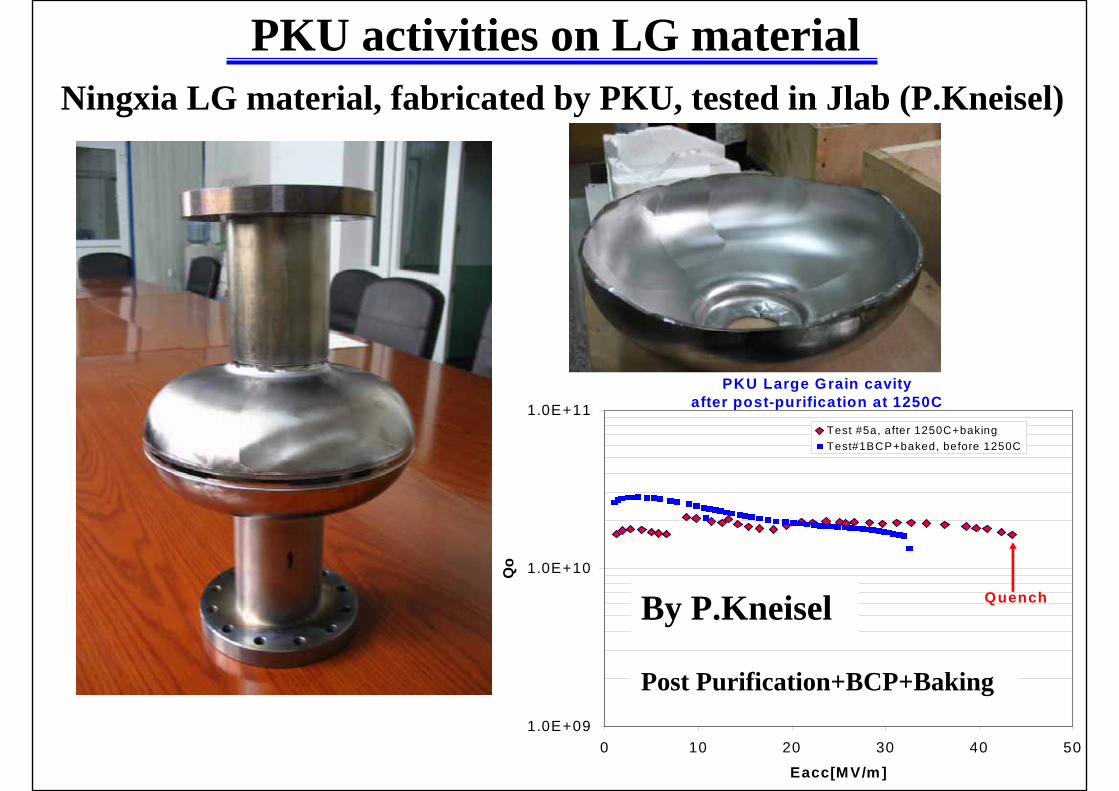
PKU activities on LG materialNingxia LG material, fabricated by PKU, tested in Jlab (P.Kneisel)
PKU Large Grain cavityafter post-purification at 1250C
1.0E+09
1.0E+10
1.0E+11
0 10 20 30 40 50
Eacc[MV/m ]
Qo
Test #5a, after 1250C+bakingTest#1BCP+baked, before 1250C
Quench
Post Purification+BCP+Baking
By P.Kneisel

10
F-G Nb Cavities made by Peking UniversityIn Aug. 2009, third 9-cell cavity at Peking University,Eacc is 28.6MV/m
Vertical test at JLabBy Dr. Rongli Geng
After high-pressure rinsing and clean room assembly, the first radio frequency (RF) test was done on 30 July. The maximum accelerating gradient was 20 megavolts per metre(MV/m) at an unloaded quality factor of 2.3×10⁹, limited by field emission. After partial disassemble, additional high-pressure water rinsing was done, followed by the second RF test on 9 August. The maximum accelerating gradient reached 28.6 MV/m at an unloaded quality factor of 4×10⁹, limited by RF cable heating.

11
Observations of As-built Surface Reported on May 9, 2010 @ 1st WebEx Meeting
Lack of full penetration at equator EBW Sharp steps at iris EBW
from Rongli’s file

12
KEK/Tokyo Denkai Activities

13
Large Grain Sheet Production at Tokyo DenkaiTokyo Denkai

14
Multi-Wire SlicingK.Saito Single Crystal-Large Grain Niobium Technology Workshop in Brazil 2006
Nb
PressingSplay liquid abrasives
This technology is well established on silicon wafer slicing.
Slicing used very thin piano wire (0.16Φ)and liquid abrasive

15
The surfaces have wire traces but no problem for cavity fabrication.
R&D of Multi-Wire Slicing @ KEK/Tokyo DenkaiThe first trial for niobium ingot slicing after small sample cuttings
108
109
1010
1011
0 10 20 3 0 40 50 60
Q o
E acc [M V/m]
E acc=42.6M V/mQ o= 8.04e9 @ 2K
N o X -ray
C B P+C P (10)+A N +C P (160)+H PR (15m in.)+B aking(48hrs)
L imited by Q -slope
20mmL
270Φ
45 hrsConventional Silicon wafer
slicing machineTokyo Denkai RRR=480
First Measurement !LL End single cell cavity
(End cell shape)
BCP , not EP
Directly formedthe sliced sheets.
No annealed the sheets.

16
Step by step tests for more sheets production
6 sheets(2.8t)
270Φ 20mmL
58 sheets(3.2t for Jlab)
270Φ 201mmL
265Φ 307mmL
102 sheets(2.8t)19 sheets (2.8t)
270Φ 61mmL

17
1300
1350
1400
1450
0 5 10 15 20
WeightW
eigh
t [g]
No. of sheet
1387 ± 1.2 g
Scatter 0.09%0
200
400
600
800
1000
0 5 10 15 20
Tickness
Thi
ckne
ss 2
xxx[µm
]
No. of sheet
Scatter 0.13%
0
2
4
6
8
10
0 5 10 15 20
Rz
ave.
[µm
]
Sheet No.
Rz=4.9+-1.8µm
Feature of The Multi-Wire Slicing
Very Uniform
Very Smooth
0
20
40
60
80
100
120
140
2.7 2.75 2.8 2.85 2.9 2.95Thickness[mm]
All 2.741Min.2.906Max.
1144.621Total408Poits
2.805Average2.803Center2.806RMS0.020S.T deviation
0.0004Dispersion0.001Error in S.T
KEK 102 sheets
KEK 19 sheets
Rz=4.9±1.8µm
t=2.906±0.038µm

18
Simplified Nb production by this slicing method
150 sheets can be produced in 48hrs, if you have a 270φx 450L Nb ingot.
19
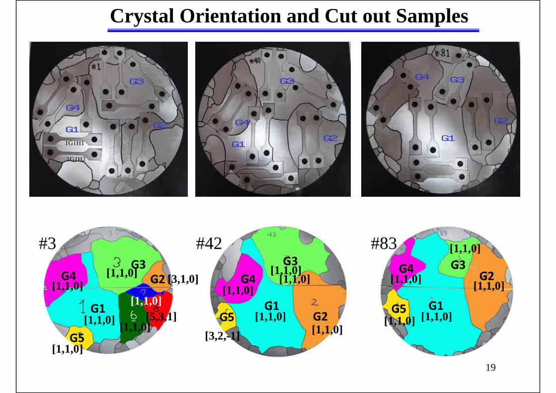
Crystal Orientation and Cut out Samples
G1
G1G1
G2
G2
G2
G3 G3 G3
G4
G4
G4
1G1H1
1G1H2
G1
G2G3
G4
G5
G1G2
G3G4
G5G1
G2G3G4
G5[1,1,0]
[1,1,0][1,1,0]
[5,3,1][1,1,0]
[3,1,0]
[1,1,0]
[1,1,0]
#3 #42 #83
[1,1,0][1,1,0]
[1,1,0]
[1,1,0]
[1,1,0]
[1,1,0]
[1,1,0]
[1,1,0][1,1,0]
[3,2,-1][1,1,0]

20
Mechanical Properties of LG niobium at RT&4.2K
Tensile becomes higher about 10 times, Young’s modulus 2 times larger, and Elongation 7 times smaller at 4.2K.
Tensile Young’s modulus
Elongation

21
Fist LG 9-Cell Cavity Fabricated at KEK
Totally 96µm (in average) removed by BCPMaterial removal distribution by the vertical BCP and horizontal one.
Horizontal BCP system has been successfully developed at KEK in order to improve the none-uniform material removal with vertical BCP.
0
20
40
60
80
100
120
140
160
0 5 10 15 20 25
Vertical BCPHorizontal BCP
Rem
oval
[µm
]
Location
1 2 3 4 5 6 7 8 9
Top Bottom
Ave.=64+-13µm
Ave.=96+-28µm
108
109
1010
1011
0 5 10 15 20 25 30
Qo
Eacc [MV/m]
+HCP(65µm)+Degreasing+HPR(10hr)+Bake(120OCx48hr)
Eacc=27.1MV/mQo=1.1E+10 @ 2K
CBP+HBCP+Bake

22
Improvement of crystallization at Tokyo Denkai
Single Crystal
Ultrasonic images by H.UmezawaTokyo-Denkai
Ingot No.1 Ingot No.2 Ingot No.3Ingot No.3
Improving Crystallization of Ingot at Tokyo Denkai
Grains grow column likely in
EBM.
Make a seed plate for single crystal Ingot

23
Cut out large crystal piece
EBW of large crystal pieces
Trial of Single Crystal Seed for EBM Nb IngotUse nearby 9 sheets
Ultrasonic diagnosis as received
Ultrasonic diagnosis after buffingAfter BCP
280Φ
We are very much looking forward to see the EBM result, which will come out on the IPAC10 in Kyoto.
EBW H.Inoue
EDM by Y.Kobayashi
Ultrasonic investigation by H.Umezawa

24
Seed plate 2.8mm thick on the EBM base-plate
First experiment was failed. We will hear more information here from Tokyo Denkai.

25
Scope of the LG/Single crystal niobium material from single cellcavity R&D
Large Grain: Benefits in material and preparation costs
• TESLA shape+LG+BCP(+bake) is hopeless for the ILC baseline performance : 35MV/m @ Qo=8E+9, which has been already confirmed with 9-cell cavities at DESY.
XFEL specification is well satisfied by this scheme.
TESLA shape+LG
+[CBP or Post purification at 1250OC ]+BCP(+bake) on ILC baseline performance ?
• LL shape+LG+BCP(+bake) is hopeful for the ILC baseline performance.
• LL shape+LG+CBP+BCP(+bake) is hopeful for the ACD performance: 40MV/m @ Qo=8E+9. Need more statistics.
Single Crystal
• Single crystal will make possible the ILC ACD performance without CBP on the scheme:
LL shape+LG+BCP(+bake) .
• Single crystal has more advantage on the cavity performance.
Single crystal is trade off CBP.
• Single Crystal R&D should be kept going.

26
0
10
20
30
40
50
0 100 200 300 400 500
V ertical BCP
H orizontal BCP
y = 46.451 * e^(-0.00078474x) E
acc
[MV
/m]
removal [µm]
CBP(100)+VBCP(170)
ILC Baseline
BCP material removal vs Eacc,max on LG after CBP
Enhanced grain boundary steps are problem?

27
Summary
• IHEP and PKU in China keep going ILC 9-cell cavity R&D with helps other laboratories. Single crystal is already produced at Ningxia.
• Multi-wire slicing has been successfully developed at KEK/Tokyo Denkai, and now it is applied in the production phase in Tokyo Denkai..
It is ready to produce 150 sheets ILC like in 48hrs, if you bring an ingot 270φ -450mm L.
• KEK has started LL 9-cell cavity fabrication LG based, and is challenging to the ILC ACD cavity performance.
• Single crystal R&D is trade off CBP. KEK/Tokyo Denkai have started the R&D.

28
Acknowledgments
We express many thanks to KEK STF people, who made vertical test for IHEP01 9-cell cavity.
We thank Drs. Y.Higashi and S.Chan, who helped a lot to measure crystal orientation of LG niobium materials.
29
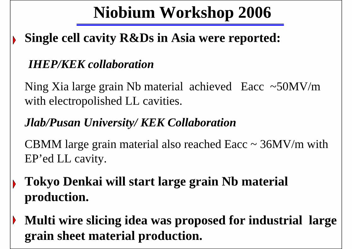
Niobium Workshop 2006Single cell cavity R&Ds in Asia were reported:
IHEP/KEK collaboration
Ning Xia large grain Nb material achieved Eacc ~50MV/m with electropolished LL cavities.
Jlab/Pusan University/ KEK Collaboration
CBMM large grain material also reached Eacc ~ 36MV/m with EP’ed LL cavity.
Tokyo Denkai will start large grain Nb material production.
Multi wire slicing idea was proposed for industrial large grain sheet material production.

30
IHEP Further R&D for LG
• IHEP-01 is now back to IHEP, will be processed again and make 2nd vertical test early next year
• IHEP-02 Large Grain Low Loss 9-cell cavity with HOM couplers in fabrication, 1st vertical test early next year
• More IHEP cavities for ILC, ADS and ERL are coming… LG may be considered.

31
Ultrasonic Imaging Machine at Tokyo Denkai

32
Grain boundary appearance Test using Single Crystal Coin Samples