rdc r8032s data sheet - keil.com · 56 55 54 53 52 51 50 5c 67 66 64 64 5f 5e 5d 6c 6b 6a 69 68 ......
TRANSCRIPT

RDCRDCRDCRDC® R8032S
RDC Semiconductor Co. Version: 1.1
- 1 –
R8032S8-Bit RISC MCU IP Specification
VERSION: 1.1
RDCRDCRDCRDC RISC DSP Controller
RDC Semiconductor Co., Ltd http:\\www.rdc.com.tw
Tel. 886-3-666-2866 Fax 886-3-563-1498

RDCRDCRDCRDC® R8032S
RDC Semiconductor Co. Version: 1.1
- 2 –
R8032S 8-BIT MCU IP SPECIFICATION
1. DESIGN SPECIFICATION RISC Architecture Synchronous Design Static Design Synthesizable Silicon proved (0~66 MHz at 0.5um process) RTL Code with verilog format Application
-DSC,CF Card, CD ROM Controller, Pattern Recognition, LCD MoniterController, USB Device Controller, Scanner Controller, MP3 Controller,Modem Controller, Voice Recognition, …etc.
Instruction compatible with generic 8051 256 byte scratchpad RAM interface Two external interrupts Memory Addressing Capability
-64K Byte external RAM & ROM 8-bit I/O port x 4 (P0~P3) 16-bit timer/counter x3 Full duplex UART x1 Data Pointer x1 Watch Dog Timer x1 Support Power Down and Idle Mode Power Down waked up by Interrupt
2.FEATURES
RDC® R8032S
RDC Semiconductor Co. Version: 1.1
- 3 –
3.GENERAL DESCRIPTION
The 8032S is a high-performance 8051 family compatible micro-controller based on RISCarchitecture & Pipeline design. This IP Specification of interface timing, external DataMemory read / write timing and external Program Memory read timing are different from thatof the standard 80C52. But instruction-set is fully compatible with standard 8051 family.
4.FUNCTIONAL DESCRIPTION
MemoryThe R8032S manipulates operands in four memory spaces. There are 64K-byte ProgramMemory space, 64K-byte External Data Memory space, 256-byte Internal Data Memory, andwith a 16-bit Program Counter space. The Internal Data Memory address space is furtherdivided into the 256-byte Internal Data RAM and 128-byte Special Function Register addressspace. The up 128-bytes RAM can reach by indirect addressing. Four Register Banks, 128addressable bits, and the stack reside in the Internal Data RAM.
I/O portsThe R8032S has 8-bit I/O ports. The four ports provide 32 I/O lines to interface to theexternal world. All four ports are both byte and bit addressable. Port 0 is used as a Address/Data bus and Port 2 is used as the upper 8-bits address when external program is running orexternal memory/device is accessed. Port 3 contains special control signals such as the readand write strobes. Port 1 is used for both I/O and external interrupts.
InterruptsIn the R8032S there are six hardware resources that generate an interrupt request. The startingaddresses of the interrupt service program for each interrupt source are like standard 8052.The external interrupt request inputs ( 0INT , 1INT ) can be programmed for either negativeedge or low level-activated operation.
3 Timers / CountersThe R8032S has three 16-bit timers/counters that are same as the timers of the standard 8051family. The R8032S has two additional watchdog timers for system failure monitor.
Serial I/O portsThe R8032S has 1~2 programmable, full-duplex serial I/O ports that the function is same as

RDCRDCRDCRDC® R8032S
RDC Semiconductor Co. Version: 1.1
- 4 –
that of 8051 family and dependent on requirement.
Power ManagementThe R8032S default support IDLE and POWER-DOWN modes of operation. In the IDLEmode, the CPU core is stopped operation while the peripherals continue operating. In thePOWER-DOWN mode, all the clocks are stopped. The power-down mode can be waked upby 0INT or 1INT external interrupt with level trigger. The extra power management can befound on PMR register in SFR.
Watch Dog Timers Interrupt / ResetThe R8032S creates one programmable watchdog timers to monitor system failure. That ismaximum 262 .

RDCRDCRDCRDC® R8032S
RDC Semiconductor Co. Version: 1.1
- 5 –
5.MEMORY ORGANIZATION
In the R8032S the memory is organized as three address spaces and the program counter.The memory spaces shown in memory map.
- 16-bit Program Counter- 64k-byte Program Memory address space- 64k-byte External Data Memory address space- 256-byte Internal Data Memory address
The 16-bit Program Counter register provides the R8032S with its 64k addressing capabilities.The program Counter allows the user to execute calls and branches to any location within theProgram Memory space. There are no instructions that permit program execution to movefrom the Program Memory space to any of the data memory spaces.
R8032S hasn’t internal Program Memory, thus the EA pin should be tied low. The 64k-byteProgram Memory address space is located in the external space. The 64k-byte External DataMemory address space is automatically accessed when the MOVX instruction is executed.The Internal Data Memory space is subdivided into a 256-byte Internal Data RAM addressSpace and a 128-byte Special Function Resister address space as shown in the SFRs Map.The Internal Data RAM address space is 0 to 255. Four 8-Register Banks occupy locations0 through 31. The stack can be located anywhere in the Internal Data RAM address space.In addition, 128 bit locations of the on-chip RAM are accessible through Direct Addressing.

RDCRDCRDCRDC® R8032S
RDC Semiconductor Co. Version: 1.1
- 6 –
Special Function Registers DescriptionThe Special Function Register address space is 80h to FFh. All registers except the ProgramCounter and the four 8-Register Banks reside here. The SFRs are accessed using direct
64KProgramMemorySpace
64KExternal
DataMemorySpace
64K
0
64K
0
ProgramCounter
Memory Organization
SpecialFunctionRegister
IndirectAddressing
RAM
Direct&
IndirectAddressing
RAM
Internal Data Memory
FFh
80h7Fh
00h
07 06 05 04 03 02 01 00
Bank3
Bank2
Bank1
Bank0
08090A0B0C0D0E0F17 16 15 14 13 12 11 10
18191A1B1C1D1E1F07 26 25 24 23 22 21 202F 2E 2D 2C 2B 2A 29 28
3C 3B 3A 39 383031323334353737
444546473F 3E 3D
434D 4C 4B 4A 49 48
404142
574F 4E
5B 5A 59 5850515253545556
5C64646667
5F 5E 5D
6C 6B 6A 69 6860616263
6D6E6F77 76 75 74 73 72 71 70
78797A7B7C7D7E7F(MSB) (LSB)
FFh
80h7Fh
2Fh2Eh2Dh2Ch2Bh2Ah29h28h27h26h25h24h23h22h21h20h1Fh18h17h10h0fh08h07h00h
4746
404142434445
3536373839
323334
3124
151623
870
127128
256
R7R0
R0R7R0R7
R7R0
Indirect RAM
RAM Bit Addresses
Addressable Bits20h-2Fh

RDCRDCRDCRDC® R8032S
RDC Semiconductor Co. Version: 1.1
- 7 –
addressing only. All of the SFRs are the compatible with standard 8052 .
F8H
F0H B
E8H
E0H ACC
D8H WDTCON
D0H PSW
C8H T2CON T2MOD RCAP2L RCAP2H TL2 TH2
C0H
B8H IP
B0H P3
A8H IE
A0H P2 Reserved Reserved
98H SCON SBUF
90H P1
88H TCON TMOD TL0 TL1 TH0 TH1 CKCON
80H P0 SP DPL DPH PCON
B Register. The B Register is used as both a source and destination in multiply anddivide operations.
B Address:F0h
bit 7 bit 0B.3B.6 B.4B.7 B.5 B.2 B.1 B.0

RDCRDCRDCRDC® R8032S
RDC Semiconductor Co. Version: 1.1
- 8 –
Accumulator. The instruction use the accumulator as both source and destinationfor calculations and moves.
PSW Address:D0h bit 7 bit 0
CY AC F0 RS1 RS0 OV F1 PARITY
Program Status Word.CY: Carry Flag CY is set if the operation result in a carry out of (during addition) or a borrow into (during subtraction) the high-order bit of the result; otherwise CY is cleared.AC: Auxiliary-Carry Flag AC is set if the operation results in a carry out of the low-order 4 bits of the result (during addition) or a borrow form the high-order bits into the low-order 4 bits (during subtraction); otherwise AC is cleared.F0: User Flag 0 General-purpose flag.RS1,RS0: Register Bank Select Bits 1 and 0 These bits select the memory locations that comprise the active bank of the register file. RS1 RS0 Bank Address 0 0 0 00-07h 0 1 1 08h-0Fh 1 0 2 10h-17h 1 1 3 18h-1Fh
OV: Overflow Flag This bit is set if an addition or signed variables results in an overflow error (i.e., if the magnitude of the sum or difference is too great for the seven LSBs in 2’s- complement representation). The overflow flag is also set if multiplication product overflows one byte or if a division by zero is attempted.
ACC Address:E0h
bit 7 bit 0ACC.3ACC.6 ACC.4ACC.7 ACC.5 ACC.2 ACC.1 ACC.0
RDCRDCRDCRDC® R8032S
RDC Semiconductor Co. Version: 1.1
- 9 –
UD: User-definable Flag This general-purpose flag is available to the user.
P: Parity FlagThis bit indicates the parity of the accumulator. It is set if an odd number of bits in
the accumulator are set Otherwise, it is cleared. Not all instructions update the parity bit. The parity bit is set or cleared by instructions that change the contents to the accumulator.
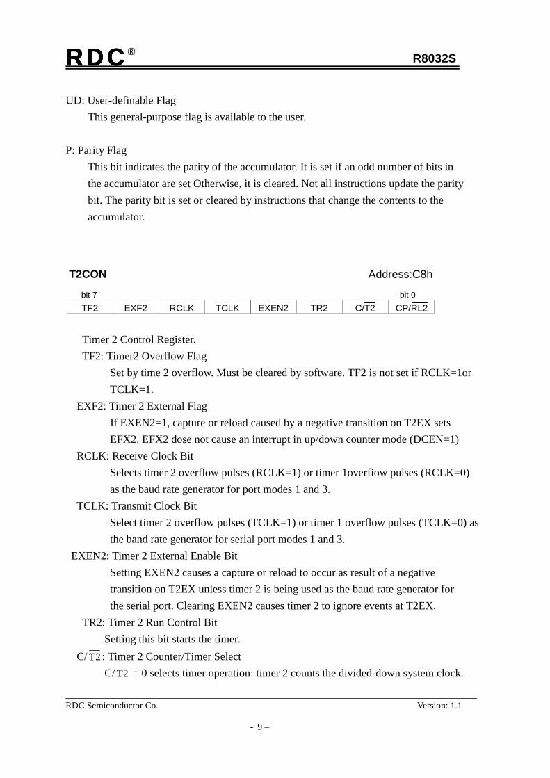
Timer 2 Control Register. TF2: Timer2 Overflow Flag Set by time 2 overflow. Must be cleared by software. TF2 is not set if RCLK=1or TCLK=1. EXF2: Timer 2 External Flag If EXEN2=1, capture or reload caused by a negative transition on T2EX sets EFX2. EFX2 dose not cause an interrupt in up/down counter mode (DCEN=1) RCLK: Receive Clock Bit Selects timer 2 overflow pulses (RCLK=1) or timer 1overfiow pulses (RCLK=0) as the baud rate generator for port modes 1 and 3. TCLK: Transmit Clock Bit Select timer 2 overflow pulses (TCLK=1) or timer 1 overflow pulses (TCLK=0) as the band rate generator for serial port modes 1 and 3. EXEN2: Timer 2 External Enable Bit Setting EXEN2 causes a capture or reload to occur as result of a negative transition on T2EX unless timer 2 is being used as the baud rate generator for the serial port. Clearing EXEN2 causes timer 2 to ignore events at T2EX. TR2: Timer 2 Run Control Bit Setting this bit starts the timer. C/ 2T : Timer 2 Counter/Timer Select C/ 2T = 0 selects timer operation: timer 2 counts the divided-down system clock.
T2CON Address:C8h
bit 7 bit 0EXEN2 TR2EXF2 TCLKTF2 RCLK C/T2 CP/RL2

RDCRDCRDCRDC® R8032S
RDC Semiconductor Co. Version: 1.1
- 10 –
C/ 2T = 1 selects counter operation: timer 2 counts negative transitions on external pin T2.CP/ 2RL : Capture/Reload Bit When set, captures occur on negative transitions at T2EX if EXEN2=1.When cleared, auto-reloads occur on timer 2 overflows or negative transitions at T2EX if EXEN2=1. The CP/ 2RL bit is ignored and timer 2 forced to auto-reload on timer 2 overflow, if RCLK =1 or TCLK = 1.
Timer 2 Mode Control Register.Bit7-Bit2 : ReservedT2OE: Timer 2 Output Enable Bit In the timer 2 clock-out mode, connects the programmable clock output to external pin T2. DCEN: Down Count Enable Bit Configures timer 2 as an up/down counter.
Timer2 Capture LSBLow byte of the timer2 reload/recapture register. This register stores 8-bit values to beloaded into or captured from the timer register TL2 in timer 2
T2MOD Address:C9h
bit 7 bit 0T2OE DCEN
RCAP2L Address:CAh
bit 7 bit 0RCAP2L.3RCAP2L.6 RCAP2L.4RCAP2L.7 RCAP2L.5 RCAP2L.1 RCAP2L.0RCAP2L.2
RDCRDCRDCRDC® R8032S
RDC Semiconductor Co. Version: 1.1
- 11 –
Timer2 Capture MSBHigh byte of the timer2 reload/recapture register. This register stores 8-bit values to beloaded into or captured from the timer register TH2 in timer2
Timer 2 LSBLow byte of the timer 2 timer register
Timer 2 MSBHigh byte of the timer 2 timer register
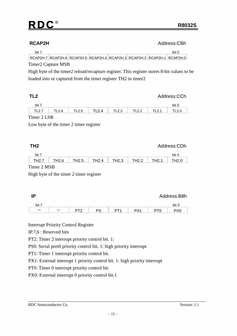
Interrupt Priority Control RegisterIP.7,6 : Reserved bitsPT2: Timer 2 interrupt priority control bit. 1:PS0: Serial port0 priority control bit. 1: high priority interruptPT1: Timer 1 interrupt priority control bit.PX1: External interrupt 1 priority control bit. 1: high priority interruptPT0: Timer 0 interrupt priority control bit.PX0: External interrupt 0 priority control bit.1
RCAP2H Address:CBh
bit 7 bit 0RCAP2H.3RCAP2H.6 RCAP2H.4RCAP2H.7 RCAP2H.5 RCAP2H.1 RCAP2H.0RCAP2H.2
TL2 Address:CCh
bit 7 bit 0TL2.3TL2.6 TL2.4TL2.7 TL2.5 TL2.2 TL2.1 TL2.0
TH2 Address:CDh
bit 7 bit 0TH2.3TH2.6 TH2.4TH2.7 TH2.5 TH2.2 TH2.1 TH2.0
IP Address:B8h
bit 7 bit 0PT1 PT0 PX0PX1PT2 PS
RDCRDCRDCRDC® R8032S
RDC Semiconductor Co. Version: 1.1
- 12 –
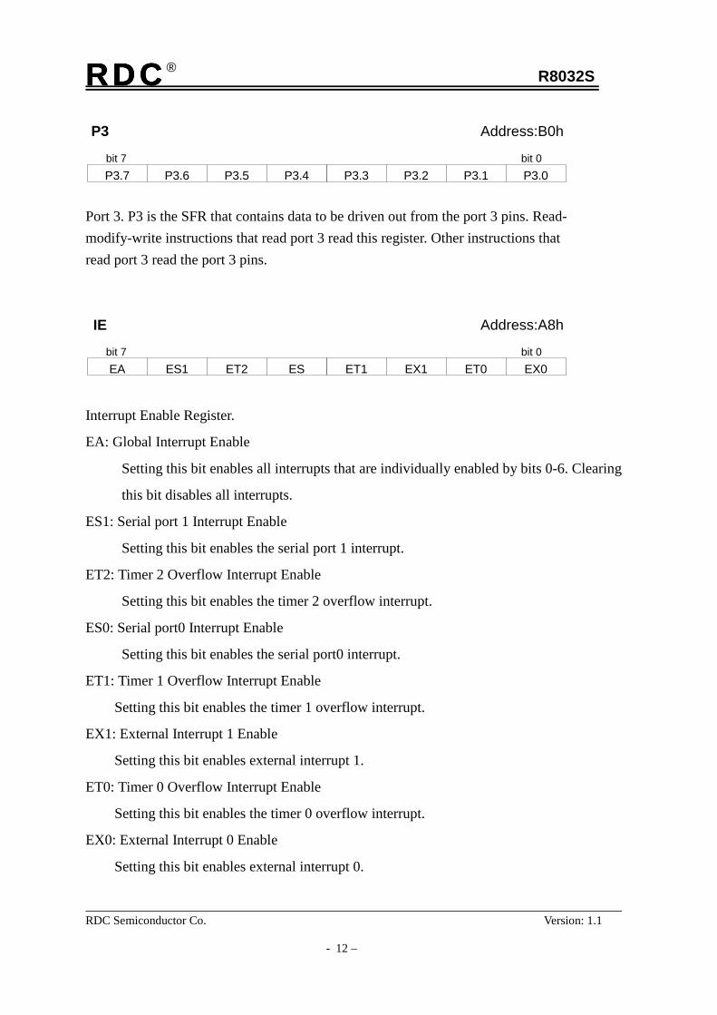
Port 3. P3 is the SFR that contains data to be driven out from the port 3 pins. Read-modify-write instructions that read port 3 read this register. Other instructions thatread port 3 read the port 3 pins.
Interrupt Enable Register.
EA: Global Interrupt Enable
Setting this bit enables all interrupts that are individually enabled by bits 0-6. Clearing
this bit disables all interrupts.
ES1: Serial port 1 Interrupt Enable
Setting this bit enables the serial port 1 interrupt.
ET2: Timer 2 Overflow Interrupt Enable
Setting this bit enables the timer 2 overflow interrupt.
ES0: Serial port0 Interrupt Enable
Setting this bit enables the serial port0 interrupt.
ET1: Timer 1 Overflow Interrupt Enable
Setting this bit enables the timer 1 overflow interrupt.
EX1: External Interrupt 1 Enable
Setting this bit enables external interrupt 1.
ET0: Timer 0 Overflow Interrupt Enable
Setting this bit enables the timer 0 overflow interrupt.
EX0: External Interrupt 0 Enable
Setting this bit enables external interrupt 0.
P3 Address:B0h
bit 7 bit 0P3.3 P3.1 P3.0P3.2P3.7 P3.6 P3.5 P3.4
IE Address:A8h
bit 7 bit 0ET1 ET0 EX0EX1EA ET2 ESES1

RDCRDCRDCRDC® R8032S
RDC Semiconductor Co. Version: 1.1
- 13 –
Port 2. P2 is the SFR that contains data to be driven out from the port 2 pins. Read-modify-write instructions that read port 2 read this register. Other instructions thatread port 2 read the port 2 pins.
Serial Data Buffer. Writing to SBUF loads the transmit buffer to the serial I/O port.Reading SBUF reads the receive buffer of the serial port.
Port 1. P1 is the SFR that contains data to be driven out from the port 1 pins. Read-modify-write instructions that read port 1 read this register. Other instructions thatread port 1 read the port 1 pins.
P2 Address:A0h
bit 7 bit 0P2.7 P2.5 P2.4 P2.3 P2.1 P2.0P2.6 P2.2
SBUF Address:99h
bit 7 bit 0SBUF.7 SBUF.5 SBUF.4 SBUF.3 SBUF.1 SBUF.0SBUF.6 SBUF.2
P1 Address:90h
bit 7 bit 0P1.7 P1.5 P1.4 P1.3 P1.1 P1.0P1.6 P1.2

RDCRDCRDCRDC® R8032S
RDC Semiconductor Co. Version: 1.1
- 14 –
Timer/Counter Control Register..
TF1: Timer 1 Overflow Flag.
Set by hardware when the timer 1 register overflows. Cleared by hardware
when the processor vectors to the interrupt routine.
TR1:Timer 1 Run Control Bit.
Set/cleared by software to turn timer 1 on/off.
TF0: Timer 0 Overflow Flag.
Set by hard ware when the timer 0 register overflows. Cleared by hardware
when the processor vectors to the interrupt routine.
TR0: Timer 0 Run Control Bit.
Set/cleared by software to turn timer 1 on/off.
IE1: Interrupt 1 Edge Detect
Set by hard ware when an external interrupt is detected on the 1INT pin edge-
or level-triggered (see IT1). Cleared when interrupt is processed if edge- triggered.
IT1: Interrupt 1 Type Select Bit.
Set this bit select edge-triggered (high-to-low) for external interrupt 1. Clear
this bit to select level-triggered (active low).
IE0: Interrupt 0 Edge Detect
Set by hardware when an external interrupt is detected on the 0INT pin edge-
or level-triggered (see IT0). Cleared when interrupt is processed if edge- triggered.
IT0: Interrupt 0 Type Select Bit.
Set this bit to select edge-triggered (high-to-low) for external interrupt 0. Clear
this bit to select level-triggered (active low).
TCON Address:88h
bit 7 bit 0TF1 TR1 TF0 TR0 IE1 IT1 IE0 IT0
RDCRDCRDCRDC® R8032S
RDC Semiconductor Co. Version: 1.1
- 15 –
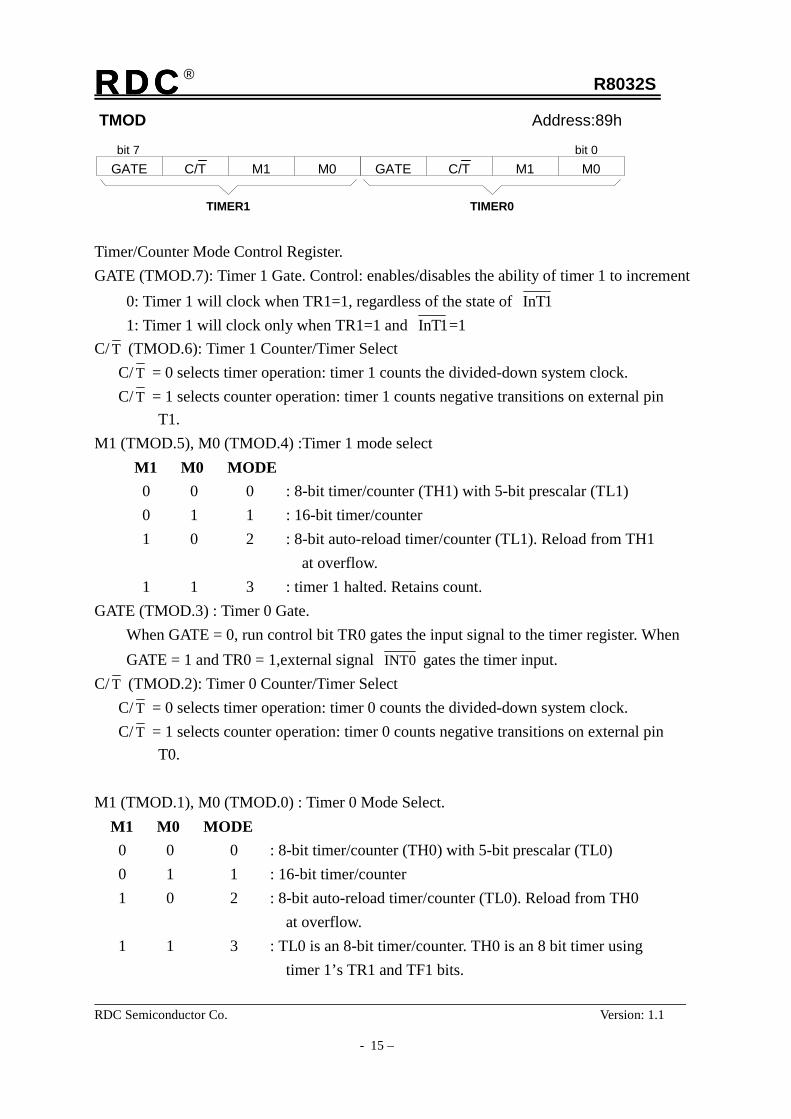
Timer/Counter Mode Control Register.GATE (TMOD.7): Timer 1 Gate. Control: enables/disables the ability of timer 1 to increment 0: Timer 1 will clock when TR1=1, regardless of the state of 1InT 1: Timer 1 will clock only when TR1=1 and 1InT =1C/ T (TMOD.6): Timer 1 Counter/Timer Select C/ T = 0 selects timer operation: timer 1 counts the divided-down system clock. C/ T = 1 selects counter operation: timer 1 counts negative transitions on external pin T1.M1 (TMOD.5), M0 (TMOD.4) :Timer 1 mode select M1 M0 MODE 0 0 0 : 8-bit timer/counter (TH1) with 5-bit prescalar (TL1) 0 1 1 : 16-bit timer/counter 1 0 2 : 8-bit auto-reload timer/counter (TL1). Reload from TH1 at overflow. 1 1 3 : timer 1 halted. Retains count.GATE (TMOD.3) : Timer 0 Gate. When GATE = 0, run control bit TR0 gates the input signal to the timer register. When GATE = 1 and TR0 = 1,external signal 0INT gates the timer input.C/ T (TMOD.2): Timer 0 Counter/Timer Select C/ T = 0 selects timer operation: timer 0 counts the divided-down system clock. C/ T = 1 selects counter operation: timer 0 counts negative transitions on external pin T0.
M1 (TMOD.1), M0 (TMOD.0) : Timer 0 Mode Select. M1 M0 MODE 0 0 0 : 8-bit timer/counter (TH0) with 5-bit prescalar (TL0) 0 1 1 : 16-bit timer/counter 1 0 2 : 8-bit auto-reload timer/counter (TL0). Reload from TH0 at overflow. 1 1 3 : TL0 is an 8-bit timer/counter. TH0 is an 8 bit timer using timer 1’s TR1 and TF1 bits.
TMOD Address:89h
bit 7 bit 0GATE M1 M0 GATE M1 M0
TIMER1 TIMER0
C/TC/T
RDCRDCRDCRDC® R8032S
RDC Semiconductor Co. Version: 1.1
- 16 –
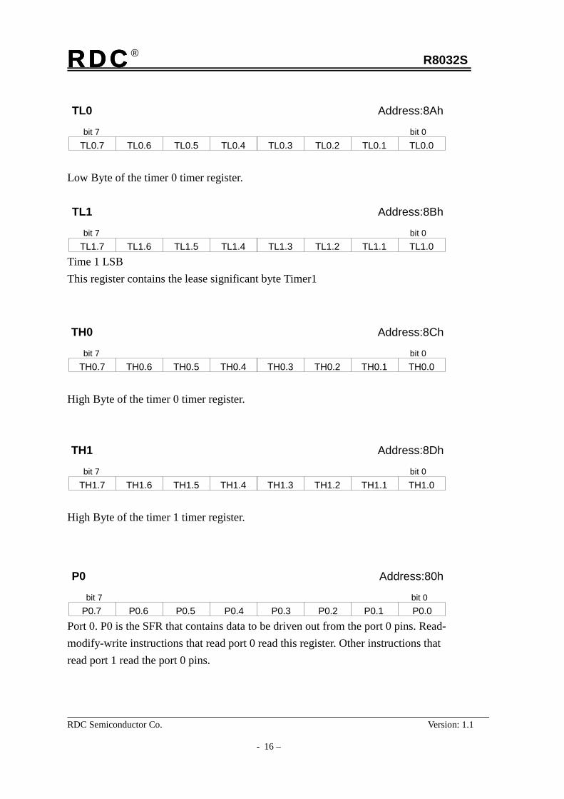
Low Byte of the timer 0 timer register.
Time 1 LSBThis register contains the lease significant byte Timer1
High Byte of the timer 0 timer register.
High Byte of the timer 1 timer register.
Port 0. P0 is the SFR that contains data to be driven out from the port 0 pins. Read-modify-write instructions that read port 0 read this register. Other instructions thatread port 1 read the port 0 pins.
TL0 Address:8Ah
bit 7 bit 0TL0.7 TL0.5 TL0.4 TL0.3 TL0.1 TL0.0TL0.6 TL0.2
TL1 Address:8Bh
bit 7 bit 0TL1.7 TL1.5 TL1.4 TL1.3 TL1.1 TL1.0TL1.6 TL1.2
TH0 Address:8Ch
bit 7 bit 0TH0.7 TH0.5 TH0.4 TH0.3 TH0.1 TH0.0TH0.6 TH0.2
TH1 Address:8Dh
bit 7 bit 0TH1.7 TH1.5 TH1.4 TH1.3 TH1.1 TH1.0TH1.6 TH1.2
P0 Address:80h
bit 7 bit 0P0.7 P0.6 P0.5 P0.4 P0.3 P0.2 P0.1 P0.0

RDCRDCRDCRDC® R8032S
RDC Semiconductor Co. Version: 1.1
- 17 –
Stack Pointer. The 8-bit SP contains the address at which the last byte was push onto the stack.This is also the address of the next byte that will be stopped. The SP is incremented beforevery PUSH operation.. SP can be read or written to under software control.
Data Pointer Low. DPL is the low byte of the 16-bit data pointer, DPTR.
Data Pointer High. DPH is the high byte of the 16-bit data pointer, DPTR.
Power Control Register.SMOD1: 1 for Timer1 in mode 1, 2, 3 double the baud ratePD: Power- Down Mode Bit. When set, activates power-down mode. Clear by hardware when an interrupt or reset occurs.IDL: Idle Mode Bit. When set, activates Idle mode. Clear by hardware when an interrupt or reset occurs.Bit 7 & bit 5~2: reserved
SP Address:81h
bit 7 bit 0SP.7 SP.6 SP.5 SP.4 SP.3 SP.2 SP.1 SP.0
DPL Address:82h
bit 7 bit 0DPL.7 DPL.6 DPL.5 DPL.4 DPL.3 DPL.2 DPL.1 DPL.0
DPH Address:83h
bit 7 bit 0DPH.7 DPH.6 DPH.5 DPH.4 DPH.3 DPH.2 DPH.1 DPH.0
PCON Address:87h
bit 7 bit 0PD IDLSMOD1
RDCRDCRDCRDC® R8032S
RDC Semiconductor Co. Version: 1.1
- 18 –
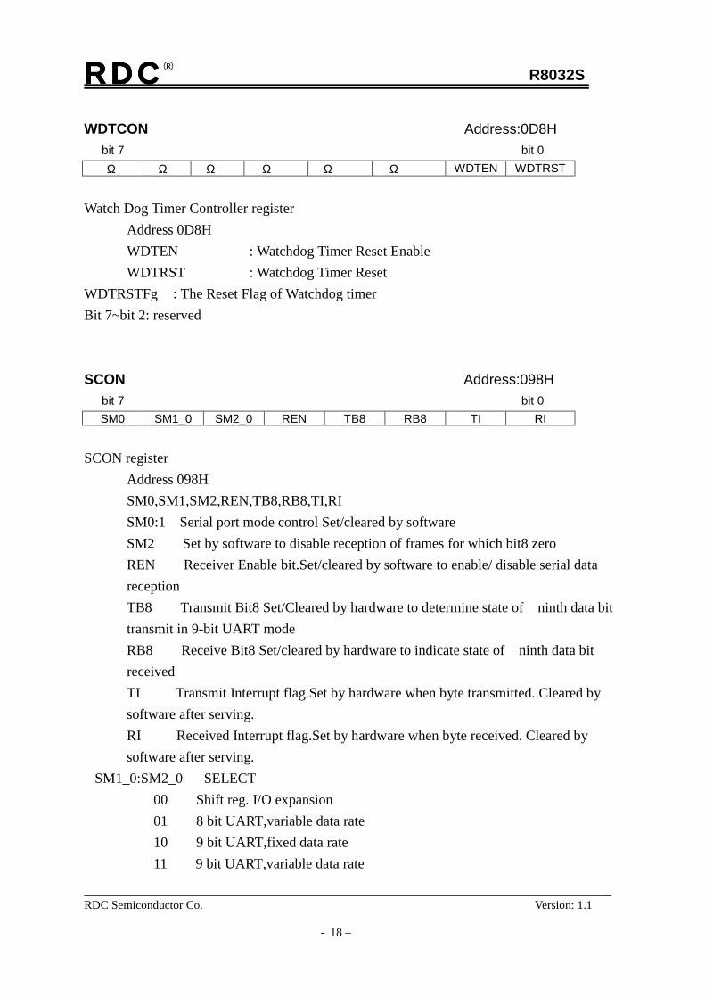
WDTCON Address:0D8H bit 7 bit 0
Ω Ω Ω Ω Ω Ω WDTEN WDTRST
Watch Dog Timer Controller registerAddress 0D8HWDTEN : Watchdog Timer Reset EnableWDTRST : Watchdog Timer Reset
WDTRSTFg : The Reset Flag of Watchdog timerBit 7~bit 2: reserved
SCON Address:098H bit 7 bit 0
SM0 SM1_0 SM2_0 REN TB8 RB8 TI RI
SCON registerAddress 098HSM0,SM1,SM2,REN,TB8,RB8,TI,RISM0:1 Serial port mode control Set/cleared by softwareSM2 Set by software to disable reception of frames for which bit8 zeroREN Receiver Enable bit.Set/cleared by software to enable/ disable serial datareceptionTB8 Transmit Bit8 Set/Cleared by hardware to determine state of ninth data bittransmit in 9-bit UART modeRB8 Receive Bit8 Set/cleared by hardware to indicate state of ninth data bitreceivedTI Transmit Interrupt flag.Set by hardware when byte transmitted. Cleared bysoftware after serving.RI Received Interrupt flag.Set by hardware when byte received. Cleared bysoftware after serving.
SM1_0:SM2_0 SELECT00 Shift reg. I/O expansion01 8 bit UART,variable data rate10 9 bit UART,fixed data rate11 9 bit UART,variable data rate

RDCRDCRDCRDC® R8032S
RDC Semiconductor Co. Version: 1.1
- 19 –
CKCON Address:08Eh bit 7 bit 0
WDT1 WDT0 Ω Ω Ω Ω Ω Ω
Clock Control registeraddress : 08EhWDT1, WDT0,WDT1, WDT0 : WDT time-out counter select
0,0 - 17 bit counter / 0,1 - 20 bit counter1,0 - 23 bit counter / 1,1 - 26 bit counter

RDCRDCRDCRDC® R8032S
RDC Semiconductor Co. Version: 1.1
- 20 –
7.ON-CHIP PERIPHERALS
Interrupt Source Request Flag Priority Flag Enable Flag VectorAddress
Priority-Within-Level
Flog Cleared byHardware?
External Request IE0/TCON.1 PX0/IP.0 EX0/IE.0 0003h 1 Edge-YesLevel-No
Internal Timer0/Counter0 TF0/TCON.5 PT0/IP.1 ET0/IE.1 000Bh 2 YesExternal Request IE1/TCON.3 PX1/IP.2 EX1/IE.2 0013h 3 Edge-Yes
Level-NoInternal Timer1/Counter1 TF1/TCON.7 PT1/IP.3 ET1/IE.3 001Bh 4 Yes
Xmit Ti/SCON.1Internal Serial PortRcvr RI/SCON.0
PS/IP.4 ES/IE.4 0023h 5 No
TF2/T2CON.7Internal Timer2/Counter2EXF2/TSCON.6
PT2/IP.5 ET2/IE.5 002Bh 6 No
Interrupt System Table

RDCRDCRDCRDC® R8032S
RDC Semiconductor Co. Version: 1.1
- 21 –
0
1
TF0
0
1IE0
Timer 0
EA
EX0
ET0
EX1
Interrupt Enable
IPPriority Enable
HighestPriority
Interrupt
Inte
rrup
t Po
lling
Squ
ence
Interrupt Control System Configuration
INT1
INT0 IT0
IT1
PFIPower Fail Detector
IE1
Timer 1 TF1ET1
RITI
ReceiveTransmit
ES
ET2
EXF2TF2Timer 2
T2EX
EPFI
PX0
PT0
PX1
PT1
PS
PT2

RDCRDCRDCRDC® R8032S
RDC Semiconductor Co. Version: 1.1
- 22 –
External InterruptExternal Interrupt 0INT and 1INT pins may each be programmed to be level-triggered oredge triggered, depend upon bits IT0 and IT1 in the TCON register. If IT0 or IT1 = 0, 0INTor 1INT is triggered by detected low at the pin. If IT0 or IT1 = 1, 0INT or 1INT is negative-edge triggered. External interrupts are enabled with bits EX0 and EX1in the IE register. Evenson the external interrupt pins set the interrupt flags IE0 or IE1 in TCON. These request bitsare cleared by hardware vectors to service routines only if the interrupt is negative-edgetriggered. If the interrupt is level-triggered, the interrupt service routine must clear the requestbit. External hardware must release 0INT or 1INT before the service routine completes, oran additional interrupt is requested.
External interrupt pins are sampled once every oscillator clock’s rising edge. A level-triggered interrupt pin held low or high for at least three clocks guarantees detection. Edge-triggered external interrupts only the request pin for one clock time. This ensures edgerecognition and sets interrupt request bit EX0 or EX1. The R8032S clears EX0 or EX1automatically during service routine fetch cycles for edge-triggered interrupts.
Timer InterruptsThree timer-interrupt request bits TF0 ,TF1 and TF2 are set by timer 0 ,timer 1 and timer 2overflow. When timer 0 and timer 1 interrupts are generated, the bits TF0 and TF1 are clearedby an on-chip hardware vector to an interrupt service routine. Timer 2 is different from timer0 or timer 1. Timer 2 has to clear TF2 bit by software writing when timer 2 interrupt isgenerated. Timer interrupts are enabled by bits ET0, ET1, and ET2 in the IE register.
Timer 2 interrupts are generated by a logical OR of bits TF2 and EXF2 in register T2CON.Neither flag is cleared by a hardware vector to a service routine. In fact, the interrupt serviceroutine must determine if TF2 or EXEF2 generated the interrupt, and then clear the bit. Timer2 interrupt is enabled by ET2 in register IE.
Serial Port InterruptSerial port interrupts are generated by the logical OR of bits RI and TI in the SCON register.Neither flag is cleared by a hardware vector to the service routine. The service routineresolves RI and TI interrupt generation and clears the serial port request flag. The serial portinterrupt is enabled by bit ES in the IE register. In the same way by using serial port 1. Serialport 1 control register is SCON1, and the buffer is SBUF1. Here is one thing to be noticed

RDCRDCRDCRDC® R8032S
RDC Semiconductor Co. Version: 1.1
- 23 –
that serial port 1 only uses timer 1 to generate baud rate.
Interrupt PriorityR8032S has 2 level priorities. Setting / clearing a bit in the Interrupt Priority register (IP) orExtent Interrupt Priority register (EIP) established its associated interrupt request as a high /low priority. If a low-priority level interrupt is being serviced, a high-priority level interruptwill interrupt it. However, an interrupt source cannot interrupt a service program of the sameor higher level. The interrupt priority is shown on Interrupt Control System Configuration.
Interrupt Response TimeThe Figure of Interrupt Response Time shows the response time is between the interruptrequest being active and the interrupt service routing being executed. The minimum interruptresponse time is eight clocks that when an interrupt request asserts after the ending instructionexecution completes. The maximum interrupt response time is 24 clocks when an interruptrequest asserts during the ending instruction, DJNZ direct, rel or others instruction sets whichoperation period is 16 clocks, is decoded ok. However a high priority interrupt asserts duringa low priority interrupt service program is executing, both the minimum and the maximuminterrupt response times are 8 clocks and 24 clocks.
CLK
Call ISRPush PCEnding Instructions Interrupt Vector address
Interrupt Response Time
Interrupt Response Time
INT0 or INT1

RDCRDCRDCRDC® R8032S
RDC Semiconductor Co. Version: 1.1
- 24 –
7.TIMER/COUNTERS
Timer 0Timer 0 functions as either a timer or event counter in four modes of operation. Timer 0 iscontrolled by the four low-order bits of the TMOD register and bits 5, 4, 1, and 0 of theTCON register. The TMOD register selects the method of timer gating (GATE), timer orcounter operation (C/ T ), and mode of operation (M1, M0). The TCON register providestimer 0 control functions: overflag (TF0), run control (TR0), interrupt flag (IE0), andinterrupt type control (IT0). For normal timer operation (GATE = 0), setting TR0 allowsTL0 to be incremented by the selected input. Setting GATE and TR0 allows 0INT to controltimer operation.
Timer0/Mode 0 (13-bit Timer)Mode 0 configures timer 0 as a 13-bit timer which is set up as an 8-bit timer (TH0 register)with a modulo 32 prescalar implemented with the lower five bits of the TL0 register. Theupper three bits of TL0 register are indeterminate and should be ignored. Prescalar overflowincrements the TH0 register.
Timer 0/ Mode 1 (16-bit Timer)Mode 1 configures timer 0 as a 16-bit timer with TH0 and TL0 connected in cascade.The selected input increments TL0.
12
0
1
XTAL1
Tx
THx(8 Bits)
TLx(8 Bits)
OverflowInterruptRequest
TFx
GATEx
TRx x = 0 or 1
Mode 0: 13-bit Time/CounterMode 1: 16-bit Time/Counter
C/ Tx
INTx Timer 0/1 in Mode 0 and Mode 1

RDCRDCRDCRDC® R8032S
RDC Semiconductor Co. Version: 1.1
- 25 –
Timer 0/ Mode 2 (8-bit Timer With Auto-reload)Mode 2 configures timer 0 as an 8-bit timer (TL0 register) that automatically reloads from theTH0 register. TL0 overflow sets the timer overflow flag (TF0) in the TCON register andreloads TL0 with the contents of TH0, which is preset by software. When the interrupt requestis serviced, hardware clears TF0. The reload leaves TH0 unchanged.
Timer 0/ Mode 3(Two 8-bit Timers)Mode 3 configures timer 0 such that registers TL0 and TH0 operate as separate 8-bit timers.This mode is provided for application requiring an additional 8-bit timer or counter. TL0 usesthe timer 0 control bits C/ T and GATE in TMOD, and TR0 in TCON in the normal manner.TH0 is locked into a timer function (counting Fosc/12) and takes over use of the timer 1interrupt (TF1) and run control (TR1) bits. Thus, operation of timer 1 is restricted when timer0 is in mode 3.
12
0
1
XTAL1
Tx
TLx(8 Bits)
Overflow InterruptRequest
TFx
GATEx
TRx
x = 0 or 1
THx(8 Bits)
ReloadC/ Tx
INTx
Timer 0/1 in Mode 2,Auto-Reload

RDCRDCRDCRDC® R8032S
RDC Semiconductor Co. Version: 1.1
- 26 –
Timer 1Timer 1 functions as either a timer or event counter in three modes of operation. The logicalconfiguration for modes 0,1,and 2 are the same as that of Timer 0. Timer 1’s mode 3 is a hold-count mode.Timer 1 is controlled by the four high-order bits of the TMOD register and bits 7,6,3,and 2 ofthe TCON register. The TMOD register selects the method of timer gating (GATE),timer orcounter operation (C/ T ), and mode of operation (M1 and M0). The TCON register providestimer 1 control functions: overflow flag (TF1),run control (TR1),interrupt flag(IE1), andinterrupt type control (IT1).For normal timer operation (GATE = 0), setting TR1 allows timer register TL1 to beincremented by the selected input. Setting GATE and TR1 allows external pin 1INT tocontrol timer operation. This setup can be used to make pulse width measurements.
Timer 1/ Mode 0 (13-bit Timer)Mode 0 configures timer 0 as a 13-bit timer, which is set up as an 8-bit timer (TH1 register)with a modulo-32 prescalar implemented with the lower 5 bits of the TL1 register. The upper3 bits of the TL1 register are ignored. Prescalar overflow increment the TH1 register.
Timer1/ Mode 1 (16-bit Timer)Mode 1 configures timer 1 as a16-bit timer with TH1 and TL1 connected in cascade. Theselected input increments TL1.
Timer 1/ Mode 2 (8-bit Timer)Mode 2 configures timer 1 as an 8-bit timer (TL1 register) with automatic reload from theTH1 register on overflow. Overflow from TL1 sets overflow flag TF1 in the TCON register
12
0
1
XTAL1
T0
TL0(8 Bits)
OverflowInterruptRequest
GATE0
TR0
1/12 Fosc
TH0(8 Bits)
TF0
TF11/12 Fosc
TR1
InterruptRequestOverflow
C/T0
INT0
Timer 0 in Mode 3 Two 8-bit Timers
RDCRDCRDCRDC® R8032S
RDC Semiconductor Co. Version: 1.1
- 27 –
and reloads TL1 with the contents of TH1, which is preset by software. The reload leavesTH1 unchanged.
Timer 1/ Mode3 (Halt)Placing timer in mode 3 causes it to halt and its count. This can be used to halt timer 1 whenthe TR1 run control bit is not available, i.e., when timer 0 is in mode 3.
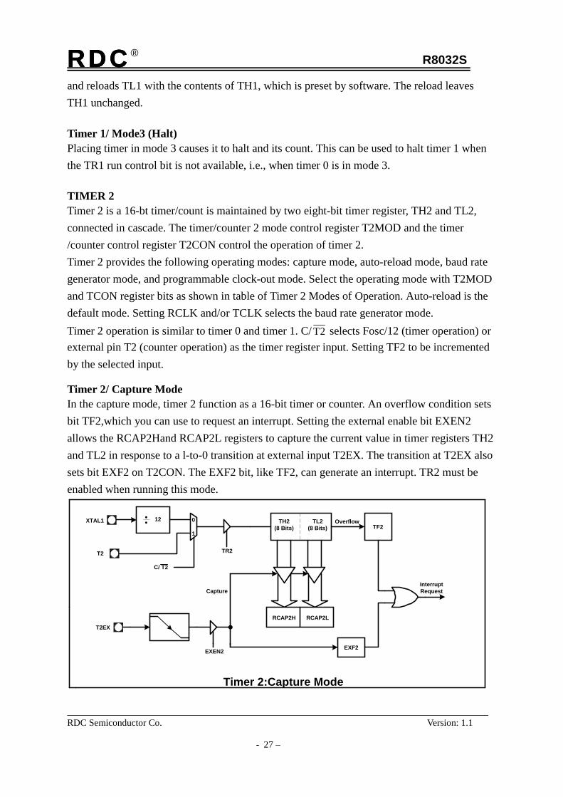
TIMER 2Timer 2 is a 16-bt timer/count is maintained by two eight-bit timer register, TH2 and TL2,connected in cascade. The timer/counter 2 mode control register T2MOD and the timer/counter control register T2CON control the operation of timer 2.Timer 2 provides the following operating modes: capture mode, auto-reload mode, baud rategenerator mode, and programmable clock-out mode. Select the operating mode with T2MODand TCON register bits as shown in table of Timer 2 Modes of Operation. Auto-reload is thedefault mode. Setting RCLK and/or TCLK selects the baud rate generator mode.Timer 2 operation is similar to timer 0 and timer 1. C/ 2T selects Fosc/12 (timer operation) orexternal pin T2 (counter operation) as the timer register input. Setting TF2 to be incrementedby the selected input.
Timer 2/ Capture ModeIn the capture mode, timer 2 function as a 16-bit timer or counter. An overflow condition setsbit TF2,which you can use to request an interrupt. Setting the external enable bit EXEN2allows the RCAP2Hand RCAP2L registers to capture the current value in timer registers TH2and TL2 in response to a l-to-0 transition at external input T2EX. The transition at T2EX alsosets bit EXF2 on T2CON. The EXF2 bit, like TF2, can generate an interrupt. TR2 must beenabled when running this mode.
12 0
1
XTAL1
T2
TL2(8 Bits)
Overflow
InterruptRequest
TH2(8 Bits) TF2
RCAP2H RCAP2LT2EX
EXF2EXEN2
TR2
Capture
C/ T2
Timer 2:Capture Mode

RDCRDCRDCRDC® R8032S
RDC Semiconductor Co. Version: 1.1
- 28 –
Timer 2/ Auto-reload ModeThe auto-reload mode configures timer 2 as a 16-bit timer or event counter with automaticreload. The timer operates an as an up counter or as an up/down counter, as determined by thedown counter enable bit (DCEN). At device reset, DCEN is cleared, so in the auto-reloadmode, timer 2 defaults to operation as an up counter. TR2 must be enabled when runningthis mode.
Up Counter OperationWhen DCEN = 0, timer 2 operates as an up counter. If EXEN = 0, timer 2 counts up toFFFFH and sets the TF2 overflow flag. The overflow condition loads the 16-bit value in thereload/capture registers (RCAP2H, RCAP2L) into the timer registers (TH2, TL2). The valuesin RCAP2H and RCAP2L are preset by software.If EXEN2 = 1, the timer registers are reloaded by either a timer overflow or a high-to-lowtransition at external input T2EX. This transition also sets the EXF2 bit in the T2CON register.Either TF2 or EXF2 bit can generate a timer 2 interrupt request. TR2 must be enabled whenrunning this mode.
Up/Down Counter OperationWhen DCEN = 1, timer 2 operates as an up/down counter. External pin T2EX controls thedirection of the count. When T2EX is high, timer 2 counts up. The timer overflow occurs atFFFFH which sets the timer 2 overflow flag (TF2) and generates an interrupt request. Theoverflow also causes the 16-bit value in RCAP2H and RCAP2L to be loaded into the timerregisters TH2 and TL2.
When T2EX is low, timer 2 counts down. Timer underflow occurs when the count in the timerregisters (TH2, TL2) equals the value stored in RCAP2H and RCAP2L. The underflow setsthe TF2 bit and reloads FFFFH into the timer registers.
The EXF2 bit toggles when timer 2 overflows or underflows changing the direction of thecount. When timer 2 operates as an up/down counter, EXF2 does not generate an interrupt.This bit can be used to provide 17-bit resolution. TR2 must be enabled when running thismode.

RDCRDCRDCRDC® R8032S
RDC Semiconductor Co. Version: 1.1
- 29 –
Timer 2/ Baud Rate Generator ModeThis mode configures timer 2 as a baud rate generator for use with the serial port. Select thismode by setting the RCLK and/ or TCLK bits in T2CON.
Timer 2/ Clock-out ModeIn the clock-out mode, timer 2 functions as a 50%-duty-cycle, variable-frequency clock. Theinput clock increments TL0 at frequency Fosc/2. The timer repeatedly counts to overflow
12 0
1
XTAL1
T2
TL2(8 Bits)
Overflow
InterruptRequest
TH2(8 Bits)
RCAP2H RCAP2L
T2EX
EXF2EXEN2
TR2
TF2
Reload
C/ T2
Timer 2: Auto Reload Mode (DECN = 0)
T2EX
TR2
TL2(8 Bits)
OverflowTH2(8 Bits)
RCAP2H RCAP2L
FFH FFH
12XTAL1
T2
0
1
Count Direction
1 = Up 0 = Down
InterruptRequest
TF2
EXF2
(Down Counting ReloadValue)
(Up Counting Reload Value)
C/ T2
Timer 2:Auto Reload Mode (DECN = 1)

RDCRDCRDCRDC® R8032S
RDC Semiconductor Co. Version: 1.1
- 30 –
from a preloaded value. At overflow, the contents of the RCAP2H and RCAP2L registers areloaded into TH2/TL2. In this mode, timer 2 overflows do not generates interrupts. Theformula gives the clock-out frequency as a function of the system oscillator frequency and thevalue in the RCAP2H and RCAP2L registers:
Watchdog TimerThe watchdog timer has system reset functions. User can set WD1-1, WD1-0 (in registerCKCON, 8Eh) to choose 172 , 202 , 232 or 262 counter for Watchdog Timer. After the WatchdogTimer counting the specific counter and occurring an overflow, sets WDTRSTFg (in registerWDCON, D8h) and finally resets the R8032S. If R8032S has been reset by Watchdog Timer ,WDTRSTFg remains one and POR (in register WDCON, D8h) is zero. On the other hand, ifR8032S has been power-on reset, WDTRSTFg is zero and POR one.
Clock-out Frequency = 4X(65536 - RCAP2H, RCAP2L)FoscFoscFoscFosc
ModeAuto-reload ModeCapture ModeBaud Rate Generator ModeProgrammable Clock-Out
RCLK OR TCLK(in T2COON)
CP/RL2#(in T2MOD)
T2OE(in T2MOD)
001X
01X0
00X1
Timer 2 Modes of Operation
T2OE
XTAL1
TR2T2
0
1
TL2(8 Bits)
OverflowTH2(8 Bits)
RCAP2H RCAP2L
2
2
InterruptRequestEXF2
EXEN2
T2EX
C/ T2
Timer 2: Clock Out Mode

RDCRDCRDCRDC® R8032S
RDC Semiconductor Co. Version: 1.1
- 31 –
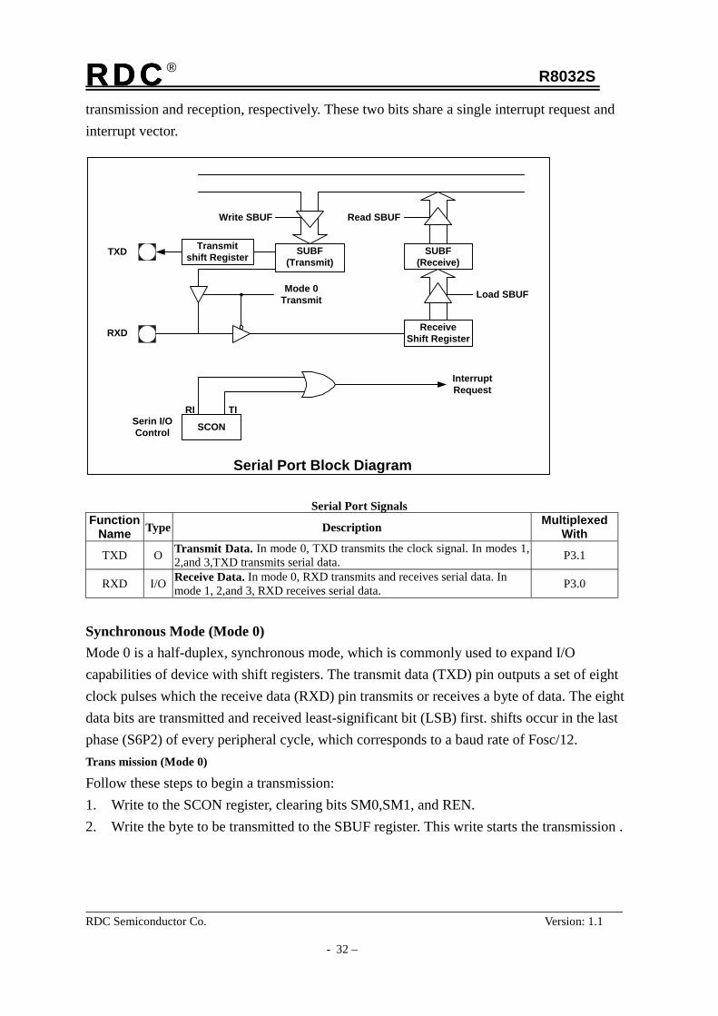
SERIAL I/O PORTThe serial I/O port provides both synchronous and asynchronous communication modes. Itoperates as a universal asynchronous receiver and transmitter (UART) in three full-duplexmodes (modes 1, 2, and 3). Asynchronous transmission and reception can occursimultaneously and at different baud rates. The serial port also operates in a singlesynchronous mode (mode 0).
The synchronous mode (mode 0) operates at a single baud rate. Mode 2 operates at two baudrates. Modes 1 and 3 operate over a wide range of baud rates, which are generated by timer 1and timer 2.
The serial port signals are defined in Table of Serial Port Signals, and the serial port specialfunction registers (SBUF, SCON) are described in the section of Special Function Registers.
For the three asynchronous modes, the UART transmits on the TXD pin and receives on theRXD pin. For the synchronous mode (mode 0), the UART outputs a clock signal on the TXDpin and sends and receives messages in the RXD pin. The SBUF register, which holdsreceived bytes and bytes to be transmitted, actually consists of two physically differentregisters. To send, software writes a byte to SBUF; to receive, software reads SBUF. Thereceive shift register allows reception of a second byte before the byte has been read fromSBUF. However, if software has not read the first byte by the time the second byte is received,the second byte will overwrite the first. the UART sets interrupt bits TI and RI on
Watchdog Timer 1
Reset
RWT
EWT
XTAL 1 overflow
Counter
WD1-1 WD1-0 Counting
0 0
0
0
1
1
1 1
172202232262
WDTRSTFg
0000000h
RDCRDCRDCRDC® R8032S
RDC Semiconductor Co. Version: 1.1
- 32 –
transmission and reception, respectively. These two bits share a single interrupt request andinterrupt vector.
Serial Port SignalsFunction
Name Type Description MultiplexedWith
TXD O Transmit Data. In mode 0, TXD transmits the clock signal. In modes 1,2,and 3,TXD transmits serial data. P3.1
RXD I/O Receive Data. In mode 0, RXD transmits and receives serial data. Inmode 1, 2,and 3, RXD receives serial data. P3.0
Synchronous Mode (Mode 0)Mode 0 is a half-duplex, synchronous mode, which is commonly used to expand I/Ocapabilities of device with shift registers. The transmit data (TXD) pin outputs a set of eightclock pulses which the receive data (RXD) pin transmits or receives a byte of data. The eightdata bits are transmitted and received least-significant bit (LSB) first. shifts occur in the lastphase (S6P2) of every peripheral cycle, which corresponds to a baud rate of Fosc/12.Trans mission (Mode 0)
Follow these steps to begin a transmission:1. Write to the SCON register, clearing bits SM0,SM1, and REN.2. Write the byte to be transmitted to the SBUF register. This write starts the transmission .
SUBF(Transmit)
SCON
Write SBUF Read SBUF
SUBF(Receive)
ReceiveShift Register
Mode 0Transmit Load SBUF
InterruptRequest
TIRISerin I/OControl
TXD
RXD
Serial Port Block Diagram
Transmitshift Register

RDCRDCRDCRDC® R8032S
RDC Semiconductor Co. Version: 1.1
- 33 –
Hardware executes the write to SBUF in the last phase (S6P2) of a peripheral cycle. At S6P2of the following cycle, hardware shifts the LSB (D0) onto the RXD pin. At S3P1 of the nestcycle, the TXD pin goes low for the first clock-signal pulse. Shifts continue every peripheralcycle. In the ninth cycle after the write to SBUF, the MSB (D7) is on the RXD pin. At thebeginning of the tenth cycle, hardware drives the RXD pin high and assert TI (S1P1) toindicate the end of the transmission.
Reception (Mode 0)
To start a reception in mode 0, write to the SCON register. Clear bits SM0, SM1, and RI andset the REN bit.Hardware executes the write to SCON in the last phase (S6P2) of a peripheral cycle. In thesecond peripheral cycle following the write to SCON, TXD goes low at S3P1 for the first
TXD
Write toSBUF
Shift
RXD
TI
TXD
Write toSBUF
Shift
RXD
RI
S3P1 S6P1
S6P2
S6P2 S6P2 S6P2 S6P2
S6P2 S6P2
S1P1
D0 D1 D2 D6 D7
S3P1 S6P1
S6P2
S6P2 S6P2 S6P2 S6P2
S6P2 S6P2 S5P2
S1P1
D0 D1 D6
D0
D7
Transmit
Receive
Mode 0 Timing
Set REN, Clear RI

RDCRDCRDCRDC® R8032S
RDC Semiconductor Co. Version: 1.1
- 34 –
clock-signal pulse, and the LSB (D0) is sampled on the RXD pin at S5P2. The D0 bit is thenshifted into the shift register. After eight shifts at S6P2 of every peripheral cycle, the LSB (D7)is shifted into the shift register, and hardware asserts RI (S1P1) to indicate a completedreception. Software can then read the received byte from SBUF.
Asynchronous Modes (Modes 1, 2, and 3)The serial port has three asynchronous modes of operation.Mode 1
Mode 1 is a full-duplex, asynchronous mode. The data frame consists of 10 bits: one start bit,eight data bits, and one stop bit. Serial data is transmitted on the TXD pin and received on theRXD pin. When a message is received, the stop bit is read in the RB8 bit in the SCONregister. The baud rate is generated by overflow of timer 1 or timer 2.Mode 2 and 3
Modes 2 and 3 are full-duplex, asynchronous modes. The data frame consists of 11 bits: onestart bit, eight data bits (transmitted and received LSB first), one programmable ninth data bit,and one stop bit is read from the RB8 bit in the SCON register. On transmit, the ninth data bitis written to the TB8 bit in the SCON register. Alternatively, you can use the ninth bit as acommand/data flag.- In mode 2, the baud rate is programmable to 1/32 or 1/64 of the oscillator frequency.- In mode 3, the baud rate is generated by overflow of timer 1 or timer 2.
Transmission (Modes 1, 2, 3)
Follow these steps to initiate a transmission:1. Write to the SCON register. Select the mode with the SM0 and SM1 bits, and clear the
REN bit. For modes 2 and 3, also write the ninth bit to the TB8 bit.2. Write the byte to be transmitted to the SBUF register. This write stars the transmission.
Reception (Modes 1, 2, 3)
To prepare for a reception, set the REN bit in the SCON register. The actual reception is theninitiated by a detected high-to-low transition on the RXD pin.
D0 D1 D2 D3 D4 D5 D6 D7 D8
Start Bit
Data Byte
Ninth Data Bit (Modes 2 and 3 only)Stop Bit
Data Frame (Modes 1, 2, and 3)

RDCRDCRDCRDC® R8032S
RDC Semiconductor Co. Version: 1.1
- 35 –
Baud Rates
Baud Rate for Mode 0
The baud rate for mode 0 id fixed at Fosc/12.
Baud Rtes for Mode 2
Mode 2 has two baud rates, which are selected by the SMOD bit in the PCON register. Thefollowing expression defines the baud rate:
Baud Rates for Modes 1 and 3
In modes 1 and 3, the baud rate is generated by overflow of timer (default) and/or timer 2.You may select either or both timer(s) to generate the baud rate(s) for the transmitter and/orthe receiver.
Timer 1 Generated Baud Rates (Mode 1 and 3)
Timer 1 is the default baud rate generator for the transmitter and the receiver in modes 1 and 3.The baud rate is determined by the timer 1 overflow rate and the value of SMOD, as shown inthe following formula:
Selecting Timer 1 as the Baud Rate Generator
To select timer 1 as the baud rate generator: • Disable the timer interrupt by clearing the IE0 register. • Configure timer 1 as a timer or an event counter (set or clear the C/T bit in the TMOD register).
• Select timer mode 0-3 by programming the M1, M0 bits in the TMOD register.
In most applications, timer 1 is configured as a timer in auto-reload mode (high nibble ofTMOD = 0010B). The resulting baud rate is defined by the following expression:
Timer 1 can generate very low baud rates with the following setup: • Enable the timer 1 interrupt by setting the ET1 bit in the IE register.
Sreial I/O Mode 2 Baud Rate 2SMOD Fosc
64
Sreial I/O Mode 1 and 3 Baud Rate 2SMOD Timer 1 Onerflow Rate
32
2SMOD Fosc
32 X 12 X [256 - (Th1)]Sreial I/O Mode 1 and 3 Baud Rate

RDCRDCRDCRDC® R8032S
RDC Semiconductor Co. Version: 1.1
- 36 –
• Configure timer 1 to run as a 16-bit timer (high nibble of TMOD = 0001B). • Use the timer 1 interrupt to initiate a 16-bit software reload.Timer 2 Generated Baud Rates (Modes 1 and 3)
Timer 2 may be selected as the baud rate generator for the transmitter and/or receiver. Thetimer 2 baud rate generator mode is similar to the auto-reload mode. A rollover in the TH2register reloads registers TH2 and TL2 with the 16-bit value on registers RCAP2H andRCAP2L, which are preset by software.
The timer 2 baud rate is expressed by the following formula:
Selecting Timer 2 as the Baud Rate Generator
To select timer 2 as the baud rate generator for the transmitter and/or receiver, program theRCLCK and TCLCK bits in the T2CON register. Setting RCLK and/or TCLK puts timer 2into its baud rate generator mode. In this mode, a rollover in the TH2 register does not set theTF2 bit in the T2CON register. Also, a high-to-low transition at the T2EX pin sets the EXF2bit in the T2CON register but does not cause a reload from (RCAP2H, RCAP2L) to (TH2,TL2). You can use the TT2EX pin as an additional external interrupt by setting the EXEN2 bitin T2CON.
NOTE : Turn the timer off (clear the TR2 bit in the T2CON register) before accessing registersTH2, TL2, RCAP2H,and RCAP2L.
You may configure timer 2 as a timer or a counter. In most applications, it is configured fortimer operation (i.e., the C/T2 bit is clear in the T2CON register).
Selecting the Baud Rate Generator(s)RCLK
BitTCLCK
BitReceiver
Baud Rate GeneratorTransmitter
Baud Rate generator0 0 Timer 1 Timer 10 1 Timer 1 Timer 21 0 Timer 2 Timer 11 1 Timer 2 Timer 2
Timer 2 Onerflow Rate16Sreial I/O Mode 1 and 3 Baud Rate

RDCRDCRDCRDC® R8032S
RDC Semiconductor Co. Version: 1.1
- 37 –
Note that timer 2 increments every state time (2Tosc) when it is in the baud rate generatormode. In the baud rate formula that follows, “RCAP2H,RCAP2L” denotes the contents ofRCAP2H and RCAP2L taken as a 16-bit unsigned integer:
NOTE : When timer 2 is configured as a timer and is in baud rate generator mode, do not reador write the TH2 or TL2 registers. The timer is being incremented every state time, and theresult of a read or write may not be accurate. In addition, you may read, but not write to, theRCAP2 registers; a write may overlap a reload and cause write and/or reload errors.
Serial I/O Port 1Serial I/O port 1 is the same as serial I/O port mentioned above. RXD1 is at P1.2 and TXD1at P1.3. The Serial I/O port 1 has its own buffer (SBUF1, C1h) and control register (SCON1,C0h). All functions and structures are the same as serial I/O port. But the only difference isthat serial I/O port 1 only uses timer 1 for baud rate at mode 1 and mode 3. The double baudrate bit SMODE1 is at WDCON (D8h) register.
XTAL1
TR2T2
0
1
2
C/ T2
Timer 2 in Baud Rate Generator Mode
TL2(8 Bits)
TH2(8
Bits)
RCAP2H RCAP2L
2 0
1
Timer 1Overflow
SMOD
0
1
TCLCK
Interrupt
Request
EXF2
EXEN2
T2EX
16 TXClock
NOTE:Oscillator frequencyis divided by 2, not 12.
Note availability of additional external interrupt
0
1
RCLCK
16 RXClock
0
1
SMOD1 16 TX1Clock
16 RX1Clock
Fosc32 X [65536 - (RCAP2H,RACAP2L)]Sreial I/O Mode 1 and 3 Baud Rate

RDCRDCRDCRDC® R8032S
RDC Semiconductor Co. Version: 1.1
- 38 –
8.POWER-DOWN and IDLE-MODE Idle-Mode
When set IDL bit in PCON(87h), the P will enter idle mode. In idle mode , the P is idlewhile all the on-chip peripherals remain active. The internal RAM and SFRs registersremain unchanged during this mode. The idle mode can be terminated by any enabledinterrupt or by a hardware reset.
Power-Down ModeWhen set PD bit in PCON(87h), the P will enter power down-mode .In the power-downmode, the oscillator is stopped. Before entering power-down mode, the RNGEN bit inVDT(D9h) should be clear for saving power consumption. The power down mode can bewakened up by the hardware reset or by the external enable interrupt with level triggeractivation (ITx in register TCON is set to 0). The Program Counter, internal RAM andSFRs registers retain their values and will not be changed after the power-down mode isterminated by external interrupt. The reset will restart the CPU, while the SFRs withinitial values and the internal RAM retain their values.
Status of External Pins During Idle and Power-DownMode ALE PSEN Port 0- Port 3
Idle 0 1 Retain the values beforeenter Idle Mode
Power-Down 0 1 FFH
R8034T in Power-Down mode R8034T in operation mode
Twk = 20-bit counter counts form 0 to overflow, whose clock source is OSC
Power-Down mode wake-up operation
CLK
INT0 OR INT1
Twk

RDCRDCRDCRDC® R8032S
RDC Semiconductor Co. Version: 1.1
- 39 –
9.RESETProcessor initialization is accomplished with activation of the RESET pin. To reset theprocessor, this pin should be held high for at least two oscillator periods.
minimum 2oscillator period
VCC
CLK
RESET
Reset Timing
RDCRDCRDCRDC® R8032S
RDC Semiconductor Co. Version: 1.1
- 40 –
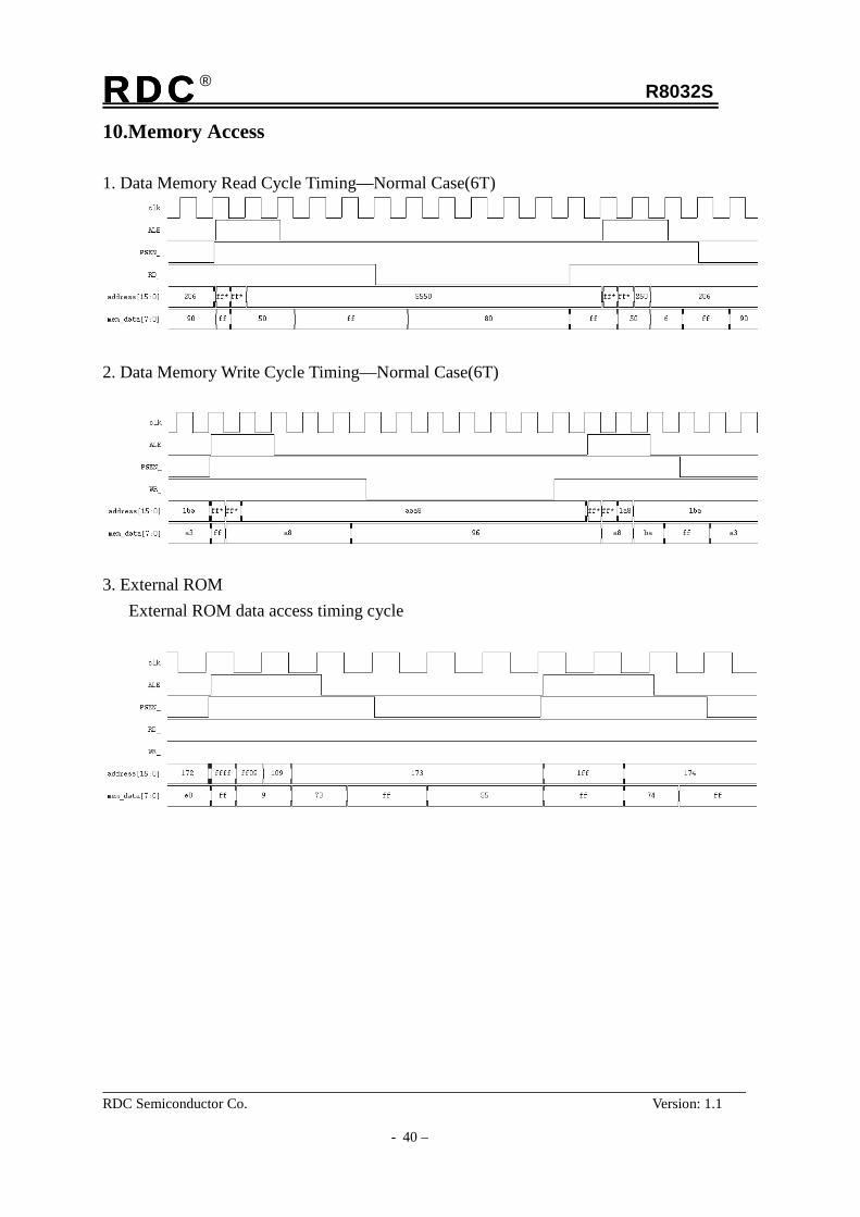
10.Memory Access
1. Data Memory Read Cycle Timing—Normal Case(6T)
2. Data Memory Write Cycle Timing—Normal Case(6T)
3. External ROM External ROM data access timing cycle
RDCRDCRDCRDC® R8032S
RDC Semiconductor Co. Version: 1.1
- 41 –
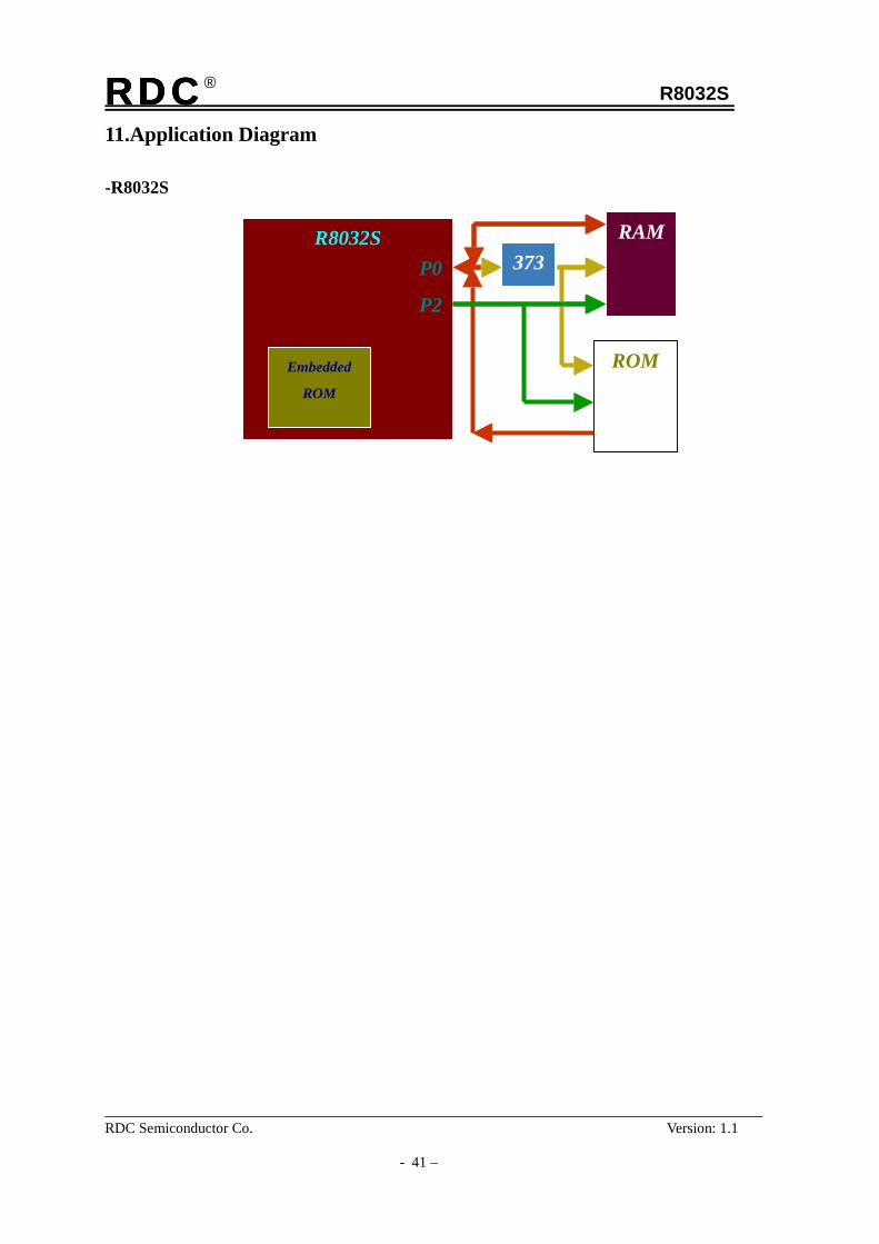
11.Application Diagram
-R8032S
R8032S
Embedded
ROM
P0
P2
RAM373
ROM
RAM373

RDCRDCRDCRDC® R8032S
RDC Semiconductor Co. Version: 1.1
- 42 –
12. Instruction Cycle12.1 Instruction Cycle table (8032S)
Logical OperationsOscillator PeriodInstruction 80C32 R8032S
ANL A, Rn 12 4ANL A, dir 12 8ANL A, @Ri 12 4ANL A, #data 12 8ANL dir, A 12 8ANL dir, #data 24 12ORL A, Rn 12 4ORL A, dir 12 8ORL A, @Ri 12 4ORL A, #data 12 8ORL dir, A 12 8ORL dir, #data 24 12XRL A, Rn 12 4XRL A, dir 12 8XRL A, @Ri 12 4XRL A, #data 12 8XRL dir, A 12 8XRL dir, #data 24 12CLR A 12 4CPL A 12 4RL A 12 4RLC A 12 4RR A 12 4RRC A 12 4SWAP A 12 4
DATA TransferOscillator PeriodInstruction 80C32 R8032S
MOV A, Rn 12 4MOV A, dir 12 8MOV A, @Ri 12 4MOV A, #data 12 8MOV Rn, A 12 4MOV Rn, dir 24 8MOV Rn, #data 12 8MOV dir, A 12 8MOV dir, Rn 24 4MOV dir, dir 24 12MOV dir, @Ri 24 8

RDCRDCRDCRDC® R8032S
RDC Semiconductor Co. Version: 1.1
- 43 –
MOV, dir, #data 24 12MOV @Ri, A 12 4MOV @Ri, dir 24 8MOV @Ri, #data 12 8MOV DPTR,#data16 24 12MOVC @A+DPRT 24 16MOVC A, @A+PC 24 12MOVX A, @Ri 24 16MOVX A, @DPTR 24 16MOV @Ri, A 24 16MOVX @DPTR, A 24 16PUSH dir 24 8POP dir 24 8XCH A, Rn 12 12XCH A, dir 12 8XCH A, @Ri 12 8XCHD A, @Ri 12 12
Arithmetic OperationsOscillator PeriodInstruction 80C32 R8032 S
ADD A, Rn 12 4ADD A, dir 12 8ADD A, @Ri 12 4ADD A, #data 12 8ADDC A, Rn 12 4ADDC A, dir 24 8ADDC A, @Ri 12 4ADDC A, #data 12 8SUBB A, Rn 12 4SUBB A, dir 12 8SUBB A, @Ri 12 4SUBB A, #data 24 8INC A 12 4INC Rn 12 4INC dir 12 8INC @Ri 12 8DEC A 12 4DEC Rn 24 4DEC dir 12 8DEC @Ri 12 8INC DPTR 12 8MUL AB 12 12DIV AB 12 12DA A 12 4

RDCRDCRDCRDC® R8032S
RDC Semiconductor Co. Version: 1.1
- 44 –
Boolean Variable ManipulationOscillator PeriodInstruction 80C32 R8032S
CLR C 12 4CLR bit 12 8SETB C 12 4SETB bit 12 8CPL C 12 4CPL bit 12 8ANL C, bit 24 8ANL C, bit 24 8ORL C, bit 24 8ORL C, bit 24 8MOV C, bit 12 8MOV bit, C 24 8JC Rel 24 12JNC Rel 24 12JB Bit, rel 24 16JNB Bit, rel 24 16JBC Bit, rel 24 16
Programming BranchingOscillator PeriodInstruction 80C32 R8032S
ACALL addr11 24 12LCALL addr16 24 12RET 24 12RETI 24 12AJMP addr11 24 12LJMP addr16 24 12SJMP rel 24 12JMP @A+DPTR 24 12JZ rel 24 12JNZ rel 24 12CJNE A, dir, rel 24 16CJNE A, #data, rel 24 16CJNE Rn, dir, rel 24 16CJNE @Ri, dir, rel 24 16
DJNZ Rn, rel 24 12DJNZ dir, rel 24 16NOP 12 4

RDCRDCRDCRDC® R8032S
RDC Semiconductor Co. Version: 1.1
- 45 –

RDCRDCRDCRDC® R8032S
RDC Semiconductor Co. Version: 1.1
- 46 –
13.Revision History
Rev. Date History1.0 2001/10/17 Formal release1.1 2002/05/02 Fix:MOV Rn,dir (from I/O)