razor: a variability-tolerant design methodology for...
TRANSCRIPT

RAZOR: A VARIABILITY-TOLERANT DESIGN METHODOLOGY FOR LOW -POWER AND
ROBUST COMPUTING
by
Shidhartha Das
A dissertation submitted in partial fulfillment of the requirements for the degree of
Doctor of Philosophy (Computer Science and Engineering)
in The University of Michigan 2009
Doctoral Committee:
Professor David T. Blaauw, Chair Professor Trevor N. Mudge Professor Marios C. Papaefthymiou Associate Professor Dennis M. Sylvester Krisztián Flautner, Director of Research, ARM Ltd.

© Shidhartha Das All Rights Reserved
2009

ii
To my family, friends and teachers

iii
ACKNOWLEDGEMENTS
This thesis has been in making for the last six years or so. While I take immense
pride and joy in being finally able to finish it, this task could not have been accomplished
without the many contributions of the wonderful people that I have had the good fortune
of being associated with, all these years. I want to take this opportunity to express my
sincere and heartfelt gratitude to them.
First and foremost, I would like to thank my advisor, Prof. David Blaauw. His
incredible creativity has been the source of a lot of ideas in this thesis. His capacity for
hard work and single-minded focus is inspirational. In the last six years that I have known
David, he has taught me by example, how to be a better researcher, writer, speaker and,
perhaps more importantly, a better person. I have often turned to him for counsel during
difficult times in this dissertation and his support has helped me sustain my focus. David
is easily one of the best advisors to have.
Secondly, I would like to thank Prof. Mudge, Prof. Sylvester, Prof. Papaefthymiou
and Dr. Flautner to take time from their busy schedules to be a member of my
dissertation committee. Your valuable suggestions and feedback have greatly
strengthened the thesis. In particular, I would like to thank Kris for initiating the Razor
project in ARM and for the opportunity of turning Razor into a “real world” technology.
Special thanks are due to Trevor for the long conversations on politics, history and
theology that we have shared over dinner in the curry houses in Cambridge, U.K. His
sense of humor has been a big help when the going got tough.
I want to express my gratitude to my colleagues at ARM, particularly David Bull,
who I have worked with very closely in the past four years. David is easily one of the
sharpest minds that I have ever interacted with. I have learnt a lot from his vast
experience and his creativity. Long discussions with him have helped spawn a lot of the
ideas in this thesis. I would also like to thank Emre Ozer from ARM R&D for the

iv
numerous discussions about a broad range of topics, both technical and otherwise. I also
thank David Flynn, John Biggs, Sachin Idgunji, Robert Aitken, Nathan Chong and my
other colleagues at ARM from whom I have learnt a lot about various aspects of
computer engineering.
During my stay at Ann Arbor, I have met incredibly talented people and made great
friends. They have been a very strong source of support for me and made my graduate
career a memorable experience. In particular I will like to mention Sanjay Pant, Visvesh
Sathe, Ashish Srivastava, Rajeev Rao, Sarvesh Kulkarni, Bo Zhai, Carlos Tokunaga,
Kaviraj Chopra, Ajay T.M., Ajay Raghavan, David Roberts, Mark Woh, Ganesh Dasika
and countless others who have always been there to share ideas, jokes and the occasional
laughter. Special thanks are due to the RazorII design team Sudherssen Kalaiselvan,
Kevin Lai and Wei-shiang Ma. Without their hard work and dedication, the RazorII
processor would not have been possible. I will also like to thank Ed Chusid, Amanda
Brown, Denise Duprie, Bertha Wachsman and Dawn Freysinger for helping me with all
sorts of difficulties at various times during my graduate career.
I am forever indebted to my parents for their unconditional love and support. They
have instilled in me an appreciation of hard work and they receive the most credit for
whatever I have accomplished in my life thus far.
Finally, I would like to thank my wife, Kasturee. Ever since she has been in my life,
every day has been special. With her laughter and her loving support, she has made
writing this thesis a very pleasant exercise.

v
TABLE OF CONTENTS
DEDICATION ............................................................................................................. ii
ACKNOWLEDGEMENTS ....................................................................................... iii
LIST OF FIGURES .....................................................................................................ix
LIST OF TABLES .....................................................................................................xii
LIST OF ACRONYMS ............................................................................................ xiii
ABSTRACT ...............................................................................................................xiv
CHAPTER 1
Introduction....................................................................................................................1
1.1 Categorizing sources of variations ...................................................................4
Spatial reach....................................................................................................4
Temporal rate of change ..................................................................................5
1.2 Adaptive design approaches ............................................................................7
1.3 Introduction to Razor.......................................................................................9
1.4 Main contributions and organization of the thesis ..........................................12
CHAPTER 2
Adaptive Design Techniques ........................................................................................14
2.1 “Always Correct” Techniques .......................................................................14
2.1.1 Look-up table based approach............................................................14
2.1.2 Canary-circuits based approach..........................................................15
2.1.3 In situ triple-latch monitor .................................................................17
2.1.4 Micro-architectural techniques...........................................................18
2.2 “Let fail and correct” approaches...................................................................20

vi
2.2.1 Techniques for communication and signal processing ........................21
2.2.2 Techniques for general-purpose computing........................................23
2.3 Summary and discussion ...............................................................................24
CHAPTER 3
RazorI: State Comparison based Error-detection and Circuit-architectural Recovery ....26
3.1 Concept of Razor error detection and recovery ..............................................27
3.2 Transistor-level design of the RazorI flip-flop ...............................................31
3.2.1 Metastability detection.......................................................................33
3.3 Pipeline Error Recovery mechanisms ............................................................36
3.3.1 Recovery using clock gating ..............................................................37
3.3.2 Recovery using counterflow pipelining ..............................................38
3.4 Supply voltage control...................................................................................40
3.5 Silicon implementation and evaluation of the scheme....................................41
3.6 Summary and discussion ...............................................................................42
CHAPTER 4
Self-tuning RazorI Processor: Design and Silicon Measurement Results.......................43
4.1 Processor implementation details...................................................................44
4.2 Measurement Results ....................................................................................45
4.2.1 Energy Savings from Sub-critical Operation ......................................47
4.3 Total Energy Savings with RazorI .................................................................50
4.4 RazorI Voltage Control .................................................................................53
4.5 Summary and discussion ...............................................................................56
CHAPTER 5
RazorII: Transition-Detection based Error -Detection and Micro-architectural Recovery...............................................................................................................................57
5.1 Issues with the RazorI technique....................................................................58
5.1.1 Timing constraint on the pipeline restore signal.................................58
5.1.2 Issues with metastability detection .....................................................59
vii
5.2 Key concepts of RazorII ................................................................................60
5.3 RazorII pipeline micro-architecture ...............................................................61
5.4 Transition-detection based error-detection .....................................................64
5.4.1 Fundamental minimum-delay trade-off ..............................................67
5.5 SEU detection using the RazorII flip-flop ......................................................68
5.5.1 Impact of intra-die process-variability................................................71
5.5.2 SEU Detection using the R2LAT .......................................................73
5.5.3 Comparative Analysis with the RazorI flip-flop .................................76
5.6 Memory design for a Razor processor core....................................................77
5.6.1 Handling speculative read accesses to the memory.............................77
5.6.2 Timing speculation in the sense-amplifier circuit ...............................79
5.7 Summary and discussion ...............................................................................80
CHAPTER 6
Alternative Hold-fixing Schemes for Razor-based Pipelines .........................................82
6.1 Level-sensitive latch based scheme for hold-fixing........................................83
6.2 Intel X-pipe ...................................................................................................85
6.3 Logic replication in statically-scheduled machines ........................................87
6.4 RazorII flip-flop with integrated clock-pulse generator..................................89
6.5 Summary and discussion ...............................................................................90
CHAPTER 7
Self-tuning RazorII Processor: Using RazorII for PVT and SER Tolerance ..................92
7.1 Pipeline design of the RazorII processor........................................................92
7.2 Setting limits to voltage and frequency scaling in RazorII .............................95
7.2.1 Conservative estimation from static timing analysis ...........................96
7.2.2 Worst-case vector based tuning..........................................................98
7.3 Silicon measurement results ........................................................................100
7.3.1 RazorII clocking scheme..................................................................101
viii
7.3.2 Total energy savings ........................................................................104
7.3.3 RazorII sub-critical operation...........................................................107
7.4 Soft Error Rate Radiation tests with RazorII ................................................109
CHAPTER 8
Conclusion and Future Work......................................................................................111
8.1 Key concept of Razor ..................................................................................111
8.2 The RazorI approach ...................................................................................112
8.3 The RazorII approach..................................................................................113
8.4 Merits and demerits of the Razor approach..................................................114
8.5 Future directions of research into Razor.......................................................114
8.5.1 Razor System Design Considerations...............................................115
8.5.2 Micro-architectural research into Razor-based pipelines...................115
8.5.3 Silicon test-and-debug .....................................................................116
BIBLIOGRAPHY ....................................................................................................117
ix
LIST OF FIGURES
Figure 1.1 Timing wall: A consequence of downsizing off-critical paths [40]..................3
Figure 1.2 Qualitative relationship between supply voltage and Error-rate.....................10
Figure 2.1 Uht's TEATime: A canary circuits based approach .......................................16
Figure 2.2 Kehl’s triple-latch technique for in situ delay monitoring. Figure a) shows the mechanism of monitoring delay through temporal redundancy. Figure b) shows the timing diagrams for a “tuned” system ....................................................................17
Figure 2.3 Data-dependent delay variations in adders a) Carry-propagation for SPECInt 2000 vectors b) Carry-propagation for random vectors [25] ...................................18
Figure 2.4 Self-calibrating interconnects........................................................................21
Figure 2.5 Algorithmic Noise Tolerance [30] ................................................................22
Figure 3.1 Abstract view of the RazorI flip-flop. The speculative data in the master-slave flip-flop is compared with the correct data in the positive level-sensitive shadow latch.......................................................................................................................27
Figure 3.2 Conceptual timing diagrams showing the operation of the RazorI flip-flop. In Cycle 2, a setup violation causes Error to be flagged whereas in Cycle 4, a hold violation causes error to be asserted. ......................................................................28
Figure 3.3 RazorI flip-flop circuit schematic..................................................................31
Figure 3.4 Restore generation circuitry..........................................................................32
Figure 3.5 Metastability-detector: Principle of Operation. Figure a) shows the DC transfer characteristics of a P- and a N-skewed inverter compared to an unskewed inverter. Figure b) shows error detection operation of the metastability-detector..................34
Figure 3.6 Pipeline recovery using global clock-gating. Figure a) shows the pipeline organization and Figure b) illustrates the pipeline timing for a failure in the EX stage of the pipeline. The “*” denotes a failed stage computation....................................37
Figure 3.7 Pipeline recovery using counter-flow pipelining. Figure a) shows the pipeline organization and Figure b) illustrates the pipeline timing for a failure in the EX stage of the pipeline. The “*” denotes a failed stage computation....................................39
Figure 3.8 Razor supply voltage control ........................................................................41
Figure 4.1 Die photograph of the RazorII processor. The 64bit processor executes a sub-set of the ALPHA instruction set............................................................................44
Figure 4.2 Sub-critical operation in chips named "Chip 1" and "Chip 2"........................46

x
Figure 4.3 Normalized energy savings over point of first failure at the 0.1% error-rate for 33 measured chips at 120 and 140MHz..................................................................48
Figure 4.4 Relationship between the Point of First failure and the 0.1% Error-rate point. Figure a) shows the distribution of the Point of First Failure for 33 different chips. Figure b) shows that the 0.1% point has a smaller spread than the Point of First Failure. ..................................................................................................................49
Figure 4.5 Temperature margins....................................................................................50
Figure 4.6 Total Energy Savings with RazorI. ...............................................................51
Figure 4.7 Distribution of the total energy savings over the worst-case for 33 measured chips. .....................................................................................................................52
Figure 4.8 RazorI voltage control loop...........................................................................53
Figure 4.9 Run-time response of the RazorI voltage controller. Shown in the figure is a two minute snapshot of the error-rate for a program with two error-rate phases......54
Figure 4.10 RazorI voltage controller: Error-rate phase transition response. Figure a) shows the transition from low to high error-rate. Figure b) shows the transition in the opposite direction. .................................................................................................55
Figure 5.1 Timing constraint on the Restore signal. The Restore signal is a high fan-out net which is generated out of a high fan-in OR gate. It needs to setup before the next rising edge with sufficient safety margin................................................................58
Figure 5.2 RazorII pipeline organization........................................................................62
Figure 5.3 Transition-detection based error detection.....................................................64
Figure 5.4 Transition-detecting RazorII flip-flop ...........................................................65
Figure 5.5 Timing diagrams showing the principle of operation of the Transition Detector..............................................................................................................................66
Figure 5.6 Modified RazorII flip-flop for SEU and timing-error detection .....................69
Figure 5.7 Circuit schematic of the R2LAT ...................................................................70
Figure 5.8 Timing constraints with intra-die process variations......................................71
Figure 5.9 Conceptual timing diagrams showing SEU detection when DC is high .........73
Figure 5.10 SEU Detection when DC pulse is low.........................................................75
Figure 5.11 Sense-amplifier Flip-flop augmented with a transition-detector to sample critical Read signals in a SRAM array ...................................................................78
Figure 5.12 Dual Sense-amplifier scheme for faster read timings...................................79
Figure 6.1 Latch-insertion scheme for satisfying the short-path constraint .....................84
Figure 6.2 Error-rate and wasted-time trade-off .............................................................85
Figure 6.3 Intel X-pipe micro-architecture.....................................................................87

xi
Figure 6.4 Replicated functional units eliminate the Razor minimum-delay constraint...88
Figure 6.5 Pulsed-latch implementation of the RazorII flip-flop. The transition-detector monitors the data input rather than the internal node. .............................................90
Figure 7.1 RazorII Processor: Pipeline Design...............................................................93
Figure 7.2 The limit of safe operation in RazorII ...........................................................95
Figure 7.3 Worst-case vector based tuning.....................................................................97
Figure 7.4 Die-photograph of the RazorII processor ....................................................100
Figure 7.5 RazorII processor clocking scheme. Figure a) shows the schematic of the clock-generator. Figure b) shows the relevant timing diagrams. ...........................102
Figure 7.6 Total energy savings through RazorII based supply-voltage control............104
Figure 7.7 Distribution of total energy savings through Razor .....................................105
Figure 7.8 Sub-critical operation in RazorII.................................................................106
Figure 7.9 Run-time versus replay tradeoff..................................................................107
Figure 7.10 Histogram of instructions as a function of replay iterations .......................108
Figure 7.11 SER Test Setup.........................................................................................109
xii
LIST OF TABLES
Table 1.1 Categorizing sources of variation .....................................................................5
Table 2.1 Adaptive techniques landscape.......................................................................15
Table 3.1 Metastability-detector Corner Analysis ..........................................................35
Table 4.1 Processor implementation details ...................................................................45
Table 4.2 Error-rate and energy-per-instruction measurement for chips 1 and 2 at the Point of First Failure and at the Point of 0.1% Error Rate.......................................47
Table 7.1 Chip Implementation details ........................................................................101
Table 7.2 SER Tests ....................................................................................................110
xiii
LIST OF ACRONYMS
SEU……………………………………………………….……………Single Event Upset
SER………………………………………………………………….……...Soft Error Rate
SRAM…………………………………………………….Static Random Access Memory
PoFF………………………………………………………….………Point of First Failure
TMR………………………………………………………….Triple-Modular Redundancy
ECC………………………………………………………………..Error-Correcting Codes
DC……………………………………………………………………...…Detection-Clock
TD……………………………………………………………………...Transition-Detector
BER………………………………………………………………...………..Bit Error Rate
PVT……………………………………………………..Process Voltage and Temperature
FPGA……………………………………………………Field Programmable Gate Arrays
VLSI…………………………………………………………Very Large Scale Integration
CPU………………………………………………………………..Central Processing Unit
FIR………………………………………………………………..Finite Impulse Response
DAC………………………………………………………….Digital-to-Analog Converter
FO4…………………………………………………………….Fan-out of Four (inverters)
xiv
ABSTRACT
RAZOR: A VARIABILITY-TOLERANT DESIGN METHODOLOGY FO R LOW -POWER AND ROBUST COMPUTING
by
Shidhartha Das
Chair: David T. Blaauw
Rising PVT variations at advanced process nodes make it increasingly difficult to
meet aggressive performance targets under strict power budgets. Traditional adaptive
techniques that compensate for PVT variations need safety margins and cannot respond
to rapid environmental changes. In this thesis, we present a novel voltage management
technique, called Razor, which eliminates worst-case safety margins through in situ error
detection and correction of variation-induced delay errors. In Razor, we use a delay-error
tolerant flip-flop on critical paths to scale the supply voltage to the point of first failure of
a die for a given frequency. Thus, all margins due to global and local PVT variations are
eliminated, resulting in significant energy savings. In addition, the supply voltage can be
scaled even lower than the first failure point into the sub-critical region, deliberately
tolerating a targeted error rate, thereby providing additional energy savings. Thus, in the
context of Razor, a timing error is not a catastrophic system failure but a trade-off
between the overhead of error-correction and the additional energy savings due to sub-
critical operation. In Razor, the error-rate is monitored and the supply voltage is tuned to
achieve a targeted error-rate.
We developed two techniques, called RazorI and RazorII, for implementation of
Razor-based voltage tuning in microprocessors. The RazorI approach achieves error-
xv
detection by double-sampling the critical-path output at different points in time and
comparing both samples. A global recovery signal overwrites the earlier, speculative
sample with the later sample and restores the pipeline to its correct state. We
implemented RazorI error-detection and correction in a 64bit processor in 0.18micron
technology and obtained 50% energy savings over the worst-case at 120MHz. However,
the efficacy of the RazorI technique for high-performance processors is undermined by
its reliance on a metastability-detector and potentially, timing-critical pipeline recovery
path.
The RazorII approach addresses this issue by achieving recovery from delay-errors
through a conventional, architectural-replay mechanism. Error-detection in RazorII
occurs by flagging spurious transitions at critical-path endpoints. Furthermore, RazorII
also detects logic and register SER. We implemented a RazorII-enabled 64bit processor
in 0.13µm technology and obtained 33% power savings over the worst-case. SER
tolerance was demonstrated with radiation experiments.

1
CHAPTER 1
INTRODUCTION
In the last few years, the computational capability of mobile and hand-held devices
has witnessed phenomenal improvements. Heavyweight compute-intensive applications
such as 3-D graphics, audio/video, internet access and gaming which were traditionally
exclusive to the domain of desktop computers are now available for mobile platforms as
well. This is evident in the evolution of the mobile phone: in the last decade and half
mobile phones have shown more than 50X improvement1 in talk-time per gram of
battery. Indeed, the surge in the market for smartphones, Mobile Internet Devices
(MIDs) and Ultra-Mobile Personal Computers (UMPCs) is expected to push the
performance envelope of mobile processors in the coming years.
A key technique that has led to such performance improvements has been technology
scaling at the rate dictated by the Moore’s Law [7]. By shrinking transistor dimensions,
designers can deliver consistent improvements in computational capability of processors
through higher integration levels and faster switching times [5]. Thus, technology scaling
has been the fundamental driver that has fuelled the growth of the semiconductor industry
over the past decades. Traditionally, supply voltage of processors has also reduced with
each process generation. Hence, in addition to performance improvements, technology
scaling delivered power savings as well. However, starting with the 65nm node, higher
transistor integration levels, combined with almost constant supply voltages and
stagnation of energy efficiency, has caused power consumption of processors to actually
worsen at aggressive process nodes. This has created a design paradox: more transistors
can now be fitted on a die; however, they cannot be used due to strict power limits.
1 Comparison of standard configurations of Nokia 232 and Nokia N70 phones

2
Indeed, rising power dissipation is a fundamental barrier towards sustaining the current
rate of transistor integration [9].
Power consumption is especially relevant for battery-operated mobile processors as
they increasingly handle computationally demanding applications under stringent power
budgets. This is a major concern because battery capability has not kept pace with
performance demands. Power consumption issues are further exacerbated by variations in
transistor performance at aggressive geometries. Due to the inherent lithographic
difficulties in manufacturing millions of transistors with very small feature sizes, some
dies operate much slower than others (up to 2x difference can be commonly observed
between the fastest and slowest chips) [20]. Such manufacturing-process induced
differences in processor speeds across different chips are called inter-die process
variations. Variations in transistor switching delays within the same chip itself are called
intra-die variations.
In addition, transistors vary in performance due to changes in the ambient
environment. For instance, glitches in the power supply and fluctuations in the
temperature conditions are a regular occurrence during the dynamic operation of the
processor [49][50][51]. Temperature and voltage conditions can also vary locally
between different parts of the same chip. In general, under high temperature or low-
voltage conditions, transistor switching speed between logic states is substantially
reduced. Designing robust circuits that can cope with these variations in silicon grade and
ambient conditions requires operation at a higher supply voltage. This ensures that any
unforeseen slow-down because of voltage glitches, high temperature conditions and
process variations does not cause computing errors due to processor timing violations.
While the practice of adding a safety margin or so-called “guardband” to the supply
voltage leads to robust circuit operation in presence of variations, it is also leads to higher
power consumption. At smaller geometries, variations worsen due to inherent limitations
in accurately controlling the manufacturing process and the operational environment of
transistors. This necessitates the use of even wider margins as we scale transistor
technology. However, safety margins are not needed for all chips or for the entire
duration of their operational lifetime. Only a small percentage of the manufactured chips
are inherently slow. Even for these slow chips, it is highly unlikely that they will exhibit

3
worst-case temperature and voltage conditions for significant periods of time during their
operation. For most chips, safety margins are unnecessary and lead to wasted battery
power. Thus, the fundamental issue with margining is that it seeks to budget for worst-
case conditions that occur extremely rarely in practice. This leads to overly conservative
designs and adversely impacts the power budgets of processors that are already stressed
due to rising performance demands.
A key observation to make from the above discussion is that low-power and robust
operation are fundamentally at odds with each other. Robust designing requires larger
safety margins, such as a higher operating voltage, thicker interconnects and wider
devices, at the expense of increased power consumption. On the other hand, low-power
methodologies typically trade off circuit robustness for improved energy efficiency. For
example, an effective low-power technique is Dynamic Voltage Scaling (DVS) which
enables quadratic savings in energy by scaling supply voltage during low CPU utilization
periods. However, low voltage operation causes signal integrity concerns by reducing the
static noise margins for sensitive circuits. Furthermore, sensitivity to threshold voltage
variation also increases at low voltages [2] which can lead to circuit failure. Another
Path delay
# of
pat
hs Initial pathdistribution
Path distributionafter power optimization Critical-path
delay
“Timing wall”
Path delay
# of
pat
hs Initial pathdistribution
Path distributionafter power optimization Critical-path
delay
“Timing wall”
Figure 1.1 Timing wall: A consequence of downsizing off-critical paths [40]

4
popular technique for low-power relies on downsizing off-critical paths [40]. This
balances path delays in the design leading to the so-called timing wall, as shown in
Figure 1.1. In a delay-balanced design, the likelihood of parametric-yield failure
significantly increases because more paths can now fail setup requirements. This
fundamental conflict between robustness and low-power, exacerbated due to rising
variations, leads to a very complex optimization space wherein achieving design closure
can be exceedingly difficult.
1.1 Categorizing sources of variations
In order to effectively address the issue of design closure in presence of variations, it
is helpful to analyze and categorize the different sources of variations based on their
spatial reach and temporal rate of change [20] , as represented in Table 1.1.
Spatial reach
Based on spatial reach, the source of variations can be global or local in extent.
Those that affect all transistors on the die are global in nature. For example, voltage
fluctuations in the on-board Power Supply Unit (PSU) affects supply to the entire die.
Inter-die process variations and ambient temperature are other such examples of
phenomena that affect all transistors on die and are hence classified as global variations.
Jitter in the Phase Locked Loop (PLL) output adds uncertainty to the system clock at the
root of the clock-tree and this uncertainty propagates to every latch and flip-flop driven
by the clock-tree. Similarly, ageing effects, such as Time Dependent Di-electric
Breakdown [42] (TDDB) and Negative Bias Temperature Instability [41] (NBTI), can
also be categorized as predominantly global since all transistors on the die experience
slow down due to these effects, over the course of its lifetime. Of course, all of the
aforementioned global phenomena affect individual transistors to varying extents
according to differences in their actual locations on die.
Contrary to global sources of variation, local effects are limited to a few transistors
in the immediate vicinity of each other. Voltage variations due to resistive drops in the
power grid and temperature hot-spots in regions of high switching activity have local
effects. Signal integrity issues caused due to inductive and capacitive coupling noise
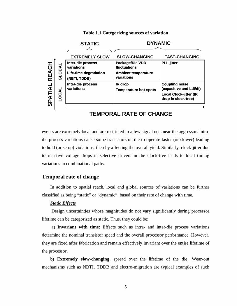
5
events are extremely local and are restricted to a few signal nets near the aggressor. Intra-
die process variations cause some transistors on die to operate faster (or slower) leading
to hold (or setup) violations, thereby affecting the overall yield. Similarly, clock-jitter due
to resistive voltage drops in selective drivers in the clock-tree leads to local timing
variations in combinational paths.
Temporal rate of change
In addition to spatial reach, local and global sources of variations can be further
classified as being “static” or “dynamic”, based on their rate of change with time.
Static Effects
Design uncertainties whose magnitudes do not vary significantly during processor
lifetime can be categorized as static. Thus, they could be:
a) Invariant with time: Effects such as intra- and inter-die process variations
determine the nominal transistor speed and the overall processor performance. However,
they are fixed after fabrication and remain effectively invariant over the entire lifetime of
the processor.
b) Extremely slow-changing, spread over the lifetime of the die: Wear-out
mechanisms such as NBTI, TDDB and electro-migration are typical examples of such
Table 1.1 Categorizing sources of variation
Intra-die process variations
Inter-die process variations
Life-time degradation
(NBTI, TDDB)
Coupling noise (capacitive and Ldi/dt)
Local Clock-jitter (IR drop in clock-tree)
IR drop
Temperature hot-spots
PLL jitterPackage/Die VDD fluctuations
Ambient temperature variations
Intra-die process variations
Inter-die process variations
Life-time degradation
(NBTI, TDDB)
Coupling noise (capacitive and Ldi/dt)
Local Clock-jitter (IR drop in clock-tree)
IR drop
Temperature hot-spots
PLL jitterPackage/Die VDD fluctuations
Ambient temperature variations
SLOW-CHANGING FAST-CHANGINGG
LOB
AL
LOC
AL
TEMPORAL RATE OF CHANGE
SP
AT
IAL
RE
AC
HSTATIC DYNAMIC
EXTREMELY SLOW

6
effects that gradually degrade processor performance, albeit slowly during its operational
lifetime.
Dynamic effects
Such effects develop during the course of the dynamic operation of the processor.
Both extremely fast, transient noise events as well as slow-changing ambient temperature
fluctuations fall in this category. Thus, dynamic effects could be:
a) Slow-changing, spread over thousands of processor cycles or more:
Uncertainties attributed to the Voltage Regulation Module or on-board parasitics can
cause supply voltage variations on-die. Such effects develop over a range of few micro-
seconds or thousands of processor cycles. Local temperature hot-spots also fall in this
category and have similar time constants. On the other hand, variations in the ambient
temperature have comparatively slow rate of change.
b) Fast-changing, spread over tens of cycles or less: Inductive overshoots due to
package inductance cause supply voltage fluctuations [52], with time constants of the
order of tens of processor cycles. Similarly resistive drops in the supply voltage network
(IR drop) due to high activity computations manifest themselves over the course of a few
processor cycles.
c) Extremely fast-changing, spread over less than a cycle: Typically the effect of
coupling noise events on victim nets lasts for duration less than a cycle. In addition, PLL
jitter occurs on a cycle-by-cycle basis and is categorized as extremely fast-changing.
In addition to silicon-grade and ambient conditions, input vector dependence of
circuit delay is another major source of delay variation in circuits which cannot be easily
captured in the above categories. Circuits exhibit worst-case delay for very specific
instruction and data sequences [11]. Most input vectors do not sensitize the critical path
and, therefore, are not likely to fail even when operating under adverse ambient
conditions. Hence, for most computations, worst-case safety margins are not required for
correctness and this further aggravates the energy wastefulness inherent in conservative
design margining.

7
1.2 Adaptive design approaches
This growing energy waste has led to significant interest in a new approach to chip
design called “adaptive design”. The key idea of this approach is to tune system
parameters (supply voltage and frequency of operation) during the dynamic operation of
a processor, specific to the native speed of each die and its run-time computational
workload. By dynamically tuning system parameters, such techniques mitigate the
performance and power overheads of excessive margining. Thus, if the transistors are
inherently faster, then the die automatically detects this and adjusts system parameters
accordingly. Of course, voltage and frequency scaling needs to be within safe limits;
otherwise, the consequent slow-down of the transistors can result in timing failures.
The most popular class of adaptive design techniques is called the “always-correct”
approach. The “always-correct” approach seeks to predict the failure voltage of a chip
and to tune the system to operate close to this point. The key issue for such approaches is
to ensure that the operating voltage is not too aggressive. Consequently, safety margins
are required to be added to the predicted failure point in order to guarantee computational
correctness. Accurate prediction of the fail ure point requires special circuits to monitor
circuit speeds in each die.
One approach for achieving this relies on the use of so-called “canary circuits”.
Canary circuits are named after the practice of carrying canary birds to the pits, in the
early days of coal-mining. If the bird died, it warned the miners of the presence of
methane upon which they could retreat to safety. In a similar fashion, a replica of the
speed-limiting critical-path of the processor is used as a “canary” to indicate when the
actual processor is approaching failure. The replica-path is monitored for timing failures
as the supply voltage is scaled. Scaling is limited to the point where the replica-path just
begins to experience timing failures.
For correct operation, it is required that the replica-path fails sufficiently before the
failure of the processor. In this regard, one complicating issue is that the location of the
replica-path on die differs from the actual critical-path. Consequently, the replica-path
experiences different intra-die variations and on-die voltage and frequency fluctuations
than the actual speed-path. Hence, safety margins required to be added to the supply
voltage to account for such local variations (Table 1.1). In future technologies, the local

8
component of environmental and process variations is expected to become more
prominent, thereby increasing the necessary margins and reducing the scope for energy
savings.
To address the limited scope for margin elimination in the “always-correct”
approach, designers have developed an alternative class of techniques which we refer to
as the “let fail and correct” approach. The key idea of these techniques is to eliminate
margins altogether by allowing a processor to fail and then recover from failure, to
achieve correct operation. Typically, such techniques have been used in on-chip
communication and for signal-processing applications. This is because such applications
use algorithms that have built-in support for error-correction in order to deal with data
corruption during transmission across noisy channels. The quality of output for most
signal processing applications is largely statistical and indeed the data itself possesses
significant amount of temporal and spatial redundancy that naturally facilitates error
correction. Consequently, the pre-existing algorithmic detection and recovery capability
can be easily augmented with additional hardware infrastructure to handle timing errors
due to insufficient safety margins.
The elimination of safety margins allows significant improvements in energy
efficiency. However, deliberately allowing timing errors to occur greatly complicates the
deployment of such techniques for general-purpose computing, where the execution
output necessarily has to be always correct before it is committed to storage. In addition,
the detection and recovery infrastructure should be sufficiently low-overhead so that the
system can adequately benefit from the energy gains through margin elimination.
Previous studies on voltage-scaled arithmetic structures on FPGA [26] suggest that
timing errors can cause multiple bit flips in the execution output. In addition, the bit flips
could be in either direction i.e. from 0 to 1 or vice versa. Using algorithmic approaches
such as those based on Error Correcting Codes (ECC) to detect and recover from timing
errors is likely to add prohibitive area and power overhead. This overhead is perhaps
higher for random logic, such as instruction decoders, which do not have the regular or
symmetrical structure that exist in arithmetic logic units. Consequently, the algorithmic
approach which works well for communication and signal-processing is not amenable for
general-purpose computing.
9
An alternative approach to error-detection and correction uses computational
redundancy. In this approach, multiple copies for the same block are used to obtain
greater confidence in the final output which is often chosen through majority voting
between the redundant blocks. In general, this approach is more suited for infrequent
transient errors such as Soft Error Upsets (SEUs) due to cosmic particle strikes, rather
than for timing errors. This is because lack of sufficient margins can equally affect the
multiple blocks in the same way, effectively neutralizing the advantage of redundancy.
Furthermore, since this approach can lead to a doubling of the area and the power
consumption, it is restricted to only a few blocks in the data-path or to niche application
areas where constraints on power consumption are fairly relaxed. Typical examples of
such applications can be found in the automobile electronics such as Automatic Braking
Systems (ABS) and in outer-space satellite communications.
In this thesis, we propose the first application of a low-overhead, “let fail and
correct” technique to general-purpose computing. This approach, called Razor [11][53],
addresses the power impact of safety margins by monitoring processor delay through in
situ timing error detection and correction mechanisms. Allowing the processor to fail and
then recover safely from timing errors enables operation at a voltage right at the edge of
failure. We refer to the point of onset of errors as the “Point of First Failure” (PoFF).
Similar to other techniques in this category, Razor enables significant improvements in
energy efficiency by eliminating safety margins. However, in contrast with other
techniques, Razor achieves these through efficient, low-overhead mechanisms.
Razor represents a fundamental departure from the conventional “worst-case” and
“always-correct” design paradigm to “average-case” and “usually-correct”. The idea of
average case design is not new and has been avidly researched in the asynchronous
design community [16]. Razor, being a completely synchronous design fabric, benefits
from the average-case operation and yet avoids the pitfalls that have been the bane of
asynchronous design.
1.3 Introduction to Razor
Razor [11] is a circuit-level timing speculation technique based on dynamic
detection and correction of speed-path failures in digital designs. In Razor, input vectors

10
are speculatively executed under the assumption that they would meet the setup and hold-
time requirements for a given clock cycle. A timing mis-speculation leads to a delay error
which is detected by comparing the speculative execution output against worst-case
assumptions. In such an event, suitable recovery mechanisms are engaged to achieve
correct state. Thus, computational correctness in Razor is achieved not through worst-
case safety margins but rather through in situ detection and recovery mechanisms in the
presence of errors.
The key idea of Razor is to tune the supply voltage by monitoring the error rate
during operation. Since this technique of error-detection provides in situ monitoring of
the actual circuit delay, it accounts for both global and local delay variations and does not
suffer from voltage scaling disparities. It therefore eliminates the need for voltage
margins that are necessary for “always-correct” circuit operation in traditional designs.
Thus, with Razor, it is possible to tune the supply voltage to the PoFF. In addition,
voltage can also be scaled below this first point of failure into the sub-critical regime,
Supply Voltage
Energy w/o Razor Support,
Enom Lower Limit of Traditional DVSTotal Energy,
Etotal = Eproc + Erecovery
Optimal E total
Energy with Razor Support
Eproc
Energy of Pipeline Recovery, E recovery
Sub-critical
VmarginVffPoint of First FailureEnergy
IPC
Pipeline Throughput
Supply Voltage
Energy w/o Razor Support,
Enom Lower Limit of Traditional DVSTotal Energy,
Etotal = Eproc + Erecovery
Optimal E total
Energy with Razor Support
Eproc
Energy of Pipeline Recovery, E recovery
Sub-critical
VmarginVffPoint of First FailureEnergy
IPC
Pipeline Throughput
Figure 1.2 Qualitative relationship between supply voltage and Error-rate
11
thereby deliberately tolerating a targeted error rate. In the context of Razor, an error does
not constitute a catastrophic failure, but instead represents a trade-off between the power
penalty incurred from error correction against additional power savings obtained from
operating at a lower supply voltage. This is analogous to wireless communication where
transmit power is often tuned to achieve a targeted Bit Error Rate [30]. We use this
distinction throughout the remainder of the thesis wherein an “error” refers to a timing
violation recoverable through Razor error correction and a “system failure” refers to
unrecoverable pipeline corruption.
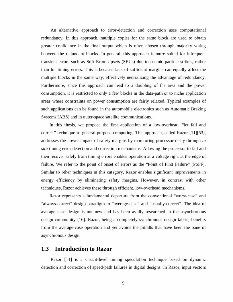
The operational principle of Razor is illustrated in Figure 1.2 which shows the
qualitative relationship between the supply voltage, energy consumption and pipeline
throughput of a Razor-enabled processor. The voltage at the PoFF of the processor (Vff)
and the minimum allowable voltage of traditional techniques (Vmargin) are also labeled in
the figure. Vmargin is much higher than Vff under typical conditions, since safety margins
need to be included to accommodate for worst-case operating conditions. Razor relies on
in situ error detection and correction capability to operate at Vff, rather than at Vmargin.
The total energy of the processor (Etot) is the sum of the energy required to perform
standard processor operations (Eproc) and the energy consumed in recovery from timing
errors (Erecovery). Of course, implementing Razor incurs power overhead due to which the
nominal processor energy (Enom) without Razor technology is slightly less than Eproc. This
overhead is attributed to the use of delay-error tolerant flip-flops on the critical paths and
the additional recovery logic required for Razor. However, since the extra circuitry is
deployed only for those flip-flops which have critical paths terminating in them, the
power overhead due to Razor is fairly minimal. In the two Razor prototypes that we
present subsequently in this thesis, the net power overhead due to Razor was less than 3%
of the nominal chip power.
As the supply voltage is scaled, the processor energy (Eproc) reduces quadratically
with voltage. However, as voltage is scaled below the first failure point (Vff), a
significant number of paths fail to meet timing. Hence, the error rate and the recovery
energy (Erecovery) increase exponentially. The processor throughput also reduces due to the
increasing error rate because the processor now requires more cycles to complete the
12
instructions. The total processor energy (Etot) shows an optimal point where the rate of
change of Erecovery and Eproc offset each other.
It was previously observed that circuit delay is strongly data-dependent, and only
exhibits its worst-case delay for very specific instruction and data sequences [11]. From
this, it can be conjectured that for moderately sub-critical supply voltages only a few
critical instructions will fail, while a majority of instructions will continue to operate
correctly. Our hardware measurements and circuit simulation studies support this
conjecture and demonstrate that the circuit operation degrades gracefully for sub-critical
supply voltages, showing a gradual increase in the error rate. The proposed Razor
approach automatically exploits this data-dependence of circuit delay by tuning the
supply voltage to obtain a small, but non-zero error rate. It was found that if the error rate
is maintained sufficiently low, the power overhead from error correction is minimal,
while substantial power savings are obtained due to operating the circuit at a lower
supply voltage. Note that as the processor executes different sets of instructions, the
supply voltage automatically adjusts to the delay characteristics of the executed
instruction sequence, lowering the supply voltage for instruction sequences with many
non-critical instructions, and raising the supply voltage for instruction sequences that are
more delay intensive.
1.4 Main contributions and organization of the thesis
This thesis develops the idea of Razor through two different implementation
techniques which we refer to as RazorI and RazorII, respectively.
• The RazorI approach relies on a double-sampling Razor flip-flop for error-
detection. In this technique, the critical-path output is sampled at two different
points in time. The earlier, speculative sample is captured at the rising edge of the
clock in the main flip-flop. The latter, always-correct sample is captured at a
delayed clock-edge (we use the falling edge for convenience of implementation) in
a so-called shadow-latch. A metastability-tolerant comparator then flags an error
when both samples disagree. Once an error signal is flagged, a circuit-based
technique to engaged to recover correct state within the flip-flop. Pipeline recovery
is achieved through a micro-architectural technique that restores correctness. We

13
propose two approaches based on either clock-gating or on counter-flow pipeline
architecture [38] for pipeline recovery. We designed a 64bit microprocessor that
uses RazorI for supply voltage control. We obtained, on an average, 50% energy
savings through eliminating design margins and operating at 0.1% error-rate, at
120MHz.
• The RazorII approach was developed with the need to address the key issues and
weaknesses in the RazorI technique which impairs its applicability to high-
performance micro-processors. RazorII differs significantly from RazorI in that it
moves the responsibility of recovery entirely into the micro-architectural domain.
Error-detection is achieved within the RazorII flip-flop by monitoring the critical
endpoints for spurious transitions. Recovery is achieved by replay from a check-
pointed state. As we show in Chapter 5, the RazorII flip-flop naturally detects
Single Event Upsets (SEU) in combinational logic and inside latches. We
implemented RazorII based voltage control on a 64bit microprocessor and obtained
33% energy savings, on an average. In addition, we demonstrated correct processor
operation in the presence of neutron irradiation, using RazorII for SEU tolerance.
The remainder of this thesis is organized as follows. In Chapter 2, we survey the
different adaptive techniques described in literature and analyze the margins eliminated
by each of them. Chapter 3 introduces the concept of error-detection and recovery in the
RazorI technique. In Chapter 4, we present measurement results on silicon from a 64bit
Alpha processor that uses RazorI for supply voltage control. We discuss the key
weaknesses of RazorI in Chapter 5 and propose RazorII as a low-overhead alternative to
RazorI. Chapter 6 deals with different techniques that address the minimum delay
requirement (explained in Chapter 3) in Razor. In Chapter 7, we present silicon
measurement results on a RazorII prototype and demonstrate correct operation in
presence of neutron irradiation. Finally, we summarize this thesis in Chapter 8 and
conclude with directions on future research.

14
CHAPTER 2
ADAPTIVE DESIGN TECHNIQUES
Adaptive techniques tune system parameters based on variations in silicon-grade and
ambient conditions. Instead of using a single operating voltage and frequency point for all
dies, adjusting system parameters enables such techniques to deliver better energy-
efficiency through the elimination of a sub-set of worst-case safety margins. As
mentioned in the Introduction, adaptive techniques can be broadly classified into two
main categories, which we refer to as the “always correct” and the “let fail and correct”
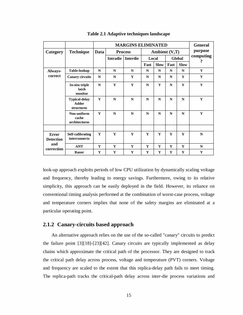
approaches. Table 2.1 lists the different adaptive architectures discussed in literature and
the margins eliminated by each of them. In the remainder of this chapter, we discuss each
of these techniques in greater detail. We focus on “always correct” approaches in Section
2.1 and discuss “let fail and correct” approaches in Section 2.2.
2.1 “Always Correct” Techniques
The key idea in the “always correct” techniques is to predict the operational point
where the critical-path fails to meet timing and to guarantee correctness by adding safety
margins to the predicted failure point. The conventional approach of predicting this point
of failure is to use either a look-up table or so-called “canary” circuits.
2.1.1 Look-up table based approach
In the look-up table based approach [14][13][15], the processor is pre-characterized
during design-time to obtain its maximum obtainable frequency for a given supply
voltage. The safe voltage-frequency pairs are obtained by performing conventional
timing analysis on the processor. Typically, the operating frequency is decided based on
the deadline under which a given computational task needs to be completed. Accordingly,
the supply voltage corresponding to the frequency requirement is “dialed in”. The table
15
look-up approach exploits periods of low CPU utilization by dynamically scaling voltage
and frequency, thereby leading to energy savings. Furthermore, owing to its relative
simplicity, this approach can be easily deployed in the field. However, its reliance on
conventional timing analysis performed at the combination of worst-case process, voltage
and temperature corners implies that none of the safety margins are eliminated at a
particular operating point.
2.1.2 Canary-circuits based approach
An alternative approach relies on the use of the so-called "canary" circuits to predict
the failure point [3][18]-[23][42]. Canary circuits are typically implemented as delay
chains which approximate the critical path of the processor. They are designed to track
the critical path delay across process, voltage and temperature (PVT) corners. Voltage
and frequency are scaled to the extent that this replica-delay path fails to meet timing.
The replica-path tracks the critical-path delay across inter-die process variations and
Table 2.1 Adaptive techniques landscape
YYYYYYYYRazor
NYYYYYYYANT
NYYYYYYYSelf-calibrating interconnects
Error Detection
and correction
YNNNNNNYNon-uniform cache
architectures
YNNNNNNYTypical-delay Adder
structures
YYNYNYYNIn-situ triple latch
monitor
YYNNNYNNCanary circuits
YNNNNNNNTable-lookupAlways-correct
SlowFastSlowFast
GlobalLocalInterdieIntradie
Ambient (V,T)ProcessDataTechniqueCategory
General purpose
computing?
MARGINS ELIMINATED
16
global fluctuations in supply voltage and temperature, thereby eliminating margins due to
global PVT variations (Table 1.1). However, the replica-path does not share the same
ambient environment as the critical-path since their on-die location differs. Consequently,
margins are added to the replica-path in order to budget for delay mismatches due to on-
chip variation and local fluctuations in temperature and supply voltage. Margins are also
required to address fast-changing transient effects, such as coupling noise effects, which
are difficult to respond to in time using this approach. Furthermore, mismatches in the
scaling characteristics of the critical-path and its replica require additional safety margins.
These margins ensure that the processor still operates correctly at the point of failure of
the replica-path.
There are several systems reported in literature based on canary-circuits. One
approach uses the replica path as a delay-reference for a voltage-controlled oscillator
(VCO) unit. The VCO monitors the delay through the chain at a given supply voltage and
scales the operating frequency to the point of failure of the replica-path. An example of
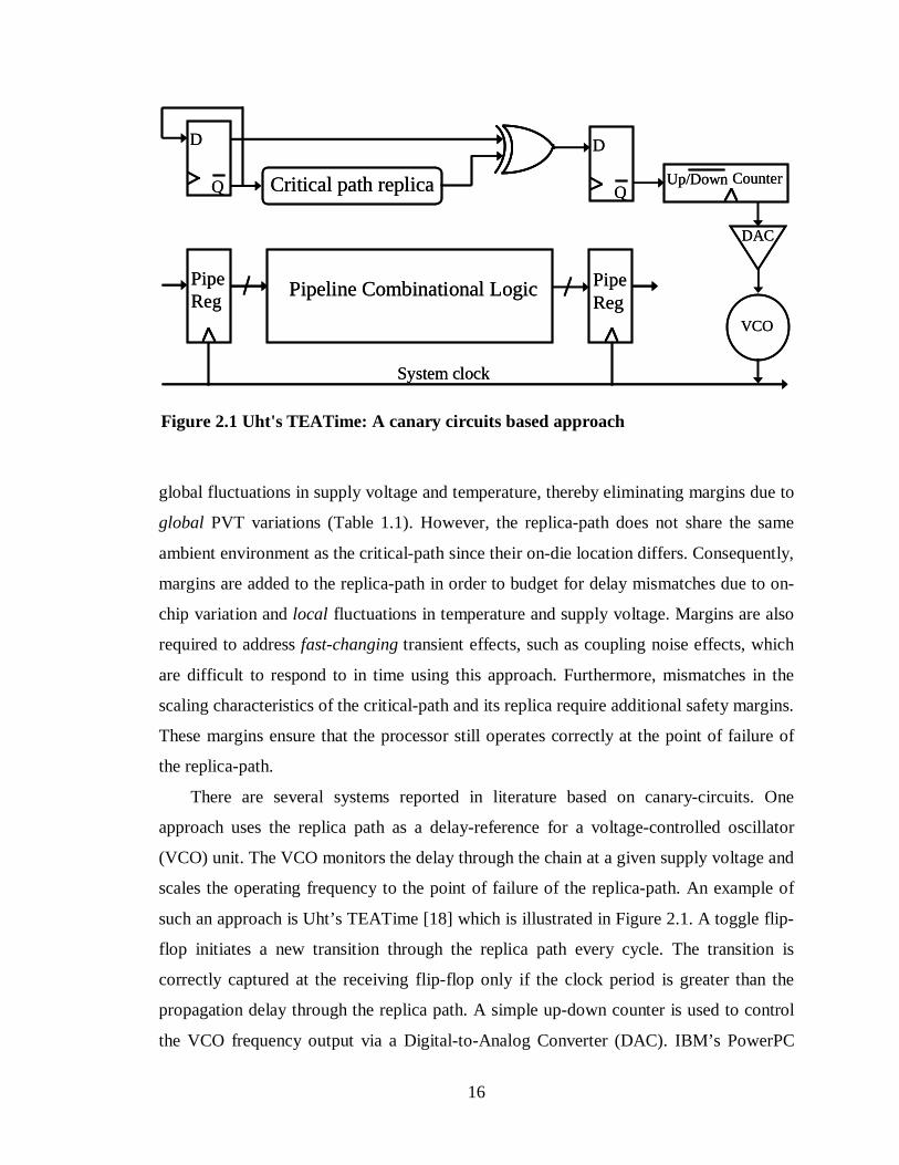
such an approach is Uht’s TEATime [18] which is illustrated in Figure 2.1. A toggle flip-
flop initiates a new transition through the replica path every cycle. The transition is
correctly captured at the receiving flip-flop only if the clock period is greater than the
propagation delay through the replica path. A simple up-down counter is used to control
the VCO frequency output via a Digital-to-Analog Converter (DAC). IBM’s PowerPC
Critical path replicaQ
D
Q
D
Up/DownCounter
DAC
VCO
System clock
Pipeline Combinational LogicPipeReg
PipeReg
Critical path replicaQ
D
Q
D
Up/DownCounter
DAC
VCO
System clock
Pipeline Combinational LogicPipeReg
PipeReg
Figure 2.1 Uht's TEATime: A canary circuits based approach

17
System-on-chip design reported in [19] and the Berkeley Wireless Research Center’s [22]
[21] low-power microprocessor are all based on a similar concept. An alternative
approach, developed by Sony and reported in [23], uses a delay-synthesizer unit
consisting of several delay chains which selects a safe frequency depending on the
maximum propagation-delay through the chains. Typically, canary circuits enable better
energy efficiency than the table look-up approach because unlike the latter, they are able
to eliminate margins due to slow-changing, global variations (Table 1.1) such as inter-die
process variations and global fluctuations in voltage and temperature.
2.1.3 In situ triple-latch monitor
Kehl’s Triple-Latch Monitor is similar to the canary-circuits based techniques, but
utilizes in situ monitoring of circuit delay [24]. Using this approach, all monitored system
state is sampled at three different latches with a small delay interval between each
sampling point, as shown in Figure 2.2(a). The value in the latest-clocked latch which is
allowed the most time is assumed correct and is always forwarded to later logic. The
system is considered “tuned” (Figure 2.2b) when the first latch does not match the second
and third latch values, meaning that the logic transition was very near the critical speed,
EQ0 EQ1 EQ2
CK0 CK1 CK2
INCOMING DATA
To System
Td Td
S0 S1 S2
CK0
CK1
CK2
D
EQ0
EQ1
EQ2
CK
a) b)
Figure 2.2 Kehl’s triple-latch technique for in situ delay monitoring. Figure a) shows the mechanism of monitoring delay through temporal redundancy. Figure b) shows the timing diagrams for a “tuned” system

18
but not dangerously close. If all latches see the same value, the system is running too
slowly and frequency should be increased. If the first two latches see different values
than the last, then the system is running dangerously fast and should be slowed down.
Because of the in situ nature of this approach, it can adjust to local variations such as
intra-die process and temperature variations. However, it still cannot track fast-changing
conditions such as cross-coupling and voltage noise events. Hence, the delay between the
successive samples has to be sufficiently separated to allow for margins for such events.
In addition, to avoid overly aggressive clocking, evaluations of the latch values must be
limited to tests using worst-cast latency vectors. Kehl suggests that the system should
periodically stop and test worst-case vectors to determine if the system requires tuning.
This requirement severely limits the general applicability of this approach since vectors
that account for the worst-case delay and coupling noise scenario are difficult to generate,
and exercise, for general-purpose processors.
2.1.4 Micro-architectural techniques
A potential short-coming of all the techniques discussed above is that they seek to
track variations in the critical-path delay and consequently, cannot adapt to input vector
dependent delay variations. The processor voltage and frequency is unnecessarily
constrained by the worst-case critical-path, even if it is rarely sensitized. This observation
b)a)
Figure 2.3 Data-dependent delay variations in adders a) Carry-propagation for SPECInt 2000 vectors b) Carry-propagation for random vectors [25]
19
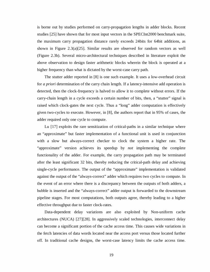
is borne out by studies performed on carry-propagation lengths in adder blocks. Recent
studies [25] have shown that for most input vectors in the SPECInt2000 benchmark suite,
the maximum carry propagation distance rarely exceeds 24bits for 64bit additions, as
shown in Figure 2.3(a)[25]. Similar results are observed for random vectors as well
(Figure 2.3b). Several micro-architectural techniques described in literature exploit the
above observation to design faster arithmetic blocks wherein the block is operated at a
higher frequency than what is dictated by the worst-case carry path.
The stutter adder reported in [8] is one such example. It uses a low-overhead circuit
for a priori determination of the carry chain length. If a latency-intensive add operation is
detected, then the clock-frequency is halved to allow it to complete without errors. If the
carry-chain length in a cycle exceeds a certain number of bits, then, a “stutter” signal is
raised which clock-gates the next cycle. Thus a “long” adder computation is effectively
given two-cycles to execute. However, in [8], the authors report that in 95% of cases, the
adder required only one cycle to compute.
Lu [17] exploits the rare sensitization of critical-paths in a similar technique where
an “approximate” but faster implementation of a functional unit is used in conjunction
with a slow but always-correct checker to clock the system a higher rate. The
“approximate” version achieves its speedup by not implementing the complete
functionality of the adder. For example, the carry propagation path may be terminated
after the least significant 32 bits, thereby reducing the critical-path delay and achieving
single-cycle performance. The output of the “approximate” implementation is validated
against the output of the “always-correct” adder which requires two cycles to compute. In
the event of an error where there is a discrepancy between the outputs of both adders, a
bubble is inserted and the “always-correct” adder output is forwarded to the downstream
pipeline stages. For most computations, both outputs agree, thereby leading to a higher
effective throughput due to faster clock-rates.
Data-dependent delay variations are also exploited by Non-uniform cache
architectures (NUCA) [27][28]. In aggressively scaled technologies, interconnect delay
can become a significant portion of the cache access time. This causes wide variations in
the fetch latencies of data words located near the access port versus those located further
off. In traditional cache designs, the worst-case latency limits the cache access time.
20
However, NUCA allows early access times for addresses near the access port, thereby
achieving throughput improvement. Additional throughput can be achieved by mapping
frequently accessed data to banks located nearest to the access port. Thus, in the context
of NUCA, data-dependence of delay relates to the frequency with which an address in the
cache is accessed.
While the stutter adder and the NUCA architectures adapt to data-dependent
variations, they still require margins to account for slow silicon grade and worst-case
ambient conditions. On the contrary, “let fail and correct” approaches seek to achieve
both i.e. eliminate worst-case safety margins for all types of uncertainties and adapt to
data-dependent variations as well. However, they are more complex and incur additional
overhead in their implementation. Such approaches are discussed in detail in the next
section.
2.2 “Let fail and correct” approaches
The key concept of these schemes is to scale the system parameters (e.g. voltage and
frequency) till the point where the processor fails to meet timing, thereby leading to an
error. An error-detection block flags the occurrence of the timing error upon which a
recovery infrastructure is engaged to achieve correct state. To ensure that the system does
not deadlock due to persistent errors, an additional controller monitors the error-rate and
tunes voltage and frequency to achieve a targeted error rate.
Allowing the processor to fail and then recover eliminates worst-case safety
margins. This enables significantly greater performance and energy efficiency over
“always-correct” techniques. Furthermore, such techniques naturally exploit input vector
dependence of delay by relying on the error-rate for voltage and frequency tuning.
Instead of relying on safety margins, computational correctness is achieved through
successful detection and correction of timing errors. The net energy consumption of the
system is essentially a trade-off between the increased efficiency afforded by the
elimination of margins and the additional overhead of recovery. Of course, the overhead
of recovery can make sustaining a high error-rate counterproductive. Hence, these
systems typically rely on restricting operation to low error-rate regimes to maximize
energy efficiency.
21
Their relative complexity makes the general applicability of such systems difficult.
However, they are naturally amenable for certain applications areas such as
communications and signal processing. Communication systems require error correction
to reliably transfer information across a noisy channel. Therefore, it is relatively easier to
overload the existing error correction infrastructure to enable adaptivity to variable
silicon and ambient conditions. Self-calibrating interconnects by Worm et al. [29] and
Algorithmic Noise Tolerance by Shanbhag et al. [30] are examples of applications of
such techniques to on-chip communication and signal processing architectures.
2.2.1 Techniques for communication and signal processing
Self-calibrating interconnects (Figure 2.4) address the problem of reliable on-chip
communication in aggressively scaled technologies. Signal integrity concerns require on-
chip busses to be strongly buffered which consumes a significant portion of the total chip
power. Hence, it is desirable to transfer bits at the lowest possible operating voltage while
still guaranteeing the required performance and the targeted bit-error-rate (BER). Worm
[29] addresses this issue by encoding the data words with so-called self synchronizing
codes before transmission. The receiver is augmented with a checker unit that decodes
the received code word and flags timing errors. Correction occurs by requesting re-
FIFO
ddV
ControllerE
ncod
er
Dec
ode
r Data
error
Fcomm
Vcomm
ARQretransmit
FIFO
ddV
ControllerE
ncod
er
Dec
ode
r Data
error
Fcomm
Vcomm
ARQretransmit
Figure 2.4 Self-calibrating interconnects
22
transmission through an Automatic Repeat Request (ARQ) block, as shown in Figure 2.4.
Furthermore, an additional controller obtains feedback from the checker and accordingly
adjusts the voltage and the frequency of the transmission. By reacting to the error-rates,
the controller is able to adapt to the operating conditions and thus eliminate worst-case
safety margins. This improves the energy efficiency of the on-chip busses with negligible
BER degradation.
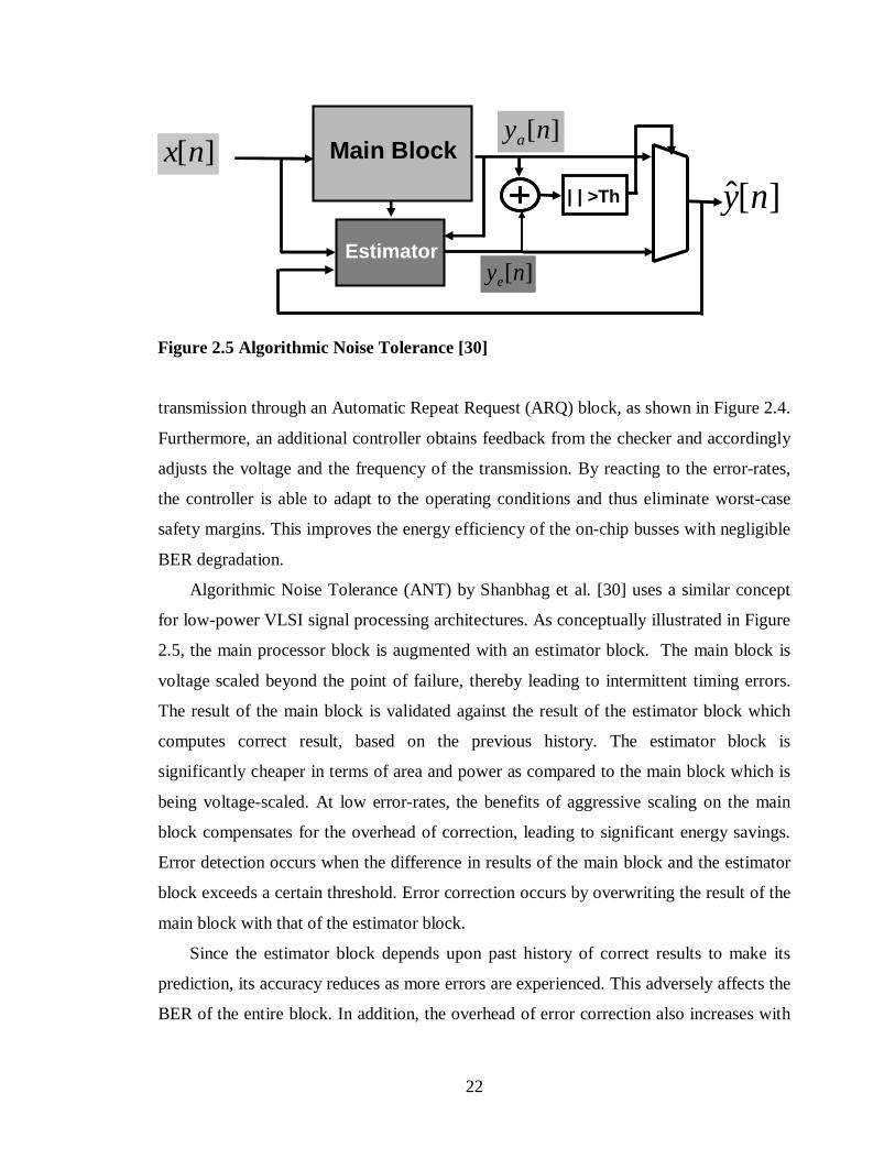
Algorithmic Noise Tolerance (ANT) by Shanbhag et al. [30] uses a similar concept
for low-power VLSI signal processing architectures. As conceptually illustrated in Figure
2.5, the main processor block is augmented with an estimator block. The main block is
voltage scaled beyond the point of failure, thereby leading to intermittent timing errors.
The result of the main block is validated against the result of the estimator block which
computes correct result, based on the previous history. The estimator block is
significantly cheaper in terms of area and power as compared to the main block which is
being voltage-scaled. At low error-rates, the benefits of aggressive scaling on the main
block compensates for the overhead of correction, leading to significant energy savings.
Error detection occurs when the difference in results of the main block and the estimator
block exceeds a certain threshold. Error correction occurs by overwriting the result of the
main block with that of the estimator block.
Since the estimator block depends upon past history of correct results to make its
prediction, its accuracy reduces as more errors are experienced. This adversely affects the
BER of the entire block. In addition, the overhead of error correction also increases with
][nx][nyaMain Block
Estimator
][ˆ ny| | >Th
][nye
Figure 2.5 Algorithmic Noise Tolerance [30]

23
increase in the error-rate. Hence, it is desirable to keep the rate of timing errors low for
maintaining a low BER and high energy efficiency. The authors built a FIR filter in 0.35
micron technology [30] to demonstrate the efficacy of this technique. They obtained at
least 70% savings over an error-free design for a 1% reduction in the Signal to Noise
(SNR) ratio of the final output.
By reacting to error-rates, both of the above techniques are able to exploit data-
dependent delay variations because even under aggressively scaled voltage and frequency
conditions, it is possible to maintain a low error-rate as long as the critical paths are not
being sensitized.
2.2.2 Techniques for general-purpose computing
“Let fail and correct” approaches are naturally suited for communication applications
which use algorithms that have built-in support for error-correction to deal with data
corruption. The quality of output for most signal processing applications is largely
statistical and the data itself possesses significant amount of temporal and spatial
redundancy that naturally facilitates error correction. Errors do not affect the correct
functionality of the system and lead to a negligible degradation of the Bit Error Rate
(BER), at worst. However, in general-purpose computing the committed architectural
state necessarily has to be always correct. Therefore, all timing errors that can alter the
architectural state need to be flagged and corrected. Unlike in communication and signal
processing applications, corruption of the architectural state in general-purpose
computing leads to system failure and needs to be avoided at all costs.
Razor [11] is the first application of a “let fail and correct” technique to general-
purpose computing. Razor uses temporal redundancy for error-detection as described in
subsequent chapters. In this thesis, we describe two techniques for implementing Razor.
In the RazorI technique (Chapter 3), a critical path signal is speculatively sampled at the
rising edge of the regular clock and is compared against a shadow latch which samples at
a delayed edge. A timing error is flagged when the speculative sample does not agree
with the delayed sampled. State correction involves overwriting the shadow latch data
into the main flip-flop and engaging micro-architectural recovery features to recover
correct state. Unlike the RazorI technique which relies on state comparison, RazorII
24
(Chapter 5) achieves error-detection by monitoring the critical-path output for spurious
transitions. Recovery is achieved by re-execution from a check-pointed state. We discuss
RazorI and RazorII in greater detail in the next chapter onwards.
The idea of temporal redundancy for error detection has been used previously in the
design and test community for at-speed delay testing. Anghel and Nicolaidis [31] use a
similar concept for detecting SEU failures in combinational logic. A cosmic particle
strike in the combinational logic manifests itself as a pulse which can get captured by
downstream flip-flops. The authors detect such an event by re-sampling the flip-flop
input after the pulse has died down. A discrepancy between the two samples indicates a
SEU event in the combinational logic. This technique is limited to error detection and
does not enable recovery which restricts its applicability to SEU detection only.
2.3 Summary and discussion
In this chapter, we surveyed the different adaptive techniques presented in literature. We
broadly classified such techniques as “always-correct” approaches and “let fail and
correct” approaches. Always-correct techniques use failure prediction techniques such as
pre-characterized look-up tables and canary circuits to approach the PoFF as close as
possible, without risking failure. However, doing so requires safety margins especially
for local variations. As process technology scales, local variations are expected to
worsen, thereby undermining the efficacy of always-correct techniques at aggressive
geometries.
“Let fail and correct” approaches use error-detection and correction mechanisms to
operate around the PoFF while deliberately incurring errors. We surveyed two
representative approaches related to wireless communication (Algorithmic Noise
Tolerance) and on-chip communication (Self-calibrating interconnects) that trade-off
error-rate for increased energy efficiency of operation. Unlike signal-processing
applications, general-purpose computing is not naturally resilient to errors. Consequently,
such techniques have rarely found application in the general-purpose domain.
This thesis describes Razor which is the first low-overhead application of a “let fail
and correct” approach to general-purpose computing. In the subsequent chapters, we
develop the Razor concept and present two implementation techniques, called RazorI and

25
RazorII, for deployment of Razor in micro-processors. Chapter 3 discusses the key ideas
in Razor and describes the RazorI technique.

26
CHAPTER 3
RAZOR I: STATE COMPARISON BASED ERROR-DETECTION AND CIRCUIT -ARCHITECTURAL RECOVERY
RazorI relies on a combination of architectural and circuit techniques to achieve
efficient error detection and correction of timing violations. Critical-path endpoints are
monitored using a delay-error tolerant RazorI flip-flop which samples its input at two
different points in time. The main flip-flop samples its input speculatively at the rising
clock-edge. It is augmented with a so-called shadow latch, controlled using a delayed
clock-edge, which samples the correct value of the data input. The operating voltage is
constrained such that the worst-case delay is guaranteed to meet the shadow latch setup
time, even though the main flip-flop could fail. By comparing the values latched by the
flip-flop and the shadow latch through a metastability-tolerant comparator, a delay error
in the main flip-flop is detected. The value in the shadow latch, which is guaranteed to be
correct, is then overwritten into the main flip-flop to achieve recovery. At the same time a
pipeline recovery mechanism is initiated as well.
The rest of the chapter is organized as follows. In Section 3.1, we develop the
concept of RazorI error detection and recovery. Section 3.2 deals with the transistor level
design details of the RazorI flip-flop. In Section 3.3, we present several architectural
solutions for error correction, ranging from simple clock gating to more sophisticated
mechanisms that augment the existing mis-speculation recovery infrastructure. Section
3.4 deals with supply voltage control in RazorI. Section 3.5 briefly mentions the
measurement results that we obtained from a self-tuning processor built to evaluate
RazorI. Finally, we give a succinct summary of this chapter in Section 3.6.
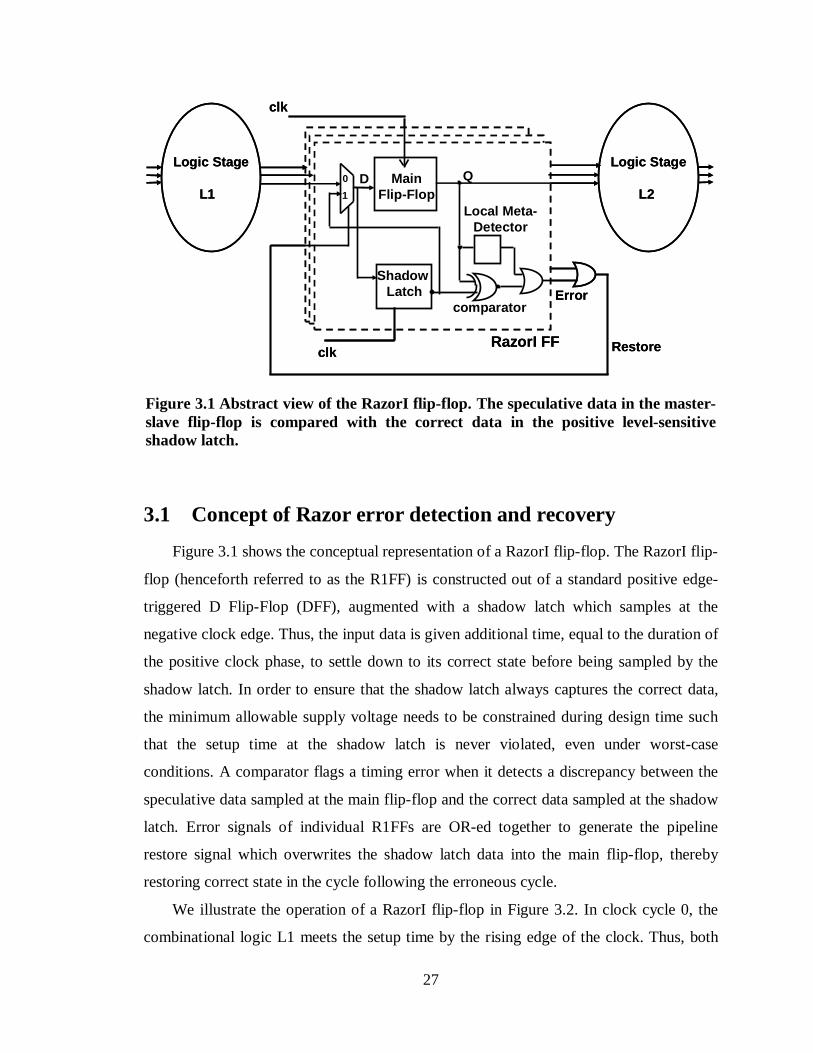
27
3.1 Concept of Razor error detection and recovery
Figure 3.1 shows the conceptual representation of a RazorI flip-flop. The RazorI flip-
flop (henceforth referred to as the R1FF) is constructed out of a standard positive edge-
triggered D Flip-Flop (DFF), augmented with a shadow latch which samples at the
negative clock edge. Thus, the input data is given additional time, equal to the duration of
the positive clock phase, to settle down to its correct state before being sampled by the
shadow latch. In order to ensure that the shadow latch always captures the correct data,
the minimum allowable supply voltage needs to be constrained during design time such
that the setup time at the shadow latch is never violated, even under worst-case
conditions. A comparator flags a timing error when it detects a discrepancy between the
speculative data sampled at the main flip-flop and the correct data sampled at the shadow
latch. Error signals of individual R1FFs are OR-ed together to generate the pipeline
restore signal which overwrites the shadow latch data into the main flip-flop, thereby
restoring correct state in the cycle following the erroneous cycle.
We illustrate the operation of a RazorI flip-flop in Figure 3.2. In clock cycle 0, the
combinational logic L1 meets the setup time by the rising edge of the clock. Thus, both
Errorcomparator
RazorI FF
Main Flip-Flop
clk
clk
Shadow Latch
QLogic Stage
L1
Logic Stage
L2 0
1
D
Restore
Local Meta-Detector
Errorcomparator
RazorI FF
Main Flip-Flop
clk
clk
Shadow Latch
QLogic Stage
L1
Logic Stage
L2 0
1
D
Restore
Local Meta-Detector
Figure 3.1 Abstract view of the RazorI flip-flop. The speculative data in the master-slave flip-flop is compared with the correct data in the positive level-sensitive shadow latch.

28
the main flip-flop and the shadow latch will latch the correct data. In this case, the error
signal at the output of the comparator remains low and the operation of the pipeline is
unaltered. In cycle 1, we show an example of the operation when the combinational logic
exceeds the intended delay due to sub-critical voltage scaling. In this case, the data is not
latched correctly by the main flip-flop, but since the shadow-latch samples at the negative
edge of the clock, it successfully latches the data half-way through cycle 2. By comparing
the valid data of the shadow latch with the data in the main flip-flop, an error signal is
then generated in cycle 2. Error signals of individual R1FFs are OR-ed together to
generate the pipeline restore signal which overwrites the shadow latch data into the main
flip-flop, thereby restoring correct state at the positive edge of the subsequent cycle, cycle
4.
If an error occurs in pipeline stage L1 in a particular clock cycle, the data in L2 in the
following clock cycle is incorrect and must be flushed from the pipeline using one of the
pipeline control methods described in Section 3.3. However, since the shadow latch
contains the correct output data of pipeline stage L1, the instruction does not need to be
re-executed through this failing stage. Thus, a key feature of RazorI is that if an
Clk
Min PathD_in
Error
Restore
Q
Cycle 1 Cycle 2 Cycle 3 Cycle 4 Cycle 5
Td
Thold
Qshadow
Cycle 0
Clk
Min PathD_in
Error
Restore
Q
Cycle 1 Cycle 2 Cycle 3 Cycle 4 Cycle 5
Td
Thold
Qshadow
Cycle 0
Figure 3.2 Conceptual timing diagrams showing the operation of the RazorI flip-flop. In Cycle 2, a setup violation causes Error to be flagged whereas in Cycle 4, a hold violation causes error to be asserted.
29
instruction fails in a particular pipeline stage it is re-executed through the following
pipeline stage, while incurring a one cycle penalty. The proposed approach therefore
guarantees forward progress of a failing instruction, which is essential to avoid the
perpetual failure of an instruction at a particular stage in the pipeline.
Using the negative edge of the clock as the sampling trigger for the shadow latch
precludes the need for an additional clock tree. This simplifies implementation because
only a single clock is required and prevents the excessive overhead of routing a second
clock tree just for the purposes of clocking the shadow latch in the R1FFs. The duration
of the positive clock phase, when the shadow latch is transparent, determines the
sampling delay of the shadow latch. This constrains the minimum propagation delay for a
combinational logic path terminating in a R1FF to be at least greater than the duration of
the positive clock phase and the hold time of the shadow latch. Figure 3.2 conceptually
illustrates this minimum delay constraint. In cycle 4, the R1FF input, D_in, violates this
constraint and changes state before the negative edge of the clock, thereby corrupting the
state of the shadow latch. Delay buffers are required to be inserted in those paths which
fail to meet this minimum path delay constraint imposed by the shadow latch.
The insertion of delay buffers incurs power overhead because of the extra
capacitance added. A large shadow latch sampling delay requires a greater number of
delay buffers to be inserted, thereby increasing the power overhead. However, a small
sampling delay implies that the voltage difference between the point of first failure and
the point where shadow latch fails is less and, thus, reduces the voltage margin available
through Razor timing speculation. Hence, the shadow latch sampling delay represents the
trade-off between power overhead due to delay buffers and the voltage margin available
for Razor sub-critical mode of operation. Using suitable clock chopping techniques, the
duration of the positive phase of the propagated clock can be configured as required so as
to exploit the above trade-off.
A key point to note is the fact that the hold constraint imposed by the shadow latch
only limits the maximum duration of the positive clock phase and has no bearing upon
the clock frequency. Thus, a RazorI pipeline can still be operated at any frequency as
required as long as the positive clock phase is sufficient to meet the minimum path delay
constraint. In the prototype RazorI processor that we present in Chapter 4, for a sampling

30
delay of 3.0ns which is approximately half the cycle time at 140MHz, it was required to
add 2388 delay buffers to satisfy the short path constraint on 207 R1FFs (7.4% of the
total number of flip-flops). The power overhead due to these buffers was less than 3% of
the nominal chip power.
Since setup and hold constraints at the main flip-flop input (D_in) are not respected,
it is possible that the state of the flip-flop becomes metastable. A metastable signal
increases critical path delay which can cause a shadow latch in the succeeding pipeline
stage to capture erroneous data, thereby leading to incorrect execution. In addition, a
metastable flip-flop output can be inconsistently interpreted by the error comparator and
the downstream logic. Hence, an additional detector is required to correctly flag the
occurrence of metastability at the output of the main flip-flop. The outputs of the
metastability-detector and the error comparator are OR-ed to generate the error signal of
the R1FF. Thus, the system reacts to the occurrence of metastability in exactly the same
way as it reacts to a conventional timing failure.
A key point to note is the fact that metastability need not be resolved correctly in the
R1FF and that just the detection of such an occurrence is sufficient to engage the RazorI
recovery mechanism. However, in order to prevent potentially metastable signals from
being committed to memory, at least two successive non-critical pipeline stages are
required immediately before storage. This ensures that every signal is validated by RazorI
and is effectively double-latched in order to have a negligible probability of being
metastable, before being written to memory. In our design, data accesses in the Memory
stage were non-critical and hence we required only one additional pipeline stage to act as
a dummy stabilization stage. The circuit level implementation of the metastability-
detector is discussed in greater detail in Section 3.2.
In addition to invalidating the data in the following pipeline stage, an error must also
stall the preceding pipeline stages while the shadow latch data is restored into the main
flip-flops. A number of different methods, such as clock gating or flushing the instruction
in the preceding stages, were examined to accomplish this and are discussed in Section
3.3. The proposed approach also raises a number of circuit related issues. The RazorI
flip-flop must be constructed such that the power and delay overhead is minimized.
Suitable circuits for detecting and flagging metastability need to be designed. These
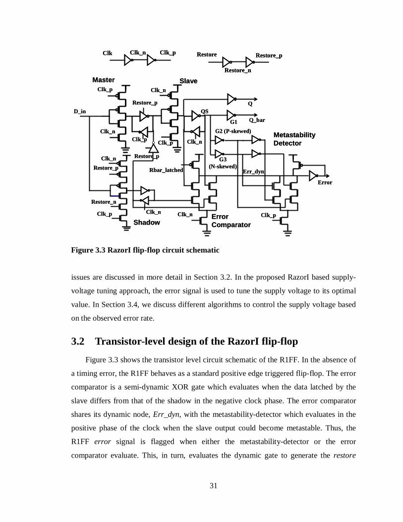
31
issues are discussed in more detail in Section 3.2. In the proposed RazorI based supply-
voltage tuning approach, the error signal is used to tune the supply voltage to its optimal
value. In Section 3.4, we discuss different algorithms to control the supply voltage based
on the observed error rate.
3.2 Transistor-level design of the RazorI flip-flop
Figure 3.3 shows the transistor level circuit schematic of the R1FF. In the absence of
a timing error, the R1FF behaves as a standard positive edge triggered flip-flop. The error
comparator is a semi-dynamic XOR gate which evaluates when the data latched by the
slave differs from that of the shadow in the negative clock phase. The error comparator
shares its dynamic node, Err_dyn, with the metastability-detector which evaluates in the
positive phase of the clock when the slave output could become metastable. Thus, the
R1FF error signal is flagged when either the metastability-detector or the error
comparator evaluate. This, in turn, evaluates the dynamic gate to generate the restore
Restore_p
Restore_n
Clk_n
Restore_p
D_in
Q_bar
Q
Clk_p
Clk_n
Clk_n
Clk_n
Clk_p
Restore_p
Clk_n
Rbar_latched
G2 (P-skewed)Clk_p Clk_p Clk_n
Clk Clk_pClk_n Restore
Restore_n
Restore_p
Master Slave
Shadow Error Comparator
QS
Clk_p
Error
Metastability Detector
Err_dyn
G1
G3 (N-skewed)Restore_p
Restore_n
Clk_n
Restore_p
D_in
Q_bar
Q
Clk_p
Clk_n
Clk_n
Clk_n
Clk_p
Restore_p
Clk_n
Rbar_latched
G2 (P-skewed)Clk_p Clk_p Clk_n
Clk Clk_pClk_n Restore
Restore_n
Restore_p
Master Slave
Shadow Error Comparator
QS
Clk_p
Error
Metastability Detector
Err_dyn
G1
G3 (N-skewed)
Figure 3.3 RazorI flip-flop circuit schematic
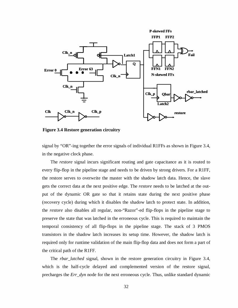
32
signal by “OR”-ing together the error signals of individual R1FFs as shown in Figure 3.4,
in the negative clock phase.
The restore signal incurs significant routing and gate capacitance as it is routed to
every flip-flop in the pipeline stage and needs to be driven by strong drivers. For a R1FF,
the restore serves to overwrite the master with the shadow latch data. Hence, the slave
gets the correct data at the next positive edge. The restore needs to be latched at the out-
put of the dynamic OR gate so that it retains state during the next positive phase
(recovery cycle) during which it disables the shadow latch to protect state. In addition,
the restore also disables all regular, non-“Razor”-ed flip-flops in the pipeline stage to
preserve the state that was latched in the erroneous cycle. This is required to maintain the
temporal consistency of all flip-flops in the pipeline stage. The stack of 3 PMOS
transistors in the shadow latch increases its setup time. However, the shadow latch is
required only for runtime validation of the main flip-flop data and does not form a part of
the critical path of the R1FF.
The rbar_latched signal, shown in the restore generation circuitry in Figure 3.4,
which is the half-cycle delayed and complemented version of the restore signal,
precharges the Err_dyn node for the next erroneous cycle. Thus, unlike standard dynamic
Error 0 Error 63
Clk_n
Clk_n
Clk_n
Clk_p
Q
Latch1
rbar_latched
restore
Qbar
Latch2
Clk Clk_pClk_n
P-skewed FFs
N-skewed FFs
Fail
FFP1 FFP2
FFN1 FFN2Error 0 Error 63
Clk_n
Clk_n
Clk_n
Clk_p
Q
Latch1
rbar_latched
restore
Qbar
Latch2
Clk Clk_pClk_n
P-skewed FFs
N-skewed FFs
Fail
FFP1 FFP2
FFN1 FFN2
Figure 3.4 Restore generation circuitry

33
gates where precharge takes place every cycle, the Err_dyn node is conditionally
precharged in the recovery cycle following a Razor error. Precharge can take place
without contention because in this cycle the slave latch has exactly the same data as the
shadow latch and is guaranteed not to be metastable. Hence, neither the error comparator
nor the metastability-detector evaluates. A weak PMOS half-latch protects Err_dyn from
discharge due to leakage.
The R1FF was compared with a standard DFF for power consumption at 0.18µm
technology. Both are designed for the same delay (clk-q delay + setup time) and drive
strength. The characterization setup consists of the flip-flop under test driving a FO4
capacitive load. The clock and the input data are each driven by signals with a 100ps
transition time and with sufficient delay between transitions on the data and the clock so
as not to violate setup time. The R1FF was found to consume 22% extra (60fJ/ 49fJ)
energy when the sampled data does not change state and 65% extra (205fJ/124fJ) energy
when sampled data switches. However, in our processor only 207 flip-flops out of 2801
flip-flops, or 7.4%, had critical paths terminating in them and needed use of R1FFs. The
measured power of the processor at 120MHz at 25C for a supply voltage of 1.8V was
130mW. A simulation based power analysis was performed to compute the power
overhead of the R1FFs and the delay buffers required to meet the short path constraint.
For a conservative activity factor of 20%, the net power overhead due to R1FFs was
0.31% and that due to delay buffers was 2.6%. Thus, the total power overhead due to
RazorI was computed to be less than 3% of the nominal chip power. Thus, most of the
additional power due to RazorI is attributed to the delay buffers added for meeting the
short path constraint.
3.2.1 Metastability detection
As was mentioned in Section 3.2, metastability can potentially cause incorrect
execution because of inconsistent interpretation and increase in propagation delay. We,
therefore, perform metastability detection at the R1FF node QS (as labeled in Figure 3.3)
because QS fans out to the flip-flop driver G1 and the error comparator and thus, directly
affects the R1FF outputs, namely Q and error.
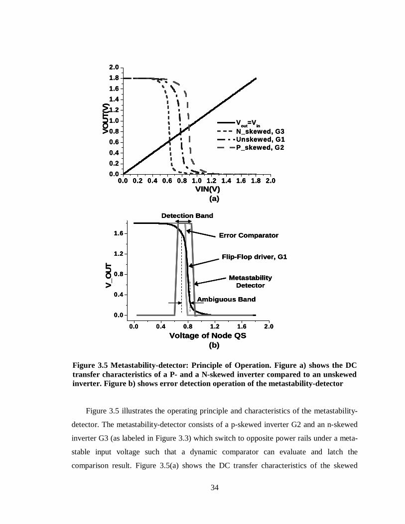
34
Figure 3.5 illustrates the operating principle and characteristics of the metastability-
detector. The metastability-detector consists of a p-skewed inverter G2 and an n-skewed
inverter G3 (as labeled in Figure 3.3) which switch to opposite power rails under a meta-
stable input voltage such that a dynamic comparator can evaluate and latch the
comparison result. Figure 3.5(a) shows the DC transfer characteristics of the skewed
(a)VIN(V)
0.0 0.2 0.4 0.6 0.8 1.0 1.2 1.4 1.6 1.8 2.00.0
0.2
0.4
0.6
0.8
1.0
1.2
1.4
1.6
1.8
2.0
Vout
=Vin
N_skewed, G3 Unskewed, G1 P_skewed, G2
VO
UT(V
)
0.0 0.4 0.8 1.2 1.6 2.0
0.0
0.4
0.8
1.2
1.6
Voltage of Node QS
V_O
UT
Detection Band
Ambiguous Band
Error Comparator
Flip-Flop driver, G1
MetastabilityDetector
(b)
(a)VIN(V)
0.0 0.2 0.4 0.6 0.8 1.0 1.2 1.4 1.6 1.8 2.00.0
0.2
0.4
0.6
0.8
1.0
1.2
1.4
1.6
1.8
2.0
Vout
=Vin
N_skewed, G3 Unskewed, G1 P_skewed, G2
VO
UT(V
)
VIN(V)0.0 0.2 0.4 0.6 0.8 1.0 1.2 1.4 1.6 1.8 2.0
0.0
0.2
0.4
0.6
0.8
1.0
1.2
1.4
1.6
1.8
2.0
Vout
=Vin
N_skewed, G3 Unskewed, G1 P_skewed, G2
VO
UT(V
)
0.0 0.4 0.8 1.2 1.6 2.0
0.0
0.4
0.8
1.2
1.6
Voltage of Node QS
V_O
UT
Detection Band
Ambiguous Band
Error Comparator
Flip-Flop driver, G1
MetastabilityDetector
0.0 0.4 0.8 1.2 1.6 2.0
0.0
0.4
0.8
1.2
1.6
Voltage of Node QS
V_O
UT
Detection Band
Ambiguous Band
Error Comparator
Flip-Flop driver, G1
MetastabilityDetector
(b)
Figure 3.5 Metastability-detector: Principle of Operation. Figure a) shows the DC transfer characteristics of a P- and a N-skewed inverter compared to an unskewed inverter. Figure b) shows error detection operation of the metastability-detector

35
inverters compared to that of the driver inverter, G1. The switching points are denoted as
the points where the 45 degree line intersects the DC transfer curves. We note that the
switching points for the p-skewed inverter and the n-skewed inverter lie on either side of
that for G1. During normal operation, when the output of the main flip-flop is logically
well defined, the output of G2 and G3 match. Thus, the comparator does not evaluate and
the dynamic node is not discharged. However, when QS is metastable at approximately
VDD/2, the output of the p-skewed inverter G2 is at a voltage level near VDD and the
output of the n-skewed inverter G3 is near ground. This causes the comparator to
evaluate and discharge the dynamic node, Err_dyn, thereby flagging the error signal.
It is imperative that the metastability-detector is guaranteed to evaluate for a voltage
range of the input node QS for which the fan-out of QS, namely the error comparator and
the flip-flop driver G1, have either logically undefined or logically inconsistent outputs.
This “ambiguous” band of voltage is defined as the voltage range for which the outputs
of either G1 or the error comparator are in between 10% to 90% of VDD. The range of
voltage for which the metastability-detector actually evaluates is defined to be the
“detection” band of voltage. Figure 3.5(b) shows the DC transfer curve of inverter G1,
the error comparator and the metastability-detector. As is clearly shown in the figure, the
“ambiguously” interpreted voltage band is contained well within the “detection” band.
Table 3.1 shows that the “detection” band subsumes the “ambiguous” band across
Table 3.1 Metastability-detector Corner Analysis
0.58-0.890.64-0.8127C1.8VFast
0.65-0.900.71-0.8340C1.8VTyp.
0.67-0.930.77-0.8785C1.8VSlow
0.40-0.610.48-0.5627C1.2VFast
0.48-0.610.52-0.5840C1.2VTyp.
0.53-0.640.57-0.6085C1.2VSlow
TEMPVDDProc
DetectionBand
AmbiguousBand
Corner
0.58-0.890.64-0.8127C1.8VFast
0.65-0.900.71-0.8340C1.8VTyp.
0.67-0.930.77-0.8785C1.8VSlow
0.40-0.610.48-0.5627C1.2VFast
0.48-0.610.52-0.5840C1.2VTyp.
0.53-0.640.57-0.6085C1.2VSlow
TEMPVDDProc
DetectionBand
AmbiguousBand
Corner

36
different process, voltage and temperature (PVT) corners to ensure correct operation
under all conditions. These characterization results are for a metastability-detector
designed in 0.18µm technology.
There is a certain delay between QS becoming metastable and the detector correctly
flagging such an occurrence. If QS remains metastable for a very small duration of time,
shorter than the evaluation delay through the detector, then the dynamic node Err_dyn is
not discharged completely and hence the error signal can become metastable. A key point
to note in this case is that when the error signal itself becomes metastable, the actual
R1FF output is already resolved and hence is not metastable. Such a situation, therefore,
does not constitute an actual failure. However, a metastable error signal can potentially
propagate through the restore generation logic and cause unpredictable behavior of the
pipeline recovery infrastructure. This can corrupt the processor state. Since the error
signal goes through intermediate logic gates and thus through several stages of gain until
restore generation takes place, it is very unlikely that metastability at the error signal can
propagate to cause metastability at the restore node.
The probability of the restore node becoming metastable was computed to be less
than 2e-30 [3]. Despite this being a sufficiently low probability, the unlikely event of it
happening is detected by means of skewed flip-flops, as shown in Figure 3.4. A p-skewed
flip-flop and an n-skewed flip-flop resolve a metastable input to opposite power rails
such that a XOR comparator can detect the discrepancy by flagging the fail signal. The
outputs of the skewed flip-flops are latched before being compared so that the fail signal
itself has negligible probability of being metastable. In the event of fail being flagged, the
entire pipeline is flushed and the failed instruction is re-executed. Since forward progress
is violated in this case, the supply voltage is immediately increased to ensure that the
failed instruction completes. During the 4 months of chip testing, such an event was
never detected.
3.3 Pipeline Error Recovery mechanisms
The pipeline error recovery mechanism must guarantee that, in the presence of Razor
errors, register and memory state is not corrupted with an incorrect value. In this section,
we highlight two possible approaches to implementing pipeline error recovery. The first
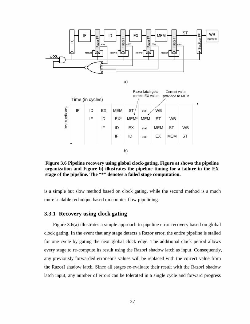
37
is a simple but slow method based on clock gating, while the second method is a much
more scalable technique based on counter-flow pipelining.
3.3.1 Recovery using clock gating
Figure 3.6(a) illustrates a simple approach to pipeline error recovery based on global
clock gating. In the event that any stage detects a Razor error, the entire pipeline is stalled
for one cycle by gating the next global clock edge. The additional clock period allows
every stage to re-compute its result using the RazorI shadow latch as input. Consequently,
any previously forwarded erroneous values will be replaced with the correct value from
the RazorI shadow latch. Since all stages re-evaluate their result with the RazorI shadow
latch input, any number of errors can be tolerated in a single cycle and forward progress
IF
Raz
or F
FR
azor
FF ID
Raz
or F
FR
azor
FF EX
Raz
or F
FR
azor
FF MEM WB
(reg/mem)
error
recover recover recover
Raz
or F
FR
azor
FF
PC
PC
recover
errorerror errorclockTime (in cycles)
IF ID EX* MEM* WB
Sta
biliz
er F
FS
tabi
lizer
FF
a)
b)
IF ID EX MEM WB
IF ID EX MEM WBstallInst
ruct
ions
IF ID EX MEMstall
Correct valueprovided to MEM
MEM
Razor latch getscorrect EX value
ST
ST
ST
ST
ST
stall
Figure 3.6 Pipeline recovery using global clock-gating. Figure a) shows the pipeline organization and Figure b) illustrates the pipeline timing for a failure in the EX stage of the pipeline. The “*” denotes a failed stage computation.
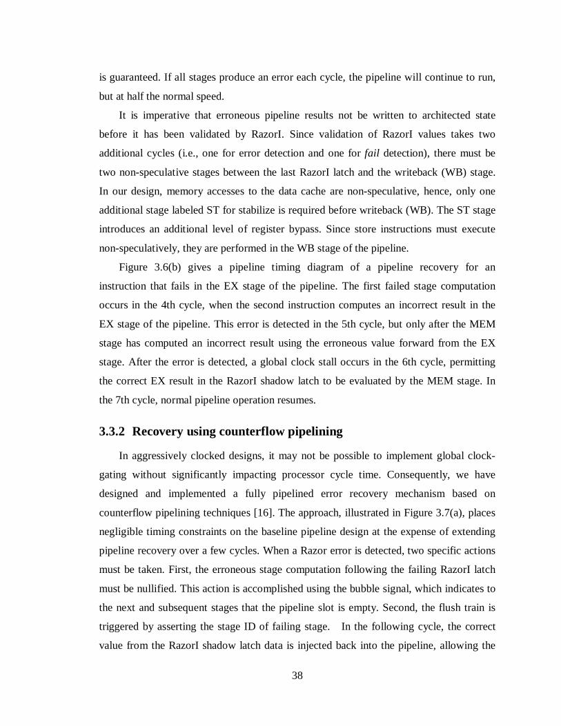
38
is guaranteed. If all stages produce an error each cycle, the pipeline will continue to run,
but at half the normal speed.
It is imperative that erroneous pipeline results not be written to architected state
before it has been validated by RazorI. Since validation of RazorI values takes two
additional cycles (i.e., one for error detection and one for fail detection), there must be
two non-speculative stages between the last RazorI latch and the writeback (WB) stage.
In our design, memory accesses to the data cache are non-speculative, hence, only one
additional stage labeled ST for stabilize is required before writeback (WB). The ST stage
introduces an additional level of register bypass. Since store instructions must execute
non-speculatively, they are performed in the WB stage of the pipeline.
Figure 3.6(b) gives a pipeline timing diagram of a pipeline recovery for an
instruction that fails in the EX stage of the pipeline. The first failed stage computation
occurs in the 4th cycle, when the second instruction computes an incorrect result in the
EX stage of the pipeline. This error is detected in the 5th cycle, but only after the MEM
stage has computed an incorrect result using the erroneous value forward from the EX
stage. After the error is detected, a global clock stall occurs in the 6th cycle, permitting
the correct EX result in the RazorI shadow latch to be evaluated by the MEM stage. In
the 7th cycle, normal pipeline operation resumes.
3.3.2 Recovery using counterflow pipelining
In aggressively clocked designs, it may not be possible to implement global clock-
gating without significantly impacting processor cycle time. Consequently, we have
designed and implemented a fully pipelined error recovery mechanism based on
counterflow pipelining techniques [16]. The approach, illustrated in Figure 3.7(a), places
negligible timing constraints on the baseline pipeline design at the expense of extending
pipeline recovery over a few cycles. When a Razor error is detected, two specific actions
must be taken. First, the erroneous stage computation following the failing RazorI latch
must be nullified. This action is accomplished using the bubble signal, which indicates to
the next and subsequent stages that the pipeline slot is empty. Second, the flush train is
triggered by asserting the stage ID of failing stage. In the following cycle, the correct
value from the RazorI shadow latch data is injected back into the pipeline, allowing the
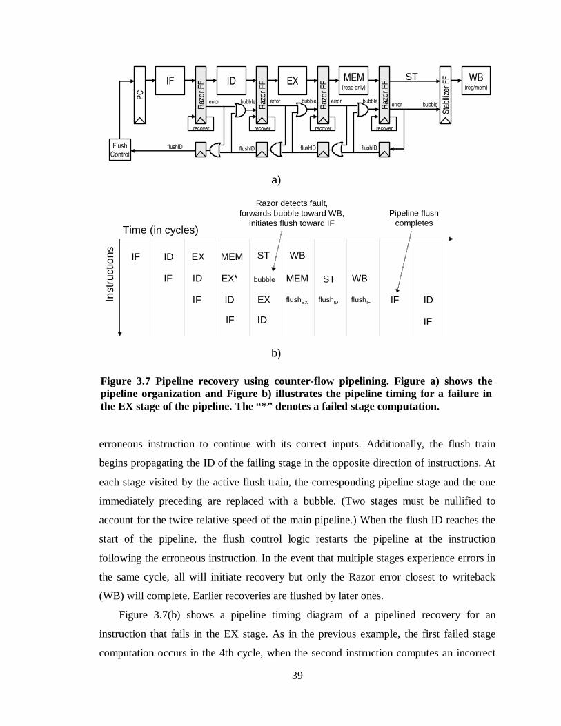
39
erroneous instruction to continue with its correct inputs. Additionally, the flush train
begins propagating the ID of the failing stage in the opposite direction of instructions. At
each stage visited by the active flush train, the corresponding pipeline stage and the one
immediately preceding are replaced with a bubble. (Two stages must be nullified to
account for the twice relative speed of the main pipeline.) When the flush ID reaches the
start of the pipeline, the flush control logic restarts the pipeline at the instruction
following the erroneous instruction. In the event that multiple stages experience errors in
the same cycle, all will initiate recovery but only the Razor error closest to writeback
(WB) will complete. Earlier recoveries are flushed by later ones.
Figure 3.7(b) shows a pipeline timing diagram of a pipelined recovery for an
instruction that fails in the EX stage. As in the previous example, the first failed stage
computation occurs in the 4th cycle, when the second instruction computes an incorrect
recover
IF
Raz
or F
FR
azor
FF ID
Raz
or F
FR
azor
FF EX
Raz
or F
FR
azor
FF MEM
(read-only)
WB(reg/mem)
error bubble
recover recover
Raz
or F
FR
azor
FF
Sta
biliz
er F
FS
tabi
lizer
FF
PC
PC
recover
flushID
bubbleerror bubble
flushID
error bubble
flushIDFlushControl
flushID
error
IF ID EX* MEM WB
a)
b)
IF ID EX MEM WB
IF ID flushEX
Time (in cycles)
Inst
ruct
ions
bubble
ST
ST
ST
flushID flushIFEX IF ID
Razor detects fault,forwards bubble toward WB,
initiates flush toward IFPipeline flush
completes
IF ID IF
Figure 3.7 Pipeline recovery using counter-flow pipelining. Figure a) shows the pipeline organization and Figure b) illustrates the pipeline timing for a failure in the EX stage of the pipeline. The “*” denotes a failed stage computation.
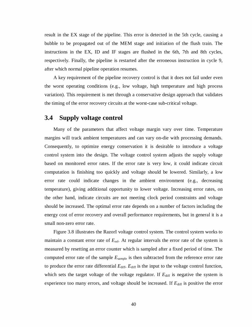
40
result in the EX stage of the pipeline. This error is detected in the 5th cycle, causing a
bubble to be propagated out of the MEM stage and initiation of the flush train. The
instructions in the EX, ID and IF stages are flushed in the 6th, 7th and 8th cycles,
respectively. Finally, the pipeline is restarted after the erroneous instruction in cycle 9,
after which normal pipeline operation resumes.
A key requirement of the pipeline recovery control is that it does not fail under even
the worst operating conditions (e.g., low voltage, high temperature and high process
variation). This requirement is met through a conservative design approach that validates
the timing of the error recovery circuits at the worst-case sub-critical voltage.
3.4 Supply voltage control
Many of the parameters that affect voltage margin vary over time. Temperature
margins will track ambient temperatures and can vary on-die with processing demands.
Consequently, to optimize energy conservation it is desirable to introduce a voltage
control system into the design. The voltage control system adjusts the supply voltage
based on monitored error rates. If the error rate is very low, it could indicate circuit
computation is finishing too quickly and voltage should be lowered. Similarly, a low
error rate could indicate changes in the ambient environment (e.g., decreasing
temperature), giving additional opportunity to lower voltage. Increasing error rates, on
the other hand, indicate circuits are not meeting clock period constraints and voltage
should be increased. The optimal error rate depends on a number of factors including the
energy cost of error recovery and overall performance requirements, but in general it is a
small non-zero error rate.
Figure 3.8 illustrates the RazorI voltage control system. The control system works to
maintain a constant error rate of Eref. At regular intervals the error rate of the system is
measured by resetting an error counter which is sampled after a fixed period of time. The
computed error rate of the sample Esample is then subtracted from the reference error rate
to produce the error rate differential Ediff. Ediff is the input to the voltage control function,
which sets the target voltage of the voltage regulator. If Ediff is negative the system is
experience too many errors, and voltage should be increased. If Ediff is positive the error
41
rate is too low and voltage should be lowered. The magnitude of Ediff indicates the degree
to which the system is “out of tune”.
While control of this system may seem simple on the surface, it is complicated by
the slow response time of the voltage regulator. Typical commercial voltage regulators
can take 10’s of microseconds to adjust supply voltage by 100 mV. Consequently, if the
controller reacts too fast or too abruptly, the system could become unstable or go into
oscillation. Moreover, an overly conservative control function that is slow to react to
changing system environments will reduce the overall efficiency of the design. We
implemented a proportional control system [32] which adjusts supply voltage in
proportion to the sampled Ediff in the RazorI prototype processor. To prevent the control
system from over-reacting and potentially placing the system in an unstable state, the
error sample rate is roughly equivalent to the minimum voltage step period.
3.5 Silicon implementation and evaluation of the scheme
In order to evaluate the concept of RazorI, we designed and fabricated a 64bit
processor which implements a subset of the Alpha instruction set in an industrial
0.18micron technology. This processor was fabricated under the MOSIS [33] university
research program. This is the first silicon implementation of a Razor design [35] using
the RazorI methodology. We present implementation details and measurement results for
this design in Chapter 4. Voltage control is based on the observed error rate and power
savings are achieved by 1) eliminating the safety margins under nominal operating and
silicon conditions and 2) scaling voltage 120mV below the first failure point to achieve a
0.1% targeted error rate. We tested and measured savings due to RazorI based voltage
Eref
VoltageControl
FunctionΣ.
.
.Pipeline
reset
Vdd
Ediff = Eref - Esample
-
Esample
panic
VoltageRegulator
Ediff errorsignalsEref
VoltageControl
FunctionΣΣ.
.
.Pipeline
reset
Vdd
Ediff = Eref - Esample
-
Esample
panic
VoltageRegulator
Ediff errorsignals
Figure 3.8 Razor supply voltage control
42
control for 33 different dies and obtained an average energy savings of 50% over the
worst-case operating conditions by operating at the 0.1% error rate voltage, at a fixed
frequency of 120MHz.
3.6 Summary and discussion
In this chapter, we developed the concept of error-detection and recovery through the
RazorI technique. We presented transistor-level schematic of the RazorI flip-flop which
flags timing errors by detecting discrepancies between the speculative data captured at
the main flip-flop and the always-correct data captured at the shadow latch. A
metastability-detector flags the occurrence of metastability at the output of the main flip-
flop.
We discussed two different schemes for micro-architectural recovery. The clock-
gating based approach stalls the pipeline for an entire cycle in the event of an error.
While its performance impact in the event of an error is small, however, it incurs
significant routing overhead on the global clock-gating signal. The counter-flow
architecture based approach trades-off higher performance impact of recovery for more
relaxed timing constraints. Consequently, this approach is more suited to large
microprocessors compared to the clock-gating approach.
We presented the Razor voltage controller which monitors the error-rate during
dynamic operation of the processor and adjusts the supply voltage to achieve a targeted
error-rate. We implemented Razor-based voltage control in a 64bit processor in 0.18µm
TSMC technology. In the next chapter, we present silicon measurement results from this
chip in greater detail.

43
CHAPTER 4
SELF-TUNING RAZOR I PROCESSOR: DESIGN AND SILICON M EASUREMENT RESULTS
We designed a 64-bit microprocessor with RazorI based dynamic voltage
management [10]. The processor core is a five stage in-order pipeline which implements
a subset of the Alpha instruction set. The timing critical stages of the processor are the
Instruction Decode (ID) and the Execute (EX) stages. The output registers of these
pipeline stages required R1FFs for validating computation results. We implemented the
distributed pipeline recovery scheme as has been outlined in Chapter 3 and illustrated in
Figure 3.7. Since the write-back stage was not critical, we needed just one extra
stabilization stage before data was committed to memory. The extra stage of pipelining
meant that all the memory store operations and register write operations were guaranteed
not to be metastable. In addition to the write accesses, the memory read accesses were
also non-critical and did not require RazorI validation. The processor was fabricated in a
0.18micron industrial technology. The die photograph of the processor is shown in Figure
4.1 and the relevant implementation details are provided in Table 4.1.
The remainder of this chapter is organized as follows. In Section 4.1 0, we discuss
the clocking scheme and relevant implementation details of the RazorI processor. Section
4.2 discusses silicon measurement results on 33 tested dies where we demonstrate sub-
critical operation with RazorI error correction. We quantify the total energy savings due
to RazorI in Section 4.3 and discuss RazorI based supply voltage control in Section 4.4.
Finally, we summarize the chapter in Section 4.5.
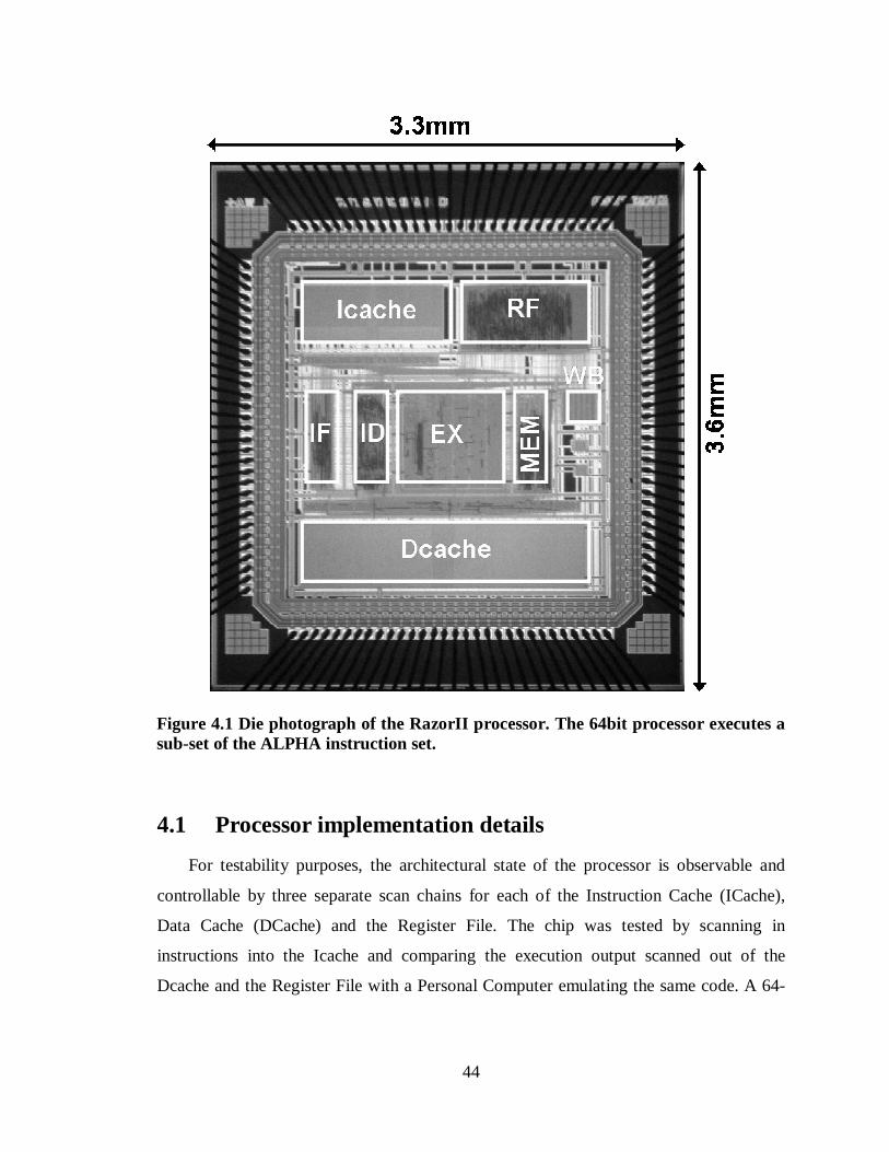
44
4.1 Processor implementation details
For testability purposes, the architectural state of the processor is observable and
controllable by three separate scan chains for each of the Instruction Cache (ICache),
Data Cache (DCache) and the Register File. The chip was tested by scanning in
instructions into the Icache and comparing the execution output scanned out of the
Dcache and the Register File with a Personal Computer emulating the same code. A 64-
Figure 4.1 Die photograph of the RazorII processor. The 64bit processor executes a sub-set of the ALPHA instruction set.

45
bit special purpose register keeps a record of the total number of errant cycles and is
sampled to compute the error rate for a particular run.
The core frequency is controlled by an internal Clock Generation Unit (CGU). The
CGU generates an asymmetric clock in a range between 60 MHz to 400 MHz in steps of
20MHz. The shadow latch sampling delay, defined by the duration of the positive clock
phase, is configurable from 0ps to 3.5ns in steps of 500ps. The CGU has a separate
voltage domain that is not voltage scaled. Hence, the core frequency and the shadow latch
sampling delay remains constant even when the core voltage is dynamically scaled.
4.2 Measurement Results
We measured energy savings obtainable from RazorI based Dynamic Voltage
Scaling (DVS) at 140 MHz and 120MHz for 33 chips from two different fabrication runs.
Table 4.1 Processor implementation details
2.9%% Total Chip Power Overhead due to Razor Flip-Flops and Delay Buffers
2388Number of Delay Buffers Added
207Total Number of Razor Flip-Flops
2801Total Number of Flip-Flops
8KBDcache Size
8KBIcache Size
130mWMeasured Chip Power at 1.8V
3.3mm*3.6mmDie Size
1.58millionTotal Number of Transistors
1.2-1.8VDVS Supply Voltage Range
140MHzMax. Clock Frequency
0.18µmTechnology Node
260fJEnergy of RFF per error event
Error Detection and Recovery Overhead
60fJ/205fJRFF Energy (static/switching)
49fJ/125fJStandard Flip-Flop Energy (static/switching)
Error Free Operation
260fJEnergy of RFF per error event
Error Detection and Recovery Overhead
60fJ/205fJRFF Energy (static/switching)
49fJ/125fJStandard Flip-Flop Energy (static/switching)
Error Free Operation

46
As mentioned, RazorI energy savings are due to both elimination of voltage safety
margins and operation below the point of first failure in the sub-critical voltage regime.
For every chip, we quantified the safety margin due to inter-die process variations by
measuring the difference between the first failure point of the slowest (worst-case process
corner) chip and the chip under test. Temperature margins were computed by the shift in
the first failure point for a chip when operating at 105C as opposed to operating at 25C.
1.52 1.56 1.60 1.64 1.68 1.72 1.760.70
0.75
0.80
0.85
0.90
0.95
1.00
1.05
1.10
1.15
1.20
1E-8
1E-7
1E-6
1E-5
1E-4
1E-3
0.01
0.1
1
10
120MHz
Nor
mal
ized
Ene
rgy
Per
cent
age
Err
or R
ate
140MHz
Voltage (in Volts)
Chip 2
b)
1.52 1.56 1.60 1.64 1.68 1.72 1.760.70
0.75
0.80
0.85
0.90
0.95
1.00
1.05
1.10
1.15
1.20
1E-8
1E-7
1E-6
1E-5
1E-4
1E-3
0.01
0.1
1
10
120MHz
Nor
mal
ized
Ene
rgy
Per
cent
age
Err
or R
ate
140MHz
Voltage (in Volts)
Chip 2
1.52 1.56 1.60 1.64 1.68 1.72 1.760.70
0.75
0.80
0.85
0.90
0.95
1.00
1.05
1.10
1.15
1.20
1E-8
1E-7
1E-6
1E-5
1E-4
1E-3
0.01
0.1
1
10
120MHz
Nor
mal
ized
Ene
rgy
Per
cent
age
Err
or R
ate
140MHz
Voltage (in Volts)
Chip 2
b)
1.48 1.52 1.56 1.60 1.641E-8
1E-7
1E-6
1E-5
1E-4
1E-3
0.01
0.1
1
10
0.80
0.85
0.90
0.95
1.00
1.05
1.10
1.15
1.20
P
erce
ntag
e E
rror
Rat
e
Nor
mal
ized
Ene
rgy
120MHz
140MHz
Voltage (in Volts)
Chip 1
Point of First Failure at 120MHz
Sub-critical
a)
1.48 1.52 1.56 1.60 1.641E-8
1E-7
1E-6
1E-5
1E-4
1E-3
0.01
0.1
1
10
0.80
0.85
0.90
0.95
1.00
1.05
1.10
1.15
1.20
P
erce
ntag
e E
rror
Rat
e
Nor
mal
ized
Ene
rgy
120MHz
140MHz
Voltage (in Volts)
Chip 1
Point of First Failure at 120MHz
Sub-critical
1.48 1.52 1.56 1.60 1.641E-8
1E-7
1E-6
1E-5
1E-4
1E-3
0.01
0.1
1
10
0.80
0.85
0.90
0.95
1.00
1.05
1.10
1.15
1.20
P
erce
ntag
e E
rror
Rat
e
Nor
mal
ized
Ene
rgy
120MHz
140MHz
Voltage (in Volts)
Chip 1
1.48 1.52 1.56 1.60 1.641E-8
1E-7
1E-6
1E-5
1E-4
1E-3
0.01
0.1
1
10
0.80
0.85
0.90
0.95
1.00
1.05
1.10
1.15
1.20
P
erce
ntag
e E
rror
Rat
e
Nor
mal
ized
Ene
rgy
120MHz
140MHz
Voltage (in Volts)
Chip 1
Point of First Failure at 120MHz
Sub-critical
a)
Figure 4.2 Sub-critical operation in chips named "Chip 1" and "Chip 2"

47
In addition, by scaling the supply voltage below the first failure point, we measured the
minimum voltage for which error correction is achievable with RazorI and the voltage
where a 0.1% error rate is attained.
4.2.1 Energy Savings from Sub-critical Operation
Figure 4.2 shows the error rates and normalized energy savings versus supply
voltage at 120 and 140MHz for two different chips. Energy at a particular voltage is
normalized with respect to the energy at the point of first failure. For all plotted points,
correct program execution with RazorI error correction was verified.
From the figure, we note that the error rate at the point of first failure is very low,
and is on the order of 1.0e-8, because only a few critical paths that are rarely sensitized
fail to meet setup requirements and are flagged as timing errors. As voltage is scaled
further into the sub-critical regime the error rate increases exponentially. The IPC penalty
due to the error recovery cycles is negligible for error rates below 0.1%. Under such low
error rates, the recovery overhead energy is also negligible and the total processor energy
shows a quadratic reduction with the supply voltage. At error rates exceeding 0.1%, the
recovery energy rapidly starts to dominate, offsetting the quadratic savings due to voltage
scaling. For the measured chips, the energy optimal error rate fell at approximately 0.1%.
Table 4.2 shows the measured power at the point of first failure and the energy per
instruction for both the chips at the point of first failure and at the point of 0.1% error rate.
At 120MHz, chip 1 consumes 104.5mW at the first failure point and 89.7mW at an
optimal 0.1% error rate, leading to 14% energy savings with negligible IPC hit. The
Table 4.2 Error-rate and energy-per-instruction measurement for chips 1 and 2 at the Point of First Failure and at the Point of 0.1% Error Rate
1.58V
1.52V
Voltage
Point of 0.1% Error RatePoint of First Failure
Chip2
Chip1
1.74V
1.63V
Voltage
99.6mW
89.7mW
Power
830pJ
740pJ
Energy perInstruction (Power/IPC
/Freq)
119.4mW
104.5mW
Power
990pJ
870pJ
Energy perInstruction (Power/IPC
/Freq)
1.58V
1.52V
Voltage
Point of 0.1% Error RatePoint of First Failure
Chip2
Chip1
1.74V
1.63V
Voltage
99.6mW
89.7mW
Power
830pJ
740pJ
Energy perInstruction (Power/IPC
/Freq)
119.4mW
104.5mW
Power
990pJ
870pJ
Energy perInstruction (Power/IPC
/Freq)

48
energy saving for chip 2 is 17%. These savings are in addition to the energy saved just by
eliminating voltage margins. Figure 4.3 shows the distribution of the percentage
normalized energy savings obtained over the first failure point while operating at the
0.1% error rate voltage for all the chips tested. At 120MHz, the range extends from 5% to
23% while at 140MHz the range extends from 5% to 19%.
Figure 4.4(a) shows the distribution of the first failure voltage for the 33 measured
chips. At 120MHz, the measured range of variation of the first failure point is from 1.46V
to 1.76V. The correlation between the first failure voltage and the 0.1% error rate voltage
is shown in the scatter plot of Figure 4.4(b). The 0.1% error rate voltage shows a net
variation of 0.24V from 1.38V to 1.62V which is approximately 20% less than the
variation observed for the voltage at the point of first failure.
0 5 10 15 20 25 300
2
4
6
8
10
12
14
16 L o t0 L o t1
120MHzT=27C
Percentage Savings
Num
ber
of C
hips
5 9 13 17 210
2
4
6
8
10
12
14 Lot0 Lot1
Percentage Savings
Num
ber
of C
hips
140MHzT=27C
(a) (b)
0 5 10 15 20 25 300
2
4
6
8
10
12
14
16 Lo t0 Lo t1
120MHzT=27C
Percentage Savings
Num
ber
of C
hips
5 9 13 17 210
2
4
6
8
10
12
14 Lot0 Lot1
Percentage Savings
Num
ber
of C
hips
140MHzT=27C
0 5 10 15 20 25 300
2
4
6
8
10
12
14
16 Lo t0 Lo t1
120MHzT=27C
Percentage Savings
Num
ber
of C
hips
5 9 13 17 210
2
4
6
8
10
12
14 Lot0 Lot1
Percentage Savings
Num
ber
of C
hips
140MHzT=27C
(a) (b)
Figure 4.3 Normalized energy savings over point of first failure at the 0.1% error-rate for 33 measured chips at 120 and 140MHz.
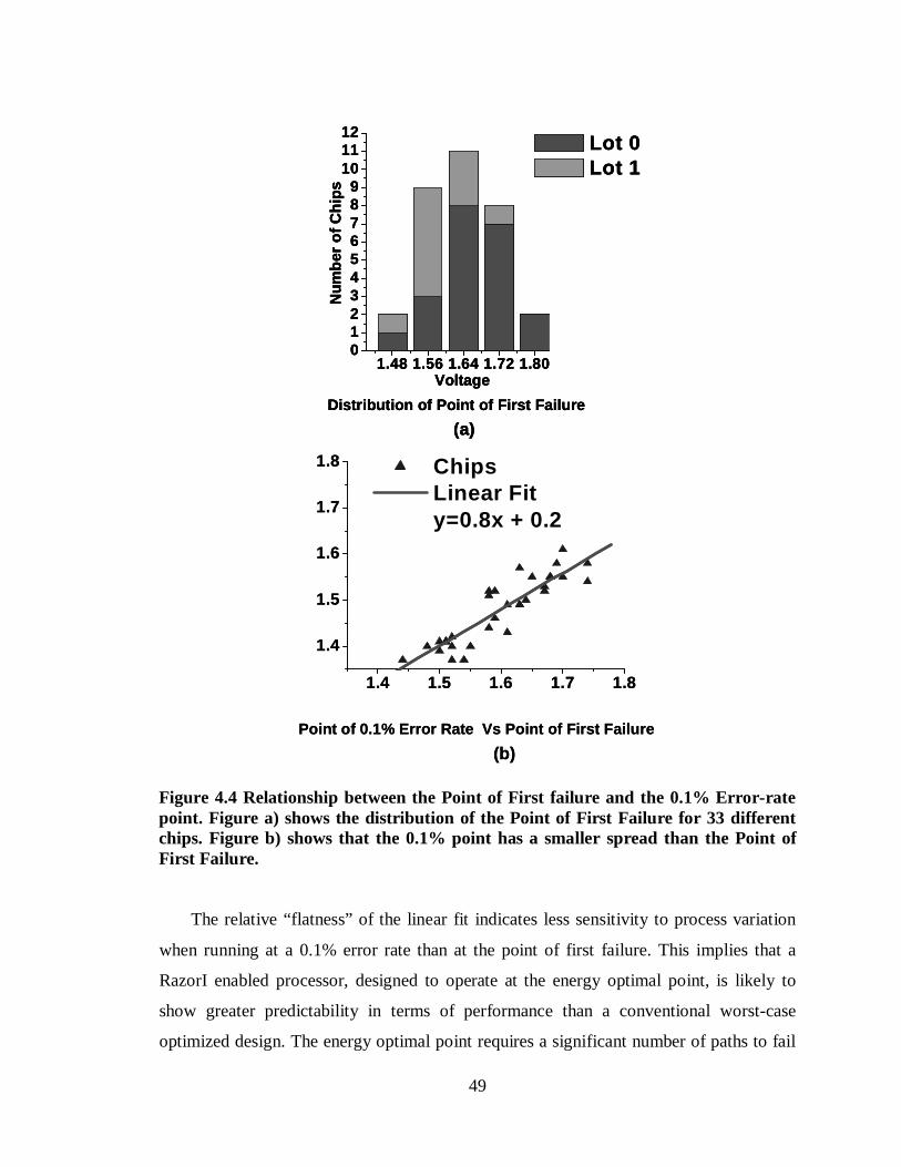
49
The relative “flatness” of the linear fit indicates less sensitivity to process variation
when running at a 0.1% error rate than at the point of first failure. This implies that a
RazorI enabled processor, designed to operate at the energy optimal point, is likely to
show greater predictability in terms of performance than a conventional worst-case
optimized design. The energy optimal point requires a significant number of paths to fail
1.48 1.56 1.64 1.72 1.800123456789
101112
Lot 0 Lot 1
Distribution of Point of First Failure
Voltage
Num
ber
of C
hips
(a)
1.4 1.5 1.6 1.7 1.8
1.4
1.5
1.6
1.7
1.8 Chips Linear Fit y=0.8x + 0.2
Point of 0.1% Error Rate Vs Point of First Failure
(b)
1.48 1.56 1.64 1.72 1.800123456789
101112
Lot 0 Lot 1
Distribution of Point of First Failure
Voltage
Num
ber
of C
hips
(a)
1.48 1.56 1.64 1.72 1.800123456789
101112
Lot 0 Lot 1
Distribution of Point of First Failure
Voltage
Num
ber
of C
hips
(a)
1.4 1.5 1.6 1.7 1.8
1.4
1.5
1.6
1.7
1.8 Chips Linear Fit y=0.8x + 0.2
Point of 0.1% Error Rate Vs Point of First Failure
(b)
Figure 4.4 Relationship between the Point of First failure and the 0.1% Error-rate point. Figure a) shows the distribution of the Point of First Failure for 33 different chips. Figure b) shows that the 0.1% point has a smaller spread than the Point of First Failure.

50
and statistically averages out the variations in path delay due to process variation, as
opposed to the first failure point which, being determined by the single longest critical
path, shows higher process variation dependence.
Figure 4.5 shows the effect of temperature on the point of first failure for a typical
chip. As expected, the first failure point increases and shifts by 100mV from 1.45V to
1.55V for a temperature change from 25C to 105C.
4.3 Total Energy Savings with RazorI
The bar graph in Figure 4.6 shows the energy for chips 1 and 2 when operating at
120MHz. The first failure voltage for chips 1 and 2, as shown in Figure 4.2, are 1.63V
and 1.74V respectively, and hence represent typical and worst-case process conditions.
The first set of bars shows the energy when RazorI is turned off and the chip under
test is operated at the worst-case operating voltage at 120MHz, as determined for all the
chips tested. This is the minimum voltage which guarantees error-free operation for the
slowest process corner silicon at the worst-case temperature of 105C and a power supply
drop equal to 10% of the nominal voltage of 1.8V. The point of first failure for the
-35 -15 5 25 45 65 85 105
1.40
1.44
1.48
1.52
1.56
Poi
nt o
f Firs
t Fai
lure
(V)
Temperature( oC)
Figure 4.5 Temperature margins
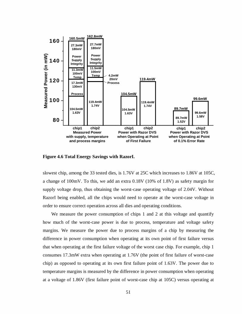
51
slowest chip, among the 33 tested dies, is 1.76V at 25C which increases to 1.86V at 105C,
a change of 100mV. To this, we add an extra 0.18V (10% of 1.8V) as safety margin for
supply voltage drop, thus obtaining the worst-case operating voltage of 2.04V. Without
RazorI being enabled, all the chips would need to operate at the worst-case voltage in
order to ensure correct operation across all dies and operating conditions.
We measure the power consumption of chips 1 and 2 at this voltage and quantify
how much of the worst-case power is due to process, temperature and voltage safety
margins. We measure the power due to process margins of a chip by measuring the
difference in power consumption when operating at its own point of first failure versus
that when operating at the first failure voltage of the worst case chip. For example, chip 1
consumes 17.3mW extra when operating at 1.76V (the point of first failure of worst-case
chip) as opposed to operating at its own first failure point of 1.63V. The power due to
temperature margins is measured by the difference in power consumption when operating
at a voltage of 1.86V (first failure point of worst-case chip at 105C) versus operating at
80
100
120
140
160
27.3mW180mV
PowerSupply
Integrity
11.3mW100mVTemp
17.3mW130mV
Process
104.5mW1.63V
4.2mW20mV
Process
89.7mW1.52V
99.6mW1.58V
104.5mW
119.4mW
89.7mW
119.4mW1.74V
11.5mW100mVTemp
27.7mW180mV
PowerSupply
Integrity
119.4mW1.74V
99.6mW
chip1 chip2 chip1 chip2 chip1 chip2Measured Power
with supply, temperatureand process margins
Power with Razor DVS when Operating at Point
of First Failure
Power with Razor DVS when Operating at Point
of 0.1% Error Rate
Mea
sure
d P
ower
(in
mW
)
160.5mW 162.8mW
104.5mW1.63V
Figure 4.6 Total Energy Savings with RazorI.
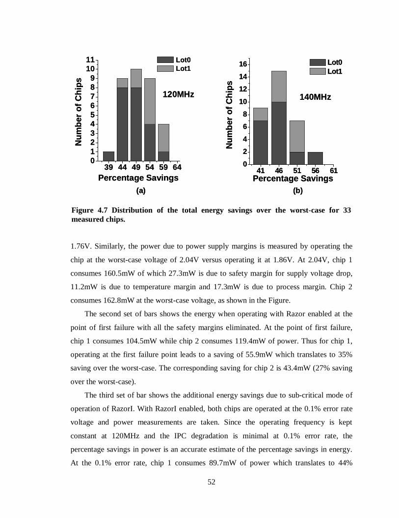
52
1.76V. Similarly, the power due to power supply margins is measured by operating the
chip at the worst-case voltage of 2.04V versus operating it at 1.86V. At 2.04V, chip 1
consumes 160.5mW of which 27.3mW is due to safety margin for supply voltage drop,
11.2mW is due to temperature margin and 17.3mW is due to process margin. Chip 2
consumes 162.8mW at the worst-case voltage, as shown in the Figure.
The second set of bars shows the energy when operating with Razor enabled at the
point of first failure with all the safety margins eliminated. At the point of first failure,
chip 1 consumes 104.5mW while chip 2 consumes 119.4mW of power. Thus for chip 1,
operating at the first failure point leads to a saving of 55.9mW which translates to 35%
saving over the worst-case. The corresponding saving for chip 2 is 43.4mW (27% saving
over the worst-case).
The third set of bar shows the additional energy savings due to sub-critical mode of
operation of RazorI. With RazorI enabled, both chips are operated at the 0.1% error rate
voltage and power measurements are taken. Since the operating frequency is kept
constant at 120MHz and the IPC degradation is minimal at 0.1% error rate, the
percentage savings in power is an accurate estimate of the percentage savings in energy.
At the 0.1% error rate, chip 1 consumes 89.7mW of power which translates to 44%
39 44 49 54 59 640123456789
1011 Lot0
Lot1
Percentage Savings
Num
ber
of C
hips
120MHz
41 46 51 56 610
2
4
6
8
10
12
14
16 Lot0 Lot1
Percentage Savings
Num
ber
of C
hips
140MHz
(a) (b)
39 44 49 54 59 640123456789
1011 Lot0
Lot1
Percentage Savings
Num
ber
of C
hips
120MHz
41 46 51 56 610
2
4
6
8
10
12
14
16 Lot0 Lot1
Percentage Savings
Num
ber
of C
hips
140MHz
(a) (b)
Figure 4.7 Distribution of the total energy savings over the worst-case for 33 measured chips.
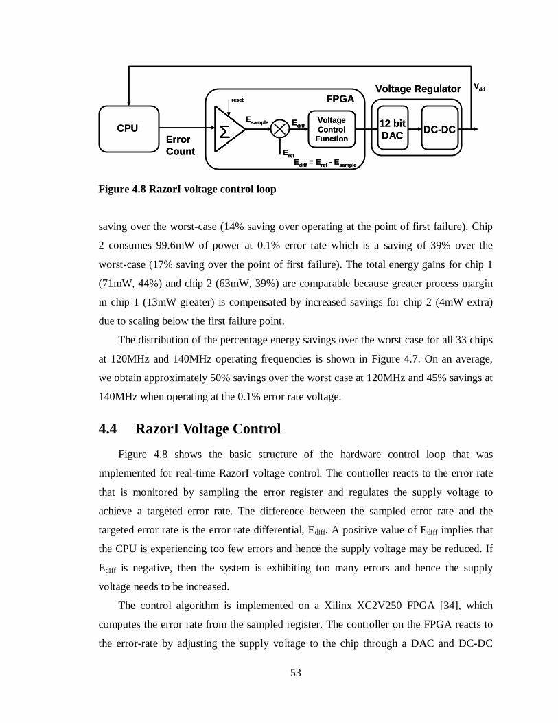
53
saving over the worst-case (14% saving over operating at the point of first failure). Chip
2 consumes 99.6mW of power at 0.1% error rate which is a saving of 39% over the
worst-case (17% saving over the point of first failure). The total energy gains for chip 1
(71mW, 44%) and chip 2 (63mW, 39%) are comparable because greater process margin
in chip 1 (13mW greater) is compensated by increased savings for chip 2 (4mW extra)
due to scaling below the first failure point.
The distribution of the percentage energy savings over the worst case for all 33 chips
at 120MHz and 140MHz operating frequencies is shown in Figure 4.7. On an average,
we obtain approximately 50% savings over the worst case at 120MHz and 45% savings at
140MHz when operating at the 0.1% error rate voltage.
4.4 RazorI Voltage Control
Figure 4.8 shows the basic structure of the hardware control loop that was
implemented for real-time RazorI voltage control. The controller reacts to the error rate
that is monitored by sampling the error register and regulates the supply voltage to
achieve a targeted error rate. The difference between the sampled error rate and the
targeted error rate is the error rate differential, Ediff. A positive value of Ediff implies that
the CPU is experiencing too few errors and hence the supply voltage may be reduced. If
Ediff is negative, then the system is exhibiting too many errors and hence the supply
voltage needs to be increased.
The control algorithm is implemented on a Xilinx XC2V250 FPGA [34], which
computes the error rate from the sampled register. The controller on the FPGA reacts to
the error-rate by adjusting the supply voltage to the chip through a DAC and DC-DC
CPUErrorCount
ΣEref
Esample
Ediff = Eref - Esample
Ediff
Vdd
12 bitDAC DC-DC
VoltageControl
Function
Voltage RegulatorFPGAreset
CPUErrorCount
ΣΣEref
Esample
Ediff = Eref - Esample
Ediff
Vdd
12 bitDAC DC-DC
VoltageControl
Function
Voltage RegulatorFPGAreset
Figure 4.8 RazorI voltage control loop

54
switching regulator. The DAC outputs an analog reference voltage to the regulator based
on the 12-bit control output from the FPGA. The DC-DC regulator has a voltage gain of
1.76 and can source a maximum current of 600mA. It can easily supply sufficient current
to the chip which consumes less than 80mA at 1.8V. We tested the controller using a
program which has alternating high and low error rate phases. At the high error rate phase,
the processor is executing high latency instructions and hence the critical paths of the
circuit are being exercised frequently. Therefore, a higher supply voltage is required to
sustain the targeted error rate and vice versa.
The on-chip error counter is sampled at a frequency of 750KHz and is accumulated
within the FPGA. The algorithm updates the control output at a conservative frequency of
1 KHz. If error rates are too high, voltage is increased at a rate of 1 bit per millisecond.
Conversely, a low error rate caused a 1-bit decrease. This corresponds to a voltage
change of 2.15 mV at the output of the DC-DC regulator feeding into the chip.
Figure 4.9 shows a 2 minute portion of the voltage controller response for the 2-
phase program execution. The targeted error rate for the given trace is set to 0.1% relative
to CPU clock cycle count. The controller maintains an average of 0.1% error rate during
Figure 4.9 Run-time response of the RazorI voltage controller. Shown in the figure is a two minute snapshot of the error-rate for a program with two error-rate phases.
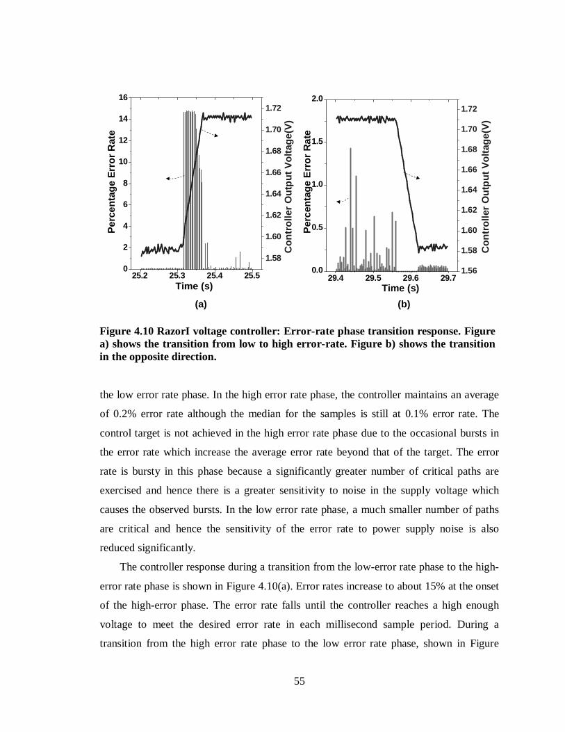
55
the low error rate phase. In the high error rate phase, the controller maintains an average
of 0.2% error rate although the median for the samples is still at 0.1% error rate. The
control target is not achieved in the high error rate phase due to the occasional bursts in
the error rate which increase the average error rate beyond that of the target. The error
rate is bursty in this phase because a significantly greater number of critical paths are
exercised and hence there is a greater sensitivity to noise in the supply voltage which
causes the observed bursts. In the low error rate phase, a much smaller number of paths
are critical and hence the sensitivity of the error rate to power supply noise is also
reduced significantly.
The controller response during a transition from the low-error rate phase to the high-
error rate phase is shown in Figure 4.10(a). Error rates increase to about 15% at the onset
of the high-error phase. The error rate falls until the controller reaches a high enough
voltage to meet the desired error rate in each millisecond sample period. During a
transition from the high error rate phase to the low error rate phase, shown in Figure
29.4 29.5 29.6 29.70.0
0.5
1.0
1.5
2.0
1.56
1.58
1.60
1.62
1.64
1.66
1.68
1.70
1.72
25.2 25.3 25.4 25.50
2
4
6
8
10
12
14
16
1.58
1.60
1.62
1.64
1.66
1.68
1.70
1.72
(a) (b)
Per
cent
age
Err
or R
ate
Con
trol
ler
Out
put V
olta
ge(V
)
Per
cent
age
Err
or R
ate
Con
trol
ler
Out
put V
olta
ge(V
)Time (s) Time (s)
Figure 4.10 RazorI voltage controller: Error-rate phase transition response. Figure a) shows the transition from low to high error-rate. Figure b) shows the transition in the opposite direction.

56
4.10(b), the error rate drops to zero because the supply voltage is higher than required.
The controller responds by gradually reducing the voltage until the target error rate is
achieved. The average voltage maintained during the low error rate phase is 1.59V and
the average voltage maintained at the high error rate phase is 1.72V, a difference of
130mV. More efficient and complex control and error prediction strategies are an area of
ongoing research, including automatic optimal error-rate selection.
4.5 Summary and discussion
In this chapter, we presented a self-tuning processor with RazorI based supply
voltage control. RazorI incorporates in situ error detection and correction mechanisms to
eliminate voltage margins and to operate below the point of first failure. We presented
the design of a novel delay-error tolerant flip-flop that detects and recovers from timing
errors on the processor critical paths. With RazorI based voltage management, we
obtained 50% energy savings over the worst-case, on an average across 33 tested dies, by
operating at the 0.1% error rate voltage at a constant frequency of 120MHz. Since the
energy-optimal voltage for RazorI occurs at moderately low error rates, it motivates
design optimization targeted at improving the delay of typically exercised logic paths as
opposed to the worst case critical path.
However, RazorI makes certain assumptions about the timing properties of the
underlying architecture which may not hold true in the general case. For example, the
propagation delay of the pipeline restore signal, which is a high fan-out net, can become
critical for high-performance pipelines, especially at aggressive technologies. This can
have the undesirable consequence of RazorI voltage scaling being limited by the restore
signal rather than by the critical-paths in the pipeline. This and similar concerns were the
primary motivation for us to develop an alternative technique for implementing Razor in
processors, which we call RazorII. We discuss, in detail, the various issues and
weaknesses in RazorI in the next chapter and develop the key concepts of RazorII which
address these.

57
CHAPTER 5
RAZOR II: TRANSITION -DETECTION BASED ERROR -DETECTION AND M ICRO-ARCHITECTURAL RECOVERY
In Chapter 3, we introduced the concept of RazorI which uses a double-sampling
RazorI flip-flop (R1FF) for in situ error-detection. In RazorI speculative data captured at
the positive edge of the clock is compared against the correct sample stored in a shadow
latch. Recovery is achieved through a pipeline restore signal which a) overwrites the
main flip-flop with the correct data in the shadow latch, thereby restoring correct state in
the main flip-flop with a single cycle penalty and b) engages additional infrastructure
embedded within the micro-architecture which reverts the pipeline back to its correct
state. Thus, the recovery process has both circuits as well as micro-architectural aspects
to it.
This technique of error-detection and the circuit-architectural recovery has
fundamental design constraints which make it significantly less amenable to high-
performance microprocessors at advanced process nodes. In this chapter, we propose a
new technique, called RazorII, which addresses the issues in the RazorI approach. The
remainder of the chapter is organized as follows. In Section 5.1, we discuss the
weaknesses of the RazorI technique which complicates its deployment in high-
performance pipelines. Section 5.2 describes the key concepts of the RazorII technique.
Section 5.3 deals with the pipeline modifications necessary to support recovery in a
RazorII pipeline when a timing error is detected. The transistor-level schematic of the
error-detecting RazorII flip-flop is described in Section 5.4. Section 5.5 deals with an
alternative design of the RazorII flip-flop which uses a transparent latch, instead of a flip-
flop. We show how this design simultaneously achieves timing-error detection and SEU
tolerance in logic and inside registers. Memory design for the RazorII pipeline is
discussed in Section 5.6. Finally, we summarize this chapter in Section 5.7.
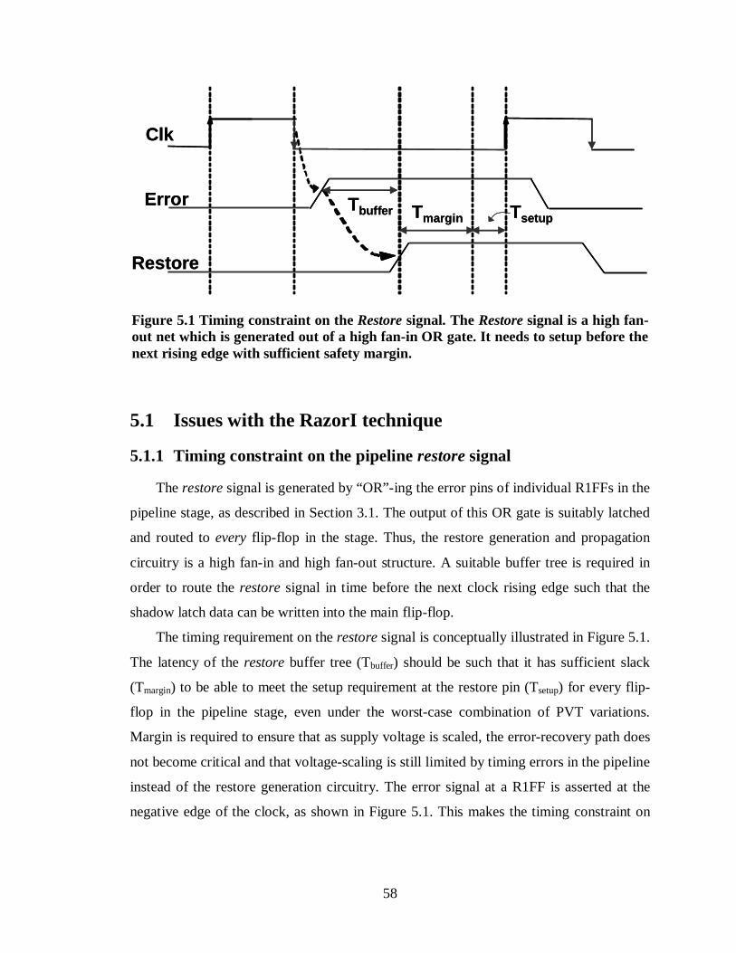
58
5.1 Issues with the RazorI technique
5.1.1 Timing constraint on the pipeline restore signal
The restore signal is generated by “OR”-ing the error pins of individual R1FFs in the
pipeline stage, as described in Section 3.1. The output of this OR gate is suitably latched
and routed to every flip-flop in the stage. Thus, the restore generation and propagation
circuitry is a high fan-in and high fan-out structure. A suitable buffer tree is required in
order to route the restore signal in time before the next clock rising edge such that the
shadow latch data can be written into the main flip-flop.
The timing requirement on the restore signal is conceptually illustrated in Figure 5.1.
The latency of the restore buffer tree (Tbuffer) should be such that it has sufficient slack
(Tmargin) to be able to meet the setup requirement at the restore pin (Tsetup) for every flip-
flop in the pipeline stage, even under the worst-case combination of PVT variations.
Margin is required to ensure that as supply voltage is scaled, the error-recovery path does
not become critical and that voltage-scaling is still limited by timing errors in the pipeline
instead of the restore generation circuitry. The error signal at a R1FF is asserted at the
negative edge of the clock, as shown in Figure 5.1. This makes the timing constraint on
Clk
Error
Restore
TsetupTmarginTbuffer
Clk
Error
Restore
TsetupTmarginTbuffer
Figure 5.1 Timing constraint on the Restore signal. The Restore signal is a high fan-out net which is generated out of a high fan-in OR gate. It needs to setup before the next rising edge with sufficient safety margin.
59
the restore signal even more stringent since its generation and propagation has to occur
strictly within the negative clock-phase with sufficient margin to spare.
For larger designs with many critical flip-flops, meeting this design constraint is
naturally expected to be difficult. Consequently, at future technologies, the efficacy of the
RazorI technique will be undermined by the voltage headroom being limited by the
criticality of the restore signal rather than by the speculation time available.
5.1.2 Issues with metastability detection
Metastability at the main flip-flop output can cause the downstream pipeline stage
and the restore generation circuitry to interpret the metastable signal differently, thereby
leading to system failure. In addition, metastability can cause the delay of the succeeding
pipestage to exceed the error-detection window. Hence, it is imperative that the
metastability-detector is very carefully designed to flag all occurrences of metastability at
the main flip-flop for the entire range of operation.
As mentioned in Section 3.2, the metastability-detector relies on skewed inverters
and, hence, is susceptible to process variation. It needs to be designed for correct
operation at the skewed process corners such as SF (slow NMOS, fast PMOS) and FS
(fast NMOS, slow PMOS). This requires the use of wider transistors inside the skewed
inverters which, unfortunately, increases the capacitive load driven by the flip-flop node
where metastability is being monitored. This not only worsens the intrinsic CLK-Q delay
of the flip-flop, but also exponentially increases the likelihood of metastability occurring
at that node [12].
Thus, the design of the metastability-detector presents conflicting constraints. On
one hand, it requires wider transistors to ensure functional correctness across process
corners. On the other hand, wider transistors increase the likelihood of metastability at
the flip-flop sampling node driving the metastability-detector. Rise in intra-die process
variability at future technology nodes further exacerbate the difficulties in ensuring
robust operation of the metastability-detector.
In addition to the complications involved in the metastability-detector and the
stringent timing constraint on the restore signal, critical control signals greatly
complicate the RazorI technique. Control signals determine the state of the data-path.

60
Therefore, timing violations in such signals can corrupt the shadow latch data, thereby
leading to system failure.
In order to effectively address these issues, we introduce an alternative technique for
error detection and correction, henceforth referred to as RazorII. RazorII exploits a key
observation from our measurements performed on the RazorI processor that the error rate
at the Point of First Failure (PoFF) is extremely low, ~1 error in 10 million cycles. An
extremely low error-rate makes the recovery energy negligible at this operating point. In
addition, we also found that beyond the PoFF, the error rate increases exponentially at
one decade per 10mV supply voltage increase. Hence the energy gain from operating
substantially below the PoFF was small (~10%) compared to the energy gain from
eliminating the PVT margins (~35 to 45%) [10]. We take advantage of these findings in
RazorII wherein a processor is intended to operate at the PoFF and recovery from a
timing error occurs by a conventional architectural replay mechanism.
Replaying an erroneous instruction incurs greater Instructions Per Cycle (IPC)
overhead than the counter-flow pipeline recovery technique used in [10]. However, as
error-rates are extremely low at the PoFF, the increased IPC overhead from using
architectural replay has a negligible impact on the overall energy efficiency. Architectural
replay greatly simplifies the error recovery path, thereby making RazorII significantly
more amenable to high-performance microprocessors compared to RazorI. We introduce
a novel timing-error detecting flip-flop (RazorII flip-flop or the R2FF) based on flagging
spurious transitions at the critical-path endpoint. We present a design of the RazorII flip-
flop which naturally detects Single Event Upsets (SEU) within combinational logic and
in latches. In order to validate RazorII, we designed and fabricated a 64bit prototype
processor which uses RazorII for SEU tolerance and low-energy operation through
dynamic supply adaptation. We present silicon measurement results from this processor
in Chapter 7 of this thesis.
5.2 Key concepts of RazorII
The RazorII approach introduces two novel components which are as follows:
1. Instead of performing both error detection and correction in the flip-flop, RazorII
performs only detection in the flip-flop, while correction is performed through
61
architectural replay. This allows significant reduction in the complexity and size of the
RazorII flip-flop, although at the cost of increased IPC penalty during recovery.
Architectural replay is a conventional technique which often already exists in high-
performance microprocessors to support speculative operation such as out-of-order
execution and branch prediction. Hence, it is possible to overload the existing framework
to support replay in the event of timing errors. In addition, this technique precludes the
need for a pipeline restore signal, thereby significantly relaxing the timing constraints on
the error-recovery path. This feature makes RazorII highly amenable to deployment in
high-performance processors.
2. The design of the RazorII flip-flop detects timing errors by flagging any transition
at the critical-path endpoint in the positive phase of the clock. Using a transition-detector
for flagging timing errors allows the elimination of the metastability-detector and the
shadow-latch. This significantly reduces the clock-pin capacitance of the flip-flop
bringing down its power and area overhead. In addition, the basic design of the RazorII
flip-flop can be easily modified to use a level-sensitive transparent latch instead of a flip-
flop. This simplification allows it to naturally detect Single Event Upsets (SEU) in the
logic and registers without additional overhead. We describe the design of this modified
RazorII flip-flop in Section 5.5.
In the following sections, we develop the RazorII error-detection and recovery
concept in greater detail.
5.3 RazorII pipeline micro-architecture
The key idea in RazorII is to use the RazorII flip-flop only for error-detection. State
recovery after a timing error occurs by a conventional replay mechanism from a check-
pointed state. Relying on the roll-back mechanism eliminates the requirement for a
timing-critical restore signal and greatly simplifies recovery in the event of a timing
error.
Figure 5.2 conceptually illustrates all the major micro-architectural modifications to
the basic pipeline in order to support roll-back. The pipeline shown in the figure is a
conventional in-order, five-stage pipeline. The critical flip-flops in each pipeline stage are
RazorII flip-flops which monitor their respective data inputs for timing-error violations.
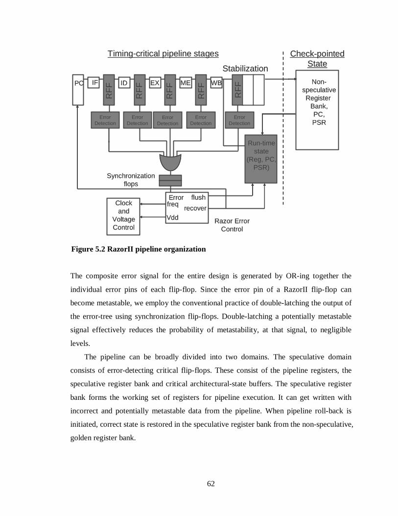
62
The composite error signal for the entire design is generated by OR-ing together the
individual error pins of each flip-flop. Since the error pin of a RazorII flip-flop can
become metastable, we employ the conventional practice of double-latching the output of
the error-tree using synchronization flip-flops. Double-latching a potentially metastable
signal effectively reduces the probability of metastability, at that signal, to negligible
levels.
The pipeline can be broadly divided into two domains. The speculative domain
consists of error-detecting critical flip-flops. These consist of the pipeline registers, the
speculative register bank and critical architectural-state buffers. The speculative register
bank forms the working set of registers for pipeline execution. It can get written with
incorrect and potentially metastable data from the pipeline. When pipeline roll-back is
initiated, correct state is restored in the speculative register bank from the non-speculative,
golden register bank.
Non-speculativeRegister
Bank,PC,PSR
Run-time state
(Reg, PC, PSR)
Razor Error Control
Error
recover
IF ID EX ME WB
Stabilization
freq
Vdd
Clockand
VoltageControl
Check-pointed State
Timing-critical pipeline stages
PC
RF
F
RF
F
RF
F
RF
F
ErrorDetection
ErrorDetection
ErrorDetection
ErrorDetection
ErrorDetection
Synchronization flops
flush
RF
F Non-speculativeRegister
Bank,PC,PSR
Run-time state
(Reg, PC, PSR)
Razor Error Control
Error
recover
IF ID EX ME WB
Stabilization
freq
Vdd
Clockand
VoltageControl
Check-pointed State
Timing-critical pipeline stages
PC
RF
F
RF
F
RF
F
RF
F
ErrorDetection
ErrorDetection
ErrorDetection
ErrorDetection
ErrorDetection
Synchronization flops
flush
RF
F
Figure 5.2 RazorII pipeline organization
63
The golden register bank along with the data cache and the architectural state
registers such as the program counter (PC) and the program status register (PSR) form the
non-speculative domain of the pipeline. It is required to guarantee that the non-
speculative domain is non-critical and always-correct. The pipeline output is check-
pointed within the non-speculative domain once it has been validated by Razor to be
error-free. Thus, it is effectively a snapshot of the processor state to which the pipeline
can revert to, without losing correctness. The speculative domain is prevented from
updating the state of the non-speculative domain with incorrect data by means a
stabilization pipeline. The first stage of the stabilization pipeline requires error detection
since it interfaces directly with a critical processor core. The subsequent stages are
required to be non-critical which is easily guaranteed since no computation occurs in the
stabilization pipeline. The depth of the stabilization pipeline is equal to the latency
through the error detection tree.
The primary objective of the stabilization pipeline is to ensure that speculative data is
not committed before it has been validated to be correct. When an instruction at the
output of the stabilization stage is qualified to be error-free by the Razor error controller,
it is safely allowed to update the processor architectural state. These updates include
register writes to the golden register file, the data cache and the program status register.
In addition, the instruction program counter is also check-pointed.
When the error controller block detects incorrect execution in the pipeline, it initiates
the roll-back mechanism to revert the pipeline back to the last check-pointed state. First,
the stabilization pipeline and the speculative architectural state buffers are flushed. Then,
rest of the pipeline registers are “reset”-ed. The state in the speculative register file and
the speculative state buffers is restored by overwriting them with the contents of the
golden register file and the golden architectural-state registers, respectively. Thus, the
entire pipeline is reset to the state of the last committed instruction and normal pipeline
operation is resumed.
As was mentioned earlier, re-executing from the last committed instruction does not
guarantee forward progress since the pipeline may effectively stall due to a repeatedly
failing instruction. The RazorII error controller detects such a deadlock and responds to it
by gating every alternate clock cycle during recovery. Thus, running the pipeline at half

64
frequency ensures that the pipeline completes without incurring timing errors. However,
it is expected that a major proportion of errors will be due to transient noise events which
disappear when the pipeline state is changed during the flush and re-execution process.
This observation is borne out from silicon measurement results on the RazorII prototype
processor which we present in Chapter 7 of this thesis.
The RazorII error controller also maintains a running count of the error-rate and
implements the voltage controller algorithm. Accordingly, it interfaces with an external
voltage regulator to adjust the supply voltage of the processor so as to achieve a targeted
error rate.
5.4 Transition-detection based error-detection
The concept of error detection through transition-detection is illustrated in Figure 5.3.
An error is flagged when the data input changes in the setup window of the flip-flop in
front of the positive clock-edge. The time before the positive edge when the transition-
detector actually begins to monitor for spurious state changes at the data input is required
to subsume the setup time for the flip-flop. Therefore, an additional safety margin (Tmar-
gin) is added to the transition-detector such that it is guaranteed to flag timing errors
before actual setup violations begin occurring, even in the worst-case scenario. This
margin is statically built within the transition detector using conventional worst-case
design practices.
Tsetup Tpos
ClockDataError
Tmargin Detection Window
Figure 5.3 Transition-detection based error detection
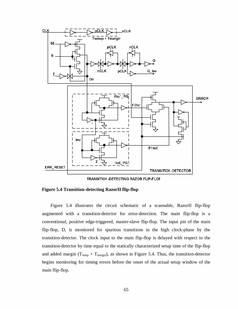
65
Figure 5.4 illustrates the circuit schematic of a scannable, RazorII flip-flop
augmented with a transition-detector for error-detection. The main flip-flop is a
conventional, positive edge-triggered, master-slave flip-flop. The input pin of the main
flip-flop, D, is monitored for spurious transitions in the high clock-phase by the
transition-detector. The clock input to the main flip-flop is delayed with respect to the
transition-detector by time equal to the statically characterized setup time of the flip-flop
and added margin (Tsetup + Tmargin), as shown in Figure 5.4. Thus, the transition-detector
begins monitoring for timing errors before the onset of the actual setup window of the
main flip-flop.
Figure 5.4 Transition-detecting RazorII flip-flop

66
Adding the delay-chain to the clock-path increases the power overhead of the flip-
flop. Alternatively, this delay can also be added to the input data of the transition-detector
at the expense of reducing its sensitivity to glitches. Doing this reduces the power
overhead of the flip-flop, however, it also increases the potential risk of a narrow glitch
getting filtered through the delay-chain. This can cause the transition-detector to miss the
glitch even when it causes a state upset inside the main flip-flop, thereby leading to
system failure. Consequently, adding the delay chain to the clock-path as opposed to the
data is a safer design trade-off even though it incurs additional power overhead.
Timing diagrams in Figure 5.5 explain the working of the pulse generators. The
transition-detector consists of two conventional pulse-generators (0to1_PG and 1to0_PG)
which generate a pulse out of a transition at the monitored node. This pulse is then
captured by a dynamic OR gate in the high phase of the clock by discharging the dynamic
node, Err_dyn, as shown in Figure 5.4. The pulse-generators consist of an inverter and an
AND gate. When the input to the pulse-generator (D_in), 0to1_PG, transitions from low
to high, the output of the inverter, I1, transitions low after a delay equal to the
propagation delay through the inverter. This causes a pulse to occur at the output of the
pulse-generator (p0to1). The width of the pulse is dependent upon the delay through the
Tsetup Tpos
Clock
Din
Err_dyn
Error
p0to1
Tmargin Tsetup Tpos
Clock
Din
Err_dyn
Error
p1to0
Tmargin
inv
0 to 1 transition 1 to 0 transition
Tsetup Tpos
Clock
Din
Err_dyn
Error
p0to1
Tmargin Tsetup Tpos
Clock
Din
Err_dyn
Error
p1to0
Tmargin
inv
0 to 1 transition 1 to 0 transition
Figure 5.5 Timing diagrams showing the principle of operation of the Transition Detector
67
inverter. An additional pulse generator is required to sense a transition in the opposite
direction i.e. from logic high to low.
The Err_reset signal, generated by the pipeline recovery mechanism in the event of
an error, precharges the dynamic node, Err_dyn and readies it for the detection of the
next timing error. Thus, unlike conventional semi-dynamic circuits, the Err_dyn node is
conditionally precharged in the event of an error. This is similar to error-resetting scheme
used in the RazorI technique (Section 3.2). However, in the RazorII scheme, the global
Err_reset signal can be a multicycle signal and thus has relaxed timing constraint.
A key observation is that when the flip-flop is likely to be metastable, the transition
detector outputs a logically defined signal. On the other hand, if the data transitions right
at the beginning of the error detection window, then the transition detector itself can get
metastable. However, due to the safety margin (Tmargin), when such an event occurs, it is
guaranteed that the main flip-flop data is correct. Hence, such an event is benign from the
perspective of the data path. To avoid the metastable error signal from propagating
through the error recovery logic, it is double-latched before being forwarded to the
architectural replay unit. Depending on how the metastable signal resolves, the replay
unit can potentially interpret the event as a valid error. In this case, the pipeline is flushed
and a replay event occurs. This is a “false positive” wherein replay occurs even though
the pipeline data is still correct. Thus, the occurrence of metastability at the error output
of the transition-detector is essentially a “don’t-care” condition.
5.4.1 Fundamental minimum-delay trade-off
The RazorII error detection window is defined by the high phase of the clock and can
be controlled by adjusting the duty cycle. This constrains the minimum propagation delay
for a combinational logic path terminating in a RazorII flip-flop to be at least greater than
the duration of the high clock phase. Delay buffers are required to be inserted in those
paths which fail to meet this minimum path delay constraint. The insertion of delay
buffers incurs power overhead because of the extra capacitance added. A longer clock
high-phase requires a greater number of delay buffers to be inserted, thereby increasing
the power overhead. However, a smaller high-phase implies that the voltage difference
68
between the PoFF and the point where error-detection fails is less and, thus, reduces
Razor timing speculation.
The duration of the positive phase of the propagated clock can be configured as
required so as to exploit the above trade-off. As in the case of RazorI, the hold constraint
only limits the maximum duration of the positive clock phase and does not affect the
clock frequency. Thus, the pipeline can still be operated at any frequency as required as
long as the positive clock phase is sufficient to meet the minimum delay constraint. In the
RazorII prototype that we present in Chapter 7, timing critical flip-flops had a clock with
a 40% duty cycle resulting in a 25 FO4 detection window while non-critical flip-flops
had a 13% clock duty cycle to minimize buffer insertion. A total of 1924 buffers were
added to meet hold time constraints which added a 1.3% power overhead. In Chapter 6,
we present alternative techniques to satisfy this minimum-delay constraint.
5.5 SEU detection using the RazorII flip-flop
The basic design of the RazorII flip-flop outlined in the previous section can be
further simplified which, as we show in this section, enables it to detect both timing
errors as well as Single Event Upsets (SEU) in combinational logic and inside registers.
The modified RazorII flip-flop uses a positive level-sensitive latch instead of a master-
slave flip-flop. This exploits the observation that satisfying the fundamental minimum-
delay constraint ensures that no legal transitions can occur in the high-phase of the clock.
This precludes the requirement of a master-latch to maintain its edge-triggered property.
Indeed, flip-flop operation is enforced by flagging any transition on the input data in the
positive clock-phase as a timing error. Elimination of the master latch significantly
reduces the clock-pin capacitance of the flip-flop bringing down its power and area
overhead. As we shown subsequently in this section, by monitoring the internal latch
node for transitions, instead of the data input, the RazorII flip-flop can naturally detect
SEU in the logic and registers without additional overhead.
The architecture and the principle of operation of the modified RazorII flip-flop,
henceforth referred to as R2LAT, are illustrated in Figure 5.6. It uses a single positive
level-sensitive latch, augmented with a transition-detector controlled by a detection clock
(DC). Timing errors are detected by monitoring the internal latch node for spurious
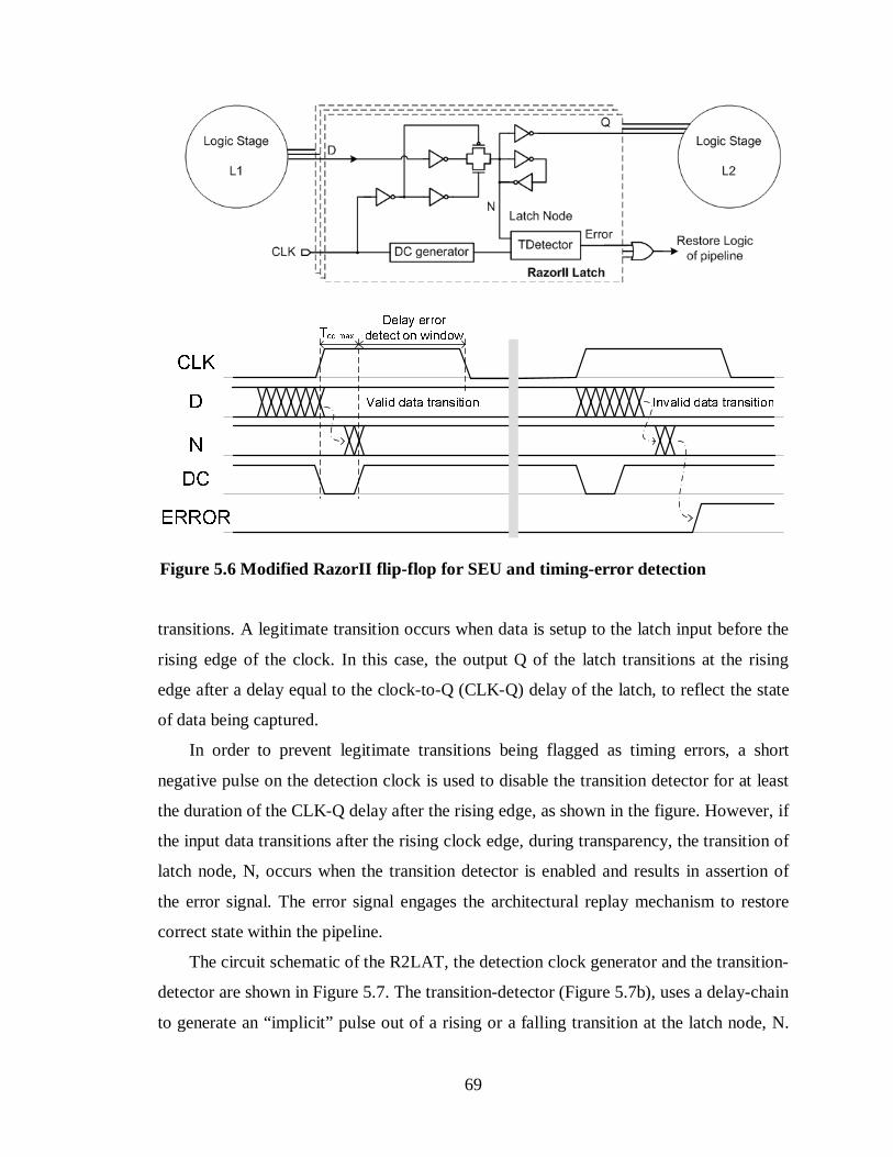
69
transitions. A legitimate transition occurs when data is setup to the latch input before the
rising edge of the clock. In this case, the output Q of the latch transitions at the rising
edge after a delay equal to the clock-to-Q (CLK-Q) delay of the latch, to reflect the state
of data being captured.
In order to prevent legitimate transitions being flagged as timing errors, a short
negative pulse on the detection clock is used to disable the transition detector for at least
the duration of the CLK-Q delay after the rising edge, as shown in the figure. However, if
the input data transitions after the rising clock edge, during transparency, the transition of
latch node, N, occurs when the transition detector is enabled and results in assertion of
the error signal. The error signal engages the architectural replay mechanism to restore
correct state within the pipeline.
The circuit schematic of the R2LAT, the detection clock generator and the transition-
detector are shown in Figure 5.7. The transition-detector (Figure 5.7b), uses a delay-chain
to generate an “implicit” pulse out of a rising or a falling transition at the latch node, N.
CLKDNDCERRORTcq max Valid data transition Invalid data transitionDelay error detection window
Figure 5.6 Modified RazorII flip-flop for SEU and timing-er ror detection
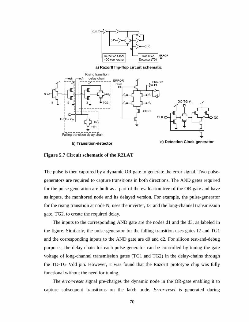
70
The pulse is then captured by a dynamic OR gate to generate the error signal. Two pulse-
generators are required to capture transitions in both directions. The AND gates required
for the pulse generation are built as a part of the evaluation tree of the OR-gate and have
as inputs, the monitored node and its delayed version. For example, the pulse-generator
for the rising transition at node N, uses the inverter, I3, and the long-channel transmission
gate, TG2, to create the required delay.
The inputs to the corresponding AND gate are the nodes d1 and the d3, as labeled in
the figure. Similarly, the pulse-generator for the falling transition uses gates I2 and TG1
and the corresponding inputs to the AND gate are d0 and d2. For silicon test-and-debug
purposes, the delay-chain for each pulse-generator can be controlled by tuning the gate
voltage of long-channel transmission gates (TG1 and TG2) in the delay-chains through
the TD-TG Vdd pin. However, it was found that the RazorII prototype chip was fully
functional without the need for tuning.
The error-reset signal pre-charges the dynamic node in the OR-gate enabling it to
capture subsequent transitions on the latch node. Error-reset is generated during
c) Detection Clock generator b) Transition-detector
a) RazorII flip-flop circuit schematic
Figure 5.7 Circuit schematic of the R2LAT

71
architectural recovery in the event of a timing error. A cross-coupled inverter pair is used
as a latch structure to protect the dynamic node from discharge due to leakage.
5.5.1 Impact of intra-die process-variability
As explained previously, the low-pulse on DC, temporarily disables the transition-
detector to prevent legitimate transitions at the latch node from being flagged as errors.
For correct functionality, it is required that the minimum width of the low pulse at the DC
clock is greater than the maximum CLK-Q delay of the main latch across all PVT corners.
We used conventional worst-case sizing of the transistors in the DC-generator to achieve
this relationship on the test-chip. Guaranteeing this relationship in the face of rising intra-
die process variability at 45nm and below may require the use of Monte-Carlo sampling
techniques. This is illustrated in the timing diagrams shown in Figure 5.8. For a 3-sigma
yield, it is required to ensure that the DC-generator is sized such that the worst-case 3-
sigma increase of the CLK-Q delay of the latch is still covered by the worst-case 3-sigma
decrease in the DC pulse-width.
Nom CLK-Q 3σσσσ CLK-Q
CLK
D
N
DC
ERROR
Nom PW
3σσσσ PW
Nom = NominalPW = DC Pulse Width
3σσσσ increase in latch delay is less than 3 σσσσ reduction in DC pulse-width
Figure 5.8 Timing constraints with intra-die process variations
72
To support post-manufacture tuning, the delay chain is made tunable to account for
process variation mismatches between the latch delay and detection-clock pulse-width by
controlling the gate voltage of the transmission gate through DC-TG Vdd. Again, tuning
was not required for the normal operation of the chip. The DC-TG Vdd pin of individual
R2LATs were routed as conventional signal nets with an input pad serving as a common
driver. The TD-TG Vdd pin was also routed in a similar manner. These pins have relaxed
timing constraints since they are only meant for post-manufacture tuning.
The difference between the CLK-Q delay and the DC pulse-width represents the
duration when a transition on N goes undetected. This allows dynamic time-borrowing in
the R2LAT wherein a critical computation gets extra time from the next cycle to
complete, without flagging a timing error. Of course, this reduces the available time for
the succeeding pipestage. However, if a time-borrowing critical computation is followed
by a non-critical computation in the succeeding pipeline stage, then no timing errors will
be flagged. Thus, the pipeline can potentially operate at a frequency greater than what is
dictated by the critical path of the circuit. A larger value of the DC pulse-width allows
greater scope for dynamic time-borrowing, although at the expense of reducing the
available time for error detection. Thus, the DC pulse-width represents the trade-off
between dynamic time-borrowing versus timing speculation available on the critical path
of the circuit.
The duration of suppression of the transition-detector, denoted by the DC pulse-
width needs to be greater than the CLK-Q delay of the actual latch across all PVT
corners. In the RazorII prototype processor, we ensured this through conservative sizing
during design time. At the slow corner (at 130nm technology node), the DC pulse width
is 350ps and the actual CLK-Q delay of the latch is 200ps leading to a margin of 150ps at
the slow corner. As explained previously, a higher value of the DC pulse-width reduces
the PoFF through dynamic time-borrowing at the expense of reducing the speculation
time available. Thus, reduction in energy savings due to reduced speculation is counter-
balanced by the energy gain due to a lower PoFF. Hence, it is unlikely that the margin in
the DC pulse width has a significant impact on the total energy savings of the processor.

73
5.5.2 SEU Detection using the R2LAT
The transition detector is always enabled except for the period after the rising edge
of the clock where valid transitions occur. This naturally allows the R2LAT to detect and
flag SEUs on the latch node as well as in the combinational logic that fans in to it. The
voltage pulse due to a SEU event in the combinational logic can possibly propagate to a
R2LAT in the transparent phase of the clock, leading to a glitch in the latch node. If the
glitch is sufficiently wide, the transition detector interprets the glitch as a combination of
two transitions and flags it as a timing error. Of course, in the low-phase of the clock, the
SEU pulse is benign, as it can never propagate to the latch node.
Figure 5.9 Conceptual timing diagrams showing SEU detection when DC is high

74
A particle strike on the latch node, N, leads to a single transition causing a state flip
to occur when the clock is low, as shown in Figure 5.9(a). A high energy particle strike at
N (Figure 5.9(b)) leads to a pulse when the strike occurs in the transparent phase of the
clock. In both the cases of Figure 5.9(a) and (b), the TD successfully detects the event
and flags an error. A weak pulse due to SEU in the transparent clock phase, shown in
Figure 5.9(c), can go undetected by the TD but it can possibly cause a glitch in the
output, Q. If the glitch is amplified by the downstream logic, it will still be flagged by a
R2LAT in the succeeding stage, leading to an error.
An interesting case to consider is when the SEU pulse occurs while the detection
clock is low. There can be three possible scenarios that follow as illustrated in the timing
diagrams in Figure 5.10:
Case I: The pulse occurs and dies before the detection clock is enabled as shown in
Figure 5.10(a). In such a case, the transition detector does not flag an error since the latch
node, N, is restored to its correct state before the detection clock is enabled. Since no
state corruption occurs, this is essentially benign.
Case II: The pulse on N initiates when the detection clock is low but N recovers
correct state after the rising edge of the detection clock (Figure 5.10(b)). In such a case,
the transition detector responds to the trailing edge of the pulse and flags an error. While
the pulse does revert back to its correct state, it does so after the DC has reengaged and
hence, it is correctly interpreted as a timing error.
Case III: Figure 5.10 (c) illustrates the case when a SEU pulse actually causes state
corruption to occur at the latch node, N, without an error being flagged. This is a special
condition which occurs when the width of the DC pulse is equal to the width of high
phase of clock. As shown in the figure, if the SEU pulse occurs just before the falling
edge of the clock, then the latch node, N, samples the leading edge of the pulse and is
unable to revert back to its correct state.
This is because the main latch enters into its opaque phase just before the trailing
edge of the pulse occurs. In essence, the SEU pulse degenerates into a single transition at
the latch node, N. Since this transition occurs when the detection clock is low, the
transition detector does not flag this as a timing error, leading to system failure.
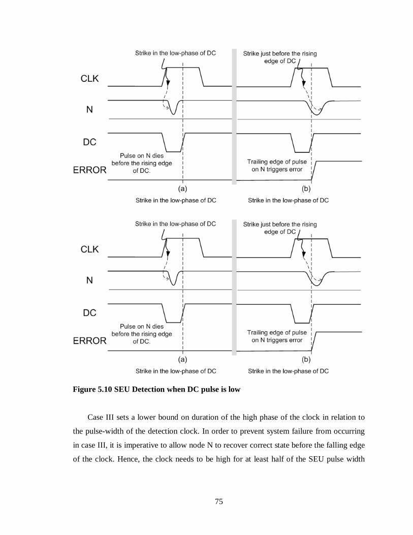
75
Case III sets a lower bound on duration of the high phase of the clock in relation to
the pulse-width of the detection clock. In order to prevent system failure from occurring
in case III, it is imperative to allow node N to recover correct state before the falling edge
of the clock. Hence, the clock needs to be high for at least half of the SEU pulse width
Figure 5.10 SEU Detection when DC pulse is low

76
after the rising edge of the detection clock. This allows N to follow the trailing edge of
the pulse and achieve correct state as shown in Figure 5.10(d).
For the RazorII prototype processor that we present in Chapter 7, we chose this
minimum overlap to be 100ps at the typical corner at the 130nm technology node. The
trailing edge of the pulse occurs after the transition-detector has been enabled and hence
is flagged as an error, thus maintaining correct operation in the pipeline.
5.5.3 Comparative Analysis with the RazorI flip-flop
The RazorI flip-flop detects late-arriving data by comparing the flip-flop state with
that of a “shadow” latch which samples off the negative edge of the clock. In total it
consists of three latches (master, slave and shadow), a comparator and a meta-stability
detector. The implementation requires 76 transistors. Compared to a conventional flip-
flop, the RazorI flip-flop has a worse CLK-Q delay for the same drive strength due to the
extra loading of the metastability-detector and the error comparator. Its setup time is the
same or slightly worse than a library flip-flop. It consumes 25% extra power when data
does not switch (due to transitions on clock) and 70% extra power when data switches.
Thus, for a 10% activity rate, the total power overhead of the RazorI flip-flop is 30%
when compared to a conventional flip-flop. For our implementation of the RazorI
processor in [10], we needed to use the RazorI flip-flop only for timing-error protection
on the critical paths. Hence, the net power overhead of using RazorI flip-flops was less
than 3% of the total chip power.
The elimination of the master latch and the metastability-detector in the R2LAT are
significant simplifications that lead to improvements in delay, power and area. The
R2LAT uses 47 transistors in total. The elimination of the master latch leads to slightly
improved CLK-Q delay compared to a conventional flip-flop. In addition, it completely
eliminates the setup time constraint at the positive edge of the clock. Thus, the R2LAT
can be effectively modeled as having 0ps setup time. The power overhead compared to a
conventional flip-flop of the same drive strength for a 10% activity factor is 28.5%. The
total power overhead due to insertion of R2LATs in the processor was 1.2%.
Metastability risks at the positive edge of the clock for the latch data-path are completely
eliminated, thereby precluding the need for a metastability-detector.
77
As mentioned before, the generation of the detection clock could be easily shared
across multiple R2LATs. Such an implementation requires 39 transistors in total as
opposed to 76 transistors used for the RazorI flip-flop. In addition, it requires just a single
additional transistor on clock for error evaluation. In total, it has 5 transistors on a clock
as compared to 14 clock transistors in the RazorI flip-flop. Thus when compared to a
conventional flip-flop, for an activity factor of 10%, it consumes 11% less power based
on a simulation analysis. This is a significant reduction compared to the RazorI flip-flop
which consumes 30% extra power. In the actual implementation of the processor, the
detection clock was generated locally within each R2LAT and was not shared.
5.6 Memory design for a Razor processor core
The pipeline output from the write-back stage of a Razorized processor core is
speculative and hence, potentially incorrect. We address critical Register File read and
write operations by replicating the Register File and using the speculative version as the
working register set for pipeline operations. The speculative Register File is updated from
the guaranteed-correct, golden Register File during recovery. However, replication
cannot be used for on-chip cache memory because it incurs prohibitive power and area
overhead. Therefore, we modify conventional SRAM structures in order to handle
speculative load and store operations without causing state corruption inside the bit-cell
array.
Speculative memory stores can be pipelined in a stabilization queue. The
stabilization queue provides the extra latency required for the Razor error detection
infrastructure to check for timing-errors in the store data. Thus, the store stabilization
queue not only delays data commits to memory to allow for Razor validation, but also
serves the purpose of a store buffer that exists in most high-throughput memory systems.
5.6.1 Handling speculative read accesses to the memory
Memory load operations cannot be pipelined in a non-speculative queue (as in the
case of store operations) because doing this incurs significant Instruction Per Cycle (IPC)
penalty. For most microprocessors, load operations are accompanied by address
calculations and are therefore timing-critical. Consequently, all the signals involved in a
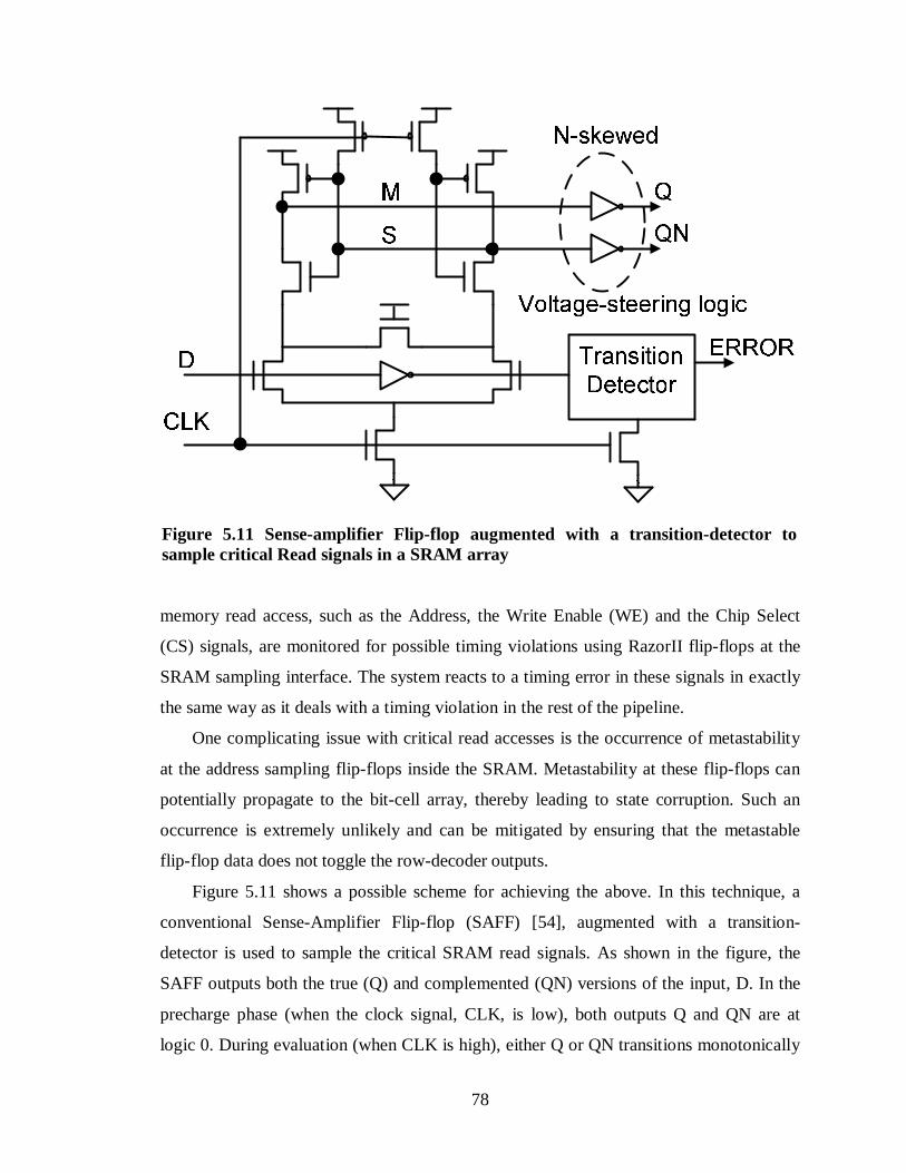
78
memory read access, such as the Address, the Write Enable (WE) and the Chip Select
(CS) signals, are monitored for possible timing violations using RazorII flip-flops at the
SRAM sampling interface. The system reacts to a timing error in these signals in exactly
the same way as it deals with a timing violation in the rest of the pipeline.
One complicating issue with critical read accesses is the occurrence of metastability
at the address sampling flip-flops inside the SRAM. Metastability at these flip-flops can
potentially propagate to the bit-cell array, thereby leading to state corruption. Such an
occurrence is extremely unlikely and can be mitigated by ensuring that the metastable
flip-flop data does not toggle the row-decoder outputs.
Figure 5.11 shows a possible scheme for achieving the above. In this technique, a
conventional Sense-Amplifier Flip-flop (SAFF) [54], augmented with a transition-
detector is used to sample the critical SRAM read signals. As shown in the figure, the
SAFF outputs both the true (Q) and complemented (QN) versions of the input, D. In the
precharge phase (when the clock signal, CLK, is low), both outputs Q and QN are at
logic 0. During evaluation (when CLK is high), either Q or QN transitions monotonically
`QQNDCLK
N-skewed Voltage-steering logicTransition Detector` ERRORSM
Figure 5.11 Sense-amplifier Flip-flop augmented with a transition-detector to sample critical Read signals in a SRAM array
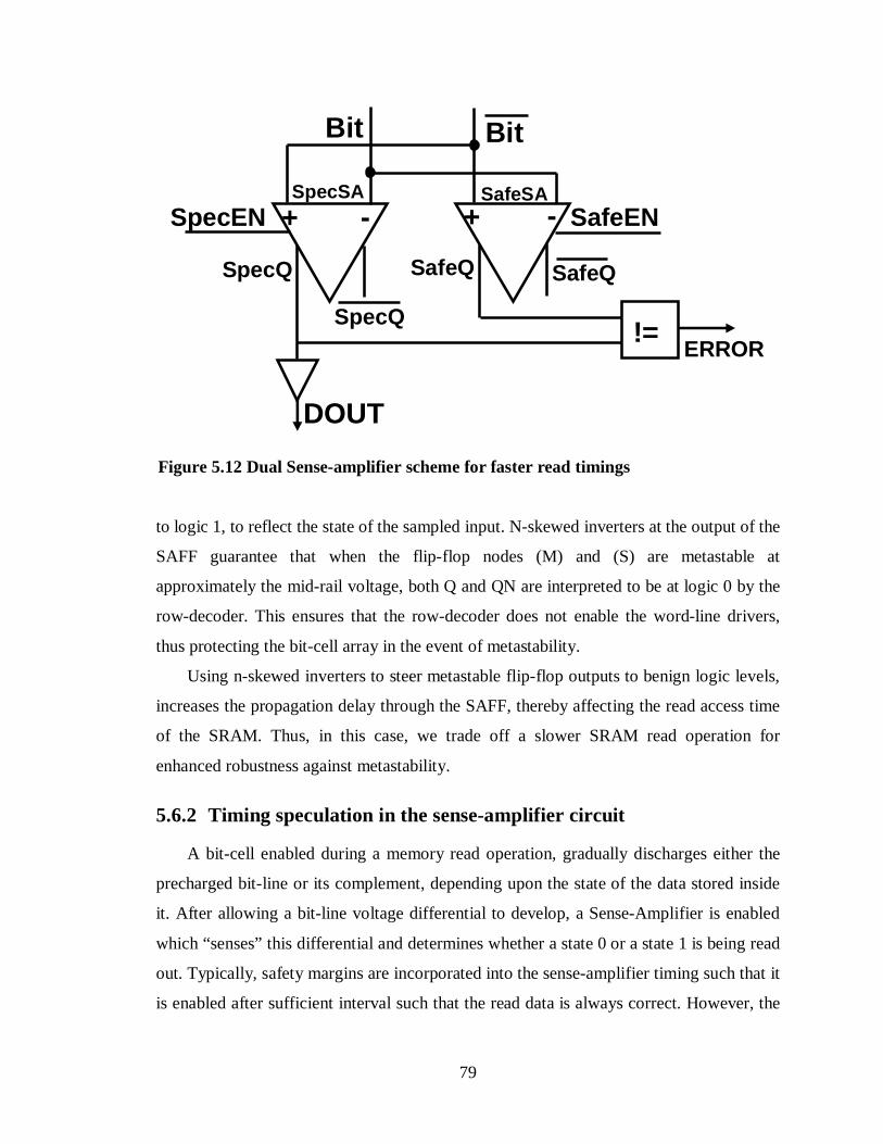
79
to logic 1, to reflect the state of the sampled input. N-skewed inverters at the output of the
SAFF guarantee that when the flip-flop nodes (M) and (S) are metastable at
approximately the mid-rail voltage, both Q and QN are interpreted to be at logic 0 by the
row-decoder. This ensures that the row-decoder does not enable the word-line drivers,
thus protecting the bit-cell array in the event of metastability.
Using n-skewed inverters to steer metastable flip-flop outputs to benign logic levels,
increases the propagation delay through the SAFF, thereby affecting the read access time
of the SRAM. Thus, in this case, we trade off a slower SRAM read operation for
enhanced robustness against metastability.
5.6.2 Timing speculation in the sense-amplifier circuit
A bit-cell enabled during a memory read operation, gradually discharges either the
precharged bit-line or its complement, depending upon the state of the data stored inside
it. After allowing a bit-line voltage differential to develop, a Sense-Amplifier is enabled
which “senses” this differential and determines whether a state 0 or a state 1 is being read
out. Typically, safety margins are incorporated into the sense-amplifier timing such that it
is enabled after sufficient interval such that the read data is always correct. However, the
+ -
SpecQ
SpecQ
+ -
SafeQ SafeQ
!=
SpecEN SafeEN
Bit Bit
DOUT
ERROR
SpecSA SafeSA
Figure 5.12 Dual Sense-amplifier scheme for faster read timings
80
safety margins have the undesirable effect of limiting the speed of the read operation by
delaying the point when the Sense-Amplifier is enabled. Using timing-speculation, it is
possible to eliminate these safety margins and achieve faster SRAM read access timing
by enabling the Sense-amplifier early, even when the bit-line differential is inadequate
for correct operation in the worst-case.
This concept of timing speculation in the sense-amplifiers is illustrated in Figure
5.12. The key idea in this technique is to use two sense-amplifiers to sense the bit-line
differential at two different points in time. The speculative sense-amplifier (SpecSA) is
enabled earlier and can therefore read out a potentially incorrect signal when the bit-line
differential is not sufficiently developed. The output of the speculative sense-amplifier is
validated against the data read out by a non-speculative sense-amplifier (SafeSA) enabled
later, the timing of which is generously margined using conventional worst-case
assumptions. An error signal is flagged when the data read out of the speculative sense-
amplifier does not match with the correct data read out from the non-speculative sense-
amplifier. The system responds to this error signal by forwarding the correct output from
the non-speculative sense-amplifier to the downstream pipeline stage.
A separate error controller is used to monitor the error-rate of the speculative
sense-amplifier. The error-controller tunes its enable timing to achieve a targeted error-
rate.
5.7 Summary and discussion
In this chapter, we introduced the RazorII error-detection and recovery scheme.
Timing-error detection occurs within a RazorII flip-flop, using a so-called transition-
detector, which flags spurious transitions in the critical-path output during the speculation
window. Monitoring for timing-errors before the onset of the setup window of the flip-
flop precludes the need for a metastability-detector, thereby greatly reducing the area and
the power overhead of the RazorII flip-flop.
We showed an alternative design of a RazorII flip-flop, called the R2LAT, which
enables both timing-error and SEU detection inside registers and combinational logic.
The R2LAT uses a level-sensitive latch, instead of a flip-flop, as the main state-holding,
sequential element. Positive-edge triggered flip-flop operation is enforced by a transition-

81
detector, controlled by a detection clock, which flags any transition on the latch node in
the high-phase of the clock as a timing error. SEUs manifest as voltage pulses which can
cause bit-flips in the latch node. The resultant transition can be flagged as an error by the
transition-detector.
We showed the design of a generic, 5-stage, in-order RazorII pipeline based on
check-pointing and replay architecture. After an instruction has been validated to be
correct, it is check-pointed before being committed to storage. Recovery is achieved by
flushing the pipeline and re-executing from the check-pointed state. We discussed the
design of the memory system which interfaces to a timing-critical RazorII pipeline.
We implemented RazorII in a 64bit processor for tolerance against SEU and PVT
variations. We present the measurement results from this processor in Chapter 7. In the
next chapter, we discuss schemes that mitigate the stringent minimum-delay requirement
in Razor-based pipelines.

82
CHAPTER 6
ALTERNATIVE HOLD-FIXING SCHEMES FOR RAZOR-BASED PIPELINES
Razor timing speculation imposes a fundamental minimum delay constraint which
requires that every combinational path fanning into a Razor flip-flop needs to be at least
greater than the positive clock-phase and the hold time of the shadow latch (in case of
RazorI) or the transition-detector (in case of RazorII). In the traditional approach, this
constraint is met by inserting delay buffers in the short-paths that violate the minimum-
delay constraint. Using suitable clock-chopping techniques, a high phase of the clock is
generated such that there are no short-path violations across all process, voltage and
temperature corners. Typically, clock-choppers rely on delay-chains which gate the
conventional fifty-percent duty cycle clock to obtain an output clock with the same
frequency but an asymmetric duty cycle. The delay through the chain determines the
duration of the high-phase of the output clock. Conventional timing analysis is then
performed to ensure that the minimum-delay constraint is met across all corners for the
high-phase thus determined during design time.
The issue with this approach is that the propagation delay through the delay-chain
used to generate the high-phase of the processor clock can vary with variations in PVT
conditions. In addition, it is likely to have different scaling characteristics compared to
the actual short-paths in the design. This mismatch in scaling characteristics is especially
accentuated for simple gates used in the delay-chain, such as inverters, compared to more
complex gates in actual paths. Due to these reasons, safety margins are incorporated
either through additional buffer insertion on short-paths or by using a narrower high-
phase of the clock. Additional buffer insertion adversely impacts power consumption of
the design. Similarly, using a narrower high-phase limits the available speculation time
for Razor. A possible alternative is to use a tunable delay chain to control the high-phase

83
of the clock on a per die basis. Thus, the high-phase of the clock is adjusted on the tester
to a level wherein no short-path violations are observed. However, this approach is
complicated and requires additional tester-time which adversely impacts yield economics.
For most processors, buffer-insertion based hold-fixing effectively achieves the
minimum-delay constraint without adding significant overhead. For example, the power
overhead of hold-fixing was less than 3% of the total chip power for both the RazorI and
the RazorII prototype processors. However, at aggressive process nodes, increasing
variability in the short-paths can significantly worsen the hold-time constraint through the
requirement of large number of delay buffers. In addition to the area and power overhead,
excessive buffer insertion adversely affects the critical-path timing as well, thereby
impacting performance.
In the following sections, we present alternative techniques to buffer-insertion based
hold-fixing. These techniques address the impact of variability in short-paths to achieve
very high speculation times while using conventional 50percent duty-cycle clocking. We
discuss the relative merits and demerits of each scheme. The remainder of the chapter is
organized as follows. Section 6.1 discusses insertion of level-sensitive latches halfway
through the combinational logic to satisfy the hold requirement at destination Razor flip-
flops. Section 6.2 deals with a Razor-like scheme from Intel, called the X-Pipe micro-
architecture, which staggers the cycles where new data is launched and old computation
is checked for errors, in order to eliminate the hold-requirement. The BLADES technique
for statically-scheduled processor is presented in Section 6.3. Section 6.4 discusses the
design of a pulsed-latch based RazorII flip-flop which uses a narrow pulse to relax the
hold constraint and simplify clocking. Finally, we summarize this chapter in Section 6.5.
6.1 Level-sensitive latch based scheme for hold-fixing
The key idea of this scheme is to divide the combinational logic within a pipeline
stage into two equal portions with critical-path delay equal to half of the critical-path of
the unmodified pipestage. Level-sensitive latches are inserted between the two blocks of
logic thus created. These latches are transparent in the negative phase of the clock and
sample in the positive phase of the clock. Figure 6.1 conceptually illustrates this scheme
of pipeline transformation. The inputs to the Razor flip-flops are prevented from being

84
updated by short-path computations in the positive phase, due to the opaque latches. This
guarantees, by construction, that the transitions which occur at the Razor flip-flop inputs
in the high clock-phase are valid timing errors caused due to setup violations. A point to
note here is that the level-sensitive latches are required only in the logic cones that fan-
out to Razor flip-flops.
This approach guarantees half-cycle speculation time. However, the additional
latches greatly increase the clock load in this scheme, thereby significantly increasing the
pipeline power consumption. Consequently, such a scheme can only be used in
applications where the combinational power is a significant portion of the total power,
such as in graphics processors and hardware accelerators. Due to its significant power
overhead, this scheme is not amenable for general-purpose computing.
Another weakness of this scheme is that it introduces phase-paths which adversely
impact the error-rate. The trade-off between the error-rate and the phase path timings is
shown in Figure 6.2. In the figure, the latency through the positive phase logic is labeled
as Tpos and that through the negative phase logic is labeled, Tneg. Even if the positive
phase logic finishes early, the pipeline has to wait until the negative clock-edge in order
to resume computation. The computational time wasted in the positive phase due to this
is labeled as Twaste. Due to the wasted time, previously non-critical paths can become
critical and contribute to the error-rate.
Conditionally Retimed Razored Pipeline
RFF
Normal FF
T-Latch
Stage 1 Stage 2Tcycle/2 Tcycle/2
CLK
CKN
Combinational
Logic
CLK
Stage 1 Stage 2Tcycle
Original Non-Razored Pipeline
Combinational
Logic
CLK
Stage 1 Stage 2Tcycle
Original Non-Razored Pipeline
Figure 6.1 Latch-insertion scheme for satisfying the short-path constraint

85
The key advantage of this scheme is that conventional fifty percent duty cycle
clocking can be used. This greatly simplifies the clock-generation and propagation. In
addition, it is highly resilient to variability on the short-paths of the processor and
eliminates the safety margins required to meet the minimum delay constraint.
The key disadvantage of this scheme, as discussed before, is that it increases clock-
tree loading and contributes significantly to the total power overhead. Several
optimizations can be performed to mitigate the power overhead of this approach. Firstly,
the clock-tree for the hold-fixing latches is not limited by skew constraints unlike in a
conventional clock-tree. Hence, a low-performance clock-tree can be deployed for hold-
fixing latches, thereby bringing down the total power overhead. In addition, the latches
can be clock-gated when either the producer flip-flops in its fan-in or consuming flip-
flops in its fan-out are clock-gated.
6.2 Intel X-pipe
In [48], the authors present a new micro-architecture, called the X-Pipe, where error-
detection is achieved using a Razor-like technique that eliminates the minimum-delay
constraint of Razor. As shown in Chapter 3, the minimum-delay constraint in Razor
arises because the duration after the positive clock-edge when the output of the previous
Tpos Twaste
R_CLK
Tneg
“Error”
RFF
Stage 1 Stage 2Tpos Tneg
CKN
Figure 6.2 Error-rate and wasted-time trade-off
86
computation is being monitored for timing errors, new data can potentially race-through
and overwrite the previous results (Figure 3.2). The key idea in the X-Pipe approach is to
stagger the clock edges when a new computation is initiated and when the output of the
previous computation is checked for correctness. By launching a new computation and
validating a previous computation at different clock edges, the minimum-delay constraint
is eliminated, by construction.
Figure 6.3 shows the pipeline organization in the X-pipe technique. The entire data-
path is divided into positive and negative phase logic. Data launched at the positive edge
is speculatively captured at the negative clock-edge by the next pipeline stage. This
speculative sample is then forwarded onto the consuming negative-phase logic and vice
versa. Each error-detecting flip-flop is augmented with a shadow flip-flop which samples
the always-correct output of the producer logic at the next launching edge. As an example,
when the main flip-flop captures data at the negative clock-edge, the corresponding
shadow flip-flop captures the same input at the next positive edge. Thus, the shadow flip-
flop input gets the entire cycle to achieve correct state whereas the main flip-flop
speculatively samples data midway through the clock-cycle. Error is flagged by
comparing the shadow flip-flop output with the speculative sample. Recovery occurs
through a replay mechanism based on check-pointing.
In the X-pipe approach, launch and capture edges are separated by half of a clock
cycle. This eliminates the minimum-delay constraint by construction. While this is a
major advantage of this approach, however, it imposes formidable design and
implementation challenges that severely limit its applicability to generic pipeline designs.
Firstly, the pipeline needs to be partitioned in such a way that computed results are
forwarded to a stage that launches on the opposite clock-phase. This greatly complicates
pipeline designs with large number of inter-stage forwarding paths.
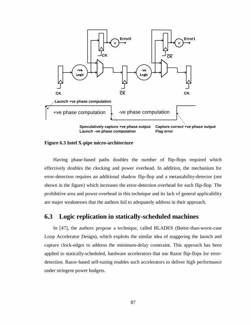
87
Having phase-based paths doubles the number of flip-flops required which
effectively doubles the clocking and power overhead. In addition, the mechanism for
error-detection requires an additional shadow flip-flop and a metastability-detector (not
shown in the figure) which increases the error-detection overhead for each flip-flop. The
prohibitive area and power overhead in this technique and its lack of general applicability
are major weaknesses that the authors fail to adequately address in their approach.
6.3 Logic replication in statically-scheduled machines
In [47], the authors propose a technique, called BLADES (Better-than-worst-case
Loop Accelerator Design), which exploits the similar idea of staggering the launch and
capture clock-edges to address the minimum-delay constraint. This approach has been
applied to statically-scheduled, hardware accelerators that use Razor flip-flops for error-
detection. Razor-based self-tuning enables such accelerators to deliver high performance
under stringent power budgets.
+veLogic Error0== -veLogic Error1
==
CK CK CK
+ve phase computation -ve phase computation
Launch +ve phase computation
Speculatively capture +ve phase output Launch –ve phase computation
Capture correct +ve phase output Flag error
CK CK
Figure 6.3 Intel X-pipe micro-architecture

88
The key idea in BLADES is to combine multiple Functional Units (FUs), such as an
adder and a shifter, into 2-cycle “custom functional units” (CFUs), as shown in Figure
6.4(b). A CFU uses two cycles to execute two or more operations back-to-back. Its inputs
are only changed every other cycle and the values computed, after one cycle, are stored in
a register. This way, the values that fan-in to Razor flip-flops are guaranteed not to
change during the speculation window unless there is a timing error, thereby eliminating
the need to insert extra buffers. Note that in the example shown in Figure 6.4(b), if there
are two successive add instruction, then the adder block has to be replicated so as to
prevent a stall cycle. In statically scheduled machines, code analysis and compiler
optimizations can ensure that a particular Functional Unit is not exercised in successive
cycles, thereby minimizing logic replication.
Figure 6.4 Replicated functional units eliminate the Razor minimum-delay constraint

89
The CFUs are identified by the compiler after analyzing the dataflow between
different instructions. It is possible to extend this technique to general-purpose processors
wherein each functional unit is replicated and an individual block is sensitized once every
two cycles. However, since this entails significant logic and flip-flop replication, in-depth
analysis is required before such a technique can be applied to general-purpose processors.
6.4 RazorII flip-flop with integrated clock-pulse generator
In the RazorII approach, the system tunes itself for the Point of First Failure (PoFF).
Consequently, in such systems wider speculation windows are not required. This
observation is exploited in the design of the RazorII flip-flop, shown in Figure 6.5. The
design is essentially a pulsed-latch which uses a locally generated clock-pulse to obtain
the speculation window for error-detection. The transition-detector monitors the flip-flop
input instead of the internal latch-node which limits its SEU detection capability. The
clock-pulse generator could be integrated within the RazorII flip-flop (similar to the
design of the R2LAT) or it could be a part of a clock-gating cell which drives a bank of
RazorII flip-flops.
The key advantage of this scheme is that a narrow clock-pulse can be used to drive
the RazorII flip-flop. This significantly reduces the minimum-delay requirement. In
addition, primary clock-tree of the processor is driven by a conventional 50% duty cycle
clock which greatly simplifies the pipeline clock-generation. Furthermore, by integrating
the clock-pulse generator within the RazorII flip-flop the ease of pulse-generation can be
traded off for increased power consumption within each flip-flop. The alternative
technique of using a local clock-gating cell to drive the clock-pulse ensures that the
narrow pulse is driven to very short distances and therefore sees a low interconnect (RC)
load. This mitigates possible “pulse-evaporation” concerns.
The key disadvantage of this scheme is that it increases susceptibility to possible
delay “overshoots” wherein a transient noise or supply-voltage glitch suddenly increases
the critical-path delay to an extent that it entirely misses the error-detection window.
However, the transition-detector can be enabled before the rising edge of the clock,
thereby increasing the effective error-detection window. However, this incurs a

90
performance overhead since the PoFF as seen by the transition-detector, occurs before the
PoFF of the actual processor critical-path.
6.5 Summary and discussion
In this chapter, we discussed several techniques that address the hold-fixing
requirement in the Razor technique. We presented the transparent-latch insertion scheme
which inserts negative-level sensitive latches midway through the data-path such that no
short-path race-through can occur during the high-phase of the clock. This technique
guarantees achieving the minimum-delay constraint by construction, however, suffers
from significant clock-power overhead. Consequently, such a technique may be more
suited towards signal-processing applications where the combination logic power can
dominate over sequential power.
We surveyed the Intel X-pipe technique which is a novel method that divides the
data-path into positive-phase and negative-phase logic. Execution output is speculatively
captured at the opposite clock-edge whereas error-detection occurs at the next launching
edge. By staggering launch and capture cycles, it is possible to avoid the minimum-delay
constraint. However, this technique suffers from its complicated micro-architecture and
Figure 6.5 Pulsed-latch implementation of the RazorII flip-flop. The transition-detector monitors the data input rather than the internal node.

91
its inability to effectively handle forwarding paths. In addition, it doubles the number of
registers required in the data-path and significantly adds to the power-overhead of
detection. Hence, this technique has limited applicability.
We surveyed another technique for statically-scheduled machines based on
replication of combinational logic blocks. The key idea in this technique is to merge FUs
into so-called CFUs (custom functional units) and to issue operands to a CFU not faster
than once every two cycles. Stall cycles are avoided by replicating a CFU, if it is
exercised in successive cycles. The combinational logic blocks that require replication
can be identified by the compiler.
We presented the design of a pulsed-latch based design of the RazorII flip-flop
which uses a narrow speculation window. Targeting the PoFF rather than aggressive sub-
critical operation presents opportunities for trading-off setup time pessimism for low
buffer-insertion overhead, in this technique. In addition, it is possible to split the clock-
tree and route a wider high-phase clock to critical RazorII flip-flops and to use a narrower
high-phase for the relatively non-critical RazorII flip-flops. We exploit the latter scheme
in the design of the RazorII processor which is presented in the next chapter.
92
CHAPTER 7
SELF-TUNING RAZOR II PROCESSOR: USING RAZOR II FOR PVT AND SER TOLERANCE
RazorII was incorporated in a 64bit, 7 stage, in-order Alpha processor in an
industrial 0.13µm technology [44] [45]. We use the modified RazorII flip-flop, called the
R2LAT (Section 5.4), for both timing-error detection and Soft Error Rate (SER)
tolerance. We have described in detail the basic design and the principle of operation of
the R2LAT in Section 5.4. The remainder of this chapter is organized as follows. In
Section 7.1, we present the pipeline details and the modifications required to the basic 5-
stage pipeline to support detection and correction of Single Event Upsets (SEU) in
SRAM arrays and architectural-state registers that are not protected using R2LAT error-
detection capability. We present potential techniques that restrict voltage and frequency
scaling to safe limits in RazorII-based systems in Section 7.2. Section 7.3 discusses the
measured energy savings from RazorII based supply voltage control on 33 tested dies.
We present measurement results from SER tests in Section 7.4.
7.1 Pipeline design of the RazorII processor
The pipeline design for the prototype RazorII processor is based on the architecture
of a generic, in-order RazorII pipeline as illustrated in Figure 5.2. However, it includes
additional features to support detection and recovery in the presence of SEU in memory
arrays and architectural-state registers. The pipeline, shown in Figure 7.1, can be broadly
divided into a speculative domain which is timing-critical and a non-speculative domain
with sufficient timing slack. The speculative domain consists of a two-stage fetch stage
(IF1 and IF2), instruction decode (ID), an integer execution unit (EX) and the memory
access (MEM) stage. All pipeline registers in the speculative domain require RazorII
protection against state corruption due to SEU. The error pins of individual R2LATs in
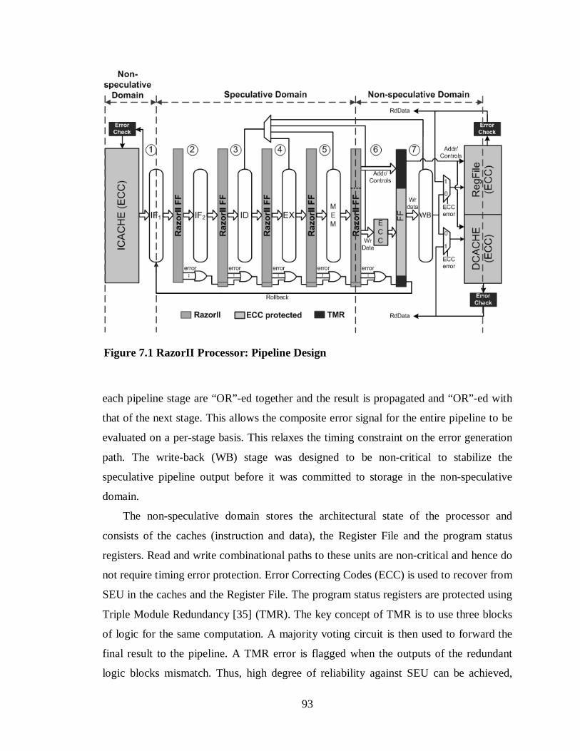
93
each pipeline stage are “OR”-ed together and the result is propagated and “OR”-ed with
that of the next stage. This allows the composite error signal for the entire pipeline to be
evaluated on a per-stage basis. This relaxes the timing constraint on the error generation
path. The write-back (WB) stage was designed to be non-critical to stabilize the
speculative pipeline output before it was committed to storage in the non-speculative
domain.
The non-speculative domain stores the architectural state of the processor and
consists of the caches (instruction and data), the Register File and the program status
registers. Read and write combinational paths to these units are non-critical and hence do
not require timing error protection. Error Correcting Codes (ECC) is used to recover from
SEU in the caches and the Register File. The program status registers are protected using
Triple Module Redundancy [35] (TMR). The key concept of TMR is to use three blocks
of logic for the same computation. A majority voting circuit is then used to forward the
final result to the pipeline. A TMR error is flagged when the outputs of the redundant
logic blocks mismatch. Thus, high degree of reliability against SEU can be achieved,
Figure 7.1 RazorII Processor: Pipeline Design

94
although at the cost of redundant logic and registers. TMR allows SEU errors in the
architectural state registers to be corrected on-the-fly and no extra recovery mechanism is
required.
Data from the speculative pipeline is encoded before the write-back stage. The data
word and the corresponding redundant bits are then written into storage. Thus, the ECC
encoder adds 22 redundant bits to the 64bit data for a Data-Cache (DCache) and Register
File write access and 17 redundant bits for a 32bit Instruction-Cache (ICache) write
access. On a read access, the ECC decoder operates on the obtained code word and
determines if a state flip has occurred, while in storage. In the event of an error, the data
word is corrected and forwarded into the pipeline and the corrected word is recommitted
to storage. The ECC decoder can correct one random bit flip and up to 4 consecutive bit-
flips in the data word. Both ECC and TMR errors are corrected in-place and do not
engage the pipeline recovery mechanism.
Replay is achieved by check-pointing the Program Counter (PC) register in the WB
stage of the pipeline. The Program Counter (PC) register is passed along the Razor
pipeline. When an error is detected, the entire pipeline is flushed and the PC in the fetch
stage is overwritten with the PC in the WB stage. Normal instruction execution resumes
from then on. The PC in the WB stage is protected from SEU through TMR. Since an
erroneous instruction is re-executed through the pipeline during replay, the same
instruction can suffer repeated timing errors. Hence, it is required to monitor the
instruction being replayed to detect a deadlock situation. When the number of replay
iterations for the same instruction reaches a certain threshold, called the “replay limit”,
the clock frequency is halved for 8 cycles to allow guaranteed completion. Thus, for a
replay limit of 1, every timing error is accompanied by recovering at half the clock
frequency. For a replay limit of “n”, an errant instruction is replayed “n-1” times at the
same frequency, if required, before the frequency is halved for the “n”th iteration.
A majority of timing errors at the Point of First Failure (PoFF) are actually caused
due to transient events, such as cross-coupling noise, which disappear during replay.
Hence, it is expected that for most timing errors, replaying the erroneous instruction just
once will be sufficient for completion, without having to reduce the clock frequency. This
observation is borne out from our silicon measurement results, described in Section 7.3,

95
where 60% of failing instructions are executed to completion in the first replay iteration
without reducing the clock frequency. The replay limit is externally programmable.
7.2 Setting limits to voltage and frequency scaling in RazorII
Voltage scaling in RazorII based systems is limited to the point where the error
detection window is sufficient to detect and flag timing errors. At this safe limit, shown
in Figure 7.2, the critical-path computation finishes before the negative clock-edge of the
next cycle and causes the internal latch-node, N, to transition while meeting the setup
time of the level-sensitive latch at this clock-edge. If the critical path transition occurs
after this setup time, the latch will be opaque and the transition will not be visible to the
transition detection to flag an error.
The Razor error-detection window (Tspec) defined between the rising edge of the
Detection Clock and the falling clock-edge is also shown in the figure. In the RazorII
based processor, the system controller monitors error-rates and tunes itself to the PoFF
Critical-path delay, T crit
Capture Error
Capture N
Tsetup
Launch Clock
Capture Clock
Critical pathD Q
Launch Capture
D Q
RFFRFFE Error E Error
Tmin TON
Capture DC
TSPEC
Critical-path delay, T crit
Capture Error
Capture N
Tsetup
Launch Clock
Capture Clock
Critical pathD Q
Launch Capture
D Q
RFFRFFE Error E Error
Tmin TON
Capture DC
TSPEC
Figure 7.2 The limit of safe operation in RazorII

96
where the error-rates are extremely low. However, the risk with using error-rates for self-
tuning is that for an idle processor, where the observed error-rate is zero, the processor
voltage and frequency can be potentially scaled too aggressively, beyond this safe limit.
Thus, if the idle period is followed by a critical-path operation, the latency of the
computation may exceed the error detection window, leading to system failure. Hence, it
is imperative that the system is able to limit itself to a known, safe operating point even
when the monitored error-rate is actually zero.
The critical-path delay can dynamically vary due to changes in the ambient
conditions (voltage and temperature) or ageing effects. This can cause a shift in the safe
operating limit. Consequently, it may be required to periodically tune the processor to
obtain this limit. In the following, we discuss several ways in which the safe operating
limit can be obtained.
7.2.1 Conservative estimation from static timing analysis
In this scheme, static timing analysis is used to obtain the maximum frequency of
operation. Contrary to conventional practice, timing analysis is performed with respect to
the negative edge of the clock. At the maximum frequency, the critical path delay (Tcrit),
the setup time of the latch at the negative clock-edge (Tsetup), the cycle time (Tmin) and the
high phase of the clock (TON) are related by the following equation (Figure 7.2):
Tcrit + Tsetup = Tmin + TON
Thus, maximum frequency of operation (Fmax) is obtained as follows:
ONsetupcrit TTTT
F−+
== 11
minmax (Equation 1)
The duration of the high phase of the clock, TON, is a function of the minimum delay
constraint, as explained in Chapter 5, and is independent of the clock frequency. Tsetup is
obtained by the characterization of the R2LAT latch during design time. Tcrit is obtained
through static timing analysis on the entire design, at a given voltage of operation. Thus,

97
these parameters can be used in Equation 1 to obtain the Fmax. At Fmax, it is guaranteed
that all timing errors will be detected and flagged by Razor even in the worst-case
condition. Thus, Fmax values at different operating voltages can be stored in a look-up
table.
The key advantage of this technique is its simplicity. The key disadvantage is that its
reliance on static timing analysis incorporates worst-case margins in the estimation of
Fmax. An important observation to make here is that Fmax is measured with respect to the
negative edge of the clock. Thus, in this technique worst-case margins are still eliminated
from the positive edge but are now moved to the negative edge. It is expected that for a
reasonably large value of TON, the PoFF of the processor will be attained before Fmax is
reached. Thus, the conservative margins do not have any performance impact. This is in
contrast with conventional look-up table approaches where margins are added to the
Capture Error
Launch Clock
Capture Clock
Tcrit_L
TON
TMIN
Clock@F max
TON
Capture DC
Capture N
TPoFF
Tspec
TDC
Figure 7.3 Worst-case vector based tuning

98
positive clock-edge and hence have significant impact on performance and energy
efficiency.
7.2.2 Worst-case vector based tuning
In this technique, the processor has two modes of operation. The normal operating
mode is interrupted to enter the tuning mode wherein worst-case vectors are executed
through the pipeline. In the tuning phase, the frequency of operation is adjusted until the
PoFF for the worst-case vectors is reached. The worst-case vectors exercise the critical
path of the processor and can be used to obtain Fmax as shown in Figure 7.3. At the PoFF
of the worst-case vectors, a critical-path computation causes a transition at the internal
latch node, N, of the capture R2LAT just at the rising edge of the Detection Clock. Thus,
the cycle time (TPoFF) at this point is related to the critical path and the pulse width of the
Detection Clock (TDC) by the following equation.
DCPoFFLcrit TTT +=_ (Equation 2)
Note that in Equation 2, Tcrit_L refers to the delay required to transition the internal
latch node. Thus, it is the sum of the propagation delay through the critical path and the
internal delay through the latch.
TDC can be expressed as a function of the Razor error detection window (Tspec) and
the high-phase of the clock TON in the following equation.
specONDC TTT −= (Equation 3)
Thus, from equations 2 and 3, we can obtain Tcrit_L as a function of TPoFF as follows:
specONPoFFLcrit TTTT −+=_ (Equation 4)
At the maximum frequency of operation (Fmax), the internal latch node transitions
before the negative edge of the clock. Thus, the cycle time at Fmax (Tmin) can be expressed
as a function of Tcrit_L and TON as:
99
ONLcrit TTT += min_ (Equation 5)
Thus, from equations 4 and 5, we can obtain Fmax as follows:
specPoFFONLcrit TTTTT
F−
=−
== 111
_minmax (Equation 6)
Safety margins can then be empirically added to the Fmax thus obtained. The key
advantage of this scheme is that it uses the pre-existing Razor flip-flops for in situ delay
monitoring. Thus, conservative worst-case margining at the negative edge of the clock is
avoided. The key disadvantage is that the processor needs to be periodically interrupted
for tuning. However, this can be achieved on-the-fly by the Operating System, especially
when the system is waiting on long-latency events such as servicing a cache miss or
waiting for an interrupt.
The complexity of this approach requires further investigation before it can be
qualified on silicon in a functional system. This approach is further complicated by the
difficulty in obtaining worst-case vectors and replaying them deterministically. In
addition, worst-case vectors can change with variations in operating conditions as well.
These difficulties can be addressed by using the Razor flip-flops themselves as diagnostic
monitors and allowing the system to detect and flag the vectors that fail. Thus, we can
detect which vectors are the first to fail as the voltage is lowered or the frequency is
increased. Once such vectors are obtained, they can be stored and rerun during tuning.
However, additional infrastructure is required for capturing the failing vectors, storing
and replaying them during tuning. Future research efforts are focused on addressing these
and related issues.
In the above sub-sections, we have discussed methods for obtaining the maximum
frequency of operation at a constant supply voltage. However, it is also possible to keep
the operating frequency constant and scale the supply voltage to obtain the limits of error-
detection. This can be achieved by means of a voltage control loop. The controller can be
run as a software routine on the “Razor”-ized processor core. The processor can then
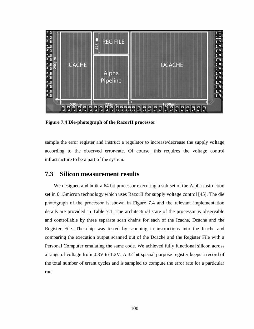
100
sample the error register and instruct a regulator to increase/decrease the supply voltage
according to the observed error-rate. Of course, this requires the voltage control
infrastructure to be a part of the system.
7.3 Silicon measurement results
We designed and built a 64 bit processor executing a sub-set of the Alpha instruction
set in 0.13micron technology which uses RazorII for supply voltage control [45]. The die
photograph of the processor is shown in Figure 7.4 and the relevant implementation
details are provided in Table 7.1. The architectural state of the processor is observable
and controllable by three separate scan chains for each of the Icache, Dcache and the
Register File. The chip was tested by scanning in instructions into the Icache and
comparing the execution output scanned out of the Dcache and the Register File with a
Personal Computer emulating the same code. We achieved fully functional silicon across
a range of voltage from 0.8V to 1.2V. A 32-bit special purpose register keeps a record of
the total number of errant cycles and is sampled to compute the error rate for a particular
run.
Figure 7.4 Die-photograph of the RazorII processor

101
7.3.1 RazorII clocking scheme
The core frequency of the processor is controlled by an internal Clock Generation
Unit (CGU). The CGU generates clock frequencies in the range between 50MHz to
370MHz. The CGU has a separate voltage domain that is not scaled. Hence, the core
frequency remains constant even when the core voltage is dynamically scaled. The
frequency output of the CGU is externally programmable.
The minimum delay constraint for a R2LAT is defined by the duration of the high
clock phase. Since, all pipeline registers are required to be R2LATs for SEU tolerance,
the excessive buffer insertion required to satisfy this constraint can have prohibitive area
and power impact. We solve this problem by having separate clock trees for timing-
critical flip-flops and those that have sufficient slack, as shown in Figure 7.5(a). We use a
Ring Oscillator (RO) for frequency synthesis. The clock output of the ring oscillator has
approximately 50% duty cycle. Delay chains are then used to tune the high phase of the
clock to create separate asymmetric duty-cycle clocks for the timing-critical and the non-
critical flip-flops. The delay through the chains determines the duration of the high-phase
of the individual clocks. The frequency output of the RO and the high-phase of the
asymmetric clocks are all separately tunable via an external interface.
Table 7.1 Chip Implementation details
Technology CMOS 0.13um
Dimensions 2700um x 1250um
No. critical RazorII FF 121 of 826
RazorII power overhead 1.2%
No. buffers added for hold-time fixing 1924
Buffer insertion power overhead 1.3%
Total no. of transistors 260k
Operating voltage 0.8-1.2V
Frequency 185MHz @ 1.2V
Power @ 185MHz 94.3mW
Technology CMOS 0.13um
Dimensions 2700um x 1250um
No. critical RazorII FF 121 of 826
RazorII power overhead 1.2%
No. buffers added for hold-time fixing 1924
Buffer insertion power overhead 1.3%
Total no. of transistors 260k
Operating voltage 0.8-1.2V
Frequency 185MHz @ 1.2V
Power @ 185MHz 94.3mW

102
Figure 7.5(b) illustrates the asymmetric clocks used for different flip-flops in the
design, at the slow corner. We use larger speculation windows for timing-critical
R2LATs whereas non-critical flip-flops require much smaller speculation duration.
Critical endpoints were identified through static timing analysis performed on a post-
routed and extracted netlist. We chose to route the clock with the larger speculation
window to the top-15% most-critical R2LATs. These represented 121 out of a total of
876 flip-flops. Thus, in this processor, the timing critical flip-flops had a clock with a
40% duty cycle resulting in a 25 FO4 detection window while non-critical flip-flops had
a 13% clock duty cycle to minimize buffer insertion. The high phase, TON, of the critical
a) Clock Generation Unit
b) Asymmetric clocks
Figure 7.5 RazorII processor clocking scheme. Figure a) shows the schematic of the clock-generator. Figure b) shows the relevant timing diagrams.
103
R2LATs was tunable with a range from 850ps to 1500ps while TON for the non-critical
flip-flops was tunable from 450ps to 700ps. A total of 1924 buffers were added to meet
the hold time constraint, which added a 1.3% power overhead.
As explained in Chapter 5, the minimum overlap between the high phase of the clock
and the detection clock (DC) is required to be half of a SEU pulse width. An additional
concern that affects the duration of the high phase is the risk of attenuation during
propagation through the clock-tree. Attenuation can occur due to asymmetric rise or fall
times through the buffers in the clock-tree or power-supply jitter affecting the clock-tree.
This can be an issue for the non-critical clock, which uses a narrower high-phase
compared to the critical clock (450ps versus 1.5ns at the slow corner). In such a case, a
wider high-phase maybe required for the non-critical clock. In our implementation, we
added 100ps as the difference between the DC pulse-width and the high-phase of the non-
critical clock. This was sufficient for the correct operation of the chip. However, we also
provided capability for post-silicon tuning of the high-phase (from 450ps to 750ps) which
was not required to be exercised for the chip to operate. Attenuation is not a concern for
the DC clock pulse since it was locally generated within each R2LAT.
An important observation to make here is that the only restriction imposed by the
RazorII clocking scheme is on the duration of the high phase required to meet the
minimum delay constraint at the destination R2LATs. Hence, all the conventional
clocking techniques such as clock-gating and useful skew insertion can be used as is with
RazorII without any modification to the existing methodology. Of course, such
techniques may worsen the minimum-path constraints. This can be addressed in the
conventional manner through additional buffer insertion on the violating paths.
The impact of clock uncertainties which affect the rising clock-edge, such as cycle-
to-cycle jitter, impacts RazorII technology in the same way as it affects conventional
clocking techniques. However, RazorII is naturally robust against timing uncertainties
caused due to such jitter mechanisms and can tolerate higher level of jitter compared to
conventional techniques. Phenomena that affect both clock edges, such as duty-cycle
jitter, have an impact on the high-phase of the clock at the destination flip-flop and hence,
affect the minimum-path constraint. Additional buffer insertion may be required to
account for minimum-path violations caused due to duty-cycle jitter.

104
Since the asymmetric clocks were digitally generated, care was taken to reduce the
jitter induced by power-supply noise in the CGU. The CGU had additional metallization
in the power-grid and had sufficient number of decoupling capacitors to reduce supply
voltage ripple to the high-frequency RO. Alternatively, analog techniques can also be
used for jitter compensation within the CGU.
7.3.2 Total energy savings
We measured the energy savings from RazorII based DVS on 33 different dies at
185MHz operating frequency. Figure 7.6 shows the energy savings for three different
chips at the fast, slow and the typical corners respectively. These chips are labeled
according to the corner that they represent.
The first set of bars show the energy consumption when Razor error correction is
disabled and the chips are operated at the worst-case voltage. We obtain the worst-case
operating voltage by adding margins to the PoFF of the slowest chip of the lot (1.21V).
We added an estimated 5% of the nominal operating voltage (1.2V), or 60mV, as margin
Figure 7.6 Total energy savings through RazorII based supply-voltage control

105
for power supply uncertainties, wear-out effects and safety, respectively. Temperature
margins were measured by the shift in the PoFF of the worst-case chip at 85C versus that
at 25C. The PoFF of the worst-case chip at 25C and 85C was measured to be 1.21V and
1.26V respectively, a shift of 50mV. Thus, by adding these margins to the PoFF of the
slowest chip, we obtained the worst-case operating voltage to be 1.44V. At this operating
voltage, correct operation is guaranteed for all the tested dies, across all operating
conditions. A key observation to make here is that these margins are optimistic since the
actual process spread is significantly worse than what we can obtain with a limited
sample size of 33 dies.
The first set of bar graphs in Figure 7.6 show the Energy Per Instruction (EPI) of the
chips-under-test when operating at 1.44V. For each chip, we measured the contribution of
each category of margins to the overall energy consumption. The energy due to process
variations margin was measured by the difference in energy consumption when operating
at the PoFF of the worst-case chip (1.21V) versus operating at its own PoFF, at 25C. For
the “fast” chip, this was measured to be 44pJ per instruction. This is significantly greater
than the process variations margin for the “slow” chip which was measured to be 5.3pJ.
This is because the PoFF of “slow” chip (1.205V) is very close to the PoFF of the worst-
case chip (1.21V). The energy due to temperature margins was measured by the
difference in energy when operating at the PoFF of the worst-case chip at 85C (1.26V)
versus operating at 1.21V. At the worst-case voltage, the “fast” chip consumes 816pJ per
Figure 7.7 Distribution of total energy savings through Razor
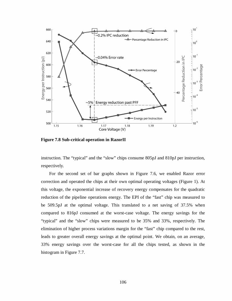
106
instruction. The “typical” and the “slow” chips consume 805pJ and 810pJ per instruction,
respectively.
For the second set of bar graphs shown in Figure 7.6, we enabled Razor error
correction and operated the chips at their own optimal operating voltages (Figure 1). At
this voltage, the exponential increase of recovery energy compensates for the quadratic
reduction of the pipeline operations energy. The EPI of the “fast” chip was measured to
be 509.5pJ at the optimal voltage. This translated to a net saving of 37.5% when
compared to 816pJ consumed at the worst-case voltage. The energy savings for the
“typical” and the “slow” chips were measured to be 35% and 33%, respectively. The
elimination of higher process variations margin for the “fast” chip compared to the rest,
leads to greater overall energy savings at the optimal point. We obtain, on an average,
33% energy savings over the worst-case for all the chips tested, as shown in the
histogram in Figure 7.7.
Figure 7.8 Sub-critical operation in RazorII

107
7.3.3 RazorII sub-critical operation
Figure 7.8 shows the measured error-rate, IPC and energy-per-instruction of the
“fast” chip as a function of the supply voltage in the sub-critical voltage regime at
185MHz. The voltage at the PoFF is 1.197mV. At this voltage, the error-rate is extremely
low of the order of 10-6. As the supply voltage is reduced below the PoFF, the error-rate
increases exponentially. Initially, the error-rate is still extremely low and the pipeline
operations energy dominates over the recovery energy. Consequently, the overall energy-
per-instruction reduces quadratically with the supply voltage. At the optimal operating
voltage of 1.165V, the EPI is measured to be 509.5pJ for an error-rate of 0.04% and an
IPC degradation of 0.2%.
Beyond the optimal energy point, the recovery energy for the exponentially
increasing error-rates dominates the overall processor energy. Hence, both the IPC
degradation and the energy-per-instruction of the processor show an exponential trend.
This greatly complicates the design of a voltage controller which can dynamically tune
the supply voltage for the optimal operating point. In addition, the energy savings at the
optimal point compared to the PoFF is not significant (5%). Hence, it is beneficial to
Figure 7.9 Run-time versus replay tradeoff

108
operate at the PoFF rather than at the optimal voltage.
Figure 7.9 shows the measured statistics on the number of replay iterations required
to commit an erroneous instruction. An erroneous instruction can suffer repeated timing
errors during replay. A possible deadlock situation can be avoided by recovering at half
the frequency to guarantee completion for a repeatedly failing instruction. As explained
in Section 7.1, the number of replay iterations allowed for a failing instruction before
frequency is halved, is called the “replay limit”. In Figure 7.9, we plot the number of
times the replay limit is reached as a function of the replay limit. The runtime for the
code being executed is also plotted against the replay limit. We see that the runtime for
the replay limit of 1 is much higher than that for the replay limit of 2. This is because for
the replay limit of 1, recovery for every timing error occurs at half the clock frequency.
On the contrary, for a replay limit of 2, most instructions complete when re-executed at
the same frequency.
Those instructions that don’t complete in the first replay keep failing repeatedly for
subsequent replay iterations until the replay limit is reached. Therefore, as the replay
limit is increased beyond 2, the runtime also linearly increases. These observations are
also borne out from the histogram in Figure 7.10. As can be seen, 60% of erroneous
instructions require a limit of 2 to complete. This number drastically reduces as the limit
Figure 7.10 Histogram of instructions as a function of replay iterations
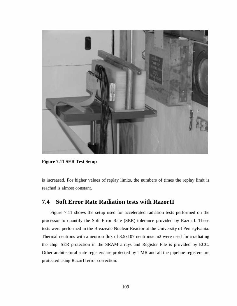
109
is increased. For higher values of replay limits, the numbers of times the replay limit is
reached is almost constant.
7.4 Soft Error Rate Radiation tests with RazorII
Figure 7.11 shows the setup used for accelerated radiation tests performed on the
processor to quantify the Soft Error Rate (SER) tolerance provided by RazorII. These
tests were performed in the Breazeale Nuclear Reactor at the University of Pennsylvania.
Thermal neutrons with a neutron flux of 3.5x10⁷ neutrons/cm2 were used for irradiating
the chip. SER protection in the SRAM arrays and Register File is provided by ECC.
Other architectural state registers are protected by TMR and all the pipeline registers are
protected using RazorII error correction.
Figure 7.11 SER Test Setup
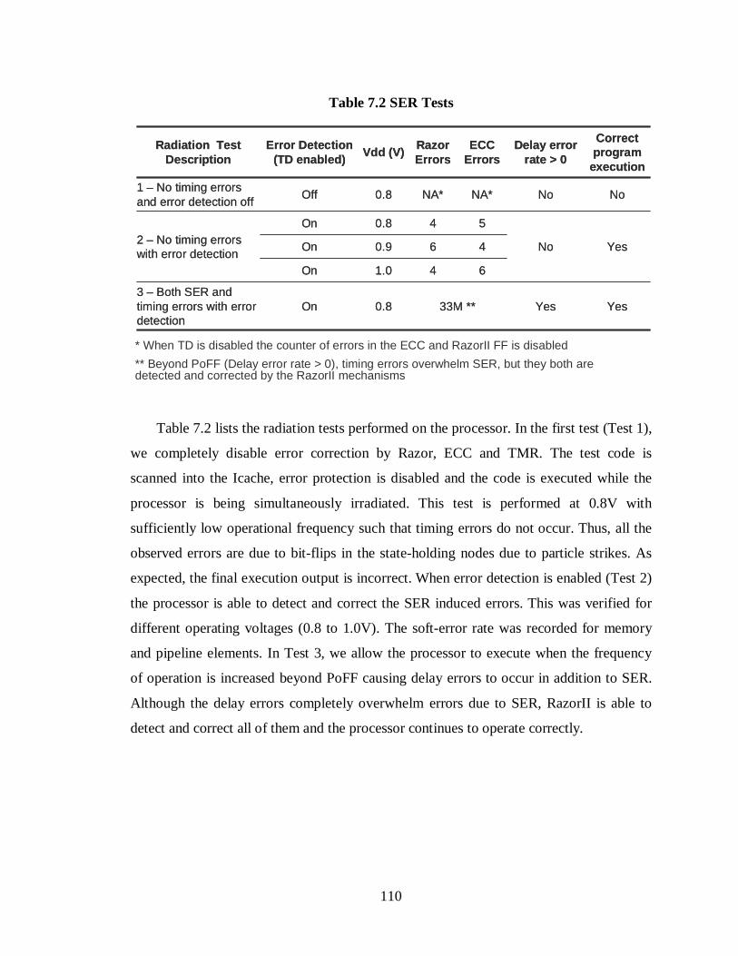
110
Table 7.2 lists the radiation tests performed on the processor. In the first test (Test 1),
we completely disable error correction by Razor, ECC and TMR. The test code is
scanned into the Icache, error protection is disabled and the code is executed while the
processor is being simultaneously irradiated. This test is performed at 0.8V with
sufficiently low operational frequency such that timing errors do not occur. Thus, all the
observed errors are due to bit-flips in the state-holding nodes due to particle strikes. As
expected, the final execution output is incorrect. When error detection is enabled (Test 2)
the processor is able to detect and correct the SER induced errors. This was verified for
different operating voltages (0.8 to 1.0V). The soft-error rate was recorded for memory
and pipeline elements. In Test 3, we allow the processor to execute when the frequency
of operation is increased beyond PoFF causing delay errors to occur in addition to SER.
Although the delay errors completely overwhelm errors due to SER, RazorII is able to
detect and correct all of them and the processor continues to operate correctly.
Table 7.2 SER Tests
NoNoNA*NA*0.8Off1 – No timing errors and error detection off
YesYes33M **0.8On3 – Both SER and timing errors with error detection
YesNo
540.8On2 – No timing errors with error detection
641.0On
460.9On
Correct program
execution
Delay error rate > 0
ECC Errors
Razor Errors
Vdd (V)Error Detection
(TD enabled)Radiation Test
Description
* When TD is disabled the counter of errors in the ECC and RazorII FF is disabled
** Beyond PoFF (Delay error rate > 0), timing errors overwhelm SER, but they both are detected and corrected by the RazorII mechanisms

111
CHAPTER 8
CONCLUSION AND FUTURE WORK
In this chapter, we summarize our research on Razor and present the key insights
from our work. We analyze the merits and the weaknesses of Razor-based self-tuning
based on our experience with the RazorI and RazorII prototypes. Finally, we discuss the
barriers to the deployment of Razor as a mainstream technology and present avenues of
future research on Razor.
8.1 Key concept of Razor
We developed Razor with the aim of designing low-power yet robust circuits in the
presence of design uncertainties that arise due to large PVT variations at advanced
process nodes. We discussed how traditional adaptive techniques, such as the canary-
circuits approach, fail to adequately address these uncertainties. Traditional techniques
require widening margins to account for the increasing contribution of the local
component of variations. This incurs large performance and power overheads which
undermine the efficacy of such techniques at aggressive geometries.
We showed how Razor is able to mitigate the impact of excessive margining through
circuit-level timing speculation based on dynamic detection and correction of timing
errors. Allowing error-tolerant processor operation enables elimination of worst-case
safety margins, thereby leading to significant improvements in energy efficiency. Error-
detection in Razor occurs through a delay-error tolerant flip-flop which monitors the
critical-path of processors for timing errors. Since Razor error-detection is required only
for the top few critical flip-flops, the total power and area overhead of Razor was
measured to be less than 3% for both prototypes that we fabricated for validating Razor.
The Razor voltage control system monitors the error-rate and tunes the supply
voltage according to the observed error-rate to achieve a targeted rate, given as an input

112
to the system. We qualitatively illustrated how, by operating in very low error-rate
regimes, Razor favorably trades-off the energy overhead of error-correction for additional
efficiency benefits through margin elimination. We developed two techniques, called
RazorI and RazorII, for implementation of Razor-based voltage tuning in microprocessor
cores. We validated both those techniques from our measurements on fabricated silicon
and demonstrated significant energy savings.
8.2 The RazorI approach
The RazorI flip-flop (R1FF) samples its input at two different points in time. The
earlier, speculative sample is captured in the main flip-flop at the rising edge of the clock.
The latter, always-correct sample is captured at a delayed edge in a shadow latch. A
metastability-tolerant comparator flags an error when the speculative sample differs from
the correct sample. Error-correction is achieved by engaging a recovery mechanism
which overwrites the main flip-flop with correct data in the shadow latch. In addition, the
recovery mechanism restores the pipeline back to its correct state.
We proposed two techniques by which pipeline recovery can be achieved. The first
technique is based upon clock-gating wherein the entire pipeline stalls for the cycle
immediately following a timing error. The second technique is based on a counter-flow
pipeline architecture in which the pipeline is flushed and execution is resumed from the
instruction following the one that caused the error. We implemented the latter technique
in a 64bit RazorI prototype implementing a sub-set of the Alpha instruction set.
From our measurements on silicon, we demonstrated correct operation in the sub-
critical regimes with RazorI error-correction, whereby the processor is deliberately
operated in the sub-critical voltage regimes below the Point of First Failure (PoFF).
Through margin elimination and sub-critical operation, we obtained 50% energy savings,
on an average, for 33 tested dies. We demonstrated a voltage control loop that tuned
supply voltage to achieve a 0.1% targeted error-rate. While the Razor voltage control
algorithm was implemented in a Xilinx FPGA board, it can also be implemented in
software as well.
113
8.3 The RazorII approach
A key observation from our experiments with the RazorI prototype was that most of
the energy savings are actually realized through elimination of safety margins and
operating at the PoFF. Furthermore, the error-rate increased exponentially beyond this
point which undermined the efficacy of operating significantly below the PoFF. We
exploited these observations in the RazorII technique wherein the processor is intended to
operate right at the PoFF. Error-detection is achieved by a so-called “transition-detector”
which flags spurious transitions in the monitored critical-path. Recovery occurs through a
replay mechanism from a Razor-validated check-pointed state. This mechanism for
recovery greatly simplifies the design of the error-detecting RazorII flip-flop while
adding very little area and clock-power overhead. However, replaying the same
instruction again can cause a deadlock situation to occur. Such an occurrence is mitigated
by recovering at half the clock frequency.
We developed a design of the RazorII flip-flop, called the R2LAT that uses a level-
sensitive latch instead of a flip-flop. Positive-edge triggered flip-flop operation is
enforced through the transition-detector which flags any transition in the latch-node in the
high-phase of the clock as a timing error. Elimination of the master-latch leads to a faster
and a more energy-efficient implementation. In addition, this design naturally allows
detection of Single Event Upsets (SEU) in logic and inside registers. We used the R2LAT
for timing-error detection and SEU tolerance in a 64bit RazorII prototype. We obtained,
on an average, 35% energy savings through margin elimination on 33 tested dies. In
addition, we demonstrated correct operation of the processor even when exposed to high-
energy neutron irradiation.
The recovery mechanism in the RazorII approach relies on a conventional replay
technique. The lower overhead of error-detection makes this technique highly amenable
to high-performance microprocessors. Consequently, the RazorII approach is much more
suitable for industrial deployment than RazorI.
114
8.4 Merits and demerits of the Razor approach
The key advantage of Razor, as we have already discussed, is its in situ error-
detection capability. This enables Razor to detect and recover from timing uncertainties
due to local fluctuations in process, voltage and temperature. While most state-of-the-art
microprocessor designs [49][50][51] incorporate mechanisms to adaptively respond to
IR-drops and temperature hotspots, however, in our knowledge, Razor is the only
technique that can effectively respond to highly local and fast-changing variations, such
as coupling noise events. Unlike traditional techniques, Razor tunes the supply voltage
based on the monitored error-rate which enables it to exploit data-dependent delay
variations. Another key advantage of Razor is that it allows reliability in the presence of
SEU with very little additional overhead. The performance and energy-efficiency upside
obtainable from Razor allows faster design closure and parametric yield improvement.
A key demerit of the Razor technique is the minimum-delay requirement. Rising
variations in short-paths can actually exacerbate this constraint. Consequently, additional
buffer insertion may be required to compensate and margin for possible minimum-delay
violations. However, from our experience with industrial designs, it is possible to satisfy
aggressive minimum-delay constraints through buffer insertion, even at the 65nm
technology node. Consequently, we believe that this constraint can be adequately
addressed even at advanced process nodes.
8.5 Future directions of research into Razor
In the recent past, Razor has received considerable traction within the industry. In the
International Solid-state Circuits Conference, 2008, researchers from Intel presented their
measurements from a prototype which uses a frequency-management technique for
performance enhancement, very similar to RazorII [37]. ARM Limited, Cambridge, U.K,
have also initiated research efforts focused at evaluating Razor for low-power micro-
processor cores. However, several challenges remain before Razor can be widely adopted
as mainstream technology. In the following, we discuss some of these challenges and
opportunities for future research into Razor.

115
8.5.1 Razor System Design Considerations
Designing complete and fully-functional Razor-based systems that can boot
operating systems and execute “real” software requires significant amount of engineering
effort. A complicating issue in this regard is the limitation of common, industrial
peripheral designs which cannot easily interface with a variable frequency processor core.
Using such systems requires the separation of the Razor-based pipeline from the
interfacing peripherals through FIFO buffers.
Designing voltage and frequency tuning algorithms that can tune for the Point of
First Failure needs further investigation. For such algorithms, it is important that when
the error-rate is low due to the critical-path not being sensitized, the system is able to
restrict scaling to safe limits. In Chapter 7, we discussed potential techniques that can
achieve this. The first technique we discussed uses conventional static timing analysis to
obtain the safe limit, but at the expense of safety margins to the negative edge of the
clock. On the other hand, tuning using worst-case vectors can obtain system limits
without adding excessive margins to the negative edge. However, the latter approach
requires additional infrastructure to obtain worst-case vectors and to replay them
deterministically. These and new such approaches need to be developed further and
validated on silicon in functional systems.
8.5.2 Micro-architectural research into Razor-based pipelines
By eliminating design margins, Razor enables better energy-efficiency and higher
performance. High-performance architectures such as out-of-order processors rely on
deep pipelines and complex control structures such as Reservation Stations and Reorder
Buffers to achieve the targeted throughput requirement, often at the expense of increased
power consumption. Incorporating Razor, specifically RazorII, in such pipelines can
achieve the required performance boost within the power budget.
In addition, architecting efficient memory systems that can deal with the variable
latency of the processor core can be explored as a topic for future research. Common
Instruction Set Architectures (ISAs), such as the ARM ISA, have support for multiple
cycle instructions. Efficient check-pointing and replay of such instructions can also be
explored further.
116
8.5.3 Silicon test-and-debug
The testability aspect of Razor-based designs is another avenue of research into
Razor. The RazorII flip-flop supports the conventional, scan-based testing
methodologies. However, tuning based on the error-rates poses testing issues such as
ensuring that the system is self-limiting i.e. the system restricts itself to known, safe
operating regimes. These issues relate to our discussions regarding setting safe limits to
voltage and frequency scaling in Section 7.2. In addition, the error-detection capability of
Razor flip-flops enables significant observability of failing critical-paths and, hence, can
be exploited extensively during silicon testing.
Razor offers designers the capability of reconciling conflicting constraints and
achieving faster design closure in the presence of rising uncertainties. In this thesis, we
have made several contributions towards developing Razor as a potential mainstream
technology. However, significant barriers to adoption of Razor by industry still remain.
The International Technology Roadmap for Semiconductors [46], 2007 edition, lists
Razor as a key optimization “for reliable computing” that will “extend existing
techniques for robust computation”. Indeed, the difficulties in sustaining the Moore’s
Law into the next decade and beyond makes techniques such as Razor assume ever-
increasing relevance. Future research into Razor needs to focus on building robust and
field-deployable systems that use Razor for supply voltage control.

117
BIBLIOGRAPHY
118
[1] S.T. Ma, A. Keshavarzi, V. De, J.R. Brews, “A statistical model for extracting
geometric sources of transistor performance variation”, IEEE Transactions on
Electron Devices, Volume 51, Issue 1, Page(s):36 - 41, Jan. 2004.
[2] R. Gonzalez, B. Gordon, and M. Horowitz, “Supply and Threshold Voltage
Scaling for Low Power CMOS,” IEEE Journal of Solid-State Circuits, 32 (8), August
1997.
[3] T. Burd, T. Pering, A. Stratakos, and R. Brodersen, “A Dynamic Voltage Scaled
Microprocessor System,” International Solid-State Circuits Conference, Feb. 2000.
[4] International Technology Roadmap for Semiconductors, 2005 edition,
http://www.itrs.net/ Links/2005ITRS/Home2005.htm.
[5] R. H. Dennard, F. H. Gaensslen, H. N. Yu, V. L. Rideout, E. Bassous and A. R.
LeBlanc, “Design of ion-implanted MOSFETs with very small physical dimensions,”
IEEE J. Solid-State Circuits, vol. SC-9, pp. 256–268, Oct. 1974.
[6] A. Asenov, S. Kaya, A.R. Brown, “Intrinsic parameter fluctuations in
decananometer MOSFETs introduced by gate line edge roughness,”, IEEE
Transactions on Electron Devices, Volume 50, Issue 5, Page(s):1254 - 1260, May
2003.
[7] Gordon Moore, “Cramming more components into Integrated Circuits”,
ftp://download.intel.com/research/silicon/moorespaper.pdf
[8] G. Wolrich, E. McLellan, L. Harada, J. Montanaro, and R. Yodlowski, “A High
Performance Floating Point Coprocessor,” IEEE Journal of Solid-State Circuits, (5),
October 1984.
[9] Dr. Andy Grove, key note speech at the International Electron Devices Meeting,
2002, http://www.intel.com/pressroom/archive/speeches/grove_20021210.pdf
[10] S. Das, D. Roberts, S. Lee, S. Pant, D. Blaauw, T. Austin, T. Mudge, K. Flautner,
“A Self-Tuning DVS Processor using Delay-Error Detection and Correction,” IEEE
Journal of Solid-State Circuits, pages 792 - 804, April 2006.
[11] D. Ernst, N. S. Kim, S. Das, S. Pant, T. Pham, R. Rao, C. Ziesler, D. Blaauw, T.
Austin, T. Mudge, K. Flautner, “RazorI: A low-power pipeline based on circuit-level
119
timing speculation,” Proceedings of the 36th Annual IEEE/ACM International
Symposium on Microarchitecture, Dec. 2003, pages 7-18.
[12] W. Dally, J. Poulton, Digital System Engineering, Cambridge University Press,
1998
[13] Intel Corporation, “Intel Speedstep Technology”,
http://www.intel.com/support/processors/mobile/pentiumiii/ss.htm
[14] Trasmeta Corporation, “LongRun Power Management”,
http://www.transmeta.com/tech/longrun2.html
[15] ARM Limited, http://www.arm.com/products/esd/iem_home.html
[16] S. Hauck, “Asynchronous Design Methodologies: An Overview,” Proceedings of
the IEEE, 83 (1), January 1995.
[17] S. Lu, “Speeding up Processing with Approximation Circuits”, IEEE Micro Top
Picks, pg. 67-73, 2004
[18] A.K. Uht, “Going beyond worst-case specs with TEATime”, IEEE Micro Top
Picks, pg. 51-56, 2004
[19] K.J. Nowka, G.D. Carpenter, E.W. MacDonald, H.C. Ngo, B.C Brock, K.I. Ishii,
T.Y. Nguyen and J.L. Burns, “A 32-bit PowerPC System-on-a-chip With Support for
Dynamic Voltage Scaling and Dynamic Frequency Scaling”, IEEE Journal of Solid-
State Circuits, Volume 37, Issue 11, pp.1441-1447, Nov. 2002
[20] IBM : Kerry Bernstein et al.
[21] T.D. Burd, T.A. Pering, A.J. Stratakos and R.W. Brodersen, “A Dynamic Voltage
Scaled Microprocessor System”, IEEE Journal of Solid-State Circuits, Volume 35,
Issue 11, pages 1571–1580, Nov. 2000.
[22] Berkeley Wireless Research Center, http://bwrc.eecs.berkeley.edu/
[23] M. Nakai, S. Akui, K. Seno, T. Meguro, T. Seki, T. Kondo, A. Hashiguchi, H.
Kawahara, K. Kumano and M. Shimura, “Dynamic Voltage and Frequency
Management for a Low Power Embedded Microprocessor”, IEEE Journal of Solid-
State Circuits, Volume 40, Issue 1, pages 28-35, Jan. 2005
[24] T. Kehl, “Hardware Self-Tuning and Circuit Performance Monitoring,” 1993 Int’l
Conference on Computer Design (ICCD-93), October 1993.

120
[25] T. Austin, V. Bertacco, D. Blaauw and T. Mudge, “Opportunities and challenges
in better than worst-case design”, Proceedings of the ASP-DAC 2005, Vol. 1, 18-21,
2005.
[26] D. Roberts, T. Austin, T. Mudge and K.Flautner, “Error analysis for the support
of robust voltage scaling”, Sixth International Symposium on
Quality of Electronic Design, 2005, Page(s):65 – 70, March 2005.
[27] Kim, D. Burger and S.W. Keckler, IEEE Micro, Volume 23, Issue 6, Nov.-Dec.
2003 Pg(s):99 – 107.
[28] Z. Chishti, M.D. Powell, T. N. Vijaykumar, “Distance associativity for high-
performance energy-efficient non-uniform cache architectures”, Proceedings of the
International Symposium on Microarchitecture, 2003, MICRO-36
[29] F. Worm, P. Ienne and P. Thiran, “A Robust Self-Calibrating Transmission
Scheme for On-Chip Networks”, IEEE Transactions on Very Large Scale Integration,
Vol. 13, No. 1, January 2005.
[30] R. Hegde and N. R. Shanbhag, “A Voltage Overscaled Low-Power Digital Filter
IC”, IEEE Journal of Solid-State Circuits, Vol.39, No. 2, February 2004.
[31] L. Anghel and M. Nicolaidis, “Cost Reduction and Evaluation of a Temporary
Faults Detecting Technique”, Proceedings of Design, Automation and Test in Europe
Conference and Exhibition 2000, 27-30 March 2000 Page(s):591 – 598
[32] K. Ogata, “Modern Control Engineering,” 4th edition, Prentice Hall, New Jersey,
2002.
[33] www.mosis.org
[34] www.xilinx.com
[35] W.J. Van Gils, “A Triple Modular Redundancy Technique Providing Multiple-Bit
Error Protection Without Using Extra Redundancy”, IEEE Transactions on
Computers, Volume C-35, Issue 7, pages 623-631, July 1986.
[36] S.J. Piestrak, A. Dandache and F. Monteiro, “Designing fault-secure parallel
encoders for systematic linear error correcting codes,” IEEE Transactions on
Reliability, Volume 52, Issue 4, pages 492-500, Dec. 2003.
[37] K.A. Bowman, J.W. Tschanz, N.S. Kim, J.C. Lee, C.B. Wilkerson, S. Lu, T.
Karnik and V. De, “Energy-Efficient and Metastability-Immune Timing-Error
121
Detection and Instruction-Replay-Based Recovery Circuits for Dynamic-Variation
Tolerance,” Proceedings of the 2008 International Solid-State Circuits Conference,
pages 402-403, Feb. 2008.
[38] R. Sproull, I. Sutherland, and C. Molnar, “Counterflow Pipeline Processor
Architecture,” Sun Microsystems Laboratories Inc. Technical Report SMLI-TR-94-25,
April 1994.
[39] S. Yokogawa, H. Takizawa, “Electromigration induced incubation, drift and
threshold in single-damascene copper interconnects”, IEEE 2002 International
Interconnect Technology Conference, 2002, Page(s):127 - 129, 3-5 June 2002.
[40] M. Hashimoto, H. Onodera, “Increase in delay uncertainty by performance
optimization”, IEEE International Symposium on Circuits and Systems, 2001,
Volume 5, Page(s):379 - 382 vol. 5, 6-9 May 2001.
[41] S. Rangan, N. Mielke and E. Yeh, "Universal Recovery Behavior of Negative
Bias Temperature Instability," IEEE Intl. Electron Devices Mtg., December 2003, p.
341.
[42] W. Jie and E. Rosenbaum, “Gate oxide reliability under ESD-like pulse stress”,
IEEE Transactions on Electron Devices, Vol. 51, Issue 7, July 2004.
[43] A. Drake, R. Senger, H. Deogun, G. Carpenter, S. Ghiasi, T. Ngyugen, N. James
and M. Floyd, “A Distributed critical-path timing monitor for a 65nm high-
performance microprocessor”, International Solid-State Circuits Conference, 2007,
pages 398-399.
[44] D. Blaauw, S. Kalaiselvan, K. Lai, W. Ma, S.Pant, C. Tokunaga, S. Das and D.
Bull, “RazorII: In Situ Error Detection and Correction for PVT and SER Tolerance”,
Proceedings of the 2008 International Solid-State Circuits Conference, pages 400-
401, Feb. 2008.
[45] S. Das, C. Tokunaga, S. Pant, W. Ma, S. Kalaiselvan, D. Blaauw, K. Lai, D. Bull
and D. Blaauw “RazorII: In Situ Error Detection and Correction for PVT and SER
Tolerance”, Journal of Solid-State Circuits, to appear, Jan. 2009.
[46] International Technology Roadmap for Semiconductors, 2007, Design Chapter,
http://www.itrs.net/Links/2007ITRS/2007_Chapters/2007_Design.pdf.

122
[47] G. Dasika, S. Das, K. Fan, S. Mahlke and D. Bull, “DVFS in Loop Accelerators
using BLADES”, Proceedings of the Design Automation Conference, pages 894-897,
June 2008.
[48] X. Vera, O. Unsal, and A. Gonzalez, “X-Pipe: An Adaptive Resilient
Microarchitecture for Parameter Variations”, Proceedings of the Workshop on
Architectural Support for Gigascale Integration, June 2006.
[49] B. Stolt, Y. Mittlefehldt, S. Dubey, G. Mittal, M. Lee, J. Friedrich, E. Fluhr,
“Design and Implementation of the POWER6 Microprocessor”, IEEE Journal of
Solid-State Circuits, pages 21-28, January 2008.
[50] N. Sakran, M. Yuffe, M. Mehalel, J. Doweck, E. Knoll and A. Kovacs, “The
Implementation of the 65nm Dual-Core 64b Merom Processor”,
Digest of Technical Papers, International Solid-State Circuits Conference, 2007,
pages 11-15, February 2007.
[51] S. Naffziger, B. Stackhouse, T. Grutkowski, D. Josephson, J. Desai, E. Alon and
M. Horowitz, “The Implementation of a 2-Core, Multi-Threaded Itanium Family
Processor”, IEEE Journal of Solid-State Circuits, vol. 41, pages 197-209, January
2006.
[52] T. Fisher, J. Desai, B. Doyle, S. Naffziger, B. Patella, “A 90-nm Variable
Frequency Clock System for a Power-Managed Itanium Architecture Processor”,
IEEE Journal of Solid-State Circuits, Vol. 41, pages 218-228, January 2006.
[53] D. Ernst, S. Das, S. Lee, D. Blaauw, T. Austin, T. Mudge, N.S. Kim and K.
Flautner, “Razor: circuit-level correction of timing errors for low-power operation”
IEEE Micro Top Picks, Vol. 24, Issue 6, pages 10-20, December 2004.
[54] B. Nikolic, V.G. Oklobdzija, V. Stojanovic, Wenyan Jia, James Kar-Shing Chiu,
M. Ming-Tak Leung, “Improved sense-amplifier-based flip-flop: design and
measurements”, IEEE Journal of Solid-State Circuits, Volume 35, Issue 6,
Page(s):876 - 884, June 2000.