raman spectroscopy and photoluminescence mapping of … spectroscopy... · 2019-05-11 · raman...
TRANSCRIPT

“WE DREAM, WE DEVELOP, WE DELIVER.”
www.master-dynamic.com 852 - 3543 5898
Unit 103, 1/F, 10 Science Park West Avenue, Hong Kong Science Park, Shatin, N.T., HONG KONG
MD Technical Review Letter -
Raman Spectroscopy and Photoluminescence
Mapping
of Diamonds with Multiple Fluorescence Zones
Charis W.Y. LEE, J. CHENG, K. W. CHENG and Tony K. C. HUI
Master Dynamic Ltd.
Dr. Tim BATTEN
Renishaw PLC ·
Deep UV (DUV) excitation and Raman spectroscopy are the principle tools that help
gemologists identify the origin of diamonds and their authenticity. When illuminated with a DUV
source diamonds fluoresce in a range of colors, which are attributed to a specific optical defect
in the diamond allowing a real-time image to be displayed. To identify and observe the
distributions of these optical centers, it is necessary to not only pin-point the DUV source at a
spot on the sample, but to obtain a full screening over the surface of interest.
By applying correlated Raman spectroscopy and photoluminescence (PL) mapping to the same
region of the sample it is possible to directly characterize and precisely identify the optical
centers responsible for this fluorescence, allowing material properties of the diamond such as
unintentional doping to be determined.

2 Unit 103, 1/F, 10 Science Park West Avenue, Hong Kong Science Park, Shatin, N.T., H.K. 852 - 3543 5898
www.master-dynamic.com
Introduction
The techniques for lab-grown diamonds continues to advance and it is important to study how
they are grown, their characteristics and traits and how different treatment could change them
both internally and externally. From this information, the classification and identification of these
synthetic diamonds can be made easier. In this study, we focus on two techniques DUV
illumination and Raman/photoluminescence spectroscopy and demonstrate how they can be
used in tandem to characterize synthetic Diamonds.
Raman spectrometers and DUV illumination systems are fundamental instruments in the
identification process. Both provide photoluminescence (PL) information displayed as a
spectrum or as an image.
Raman and PL spectroscopy is a non-contact and non-destructive analytical method that can
detect defects at lower concentrations than other absorption spectroscopy [5]. A Raman
spectrometer can be equipped with different laser wavelengths to cover a wide range of the
spectrum and detect different optical defects with high sensitivity. On the other hand, a DUV
system exposes the samples to a short-UV radiation (~230 nm) and provides phosphorescence,
as well as, luminescence that results from the optical defects in the diamond.
The localized study of these techniques on the diamond (together with other analytical
instruments) is enough to identify origin, and a relatively standard measurement. However it is
also important to visualize the whole diamond in order to characterise more comprehensively
how these synthetic diamonds are grown And this can be achieved by carrying out correlated
PL mapping as demonstrated here.

3 Unit 103, 1/F, 10 Science Park West Avenue, Hong Kong Science Park, Shatin, N.T., H.K. 852 - 3543 5898
www.master-dynamic.com
Materials and Methods
The sample of interest is a 0.32ct Oval cut near-colorless CVD diamond.
Fig. 1. Sample examined is a 0.32ct Oval Cut CVD Diamond
The infrared absorption spectrum collected using FTIR shows the diamond to be Type IIa, as
there were no peaks present in the 0-1500cm-1 range (Fig. 2) which would be indicative of any
Nitrogen A- or B-aggregates exist.
Fig.2: FTIR spectra shows the CVD diamond examined to be Type IIa
Photoluminescence Spectra
PL measurement was conducted with Renishaw inVia Raman microscope and collected at
room and liquid nitrogen (LN) temperature prior mapping. 320 nm, 514 nm and 633 nm laser
4 Unit 103, 1/F, 10 Science Park West Avenue, Hong Kong Science Park, Shatin, N.T., H.K. 852 - 3543 5898
www.master-dynamic.com
excitation wavelengths were used to ensure the entire PL range of interest was covered A 20×
with 0.40 numerical aperture objective lens was used. In this case a Raman spectrometer was
used to collect PL data as the PL spectrum is weak and such spectrometers are significantly
more sensitive than standard PL instrumentation, in addition because the Raman spectrometer
chosen has a dispersive element it is able to provide excellent spectral resolution.
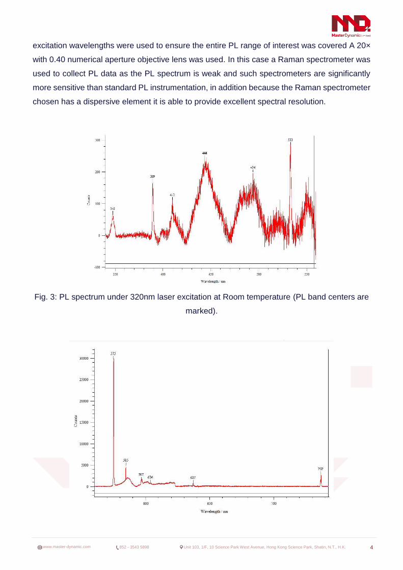
Fig. 3: PL spectrum under 320nm laser excitation at Room temperature (PL band centers are
marked).
5 Unit 103, 1/F, 10 Science Park West Avenue, Hong Kong Science Park, Shatin, N.T., H.K. 852 - 3543 5898
www.master-dynamic.com
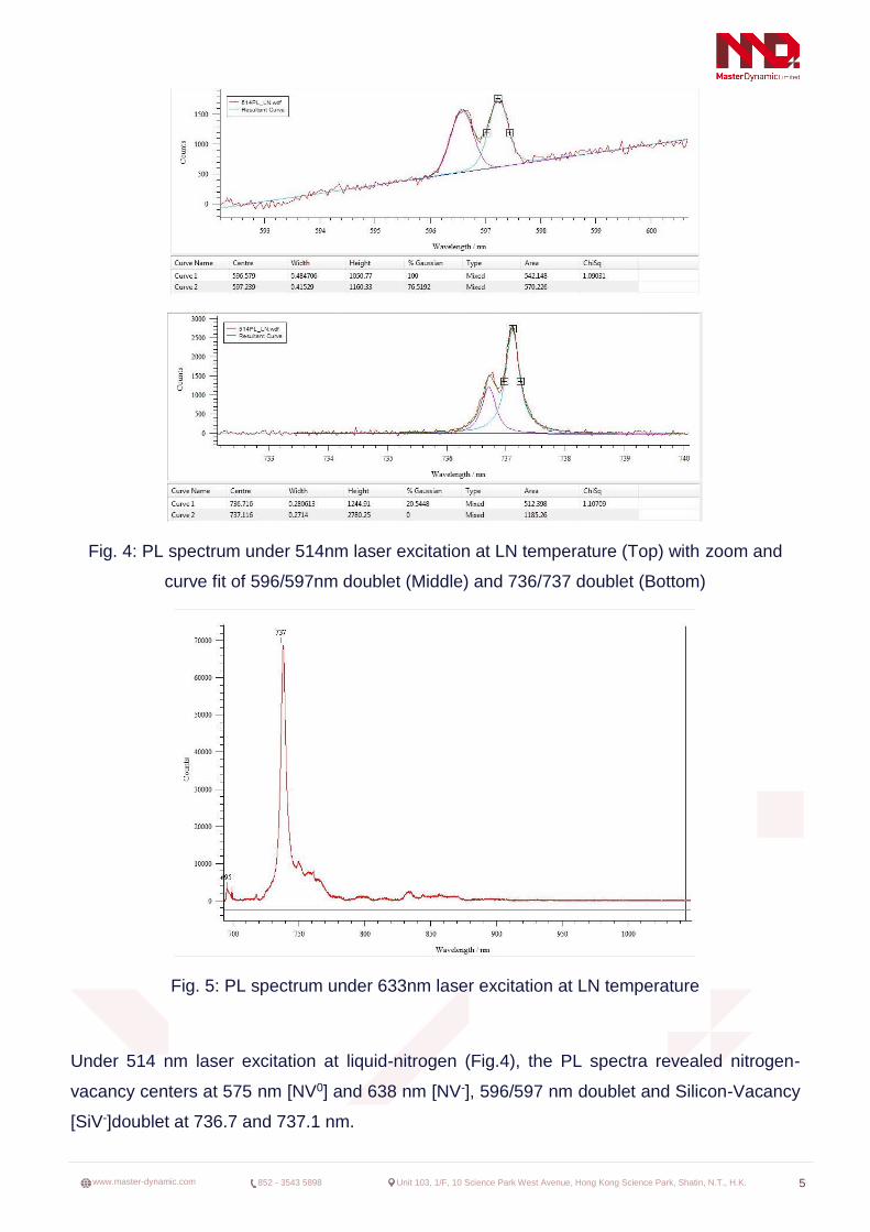
Fig. 4: PL spectrum under 514nm laser excitation at LN temperature (Top) with zoom and
curve fit of 596/597nm doublet (Middle) and 736/737 doublet (Bottom)
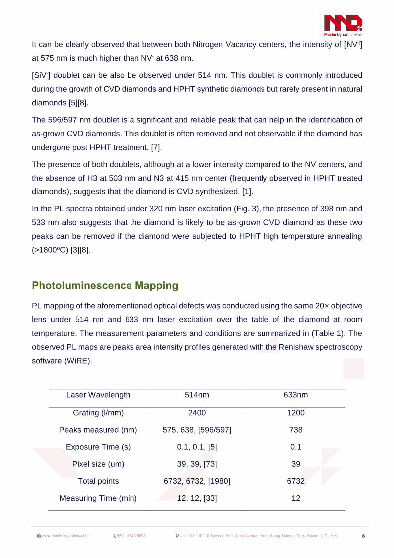
Fig. 5: PL spectrum under 633nm laser excitation at LN temperature
Under 514 nm laser excitation at liquid-nitrogen (Fig.4), the PL spectra revealed nitrogen-
vacancy centers at 575 nm [NV0] and 638 nm [NV-], 596/597 nm doublet and Silicon-Vacancy
[SiV-]doublet at 736.7 and 737.1 nm.
6 Unit 103, 1/F, 10 Science Park West Avenue, Hong Kong Science Park, Shatin, N.T., H.K. 852 - 3543 5898
www.master-dynamic.com
It can be clearly observed that between both Nitrogen Vacancy centers, the intensity of [NV0]
at 575 nm is much higher than NV- at 638 nm.
[SiV-] doublet can be also be observed under 514 nm. This doublet is commonly introduced
during the growth of CVD diamonds and HPHT synthetic diamonds but rarely present in natural
diamonds [5][8].
The 596/597 nm doublet is a significant and reliable peak that can help in the identification of
as-grown CVD diamonds. This doublet is often removed and not observable if the diamond has
undergone post HPHT treatment. [7].
The presence of both doublets, although at a lower intensity compared to the NV centers, and
the absence of H3 at 503 nm and N3 at 415 nm center (frequently observed in HPHT treated
diamonds), suggests that the diamond is CVD synthesized. [1].
In the PL spectra obtained under 320 nm laser excitation (Fig. 3), the presence of 398 nm and
533 nm also suggests that the diamond is likely to be as-grown CVD diamond as these two
peaks can be removed if the diamond were subjected to HPHT high temperature annealing
(>1800oC) [3][8].
Photoluminescence Mapping
PL mapping of the aforementioned optical defects was conducted using the same 20× objective
lens under 514 nm and 633 nm laser excitation over the table of the diamond at room
temperature. The measurement parameters and conditions are summarized in (Table 1). The
observed PL maps are peaks area intensity profiles generated with the Renishaw spectroscopy
software (WiRE).
Laser Wavelength 514nm 633nm
Grating (l/mm) 2400 1200
Peaks measured (nm) 575, 638, [596/597] 738
Exposure Time (s) 0.1, 0.1, [5] 0.1
Pixel size (um) 39, 39, [73] 39
Total points 6732, 6732, [1980] 6732
Measuring Time (min) 12, 12, [33] 12
7 Unit 103, 1/F, 10 Science Park West Avenue, Hong Kong Science Park, Shatin, N.T., H.K. 852 - 3543 5898
www.master-dynamic.com
Table 1. PL Mapping measurement parameters and conditions under different laser
excitations. Data in brackets “[.]”, belongs to the 596/597nm doublets.
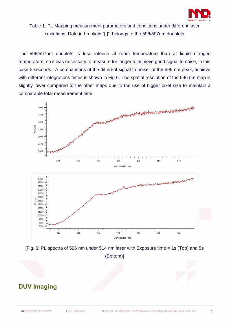
The 596/597nm doublets is less intense at room temperature than at liquid nitrogen
temperature, so it was necessary to measure for longer to achieve good signal to noise, in this
case 5 seconds.. A comparisons of the different signal to noise of the 596 nm peak, achieve
with different integrations times is shown in Fig 6. The spatial resolution of the 596 nm map is
slightly lower compared to the other maps due to the use of bigger pixel size to maintain a
comparable total measurement time.
[Fig. 6: PL spectra of 596 nm under 514 nm laser with Exposure time = 1s (Top) and 5s
(Bottom)]
DUV Imaging

8 Unit 103, 1/F, 10 Science Park West Avenue, Hong Kong Science Park, Shatin, N.T., H.K. 852 - 3543 5898
www.master-dynamic.com
The sample is examined under a DUV illumination system using 230 nm short-wave UV
radiation. Although there were no clear growth patterns, the sample exhibited an overall strong
reddish-orange fluorescence with dislocation areas of violet-blue fluorescence and a strong
strand of greenish blue fluorescence (Fig. 7). In addition, green-blue phosphorescence can be
observed at the same location (Fig. 8).
Fig. 7. Overall reddish-orange fluorescence with violet-blue dislocation bundles under D UV
illumination.

9 Unit 103, 1/F, 10 Science Park West Avenue, Hong Kong Science Park, Shatin, N.T., H.K. 852 - 3543 5898
www.master-dynamic.com
Fig. 8: A weak green-blue phosphorescence (Right Top & Bottom images) can be observed
under DUV at the same location as the strand of bright blue fluorescence (Left Top & Bottom
images).
The reddish-orange fluorescence is mainly attributed to the presence of [N-V] centers with
emission at 575 nm [NV0] and 638 nm [NV-]. The irregular violet-blue fluorescence is a typical
feature of as-grown CVD diamond [1][9]. Around the violet-blue dislocation bundle, some
pinkish fluorescence can be observed. This feature is associated to the 596/597 nm doublet
[7]., present in as-grown CVD diamonds.
The pronounced greenish-blue color observed as a strand in Fig. 8, is often related to H3
centers which are commonly present in CVD diamonds that has underwent HPHT treatment.
[1][9]. However, based on the PL spectra, H3 center characteristic peak at 503 nm is not
observed. On the other hand, the 596/597 nm doublet, an indicator that the diamond is as-
grown, is present.
In addition, this greenish-blue phosphorescence can also be found in boron-doped diamonds.
[8]. Yet, there is no sign of boron absorption peak in FTIR spectra (Refer to Fig.2).
This combination is rarely seen in as-grown CVD diamonds as during HPHT treatment, 389
nm, 533 nm and 596/597 nm doublet should have been removed [3][8].
So far, it can only suggest that there is a possibility that the diamond has undergo HPHT
annealing at a temperature lower than 1800oC. [1]
PL mapping and Results
Although the growth features cannot be observed clearly, the diamond display typical CVD
features: [N-V] centers at 575 nm and 638 nm, [Si-V] center at 736 nm and the 596/597 nm
doublets. H3 and N3 centers were not observed.
The whole table image is a result of the collection of numerous snaps along the diamond. This
montage (Fig.9) is done to facilitate the location of the mapping as the whole table cannot be
fully visualized using 20x objective lens in the microscope. Fig. 10, 11 and 12 are PL maps

10 Unit 103, 1/F, 10 Science Park West Avenue, Hong Kong Science Park, Shatin, N.T., H.K. 852 - 3543 5898
www.master-dynamic.com
corresponding to a different optical defect and its area intensity under different laser excitation
over the table of the diamond.
Fig. 9: Montage of numerous snaps along the table of the diamond
As observed in (Fig. 10), the NV centers are highly concentrated in one of the extremes of the
diamond and cut off by where the dislocation bundles are located. Under DUV illumination, one
of the extremes appear to be of a darker reddish/orange color than the rest of the table of the
diamond. After the bundles, the NV centers are also present in the rest of the diamond, but at
lower intensity. This shows that the NV centers are not evenly distributed along surface.
Low Intensity High Intensity
11 Unit 103, 1/F, 10 Science Park West Avenue, Hong Kong Science Park, Shatin, N.T., H.K. 852 - 3543 5898
www.master-dynamic.com
Fig. 10: PL Map of the NV0 located at 575 nm
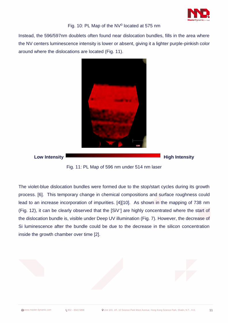
Instead, the 596/597nm doublets often found near dislocation bundles, fills in the area where
the NV centers luminescence intensity is lower or absent, giving it a lighter purple-pinkish color
around where the dislocations are located (Fig. 11).
Low Intensity High Intensity
Fig. 11: PL Map of 596 nm under 514 nm laser
The violet-blue dislocation bundles were formed due to the stop/start cycles during its growth
process. [6]. This temporary change in chemical compositions and surface roughness could
lead to an increase incorporation of impurities. [4][10]. As shown in the mapping of 738 nm
(Fig. 12), it can be clearly observed that the [SiV-] are highly concentrated where the start of
the dislocation bundle is, visible under Deep UV illumination (Fig. 7). However, the decrease of
Si luminescence after the bundle could be due to the decrease in the silicon concentration
inside the growth chamber over time [2].

12 Unit 103, 1/F, 10 Science Park West Avenue, Hong Kong Science Park, Shatin, N.T., H.K. 852 - 3543 5898
www.master-dynamic.com
Low Intensity High Intensity
Fig. 12: PL Map of 738 nm under 633 nm laser
Discussion
Despite the fact that it is still unclear whether the CVD sample studied has been subjected to
post-growth HPHT annealing, it is certain that both Raman and Deep UV systems are
indispensable tools in the identification of products of continuously advancing synthesis
techniques (lab-grown diamond).
Photoluminescence mapping was successful in revealing the distribution of the different optical
defects found in a single spectrum along the diamond. It also allowed a better understanding
of the fluorescence colors displayed under DUV illumination. Both are reliable instruments that
help in the study and classification of the nature of the diamond. Additionally, with the
considerably fast screening of the defects at room temperature, PL mapping serves as a useful
method for the study of optical defects and its impurities uptake during the growth of both
synthetic and natural diamonds.

13 Unit 103, 1/F, 10 Science Park West Avenue, Hong Kong Science Park, Shatin, N.T., H.K. 852 - 3543 5898
www.master-dynamic.com
About the Authors
Miss Charis W.Y. LEE is Biology Engineer, Dr. J. CHENG is Principal Engineer (expertise in
Optical & Raman Spectroscopy), Mr. K.W. CHENG is Technical Manager and Mr. Tony K.C.
HUI is Senior Director of the NanoTechnology Development & Applications Centre (NTAC), at
Master Dynamic Limited in Hong Kong.
Dr. Tim BATTEN specializes in the study of carbon materials, semiconductors and
nanomaterials using optical spectroscopy and is a Senior Raman Spectroscopy Application
Scientist at Renishaw plc, UK.
References
[1] D’Alene’s-Johansson, U. et al. (2013) “Three CVD Synthetic Diamonds Submitted to Mumbai Laboratory”.
Gems & Gemology, Spring 2013, Vol. 49, No. 1
[2] Dieck C. et al (2015) “Two Large CVD-Grown Synthetic Diamonds Tested by GIA”. Gems & Gemology, Winter
2015, Vol. 51, No. 4
[3] Dobrinets I.A. et al (2013) “HPHT-Treated Diamonds”. Springer Series in Materials Science 181
[4] Eaton-Magaña, S, et al. (2014). “CVD Synthetic Diamond with Unusual DiamondView Image.” Gems &
Gemology, Spring 2014, Vol. 50, No. 1
[5] Eaton-Magaña, S, et al. (2016). “Observations on CVD-grown synthetic diamonds: A review”. Gems &
Gemology, Vol. 52, No. 3, pp. 222–245
[6] Law P.L, et al. (2016) “CVD Synthetic Diamond Over 5 Carats Identified by GIA”. Gems & Gemology, Winter
2016, Vol. 52, No. 4
[7] Martineau P.M, et al. (2004) “Identification of synthetic diamond grown
using chemical vapor deposition (CVD)”. Gem & Gemology, Vol. 40, No.1, pp. 2–25
[8] Nad S, et al. (2015) “Growth strategies for large and high quality single crystal diamond substrates”. Diamond
and Related Materials, Vol. 60, pp. 26–34,
[9] Wang W., et al. (2012) “CVD synthetic diamonds from Gemesis Corp”. Gem &Gemology, Vol. 48, No. 2, pp.
80–97
[10] Willems et al. (2011) “Exploring the origin and nature of luminescent regions in CVD synthetic diamond,” Fall
2011 G&G, pp. 202–207