radio frequency tracking filter
TRANSCRIPT
(12) United States Patent Roberts
US006453157B1
(10) Patent N0.: (45) Date of Patent:
US 6,453,157 B1 Sep. 17, 2002
(54) RADIO FREQUENCY TRACKING FILTER
(75) Inventor: Gerald E. Roberts, Lynchburg, VA (Us)
(73) Assignee: Ericsson Inc., Research Triangle Park, NC (US)
( * ) Notice: Subject to any disclaimer, the term of this patent is extended or adjusted under 35 U.S.C. 154(b) by 0 days.
(21) Appl. No.: 09/045,701
(22) Filed: Mar. 23, 1998
(51) Int. Cl.7 ................................................ .. H04B 1/16
(52) us. Cl. .... .. 455/337; 455/302; 455/307; 455/340; 333/176
(58) Field of Search ........................ .. 455/339, 78, 302,
455/303, 304307, 340, 318, 319, 334—338; 333/202—208, 29 C, 167—180
(56) References Cited
U.S. PATENT DOCUMENTS
3,882,434 A * 5/1975 Levy ........................ .. 333/212
4,287,602 A * 9/1981 Kessler .... .. 455/286
4,316,108 A 2/1982 Rogers, Jr. . 327/553 4,338,571 A * 7/1982 Young . . . . . . . . . . . . . . . . . .. 330/84
4,518,935 A * 5/1985 Van Roermund 333/173 4,714,906 A 12/1987 D’Albaret et al. 333/207 5,060,297 A 10/1991 Ma et al. ........... .. 455/302
5,065,120 A * 11/1991 Munn 333/207 5,227,748 A 7/1993 Sroka ......... .. 333/202
5,495,215 A 2/1996 NeWell et al. 327/553 5,774,555 A * 6/1998 Lee et al. . . . . . . . . . . . . . .. 381/4
6,011,959 A * 1/2000 Reeser et al. ............... .. 455/76
OTHER PUBLICATIONS
Mole, J.H. “Filter Design Data for Communication Engi neers” 1952; John Wiley & Sons, NeW York pp. 55—56.* Perry et al “The Design of Log—Domain Filters Based on the Operational Simulation of LC Ladders” IEEE 1057—7130 11/96 pp. 763—773.*
Kim et al “A Modi?ed Elliptic Function With Diminishing Ripples” IEEE 7803—2428 5/95 pp. 1027—1031.*
Fischerauer et al “IF and RF ?lters for mobile telephone
systems” IEEE Ultrasonics Symposium, 1991 pp. 235—239, Dec. 1991.*
RaZavi, BehZad RF Microelectronics, 1998 CH 5 “Trans ceiver Architectures”, pp. 122—128, Jan. 1998.*
(List continued on neXt page.)
Primary Examiner—DWayne Bost Assistant Examiner—Charles Craver (74) Attorney, Agent, or Firm—NiXon & Vanderhye PC.
(57) ABSTRACT
Apassive bandpass tracking ?lter tracks the frequency of an RF input signal received Within a radio receiver’s tracking range of RF frequencies. The bandpass ?lter includes par allel inductor and capacitor circuits connected in shunt betWeen the input and output ?lter ports. A tracking control signal is selectively applied to change the capacitance of the LC circuits in order to shift the ?lter’s frequency characteristics/pro?le as the ?lter tracks through the tracking band. The ?lter attenuates half-IF, receiver IF, and image spurious signals. In particular, the ?lter substantially attenu ates the image spurious signal throughout the tracking frequency range by 50 dB or more beloW the ?lter output signal level. The ?lter also attenuates the half-IF spurious signal throughout the tracking frequency range by Well over 10 dB or more beloW the ?lter output signal level. The receiver IF spurious signal is attenuated about 40 dB. The bandpass tracking ?lter has both a 10W insertion loss of about 5.0 dB or less and a substantially constant insertion loss variance at the RF receive frequency of about 1 dB or less over the entire tracking frequency range.
29 Claims, 5 Drawing Sheets
E [30 [36 Input Output
—> Matching Matching —>
Circuit Circuit
[62 EL Controller
US 6,453,157 B1 Page 2
OTHER PUBLICATIONS
DeVerl S. Hurnphreys, “The Analysis, Design, and Synthe sis of Electrical Filters,” Dept. of Electrical Engineering, Brigham Young University, Prentice—Hall, Inc., EngleWood Cliffs, N.J., 1970, pp. 15—17. Arthur B. Williams and Fred J. Taylor, “Electronic Filter Design Handbook,” 3’“ edition, McGraW—Hill, Inc., NeW York, 1995, pp. 1.7—1.8, 2.37, 2.74—2.75, 5.15, and 5.38. SAMS, “Reference Data for Engineers: Radio, Electronics, Computer, and Communications,” Eighth Edition, A Revi sion of Reference Data for Radio Engineers, Prentice Hall Computer Publishing, Carmel, Indiana, pp. 10—3—10—35. IEEE & CRC Press, Wai—Kai Chen, Editor—in—Chief, Uni versity of Illinois, Chicago, Illinois, “The Circuits and Filters Handbook”, 1995, pp. 371—398, 2491—2492, 2502 2511 & 2519—2520.
David M. PoZar, “Microwave Engineering,” University of Massachusetts at Amherst, Addison—Wesley Publishing Company, Reading, Massachusetts, 1990, p. 1. David M. PoZar, “MicroWave Engineering,” University of Massachusetts at Amherst, Addison—Wesley Publishing Company, Reading, Massachusetts, 1990, p. 1. Communications Receivers, Principles and Designs, Ulrich L. Rhode and T.T.N. Bucher, McGraW—Hill Book Company, 1988, pp. 160—164. Ericsson Maintenance Manual, Prisrn HP/LPE—200, Scan and System Portable Radios, 800 MHZ, Aug. 1997, pp. 4—18 and 38—39.
Motorola Detailed Service Manual, 68P81076C10—0, Nov. 1994, Table of Contents, pp. 1—23, 101, and 106.
* cited by eXarniner
U.S. Patent Sep. 17, 2002 Sheet 1 0f 5 US 6,453,157 B1
N .Sa :36 Al @5582 525 @m\ ~ .5
E55 283mm
mm
65:30 =83 3
5E5 5E “E 6623.21 2\ $\
U.S. Patent Sep. 17, 2002 Sheet 2 0f 5 US 6,453,157 B1
R source = 50 Q
U.S. Patent Sep. 17, 2002 Sheet 4 0f 5 US 6,453,157 B1
mg
nzéx
NI_>_ madam mu www.mm- 6 N12 and? mu 33.2,- “N N_.=>_ mémw mu mmm.m. ;
F ._________________—______
20> Z H 0> m Sm
on. cm. on. ow om. cm.
U.S. Patent Sep. 17, 2002 Sheet 5 0f 5 US 6,453,157 B1
ELSE '- _______________---__——__
20> 3 H 0> Q .sm
on ow om ow om om

US 6,453,157 B1 1
RADIO FREQUENCY TRACKING FILTER
FIELD OF THE INVENTION
The present invention generally relates to ?lters, and in particular, to a tracking ?lter that tracks received signals over a relatively Wide radio frequency (RF) band.
BACKGROUND AND SUMMARY OF THE INVENTION
Electrical Wave ?lters are used in communication systems to control, distinguish and/or separate certain frequency bands of an electrical signal from other signals in neighbor ing frequency bands. A?lter is typically placed betWeen tWo terminal pairs or tWo ports of an electrical circuit in order to modify the frequency components of a signal. Ideally, a ?lter Will alloW a certain band or bands of frequencies of a signal to pass through it With little or no attenuation. These are called the passbands of the ?lter. Other bands of the same signal are substantially attenuated. These bands are called the stopband or stopbands of the ?lter. Filters can be classi?ed as to the range of frequencies that are passed and those that are attenuated. The more common classi?cations
of ?lters are loWpass, highpass, bandpass, and bandstop ?lters. The present invention pertains particularly to a band pass ?lter Whose passband is in the radio frequency range and Whose passband can be shifted in frequency electroni cally.
In the practical case, the band of frequencies separating a passband from its adjacent stopband or stopbands is called a transition band. The cutoff frequency of a ?lter de?nes the passband limit and usually corresponds to a frequency that is 3 dB doWn from the passband transmission maximum. LoWpass and highpass ?lters have only one cutoff frequency, While bandpass and bandstop ?lters have tWo cutoff fre quencies.
If the frequency components of a signal falling Within the passband of an ideal ?lter are applied to the input of the ?lter, they are “passed” by the ?lter Without attenuation to the output of the ?lter. Those frequency components in the stopband of the ideal ?lter are suppressed, and the transition band or bands have Zero Width. HoWever, the amplitude of the frequency components falling Within the passband fre quency range of a practical RF bandpass ?lter may experi ence attenuation due to circuit absorption, re?ections, radiation, and the “roll-off” to the 3 dB cutoff frequencies at the passband edges. All of these contributions to signal attenuation result in poWer loss of the signal passed to the output of the ?lter.
A?lter attenuation or insertion loss function A(u)) may be de?ned as the decrease in poWer delivered to the load When a ?lter netWork is inserted betWeen the source and the load:
A(w)=10 logm (IPWI/IPWI),
Where no is radian frequency 2J'cf, Pmax is maXimum poWer available to the load, and Pom is the poWer delivered to the load When the ?lter is betWeen the source and load. In general, the insertion loss at the minimum passband attenu ation is often called “?at loss.” The de?nition of insertion loss applies at any frequency and includes the attenuation due to the ?lter’s selectivity. TWo major problems With tracking ?lters include a large
value of ?at loss or substantial changes to the ?lter’s ?at loss over the tracking range or both. For eXample, a large value of ?at loss for an RF receiver tracking ?lter causes the desired received RF signal to be substantially attenuated
15
25
35
45
55
65
2 regardless of Where it falls in the bandpass and adversely affects the gain distribution, the sensitivity, and the noise ?gure of the receiver. The change in ?at loss of the RF tracking ?lter (and therefore the change in the passband insertion loss) over the tracking range causes another prob lem in the distribution and control of gain through the receiver Which changes the ?lter’s noise ?gure over the tracking range. This latter problem makes certain receive bands more noisy and less desirable than other receive bands. Variation in the ?at loss of the tracking ?lter and/or the variation in the passband insertion loss of the tracking ?lter over the tracking range may cause a decrease in receiver sensitivity When the passband of the tracking ?lter is in one position as compared to another position in the RF tracking range. Most radio receivers are of the superheterodyne or double
superheterodyne type in Which the incoming RF signal is fed to a miXer and miXed With a locally-generated signal from a local oscillator. The miXer output includes an intermediate frequency (IF) signal equal to the difference betWeen the locally-generated signal and the received RF frequency but still containing all of the original modulation. Stable high gain ampli?cation and greater selectivity are directly attrib utable to the use of the intermediate frequency. Many receivers employ “high-side injection” because the
required voltage-controlled oscillator (VCO) tuning range for the synthesiZer providing local oscillator frequency for the ?rst miXer in the receiver chain is smaller (percentage Wise) for high-side injection than for loW-side injection. When high-side injection is used, the problem is to design a bandpass-tracking ?lter of small siZe using practical passive element (i.e., inductors and capacitor) values. Apassive ?lter requires no poWer for signal passband gain, but a control voltage may be used to change the position of the ?lter passband. Also, the passband of the tracking ?lter should have a loW insertion loss and a relatively constant insertion loss as it is shifted in frequency over a relatively Wide tracking range Which can encompass the entire RF receive passband of the radio. In addition, the ?lter should have substantial attenuation on the high side of the passband.
Typically, achieving small siZe is associated With the simplicity of the ?lter (i.e., the order of the ?lter). On the other hand, substantial attenuation on the high side of the passband is associated With more ?lter compleXity. Added compleXity is especially a problem in achieving substantial attenuation on the high side of passband of the ?lter close enough to the passband to attenuate three of the most potentially troublesome and unWanted signals Which may be received by the radio at fRF+(V2)flf, fRF+fl-, and fRF+2flf, commonly called the half-IF, the IF, and the image spurious signals, respectively. These unWanted RF signals may be produced directly (in varying degrees) in the IF band in the IF section of the receiver due to miXer nonlinearity, straight IF frequency pickup, and normal miXer action, respectively. If the RF tracking band to be covered is Wide, then one or all of these unWanted signals may fall Within this RF tracking band When the desired RF signal is received at the loWer frequency portion of the RF tracking band. Therefore, a ?Xed passive RF ?lter With a passband corresponding to the Width of the RF tracking band cannot be used because the unWanted signals Would not be attenuated. HoWever, if a narroWer ?lter is used, then a desired RF signal received in the upper section of the RF tracking band Would be attenuated. Atracking ?lter is needed to pass the desired RF signal received on the loWer frequency section of the RF tracking band While still attenuating three spurious signals described above, one or all of Which may occur Within the overall RF tracking band.
US 6,453,157 B1 3
One possible solution to deal With such image frequencies is to employ several passive ?lters, such as surface acoustic Wave (SAW) ?lters, having different center frequencies and, using sWitches, select one of several ?lters based on the received signal frequency. The drawback With this solution is that multiple ?lters and sWitches corresponding increase the cost, complexity, and siZe of the radio receiver. Therefore, What is needed is a single passive bandpass ?lter (small siZe and loW complexity) that can be manufactured inexpensively using realistic element values Which (1) can be easily controlled to operate over a relatively Wide RF tracking band, (2) has relatively loW and constant insertion loss over that RF tracking band, (3) substantially attenuates undesirable frequencies on the high side of the pass band, and (4) attenuates unWanted spurious signals received inside the tracking band.
It is an object of the present invention to overcome the draWbacks and meet the needs described above by providing a single, passive bandpass ?lter Whose passband can be shifted over a relatively Wide RF tracking band While at the same time signi?cantly attenuating undesirable spurious signals both Within and outside the RF tracking band.
It is a further object of the present invention to provide a passive RF bandpass tracking ?lter having relatively loW insertion loss of about 5.0 db or less across the RF tracking band.
It is a further object of the present invention to provide a passive RF bandpass tracking ?lter having a substantially constant insertion loss across the RF tracking frequency range With a variance of 1 db or less.
It is a further object of the present invention to provide a passive RF bandpass tracking ?lter in Which both the center frequency of the ?lter pass band and a high side ?nite attenuation pole of the ?lter can be shifted together as the ?lter tracks the input RF signal.
It is a further object of the present invention to provide a passive RF tracking ?lter Which uses standard inductor and capacitor element values and is relatively simple, loW cost, and small in siZe.
It is yet another object of the present invention to provide a passive RF tracking ?lter Which achieves loW intermodu lation (IM) distortion despite its Wide RF tracking band.
The present invention provides a passive bandpass track ing ?lter that tracks the frequency of an RF input signal received Within a radio receiver’s tracking range of RF frequencies. The bandpass ?lter includes parallel inductor and capacitor (LC) circuits connected in shunt betWeen input and output terminals of the ?lter. A tracking control voltage is selectively applied to change the capacitance of the LC circuits in order to shift the ?lter’s frequency characteristic/ pro?le as the ?lter tracks through the tracking band. The control signal can be selectively applied to the capacitors in the LC circuits to change the capacitance in all of the LC circuits by the same amount or by different amounts depend ing upon the application. The ?lter frequency pro?le includes both a center frequency of the pass band of the ?lter as Well as a high side, ?nite attenuator pole of the ?lter Which de?nes the frequency at maximum attenuation. Both the center frequency and ?nite attenuation pole shift as the ?lter tracks an incoming RF signal. In the example embodiment, the tracking frequency range is about 403 MHZ to 470 MHZ.
Half-IF, receiver IF, and image spurious signals are all attenuated. The ?lter substantially attenuates the image spurious signal throughout the tracking frequency range by over 50 db or more beloW the ?lter output signal level. The ?lter also attenuates the half-IF spurious signal throughout
10
15
20
25
30
35
40
45
55
60
65
4 the tracking frequency range by Well over 10 dB beloW the ?lter output signal level. The receiver IF spurious signal is attenuated about 40 dB. The bandpass tracking ?lter has both a loW insertion loss of 5.0 dB or less and a substantially constant insertion loss variance at the RF receive frequency of about 1 dB or less over the entire tracking frequency range.
These and other objects, advantages, and features of the present invention Will be described in further detail beloW in conjunction With the draWings.
BRIEF DESCRIPTION OF THE DRAWINGS
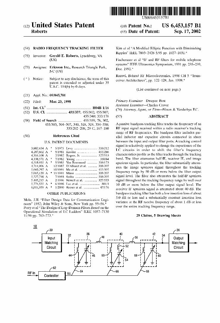
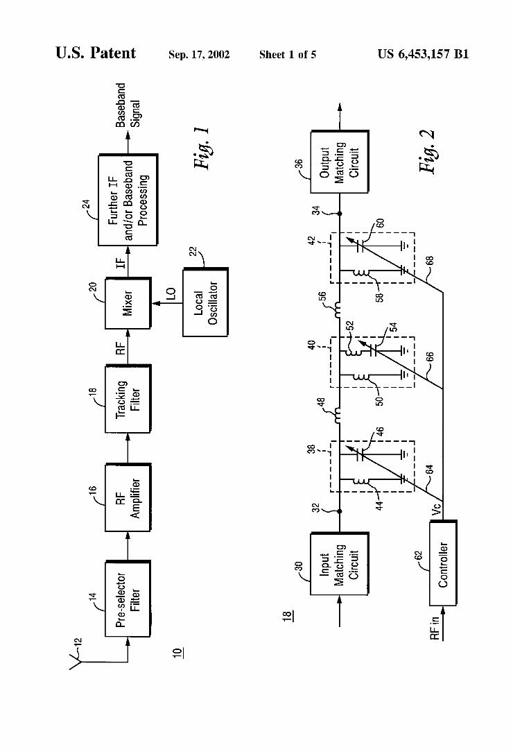
FIG. 1 is a function block diagram of an example radio receiver in Which the present invention may be employed;
FIG. 2 is a generaliZed circuit diagram illustrating a tracking ?lter in accordance With a preferred example embodiment of the present invention;
FIG. 3 is a more detailed schematic of an example embodiment of a tracking ?lter in accordance With the present invention providing one set of example passive element values; and
FIGS. 4—6 are frequency plots shoWing the frequency response of the ?lter of FIG. 3 for different control voltages VC over the RF tracking band of 403 MHZ—470 MHZ.
DETAILED DESCRIPTION OF THE DRAWINGS
In the folloWing description, for purposes of explanation and not limitation, speci?c details are set forth, such as particular embodiments, circuits, circuit components, etc. in order to provide a thorough understanding of the present invention. HoWever, it Will be apparent to one skilled in the art that the present invention may be practiced in other embodiments that depart from these speci?c details. In other instances, detailed descriptions of Well-knoWn methods, devices, circuits, and circuit components are omitted so as not to obscure the description of the present invention With unnecessary detail.
FIG. 1 shoWs a function block diagram of a radio receiver 10 in Which the present invention may be advantageously implemented. An RF signal is received at an antenna 12 and ?ltered in a preselector loW pass ?lter 14 to remove spurious high frequency signals and improve the selectivity of the receiver. The ?ltered signal is ampli?ed in an RF ampli?er 16 and then ?ltered in the tracking ?lter 18 to attenuate, among other things, various unWanted receiver spurious signals as Will be described in more detail in the example embodiment disclosed beloW. A local oscillator (LO) 22 provides a range of local oscillator signals to a mixer 20. The mixer 20 mixes the ?ltered RF signal from the tracking ?lter 18 and the LO signal to generate an intermediate frequency (IF) signal Which contains the modulated information but at a loWer frequency. The IF signal is further processed in block 24 to produce a baseband signal that may, for example, be used to drive a speaker if the baseband signal contains audio information. Although only one IF stage is shoWn in FIG. 1, a second IF stage may be desired in order to make use of existing components and integrated circuits readily available at loW cost.
The radio receiver 10 in FIG. 1 may be incorporated, for example, into a UHF radio that receives RF signals over the relatively Wide RF band of 403—470 MHZ. Accordingly, RF signals are input to the mixer 20 in the range of 403—470 MHZ. A relatively high IF frequency is employed at 125.25 MHZ. Since high side injection is used, the local oscillator 22 generates LO signals for input to the mixer 20 in the

US 6,453,157 B1 5
range of 528.25—595.25 MHZ depending on the detected RF input signal frequency. The desired IF output of the mixer 20 therefore corresponds to the difference of the LO signal and input RF signal from tracking ?lter 18. If a second IF stage is employed, the second IF frequency may be for example 450 kHZ.
With the IF frequency at 125.25 MHZ, the mixer 20 also produces undesirable mixer products at various image fre quencies linked to that IF frequency of 125.25 MHZ. The image is produced at the RF input signal plus tWice the IF. Thus, if the received RF signal is at 403 MHZ, an image spurious signal is produced at 653.5 MHZ (403+2><125 .25). The tracking ?lter 18 strongly attenuates this image spurious signal 50 db or more beloW the ?lter output signal.
Because the receiver band from 403 to 470 MHZ is relatively Wide, an unWanted receiver spurious signal can unfortunately be produced Within the tracking band of the ?lter 18. Speci?cally, this unWanted receiver spurious signal corresponds to the RF input signal plus one-half of the IF and is knoWn as half-IF spurious signal. Continuing With the example of an RF signal received at 403 MHZ, a half-IF spurious signal is produced at 456.25 MHZ (403+1/z><125.25) Which falls Within the tracking band of 403—470 MHZ. Attenuation of the half-IF spurious signal is therefore par ticularly challenging, especially When it may be necessary or otherWise desirable to attenuate such a half-IF spurious signal Within the tracking band by 10 db or more beloW the ?lter output level.
Rather than sWitching betWeen multiple ?lters, e.g., SAW ?lters, at various center frequencies strategically spaced over the tracking band to avoid the undesirable image frequencies, the present invention provides a single, inexpensive, but nevertheless very effective passive ?lter that provides the necessary attenuation at the in-band and out-of-band unWanted receiver spurious signals With rela tively loW and constant insertion loss across the tracking band. An example embodiment of such a tracking ?lter 18 is illustrated in FIG. 2.
An input matching circuit 30 receives an RF input signal and generates an output connected to a ?lter input terminal 32. Filter output terminal 34 is connected to an output matching 36 Whose output is connected to the mixer 20. Three LC circuits 38, 40, and 42 indicated by dashed lines are interconnected by series inductors 48 (betWeen LC circuits 38 and 40) and 56 (betWeen LC circuits 40 and 42). Each parallel LC circuit 38, 40, and 42 is connected in shunt betWeen the input terminal 32 and output terminal 34. LC circuit 48 includes inductor 44 and variable capacitor 46; LC circuit 40 includes parallel inductor 50 and variable capaci tor 54 With an additional inductor 52 connected in series With variable capacitor 54; and LC circuit 42 includes inductor 58 and variable capacitor 60.
Acontroller 62 provides control signals 64, 66, and 68 to vary the capacitance of capacitors 46, 54, and 60 in accor dance With the tracked RF frequency received by antenna 12. For example, controller 62 receives a signal correspond ing to the currently received RF input signal and determines the center frequency of the currently received signal some Where Within the tracking band of 403 to 470 MHZ. Based upon the detected frequency of the input signal, the control ler 62 generates a control signal VC Which changes the capacitance value of the LC circuits. By changing the capacitance values of the LC circuits an appropriate amount, the controller 62 shifts the frequency response of the track ing ?lter so that the center frequency of the pass band is at or near the received RF frequency. Depending upon the
10
15
20
25
30
35
40
45
50
55
60
65
6 design application, the controller may apply the same con trol signal VC to each of the three capacitors or, in some applications, may apply the same control voltage to capaci tors 46 and 60 With a someWhat different control voltage to capacitor 54.
Although someWhat oversimpli?ed, it is helpful for pur poses of understanding the operation of the tracking ?lter 18, to vieW the LC circuits 38 and 42 as being controlled together to shift the ?lter pass band in accordance With the frequency of the currently received signal. The LC circuit 40 is controlled to move the ?nite attenuation pole at the high side of the ?lter frequency pro?le/characteristic also in accordance With the frequency of the currently received signal. If similar or the same control voltages are applied to the capacitors in all three of the LC circuits 38, 40, and 42, the center frequency of the pass band as Well as the high side ?nite attenuation pole are shifted together in accordance With the frequency of the currently received signal. On the other hand, the control voltage applied to LC circuit 40 may be such that the high side ?nite attenuation pole remains relatively stationary While the center frequency of the ?lter pass band is moved thereby changing the slope of the ?lter “skirt” on the high side of the pass band Which may be desirable in certain applications.
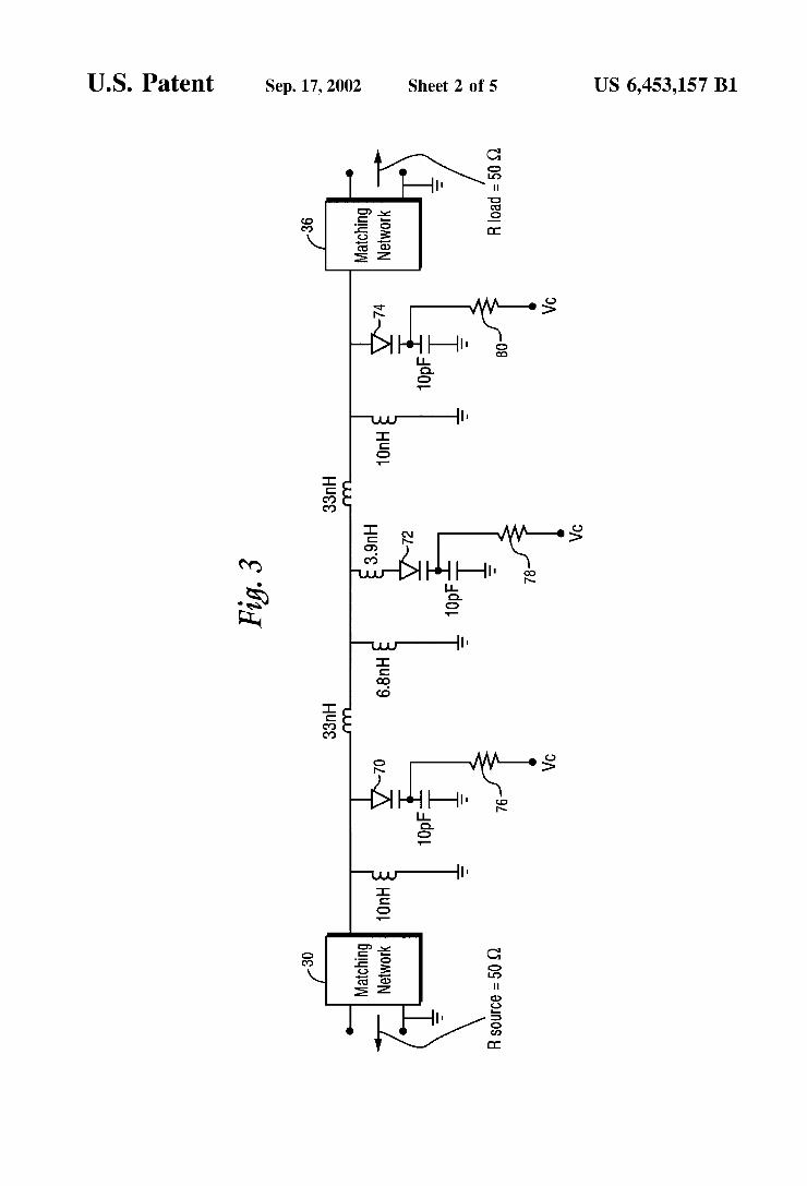
FIG. 3 shoWs a someWhat more detailed schematic of one example, non-limiting implementation of the tracking ?lter 18. The variable capacitors are implemented using varactor diodes 70, 72, and 74. Thus, the selection of capacitor elements therefore must take into account each varactor diode is a part of the variable capacitance in each capacitor position. The capacitance changes are controlled by selec tively applying a control voltage VC through respective resistors 76, 78, and 80 to the varactor diodes 70, 72, and 74, respectively. One commercially available varactor diode Which may be used is a varactor diode model TOKO1410 manufactured and sold by Toko America, Inc. Sample values for the lumped L and C elements shoWn in FIG. 3 are indicated in the draWing for an example, lumped element implementation. HoWever, a preferred implementation Would employ microstrip lines and Would take into account parasitic effects associated With a microstrip, PC board implementation at these RF frequencies. Those skilled in the art Will recogniZe that these values are approximate only and depend on the particular circuit layout.
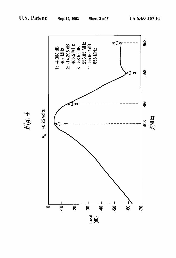
FIGS. 4—6 shoW example frequency responses (not to scale) of the tracking ?lter shoWn in FIG. 3 at different varactor control voltages. Speci?cally, FIG. 4 shoWs a frequency response of the ?lter at a control voltage VC of 0.25 volts. At this control voltage, the center frequency of the ?lter response shoWn at marker 1 is at 403 MHZ at an attenuation of —4.008 db beloW the ?lter input signal level, i.e., 0 db. Accordingly, the insertion loss of the ?lter is quite loW especially given the number of inductors employed. The half-IF spurious signal (marker 2) is at —465 .5 MHZ Within the tracking band and is attenuated someWhat more than 10 db beloW the ?lter output signal level of —4.008 db at —14.295 db. The receiver IF spurious signal at 528.25 MHZ is attenuated about 40 db beloW the ?lter output. The high side ?nite attenuation pole at pointer 3, corresponding to the maximum attenuation of the ?lter stop band corresponds to the ?nite loss pole at 558.5 MHZ With an attenuation of —58.52 db, more than 50 db beloW the ?lter output signal level of —4008 db. The “return” portion of the stop band from 558.5 MHZ includes the receiver image spurious signal Which might occur at marker 4 at 653 MHZ and Which is attenuated to —55.602 db Which again is also more than 50 db beloW the ?lter output signal level.
US 6,453,157 B1 7
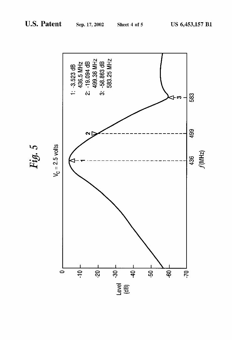
FIG. 5 shows the frequency characteristic of the ?lter in FIG. 3 With a control voltage VC equal to 2.5 volts applied to the varactors 70, 72, and 74. At that control voltage, the center frequency of the ?lter pass band corresponds to approximately 436.5 MHZ as shoWn at marker 1 With an attenuation of —3.523 db. The half-IF spurious signal cor responds to marker 2 at approximately 499 MHZ With an attenuation of —19.094 db over 15 db beloW the ?lter output signal level. The receiver IF spurious signal at 561.75 MHZ is attenuated about 40 dB beloW the ?lter output. Marker 3 indicates the ?nite attenuation pole at 583.25 MHZ With an attenuation of —58.863 dB. The return, including the position Where the unWanted image spurious signal (not shoWn) Would occur, is about 50 dB beloW the ?lter output signal band.
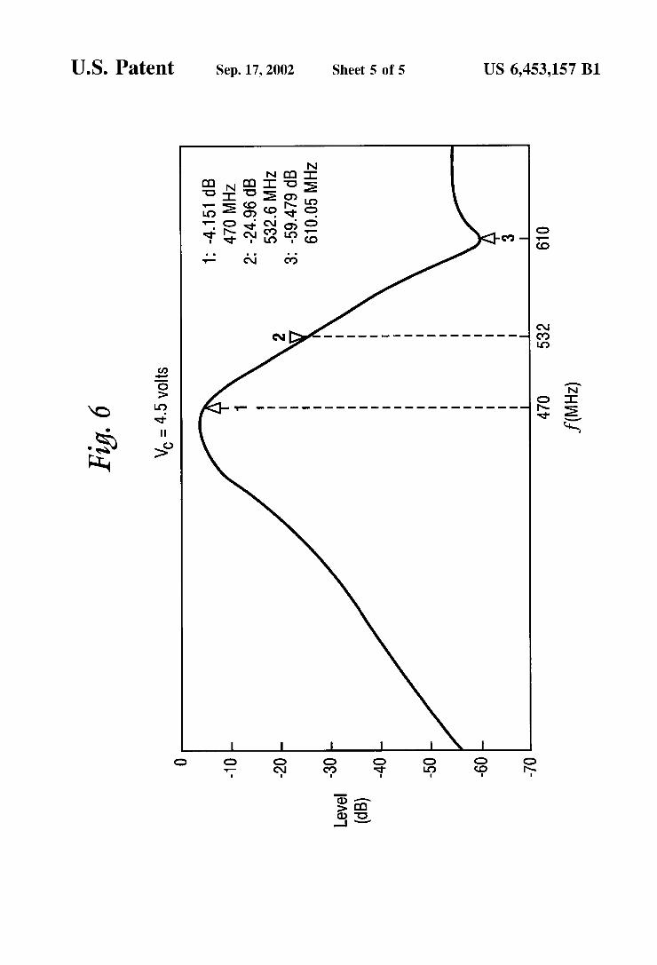
FIG. 6 shoWs the frequency response of the tracking ?lter in FIG. 3 When a control voltage VC equal to 4.5 volts is applied to the varactors 70, 72, and 74. Note that the ?lter’s frequency response has been shifted over so that the approximate center frequency of the pass band corresponds to the upper end of the tracking band 470 MHZ With an attenuation of —4.151 dB. The unWanted receiver half-IF spurious signal corresponds to a frequency of approximately 532.6 MHZ With an attenuation of —24.96 dB Well over 15 dB beloW the ?lter output signal level. The receiver IF spurious signal at 595.25 MHZ is attenuated about 40 dB beloW the ?lter output signal. The ?nite attenuation pole notch at 610 MHZ shoWs —59.479 dB attenuation With the image spurious signal on the return (not shoWn) being attenuated about 50 dB beloW the ?lter output signal.
The example ?lter characteristics shoWn in FIGS. 4—6 illustrate a number of advantageous features of a tracking ?lter constructed in accordance With the present invention. First, the ?lter insertion loss is relatively small and constant throughout the tracking range as indicated in Table 1 beloW.
TABLE 1
Received Frequency Insertion Loss (dB)
403 —4.008 436.5 —3.522 470 —4.151
Over the entire tracking band, the insertion loss is basically constant at 3.84 dB Within a 0.5 dB tolerance. This value of 3.8 dB is particularly loW at these RF frequencies of 403 MHZ—470 MHZ. As the control voltage VC goes through its full range, corresponding to the complete tracking frequency range, the actual insertion loss of the ?lter only varies by less than 1 dB. By keeping the insertion loss of each desired RF receive signal substantially constant over the entire tracking range, several major design and performance advantages occur. For example, the gain distribution of the receiver is simpli?ed, the sensitivity of the receiver is the same regard less of Which portion of the RF band the radio is operating. Both the noise ?gure and the signal-to-noise ratio also remain constant over the RF tracking band.
Another advantageous feature of the present invention is that both the ?lter stop band and pass band change With the variation of the control voltage VC to the variable capacitors. As can be seen in the example frequency response charac teristics shoWn in FIGS. 4—6, both the center frequency of the pass band and the ?nite attenuation pole shift in fre quency by changing the control voltage applied to all is three varactors 70, 72, and 74 Without substantially changing the shape of the pass band or the stop band. As the center frequency shifts, the ?lter continues to attenuate the image
10
15
20
25
30
35
40
45
50
55
60
65
8 spurious signal substantially, e.g., on the order of 50 dB or more beloW the output signal level, and also signi?cantly attenuates any spurious signal at the half-IF (Which may be Within the tracking band), i.e., on the order of about 10 to 15 dB beloW the ?lter output level. The receiver IF spurious signal at fRF+flf is attenuated as much as 40 or 50 dB as Well. The present invention employs a relatively large number
of inductors, Which is unusual at RF frequencies. The conventional approach to designing a bandpass ?lter at RF frequencies is to minimiZe the number of inductors used for a speci?c number of attenuation poles. This minimiZes the problems With the loW Q associated With inductors at RF frequencies and particularly at UHF frequencies, and With the mutual coupling betWeen inductors in close proximity of each other at these frequencies. The loW Q in an inductor produces resistance Which causes ?lter attenuation/insertion loss, particularly in the passband, at RF frequencies. On the other hand, there is negligible mutual coupling betWeen capacitors in close proximity of each other at these frequen cies. As a result, typical RF ?lter designs usually have more capacitors than inductors.
In contrast, the ?lter in accordance With the present invention employs more inductors than capacitors. In the example embodiment shoWn in FIGS. 2 and 3, the tracking ?lter employs three capacitors and tWice as many (six) inductors. Signi?cantly, despite the large number of inductors, the ?lter insertion loss is quite good and remains relatively constant over the entire tracking range as a result of careful determination of ?lter bandWidth, layout of the inductors to produce minimum effects of mutual coupling betWeen inductors, positioning of the ?nite attenuation pole relative to the passband, and use of standard values of the inductors and capacitors. The intermodulation (IM) perfor mance of this tracking ?lter is comparable to a normal passive ?lter because there are no nonlinear devices in the series arms of the ?lter.
Accordingly, the present invention provides excellent tracking ?ltering over a relatively Wide RF frequency band using only a single, relatively small, inexpensive, and pas sive ?lter. While the present invention may be advanta geously employed in the radio receiver described above, those skilled in the art Will appreciate that it is only one example application. For example, the tracking ?lter is not limited to a particular frequency range or a particular type of receiver. The invention has been described in terms of speci?c
embodiments to facilitate understanding. The above embodiments, hoWever, are illustrative rather than limitive. It Will be apparent to one of ordinary skill in the art that departures may be made from the speci?c embodiments shoWn above Without departing from the essential spirit and scope of the invention. For example, the present invention could be applied to attenuate unWanted signals generated by a synthesiZer before the synthesiZer signal is provided to a mixer. Therefore, the invention should not be regarded as being limited to the above examples, but should be regarded instead as being fully commensurate in scope With the folloWing claims. What is claimed is: 1. A passive, lumped, ultrahigh frequency (UHF) band
pass tracking ?lter that tracks a frequency of an input signal received in an UHF tracking range of frequencies, the bandpass ?lter including an input port receiving the input signal and an output port providing a ?ltered signal, com prising:
plural parallel inductor and capacitor circuits connected in shunt betWeen the input port and the output port, each circuit including a capacitor connected to an inductor, and