radiation pattern due to higher order modes in...
TRANSCRIPT

Radiation Pattern due to Higher Order
Modes in Cylindrical Waveguides
By
Arnab Pramanik
D. Anish Roshi
William Shillue
06/01/15 – 07/14/15

1
Arnab Pramanik ([email protected]) 08-12-2015
Index:
INTRODUCTION …………………………………………………………………… 02
MODES OF A CIRCULAR WAVEGUIDE ……………………………………….. 03
RADIATION PATTERN OF DIFFERENT MODES ……………………………... 03
CALCULATION OF RADIATED POWER ……………………………………….. 32
SLOT ANTENNA …………………………………………………………………... 33
DISCUSSION ………………………………………………………………………... 47
CONCLUSION ………………………………………………………………………. 48
APPENDIX …………………………………………………………………………... 49

2
Arnab Pramanik ([email protected]) 08-12-2015
Introduction:
The broader objective of the project is to find ways to increase the field of view of radio interferometer. The field of view of a radio interferometer is limited by the primary beam of individual antenna. The beam of a radio telescope is proportional to the wavelength as the diameter of the telescope is fixed. For higher frequency the beam reduces. So the field of view reduces (see figure: 1). In this project we have investigated the multimode feed horn as possible solution to the problem. Specifically, for the project, we aimed at (a) obtaining the radiation pattern of different modes and their radiation efficiencies and (b) ways to control complex amplitude of modes in waveguide. CST microwave studio is used to simulate far-field pattern when different modes in a circular waveguide are excited. We developed MATLAB programs to verify scatter parameters provided by CST. We also developed MATLAB programs to estimate the radiated power from CST field pattern.
Beam ~ λ/𝐷
λ = wavelength
D = diameter of the antenna
Figure 1: Field of view of a radio interferometer

3
Arnab Pramanik ([email protected]) 08-12-2015
1. Modes of a Circular Waveguide:
The field pattern inside the waveguide can be considers as a combination of different modes. This modes can be transverse electric (TE) and transvers magnetic (TM). Figure : 2 shows field pattern of two modes inside the waveguide.
Figure 2: field patterns of different modes
2. Radiation pattern of different modes:
To find the radiation pattern of different modes we used CST microwave studio, which has a CAD based user interface where we can design mechanical structure of antennas and waveguides and simulate their radiation pattern. CST solves the Maxwell’s equations in numerical fashion to obtained the field pattern and scatter parameters.
a) Waveguide design and simulation
A cylindrical waveguide model was created in CST microwave studio. The inner, outer diameters and length of the waveguide are set as parameters. The material of the waveguide is selected as perfect electric conductor (PEC). The inner radius is set to Rin = 95mm and the outer radius is set to Rout = 100 mm. The cutoff frequency of a circular waveguide depends upon the inner radius and the modes. For this specific configuration the lowest cutoff frequency we got is 0.925 GHz for TE11 mode. We kept the length of the waveguide of 600 mm (see Fig. 3). CST’s waveguide ports are used to excite the waveguide.
After completing the mechanical design of the waveguide we set the frequency to 0 to 10 GHz for simulation. Initially, two waveguide ports were placed on either side of the waveguide (see Fig. 4). The port is set to excite one mode (TE11). The mesh size is set to 1/10th of the wavelength. The transient solver is used for the simulation, with accuracy set to -30 dB and scatter parameter (S parameter) normalized to reference impedance of 50 Ω. The

4
Arnab Pramanik ([email protected]) 08-12-2015
field pattern at 5 GHz and 10 GHz in the waveguide is shown in Fig. 3 & 4 respectively. The |S11| vs frequency is shown in Fig. 7.
Figure 3: Cylindrical Waveguide Design
Figure 4: Cylindrical Waveguide with Two Waveguide Ports
Figure 5: Electric Field Pattern for 5 GHz

5
Arnab Pramanik ([email protected]) 08-12-2015
Figure 6: Electric Field Pattern for 5 GHz
Figure 7: |S11| for two ports configuration
To understand the behavior of S11 as a function of frequency we developed a simple network model of the waveguide-port system in MATLAB. We know the cutoff frequency of circular waveguide for TE11 is given by
𝑓𝑓𝑓𝑓𝑓𝑓𝑓 = 1.8412 ∗ 𝑓2 ∗ 𝜋 ∗ 𝑟
Where c = 3 * 10^8 m/sec and r = radius of the circular section of the waveguide in meters. The cutoff frequency for TE11 is 0.925 GHz for r = 95 mm. The characteristic impedance of a circular waveguide can be measured as

6
Arnab Pramanik ([email protected]) 08-12-2015
𝑍0 = 377
1 − 𝑓𝑐𝑐𝑐𝑐𝑐𝑐𝑐
𝑓
Here 377 Ohm is the approximate free space impedance, f is the frequency. The circular waveguide is considered as a transmission line terminated with load ZL. The input impedance of a transmission line is given by
𝑍𝑖𝑖 = 𝑍0 ∗(𝑍𝐿+𝑖∗𝑍0∗tan(𝛽∗𝐿))(𝑍0+𝑖∗𝑍𝐿∗tan(𝛽∗𝐿))
where Beta is 𝟐𝟐𝝀
, lambda is the wavelength in the waveguide, and L is the length of the
transmission line. The S11 is then obtained using the equation
𝑆11 = 𝑍𝑖𝑖 − 𝑍′0𝑍𝑖𝑖 + 𝑍′0
Figure 8: S parameter for circular waveguide with two ports

7
Arnab Pramanik ([email protected]) 08-12-2015
Figure 9: Impedance plot of circular waveguide with two ports
Where Z’0 is the reference impedance (= 50 Ohms) used by CST. The computed
characteristics impedance is shown in Fig. 9 and S11 is shown in Fig. 8 The computed S11 matches well with the CST simulation.
b) Radiation pattern:
To get the radiation pattern of different modes, we placed a port on one side and kept the other end open (see Fig. 10). The field pattern in the waveguide for TE11 and the S11 for this case are shown in Fig 11 & 12 for 5 and 10 GHz respectively. We simulate the S parameter in CST first (See Figure: 13). Then we have tried the simulation in MATLAB and plot the S parameter and input impedance over frequencies for Mode: 1 (See Figure: 14 & 15).

8
Arnab Pramanik ([email protected]) 08-12-2015
Figure 10: Cylindrical Waveguide with Single Port
Figure 11: Electric Field Pattern for 5 GHz, Single Port
Figure 12: Electric Field Pattern for 10 GHz, Single Port

9
Arnab Pramanik ([email protected]) 08-12-2015
Figure 13: S parameter plot for Single Port
Figure 14: MATLAB Simulation of S Parameter for Single Port

10
Arnab Pramanik ([email protected]) 08-12-2015
Figure 15: MATLAB Simulation of Input Impedance at Port 1
We then excited the waveguide with different modes (1 to 10) to analyze its S parameters and far field patterns for different frequencies. We also have developed an analytical model of the waveguide to reproduce the s parameter so that we can verify the CST simulation. The figures attached below shows the simulation results of S parameters from CST and MATLAB and far field from CST. For every mode the waveguide has different cutoff frequency. Figure: 16 show the different cutoff frequency of the waveguide for different modes.

11
Arnab Pramanik ([email protected]) 08-12-2015
Figure 16: Different cutoff frequencies of the waveguide for different modes

12
Arnab Pramanik ([email protected]) 08-12-2015
MODE 1
Mode: 1 is TE 11 mode. The cutoff frequency is 0.925 GHz. Figure: 17 shows the plot of S parameter in CST. Figure: 18 shows S parameter plot obtained from MATLAB model. Figure: 19 and Figure: 20 shows far field pattern obtained from CST and plotted in MTLAB for 5 GHz.
CST Simulation
Figure 17: S parameter plot from CST for Mode: 1
MATLAB Simulation
Figure 18: S parameter plot from MATLAB model for Mode: 1

13
Arnab Pramanik ([email protected]) 08-12-2015
Far field Pattern for 5 GHz
Figure 19: Contour plots of far field at 5 GHz for Mode: 1
Figure 20: 3-D plot of far field at 5 GHz for Mode: 1

14
Arnab Pramanik ([email protected]) 08-12-2015
MODE 2
Mode: 2 is TE 11 mode with orthogonal polarization. The cutoff frequency is 0.925 GHz. Figure: 21 show the plot of S parameter from CST. Figure: 22 shoes S parameter plot from MATLAB model. Figure: 23 and Figure: 24 shows far field obtained from CST and plotted using MATLAB for 5 GHz.
CST Simulation
Figure 21: S parameter plot from CST for Mode: 2
MATLAB Simulation
Figure 22: S parameter plot from MATLAB for Mode: 2

15
Arnab Pramanik ([email protected]) 08-12-2015
Far field Pattern for 5 GHz
Figure 23: Contour plot of the far field at 5 GHz for Mode: 2
Figure 24: 3-D plot of far field at 5 GHz for Mode: 2

16
Arnab Pramanik ([email protected]) 08-12-2015
MODE 3
Mode: 3 is TM 01 mode. The cutoff frequency is 1.21 GHz. Figure: 25 show the plot of S parameter from CST. Figure: 26 shows S parameter plot from MATLAB model. Figure: 27 and Figure: 28 show far field obtained from CST and plotted using MATLAB for 5 GHz.
CST Simulation
Figure 25: S parameter plot in CST for Mode: 3
MATLAB Simulation
Figure 26: S parameter plot from MATLAB model for Mode: 3

17
Arnab Pramanik ([email protected]) 08-12-2015
Far field Pattern for 5 GHz
Figure 27: Contour plot of the far field at 5 GHz for Mode: 3

18
Arnab Pramanik ([email protected]) 08-12-2015
Figure 28: 3-D plot of far field at 5 GHz for Mode: 3
MODE 4
Mode: 4 is TE 21 mode. The cutoff frequency is 1.53 GHz. Figure: 29 shows the plot of S parameter from CST. Figure: 30 shows S parameter plot from MATLAB model. Figure: 31 and Figure: 32 show far field obtained from CST and plotted using MATLAB for 5 GHz.
CST Simulation
Figure 29: S parameter plot in CST for Mode: 4
MATLAB Simulation

19
Arnab Pramanik ([email protected]) 08-12-2015
Figure 30: S parameter plot from MATLAB model for Mode: 4
Far field Pattern for 5 GHz

20
Arnab Pramanik ([email protected]) 08-12-2015
Figure 31: Contour plot of the far field at 5 GHz for Mode: 4
Figure 32: 3-D plot of far field at 5 GHz for Mode: 4
MODE 5

21
Arnab Pramanik ([email protected]) 08-12-2015
Mode: 5 is TE 21 mode (orthogonal polarization). The cutoff frequency is 1.53 GHz. Figure: 33 shows the plot of S parameter from CST. Figure: 34 shows S parameter plot from MATLAB model. Figure: 35 and Figure: 36 show far field obtained from CST and plotted using MATLAB for 5 GHz.
CST Simulation
Figure 33: S parameter plot in CST for Mode: 5
MATLAB Simulation
Figure 34: S parameter plot from MATLAB model for Mode: 5

22
Arnab Pramanik ([email protected]) 08-12-2015
Far field Pattern for 5 GHz
Figure 35: 3-D plot of far field at 5 GHz for Mode: 5
Figure 36: Contour plot of the far field at 5 GHz for Mode: 5

23
Arnab Pramanik ([email protected]) 08-12-2015
MODE 6
Mode: 6 is TE 01 mode. The cutoff frequency is 1.92 GHz. Figure: 37 shows the plot of S parameter from CST. Figure: 38 shows S parameter plot from MATLAB model. Figure: 39 and Figure: 40 show far field obtained from CST and plotted using MATLAB for 5 GHz.
CST Simulation
Figure 37: S parameter plot from CST for Mode: 6
MATLAB Simulation
Figure 38: S parameter plot from MATLAB for Mode: 6

24
Arnab Pramanik ([email protected]) 08-12-2015
Far field Pattern for 5 GHz
Figure 39: 3-D plot of far field at 5 GHz for Mode: 6
Figure 40: Contour plot of the far field at 5 GHz for Mode: 6

25
Arnab Pramanik ([email protected]) 08-12-2015
MODE 7
Mode: 7 is TM 11 mode. The cutoff frequency is 1.92 GHz. Figure: 41 shows the plot of S parameter from CST. Figure: 42 shows S parameter plot from MATLAB model. Figure: 43 and Figure: 44 show far field obtained from CST and plotted in MTLAB for 5 GHz.
CST Simulation
Figure 41: S parameter plot from CST for Mode: 7
MATLAB Simulation
Figure 42: S parameter plot from MATLAB model for Mode: 7

26
Arnab Pramanik ([email protected]) 08-12-2015
Far field Pattern for 5 GHz
Figure 43: 3-D plot of far field at 5 GHz for Mode: 7
Figure 44: Contour plot of the far field at 5 GHz for Mode: 7

27
Arnab Pramanik ([email protected]) 08-12-2015
MODE 8
Mode: 8 is TM 11 mode (orthogonal polarization). The cutoff frequency is 1.92 GHz. Figure: 45 shows the plot of S parameter from CST. Figure: 46 shows S parameter plot from MATLAB model. Figure: 47 and Figure: 48 show far field obtained from CST and plotted using MATLAB for 5 GHz.
CST Simulation
Figure 45: S parameter plot from CST for Mode: 8
MATLAB Simulation

28
Arnab Pramanik ([email protected]) 08-12-2015
Figure 46: S parameter plot from MATLAB model for Mode: 8
Far field Pattern for 5 GHz
Figure 47: 3-D plot of far field at 5 GHz for Mode: 8

29
Arnab Pramanik ([email protected]) 08-12-2015
Figure 48: Contour plot of the far field at 5 GHz for Mode: 8
MODE 9
Mode: 9 is TE 31 mode. The cutoff frequency is 2.11 GHz. Figure: 49 shows the plot of S parameter from CST. Figure: 50 shows S parameter plot from MATLAB model. Figure: 51 and Figure: 52 show far field obtained from CST and plotted using MATLAB for 5 GHz.
CST Simulation
Figure 49: S parameter plot from CST for Mode: 9

30
Arnab Pramanik ([email protected]) 08-12-2015
MATLAB Simulation
Figure 50: S parameter plot from MATLAB model for Mode: 9
Far field Pattern for 5 GHz

31
Arnab Pramanik ([email protected]) 08-12-2015
Figure 51: 3-D plot of far field at 5 GHz for Mode: 9
Figure 52: Contour plot of the far field at 5 GHz for Mode: 9
MODE 10
Mode: 10 is TE 31 mode (orthogonal polarization). The cutoff frequency is 2.11 GHz. Figure: 53 shows the plot of S parameter from CST. Figure: 54 shows S parameter plot from

32
Arnab Pramanik ([email protected]) 08-12-2015
MATLAB model. Figure: 55 and Figure: 56 show far field obtained from CST and plotted using MATLAB for 5 GHz.
CST Simulation
Figure 53: S parameter plot from CST for Mode: 10
MATLAB Simulation
Figure 54: S parameter plot from MATLAB model for Mode: 10
Far field Pattern for 5 GHz

33
Arnab Pramanik ([email protected]) 08-12-2015
Figure 55: 3-D plot of far field at 5 GHz for Mode: 10
Figure 56: Contour plot of the far field at 5 GHz for Mode: 10

34
Arnab Pramanik ([email protected]) 08-12-2015
c) Calculation of Radiated Power:
We developed a MATLAB program to calculate the radiated power using the far field patterns provided by CST. Table:1 and Table: 2 show radiated power for different modes for 5 GHz and 10 GHz respectively. The RMS excitation power was set by CST to 0.5 W. In table below, radiated power larger than 0.5 W is due to numerical inaccuracies in the simulation. This numerical inaccuracy was inferred by comparing the mode impedance with free space impedance. The difference in impedance provides a measure of power transmitted to free space.
Radiated Power for Different Modes for Frequency = 5 GHz
Modes Radiated Power (in Watts) 1 TE11 0.4809 2 TE11 0.4809 3 TM01 0.4829 4 TE21 0.4904 5 TE21 0.4903 6 TE01 0.5046 7 TM11 0.5175 8 TM11 0.5175 9 TE31 0.4906 10 TE31 0.4906
Table 1: Radiated Power for Different modes at 5 GHz
Radiated Power for Different Modes for Frequency = 10 GHz
Modes Radiated Power (in Watts) 1 TE11 0.4230 2 TE11 0.4230 3 TM01 0.4576 4 TE21 0.4833 5 TE21 0.4824 6 TE01 0.4890 7 TM11 0.5011 8 TM11 0.5011 9 TE31 0.4826 10 TE31 0.4826
Table 2: Radiated Power for Different modes at 10 GHz

35
Arnab Pramanik ([email protected]) 08-12-2015
Figure 57: Radiation efficiency for different modes
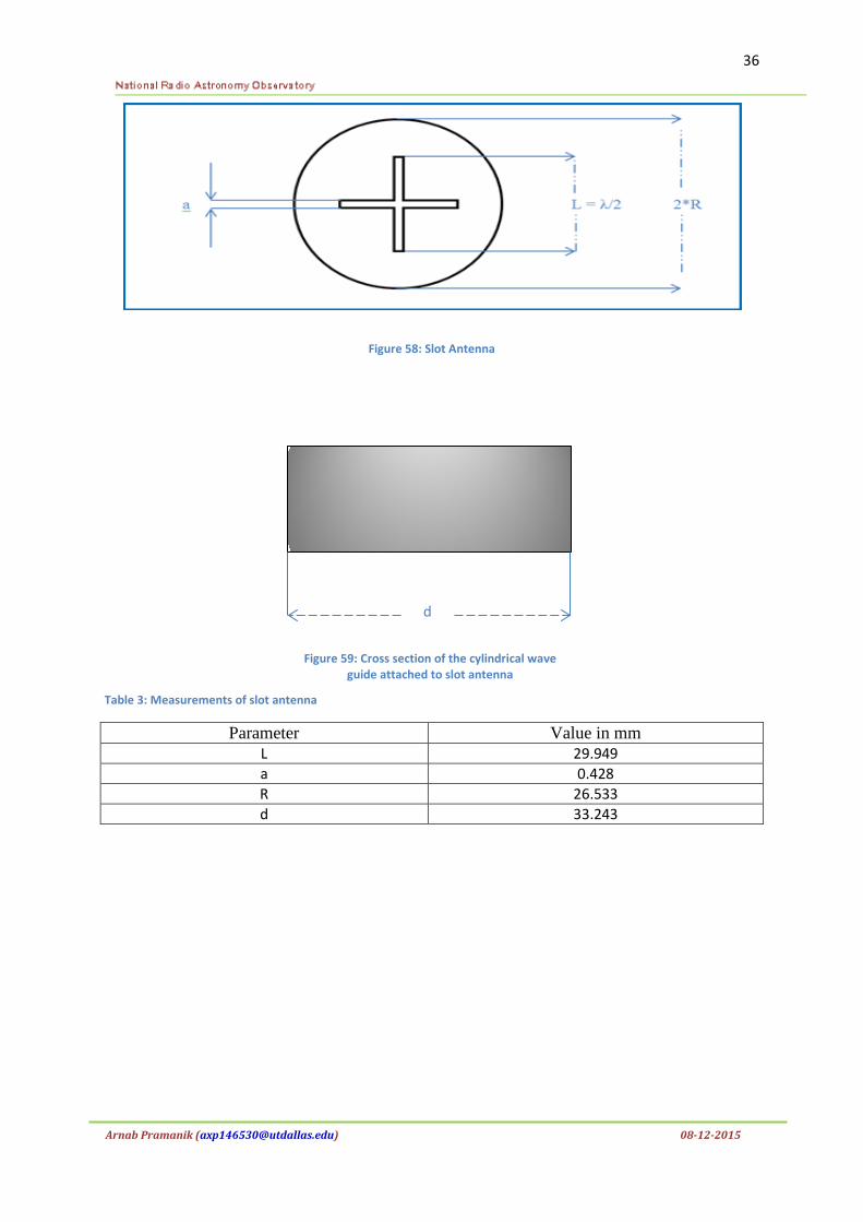
The radiation efficiency for the 10 modes are shown in Fig. 57. We found that radiation efficiency for 10 modes (1 to 10) is almost similar within 10 % (limited by simulation accuracy) . To find ways to control different modes of a waveguide we designed a slot antenna and excited the waveguide with the slot antenna. 3. Slot Antenna: Slot antennas are quite popular in radar, navigation and other high frequency usage. The main advantage of using slot antennas is that they are simpler to fabricate, have low loss and high efficiency. The slot antenna generally has a narrow width. We first designed a cross polarized slot antenna based on the theory developed by Li, Hummer & Chang (1991). We kept the length of the slot as λ/2 and the width a fraction of λ/2 (see Figure: 58 and 59). The slot antenna was tuned to 5 GHz. The dimensions of the designed antenna are given in Table 3. The slot antenna was then constructed in CST microwave studio. Figure: 61 & 62 show the slot antenna model in CST. Our goal is to get the S parameter and far field pattern of the slot antenna. The S parameter obtained from CST (See Figure: 64) shows that the slot antenna is tuned at 5 GHz.. The far field patterns of the slot antenna obtained from CST are shown in Figure: 65 & 66. We excited the waveguide with a single TE11 mode to get the far field pattern. Contour and 3D plots of the far field were also made using MATLAB, which are shown Figure: 67 & 68.
36
Arnab Pramanik ([email protected]) 08-12-2015
Figure 58: Slot Antenna
Table 3: Measurements of slot antenna
Parameter Value in mm L 29.949 a 0.428 R 26.533 d 33.243
d
Figure 59: Top view of the slot antenna Figure 59: Cross section of the cylindrical wave guide attached to slot antenna

37
Arnab Pramanik ([email protected]) 08-12-2015
Figure 60: Slot Antenna tuned at 5 GHz
Figure 61: Back View of Slot Antenna tuned at 5 GHz

38
Arnab Pramanik ([email protected]) 08-12-2015
Figure 62: Front View of Slot Antenna tuned at 5 GHz
Figure 63: S parameter plot of the slot antenna from CST

39
Arnab Pramanik ([email protected]) 08-12-2015
Figure 64: Far field plot of the slot antenna at 5 GHz from CST
Figure 65: Far field plot of the slot antenna at 5 GHz from CST

40
Arnab Pramanik ([email protected]) 08-12-2015
Figure 66: Contour plot of the Far field pattern at 5 GHz made using MATLAB
Figure 67: 3D plot of far field pattern of the slot antenna at 5 GHz made using MATLAB

41
Arnab Pramanik ([email protected]) 08-12-2015
Configuration I: Cylindrical Waveguide Excited by Slot Antenna
We attached the slot antenna with our original cylindrical waveguide to get the far field pattern and field pattern inside the waveguide. The CST model of a centrally placed slot antenna (configuration I) is shown in Figure: 68, 69 & 70.
Figure 68: Cylindrical waveguide with the slot antenna
The S parameter plot shown in Fig. 71, indicates a slight offset in frequency – ie the antenna in this setup is tuned at 4.97 GHz. For the present experiment, this shift in frequency is not significant.
Figure 69: Back view of the waveguide with slot antenna

42
Arnab Pramanik ([email protected]) 08-12-2015
Figure 70: Front view of the waveguide with slot antenna
Figure 71: S parameter plot of waveguide with slot antenna from CST
Figure: 72 & 73 show the far field plot of the waveguide with the centrally located slot antenna for single polarization for TE11 mode at the slot antenna input. The contour and 3D plot of the far field obtained using MATLAB are shown in Figure: 74 & 75.

43
Arnab Pramanik ([email protected]) 08-12-2015
Figure 72: Far field plot of the waveguide with centrally located slot antenna using CST
Figure 73: Far field plot of the waveguide with centrally located slot antenna using CST

44
Arnab Pramanik ([email protected]) 08-12-2015
Figure 74: Contour plot of Far field pattern for configuration I
Figure 75: 3D plot of far field for configuration I

45
Arnab Pramanik ([email protected]) 08-12-2015
Configuration II: Waveguide with an off-center slot antenna:
We then repeated the same experiment with an off-center slot antenna. We have shifted the center of the slot feed along the radius of the cylindrical waveguide (See Figure: 76, 77 & 78). The S parameter plot (see Fig. 79) shows that the antenna is tuned at 5 GHz. The far field patterns with TE11 mode excitation at the slot antenna input are shown in Figs. 80, 81, 82 & 83. The far field pattern is asymmetric compared to the centrally fed slot antenna excitation.
Figure 76: Cylindrical waveguide with the off-center slot antenna
Figure 77: Back view of the waveguide with off-center slot antenna

46
Arnab Pramanik ([email protected]) 08-12-2015
Figure 78: Front view of the waveguide with off-center slot antenna
Figure 79: S parameter plot of waveguide with the off-center slot antenna from CST

47
Arnab Pramanik ([email protected]) 08-12-2015
Figure 80: Far field plot of configuration II from the CST
Figure 81: Far field plot of configuration II from CST

48
Arnab Pramanik ([email protected]) 08-12-2015
Figure 82: 3D plot of far field pattern of configuration II.
Figure 83: Contour plot of the far field pattern for configuration II.

49
Arnab Pramanik ([email protected]) 08-12-2015
Discussion and Conclusion: Fig. 84 shows the field pattern inside the waveguide for Configuration I and II. These field patterns can be written as a linear superposition of waveguide modes. The complex amplitudes for the first 10 modes are obtained by multiplying the mode field patterns of the cylindrical waveguide with the field patterns shown in Fig 84 and integrating over the cross section of the waveguide. The cross section was selected 100 mm inside the open end of the waveguide to obtain the complex amplitudes. Plots of the absolute value of complex amplitudes for the two configurations are shown in Fig 85. The amplitudes for the 10 modes are very different. This means that it may be possible to design probes such that each probe can produce modes with an associated set of complex amplitude. By combining the probe outputs with complex weights it may be possible to control the field pattern in the waveguide and thus the far field pattern. This will be our future direction of investigation.
Figure 84: Electric field pattern inside the cylindrical waveguide for configuration I (left) and configuration II (right). The field patterns are obtained at 100 mm inside the waveguide from the radiating end.
Figure 85: Complex amplitude for different modes for configuration I (left) and configuration II (right) respectively. They are plotted as 10*log10(coefficients) vs mode number.

50
Arnab Pramanik ([email protected]) 08-12-2015
4. Appendix:
1. MATLAB Code for S11 Calculation for Port 1 and Port 2
%Frequency from 0 to 10 GHz f = 0:0.01:10; f_fc = zeros(1,1001); Z = zeros(1,1001); %Characteristic Impedance Calculation for i = 1:1001 f_fc(i) = (0.925/f(i))^2; Z(i) = 377/(sqrt(1-f_fc(i))); end %Initialization S11 = zeros(1,1001); S11_dB = zeros(1,1001); c = 3000*10^8; Zin = zeros(1,1001); BL = 2*pi*f*10^9*(600/c).*sqrt(1-f_fc); %S11 calculation for port 1 and port 2 for i = 1:1001 Zin(i) = (Z(i)*((50+j*(Z(i)*tan(BL(i))))/ (Z(i)+j*(50*tan(BL(i)))))); S11(i) = abs((Zin(i)-50.0)/(Zin(i)+50.0)); S11_dB(i) = 20*log10(S11(i)); end %Plots figure (1); plot(f, Z); xlabel('Frq in GHz'); ylabel('Characteristic Impedence in Ohm'); title('Characteristic Impedence vs Frequency'); figure (2); plot (f, Zin); xlabel('Frq in GHz'); ylabel('input Impedence in Ohm'); title('Input Impedence vs Frequency'); figure (3); plot(f, S11_dB); axis([0 10 -5 5]); xlabel('Frqquency in GHz'); ylabel('S11 in dB'); title('S11 vs Frequency plot for circular waveguide');

51
Arnab Pramanik ([email protected]) 08-12-2015
2. MATLAB Code for S11 Calculation for Port 1 and Port 2 %Frequency from 0 to 10 GHz f = 0:0.01:10; f_fc = zeros(1,1001); Z = zeros(1,1001); %Characteristic Impedance Calculation for i = 1:1001 f_fc(i) = (0.925/f(i))^2; Z(i) = 377/(sqrt(1-f_fc(i))); end %Initialization S11 = zeros(1,1001); S11_dB = zeros(1,1001); c = 3000*10^8; Zin = zeros(1,1001); BL = 2*pi*f*10^9*(600/c).*sqrt(1-f_fc); %S11 calculation for port 1 only for i = 1:1001 Zin(i) = (Z(i)*((377+j*(Z(i)*tan(BL(i))))/ (Z(i)+j*(377*tan(BL(i)))))); S11(i) = abs((Zin(i)-Z(i))/(Zin(i)+Z(i))); %The reference impedance for S11 used by CST is 50 Ohms since %we selected that in the simulator. So I changed Z(i) to 50 Ohms. %Anish %S11(i) = abs((Zin(i)-50.0)/(Zin(i)+50.0)); S11_dB(i) = 20*log10(S11(i)); end %Plots figure (1); plot(f, Z); xlabel('Frq in GHz'); ylabel('Characteristic Impedence in Ohm'); title('Characteristic Impedence vs Frequency'); figure (2); plot (f, Zin); xlabel('Frq in GHz'); ylabel('input Impedence in Ohm'); title('Input Impedence vs Frequency'); figure (3); plot(f, S11_dB); %axis([0 10 -3 1.5]); xlabel('Frqquency in GHz'); ylabel('S11 in dB'); title('S11 vs Frequency plot for Cir waveguide With Open Port 2');

52
Arnab Pramanik ([email protected]) 08-12-2015
3. MATLAB Code to Plot and Calculated Radiated Power of The Far Field %Plot the beam from CST ffs file clear all close all % Cell Library for the file names. data1 = ['cylwaveguide_mode01_f5GHz.ffs'; 'cylwaveguide_mode02_f5GHz.ffs'; 'cylwaveguide_mode03_f5GHz.ffs'; 'cylwaveguide_mode04_f5GHz.ffs'; 'cylwaveguide_mode05_f5GHz.ffs'; 'cylwaveguide_mode06_f5GHz.ffs'; 'cylwaveguide_mode07_f5GHz.ffs'; 'cylwaveguide_mode08_f5GHz.ffs'; 'cylwaveguide_mode09_f5GHz.ffs'; 'cylwaveguide_mode10_f5GHz.ffs']; data2 = ['cylwaveguide_mode01_f10GHz.ffs'; 'cylwaveguide_mode02_f10GHz.ffs'; 'cylwaveguide_mode03_f10GHz.ffs'; 'cylwaveguide_mode04_f10GHz.ffs'; 'cylwaveguide_mode05_f10GHz.ffs'; 'cylwaveguide_mode06_f10GHz.ffs'; 'cylwaveguide_mode07_f10GHz.ffs'; 'cylwaveguide_mode08_f10GHz.ffs'; 'cylwaveguide_mode09_f10GHz.ffs'; 'cylwaveguide_mode10_f10GHz.ffs']; celldata = cellstr(data2); Etheta_cu = zeros (37,73); Ephi_cu = zeros (37,73); %Loop to calculate cumulative Etheta and Ephi for n = [1, 4, 7, 9] filename = celldatan; Beam = getEfromCST2014ffs(filename); prad = radpwr(Beam); %cumulative Etheta and Ephi Etheta_cu = Etheta_cu + Beam.Etheta; Ephi_cu = Ephi_cu + Beam.Ephi; end %Plot of Cross section of the Radiated Power figure(1) cntrlevels=[0,-1,-2,-3,-5,-10,-15,-20,-25,-30]; axisvalue=[-90,90,-90,90]; %Subtracting pi from theta since the beam is in the negative z axis %in CST theta1 = (Beam.theta - pi).*cos(Beam.phi)*180/pi; theta2 = (Beam.theta - pi).*sin(Beam.phi)*180/pi; Powpatt = Etheta_cu.*conj(Etheta_cu) + ... Ephi_cu.*conj(Ephi_cu); Powpatt = 10*log10(Powpatt/max(max(Powpatt))); [C, h] = contour(theta1, theta2, Powpatt, cntrlevels); clabel(C,h); colorbar;

53
Arnab Pramanik ([email protected]) 08-12-2015
axis(axisvalue); axis square; %3-D Plot of the Radiated Power figure(2) %Subtracting pi from theta since the beam is in the negative z axis %in CST theta1 = (Beam.theta - pi).*cos(Beam.phi)*180/pi; theta2 = (Beam.theta - pi).*sin(Beam.phi)*180/pi; Powpatt = Etheta_cu.*conj(Etheta_cu) + ... Ephi_cu.*conj(Ephi_cu); Powpatt = 10*log10(Powpatt/max(max(Powpatt))); mesh(theta1, theta2, Powpatt); caxis([-30,0]); colorbar; axisvalue=[-90,90,-90,90]; axis(axisvalue); axis square; view(60,45); %Reads the Etheta and Ephi components of the fields of M elements %and put them in a four dimensional array (dipole, freq, theta,phi). %The input file from CST should be in CST source format output of %the field pattern and broadband selected in CST. function ffs = getEfromCST2014ffs(filename) collen = 6; %Get the beam values from these files fid = fopen(filename); [radP, accP, stimP, freq] = readheader(fid); for fcnt = 1:length(freq) A = ' '; while ~strncmp(A, '// >> Total', 11) A = fgetl(fid); end A = fgetl(fid); B = strsplit(A); phisamp = str2num(B1); thetasamp = str2num(B2); while ~strncmp(A, '// >> Phi,', 10) A = fgetl(fid); end B = fscanf(fid,'%f', [collen, phisamp*thetasamp]); B = reshape(B', thetasamp, phisamp, collen); phi = B(:,:,1)*pi/180; theta = B(:,:,2)*pi/180; Etheta(:,:) = B(:,:,3) + j*B(:,:,4); %in V/m Ephi(:,:) = B(:,:,5) + j*B(:,:,6); end fclose(fid);

54
Arnab Pramanik ([email protected]) 08-12-2015
ffs.theta = theta; ffs.phi = phi; ffs.freq = freq/1e9; %in GHz. ffs.Etheta = Etheta; ffs.Ephi = Ephi; function [radP, accP, stimP, freq] = readheader(fid) A1 = ' '; while ~strncmp(A1, '// #Frequencies', 16) A1 = fgetl(fid); end A1 = fgetl(fid); nfreq = str2num(A1); while ~strncmp(A1, '// Radiated', 11) A1 = fgetl(fid); end for cnt1 = 1:nfreq A1 = fgetl(fid); radP(cnt1) = str2num(A1); A1 = fgetl(fid); accP(cnt1) = str2num(A1); A1 = fgetl(fid); stimP(cnt1) = str2num(A1); A1 = fgetl(fid); freq(cnt1) = str2num(A1); A1 = fgetl(fid); end end end %Function to calculate the radiated power function Prad = radpwr(dipole) theta = dipole.theta; phi = dipole.phi; freq = dipole.freq; Etheta(:,:) = dipole.Etheta(:,:); %in V/m Ephi(:,:) = dipole.Ephi(:,:); pwr = (abs(Etheta).^2 + abs(Ephi).^2)/(120*pi*2); Prad = trapz(theta(:,1), (trapz(phi(1,:), pwr, 2)).*sin(theta(:,1))); fprintf('Total Radiated Power from the Beam = %7.4f (W) \n', Prad); end