q.2 a. with the help of diagram, explain the different ......the c flag is set to 1 if a carry...
TRANSCRIPT

AC58/AT58/AC106/AT106 COMPUTER ORGANIZATION DEC 2015
© IETE 1
Q.2 a. With the help of diagram, explain the different functional units of a Computer. (6)
Answer: A computer consists of five functionally independent main parts: input, memory, arithmetic and logic, output, and control units, as shown in figure below. The input unit accepts coded information from human operators using devices such as keyboards or from other computers over digital communication lines. The information received is stored in the computer’s memory, either for later use or to be processed immediately by the arithmetic and logic unit. The processing steps are specified by a program that is also stored in the memory. Finally, the results are sent back to the outside world through the output unit. All of these actions are coordinated by the control unit. An interconnection network provides the means for the functional units to exchange information and coordinate their actions.
Basic functional units of a Computer
Input Unit Computers accept coded information through input units. The most common input device is the keyboard. Whenever a key is pressed, the corresponding letter or digit is automatically translated into its corresponding binary code and transmitted to the processor. Many other kinds of input devices for human-computer interaction are available, including the touchpad, mouse, joystick, and trackball. These are often used as graphic input devices in conjunction with displays. Microphones can be used to capture audio input which is then sampled and converted into digital codes for storage and processing. Similarly, cameras can be used to capture video input. Digital communication facilities, such as the Internet, can also provide input to a computer from other computers and database servers. Memory Unit The function of the memory unit is to store programs and data. There are two classes of storage, called primary and secondary. Primary Memory Primary memory, also called main memory, is a fast memory that operates at electronic speeds. Programs must be stored in this memory while they are being executed. The memory consists of a large number of semiconductor storage cells, each capable of storing one bit of information. These cells are rarely read or written individually. Instead, they are handled in groups of fixed size called words. The memory is organized so that one word can be stored or retrieved in one basic operation. The number of bits in each word is referred to as the word length of the computer, typically 16, 32, or 64 bits. To provide easy access to any word in the memory, a distinct address is associated with each word location. Addresses are consecutive numbers, starting from 0, that identify successive locations. A particular word is accessed by specifying its address and issuing a control command to the memory that starts the storage or retrieval process. Instructions and data can be written into or read from the memory under the control of the processor. It is essential to be able to access any word location in the memory as quickly as possible. A memory in which
1

AC58/AT58/AC106/AT106 COMPUTER ORGANIZATION DEC 2015
© IETE 2
any location can be accessed in a short and fixed amount of time after specifying its address is called a random-access memory (RAM). The time required to access one word is called the memory access time. This time is independent of the location of the word being accessed. It typically ranges from a few nanoseconds (ns) to about 100 ns for current RAM units. Cache Memory As an adjunct to the main memory, a smaller, faster RAM unit, called a cache, is used to hold sections of a program that are currently being executed, along with any associated data. The cache is tightly coupled with the processor and is usually contained on the same integrated-circuit chip. The purpose of the cache is to facilitate high instruction execution rates. At the start of program execution, the cache is empty. All program instructions and any required data are stored in the main memory. As execution proceeds, instructions are fetched into the processor chip, and a copy of each is placed in the cache. When the execution of an instruction requires data located in the main memory, the data are fetched and copies are also placed in the cache. Secondary Storage Although primary memory is essential, it tends to be expensive and does not retain information when power is turned off. Thus additional, less expensive, permanent secondary storage is used when large amounts of data and many programs have to be stored, particularly for information that is accessed infrequently. Access times for secondary storage are longer than for primary memory. A wide selection of secondary storage devices is available, including magnetic disks, optical disks (DVD and CD), and flash memory devices. Arithmetic and Logic Unit Most computer operations are executed in the arithmetic and logic unit (ALU) of the processor. Any arithmetic or logic operation, such as addition, subtraction, multiplication, division, or comparison of numbers, is initiated by bringing the required operands into the processor, where the operation is performed by the ALU. For example, if two numbers located in the memory are to be added, they are brought into the processor, and the addition is carried out by the ALU. The sum may then be stored in the memory or retained in the processor for immediate use. When operands are brought into the processor, they are stored in high-speed storage elements called registers. Each register can store one word of data. Access times to registers are even shorter than access times to the cache unit on the processor chip. Output Unit The output unit is the counterpart of the input unit. Its function is to send processed results to the outside world. A familiar example of such a device is a printer. Most printers employ either photocopying techniques, as in laser printers, or ink jet streams. Such printers may generate output at speeds of 20 or more pages per minute. However, printers are mechanical devices, and as such are quite slow compared to the electronic speed of a processor. Some units, such as graphic displays, provide both an output function, showing text and graphics, and an input function, through touch screen capability. The dual role of such units is the reason for using the single name input/output (I/O) unit in many cases. Control Unit The memory, arithmetic and logic, and I/O units store and process information and perform input and output operations. The operation of these units must be coordinated in some way. This is the responsibility of the control unit. The control unit is effectively the nerve center that sends control signals to other units and senses their states. I/O transfers, consisting of input and output operations, are controlled by program instructions that identify the devices involved and the information to be transferred. Control circuits are responsible for generating the timing signals that govern the transfers and determine when a given action is to take place. Data transfers between the processor and the memory are also managed by the control unit through timing signals. It is reasonable to think of a control unit as a well-defined, physically separate unit that interacts with other parts of the computer. In practice, however, this is seldom the case. Much of the control circuitry is physically distributed throughout the computer. A large set of control lines (wires) carries the signals used for timing and synchronization of events in all units.
5

AC58/AT58/AC106/AT106 COMPUTER ORGANIZATION DEC 2015
© IETE 3
The operation of a computer can be summarized as follows: • The computer accepts information in the form of programs and data through an input unit and stores it in the memory. • Information stored in the memory is fetched under program control into an arithmetic and logic unit, where it is processed. • Processed information leaves the computer through an output unit. • All activities in the computer are directed by the control unit. b. Briefly explain about any four flags used by the processor to keep track of
the information about the results of various operations. (4) Answer: Four commonly used flags are (1 M Each)
• N (negative) Set to 1 if the result is negative; otherwise, cleared to 0 • Z (zero) Set to 1 if the result is 0; otherwise, cleared to 0 • V (overflow) Ste to 1 if arithmetic overflow occurs; otherwise, cleared to 0 • C (carry) Set to 1 if a carry-out results from the operation; otherwise, cleared to 0
The N and Z flags indicate whether the result of an arithmetic or logic operation is negative or zero. The N and Z flags may also affected by instructions that transfer data, such as Move, Load, or store. This makes it possible for a later conditional branch instruction to cause a branch based on the sign and value of the operand that was moved. Some computes also provide a special Test instruction that examines a value in a register or in the memory and sets or clears the N and Z flags accordingly. The V flag indicates whether overflow has taken place. Overflow occurs when the result of an arithmetic operation is outside the range of values that can be represented by the number of bits available for the operands. The processor sets the V flag to allow the programmer to test whether overflow occurred and branch to an appropriate routine that corrects the problem. A program interrupt may occur automatically as a result of the V bit being set, and the operation system will resolve what to do. The C flag is set to 1 if a carry occurs from the most significant bit position during an arithmetic operation. This flag makes it possible to perform arithmetic operations on operands that are longer than the word length of the processor. Such operations are used in multiple-precision arithmetic. c. Explain the use of following registers: (i) PC (ii) MAR (iii) IR (iv) MDR (1½ × 4) Answer:
(i) PC: The program counter (PC) keeps track of the execution of a program. It contains the memory address of the next instruction to be fetched and executed. During the execution of an instruction, the contents of the PC are updated to correspond to the address of the next instruction to be executed. Hence, it points to the next instruction that is to be fetched from the memory.
(ii) MAR: The memory address register (MAR) holds the address of the location to be accessed. Execution of the program starts when the PC is set to point to the first instruction of the program. The contents of the PC are transferred to the MAR and a Read control signal is sent to the memory.
(iii) IR: The instruction register (IR) holds the instruction that is currently being executed. Its output is available to the control circuits which generate the timing signals that control the various processing elements involved in executing the instruction.
(iv) MDR: The memory data register (MDR) contains the data to be written into or read out of the addressed location. When the operand has been read from the memory into the MDR, it is transferred from MDR to the ALU.

AC58/AT58/AC106/AT106 COMPUTER ORGANIZATION DEC 2015
© IETE 4
Q.3 a. Explain the following addressing modes with examples: (i) Immediate mode (ii) Relative mode (iii) Auto increment (2×3) Answer:
(i) Immediate mode The operand is given explicitly in the instruction. For example, the instruction Move #200, R0 places the value 200 in the register. Clearly, the Immediate mode is only used to specify the value of a source operand. A common convention is to use the sharp sign (#) in front of the value to indicate that this value is to be used as an immediate operand. Constant values are used frequently in high-level language programs. For example the statement A = B + 6 contains the constant 6. Assuming that A and B have been declared as variables and may be accessed using the Absolute mode, this statement may be compiled as Move B, R1 Add #6, R1 Move R1, A
(ii) Relative mode In relative addressing mode, the effective address is determined by the using the program counter in place of the general-purpose register. Hence, X(PC) can be used to address a memory location that is X bytes away from the location presently pointed by the program counter. Since the addresses location is identified “relative” to the program counter, which always identifies the current execution point in a program, the name Relative mode is associated with this type of addressing. This mode can be used to access data operands. But, its most common use is to specify that target address in branch instructions. An instruction such as Branch > 0 LOOP causes program execution to go to the branch target location identified by the name LOOP if the branch condition is satisfied. This location can be computed by specifying it as an offset from the current value of the program counter.
(iii) Autoincrement The effective address of the operand is the contents of a register specified in the instruction. After accessing the operand, the contents of this register are automatically incremented to point to the next item in a list. We denote the Autoincrement mode by putting the specified register in parentheses, to show that the contents of the register are used as the effective address, followed by a plus sign to indicate that these contents are to be incremented after the operand is accessed. Thus, the Autoincrement mode is written as (Ri) +
Implicitly, the increment amount is 1 when the mode is given in this form. But in a byte addressable memory, this mode would only be useful in accessing successive bytes of some list. To access successive words in a byte-addressable memory with a 32-bit word length, the increment must be 4. Computes that have the Autoincrement mode automatically increment the contents of the register by a value that corresponds to the size of the accessed operand. Thus, the increment is 1 for byte-sized operands, 2 for 16-bit operands, and 4 for 32-bit operands. Since the size of the operand is usually specified as part of the operation code of an instruction, it is sufficient to indicate the Autoincrement mode as (Ri) +.
2
2
2

AC58/AT58/AC106/AT106 COMPUTER ORGANIZATION DEC 2015
© IETE 5
b. Write a program that can evaluate the expression X = (A-B) * ((C – D * E) / F) in a single-accumulator processor. Assume that the processor has Load,
Store, Multiply, Add instructions, and that all values fit in the accumulator. (4)
Answer: LOAD A AC ← M[A]
SUB B AC ← AC – M[B] STORE X M[X] ← AC LOAD D AC ← M[D] MUL E AC ← AC * M[E]
STORE T M[T] ← AC LOAD C AC ← M[C] SUB T AC ← AC – M[T] DIV F AC ← AC / M[F]
MUL X AC ← AC * M[X] STORE X M[X] ← AC
c. Write a program for adding a list of numbers implemented as a subroutine,
LISTADD, with the parameters passed through processor registers. (6) Answer: The size of the list, n, contained in memory location N, and the address, NUM1, of the first number, are passed through registers R2 and R4. The sum computed by the subroutine is passed back to the calling program through register R3. The first four instructions constitute the relevant part of the calling program. The first two instructions load n and NUM1 into R2 and R4. The Call instruction branches to the subroutine starting at location LISTADD. This instruction also saves the return address (i.e., the address of the Store instruction in the calling program) in the link register. The subroutine computes the sum and places it in R3. After the Return instruction is executed by the subroutine, the sum in R3 is stored in memory location SUM by the calling program. In addition to registers R2, R3, and R4, which are used for parameter passing, the subroutine also uses R5. Since R5 may be used in the calling program, its contents are saved by pushing them onto the processor stack upon entry to the subroutine and restored before returning to the calling program. Calling Program
Load R2, N Parameter 1 is the list size Move R4, #NUM1 Parameter 2 is the list location Call LISTADD Call subroutine Store R3, SUM Save result .
.
.
Subroutine LISTADD: Subtract SP, SP, #4 Save the contents of Store R5, (SP) R5 on the stack Clear R3 Initialize sum to 0 LOOP: Load R5, (R4) Get the next number Add R3, R3, R5 Add this number to sum Add R4, R4, #4 Increment the pointer by 4
6
1

AC58/AT58/AC106/AT106 COMPUTER ORGANIZATION DEC 2015
© IETE 6
Subtract R2, R2, #1 Decrement the counter Branch_if_[R2]>0 LOOP Load R5, (SP) Restore the contents of R5 Add SP, SP, #4 Return Return to calling program Q.4 a. Discuss handshaking scheme for controlling data transfers on the bus
between the master and the slave. Explain the timing of an input data transfer using the handshake scheme. (8)
Answer: A handshake is an exchange of command and response signals between the master and the slave. It is a generalization of the way the Slave-ready signal. A control line called Master-ready is asserted by the master to indicate that it is ready to start a data transfer. The Slave responds by asserting Slave-ready. A data transfer controlled by a handshake protocol proceeds as follows. The master places the address and command information on the bus. Then it indicates to all devices that it has done so by activating the Master-ready line. This causes all devices to decode the address. The selected slave performs the required operation and informs the processor that it has done so by activating the Slave-ready line. The master waits for Slave-ready to become asserted before it removes its signals from the bus. In the case of a Read operation, it also loads the data into one of its registers. An example of the timing of an input data transfer using the handshake protocol is given in figure below, which depicts the following sequence of events:
Handshake control of data transfer during an input operation
t0—The master places the address and command information on the bus, and all devices on the bus decode this information. t1—The master sets the Master-ready line to 1 to inform the devices that the address and command information is ready. The delay t1 − t0 is intended to allow for any skew that may occur on the bus. Skew occurs when two signals transmitted simultaneously from one source arrive at the destination at different times. This happens because different lines of the bus may have different propagation speeds. Thus, to guarantee that the Master-ready signal does not arrive at any device ahead of the address and command information, the delay t1 − t0 should be longer than the maximum possible bus skew. Sufficient time
3
5

AC58/AT58/AC106/AT106 COMPUTER ORGANIZATION DEC 2015
© IETE 7
should be allowed for the device interface circuitry to decode the address. The delay needed can be included in the period t1 − t0. t2—The selected slave, having decoded the address and command information, performs the required input operation by placing its data on the data lines. At the same time, it sets the Slave-ready signal to 1. If extra delays are introduced by the interface circuitry before it places the data on the bus, the slave must delay the Slave-ready signal accordingly. The period t2 − t1 depends on the distance between the master and the slave and on the delays introduced by the slave’s circuitry. t3—The Slave-ready signal arrives at the master, indicating that the input data are available on the bus. The master must allow for bus skew. It must also allow for the setup time needed by its register. After a delay equivalent to the maximum bus skew and the minimum setup time, the master loads the data into its register. Then, it drops the Master-ready signal, indicating that it has received the data. t4—The master removes the address and command information from the bus. The delay between t3 and t4 is again intended to allow for bus skew. Erroneous addressing may take place if the address, as seen by some device on the bus, starts to change while the Master-ready signal is still equal to 1. t5—When the device interface receives the 1-to-0 transition of the Master-ready signal, it removes the data and the Slave-ready signal from the bus. This completes the input transfer. The handshake signals in figure is said to be fully interlocked, because a change in one signal is always in response to a change in the other. Hence, this scheme is known as a full handshake. It provides the highest degree of flexibility and reliability. b. Define exception. Explain the different kinds of exceptions. (8) Answer: The term exception is often used to refer to any event that causes an interruption. Hence, I/O interrupt are one example of an exception. Different kinds of exception are as follows:
• Recovery from Errors: Computer uses a variety of techniques to ensure that all hardware components are operating properly. For example, many computers include an error-checking code in the main memory, which allows detection of errors in the stored data. If an error occurs, the control hardware detects it and informs the processor by raising an interrupt. The processor may also interrupt a program if it detects an error or an unusual condition while executing the instructions of this program. For example, the OP-code field of an instruction may not correspond to any legal instruction, or an arithmetic instruction may attempt a division by zero. When exception processing is initiated as a result of such errors, the processor proceeds in exactly the same manner as in the case of an I/O interrupt request. It suspends the program being executed and starts an exception-service routine. This routine takes appropriate action to recover from an error, if possible, or to inform the user about it. In case of an I/O interrupt, the processor completes execution of the instruction in progress before accepting the interrupt. However, when an interrupt is caused by an error, execution of the interrupted instruction cannot usually be completed, and the processor begins exception processing immediately.
• Debugging: Another important type of exception is used as an aid in debugging program. System software usually includes a program called a debugger, which helps the programmer find errors in a program. The debugger uses exceptions to provide two important facilities called trace and breakpoints. Trace When a processor is operating in the trace mode, an exception occurs after execution of every instruction, using the debugging program as the exception-service routine. The debugging program enables the user to examine the contents of registers, memory locations, and so on. On return from the debugging program, the next instruction in the program being debugged is executed, then the debugging program is activated again. The trace exception is disabled during the execution of the debugging program. Breakpoints
½
2½
2½
AC58/AT58/AC106/AT106 COMPUTER ORGANIZATION DEC 2015
© IETE 8
Breakpoints provide a similar facility, except that the program being debugged is interrupted only at specific points selected by the user. An instruction called Trap or Software-interrupt is usually provided for this purpose. Execution of this instruction result in exactly the same actions as when hardware interrupt request is received. While debugging a program, the user may wish to interrupt program execution after instruction i. The debugging routine saves instruction i + 1 and replaces it with a software interrupt instruction. When the program is executed and reaches that point, it is interrupted and the debugging routine is activated. This gives the user a chance to examine memory and register contents. When the user is ready to continue executing the program being debugged, the debugging routine restores the saved instruction that was at location i + 1 and executes a Return-from-interrupt instruction.
• Privilege Exception: To protect the operating system of a computer being corrupted by user programs, certain instructions can be executed only while the processor is in the supervisor mode. These are called privileged instructions. For example, when the processor is running in the user mode, it will not execute an instruction that changes the priority level of the processor or that enables a user program to access areas in the computer memory that have been allocated to other users. An attempt to execute such an instruction will produce a privilege exception, causing the processor to switch to the supervisor mode and begin executing an appropriate routine in the operating system.
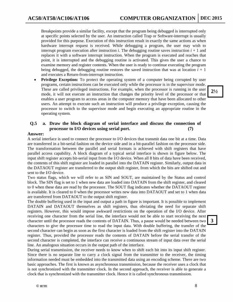
Q.5 a. Draw the block diagram of serial interface and discuss the connection of
processor to I/O devices using serial port. (7) Answer: A serial interface is used to connect the processor to I/O devices that transmit data one bit at a time. Data are transferred in a bit-serial fashion on the device side and in a bit-parallel fashion on the processor side. The transformation between the parallel and serial formats is achieved with shift registers that have parallel access capability. A block diagram of a typical serial interface is shown in figure below. The input shift register accepts bit-serial input from the I/O device. When all 8 bits of data have been received, the contents of this shift register are loaded in parallel into the DATAIN register. Similarly, output data in the DATAOUT register are transferred to the output shift register, from which the bits are shifted out and sent to the I/O device. Two status flags, which we will refer to as SIN and SOUT, are maintained by the Status and control block. The SIN flag is set to 1 when new data are loaded into DATAIN from the shift register, and cleared to 0 when these data are read by the processor. The SOUT flag indicates whether the DATAOUT register is available. It is cleared to 0 when the processor writes new data into DATAOUT and set to 1 when data are transferred from DATAOUT to the output shift register. The double buffering used in the input and output a path in figure is important. It is possible to implement DATAIN and DATAOUT themselves as shift registers, thus obviating the need for separate shift registers. However, this would impose awkward restrictions on the operation of the I/O device. After receiving one character from the serial line, the interface would not be able to start receiving the next character until the processor reads the contents of DATAIN. Thus, a pause would be needed between two characters to give the processor time to read the input data. With double buffering, the transfer of the second character can begin as soon as the first character is loaded from the shift register into the DATAIN register. Thus, provided the processor reads the contents of DATAIN before the serial transfer of the second character is completed, the interface can receive a continuous stream of input data over the serial line. An analogous situation occurs in the output path of the interface. During serial transmission, the receiver needs to know when to shift each bit into its input shift register. Since there is no separate line to carry a clock signal from the transmitter to the receiver, the timing information needed must be embedded into the transmitted data using an encoding scheme. There are two basic approaches. The first is known as asynchronous transmission, because the receiver uses a clock that is not synchronized with the transmitter clock. In the second approach, the receiver is able to generate a clock that is synchronized with the transmitter clock. Hence it is called synchronous transmission.
2½
3
AC58/AT58/AC106/AT106 COMPUTER ORGANIZATION DEC 2015
© IETE 9
A serial interface
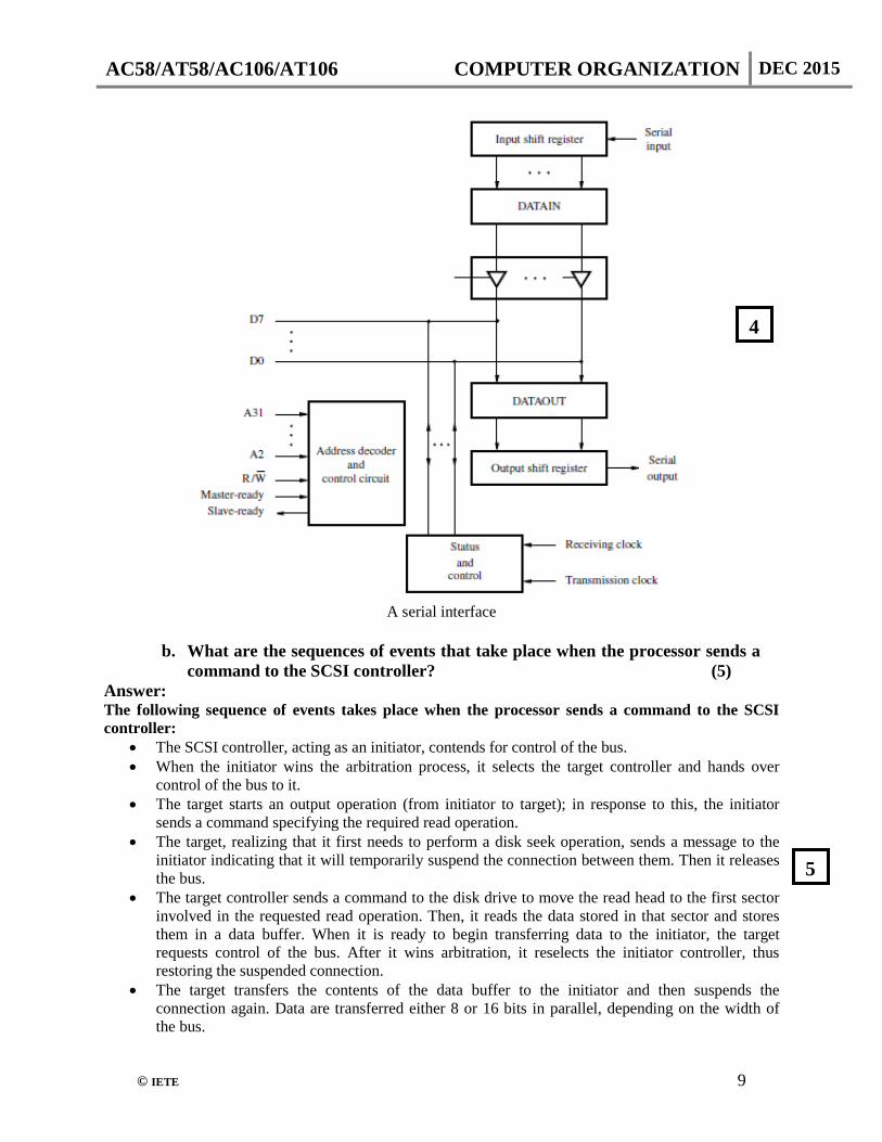
b. What are the sequences of events that take place when the processor sends a
command to the SCSI controller? (5) Answer: The following sequence of events takes place when the processor sends a command to the SCSI controller:
• The SCSI controller, acting as an initiator, contends for control of the bus. • When the initiator wins the arbitration process, it selects the target controller and hands over
control of the bus to it. • The target starts an output operation (from initiator to target); in response to this, the initiator
sends a command specifying the required read operation. • The target, realizing that it first needs to perform a disk seek operation, sends a message to the
initiator indicating that it will temporarily suspend the connection between them. Then it releases the bus.
• The target controller sends a command to the disk drive to move the read head to the first sector involved in the requested read operation. Then, it reads the data stored in that sector and stores them in a data buffer. When it is ready to begin transferring data to the initiator, the target requests control of the bus. After it wins arbitration, it reselects the initiator controller, thus restoring the suspended connection.
• The target transfers the contents of the data buffer to the initiator and then suspends the connection again. Data are transferred either 8 or 16 bits in parallel, depending on the width of the bus.
4
5

AC58/AT58/AC106/AT106 COMPUTER ORGANIZATION DEC 2015
© IETE 10
• The target controller sends a command to the disk drive to perform another seek operation. Then, it transfers the contents of the second disk sector to the initiator, as before. At the end of this transfer, the logical connection between the two controllers is terminated.
• As the initiator controller receives the data, it stores them into the main memory using the DMA approach.
• The SCSI controller sends an interrupt to the processor to inform it that the requested operation has been completed.
This scenario shows that the messages exchanged over the SCSI bus are at a higher level than those exchanged over the processor bus.
c. Explain how USB support Isochronous data. (4) Answer: One of the key objectives of the USB is to support the transfer of isochronous data, such as sampled voice, in a simple manner. Devices that generate or receive isochronous data require a time reference to control the sampling process. To provide this reference transmission over the USB is divided into frames of equal length. A frame is 1 ms long for low – and full-speed data. The root hub generates a Start Of Frame control packet (SOF) precisely once every 1 ms to mark the beginning of a new frame. The arrival of an SOF packet at any device constitutes a regular clock signal that the device can use for its purpose. To assist devices that may need longer periods of time, the SOF packet carries an 11-bit frame number, as shown in figure (a). Following each SOF packet, the host carries out input and output transfers for isochronous devices. This means that each device will have an opportunity for an input or output transfer once every 1 ms. The main requirement for isochronous traffic is consistent timing. An occasional error can be tolerated. Hence there is no need to transmit packets that are lost or to send acknowledgements. Figure (b) shows the first two transmission following SOF. A control packet carrying device address 3 is followed by data for that device. This may be input or output data, depending on whether the control packet is an IN or OUT control packet. There is no acknowledgement packet. The next transmission sequence is for device 7.
Bits 8 11 5
PID Frame Number CRC5
(a) SOF Packet
1-ms frame
S T3 D T7 D . . . S T3 D
S – Start-of-frame packet Tn – Token packet, address = n D – Data packet A – ACK packet
(b) Frame example As an example, the data packet for device 3 may contain 8 bytes of data. One such packet is sent in each frame, providing a 64-kilobits/s isochronous channel. Such a channel may be used for a voice connection. The transmission of 8 bytes of data requires a 3-byte token packet followed by an 11-byte data packet
2

AC58/AT58/AC106/AT106 COMPUTER ORGANIZATION DEC 2015
© IETE 11
(including the PID and CRC fields), for a total of 132 bits. A minimum of three more bytes are needed for clock synchronization and to mark the end of packet sequence. At a speed of 12 megabits/s, this takes about 13 s. Clearly, there is a room in a frame to support several such devices. Isochronous data are allowed only on full-speed and high-speed links. For high-speed links, the SOF packet is repeated eight times at equal intervals within the 1-ms frame to create eight microframes if 125 s each. Q.6 a. Consider a memory consisting of 64K words of 8 bits each. Give the
organization to implement this memory using 16K X 1 static memory chips. (8)
Answer:
b. Consider a cache consisting of 128 blocks of 16 words each, for a total of 2048
(2K) words, and assume that the main memory is addressable by a 16-bit address. The main memory has 64K words, which we will view as 4K blocks of 16 words each. With the help of above given data, explain the following mapping techniques with proper diagram of cache and main memory:
(i) Associative Mapping (ii) Set-Associative Mapping (4×2) Answer:
i) Associative Mapping Following figure shows the most flexible mapping method, in which a main memory block can be placed into any cache block position. In this case, 12 tag bits are required to identify a memory block when it is resident in the cache. The tag bits of an address received from the processor are compared to the tag bits of each block of the cache to see if the desired block is present. This is called the associative-mapping technique. It gives complete freedom in choosing the cache
2
8

AC58/AT58/AC106/AT106 COMPUTER ORGANIZATION DEC 2015
© IETE 12
location in which to place the memory block, resulting in a more efficient use of the space in the cache. When a new block is brought into the cache, it replaces (ejects) an existing block only if the cache is full. In this case, we need an algorithm to select the block to be replaced. The complexity of an associative cache is higher than that of a direct-mapped cache, because of the need to search all 128 tag patterns to determine whether a given block is in the cache. To avoid a long delay, the tags must be searched in parallel. A search of this kind is called an associative search.
Associative-Mapped Cache
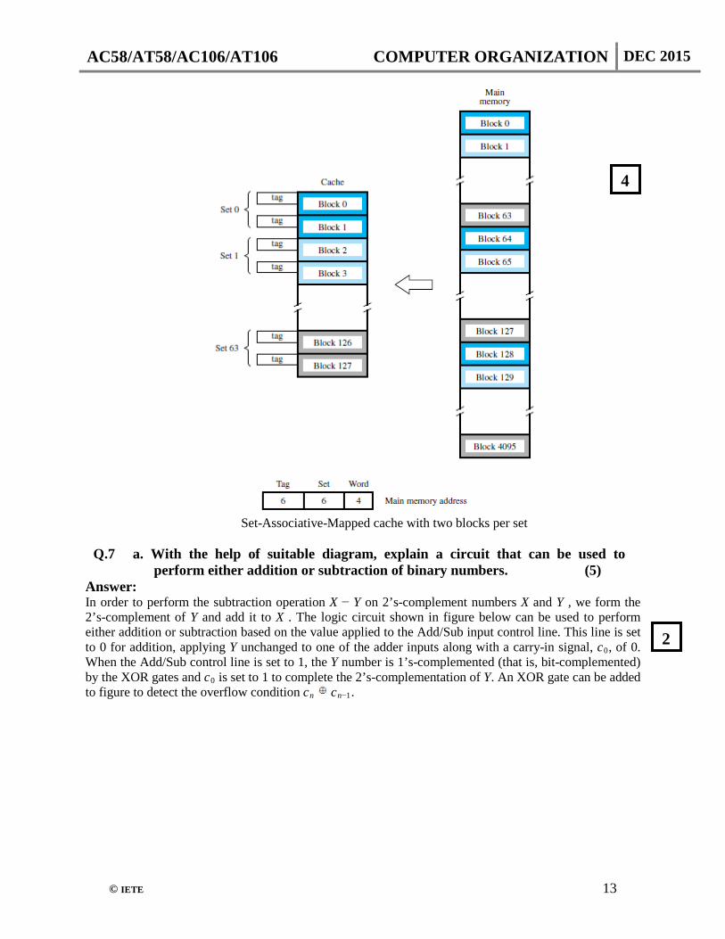
ii) Set-Associative Mapping
Set-Associative mapping approach is to use a combination of the direct and associative mapping techniques. The blocks of the cache are grouped into sets, and the mapping allows a block of the main memory to reside in any block of a specific set. Hence, the contention problem of the direct method is eased by having a few choices for block placement. At the same time, the hardware cost is reduced by decreasing the size of the associative search. An example of this set-associative-mapping technique is shown in following figure for a cache with two blocks per set. In this case, memory blocks 0, 64, 128, . . . , 4032 map into cache set 0, and they can occupy either of the two block positions within this set. Having 64 sets means that the 6-bit set field of the address determines which set of the cache might contain the desired block. The tag field of the address must then be associatively compared to the tags of the two blocks of the set to check if the desired block is present. This two-way associative search is simple to implement. The number of blocks per set is a parameter that can be selected to suit the requirements of a particular computer. For the main memory and cache sizes in figure below, four blocks per set can be accommodated by a 5-bit set field, eight blocks per set by a 4-bit set field, and so on. The extreme condition of 128 blocks per set requires no set bits and corresponds to the fully-associative technique, with 12 tag bits. The other extreme of one block per set is the direct-mapping method. A cache that has k blocks per set is referred to as a k-way set-associative cache.
4
AC58/AT58/AC106/AT106 COMPUTER ORGANIZATION DEC 2015
© IETE 13
Set-Associative-Mapped cache with two blocks per set
Q.7 a. With the help of suitable diagram, explain a circuit that can be used to
perform either addition or subtraction of binary numbers. (5) Answer: In order to perform the subtraction operation X − Y on 2’s-complement numbers X and Y , we form the 2’s-complement of Y and add it to X . The logic circuit shown in figure below can be used to perform either addition or subtraction based on the value applied to the Add/Sub input control line. This line is set to 0 for addition, applying Y unchanged to one of the adder inputs along with a carry-in signal, c0, of 0. When the Add/Sub control line is set to 1, the Y number is 1’s-complemented (that is, bit-complemented) by the XOR gates and c0 is set to 1 to complete the 2’s-complementation of Y. An XOR gate can be added to figure to detect the overflow condition cn cn−1.
4
2

AC58/AT58/AC106/AT106 COMPUTER ORGANIZATION DEC 2015
© IETE 14
Binary addition / subtraction logic circuit
b. Define and draw the logic diagram of n-bit ripple-carry adder. (6) Answer: A cascaded connection of n full adders shown in following figure can be used to add two n-bit numbers. Since the carries must propagate, or ripple, through this cascade, this configuration is called as n-bit ripple-carry adder.
n-bit ripple-carry adder c. Write short notes on DVD Technology. (5) Answer: The success of CD technology and the continuing quest for greater storage capability has led to the development of DVD (Digital Versatile Disk) technology. The first DVD standard was defined in 1996 by a consortium of companies. The objective is to be able to store a full-length movie on one side of a DVD disk. The physical size of a DVD disk is the same as for CDs. The disk is 1.2 mm thick, and it is 120 mm in diameter. Its storage capacity is made much larger than that of CDs by several design changes:
• A red light laser with a wavelength of 635 nm is used instead of the infrared light laser used in CDs, which has a wavelength of 780nm. The shorter wavelength makes it possible to focus the light to a smaller spot.
• Pits are smaller, having a minimum length of 0.4 micron.
FA
FA
FA
xn-1 yn-1 x1 y1 x0 y0
cn
cn-
1
c1
c0
sn-1 s1 s0
3
3
3
3
AC58/AT58/AC106/AT106 COMPUTER ORGANIZATION DEC 2015
© IETE 15
• Tracks are placed closer together; the distance between tracks is 0.74 micron. Using these improvements leads to a DVD capacity of 4.7 Gbytes. Further increases in capacity have been achieved by going to two-layered and two-sided disks. The single-layered single-sided disk, defined in the standard as DVD-5, has a structure that is almost the same as the CD. A double-layered disk makes use of two layers on which tracks are implemented on top of each layer. The first layer is the clear base, as in CD disks. But, instead of using reflecting aluminium, the lands and pits of this layer are covered by a translucent material that acts as a semi reflector. A rewritable version of DVD devices, known as DVD-RAM, has also been developed. It provides a large storage capacity. Its only disadvantages are higher price and relatively slow writing speed. To ensure that the data have been recorded correctly on the disk, a process known as write verification is performed. This is done by the DVD-RAM drive, which reads the stored contents and checks them against the original data. Q.8 a. Multiply the following pairs of signed 2’s-complement numbers using: (i) Booth algorithm (ii) Bit-pairing of the multiplier A = 010111 and B = 110110 Assume A is the multiplicand and B is the multiplier. (5+5) Answer:
(i) Booth’s algorithm
0 1 0 1 1 1 1 1 0 1 1 0 0 -1 +1 0 -1 0 0 0 0 0 0 0 0 0 0 0 0 0 1 1 1 1 1 1 0 1 0 0 1 0 0 0 0 0 0 0 0 0 0 0 0 0 0 1 0 1 1 1 1 1 1 0 1 0 0 1 0 0 0 0 0 0 0 1 1 1 1 0 0 0 1 1 0 1 0
Second Method (Tabular Form) Qn Qn+1
Y = 010111 Y′+1 = 101001 X Q Qn+1 C
000000 110110 0 110 0 0 ashr 000000 011011 0 101 1 0 Subtract Y 101001 101001 ashr 110100 101101 1 100
1 1 ashr 111010 010110 1 011 0 1 Add Y 010111 010001 ashr 001000 101011 0 010
1 0 Subtract Y 101001 110001 ashr 111000 110101 1 001
1 1 ashr 111100 011010 1 000
2
5

AC58/AT58/AC106/AT106 COMPUTER ORGANIZATION DEC 2015
© IETE 16
Final Answer is 111100011010 (ii) Bit-pairing of the multiplier
0 1 0 1 1 1 1 1 0 1 1 0 -1 +2 -2 1 1 1 1 1 1 0 1 0 0 1 0 0 0 0 0 1 0 1 1 1 0 1 1 1 0 1 0 0 1 1 1 1 1 0 0 0 1 1 0 1 0
b. With the help of formats given by IEEE, explain IEEE standards for
representing floating-point numbers. (6) Answer: The basic IEEE format is a 32-bit representation, shown in figure below. The leftmost bit represents the sign, S, for the number. The next 8 bits, E, represent the signed exponent of the scale factor (with an implied base of 2), and the remaining 23 bits, M, are the fractional part of the significant bits. The full 24-bit string, B, of significant bits, called the mantissa, always has a leading 1, with the binary point immediately to its right. Therefore, the mantissa
B = 1.M = 1.b−1b−2 . . . b−23 has the value
V(B) = 1 + b−1 × 2−1 + b−2 × 2−2 +・ ・ ・+b−23 × 2−23
Single precision
Example of a single precision number
By convention, when the binary point is placed to the right of the first significant bit, the number is said to be normalized. The base, 2, of the scale factor and the leading 1 of the mantissa are both fixed. They do not need to appear explicitly in the representation. Instead of the actual signed exponent, E, the value stored in the exponent field is an unsigned integer E′ = E + 127. This is called the excess-127 format. Thus, E′ is in the range 0 ≤ E ≤ 255. The end values of this range, 0 and 255, are used to represent special values. Therefore, the range of E′ for normal values is 1 ≤ E′ ≤ 254. This means that the actual exponent, E, is in the range −126 ≤ E ≤ 127. The use of the excess-127 representation for exponents simplifies comparison of the relative sizes of two floating-point numbers. The 32-bit standard representation in figure below is called a single-precision representation because it occupies a single 32-bit word. The scale factor has a range of 2−126 to 2+127, which is approximately equal
5
3 M for Single Precision
AC58/AT58/AC106/AT106 COMPUTER ORGANIZATION DEC 2015
© IETE 17
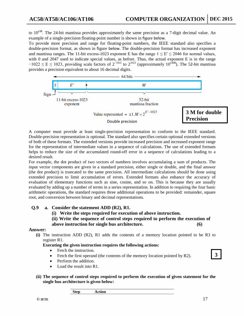
to 10±38. The 24-bit mantissa provides approximately the same precision as a 7-digit decimal value. An example of a single-precision floating-point number is shown in figure below. To provide more precision and range for floating-point numbers, the IEEE standard also specifies a double-precision format, as shown in figure below. The double-precision format has increased exponent and mantissa ranges. The 11-bit excess-1023 exponent E has the range 1 ≤ E′ ≤ 2046 for normal values, with 0 and 2047 used to indicate special values, as before. Thus, the actual exponent E is in the range −1022 ≤ E ≤ 1023, providing scale factors of 2−1022 to 21023 (approximately 10±308). The 52-bit mantissa provides a precision equivalent to about 16 decimal digits.
Double precision
A computer must provide at least single-precision representation to conform to the IEEE standard. Double-precision representation is optional. The standard also specifies certain optional extended versions of both of these formats. The extended versions provide increased precision and increased exponent range for the representation of intermediate values in a sequence of calculations. The use of extended formats helps to reduce the size of the accumulated round-off error in a sequence of calculations leading to a desired result. For example, the dot product of two vectors of numbers involves accumulating a sum of products. The input vector components are given in a standard precision, either single or double, and the final answer (the dot product) is truncated to the same precision. All intermediate calculations should be done using extended precision to limit accumulation of errors. Extended formats also enhance the accuracy of evaluation of elementary functions such as sine, cosine, and so on. This is because they are usually evaluated by adding up a number of terms in a series representation. In addition to requiring the four basic arithmetic operations, the standard requires three additional operations to be provided: remainder, square root, and conversion between binary and decimal representations. Q.9 a. Consider the statement ADD (R2), R1. (i) Write the steps required for execution of above instruction. (ii) Write the sequence of control steps required to perform the execution of
above instruction for single bus architecture. (6) Answer:
(i) The instruction ADD (R2), R1 adds the contents of a memory location pointed to be R3 to register R1. Executing the given instruction requires the following actions:
• Fetch the instruction. • Fetch the first operand (the contents of the memory location pointed by R2). • Perform the addition. • Load the result into R1.
(ii) The sequence of control steps required to perform the execution of given statement for the single bus architecture is given below:
Step Action
3 M for double Precision
3
AC58/AT58/AC106/AT106 COMPUTER ORGANIZATION DEC 2015
© IETE 18
1 PCout, MARin, Read, Select, Add, Zin 2 Zout, PCin, Yin, WMFC 3 MDRout, IRin 4 R2out, MARin, Read 5 R1out, Yin, WMFC 6 MDRout, SelectY, Add, Zin 7 Zout, R1in, End
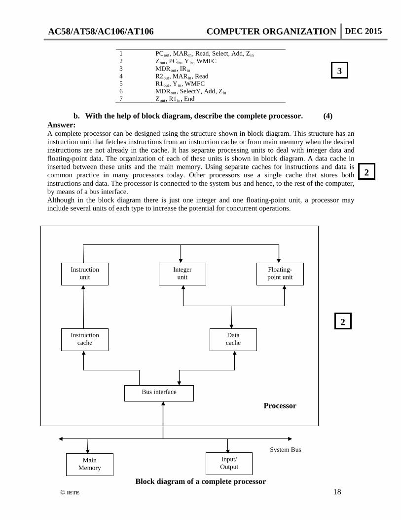
b. With the help of block diagram, describe the complete processor. (4) Answer: A complete processor can be designed using the structure shown in block diagram. This structure has an instruction unit that fetches instructions from an instruction cache or from main memory when the desired instructions are not already in the cache. It has separate processing units to deal with integer data and floating-point data. The organization of each of these units is shown in block diagram. A data cache in inserted between these units and the main memory. Using separate caches for instructions and data is common practice in many processors today. Other processors use a single cache that stores both instructions and data. The processor is connected to the system bus and hence, to the rest of the computer, by means of a bus interface. Although in the block diagram there is just one integer and one floating-point unit, a processor may include several units of each type to increase the potential for concurrent operations.
Block diagram of a complete processor
Instruction unit
Integer unit
Floating-point unit
Instruction cache
Data cache
Bus interface
Processor
Main Memory
Input/ Output
System Bus
3
2
2
AC58/AT58/AC106/AT106 COMPUTER ORGANIZATION DEC 2015
© IETE 19
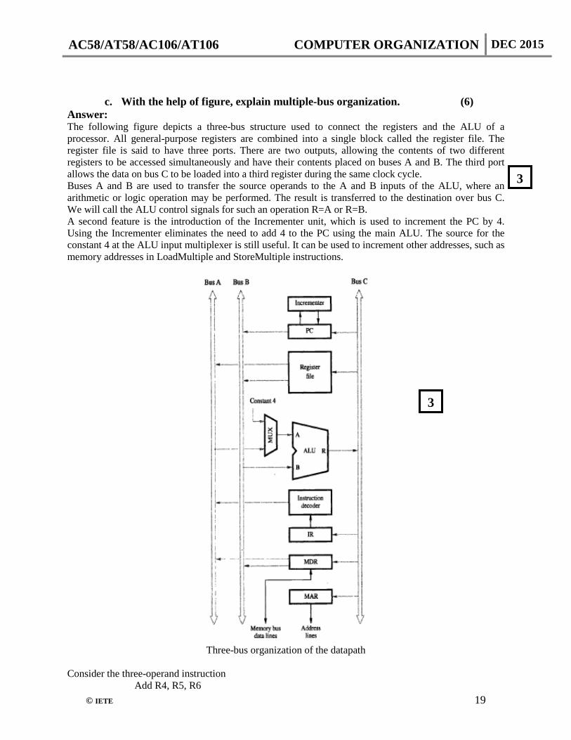
c. With the help of figure, explain multiple-bus organization. (6) Answer: The following figure depicts a three-bus structure used to connect the registers and the ALU of a processor. All general-purpose registers are combined into a single block called the register file. The register file is said to have three ports. There are two outputs, allowing the contents of two different registers to be accessed simultaneously and have their contents placed on buses A and B. The third port allows the data on bus C to be loaded into a third register during the same clock cycle. Buses A and B are used to transfer the source operands to the A and B inputs of the ALU, where an arithmetic or logic operation may be performed. The result is transferred to the destination over bus C. We will call the ALU control signals for such an operation R=A or R=B. A second feature is the introduction of the Incrementer unit, which is used to increment the PC by 4. Using the Incrementer eliminates the need to add 4 to the PC using the main ALU. The source for the constant 4 at the ALU input multiplexer is still useful. It can be used to increment other addresses, such as memory addresses in LoadMultiple and StoreMultiple instructions.
Three-bus organization of the datapath
Consider the three-operand instruction Add R4, R5, R6
3
3

AC58/AT58/AC106/AT106 COMPUTER ORGANIZATION DEC 2015
© IETE 20
The control sequence for executing this instruction is given below:
Step Action 1 PCout , R=B, MARin, Read, IncPC 2 WMFC 3 MDRoutB , R=B, IRin 4 R4outA , R5outB , SelectA, Add, R6in , End
Control sequence for the instruction Add R4, R5, R6 for the three-bus organization
in step 1, the contents of the PC are passed through the ALU, using the R=B control signal, and loaded into the MAR to start a memory read operation. At the same time the PC is incremented by 4. The value loaded into MAR is the original contents of the PC. The incremented value is loaded into the PC at the end of the clock cycle and will not affect the contents of MAR. In step 2, the processor waits for MFC and loads the data received into MDR, then transfers them to IR in step 3. Finally, the execution phase of the instruction requires only one control step to complete, step 4.
TEXT BOOK
I. Computer Organization, Carl Hamacher, Zvonko Vranesic, Safwat Zaky, 5th Edition, TMH, 2002 (TB-I)