pyxis april lewis aaron martin steve sherk. 2 pyxis1600 general-purpose 16-bit risc microprocessor...
Post on 21-Dec-2015
235 views
TRANSCRIPT

Pyxis
April Lewis
Aaron Martin
Steve Sherk
2
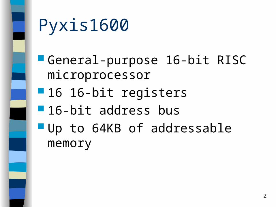
Pyxis1600
General-purpose 16-bit RISC microprocessor
16 16-bit registers 16-bit address bus Up to 64KB of addressable memory

3
Registers 16 registers 3 special purpose
– $r0 – zero– $r14 – stack pointer– $r15 – return address
13 general purpose – $r1 - $r13
Status register (sr)– 8 bits – carry (c), overflow (o), negative (n), zero (z), interrupt
enable (i), less than (l), 2 bits unused Program counter (pc) Accumulator high (ah) and accumulator low (al)
– Used for multiply and divide Interrupt Return Address (IRA)
– Register to hold return address from interrupt
4
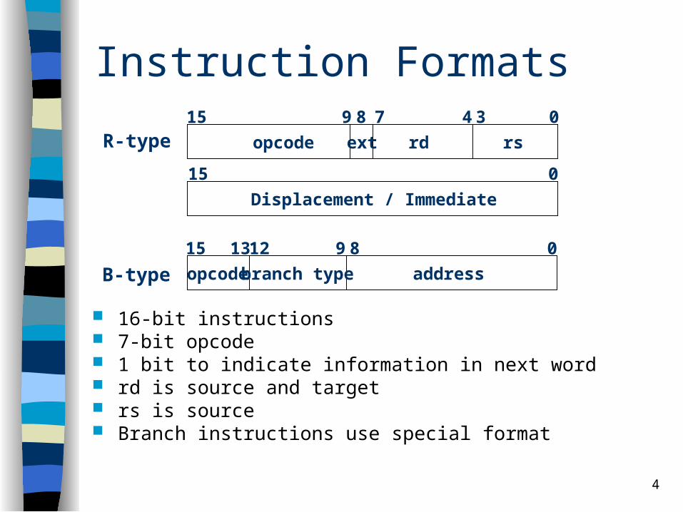
Instruction Formats
16-bit instructions 7-bit opcode 1 bit to indicate information in next word rd is source and target rs is source Branch instructions use special format
opcode rd rs
Displacement / Immediate
ext
0
015
315 4789
opcode branch type address
089121315
R-type
B-type

5
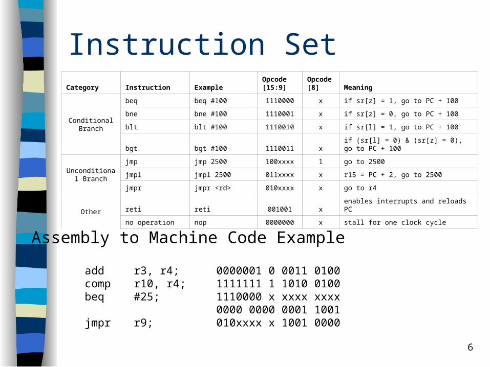
Instruction SetCategory Instruction Example
Opcode [15:9]
Opcode[8] Meaning
Arithmetic
add add <rd>,<rs> 0000001 0 r3 = r3 + r4
add immediate addi <rd>, #100 0000001 1 r3 = r3 + 100
subtract sub <rd>, <rs> 0000010 0 r3 = r3 - r4
subtract immediate subi <rd>, #200 0000010 1 r3 = r3 - 200
divide div <rd>, <rs> 0000100 0 <ah, al> = r3 / r4
divide immediate divi <rd>, #4 0000100 1 <ah, al> = r3 / 4
multiply mult <rd>, <rs> 0000011 0 <ah, al> = r3 * r4
multiply immediate multi <rd>, #6 0000011 1 <ah, al> = r3 * 6
move from al mal <rd> 1010000 x r4 = (al)
move from ah mah <rd> 1011111 x r4 = (ah)
Data Transfersload word lw <rd>, 100(<rs>) 0011111 1 r3 = Memory[r4 + 100]
store word sw 200(<rd>), <rs> 0010000 1 Memory[r3 + 200] = r4
Logical
and and <rd>, <rs> 0000100 0 r3 = r3 & r4
andi andi <rd>, #4 0000100 1 r3 = r3 & 4
or or <rd>, <rs> 0000101 0 r3 = r3 | r4
ori ori <rd>, #4 0000101 1 r3 = r3 | 4
nor nor <rd>, <rs> 0000110 0 r3 = ~(r3 | r4)
nori nori <rd>, #4 0000110 1 r3 = ~(r3 | 4)
comp comp <rd>, <rs> 1111111 0 set sr bits after compare
shl shl <rd>, #10 0000111 0 r3 = r3 << 10
shr shr <rd>, #10 0001000 0 r3 = r3 >> 10
6
Instruction Set
Assembly to Machine Code Example
add r3, r4;comp r10, r4;beq #25;
jmpr r9;
0000001 0 0011 01001111111 1 1010 01001110000 x xxxx xxxx0000 0000 0001 1001010xxxx x 1001 0000
Category Instruction ExampleOpcode [15:9]
Opcode[8] Meaning
Conditional Branch
beq beq #100 1110000 x if sr[z] = 1, go to PC + 100
bne bne #100 1110001 x if sr[z] = 0, go to PC + 100
blt blt #100 1110010 x if sr[l] = 1, go to PC + 100
bgt bgt #100 1110011 x if (sr[l] = 0) & (sr[z] = 0), go to PC + 100
Unconditional Branch
jmp jmp 2500 100xxxx 1 go to 2500
jmpl jmpl 2500 011xxxx x r15 = PC + 2, go to 2500
jmpr jmpr <rd> 010xxxx x go to r4
Otherreti reti 001001 x enables interrupts and reloads PC
no operation nop 0000000 x stall for one clock cycle

7
Addressing Modes
Register direct Register indirect plus displacement
– Use r0 for absolute addressing PC-relative Immediate
8
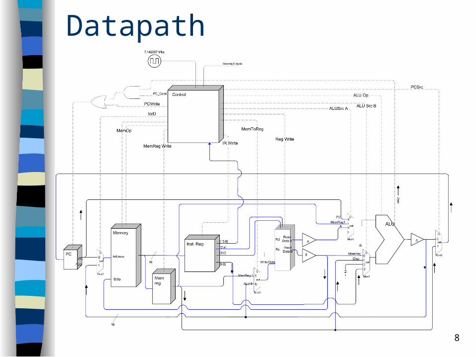
Datapath
9
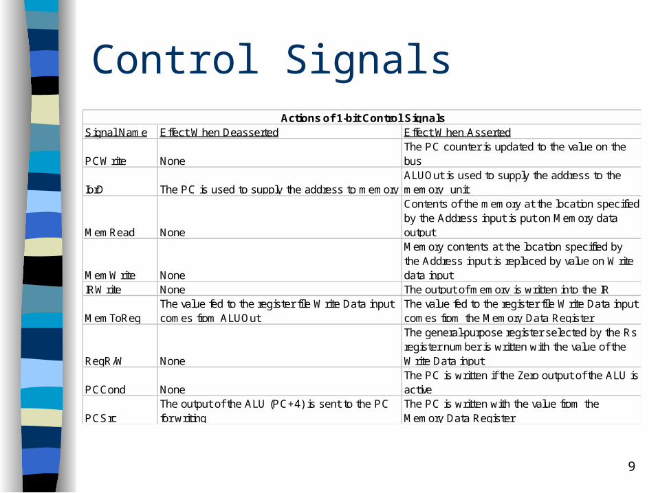
Control Signals
Signal Name Effect When Asserted
PCWriteThe PC counter is updated to the value on the bus
IorDALUOut is used to supply the address to the memory unit
MemRead
Contents of the memory at the location specified by the Address input is put on Memory data output
MemWrite
Memory contents at the location specified by the Address input is replaced by value on Write data input
IRWrite The output of memory is written into the IR
MemToRegThe value fed to the register file Write Data input comes from the Memory Data Register
RegR/W
The general-purpose register selected by the Rs register number is written with the value of the Write Data input
PCCondThe PC is written if the Zero output of the ALU is active
PCSrcThe PC is written with the value from the Memory Data Register
Effect When Deasserted
None
NoneNoneThe value fed to the register file Write Data input comes from ALUOut
None
The output of the ALU (PC+4) is sent to the PC for writing
Actions of 1-bit Control Signals
None
The PC is used to supply the address to memory
None
10
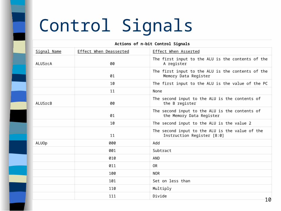
Control SignalsActions of n-bit Control Signals
Signal Name Effect When Deasserted Effect When Asserted
ALUSrcA 00 The first input to the ALU is the contents of the A register
01The first input to the ALU is the contents of the Memory Data
Register
10 The first input to the ALU is the value of the PC
11 None
ALUSrcB 00 The second input to the ALU is the contents of the B register
01The second input to the ALU is the contents of the Memory Data
Register
10 The second input to the ALU is the value 2
11The second input to the ALU is the value of the Instruction Register
[8:0]
ALUOp 000 Add
001 Subtract
010 AND
011 OR
100 NOR
101 Set on less than
110 Multiply
111 Divide
11
State Transition DiagramFetch
IRWrite=1RegWrite=0PCWrite=0
Decode
R-type (ext=0)
0
1
2
3Write-backALU to Reg
Execute
R-type (ext=1)
4
5
Calc EA orImmediate
96
8Calc EA
Memory Read
Fetch Immediate
IorD=0MemRead=1MemWrite=0
ALUOp=ADDALUSrcA=2ALUSrcB=2
PCSrc=0PCWrite=1RegWrite=0
ALUSrcA=0ALUSrcB=0ALUOp=OPIRWrite=0
RegWrite=0PCWrite=0
RegWrite=1MemtoReg=0ALUOp=OFF
IRWrite=0PCWrite=0
IorD=0MemRead=1MemWrite=0
IRWrite=0ALUOp=ADDALUSrcA=2ALUSrcB=2
PCSrc=0PCWrite=1RegWrite=0
IorD=1MemRead=1ALUOp=OFFRegWrite=0IRWrite=0PCWrite=0
RegWrite=1MemtoReg=1ALUOp=OFF
IRWrite=0PCWrite=0
Write-backMem to Reg
ALUSrcA=1ALUSrcB=0ALUOp=OPIRWrite=0
RegWrite=0PCWrite=0 IorD=1
MemWrite=1ALUOp=OFFRegWrite=0IRWrite=0PCWrite=0
7
Check Interrupt
ALUSrcA=0ALUSrcB=1
ALUOp=ADDIRWrite=0
RegWrite=0PCWrite=0
Memory Write
Arithmetic InstructionsWrite to Reg from ALULoad from MemoryWrite to Memory
To State 0
15

12
State Transition Diagram
10
11
12
13
ALUSrcA=0ALUSrcB=0
ALUOp=ADDPCSrc=0
PCWrite=1IRWrite=0
RegWrite=0
Jump to Reg Addr
R-type Jump (ext=0)
PCSrc=1PCWrite=1
IorD=0MemRead=1MemWrite=0ALUOp=OFFRegWrite=0IRWrite=0
R-type Jump &Link
Save Return Addr
RegWrite=1MemtoReg=1ALUOp=OFF
IRWrite=0PCWrite=0
ALUSrcA=0ALUSrcB=0
ALUOp=SUBIRWrite=0
RegWrite=0PCWrite=0
Compare
ALUSrcA=2ALUSrcB=3
ALUOp=ADDPCCond=1PCSrc=0
PCWrite=1IRWrite=0
RegWrite=0
Update PC
14
R-type Jump (ext=1)
Jump
Fetch
IRWrite=1RegWrite=0PCWrite=0
Decode0
IorD=0MemRead=1MemWrite=0
ALUOp=ADDALUSrcA=2ALUSrcB=2
PCSrc=0PCWrite=1RegWrite=0
1
B-type
Conditional BranchJump to Register AddressJump to Register Address and LinkJump to Immediate and LinkJump to Immediate
To State 15
13
Interrupts Interrupts will be checked at the completion of
each instruction An interrupt will trigger some extra states that
send the processor to an Interrupt Service Routine (ISR), pre-programmed in code memory.
These states will perform the following:– Save the processor’s state– Disable interrupts– Jump to the ISR
The ‘RETI’ instruction will return the processor from the ISR
14
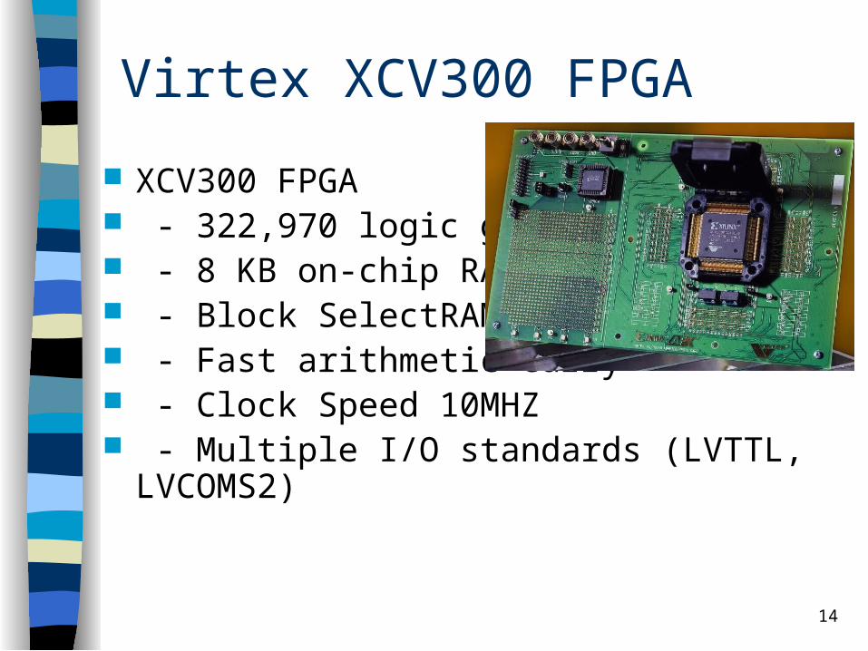
Virtex XCV300 FPGA
XCV300 FPGA - 322,970 logic gates - 8 KB on-chip RAM - Block SelectRAM - Fast arithmetic carry - Clock Speed 10MHZ - Multiple I/O standards (LVTTL, LVCOMS2)

15
Input / Output Serial Interface
UART Transmitter and Receiver Macros
UART_TX8-bit Serial
16 Byte FIFO BUFFER
8-bit Serial16 Byte FIFO BUFFER
UART_RX
These macros are fully compatible with standard UART communications protocols such as to a PC, providing level shifting components are employed to generate RS232 signaling. The buffers will be interrupt driven.
16
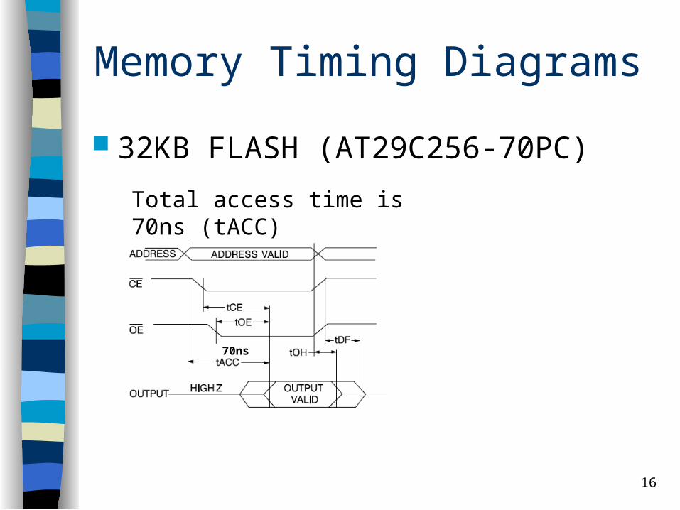
Memory Timing Diagrams
32KB FLASH (AT29C256-70PC)
Total access time is 70ns (tACC)
70ns
17
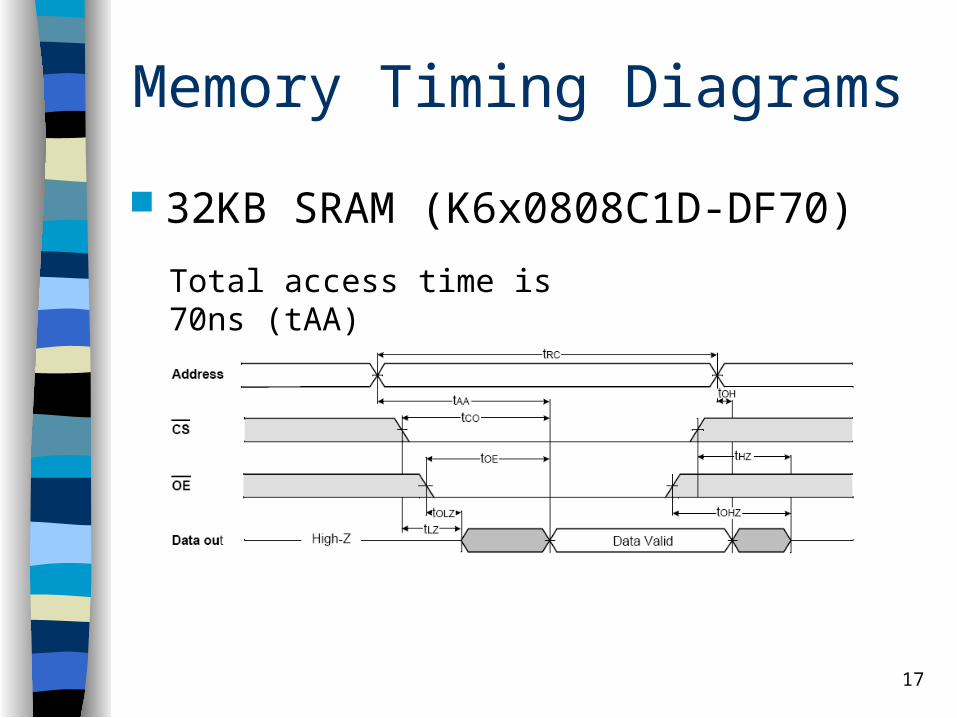
Memory Timing Diagrams
32KB SRAM (K6x0808C1D-DF70)
Total access time is 70ns (tAA)
18
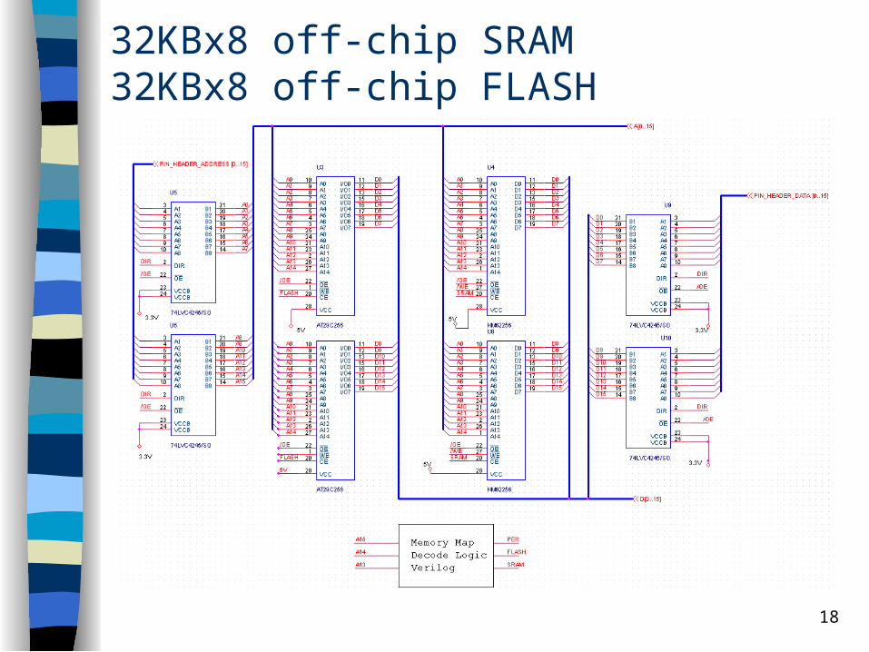
32KBx8 off-chip SRAM32KBx8 off-chip FLASH
19
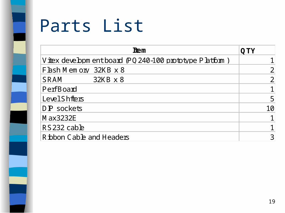
Parts ListQTY
12215
10113
ItemVitex development board (PQ240-100 prototype Platform)
DIP sockets
Perf BoardLevel Shfters
Flash Memory 32KB x 8 SRAM 32KB x 8
Ribbon Cable and Headers
Max3232ERS232 cable

20
Roles and Responsibilities Aaron
– Logic design– Verilog programming– Hardware implementation
April– Logic design– Verilog programming– Assembler
Steve– Logic design– Verilog programming– Hardware implementation
All– Test programs– Integration and Test– Documentation
21
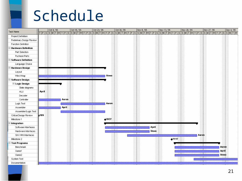
Schedule

Questions