pv inverter products manufacturing and design improvements - nrel
TRANSCRIPT
Revised April 2004 • NREL/SR-520-35885
R. West Xantrex Technology Inc. San Luis Obispo, California
PV Inverter Products Manufacturing and Design Improvements for Cost Reduction and Performance Enhancements Final Subcontract Report November 2003
National Renewable Energy Laboratory 1617 Cole Boulevard Golden, Colorado 80401-3393 NREL is a U.S. Department of Energy Laboratory Operated by Midwest Research Institute • Battelle
Contract No. DE-AC36-99-GO10337
Revised April 2004 • NREL/SR-520-35885
PV Inverter Products Manufacturing and Design Improvements for Cost Reduction and Performance Enhancements Final Subcontract Report November 2003
R. West Xantrex Technology Inc. San Luis Obispo, California
NREL Technical Monitor: D. Mooney Prepared under Subcontract No. NDO-1-30628-02
National Renewable Energy Laboratory 1617 Cole Boulevard Golden, Colorado 80401-3393 NREL is a U.S. Department of Energy Laboratory Operated by Midwest Research Institute • Battelle
Contract No. DE-AC36-99-GO10337

This publication was reproduced from the best available copy
Submitted by the subcontractor and received no editorial review at NREL NOTICE This report was prepared as an account of work sponsored by an agency of the United States government. Neither the United States government nor any agency thereof, nor any of their employees, makes any warranty, express or implied, or assumes any legal liability or responsibility for the accuracy, completeness, or usefulness of any information, apparatus, product, or process disclosed, or represents that its use would not infringe privately owned rights. Reference herein to any specific commercial product, process, or service by trade name, trademark, manufacturer, or otherwise does not necessarily constitute or imply its endorsement, recommendation, or favoring by the United States government or any agency thereof. The views and opinions of authors expressed herein do not necessarily state or reflect those of the United States government or any agency thereof.
Available electronically at http://www.osti.gov/bridge
Available for a processing fee to U.S. Department of Energy and its contractors, in paper, from:
U.S. Department of Energy Office of Scientific and Technical Information P.O. Box 62 Oak Ridge, TN 37831-0062 phone: 865.576.8401 fax: 865.576.5728 email: [email protected]
Available for sale to the public, in paper, from:
U.S. Department of Commerce National Technical Information Service 5285 Port Royal Road Springfield, VA 22161 phone: 800.553.6847 fax: 703.605.6900 email: [email protected] online ordering: http://www.ntis.gov/ordering.htm
Printed on paper containing at least 50% wastepaper, including 20% postconsumer waste

i
TABLE OF CONTENTS
FIGURES............................................................................................................................................... iv 1 INTRODUCTION .................................................................................................................... 1 1.1 BACKGROUND ....................................................................................................................... 1 1.2 OBJECTIVES........................................................................................................................... 1 2 OVERVIEW.............................................................................................................................. 1 2.1 FIRST YEAR OVERVIEW ..................................................................................................... 1 2.2 SECOND YEAR OVERVIEW ................................................................................................ 3 2.3 INVERTER PHOTOGRAPHS ............................................................................................... 4 3 PROJECT PERFORMANCE ................................................................................................. 7 TASK 3.1 Three-Phase Inverter Manufacturability Modifications .............................................. 7 3.1.1 Three-Phase Magnetics Design .................................................................................................. 7 3.1.2 Three-Phase Power Bridge Design ............................................................................................. 8 3.1.3 Three-Phase Heat Removal System Design ............................................................................... 8 3.1.4 Three-Phase Enclosure Design ................................................................................................... 9 TASK 3.2 DSP3 Control Board Design and Prototype .................................................................. 9 3.2.1 DSP3 Embedded Controller Specification ................................................................................. 9 3.2.2 DSP3 Circuit Design, Schematic and Bill of Materials .............................................................. 9 3.2.3 DSP3 Control Board Assembly Fabrication ............................................................................. 10 TASK 3.3 Three-Phase Simulator Board .......................................................................................11 3.3.1 Three-Phase Simulator Board Circuit Design ...........................................................................11 3.3.2 Three-phase Simulator Board Fabrication................................................................................ 12 TASK 3.4 DSP3 Control Board Firmware Shell Design .............................................................. 13 TASK 3.5 Single-phase Inverter Manufacturability Modifications ............................................ 14 3.5.1 Single-phase Magnetics Design................................................................................................ 14 3.5.2 Single-phase Power Bridge Design .......................................................................................... 14 3.5.3 Single-phase Heat Removal System Design............................................................................. 15 3.5.4 Single-phase Enclosure Design ................................................................................................ 17 TASK 3.6 DSP1 Control Board Design and Prototype ................................................................ 18 3.6.1 DSP1 Embedded Controller Specification ............................................................................... 18 3.6.2 DSP1 Circuit Design, Schematic and Bill of Materials ............................................................ 18 3.6.3 DSP1 Circuit Board Assembly Fabrication .............................................................................. 19 TASK 3.7 Single-Phase Simulator board....................................................................................... 20 3.7.1 Single-phase Simulator Board Circuit Design.......................................................................... 20 3.7.2 Single-phase Simulator Board Layout and Fabrication............................................................ 21 TASK 3.8 DSP1 Control Board Software Shell Design ................................................................ 21 TASK 3.9 DSP2 Control Board Design and Prototype ................................................................ 22 3.9.1 DSP2 Embedded Controller Specification ............................................................................... 22 3.9.2 DSP2 Circuit Design, Schematic and Bill of Materials ............................................................ 22 TASK 3.10 Three Phase Inverters and DSP3 Software Integration............................................. 23

ii
3.10.1 Grid-Tied Inverter Operation ........................................................................................... 23 3.10.2 Test Methods .................................................................................................................... 23 3.10.3 DSP3 Firmware Updates.................................................................................................. 23 3.10.4 Hardware Updates............................................................................................................ 24 3.10.5 Test Setup......................................................................................................................... 25 3.10.6 Test Results ...................................................................................................................... 25 3.10.7 Inverter Operational Modes ............................................................................................. 25 3.10.8 Auto-Frequency Detection............................................................................................... 26 3.10.9 Auto-Phase Sequence Detection ...................................................................................... 27 3.10.10 Power Quality .................................................................................................................. 27 3.10.11 Third Party Certification .................................................................................................. 27 3.10.12 DC Bus Minimum Voltage Limit ..................................................................................... 27 3.10.13 Inverter Software Protection ............................................................................................ 27 3.10.14 Line Voltage / Frequency Detection................................................................................. 28 3.10.15 Voltage and Frequency Limits for Utility Interaction ...................................................... 28 3.10.16 Island Detection ............................................................................................................... 28 3.10.17 Device Over-Temperature ................................................................................................ 29 3.10.18 DC Bus Over-Voltage Detection ...................................................................................... 29 3.10.19 Current Imbalance............................................................................................................ 30 3.10.20 Over Current .................................................................................................................... 30 3.10.21 Operator Interface LCD ................................................................................................... 30 3.10.22 Operating States ............................................................................................................... 31 3.10.23 Fault Detection andAnnunciation .................................................................................... 33 3.10.24 TEST DATA..................................................................................................................... 34 3.10.25 Notes to the Data Sheets .................................................................................................. 38 3.10.26 PV10A Power Data .......................................................................................................... 39 3.10.27 PV25A Power Data .......................................................................................................... 40 3.10.28 Proposed Changes............................................................................................................ 41 TASK 3.11 PV2.5A, Single-phase Inverter and DSP1 Software Integration ............................... 41 3.11.1 PV2.5A Grid-Tied Inverter Operation ............................................................................. 41 3.11.2 PV2.5A Test Methods ...................................................................................................... 42 3.11.3 DSP1 Firmware Updates.................................................................................................. 42 3.11.4 PV2.5A Hardware Updates .............................................................................................. 43 3.11.5 PV2.5A Test Setup ........................................................................................................... 43 3.11.6 PV2.5A Test Results......................................................................................................... 43 3.11.7 PV2.5A Inverter Operational Modes ............................................................................... 43 3.11.8 PV2.5A Power Quality..................................................................................................... 45 3.11.9 PV2.5A Third Party Certification .................................................................................... 45 3.11.10 PV2.5A DC Bus Minimum Voltage Limit ....................................................................... 45 3.11.11 PV2.5A Inverter Software Protection .............................................................................. 45

iii
3.11.12 PV2.5A Line Voltage / Frequency Detection ................................................................... 45 3.11.13 PV2.5A Voltage and Frequency Limits for Utility Interaction ........................................ 46 3.11.14 PV2.5A Island Detection.................................................................................................. 46 3.11.15 PV2.5A Device Over-Temperature .................................................................................. 47 3.11.16 PV2.5A DC Bus Over-Voltage Detection ........................................................................ 47 3.11.17 PV2.5A Over Current....................................................................................................... 47 3.11.18 PV2.5A Operator Interface LCD ..................................................................................... 47 3.11.19 PV2.5A Operating States ................................................................................................. 48 3.11.20 PV2.5A Fault Detection and Annunciation...................................................................... 50 3.11.21 PV 2.5A Performance Test Data Sheets ........................................................................... 52 3.11.22 PV2.5A Notes to the Data Sheets..................................................................................... 54 3.11.23 PV2.5A Conversion Efficiency Data ............................................................................... 54 3.11.24 PV2.5A Power Factor and THD Test Data....................................................................... 55 3.11.25 PV2.5A Proposed Changes .............................................................................................. 56 TASK 3.12 UL Listing Submittal ................................................................................................. 56 TASK 3.13 Create Standard Software Module Catalog ............................................................ 56 3.13.1 Coding Standards ............................................................................................................. 57 3.13.2 Coding Reviews ............................................................................................................... 58 3.13.3 Change Management........................................................................................................ 59 3.13.4 Software Module Listing ................................................................................................. 61 TASK 3.14 Create Standard Serial Communications Description Document......................... 66 TASK 3.15 SNL Testing, Three-Phase Inverter Prototype ........................................................ 77 TASK 3.16 SNL Testing, Single-Phase Inverter Prototype........................................................ 77 4 SUMMARY ............................................................................................................................. 77

iv
FIGURES Figure 1. 10kW Inverter Comparison Photograph.............................................................................................4 Figure 2. 20kW/25kW Inverter Comparison Photograph ................................................................................5 Figure 3. Photograph of PV2.5A, 2500W Inverter ............................................................................................6 Figure 4. DSP3 Control Board...........................................................................................................................11 Figure 5. Photograph of Three-Phase Simulator Board, SIM3 ......................................................................12 Figure 6. Back of PV2.5A Inverter Showing Heatsink ....................................................................................15 Figure 7. PV2.5A Power Bridge Assembly........................................................................................................17 Figure 8. DSP1 Control Board...........................................................................................................................20 Figure 9. Single-Phase Simulator Board, SIM1 ...............................................................................................21 Figure 10: ISO OSI Model ..................................................................................................................................66 Figure 11: Address Claiming—Different Addresses .........................................................................................70 Figure 12: Address Claiming—Same Addresses, High Priority Node Claims First ......................................71 Figure 13: Address Claiming—Same Addresses, Low Priority Node Claims First .......................................72 Figure 14: Multi-Packet Transfer.......................................................................................................................74
TABLES
Table 1. Magnetic Components Normalized Cost Reductions..........................................................................7 Table 2. Magnetic Component Cost Reductions ................................................................................................7 Table 3. Power Bridge Parts Normalized Cost Reductions ...............................................................................8 Table 4. Heat Removal Parts Normalized Cost Reductions..............................................................................8 Table 5. Enclosure Cost Reduction......................................................................................................................9 Table 6. DSP3 Control Board Normalized Cost Reduction ............................................................................10 Table 7. DSP3 Control Board Analog Function Check List............................................................................10 Table 8. SIM3 Start-Up and Function Check List ...........................................................................................13 Table 9. Magnetic Components Normalized Costs ..........................................................................................14 Table 10. Magnetic Component Cost Reduction..............................................................................................14 Table 11. Enclosure Normalized Cost Reduction .............................................................................................18 Table 12. DSP1 Cost Reduction .........................................................................................................................18 Table 13. DSP1 Control Board Analog Function Check List..........................................................................19 Table 14: NAME Fields .......................................................................................................................................68 Table 15. Summary Comparison PV10208 and PV10A ..................................................................................80 Table 16. Summary Comparison PV20208 and PV25A ..................................................................................81 Table 17. Summary PV2.5A Cost Savings ........................................................................................................81

1
1 INTRODUCTION 1.1 BACKGROUND Xantrex Technology Inc. (Xantrex) is a leading manufacturer of power conversion equipment for the renewable energy industry. Throughout this subcontract work, Xantrex has addressed the PV manufacturing goals of improving PV manufacturing processes and products while reducing costs and providing a technology that supports significant manufacturing scale-up. To accomplish these goals, Xantrex has developed both hardware and software functional blocks that can be applied across a number of different product lines. Using this approach, Xantrex has been able to:
• Reduce Non-Recurring Engineering (NRE) costs for new development.
• Decrease testing costs through standardization of subassemblies.
• Decrease manufacturing and component parts costs.
• Improve reliability through design standardization.
• Reduce the time to market for new products
1.2 OBJECTIVES The specific objectives of this development work were to:
• Capture the newest Digital Signal Processor (DSP) technology to create high impact, “next generation” power conversion equipment for the PV industry.
• Create a common resource base for three PV product lines. This standardized approach to both hardware and software control platforms will provide significant market advantage over foreign competition.
• Achieve cost reductions through increased volume of common components, reduced assembly labor, and the higher efficiency of producing more products with fewer design, manufacturing, and production test variations.
• Increase PV inverter product reliability.
• Reduce inverter size, weight and conversion losses.
2 OVERVIEW 2.1 FIRST YEAR OVERVIEW In the first year of this subcontract, Xantrex developed the hardware for three advanced, high-impact PV inverter products for grid-tied applications. Two of the three inverters were designed as direct replacements for existing inverters. The weight, size, cost and conversion losses of these new inverters were reduced by nearly 50% compared to the current technology.
The control for all of the inverters is based on a high performance, low cost Digital Signal Processing (DSP) embedded controller. Three different DSP based control boards, for three

2
different types of PV inverter topologies were developed to support a number of current and future inverter products. These control boards were designed for universal application at virtually any power level for any inverter with the same electrical topology.
Borrowing from existing technology and manufacturing experience, two cost reduced three-phase, grid-tied inverter hardware platforms and one cost reduced single-phase grid-tied inverter hardware platform were developed. The designs are targeted for larger production volumes and increases in manufacturing efficiencies in order to reduce manufacturing and component part costs, improve performance, and increase reliability.
In the first subcontract year, Xantrex has designed and fabricated the following complete prototype hardware. The reference designator names given below will be used throughout this report:
PV10A – 10kW three-phase, grid-interactive inverter PV25A – 25kW three-phase, grid-interactive inverter PV2.5A – 2500W single-phase, grid-interactive inverter DSP 1 – DSP based control board for single-phase inverters using an H-bridge topology DSP 2 – DSP based control board for 1-phase hybrid systems using an H-bridge topology DSP 3 – DSP based control board for 3-phase inverters using a 6-switch bridge topology SIM 1 – Test system for simulating single-phase inverter hardware at the control interface SIM 3 – Test system for simulating three-phase inverter hardware at the control interface
The original minimum targeted power rating for the larger three-phase inverter was 20kW. Thermal tests results indicate a nominal power capability of 25kW, therefore the PV25A reference designator is more appropriate. Final NREL deliverables will still be based on the 20kW minimum power requirement but the nominal power for this product will be specified at 25kW.
The original minimum targeted power rating for the single-phase inverter was 2kW. Thermal tests results indicate a nominal power capability of 2.5kW, therefore the PV2.5A reference designator is more appropriate. Final NREL deliverables will still be based on the 2000W minimum power requirement but the nominal power for this product will be specified at 2500W.

3
2.2 SECOND YEAR OVERVIEW The first year of this subcontract was primarily dedicated to hardware development. The second year was primarily dedicated to the development of the DSP firmware code and more importantly the integration of this control firmware and the target hardware. This was the area of greatest technical risk.
A number of diverse tasks were performed to bring three new, cost reduced PV inverter products to pre-production status. The control firmware code was completed and debugged for the PV10A and PV25A three-phase inverter prototypes and PV2.5A single-phase inverter prototype. The same prototypes were evaluated for UL listing. The PV25A and the PV2.5A were successfully tested at Sandia National Labs.
The bulk of the DSP firmware, or program code, was produced in the second year. This was accomplished by incrementally adding control functions to the software shells developed in the previous year. This is an iterative design process where the DSP controller code is written, tested for the expected response in the target hardware and then modified again until the desired results are obtained. A significant part of the hardware/firmware integration work involved “debugging” parts of the program code where the program locks up or does not perform the desired functions. This effort culminated in the testing of each of the three inverters for full specification compliance.
In a loosely related task Xantrex created a Standard Software Module Catalogue to improve the time to market for the PV inverter products addressed in this contract and for any future inverter development. Also, a Serial CAN (controller area network) Bus Communications Standard was drafted for the same effect.
The overall purpose of the second year work was to bring improved, cost reduced, higher reliability, high impact, PV products to market by improving development, procurement and manufacturing efficiencies.

4
2.3 INVERTER PHOTOGRAPHS
Figure 1. 10kW Inverter Comparison Photograph Left - The existing Xantrex PV10208
Right - The PV10A developed under this contract
Size Reduction 58%
Weight Reduction 47%
Conversion Loss Reduction 49%
Cost Reduction 56%

5
Figure 2. 20kW/25kW Inverter Comparison Photograph Left - The existing Xantrex PV20208 (20kW)
Right - The PV25A (25kW) developed under this contract Photographs are to scale
Size Reduction 70%
Weight Reduction 54%
Conversion Loss Reduction 49%
Cost Reduction 53%
Comparisons have been normalized per kilowatt for these two machines.
6
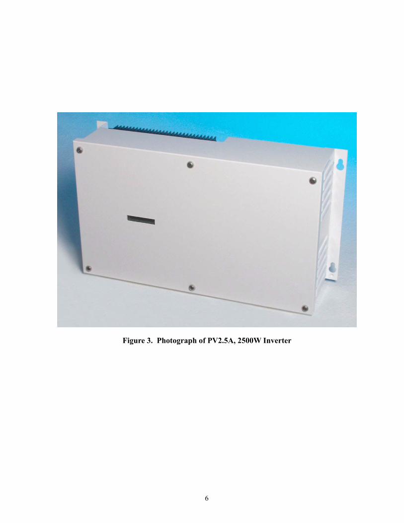
Figure 3. Photograph of PV2.5A, 2500W Inverter

7
3 PROJECT PERFORMANCE This project was organized into sixteen tasks. Goals and objectives were laid out in order to monitor and evaluate the results of this development work.
TASK 3.1 Three-Phase Inverter Manufacturability Modifications
The purpose of this task was to reduce the manufacturing costs of four, 3-phase inverters, the Models PV5208 (5kW), PV10208 (10 kW), PV15208 (15 kW) and the PV20208 (20 kW) currently offered by Xantrex Technology Inc. Two new models rated at 10kW and 25kW were developed to replace these four models.
3.1.1 Three-Phase Magnetics Design
The goal of this subtask was to reduce the cost of magnetic components, including primary line filter chokes, secondary line filter chokes and power supply transformers, in the two 3-phase inverters, by 10%. This has been accomplished by using “Super-HF” core materials. The cost goals were exceeded, substantial weight reductions were had and the power conversion efficiency of both has been enhanced.
The comparison is made between the current Xantrex product offering and the two new products being developed under this contract. For reference we will refer to the new, reduced cost versions of the existing PV10208 and PV20208 as the PV10A and PV25A respectively. All costs are based on 100 piece purchase quantities. Table 1 compares the normalized costs of the associated magnetics components. Table 2 illustrates the percentage cost savings had with the magnetic components designed for the new inverters.
Component \ Model PV10208 PV10A PV20208 PV25A Primary Line Filter Choke .58 .67 .57 .62 Primary Line Filter Choke .33 .17 .37 .14 Power Supply Transformers .09 .04 .06 .03 Total Magnetics Costs 1.00 .88 1.00 .78
Table 1. Magnetic Components Normalized Costs
Models Percentage Cost Reduction PV10208 vs. PV10A 12% PV20208 vs. PV25A 22%
Table 2. Magnetic Component Cost Reductions
Significant reductions were also made in weight. For example, the PV10208 primary line filter choke weight was reduced from 72 lbs. to 29 lbs.

8
3.1.2 Three-Phase Power Bridge Design
The purpose of this subtask was to reduce the cost of the inverter power bridges for the 10kW and 20kW hardware platforms. This has been accomplished by using simplified, lower cost IGBT drive circuits, “dumb” IGBT modules and a highly integrated, PCB based, laminated bus, Power Bridge design. The 20kW Bridge is approximately twice the size of the 10kW bridge because of larger power modules, more bus capacitance and the requirement for a larger heatsink.
The goal of this Subtask was to reduce the cost of the 10kW and 20kW power bridge designs by 10%. This goal was exceeded. Table 3 summarizes the cost savings had with the new integrated power bridge designs.
Unit Power Bridge Parts Cost % Reduction PV10208 1.00 PV10A .47
53%
PV20208 1.00 PV25A .79
21%
Table 3. Power Bridge Parts Normalized Cost Reductions
3.1.3 Three-Phase Heat Removal System Design
The goal of this Subtask was to reduce the cost of the 10kW and 20kW heatsink and associated heat removal system components by 20%. This goal was exceeded. This was accomplished by using higher efficiency IGBT modules that generate less heat and by using a more efficient, high-turbulence forced convection system. Table 4 summarizes the cost savings had with the new heat removal system designs.
Unit Heat Removal Parts Cost % Reduction
PV10208 1.00 PV10A .41
59%
PV20208 1.00 PV25A .46
53%
Table 4. Heat Removal Parts Normalized Cost Reductions

9
3.1.4 Three-Phase Enclosure Design
The purpose of this subtask was to lower the total cost of all sheet metal components. This was accomplished by incorporating integral weather shields and insect baffles, eliminating enclosure door flanges and by using continuous door hinges for both the 10kW and the 20kW designs.
The goal of this Subtask was to reduce the cost of the 10kW and 20kW enclosure designs by 20%. This goal was exceeded. Table 5 summarizes the cost savings had with the new enclosure designs.
Unit % Cost Reduction PV10208 PV10A
30%
PV20208 PV25A
31%
Table 5. Enclosure Cost Reduction
TASK 3.2 DSP3 Control Board Design and Prototype
The purpose of this task was to design and fabricate a low cost, high performance, universal application, 3-phase, PV grid tie control board that can be applied at virtually any power level. This was accomplished using an embedded DSP controller and a minimum number of peripheral components. The enhanced DSP performs all of the real time pulse-width-modulation (PWM) functions of the inverter, and will also perform those functions more commonly performed by a microprocessor.
3.2.1 DSP3 Embedded Controller Specification
The purpose of this subtask was to precisely define the functional performance parameters of the DSP3 card. All input and output signals were defined, as well as the controller requirements to meet power, performance and UL 1741 targets. This specification is applicable for both the 10kW and 20kW inverters.
This specification was utilized in the development of the DSP3 circuit design, subtask 3.2.2, and the DSP3 control board firmware shell design, Task 3.4.
3.2.2 DSP3 Circuit Design, Schematic and Bill of Materials
The purpose of this subtask was to translate the controller specification into a hardware design. This was accomplished by traditional analog and digital electronic design techniques creating the most cost-effective configuration of the circuit components peripheral to the DSP controller. This controller card will be used for both the 10kW and 20kW inverters.
The goal of this Subtask was to reduce the cost of the control board used on the existing Xantrex PV10208 and PV20208 three-phase inverters by 20%. This goal was exceeded. Table 6 summarizes the parts cost savings had with the new control board design.

10
Control Board Total Parts Cost Cost Reduction PV258 series control board and LCD module 1.00
DSP3 control board, including LCD display .38
62%
Table 6. DSP3 Control Board Normalized Cost Reduction
3.2.3 DSP3 Control Board Assembly Fabrication
This subtask was a follow on to Subtask 3.2.2. The goal was to fabricate the DSP3 control board hardware according to the design and specification developed in that subtask. The task resulted in the fabrication of four DSP3 printed circuit board assemblies part number (p/n) B09010A as shown in Figure 4. The Xantrex DSP3 control board p/n B09010A is a fully functional single board unit used to control all functions, including the switching of the Power Bridge Assembly and the PWM loop regulation for the PV10A and PV25A inverters. It has a Liquid Crystal Display on board eliminating the need for extra cabling and hardware. This control board design achieves a cost savings of over 60% compared to the control board components currently used in the PV10208 and PV20208 inverters as shown under the heading of Subtask 3.2.2. Table 7 is a check list of the analog functions on the board that were tested in order to ready the board for use in software development:
Item Description Complete1 Supply Voltage IN: +/-12 volts √2 Verify Supply Voltage, analog: +5 volts √ 3 Verify Supply Voltage, analog: +3.3 volts √ 4 Verify Supply Voltage, digital: +5 volts √ 5 Verify Supply Voltage, digital: +3.3 volts √ 6 Verify Supply Voltage, isolated: +5 volts √ 7 Verify Reference Voltage: +1.65 volts √ 8 Verify 40.mHz square wave on X1 pin 3 √ 9 Verify Manual Adjust (MAN): 0 to 3.3 volts √ 10 Install jumper select for IOPB4, verify LED lights √ 11 Install jumper select for IOPB5, verify LED lights √ 12 Install all jumper selects for 10 kW test √ 13 Adjust the AC Voltage Adjust trimpot on the DSP3SIM board fully CW √ 14 Verify that there are 3 Vpp sine waves on test points 0, 1, 2 on B09010 √ 15 Adjust VR1 CCW. Verify all three sine waves smoothly adjust to 0 volts √ 16 Change all jumper selects for 25 kW test. √ 17 Adjust the AC Voltage Adjust trimpot on the DSP3SIM board fully CW √ 18 Verify that there are 3 Vpp sine waves on test points 0, 1, 2 on B09010 √
Table 7. DSP3 Control Board Analog Function Check List

11
Figure 4. DSP3 Control Board
TASK 3.3 Three-Phase Simulator Board
The purpose of this task was to develop a simulator board, the SIM3, for the DSP3 control board to facilitate firmware development in a low power environment. This was accomplished by using adjustable amplitude sinewave generators and DC sources to simulate scaled analog DSP input signals. Controller outputs were terminated into characteristic load impedances and test points were made available. The task was accomplished through a two-step design, development and fabrication process resulting in the design, fabrication and assembly of one SIM3 simulator PCB assembly.
3.3.1 Three-Phase Simulator Board Circuit Design
The purpose of this subtask was to translate the controller I/O specifications into a hardware design for the SIM3 simulator board. This was accomplished by traditional analog and digital electronic design techniques, modeling for the control board input and output signals.
This circuit design was used to fabricate the simulator as shown in Subtask 3.3.2.

12
3.3.2 Three-phase Simulator Board Fabrication
The goal of this Subtask was to fabricate a three-phase simulator board based upon the designs developed in Subtask 3.3.1. The result of this subtask has been the fabrication of a completed simulator board assembly. This goal has been met. Figure 5 shows a photograph of the completed three-phase simulator board assembly. Table 8 verifies the performance and function of the three-phase simulator board.
Figure 5. Photograph of Three-Phase Simulator Board, SIM3
Item Description Complete1 Supply Voltage: +12 volts √2 Supply Voltage: -12 volts √ 3 Supply Voltage: +5 volts √ 4 Supply Voltage, Digital: +12 volts √ 5 Voltage Reference: +2.5 volts √ 6 Verify 245.76kHz square wave on U4 pin 10 √ 7 Verify AC Voltage Adjust (VR1): 0 to 2.5 volts √ 8 With VR1 fully clockwise check: √

13
9 24 volt sine wave @VA √10 24 volt sine wave @VB √ 11 24 volt sine wave @VC √ 12 120° phase shift between each sine wave √ 13 Adjust VR1 CCW. Verify all three sine waves adjust to 0 volts √ 14 With unit in standby, verify 0 volts on the output of U21, U22, U24. √ 15 With unit in run mode, verify sine wave on the output of U21, U22, U24. √ 16 Verify output of sensor U23 is accurate with the ambient temperature. √
Table 8. SIM3 Start-Up and Function Check List
TASK 3.4 DSP3 Control Board Firmware Shell Design
The goal of this subtask was to create the pre-integration firmware code. This has been accomplished and we are ready to begin the hardware/firmware integration phase of the project.
The pre-integration code consists of two assembly language source files, fifteen C language source files, and thirty-four ‘include’ files. This code initializes all of the microprocessor’s internal registers (system and core, data direction, watchdog, analog-to-digital, serial communications interface, pulse-width modulation, and event manager registers), RAM (Random Access Memory), and the external hardware.
The code has functions to perform 50 versus 60 Hertz detection, photovoltaic power tracking, reference sine wave generation, various RMS and other power calculations and data logging functions, a state-machine-based limits checking and shutdown, and some LCD display functions.
The purpose of this task was to design the internal configuration and basic function of the embedded controller. This shall be supported using the simulator board from Task 3. This task brought the firmware to a point where the hardware/firmware integration phase could proceed with the greatest efficiency.

14
TASK 3.5 Single-phase Inverter Manufacturability Modifications
The purpose of this task was to reduce the costs of manufacturing the Xantrex single-phase, grid-tied inverter hardware platforms. One new platform is intended as a next generation replacement for both the Xantrex ST and 4000 series of grid tie inverters. The new platform will be designed to maximize manufacturing efficiency by utilizing common cost reduced components and common manufacturing techniques wherever possible. Specifically, IGBT (Insulated Gate Bipolar Transistor) drive circuits, control power supplies, bus capacitors and power modules are components and circuits where commonality and cost reductions are expected.
3.5.1 Single-phase Magnetics Design
The goal of this subtask was to reduce the cost of all magnetic components in the single-phase inverter by 10%. This cost goal was exceeded.
The comparison is made between the current Xantrex SW Series product offering and the new product being developed under this contract. The current SW product most closely represents the topology of the new single-phase inverter. All costs are based on 100 piece purchase quantities. For future reference, the new single-phase 2500W unit will be designated as the PV2.5A. Table 9 compares the normalized costs of the associated magnetics components. Table 10 illustrates the percentage cost savings had with the magnetic components designed for the new inverter.
Component \ Model SW2512 PV2.5A Output Transformer(s) .94 .67 Output Choke .03 .11 Power Supply Transformer .03 .04 Total Magnetics Costs 1.00 .82
Table 9. Magnetic Components Normalized Costs
Models Percentage Cost Reduction SW2512 vs. PV2.5A 18%
Table 10. Magnetic Component Cost Reduction
3.5.2 Single-phase Power Bridge Design
The goal of this Subtask was to reduce the cost of the existing power bridge board used in the ST2500XR inverter by 10%. This goal was exceeded. The new design offers a cost reduction of 31%.
The reduction is attributed to the differences in the topologies used for each design. The ST2500XR bridge is effectively a three conversion design. Two conversions, DC to high frequency AC and rectification of the high frequency AC to DC, are in a full bridge boost

15
circuit used on the front end of the inverter to boost the input DC voltage up to a high DC bus voltage. This DC voltage is then converted to the 120VAC output voltage. Since the DC to DC converter is isolated from the DC to AC converter, separate power supplies and drive circuits are needed for each. This greatly adds to the parts cost of the inverter.
The new design uses a single stage to convert DC voltage to AC current employing a 60Hz transformer driven by a full bridge. This topology does not require the large number of isolated power supplies and drive circuits required with the ST2500XR topology, so cost is reduced. This design not only reduces cost, but provides more efficient power conversion. The reduction in parts and lower operating temperatures further enhances product reliability.
3.5.3 Single-phase Heat Removal System Design
The goals of this Subtask were to redesign the heat removal system with no increase in current costs and no reduction in performance for the single-phase inverter. In the strictest sense, this goal was not attained. The heat removal system cost was increased by 32% but the performance was greatly improved. The intent of this development task is satisfied because the value of the product is enhanced through higher reliability and silent operation. Typically, the jump from forced convection to natural convection is much more costly than demonstrated here.
The new design uses a heat sink cooled by “fanless” natural convection. This can be done because multiple power switching devices are paralleled to achieve low conduction losses and the spread the losses over a large area. All of the heat in the switching device is efficiently transferred to the heat sink.
Figure 6. Back of PV2.5A Inverter Showing Heatsink
The specific purpose of the cooling system is to remove the heat from switching devices. There is a maximum junction temperature that must not be exceeded or the device will fail. The power that can be dissipated in each device can be stated as:
Pd=∆T/ΣRφ

16
Where: Pd = power dissipated
∆T = difference between the junction temperature and the ambient temperature = Tj -Ta
ΣRφ = sum of the thermal resistances between the devices and the heat sink
= φjc + φthermal clad pcb + φsil-pad Calculating for junction temperature:
Tj = Pd(φjc + φthermal clad pcb + φsil-pad) + Ths + Ta
= [2.3 (.75 + .80 +.74)] +30 + 45 = 80.3°C This is well below the 175°C max temperature of the devices being used. This conservative thermal design will result in lower switch temperatures, which means lower enclosure temperatures. This will increase the life expectancy of all of the internal components like capacitors and the switches themselves.
The above calculations show that the selected heat sink material will be more than adequate to cool, without a fan, the switching devices in this design. Because the cooling system doesn’t need a fan, a likely component to fail, inverter reliability is increased. This also means reduced parts cost, and an inverter that operates silently. The assembly for the power bridge board is also simplified by using surface mount power components.

17
Figure 7. PV2.5A Power Bridge Assembly
3.5.4 Single-phase Enclosure Design
The purpose of this subtask was to lower total cost of all sheet metal components for the single-phase inverter. This was accomplished using an enclosure with two compartments, one vented with louvers containing environmentally robust magnetics components and one sealed containing environmentally sensitive electronic devices. The performance over the Xantrex ST Series, where the forced convection airflow deposits dust on sensitive components, is much improved. Also, the PV2.5A enclosure is weatherproof by design and does not require an optional plastic weather shield. For an equitable cost comparison, the ST outdoor weather shield is added to the ST sheet metal component costs.
The result of this subtask was expected to be a 20% reduction in sheet metal costs for the single-phase inverter when compared to the Xantrex ST series. This goal was exceeded. The actual reduction, including the cost of the weather shield, was 25%. Table 11 shows the normalized costs and percentage cost savings had with the new single-phase inverter enclosure design.
18
Unit Enclosure Sheet Metal Cost Cost Reduction ST2500XR *With weather shield 1.00
PV2.5A .75 25%
Table 11. Enclosure Normalized Cost Reduction
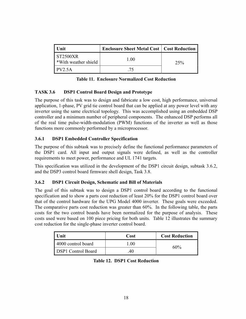
TASK 3.6 DSP1 Control Board Design and Prototype
The purpose of this task was to design and fabricate a low cost, high performance, universal application, 1-phase, PV grid tie control board that can be applied at any power level with any inverter using the same electrical topology. This was accomplished using an embedded DSP controller and a minimum number of peripheral components. The enhanced DSP performs all of the real time pulse-width-modulation (PWM) functions of the inverter as well as those functions more commonly performed by a microprocessor.
3.6.1 DSP1 Embedded Controller Specification
The purpose of this subtask was to precisely define the functional performance parameters of the DSP1 card. All input and output signals were defined, as well as the controller requirements to meet power, performance and UL 1741 targets.
This specification was utilized in the development of the DSP1 circuit design, subtask 3.6.2, and the DSP3 control board firmware shell design, Task 3.8.
3.6.2 DSP1 Circuit Design, Schematic and Bill of Materials
The goal of this subtask was to design a DSP1 control board according to the functional specification and to show a parts cost reduction of least 20% for the DSP1 control board over that of the control hardware for the UPG Model 4000 inverter. These goals were exceeded. The comparative parts cost reduction was greater than 60%. In the following table, the parts costs for the two control boards have been normalized for the purpose of analysis. These costs used were based on 100 piece pricing for both units. Table 12 illustrates the summary cost reduction for the single-phase inverter control board.
Unit Cost Cost Reduction 4000 control board 1.00 DSP1 Control Board .40
60%
Table 12. DSP1 Cost Reduction

19
3.6.3 DSP1 Circuit Board Assembly Fabrication
This subtask is a follow on to Subtask 3.6.2. The goal was to fabricate the DSP1 control board hardware according to the design and specification developed in that subtask. The task resulted in the fabrication of the DSP1 printed circuit board assemblies.
The Xantrex DSP1 control board is a fully functional single board unit used to control all functions, including the switching of the Power Bridge Assembly, and the PWM loop regulation for the single-phase inverter. It has a Liquid Crystal Display on board eliminating the need for extra cabling and hardware. This control board has a cost savings of over 60% compared to the control board components currently used in the model 4000 inverters, as shown under the heading of Subtask 3.6.2.
Table 14 shows a check list of the analog functions on the board that were tested in order to ready the board for use in software development:
Parameter Simulator Signal Ratio Scale
ExpectedLevel
Measured Level Comments
Input Voltage (+5) 4.95 1 1 4.95 4.95 Input Voltage (+15) 15.1 1 1 15.1 15.1 Input Voltage (-15) -15.4 1 1 -15.4 -15.4
+3.3D - - - 3.3 3.3 +3.3A - - - 3.3 3.28
Line Voltage Sense 24 10 0.004 0.96 1.04 240 VAC SimulatedLine Voltage Offset 0 0 1.65 1.65 1.62
Sync Signal - - - 60 Hz SW 60 Hz SW Has some bounce UP Switch Push - - 0 0 Noisy w/switch open
Down Switch Push - - 0 0 Select Switch Push - 0 0 LEM Output 0.117 100 0.01 0.117 0.113 11.7 Amps simulated
Overcurrent Signal - - - 3.3 3.3 Overvoltage Signal - - - 3.3 3.3
PDPINT Signal - - - 3.3 3.3 DC Voltage Sense 48 1 0.02 0.96 0.964 48 VDC Simulated
Temperature Sensor 0.305 1 1 0.305 0.305 Rises when heated
Table 13. DSP1 Control Board Analog Function Check List

20
Figure 8. DSP1 Control Board
TASK 3.7 Single-Phase Simulator board
The purpose of this task was to develop a simulator board, SIM1, for the DSP1 control board to facilitate firmware development in a low power environment. This was accomplished by using adjustable amplitude sinewave generators and DC sources to simulate scaled analog DSP input signals. Controller outputs are terminated into characteristic load impedances and test points are made available. The task resulted in the design, fabrication and assembly of one SIM1 simulator PCB assembly.
The result is a simulator board built to test the DSP1 control board and is intended to shorten the firmware development time by more than 20%.
3.7.1 Single-phase Simulator Board Circuit Design
The purpose of this subtask was to translate the controller I/O specifications into a hardware design for the SIM1 simulator board. This was accomplished by traditional analog and digital electronic design techniques, modeling for the control board input and output signals.
This circuit design was used to fabricate the simulator as shown in Subtask 3.7.2.

21
3.7.2 Single-phase Simulator Board Layout and Fabrication
The goal of this Subtask was to fabricate a single-phase simulator board based upon the designs developed in Subtask 3.7.1. The result of this subtask has been the fabrication of a completed simulator board assembly. This goal has been met.
Figure 9. Single-Phase Simulator Board, SIM1
TASK 3.8 DSP1 Control Board Software Shell Design
The purpose of this task was to setup the internal configuration and basic function of the embedded controller. This was accomplished using the simulator board from Task 5. This task brings the firmware to a point where the hardware/firmware integration phase can proceed with the greatest efficiency. This task has resulted in the completion of the pre-integration firmware code.
The DSP1 hardware platform provides the support for the necessary software modules. There exists one assembly language module (interrupt vectors only), and six C language modules. Upon startup, the DSP reset vector points to the C run-time library. This code, supplied by TI, performs all of the actions necessary in order for the C environment to function. Once that is

22
done, control is then passed to the function called “MAIN”. This function performs the hardware initialization as well as the remainder of the software initialization (including the enabling of interrupts), and then control is passed to the main loop. This loop provides the inverter’s functionality, and control does not leave this loop until the unit is reset.
The goal of this subtask was to create the pre-integration firmware code. This has been accomplished and we are ready to begin the hardware/firmware integration phase of the project.
The code has functions to perform 50 versus 60 Hertz detection, photovoltaic power tracking, reference sine wave generation, various RMS and other power calculations and data logging functions, a state-machine-based limits checking and shutdown, and some LCD display functions.
TASK 3.9 DSP2 Control Board Design and Prototype
The purpose of this task was to design and fabricate a low cost, high performance, universal application control board for residential PV power systems with low voltage battery storage of up to 10kW based on the same electrical topology. This has been accomplished using an embedded DSP controller and a minimum number of peripheral components. The results of this task shall be the design of the DSP2 controller.
3.9.1 DSP2 Embedded Controller Specification
The purpose of this subtask was to precisely define the functional performance parameters of the DSP2 card. All input and output signals were defined, as well as the controller requirements to meet power, performance and UL 1741 targets. This specification is applicable for residential PV power systems with low voltage battery storage of up to 10kW based on the same electrical topology. This specification was utilized in the development of the DSP2 circuit design, subtask 3.9.2
3.9.2 DSP2 Circuit Design, Schematic and Bill of Materials
The purpose of this subtask was to translate the DSP2 controller specification into a hardware design. This was accomplished by traditional analog and digital electronic design techniques creating the most cost-effective configuration of the circuit components peripheral to the DSP controller. This controller card will be used for residential PV power systems with low voltage battery storage of up to 10kW based on the same electrical topology
There were no specific contract cost reduction goals for the DSP2 board. This is because there is no existing equipment with the extended performance capabilities of this new board. The closest comparison, by like end user application, would be the Xantrex SW Series. When compared to the Xantrex SW Series control board, the DSP2 control board costs were reduced by 14%. The costs used were based on 3000 piece pricing for both units.
This meets the contract goals since performance, features and flexibility were all enhanced with the new design and a cost reduction was achieved.

23
TASK 3.10 Three Phase Inverters and DSP3 Software Integration
The purpose of this task was to make the target hardware function correctly with the embedded DSP control firmware. All of the elements of the enhanced DSP3 controller and the manufacturability changes were integrated for testing and debugging. Testing of the 10kW and 20kW inverters began with low power operation while verifying the stable, safe operation of the inverters. Output power was increased to demonstrate basic, full power operation of the inverters. The expected result of this task was to test the 10kW and 20kW inverters per the corresponding performance specifications and meet or exceed the specified performance criteria. An explanation of the task methodology follows.
3.10.1 Grid-Tied Inverter Operation
A PV10A and a PV25A inverter have been operated through a series of tests devised to compare operation of each unit to the corresponding performance specifications as defined in document DSP3 FS 102502, Functional Specification for DSP3 Based Grid Tied Inverters. In some cases, the performance of the inverters was found to be desirable, although minor technical deviations from the specification predictions were observed. In these cases, changes to the specification have been proposed.
As a result of firmware and hardware optimization, the input voltage range for full power operation, the maximum power point tracking (MPPT) range, the over temperature fault limit, the conversion efficiency, and the sleep threshold have been modified.
Each inverter has been tested per the corresponding performance specifications as proposed, and has met or exceeded that performance criterion.
3.10.2 Test Methods
Performance of the inverters was verified through a combination of testing, analysis, and review of previously obtained data.
In some cases, the inverter control board was connected to a computer via the JTAG interface. The Joint Test Action Group (JTAG) defined an interface called the JTAG interface for testing and configuring individual devices on printed circuit boards, without the need to remove the devices from the board. This test method allows a computer-based system to connect to modern CPUs such as DSPs while they are running, and to monitor and change device parameters.
The input power was not derived from a photovoltaic (PV) source. Rather, it was supplied from an adjustable DC power source with a variable source resistance. This allows for the complete control of the input parameters, independent of weather conditions, which is necessary to demonstrate the inverter performance over a wide range of normal and fault conditions.
3.10.3 DSP3 Firmware Updates
The DSP3 firmware was previously demonstrated to successfully operate the inverters in the grid-tied configuration with nominal input and output conditions. The PWM controller

24
maintained the output current waveforms within the performance specification requirements for THD and Power Factor.
The result of this task has been to expand the functions of the controller to operate the inverters over a broad range of input and output conditions. A variety of functions are performed simultaneously, which may be summarized as follows:
• Maintain the output current waveform within the requirements of the performance specification while the input and output parameters vary over a wide range of normal operating conditions.
• Detect the power available from the photovoltaic array, command the inverter to run and track the maximum power point when the available power is sufficient for the inverter to drive the grid, and halt operation of the inverter when sufficient power is not available.
• Detect any fault condition that may arise, due to either external conditions or malfunction within the inverter, cease power production when fault conditions arise, annunciate the nature of the fault, and, after a prescribed delay, re-start power production if the fault condition has been cleared.
• Calculate and display the inverter operational statistics and mode.
The latest source code incorporates the changes and additions to the firmware that were made to facilitate performance to these requirements.
3.10.4 Hardware Updates
Modifications to the circuitry of both the PV10A and the PV25A inverters were made to complete the functional testing. During test of the PV25A, the temperature sensing circuit failed to detect an over temperature condition, resulting in the failure of power components. This circuit was replaced with a thermal switch to safely complete the tests. The PV10A successfully utilized the same circuit without failure. The semiconductor temperature sensor was found to be sensitive to electromagnetic interference. The design was changed to substitute a passive thermistor for the semiconductor sensor in both the PV10A and PV 25A.

25
3.10.5 Test Setup
The following equipment was utilized in the testing of the inverters:
• DC power Source, 0-600 Volt, 0-100 Amp, with source resistor, 0-12 ohm. • Transformer, 30KVA, 3-phase, 208 Volt Delta to 120/208 Volt Wye. • Variac, 3-phase, 208 Volt, 50A. • Voltmeters, Fluke model 77. • Oscilloscope, Phillips model 3394A. • Power Analyzers, Fluke Models 39 and 41.
3.10.6 Test Results
The technical requirements and predictions for the two inverters are specified in section 5, Technical Requirements, of document DSP3 FS 102502, Functional Specification for DSP3 Based Grid Tied Inverters. The following specification compliance discussion applies equally to the PV10A and PV25A inverters unless noted otherwise.
3.10.7 Inverter Operational Modes
The inverter controller is based upon a state machine that allows the inverter to operate in one of 4 main modes. POWER TRACKING MODE This is the mode in which the inverter normally operates when there is sufficient power from the PV array for the inverter to deliver power to the grid. The inverter transitions to the power tracking mode when the wake-up test is successfully completed.
In the power tracking mode, the Maximum Power Point Tracking (MPPT) algorithm is operative. The MPPT continuously seeks the PV array operating point that yields the most output power. The algorithm is a perturb and observe function.
Performance to this requirement was tested utilizing a DC power source with DC current limiting and a source resistance of 1 ohm. The DC voltage and the current limit point were varied to simulate the output of a PV array as the solar conditions change.
The voltage and current limit point were varied to achieve a maximum power point (MPP) from 300 to 550 VDC. The inverters were able to track the maximum power point of the DC source within ±4 Volts DC. When the MPP was below the calculated DC bus minimum voltage limit, each inverter was able to track down only to that limit, and resume tracking when the MPP was raised.

26
Characteristics of Simulated Array MANUAL MODE This mode is intended for maintenance and test personnel only, to provide them with manual control of basic inverter functionality. A potentiometer on the controller circuit board is available to adjust the inverter power level while in this mode. The manual mode was utilized during the testing of the inverters in order to maintain operating conditions independent of the MPPT circuit, and to create fault conditions. Both inverters operate in a stable manner in the manual mode. The output current was adjusted from 5% to 100% of rated output current power while the input was varied over the full range specified. STANDBY MODE The controller executes the standby mode when there is insufficient energy from the PV array to provide positive power transfer. It is also executed after the detection and response to any recoverable fault, and when an inverter is in manual mode and is commanded to stop. Both inverters functioned successfully in all of these conditions. SHUTDOWN Whenever a latching fault is detected, the inverter enters the shutdown mode. It is necessary to remove and reapply the AC power to the inverter, or to reset the DSP via the JTAG interface, in order to clear the shutdown mode. Both inverters functioned successfully when latching fault conditions were imposed.
3.10.8 Auto-Frequency Detection
The DSP controller firmware has algorithms for both 50 Hz and 60 Hz operation. Upon initial power-up, each inverter successfully detected the operating frequency of 60 Hz. Operation has not been tested 50 Hz. The firmware code for 50 Hz operation selects an alternate numerical sine wave table that has been calculated by the same means as the 60 Hz table, and changes a system timer for a nominal period of 20 mS v. 16.67mS. All other firmware functions are performed utilizing the same exact code.
200
100
10
400
300V
OLT
S
500
70
AMPS3020 40 50 60

27
3.10.9 Auto-Phase Sequence Detection
Upon initial power-up, the inverter detects the line voltage phase sequence rotation, and sets the switching order of the power bridge devices. This allows proper operation of the inverter when installed in either phase sequence arrangement.
Each inverter was powered up with the input wiring configured first for clockwise rotation of the AC line voltage, and then again with counter-clockwise phase rotation. The inverters successfully detected the rotation and delivered output current with the correct rotation to deliver power to the utility grid.
3.10.10 Power Quality
Output power quality is maintained by hardware components and firmware optimized to exceed the requirements of IEEE-519/929. These requirements are defined in section 5.10 of document DSP3 FS 102502, Functional Specification for DSP3 Based Grid Tied Inverters.
Both inverters successfully demonstrated compliance with the data sheet predictions relating to power quality.
3.10.11 Third Party Certification
The inverters were submitted to UL for preliminary mechanical and electrical evaluation. That exercise has been successful completed, documented, and submitted in Deliverable D2.7.
3.10.12 DC Bus Minimum Voltage Limit
In order to minimize Total Harmonic Distortion (THD), the minimum DC bus voltage is limited to a numerical value that is a function of the peak-to-peak AC line voltage. This limit is dynamically adjusted to compensate for utility voltage fluctuations throughout the day.
Both inverters successfully calculated the VMIN BUS value, and performed the power tracking function while preventing the DC bus voltage from going below the calculated VMIN POWER TRACKER voltage.
3.10.13 Inverter Software Protection
The PV grid tied inverter incorporates a variety of protection functions designed to protect the inverter from damage. Some of these protection functions are triggered by software while others are triggered by hardware. Both cause software to annunciate the condition to the operator interface. Both of the inverters successfully performed these functions, as detailed in the following sections.

28
3.10.14 Line Voltage / Frequency Detection
The inverter continuously measures the line voltage and frequency in all operating states except for shutdown. If the voltage or frequency exceeds the high or low limits, as specified in UL1741, the inverter ceases to deliver power to the grid and annunciates the detected fault. After the line voltage and frequency have returned to the normal range for a period of 5 minutes, the inverter resumes normal operation.
These fault conditions are also related to the island detection methods, which destabilize balanced loads and drive the inverter induced voltage and frequency output outside of the acceptable limits.
The precise adjustment and measurement of utility frequency and voltage requires a high power, low distortion, precision, 3-phase, grid simulator. This specialized equipment was not available. An alternate test method was used to substantially achieve the same results. The line voltage fault detection for undervoltage and overvoltage has been verified with the units running, utilizing a variable transformer. Frequency detection and fault response were verified with the inverter bridges disconnected from the AC line. An oscillator was used to inject a 60 Hz signal to the DSP controller. The frequency at which the frequency fault response occurred was measured on an oscilloscope. Although exact measurement of the trip voltages, frequencies, and response times was not possible, these tests did successfully verify that the fault detection firmware performed the desired detection and responses. A review of the firmware source code has verified that the set-points and response times are programmed to the desired values.
3.10.15 Voltage and Frequency Limits for Utility Interaction
These limits are preset to the levels described below. They are equivalent to those found in the IEEE-929 and UL1741 standards:
Extreme High Voltage: >= 137% of nominal, shut down within 2 cycles. High Voltage: >= 110% of nominal, shut down within 120 cycles. Nominal Voltage: = 208 Vrms. Low Voltage: <= 88% of nominal, shut down within 120 cycles. Extreme Low Voltage: <= 50% of nominal, shut down within 2 cycles. High Frequency: >= Base + 0.5 Hz, shutdown within 6 cycles. Base Frequency: = 60.0 Hz. Low Frequency: <= Base - 0.7 Hz, shutdown within 6 cycles.
Theses limits are programmed into the DSP controller.
3.10.16 Island Detection
The potential for an island condition occurs when the utility power is interrupted while the inverter is delivering power. Detection of islanding from the utility grid is achieved via AC overvoltage, undervoltage, overfrequency, and underfrequency detection functions, as well as load destabilization algorithms in compliance with UL1741.

29
Load destabilization is accomplished with an upward and downward current phase shift relative to phase voltage. Output currents are shifted twice per second. Voltage frequency and magnitude are measured every cycle and compared to the programmed limits. Shifting the current phase angles in this manner will destabilize balanced resonant loads that have been disconnected from the utility. If an island situation occurs, the destabilized load will drive the inverter beyond the programmed limits for AC line voltage and/or frequency, causing the inverter to shut down within two seconds.
When the inverter shuts down due to an island condition, the AC line voltage will no longer be present, and the unit will be powered down. Upon restoration of the AC line voltage, the inverter will proceed through the normal power-up initialization process.
This method of island protection is identical to that as performed by the existing PV10 and PV20 inverters, which have passed testing to UL1741. Actual testing in island conditions has not been performed on the PV10A and the PV25A. The voltage and frequency fault detection and the output current phase shift have been successfully verified.
3.10.17 Device Over-Temperature
The DSP3 controller monitors the heatsink temperature via a solid-state temperature sensor. When the heatsink temperature exceeds a predefined level it will declare an over-temperature condition. When an over-temperature condition is detected, the inverter ceases to deliver power to the grid and annunciates the over-temperature fault on the LCD display. After the inverter has cooled to the normal range for a period of 5 minutes, the inverter resumes normal operation.
The performance specification states that the overtemperature fault will occur at a heatsink temperature of 90 degrees Centigrade. That limit has been set to 75 degrees C, in the controller firmware, to enhance the product reliability.
3.10.18 DC Bus Over-Voltage Detection
The inverters have bus over-voltage hardware and software detection. The inverter ties the PV array conductors directly to the DC bus. In the event the PV voltage exceeds 600VDC, the inverter will shut down and annunciate this fault to the operator interface. When a hardware fault signal occurs the system will immediately shut down the inverter and annunciate the fault to the operator interface.
This fault condition is latching and requires service attention. If the PV system has been correctly designed, the open-circuit voltage should never exceed 600VDC. Therefore, the occurrence of this fault usually indicates the inverter is pushing current against the PV array, causing the PV voltage to increase.
Each inverter was subjected to a DC overvoltage condition and safely shut down. When the overvoltage condition was eliminated and power was removed and reapplied, the inverters resumed normal operation.

30
3.10.19 Current Imbalance
This fault condition checks for imbalance in the three AC current measurements. The DSP3 board checks the three AC line RMS current values to ensure each one is within 10% of the median (middle) value for 120 continuous cycles. This fault condition is normally checked only in the Power Tracking state, when the output current is at least 20% of the full rated output current. At very low operating currents, the current imbalance may exceed 10%. When the current imbalance fault is detected, the inverter shuts down and annunciates this fault to the operator interface. This fault is latching and must be cleared by removing and reapplying the power to the inverter.
The inverters are designed to prevent output current imbalance in all operating conditions. In order to test this feature, the firmware was modified. The current imbalance detection was enabled for all levels of output current, and the input voltage was reduced until the output current diminished. Under this condition the current balance is no longer maintained, and the inverter successfully responded with the desired current imbalance fault. When the imbalance condition was eliminated and power was removed and reapplied, the inverters resumed normal operation.
3.10.20 Over Current
This fault indicates that the output current of the bridge has exceeded the maximum allowed. In normal operation, the DSP3 controller will prevent the output current from exceeding the maximum limit by overriding the Peak Power Tracker and limiting the AC current command. During some AC line transient conditions, the maximum current may be exceeded. In this case, the inverter ceases to deliver power to the grid and annunciates the detected fault on the LCD display. After a period of 5 minutes, the inverter resumes normal operation
This function was tested by operating the inverters in the manual mode and overriding the software limit. When the output current was manually adjusted beyond the current limit point, the inverters correctly detected and responded to the fault.
3.10.21 Operator Interface LCD
The LCD interface is standard equipment. The display consists of a 1 line, 16-character liquid crystal display located on the DSP3 controller board. A viewing slot is cut in the front door of the enclosure. A window on the inside of the door protects the LCD. The display shows 4 different parameters in rotation, 2 to 3 seconds for each parameter (line of text). The display functions as follows:
System Status - This is the current operating state of the inverter as defined in 3.8.1
AC Power in Watts - This shows the real time power output of the inverter. This value is filtered to compensate for noise fluctuations. This line is only displayed in the power tracking or manual running modes.
DC Voltage - This shows the inverter’s DC input in volts. This value is filtered to compensate for noise fluctuations. This line is only displayed in the power tracking or manual running modes.

31
Cumulative Output Energy in Kilowatt-Hours - This parameter continually calculated whenever the inverter is in the power tracking state or running in the manual mode. The total is stored in nonvolatile memory once every hour, and whenever the inverter transitions to the fault state or the standby state, and is retrieved from nonvolatile memory whenever the inverter transitions to the power tracking state or begins running in the manual mode.
DISPLAYED PARAMETERS Line 1: System Status
• “STANDBY” • “WAKE UP TEST” • “POWER TRACKING” • “SLEEP TEST” • “MANUAL MODE” • “SHUTDOWN” • “OVER TEMPERATURE” • “OVERCURRENT” • “DC OVERVOLTAGE” • “AC FREQ FAULT” • “AC VOLTAGE LOW” • “AC VOLTAGE HIGH” • “AC CURRENT IMBAL”
The inverters correctly displayed all of the above status parameters.
Line 2: AC Power: “##### WATTS AC”
The inverters correctly computed the AC power output and displayed that quantity while in the power tracking and manual running modes.
Line 3: DC Voltage: “### VOLTS DC”
The inverters correctly measured and displayed the DC input voltage while in the power tracking and manual running modes.
Line 4: Cumulative Output Energy. “#### ###.## KWHR”
The inverters correctly calculated and displayed the cumulative output energy. The cumulative energy value, accrued from the time of commissioning, was successfully stored in nonvolatile memory, and retrieved for display.
3.10.22 Operating States
The following is a list of states defining the inverter state machine. The states defined below are used to perform the various modes of operation defined above.

32
STANDBY Condition: The PV array does not have enough power capacity to maintain the inverter system operating losses, or the inverter has responded to a fault condition, and has returned to standby because the fault has cleared.
The inverter is idle. The line contactor is open and the devices are not switching. This generally indicates the PV array is not energized. The inverter will remain in this state until the PV voltage exceeds the PV Wake-Up value. Once these conditions are met and the goal state is Power Tracking, the state machine will automatically transition to System Wakeup Test state.
If the goal state is set to manual mode, then the state machine will automatically transition to the Manual Current state whenever IOPB4 is set to 1.
Both inverters successfully invoked the standby state. SYSTEM WAKE-UP TEST
This state only occurs during the transition from standby to power tracking. Condition: The PV array voltage is greater than the wake-up voltage level. This indicates that the array is on the threshold of having enough energy capacity to support the operating losses of the inverter.
While in the standby state, once the input voltage exceeds the wake-up voltage, the inverter will commence the wake up test. Once the voltage on the array exceeds the wakeup voltage value for 5 minutes, the inverter will check to see if the voltage has exceeded the start voltage, and if so, will transition to the power tracking state. If the PV voltage does not reach the start voltage limit, the state machine will transition back to the standby state.
The inverter correctly sensed the input conditions and transitioned between Standby, Wake Up Test, and Power Tracking. POWER TRACKING
This is the main operating state of the inverter. The control system commands output current to the utility, while calculating the output power to the grid. This function is also commonly defined as Peak Power Tracking (PPT). The power tracker algorithm optimizes output power given a variety of solar irradiance and array temperature conditions.
The specification target for the power tracking range was 300 to 570 Volts. With an absolute maximum open circuit voltage limit of 600VDC, no PV array will generate maximum power at 570 Volts. The power tracking range has been set to 300 to 550 volts, and the highest voltage for full rated output power is 500VDC. These values allow for maximum harvest of energy from standard PV array configurations and maintain suitable margin for reliable inverter operation.
Both inverters have demonstrated the successful implementation of the power tracking state, including optimization algorithm for adjusting the wake up voltage. SLEEP TEST
This state only occurs during the transition from power tracking to standby. When the output power drops below 2% of the full rated power of the inverter, the sleep test begins. If this condition persists continuously for five minutes, the state machine will transition to the

33
Standby state. While in the sleep test state, if the inverter power output rises above the sleep test value, the inverter will transition back to Power Tracking. MANUAL CURRENT
This state is only available in the manual operating mode. It allows the inverter to deliver a fixed output current, regardless of available PV array power. Both inverters operate correctly in the manual mode when the IOPB4 jumper is set to the 1 position. SHUTDOWN
When a DC overvoltage fault condition or a line current imbalance fault condition was created, the inverter successfully detected and annunciated the fault, and transitioned to the Shutdown state. It was necessary to remove and re-apply AC power to the inverter to reset either of these faults. This manual interaction is required, because faults of this nature usually indicate a catastrophic hardware failure.
3.10.23 Fault Detection and Annunciation
The inverters were tested for all fault conditions defined by the specification, and successfully detected and responded to these conditions. When the inverter experiences a fault condition, the DSP controller performs a power-down and disconnects the inverter from the utility. The fault condition is displayed on the LCD. FAULT CONDITIONS AC Line Frequency AC Line Voltage Low AC Line Voltage High Device Overtemperature DC Bus Over Voltage Current Imbalance Over Current AUTO-RECOVERABLE FAULTS For those faults defined as recoverable, the system successfully returned to a normal operating state once the fault condition was removed. The controller continued to monitor the specific parameter, and once the value was returned to a normal operating range for 5 minutes, each fault was cleared and the state machine transitioned to the standby state. LATCHING FAULTS Current imbalance and DC bus overvoltage are latching faults. These faults caused the inverter to go into the shutdown state.

34
3.10.24 TEST DATA
PV10A TEST DATA
PV10A TEST DATA BRIDGE ID: 1 CONTROLLER ID: 3 Test Test Conditions LIMIT Measured
350 VDC 10.5330VDC 10.7Nominal Power Rating 550 VDC
10 KW 10.4
Maximum Line Current 350 VDC
208 VAC
28 Amps 28.0100% Load >= 0.99 1.075% Load 0.9950% Load 0.9925% Load
350 VDC >= 0.85 0.97
100% Load >= 0.99 1.075% Load 0.9950% Load 0.98
Power Factor
25% Load
500 VDC >= 0.85 0.95
Current Distortion Phase-A 4.7Current Distortion Phase-B 3.5Current Distortion Phase-C
100% Load 350 VDC, 208 VDC <= 5% 4.5
Current Distortion Phase-A 4.4Current Distortion Phase-B 3.0Current Distortion Phase-C
100% Load 500 VDC, 208 VDC <= 5% 4.2
Power Tracking Range DC Bus Minimum Voltage Limit
50% Load Minimum limited by (VAC*root2*1.07) + 25
340-550 VDC 349-508(3)
100% Load >= 96% (1)75% Load >= 96% (1)50% Load >= 94% (1)
Conversion Efficiency
25% Load
350 VDC
>= 94% (1)Standby Losses Standby <= 30W 4Wake-up Voltage Self-Adjusting 320Wake-up Delay
Increasing DC Voltage 5 Minutes √
Sleep Threshold < 200 Watts √ (4)Sleep Shutdown Delay
Decreasing Power
208 VAC
5 Minutes √Under-Voltage Fault < 183VAC 2 Second Delay 183 V (2)Over-Voltage Fault > 229VAC
Vary Line Voltage 2 Second Delay 230 V (2)
Under-Frequency Fault < 59.3 Hz 0.1 Second Dalay 59.3 Hz (2)Over-Frequency Fault > 60.5 Hz Signal Injection 0.1 Second Delay 60.5 Hz (2)Anti-Islanding Protection 100% Load Verify Phase-angle Sequencing √Over-temperature Fault 100% Load 350 VDC, 208 VDC 75° C. Nominal 76DC Bus Over-Voltage Fault Standby Raise DC Bus 600VDC Nominal 602Line Current Imbalance Fault 50% Load Minimum Reduced √Line Overcurrent Fault Overload Manual Adjustment 32Frequency Detection Normal Operation Detects 60 Hz √Auto-Phase Sequence Detection Reverse Line-Phase Rotation Detects Phase
Rotation √

35
Test Test Conditions
LIMIT Measured
Standby Low DC Voltage “STANDBY / KWHR” √
Wake Up Test Raise DC Voltage “WAKE UP TEST / KWHR” √
Power Tracking Normal Operation
“POWER TRACKING / WATTS AC / VOLTS DC / KWHR”
√
“SLEEP TEST / WATTS AC / VOLTS DC / KWHR”
√Sleep Test / Standby Reduce DC Voltage
“STANDBY / KWHR” √Shutdown Run, Force Overcurrent “SHUTDOWN” √
“OVER TEMPERATURE” √Over Temperature Re-Starts √“OVER CURRENT” √Over Current Re-Starts √“AC FREQ FAULT” √AC Frequency Fault Re-Starts √“AC VOLTAGE LOW” √AC Voltage Low Re-Starts √“AC VOLTAGE HIGH” √AC Voltage High Re-Starts √“AC CURRENT IMBAL” √AC Current Imbalance Latches off √“OVER VOLTAGE” √
State Controller, Display
DC Overvoltage
Fault Conditions
Latches Off √Manual Operation Manual Current Adjust output current 1.4 to 28 Amps 1.2 to 28.1
Initial wake-up Voltage (350*.9) + 5 = 320 VDC 320
Adjust input for < 500 Watts AC, allow unit to complete sleep test.
Re-start: Wake-up Voltage 325 VDC 324Wake-up
Test Timer Adjust input for > 1000W for > 5 minutes.
Re-start: Wake-up Voltage 320 VDC 320
Test data sheets have been prepared and completed for both inverters. These data sheets address each of the requirements and predictions stated in the performance specifications.

36
PV25A TEST DATA BRIDGE ID: 1 CONTROLLER ID: 4 Test Test Conditions LIMIT Measured
350 VDC 25.7330VDC 25.0Nominal Power Rating 550 VDC
25 KW 25.4
Maximum Line Current 350 VDC
208 VAC
70 Amps 71A100% Load >= 0.99 1.075% Load 1.050% Load 1.025% Load
350 VDC >= 0.85 0.99
100% Load >= 0.99 1.075% Load 1.050% Load 1.0
Power Factor
25% Load
500 VDC >= 0.85 1.0
Current Distortion Phase-A 3.5Current Distortion Phase-B 2.7Current Distortion Phase-C
100% Load 350 VDC, 208 VDC <= 5% 3.8
Current Distortion Phase-A 4.1Current Distortion Phase-B 2.8Current Distortion Phase-C
100% Load 500 VDC, 208 VDC <= 5% 2.8
Power Tracking Range DC Bus Minimum Voltage Limit
50% Load Minimum limited by (VAC*root2*1.07) + 25
340-550 VDC 348 – 507(3)
100% Load >= 96% (1)75% Load >= 96% (1)50% Load >= 94% (1)
Conversion Efficiency
25% Load
350 VDC
>= 94% (1)Standby Losses Standby <= 30W 5Wake-up Voltage Self-Adjusting 318Wake-up Delay
Increasing DC Voltage 5 Minutes √
Sleep Threshold < 500 Watts √ (4)Sleep Shutdown Delay
Decreasing Power
208 VAC
5 Minutes √Under-Voltage Fault < 183VAC 2 Second Delay 182 V (2)Over-Voltage Fault > 229VAC
Vary Line Voltage 2 Second Delay 229 V (2)
Under-Frequency Fault < 59.3 Hz 0.1 Second Dalay 59.3 Hz (2)Over-Frequency Fault > 60.5 Hz Signal Injection 0.1 Second Delay 60.5 Hz (2)Anti-Islanding Protection 100% Load Verify Phase-angle Sequencing √Over-temperature Fault 100% Load 350 VDC, 208 VDC 75° C. Nominal (5)DC Bus Over-Voltage Fault Standby Raise DC Bus 600VDC Nominal 600Line Current Imbalance Fault 5% Load Minimum reduced √Line Overcurrent Fault Overload Manual Adjustment 75 AFrequency Detection Normal Operation Detects 60 Hz √Auto-Phase Sequence Detection Reverse Line-Phase Rotation Detects Phase
Rotation √

37
PV25A TEST DATA Test Test Conditions LIMIT Measured
Standby Low DC Voltage “STANDBY / KWHR” √
Wake Up Test Raise DC Voltage “WAKE UP TEST / KWHR” √
Power Tracking Normal Operation
“POWER TRACKING / WATTS AC / VOLTS DC / KWHR”
√
“SLEEP TEST / WATTS AC / VOLTS DC / KWHR”
√Sleep Test / Standby Reduce DC Voltage
“STANDBY / KWHR” √Shutdown Run, Force Overcurrent “SHUTDOWN” √
“OVER TEMPERATURE” √Over Temperature Re-Starts √“OVER CURRENT” √Overcurrent Re-Starts √“AC FREQ FAULT” √AC Frequency Fault Re-Starts √“AC VOLTAGE LOW” √AC Voltage Low Re-Starts √“AC VOLTAGE HIGH” √AC Voltage High Re-Starts √“AC CURRENT IMBAL” √AC Current Imbalance Latches off √“OVER VOLTAGE” √
State Controller, Display
DC Overvoltage
Fault Conditions
Latches Off √Manual Operation Manual Current Adjust output current 3.5 to 70 Amps 3.3 to 71
Initial wake-up Voltage (350*.9)+5 = 320 VDC 318Adjust input for < 500 Watts AC, allow unit to complete sleep test.
Re-start: Wake-up Voltage 324 VDC 323
Wake-up Test Timer
Adjust input for > 1000W for > 5 minutes.
Re-start: Wake-up Voltage 320 VDC 318

38
3.10.25 Notes to the Data Sheets NOTE 1 - CONVERSION EFFICIENCY Efficiency measurements on the PV10A inverter have been documented previously, prior to completion of full functionality of the inverters. The power conversion efficiency of the PV25A has not been tested for lack of a power analyzer with the required precision. The design methodology for the PV10A and PV25A are very similar and it is anticipated that the power vs. efficiency curves will be close to identical. It is proposed that the final validation of the efficiency parameter for the PV25A be had during the performance testing at Sandia National Laboratories.
The data collected earlier for the PV10A indicates a peak efficiency of 96%.
OUTPUT POWER MEASURED EFFICIENCY
PREDICTED EFFICIENCY
10 KW 95.9 % 96 % 7.5 KW 95.6 % 96 % 5.0 KW 95.5 % 94 % 2.5 KW 94.3 % 94 %
The measurements at 75% and 100% of full rated output power fall fractionally short of the predicted value given in the DSP3 functional specification while the efficiencies at 50% and 25% of rated power exceed the predicted values. This added "flatness" of the power vs. efficiency curve due to the enhanced performance at lighter loads is desirable and is viewed by the design team as an equitable tradeoff for the fractional reduction in full power efficiency. NOTE 2 – MPPT RANGE The proposed MPPT range for the inverters was 300 to 570 VDC, with a maximum peak open circuit input voltage of 600 VDC. The nature of photovoltaic modules is that the peak power voltage is always considerably lower than the open circuit voltage. Due to firmware and hardware constraints, the inverters have been set up for a MPPT range of 300 the 550 VDC, with full rated output power available up to 500 VDC input. These values allow for maximum harvest of energy from standard PV array configurations and maintain suitable margin for reliable inverter operation. NOTE 3 - SLEEP THRESHOLD The specification states that the sleep test shall be invoked, in each inverter, when the output current is less than 0.5 Amps. This value is too low because reactive current at very low power levels can prevent the inverters from going into the sleep test mode. The sleep test thresholds have been set to a power level of 2% of rated full power output, the same level as is used in the PV10 and PV20 inverters. NOTE 4 - OVER TEMPERATURE LIMIT During test of the PV25A, the temperature sensing circuit failed to detect an over temperature condition, resulting in the failure of power components. This circuit was replaced with a

39
thermal switch to safely complete the tests. The PV10A successfully utilized the design circuit without failure. However, it is proposed that this circuit be updated to utilize a thermistor, rather than the solid-state temperature sensor, to increase reliability.
Additionally, the set point proposed in the specification is 90°C. The firmware has been created with an over temperature set point of 75°C. This can be easily adjusted if field testing suggests the need.
3.10.26 PV10A Power Data
The output power of 10 kilowatts was achieved with a reading of 3.3 kW on phase-A and Phase-B, and a reading of 3.4 kW on Phase-C, for a total of 10 kW. The following data demonstrate the full rated output power and the Power Factor (PF):
PV10A Power Factor (PF) at 25% of rated output current was almost as high as at 100% power:
PV10A output current sinusoidal waveforms at full rated output power:

40
3.10.27 PV25A Power Data
The output power of 25 kilowatts was achieved with a reading of 8.2 kW on phase-A, and a reading of 8.5 kW on Phase-B and Phase-C, for a total of 25.2 kW. The following data demonstrate the full rated output power and the Power Factor (PF):
PV25A power factor at 25% of rated output current was almost as high as at 100% power:
PV25A output current sinusoidal waveforms at full rated output power:

41
3.10.28 Proposed Changes Parameter Specification Prediction Proposed
Conversion Efficiency, 50%-100% load 96% 95.5% Conversion Efficiency, 25% load 94% 94%
Max Power Tracking Range 300-570 VDC 300-550 VDC Full Power Input Range Not Specified 330-500 VDC
Sleep Threshold ILINE < 0.5 Adc POUT < 2% Overtemperature Fault THEATSINK > 90°C THEATSINK > 75°C
As a result of firmware and hardware optimization, the input voltage range for full power operation, the maximum power point tracking (MPPT) range, the over temperature fault limit, the conversion efficiency, and the sleep threshold have been modified. The reduction in the upper limits of the DC input voltage is a moot point because no known PV technology with an open circuit voltage of 600Vdc has a max power point above 480Vdc. The sleep threshold was improved to prevent the inverter from not entering the sleep mode at night. The reduction in heatsink temperature was implemented to improve overall product reliability.
The overall goals of this specification compliance task for the 3-phase inverters have been met. All of the "hard" DSP3 performance specifications required for third party approval have been met. All of the test results verifying the predicted "soft" inverter performance parameters were met with a few minor exceptions. The exceptions are highlighted in the test data and discussion, and summarized above.
TASK 3.11 PV2.5A, Single-phase Inverter and DSP1 Software Integration
The purpose of this task was to make the target hardware function correctly with the embedded DSP control firmware. All of the elements of the enhanced DSP1 controller and the manufacturability changes have been integrated for testing and debugging. Testing of the 2kW single-phase inverter began with low power operation while verifying the stable, safe operation of the inverters. Output power was increased to demonstrate basic, full power operation of the inverters. The expected result of this task was to test the 2kW inverter per the corresponding performance specifications and meet or exceed the specified performance criteria. An explanation of the task methodology follows.
3.11.1 PV2.5A Grid-Tied Inverter Operation
The PV2.5A inverter has been operated through a series of tests devised to compare operation of each unit to the corresponding performance specifications as defined in document DSP1 FS 102502, Functional Specification for DSP1 Based Grid Tied Inverter. In some cases, the performance of the inverter was found to be desirable, although minor technical deviations from the specification predictions were observed. In these cases, changes to the specification have been proposed. As a result of firmware and hardware optimization, specifications for the input voltage range and the maximum power point tracking (MPPT) range have been modified. Each inverter has been tested per the corresponding performance specifications as proposed, and has met or exceeded the specified performance criteria.

42
3.11.2 PV2.5A Test Methods
Performance of the inverter was verified through a combination of testing, analysis, and review of previously obtained data.
In some cases, the inverter control board was connected to a computer via the JTAG interface. The Joint Test Action Group (JTAG) defined an interface called the JTAG interface for testing and configuring individual devices on printed circuit boards, without the need to remove the devices from the board. This test method allows a computer-based system to connect to the Digital Signal Processor (DSP) while the inverter is running, and to monitor and change device parameters.
The input power was not derived from a photovoltaic (PV) source. Rather, it was supplied from an adjustable DC power source with a variable source resistance. This allows for the complete control of the input parameters, independent of weather conditions, which is necessary to demonstrate the inverter performance over a wide range of normal and fault conditions.
3.11.3 DSP1 Firmware Updates
The DSP1 firmware was previously demonstrated to successfully operate the inverter in the grid-tied configuration with nominal input and output conditions. The PWM controller maintained the output current waveforms within the performance specification requirements for THD and Power Factor.
The result of this task has been to expand the functions of the controller to operate the inverter over a broad range of input and output conditions. A variety of functions are performed simultaneously, which may be summarized as follows:
• Maintain the output current waveform within the requirements of the performance specification while the input and output parameters vary over a wide range of normal operating conditions.
• Detect the power available from the photovoltaic array, command the inverter to run and track the maximum power point when the available power is sufficient for the inverter to drive the grid, and halt operation of the inverter when sufficient power is not available.
• Detect any fault condition, which may arise, due to either external conditions or malfunction within the inverter, cease power production when fault conditions arise, annunciate the nature of the fault, and, after a prescribed delay, re-start power production if the fault condition has been cleared.
• Calculate and display the inverter operational statistics and mode.
• The latest source code incorporates the changes and additions to the firmware that were made to facilitate performance to these requirements.

43
3.11.4 PV2.5A Hardware Updates
Modifications to the circuitry of the PV2.5A inverter were made to complete the functional testing. In order to meet the efficiency goal for the inverter, the power FETs were replaced with higher-speed, lower-resistance devices. The voltage rating and the extremely high speed of these FETs results in the requirement that the inverter input voltage be maintained below 100VDC. Without a detailed marketing analysis, it was assumed that the value of higher conversion efficiency was greater than the value of an extended PV input voltage range.
3.11.5 PV2.5A Test Setup
The following equipment was utilized in the testing of the inverter:
DC power Source, 0-600 Volt, 0-100 Amp, with source resistor, 0-12 ohm Voltmeters, Fluke model 77 Oscilloscope, Phillips model 3394A Power Analyzer, Fluke Models 41 Power Analyzer, Voltech model PM3000A
3.11.6 PV2.5A Test Results
The technical requirements and predictions for the inverter are specified in Section 5, Technical Requirements, of document DSP1 FS 102502, Functional Specification for DSP1 Based Grid Tied Inverter.
3.11.7 PV2.5A Inverter Operational Modes
The inverter controller is based upon a state machine that allows the inverter to operate in one of four main modes. The state machine for the DSP1 controller is derived directly from the state machine in the DSP3 controller that has also been developed under this contract. POWER TRACKING MODE This is the mode in which the inverter normally operates when there is sufficient power from the PV array for the inverter to deliver power to the grid. The inverter transitions to the power tracking mode when the wake-up test is successfully completed.
In the power tracking mode, the Maximum Power Point Tracking (MPPT) algorithm is operative. The MPPT continuously seeks the PV array operating point that yields the most output power. The algorithm is a perturb and observe function.
Performance to this requirement was tested utilizing a DC power source with DC current limiting and a source resistance of 1 ohm. The DC voltage and the current limit point were varied to simulate the output of a PV array as the solar conditions change.

44
Volt/Amp Characteristics of Simulated Array MANUAL MODE
This mode is intended for maintenance and test personnel only, to provide them with manual control over all basic inverter functionality. A set of pushbuttons on the controller circuit board is available to select this mode, and to adjust the inverter power level while this mode is selected.
The manual mode was utilized during the testing of the inverter in order to maintain operating conditions independent of the MPPT circuit, and to create fault conditions.
The inverter operates in a stable manner in the manual mode. The output current was adjusted from 5% to 100% of rated output current power while the input was varied over the full range specified. STANDBY MODE
The controller executes the standby mode when there is insufficient energy from the PV array to provide positive power transfer. It is also executed after the detection and response to any recoverable fault, and when an inverter is in manual mode and is commanded to stop. The inverter functioned successfully in all of these conditions. SHUTDOWN
Whenever a latching fault is detected, the inverter enters the shutdown mode. It is necessary to remove and reapply the AC power to the inverter, or to reset the DSP via the JTAG interface, in order to clear the shutdown mode. The inverter functioned successfully when latching fault conditions were imposed.
30
60V
OLT
S
20
40
10 20
80
40

45
3.11.8 PV2.5A Power Quality
Output power quality is a maintained by hardware components and firmware optimized to exceed the requirements of IEEE-519/929. These requirements are defined in section 5.8, Performance Specifications, of document DSP1 FS 102502, Functional Specification for DSP1 Based Grid Tied Inverter. The inverter successfully demonstrated compliance with the data sheet predictions relating to power quality.
3.11.9 PV2.5A Third Party Certification
The inverter was submitted to UL for preliminary mechanical and electrical evaluation. That exercise has been successful completed, documented, and submitted in Deliverable D2.8 under this subcontract.
3.11.10 PV2.5A DC Bus Minimum Voltage Limit
In order to minimize Total Harmonic Distortion (THD), the minimum DC bus voltage is limited to a numerical value that is a function of the peak-to-peak AC line voltage. This limit is dynamically adjusted to compensate for utility voltage fluctuations throughout the day. Since line voltage fluctuations are relatively slow, this value is averaged using a first order filter. The inverter successfully calculated the VMIN BUS value.
3.11.11 PV2.5A Inverter Software Protection
The PV grid tied inverter incorporates a variety of protection functions designed to prevent damage to the inverter. Some of these protection functions are triggered by software while others are triggered by hardware. Both cause the software to annunciate the condition to the operator interface. The inverter successfully performed these functions, as detailed in the following sections.
3.11.12 PV2.5A Line Voltage / Frequency Detection
The inverter continuously measures the line voltage and frequency in all operating states except for shutdown. If the voltage or frequency exceeds the high or low limits, the inverter ceases to deliver power to the grid and annunciates the detected fault. After the line voltage and frequency have returned to the normal range for a period of 5 minutes, the inverter resumes normal operation.
These fault conditions are also related to the island detection methods, which destabilize balanced loads and drive the inverter induced voltage and frequency output outside of the acceptable limits.
The precise adjustment and measurement of utility frequency and voltage requires specialized equipment that is not available to us at this time. The line voltage fault detection for undervoltage and overvoltage has been verified with the units running, utilizing a variable transformer. Frequency detection and fault response was verified with the inverter bridges disconnected from the AC line. An oscillator was used to inject a 60 Hz signal to the DSP controller. The frequency at which the frequency fault response occurred was measured on an oscilloscope. Although exact measurement of the trip voltages, frequencies, and response

46
times was not possible, these tests did successfully verify that the fault detection firmware performed the desired detection and responses. A review of the firmware source code has verified that the set-points and response times are programmed to the desired values.
Full compliance of the line voltage and frequency detection and response will be verified during Task 3.16, SNL Testing, Single-Phase Inverter Prototype.
3.11.13 PV2.5A Voltage and Frequency Limits for Utility Interaction
These limits are preset to the levels described below. They are equivalent to those found in the IEEE-929 and UL1741 standards:
Voltage: Extreme High Voltage: >= 137% of nominal, shut down within 2 cycles. High Voltage: >= 110% of nominal, shut down within 120 cycles. Nominal Voltage: = 240 Vrms. Low Voltage: <= 88% of nominal, shut down within 120 cycles. Extreme Low Voltage: <= 50% of nominal, shut down within 2 cycles.
Frequency: High Frequency: >= Base + 0.5 Hz, shutdown within 6 cycles. Base Frequency: = 60.0 Hz. Low Frequency: <= Base - 0.7 Hz, shutdown within 6 cycles.
Theses limits are programmed into the DSP controller.
3.11.14 PV2.5A Island Detection
The potential for an island condition occurs when the utility power is interrupted while the inverter is delivering power. Detection of islanding from the utility grid is achieved via AC overvoltage, undervoltage, overfrequency, and underfrequency detection functions, as well as load destabilization algorithms in compliance with UL1741.
Load destabilization is accomplished with an upward and downward current phase shift relative to phase voltage. Shifting the current phase angles will destabilize balanced resonant loads that have been disconnected from the utility. If an island situation occurs, the destabilized load will drive the inverter beyond the programmed limits for AC line voltage and/or frequency, causing the inverter to shut down within two seconds.
When the inverter shuts down due to an island condition, the AC line voltage will no longer be present, and the unit will be powered down. When the AC line voltage is restored, the inverter will proceed through the normal power-up initialization process.
This method of island protection is proprietary and will not be disclosed in detail. The method is identical to that as performed by the existing Xantrex PV10208 and PV20208 inverters, which have passed testing to UL1741. Actual testing in island conditions will be performed during Task 3.16, SNL Testing, Single-Phase Inverter Prototype. The voltage and frequency fault detection and the output current phase shift have been successfully verified.

47
3.11.15 PV2.5A Device Over-Temperature
The DSP1 controller monitors the heatsink temperature via a solid-state temperature sensor. When the heatsink temperature exceeds a predefined level, it will declare an over-temperature condition. When an over-temperature condition is detected, the inverter will disconnect from the utility grid and annunciate the fault condition on the LCD display.
3.11.16 PV2.5A DC Bus Over-Voltage Detection
The inverter has bus over-voltage hardware and software detection. The inverter ties the PV array conductors directly to the DC bus. In order to enhance the inverter efficiency, the power FETs were replaced with higher-speed, lower-resistance devices. The voltage rating and the extremely high speed of these FETs results in the requirement that the inverter input voltage be maintained below 100VDC. This voltage is compatible with all present production single-crystal and poly-crystalline modules, configured in a series string of two modules for the “24 volt” modules, or four “12 volt” modules.
In the event the PV voltage exceeds 100VDC, the inverter will shut down and annunciate this fault to the operator interface. When a hardware fault signal occurs the system will immediately shut down the inverter and annunciate the fault to the operator interface.
This fault condition is latching and requires service attention. If the PV system has been correctly designed, the open-circuit voltage should never exceed 100Vdc. Therefore, the occurrence of this fault usually indicates that the inverter is connected to an incompatible array.
The inverter was subjected to a DC overvoltage condition and safely shut down. When the overvoltage condition was eliminated and power was removed and reapplied, the inverter resumed normal operation.
3.11.17 PV2.5A Over Current
This fault indicates that the output current of the bridge has exceeded the maximum allowed. In normal operation, the DSP1 controller will prevent the output current from exceeding the maximum limit by overriding the Peak Power Tracker and limiting the AC current command. During some AC line transient conditions, the maximum current may be exceeded. In this case, the inverter will shut down and announce the over current fault.
Operating the inverter in the manual mode and overriding the software limit tested this function. When the output current was manually adjusted beyond the current limit point, the inverter correctly detected and responded to the fault.
3.11.18 PV2.5A Operator Interface LCD
The LCD interface is standard equipment. The display consists of a 1 line, 16-character liquid crystal display located on the inverter cover and connected to the DSP1 controller board through a ribbon cable. A window on the inside of the door protects the LCD. The display shows 4 different parameters in rotation, 2 to 3 seconds for each parameter (line of text). The display functions as follows:

48
System Status - This is the current operating state of the inverter as defined in 3.6.1
AC Power in Watts - This shows the real time power output of the inverter. This value is filtered to compensate for noise fluctuations. This line is only displayed in the power tracking or manual running modes.
DC Voltage - This shows the inverter’s DC input in volts. This value is filtered to compensate for noise fluctuations. This line is only displayed in the power tracking or manual running modes.
Cumulative Output Energy in Kilowatt-Hours - This parameter is stored in nonvolatile memory.
DISPLAYED PARAMETERS Line 1: System Status
• “STANDBY” • “WAKE UP TEST” • “POWER TRACKING” • “SLEEP TEST” • “MANUAL MODE” • “SHUTDOWN” • “OVER TEMPERATURE” • “OVERCURRENT” • “DC OVERVOLTAGE” • “AC FREQ FAULT” • “AC VOLTAGE LOW” • “AC VOLTAGE HIGH”
The inverter correctly displayed all of the above status parameters.
Line 2: AC Power: “##### WATTS AC”
The inverter correctly computed the AC power output and displayed that quantity while in the power tracking and manual running modes.
Line 3: DC Voltage: “### VOLTS DC”
The inverter correctly measured and displayed the DC input voltage while in the power tracking and manual running modes.
Line 4: Cumulative Output Energy. “#### ###.## KWHR”
The inverter correctly calculated and displayed the cumulative output energy. The cumulative energy value was successfully stored in nonvolatile memory, and retrieved for display.
3.11.19 PV2.5A Operating States
The following is a list of states defining the inverter state machine. The states defined below are used to perform the various modes of operation defined above.

49
STANDBY Condition: The PV array does not have enough power capacity to maintain the inverter system operating losses, or the inverter has responded to a fault condition, and has returned to standby because the fault has cleared.
The inverter is idle. The line contactor is open and the devices are not switching. This generally indicates the PV array is not energized. The inverter will remain in this state until the PV voltage exceeds the PV Wake-Up value. Once these conditions are met and the goal state is Power Tracking, the state machine will automatically transition to the System Wakeup Test state.
If the goal state is set to manual mode, then the state machine will automatically transition to the Manual Current state.
The inverter successfully invoked the standby state. SYSTEM WAKE UP TEST This state only occurs during the transition from standby to power tracking. Condition: The PV array voltage is greater than the wake-up voltage level. This indicates that the array is on the threshold of having enough energy capacity to support the operating losses of the inverter.
While in the standby state, once the input voltage exceeds the wake-up voltage, the inverter will commence the wake up test.
Once the voltage on the array exceeds the wakeup voltage value for 5 minutes, the inverter will check to see if the voltage has exceeded the start voltage, and if so, will transition to the power tracking state. If the PV voltage does not reach the start voltage limit, the state machine will transition back to the standby state.
The inverter correctly sensed the input conditions and transitioned between Standby, Wake Up Test, and Power Tracking.
In order to facilitate testing, the wake-up test time was set to 30 seconds for the balance of the tests.

50
POWER TRACKING This is the main operating state of the inverter. The control system commands output current to the utility, while calculating the output power to the grid. This function is commonly defined as Peak Power Tracking (PPT). The power tracker algorithm optimizes the photovoltaic array output power given a variety of solar irradiance and temperature conditions. The inverter has demonstrated the successful implementation of the power tracking state. SLEEP TEST This state only occurs during the transition from power tracking to standby. When the output power drops below 2% of the full rated power of the inverter, the sleep test begins. If this condition persists continuously for five minutes, the state machine will transition to the Standby state. While in the sleep test state, if the inverter power output rises above the sleep test value, the inverter will transition back to Power Tracking. MANUAL CURRENT This state is only available in the manual-operating mode. It allows the inverter to deliver a fixed output current, regardless of available PV array power. The inverter operates correctly in the manual mode when selected by use of the push-buttons on the control board. SHUTDOWN When a DC overvoltage fault condition was created, the inverter successfully detected and annunciated the fault, and transitioned to the Shutdown state. It was necessary to remove and re-apply AC power to the inverter to reset either of these faults. In order to facilitate testing, the shutdown feature was disabled, allowing the inverter to reset automatically in the case of DC overvoltage.
3.11.20 PV2.5A Fault Detection and Annunciation
The inverter was tested for all fault conditions defined by the specification, and successfully detected and responded to these conditions. When the inverter experiences a fault condition, the DSP controller performs a power-down and disconnects the inverter from the utility. The fault condition is displayed on the LCD. FAULT CONDITIONS AC Line Frequency AC Line Voltage Low AC Line Voltage High Section Device Overtemperature DC Bus Over Voltage Over Current AUTO-RECOVERABLE FAULTS For those faults defined as recoverable, the system successfully returned to a normal operating state once the fault condition was removed. The controller continued to monitor the specific parameter, and once the value was returned to a normal operating range for 5 minutes, each fault was cleared and the state machine transitioned to the standby state. This reset time was adjusted to 30 seconds to facilitate testing of the inverter.

51
LATCHING FAULTS DC bus overvoltage is a latching fault. This fault caused the inverter to go into the shutdown state. This fault was then re-assigned as a non-latching fault, to facilitate testing. Latching faults can only be cleared with a manual reset or removal and reapplication of AC power. Manual interaction is required, because a DC overvoltage fault may be indicative a catastrophic hardware failure.

52
3.11.21 PV 2.5A Performance Test Data Sheets
Test data sheets have been prepared and completed for the inverter. The data sheets address each of the requirements and predictions stated in the performance specifications.
PV2.5A TEST DATA BRIDGE ID: 1 CONTROLLER ID: 3 Test Test Conditions Prediction Measured
Nominal Power Rating 68 VDC 240 VAC 2.5 KW 2.51
Maximum Line Current 68 VDC 10.4 Amps 10.6100% Load >= 0.99 0.9975% Load 0.9950% Load 0.97
Power Factor
25% Load
68 VDC >= 0.85 0.92
Current Distortion 100% Load 68 VDC <= 5% 2.4
Power Tracking Range DC Bus Minimum Voltage Limit
50% Load Minimum limited by Line Voltage 55-85 VDC 52 – 86
Note 1
100% Load >= 90% 90.875% Load >= 90% 91.750% Load >= 90% 92.2
Conversion Efficiency
25% Load
68 VDC
>= 90%
92% Peak
91.5Standby Losses Standby <= 20W 2Wake-up Voltage 61 62Wake-up Delay
Increasing DC Voltage 5 Minutes 5
Sleep Threshold < 50 Watts Note 2 √Sleep Shutdown Delay
Decreasing Power
68 VAC
5 Minutes 5Under-Voltage Fault < 183VAC 2 Second Delay Note 3Over-Voltage Fault > 229VAC
Vary Line Voltage 2 Second Delay Note 3
Under-Frequency Fault < 59.3 Hz 0.1 Second Dalay Note 3Over-Frequency Fault > 60.5 Hz Signal Injection 0.1 Second Delay Note 3Anti-Islanding Protection 100% Load Verify Phase-angle Sequencing √Over-temperature Fault 100% Load 68 VDC, 240 VDC 75°C. Nominal √DC Bus Over-Voltage Fault Standby Raise DC Bus 100VDC Nominal 100Line Overcurrent Fault Overload Manual Adjustment >10.4Arms 10.6

53
PV2.5A TEST DATA Test Test Conditions LIMIT Measured
Standby Low DC Voltage “STANDBY / KWHR” √
Wake Up Test Raise DC Voltage “WAKE UP TEST / KWHR” √
Power Tracking Normal Operation
“POWER TRACKING / WATTS AC / VOLTS DC / KWHR”
√
“SLEEP TEST / WATTS AC / VOLTS DC / KWHR”
√Sleep Test / Standby Reduce DC Voltage
“STANDBY / KWHR” √“OVER TEMPERATURE” √Over da3ferature Re-Starts √“OVERCURRENT” √Overcurrent
Re-Starts √“AC FREQ FAULT” √AC Frequency Fault Re-Starts √“AC VOLTAGE LOW” √AC Voltage Low Re-Starts √“AC VOLTAGE HIGH” √
State Controller, Display
AC Voltage High
Note 2.
Re-Starts √Manual Operation Manual Current Adjust Output Current √

54
3.11.22 PV2.5A Notes to the Data Sheets NOTE 1 - MPPT RANGE The proposed MPPT range for the inverter was 45 to 125 VDC, with a maximum peak open circuit input voltage of 150 VDC. To optimize conversion efficiency for this design, the inverter has been set up for a MPPT range of 45 the 85 VDC, with a maximum open circuit voltage of 100 VDC. The new DC input range is targeted for 48V nominal arrays. NOTE 2 - SLEEP THRESHOLD The specification states that the sleep test shall be invoked, in each inverter, when the output current is less than 0.1 Amps. This value is too low because reactive current at very low power levels can prevent the inverter from going into the sleep test mode. The sleep test threshold has been set to a power level of 2% of rated full power output, the same level as is used in the PV10208 and PV20208 inverters.
3.11.23 PV2.5A Conversion Efficiency Data
PV2.5A EFFICIENCY
88
89
90
91
92
93
94
237 474 768 1007 1237 1475 1722 2027 2266 2324
WATTS AC
EFFI
CIE
NC
Y

55
3.11.24 PV2.5A Power Factor and THD Test Data
Power Factor:
Output current sinusoidal waveform:
Output current numerical data demonstrating Total Harmonic Distortion (%THD-R):
Output voltage during full power operation:

56
3.11.25 PV2.5A Proposed Changes
Parameter Specification Prediction Proposed Max Power Tracking Range 45-125 VDC 45-85 VDC Max Open Circuit Voltage 150 VDC 100 VDC
Sleep Threshold ILINE < 0.1 Adc POUT < 2%
As a result of firmware and hardware optimization, the input voltage range, the maximum power point tracking (MPPT) range, and the sleep threshold have been modified. With these modifications, the PV2.5A inverter has successfully demonstrated specification conformance.
The overall goals of this specification compliance task for the 1-phase inverter have been met. All of the "hard" DSP1 performance specifications required for third party approval have been met. All of the test results verifying the predicted "soft" inverter performance parameters were met with a few minor exceptions. The exceptions are highlighted in the test data and discussion, and summarized above.
TASK 3.12 UL Listing Submittal
The purpose of this task was to complete the preliminary UL electrical and mechanical evaluations for all three inverter prototypes. A submittal package was prepared for each inverter. A list was complied showing the UL compliance level of every component part and material used in the inverters. Also, voltage maps of each circuit board were prepared to enable UL to evaluate voltage clearance and creepage requirements. The PV10A, PV25A and the PV2.5A inverters were submitted to UL for listing evaluation. A report was completed by UL for each inverter product. A few minor design oversights were discovered in the preliminary evaluations. The preliminary UL electrical and mechanical evaluations were completed an all inverters.
TASK 3.13 Create Standard Software Module Catalog
The Xantrex philosophy towards software allows for the creation, verification and maintenance of a reusable software code base for Xantrex products. The software falls under the controlled processes at Xantrex and is used across products and platforms as needed to meet the requirements of each Xantrex product.
Software at Xantrex is constructed such that individual modules are available for use in future products. To accomplish this, all software is designed using abstractions. The use of an abstract interface allows modules to be changed independently of each other as well as independently from the other software components that rely on them. Modules are deployed as individual units within the major functional components of the software. This method increases the reliability of software, improving stability and allowing for increased functionality to be isolated to a minimum amount of modules.
Abstraction allows for only a few ideas, concepts or relationships to be dealt with simultaneously. These abstracted modules allow themselves to be tested independently of other modules. These tests are known as unit tests, which allow developers to verify the

57
abstracted module to the given requirements without requiring the overhead of an entire software build. Once a unit test is written, running the module's unit test validates any changes to a module quickly and properly.
Creating an abstracted module requires the isolation and layout of ideas and relationships. To facilitate easy reading and consistency amongst development of these modules, coding standards are set in place. The coding standards increase reliability along with reusability and reduce maintenance overhead. The coding standard in essence, is the mechanism for all developers to “speak the same language”.
Having coding standards that are common to all software development allows code reviews to occur quickly and efficiently. Since the coding standards provide the mechanism for all the software to look and read the same, all code reviewers can work together to catch potential issues in a module quickly and consistently. This method is proven by many in the software community to catch most issues within software modules prior to release.
Updating a reusable abstracted module is a process that can affect many products at the same time. Controlling these changes becomes an important process for management. Software version management means knowing what, why, by whom and when updates are added, and which version the updates will be represented in. This process requires various standards and tools to be used to control and manage the changes. An issue-tracking tool is used to log and then prioritize all changes to be implemented. Software source control provides automatic versioning and source code management. The two tools are also linked so that logged issues can only be updated in a specific code based/version. The linkage between the tools helps to assure that developers only update software if an issue from the tracker has been assigned to them.
The creation of reusable and manageable software is detailed yet needed and desired at Xantrex. All of the standards, processes and tools mentioned here are used to create a stable code base at the project and corporate level for software modules.
3.13.1 Coding Standards
All reusable software modules adhere to the coding standard at Xantrex. The standard describes a common way for software developers to write code for any Xantrex product. This standard defines items including, but not limited to file layout (headers, location of certain information), creating meaningful names (by following a defined naming standard), symbol prefixing and post fixing, function names, file names, variable usage and scope, statement placement, braces, and use of specific keywords, white space, blank lines, spacing, indentation, and commenting.
Every software development team should have an agreed-upon and formally documented coding standard. A coding standard consists of a set of rules that addresses weaknesses in the language standard. It also defines a format or style used for code writing.
The goals for a coding standard are to:
• Improve readability • Improve portability • Minimize the probability of coding error

58
• Increase the efficiency of code reviews • Enhance the overall quality of the software • Reduce development time
The most involved part of the coding standard is prefixing of variables and packages. This method allows for easy and fast determinations of the size and type of a value or function as well as where it is defined. This allows for fast visual identification of package dependencies.
Other parts of this standard include a standard layout for functions, function arguments, and handling returns from functions. As well, the program's organization is detailed so that standard libraries and reusable modules are created in a standard way. This includes file headers and filename extensions.
Due to the nature of this standard, the coding standard contains a section on standard practices. The standard practices are guidelines into preventing common problems in software that have been found through past experiences. These requirements specify the minimum amount of code space left in a target at the end of a project, creation of shadow ports for handling input and output devices, that the first element in enumerations should be explicitly set, how infinite loops should be represented, temporary variable naming, how to comment code, and many other practices.
3.13.2 Coding Reviews
The principal goal of inspections is the detection of defects and the examination of design issues. Defects include (but are not limited to): logical errors, anomalies in the code, and non-compliance with company or program standards.
The author of the code conducts the code review along with several of his/her peers. The team systematically analyzes the code and points out potential defects. The review team is only expected to have a limited understanding of the code functionality.
• Benefits of conducting a code review: • Increase the chance of catching bugs • Many different defects may be detected in a single session • The quality of the software is improved • Knowledge about the code is shared among the team • The coding standard is enforced
The code inspection team is comprised of at least 3 people (including the author of the code). Each member of the team must prepare for the review ahead of time. The code reviews are not limited to a single location and can involve developers any where in the world.
For the code reviewers, they must:
• Know and understand the language of the code being reviewed
• Be familiar with the appropriate coding standards
• Summarize the code changes by using a comparison tool (e.g. the diff command in SourceSafe). Send these results to the reviewers via e-mail (see Appendix A).
59
• Prepare to spend about 1-2 hours on the review (the length of the review will depend on the experience of the team, the programming language and the complexity of the code)
The inspection meeting is relatively short (no more than 2 hours). Reviews are held regularly to ensure updates are reviewed and to prevent the buildup of code. By the end of the review, the inspection team should know how the code works and what its purpose is.
Issues found by the inspection team are logged and retained for future follow-up. The resulting log is used for capturing metrics to improve future development and future reviews. The author uses the logged results to update the reviewed module(s). The logged issues are also added to the issue-tracking tool in order to control and manage the changes.
Whenever possible, automated syntax-checking tools are used. Automated tools reduce the number of items in the log, reduce the workload on the inspection team and speed up the review process. The results of any automated checking must be brought into the inspection meeting for the team to review.
A final part of the review process that all developers/reviewers perform is known as “lint” checking. With the assistance of an industry standard tool, modules are verified through the tool to determine common problems, issues, limit checking, known potential issues, and more, prior to reviews. All reusable software requires a lint report to be accompanied by the module.
3.13.3 Change Management
One meaning of managing change refers to the making of changes in a planned and managed or systematic fashion. The aim is to more effectively implement new methods and systems in an ongoing organization. The changes to be managed lie within and are controlled by Xantrex and pertain to the creation and management of software modules.
Change management is obtained by the use of change management software. Xantrex employs two tools in the area of change management. The first tool is used for issue/change management where an issue pertaining to a product or module is logged and assigned to developers for updates as needed. The second is for source control where software modules are maintained in a database and access is controlled and the software protected from misplacement, improper modifications and more. These tools operate in synchronicity to obtain a third higher-level function for managing and controlling change. ISSUE TRACKING In order to properly deploy and use an issue tracking system, the software tool is used in conjunction with a flow of information. This flow of information pertains to three main functional groups: Engineering, Quality Assurance (QA) and the Change Control Board (CCB). QA and Engineering log defects in modules or products. All defects are reviewed by the CCB and then assigned to a developer as necessary.
The CCB decides what changes are to be made to the system definition during the course of the project. The CCB approves, monitors, and controls:
• The conversion of design objects into system configuration items (project files)

60
• Changes to the system
The CCB is responsible for approving and assigning change requests that will have a substantial impact to the deliverable (either in terms of time or feature set).
For the above process to work, the engineering team develops a clear definition of roles and responsibilities of each participant in the development project. Team members consist of (but are not limited to) CCB member, Program Manager/Team Lead, Engineer(s), QA manager, Test Engineer(s), Product Managed/Business Champion.
Once a change/issue is logged, its life will follow a Status-Action workflow. Once logged, the issue is known as a Change Request (CR). The workflow of the change request is comprised of a set of control mechanisms and rules that must be adhered. With these mechanisms in place, the change request moves through a series of controlled steps. Change requests are classified by type, severity and priority. These and other types of details are used to collect metrics on various types of issues enhancing software development for future products. SOURCE CONTROL All software modules are under source control and follow change management procedures. This provides an easy, project-oriented version control environment. Added benefits include security, revision histories at the file or project level, automated versioning, and the promotion of common files (reusable code) to be used for new products and links to the issue tracking tool’s change records.
Security to the software at Xantrex is high and important to protect the company’s intellectual property. By requiring proper login to the database of software as well as workstations, access to the software is limited to only those added to the list of users for the source control database. Procedures for working with the source control tool also enforce software be worked on network drives only. This means login is mandatory to reach Xantrex software. As well, since the IT group performs daily back-ups of network drives, all developers' software is backed up regularly.
Large projects require multiple developers to operate on a single code base. Using source control allows only a single file to be modified by a single developer at any point in time. This ensures updates to files/modules occur systematically and are not lost due to the same file being modified by two different developers.
The source control software retains file and project history. Files and project histories are kept from creation to most recent. Differences between these can be viewed at any point in the life of the files. Labels can be applied to the histories in order to freeze a point in time and hence have a point to go back to. For example, a release of software can be labeled and used to denote a specific version. As this version is updated and a new release is performed, a new label can be applied denoting the new version. The differences between these two label/versions can now be reviewed as needed.
Source control promotes reusability by providing the mechanism to allow for file/modules to be shared amongst projects. If the module is updated, these changes are reflected to all projects sharing this file.

61
3.13.4 Software Module Listing
This section describes the active Software Module Listing for Xantrex. As the software becomes more involved and feature rich to provide high tech and high quality reliable products to users, the more reusable software is desired. Software used in more than one product means the module is tested in more than one place reducing the number of potential issues. In turn, using a reusable module means the reliability of a product is immediately increased. This becomes a self-motivating factor when creating new products with reusable modules.
The modules listed here are the first to be added to the database and used across multiple product platforms. This code base will grow as new products are developed.
Modules here are also referred to as packages. PACKAGE NAME: CALC Description: Contains common mathematical operations that have no or minimal amount of bearing on the intended target these operations may execute on. These operations included data conditioning algorithms, including filtering and scaling of data representing real world values. Scaling of data allows for all data to be represented as real world numbers (minimal interpretation needed). This package also provides an interface to a CRC16 interface and various data clamping operations. PACKAGE NAME: HAL Description: Hardware Abstraction Layer. Contains all hardware specific drivers. All hardware specific coding is hidden behind an abstraction. These hardware abstractions are organized into modules, or drivers, that collect all similar processor peripheral functions into a single cohesive unit. Isolation of hardware details behind an abstract interface allows the hardware to be changed independently of the application code. The abstraction is managed by maintaining a layer of software known as the Application Programming Interface (API) that is common to all hardware drivers of a given function. In practice, the application code relies on the public interface published for the driver, and then any hardware driver written to implement this interface may be used. A list of driver interfaces follows.
AdcDrv
Provides service functions for access to the Analog to Digital Converter (ADC). Some provided functionality includes:
• Setup • Conversion starting • Channel value retrieval
CapDrv
Provides service functions for utilization of timer capture facilities. Some provided functionality includes:
• Setup • Start and stop • Interrupt handling • Count retrieval

62
EeDrv
Provides service functions for access to EEPROM. Some provided functionality includes: • Setup • Read and write a byte • Read and write a page • Erase • Blank determination • Ready determination
FlashDrv
Provides service functions for reprogramming flash memory. Some provided functionality includes:
• Setup • Programming • Erasing
IoDrv
Provides generic digital I/O service functions. Some provided functionality includes: • Pin handling – read and write • Port handling – read and write

63
PllDrv
Provides service functions for the Phase-Locked Loop (PLL). Some provided functionality includes:
• Setup
PwmDrv
Provides service functions for the Pulse Width Modulator (PWM). Some provided functionality includes:
• Setup • Output enable and disable • Interrupt handling • Period update • Duty cycle update • Start and stop
SciDrv
Provides service functions for the Serial Communications Interface (SCI). Some provided functionality includes:
• Setup • Transmitter enable and disable • Receiver enable and disable • Send value • Receive value • Interrupt handling
SpiDrv
Provides service functions for the Serial Peripheral Interface (SPI). Some provided functionality includes:
• Setup • Read value • Write value • Interrupt handling • Enable and disable

64
TmrDrv
Provides service functions for CPU timers. Some provided functionality includes: Setup
• Start and stop • Hold and resume • Period update • Status retrieval • Interrupt handling
PACKAGE NAME: HSMBASE (HIERARCHICAL STATE MACHINE) Description: This package provides the base class for the state machine engine. Specific application state charts can be created and implemented to use the common HSM base class.
A common engineering problem is the specification and design of large and complex reactive systems (i.e. event driven). Many articles have been written on solving this common issue by providing insight to various state chart methodologies. The basis is to eliminate conditional branches (if-else or switch-case) in order to make the code much easier to understand (and test) and to reduce the number of execution paths (improved reliability and maintenance).
Developers use the HSMBase by creating a project specific module that implements the desired state operation. The states are represented in a state chart by using UML notation. This project specific module inherits from the HSMBase class to achieve the functionally required to perform the state changes. PACKAGE NAME: PROTOCOLS Description: This package contains various communication protocols used for inter-processor and external communication interfaces. The medium on which these protocols operate is abstracted and hence provides a flexible range of implementations. Protocols range in use and features and are diversified to provide a useful choice of options based the products environment and requirements. PACKAGE NAME: SERVICES Description: Referring to the HAL abstraction, the Services package provides another level of abstraction above the HAL abstraction in order to further isolate the hardware, allowing changes to be further separated and independent of the application code.

65
The following diagram shows the abstraction use of the services layer:
Services layer placement
Application
Services
HAL/Drivers

66
TASK 3.14 Create Standard Serial Communications Description Document
Xantrex Technology, Inc. has developed a serial communications protocol for interconnecting power management products including inverters, chargers, user interface panels, automatic generator starters and DC measurement nodes (battery monitors). The protocol is logically divided into layers per the ISO Open Systems Interconnection (OSI) Model as shown in Figure 10. All the layers are based on open standards to facilitate integration with third-party products. The two lowest layers, namely the physical (PHY) and data link layers (DLL), are based on the Bosch-developed Controller Area Network (CAN) 2.0 that is used extensively in the transportation and heavy equipment markets. CAN has been formalized into the ISO 11898 standard. The middle layers that include the network and transport layers in Xantrex’s implementation are based on the ISO 11783 standard with extensions from the National Marine Electronics Association (NMEA) 2000 protocol standard. In turn, ISO 11783 is based on the SAE J1939 recommendations. The current version of the protocol does not provide session or presentation layers.
ApplicationLayer
PresentationLayer
SessionLayer
TransportLayer
NetworkLayer
Data LinkLayer (DLL)
PhysicalLayer
NetworkLayer
Data LinkLayer (DLL)
PhysicalLayer
NetworkLayer
Data LinkLayer (DLL)
PhysicalLayer
ApplicationLayer
PresentationLayer
SessionLayer
TransportLayer
NetworkLayer
Data LinkLayer (DLL)
PhysicalLayer
APDU
PPDU
SPDU
TPDU
Packet
Frame
Bit
Node 1 Node 2Subnet
1
2
3
4
5
6
7
Application Protocol
Presentation Protocol
Session Protocol
Transport Protocol
TransferUnitLevel
Subnet ProtocolsNode - Subnet Protocols Node 1 - 2 Message Path
Figure 10: ISO OSI Model

67
PHYSICAL AND DATA LINK LAYERS – ISO 11898 CAN The ISO 11898 standard is based on the original Bosch CAN Specification. ISO 11898 specifies the requirements for the data link and physical layers of a CAN-based network. ISO 11898 provides for
▪ Peer-to-peer communications ▪ Limited packet size (8 data bytes) ▪ Priority-based arbitration ▪ No node addressing ▪ Automatic retry and acknowledgement ▪ Robustness and reliability through multiple methods of error detection and fault
confinement.
Peer-to-peer communications means that all the nodes (ECUs/devices) on the network are equal in terms of their ability to access the network. There is no polling or token passing; when a node wishes to transmit, it waits for the network to be idle and then begins its transmission.
CAN’s limited packet size means that node’s cannot “hog” the bus and degrade overall network performance. CAN was designed originally for automotive control applications where performance and reliability are critical to its acceptance and success. Of course, small packets also mean that CAN is not designed for high bandwidth applications like streaming audio or video.
Using priority-based arbitration, a node listens to its own transmission bit-by-bit and arbitrates with other nodes for access to the network. If, after detecting that the network is idle, two nodes begin transmitting simultaneously then the node transmitting the packet with the lower priority will cease transmitting and the node with the higher priority packet will continue. The levels of the identifier bits determine the priority. A logic “1” bit is recessive (low priority) while a logic “0” bit is dominant (high priority). If a node is transmitting a “1” but detects a “0” then it has lost the arbitration and will stop transmitting and wait for the next idle period. Twenty-nine (29) identifier bits make up of a portion of every CAN packet. In ISO 11783 (NMEA 2000 and SAE J1939), these bits are re-interpreted as the parameter group number (PGN).
In the CAN protocol, there is no concept of a node address. Therefore, one node cannot direct a message to another specific node. All nodes receive all messages, even the sender. This means that nodes must examine message identifiers in order to determine whether they should really “listen” to a message or not. Typically, CAN controllers provide bit filters that allow nodes to “listen” for specific identifier bit patterns at the hardware implementation level.
The CAN protocol supports automatic retry and acknowledgement. After a node has transmitted all the bits in a message, it immediately waits for an acknowledgement from at least one other node. In this way, the transmitting node is sure that its transmission was successfully sent on the network. If the node does not get this acknowledgement then it will retry the message at the next idle period.
To provide robustness and reliability, the CAN protocol supports multiple methods of error detection including

68
▪ Bit level checking ▪ Cyclical redundancy check (CRC) ▪ Bit stuffing and ▪ Frame (message) format checking.
In addition to error detection, the CAN protocol specifies that nodes will support fault confinement. The specifications for fault confinement provides that all nodes will maintain a count of transmit and receive errors. If the error counts become too high then the node isolates (confines) itself from the network so that it will not adversely affect the other nodes.
Perhaps the most enticing reason to use CAN, however, is the availability of implementation resources including microcontrollers (MCUs) and digital signal processors (DSPs) with built-in CAN controllers, off-the-shelf operating systems that include CAN drivers and excellent CAN diagnostic tools. NETWORK AND TRANSPORT LAYERS – ISO 11783 & NMEA 2000 As mentioned in the previous section, ISO 11898 (CAN) specifies a low-level protocol that does not provide for node addressing and does not support messages longer than eight (8) bytes. These issues are resolved by the ISO 11783 Standard, which essentially enhances the ISO11898 data link layer and adds a network management component in order to support node addresses and multi-packet transfers.
In the ISO 11783 specification, the data link layer provides the ability to address messages to a particular node or all nodes (broadcast). The node addresses range from 0 to 253 allowing for 254 nodes on a given network. There is also a broadcast address (255), which allows a node to direct its message to all other nodes and a null address (254), which allows a node to self-configure its own address using the network management component of 11783.
The network management portion of ISO 11783 specifies the way nodes determine their addresses. The specification states that each node shall have a unique 64-bit NAME that is stored in a non-volatile location. The NAME is divided into 10 fields as shown in Table 14.
Table 14: NAME Fields
Field Name Description Size in Bits
Self-Configurable Address
If “1” then the node uses self-configurable addressing, otherwise command or non-configurable.
1
Industry Group Defined and assigned by ISO 3 Device Class Instance Indicates occurrence of a particular device class. Depends
on industry. 4
Device Class Defined and assigned by ISO. Examples of device classes would be navigation, power management, engine control, security, communications, etc.
7
Reserved Reserved for future use by ISO. Set to zero. 1 Function Defined and assigned by ISO. May depend on device
class. Examples of functions for the security device class would be siren, motion sensor, control panel, etc.
8

69
Field Name Description Size in Bits
Function Instance Indicates a specific occurrence of a particular function. For example, there may be multiple motion sensors in a security system.
5
Node Instance Allows multiple nodes to be associated with a given function.
3
Manufacturer Code Assigned by ISO. 11 Identity Number Assigned by the node manufacturer to prevent two nodes
on a given network from having the same NAME. 21
Most of the field values are defined and/or assigned by the ISO 11783 committee. (Both NMEA 2000 and the SAE J1939 committees perform similar assignments for their respective market areas.)
As implied by the first field in the NAME, a node may be classified as having a non-configurable, command-configurable or self-configurable address. A non-configurable address means that the node’s address is set at the factory and may not be changed. A command-configurable node’s address has a default value that may be changed (commanded) by another node (perhaps a diagnostic unit) using a specific message. Finally, a self-configurable node acquires its operating address based on the priority of its NAME and the NAMEs of other nodes on the network.
The node-addressing scheme specified by ISO 11783 is straightforward. Consider the case of two self-configuring nodes attached to the same network as represented in Figure 11. When power is applied to the first node, it will attempt to acquire an address by transmitting an address claimed message. As no other nodes are on the network, it will succeed after waiting 250 milliseconds. When node 2 is powered up, it will attempt to claim an address. If it claims a different address than node 1, as shown in the figure, then node 1 will simply re-send its original claim so that node 2 is aware of node 1. If node 2 attempts to claim the same address as node 1 then node 1 will compare its NAME with that of node 2. If node 1’s name is a higher priority than node 2 then node 1 will re-send its address claimed message forcing node 2 to claim a different address as shown in Figure 12. If node 1’s NAME is a lower priority then node 1 will it have to send a new address claimed message with a different address from node 2 as shown in Figure 13.

70
Node 1 Node 2
Address ClaimedSA=x, DA=FF, NAME1
Node 1 powers upand performsinternal initialization.
Off
Initialized
Node 1 attempts toclaim its address.
Off
On
On BusAfter waiting 250ms, node 1 hassuccessfully claimedaddress x.
Address ClaimedSA=y, DA=FF, NAME2
Initialized
On Node 2 powers upand performsinternal initialization.
Node 2 attempts toclaim its address, adiffrent addressfrom node 1.
On BusAfter waiting 250ms, node 2 hassuccessfully claimedaddress y.Request Addr Claimed
SA=x, DA=FF
Node 1 respondswith its addressclaim.
Node 1 updates itsnode list to includenode 2.
Node 2 requests theaddress claims of allother nodes.
Address ClaimedSA=x, DA=FF, NAME1
Node 2 responds toits own request.
Request Addr ClaimedSA=x, DA=FF
Node 1 requests theaddress claims of allother nodes.
Node 1 responds toits own request.
Address ClaimedSA=y, DA=FF, NAME2
Address ClaimedSA=x, DA=FF, NAME2
Figure 11: Address Claiming—Different Addresses

71
Node 1 Node 2
Address ClaimedSA=x, DA=FF, NAME1
Node 1 powers upand performsinternal initialization.
Off
Initialized
Node 1 attempts toclaim its address.
Off
On
On Bus
After waiting 250ms, node 1 hassuccessfully claimedaddress x.
Address ClaimedSA=x, DA=FF, NAME2
Initialized
OnNode 2 powers upand performsinternal initialization.
Node 2 attempts toclaim its address,the same addressas node 1.
On BusAfter waiting 250ms, node 2 hassuccessfully claimedaddress y.
Address ClaimedSA=x, DA=FF, NAME1
Node 2 updates itsnode list to includenode 1.
Node 1 comparesits NAME with thatof node 2 andrealizes that node 2does not havepriority.
Node 1 re-claimsthe same address tolet node 2 know thatit has priority.
Address ClaimedSA=y, DA=FF, NAME2 Node 2 attempts to
claim a differentaddress.
Node 1 updates itsnode list to includenode 2.
Address ClaimedSA=x, DA=FF, NAME1
Node 1 requests theaddress claims of allother nodes.
Request Addr ClaimedSA=x, DA=FF
Node 1 responds toits own request.
Address ClaimedSA=y, DA=FF, NAME2
Request Addr ClaimedSA=x, DA=FF
Node 2 requests theaddress claims of allother nodes.
Node 2 responds toits own request.
Address ClaimedSA=x, DA=FF, NAME1Node 1 responds to
Node 2's request.
Figure 12: Address Claiming—Same Addresses, High Priority Node Claims First

72
Node 1 Node 2
Address ClaimedSA=x, DA=FF, NAME1
Node 1 powers upand performsinternal initialization.
Off
Initialized
Node 1 attempts toclaim its address.
Off
On
On Bus
After waiting 250ms, node 1 hassuccessfully claimedaddress x.
Address ClaimedSA=x, DA=FF, NAME2
Initialized
OnNode 2 powers upand performsinternal initialization.
Node 2 attempts toclaim its address,the same addressas node 1.
On Bus
After waiting 250ms, node 2 hassuccessfully claimedaddress y.
Address ClaimedSA=y, DA=FF, NAME1
Node 1 updates itsnode list to includenode 2.
Node 2 updates itsnode list to includenode 1.
Node 1 comparesits NAME with thatof node 2 andrealizes that node 2has priority.
Node 1 attempts toclaim a differentaddress.
No Address
After waiting 250ms, node 1 hassuccessfully claimedaddress x.
On Bus
Address ClaimedSA=x, DA=FF, NAME1
Node 1 requests theaddress claims of allother nodes.
Request Addr ClaimedSA=x, DA=FF
Node 1 responds toits own request.
Address ClaimedSA=y, DA=FF, NAME2
Request Addr ClaimedSA=x, DA=FF Node 2 requests the
address claims of allother nodes.
Address ClaimedSA=y, DA=FF, NAME1
Node 1 requests theaddress claims of allother nodes.
Request Addr ClaimedSA=x, DA=FF
Node 1 responds toits own request.
Address ClaimedSA=x, DA=FF, NAME2
Node 2 responds toits own request.
Node 2 responds toNode 1's request.
Figure 13: Address Claiming—Same Addresses, Low Priority Node Claims First
73
During the claiming process, both of the nodes maintain a node list, which indicates the address and NAME of all the nodes on the network. If a new node, with a NAME that is of a higher priority than one or more of the existing nodes, is added to the network it will claim its address and the lower priority nodes will have to re-claim different addresses.
All nodes regardless of their addressing type (non, command or self-configurable) send an address claimed message so that all of them may maintain their node lists. If a self-configurable node has a higher priority than a non or command-configurable node then it will claim its address and the lower priority node will send a cannot claim address message indicating that it cannot participate on the network. This situation is easy to avoid either through careful planning and address assignment by function or by insisting that all nodes use self-configurable addressing.
The actual software implementation of self-configurable addressing is trivial and adds minimal overhead to a node’s processing and memory requirements. Each node requires seven (7) bytes of non-volatile storage for its NAME and address. A node requires seven (7) bytes of memory for every other node on the network in order to maintain a node list (NAME and address). In a practical system, the number of nodes will be less than fifty and that amounts to a maximum of 350 bytes for the node list. The nodes already have to send and receive messages so sending/receiving an address claimed message adds nothing to the performance requirements. The only other addition to the software is some simple logic (algorithm) that handles the address claimed messages and updates the node list. Once again, this is a straightforward algorithm that is not difficult to implement and will not adversely affect a node’s performance on the network.
In addition to network management, the ISO 11783 data link layer also provides specific messages and methods for sending and receiving multi-packet messages. This enhancement to the CAN data link layer allows a node to send a message with a maximum size of 1785 bytes. Figure 14 shows an example of a multi-packet exchange between two nodes.

74
Node 1SA=x
Node 2SA=y
On Bus On Bus
Node 1 requests toinitiate a multi-packet transfer of 24bytes (4 packets) ofdata correspondingto PGN.
Request to SendSA=x, DA=y, Ctrl=16,nBytes=24, nPkts=4, PGN
Node 2 acceptsrequest to transferallowing one packet.
Clear to SendSA=y, DA=x, Ctrl=17,nPkts=1, nxtPkt=1, PGN
Data TransferSA=x, DA=y, pktSeq=1,PGN Data (7 bytes)
Clear to SendSA=y, DA=x, Ctrl=17,nPkts=2, nxtPkt=2, PGN
Data TransferSA=x, DA=y, pktSeq=2,PGN Data (7 bytes)
Data TransferSA=x, DA=y, pktSeq=3,PGN Data (7 bytes)
Clear to SendSA=y, DA=x, Ctrl=17,nPkts=1, nxtPkt=4, PGN
Data TransferSA=x, DA=y, pktSeq=4,PGN Data (3 bytes)
End of Message ACKSA=y, DA=x, Ctrl=19,nBytes=24 nPkts=4, PGN
Node 1 transmitsfirst packet.
Node 2 acceptspacket and allowstransfer of 2 morepackets.
Node 1 transmitsnext two packets.
Node 2 acceptspackets and allowstransfer of lastpacket.
Node 1 transmitslast packet.
Node 2 acceptspacket andacknowledges thatthe transfer iscomplete.
Figure 14: Multi-Packet Transfer

75
As mentioned in the introduction, the NMEA 2000 Standard may be considered a superset of the ISO 11783 Standard. In addition to the specifications in the ISO Standards, the NMEA Standard provides specifications for
▪ Network powered devices ▪ Network power supplies ▪ Galvanic isolation of devices ▪ Cable options ▪ IEC 60945 compliance sections 8 (environment), 9 and 10 (EMC) ▪ Connector options ▪ Fast-packet messaging ▪ Self-configurable addressing ▪ A 200 meter network backbone at 250 kbps ▪ -40 to 85 degrees Celsius operating temperature range ▪ A certification process.
The first point, network powered devices, means that the network itself, via network power supplies or designated nodes, provides power to connected nodes. This reduces the number of wire routing, installation and reliability issues. The NMEA specification allows a single node to draw a maximum of 1Ampere. For larger draws, the node must have its own power source.
Galvanic isolation reduces grounding issues by requiring that every node’s network interface circuit (i.e., CAN transceiver) must be powered by the network and that the circuit be optically isolated from the rest of the node’s circuitry.
NMEA requires that all network cables be shielded in order to comply with IEC 60945 sections 9 and 10 on electromagnetic compatibility (EMC) standards. The NMEA specification implies the use of DeviceNet cabling. There are two varieties of cable: “thick” and “thin.” The thick cable is typically used as a network backbone while the thin cable is used for drops to the nodes. For unshielded, cost-sensitive applications, Xantrex has added category 5 (CAT 5) cable to the list of wiring possibilities.
The NMEA specification also provides for a couple of connector options including DeviceNet™ and terminal strips/blocks. The DeviceNet connectors are reliable, robust and useful where nodes may be regularly detached or serviced. Terminal blocks/strips are useful in low maintenance applications. These connector specifications both provide the ability to remove a node without disrupting the other nodes on the network. In conjunction with the CAT 5 cable above, Xantrex has added modular RJ45 connectors to the list of potential connector options.
Fast-packet messaging is a NMEA addition to ISO 11783’s support for multi-packet transfers. ISO multi-packet transfers incur some overhead (additional messages) in order to provide long message transfer services. NMEA’s fast-packet transfer method does not incur that overhead and so allows large messages to be sent more quickly. The maximum fast-packet message size is limited to a maximum of 223 bytes.

76
Unlike the SAE J1939 Recommendations, the NMEA 2000 Standards specify a product certification process. SAE’s lack of certification has led to a variety of incompatible SAE J1939 implementations. NMEA also provides a certification tool and services. APPLICATION LAYER The application layer defines the contents and semantics of the messages that are exchanged by the power management devices, which currently include inverters, chargers, automatic generator starters and user interfaces (panels). The messages are organized into several categories including ▪ Configuration ▪ Status ▪ Statistics ▪ Command ▪ Request and ▪ Acknowledgement.
Configuration messages are typically requested/transmitted by a user interface device from/to a configurable device such as an inverter or charger. Configuration parameters for an inverter might include ▪ Warning and fault set points for input voltage, current and/or frequency ▪ Warning and fault set points for temperature ▪ Grid-connect mode ▪ DC source type (i.e., PV array, battery, fuel cell, etc.) ▪ Load sensing
Status messages are broadcast periodically so that other devices on the network may “listen-in” and possibly take advantage of the information. For example, if an inverter indicates a fault, a backup inverter may detect it and may be able to take over.
Statistics messages are normally requested for diagnostic purposes. An inverter, for example, may keep track of the number of input under voltage conditions that have occurred. This information may be useful in diagnosing the power system.
Command messages are sent by a user interface device to other devices in order to change their behavior. A grid-connected inverter, for example, may be commanded to disconnect from the grid.
The protocol currently supports a single request message that allows a user interface device to request any configuration, status or statistics message from any other device.
In order to verify, at the application level, that a command or configuration message has been received, the protocol supports a single acknowledgement message that is able to indicate either positive or negative acknowledgement.

77
TASK 3.15 SNL Testing, Three-Phase Inverter Prototype
The purpose of this task was to test the 20-kW three-phase inverter prototype at Sandia National Laboratories to demonstrate the machines conformance to specifications.. An abbreviated performance specification, written by Xantrex, was used as the test plan.
Sandia National Laboratories has determined that this contract development was completed on a best effort basis and according to good engineering practice.
TASK 3.16 SNL Testing, Single-Phase Inverter Prototype
The purpose of this task was to test the 2kW single-phase inverter prototype at Sandia National Laboratories to demonstrate the machines intended performance. An abbreviated performance specification was used as the test plan. The unit shall be returned to Xantrex.
Sandia National Laboratories has determined that this contract development was completed on a best effort basis and according to good engineering practice.
4 SUMMARY This focus of this development was the cost reduction and performance enhancement of utility interactive inverters for photovoltaic applications. The approach was to design a relatively large number of products based on a relatively small number of functional modules to achieve high manufacturing efficiencies and to enhance product reliability. The specific emphasis is on new products designed for high-volume manufacture. To this end, three prototypes have been developed, three-phase 10kW and 25kW inverters and a 2.5kW single-phase inverter. The key enabling technology involves the application of new Digital Signal Processor (DSP) controllers. DIGITAL SIGNAL PROCESSING DSP controllers have been recently developed for motor control markets and applications. The requirements for motor control and inverter topologies are very similar. These DSP controllers are highly integrated and task-specific. All of the functions necessary to implement real-time sinewave regulation are included within these embedded controllers. DSP devices can perform repetitive math operations much faster than traditional microcontrollers. Most existing inverter control designs use a microcontroller in conjunction with parts-heavy analog circuitry to perform the high-frequency, Pulse Width Modulated (PWM) regulation tasks. With the advent of DSP technologies for power electronics applications, analog feedback and status sensors are fed directly into the DSP and multiple PWM outputs directly provide the drive logic for the inverter power switches.
This NREL development work is largely based on the development of this DSP technology for use with inverters for renewable and distributed energy applications.
MODULAR PRODUCT ARCHITECTURES As part of this contract, three DSP based control boards were developed for three different product groups. The control board reference designators and product groups are:

78
• DSP3 Three-Phase Grid-Tie Inverters
5kW to 100kW
• DSP1 Single-Phase Grid-Tie Inverters
1kW to 5kW
• DSP2 Hybrid System Inverter/Chargers
1kW to 20kW
All control boards use the same DSP controller. More importantly, the firmware being developed for all three controllers is based on functional software modules or blocks of code that are task specific and can be imported from one application to another. As products become more sophisticated, more than half of the engineering development time can be spent on firmware development. One of the NREL contract requirements is to generate a catalogue of “reusable” functional software modules. By so doing, non-recurring engineering charges associated with the product firmware development are substantially reduced as well as the time-to-market for new products.
The 10kW and 25kW three-phase inverters will be the first two products to use the DSP3 control board. The 2.5kW single-phase inverter will be the first product to use the DSP1 control board. The DSP2 control board is currently being used in the development of new Xantrex mobile inverter products. Development of these mobile products is beyond the scope of this contract but the use of the DSP2 control board serves to illustrate the commercialization potential of this modular design approach.
Other non-control related functional blocks are incorporated in the design of the three “NREL” inverters. The control power supplies, variable speed cooling fan drive and IGBT drive circuits can be used within these product groups and others.
Modularity on a lower tier was also achieved by designing for the fewest number of different component parts to be used on a relatively large number of products. Standardizing on component parts can reduce the costs of purchasing, stocking, kiting, and manufacturing. This approach was successfully used in the development of the NREL inverters. REDUCTION IN ASSEMBLY LABOR The three Xantrex inverter products were designed for high volume manufacture. Testable, modular subassemblies designed with a limited number of component parts are interconnected with the fewest number of hand-wired connections. Using this approach and inverter electrical architectures and mechanical packaging designs targeted for high-volume manufacture, an 80% reduction in assembly costs was achieved.
By way of example, in the 10kW inverter, the number of hand-wired connections was reduced from 115 to 27. Also, the number of mechanical fasteners used was reduced from 64 to 34. These are only two of many significant indicators that illustrate the improvements in product manufacturability.

79
PRODUCT RELIABILITY ENHANCEMENTS Although product reliability was not a key contract goal and no operational field history for the new inverters is available, the new inverter product architectures should support higher product reliabilities. Internal component operating temperatures have been reduced considerably, the overall number of electrical component parts has been reduced and the number of wired connections has been reduced. RESULTS The following tables illustrate the success of this development work. The comparison is made between the existing Xantrex Model PV10208 product and the 10kW inverter developed under this contract. The three-phase 25kW inverter exhibits almost identical improvements. The 2.5kW, single-phase product is more difficult to compare because the existing Xantrex product has a different electrical topology and feature set but the benefits of this design approach are equally supported. CONCLUSIONS The contract goals were to achieve and overall cost reduction of 10% to 20% for the three inverters and with no compromise in performance. The cost of the 10kW inverter was reduced by 56% and the cost of the 25kW inverter was reduced by 53%. The 2.5kW inverter has no basis for comparison but should benefit equally form this design approach.
Not only were the contract cost reduction goals exceeded by a wide margin but the performance and reliability of the products were also enhanced. The conversion efficiency improvement, as reflected in the 50% conversion loss reduction, adds significant value in renewable energy applications. The size and weight reductions also add value by providing less cumbersome product solutions for system designers. Tables 15 and 16 give a summary of the improvements and cost reductions for the three-phase inverters. Table 17 gives a summary cost reduction for the single-phase inverter.

80
Cost Summary
Total Unit Cost -55.8 %
Materials -34.8 %
Labor -80.7 %
Material Cost Breakdown
Total Materials -34.8 %
Bridge -39.0 %
Heat Removal -56.6 %
Enclosure -25.8 %
Magnetics -07.7 %
Control -39.9 %
Hardware -45.0 %
Shipping Materials -58.8 %
Physical Summary
Volume -57.6 %
Weight -46.6 %
Performance Summary
Conversion Losses -49.0 %
Table 15. Summary Comparison PV10208 and PV10A
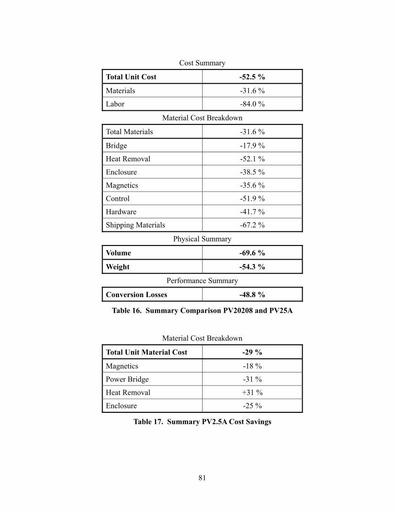
81
Cost Summary
Total Unit Cost -52.5 %
Materials -31.6 %
Labor -84.0 %
Material Cost Breakdown
Total Materials -31.6 %
Bridge -17.9 %
Heat Removal -52.1 %
Enclosure -38.5 %
Magnetics -35.6 %
Control -51.9 %
Hardware -41.7 %
Shipping Materials -67.2 %
Physical Summary
Volume -69.6 %
Weight -54.3 %
Performance Summary
Conversion Losses -48.8 %
Table 16. Summary Comparison PV20208 and PV25A
Material Cost Breakdown
Total Unit Material Cost -29 %
Magnetics -18 %
Power Bridge -31 %
Heat Removal +31 %
Enclosure -25 %
Table 17. Summary PV2.5A Cost Savings
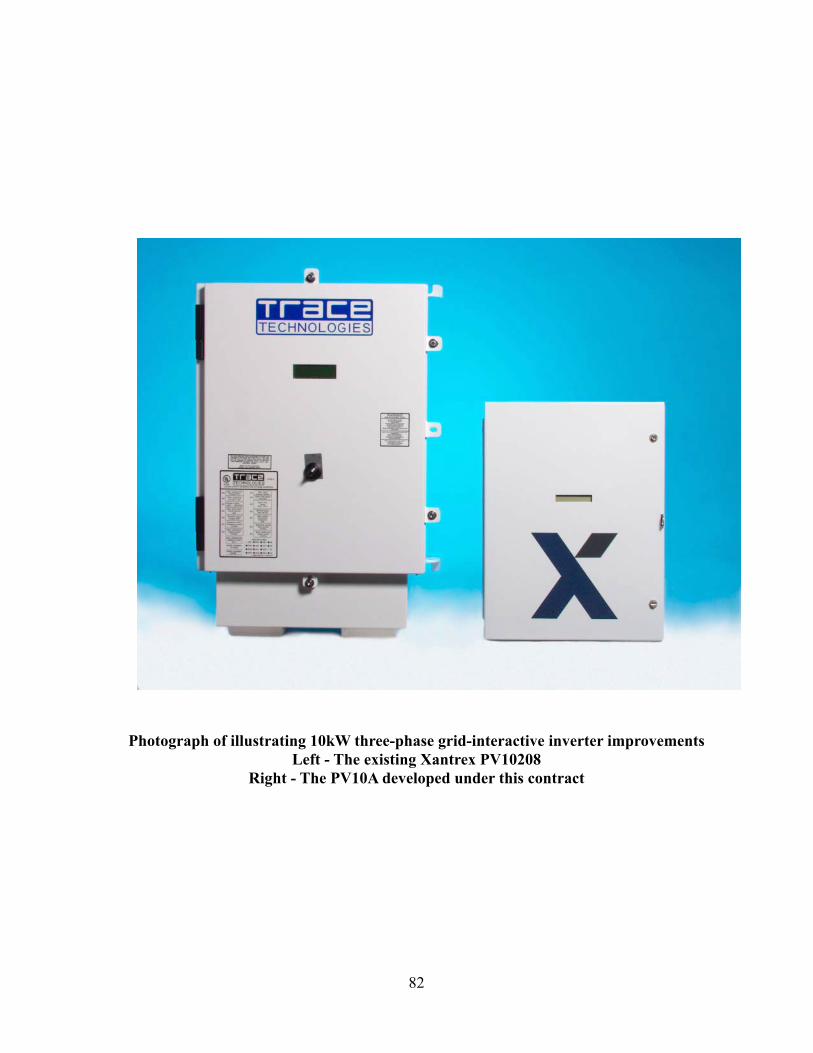
82
Photograph of illustrating 10kW three-phase grid-interactive inverter improvements Left - The existing Xantrex PV10208
Right - The PV10A developed under this contract

83
Photograph of illustrating higher power phase grid-interactive inverter improvements Left - The existing Xantrex PV20208 (20kW)
Right - The PV25A (25kW) developed under this contract
Inverters are shown with front doors removed

84
Photograph of 2500W single-phase grid-interactive inverter
Inverter shown with front cover removed

REPORT DOCUMENTATION PAGE
Form Approved OMB NO. 0704-0188
Public reporting burden for this collection of information is estimated to average 1 hour per response, including the time for reviewing instructions, searching existing data sources, gathering and maintaining the data needed, and completing and reviewing the collection of information. Send comments regarding this burden estimate or any other aspect of this collection of information, including suggestions for reducing this burden, to Washington Headquarters Services, Directorate for Information Operations and Reports, 1215 Jefferson Davis Highway, Suite 1204, Arlington, VA 22202-4302, and to the Office of Management and Budget, Paperwork Reduction Project (0704-0188), Washington, DC 20503. 1. AGENCY USE ONLY (Leave blank)
2. REPORT DATE
April 2004
3. REPORT TYPE AND DATES COVERED
Final Subcontract Report November 2003
4. TITLE AND SUBTITLE PV Inverter Products Manufacturing and Design Improvements for Cost Reduction and
Performance Enhancements: Final Subcontract Report, November 2003 6. AUTHOR: R. West
5. FUNDING NUMBERS
PVP46101 NDO-1-30628-02
7. PERFORMING ORGANIZATION NAME(S) AND ADDRESS(ES)
Xantrex Technology Inc. San Luis Obispo, California
8. PERFORMING ORGANIZATION
REPORT NUMBER
9. SPONSORING/MONITORING AGENCY NAME(S) AND ADDRESS(ES)
National Renewable Energy Laboratory 1617 Cole Blvd. Golden, CO 80401-3393
10. SPONSORING/MONITORING
AGENCY REPORT NUMBER NREL/SR-520-35885
11. SUPPLEMENTARY NOTES
NREL Technical Monitor: D. Mooney 12a. DISTRIBUTION/AVAILABILITY STATEMENT
National Technical Information Service U.S. Department of Commerce 5285 Port Royal Road
Springfield, VA 22161
12b. DISTRIBUTION CODE
13. ABSTRACT (Maximum 200 words): The specific objectives of this subcontracted development work by Xantrex Technology Inc. were to: 1) Capture the newest digital signal processor (DSP) technology to create high-impact, “next generation” power conversion equipment for the PV industry; 2) Create a common resource base for three PV product lines. This standardized approach to both hardware and software control platforms will provide significant market advantage over foreign competition; 3) Achieve cost reductions through increased volume of common components, reduced assembly labor, and the higher efficiency of producing more products with fewer design, manufacturing, and production test variations; 4) Increase PV inverter product reliability. Reduce inverter size, weight and conversion losses. The contract goals were to achieve an overall cost reduction of 10% to 20% for the three inverters and with no compromise in performance. The cost of the 10-kW inverter was reduced by 56%, and the cost of the 25-kW inverter was reduced by 53%. The 2.5-kW inverter has no basis for comparison, but should benefit equally from this design approach. Not only were the contract cost reduction goals exceeded by a wide margin, but the performance and reliability of the products were also enhanced. The conversion efficiency improvement, as reflected in the 50% conversion loss reduction, adds significant value in renewable energy applications. The size and weight reductions also add value by providing less cumbersome product solutions for system designers.
15. NUMBER OF PAGES
14. SUBJECT TERMS: PV; thin film; solar cell; digital signal processor (DSP); manufacturing; inverter; module; next generation; conversion loss
16. PRICE CODE
17. SECURITY CLASSIFICATION
OF REPORT Unclassified
18. SECURITY CLASSIFICATION
OF THIS PAGE Unclassified
19. SECURITY CLASSIFICATION
OF ABSTRACT Unclassified
20. LIMITATION OF ABSTRACT
UL
NSN 7540-01-280-5500 Standard Form 298 (Rev. 2-89) Prescribed by ANSI Std. Z39-18 298-102