pulsed plasma etching for semiconductor manufacturing · pulsed plasma etching for semiconductor...
TRANSCRIPT

Journal of Physics D: Applied Physics
J. Phys. D: Appl. Phys. 47 (2014) 303001 (27pp) doi:10.1088/0022-3727/47/30/303001
Topical Review
Pulsed plasma etching for semiconductormanufacturing
Demetre J Economou
Plasma Processing Laboratory, Department of Chemical and Biomolecular Engineering, University ofHouston, Houston, TX 77204-4004, USA
E-mail: [email protected]
Received 21 January 2014, revised 16 April 2014Accepted for publication 22 May 2014Published 1 July 2014
AbstractPower-modulated (pulsed) plasmas have demonstrated several advantages compared tocontinuous wave (CW) plasmas. Specifically, pulsed plasmas can result in a higher etchingrate, better uniformity, and less structural, electrical or radiation (e.g. vacuum ultraviolet)damage. Pulsed plasmas can also ameliorate unwanted artefacts in etched micro-features suchas notching, bowing, micro-trenching and aspect ratio dependent etching. As such, pulsedplasmas may be indispensable in etching of the next generation of micro-devices with acharacteristic feature size in the sub-10 nm regime. This work provides an overview ofprinciples and applications of pulsed plasmas in both electropositive (e.g. argon) andelectronegative (e.g. chlorine) gases. The effect of pulsing the plasma source power (sourcepulsing), the electrode bias power (bias pulsing), or both source and bias power (synchronouspulsing), on the time evolution of species densities, electron energy distribution function andion energy and angular distributions on the substrate is discussed. The resulting pulsed plasmaprocess output (etching rate, uniformity, damage, etc) is compared, whenever possible, to thatof CW plasma, under otherwise the same or similar conditions.
Keywords: pulsed plasma , microelectronics, plasma processing
(Some figures may appear in colour only in the online journal)
1. Introduction
Low temperature non-equilibrium glow discharge plasmas area workhorse in the fabrication of microelectronic devices.They are used mainly for etching and deposition of thinfilms, but also for other unit processes, such as shallowion implantation [1, 2]. Typical range of conditions underwhich these plasmas operate are: pressure ∼0.1 mTorr to10 Torr, gas temperature ∼300–600 K and degree of ionization(mole fraction of charged species) ∼10−1–10−6. Lowtemperature plasmas also find extensive use in lighting, surfacemodification (e.g. to effect corrosion resistance or hardening),even environmental remediation. Furthermore, atmosphericpressure non-equilibrium glow discharges are currently beingintensively investigated in connection with the burgeoningfield of plasma medicine [3]. Figure 1 is a panorama ofplasma etching, taking polysilicon etching with chlorine as
an example. Radio frequency (RF) or microwave power(source power) generates and sustains a plasma in a partiallyevacuated chamber. In the example of figure 1 the plasmais powered by an RF inductive coil on top of a dielectricwindow. Feed gas (e.g. chlorine) enters the reactor ata specified flow rate. Spent gas and reaction by-products(e.g. SiCl4) are evacuated by a pumping system. Energeticplasma electrons dissociate and ionize the feedstock gas toproduce Cl radicals and Cl+
2 ions (figure 1(a)). Positive ionsdrift towards the reactor walls and enter the sheath, wherethey accelerate in the direction perpendicular to the wafer.The sheath (figure 1(b)), a boundary layer naturally formingover any material surface in contact with plasma, is a regionof net positive charge resulting in a relatively high electricfield. Neutral radical species have no directionality. They aretransported by convective gas flow and diffusion, and adsorbon the silicon wafer. Ion bombardment of the silicon wafer
0022-3727/14/303001+27$33.00 1 © 2014 IOP Publishing Ltd Printed in the UK

J. Phys. D: Appl. Phys. 47 (2014) 303001 Topical Review
Sheath
Silicon Wafer
ClCl2+
Cl ClSi
Cl Cl
Gas In
dissociation Cl2 + e → 2Cl + eionization Cl2 + e → Cl2
+ + 2e Plasma
Substrate (e.g., Si Wafer)
Poly-Si
Silicon Wafer
Mask
(a)
(b)
(c) (d)
ClCl2+ SiCl4
Poly-SiSiO2
Sheath
Inductive Coil
Dielectric Window
Gas Out
Source Power
Bias PowerSheath Edge
dissociation Cl2 + e →→→→ 2Cl + eionization Cl2 + e →→→→ Cl2
+ + 2e
Figure 1. Panorama of plasma etching using silicon etching with chlorine as an example. (a) The source power generates plasma, in thiscase an ICP, which controls the plasma density. The bias power on the substrate electrode controls the energy of ions bombarding the wafer.Cl radicals and Cl+
2 ions are generated in the plasma by electron impact on Cl2 molecules. (b) Close-up view of the sheath over the wafer.Ions accelerate in the sheath and bombard the wafer along the vertical direction (anisotropically). At the same time isotropic neutrals strikethe wafer. The combination of neutral and energetic ion bombardment results in the formation of etch products. (c) Close-up view of anetching micro-feature. Ion bombardment induces anisotropic etching, replicating the mask pattern into the poly-Si film. (d) Close-up viewof the silicon lattice. Ion bombardment creates a modified surface layer where Cl is mixed within the Si lattice to a depth of ∼10 Å,depending on the ion energy. Activation of this layer by ion bombardment yields etching products that desorb into the gas phase. In thepulsed plasma operation, the source or bias power (or both) are modulated in time.
promotes the formation of reaction products that are eithersputtered (SiClx , x = 1, 2, 3) or desorb spontaneously (SiCl4)in the gas phase. When ion bombardment is necessary foretching to occur (e.g. p-type silicon), anisotropic etchingcan be obtained, since etching occurs only at the bottom ofthe micro-feature (figure 1(c)) where ions strike the surface,provided ions maintain their directionality (for example nocollisions in the sheath). If radicals can etch the waferspontaneously (without the presence of ion bombardment) as,for example, in the case of heavily doped n-type Si, thena sidewall passivation mechanism is necessary to achieveanisotropy. At the atomic level, ions bombarding the waferwith energy of 10s–100s of eV create a cascade of breaking andforming bonds that yields chlorinated silicon reaction products(figure 1(d)). Activation occurs in a modified layer at the topof the solid, the depth of which depends mainly on ion energy.Besides the RF source power, a separate RF power supply(bias power) may be connected to the substrate electrode. Thesource power is normally at relatively high frequencies (10–100 MHz) and its function is to generate plasma to controlthe plasma density. The bias power is normally at lowerfrequencies (100s kHz to 10 MHz) and is used to control theion bombardment energy. This reactor configuration providessome degree of independent control of ion flux and ion energyon the substrate, in contrast to classical capacitively coupledplasma (CCP) reactors in which ion flux and ion bombardmentenergy are intimately coupled.
The goals of any plasma etching process are highthroughput, high uniformity, high selectivity, anisotropy and
no damage. Throughput (wafers per unit time) is a measureof productivity. Uniformity across the wafer and from wafer-to-wafer is required so that the devices produced are withinspecifications. Selectivity is required with respect to boththe masking layer and the underlying layer (silicon dioxidein figure 1(c)). The mask must not etch or critical dimension(CD) control is difficult to achieve. Selectivity with respect tothe underlayer is important when the plasma or the thickness ofthe film to be etched is not uniform. Such situations necessitateoveretching, exposing the underlayer to potentially harmfulplasma in places where the film has been etched to end-point,while other areas of the wafer are yet to clear. Anisotropyrefers to the shape of the micro-feature wall profile. Almostvertical sidewalls, perhaps with some rounding of the bottomof the feature, is often required. Damage can occur by severalmechanisms, including (a) amorphization of the top layers ofthe substrate by ion bombardment, (b) radiation damage dueto UV, VUV and soft x-rays originating in the plasma [4].In particular, VUV radiation can lead to undesired etchingand distorted wall profiles of nanoscale features [5], and(c) charging damage. The latter can in turn be distinguished incharging and breakdown of insulating films (e.g. gate oxides)due to non-uniform plasma [6], or charging damage due to theelectron shading effect. Since electrons have high temperature(∼1–10 eV), are repelled by the sheath, and suffer momentumrandomizing collisions, the flux of electrons on the waferis essentially isotropic. On the contrary, positive ions havelow temperature (∼0.1 eV) and are accelerated in the sheath,
2

J. Phys. D: Appl. Phys. 47 (2014) 303001 Topical Review
perpendicular to the wafer, resulting in a flux on the surface thatis highly anisotropic. This difference in flux directionalitiescan cause a localized build-up of negative charge at the top,mouth entrance, and sidewalls of insulating features, and apositive charge at the bottom of the features. The local electricfield established by this differential charging [7, 8] is believedto deflect further oncoming positive ions causing etch profiledistortions (notching and/or bowing [9, 10], micro-trenching[11], etc) and aspect ratio dependent etching (ARDE) [12]. InARDE, the etch rate of micro-features depends on the featureaspect ratio (depth/width) and usually decreases as the aspectratio increases.
As device dimensions continue to shrink into thesub-10 nm regime, achieving the goals of plasma etchingmentioned above becomes extremely challenging. Thereare many externally controlled variables (process inputs)which can influence the process output (figure 2). Givena reactor type (e.g. CCP, inductively coupled plasma (ICP),electron cyclotron resonance (ECR), plasma, etc), itsgeometrical configuration and materials of construction,one can manipulate operating parameters (pressure, power,frequency, gas composition, gas flow rate, etc) to influence theprocess output (etching rate, uniformity, anisotropy, damage,etc). Rational selection of reactor design and plasma chemistrycan be facilitated by understanding the fundamentals of thechemical and physical processes taking place in the plasmaand on the wafer surface. Such understanding can be obtainedby bridging the gap between the process inputs and outputsthrough key plasma properties (figure 2).
2. Pulsed plasmas
Pulsed plasmas have emerged as promising candidates toaddress the formidable challenges of fabricating futuregenerations of micro-devices. This is especially the casefor electronegative gas plasmas (e.g. Cl2, HBr, SF6, O2,fluorocarbons, etc) which are used extensively in industrialpractice. Experiments using pulsed electronegative dischargeshave shown suppression of anomalous etch profiles (e.g.notching) during poly-Si etching, and reduced chargingdamage of the gate insulator [13–16]. This improvement in theetching characteristics of pulsed electronegative discharges,compared to conventional continuous wave (CW) operation,has been attributed (at least in part) to negative ions. Morerecent studies have shown reduced damage to the Si substrateduring gate etching [17]. Furthermore, pulsed plasmasoffer other important advantages (compared to CW plasmas)including (a) improved etch selectivity by, for example,modifying the concentration of chemical species present in theplasma [18–20], (b) improved etch or deposition rate [21, 22],(c) reduced dust generation [23–26] and (d) improved etchor deposition uniformity [22, 27, 28]. A review of pulsedplasmas, focusing on high density reactors, has been presentedby Banna et al [29].
In pulsed plasmas the power fed to the reactor is modulatedin time. Square wave modulation is most frequently appliedas shown in figure 3. The duration of the power ON fractionof the cycle (active glow) is τON, while that of the power
Type of source/design/geometry.Source and bias power.Pressure, frequency.Gas flow rate and composition.Wall material and temperature.
PULSED PLASMA
Source, bias, orsynchronous pulsing.Pulsing frequencies.Duty ratios.Phase difference.
Etch rate.Uniformity.Selectivity.Anisotropy.Damage.
Species densities.Species fluxes. EEAD, IEAD.Etching yields.
OUTPUTS
INPUTS
KEYS
Figure 2. The key internal plasma properties bridge the gapbetween the plasma etch process inputs (control variables) andoutputs. Pulsing the plasma adds more ‘knobs’ (type of pulsing,pulsing frequencies, duty ratios) to a plethora of inputs(EEAD = electron energy and angular distribution, IEAD = ionenergy and angular distribution).
ONOFF
ON
OFF
PP= ON + OFF
Figure 3. In pulsed plasmas, power is square-wave modulated.Within each pulse, the power is ON for time τON and OFF for timeτOFF. The pulse period is τP = τON + τOFF and the duty ratio isD = τON/τP. The pulsing frequency is usually 10 kHz or lower.During power ON, the plasma excitation frequency is usually fromRF to microwave.
OFF fraction of the cycle (afterglow) is τOFF. The pulseperiod is τP = τON + τOFF, and the duty ratio (or duty cycle)is defined as D = τON/τP, i.e. the fraction of the cyclewith power ON. Usually 100% power modulation depth isapplied, i.e. the power in the afterglow is zero. Partial powermodulation has also been used, for the purpose of measuringthe kinetics of plasma-chemical or wall reactions [30, 31], andwill not be considered here. The following cases of powermodulation may be encountered (figure 4): (a) modulation ofthe power that sustains the plasma (source pulsing) with nopower on the substrate electrode, (b) modulation of the powerthat sustains the plasma (source pulsing) with CW power onthe substrate electrode, (c) modulation of the power to thesubstrate electrode (bias pulsing) with CW source power, and(d) modulation of both the source and bias powers with orwithout a phase shift between the two (synchronous pulsing).
3

J. Phys. D: Appl. Phys. 47 (2014) 303001 Topical Review
ONOFF
OFF
(a)
(d)
(b)
(c)
Source
Bias
Bias
SourceON
ONOFF
ON
Figure 4. Common pulsed plasma schemes. (a) Source pulsingwith no substrate bias. (b) Source pulsing with CW substrate bias.(c) Bias pulsing with CW source power. (d) Synchronous sourceand bias pulsing, where bias power may be phase shifted withrespect to the source power. In synchronous pulsing, the PRF is thesame for both source and bias, but the duty ratios can differ. Thepulsing frequency is usually 10 kHz or lower. The plasma source isusually powered with frequencies from RF to microwave. Electrodebias is usually RF or dc.
Synchronous in this context means that both the source andbias powers are modulated with the same frequency, but theduty ratios can be different. The source power is usually atfrequencies from RF to microwave. Bias power is usually RFor dc. One more configuration (not shown in figure 4) thatwill be discussed involves source pulsing with synchronousbias on an auxiliary electrode (so-called boundary electrode(BE)) that controls the plasma potential [32–34]. In this case,the substrate electrode may be grounded or biased with anindependent power supply.
It should be noted that power turn ON or OFF is oftenassumed instantaneous. In practice, there is a ‘ramp-up’ and a‘ramp-down’ time which can make a difference in heating ofthe electron energy distribution function (EEDF). Based on thefindings of Lafleur and Booth [35], for example, the faster therate of change of the applied voltage, the more the heating ofthe EEDF. When the plasma is pulsed, in addition to the typeof pulsing (source, bias or synchronous) there are at least twonew input variables, namely, pulse period (or its equivalent,pulse repetition frequency (PRF)) and duty ratio. The additionof more variables to the plethora of the already existing ones(figure 2) makes plasma reactor or process optimization adaunting task. On the other hand, additional ‘knobs’ increaseprocess flexibility.
3. Time evolution of pulsed electronegative plasmas(figures 5–7)
Industrial plasma processes employ electronegative gases.For example, etching of silicon, silicon dioxide orpolymers is carried out with halogen-containing gases,fluorocarbons or oxygen-containing plasmas, respectively[1, 2]. Electronegative gas plasmas tend to stratify: negativeions pile-up in the central region of the plasma formingan electronegative core, surrounded by a region devoid ofnegative ions (electropositive periphery), followed by the
Figure 5. Time evolution of species densities (left axis) and electrontemperature (right axis) predicted by a pulsed plasma model inchlorine. Plasma source was pulsed with a period of 100 µs andduty ratio = 50%. There was no substrate bias. Peakpower = 320 W, pressure = 20 mTorr. Each pulse is separated infour time windows: early active glow (I), late active glow (II), earlyafterglow (III) and late afterglow (IV). Only the major ion Cl+
2density is shown (Cl+ is not included). From [76] with permission.Copyright 2002 American Vacuum Society.
wall sheath which contains only positive ions and electrons.For high enough negative-ion densities, the electropositiveperiphery is squeezed, and eventually the negative ions reachthe sheath edge. Negative ions cannot enter the sheath since thenegative-ion energy is far less than the sheath potential. Thestratification of electronegative discharges has been studiedextensively, particularly for collisional plasmas [1, 36–39].Abrupt transitions and oscillatory behaviour of the potential inthe plasma have also been reported [40–42]. In CW plasmas,negative ions are trapped in the plasma by the electrostatic field.Therefore negative ions cannot reach the substrate. Pulsingthe plasma (source pulsing) provides a means to having anegative-ion flux bombarding the substrate. This is becausein the afterglow of the pulsed plasma, the electrostatic fielddisintegrates, allowing negative ions to diffuse from the plasmacore to the wall. Combining source pulsing with low frequencyRF substrate bias can result in alternating acceleration ofpositive and negative ions out of the plasma and onto the wafer.Such action can reduce charging damage, and improve etchresults [13, 14, 43, 44]. It was suggested that, because positiveand negative ions have comparable masses and similar velocityanisotropy under acceleration by low frequency sinusoidalbias, differential charging [7, 8] of the walls of micro-featureswas reduced ameliorating charging damage.
Midha and Economou [45] reported a model of a pulsedICP (source pulsing, no substrate bias) under the followingconditions: power density 1 W cm−3, pressure 20 mTorr,interelectrode spacing 3.8 cm, pulse period 100 µs and dutyratio 50%. Figure 5 shows the time evolution of speciesdensities (left y-axis) and electron temperature (right y-axis)at the central plane of the reactor, after reaching a periodic
4

J. Phys. D: Appl. Phys. 47 (2014) 303001 Topical Review
steady-state. The source power was turned ON at t = 0 µs andOFF at t = 50 µs. The trends shown in figure 5 are in goodagreement with experimental results reported in the literature[46–48]. The power ON fraction of the cycle (active glow,t = 0 − 50 µs) is separated into early active glow (region Iin figure 5) and late active glow (region II). The power OFFfraction of the cycle (afterglow, t = 50 − 100 µs) is separatedinto early afterglow (region III) and late afterglow (region IV).The electron temperature goes through a sharp maximum at thevery early active glow and settles to a quasi-steady value within∼10 µs into the pulse. In the afterglow, Te plummets to 0.5 eVwithin ∼5 µs after power is turned OFF. The electron density isseverely modulated during a cycle. It increases monotonicallyafter the power is turned ON, only to reach a quasi-steady valueby the end of the early active glow. The electron density decaysin the afterglow reaching very low values by the end of the earlyafterglow. In contrast, the positive- and negative-ion densitiesare much less modulated. The positive-ion density increases inthe active glow and decreases in the afterglow. The negative-ion density goes through a shallow minimum in the early activeglow and then keeps on increasing for the remainder of theactive glow. Upon power turn OFF, the negative-ion densitygoes through a small peak in the early afterglow and thendecreases for the remainder of the afterglow. The plasmais weakly electronegative (ratio of electron to negative-iondensity ∼1) in the active glow and then becomes progressivelymore electronegative in the afterglow. The electron densitydecays rapidly in the afterglow, eventually becoming negligiblecompared to the negative-ion density. At that point a positive-ion negative-ion (ion–ion) plasma forms [49]. In an ion–ionplasma, the ambipolar field can be approximated by [45, 50],
E ≈[(Dp − Dn)∇nn
(µn + µp)nn
]. (1)
This field is much reduced compared to that in anelectropositive discharge E = −Te(∇ne/ne). The negativeions essentially neutralize the space charge field. Here D is the(free) species diffusivity, and n and µ are species density andmobility, respectively. Subscripts p, n and e refer to positiveions, negative ions and electrons, respectively. If the positive-and negative-ion diffusivities are comparable, Dp ≈ Dn, theelectric field vanishes, and diffusion is free for all chargedspecies. Furthermore, the ambipolar electron diffusivity Dae
in an electronegative plasma is given by [45, 50]
Dae ≈[
1 + 2(nn/ne)
[(µe/µn) + 1] + 2(nn/ne)
]De. (2)
In deriving equation (2) it was assumed that µn = µp andalso that proportionality holds between the species densityratios and the corresponding gradients of density. Equation (2)indicates that Dae becomes a larger fraction of the free electrondiffusivity (De) as the electronegativity (nn/ne) increases. Atthe extreme of an ion–ion plasma, nn � ne, electrons diffusewith the maximum (free) diffusivity. A detailed account ofthe physics of the discharge evolution during a full pulse isgiven next.
Figure 6. Predictions of a model of a high density pulsed chlorineplasma sustained between two parallel plates. (top) Space and timeevolution of the negative-ion Cl− density during the first 20 µs ofthe active glow. (bottom) Space and time evolution of negative-ionand electron densities during the first 20 µs of the afterglow.Conditions: power = 1.0 W cm−3, pressure = 20 mTorr, pulseperiod = 100 µs, and duty ratio = 50% (50 µs active glow, 50 µsafterglow; source pulsing only). Only the right half of the 3.8 cminterelectrode space is shown (the centre of the plasma is at 1.9 cmand the right wall is at 3.8 cm). From [45] with permission.
3.1. Early active glow (0–15 µs)
After the power is turned ON, the electron temperature risessharply, overshooting its quasi-steady value, while the electrondensity increases more gradually. Initially (t = 0), there arevery few electrons remaining by the end of the afterglow of theprevious pulse. In fact, the state of the plasma at t = 0 (whichis identical to that at t = T , provided that periodic steady-statehas been reached) is an ion–ion (Cl+
2 , Cl−) plasma in which theelectrons diffuse almost freely (see equation (2)) due to the veryweak electrostatic fields, determined by the ion temperature.As power is initially deposited to a small number of electrons,the electron temperature goes through a spike. As the electrontemperature increases, the strength of the electrostatic fieldalso increases, and negative ions, that had reached the wall latein the afterglow of the previous pulse, are squeezed towardsthe centre of the plasma (figure 6, top). As Te increases,ionization comes into play which causes the electron density
5
J. Phys. D: Appl. Phys. 47 (2014) 303001 Topical Review
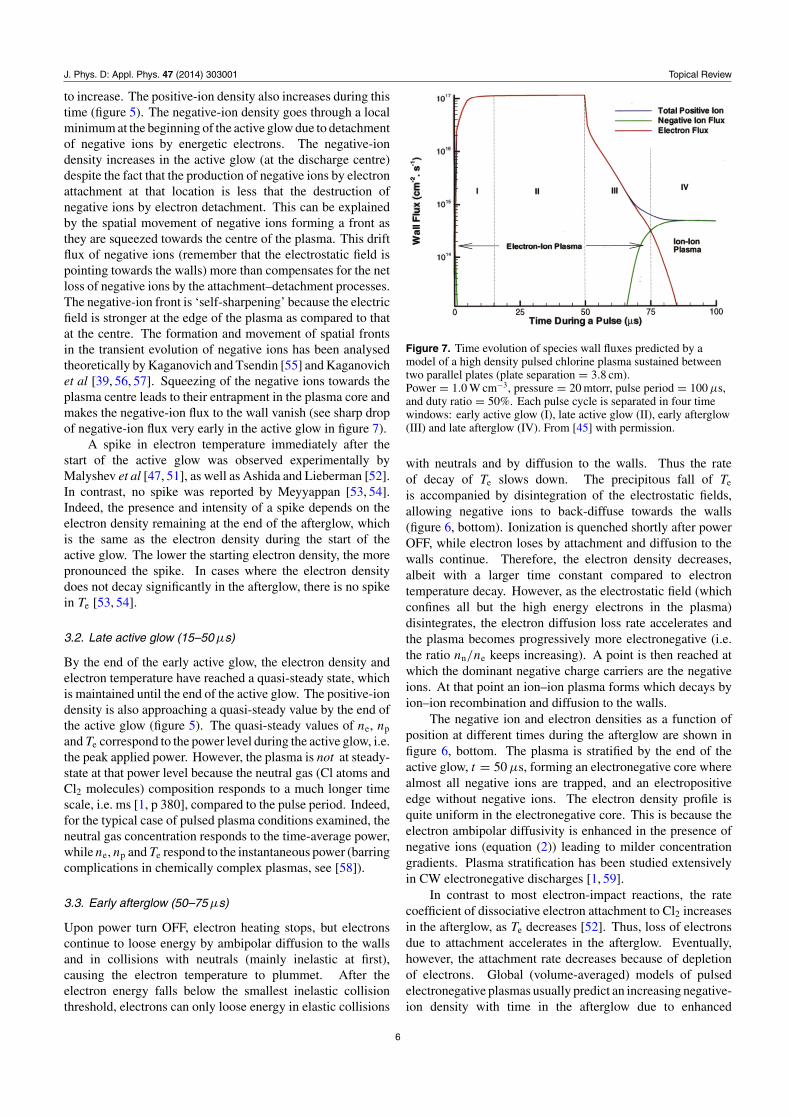
to increase. The positive-ion density also increases during thistime (figure 5). The negative-ion density goes through a localminimum at the beginning of the active glow due to detachmentof negative ions by energetic electrons. The negative-iondensity increases in the active glow (at the discharge centre)despite the fact that the production of negative ions by electronattachment at that location is less that the destruction ofnegative ions by electron detachment. This can be explainedby the spatial movement of negative ions forming a front asthey are squeezed towards the centre of the plasma. This driftflux of negative ions (remember that the electrostatic field ispointing towards the walls) more than compensates for the netloss of negative ions by the attachment–detachment processes.The negative-ion front is ‘self-sharpening’ because the electricfield is stronger at the edge of the plasma as compared to thatat the centre. The formation and movement of spatial frontsin the transient evolution of negative ions has been analysedtheoretically by Kaganovich and Tsendin [55] and Kaganovichet al [39, 56, 57]. Squeezing of the negative ions towards theplasma centre leads to their entrapment in the plasma core andmakes the negative-ion flux to the wall vanish (see sharp dropof negative-ion flux very early in the active glow in figure 7).
A spike in electron temperature immediately after thestart of the active glow was observed experimentally byMalyshev et al [47, 51], as well as Ashida and Lieberman [52].In contrast, no spike was reported by Meyyappan [53, 54].Indeed, the presence and intensity of a spike depends on theelectron density remaining at the end of the afterglow, whichis the same as the electron density during the start of theactive glow. The lower the starting electron density, the morepronounced the spike. In cases where the electron densitydoes not decay significantly in the afterglow, there is no spikein Te [53, 54].
3.2. Late active glow (15–50 µs)
By the end of the early active glow, the electron density andelectron temperature have reached a quasi-steady state, whichis maintained until the end of the active glow. The positive-iondensity is also approaching a quasi-steady value by the end ofthe active glow (figure 5). The quasi-steady values of ne, np
and Te correspond to the power level during the active glow, i.e.the peak applied power. However, the plasma is not at steady-state at that power level because the neutral gas (Cl atoms andCl2 molecules) composition responds to a much longer timescale, i.e. ms [1, p 380], compared to the pulse period. Indeed,for the typical case of pulsed plasma conditions examined, theneutral gas concentration responds to the time-average power,while ne, np and Te respond to the instantaneous power (barringcomplications in chemically complex plasmas, see [58]).
3.3. Early afterglow (50–75 µs)
Upon power turn OFF, electron heating stops, but electronscontinue to loose energy by ambipolar diffusion to the wallsand in collisions with neutrals (mainly inelastic at first),causing the electron temperature to plummet. After theelectron energy falls below the smallest inelastic collisionthreshold, electrons can only loose energy in elastic collisions
Figure 7. Time evolution of species wall fluxes predicted by amodel of a high density pulsed chlorine plasma sustained betweentwo parallel plates (plate separation = 3.8 cm).Power = 1.0 W cm−3, pressure = 20 mtorr, pulse period = 100 µs,and duty ratio = 50%. Each pulse cycle is separated in four timewindows: early active glow (I), late active glow (II), early afterglow(III) and late afterglow (IV). From [45] with permission.
with neutrals and by diffusion to the walls. Thus the rateof decay of Te slows down. The precipitous fall of Te
is accompanied by disintegration of the electrostatic fields,allowing negative ions to back-diffuse towards the walls(figure 6, bottom). Ionization is quenched shortly after powerOFF, while electron loses by attachment and diffusion to thewalls continue. Therefore, the electron density decreases,albeit with a larger time constant compared to electrontemperature decay. However, as the electrostatic field (whichconfines all but the high energy electrons in the plasma)disintegrates, the electron diffusion loss rate accelerates andthe plasma becomes progressively more electronegative (i.e.the ratio nn/ne keeps increasing). A point is then reached atwhich the dominant negative charge carriers are the negativeions. At that point an ion–ion plasma forms which decays byion–ion recombination and diffusion to the walls.
The negative ion and electron densities as a function ofposition at different times during the afterglow are shown infigure 6, bottom. The plasma is stratified by the end of theactive glow, t = 50 µs, forming an electronegative core wherealmost all negative ions are trapped, and an electropositiveedge without negative ions. The electron density profile isquite uniform in the electronegative core. This is because theelectron ambipolar diffusivity is enhanced in the presence ofnegative ions (equation (2)) leading to milder concentrationgradients. Plasma stratification has been studied extensivelyin CW electronegative discharges [1, 59].
In contrast to most electron-impact reactions, the ratecoefficient of dissociative electron attachment to Cl2 increasesin the afterglow, as Te decreases [52]. Thus, loss of electronsdue to attachment accelerates in the afterglow. Eventually,however, the attachment rate decreases because of depletionof electrons. Global (volume-averaged) models of pulsedelectronegative plasmas usually predict an increasing negative-ion density with time in the afterglow due to enhanced
6

J. Phys. D: Appl. Phys. 47 (2014) 303001 Topical Review
attachment [60]. Spatially resolved simulations (figure 5)predict that the negative-ion density at the plasma centredecreases in the afterglow (except for a small increase inthe early afterglow). This is because of a significant flux ofnegative ions out of the plasma centre (figure 6, bottom), asnegative ions diffuse back towards the walls. In fact, dependingon the spatial position at which the negative-ion density nn ismeasured, nn can increase or decrease as a function of time.
Figure 7 shows the charged species fluxes on the groundedelectrode during a pulse period. The negative-ion flux becomesnegligible (compared to the electron flux) very early in theactive glow due to re-emergence of the electrostatic field, as theplasma is turned ON. The negative-ion flux remains suppressed(negative ions are trapped) until the late afterglow when anion–ion plasma forms and negative ions are free to diffuse tothe wall. While the negative-ion flux is zero, the electron andion fluxes on the wall are equal to preserve electroneutrality.When an ion–ion plasma is present, the electron flux isnegligible, making the positive and negative-ion fluxes equal.The positive-ion and electron fluxes decay rapidly a few µs intothe afterglow due to the rapid decrease of electron diffusivityas Te plummets. Furthermore, in the late afterglow, the rateof loss of electrons accelerates as the electron diffusivity Dae
approaches the free diffusion coefficient, De (equation (2)).
3.4. Late afterglow (75–100 µs)
Electrons are lost in the early afterglow by ambipolar diffusionto the walls and dissociative attachment, while negative ionsare still trapped in the reactor. Once the electron density ne
becomes less than 1/2(mi/me)nn, negative ions become thedominant negative charge carrier in the plasma [45]. Theelectric field is now determined by negative ions instead ofelectrons and there is an abrupt transition from an electron-dominated plasma to an ion–ion plasma. The ion–ion plasmais characterized by weak electrostatic fields and a diffusive fluxof negative ions to the walls. In figure 7, the transition froman electron–ion plasma to an ion–ion plasma is characterizedby the electron flux becoming equal to the negative-ion fluxat the walls (t = 75 µs). The positive-ion flux, whichinitially overlaps with the electron flux in the early afterglowbecomes equal to the negative-ion flux in the late afterglow.Experimental results reported by Smith et al [61] in theafterglow of an oxygen plasma show similar behaviour: thenegative-ion flux was negligible in the early afterglow andabruptly increased by several orders of magnitude to becomeequal to the positive-ion flux in the late afterglow. The samebehaviour was reported by Gutsev et al [62] and Kudryavtsevand Tsendin [63].
After the transition to an ion–ion plasma, electrons are nolonger confined in the plasma and are lost at a faster rate whicheventually approaches the limit of free diffusion of electronsto the walls (equation (2)) in the absence of electrostaticfields. The positive-ion and negative-ion densities decaytogether much more slowly due to ion–ion recombination anddiffusion losses to the walls. The peak magnitude of thenegative-ion flux is about two orders of magnitude less thanthe electron flux in the active glow. In the collisional plasma
under investigation this corresponds roughly to the ratio of theambipolar diffusion coefficient to the ion diffusion coefficient,or, the ratio of electron temperature in the active glow (∼3 eV)to ion temperature (∼0.03 eV).
Ashida and Lieberman [52] also showed that extractionof negative ions becomes possible only when the sheathvoltage or electrostatic fields collapse in the afterglow due tothermalization and loss of electrons. Once the electrons arelost, the negative-ion flux to the walls increases and becomesequal to the total positive-ion flux. They also showed thatthe coefficient for recombination of Cl radicals on the reactorwalls played an important role in determining the extent ofdissociation of Cl2 molecules in the plasma. The neutralcomposition, in turn, affected the rate of decay of electronsand the evolution of negative ions in the afterglow.
It should be mentioned that instead of a temporal afterglowas a result of source pulsing, one can have an equivalent spatialafterglow in a flowing plasma, sustained by a CW power source.In a spatial afterglow, time is replaced by downstream distanced from the plasma, t = d/u, where u is an average flowvelocity. Far enough downstream of the plasma generationzone, the electron density can decay substantially to form anion–ion plasma. For the plasmas of interest, electron decayis mainly by electron attachment to electronegative gases anddiffusion to the walls of the reactor.
4. Pulsed plasma panoply
This section starts with the use of pulsed plasmas to studychemical reaction kinetics in situ (in the plasma itself).Then, the effect of pulsing on several plasma characteristics(charged and neutral species densities and fluxes, ion energydistributions (IEDs) on the plasma electrodes, and the EEDF)is discussed. The use of pulsed plasmas to extract negativeions is also discussed.
4.1. Measurement of reaction kinetics
Pulsed plasmas (usually source pulsing without bias) are oftenused to measure the kinetics of homogeneous or heterogeneousreactions under ‘realistic’ conditions, i.e. in the plasma itself[64–66]. Belostotsky et al [64] investigated the dynamicsof negative-ion density in the positive column of a dc glowdischarge in pure oxygen. They used laser photodetachmentover a wide range of pressure (0.1–5 Torr) and current density(2–40 mA cm−2). Using square wave modulation of thedischarge current (i.e. power), the time evolution of theconcentration of critical species in the discharge was analysed,to extract the rate coefficients of O− detachment by atomicoxygen, O(3P), and singlet molecular oxygen, O2(a
1�g),under plasma conditions. Hansen et al [65] studied thekinetics of formation and decay of excited fluorine atoms(F∗), and CF and CF2 radicals in source modulated CF4
plasmas. F∗ was monitored by optical emission spectroscopyand CFx (x = 1, 2) radicals were detected using laser inducedfluorescence (LIF). Takahashi et al [66] used infrared diodelaser absorption spectroscopy (IRLAS) to measure CFx
(x = 1, 2, 3) radical densities in source power modulated (no
7

J. Phys. D: Appl. Phys. 47 (2014) 303001 Topical Review
bias) ECR CHF3 plasmas. The radical density varied withthe duty ratio of the 100 ms PRF discharge. The polymerdeposition rate (no bias) was the same on Si and SiO2 surfacesand followed the same trend with the CF and CF2 densities,decreasing with increasing duty ratio.
Booth et al [67] measured, using LIF, the spatial andtemporal variation of CF and CF2 radical concentrations inCF4 capacitively coupled RF (13.56 MHz) plasmas at 50and 200 mTorr, under fluorine rich conditions (no polymerdeposition). The temporal variation was obtained by switchingthe plasma ON or OFF. This can be thought of as a limiting caseof a pulsed plasma with very long active glow and afterglow,so that a steady state is obtained during both plasma ON andplasma OFF. They found that the Al powered electrode was anet source of these radicals whereas the Al grounded counter-electrode was a net sink. They concluded that CFx radicalswere predominantly produced by CF+
x ions neutralizing,dissociating and reflecting off of the powered electrode. Thedifferent behaviour of the grounded electrode was explainedbased on the different energy and mass distribution of ionsstriking that electrode. In a companion study, Cunge andBooth [68] measured the CF2 concentration profiles underfluorine starved conditions (polymerization). The F atomconcentration was suppressed by loading the reactor with aSi wafer or by using C2F6 instead of CF4 plasma. They foundthat all surfaces in contact with the plasma were sources of CF2
radicals. This led them to conclude that the CF2 radical is nota direct precursor of polymer growth on the walls, as has beensuggested in the literature [69]. Instead, CF2 radicals formoligomers in the gas phase and these are the actual polymerdeposition precursors.
Vempaire and Cunge [70] used a pulsed plasma to probethe kinetics of BCl radicals in the afterglow of a BCl3/Cl2ICP. In most of the afterglow, there is virtually no productionof radicals by electron-impact reactions since the electrontemperature quenches within several µs. Thus, the radicalloss, occurring at much longer time scales by homogeneouschemical reactions as well as surface processes, can be studied.The authors estimated the rate coefficient of the reaction ofBCl with Cl2 to be 5 × 10⁻¹¹ cm3 s−1, large enough to makethis gas-phase reaction the main loss of BCl, despite the lowpressure of 5 mTorr. The reaction probability of BCl on thereactor walls was estimated to be γ = 0.3 ± 0.1. Cungeet al [71] studied radical-wall interactions during etching ofsilicon in Cl2/O2 plasmas in industrial plasma reactors. Theyfound that SiCl can stick on a SiOCl-coated reactor wall witha probability nearly 100%. SiCl2 appeared to be much lessreactive towards that wall. SiCl residing on the wall is oxidizedin the presence of oxygen to form SiOCl. Using a pulsedplasma and following the evolution of radicals in the afterglowwith time-resolved absorption measurements, they estimatedthe Cl recombination coefficient to be ∼0.007 on the SiOClcovered surface, and ∼0.1 on the clean wall (AlF3). They alsofound that, despite the low operating pressure of 20 mTorr,gas-phase reactions such as SiCl + Cl2 → SiCl2 + Cl have asignificant influence on the radical densities.
Kono et al [72] presented an experimental study of thevariation of electron and negative-ion densities in pulsed
CF4 plasmas at low power and pressure in the range 100–300 mTorr. In accordance with other investigators [45, 62],they observed enhanced loss of electrons in the afterglowdue to the presence of negative ions. They also reportedthat loss of negative ions by detachment was comparable tothat by negative-ion/positive-ion recombination in the activeglow. The main species causing detachment was CF3, anddissociative electron attachment to CF4 was the main channelto produce F− negative ions.
4.2. Species densities
Source power modulation can influence not only the relativeconcentration of radicals but also the spatial distribution ofthese radicals (and of the precursor gas) in a plasma reactor.For example, as the feed gas flows through the plasma, theprecursor is depleted by electron-impact dissociation. As aresult, the etching or deposition rate may vary along the flowpath of the gas. Power modulation can be used to alleviatesuch variations, thereby improving process uniformity. Thereare at least two ways power modulation can affect the spatialdistribution of neutral species. (1) If the plasma power-OFF phase (afterglow) lasts for a time comparable to the gasresidence time in the reactor, the reactor can be essentiallyrefilled with fresh precursor gas during the afterglow. Thisminimizes spatial density variations of the precursor andimproves uniformity. (2) If the duration of the active glowis short compared to the time it takes for the concentrationgradients of the etch or deposition radicals (originating bye-impact dissociation of the precursor) to develop significantly,source pulsing again should improve uniformity [22, 27, 28].
The effect of source pulsing (pulse period 10s of ms) withno bias, on the radical concentration and etching rate of Si in arelatively high pressure (1 Torr) CF4 plasma was simulatedusing a transport and reaction model [22]. The reactorwas a parallel-plate single-wafer etcher with a showerheadelectrode. Under conditions for which chemical etching wasdominant, it was found that etch uniformity improved withpower modulation, especially for low flow rates. In addition,by changing the duty ratio, the radical concentration ratiosCF2/F and CF3/F were altered, which can impact selectivity.In an experimental investigation, Bodart et al [73] reported theeffect of source pulsing (no bias) on the density of radicals inCl2 and HBr ICPs at 20 mTorr. For pulsing frequencies greaterthan 500 Hz, the radical (Cl and Br) density increased with dutyratio, and did not depend on the pulsing frequency. On the otherhand, after the plasma was turned ON, the ion flux reached asteady state within 10s of µs. The authors concluded that, fornot too high pulse frequencies (less than 10 kHz), the ion fluxis roughly independent of duty ratio. Therefore, the ion-to-radical flux ratio could be controlled quasi-independently byvarying the pulse frequency and duty ratio.
The time evolution of the electron density during sourcepulsing of an argon or chlorine ICP (no bias) was studiedexperimentally by Hebner and Fleddermann [46]. For a PRFof 10 kHz, the electron density reached a plateau (for dutyratios D > 50%) that corresponds to the CW plasma at thesame power (figure 8(a)). The effect of power on electron
8

J. Phys. D: Appl. Phys. 47 (2014) 303001 Topical Review
Figure 8. Time-dependent electron density in an argon ICP as afunction of (a) duty ratio, (b) peak RF power and (c) PRF. In (a), thepeak RF power was 300 W and the PRF was 10 kHz. In (b), the dutyratio was 30% and the PRF was 10 kHz. In (c), the peak power was300 W and the duty ratio was 50%. In all cases, the pressure was20 mTorr. From [46] with permission. Copyright 1997 AIPPublishing LLC.
density is shown in figure 8(b). Duty ratio D = 30% is notenough to reach a plateau. However, the extrapolated plateauvalues scale linearly with power. Also, for a fixed duty ratioand peak power, the time-average power remains constant asthe pulse period varies. Since the ‘power ON’ fraction of thecycle is longer than the time scale of electron density evolution,the same quasi-steady value of electron density is attained asthe pulse period is varied (figure 8(c)). The situation is morecomplicated in chlorine discharges, however (figure 9). Forexample, in contrast to figure 8(a), the plateau electron densitydecreases with duty ratio (figure 9(a)). Increasing the PRFyields a decrease of the plateau value initially, and then anincrease (figure 9(c)). These complications were attributed tochanging plasma gas composition (ratio of Cl to Cl2 densities)as PRF and D were varied. Analytic expressions for thevariation of electron temperature and density in the activeglow and the afterglow under simplified conditions are givenin [1, pp 369–81].
The Cl− density profile evolution in a GEC reference cell,predicted by a plasma reactor simulation [74, 75], is shownin figures 10(a)–(f ) [76]. At the start of a pulse, negativeions are present in the periphery (figures 10(a) and (b)) dueto diffusion during the afterglow of the previous pulse. As
Figure 9. Time-dependent electron density in a chlorine ICP as afunction of (a) duty ratio, (b) peak RF power and (c) PRF. In (a), thepeak RF power was 320 W and the PRF was 10 kHz. In (b) the dutyratio was 50% and the PRF was 10 kHz. In (c), the peak power was290 W and the duty ratio was 50%. In all cases, the pressure was20 mTorr. From [46] with permission. Copyright 1997 AIPPublishing LLC.
the electron temperature and electron density start to increase,the ambipolar electric field also increases, causing negativeions to be squeezed into the plasma (figures 10(c) and (d)).The squeezing of negative ions is stronger near the quartzwindow since the electron temperature (therefore the field)is larger in that region. Because there is negligible flux ofnegative ions to the wall during the active glow, the quasi-steady state of negative-ion profile (see also figure 6) issustained by a balance between production processes suchas attachment and destruction processes such as detachmentand ion–ion recombination. Later in the afterglow, negativeions start diffusing back towards the walls, as the electric fielddiminishes. Their diffusion is almost free (almost no electricfield) after an ion–ion plasma forms.
Agarwal et al [77] simulated silicon etching in anAr/Cl2 (20/80) ICP at 10 mTorr and 100 sccm total flow.Three situations were studied, under the following base caseconditions: (I) pulsed source power (300 W peak) and CW biaspower (100 W), (II) CW source power (300 W) and pulsedbias power (100 W peak), and (III) synchronous (in phase)pulsing of both source power and bias power (300 W peaksource power, 100 W peak bias power). In all cases of pulsing
9

J. Phys. D: Appl. Phys. 47 (2014) 303001 Topical Review
135
R (cm)
Z(c
m)
0 5 100
1
2
3
4
5
6
7
8
9
10
11
12
13
14
5 2.27E+114 1.81E+113 1.36E+112 9.07E+101 4.54E+10
(a)
135
R (cm)
Z
0 5 100
1
2
3
4
5
6
7
8
9
10
11
12
13
14
5 2.31E+114 1.85E+113 1.39E+112 9.24E+101 4.62E+10
(b)
135
8
R (cm)
Z(c
m)
0 5 100
1
2
3
4
5
6
7
8
9
10
11
12
13
14
8 5.40E+117 4.73E+116 4.05E+115 3.38E+114 2.70E+113 2.03E+112 1.35E+111 6.75E+10
(c)
136
R (cm)
Z(c
m)
0 5 100
1
2
3
4
5
6
7
8
9
10
11
12
13
14
6 1.11E+125 9.26E+114 7.41E+113 5.56E+112 3.70E+111 1.85E+11
(d)
135
R (cm)
Z(c
m)
0 5 100
1
2
3
4
5
6
7
8
9
10
11
12
13
14
5 6.37E+114 5.10E+113 3.82E+112 2.55E+111 1.27E+11
(e)
135
R (cm)
Z(c
m)
0 5 100
1
2
3
4
5
6
7
8
9
10
11
12
13
14
5 2.71E+114 2.17E+113 1.63E+112 1.08E+111 5.42E+10
(f)
Figure 10. Negative-ion Cl− density (cm−3) evolution in a GEC reference cell (inductive coupling) with source pulsing (no substrate bias).Pressure = 20 mTorr, peak power = 320 W, PRF 10 kHz, and duty ratio 50% (50 µs active glow, 50 µs afterglow): (a) 0 µs, (b) 1 µs,(c) 5 µs, (d) 50 µs, (e) 60 µs and (f ) 90 µs from the start of the active glow, which is at t = 0. The density values corresponding to eachcontour are given as insert in each panel. From [76] with permission. Copyright 2002 American Vacuum Society.
the pulse frequency was 5 kHz with 50% duty ratio. The timeevolution of the spatially averaged (over the reactor volume)electron, negative ion (Cl−), and dominant positive-ion (Cl+
2)
densities as well as the electron temperature are shown infigure 11 for cases I (source), II (bias) and III (sync). Generally,bulk plasma quantities (e.g. species densities) are controlled bythe source power since, when the bias power is pulsed (and thesource power is CW, i.e. case II), there is no modulation of thedensities or the Te. If bias power had an effect, these quantitieswould change over the pulse period. For the same reason, caseI and case III result in very similar profiles. However, there is aslight heating of electrons by the RF bias during the afterglowin case I (pulsed source but CW bias), that results in warmingof electrons late in the pulse (figure 11(d)). Regarding thenegative ions, their density decreases in the active glow, incases I and III, as energetic electrons detach negative ions. Incontrast, cool electrons readily attach in the afterglow leadingto increasing (albeit very slowly) negative-ion density. In caseII (bias), the electrons are energetic throughout the pulse, andthe negative-ion density has a lower constant value.
Brihoum et al [58] measured the flux and energydistribution of ions bombarding the substrate electrode in anICP at 10 mTorr. The source power (750 W peak) was pulsedat 1 kHz and different duty ratios. In noble gas (Ar, He)plasmas, the ion flux increased upon power turn ON and, forlong enough active glow duration, reached a quasi-steady statevalue identical to that in a CW plasma at the same power. This
matches the argon plasma results of Hebner and Fleddermann[46]. Thus, for pulse periods long compared to the ion densityrise time of ∼100 µs, the ion flux should be independent ofthe duty ratio. This was in contrast to Cl2/SiCl4 plasmas forwhich the pulsed plasma ion flux was much lower than thatof the CW plasma, and it was a strong function of the dutyratio. This was attributed to plasma chemical composition andelectronegativity changing upon variation of the duty ratio.Furthermore, when the substrate was biased synchronously (inphase) with the source, the substrate was bombarded witha low flux of high energy ions, resembling a CCP reactor.The authors concluded that pulsing the plasma can offer awide latitude in the operating parameter space that may haveprocessing advantages.
Wagner and Katsch [78] measured the spatio-temporalprofiles of negative oxygen ions (O−) in a pulsed ICP (sourcepulsing) in mixtures of oxygen with Ar, Kr or Ne. Anincrease in the negative-ion density was observed in theearly afterglow suggesting that negative ions were formedby a process that becomes more important as the electrontemperature decreases. The authors surmised that negativeions were produced by dissociative attachment of electrons tohighly excited metastable oxygen molecules. This suggestionwas made earlier by Hayashi and Kadota [79], and wasimplemented in a global model of pulsed oxygen dischargesby Panda et al [80]. Wagner and Katsch also found that noblegas metastable atoms play negligible role in the formation ofnegative ions in the afterglow.
10

J. Phys. D: Appl. Phys. 47 (2014) 303001 Topical Review
Figure 11. Spatially averaged plasma properties as a function of time during a pulse for different pulsing modes (source, bias, andsynchronous without phase shift): (a) electron density, (b) Cl− density, (c) Cl+
2 density and (d) electron temperature. Ar/Cl2 = 80/20 ICP at10 mTorr, 100 sccm, 300 W peak source power, 100 W peak bias power, 5 kHz PRF, and 50% duty ratio. From [77] with permission.Copyright 2011 American Vacuum Society.
Useful insights on the time evolution of species densitiesand electron temperature may be obtained by global(volume-averaged or zero dimensional) models. These modelsare popular because of their simplicity and fast executiontime. In global models, plasma parameters are assumed tobe spatially uniform and the sheath thickness is assumed tobe negligible, allowing the plasma-sheath edge to be at thegeometrical location of the wall. This assumption is better inhigh density plasmas where the sheath is thin (small Debyelength). Species mass balance equations, and an energybalance are solved simultaneously to determine the speciesdensity and electron temperature (often assuming MaxwellianEEDF). Ashida and Lieberman studied both electropositive(argon [81]) and electronegative (Cl2) discharges [52]. Theyfound higher (more than 2 times) time-average plasma densityin a 5 mTorr pulsed Ar discharge, compared to a CWdischarge at the same time-average power. Properties ofa chlorine discharge were found to depend on the wallrecombination probability of Cl atoms, which determined theelectronegativity of the discharge. The afterglow duration hadto be above a critical value to allow extraction of negative ions.The negative-ion density Cl− increased slightly during theactive glow, exhibiting a shallow maximum in the afterglow,due to dissociative attachment of electrons with Cl2 to produceCl−. Global models of pulsed plasmas in chlorine werealso reported by Meyyappan [54], Yokozawa et al [82],
and Thorsteinsson and Gudmundsson [60], among others.Meyyappan [53] also presented a global model in SF6 whileLee et al [83] and Panda et al [80] studied pulsed plasmasin oxygen. Pulsed hydrogen discharges have also receivedconsiderable attention [84, 85] in relation to production ofnegative ions, H−. Unfortunately, global models cannotcapture the formation and propagation of negative-ion fronts.These fronts can impact the time evolution of the negative-iondensity, making it a sensitive function of the spatial location inthe reactor. For example, depending on the spatial location atwhich the negative ions are monitored, the negative-ion densitycan increase or decrease in the afterglow. Also, Monahan andTurner [86], found the assumption of Maxwellian EEDF to bea significant limitation of global models.
4.3. Extraction of negative ions
Negative ions are trapped in CW plasmas, but can be extractedfrom the late afterglow of pulsed plasmas, and acceleratedby applying a positive dc bias on the substrate electrode ora negative dc bias on a BE. Samukawa et al [87] used pulsedCl2 or SF6 ICPs to extract negative ions by applying a positivedc bias on the substrate electrode, late in the afterglow, whenan ion–ion plasma had formed. The extraction electrode hadhigh aspect ratio (10 : 1) through holes. Negative ions withdirected velocity perpendicular to the substrate entered the
11

J. Phys. D: Appl. Phys. 47 (2014) 303001 Topical Review
holes and suffered grazing angle collisions with the internalwall of the holes, turning into fast neutrals. This concept ofion neutralization to produce energetic neutral beams was alsoexplored by Panda et al [88]. Another example of extractionand neutralization of negative ions involves H−. Hydrogennegative ions are produced using pulsed plasmas in H2 [84, 85].Highly excited vibrational states of molecular hydrogen areformed during the active glow, which undergo dissociativeattachment with cool electrons in the afterglow, producingnegative ions. These ions are accelerated to 10s–100s of keVand are neutralized before being injected in fusion reactors toassist in plasma heating.
Kanakasabapathy et al [89] used molecular beam massspectrometry to study alternating extraction of positive andnegative ions out of a 1 mTorr, 300 W (peak power) pulsedCl2 plasma (PRF = 1 kHz, 50% duty ratio). A sinusoidalbias voltage (225 V peak, 100 kHz) was applied to thesubstrate electrode during the afterglow of the pulsed plasma(synchronous biasing). Ions were detected by a differentiallypumped mass spectrometer located behind the substrate.Results are shown in figure 12. The left half of figure 12corresponds to the active glow (0–500 µs) and the right half tothe afterglow (500–1000 µs). Figure 12(a) shows Cl− peaks(designated by letters A, B, C, . . . , I) alternating with Cl+
2 peaks(designated by numbers 1,2,3,. . . ,9). Figure 12(c) shows thatthe Cl− peaks correspond to the positive swing of the biasvoltage while the Cl+
2 peaks correspond to the negative swingof the bias voltage. This implies the existence of an ion–ionplasma. Apparently the bias applied in the afterglow was nothigh enough to heat the remaining electrons and re-establish apotential well deep enough to trap the negative ions [51, 90].The intensity of the peaks decays as a function of time, as theion–ion plasma decays by ion–ion recombination and diffusionto the walls. Formation of an ion–ion plasma is corroboratedby figure 12(e) showing that the electron density (measuredby both Langmuir probe (LP) and microwave interferometry)vanishes ∼15 µs after power is turned OFF (giving way to anion–ion plasma). Figure 12(a) also shows the Cl+
2 signal goingthrough a peak in the early active glow, only to decay shortlythereafter as molecular chlorine is dissociated in the plasma.The Cl+
2 signal is delayed by tTOF = 50 µs corresponding tothe time of flight through the mass spectrometer. The Cl+ peak,in contrast is building up during the active glow (figure 12(b)).The Cl+ signal decays in the afterglow due to charge exchangewith Cl2 to form Cl+
2. The nuances of negative-ion extractionfrom a pulsed plasma were reported by Overzet et al [91]. Theauthors discussed conditions under which negative ions can beextracted from a plasma, and the dependence of negative-ionflux on pulse modulation frequency.
Ahn and co-workers [48] studied source power modulatedAr and Cl2 ICPs. For otherwise identical conditions, theelectron density decayed much faster in chlorine comparedto Ar, because chlorine has an additional sink of electronsvia dissociative attachment to Cl2. The authors observedsuppression of notching in poly-Si gate structures whena +35 V bias was applied during part of the afterglow.The Cl− density, measured by photodetachment, increasedmonotonically in the afterglow. However, as mentioned above,
Figure 12. Alternating extraction of positive and negative ions froma pulsed chlorine ICP (1 mTorr, 300 W peak source power, 1 kHzPRF, 50% duty ratio, i.e. plasma source was ON during 0–500 µs,and OFF during 500–1000 µs. A 100 kHz bias was applied to asubstrate electrode synchronously during the entire afterglow of theICP (500–1000 µs). (a) Time evolution of molecular chlorinepositive ions
(Cl+
2
)and atomic chlorine negative ions (Cl−)
bombarding the substrate electrode, (b) time evolution of the Cl+
signal, (c) voltage on the substrate electrode, (d) complex power and(e) electron density evolution (measured with a LP and withmicrowave interferometry (MWI)), during a pulse. From [89] withpermission. Copyright 2001 AIP Publishing LLC.
the time behaviour of negative-ion density depends on thespatial position where the measurement is taking place.
Maeshige et al [92] used a ‘test structure’ to study injectionof negatively charged species (electrons and negative ions) in apower-modulated dual-frequency capacitively coupled reactorin Ar–CF4 (90%–10%) gas mixtures at 25 mTorr. The sourcepower (at 100 MHz) was square-wave modulated 10 µs ONand 10 µs OFF. The substrate bias voltage was negative duringsource power ON, but it swung temporarily positive duringthe afterglow (source power OFF). A test structure, resting onthe substrate electrode, was fabricated by opening holes in aSiO2 layer grown on a silicon wafer. The voltage of the siliconwafer surface at the bottom of the hole (charging voltage) was
12

J. Phys. D: Appl. Phys. 47 (2014) 303001 Topical Review
monitored. Under CW operation a large positive chargingvoltage was measured due to differential charging of the holes.Under pulsed plasma conditions, the charging voltage wassignificantly reduced. The authors hypothesized that duringthe positive swing of the substrate voltage, there was an electricfield reversal (E-field pointing towards the plasma) whichcaused injection of negative species (electrons and negativeions) that neutralized the positive charge accumulated at thehole bottom. Time-resolved optical emission spectroscopyshowed a strong signal at the sheath edge during the positiveswing of the substrate voltage corroborating the evidence ofenergetic electrons during that time. There was no chargeneutralization observed when the substrate voltage swungpositive during the active glow of the Ar–CF4 plasma or inthe afterglow of a 100% argon plasma. Apparently there wasno field reversal occurring in these cases [92, 93].
The decay of electronegative plasmas in the afterglowof pulsed discharges under a variety of situations has beenstudied by Kaganovich et al [56]. The time needed for negativeions to reach the wall is of importance for applications basedon negative-ion extraction. For a three-component plasma(electrons, negative ions and positive ions), when all threespecies have the same temperature Ti, the following limitingcases were distinguished:
(a) For diffusion dominated afterglow (neglecting plasmachemical processes such as attachment, detachment, ion–ion recombination, etc), the time needed for negative ionsto reach the wall is given by,
tn,out = �2
2µiTiln
(p0
n0
)(3)
where � is the effective diffusion length, µi is the ionmobility, and p0, n0 are the positive- and negative-ion den-sities, respectively, at the beginning of the afterglow. Thisequation has practical significance, despite the assumptionof equal temperatures among the three charged species,since the electron temperature normally plummets withinseveral µs in the afterglow to near the other species tem-perature. Equation (3) indicates that the time it takes forthe negative ions to reach the wall is shorter for higherelectronegativity (as electronegativity increases, n0 getscloser to p0 and tn,out decreases. (note that this equationin [49] is missing the logarithm (ln), by oversight).
(b) When attachment dominates in the afterglow, the corre-sponding time is [56]
tn,out = 1
νattln
(νatt�
2ne0
2µiTip0
)(4)
where νatt is the attachment frequency (νatt = katt [Cl2]),and ne0 is the electron density at the beginning of the af-terglow.
(c) When detachment of negative ions is important in theafterglow (e.g. case of O2 plasma where O(3P) atomsand O2(a
1�g) molecules can detach negative ions O−,see [64]), the situation depends critically on the productof the detachment frequency γdet and the negative-ion dif-fusion time, τd [90]. If γdetτd > 2, negative ions detach
Figure 13. Time-average IVDFs for different duty ratios in(a) 50 sccm argon and (b) 60 sccm SiCl4/20 sccm Cl2, synchronouslypulsed ICPs. In both cases the source power was 750 W, the pulsedrepetition frequency was 1 kHz, and the pressure was 10 mTorr. Thebias power was 50 W in (a) and 30 W in (b). The CW IVDFs underotherwise the same conditions are also shown. From [58] withpermission. Copyright 2013 American Vacuum Society.
during their diffusion to the wall, and the resulting elec-trons generate an electric field, trapping the negative ions.If γdetτd < 2, detached electrons disappear by free dif-fusion, and the negative-ion flux to the wall equals thepositive-ion flux.
(d) When Ti � Te, a negative-ion front propagates in the af-terglow with a constant velocity (assuming constant Ti andTe),Vif = √
4DiZe,loss, where Di is the ion diffusivity andZe,loss is the electron loss frequency [57].
4.4. Ion energy and angular distributions
Brihoum et al [58] measured time-average ion velocitydistribution functions (IVDFs) for different duty ratios in Arand SiCl4/Cl2 ICPs with synchronous pulsing of the sourceand bias powers (figure 13). The IVDF of the correspondingCW plasma was also measured. Figure 13(a) shows that theIVDF of the CW argon plasma has a single peak at ∼50 V.This is according to expectations given a plasma potential of∼15 V and a dc self-bias of −40 V developed on the substrateelectrode in the CW plasma. The presence of a single peak
13

J. Phys. D: Appl. Phys. 47 (2014) 303001 Topical Review
Figure 14. Schematic of a pulsed power waveform with finiteramp-up and ramp-down times. Five distinct phases during a pulseare identified: ramp-up, top-flat, ramp-down, off-1 and off-2.From [77] with permission. Copyright 2011 American VacuumSociety.
for the CW plasma implies that the ion transit time is largerthan the period of the applied field. The IVDF of the pulsedplasma exhibits two peaks. The higher energy peak is due tothe fraction of the cycle when the synchronous bias is applied.The area under this peak scales with duty ratio. The locationof this peak shifts to slightly lower energy as the duty ratioincreases, because of the slightly higher ion current as dutyratio increases. The lower energy peak (∼15 eV) is due to theafterglow fraction of the cycle. The IVDFs of the reactive gasplasma (figure 13(b)) are very different. The CW IVDF peaksat 90 eV. This is because the ion flux is much lower in thisplasma so that a larger dc bias (in absolute value) developsto dissipate the applied bias power. The IVDF of the pulsedplasma shows that the peak energy shifts to higher values asduty ratio decreases because of the lower ion current withdecreasing duty ratio.
Agarwal et al [77] simulated silicon etching in an Ar/Cl2(20/80) ICP at 10 mTorr and 100 sccm total flow, usingsynchronous (in phase) pulsing of both source power (300 Wpeak) and bias power (100 W peak). The pulse frequencywas 5 kHz with 50% duty ratio. The duration of both ramp-up and ramp-down of the power (figure 14) was 2 µs. Theafterglow was divided in an early afterglow stage (Off-1)and a late afterglow stage (Off-2). The calculated IED isshown in figure 15. Figure 15(a) shows the full IED whilefigures 15(b)–(d) show the ‘component’ IEDs during distinctphases of a pulse cycle: ramp-up and ramp-down (b), top-flat(c), and power-off phases (d). The full IED is a weightedsuperposition of the component IEDs. The peak with energy∼5 eV in figure 15(a) corresponds to the afterglow whenboth source and bias power are OFF. The seemingly bimodalpeak around 100 eV is due to the top flat phase of the pulse(see figure 15(c)). There is also a weak peak at ∼250 eVcorresponding to the early stages of power turn ON. Becausethe ion density has diminished over the afterglow of theprevious pulse, the bias voltage on the electrode briefly exceedsthe quasi-steady-state value (i.e. ∼100 V) to maintain thepower deposition at 100 W. The component IED correspondingto the ramp-up and ramp-down of the power is shown infigure 15(b). This component contributes to the widening ofthe base of the main peak (at ∼100 eV) of the full IED (compare
figures 15(a) and (c)). Furthermore, the authors employeda Monte Carlo simulation to follow the profile evolution ofhigh aspect ratio features etched in Si. Using pulsed sourcepower (300 W peak) and CW bias power (100 W), resulted inthe highest etching rate, but also in potentially more damagedue to energetic ion bombardment, especially at the start ofthe active glow. Power compensation (i.e. using the sametime-average power when pulsing, versus the CW case, asopposed to using the same peak power) enhanced the etchingrate while had minor effect on the IED. It was concluded thatCW source power (300 W) and pulsed bias power (100 W peak)or synchronous (in phase) pulsing of both source power (300 Wpeak) and bias power (100 W peak) with power compensation,may be used to maintain throughput while minimizing damage.
Agarwal et al [94] simulated the effect of simultaneoussource and bias pulsing in plasma etching of Si using an Ar/Cl2(80/20) ICP at 10 mTorr. Other conditions were 100 sccm totalflow, 300 W peak source power (13.56 MHz), 100 W peak biaspower (also at 13.56 MHz), 5 kHz pulsing frequency (200 µsperiod), the same duty ratio for both source and bias, andzero phase shift between the two. Rise and fall times for thepower pulse were 2 µs each. Figure 16 shows the IEAD ofthe dominant ion, Cl+2 , for each distinct phase of the pulse (seefigure 14), for three duty ratios (25%, 50% and 75%). Thecorresponding RF bias voltage required to achieve the targetpeak power of 100 W, and the resulting dc self-bias voltage onthe electrode, are shown in figure 17. At time zero, the powerturns ON, heating the electrons left over from the previouspulse. Because of the low electron density at the beginningof the pulse, the sheath is relatively thick and most ions donot acquire the full sheath potential. The dc bias overshootsbefore reaching a quasi-steady state during plasma ON. As theplasma density increases in the top-flat phase, and the sheathbecomes thinner, the time it takes ions to cross the sheathbecomes commensurate to the RF period, yielding a bimodalIED. Since the ion energy is on average higher during thisphase of the pulse, the ion angular distribution (IAD) becomestighter. The ion energy is a bit higher during power ramp-downcompared to ramp-up because the dc blocking capacitor takessome time before discharging, keeping the average dc biasmore negative. During the power OFF phase of the cycle, theelectric fields disintegrate and ions bombarding the electrodehave low energy and wide angular distribution. Increasing theduty ratio leads to lower ion energies. This is because theelectron density at the beginning of a pulse is higher as theduty ratio increases. Thus the dc bias required to deposit thesame peak power of 100 W is lower.
Subramonium and Kushner [95] simulated extraction ofnegative ions from a pulsed ICP under the following basecase conditions: Ar/Cl2 (variable composition) plasma at10 mTorr, 100 sccm, 450 W peak source power (10 MHz),10 kHz pulsing frequency (100 µs period), and 50% duty ratio.When, in addition, 250 W CW bias power (also at 10 MHz)was applied to the substrate electrode, no negative ions couldbe extracted. This was because the bias power heated theelectrons, especially in the late afterglow, yielding a sheathvoltage that could not be overcome by negative ions [51].However, negative ions could be extracted when pulsed (100 V
14

J. Phys. D: Appl. Phys. 47 (2014) 303001 Topical Review
Figure 15. IEDs, integrated over the angle, during distinct phases of a pulse (figure 14) for synchronous biasing without phase difference:(a) full pulse average. IED is multi-peaked with each peak corresponding to distinct phases of the pulse; (b) ramp-up and ramp-down (each2 µs long); (c) top-flat; and (d) off-1 and off-2. Conditions: Ar/Cl2 = 80/20, 10 mTorr, 100 sccm, 300 W peak ICP power, 100 W peak biaspower and 5 kHz pulse frequency, 50% duty ratio. From [77] with permission. Copyright 2011 American Vacuum Society.
RF voltage, 6.67 kHz pulsing frequency, 33% duty ratio) biaspower was applied during the last 50 µs of the afterglowand the first 10 µs of the active glow. The authors foundthat the amplitude of the applied voltage and the durationof the bias are key to obtaining negative-ion extraction frompulsed ICPs. For 50 or 100 V bias voltages at 10 MHz, ionsarrived on the substrate with thermal energies and isotropicangular distributions. At lower bias frequencies (1–2 MHz),the extracted negative ions had energy in the range 2–25 eVand anisotropic angular distributions. Anisotropic negativeions, pointing perpendicular to the wafer surface, can be usefulfor neutralizing the positive charge accumulated at the bottomof micro-features due to the electron shading affect.
4.5. Source pulsing with synchronous dc bias on a BE
Source pulsing with application of a synchronous bias(figure 18) on an auxiliary electrode (so-called BE) during aspecified time window in the afterglow has been used to controlthe IED on the substrate electrode [32–34]. The advantageof this technique is that IEDs with controlled energy andnarrow full-width at half-maximum (FWHM) may be obtained.As the plasma source power is turned OFF in the afterglow,the electron temperature (and plasma potential) plummets to<1 eV within a few µs (figure 5). Thus, for a typical source
pulsing frequency of 10 kHz and a duty ratio of 50%, (50 µsactive glow and 50 µs afterglow), the electron temperature andplasma potential are, for the most part of the afterglow, at verylow values. Under these conditions, application of a positivedc bias to a BE, raises the plasma potential by an amountcontrolled by the value of dc bias. That way, positive ionsare expelled from the plasma, and assuming a collisionlesssheath, bombard a grounded substrate with energy equal tothe plasma potential. Furthermore, since the distribution ofion energies entering the sheath scales with Te [96, 97], theFWHM of the IED on the substrate can be made very small(∼1 eV) by applying the dc bias late in the afterglow, when Te isvery low. Biasing in the afterglow has the additional advantageof better ion directionality on the substrate, since the IAD alsodepends on Te. Assuming a Gaussian IAD, no collisions in thesheath, and a sheath potential Vsh � Te, the IAD can be writtenas f (θ) ≈ CNexp(−βθ2) where CN is a normalization factorand β = Vsh/T+, with the ion temperature T+ expressed inV [98]. However, the ion temperature scales with Te assumingthat ions have their last collision in the presheath. Therefore,the ion flux becomes more anisotropic as Te decreases in theafterglow making β larger.
Figure 19 shows measured IEDs on a grounded substratein a pulsed ICP at different argon gas pressures. The ICPsource power was modulated at 10 kHz and 20% duty ratio, i.e.
15

J. Phys. D: Appl. Phys. 47 (2014) 303001 Topical Review
Figure 16. Ion energy-angular distributions (IEADs), averaged overthe wafer, during each distinct phase of a pulse cycle of figure 14,for different duty ratios: (a) 25%, (b) 50% and (c) 75%.Synchronous biasing without phase difference under the followingconditions: Ar /Cl2 = 80/20, 10 mTorr, 100 sccm, 300 W peak ICPpower, 100 W peak bias power and 5 kHz pulse frequency. Ramp-upand ramp-down duration was 2 µs each. IEADs are plotted using alog scale over 2 decades. From [94] with permission. Copyright2009 AIP Publishing LLC.
20 µs ON and 80 µs OFF. A 24.4 V positive bias was appliedsynchronously to a BE for 50 µs during the afterglow (fromt = 45 µs to t = 95 µs, the afterglow started at t = 20 µs).
Figure 17. Temporal dynamics of the RF bias voltage andself-generated dc bias voltage necessary to deposit the peak biaspower (100 W) on the substrate electrode, for different duty ratios:(a) 25%, (b) 50% and (c) 75%. Synchronous biasing without phasedifference under the following conditions: Ar/Cl2 = 80/20,10 mTorr, 100 sccm, 300 W peak ICP power, 100 W peak biaspower, and 5 kHz pulse frequency. From [94] with permission.Copyright 2009 AIP Publishing LLC.
For a given pressure, the IED has two peaks. The broader peakat lower energies is due to the active glow and the part of theafterglow when there is no bias applied to the BE. The sharperpeak at higher energies is due to the dc bias applied to the BE.It should be noted that since the substrate is grounded, the IEDis a reflection of the plasma potential, assuming no ion-neutralcollisions in the sheath. The location of the broader peakcan be changed by changing pressure. As pressure increases,Te and the plasma potential both decrease. Thus the peakmoves to lower energies. This is important if one desires toachieve a nearly monoenergetic IED on the substrate. The
16

J. Phys. D: Appl. Phys. 47 (2014) 303001 Topical Review
Boundary Voltage Bias
Plasma
Boundary Electrode
Substrate
Plasma Power
ON OFF
BiasON OFF
Figure 18. (a) Schematic of apparatus for generating nearlymonoenergetic IEDs by utilizing synchronous pulsing. A dc pulse isapplied on a BE in the afterglow of a pulsed discharge, to control theplasma potential. (b) Timing of power-modulated source plasma(red line) and synchronous dc pulse (green line) applied on BE.
Figure 19. IEDs for different pressures under pulsed plasmaconditions with a synchronous +24.4 V dc bias applied on the BE inthe afterglow, over the time window, �tb = 45 − 95 µs. Otherconditions: 10 kHz plasma power modulation frequency at 20%duty ratio, 120 W average power and 40 sccm argon gas flow.From [33] with permission.
lower peak of the IED has to lie entirely in the energy rangeof about <10–15 eV, i.e. below the threshold for reactive ionetching (RIE). The sharper peak location can be adjusted byvarying the dc bias applied to the BE. Thus, by varying pressureand/or dc bias the separation of the two peaks can be varied.The fraction of ions under each peak can also be adjusted byvarying the duty ratio of the pulsed power or by varying thetime window during which the bias is applied. Simulationresults of IEDs obtained by applying synchronous bias in theafterglow of pulsed discharges and comparisons with data aregiven in [34, 99, 100].
The application of dc bias on an auxiliary electrode tocontrol the plasma potential was implemented by Smith andOverzet [101], Coburn and Kay [102] and Panda et al [88].A monoenergetic IED was obtained experimentally by Xu etal [32] by pulsing the source power of a CCP reactor (PRF =
5 kHz, duty ratio = 50%) and applying a dc bias on a BEduring the afterglow of an argon plasma. An electrostatic filterwas used to remove the low energy peak from the IED. Namet al [100] employed PIC-MCC to simulate the system of Xuet al. Spatial gradients of the plasma potential were minimizedin the afterglow allowing extraction of a monoenergetic,collimated ion beam. LP measurements indicated that theplasma potential was raised uniformly by applying a BEbias. The electron density and the EEDF were not affectedwhen compared to the case of no bias applied. PIC-MCCsimulations of the IEDFs were in excellent agreement with theexperimental data. Diomede et al [103, 104] also conductedPIC-MCC simulations of the application of tailored dc voltagesteps on an electrode. For the above methodology to work theauxiliary electrode should remain free of any insulating layersthat may deposit on the electrode. Thus, this method will notbe applicable to PECVD of insulating films (e.g. SiO2)
4.6. Control of the EEDF
The EEDF is critical for controlling the e-impact dissociationand ionization rates in a plasma, therefore controlling theradical and ion fluxes bombarding the substrate. In CWplasmas, the EEDF reaches a steady-state depending onexternally controlled variables such as pressure and plasmaexcitation frequency [105, 106]. Pulsed plasmas offerflexibility in ‘shaping’ the EEDF to favor processes of interest.For example, lower PRF and smaller duty ratios produce largerexcursions of the tail of the EEDF favouring large thresholde-impact processes (e.g. ionization or production of highlyvibrationally excited hydrogen molecules [107]). On the otherhand, during power OFF the EEDF cools down, favouringprocesses with low or no threshold (e.g. electron attachmentto vibrationally excited hydrogen molecules to produce H−
or attachment to Cl2 to produce Cl−). Hopkins and Graham[84] used a LP to measure time-resolved electron energyprobability functions (EEPFs) in a pulsed hydrogen discharge(source pulsing) sustained in a vessel with multipole magneticconfinement at a pressure of 2 mTorr. The magnetic poles werearranged to also form a magnetic filter separating the dischargein a ‘driver’ region and a downstream ‘extraction’ region.The purpose of the filter was to allow only cool electronsto pass into the extraction region where they could collidewith vibrationally excited hydrogen molecules to produce H−
negative ions. The negative ions were extracted through anaperture in a biased plate forming one of the walls of theextraction region. The dc voltage applied to the filamentsdriving the discharge was pulsed ON for 0 < t < 200 µs andOFF for 200 µs < t < 2 ms. The EEPF was bi-Maxwellianin a CW discharge (for long active glow times) but becameMaxwellian in the afterglow. It took ∼160 µs to reach steady-state after power was turned ON. In the afterglow, diffusioncooling was the dominant loss of electron energy. Species losswas also generally controlled by diffusion to the walls of thedischarge vessel.
Song and Kushner [107] simulated dual-frequencycapacitively coupled reactors in Ar or Ar/CF4/O2 (75/20/5)mixtures. The upper electrode was driven with 500 W (time-average power) at 40 MHz and could be pulsed. The lower
17

J. Phys. D: Appl. Phys. 47 (2014) 303001 Topical Review
Figure 20. EEDFs in 40 mTorr Ar/CF4/O2 = 75/20/5dual-frequency capacitively coupled plasmas, at different times(1,2,3,4) during the pulse cycle, shown in the bottom figure. Thelower frequency (10 MHz, 500 W) was applied in CW mode whilethe higher frequency (40 MHz, 500 W time-average) was pulsed(50 kHz PRF and 25% duty ratio). (a) Near the higher frequencysheath, (b) in the bulk plasma and (c) near the lower frequencysheath. Comparisons of the EEDF averaged over the pulse periodwith that obtained under CW excitation are shown in the rightcolumn. From [107] with permission.
(substrate) electrode was driven with 500 W of CW power at10 MHz. Base case conditions were: 40 mTorr, 4 cm gap,200 sccm flow rate, 50 kHz PRF and 25% duty ratio (D).Figure 20 shows the calculated EEDFs in the gas mixture atdifferent times during the pulse (as shown in the schematic atthe bottom figure) and at three locations in the interelectrodegap: (a) near the sheath edge of the upper electrode, (b) atthe middle of the gap (in the bulk plasma), and (c) near the
Figure 21. Time evolution of the calculated EEPF at the dischargecentre. Power to a 10 mTorr Ar CCP was modulated at 10 kHz withduty ratio 50% (50 µs active glow and 50 µs afterglow). A 50 V dcbias was applied 20 µs into the afterglow (at t = 70 µs), followedby a 300 V dc applied at t = 85 µs until the end of the afterglow(t = 100 µs). Time t = 0 refers to the start of the active glow(plasma ON). The EEPF is heated at the time the 300 V dc bias pulseis applied. A Maxwellian distribution would be a straight line on thisplot. From [103] with permission. Copyright AIP Publishing LLC.
sheath edge of the lower electrode. Comparisons of the cycleaverage EEDFs (at the same time-average power) with theEEDFs under CW power on both electrodes are also shown infigure 20. The tail of the EEDF is modulated violently withina pulse. The tail extends furthest into high energies when thepower has reached its peak value (time 2). This effect can beexacerbated by using low PRF and low D. Low PRF impliesthat the electron density decreases to very low values duringthe long afterglow. Consequently, the excursion of the electricfield to ignite the plasma during power turn ON will be moresevere. This corresponds to the electron temperature spikeduring the early active glow; the lower the electron density atthe end of the preceding afterglow, the stronger the spike. Thetail of the EEDF near the upper electrode sheath extends tohigher energies (compared to that near the lower sheath) dueto more efficient heating by the high frequency oscillations ofthe upper sheath (heating scales with ω2, see [1, p 410]). Alsothe lower EEDF has hotter electrons compared to that at thecentre due to heating by the oscillating sheath of the lowerelectrode. The pulse period averaged (PPA) EEDF is verysimilar to that under CW conditions. However, the PPA EEDFmisses the violent excursions of the tail of the distribution thathave direct bearing on very high threshold reactions, which areinaccessible by the CW EEDF.
The effect of a dc bias on the plasma dynamics of apower-modulated CCP reactor was simulated by Diomede etal [103]. The PRF was 10 kHz and the duty ratio was 50%(50 µs active glow and 50 µs afterglow, t = 0 correspondsto the start of the active glow). A ‘staircase’ dc voltage wasapplied to the powered electrode, when the source power wasOFF (during the afterglow). Specifically, 50 V dc bias wasapplied 20 µs into the afterglow (at t = 70 µs) for 15 µs,followed by a 300 V dc bias applied at t = 85 µs until theend of the pulse (t = 100 µs). The calculated time-resolved
18

J. Phys. D: Appl. Phys. 47 (2014) 303001 Topical Review
Figure 22. EEPFs for different times (around the transition to the ‘RIE mode’) during the afterglow of a 10 mTorr Cl2 plasma. The sourcepower (300 W net, time-averaged), was modulated 50 µs ON/50 µs OFF. Open symbols denote the case with no bias; closed symbols denotethe case with RF bias (70 W) on the substrate electrode. A Maxwellian distribution would be a straight line on this plot. From [51] withpermission.
EEPFs around the time the 300 V dc was applied are shownin figure 21. In this plot, a Maxwellian EEPF will be astraight line with slope proportional to 1/Te. The application of300 V dc modifies the EEPF from bi-Maxwellian with a coldtail to a bi-Maxwellian with a hot tail. The EEPF is heatedduring the ramp-up of the dc bias by the expanding sheath.Electron heating of the tail of the EEPF over this short transient,however, hardly affected the electron density evolution. Therewas a perceptible but not as significant change in the EEPFimmediately following the application of 50 V dc as well (notshown). In contrast, by periodically applying a much strongernegative dc pulse (−2500 V) to the powered electrode of anotherwise conventional CCP, Sun et al [108] observed not onlyheating of the EEDF but also an increase in plasma density.
Malyshev and Donnelly [51] presented an experimentalstudy of the dynamics of an ICP in 10 mTorr chlorine(100 sccm), under source pulsing (300 W net average power,PRF 10 kHz, duty ratio 50%), and with CW bias (70–100 Wat 12.5 MHz) on the substrate electrode. They used a LP tomeasure electron and positive-ion densities, as well as thetime-resolved EEPF. Without bias power (reference case),the electron temperature exhibited the expected behaviour; itovershot upon power turn ON, then reached a quasi-steadystate at about 2.5 eV for the remainder of the 50 µs-long activeglow. Upon power turn OFF, Te dropped initially quickly and
then more gradually to reach a very low value (∼0.25 eV) atthe end of the 50 µs-long afterglow. When the CW bias powerwas applied, Te showed the same behaviour, as without bias, forthe duration of the active glow, and the subsequent 25 µs intothe afterglow. At that point, Te started to increase, reachingalmost 7 eV at the end of the afterglow. This re-heating ofthe electron energy distribution was attributed to stochasticheating by the oscillating sheath of the biased electrode.Meanwhile, neither the electron nor the positive-ion densitywas affected by the bias; both continued to decay throughoutthe 50 µs afterglow, as they did without bias. However, whenthe afterglow was made sufficiently long, the plasma densitystarted to increase as the system transitioned to a so-called‘reactive ion etching mode’, sustained solely by the bias power.This transition occurred when the positive-ion density in theafterglow reached the value corresponding to a capacitivelycoupled plasma at the applied bias power and in the absenceof source power. Time-resolved EEPFs in the afterglow, withand without applied CW bias, are shown in figure 22 whichdepicts the transition to the RIE mode when a bias is applied.7 µs into the afterglow, bias has no influence on the EEPF.However, 17 µs into the afterglow, the EEPF with bias is‘hotter’ (not as steep), compared to that without bias. Thedifference between the two EEPFs becomes larger as timeprogresses; the EEPF without bias keeps cooling down, while
19

J. Phys. D: Appl. Phys. 47 (2014) 303001 Topical Review
Figure 23. Etch rate of silicon in SF6 pulsed plasma for differentpulse durations and a duty ratio of D = 20%. For very short pulsedurations (compared to the F-atom lifetime), the CW plasma etchrate RCW is obtained. For very long pulse durations, the etch rate isD × RCW. From [21] with permission. Copyright 1987 AIPPublishing LLC.
that with bias keeps heating up. Figure 22(d) shows that theEEPF with bias has a bi-Maxwellian character typical of sheathheating in CCPs [105, 109].
5. Applications of pulsed plasmas
5.1. Etching of Si-based materials
Very high etch rate (∼ 3 µm min−1) of silicon in SF6 plasmasustained by a resonant RF source was observed by Boswelland Henry [110]. By pulsing the plasma (source pulsing), theselectivity of etching Si versus SiO2 could be varied between100 at high repetition rates, to 6 at low repetition rates or CWplasma. When the substrate was biased, the etch profile variedfrom isotropic at high repetition rates to anisotropic at CWoperation. Using the same apparatus, Boswell and Porteousfound the Si etch rate to be essentially the same in CW plasmaand in pulsed plasma with short pulses (∼1 ms period) at a dutyratio of only 20%. This was attributed to etching by F atomsduring the afterglow. The F-atom lifetime in the afterglowwas determined to be ∼50 ms. Therefore for short (e.g. 1 ms)pulses (corresponding to short afterglow duration), the F-atomdensity would be at the level of CW plasma. For long (e.g.1000 ms) pulses, the F atoms density would be near zero foralmost all of the afterglow. In this case the etch rate would bethat of CW plasma multiplied by the duty ratio (figure 23).Analytical expressions for the space-averaged (well-mixedreactor or global model) reactant concentration and reactionrate as a function of the relevant parameters were given byPark and Economou for PECVD (appendix B [27]). The samemodel can be readily adapted to etching, assuming that ion-assisted etching does not play a role (chemical etching only).
Samukawa [43] etched Si with chlorine in an ECR reactorat 2 mTorr. The source power was pulsed (PRF 10–100s µs,50% duty ratio) while the substrate electrode was biased
with 600 kHz RF power. Enhancement in etch rate andsuppression of notching was thought to be the result ofalternating bombardment of the substrate with positive andnegative ions under the influence of the low RF frequency.In other studies [111] source pulsing was used to control theF/CF2 radical density ratio in a CHF3 plasma. Low values ofthis ratio are required for selective etching of SiO2 over Si.
Shin and co-workers [20] did experiments on etchingof SiO2 in C4F8/Ar ICPs by pulsing both the source andbias power (synchronous pulsing), varying the phase betweenthem. They observed heavy polymerization in the out-of-phase condition, which enhanced selectivity of SiO2 etchingcompared to the photoresist mask. Polymer deposition wasattributed to ion-enhanced polymerization due to the higherCF+
x(x = 1, 2, 3) ion energies (10s of eV) in the out-of-phasecondition, measured with a mass spectrometer equipped withan ion energy analyser. Using optical emission spectroscopy,they also observed higher concentration of C2 in the out-of-phase condition, and surmised that C2 was another contributorto polymer deposition.
Petit-Etienne et al [17] studied experimentally siliconrecess as a result of the overetch step in gate etching usingHBr/O2/Ar (200/5/150 sccm) plasmas at 50 mTorr. Suchundesirable Si loss occurs in the active region of the transistordue to oxidation of the crystalline Si underneath a thin gateoxide. The oxidized silicon layer is inevitably removed bythe wet cleaning step following etching. It was found thatpulsing (5 kHz, 20% duty ratio) the plasma source (500 W peakpower) synchronously (no phase delay) with the bias power(100 W peak) reduced the damaged layer thickness to 0.8 nm,compared to 4 nm in the CW mode. It has been theorizedthat Si oxidation through a thin gate oxide during gate etchingoccurs in a synergistic manner. Protons (H+), generated in theplasma, create diffusion paths through the gate oxide, leadingto partial amorphization of the silicon surface under the oxide.Species (especially Br) diffusing or implanting through thegate oxide react with the modified silicon layer to form SiBrx ,which in turn is readily oxidized by oxygen in the plasma ormoisture during exposure to ambient air. Pulsing the plasmareduces the gas dissociation, preserving the molecular natureof the reactants in the feedstock gas. Molecular ions acquirethe same energy in the sheath as atomic ions but, upon impact,molecular ions break apart in atoms each carrying a fraction ofthe original ion energy. This creates less ion induced damageand reduces the diffusion rate of species through the thin gateoxide, thus reducing the thickness of the damaged siliconunderlayer. In a more recent study, Petit-Etienne et al [112]investigated etching of silicon using 20 mTorr Cl2 in an ICPwithout substrate bias. By pulsing the plasma source power(1 kHz, 10% duty ratio) they were able to control Si etchingdown to 0.2 nm min−1. In situ angle resolved XPS of the etchedsamples revealed that the Si surface was less chlorinated, thetop damaged layer was thinner and wall sputtering was reducedin the pulsed plasma compared to CW plasma. Control of etchrate with monolayer accuracy is important for atomic layeretching (ALET) [113–115].
The conventional thinking is that differential chargingis mitigated in pulsed electronegative plasmas by negative
20

J. Phys. D: Appl. Phys. 47 (2014) 303001 Topical Review
ions extracted from the plasma. Hwang and Giapis [116]proposed a different mechanism for charging damage reductionin pulsed discharges, based on the fact that low energy positiveions are created in the afterglow, due to the decay of thesheath electric field. The trajectory of these ions is moreamenable to deflection by the local electric fields at the micro-feature entrance, where the ions can neutralize (at least partly)the negative charge accumulated in that region due to theelectron shading effect. At the same time, current balanceat the micro-feature bottom is satisfied at lower chargingpotential, making notching and gate oxide degradation lessprevalent. Directional injection of negative charges (electronsand negative ions) by applying a positive substrate bias inthe afterglow would also help in neutralizing the accumulatedpositive charge at the bottom of the feature.
Ishikawa et al [117] studied UV photon-induced defects(such as E’ centres) in silicon dioxide exposed to a plasma.The defect density was reduced when using a pulsed plasma,as compared to a CW plasma. This was attributed to lower doseof UV exposure in the pulsed plasma since the electrons coolrapidly in the afterglow and production of UV radiation ceaseswithin a few µs after the plasma is turned OFF. In addition,defects introduced in the pulsed plasma could be annealed at alower temperature compared to those created in a CW plasma.
Shibayama et al [16] etched Si in a pulsed SF6 microwaveplasma while applying a 400 kHz CW bias on the substrateelectrode. Ions emanating from the plasma were characterizedby a quadrupole mass spectrometer. The dominant negative ionwas found to be F−. The Si etch rate as a function of pressurefollowed the same trend with the F− density; both attainedtheir maximum value at 40 mTorr. It was surmised that the lowfrequency bias extracted negative ions (as well as positive ions)out of the plasma, and that negative ions were more effectiveat etching Si compared to positive ions. However, more directevidence is required to support this proposition.
Subramonium and Kushner [28] simulated the effect ofplasma source pulsing on reducing non-uniformities in anICP. Azimuthal asymmetry in the ion density profiles inthe CW plasma was due to the presence of a pump portopening in the wall, extending over a 60◦ arc in one sideof the reactor. The absence of a wall reduced the surfacerecombination loss of positive ions, and resulted in a localenhancement of the ion concentration (figure 24). Pulsing theplasma power could alleviate these concentration gradients,by allowing the ions to diffuse (ambipolar diffusion) duringthe afterglow of the pulsed plasma, when ion production hadseized, thereby reducing the concentration gradients. For givenPRF, a lower duty ratio, hence longer afterglow time, gavebetter azimuthal uniformity because the homogenizing effectof diffusion operated for longer time. The azimuthal non-uniformities are not pronounced right underneath the dielectricwindow (left column in figure 24) because the pump openingis restricted to the lower part of the cylindrical wall.
Ono and Tuda [118] simulated the profile evolution of 2Dtrenches etched in silicon in a high density chlorine plasma,under pulsed plasma conditions. The time-dependent chlorinesurface coverage was found using a Langmuir–Hinshelwoodmodel. Their study focused in the ‘neutral starved’ regime
Figure 24. Argon ion density averaged over the pulse period at theend of the sixth pulse (source pulsing) following CW operation, forduty ratios of 30%, 50% and 70%. (a) Just below the dielectric ofthe ICP with stove-top coil; (b) just above the wafer. Otherconditions: 10 mTorr, 50 sccm Ar, 250 W time-average power, PRF10 kHz. Values in brackets indicate the maximum value of iondensity for each column. From [28] with permission. Copyright2004 AIP Publishing LLC.
(neutral-to-ion flux ratio of 3) at low pressure (1 mTorr).Figure 25 shows the profile evolution of trenches with differentaspect ratios. ARDE is clearly observed. Under their condi-tions, a period of 10 ms with 10% duty ratio resulted in the leastARDE. This was explained based on the Cl surface coverage atthe bottom of the trench being highest under these conditions.
Schaepkens et al [119] presented experiments on theeffect of RF bias pulsing (CW source power) on the rate andselectivity of SiO2 etching in fluorocarbon plasmas. For theblanket films examined, the oxide etching rate, as a functionof self-bias voltage, depended on duty ratio but not on pulsingperiod (1–900 ms). The etching rate of silicon and photoresistdisplayed the same behaviour with respect to self-bias voltage.It was concluded that pulsing the RF bias did not offer anyselectivity advantages compared to CW plasma. Raballandet al [120] studied etching of SiOCH (a low-k dielectric),SiCH (an etch stop layer) and SiO2(a masking layer) in CHF3
ICP with pulsed bias (1500 W source power, 40 sccm flow and
21

J. Phys. D: Appl. Phys. 47 (2014) 303001 Topical Review
(b) Pulse Period T = 10 ms (0.1 kHz)
(c) cw
(a) Pulse Period T = 0.1 ms (10 kHz)
Y / L
-1.0
-0.5
0.0
0.5
0.0 0.5 1.0 1.5 2.0 2.5 3.0 3.5 4.0
X / L
c w
Mask
Si Substrate
X / L
Y / L
-1.0
-0.5
0.0
0.5
0.0 0.5 1.0 1.5 2.0 2.5 3.0 3.5 4.0
Duty Ratio = 50%
Mask
Si Substrate
0.0 0.5 1.0 1.5 2.0 2.5 3.0 3.5 4.0
Y / L
-1.0
-0.5
0.0
0.5
Duty Ratio = 10%
Mask
Si Substrate
Y / L
-1.0
-0.5
0.0
0.5Mask
0.0 0.5 1.0 1.5 2.0 2.5 3.0 3.5 4.0
X / L
Si Substrate Duty Ratio = 50%
0.0 0.5 1.0 1.5 2.0 2.5 3.0 3.5 4.0
Y / L
-1.0
-0.5
0.0
0.5Mask
Si Substrate Duty Ratio = 10%
Figure 25. Simulated profile evolution of long rectangular trenches etched in silicon with chlorine plasma. (a) Pulsed plasma with pulsingperiod of 0.1 ms and duty ratio 10% (top) and 50% (bottom). (b) Pulsed plasma with pulsing period of 10 ms and duty ratio 10% (top) and50% (bottom). (c) CW plasma. Other conditions: pressure = 1 mTorr, CW ion flux 10 mA cm−2 and CW neutral-to-ion flux ratio = 3. Aperiod of 10 ms with 10% duty ratio results in the least ARDE. From [118] with permission. Copyright 2000 Elsevier.
5 mTorr pressure). In accordance with Schaepkens et al [119],they observed that the etching rate of porous SiOCH wasindependent of PRF, in the range 1 Hz to 10 kHz investigated,but depended on duty ratio. Etching selectivity of porousSiOCH versus SiCH and SiO2 was considerably increasedwhen the duty ratio was decreased.
Banna et al [121] reported a combined experimental-simulation study of conductor (poly-Si gate) etching usinga pulsed ICP with synchronous pulsed substrate bias. Byvarying the pulsed plasma parameters (pulse frequency, dutycycle, phase difference between the source and bias pulsing),they demonstrated that synchronous pulsing can be used tocontrol the etching uniformity, selectivity, and feature profile.In addition, there was significant reduction of the electronshading effect and the plasma induced damage. Finally, itwas possible to independently control the ion flux and energybombarding the substrate.
Besides etching, pulsed plasmas have also been used inplasma enhanced chemical vapour deposition (PECVD) in aneffort to tailor the deposited film microstructure and resultingproperties [122–124].
5.2. Emerging applications
Pulsed plasmas may find application in the burgeoning fieldof ALET, where the goal is to etch a solid with atomic layerprecision [125]. Conventional ALET consists of four steps
[114]: (1) chemisorption of a reactive gas to form a monolayerof the gas on the solid surface; (2) evacuation of the chamber toavoid unwanted etching with background etchant; (3) exposureof the chemisorbed layer to a monoenergetic ion (or fastneutral) beam to remove the top layer of the solid (attachedto the chemisorbed gas). An ion beam is extracted from aplasma; a neutral beam is formed by neutralizing ions extractedfrom a plasma. (4) Evacuation of the reaction products. Inideal ALET, each cycle removes exactly one monolayer of acrystalline solid. The cycle can be repeated as many times asthe number of monolayers to be removed [113, 126–128]
There are two issues with traditional ALET. First, gaspulsing is a disadvantage, exacerbated by the fact that etchinggases such as Cl2 have a long residence time on the chamberwalls, requiring long pumping periods before the inert gasplasma is ignited to execute step (3) above. This makesthe etching rate slow, even for very thin films. Second, theetching rate per cycle may not necessarily remain constant. Ionbombardment induced roughening, for example, can cause thesaturated layer thickness to increase with cycle number, andhence lead to an increase in etching rate with cycle number,losing atomic layer precision.
A new methodology for rapid ALET has been presented[115]. First, a CW RF ICP is ignited in dilute (e.g. 1%) Cl2/Argas for approximately 1 s, to provide reactants (e.g. Cl) to forma chemisorbed layer (e.g. SiClx) on the Si surface. During thistime, the ion bombardment energy is too low (∼10 eV) for any
22

J. Phys. D: Appl. Phys. 47 (2014) 303001 Topical Review
etching to occur. Next, a pulsed ICP, lasting typically a total of∼0.5 s, is used to remove the chemisorbed layer. During the0.5 s interval, the plasma is pulsed ON and OFF. For most of the100 µs afterglow (OFF) period, a positive dc voltage is appliedto a BE raising the plasma potential and expelling positiveions (with a nearly monoenergetic IED), out of the plasma tothe grounded substrate [33]. Control of the IED is criticalto effect chemical sputtering of the chemisorbed halogenatedlayer, without physical sputtering of the underlying substrate(self-limiting process). This extreme selectivity requires verynarrow IED, so that ALET with monolayer accuracy maybe achieved. The cycle of 1 s surface chlorination, followedby 0.5 s product removal, may be repeated as many times asnecessary to remove the desired number of atomic layers offof the substrate.
Charging damage of sensitive devices may be minimizedor totally eliminated by using energetic neutrals (10s to100s eV) to perform the action of ions and turn ‘reactiveion etching’ into ‘neutral beam etching’ [129]. A promisingmethod to generate a fast neutral beam is to extract ions froma plasma, under the influence of bias, and neutralize theseions by grazing angle collisions on the internal walls of highaspect ratio (e.g. 10 : 1) holes of a grid. Due to the grazingangle collision only a small fraction of the initial energy ofthe parent ion is lost. Depending on the kind of fast neutralsdesired, a pulsed plasma in an appropriate electronegative gas(for example Cl2 or SF6 to generate Cl or F atoms, respectively)may be used and a negative potential applied to a BE (or apositive potential applied to the extraction grid) during theafterglow, to force negative ions out of the plasma and throughthe grid holes. Application of a negative dc bias to a BE lateenough in the afterglow when the plasma potential has droppedto very low value, can result in a nearly monoenergetic ionflux entering the grid holes. The energy distribution of theoutcoming neutral beam is expected to be broader [130], but itmay still be tight enough to achieve selective etching.
5.3. Power delivery
Power delivery is one of the challenges for efficient utilizationand reproducibility of pulsed plasmas. In particular,mechanical matching networks used in plasma reactors cannotfollow the variation of plasma impedance over pulsing timescales of 10–100s of µs. Several methods have been proposedto alleviate this problem [121, 131]. (a) The matching networkis pre-set to match the impedance of the CW plasma. Thismethod should work best if, after the power is turned ON, theplasma reaches a quasi-steady state quickly, and this steadystate is the same as for a CW plasma at a power equal to thepeak power of the pulsed plasma. This is the case for noble gasplasmas [46, 58], but it does not hold for reactive gas plasmas.(b) The applied excitation frequency is tuned ‘on the fly’ inan effort to match the load impedance as it varies with time.Frequency tuning is done electronically so it can respond tothe pulsing time scale, and (c) a combination of (a) and (b).The power reported in the literature is often a nominal valueand not necessarily the power dissipated in the plasma. Evenwhen the net (forward minus reflected) power is given, there
could be a significant fraction of power dissipated as Ohmiclosses (e.g. I 2R loss in the inductive coil) which often timesis not accounted for.
In many cases (especially in laboratory plasma reactors)capacitive coupling is blocked (for example ICP with Faradayshield) to obtain a quiescent plasma potential. Suppressingplasma potential oscillations due to capacitive coupling maybe necessary to achieve nearly monoenergetic IEDs. However,when such systems are operated in pulsed plasma mode,especially with attaching gases, and with a relatively longafterglow duration, electrons may essentially disappear by theend of the afterglow. The absence of electrons, and the lackof capacitive coupling, make re-ignition of the plasma, whenpower is turned back ON, very challenging. An auxiliary(igniter) plasma, operated in CW mode in communication withthe main plasma, could provide enough seed electrons to re-ignite the main plasma [132].
6. Concluding remarks
Power-modulated (pulsed) plasmas hold promise in resolvingsome of the challenges of manufacturing nano-devices withsub-10 nm design rules. The choice of the kind of pulsing(source, bias, synchronous or other), and judicious selectionof the pulsing frequency(ies) and duty ratio(s) open newprocessing windows with unprecedented flexibility. Forexample, the electron and ion distribution functions can betailored to independently control the radical and ion fluxes, aswell as the ion energy, to better satisfy process requirements.Application of power at multiple frequencies (for exampledual-frequency [93, 107] or even triple frequency capacitivelycoupled plasmas) and the possibility of pulsing the power ateach of these frequencies, introduces a herculean problem interms of process design and optimization. Another possibilityis to use dc pulsing or RF/dc hybrids to better tailor the IEDand the EEDF simultaneously [104, 108]. The problem of theplethora of knobs is exacerbated by the need to match thedifferent pulsed powers to the plasma. The inclusion of dc biasdoes not present power matching problems, but may result incharging of insulated wafers. Such methodologies, yet to beapplied to manufacturing, can provide enormous flexibility intrying to satisfy the often contradictory process requirements.
Acknowledgments
Financial support for this work was provided by theDepartment of Energy, Office of Fusion Energy Science,contract DE-SC0001939, and the National Science Foundationgrants CMMI-1030620, and IIP-1343387.
References
[1] Lieberman M A and Lichtenberg A J 2005 Principles ofPlasma Discharges and Materials Processing 2nd edn(New York: Wiley-Interscience)
[2] Franz G 2009 Low Pressure Plasmas and MicrostructuringTechnology (Berlin: Springer)
23

J. Phys. D: Appl. Phys. 47 (2014) 303001 Topical Review
[3] Kong M G, Kroesen G, Morfill G, Nosenko T, Shimizu T,van Dijk J and Zimmermann J L 2009 Plasma medicine:an introductory review New J. Phys. 11 115012
[4] Cheung K P 2001 Plasma Charging Damage(London: Springer)
[5] Shin H, Zhu W, Economou D J and Donnelly V M 2012Surprising importance of photo-assisted etching of siliconin chlorine-containing plasmas J. Vac. Sci. Technol. A30 021306
[6] Cheung K P and Chang C P 1994 Plasma-charging damage: aphysical model J. Appl. Phys. 75 4415
[7] Arnold J C and Sawin H H 1991 Charging of pattern featuresduring plasma etching J. Appl. Phys. 70 5314
[8] Economou D J and Alkire R C 1988 Effect of potential field onion deflection and shape evolution of trenches duringplasma-assisted etching J. Electrochem. Soc. 135 941
[9] Kinoshita T, Hane M and McVittie J 1996 Notching as anexample of charging in uniform high density plasmasJ. Vac. Sci. Technol. B 14 560
[10] Hwang G S and Giapis K P 1997 On the origin of the notchingeffect during etching in uniform high density plasmasJ. Vac. Sci. Technol. B 15 70
[11] Watanabe M, Shaw D M and Collins G J 2001 Reduction ofmicrotrenching and island formation in oxide plasmaetching by employing electron beam charge neutralizationAppl. Phys. Lett. 79 2698
[12] Gottscho R A, Jurgensen C W and Vitkavage D J 1992Microscopic uniformity in plasma etching J. Vac. Sci.Technol. B 10 2133
[13] Samukawa S and Mieno T 1996 Pulse-time modulated plasmadischarge for highly selective, highly anisotropic andcharge-free etching Plasma Sources Sci. Technol. 5 132
[14] Samukawa S, Ohtake H and Mieno T 1996Pulse-time-modulated electron cyclotron resonance plasmadischarge for highly selective, highly anisotropic, andcharge-free etching J. Vac. Sci. Technol. A 14 3049
[15] Samukawa S 1994 Pulse-time-modulated electron cyclotronresonance plasma etching for highly selective, highlyanisotropic, and notch-free polycrystalline siliconpatterning Appl. Phys. Lett. 64 3398
[16] Shibayama T, Shindo H and Horiike Y 1996 Silicon etching byalternating irradiations of negative and positive ions PlasmaSources Sci. Technol. 5 254
[17] Petit-Etienne C, Darnon M, Vallier L, Pargon E, Cunge G,Boulard F, Joubert O, Banna S and Lill T 2010 Reducingdamage to the Si substrate during gate etching processesby synchronous plasma pulsing J. Vac. Sci. Technol. B28 926
[18] Sugai H, Nakamura K, Hikisaka Y and Nakamura M 1995Diagnostics and control of radicals in an inductivelycoupled etching reactor J. Vac. Sci. Technol. A 13 887
[19] Samukawa S 1993 Time-modulated electron cyclotronresonance discharge for controlling the polymerization inSiO2 etching Japan. J. Appl. Phys. 32 6080
[20] Shin K S, Shi K K, Kang C J, Jung C, Jung C O, Moon J T andLee M Y 1998 Enhancement of mask selectivity in SiO2
etching with a phase-controlled pulsed inductively coupleplasma Japan. J. Appl. Phys. 37 2349
[21] Boswell R W and Porteous R K 1987 Etching in a pulsedplasma J. Appl. Phys. 62 3123
[22] Jiang P, Economou D J and Shin C B 1995 Effect of powermodulation on radical concentration and uniformity in asingle-wafer plasma reactor Plasma Chem. Plasma Process.15 383
[23] Verdeyen J, Beberman J and Overzet L 1990 Modulateddischarges: effect on plasma parameters and depositionJ. Vac. Sci. Technol. A 8 1851
[24] Bouchoule A and Ranson P 1991 Study of volume and surfaceprocesses in low pressure radio frequency plasma reactors
by pulsed excitation methods: I. Hydrogen–argon plasmaJ. Vac. Sci. Technol. A 9 317
[25] Bouchoule A, Plain A, Boufendi L, Blondeau J Ph and LaureC 1991 Particle generation and behavior in a silane–argonlow-pressure discharge under continuous or pulsedradio-frequency excitation J. Appl. Phys. 70 1991
[26] Watanabe Y, Shiratani M and Makino H 1990 Powder-freeplasma chemical vapor deposition of hydrogenatedamorphous silicon with high rf power density usingmodulated rf discharge Appl. Phys. Lett. 57 1616
[27] Park S-K and Economou D J 1991 Analysis of apulsed-plasma chemical vapor deposition reactor withrecycle J. Electrochem. Soc. 138 1499
[28] Subramonium P and Kushner M J 2004 Pulsed plasmas as amethod to improve uniformity during materials processingJ. Appl. Phys. 96 82
[29] Banna S, Agarwal A, Cunge G, Darnon M, Pargon E andJoubert O 2012 Pulsed high-density plasma for advanceddry etching processes J. Vac. Sci. Technol. A 30 040801
[30] Tserepi A D, Dunlop J R, Preppernau B L and Miller T A1992 Effect of surfaces on H-atom concentration inpulsed and continuous discharges J. Vac. Sci. Technol. A10 1188
[31] Kiss L D B and Sawin H H 1992 Comparison of CF3Cl andC2F6 + Cl2 plasma chemistry by power modulationJ. Electrochem. Soc. 139 1414
[32] Xu L, Economou D J, Donnelly V M and Ruchhoeft P 2005Extraction of a nearly monoenergetic ion beam from apulsed plasma Appl. Phys. Lett. 87 041502
[33] Shin H, Zhu W, Xu L, Ouk T, Economou D J andDonnelly V M 2011 Control of ion energy distributionsusing a pulsed plasma with synchronous bias on a boundaryelectrode Plasma Sources Sci. Technol. 20 055001
[34] Logue M D, Shin H, Zhu W, Xu L, Donnelly V M,Economou D J and Kushner M J 2012 Ion energydistributions in inductively coupled plasmas having a biasedboundary electrode Plasma Sources Sci. Technol. 21 065009
[35] Lafleur T and Booth J P 2012 Control of the ion flux and ionenergy in CCP discharges using non-sinusoidal voltagewaveforms J. Phys. D: Appl. Phys. 45 395203
[36] Lampe M, Manheimer W M, Fernsler R F, Slinker S P andJoyce G 2004 The physical and mathematical basis ofstratification in electronegative plasmas Plasma SourcesSci. Technol. 13 15
[37] Daniels P G, Franklin R N and Snell J 1990 The contractedpositive column in electronegative gases J. Phys. D: Appl.Phys. 23 823
[38] Tsendin L D 1989 Plasma stratification in a discharge in anelectronegative gas Sov. Phys.—Tech. Phys. 34 11
[39] Kaganovich I D, Franklin R N and Demidov V I 2010Principles of transport in multicomponent plasmasIntroduction to Complex Plasmas ed M Bonitz et al(Berlin: Springer) pp 17–39
[40] Kouznetsov I G, Lichtenberg A J and Lieberman M A 1999Internal sheaths in electronegative discharges J. Appl. Phys.86 4142
[41] Kolobov V I and Economou D J 1998 Ion–ion plasmas anddouble layer formation in weakly collisional electronegativedischarges Appl. Phys. Lett. 72 656
[42] Kono A 1999 Formation of an oscillatory potential structure atthe plasma boundary in electronegative plasmas J. Phys. D:Appl. Phys. 32 1357
[43] Samukawa S 1996 Pulse-time-modulated electron cyclotronresonance plasma etching with low radio-frequencysubstrate bias Appl. Phys. Lett. 68 316
[44] Maruyama T, Fujiwara N, Ogino S and Miyatake H 1998Reduction of charge build-up with pulse-modulated bias inpulsed electron cyclotron resonance plasma Japan. J. Appl.Phys. 37 2306
24

J. Phys. D: Appl. Phys. 47 (2014) 303001 Topical Review
[45] Midha V and Economou D J 2000 Spatiotemporal evolution ofa pulsed chlorine discharge Plasma Sources Sci. Technol.9 256
[46] Hebner G A and Fleddermann C B 1997 Characterization ofpulse-modulated inductively coupled plasmas in argon andchlorine J. Appl. Phys. 82 2814
[47] Malyshev M V, Donnelly V M, Colonell J I and Samukawa S1999 Dynamics of pulsed-power chlorine plasmas J. Appl.Phys. 86 4813
[48] Ahn T H, Nakamura K and Sugai H 1996 Negative ionmeasurements and etching in a pulsed power inductivelycoupled plasma in chlorine Plasma Sources Sci. Technol.5 139
[49] Economou D 2007 Fundamentals and applications of ion–ionplasmas Appl. Surf. Sci. 253 6672
[50] Rogoff G L 1985 Ambipolar diffusion coefficients fordischarges in attaching gases J. Phys. D: Appl. Phys. 181533
[51] Malyshev M V and Donnelly V M 2000 Dynamics ofinductively-coupled pulsed chlorine plasmas in the presenceof continuous substrate bias Plasma Sources Sci. Technol.9 353
[52] Ashida S and Lieberman M A 1997 Spatially averaged(global) model of time modulated high density chlorineplasmas Japan. J. Appl. Phys. 36 854
[53] Meyyappan M 1997 Modeling of pulsed-power SF6 plasmaJapan. J. Appl. Phys. 36 4820
[54] Meyyappan M 1996 Analysis of pulse-time modulated highdensity plasmas J. Vac. Sci. Technol. A 14 2122
[55] Kaganovich I D and Tsendin L D 1993 Formation ofdiscontinuities in multistage evolution associated withdiffusion of a multicomponent weakly ionized hot-electronplasma Plasma Phys. Rep. 19 645
[56] Kaganovich I D, Ramamurthi B N and Economou D J 2001Spatiotemporal dynamics of charged species in theafterglow of plasmas containing negative ions Phys. Rev. E64 036402
[57] Kaganovich I D, Economou D J, Ramamurthi B N andMidha V 2000 Negative ion density fronts during ignitionand extinction of plasmas in electronegative gases Phys.Rev. Lett. 84 1918
[58] Brihoum M, Cunge G, Darnon M, Gahan D, Joubert O andBraithwaite N St J 2013 Ion flux and iondistribution function measurements in synchronouslypulsed inductively coupled plasmas J. Vac. Sci. Technol. A31 020604
[59] Lichtenberg A J, Vahedi V, Lieberman M A and Rognlien T1994 Modeling electronegative plasma discharges J. Appl.Phys. 75 2339
[60] Thorsteinsson E G and Gudmundsson J T 2010 A global(volume-averaged) model of a Cl2/Ar discharge: II.Pulsed power modulation J. Phys. D: Appl. Phys.43 115202
[61] D Smith, Dean A G and Adams N G 1974 Space charge fieldsin afterglow plasmas J. Phys. D: Appl. Phys. 7 1944
[62] Gutsev S A, Kudryavtsev A A and Romanenko V A 1995Formation of an ion–ion plasma as a result of electronrunaway in the pauses of pulsed discharge in oxygen Tech.Phys. 40 1131
[63] Kudryavtsev A A and Tsendin L D 2000 On the possibility ofnegative ion concentration growth between pulses ofdischarge current in oxygen Tech. Phys. Lett. 26 582
[64] Belostotsky S G, Economou D J, Lopaev D V andRakhimova T V 2005 Negative ion destruction by O(3P)atoms and O2(a
1�g) molecules in an oxygen plasmaPlasma Sources Sci. Technol. 14 532
[65] Hansen S G, Luckman G and Colson S D 1988 Measurementsof F∗, CF and CF2 formation and decay in pulsedfluorocarbon discharges Appl. Phys. Lett. 53 1588
[66] Takahashi K, Hori M and Goto T 1993 Control of fluorocarbonradicals by on–off modulated electron cyclotron resonanceplasma Japan. J. Appl. Phys. Part 2 32 L1088
[67] Booth J P, Cunge G, Chabert P and Sadeghi N 1999 CFx
radical production and loss in a CF4 reactive ion etchingplasma: fluorine-rich conditions J. Appl. Phys. 85 3097
[68] Cunge G and Booth J P 1999 CF2 production and lossmechanisms in fluorocarbon discharges: fluorine-poorconditions and polymerization J. Appl. Phys. 85 3952
[69] Goto T and Hori M 1996 Radical behavior in fluorocarbonplasma and control of silicon oxide etching by injection ofradicals Japan J. Appl. Phys. Part I 35 6521
[70] Vempaire D and Cunge G 2009 Probing radical kinetics in theafterglow of pulsed discharges by absorption spectroscopywith light emitting diodes: application to BCl radical Appl.Phys. Lett. 94 021504
[71] Cunge G, Vempaire D, Ramos R, Touzeau M, Joubert O,Bodard P and Sadeghi N 2010 Radical surface interactionsin industrial silicon plasma etch reactors Plasma SourcesSci. Technol. 19 034017
[72] Kono A, Haverlag M, Kroesen G M W and de Hoog F J 1991Temporal behavior of the electron and negative ion densitiesin a pulsed radio frequency CF4 plasma J. Appl. Phys.70 2930
[73] Bodart P, Brihoum M, Cunge G, Joubert O and Sadeghi N2011 Analysis of pulsed high-density HBr and Cl2 plasmas:impact of the pulsing parameters on the radical densitiesJ. Appl. Phys. 110 113302
[74] Hargis P J et al 1994 The gaseous electronics conferenceradio-frequency reference cell: a defined parallel-plateradio-frequency system for experimental and theoreticalstudies of plasma-processing discharges Rev. Sci. Instrum.65 140
[75] Miller P A, Hebner G A, Pochan P D, Greenberg K E andAragon B P 1995 An inductively coupled plasma source forthe gaseous electronics conference rf reference cell J. Res.Natl Inst. Stand. Technol. 100 427
[76] Ramamurthi B and Economou D J 2002 Two-dimensionalpulsed-plasma simulation of a chlorine discharge J. Vac.Sci. Technol. A 20 467
[77] Agarwal A, Stout P J, Banna S, Rauf S and Collins K 2011Recouping etch rates in pulsed inductively coupled plasmasJ. Vac. Sci. Technol. A 29 011017
[78] Wagner J A and Katsch H-M 2006 Negative oxygen ions in apulsed RF-discharge with inductive coupling in mixtures ofnoble gases and oxygen Plasma Sources Sci. Technol.15 156
[79] Hayashi D and Kadota K 1998 Measurements of negative iondensity in high-density oxygen plasmas by probe-assistedlaser photodetachment J. Appl. Phys. 83 697
[80] Panda S, Economou D J and Meyyappan M 2000 Effectof metastable oxygen molecules in high-density powermodulated oxygen discharges J. Appl. Phys.87 8323
[81] Ashida S, Lee C and Lieberman M A 1995 Spatially averaged(global) model of time modulated high density argonplasmas J. Vac. Sci. Technol. A 13 2498
[82] Yokozawa A, Ohtake H and Samukawa S 1996 Simulation ofpulse time-modulated bulk plasma in Cl2 Japan. J. Appl.Phys. 35 2433
[83] Lee C, Graves D B, Lieberman M A and Hess D W 1994Global model of plasma chemistry in a high density oxygendischarge J. Electrochem. Soc. 141 1546
[84] Hopkins M B and Graham W G 1991 Time-resolved electronenergy distribution function measurements in a pulsedmagnetic multipole hydrogen discharge J. Appl. Phys.69 3461
[85] Bechu S, Soum-Glaude A, Bes A, Lacoste A, Svarnas P,Aleiferis S, Ivanov A A Jr and Bacal M 2013 Multi-dipolar
25

J. Phys. D: Appl. Phys. 47 (2014) 303001 Topical Review
microwave plasmas and their application to negative ionproduction Phys. Plasmas 20 101601
[86] Monahan D D and Turner M M 2008 Global models ofelectronegative discharges: critical evaluation andpractical recommendations Plasma Sources Sci. Technol.17 045003
[87] Samukawa S, Sakamoto K and Ichiki K 2001 Generatinghigh-efficiency neutral beams by using negative ions in aninductively coupled plasma source Japan. J. Appl. Phys.Part 2 40 L779
[88] Panda S, Economou D J and Chen L 2001 Anisotropicetching of polymer films by high energy (∼100s of eV)oxygen atom neutral beams J. Vac. Sci. Technol. A 19 398
[89] Kanakasabapathy S K, Overzet L J, Midha V andEconomou D J 2001 Alternating fluxes of positive andnegative ions from an ion–ion plasma Appl. Phys. Lett.78 22
[90] Kaganovich I, Ramamurthi D B and Economou D J 2000Self-trapping of negative ions due to electron detachment inthe afterglow of electronegative gas plasmas Appl. Phys.Lett. 76 2844
[91] Overzet L J, Smith B A, Kleber J and Kanakasabapathy S K1997 Negative ion extraction from pulsed discharges Japan.J. Appl. Phys. 36 2443
[92] Maeshige K, Washio G, Yagisawa T and Makabe T 2002Functional design of a pulsed two-frequency capacitivelycoupled plasma in CF4/Ar for SiO2 etching J. Appl. Phys.91 9494
[93] Yagisawa T and Makabe T 2003 Temporal velocity distributionof positive and negative ions incident on a wafer in a pulsedtwo-frequency capacitively coupled plasma in CF4/Ar forSiO2 etching IEEE Trans. Plasma Sci. 31 521
[94] Agarwal A, Stout P J, Banna S, Rauf S, Tokashiki K, Lee J-Yand Collins K 2009 Effect of simultaneous source and biaspulsing in inductively coupled plasma etching J. Appl. Phys.106 103305
[95] Subramonium P and Kushner M J 2004 Extraction of negativeions from pulsed electronegative inductively coupledplasmas having a radio frequency substrate bias J. Vac. Sci.Technol. A 22 534
[96] Riemann K-U 2003 Kinetic analysis of the collisionalplasma–sheath transition J. Phys. D: Appl. Phys.36 2811
[97] Kortshagen U and Zethoff M 1995 Ion energy distributionfunctions in a planar inductively coupled RF dischargePlasma Sources Sci. Technol. 4 541
[98] Aydil E S, Quiniou B O M, Lee J T C, Gregus J A andGottscho R A 1998 Incidence angle distributions of ionsbombarding grounded surfaces in high density plasmareactors Mater. Sci. Semicond. Process. 1 75
[99] Diomede P, Longo S, Economou D J and Capitelli M 2012Hybrid simulation of a dc-enhanced radio-frequencycapacitive discharge in hydrogen J. Phys. D: Appl. Phys.45 175204
[100] Nam S K, Economou D J and Donnelly V M 2007Particle-in-cell simulation of ion beam extraction from apulsed plasma through a grid Plasma Sources Sci. Technol.16 90
[101] Smith B A and Overzet L J 1995 Time-resolved energydistributions of F− from pulsed radio frequency dischargesJ. Appl. Phys. 78 5195
[102] Coburn J W and Kay E 1972 Positive-ion bombardment ofsubstrates in rf diode glow discharge sputtering J. Appl.Phys. 43 4965
[103] Diomede P, Donnelly V M and Economou D J 2011Particle-in-cell simulation of ion energy distributionson an electrode by applying tailored bias waveformsin the afterglow of a pulsed plasma J. Appl. Phys.109 083302
[104] Diomede P, Kim D and Economou D J 2013 Particle-in-cellsimulation of electron and ion energy distributions indc/RF hybrid capacitively-coupled plasmas AIChE J.59 3214
[105] Godyak V A, Piejak R B and Alexandrovich B M 1992Measurement of electron energy distribution in low-pressureRF discharges Plasma Sources Sci. Technol. 1 36
[106] Sugai H, Ghanashev I, Hosokawa M, Mizuno K,Nakamura K, Toyoda H and Yamauch K 2001 Electronenergy distribution functions and the influence onfluorocarbon plasma chemistry Plasma Sources Sci.Technol. 10 378
[107] Song S-H and Kushner M J 2012 Control of electronenergy distributions and plasma characteristics of dualfrequency, pulsed capacitively-coupled plasmas sustainedin Ar and Ar/CF4/O2 Plasma Sources Sci. Technol.21 055028
[108] Sun J, Li X, Sang C, Jiang W, Zhang P and Wang D 2010Particle-in-cell simulation of hydrogen discharge driven bycombined radio frequency and pulse sources Phys. Plasmas17 103505
[109] Gozadinos G, Vender D, Turner M M and Lieberman M A2001 Collisionless electron heating by capacitiveradio-frequency plasma sheaths Plasma Sources Sci.Technol. 10 117
[110] Boswell R W and Henry D 1985 Pulsed high rate plasmaetching with variable Si/SiO2 selectivity and variable Sietch profiles Appl. Phys. Lett. 47 1095
[111] Samukawa S and Furuoya S 1993 Time-modulated electroncyclotron resonance discharge for controlling generation ofreactive species Appl. Phys. Lett. 63 2044
[112] Petit-Etienne C, Darnon M, Bodart P, Fouchier M, Cunge G,Pargon E, Vallier L and Joubert O 2013 Atomic scalesilicon etching control using pulsed plasma J. Vac. Sci.Technol. B 31 011201
[113] Athavale S and Economou D J 1996 Realization of atomiclayer etching (ALET) of silicon J. Vac. Sci. Technol. B14 3702
[114] Athavale S D and Economou D J 1995 Molecular dynamicssimulation of atomic layer etching (ALET) of silicon J. Vac.Sci. Technol. A 13 966
[115] Donnelly V M and Economou D J 2009 Atomic layer etchingwith pulsed plasmas US and International PatentsProvisional patent application No. 61/286, 572
[116] Hwang G S and Giapis K P 1998 Mechanism of chargingreduction in pulsed plasma etching Japan J. Appl. Phys.37 2291
[117] Ishikawa Y, Ichihashi Y, Yamasaki S and Samukawa S 2008UV photon-induced defect and its control in plasma etchingprocesses J. Appl. Phys. 104 063306
[118] Ono K and Tuda M 2000 Dynamics of plasma–surfaceinteractions and feature profile evolution during pulsedplasma etching Thin Solid Films 374 208
[119] Schaepkens M, Oehrlein G S and Cook J M 2000 Effectsof radio frequency bias frequency and radio frequencybias pulsing on SiO2 feature etching in inductivelycoupled fluorocarbon plasma J. Vac. Sci. Technol. B18 856
[120] Raballand V, Cartry G and Cardinaud C 2007 Porous SiOCH,SiCH and SiO2 etching in high density fluorocarbon plasmawith a pulsed bias Plasma Process. Polym. 4 563
[121] Banna S et al 2009 Inductively coupled pulsed plasmas in thepresence of synchronous pulsed substrate bias for robust,reliable, fine conductor etching IEEE Trans. Plasma Sci.37 1730
[122] Cicala G 2012 Deposition of carbon based materials bycontinuous and pulsed discharges Surf. Eng. 28 141
[123] Winder E J and Gleason K K 2000 Growth andcharacterization of fluorocarbon thin films grown from
26

J. Phys. D: Appl. Phys. 47 (2014) 303001 Topical Review
trifluoromethane (CHF3) using pulsed-plasma enhancedCVD J. Appl. Polym. Sci. 78 842
[124] Pedersen H, Larsson P, Aijaz A, Jensen J and Lundin D 2012A novel high-power pulse PECVD method Surf. Coat.Technol. 206 4562
[125] Agarwal A and Kushner M J 2009 Plasma atomic layeretching using conventional plasma equipment J. Vac. Sci.Technol. A 27 37
[126] Park S-D, Min K-S, Yoon B-Y, Lee D-H and Yeom G-Y 2005Precise depth control of silicon etching using chlorineatomic layer etching Japan. J. Appl. Phys. 44 389
[127] Park S D, Oh C K, Lee D H and Yeom G Y 2005 Surfaceroughness variation during Si atomic layer etching bychlorine adsorption followed by an Ar neutral beamirradiation Electrochem. Solid State Lett. 8 C177
[128] Metzler D, Bruce R L, Engelmann S, Joseph E A andOehrlein G S 2014 Fluorocarbon assisted atomic layer
etching of SiO2 using cyclic Ar/C4F8 plasma J. Vac. Sci.Technol. A 32 020603
[129] Economou D J 2008 Fast (10s–100s eV) neutral beamsfor materials processing J. Phys. D: Appl. Phys.41 024001
[130] Ranjan A, Donnelly V M and Economou D J 2006 Energydistribution and flux of fast neutrals and residual ionsextracted from a neutral beam source J. Vac. Sci. Technol.A 24 1839
[131] Todorow V, Holland J and Gani N 2004 US Patent 6818562Chen J-Y, Holland J P, Sato A H and Todorow V N 2002 US
Patent 6472822Banna S, Todorow V and Ramaswamy K 2009 US Patent
0284156 A1[132] Liu L, Sridhar S, Zhu W, Donnelly V M and Economou D J
unpublished
27