pulse frequency modulation zcs flyback converter...
TRANSCRIPT

PULSE FREQUENCY MODULATION ZCS FLYBACK CONVERTER IN INVERTER APPLICATIONS
by
FENG TIAN B.S. Tsinghua University, 1999 M.S. Tsinghua University, 2002
M.S. University of Central Florida, 2005
A dissertation submitted in partial fulfillment of the requirements for the degree of Doctor of Philosophy
in the School of Electrical Engineering and Computer Science in the College of Engineering and Computer Science
at the University of Central Florida Orlando, Florida
Spring Term 2009
Major Professor: Issa Batarseh

UMI Number: 3414095
All rights reserved
INFORMATION TO ALL USERS The quality of this reproduction is dependent upon the quality of the copy submitted.
In the unlikely event that the author did not send a complete manuscript
and there are missing pages, these will be noted. Also, if material had to be removed, a note will indicate the deletion.
UMI 3414095
Copyright 2010 by ProQuest LLC. All rights reserved. This edition of the work is protected against
unauthorized copying under Title 17, United States Code.
ProQuest LLC 789 East Eisenhower Parkway
P.O. Box 1346 Ann Arbor, MI 48106-1346

© 2009 [Feng Tian]
ii

ABSTRACT
Renewable energy source plays an important role in energy co-generation and
distribution. A traditional solar-based inverter system has two stages cascaded, which has
simpler controller but low efficiency. A new solar-based single-stage grid-connected inverter
system can achieve higher efficiency by reducing the power semiconductor switching loss and
output stable and synchronizing sinusoid current into the utility grid.
In Chapter 1, the characteristic I-V and P-V curve of PV array has been illustrated. Based
on prediction of the PV power capacity installed on the grid-connected and off-grid, the trends of
grid-tied inverter for DG system have been analyzed.
In Chapter 2, the topologies of single-phase grid-connect inverter system have been listed
and compared. The key parameters of all these topologies are listed in a table in terms of
topology, power decoupling, isolation, bi-directional/uni-directional, power rating, switching
frequency, efficiency and input voltage.
In Chapter 3, to reduce the capacitance of input filter, an active filter has been proposed,
which will eliminate the 120/100Hz low frequency ripple from the PV array’s output voltage
completely. A feedforward controller is proposed to optimize the step response of PV array
output voltage. A sample and hold also is used to provide the 120/100Hz low frequency
decoupling between the controller of active filter and inverter stage.
In Chapter 4, the single-stage inverter is proposed. Compared with conventional two-
stage inverter, which has two high frequency switching stages cascaded, the single-stage inverter
system increases the system efficiency by utilizing DC/DC converter to generate rectified
sinusoid voltage. A transformer analysis is conducted for the single-stage inverter system, which
iii

iv
proves the transformer has no low-frequency magnetic flux bias. To apply peak current mode
control on single-stage inverter and get unified loop gain, adaptive slope compensation is also
proposed for single-stage inverter.
In Chapter 5, a digital controller for single-stage inverter is designed and optimized by
the Matlab Control Toolbox. A Psim simulation verified the performance of the digital controller
design.
In Chapter 6, three bi-directional single-stage inverter topologies are proposed and
compared. A conventional single-stage bi-directional inverter has certain shortcoming that
cannot be overcome. A modular grid-connect micro-inverter system with dedicated reactive
energy processing unit can overcome certain shortcoming and increase the system efficiency and
reliability. A unique controller design is also proposed.
In Chapter 7, a PFM ZCS flyback inverter system is invented. By using half-wave quasi-
resonant ZCS flyback resonant converter and PFM control, this topology completely eliminates
switching loss. A detailed mathematical analysis provides all the key parameters for the inverter
design. As the inductance of transformer secondary side get smaller, the power stage transfer
function of PFM ZCS flyback inverter system demonstrates nonlinearity. An optimized PFM
ZCS flyback DC/DC converter design resolves this issue by introducing a MOSFET on the
secondary side of transformer.
In Chapter 8, experimental results of uni-direcitonal single-stage inverter with grid-
connection, bi-directional single-stage inverter and single-stage PFM ZCS flyback inverter have
been provided.
Conclusions are given in Chapter 9.

To my parents.
v

ACKNOWLEDGMENTS
I would like to express my sincere gratitude to my advisors, Dr. Issa Batarseh and Dr.
Kasemsan Siri, for their guidance, inspiration and support during the course of this work. I would
not have been able to complete my research without their extensive knowledge and creative
thoughts. Through their enthusiasm and personality, they also gained my most sincere admiration.
I also thank many of my colleagues at University of Central Florida (UCF): Dr. Hussam
Al-Atrash, Dr. Xiangcheng Wang, Dr. Peter Kornetzky and Rene Kersten for many enlightening
discussions. Their invaluable suggestions were so helpful to my research.
My experience at UCF has been a great period in my life. I am grateful to have the
chance to combine an enjoyable education with a productive research atmosphere through the
dynamic group at UCF. I wish to thank my fellow researchers: Charles Scholl, Keith Mansfield,
Michael Pepper and Nick Shorter for their help and cooperation.
Finally, my heartfelt appreciation goes to my parents, my wife and my daughter for their
love and for never giving-up on me.
vi

TABLE OF CONTENTS
LIST OF FIGURES ....................................................................................................................... ix
LIST OF TABLES...................................................................................................................... xvii
LIST OF ACRONYMS/ABBREVIATIONS............................................................................ xviii
CHAPTER ONE: INTRODUCTION............................................................................................. 1
CHAPTER TWO: SINGLE-PHASE GRID-CONNECT INVERTER TOPOLOGY REVIEW... 8
CHAPTER THREE: ACTIVE FILTER DESIGN ....................................................................... 21
3.1 Introduction......................................................................................................................... 21
3.2 Active Filter Design............................................................................................................ 25
3.3 Active Filter with Feedforward Controller ......................................................................... 33
CHAPTER FOUR: SINGLE-STAGE INVERTER DESIGN...................................................... 43
4.1 Introduction......................................................................................................................... 43
4.2 Full-Bridge Phase-Shift ZVS Single-Stage Inverter........................................................... 45
4.3 Transformer Analysis.......................................................................................................... 46
4.3 Slope Compensation Mathematical Model for Single-Stage Peak Current Mode Control 49
4.4 Adaptive Slope Compensation for Single-Stage Inverter................................................... 64
CHAPTER FIVE: DIGITAL CONTROLLER DESIGN FOR THE ACTIVE FILTER OF
SINGLE-STAGE INVERTER ..................................................................................................... 68
5.1 Digital Controller Design for Single-Stage Inverter System .............................................. 68
5.2 Optimization of Digital Controller ..................................................................................... 74
CHAPTER SIX: BI-DIRECTIONAL SINGLE-STAGE INVERTER DESIGN FOR MICRO-
INVERTER SYSTEM.................................................................................................................. 79
vii

viii
6.1 Introduction......................................................................................................................... 79
6.2 Bi-Directional Power Flow and Its Mathematical Model................................................... 83
6.3 Bi-Directional Single-Stage Inverter Design for Micro-Inverter System........................... 86
6.4 Bi-Directional Single-Stage Inverter Design with Flyback DC/DC Converter for Micro
Inverter System ......................................................................................................................... 90
6.5 Bi-Directional Single-Stage Inverter Design with Energy Storage for Micro Inverter
System....................................................................................................................................... 94
CHAPTER SEVEN: PFM ZCS FLYBACK INVERTER SYSTEM DESIGN ......................... 102
7.1. PFM Inverter Introduction ............................................................................................... 102
7.2 Flyback ZCS Converter Operation Analysis .................................................................... 104
7.3 Flyback ZCS Single-Stage Inverter .................................................................................. 114
7.4 Optimization of Flyback ZCS Single-Stage Inverter........................................................ 115
7.5 PFM ZCS Flyback DC/DC Converter V.S. PWM Flyback DC/DC Converter ............... 125
CHAPTER EIGHT: EXPERIMENTAL VERIFICATION........................................................ 130
8.1 Prototype of Single-Stage Inverter with Grid-Tie ............................................................ 130
8.2 Prototype of Single-Stage Bi-Directional Inverter ........................................................... 139
8.3 Single-Stage Bi-Directional Inverter with Flyback Converter ......................................... 141
8.4 Prototype of PFM ZCS Flyback Inverter.......................................................................... 141
CHAPTER NINE: CONCLUSION............................................................................................ 147
LIST OF REFERENCES............................................................................................................ 149

LIST OF FIGURES
Figure 1.1: Cumulative Installed Grid-Connected and Off-Grid PV Power Capacity [2].............. 2
Figure 1.2: I-V and P-V Solar Array Characteristics [4][5] ........................................................... 3
Figure 1.3: Bp Solar Msx60 60watt Polycrystalline Shell Sp75 75 Watts Signal Crystal [14]...... 4
Figure 1.4: Shadowing of PV Cells [14]......................................................................................... 4
Figure 2.1: General Block Diagram of Single-Stage Grid-Connected Inverter.............................. 8
Figure 2.2: Conventional Two-Stage Isolation Full-Bridge Inverter............................................ 11
Figure 2.3: Single-Stage Isolation Bi-Directional Flyback Inverter [21] ..................................... 12
Figure 2.4: Single-Stage Isolation Flyback Type Buck-Boost Inverter........................................ 12
Figure 2.5: Single-Stage Isolation Flyback Inverter with Power Decoupling .............................. 13
Figure 2.6: Single-Stage Isolation Bi-Directional Full-Bridge Inverter with Cycloconverter ..... 13
Figure 2.7: Single-Stage Isolation Bi-Directional Full-Bridge Inverter ....................................... 14
Figure 2.8: Single-Stage Isolation Forward Inverter .................................................................... 14
Figure 2.9: Single-Stage Isolation Resonant Half-Bridge Inverter............................................... 15
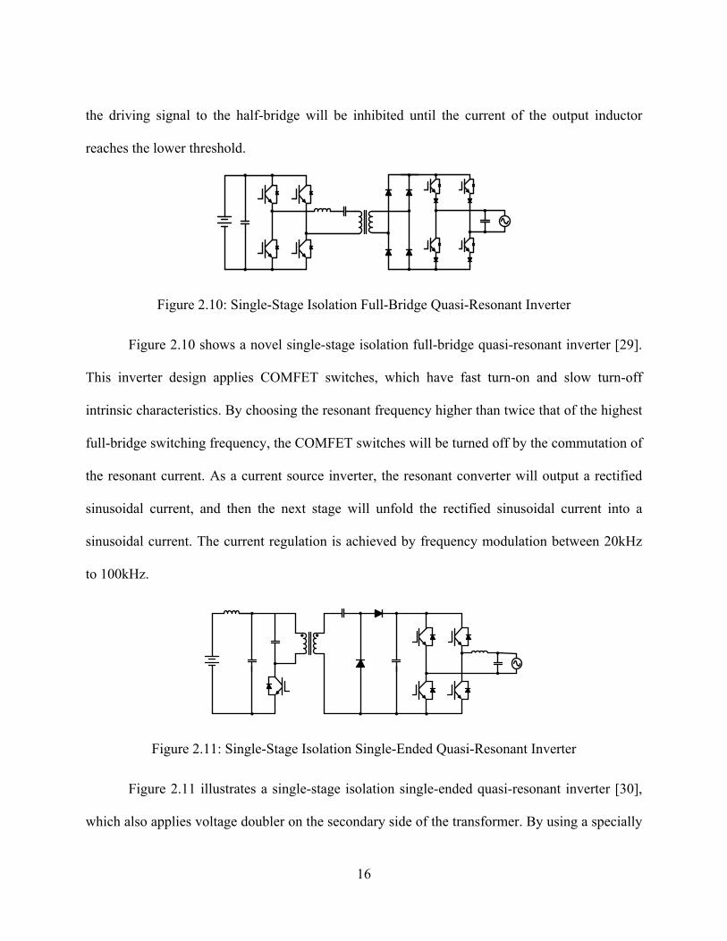
Figure 2.10: Single-Stage Isolation Full-Bridge Quasi-Resonant Inverter................................... 16
Figure 2.11: Single-Stage Isolation Single-Ended Quasi-Resonant Inverter................................ 16
Figure 2.12: Single-Stage Isolation Full-Bridge Inverter with Active Harmonic Filter............... 17
Figure 2.13: Single-Stage Isolation Flyback Inverter with Zero-Voltage Transition................... 18
Figure 2.14: Single-Stage Isolation Two-Switch Flyback Inverter with Zero-Voltage Switching
............................................................................................................................................... 18
Figure 3.1: Comparison of Passive and Active Filter for Inverter System with Grid Connection22
Figure 3.2: De-Coupling Capacitor for Passive Filter .................................................................. 23
ix

Figure 3.3: Control System Design of Single-Stage Inverter with Series Active Filter ............... 26
Figure 3.4: Block Diagram of Optimized Two-Stage Inverter Brick with Grid Connection ....... 27
Figure 3.5: Schematics of Psim Simulation Model for Active Filter ........................................... 28
Figure 3.6: I-V and P-I Curves of PV Arrays Used in Figure 3.5 ................................................ 28
Figure 3.7: Algorithm of Maximum Power Point of PV Array.................................................... 31
Figure 3.8: Simulation Results of Inverter Brick at Different Power Rating PV Cell.................. 32
Figure 3.9: Simulation Results of Inverter Brick at Different Power Rating PV Cells ................ 33
Figure 3.10: Step Response of Single-Stage Inverter with Active Filter to the Maximum Power
of Solar Array ....................................................................................................................... 35
Figure 3.11: Block Diagram of Single-Stage Inverter with Active Filter and Feedforward Control
............................................................................................................................................... 36
Figure 3.12: Step Response of Single-Stage Inverter with Active Filter and Feedforward
Controller to the Maximum Power of Solar Array ............................................................... 38
Figure 3.13: 10% 2nd Harmonics on DC Bus Causes 5% 3rd Harmonics on Inverter Output
Current [34], [35] .................................................................................................................. 39
Figure 3.14: Step Response of Single-Stage Inverter with Active Filter, Feedforward Controller
and Sample and Hold to the Maximum Power of Solar Array............................................. 41
Figure 4.1: PV-Based Two-Stage and Single-Stage Inverters...................................................... 43
Figure 4.2: Block Diagram of Single-Stage Full-Bridge Phase-Shift Inverter............................. 45
Figure 4.3: Voltage on the Primary Side of Transformer ............................................................. 46
Figure 4.4: Voltage-Seconds Analysis of Transformer ................................................................ 46
Figure 4.5: Slope Compensation for a DC/DC Converter ............................................................ 50
Figure 4.6: Slope Compensation for a Single-Stage Inverter ....................................................... 51
x

Figure 4.7: Slope Compensation for Single-Stage Inverter .......................................................... 52
Figure 4.8: DC/DC Converter Slope Compensation .................................................................... 54
Figure 4.9: Derivation of G(θ) ...................................................................................................... 55
Figure 4.10: Simulation Model for the Peak Current Mode Control............................................ 57
Figure 4.11: Output Voltage of Unstable Condition Due to No Slope Compensation (output
voltage is shown in the top figure, and the control signal is in the bottom figure, which is
current reference in red, switch current in blue and diode current in green.) ....................... 58
Figure 4.12: Output Voltage of Unstable Condition Due to No Slope Compensation (output
voltage is shown in the top figure, and the control signal is in the bottom figure, which is
current reference in red, switch current in blue and diode current in green.) ....................... 59
Figure 4.13: Output Voltage of Unstable Condition Due to No Slope Compensation (output
voltage is shown in the top figure, and the control signal is in the bottom figure, which is
current reference in red, switch current in blue and diode current in green.) ....................... 60
Figure 4.14: Step Response of Input Voltage from 180Vdc to 220Vdc at 4mS........................... 61
Figure 4.15: (a) Frequency Domain Analysis Simulation Model (b) Voltage Loop Loop Gain of
DC/DC Converter with Different Slope Compensation @ VO=60Vdc................................ 62
Figure 4.16: (a) Frequency Domain Analysis Simulation Model (b) Current Loop Loop Gain Of
DC/DC Converter with Different Slope Compensation ....................................................... 63
Figure 4.17: Loop Gain of Voltage Loop and Transfer Function of Current Loop...................... 63
Figure 4.18: Output Voltage and Control Signals with Unified Slope Compensation (red
waveform is current reference with unified slope compensation, blue waveform is current
sensing signal of switch and green waveform is the current sensing signal of diode in b, c, d
and e)..................................................................................................................................... 65
xi
Figure 4.19: Peak Current Mode Control with Adaptive Slope Compensation for Single-Stage
Inverter (red waveform is current reference with adaptive slope compensation, blue
waveform is current sensing signal of switch and green waveform is the current sensing
signal of diode in c, d, e and f).............................................................................................. 66
Figure 4.20: Comparison of Peak Current Mode Control with Unified and Adaptive Slope
Compensation at VO=20Vdc, 100Vdc and 160Vdc.............................................................. 67
Figure 5.1: System Block Diagram of Single-Stage Inverter with Digital Controller.................. 68
Figure 5.2: Block Diagram of Digital Controller.......................................................................... 68
Figure 5.3: Block Diagram of Current Control Loop [44]............................................................ 70
Figure 5.4: Bode Plot of Gp(s) and Gp(z)..................................................................................... 71
Figure 5.5: 2p-1z Compensator..................................................................................................... 71
Figure 5.6: Bode Plot of Gci(s) and Gci(z)................................................................................... 73
Figure 5.7: Bode Plot of Loop Gain Gci(s)Gp(s) and Gci(z)Gp(z) .............................................. 74
Figure 5.8: Bode Plot of Closed Loop Loop Gain Gci(s)Gp(s) and Gci’(s)Gp(s)........................ 76
Figure 5.9: Bode Plot of Closed Lop Loop Gain Gci(z)Gp(z) and Gci’(z)Gp(z)......................... 76
Figure 5.10: Switching Model Simulation.................................................................................... 77
Figure 6.1: Bi-Directional, Uni-Directional DC/DC Converters and Optimized Single-Stage Bi-
Directional Inverter............................................................................................................... 80
Figure 6.2: Experiment Results of Ringing Voltage across Diode and MOSFET with the Same
Prototype as Shown in Figure 6.1 ......................................................................................... 81
Figure 6.3: Current and Voltage of a Vacuum and a Refrigerator Starting.................................. 84
Figure 6.4: Output Voltage and Current of Stand-Alone Inductive Load .................................... 84
Figure 6.5: Comparison of Conventional and Micro Inverters Systems ...................................... 87
xii

Figure 6.6: Solar Radiation of PV Panels ..................................................................................... 88
Figure 6.7: System Block Diagram of Single-Staged Bi-Directional Inverter System ................ 89
Figure 6.8: Bi-Directional Single-Stage Inverter with Flyback DC/DC Converter...................... 91
Figure 6.9: Timing Diagram of Bi-Directional Single-Stage Inverter with Flyback DC/DC
Converter............................................................................................................................... 92
Figure 6.10: ENABLE Signal Generation .................................................................................... 93
Figure 6.11: System Block Diagram of Single-Staged Bi-Directional Inverter System .............. 93
Figure 6.12: Simulation Results of Load Voltage (VAC), Load Current (IAC), Output Current of
DC/DC Converter (IForward), Input Current of Reverse DC/DC Converter (IReverse), Output of
Error Amplifier of Both Converters (VFerr and VRerr) ........................................................... 94
Figure 6.13: Bi-Directional Single-Staged Inverter with Reactive Energy Storage Network...... 95
Figure 6.14: Three Operation Modes of Reactive Energy Storage Network................................ 95
Figure 6.15: Instantaneous and Average Output Current and Voltage......................................... 96
Figure 6.16: Block Diagram of Single-Staged Inverter with Reactive Energy Storage Network 97
Figure 6.17: Timing Diagram of Single-Staged Inverter with Reactive Energy Storage Network
............................................................................................................................................... 98
Figure 6.18: Pspice Simulation Model of Single-Staged Inverter with Reactive Energy Storage
Network................................................................................................................................. 98
Figure 6.19: Simulation Results of Schematics in Figure 6.18 (output voltage and current,
voltage of Caux and filter inductor current) ........................................................................... 99
Figure 6.20: Simulation Results of Energy Storage Network without and with Feed-Forward
Compensator (180Hz)........................................................................................................... 99
xiii

Figure 6.21: Simulation Results of Single-Staged Inverter with Energy Storage Network (60Hz)
............................................................................................................................................. 101
Figure 7.1: Flyback ZCS Single-Stage Inverter with PFM Control ........................................... 105
Figure 7.2: Detailed Analysis of Flyback ZCS Single-Stage Inverter........................................ 110
Figure 7.3: Timing Diagram of Flyback ZCS Single-Stage Inverter.......................................... 111
Figure 7.4: Simulation Results of Proposed Flyback ZCS Converter ........................................ 112
Figure 7.5: Control Algorithm of Flyback ZCS Single-Stage Inverter ...................................... 114
Figure 7.6: Proposed Flyback ZCS Single-Stage Inverter.......................................................... 114
Figure 7.7: Simulation Results of Flyback ZCS Single-Stage Inverter ...................................... 115
Figure 7.8: Timing Diagram of Flyback ZCS Single-Stage Inverter When Isec=0 ..................... 116
Figure 7.9: Simulation Results of Flyback ZCS Single-Stage Inverter with Less Inductance of
Transformer Secondary Winding at Lower Switching Frequency ..................................... 117
Figure 7.10: Simulation Results of Nonlinear Transfer Function between the Switching
Frequency and Output Power.............................................................................................. 118
Figure 7.11: Distortion Caused by Nonlinearity of Flyback ZCS DC/DC Converter ................ 119
Figure 7.12: Optimized Flyback ZCS Single-Stage Inverter without Nonlinearity ................... 119
Figure 7.13: Detailed Operation Stages for Optimized Flyback ZCS Single-Stage Inverter with
Synchronous Rectification .................................................................................................. 120
Figure 7.14: Timing Diagram of Optimized Flyback ZCS Single-Stage Inverter with
Synchronous Rectification .................................................................................................. 121
Figure 7.15: Simulation Results of Optimized Flyback ZCS Single-Stage Inverter with
Synchronous Rectification When the Switching Frequency is Lower than the Critical
Frequency............................................................................................................................ 123
xiv

Figure 7.16: Simulation Results of Transfer Function of Optimized Flyback ZCS Single-Stage
Inverter with Rectification .................................................................................................. 124
Figure 7.17: PWM vs. PFM........................................................................................................ 125
Figure 7.18: System Block Diagram of PFM ZCS Flyback Single-Stage Inverter .................... 126
Figure 7.19: Timing Diagram of PFM ZCS Flyback DC/DC Converter ................................... 126
Figure 7.20: Voltage and Current of MOSFET and Rectifier Diode.......................................... 127
Figure 7.21: Small Signal Power Stage Transfer Function Analysis.......................................... 128
Figure 7.22: Schematics of Small Signal Power Stage Transfer Function Analysis .................. 128
Figure 7.23: Simulation Results of Power Stage Transfer Function Small Signal Analysis...... 129
Figure 8.1: Prototype of Full-Bridge Phase-Shift Single-Stage Inverter.................................... 130
Figure 8.2: Experimental Results of Vref, Output Current and Voltage...................................... 131
Figure 8.3: Experimental Results of Output Current, VDS and VGS of Switch A in Figure 4.2.. 132
Figure 8.4: Experimental Results of Output Current, VDS and VGS of Switch B Figure 4.2 ...... 133
Figure 8.5: Experimental Results of Output Current, VDS and VGS of Switch C in Figure 4.2.. 134
Figure 8.6: Experimental Results of Output Current, VDS and VGS of Switch D in Figure 4.2.. 135
Figure 8.7: Experimental Results of Output Current, Transformer Primary and Secondary Side
Voltage................................................................................................................................ 136
Figure 8.8: Prototype of 1kW Single-Stage High-Frequency Link Inverter System.................. 137
Figure 8.9: Experimental Results of Single-Stage Inverter Output Current IOUT (Green, 10A/Div)
and Utility Grid Voltage VUT (Red, 100V/Div, 5ms/Div) in Grid Connection Mode........ 138
Figure 8.10: Experimental Results of Single-Stage Inverter Output Current IOUT (Green, 5A/Div)
and Inverter Output Voltage VOUT (Red, 100V/Div, 5ms/Div) in Stand-Alone Mode ...... 138
xv

Figure 8.11: Experimental Results of Single-Stage Inverter Output Current IOUT (Green, 1A/Div)
and Control Signals (Blue, Red and Yellow, 50ms/Div) in Transition from Grid-Connection
to Stand-Alone Mode and from Stand-Alone to Grid-Connection Mode........................... 138
Figure 8.12: Prototype of Optimized Single-Staged Bi-Directional Inverter System ................ 140
Figure 8.13: Experimental Results.............................................................................................. 140
Figure 8.14: Single-Stage Bi-Directional Inverter with Flyback Converter............................... 141
Figure 8.15: Prototype of PFM ZCS Flyback Inverter ............................................................... 142
Figure 8.16: Experimental Results of PFM ZCS Flyback Inverter ............................................ 142
Figure 8.17: Experimental Results of PFM ZCS Flyback Inverter ............................................ 143
Figure 8.18: Experimental Results of PFM ZCS Flyback Inverter ............................................ 143
Figure 8.19: Zoomed View of Figure 8.18 ................................................................................. 144
Figure 8.20: Thermal Images of PFM ZCS Flyback Single-Stage Inverter Prototype............... 146
xvi

LIST OF TABLES
Table 2.1 Review of Inverter Topologies ..................................................................................... 20
Table 3.1 Lifetime of Electrolytic Capacitors............................................................................... 21
Table 3.2 C Program for Maximum Power Point Tracking.......................................................... 30
Table 5.1 Digital Controller in C Code......................................................................................... 78
Table 6.1 IRF® 600V MOSFETs.................................................................................................. 82
Table 6.2 IRF® 600V Diodes ........................................................................................................ 82
Table 6.3 Price of 600V MOSFETs and Diodes........................................................................... 82
Table 7.1 Key Parameters of Flyback ZCS Converter ............................................................... 113
xvii

xviii
LIST OF ACRONYMS/ABBREVIATIONS
CSI Current Source Inverter
DG Distributed Generation
EMI Electromagnetic Interference
IGBT Insulated Gate Bipolar Transistor
MOSFET Metal-Oxide Semiconductor Field-Effect Transistor
MPP Maximum Power Point
MPPT Maximum Power Point Tracking
PFM Pulse Frequency Modulation
PWM Pulse Width Modulation
PV Photovoltaic
RMS Root Mean Square
SMD Surface Mount Device
SPWM Sinusoidal Pulse Width Modulation
VCO Voltage Controlled Oscillator
VSI Voltage Source Inverter
ZCS Zero Current Switching
ZVS Zero Voltage Switching
ZOH Zero Order Hold

CHAPTER ONE: INTRODUCTION
Alternate energy systems are in high demand to minimize dependence on foreign oil
imports, reduce significant capital investments for newer centralized power generating units and
lower environmental pollution. Additionally and yet equally importantly, such distributed
generation potentially reduces the risk of complete blackout in the event of cascaded power
system failures, as experienced recently on the U.S. Northeast grid.
Of all the various kinds of renewable energy sources, such as wind, sun and fuel cell,
solar energy is one of the best renewable energy sources to be utilized, and it mainly converters
the energy from sun light into electrical energy by photovoltaic effect. Solar energy is green and
inexhaustible energy, without any pollution to the earth and atmosphere.
The major benefit of designing a reliable, stable, efficient and lower cost photovoltaic
power electronics system is the availability of reliable and quality power without relying on the
utility grid. It also avoids the major investment in transmission and distribution. For the United
States, another major benefit lies in the fact that it reduces greenhouse gas emissions, responding
to the increasing energy demands by establishing a new, high-profiled industry. Grid-connected
solar power has been developed for more than 10 years, as an alternative energy source to the
utility grid, especially at remote areas and in developing countries, where the utility is not stable.
Due to these reasons, the grid-connected solar power market has annual growth of 10% globally,
which is $276 million in 2003, and will be $445 million in 2008 [1].
1
4,000
Grid-connectedOff-grid
3.500
3,000
2,500
2,000
1,500
1,000
500
0
1992
1993
1994
1995
1996
1997
1998
1999
2000
2001
2002
2003
2004
2005
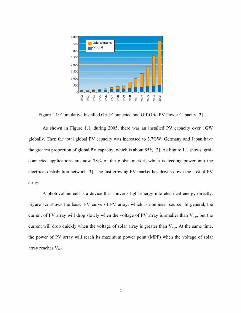
Figure 1.1: Cumulative Installed Grid-Connected and Off-Grid PV Power Capacity [2]
As shown in Figure 1.1, during 2005, there was an installed PV capacity over 1GW
globally. Then the total global PV capacity was increased to 3.7GW. Germany and Japan have
the greatest proportion of global PV capacity, which is about 85% [2]. As Figure 1.1 shows, grid-
connected applications are now 78% of the global market, which is feeding power into the
electrical distribution network [3]. The fast growing PV market has driven down the cost of PV
array.
A photovoltaic cell is a device that converts light energy into electrical energy directly.
Figure 1.2 shows the basic I-V curve of PV array, which is nonlinear source. In general, the
current of PV array will drop slowly when the voltage of PV array is smaller than Vmp, but the
current will drop quickly when the voltage of solar array is greater than Vmp. At the same time,
the power of PV array will reach its maximum power point (MPP) when the voltage of solar
array reaches Vmp.
2

Vmp Voc
Isc
MPP
Imp
V
P vs. V
I vs. V
Figure 1.2: I-V and P-V Solar Array Characteristics [4][5]
The I-V curve of PV array also will change with the ambient temperature and solar
radiation. Then the point of Vmp is not constant. To regulate the solar array at its MPP, a DC/DC
converter with MPP controller is usually applied, which will regulate the solar array at its MPP
no matter what the temperature or solar radiation. The MPT algorithm and MPT controller are
described in [4] and [5].
Single-crystalline silicon and multi-crystalline silicon modules are the most popularly
used among the PV cells on the market [6]. By using such material, the characteristic open-
circuit voltage of 36 cells and 72 cells is between [18V, 26V] and [38V, 46V] [7]. The new
technologies, such as thin-layer silicon, amorphous-silicon and photo electro chemical, will
improve the voltage per cell to [0.5V 2.0V] [8], [9], [10], [11].
As shown in Figure 1.3, the 36 cell modules are connected in parallel to form a grid-
connected PV panel. Since the characteristic output voltage of PV cells are much lower
compared with grid voltage, several PV cells need to be connected in series and/or in parallel to
facilitate the inverter design. For a centralized inverter system, all the PV cells are connected in
parallel or in series and use a single inverter to perform the power processing and converting
function. If one of the cells is shadowed or malfunctions due to aging, then the centralized
3

maximum power point will be mismatched between the cells. If these cells are in parallel with
others, then they will behave like a load instead of source, due to the output voltage being lower
than others. A fully shadowed cell among the 160 cells will be 70°C above the ambient
temperature, which will cause the lifetime of the heated cell to be reduced dramatically [12], [13].
Figure 1.3: Bp Solar Msx60 60watt Polycrystalline Shell Sp75 75 Watts Signal Crystal [14]
Figure 1.4: Shadowing of PV Cells [14]
The trends of the inverter for the small DG system are:
1. Modular Design
For a DG system, volumetric heat dissipation and high current ability are the limitations
that individual inverter cannot overcome. Especially in the applications of renewable energy DC
source, the input voltage is low and variable in a wide range. A modularized inverter approach is
4

a more reliable and economic solution for distributed AC power systems. Modularized inverters
will share the high load current and also offer redundancy, uninterrupted operation and extended
life expectancy to the system [15].
The traditional PV cell inverter system with grid-connection is a centralized inverter
system. The PV panels are connected in parallel and in series to get enough input DC voltage to
facilitate the inverter design. The centralized inverter is the lowest cost solution. But if any
shadowing happens, as shown in Figure 1.4, a hot-spot will generate in the shadowed PV panels.
Other than that, due to different position of each of the PV panels, the MPP of each of the panels
is different. If the centralized inverter cannot track each MPP of the PV panels, then system
efficiency is lower.
If each PV panel has an inverter module attached and converts the solar energy into
utility grid, then each PV’s MPP can be tracked efficiently by each inverter module and the hot
spot will be eliminated from the whole system. The modular design of each inverter within the
grid also will provide an uninterrupted power converter even if one of the modules malfunctions.
Mass production, high reliability and lower costs reduce the price per watts. A plug and
play system can be installed by the customer without electrical engineering training. The
reduction of installation costs will further reduce the cost of an inverter system [16].
The next generation of modular inverter will be an inverter cell integrated with a single
PV cell and converts the sunlight energy to electrical energy [17][18][19]. The next generation
PV cell will be much easier to integrate into building, houses and portable devices.
2. Higher Efficiency and Longer Warranty
Higher efficiency reduces the heat generation and increases the system stability. The
lifetime of electrolytic capacitor will be strongly affected by the ambient temperature. Research
5

shows that a 10 degrees ambient temperature increase will decrease the lifetime of the
electrolytic capacitor by half. The longer lifetime will let the manufacturer have a longer
warranty on the inverter, which makes the inverter more attractive to the customer. To increase
system efficiency, zero voltage switching and zero current switching topologies need to be
applied, which will also reduce the switching stress of the switches and extend the lifetime of the
inverter. Some researcher-applied resonant and quasi-resonant converter topologies will greatly
increase inverter efficiency.
3. Less Components Counts and Lower Cost
A single-stage inverter reduces components counts, increases system efficiency and has
lower costs than a conventional multiple-stage inverter. As new control techniques and
topologies are developed, a single-stage inverter will become more and more popular.
4. Multi-Source Design and Wide Input Voltage Range
An inverter design for multi-source, including PV power, fuel cell, wind power, micro
gas turbines and small hydro systems, will decrease the cost of an inverter system and facilitate
the design of a modularized inverter. A multi-source design inverter has an even wider input
voltage range. A wider input voltage range also increases the utilization of the voltage source.
5. Power Decoupling
An inexpensive and small film capacitor is applied in the inverter to replace the
expensive and large electrolytic decoupling capacitors. This will increase the lifetime of the
inverter [20].
6. Digital Control
6

All the functions mentioned above need more agility control techniques, such as MPPT
control for PV optimal efficiency in a fuel system or other complex power flow controls. Digital
control also provides a friendly interface between the DG system and customers.
7

CHAPTER TWO: SINGLE-PHASE GRID-CONNECT INVERTER TOPOLOGY REVIEW
There are many existing inverter topologies for single-phase grid-connected inverters. In
this chapter, the single-phase grid-connected inverter topologies will be reviewed, which have
transformers to provide galvanic isolation to meet the safety requirement. The old generation
single-stage grid-connected inverter was using a low frequency transformer, which is bulky,
heavy and expensive. The new generation single-stage inverter is using a high frequency
transformer, which is called high frequency link inverter. The general high frequency link
inverter block diagram is shown in Figure 2.1, which includes most of the function blocks of
existing inverters.
Figure 2.1: General Block Diagram of Single-Stage Grid-Connected Inverter
The function of a pre-regulator in Figure 2.1 is to provide initial input voltage boosting or
MPPT function. Some inverter designs also provide 120/100Hz low frequency ripple
cancellation.
8

The function of the DC/DC converter is to provide further voltage boosting or MPPT
function and high frequency link galvanic isolation. A conventional DC/DC converter in inverter
application is voltage source and outputs constant DC voltage. The DC/DC converter for single-
stage inverter is current source and output rectified sinusoidal current instead of constant current.
The function of the inverter is to convert the DC voltage into sinusoidal current and inject
it into utility grid, which makes it a current source. For a single-stage inverter, the inverter stage
is the unfolding circuit, which is operated at 60/50 Hz and inverts the rectified sinusoidal current
into sinusoidal waveform.
The MPPT controller detects the voltage and output current of the solar array. Then, it
regulates the power point of solar array to its maximum power point by adjusting the pre-
regulator or DC/DC converter reference.
The pre-regulator, DC/DC converter and inverter controllers are controlling the power
stages. The controllers will regulate voltage or current to convert the solar energy to electrical
energy.
The stand-alone load is the customer’s load in home. The single-phase inverter converts
the solar energy to electrical power and onto the utility grid. Besides the utility grid, the solar
power also can be utilized by the stand-alone load. The function of a backup battery provides
energy storage during night to continue powering the stand-alone load.
The general block diagram in Figure 2.1 illustrates all the possible functional blocks that
most single-phase grid-connected inverters could have. It is not necessary for every inverter to
have all the blocks.
There are different categories for single-phase grid-connected inverters, which are: high
frequency link inverters or inverters with low frequency transformer, single-stage or multiple-
9

stage inverter, uni-directional or bi-directional inverter, inverter with electrolytic capacitor as
power decoupling or inverter with active power stage as power decoupling stage.
Single-phase grid-connected inverter with low frequency transformer is an old fashioned
inverter technique, which uses 50/60 Hz frequency transformer to provide galvanic isolation with
utility grid. Low frequency transformer is expensive, bulky and heavy. A high frequency link
inverter uses a high frequency transformer to provide galvanic isolation, which makes the single-
phase inverter cheaper and smaller.
To convert the solar energy into electrical energy and invert the DC voltage source into
AC current, a single phase inverter needs either single or multiple stages to perform the power
processing functions. A single-stage inverter uses one power processing stage to provide
galvanic isolation and DC/AC conversion. A single-stage inverter applies PWM on the primary
side of high frequency link transformer to generate rectified sinusoidal waveform and uses a low
frequency switch bridge to invert rectified sinusoidal waveform into pure sinusoidal waveform
with 50/60Hz switching cycle. A single-stage inverter has higher efficiency due to less power
conversion but has poor power decoupling between solar array and utility grid. To provide
proper voltage amplification, a single-stage inverter needs to put multiple PV panels into series
to have enough input DC voltage, or needs to apply a high turns ratio transformer, which tends to
have large leakage inductance and higher voltage stress for the secondary side switches. Two-
stage or multiple-stage inverters have a DC/DC converter to amplify the solar array voltage,
providing galvanic isolation and power decoupling. The shortcoming of a multiple-stage inverter
is lower power efficiency and higher cost.
A uni-directional inverter will not allow bi-directional power flow between the load and
the power decoupling capacitor. Therefore, a uni-directional inverter can only handle pure
10

resistive load or be used as a grid-connected inverter system. On the contrary, the bi-directional
inverter can handle the reactive load, which generates the bi-directional power flow through the
inverter and the power decoupling capacitors.
For a single-phase grid-connected inverter, the input power from solar array is constant,
which is the MPP of solar array. The output power of the inverter is pulsing at 120/100Hz and
the peak instantaneous power is twice that of the average power of the inverter system. Then, the
power decoupling is necessary between the solar source and the utility grid. The conventional
power decoupling method uses large electrolytic capacitance at the output of solar array for a
single-stage inverter or output of a DC/DC converter. An active power processing stage could be
another solution for power decoupling.
Figure 2.2: Conventional Two-Stage Isolation Full-Bridge Inverter
Figure 2.2 illustrates the conventional two-stage isolation full-bridge inverter, which has
a fully functional DC/DC converter and a SPWM full-bridge inverter in series. The DC/DC
converter boosts and regulates the solar array output variable DC voltage and provides a stable
and regulated DC bus voltage for the next stage inverter. The DC/DC converter also provides
galvanic isolation between the solar array and the utility grid. The DC bus capacitance provides
power decoupling between the two stages.
11
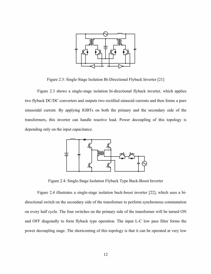
Figure 2.3: Single-Stage Isolation Bi-Directional Flyback Inverter [21]
Figure 2.3 shows a single-stage isolation bi-directional flyback inverter, which applies
two flyback DC/DC converters and outputs two rectified sinusoid currents and then forms a pure
sinusoidal current. By applying IGBTs on both the primary and the secondary side of the
transformers, this inverter can handle reactive load. Power decoupling of this topology is
depending only on the input capacitance.
Figure 2.4: Single-Stage Isolation Flyback Type Buck-Boost Inverter
Figure 2.4 illustrates a single-stage isolation buck-boost inverter [22], which uses a bi-
directional switch on the secondary side of the transformer to perform synchronous commutation
on every half cycle. The four switches on the primary side of the transformer will be turned ON
and OFF diagonally to form flyback type operation. The input L-C low pass filter forms the
power decoupling stage. The shortcoming of this topology is that it can be operated at very low
12

voltage of solar array. The power decoupling function is relying on the bulky and expensive low
pass filter. The system efficiency tends to be low.
Figure 2.5: Single-Stage Isolation Flyback Inverter with Power Decoupling
Figure 2.5 shows a new flyback and buck boost type inverter with power decoupling [23],
[24]. This design can eliminate the use of electrolytic capacitors, which limit the life-time of the
system. The intermediate capacitor will act as an energy buffer between the PV array and the
utility connected inverter. The output power of PV array will be regulated to its MPP and the
power variation caused by the inverter will be only shown in the intermediate capacitor. In
addition to power decoupling, another benefit of this topology is that the flyback type inverter
can work in a wide range of PV array voltage. The drawbacks of this topology are that its
controller design is complicated, the power decoupling stage is in series with the flyback
converter and the solar array still sees high frequency current ripples, which will need a capacitor
to filter out. The power decoupling stage is operating at the same frequency as the inverter stage.
Figure 2.6: Single-Stage Isolation Bi-Directional Full-Bridge Inverter with Cycloconverter
13
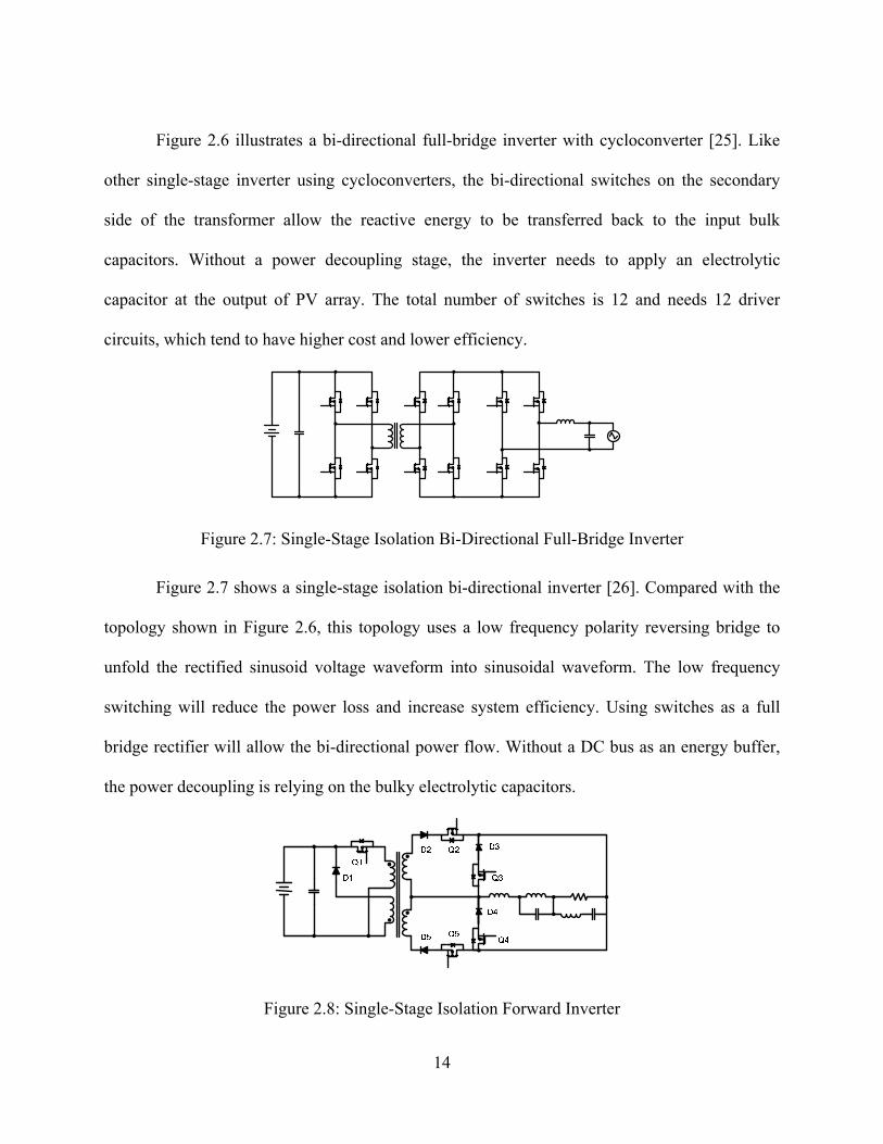
Figure 2.6 illustrates a bi-directional full-bridge inverter with cycloconverter [25]. Like
other single-stage inverter using cycloconverters, the bi-directional switches on the secondary
side of the transformer allow the reactive energy to be transferred back to the input bulk
capacitors. Without a power decoupling stage, the inverter needs to apply an electrolytic
capacitor at the output of PV array. The total number of switches is 12 and needs 12 driver
circuits, which tend to have higher cost and lower efficiency.
Figure 2.7: Single-Stage Isolation Bi-Directional Full-Bridge Inverter
Figure 2.7 shows a single-stage isolation bi-directional inverter [26]. Compared with the
topology shown in Figure 2.6, this topology uses a low frequency polarity reversing bridge to
unfold the rectified sinusoid voltage waveform into sinusoidal waveform. The low frequency
switching will reduce the power loss and increase system efficiency. Using switches as a full
bridge rectifier will allow the bi-directional power flow. Without a DC bus as an energy buffer,
the power decoupling is relying on the bulky electrolytic capacitors.
Figure 2.8: Single-Stage Isolation Forward Inverter
14

Figure 2.8 illustrates a single-stage isolation forward type inverter [27]. Q2, D2, Q3, D3
and Q5, D5, Q4, D4 form two sets of high frequency rectifiers. Each set works for a half cycle of
the utility grid. This topology uses a forward converter on the primary side of the transformer.
Another coupling winding will create free wheeling on the primary side current when Q1 is OFF.
Then the input current of the forward converter will be continuous, but the 120/100Hz power
ripple will pass through the transformer. Another drawback is that the input voltage boost is
relying on the turns ratio of the transformer, which will limit the effective input voltage range.
Figure 2.9: Single-Stage Isolation Resonant Half-Bridge Inverter
Figure 2.9 shows a single-stage isolation resonant half-bridge inverter [28]. This inverter
design is regulating the current of the inductor on the transformer secondary side to be rectified
sinusoidal. The next unfolding stage unfolds the rectified sinusoidal current into pure sinusoidal
current. This design applies thyristors as the switches to form a high frequency resonant half-
bridge inverter on the primary side of the transformer. It also applies hysteretic control to
regulate the output inductor current as a rectified sinusoidal waveform. Then the next stage will
unfold the current into sinusoidal current and inject it into the utility grid. The LC resonant tank
on the primary side is oscillating at constant frequency. The upper IGBT will be turned off when
the resonant tank’s current changes direction, and the diode in parallel with the IGBT will be
turned on to free-wheeling the current. Then, the lower IGBT is turned on as the resonant tank
continues to be resonant. If the current of output inductor is reaching the upper threshold, then
15
the driving signal to the half-bridge will be inhibited until the current of the output inductor
reaches the lower threshold.
Figure 2.10: Single-Stage Isolation Full-Bridge Quasi-Resonant Inverter
Figure 2.10 shows a novel single-stage isolation full-bridge quasi-resonant inverter [29].
This inverter design applies COMFET switches, which have fast turn-on and slow turn-off
intrinsic characteristics. By choosing the resonant frequency higher than twice that of the highest
full-bridge switching frequency, the COMFET switches will be turned off by the commutation of
the resonant current. As a current source inverter, the resonant converter will output a rectified
sinusoidal current, and then the next stage will unfold the rectified sinusoidal current into a
sinusoidal current. The current regulation is achieved by frequency modulation between 20kHz
to 100kHz.
Figure 2.11: Single-Stage Isolation Single-Ended Quasi-Resonant Inverter
Figure 2.11 illustrates a single-stage isolation single-ended quasi-resonant inverter [30],
which also applies voltage doubler on the secondary side of the transformer. By using a specially
16
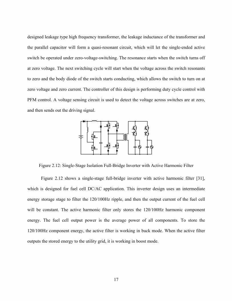
designed leakage type high frequency transformer, the leakage inductance of the transformer and
the parallel capacitor will form a quasi-resonant circuit, which will let the single-ended active
switch be operated under zero-voltage-switching. The resonance starts when the switch turns off
at zero voltage. The next switching cycle will start when the voltage across the switch resonants
to zero and the body diode of the switch starts conducting, which allows the switch to turn on at
zero voltage and zero current. The controller of this design is performing duty cycle control with
PFM control. A voltage sensing circuit is used to detect the voltage across switches are at zero,
and then sends out the driving signal.
Figure 2.12: Single-Stage Isolation Full-Bridge Inverter with Active Harmonic Filter
Figure 2.12 shows a single-stage full-bridge inverter with active harmonic filter [31],
which is designed for fuel cell DC/AC application. This inverter design uses an intermediate
energy storage stage to filter the 120/100Hz ripple, and then the output current of the fuel cell
will be constant. The active harmonic filter only stores the 120/100Hz harmonic component
energy. The fuel cell output power is the average power of all components. To store the
120/100Hz component energy, the active filter is working in buck mode. When the active filter
outputs the stored energy to the utility grid, it is working in boost mode.
17
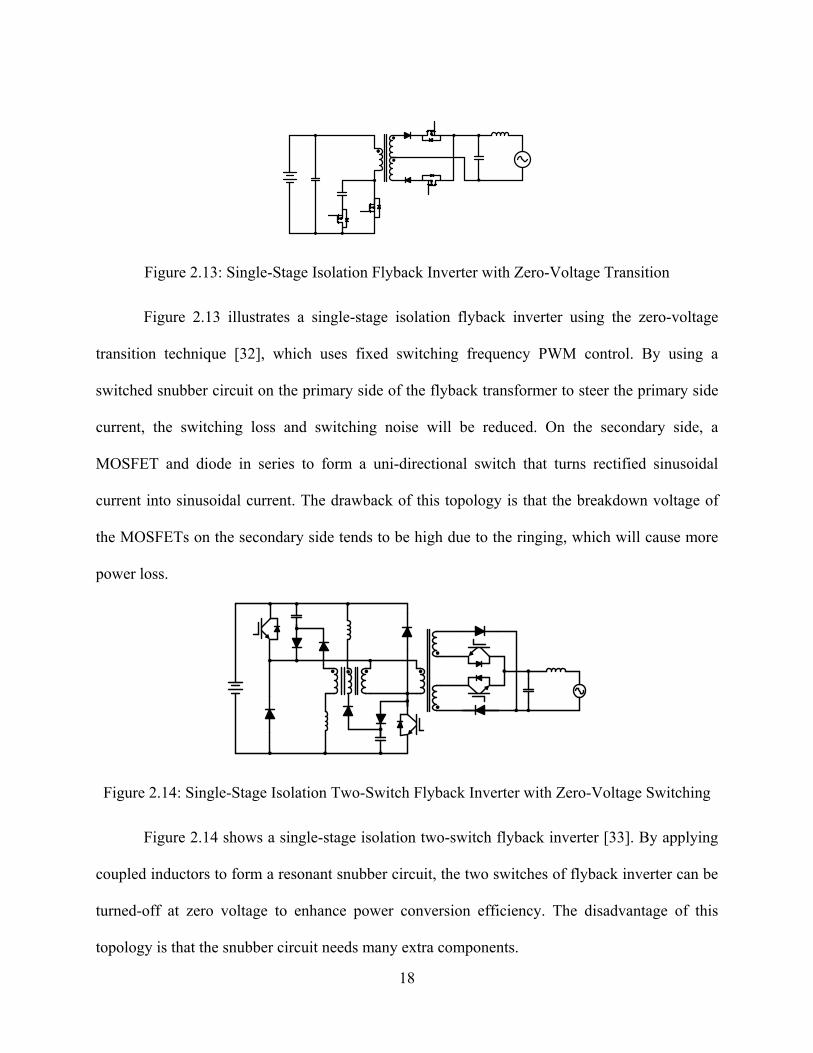
Figure 2.13: Single-Stage Isolation Flyback Inverter with Zero-Voltage Transition
Figure 2.13 illustrates a single-stage isolation flyback inverter using the zero-voltage
transition technique [32], which uses fixed switching frequency PWM control. By using a
switched snubber circuit on the primary side of the flyback transformer to steer the primary side
current, the switching loss and switching noise will be reduced. On the secondary side, a
MOSFET and diode in series to form a uni-directional switch that turns rectified sinusoidal
current into sinusoidal current. The drawback of this topology is that the breakdown voltage of
the MOSFETs on the secondary side tends to be high due to the ringing, which will cause more
power loss.
Figure 2.14: Single-Stage Isolation Two-Switch Flyback Inverter with Zero-Voltage Switching
Figure 2.14 shows a single-stage isolation two-switch flyback inverter [33]. By applying
coupled inductors to form a resonant snubber circuit, the two switches of flyback inverter can be
turned-off at zero voltage to enhance power conversion efficiency. The disadvantage of this
topology is that the snubber circuit needs many extra components.
18

19
As a summary, Table 2.1 lists all the topologies mentioned above, with the key features
listed.

Table 2.1 Review of Inverter Topologies
Fig. No. Topology Power Decoupling Isolation Bi-directional/
uni-directional Power Rating
Switching Frequency Efficiency Input
voltage
Figure 2.2 Two-stage full-bridge electrolytic capacitor isolation bi-directional <10kW <200kHz <85%
Figure 2.3 Single-stage flyback electrolytic capacitor isolation bi-directional 1kW 100kHz 165VDC
Figure 2.4 Single-stage buck-boost electrolytic capacitor isolation uni-directional 400W 50kHz 100VDC
Figure 2.5 Single-stage flyback active filter isolation uni-directional 50W 200kHz 35VDC
Figure 2.6 Single-stage full-bridge electrolytic capacitor isolation bi-directional 1kW 200VDC
Figure 2.7 Single-stage full-bridge electrolytic capacitor isolation bi-directional 200W 83~85% 23VDC
Figure 2.8 Single-stage forward electrolytic capacitor isolation bi-directional 50W 25kHz 70% 48VDC
Figure 2.9 Single-stage half-bridge electrolytic capacitor isolation uni-directional 1kW 35kHz 89% 200VDC
Figure 2.10 Single-stage full-bridge electrolytic capacitor isolation uni-directional 2.5kW 20~100kHz 160VDC
Figure 2.11 Single-stage single-ended electrolytic capacitor isolation uni-directional 4kW 20~30kHz 92.5% 200VDC
Figure 2.12 Single-stage full-bridge active filter isolation uni-directional 1.5kW 20kHz 48VDC
Figure 2.13 Single-stage flyback electrolytic capacitor isolation uni-directional 100W 50kHz 84% 30VDC
Figure 2.14 Single-stage flyback electrolytic capacitor isolation uni-directional 1kW 16kHz 93% 200VDC
20
CHAPTER THREE: ACTIVE FILTER DESIGN
3.1 Introduction
The inverter module is designed for single PV panel, which has limited power rating.
Therefore, it is extremely important to regulate power input from a PV cell at its maximum
power point without 120Hz ripple, because the 120/100Hz ripple will degrade the utilization of
the PV cell. To maintain a near constant input current from the PV cell, a low frequency input
filter needs to be applied to filter the switching frequency ripple and 120/100Hz ripple.
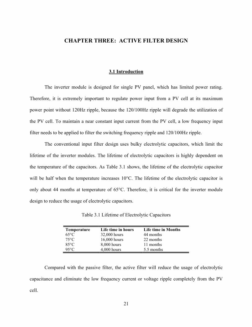
The conventional input filter design uses bulky electrolytic capacitors, which limit the
lifetime of the inverter modules. The lifetime of electrolytic capacitors is highly dependent on
the temperature of the capacitors. As Table 3.1 shows, the lifetime of the electrolytic capacitor
will be half when the temperature increases 10°C. The lifetime of the electrolytic capacitor is
only about 44 months at temperature of 65°C. Therefore, it is critical for the inverter module
design to reduce the usage of electrolytic capacitors.
Table 3.1 Lifetime of Electrolytic Capacitors
Temperature Life time in hours Life time in Months 65°C 32,000 hours 44 months 75°C 16,000 hours 22 months 85°C 8,000 hours 11 months 95°C 4,000 hours 5.5 months
Compared with the passive filter, the active filter will reduce the usage of electrolytic
capacitance and eliminate the low frequency current or voltage ripple completely from the PV
cell.
21
(a) Single-Stage Inverter with Passive Filter
(b) Two-Stage Inverter with Passive Filter
(c) Single-Stage Inverter with Active Filter in Parallel
(d) Single-Stage Inverter with Active Filter in Series
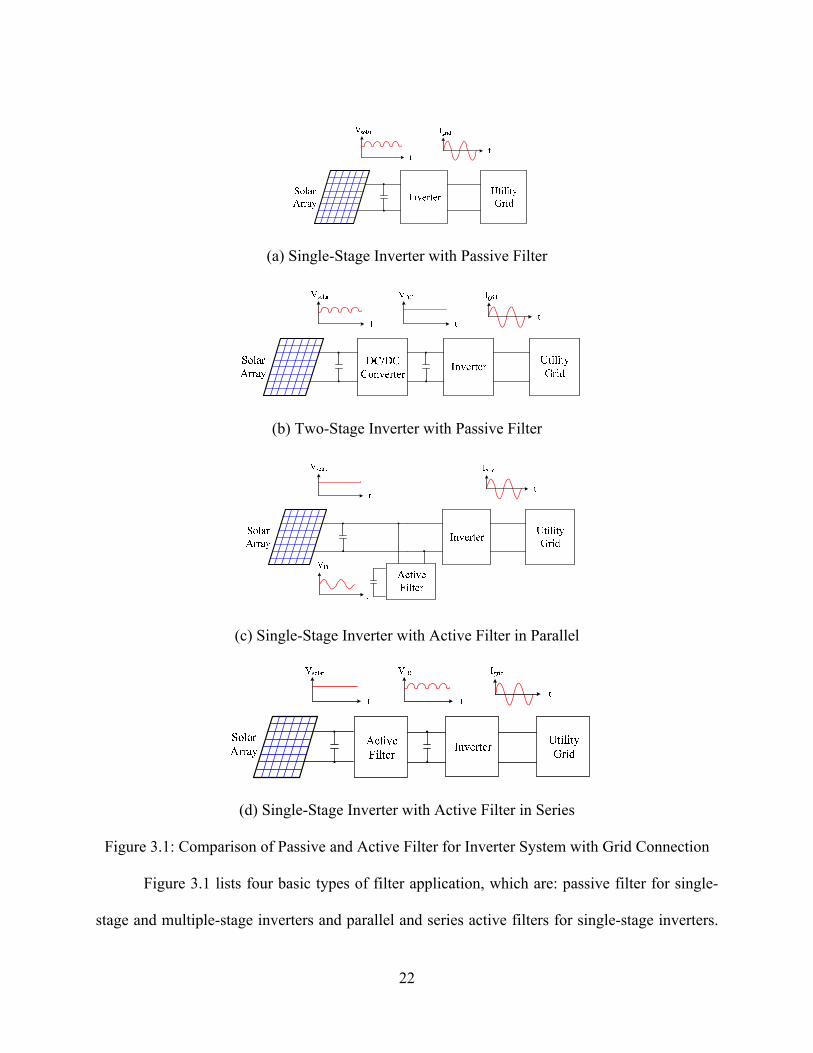
Figure 3.1: Comparison of Passive and Active Filter for Inverter System with Grid Connection
Figure 3.1 lists four basic types of filter application, which are: passive filter for single-
stage and multiple-stage inverters and parallel and series active filters for single-stage inverters.
22

For the passive filters, the voltage ripple on the electrolytic capacitor is inversely proportional to
the capacitance of the DC bus.
To get the same input voltage ripple, single-stage and multiple-stage inverters need the
same de-coupling capacitance, as shown in Figure 3.1 (a) and (b). In the multiple-stage inverter,
the function of DC/DC converter is booting the PV array voltage and providing the constant
voltage to the inverter stage. Since there is no energy storage stage in the DC/DC converter and
output voltage is constant, then the ripple voltage on the input capacitors are the same. The
voltage ripple on the de-coupling capacitor is also shown in Figure 3.2.
igridvgrid t
vcapVcap,avg
t
t
pgridPgrid,avg
capv~
t
pPVPPV,avg
Figure 3.2: De-Coupling Capacitor for Passive Filter
To derive the relationship between the voltage ripple and the capacitance as shown in
Figure 3.2, assume the grid current and voltage are:
)sin( tIi gridgridgrid ⋅= ω (3.1)
)sin( tUv gridgridgrid ⋅= ω (3.2)
Then the output power of the inverter is the production of the grid current and voltage:
23

( )2cos(12
)(sin2 tP
tPvip gridgrid
gridgridgridgridgrid ⋅−=⋅=⋅= ωω ) (3.3)
The average output power of inverter can be derived as:
( )
22sin
21
2
)2cos(1200,
grid
gridgrid
gridgrid
gridgridgrid
gridgrid
avggrid
PP
dttP
dtpP gridgrid
=⎟⎟⎠
⎞⎜⎜⎝
⎛+⋅=
⋅−== ∫∫
πωω
ππ
ω
ωπ
ωπ
ω ωπωπ
(3.4)
Note:
avggridavgPV PP ,, = (3.5)
Assume the energy variation of grid power is E, then:
( )
grid
grid
grid
grid
grid
grid
grid
grid
grid
grid
gridgrid
grid
grid
gridgrid
grid
gridgridavggridgrid
P
PPP
PP
Pt
P
PpE
grid
grid
grid
grid
ω
ωπ
ωωπ
ωπππ
ωωπ
ωπ
ω
ωπ
ωπ
ωπ
ωπ
ωπ
ωπ
2
424
42sin
23sin
21
22
4)2cos(1
2
)44
3(
43
4
,
43
4
=
−+=
−⎥⎥⎦
⎤
⎢⎢⎣
⎡⎟⎠⎞
⎜⎝⎛ −−=
−⋅−=
−⋅−=
∫
∫
(3.6)
The same energy stored in the capacitor is:
( ) ([capavgcap
capavgcapcapavgcap
capcap
vCV
vVvVC
vCvCE
~
~~21
21
21
.
2.
2.
2min,
2max,
=
−−+=
⋅−⋅=
) ] (3.7)
Then the relationship between the capacitance and voltage ripple is:
24

capavgcapgrid
avggridcapavgcap
grid
grid
vVP
CvCVP
E ~2~
2 .
,. ωω
=⇒== (3.8)
An inverter system is operating at 34V PV output voltage with less than 1V voltage
ripple, and then the de-coupling capacitance of passive filter must be greater than 39μF/Watts.
As shown in the analysis above, a lot of capacitance is needed to stabilize the PV output voltage
for the passive filter of a grid-tied inverter system
3.2 Active Filter Design
Comparing the parallel and series active filter as shown in Figure 3.1 (c) and (d), the
parallel filter has better performance on system efficiency, since the active filter only processes
the ripple energy and the PV array outputs the average power. The parallel active filter cannot
boost the solar array output voltage to facilitate the inverter design. On the contrary, the series
active filter processes all the energy of PV array, but will boost the output voltage of the PV
array, so the next stage design will become easier.
For series active filter, it is better to use boost converter as the first stage, which has
continued current without any switching ripples. A conventional two-stage inverter has two
closed-loop controllers, which are the DC/DC converter controller and the inverter controller.
The objective of the DC/DC controller is to regulate the output voltage of the DC/DC converter
to be constant, and the objective of the inverter controller is to regulate the output current of the
inverter to be pure sinusoid.
25
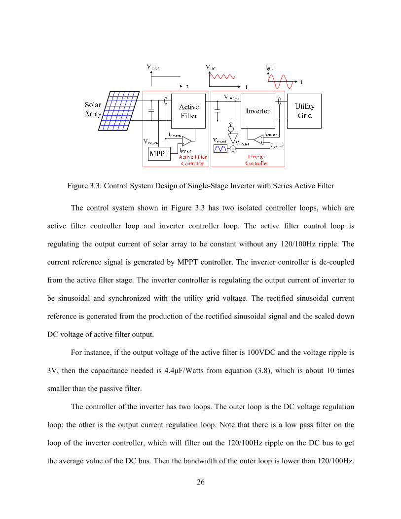
Figure 3.3: Control System Design of Single-Stage Inverter with Series Active Filter
The control system shown in Figure 3.3 has two isolated controller loops, which are
active filter controller loop and inverter controller loop. The active filter control loop is
regulating the output current of solar array to be constant without any 120/100Hz ripple. The
current reference signal is generated by MPPT controller. The inverter controller is de-coupled
from the active filter stage. The inverter controller is regulating the output current of inverter to
be sinusoidal and synchronized with the utility grid voltage. The rectified sinusoidal current
reference is generated from the production of the rectified sinusoidal signal and the scaled down
DC voltage of active filter output.
For instance, if the output voltage of the active filter is 100VDC and the voltage ripple is
3V, then the capacitance needed is 4.4μF/Watts from equation (3.8), which is about 10 times
smaller than the passive filter.
The controller of the inverter has two loops. The outer loop is the DC voltage regulation
loop; the other is the output current regulation loop. Note that there is a low pass filter on the
loop of the inverter controller, which will filter out the 120/100Hz ripple on the DC bus to get
the average value of the DC bus. Then the bandwidth of the outer loop is lower than 120/100Hz.
26
The inner loop is the output current regulation loop, which is a fast loop and has bandwidth of
about 10kHz.
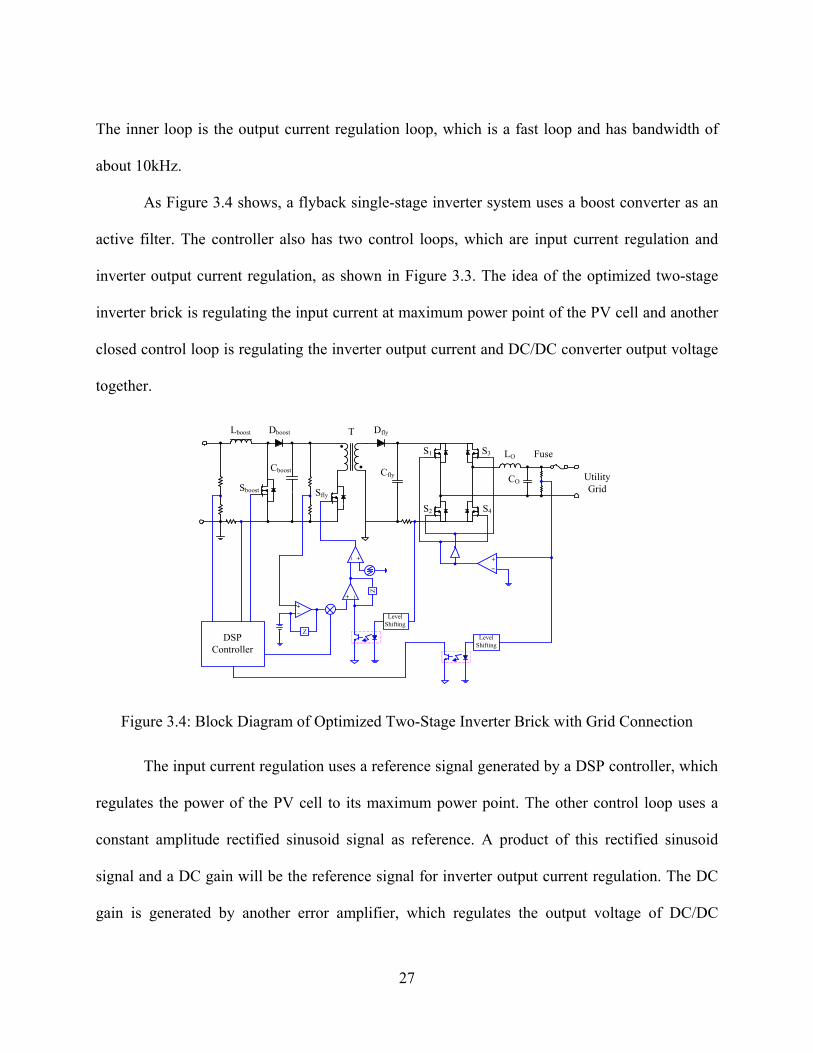
As Figure 3.4 shows, a flyback single-stage inverter system uses a boost converter as an
active filter. The controller also has two control loops, which are input current regulation and
inverter output current regulation, as shown in Figure 3.3. The idea of the optimized two-stage
inverter brick is regulating the input current at maximum power point of the PV cell and another
closed control loop is regulating the inverter output current and DC/DC converter output voltage
together. Z+ _
SflySboost
T DflyDboost
S2 S4
Utility Grid
FuseLO
Cboost Cfly CO
S1 S3
Lboost
DSP Controller
Level Shifting
+
_
Level Shifting
Z
+_
+_
Figure 3.4: Block Diagram of Optimized Two-Stage Inverter Brick with Grid Connection
The input current regulation uses a reference signal generated by a DSP controller, which
regulates the power of the PV cell to its maximum power point. The other control loop uses a
constant amplitude rectified sinusoid signal as reference. A product of this rectified sinusoid
signal and a DC gain will be the reference signal for inverter output current regulation. The DC
gain is generated by another error amplifier, which regulates the output voltage of DC/DC
27

converter to be 100V. It is a negative feedback regulation. If the DC/DC output voltage is higher
than 100V, then the DC gain increases and the power drawn from the DC/DC converter also will
increase, and this will compensate the output voltage of DC/DC the converter.
As Figure 3.3 shows, the optimized two-stage inverter brick system has two separated
control loops, which will let the inverter system drawn constant current from the PV cell and
output pure sinusoidal current to the utility grid.
Figure 3.5: Schematics of Psim Simulation Model for Active Filter
(a) I-V curves (b) P-I curves
Figure 3.6: I-V and P-I Curves of PV Arrays Used in Figure 3.5
To verify the optimized two-stage inverter brick system, a Psim simulation model is built,
as shown in Figure 3.5. Besides the analog circuits, the look-up table source is applied to
28

generate characteristic I-V curve, which simulates the PV cell, as shown in Figure 3.6. The
power of the source is rated as 50W, 100W, 200W, 300W and 400W.
A digital controller simulates the DSP controller, which provides the current reference for
the boost converter and regulates the output current of the PV cell to be its maximum power
point. A C program is coded inside of the digital controller, which could be directly converted to
the DSP code. Then, this simulation model can be used to simulate not just a power electronic
circuit and its analog controller, but also a digital controller and its performance.
The following list shows the C program used for maximum power point tracking.
29

Table 3.2 C Program for Maximum Power Point Tracking
static double Vo, Iin; static clock_0=0, clock_1; static double Vsolar_1, Isolar_1; static double Vsolar_0=0, Isolar_0=0; static double Pref_0=0.1, Pref_1=0.05; static double power_1, power_0=0; static double delt_ref=0.05; static double indicator=0; static double direction=1; static double first=0; clock_1=in[2]; Vsolar_1=in[1]; Isolar_1=in[0]; if ( clock_0 == 1 && clock_1 == 0 ) power_1=Vsolar_1*Isolar_1; power_0=Vsolar_0*Isolar_0; if (first==0) Pref_1=Pref_0+direction*delt_ref; first=1; else if (power_1>power_0 ) if (Vsolar_1>Vsolar_0) Pref_1=Pref_0-direction*delt_ref; else Pref_1=Pref_0+direction*delt_ref; indicator=1;
else if ( power_1<=power_0 ) if (Vsolar_1>Vsolar_0) Pref_1=Pref_0+direction*delt_ref; else Pref_1=Pref_0-direction*delt_ref; indicator=2; else Pref_1=Pref_1+direction*delt_ref; indicator=4; if (Pref_1<0.1) Pref_1=0.1; indicator=3; Vsolar_0=Vsolar_1; Isolar_0=Isolar_1; power_0=power_1; Pref_0=Pref_1; clock_0=clock_1; out[0]=Pref_1; out[1]=indicator; out[2]=power_0; out[3]=direction;
30
I I
PP
P1
P0 P0
P1
P1
P0 P0
P1
0 0
VV0
0
V
0 II
V1 V0 V1
V0
V1
V1
V0
(a) (b)
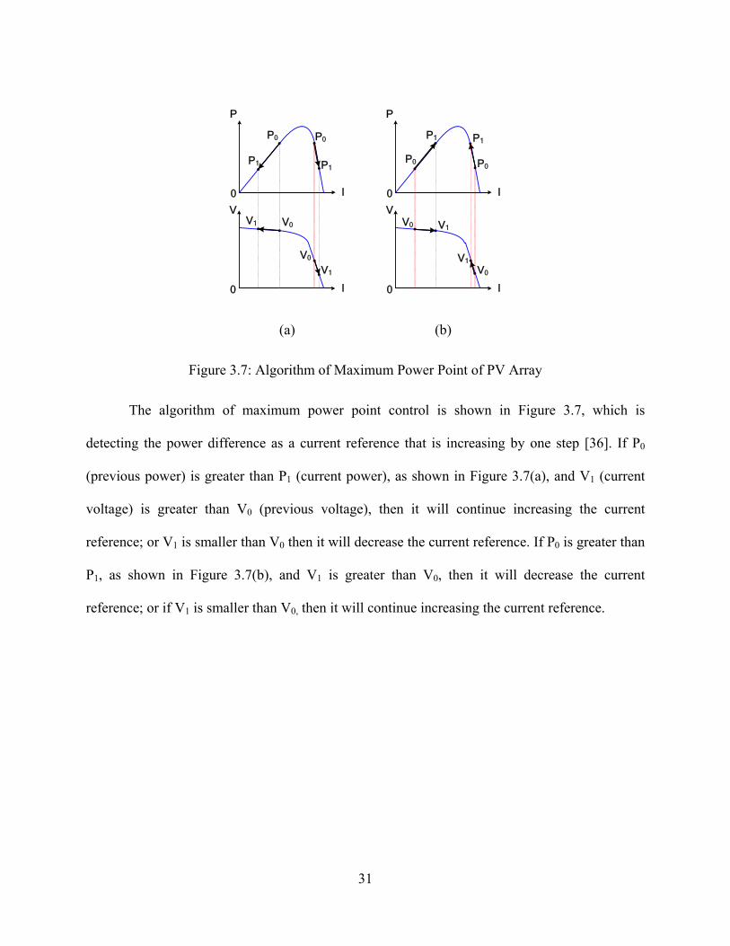
Figure 3.7: Algorithm of Maximum Power Point of PV Array
The algorithm of maximum power point control is shown in Figure 3.7, which is
detecting the power difference as a current reference that is increasing by one step [36]. If P0
(previous power) is greater than P1 (current power), as shown in Figure 3.7(a), and V1 (current
voltage) is greater than V0 (previous voltage), then it will continue increasing the current
reference; or V1 is smaller than V0 then it will decrease the current reference. If P0 is greater than
P1, as shown in Figure 3.7(b), and V1 is greater than V0, then it will decrease the current
reference; or if V1 is smaller than V0, then it will continue increasing the current reference.
31

Output voltage of boost converter
Output current of inverter brick
Output power of PV cell
Figure 3.8: Simulation Results of Inverter Brick at Different Power Rating PV Cell
To test the performance of the MPPT algorithm and the inverter with grid connection,
five different power rating PV cells are used as sources, which are shown in Figure 3.6. As
Figure 3.8 illustrates, the average output voltage of a boost converter is stabilized at 100Vdc with
120Hz ripple. The output current of the inverter brick is synchronized with the utility grid and
amplitude of sinusoid current is adjusted accordingly to maintain the output voltage of boost
converter to be 100Vdc. The output power of PV cells is maintained at its maximum power,
which is 400W, 300W, 200W, 100W and 50W.
To test the dynamics of the MPPT algorithm, another simulation is performed, which lets
the power rating of the PV cell be switched from 200W to 300W and from 300W to 400W, then
changed back to 300W and 200W.
32

As Figure 3.9 shows, the inverter brick system is tracking the dynamic maximum power
of the PV cell. Note the output current of the PV cell is constant without any apparent 120Hz low
frequency ripple, and the power of the PV cell stays at its maximum power point without any
degrading, which proves the optimized two-stage inverter brick system is more suitable to the
low power of the PV cell and has the maximum utilization efficiency.
Output voltage of the boost converter
Output current of the inverter brick and the utility grid voltage
Output power of the PV cell
Output current of the PV cell
Figure 3.9: Simulation Results of Inverter Brick at Different Power Rating PV Cells
3.3 Active Filter with Feedforward Controller
To regulate the input current of the active filter to be constant, the inverter current control
loop and active filter’s control loop are de-coupled completely. The current reference of inverter
33

is generated from the voltage sensing signal of the output voltage of the active filter. Since there
is no voltage regulation of active filter output voltage, the voltage sensing signal has 120/100Hz
ripple as shown in Figure 3.2. For a single-stage inverter with active filter, as shown in Figure
3.3, there are two existing control loops. The inner loop is the inverter current control loop,
which has higher bandwidth. The inner loop regulates the inverter current to follow the current
reference, which is generated from the outer loop. To filter out 120/100Hz low frequency ripple,
the bandwidth of the voltage loop must be lower than 120/100Hz, which means the speed of the
voltage control loop is very slow. Then the inverter voltage loop’s response to the variation of
solar array will be slow. The power of solar array can be as varied as the shadow of a cloud or
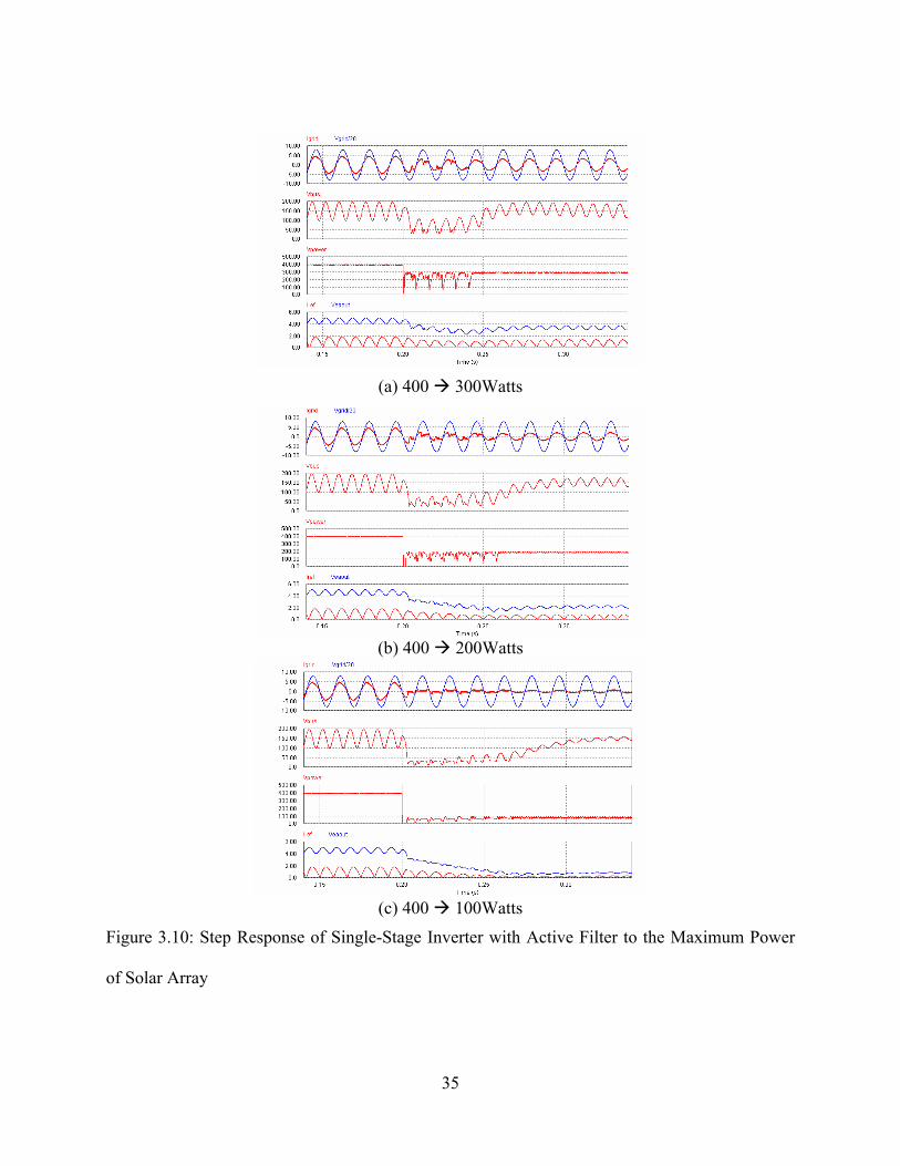
any other obstacle. Figure 3.10 shows the step response of a single-stage inverter to the
maximum power of solar array. As these figures show, the transition of the single-stage inverter
gets worse as the step change of the solar array maximum power point increases. The transition
time ranges from 50ms to 100ms as the maximum power of solar array changes from 400Watts
to 300Watts, 200Watts and 100Watts. Besides the longer transition time, the bus voltage drops
dramatically and severe distortion happens on the inverter output current. The maximum power
point of solar array output power is not tracked well either, which means the de-coupling of the
active filter and the single-stage inverter fail too.
34
(a) 400 300Watts
(b) 400 200Watts
(c) 400 100Watts
Figure 3.10: Step Response of Single-Stage Inverter with Active Filter to the Maximum Power
of Solar Array
35

The step response of the single-stage inverter with active filter can be enhanced with
feedforward control. The feedforward control signal is generated by the MPPT controller, which
is regulating the output power of the solar array. The inverter’s output current is proportional to
the output power of solar array. The amplitude of output current can be computed by the output
power of solar array and the efficiency of the inverter system. The efficiency is predicted through
analysis, but the real number could be varied. So the feedback loop is still necessary to regulate
the DC bus voltage. In most of cases, the power level disturbance of solar array is small, so the
efficiency number varies slightly and the whole system step response will be enhanced.
ActiveFilter
Inverter UtilityGrid
ttt
IgridVDCVsolar
Solar Array
+_
MPPT
+_
×
IPV.sen
IPV.ref
VPV.sen Igrid.sen
Igrid.ref
Vrec,ref
VDC.sen
_+
VPOW.refVEA.ref
Active Filter Controller
Inverter Controller
Figure 3.11: Block Diagram of Single-Stage Inverter with Active Filter and Feedforward Control
Figure 3.11 illustrates the block diagram of single-stage inverter with active filter and
feedforward control. The instant value of solar array output power feeds into the outer loop of
the single-stage inverter to adjust the magnitude of inverter output current. The reference of
inverter output current is the production of solar array output power, DC bus voltage error
amplifier output and rectified sinusoidal waveform. A factor k converts the power of solar array
into corresponding inverter output current amplitude, and the inverter efficiency is also taken
into account, which is shown as follows:
36

refPOWrefEArefrecrefgrid VVVkI .... ⋅⋅⋅= (3.9)
)(120
2 Pk η= (3.10)
where, η(P) is the system efficiency with respect to the output power of the inverter.
37
(a) 400 300Watts
(b) 400 200Watts
(c) 400 100Watts
Figure 3.12: Step Response of Single-Stage Inverter with Active Filter and Feedforward
Controller to the Maximum Power of Solar Array
38

Figure 3.12 illustrates the step response of a single-stage inverter with active filter and
feedforward control to the maximum power of solar array. Compared with Figure 3.10, with
feedforward control, the step response of solar power from 400watts to 300, 200 and 100watts
demonstrates much less transition time, and the DC bus voltage variation is much smaller.
Fundamental component with 90° phase lead
Total distortion
3rd harmonic
Normalized rectified sinusoid signal
Normalized DC bus voltage
Normalized inverter output current reference Normalized rectified sinusoid signal Normalized ideal sinusoidal inverter output current
Normalized inverter output current
Figure 3.13: 10% 2nd Harmonics on DC Bus Causes 5% 3rd Harmonics on Inverter Output
Current [34], [35]
The system efficiency can be acquired by simulations and tests. But the efficiency curve
can be different from unit to unit. Therefore, the outer loop of DC bus regulation will finely
adjust the amplitude of the inverter output current to maintain the voltage of DC bus stability.
The majority of the adjustment has already been done by feedforward control; the feedback loop
39

only performs minor adjustments. Even the bandwidth of the DC bus voltage control loop is
limited by the inner loop, but the overall speed of the system will be enhanced.
The de-coupling capacitance of the single-stage inverter is inversely proportional to the
voltage ripple superimposed on the DC bus voltage as (3.8) illustrated. The 120/100Hz voltage
ripple will be coupled to the inverter output current reference. A similar 3rd harmonic analysis in
[34] and [35] can be applied in this active filter design. As [34] and [35] claimed, for instance,
10% of 2nd harmonic voltage on the DC bus generates 5% of 3rd harmonics on the input current
of power factor correction circuit. The same result for the single-stage inverter is that a half
percentage of the 3rd harmonic component will be superimposed on the inverter output current,
as shown in Figure 3.13. The normalized DC bus voltage has 10% 2nd harmonic superimposed
on the DC. The inverter output current reference signal is generated from the production of
normalized DC bus voltage and normalized rectified sinusoid signal, which has distortion as
shown in Figure 3.13. Then the output current will be programmed with the same amount of
distortion, which is 3rd harmonic. Subtracting the normalized ideal sinusoid signal from the
normalized inverter output current, the total distortion caused by 2nd harmonic is shown in the
bottom of Figure 3.13, which is the summation of 5% 3rd harmonic and 5% fundamental
component with 90° phase lead.
40

(a) 400 300Watts
(c) 400 200Watts
(c) 400 100Watts
Figure 3.14: Step Response of Single-Stage Inverter with Active Filter, Feedforward Controller
and Sample and Hold to the Maximum Power of Solar Array
41

To overcome the 3rd harmonics on the inverter output current, the DC bus capacitance
can be increased or the gain and bandwidth of DC bus error amplifier can be decreased, which
causes a dilemma between the DC bus voltage regulation and inverter output current regulation.
Because the DC bus voltage regulation needs the inverter outer loop to have high bandwidth, but
the inverter output current regulation, the inner loop, needs the output of outer loop to be flat,
which means the bandwidth of the outer loop must be low to filter out 120/100Hz low frequency
ripple.
To solve the dilemma, a 120/100Hz sample and hold is used to process the output of the
DC bus voltage error amplifier. Since the output of sample and hold will be constant and updated
at 120/100Hz, the output current of the inverter will be pure rectified sinusoidal.
42
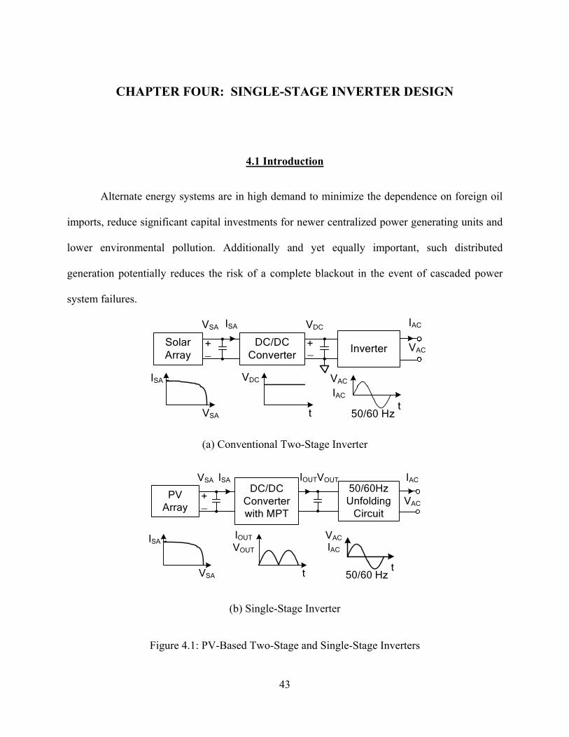
CHAPTER FOUR: SINGLE-STAGE INVERTER DESIGN
4.1 Introduction
Alternate energy systems are in high demand to minimize the dependence on foreign oil
imports, reduce significant capital investments for newer centralized power generating units and
lower environmental pollution. Additionally and yet equally important, such distributed
generation potentially reduces the risk of a complete blackout in the event of cascaded power
system failures.
Solar Array
DC/DC Converter
Inverter
IAC
VAC
ISA
+_
+_
VSA
ISA
t
VDCVSA
VDC
50/60 Hz
VAC
tIAC
(a) Conventional Two-Stage Inverter
PV Array
DC/DC Converterwith MPT
50/60Hz Unfolding
Circuit
IAC
VAC
50/60 Hz
ISA
+_
VSA
ISA
t
VAC
t
VOUTVSA
IOUT
VOUT
IOUT
IAC
(b) Single-Stage Inverter
Figure 4.1: PV-Based Two-Stage and Single-Stage Inverters
43
The PV array is an important alternate energy source, which has a special characteristic I-
V curve [36]. Then, a DC/DC converter stage is needed to pre-regulate the DC bus voltage to be
constant, provide galvanic isolation between the PV array and the utility grid and regulate the
output voltage of the PV array to be its maximum power, as Figure 4.1 (a) shows. If a
conventional inverter system has two high-frequency power conversion stages cascaded, the
overall efficiency will be the production of each stage. Two 90% efficiency power stages will
end up with an 81% efficiency overall [37].
A single-stage high-frequency link inverter system is shown in Figure 4.1 (b), which uses
a DC/DC converter to provide galvanic isolation, regulated voltage of the PV array with
maximum power tracking (MPT) and output rectified sinusoid current, which is synchronized
with the utility grid. Another 50/60Hz low frequency unfolding circuit will unfold this rectified
sinusoid current into a pure sinusoid current as shown in Figure 4.1 (b). Since the unfolding
circuit is only operated at low frequency, the switching loss can be omitted and only conduction
loss will be taken into account. Only one high-frequency power processing stage in the inverter
system will reduce the switching loss as well as increase the reliability of the whole system.
Because the unfolding circuit only switches at zero voltage and current, the switching stress is
much smaller than a conventional one.
A single-stage inverter system also brings the benefit of an expandable system structure.
By using the modularized design of DC/DC converters in Figure 4.1 (b), the inverter system can
be paralleled easily up to a high power inverter system by using only one unfolding circuit.
44

4.2 Full-Bridge Phase-Shift ZVS Single-Stage Inverter
There are many topologies for a DC/DC converter, such as buck, boost, half-bridge, full-
bridge, and forward. For single-stage solar-based inverter system, three requirements need to be
fulfilled, which are high efficiency, high power rating (above 1kW) and isolation. When all these
topologies are compared, full-bridge is the best topology for this application.
Full-bridge can easily handle higher power (1kW or even more) than other topologies and
supply isolation between the solar array and the utility grid, which can protect the customers
safety, as shown in Figure 4.2. The main transformer of the full-bridge topology works under full
symmetry of volt-seconds, which will eliminate the saturation of the transformer and greatly
reduce the size of the transformer. Another benefit of the full-bridge topology is that it can easily
achieve zero voltage switching (ZVS) controlled by a phase-shift controller, such as UCC3895,
UC3875 and HIP4080, which can increase efficiency and reliability.
.LI SA
SB
CSA
CSB
T
S1
CS1
CS2
SC
SD
CSC
CSD
.S2
S3CS3
CS4
S4
CI1 CI2
RI2
D1
D2
. LO
CO
Figure 4.2: Block Diagram of Single-Stage Full-Bridge Phase-Shift Inverter
To invert the rectified sinusoid current into sinusoid current, a full-bridge unfolding
circuit is applied, which will be switched in 50/60Hz frequency. Without high frequency
45

switching, the unfolding circuit will have much higher efficiency than high frequency PWM
conventional inverter.
4.3 Transformer Analysis
Since the DC/DC converter of a single-stage inverter outputs rectified sinusoid current to
the unfolding circuit, the width of voltage pulses on the primary side of the transformer is
modulated sinusoidally [38][39]. The height of these pulses is VIN, as shown in Figure 4.3. The
frequency of sinusoid modulation is 100/120Hz. A voltage-seconds analysis can prove that this
sinusoid modulation will not affect the high-frequency operation of the transformer. The design
of the single-stage inverter transformer is the same with conventional DC/DC converter high-
frequency transformer.
Figure 4.3: Voltage on the Primary Side of Transformer
VTR
VCOMP
VREF
VRAMP
b1
a1 a2
b2
a3
b3 … bn bn-1 bn-2
an-2 an-1 an …
Figure 4.4: Voltage-Seconds Analysis of Transformer
46

Figure 4.4 shows simplified key waveforms of average current mode controller for a
single-stage inverter. VREF is the output signal of error amplifier, which can be assumed to be a
rectified pure sinusoid waveform. VRAMP is a high-frequency ramp signal. A comparator will
compare these two signals. And the output of comparator VCOMP will drive the MOSFET through
the driver circuit. Accordingly, the voltage of the primary side transformer will be VTR. The
amplitude of VTR is VIN, which is the output voltage of PV array [40].
In a conventional high-frequency transformer design, a value of the peak ac flux density
ΔB is usually defined to limit the core loss of the high-frequency transformer. The relationship
between the voltage-seconds production of the transformer primary side with ΔB is:
NABDTVIN ⋅⋅Δ=⋅⋅ maxmax (4.1)
where,
VIN: the input voltage of DC/DC converter.
T: the switching period of DC/DC converter.
Dmax: the maximum duty cycle of DC/DC converter.
ΔBmax: the maximum ac flux density.
A: the cross section area of the ferrite core.
N: the turns of transformer primary side.
Consider the voltage of the transformer as shown in Figure 4.4. Assume the voltage-
seconds production of positive pulses are b1, b2, …, bn-1 bn, and negative pulses are a1, a2,…, an-1
and an. Also assume bn is the voltage-seconds production of the pulse with maximum width
among all the pulses. The net voltage-seconds production will be:
47

KK nn bababa +−+−+−= 2211λ (4.2)
The maximum value of net voltage-seconds production will be:
nn bababa +−+−+−= K2211maxλ (4.3)
This equation is of the form
AB −=maxλ (4.4)
with
∑=
=n
iiaA
1 (4.5)
∑=
=n
iibB
1 (4.6)
From Figure 4.4
nnnn abababab >>>> −− ,,, 112211 K (4.7)
12312 ,, −>>> nn bababa K (4.8)
So
nbBaA −>− 1 (4.9)
1abAB n −<− (4.10)
Then
nn bab <−< 1maxλ (4.11)
inn TVb 5.0max, ≤ (4.12)
For full-bridge topology, the maximum pulse width is 0.5T, where T is the switching
period. Then, for the conventional high-frequency DC/DC converter, (1) can be derived as:
48

NABTVin ⋅⋅Δ= max5.0 (4.13)
Also for single-stage inverter transformer, (1) can be written as:
inTVNAB 5.0maxmax =⋅⋅Δ=λ (4.14)
Then, the transformer of a single-stage inverter can be designed as a conventional DC/DC
converter transformer. The sinusoidal modulation will not cause any low frequency component
or saturation of the transformer core [41].
4.3 Slope Compensation Mathematical Model for Single-Stage Peak Current Mode Control
When the current-mode converter is operated at a duty cycle higher than 50%, the inner
loop has an unconditional instability, which cannot be cured by the feedback loop. A certain
amount of slope compensation can resolve the stability issue at any duty cycle values [42].
49
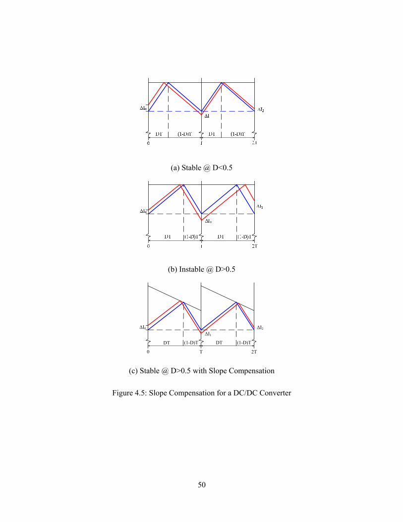
(a) Stable @ D<0.5
(b) Instable @ D>0.5
0 T
ΔI0 ΔI2
DT (1-D)T DT (1-D)T
2T
ΔI1
(c) Stable @ D>0.5 with Slope Compensation
Figure 4.5: Slope Compensation for a DC/DC Converter
50
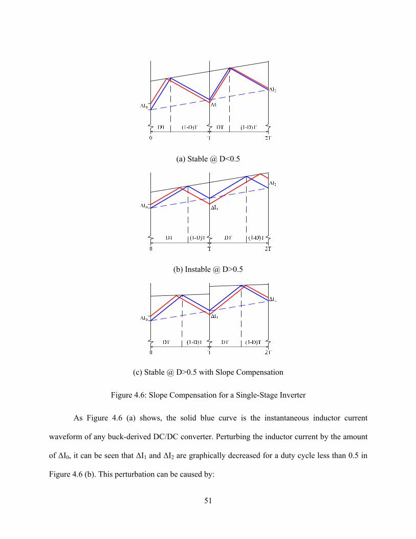
(a) Stable @ D<0.5
(b) Instable @ D>0.5
(c) Stable @ D>0.5 with Slope Compensation
Figure 4.6: Slope Compensation for a Single-Stage Inverter
As Figure 4.6 (a) shows, the solid blue curve is the instantaneous inductor current
waveform of any buck-derived DC/DC converter. Perturbing the inductor current by the amount
of ΔI0, it can be seen that ΔI1 and ΔI2 are graphically decreased for a duty cycle less than 0.5 in
Figure 4.6 (b). This perturbation can be caused by:
51

1. Step change of input voltage of DC/DC converter.
2. Jittering on the switch’s driving circuit.
3. Jittering on the inductor current reference signal.
Figure 4.6(c) depicts that applying slope compensation when the duty cycle is greater
than 0.5, ΔI1 and ΔI2 will be decreased dramatically.
Figure 4.6 depicts the slope compensation for the single-stage inverter, which is different
with a conventional DC/DC converter by using rectified sinusoid signal. Again, without slope
compensation, perturbation ΔI0 will be damped when the duty cycle is less than 0.5 and
amplified when the duty cycle is greater than 0.5. For the same reason, applying slope
compensation can solve the problem.
A mathematical model is derived to analyze the stability and slope compensation method
for the single-stage inverter.
Figure 4.7: Slope Compensation for Single-Stage Inverter
Assume the current reference has the slope compensation with an angle of γ and the
inductor current reference has an angle of θ to the horizontal line. Also a characteristic triangle
CGD is shown in Figure 4.7. In this triangle, we have:
αtanABGD = (4.15)
52

)2
sin()2
sin( απγαπ−
=−+
CDGD (4.16)
ABABGDGDCD)cos(
sin)cos(
tancos)cos(
cos
)2
sin(
)2
sin(
γαα
γααα
γαα
γαπ
απ
−=
−⋅
=−
=−+
−= (4.17)
)2
sin()2
sin()2
sin( γβπγβααππβπ−−
=−−−+−
=+
HDHDCD (4.18)
ABCDCDHD)cos(cos)cos(sin
cos)cos(
)2
sin(
)2
sin(
γαβγβα
βγβ
βπ
γβπ
−⋅+⋅
=+
=+
−−= (4.19)
ABHDEF)cos(sin)cos(sin
tan γαβγβα
β −⋅+⋅
== (4.20)
which is:
01 )cos(sin)cos(sin II Δ
−⋅+⋅
=Δγαβγβα (4.21)
Let:
αγαγα
βγβγβ
γαβγαβγβαγβα
γαβγβαθ
sinsinsincoscos
sinsinsincoscos
sinsinsincoscossinsinsinsincoscossin
)cos(sin)cos(sin)(
+
−
=+⋅−⋅
=−⋅+⋅
=G (4.22)
γα
γβ
γα
γα
γβ
γβ
θtan
tan1
tantan
1
sinsin
coscos
sinsin
coscos
)(+
−=
+
−=G (4.23)
If G(θ) is greater than 1, the system is unstable when the duty cycle is greater than 0.5.
The system is unconditionally stable at any duty cycle when G(θ) is always less than 1. Also, the
53

smaller of G(θ), the sooner the inductor current reaches the steady state with zero steady state
error, which means a more stable margin.
To verify this mathematical model, the DC/DC converter case without slope
compensation will be used, which is θ and γ=0. From (4.23),
βα
α
β
γα
γβθ
tantan
tan1
tan1
tantan
1
tantan
1
)( ==+
−=G (4.24)
(a) Without Slope Compensation (b) With Slope Compensation
Figure 4.8: DC/DC Converter Slope Compensation
From Figure 4.8 (a), we have,
DD
TDDTG
−=
−==
1)1(tantan)(
βαθ (4.25)
So, G(θ)>1, when D>0.5, unstable; G(θ)<1, when D<0.5, stable, without slope
compensation.
To apply slope compensation as shown in Figure 4.8 (b), choose γ to let tanγ=k/tanβ
kD
Dk
k
kk
k
G+
−−
=+
−=
+
−=
+
−=
11
tantan
1
tantan1
tantan1
tantan
1
tantan
1
)(
αβ
βα
ββ
γα
γβθ (4.26)
To let G(θ) always be less than 1,
54

kD
Dk +−
<−11 (4.27)
which is equivalent to:
5.01
5.015.0=
−≥
−>
DDk (4.28)
Then, to guarantee the DC/DC converter to be stable at any duty cycle, the slope
compensation must have:
βγ
tan5.0tan > (4.29)
The mathematical model is verified in DC/DC converter case.
0
B
D
E
θ
γ
α β
DT (1-D)T
K
L
M
Figure 4.9: Derivation of G(θ)
From the triangle DBE, the G(θ) can be simplified as:
βθ
βθθ
α
tan1tan
tan)1(tan)1(tan
tan
DD
TDTDDT
DTDKKLLM
BMDMBM
−+
=
−+−+
=
++==
(4.30)
55

γβ
θ
γβ
γβθ
γβ
γα
γβθ
tantan
11tan1
tantan
1
tantan1tan
tantan
1
tantan
1
tantan
1
)(+
−+
−=
+
−+
−=
+
−=
DD
DD
DG (4.31)
Assume tanγ=k/tanβ, so we have:
kD
DD
kk
DD
D
k
G+
−+
−=
+−
+
−=
1tantan11
tantan11tan1
tantan1
)(βθ
ββθ
ββθ (4.32)
where,
( )( )[ ]θβ tanarccossin2120/)(//tan OOO LtvLDKEK ===
and Lo is the inductance of single-stage inverter.
( ) ( )( ) ⎟⎟⎠
⎞⎜⎜⎝
⎛+
−+−= k
DDL
DkG o 1
tanarccossin170tan1/1)(
θθθ (4.33)
To guarantee the stability of the single-stage inverter, G(θ) must be less than 1. Then,
( ) ( )( ) 11tanarccossin170
tan/1)( <⎟⎟⎠
⎞⎜⎜⎝
⎛+
−+−= k
DD
DL
kG o
θθθ (4.34)
( )( ) DD
DL
k O
21
tanarccossin340tan5.0 −
−−>θ
θ (4.35)
The output inductor Lo is about 100nH up to 100uH, so Lo/312 is very small and can be
ignored. Then k must be greater than 0.5 to guarantee the system stability at any duty cycle.
A Psim simulation model has been developed to prove the slope compensation for the
peak current mode control of DC/DC converter as illustrated in Figure 4.10, which outputs a
rectified sinusoidal waveform. A buck circuit represents all the buck-derived isolated or non-
isolated topologies. This circuit has an inner-loop for the regulation of inductor current with peak
current mode control and another outer-loop for the regulation of output voltage. To simulate the
56
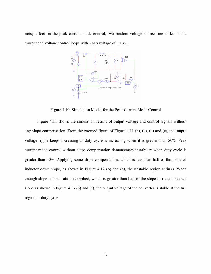
noisy effect on the peak current mode control, two random voltage sources are added in the
current and voltage control loops with RMS voltage of 30mV.
Figure 4.10: Simulation Model for the Peak Current Mode Control
Figure 4.11 shows the simulation results of output voltage and control signals without
any slope compensation. From the zoomed figure of Figure 4.11 (b), (c), (d) and (e), the output
voltage ripple keeps increasing as duty cycle is increasing when it is greater than 50%. Peak
current mode control without slope compensation demonstrates instability when duty cycle is
greater than 50%. Applying some slope compensation, which is less than half of the slope of
inductor down slope, as shown in Figure 4.12 (b) and (c), the unstable region shrinks. When
enough slope compensation is applied, which is greater than half of the slope of inductor down
slope as shown in Figure 4.13 (b) and (c), the output voltage of the converter is stable at the full
region of duty cycle.
57
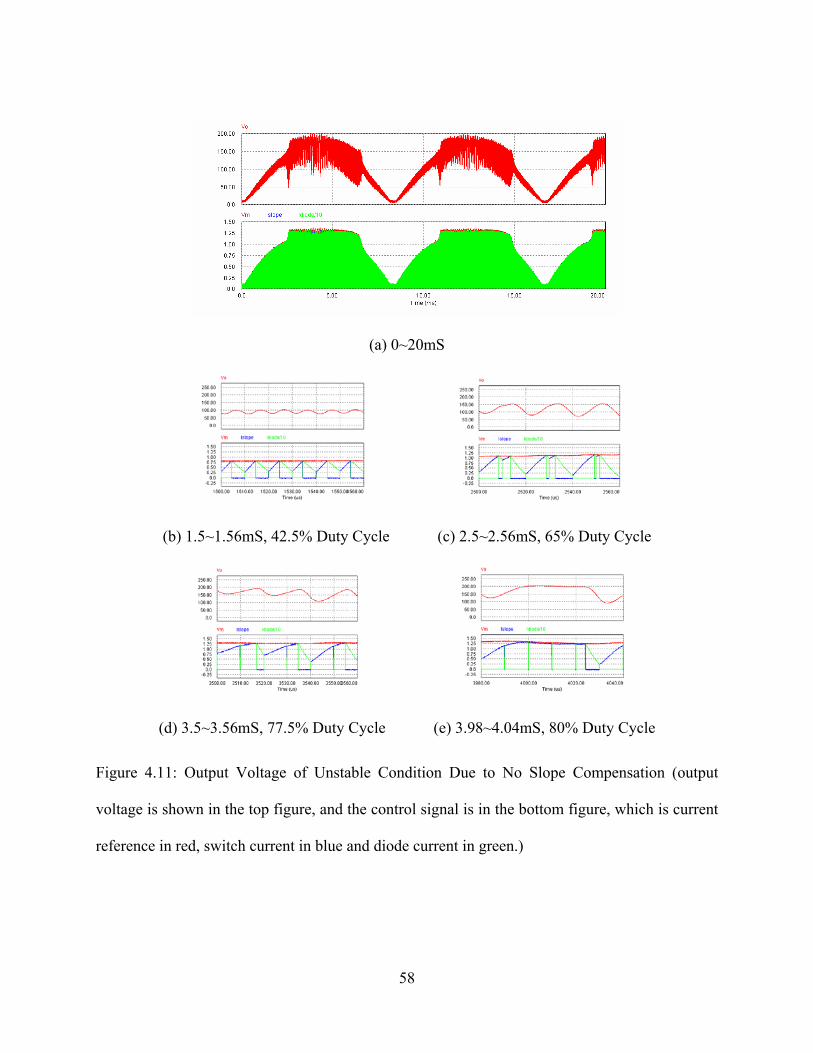
(a) 0~20mS
(b) 1.5~1.56mS, 42.5% Duty Cycle (c) 2.5~2.56mS, 65% Duty Cycle
(d) 3.5~3.56mS, 77.5% Duty Cycle (e) 3.98~4.04mS, 80% Duty Cycle
Figure 4.11: Output Voltage of Unstable Condition Due to No Slope Compensation (output
voltage is shown in the top figure, and the control signal is in the bottom figure, which is current
reference in red, switch current in blue and diode current in green.)
58
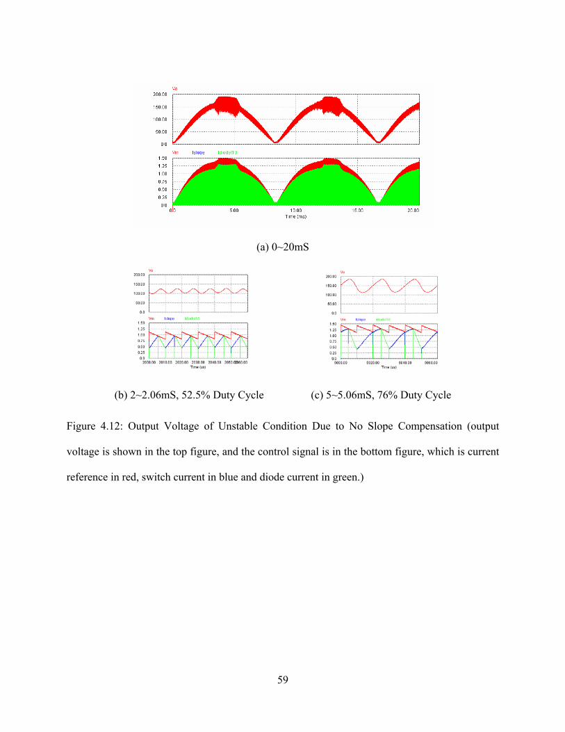
(a) 0~20mS
(b) 2~2.06mS, 52.5% Duty Cycle (c) 5~5.06mS, 76% Duty Cycle
Figure 4.12: Output Voltage of Unstable Condition Due to No Slope Compensation (output
voltage is shown in the top figure, and the control signal is in the bottom figure, which is current
reference in red, switch current in blue and diode current in green.)
59

(a) 0~20mS
(b) 2~2.06mS, 52.5% Duty Cycle (c) 5~5.06mS, 76% Duty Cycle
Figure 4.13: Output Voltage of Unstable Condition Due to No Slope Compensation (output
voltage is shown in the top figure, and the control signal is in the bottom figure, which is current
reference in red, switch current in blue and diode current in green.)
Another test is the step response of the input voltage, as shown in Figure 4.14, which is
happening at 4ms and from 220Vdc to 180Vdc. Figure 4.14 (b) shows the feedforward
characteristic of the peak current mode control, which adjusts the duty cycle cycle-by-cycle, so
the response time is very fast.
60
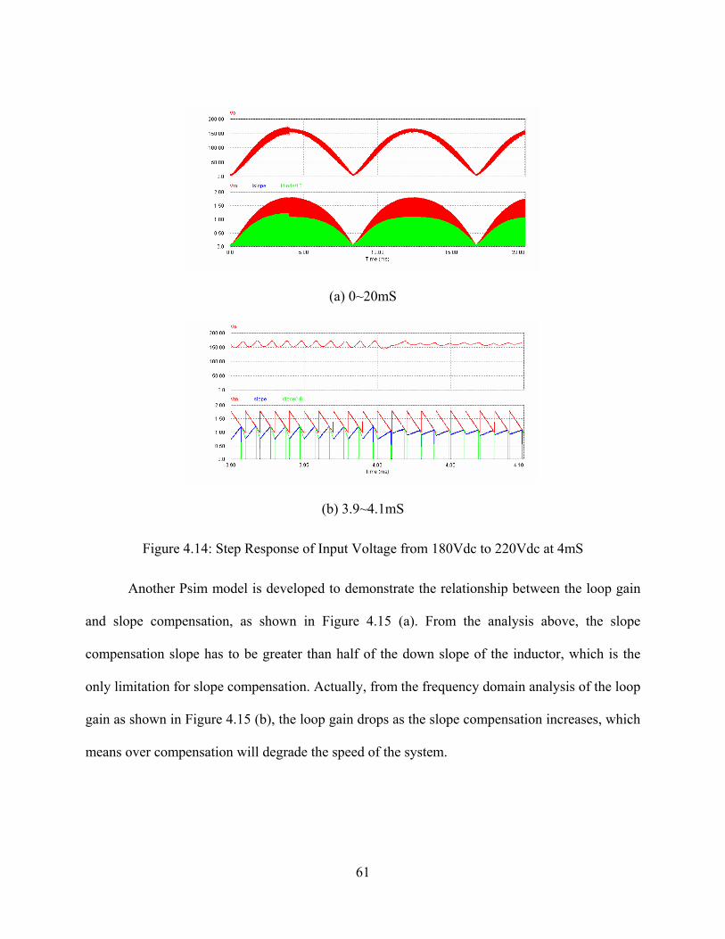
(a) 0~20mS
(b) 3.9~4.1mS
Figure 4.14: Step Response of Input Voltage from 180Vdc to 220Vdc at 4mS
Another Psim model is developed to demonstrate the relationship between the loop gain
and slope compensation, as shown in Figure 4.15 (a). From the analysis above, the slope
compensation slope has to be greater than half of the down slope of the inductor, which is the
only limitation for slope compensation. Actually, from the frequency domain analysis of the loop
gain as shown in Figure 4.15 (b), the loop gain drops as the slope compensation increases, which
means over compensation will degrade the speed of the system.
61
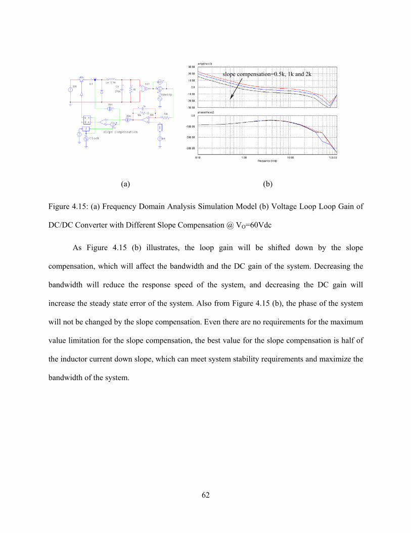
slope compensation=0.5k, 1k and 2k
(a) (b)
Figure 4.15: (a) Frequency Domain Analysis Simulation Model (b) Voltage Loop Loop Gain of
DC/DC Converter with Different Slope Compensation @ VO=60Vdc
As Figure 4.15 (b) illustrates, the loop gain will be shifted down by the slope
compensation, which will affect the bandwidth and the DC gain of the system. Decreasing the
bandwidth will reduce the response speed of the system, and decreasing the DC gain will
increase the steady state error of the system. Also from Figure 4.15 (b), the phase of the system
will not be changed by the slope compensation. Even there are no requirements for the maximum
value limitation for the slope compensation, the best value for the slope compensation is half of
the inductor current down slope, which can meet system stability requirements and maximize the
bandwidth of the system.
62

(a) (b)
Figure 4.16: (a) Frequency Domain Analysis Simulation Model (b) Current Loop Loop Gain Of
DC/DC Converter with Different Slope Compensation
loop gain trans fun loop gain trans fun
(a) VO=160Vdc (b) VO=20Vdc
Figure 4.17: Loop Gain of Voltage Loop and Transfer Function of Current Loop
Figure 4.16 depicts the Psim simulation model to analyze the current loop loop gain,
which is using a constant current reference. The simulation results shown in Figure 4.16 (b)
prove that the loop gain of the current loop is inversely proportional to the slope of compensation,
which is also shown in [42] and [43].
63
Continuing loop gain analysis in Figure 4.17 shows the simulation results of voltage loop
gain and transfer function of current loop. The transfer function of current loop is part of the
closed-loop voltage loop gain, which is the transfer function of output of the voltage error
amplifier and the current of inductor. As Figure 4.17 shown, the transfer function of current loop
is reduced as the slope compensation increase. As a result, the voltage loop loop gain is reduced
also, which explains the simulation results of Figure 4.15 (b).
4.4 Adaptive Slope Compensation for Single-Stage Inverter
Figure 4.18 has shown the unified slope compensation, which is applying the same slope
compensation at any duty cycle and load. The down slope of the inductor current will depend on
the output voltage of the DC/DC converter by VO/L. For the case of the single-stage inverter, the
output voltage is rectified sinusoid, which is in the range of 0~170V. That means the slew rate of
the inductor current is near zero at small duty cycle, and it has high slew rate at the peak of
output voltage. If applying a unified slope compensation for a DC/DC converter of single-stage
inverter, it will be over compensated at most of the region, since the unified slope compensation
must meet the stability requirements of peak output voltage. As shown in Figure 4.18 (d) and (e),
the slope compensation is half of the down slope, but in Figure 4.18 (b) and (c), the slope
compensation is near or even larger than the down slope of the inductor current, which is over
compensated.
64

(a) Output Voltage of DC/DC Converter, 0~10mS
(b) 1~1.03mS (c) 2~2.03mS (d) 3~3.03mS (e) 4~4.03mS
Figure 4.18: Output Voltage and Control Signals with Unified Slope Compensation (red
waveform is current reference with unified slope compensation, blue waveform is current
sensing signal of switch and green waveform is the current sensing signal of diode in b, c, d and
e)
To achieve the uniform bandwidth of the system, adaptive slope compensation is
proposed, which applies a compensation slope of half inductor down slope at any output voltage.
Adaptive slope compensation will meet the requirement of stability for peak current mode
control and guarantee the maximum loop gain of the system. As shown in Figure 4.19 (a), the
adaptive slope compensation is generated by modulation of the rectified sinusoid reference signal.
The zoomed-in simulation results in Figure 4.19 (c), (d), (e) and (f) prove that the slope of
compensation is always equal to a half of the inductor current down slope at full range of the
rectified sinusoid output voltage.
65

Comparing the loop gain of the unified and the adaptive slope compensation at different
output voltage in Figure 4.20, the loop gain of the adaptive slope compensation has more
consistence than the unified slope compensation.
This adaptive slope compensation concept can also be applied to the DC/DC converter,
which has wide range of output voltage to get maximum system bandwidth.
(a) Schematics (b) VO
(c) 1~1.03mS (d) 2~2.03mS (e) 3~3.03mS (f) 4~4.03mS
Figure 4.19: Peak Current Mode Control with Adaptive Slope Compensation for Single-Stage
Inverter (red waveform is current reference with adaptive slope compensation, blue waveform is
current sensing signal of switch and green waveform is the current sensing signal of diode in c, d,
e and f)
66
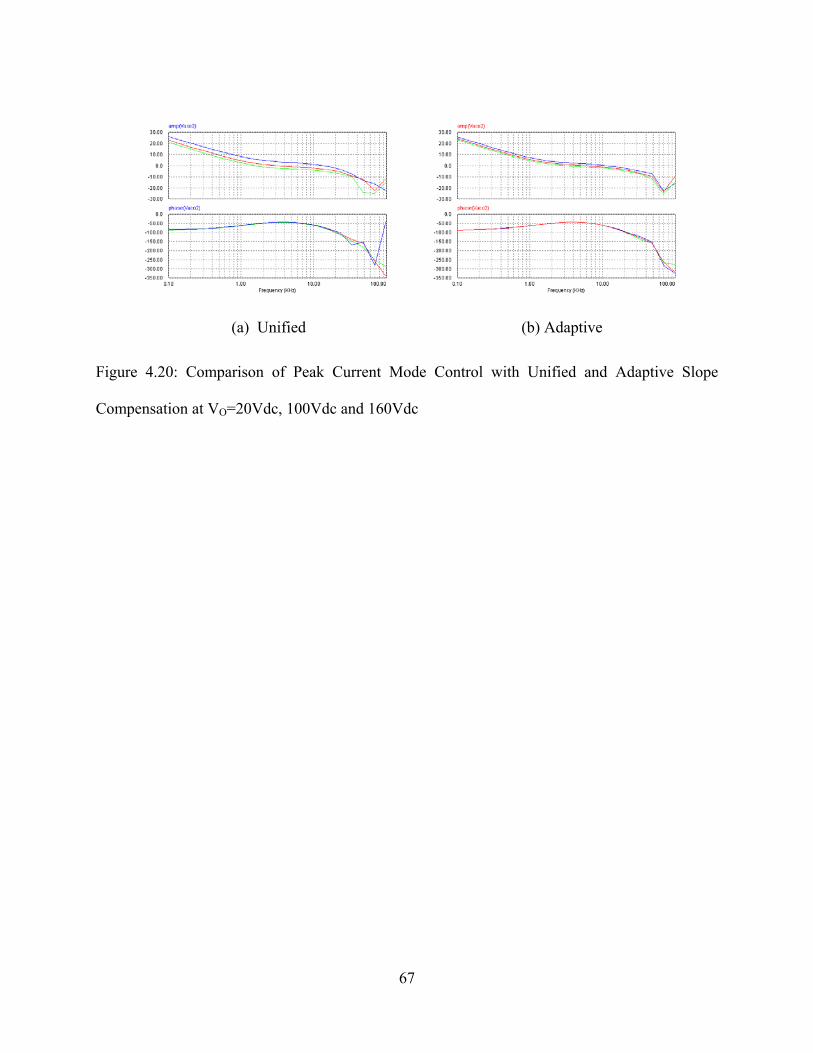
(a) Unified (b) Adaptive
Figure 4.20: Comparison of Peak Current Mode Control with Unified and Adaptive Slope
Compensation at VO=20Vdc, 100Vdc and 160Vdc
67

CHAPTER FIVE: DIGITAL CONTROLLER DESIGN FOR THE ACTIVE FILTER OF SINGLE-STAGE INVERTER
5.1 Digital Controller Design for Single-Stage Inverter System
SflySboost
T DflyDboost
Cboos
t Cfly
Lboost
TIsen
RIsen
CIsen
Ibus
Vbus
DSP Controller
S2 S4
Utility Grid
FuseLO
CO
S1 S3
Level ShiftingVin Vgrid
Drvfly
Drvbs
tIin
PVCell
Figure 5.1: System Block Diagram of Single-Stage Inverter with Digital Controller
Figure 5.2: Block Diagram of Digital Controller
68

The system parameters used in this design are:
• Vin = 40~60V, Vo = 100V, Max output current Iin = 2.5A.
• Maximum input current sensing (used for ADC signal scaling) VIin,sen = 2V.
• PWM frequency fpwm = 250kHz; Voltage loop sampling frequency fs = 250kHz.
• Output filter components, L = 400uH, C = 200uF, RC = 0.004Ω.
• Desired current loop bandwidth fci = 20kHz.
• Phase Margin = 45°.
• Vse = 5V.
• Rs = 0.05Ω. The amplifier gain is 10, then the equivalent sensing resistance 0.5Ω.
The small signal model of current control loop is:
se
sOid sLV
RVsG ⋅=)( (5.1)
Where, Vo is output voltage of boost converter, Rs is the current sensing resistor, L is the
inductor of boost converter, Vse is the oscillator ramp voltage.
The corresponding digitalized closed-loop control system is shown in Figure 5.2, which
includes the effect of sample and hold. Hc represents the gain of ADC. The on-chip PWM
module is functioning as a zero-order-hold device. The ADC and the PWM module together
from a sampling and hold device. The effect of such sample and hold action will introduce a time
delay of Ts/2 or a phase lag of ωTs/2 or 180f/fs degree [44].
A sample and hold device can be expressed as s-domain transfer function:
sesSH
sTs )1()(−−
= (5.2)
69
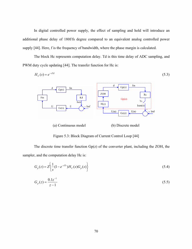
In digital controlled power supply, the effect of sampling and hold will introduce an
additional phase delay of 180f/fs degree compared to an equivalent analog controlled power
supply [44]. Here, f is the frequency of bandwidth, where the phase margin is calculated.
The block Hc represents computation delay. Td is this time delay of ADC sampling, and
PWM duty cycle updating [44]. The transfer function for Hc is:
sTdC esH −=)( (5.3)
(a) Continuous model (b) Discrete model
Figure 5.3: Block Diagram of Current Control Loop [44]
The discrete time transfer function Gp(z) of the converter plant, including the ZOH, the
sampler, and the computation delay Hc is:
⎭⎬⎫
⎩⎨⎧ −= − )()()1(1)( sGsHe
sZzG pC
sTsp (5.4)
11.0)(
1
−=
−
zzzGp (5.5)
70
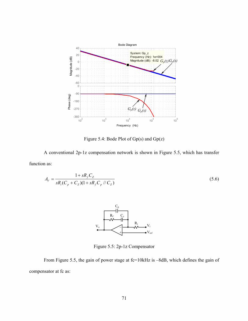
-60
-40
-20
0
20
40
Mag
nitu
de (d
B)
System: Gp_zFrequency (Hz): 1e+004Magnitude (dB): -8.02
102
103
104
105
106
-360
-270
-180
-90
0
Phas
e (d
eg)
Bode Diagram
Frequency (Hz)
Gp(z)
Gp(z)Gp(s)
Gp(s)
Figure 5.4: Bode Plot of Gp(s) and Gp(z)
A conventional 2p-1z compensation network is shown in Figure 5.5, which has transfer
function as:
)//1)((1
ZpfZpi
ZfV CCsRCCsR
CsRA
++
+= (5.6)
+
_
Rf Cz
Cp
Ri Vi
Vref
Vo
Figure 5.5: 2p-1z Compensator
From Figure 5.5, the gain of power stage at fc=10kHz is –8dB, which defines the gain of
compensator at fc as:
71

5.25.281
)(1
==⇒=−
==i
fV
idEA R
RA
dBsGG (5.7)
Ri is chosen to be 4kΩ, and then Rf is 10kΩ. A zero is placed at the cross over frequency
to give a phase margin of 45 degrees. To reduce the switching noise, a pole is placed at one half
the switching frequency.
nFCkHzCRff zzfCzero 59.110)2(11 =⇒=== π (5.8)
pFCkHzCCCCRf ppzpzfpole 159100))((2(1 =⇒=+= π (5.9)
The total phase lag is introduced by the compensation network, and the error amplifier at
the unity-gain crossover frequency, f1, is:
oooop
z
o
ff
ff 3098445270)(tan)(tan270
1
111 =+−=+−= −−θ (5.10)
The 270° phase lag is due to phase inversion introduced by the inverting error amplifier
(180°) and the pole at the origin introduced by the compensation network (90°). From Figure 5.6,
the maximum phase boost caused by the compensation network is about 60° at 40kHz, and the
phase boost is 40° at 10kHz. The phase response of the compensation network has a phase lag of
230°. From Figure 5.7, the power stage has a phase lag of 110° at 10kHz. The total phase lag is
330° at the crossover frequency 10kHz. Therefore, we have 20° phase margin, which is much
less than the requirement 45°.
ssssGci ⋅×+⋅×
+⋅×= −−
−
6211
5
10074.710126.1110592.1)( (5.11)
21
21
081.0081.11945.1501.2)( −−
−−
+−−
==zz
zzEUzGci (5.12)
Where, the sampling time is Ts = 4μS.
72

In discrete form, this controller is written as:
)2(945.1)1(501.2)2(081.0)1(081.1)( −−−+−−−= nEnEnUnUnU (5.13)
Where, U is the control output, and E is the error voltage. The quantities with (n) denote
the sampled values for the current sampling cycle, the quantities with (n-1) denote one sample
old values and so on [44].
-20
0
20
40
60
Mag
nitu
de (d
B) System: Gci_zFrequency (Hz): 1.01e+004
Magnitude (dB): 10.6
102
103
104
105
106
-180
-135
-90
-45
0System: Gci_s
Frequency (Hz): 1e+004Phase (deg): -50.7
System: Gci_zFrequency (Hz): 1e+004
Phase (deg): -60.4Phas
e (d
eg)
Bode Diagram
Frequency (Hz)
Gp(z)
Gp(z)
Gp(s)
Gp(s)
Figure 5.6: Bode Plot of Gci(s) and Gci(z)
73

Bode Diagram
Frequency (Hz)
-60
-40
-20
0
20
40
60
System: lg_zFrequency (Hz): 1.23e+004
Magnitude (dB): 0.00158M
agni
tude
(dB)
102
103
104
105
106
-360
-315
-270
-225
-180
-135
-90
System: lg_sFrequency (Hz): 1.23e+004
Phase (deg): -136
System: lg_zFrequency (Hz): 1.23e+004
Phase (deg): -175
Phas
e (d
eg)
Figure 5.7: Bode Plot of Loop Gain Gci(s)Gp(s) and Gci(z)Gp(z)
The bode plot of Gci(s) and Gci(z) are shown in Figure 5.6, which illustrates that the
discrete compensator has extra delay caused by sample and hold. The continuous compensator
has a 40° phase boost at 10kHz, but the discrete one only has 30°. As a result, Figure 5.7
illustrates the bode plot of loop gain of the closed loop current control. Due to the delay of
discrete controller, the phase margin of the discrete controller only has 5° at the fc=12.3kHz,
which will not be a stable controller, even though the corresponding continuous loop gain
provides 44° phase margin to stabilize the current regulation.
5.2 Optimization of Digital Controller
To optimize the discrete compensator and increase the phase margin to 45°, Matlab
control toolbox sisotool is applied, which can dynamically adjust the gain, poles and zeros. As
74

Figure 5.8 illustrates, the zero is moved to 4kHz and poles are staying at 0Hz and 100kHz. Then,
the phase margin is increased to 62.9°. The compensator transfer function is changed to:
)1028.6()1055.2(106.1)(' 5
46
×+×+×
=ss
ssGci (5.14)
Then, the corresponding discrete compensator transfer function is:
)081.0)(1()905.0(5.2)('
−−−
=zz
zzGci (5.15)
21
21
081.0081.112625.255.2)(' −−
−−
+−−
==zz
zzEUzGci (5.16)
Where, the sampling time is Ts=4μS.
In discrete form, this controller is written as:
)2(2625.2)1(5.2)2(081.0)1(081.1)( −−−+−−−= nEnEnUnUnU (5.17)
Where, U is the control output and E is the error voltage. The quantities with (n) denote
the sampled values for the current sampling cycle, the quantities with (n-1) denote one sample
old values and so on.
The corresponding bode plots of closed loop loop gain Gci’(s) Gp(s) and Gci’(z) Gp(z)
are shown in Figure 5.8 and Figure 5.9. In comparison, the original closed loop loop gain Gci(s)
Gp(s) and Gci(z) Gp(z) are also shown in Figure 5.8 and Figure 5.9. As illustrated, the optimized
compensator transfer function Gci’(s) boosts the phase margin from 42.8° to 62.9°, and Gci’(z)
boosts the phase margin of discrete loop gain from 23.2° to 42.8°. Then, the optimized
compensator meets the requirements.
75

Gci(z)Gp(z)
Gci’(s)Gp(s) Gci(s)Gp(s)
Gci’(z)Gp(z)
Figure 5.8: Bode Plot of Closed Loop Loop Gain Gci(s)Gp(s) and Gci’(s)Gp(s)
Gci(z)Gp(z)
Gci’(z)Gp(z)
Gci(z)Gp(z)
Gci’(z)Gp(z)
Figure 5.9: Bode Plot of Closed Lop Loop Gain Gci(z)Gp(z) and Gci’(z)Gp(z)
To verify the analytical design, a switch mode boost converter is designed as shown in
Figure 5.10(a), which uses all the design parameters and the optimized compensator Cci(z).
76

The discrete compensator is designed in C code, which is listed in Table 5.1. The clock
frequency is set to be 250kHz. The compensator output will be updated in every 4μs, which is
equivalent to the computation delay Td. The input current sensing signal is also updated in very
4μs, which is equivalent ZOH. As shown in Figure 5.10(b), the bandwidth of current regulation
is 11kHz with 44° phase margin and 11dB gain margin, which is close to the analytical results
shown in Figure 5.9 with 45° phase margin, 11.1dB gain margin and 11kHz bandwidth.
The time domain analysis shows that the step response current reference (from 0.5A to
2A) and step response of input voltage from 40V to 60V are both 100μs.
(a) Schematics (b) Closed Loop Bode Plots
(c) Step Response of Current Reference (d) Step Response of Input Voltage
Figure 5.10: Switching Model Simulation
77

Table 5.1 Digital Controller in C Code
static double Un, Un1=0, Un2=0; static clock_0=0, clock_1; static double Yn, Yn1=0, Yn2=0; static double count=0; clock_1=in[1]; Un=in[0]; if ( clock_0 == 0 && clock_1 == 1 ) Yn=1.081*Yn1-0.081*Yn2+2.5*Un1-2.2625*Un2; Yn2=Yn1; Yn1=Yn; Un2=Un1;
Un1=Un; if (Yn>5) Yn=5; if (Yn<0) Yn=0; if (Yn1>5) Yn1=5; if (Yn1<0) Yn1=0; if (Yn2>5) Yn2=5; if (Yn2<0) Yn2=0; clock_0=clock_1; out[0]=Yn
78

CHAPTER SIX: BI-DIRECTIONAL SINGLE-STAGE INVERTER DESIGN FOR MICRO-INVERTER SYSTEM
6.1 Introduction
For a grid-connected inverter, the output current of the inverter is in-phase of grid voltage.
However, for stand-alone AC load, especially an electrical device without PFC and inductive
load-like motors, a bi-directional inverter is needed to handle the reactive power.
A conventional bi-directional single-staged inverter is a cycloconverter as shown in
Figure 6.1 (a). When compared with a conventional uni-directional full-bridge DC/DC converter
as shown in Figure 6.1 (b), which uses two diodes as rectifiers, the cycloconverter will have
some disadvantages:
The first disadvantage is that the junction capacitance of high-voltage power MOSFET is
much larger than the same voltage rating of power diodes, which will cause more switching loss.
Second, a high-voltage power MOSFET has more RDS(on), which will cause more
conduction loss.
Third, more junction capacitance of a high-voltage power MOSFET will cause more
ringing across the switches, as Figure 6.2 shows. For the same prototype and input voltage, the
peak ringing voltage across diodes in Figure 6.2 (a) is 330V, but for the MOSFET in Figure 6.2
(b), the peak voltage is 530V. The high ringing voltage requires a higher voltage rating power
MOSFET, which will have even larger RDS(on). A 600V power MOSFET is almost the maximum
voltage rating power MOSFET that can be used practically in this kind of application. For a
power MOSFET, when the voltage rating is higher than 600V, the RDS(on) is unacceptable. Then,
79
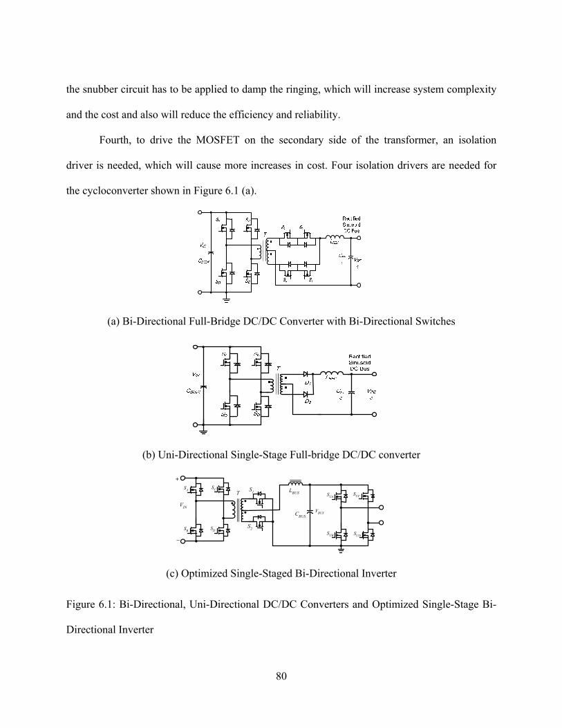
the snubber circuit has to be applied to damp the ringing, which will increase system complexity
and the cost and also will reduce the efficiency and reliability.
Fourth, to drive the MOSFET on the secondary side of the transformer, an isolation
driver is needed, which will cause more increases in cost. Four isolation drivers are needed for
the cycloconverter shown in Figure 6.1 (a).
(a) Bi-Directional Full-Bridge DC/DC Converter with Bi-Directional Switches
(b) Uni-Directional Single-Stage Full-bridge DC/DC converter
.T
.S1
S2
LBUS
CBUS
.SC
SD
+
_
VINVBUS
SA
SB
SUC
SUD
SUA
SUB
(c) Optimized Single-Staged Bi-Directional Inverter
Figure 6.1: Bi-Directional, Uni-Directional DC/DC Converters and Optimized Single-Stage Bi-
Directional Inverter
80

Figure 6.2: Experiment Results of Ringing Voltage across Diode and MOSFET with the Same
Prototype as Shown in Figure 6.1
For the PV array application, the input voltage is highly variable (30~60VDC). Therefore,
the single-stage inverter must have high turns ratio to step-up input voltage. Normally, the turns
ratio is 1:4. To reduce the semiconductor switches number, a center-tap rectification is used, as
shown in Figure 6.1. Then, system efficiency will increase and the cost will decrease. But the
center-tap transformer will double the requirements for the break-down voltage of the rectifiers
on the secondary side. For example, the reverse voltage on the rectifiers of 60VDC input and 1:4
transformer single-stage inverter is 60×4×2=480V. Due to the reason of leakage inductance on
the secondary side of the transformer, the peak voltage of the ringing can easily be higher than
600V. Even if snubbers are applied, 600V break-down voltage is the minimum requirement for
the MOSFETs. The ON resistance (RDS(ON)) of a high voltage MOSFET increases dramatically
as the break-down voltage increase. Above a break-down voltage of 600V, few MOSFETs are
available to be applied. IGBTs is a feasible choice when break-down voltage is higher than 600V,
but the switching frequency will be reduced to 40kHz or even lower, which will increase the size
and weight of the transformer.
To compare the performance, dynamic behavior and price of 600V MOSFETs and 600V
diodes, Table 6.1, Table 6.2 and Table 6.3 are presented. The MOSFETs and diodes listed in
these three tables are all chosen from International Rectifier Corporation.
81

Table 6.1 IRF® 600V MOSFETs
Body Diode
VDSS
(V)
RDS(on)
(mΩ)
ID
(A)
Junction
Capacitance
(pF)
Reverse
Recovery
Time
@25°C
(nS)
Reverse
Recovery
Time
@125°C
(nS)
Diode
Forward
Voltage
@25°C
(V)
Reverse
Recovery
Charge
@25°C
(µC)
Reverse
Recovery
Charge
@125°C
(µC)
irfps40n60k 600 110 40 675 630~950 730~1090 1.5 14~20 17~25
irfps38n60l 600 120 38 668 170~250 420~630 1.5 0.83~1.24 2.6~3.9
irfps30n60k 600 160 30 476 640~960 1.5 11~16
Table 6.2 IRF® 600V Diodes
VRRM
(V)
IF(AV)
(A)
Junction
Capacitance
(pF)
Reverse
Recovery
Time
@25°C
(nS)
Reverse
Recovery
Time
@125°C
(nS)
Diode
Forward
Voltage
@25°C
(V)
Diode
Forward
Voltage
@125°C
(V)
Reverse
Recovery
Charge
@25°C
(µC)
Reverse
Recovery
Charge
@125°C
(µC)
30eth06 600 30 33 31 77 2.0 1.34 0.065 0.345
30epf06 600 30 160 1.41 1.25
40epf06 600 40 180 1.25 0.5
60epu06 600 60 39 81 164 1.35 1.20 0.3 1.394
Table 6.3 Price of 600V MOSFETs and Diodes
irfps40n60k irfps38n60l irfps30n60k 30eth06 30epf06 40epf06 60epu06
Price of Quantity 1000 ($) 11.699 9.845 6.400 1.053 2.214 2.628 4.238
Upon comparison of the body diodes of MOSFETs with the diodes, the reverse recovery
time is much longer, and the reverse recovery charge of the MOSFET body diodes is also much
82

higher than the diodes, which cause more switching loss than the diodes. The junction
capacitance of the MOSFETs is much larger than the diodes. The ringing on the secondary side
of the transformer is mainly caused by the leakage inductance of the transformer and the junction
capacitance of the rectifiers. The large junction capacitance of the MOSFETs will cause even
higher ringing, which will exceed the break-down of the MOSFETs. Another consideration is the
issue of price. The 600V MOSFETs are far more expensive than the 600V diode. When the
driver circuits are taken into account, the cost of a bi-directional or uni-directional switch is more
expensive than the rectifier made of diodes.
6.2 Bi-Directional Power Flow and Its Mathematical Model
For a home appliance, the reactive power is not a main concern for the inverter system,
because more and more appliances have power factor correction. But for some motor driving
appliances, there is still a phase shift between the load current with the inverter output voltage,
due to the reason of inductive load. Figure 6.3 shows the measurement of input current and the
utility grid voltage of a refrigerator and a vacuum during startup. As Figure 6.3 illustrates, the bi-
directional power flow only happens when the voltage and current of the load has different
polarities.
83

(a) Vacuum
(b) Refrigerator
Figure 6.3: Current and Voltage of a Vacuum and a Refrigerator Starting
Figure 6.4: Output Voltage and Current of Stand-Alone Inductive Load
Figure 6.4 illustrates a general case of inverter output current and voltage at stand-alone
inductive load. To reveal the relationship of reactive energy of load and the peak voltage of Caux,
it is assumed:
84

tVtv rmsO ωω sin2)( = (6.1)
( φωω −= tIti rmsO sin2)( ) (6.2)
The instantaneous output power is:
⎥⎦⎤
⎢⎣⎡ −−=
−==
)2cos(21cos
212
)sin(sin2)()()(
φωφ
φωωωωω
tIV
ttIVtitvtp
rmsrms
rmsrms
OOO
(6.3)
[ ] )2(cos)2cos(cos)( φωφφωφω −−=−−= tconsIVIVtIVtp rmsrmsrmsrmsrmsrmsO (6.4)
During t0 and t1 the reactive energy of the load will be charged into the capacitor Caux,
and the total energy is:
[ ]∫∫++
−−==φπ
π
φπ
πωφωφωω tdtIVIVtdtpE rmsrmsrmsrmsOre )2cos(cos)(
tdtIVIV rmsrmsrmsrms ωφωφφφπ
π∫+
−−= )2cos(cos
φφφ sincos rmsrmsrmsrms IVIV −= (6.5)
( )φφφ sincos −= rmsrms IV
The basic concept of the proposed technique is that the capacitor Caux stores the reactive
energy of Ere from the inductive load during [t0, t1]. Assuming the voltage of capacitor Caux
before charging is Cini, then:
22
21
21
iniauxpkauxre VCVCE −= (6.6)
Then Vpk can be found to facilitate the choosing of Saux and Caux. Assuming the inverter output
power rating is 1kW, the phase delay between the inverter output current and the voltage is 10°,
85

the initial voltage on Caux is 250V and the maximum peak voltage allowed on Caux is 400V, then
a 47μF capacitor is enough to store this reactive energy.
6.3 Bi-Directional Single-Stage Inverter Design for Micro-Inverter System
Micro-inverter system makes residential solar power systems more economically viable
through innovative power electronics system design. More specifically, the initiative proposes
and designs a new modular inverter brick solar energy conversion system that will allow
customers to install and expand solar modules into homes by themselves, at a pace most
comfortable to their financial means.
This goal of a micro inverter system will be achieved through a new residential solar
energy conversion architecture that can minimize the cost and through a new power electronics
technology that can improve the conversion efficiency, reduce the cost and increase the inverter
system’s reliability. Figure 6.5(a) shows the conventional centralized inverter system and
proposed modularized inverter brick with grid connection.
86

Integrated Inverter System
AC Utility Meter
AC Utility Line
PV Panels DC Bus
AC Bus
Breaker Panel
(a) Conventional Grid-Tied PV Inverter System
PV Panels with Embedded Inverter and Wireless Ethernet
AC Utility Meter AC Utility Line Breaker Panel AC Bus
Wireless Router
Control Computers
(b) Grid-Tied PV DC/AC System with Embedded Inverter and Wireless Ethernet
Figure 6.5: Comparison of Conventional and Micro Inverters Systems
The conventional inverter system centralizes the DC/DC converter and DC/AC inverter
together. This structure needs the power rating of the inverter system to match the power rating
of PV array, which requires the customers to purchase enough PV array at one time. Since all the
PV panels are in series or parallel, the inverter can only be operated at the overall maximum
power point of all the panels. If some PV panels are degraded, the overall system efficiency will
be low. If any PV panel malfunctions, it will endanger the whole inverter system. Other than that,
the centralized inverter failure will also shut down the whole system. The centralized system
tends to be bulky, heavy and noisy, and the customer has to find a strong wall on which to mount
87

the inverter system. If the customer wants to upgrade the PV panels, the inverter will be
exchanged for a higher powered one, although then the initial investment on the inverter will be
lost.
(a) Incremental Installation of Solar Tiles on a Residential Roof
(b) At the Same Time, Different Positions
Figure 6.6: Solar Radiation of PV Panels
As the numbers of PV Tiles increase, the panels will be laid on the different position of
the house roof. As shown in Figure 6.6, the PV panels will have different solar radiation
conditions. Different solar radiation will result in different power levels. At the same time, the
power level varies with the orientation of PV panels as shown in Figure 6.6 (b), and the right PV
panel will have the highest power level and the left one will have the lowest. The character of the
PV inverter system requires a complicated maximum power tracking algorithm, which has
statistical data analysis and dynamic monitoring functions.
A conventional grid-tied PV inverter system is shown in Figure 6.5 (a), which uses an
integrated inverter system to achieve MPPT and isolation functions. The PV panels could be in
88

series and parallel to meet the requirements of the DC bus. A breaker panel will detect a
dangerous situation and will shut down the inverter. An AC meter will measure the power
delivered to the utility grid.
Due to the integrated inverter, the conventional system is cheaper and simpler. But the
utilization of PV power is low. As shown in Figure 6.6 (a), since the orientation of PV panels is
different, the maximum power point of the panels is different too. Even though the integrated
inverter has MPPT function, the inverter system can achieve only the overall maximum power
point of the PV panels. So the overall utilization of PV panels is not as efficient as the proposed
topology shown in Figure 6.5 (b), which has an embedded DC/AC inverter attached to each of
PV panels and converts solar energy directly to utility line.
In addition to the efficient utilization, the proposed topology also provides more
reliability than the conventional one. Since all the PV panels are in parallel and connected to the
utility line, if any panel fails it can be disconnected from the AC grid by the monitoring circuit in
the embedded inverters, which is attached to the PV panels. Other units will not be affected.
Compared with the topology shown in Figure 6.5 (a), if any PV panel has a short circuit, the
whole system will fail. If an open circuit occurs on any PV panel in series with other, then the
whole branch will fail.
UnfoldingCircuit
DC/DC Converter
1
DC/DC Converter
2
DC/DC Converter
n
ReverseDC/DC
Converter
RectifiedSinusoidDC Bus
...
DCSource
60/50HzAC LOAD
tV
tV
+
_
Figure 6.7: System Block Diagram of Single-Staged Bi-Directional Inverter System
89

For high AC power distribution applications, volumetric heat dissipation and high current
ability are the limitations that an individual inverter cannot overcome. Especially in the
applications of a renewable energy DC source, the input voltage is low and variable in a wide
range. A modularized inverter approach is a more reliable and economic solution for distributed
AC power systems. Modularized inverters will share the high load current and also offer
redundancy, uninterrupted operation and extended life expectancy to the system. For high current
applications, only the DC/DC converters and reverse converters need to be paralleled. Due to
low frequency operation, the unfolding circuit does not need be paralleled. The unfolding circuit
can apply IGBT, which can handle very high current. The system shown in Figure 6.7 also offers
flexibility to different loads, which means the number of DC/DC converters depends on the
amount of reactive power required by the load. The number of reverse modules is optional to the
users. In most cases, a very small power rating DC/DC converter can handle the reactive power
flow of the load.
6.4 Bi-Directional Single-Stage Inverter Design with Flyback DC/DC Converter for Micro Inverter System
The reactive power of load shown in Figure 6.3 is much smaller than the real power
delivered to the load in each cycle. Then, if a separated DC/DC stage can handle this part of
reactive power, then a uni-directional DC/DC converter can be applied, which uses power diodes
as rectifiers at the secondary side of the transformer as Figure 6.8 shows. The topology shown in
Figure 6.8 also keeps the efficiency of single-staged inverter high. Based on this idea, an
expandable system structure is proposed in Figure 6.7. To build an inverter system with very
90

high power rating, the modularized designed DC/DC converters and reverse DC/DC converters
are in parallel.
VIN
CBulk
SA SC
SB SD
T D1
D2
LO
CO
S1
S2
S3
S4
Load SF2
SF1
VIN
+
_
+
_T1 D3
CC
LI
Figure 6.8: Bi-Directional Single-Stage Inverter with Flyback DC/DC Converter
Figure 6.8 shows the proposed new single-staged bi-directional inverter with inverse
DC/DC converter, which is fully analyzed in previous chapters. The basic principle for this
topology is that the inverse DC/DC converter will absorb the extra reactive energy back to the
DC source to keep the sinusoid wave shape inverter output voltage. The DC/DC converter
topology is still full-bridge phase-shift, which is using diodes as a rectifier on the secondary side
of the transformer. The inverse DC/DC converter topology is flyback with active clamping,
which uses an auxiliary switch SF2 to clamp the ringing of SF1 when SF1 is turning off.
91

CLOCK
RAMP and COMP
PWM
OUTA
OUTB
OUTC
OUTD
ENABLE
Drive SF1
Drive SF2
Figure 6.9: Timing Diagram of Bi-Directional Single-Stage Inverter with Flyback DC/DC
Converter
Figure 6.9 is the timing diagram of bi-directional single-staged inverter with flyback
DC/DC converter. When the ENABLE signal is high, the full-bridge phase-shift is active and the
driving signal is enabled. At the same time, the driving signal to the flyback DC/DC converter
will be disabled. Since at any time, only one converter’s driving signal is enabled, there is no
circling current existing. There are two methods to generate the ENABLE signal. First, the
comparison of DC/DC converter error amplifier output and inverse DC/DC converter error
amplifier output can be the ENABLE signal in Figure 6.10 (a). The second method is to use
isolated current and voltage sensor to sense the inverter output current and voltage polarities and
generate the ENABLE signal through a NOR gate.
The benefit of the circuit in Figure 6.10 (a) is that it is simpler and cheaper. Only a
hysteresis comparator is added. For the circuit of Figure 6.10 (b), an isolated current sensing and
two comparators are added.
92

+
_
Vref
+
_
+
_
Vsense
ENABLE
DC-DC COMP
Inverse DC-DC COMP
Load
+_
+
_
+
_
Current Sensor
Voltage Sensor
ENABLE
(a) (b)
Figure 6.10: ENABLE Signal Generation
A Psim simulation module is developed to verify the concept of single-staged high-
frequency link inverter system as shown in Figure 6.11. The simulation results are shown in
Figure 6.12.
Figure 6.11: System Block Diagram of Single-Staged Bi-Directional Inverter System
93
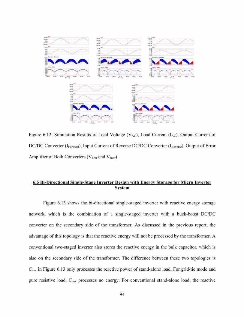
Figure 6.12: Simulation Results of Load Voltage (VAC), Load Current (IAC), Output Current of
DC/DC Converter (IForward), Input Current of Reverse DC/DC Converter (IReverse), Output of Error
Amplifier of Both Converters (VFerr and VRerr)
6.5 Bi-Directional Single-Stage Inverter Design with Energy Storage for Micro Inverter System
Figure 6.13 shows the bi-directional single-staged inverter with reactive energy storage
network, which is the combination of a single-staged inverter with a buck-boost DC/DC
converter on the secondary side of the transformer. As discussed in the previous report, the
advantage of this topology is that the reactive energy will not be processed by the transformer. A
conventional two-staged inverter also stores the reactive energy in the bulk capacitor, which is
also on the secondary side of the transformer. The difference between these two topologies is
Caux in Figure 6.13 only processes the reactive power of stand-alone load. For grid-tie mode and
pure resistive load, Caux processes no energy. For conventional stand-alone load, the reactive
94
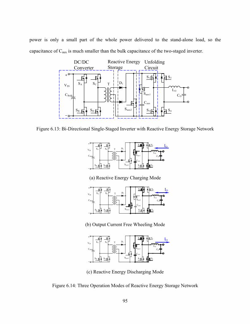
power is only a small part of the whole power delivered to the stand-alone load, so the
capacitance of Caux is much smaller than the bulk capacitance of the two-staged inverter.
VIN
CBulk
SA SC
SB SD
T D1
LO
CO
S1
S2
S3
S4
+
_
Saux1
Saux2
Caux
Figure 6.13: Bi-Directional Single-Staged Inverter with Reactive Energy Storage Network
VIN
CBulk
SA SC
SB SD
T D1
LO
CO
S1
S2
S3
S4
+
_
Saux1
Saux2
Caux
(a) Reactive Energy Charging Mode
VIN
CBulk
SA SC
SB SD
T D1
LO
CO
S1
S2
S3
S4
+
_
Saux1
Saux2
Caux
(b) Output Current Free Wheeling Mode
VIN
CBulk
SA SC
SB SD
T D1
LO
CO
S1
S2
S3
S4
+
_
Saux1
Saux2
Caux
(c) Reactive Energy Discharging Mode
Figure 6.14: Three Operation Modes of Reactive Energy Storage Network
DC/DC Converter
Reactiv nergyStorage
Unfolding Circuit
e E
IO
IO
IO
95

Figure 6.4 shows the output current and voltage of the inverter at stand-alone inductive
load and the output voltage and current seen by the DC/DC converter. To handle this reactive
power at region [t0, t1] and [t2, t3], two methods were proposed. The first method is to replace the
diodes D1 and D2 with MOSFET as shown in Figure 6.1 (c). The second method is to parallel
another DC/DC converter, which will only be activated at region [t0, t1] and [t2, t3] to handle the
reactive power of inductive load. Both methods keep the single-staged structure of the inverter
system. Both methods will be analyzed, simulated and prototyped in this dissertation.
There are three operating modes for the topology shown in Figure 6.13, which are
reactive energy charging, reactive energy free wheeling and reactive energy discharging modes.
In reactive energy charging mode, the inductive load current will be charged to Caux, the voltage
of the Caux will be applied to the inductive load, which will decrease the load current. In the free
wheeling mode, the load current is free wheeling through Saux2 in Figure 6.14 (b). In this mode,
the load current is slightly reduced due to the resistance of the load. After t1, the load current
passes zero, the energy stored in Caux discharged to the load by discharging the mode in Figure
6.14 (c).
C DF F FC F DC
C=Charging ModeF=Free Wheeling ModeD=Discharging Mode
t
iO(t)
iO(t)avg
vO(t)
vO(t)avg
t0 t1
Figure 6.15: Instantaneous and Average Output Current and Voltage
96

The initial voltage on the capacitor Caux is derived by the turns ratio and maximum input
voltage production plus a little margin. In normal conditions of pure resistive or grid connection,
Caux will be disconnected from the single-staged inverter. The inverter will be the same as the
conventional single-staged inverter. The Caux will be charged only when the reactive power tries
to find a path to feed back to the DC source, which will increase the capacitor voltage. A
comparator network will sense this increasing and disable the DC/DC converter’s full-bridge
driving signals. And the driving signals to the reactive energy storage network will be enabled.
The driving signals for the full-bridge and reactive energy storage network are generated by
UCC3895, a full-bridge phase-shift PWM controller plus some logic gates.
To optimize this compensator, a new average current mode controller is applied instead
of the average voltage mode as shown in Figure 6.16. Figure 6.17 shows the timing diagram of
Figure 6.16.
VIN
CBulk
SA SC
SB SD
T D1
D2
LO
CO
S1
S2
S3
S4
IR2110 IR2110
UCC3895
+
_
D D D D
Vref
IR2110 IR2110
D D D D
abs
+5V
+
_
VsinD = Delay Circuit
Load
+ _+_
+_
D D
Vini
Saux2
Saux1
Caux
COMP
ENABLE
Laux
+
_
abs
Figure 6.16: Block Diagram of Single-Staged Inverter with Reactive Energy Storage Network
97
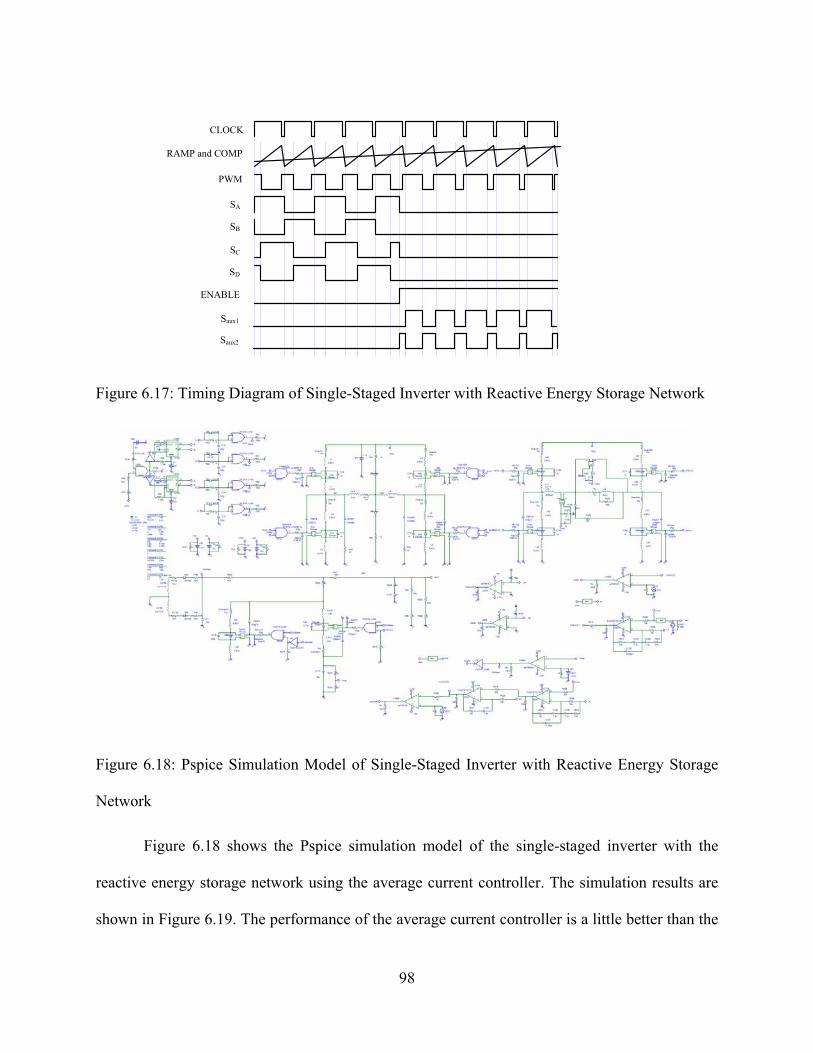
CLOCK
RAMP and COMP
PWM
SA
SB
SC
SD
ENABLE
Saux1
Saux2
Figure 6.17: Timing Diagram of Single-Staged Inverter with Reactive Energy Storage Network
Figure 6.18: Pspice Simulation Model of Single-Staged Inverter with Reactive Energy Storage
Network
Figure 6.18 shows the Pspice simulation model of the single-staged inverter with the
reactive energy storage network using the average current controller. The simulation results are
shown in Figure 6.19. The performance of the average current controller is a little better than the
98
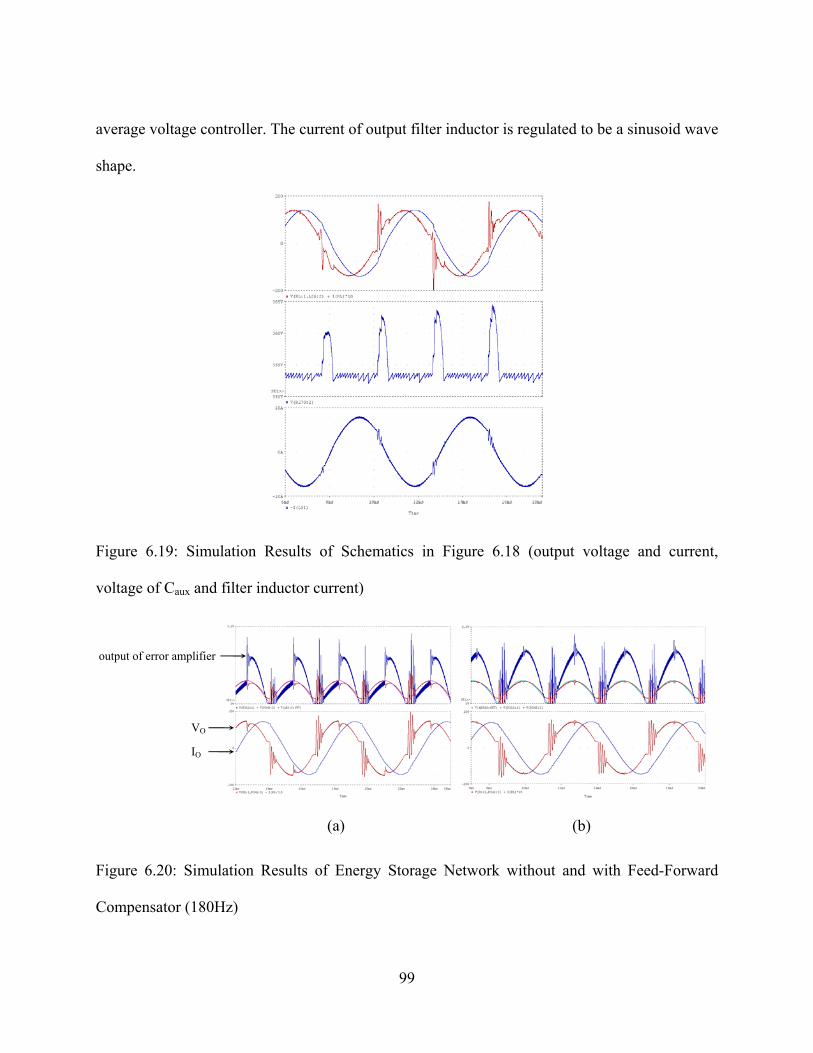
average voltage controller. The current of output filter inductor is regulated to be a sinusoid wave
shape.
Figure 6.19: Simulation Results of Schematics in Figure 6.18 (output voltage and current,
voltage of Caux and filter inductor current)
IO
VO
output of error amplifier
(a) (b)
Figure 6.20: Simulation Results of Energy Storage Network without and with Feed-Forward
Compensator (180Hz)
99

The power stage gains are different because of the input voltage. If the energy storage
network compensator is the same compensator used for the DC/DC converter, a transient step
response appears, as shown in Figure 6.20(a). To automatically adjust the gain of the
compensator for both modes, a feed-forward compensator is applied and solves the problem as
shown in Figure 6.20 (b).
Detailed Pspice simulation results proved the performance of this compensator design for
the single-staged inverter at inductive load, as shown in Figure 6.21.
100

Control Signal
VCaux
(a) Voltage of Caux and Control Signal for the Energy Storage Network
Output of
Compensator
(b) Output of Compensator
Output Voltage
Output Current
(c) Inverter Output Voltage and Current
Figure 6.21: Simulation Results of Single-Staged Inverter with Energy Storage Network (60Hz)
101

CHAPTER SEVEN: PFM ZCS FLYBACK INVERTER SYSTEM DESIGN
7.1. PFM Inverter Introduction
A PFM converter is an alternative DC/DC power converter architecture that uses a
variable frequency clock to drive the power switches and transfer energy from input to output.
Because switch mode PWM and PFM converters are commonly used in portable devices to
maximize the battery life, PFM mode is only enabled when the devices are idle to reduce the
switching loss by less switching cycles [45][46][47].
One of the concerns with switch-mode power converters is the generation of unwanted
EMI. PWM converters are often preferred by system designers because they operate at a
specified known frequency, which may make the EMI filtering design process easier. PFM
converters inherently have a variable operating frequency, and therefore many system designers
have concerns about using this type of architecture in portable products with sensitive audio or
RF subsystems.
Conventional inverters or converters are using PWM to regulate the output voltage or
current. For a single-stage inverter system, the output of the DC/DC converter is rectified
sinusoid wave form, which results in the DC/DC converter being modulated sinusoidally. The
instantaneous output power of the DC/DC converter is also regulated sinusoidally from 0 to its
maximum power, which means the light load conditions are happening repeatedly.
The motivations for applying the PFM control on a single-stage inverter are:
1. Increase the power conversion efficiency of single-stage inverter.
102
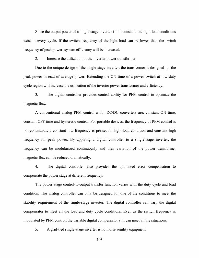
Since the output power of a single-stage inverter is not constant, the light load conditions
exist in every cycle. If the switch frequency of the light load can be lower than the switch
frequency of peak power, system efficiency will be increased.
2. Increase the utilization of the inverter power transformer.
Due to the unique design of the single-stage inverter, the transformer is designed for the
peak power instead of average power. Extending the ON time of a power switch at low duty
cycle region will increase the utilization of the inverter power transformer and efficiency.
3. The digital controller provides control ability for PFM control to optimize the
magnetic flux.
A conventional analog PFM controller for DC/DC converters are: constant ON time,
constant OFF time and hysteretic control. For portable devices, the frequency of PFM control is
not continuous; a constant low frequency is pre-set for light-load condition and constant high
frequency for peak power. By applying a digital controller to a single-stage inverter, the
frequency can be modularized continuously and then variation of the power transformer
magnetic flux can be reduced dramatically.
4. The digital controller also provides the optimized error compensation to
compensate the power stage at different frequency.
The power stage control-to-output transfer function varies with the duty cycle and load
condition. The analog controller can only be designed for one of the conditions to meet the
stability requirement of the single-stage inverter. The digital controller can vary the digital
compensator to meet all the load and duty cycle conditions. Even as the switch frequency is
modulated by PFM control, the variable digital compensator still can meet all the situations.
5. A grid-tied single-stage inverter is not noise senility equipment.
103

The PFM switching noise can be easily filtered with a line filter. The pre-regulator also
isolates the inverter stage with solar cell with a constant current drawn from the source.
The basic signal is PFM ramp signal, which is modulated as the rectified sinusoid
reference. The highest frequency happens at the peak of rectified sinusoid reference. As the
reference voltage decreases, the switching frequency decreases also.
The PFM inverter can be applied to any topology of a single-stage inverter and a two-
stage inverter with SPWM. Reducing the switching frequency at a lower power output can
effectively increase the power converting efficiency by reducing the switching loss. The
switching frequency is limited by design, which facilitates the output filter design. Since the
output filter of the inverter tends to have a lower cut-off frequency, the EMI issue of the PFM
inverter will be resolved.
7.2 Flyback ZCS Converter Operation Analysis
The PFM inverter proposed above still has shortcoming due to the switching loss.
Especially for the flyback topology, the leakage inductance of a flyback transformer primary side
winding causes huge voltage spike on the switch when the switch is turning off. Conventionally,
a passive RC snubber is applied across the switch to dissipate the energy of leakage inductance.
A better solution is called active clamping circuit, which uses an auxiliary switch to form a
resonant LC circuit. This LC resonant circuit circulates the energy of leakage inductance and
facilitates the switch turning on to achieve zero-voltage-switching [48]. The performance of both
solutions depends on the switching frequency of the flyback converter, so they are not ideal
solutions for the PFM flyback single-stage inverter.
104
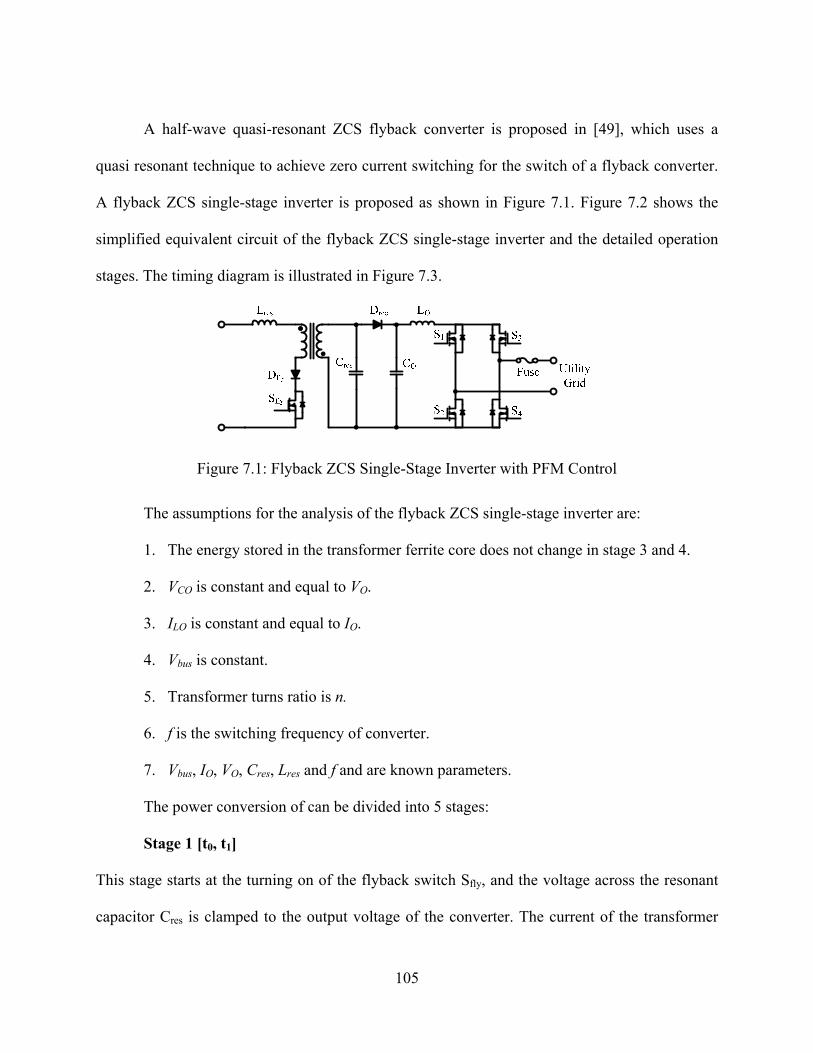
A half-wave quasi-resonant ZCS flyback converter is proposed in [49], which uses a
quasi resonant technique to achieve zero current switching for the switch of a flyback converter.
A flyback ZCS single-stage inverter is proposed as shown in Figure 7.1. Figure 7.2 shows the
simplified equivalent circuit of the flyback ZCS single-stage inverter and the detailed operation
stages. The timing diagram is illustrated in Figure 7.3.
Figure 7.1: Flyback ZCS Single-Stage Inverter with PFM Control
The assumptions for the analysis of the flyback ZCS single-stage inverter are:
1. The energy stored in the transformer ferrite core does not change in stage 3 and 4.
2. VCO is constant and equal to VO.
3. ILO is constant and equal to IO.
4. Vbus is constant.
5. Transformer turns ratio is n.
6. f is the switching frequency of converter.
7. Vbus, IO, VO, Cres, Lres and f and are known parameters.
The power conversion of can be divided into 5 stages:
Stage 1 [t0, t1]
This stage starts at the turning on of the flyback switch Sfly, and the voltage across the resonant
capacitor Cres is clamped to the output voltage of the converter. The current of the transformer
105

secondary winding is freewheeling through the rectifier diode Drec. On the primary side, the
current of the primary winding is increased from zero, which means the switch is turning on at
zero current without switching loss.
)()( 0ttL
nVVtires
ObusLres −
+= (7.1)
As the equation above shows, the current of the primary winding is increased linearly, and the
current of secondary winding decreases linearly. In this stage, the secondary winding current is
equal to the current of the rectifier diode.
OLresSfly nItiti == )()( 11 (7.2)
The time duration of this stage is:
nVVLnItt
Obus
resO
+⋅
=− 01 (7.3)
Stage 2 [t1, t2]
As the current of the rectifier diode Drec decreases linearly to zero, Drec is turned off at
zero-current. Then, the resonance between Lres and Cres starts at the Icap equal to zero and ILres
equal to ISfly.
By applying the superimposing method, the current of the primary and the secondary
windings is as follows:
)()(')( 111 tittitti LresLresLres +−=− , (7.4)
dtttdiLttv Lres
resLres)(')( 1
1−
=− , (7.5)
dtttdvCtti Cres
resCres)()( 1
1−
=− (7.6)
and
106

)(')( 11 ttittni LresCres −−=− (7.7)
)(')( 11 ttnvttv LresCres −=− (7.8)
0)('1)('122
12
=−+− tti
CLndtttid
Lresresres
Lres , resresCLn
11=ω , (7.9)
then
0)(')('1
22
12
=−+− tti
dtttid
LresLres ω (7.10)
0)(')0(')0(')(' 22 =+−− sIdt
disisIs LresLres
LresLres ω (7.11)
0)(')(' 22 =++
− sIL
nVVsIs Lresres
ObusLres ω (7.12)
22)('ω+
+
=s
LnVV
sI res
Obus
Lres (7.13)
)(sin)(' 11 ttL
VnVttires
busOLres −
+=− ω
ω (7.14)
therefore
Ores
Obus
Lresres
Obus
LresLresLres
nIttL
nVV
tittL
nVVtittitti
+−+
=
+−+
=
+−=−
)(sin
)()(sin
)()(')(
1
11
111
ωω
ωω
(7.15)
Ores
ObusLres nI
LnVVI +
+=
ωmax, (7.16)
dtttinC
tvdtttiC
tvttvtt
Lresres
Cres
tt
Cresres
CresCres ∫∫−−
−+=−+=−1
0 11
1
0 111 )('1)()(1)()( (7.17)
107

( )
( )1)(cos)()(
1)(cos1)()(
11
111
−−++=
−−+
+=−
ttnVVtv
ttL
VnVnC
tvttv
busOCres
res
busO
resCresCres
ω
ωωω (7.18)
( ) busbusObusOOCres nVttnVVttnVVVttv −−+=−−++=− )(cos)(1)(cos)()( 111 ωω (7.19)
busOCres nVVV 2min, −−= (7.20)
OCres VV =max, (7.21)
and therefore
busOpkpkCres nVVv 22, += (7.22)
OCresDrec Vttvttv −−=− )()( 11 (7.23)
busODrec nVVv 22min, −−= (7.24)
0max, =Drecv (7.25)
busOpkpkCres nVVv 22, += (7.26)
To simply the expression of t2, iLres(t) can be linearized in the region of [t2’, t2] as:
Ores
ObusLres
res
ObusLres nItt
LnVVtitt
LnVVtti +−
+−=+−
+−=− )'()'()'()'( 2222 (7.27)
At the end of region [t2’, t2], iLres(t) goes to zero, therefore
Ores
Obus nIttL
nVV+−
+−= )'(0 22 (7.28)
0122 ' ttVnVInLtt
busO
Ores −=+
=− (7.29)
The total energy delivered from the primary side of the transformer can be calculated as:
108

ωπ
ω
ωω
Obusres
ObusbusresO
Obus
bus
t
t Ores
Obusbus
t
tres
Obusbus
t
t Lresbus
t
t Lresbus
t
t Lresbus
t
t Lresbus
t
t Lresbus
InVL
nVVVLInnVV
V
dtnIttL
nVVVdtttL
nVVV
dttiVdtttiV
dttiVdttiVdtttiVE
++
+⋅+
=
⎥⎦
⎤⎢⎣
⎡+−
++−
+=
+−=
⋅+⋅+−⋅=
∫∫
∫∫
∫∫∫
222
'
10
'
0
'
'
0
2
)(sin)(2
)()(2
)()()(
2
1
1
0
2
1
1
0
2
2
2
1
1
0
(7.30)
Stage 3 [t2, t3]
Stage 3 starts as the current of primary winding reaches zero, and the resonance between
Lres and Cres stops due to the blocking of Dfly. In this stage, the resonant capacitor Cres is
discharging through the secondary side winding of the transformer by resonance. As the
discharging continues, the voltage across the resonant capacitor Cres changes its polarity. In stage
3, before the blocking diode is conducted, the voltage across the blocking diode can be illustrated
as:
)0)((0)(,)()( <=−−= tvtvVtvtv CresSflybusCresDfly (7.31)
)0)((0)()()( >=+= tvtvVtvtv CresDflybusCresSfly (7.32)
therefore
busObusbusObusCresDfly VnVVVnVVnVV +=−+=−−< 2min,max, (7.33)
busObusCresSfly VnVVnVV +=+= max,max, (7.34)
Stage 3 ends when the voltage of Cres reaches VO.
OCresres
CresCres VtttvttC
Itvtv =−−−+= )(cos)()(sin)(2)( 23sec223secsec
sec23 ωω
ω (7.35)
Then, the voltage across the switch Ssfly is
OSfly Vtv =)( 3 (7.36)
109
The turning off signal of the flyback switch is sent at stage 3.
Stage 4 [t3, t4]
Stage 4 starts when the resonant capacitor voltage reaches to the voltage across CO, then
the rectifier diode turns on at zero voltage, and the transformer secondary side winding starts to
charge output capacitor CO. Stage 4 stops at the driving signal uprising edge of the flyback
switch.
In this stage, the current of the transformer secondary winding decreases linearly:
)()()( 3sec
3 ttLVtiti O
CresCres −−= (7.37)
(a) [t0, t1] (b) [t1, t2]
(c) [t2, t3] (d) [t3, t4]
Figure 7.2: Detailed Analysis of Flyback ZCS Single-Stage Inverter
110

Figure 7.3: Timing Diagram of Flyback ZCS Single-Stage Inverter
Figure 7.3 shows the detailed timing diagram for the 5 stages shown in Figure 7.2. As
Figure 7.3 shows, the flyback switch Sfly is turning on and off at zero current and the rectifier
diode at the secondary side is turning off at zero current also. The proposed flyback ZCS single-
stage inverter has zero switching loss both on the primary and the secondary side of the
transformer. Only conduction loss exists. As Figure 7.4 shows, the simulation results of the
flyback ZCS single-stage inverter is the same as Figure 7.3. And the key parameters for the
flyback ZCS converter shown in Figure 7.1 are summarizes in Table 7.1, which will be used to
design a prototype.
111
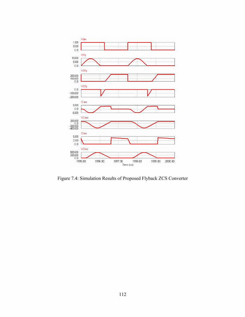
Figure 7.4: Simulation Results of Proposed Flyback ZCS Converter
112

Table 7.1 Key Parameters of Flyback ZCS Converter
Transformer turns ratio: 1:n
ISfly,max Ores
Obus nIL
nVV+
+ω
VSfly,max busO VnV +
IDfly,max Ores
Obus nIL
nVV+
+ω
VDfly,max busO VnV +
ILres,max Ores
Obus nIL
nVV+
+ω
ICres,max res
Obus
LnVnV
ω
2+
resres
Obus
CLnVV +
VCres,pkpk busO nVV 22 +
VDrec,max busO nVV 22 +
IDrec,max OI
ω resresCLn
11
Pout fInVL
nVVVLIn
nVVV
Obusres
ObusbusresO
Obus
bus ⋅⎟⎟⎠
⎞⎜⎜⎝
⎛+
++⋅
+ ωπ
ω222 2
113

7.3 Flyback ZCS Single-Stage Inverter
Based on the flyback ZCS converter analysis above, a flyback ZCS single-stage inverter
is proposed. The control algorithm is pulse frequency modulation as illustrated in Figure 7.5.
Figure 7.5: Control Algorithm of Flyback ZCS Single-Stage Inverter
As Figure 7.5 shows, the on time of the flyback switch is constant. But the off time is
varied accordingly to generate rectified sinusoidal current. A closed loop control is formed to
adjust the frequency of the constant on pulses. A Psim simulation is performed as shown in
Figure 7.6 and simulation results are given in Figure 7.7.
Figure 7.6: Proposed Flyback ZCS Single-Stage Inverter
114

Figure 7.7: Simulation Results of Flyback ZCS Single-Stage Inverter
7.4 Optimization of Flyback ZCS Single-Stage Inverter
In stage 5, the resonant capacitor is clamped at the output voltage of the inverter. The
current of the secondary side transformer winding decreases linearly. As the off time increases,
the current of the secondary side winding can decrease to zero, as shown in Figure 7.8
115
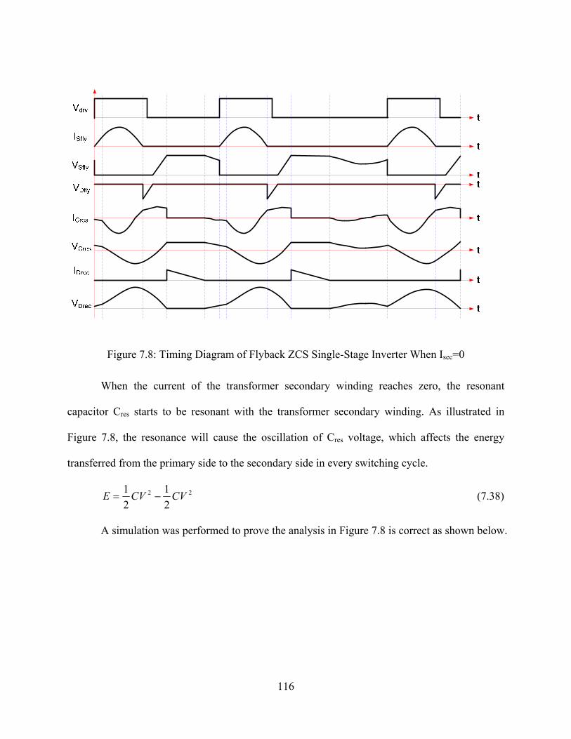
Figure 7.8: Timing Diagram of Flyback ZCS Single-Stage Inverter When Isec=0
When the current of the transformer secondary winding reaches zero, the resonant
capacitor Cres starts to be resonant with the transformer secondary winding. As illustrated in
Figure 7.8, the resonance will cause the oscillation of Cres voltage, which affects the energy
transferred from the primary side to the secondary side in every switching cycle.
22
21
21 CVCVE −= (7.38)
A simulation was performed to prove the analysis in Figure 7.8 is correct as shown below.
116

Figure 7.9: Simulation Results of Flyback ZCS Single-Stage Inverter with Less Inductance of
Transformer Secondary Winding at Lower Switching Frequency
As the equation above shows, at a certain switching frequency region, as the switching
frequency decreases, the output power of the flyback ZCS inverter is increasing instead of
decreasing.
When the secondary side winding goes to zero and the rectifier diode turns off, the
resonance happens between Cres and the secondary winding of transformer. Depending on the off
time, the resonance could happen in multiple cycles or in less than one cycle.
117
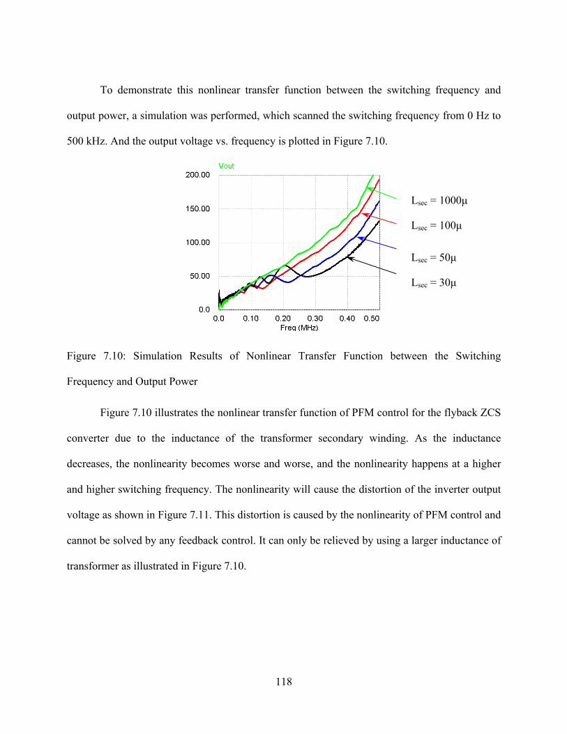
To demonstrate this nonlinear transfer function between the switching frequency and
output power, a simulation was performed, which scanned the switching frequency from 0 Hz to
500 kHz. And the output voltage vs. frequency is plotted in Figure 7.10.
Lsec = 30μ
Lsec = 50μ
Lsec = 100μ
Lsec = 1000μ
Figure 7.10: Simulation Results of Nonlinear Transfer Function between the Switching
Frequency and Output Power
Figure 7.10 illustrates the nonlinear transfer function of PFM control for the flyback ZCS
converter due to the inductance of the transformer secondary winding. As the inductance
decreases, the nonlinearity becomes worse and worse, and the nonlinearity happens at a higher
and higher switching frequency. The nonlinearity will cause the distortion of the inverter output
voltage as shown in Figure 7.11. This distortion is caused by the nonlinearity of PFM control and
cannot be solved by any feedback control. It can only be relieved by using a larger inductance of
transformer as illustrated in Figure 7.10.
118
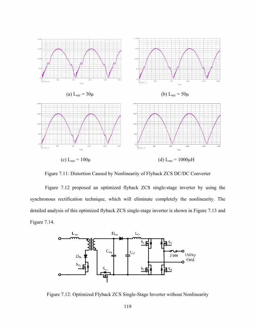
(a) Lsec = 30µ (b) Lsec = 50µ
(c) Lsec = 100µ (d) Lsec = 1000µH
Figure 7.11: Distortion Caused by Nonlinearity of Flyback ZCS DC/DC Converter
Figure 7.12 proposed an optimized flyback ZCS single-stage inverter by using the
synchronous rectification technique, which will eliminate completely the nonlinearity. The
detailed analysis of this optimized flyback ZCS single-stage inverter is shown in Figure 7.13 and
Figure 7.14.
Figure 7.12: Optimized Flyback ZCS Single-Stage Inverter without Nonlinearity
119

(a) [t0, t1] (b) [t1, t2]
Sfly
Tfly Drec LO
Cres CO
Lres
Dfly
Sres
(c) [t2, t3] (d) [t3, t4]
(e) [t4, t5]
Figure 7.13: Detailed Operation Stages for Optimized Flyback ZCS Single-Stage Inverter with
Synchronous Rectification
120
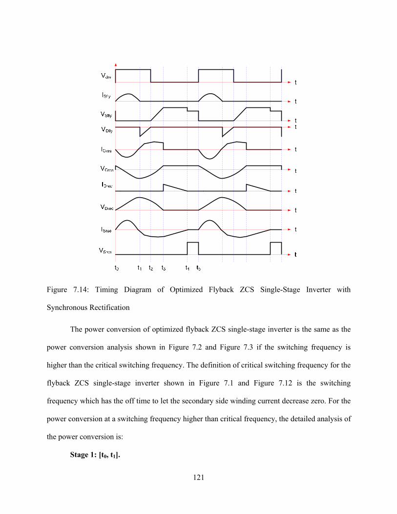
Figure 7.14: Timing Diagram of Optimized Flyback ZCS Single-Stage Inverter with
Synchronous Rectification
The power conversion of optimized flyback ZCS single-stage inverter is the same as the
power conversion analysis shown in Figure 7.2 and Figure 7.3 if the switching frequency is
higher than the critical switching frequency. The definition of critical switching frequency for the
flyback ZCS single-stage inverter shown in Figure 7.1 and Figure 7.12 is the switching
frequency which has the off time to let the secondary side winding current decrease zero. For the
power conversion at a switching frequency higher than critical frequency, the detailed analysis of
the power conversion is:
Stage 1: [t0, t1].
121

This stage starts at the turning-on of flyback switch Sfly and synchronous switch Sres at zero
current without any switching loss. The voltage across the resonant capacitor Cres is clamped to
the output voltage of the converter when the switches are turned on. In this stage, the resonant
inductor on the primary side Lres starts to be resonant with the resonant capacitor. The initial
current of Lres is zero and the initial voltage of Cres is Vo. This stage ends when the current of ISfly
reaches zero and voltage of Cres reaches its maximum value.
The diode in series with Sfly will block the resonant current of Lres from going in the
inverse direction. Then, the current of Sfly will remain at zero.
Stage 2 and 3: [t1, t2] and [t2, t3].
At stage 2, the energy stored in the resonant capacitor is transferred to the secondary
winding of the flyback transformer by resonance. As the current of Lsec is increasing, the voltage
across Cres is decreasing. Stage 2 ends with the down slope of the driving signal. Stage 3 starts at
the turning-off of Sfly and Sres. The body diode of Sres starts to conduct current, and then Sfly is
turned off at zero current and Sres is turned off at zero voltage. The current of Lsec reaches its
maximum value when the voltage of Cres reaches zero. Then, the resonant capacitor Cres is
charged inversely. This stage stops when the voltage of Cres reaches the value of Vo. Stage 3
ends when the resonant capacitor voltage reaches VO.
Stage 4: [t3, t4].
Stage 4 starts when the resonant capacitor voltage reaches to the voltage across CO, then
the rectifier diode turns on at zero voltage and the transformer secondary side winding starts
charging output capacitor CO. Stage 4 stops when the current of the transformer secondary
winding reaches zero and the body diode of Sfly is off. Stage 4 ends when the current of the
transformer secondary winding reaches zero.
122
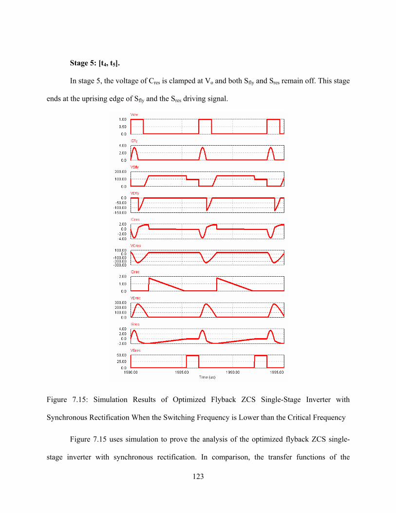
Stage 5: [t4, t5].
In stage 5, the voltage of Cres is clamped at Vo and both Sfly and Sres remain off. This stage
ends at the uprising edge of Sfly and the Sres driving signal.
Figure 7.15: Simulation Results of Optimized Flyback ZCS Single-Stage Inverter with
Synchronous Rectification When the Switching Frequency is Lower than the Critical Frequency
Figure 7.15 uses simulation to prove the analysis of the optimized flyback ZCS single-
stage inverter with synchronous rectification. In comparison, the transfer functions of the
123

optimized flyback ZCS single-stage inverter with rectification are shown in Figure 7.16. The
optimized design makes the output voltage of the single-stage inverter monotonically increasing
as the frequency increases, which makes the optimized flyback ZCS converter much more
suitable for a single-stage inverter.
(a) Lsec = 1000μH (b) Lsec = 100μH
(c) Lsec = 50μH (d) Lsec = 30μH
Figure 7.16: Simulation Results of Transfer Function of Optimized Flyback ZCS Single-Stage
Inverter with Rectification
124
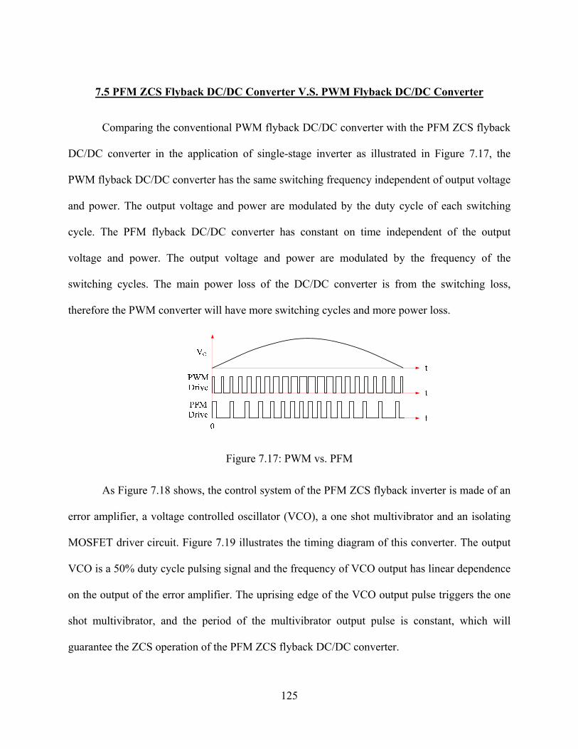
7.5 PFM ZCS Flyback DC/DC Converter V.S. PWM Flyback DC/DC Converter
Comparing the conventional PWM flyback DC/DC converter with the PFM ZCS flyback
DC/DC converter in the application of single-stage inverter as illustrated in Figure 7.17, the
PWM flyback DC/DC converter has the same switching frequency independent of output voltage
and power. The output voltage and power are modulated by the duty cycle of each switching
cycle. The PFM flyback DC/DC converter has constant on time independent of the output
voltage and power. The output voltage and power are modulated by the frequency of the
switching cycles. The main power loss of the DC/DC converter is from the switching loss,
therefore the PWM converter will have more switching cycles and more power loss.
Figure 7.17: PWM vs. PFM
As Figure 7.18 shows, the control system of the PFM ZCS flyback inverter is made of an
error amplifier, a voltage controlled oscillator (VCO), a one shot multivibrator and an isolating
MOSFET driver circuit. Figure 7.19 illustrates the timing diagram of this converter. The output
VCO is a 50% duty cycle pulsing signal and the frequency of VCO output has linear dependence
on the output of the error amplifier. The uprising edge of the VCO output pulse triggers the one
shot multivibrator, and the period of the multivibrator output pulse is constant, which will
guarantee the ZCS operation of the PFM ZCS flyback DC/DC converter.
125
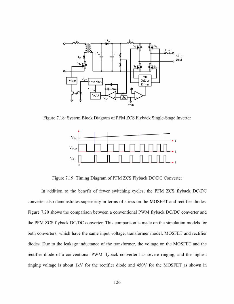
Figure 7.18: System Block Diagram of PFM ZCS Flyback Single-Stage Inverter
VEA
VVCO
Vdrv
0
t
t
t
Figure 7.19: Timing Diagram of PFM ZCS Flyback DC/DC Converter
In addition to the benefit of fewer switching cycles, the PFM ZCS flyback DC/DC
converter also demonstrates superiority in terms of stress on the MOSFET and rectifier diodes.
Figure 7.20 shows the comparison between a conventional PWM flyback DC/DC converter and
the PFM ZCS flyback DC/DC converter. This comparison is made on the simulation models for
both converters, which have the same input voltage, transformer model, MOSFET and rectifier
diodes. Due to the leakage inductance of the transformer, the voltage on the MOSFET and the
rectifier diode of a conventional PWM flyback converter has severe ringing, and the highest
ringing voltage is about 1kV for the rectifier diode and 450V for the MOSFET as shown in
126
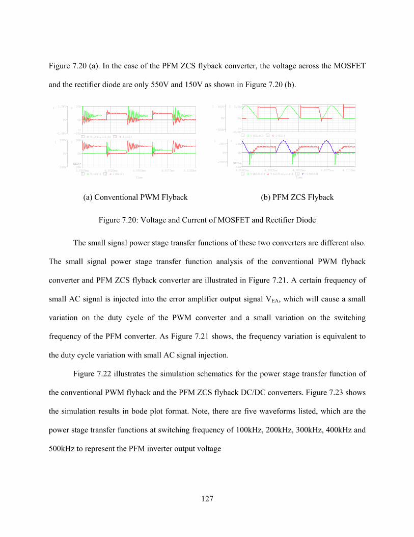
Figure 7.20 (a). In the case of the PFM ZCS flyback converter, the voltage across the MOSFET
and the rectifier diode are only 550V and 150V as shown in Figure 7.20 (b).
Time
4.0000ms 4.0025ms 4.0050ms 4.0075ms 4.0100ms1 V(U2:1) 2 I(U2:1)
-500V
0V
500V1
-20A
0A
20A2
SEL>>SEL>>
1 V(L4:1,D11:A) 2 I(D11)-1.0KV
0V
1.0KV1
-10A
0A
10A2
>>
Time
4.0000ms 4.0025ms 4.0050ms 4.0075ms 4.0100ms1 V(R333:1) V(C133:2,L1:1) 2 -I(R333)
-200V
0V
200V1
0A
20A
-30A
2
SEL>>SEL>>
1 V(D11:C) 2 I(D11)
-500V
0V
500V1
0A
5.0A
-6.0A
2
>>
(a) Conventional PWM Flyback (b) PFM ZCS Flyback
Figure 7.20: Voltage and Current of MOSFET and Rectifier Diode
The small signal power stage transfer functions of these two converters are different also.
The small signal power stage transfer function analysis of the conventional PWM flyback
converter and PFM ZCS flyback converter are illustrated in Figure 7.21. A certain frequency of
small AC signal is injected into the error amplifier output signal VEA, which will cause a small
variation on the duty cycle of the PWM converter and a small variation on the switching
frequency of the PFM converter. As Figure 7.21 shows, the frequency variation is equivalent to
the duty cycle variation with small AC signal injection.
Figure 7.22 illustrates the simulation schematics for the power stage transfer function of
the conventional PWM flyback and the PFM ZCS flyback DC/DC converters. Figure 7.23 shows
the simulation results in bode plot format. Note, there are five waveforms listed, which are the
power stage transfer functions at switching frequency of 100kHz, 200kHz, 300kHz, 400kHz and
500kHz to represent the PFM inverter output voltage
127

Figure 7.21: Small Signal Power Stage Transfer Function Analysis
(a) Conventional PWM Flyback (b) PFM ZCS Flyback
Figure 7.22: Schematics of Small Signal Power Stage Transfer Function Analysis
The simulation results of the power stage transfer function of the two converters are
illustrated in Figure 7.23. The conventional PWM flyback has a typical -40dB/decade two-pole
system, but the PFM ZCS flyback has about -20dB/decade with the same load. Also, the phase
delay of the PFM ZCS flyback converter as a function of frequency changes much smoother,
which makes the compensator design much easier. From 100kHz to 500kHz, the PFM ZCS
flyback also demonstrates power stage transfer functions that have much less dependence on the
effective duty cycle variation, which also make the compensator design easier. All these features
of the PFM ZCS flyback converter provide superiority to the conventional PWM flyback
converter on the application of a single-stage inverter in terms of efficiency, voltage/current
stress and control ability.
128
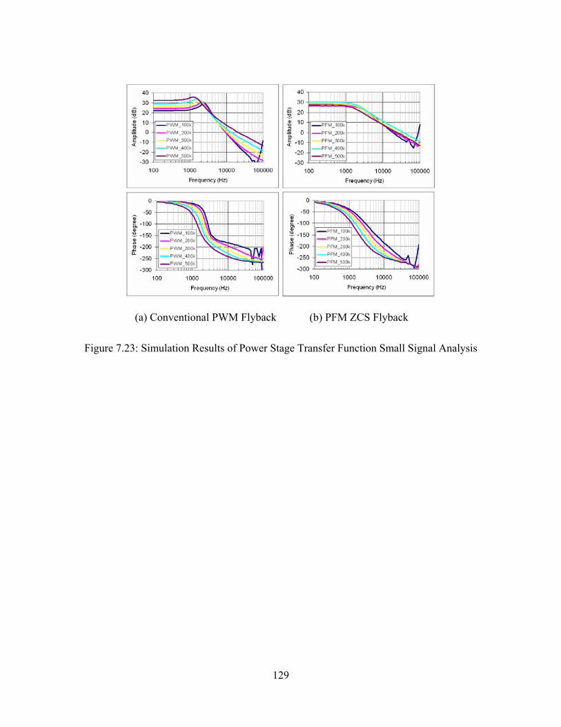
(a) Conventional PWM Flyback (b) PFM ZCS Flyback
Figure 7.23: Simulation Results of Power Stage Transfer Function Small Signal Analysis
129

CHAPTER EIGHT: EXPERIMENTAL VERIFICATION
8.1 Prototype of Single-Stage Inverter with Grid-Tie
Controller Board
Main Switches
Output
Capacitors
Transformer
Rectifier Diodes
Output Inductor
Output Common
Mode Choke
Output Current
Hall Sensor
Input Capacitors
Input Common
Mode Choke
Input Connectors
Output Connectors
Figure 8.1: Prototype of Full-Bridge Phase-Shift Single-Stage Inverter
130

Figure 8.1 shows pictures of the DC/DC converter prototype for the single-stage inverter,
which is proposed in Figure 4.1(b) and Figure 4.2. The prototype is made of two print circuit
boards (PCB): the controller board and the power stage board. In this way, the high voltage
components and trace will be confined on the power stage board and the low voltage components
and trace on the controller board. Another benefit of this structure is that the power stage
prototype need not change too much, but the controller board may change a lot. By putting these
onto two different boards, optimization can be much easier. The drivers’ circuit is on the power
stage board to make sure that it is as near to the MOSFETs as possible to eliminate the noise and
parasitic inductance affections.
Figure 8.2: Experimental Results of Vref, Output Current and Voltage
As Figure 8.2 shows, the output current reference signal is generated by the absolution
circuit from a sinusoid signal, which is generated by a function generator. The load is a 52Ω
resistor. The RMS. value of output voltage and current is 110V and 2.2A.
131

As Figure 8.2 shows, the output current follows the reference strictly. After the properly
designed output filter, the output current has very little noise and distortion. The next stage will
be the unfolding circuit, which will invert this rectified sinusoid current and voltage into sinusoid.
With this kind of rectified current, the output of the inverter can achieve very high power factor
and power quantity.
The peak value of the output voltage and the current is 160V and 3.1A. The peak output
power is 450Watts, which is limited by the power rating of a single channel solar array simulator.
Zero crossing is still a small problem. A very small DC offset, such as 50mV, can solve the
problem.
(a) (b)
(c) (d)
Figure 8.3: Experimental Results of Output Current, VDS and VGS of Switch A in Figure 4.2
132
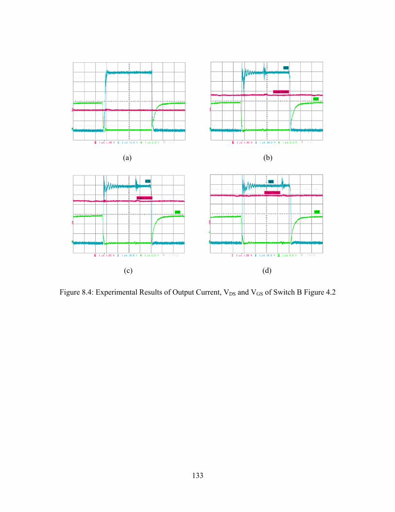
(a) (b)
(c) (d)
Figure 8.4: Experimental Results of Output Current, VDS and VGS of Switch B Figure 4.2
133
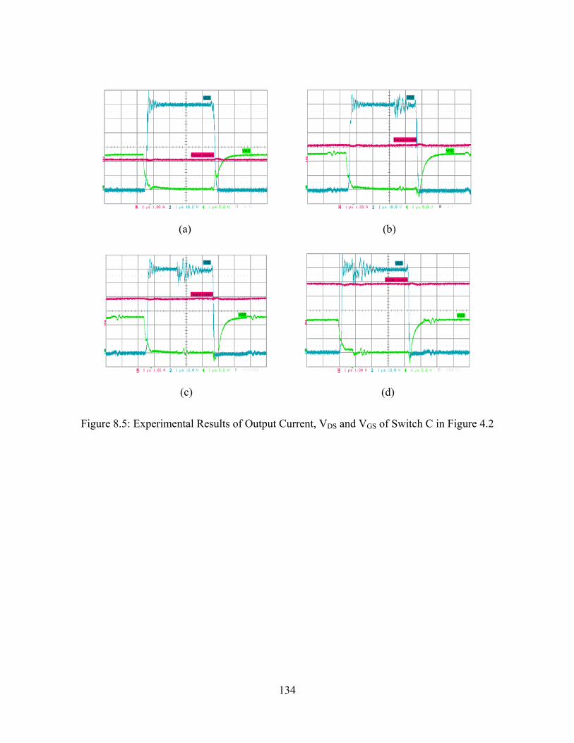
(a) (b)
(c) (d)
Figure 8.5: Experimental Results of Output Current, VDS and VGS of Switch C in Figure 4.2
134

(a) (b)
(c) (d)
Figure 8.6: Experimental Results of Output Current, VDS and VGS of Switch D in Figure 4.2
To examine the switching process of the full bridge at steady state, the reference of the
DC/DC converter was changed from rectified sinusoid to pure DC and then the DC/DC converter
output to pure DC voltage. Figure 8.3, Figure 8.4, Figure 8.5 and Figure 8.6 show the output
current, VDS and VGS of switches A, B, C and D. The load is 52Ω resistor and the output current
of these figure are 0.1A, 1.1A 1.8A and 2.9A, and therefore these figures show the load of
0.5Watt, 62Watts, 182Watts and 440Watts. At light load, all the switches are turned on under
“hard switching”. As the load increases, all the switches are turned on under “soft switching”,
135
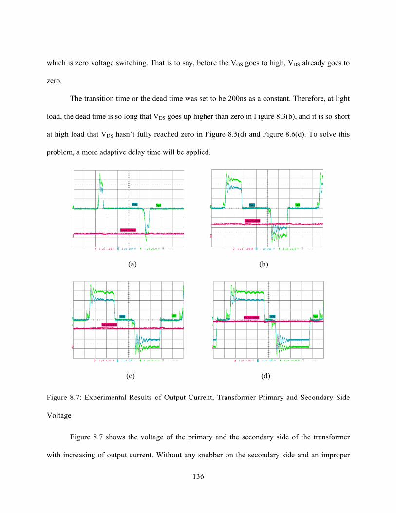
which is zero voltage switching. That is to say, before the VGS goes to high, VDS already goes to
zero.
The transition time or the dead time was set to be 200ns as a constant. Therefore, at light
load, the dead time is so long that VDS goes up higher than zero in Figure 8.3(b), and it is so short
at high load that VDS hasn’t fully reached zero in Figure 8.5(d) and Figure 8.6(d). To solve this
problem, a more adaptive delay time will be applied.
(a) (b)
(c) (d)
Figure 8.7: Experimental Results of Output Current, Transformer Primary and Secondary Side
Voltage
Figure 8.7 shows the voltage of the primary and the secondary side of the transformer
with increasing of output current. Without any snubber on the secondary side and an improper
136

choice of clamping diodes on the primary side, the ringing is still a problem. To conquer it, a fast
recovery Schottky diode will be applied. A resistor and a capacitor in series can damp the ringing
further. The experiment’s results show that this method will cause extra power loss and thermal
problems.
The small steps on the primary side of the transformer are caused by leakage inductance
of the transformer. The leakage inductance will store energy during the conduction mode. During
the freewheeling mode, the stored energy will help to oscillate the voltage of the other diagonal
switches’ voltage to zero and facilitate the ZVS.
Due to the optimized transformer and zero voltage switching, the overall efficiency is
greater than 91% at 480Watts, with 100kHz switching frequency.
Figure 8.8: Prototype of 1kW Single-Stage High-Frequency Link Inverter System
Figure 8.8 shows the 1kW prototype of the single-stage high-frequency link inverter
system. Due to the resonance of the full-bridge phase shift topology, the output capacitance of
the MOSFET is discharged to zero before the MOSFET is turned on. Figure 8.6 shows all four
switches of the full bridge operating under ZVS.
137
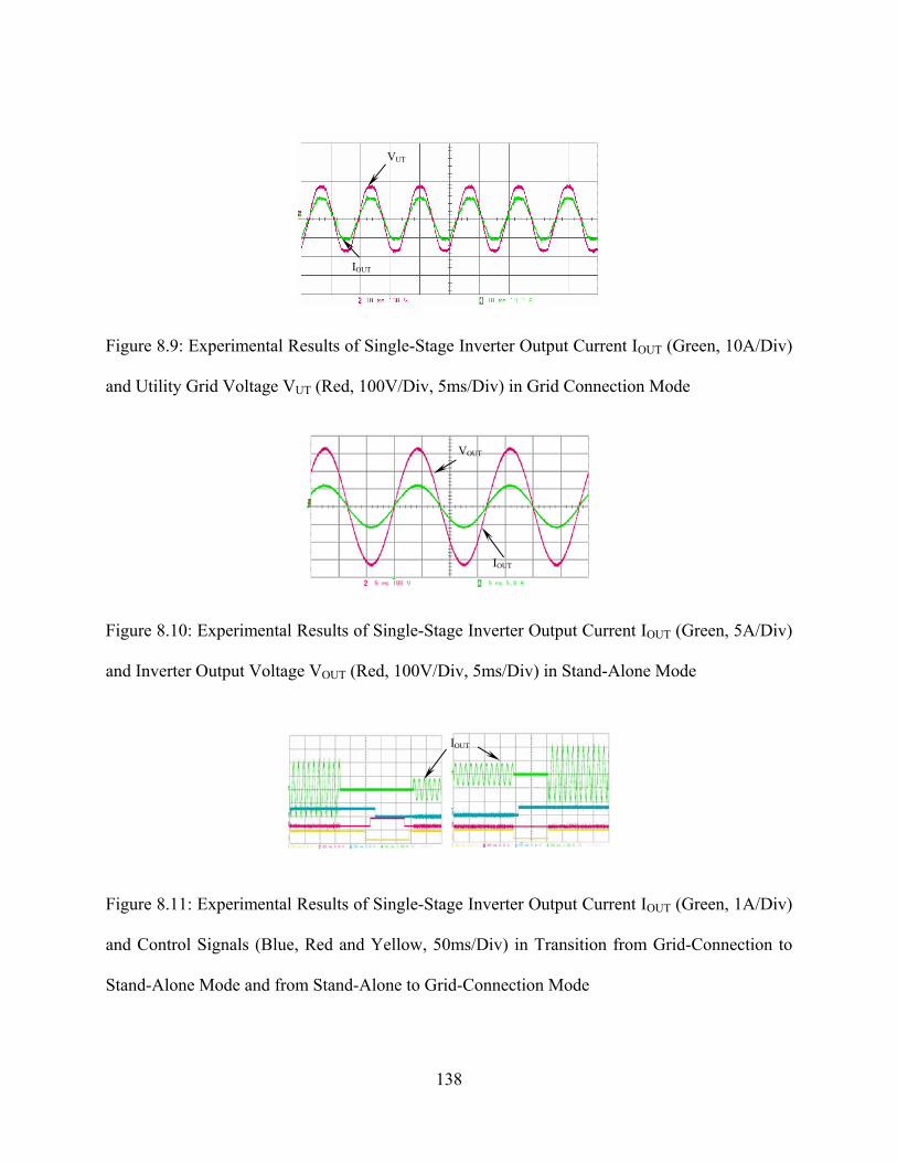
VUT
IOUT
Figure 8.9: Experimental Results of Single-Stage Inverter Output Current IOUT (Green, 10A/Div)
and Utility Grid Voltage VUT (Red, 100V/Div, 5ms/Div) in Grid Connection Mode
VOUT
IOUT
Figure 8.10: Experimental Results of Single-Stage Inverter Output Current IOUT (Green, 5A/Div)
and Inverter Output Voltage VOUT (Red, 100V/Div, 5ms/Div) in Stand-Alone Mode
IOUT
Figure 8.11: Experimental Results of Single-Stage Inverter Output Current IOUT (Green, 1A/Div)
and Control Signals (Blue, Red and Yellow, 50ms/Div) in Transition from Grid-Connection to
Stand-Alone Mode and from Stand-Alone to Grid-Connection Mode
138

Figure 8.9 shows the experimental result of a 1kW single-stage inverter in the grid
connection mode. Figure 8.10 shows the output voltage and current of the inverter in the stand-
alone mode. By making two DC/DC converters in series, the inverter output voltage is 240VRMS.
As Figure 8.11 shows, when abnormal and unstable utility grid voltage appears, the inverter
shuts down the connection with the utility grid and powers the stand-alone load without
transferring PV array power energy into the grid. When utility grid voltage becomes stable and
normal, the inverter connects to the grid and powers both the stand-alone load and the utility grid.
8.2 Prototype of Single-Stage Bi-Directional Inverter
Figure 8.12 shows the prototype of an optimized single-staged bi-directional inverter
system, which is proposed in Figure 6.1 (c). The full-bridge switches and MOSFET rectifiers are
located near the primary and secondary winding of the transformer, so the leakage inductance
has been greatly minimized as shown in Figure 8.12 (a). The MOSFET driver circuit was on a
seperate PCB board as shown on Figure 8.12 (b). To have a separate PCB board for the
MOSFET driver can make the power trace on the power stage much wider, which will simplify
the layout of power stage. Another benefit is that a MOSFET driver board can be utilized for the
next version of the prototype, since the driver circuit is well analyzed and developed. There is no
need for updating the driver circuit further. The controller board and all the driver boards are
using the SMD components and SOIC IC, which reduced the size of PCB board greatly. The
experimental results are illustrated in Figure 8.13.
139
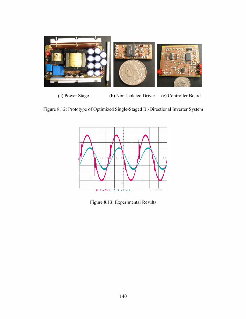
(a) Power Stage (b) Non-Isolated Driver (c) Controller Board
Figure 8.12: Prototype of Optimized Single-Staged Bi-Directional Inverter System
Figure 8.13: Experimental Results
140

8.3 Single-Stage Bi-Directional Inverter with Flyback Converter
Figure 8.14: Single-Stage Bi-Directional Inverter with Flyback Converter
Figure 8.14 illustrates a prototype and preliminary experimental result for the single-stage
bi-directional inverter with flyback DC/DC inverter as shown in Figure 6.8. A flyback converter
is in parallel with a full-bridge phase-shift DC/DC converter and is handling the reactive energy
from the inductive load.
8.4 Prototype of PFM ZCS Flyback Inverter
Figure 8.15 illustrates a prototype of the PFM ZCS flyback inverter proposed in Figure
7.1. The PFM flyback inverter includes a flyback ZCS converter and unfolding circuit as the
power stage. The controller circuit has a PFM circuit, a driver circuit, an error compensator and
an auxiliary power supply. This prototype is built on a four-layer PCB board, which has been
laid out and manufactured as shown in Figure 8.15. This prototype is rated at 250Watts, with
proper thermal pad design for the surface mounted MOSFETs and diodes, and this prototype has
no heat sink. With further planar transformer design, this prototype can be designed into a very
tight package.
141

(a) Top Side (b) Bottom Side
Figure 8.15: Prototype of PFM ZCS Flyback Inverter
Figure 8.16: Experimental Results of PFM ZCS Flyback Inverter
Figure 8.16 illustrates the experimental results of the PFM ZCS flyback inverter. The
yellow waveform is the gate driving signal, the blue waveform is current flow through the
MOSFET Sfly, the green waveform is the voltage across the MOSFET Sfly and the magenta
waveform is the voltage across the blocking diode Dfly. Compared with Figure 7.3 and Figure 7.4,
the experimental results prove the analytical and simulation results.
142

Figure 8.17: Experimental Results of PFM ZCS Flyback Inverter
(a) (b) (c) (d) (e) (f) (g) (h) (i) (j) (k) (l)
Figure 8.18: Experimental Results of PFM ZCS Flyback Inverter
143

(a) (b) (c)
(d) (e) (f)
(g) (h) (i)
(j) (k) (l)
Figure 8.19: Zoomed View of Figure 8.18
144

Figure 8.16 shows the experimental results of the ZCS switching process of the PFM
ZCS flyback inverter. At the uprising edge of the driving signal, the current of Sfly is increasing
linearly from zero with zero switching on loss. The current of Sfly has already reached zero
before Sfly is turned off, so there is no switching off loss either.
Figure 8.17, Figure 8.18 and Figure 8.19 illustrate how the PFM technique is applied to
generate sinusoidal inverter output voltage. As the switching frequency increases, the output
voltage is increasing sinusoidally. At any time, the switching process is under the zero current
condition.
To verify system efficiency, the thermal images are taken by a thermal camera as
illustrated in Figure 8.20. The thermal images show that hot spots of the PFM ZCS flyback
single-stage inverter prototype are located on the resonant capacitors and resonant inductor. The
MOSFET, blocking diode and rectifier diodes are not hot spots, which prove that this topology
has less switching loss than a conventional flyback converter.
The hot spot on the resonant inductor reveals that the magnetic design of the resonant
inductor is causing extra loss. By applying a larger ferrite core, system efficiency is increased
from 90.5% to 91.5% at 150Watts.
145
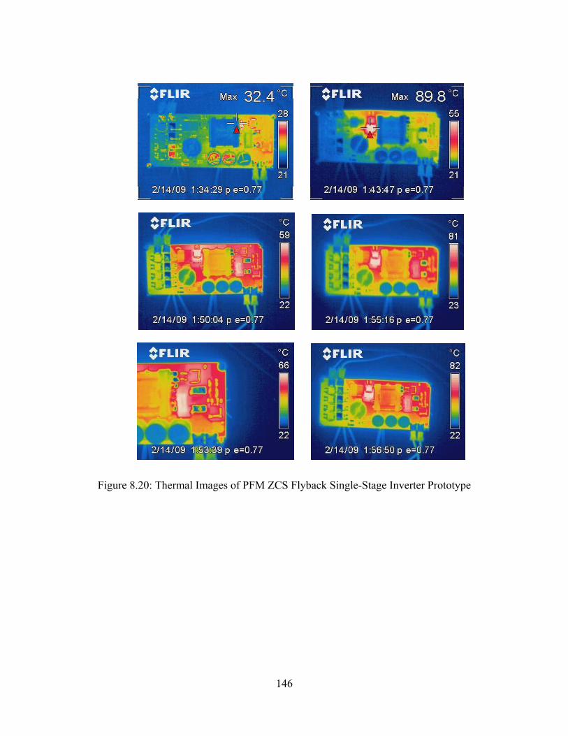
Figure 8.20: Thermal Images of PFM ZCS Flyback Single-Stage Inverter Prototype
146

CHAPTER NINE: CONCLUSION
Compared with a conventional two-stage inverter, the single-stage inverter has better
performance on system efficiency. By applying the active filter as pre-regulator of the single-
stage inverter, the low frequency current ripple can be eliminated from the PV array. The
capacitance of input filter then can be reduced, and the lifetime of the capacitor will be increased.
A feedforward and a 120Hz sample and hold controller will be applied to enhance the single-
stage inverter’s response speed to the PV array’s output voltage variation.
Transformer analysis for the single-stage inverter proves that there is no low frequency
harmonics in the transformer’s magnetic flux. The adaptive slope compensation is developed to
keep the single-stage inverter system stable when the duty cycle is greater than 0.5 and to keep
the control loop loop gain near constant with different input voltage. To apply the digital
controller on a single-stage inverter system, a detailed design procedure and optimization method
have been provided.
A conventional single-stage bi-directional inverter uses MOSFETs as rectifiers on the
secondary side of the transformers, which tends to generate higher ringing voltage spikes than
diodes. Two new bi-directional single-stage inverter topologies are proposed and analyzed.
Based on the new topologies, a new architecture of a PV based grid-tied DC/AC system is also
proposed, which is more suitable for residential PV array application than a centralized inverter
system.
To increase the efficiency of the single-stage inverter system, a new ZCS flyback inverter
with PFM control is proposed. With further optimization, the non-linearity of the PFM ZCS
flyback inverter is completely removed.
147

All the inverter topologies are verified by experimental prototypes.
148

LIST OF REFERENCES
[1] Shepard, J. “Distributed and cogeneration, an unconventional path to growth, power
electronics for distributed and co-generation,” 2004 Irvine, California, Darnell Com. Inc.
[2] Trends in photovoltaic applications, Survey report of selected IEA countries between
1992 and 2006.
[3] IEA www.iea-pvps.org
[4] K. Siri, “Maximum power tracking solar power system,” U.S. Patent 6,281,485, August
28, 2001 and U.S. Patent 6,369,462, April 9, 2002.
[5] K. Siri, F. Tian, S. Kaluvala, and I. Batarseh, “Solar-based inverter with maximum power
tracking,” in Proc. of Power Electronics for Distributed and Co-Generation, 2004 Irvine,
California.
[6] J. P. Benner and L. Kazmerski, “Photovoltaics gaining greater visibility,” IEEE Spectrum,
vol. 29, issue 9, pp. 34-42, September 1999.
[7] S. B. Kjær, “State of the art analysis for the ‘SolcelleInverter’ project,” Aalborg
University, 2001, unpublished.
[8] J. P. Benner and L. Kazmerski, “Photovoltaics gaining greater visibility,” IEEE Spectrum,
vol. 29, issue 9, pp. 34-42, September 1999.
[9] E. Bezzel, H. Lauritzen, and S. Wedel, “The photo electro chemical solar cell, Danish
Technological Institute,” Denmark, www.solarcell.dk.
[10] M. Wuest, P. Toggweiler, and J. Riatsch, “Single cell converter system (SCCS),” in Proc.
of IEEE 1st WCPEC, Dec. 1994, USA, vol. 1, pp. 813-815.
149
[11] J. Riatsch, H. Stemmler, and R. Schmidt, “Single cell module integrated converter system
for photovoltaic energy generation,” in Proc. of EPE 97, 1997, Norway.
[12] P. Rooij, M. Real, U. Moschella, T. Sample and M. Kardolus, “Advanced reliability
improvement of AC-modules (ARIA),” Netherlands energy research foundation ECN,
Contract: JOR3-CT97-0122, May 2000.
[13] S.B. Kjaer, J.K. Pedersen and F. Blaabjerg, “Power inverter topologies for photovoltaic
modules-a review,” in Rec. of 37th IAS Annual Meeting, Pittsburgh, PA, Oct. 13-18,
2002, pp. 782–788.
[14] Designing and installing code-compliant PV systems,
http://solargenerations.com/downloads/SolarGenerationsInstallerTraining.pdf
[15] Laszlo Balogh, “The UC3902 load share controller and its performance in distributed
power systems,” Application Note U-163, Unitrode Corporation.
[16] S.B. Kjaer and F. Blaabjerg, “Design optimization of a single phase inverter for
photovoltaic applications,” in Proc. of PESC '03, June 15-19, 2003, vol.3, pp. 1183-1190.
[17] E. Bezzel, H. Lauritzen, and S. Wedel, “The photo electro chemical solar cell, Danish
Technological Institute,” Denmark, www.solarcell.dk.
[18] M. Wuest, P. Toggweiler, and J. Riatsch, “Single cell converter system (SCCS),” in Proc.
of IEEE 1st WCPEC, December 1994, USA, vol. 1, pp. 813-815.
[19] J. Riatsch, H. Stemmler, and R. Schmidt, “Single cell module integrated converter system
for photovoltaic energy generation,” in Proc. of EPE 97, 1997, Norway.
[20] H. Oldenkamp, I. J. de Jong, C. W. A. Balhls, S. A. M. Verhoeven, and S. Elstgeest,
“Reliability and accelerated life tests of the AC module mounted OKE4 inverter,” in Proc.
of IEEE Photovoltaic Specialists Conference, 1996, pp.1339-1342.
150

[21] S. B. Kær and F. Blaabjerg, “A novel single-stage inverter for the ac-module with reduced
low-frequency ripple penetration,” in Proc. of 10th EPE European Conf. Power
Electronics and Applications, Toulouse, France, Sept. 2–4, 2003.
[22] M. Nagao and K. Harada, “Power flow of photovoltaic system using buck-boost PWM
ower inverter,” in Proc. of IEEE PEDS’97, Singapore, May 26–29, 1997, pp. 144–149.
[23] T. Shimizu, K. Wada, and N. Nakamura, “A flyback-type single phase utility interactive
inverter with low-frequency ripple current reduction on the dc input for an ac photovoltaic
module system,” in Proc. of IEEE PESC’02, Cairns, Australia, June 23–27, 2002, pp.
1483–1488.
[24] S. B. Kjær and F. Blaabjerg, “Design optimization of a single phase inverter for
photovoltaic applications,” in Proc. of IEEE PESC’03, Acapulco, México, June 15–19,
2003, pp. 1183–1190.
[25] A. Beristáin, J. Bordonau, A. Gilabert, and G. Velasco, “Synthesis and modulation of a
single phase dc/ac converter with high frequency isolation in photovoltaic energy
applications,” in Proc. of IEEE PESC’03, Acapulco, México, June 15–19, 2003, pp.
1191–1196.
[26] E.Koutroulis, J.Chatzakis, K.Kalaitzakis and N.C.Voulgaris, “A bidirectional, sinusoidal,
high-frequency inverter Design,” in Proc. of IEE Electric Power Applications, July 2001
vol. 148, issue 4, pp.315–321.
[27] N. Prakash and A. Mohan etc., “A new sinewave inverter with high frequency link and
synchronous rectification using power MOSFETs,” in Rec. of Power Electronics
Specialists Conference, June 11-14, 1990, pp. 723-728.
151
[28] A. K. S. Bhat and S. B. Dewan, “Analysis and design of a high-frequency link DC to
utility interface using square-wave output resonant inverter,” IEEE Trans. Power
Electronics, vol. 3, pp. 355-363, Jul. 1988.
[29] R. Chaffai, K. Ai-Haddad, and V. Rajagopalan, “A 5kW utility-interactive inverter
operating at high frequency and using zero current turn off COMFET switches,” in Proc.
of Industry Applications Society Annual Meeting, Oct. 7-12, 1990, vol. 2, pp. 1081-1085.
[30] H. Terai, S.Sumiyoshi, and T. Kitaizumi, etc., “Utility-interactive solar power conditioner
using high-frequency sine wave modulated inverter for distributed small-scale power
supply,” in Proc. of ISIE 2002, vol. 3, May 26-29, 2002, pp. 942-947.
[31] Y. J. Song, S. K. Chung, and P. N. Enjeti, "A current-fed HF link direct DC/AC converter
with active harmonic filter for fuel cell power systems," in Proc. of 39th IAS Annual
Meeting, Oct. 3-7, 2004, vol. 1, pp. 123-128.
[32] N. Kasa, T. Iida, and A.K.S. Bhat, "Zero-voltage transition flyback inverter for small
scale photovoltaic power system," in Proc. of Power Electronics Specialists Conference,
June 16, 2005, pp. 2098–2103.
[33] S. Chandhaket, Y. Konishi, K. Ogura, and M. Nakaoka, "Utility AC interfaced soft-
switching sinewave PWM power conditioner with two-switch Flyback high-frequency
transformer," in Proc. of Electric Power Applications, Sept. 9, 2004, vol. 151, issue 5, pp.
526–533.
[34] "Optimizing the design of a high power factor switching preregulator," Lloyd Dixon,
Unitrode Design Seminars, SEM700, 1990.
[35] "High power factor preregulator for off-line power supplies," Lloyd Dixon, Unitrode
Design Seminars, SEM600, 1988.
152

[36] W. Wu, N. Pongratananukul, W. Qiu, K. Rustom, T. Kasparis, and I. Batarseh, “DSP-
based multiple peak power tracking for expandable power system,” in Proc. of APEC
2003, Eighteenth Annual IEEE, 2003, vol. 1, pp. 525-530.
[37] K. Siri, F. Tian, S. Kaluvala, and I. Batarseh, “Solar-based inverter with maximum power
tracking,” in Proc. of Power Electronics for Distributed and Co-Generation 2004, PEDAC
‘04, Irvine, California, April, 2004.
[38] T. Aoki, K. Yotsumoto, S. Muroyama, and Y. Kenmochi, “A new uninterruptible power
supply with a bidirectional cycloconverter,” in Proc. of Telecommunications Energy
Conference, INTELEC '90, Oct. 1990, pp. 424-429.
[39] S. Sivakumar, T. Parsons, and S. C. Sivakumar, “Modeling, analysis and control of
bidirectional power flow in grid connected inverter systems,” in Proc. of Power
Conversion Conference, Osaka, Japan, April 2002, vol. 3, pp.1015-1019.
[40] J. Beristain, J. Bordonau, A. Gilabert, and G. Velasco, “Synthesis and modulation of a
single phase DC/AC converter with high-frequency isolation in photovoltaic energy
applications,” in Proc. of Power Electronics Specialist Conference, IEEE 34th Annual,
Acapulco, Mexico, June 2003, vol. 3, pp. 1191-1196.
[41] S. Deng, H. Mao, J. Mazumdar, I. Batarseh, and K.K. Islam, “A new control scheme for
high-frequency link inverter design,” in Proc. of Applied Power Electronics Conference
and Exposition, Eighteenth Annual IEEE, Miami, FL, Feb. 2003, vol. 1, pp.512-517.
[42] “Practical considerations in current mode power supplies,” Unitrode Application Notes,
U-111.
[43] R. D. Middlebrook, “Topics in multiple-loop regulators and current mode programming,”
IEEE Trans. Power Electron., vol. 2, no. 2, pp. 109-124, 1987.
153

154
[44] “Designing a TMS320F280x based digitally controlled DC/DC switching power supply,”
Texas Instruments Application Report, SPRAAB3, July 2005.
[45] “Step-down, PWM control or PWM/PFM switchable switching regulator controller S-
8520/8521 Series,” Seiko Instruments Inc., http://datasheet.sii-
ic.com/en/switching_regulator/S8520_8521_E.pdf.
[46] “PFM/PWM step-up DC/DC converter,” MICROCHIP datasheet,
http://ww1.microchip.com/downloads/en/devicedoc/21361c.pdf.
[47] “FAN5234 mobile-friendly PWM/PFM controller,” Fairchild Semiconductor,
http://www.fairchildsemi.com/ds/FA/FAN5234.pdf.
[48] "Designing for high efficiency with the active clamp UCC2891 PWM controller," Steve
Mappus, Texas Instruments, slua303, April 2004.
[49] S. D. Freeland, "I- A unified analysis of converters with resonant switches. II- Input-
current shaping for single-phase AC-DC power converters," Ph.D. dissertation, Caltech,
CA, 1988.