publication€p2 conference€ (eumic€ 2008).€...
TRANSCRIPT
Publication P2
Mikko Kärkkäinen, Mikko Varonen, Dan Sandström, Tero Tikka, SaskaLindfors, and Kari A. I. Halonen. 2008. Design aspects of 65nm CMOSMMICs. In: Proceedings of the 3rd European Microwave Integrated CircuitsConference (EuMIC 2008). Amsterdam, The Netherlands. 2728 October2008, pages 115118.
© 2008 European Microwave Association (EuMA)
Reprinted by permission of European Microwave Association.
Proceedings of the 3rd European Microwave Integrated Circuits Conference
Design Aspects of 65-nm CMOS MMICsMikko Karkkainen, Mikko Varonen, Dan Sandstrom, Tero Tikka, Saska Lindfors, and Kari A. I. Halonen
TKK Helsinki University ofTechnologySMARAD2 /Department ofMicro and Nanosciences, Espoo, Finland
mmkarkka@ecdl .tkk. fi
Abstract-We present design aspects and techniques for conductor and the ground plane S can be used for realizingmillimeter-wave circuits implemented in 65-nm CMOS. Different different characteristic impedances for the CPW. A widertransmission line topologies are discussed and measurement centre conductor leads to lower conductor losses. In principle,results for a conventional coplanar waveguide and slow-wave the maximum width of the centre conductor is limited by thecoplanar waveguide implemented in 65-nm CMOS are shown design rules of the chosen process. The metal densityThe attenuation of the on-chip transmission lines can be reduced layutby using slow-wave coplanar waveguides. A 1-stage cascode requirements set the limits for themaximum distance betweenamplifier in 65-nm CMOS employing inductors as matching thecentreconductorandthegroundplanefortheCPW.elements is presented. On-chip interconnections of the amplifier Because of the thin dielectric layers of a nanoscale CMOSare implemented and modeled using coplanar waveguides. The process, the lossy silicon substrate is very close to the CPW,ground plane of the coplanar waveguide provides a good ground which causes increased substrate loss. One way to minimizereference for the entire circuit. the effect of the conductive substrate is to use the microstrip
structure instead of the CPW. The microstrip line is realizedI. INTRODUCTION between the top metal and lower metal planes. Ideally, this
There are many emerging millimetre wave applications, isolates the effect of the lossy silicon substrate. The removalwhich demand for low unit cost manufacturing solutions. The of dummy metal from both underneath and the vicinity of thecomplementary metal oxide semiconductor (CMOS) centre conductor can create a metal density problem. A way totechnology has received a lot of interest since it enables mass realize a microstrip line in a CMOS technology is shown inproduction and integration of both digital and analogue Fig. 2 [3]. Drawing ground planes similar to a CPW-linefunctions on the same microchip. The device scaling of fulfills the metal density requirements. These ground planesCMOS technologies improves the performance of the are then connected together using lower metal levels. Thetransistors in terms of a higher unity gain frequency (fT) and wide ground plane on the lower metal level must havemaximum frequency of oscillation (fMAx). We have already longitudinal slots, which do not interfere with longitudinaldemonstrated 40 GHz and 60 GHz amplifiers and a V-band ground currents of the microstrip line. When the height H ofbalanced mixer in 65-nm baseline CMOS achieving state-of- the dielectric material is rather low and when the top groundthe-art performance [1][2]. The continuing scaling of bulk planes are located far from the center conductor, the signalCMOS process typically introduces some challenges to the propagates mostly in microstrip mode. In a nanoscale CMOSdesigner. These include lower supply voltage, stringent metal technology the more stringent metal density requirementsdensity requirements and thinner dielectric layers above the render the design of millimeter wave circuits even moresubstrate leading to higher substrate losses of passives. In this problematic. A rather large change in the width of the centrepaper, we discuss design aspects for millimetre wave circuitsimplemented in 65-nm CMOS. __
II. TRANSMISSION LINES IN NANoSCALE CMOS
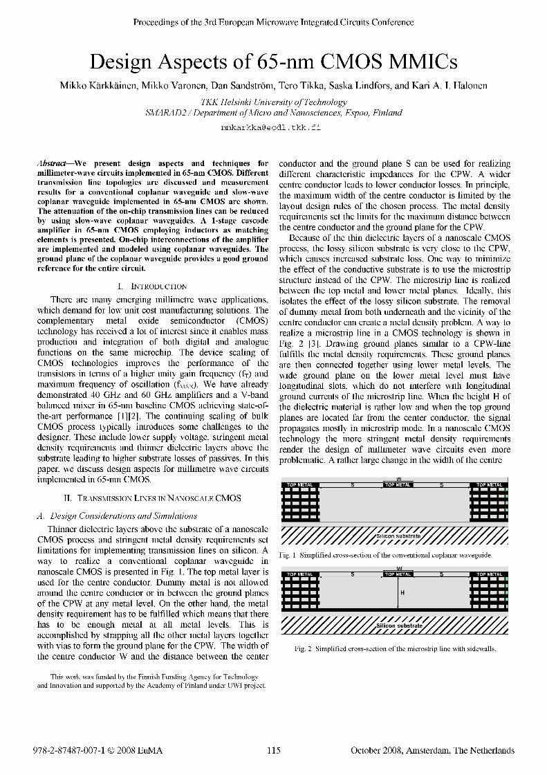
A. Design Considerations and SimulationsThinner dielectric layers above the substrate of a nanoscale
CMOS process and stringent metal density requirements set Silicon substratelimitations for implementing transmission lines on silicon. A Fig. 1 Simplified cross-section of the conventional coplanar waveguide.way to realize a conventional coplanar waveguide innanoscale CMOS is presented in Fig. 1. The top metal layer is _ Sused for the centre conductor. Dummy metal is not allowedaround the centre conductor or in between the ground planesHof the CPW at any metal level. On the other hand, the metaldensity requirement has to be fulfilled which means that therehas to be enough metal at all metal levels. This is Silcon//substrate//accomplished by strapping all the other metal layers together / /////''''''with vias to form the ground plane for the CPW. The width of Fig. 2 Simplified cross-section of the microstrip line with sidewalls.the centre conductor W and the distance between the center
This work was funded by the Finnish Funding Agency for Technologyand Innovation and supported by the Academy of Finland under UTWI project.
978-2-87487-007-1 ©C 2008 EuMA 115 October 2008, Amsterdam, The Netherlands
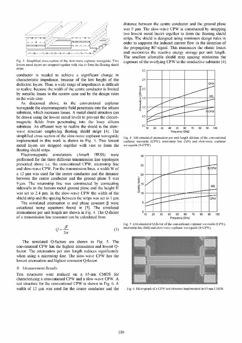
distance between the centre conductor and the ground planewas 9 gim. The slow-wave CPW is constructed by strappingtwo lowest metal layers together to form the floating shield
LL I] I u I I] strips. The shield is designed using minimum design rules inorder to suppress the induced current flow in the direction ofthe propagating RF-signal. This minimizes the ohmic lossesand maximizes the reactive energy storage per unit length.The smallest allowable shield strip spacing minimizes the
Fig. 3 Simplified cross-section of the slow-wave coplanar waveguide. Two exposure of the overlying CPW to the conductive substrate [4].lowest metal layers are strapped together with vias to form the floating shieldstrips. 3.0
conductor is needed to achieve a significant change incharacteristic impedance, because of the low height of the 2.5dielectric layers. Thus, a wide range of impedances is difficult CPWto realize, because the width of the centre conductor is limited E 2.0by metallic losses in the narrow case and by the design rules cMin the wide case. 51.5As discussed above, in the conventional coplanar
waveguide the electromagnetic field penetrates into the silicon _ 1_ /substrate, which increases losses. A metal shield structure can
< PW
be drawn using the lowest metal levels to prevent the electro- 0.5 lmagnetic fields from penetrating into the lossy siliconsubstrate. An efficient way to realize the shield is the slow- ° 20 30 40 50 60 70 80 90 110wave structure employing floating shield strips [4]. The Frequency [GHz]simplified cross section of the slow-wave coplanar waveguide Fig. 4 EM-simulated attenuation per unit length dB/mm of the conventionalimplemented in this work is shown in Fig. 3. Two lowest coplanar waveuide (CPW), microstrip line (MS) and slow-wave coplanarmetal layers are strapped together with vias to form the waveguide (S-CPW).floating shield strips.
Electromagnetic simulations (Ansoft HFSS) were 30performed for the three different transmission line topologiespresented above i.e. the conventional CPW, microstrip line 25and slow-wave CPW. For the transmission lines, a width W of _-cPwa 12 tm was used for the centre conductor and the distance 20between the centre conductor and the ground plane S was v9 gim. The microstrip line was constructed by connecting _15sidewalls to the bottom metal ground plane and the height H ,was set to 2.4 gim. In the slow-wave CPW the width of the a 10 L
shield strip and the spacing between the strips was set to 1 gim. C|WThe simulated attenuation oc and phase constant D were 5
calculated using equations found in [5]. The simulatedattenuations per unit length are shown in Fig. 4. The Q-factor 0
10 20 30 40 50 60 70 80 90 100of a transmission line resonator can be calculated from Frequency [GHz]
Fig. 5 EM-simulated Q-factor of the conventional coplanar waveuide (CPW),(, . >1) microstrip line (MS) and slow-wave coplanar waveguide (S-CPW).
2a
The simulated Q-factors are shown in Fig. 5. Theconventional CPW has the highest attenuation and lowest Q-factor. The attenuation per unit length reduces significantlywhen using a microstrip line. The slow-wave CPW has thelowest attenuation and highest resonator Q-factor.
B. Measurement Results
characerizing a Conventonal CPW anld a slow-wave C.PW. Atest structure for the conventional CPW iS shown in Fig. 6. Awidth of 12 gin was used for the centre conductor and the Fig. 6 Micrograph ofaCPWtest structure implemented in 65-nm CMOS.
116
The measured characteristic impedance of the conventional interconnections are implemented and modelled usingCPW is around 47 Q. Because of the shield strips, the relative coplanar waveguides. The coplanar waveguide provides adielectric constant for the slow-wave CPW is higher and the ground reference for the circuit.resulting characteristic impedance for the slow-wave versionis lower (around 35 Q).
The measured attenuation per unit length and quality factor MIMAjfor both conventional and slow-wave CPW are shown in CAPT GROUNDFig. 7 and Fig. 8, respectively. Even though the direct G C -ecomparison of the CPW structures having differentimpedances is difficult, the transmission line attenuation of | -the slow-wave coplanar waveguide is significantly lower RFOUT
when compared to the conventional coplanar waveguide.
6cPw UCTO
5
E 4 ,,/'11' < Fig. 9 Principle layout of the 30-GHz amplifier. Inductors are used formn JJ*fmatching the cascode transistor. Coplanar waveguides are used for
'3 X interconnections. The ground plane of the coplanar waveguide is used for° >dr S-CPVM j 1llli ground reference for the circuit. Lower metal layers are used for connecting
____ _____ I.LIILIJA L the ground planes of the CPW together around the discontinuities.
00 10 20 30 40 50 60 70 80
Frequency [GHz]
Fig. 7 Attenuation per unit length of the conventional and slow-wave CPW.
16
14
12
10
A.~ ~ i. 0Mcorahoh30-GHzAamplifier in 65n CMS Chip-areAtm~~~~~~~~~~~~~~~inludingtepades,terasisso0.54 mmthnx 0.3 mm}?1.,|
0~~ ~~~~~~~~~~~~~~~~~~1
0~~~~ ~~~~ 10 20 30 40 50 6 0 8
Fig. 8 Quality factoroftheFrequency [GHz] 5Freque y [GH-Apriniplelyout/ conventiona andslcow-wave CfaPW sag
II..xACTVTES STUTUE ImlmNte65-nmCMOS.--
CPW~~~~
networks provide weldeiedgound for icorthef he3 circuit. i 6-n CO. hi-ae
lumped elements such as inductors. Atcludigmillimetre4waves,36the
inaccraseteclmvgfrqec repnsevl. 1U eptll. ncp
117
The input of the amplifier is matched to 50 Q using a series 15and short-circuited shunt inductor. The short-circuit isimplemented using a metal-insulator-metal capacitor (2 pF). 10 -21The low frequency stability is ensured using resistor-capacitor 5 \networks. A short-circuited shunt inductor is used formatching the output of the amplifier to 50 Q. _ o __ _ X_ _c
The simulated and measured S-parameters of the amplifier Dare shown in Fig. 11. Because of the use of CPWs as -5 - - -interconnections and the ground plane of the CPW as a ground 22reference for the circuit, there is a good agreement between -10measured and simulated response. The measured small-signal 15gain is 4.5 dB at 32 GHz.
-201 11 1B. Transistor test structure in 65-nm CMOS 0 10 20 30 40 50 60 70 80 90 100 110A CPW test structure, shown in Fig. 12, was developed for Frequency [GHz]
characterizing a common-source NMOS-transistor up to at Fig. 13 Measured and simulated S-parameters of the transistor test structure.least 60 GHz. The transistor data was de-embedded using Extracted transistor modelopen and short de-embedding [6]. The measured maximum PWOUstable gain is 9.4 dB at 60 GHz. IN CPWW _ _
1 _ _ _ ~Pad capacitancEPad capacitance
Fig. 14 The schematic for simulating the transistor test structure.
IV. CONCLUSIONSIn this paper we discussed and presented design aspects for
implementing transmission lines in 65-nm CMOS. Thel I i-.XXattenuation of the on-chip transmission lines can be reduced
by using slow-wave coplanar waveguides. A 30-GHzamplifier employing inductors and coplanar waveguides waspresented. As the CPW provides a good ground reference forthe circuit a good agreement between simulated and measuredresponse is achieved.
ACKNOWLEDGMENT
We want to thank Hannu Hakojarvi, Millimetre WaveFig. 12 A coplanar waveguide transistor test structure in 65-nm CMOS. Laboratory of Finland - MilliLab, for on-wafer measurements.
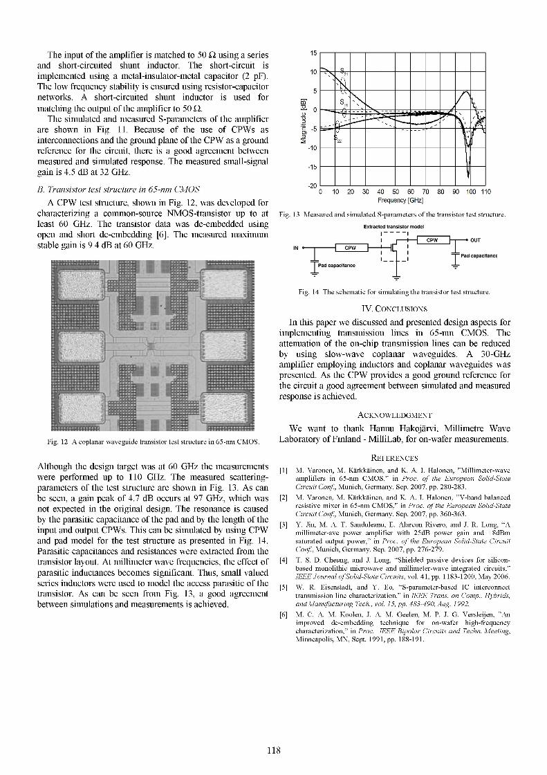
REFERENCESAlthough the design target was at 60 GH-Iz the measurements [1] M. Varonen, M. Karkkainen, and K. A. I. Halonen, "Millimeter-wavewere performed up to 110 GHz. The measured scattering- amplifiers in 65-nm CMOS," in Proc. of the European Solid-Stateparameters of the test structure are shown in Fig. 13. As can Circuit Conf, Munich, Germany. Sep. 2007, pp. 280-283.be seen, a gain peak of 4.7 dB occurs at 97 GHz, which was [2] M. Varonen, M. Karkkainen, and K. A. I. Halonen, "V-band balancednot expected in the original design. The resonance is caused resistive mixer in 65-nm CMOS," in Proc. of the European Solid-State
by the parasitic capacitance of the pad and by the length of the Circuit Conf, Munich, Germany. Sep. 2007, pp. 360-363.input andoutput CPWsThis tnepaaanbesimulatedbyung CPW
tne [3] Y. Jin, M. A. T. Sanduleanu, E. Alarcon Rivero, and J. R. Long, "Ainput and output CPWs. This can be simulated by using CPW millimeter-ave power amplifier with 25dB power gain and +8dBmand pad model for the test structure as presented in Fig. 14. saturated output power," in Proc. of the European Solid-State CircuitParasitic capacitances and resistances were extracted from the Conf, Munich, Germany. Sep. 2007, pp. 276-279.transistor layout. At millimeter wave frequencies, the effect of [4] T. S. D. Cheung, and J. Long, "Shielded passive devices for silicon-
* inductances becomes significant. Thus, small valued based monolithic microwave and millimeter-wave integrated circuits,"parasitic m a ese IEEE Journal ofSolid-State Circuits, vol. 41, pp. 1183-1200, May 2006.series inductors were used to model the access parasitic ofthe [5] W. R. Eisenstadt, and Y. Eo, "S-parameter-based IC interconnecttransistor. As can be seen from Fig. 13, a good agreement transmission line characterization," in IEEE Trans. on Comp., Hybrids,between simulations and measurements is achieved. and Manufacturing Tech., vol. 15, pp. 483-490, Aug. 1992.
[6] M. C. A. M. Koolen, J. A. M. Geelen, M. P. J. G. Versleijen, "Animproved de-embedding technique for on-wafer high-frequencycharacterization," in Proc. IEEE Bipolar Circuits and Techn. Meeting,Minneapolis, MN, Sept. 1991, pp. 188-19 1.
118