pspice® user’s guide - gdyniacastor.am.gdynia.pl/~luksza/doc/pspice_user_guide.pdf · pspice®...
TRANSCRIPT

PSpice® User’s Guide
includes PSpice A/D, PSpice A/D Basics, and PSpice
Product Version 10.5July 2005

1985-2005 Cadence Design Systems, Inc. All rights reserved.Printed in the United States of America.
Cadence Design Systems, Inc., 555 River Oaks Parkway, San Jose, CA 95134, USA
Trademarks: Trademarks and service marks of Cadence Design Systems, Inc. (Cadence)contained in this document are attributed to Cadence with the appropriate symbol. For queriesregarding Cadence’s trademarks, contact the corporate legal department at the address shownabove or call 1-800-862-4522.
All other trademarks are the property of their respective holders.
Restricted Print Permission: This publication is protected by copyright and any unauthorized useof this publication may violate copyright, trademark, and other laws. Except as specified in thispermission statement, this publication may not be copied, reproduced, modified, published,uploaded, posted, transmitted, or distributed in any way, without prior written permission fromCadence. This statement grants you permission to print one (1) hard copy of this publication subjectto the following conditions:
1 The publication may be used solely for personal, informational, and noncommercial purposes;
2 The publication may not be modified in any way;
3 Any copy of the publication or portion thereof must include all original copyright, trademark, andother proprietary notices and this permission statement; and
4 Cadence reserves the right to revoke this authorization at any time, and any such use shall bediscontinued immediately upon written notice from Cadence.
Disclaimer: Information in this publication is subject to change without notice and does notrepresent a commitment on the part of Cadence. The information contained herein is the proprietaryand confidential information of Cadence or its licensors, and is supplied subject to, and may be usedonly by Cadence’s customer in accordance with, a written agreement between Cadence and itscustomer. Except as may be explicitly set forth in such agreement, Cadence does not make, andexpressly disclaims, any representations or warranties as to the completeness, accuracy orusefulness of the information contained in this document. Cadence does not warrant that use of suchinformation will not infringe any third party rights, nor does Cadence assume any liability fordamages or costs of any kind that may result from use of such information.
Restricted Rights: Use, duplication, or disclosure by the Government is subject to restrictions asset forth in FAR52.227-14 and DFAR252.227-7013 et seq. or its successor.
PSpice User's Guide
Contents
Before you begin . . . . . . . . . . . . . . . . . . . . . . . . . . . . . . . . . . . . . . . . . . . . . . . . . . 19
Welcome . . . . . . . . . . . . . . . . . . . . . . . . . . . . . . . . . . . . . . . . . . . . . . . . . . . . . . . . . . . . . 19How to use this guide . . . . . . . . . . . . . . . . . . . . . . . . . . . . . . . . . . . . . . . . . . . . . . . . . . . 20
Symbols and conventions . . . . . . . . . . . . . . . . . . . . . . . . . . . . . . . . . . . . . . . . . . . . . . 20Related documentation . . . . . . . . . . . . . . . . . . . . . . . . . . . . . . . . . . . . . . . . . . . . . . . 21
What this user’s guide covers . . . . . . . . . . . . . . . . . . . . . . . . . . . . . . . . . . . . . . . . . . . . . 24PSpice A/D overview . . . . . . . . . . . . . . . . . . . . . . . . . . . . . . . . . . . . . . . . . . . . . . . . . 24PSpice A/D Basics overview . . . . . . . . . . . . . . . . . . . . . . . . . . . . . . . . . . . . . . . . . . . 25PSpice overview . . . . . . . . . . . . . . . . . . . . . . . . . . . . . . . . . . . . . . . . . . . . . . . . . . . . . 25
Add-on options . . . . . . . . . . . . . . . . . . . . . . . . . . . . . . . . . . . . . . . . . . . . . . . . . . . . . . . . . 25PSpice Smoke Option . . . . . . . . . . . . . . . . . . . . . . . . . . . . . . . . . . . . . . . . . . . . . . . . 25PSpice Advanced Optimizer Option . . . . . . . . . . . . . . . . . . . . . . . . . . . . . . . . . . . . . . 26PSpice Advanced Analysis . . . . . . . . . . . . . . . . . . . . . . . . . . . . . . . . . . . . . . . . . . . . . 26
If you don’t have the standard PSpice A/D package . . . . . . . . . . . . . . . . . . . . . . . . . . . . 26Comparison of the different versions of PSpice . . . . . . . . . . . . . . . . . . . . . . . . . . . . . 26If you have PSpice A/D Lite . . . . . . . . . . . . . . . . . . . . . . . . . . . . . . . . . . . . . . . . . . . . 30Minimum hardware requirements for running PSpice: . . . . . . . . . . . . . . . . . . . . . . . . 30
Part one: Simulation primer . . . . . . . . . . . . . . . . . . . . . . . . . . . . . . . . . . . . . 33
1Things you need to know . . . . . . . . . . . . . . . . . . . . . . . . . . . . . . . . . . . . . . . . 35
Chapter overview . . . . . . . . . . . . . . . . . . . . . . . . . . . . . . . . . . . . . . . . . . . . . . . . . . . . . . . 35What is PSpice A/D? . . . . . . . . . . . . . . . . . . . . . . . . . . . . . . . . . . . . . . . . . . . . . . . . . . . . 36Analyses you can run with PSpice A/D . . . . . . . . . . . . . . . . . . . . . . . . . . . . . . . . . . . . . . 40
Basic analyses . . . . . . . . . . . . . . . . . . . . . . . . . . . . . . . . . . . . . . . . . . . . . . . . . . . . . . 40Advanced multi-run analyses . . . . . . . . . . . . . . . . . . . . . . . . . . . . . . . . . . . . . . . . . . . 43
Analyzing waveforms with PSpice . . . . . . . . . . . . . . . . . . . . . . . . . . . . . . . . . . . . . . . . . . 45What is waveform analysis? . . . . . . . . . . . . . . . . . . . . . . . . . . . . . . . . . . . . . . . . . . . 45
Using PSpice with other programs . . . . . . . . . . . . . . . . . . . . . . . . . . . . . . . . . . . . . . . . . . 46Using OrCAD Capture to prepare for simulation . . . . . . . . . . . . . . . . . . . . . . . . . . . . 46What is the PSpice Stimulus Editor? . . . . . . . . . . . . . . . . . . . . . . . . . . . . . . . . . . . . . 46
July 2005 3 Product Version 10.5

PSpice User's Guide
What is the PSpice Model Editor? . . . . . . . . . . . . . . . . . . . . . . . . . . . . . . . . . . . . . . . 47Files needed for simulation . . . . . . . . . . . . . . . . . . . . . . . . . . . . . . . . . . . . . . . . . . . . . . . 47
Files that OrCAD Capture generates . . . . . . . . . . . . . . . . . . . . . . . . . . . . . . . . . . . . . 48Other files that you can configure for simulation . . . . . . . . . . . . . . . . . . . . . . . . . . . . 50
Files that PSpice generates . . . . . . . . . . . . . . . . . . . . . . . . . . . . . . . . . . . . . . . . . . . . . . . 53New directory structure for analog projects . . . . . . . . . . . . . . . . . . . . . . . . . . . . . . . . . . . 55
How are files configured at the design level maintained in the new directory structure foranalog projects? . . . . . . . . . . . . . . . . . . . . . . . . . . . . . . . . . . . . . . . . . . . . . . . . . . . . . 58How are files configured at the profile level maintained in the new directory structure foranalog projects? . . . . . . . . . . . . . . . . . . . . . . . . . . . . . . . . . . . . . . . . . . . . . . . . . . . . . 60What happens when I convert an analog project that uses a design from another projector from another location? . . . . . . . . . . . . . . . . . . . . . . . . . . . . . . . . . . . . . . . . . . . . . . 62What should I do if the schematic for a converted analog project uses FILESTIMn partsfrom the SOURCE library? . . . . . . . . . . . . . . . . . . . . . . . . . . . . . . . . . . . . . . . . . . . . . 62
2Simulation examples . . . . . . . . . . . . . . . . . . . . . . . . . . . . . . . . . . . . . . . . . . . . . 63
Chapter overview . . . . . . . . . . . . . . . . . . . . . . . . . . . . . . . . . . . . . . . . . . . . . . . . . . . . . . . 63Example circuit creation . . . . . . . . . . . . . . . . . . . . . . . . . . . . . . . . . . . . . . . . . . . . . . . . . . 64
Finding out more about setting up your design . . . . . . . . . . . . . . . . . . . . . . . . . . . . . 72Running PSpice . . . . . . . . . . . . . . . . . . . . . . . . . . . . . . . . . . . . . . . . . . . . . . . . . . . . . . . . 72
Performing a bias point analysis . . . . . . . . . . . . . . . . . . . . . . . . . . . . . . . . . . . . . . . . . 73Using the simulation output file . . . . . . . . . . . . . . . . . . . . . . . . . . . . . . . . . . . . . . . . . 75Finding out more about bias point calculations . . . . . . . . . . . . . . . . . . . . . . . . . . . . . 76
DC sweep analysis . . . . . . . . . . . . . . . . . . . . . . . . . . . . . . . . . . . . . . . . . . . . . . . . . . . . . 76Setting up and running a DC sweep analysis . . . . . . . . . . . . . . . . . . . . . . . . . . . . . . . 76Displaying DC analysis results . . . . . . . . . . . . . . . . . . . . . . . . . . . . . . . . . . . . . . . . . . 78Finding out more about DC sweep analysis . . . . . . . . . . . . . . . . . . . . . . . . . . . . . . . . 83
Transient analysis . . . . . . . . . . . . . . . . . . . . . . . . . . . . . . . . . . . . . . . . . . . . . . . . . . . . . . 83Finding out more about transient analysis . . . . . . . . . . . . . . . . . . . . . . . . . . . . . . . . . 87
AC sweep analysis . . . . . . . . . . . . . . . . . . . . . . . . . . . . . . . . . . . . . . . . . . . . . . . . . . . . . . 88Setting up and running an AC sweep analysis . . . . . . . . . . . . . . . . . . . . . . . . . . . . . . 88AC sweep analysis results . . . . . . . . . . . . . . . . . . . . . . . . . . . . . . . . . . . . . . . . . . . . . 90Finding out more about AC sweep and noise analysis . . . . . . . . . . . . . . . . . . . . . . . . 92
Parametric analysis . . . . . . . . . . . . . . . . . . . . . . . . . . . . . . . . . . . . . . . . . . . . . . . . . . . . . 93Setting up and running the parametric analysis . . . . . . . . . . . . . . . . . . . . . . . . . . . . . 94
July 2005 4 Product Version 10.5

PSpice User's Guide
Analyzing waveform families . . . . . . . . . . . . . . . . . . . . . . . . . . . . . . . . . . . . . . . . . . . 97Finding out more about parametric analysis . . . . . . . . . . . . . . . . . . . . . . . . . . . . . . 100
Performance analysis . . . . . . . . . . . . . . . . . . . . . . . . . . . . . . . . . . . . . . . . . . . . . . . . . . 101Finding out more about performance analysis . . . . . . . . . . . . . . . . . . . . . . . . . . . . . 103
Part two: Design entry . . . . . . . . . . . . . . . . . . . . . . . . . . . . . . . . . . . . . . . . . . 105
3Preparing a design for simulation. . . . . . . . . . . . . . . . . . . . . . . . . . . . . . 107
Chapter overview . . . . . . . . . . . . . . . . . . . . . . . . . . . . . . . . . . . . . . . . . . . . . . . . . . . . . . 107Checklist for simulation setup . . . . . . . . . . . . . . . . . . . . . . . . . . . . . . . . . . . . . . . . . . . . 108
Typical simulation setup steps . . . . . . . . . . . . . . . . . . . . . . . . . . . . . . . . . . . . . . . . . 108Advanced design entry and simulation setup steps . . . . . . . . . . . . . . . . . . . . . . . . . 109When netlisting fails or the simulation does not start . . . . . . . . . . . . . . . . . . . . . . . . 110
Using parts that you can simulate . . . . . . . . . . . . . . . . . . . . . . . . . . . . . . . . . . . . . . . . . 111Vendor-supplied parts . . . . . . . . . . . . . . . . . . . . . . . . . . . . . . . . . . . . . . . . . . . . . . . 112Passive parts . . . . . . . . . . . . . . . . . . . . . . . . . . . . . . . . . . . . . . . . . . . . . . . . . . . . . . 117Breakout parts . . . . . . . . . . . . . . . . . . . . . . . . . . . . . . . . . . . . . . . . . . . . . . . . . . . . . 118Behavioral parts . . . . . . . . . . . . . . . . . . . . . . . . . . . . . . . . . . . . . . . . . . . . . . . . . . . . 120
Specifying values for part properties . . . . . . . . . . . . . . . . . . . . . . . . . . . . . . . . . . . . . . . 120Using global parameters and expressions for values . . . . . . . . . . . . . . . . . . . . . . . . . . 121
Global parameters . . . . . . . . . . . . . . . . . . . . . . . . . . . . . . . . . . . . . . . . . . . . . . . . . . 121Expressions . . . . . . . . . . . . . . . . . . . . . . . . . . . . . . . . . . . . . . . . . . . . . . . . . . . . . . . 124
Defining power supplies . . . . . . . . . . . . . . . . . . . . . . . . . . . . . . . . . . . . . . . . . . . . . . . . . 133For the analog portion of your circuit . . . . . . . . . . . . . . . . . . . . . . . . . . . . . . . . . . . . 133For A/D interfaces in mixed-signal circuits . . . . . . . . . . . . . . . . . . . . . . . . . . . . . . . . 133
Defining stimuli . . . . . . . . . . . . . . . . . . . . . . . . . . . . . . . . . . . . . . . . . . . . . . . . . . . . . . . 135Analog stimuli . . . . . . . . . . . . . . . . . . . . . . . . . . . . . . . . . . . . . . . . . . . . . . . . . . . . . . 135Digital stimuli . . . . . . . . . . . . . . . . . . . . . . . . . . . . . . . . . . . . . . . . . . . . . . . . . . . . . . 138
Things to watch for . . . . . . . . . . . . . . . . . . . . . . . . . . . . . . . . . . . . . . . . . . . . . . . . . . . . . 140Unmodeled parts . . . . . . . . . . . . . . . . . . . . . . . . . . . . . . . . . . . . . . . . . . . . . . . . . . . 140Unconfigured model, stimulus, or include files . . . . . . . . . . . . . . . . . . . . . . . . . . . . . 144Unmodeled pins . . . . . . . . . . . . . . . . . . . . . . . . . . . . . . . . . . . . . . . . . . . . . . . . . . . . 145Missing ground . . . . . . . . . . . . . . . . . . . . . . . . . . . . . . . . . . . . . . . . . . . . . . . . . . . . . 146Missing DC path to ground . . . . . . . . . . . . . . . . . . . . . . . . . . . . . . . . . . . . . . . . . . . . 146
July 2005 5 Product Version 10.5

PSpice User's Guide
4Creating and editing models . . . . . . . . . . . . . . . . . . . . . . . . . . . . . . . . . . . 149
Chapter overview . . . . . . . . . . . . . . . . . . . . . . . . . . . . . . . . . . . . . . . . . . . . . . . . . . . . . . 149What are models? . . . . . . . . . . . . . . . . . . . . . . . . . . . . . . . . . . . . . . . . . . . . . . . . . . . . . 151How are models organized? . . . . . . . . . . . . . . . . . . . . . . . . . . . . . . . . . . . . . . . . . . . . . 152
Model libraries . . . . . . . . . . . . . . . . . . . . . . . . . . . . . . . . . . . . . . . . . . . . . . . . . . . . . 152Model library configuration . . . . . . . . . . . . . . . . . . . . . . . . . . . . . . . . . . . . . . . . . . . . 153Global vs. design vs. profile models and libraries . . . . . . . . . . . . . . . . . . . . . . . . . . 153Nested model libraries . . . . . . . . . . . . . . . . . . . . . . . . . . . . . . . . . . . . . . . . . . . . . . . 154PSpice-provided models . . . . . . . . . . . . . . . . . . . . . . . . . . . . . . . . . . . . . . . . . . . . . 155Model library data . . . . . . . . . . . . . . . . . . . . . . . . . . . . . . . . . . . . . . . . . . . . . . . . . . . 155Device characteristic curves-based models vs. Template-based models . . . . . . . . 157
Tools to create and edit models . . . . . . . . . . . . . . . . . . . . . . . . . . . . . . . . . . . . . . . . . . . 160Ways to create and edit models . . . . . . . . . . . . . . . . . . . . . . . . . . . . . . . . . . . . . . . . . . . 161Using the Model Editor . . . . . . . . . . . . . . . . . . . . . . . . . . . . . . . . . . . . . . . . . . . . . . . . . 163
Ways to use the Model Editor . . . . . . . . . . . . . . . . . . . . . . . . . . . . . . . . . . . . . . . . . . 164Running the Model Editor alone . . . . . . . . . . . . . . . . . . . . . . . . . . . . . . . . . . . . . . . . . . 165
Starting the Model Editor . . . . . . . . . . . . . . . . . . . . . . . . . . . . . . . . . . . . . . . . . . . . . 166Creating models using the Model Editor . . . . . . . . . . . . . . . . . . . . . . . . . . . . . . . . . . . . 166
Creating models based on device characteristic curves . . . . . . . . . . . . . . . . . . . . . 166Creating models based on PSpice templates . . . . . . . . . . . . . . . . . . . . . . . . . . . . . 171Importing an existing model . . . . . . . . . . . . . . . . . . . . . . . . . . . . . . . . . . . . . . . . . . . 174Enabling and disabling automatic part creation . . . . . . . . . . . . . . . . . . . . . . . . . . . . 175Running the Model Editor from the schematic editor . . . . . . . . . . . . . . . . . . . . . . . . 177
Model creation examples . . . . . . . . . . . . . . . . . . . . . . . . . . . . . . . . . . . . . . . . . . . . . . . . 180Example: Creating a PSpice model based on device characteristic curves . . . . . . . 180Example: Creating template-based PSpice model . . . . . . . . . . . . . . . . . . . . . . . . . . 187
Editing model text . . . . . . . . . . . . . . . . . . . . . . . . . . . . . . . . . . . . . . . . . . . . . . . . . . . . . 193Example: editing a Q2N2222 instance model . . . . . . . . . . . . . . . . . . . . . . . . . . . . . 195
Using the Create Subcircuit Format Netlist command . . . . . . . . . . . . . . . . . . . . . . . . . . 196Changing the model reference to an existing model definition . . . . . . . . . . . . . . . . . . . 199Reusing instance models . . . . . . . . . . . . . . . . . . . . . . . . . . . . . . . . . . . . . . . . . . . . . . . . 200
Reusing instance models in the same schematic . . . . . . . . . . . . . . . . . . . . . . . . . . 200Making instance models available to all designs . . . . . . . . . . . . . . . . . . . . . . . . . . . 201
Configuring model libraries . . . . . . . . . . . . . . . . . . . . . . . . . . . . . . . . . . . . . . . . . . . . . . 202
July 2005 6 Product Version 10.5

PSpice User's Guide
The Configuration Files tab . . . . . . . . . . . . . . . . . . . . . . . . . . . . . . . . . . . . . . . . . . . 202How PSpice uses model libraries . . . . . . . . . . . . . . . . . . . . . . . . . . . . . . . . . . . . . . . 203Adding model libraries to the configuration . . . . . . . . . . . . . . . . . . . . . . . . . . . . . . . 205Changing the model library scope from profile to design, profile to global, design to globaland vice versa . . . . . . . . . . . . . . . . . . . . . . . . . . . . . . . . . . . . . . . . . . . . . . . . . . . . . 206Changing model library search order . . . . . . . . . . . . . . . . . . . . . . . . . . . . . . . . . . . . 208Changing the library search path . . . . . . . . . . . . . . . . . . . . . . . . . . . . . . . . . . . . . . . 210
Handling smoke information using the Model Editor . . . . . . . . . . . . . . . . . . . . . . . . . . . 212Adding smoke information to PSpice models . . . . . . . . . . . . . . . . . . . . . . . . . . . . . . 212Creating template-based PSpice models with smoke information . . . . . . . . . . . . . . 214Using the Model Editor to edit smoke information . . . . . . . . . . . . . . . . . . . . . . . . . . 214
Examples: Smoke . . . . . . . . . . . . . . . . . . . . . . . . . . . . . . . . . . . . . . . . . . . . . . . . . . . . . 215Adding smoke information to the D1 diode model . . . . . . . . . . . . . . . . . . . . . . . . . . 215Adding smoke information to the OPA_LOCAL operational amplifier model . . . . . . 216
Smoke parameters . . . . . . . . . . . . . . . . . . . . . . . . . . . . . . . . . . . . . . . . . . . . . . . . . . . . . 218Diode . . . . . . . . . . . . . . . . . . . . . . . . . . . . . . . . . . . . . . . . . . . . . . . . . . . . . . . . . . . . 219Bipolar Junction Transistors . . . . . . . . . . . . . . . . . . . . . . . . . . . . . . . . . . . . . . . . . . . 220Magnetic Core . . . . . . . . . . . . . . . . . . . . . . . . . . . . . . . . . . . . . . . . . . . . . . . . . . . . . 221Ins Gate Bipolar Transistor (IGBT) . . . . . . . . . . . . . . . . . . . . . . . . . . . . . . . . . . . . . . 222Junction FET . . . . . . . . . . . . . . . . . . . . . . . . . . . . . . . . . . . . . . . . . . . . . . . . . . . . . . 223Operational Amplifier . . . . . . . . . . . . . . . . . . . . . . . . . . . . . . . . . . . . . . . . . . . . . . . . 224MOSFET . . . . . . . . . . . . . . . . . . . . . . . . . . . . . . . . . . . . . . . . . . . . . . . . . . . . . . . . . 226Voltage Regulator . . . . . . . . . . . . . . . . . . . . . . . . . . . . . . . . . . . . . . . . . . . . . . . . . . . 228Darlington Transistor . . . . . . . . . . . . . . . . . . . . . . . . . . . . . . . . . . . . . . . . . . . . . . . . 229
5Creating parts for models. . . . . . . . . . . . . . . . . . . . . . . . . . . . . . . . . . . . . . . 231
Chapter overview . . . . . . . . . . . . . . . . . . . . . . . . . . . . . . . . . . . . . . . . . . . . . . . . . . . . . . 231What’s different about parts used for simulation? . . . . . . . . . . . . . . . . . . . . . . . . . . . . . 232Ways to create parts for models . . . . . . . . . . . . . . . . . . . . . . . . . . . . . . . . . . . . . . . . . . 233Preparing your models for part creation . . . . . . . . . . . . . . . . . . . . . . . . . . . . . . . . . . . . 235Starting the Model Editor . . . . . . . . . . . . . . . . . . . . . . . . . . . . . . . . . . . . . . . . . . . . . . . . 236Using the Model Editor to create parts . . . . . . . . . . . . . . . . . . . . . . . . . . . . . . . . . . . . . 237
Batch mode of part creation . . . . . . . . . . . . . . . . . . . . . . . . . . . . . . . . . . . . . . . . . . . 237Interactive mode of part creation . . . . . . . . . . . . . . . . . . . . . . . . . . . . . . . . . . . . . . . 237
July 2005 7 Product Version 10.5

PSpice User's Guide
Creating Capture parts for all models in a library . . . . . . . . . . . . . . . . . . . . . . . . . . . . . 238Using batch mode . . . . . . . . . . . . . . . . . . . . . . . . . . . . . . . . . . . . . . . . . . . . . . . . . . 238Using interactive mode . . . . . . . . . . . . . . . . . . . . . . . . . . . . . . . . . . . . . . . . . . . . . . . 240
Setting up automatic part creation . . . . . . . . . . . . . . . . . . . . . . . . . . . . . . . . . . . . . . . . . 245Example . . . . . . . . . . . . . . . . . . . . . . . . . . . . . . . . . . . . . . . . . . . . . . . . . . . . . . . . . . . . . 246
Creating parts in the batch mode . . . . . . . . . . . . . . . . . . . . . . . . . . . . . . . . . . . . . . . 246Creating parts using interactive mode . . . . . . . . . . . . . . . . . . . . . . . . . . . . . . . . . . . 250
Basing new parts on a custom set of parts . . . . . . . . . . . . . . . . . . . . . . . . . . . . . . . . . . 254Editing part graphics . . . . . . . . . . . . . . . . . . . . . . . . . . . . . . . . . . . . . . . . . . . . . . . . . . . 256
How Capture places parts . . . . . . . . . . . . . . . . . . . . . . . . . . . . . . . . . . . . . . . . . . . . 256Defining grid spacing . . . . . . . . . . . . . . . . . . . . . . . . . . . . . . . . . . . . . . . . . . . . . . . . 258
Attaching models to parts . . . . . . . . . . . . . . . . . . . . . . . . . . . . . . . . . . . . . . . . . . . . . . . 259MODEL . . . . . . . . . . . . . . . . . . . . . . . . . . . . . . . . . . . . . . . . . . . . . . . . . . . . . . . . . . . 260
Defining part properties needed for simulation . . . . . . . . . . . . . . . . . . . . . . . . . . . . . . . 262PSPICETEMPLATE . . . . . . . . . . . . . . . . . . . . . . . . . . . . . . . . . . . . . . . . . . . . . . . . . 263IO_LEVEL . . . . . . . . . . . . . . . . . . . . . . . . . . . . . . . . . . . . . . . . . . . . . . . . . . . . . . . . 272MNTYMXDLY . . . . . . . . . . . . . . . . . . . . . . . . . . . . . . . . . . . . . . . . . . . . . . . . . . . . . . 273PSPICEDEFAULTNET . . . . . . . . . . . . . . . . . . . . . . . . . . . . . . . . . . . . . . . . . . . . . . . 274
6Analog behavioral modeling . . . . . . . . . . . . . . . . . . . . . . . . . . . . . . . . . . . . 275
Chapter overview . . . . . . . . . . . . . . . . . . . . . . . . . . . . . . . . . . . . . . . . . . . . . . . . . . . . . . 275Overview of analog behavioral modeling . . . . . . . . . . . . . . . . . . . . . . . . . . . . . . . . . . . . 276The ABM.OLB part library file . . . . . . . . . . . . . . . . . . . . . . . . . . . . . . . . . . . . . . . . . . . . 277Placing and specifying ABM parts . . . . . . . . . . . . . . . . . . . . . . . . . . . . . . . . . . . . . . . . . 278
Net names and device names in ABM expressions . . . . . . . . . . . . . . . . . . . . . . . . . 278Forcing the use of a global definition . . . . . . . . . . . . . . . . . . . . . . . . . . . . . . . . . . . . 279
ABM part templates . . . . . . . . . . . . . . . . . . . . . . . . . . . . . . . . . . . . . . . . . . . . . . . . . . . . 280Control system parts . . . . . . . . . . . . . . . . . . . . . . . . . . . . . . . . . . . . . . . . . . . . . . . . . . . 281
Basic components . . . . . . . . . . . . . . . . . . . . . . . . . . . . . . . . . . . . . . . . . . . . . . . . . . 284Limiters . . . . . . . . . . . . . . . . . . . . . . . . . . . . . . . . . . . . . . . . . . . . . . . . . . . . . . . . . . . 285Chebyshev filters . . . . . . . . . . . . . . . . . . . . . . . . . . . . . . . . . . . . . . . . . . . . . . . . . . . 286Integrator and differentiator . . . . . . . . . . . . . . . . . . . . . . . . . . . . . . . . . . . . . . . . . . . 290Table look-up parts . . . . . . . . . . . . . . . . . . . . . . . . . . . . . . . . . . . . . . . . . . . . . . . . . . 291Laplace transform part . . . . . . . . . . . . . . . . . . . . . . . . . . . . . . . . . . . . . . . . . . . . . . . 296
July 2005 8 Product Version 10.5

PSpice User's Guide
Math functions . . . . . . . . . . . . . . . . . . . . . . . . . . . . . . . . . . . . . . . . . . . . . . . . . . . . . 299ABM expression parts . . . . . . . . . . . . . . . . . . . . . . . . . . . . . . . . . . . . . . . . . . . . . . . 299An instantaneous device example: modeling a triode . . . . . . . . . . . . . . . . . . . . . . . 303
PSpice-equivalent parts . . . . . . . . . . . . . . . . . . . . . . . . . . . . . . . . . . . . . . . . . . . . . . . . . 307Implementation of PSpice-equivalent parts . . . . . . . . . . . . . . . . . . . . . . . . . . . . . . . 308Modeling mathematical or instantaneous relationships . . . . . . . . . . . . . . . . . . . . . . 309Lookup tables (ETABLE and GTABLE) . . . . . . . . . . . . . . . . . . . . . . . . . . . . . . . . . . . 313Frequency-domain device models . . . . . . . . . . . . . . . . . . . . . . . . . . . . . . . . . . . . . . 315Laplace transforms (LAPLACE) . . . . . . . . . . . . . . . . . . . . . . . . . . . . . . . . . . . . . . . . 315Frequency response tables (EFREQ and GFREQ) . . . . . . . . . . . . . . . . . . . . . . . . . 317
Cautions and recommendations for simulation and analysis . . . . . . . . . . . . . . . . . . . . . 320Instantaneous device modeling . . . . . . . . . . . . . . . . . . . . . . . . . . . . . . . . . . . . . . . . 320Frequency-domain parts . . . . . . . . . . . . . . . . . . . . . . . . . . . . . . . . . . . . . . . . . . . . . 321Laplace transforms . . . . . . . . . . . . . . . . . . . . . . . . . . . . . . . . . . . . . . . . . . . . . . . . . . 322Trading off computer resources for accuracy . . . . . . . . . . . . . . . . . . . . . . . . . . . . . . 325
Basic controlled sources . . . . . . . . . . . . . . . . . . . . . . . . . . . . . . . . . . . . . . . . . . . . . . . . 326Creating custom ABM parts . . . . . . . . . . . . . . . . . . . . . . . . . . . . . . . . . . . . . . . . . . . 326
7Digital device modeling . . . . . . . . . . . . . . . . . . . . . . . . . . . . . . . . . . . . . . . . . 329
Chapter overview . . . . . . . . . . . . . . . . . . . . . . . . . . . . . . . . . . . . . . . . . . . . . . . . . . . . . . 329Introduction . . . . . . . . . . . . . . . . . . . . . . . . . . . . . . . . . . . . . . . . . . . . . . . . . . . . . . . . . . 330Functional behavior . . . . . . . . . . . . . . . . . . . . . . . . . . . . . . . . . . . . . . . . . . . . . . . . . . . . 331Timing characteristics . . . . . . . . . . . . . . . . . . . . . . . . . . . . . . . . . . . . . . . . . . . . . . . . . . 339
Timing model . . . . . . . . . . . . . . . . . . . . . . . . . . . . . . . . . . . . . . . . . . . . . . . . . . . . . . 339Propagation delay calculation . . . . . . . . . . . . . . . . . . . . . . . . . . . . . . . . . . . . . . . . . . 342Inertial and transport delay . . . . . . . . . . . . . . . . . . . . . . . . . . . . . . . . . . . . . . . . . . . . 343
Input/Output characteristics . . . . . . . . . . . . . . . . . . . . . . . . . . . . . . . . . . . . . . . . . . . . . . 346Input/Output model . . . . . . . . . . . . . . . . . . . . . . . . . . . . . . . . . . . . . . . . . . . . . . . . . . 346Defining Output Strengths . . . . . . . . . . . . . . . . . . . . . . . . . . . . . . . . . . . . . . . . . . . . 350Charge storage nets . . . . . . . . . . . . . . . . . . . . . . . . . . . . . . . . . . . . . . . . . . . . . . . . . 352Creating your own interface subcircuits foradditional technologies . . . . . . . . . . . . . . . . . . . . . . . . . . . . . . . . . . . . . . . . . . . . . . . 353
Creating a digital model using the PINDLY and LOGICEXP primitives . . . . . . . . . . . . . 358Digital primitives . . . . . . . . . . . . . . . . . . . . . . . . . . . . . . . . . . . . . . . . . . . . . . . . . . . . 359
July 2005 9 Product Version 10.5

PSpice User's Guide
Logic expression (LOGICEXP primitive) . . . . . . . . . . . . . . . . . . . . . . . . . . . . . . . . . 359Pin-to-pin delay (PINDLY primitive) . . . . . . . . . . . . . . . . . . . . . . . . . . . . . . . . . . . . . 361BOOLEAN . . . . . . . . . . . . . . . . . . . . . . . . . . . . . . . . . . . . . . . . . . . . . . . . . . . . . . . . 362PINDLY . . . . . . . . . . . . . . . . . . . . . . . . . . . . . . . . . . . . . . . . . . . . . . . . . . . . . . . . . . . 363Constraint checker (CONSTRAINT primitive) . . . . . . . . . . . . . . . . . . . . . . . . . . . . . 364Setup_Hold . . . . . . . . . . . . . . . . . . . . . . . . . . . . . . . . . . . . . . . . . . . . . . . . . . . . . . . . 365Width . . . . . . . . . . . . . . . . . . . . . . . . . . . . . . . . . . . . . . . . . . . . . . . . . . . . . . . . . . . . 365Freq . . . . . . . . . . . . . . . . . . . . . . . . . . . . . . . . . . . . . . . . . . . . . . . . . . . . . . . . . . . . . 36674160 example . . . . . . . . . . . . . . . . . . . . . . . . . . . . . . . . . . . . . . . . . . . . . . . . . . . . . 366
Part three: Setting up and running analyses . . . . . . . . . . . . . . . . . 369
8Setting up analyses and starting simulation. . . . . . . . . . . . . . . . . . 371
Chapter overview . . . . . . . . . . . . . . . . . . . . . . . . . . . . . . . . . . . . . . . . . . . . . . . . . . . . . . 371Analysis types . . . . . . . . . . . . . . . . . . . . . . . . . . . . . . . . . . . . . . . . . . . . . . . . . . . . . . . . 372Setting up analyses . . . . . . . . . . . . . . . . . . . . . . . . . . . . . . . . . . . . . . . . . . . . . . . . . . . . 373
Execution order for standard analyses . . . . . . . . . . . . . . . . . . . . . . . . . . . . . . . . . . . 374Output variables . . . . . . . . . . . . . . . . . . . . . . . . . . . . . . . . . . . . . . . . . . . . . . . . . . . . 376
Performance package . . . . . . . . . . . . . . . . . . . . . . . . . . . . . . . . . . . . . . . . . . . . . . . . . . 383Starting a simulation . . . . . . . . . . . . . . . . . . . . . . . . . . . . . . . . . . . . . . . . . . . . . . . . . . . 385
Creating a simulation netlist . . . . . . . . . . . . . . . . . . . . . . . . . . . . . . . . . . . . . . . . . . . 385Starting a simulation from Capture . . . . . . . . . . . . . . . . . . . . . . . . . . . . . . . . . . . . . . 394Starting a simulation outside of Capture . . . . . . . . . . . . . . . . . . . . . . . . . . . . . . . . . 394Setting up batch simulations . . . . . . . . . . . . . . . . . . . . . . . . . . . . . . . . . . . . . . . . . . 395The PSpice simulation window . . . . . . . . . . . . . . . . . . . . . . . . . . . . . . . . . . . . . . . . . 396
Interacting with a simulation . . . . . . . . . . . . . . . . . . . . . . . . . . . . . . . . . . . . . . . . . . . . . . 400Extending a transient analysis . . . . . . . . . . . . . . . . . . . . . . . . . . . . . . . . . . . . . . . . . 401Interrupting a simulation . . . . . . . . . . . . . . . . . . . . . . . . . . . . . . . . . . . . . . . . . . . . . . 404Scheduling changes to runtime parameters . . . . . . . . . . . . . . . . . . . . . . . . . . . . . . . 406
Using the Simulation Manager . . . . . . . . . . . . . . . . . . . . . . . . . . . . . . . . . . . . . . . . . . . . 409Overview of the Simulation Manager . . . . . . . . . . . . . . . . . . . . . . . . . . . . . . . . . . . . 409Setting up multiple simulations . . . . . . . . . . . . . . . . . . . . . . . . . . . . . . . . . . . . . . . . . 413Starting, stopping, and pausing simulations . . . . . . . . . . . . . . . . . . . . . . . . . . . . . . . 414Attaching PSpice to a simulation . . . . . . . . . . . . . . . . . . . . . . . . . . . . . . . . . . . . . . . 415
July 2005 10 Product Version 10.5

PSpice User's Guide
Setting options in the Simulation Manager . . . . . . . . . . . . . . . . . . . . . . . . . . . . . . . . 415
9DC analyses. . . . . . . . . . . . . . . . . . . . . . . . . . . . . . . . . . . . . . . . . . . . . . . . . . . . . . 419
Chapter overview . . . . . . . . . . . . . . . . . . . . . . . . . . . . . . . . . . . . . . . . . . . . . . . . . . . . . . 419DC Sweep . . . . . . . . . . . . . . . . . . . . . . . . . . . . . . . . . . . . . . . . . . . . . . . . . . . . . . . . . . . 420
Minimum requirements to run a DC sweep analysis . . . . . . . . . . . . . . . . . . . . . . . . 420Overview of DC sweep . . . . . . . . . . . . . . . . . . . . . . . . . . . . . . . . . . . . . . . . . . . . . . . 421Setting up a DC stimulus . . . . . . . . . . . . . . . . . . . . . . . . . . . . . . . . . . . . . . . . . . . . . 423Nested DC sweeps . . . . . . . . . . . . . . . . . . . . . . . . . . . . . . . . . . . . . . . . . . . . . . . . . . 424Curve families for DC sweeps . . . . . . . . . . . . . . . . . . . . . . . . . . . . . . . . . . . . . . . . . 426
Bias point . . . . . . . . . . . . . . . . . . . . . . . . . . . . . . . . . . . . . . . . . . . . . . . . . . . . . . . . . . . . 429Minimum requirements to run a bias point analysis . . . . . . . . . . . . . . . . . . . . . . . . . 429Overview of bias point . . . . . . . . . . . . . . . . . . . . . . . . . . . . . . . . . . . . . . . . . . . . . . . 429
Small-signal DC transfer . . . . . . . . . . . . . . . . . . . . . . . . . . . . . . . . . . . . . . . . . . . . . . . . 431Minimum requirements to run a small-signal DC transfer analysis . . . . . . . . . . . . . 431Overview of small-signal DC transfer . . . . . . . . . . . . . . . . . . . . . . . . . . . . . . . . . . . . 432
DC sensitivity . . . . . . . . . . . . . . . . . . . . . . . . . . . . . . . . . . . . . . . . . . . . . . . . . . . . . . . . . 434Minimum requirements to run a DC sensitivity analysis . . . . . . . . . . . . . . . . . . . . . . 434Overview of DC sensitivity . . . . . . . . . . . . . . . . . . . . . . . . . . . . . . . . . . . . . . . . . . . . 435
10AC analyses . . . . . . . . . . . . . . . . . . . . . . . . . . . . . . . . . . . . . . . . . . . . . . . . . . . . . . 437
Chapter overview . . . . . . . . . . . . . . . . . . . . . . . . . . . . . . . . . . . . . . . . . . . . . . . . . . . . . . 437AC sweep analysis . . . . . . . . . . . . . . . . . . . . . . . . . . . . . . . . . . . . . . . . . . . . . . . . . . . . . 438
Setting up and running an AC sweep . . . . . . . . . . . . . . . . . . . . . . . . . . . . . . . . . . . . 438What is AC sweep? . . . . . . . . . . . . . . . . . . . . . . . . . . . . . . . . . . . . . . . . . . . . . . . . . 438Setting up an AC stimulus . . . . . . . . . . . . . . . . . . . . . . . . . . . . . . . . . . . . . . . . . . . . 439Setting up an AC analysis . . . . . . . . . . . . . . . . . . . . . . . . . . . . . . . . . . . . . . . . . . . . 442AC sweep setup in example.opj . . . . . . . . . . . . . . . . . . . . . . . . . . . . . . . . . . . . . . . . 444How PSpice treats nonlinear devices . . . . . . . . . . . . . . . . . . . . . . . . . . . . . . . . . . . . 446
Noise analysis . . . . . . . . . . . . . . . . . . . . . . . . . . . . . . . . . . . . . . . . . . . . . . . . . . . . . . . . 448Setting up and running a noise analysis . . . . . . . . . . . . . . . . . . . . . . . . . . . . . . . . . . 448What is noise analysis? . . . . . . . . . . . . . . . . . . . . . . . . . . . . . . . . . . . . . . . . . . . . . . 449Setting up a noise analysis . . . . . . . . . . . . . . . . . . . . . . . . . . . . . . . . . . . . . . . . . . . . 450
July 2005 11 Product Version 10.5
PSpice User's Guide
Analyzing Noise in the Probe window . . . . . . . . . . . . . . . . . . . . . . . . . . . . . . . . . . . 452
11Parametric and temperature analysis . . . . . . . . . . . . . . . . . . . . . . . . . 457
Chapter overview . . . . . . . . . . . . . . . . . . . . . . . . . . . . . . . . . . . . . . . . . . . . . . . . . . . . . . 457Parametric analysis . . . . . . . . . . . . . . . . . . . . . . . . . . . . . . . . . . . . . . . . . . . . . . . . . . . . 458
Minimum requirements to run a parametric analysis . . . . . . . . . . . . . . . . . . . . . . . . 458Overview of parametric analysis . . . . . . . . . . . . . . . . . . . . . . . . . . . . . . . . . . . . . . . 459RLC filter example . . . . . . . . . . . . . . . . . . . . . . . . . . . . . . . . . . . . . . . . . . . . . . . . . . 459Example: frequency response vs. arbitrary parameter . . . . . . . . . . . . . . . . . . . . . . . 464
Temperature analysis . . . . . . . . . . . . . . . . . . . . . . . . . . . . . . . . . . . . . . . . . . . . . . . . . . . 467Minimum requirements to run a temperature analysis . . . . . . . . . . . . . . . . . . . . . . . 467Overview of temperature analysis . . . . . . . . . . . . . . . . . . . . . . . . . . . . . . . . . . . . . . 468
12Transient analysis. . . . . . . . . . . . . . . . . . . . . . . . . . . . . . . . . . . . . . . . . . . . . . . . 471
Chapter overview . . . . . . . . . . . . . . . . . . . . . . . . . . . . . . . . . . . . . . . . . . . . . . . . . . . . . . 471Overview of transient analysis . . . . . . . . . . . . . . . . . . . . . . . . . . . . . . . . . . . . . . . . . . . . 472
Minimum requirements to run a transient analysis . . . . . . . . . . . . . . . . . . . . . . . . . . 472Defining a time-based stimulus . . . . . . . . . . . . . . . . . . . . . . . . . . . . . . . . . . . . . . . . . . . 474
Overview of stimulus generation . . . . . . . . . . . . . . . . . . . . . . . . . . . . . . . . . . . . . . . 474The Stimulus Editor utility . . . . . . . . . . . . . . . . . . . . . . . . . . . . . . . . . . . . . . . . . . . . . . . 476
Stimulus files . . . . . . . . . . . . . . . . . . . . . . . . . . . . . . . . . . . . . . . . . . . . . . . . . . . . . . 477Configuring stimulus files . . . . . . . . . . . . . . . . . . . . . . . . . . . . . . . . . . . . . . . . . . . . . 477Starting the Stimulus Editor . . . . . . . . . . . . . . . . . . . . . . . . . . . . . . . . . . . . . . . . . . . 478Defining stimuli . . . . . . . . . . . . . . . . . . . . . . . . . . . . . . . . . . . . . . . . . . . . . . . . . . . . . 478Creating new stimulus symbols . . . . . . . . . . . . . . . . . . . . . . . . . . . . . . . . . . . . . . . . 483Editing a stimulus . . . . . . . . . . . . . . . . . . . . . . . . . . . . . . . . . . . . . . . . . . . . . . . . . . . 484Deleting and removing traces . . . . . . . . . . . . . . . . . . . . . . . . . . . . . . . . . . . . . . . . . . 485Manual stimulus configuration . . . . . . . . . . . . . . . . . . . . . . . . . . . . . . . . . . . . . . . . . 485Finding out more about the Stimulus Editor . . . . . . . . . . . . . . . . . . . . . . . . . . . . . . . 487
Transient (time) response . . . . . . . . . . . . . . . . . . . . . . . . . . . . . . . . . . . . . . . . . . . . . . . 487Internal time steps in transient analyses . . . . . . . . . . . . . . . . . . . . . . . . . . . . . . . . . . . . 490Switching circuits in transient analyses . . . . . . . . . . . . . . . . . . . . . . . . . . . . . . . . . . . . . 491Plotting hysteresis curves . . . . . . . . . . . . . . . . . . . . . . . . . . . . . . . . . . . . . . . . . . . . . . . 492
July 2005 12 Product Version 10.5

PSpice User's Guide
Fourier components . . . . . . . . . . . . . . . . . . . . . . . . . . . . . . . . . . . . . . . . . . . . . . . . . . . . 493
13Monte Carlo and sensitivity/worst-case analyses . . . . . . . . . . . 495
Chapter overview . . . . . . . . . . . . . . . . . . . . . . . . . . . . . . . . . . . . . . . . . . . . . . . . . . . . . . 495Statistical analyses . . . . . . . . . . . . . . . . . . . . . . . . . . . . . . . . . . . . . . . . . . . . . . . . . . . . 496
Overview of statistical analyses . . . . . . . . . . . . . . . . . . . . . . . . . . . . . . . . . . . . . . . . 496Output control for statistical analyses . . . . . . . . . . . . . . . . . . . . . . . . . . . . . . . . . . . . 497Model parameter values reports . . . . . . . . . . . . . . . . . . . . . . . . . . . . . . . . . . . . . . . . 497Monte Carlo history support . . . . . . . . . . . . . . . . . . . . . . . . . . . . . . . . . . . . . . . . . . . 498Waveform reports . . . . . . . . . . . . . . . . . . . . . . . . . . . . . . . . . . . . . . . . . . . . . . . . . . . 503Collating functions . . . . . . . . . . . . . . . . . . . . . . . . . . . . . . . . . . . . . . . . . . . . . . . . . . 504Temperature considerations in statistical analyses . . . . . . . . . . . . . . . . . . . . . . . . . 505
Monte Carlo analysis . . . . . . . . . . . . . . . . . . . . . . . . . . . . . . . . . . . . . . . . . . . . . . . . . . . 506Example: Monte Carlo analysis of a pressure sensor . . . . . . . . . . . . . . . . . . . . . . . 512Monte Carlo Histograms . . . . . . . . . . . . . . . . . . . . . . . . . . . . . . . . . . . . . . . . . . . . . . 521
Worst-case analysis . . . . . . . . . . . . . . . . . . . . . . . . . . . . . . . . . . . . . . . . . . . . . . . . . . . . 528Overview of worst-case analysis . . . . . . . . . . . . . . . . . . . . . . . . . . . . . . . . . . . . . . . 528Worst-case analysis example . . . . . . . . . . . . . . . . . . . . . . . . . . . . . . . . . . . . . . . . . . 531Tips and other useful information . . . . . . . . . . . . . . . . . . . . . . . . . . . . . . . . . . . . . . . 535
14Digital simulation. . . . . . . . . . . . . . . . . . . . . . . . . . . . . . . . . . . . . . . . . . . . . . . . . 539
Chapter overview . . . . . . . . . . . . . . . . . . . . . . . . . . . . . . . . . . . . . . . . . . . . . . . . . . . . . . 539What is digital simulation? . . . . . . . . . . . . . . . . . . . . . . . . . . . . . . . . . . . . . . . . . . . . . . . 540Steps for simulating digital circuits . . . . . . . . . . . . . . . . . . . . . . . . . . . . . . . . . . . . . . . . . 540Concepts you need to understand . . . . . . . . . . . . . . . . . . . . . . . . . . . . . . . . . . . . . . . . . 541
States . . . . . . . . . . . . . . . . . . . . . . . . . . . . . . . . . . . . . . . . . . . . . . . . . . . . . . . . . . . . 541Strengths . . . . . . . . . . . . . . . . . . . . . . . . . . . . . . . . . . . . . . . . . . . . . . . . . . . . . . . . . 542
Defining a digital stimulus . . . . . . . . . . . . . . . . . . . . . . . . . . . . . . . . . . . . . . . . . . . . . . . 543Using the DIGSTIMn part . . . . . . . . . . . . . . . . . . . . . . . . . . . . . . . . . . . . . . . . . . . . . 544Defining input signals using the Stimulus Editor . . . . . . . . . . . . . . . . . . . . . . . . . . . 544Using the DIGCLOCK part . . . . . . . . . . . . . . . . . . . . . . . . . . . . . . . . . . . . . . . . . . . . 552Using STIM1, STIM4, STIM8 and STIM16 parts . . . . . . . . . . . . . . . . . . . . . . . . . . . 553Using the FILESTIMn parts . . . . . . . . . . . . . . . . . . . . . . . . . . . . . . . . . . . . . . . . . . . 554
July 2005 13 Product Version 10.5
PSpice User's Guide
Defining simulation time . . . . . . . . . . . . . . . . . . . . . . . . . . . . . . . . . . . . . . . . . . . . . . . . . 558Adjusting simulation parameters . . . . . . . . . . . . . . . . . . . . . . . . . . . . . . . . . . . . . . . . . . 558
Selecting propagation delays . . . . . . . . . . . . . . . . . . . . . . . . . . . . . . . . . . . . . . . . . . 560Initializing flip-flops . . . . . . . . . . . . . . . . . . . . . . . . . . . . . . . . . . . . . . . . . . . . . . . . . . 562
Starting the simulation . . . . . . . . . . . . . . . . . . . . . . . . . . . . . . . . . . . . . . . . . . . . . . . . . . 562Analyzing results . . . . . . . . . . . . . . . . . . . . . . . . . . . . . . . . . . . . . . . . . . . . . . . . . . . . . . 563
Adding digital signals to a plot . . . . . . . . . . . . . . . . . . . . . . . . . . . . . . . . . . . . . . . . . 564Adding buses to a waveform plot . . . . . . . . . . . . . . . . . . . . . . . . . . . . . . . . . . . . . . . 566Tracking timing violations and hazards . . . . . . . . . . . . . . . . . . . . . . . . . . . . . . . . . . . 569
15Mixed analog/digital simulation . . . . . . . . . . . . . . . . . . . . . . . . . . . . . . . . 577
Chapter overview . . . . . . . . . . . . . . . . . . . . . . . . . . . . . . . . . . . . . . . . . . . . . . . . . . . . . . 577Interconnecting analog and digital parts . . . . . . . . . . . . . . . . . . . . . . . . . . . . . . . . . . . . 578Interface subcircuit selection by PSpice . . . . . . . . . . . . . . . . . . . . . . . . . . . . . . . . . . . . 579
Level 1 interface . . . . . . . . . . . . . . . . . . . . . . . . . . . . . . . . . . . . . . . . . . . . . . . . . . . . 580Level 2 interface . . . . . . . . . . . . . . . . . . . . . . . . . . . . . . . . . . . . . . . . . . . . . . . . . . . . 581Setting the default A/D interface . . . . . . . . . . . . . . . . . . . . . . . . . . . . . . . . . . . . . . . . 582
Specifying digital power supplies . . . . . . . . . . . . . . . . . . . . . . . . . . . . . . . . . . . . . . . . . . 583Default power supply selection by PSpice A/D . . . . . . . . . . . . . . . . . . . . . . . . . . . . . 583Creating custom digital power supplies . . . . . . . . . . . . . . . . . . . . . . . . . . . . . . . . . . 585
Interface generation and node names . . . . . . . . . . . . . . . . . . . . . . . . . . . . . . . . . . . . . . 589
16Digital worst-case timing analysis . . . . . . . . . . . . . . . . . . . . . . . . . . . . . 593
Digital worst-case timing . . . . . . . . . . . . . . . . . . . . . . . . . . . . . . . . . . . . . . . . . . . . . . . . 594Digital worst-case analysis compared to analog worst-case analysis . . . . . . . . . . . 595
Starting digital worst-case timing analysis . . . . . . . . . . . . . . . . . . . . . . . . . . . . . . . . . . . 596Simulator representation of timing ambiguity . . . . . . . . . . . . . . . . . . . . . . . . . . . . . . . . . 596Propagation of timing ambiguity . . . . . . . . . . . . . . . . . . . . . . . . . . . . . . . . . . . . . . . . . . 598Identification of timing hazards . . . . . . . . . . . . . . . . . . . . . . . . . . . . . . . . . . . . . . . . . . . 599
Convergence hazard . . . . . . . . . . . . . . . . . . . . . . . . . . . . . . . . . . . . . . . . . . . . . . . . 599Critical hazard . . . . . . . . . . . . . . . . . . . . . . . . . . . . . . . . . . . . . . . . . . . . . . . . . . . . . 600Cumulative ambiguity hazard . . . . . . . . . . . . . . . . . . . . . . . . . . . . . . . . . . . . . . . . . . 601Reconvergence hazard . . . . . . . . . . . . . . . . . . . . . . . . . . . . . . . . . . . . . . . . . . . . . . 603
July 2005 14 Product Version 10.5

PSpice User's Guide
Glitch suppression due to inertial delay . . . . . . . . . . . . . . . . . . . . . . . . . . . . . . . . . . . . . 605Methodology . . . . . . . . . . . . . . . . . . . . . . . . . . . . . . . . . . . . . . . . . . . . . . . . . . . . . . . . . 606
Part four: Viewing results . . . . . . . . . . . . . . . . . . . . . . . . . . . . . . . . . . . . . . . 609
17Analyzing waveforms. . . . . . . . . . . . . . . . . . . . . . . . . . . . . . . . . . . . . . . . . . . . 611
Chapter overview . . . . . . . . . . . . . . . . . . . . . . . . . . . . . . . . . . . . . . . . . . . . . . . . . . . . . . 611Overview of waveform analysis . . . . . . . . . . . . . . . . . . . . . . . . . . . . . . . . . . . . . . . . . . . 612
Elements of a plot . . . . . . . . . . . . . . . . . . . . . . . . . . . . . . . . . . . . . . . . . . . . . . . . . . . 613Elements of a Probe window . . . . . . . . . . . . . . . . . . . . . . . . . . . . . . . . . . . . . . . . . . 614Managing multiple Probe windows . . . . . . . . . . . . . . . . . . . . . . . . . . . . . . . . . . . . . . 615
Setting up waveform analysis . . . . . . . . . . . . . . . . . . . . . . . . . . . . . . . . . . . . . . . . . . . . 617Setting up colors . . . . . . . . . . . . . . . . . . . . . . . . . . . . . . . . . . . . . . . . . . . . . . . . . . . . 617
Viewing waveforms . . . . . . . . . . . . . . . . . . . . . . . . . . . . . . . . . . . . . . . . . . . . . . . . . . . . 622Setting up waveform display from Capture . . . . . . . . . . . . . . . . . . . . . . . . . . . . . . . . 622Viewing waveforms while simulating . . . . . . . . . . . . . . . . . . . . . . . . . . . . . . . . . . . . 623Using schematic page markers to add traces . . . . . . . . . . . . . . . . . . . . . . . . . . . . . 626Using display control . . . . . . . . . . . . . . . . . . . . . . . . . . . . . . . . . . . . . . . . . . . . . . . . 630Using plot window templates . . . . . . . . . . . . . . . . . . . . . . . . . . . . . . . . . . . . . . . . . . 633Limiting waveform data file size . . . . . . . . . . . . . . . . . . . . . . . . . . . . . . . . . . . . . . . . 646Viewing large data files . . . . . . . . . . . . . . . . . . . . . . . . . . . . . . . . . . . . . . . . . . . . . . . 650Using simulation data from multiple files . . . . . . . . . . . . . . . . . . . . . . . . . . . . . . . . . 658Saving simulation results in ASCII format . . . . . . . . . . . . . . . . . . . . . . . . . . . . . . . . 663
Analog example . . . . . . . . . . . . . . . . . . . . . . . . . . . . . . . . . . . . . . . . . . . . . . . . . . . . . . . 665Mixed analog/digital tutorial . . . . . . . . . . . . . . . . . . . . . . . . . . . . . . . . . . . . . . . . . . . . . . 669
About digital states . . . . . . . . . . . . . . . . . . . . . . . . . . . . . . . . . . . . . . . . . . . . . . . . . . 669About the oscillator circuit . . . . . . . . . . . . . . . . . . . . . . . . . . . . . . . . . . . . . . . . . . . . 670Setting up the design . . . . . . . . . . . . . . . . . . . . . . . . . . . . . . . . . . . . . . . . . . . . . . . . 670Running the simulation . . . . . . . . . . . . . . . . . . . . . . . . . . . . . . . . . . . . . . . . . . . . . . . 671Analyzing simulation results . . . . . . . . . . . . . . . . . . . . . . . . . . . . . . . . . . . . . . . . . . . 671
User interface features for waveform analysis . . . . . . . . . . . . . . . . . . . . . . . . . . . . . . . . 674Zoom regions . . . . . . . . . . . . . . . . . . . . . . . . . . . . . . . . . . . . . . . . . . . . . . . . . . . . . . 674Scrolling traces . . . . . . . . . . . . . . . . . . . . . . . . . . . . . . . . . . . . . . . . . . . . . . . . . . . . . 676Sizing digital plots . . . . . . . . . . . . . . . . . . . . . . . . . . . . . . . . . . . . . . . . . . . . . . . . . . 676
July 2005 15 Product Version 10.5

PSpice User's Guide
Modifying trace expressions and labels . . . . . . . . . . . . . . . . . . . . . . . . . . . . . . . . . . 678Moving and copying trace names and expressions . . . . . . . . . . . . . . . . . . . . . . . . . 679Copying and moving labels . . . . . . . . . . . . . . . . . . . . . . . . . . . . . . . . . . . . . . . . . . . 680Tabulating trace data values . . . . . . . . . . . . . . . . . . . . . . . . . . . . . . . . . . . . . . . . . . 681Using cursors . . . . . . . . . . . . . . . . . . . . . . . . . . . . . . . . . . . . . . . . . . . . . . . . . . . . . . 682
Tracking digital simulation messages . . . . . . . . . . . . . . . . . . . . . . . . . . . . . . . . . . . . . . . 687Message tracking from the message summary . . . . . . . . . . . . . . . . . . . . . . . . . . . . 687Message tracking from the waveform . . . . . . . . . . . . . . . . . . . . . . . . . . . . . . . . . . . . 689
Trace expressions . . . . . . . . . . . . . . . . . . . . . . . . . . . . . . . . . . . . . . . . . . . . . . . . . . . . . 689Basic output variable form . . . . . . . . . . . . . . . . . . . . . . . . . . . . . . . . . . . . . . . . . . . . 690Output variable form for device terminals . . . . . . . . . . . . . . . . . . . . . . . . . . . . . . . . . 692Analog trace expressions . . . . . . . . . . . . . . . . . . . . . . . . . . . . . . . . . . . . . . . . . . . . . 700Digital trace expressions . . . . . . . . . . . . . . . . . . . . . . . . . . . . . . . . . . . . . . . . . . . . . 703
18Measurement expressions. . . . . . . . . . . . . . . . . . . . . . . . . . . . . . . . . . . . . . 709
Chapter overview . . . . . . . . . . . . . . . . . . . . . . . . . . . . . . . . . . . . . . . . . . . . . . . . . . . . . . 709Measurements overview . . . . . . . . . . . . . . . . . . . . . . . . . . . . . . . . . . . . . . . . . . . . . . . . 710Measurement strategy . . . . . . . . . . . . . . . . . . . . . . . . . . . . . . . . . . . . . . . . . . . . . . . . . . 711Procedure for creating measurement expressions . . . . . . . . . . . . . . . . . . . . . . . . . . . . 712
Setup . . . . . . . . . . . . . . . . . . . . . . . . . . . . . . . . . . . . . . . . . . . . . . . . . . . . . . . . . . . . 712Composing a measurement expression . . . . . . . . . . . . . . . . . . . . . . . . . . . . . . . . . . 712Viewing the results of measurement evaluations . . . . . . . . . . . . . . . . . . . . . . . . . . . 713
Example . . . . . . . . . . . . . . . . . . . . . . . . . . . . . . . . . . . . . . . . . . . . . . . . . . . . . . . . . . . . . 714Viewing the results of measurement evaluations. . . . . . . . . . . . . . . . . . . . . . . . . . . 717Measurement definitions included in PSpice . . . . . . . . . . . . . . . . . . . . . . . . . . . . . . 718
For power users . . . . . . . . . . . . . . . . . . . . . . . . . . . . . . . . . . . . . . . . . . . . . . . . . . . . . . . 721Creating custom measurement definitions . . . . . . . . . . . . . . . . . . . . . . . . . . . . . . . . 721Definition example . . . . . . . . . . . . . . . . . . . . . . . . . . . . . . . . . . . . . . . . . . . . . . . . . . 722Measurement definition syntax . . . . . . . . . . . . . . . . . . . . . . . . . . . . . . . . . . . . . . . . . 725Syntax example . . . . . . . . . . . . . . . . . . . . . . . . . . . . . . . . . . . . . . . . . . . . . . . . . . . . 734
19Other output options. . . . . . . . . . . . . . . . . . . . . . . . . . . . . . . . . . . . . . . . . . . . . 737
Chapter overview . . . . . . . . . . . . . . . . . . . . . . . . . . . . . . . . . . . . . . . . . . . . . . . . . . . . . . 737
July 2005 16 Product Version 10.5

PSpice User's Guide
Viewing analog results in the PSpice window . . . . . . . . . . . . . . . . . . . . . . . . . . . . . . . . 738Writing additional results to the PSpice output file . . . . . . . . . . . . . . . . . . . . . . . . . . . . . 739
Generating plots of voltage and current values . . . . . . . . . . . . . . . . . . . . . . . . . . . . 739Generating tables of voltage and current values . . . . . . . . . . . . . . . . . . . . . . . . . . . 741Generating tables of digital state changes . . . . . . . . . . . . . . . . . . . . . . . . . . . . . . . . 742
Creating test vector files . . . . . . . . . . . . . . . . . . . . . . . . . . . . . . . . . . . . . . . . . . . . . . . . 743
ASetting initial state . . . . . . . . . . . . . . . . . . . . . . . . . . . . . . . . . . . . . . . . . . . . . . . 745
Appendix overview . . . . . . . . . . . . . . . . . . . . . . . . . . . . . . . . . . . . . . . . . . . . . . . . . . . . . 745Save and load bias point . . . . . . . . . . . . . . . . . . . . . . . . . . . . . . . . . . . . . . . . . . . . . . . . 746
Save bias point . . . . . . . . . . . . . . . . . . . . . . . . . . . . . . . . . . . . . . . . . . . . . . . . . . . . . 746Load bias point . . . . . . . . . . . . . . . . . . . . . . . . . . . . . . . . . . . . . . . . . . . . . . . . . . . . . 747
Setpoints . . . . . . . . . . . . . . . . . . . . . . . . . . . . . . . . . . . . . . . . . . . . . . . . . . . . . . . . . . . . 748Setting initial conditions . . . . . . . . . . . . . . . . . . . . . . . . . . . . . . . . . . . . . . . . . . . . . . . . . 750
BConvergence and “time step too small errors” . . . . . . . . . . . . . . . 751
Appendix overview . . . . . . . . . . . . . . . . . . . . . . . . . . . . . . . . . . . . . . . . . . . . . . . . . . . . . 751Introduction . . . . . . . . . . . . . . . . . . . . . . . . . . . . . . . . . . . . . . . . . . . . . . . . . . . . . . . . . . 752
Newton-Raphson requirements . . . . . . . . . . . . . . . . . . . . . . . . . . . . . . . . . . . . . . . . 752Is there a solution? . . . . . . . . . . . . . . . . . . . . . . . . . . . . . . . . . . . . . . . . . . . . . . . . . . 753Are the equations continuous? . . . . . . . . . . . . . . . . . . . . . . . . . . . . . . . . . . . . . . . . . 754Is the initial approximation close enough? . . . . . . . . . . . . . . . . . . . . . . . . . . . . . . . . 755
Diagnostics . . . . . . . . . . . . . . . . . . . . . . . . . . . . . . . . . . . . . . . . . . . . . . . . . . . . . . . . . . 756Bias Point (DC) Convergence . . . . . . . . . . . . . . . . . . . . . . . . . . . . . . . . . . . . . . . . . . . . 757DC Sweep Convergence . . . . . . . . . . . . . . . . . . . . . . . . . . . . . . . . . . . . . . . . . . . . . . . . 762Transient Convergence . . . . . . . . . . . . . . . . . . . . . . . . . . . . . . . . . . . . . . . . . . . . . . . . . 763
CImporting Spice Models . . . . . . . . . . . . . . . . . . . . . . . . . . . . . . . . . . . . . . . . . 771
Appendix Overview . . . . . . . . . . . . . . . . . . . . . . . . . . . . . . . . . . . . . . . . . . . . . . . . . . . . 771Introduction . . . . . . . . . . . . . . . . . . . . . . . . . . . . . . . . . . . . . . . . . . . . . . . . . . . . . . . . . . 772Importing text models . . . . . . . . . . . . . . . . . . . . . . . . . . . . . . . . . . . . . . . . . . . . . . . . . . 772
July 2005 17 Product Version 10.5

PSpice User's Guide
Generating Part Symbols . . . . . . . . . . . . . . . . . . . . . . . . . . . . . . . . . . . . . . . . . . . . . . . . 773Creating New Symbols . . . . . . . . . . . . . . . . . . . . . . . . . . . . . . . . . . . . . . . . . . . . . . . 773Using symbols from an existing symbol library . . . . . . . . . . . . . . . . . . . . . . . . . . . . . 775Using Model Import wizard . . . . . . . . . . . . . . . . . . . . . . . . . . . . . . . . . . . . . . . . . . . . 778
Configuring new model library . . . . . . . . . . . . . . . . . . . . . . . . . . . . . . . . . . . . . . . . . . . . 779Editing Model Editor created symbols . . . . . . . . . . . . . . . . . . . . . . . . . . . . . . . . . . . . . . 781
DPSpice SLPS Interface. . . . . . . . . . . . . . . . . . . . . . . . . . . . . . . . . . . . . . . . . . 785
What is PSpice SLPS Interface? . . . . . . . . . . . . . . . . . . . . . . . . . . . . . . . . . . . . . . . . . . 785How to get PSpice SLPS Interface? . . . . . . . . . . . . . . . . . . . . . . . . . . . . . . . . . . . . . . . 786
Index. . . . . . . . . . . . . . . . . . . . . . . . . . . . . . . . . . . . . . . . . . . . . . . . . . . . . . . . . . . . . . . 787
July 2005 18 Product Version 10.5

PSpice User's Guide 19
Before you begin
Welcome
OrCAD products offer a total solution for your core designtasks: schematic- and VHDL-based design entry; FPGA andCPLD design synthesis; digital, analog, and mixed-signalsimulation; and printed circuit board layout. What's more,OrCAD products are a suite of applications built around anengineer's design flow—not just a collection of independentlydeveloped point tools. PSpice is just one element in our totalsolution design flow.
PSpice is a simulation program that models the behavior of acircuit. PSpice simulates analog-only circuits, whereasPSpice A/D simulates any mix of analog and digital devices.Used with OrCAD Capture for design entry, you can think ofPSpice as a software-based breadboard of your circuit thatyou can use to test and refine your design beforemanufacturing the physical circuit board or IC.

Chapter Before you begin Product Version 10.5
20 PSpice User's Guide
How to use this guide
This guide is designed so you can quickly find the informationyou need to use PSpice. To help you learn and use PSpiceefficiently, this manual is separated into the following sections:
Part 1 - Simulation primer
Part 2 - Design entry
Part 3 - Setting up and running analyses
Part 4 - Viewing results
Symbols and conventions
Our online documentation uses a few special symbols andconventions.
Notation Examples Description
Ctrl+R Press Ctrl+R Means to hold down the Control keywhile pressing R.
Alt, F, O From the File menu, chooseOpen (Alt, F, O).
Means that you have two options.You can use the mouse to choose theOpen command from the File menu,or you can press each of the keys inparentheses in order: first Alt, then F,then O.
Monospace font In the Part Name text box, typePARAM.
Text that you type is shown inmonospace font. In the example, youtype the characters P, A, R, A, and M.
UPPERCASE In Capture, openCLIPPERA.DSN.
Path and filenames are shown inuppercase. In the example, you openthe design file namedCLIPPER.DSN.
Italics In Capture, savedesign_name.DSN.
Information that you are to provide isshown in italics. In the example, yousave the design with a name of yourchoice, but it must have an extensionof .DSN.

Product Version 10.5 Welcome
PSpice User's Guide 21
Related documentation
In addition to this guide, you can find technical productinformation in the online help, online books, and our technicalweb site, as well as in other books. The table below describesthe types of technical documentation provided with PSpice.
Note: The documentation you receive depends on thesoftware configuration you have purchased. Previouseditions of the PSpice User’s Guide focused only onPSpice. The current PSpice User’s Guide supersedesall other editions and covers PSpice A/D, PSpice A/DBasics, and PSpice.
This documentation component . . . Provides this . . .
This guide—
PSpice User’s Guide
An online, searchable, comprehensive guide forunderstanding and using the features available inPSpice A/D, PSpice A/D Basics, and PSpice.
See Accessing online documentation on page 23for information on how to access this online book.
PSpice Online help Comprehensive information for understanding andusing the features available in PSpice A/D, PSpiceA/D Basics, and PSpice.
You can access help from the Help menu in PSpiceA/D, PSpice A/D Basics, or PSpice, by choosing theHelp button in a dialog box, or by pressing F1.Topics include:
Explanations and instructions for commontasks.
Descriptions of menu commands, dialog boxes,tools on the toolbar and tool palettes, and thestatus bar.
Error messages and glossary terms.
Reference information.
Product support information.
You can get context-sensitive help for a errormessage by placing your cursor in the errormessage line in the session log and pressing F1.

Chapter Before you begin Product Version 10.5
22 PSpice User's Guide
PSpice Advanced Analysis User’sGuide
An online, searchable, comprehensive guide forunderstanding and using the features available inthe PSpice Advanced Analysis add on program.
PSpice Advanced Analysis is an add-on option toPSpice A/D and PSpice. PSpice AdvancedAnalysis allows PSpice and PSpice A/D users tooptimize performance and improve quality ofdesigns before committing them to hardware.Advanced Analysis’ four important capabilities:sensitivity analysis, optimization, yield analysis(Monte Carlo), and stress analysis (Smoke)address design complexity as well as price,performance, and quality requirements of circuitdesign.
See Accessing online documentation on page 23for information on how to access this online book.
PSpice Reference Guide An online, searchable reference guide for PSpicedescribing: detailed descriptions of the simulationcontrols and analysis specifications, start-up optiondefinitions, and a list of device types in the analogand digital model libraries. User interfacecommands are provided to instruct you on each ofthe screen commands.
See Accessing online documentation on page 23for information on how to access this online book.
PSpice Library List An online, searchable listing of all of the analog,digital, and mixed-signal parts in the standardmodel and part libraries that are shipped withPSpice.
See Accessing online documentation on page 23for information on how to access this online book.
This documentation component . . . Provides this . . .

Product Version 10.5 Welcome
PSpice User's Guide 23
Accessing online documentation
To access online documentation, you must open the CadenceDocumentation window.
1 Do one of the following:
From the Windows Start menu, choose theRelease OrCAD 10.3 programs folder and then theOnline Documentation shortcut.
From the Help menu in PSpice, choose Manuals.
The Cadence Documentation window appears.
2 Click the PSpice category to show the documents in thecategory.
PSpice Advanced Analysis LibraryList
An online, searchable library list of components inthe Advanced Analysis libraries that are shippedwith PSpice.
The Advanced Analysis libraries containparameterized and standard components. Theparametrized components have tolerance,distribution, optimizable and smoke parameters thatare required by the PSpice Advanced Analysistools.
See Accessing online documentation on page 23for information on how to access this online book.
PSpice Quick Reference Concise descriptions of the commands, shortcuts,and tools available in PSpice.
See Accessing online documentation on page 23for information on how to access this online book.
OrCAD Capture User’s Guide Comprehensive information for understanding andusing the features available in the OrCAD Captureschematic editor.
See Accessing online documentation on page 23for information on how to access this online book.
This documentation component . . . Provides this . . .

Chapter Before you begin Product Version 10.5
24 PSpice User's Guide
3 Double-click a document title to load that document intoyour web browser.
What this user’s guide covers
PSpice is available in three versions:
PSpice A/D
PSpice A/D Basics
PSpice
Note: An evaluation/academic version called PSpice A/D Liteis also available.
This user’s guide is intended to provide a completeunderstanding of how to use all of the features andfunctionality provided by PSpice A/D. Because PSpice A/DBasics and PSpice are each limited versions of the full PSpiceA/D product, their functionality is also described in this guide.
Note: For a summary of the differences between the versionsof PSpice, please see the sections below.
Wherever certain features or functions of PSpice A/D areexplained in this guide which are not available in one of theother two versions, that limitation is noted.
If you are currently using PSpice A/D Basics or PSpice anddiscover that you need the expanded capabilities offered byPSpice A/D, you can easily upgrade without any loss of dataor conversion utilities. Any circuit file designed to simulate withPSpice A/D Basics or PSpice will simulate with PSpice A/D.
PSpice A/D overview
PSpice A/D simulates analog-only, mixed analog/digital, anddigital-only circuits. PSpice A/D’s analog and digitalalgorithms are built into the same program so that mixedanalog/digital circuits can be simulated with tightly-coupledfeedback loops between the analog and digital sectionswithout any performance degradation.

Product Version 10.5 Add-on options
PSpice User's Guide 25
After you prepare a design for simulation, OrCAD Capturegenerates a circuit file set. The circuit file set, containing thecircuit netlist and analysis commands, is read by PSpice A/Dfor simulation. PSpice A/D formulates these into meaningfulgraphical plots, which you can mark for display directly fromyour schematic page using markers.
PSpice A/D Basics overview
PSpice A/D Basics provides the basic functionality needed foranalog and mixed-signal design without the advancedfeatures in the full PSpice A/D package.
PSpice overview
PSpice simulates analog circuits only, not mixed signal ordigital circuits. Otherwise, PSpice offers essentially the sameset of features and functionality as that provided by PSpiceA/D.
Note: For a more detailed list of the features and functionalityin each version of PSpice, see If you don’t have thestandard PSpice A/D package on page 26.
Add-on options
Besides PSpice, that are products that are available as add-onoptions to PSpice or PSpice A/D and can be used to optimizeperformance and reliability of their designs before committingthem to hardware.
These add-on options enable analog/mixed-signal circuitdesigners to employ sophisticated design methodologies forimproving performance, time-to-market, and quality of designwhile keeping the production costs in check.
PSpice Smoke Option
PSpice Smoke Option allows users to run smoke analysis ontheir circuit designs.

Chapter Before you begin Product Version 10.5
26 PSpice User's Guide
PSpice Advanced Optimizer Option
PSpice Advanced Optimizer Option enables users to runOptimizer, Monte Carlo, and Sensitivity analyses on theircircuit designs.
PSpice Advanced Analysis
The analyses covered in this bundle are Parametric Plotter,Sensitivity, Optimizer, Smoke, and Monte Carlo.
Parametric Plotter provides the design exploration capabilitiesto the designers. Using Parametric Plotter, you can performnested parametric sweep analysis on your circuit design.Sensitivity Analysis shows graphically how much a change ina design parameter affects your measurements. Optimizerautomates the iterative process of re-running simulations andfine tuning your design. Smoke Analysis determines whethercomponents are operating within their safe operating limits.Monte Carlo explores the parameter space bounded bycomponent tolerances and estimates the expected yield.
If you don’t have the standard PSpice A/D package
Comparison of the different versions of PSpice
The following table identifies which significant features areincluded with PSpice A/D, PSpice A/D Basics, or PSpice.
Another version of PSpice A/D, called PSpice A/D Lite, is alsoavailable. This product is intended for use by students, and isprovided for evaluation purposes as well. The limitations ofPSpice A/D Lite are listed after this table.
Note: For expert PSpice users, these are the PSpice circuitfile commands that are not available in the Basicspackage:
.STIMULUS
.STIMLIB
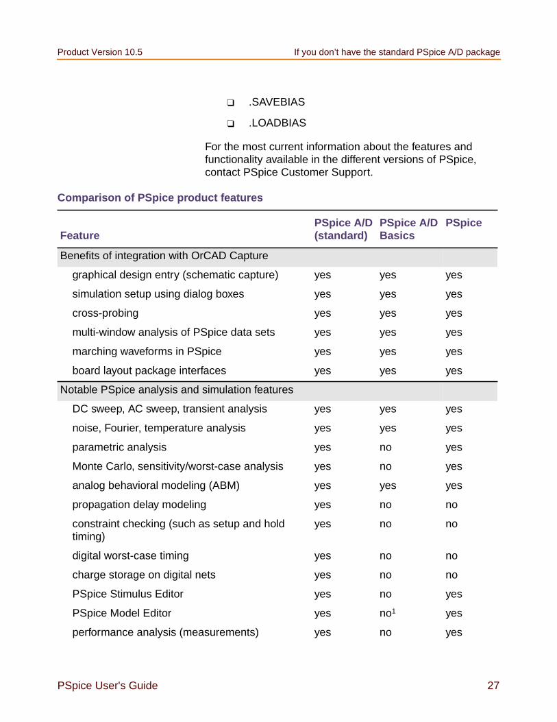
Product Version 10.5 If you don’t have the standard PSpice A/D package
PSpice User's Guide 27
.SAVEBIAS
.LOADBIAS
For the most current information about the features andfunctionality available in the different versions of PSpice,contact PSpice Customer Support.
Comparison of PSpice product features
FeaturePSpice A/D(standard)
PSpice A/DBasics
PSpice
Benefits of integration with OrCAD Capture
graphical design entry (schematic capture) yes yes yes
simulation setup using dialog boxes yes yes yes
cross-probing yes yes yes
multi-window analysis of PSpice data sets yes yes yes
marching waveforms in PSpice yes yes yes
board layout package interfaces yes yes yes
Notable PSpice analysis and simulation features
DC sweep, AC sweep, transient analysis yes yes yes
noise, Fourier, temperature analysis yes yes yes
parametric analysis yes no yes
Monte Carlo, sensitivity/worst-case analysis yes no yes
analog behavioral modeling (ABM) yes yes yes
propagation delay modeling yes no no
constraint checking (such as setup and holdtiming)
yes no no
digital worst-case timing yes no no
charge storage on digital nets yes no no
PSpice Stimulus Editor yes no yes
PSpice Model Editor yes no1 yes
performance analysis (measurements) yes no yes

Chapter Before you begin Product Version 10.5
28 PSpice User's Guide
interactive simulation yes no yes
preemptive simulation yes yes2 yes
save/load bias point yes no yes
performance package yes no yes
Notable PSpice devices and library models
GaAsFETs: Curtice, Statz, TriQuint,Parker-Skellern
all Statz all
MOSFETs: SPICE3 (1-3) with chargeconservation, BSIM1, BSIM3.1, EKV (version2.6)
yes yes yes
IGBTs yes no yes
JFETs, BJTs yes yes yes
SCRs, thyristors yes no yes
PWMs yes no no
resistor, capacitor, and inductor .MODEL support yes yes yes
ideal, non-ideal lossy transmission lines all ideal all
coupled inductors yes yes yes
coupled transmission lines yes no yes
nonlinear magnetics yes no yes
voltage- and current-controlled switches yes yes yes
analog model library 16,000+ 12,000+ 16,000+
digital primitives all most3 none
digital model library 1,600+ 1,600+ 0
advanced analysis library 4300+ 0 4300+
Purchase options
PSpice Optimizer yes no yes
Advanced Analysis yes no yes
Comparison of PSpice product features
FeaturePSpice A/D(standard)
PSpice A/DBasics
PSpice

Product Version 10.5 If you don’t have the standard PSpice A/D package
PSpice User's Guide 29
network licensing yes no yes
Other options
PSpice Device Equations Developer’s Kit(DEDK)4
yes no yes
Miscellaneous specifications
unlimited circuit size yes yes5 yes
1. Limited to text editing and diode device characterization.
2. Only allows one paused simulation in the queue.
3. PSpice A/D Basics does not include bidirectional transfer gates.
4. Available to qualified customers - contact PSpice Customer Support for qualification criteria.
5. Depends on system resources.
Comparison of PSpice product features
FeaturePSpice A/D(standard)
PSpice A/DBasics
PSpice

Chapter Before you begin Product Version 10.5
30 PSpice User's Guide
If you have PSpice A/D Lite
Limits of PSpice A/D Lite
PSpice A/D Lite has the following limitations:
circuit simulation limited to circuits with up to 64 nodes, 10transistors, two operational amplifiers or 65 digitalprimitive devices, and 10 transmission lines (ideal ornon-ideal) with not more than 4 pairwise coupled lines
device characterization using the PSpice Model Editorlimited to diodes
stimulus generation limited to sine waves (analog) andclocks (digital)
sample library of approximately 39 analog and 134 digitalparts
displays only simulation data created using the demoversion of the simulator
PSpice Optimizer limited to one goal, one parameter andone constraint
designs created in Capture can be saved if they have nomore than 30 part instances
Minimum hardware requirements for running PSpice:
Intel Pentium 300 MHz or equivalent processor
Windows XP Professional® (32-bit), Windows 2000 (withService Pack 2), and Windows NT 4.0 (with Service Pack6a or higher).
64 MB RAM
256 MB swap space
150 MB of free hard disk space (in addition to Capture orCapture CIS requirements)
A 256-color Windows display driver with 800 x 600resolution (1024 x 768 recommended)

Product Version 10.5 If you don’t have the standard PSpice A/D package
PSpice User's Guide 31
CD-ROM drive
Mouse or similar pointing device

Chapter Before you begin Product Version 10.5
32 PSpice User's Guide
PSpice User's Guide 33
Part one: Simulation primer
Part one provides basic information about circuit simulationincluding examples of common analyses.
Chapter 1, “Things you need to know,” provides anoverview of the circuit simulation process including whatPSpice does, descriptions of analysis types, anddescriptions of important files.
Chapter 2, “Simulation examples,” presents examples ofcommon analyses to introduce the methods and toolsyou’ll need to enter, simulate, and analyze your design.

Chapter Part one: Simulation primer Product Version 10.5
34 PSpice User's Guide

PSpice User's Guide 35
1
Things you need to know
Chapter overview
This chapter introduces the purpose and function of thePSpice A/D circuit simulator.
What is PSpice A/D? on page 36 describes PSpice A/Dcapabilities.
Analyses you can run with PSpice A/D on page 40introduces the different kinds of basic and advancedanalyses that PSpice A/D supports.
Using PSpice with other programs on page 46 presentsthe high-level simulation design flow.
Files needed for simulation on page 47 describes the filesused to pass information between PSpice and otherprograms. This section also introduces the things you cando to customize where and how PSpice finds simulationinformation.
Files that PSpice generates on page 53 describes thefiles that contain simulation results.
New directory structure for analog projects on page 55describes the new directory structure for analog projects.

Chapter 1 Things you need to know Product Version 10.5
36 PSpice User's Guide
What is PSpice A/D?
PSpice A/D is a simulation program that models the behaviorof a circuit containing any mix of analog and digital devices.Because the analog and digital simulation algorithms are builtinto the same program, PSpice A/D simulates mixed-signalcircuits with no performance degradation because of tightlycoupled feedback loops between the analog and digitalsections.
Used with OrCAD Capture for design entry, you can think ofPSpice A/D as a software-based breadboard of your circuitthat you can use to test and refine your design before evertouching a piece of hardware.
Run basic and advanced analyses
PSpice A/D can perform:
DC, AC, and transient analyses, so you can test theresponse of your circuit to different inputs.
Parametric, Monte Carlo, and sensitivity/worst-caseanalyses, so you can see how your circuit’s behaviorvaries with changing component values.
Note: Parametric, Monte Carlo, andsensitivity/worst-case analyses are not available inPSpice A/D Basics.
Digital worst-case timing analysis to help you find timingproblems that occur with only certain combinations ofslow and fast signal transmissions.
Note: Digital worst-case timing analysis is not availablein PSpice and PSpice A/D Basics.
The range of models built into PSpice A/D include not onlythose for resistors, inductors, capacitors, and bipolartransistors, but also these:
transmission line models, including delay, reflection, loss,dispersion, and crosstalk (no lossy in PSpice A/D Basics)

Product Version 10.5 Chapter overview
PSpice User's Guide 37
nonlinear magnetic core models, including saturation andhysteresis (not in PSpice A/D Basics)
seven MOSFET models, including BSIM3 version 3.2 andEKV version 2.6
five GaAsFET models, including Parker-Skellern andTriQuint’s TOM2 model (only Statz in PSpice A/D Basics)
IGBTs (not in PSpice A/D Basics)
digital components with analog I/O models (not inPSpice)
Use parts from PSpice’s extensive set of libraries
PSpice provides two types of libraries:
Standard PSpice libraries
PSpice Advanced Analysis libraries
Standard PSpice libraries
The standard PSpice libraries feature over 16,000 analog and1,600 digital and mixed-signal models of devicesmanufactured in North America, Japan, and Europe.
Use parts from standard PSpice libraries or PSpice AdvancedAnalysis libraries if you want to analyze the part with PSpice.
The standard PSpice libraries are installed at the followinglocations in the installation directory:
Capture symbols for standard PSpice libraries at
\tools\Capture\Library\PSpice\
Standard PSpice model libraries at
\tools\PSpice\Library\
The parts in the standard PSpice libraries are listed in theonline PSpice Library List. For information on finding partsusing the online PSpice Library List, see To find parts usingthe online library lists on page 116. To find out more abouteach model library, read the comments in the .LIB file header.

Chapter 1 Things you need to know Product Version 10.5
38 PSpice User's Guide
PSpice Advanced Analysis libraries
The PSpice Advanced Analysis libraries contain over 4,300analog parts. The Advanced Analysis libraries containparameterized and standard parts. The majority of the partsare parameterized. The parametrized parts have tolerance,distribution, optimizable and smoke parameters that arerequired by the PSpice Advanced Analysis tools. Standardparts in the Advanced Analysis libraries are similar to parts inthe standard PSpice libraries.
Note: The Advanced Analysis libraries are not available withPSpice A/D Basics.
The parametrized parts are associated with template-basedPSpice models. An important advantage of using thetemplate-based PSpice models is that you can pass modelparameters as properties from Capture. For example, if atemplate-based model is associated with a part, the modelparameters that you specify on an instance of the part in yourdesign will be passed to the model. There is no need to editthe model itself to change a parameter value. This is unlike thestandard PSpice parts that are associated with devicecharacteristic curve-based PSpice models, where you need toedit the model to change a simulation parameter. For moreinformation on template-based and device characteristiccurve-based PSpice models, see Chapter 4, “Creating andediting models.”
Use parametrized parts from Advanced Analysis libraries ifyou want to analyze the part with an Advanced Analysis tool.Most of the analog parts in the standard PSpice librariescontain smoke parameters. You can use these parts toperform smoke analysis using the Smoke tool in PSpiceAdvanced Analysis.
This AdvancedAnalysis tool...
Uses these part parameters...
Sensitivity Tolerance parameters
Optimizer Optimizable parameters
Smoke Smoke parameters

Product Version 10.5 Chapter overview
PSpice User's Guide 39
Note: You may use a mixture of standard and parameterizedparts in your design.
The Advanced Analysis libraries are installed at the followinglocations in the installation directory:
Capture symbols for Advanced Analysis libraries at
\tools\Capture\Library\PSpice\AdvAnls\
PSpice Advanced Analysis model libraries at
\tools\PSpice\Library
The parts in the Advanced Analysis libraries are listed in thePSpice Advanced Analysis Library List. For informationon finding parts using the online PSpice Advanced AnalysisLibrary List, see To find parts using the online library lists onpage 116. To find out more about each model library, read thecomments in the .LIB file header.
Vary device characteristics without creating new parts
PSpice A/D has numerous built-in models with parametersthat you can tweak for a given device. These includeindependent temperature effects.
Model behavior
PSpice A/D supports analog and digital behavioral modeling,so you can describe functional blocks of circuitry usingmathematical expressions and functions.
Monte Carlo Tolerance parameters,
Distribution parameters(default parameter value is Flat /Uniform)
This AdvancedAnalysis tool...
Uses these part parameters...

Chapter 1 Things you need to know Product Version 10.5
40 PSpice User's Guide
Analyses you can run with PSpice A/D
See Chapter 2, “Simulation examples,” for introductoryexamples showing how to run each type of analysis.
See Part three: Setting up and running analyses, for a moredetailed discussion of each type of analysis and how toset it up.
Basic analyses
DC sweep & other DC calculations
These DC analyses evaluate circuit performance in responseto a direct current source. Table 1-1 summarizes whatPSpice A/D calculates for each DC analysis type.
AC sweep and noise
These AC analyses evaluate circuit performance in responseto a small-signal alternating current source. Table 1-2
Table 1-1 DC analysis types
For this DCanalysis...
PSpice A/D computes this...
DC sweep Steady-state voltages, currents, and digitalstates when sweeping a source, a modelparameter, or temperature over a range ofvalues.
Bias point detail Bias point data in addition to what isautomatically computed in any simulation.
DC sensitivity Sensitivity of a net or part voltage as afunction of bias point.
Small-signalDC transfer
Small-signal DC gain, input resistance,and output resistance as a function of biaspoint.

Product Version 10.5 Chapter overview
PSpice User's Guide 41
summarizes what PSpice A/D calculates for each AC analysistype.
Note: To run a noise analysis, you must also run an AC sweepanalysis.
Table 1-2 AC analysis types
For this ACanalysis...
PSpice A/D computes this...
AC sweep Small-signal response of the circuit(linearized around the bias point) whensweeping one or more sources over arange of frequencies. Outputs includevoltages and currents with magnitude andphase. You can also use Bode PlotTemplate Windows in Probe to view thisinformation.
Noise For each frequency specified in the ACanalysis:
Propagated noise contributions at anoutput net from every noise generatorin the circuit.
RMS sum of the noise contributions atthe output.
Equivalent input noise.

Chapter 1 Things you need to know Product Version 10.5
42 PSpice User's Guide
Transient and Fourier
These time-based analyses evaluate circuit performance inresponse to time-varying sources. Table 1-3 summarizes whatPSpice A/D calculates for each time-based analysis type.
Note: To run a Fourier analysis, you must also run a transientanalysis.
Table 1-3 Time-based analysis types
For thistime-basedanalysis...
PSpice A/D computes this...
Transient Voltages, currents, and digital statestracked over time.
For digital devices, you can set thepropagation delays to minimum, typical,and maximum. If you have enabled digitalworst-case timing analysis, thenPSpice A/D considers all possiblecombinations of propagation delays withinthe minimum and maximum range.
Note: Digital worst-case timing analysis isnot available in PSpice andPSpice A/D Basics.
Fourier DC and Fourier components of thetransient analysis results.

Product Version 10.5 Chapter overview
PSpice User's Guide 43
Advanced multi-run analyses
The multi-run analyses—parametric, temperature, MonteCarlo, and sensitivity/worst-case—result in a series of DCsweep, AC sweep, or transient analyses depending on whichbasic analyses you enabled.
Parametric and temperature
For parametric and temperature analyses, PSpice A/D stepsa circuit value in a sequence that you specify and runs asimulation for each value.
Note: Parametric and temperature analyses are not availablein PSpice A/D Basics.
Table 1-4 shows the circuit values that you can step for eachkind of analysis.
Monte Carlo and sensitivity/worst-case
Monte Carlo and sensitivity/worst-case analyses arestatistical. PSpice changes device model parameter valueswith respect to device and lot tolerances that you specify, andruns a simulation for each value.
Note: Monte Carlo and sensitivity/worst-case analyses arenot available in PSpice A/D Basics.
Table 1-4 Parametric and temperature analysis types
For thisanalysis...
You can step one of these...
Parametric global parametermodel parametercomponent valueDC sourceoperational temperature
Temperature operational temperature

Chapter 1 Things you need to know Product Version 10.5
44 PSpice User's Guide
Table 1-5 summarizes how PSpice runs each statisticalanalysis type.
Table 1-5 Statistical analysis types
For thisstatisticalanalysis...
PSpice does this...
Monte Carlo For each simulation, randomly varies alldevice model parameters for which youhave defined a tolerance.
Sensitivity/worst-case
Computes the probable worst-caseresponse of the circuit in two steps:
1. Computes component sensitivity tochanges in the device model parameters.This means PSpice A/D nonrandomlyvaries device model parameters for whichyou have defined a tolerance, one at atime for each device and runs a simulationwith each change.
2. Sets all model parameters for all devicesto their worst-case values (assumed to beat one of the tolerance limits) and runs afinal simulation.
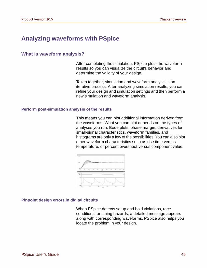
Product Version 10.5 Chapter overview
PSpice User's Guide 45
Analyzing waveforms with PSpice
What is waveform analysis?
After completing the simulation, PSpice plots the waveformresults so you can visualize the circuit’s behavior anddetermine the validity of your design.
Taken together, simulation and waveform analysis is aniterative process. After analyzing simulation results, you canrefine your design and simulation settings and then perform anew simulation and waveform analysis.
Perform post-simulation analysis of the results
This means you can plot additional information derived fromthe waveforms. What you can plot depends on the types ofanalyses you run. Bode plots, phase margin, derivatives forsmall-signal characteristics, waveform families, andhistograms are only a few of the possibilities. You can also plotother waveform characteristics such as rise time versustemperature, or percent overshoot versus component value.
Pinpoint design errors in digital circuits
When PSpice detects setup and hold violations, raceconditions, or timing hazards, a detailed message appearsalong with corresponding waveforms. PSpice also helps youlocate the problem in your design.

Chapter 1 Things you need to know Product Version 10.5
46 PSpice User's Guide
Using PSpice with other programs
Using OrCAD Capture to prepare for simulation
OrCAD Capture is a design entry program you need toprepare your circuit for simulation. This means:
placing and connecting part symbols,
defining component values and other attributes,
defining input waveforms,
enabling one or more analyses, and
marking the points in the circuit where you want to seeresults.
OrCAD Capture is also the control point for running otherprograms used in the simulation design flow.
What is the PSpice Stimulus Editor?
The Stimulus Editor is a graphical input waveform editor thatlets you define the shape of time-based signals used to testyour circuit’s response during simulation.
Using the Stimulus Editor, you can define:
analog stimuli with sine wave, pulse, piecewise linear,exponential pulse, single-frequency FM shapes, and
digital stimuli that range from simple clocks to complexpulse patterns and bus sequences.

Product Version 10.5 Files needed for simulation
PSpice User's Guide 47
The Stimulus Editor lets you draw analog piecewise linear andall digital stimuli by clicking at the points along the timeline thatcorrespond to the input values that you want at transitions.
Note: The Stimulus Editor is not available inPSpice A/D Basics.
What is the PSpice Model Editor?
The PSpice Model Editor is a model extractor that generatesmodel definitions for PSpice A/D to use during simulation.
All the PSpice Model Editor needs is information about thedevice found in standard data sheets. As you enter the datasheet information, the Model Editor displays devicecharacteristic curves so you can verify the model-basedbehavior of the device. When you are finished, the PSpiceModel Editor automatically creates a part for the model so youcan use the modeled part in your design immediately.
Note: In PSpice A/D Basics, the PSpice Model Editor isavailable but is limited to text editing and diode devicecharacterization.
Files needed for simulation
To simulate your design, PSpice needs to know about:
the parts in your circuit and how they are connected,
what analyses to run,
the simulation models that correspond to the parts in yourcircuit, and

Chapter 1 Things you need to know Product Version 10.5
48 PSpice User's Guide
the stimulus definitions to test with.
This information is provided in various data files. Some ofthese are generated by OrCAD Capture, others come fromlibraries (which can also be generated by other programs likethe PSpice Stimulus Editor and the PSpice Model Editor), andstill others are user-defined.
Files that OrCAD Capture generates
When you begin the simulation process, OrCAD Capture firstgenerates files describing the parts and connections in yourcircuit. These files are the netlist file and the circuit file thatPSpice reads before doing anything else.
Netlist file
The netlist file contains a list of device names, values, and howthey are connected with other devices.
The name that OrCAD Capture generates for this file is:
ROOT_SCHEMATIC_NAME.NET, if you have updatedyour project to the new project format. For moreinformation on the new format for analog projects, seeConversion of old analog projects to new projectformat in the OrCAD Capture Online Help and Newdirectory structure for analog projects on page 55.
In the new project format, the netlist file is located in thedirectory:
\<project_name>-PSpiceFiles\<schematic_name>\
DESIGN_NAME-ROOT_SCHEMATIC_NAME.NET, if youdid not update your project to the new project format. Inthe old format for analog projects, the netlist file is locatedin the project directory.
Refer to the online PSpice Reference Guide for the syntaxof the statements in the netlist file.

Product Version 10.5 Files needed for simulation
PSpice User's Guide 49
Circuit file
The circuit file contains commands describing how to run thesimulation. This file also refers to other files that containnetlist, model, stimulus, and any other user-definedinformation that apply to the simulation.
The name that OrCAD Capture generates for this file is:
PROFILE_NAME.CIR, if you updated your project to thenew project format. For more information on the newformat for analog projects, see Conversion of oldanalog projects to new project format in the OrCADCapture Online Help and New directory structure foranalog projects on page 55.
In the new project format, the circuit file is located in thedirectory:
\<project_name>-PSpiceFiles\<schematic_name>\<profile_name>\
DESIGN_NAME-ROOT_SCHEMATIC_NAME-PROFILE_NAME.SIM.CIR, if you did not update your project to the newproject format. In the old format for analog projects, thecircuit file is located in the project directory.
Refer to the online PSpice Reference Guide for the syntaxof the statements in the circuit file.

Chapter 1 Things you need to know Product Version 10.5
50 PSpice User's Guide
Other files that you can configure for simulation
Figure 1-1 User-configurable data files that PSpice A/Dreads.
Before starting simulation, PSpice needs to read other filesthat contain simulation information for your circuit. These aremodel files, and if required, stimulus files and include files.
You can create these files using PSpice programs like thePSpice Stimulus Editor and the PSpice Model Editor. Theseprograms automate file generation and provide graphicalways to verify the data. You can also use the Model Text viewin the PSpice Model Editor (or another text editor likeNotepad) to enter the data manually.
The circuit file (.CIR) that OrCAD Capture generates containsreferences to the other user-configurable files that PSpiceneeds to read.
Model library
A model library is a file that contains the electrical definition ofone or more parts. PSpice uses this information to determinehow a part will respond to different electrical inputs.
PSpiceModel Editor
PSpiceStimulus Editor
PSpice A/D
simulationprimitives
inputwaveforms
modeldefinitions
stimulus file
custominclude file
globalmodel
localmodel
libraries
libraries

Product Version 10.5 Files needed for simulation
PSpice User's Guide 51
These definitions take the form of either a:
model parameter set, which defines the behavior of apart by fine-tuning the underlying model built into PSpice,or
subcircuit netlist, which describes the structure andfunction of the part by interconnecting other parts andprimitives.
A subcircuit, sometimes called a macromodel, isanalogous to a procedure call in a software programminglanguage.
The most commonly used models are available in the PSpicemodel libraries shipped with your programs. The model librarynames have a .LIB extension.
If needed, however, you can create your own models andlibraries, either:
manually using the Model Text view in the PSpice ModelEditor (or another text editor like Notepad), or
automatically using the PSpice Model Editor.
See What is the PSpice Model Editor? on page 47 for adescription.
Stimulus file
A stimulus file contains time-based definitions for analog ordigital input waveforms. You can create a stimulus file either:
manually using a standard text editor such as Notepad tocreate the definition (a typical file extension is .STM), or
automatically using the Stimulus Editor (which generatesa .STL file extension).
See What is the PSpice Stimulus Editor? on page 46 for adescription.
Note: Not all stimulus definitions require a stimulus file. Insome cases, like DC and AC sources, you must use aschematic symbol and set its properties.

Chapter 1 Things you need to know Product Version 10.5
52 PSpice User's Guide
Include file
An include file is a user-defined file that contains:
PSpice commands, or
supplemental text comments that you want to appear inthe PSpice output file (see PSpice output file onpage 53).
Example: An include file that contains definitions, using thePSpice .FUNC command, for functions that you want to use innumeric expressions elsewhere in your design.
You can create an include file using any text editor, such asNotepad. Typically, include file names have an .INCextension.
Configuring model library, stimulus, and include files
PSpice searches model libraries, stimulus files, and includefiles for any information it needs to complete the definition of apart or to run a simulation.
The files that PSpice searches depend on how you configureyour model libraries and other files. Much of the configurationis set up for you automatically, however, you can do thefollowing yourself:
Add and delete files from the configuration.
Change the scope of a file: that is, whether the file appliesto one profile only, one design only (local) or to any design(global).
Change the search order.
Libraries are configured by editing the simulation profile. Fromthe PSpice menu in OrCAD Capture, choose Edit SimulationProfile, click the Configuration Files tab in the SimulationSettings dialog box, then click Library in the Category field. Tofind out more, refer to the OrCAD Capture User’s Guide.

Product Version 10.5 Files that PSpice generates
PSpice User's Guide 53
Files that PSpice generates
After reading the circuit file, netlist file, model libraries, and anyother required inputs, PSpice starts the simulation. Assimulation progresses, PSpice saves results to two files—thedata file and the PSpice output file.
Waveform data file
The data file contains simulation results that can be displayedgraphically. PSpice reads this file automatically and displayswaveforms reflecting circuit response at nets, pins, and partsthat you marked in your schematic (cross-probing). You canset up your design so PSpice displays the results as thesimulation progresses or after the simulation completes.
For a description of how to display simulation results, see Partfour: Viewing results. For a description of the waveformanalyzer program, see What is waveform analysis? onpage 45.
After PSpice has read the data file and displays the initial setof results, you can add more waveforms and performpost-simulation analysis of the data. There are two ways toadd waveforms to the display:
From within PSpice, by specifying trace expressions.
From within OrCAD Capture, by cross-probing.
PSpice output file
The PSpice output file is an ASCII text file that contains:
the netlist representation of the circuit,
the PSpice command syntax for simulation commandsand options (like the enabled analyses),
simulation results, and
warning and error messages for problems encounteredduring read-in or simulation.

Chapter 1 Things you need to know Product Version 10.5
54 PSpice User's Guide
Its content is determined by:
the types of analyses you run,
the options you select for running PSpice, and
the simulation control symbols (like VPRINT1 andVPLOT1, available in SPECIAL.OLB) that you place andconnect to nets in your design.
Example: Each instance of a VPRINT1 symbol placed inyour schematic causes PSpice to generate a table ofvoltage values for the connecting net, and to write thetable to the PSpice output file.

Product Version 10.5 Files that PSpice generates
PSpice User's Guide 55
New directory structure for analog projects
The files related to analog projects created usingOrCAD Capture version 9.2.3 or older versions weremaintained in a single directory.
In the above figure, the rf_amp project has a design namedrf_amp.dsn. The rf_amp design has a schematic namedSCHEMATIC1 and SCHEMATIC1 has two profiles,rf_amp-schematic1-ac.sim andrf_amp-schematic1-tran.sim. The long file namesmake it difficult to identify files associated with the design,schematic or profile, and delete them if they are no longerrequired. For example, the .sim (simulation profile) files havethe name,
Figure 1-2 Directory structure for RF_AMP analogproject created using Capture 9.2.3 or older versions

Chapter 1 Things you need to know Product Version 10.5
56 PSpice User's Guide
<DesignName>-<SchematicName>-<ProfileName>.SIM
Capture 10.0 introduces a new directory structure for analogprojects in which the design level, schematic level andsimulation profile level PSpice files are organized in theirrespective directories. This makes it easier to manage the filesfor the project.
Note: If you open an analog project that was created usingCapture version 9.2.3 or older versions in Capture10.0, you will be prompted to convert the project to theCapture 10.0 format. For more information, seeConversion of old analog projects to new projectformat in the OrCAD Capture Online Help.

Product Version 10.5 Files that PSpice generates
PSpice User's Guide 57
In the new directory structure all the PSpice related files forthe rf_amp project are maintained in a directory namedrf_amp-PSpiceFiles.
The PSpice files related to the design are maintained inthe rf_amp-PSpiceFiles directory. For more
Directory forschematic levelPSpice files
Directory fordesign levelPSpice files
Directory forprofile levelPSpice files
Projectdirectory
Figure 1-3 New directory structure of RF_AMPanalog project

Chapter 1 Things you need to know Product Version 10.5
58 PSpice User's Guide
information, see How are files configured at the designlevel maintained in the new directory structure for analogprojects? on page 58.
The PSpice files related to the schematic namedSCHEMATIC1 are maintained in a sub-directory namedSCHEMATIC1 under the rf_amp-PSpiceFilesdirectory.
The PSpice files related to the AC and Tran simulationprofiles are maintained in the AC and Transub-directories under the SCHEMATIC1 directory. Formore information, see How are files configured at theprofile level maintained in the new directory structure foranalog projects? on page 60.
How are files configured at the design level maintained in the new directorystructure for analog projects?
The model libraries, stimulus files and include files configuredat the design level are stored in the<projectname>-PSpiceFiles directory. For example, inthe New directory structure of RF_AMP analog project figureon page 57, the model libraries, stimulus files and include filesconfigured at the design level are stored in therf_amp-PSpiceFiles directory. The rf_amp.stlstimulus file in the rf_amp-PSpiceFiles directory is anexample of a PSpice file related to the design.
You can view the paths to the model libraries, stimulus filesand include files configured at the design level in the CaptureProject Manager window.
Note the following:
If you select the Retain Old Project check box when youconvert an analog project that was created using Captureversion 9.2.3 or older versions to the new project format,only the files configured at the design level that have thesame name as the design are copied over to the<projectname>-PSpiceFiles directory in thelocation you specified for creating the project in the newformat.

Product Version 10.5 Files that PSpice generates
PSpice User's Guide 59
The files configured at the design level that do not havethe same name as the design are not copied over to the<projectname>-PSpiceFiles directory becausethey are custom files. Instead, these files are read fromtheir original location. You can view the path to thecustom files configured at the design level in theConfiguration Files tab of the Simulation Settings dialogbox and in the Capture Project Manager window.
For example, suppose that your design name is rf_amp,and you have configured the following files at the designlevel:
rf_amp.inc
decoder.lib
rf_amp.lib
rf_amp.prp
rf_amp.stl
If you select the Retain Old Project check box when youconvert the analog project to the new format, only thefollowing files are copied over to therf_amp-PSpiceFiles directory in the location youspecified for creating the project in the new format.
rf_amp.inc
rf_amp.lib
rf_amp.prp
rf_amp.stl
The decoder.lib file is read from the old projectlocation. You can view the path to the decoder.lib filein the Configuration Files tab of the Simulation Settingsdialog box and in the Capture Project Manager window.
For more information on converting analog projects fromthe old format to the new format, see Conversion of oldanalog projects to new project format in the OrCADCapture Online Help.

Chapter 1 Things you need to know Product Version 10.5
60 PSpice User's Guide
When you create a new simulation profile by importingthe settings from another simulation profile that exists inanother project, only the simulation settings are inheritedfrom the source simulation profile. The files configured atthe design level for the source simulation profile are notcopied over to the <projectname>-PSpiceFilesdirectory of the project in which you are creating the newsimulation profile.
How are files configured at the profile level maintained in the newdirectory structure for analog projects?
The model libraries, stimulus files and include files configuredat the profile level are stored in a directory that has the samename as the profile. For example, in Figure 1-4, the PSpicefiles related to the Tran simulation profile are maintained in theTran sub-directory under the SCHEMATIC1 directory.

Product Version 10.5 Files that PSpice generates
PSpice User's Guide 61
Figure 1-4 Directory structure of RF_AMP analog projectwith files configured for the Tran profile
Chapter 1 Things you need to know Product Version 10.5
62 PSpice User's Guide
An include file named <profilename>_profile.inc iscreated in the directory for the simulation profile. This filecontains information on the model libraries, stimulus files andinclude files configured for that profile. For example, inFigure 1-4, the Tran profile directory contains aTran_profile.inc include file that includes information onthe decoder.lib model library, decoder.stl stimulus fileand the Tran.inc include files configured for the Tran profile.
You must not delete the <profilename>_profile.inc filein the directory for a simulation profile.
Note: When you create a new simulation profile by importingthe settings from another simulation profile that existsin the same project or in another project, the filesconfigured at the profile level for the source simulationprofile are copied to the directory for the new simulationprofile. The files configured at the design level for thesource simulation profile are not copied over to the<projectname>-PSpiceFiles directory of theproject in which you are creating the new simulationprofile.
What happens when I convert an analog project that uses a design fromanother project or from another location?
If you convert an analog project (created using Capture 9.2.3or older versions) that uses a design from another project orfrom another location, to the new project format, the design fileand all the contents of the design are copied to the currentproject and maintained in the new directory structure foranalog projects.
What should I do if the schematic for a converted analog project usesFILESTIMn parts from the SOURCE library?
If you have specified only the name of the stimulus file as thevalue of the FILENAME property on a FILESTIMn part, youmust specify the path to the stimulus file in the value for theFILENAME property on the FILESTIMn part.

PSpice User's Guide 63
2
Simulation examples
Chapter overview
The examples in this chapter provide an introduction to themethods and tools for creating circuit designs, runningsimulations, and analyzing simulation results. All analyses areperformed on the same example circuit to clearly illustrateanalysis setup, simulation, and result-analysis procedures foreach analysis type.
This chapter includes the following sections:
Example circuit creation on page 64
Performing a bias point analysis on page 73
DC sweep analysis on page 76
Transient analysis on page 83
AC sweep analysis on page 88
Parametric analysis on page 93
Performance analysis on page 101

Chapter 2 Simulation examples Product Version 10.5
64 PSpice User's Guide
Example circuit creation
This section describes how to use OrCAD Capture to createthe simple diode clipper circuit shown in Figure 2-1.
Figure 2-1 Diode clipper circuit.
To create a new PSpice project
1 From the Windows Start menu, choose Release OrCAD10.0 from the Programs folder and then the Captureshortcut to start Capture.
2 In the Project Manager, from the File menu, point to Newand choose Project.
3 Select Analog or Mixed-Signal Circuit Wizard.
4 In the Name text box, enter the name of the project(CLIPPER).
5 Use the Browse button to select the location for theproject files, then click OK.
6 In the Create PSpice Project dialog box, select Create ablank project.
7 Click OK.

Product Version 10.5 Chapter overview
PSpice User's Guide 65
No special libraries need to be configured at this time. Anew page will be displayed in Capture and the newproject will be configured in the Project Manager.
To place the voltage sources
1 In Capture, switch to the schematic page editor.
2 From the Place menu, choose Part to display the PlacePart dialog box.
3 Add the library for the parts you need to place:
a. Click the Add Library button.
b. Select SOURCE.OLB (from the PSpice library) andclick Open.
Note: There are two sets of library files supplied withCapture and PSpice. The standard schematic partlibraries are found in the directory\TOOLS\CAPTURE\LIBRARY. The part libraries that aredesigned for simulation with PSpice are found in thesub-directory \TOOLS\CAPTURE\LIBRARY\PSPICE. Inorder to have access to specific parts, you must firstconfigure the library in Capture using the Add Libraryfunction.
4 In the Part text box, type VDC.
5 Click OK.
6 Move the pointer to the correct position on the schematicpage (see Figure 2-1) and click to place the first part.
7 Move the cursor and click again to place the second part.
8 Right-click and choose End Mode to stop placing parts.
To place the diodes
1 From the Place menu, choose Part to display the PlacePart dialog box.
2 Add the library for the parts you need to place:

Chapter 2 Simulation examples Product Version 10.5
66 PSpice User's Guide
a. Click the Add Library button.
b. Select DIODE.OLB (from the PSpice library) andclick Open.
Important
If you are working with the demo version of Capture,add EVAL.OLB instead of DIODE.OLB.
3 In the Part text box, type D1N39 to display a list of diodes.
When placing parts:
Leave space to connect the parts with wires.
You will change part names and values that do notmatch those shown in Figure 2-1 later in this section.
4 Select D1N3940 from the Part List and click OK.
Important
If you are working with the demo version of Capture,select D1N914 from the Part List.
5 Press R to rotate the diode to the correct orientation.
6 Click to place the first diode (D1), then click to place thesecond diode (D2).
7 Right-click and choose End Mode to stop placing parts.
To move the text associated with the diodes (or any otherobject)
1 Click the text to select it, then drag the text to a newlocation.
To place the other parts
1 From the Place menu, choose Part to display the PlacePart dialog box.
2 Add the library for the parts you need to place:

Product Version 10.5 Chapter overview
PSpice User's Guide 67
a. Click the Add Library button.
b. Select ANALOG.OLB (from the PSpice library) andclick Open.
3 Follow similar steps as described for the diodes to placethe parts listed below, according to Figure 2-1 onpage 64. The part names you need to type in the Partname text box of the Place Part dialog box are shown inparentheses:
resistors (R)
capacitor (C)
4 To place the off-page connector parts(OFFPAGELEFT-R), click the Place Off-Page Connectorbutton on the tool palette.
5 Add the library for the parts you need to place:
a. Click the Add Library button.
b. Select CAPSYM.OLB (from the Capture library) andclick Open.
6 Place the off-page connector parts according toFigure 2-1 on page 64.
Note: To rotate the part so the arrows are pointing in thecorrect direction, place the part, select it, then press Rone or more times to rotate the part to the desiredorientation.
To place the zero ground part
1 To place the ground parts (0), click the GNDbutton on the tool palette.

Chapter 2 Simulation examples Product Version 10.5
68 PSpice User's Guide
2 Add the library for the parts you need to place:
a. Click the Add Library button.
b. Select SOURCE.OLB (from the PSpice library) andclick Open.
3 Place the 0 ground part from SOURCE.OLB as shown inFigure 2-1 on page 64.
Important
You must use the 0 (zero) ground part from theSOURCE.OLB part library. You can use any otherground part only if you change its name to 0 (zero).
To connect the parts
1 From the Place menu, choose Wire to begin wiring parts.
The pointer changes to a crosshair.
2 Click the connection point (the very end) of the pin on theoff-page connector at the input of the circuit.
3 Click the nearest connection point of the input resistor R1.
To stop wiring, right-click and choose End Wire. Thepointer changes to the default arrow.
Clicking on any valid connection point ends a wire. A validconnection point is shown as a box (see Figure 2-2).
If you make a mistake when placing or connectingcomponents:
From the Edit menu, choose Undo, or click .
4 Connect the other end of R1 to the output capacitor.
Figure 2-2 Connection points.

Product Version 10.5 Chapter overview
PSpice User's Guide 69
5 Connect the diodes to each other and to the wire betweenthem:
a. Click the connection point of the cathode for thelower diode.
b. Move the cursor straight up and click the wirebetween the diodes. The wire ends, and the junctionof the wire segments becomes visible.
c. Click again on the junction to continue wiring.
d. Click the end of the upper diode’s anode pin.
6 Continue connecting parts until the circuit is wired asshown in Figure 2-1 on page 64.
To assign names (labels) to the nets
1 From the Place menu, choose Net Alias to display thePlace Net Alias dialog box.
2 In the Name text box, type Mid.
3 Click OK.
4 Place the net alias on any segment of the wire thatconnects R1, R2, R3, the diodes, and the capacitor. Thelower left corner of the net alias must touch the wire.
5 Right-click and choose End Mode to quit the Net Aliasfunction.
Tip
It is recommended that special characters should notbe used for naming nets, nodes, projects, or libraries.While naming nets, characters such as ? (questionmark), @ (at symbol), ~ (telda), #(hash), &(ampersand), %(percent sign), and “ (quotationmarks) should not be used. These might cause thenetlister to fail. Other special characters such as! (exclamation mark), ( )(paranthesis), < (smallerthan), = (equal), > (greater than), [ ](squareparenthesis), and * (asterix) are also considered asillegal for naming nets.

Chapter 2 Simulation examples Product Version 10.5
70 PSpice User's Guide
To assign names (labels) to the off-page connectors
Label the off-page connectors as shown in Figure 2-1 onpage 64.
1 Double-click the name of an off-page connector to displaythe Display Properties dialog box.
2 In the Name text box, type the new name.
3 Click OK.
4 Select and relocate the new name as desired.
To assign names to the parts
1 Double-click the second VDC part to display the Partsspreadsheet.
2 Click in the first cell under the Reference column.
3 Type in the new name Vin.
4 Click Apply to update the changes to the part, then closethe spreadsheet.
5 Continue naming the remaining parts until yourschematic looks like Figure 2-1 on page 64.
Tip
A more efficient way to change the names, valuesand other properties of several parts in your designis to use the Property Editor, as follows:
a. Select all of the parts to be modified by pressing Ctrland clicking each part.
b. From the Edit menu, choose Properties.
The Parts Spreadsheet appears.
Change the entries in as many of the cells as needed,and then click Apply to update all of the changes at once.

Product Version 10.5 Chapter overview
PSpice User's Guide 71
To change the values of the parts
1 Double-click the voltage label (0V) on V1 to display theDisplay Properties dialog box.
2 In the Value text box, type 5V.
3 Click OK.
4 Continue changing the Part Value properties of the partsuntil all the parts are defined as in Figure 2-1 on page 64.
Your schematic page should now have the same parts,wiring, labels, and properties as Figure 2-1 on page 64.
Using European notation
You can use the European notation, such as 2K2, to assignvalues to resistors, capacitors, and inductors. Assigningvalues in this format reduces the possibility of errors whilereading component values from screen or from a print out ofthe schematic. The table below lists the alphabets that can beused in the 2K2 notation.
Alphabet used.. Stands for..
F(f) femto
P(p) pico
N(n) nano
U(u) micro
M(m) milli
K(k) kilo
MEG(meg) mega
G(g) giga
T(t) tera
Chapter 2 Simulation examples Product Version 10.5
72 PSpice User's Guide
Some examples and their explanations are listed in the tablebelow.
To save your design
1 From the File menu, choose Save.
Finding out more about setting up your design
About setting up a design for simulation
For a checklist of all of the things you need to do to set up yourdesign for simulation, and how to avoid common problems,see Chapter 3, “Preparing a design for simulation.”
Running PSpice
When you perform a simulation, PSpice generates an outputfile (*.OUT).
Notations Equivalent to...
2M2 2.2 M
2MEG2 2.2 MEG
4L5 inductor of 4.5 henry
2K2 2.2K
12C2 capacitor of 12.2 farads
5R4 resistor of 5.4 ohms
2p2 2.2 p (2.2*10-12)

Product Version 10.5 Running PSpice
PSpice User's Guide 73
While PSpice is running, the progress of the simulationappears and is updated in the PSpice simulation outputwindow (see Figure 2-3).
Figure 2-3 PSpice simulation output window.
You can set up a simulation profile to run one analysis at atime. To run multiple analyses (for example, both DC sweepand transient analyses), set up a batch simulation. For moreinformation, see Chapter 8, “Setting up analyses and startingsimulation.”
Performing a bias point analysis
To set up a bias point analysis in Capture
1 In Capture, switch to CLIPPER.OPJ in the schematicpage editor.
2 From the PSpice menu, choose New Simulation Profile todisplay the New Simulation dialog box.
3 In the Name text box, type Bias.
4 From the Inherit From list, select None, then click Create.
The Simulation Settings dialog box appears.
The root schematic listed is the schematic pageassociated with the simulation profile you are creating.
5 From the Analysis type list, select Bias Point.
6 Click OK to close the Simulation Settings dialog box.

Chapter 2 Simulation examples Product Version 10.5
74 PSpice User's Guide
To simulate the circuit from within Capture
1 From the PSpice menu, choose Run.
PSpice simulates the circuit and calculates the bias pointinformation.
Note: Because waveform data is not calculated during a biaspoint analysis, you will not see any plots displayed inthe Probe window for this simulation. To find out how toview the results of this simulation, see Using thesimulation output file below.

Product Version 10.5 Running PSpice
PSpice User's Guide 75
Using the simulation output file
The simulation output file acts as an audit trail of thesimulation. This file optionally echoes the contents of thecircuit file as well as the results of the bias point calculation. Ifthere are any syntax errors in the netlist declarations orsimulation commands, or anomalies while performing thecalculation, PSpice writes error or warning messages to theoutput file.
To view the simulation output file
1 In PSpice, from the View menu, choose Output File.
Figure 2-4 shows the results of the bias point calculationas written in the simulation output file.
2 When finished, close the window.
PSpice measures the current through a two-terminal deviceinto the first terminal and out of the second terminal. Forvoltage sources, current is measured from the positiveterminal to the negative terminal; this is opposite to thepositive current flow convention and results in a negative valuein the output file.
Figure 2-4 Simulation output file.

Chapter 2 Simulation examples Product Version 10.5
76 PSpice User's Guide
Finding out more about bias point calculations
DC sweep analysis
You can visually verify the DC response of the clipper byperforming a DC sweep of the input voltage source anddisplaying the waveform results in the Probe window inPSpice. This example sets up DC sweep analysis parametersto sweep Vin from -10 to 15 volts in 1 volt increments.
Setting up and running a DC sweep analysis
To set up and run a DC sweep analysis
1 In Capture, from the PSpice menu, chooseNew Simulation Profile.
The New Simulation dialog box appears.
2 In the Name text box, type DC Sweep.
3 From the Inherit From list, select Schematic1-Bias, thenclick Create.
The Simulation Settings dialog box appears.
4 Click the Analysis tab.
5 From the Analysis type list, select DC Sweep and enterthe values shown in Figure 2-5.
Note: The default settings for DC Sweep simulation areVoltage source as the swept variable type and Linear asthe sweep type. To use a different swept variable type orsweep type, choose different options under Sweep
To find out more aboutthis...
See this...
Bias point calculations Bias point on page 429

Product Version 10.5 DC sweep analysis
PSpice User's Guide 77
variable and Sweep type.
6 Click OK to close the Simulation Settings dialog box.
7 From the File menu, choose Save.
8 From the PSpice menu, choose Run to run the analysis.
Figure 2-5 DC sweep analysis settings.

Chapter 2 Simulation examples Product Version 10.5
78 PSpice User's Guide
Displaying DC analysis results
Probe windows can appear during or after the simulation isfinished.
To plot voltages at nets In and Mid
1 From PSpice’s Trace menu, choose Add Trace.
2 In the Add Traces dialog box, select V(In) and V(Mid).
3 Click OK.
To display a trace using a marker
1 From Capture’s PSpice menu, point to Markers andchoose Voltage Level.
Figure 2-7 Probe window.

Product Version 10.5 DC sweep analysis
PSpice User's Guide 79
2 Click to place a marker on net Out, as shown in Figure2-8.
3 Right-click and choose End Mode to stop placingmarkers.
4 From the File menu, choose Save.
5 Switch to PSpice. The V(Out) waveform trace appears, asshown in Figure 2-9.
Figure 2-8 Clipper circuit with voltage marker on nOut.
Figure 2-9 Voltage at In, Mid, and Out.

Chapter 2 Simulation examples Product Version 10.5
80 PSpice User's Guide
To place cursors on V(In) and V(Mid)
This example uses the cursors feature to view the numericvalues for two traces and the difference between them byplacing a cursor on each trace.
1 From PSpice’s Trace menu, point to Cursor and chooseDisplay.
Two cursors appear for the first trace defined in thelegend below the x-axis—V(In) in this example. TheProbe Cursor window also appears.
2 To display the cursor crosshairs:
a. Position the mouse anywhere inside the Probewindow.
b. Click to display the crosshairs for the first cursor.
c. Right-click to display the crosshairs for the secondcursor.
Table 2-1 Association of cursors with mousebuttons.
In the trace legend, the part for V(In) is outlined in thecrosshair pattern for each cursor, resulting in a dashedline as shown in Figure 2-10.
3 Place the first cursor on the V(In) waveform:
a. Click the portion of the V(In) trace in the proximity of4 volts on the x-axis. The cursor crosshair appears,
cursor 1 left mouse button
cursor 2 right mouse button
Figure 2-10 Trace legend with cursors activated.

Product Version 10.5 DC sweep analysis
PSpice User's Guide 81
and the current X and Y values for the first cursorappear in the cursor window.
b. To fine-tune the cursor location to 4 volts on thex-axis, drag the crosshairs until the x-axis value ofthe A1 cursor in the cursor window is approximately4.0. You can also press Right arrow key and Leftarrow key for tighter control.
Note: Your ability to get as close to 4.0 as possibledepends on screen resolution and window size.
4 Place the second cursor on the V(Mid) waveform:
a. Right-click the trace legend part (diamond) forV(Mid) to associate the second cursor with the Midwaveform. The crosshair pattern for the secondcursor outlines the V(Mid) trace part as shown inFigure 2-11.
b. Right-click the portion on the V(Mid) trace that is inthe proximity of 4 volts on the x-axis. The X and Yvalues for the second cursor appear in the cursorwindow along with the difference (dif) between thetwo cursors’ X and Y values.
c. To fine-tune the location of the second cursor to 4volts on the x-axis, drag the crosshairs until thex-axis value of the A2 cursor in the cursor window isapproximately 4.0. You can also press Shift+Rightarrow key and Shift+Left arrow key for tightercontrol.
Figure 2-11 Trace legend with V(Mid)symbol outlined.

Chapter 2 Simulation examples Product Version 10.5
82 PSpice User's Guide
Figure 2-12 shows the Probe window with both cursorsplaced.
Figure 2-12 Voltage difference at V(In) = 4 volts.
There are also ways to display the difference between twovoltages as a trace:
In PSpice, add the trace expression V(In)-V(Mid).
In Capture, from the PSpice menu, point to Markers andchoose Voltage Differential. Place the two markers ondifferent pins or wires.
To delete all of the traces
1 From the Trace menu, choose Delete All Traces.
Note: You can also delete an individual trace by selectingits name in the trace legend and then pressing Delete.Example: To delete the V(In) trace, click the text, V(In),located under the plot’s x-axis, and then press Delete.
At this point, the design has been saved. If needed, youcan quit Capture and PSpice and complete the remaininganalysis exercises later using the saved design.

Product Version 10.5 Transient analysis
PSpice User's Guide 83
Finding out more about DC sweep analysis
Transient analysis
This example shows how to run a transient analysis on theclipper circuit. This requires adding a time-domain voltagestimulus as shown in Figure 2-13.
Figure 2-13 Diode clipper circuit with a voltage stimulus.
To add a time-domain voltage stimulus
1 From Capture’s PSpice menu, point to Markers andchoose Delete All.
2 Select the ground part beneath the VIN source.
3 From the Edit menu, choose Cut.
To find out more aboutthis...
See this...
DC sweep analysis DC Sweep on page 420

Chapter 2 Simulation examples Product Version 10.5
84 PSpice User's Guide
4 Scroll down (or from the View menu, point to Zoom, thenchoose Out).
5 Place a VSTIM part (from the PSpice librarySOURCSTM.OLB) as shown in Figure 2-13.
6 From the Edit menu, choose Paste.
7 Place the ground part under the VSTIM part as shown inFigure 2-13.
8 From the View menu, point to Zoom, then choose All.
9 From the File menu, choose Save to save the design.
To set up the stimulus
Note: The Stimulus Editor is not available inPSpice A/D Basics. If you are usingPSpice A/D Basics, see If you do not have theStimulus Editor on page 85.
1 Select the VSTIM part (V3).
2 From the Edit menu, choose PSpice Stimulus.
The New Stimulus dialog box appears.
3 In the New Stimulus dialog box, type SINE.
4 Click SIN (sinusoidal), then click OK.
5 In the SIN Attributes dialog box, set the first threeproperties as follows:
Offset Voltage = 0Amplitude = 10Frequency = 1kHz
6 Click Apply to view the waveform.

Product Version 10.5 Transient analysis
PSpice User's Guide 85
The Stimulus Editor window should look like Figure 2-14.
7 Click OK.
8 From the File menu, choose Save to save the stimulusinformation. Click Yes to update the schematic.
9 From the File menu, choose Exit to exit the StimulusEditor.
If you do not have the Stimulus Editor
1 Place a VSIN part instead of VSTIM and double-click it.
2 In the Edit Part dialog box, click User Properties.
3 Set values for the VOFF, VAMPL, and FREQ propertiesas defined in step 5. When finished, click OK.
To set up and run the transient analysis
1 From Capture’s PSpice menu, chooseNew Simulation Profile.
The New Simulation dialog box appears.
2 In the Name text box, type Transient.
Figure 2-14 Stimulus Editor window.

Chapter 2 Simulation examples Product Version 10.5
86 PSpice User's Guide
3 From the Inherit From list, select Schematic1-DC Sweep,then click Create.
The Simulation Settings dialog box appears.
4 Click the Analysis tab.
5 From the Analysis list, select Time Domain (Transient)and enter the settings shown in Figure 2-15.
TSTOP = 2ms
Start saving data after = 20ns
6 Click OK to close the Simulation Settings dialog box.
7 From the PSpice menu, choose Run to perform theanalysis.
PSpice uses its own internal time steps for computation.The internal time step is adjusted according to therequirements of the transient analysis as it proceeds.PSpice saves data to the waveform data file for eachinternal time step.
Note: The internal time step is different from the PrintStep value. Print Step controls how often optional textformat data is written to the simulation output file (*.OUT).
To display the input sine wave and clipped wave at V(Out)
1 From PSpice’s Trace menu, choose Add Trace.
2 In the trace list, select V(In) and V(Out) by clicking them.
Figure 2-15 Transientanalysis simulationsettings.

Product Version 10.5 Transient analysis
PSpice User's Guide 87
3 Click OK to display the traces.
4 From the Tools menu, choose Options to display theProbe Options dialog box.
5 In the Use Symbols frame, click Always if it is not alreadyenabled.
6 Click OK.
Figure 2-16 Sinusoidal input and clipped outputwaveforms.
The waveforms illustrate the clipping of the input signal.
Finding out more about transient analysis
To find out more aboutthis...
See this...
transient analysis for analogand mixed-signal designs1
1. Includes how to set up time-based stimuli using the StimulusEditor.
Chapter 12, “Transientanalysis”
transient analysis for digitaldesigns1
Chapter 14, “Digitalsimulation”

Chapter 2 Simulation examples Product Version 10.5
88 PSpice User's Guide
AC sweep analysis
The AC sweep analysis in PSpice is a linear (or small signal)frequency domain analysis that can be used to observe thefrequency response of any circuit at its bias point.
Setting up and running an AC sweep analysis
In this example, you will set up the clipper circuit for ACanalysis by adding an AC voltage source for a stimulus signal(see Figure 2-17) and by setting up AC sweep parameters.
Figure 2-17 Clipper circuit with AC stimulus.
To change Vin to include the AC stimulus signal
1 In Capture, open CLIPPER.OPJ.
2 Select the DC voltage source, Vin, and press D to removethe part from the schematic page.
3 From the Place menu, choose Part.
4 In the Part text box, type VAC (from the PSpice librarySOURCE.OLB) and click OK.

Product Version 10.5 Transient analysis
PSpice User's Guide 89
5 Place the AC voltage source on the schematic page, asshown in Figure 2-17.
6 Double-click the VAC part (0V) to display the Partsspreadsheet.
7 Change the Reference cell to Vin and change theACMAG cell to 1V.
Note: PSpice simulation is not case-sensitive, so both Mand m can be used as “milli,” and MEG, Meg, and megcan all be used for “mega.” However, waveform analysistreats M and m as mega and milli, respectively.
8 Click Apply to update the changes and then close thespreadsheet.
To set up and run the AC sweep simulation
1 From Capture’s PSpice menu, choose New SimulationProfile.
2 In the Name text box, enter AC Sweep, then click create.
The Simulation Settings dialog box appears.
3 Click the Analysis tab.
4 From the Analysis type list, select AC Sweep/Noise andenter the settings shown in Figure 2-18.
Figure 2-18 AC sweep and noise analysissimulation settings.

Chapter 2 Simulation examples Product Version 10.5
90 PSpice User's Guide
5 Click OK to close the Simulation Settings dialog box.
6 From the PSpice menu, choose Run to start thesimulation.
PSpice performs the AC analysis.
To add markers for waveform analysis
1 From Capture’s PSpice menu, point to Markers, point toAdvanced, then choose db Magnitude of Voltage.
Note: You must first define a simulation profile for the ACSweep/Noise analysis in order to use advanced markers.
2 Place one Vdb marker on the Out net, then place anotheron the Mid net.
3 From the File menu, choose Save to save the design.
AC sweep analysis results
PSpice displays the dB magnitude (20log10) of the voltage atthe marked nets, Out and Mid, in a Probe window as shown inFigure 2-19 below. VDB(Mid) has a lowpass response due tothe diode capacitances to ground. The output capacitanceand load resistor act as a highpass filter, so the overallresponse, illustrated by VDB(out), is a bandpass response.Because AC is a linear analysis and the input voltage was set

Product Version 10.5 Transient analysis
PSpice User's Guide 91
to 1V, the output voltage is the same as the gain (orattenuation) of the circuit.
Figure 2-19 dB magnitude curves for “gain” at Mid andOut.
To display a Bode plot of the output voltage, includingphase
1 From Capture’s PSpice menu, point to Markers, point toAdvanced and choose Phase of Voltage.
2 Place a Vphase marker on the output next to the Vdbmarker.
Note: Depending upon where the Vphase marker wasplaced, the trace name may be different, such asVP(Cout:2), VP(R4:1).
3 Delete the Vdb marker on Mid.
4 Switch to PSpice.
In the Probe window, the gain and phase plots bothappear on the same graph with the same scale.
For more information on Probe windows and traceexpressions, see Chapter 17, “Analyzing waveforms.”
5 Click the trace name VP(Out) to select the trace.
6 From the Edit menu, choose Cut.

Chapter 2 Simulation examples Product Version 10.5
92 PSpice User's Guide
7 From the Plot menu, choose Add Y Axis.
8 From the Edit menu, choose Paste.
The Bode plot appears, as shown in Figure 2-20.
Figure 2-20 Bode plot of clipper’s frequency response.
Finding out more about AC sweep and noise analysis
To find out more aboutthis...
See this...
AC sweep analysis AC sweep analysis onpage 438
noise analysis based on anAC sweep analysis
Noise analysis on page 448

Product Version 10.5 Transient analysis
PSpice User's Guide 93
Parametric analysis
Note: Parametric analysis is not included in PSpice A/DBasics.
This example shows the effect of varying input resistance onthe bandwidth and gain of the clipper circuit by:
Changing the value of R1 to the expression Rval.
Placing a PARAM part to declare the parameter Rval.
Setting up and running a parametric analysis to step thevalue of R1 using Rval.
Figure 2-21 Clipper circuit with global parameter Rval.
This example produces multiple analysis runs, each with adifferent value of R1. After the analysis is complete, you cananalyze curve families for the analysis runs using PSpice A/D.

Chapter 2 Simulation examples Product Version 10.5
94 PSpice User's Guide
Setting up and running the parametric analysis
To change the value of R1 to the expression Rval
1 In Capture, open CLIPPER.OPJ.
2 Double-click the value (1k) of part R1 to display theDisplay Properties dialog box.
3 In the Value text box, replace 1k with Rval.
PSpice interprets text in curly braces as an expressionthat evaluates to a numerical value. This example usesthe simplest form of an expression—a constant. Thevalue of R1 will take on the value of the Rval parameter,whatever it may be.
4 Click OK.
To add a PARAM part to declare the parameter Rval
1 From Capture’s Place menu, choose Part.
2 In the Part text box, type PARAM (from the PSpice librarySPECIAL.OLB), then click OK.
3 Place one PARAM part in any open area on theschematic page.
4 Double-click the PARAM part to display the Partsspreadsheet, then click New.
For more information about using the Parts spreadsheet,see the OrCAD Capture User’s Guide.
5 In the Property Name text box, enter Rval (no curlybraces), then click OK.
This creates a new property for the PARAM part, asshown by the new column labeled Rval in thespreadsheet.
6 Click in the cell below the Rval column and enter 1k as theinitial value of the parametric sweep.
7 While this cell is still selected, click Display.

Product Version 10.5 Transient analysis
PSpice User's Guide 95
8 In the Display Format frame, select Name and Value, thenclick OK.
9 Click Apply to update all the changes to the PARAM part.
10 Close the Parts spreadsheet.
11 Select the VP marker and press Delete to remove themarker from the schematic page.
Note: This example is only interested in the magnitude ofthe response.
12 From the File menu, choose Save to save the design.
To set up and run a parametric analysis to step the valueof R1 using Rval
1 From Capture’s PSpice menu, chooseNew Simulation Profile.
The New Simulation dialog box appears.
2 In the Name text box, type Parametric.
3 From the Inherit From list, select AC Sweep, then clickCreate.
The Simulation Settings dialog box appears.
The root schematic listed is the schematic pageassociated with the simulation profile you are creating.
4 Click the Analysis tab.

Chapter 2 Simulation examples Product Version 10.5
96 PSpice User's Guide
5 Under Options, select Parametric Sweep and enter thesettings as shown below.
This profile specifies that the parameter Rval is to bestepped from 100 to 10k logarithmically with a resolutionof 10 points per decade.
The analysis is run for each value of Rval. Because thevalue of R1 is defined as Rval, the analysis is run foreach value of R1 as it logarithmically increases from 100Ωto 10 kΩ in 20 steps, resulting in a total of 21 runs.
6 Click OK.
7 From the PSpice menu, choose Run to start the analysis.
Figure 2-22 Parametric simulation settings.

Product Version 10.5 Transient analysis
PSpice User's Guide 97
Analyzing waveform families
Continuing from the example above, there are 21 analysisruns, each with a different value of R1. After PSpice completesthe simulation, the Available Sections dialog box appears,listing all 21 runs and the Rval parameter value for each. Youcan select one or more runs to display. To select individualruns, click each one separately.
To display all 21 traces
1 In the Available Sections dialog box, click OK.
All 21 traces (the entire family of curves) for VDB(Out)appear in the Probe window as shown in Figure 2-23.
To see more information about the section that produceda specific trace, double-click the corresponding symbol inthe legend below the x-axis.
2 Click the trace name to select it, then press Delete toremove the traces shown.
You can also remove the traces by removing the VDBmarker from your schematic page in Capture.
Figure 2-23 Small signal response as R1 is variedfrom 100Ω to 10 kΩ.

Chapter 2 Simulation examples Product Version 10.5
98 PSpice User's Guide
To compare the last run to the first run
1 From the Trace menu, choose Add Trace to display theAdd Traces dialog box.
2 In the Trace Expression text box, type the following:
Vdb(Out)@1 Vdb(Out)@21
Tip
You can avoid some of the typing for the TraceExpression text box by selecting V(OUT) twice in thetrace list and inserting text where appropriate in theresulting Trace Expression.
3 Click OK.
Note: The difference in gain is apparent. You can also plot thedifference of the waveforms for runs 21 and 1, then usethe search commands to find certain characteristics ofthe difference.
4 Plot the new trace by specifying a waveform expression:
a. From the Trace menu, choose Add Trace.
b. In the Trace Expression text box, type the followingwaveform expression:
Vdb(Out)@1-Vdb(OUT)@21
c. Click OK.
5 Use the search commands to find the value of thedifference trace at its maximum and at a specificfrequency:
a. From the Trace menu, point to Cursor and chooseDisplay.
b. Right-click then left-click the trace part (triangle) forVdb(Out)@1 - Vdb(Out)@21. Make sure that youleft-click last to make cursor 1 the active cursor.
c. From the Trace menu, point to Cursor and chooseMax.

Product Version 10.5 Transient analysis
PSpice User's Guide 99
d. From the Trace menu, point to Cursor and chooseSearch Commands.
e. In the Search Command text box, type the following:
search forward x value (100)
The search command tells PSpice to search for thepoint on the trace where the x-axis value is 100.
f. Select 2 as the Cursor to Move option.
g. Click OK.
Figure 2-24 shows the Probe window with cursors placed.
Note that the Y value for cursor 2 in the cursor box isabout 17.87. This indicates that when R1 is set to 10 kΩ,the small signal attenuation of the circuit at 100Hz is17.87dB greater than when R1 is 100Ω.
6 From the Trace menu, point to Cursor and choose Displayto turn off the display of the cursors.
7 Delete the trace.
Figure 2-24 Small signal frequency responseat 100 and 10 kΩ input resistance.

Chapter 2 Simulation examples Product Version 10.5
100 PSpice User's Guide
Finding out more about parametric analysis
To find out more aboutthis...
See this...
parametric analysis Parametric analysis onpage 458
using global parameters Using global parameters andexpressions for values onpage 121

Product Version 10.5 Transient analysis
PSpice User's Guide 101
Performance analysis
Note: Performance analysis is not available inPSpice A/D Basics.
Performance analysis is an advanced feature in PSpice thatyou can use to compare the characteristics of a family ofwaveforms. Performance analysis uses the principle of searchcommands introduced earlier in this chapter to definefunctions that detect points on each curve in the family.
After you define these functions, you can apply them to afamily of waveforms and produce traces that are a function ofthe variable that changed within the family.
This example shows how to use performance analysis to viewthe dependence of circuit characteristics on a sweptparameter. In this case, the small signal bandwidth and gainof the clipper circuit are plotted against the swept inputresistance value.
To plot bandwidth vs. Rval using the performanceanalysis wizard
1 In Capture, open CLIPPER.OPJ.
2 From PSpice’s Trace menu, choose PerformanceAnalysis.
The Performance Analysis dialog box appears withinformation about the currently loaded data andperformance analysis in general.
Note: The Performance Analysis menu item is onlyavailable if an analysis data file is available. In this case,the data from the parametric analysis of the previousexample should still be open.
3 Click the Wizard button.
At each step, the wizard provides information andguidelines.
4 Click the Next> button.

Chapter 2 Simulation examples Product Version 10.5
102 PSpice User's Guide
5 In the Choose a Goal Function list, click Bandwidth, thenclick the Next> button.
6 Click in the Name of Trace to search text box and typeV(Out).
7 Click in the db level down for bandwidth calc text box andtype 3.
8 Click the Next> button.
The wizard displays the gain trace for the first run(R=100) and shows how the bandwidth is measured. Thisis done to test the goal function.
9 Click the Next> button or the Finish button.
A plot of the 3dB bandwidth vs. Rval appears.
10 Change the x-axis to log scale:
a. From the Plot menu, choose Axis Settings.
b. Click the X Axis tab.
c. Under Scale, choose Log.
d. Click OK.
To plot gain vs. Rval manually
1 From the Plot menu, choose Add Y Axis.
2 From the Trace menu, choose Add to display the AddTraces dialog box.
3 In the Functions or Macros frame, select theMeasurements list, and then click the Max(1) goalfunction.
The Trace list includes measurements expressions onlyin performance analysis mode when the x-axis variable isthe swept parameter.
4 In the Simulation Output Variables list, click V(out).
5 In the Trace Expression text box, edit the text to beMax(Vdb(out)), then click OK.

Product Version 10.5 Transient analysis
PSpice User's Guide 103
PSpice displays gain on the second y-axis vs. Rval.
Figure 2-25 shows the final performance analysis plot of 3dBbandwidth and gain in dB vs. the swept input resistance value.
Figure 2-25 Performance analysis plots of bandwidth andgain vs. Rval.
Finding out more about performance analysis
To find out more aboutthis...
See this...
how to use performanceanalysis
RLC filter example onpage 459
Example: Monte Carloanalysis of a pressure sensoron page 512
how to use searchcommands and createmeasurement expressions
Chapter 18, “Measurementexpressions”

Chapter 2 Simulation examples Product Version 10.5
104 PSpice User's Guide

PSpice User's Guide 105
Part two: Design entry
Part two provides information about how to enter circuitdesigns in OrCAD Capture that you want to simulate.
Chapter 3, “Preparing a design for simulation,” outlinesthe things you need to do to successfully simulate yourschematic including troubleshooting tips for the mostfrequently asked questions.
Chapter 4, “Creating and editing models,” describes howto use the tools to create and edit model definitions, andhow to configure the models for use.
Chapter 5, “Creating parts for models,” explains how tocreate symbols for existing or new model definitions soyou can use the models when simulating from yourschematic.
Chapter 6, “Analog behavioral modeling,” describes howto model analog behavior mathematically or using tablelookups.
Chapter 7, “Digital device modeling,” explains thestructure of digital subcircuits and how to create your ownfrom primitives.

Chapter Part two: Design entry Product Version 10.5
106 PSpice User's Guide

PSpice User's Guide 107
3
Preparing a design forsimulation
Chapter overview
This chapter provides introductory information to help youenter circuit designs that simulate properly. If you want anoverview, use the Checklist for simulation setup on page 108to guide you to specific topics. Refer to the OrCAD CaptureUser’s Guide for general schematic entry information.
Topics include:
Checklist for simulation setup on page 108
Using parts that you can simulate on page 111
Using global parameters and expressions for values onpage 121
Defining power supplies on page 133
Defining stimuli on page 135
Things to watch for on page 140

Chapter 3 Preparing a design for simulation Product Version 10.5
108 PSpice User's Guide
Checklist for simulation setup
This section describes what you need to do to set up yourcircuit for simulation.
1 Find the topic that is of interest in the first column of anyof these tables.
2 Go to the referenced section. For those sections thatprovide overviews, you will find references to moredetailed discussions.
Typical simulation setup steps
For more informationon this step...
See this... To find out this...
Set componentvalues and otherproperties.
Using parts that you cansimulate on page 111
An overview of vendor, passive,breakout, and behavioral parts.
Specifying values for partproperties on page 120
Things to consider whenspecifying values for partproperties
Using global parametersand expressions for valueson page 121
How to define values usingvariable parameters, functionalcalls, and mathematicalexpressions.
Define powersupplies.
Defining power supplies onpage 133
An overview of DC power foranalog circuits and digital powerfor mixed-signal circuits.
Define inputwaveforms.
Defining stimuli onpage 135
An overview of DC, AC, andtime-based stimulus parts.
Set up one or moreanalyses.
Chapter 8, “Setting upanalyses and startingsimulation”
Procedures, general to all analysistypes, to set up and start thesimulation.
Chapter 9 throughChapter 14 (see the table ofcontents)
Detailed information about DC,AC, transient, parametric,temperature, Monte Carlo,sensitivity/worst-case, and digitalanalyses.

Product Version 10.5 Chapter overview
PSpice User's Guide 109
Advanced design entry and simulation setup steps
Place markers. Using schematic pagemarkers to add traces onpage 626
How to display results in PSpice bypicking design nets.
Using display control onpage 630
How to limit the data file size.
For more informationon this step...
See this... To find out this...
For more informationon this step...
See this... To find out how to...
Create newmodels.
Chapter 4, “Creating andediting models”
Define models using the ModelEditor or Create Subcircuit FormatNetlist command.
Chapter 6, “Analogbehavioral modeling”
Define the behavior of a block ofanalog circuitry as a mathematicalfunction or lookup table.
Digital device modeling onpage 329
Define the functional, timing, andI/O characteristics of a digital part.
Create new parts. Chapter 5, “Creating partsfor models”
Create parts either automatically formodels using the part wizard or theParts utility, or by manually definingAKO parts; definesimulation-specific properties.
The OrCAD CaptureUser’s Guide
Create and edit part graphics, pins,and properties in general.
Choose aperformancepackage solutionalgorithm.
Chapter 8, “Setting upanalyses and startingsimulation”
Choose the solution algorithm thatyou want to use. Solver 1 works wellon larger MOS and bipolar circuitswith substantial runtimes.
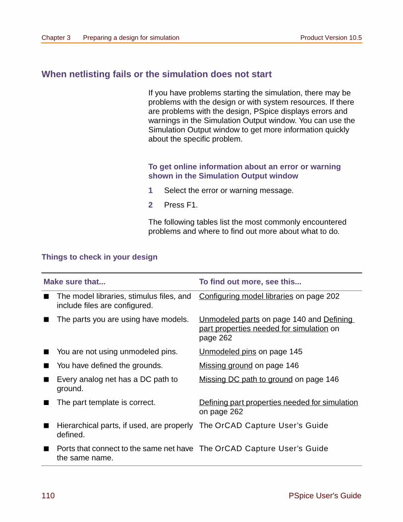
Chapter 3 Preparing a design for simulation Product Version 10.5
110 PSpice User's Guide
When netlisting fails or the simulation does not start
If you have problems starting the simulation, there may beproblems with the design or with system resources. If thereare problems with the design, PSpice displays errors andwarnings in the Simulation Output window. You can use theSimulation Output window to get more information quicklyabout the specific problem.
To get online information about an error or warningshown in the Simulation Output window
1 Select the error or warning message.
2 Press F1.
The following tables list the most commonly encounteredproblems and where to find out more about what to do.
Things to check in your design
Make sure that... To find out more, see this...
The model libraries, stimulus files, andinclude files are configured.
Configuring model libraries on page 202
The parts you are using have models. Unmodeled parts on page 140 and Definingpart properties needed for simulation onpage 262
You are not using unmodeled pins. Unmodeled pins on page 145
You have defined the grounds. Missing ground on page 146
Every analog net has a DC path toground.
Missing DC path to ground on page 146
The part template is correct. Defining part properties needed for simulationon page 262
Hierarchical parts, if used, are properlydefined.
The OrCAD Capture User’s Guide
Ports that connect to the same net havethe same name.
The OrCAD Capture User’s Guide

Product Version 10.5 Using parts that you can simulate
PSpice User's Guide 111
Things to check in your system configuration
Using parts that you can simulate
The PSpice part libraries supply numerous parts designed forsimulation. These include:
vendor-supplied parts
passive parts
breakout parts
behavioral parts
The PSpice part libraries also include special parts that youcan use for simulation only. These include:
stimulus parts to generate input signals to the circuit(see Defining stimuli on page 135)
ground parts required by all analog and mixed-signalcircuits, which need reference to ground
simulation control parts to do things like set biasvalues (see Appendix A, “Setting initial state”)
output control parts to do things like generate tablesand line-printer plots to the PSpice output file (seeChapter 19, “Other output options”)
At minimum, a part that you can simulate has theseproperties:
A simulation model to describe the part’s electricalbehavior; the model can be:
Make sure that... To find out more, see this...
Path to the PSpice programs is correct.
Directory containing your design haswrite permission.
Your operating system manual
Your system has sufficient free memoryand disk space.
Your operating system manual

Chapter 3 Preparing a design for simulation Product Version 10.5
112 PSpice User's Guide
explicitly defined in a model library
built into PSpice
built into the part (for some kinds of analogbehavioral parts)
A part with modeled pins to form electrical connections inyour design.
A translation from design part to netlist statement so thatPSpice can read it in.
Note: Not all parts in the libraries are set up for simulation.For example, connectors are parts destined for boardlayout only and do not have these simulationproperties.
Vendor-supplied parts
The PSpice libraries provide an extensive selection ofmanufacturers’ analog and digital parts. Typically, the libraryname reflects the kind of parts contained in the library and thevendor that provided the models.
Example: MOTOR_RF.OLB and MOTOR_RF.LIB contain partsand models, respectively, for Motorola-made RF bipolartransistors.
Two types of libraries are provided with PSpice:
Standard PSpice libraries
PSpice Advanced Analysis libraries
Standard PSpice libraries
The standard PSpice libraries feature over 16,000 analog and1,600 digital and mixed-signal models of devicesmanufactured in North America, Japan, and Europe.
Use parts from standard PSpice libraries or PSpice AdvancedAnalysis libraries if you want to analyze the part with PSpice.

Product Version 10.5 Using parts that you can simulate
PSpice User's Guide 113
The standard PSpice libraries are installed at followinglocations in the installation directory:
Capture symbols for standard PSpice libraries at
\tools\Capture\Library\PSpice\
Standard PSpice model libraries at
\tools\PSpice\Library\
The parts in the standard PSpice libraries are listed in theonline PSpice Library List. For information on finding partsusing the online PSpice Library List, see To find parts usingthe online library lists on page 116. To find out more abouteach model library, read the comments in the .LIB file header.
PSpice Advanced Analysis libraries
The PSpice Advanced Analysis libraries contain over 4,300analog parts. The Advanced Analysis libraries containparameterized and standard parts. The majority of the partsare parameterized. The parametrized parts have tolerance,distribution, optimizable and smoke parameters that arerequired by the PSpice Advanced Analysis tools. Standardparts in the Advanced Analysis libraries are similar to parts inthe standard PSpice libraries.
Note: The Advanced Analysis libraries are not available withPSpice A/D Basics.
The parametrized parts are associated with template-basedPSpice models. An important advantage of using thetemplate-based PSpice models is that you can pass modelparameters as properties from Capture. For example, if atemplate-based model is associated with a part, the modelparameters that you specify on an instance of the part in yourdesign will be passed to the model. There is no need to editthe model itself to change a parameter value. This is unlike thestandard PSpice parts that are associated with devicecharacteristic curve-based PSpice models, where you need toedit the model to change a simulation parameter. For moreinformation on template-based and device characteristiccurve-based PSpice models, see Chapter 4, “Creating andediting models.”
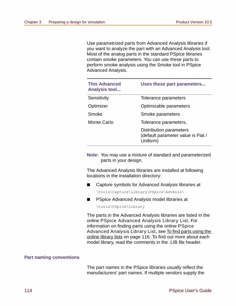
Chapter 3 Preparing a design for simulation Product Version 10.5
114 PSpice User's Guide
Use parametrized parts from Advanced Analysis libraries ifyou want to analyze the part with an Advanced Analysis tool.Most of the analog parts in the standard PSpice librariescontain smoke parameters. You can use these parts toperform smoke analysis using the Smoke tool in PSpiceAdvanced Analysis.
Note: You may use a mixture of standard and parameterizedparts in your design.
The Advanced Analysis libraries are installed at followinglocations in the installation directory:
Capture symbols for Advanced Analysis libraries at
\tools\Capture\Library\PSpice\AdvAnls\
PSpice Advanced Analysis model libraries at
\tools\PSpice\Library
The parts in the Advanced Analysis libraries are listed in theonline PSpice Advanced Analysis Library List. Forinformation on finding parts using the online PSpiceAdvanced Analysis Library List, see To find parts using theonline library lists on page 116. To find out more about eachmodel library, read the comments in the .LIB file header.
Part naming conventions
The part names in the PSpice libraries usually reflect themanufacturers’ part names. If multiple vendors supply the
This AdvancedAnalysis tool...
Uses these part parameters...
Sensitivity Tolerance parameters
Optimizer Optimizable parameters
Smoke Smoke parameters
Monte Carlo Tolerance parameters,
Distribution parameters(default parameter value is Flat /Uniform)

Product Version 10.5 Using parts that you can simulate
PSpice User's Guide 115
same part, each part name includes a suffix that indicates thevendor that supplied the model.
Example: The PSpice libraries include several models for theOP-27 opamp as shown by these entries in the online PSpiceLibrary List.
Notice that there is a generic OP-27 part provided by PSpice,the OP-27/AD from Analog Devices, Inc., and the OP-27/LTfrom Linear Technology Corporation.
Finding the part that you want
If you are having trouble finding a part, you can search thelibraries for parts with similar names by using either:
the parts browser in Capture and restricting the parts listto those names that match a specified wildcard textstring, or
the online PSpice Library List or the PSpiceAdvanced Analysis Library List and searching for thegeneric part name using capabilities of the Adobe

Chapter 3 Preparing a design for simulation Product Version 10.5
116 PSpice User's Guide
Acrobat Reader (see To find parts using the online librarylists on page 116).
To find parts using the parts browser
1 In Capture, from the Place menu, choose Part.
2 In the Part Name text box, type a text string with wildcardsthat approximates the part name that you want to find.Use this syntax:
<wildcard><part_name_fragment><wildcard>
where <wildcard> is one of the following:
The parts browser displays only the matching partnames.
Note: This method finds any part contained in the current partlibraries configuration, including parts for user-definedmodels.
If you want to find out more about a part supplied in the PSpicelibraries, such as manufacturer or whether you can simulate it,then search the online library lists (see To find parts using theonline library lists on page 116).
To find parts using the online library lists
OrCAD provides separate library lists for standard PSpicelibraries and Advanced Analysis libraries. The parts in thestandard PSpice libraries are listed in the online PSpiceLibrary List. The parts in the Advanced Analysis libraries arelisted in the online PSpice Advanced Analysis Library List.
1 Do one of the following:
From the Windows Start menu, choose the ReleaseOrCAD 10.0 programs folder and then the OnlineDocumentation shortcut.
From the Help menu in PSpice, choose Manuals.
* to match zero or more characters? to match exactly one character

Product Version 10.5 Using parts that you can simulate
PSpice User's Guide 117
The Cadence Documentation window appears.
2 Click the PSpice category to show the documents in thecategory.
3 Double-click PSpice Library List or PSpice AdvancedAnalysis Library List.
This opens the library list in your web browser.
4 Follow the instructions in the second page of the librarylist to use the library list.
Note: This method finds only the parts that PSpice suppliesthat have models.
If you want to include user-defined parts in the search, use theparts browser in Capture (see To find parts using the partsbrowser on page 116).
Passive parts
The PSpice libraries supply several basic parts based on thepassive device models built into PSpice. These aresummarized in the following table.
Table 3-1 Passive parts
These parts areavailable... For this device type...
Which is thisPSpice deviceletter...
CC_VAR
capacitor C
L inductor L
RR_VAR
resistor R
XFRM_LINEARK_LINEAR
transformer K and L
T ideal transmission line T
TLOSSY1 Lossy transmission line T

Chapter 3 Preparing a design for simulation Product Version 10.5
118 PSpice User's Guide
To find out more about how to use these parts and define theirproperties, look up the corresponding PSpice device letter inthe Analog Devices chapter in the online PSpiceReference Guide, and then see the Capture Parts sections.
Breakout parts
The PSpice libraries supply passive and semiconductor partswith default model definitions that define a basic set of modelparameters. This way, you can easily:
assign device and lot tolerances to model parameters forMonte Carlo and sensitivity/worst-case analyses.
To find out more about models, see What are models? onpage 151. To find out more about Monte Carlo andsensitivity/worst-case analyses, see Chapter 13, “MonteCarlo and sensitivity/worst-case analyses.”
define temperature coefficients, and
define device-specific operating temperatures.
To find out more about setting temperature parameters,see the Analog Devices chapter of the online PSpiceReference Guide and find the device type that you areinterested in.
TnCOUPLED2
TnCOUPLEDX2
KCOUPLEn 2
coupled transmissionline
T and K
1. TLOSSY is not available in PSpice A/D Basics packages.
2. For these device types, the PSpice libraries supply severalparts. Refer to the online PSpice Reference Guide for theavailable parts.
Table 3-1 Passive parts
These parts areavailable... For this device type...
Which is thisPSpice deviceletter...

Product Version 10.5 Using parts that you can simulate
PSpice User's Guide 119
These are called breakout parts and are summarized in thefollowing table.
To find out more about how to use these parts and define theirproperties, look up the corresponding PSpice device letter inthe Analog Devices chapter of the online PSpiceReference Guide, and then look in the Capture Partssection.
Table 3-2 Breakout parts
Use thisbreakout part... For this device
type...
Which is thisPSpice deviceletter...
BBREAK GaAsFET B
CBREAK capacitor C
DBREAKx1
1. For this device type, the PSpice libraries supply severalbreakout parts. Refer to the online PSpice ReferenceGuide for the available parts.
diode D
JBREAKx1 JFET J
KBREAK inductor coupling K
LBREAK inductor L
MBREAKx1 MOSFET M
QBREAKx1 bipolar transistor Q
RBREAK resistor R
SBREAK voltage-controlled switch
S
WBREAK current-controlled switch
W
XFRM_NONLINEAR transformer K and L
ZBREAKN IGBT Z

Chapter 3 Preparing a design for simulation Product Version 10.5
120 PSpice User's Guide
Behavioral parts
Behavioral parts allow you to define how a block of circuitryshould work without having to define each discretecomponent.
Analog behavioral parts
These parts use analog behavioral modeling (ABM) to defineeach part’s behavior as a mathematical expression or lookuptable. The PSpice libraries provide ABM parts that operate asmath functions, limiters, Chebyshev filters, integrators,differentiators, and others that you can customize for specificexpressions and lookup tables. You can also create your ownABM parts. For more information, see Chapter 6, “Analogbehavioral modeling.”
Digital behavioral parts
These parts use special behavioral primitives to define eachpart’s functional and timing behavior. These primitives are:
Many of the digital parts provided in the PSpice libraries aremodeled using these primitives. You can also create your owndigital behavioral parts using these primitives.
For more information, see:
Chapter 7, “Digital device modeling”
the Digital Devices chapter in the online PSpiceReference Guide.
Specifying values for part properties
Note the following when specifying values for part properties:
LOGICEXP to define logic expressionsPINDLY to define pin-to-pin delaysCONSTRAINT to define constraint checks

Product Version 10.5 Using global parameters and expressions for values
PSpice User's Guide 121
Do not leave a space between the value and its unit, if theunit is a scale symbol. For example, specify 5K instead of5 K.
For a listing of the scale symbols, see Numeric valueconventions in the Before you begin chapter of theonline PSpice Reference Guide.
Do not use the European notation for specifying values.For example, if you specify 3K3 (the European notationfor 3.3K), PSpice reads the value as 3K. Use 3.3Kinstead.
Specify tolerance values as percentages. If you specifyan absolute value, the tolerance value will be read as anabsolute number. For example, if you specify the value ofthe POSTOL property as a percentage, say 10%, on a10K resistor, the distribution values will be taken in therange of . If you specify the tolerance value as anabsolute number, say 10, the distribution values will betaken in the range of .
Using global parameters and expressions for values
In addition to literal values, you can use global parameters andexpressions to represent numeric values in your circuit design.
Global parameters
A global parameter is like a programming variable thatrepresents a numeric value by name.
Once you have defined a parameter (declared its name andgiven it a value), you can use it to represent circuit valuesanywhere in the design; this applies to any hierarchical level.
When multiple parts are set to the same value, globalparameters provide a convenient way to change all of theirvalues for “what-if” analyses. For example, if two independentsources have a value defined by the parameter VSUPPLY,then you can change both sources to 10 volts by assigning thevalue once to VSUPPLY.
10K 1K±
10K 10Ω±

Chapter 3 Preparing a design for simulation Product Version 10.5
122 PSpice User's Guide
Some ways that you can use parameters are as follows:
Apply the same value to multiple part instances.
Set up an analysis that sweeps a variable through a rangeof values (for example, DC sweep or parametric analysis).
Declaring and using a global parameter
To use a global parameter in your design, you need to:
define the parameter using a PARAM part, and
use the parameter in place of a literal value somewherein your design.
To declare a global parameter
1 Place a PARAM part in your design.
2 Double-click the PARAM part to display the Partsspreadsheet, then click the New Column or New Rowbutton.
For more information about using the Parts spreadsheet,see the OrCAD Capture User’s Guide.
3 To avoid adding the new parameter to the selected filterfor all parts, change the Filter by field to Currentproperties.
4 Declare up to three global parameters by doing thefollowing for each global parameter:
a. Click New.
b. In the Property Name text box, enter NAMEn, thenclick OK.
This creates a new property for the PARAM part,NAMEn in the spreadsheet.
c. Click in the cell below (to the right of) the NAMEncolumn (or row) and enter a default value for theparameter.
d. While this cell is still selected, click Display.

Product Version 10.5 Using global parameters and expressions for values
PSpice User's Guide 123
e. In the Display Format frame, select Name and Value,then click OK.
Note: The system variables in Table 3-5 on page 131 havereserved parameter names. Do not use theseparameter names when defining your own parameters.
5 Close the Parts spreadsheet.
Example
To declare the global parameter VSUPPLY that will set thevalue of an independent voltage source to 14 volts, place thePARAM part, and then create a new property namedVSUPPLY with a value of 14v.
To use the global parameter in your circuit
1 Find the numeric value that you want to replace: acomponent value, model parameter value, or otherproperty value.
2 Replace the value with the name of the global parameterusing the following syntax:
global_parameter_name
The curly braces tell PSpice to evaluate the parameterand use its value.
Example
To set the independent voltage source, VCC, to the value ofthe VSUPPLY parameter, set its DC property to VSUPPLY.

Chapter 3 Preparing a design for simulation Product Version 10.5
124 PSpice User's Guide
Expressions
An expression is a mathematical relationship that you can useto define a numeric or boolean (TRUE/FALSE) value.
PSpice evaluates the expression to a single value every time:
it reads in a new circuit, and
a parameter value used within an expression changesduring an analysis.
Example: A parameter that changes with each step of aDC sweep or parametric analysis.
Specifying expressions
To use an expression in your circuit
1 Find the numeric or boolean value you want to replace: acomponent value, model parameter value, other propertyvalue, or logic in an IF function test (see Table 3-4 for adescription of the IF function).
2 Replace the value with an expression using the followingsyntax:
expression
where expression can contain any of the following:
standard operators listed in Table 3-3
built-in functions listed in Table 3-4
user-defined functions
For more information on user-defined functions, seethe .FUNC command in the Commands chapter inthe online PSpice Reference Guide.
system variables listed in Table 3-5
user-defined global parameters

Product Version 10.5 Using global parameters and expressions for values
PSpice User's Guide 125
For more information on user-defined parameters,see Using global parameters and expressions for valueson page 121.
literal operands
The curly braces tell PSpice to evaluate the expressionand use its value.
Example
Suppose you have declared a parameter named FACTOR(with a value of 1.2) and want to scale a -10 V independentvoltage source, VEE, by the value of FACTOR. To do this, setthe DC property of VEE to:
-10*FACTOR
PSpice A/D evaluates this expression to:
(-10 * 1.2) or -12 volts

Chapter 3 Preparing a design for simulation Product Version 10.5
126 PSpice User's Guide
Table 3-3 Operators in expressions
This operatorclass...
Includesthisoperator...
Which means...
arithmetic + addition or stringconcatenation
- subtraction
* multiplication
/ division
** exponentiation
logical1
1. Logical and relational operators are used within the IF()function; for digital parts, logical operators are used inBoolean expressions.
~ unary NOT
| boolean OR
^ boolean XOR
& boolean AND
relational1 == equality test
!= non-equality test
> greater than test
>= greater than or equal to test
< less than test
<= less than or equal to test
Table 3-4 Functions in arithmetic expressions
This function... Means this...
ABS(x) |x|
SQRT(x) x1/2
EXP(x) ex

Product Version 10.5 Using global parameters and expressions for values
PSpice User's Guide 127
LOG(x) ln (x) which is log base e
LOG10(x) log (x) which is log base 10
PWR(x,y) |x|y
PWRS(x,y) +|x|y (if x > 0)-|x|y (if x < 0)
SIN(x) sin(x) where x is in radians
ASIN(x) sin-1 (x) where the result is inradians
SINH(x) sinh (x) where x is in radians
ASINH(x) sinh-1 (x) where x is in radians
COS(x) cos (x) where x is in radians
ACOS(x) cos-1 (x) where the result is inradians
COSH(x) cosh (x) where x is in radians
ACOSH(x) cosh-1 (x) where x is in radians
TAN(x) tan (x) where x is in radians
ATAN(x)ARCTAN(x)
tan-1 (x) where the result is inradians
ATAN2(y,x) tan-1 (y/x) where the result is inradians
TANH(x) tanh (x) where x is in radians
ATANH(x) tanh-1 (x) where x is in radians
M(x) magnitude ofx1
which is the same asABS(x)
P(x) phase of x1 in degrees; returns 0.0for real numbers
R(x) real part of x1
IMG(x) imaginary partof x1
which is applicable toAC analysis only
Table 3-4 Functions in arithmetic expressions, continued
This function... Means this...

Chapter 3 Preparing a design for simulation Product Version 10.5
128 PSpice User's Guide
DDT(x) time derivativeof x
which is applicable totransient analysis only
Note: In waveformanalysis, thisfunction is D(x).
SDT(x) time integral ofx
which is applicable totransient analysis only
Note: In waveformanalysis, thisfunction is S(x).
TABLE(x,x1,y1,...) y value as afunction of x
where xn,yn point pairsare plotted andconnected by straightlines
MIN(x,y) minimum of xand y
MAX(x,y) maximum of xand y
LIMIT(x,min,max) min if x < minmax if x > maxelse x
SGN(x) +1 if x > 00 if x = 0-1 if x < 0
STP(x) 1 if x >= 00 if x < 0
which is used tosuppress a value until agiven amount of timehas passed
Example:v(1)*STP(TIME-10ns)gives a value of 0.0 until10 nsec has elapsed,then gives v(1).
Table 3-4 Functions in arithmetic expressions, continued
This function... Means this...

Product Version 10.5 Using global parameters and expressions for values
PSpice User's Guide 129
IF(t,x,y) x if t is truey otherwise
where t is a relationalexpression using therelational operatorsshown in Table 3-3
Zero(expression) Expression is evluated,and the function retuirnsthe value as 0
I/Ps from kukal
one(expression) I/Ps from kukal
ceil(arg) value returnedis an integerwhich is eitherequal to, orgreater thanthe argumentvalue.
argument should be anumeric value or anexpression thatevaluates to a numericvalue
Example:
ceil(PI)=4
ceil(5)=5
ceil(5.4)=6
floor(arg) value returnedis an integerwhich is eitherequal to theargumentvalue, or is thenearestinteger,smaller thanthe argumentvalue.
the argument should bea numeric value or anexpression thatevaluates to a numericvalue
Example:
floor(PI)=3
floor(5)=5
floor(5.4)=5
Table 3-4 Functions in arithmetic expressions, continued
This function... Means this...

Chapter 3 Preparing a design for simulation Product Version 10.5
130 PSpice User's Guide
intq(arg) returns 1, ifarg in aninteger else
returns 0
The argument passed tothis function can be anumeric value or anexpression thatevaluates to a numericvalue.
1. M(x), P(x), R(x), and IMG(x) apply to Laplace expressionsonly.
Table 3-4 Functions in arithmetic expressions, continued
This function... Means this...

Product Version 10.5 Using global parameters and expressions for values
PSpice User's Guide 131
The system variables listed in Table 3-5 on page 131, cannotbe used in the trace expressions in the Probe window. Thesevariables are supported only by the PSpice engine.
Table 3-5 System variables
Thisvariable...
Evaluates to this...
TEMP Temperature values resulting from atemperature, parametric temperature, or DCtemperature sweep analysis.
The default temperature, TNOM, is set in theOptions dialog box (from the SimulationSettings dialog box, choose the Options tab).TNOM defaults to 27°C.
Note: TEMP can only be used in expressionspertaining to analog behavioral modelingand the propagation delay of digitalmodels.
Is this note valid after 10.5enhancements???
Note: If a passive or semiconductor device hasan independent temperatureassignment, then TEMP does notrepresent that device’s temperature.
To find out more about customizingtemperatures for passive or semiconductordevices, refer to the .MODEL command in theCommands chapter in the online PSpiceReference Guide.
TIME Time values resulting from a transient analysis.If no transient analysis is run, this variable isundefined.
Note: TIME can only be used in analogbehavioral modeling expressions.

Chapter 3 Preparing a design for simulation Product Version 10.5
132 PSpice User's Guide
Validate the value of PI. Upto which decimal point is itsupported.
RELTOL Relative tolerance of Voltage and current
The value of this variable is as specified in theOptions tab of the Simulation Settings dialogbox.
ABSTOL Current tolerance
Describes the best accuracy of currents in asimulation run. The value of this variable isspecified in the Options tab of the SimulationSettings dialog box.
VNTOL Voltage tolerance
Describes the best accuracy of voltages in asimulation run.The value of this variable isspecified in the Options tab of the SimulationSettings dialog box.
CHGTOL Charge tolerance
Describes the best accuracy of charges. Thevalue of this variable is specified in the Optionstab of the Simulation Settings dialog box.
GMIN Indicates the minimum conductance used forany branch. The value of this variable isspecified in the Options tab of the SimulationSettings dialog box.
Table 3-6 Constants in arithmetic expressions,
Constant.. Value
PI 3.14159265
Table 3-5 System variables, continued
Thisvariable...
Evaluates to this...

Product Version 10.5 Defining power supplies
PSpice User's Guide 133
Defining power supplies
For the analog portion of your circuit
If the analog portion of your circuit requires DC power, thenyou need to include a DC source in your design. To specify aDC source, use one of the following parts.
To find out how to use these parts and specify their properties,see the following:
Setting up a DC stimulus on page 423
Using VSRC or ISRC parts on page 138
For A/D interfaces in mixed-signal circuits
Default digital power supplies
Every digital part supplied in the PSpice libraries has a defaultdigital power supply defined for its A-to-D or D-to-A interfacesubcircuit. This means that if you are designing a mixed-signalcircuit, then you have a default 5 volt digital power supplybuilt-in to the circuit at every interface.
Custom digital power supplies
If needed, you can customize the power supply for differentlogic families.
For this source type... Use this part...
voltage VDC or VSRC
current IDC or ISRC
For this logicfamily...
Use this part...
CD4000 CD4000_PWR

Chapter 3 Preparing a design for simulation Product Version 10.5
134 PSpice User's Guide
To find out how to use these parts and specify their digitalpower and ground pins, see Specifying digital power supplies onpage 583.
TTL DIGIFPWR
ECL 10K ECL_10K_PWR
ECL 100K ECL_100K_PWR
For this logicfamily...
Use this part...

Product Version 10.5 Defining power supplies
PSpice User's Guide 135
Defining stimuli
To simulate your circuit, you need to connect one or moresource parts that describe the input signal that the circuit mustrespond to.
The PSpice libraries supply several source parts that aredescribed in the tables that follow. These parts depend on:
the kind of analysis you are running,
whether you are connecting to the analog or digitalportion of your circuit, and
how you want to define the stimulus: using the StimulusEditor, using a file specification, or by defining partproperty values.
Analog stimuli
Analog stimuli include both voltage and current sources. Thefollowing table shows the part names for voltage sources.
If you want this kind ofinput...
Use this part for voltage...
For DC analyses
See Setting up a DC stimuluson page 423 for more details.
DC bias VDC or VSRC
For AC analyses
See Setting up an AC stimuluson page 439 for more details.
AC magnitude and phase VAC or VSRC
For transient analyses
See Defining a time-basedstimulus on page 474 for moredetails.
exponential VEXP or VSTIM1

Chapter 3 Preparing a design for simulation Product Version 10.5
136 PSpice User's Guide
To determine the part name for an equivalent currentsource
− In the table of voltage source parts, replace the first V inthe part name with I.
For example, the current source equivalent to VDC isIDC, to VAC is IAC, to VEXP is IEXP, and so on.
Using VSTIM and ISTIM
You can use VSTIM and ISTIM parts to define any kind oftime-based input signal. To specify the input signal itself, youneed to use the Stimulus Editor. See The Stimulus Editorutility on page 476.
Note: The Stimulus Editor is not included withPSpice A/D Basics.
periodic pulse VPULSE or VSTIM1
piecewise-linear VPWL or VSTIM1
piecewise-linear that repeatsforever
VPWL_RE_FOREVER orVPWL_F_RE_FOREVER2
piecewise-linear that repeatsn times
VPWL_N_TIMES orVPWL_F_N_TIMES2
frequency-modulated sinewave
VSFFM or VSTIM1
sine wave VSIN or VSTIM1
1. VSTIM and ISTIM parts require the Stimulus Editor to definethe input signal; these parts are not available in Basics+.
2. VPWL_F_RE_FOREVER and VPWL_F_N_TIMES arefile-based parts; the stimulus specification is saved in a fileand adheres to PSpice netlist syntax.
If you want this kind ofinput...
Use this part for voltage...

Product Version 10.5 Defining power supplies
PSpice User's Guide 137
If you want to specify multiple stimulus types
If you want to run more than one analysis type, including atransient analysis, then you need to use either of the following:
time-based stimulus parts with AC and DC properties
VSRC or ISRC parts
Using time-based stimulus parts with AC and DCproperties
The time-based stimulus parts that you can use to define atransient, DC, and/or AC input signal are listed below.
In addition to the transient properties, each of these parts alsohas a DC and AC property. When you use one of these parts,you must define all of the transient properties. However, it iscommon to leave DC and/or AC undefined (blank). When yougive them a value, the syntax you need to use is as follows.
For the meaning of transient source properties, refer to the I/V(independent current and voltage source) device type syntaxin the Analog Devices chapter in the online PSpiceReference Guide.
This property... Has this syntax...
DC DC_value[units]
AC magnitude_value[units][phase_value]
VEXPVPULSEVPWLVPWL_F_RE_FOREVERVPWL_F_N_TIMESVPWL_RE_FOREVERVPWL_RE_N_TIMESVSFFMVSIN
IEXPIPULSEIPWLIPWL_F_RE_FOREVERIPWL_F_N_TIMESIPWL_RE_FOREVERIPWL_RE_N_TIMESISFFMISIN

Chapter 3 Preparing a design for simulation Product Version 10.5
138 PSpice User's Guide
Using VSRC or ISRC parts
The VSRC and ISRC parts have one property for eachanalysis type: DC, AC, and TRAN. You can set any or all ofthem using PSpice netlist syntax. When you give them avalue, the syntax you need to use is as follows.
Note: If you are running a PSpice-only transient analysis, usea VSTIM or ISTIM part if you have the standardpackage, or one of the other time-based source partsthat has properties specific for a waveform shape.
Digital stimuli
This property... Has this syntax...
DC DC_value[units]
AC magnitude_value[units][phase_value]
TRAN time-based_type (parameters)
where time-based_type is EXP,PULSE, PWL, SFFM, or SIN, and theparameters depend on thetime-based_type.
For the syntax and meaning oftransient source specifications, referto the I/V (independent current andvoltage source) device type in theAnalog Devices chapter in the onlinePSpice Reference Guide.
If you want this kind of input... Use this part....
For transient analyses
signal or bus (n width) DIGSTIMn1
clock signal DIGCLOCK
1-bit signal STIM1
4-bit bus STIM4

Product Version 10.5 Defining power supplies
PSpice User's Guide 139
You can use the DIGSTIM part to define both 1-bit signal orbus (n width) input signals using the Stimulus Editor.
See Defining a digital stimulus on page 543 to find out moreabout:
all of these source parts, and
how to use the Stimulus Editor to specify DIGSTIMn(DIGSTIM1, DIGSTIM4, etc.) part.
8-bit bus STIM8
16-bit bus STIM16
file-based signal or bus (n width) FILESTIMn
1. The DIGSTIM part requires the Stimulus Editor todefine the input signal; these parts are not available inPSpice A/D Basics.
If you want this kind of input... Use this part....

Chapter 3 Preparing a design for simulation Product Version 10.5
140 PSpice User's Guide
Things to watch for
This section includes troubleshooting tips for some of the mostcommon reasons your circuit design may not netlist orsimulate.
For a roadmap to other commonly encountered problems andsolutions, see When netlisting fails or the simulation does notstart on page 110.
Unmodeled parts
If you see messages like this in the PSpice Simulation Outputwindow,
Warning: Part part_name has no simulation model.
then you may have done one of the following things:
Placed a part from the PSpice libraries that is notavailable for simulation (used only for board layout).
Placed a custom part that has been incompletely definedfor simulation.
Do this if the part in question is from the PSpice libraries
Replace the part with an equivalent part from one of thelibraries listed in the tables below.
Make sure that you can simulate the part by checking thefollowing:
That it has a PSPICETEMPLATE property and thatits value is non-blank.
The libraries listed in the tables that follow all containparts that you can simulate. Some files also containparts that you can only use for board layout. That’swhy you need to check the PSPICETEMPLATEproperty if you are unsure or still getting warningswhen you try to simulate your circuit.

Product Version 10.5 Defining power supplies
PSpice User's Guide 141
That it has an Implementation Type = PSpiceMODEL property and that its Implementationproperty is non-blank.
Note: The PSPICETEMPLATE property is case insensitive,and is shown throughout the documentation in capitalletters by convention only.

Chapter 3 Preparing a design for simulation Product Version 10.5
142 PSpice User's Guide
Table 3-7
Analog libraries with modeled parts (installed in\tools\Capture\Library\PSpice)
1_SHOT EPWRBJT ON_AMP
ABM FAIRCHILD ON_BJT
ADV_LIN FILTSUB ON_DIODE
AMP FWBELL ON_MOS
ANALOG HARRIS ON_PWM
ANA_SWIT IBGT1
1. Not included in PSpice A/D Basics.
OPAMP
ANLG_DEV INFINEON OPTO
ANL_MISC IXYS PHIL_BJT
APEX JBIPOLAR PHIL_DIODE
APEX_PWM JDIODE PHIL_FET
BIPOLAR JFET PHIL_RF
BREAKOUT JJFET POLYFET
BUFFER JOPAMP PWRBJT
BURR_BRN JPWRBJT PWRMOS
CD4000 JPWRMOS SWIT_RAV
COMLINR LINEDRIV SWIT_REG
DATACONV LIN_TECH TEX_INST
DARLNGTN MAGNETIC1 THYRISTR1
DIODE MAXIM TLINE1
EBIPOLAR MIX_MISC2
2. Contains mixed-signal parts.
XTAL
EDIODE MOTORSEN ZETEX
ELANTEC MOTOR_RF
EPCOS NAT_SEMI

Product Version 10.5 Defining power supplies
PSpice User's Guide 143
To find out more about a particular library, refer to the onlinePSpice Library List or read the header of the model libraryfile itself.
Check for this if the part in question is custom-built
Are there blank (or inappropriate) values for the part’sImplementation and PSPICETEMPLATE properties?
If so, load this part into the part editor and set these propertiesappropriately. One way to approach this is to edit the part thatappears in your design.
To edit the properties for the part in question
1 In the schematic page editor, select the part.
2 From the Edit menu, choose Part.
The part editor window appears with the part alreadyloaded.
3 From the Edit menu, choose Properties and proceed tochange the property values.
To find out more about setting the simulation properties forparts, see Defining part properties needed for simulation onpage 262. To find out more about using the part editor, refer toyour OrCAD Capture User’s Guide.
Digital libraries with modeled parts
7400 74H DIG_ECL
74AC 74HC DIG_GAL
74ACT 74HCT DIG_MISC
74ALS 74L DIG_PAL
74AS 74LS DIG_PRIM
74F 74S

Chapter 3 Preparing a design for simulation Product Version 10.5
144 PSpice User's Guide
Unconfigured model, stimulus, or include files
If you see messages like these in the PSpice SimulationOutput window,
(design_name) Floating pin: refdes pin pin_name
Floating pin: pin_id
File not found
Can’t open stimulus file
or messages like these in the PSpice output file,
Model model_name used by device_name is undefined.
Subcircuit subckt_name used by device_name isundefined.
Can’t find .STIMULUS “refdes” definition
then you may be missing a model library, stimulus file, orinclude file from the configuration list, or the configured file isnot on the library path.
Check for this
Does the PSpice library configuration file NOM.LIBappear in the Library files list in the Configuration Filestab in the Simulation Profile?
Does the relevant model library, stimulus file, or includefile appear in the configuration list?
If the file is configured, does the default library searchpath include the directory path where the file resides, orexplicitly define the directory path in the configurationlist?
If the file is not configured, add it to the list and make sure thatit appears before any other library or file that has anidentically-named definition.
To find out more about how to configure these files and aboutsearch order, see Configuring model libraries on page 202. Tofind out more about the default configuration, see How aremodels organized? on page 152.

Product Version 10.5 Defining power supplies
PSpice User's Guide 145
To view the configuration list
1 In the Simulation Settings dialog box, click theConfiguration Files tab and view the Library, Include, andStimulus files lists.
If the directory path is not specified in each, update thedefault library search path or change the file entry in theconfiguration list to include the full path specification.
To view the default library search path
1 In the Simulation Settings dialog box, click theConfiguration Files tab.
2 Click Library in the Category field to display the Libraryfiles list.
To find out more about the library search path, see Changingthe library search path on page 210.
Unmodeled pins
If you see messages like these in the PSpice SimulationOutput window,
Warning: Part part_name pin pin_name is unmodeled.
Warning: Less than 2 connections at node node_name.
or messages like this in the PSpice output file,
Floating/unmodeled pin fixups
then you may have drawn a wire to an unmodeled pin.
The PSpice libraries include parts that are suitable for bothsimulation and board layout. The unmodeled pins map intopackages but have no electrical significance; PSpice ignoresunmodeled pins during simulation.
Check for this
Are there connections to unmodeled pins?
If so, do one of the following:

Chapter 3 Preparing a design for simulation Product Version 10.5
146 PSpice User's Guide
Remove wires connected to unmodeled pins.
If you expect the connection to affect simulation results,find an equivalent part that models the pins in questionand draw the connections. To find out more aboutsearching for parts, see Finding the part that you want onpage 115.
Missing ground
This problem applies to analog-only and mixed-signal circuits.
If for every net in your circuit you see this message in thePSpice output file,
ERROR -- Node node_name is floating.
then your circuit may not be tied to ground.
Check for this
Are there ground parts named 0 (zero) connectedappropriately in your design?
If not, place and connect one (or more, as needed) in yourdesign. You can use the 0 (zero) ground part in SOURCE.OLBor any other ground part as long as you change its name to 0.
Missing DC path to ground
This problem applies to analog-only and mixed-signal circuits.
If for selected nets in your circuit you see this message in thePSpice output file,
ERROR -- Node node_name is floating.
then you may be missing a DC path to ground.
Check for this
Are there any nets that are isolated from ground by eitheropen circuits or capacitors?
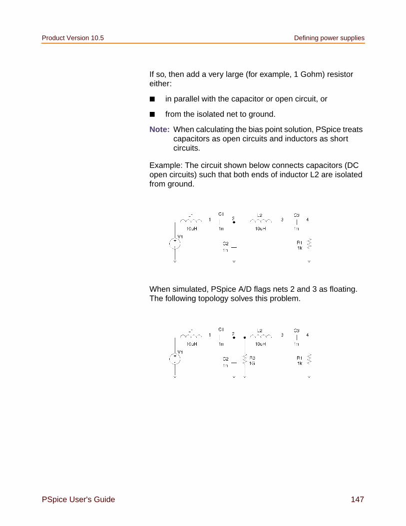
Product Version 10.5 Defining power supplies
PSpice User's Guide 147
If so, then add a very large (for example, 1 Gohm) resistoreither:
in parallel with the capacitor or open circuit, or
from the isolated net to ground.
Note: When calculating the bias point solution, PSpice treatscapacitors as open circuits and inductors as shortcircuits.
Example: The circuit shown below connects capacitors (DCopen circuits) such that both ends of inductor L2 are isolatedfrom ground.
When simulated, PSpice A/D flags nets 2 and 3 as floating.The following topology solves this problem.

Chapter 3 Preparing a design for simulation Product Version 10.5
148 PSpice User's Guide

PSpice User's Guide 149
4
Creating and editing models
Chapter overview
This chapter provides information about creating and editingmodels for parts that you want to simulate.
Topics are grouped into four areas introduced later in thisoverview. If you want to find out quickly which tools to use tocomplete a given task and how to start, then:
1 Go to the roadmap in Ways to create and edit models onpage 161.
2 Find the task you want to complete.
3 Go to the sections referenced for that task for moreinformation about how to proceed.
Background information
These sections present model library concepts and anoverview of the tools that you can use to create and editmodels:
What are models? on page 151
How are models organized? on page 152
Tools to create and edit models on page 160

Chapter 4 Creating and editing models Product Version 10.5
150 PSpice User's Guide
Task roadmap
This section helps you find other sections in this chapter thatare relevant to the model editing task that you want tocomplete:
Ways to create and edit models on page 161
How to use the tools
These sections explain how to use different tools to create andedit models on their own and when editing schematic pagesor parts:
For a list of device types that the Model Editor supports,see Table 4-2 and Table 4-3. If the Model Editor does notsupport the device type for the model definition that youwant to create, then you can use a standard text editor tocreate a model definition using the PSpice .MODEL and.SUBCKT command syntax. Remember to configure thenew model library (see Configuring model libraries onpage 202).
Editing model text on page 193
Using the Create Subcircuit Format Netlist command onpage 196
Other useful information
These sections explain how to configure and reuse modelsafter you have created or edited them:
Changing the model reference to an existing modeldefinition on page 199
Reusing instance models on page 200
Configuring model libraries on page 202

Product Version 10.5 Chapter overview
PSpice User's Guide 151
What are models?
A model defines the electrical behavior of a part. On aschematic page, this correspondence is defined by theImplementation property on the part, which is assigned themodel name.
Depending on the device type that it describes, a model isdefined as one of the following:
a model parameter set
a subcircuit netlist
Both ways of defining a model are text-based, with specificrules of syntax.
Models defined as model parameter sets
PSpice has built-in algorithms or models that describe thebehavior of many device types. The behavior of these built-inmodels is described by a set of model parameters.
You can define the behavior for a device that is based on abuilt-in model by setting all or any of the corresponding modelparameters to new values using the PSpice .MODEL syntax.For example:
.MODEL MLOAD NMOS+ (LEVEL=1 VTO=0.7 CJ=0.02pF)
Note: In addition to the analog models built into PSpice, the.MODEL syntax applies to the timing and I/Ocharacteristics of digital parts.
Models defined as subcircuit netlists
For some devices, there are no PSpice built-in models thatcan describe their behavior fully. These types of devices aredefined using the PSpice .SUBCKT/.ENDS or subcircuitsyntax instead.
Subcircuit syntax includes:
Netlists to describe the structure and function of the part.

Chapter 4 Creating and editing models Product Version 10.5
152 PSpice User's Guide
Variable input parameters to fine-tune the model.
For example:
* FIRST ORDER RC STAGE.SUBCKT LIN/STG IN OUT AGND+ PARAMS: C1VAL=1 C2VAL=1 R1VAL=1 R2VAL=1+ GAIN=10000C1 IN N1 C1VALC2 N1 OUT C2VALR1 IN N1 R1VALR2 N1 OUT R2VALEAMP1 OUT AGND VALUE=V(AGND,N1)*GAIN.ENDS
To find out more about PSpice command and netlist syntax,refer to the online PSpice Reference Guide.
How are models organized?
The key concepts behind model organization are as follows:
Model definitions are saved in files called model libraries.
Model libraries must be configured so that PSpicesearches them for definitions.
Depending on the configuration, model libraries areavailable either to a specific profile, to a specific design orto all (global) designs. For more information, see Globalvs. design vs. profile models and libraries on page 153.
Model libraries
Device model and subcircuit definitions are organized intomodel libraries. Model libraries are text files that contain oneor more model definitions. Typically, model library names havea .LIB extension.
Most model libraries contain models of similar type. Forvendor-supplied models, libraries are also partitioned bymanufacturer. For example, MOTOR_RF.LIB contains modelsfor Motorola-made RF bipolar transistors.
To find out more about the models contained in a modellibrary, read the comments in the file header.

Product Version 10.5 How are models organized?
PSpice User's Guide 153
Note: You can use the PSpice Model Editor, or any standardtext editor, to view model definitions in libraries.
Model library configuration
PSpice searches model libraries for the model namesspecified by the MODEL implementation for parts in yourdesign. These are the model definitions that PSpice uses tosimulate your circuit.
For PSpice to locate these model definitions, you mustconfigure the libraries. This means:
Specifying the directory path or paths to the modellibraries.
Naming each model library that PSpice should searchand listing them in the desired search order.
Assigning global, design or profile scope to the modellibrary.
To optimize the model library search, PSpice uses indexes. Tofind out more about this and how to add, delete, and rearrangeconfigured libraries, see Configuring model libraries onpage 202.
Global vs. design vs. profile models and libraries
Model libraries and the models they contain have eitherprofile, design or global application to your designs.
Profile models
Profile models apply to one profile. You can create modelsusing the Model Editor and then manually configure the newlibraries for a specific profile.
Example usage: To set up device and lot tolerances on themodel parameters for a particular part instance when runninga Monte Carlo or sensitivity/worst-case analysis using aspecific profile.

Chapter 4 Creating and editing models Product Version 10.5
154 PSpice User's Guide
Design models
Design models apply to one design. The schematic pageeditor automatically creates a design model whenever youmodify the model definition for a part instance on yourschematic page. You can also create models externally andthen manually configure the new libraries for a specific design.
Example usage: To set up device and lot tolerances on themodel parameters for a particular part instance when runninga Monte Carlo or sensitivity/worst-case analysis.
Global models
Global models are available to all designs you create. Thepart editor automatically creates a global model wheneveryou create a part with a new model definition. The ModelEditor also creates global models. You can also create modelsexternally and then manually configure the new libraries foruse in all designs.
To find out how to change the profile, design and globalconfiguration of model libraries, see Changing the modellibrary scope from profile to design, profile to global, design toglobal and vice versa on page 206.
PSpice searches profile libraries before design libraries anddesign libraries before global libraries. To find out more, seeChanging model library search order on page 208.
Nested model libraries
Besides model and subcircuit definitions, model libraries canalso contain references to other model libraries using thePSpice .LIB syntax. When searching model libraries formatches, PSpice also scans these referenced libraries.
Example: Suppose you have two custom model libraries,MYDIODES.LIB and MYOPAMPS.LIB, that you wantPSpice A/D to search any time you simulate a design. Thenyou can create a third model library, MYMODELS.LIB, thatcontains these two statements:

Product Version 10.5 How are models organized?
PSpice User's Guide 155
.LIB mydiodes.lib
.LIB myopamps.lib
and configure MYMODELS.LIB for global use. BecauseMYDIODES.LIB and MYOPAMPS.LIB are referenced fromMYMODELS.LIB, they are automatically configured for globaluse as well.
PSpice-provided models
The model libraries that you initially install with your PSpiceprograms are listed in NOM.LIB. This file demonstrates howyou can nest references to other libraries and models.
If you click the Configuration Files tab in the SimulationSettings dialog box and view the Library files list immediatelyafter installation, you see the NOM.LIB entry in the Libraryfiles list. The icon means that this model library and any ofthe model libraries it references contain global modeldefinitions.
Model library data
Information contained in PSpice model libraries can beclassified as:
Simulation information
Device information
Simulation information
Simulation information is also termed as model informationand is used while simulating the models. Depending on themethod of creation, PSpice simulation models are of twotypes:
Device characteristic curves-based models
Template-based models

Chapter 4 Creating and editing models Product Version 10.5
156 PSpice User's Guide
Device characteristic curves-based models
Simulation models based on the device characteristic curvesare the models that are historically being used in theCapture-PSpice flow. You can extract device parametersbased on the device characteristic curves in the data sheets.
For a list of device characteristic curve-based modelsprovided with PSpice, refer to the online PSpice Library List.
Template-based models
These simulation models are based on PSpice-providedtemplates and are a new addition to the PSpice model library.Simulation models that are based on PSpice providedtemplates are also referred to as parameterized models.Parameterized models are specified in terms of modelparameters. Changing a parameter changes the behavior ofthe model. Template-based PSpice models describe theanalog simulation behavior of a device in terms of parametricequations. These models are of the .SUBCKT type. The.SUBCKT wrapper enables symbol properties to be passed asparameters to the simulator.
The PSpice-provided templates are available in theTEMPLATES.LIB file. This is an encrypted file, andtemplate-based models are wrappers to this file.
The main advantage of using template-based models is thatsimulation parameter values can be passed as propertiesfrom Capture. Besides this, parameterized models are bestsuited to be used with PSpice Advanced Analysis, and also forperforming statistical analysis for variations in modelparameters.
For a list of template-based device models provided withPSpice, refer to the online PSpice Advanced AnalysisLibrary List.
For a description of models supported by the Model Editor,see Model Editor-supported device types based on PSpicetemplates on page 173.

Product Version 10.5 How are models organized?
PSpice User's Guide 157
Device information
Information that is specific to each device, such as simulationparameter tolerance and maximum operating conditions, istermed as device information. The device information is storedin the device property file and is required by PSpice AdvancedAnalysis. To know more about the device property file, seeAppendix A, Property Files in the PSpice AdvancedAnalysis User’s Guide.
You can use the Model Editor to add device information to amodel. For template-based simulation models, you can addsmoke and tolerance information. For other simulationmodels, you can add only the smoke information.
Tolerance information is required to perform a Monte Carloand Sensitivity/Worst-Case analysis. To know more aboutMonte Carlo and Sensitivity/Worst-Case analysis, seePSpice Advanced Analysis User’s Guide.
The tolerance information is added in the SimulationParameters frame but smoke information can be added ormodified only if you have Advanced Analysis installed. SeeAdding tolerance information on page 172
To know more about how to add smoke information to a modelusing the Model Editor, see Handling smoke information usingthe Model Editor on page 212.
Device characteristic curves-based models vs. Template-based models
Table 4-1 highlights the differences between two types ofsimulation models.
Table 4-1 Differences between device characteristic curves-based andtemplate-based models
Device characteristic curves-basedPSpice models
Template-based PSpice models
They are based on device characteristiccurves. Device characteristic curves can beobtained from device datasheets.
They are based on PSpice-providedtemplates.

Chapter 4 Creating and editing models Product Version 10.5
158 PSpice User's Guide
They cannot be used for Advanced AnalysisSensitivity, Monte Carlo, and Optimizer runs.They can be used for Advanced Analysissmoke test only if smoke information isexplicitly added.
They can be used for all Advanced Analysisruns, such as Sensitivity, Smoke, MonteCarlo, and Optimizer.
All simulation information is contained in themodel itself.
Models are wrappers to a template modelfile. Therefore, both the model and thetemplate model are required for simulation.
The PSpiceTemplate property must beattached to the symbol for generating thePSpice netlist.
To know more about the PSpiceTemplateproperty, see PSPICETEMPLATE onpage 263.
The PSpiceTemplate property is not requiredon the symbol. The PORT_ORDERinformation present in the device propertyfile is used for generating the PSpice netlist.
Note: The model library and the deviceproperty file must have the samename and must be at the samelocation.
To know more about the device property file,see Appendix A, Property Files in thePSpice Advanced Analysis User’sGuide.
To modify a simulation property, you need toedit the simulation parameter. This impliesthat you either update the values in theoriginal model or create an instance modelfor the design.
To know more, see Using the Model Editor toedit the D1 diode model on page 182.
Simulation parameter values can be passedas properties from the schematic editor. Thisimplies that instance-specific values ofsimulation parameters can be passed fromthe schematic editor, without changing theoriginal model.
To know more, see Changing the level forCA1458 on page 249.
Table 4-1 Differences between device characteristic curves-based andtemplate-based models
Device characteristic curves-basedPSpice models
Template-based PSpice models

Product Version 10.5 How are models organized?
PSpice User's Guide 159
By default, tolerance and smoke informationis not available in the models created usingthe Model Editor.
Editing model text to add DEV and LOTinformation does not make the modelcompatible with Advanced Analysis MonteCarlo run.
Tolerance and smoke information for thedevice is available in the device property fileassociated with the model library.
If PSpice Advanced Analysis is installed,default values for the smoke parameters arevisible through the Model Editor userinterface.
Note: The shape and size of the part symbol generated by the Model Editor for thetemplate-based models and device characteristic curves-based models may bedifferent.
Table 4-1 Differences between device characteristic curves-based andtemplate-based models
Device characteristic curves-basedPSpice models
Template-based PSpice models

Chapter 4 Creating and editing models Product Version 10.5
160 PSpice User's Guide
Tools to create and edit models
There are two tools that you can use to create and edit modeldefinitions.
The Model Editor
Use the Model Editor when you want to:
derive models from data sheet curves provided bymanufacturers.
create models based on PSpice-provided templates.
modify the behavior of a Model Editor-supportedmodel.
edit the PSpice command syntax (text) for .MODELand .SUBCKT definitions.
Note: For template-based models, the model text isread-only and cannot be edited using the Model Editor.
Note: The Model Editor is not available with PSpice. Alimited version of the Model Editor is supplied withPSpice A/D Basics.
Capture
Use the Create Subcircuit Format Netlist command inCapture when you have a hierarchical level in your designthat you want to set up as an equivalent part with behaviordescribed as a subcircuit netlist (.SUBCKT syntax).
Note: The Create Subcircuit Format Netlist commanddoes not help you create a hierarchical design. You needto create this yourself before using the Create SubcircuitFormat Netlist command. For information on hierarchicaldesigns and how to create them, refer to the OrCADCapture User’s Guide.
Note: If you created a subcircuit definition using theCreate Subcircuit Format Netlist command and want toalter it, use the Model Editor to edit the definition, ormodify the original hierarchical schematic and run CreateSubcircuit Format Netlist again to replace the definition.

Product Version 10.5 How are models organized?
PSpice User's Guide 161
Ways to create and edit models
This section is a roadmap to other information in this chapter.Find the task that you want to complete, then go to thereferenced sections for more information.
If you want to... Then do this... To find out more, see this...
Create a modelfrom scratch andautomatically create asymbol for it to use inany schematic.
Create a modelfrom scratchwithout a symboland have the modeldefinition available toany design.
View modelcharacteristics for apart.
Start the Model Editor andenable/disable automaticsymbol creation as needed.Then, create or view the model.
Running the Model Editoralone on page 165.
Create a newmodel by copyingan existing model
Copy the text of an existingmodel in a text editor andrename the file.
or
From the Model menu, choosethe Copy From command.
Model Editor Help
Create or edit themodel for anexisting symboland incorporate thechanges in allschematics that usethat symbol.
First, create or load the symbolin Capture, and then edit themodel using the Model Editor.You can edit models by:
changing parametervalues in the Parameterswindow.
editing text in the ModelText window.
Running the Model Editor fromthe schematic editor onpage 177.
Editing model text onpage 193

Chapter 4 Creating and editing models Product Version 10.5
162 PSpice User's Guide
Note: For a list of device types that the Model Editor supports,see Table 4-2 and Table 4-3. If the Model Editor doesnot support the device type for the model definition that
Edit a model to addsmoke information.
Start the Model Editor andopen the library with the model,and then add the smokeinformation.
Note: This feature is availableonly if you haveAdvanced Analysisinstalled on yourmachine.
Define toleranceson model parametersfor statistical analysis.
Select the part instance onyour schematic and then editthe model text using the ModelEditor.
Note: For template-basedPSpice models,tolerance informationcan be added in thePostol and Negtolcolumns of theSimulation Parameterswindow.
Editing model text onpage 193.
Test behaviorvariations on a part.
Refine a modelbefore making itavailable to allschematics.
Select the part instance onyour schematic and then editthe model using either:
the Model Editor, or
editing the Model Text in atext editor.
Running the Model Editor fromthe schematic editor onpage 177.
Starting the Model Editor onpage 178.
Derive subcircuitdefinitions from ahierarchicalschematic.
In the Project Manager, selectthe .DSN file. From the Toolsmenu, choose Create Netlist,select the PSpice tab, and thencheck the Create SubcircuitFormat Netlist check box.
Using the Create SubcircuitFormat Netlist command onpage 196.
If you want to... Then do this... To find out more, see this...

Product Version 10.5 Using the Model Editor
PSpice User's Guide 163
you want to create, then you can use a standard texteditor to create a model definition using the PSpice.MODEL and .SUBCKT command syntax. Rememberto configure the new model library (see Configuringmodel libraries on page 202).
Using the Model Editor
The Model Editor converts information that you enter from thedevice manufacturer’s data sheet into either:
model parameter sets using PSpice .MODEL syntax, or
subcircuit netlists using PSpice .SUBCKT syntax.
Note: The Extract Model view in the Model Editor doesnot support the following subcircuit constructs:
optional nodes construct, OPTIONAL:
variable parameters construct, PARAMS:
local .PARAM command
local .FUNC command
To refine the subcircuit definition for these constructs, usethe Model Text view in Model Editor, described in Editingmodel text on page 193.
The Model Editor then saves these definitions to modellibraries that PSpice can search when looking for simulationmodels.
Model Editor
model libraries
CaptureOrCAD
PSpice A/D
exportedmodel file
modeldefinitions

Chapter 4 Creating and editing models Product Version 10.5
164 PSpice User's Guide
Figure 4-1 Relationship of the Model Editor to Captureand PSpice.
Note: By default, the Model Editor creates or updates modellibraries. To create an exported model file, choose theExport command from the Model menu and configureit as an include file. For more information, see HowPSpice uses model libraries on page 203.
Note: The Model Editor is not available with PSpice. A limitedversion of the Model Editor is supplied withPSpice A/D Basics.
Ways to use the Model Editor
You can use the Model Editor in the following ways:
To define a new model, and then automaticallycreate a part. Any new models and parts areautomatically available to any design. To find out more,see Running the Model Editor alone on page 165.
To define a new model only (no part). You canoptionally turn off the part creation feature for newmodels. The model definition is available to any design,for example, by changing the model implementation for apart instance. To find out more, see Running the ModelEditor alone on page 165.
To edit a model definition for a part instance onyour schematic. This means you need to start theModel Editor from the schematic editor after selecting apart instance on your schematic. The schematic editorautomatically attaches the new model implementation(that the Model Editor creates) to the selected partinstance. To find out more, see Running the Model Editorfrom the schematic editor on page 177.
To examine or verify the electrical characteristicsof a model without running PSpice. This means youcan use the Model Editor alone to:
check characteristics of a model quickly, given a setof model parameter values, or

Product Version 10.5 Running the Model Editor alone
PSpice User's Guide 165
compare characteristic curves to data sheetinformation or measured data.
To find out more, see Running the Model Editor alone onpage 165.
To add and modify a model definition forparameterized or template-based PSpice models.This means you can create new parameterized models.You can also edit the existing models in theparameterized libraries to modify the values of simulationparameters.
Adding and editing smoke data to the models supportedby the Model Editor. If you have Advanced Analysisinstalled on your machine, you can use the Model Editorto add smoke information to device characteristiccurves-based PSpice models. Editing of smokeinformation is possible for all types of PSpice models.
Running the Model Editor alone
Run the Model Editor alone if you want to do any of thefollowing:
create a model and use the model in any design (andautomatically create a part),
create a model and have the model definition available toany design (without creating a part), or
examine or verify the characteristics of a given modelwithout using PSpice.
Running the Model Editor alone means that the model you arecreating or examining is not currently tied to a part instance onyour schematic page or to a part editing session.
Note: You can edit models in the Edit Model View only fordevice types that the Model Editor supports.

Chapter 4 Creating and editing models Product Version 10.5
166 PSpice User's Guide
Starting the Model Editor
To start the Model Editor alone
1 From the Start menu, point to Programs, Release OrCAD10.0, choose PSpice Accessories and then chooseModel Editor.
2 From the File menu, choose New or Open.
If you have already started the Model Editor from Capture andwant to continue working on new models, then:
1 Save the opened model library.
2 Open or create a different model library.
3 Get a model, or create a new one.
Creating models using the Model Editor
Using the Model Editor, you can create models from scratch.The Model Editor supports creation of PSpice models basedon device characteristic curves as well as templates. Thissection covers:
Creating models based on device characteristic curves
Creating models based on PSpice templates
Creating models based on device characteristic curves
1 In the Model Editor, open a library.
2 From the Models menu, choose New.
3 Specify the name of the new model in the Model Nametext box.
4 Select the Use Device Characteristic Curves option.
5 From the From Model drop-down list, select the devicetype and click OK.
Note: Depending of the device type, you may have to
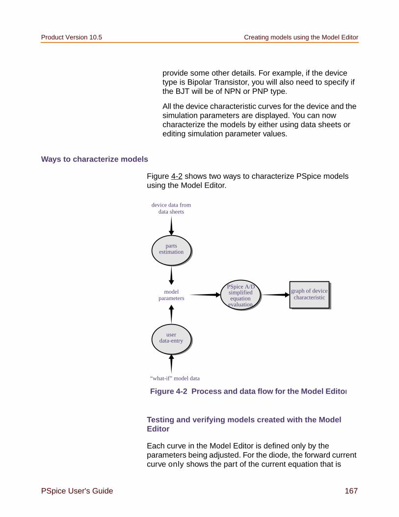
Product Version 10.5 Creating models using the Model Editor
PSpice User's Guide 167
provide some other details. For example, if the devicetype is Bipolar Transistor, you will also need to specify ifthe BJT will be of NPN or PNP type.
All the device characteristic curves for the device and thesimulation parameters are displayed. You can nowcharacterize the models by either using data sheets orediting simulation parameter values.
Ways to characterize models
Figure 4-2 shows two ways to characterize PSpice modelsusing the Model Editor.
Testing and verifying models created with the ModelEditor
Each curve in the Model Editor is defined only by theparameters being adjusted. For the diode, the forward currentcurve only shows the part of the current equation that is
graph of devicecharacteristic
PSpice A/D
equationevaluation
partsestimation
userdata-entry
model
device data fromdata sheets
“what-if” model data
parameters
Figure 4-2 Process and data flow for the Model Editor
simplified

Chapter 4 Creating and editing models Product Version 10.5
168 PSpice User's Guide
associated with the forward characteristic parameters (suchas IS, N, Rs).
However, PSpice uses the full equation for the diode model,which includes a term involving the reverse characteristicparameters (such as ISR, NR). These parameters could havea significant effect at low current.
This means that the curve displayed in the Model Editor doesnot exactly match what is displayed in PSpice after asimulation. Be sure to test and verify models using PSpice. Ifneeded, fine-tune the models.
Creating models from data sheet information
The most common way to characterize models is to enter datasheet information for each device characteristic. After you aresatisfied with the behavior of each characteristic, you canhave the Model Editor estimate (or extract) the correspondingmodel parameters and generate a graph showing the behaviorof the characteristic. This is called the fitting process.
You can repeat this process, and when you are satisfied withthe results, save them; the Model Editor creates modellibraries containing appropriate model and subcircuitdefinitions.
Note: When specifying operating characteristics for a model,you can use typical values found on data sheetseffectively for most simulations. To verify your design,you may also want to use best- and worst-case valuesto create separate models, and then swap them into thecircuit design.
Analyzing the effect of model parameters on devicecharacteristics
You can also edit model parameters directly and see howchanging their values affects a device characteristic. As youchange model parameters, the Model Editor recalculates thebehavior of the device characteristics and displays a newcurve for each of the affected ones.

Product Version 10.5 Creating models using the Model Editor
PSpice User's Guide 169
How to fit models
For a given model, the Model Editor displays a list of thedevice characteristics and a list of all model parameters andperformance curves (see Figure 4-3).
For more information about the characteristics of devicessupported by the Model Editor, refer to the online PSpiceReference Guide.
Figure 4-3 Model Editor workspace with data for a bipolartransistor.
To fit the model
1 For each device characteristic that you want to set up:
a. In the Spec Entry frame, click the tab of the devicecharacteristic.
b. Enter the device information from the data sheet.
2 From the Tools menu, choose Extract Parameters toextract all relevant model parameters for the currentspecification.
A check mark appears in the Active column of theParameters frame for each extracted model parameter.

Chapter 4 Creating and editing models Product Version 10.5
170 PSpice User's Guide
To keep a parameter value fixed, check the Fixed fieldcorresponding to the parameter.
3 Repeat steps 1-2 until the model meets target behaviors.
To view updated performance curves
1 On the toolbar, click the Update Graph button .
Note: If you view performance curves before fitting, then yourdata points and the curve for the current modelspecification may not match.
Model Editor-supported device types based on device characteristic curves
Device types that the Model Editor models using the .MODELstatement are based on the models built into PSpice.
Table 4-2 summarizes the device types for which you cancreate PSpice models based on characteristic curves.
Table 4-2 Device characteristic curves-based devicetypes supported in Model Editor
This part type...Uses thisdefinitionform...
And thisnameprefix1...
diode2 .MODEL D
bipolar transistor .MODEL Q
bipolar transistor, Darlingtonmodel
.SUBCKT X
IGBT .MODEL Z
JFET .MODEL J
MOSFET .MODEL M
operational amplifier3 .SUBCKT X
voltage comparator .SUBCKT X
voltage regulator .SUBCKT X
voltage reference .SUBCKT X
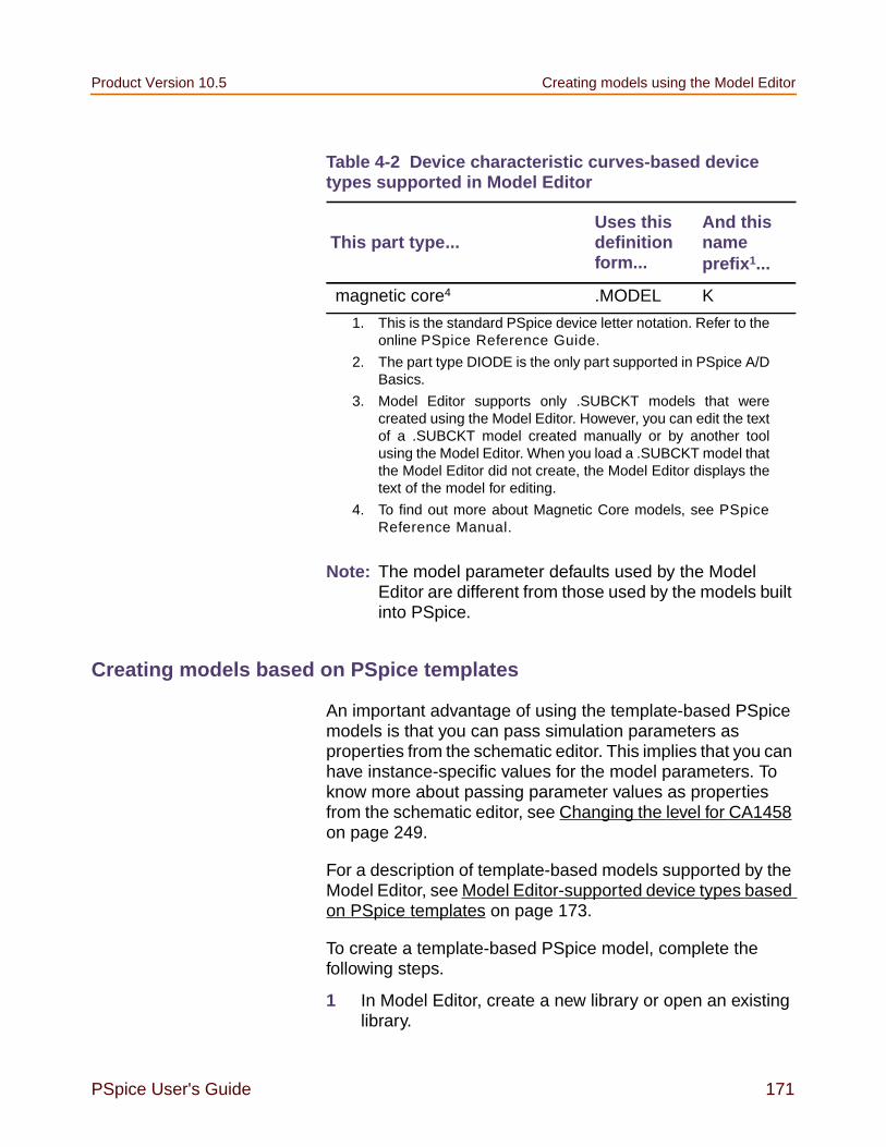
Product Version 10.5 Creating models using the Model Editor
PSpice User's Guide 171
Note: The model parameter defaults used by the ModelEditor are different from those used by the models builtinto PSpice.
Creating models based on PSpice templates
An important advantage of using the template-based PSpicemodels is that you can pass simulation parameters asproperties from the schematic editor. This implies that you canhave instance-specific values for the model parameters. Toknow more about passing parameter values as propertiesfrom the schematic editor, see Changing the level for CA1458on page 249.
For a description of template-based models supported by theModel Editor, see Model Editor-supported device types basedon PSpice templates on page 173.
To create a template-based PSpice model, complete thefollowing steps.
1 In Model Editor, create a new library or open an existinglibrary.
magnetic core4 .MODEL K
1. This is the standard PSpice device letter notation. Refer to theonline PSpice Reference Guide.
2. The part type DIODE is the only part supported in PSpice A/DBasics.
3. Model Editor supports only .SUBCKT models that werecreated using the Model Editor. However, you can edit the textof a .SUBCKT model created manually or by another toolusing the Model Editor. When you load a .SUBCKT model thatthe Model Editor did not create, the Model Editor displays thetext of the model for editing.
4. To find out more about Magnetic Core models, see PSpiceReference Manual.
Table 4-2 Device characteristic curves-based devicetypes supported in Model Editor
This part type...Uses thisdefinitionform...
And thisnameprefix1...
Chapter 4 Creating and editing models Product Version 10.5
172 PSpice User's Guide
2 From the Model menu, choose New.
3 Specify the name of the new model in the Model Nametext box.
4 Select the Use Templates option.
5 From the From Model drop-down list, select the devicetype.
Depending of the device type, you may have to providesome other details. For example, if the device type isBipolar Transistor, you will also need to specify if the BJTwill be of NPN or PNP type.
6 Click OK.
The Simulation parameters window appears with thedefault values of all simulation parameters. These valuesare editable and can be modified as required.
Notice that the Model Text window of a template-basedPSpice model is not editable, it is read-only. Also, themodel text does not display the port information under the.SUBCKT statement.
Adding tolerance information
While creating template-based simulation models, you canadd tolerance information using the Model Editor userinterface. Tolerance information is required only for AdvancedAnalysis Monte Carlo and Sensitivity runs and not forsimulating the models.
The Postol, Negtol, and the Distribution columns are used tospecify the tolerance information. In the Postol and Negtolcolumns, specify the positive and negative tolerances,respectively, for each of the simulation parameters. Adding atolerance value enables the Distribution field for theparameter. The possible distribution types are:
FLAT - Use the flat distribution function if you want anequal probability of one parameter value being chosenover another.

Product Version 10.5 Creating models using the Model Editor
PSpice User's Guide 173
BSIMD.4.2 - Use the bimodal distribution function if youwant to represent the probability of a manufacturedcomponent falling in the outer range of tolerance values.
GAUSS0.4 - Use the Gaussian distribution function if youwant a bell curve probability that one parameter value willbe chosen versus another.
SKEW.4.8 - Use the skewed distribution function if youwant to weigh the probability of one parameter valuebeing chosen versus another.
By default, the distribution type is FLAT. The distribution typeinfluences the Sensitivity and Monte Carlo analysis. To knowmore about Sensitivity and Monte Carlo analysis, see PSpiceAdvanced Analysis User’s Guide.
To find out more about the distribution functions, see thetechnical note, Specifying Advanced Analysis MonteCarlo Distribution Functions at www.orcadpcb.com.
Model Editor-supported device types based on PSpice templates
Table 4-3 lists the device types for which template-basedmodels can be created using the Model Editor.
Table 4-3 Template-based device types supported inModel Editor
This part type1...And this nameprefix2...
diode3 X
bipolar transistor X
IGBT X
JFET X
Power MOSFET X
operational amplifier X
voltage regulator X
magnetic core4 K

Chapter 4 Creating and editing models Product Version 10.5
174 PSpice User's Guide
Importing an existing model
You can import third-party or vendor-provided Spice modelsinto a format understood by the Model Editor. Importing amodel enables editing the model using the Model Editor userinterface.
1 Open the Model Editor.
From the Start menu, point to Release OrCAD 10.0 in thePrograms folder, choose PSpice Accessories and thenchoose Model Editor.
2 Open a model library.
From the File menu, choose New or Open.
3 From the Model menu, choose Import.
4 Select the file containing the model definition and selectOpen.
The imported model appears in the model library.Although, only the first model of the selected library file isimported to the Model Editor, it is recommended that thefile selected in step 4 should contain only one modeldefinition.
Caution
The device property file associated with themodel is not imported.
1. For template-based PSpice models the model text isread-only and cannot be edited using the Model Editor.
2. This is the standard PSpice device letter notation. Refer to theonline PSpice Reference Guide.
3. The part type DIODE is the only part supported in PSpice A/DBasics.
4. A template-based magnetic core model is a SpicePlus model.To find out more about Magnetic Core models, see PSpiceReference Manual.

Product Version 10.5 Creating models using the Model Editor
PSpice User's Guide 175
Enabling and disabling automatic part creation
Part creation in the Model Editor is optional. By default,automatic part creation is enabled. However, if you previouslydisabled part creation, you will need to enable it beforecreating a new model and part.
Instead of using the PSpice default part set for new models,you can have the Model Editor use your own set of standardparts. To find out more, see Basing new parts on a custom setof parts on page 254.
To automatically create parts for new models
1 From the Tools menu, choose Options.
2 Select the Always Create Part when Saving Model optionif it is not already checked.
3 Under Schematic Editor, select Capture.
4 Under Save Part To, enter the name of the part library forthe new part. Choose either:
Part Library Path Same As Model Library to create oropen the *.OLB file that has the same name prefixas the currently open model library (*.LIB).
Example: If the model library is MYPARTS.LIB, thenthe Model Editor creates the part libraryMYPARTS.OLB.
User-Defined Part Library, and then enter a file namein the Part Library Name text box.
Note: If you select a user-defined Part library, the ModelEditor saves all new parts to the specified file until youchange it.
Saving global models (and parts)
When you save your changes, the Model Editor does thefollowing for you:
Chapter 4 Creating and editing models Product Version 10.5
176 PSpice User's Guide
Saves the model definition to the model library that youoriginally opened.
If you had the automatic part creation option enabled,saves the part definition toMODEL_LIBRARY_NAME.OLB.
If you want to save the open model library to a new library,then:
1 From the File menu, choose Save As.
2 Enter the name of the new model library.
If you want to save only the model definition that you arecurrently editing to a different library, then
1 From the Model menu, select Export.
2 Enter the name of the new file.
Note: When you use the Export command, the modeldefinition is saved with a .MOD extension.
3 If you want PSpice to search this file automatically,configure it in Capture (using the Library files list in theConfiguration Files tab on the Simulation Settings dialogbox).
You cannot export multiple models to a single MOD file.Exporting a model to the same file overwrites the originalcontents of the MOD file.
To save the new model (and part)
1 From the File menu, choose Save to updateMODEL_LIBRARY_NAME.LIB,MODEL_LIBRARY_NAME.PRP (and, if you enabled partcreation, MODEL_LIBRARY_NAME directory), and savethem to disk.
Note: To simulate the model, add the Model Library (.LIB) tothe project using the PSpice menu, Edit Profile,Simulation Settings dialog box. Click the ConfigurationFiles tab, click Library in the Category field, browse tothe Model Library, and click the Add to Design button.
Product Version 10.5 Creating models using the Model Editor
PSpice User's Guide 177
Running the Model Editor from the schematic editor
Start the Model Editor from the schematic editor when youwant to:
define tolerances on model parameters for statisticalanalysis (see Example: editing a Q2N2222 instancemodel on page 195)
test behavior variations on a part, or
refine a model before making it available to all designs.
This means editing models for part instances on yourschematic page. When you select a part instance and edit itsmodel, the Model Editor automatically creates an instancemodel that you can then change.
Once you have started the Model Editor, you can proceed withentering data sheet information and model fitting as describedin How to fit models on page 169.
You can also use the Model Editor to view the syntax for amodel definition. When you have finished viewing, be sure toquit the Model Editor without saving the library, so that theschematic page editor does not create an instance model.
Note: When the Model Editor is invoked from a schematiceditor, the part creation feature is disabled.
What is an instance model?
An instance model is a copy of the part’s original model. Thecopied model is local to the design. You can customize theinstance model without impacting any other design that usesthe original part from the library.
Instance models are created only when you want to editmodels from global libraries. If you open a model for editingfrom a local library, after editing, the model will be saved in thesame local library. For more information on global and locallibraries see Global vs. design vs. profile models and libraries onpage 153.
Chapter 4 Creating and editing models Product Version 10.5
178 PSpice User's Guide
When the schematic editor creates the copy, it saves a copy ofthe model in DESIGN_NAME.LIB.
For more information on instance models, see Reusinginstance models on page 200.
Starting the Model Editor
To start editing an instance model
1 In Capture, select one part on your schematic page.
2 From the Edit menu, choose PSpice Model.
The schematic page editor searches the model librariesfor the instance model. To find out how Capture searchesthe library, see Changing model library search order onpage 208.
If found, the schematic page editor starts the ModelEditor, which opens the design library and loads theinstance model.
If not found, the schematic page editor assumes thatthis is a new instance model and does the following:makes a copy of the original model definition in theDESIGN_NAME.LIB and starts the Model Editorwith the new model loaded.
After you start the Model Editor, you can proceed tochange the text as described in To display the model texton page 193.
Saving design models
When you save your edits, the following is done for you tomake sure the instance model is linked to the selected partinstances in your design:
The Model Editor saves the model definition toDESIGN_NAME.LIB.
If the library is new, the Model Editor configuresDESIGN_NAME.LIB for local use.

Product Version 10.5 Creating models using the Model Editor
PSpice User's Guide 179
The schematic page editor assigns the new model name tothe Implementation property for each of the selected partinstances (see What happens if you don’t save the instancemodel on page 179).
Actions that automatically configure the instance modellibrary for global use
Instance model libraries are normally configured for designuse. However, if you perform the following action, the ModelEditor configures the library for global use instead:
Save the model to a different library by typing a new filename in the Library text box in the Save To frame.
To save instance models
1 From the File menu, choose Save to updateDESIGN_NAME.LIB and save it to disk.
What happens if you don’t save the instance model
Before the schematic page editor starts the Model Editor, itdoes the following:
Makes a copy of the original model and saves it as aninstance model in SCHEMATIC_NAME.LIB.
Configures SCHEMATIC_NAME.LIB for design use, ifnot already done.
Attaches the new instance model name to theImplementation property for the selected part instance.
This means that if you:
quit the Model Editor, or
return to Capture to simulate the design
without first saving the model you are editing, the partinstance on your schematic page is still attached to theinstance model implementation.

Chapter 4 Creating and editing models Product Version 10.5
180 PSpice User's Guide
In this case, the instance model is identical to the originalmodel. If you decide to edit this model later, be sure to do oneof the following:
If you want the changes to remain specific to the currentdesign, edit the instance model in the design library usingthe Model Editor.
If you want the change to be global, change the modelimplementation for the part instance in your design backto the original model name in the global library, and thenedit the original model from within the part editor.
To find out how to change model references, see Changingthe model reference to an existing model definition onpage 199.
Model creation examples
Examples covered in this section cover how to use the ModelEditor to create simulation models based on:
Device characteristic curves. See Example: Creating aPSpice model based on device characteristic curves.
PSpice-provided templates. See Example: Creatingtemplate-based PSpice model on page 187.
Example: Creating a PSpice model based on device characteristic curves
In this example, you will model a simple diode device asfollows:
Create the schematic for a simple half-wave rectifier.
Create a new model for a diode.
Attach new model to the D1 diode.

Product Version 10.5 Model creation examples
PSpice User's Guide 181
Creating the half-wave rectifier design
To draw the design
1 From the Project Manager, from the File menu point toNew, then choose Project.
2 In the New Project dialog box, ensure that the Analog orMixed A/D option is selected.
3 Enter the name of the new project (RECTFR) and clickCreate.
4 From the Capture Place menu, choose Part.
5 Place one each of the following parts (referencedesignator shown in parentheses) as shown inFigure 4-4:
Dbreak (D1 diode)
C (C1 capacitor)
R (R1 resistor)
VSIN (V1 sine wave source)
6 Click the Ground button on the tool palette and placethe ‘0’ analog ground from the SOURCE.OLB part library.
7 From the Place menu, choose Wire, and draw theconnections between parts as shown in Figure 4-4.
8 From the File menu, choose Save.
Note: If you were to simulate this design using a transientanalysis, you would also need to set up a transient
Figure 4-4 Design for ahalf-wave rectifier.

Chapter 4 Creating and editing models Product Version 10.5
182 PSpice User's Guide
specification for V1; most likely, this would meandefining the VOFF (offset voltage), VAMPL (amplitude),and FREQ (frequency) properties for V1. For thistutorial, however, you will not perform a simulation, soyou can skip this step.
Using the Model Editor to edit the D1 diode model
To create a new model and model library
1 Open the Model Editor.
2 From the File menu in the Model Editor, choose New.
3 From the Model menu, choose New.
4 In the New dialog box, do the following:
a. In the Model Name text box, type DbreakX.
b. Select Use Device Characteristic Curves.
c. From the From Model list, select Diode.
d. Click OK.
5 From the File menu, choose Save.
By default, the updated model is saved in theRECTFR.LIB library.
Entering data sheet information
As shown in Figure 4-5, the Model Editor initially displays:
diode model characteristics listed in the Models Listwindow, and

Product Version 10.5 Model creation examples
PSpice User's Guide 183
DbreakX model parameter values listed in theParameters window.
Figure 4-5 Model characteristics and parameter valuesfor DbreakX.
You can modify each model characteristic shown in the ModelSpec frame with new values from data sheets. The ModelEditor takes the new information and fits new modelparameter values.
When updating the entered data, the Model Editor expectseither:
device curve data (point pairs) or
single-valued data
depending on the device characteristic.
For the diode, Forward Current, Junction Capacitance, andReverse Leakage require device curve data. ReverseBreakdown and Reverse Recovery require single-valued data.

Chapter 4 Creating and editing models Product Version 10.5
184 PSpice User's Guide
Table 4-4 lists the data sheet information for the DbreakXmodel.
To change the Forward Current characteristic
1 In the Spec Entry frame, click the Forward Current tab.
This tab requires curve data.
2 In the Vfwd text box, type 1.3.
3 Press Tab to move to the Ifwd text box, and then type0.2.
To change the values for Junction Capacitance andReverse Leakage
Follow the same steps as for Forward Current, entering thedata sheet information listed in Table 4-4 that corresponds tothe current model characteristic.
To change the Reverse Breakdown characteristic
1 In the Spec Editing frame, click the Reverse Breakdowntab.
This tab requires single-valued data.
2 In the Vz text box, type 7.5.
Note: The Model Editor accepts the same scale factors
Table 4-4 Sample diode data sheet values
For this modelcharacteristic...
Enter this...
forward current (1.3, 0.2)
junction capacitance (1m, 120p) (1, 73p) (3.75, 45p)
reverse leakage (6, 20n)
reverse breakdown (Vz=7.5, Iz=20m, Zz=5)
reverse recovery no changes

Product Version 10.5 Model creation examples
PSpice User's Guide 185
normally accepted by PSpice.
3 Press Tab to move to the Iz text box, and then type 20m.
4 Press Tab to move to the Zz text box, and then type 5.
Extracting model parameters
To generate new model parameter values
1 From the Tools menu, choose Extract Parameters.
A check mark appears in the Active column of theParameters frame for each extracted model parameter.
To display the curves for the five diode characteristics
1 From the Window menu, choose Tile.
Some of the plots are shown in Figure 4-6 below.
Figure 4-6 Assorted device characteristic curves for adiode.
You can also do the following with an active plot window:
Pan and zoom within the plot using commands on theView menu.

Chapter 4 Creating and editing models Product Version 10.5
186 PSpice User's Guide
Rescale axes using the Axis Settings command on thePlot menu.
Adding curves for more than one temperature
By default, the Model Editor computes device curves at 27°C.For any characteristic, you can add curves to the plot at othertemperatures.
To add curves for Forward Current at a differenttemperature
1 In the Spec Entry frame, click the Forward Current tab.
2 From the Plot menu, choose Add Trace.
3 Type 100 (in °C).
4 Click OK.
The Forward Current plot should appear as shown inFigure 4-7.
Completing the model definition
You can refine the model definition by:
modifying the entered data as described before, or
Figure 4-7 Forward Current device curve at twotemperatures.
Product Version 10.5 Model creation examples
PSpice User's Guide 187
editing model parameters directly.
You can update individual model parameters by editing themin the Parameters frame of the Model Editor workspace. Whenyou save the model library, the Model Editor automaticallyupdates the device curves.
For this tutorial, leave the model parameters at their currentsettings.
To save the model definition with the current parametervalues and to make the model available to your design
1 From the File menu, select Save to update RECTFR.LIBand save the library to disk.
The model definition is now complete. You can use thismodel definition in your design.
Attaching the DbreakX model to the D1 diode
1 In Capture, open the RECTFR project.
2 Select the D1 diode.
3 From the Edit menu, choose Properties.
4 In the Property Editor dialog box, change the value ofImplementation property from Dbreak to DbreakX.
To know more about the Implementation property, seeMODEL on page 260.
5 Close the dialog box, and save the design.
Your design is ready to simulate with the model definitionyou just created.
Example: Creating template-based PSpice model
In this example, you will create a template-based PSpicemodel for an operational amplifier, using the Model Editor.
The template-based OPAMP model is the only model createdusing the Model Editor that has multiple level support for

Chapter 4 Creating and editing models Product Version 10.5
188 PSpice User's Guide
simulation parameters. Tasks that will be covered in thisexample are:
Creating a new template-based PSpice model forOperational Amplifier
Multiple level support for template-based OPAMP modelsin the Model Editor
Multiple level support implies that the number ofsimulation parameters used in the model varies with themodel level. The higher the level, the more are thenumber of simulation parameters.
The models with a higher number of simulationparameters are closer to the real life devices. Therefore,the simulation results are more accurate when high levelmodels are used. Use lower level simulation models tominimize the simulation time.
Creating a new model
1 Start the Model Editor alone.
2 From the File menu, choose New to create a new library.
3 From the Model menu, choose New.
4 In the New dialog box, specify the name of the new modelas OPA_LOCAL.
5 Select the Use Templates option.
6 To specify the device type, select Operational Amplifierfrom the From Model drop-down list.

Product Version 10.5 Model creation examples
PSpice User's Guide 189
7 Specify the type of OPAMP to be created. In this example,select options to create an internally compensatedbipolar operational amplifier with PNP input.
Figure 4-8 The New dialog box
8 Click OK.
The Simulation Parameters and the Model Text windowsappear. In the Models List, three models, OPA_LOCAL_1,OPA_LOCAL_2, and OPA_LOCAL_3 appear.
Caution
The Model Editor creates multiple models only forAdvanced Analysis OPAMP models. This isbecause, template-based OPAMP modelssupport multiple levels of simulation parameters,and the Model Editor creates one model for eachlevel.
The OPA_LOCAL_3 model contains all the simulationparameters available in the OPA_LOCAL_2 model plussome extra simulation parameters. The OPA_LOCAL_2

Chapter 4 Creating and editing models Product Version 10.5
190 PSpice User's Guide
model contains some additional simulation parametersbesides the ones listed in the OPA_LOCAL_1 model.
9 Select the OPA_LOCAL_3 model, and edit the values ofthe simulation parameters listed in Table 4-5. Table 4-5lists the simulation parameters along with the new values.For other simulation parameters not listed in the table,accept the default values.
10 To ensure that the values entered by you in the SimulationParameters frame overwrite the default value of thesimulation parameters, check the Editable check box forall the simulation properties.
Selecting the Editable check box ensures that thesimulation parameter value:
entered by users will overwrite the values in thetemplate property file.
appears in the device property file.
can be directly passed from the schematic editor asproperties attached to the symbol.
Table 4-5 List of Simulation Parameters to be modified
SimulationPropertyName
Value Distribution
PostiveTolerance(Postol)
NegativeTolerance(Negtol)
VOS 1e-7 FLAT 10% 10%
IB default FLAT 10% 10%
IBOS default FLAT 10% 10%
A0 1000000 FLAT 10% 10%
GBW default FLAT 10% 10%
SRP 1.0e+6 FLAT 10% 10%
SRM 1.0e+6 FLAT 10% 10%
CMRR default FLAT 10% 10%

Product Version 10.5 Model creation examples
PSpice User's Guide 191
In such cases, the values of the simulation parameterscan be picked up from following three locations in thedecreasing order of priority:
schematic editor
device property file
template property file
11 After making the simulation parameters editable, save themodel. Specify the library name as LOCAL_LIB.
All the changes in the OPA_LOCAL_3model are reflectedin the OPA_LOCAL_2 and OPA_LOCAL_1 models also.This is because all three models have a common sectionfor the simulation and smoke parameters in the deviceproperty file, LOCAL_LIB.PRP.
Caution
It is recommended that multiple level modelscreated using the Model Editor should be usedcautiously especially when used in differentdesigns.
Consider a situation where you use OPA_LOCAL_1 fromthe LOCAL_LIB library in design A and OPA_LOCAL_3from the LOCAL_LIB library in design B. Any changesthat you make to the simulation or smoke parametervalues of the OPA_LOCAL_1 model for design A will alsobe reflected in the OPA_LOCAL_3 model used in designB.
After you have saved your changes in the Model Editor, thefollowing files are generated:
LOCAL_LIB.LIB - The library file containing modelinformation.
LOCAL_LIB.PRP - The device property file containingdevice specific information for all the models in theLOCAL_LIB.LIB.
Saving the LOCAL_LIB library completes the tasks of creatinga template-based PSpice model for Operational Amplifier.

Chapter 4 Creating and editing models Product Version 10.5
192 PSpice User's Guide
Because of the multiple-level support for Advanced AnalysisOPAMP models in the Model Editor, instead of one, threemodels are created.
Note: Deleting a Model Editor-created multiple-level modeldeletes the model only from the library. The modelinformation is not deleted from the device property file.This is because, all three OPAMP models are linked tothe same section in the device property file. The deviceproperty section for the model will be deleted only afterall the linked models are deleted.
Note: If you have Advanced Analysis installed, the Smoke tabalso appears besides the Simulation tab, and you canalso add smoke information to the model. See Addingsmoke information to the OPA_LOCAL operationalamplifier model on page 216.
Note: Example covered in the section, Creating parts in thebatch mode on page 246 in Chapter 5, “Creating partsfor models” is an extension of this example. It coverspart creation using Model Editor and using ModelEditor-created parts in a schematic.
Product Version 10.5 Model creation examples
PSpice User's Guide 193
Editing model text
Note: This section is valid only for PSpice models that arebased on device characteristic curves.
The Model Text is editable only for PSpice models. Fortemplate-based PSpice models, the Model Text window isread-only.
Caution
If you edit the text of a model that was created byentering data sheet values, you may not be ableto edit the model in the Extract Model view again.
For any model, you can edit model text in the Model Editorinstead of using the Spec Entry and Parameter frames.However, there are two cases where you must edit the modeltext:
When you want to edit models of device types notsupported by the Model Editor. The model text isdisplayed automatically when you load one of thesemodels.
When you want to add DEV and LOT tolerances forMonte Carlo or sensitivity/worst-case analysis.
By typing PSpice commands and netlist entries, you can dothe following:
change definitions, and
create new definitions
When you have finished, the Model Editor automaticallyconfigures the model definitions into the model libraries.
To display the model text
1 From the View menu, choose Edit Model.
The Model Editor displays the PSpice syntax for modeldefinitions:

Chapter 4 Creating and editing models Product Version 10.5
194 PSpice User's Guide
.MODEL syntax for models defined as parametersets
.SUBCKT syntax for models defined as netlistsubcircuits
You can edit the definition just as you would in anystandard text editor.
To find out more about PSpice command and netlist syntax,refer to the online PSpice Reference Guide.
Editing .MODEL definitions
For definitions implemented as model parameter sets usingthe PSpice .MODEL syntax, the Model Editor lists oneparameter per line. This makes it easier to add DEV/LOTtolerances to model parameters for Monte Carlo orsensitivity/worst-case analysis.
Editing .SUBCKT definitions
For definitions implemented as subcircuit netlists using thePSpice .SUBCKT syntax, the Model Editor displays thesubcircuit syntax exactly as it appears in the model library. TheModel Editor also includes all of the comments immediatelybefore or after the subcircuit definition.
Changing the model name
You can change the model name directly in the PSpice.MODEL or .SUBCKT syntax, but double-check that the newname does not conflict with models already contained in thelibraries. To find out more about instance model namingconventions, see What is an instance model? on page 177.
Note: If you do create a model with the same name asanother model and want PSpice to always use yourmodel, make sure the configured model libraries areordered such that your definition precedes any otherdefinitions. To find out more about search order in themodel library, see Changing model library search orderon page 208.

Product Version 10.5 Model creation examples
PSpice User's Guide 195
Example: editing a Q2N2222 instance model
Suppose you have a design named MY.OPJ that containsseveral instances of a Q2N2222 bipolar transistor. If you wantto see the effect of base resistance variation on one specificdevice, Q6, you need to do the following:
Define a tolerance (in this example, 5%) on the Rb modelparameter.
Important
Adding tolerance to a device characteristiccurve-based model does not make it compatible foruse with Advanced Analysis Monte Carlo.
Set up and run PSpice Monte Carlo analysis.
The following example demonstrates how to set up theinstance model for Q6.
Starting the Model Editor
To start the Model Editor,
1 In the schematic page editor, select Q6 on the schematicpage.
2 From the Edit menu, choose PSpice Model.
The Model Editor automatically creates a copy of theQ2N2222 base model definition.
3 In the Model Editor, from the View menu, choose ModelText.
The Model Editor displays the PSpice syntax for thecopied model in the text editing area.
Editing the Q2N2222 model instance
Text edits appropriate to this example are as follows:
Add the DEV 5% clause to the Rb statement (required).

Chapter 4 Creating and editing models Product Version 10.5
196 PSpice User's Guide
Change the model name to Q2N2222-MC (optional, fordescriptive purposes only).
To find out more about PSpice command and netlist syntax,refer to the online PSpice Reference Guide.
Saving the edits and updating the schematic
When you choose Save from the File menu, two thingshappen:
The Model Editor saves the model definition to the modellibrary.
The schematic page editor updates the Implementationproperty value to Q2N2222-MC for the Q6 part instance.
In this example, the default model library is MY.LIB. IfMY.LIB does not already exist, the Model Editor creates andsaves it in the current working directory. The schematic pageeditor then automatically configures it as a design modellibrary for use with the current design only.
Now you are ready to set up and run the Monte Carlo analysis.
Note: If you verify the model library configuration (in theSimulation Settings dialog box, click the ConfigurationFiles tab and view the Library files list), you see entriesfor NOM.LIB (for global use, as denoted by theicon) and MY.LIB (for design use, as denoted by the
icon) in the Library files list.You can change the model reference for this part backto the original Q2N2222 by following the procedure Tochange model references for part instances on yourdesign on page 199.
Using the Create Subcircuit Format Netlist command
The Create Subcircuit Format Netlist command is used fromCapture. This command creates a subcircuit netlist definitionfor the displayed level of hierarchy and all lower levels in yourdesign.

Product Version 10.5 Using the Create Subcircuit Format Netlist command
PSpice User's Guide 197
Note: The Create Subcircuit Format Netlist command doesnot help you create a hierarchical design. You need todo this yourself before using the Create SubcircuitFormat Netlist command. For information onhierarchical designs and how to create them, refer tothe OrCAD Capture User’s Guide.
The schematic page editor does the following things for you:
Maps any named interface ports at the active level ofhierarchy to terminal nodes in the PSpice .SUBCKTstatement.
Saves the subcircuit definition to a file namedDESIGN_NAME-SCHEMATIC_NAME.LIB.
Before you can use the subcircuit definition in your design, youneed to:
Create a part for the subcircuit.
Configure theDESIGN_NAME-SCHEMATIC_NAME.LIB file soPSpice knows where to find it.
To create a subcircuit definition for a portion of yourdesign
To create a subcircuit netlist definition
1 In the Project Manager, select the schematic folder thatcontains the circuitry for which a subcircuit netlistdefinition is to be created.
2 If the schematic folder is not the root folder, choose MakeRoot from the Design menu. You may be prompted tosave the design first.
3 In the Project Manager, from the Tools menu, chooseCreate Netlist.
4 Select the PSpice tab.
5 In the Options frame, select Create SubCircuit FormatNetlist.

Chapter 4 Creating and editing models Product Version 10.5
198 PSpice User's Guide
6 Click OK to generate the subcircuit definition and save itto DESIGN_NAME-SCHEMATIC_NAME.LIB.
To create a part for the subcircuit netlist definition
1 Open the Model Editor alone.
2 From the File menu, select the Open command and openthe DESIGN_NAME-SCHEMATIC_NAME.LIB file.
3 Select the model from the Models List and, if necessary,refine the subcircuit definition.
Refinements can include extending the subcircuitdefinition using the optional nodes construct,OPTIONAL:, the variable parameters construct,PARAMS:, and the .FUNC and local .PARAM commands.
4 From the File menu, select Create Capture Parts.
5 In the Enter Input Model Library text box, browse andopen the DESIGN_NAME-SCHEMATIC_NAME.LIB file.
Note: The Enter Output Part Library is automaticallyfilled in with theDESIGN_NAME-SCHEMATIC_NAME.OLB file.
6 Click OK and OK again to clear the .ERR log window.
The subcircuit part is now ready for use in a design.
To configure the subcircuit file
1 In the schematic page editor, from the PSpice menu,choose Edit Profile to display the Simulation Settingsdialog box.
2 Click the Configuration Files tab.
3 Click either Library or Include in the Category field of theConfiguration Files tab, and then configureDESIGN_NAME-SCHEMATIC_NAME.LIB as either amodel library or an include file (see Configuring modellibraries on page 202).

Product Version 10.5 Changing the model reference to an existing model definition
PSpice User's Guide 199
Changing the model reference to an existing modeldefinition
Parts are linked to models by the model name assigned to theparts’ Implementation property. You can change thisassignment by replacing the Implementation property valuewith the name of a different model that already exists in thelibrary.
You can do this for:
A part instance in your design.
A part in the part library.
To change model references for part instances on yourdesign
1 Find the name of the model that you want to use.
2 In the schematic page editor, select one or more parts onyour schematic page.
3 From the Edit menu, choose Properties.
The Parts spreadsheet appears.
4 Click the cell under the column Implementation Type.
5 From the Implementation list, select PSpice Model.
6 In the Implementation column, type the name of theexisting model that you want to use if it is not alreadylisted.
7 Click Apply to update the changes, then close thespreadsheet.
To change the model reference for a part in the partlibrary
1 Find the name of the model that you want to use.
2 In the schematic page editor, select the part you want tochange.

Chapter 4 Creating and editing models Product Version 10.5
200 PSpice User's Guide
3 From the Edit menu, choose Part to load the part in thepart editor for editing.
4 From the Options menu, choose Part Properties todisplay the User Properties dialog box.
5 Select Implementation Type.
6 From the Implementation list, select PSpice Model.
7 In the Implementation text box, type the name of theexisting model that you want to use if it is not alreadylisted.
8 Click OK to close the Edit Part dialog box.
Reusing instance models
If you created instance models in your design and want toreuse them, there are two things you can do:
Attach the instance model implementation to other partinstances in the same design.
Change the instance model to a global model and createa part that corresponds to it.
For information on how to create instance models, see:
Running the Model Editor from the schematic editor onpage 177.
Starting the Model Editor on page 178.
Reusing instance models in the same schematic
There are two ways to use the instance model elsewhere inthe same design.
To use the instance model elsewhere in your design
Do one of the following:
Change the model reference for other part instances tothe name of the new model instance.

Product Version 10.5 Reusing instance models
PSpice User's Guide 201
See Changing the model reference to an existing modeldefinition on page 199.
From the Edit menu, use the Copy and Paste commandsto place more part instances.
Making instance models available to all designs
If you are refining model behavior specific to your design, andare ready to make it available to any design, then you need tolink the model definition to a part and configure it for globaluse.
To make your instance model available to any design
1 Create a part and assign the instance model name to theImplementation property. See Chapter 5, “Creating parts formodels” for more information.
2 If needed, move the instance model definition to anappropriate model library, and make sure the library isconfigured for global use. See Configuring model librarieson page 202 for more information.
Note: If you use the part wizard to create the partautomatically from the model definition, then this stepis completed for you.

Chapter 4 Creating and editing models Product Version 10.5
202 PSpice User's Guide
Configuring model libraries
Although model libraries are usually configured for you, thereare things that you sometimes must do yourself. These are:
adding new model libraries that were created outside ofCapture or the Model Editor
changing the global, design or profile scope of a modellibrary
changing the library search order
changing or adding directory search paths
The Configuration Files tab
The Configuration Files tab of the Simulation Settings dialogbox lets you add, change, and remove model libraries andinclude files from the configuration or modify the search order.
Note: Removing a library in this dialog box means that youare removing the model library from the configured list.The library still exists on your computer and you canadd it back to the configuration later.
To display the Library files list
1 In PSpice, open or create a PSpice project.
2 From the PSpice menu, choose either New SimulationProfile or Edit Profile if a profile already exists.
3 Click the Configuration Files tab in the SimulationSettings dialog box.

Product Version 10.5 Reusing instance models
PSpice User's Guide 203
4 Click Library in the Category field to display the Libraryfiles list.
The Library files list shows the model libraries that PSpicesearches for definitions matching the parts in yourdesign. Files showing an icon after their name haveglobal scope; files having the icon have a designscope and files with the icon have a profile scope.
The buttons for adding model libraries to the configurationfollow the same profile/local/global syntax convention.Click one of the following:
Add to Profile for profile models
Add to Design for design models.
Add as Global for global models.
The Include files list in the Configuration Files tab containsinclude files. You can manually add profile, design and globalinclude files to your configuration using the Add to Profile, Addto Design and Add as Global buttons, respectively.
The Stimulus files list in the Configuration Files tab containsstimulus files. See Configuring stimulus files on page 477 formore information.
How PSpice uses model libraries
PSpice searches libraries for any information it needs tocomplete the definition of a part or to run a simulation. If anup-to-date index does not already exist, PSpice automaticallygenerates an index file and uses the index to access only themodel definitions relevant to the simulation. This means:
Disk space is not used up with definitions that your designdoes not use.
There is no memory penalty for having large modellibraries.
Loading time is kept to a minimum.

Chapter 4 Creating and editing models Product Version 10.5
204 PSpice User's Guide
Caution—When you use include files instead
PSpice treats model library and include files differently asfollows:
For model library files, PSpice reads in only thedefinitions it needs to run the current simulation.
For include files, PSpice reads in the file in its entirety.
This implies that if you configure a model library (*.LIBextension) as an include file using the Add to Design or Addas Global button, PSpice loads every model definitioncontained in that file.
If the model library is large, you might overload the memorycapacity of your system. However, when developing models,you can do the following:
1 Initially configure the model library as an include file; thisavoids rebuilding the index files every time the modellibrary changes.
2 When your models are stable, reconfigure the include filecontaining the model definitions as a library file.
To reconfigure an include file as a model library file:
1 From the Simulation menu, choose Edit Profile, then clickthe Configuration Files tab.
2 Click Include in the Category field to display the Includefiles list.
3 Select the include file that you want to change.
4 Click the Delete button located above the Include files list.
See Adding model libraries to the configuration on page 205.
Search order
When searching for model definitions, PSpice scans themodel libraries using these criteria:
profile model libraries before design model libraries

Product Version 10.5 Reusing instance models
PSpice User's Guide 205
design model libraries before global model libraries
model library sequence as listed in the Library files list inthe Configuration Files tab of the Simulation Settingsdialog box
list of directories (including the design library) specified inthe library search path in the order given (see Changingthe library search path on page 210). From the directorieslisted in the Library Path, only the directories that containa NOM.LIB file are looked up by PSpice during the modelsearch.
Tip
The search order for the device property files is sameas that of the model library files. The .PRP files aresearched along with the .LIB files.
Handling duplicate model names
If two or more model libraries contain models with the samename, PSpice always uses the first model it finds. This meansyou might need to modify the search order to make surePSpice uses the model that you want. See Changing modellibrary search order on page 208.
Note: PSpice searches profile libraries before designlibraries and design libraries before global libraries.Therefore, if the new model you want to use is specificto your profile and the duplicate definition is design orglobal, you do not need to make any changes.Similarly, if the new model you want to use is specific toyour design and the duplicate definition is global, youdo not need to make any changes.
Adding model libraries to the configuration
New libraries are added above the selected library name inthe Library files list box.

Chapter 4 Creating and editing models Product Version 10.5
206 PSpice User's Guide
To add model libraries to the configuration
1 From the Simulation menu, choose Edit Profile, then clickthe Configuration Files tab.
2 Click Library in the Category field to display the Libraryfiles list.
3 Click the library name positioned one entry below whereyou want to add the new library.
4 In the Filename text box, either:
type the name of the model library, or
click Browse to locate and select the library.
5 Do one of the following:
If the model definitions are for use in the currentprofile only, click the Add to Profile button.
If the model definitions are for use in the currentdesign only, click the Add to Design button.
If the model definitions are for global use in anyschematic, click the Add as Global button instead.
6 Click OK.
Note: If the model libraries reside in a directory that is not onthe library search path, and you use the Browse buttonin step 4 to select the libraries you want to add, then theschematic editor automatically updates the librarysearch path to include the selected library in the searchpath. Otherwise, you need to add the directory pathyourself. See Changing the library search path onpage 210.
Changing the model library scope from profile to design, profile to global,design to global and vice versa
There are times when you might need to change the scope ofa model library from profile to design, profile to global, designto global, or vice versa.

Product Version 10.5 Reusing instance models
PSpice User's Guide 207
Example: If you have an instance model that you now want tomake available to any design, then you need to set the scopeof the local model library that contains it to global.
For more information, see Global vs. design vs. profile modelsand libraries on page 153.
To change the scope of a design model to global
1 From the Simulation menu, choose Edit Profile, then clickthe Configuration Files tab.
2 Click Library in the Category field to display the Libraryfiles list.
3 Select the model library that you want to change.
4 Click the Delete toolbar button to remove the local entry.
5 Add the model library as a global entry.
For more information, see Adding model libraries to theconfiguration on page 205.

Chapter 4 Creating and editing models Product Version 10.5
208 PSpice User's Guide
Changing model library search order
Two reasons why you might want to change the search orderare to:
reduce the search time
avoid using the wrong model when there are modelnames duplicated across libraries. PSpice A/D alwaysuses the first instance. See Handling duplicate model nameson page 205 for more information.
To change the order of libraries
1 Click the Configuration Files tab in the SimulationSettings dialog box.
2 Click Library in the Category field to display the Libraryfiles list. On the Library files list of the Configuration Filestab:
a. Select the library name you wish to move.
b. Use either the Up Arrow or Down Arrow toolbarbutton to move the library name to a different placein the list.
Note: You can only change the order of libraries thathave the same scope. This implies that though you canchange the order of profile libraries, local libraries andglobal libraries, you cannot place a global library before alocal library or a local library before a profile library.
3 If you have listed multiple *.LIB commands within asingle library (like NOM.LIB), then edit the library using atext editor to change the order.
Example: The model libraries DIODES.LIB andEDIODES.LIB (European manufactured diodes) shippedwith your PSpice programs have identically named devicedefinitions. If your design uses a device out of one ofthese libraries, you need to position the model librarycontaining the definition of choice earlier in the list. If yoursystem is configured as originally shipped, this meansyou need to add the specific library to the list beforeNOM.LIB.

Product Version 10.5 Reusing instance models
PSpice User's Guide 209
Caution
Do not edit NOM.LIB. If you do, PSpice willrecreate the indexes for every model libraryreferenced in NOM.LIB. This can take some time.
4 After you have modified the library settings using theSimulation Settings dialog box, you must first select thedesign name in the Project Manager and then save thedesign by clicking the save button. This must be doneevery time you make a change in the Simulation Settingsdialog box. This is to ensure that the changes in thesimulation settings are reflected in the .OPJ file and arepicked up the netlister in the subsequent flows.
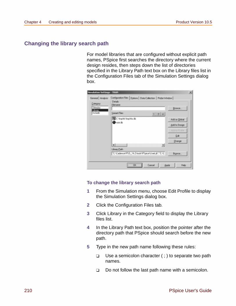
Chapter 4 Creating and editing models Product Version 10.5
210 PSpice User's Guide
Changing the library search path
For model libraries that are configured without explicit pathnames, PSpice first searches the directory where the currentdesign resides, then steps down the list of directoriesspecified in the Library Path text box on the Library files list inthe Configuration Files tab of the Simulation Settings dialogbox.
To change the library search path
1 From the Simulation menu, choose Edit Profile to displaythe Simulation Settings dialog box.
2 Click the Configuration Files tab.
3 Click Library in the Category field to display the Libraryfiles list.
4 In the Library Path text box, position the pointer after thedirectory path that PSpice should search before the newpath.
5 Type in the new path name following these rules:
Use a semicolon character ( ; ) to separate two pathnames.
Do not follow the last path name with a semicolon.

Product Version 10.5 Reusing instance models
PSpice User's Guide 211
Example: To search first C:\ORCAD\PSPICE\LIBRARY, then C:\MYLIBS, for model libraries, type
"C:\ORCAD\PSPICE\LIBRARY";"C:\MYLIBS"
in the Library Path text box.

Chapter 4 Creating and editing models Product Version 10.5
212 PSpice User's Guide
Handling smoke information using the Model Editor
You can use the Model Editor to add smoke information to adevice type supported by the Model Editor. This feature isavailable only if you have PSpice Advanced Analysis installed.
Using the Model Editor, you can:
Add smoke information PSpice models.
Create template-base PSpice models with smokeinformation.
Edit smoke information for the device types supported bythe Model Editor.
Adding smoke information
If you have Advanced Analysis installed, an extra tab, theSmoke tab, appears next to the Simulation tab. Adding smokeinformation involves specifying the maximum operatingconditions for different smoke parameters. Smoke parametersare the tests that are predefined in the device template file.These tests are performed between two different nodes of thedevice. The node to port mapping information for the device isavailable in the Test Node Mapping frame.
The information in the Test Node Mapping frame cannot beedited for template-based models. For models based ondevice characteristic curves, this information is editable. TheTest Node Mapping information is not editable fortemplate-based models. This is to avoid risk of smokeinformation getting out of sync with the smoke test.
See Smoke parameters on page 218
Adding smoke information to PSpice models
Adding smoke information to PSpice models enable you touse the models for Advanced Analysis smoke run. Using theModel Editor, you can add smoke information only to thedevice types supported by the Model Editor.

Product Version 10.5 Reusing instance models
PSpice User's Guide 213
For template-based models, smoke information is present bydefault and is visible in the Smoke Parameters frame. You canedit this information using the Model Editor. To add smokeinformation to a non template-based model, you need tocomplete the following steps.
1 From the Models List window, select the model to whichthe smoke information is to be added.
Note: If the model that you are trying to edit, has multipleimplementations, you first need to select theimplementation for which changes have to be made, fromthe Select Implementation dialog box. This dialog boxlists all the implementations associated with a model. Thechanges are saved to the location where originalimplementation is stored.
2 From the Model menu choose Add Smoke.
If the model uses the.SUBCKT definition, the AddSmoke dialog box appears.
a. In the Add Smoke dialog box, specify the devicetype.
b. Click OK.
The Test Node Mapping and the Smoke Parametersframes appear along with the Model Text window thatdisplays the model definition in the text format.
If the Model uses the .MODEL definition, the TestNode Mapping and the Smoke Parameters framesappear along with the Model Text window.
In the Test Node Mapping frame, enter the name of theport that maps to each Node. The correct node to portmapping is essential to ensure that smoke analysis givescorrect results. To know more about Test Node Mapping,see Smoke parameters on page 218.
For the PSpice models with the .MODEL definition, nodenames should be the ones that get assigned by partcreated using the Model Editor. For the PSpice modelswith .SUBCKT definition, node names are defined by theports in the subcircuit definition.

Chapter 4 Creating and editing models Product Version 10.5
214 PSpice User's Guide
3 Enter the maximum operating values for the parametersin the Smoke Parameters frame.
4 Save the model.
When you save the model, the .LIB and .PRP files areupdated.
Note: When you use the Model Editor to create devicecharacteristic curves-based PSpice models, the smokeinformation is not available by default. After you add thesmoke information, a new file, LIB_NAME.PRP iscreated.
Creating template-based PSpice models with smoke information
The steps for creating template-based models with smokeinformation are exactly the same as the steps for creatingtemplate-based simulation models. If you have AdvancedAnalysis installed, the Smoke tab appears by default. You arenot required to select Add Smoke from the Model menu.
See Example: Creating template-based PSpice model onpage 187
Using the Model Editor to edit smoke information
Open a model with smoke information in the Model Editor. Youcan modify the maximum operating values for different smokeparameters in the Smoke Parameters frame. For modelsbased on device characteristic curves, you can also changethe port to node mapping in the Test Node Mapping window.Saving the model will update the .PRP file with the latestinformation.

Product Version 10.5 Reusing instance models
PSpice User's Guide 215
Examples: Smoke
Adding smoke information to the D1 diode model
In this example, you will use the Model Editor to add smokeinformation to the D1 diode model used in the half-waverectifier design explained previously in Example: Creating aPSpice model based on device characteristic curves on page 180.
To add smoke information, complete the following steps.
1 From the Model menu, choose Add Smoke.
The Test Node Mapping and Smoke Parameters framesappear.
Note: The Add Smoke command is enabled only if youhave Advanced Analysis installed.
2 In the Test Node Mapping frame, add the followinginformation.
You can get the port names by opening the symbol inCapture.
a. Select the part in Capture.
b. From the Edit menu, choose Part.
c. The symbol view of the part displays. Double-click apin.
Node Port
TERM_AN 1
NODE_AN 1
NODE_CAT 2

Chapter 4 Creating and editing models Product Version 10.5
216 PSpice User's Guide
d. The Name field in the Pin Properties dialog boxdisplays the port name.
3 In the Smoke Parameters frame, add the following smokeinformation.
Note: Smoke information is available in the data sheetsprovided by the device vendor.
4 To save the changes to the diode model, choose Savefrom the File menu.
Once you have modified the D1 diode by adding smokeinformation, you can run Smoke analysis on your circuit.
Adding smoke information to the OPA_LOCAL operational amplifiermodel
In this example, you will add smoke information to an OPAMPmodel created using the Model Editor.
Property Name Value
IF 1
VR 30
PDM 1.5
TJ 175
RJC 50
RCA 50

Product Version 10.5 Reusing instance models
PSpice User's Guide 217
See Example: Creating template-based PSpice model onpage 187
You can use the Model Editor to add/edit the smokeinformation only if you have Advanced Analysis installed.
The steps in this design example assume that you haveAdvanced Analysis installed.
1 Open the Model Editor.
2 Open the LOCAL_LIB library.
3 Select the OPA_LOCAL_3.
Besides the Simulation Parameters and the Model Textwindow, a Smoke tab is also displayed.
4 Select the Smoke tab.
The Test Node Mapping and Smoke Parameters framesare displayed.
5 In the Smoke Parameters frame, specify the maximumoperating conditions for the operational amplifier to matchthe values shown in Table 5.
Table 4-6 Modified value of smoke parameters
Device Max Ops Value
IPLUS .05
IMINUS .05
IOUT .04
VDIFF 32
VSMAX 32
VSMIN -.3
VPMAX .3
VPMIN .3
VMMAX -1.5
VMMIN .3

Chapter 4 Creating and editing models Product Version 10.5
218 PSpice User's Guide
6 Save the model.
The LOCAL_LIB.PRP file will be updated with the smokeinformation. The smoke parameters added in thisexample are valid for all levels. Even if you deleteOPA_LOCAL_3 from the LOCAL_LIB library, theLOCAL_LIB.PRP will not be deleted because it containssmoke information for OPA_LOCAL_1 andOPA_LOCAL_2.
Smoke parameters
Using the Model Editor, you can add smoke information to thedevice types supported by the Model Editor.
When you add smoke information to a device, the followingtwo frames are displayed in the Model Editor.
Test Node Mapping
In this section you specify the port name that must mapto the predefined node names. The predefined terminalnames starting with TERM indicate current nodes, andthose starting with NODE indicate voltage nodes.
Smoke Parameters
In this section, you specify the maximum operatingconditions in terms of the values of the smokeparameters.
The thermal parameters that are common to all device typessupported by the Model Editor are listed below along with theirdescription.
PDM Maximum power dissipation
TJ Maximum junction temperature
RJC Maximum thermal resistance
(Junction to case thermal resistance)
RCA Maximum thermal resistance (Case toambient thermal resistance)

Product Version 10.5 Smoke parameters
PSpice User's Guide 219
Besides the parameters listed above, there are smokeparameters specific to a particular class of devices. Anexplanation of device-specific smoke parameters and nodenames for the Model Editor-supported device types is givenbelow.
Diode
Test Node Mapping
Smoke Parameters
Node Port name
TERM_AN Forward current terminal
NODE_AN Anode voltage node
NODE_CAT Cathode voltage node
Smokeparameter
Maximum operating condition
IF Maximum Forward Current
(Current through Anode)
VR Peak Reverse Voltage
(Maximum voltage betweenCathode and Anode)

Chapter 4 Creating and editing models Product Version 10.5
220 PSpice User's Guide
Bipolar Junction Transistors
Test Node Mapping
Smoke parameters
Node Port name
TERM_IC Collector current terminal
TERM_IB Base current terminal
NODE_VC Collector voltage node
NODE_VB Base voltage node
NODE_VE Emitter voltage node
Smokeparameter
Maximum operating condition
IB Maximum base current
IC Maximum collector current
VCB Maximum collector-base voltage
(Maximum voltage difference betweenCollector and Base)

Product Version 10.5 Smoke parameters
PSpice User's Guide 221
Magnetic Core
These are a special type of template-based PSpice modelsthat do not have smoke information. Therefore, the NodeMapping and Smoke Parameters frames are not available forthese models.
VCE Maximum collector-emitter voltage
(Maximum voltage difference betweenCollector and Emitter)
VEB Maximum emitter-base voltage
(Maximum voltage difference betweenEmitter and Base)
SBSLP Secondary breakdown slope
Note: Secondary breakdown is thevoltage breakdown betweenVC and VE at maximumcollector current.
SBINT Secondary breakdown intercept
SBTSLP Secondary breakdown temperaturederating slope
SBMIN Secondary breakdown deratepercentage at maximum junctiontemperature

Chapter 4 Creating and editing models Product Version 10.5
222 PSpice User's Guide
Ins Gate Bipolar Transistor (IGBT)
Test Node Mapping
Smoke parameters
Node Port name
TERM_IC Collector current terminal
TERM_IG Gate current terminal
NODE_VC Collector voltage node
NODE_VG Gate voltage node
NODE_VS Source voltage node
Smokeparameter
Maximum operating condition
IG Maximum gate current
IC Maximum collector current
VCG Maximum collector-gate voltage
(Voltage between Collector and Gate)

Product Version 10.5 Smoke parameters
PSpice User's Guide 223
Junction FET
Test Node Mapping
VCE Maximum collector-emitter voltage
(Voltage between Collector andEmitter)
VGEF Maximum forward gate-emittervoltage
(Voltage between Gate and Emitter)
VGER Maximum reverse gate-emittervoltage
Node Port name
TERM_ID Depletion current terminal
TERM_IG Gate current terminal
NODE_VD Depletion voltage node
NODE_VG Gate voltage node
NODE_VS Source voltage node

Chapter 4 Creating and editing models Product Version 10.5
224 PSpice User's Guide
Smoke parameters
Operational Amplifier
Test Node Mapping
Smokeparameter
Maximum operating condition
ID Maximum drain current
IG Maximum forward gate current
VDG Maximum drain-gate voltage
(Maximum voltage between drain andgate)
VDS Maximum drain-source voltage
(Maximum voltage between drain andsource)
VGS Maximum gate-source voltage
(Maximum voltage between gate andsource)
Node Port name
NODE_POS Positive voltage source node(POS)

Product Version 10.5 Smoke parameters
PSpice User's Guide 225
Smoke parameters
NODE_NEG Negative voltage source node(NEG)
NODE_VCC Positive voltage source node
NODE_VEE Negative voltage source node
NODE_GND
TERM_POS Positive current terminal(POS)
TERM_NEG Negative current terminal(NEG)
TERM_OUT Output current terminal (OUT)
Smokeparameter
Maximumoperatingcondition
Stands for...
IPLUS Maximum inputcurrent (+)
Maximum value ofcurrent at the POSterminal
IMINUS Maximum inputcurrent (-)
Maximum value ofcurrent at the NEGterminal
IOUT Maximum outputcurrent
Maximum value ofcurrent at the OUTterminal
VDIFF Maximumdifferential VIN
Absolute voltagedifference betweenPOS and NEG
VSMAX Maximum supplyvoltage difference
Voltage differencebetween NODE_VCCand NODE_VEE
Node Port name

Chapter 4 Creating and editing models Product Version 10.5
226 PSpice User's Guide
MOSFET
Test Node Mapping
VSMIN Minimum supplyvoltage difference
Voltage differencebetween NODE_VEEand NODE_VCC
VPMAX Maximum inputvoltage (+)
Voltage differencebetween NODE_POSand NODE_VCC
VPMIN Minimum inputvoltage (+)
Voltage differencebetween NODE_VEEand NODE_POS
VMMAX Maximum inputvoltage (-)
Voltage differencebetween NODE_NEGand NODE_VCC
VMMIN Minimum inputvoltage (-)
Voltage differencebetween NODE_VEEand NODE_NEG
Node Port name
TERM_ID Drain current terminal
TERM_IG Gate current terminal

Product Version 10.5 Smoke parameters
PSpice User's Guide 227
Smoke parameters
NODE_VD Drain voltage node
NODE_VG Gate voltage node
NODE_VS Source voltage node
SmokeParameter
Maximum Operating Condition
IG Maximum forward gate current
ID Maximum drain current
VDG Maximum drain-gate voltage
(Maximum difference betweenNODE_VD and NODE_VG)
VDS Maximum drain-source voltage
(Maximum difference betweenNODE_VD and NODE_VS)
VGSF Maximum forward gate-sourcevoltage
VGSR Maximum reverse gate-sourcevoltage
Node Port name
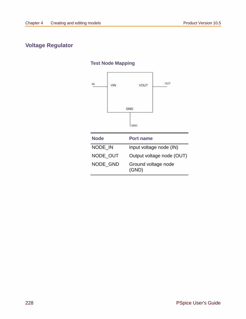
Chapter 4 Creating and editing models Product Version 10.5
228 PSpice User's Guide
Voltage Regulator
Test Node Mapping
Node Port name
NODE_IN Input voltage node (IN)
NODE_OUT Output voltage node (OUT)
NODE_GND Ground voltage node(GND)

Product Version 10.5 Smoke parameters
PSpice User's Guide 229
Darlington Transistor
Test Node Mapping
Smoke parameters
Node Port name
TERM_IC Collector current terminal
TERM_IB Base current terminal
NODE_VC Collector voltage node
NODE_VB Base voltage node
NODE_VE Emitter voltage node
Smokeparameter
Maximum operating condition
IB Maximum base current
Max(TERM_IB)
IC Maximum Collector current
Max(TERM_IC)
VCB Maximum collector-base voltage
Max(NODE_VC -NODE_VB)

Chapter 4 Creating and editing models Product Version 10.5
230 PSpice User's Guide
VCE Maximum collector-emitter voltage
Max(NODE_VC -NODE_VE)
VEB Maximum emitter-base voltage
Max(NODE_VE -NODE_VB)
SBSLP Secondary breakdown slope
Note: Secondary breakdown is thevoltage breakdown betweenVC and VE at maximumcollector current.
SBINT Secondary breakdown intercept
SBTSLP Secondary breakdown temperaturederating slope
SBMIN Secondary breakdown deratepercentage at maximum junctiontemperature

PSpice User's Guide 231
5
Creating parts for models
Chapter overview
This chapter provides information about creating parts formodel definitions, so you can simulate the model from yourdesign using OrCAD Capture. For general information aboutcreating parts, refer to the Capture User’s Guide.
Topics are grouped into four areas introduced later in thisoverview. If you want to find out quickly which tools to use tocomplete a given task and how to start, then:
1 Go to the roadmap in Ways to create parts for models onpage 233.
2 Find the task you want to complete.
3 Go to the sections referenced for that task for moreinformation about how to proceed.
Background information
These sections provide background on the things you need toknow and do to prepare for creating parts:
What’s different about parts used for simulation? onpage 232
Preparing your models for part creation on page 235

Chapter 5 Creating parts for models Product Version 10.5
232 PSpice User's Guide
Task roadmap
This section helps you find the sections in this chapter that arerelevant to the part creation task that you want to complete:
Ways to create parts for models on page 233
How to use the tools
These sections explain how to use different tools to createparts for model definitions:
Using the Model Editor to create parts on page 237
Basing new parts on a custom set of parts on page 254
Other useful information
These sections explain how to refine part graphics andproperties:
Editing part graphics on page 256
Defining part properties needed for simulation onpage 262
What’s different about parts used for simulation?
A part used for simulation has these special characteristics:
a link to a simulation model
For information on adding simulation models to a modellibrary, see Chapter 4, “Creating and editing models.”
a netlist translation
modeled pins
other simulation properties specific to the part, which caninclude hidden pin connections or propagation delay level(for digital parts)

Product Version 10.5 Ways to create parts for models
PSpice User's Guide 233
Ways to create parts for models
If you want to... Then do this... To find out more, see this...
Create parts for aset of vendor oruser-defined modelssaved in a modellibrary.
Change the graphicstandard for anexisting model library.
Use the Model Editor tocreate parts from a modellibrary.
Basing new parts on a customset of parts on page 254
Automatically createone part each timeyou extract a newmodel.
Use the Model Editor1 andenable automatic creationof parts.
Using the Model Editor to createparts on page 237.
For a list of device types that theModel Editor supports, seeRunning the Model Editor aloneon page 165. If the Model Editordoes not support the device typefor the model definition that youwant to create, then you can usea standard text editor to create amodel definition using the PSpice.MODEL and .SUBCKTcommand syntax. Remember toconfigure the new model library(see Configuring model librarieson page 202).
Basing new parts on a customset of parts on page 254

Chapter 5 Creating parts for models Product Version 10.5
234 PSpice User's Guide
Create parts for allthe models saved in amodel library.
in batch mode
in interactive mode
Use the Export to CapturePart Library commandavailable in Model Editor tocreate parts from a modellibrary.
Use the Model ImportWizard [Capture] to createparts from a modellibrary.Use the ModelImport Wizard [Capture] tocreate parts from a modellibrary.
Creating Capture parts for allmodels in a library on page 238.
1. For a list of device types that the Model Editor supports, see Running the Model Editor alone onpage 165.
If you want to... Then do this... To find out more, see this...

Product Version 10.5 Ways to create parts for models
PSpice User's Guide 235
Preparing your models for part creation
If you already have model definitions and want to create partsfor them, you should organize the definitions into librariescontaining similar device types.
To set up a model library for part creation
1 If all of your models are in one file and you wish to keepthem that way, rename the file to:
Reflect the kinds of models contained in the file.
Have the .LIB extension.
Note: Model libraries typically have a .LIB extension.However, you can use a different file extension aslong as the file format conforms to the standardmodel library file format.
2 If each model is in its own file, and you want toconcatenate them into one file, use the DOS copycommand.
Example:
You can append a set of files with .MOD extensions into asingle .LIB file using the DOS command:
copy *.MOD MYLIB.LIB
3 Make sure the model names in your new library do notconflict with model names in any other model library.
For information on managing model libraries, includingthe search order PSpice uses, see Configuring modellibraries on page 202.

Chapter 5 Creating parts for models Product Version 10.5
236 PSpice User's Guide
Starting the Model Editor
To start the Model Editor alone
1 From the Windows Start menu, point to the ReleaseOrCAD 10.5 program folder, then choose PSpiceAccessories, Model Editor.
2 From the File menu, choose Open or New, and enter anexisting or new model library name.
3 In the Models List frame, select the name of a model todisplay it for editing in the Spec Entry frame.
To start the Model Editor from within Capture
1 In the schematic page editor, select the part whose modelyou want to edit.
2 From the Edit menu, choose PSpice Model.
The Model Editor starts with the model loaded for editing.
If you have already started the Model Editor from Capture, andwant to continue working on new models, then:
1 Close the opened model library.
2 Open a new model library.
3 Load a device model or create a new one.
Note: Part creation is disabled, when you launch the ModelEditor from Capture.

Product Version 10.5 Starting the Model Editor
PSpice User's Guide 237
Using the Model Editor to create parts
If you want to create new parts that are not tied to a localdesign, open the Model Editor alone. Using Model Editor, youcan create parts in two modes:
Batch mode
Interactive mode
Batch mode of part creation
In this method, you use the Export to Capture Part Librarycommand from the File menu, to create part symbols for allmodels in a simulation library. In this approach, you can viewthe symbols only after all the changes have been done andsaved in the .olb file. You need to open the .olb file inCapture and view the symbols.
To know more about how to use the Export to Capture PartLibrary command for part creation see Using batch mode onpage 238.
Interactive mode of part creation
In this mode, you can view the part symbol being attached toa simulation model before the changes are saved in thesymbol library. You can also update and attach symbols ofyour own choice to the models in the library. To create Capturesymbols in an interactive mode, choose Model ImportWizard [Capture] command, from the File menu.
When you generate part symbols using Model Import wizard,you can review the symbol shapes before you save thechanges to the part library. This is unlike using Export ToCapture Part Library command, where all the changes aremade to the part library before you can review the symbols byopening them in Capture.
In the Model Import Wizard, specify the input model libraryand the output symbol library and click Next. The model

Chapter 5 Creating parts for models Product Version 10.5
238 PSpice User's Guide
names and the names of the symbol to be associated witheach model is listed. The symbol shape is visible on the right.
If the users do not make any change and selects the Finishbutton, a message box may appear. This message boxappears only if there are models for which symbols could notbe found. To attach a rectangular symbols to such modelsclick Yes. If you do not wish to attach any symbols select No.If you select yes, the symbol library generated using the ModelImport Wizard will be exactly same as the .olb generatedusing the Export to Capture Part Library command.
To know more about how to create parts using Model ImportWizard, see Using interactive mode on page 240.
To find out which device types the Model Editor supports, seeRunning the Model Editor alone on page 165. If the ModelEditor does not support the device type for the modeldefinition that you want to create, then you can use a standardtext editor to create a model definition using the PSpice.MODEL and .SUBCKT command syntax. Remember toconfigure the new model library.
Note: The Model Editor is not available with PSpice. A limitedversion of the Model Editor is supplied withPSpice A/D Basics.
Creating Capture parts for all models in a library
Note: Creating parts for all the models in a library is notsupported for libraries that have models with multipleimplementation.
Using batch mode
1 Open the Model Editor alone.From the Windows Start menu, point to the Programs,Release OrCAD 10.5, and then choose PSpiceAccessories, Model Editor.
2 From the File menu, choose Export to Capture PartLibrary.

Product Version 10.5 Creating Capture parts for all models in a library
PSpice User's Guide 239
The Create Parts for Library dialog box appears.
Tip
Export to Capture Part Library option is availableonly if Capture is selected as the schematic editor inthe Options dialog box. To display the Options dialogbox, choose Options from the Tools menu.
3 In the Enter Input Model Library text box, specify thelocation of the model library for which the Capture partsare to be created.
Note: You can use the Browse button to specify adifferent location of the .OLB file.
The Enter Output Part Library text box automaticallydisplays the name and the location of the new .OLB fileto be created. The displayed library name is same asspecified by the user in the Save Part To section of theOPTIONS dialog box.
4 Click OK to create the part and click OK again to clear the.ERR log dialog box.
Caution
Recreating an already existing part library, usingthe Export to Capture Part Library command doesnot overwrite the contents of the part library. Onlythe new parts are appended to the library.Consider a part library, MYLIB.OLB that has twoparts a1 and a2, and a model library, MYLIB.LIBthat has three models a2, b1, and b3. RecreatingMYLIB.OLB from MYLIB.LIB will not delete a1from MYLIB.OLB. The modified MYLIB.OLB hasfour parts, a1, a2, b1, and b2.

Chapter 5 Creating parts for models Product Version 10.5
240 PSpice User's Guide
Using interactive mode
Important
Model Import Wizard is not recommended if youwant to create new symbol shapes. Using the wizard,you can only associate existing PSpice model toexisting symbols and vice-versa.You can create newsymbols in OrCAD Capture. To know more aboutcreating new part symbols or editing existing symbolgraphics, see Editing part graphics on page 256.
Invoke Model Import wizard
From Model Editor
− From the File drop-down menu, choose Model ImportWizard [Capture].
Important
To be able to generate Capture parts using ModelEditor, select Capture as the schematic editor in theOptions dialog box.
From Capture
1 Select the Project Manager window in Capture.
2 From the Tools drop-down menu, select Generate Part.
3 In the Generate Part dialog box, select the Pick symbolmanually check box.
4 From the Netlist/source file type drop-down list box, selectPSpice Model Library.
5 To start the symbol generation process, click OK.
Using Model Import wizard
1 In the Specify Library page of the Model Import Wizard,provide inputs.

Product Version 10.5 Creating Capture parts for all models in a library
PSpice User's Guide 241
a. Specify the name and location of the input modellibrary (.lib)
b. Specify the name and location of the output partlibrary (.olb)
Tip
While specifying the library name, you must ensurethat special characters, such as tilde (~), backtick (`),exclamation mark (!), dollar ($), percentage (%),caret (^), ampersand (&), plus (+), minus (-), comma(,), semi colon(;), single quotes ('), and doublequotes (") are not used in the library name.
c. Click the Next button to move to the next step of thewizard.
When you click the Next button, the Model ImportWizard automatically starts the process of looking upsymbols for each of the models in the .lib file andassociating the symbols that match the modeldefinition.
Important
Model Import Wizard uses the model definitionto find a matching symbol for a simulationmodel. Therefore, Model Import Wizard canautomatically match symbols only for the devicetypes supported by the Model Editor. To knowmore about these device types, see ModelEditor-supported device types based on devicecharacteristic curves on page 170.
The matching symbols are stored in the destination partlibrary specified by you.
2 View the symbols provided by the Model Import Wizard.
The Associate/Replace Symbol page of the wizard liststhe models in the .lib file and the corresponding symbolnames. By default, all models are listed. You cancustomize the view to display only those models that have

Chapter 5 Creating parts for models Product Version 10.5
242 PSpice User's Guide
symbols attached or the models that do not have anysymbols attached.
To display only the models with symbols attached, ensurethat only the Models with symbols check box isselected.
To display only the models with no symbols attached, onlythe Models without symbols check box should beselected. In this case, the Symbol Name column is blank.
You can view the attached symbol by selecting a modelfrom the list of the models with attached symbols. Thesymbol shape appears on the right of the wizard.
At this stage, you can complete the process ofassociating symbols, and close the Model import wizardby clicking the Finish button. When you click the Finishbutton, you receive a message stating whether you wantto attach rectangular symbols to the models that do nothave symbols attached to them. This message appears

Product Version 10.5 Creating Capture parts for all models in a library
PSpice User's Guide 243
only if the .lib file has some models for which symbolswere not available
In this case, you want rectangular shaped symbols to beassociated with the models, select Yes. To close thewizard without attaching rectangular symbols to themodels, select No.
3 Associate/Replace desired part symbol to a PSpicemodel
As the name suggests, the Associate/Replace Symbolpage of the wizard can also be use to review symbolshapes and if required, attach user-defined symbols tothe models.
The Model import wizard allows you to attachuser-defined symbols to the models without symbols or toreplace the attached symbols with a symbol of your ownchoice.
To change the model-symbol association suggestedby Model Import wizard, click the Replace Symbolbutton.
To attach a specific symbol to a model for whichmatching symbols could not be found, click theAssociate Symbol button.
To attach user-defined symbols to a model:
Yes Destination symbol library (.olb) hassymbol looked up by the Model Importwizard
No The .olb file has symbols for all themodels in the .lib file.

Chapter 5 Creating parts for models Product Version 10.5
244 PSpice User's Guide
a. Click the Associate/Replace symbol button.
b. In the Select Matching page of the wizard, specifythe path to the base library
A base library can be defined as the symbol library(.olb) that contains the desired part symbol. Fromthe specified library, the Model Import wizard filtersand lists the symbol names that can be attached tothe selected model. You can then select a symbolfrom the list, to be associated with the model.
c. Complete the model terminal and symbol pinmapping.
Use the View Model Test button, to display the modeldefinition for the selected mode. The pin names ofthe selected symbols appear in the Symbol Pindrop-down list box.
d. Select the Save button to update the destinationsymbol file specified in Step 1, with the changesmade by you.
Note: The changes made to the destination library areirreversible. Once saved, you cannot undo the changes atthe click of a button.
Similarly, you can make associate an existing symbol to any ofthe models in the .lib file.
When you use the Model Import wizard to attach a symbol toa model and vice-versa, following tasks are performed:
The value of IMPLEMENTATION TYPE property attachedto the symbol is set to PSpice Model.
The value of the IMPLEMENTATION property attached tothe symbol is set to the name of the selected model.(Except in case of leveled models where the level numberis removed.)
For models based on device characteristic curves, thePSPICETEMPLATE property is updated with thepinname information.

Product Version 10.5 Setting up automatic part creation
PSpice User's Guide 245
For template-based PSpice models, pspice_lnk view isgenerated.
Setting up automatic part creation
Automatic part creation from the Model Editor is optional. Bydefault, automatic part creation is disabled. You can enable itusing the procedure below.
Note: Instead of using the PSpice default part set, you canuse your own set of standard parts. To find out more,see Basing new parts on a custom set of parts onpage 254.
Tip
In case you want to create a new symbol for only onemodel in a library that contains several models, setup the automatic part creation feature and use theFile, Save command. Every time the file is saved withautomatic part creation enabled, a new symbol iscreated for the selected model. All other symbols areleft alone.
To enable automatic part creation for new models
1 In the Model Editor with a library open, choose Optionsfrom the Tools menu.
2 In the Part Creation Setup frame, select Always CreatePart when Saving Model if it is not already checked.
Note: The Always Create Part when Saving Model optionwill be disabled if you start the Model Editor from Capture.
3 Select the Pick symbols Manually check box, to ensurethat Model Import Wizard is invoked every time yougenerate a part symbol for a model.
Note: In this case, the Specify Library page of the wizardis not required and is therefore, not visible. TheAssociate/Replace symbol page will be invoked.
Chapter 5 Creating parts for models Product Version 10.5
246 PSpice User's Guide
4 In the Save Part To frame, define the name of the partlibrary for the new part. Choose one of the following:
Part library path same as model library to create oropen the *.OLB file that has the same filename asthe open model library (*.LIB).
For example, if the model library is namedMYPARTS.LIB, then the Model Editor creates thepart library named MYPARTS.OLB.
User-defined part library, and then enter a libraryname in the part Library Name text box.
Example
The examples covered in this section demonstrate the stepsinvolved in creating a part using the Model Editor. Theexamples covered in this section are:
Creating parts in the batch mode
Creating parts using interactive mode
Creating parts in the batch mode
This example is the continuation of the Example: Creatingtemplate-based PSpice model used in Chapter 4, “Creatingand editing models.”
The tasks covered in this example are:
Creating parts for the models in a model library using theExport to Capture Part Library command.
Using the Model Editor created part in a schematicdesign.
Passing parameters to a simulation model from theschematic.
Using model with multiple levels of simulationparameters. Difference in the use model for ModelEditor-created model and OrCAD supplied model

Product Version 10.5 Example
PSpice User's Guide 247
In this example, you will create parts for the simulation modelsin the LOCAL_LIB model library. The LOCAL_LIB librarycreated as part of Example: Creating template-based PSpicemodel has a template-based model of an operationalamplifier, OPA_LOCAL.
Creating Capture parts
To create Capture parts for all the models in theLOCAL_LIB.LIB library:
1 From the File menu choose Export to Capture Part library.
Note: The Export to Capture Part Library option isavailable only if you select Capture as the schematiceditor in the Options dialog box.
2 In the Create Parts for Library dialog box, ensure that theinput model library is LOCAL_LIB.LIB and save the newCapture part library (LOCAL_LIB.OLB) in the samelocation as the model library.
3 Click OK, to create parts.
The LOCAL_LIB.OLB that gets created has one part,OPA_LOCAL, with the LEVEL property is attached to the partsymbol. By default, the value of the LEVEL property is set to 1.
Template-based operational amplifier model created using theModel Editor has multiple level support. If the value of theLEVEL property is set to 1, first level of simulation parametersare used while simulating the model. Similarly, if the LEVELvalue set to 2, second level of simulation parameters are used,and so on.
Using the Model Editor created parts in a design
In this section you will create an amplifier using two internallycompensated operational amplifiers. One of the OperationalAmplifier, CA1458, is supplied along with PSpice in theOPA.LIB model library, and the second Operational Amplifierused is OPA_LOCAL, created using the Model Editor. Both themodels are template-based and both support multiple levels ofsimulation parameters.

Chapter 5 Creating parts for models Product Version 10.5
248 PSpice User's Guide
1 In Capture, create a new project FUNC_GEN.OPJ, andinclude LOCAL_LIB.LIB as one of the model library.
2 Create a circuit as shown in the figure below.
The model CA1458, is a multi-level model and by default,the model level is 3. The LEVEL property for theOPA_LOCAL model is set to 2.
Note: You can also pick the design from,...\tools\pspice\tutorial\capture\modeleditor.
3 To simulate the circuit, choose Run from the PSpicemenu in Capture.
Changing the level of simulation parameters used in the design
We will now modify the circuit design, such that level 2simulation parameters are used for CA1458 and level 3simulation parameters are used for the OPA_LOCAL model,created using the Model Editor.

Product Version 10.5 Example
PSpice User's Guide 249
Changing the level for CA1458
To change the level of simulation parameters for CA1458 from3 to 2,
1 Select the part CA1458.
2 From the Edit menu, choose Properties.
3 In the Property editor dialog box, change the value ofLEVEL property from 3 to2.
4 Click Apply and close the Property Editor.
Similarly, change the value of the LEVEL property onOPA_LOCAL from 2 to 3.
You can now simulate the circuit using PSpice or PSpiceAdvanced Analysis.
Changing Simulation Properties from Capture
For all the editable simulation properties, you can specify thevalue of simulation parameters from Capture.
1 Select OPA_LOCAL.
2 From the Edit menu, choose Properties.
3 In the Property Editor dialog box, select New Row.
4 In the Add New Row dialog box, enter the name of thesimulation parameter in the Name text box. Enter VOS.
5 In the Value text box, add the value of the simulationparameter as 2e-3 and select OK.
6 To make the property and its value visible, first selectproperty row and then select the Display button in theProperty Editor dialog box.
7 Specify the Display Format. Select Name and Value.
8 Select Apply and close the dialog box.
The simulation parameter and its value appear in the Capture.If you now simulate the design, the simulation parameter valuespecified in Capture will be used.

Chapter 5 Creating parts for models Product Version 10.5
250 PSpice User's Guide
Creating parts using interactive mode
In this section, we will use the Model Import wizard to createmodels stored in a user defined library, MYLIB. This libraryconsists of four simulation models. These are LM339; which isa voltage comparator macro model subcircuit, INA105E;which is an operational amplifier plus precision resistornetwork, LF442A/NS; which is a JFET OPAMP, and mybjt;which is a Bipolar Junction Transistor.
Launch Model Import Wizard
1 From the File drop-down menu in Model Editor, chooseModel Import Wizard [Capture].
Provide Inputs
1 In the Specify Library page of the wizard, specify thelocation of MYLIB.LIB.
2. Specify the name of the part library in which the partsymbols generated by the Wizard are to be stored.

Product Version 10.5 Example
PSpice User's Guide 251
You can either specify the name of an existing .olb fileor create a new .olb file.
When you specify the name of an existing .olb file, youalso need to specify if symbols should be created for allthe models in the model library while replacing theexisting symbols, or whether part symbols are to becreated only for the models without the symbols.
The name and the location of the destination symbollibrary gets populated by default. For the current example,accept the default name, mylib.olb and click Next.
Depending on the model definition, the Model Importwizard could locate appropriate part symbol for the BJTmodel only. The named of the symbol attached to themybjt model, is listed in the Symbol Name column andthe symbol shape is also visible.
3 You can now complete one of the following steps:
a. Close the wizard without attaching any symbols ofthe rest of the three models in mylib.lib.

Chapter 5 Creating parts for models Product Version 10.5
252 PSpice User's Guide
b. Close the wizard, after Model Import wizard attachesrectangular symbols to rest of the models inmylib.lib.
c. Use the Model Import wizard to select and attach anexisting symbol shape to one or all the models inmylib.lib.
To execute the first two options, click the Finish button. Inthe message box that appears, select No to close thelibrary and Yes to attach rectangular symbols and thenclose the library.
Associating desired part symbol to a PSpice model
We will now use the Model Import wizard to attach an existinguser-defined, symbol to LF442A/NS; which is a JFET OPAMP.LF442A is a Dual Low Power JFET Input OperationalAmplifier, downloaded from National Semiconductor's website. We will pick up the symbol from the symbol libraryopamp.olb, which contains symbols for different types ofOPAMPs.
1 In the Associate/Replace page of the Model ImportWizard, select LF442A/NS, and click Associate Symbol.
2 In the Select Matching page of the wizard, specify thename and the location of opamp.olb.
All symbols that match the model definition are listed inthe Matching Symbols list.
3 From the Matching symbols list, select LM158 and clickNext.
4 Before you start mapping the model terminals to thesymbol pin names, click the View Model Text button.

Product Version 10.5 Example
PSpice User's Guide 253
The model definition of LF442A/NS appears in a differentwindow.
5 Map the model terminals and the symbol pin names.
6 To attach the symbol to LF442A/NS, click the SaveSymbol button.
The name of the symbol attached to the model appearsin the Symbol Name list.
You have successfully attached a symbol to the selectedmodel. Similarly, you can attach models for the other twosymbols as well.
Note: You can use the Model Import wizard to replace asymbol attached to a model with another symbol. To dothis, select the model that has a symbol attached to it,and click the Replace Symbol button.
Model terminal Mapped to Symbol Pin
1 +
2 -
99 V+
50 V-
28 OUT

Chapter 5 Creating parts for models Product Version 10.5
254 PSpice User's Guide
Important
Model Import Wizard can be invoked from Capture toassociate a PSpice model to an existing CaptureSymbol. To know more about associating PSpicemodel to a Capture symbol, see OrCAD CaptureUser Guide.
Basing new parts on a custom set of parts
If you are using the Model Editor to automatically generateparts for model definitions, and you want to base the newparts on a custom graphic standard (rather than the PSpicedefault parts), then you can change which underlying partseither application uses by setting up your own set of parts.
Note: If you use a custom part set, the Model Editor alwayschecks the custom part library first for a part thatmatches the model definition. If none can be found,they use the PSpice default part instead.
To create a custom set of parts for automatic partgeneration
1 Create a part library with the custom parts.
Be sure to name these parts by their device type asshown in Table 5-1 and Table 5-2; this is how the ModelEditor determines which part to use for a model definition.
For more information on creating parts, refer to theOrCAD Capture User’s Guide.
Table 5-1 Symbol Names for custom symbol generation for regular PSpice models
For this device type... Use this symbolname...
For this device type... Use this symbolname...
Bipolar transistor: LPNP LPNP Magnetic core CORE
Bipolar transistor: NPN NPN MOSFET: N-channel NMOS
Bipolar transistor: PNP PNP MOSFET: P-channel PMOS

Product Version 10.5 Basing new parts on a custom set of parts
PSpice User's Guide 255
Capacitor1 CAP OPAMP: 5-pin OPAMP5
Darlington: N-channel DARNPN OPAMP: 7-pin OPAMP7
Darlington: P-channel DARPNP Resistor1 RES
Diode DIODE Switch:voltage-controlled1
VSWITCH
GaAsFET1 GASFET Transmission line1 TRN
IGBT: N-channel NIGBT Voltage comparator VCOMP
Inductor1 IND Voltage comparator: 6 pin VCOMP6
JFET: N-channel NJF Voltage reference VREF
JFET: P-channel PJF Voltage regulator VREG
1. Does not apply to the Model Editor.
Table 5-1 Symbol Names for custom symbol generation for regular PSpice models
For this device type... Use this symbolname...
For this device type... Use this symbolname...
Table 5-2 Symbol Names for Custom Symbol Generation for template-based Models
For this device type... Use this symbolname...
For this device type... Use this symbolname...
Bipolar transistor: LPNP Magnetic core AACORE
Bipolar transistor: NPN AANPN3 MOSFET: N-channel AANMOSFET3
Bipolar transistor: PNP AAPNP3 MOSFET: P-channel AAPMOSFET3
Capacitor1 CAP OPAMP: 5-pin AA5_PIN_OPAMP
Darlington: N-channel AADARNPN3 OPAMP: 7-pin AA7_PIN_OPAMP
Darlington: P-channel AADARPNP3 Resistor1
Diode AADIODE Switch:voltage-controlled1
GaAsFET1 Transmission line1
IGBT: N-channel AANIGBT3 Voltage comparator
Inductor1 Voltage comparator: 6pin

Chapter 5 Creating parts for models Product Version 10.5
256 PSpice User's Guide
2 For each custom part, set its IMPLEMENTATIONproperty to `M where ` is a back-single quote or gravecharacter.
This tells the Model Editor to substitute the correct modelname.
To base new parts on custom parts using the ModelEditor
1 In the Model Editor with the library open, choose PartCreation Setup from the Options menu, and enableautomatic part creation as described in To enableautomatic part creation for new models on page 245.
2 In the Base Parts On frame, enter the name of theexisting part library (*.OLB) that contains your customparts.
3 Click OK.
Editing part graphics
If you created parts using the Model Editor, and you want tomake further changes, the following sections explain a fewimportant things to remember when you edit the parts.
How Capture places parts
When placing parts on the schematic page, the schematicpage editor uses the grid as a point of reference for different
JFET: N-channel AANCHANNEL3 Voltage reference
JFET: P-channel AANPHANNEL3 Voltage regulator AAVREG
1. Does not apply to the Model Editor.
Table 5-2 Symbol Names for Custom Symbol Generation for template-based Models
For this device type... Use this symbolname...
For this device type... Use this symbolname...

Product Version 10.5 Editing part graphics
PSpice User's Guide 257
editing activities. The part’s pin ends are positioned on the gridpoints.
To edit a part in a library
1 From Capture’s File menu, point to Open, then chooseLibrary.
2 Select the library that has the part you want to edit.
The library opens and displays all its parts.
3 Double-click the part you want to edit.
The part appears in the part editor.
4 Edit the part.
You can resize it, add or delete graphics, and add ordelete pins. For more information about specific partediting tasks, refer to the OrCAD Capture User’sGuide.
5 After you have finished editing the part, from the Filemenu, choose Save to save the part to its library.
Here are the things to check when editing part properties:
Does the PSPICETEMPLATE specify the correct numberof pins/nodes?
Are the pins/nodes in the PSPICETEMPLATE specifiedin the proper order?
grid point
part body border

Chapter 5 Creating parts for models Product Version 10.5
258 PSpice User's Guide
Do the pin/node names in the PSPICETEMPLATE matchthe pin names on the part?
Defining grid spacing
Grid spacing for graphics
The grid, denoted by evenly spaced grid points, regulates thesizing and positioning of graphic objects and the positioning ofpins. The default grid spacing with snap-to-grid enabled is0.10", and the grid spacing is 0.01".
You can turn off the grid spacing when you need to drawgraphics in a tighter space.
To edit the part graphics
1 In Capture’s part editor, display the part you want to edit.
2 Select the line, arc, circle, or other graphic object youwant to change, and do any of the following:
To stretch or shrink the graphic object, click and dragone of the size handles.
To move the entire part graphic, click and drag theedge of the part.
The part body border automatically changes to fit thesize of the part graphic.
3 After you have finished editing the part, from the Filemenu, choose Save to save the part to its library.
Note: When changing part graphics, check to see that all pinsare on the grid.
Grid spacing for pins
The part editor always places pins on the grid, even when thesnap-to-grid option is turned off. The size of the part is relativeto the pin-to-pin spacing for that part. That means that pins

Product Version 10.5 Attaching models to parts
PSpice User's Guide 259
placed one grid space apart in the part editor are displayed asone grid space apart in the schematic page editor.
Pins must be placed on the grid at integer multiples of the gridspacing. Because the default grid spacing for the SchematicPage Grid is set at 0.10", you will achieve the best results bysetting pin spacing in the Part and Symbol Grid at 0.10"intervals from the origin of the part and at least 0.10" from anyadjacent pins. For more information about grid spacing andpin placement, refer to the OrCAD Capture User’s Guide.
The part editor considers pins that are not placed at integermultiples of the grid spacing from the origin as off-grid, and awarning appears when you try to save the part.
Here are two guidelines:
Make sure Pointer Snap to Grid is enabled when editingpart pins and editing schematic pages so you can easilymake connections.
Make sure the Part and Symbol Grid spacing matchesthe Schematic Page Grid spacing.
Note: Pin changes that alter the part template can occur ifyou either:
change pin names
or
delete pins
In these cases you must adjust the value of the part’sPSPICETEMPLATE property to reflect these changes. Tofind out how, see Pin callout in subcircuit templates onpage 270.
Attaching models to parts
If you create parts and want to simulate them, you need toattach model implementations to them. If you created yourparts using any of the methods discussed in this chapter, thenyour part will have a model implementation already attachedto it.

Chapter 5 Creating parts for models Product Version 10.5
260 PSpice User's Guide
MODEL
The IMPLEMENTATION property defines the name of themodel that PSpice must use for simulation. When attachingthis implementation, this rule applies:
The Implementation name should match the name of the.MODEL or .SUBCKT definition of the simulation modelas it appears in the model library (*.LIB).
Example:
If your design includes a 2N2222 bipolar transistor with a.MODEL name of Q2N2222, then the Implementation namefor that part should be Q2N2222.
Note: Make sure that the model library containing thedefinition for the attached model is configured in the listof libraries for your project. See Configuring modellibraries on page 202 for more information.
For more information on model editing in general, seeChapter 4, “Creating and editing models.” For specificinformation on changing model references, see Changing themodel reference to an existing model definition on page 199.
To attach a model implementation
1 In the schematic page editor, double-click a part todisplay the Parts spreadsheet of the Property Editor.
Assume the spreadsheet is displayed in columns andfollow the instructions below.
2 Click on the empty cell under the Implementation Typecolumn.
A drop-down list appears in the cell.
3 From the Implementation Type drop-down list, selectPSpice Model.
4 Click on the empty cell under the Implementation column,and type the name of the model to attach to the part.
Note: You do not need to enter an Implementation Path

Product Version 10.5 Attaching models to parts
PSpice User's Guide 261
because PSpice searches for the model in the list ofmodel libraries you configure for this project.
5 Click Apply to update the design, then close the Partsspreadsheet.
Caution
In case you want to reuse the part symbol thatwas originally attached to a characteristiccurve-based model, with a template-basedsimulation model, you must delete thePSPICETEMPLATE property from the partsymbol.
Example:
Consider a scenario where you have two simulationmodels for a bipolar transistor, with the same name2n2222 in two different libraries. First simulation model isbased on characteristic curves and the second based onPSpice templates. Both the simulation models have samename, therefore the same value for theIMPLEMENTATION property.
The simulation model based on characteristic curves,which is of .MODEL type, is used in a schematic design.The part symbol for the bipolar transistor will have theIMPLEMENTAION property set to Q2n2222 and thePSPICETEMPLATE property attached to it. Now modifythe BJT symbol by attaching a template-based model tothe symbol. The value of the IMPLEMENTATION propertywill not change because the name of the template-basedmodel is same as that of the characteristic curves-basedmodel. Therefore, to ensure that the correct model isused during simulation, you must delete thePSPICETEMPLATE property from the part symbol andconfigure the library containing the template-based BJTmodel.
Note: You can check whether the right model is beingused or not, by viewing the simulation netlist generated byPSPice. The simulation netlist for a .MODEL type BJTmodel starts with Q, where as the simulation netlist for a.SUBCKT model starts with X.

Chapter 5 Creating parts for models Product Version 10.5
262 PSpice User's Guide
Defining part properties needed for simulation
If you created your parts using any of the methods discussedin this chapter, then your part will have these propertiesalready defined for it:
PSpice PSPICETEMPLATE for simulation
PART and REFDES for identification
You can also add other simulation-specific properties fordigital parts: IO_LEVEL, MNTYMXDLY, andPSPICEDEFAULTNET (for pins).
Example:
If you create a part that has electrical behavior described bythe subcircuit definition that starts with:
.SUBCKT 7400 A B Y+ optional: DPWR=$G_DPWR DGND=$G_DGND+ params: MNTYMXDLY=0 IO_LEVEL=0
then the appropriate part properties are:
IMPLEMENTATION = 7400MNTYMXDLY = 0IO_LEVEL = 0PSPICETEMPLATE = X^@REFDES %A %B %Y %PWR %GND@MODEL PARAMS:IO_LEVEL=@IO_LEVELMNTYMXDLY=@MNTYMXDLY
Note: For clarity, the PSPICETEMPLATE property value isshown here in multiple lines; in a part definition, it isspecified in one line (no line breaks).
To edit a property needed for simulation:
1 In the schematic page editor, select the part to edit.
2 From the Edit menu, choose Properties to display theParts spreadsheet of the Property Editor.
3 Click in the cell of the column you want to change (forexample, PSPICETEMPLATE), or click the New button toadd a property (and type the property name in the Nametext box).
4 If needed, type a value in the Value text box.

Product Version 10.5 Defining part properties needed for simulation
PSpice User's Guide 263
5 Click Apply to update the design, then close thespreadsheet.
PSPICETEMPLATE
The PSPICETEMPLATE property defines the PSpice syntaxfor the part’s netlist entry. When creating a netlist, Capturesubstitutes actual values from the circuit into the appropriateplaces in the PSPICETEMPLATE syntax, then saves thetranslated statement to the netlist file.
Caution
The PSPICETEMPLATE property is required onlyfor models based on device characteristic curves.For template-based models, netlisting is doneusing the PORT_ORDER information available inthe device property file.
Note: The PSPICETEMPLATE property is not requiredwith template-based models. Therefore, while modifyinga design, if you attach a template-based model to a partoriginally attached to a characteristic curve based model,then besides changing the Implementation property, youmust also delete the PSPICETEMPLATE property.
Any part that you want to simulate must have a definedPSPICETEMPLATE property. These rules apply:
Table 5-3
To find out more aboutthis property...
See this...
PSPICETEMPLATE PSPICETEMPLATE onpage 263
IO_LEVEL IO_LEVEL on page 272
MNTYMXDLY MNTYMXDLY on page 273
PSPICEDEFAULTNET PSPICEDEFAULTNET onpage 274

Chapter 5 Creating parts for models Product Version 10.5
264 PSpice User's Guide
The pin names specified in the PSPICETEMPLATEproperty must match the pin names on the part.
The number and order of the pins listed in thePSPICETEMPLATE property must match those for theassociated .MODEL or .SUBCKT definition referenced forsimulation.
The first character in a PSPICETEMPLATE must be aPSpice device letter appropriate for the part (such as Qfor a bipolar transistor).
See Passive parts on page 117 and Breakout parts onpage 118 for a list of device types and PSpice deviceletters.
Device types and PSpice device letters are also listed inthe online PSpice A/D Reference Guide.
Caution
Creating parts not intended for simulationSome part libraries contain parts designed onlyfor board layout; PSpice cannot simulate theseparts. This means they do not havePSPICETEMPLATE properties or that thePSPICETEMPLATE property value is blank.
PSPICETEMPLATE syntax
The PSPICETEMPLATE contains:
regular characters that the schematic page editorinterprets verbatim
property names and control characters that theschematic page editor translates
Regular characters in templates
Regular characters include the following:
alphanumerics

Product Version 10.5 Defining part properties needed for simulation
PSpice User's Guide 265
any keyboard part except the special syntactical partsused with properties (@ & ? ~ #).
white space
An identifier is a collection of regular characters of the form:
alphabetic character [any other regular character]*.
Property names in templates
Property names are preceded by a special character asfollows:
[ @ | ? | ~ | # | & ]<identifier>
The schematic page editor processes the property accordingto the special character as shown in the following table.
Table 5-4
This syntax...1
1. s is a separator character
Is replaced with this...
@<id> Value of <id>. Error if no <id> attribute orif no value assigned.
&<id> Value of <id> if <id> is defined.
?<id>s...s Text between s...s separators if <id> isdefined.
?<id>s...ss...s Text between the first s...s separators if<id> is defined, else the second s...sclause.
~<id>s...s Text between s...s separators if <id> isundefined.
~<id> s...ss...s Text between the first s...s separators if<id> is undefined, else the second s...sclause.
#<id>s...s Text between s...s separators if <id> isdefined, but delete rest of template if <id>is undefined.

Chapter 5 Creating parts for models Product Version 10.5
266 PSpice User's Guide
Separator characters include commas (,), periods (.),semicolons (;), forward slashes (/), and verticalbars ( | ). You must always use the same character to specifyan opening-closing pair of separators.
Example: The template fragment ?G|G=@G||G=1000| usesthe vertical bar as the separator between the if-then-else partsof this conditional clause. If G has a value, then this fragmenttranslates to G=<G property value>. Otherwise, thisfragment translates to G=1000.
Note: You can use different separator characters to nestconditional property clauses.
The ^ character in templates
The schematic page editor replaces the ^ character with thecomplete hierarchical path to the device being netlisted.
The \n character sequence in templates
The part editor replaces the character sequence \n with a newline. Using \n, you can specify a multi-line netlist entry from aone-line template.
The % character and pin names in templates
Pin names are denoted as follows:
%<pin name>
where pin name is one or more regular characters.
The schematic page editor replaces the %<pin name> clausein the template with the name of the net connected to that pin.
The end of the pin name is marked with a separator (seeProperty names in templates on page 265). To avoid name

Product Version 10.5 Defining part properties needed for simulation
PSpice User's Guide 267
conflicts in PSpice, the schematic page editor translates thefollowing characters contained in pin names.
Note: To include a literal % character in the netlist, type %% inthe template.
Caution
Recommended scheme for netlist templatesTemplates for devices in the part library start witha PSpice device letter, followed by thehierarchical path, and then the referencedesignator (REFDES) property. We recommendthat you adopt this scheme when defining yourown netlist templates.
Example: R^@REFDES ... for a resistor
PSPICETEMPLATE examples
Simple resistor (R) template
The R part has:
two pins: 1 and 2
two required properties: REFDES and VALUE
Template
R^@REFDES %1 %2 @VALUE
Table 5-5
This pin namecharacter...
Is replaced with this...
< l (L)
> g
= e
\XXX\ XXXbar

Chapter 5 Creating parts for models Product Version 10.5
268 PSpice User's Guide
Sample translation
R_R23 abc def 1k
where REFDES equals R23, VALUE equals 1k, and R isconnected to nets abc and def.
Voltage source with optional AC and DC specifications(VAC) template
The VAC part has:
two properties: AC and DC
two pins: + and -
Template
V^@REFDES %+ %- ?DC|DC=@DC| ?AC|AC=@AC|
Sample translation
V_V6 vp vm DC=5v
where REFDES equals V6, VSRC is connected to nodesvp and vm, DC is set to 5v, and AC is undefined.
Sample translation
V_V6 vp vm DC=5v AC=1v
where, in addition to the settings for the previoustranslation, AC is set to 1v.
Parameterized subcircuit call (X) template
Suppose you have a subcircuit Z that has:
two pins: a and b
a subcircuit parameter: G, where G defaults to 1000 whenno value is supplied
To allow the parameter to be changed on the schematic page,treat G as an property in the template.
Template
X^@REFDES %a %b Z PARAMS: ?G|G=@G|~G|G=1000|

Product Version 10.5 Defining part properties needed for simulation
PSpice User's Guide 269
Note: For clarity, the PSPICETEMPLATE property value isshown here in multiple lines; in a part definition, it isspecified in one line (no line breaks).
Equivalent template (using the if...else form)
X^@REFDES %a %b Z PARAMS: ?G|G=@G||G=1000|
Sample translation
X_U33 101 102 Z PARAMS: G=1024
where REFDES equals U33, G is set to 1024, and thesubcircuit connects to nets 101 and 102.
Sample translation
X_U33 101 102 Z PARAMS: G=1000
where the settings of the previous translation applyexcept that G is undefined.
Digital stimulus parts with variable width pins template
For a digital stimulus device template (such as that for aDIGSTIM part), a pin name can be preceded by a * character.This signifies that the pin can be connected to a bus and thewidth of the pin is set to be equal to the width of the bus.
Template
U^@REFDES STIM(%#PIN, 0) %*PIN\n+ STIMULUS=@STIMULUS
where #PIN refers to a variable width pin.
Note: For clarity, the PSPICETEMPLATE property value isshown here in multiple lines; in a part definition, it isspecified in one line (no line breaks).
Sample translation
U_U1 STIM(4,0) 5PIN1 %PIN2 %PIN3 %PIN4+ STIMULUS=mystim
where the stimulus is connected to a four-input bus,a[0-3].

Chapter 5 Creating parts for models Product Version 10.5
270 PSpice User's Guide
Pin callout in subcircuit templates
The number and sequence of pins named in a template for asubcircuit must agree with the definition of the subcircuititself—that is, the node names listed in the .SUBCKTstatement, which heads the definition of a subcircuit. Theseare the pinouts of the subcircuit. To find out how to definesubcircuits, refer to the .SUBCKT command in the onlinePSpice Reference Guide.
Example:
Consider the following first line of a (hypothetical) subcircuitdefinition:
.SUBCKT SAMPLE 10 3 27 2
The four numbers following the name SAMPLE—10, 3, 27,and 2—are the node names for this subcircuit’s pinouts.
Now suppose that the part definition shows four pins:
IN+ OUT+ IN- OUT-
The number of pins on the part equals the number of nodes inthe subcircuit definition.
If the correspondence between pin names and nodes is asfollows:
then the template looks like this:
X^@REFDES %IN+ %IN- %OUT+ %OUT- @MODEL
Table 5-6
This nodename...
Corresponds to this pin name...
10 IN+
3 IN-
27 OUT+
2 OUT-

Product Version 10.5 Defining part properties needed for simulation
PSpice User's Guide 271
The rules of agreement are outlined in Figure 5-1.
must must
must
must
Number of nodes in first lineof subcircuit definition
Sequence of nodes in first lineof subcircuit definition
Number of pins called outin template
Sequence of pins called outin template
Number of modeled* pinsshown in part
Names of pins called outin template
Names of modeled* pinsshown in part
* Unmodeled pins may appear on a part (like the two voltage offset pins on a 741 opamp part).These pins are not netlisted and do not appear on the template.
equal
match
equal
match
Figure 5-1 Rules for pin callout in subcircuit templates

Chapter 5 Creating parts for models Product Version 10.5
272 PSpice User's Guide
IO_LEVEL
All digital parts provided in the PSpice libraries have anIO_LEVEL property.
The IO_LEVEL property defines what level of interfacesubcircuit model PSpice must use for a digital part that isconnected to an analog part. To find out more about interfacesubcircuits, see Interface subcircuit selection by PSpice onpage 579.
To use the IO_LEVEL property with a digital part
1 Add the IO_LEVEL property to the part and assign avalue shown in the table below.
2 Use this property in the PSPICETEMPLATE propertydefinition (IO_LEVEL is also a subcircuit parameter usedin calls for digital subcircuits).
Example:
PSPICETEMPLATE=X^@REFDES %A %B %C %D %PWR %GND@MODEL PARAMS:\n+IO_LEVEL=@IO_LEVELMNTYMXDLY=@MNTYMXDLY
Note: For clarity, the PSPICETEMPLATE property value isshown here in multiple lines; in a part definition, it isspecified in one line (no line breaks).
Table 5-7
Assign thisvalue...
To use this interfacesubcircuit (level)...
0 circuit-wide default
1 AtoD1 and DtoA1
2 AtoD2 and DtoA2
3 AtoD3 and DtoA3
4 AtoD4 and DtoA4

Product Version 10.5 Defining part properties needed for simulation
PSpice User's Guide 273
MNTYMXDLY
All digital parts provided in the PSpice libraries have aMNTYMXDLY property.
The MNTYMXDLY property defines the digital propagationdelay level that PSpice must use for a digital part. To find outmore about propagation delays, see Timing characteristics onpage 339 and Selecting propagation delays on page 560.
To use the MNTYMXDLY property with a digital part
1 Add the MNTYMXDLY property to the part and assign avalue shown in the table below.
2 Use this property in the PSPICETEMPLATE propertydefinition (MNTYMXDLY is also a subcircuit parameterused in calls for digital subcircuits).
Example:
PSPICETEMPLATE=X^@REFDES %A %B %C %D %PWR %GND@MODEL PARAMS:\n+IO_LEVEL=@IO_LEVELMNTYMXDLY=@MNTYMXDLY
Note: For clarity, the PSPICETEMPLATE property value isshown here in multiple lines; in a part definition, it isspecified in one line (no line breaks).
Table 5-8
Assign thisvalue...
To use this propagation delay...
0 circuit-wide default
1 minimum
2 typical
3 maximum
4 worst-case (min/max)

Chapter 5 Creating parts for models Product Version 10.5
274 PSpice User's Guide
PSPICEDEFAULTNET
The PSPICEDEFAULTNET pin property defines the net nameto which a hidden (invisible) pin is connected. Hidden pins aretypically used for power and ground on digital parts.
To use the PSPICEDEFAULTNET property with a digitalpart
1 For each PSPICEDEFAULTNET property, assign thename of the digital net to which the pin is connected.
Example:
If power (PWR) and ground (GND) pins of a digital partconnect to the digital nets $G_DPWR and $G_DGND,respectively, then the PSPICEDEFAULTNET propertiesfor these pins are:
PSPICEDEFAULTNET=$G_DPWR
PSPICEDEFAULTNET=$G_DGND
2 Use the appropriate hidden pin name in thePSPICETEMPLATE property definition.
Example:
If the name of the hidden power pin is PWR and the nameof the hidden ground pin is GND, then the template mightlook like this:
PSPICETEMPLATE=X^@REFDES %A %B %C %D %PWR %GND@MODEL PARAMS:\n+IO_LEVEL=@IO_LEVELMNTYMXDLY=@MNTYMXDLY
Note: For clarity, the PSPICETEMPLATE property value isshown here in multiple lines; in a part definition, it isspecified in one line (no line breaks).

PSpice User's Guide 275
6
Analog behavioral modeling
Chapter overview
This chapter describes how to use the Analog BehavioralModeling (ABM) feature of PSpice. This chapter includes thefollowing sections:
Overview of analog behavioral modeling on page 276
The ABM.OLB part library file on page 277
Placing and specifying ABM parts on page 278
ABM part templates on page 280
Control system parts on page 281
PSpice-equivalent parts on page 307
Cautions and recommendations for simulation andanalysis on page 320
Basic controlled sources on page 326

Chapter 6 Analog behavioral modeling Product Version 10.5
276 PSpice User's Guide
Overview of analog behavioral modeling
You can use the Analog Behavioral Modeling (ABM) feature ofPSpice to make flexible descriptions of electronic componentsin terms of a transfer function or lookup table. In other words,a mathematical relationship is used to model a circuitsegment, so you do not need to design the segmentcomponent by component.
The part library contains several ABM parts that are classifiedas either control system parts or as PSpice-equivalent parts.See Basic controlled sources on page 326 for an introductionto these parts, how to use them, and the difference betweenparts with general-purpose application and parts withspecial-purpose application.
Control system parts are defined with the reference voltagepreset to ground so that each controlling input and output arerepresented by a single pin in the part. These are described inControl system parts on page 281.
PSpice-equivalent parts reflect the structure of the PSpice Eand G device types, which respond to a differential input andhave double-ended output. These are described inPSpice-equivalent parts on page 307.
You can also use the Device Equations Developer’s Kit formodeling of this type, but we recommend using the ABMfeature wherever possible. With the Device EquationsDeveloper’s Kit, the PSpice source code is actually modified.While this is more flexible and produces faster results, it is alsomuch more difficult to use and to troubleshoot. Also, anychanges you make using the Device Equations Developer’sKit must be made to all new PSpice updates you install.
Note: The Device Equations Developer’s Kit is available toqualified customers only. Please contact PSpiceCustomer Support for qualification criteria.
Device models made with ABM can be used for most cases,are much easier to create, and are compatible with PSpiceupdates.

Product Version 10.5 The ABM.OLB part library file
PSpice User's Guide 277
The ABM.OLB part library file
The part library ABM.OLB contains theABM components.This library contains two sections.
The first section has parts that you can quickly connect to formcontrol system types of circuits. These components havenames like SUM, GAIN, LAPLACE, and HIPASS.
The second section contains parts that are useful for moretraditional controlled source forms of schematic parts. ThesePSpice-equivalent parts have names like EVALUE andGFREQ and are based on extensions to traditional PSpice Eand G device types.
Implement ABM components by using PSpice primitives;there is no corresponding ABM.LIB model library. A fewcomponents generate multi-line netlist entries, but most areimplemented as single PSpice E or G device declarations.See ABM part templates on page 280 for a description ofPSPICETEMPLATE properties and their role in generatingnetlist declarations. See Implementation of PSpice-equivalentparts on page 308 for more information about PSpice E and Gsyntax.

Chapter 6 Analog behavioral modeling Product Version 10.5
278 PSpice User's Guide
Placing and specifying ABM parts
Place and connect ABM parts the same way you place otherparts. After you place an ABM part, you can edit the instanceproperties to customize the operational behavior of the part.This is equivalent to defining an ABM expression describinghow inputs are transformed into outputs. The followingsections describe the rules for specifying ABM expressions.
Net names and device names in ABM expressions
In ABM expressions, refer to signals by name. This is alsoconsiderably more convenient than having to connect a wirefrom a pin on an ABM component to a point carrying thevoltage of interest.
If you used an expression such as V(2), then the referencednet (2 in this case) is interpreted as the name of a local orglobal net. A local net is a labeled wire or bus segment in ahierarchical schematic, or a labeled offpage connector. Aglobal net is a labeled wire or bus segment at the top level, ora global connector.
Note: The name of an interface port does not extend to anyconnected nets. To refer to a signal originating at aninterface port, connect the port to an offpage connectorof the desired name.
OrCAD Capture recognizes these constructs in ABMexpressions:
V(<net name>)V(<net name>,<net name>)I(<vdevice>)
When one of these is recognized, Capture searches for<net name> or <vdevice> in the net name space or thedevice name space, respectively. Names are searched for firstat the hierarchical level of the part being netlisted. If not foundthere, then the set of global names is searched. If thefragment is not found, then a warning is issued but Capturestill outputs the resulting netlist. When a match is found, theoriginal fragment is replaced by the fully qualified name of thenet or device.

Product Version 10.5 The ABM.OLB part library file
PSpice User's Guide 279
For example, suppose we have a hierarchical part U1. Insidethe schematic representing U1 we have an ABM expressionincluding the term V(Reference). If “Reference” is the name ofa local net, then the fragment written to the netlist will betranslated to V(U1_Reference). If “Reference” is the name ofa global net, the corresponding netlist fragment will beV(Reference).
Names of voltage sources are treated similarly. For example,an expression including the term I(Vsense) will be output asI(V_U1_Vsense) if the voltage source exists locally, and asI(V_Vsense) if the voltage source exists at the top level.
Forcing the use of a global definition
If a net name exists both at the local hierarchical level and atthe top level, the search mechanism used by Capture will findthe local definition. You can override this, and force Capture touse the global definition, by prefixing the name with a singlequote (') character.
For example, suppose there is a net called Reference bothinside hierarchical part U1 and at the top level. Then, the ABMfragment V(Reference) will result in V(U1_Reference) in thenetlist, while the fragment V('Reference) will produceV(Reference).
Chapter 6 Analog behavioral modeling Product Version 10.5
280 PSpice User's Guide
ABM part templates
For most ABM parts, a single PSpice “E” or “G” devicedeclaration is output to the netlist per part instance. ThePSPICETEMPLATE property in these cases isstraightforward. For example the LOG part defines anexpression variant of the E device with its output being thenatural logarithm of the voltage between the input pin andground:
E^@REFDES %out 0 VALUE LOG(V(%in))
The fragment E^@REFDES is standard. The “E” specifies aPSpice A/D controlled voltage source (E device); %in and%out are the input and output pins, respectively; VALUE is thekeyword specifying the type of ABM device; and theexpression inside the curly braces defines the logarithm of theinput voltage.
Several ABM parts produce more than one primitivePSpice A/D device per part instance. In this case, thePSPICETEMPLATE property may be quite complicated. Anexample is the DIFFER (differentiator) part. This isimplemented as a capacitor in series with a current sensortogether with an E device which outputs a voltage proportionalto the current through the capacitor.
The template has several unusual features: it gives rise tothree primitives in the PSpice A/D netlist, and it creates a localnode for the connection of the capacitor and itscurrent-sensing V device.
C^@REFDES %in $$U^@REFDES 1\nV^@REFDES $$U^@REFDES 0 0v\nE^@REFDES %out 0 VALUE @GAIN * I(V^@REFDES)
Note: For clarity, the template is shown on three linesalthough the actual template is a single line.
The fragments C^@REFDES, V^@REFDES, andE^@REFDES create a uniquely named capacitor, currentsensing V device, and E device, respectively. The fragment$$U^@REFDES creates a name suitable for use as a localnode. The E device generates an output proportional to thecurrent through the local V device.

Product Version 10.5 The ABM.OLB part library file
PSpice User's Guide 281
Control system parts
Control system parts have single-pin inputs and outputs. Thereference for input and output voltages is analog ground (0)from the SOURCE.OLB library. An enhancement to PSpicemeans these components can be connected together with noneed for dummy load or input resistors.
Table 6-1 lists the control system parts, grouped by function.Also listed are characteristic properties that may be set. In thesections that follow, each part and its properties are describedin more detail.
Table 6-1 Control system parts
Category Part Description Properties
Basiccomponents
CONST constant VALUE
SUM adder
MULT multiplier
GAIN gain block GAIN
DIFF subtracter
Limiters LIMIT hard limiter LO, HI
GLIMIT limiter with gain LO, HI, GAIN
SOFTLIM soft (tanh)limiter
LO, HI, GAIN
Chebyshevfilters
LOPASS lowpass filter FP, FS,RIPPLE,STOP
HIPASS highpass filter FP, FS,RIPPLE,STOP
BANDPASS bandpass filter F0, F1, F2,F3, RIPPLE,STOP
BANDREJ band reject(notch) filter
F0, F1, F2,F3, RIPPLE,STOP

Chapter 6 Analog behavioral modeling Product Version 10.5
282 PSpice User's Guide
Integratoranddifferentiator
INTEG integrator GAIN, IC
DIFFER differentiator GAIN
Tablelook-ups
TABLE lookup table ROW1...ROW5
FTABLE frequencylookup table
ROW1...ROW5
Laplacetransform
LAPLACE Laplaceexpression
NUM,DENOM
Mathfunctions(where ‘x’ isthe input)
ABS |x|
SQRT x1/2
PWR |x|EXP EXP
PWRS xEXP EXP
LOG ln(x)
LOG10 log(x)
EXP ex
SIN sin(x)
COS cos(x)
TAN tan(x)
ATAN tan-1 (x)
ARCTAN tan-1 (x)
Table 6-1 Control system parts, continued
Category Part Description Properties

Product Version 10.5 The ABM.OLB part library file
PSpice User's Guide 283
Expressionfunctions
ABM no inputs, V out EXP1...EXP4
ABM1 1 input, V out EXP1...EXP4
ABM2 2 inputs, V out EXP1...EXP4
ABM3 3 inputs, V out EXP1...EXP4
ABM/I no input, I out EXP1...EXP4
ABM1/I 1 input, I out EXP1...EXP4
ABM2/I 2 inputs, I out EXP1...EXP4
ABM3/I 3 inputs, I out EXP1...EXP4
Table 6-1 Control system parts, continued
Category Part Description Properties

Chapter 6 Analog behavioral modeling Product Version 10.5
284 PSpice User's Guide
Basic components
The basic components provide fundamental functions and inmany cases, do not require specifying property values. Theseparts are described below.
CONST
The CONST part outputs the voltage specified by the VALUEproperty. This part provides no inputs and one output.
SUM
The SUM part evaluates the voltages of the two input sources,adds the two inputs together, then outputs the sum. This partprovides two inputs and one output.
MULT
The MULT part evaluates the voltages of the two inputsources, multiplies the two together, then outputs the product.This part provides two inputs and one output.
GAIN
The GAIN part multiplies the input by the constant specified bythe GAIN property, then outputs the result. This part providesone input and one output.
DIFF
The DIFF part evaluates the voltage difference between twoinputs, then outputs the result. This part provides two inputsand one output.
VALUE constant value
GAIN constant gain value

Product Version 10.5 The ABM.OLB part library file
PSpice User's Guide 285
Limiters
The Limiters can be used to restrict an output to valuesbetween a set of specified ranges. These parts are describedbelow.
LIMIT
The LIMIT part constrains the output voltage to a valuebetween an upper limit (set with the HI property) and a lowerlimit (set with the LO property). This part takes one input andprovides one output.
GLIMIT
The GLIMIT part functions as a one-line opamp. The gain isapplied to the input voltage, then the output is constrained tothe limits set by the LO and HI properties. This part takes oneinput and provides one output.
SOFTLIMIT
The SOFTLIMIT part provides a limiting function much like theLIMIT device, except that it uses a continuous curve limitingfunction, rather than a discontinuous limiting function. Thispart takes one input and provides one output.
HI upper limit valueLO lower limit value
HI upper limit valueLO lower limit valueGAIN constant gain value
HI upper limit valueLO lower limit valueGAIN constant gain valueA, B, V,TANH
internal variables used to define thelimiting function

Chapter 6 Analog behavioral modeling Product Version 10.5
286 PSpice User's Guide
Caution
Besides the limiters listed above, the ABM.OLBconsists of a legacy part, HILO. This part is in thelibrary for backward compatibility and should notbe used in your designs.
Chebyshev filters
The Chebyshev filters allow filtering of the signal based on aset of frequency characteristics. The output of a Chebyshevfilter depends upon the analysis being performed.
Note: PSpice computes the impulse response of eachChebyshev filter used in a transient analysis duringcircuit read-in. This may require considerablecomputing time. A message is displayed on yourscreen indicating that the computation is in progress.
For DC and bias point, the output is simply the DC responseof the filter. For AC analysis, the output for each frequency isthe filter response at that frequency. For transient analysis, theoutput is then the convolution of the past values of the inputwith the impulse response of the filter. These rules follow thestandard method of using Fourier transforms.
Note: To obtain a listing of the filter Laplace coefficients foreach stage, choose Setup from the Analysis menu,click on Options, and enable LIST in the Options dialogbox.
We recommend looking at one or more of the references citedin Frequency-domain device models on page 315, as well assome of the following references on analog filter design:
Ghavsi, M.S. & Laker, K.R., Modern Filter Design,Prentice-Hall, 1981.
Gregorian, R. & Temes, G., Analog MOS IntegratedCircuits, Wiley-Interscience, 1986.
Johnson, David E., Introduction to Filter Theory,Prentice-Hall, 1976.

Product Version 10.5 The ABM.OLB part library file
PSpice User's Guide 287
Lindquist, Claude S., Active Network Design withSignal Filtering Applications, Steward & Sons, 1977.
Stephenson, F.W. (ed), RC Active Filter DesignHandbook, Wiley, 1985.
Van Valkenburg, M.E., Analog Filter Design, Holt,Rinehart & Winston, 1982.
Williams, A.B., Electronic Filter Design Handbook,McGraw-Hill, 1981.
Each of the Chebyshev filter parts is described in the followingpages.
LOPASS
The LOPASS part is characterized by two cutoff frequenciesthat delineate the boundaries of the filter pass band and stopband. The attenuation values, RIPPLE and STOP, define themaximum allowable attenuation in the pass band, and theminimum required attenuation in the stop band, respectively.The LOPASS part provides one input and one output.
Figure 6-1 shows an example of a LOPASS filter device. Thefilter provides a pass band cutoff of 800 Hz and a stop bandcutoff of 1.2 kHz. The pass band ripple is 0.1 dB and theminimum stop band attenuation is 50 dB.
Figure 6-1 LOPASS filter part example
Assuming that the input to the filter is the voltage at net 10 andoutput is a voltage between nets 5 and 0, this will produce aPSpice netlist declaration like this:
FS stop band frequencyFP pass band frequencyRIPPLE pass band ripple in dBSTOP stop band attenuation in dB
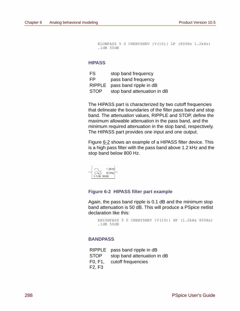
Chapter 6 Analog behavioral modeling Product Version 10.5
288 PSpice User's Guide
ELOWPASS 5 0 CHEBYSHEV V(10) LP (800Hz 1.2kHz).1dB 50dB
HIPASS
The HIPASS part is characterized by two cutoff frequenciesthat delineate the boundaries of the filter pass band and stopband. The attenuation values, RIPPLE and STOP, define themaximum allowable attenuation in the pass band, and theminimum required attenuation in the stop band, respectively.The HIPASS part provides one input and one output.
Figure 6-2 shows an example of a HIPASS filter device. Thisis a high pass filter with the pass band above 1.2 kHz and thestop band below 800 Hz.
Figure 6-2 HIPASS filter part example
Again, the pass band ripple is 0.1 dB and the minimum stopband attenuation is 50 dB. This will produce a PSpice netlistdeclaration like this:
EHIGHPASS 5 0 CHEBYSHEV V(10) HP (1.2kHz 800Hz).1dB 50dB
BANDPASS
FS stop band frequencyFP pass band frequencyRIPPLE pass band ripple in dBSTOP stop band attenuation in dB
RIPPLE pass band ripple in dBSTOP stop band attenuation in dBF0, F1,F2, F3
cutoff frequencies

Product Version 10.5 The ABM.OLB part library file
PSpice User's Guide 289
The BANDPASS part is characterized by four cutofffrequencies. The attenuation values, RIPPLE and STOP,define the maximum allowable attenuation in the pass band,and the minimum required attenuation in the stop band,respectively. The BANDPASS part provides one input and oneoutput.
Figure 6-3 shows an example of a BANDPASS filter device.This is a band pass filter with the pass band between 1.2 kHzand 2 kHz, and stop bands below 800 Hz and above 3 kHz.
Figure 6-3 BANDPASS filter part example
The pass band ripple is 0.1 dB and the minimum stop bandattenuation is 50 dB. This will produce a PSpice A/D netlistdeclaration like this:
EBANDPASS 5 0 CHEBYSHEV+ V(10) BP (800 1.2kHz 2kHz 3kHz) .1dB 50dB
BANDREJ
The BANDREJ part is characterized by four cutofffrequencies. The attenuation values, RIPPLE and STOP,define the maximum allowable attenuation in the pass band,and the minimum required attenuation in the stop band,respectively. The BANDREJ part provides one input and oneoutput.
Figure 6-4 shows an example of a BANDREJ filter device.This is a band reject (or “notch”) filter with the stop band
RIPPLE is the pass band ripple in dBSTOP is the stop band attenuation in dBF0, F1,F2, F3
are the cutoff frequencies

Chapter 6 Analog behavioral modeling Product Version 10.5
290 PSpice User's Guide
between 1.2 kHz and 2 kHz, and pass bands below 800 Hzand above 3 kHz.
Figure 6-4 BANDREJ filter part example
The pass band ripple is 0.1 dB and the minimum stop bandattenuation is 50 dB. This will produce a PSpice netlistdeclaration like this:
EBREJ 5 0 CHEBYSHEV V(10) BR (800Hz 1.2kHz 3kHz2kHz) .1dB 50dB
Integrator and differentiator
The integrator and differentiator parts are described below.
INTEG
The INTEG part implements a simple integrator. A currentsource/capacitor implementation is used to provide supportfor setting the initial condition.
DIFFER
The DIFFER part implements a simple differentiator. A voltagesource/capacitor implementation is used. The DIFFER partprovides one input and one output.
IC initial condition of the integrator outputGAIN gain value
GAIN gain value

Product Version 10.5 The ABM.OLB part library file
PSpice User's Guide 291
Table look-up parts
TABLE and FTABLE parts provide a lookup table that is usedto correlate an input and an output based on a set of datapoints. These parts are described below and on the followingpages.
TABLE
The TABLE part allows the response to be defined by a tableof one to five values. Each row contains an input and acorresponding output value. Linear interpolation is performedbetween entries.
For values outside the table’s range, the device’s output is aconstant with a value equal to the entry with the smallest (orlargest) input. This characteristic can be used to impose anupper and lower limit on the output. The TABLE part providesone input and one output.
ROWn is an (input, output) pair; by default, upto five triplets are allowed where n=1, 2,3, 4, or 5
If more than five values are required,the part can be customized through thepart editor. Insert additional rowvariables into the template using thesame form as the first five, and addROWn properties as needed to the listof properties.

Chapter 6 Analog behavioral modeling Product Version 10.5
292 PSpice User's Guide
FTABLE
The FTABLE part is described by a table of frequencyresponses in either the magnitude/phase domain (R_I= ) orcomplex number domain (R_I=YES). The entire table is readin and converted to magnitude in dB and phase in degrees.
ROWn either an (input frequency,magnitude, phase) triplet, or an(input frequency, real part,imaginary part) triplet describing acomplex value; by default, up to fivetriplets are allowed where n=1, 2, 3,4, or 5
If more than five values arerequired, the part can becustomized through the part editor.Insert additional row variables intothe template using the same formas the first five, and add ROWnproperties as needed to the list ofproperties.
DELAY group delay increment; defaults to 0if left blank
R_I table type; if left blank, thefrequency table is interpreted in the(input frequency, magnitude,phase) format; if defined with anyvalue (such as YES), the table isinterpreted in the (input frequency,real part, imaginary part) format
MAGUNITS units for magnitude where the valuecan be DB (decibels) or MAG (rawmagnitude); defaults to DB if leftblank
PHASEUNITS units for phase where the value canbe DEG (degrees) or RAD(radians); defaults to DEG if leftblank

Product Version 10.5 The ABM.OLB part library file
PSpice User's Guide 293
Interpolation is performed between entries. Magnitude isinterpolated logarithmically; phase is interpolated linearly. Forfrequencies outside the table’s range, 0 (zero) magnitude isused. This characteristic can be used to impose an upper andlower limit on the output.
The DELAY property increases the group delay of thefrequency table by the specified amount. The delay term isparticularly useful when a frequency table device generates anon-causality warning message during a transient analysis.The warning message issues a delay value that can beassigned to the part’s DELAY property for subsequent runs,without otherwise altering the table.
The output of the part depends on the analysis being done.For DC and bias point, the output is the zero frequencymagnitude times the input voltage. For AC analysis, the inputvoltage is linearized around the bias point (similar to EVALUEand GVALUE parts, Modeling mathematical or instantaneousrelationships on page 309). The output for each frequency isthen the input times the gain, times the value of the table atthat frequency.
For transient analysis, the voltage is evaluated at each timepoint. The output is then the convolution of the past valueswith the impulse response of the frequency response. Theserules follow the standard method of using Fourier transforms.We recommend looking at one or more of the references citedin Frequency-domain device models on page 315 for moreinformation.
Note: The table’s frequencies must be in order from lowest tohighest. The TABLE part provides one input and oneoutput.
Example
A device, ELOFILT, is used as a frequency filter. The input tothe frequency response is the voltage at net 10. The output isa voltage across nets 5 and 0. The table describes a low passfilter with a response of 1 (0 dB) for frequencies below 5kilohertz and a response of 0.001 (-60 dB) for frequenciesabove 6 kilohertz. The phase lags linearly with frequency. This

Chapter 6 Analog behavioral modeling Product Version 10.5
294 PSpice User's Guide
is the same as a constant time delay. The delay is necessaryso that the impulse response is causal. That is, so that theimpulse response does not have any significant componentsbefore time zero. The FTABLE part in Figure 6-5 could beused.
This part is characterized by the following properties:
ROW1 = 0Hz 0 0ROW2 = 5kHz 0 -5760ROW3 = 6kHz -60 -6912DELAY =R_I =MAGUNITS =PHASEUNITS =
Since R_I, MAGUNITS, and PHASEUNITS are undefined,each table entry is interpreted as containing frequency,magnitude value in dB, and phase values in degrees. Delaydefaults to 0.
This produces a PSpice netlist declaration like this:
ELOFILT 5 0 FREQ V(10)+0Hz 0 0+5kHz 0 -5760+6kHz -60 -6912
Since constant group delay is calculated from the values for agiven table entry as:
group delay = phase / 360 / frequency
An equivalent FTABLE instance could be defined using theDELAY property. For this example, the group delay is 3.2 msec(6912 / 360 / 6k = 5760 / 360 / 6k = 3.2m). Equivalent propertyassignments are:
ROW1 = 0Hz 0 0ROW2 = 5kHz 0 0
Figure 6-5 FTABLE part

Product Version 10.5 The ABM.OLB part library file
PSpice User's Guide 295
ROW3 = 6kHz -60 0DELAY = 3.2msR_I =MAGUNITS =PHASEUNITS =
This produces a PSpice netlist declaration like this:
ELOFILT 5 0 FREQ V(10)+0Hz 0 0+5kHz 0 0+6kHz -60 0+DELAY=3.2ms

Chapter 6 Analog behavioral modeling Product Version 10.5
296 PSpice User's Guide
Laplace transform part
The LAPLACE part specifies a Laplace transform which isused to determine an output for each input value.
LAPLACE
The LAPLACE part uses a Laplace transform description. Theinput to the transform is a voltage. The numerator anddenominator of the Laplace transform function are specifiedas properties for the part.
Note: Voltages, currents, and TIME may not appear in aLaplace transform specification.
The output of the part depends on the type of analysis beingdone. For DC and bias point, the output is the zero frequencygain times the value of the input. The zero frequency gain isthe value of the Laplace transform with s=0. For AC analysis,the output is then the input times the gain times the value ofthe Laplace transform. The value of the Laplace transform ata frequency is calculated by substituting j·ω for s, where ω is2π·frequency. For transient analysis, the output is theconvolution of the input waveform with the impulse responseof the transform. These rules follow the standard method ofusing Laplace transforms.
Example one
The input to the Laplace transform is the voltage at net 10. Theoutput is a voltage and is applied between nets 5 and 0. ForDC, the output is simply equal to the input, since the gain ats=0 is 1. The transform, 1/(1+.001·s), describes a simple,lossy integrator with a time constant of 1 millisecond. This canbe implemented with an RC pair that has a time constant of 1millisecond.
NUM numerator of the Laplaceexpression
DENOM denominator of the Laplaceexpression

Product Version 10.5 The ABM.OLB part library file
PSpice User's Guide 297
For AC analysis, the gain is found by substituting j·ω for s. Thisgives a flat response out to a corner frequency of 1000/(2π) =159 hertz and a roll-off of 6 dB per octave after 159 Hz. Thereis also a phase shift centered around 159 Hz. In other words,the gain has both a real and an imaginary component. Fortransient analysis, the output is the convolution of the inputwaveform with the impulse response of 1/(1+.001·s). Theimpulse response is a decaying exponential with a timeconstant of 1 millisecond. This means that the output is the“lossy integral” of the input, where the loss has a time constantof 1 millisecond. The LAPLACE part shown in Figure 6-6 couldbe used for this purpose.
Figure 6-6 LAPLACE part
The transfer function is the Laplace transform (1/[1+.001*s]).This LAPLACE part is characterized by the followingproperties:
NUM = 1DENOM = 1 + .001*s
The gain and phase characteristics are shown in Figure 6-7.
Figure 6-7 Viewing gain and phase characteristics of alossy integrator.

Chapter 6 Analog behavioral modeling Product Version 10.5
298 PSpice User's Guide
This produces a PSpice netlist declaration like this:
ERC 5 0 LAPLACE V(10) = 1/(1+.001*s)
Example two
The input is V(10). The output is a current applied betweennets 5 and 0. The Laplace transform describes a lossytransmission line. R, L, and C are the resistance, inductance,and capacitance of the line per unit length.
If R is small, the characteristic impedance of such a line isZ = ((R + j·ω·L)/(j·ω·C))1/2, the delay per unit length is (L C)1/2,and the loss in dB per unit length is 23·R/Z. This could berepresented by the device in Figure 6-8.
Figure 6-8 LAPLACE part
The parameters R, L, and C can be defined in a .PARAMstatement contained in a model file. (Refer to the onlinePSpice Reference Guide for more information about using.PARAM statements.) More useful, however, is for R, L, and Cto be arguments passed into a subcircuit. This part has thefollowing characteristics:
NUM = EXP(-SQRT(C*s*(R+L*s)))DENOM = 1
This produces a PSpice netlist declaration like this:
GLOSSY 5 0 LAPLACE V(10) = exp(-sqrt(C*s*(R +L*s)))
The Laplace transform parts are, however, an inefficient way,in both computer time and memory, to implement a delay. Forideal delays we recommend using the transmission line partinstead.

Product Version 10.5 The ABM.OLB part library file
PSpice User's Guide 299
Math functions
The ABM math function parts are shown in Table 6-2. Mathfunction parts are based on the PSpice “E” device type. Eachprovides one or more inputs, and a mathematical functionwhich is applied to the input. The result is output on the outputnet.
ABM expression parts
The expression parts are shown in Table 6-3. These parts canbe customized to perform a variety of functions depending onyour requirements. Each of these parts has a set of fourexpression building block properties of the form:
Table 6-2 ABM math function parts
For thisdevice...
Output is the...
ABS absolute value of the input
SQRT square root of the input
PWR result of raising the absolute value of theinput to the power specified by EXP
PWRS result of raising the (signed) input value tothe power specified by EXP
LOG LOG of the input
LOG10 LOG10 of the input
EXP result of e raised to the power specified bythe input value (ex where x is the input)
SIN sin of the input (where the input is inradians)
COS cos of the input (where the input is inradians)
TAN tan of the input (where the input is inradians)
ATAN,ARCTAN
tan-1 of the input (where the output is inradians)

Chapter 6 Analog behavioral modeling Product Version 10.5
300 PSpice User's Guide
EXPn
where n = 1, 2, 3, or 4.
During netlist generation, the complete expression is formedby concatenating the building block expressions in numericorder, thus defining the transfer function. Hence, the firstexpression fragment should be assigned to the EXP1property, the second fragment to EXP2, and so on.
Expression properties can be defined using a combination ofarithmetic operators and input designators. You may use anyof the standard PSpice arithmetic operators (see Table 3-3 onpage 126) within an expression statement. You may also usethe EXPn properties as variables to represent nets orconstants.
The following examples illustrate a variety of ABM expressionpart applications.
Example one
Suppose you want to set an output voltage on net 4 to 5 voltstimes the square root of the voltage between nets 3 and 2. Youcould use an ABM2 part (which takes two inputs and provides
Table 6-3 ABM expression parts
Part Inputs Output
ABM none V
ABM1 1 V
ABM2 2 V
ABM3 3 V
ABM/I none I
ABM1/I 1 I
ABM2/I 2 I
ABM3/I 3 I

Product Version 10.5 The ABM.OLB part library file
PSpice User's Guide 301
a voltage output) to define a part like the one shown in Figure6-9.
Figure 6-9 ABM expression part example one.
In this example of an ABM device, the output voltage is set to5 volts times the square root of the voltage between net 3 andnet 2. The property settings for this part are as follows:
EXP1 = 5V *EXP2 = SQRT(V(%IN2,%IN1))
This will produce a PSpice netlist declaration like this:
ESQROOT 4 0 VALUE = 5V*SQRT(V(3,2))
Example two
GPSK is an oscillator for a PSK (Phase Shift Keyed)modulator. Current is pumped from net 11 through the sourceto net 6. Its value is a sine wave with an amplitude of 15 mAand a frequency of 10 kHz. The voltage at net 3 can shift thephase of GPSK by 1 radian/volt. Note the use of the TIMEparameter in the EXP2 expression. This is the PSpice A/Dinternal sweep variable used in transient analysis. For anyanalysis other than transient, TIME = 0. This could berepresented with an ABM1/I part (single input, current output)like the one shown in Figure 6-10.
Figure 6-10 ABM expression part example two.
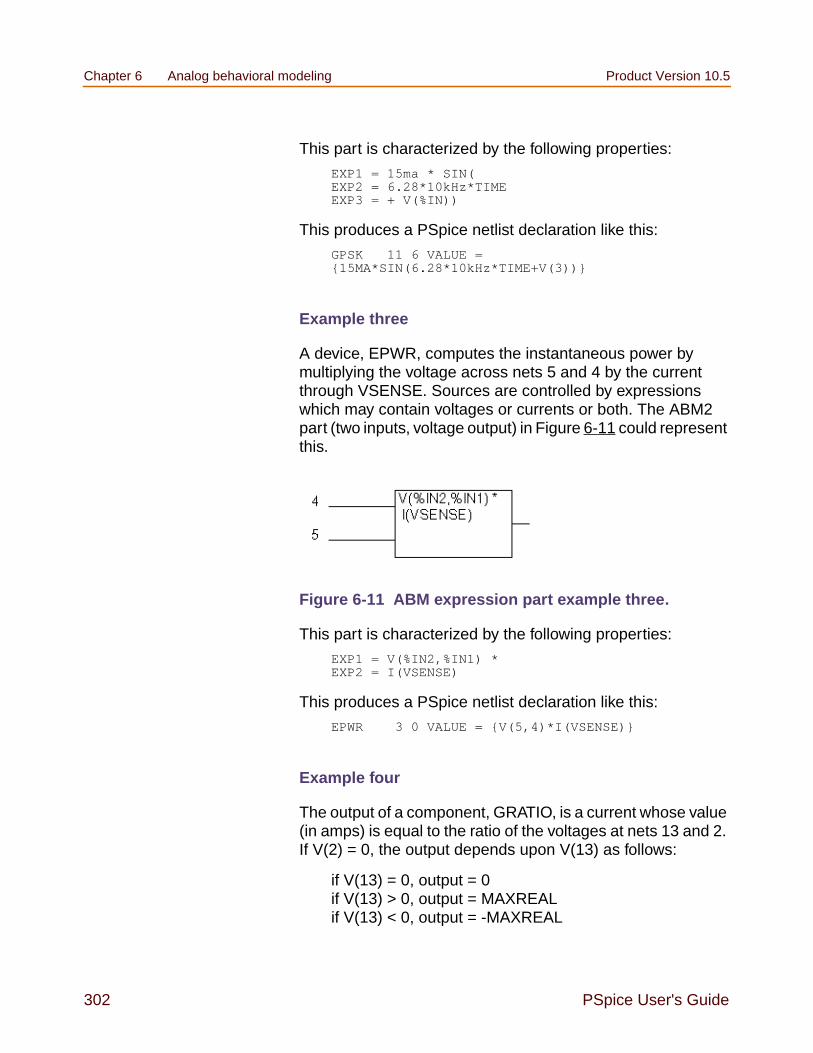
Chapter 6 Analog behavioral modeling Product Version 10.5
302 PSpice User's Guide
This part is characterized by the following properties:
EXP1 = 15ma * SIN(EXP2 = 6.28*10kHz*TIMEEXP3 = + V(%IN))
This produces a PSpice netlist declaration like this:
GPSK 11 6 VALUE =15MA*SIN(6.28*10kHz*TIME+V(3))
Example three
A device, EPWR, computes the instantaneous power bymultiplying the voltage across nets 5 and 4 by the currentthrough VSENSE. Sources are controlled by expressionswhich may contain voltages or currents or both. The ABM2part (two inputs, voltage output) in Figure 6-11 could representthis.
Figure 6-11 ABM expression part example three.
This part is characterized by the following properties:
EXP1 = V(%IN2,%IN1) *EXP2 = I(VSENSE)
This produces a PSpice netlist declaration like this:
EPWR 3 0 VALUE = V(5,4)*I(VSENSE)
Example four
The output of a component, GRATIO, is a current whose value(in amps) is equal to the ratio of the voltages at nets 13 and 2.If V(2) = 0, the output depends upon V(13) as follows:
if V(13) = 0, output = 0if V(13) > 0, output = MAXREALif V(13) < 0, output = -MAXREAL

Product Version 10.5 The ABM.OLB part library file
PSpice User's Guide 303
where MAXREAL is a PSpice internal constant representing avery large number (on the order of 1e30). In general, the resultof evaluating an expression is limited to MAXREAL. This ismodeled with an ABM2/I (two input, current output) part likethis one in 6-12.
Figure 6-12 ABM expression part example four.
This part is characterized by the following properties:
EXP1 = V(%IN2)/V(%IN1)
Note that output of GRATIO can be used as part of thecontrolling function. This produces a PSpice netlistdeclaration like this:
GRATIO 2 3 VALUE = V(13)/V(2)
Note: Letting a current approach 1e30 will almost certainlycause convergence problems. To avoid this, use thelimit function on the ratio to keep the current withinreasonable limits.
An instantaneous device example: modeling a triode
This section provides an example of using various ABM partsto model a triode vacuum tube. The schematic of the triodesubcircuit is shown in Figure 6-13.

Chapter 6 Analog behavioral modeling Product Version 10.5
304 PSpice User's Guide
Figure 6-13 Triode circuit.
Assumptions: In its main operating region, the triode’s currentis proportional to the 3/2 power of a linear combination of thegrid and anode voltages:
ianode = k0*(vg + k1*va)1.5
For a typical triode, k0 = 200e-6 and k1 = 0.12.
Looking at the upper left-hand portion of the schematic, noticethe a general-purpose ABM part used to take the inputvoltages from anode, grid, and cathode. Assume the followingassociations:
V(anode) is associated with V(%IN1)
V(grid) is associated with V(%IN2)
V(cathode) is associated with V(%IN3)
The expression property EXP1 then represents V(grid,cathode) and the expression property EXP2 represents0.12[V(anode, cathode)]. When the template substitution isperformed, the resulting VALUE is equivalent to the following:
V = V(grid, cathode) + 0.12*V(anode, cathode)
The part would be defined with the following characteristics:
EXP1 = V(%IN2,%IN3)+EXP2 = 0.12*V(%IN1,%IN3)
This works for the main operating region but does not modelthe case in which the current stays 0 when combined grid andanode voltages go negative. We can accommodate thatsituation as follows by adding the LIMIT part with the followingcharacteristics:
HI = 1E3LO = 0
This part instance, LIMIT1, converts all negative values ofvg+.12*va to 0 and leaves all positive values (up to 1 kV) alone.For a more realistic model, we could have used TABLE tocorrectly model how the tube turns off at 0 or at small negativegrid voltages.

Product Version 10.5 The ABM.OLB part library file
PSpice User's Guide 305
We also need to make sure that the current becomes zerowhen the anode alone goes negative. To do this, we can usea DIFF device, (immediately below the ABM3 device) tomonitor the difference between V(anode) and V(cathode), andoutput the difference to the TABLE part. The table translatesall values at or below zero to zero, and all values greater thanor equal to 30 to one. All values between 0 and 30 are linearlyinterpolated. The properties for the TABLE part are as follows:
ROW1 = 00ROW2 = 301
The TABLE part is a simple one, and ensures that only a zerovalue is output to the multiplier for negative anode voltages.
The output from the TABLE part and the LIMIT part arecombined at the MULT multiplier part. The output of the MULTpart is the product of the two input voltages. This value is thenraised to the 3/2 or 1.5 power using the PWR part. Theexponential property of the PWR part is defined as follows:
EXP = 1.5
The last major component is an ABM expression componentto take an input voltage and convert it into a current. Therelevant ABM1/I part property looks like this:
EXP1 = 200E-6 * V(%IN)
A final step in the model is to add device parasitics. Forexample, a resistor can be used to give a finite outputimpedance. Capacitances between the grid, cathode, andanode are also needed. The lower part of the schematic inFigure 6-13 shows a possible method for incorporating theseeffects. To complete the example, one could add a circuit

Chapter 6 Analog behavioral modeling Product Version 10.5
306 PSpice User's Guide
which produces the family of I-V curves (shown in Figure6-14).
Figure 6-14 Triode subcircuit producing a family of I-Vcurves.
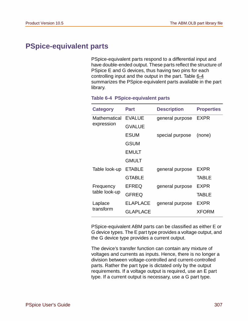
Product Version 10.5 The ABM.OLB part library file
PSpice User's Guide 307
PSpice-equivalent parts
PSpice-equivalent parts respond to a differential input andhave double-ended output. These parts reflect the structure ofPSpice E and G devices, thus having two pins for eachcontrolling input and the output in the part. Table 6-4summarizes the PSpice-equivalent parts available in the partlibrary.
PSpice-equivalent ABM parts can be classified as either E orG device types. The E part type provides a voltage output, andthe G device type provides a current output.
The device’s transfer function can contain any mixture ofvoltages and currents as inputs. Hence, there is no longer adivision between voltage-controlled and current-controlledparts. Rather the part type is dictated only by the outputrequirements. If a voltage output is required, use an E parttype. If a current output is necessary, use a G part type.
Table 6-4 PSpice-equivalent parts
Category Part Description Properties
Mathematicalexpression
EVALUE general purpose EXPR
GVALUE
ESUM special purpose (none)
GSUM
EMULT
GMULT
Table look-up ETABLE general purpose EXPR
GTABLE TABLE
Frequencytable look-up
EFREQ general purpose EXPR
GFREQ TABLE
Laplacetransform
ELAPLACE general purpose EXPR
GLAPLACE XFORM

Chapter 6 Analog behavioral modeling Product Version 10.5
308 PSpice User's Guide
Note: There are no equivalent “F” or “H” part types in the partlibrary because PSpice “F” and “H” devices do notsupport the ABM extensions.
Each E or G part type in the ABM.OLB part file is defined by atemplate that provides the specifics of the transfer function.Other properties in the model definition can be edited tocustomize the transfer function. By default, the templatecannot be modified directly choosing Properties from the Editmenu in Capture. Rather, the values for other properties (suchas the expressions used in the template) are usually edited,then these values are substituted into the template. However,the part editor can be used to modify the template ordesignate the template as modifiable from within Capture.This way, custom parts can be created for special-purposeapplication.
Implementation of PSpice-equivalent parts
Although you generally use Capture to place and specifyPSpice-equivalent ABM parts, it is useful to know the PSpicecommand syntax for “E” and “G” devices. This is especiallytrue when creating custom ABM parts since part templatesmust adhere to PSpice syntax.
The general forms for PSpice “E” and “G” extensions are:
E <name> <connecting nodes> <ABM keyword><ABM function>
G <name> <connecting nodes> <ABM keyword><ABM function>
where
<name> is the device name appended to the E or Gdevice type character
<connectingnodes>
specifies the <(+ node name, - nodename)> pair between which the device isconnected

Product Version 10.5 The ABM.OLB part library file
PSpice User's Guide 309
Refer to the online PSpice Reference Guide for detailedinformation.
Modeling mathematical or instantaneous relationships
The instantaneous models (using VALUE and TABLEextensions to PSpice “E” and “G” devices in the parttemplates) enforce a direct response to the input at eachmoment in time. For example, the output might be equal to thesquare root of the input at every point in time. Such a devicehas no memory, or, a flat frequency response. Thesetechniques can be used to model both linear and nonlinearresponses.
Note: For AC analysis, a nonlinear device is first linearizedaround the bias point, and then the linear equivalent isused.
EVALUE and GVALUE parts
The EVALUE and GVALUE parts allow an instantaneoustransfer function to be written as a mathematical expression instandard notation. These parts take the input signal, performthe function specified by the EXPR property on the signal, andoutput the result on the output pins.
In controlled sources, EXPR may contain constants andparameters as well as voltages, currents, or time. Voltagesmay be either the voltage at a net, such as V(5), or the voltageacross two nets, such as V(4,5). Currents must be the current
<ABMkeyword>
specifies the form of the transfer function tobe used, as one of:
VALUE arithmetic expressionTABLE lookup tableLAPLACE Laplace transformFREQ frequency response tableCHEBYSHEV Chebyshev filtercharacteristics
<ABMfunction>
specifies the transfer function as a formula orlookup table as required by the specified<ABM keyword>

Chapter 6 Analog behavioral modeling Product Version 10.5
310 PSpice User's Guide
through a voltage source (V device), for example, I(VSENSE).Voltage sources with a value of 0 are handy for sensingcurrent for use in these expressions.
Functions may be used in expressions, along with arithmeticoperators (+, -, *, and /) and parentheses. Available built-infunctions are summarized in Table 3-4 on page 126.
The EVALUE and GVALUE parts are defined, in part, by thefollowing properties (default values are shown):
EVALUE
EXPR V(%IN+, %IN-)
GVALUE
EXPR V(%IN+, %IN-)
Sources are controlled by expressions which may containvoltages, currents, or both. The following examples illustratecustomized EVALUE and GVALUE parts.
Example 1
In the example of an EVALUE device shown in Figure 6-15,the output voltage is set to 5 volts times the square root of thevoltage between pins %IN+ and %IN-.
Figure 6-15 EVALUE part example.
The property settings for this device are as follows:
EXPR = 5v * SQRT(V(%IN+,%IN-))

Product Version 10.5 The ABM.OLB part library file
PSpice User's Guide 311
Example 2
Consider the device in Figure 6-16. This device could be usedas an oscillator for a PSK (Phase Shift Keyed) modulator.
Figure 6-16 GVALUE part example.
A current through a source is a sine wave with an amplitude of15 mA and a frequency of 10 kHz. The voltage at the input pincan shift the phase by 1 radian/volt. Note the use of the TIMEparameter in this expression. This is the PSpice internalsweep variable used in transient analyses. For any analysisother than transient, TIME = 0. The relevant property settingsfor this device are shown below:
EXPR = 15ma*SIN(6.28*10kHz*TIME+V(%IN+,%IN-))
EMULT, GMULT, ESUM, and GSUM
The EMULT and GMULT parts provide output which is basedon the product of two input sources. The ESUM and GSUMparts provide output which is based on the sum of two inputsources. The complete transfer function may also includeother mathematical expressions.
Example 1
Consider the device in Figure 6-17. This device computes theinstantaneous power through resistor VSENSE by multiplying

Chapter 6 Analog behavioral modeling Product Version 10.5
312 PSpice User's Guide
the current through VSENSE (converted to voltage by H1) bythe voltage across VSENSE.
Figure 6-17 EMULT part example.
This device’s behavior is built-in to the PSPICETEMPLATEproperty as follows (appears on one line):
TEMPLATE=E^@REFDES %OUT+ %OUT- VALUEV(%IN1+,%IN1-)
*V(%IN2+,%IN2-)
You can use the part editor to change the characteristics of thetemplate to accommodate additional mathematical functions,or to change the nature of the transfer function itself. Forexample, you may want to create a voltage divider, rather thana multiplier. This is illustrated in the following example.
Example 2
Consider the device in Figure 6-18.
Figure 6-18 GMULT part example.
With this device, the output is a current is equal to the ratio ofthe voltages at input pins 1 and input pins 2. If V(%IN2+,

Product Version 10.5 The ABM.OLB part library file
PSpice User's Guide 313
%IN2-) = 0, the output depends upon V(%IN1+, %IN1-) asfollows:
if V(%IN1+, %IN1-) = 0, output = 0if V(%IN1+, %IN1-) > 0, output = MAXREALif V(%IN1+, %IN1-) < 0, output = -MAXREAL
where MAXREAL is a PSpice internal constant representing avery large number (on the order of 1e30). In general, the resultof evaluating an expression is limited to MAXREAL. Note thatthe output of the part can also be used as part of thecontrolling function.
To create this device, you would first make a new part, GDIV,based on the GMULT part. Edit the GDIV template to dividethe two input values rather than multiply them.
Lookup tables (ETABLE and GTABLE)
The ETABLE and GTABLE parts use a transfer functiondescribed by a table. These device models are well suited foruse with measured data.
The ETABLE and GTABLE parts are defined in part by thefollowing properties (default values are shown):
ETABLE
TABLE (-15, -15), (15,15)EXPR V(%IN+, %IN-)
GTABLE
TABLE (-15, -15), (15,15)EXPR V(%IN+, %IN-)
First, EXPR is evaluated, and that value is used to look up anentry in the table. EXPR is a function of the input (current orvoltage) and follows the same rules as for VALUEexpressions.
The table consists of pairs of values, the first of which is aninput, and the second of which is the corresponding output.Linear interpolation is performed between entries. For valuesof EXPR outside the table’s range, the device’s output is a

Chapter 6 Analog behavioral modeling Product Version 10.5
314 PSpice User's Guide
constant with a value equal to the entry with the smallest (orlargest) input. This characteristic can be used to impose anupper and lower limit on the output.
An example of a table declaration (using the TABLE property)would be the following:
TABLE =
+ (0, 0) (.02, 2.690E-03) (.04, 4.102E-03) (.06,4.621E-03)
+ (.08, 4.460E-03) (.10, 3.860E-03) (.12, 3.079E-03)(.14,+ 2.327E-03)
+ (.16, 1.726E-03) (.18, 1.308E-03) (.20, 1.042E-03)(.22,+ 8.734E-04)
+ (.24, 7.544E-04) (.26, 6.566E-04) (.28, 5.718E-04)(.30,+ 5.013E-04)
+ (.32, 4.464E-04) (.34, 4.053E-04) (.36, 3.781E-04)(.38,+ 3.744E-04)
+ (.40, 4.127E-04) (.42, 5.053E-04) (.44, 6.380E-04)(.46,+ 7.935E-04)
+ (.48, 1.139E-03) (.50, 2.605E-03) (.52, 8.259E-03)(.54,+ 2.609E-02)
+ (.56, 7.418E-02) (.58, 1.895E-01) (.60, 4.426E-01)

Product Version 10.5 The ABM.OLB part library file
PSpice User's Guide 315
Frequency-domain device models
Frequency-domain models (ELAPLACE, GLAPLACE,EFREQ, and GFREQ) are characterized by output thatdepends on the current input as well as the input history. Therelationship is therefore non-instantaneous. For example, theoutput may be equal to the integral of the input over time. Inother words, the response depends upon frequency.
During AC analysis, the frequency response determines thecomplex gain at each frequency. During DC analysis and biaspoint calculation, the gain is the zero-frequency response.During transient analysis, the output of the device is theconvolution of the input and the impulse response of thedevice.
Moving back and forth between the time andfrequency-domains can cause surprising results. Often theresults are quite different than what one would intuitivelyexpect. For this reason, we strongly recommend familiaritywith a reference on Fourier and Laplace transforms. A goodone is:
R. Bracewell, The Fourier Transform and Its Applications,McGraw-Hill, Revised Second Edition (1986)
We also recommend familiarity with the use of transforms inanalyzing linear systems. Some references on this subject:
W. H. Chen, The Analysis of Linear Systems,McGraw-Hill (1962)
J. A. Aseltine, Transform Method in Linear SystemAnalysis, McGraw-Hill (1958)
Laplace transforms (LAPLACE)
The ELAPLACE and GLAPLACE parts allow a transferfunction to be described by a Laplace transform function. TheELAPLACE and GLAPLACE parts are defined, in part, by thefollowing properties (default values are shown):
ELAPLACE

Chapter 6 Analog behavioral modeling Product Version 10.5
316 PSpice User's Guide
EXPR V(%IN+, %IN-)XFORM 1/s
GLAPLACE
EXPR V(%IN+, %IN-)XFORM 1/s
The LAPLACE parts use a Laplace transform description. Theinput to the transform is the value of EXPR, where EXPRfollows the same rules as for VALUE expressions (seeEVALUE and GVALUE parts on page 309). XFORM is anexpression in the Laplace variable, s. It follows the rules forstandard expressions as described for VALUE expressionswith the addition of the s variable.
Note: Voltages, currents, and TIME cannot appear in aLaplace transform.
The output of the device depends on the type of analysisbeing done. For DC and bias point, the output is simply thezero frequency gain times the value of EXPR. The zerofrequency gain is the value of XFORM with s = 0. For ACanalysis, EXPR is linearized around the bias point (similar tothe VALUE parts). The output is then the input times the gainof EXPR times the value of XFORM. The value of XFORM ata frequency is calculated by substituting j·w for s, where w is2p·frequency. For transient analysis, the value of EXPR isevaluated at each time point. The output is then theconvolution of the past values of EXPR with the impulseresponse of XFORM. These rules follow the standard methodof using Laplace transforms. We recommend looking at one ormore of the references cited in Frequency-domain devicemodels on page 315 for more information.
Example
The input to the Laplace transform is the voltage across theinput pins, or V(%IN+, %IN-). The EXPR property may beedited to include constants or functions, as with other parts.The transform, 1/(1+.001·s), describes a simple, lossyintegrator with a time constant of 1 millisecond. This can beimplemented with an RC pair that has a time constant of 1millisecond.

Product Version 10.5 The ABM.OLB part library file
PSpice User's Guide 317
Using the part editor, you would define the XFORM and EXPRproperties as follows:
XFORM = 1/(1+.001*s)EXPR = V(%IN+, %IN-)
The default template remains (appears on one line):
TEMPLATE= E^@REFDES %OUT+ %OUT- LAPLACE @EXPR=(@XFORM)
After netlist substitution of the template, the resulting transferfunction would become:
V(%OUT+, %OUT-) = LAPLACE V(%IN+, %IN-)=(1/1+.001*s))
The output is a voltage and is applied between pins %OUT+and %OUT-. For DC, the output is simply equal to the input,since the gain at s = 0 is 1.
For AC analysis, the gain is found by substituting j·ω for s. Thisgives a flat response out to a corner frequency of 1000/(2π) =159 Hz and a roll-off of 6 dB per octave after 159 Hz. There isalso a phase shift centered around 159 Hz. In other words, thegain has both a real and an imaginary component. The gainand phase characteristic is the same as that shown for theequivalent control system part example using the LAPLACEpart (see Figure 6-7 on page 297).
For transient analysis, the output is the convolution of the inputwaveform with the impulse response of 1/(1+.001·s). Theimpulse response is a decaying exponential with a timeconstant of 1 millisecond. This means that the output is the“lossy integral” of the input, where the loss has a time constantof 1 millisecond.
This will produce a PSpice A/D netlist declaration similar to:
ERC 5 0 LAPLACE V(10) = 1/(1+.001*s)
Frequency response tables (EFREQ and GFREQ)
The EFREQ and GFREQ parts are described by a table offrequency responses in either the magnitude/phase domain orcomplex number domain. The entire table is read in andconverted to magnitude in dB and phase in degrees.Interpolation is performed between entries. Phase is

Chapter 6 Analog behavioral modeling Product Version 10.5
318 PSpice User's Guide
interpolated linearly; magnitude is interpolated logarithmically.For frequencies outside the table’s range, 0 (zero) magnitudeis used.
EFREQ and GFREQ properties are defined as follows:
The DELAY property increases the group delay of thefrequency table by the specified amount. The delay term isparticularly useful when an EFREQ or GFREQ devicegenerates a non-causality warning message during atransient analysis. The warning message issues a delay valuethat can be assigned to the part’s DELAY property forsubsequent runs, without otherwise altering the table.
The output of the device depends on the analysis being done.For DC and bias point, the output is simply the zero frequencymagnitude times the value of EXPR. For AC analysis, EXPRis linearized around the bias point (similar to EVALUE andGVALUE parts). The output for each frequency is then the
EXPR value used for table lookup; defaults toV(%IN+, %IN-) if left blank.
TABLE series of either (input frequency,magnitude, phase) triplets, or (inputfrequency, real part, imaginary part)triplets describing a complex value;defaults to (0,0,0) (1Meg,-10,90) if leftblank.
DELAY group delay increment; defaults to 0 if leftblank.
R_I table type; if left blank, the frequencytable is interpreted in the (inputfrequency, magnitude, phase) format; ifdefined with any value (such as YES), thetable is interpreted in the (inputfrequency, real part, imaginary part)format.
MAGUNITS units for magnitude where the value canbe DB (decibels) or MAG (rawmagnitude); defaults to DB if left blank.
PHASEUNITS units for phase where the value can beDEG (degrees) or RAD (radians);defaults to DEG if left blank.
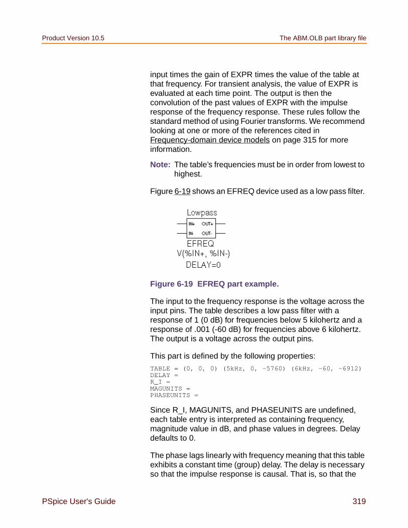
Product Version 10.5 The ABM.OLB part library file
PSpice User's Guide 319
input times the gain of EXPR times the value of the table atthat frequency. For transient analysis, the value of EXPR isevaluated at each time point. The output is then theconvolution of the past values of EXPR with the impulseresponse of the frequency response. These rules follow thestandard method of using Fourier transforms. We recommendlooking at one or more of the references cited inFrequency-domain device models on page 315 for moreinformation.
Note: The table’s frequencies must be in order from lowest tohighest.
Figure 6-19 shows an EFREQ device used as a low pass filter.
Figure 6-19 EFREQ part example.
The input to the frequency response is the voltage across theinput pins. The table describes a low pass filter with aresponse of 1 (0 dB) for frequencies below 5 kilohertz and aresponse of .001 (-60 dB) for frequencies above 6 kilohertz.The output is a voltage across the output pins.
This part is defined by the following properties:
TABLE = (0, 0, 0) (5kHz, 0, -5760) (6kHz, -60, -6912)DELAY =R_I =MAGUNITS =PHASEUNITS =
Since R_I, MAGUNITS, and PHASEUNITS are undefined,each table entry is interpreted as containing frequency,magnitude value in dB, and phase values in degrees. Delaydefaults to 0.
The phase lags linearly with frequency meaning that this tableexhibits a constant time (group) delay. The delay is necessaryso that the impulse response is causal. That is, so that the

Chapter 6 Analog behavioral modeling Product Version 10.5
320 PSpice User's Guide
impulse response does not have any significant componentsbefore time zero.
The constant group delay is calculated from the values for agiven table entry as follows:
group delay = phase / 360 / frequency
For this example, the group delay is 3.2 msec(6912 / 360 / 6k = 5760 / 360 / 6k = 3.2m). An alternativespecification for this table could be:
TABLE = (0, 0, 0) (5kHz, 0, 0) (6kHz, -60, 0)DELAY = 3.2msR_I =MAGUNITS =PHASEUNITS =
This produces a PSpice netlist declaration like this:
ELOWPASS 5 0 FREQ V(10) = (0,0,0) (5kHz,0,0)(6kHz-60,0)+ DELAY = 3.2ms
Cautions and recommendations for simulation andanalysis
Instantaneous device modeling
During AC analysis, nonlinear transfer functions are handledthe same way as other nonlinear parts: each function islinearized around the bias point and the resulting small-signalequivalent is used.
Consider the voltage multiplier (mixer) shown in Figure 6-20.
Figure 6-20 Voltage multiplier circuit (mixer).

Product Version 10.5 Cautions and recommendations for simulation and analysis
PSpice User's Guide 321
This circuit has the following characteristics:
Vin1: DC=0v AC=1vVin2: DC=0v AC=1v
where the output on net 3 is V(1)*V(2).
During AC analysis, V(3) = 0 due to the 0 volts bias pointvoltage on nets 1, 2, and 3. The small-signal equivalenttherefore has 0 gain (the derivative of V(1)*V(2) with respectto both V(1) and V(2) is 0 when V(1)=V(2)=0). So, the outputof the mixer during AC analysis will be 0 regardless of the ACvalues of V(1) and V(2).
Another way of looking at this is that a mixer is a nonlineardevice and AC analysis is a linear analysis. The output of themixer has 0 amplitude at the fundamental. (Output is nonzeroat DC and twice the input frequency, but these are notincluded in a linear analysis.)
If you need to analyze nonlinear functions, such as a mixer,use transient analysis. Transient analysis solves the full,nonlinear circuit equations. It also allows you to use inputwaveforms with different frequencies (for example, VIN1 couldbe 90 MHz and VIN2 could be 89.8 MHz). AC analysis doesnot have this flexibility, but in return it uses much lesscomputer time.
Frequency-domain parts
Some caution is in order when moving between frequency andtime domains. This section discusses several points that areinvolved in the implementation of frequency-domain parts.These discussions all involve the transient analysis, sinceboth the DC and AC analyses are straightforward.
The first point is that there are limits on the maximum valuesand on the resolution of both time and frequency. These arerelated: the frequency resolution is the inverse of themaximum time and vice versa. The maximum time is thelength of the transient analysis, TSTOP. Therefore, thefrequency resolution is 1/TSTOP.

Chapter 6 Analog behavioral modeling Product Version 10.5
322 PSpice User's Guide
Laplace transforms
For Laplace transforms, PSpice starts off with initial boundson the frequency resolution and the maximum frequencydetermined by the transient analysis parameters as follows.The frequency resolution is initially set below the theoreticallimit to (.25/TSTOP) and is then made as large as possiblewithout inducing sampling errors. The maximum frequencyhas an initial upper bound of (1/(RELTOL*TMAX)), whereTMAX is the transient analysis Step Ceiling value, andRELTOL is the relative accuracy of all calculated voltages andcurrents. If a Step Ceiling value is not specified, PSpice usesthe Transient Analysis Print Step, TSTEP, instead.
Note: TSTOP, TMAX, and TSTEP values are configuredusing Transient on the Setup menu. The RELTOLproperty is set using Options on the Setup menu.
PSpice then attempts to reduce the maximum frequency bysearching for the frequency at which the response has fallento RELTOL times the maximum response. For instance, for thetransform:
1/(1+s)
the maximum response, 1.0, is at s = j·ω = 0 (DC). The cutofffrequency used when RELTOL=.001, is approximately1000/(2π) = 159 Hz. At 159 Hz, the response is down to .001(down by 60 db). Since some transforms do not have such alimit, there is also a limit of 10/RELTOL times the frequencyresolution, or 10/(RELTOL·TSTOP). For example, considerthe transform:
e-0.001·s
This is an ideal delay of 1 millisecond and has no frequencycutoff. If TSTOP = 10 milliseconds and RELTOL=.001, thenPSpice imposes a frequency cutoff of 10 MHz. Since the timeresolution is the inverse of the maximum frequency, this isequivalent to saying that the delay cannot resolve changes inthe input at a rate faster than .1 microseconds. In general, thetime resolution will be limited to RELTOL·TSTOP/10.
A final computational consideration for Laplace parts is thatthe impulse response is determined by means of an FFT on

Product Version 10.5 Cautions and recommendations for simulation and analysis
PSpice User's Guide 323
the Laplace expression. The FFT is limited to 8192 points tokeep it tractable, and this places an additional limit on themaximum frequency, which may not be greater than 8192times the frequency resolution.
If your circuit contains many Laplace parts which can becombined into a more complex single device, it is generallypreferable to do this. This saves computation and memorysince there are fewer impulse responses. It also reduces thenumber of opportunities for numerical artifacts that mightreduce the accuracy of your transient analyses.
Laplace transforms can contain poles in the left half-plane.Such poles will cause an impulse response that increases withtime instead of decaying. Since the transient analysis isalways for a finite time span, PSpice does not have a problemcalculating the transient (or DC) response. However, suchpoles will make the actual device oscillate.
Non-causality and Laplace transforms
PSpice applies an inverse FFT to the Laplace expression toobtain an impulse response, and then convolves the impulseresponse with the dependent source input to obtain theoutput. Some common impulse responses are inherentlynon-causal. This means that the convolution must be appliedto both past and future samples of the input in order toproperly represent the inverse of the Laplace expression.
For example, the expression S corresponds to differentiationin the time domain. The impulse response for S is an impulsepair separated by an infinitesimal distance in time. Theimpulses have opposite signs, and are situated one in theinfinitesimal past, the other in the infinitesimal future. In otherwords, convolution with this corresponds to applying afinite-divided difference in the time domain.
The problem with this for PSpice is that the simulator only hasthe present and past values of the simulated input, so it canonly apply half of the impulse pair during convolution. This willobviously not result in time-domain differentiation. PSpice candetect, but not fix this condition, and issues a non-causalitywarning message when it occurs. The message tells what

Chapter 6 Analog behavioral modeling Product Version 10.5
324 PSpice User's Guide
percentage of the impulse response is non-causal, and howmuch delay would need to be added to slide the non-causalpart into a causal region. S is theoretically 50% non-causal.Non-causality on the order of 1% or less is usually not criticalto the simulation results.
You can delay S to keep it causal, but the separationbetween the impulses is infinitesimal. This means that a verysmall time step is needed. For this reason, it is usually betterto use a macromodel to implement differentiation.
Here are some guidelines:
In the case of a Laplace device (ELAPLACE), multiply theLaplace expression by e to the(-s ∗ <the suggested delay>).
In the case of a frequency table (EFREQ or GFREQ), doeither of the following:
Specify the table withDELAY=<the suggested delay>.
Compute the delay by adding a phase shift.
Chebyshev filters
All of the considerations given above for Laplace parts alsoapply to Chebyshev filter parts. However, PSpice A/D alsoattempts to deal directly with inaccuracies due to sampling byapplying Nyquist criteria based on the highest filter cutofffrequency. This is done by checking the value of TMAX. IfTMAX is not specified it is assigned a value, or if it is specified,it may be reduced.
For low pass and band pass filters, TMAX is set to (0.5/FS),where FS is the stop band cutoff in the case of a low pass filter,or the upper stop band cutoff in the case of a band pass filter.
For high pass and band reject filters, there is no clear way toapply the Nyquist criterion directly, so an additional factor oftwo is thrown in as a safety margin. Thus, TMAX is set to(0.25/FP), where FP is the pass band cutoff for the high passcase or the upper pass band cutoff for the band reject case. Itmay be necessary to set TMAX to something smaller if the

Product Version 10.5 Cautions and recommendations for simulation and analysis
PSpice User's Guide 325
filter input has significant frequency content above theselimits.
Frequency tables
For frequency response tables, the maximum frequency istwice the highest value. It will be reduced to10/(RELTOL⋅TSTOP) or 8192 times the frequency resolutionif either value is smaller.
The frequency resolution for frequency response tables istaken to be either the smallest frequency increment in thetable or the fastest rate of phase change, whichever is least.PSpice then checks to see if it can be loosened withoutinducing sampling errors.
Trading off computer resources for accuracy
There is a significant trade-off between accuracy andcomputation time for parts modeled in the frequency domain.The amount of computer time and memory scaleapproximately inversely to RELTOL. Therefore, if you can useRELTOL=.01 instead of the default .001, you will be ahead.However, this will not adversely affect the impulse response.You may also wish to vary TMAX and TSTOP, since these alsocome into play.
Since the trade-off issues are fairly complex, it is advisable tofirst simulate a small test circuit containing only thefrequency-domain device, and then after proper validation,proceed to incorporate it in your larger design. The PSpicedefaults will be appropriate most of the time if accuracy is yourmain concern, but it is still worth checking.
Note: Do not set RELTOL to a value above 0.01. This canseriously compromise the accuracy of your simulation.

Chapter 6 Analog behavioral modeling Product Version 10.5
326 PSpice User's Guide
Basic controlled sources
As with basic SPICE, PSpice has basic controlled sourcesderived from the standard SPICE E, F, G, and H devices. Table6-5 summarizes the linear controlled source types provided inthe standard part library.
Creating custom ABM parts
Create a custom part when you need a controlled source thatis not provided in the special purpose set or that is moreelaborate than you can build with the general purpose parts(with multiple controlling inputs, for example). Refer to yourOrCAD Capture User’s Guide for a description of how tocreate a custom part.
The transfer function can be built into the part two differentways:
directly in the PSPICETEMPLATE definition.
by defining the part’s EXPR and related properties (ifany).
The PSpice syntax for declaring E and G devices can help youform a PSPICETEMPLATE definition. Refer to the online
Table 6-5 Basic controlled sources in ANALOG.OLB
Device type Part name
Controlled Voltage Source
(PSpice A/D E device)
E
Current-Controlled Current Source
(PSpice A/D F device)
F
Controlled Current Source
(PSpice A/D G device)
G
Current-Controlled Voltage Source
(PSpice A/D H device)
H

Product Version 10.5 Cautions and recommendations for simulation and analysis
PSpice User's Guide 327
PSpice Reference Guide for more information about E andG devices.

Chapter 6 Analog behavioral modeling Product Version 10.5
328 PSpice User's Guide

PSpice User's Guide 329
7
Digital device modeling
Chapter overview
This chapter provides information about digital modeling, andincludes the following sections:
Introduction on page 330
Functional behavior on page 331
Timing characteristics on page 339
Input/Output characteristics on page 346
Creating a digital model using the PINDLY andLOGICEXP primitives on page 358
Note: This entire chapter describes features that are notincluded in PSpice.

Chapter 7 Digital device modeling Product Version 10.5
330 PSpice User's Guide
Introduction
The standard part libraries contain a comprehensive set ofdigital parts in many different technologies. Each digital part isdescribed electrically by a digital device model in the form ofa subcircuit definition stored in a model library. Thecorresponding subcircuit name is defined by the part’sMODEL attribute value. Other attributes—MNTYMXDLY,IO_LEVEL, and the PSPICEDEFAULTNET set—are passedto the subcircuit, thus providing a high-level means forinfluencing the behavior of the digital device model.
Generally, the digital parts provided in the part libraries aresatisfactory for most circuit designs. However, if your designrequires digital parts that are not already provided in thePSpice part and model libraries, you need to define digitaldevice models corresponding to the new digital parts.
A complete digital device model has three maincharacteristics:
Functional behavior: described by the gate-level andbehavioral digital primitives comprising the subcircuit.
I/O behavior: described by the I/O model, interfacesubcircuits, and power supplies related to a logic family.
Timing behavior: described by one or more timingmodels, pin-to-pin delay primitives, or constraint checkerprimitives.
These characteristics are described in this chapter with arunning example demonstrating the use of gate-levelprimitives.
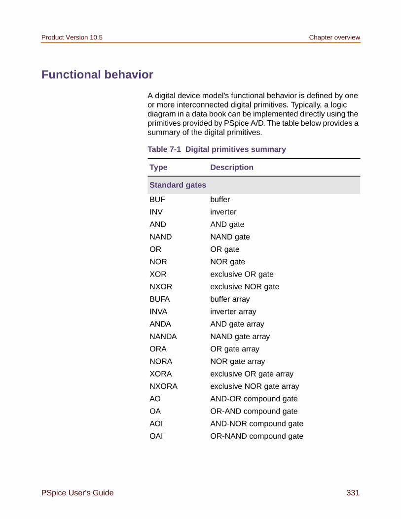
Product Version 10.5 Chapter overview
PSpice User's Guide 331
Functional behavior
A digital device model’s functional behavior is defined by oneor more interconnected digital primitives. Typically, a logicdiagram in a data book can be implemented directly using theprimitives provided by PSpice A/D. The table below provides asummary of the digital primitives.
Table 7-1 Digital primitives summary
Type Description
Standard gates
BUF
INV
AND
NAND
OR
NOR
XOR
NXOR
BUFA
INVA
ANDA
NANDA
ORA
NORA
XORA
NXORA
AO
OA
AOI
OAI
buffer
inverter
AND gate
NAND gate
OR gate
NOR gate
exclusive OR gate
exclusive NOR gate
buffer array
inverter array
AND gate array
NAND gate array
OR gate array
NOR gate array
exclusive OR gate array
exclusive NOR gate array
AND-OR compound gate
OR-AND compound gate
AND-NOR compound gate
OR-NAND compound gate
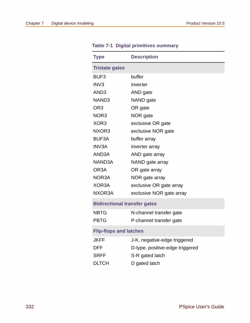
Chapter 7 Digital device modeling Product Version 10.5
332 PSpice User's Guide
Tristate gates
BUF3
INV3
AND3
NAND3
OR3
NOR3
XOR3
NXOR3
BUF3A
INV3A
AND3A
NAND3A
OR3A
NOR3A
XOR3A
NXOR3A
buffer
inverter
AND gate
NAND gate
OR gate
NOR gate
exclusive OR gate
exclusive NOR gate
buffer array
inverter array
AND gate array
NAND gate array
OR gate array
NOR gate array
exclusive OR gate array
exclusive NOR gate array
Bidirectional transfer gates
NBTG
PBTG
N-channel transfer gate
P-channel transfer gate
Flip-flops and latches
JKFF
DFF
SRFF
DLTCH
J-K, negative-edge triggered
D-type, positive-edge triggered
S-R gated latch
D gated latch
Table 7-1 Digital primitives summary
Type Description

Product Version 10.5 Chapter overview
PSpice User's Guide 333
Pullup/pulldown resistors
PULLUP
PULLDN
pullup resistor array
pulldown resistor array
Delay lines
DLYLINE delay line
Programmable logic arrays
PLAND
PLOR
PLXOR
PLNAND
PLNOR
PLNXOR
PLANDC
PLORC
PLXORC
PLNANDC
PLNORC
PLNXORC
AND array
OR array
exclusive OR array
NAND array
NOR array
exclusive NOR array
AND array, true and complement
OR array, true and complement
exclusive OR array, true and complement
NAND array, true and complement
NOR array, true and complement
exclusive NOR array, true andcomplement
Memory
ROM
RAM
read-only memory
random access read-write memory
Multi-Bit A/D & D/A Converters
ADC
DAC
multi-bit A/D converter
multi-bit D/A converter
Behavioral
Table 7-1 Digital primitives summary
Type Description

Chapter 7 Digital device modeling Product Version 10.5
334 PSpice User's Guide
The format for digital primitives is similar to that for analogdevices. One difference is that most digital primitives requiretwo models instead of one:
The timing model, which specifies propagation delaysand timing constraints such as setup and hold times.
The I/O model, which specifies information specific tothe device’s input/output characteristics.
The reason for having two models is that, while timinginformation is specific to a device, the input/outputcharacteristics are specific to a whole logic family. Thus, manydevices in the same family reference the same I/O model, buteach device has its own timing model.
Figure 7-1 presents an overview of a digital device definitionin terms of its primitives and underlying model attributes.These models are discussed further on Timing model onpage 339 and Input/Output model on page 346.
Digital primitive syntax
The general digital primitive format is shown below. Forspecific information on each primitive type see the onlinePSpice Reference Guide. Note that some digital primitives,such as pullups, do not have Timing models. See Timingmodel on page 339 for more information.
U<name> <primitive type> [( <parameter value>* )]+ <digital power node> <digital ground node>+ <node>*+ <Timing Model name> <I/O Model name>+ [MNTYMXDLY=<delay select value>]+ [IO_LEVEL=<interface subckt select value>]
where
LOGICEXP
PINDLY
CONSTRAINT
logic expression
pin-to-pin delay
constraint checking
Table 7-1 Digital primitives summary
Type Description

Product Version 10.5 Chapter overview
PSpice User's Guide 335
<primitive type> [( <parameter value>* )]
is the type of digital device, such as NAND, JKFF, or INV. It isfollowed by zero or more parameters specific to the primitivetype, such as number of inputs. The number and meaning ofthe parameters depends on the primitive type.
<digital power node> <digital ground node>
are the nodes used by the interface subcircuits whichconnect analog nodes to digital nodes or vice versa.
<node>*
is one or more input and output nodes. The number ofnodes depends on the primitive type and its parameters.Analog devices, digital devices, or both may beconnected to a node. If a node has both analog and digitalconnections, then PSpice A/D automatically inserts aninterface subcircuit to translate between digital outputstates and voltages.
<Timing model name>
is the name of a timing model that describes the device’stiming characteristics, such as propagation delay andsetup and hold times. Each timing parameter has aminimum, typical, and maximum value which may beselected during analysis setup.
This type of Timing model and its parameters are specificto each primitive type and are discussed in the onlinePSpice Reference Guide.
<I/O model name>
is the name of an I/O model that describes the device’sloading and driving characteristics. I/O models alsocontain the names of up to four DtoA and AtoD interfacesubcircuits, which are automatically called by PSpice A/Dto handle analog/digital interface nodes. See Input/Outputmodel on page 346 for more information.

Chapter 7 Digital device modeling Product Version 10.5
336 PSpice User's Guide
MNTYMXDLY
is an optional device parameter that selects either theminimum, typical, or maximum delay values from the
.subckt DotA_STD D A DPWR DGND+ params: DRVL=0 DRVH=0 CAPACITANCE=0N1 A DGND DPWR DIN74 DGTLNET=D IO_STDC1 A DGND CAPACITANCE+0.1pF.ends
.subckt AtoD_STD A D DPWR DGND+ .params: CAPACITANCE=0O0 A DGND DO74 DGTLNET=D IO_STDC1 A DGND CAPACITANCE+0.1pF.ends
.subckt 7400 A B Y+ params: MNTYMXDLY=0 IO_LEVEL=0+ optional: DPWR=$G_DPWR DGND=$G_DGNDU1 NAND(2) DPWR DGND A B Y+ D_7400 IO_STD
+ MNTYMXDLY=MNTYMXDLY IO_LEVEL=IO_LEVEL
.model IO_STD uio (+ drvh=96.4 drvl=104+ AtoD1="AtoD_STD" AtoD2="AtoD_STD_NX"+ AtoD3="AtoD_STD" AtoD4="AtoD_STD_NX"+ DtoA1="DtoA_STD" DtoA2="DtoA_STD"+ DtoA3="DtoA_STD" DtoA4="DtoA_STD"+ tswhl1=1.373ns tswlh1=3.382ns...+ DIGPOWER="DIGIFPWR" )
DtoA interface subcircuitAtoD interface subcircuit
I/O model
Figure 7-1 Elements of a digital device definition
.model D_7400 ugate (+ tplhty=11ns tplhmx=22ns+ tphlty=7ns tphlmx=15ns )
Digital device
Timing model
.model DO74 doutput(+ s0name="X" s0vlo=0.8 s0vhi=2.0+ s1name="0" s1vlo=0.0 s1vhi=0.8+ s2name="R" s2vlo=0.8 s2vhi=1.4+ s3name="R" s3vlo=1.3 s3vhi=2.0+ s4name="X" s4vlo=0.8 s4vhi=2.0+ s5name="1" s5vlo=2.0 s5vhi=7.0+ s6name="F" s6vlo=1.3 s6vhi=2.0+ s7name="F" s7vlo=0.8 s7vhi=1.4+ )
.model DIN74 dinput(+ s0name="0" s0tsw=3.5ns s0rlo=7.13 s0rhi=389+ s1name="1" s1tsw=5.5ns s1rlo=467 s1rhi=200+ s2name="X" s2tsw=3.5ns s2rlo=42.9 s2rhi=116+ s3name="R" s3tsw=3.5ns s3rlo=42.9 s3rhi=116+ s4name="F" s4tsw=3.5ns s4rlo=42.9 s4rhi=116+ s5name="Z" s5tsw=3.5ns s5rlo=200K s5rhi=200K+ )
Digital input (DtoA) modelDigital output (AtoD) model

Product Version 10.5 Chapter overview
PSpice User's Guide 337
device’s timing model. If not specified, MNTYMXDLYdefaults to 0. Valid values are:
IO_LEVEL
is an optional device parameter that selects one of thefour AtoD or DtoA interface subcircuits from the device’sI/O model. PSpice A/D calls the selected subcircuitautomatically in the event a node connecting to theprimitive also connects to an analog device. If notspecified, IO_LEVEL defaults to 0. Valid values are:
Following are some simple examples of “U” devicedeclarations:
U1 NAND(2) $G_DPWR $G_DGND 1 2 10 D0_GATE IO_DFT
U2 JKFF(1) $G_DPWR $G_DGND 3 5 200 3 3 10 2 D_293ASTD+ IO_STD
U3 INV $G_DPWR $G_DGND IN OUT D_INV IO_INV MNTYMXDLY=3+ IO_LEVEL=2
For example, the 74393 part could be defined as a subcircuitcomposed of “U” devices as shown below.
.subckt 74393 A CLR QA QB QC QD+ optional: DPWR=$G_DPWR DGND=$G_DGND+ params: MNTYMXDLY=0 IO_LEVEL=0UINV inv DPWR DGND+ CLR CLRBAR D0_GATE IO_STD+ IO_LEVEL=IO_LEVELU1 jkff(1) DPWR DGND+ $D_HI CLRBAR A $D_HI $D_HI+ QA_BUF $D_NC D_393_1 IO_STD
0 = the current value of the circuit-wideDIGMNTYMX option (default=2)
1 = minimum2 = typical3 = maximum4 = worst-case timing (min-max)
0 = the current value of the circuit-wideDIGIOLVL option (default=1)
1 = AtoD1/DtoA12 = AtoD2/DtoA23 = AtoD3/DtoA34 = AtoD4/DtoA4
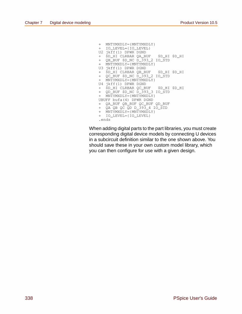
Chapter 7 Digital device modeling Product Version 10.5
338 PSpice User's Guide
+ MNTYMXDLY=MNTYMXDLY+ IO_LEVEL=IO_LEVELU2 jkff(1) DPWR DGND+ $D_HI CLRBAR QA_BUF $D_HI $D_HI+ QB_BUF $D_NC D_393_2 IO_STD+ MNTYMXDLY=MNTYMXDLYU3 jkff(1) DPWR DGND+ $D_HI CLRBAR QB_BUF $D_HI $D_HI+ QC_BUF $D_NC D_393_2 IO_STD+ MNTYMXDLY=MNTYMXDLYU4 jkff(1) DPWR DGND+ $D_HI CLRBAR QC_BUF $D_HI $D_HI+ QD_BUF $D_NC D_393_3 IO_STD+ MNTYMXDLY=MNTYMXDLYUBUFF bufa(4) DPWR DGND+ QA_BUF QB_BUF QC_BUF QD_BUF+ QA QB QC QD D_393_4 IO_STD+ MNTYMXDLY=MNTYMXDLY+ IO_LEVEL=IO_LEVEL.ends
When adding digital parts to the part libraries, you must createcorresponding digital device models by connecting U devicesin a subcircuit definition similar to the one shown above. Youshould save these in your own custom model library, whichyou can then configure for use with a given design.

Product Version 10.5 Chapter overview
PSpice User's Guide 339
Timing characteristics
A digital device model’s timing behavior can be defined in oneof two ways:
Most primitives have an associated Timing model, inwhich propagation delays and timing constraints (such assetup/hold times) are specified. This method is usedwhen it is easy to partition delays among individualprimitives; typically when the number of primitives issmall.
Use the PINDLY and CONSTRAINT primitives, which candirectly model pin-to-pin delays and timing constraints forthe whole device model. With this method, all otherfunctional primitives operate in zero delay. Refer to theonline PSpice Reference Guide for a detaileddiscussion on these two primitives.
In addition to explicit propagation delays, other factors, suchas output loads, can affect the total propagation delay througha device.
Timing model
With the exception of the PULLUP, PULLDN, and PINDLYdevices, all digital primitives have a Timing model whichprovides timing parameters to the simulator. The Timingmodel for each primitive type is unique. That is, the modelname and the parameters that can be defined for that modelvary with the primitive type.
Within a Timing model, there may be one or more types ofparameters:
Propagation delays (TP)
Setup times (TSU)
Hold times (TH)
Pulse widths (TW)
Switching times (TSW)

Chapter 7 Digital device modeling Product Version 10.5
340 PSpice User's Guide
Each parameter is further divided into three values: minimum(MN), typical (TY), and maximum (MX). For example, thetypical low-to-high propagation delay on a gate is specified asthe parameter TPLHTY. The minimum data-to-clock setuptime on a flip-flop is specified as the parameter TSUDCLKMN.
Several timing models are used by digital device 74393 fromthe model libraries. One of them, D_393_1, is shown below foran edge-triggered flip-flop.
.model D_393_1 ueff (+ tppcqhlty=18ns tppcqhlmx=33ns+ tpclkqlhty=6ns tpclkqlhmx=14ns+ tpclkqhlty=7ns tpclkqhlmx=14ns+ twclkhmn=20ns twclklmn=20ns+ twpclmn=20ns tsudclkmn=25ns+ )
When creating your own digital device models, you can createTiming models like these for the primitives you are using.PSpice recommends that you save these in your own custommodel library, which you can then configure for use with agiven design.
One or more parameters may be missing from the Timingmodel definition. Data books do not always provide all three(minimum, typical, and maximum) timing specifications. Theway the simulator handles missing parameters depends onthe type of parameter.
For a description of Timing model parameters, see the specificprimitive type under U devices in the online PSpiceReference Guide.
Treatment of unspecified propagation delays
Often, only the typical and maximum delays are specified indata books. If, in this case, the simulator were to assume thatthe unspecified minimum delay defaults to zero, the logic incertain circuits could break down.
For this reason, the simulator provides two configurableoptions, DIGMNTYSCALE and DIGTYMXSCALE, which areused to extrapolate unspecified propagation delays in theTiming models.

Product Version 10.5 Chapter overview
PSpice User's Guide 341
Note: This discussion applies only to propagation delayparameters (TP). All other timing parameters, such assetup/hold times and pulse widths are handleddifferently, and are discussed in the following section.
DIGMNTYSCALE
This option computes the minimum delay when a typical delayis known, using the formula:
TPxxMN = DIGMNTYSCALE ⋅ TPxxTY
DIGMNTYSCALE defaults to the value 0.4, or 40% of thetypical delay. Its value must be between 0.0 and 1.0.
DIGTYMXSCALE
This option computes the maximum delay from a typical delay,using the formula
TPxxMX = DIGTYMXSCALE ⋅ TPxxTY
DIGTYMXSCALE defaults to the value 1.6. Its value must begreater than 1.0.
When a typical delay is unspecified, its value is derived fromthe minimum and/or maximum delays, in one of the followingways. If both the minimum and maximum delays are known,the typical delay is the average of these two values. If only theminimum delay is known, the typical delay is derived using thevalue of the DIGMNTYSCALE option. Likewise, if only themaximum delay is specified, the typical delay is derived usingDIGTYMXSCALE. Obviously, if no values are specified, allthree delays will default to zero.
Treatment of unspecified timing constraints
The remaining timing constraint parameters are handleddifferently than the propagation delays. Often, data booksstate pulse widths, setup times, and hold times as a minimumvalue. These parameters do not lend themselves to theextrapolation method used for propagation delays.

Chapter 7 Digital device modeling Product Version 10.5
342 PSpice User's Guide
Instead, when one or more timing constraints are omitted, thesimulator uses the following steps to fill in the missing values:
If the minimum value is omitted, it defaults to zero.
If the maximum value is omitted, it takes on the typicalvalue if one was specified, otherwise it takes on theminimum value.
If the typical value is omitted, it is computed as theaverage of the minimum and maximum values.
Propagation delay calculation
The timing characteristics of digital primitives are determinedby both the timing models and the I/O models. Timing modelsspecify propagation delays and timing constraints such assetup and hold times. I/O models specify input and outputloading, driving resistances, and switching times.
When a device’s output connects to another digital device, thetotal propagation delay through a device is determined byadding the loading delay (on the output terminal) to the delayspecified in the device’s timing model. Loading delay iscalculated from the total load on the output and the device’sdriving resistances. The total load on an output is found bysumming the output and input loads (OUTLD and INLD in theI/O model) of all devices connected to that output. This totalload, combined with the device’s driving resistances (DRVLand DRVH in the I/O model), allows the loading delay to becalculated:
Loading delay = RDRIVE·CTOTAL·ln(2)
The loading delay is calculated for each output terminal ofevery device before the simulation begins. The totalpropagation delay is easily calculated during the simulation byadding the pre-calculated loading delay to the device’s timingdelay. However, for any individual timing delay specification(e.g., TPLH) having a value of 0, the loading delay is notused.
When outputs connect to analog devices, the propagationdelay is reduced by the switching times specified in the I/O

Product Version 10.5 Chapter overview
PSpice User's Guide 343
model. See Input/Output characteristics on page 346 for moreinformation.
Inertial and transport delay
The simulator uses two different types of internal delayfunctions when simulating the digital portion of the circuit:inertial delay and transport delay. The application of theseconcepts is embodied within the implementation of the digitalprimitives within the simulator. Therefore, they are notuser-selectable.
Inertial delay
The simulation of a device may be described as theapplication of some stimulus (S) to a function (F) andpredicting the response (R).
If this device is electrical in nature, application of the stimulusimplies that energy will be imparted to the device to cause it tochange state. The amount of such energy is a function of thesignal’s amplitude and duration. If the stimulus is applied tothe device for a length of time that is too short, the device willnot switch. The minimum duration required for an inputchange to have an effect on a device’s output state is calledthe inertial delay of the device. For digital simulation, alldelay parameters specified in timing models are consideredinertial, with the exception of the delay line primitive, DLYLINE.
To model the noise immunity behavior of digital devicescorrectly, the TPWRT (pulse width rejection threshold)parameter can be set in the digital device’s I/O model. Whenpulse width ≥ TPWRT and pulse width < propagationdelay, then the device generates either a 0-R-0, 1-F-1, or anX pulse.
S F

Chapter 7 Digital device modeling Product Version 10.5
344 PSpice User's Guide
This example shows normal operation in which a pulse of 20nsec width is applied to a BUF primitive having propagationdelays of 10 nsec. TPWRT is not set.
The same device with a short pulse applied produces nooutput change.
However, if TPWRT is assigned a numerical value (1 or 2 forthis example), then the device outputs a glitch.
Transport delay
The delay line primitive is the only simulator model that canpropagate any width pulse applied to its input. Its function is toskew the applied stimulus by some constant time value. Forexample:
TPLHTY=10
20 40 30 50
TPHLTY=10(TPWRT not set)
TPLHTY=10
20 22
TPHLTY=10(TPWRT not set)
TPLHTY=10
20 22 30 32
TPHLTY=10TPWRT=1
DLYTY=4
T
0 2 6 8 12 14 4 6 10 12 16 18

Product Version 10.5 Chapter overview
PSpice User's Guide 345
See the DLYLINE digital primitive in the online PSpiceReference Guide.

Chapter 7 Digital device modeling Product Version 10.5
346 PSpice User's Guide
Input/Output characteristics
A digital device model’s input/output characteristics aredefined by the I/O model that it references. Somecharacteristics, such as output drive resistance and loadingcapacitances, apply to digital simulation. Others, such as theinterface subcircuits and the power supplies, apply only tomixed analog/digital simulation.
This section describes in detail:
the I/O model
the relationship between drive resistances and outputstrengths
charge storage on digital nets
the format of the interface subcircuits
Input/Output model
I/O models are common to entire logic families. For example,in the model libraries, there are only four I/O models for theentire 74LS family: IO_LS, for standard inputs and outputs;IO_LS_OC, for standard inputs and open-collector outputs;IO_LS_ST, for Schmitt trigger inputs and standard outputs;and IO_LS_OC_ST, for Schmitt trigger inputs andopen-collector outputs. In contrast, timing models are uniqueto each device.
I/O models are specified as
.MODEL <I/O model name> UIO [model parameters]*
where valid model parameters are described in Table 7-2.
INLD and OUTLD
These are used in the calculation of loading capacitance,which factors into the propagation delay discussed undertiming models on Timing model on page 339. Note that INLD

Product Version 10.5 Chapter overview
PSpice User's Guide 347
does not apply to stimulus generators because they have noinput nodes.
DRVH and DRVL
These are used to determine the strength of the output.Strengths are discussed on Defining Output Strengths onpage 350.
DRVZ, INR, and TSTOREMN
These are used to determine which nets should be simulatedas charge storage nets. These are discussed in Chargestorage nets on page 352.
TPWRT
This is used to specify the pulse width above which the noiseimmunity behavior of a device is to be considered. See Inertialdelay on page 343 on inertial delay for detail.
The following UIO model parameters are needed only whencreating models for use in mixed-signal simulations, andtherefore only apply to PSpice A/D simulations.
AtoD1 through AtoD4, and DtoA1 through DtoA4
These are used to hold the names of interface subcircuits.Note that AtoD1 through AtoD4 do not apply to stimulusgenerators because digital stimuli have no input nodes.
DIGPOWER
This is used to specify the name of the digital power supplyPSpice A/D should call if one of the AtoD or DtoA interfacesubcircuits is called.

Chapter 7 Digital device modeling Product Version 10.5
348 PSpice User's Guide
TSWLHn and TSWHLn
These switching times are subtracted from a device’spropagation delay on the outputs which connect to interfacenodes. This compensates for the time it takes the DtoA deviceto change its output voltage from its current level to that of theswitching threshold. By subtracting the switching time from thepropagation delay, the analog signal reaches the switchingthreshold at the correct time (that is, at the exact time of thedigital transition). The values for these model parametersshould be obtained by measuring the time it takes the analogoutput of the DtoA (with a nominal analog load attached) tochange to the switching threshold after its digital inputchanges. If the switching time is larger than the propagationdelay for an output, no warning is issued, and a delay of zerois used.
When creating your own digital device models, you can createI/O models like these for the primitives you are using. Werecommend that you save these in your own custom modellibrary, which you can then configure for use with a givendesign.
See the online PSpice Reference Guide for moreinformation on units and defaults for these parameters.
Note: The switching time parameters are not used when theoutput drives a digital node.
Table 7-2 Digital I/O model parameters
UIO modelparameter
Description
INLD input load capacitance
OUTLD output load capacitance
DRVH output high level resistance
DRVL output low level resistance
DRVZ output Z-state leakage resistance
INR input leakage resistance

Product Version 10.5 Chapter overview
PSpice User's Guide 349
The digital primitives comprising the 74393 part reference theIO_STD I/O model in the model libraries as shown:
.model IO_STD uio (+ drvh=96.4 drvl=104+ AtoD1="AtoD_STD" AtoD2="AtoD_STD_NX"+ AtoD3="AtoD_STD" AtoD4="AtoD_STD_NX"+ DtoA1="DtoA_STD" DtoA2="DtoA_STD"+ DtoA3="DtoA_STD" DtoA4="DtoA_STD"+ tswhl1=1.373ns tswlh1=3.382ns
TSTOREMN minimum storage time for net to besimulated as a charge
TPWRT pulse width rejection threshold
AtoD1 (Level 1) name of AtoD interface subcircuit
DtoA1 (Level 1) name of DtoA interface subcircuit
AtoD2 (Level 2) name of AtoD interface subcircuit
DtoA2 (Level 2) name of DtoA interface subcircuit
AtoD3 (Level 3) name of AtoD interface subcircuit
DtoA3 (Level 3) name of DtoA interface subcircuit
AtoD4 (Level 4) name of AtoD interface subcircuit
DtoA4 (Level 4) name of DtoA interface subcircuit
DIGPOWER name of power supply subcircuit
TSWLH1 switching time low to high for DtoA1
TSWLH2 switching time low to high for DtoA2
TSWLH3 switching time low to high for DtoA3
TSWLH4 switching time low to high for DtoA4
TSWHL1 switching time high to low for DtoA1
TSWHL2 switching time high to low for DtoA2
TSWHL3 switching time high to low for DtoA3
TSWHL4 switching time high to low for DtoA4
Table 7-2 Digital I/O model parameters, continued
UIO modelparameter
Description

Chapter 7 Digital device modeling Product Version 10.5
350 PSpice User's Guide
+ tswhl2=1.346ns tswlh2=3.424ns+ tswhl3=1.511ns tswlh3=3.517ns+ tswhl4=1.487ns tswlh4=3.564ns+ )
Defining Output Strengths
The goal of running simulations is to calculate values for eachnode in the circuit. For analog nodes, the values are voltages.For digital nodes, these values are states. The state of adigital node is calculated from the output strengths of thedevices driving the node and the logic level of the node. Nodestrength calculations are described in Chapter 14, “Digitalsimulation.”
The purpose of strengths is to allow the simulator to find thevalue of a node when more than one output is driving it. Acommon example is a bus line which is driven by more thanone tristate driver. Under normal circumstances, all driversexcept one are driving at the Z (high impedance) strength.Thus, the bus line will take on the value of the one gate that isdriving at a higher strength (lower impedance).
Another example is a bus line connected to several opencollector output devices and a digital pullup resistor. Thepullup resistor outputs a 1 level at a weak (but non-Z) strength.If all of the open-collector devices are outputting at Z strength,then the node will have a 1 level because of the pullup resistor.If any of the open collectors output a 0, at a higher strengththan the pullup resistor, then the 0 will overpower the weak 1from the pullup, and the node will be a 0 level.
Configuring the strength scale
The 64 strengths are determined by two configurable options:DIGDRVZ and DIGDRVF. You can set these options in theSimulation Settings dialog box in PSpice A/D.
DIGDRVZ defines the impedance of the Z strength, andDIGDRVF defines the impedance of the forcing strength.These two values define a logarithmic scale consisting of 64ranges of impedance values. By default, DIGDRVZ is 20kohms and DIGDRVF is 2 ohms. The larger the range

Product Version 10.5 Chapter overview
PSpice User's Guide 351
between DIGDRVZ and DIGDRVF, the larger the range ofimpedance values in each of the 64 strengths.
Determining the strength of a device output
The simulator uses the value of the DRVH (high-level drivingresistance) or DRVL (low-level driving resistance) parametersfrom the device’s I/O model. If the level of the output is a 1, thesimulator obtains the strength by finding the bin whichcontains the value of the DRVH parameter. Likewise, if thelevel is a 0, the simulator uses the value of the DRVLparameter to obtain the strength.
See Input/Output model on page 346 for more information.
Note that if the values of DRVH and DRVL in the I/O model aredifferent, it is possible for the 1 and 0 levels to have differentstrengths. This is useful for open-collector devices, where the0 level is at a higher strength than the 1 level (which drives atthe Z strength).
Drive impedances which are higher than the value ofDIGDRVZ are assigned the Z strength (0). Likewise, driveimpedances lower than the value of DIGDRVF are assignedthe forcing strength (63).
(DRVH)
.
.
.
Level 1Strength
DIGDRVF
DIGDRVZ
(DRVL)
.
.
.
.
.
.
Level 0Strength
63
0
Output Drive
OutputStrength
DIGDRVF
DIGDRVZ
.
.
.
63
0
Output Drive
OutputStrength
Figure 7-2 Level 1 and 0 strength determination.
HigherStrength
HigherImpedance

Chapter 7 Digital device modeling Product Version 10.5
352 PSpice User's Guide
Controlling overdrive
During a simulation, the simulator uses only the strengthrange number (0-63) to compare the driving strength ofoutputs. The simulator allows you to control how muchstronger an output must be before it overdrives the otheroutputs driving the same node. This is controlled with theconfigurable DIGOVRDRV option. By default, DIGOVRDRV is3, meaning that the strength value assigned to an output mustbe at least 3 greater than all other drivers before it determinesthe level of the node.
The accuracy of the DIGOVRDRV strength comparison islimited by the size of the strength range, DIGDRVZ throughDIGDRVF. The default drive range of 2 ohms to 20,000 ohmsgives strength ranges of 7.5%. The accuracy of the strengthcomparison is 15%. In other words, depending on theparticular values of DRVH and DRVL, it might take as much asa factor of 3.45 to overdrive a signal, or as little as a factor of2.55. The accuracy of the comparison increases as the ratiobetween DIGDRVF and DIGDRVZ decreases.
You can set the DRVH, DRVL, DIGDRVF, DIGDRVZ, andDIGOVRDRV options in the Simulation Settings dialog box inPSpice A/D.
Charge storage nets
The ability to model charge storage on digital nets is useful forengineers who are designing dynamic MOS integratedcircuits. In such circuits, it is common for the designer totemporarily store a one or zero on a net by driving the net tothe appropriate voltage and then turning off the drive. Thecharge which is trapped on the net causes the net’s voltage toremain unchanged for some time after the net is no longerdriven. The technique is not normally used on PCB netsbecause sub-nanoampere input and output leakage currentswould be required, as well as low coupling from adjacentsignals.
The simulator models the stored charge nets using asimplified switch-level simulation technique. A normalized(with respect to power supply) charge or discharge current is

Product Version 10.5 Chapter overview
PSpice User's Guide 353
calculated for each output or transfer gate attached to the net.This current, divided by the net’s total capacitance, isintegrated and recalculated at intervals which are appropriatefor the particular net. The net’s digital level is determined bythe normalized voltage on the net. Only the digital level (1, 0,R, F, X) on the net is used by device inputs attached to the net.
This technique allows accurate simulation of networks oftransfer gates and capacitive loads. The sharing of chargeamong several nets which are connected by transfer gates ishandled properly because the simulation method calculatesthe charge transferred between the nets, and maintains afloating-point value for the charge on the net (not just a one orzero). Because of the increased computation, it takes thesimulator longer to simulate charge storage nets than normaldigital nets. However, charge storage nets are simulated muchfaster than analog nets.
The I/O model parameters INR, DRVZ, and TSTOREMN (seeTable 7-2 on page 348) are used by the simulator to determinewhich nets should be simulated as charge storage nets. Thesimulator will simulate charge storage only for a net which hassome devices attached to it which can be high impedance (Z),and which has a storage time greater than or equal to thesmallest TSTOREMN of all inputs attached to the net. Thestorage time is calculated as the total capacitance (sum of allINLD and OUTLD values for attached inputs and outputs)multiplied by the total leakage resistance for the net (theparallel combination of all INR and DRVZ values for attachedinputs and outputs).
Note: The default values provided by the UIO model will notallow the use of charge-storage simulationtechniques—even with circuits using non-PSpicelibraries of digital devices. This is appropriate, sincethese libraries are usually for PCB-based designs.
Creating your own interface subcircuits foradditional technologies
If you are creating custom digital parts for a technology whichis not in the model libraries, you may also need to create AtoDand DtoA subcircuits. The new subcircuits need to be

Chapter 7 Digital device modeling Product Version 10.5
354 PSpice User's Guide
referenced by the I/O models for that technology. The AtoDand DtoA interfaces have specific formats, such as node orderand parameters, which are expected by PSpice A/D formixed-signal simulations.
If you are creating parts in one of the logic families already inthe model libraries, you should reference the existing I/Omodels appropriate to that family. The I/O models, in turn,automatically reference the correct interface subcircuits forthat family. These, too, are already contained in the modellibraries.
The AtoD interface subcircuit format is shown here:
.SUBCKT ATOD <name suffix>+ <analog input node>+ <digital output node>+ <digital power supply node>+ <digital ground node>+ PARAMS: CAPACITANCE=<input load value>+ O device, loading capacitor, and other+ declarations.ENDS
It has four nodes as described. The AtoD subcircuit has oneparameter, CAPACITANCE, which corresponds to the inputload. PSpice A/D passes the value of the I/O model parameterINLD to this parameter when the interface subcircuit is called.
The DtoA interface subcircuit format is shown here:
.SUBCKT DTOA <name suffix>+ <digital input node> <analog output node>+ <digital power supply node> <digital+ ground node>+ PARAMS: DRVL=<0 level driving resistance>+ DRVH=<1 level driving resistance>+ CAPACITANCE=<output load value>+ N device, loading capacitor, and other+ declarations.ENDS
It also has four nodes. Unlike the AtoD subcircuit, the DtoAsubcircuit has three parameters. PSpice A/D will pass thevalues of the I/O model parameters DRVL, DRVH, andOUTLD to the interface subcircuit’s DRVL, DRVH, andCAPACITANCE parameters when it is called.
The library file DIG_IO.LIB contains the I/O models andinterface subcircuits for all logic families supported in themodel libraries. You should refer to this file for examples of the

Product Version 10.5 Chapter overview
PSpice User's Guide 355
I/O models, interface subcircuits, and the proper use of N andO devices.
Shown below are the I/O model and AtoD interface subcircuitdefinition used by the primitives describing the 74393 part.
.model IO_STD uio (+ drvh=96.4 drvl=104+ AtoD1="AtoD_STD" AtoD2="AtoD_STD_NX"+ AtoD3="AtoD_STD" AtoD4="AtoD_STD_NX"+ DtoA1="DtoA_STD" DtoA2="DtoA_STD"+ DtoA3="DtoA_STD" DtoA4="DtoA_STD"+ tswhl1=1.373 tswlh1=3.382ns+ tswhl2=1.346ns tswlh2=3.424ns+ tswhl3=1.511ns tswlh3=3.517ns+ tswhl4=1.487ns tswlh4=3.564ns+ )
.subckt AtoD_STD A D DPWR DGND+ params: CAPACITANCE=0*O0 A DGND DO74 DGTLNET=D IO_STDC1 A 0 CAPACITANCE+0.1pF.ends
If an instance of the 74393 part is connected to an analog partvia node AD_NODE, PSpice A/D generates an interface blockusing the I/O model specified by the digital primitive actually atthe interface. Suppose that U1 is the primitive connected atAD_NODE (see the 74393 subcircuit definition on page 337),and that the IO_LEVEL is set to 1. PSpice A/D determines thatIO_STD is the I/O model used by U1. Notice how IO_STDidentifies the interface subcircuit names AtoD_STD andDtoA_STD to be used for level 1 subcircuit selection. If theconnection with U1 is an input (such as a clock line), PSpiceA/D creates an instance of the subcircuit AtoD_STD:
X$AD_NODE_AtoD1 AD_NODE AD_NODE$AtoD $G_DPWR+ $G_DGND+ AtoD_STD+ PARAMS: CAPACITANCE=0
The AtoD_STD interface subcircuit references the DO74model in its PSpice A/D O device declaration. This model,stated elsewhere in the model libraries, describes how totranslate an analog signal on the analog side of an interfacenode, to a digital state on the digital side of an interface node.
.model DO74 doutput+ s0name="X" s0vlo=0.8 s0vhi=2.0+ s1name="0" s1vlo=-1.5 s1vhi=0.8+ s2name="R" s2vlo=0.8 s2vhi=1.4+ s3name="R" s3vlo=1.3 s3vhi=2.0+ s4name="X" s4vlo=0.8 s4vhi=2.0

Chapter 7 Digital device modeling Product Version 10.5
356 PSpice User's Guide
+ s5name="1" s5vlo=2.0 s5vhi=7.0+ s6name="F" s6vlo=1.3 s6vhi=2.0+ s7name="F" s7vlo=0.8 s7vhi=1.4+
The DOUTPUT model parameters are described under Odevices in the online PSpice Reference Guide.
Supposing the output of the 74393 is connected to an analogpart via the digital primitive UBUFF. At IO_LEVEL set to 1,PSpice A/D determines that the DtoA_STD interfacesubcircuit identified in the IO_STD model, should be used.
.subckt DtoA_STD D A DPWR DGND+ params: DRVL=0 DRVH=0 CAPACITANCE=0*N1 A DGND DPWR DIN74 DGTLNET=D IO_STDC1 A DGND CAPACITANCE+0.1pF.ends
For this subcircuit, the DRVH and DRVL parameters valuesspecified in the IO_STD model would be passed to it. (Theinterface subcircuits in the model libraries do not currently usethese values.)
The DtoA_STD interface subcircuit references the DIN74model in its PSpice A/D N device declaration. This model,stated elsewhere in the libraries, describes how to translate adigital state into a voltage and impedance.
.model DIN74 dinput (+ s0name="0" s0tsw=3.5ns s0rlo=7.13+ s0rhi=389 ; 7ohm, 0.09v+ s1name="1" s1tsw=5.5ns s1rlo=467+ s1rhi=200 ; 140ohm, 3.5v+ s2name="X" s2tsw=3.5ns s2rlo=42.9+ s2rhi=116 ; 31.3ohm, 1.35v+ s3name="R" s3tsw=3.5ns s3rlo=42.9+ s3rhi=116 ; 31.3ohm, 1.35v+ s4name="F" s4tsw=3.5ns s4rlo=42.9+ s4rhi=116 ; 31.3ohm, 1.35v+ s5name="Z" s5tsw=3.5ns s5rlo=200K+ s5rhi=200K+)
The DINPUT model parameters are described under PSpiceA/D N devices in the online PSpice Reference Guide.
Each state is turned into a pullup and pulldown resistor pair toprovide the correct voltage and impedance. The Z state isaccounted for as well as the 0, 1, and X logic levels.

Product Version 10.5 Chapter overview
PSpice User's Guide 357
You can create your own interface subcircuits, DINPUTmodels, DOUTPUT models, and I/O models like these fortechnologies not currently supported in the model libraries.We recommend that you save these in your own custommodel library, which you can then configure for use with agiven design.

Chapter 7 Digital device modeling Product Version 10.5
358 PSpice User's Guide
Creating a digital model using the PINDLY and LOGICEXPprimitives
Unlike the majority of analog device types, the bulk of digitaldevices are not primitives that are compiled into the simulator.Instead, most digital models are macro models or subcircuitsthat are built from a few primitive devices.
These subcircuits reference interface and timing models tohandle the D-to-A and A-to-D interfaces and the overall timingparameters of the physical device. For most families of digitalcomponents, the interface models are already defined andavailable in the DIG_IO.LIB library, which is supplied with alldigital and mixed-signal packages. If you are unsure of theexact name of the interface model you need to use, use a texteditor to look in DIG_IO.LIB.
For instance, if you are trying to model a 74LS component thatis not already in a library, open DIG_IO.LIB with your texteditor and search for 74LS to get the interface models for the74LS family. You can also read the information at thebeginning of the file which explains many of the terms anduses for the I/O models.
In the past, the timing model has presented the greatestchallenge when trying to model a digital component. This wasdue to the delays of a component being distributed among thevarious gates. Recently, the ability to model digitalcomponents using logic expressions (LOGICEXP) andpin-to-pin delays (PINDLY) has been added to the simulator.Using the LOGICEXP and PINDLY digital primitives, you candescribe the logic of the device with zero delay and then enterthe timing parameters for the pin-to-pin delays directly fromthe manufacturer’s data sheet. Digital primitives still mustreference a standard timing model, but when the PINDLYdevice is used, the timing models are simply zero-delaymodels that are supplied in DIG_IO.LIB. The default timingmodels can be found in the same manner as the standard I/Omodels. The PINDLY primitive also incorporates constraintchecking which allows you to enter device data such as pulsewidth and setup/hold timing from the data sheet. Then thesimulator can verify that these conditions are met during thesimulation.

Product Version 10.5 Chapter overview
PSpice User's Guide 359
Digital primitives
Primitives in the simulator are devices or functions which arecompiled directly into the code. The primitives serve asfundamental building blocks for more complex macro models.
There are two types of primitives in the simulator: gate leveland behavioral. A gate level primitive normally refers to anactual physical device (such as buffers, AND gates, inverters).A behavioral primitive is not an actual physical device, butrather helps to define parameters of a higher level model. Justlike gate level primitives, behavioral primitives are intrinsicfunctions in the simulator and are treated in much the samemanner. They are included in the gate count for circuit sizeand cannot be described by any lower level model.
In our 74160 example (see The TTL Data Book from TexasInstruments for schematic and description), the four J-Kflip-flops are the four digital gate level primitives. Whileflip-flops are physically more complex than gates in terms ofmodeling, they are defined on the same level as a gate (forexample, flip-flops are a basic device in the simulator). Sinceall four share a common Reset, Clear, and Clock signal, theycan be combined into one statement as an array of flip-flops.They could just as easily have been written separately, but thearray method is more compact. See the Digital Deviceschapter in the online PSpice Reference Guide for moreinformation.
Logic expression (LOGICEXP primitive)
Looking at the listing in 74160 example on page 366 and atthe schematic representation of the 74160 subcircuit, you cansee that there are three main parts to the subcircuit. Followingthe usual header information, .SUBCKT keyword, subcircuitname, interface pin list, and parameter list is the LOGICEXPprimitive. It contains everything in the component that can beexpressed in terms of simple combinational logic. The logicexpression device also serves to buffer other input signals thatwill go to the PINDLY primitive. In this case, LOGICEXPbuffers the ENP_I, ENT_I, CLK_I, CLRBAR_I, LOADBAR_I,and four data signals. See the Digital Devices chapter in theonline PSpice Reference Guide for more information.

Chapter 7 Digital device modeling Product Version 10.5
360 PSpice User's Guide
For our 74160 example, the logic expression (LOGICEXP)has fourteen inputs and twenty outputs. The inputs are thenine interface input pins in the subcircuit plus five feedbacksignals that come from the flip-flops (QA, QB, QC, QD, andQDBAR). The flip-flops are primitive devices themselves andare not part of the logic expression. The outputs are the eightJ-K data inputs to the flip-flops, RCO, the four data lines usedinternal to the logic expression (A, B, C, D), and the sevencontrol lines: CLK, CLKBAR, EN, ENT, ENP, CLRBAR, andLOADBAR.
The schematic representation of the device shows buffers onevery input signal of the model, while the logic diagram of thedevice in the data book shows buffers or inverters on only theCLRBAR_I, CLK_I, and LOADBAR_I signals. We have addedbuffers to the inputs to minimize the insertion of A-to-Dinterfaces when the device is driven by analog circuitry. Thebest example is the CLK signal. With the buffer in place, if theCLK signal is analog, one A-to-D interface device will beinserted into the circuit by the simulator. If the buffer was notpresent, then an interface device would be inserted at the CLKpin of each of the flip-flops. The buffers have no delayassociated with them, but by minimizing the number of A-to-Dinterfaces, we speed up the mixed-signal simulation byreducing the number of necessary calculations. For situationswhere the device is only connected to other digital nodes, thebuffers have no effect on the simulation.
The D0_GATE, shown in the listing, is a zero-delay primitivegate timing model. For most TTL modeling applications, thisonly serves as a place holder and is not an active part of themodel. Its function has been replaced by the PINDLY primitive.The D0_GATE model can be found in the library fileDIG_IO.LIB. For a more detailed description of digitalprimitives, see the Digital Devices chapter in the onlinePSpice Reference Guide.
IO_STD, shown in the listing, is the standard I/O model. Thisdetermines the A-to-D and D-to-A interface characteristics forthe subcircuit. The device contains family-specific information,but the models have been created for nearly all of the stockfamilies. The various I/O models can be found in the library fileDIG_IO.LIB.

Product Version 10.5 Chapter overview
PSpice User's Guide 361
The logic expressions themselves are straightforward. Thefirst nine are buffering the input signals from outside thesubcircuit. The rest describe the logic of the actual device upto the flip-flops. By tracing the various paths in the design, youcan derive each of the logic equations.
The D0_EFF timing model, shown in the listing, is a zero-delaydefault model already defined in DIG_IO.LIB for use withflip-flops. All of the delays for the device are defined in thePINDLY section. The I/O model is IO_STD as identifiedpreviously. We have not specified a MNTYMXDLY orIO_LEVEL parameter, so the default values are used. For amore detailed description of the general digital primitivesMNTYMXDLY and IO_LEVEL, see the Digital Deviceschapter in the online PSpice Reference Guide.
The primitive MNTYMXDLY specifies whether to use theminimum, typical, maximum, or digital worst-case timingvalues from the device’s timing model (in this case the PINDLYdevice). For the 74160, MNTYMXDLY is set to 0. This meansthat it takes on the current value of the DIGMNTYMXparameter. DIGMNTYMX defaults to 2 (typical timing) unlessspecifically changed using the .OPTIONS command.
The primitive IO_LEVEL selects one of four possible A-to-Dand D-to-A interface subcircuits from the device’s I/O model.In the header of this subcircuit, IO_LEVEL is set to 0. Thismeans that it takes on the value of the DIGIOLVL parameter.DIGIOLVL defaults to 1 unless specifically changed using the.OPTIONS command.
Pin-to-pin delay (PINDLY primitive)
The delay and constraint specifications for the model arespecified using the PINDLY primitive. The PINDLY primitive isevaluated every time any of its inputs or outputs change. Seethe Digital Devices chapter in the online PSpice ReferenceGuide for more information.
For the 74160, we have five delay paths, the four flip-flopoutputs to subcircuit outputs QA...QD to QA_O...QD_O, andRCO to RCO_O. The five paths are seen in the Delay &Constraint section of the design. For delay paths, the number

Chapter 7 Digital device modeling Product Version 10.5
362 PSpice User's Guide
of inputs must equal the number of outputs. Since the 74160does not have TRI-STATE outputs, there are no enable signalsfor this example, but there are ten reference nodes. The firstfour (CLK, LOADBAR, ENT, and CLRBAR) are used for boththe pin-to-pin delay specification and the constraint checking.The last six (ENP, A, B, C, D, and EN) are used only for theconstraint checking.
The PINDLY primitive also allows constraint checking of themodel. It can verify the setup, hold times, pulse width, andfrequency. It also has a general mechanism to allow foruser-defined conditions to be reported. The constraintchecking only reports timing violations; it does not affect thepropagation delay or the logic state of the device. Since thetiming parameters are generally specified at the pin level ofthe actual device, the checking is normally done at theinterface pins of the subcircuit after the appropriate bufferinghas been done.
BOOLEAN
The keyword BOOLEAN begins the boolean assignmentswhich define temporary variables that can be used later in thePINDLY primitive. The form is:
boolean variable = boolean expression
The curly braces are required.
In the 74160 model, the boolean expressions are actuallyreference functions. There are three reference functionsavailable: CHANGED, CHANGED_LH, and CHANGED_HL.The format is:
function name (node, delta time)
For our example, we define the variable CLOCK as a logicalTRUE if there has been a LO-to-HI transition of the CLK signalat simulation time. We define CNTENT as TRUE if there hasbeen any transition of the ENT signal at the simulation time.
Boolean operators take the following boolean values asoperands:

Product Version 10.5 Chapter overview
PSpice User's Guide 363
reference functions
transition functions
previously assigned boolean variables
boolean constants TRUE and FALSE
Transition functions have the general form of:
TRN_pn
For a complete list of reference functions and transitionfunctions, see the Digital Devices chapter in the onlinePSpice Reference Guide.
PINDLY
PINDLY contains the actual delay and constraint expressionsfor each of the outputs.
The CASE function defines a more complex, rule-based<delay expression> and works as a rule section mechanismfor establishing path delays. Each boolean expression in theCASE function is evaluated in order until one is encounteredthat produces a TRUE result. Once a TRUE expression isfound, the delay expression portion of the rule is associatedwith the output node being evaluated, and the remainder ofthe CASE function is ignored. If none of the expressionsevaluate to TRUE, then the DEFAULT delay is used. Since it ispossible for none of the expressions to yield a TRUE result,you must include a default delay in every CASE function. Alsonote that the expressions must be separated by a comma.
In the PINDLY section of the PINDLY primitive in the modellisting, the four output nodes (QA_O through QD_O) all usethe same delay rules. The CASE function is evaluatedindependently for each of the outputs in turn. The first delayexpression is:
CLOCK & LOADBAR=='1 & TRN_LH, DELAY(-1,13NS,20NS)
This means that if CLOCK is TRUE, and LOADBAR is equalto 1, and QA_O is transitioning from 0 to 1, then the values of-1, 13ns, and 20ns are used for the MINIMUM, TYPICAL, andMAXIMUM propagation delay for the CLK-to-QA data output

Chapter 7 Digital device modeling Product Version 10.5
364 PSpice User's Guide
of the chip. In this case, the manufacturer did not supply aminimum prop delay, so we used the value -1 to tell thesimulator to derive a value from what was given. If thisstatement is TRUE, then the simulator assigns the values andmove on to the CASE function for QB_O and eventuallyRCO_O.
For instances where one or more propagation delayparameters are not supplied by the data sheet, the simulatorderives a value from what is known and the values specifiedfor the .OPTION DIGMNTYSCALE and DIGTYMXSCALE.
When the typical value for a delay parameter is known but theminimum is not, the simulator uses the formula:
TPxxMN = DIGMNTYSCALE X TPxxTY
where the value of DIGMNTYSCALE is between 0.1 and 1.0with the default value being 0.4. If the typical is known and themaximum is not, then the simulator uses the formula:
TPxxMX = DIGTYMXSCALE X TPxxTY
where the value of DIGTYMXSCALE is greater than 1.0 withthe default being 1.6. If the typical value is not known, andboth the minimum and maximum are, then the typical valueused by the simulator will be the average of the minimum andmaximum propagation delays. If only one of min or max isknown, then the typical delay is calculated using theappropriate formula as listed above. If all three are unknown,then they all default to a value of 0.
Constraint checker (CONSTRAINT primitive)
The CONSTRAINT primitive provides a general constraintchecking mechanism to the digital device modeler. It performssetup and hold time checks, pulse width checks, frequencychecks, and includes a general mechanism to allowuser-defined conditions to be reported. See the DigitalDevices chapter in the online PSpice Reference Guide formore information.

Product Version 10.5 Chapter overview
PSpice User's Guide 365
Setup_Hold
The expressions in the SETUP_HOLD specification may belisted in any order.
CLOCK defines the node that is to be used as the referencefor the setup/hold/release specification. The assertion edgemust be LH or HL (for example, a transition from logic state 0to 1 or from 1 to 0.)
DATA specifies which node(s) is to have its setup/hold timemeasured.
SETUPTIME defines the minimum time that all DATA nodesmust be stable prior to the assertion edge of the clock. Thetime value must be a nonnegative constant or expression andis measured in seconds. If the device has different setup/holdtimes depending on whether the data is HI or LOW at the clockchange, you can use either or both of the following forms:
SETUPTIME_LO = <time value>SETUPTIME_HI = <time value>
If either of the time values is 0, then no check is done for thatcase.
HOLDTIME is used in the same way as SETUPTIME and alsohas the alternate _LH and _HL formats and 0 value condition.
RELEASETIME causes the simulator to perform aspecial-purpose setup check. Release time (also referred toas recovery time in some data sheets) refers to the minimumtime that a signal can go inactive before the active clock edge.Again, the _LH and _HL forms are available. The differencebetween RELEASETIME and SETUPTIME checking is thatsimultaneous CLOCK/DATA transitions are never allowed(this assumes a nonzero hold time). RELEASETIME is usuallynot used in conjunction with SETUPTIME or HOLDTIME.
Width
WIDTH does the minimum pulse-width checking. MIN_HI/MIN_LO is the minimum time that the node can remainHI/LOW. The value must be a nonnegative constant, or

Chapter 7 Digital device modeling Product Version 10.5
366 PSpice User's Guide
expression. A value of 0 means that any pulse width isallowed. At least one of MIN_HI or MIN_LO must be usedwithin a WIDTH section.
Freq
FREQ checks the frequency. MINFREQ/MAXFREQ is theminimum/maximum frequency that is allowed on the node inquestion. The value must be a nonnegative floating pointconstant or expression measured in hertz. At least one ofMINFREQ or MAXFREQ must be used within a FREQsection.
AFFECTS clauses (not used in this example) can be includedin constraints to describe how the simulator should associatethe failure of a constraint check with the outputs (pathsthrough the device) of the PINDLY. This information does notaffect the logic state of the outputs but provides causalitydetail used by the error tracking mechanism in PSpice A/Dwaveform analysis.
74160 example
In the 74160 example, we are checking that the maximumclock frequency (CLK) is not more than 25 MHz and the pulsewidth is 25 ns. We are also checking that the CLRBAR signalhas a minimum LO pulse width of 20 ns, and that the 4 datainputs (A, B, C, D) have a setup/hold time of 20 ns in referenceto the CLK signal. We are also checking that ENP and ENThave a setup/hold time of 20 ns with respect to the 0 to 1transition of the CLK signal, but only when the conditions inthe WHEN statement are met. All of the delay and constraintchecking values were taken directly from the actual datasheet. This makes the delay modeling both easy andaccurate.
All of the above primitives and modeling methods, as well asa few special cases that are not covered here, can be found inthe Digital Devices chapter of the online PSpice ReferenceGuide.
* 74160 Synchronous 4-bit Decade Counters with asynchronous clear

Product Version 10.5 Chapter overview
PSpice User's Guide 367
* Modeled using LOGICEXP, PINDLY, & CONSTRAINT devices
.SUBCKT 74160 CLK_I ENP_I ENT_I CLRBAR_I LOADBAR_I A_I B_I C_I D_I+ QA_O QB_O QC_O QD_O RCO_O+ OPTIONAL: DPWR=$G_DPWR DGND=$G_DGND+ PARAMS: MNTYMXDLY=0 IO_LEVEL=0*U160LOG LOGICEXP(14,20) DPWR DGND+ CLK_I ENP_I ENT_I CLRBAR_I LOADBAR_I A_I B_I C_I D_I+ QDBAR QA QB QC QD+ CLK ENP ENT CLRBAR LOADBAR A B C D+ CLKBAR RCO JA JB JC JD KA KB KC KD EN+ D0_GATE IO_STD IO_LEVEL=IO_LEVEL+ LOGIC:+ CLK = CLK_I ;Buffering+ ENP = ENP_I + ENT = ENT_I + CLRBAR = CLRBAR_I + LOADBAR = LOADBAR_I + A = A_I + B = B_I + C = C_I + D = D_I + CLKBAR = ~CLK ;Logic expressions+ LOAD = ~LOADBAR + EN = ENP & ENT + I1A = LOAD | EN + I2A = ~(LOAD & A) + JA = I1A & ~(LOAD & I2A) + KA = I1A & I2A + I1B = (QA & EN & QDBAR) | LOAD + I2B = ~(LOAD & B) + JB = I1B & ~(LOAD & I2B) + KB = I1B & I2B + I1C = (QA & EN & QB) | LOAD + I2C = ~(LOAD & C) + JC = I1C & ~(LOAD & I2C) + KC = I1C & I2C + I1D = ((QC & QB & QA & EN) | (EN & QA & QD)) | LOAD + I2D = ~(LOAD & D) + JD = I1D & ~(LOAD & I2D) + KD = I1D & I2D + RCO = QD & QA & ENT *UJKFF JKFF(4) DPWR DGND $D_HI CLRBAR CLKBAR JA JB JC JD KA KB KC KD+ QA QB QC QD QABAR QBBAR QCBAR QDBAR D0_EFF IO_STDU160DLY PINDLY (5,0,10) DPWR DGND+ RCO QA QB QC QD+ CLK LOADBAR ENT CLRBAR ENP A B C D EN+ RCO_O QA_O QB_O QC_O QD_O+ IO_STD MNTYMXDLY=MNTYMXDLY IO_LEVEL=IO_LEVEL+ BOOLEAN:+ CLOCK = CHANGED_LH(CLK,0) + CNTENT = CHANGED(ENT,0) + PINDLY:+ QA_O QB_O QC_O QD_O = + CASE(+ CLOCK & LOADBAR=='1 & TRN_LH, DELAY(-1,13NS,20NS),+ CLOCK & LOADBAR=='1 & TRN_HL, DELAY(-1,15NS,23NS),+ CLOCK & LOADBAR=='0 & TRN_LH, DELAY(-1,17NS,25NS),

Chapter 7 Digital device modeling Product Version 10.5
368 PSpice User's Guide
+ CLOCK & LOADBAR=='0 & TRN_HL, DELAY(-1,19NS,29NS),+ CHANGED_HL(CLRBAR,0), DELAY(-1,26NS,38NS),+ DELAY(-1,26NS,38NS)+ )+ + RCO_O = + CASE(+ CNTENT, DELAY(-1,11NS,16NS),+ CLOCK, DELAY(-1,23NS,35NS),+ DELAY(-1,23NS,35NS)+ )+ + FREQ:+ NODE = CLK+ MAXFREQ = 25MEG+ WIDTH:+ NODE = CLK+ MIN_LO = 25NS+ MIN_HI = 25NS+ WIDTH:+ NODE = CLRBAR+ MIN_LO = 20NS+ SETUP_HOLD:+ DATA(4) = A B C D+ CLOCK LH = CLK+ SETUPTIME = 20NS+ WHEN = (LOADBAR!='1 CHANGED(LOADBAR,0)) &+ CLRBAR!='0 + SETUP_HOLD:+ DATA(2) = ENP ENT+ CLOCK LH = CLK+ SETUPTIME = 20NS+ WHEN = CLRBAR!='0 & (LOADBAR!='0 + CHANGED(LOADBAR,0))+ & CHANGED(EN,20NS) + SETUP_HOLD:+ DATA(1) = LOADBAR+ CLOCK LH = CLK+ SETUPTIME = 25NS+ WHEN = CLRBAR!='0 + SETUP_HOLD:+ DATA(1) = CLRBAR+ CLOCK LH = CLK+ RELEASETIME_LH = 20NS.ENDS

PSpice User's Guide 369
Part three: Setting up andrunning analyses
Part Three describes how to set up and run analyses andprovides setup information specific to each analysis type.
Chapter 8, “Setting up analyses and starting simulation,”explains the procedures general to all analysis types toset up and start the simulation.
Chapter 9, “DC analyses,” describes how to set up DCanalyses, including DC sweep, bias point detail,small-signal DC transfer, and DC sensitivity.
Chapter 10, “AC analyses,” describes how to set up ACsweep and noise analyses.
Chapter 12, “Overview of transient analysis,” describeshow to set up transient analysis and optionally Fouriercomponents. This chapter also explains how to use theStimulus Editor to create time-based input.
Chapter 11, “Parametric and temperature analysis,”describes how to set up parametric and temperatureanalyses, and how to run post-simulation performanceanalysis in Probe on the results of these analyses.
Chapter 13, “Monte Carlo and sensitivity/worst-caseanalyses,” describes how to set up Monte Carlo andsensitivity/worst-case analyses for statisticalinterpretation of your circuit’s behavior.

Chapter Part three: Setting up and running analyses Product Version 10.5
370 PSpice User's Guide
Chapter 14, “Digital simulation,” describes how to set upa digital simulation analysis on either a digital-only ormixed-signal circuit.
Chapter 15, “Mixed analog/digital simulation,” explainshow PSpice A/D processes the analog and digitalinterfaces in mixed-signal circuits.
Chapter 16, “Digital worst-case timing analysis,”describes how PSpice A/D performs digital worst-casetiming analysis and the kinds of hazards that this analysiscan help you detect.

PSpice User's Guide 371
8
Setting up analyses and startingsimulation
Chapter overview
This chapter provides an overview of setting up analyses andstarting simulation that applies to any analysis type. The otherchapters in Part three: Setting up and running analysesprovide specific analysis setup information for each analysistype.
This chapter includes the following sections:
Analysis types on page 372
Setting up analyses on page 373
Performance package on page 383
Starting a simulation on page 385
Interacting with a simulation
Using the Simulation Manager

Chapter 8 Setting up analyses and starting simulation Product Version 10.5
372 PSpice User's Guide
Analysis types
PSpice supports analyses that can simulate analog-only,mixed-signal, and digital-only circuits.
PSpice fully supports digital analysis by simulating the timingbehavior of digital devices within a standard transient analysis,including worst-case (min/max) timing. For mixedanalog/digital circuits, all of the above-mentioned analysescan be run. If the circuit is digital-only, only the transientanalysis can be run.
Table 8-1 provides a summary of the available PSpiceanalyses and the corresponding Analysis type options wherethe analysis parameters are specified. In Capture, switch tothe PSpice view, then from the PSpice menu, choose NewSimulation Profile.
Table 8-1 Classes of PSpice analyses
Analysis Analysis type orOption
Sweptvariable
Standard analyses
DC sweep DC Sweep source
parameter
temperature
Bias point Bias Point
Small-signal DC transfer Bias Point
DC sensitivity Bias Point
Frequency response AC Sweep/Noise frequency
Noise (requires a frequencyresponse analysis)
AC Sweep/Noise frequency
Transient response Time Domain(Transient)
time
Fourier (requires transientresponse analysis)
Time Domain(Transient)
time

Product Version 10.5 Setting up analyses
PSpice User's Guide 373
The waveform analyzer calculates and displays the results ofPSpice simulations for swept analyses. The waveformanalyzer also generates supplementary analysis informationin the form of lists and tables, and saves this in the simulationoutput file.
See Part four: Viewing results, for information about usingwaveform analysis in PSpice.
Setting up analyses
Specific information for setting up each type of analysis isdiscussed in the following chapters.
To set up one or more analyses
1 From the PSpice menu, choose New Simulation Profile.
2 Enter the name of the profile and click Create.
Simple multi-run analyses
Parametric1 ParametricSweep
Temperature Temperature(Sweep)
Statistical analyses
Monte Carlo2 Monte Carlo/Worst Case
Sensitivity/worst-case3 Monte Carlo/Worst Case
1. Parametric analysis is not included in PSpice A/D Basics.
2. Monte Carlo analysis is not included in PSpice A/D Basics.
3. Sensitivity/worst-case analysis is not included in PSpice A/DBasics.
Table 8-1 Classes of PSpice analyses, continued
Analysis Analysis type orOption
Sweptvariable

Chapter 8 Setting up analyses and starting simulation Product Version 10.5
374 PSpice User's Guide
3 Click the Analysis tab if it is not already the active tab inthe dialog box.
4 Enter the necessary parameter values and select theappropriate check boxes to complete the analysisspecifications.
See Output variables on page 376 for a description of theoutput variables that can be entered in the SimulationSettings dialog box displayed for an analysis type.
5 Set up any other analyses you want to perform for thecircuit by selecting any of the remaining analysis typesand options, then complete their setup dialog boxes.
Specific information for setting up each type of analysis isdiscussed in the following chapters.
Execution order for standard analyses
For normal simulations that are run from a simulation profile,or in batch mode, only the particular analysis type that isspecified will be executed.
During simulation of a circuit file, the analysis types areperformed in the order shown in Table 8-2. Each type ofanalysis is conducted only once per run.

Product Version 10.5 Setting up analyses
PSpice User's Guide 375
Several of the analyses (small-signal transfer, DC sensitivity,and frequency response) depend upon the bias pointcalculation. Because so many analyses use the bias point,PSpice calculates this automatically. PSpice’s bias pointcalculation computes initial states of digital components aswell as the analog components..Table 8-2 Execution order for standard analysis
1. DC sweep
2. Bias point
3. Frequency response
4. Noise
5. DC sensitivity
6. Small-signal DC transfer
7. Transient response
8. Fourier components

Chapter 8 Setting up analyses and starting simulation Product Version 10.5
376 PSpice User's Guide
Output variables
Certain analyses (such as noise, Monte Carlo, sensitivity/worst-case, DC sensitivity, Fourier, and small-signal DCtransfer function) require you to specify output variables forvoltages and currents at specific points on the schematic.Depending upon the analysis type, you may need to specifythe following:
Voltage on a net, a pin, or at a terminal of asemiconductor device
Current through a part or into a terminal of asemiconductor device
A device name
If output variables or other information are required, selectOutput File Options in the Monte Carlo/Worst Case dialog boxand enter the required parameters.
Voltage
Specify voltage in the following format:
A fully qualified net name (as referred to in line 3 above) isformed by prefixing the visible net name (from a label appliedto one of the segments of a wire or bus, or an offpage portconnected to the net) with the full hierarchical path, separatedby periods. At the top level of hierarchy, this is just the visiblename.
A fully qualified device name (from line 4 above) isdistinguished by specifying the full hierarchical path followed
v[modifiers](<out id>[,<out id>]) (1)
where <out id > is:
<net id> or <pin id> (2)
<net id> is a fully qualified net name (3)
<pin id> is <fully qualified device name>:<pin name>
(4)

Product Version 10.5 Setting up analyses
PSpice User's Guide 377
by the device’s part reference, separated by periodcharacters. For example, a resistor with part reference R34inside part Y1 placed on a top-level schematic page is referredto as Y1.R34 when used in an output variable.
A <pin id> (from line 4) is uniquely distinguished by specifyingthe full part name (as described above) followed by a colon,and the pin name. For example, the pins on a capacitor withreference designator C31 placed on a top-level page and pinnames 1 and 2 would be identified as C31:1 and C31:2,respectively.
Current
Specify current in the following format:
i[modifiers](<out device>[:modifiers])
where <out device> is a fully qualified device name.
Modifiers
The basic syntax for output variables can be modified toindicate terminals of semiconductors and AC specifications.The modifiers come before <out id> or <out device>. Or,when specifying terminals (such as source or drain), themodifier is the pin name contained in <out id>, or is appendedto <out device> separated by a colon.
Modifiers can be specified as follows:
For voltage:
v[AC suffix](<out id>[, out id])v[terminal]*(<out device>)
For current:
i[AC suffix](<out device>[:terminal])i[terminal][AC suffix](<out device>])

Chapter 8 Setting up analyses and starting simulation Product Version 10.5
378 PSpice User's Guide
where
These building blocks can be used for specifying outputvariables as shown in Table 8-3 (which summarizes theaccepted output variable formats) and Tables 8-4 through 8-7(which list valid elements for two-terminal, three- or
terminal specifies one or two terminals fordevices with more than two terminals,such as D (drain), G (gate), S (source)
AC suffix specifies the quantity to be reportedfor an AC analysis, such as M(magnitude), P (phase), G (groupdelay)
out id specifies either the <net id> or <pinid> (<fully qualified devicename>:<pin name>)
out device specifies the <fully qualified devicename>

Product Version 10.5 Setting up analyses
PSpice User's Guide 379
four-terminal devices, transmission line devices, and ACspecifications).
Table 8-3 PSpice output variable formats
Format Meaning
V[ac](< + out id >) voltage at out id
V[ac](< +out id >,< - out id >) voltage across + and -out id’s
V[ac](< 2-terminal device out id >) voltage at a 2-terminaldevice out id
V[ac](< 3 or 4-terminal device outid >) or
V<x>[ac](< 3 or 4-terminal outdevice >)
voltage at non-groundedterminal x of a3 or 4-terminal device
V<x><y>[ac](< 3 or 4-terminal outdevice >)
voltage across terminalsx and y of a3 or 4-terminal device
V[ac](< transmission line out id >)or
V<z>[ac](< transmission line outdevice >)
voltage at one end z ofa transmission linedevice
I[ac](< 3 or 4-terminal out device>:<x>) or
I<x>[ac](< 3 or 4-terminal outdevice >)
current throughnon-grounded terminalx of a 3 or 4-terminalout device
I[ac](< transmission line outdevice >:<z>) or
I<z>[ac](< 3 or 4-terminal outdevice >)
current through one endz of a transmission lineout device
< DC sweep variable > voltage or currentsource name

Chapter 8 Setting up analyses and starting simulation Product Version 10.5
380 PSpice User's Guide
Table 8-4 Element definitions for 2-terminal devices
Device type <out id > or<out device >deviceindicator
Output variableexamples
capacitor C V(CAP:1)
I(CAP)
diode D V(D23:1)
I(D23)
voltage-controlledvoltage source
E V(E14:1)
I(E14)
current-controlledcurrent source
F V(F1:1)
I(F1)
voltage-controlledcurrent source
G V(G2:1)
I(G2)
current-controlledvoltage source
H V(HSOURCE:1)
I(HSOURCE)
independentcurrent source
I V(IDRIV:+)
I(IDRIV)
inductor L V(L1:1)
I(L1)
resistor R V(RC1:1)
I(RC1)
voltage-controlledswitch
S V(SWITCH:+)
I(SWITCH)
independentvoltage source
V V(VSRC:+)
I(VSRC)
current-controlledswitch
W V(W22:-)
I(W22)

Product Version 10.5 Setting up analyses
PSpice User's Guide 381
Table 8-5 Element definitions for 3- or 4-terminal devices
Device type <out id >or<outdevice >deviceindicator
< pin id > Outputvariableexamples
GaAs MESFET B D (Drain terminal)
G (Gate terminal)
S (Source terminal)
V(B11:D)
ID(B11)
Junction FET J D (Drain terminal)
G (Gate terminal)
S (Source terminal)
VG(JFET)
I(JFET:G)
MOSFET M B (Bulk, substrateterminal)
D (Drain terminal)
G (Gate terminal)
S (Source terminal)
VDG(M1)
ID(M1)
bipolartransistor
Q B (Base terminal)
C (Collector terminal)
E (Emitter terminal)
S (Source terminal)
V(Q1:B)
I(Q1:C)
IGBT Z C (Collector terminal)
E (Emitter terminal)
G (Gate terminal)
V(Z1:C)
I(Z1:C)

Chapter 8 Setting up analyses and starting simulation Product Version 10.5
382 PSpice User's Guide
The INOISE, ONOISE, DB(INOISE), and DB(ONOISE) outputvariables are predefined for use with noise (AC sweep)analysis.
Table 8-6 Element definitions for transmission linedevices
Device type <out id > or<out device >deviceindicator
<z > Outputvariableexamples
transmissionline
T A (Port A)
B (Port B)
V(T32:A+)
I(T32:B-)
Table 8-7 Element definitions for AC analysis specificelements
<ac suffix>devicesymbol
Meaning Output variableexamples
(none) magnitude (default) V(V1)
I(V1)
M magnitude VM(CAP1:1)
IM(CAP1:1)
DB magnitude in decibels VDB(R1)
P phase IP(R1)
R real part VR(R1)
I imaginary part VI(R1)

Product Version 10.5 Setting up analyses
PSpice User's Guide 383
Performance package
PSpice includes two solution algorithms: Solver 0 andSolver 1.
Note: The Performance package is not included in PSpiceA/D Basics.
To choose a solver setting
1 From the Capture PSpice menu, choose Edit SimulationProfile.
or
From the PSpice Simulation menu, choose Edit Profile.
The Simulation Settings dialog box appears.
2 Click the Options tab, then click the Advanced Optionsbutton.
The Advanced Analog Options dialog box appears.
3 In the Simulation algorithm drop-down list, select one ofthe following choices:
0 - the PSpice simulation engine uses the originalPSpice solution algorithm.
1 - the PSpice simulation engine uses an advancedsolution algorithm that provides significant speedimprovements.
Solver 1 is particularly useful for larger MOS andbipolar circuits with substantial runtimes.

Chapter 8 Setting up analyses and starting simulation Product Version 10.5
384 PSpice User's Guide
Note: Solver 1 is not available with PSpice A/DBasics.
Default - the PSpice simulation engine internallychooses Solver 0 or 1 based on the installedsoftware.
The default for the PSpice A/D Basics package isSolver 0. For all other PSpice configurations thedefault is Solver 1.
Note: If Solver 1 is selected with the PSpice A/D Basicspackage, an error message will occur during simulationstating that the requested solver is not available. To fix theproblem, change the solver setting to default or 0.
4 Click OK to close the Advanced Analog Options dialogbox.
5 Click OK to close the Options dialog box.
See the online PSpice Reference Guide for .OPTIONSstatements that use SOLVER to specify a solution algorithm.

Product Version 10.5 Setting up analyses
PSpice User's Guide 385
Starting a simulation
After you have used Capture to enter your circuit design andhave set up the analyses to be performed, you can start asimulation by choosing Run from the PSpice menu. When youenter and set up your circuit this way, Capture automaticallygenerates the simulation files and starts PSpice.
There may be situations, however, when you want to runPSpice outside of Capture. You may want to simulate a circuitthat was not created in Capture, for example, or you may wantto run simulations of multiple circuits in batch mode.
This section includes the following:
Creating a simulation netlist on page 385
Starting a simulation from Capture on page 394
Starting a simulation outside of Capture on page 394
Setting up batch simulations on page 395
The PSpice simulation window on page 396
Creating a simulation netlist
A netlist is the connectivity description of a circuit, showing allof the components, their interconnections, and their values.When you create a simulation netlist from OrCAD Capture,that netlist describes the current design.
You have a choice between two types of netlist formats:
a flat netlist
a hierarchical netlist
The flat netlist is generated for all levels of hierarchy, startingfrom the top, regardless of whether you are pushed into anylevel of the hierarchy. Flat netlists are most commonly used asinput to PCB layout tools. The flat simulation netlist format forPSpice contains device entries for all parts on a subcircuit(child) schematic multiple times, once for each instance of thehierarchical part or block used.

Chapter 8 Setting up analyses and starting simulation Product Version 10.5
386 PSpice User's Guide
The hierarchical netlist preserves the hierarchical informationin any subcircuit (child) schematics. It contains a single.SUBCKT definition for each child schematic. The devices inthe subcircuit are therefore netlisted only once. Each instanceof the hierarchical part or block is then netlisted as an instanceof that subcircuit (as an “X” device). The subcircuit namecorresponds to the name of the subcircuit (child) schematic.Hierarchical netlists are especially useful to IC designers whowant to perform Layout vs. Schematic (LVS) verificationbecause they are more accurate descriptions of the truecircuit. The hierarchical netlist format supports LVS tools suchas Dracula.
Using netlisting templates
In OrCAD Capture, the PSPICETEMPLATE property specifieshow primitive parts are described in the simulation netlist. Itdefines the pin order and which other part property values toinclude in the netlist. Only parts with a PSPICETEMPLATEproperty are included in the simulation. In the process ofcreating the netlist, buses, connectors, and so on, areresolved.
An alternate template option is provided which allows you todefine which netlisting template property to use. This optionapplies to both flat and hierarchical netlists. With this option,you may specify a particular netlist template for generatingnetlists that can be used by other simulation tools, forexample, or for creating alternate PSpice netlists that containdifferent part descriptions.
To learn more about using alternate netlist templates, seeSpecifying alternate netlist templates on page 393.
Passing parameters to subcircuits
Hierarchical netlists have the advantage of allowingparameters to be passed from the top level schematic to anysubcircuit schematics. To take advantage of this feature, youmust use the new SUBPARAM part in the SPECIAL.OLBlibrary.

Product Version 10.5 Setting up analyses
PSpice User's Guide 387
Note: Hierarchical netlists do not support cross-probing froma subcircuit, nor do they support probe markers in asubcircuit.
With the SUBPARAM part, you can pass parameters from thetop-level schematic to a subcircuit schematic. This allows youto explicitly define the properties and default values to be usedduring netlisting and simulation.
To set up parameter passing to a subcircuit usingSUBPARAM
1 Make the subcircuit your active schematic page in theCapture editor.
2 From the Place menu, choose the Part command.
3 Select the part SUBPARAM from the PSpice librarySPECIAL.OLB and place it on the subcircuit.
4 With the SUBPARAM part still selected, from the Editmenu, choose Properties.
The Property Editor spreadsheet appears.
5 In the spreadsheet, define the names and default valuesfor the properties that can be changed on aninstance-by-instance basis.
6 In the top-level schematic, use the Property Editorspreadsheet to edit the properties of the hierarchical partor block that references the subcircuit (child) schematicso they match the properties you defined in Step 5.
Any part in the subcircuit (child) schematic can reference theproperties in its PSPICETEMPLATE. The PSpice subcircuitmechanism supports parameterizing:
constants specified on device statements
model parameters
expressions consisting of constants
parameters
functions

Chapter 8 Setting up analyses and starting simulation Product Version 10.5
388 PSpice User's Guide
Creating the netlist
You can generate a simulation netlist in one of two ways:
from Capture’s Project Manager by using the CreateNetlist command under the Tools menu. (If this is the firsttime you’re creating a hierarchical netlist for this project,you can only use this method.)
- or -
directly from within Capture itself by using the CreateNetlist command under the PSpice menu.
During the netlist process, Capture creates several files withdifferent extensions: the .NET file contains the netlist; the .CIRfile contains simulation commands; and the .ALS file containsalias information.
To create a flat netlist
1 In the Capture Project manager, select the design file(.DSN) you want to netlist.
2 From the Tools menu, choose Create Netlist to display theCreate Netlist dialog box.
3 Select the PSpice tab.
4 Under the Options frame, leave all the check boxes blank.
5 In the Netlist File text box, type a name for the output file,or click the Browse button to assign a filename.
6 If desired, click the View Output check box to display thenetlist after it has been generated.
7 Click OK.
To create a hierarchical netlist
1 In the Capture Project manager, select the design file(.DSN) you want to netlist.

Product Version 10.5 Setting up analyses
PSpice User's Guide 389
2 From the Tools menu, choose Create Netlist to display theCreate Netlist dialog box.
3 Select the PSpice tab.
4 Under the Options frame, click Create HierarchicalFormat Netlist.
5 Click Settings to customize the format of the hierarchicalnetlist (see Customizing the hierarchical netlist onpage 390).
6 Click Create Subcircuit Format Netlist to specify howsubcircuits will be netlisted (see Creating subcircuitnetlists on page 392).
7 In the Use Template list box, select the netlistingtemplate(s) you wish to apply (see Specifying alternatenetlist templates on page 393).
8 In the Netlist File text box, type a name for the output file,or click the Browse button to assign a filename.
9 If desired, click the View Output check box to display thenetlist after it has been generated.
10 Click OK.

Chapter 8 Setting up analyses and starting simulation Product Version 10.5
390 PSpice User's Guide
For more information on netlist formats, refer to OrCADCapture’s online help.
Customizing the hierarchical netlist
You can customize the hierarchical netlist by specifyingvarious options using the Settings button in the Create Netlistdialog box. You can also customize the format of the subcircuitdefinition and reference text in the netlist. These settings,once defined, will apply to all subsequent PSpice netlistswhether the netlist is invoked from the Tools menu in theProject Manager or directly from the schematic editor.
Two groups of settings are saved: PSpice and LVS. Havingtwo groups makes it easy to switch between netlisting forPSpice and netlisting for an LVS compatible format. You canspecify which group of settings is active for the netlister byusing the Products list box.
Note: The settings you define are project specific. If you wantto save the settings globally, click the Save as DefaultProject Settings button.

Product Version 10.5 Setting up analyses
PSpice User's Guide 391
To customize the hierarchical netlist
1 In the PSpice tab of the Create Netlist dialog box, underthe Options frame, click Create Hierarchical FormatNetlist.
2 Click Settings, then enable or specify the followingoptions, as desired:
Make .PARAM Commands Global: If this check boxis enabled, any param parts in the design becomeglobal in scope. If it is disabled, the param parts arelocal to the subcircuit in which they occur.
Products: This list box specifies which group ofsettings is active for the netlister. Selecting a differentgroup changes the Subcircuit Patterns frame toreflect the settings of the specified tool.
Global Net Prefix: This text box allows you to definethe syntax of the global net of a subcircuit.
Reference frame
Subcircuit Call: This list box allows you to selectthe syntax of the subcircuit call using a modifiedTEMPLATE syntax.

Chapter 8 Setting up analyses and starting simulation Product Version 10.5
392 PSpice User's Guide
ParamList Element Definition: This list boxallows you to select the syntax of howparameters are passed from a reference to apart definition.
Definition frame
Subcircuit Header: This list box allows you toselect the syntax of the subcircuit header usinga modified TEMPLATE syntax. If modified, youmust make sure the definition header isconsistent with the call.
ParamList Element Definition: This list boxallows you to select the syntax of howparameters are passed from a reference to apart definition.
Param Usage Reference: This list box allowsyou to select the syntax used to enclose theparameters in references.
Subcircuit Ends: This list box allows you toselect the syntax used for the termination of asubcircuit.
Save as Project Default Settings: This button savesthe current settings in the CAPTURE.INI file, andthereby makes the current settings the defaultsettings for any new Capture projects.
3 Click OK.
For more detailed information about the syntax for thesecommands, and examples of how to use them, see the onlinePSpice Reference Guide.
Creating subcircuit netlists
You can specify how subcircuits in a hierarchical design areprocessed and defined in the simulation netlist.

Product Version 10.5 Setting up analyses
PSpice User's Guide 393
To create a subcircuit format netlist
1 In the Capture Project manager, select the design file(.DSN) you want to netlist.
2 From the Tools menu, choose Create Netlist to display theCreate Netlist dialog box.
3 Select the PSpice tab.
4 Under the Options frame, click Create Subcircuit FormatNetlist, then click one of the following options, as desired:
Descend: This generates a definition of ahierarchical design that includes the top level circuitas well as its subcircuits. (This option is onlyavailable if Create Hierarchical Format Netlist isenabled.)
Do Not Descend: This generates a definition of ahierarchical design that includes only the top levelcircuit, without any of its subcircuits. (This option isonly available if Create Hierarchical Format Netlist isenabled.)
Descend and Fully Expand: This generates adefinition of a flat design. (This option is onlyavailable if Create Hierarchical Format Netlist is notenabled.)
Specifying alternate netlist templates
To specify an alternate netlist template
1 In the Capture Project manager, select the design file(.DSN) you want to netlist.
2 From the Tools menu, choose Create Netlist to display theCreate Netlist dialog box.
3 Select the PSpice tab.
4 In the Use Template list box, select the name of thetemplate you want to use.

Chapter 8 Setting up analyses and starting simulation Product Version 10.5
394 PSpice User's Guide
By default, the netlister will use the PSPICETEMPLATE.Alternate templates in the Use Template list box will beprocessed in the order in which they appear. The ordering ofthe templates is therefore important to the netlister anddetermines what the output will be.
Use the control buttons located directly above the UseTemplate list box to configure the list of templates. You can:
Add a new template by clicking the New icon or bydouble-clicking in the dashed box at the beginning of thelist.
Delete a template by selecting the name and then clickingthe Delete icon.
Edit a template name by selecting the name and thenclicking the Edit icon.
Change the order of the listing (move a template up ordown in the listing) by selecting the name and clicking theUp or Down arrows.
Note: Templates are not specific to either a flat or hierarchicalnetlist. The same template may be used for both types.
Starting a simulation from Capture
After you have set up the analyses for the circuit, you can starta simulation from Capture in either of the following ways:
From the PSpice menu select Run.
Click the Simulate button on the PSpice toolbar.
Starting a simulation outside of Capture
To start PSpice outside of Capture
1 From the Start menu, point to the Release OrCAD 10.0program group, then choose PSpice.
2 From the File menu, choose Open Simulation.

Product Version 10.5 Setting up analyses
PSpice User's Guide 395
3 Do one of the following:
Double-click on the simulation profile filename(*.SIM) in the list box.
Enter the simulation profile filename (*.SIM) in theFile name text box and click Open.
4 From the Simulation menu, choose Edit Settings tomodify any of the analysis setup parameters.
5 From the Simulation menu, choose Run (or click the Runtoolbar button) to begin the simulation.
Setting up batch simulations
Multiple simulations can be run in batch mode when startingPSpice directly with circuit file input. You can use batch mode,for example, to run a number of simulations overnight. Thereare two ways to do this, as described below.
Multiple simulation setups within one circuit file
Multiple circuit/simulation descriptions can be concatenatedinto a single circuit file and simulated all at once with PSpice.Each circuit/simulation description in the file must begin witha title line and end with a .END statement.
The simulator reads all the circuits in the circuit file and thenprocesses each one in sequence. The data file and simulationoutput file contain the outputs from each circuit in the sameorder as they appeared in the circuit file. The effect is thesame as if you had run each circuit separately and thenconcatenated all of the outputs.
Running simulations with multiple circuit files
You can direct PSpice to simulate multiple circuit files usingeither of the following methods.

Chapter 8 Setting up analyses and starting simulation Product Version 10.5
396 PSpice User's Guide
Method 1
1 From the Start menu, point to the Release OrCAD 10.0program group, then choose PSpice.
2 Select Open Simulation from the File menu from thePSpice window.
3 Do one of the following:
Type each file name enclosed in double quotationmarks in the File Name text box separated by aspace.
Use the combination keystrokes and mouse clicks inthe list box as follows: Ctrl+click to select file namesone at a time, and Shift+click to select groups offiles.
Method 2
1 From the Start menu, point to the Release OrCAD 10.0program group, then choose PSpice.
2 Update the command line in the following way:
Include a list of circuit file names separated byspaces.
Circuit file names can be fully qualified or can contain thewild card characters (* and ?).
The PSpice simulation window
The PSpice Simulation Window is an MDI (Multiple DocumentInterface) application. This implies that you can open anddisplay multiple files at the same time in this window. Forinstance, you can have a waveform file (.DAT), a circuit file(.CIR), and a simulation output file (.OUT) open and displayedin different child windows within this one window.
The PSpice Simulation Window consists of three sections: themain window section where the open files are displayed, theoutput window section where output information such asinformational, warning, and error messages from the

Product Version 10.5 Setting up analyses
PSpice User's Guide 397
simulator are shown, and the simulation status windowsection where detailed status information about the simulationare shown. These three sections are shown in Figure 8-1.
The windows in these sections may be resized, moved, andreordered as needed.
The simulation window also includes a menu bar and toolbarsfor controlling the simulation and the waveform display.
Title bar
The title bar of the simulation window (the area at the top ofthe window) identifies the name of the currently opensimulation (either simulation profile or circuit file) and thename of the currently active document displayed in the mainwindow area. For example, the simulation window shown inFigure 8-1 indicates that simulation profile Example-TRAN iscurrently open and the active document displayed isExample-Example-TRAN.DAT.
Menus and Toolbars
The menus accessed from the menu bar include commandsto set up and control the simulator, customize the windowdisplay characteristics, and configure the way the waveforms

Chapter 8 Setting up analyses and starting simulation Product Version 10.5
398 PSpice User's Guide
are displayed. The toolbar buttons duplicate many of the morefrequently used commands.
Figure 8-1 PSpice simulation window
Main window section
The top central portion (by default) of the simulation window isthe main window section where documents (such aswaveforms, circuit description, output information etc.) aredisplayed within child windows. These windows are tabbed bydefault. The tabs at the bottom left show the names of thedocuments that each child window contains. Clicking on a tabbrings that child window to the foreground. Figure 8-1 showsthe tabbed document windows forExample-Example-TRAN.DAT andExample-Example-TRAN.OUT.
You can configure the display of these windows to suit yourpreferences and to make the analysis of the circuit quick andreadily understandable. These windows can also be resized,moved, and reordered to suit your needs.

Product Version 10.5 Setting up analyses
PSpice User's Guide 399
Output window section
The lower left portion of the simulation window provides alisting of the output from the simulation. It shows informational,warning, and error messages from the simulation. You canresize and relocate this window to make it easier to read.
Simulation status window section
The lower right portion of the simulation window presents a setof tabbed windows that show detailed status about thesimulation. There are three tabbed windows in this section:the Analysis window, the Watch Variable window, and theDevices window. The Analysis window provides a running logof values of simulation variables (parameters such asTemperature, Time Step, and Time). The Watch Variablewindow displays watch variables and their values. These arethe variables setup to be monitored during simulation. TheDevices window displays the devices that are being simulated.

Chapter 8 Setting up analyses and starting simulation Product Version 10.5
400 PSpice User's Guide
Interacting with a simulation
PSpice includes options for interacting with a simulation bychanging certain runtime parameters in the course of theanalysis. With the interactive simulation feature, you can dothe following:
Extend a transient analysis after TSTOP has beenreached in order to achieve the desired results.
Interrupt a bias or transient analysis, change certainruntime parameters, and then resume the simulation withthe new settings.
Schedule changes to certain runtime parameters so thatthey are made automatically during a simulation.
Note: The ability to interact with a simulation only applies tobias point and transient analyses. You cannot interactwith other analysis types.
What the various versions of PSpice support
The following table identifies what interactive functionality isavailable with each version of PSpice.
PSpice version Interactive simulationfunctionality
PSpice Lite
PSpice A/D Basics
Extend transient analysis
PSpice
PSpice A/D
Extend transient analysis
Interrupt a simulation, changeparameters, and resume thesimulation
Schedule automatic changes toparameters during simulation

Product Version 10.5 Setting up analyses
PSpice User's Guide 401
Extending a transient analysis
Often, a long transient analysis will run to the completion time(TSTOP) without achieving the desired simulation results(achieving a steady state, for instance). To achieve betterresults, the value for TSTOP would have to be increased andthe entire simulation would have to be rerun from thebeginning. This was time-consuming and inefficient for largesimulations.
A transient analysis will automatically pause rather than stopwhen it reaches the TSTOP value. Once paused, you canreview the results and determine if the simulation should runlonger. If desired, you can increase the value of TSTOP andresume the transient analysis from the point at which itpaused, thus saving a good deal of processing time.
Note: For more details about using TSTOP, see the onlinePSpice Reference Guide.
To help clarify under what conditions simulations will either beterminated or paused, the following table explains the differentbehaviors of PSpice for particular simulation scenarios:
Simulation scenario Behavior of PSpice
Running a single transientsimulation using a profileor a circuit file containingone circuit.
PSpice will pause after asuccessful simulation, or if aconvergence error occurs,allowing you to change certainruntime parameters andresume the analysis.
Running a single AC/DCsimulation using a profileor a circuit file containingone circuit.
PSpice will stop (terminate)after a successful simulation.
-or-
PSpice will pause if aconvergence error occurs,allowing you to change certainruntime parameters andresume the analysis.

Chapter 8 Setting up analyses and starting simulation Product Version 10.5
402 PSpice User's Guide
To extend a transient analysis
1 After you pause a transient analysis, click in the RunFortext box on the PSpice toolbar.
2 Enter a new value for TSTOP.
3 Click on the Run toolbar button to resume the simulation.
The simulation will resume from the point at which it lastpaused, and then run for the amount of time specified inthe RunFor text box, at which point it will pause again.
Note: Each time you resume the simulation after changingTSTOP, the transient analysis will always pause whencompleted. In this way, you can continue extending theanalysis indefinitely. If the simulation is paused beforeTSTOP is reached, and you enter a value in the RunFor
Running a singlesimulation with a profile ora circuit file containingouter loops.
PSpice will stop (terminate)after a successful simulation, orif a convergence error occurs.
Running a queuedsimulation.
PSpice will stop (terminate)after a successful simulation, orif a convergence error occurs.
Launching a newsimulation when anotherone is already active inPSpice.
If the old simulation hascompleted, PSpice will load thenew simulation and run it.
-or-
If the old simulation is runningor paused, PSpice will promptyou to choose whether to runthe new simulation instead,place it in the queue or cancelit.
Simulation scenario Behavior of PSpice

Product Version 10.5 Setting up analyses
PSpice User's Guide 403
text box and click the Run toolbar button, PSpice willrun for the time specified and then pause. If you clickthe Run button and if the total time has not yet reachedTSTOP, PSpice will run until TSTOP. If you pause thesimulation while it is in the middle of a RunForoperation and then resume the simulation, PSpice willcomplete the RunFor operation. If you click the Runbutton while the simulation is paused in the middle of aRunFor operation, PSpice will run until TSTOP isreached.

Chapter 8 Setting up analyses and starting simulation Product Version 10.5
404 PSpice User's Guide
Interrupting a simulation
In PSpice, you have the ability to interrupt (pause) asimulation, change certain runtime parameters, and thenresume the simulation from the point at which it was pausedusing the new parameters.
Note: The new parameters are temporary values and are notsaved in the simulation profile. However, they arelogged in the output file so that you can refer to themlater.
When a simulation has been paused, you can change thefollowing runtime parameters in the Edit Runtime Settingsdialog box:
RELTOL
ABSTOL
VNTOL
GMIN
TSTOP
TMAX
ITL1
ITL2
ITL4
Note: For more details about using these runtimeparameters, see the online PSpice Reference Guide.
The PSpice Runtime Settings dialog box will appearautomatically whenever a simulation fails to converge. (Insuch cases, the simulation will be paused automatically.) It willalso appear if you attach PSpice to a simulation that waspaused in the background. (For more information aboutmanaging background simulations, see Using the SimulationManager on page 409.)

Product Version 10.5 Setting up analyses
PSpice User's Guide 405
To interrupt a simulation and change parameters
1 In PSpice, from the Simulation menu, choose EditRuntime Settings.
The PSpice Runtime Settings dialog box appears.
2 If you want to use the original value for a particularparameter, click the Use Original Value check box for thatparameter.
The original parameter values are derived from thesimulation profile. By default, the Use Original Valuecheck boxes are checked (enabled).
3 If you want to change one or more parameters, enter newvalues for each of the runtime parameters you want tochange in the text boxes under the column Change To.
If a Change To text box is grayed out, uncheck the UseOriginal Value check box.
4 Click OK & Resume Simulation to resume the simulationwith the new parameters.
Note: If you do not want to resume the simulation, but merelywant to exit this dialog box and preserve the values youentered, click OK. If you run the simulation later, thenew parameters will be applied. If you want to exit thisdialog box without preserving the values, click Cancel.

Chapter 8 Setting up analyses and starting simulation Product Version 10.5
406 PSpice User's Guide
Scheduling changes to runtime parameters
You may want to predefine a set of values for a parameter andschedule these values to take effect at various time intervalsduring a long simulation. For instance, you may want to use asmaller time step value during periods where the inputstimulus changes rapidly, but otherwise use a larger value.
You can set up automatic changes to certain runtimeparameters that will occur at scheduled times during asimulation. By scheduling the changes, you don't have tointerrupt the simulation manually, and can even run it in abatch mode in the background.
The following runtime parameters can be changed atscheduled times during a simulation. Note that these onlyapply to transient analysis; you cannot interact with otheranalysis types.
RELTOL
ABSTOL
VNTOL
GMIN
ITL4
Note: For more details about using these runtimeparameters, see the online PSpice Reference Guide.
PSpice command syntax for scheduling parameter changes
You can schedule parameter changes by entering them eitherin the Maximum Step Size text box in the Simulation Profile orin a text file using the new expression SCHEDULE, and thenincluding that file in the simulation profile settings.
The expression SCHEDULE is a piecewise constant function(from time x forward use y) and takes the form:
SCHEDULE(x1,y1,x2,y2…xn,yn)
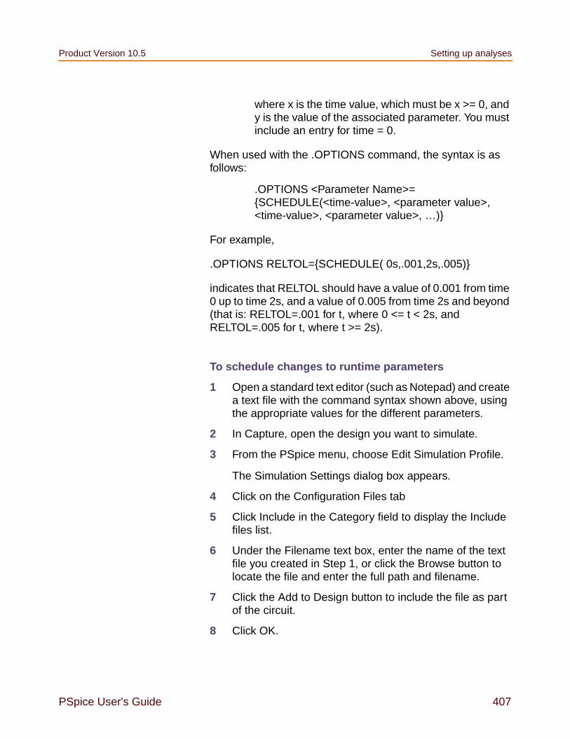
Product Version 10.5 Setting up analyses
PSpice User's Guide 407
where x is the time value, which must be x >= 0, andy is the value of the associated parameter. You mustinclude an entry for time = 0.
When used with the .OPTIONS command, the syntax is asfollows:
.OPTIONS <Parameter Name>=SCHEDULE(<time-value>, <parameter value>,<time-value>, <parameter value>, …)
For example,
.OPTIONS RELTOL=SCHEDULE( 0s,.001,2s,.005)
indicates that RELTOL should have a value of 0.001 from time0 up to time 2s, and a value of 0.005 from time 2s and beyond(that is: RELTOL=.001 for t, where 0 <= t < 2s, andRELTOL=.005 for t, where t >= 2s).
To schedule changes to runtime parameters
1 Open a standard text editor (such as Notepad) and createa text file with the command syntax shown above, usingthe appropriate values for the different parameters.
2 In Capture, open the design you want to simulate.
3 From the PSpice menu, choose Edit Simulation Profile.
The Simulation Settings dialog box appears.
4 Click on the Configuration Files tab
5 Click Include in the Category field to display the Includefiles list.
6 Under the Filename text box, enter the name of the textfile you created in Step 1, or click the Browse button tolocate the file and enter the full path and filename.
7 Click the Add to Design button to include the file as partof the circuit.
8 Click OK.

Chapter 8 Setting up analyses and starting simulation Product Version 10.5
408 PSpice User's Guide
When you run the simulation, the scheduled parameterchanges will be included as part of the circuit file and thesimulation will run to completion automatically.

Product Version 10.5 Setting up analyses
PSpice User's Guide 409
Using the Simulation Manager
Overview of the Simulation Manager
PSpice includes a new Simulation Manager that providesenhanced control over how multiple simulations areprocessed. You can preempt the current simulation to runanother one first. Or, you can use the Simulation Manager tomonitor the progress of a set of batch simulations that wereset up and launched earlier.
Note: None of the earlier functionality of batch processinghas been lost. For more information, see Setting upbatch simulations on page 395.
The PSpice Simulation Manager provides a familiar,easy-to-use interface for controlling how multiple simulationsare processed.
The Simulation Manager allows you to do the following:
add or delete simulations
start, stop or pause simulations
rearrange the order of the simulations in the queue
attach PSpice to a simulation to make it the active display

Chapter 8 Setting up analyses and starting simulation Product Version 10.5
410 PSpice User's Guide
view the status and progress of simulations running in thebackground
You can accomplish most of these functions by selecting thedesired simulation in the list, then clicking on the appropriatetoolbar button to execute the command.
Note: For simulations that are queued in the SimulationManager, the setting in the Simulation Profile to startProbe automatically is ignored. When a queuedsimulation runs to completion and finishes, it will not beloaded into Probe. You must do this manually if youwant to see the results of that simulation.
Accessing the Simulation Manager
The Simulation Manager is invoked whenever you start a newsimulation, either from PSpice or from a front-end design entrytool. Since it is active as long as a simulation is running in thebackground, you can also call up the Simulation Manager fromthe Windows system tray.
You can also launch the Simulation Manager by itself from theWindows Start menu. You do not need to have PSpice runningin order to work with the Simulation Manager.
Understanding the information in the Simulation Manager
Every job listed in the Simulation Manager will have a specificentry for Schedule, Status and Percent Complete. In addition,certain color-coded icons are shown to the left of eachsimulation file name to indicate their current state. A quickglance over the list of jobs will tell you immediately where anyparticular job is and how it will be processed. The following

Product Version 10.5 Setting up analyses
PSpice User's Guide 411
tables explain the meanings of the various categories andstates.
Icon Explanation
The simulation is either in the queue and has notbeen run yet, or has been run to completion.
The simulation is currently running.
The simulation has been paused and is on hold,waiting to either be continued or stopped.
The simulation has been stopped and is notcompleted.
Schedule Explanation
queued The simulation is in the queue. It will be run inthe order in which it is listed in the queue. (Thisis the default setting.)
running The simulation is currently running andongoing status information is displayed.
on hold The simulation has been paused.
stopped The simulation has been run completely, orwas stopped because of an error.
Note: You must manually restart a stoppedsimulation if you want it to run again at alater time.
Status Explanation
not run The simulation has not been started yet. (Thisis the default setting.)
<status> Basic status information about the progress ofthe analysis will be displayed for a simulationthat is currently running.

Chapter 8 Setting up analyses and starting simulation Product Version 10.5
412 PSpice User's Guide
What the various versions of PSpice support
The following table identifies what functionality in theSimulation Manager is available with each version of PSpice.
paused The simulation has been paused eithermanually or automatically by the SimulationManager.
Note: If you change the default option thatautomatically resumes pausedsimulations in the queue, then you mustremember to manually resume a pausedsimulation if you want it to continue at alater time.
complete –no errors
The simulation has run to completion and noerrors were encountered.
errors The simulation ran partially but stoppedautomatically because errors wereencountered.
Percent Explanation
<%> The percentage of completion for a simulation.This number increases as a simulationprogresses.
PSpice version Functionality of Simulation Manager
PSpice Lite
PSpice A/D Basics
Only one simulation may be running orpaused at a time.
The queue is run sequentially.
PSpice
PSpice A/D
One simulation may be running andmultiple simulations may be paused.
The queue is run sequentially.

Product Version 10.5 Setting up analyses
PSpice User's Guide 413
How the Simulation Manager handles errors during simulation
Since each simulation that runs in the background runsindependently, an error that occurs during one simulation willnot prevent the remaining jobs in the queue from runningsubsequently, in order. The following common error conditionsmay arise, but these will not prevent the Simulation Managerfrom running the remaining simulations pending in the queue.
Simulation crash: If a simulation crashes for whatever reason,the Simulation Manager will stop receiving progress updates.After a certain period, the Simulation Manager will stop thatsimulation and will automatically start the next job in thequeue.
Simulation pause: If a simulation pauses automatically andrequires manual intervention to continue, the SimulationManager will automatically start the next job in the queue.
Simulation stop: If a simulation stops automatically, theSimulation Manager will automatically start the next job in thequeue.
Note: You must manually restart a stopped or pausedsimulation if you want it to run again at a later time. Youwill not be able to shut down the Simulation Manageruntil all stopped and paused simulations have beendeleted.
Setting up multiple simulations
With the Simulation Manager, you can set up any number ofbatch simulations to be run sequentially in the backgroundwhile you do other work in PSpice. Each new simulation thatyou set up will be added to the bottom of the simulation queueand will be assigned the schedule category "queued". It will berun after all other queued jobs ahead of it have been run.
Once a job has been added, you can change its position in thequeue, start, stop or pause it, or make other modifications toits status.

Chapter 8 Setting up analyses and starting simulation Product Version 10.5
414 PSpice User's Guide
To add a simulation to the queue
1 From the File menu, choose Add Simulation or click theAdd Simulation button on the toolbar.
2 Locate the file (.SIM, .CIR) you wish to add to the queue.
Alternately, you can add a simulation to the queue by startingthe PSpice simulation directly from within the front-end toolyou are using, such as OrCAD Capture.
Note: If one simulation is already running in the SimulationManager and you start another one, you will beprompted to direct the Simulation Manager in how toproceed with the new simulation. For more informationabout the different ways to handle this situation, seeSetting options in the Simulation Manager onpage 415.
Starting, stopping, and pausing simulations
In the Simulation Manager, you can easily manage the variousbatch simulations in the queue. The most fundamentalcontrols that are provided are the ability to start a simulation,stop it, or pause it temporarily.
To start a simulation from the Simulation Manager
1 Select a simulation in the list.
2 From the Simulation menu, choose Run or click the RunSelected button on the toolbar.
To stop a simulation from the Simulation Manager
1 Select the simulation that is currently running.
2 From the Simulation menu, choose Stop or click the StopSelected button on the toolbar.
To pause a simulation from the Simulation Manager
1 Select the simulation that is currently running.

Product Version 10.5 Setting up analyses
PSpice User's Guide 415
2 From the Simulation menu, choose Pause or click thePause Selected button on the toolbar.
Attaching PSpice to a simulation
A simulation that is running in the Simulation Manager will notbe loaded into PSpice or displayed in Probe while it is running.This allows you to work on a different design in the PSpiceapplication while a simulation is running in the SimulationManager.
Note: If you start a new simulation from within PSpice whileanother is running in the queue in the SimulationManager, the Simulation Manager must decide how totreat the new job. You will be prompted to choosewhether you want the new job to preempt the currentsimulation and start running immediately. For moredetails, click Setting options in the Simulation Manageron page 415.
If you want to display a different simulation in PSpice bychoosing from the list of jobs in the Simulation Manager, youcan attach PSpice to a particular job in the queue.
To attach PSpice to a simulation
1 Select the simulation you want to attach PSpice to.
2 From the View menu, choose Simulation Results.
The PSpice program will activate and the results of thesimulation you selected will become the current display inProbe. If the simulation is currently running, you will be able toview the marching waveforms.
Setting options in the Simulation Manager
Each time you add a new simulation while another is running,the Simulation Manager must decide how to treat the new job.The default setting is to add the new simulation to the bottomof the queue and continue running whatever job is currentlybeing simulated.

Chapter 8 Setting up analyses and starting simulation Product Version 10.5
416 PSpice User's Guide
You can change this default so that the Simulation Managerwill start each new simulation immediately and either stop orpause whatever job is currently running. The options you canchoose from are explained in the procedure below.
You can also choose to have the Options dialog box displayeach time you add a new simulation, or not show thisanymore. If you disable the prompting, you can always enableit again using the following procedure.
In addition, you can define how paused simulations should behandled by the Simulation Manager. You can configure themto be resumed automatically after the previous simulationstops, or you can choose to leave them in a paused state untilyou manually resume them.
To set the default options for the Simulation Manager
1 From the Tools menu, choose Options.
The Options dialog box appears.

Product Version 10.5 Setting up analyses
PSpice User's Guide 417
2 In the top frame dealing with simulations that are alreadyrunning, click the appropriate radio button for the optionyou wish to set.
3 If you want the Options dialog box to appear as areminder each time you add a new simulation, be sure tocheck the Always Prompt box. (The default setting is toenable this feature.)
Radio button Function
Display thesimulation in thequeue.
The simulation that is currentlyrunning will be displayed inPSpice. The new simulation willbe added to the bottom of thequeue and will be run after allother jobs in the queue havebeen run. (This is the defaultsetting.)
Pause the currentsimulation and runthe new one.
The simulation that is currentlyrunning will be paused. Thenew simulation will be startedimmediately. You mustremember to resume thepaused simulation later if youwant it to continue.
Stop the currentsimulation and runthe new one.
The simulation that is currentlyrunning will be stopped. Thenew simulation will be startedimmediately. You mustremember to restart thestopped simulation later if youwant it to run again.

Chapter 8 Setting up analyses and starting simulation Product Version 10.5
418 PSpice User's Guide
4 In the bottom frame dealing with paused simulations, clickthe appropriate radio button for the option you wish to set.
5 Click OK to save the settings.
Radio button Function
Resumesimulating.
The first paused simulation in thelist will automatically resume afterthe previous simulation hasstopped. (This is the defaultsetting.)
Wait for userintervention.
The Simulation Manager will notresume any paused simulationsautomatically. You must intervenemanually to resume them.
Note: If you enable this radiobutton, you must rememberto intervene manually if youwant paused simulations toresume later.

PSpice User's Guide 419
9
DC analyses
Chapter overview
This chapter describes how to set up DC analyses andincludes the following sections:
DC Sweep on page 420
Bias point on page 429
Small-signal DC transfer on page 431
DC sensitivity on page 434

Chapter 9 DC analyses Product Version 10.5
420 PSpice User's Guide
DC Sweep
Minimum requirements to run a DC sweep analysis
Minimum circuit design requirements
Minimum program setup requirements
1 In Capture, select New Simulation Profile or EditSimulation Profile from the PSpice menu. (If this is a newsimulation, enter the name of the profile and click OK.)
Swept variable type Requirement
voltage source voltage source with a DCspecification (VDC, for example)
temperature none
current source current source with a DCspecification (IDC, for example)
model parameter PSpice A/D model (.MODEL)
global parameter global parameter defined with aparameter block (.PARAM)
Product Version 10.5 Chapter overview
PSpice User's Guide 421
The Simulation Settings dialog box appears.
2 Under Analysis type, select DC Sweep.
3 For the Primary Sweep option, enter the necessaryparameter values and select the appropriate check boxesto complete the analysis specifications.
4 Click OK to save the simulation profile.
5 Select Run under the PSpice menu to start thesimulation.
Note: Do not specify a DC sweep and a parametric analysisfor the same variable.
Overview of DC sweep
The DC sweep analysis causes a DC sweep to be performedon the circuit. DC sweep allows you to sweep a source(voltage or current), a global parameter, a model parameter, orthe temperature through a range of values. The bias point ofthe circuit is calculated for each value of the sweep. This isuseful for finding the transfer function of an amplifier, the highand low thresholds of a logic gate, and so on.
For the DC sweep analysis specified in Figure 9-1, the voltagesource V1 is swept from -0.125 volts to 0.125 volts by steps of0.005. This means that the output has(0.125 + 0.125)/0.005 +1 = 51 steps or simulation points.
A source with a DC specification (such as VDC or IDC) mustbe used if the swept variable is to be a voltage type or currentsource. To set the DC value, select Properties from the Editmenu, then click on the cell under the DC column and type inits value.
The default DC value of V1 is overridden during the DC sweepanalysis and is made to be the swept value. All of the othersources retain their values.
After running the analysis, the simulation output file(EXAMPLE.OUT for the EXAMPLE.OPJ circuit in Figure 9-1)

Chapter 9 DC analyses Product Version 10.5
422 PSpice User's Guide
contains a table of voltages relating V1, node OUT1, and nodeOUT2.
Figure 9-1 Example schematic EXAMPLE.OPJ.
Note: The example circuit EXAMPLE.OPJ is provided withthe program installation.
To calculate the DC response of an analog circuit, PSpiceremoves time from the circuit. This is done by treating allcapacitors as open circuits, all inductors as shorts, and usingonly the DC values of voltage and current sources. A similarapproach is used for digital devices: all propagation delays areset to zero, and all stimulus generators are set to theirtime-zero values.
In order to solve the circuit equations, PSpice uses an iterativealgorithm. For analog devices, the equations are continuous,and for digital devices, the equations are Boolean. If PSpicecannot get a self-consistent result after a certain number ofiterations, the analog/digital devices are forced to the X value,and more iterations are done. Since X as input to a digitalcomponent gives X as output, the Boolean equations canalways be solved this way.
If a digital node cannot be driven by known values during theDC iterations (for instance, the output of a flip-flop with theclock line held low), then its DC state will be X. Depending onthe circuit, some, none, or all of the digital nodes may have thestate X when the bias point is calculated.

Product Version 10.5 Chapter overview
PSpice User's Guide 423
Setting up a DC stimulus
To run a DC sweep or small-signal DC transfer analysis, youneed to place and connect one or more independent sourcesand then set the DC voltage or current level for each source.
To set up a DC stimulus
1 Place and connect one of these symbols in yourschematic:
2 Double-click the symbol instance to display the Partsspreadsheet appears.
3 Click in the cell under the DC column to edit its value.
Table 9-1
For voltage input
Usethis...
When you are running...
VDC A DC Sweep and/or Bias Point(transfer function) analysis only.
VSRC Multiple analysis types including DCSweep and/or Bias Point (transferfunction).
Table 9-2
For current input
Usethis...
When you are running...
IDC A DC Sweep and/or Bias Point(transfer function) analysis only.
ISRC Multiple analysis types including DCSweep and/or Bias Point (transferfunction).

Chapter 9 DC analyses Product Version 10.5
424 PSpice User's Guide
4 Define the DC specification as follows:
5 Click OK twice to exit the dialog boxes.
Note: If you are planning to run an AC or transient analysis inaddition to a DC analysis, see the following:
Using time-based stimulus parts with AC and DCproperties on page 137 for other source symbols thatyou can use.
Using VSRC or ISRC parts on page 138 to find outhow to specify the TRAN attribute for a time-basedinput signal when using VSRC or ISRC symbols.
Nested DC sweeps
A second sweep variable can be selected after a primarysweep value has been specified in the DC Sweep dialog box.When you specify a secondary sweep variable, it forms theouter loop for the analysis. That is, for every increment of the
Table 9-3
Set thisattribute...
To this value...
DC DC_levelwhere DC_level is in volts oramps (units are optional).

Product Version 10.5 Chapter overview
PSpice User's Guide 425
second sweep variable, the first sweep variable is steppedthrough its entire range of values.
To set up a nested sweep
1 Under Options, select the Secondary Sweep box for theDC Sweep Analysis type.
2 Enter the necessary parameter values and select theappropriate check boxes to complete the analysisspecifications.

Chapter 9 DC analyses Product Version 10.5
426 PSpice User's Guide
Curve families for DC sweeps
When a nested DC sweep is performed, the entire curvefamily is displayed. That is, the nested DC sweep is treated asa single data section (or you can think of it as a single PSpicerun).
For the circuit shown in Figure 9-2, you can set up a DC sweepanalysis with an outer sweep of the voltage source VG and aninner sweep of the voltage source VD as listed in Table 9-4.
Table 9-4 Curve family example setup
Primarysweep
Secondarysweep
Swept Var Type voltage source voltage source
Sweep Type linear linear
Name VD VG
Start Value 0 0
End Value 5 2
Increment 0.1 0.5
Figure 9-2 Curve family example schematic

Product Version 10.5 Chapter overview
PSpice User's Guide 427
When the DC sweep analysis is run, add a current marker atthe drain pin of M1 and display the simulation results inPSpice. The result will look like Figure 9-3.
Note: In Capture, from the PSpice menu, point to Markers,then choose Mark Current Into Pin to add a currentmarker.
To add a load line for a resistor, add a trace that computes theload line from the sweep voltage. Assume that the X axisvariable is the sweep voltage V_VD, which runs from 0 to 5volts. The expression which will add a trace that is the load linefor a 50 kohm resistor is:
(5V-V_VD)/50K
Note: V_VD is the hierarchical name for VD created bynetlisting the schematic.
This can be useful for determining the bias point for eachmember of a curve family as shown in Figure 9-4.
Figure 9-3 Device curve family.

Chapter 9 DC analyses Product Version 10.5
428 PSpice User's Guide
Figure 9-4 Operating point determination foreach member of the curve family.

Product Version 10.5 Chapter overview
PSpice User's Guide 429
Bias point
Minimum requirements to run a bias point analysis
Minimum circuit design requirements
None.
Minimum program setup requirements
1 Under Analysis type in the Simulation Settings dialog box,select Bias Point.
2 For the General Settings option, enter the necessaryparameter values and select the appropriate check boxesto complete the analysis specifications.
3 Click OK to save the simulation profile.
4 In Capture, from the PSpice menu, select Run to start thesimulation.
Overview of bias point
The bias point is calculated for any analysis whether or not theBias Point analysis is enabled in the Simulation Settingsdialog box. However, additional information is reported whenthe Bias Point analysis is enabled. Also see Save and load biaspoint on page 746.
When Bias Point analysis is not enabled, only analog nodevoltages and digital node states are reported to the output file.
When the Bias Point analysis is enabled, the followinginformation is reported to the output file:
a list of all analog node voltages
a list of all digital node states
the currents of all voltage sources and their total power
a list of the small-signal parameters for all devices

Chapter 9 DC analyses Product Version 10.5
430 PSpice User's Guide
If Bias Point is enabled, you can suppress the reporting of thebias point analog and digital node values, as follows:
1 Under the Options tab in the Simulation Settings dialogbox, select Output file in the Category box.
2 Uncheck the box for Bias point node voltages (NOBIAS).

Product Version 10.5 Chapter overview
PSpice User's Guide 431
Small-signal DC transfer
Minimum requirements to run a small-signal DC transfer analysis
Minimum circuit design requirements
The circuit should contain an input source, such asVSRC.
Minimum program setup requirements
1 Under Analysis type in the Simulation Settings dialog box,select Bias Point.
2 Specify the name of the input source desired. See Outputvariables on page 376 for a description of output variableformats.
3 Click OK to save the simulation profile.
4 In Capture, from the PSpice menu, select Run to start thesimulation.

Chapter 9 DC analyses Product Version 10.5
432 PSpice User's Guide
Overview of small-signal DC transfer
The small-signal DC transfer analysis calculates thesmall-signal transfer function by transforming the circuitaround the bias point and treating it as a linear circuit. Thesmall-signal gain, input resistance, and output resistance arecalculated and reported.
The digital devices themselves are not included in thesmall-signal analysis. A gate, for example, does not have afrequency response. Instead, all the digital devices hold thestates that were calculated when solving for the bias point.However, for N and O devices in the analog/digital interfacesubcircuits, the analog side has a well-defined linearequivalent.
To calculate the small-signal gain, input resistance, andoutput resistance
1 In the Bias Point dialog box, select Calculate small-signalDC gain (.TF).
2 Specify the value for either an output voltage or thecurrent through a voltage source in the To Output variablebox.
For example, entering V(a,b) as the output variablespecifies that the output variable is the output voltage

Product Version 10.5 Chapter overview
PSpice User's Guide 433
between two nets, a and b. Entering I(VDRIV) as theoutput variable specifies that the output variable is thecurrent through a voltage source VDRIV.
3 Specify the input source name in the Calculatesmall-signal DC gain (.TF) portion of the Bias Point dialogbox.
The gain from the input source to the output variable iscalculated along with the input and output resistances.
For example, if you enter V(OUT2)as the output variableand V1 as the input source, the input resistance for V1 iscalculated, the output resistance for V(OUT2) iscalculated, and the gain from V1 to V(OUT2) iscalculated. All calculations are reported to the simulationoutput file.

Chapter 9 DC analyses Product Version 10.5
434 PSpice User's Guide
DC sensitivity
Minimum requirements to run a DC sensitivity analysis
Minimum circuit design requirements
None.
Minimum program setup requirements
1 In the Bias Point dialog box, select Perform Sensitivityanalysis (.SENS).
2 Enter the required value(s) in the Output variable(s) box.
3 Click OK to save the simulation profile. (Be sure you givethe new profile an appropriate name under the Generaltab prior to saving.)
4 In Capture, from the PSpice menu, select Run to start thesimulation.

Product Version 10.5 Chapter overview
PSpice User's Guide 435
Overview of DC sensitivity
DC sensitivity analysis calculates and reports the sensitivity ofone node voltage to each device parameter for the followingdevice types:
resistors
independent voltage and current sources
voltage and current-controlled switches
diodes
bipolar transistors
The sensitivity is calculated by linearizing all devices aroundthe bias point. Purely digital devices hold the states calculatedwhen solving for the bias point as discussed in Small-signalDC transfer on page 431.

Chapter 9 DC analyses Product Version 10.5
436 PSpice User's Guide

PSpice User's Guide 437
10
AC analyses
Chapter overview
This chapter describes how to set up AC sweep and noiseanalyses.
AC sweep analysis on page 438 describes how to set upan analysis to calculate the frequency response of yourcircuit. This section also discusses how to define an ACstimulus and how PSpice treats nonlinear devices in anAC sweep.
Noise analysis on page 448 describes how to set up ananalysis to calculate device noise contributions and totalinput and output noise.

Chapter 10 AC analyses Product Version 10.5
438 PSpice User's Guide
AC sweep analysis
Setting up and running an AC sweep
The following procedure describes the minimum setuprequirements for running an AC sweep analysis. For moredetail on any step, go to the pages referenced in the sidebars.
To set up and run an AC sweep
1 Place and connect a voltage or current source with an ACinput signal.
To find out how, see Setting up an AC stimulus onpage 439.
2 From the PSpice menu, select New Simulation Profile orEdit Simulation Profile. (If this is a new simulation, enterthe name of the profile and click OK.)
The Simulation Settings dialog box appears.
3 Choose AC Sweep/Noise in the Analysis type list box.
4 Specify the required parameters for the AC sweep ornoise analysis you want to run.
To find out how, see Setting up an AC analysis onpage 442.
5 Click OK to save the simulation profile.
6 From the PSpice menu, select Run to start the simulation.
What is AC sweep?
AC sweep is a frequency response analysis. PSpicecalculates the small-signal response of the circuit to acombination of inputs by transforming it around the bias pointand treating it as a linear circuit. Here are a few things to note:
Nonlinear devices, such as voltage- or current-controlledswitches, are transformed to linear circuits about theirbias point value before PSpice A/D runs the linear

Product Version 10.5 Chapter overview
PSpice User's Guide 439
(small-signal) analysis. To find out more, see How PSpicetreats nonlinear devices on page 446.
Digital devices hold the states that PSpice calculatedwhen solving for the bias point.
Because AC sweep analysis is a linear analysis, it onlyconsiders the gain and phase response of the circuit; itdoes not limit voltages or currents.
The best way to use AC sweep analysis is to set the sourcemagnitude to one. This way, the measured output equals thegain, relative to the input source, at that output.
Setting up an AC stimulus
To run an AC sweep analysis, you need to place and connectone or more independent sources and then set the ACmagnitude and phase for each source.
Note: Unlike DC sweep, the AC Sweep/Noise dialog boxdoes not include an input source option. Instead, eachindependent source in your circuit contains its own ACspecification for magnitude and phase.

Chapter 10 AC analyses Product Version 10.5
440 PSpice User's Guide
To set up an AC stimulus
1 Place and connect one of these symbols in yourschematic:
If you are planning to run a DC or transient analysis inaddition to an AC analysis, see If you want to specifymultiple stimulus types on page 137 for additionalinformation and source symbols that you can use.
2 Double-click the symbol instance to display the Partsspreadsheet.
Table 10-1
For voltage input
Usethis...
When you are running...
VAC An AC sweep analysis only.
VSRC Multiple analysis types including ACsweep.
Table 10-2
For current input
Usethis...
When you are running...
IAC An AC sweep analysis only.
ISRC Multiple analysis types including ACsweep.

Product Version 10.5 Chapter overview
PSpice User's Guide 441
3 Click in the cell under the appropriate property column toedit its value. Depending on the source symbol that youplaced, define the AC specification as follows:
If you are also planning to run a transient analysis, seeUsing VSRC or ISRC parts on page 138 to find out howto specify the TRAN property.
Table 10-3
For VAC or IAC
Set thisproperty...
To this value...
ACMAG AC magnitude in volts (for VAC) oramps (for IAC); units are optional.
ACPHASE Optional AC phase in degrees.
Table 10-4
For VSRC orISRC
Set thisproperty...
To this value...
AC Magnitude_value [phase_value]where magnitude_value is in volts oramps (units are optional) and theoptional phase_value is in degrees.

Chapter 10 AC analyses Product Version 10.5
442 PSpice User's Guide
Setting up an AC analysis
To set up the AC analysis
1 From the PSpice menu, choose New Simulation Profile orEdit Simulation Settings. (If this is a new simulation, enterthe name of the profile and click OK.)
The Simulation Settings dialog box appears.
2 Choose AC Sweep/Noise in the Analysis type list box.
3 Under Options, select General Settings if it is not alreadyenabled.
4 Set the number of sweep points as follows:
Table 10-5
To sweep frequency... Do this...
linearly Under AC Sweep Type, clickLinear, and enter the totalnumber of points in the sweepin the Total Points box.

Product Version 10.5 Chapter overview
PSpice User's Guide 443
5 In the Start Frequency and End Frequency text boxes,enter the starting and ending frequencies, respectively,for the sweep.
6 Click OK to save the simulation profile.
Note: If you also want to run a noise analysis, then beforeclicking OK, complete the Noise Analysis frame in thisdialog box as described in Setting up a noise analysison page 450.
logarithmically bydecades
Under AC Sweep Type, clickLogarithmic, select Decade(default), and enter the totalnumber of points per decadein the Total Points box.
logarithmically byoctaves
Under AC Sweep Type, clickLogarithmic, select Octave,and enter the total number ofpoints per octave in the TotalPoints box.
Table 10-5
To sweep frequency... Do this...

Chapter 10 AC analyses Product Version 10.5
444 PSpice User's Guide
AC sweep setup in example.opj
If you look at the example circuit, EXAMPLE.OPJ, providedwith your installed programs, you’ll find that its AC analysis isset up as shown in Figure 10-2.
Figure 10-1 Circuit diagram for EXAMPLE.OPJ.
Note: The source, V1, is a VSIN source that is normally usedfor setting up sine wave signals for a transient analysis.It also has an AC property so that you can use it for anAC analysis.To find out more about VSIN and other source symbols

Product Version 10.5 Chapter overview
PSpice User's Guide 445
that you can use for AC analysis, see Using time-basedstimulus parts with AC and DC properties on page 137.
Figure 10-2 AC analysis setup for EXAMPLE.OPJ.
Frequency is swept from 100 kHz to 10 GHz by decades, with10 points per decade. The V1 independent voltage source isthe only input to an amplifier, so it is the only AC stimulus tothis circuit. Magnitude equals 1 V and relative phase is left atzero degrees (the default). All other voltage sources have zeroAC value.

Chapter 10 AC analyses Product Version 10.5
446 PSpice User's Guide
How PSpice treats nonlinear devices
An AC Sweep analysis is a linear or small-signal analysis. Thismeans that nonlinear devices must be linearized to run theanalysis.
What’s required to transform a device into a linear circuit
In order to transform a device (such as a transistor amplifier)into a linear circuit, you must do the following:
1 Compute the DC bias point for the circuit.
2 Compute the complex impedance and/ortransconductance values for each device at this biaspoint.
3 Perform the linear circuit analysis at the frequencies ofinterest by using simplifying approximations.
Example: Replace a bipolar transistor in common-emittermode with a constant transconductance (collector currentproportional to base-emitter voltage) and a number ofconstant impedances.
What PSpice does
PSpice automates this process for you. PSpice computes thepartial derivatives for nonlinear devices at the bias point anduses these to perform small-signal analysis.
Example: nonlinear behavioral modeling block
Suppose you have an analog behavioral modeling block thatmultiplies V(1) by V(2). Multiplication is a nonlinear operation.To run an AC sweep analysis on this block, the block needs tobe replaced with its linear equivalent. To determine the linearequivalent block, PSpice needs a known bias point.

Product Version 10.5 Chapter overview
PSpice User's Guide 447
Using a DC source
Consider the circuit shown below.
At the DC bias point, PSpice calculates the partial derivativeswhich determine the linear response of the multiplier asfollows:
For this circuit, this equation reduces to:
This means that the multiplier acts as an amplifier of the ACinput with a gain that is set by the DC input.
Caution: multiplying AC sources
Suppose that you replace the 2 volt DC source in this examplewith an AC source with amplitude 1 and no DC value (DC=0).When PSpice computes the bias point, there are no DCsources in the circuit, so all nodes are at 0 volts at the biaspoint. The linear equivalent of the multiplier block is a blockwith gain 0, which means that there is no output voltage at thefundamental frequency. This is exactly how a double-balancedmixer behaves. In practice, this is a simple multiplier.
Note: A double-balanced mixer with inputs at the samefrequency would produce outputs at DC at twice theinput frequency, but these terms cannot be seen with alinear, small-signal analysis.
V Out( ) V Out( )∂V In1( )∂
---------------------- V Out( )∂V In2( )∂
----------------------+=
2.V In1( ) 2.+˙ 0=
V Out( ) 2V In1( )=

Chapter 10 AC analyses Product Version 10.5
448 PSpice User's Guide
Noise analysis
Setting up and running a noise analysis
The following procedure describes the minimum setuprequirements for running a noise analysis. For more detail onany step, go to the pages referenced in the sidebars.
To set up and run an AC sweep
1 Place and connect a voltage or current source with an ACinput signal.
To find out how, see Setting up an AC stimulus onpage 439.
2 Set up the AC sweep simulation specifications.
To find out how, see Setting up an AC analysis on page 442.
3 Set up the noise simulation specifications and enable theanalysis in the AC Sweep/Noise portion of the SimulationSettings dialog box.
To find out how, see Setting up a noise analysis onpage 450.
4 Click OK to save the simulation profile.
5 From the PSpice menu, choose Run to start thesimulation.

Product Version 10.5 Chapter overview
PSpice User's Guide 449
What is noise analysis?
When running a noise analysis, PSpice calculates and reportsthe following for each frequency specified for the ACSweep/Noise analysis:
Device noise, which is the noise contribution propagatedto the specified output net from every resistor andsemiconductor device in the circuit; for semiconductordevices, the device noise is also broken down intoconstituent noise contributions where applicable
Example: Diodes have separate noise contributions fromthermal, shot, and flicker noise.
Total output and equivalent input noise
How PSpice calculates total output and input noise
To calculate total noise at an output net, PSpice computes theRMS sum of the noise propagated to the net by allnoise-generating devices in the circuit.
To calculate the equivalent input noise, PSpice then dividestotal output noise by the gain from the input source to theoutput net. This results in the amount of noise which, ifinjected at the input source into a noiseless circuit, wouldproduce the total noise originally calculated for the output net.
Table 10-6
This value... Means this...
Output noise RMS sum of all the device contributionspropagated to a specified output net
Input noise equivalent noise that would be neededat the input source to generate thecalculated output noise in an ideal(noiseless) circuit

Chapter 10 AC analyses Product Version 10.5
450 PSpice User's Guide
Setting up a noise analysis
To set up the noise analysis
1 From the PSpice menu, choose New Simulation Profile orEdit Simulation Profile. (If this is a new simulation, enterthe name of the profile and click OK.)
The Simulation Settings dialog box appears.
2 Choose AC Sweep/Noise in the Analysis type list box.
3 Under Options, select General Settings if it is not alreadyenabled.
4 Specify the AC sweep analysis parameters as describedin Setting up an AC analysis on page 442.
5 Enable the Noise Analysis check box.

Product Version 10.5 Chapter overview
PSpice User's Guide 451
6 Enter the noise analysis parameters as follows:
7 Click OK to save the simulation profile.
Table 10-7
In this textbox...
Type this...
Output Voltage A voltage output variable of the formV(node, [node]) where you want thetotal output noise calculated.
To find out more about valid syntax,see Output variables on page 376.
I/V Source The name of an independent current orvoltage source where you want theequivalent input noise calculated.
Note: If the source is in a lower level ofa hierarchical schematic,separate the names of thehierarchical devices with periods(.).Example: U1.V2
Interval An integer n designating that at everynth frequency, you want to see a tableprinted in the PSpice output file (.OUT)showing the individual contributions ofall of the circuit’s noise generators tothe total noise.
Note: In the Probe window, you canview the device noisecontributions at every frequencyspecified in the AC sweep. TheInterval parameter has no effecton what PSpice writes to theProbe data file.

Chapter 10 AC analyses Product Version 10.5
452 PSpice User's Guide
Analyzing Noise in the Probe window
You can use these output variable formats to view traces fordevice noise contributions and total input or output noise atevery frequency in the analysis.
For a break down of noise output variables by supporteddevice type, see Table 17-17 on page 698.
To view this... Use this outputvariable...
Which is represented by thisequation1...
Flicker noise for a device NFID(device_name)NFIB(device_name)
noise ∝
Shot noise for a device NSID(device_name)NSIB(device_name)NSIC(device_name)
For diodes and BJTs:
noise ∝For GaAsFETs, JFETs, andMOSFETs:
noise ∝
Thermal noise for the RB,RC, RD, RE, RG, or RSconstituent of a device,respectively
NRB(device_name)NRC(device_name)NRD(device_name)NRE(device_name)NRG(device_name)NRS(device_name)
noise ∝
Thermal noise generated byequivalent resistances in theoutput of a digital device
NRLO(device_name)NRHI(device_name)
noise ∝
Total noise for a device NTOT(device_name) Sum of all contributors indevice_name
Total output noise for thecircuit
NTOT(ONOISE)
RMS-summed output noisefor the circuit
V(ONOISE) RMS sum of all contributors
Equivalent input noise for thecircuit
V(INOISE)
kfIaf
fb
-----⋅
2qI
4kTIdVd
------- 23---⋅ ⋅
4kTR
----------
4kTR
----------
NTOT device( )device∑
NTOT ONOISE( )( )
V ONOISE( )gain
---------------------------------
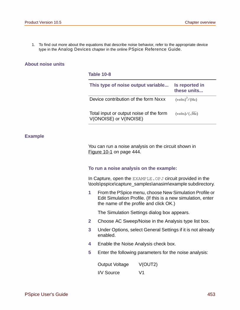
Product Version 10.5 Chapter overview
PSpice User's Guide 453
About noise units
Example
You can run a noise analysis on the circuit shown inFigure 10-1 on page 444.
To run a noise analysis on the example:
In Capture, open the EXAMPLE.OPJ circuit provided in the\tools\pspice\capture_samples\anasim\example subdirectory.
1 From the PSpice menu, choose New Simulation Profile orEdit Simulation Profile. (If this is a new simulation, enterthe name of the profile and click OK.)
The Simulation Settings dialog box appears.
2 Choose AC Sweep/Noise in the Analysis type list box.
3 Under Options, select General Settings if it is not alreadyenabled.
4 Enable the Noise Analysis check box.
5 Enter the following parameters for the noise analysis:
1. To find out more about the equations that describe noise behavior, refer to the appropriate devicetype in the Analog Devices chapter in the online PSpice Reference Guide.
Table 10-8
This type of noise output variable... Is reported inthese units...
Device contribution of the form Nxxx
Total input or output noise of the formV(ONOISE) or V(INOISE)
volts( )2Hz( )⁄
volts( ) Hz( )⁄
Output Voltage V(OUT2)
I/V Source V1

Chapter 10 AC analyses Product Version 10.5
454 PSpice User's Guide
These settings mean that PSpice will calculate noisecontributions and total output noise at net OUT2 andequivalent input noise from V1.
Figure 10-3 shows Probe traces for Q1’s constituent noisesources as well as total noise for the circuit after simulating.Notice that the trace for RMSSUM (at the top of the plot),which is a macro for the trace expression
SQRT(NTOT(Q1) + NTOT(Q2) + NTOT(Q3) + ... ),
exactly matches the total output noise, V(ONOISE),calculated by PSpice A/D.
Interval 30
For a description of theInterval parameter, seeInterval on page 451.

Product Version 10.5 Chapter overview
PSpice User's Guide 455
To find out more about PSpice macros, refer to the onlinePSpice Help.
Figure 10-3 Device and total noise traces forEXAMPLE.OPJ.
Note: The source, V1, is a VSIN source that is normally usedfor setting up sine wave signals for a transient analysis.It also has an AC property so that you can use it for anAC analysis.To find out more about VSIN and other source symbolsthat you can use for AC analysis, see Using time-basedstimulus parts with AC and DC properties on page 137.
Frequency is swept from 100 kHz to 10 GHz by decades, with10 points per decade. The V1 independent voltage source is

Chapter 10 AC analyses Product Version 10.5
456 PSpice User's Guide
the only input to an amplifier, so it is the only AC stimulus tothis circuit. Magnitude equals 1 V and relative phase is left atzero degrees (the default). All other voltage sources have zeroAC value.

PSpice User's Guide 457
11
Parametric and temperatureanalysis
Chapter overview
This chapter describes how to set up parametric andtemperature analyses. Parametric and temperature are bothsimple multi-run analysis types.
This chapter includes the following sections:
Parametric analysis on page 458
Temperature analysis on page 467

Chapter 11 Parametric and temperature analysis Product Version 10.5
458 PSpice User's Guide
Parametric analysis
Minimum requirements to run a parametric analysis
Note: Parametric analysis is not included in PSpice A/DBasics.
Minimum circuit design requirements
Set up the circuit according to the swept variable type aslisted in Table 11-1.
Set up a DC sweep, AC sweep, or transient analysis.
Minimum program setup requirements
1 In the Simulation Settings dialog box, from the Analysistype list box, select Time Domain (Transient).
See Setting up analyses on page 373 for a description ofthe Simulation Settings dialog box.
2 Under Options, select Parametric Sweep if it is notalready enabled.
Table 11-1 Parametric analysis circuit designrequirements
Swept variable type Requirement
voltage source voltage source with a DCspecification (VDC, for example)
temperature none
current source current source with a DCspecification (IDC, for example)
model parameter PSpice A/D model
global parameter global parameter defined with aparameter block (PARAM)

Product Version 10.5 Chapter overview
PSpice User's Guide 459
3 Specify the required parameters for the sweep.
4 Click OK to save the simulation profile.
5 From the PSpice menu, choose Run to start thesimulation.
Note: Do not specify a DC sweep and a parametric analysisfor the same variable.
Overview of parametric analysis
Parametric analysis performs multiple iterations of a specifiedstandard analysis while varying a global parameter, modelparameter, component value, or operational temperature. Theeffect is the same as running the circuit several times, once foreach value of the swept variable.
See Parametric analysis on page 93 for a description of howto set up a parametric analysis.
RLC filter example
This example shows how to perform a parametric sweep andanalyze the results with performance analysis.

Chapter 11 Parametric and temperature analysis Product Version 10.5
460 PSpice User's Guide
Use performance analysis to derive values from a series ofsimulator runs and plot these values versus a parameter thatvaries between the simulator runs.
For this example, the derived values are the overshoot and therise time versus the damping resistance of the filter.
Entering the design
The schematic representation for the RLC filter(RLCFILT.OPJ) is shown in Figure 11-1.
This series of PSpice runs varies the value of resistor R1 from0.5 to 1.5 ohms in 0.1 ohm steps. Since the time-constant ofthe circuit is about one second, perform a transient analysis ofapproximately 20 seconds.
Create the circuit in Capture by placing a piecewise linearindependent current source (IPWL from SOURCE.OLB). Setthe current source properties as follows:
AC = 1aT1 = 0sI1 = 0aT2 = 10msI2 = 0aT3 = 10.1msI3 = 1a
Place an instance of a resistor and set its VALUE property tothe expression, R. To define R as a global parameter, placea PARAM pseudocomponent and use the Property Editor to
Figure 11-1 Passive filter schematic.

Product Version 10.5 Chapter overview
PSpice User's Guide 461
create a new property R and set its value to 0.5. Place aninductor and set its value to 1H, place a capacitor and set itsvalue to 1, and place an analog ground symbol (0 from theSOURCE.OLB library). Wire the schematic symbols togetheras shown in Figure 11-1.
Running the simulation
Run PSpice A/D with the following analyses enabled:
After setting up the analyses, start the simulation by choosingRun from the PSpice menu.
Using performance analysis to plot overshoot and rise time
After performing the simulation that creates the data fileRLCFILT.DAT, you can calculate the specified performanceanalysis measurements.
When the simulation is finished, a list appears containing all ofthe sections (runs) in the data file produced by PSpice. To usethe data from every run, select All and click OK in the AvailableSelections dialog box. In the case of Figure 11-2, the traceI(L1) from the ninth section was added by specifying thefollowing in the Add Traces dialog box:
-I(L1)@9
transient print step: 100msfinal time: 20s
parametric swept var. type: global parametersweep type: linearname: Rstart value: 0.5end value: 1.5increment: 0.1

Chapter 11 Parametric and temperature analysis Product Version 10.5
462 PSpice User's Guide
Note: To display the Add Traces dialog box, from the Tracemenu, choose Add Trace or click the Add Trace toolbarbutton .
Figure 11-2 Current of L1 when R1 is 1.5 ohms.
To run performance analysis
1 From the Trace menu, choose Performance Analysis.
2 Click OK.
PSpice resets the X-axis variable for the graph to be theparameter that changed between PSpice runs. In theexample, this is the R parameter.
To see the rise time for the current through the inductor L1,click the Add Trace toolbar button and then enter:
genrise(-I(L1) )
Note: The genrise and overshoot measurements arecontained in the PSPICE.PRB file in the <targetinstallation directory>\PSpice\Common directory. Forlegacy users, there are now two files in thePSpice\Common directory:
PSPICE_OLB.PRB uses goal function names
PSPICE.PRB uses measurement names

Product Version 10.5 Chapter overview
PSpice User's Guide 463
Figure 11-3, shows how the rise time decreases as thedamping resistance increases for the filter.
Another Y axis can be added to the plot for the overshoot ofthe current through L1 by selecting Add Y Axis from the Plotmenu. The Y axis is immediately added. Now click the AddTrace toolbar button and enter:
overshoot(-I(L1) )
Figure 11-3 shows how the overshoot increases withincreasing resistance.
Figure 11-3 Rise time and overshoot vs. dampingresistance.
Troubleshooting tip
More than one PSpice run or data section is required forperformance analysis. Because one data value is derived foreach waveform in a related set of waveforms, at least two datapoints are required to produce a trace.
Use Eval Goal Function (from the Trace menu) to evaluate agoal function on a single waveform and produce a single datapoint result.

Chapter 11 Parametric and temperature analysis Product Version 10.5
464 PSpice User's Guide
Example: frequency response vs. arbitrary parameter
You can view a plot of the linear response of a circuit at aspecific frequency as one of the circuit parameters varies(such as the output of a band pass filter at its center frequencyvs. an inductor value).
In this example, the value of a nonlinear capacitance ismeasured using a 10 kHz AC signal and plotted versus its biasvoltage. The capacitance is in parallel with a resistor, so atrace expression is used to calculate the capacitance from thecomplex admittance of the R-C pair.
Note: This technique for measuring branch capacitancesworks well in both simple and complex circuits.
Setting up the circuit
Enter the circuit in Capture as shown in Figure 11-4.
To create the capacitor model in the schematic editor:
1 Place a CBREAK part.
2 Select it so that it is highlighted.
3 From the Edit menu, choose PSpice Model.
4 In the Model Text frame, enter the following:
.model Cnln CAP(C=1 VC1=-0.01 VC2=0.05)
5 From the File menu, choose Save.
Set up the circuit for a parametric AC analysis (sweep Vbias),and run PSpice. Include only the frequency of interest in theAC sweep.
Figure 11-4 RLC filterexample circuit.

Product Version 10.5 Chapter overview
PSpice User's Guide 465
To display the results
Use PSpice to display the capacitance calculated at thefrequency of interest versus the stepped parameter.
1 Simulate the circuit.
2 Load all AC analysis sections.
3 From the Trace menu, choose Add Trace or click the AddTrace toolbar button .
4 Add the following trace expression:
IMG(-I(Vin)/V(1,0))/(2*3.1416*Frequency)
Or add the expression:
CvF(-I(Vin)/V(1,0))
Where CvF is a macro which measures the effectivecapacitance in a complex conductance. Macros are definedusing the Macros command on the Trace menu. The CvFmacro should be defined as:
CvF(G)= IMG(G)/(2*3.1416*Frequency)
Note: -I(Vin)/V(1) is the complex admittance of the R-Cbranch; the minus sign is required for correct polarity.
To use performance analysis to plot capacitance vs. biasvoltage
1 From the Trace menu, choose Performance Analysis.
2 Click Wizard.
3 Click Next>.
4 Click YatX in the Choose a Goal Function list, and thenclick Next>.
5 In the Name of Trace text box, type the following:
CvF(-I(Vin)/V(1))
6 In the X value to get Y value at text box, type 10K.
7 Click Next>.
The wizard displays the gain trace for the first run to textthe goal function (YatX).

Chapter 11 Parametric and temperature analysis Product Version 10.5
466 PSpice User's Guide
8 Click Finish.
The resultant plot is shown in Figure 11-5.
Figure 11-5 Plot of capacitance versus bias voltage.

Product Version 10.5 Chapter overview
PSpice User's Guide 467
Temperature analysis
Minimum requirements to run a temperature analysis
Minimum circuit design requirements
None.
Minimum program setup requirements
1 In the Simulation Settings dialog box, from the Analysistype list box, select Time Domain (Transient).
See Setting up analyses on page 373 for a description ofthe Simulation Settings dialog box.
2 Under Options, select Temperature Sweep if it is notalready enabled.
3 Specify the required parameters for the sweep.
4 Click OK to save the simulation profile.
5 From the PSpice menu, choose Run to start thesimulation.
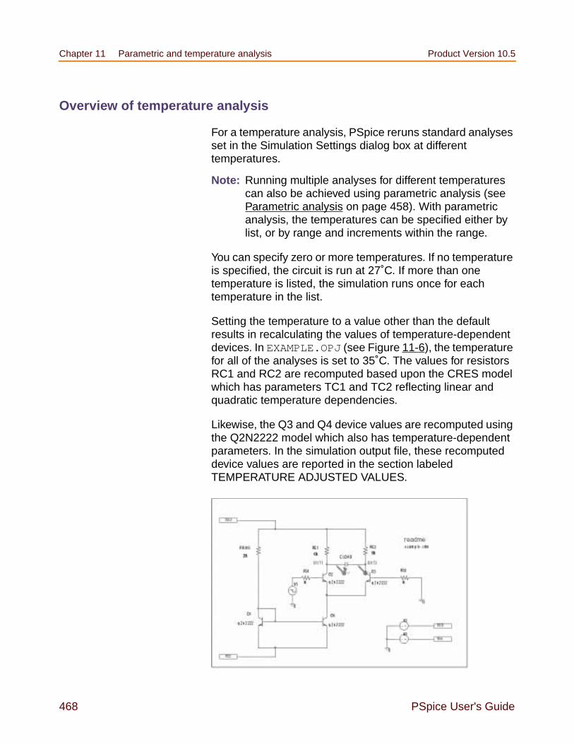
Chapter 11 Parametric and temperature analysis Product Version 10.5
468 PSpice User's Guide
Overview of temperature analysis
For a temperature analysis, PSpice reruns standard analysesset in the Simulation Settings dialog box at differenttemperatures.
Note: Running multiple analyses for different temperaturescan also be achieved using parametric analysis (seeParametric analysis on page 458). With parametricanalysis, the temperatures can be specified either bylist, or by range and increments within the range.
You can specify zero or more temperatures. If no temperatureis specified, the circuit is run at 27˚C. If more than onetemperature is listed, the simulation runs once for eachtemperature in the list.
Setting the temperature to a value other than the defaultresults in recalculating the values of temperature-dependentdevices. In EXAMPLE.OPJ (see Figure 11-6), the temperaturefor all of the analyses is set to 35˚C. The values for resistorsRC1 and RC2 are recomputed based upon the CRES modelwhich has parameters TC1 and TC2 reflecting linear andquadratic temperature dependencies.
Likewise, the Q3 and Q4 device values are recomputed usingthe Q2N2222 model which also has temperature-dependentparameters. In the simulation output file, these recomputeddevice values are reported in the section labeledTEMPERATURE ADJUSTED VALUES.

Product Version 10.5 Chapter overview
PSpice User's Guide 469
Figure 11-6 Example schematic EXAMPLE.OPJ.
Note: The example circuit EXAMPLE.OPJ is provided withthe installed programs.

Chapter 11 Parametric and temperature analysis Product Version 10.5
470 PSpice User's Guide

PSpice User's Guide 471
12
Transient analysis
Chapter overview
This chapter describes how to set up a transient analysis andincludes the following sections:
Overview of transient analysis on page 472
Defining a time-based stimulus on page 474
The Stimulus Editor utility on page 476
Transient (time) response on page 487
Internal time steps in transient analyses on page 490
Switching circuits in transient analyses on page 491
Plotting hysteresis curves on page 492
Fourier components on page 493

Chapter 12 Transient analysis Product Version 10.5
472 PSpice User's Guide
Overview of transient analysis
Minimum requirements to run a transient analysis
Minimum circuit design requirements
Circuit should contain one of the following:
An independent source with a transient specification (seeTable 12-1)
An initial condition on a reactive element
A controlled source that is a function of time
Minimum program setup requirements
1 From Capture’s PSpice menu, choose New SimulationProfile or Edit Simulation Profile. (If this is a newsimulation, enter the name of the profile and click OK.)
The Simulation Settings dialog box appears.
2 Click the Analysis tab.
See Setting up analyses on page 373 for a description ofthe Analysis Setup dialog box.

Product Version 10.5 Chapter overview
PSpice User's Guide 473
3 From the Analysis type list box, select Time Domain(Transient).
4 Specify the required parameters for the transient analysisyou want to run.
5 Click OK to save the simulation profile.
6 From the PSpice menu, choose Run to start thesimulation.

Chapter 12 Transient analysis Product Version 10.5
474 PSpice User's Guide
Defining a time-based stimulus
Overview of stimulus generation
Symbols that generate input signals for your circuit can bedivided into two categories:
those whose transient behavior is characterizedgraphically using the Stimulus Editor
those whose transient behavior is characterized bymanually defining their properties within Capture
Note: Stimulus Editor is not included with PSpice A/D Basics
These symbols are summarized in Table 12-1.
Table 12-1 Stimulus symbols for time-based inputsignals
Specifiedby...
Symbol name Description
Using theStimulusEditor
VSTIM voltage source
ISTIM current source
DIGSTIM1
DIGSTIM2
DIGSTIM4
DIGSTIM8
DIGSTIM16
DIGSTIM32
digital stimuli
Note: Digitalstimuli arenotsupportedin PSpice.
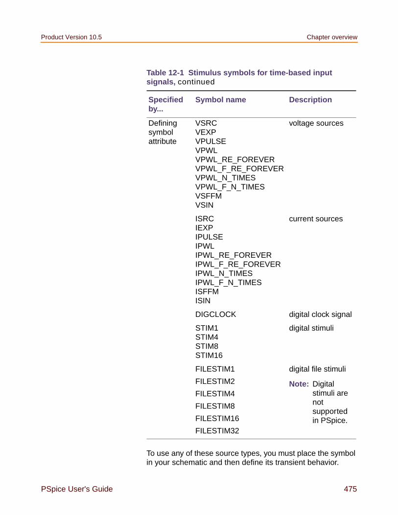
Product Version 10.5 Chapter overview
PSpice User's Guide 475
To use any of these source types, you must place the symbolin your schematic and then define its transient behavior.
Definingsymbolattribute
VSRCVEXPVPULSEVPWLVPWL_RE_FOREVERVPWL_F_RE_FOREVERVPWL_N_TIMESVPWL_F_N_TIMESVSFFMVSIN
voltage sources
ISRCIEXPIPULSEIPWLIPWL_RE_FOREVERIPWL_F_RE_FOREVERIPWL_N_TIMESIPWL_F_N_TIMESISFFMISIN
current sources
DIGCLOCK digital clock signal
STIM1STIM4STIM8STIM16
digital stimuli
FILESTIM1
FILESTIM2
FILESTIM4
FILESTIM8
FILESTIM16
FILESTIM32
digital file stimuli
Note: Digitalstimuli arenotsupportedin PSpice.
Table 12-1 Stimulus symbols for time-based inputsignals, continued
Specifiedby...
Symbol name Description

Chapter 12 Transient analysis Product Version 10.5
476 PSpice User's Guide
Each property-characterized stimulus has a distinct set ofattributes depending upon the kind of transient behavior itrepresents. For VPWL_F_xxx, IPWL_F_xxx, and FSTIM, aseparate file contains the stimulus specification. Forinformation on digital stimuli characterized by property, seeChapter 14, “Digital simulation.”
As an alternative, the Stimulus Editor automates the processof defining the transient behavior of stimulus devices. TheStimulus Editor allows you to create analog stimuli whichgenerate sine wave, repeating pulse, exponential pulse,single-frequency FM, and piecewise linear waveforms. It alsofacilitates creating digital stimuli with complex timing relations.This applies to both stimulus symbols placed in yourschematic as well as new ones that you might create.
The stimulus specification created using the Stimulus Editor issaved to a file, automatically configured into the schematic,and associated with the corresponding VSTIM, ISTIM, orDIGSTIM part instance or symbol definition.
The Stimulus Editor utility
The Stimulus Editor is a utility that allows you to quickly set upand verify the input waveforms for a transient analysis. Youcan create and edit voltage sources, current sources, anddigital stimuli for your circuit. Menu prompts guide you toprovide the necessary parameters, such as the rise time, falltime, and period of an analog repeating pulse, or the complextiming relations with repeating segments of a digital stimulus.Graphical feedback allows you to quickly verify the waveform.See the Stimulus Editor online help for more information aboutthis utility.
Note: Stimulus Editor is not included with PSpice A/D Basics
Note: If you are using a PSpice product that does not includethe Stimulus Editor, you must use thecharacterized-by-property sources listed in Table 12-1on page 474.
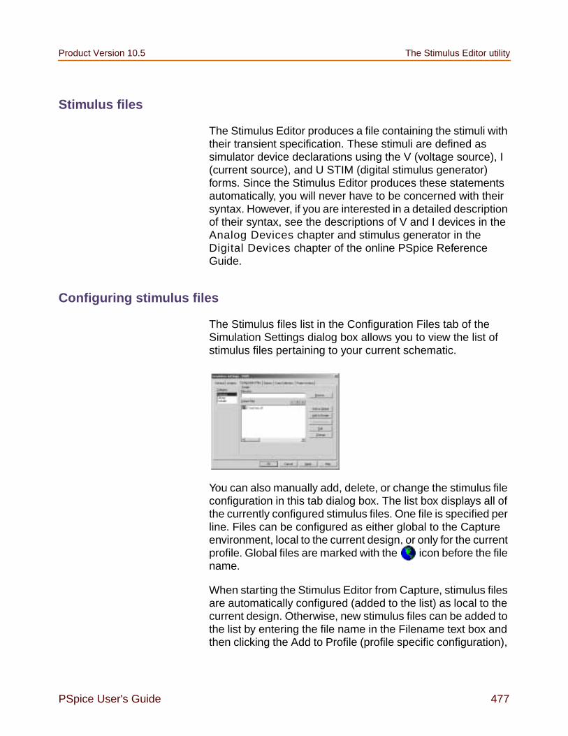
Product Version 10.5 The Stimulus Editor utility
PSpice User's Guide 477
Stimulus files
The Stimulus Editor produces a file containing the stimuli withtheir transient specification. These stimuli are defined assimulator device declarations using the V (voltage source), I(current source), and U STIM (digital stimulus generator)forms. Since the Stimulus Editor produces these statementsautomatically, you will never have to be concerned with theirsyntax. However, if you are interested in a detailed descriptionof their syntax, see the descriptions of V and I devices in theAnalog Devices chapter and stimulus generator in theDigital Devices chapter of the online PSpice ReferenceGuide.
Configuring stimulus files
The Stimulus files list in the Configuration Files tab of theSimulation Settings dialog box allows you to view the list ofstimulus files pertaining to your current schematic.
You can also manually add, delete, or change the stimulus fileconfiguration in this tab dialog box. The list box displays all ofthe currently configured stimulus files. One file is specified perline. Files can be configured as either global to the Captureenvironment, local to the current design, or only for the currentprofile. Global files are marked with the icon before the filename.
When starting the Stimulus Editor from Capture, stimulus filesare automatically configured (added to the list) as local to thecurrent design. Otherwise, new stimulus files can be added tothe list by entering the file name in the Filename text box andthen clicking the Add to Profile (profile specific configuration),

Chapter 12 Transient analysis Product Version 10.5
478 PSpice User's Guide
Add to Design (local configuration) or Add as Global (globalconfiguration) button.
Starting the Stimulus Editor
The Stimulus Editor is fully integrated with Capture and can berun from either the schematic editor or symbol editor.
You can start the Stimulus Editor by doing the following:
1 Select one or more stimulus instances in the schematic.
2 From the Edit menu, choose PSpice Stimulus.
When you first start the Stimulus Editor, you may need toadjust the scale settings to fit the trace you are going to add.You can use Axis Settings on the Plot menu or thecorresponding toolbar button to change the displayed data,the extent of the scrolling region, and the minimum resolutionfor each of the axes. Displayed Data Range parametersdetermine what portion of the stimulus data set will bepresented on the screen. Extent of Scrolling Regionparameters set the absolute limits on the viewable range.Minimum Resolution parameters determine the smallestusable increment (example: if it is set to 1 msec, then youcannot add a data point at 1.5 msec).
Defining stimuli
1 Place stimulus part instances from the symbol set:VSTIM, ISTIM and DIGSTIMn (found in theSOURCSTM.OLB part library).

Product Version 10.5 The Stimulus Editor utility
PSpice User's Guide 479
2 Click the source instance to select it.
3 From the Edit menu, choose PSpice Stimulus to start theStimulus Editor.
4 Fill in the transient specification according to the dialogsand prompts.
Piecewise linear and digital stimuli can be specified bydirect manipulation of the input waveform display.
5 From the File menu, choose Save to save the edits.
6 Click Yes to update the schematic.
See Chapter 14, “Digital simulation,” for detailed informationabout creating digital stimuli.
Example: piecewise linear stimulus
1 Open an existing schematic or start a new one.
2 From the Place menu, choose Part and browse theSOURCSTM.OLB part library file for VSTIM (and select it).
3 Place the part. It looks like a regular voltage source withan implementation property displayed.
4 Click the implementation label and type Vfirst. Thisnames the stimulus that you are going to create.
5 If you are working in a new schematic, choose Save fromthe File menu. This schematic save step is necessarysince the schematic name is used to create the defaultstimulus file name.
6 Click the VSTIM part to select it.
7 From the Edit menu, choose PSpice Stimulus. This startsthe Stimulus Editor and displays the New Stimulus dialog

Chapter 12 Transient analysis Product Version 10.5
480 PSpice User's Guide
box. You can see that the stimulus already has the nameof Vfirst.
8 Select PWL in the dialog box and click OK. The cursorlooks like a pencil. The message in the status bar at thebottom of the screen lets you know that you are in theprocess of adding new data points to the stimulus. Theleft end of the bottom status bar displays the currentcoordinates of the cursor.
9 Move the cursor to (200ns, 1) and click the left mousebutton. This adds the point. Notice that there isautomatically a point at (0,0). Ignore it for now andcontinue to add a couple more points to the right of thecurrent one.
10 Click-right to stop adding points.
11 From the File menu, choose Save.
If you make a mistake or want to make any changes, reshapethe trace by dragging any of the handles to a new location. Thedragged handle cannot pass any other defined data point.
To delete a point, click its handle and press Delete.
To add additional points, either choose Add Point from the Editmenu, press Alt+A, or click the Add Point toolbar button .
At this point you can return to Capture, edit the currentstimulus, or go on to create another.
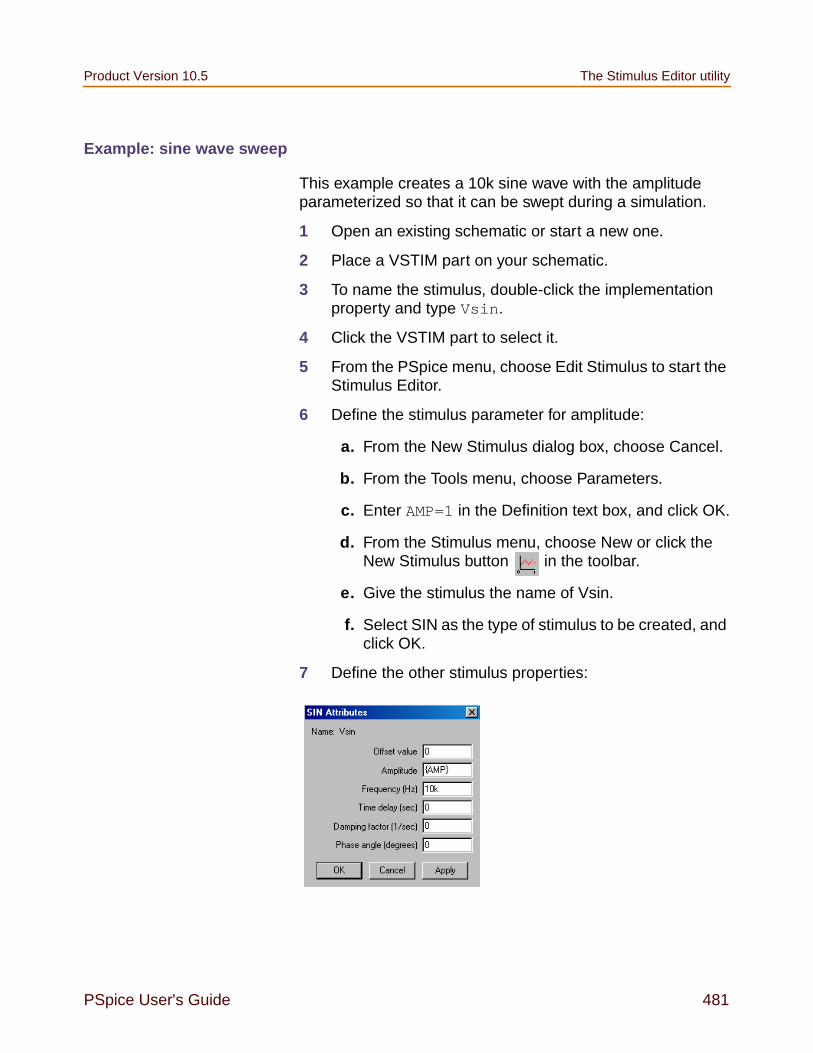
Product Version 10.5 The Stimulus Editor utility
PSpice User's Guide 481
Example: sine wave sweep
This example creates a 10k sine wave with the amplitudeparameterized so that it can be swept during a simulation.
1 Open an existing schematic or start a new one.
2 Place a VSTIM part on your schematic.
3 To name the stimulus, double-click the implementationproperty and type Vsin.
4 Click the VSTIM part to select it.
5 From the PSpice menu, choose Edit Stimulus to start theStimulus Editor.
6 Define the stimulus parameter for amplitude:
a. From the New Stimulus dialog box, choose Cancel.
b. From the Tools menu, choose Parameters.
c. Enter AMP=1 in the Definition text box, and click OK.
d. From the Stimulus menu, choose New or click theNew Stimulus button in the toolbar.
e. Give the stimulus the name of Vsin.
f. Select SIN as the type of stimulus to be created, andclick OK.
7 Define the other stimulus properties:

Chapter 12 Transient analysis Product Version 10.5
482 PSpice User's Guide
a. Enter 0 for Offset Value.
b. Enter AMP for Amplitude. The curly braces arerequired. They indicate that the expression needs tobe evaluated at simulation time.
c. Enter 10k for Frequency and click OK.
d. From the File menu, choose Save.
e. Click Yes to update the schematic.
8 Within Capture, place and define the PARAM symbol:
a. From the Place menu, choose Part.
b. Either browse SPECIAL.OLB for the PARAM part ortype in the name.
c. Place the part on your schematic and double-click it.
d. Click New to add a new user property.
e. Set the value property name to AMP (no curlybraces).
f. Set the value of the AMP property to 1.
9 Set up the parametric sweep and other analyses:
a. From the PSpice menu, choose Edit SimulationProfile, and select the Parametric Sweep option.
b. Select Global Parameter in the Swept Var. Typeframe.
c. Select Linear in the Sweep type frame.
10 Enter AMP in the Parameter name text box.
11 Specify values for the Start Value, End Value, andIncrement text boxes.
You can now set up your usual Transient, AC, or DC analysisand run the simulation.

Product Version 10.5 The Stimulus Editor utility
PSpice User's Guide 483
Creating new stimulus symbols
1 Use the Capture part editor to edit or create a part withthe following properties:
Property Value
ImplementationType
PSpice Stimulus
Implementation Name of the stimulus model
STIMTYPE Type of stimulus; valid values areANALOG or DIGITAL; if thisproperty is nonexistent, thestimulus is assumed to beANALOG
Chapter 12 Transient analysis Product Version 10.5
484 PSpice User's Guide
Editing a stimulus
To edit an existing stimulus
1 Start the Stimulus Editor and select File, Open to openthe required Stimulus library.
2 Double-click the trace name (at the bottom of the X axisfor analog and to the left of the Y axis for digital traces.)This opens the Stimulus Attributes dialog box where youcan modify the attributes of the stimulus directly andimmediately see the effect of the changes.
To edit a PWL stimulus
Note: PWL stimuli are a little different since they are a seriesof time/value pairs.
1 Double-click the trace name. This displays the handles foreach defined data point.
2 Click any handle to select it. To reshape the trace, drag itto a new location. To delete the data point, press Delete.
3 To add additional data points, either select Add from theEdit menu or click the Add Point button.
4 Right-click to end adding new points.
To select a time and value scale factor for PWL stimuli
1 Select the PWL trace by clicking on its name.
2 Select Attributes from the Edit menu or click thecorresponding toolbar button .
Note: The above procedure provides a fast way to scale aPWL stimulus.

Product Version 10.5 The Stimulus Editor utility
PSpice User's Guide 485
Deleting and removing traces
To delete a trace from the displayed screen, select the tracename by clicking on its name, then press Delete. This will onlyerase the display of the trace, not delete it from your file. Thetrace is still available by selecting Get from the Stimulus menu.
To remove a trace from a file, select Remove from theStimulus menu.
Note: Once a trace is removed, it is no longer retrievable.Remove traces with caution.
Manual stimulus configuration
Stimuli can be characterized by manually starting the StimulusEditor and saving their specifications to a file. These stimulusspecifications can then be associated to stimulus instances inyour schematic or to stimulus symbols in the symbol library.
To manually configure a stimulus
1 Start the Stimulus Editor by choosing the Stimulus Editoricon from the Windows Start menu, Release OrCAD 10.0program group, PSpice Accessories option.
2 Open a stimulus file by choosing Open from the Filemenu. If the file is not found in your current library searchpath, you are prompted for a new file name.
3 Create one or more stimuli to be used in your schematic.For each stimulus:
a. Name it whatever you want. This name will be usedto associate the stimulus specification to the stimulusinstance in your schematic, or to the symbol in thesymbol library.
b. Provide the transient specification.
c. From the File menu, choose Save.
4 In the schematic page editor, configure the StimulusEditor’s output file into your schematic:
Chapter 12 Transient analysis Product Version 10.5
486 PSpice User's Guide
a. From the PSpice menu, choose Edit SimulationProfile to display the Simulation Settings dialog box.
b. In the Simulation Settings dialog box, select theConfiguration Files tab.
c. Click Include in the Category field to display theInclude files list.
d. Enter the file name specified in step 2.
e. If the stimulus specifications are for only for thecurrent profile, click the Add to Profile button. Forlocal use in the current design, click the Add toDesign button. For global use by any design, useAdd as Global instead.
f. Click OK.
5 Modify either the stimulus instances in the schematic orsymbols in the symbol library to reference the newstimulus specification.
6 Associate the transient stimulus specification to astimulus instance:
a. Place a stimulus part in your schematic from the partset: VSTIM, ISTIM, and DIGSTIMn.
b. Click the VSTIM, ISTIM, or DIGSTIMn instance.
c. From the Edit menu, choose Properties.
d. Click the Implementation cell, type in the name of thestimulus, and click Apply.
e. Complete specification of any VSTIM or ISTIMinstances by selecting Properties from the Edit menuand editing their DC and AC attributes.
Click the DC cell and type its value.
Click the AC cell, type its value, and then click Apply.
f. Close the property editor spreadsheet.
7 To change stimulus references globally for a part:

Product Version 10.5 Transient (time) response
PSpice User's Guide 487
a. Select the part you want to edit.
b. From the Edit menu, choose Part to start the parteditor.
See Chapter 5, “Creating parts for models,” for adescription of how to create and edit parts.
c. Create or change the part definition, making sure todefine the following property:
Finding out more about the Stimulus Editor
Transient (time) response
The Transient response analysis causes the response of thecircuit to be calculated from TIME = 0 to a specified time. Atransient analysis specification is shown for the circuitEXAMPLE.OPJ in Figure 12-1. (EXAMPLE.OPJ is shown inFigure 12-2.)
Implementation stimulus name as defined inthe Stimulus Editor
To find out more aboutthis...
See this...
Stimulus Editor Stimulus Editor online help

Chapter 12 Transient analysis Product Version 10.5
488 PSpice User's Guide
The analysis is to span the time interval from 0 to 1000nanoseconds and values should be reported to the simulationoutput file every 20 nanoseconds.
During a transient analysis, any or all of the independentsources may have time-varying values. In EXAMPLE.OPJ, theonly source which has a time-varying value is V1 (VSIN part)with attributes:
VOFF = 0vVAMPL = 0.1vFREQ = 5Meg
V1’s value varies as a 5 MHz sine wave with an offset voltageof 0 volts and a peak amplitude of 0.1 volts.
Figure 12-1 Transient analysis setup forEXAMPLE.OPJ.

Product Version 10.5 Transient (time) response
PSpice User's Guide 489
In general, more than one source has time-varying values; forinstance, two or more clocks in a digital circuit.
Figure 12-2 Example schematic EXAMPLE.OPJ.
Note: The example circuit EXAMPLE.OPJ is provided withthe PSpice program.
The transient analysis does its own calculation of a bias pointto start with, using the same technique as described for DCsweep. This is necessary because the initial values of thesources can be different from their DC values. In thesimulation output file EXAMPLE.OUT, the bias point report forthe transient bias point is labeled INITIAL TRANSIENTSOLUTION. To report the bias point information for nonlinearcontrolled sources and semiconductors, choose the OPoption from the Output File Options dialog box. This bias pointinformation is reported in the output file under theOPERATING POINT INFORMATION section.

Chapter 12 Transient analysis Product Version 10.5
490 PSpice User's Guide
Internal time steps in transient analyses
During analog analysis, PSpice maintains an internal timestep which is continuously adjusted to maintain accuracywhile not performing unnecessary steps. During periods ofinactivity, the internal time step is increased. During activeregions, it is decreased. The maximum internal step size canbe controlled by specifying it in the Maximum Time Step textbox in the Transient dialog box. PSpice will never exceedeither the step ceiling value or two percent of the total transientrun time, whichever is less.
The internal time steps used may not correspond to the timesteps at which information is reported. The values at the printtime steps are obtained by second-order polynomialinterpolation from values at the internal steps.
When simulating mixed analog/digital circuits, there areactually two time steps: one analog and one digital. This isnecessary for efficiency. Since the analog and digital circuitryusually have very different time constants, any attempt to lockthem together would greatly slow down the simulation. Thetime step shown on the PSpice display during a transientanalysis is that of the analog section.
See Chapter 14, “Digital simulation,” for more information on thedigital timing analysis of PSpice A/D.

Product Version 10.5 Transient (time) response
PSpice User's Guide 491
Switching circuits in transient analyses
Running transient analysis on switching circuits can lead tolong run times. PSpice must keep the internal time step shortcompared to the switching period, but the circuit’s responseextends over many switching cycles.
One method of avoiding this problem is to transform theswitching circuit into an equivalent circuit without switching.The equivalent circuit represents a sort of quasi steady-stateof the actual circuit and can correctly model the actual circuit’sresponse as long as the inputs do not change too fast.
This technique is described in: V. Bello, “Computer ProgramAdds SPICE to Switching-Regulator Analysis,” ElectronicDesign, March 5, 1981.

Chapter 12 Transient analysis Product Version 10.5
492 PSpice User's Guide
Plotting hysteresis curves
Transient analysis can be used to look at a circuit’s hysteresis.Consider, for instance, the circuit shown in Figure 12-3 (netlistin Figure 12-4).
The QSTD model is defined as:
.MODEL QSTD NPN( is=1e-16 bf=50 br=0.1 rb=50 rc=10tf=.12ns tr=5ns+ cje=.4pF pe=.8 me=.4 cjc=.5pF pc=.8 mc=.333 ccs=1pF
va=50)
Figure 12-3 ECL-compatible Schmitt trigger.
Figure 12-4 Netlist for Schmitt trigger circuit.
* Capture Netlist
R_RIN 1 2 50R_RC1 0 3 50R_R1 3 5 185R_R2 5 8 760R_RC2 0 6 100R_RE 4 8 260R_RTH2 7 0 85C_CLOAD 0 7 5PFV_VEE 8 0 dc -5V_VIN 1 0+PWL 0 -8 1MS -1.0V 2MS -1.8VR_RTH1 8 7 125Q_Q1 3 2 4 QSTDQ_Q2 6 5 4 QSTDQ_Q3 0 6 7 QSTDQ_Q4 0 6 7 QSTD

Product Version 10.5 Fourier components
PSpice User's Guide 493
Instead of using the DC sweep to look at the hysteresis, usethe transient analysis, (Print Step = .01ms and Final Time =2ms) sweeping VIN from -1.8 volts to -1.0 volts and back downto -1.8 volts, very slowly. This has two advantages:
it avoids convergence problems
it covers both the upward and downward transitions inone analysis
After the simulation, in the Probe window in PSpice, the X axisvariable is initially set to Time. By selecting X Axis Settingsfrom the Plot menu and clicking on the Axis Variable button,you can set the X axis variable to V(1). Then use Add on theTrace menu to display V(7), and change the X axis to auser-defined data range from -1.8V to -1.0V (Axis Settings onthe Plot menu). This plots the output of the Schmitt triggeragainst its input, which is the desired outcome. The resultlooks similar to Figure 12-5.
Figure 12-5 Hysteresis curve example: Schmitt trigger.
Fourier components
Fourier analysis is enabled through the Output File Optionsdialog box under the Time Domain (Transient) Analysis type.Fourier analysis calculates the DC and Fourier components ofthe result of a transient analysis. By default, the first through

Chapter 12 Transient analysis Product Version 10.5
494 PSpice User's Guide
ninth components are computed; however, more can bespecified.
Note: You must do a transient analysis in order to do a Fourieranalysis. The sampling interval used during the Fouriertransform is equal to the print step specified for thetransient analysis.
When selecting Fourier to run a harmonic decompositionanalysis on a transient waveform, only a portion of thewaveform is used. Using the Probe window in PSpice, a FastFourier Transform (FFT) of the complete waveform can becalculated and its spectrum displayed.
In the example shown in Figure 12-1 on page 488, the voltagewaveform at node OUT2 from the transient analysis is usedand the fundamental frequency is one megahertz for theharmonic decomposition. The period of fundamentalfrequency is one microsecond (inverse of the fundamentalfrequency). Only the last one microsecond of the transientanalysis is used, and that portion is assumed to repeatindefinitely. Since V1’s sine wave does indeed repeat everyone microsecond, this is sufficient. In general, however, youmust make sure that the fundamental Fourier period fits thewaveform in the transient analysis.

PSpice User's Guide 495
13
Monte Carlo and sensitivity/worst-case analyses
Chapter overview
This chapter describes how to set up Monte Carlo andsensitivity/worst-case analyses and includes the followingsections:
Statistical analyses on page 496
Monte Carlo analysis on page 506
Worst-case analysis on page 528
Note: This entire chapter describes features that are notincluded in PSpice A/D Basics.

Chapter 13 Monte Carlo and sensitivity/worst-case analyses Product Version 10.5
496 PSpice User's Guide
Statistical analyses
Monte Carlo and sensitivity/worst-case are statisticalanalyses. This section describes information common to bothtypes of analyses.
See Monte Carlo analysis on page 506 for information specificto Monte Carlo analyses, and see Worst-case analysis onpage 528 for information specific to sensitivity/worst-caseanalyses.
Note: Monte Carlo and sensitivity/worst-case analyses arenot included in PSpice A/D Basics.
Overview of statistical analyses
The Monte Carlo and worst-case analyses vary the lot ordevice tolerances of devices between multiple runs of ananalysis (DC, AC, or transient). Before running the analysis,you must set up the model and/or lot tolerances of the modelparameter to be investigated.
A Monte Carlo analysis performs a Monte Carlo (statistical)analysis of the circuit. A worst-case analysis performs asensitivity and worst-case analysis of the circuit.
Sensitivity/worst-case analyses are different from MonteCarlo analyses in that they compute the parameters using thesensitivity data rather than using random numbers.
You can run either a Monte Carlo or a worst-case analysis, butyou cannot run both at the same time. Multiple runs of theselected analysis are done while parameters are varied. Youcan select only one analysis type (AC, DC, or transient) perrun. The selected analysis is repeated in subsequent passesof the analysis.
Generating statistical results
As the number of Monte Carlo or worst-case runs increases,simulation takes longer and the data file gets larger. Largedata files may be slow to open and slow to draw traces.

Product Version 10.5 Chapter overview
PSpice User's Guide 497
One way to work around this is to set up an overnight batchjob to run the simulation and execute commands. You caneven set up the batch job to produce a series of plots on paperto be ready for you in the morning.
Output control for statistical analyses
Monte Carlo and sensitivity/worst-case analyses generate thefollowing types of reports:
Model parameter values used for each run (that is, thevalues with tolerances applied)
Waveforms from each run, as a function of specifyingdata collection, or by specifying output variables in theanalysis set up
Summary of all the runs using a collating function
Output is saved to the data file for use by the waveformanalyzer. For Monte Carlo analyses, you can use theperformance analysis feature to produce histograms ofderived data. For information about performance analysis, seeRLC filter example on page 459. For information abouthistograms, see Creating histograms on page 523.
Model parameter values reports
To produce a list of the model parameters actually used foreach run,
1 In the Simulation Settings dialog box, click the Analysistab.
2 From the Analysis type list, select an analysis type.
3 Under Options, select Monte Carlo/Worst Case.
4 Click the More Settings button.
5 Select List model parameter values.
6 Click OK to close the Simulation Settings dialog box.
This list is written to the simulation output file at the beginningof the run and contains the parameters for each device, as

Chapter 13 Monte Carlo and sensitivity/worst-case analyses Product Version 10.5
498 PSpice User's Guide
opposed to the parameters for each .MODEL statement. Thisis because devices can have different parameter values whenusing a model statement containing a DEV tolerance.
Note that for midsize and large circuits, the List option canproduce a large output file.
Monte Carlo history support
Using the history support feature of Monte Carlo, you canstore the model parameter values used for each Monte Carlorun, in a separate file, and later reuse these values.
For every Monte Carlo run, the model parameter values aregenerated randomly with in the tolerance range specified byyou. With the history support feature, you can save theserandomly generated values and reuse exactly the samevalues in the next analysis.
The Monte Carlo history support feature allows you tocompare the results of two Monte Carlo analyses by manuallychanging only one or more parameter values. For comparisonbetween simulations, the random numbers have to remain thesame for the toleranced model parameters and this can beachieved using the Monte carlo history support feature.
Saving parameter values in a file
To enable saving of the randomly generated model parametervalues:
1. Select PSpice > Edit Simulation Profile.
2. In the Simulation Settings dialog box, select the Analysistab.
3. Select the Analysis type as transient, DC or AC/Noise.
4. In the Options list select Monte Calro/Worst Case.

Product Version 10.5 Chapter overview
PSpice User's Guide 499
5. Select the MC Load/Save button.
6. In the Load/Save Monte Carlo Parameter File dialog box,select the Save parameter values in filename: checkbox.
7. In the text box that is enabled, specify the name and thelocation of the file in which the parameter data is to besaved.
8. Click OK to save your settings.
Chapter 13 Monte Carlo and sensitivity/worst-case analyses Product Version 10.5
500 PSpice User's Guide
If you now run the Monte Carlo analysis, the model parametervalues used for various simulation runs will be stored in the.mcp file specified by you.
Reusing parameter values
To reuse model parameter values from a previous MonteCarlo analysis:
1. Select PSpice > Edit Simulation Profile.
2. In the Simulation Settings dialog box, select the Analysistab.
3. Select the Analysis type as transient, DC or AC/Noise.
4. In the Options list select Monte Calro/Worst Case.
5. Select the MC Load/Save button.
6. In the Load/Save Monte Carlo Parameter File dialog box,select the Load parameter values in filename: checkbox.
7. In the text box that is enabled, specify the name and thelocation of the .mcp file from which the parameter data isto be read.
8. Click OK to save your settings.
Now when you run the Monte Carlo analysis, the simulator willreuse all the model parameter values stored in the .mcp files.Any new or additional parameter values will be variedseparately with in the tolerance range.
While reusing values from a .mcp file, you must take care ofthe points listed below.
1 When you use the Monte Carlo history support feature,the values stored in a .mcp file for model parameters aredifferent from the values stored for components, such asresistor, capacitor, and inductor. In case of modelparameters, actual parameter values used for simulationare stored. Whereas in case of the components, insteadof the actual value, the multiplication factor used forgenerating the random values are stored.

Product Version 10.5 Chapter overview
PSpice User's Guide 501
Table 13-1 on page 501 lists down the actual entriesrecorded in a .mcp file for a model parameter and aresistor.
The difference in the method used for storing values fromprevious Monte Carlo runs, is highlighted when youchange the original value of a parameter and also chooseto reuse the values from a previous Monte Carlo run.
For example, if you change the original base value of amodel parameter from 100 to 50 and reuse the valuesfrom an .mcp file, the simulation results will be based onthe original parameter value, which is 100. Whereas, incase you change the value of a resistor from 100 to10 , and reuse the values from a .mcp file, simulationresults will be based on the changed value of 10 .
2 If the number of Monte Carlo runs is greater than thenumber of values in the .mcp file, PSpice simulator withfirst reuse all the values from the .mcp file and then forrest of the runs, the random values will be generatedusing the base value and the tolerance defined for theparameter in the schematic.
For example, consider that for a particular modelparameter, the .mcp file from which the parameter datais to be read has 10 entries, but for the current simulation,20 Monte Carlo runs are required. In such cases, for thefirst 10 Monte Carlo runs the values will be read from the.mcp file. For the last 10 runs, the simulator will calculate
Table 13-1 Entries in a .mcp file
For a model parameter:base value 100tolerance 10%
For a resistor:base value 100tolerance 10%
1.00000e+002 1
1.02747e+002 1.002
1.07986e+002 .986
1.04803e+002 1.003
9.17754e+001 .9912
ΩΩ
Ω

Chapter 13 Monte Carlo and sensitivity/worst-case analyses Product Version 10.5
502 PSpice User's Guide
the values using the base value of the model parameterand the tolerance specified on it.
The Monte Carlo Parameter (.mcp) file
When you use the Monte Carlo history support feature, youeither generate a Monte Carlo Parameter (.mcp) file or useparameters from a .mcp file. A .mcp file is a text file thatstores the parameter information generated during MonteCarlo analysis. The data is stored in a tabular format with thedata values separated by white spaces, blanks, or tabs. Eachcolumns in a .mcp file indicates a parameter whose valueswas varied during the Monte Carlo analysis.
The format for a .mcp file is shown below:
In a .mcp file, the name of the variable parameter is definedusing the following format:
<instance_name>::ParameterName.
where... indicates...
instance_name reference designator or thename that appears in thePSpice netlist

Product Version 10.5 Chapter overview
PSpice User's Guide 503
For example, if the name of the variable parameter isR_U2_R2::R, R_U2_R2 is the reference designator and Rindicates the parameter name, which in this case is a resistor.
A sample .mcp file that has three parameters values varied isshown below.
Waveform reports
For Monte Carlo analyses, there are five variations of theoutput that you can specify in the Save data from text box onthe Monte Carlo dialog box. Options:
The * indicates that you can set the number of runs in the runstext box.
Values for the output variables specified in the selectedanalyses are saved to the simulation output file and data file.
ParameterName indicates whether thecomponent is a resistor,capacitor, transistor, and so on.
<none> No output is generated
All Forces all output to be generated (includingnominal run)
First* Generates output only during the first n runsEvery* Generates output for every nth runRuns(list)* Does specified analysis and generates outputs
only for the listed runs (up to 25 values can bespecified in the list)

Chapter 13 Monte Carlo and sensitivity/worst-case analyses Product Version 10.5
504 PSpice User's Guide
Note: In excess of about 10 runs, the waveform display canlook more like a band than a set of individualwaveforms. This can be useful for seeing the typicalspread for a particular output variable. As the numberof runs increases, the spread more closelyapproximates the actual worst-case limits for thecircuit.
Note: Even a modest number of runs can produce largeoutput files.
Collating functions
You can further compress the results of Monte Carlo andworst-case analyses. If you use the collating function, a singlenumber represents each run. (Click the More Settings Optionsbutton and select a function from the Find list.) A table ofdeviations per run is reported in the simulation output file.
Collating functions are listed in Table 13-2.
Table 13-2 Collating functions used in statisticalanalyses
Function Description
YMAX Find the greatest difference in eachwaveform from the nominal
MAX Find the maximum value of each waveform
MIN Find the minimum value of each waveform
RISE_EDGE Find the first occurrence of the waveformcrossing above a specified threshold value
FALL_EDGE Find the first occurrence of the waveformcrossing below a specified threshold value

Product Version 10.5 Chapter overview
PSpice User's Guide 505
Temperature considerations in statistical analyses
The statistical analyses perform multiple runs, as does thetemperature analysis. Conceptually, the Monte Carlo andworst-case loops are inside the temperature loop.
However, since both temperature and tolerances affect themodel parameters, OrCAD recommends not usingtemperature analysis when using Monte Carlo or worst-caseanalysis.
Also, you cannot sweep the temperature in a DC sweepanalysis or put tolerances on temperature coefficients whileperforming one of these statistical analyses. InEXAMPLE.OPJ, the temperature value is fixed at 35° C.
Figure 13-1 Example schematic EXAMPLE.OPJ.
Note: The example schematic EXAMPLE.OPJ is providedwith the installed programs.

Chapter 13 Monte Carlo and sensitivity/worst-case analyses Product Version 10.5
506 PSpice User's Guide
Monte Carlo analysis
The Monte Carlo analysis calculates the circuit response tochanges in part values by randomly varying all of the modelparameters for which a tolerance is specified. This providesstatistical data on the impact of a device parameter’s variance.
Note: Monte Carlo analysis is not included in PSpice A/DBasics.
Monte Carlo analysis is frequently used to predict yields onproduction runs of a circuit. With Monte Carlo analysis, modelparameters are given tolerances, and multiple analyses (DC,AC, or transient) are run using these tolerances.
For EXAMPLE.OPJ in Figure 13-1 on page 505, you cananalyze the effects of variances in the values of resistors RC1and RC2 by assigning a model description to these resistorsthat includes a 5% device tolerance on the multiplierparameter R. The steps for adding the 5% device toleranceare given below.
Then you can perform a Monte Carlo analysis. First, thesimulator performs a DC analysis with the nominal R multipliervalue for RC1 and RC2. Then it performs a set number ofadditional runs with the R multiplier varied independently forRC1 and RC2 within a 5% tolerance.
To modify example.opj and set up simulation
1 Replace RC1 and RC2 with RBREAK parts from theBREAKOUT.OLB part library, setting property values tomatch the resistors that are being replaced (VALUE=10k)and reference designators to match previous names.
2 Select an RBREAK part and choose PSpice Model fromthe Edit menu.
The Model Editor window appears.
3 Create the model CRES by replacing the model text:
.model Rbreak RES R=1
with the text:

Product Version 10.5 Chapter overview
PSpice User's Guide 507
.MODEL CRES RES( R=1 DEV=5% TC1=0.02+ TC2=0.0045 )
Where TC1 is the linear temperature coefficient. TC2 isthe quadratic temperature coefficient.
4 From the File menu in Model Editor, choose Save.
The schematic editor automatically attaches the CRESmodel to the selected RBREAK part by updating theIMPLEMENTATION property on the part.
5 Double-click the second RBREAK part to display theParts spreadsheet.
6 In the IMPLEMENTATION text box, change the value toCRES, then click Apply.
7 Close the Parts spreadsheet.
8 From the File menu, choose Save. By default, Capturesaves the definition to the model library EXAMPLE.LIBand automatically configures the file for local use with thecurrent schematic.
9 In Capture, set up a new Monte Carlo analysis as shownin Figure 13-2. The analysis specification tells PSpice to
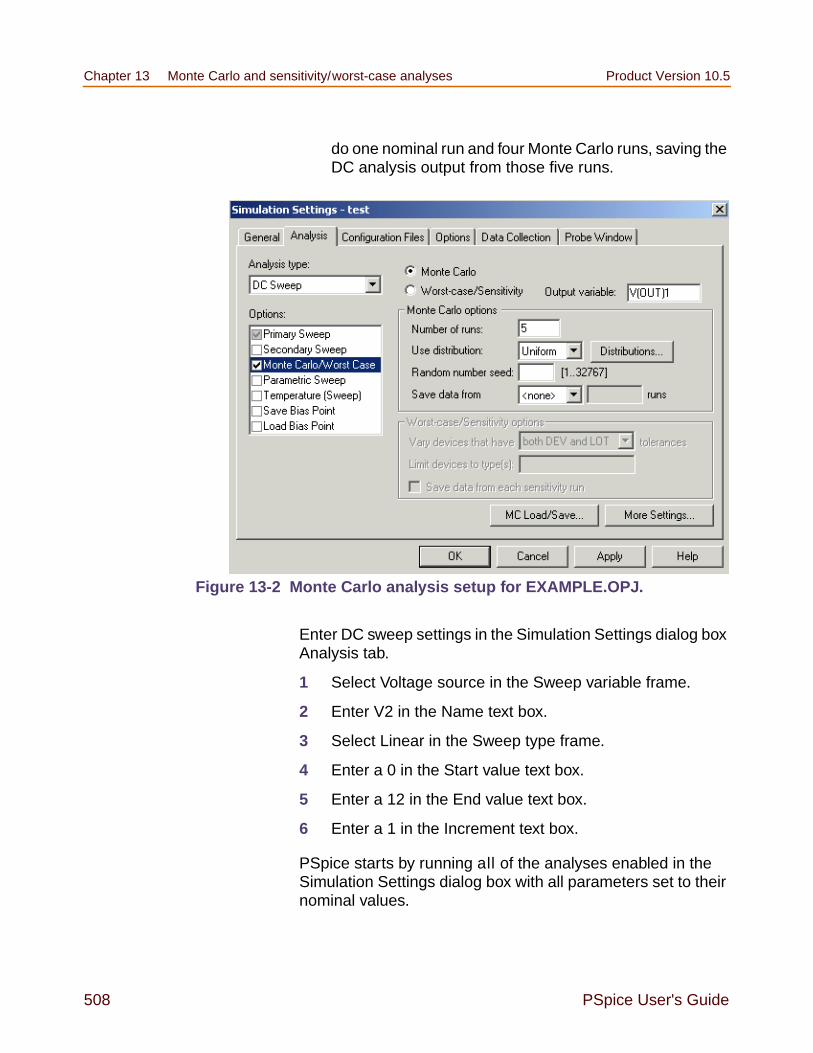
Chapter 13 Monte Carlo and sensitivity/worst-case analyses Product Version 10.5
508 PSpice User's Guide
do one nominal run and four Monte Carlo runs, saving theDC analysis output from those five runs.
Enter DC sweep settings in the Simulation Settings dialog boxAnalysis tab.
1 Select Voltage source in the Sweep variable frame.
2 Enter V2 in the Name text box.
3 Select Linear in the Sweep type frame.
4 Enter a 0 in the Start value text box.
5 Enter a 12 in the End value text box.
6 Enter a 1 in the Increment text box.
PSpice starts by running all of the analyses enabled in theSimulation Settings dialog box with all parameters set to theirnominal values.
Figure 13-2 Monte Carlo analysis setup for EXAMPLE.OPJ.

Product Version 10.5 Chapter overview
PSpice User's Guide 509
However, with Monte Carlo enabled, PSpice saves the DCsweep analysis results for later reference and comparison.After the nominal analyses are finished, PSpice A/D performsthe additional specified analysis runs (in this example, DCsweep).
Subsequent runs use the same analysis specification as thenominal run with one major exception: instead of using thenominal parameter values, the tolerances are applied to setnew parameter values and thus, new part values.
There is a trade-off in choosing the number of Monte Carloruns. More runs provide better statistics, but they require moretime. The amount of time scales directly with the number ofruns: 20 transient analyses take 20 times as long as onetransient analysis. During Monte Carlo runs, the PSpice statusdisplay includes the current run number and the total numberof runs left.
Note: PSpice offers a facility to generate histograms of dataderived from Monte Carlo waveform families throughthe performance analysis feature. For informationabout performance analysis, see RLC filter example onpage 459. For information about histograms, seeCreating histograms on page 523.
History support
The Monte Carlo analysis calculates the circuit response tochanges in part values by randomly varying all of the modelparameters for which a tolerance is specified. However, attimes users might want to keep some or all of the parameterssimilar for multiple analysis so that they can compare theresults of multiple simulations.
Consider an example of IC designs, which usually requirenumerous runs. In such cases, rather than doing large numberof runs (with too many model parameters), users would preferdoing less number of runs (with less number of parameters),manually change some components/parameters values oradd a small amount of circuitry, and then continue theanalysis. Here user expects that simulator should use similarvalues for all model parameters, so that a comparison can bedone between multiple simulations.

Chapter 13 Monte Carlo and sensitivity/worst-case analyses Product Version 10.5
510 PSpice User's Guide
PSpice allows you to save randomly generated values for arun in a .mcp file. You can then load this file to reuse the valuesfor subsequent runs.
Reading the summary report
The summary report generated in this example (see Figure13-3) specifies that the waveform generated from V(OUT1)should be the subject of the collating function YMAX. In eachof the last four runs, the new V(OUT1) waveform is compared

Product Version 10.5 Chapter overview
PSpice User's Guide 511
to the nominal V(OUT1) waveform for the first run, calculatingthe maximum deviation in the Y direction (YMAX collatingfunction). The deviations are printed in order of size along withtheir run number.
With the List option enabled, a report is also generatedshowing the parameter value used for each device in eachrun. In this case (see Figure 13-4), run three shows thehighest deviation.
Figure 13-3 Summary of Monte Carlo runs forEXAMPLE.OPJ.
V(out1)
Figure 13-4 Parameter values for Monte Carlopass three.

Chapter 13 Monte Carlo and sensitivity/worst-case analyses Product Version 10.5
512 PSpice User's Guide
Example: Monte Carlo analysis of a pressure sensor
This example shows how the performance of a pressuresensor circuit with a pressure-dependent resistor bridge isaffected by manufacturing tolerances, using Monte Carloanalysis to explore these effects.
Drawing the schematic
To begin, construct the bridge as shown in Figure 13-5.
Here are a few things to know when placing and connectingthe part:
To get the part you want to place, from the Place menu,choose Part.
To rotate a part before placing it, press R.
For V1 and Meter, place a generic voltage source usingthe VSRC part. When you place the source for the meter,change its name by double-clicking the part and typingMeter in the Reference cell in the Parts Spreadsheet.
For R1-R7, place a resistor using the R part.
Place the analog ground using the 0 ground symbol fromthe SOURCE.OLB part library.
Figure 13-5 Pressure sensor circuit.

Product Version 10.5 Chapter overview
PSpice User's Guide 513
To connect the parts, from the Place menu, choose Wire.
To move values or reference designators, click the valueor reference designator to select it, then drag it to the newlocation.
Defining part values
Define the part values as shown in Figure 13-5. For thepressure sensor, you need to do the following:
Change the resistor values for R3, R5, R6, and R7 fromtheir default value of 1 k.
Set the DC value for the V1 voltage source.
Note: Because the Meter source is used to measure current,it has no DC value and can be left unchanged.
To change resistor values
1 Double-click the value for a resistor.
2 Type the new value. Depending on the resistor you arechanging, set its value to one of the following (refer toFigure 13-5).
If you are changingthis resistor... Type this...
R3 1k*(1+P*Pcoeff/Pnom)
Note: The value for R3—1k*(1+P*Pcoeff/Pnom)—is an expression thatrepresents lineardependence ofresistance on pressure.To complete thedefinition for R3, you willcreate and define globalparameters for Pcoeff, P,and Pnom later on in thisexample.

Chapter 13 Monte Carlo and sensitivity/worst-case analyses Product Version 10.5
514 PSpice User's Guide
3 Repeat steps 1-2 for each resistor on your schematicpage.
To set the DC value for the V1 source and make it visible
1 Double-click the V1 source part.
2 In the Parts Spreadsheet, click in the cell under the DCcolumn.
3 Type 1.35v.
4 Click the Display button.
5 In the Display Format frame, choose the Value Onlyoption to make the DC value (1.35v) visible on theschematic.
6 Click OK, then click Apply to apply the changes you havemade to the part.
7 Close the Parts Spreadsheet.
Setting up the parameters
To complete the value specification for R3, define the globalparameters Pcoeff, P, and Pnom.
To define and initialize Pcoeff, P, and Pnom
1 Place a PARAM part on the schematic page.
2 Double-click the PARAM part to display the PartsSpreadsheet.
R5 2k
R6 470
R7 25
If you are changingthis resistor... Type this...

Product Version 10.5 Chapter overview
PSpice User's Guide 515
3 For each parameter, create a new property by clickingNew and typing its name. Enter its corresponding valueby clicking in the cell under the new property name andtyping its value. Specify the parameter name andcorresponding value as follows.
4 Click Apply to save the changes you have made thenclose the Parts Spreadsheet.
Using resistors with models
To explore the effects of manufacturing tolerances on thebehavior of this circuit, you set device (DEV) and (LOT)tolerances on the model parameters for resistors R1, R2, R3,and R4 in a later step (see Defining tolerances for the resistormodels on page 516). This means you need to use resistorparts that have model associations.
Because R parts do not have associated models (andtherefore no model parameters), change the resistor parts toRbreak parts that do have models.
Note: When PSpice A/D runs a Monte Carlo analysis, it usestolerance values to determine how to vary modelparameters during the simulation.
To replace R1, R2, R3, and R4 with the RBREAK part
1 Click R1 to select it.
2 Hold down the Ctrl key and click R2, R3 and R4 to addthem to the selection set.
3 Press Delete to delete the selection set.
Table 13-3
Property Value
Pcoeff -0.06
P 0
Pnom 1.0

Chapter 13 Monte Carlo and sensitivity/worst-case analyses Product Version 10.5
516 PSpice User's Guide
4 From the Place menu, choose Part.
5 Type RBREAK in the Part text box. (If RBREAK is notavailable, click the Add Library button and selectBREAKOUT.OLB to configure it for use in Capture.)
6 Click OK.
7 Manually place the RBREAK part in the circuit diagramwhere R1, R2, R3 and R4 were located.
8 Double-click on each RBREAK part and change thereference designators as desired.
Saving the design
Before editing the models for the Rbreak resistors, save theschematic.
To save the design
1 From Capture’s File menu, choose Save.
Defining tolerances for the resistor models
This section shows how to assign device (DEV) and lot (LOT)tolerances to the model parameters for resistors R1, R2, R3,and R4 using the model editor.
You can use the model editor to change the .MODEL or.SUBCKT syntax for a model definition. To find out more aboutthe model editor, see Editing model text on page 193, or referto the online PSpice Reference Guide.
To assign 2% device and 10% lot tolerances to theresistance multiplier for R1
1 Select R1.
2 From the Edit menu, choose PSpice Model.
Capture searches the libraries for the Rbreak modeldefinition and makes a copy to create an instance model.

Product Version 10.5 Chapter overview
PSpice User's Guide 517
3 To change the instance model name from Rbreak toRmonte1, do the following:
a. In the Model Text frame, double-click Rbreak.
b. Type RMonte1.
4 To add a 2% device tolerance and a 10% lot tolerance tothe resistance multiplier, do the following:
a. Add the following to the .MODEL statement (afterR=1):
DEV=2% LOT=10%
The model editing window should look somethinglike Figure 13-6.
5 From the File menu, choose Save.
By default, Capture saves the RMonte1 .MODEL definition tothe DESIGN_NAME.LIB library, which is PSENSOR.LIB.Capture also automatically configures the library for local use.To find out more about adding model libraries to theconfiguration, see Configuring model libraries on page 202.
Figure 13-6 Model definition for RMonte1.

Chapter 13 Monte Carlo and sensitivity/worst-case analyses Product Version 10.5
518 PSpice User's Guide
To have resistors R2 and R4 use the same tolerances asR1
1 In Capture’s schematic page editor, select R2 and R4.
2 From the Edit menu, select Properties.
3 In the R2 row, click in the cell under the Implementationcolumn and type RMonte1.
4 In the R4 row, click in the cell under the Implementationcolumn and type RMonte1.
To assign 5% device tolerance to the resistance multiplier forR3
1 Select R3.
2 From the Edit menu, select PSpice Model.
3 In the Model Text frame, change the .MODEL statementto:
.model RTherm RES R=1 DEV=5%
4 From the File menu, choose Save.
Your schematic page should look like Figure 13-7.
Setting up the analyses
This section shows how to define and enable a DC analysisthat sweeps the pressure value and a Monte Carlo analysisthat runs the DC sweep with each change to the resistancemultipliers.
To set up the DC sweep
1 In the PSpice menu, choose New Simulation Profile orEdit Simulation Profile. (If this is a new simulation, enterthe name of the profile and click OK.)
The Simulation Settings dialog box appears.
See Setting up analyses on page 373 for a description ofthe Simulation Settings dialog box.

Product Version 10.5 Chapter overview
PSpice User's Guide 519
2 Select DC Sweep in the Analysis type list box.
3 In the Sweep Variable frame, select Global Parameter.
4 Enter the following values:
To set up the Monte Carlo analysis
1 Select the Monte Carlo/Worst Case option.
2 Check Monte Carlo if it is not already selected.
3 In the Number of runs text box, type 10.
4 In the Save data from list box, select All.
5 Type I(Meter) in the Output variable text box.
Table 13-4
In this textbox...
Type this...
Parametername
P
Start value 0
End value 5.0
Increment 0.1
Figure 13-7 Pressure sensor circuit withRMonte1 and RTherm model definitions.

Chapter 13 Monte Carlo and sensitivity/worst-case analyses Product Version 10.5
520 PSpice User's Guide
6 Click OK to save the simulation profile.
Running the analysis and viewing the results
To complete setup, simulate, and view results
1 From Capture’s PSpice menu, choose Run to start thesimulation
When the simulation is complete, PSpice automaticallydisplays the selected waveform. Because PSpice ran aMonte Carlo analysis, it saved multiple runs or sections ofdata. These are listed in the Available Sections dialogbox.
2 From PSpice’s Trace menu, choose PerformanceAnalysis.
3 Click the Select sections button.
4 In the Available Sections dialog box, click the All button.
5 Click OK.
6 To display current through the Meter voltage source, dothe following:
a. From Capture’s PSpice menu, point to markers andchoose Current into Pin.
b. Place a current probe on the left-hand pin of theMeter source.
7 Switch to the Probe window to see the family of curves forI(Meter) as a function of P.
Another way to view the family of curves without usingschematic markers is as follows:
a. From PSpice’s Trace menu, choose Add Trace.
b. In the Simulation Output Variables list, double-clickI(Meter).
Note: For more on analyzing Monte Carlo results in PSpice,see the next section on Monte Carlo histograms.

Product Version 10.5 Chapter overview
PSpice User's Guide 521
Monte Carlo Histograms
You can display data derived from Monte Carlo waveformfamilies as histograms. This is part of the performanceanalysis feature.
In this example, you simulate a fourth-order Chebyshev activefilter, running a series of 100 AC analyses while randomlyvarying resistor and capacitor values for each run. Then,having defined performance analysis measurements forbandwidth and center frequency, you observe the statisticaldistribution of these quantities for the 100 runs. For moreinformation about performance analysis, see RLC filterexample on page 459.
Chebyshev filter example
The Chebyshev filter is designed to have a 10 kHz centerfrequency and a 1.5 kHz bandwidth. The schematic page forthe filter is shown in Figure 13-8. The stimulus specificationsfor V1, V2, and V3 are:
V1: DC=-15V2: DC=+15V3: AC=1
The parts are rounded to the nearest available 1% resistorand 5% capacitor value. In this example, note how the

Chapter 13 Monte Carlo and sensitivity/worst-case analyses Product Version 10.5
522 PSpice User's Guide
bandwidth and the center frequency vary when 1% resistorsand 5% capacitors are used in the circuit.
Creating models for Monte Carlo analysis
To vary the resistors and capacitors in the filter circuit, createmodels for these parts on which you can set device tolerancesfor Monte Carlo analysis. The BREAKOUT.OLB librarycontains generic devices for this purpose. The resistors andcapacitors in this schematic are the Rbreak and Cbreak partsfrom BREAKOUT.OLB.
Using the Model Editor, modify the models for these parts asfollows:
.model RMOD RES(R=1 DEV=1%)
.model CMOD CAP(C=1 DEV=5%)
Setting up the analysis
To analyze the filter, set up both an AC analysis and a MonteCarlo analysis. The AC analysis sweeps 50 points per decadefrom 100 Hz to 1 MHz. The Monte Carlo analysis is set to take100 runs. Save data from all runs and set the output variableto V(OUT).
Figure 13-8 Chebyshev filter.

Product Version 10.5 Chapter overview
PSpice User's Guide 523
Creating histograms
Because the data file can become quite large when running aMonte Carlo analysis, to view just the output of the filter, youplace a voltage probe at the output of the filter.
To collect data for the marked node only
1 From the PSpice menu, choose New Simulation Profile orEdit Simulation Profile. (If this is a new simulation, enterthe name of the profile and click OK.)
The Simulation Settings dialog box appears.
2 On the Data Collection tab, choose the At Markers Onlyoption for each type of marker (Voltages, Currents,Power, Digital, Noise).
3 Click OK.
To run the simulation and load Probe with data
1 From Capture’s PSpice menu, choose Run to start thesimulation.
When the simulation is complete, PSpice automaticallydisplays the selected waveform. Because PSpice ran aMonte Carlo analysis, it saved multiple runs or sections ofdata. These are listed in the Available Sections dialogbox.
2 In the Available Sections dialog box, click All.
3 Click OK.
To display a histogram for the 1 dB bandwidth
1 From PSpice’s Plot menu, choose Axis Settings.
2 Select the X Axis tab.
3 In the Processing Options frame, select the PerformanceAnalysis check box.

Chapter 13 Monte Carlo and sensitivity/worst-case analyses Product Version 10.5
524 PSpice User's Guide
For information about performance analysis, see RLCfilter example on page 459.
4 Click OK.
The histogram display appears. The Y axis is the percentof samples.
5 From the Trace menu, choose Add Trace.
6 Choose Bandwidth.
7 In the Trace Expression box, specifyBandwidth(VDB(OUT),1).
Note: You can also display this histogram by using theperformance analysis wizard to display Bandwidth(VDB(OUT),1).
To change the number of histogram divisions
1 From the Tools menu, choose Options.
2 In the Number of Histogram Divisions text box, replace 10with 20.
3 Click OK.
The histogram for 1 dB bandwidth is shown in Figure 13-9.
Figure 13-9 1 dB bandwidth histogram.

Product Version 10.5 Chapter overview
PSpice User's Guide 525
The statistics for the histogram are shown along the bottom ofthe display. The statistics show the number of Monte Carloruns, the number of divisions or vertical bars that make up thehistogram, mean, sigma, minimum, maximum, 10thpercentile, median, and 90th percentile.
Ten percent of the goal function values is less than orequal to the 10th percentile number, and 90% of the goalfunction values is greater than or equal to that number.
If there is more than one goal function value that satisfiesthis criteria, then the 10th percentile is the midpoint of theinterval between the goal function values that satisfy thecriteria. Similarly, the median and 90th percentilenumbers represent goal function values such that 50%and 90% (respectively) of the goal function values areless than or equal to those numbers.
Sigma is the standard deviation of the goal functionvalues.
If needed, you can turn off the statistical data display asfollows:
1 From the Tools menu, choose Options.
2 Clear the Display Statistics check box.
3 Click Save, and then OK.
You can also show the distribution of the center frequency ofthe filter.
To display the center frequency
1 From the Trace menu, choose Add Trace.
2 Choose CenterFreq.
3 In the Trace Expression box, specifyCenterFreq(VDB(OUT),1).
The new histogram replaces the previous histogram. Todisplay both histograms at once, choose Add Plot to Windowon the Plot menu before choosing Add from the Trace menu.

Chapter 13 Monte Carlo and sensitivity/worst-case analyses Product Version 10.5
526 PSpice User's Guide
The histogram of the center frequency is as shown in Figure13-10.
Copying histogram data
You can use the copy function to transfer the raw histogramdata points for a particular trace to the Windows clipboard.This allows you to save the data as a standard ASCII text file,or paste it directly into a report or other document for laterreference.
To copy histogram data to the clipboard
1 Select the trace symbol, or the trace name, in thehistogram.
2 From the Edit menu, choose Copy (or press Ctrl+C).
The histogram data points for the trace will be transferedto the Windows clipboard.
To copy the histogram display to the clipboard
1 From the Window menu, choose Copy to Clipboard.
Figure 13-10 Center frequency histogram.

Product Version 10.5 Chapter overview
PSpice User's Guide 527
The histogram graph will be transfered to the Windowsclipboard.

Chapter 13 Monte Carlo and sensitivity/worst-case analyses Product Version 10.5
528 PSpice User's Guide
Worst-case analysis
This section discusses the analog worst-case analysis featureof PSpice. The information provided in this section explainshow to use worst-case analysis properly and with realisticexpectations.
Note: Worst-case analysis is not included in PSpice A/DBasics.
Overview of worst-case analysis
Worst-case analysis is used to find the worst probable outputof a circuit or system given the restricted variance of itsparameters. For instance, if the values of R1, R2, and R3 canvary by +10%, then the worst-case analysis attempts to findthe combination of possible resistor values which result in theworst simulated output. As with any other analysis, there arethree important parts: inputs, procedure, and outputs.
Inputs
In addition to the circuit description, you need to provide twopieces of information:
the parameter tolerances
a definition of what worst means
You can set tolerances on any number of the parameters thatcharacterize a model.
Note: You can define models for nearly all primitive analogcircuit parts, such as resistors, capacitors, inductors,and semiconductor devices. PSpice reads the standardmodel parameter tolerance syntax specified in the.MODEL statement. For each model parameter,PSpice uses the nominal, minimum, and maximumprobable values, and the DEV and/or LOT specifiers;the probability distribution type (such as UNIFORM orGAUSS) is ignored.
Product Version 10.5 Chapter overview
PSpice User's Guide 529
The criterion for determining the worst values for the relevantmodel parameters is defined in the .WC statement as afunction of any standard output variable in a specified range ofthe sweep.
In a given range, reduce the measurement to a single value byone of these five collating functions:
You can define worst as the highest (HI) or lowest (LO)possible collating function relative to the nominal run.
You can use analog behavioral models to measure waveformcharacteristics other than those detected by the availablecollating functions, such as rise time or slope. You can alsouse analog behavioral models to incorporate several voltagesand currents into one output variable to which a collatingfunction may be applied. See Chapter 6, “Analog behavioralmodeling,” for more information.
Procedure
To establish the initial value of the collating function,worst-case analysis begins with a nominal run using all modelparameters at their nominal values.
Next, multiple sensitivity analyses determine the individualeffect of each model parameter on the collating function. Thisis accomplished by varying model parameters, one at a time,in consecutive simulations. The direction (better or worse) inwhich the collating function changes with a small increase ineach model parameter is recorded.
MAX Maximum output variable valueMIN Minimum output variable valueYMAX Output variable value at the point where it
differs the most with the nominal runRISE_EDGE(value)
Sweep value where the output variablevalue crosses above a given thresholdvalue
FALL_EDGE(value)
Sweep value where the output variablevalue crosses below a given thresholdvalue
Chapter 13 Monte Carlo and sensitivity/worst-case analyses Product Version 10.5
530 PSpice User's Guide
Finally, for the worst-case run, each parameter value is takenas far from its nominal as allowed by its tolerance, in thedirection which should cause the collating function to be itsworst (given by the HI or LO specification).
Note: This procedure saves time by performing the minimumnumber of simulations required to make an educatedguess at the parameter values that produce the worstresults. It also has some limitations, which aredescribed in the following sections.
Outputs
A summary of the sensitivity analysis is printed in the PSpiceoutput file (.OUT). This summary shows the percent changein the collating function corresponding to a small change ineach model parameter. If a .PROBE statement is included inthe circuit file, then the results of the nominal and worst-caseruns are saved for viewing in the Probe window.
Caution: An important condition for correct worst-case analysis
Worst-case analysis is not an optimization process; it does notsearch for the set of parameter values that result in the worstresult.
It assumes that the worst case occurs when each parameterhas been either pushed to one of its limits or left at its nominalvalue as indicated by the sensitivity analysis. It shows the trueworst-case results when the collating function is monotonicwithin all tolerance combinations.
Otherwise, there is no guarantee. Usually you cannot becertain whether this condition is true, but insight into theoperation of the circuit may alert you to possible anomalies.

Product Version 10.5 Chapter overview
PSpice User's Guide 531
Worst-case analysis example
The schematic shown in Figure 13-11 is for an amplifier circuitthat is a biased BJT. This circuit is used to demonstrate how asimple worst-case analysis works. It also shows hownon-monotonic dependence of the output on a singleparameter can adversely affect the worst-case analysis.
Because an AC (small-signal) analysis is being performed,setting the input to unity means that the output, Vm([OUT]), isthe magnitude of the gain of the amplifier. The only variabledeclared in this circuit is the resistance of Rb2. Because thevalue of Rb2 determines the bias on the BJT, it also affects theamplifier’s gain.
Figure 13-12 is the circuit file used to run one of the following:
a parametric analysis (.STEP, shown enabled in thecircuit file) that sets the value of resistor Rb2 by steppingmodel parameter R through values spanning thespecified DEV tolerance range, or
a worst-case analysis (shown disabled in the circuit file)that allows PSpice to determine the worst-case value forparameter R based upon a sensitivity analysis.
Only one of these analyses can run in any given simulation.
Figure 13-11 Simple biased BJT amplifier.

Chapter 13 Monte Carlo and sensitivity/worst-case analyses Product Version 10.5
532 PSpice User's Guide
Note: The AC and worst-case analysis specifications (.ACand .WC statements) are written so that the worst-caseanalysis tries to minimize Vm([OUT]) at 100 kHz.
The netlist and circuit file in Figure 13-12 are set up to runeither a parametric (.STEP) or worst-case (.WC) analysis ofthe specified AC analysis. These simulations demonstrate theconditions under which worst-case analysis works well andthose that can produce misleading results when output is notmonotonic with a variable parameter (see Figure 13-15 andFigure 13-16).
For demonstration, the parametric analysis is run first,generating the curve shown in Figure 13-15 and Figure 13-16.
* Worst-case analysis comparing monotonic and non-monotonic* output with a variable parameter
.lib
***** Input signal and blocking capacitor *****Vin In 0 ac 1Cin In B 1u
***** "Amplifier" ****** gain increases with small increase in Rb2, but* device saturates if Rb2 is maximized.Vcc Vcc 0 10Rc Vcc C 1kQ1 C B 0 Q2N2222Rb1 Vcc B 10kRb2 B 0 Rbmod 720.model Rbmod res(R=1 dev 5%) ; WC analysis results
; are correct* .model Rbmod res(R=1.1 dev 5%) ; WC analysis misled
; by sensitivity
***** Load and blocking capacitor *****Cout C Out 1uRl Out 0 1k
* Run with either the .STEP or the .WC, but not both.* This circuit file is currently set up to run the .STEP* (.WC is commented out)
**** Parametric Sweep—providing plot of Vm([OUT]) vs. Rb2 ****.STEP Res Rbmod(R) 0.8 1.2 10m
***** Worst-case analysis ****** run once for each of the .model definitions stated above)* WC AC Vm([Out]) min range 99k 101k list output all
.AC Lin 3 90k 110k
.probe
.end
Figure 13-12 Amplifier netlist and circuit file.

Product Version 10.5 Chapter overview
PSpice User's Guide 533
This curve, derived using the YatX goal function shown inFigure 13-14 illustrates the non-monotonic dependence ofgain on Rb2.
To do this yourself, place the goal function definition in aPROBE.GF file in the circuit directory. Then start PSpice, loadall of the AC sweeps, set up the X axis for performanceanalysis, and add the following trace:
YatX(Vm([OUT]),100k)
Note: The YatX goal function is used on the simulation resultsfor the parametric sweep (.STEP) defined in Figure13-12. The resulting curves are shown in Figure 13-15and Figure 13-16.
Next, the parametric analysis is commented out and theworst-case analysis is enabled. Two runs are made using thetwo versions of the Rbmod .MODEL statement shown in thecircuit file. The model parameter, R, is a multiplier which isused to scale the nominal value of any resistor referencing theRbmod model (Rb2 in this case).
The first .MODEL statement leaves the nominal value of Rb2at 720 ohms. The sensitivity analysis increments R by a smallamount and checks its effect on Vm([OUT]). This slightincrease in R causes an increase in the base bias voltage ofthe BJT, and increases the amplifier’s gain, Vm([OUT]). Theworst-case analysis correctly sets R to its minimum value forthe lowest possible Vm([OUT]) (see Figure 13-15).
The second .MODEL statement scales the nominal value ofRb2 by 1.1 to approximately 800 ohms. The gain stillincreases with a small increase in R, but a larger increase inR increases the base voltage so much that it drives the BJTinto saturation and nearly eliminates the gain. The worst-caseanalysis is fooled by the sensitivity analysis into assuming thatRb2 must be minimized to degrade the gain, but maximizingRb2 is much worse (see Figure 13-16). Note that even an
YatX(1, X_value)=y11|sfxv(X_value)!1;
Figure 13-13 YatX Goal Function
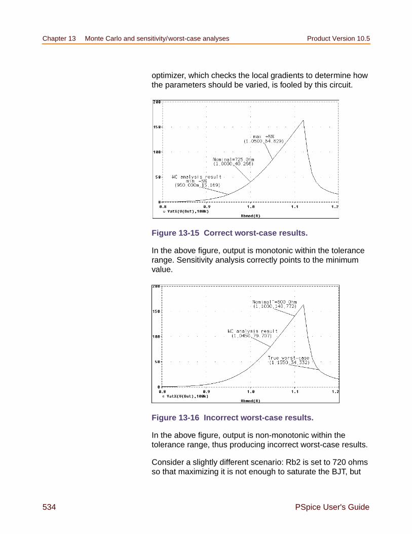
Chapter 13 Monte Carlo and sensitivity/worst-case analyses Product Version 10.5
534 PSpice User's Guide
optimizer, which checks the local gradients to determine howthe parameters should be varied, is fooled by this circuit.
Figure 13-15 Correct worst-case results.
In the above figure, output is monotonic within the tolerancerange. Sensitivity analysis correctly points to the minimumvalue.
Figure 13-16 Incorrect worst-case results.
In the above figure, output is non-monotonic within thetolerance range, thus producing incorrect worst-case results.
Consider a slightly different scenario: Rb2 is set to 720 ohmsso that maximizing it is not enough to saturate the BJT, but
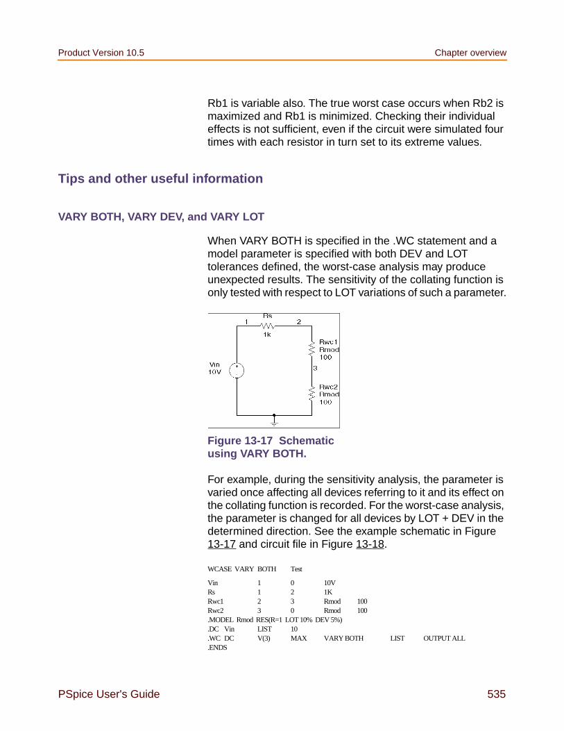
Product Version 10.5 Chapter overview
PSpice User's Guide 535
Rb1 is variable also. The true worst case occurs when Rb2 ismaximized and Rb1 is minimized. Checking their individualeffects is not sufficient, even if the circuit were simulated fourtimes with each resistor in turn set to its extreme values.
Tips and other useful information
VARY BOTH, VARY DEV, and VARY LOT
When VARY BOTH is specified in the .WC statement and amodel parameter is specified with both DEV and LOTtolerances defined, the worst-case analysis may produceunexpected results. The sensitivity of the collating function isonly tested with respect to LOT variations of such a parameter.
For example, during the sensitivity analysis, the parameter isvaried once affecting all devices referring to it and its effect onthe collating function is recorded. For the worst-case analysis,the parameter is changed for all devices by LOT + DEV in thedetermined direction. See the example schematic in Figure13-17 and circuit file in Figure 13-18.
Figure 13-17 Schematicusing VARY BOTH.
WCASE VARY BOTH Test
Vin 1 0 10VRs 1 2 1KRwc1 2 3 Rmod 100Rwc2 3 0 Rmod 100.MODEL Rmod RES(R=1 LOT 10% DEV 5%).DC Vin LIST 10.WC DC V(3) MAX VARY BOTH LIST OUTPUT ALL.ENDS

Chapter 13 Monte Carlo and sensitivity/worst-case analyses Product Version 10.5
536 PSpice User's Guide
Figure 13-18 Circuit file using VARY BOTH.
In this case, V(3) is maximized if:
Rwc1 and Rwc2 are both increased by 10% per the LOTtolerance specification, and
Rwc1 is decreased by 5% and Rwc2 is increased by 5%per the DEV tolerance specification.
The final values for Rwc1 and Rwc2 should be 105 and 115,respectively. However, because Rwc1 and Rwc2 are variedtogether during the sensitivity analysis, it is assumed that bothmust be increased to their maximum for a maximum V(3).Therefore, both are increased by 15%.
The purpose of the technique is to reduce the number ofsimulations. For a more accurate worst-case analysis, youshould first perform a worst-case analysis with VARY LOT,manually adjust the nominal model parameter valuesaccording to the results, then perform another analysis withVARY DEV specified.
Gaussian distributions
Parameters using Gaussian distributions are changed by 3σ(three times sigma) for the worst-case analysis.
YMAX collating function
The purpose of the YMAX collating function is oftenmisunderstood. This function does not try to maximize thedeviation of the output variable value from nominal.Depending on whether HI or LO is specified, it tries tomaximize or minimize the output variable value itself at thepoint where maximum deviation occurred during sensitivityanalysis.
Note: This may result in maximizing or minimizing the outputvariable value over the entire range of the sweep. Thiscollating function is useful when you know the directionin which the maximum deviation occurs.

Product Version 10.5 Chapter overview
PSpice User's Guide 537
RELTOL
During the sensitivity analysis, each parameter is varied(multiplied) by 1+RELTOL where RELTOL is specified in a.OPTIONS statement, or defaults to 0.001.
Sensitivity analysis
The sensitivity analysis results are printed in the output file(.OUT). For each varied parameter, the percent change in thecollating function and the sweep variable value at which thecollating function was measured are given. The parametersare listed in worst output order; for example, the collatingfunction was its worst when the first parameter printed in thelist was varied.
When you use the YMAX collating function, the output file alsolists mean deviation and sigma values. These are based onthe changes in the output variable from nominal at everysweep point in every sensitivity run.
Manual optimization
You can use worst-case analysis to perform manualoptimization with PSpice. The monotonicity condition isusually met if the parameters have a very limited range.
Performing worst-case analysis with tight tolerances on theparameters produces sensitivity and worst-case results (in theoutput file). You can use these to decide how the parametersshould be varied to achieve the desired response. You canthen make adjustments to the nominal values in the circuit file,and perform the worst-case analysis again for a new set ofgradients.
Note: Parametric sweeps (.STEP), like the one performed inthe circuit file shown in Figure 13-12, can be used toaugment this procedure.
Chapter 13 Monte Carlo and sensitivity/worst-case analyses Product Version 10.5
538 PSpice User's Guide
Monte Carlo analysis
Monte Carlo (.MC) analysis may be helpful when worst-caseanalysis cannot be used. Monte Carlo analysis can often beused to verify or improve on worst-case analysis results.Monte Carlo analysis randomly selects possible parametervalues, which can be thought of as randomly selecting pointsin the parameter space. The worst-case analysis assumesthat the worst results occur somewhere on the surface of thisspace, where parameters (to which the output is sensitive) areat one of their extreme values.
If this is not true, the Monte Carlo analysis may find a point atwhich the results are worse. To try this, replace .WC in thecircuit file with .MC <#runs>, where <#runs> is the number ofsimulations you want to perform. More runs provide higherconfidence results. The Monte Carlo summary in the outputfile lists the runs in decreasing order of collating functionvalue.
Tip
To save disk space, do not specify any OUTPUToptions.
Next, add the following option to the .MC statement, andsimulate again.
OUTPUT LIST RUNS <worst_run#>
This performs only two simulations: the nominal and the worstMonte Carlo run. The parameter values used during the worstrun are written to the output file, and the results of bothsimulations are saved.
Using Monte Carlo analysis with YMAX is a good way toobtain a conservative guess at the maximum possibledeviation from nominal, since worst-case analysis usuallycannot provide this information.

PSpice User's Guide 539
14
Digital simulation
Chapter overview
This chapter describes how to set up a digital simulationanalysis and includes the following sections:
What is digital simulation? on page 540
Steps for simulating digital circuits on page 540
Concepts you need to understand on page 541
Defining a digital stimulus on page 543
Defining simulation time on page 558
Adjusting simulation parameters on page 558
Starting the simulation on page 562
Analyzing results on page 563
Note: This entire chapter describes features that are notincluded in PSpice.

Chapter 14 Digital simulation Product Version 10.5
540 PSpice User's Guide
What is digital simulation?
Digital simulation is the analysis of logic and timing behaviorof digital devices over time. PSpice A/D simulates thisbehavior during transient analysis. When computing the biaspoint, PSpice A/D considers the digital devices in addition toany analog devices in the circuit.
PSpice A/D performs detailed timing analysis subject to theconstraints specified for the devices. For example, flip-flopsperform setup checks on the incoming clock and data signals.PSpice A/D reports any timing violations or hazards asmessages written to the simulation output file and thewaveform data file. See Tracking timing violations and hazardson page 569 for information about persistent hazards, and fordescriptions of the warning messages.
Steps for simulating digital circuits
There are six steps in the development and simulation ofdigital circuits:
1 Drawing the design.
For more information on drawing designs see yourOrCAD Capture User’s Guide. Steps 2 through 6 ofthis process are covered in this chapter.
2 Defining the stimuli.
3 Setting the simulation time.
4 Adjusting the simulation parameters.
5 Starting the simulation.
6 Analyzing the results.

Product Version 10.5 Steps for simulating digital circuits
PSpice User's Guide 541
Concepts you need to understand
States
When the circuit is in operation, digital nodes take on valuesor output states shown in Table 14-1. Each digital state has astrength component as well. Strengths are described in thenext section.
Note: States do not necessarily correspond to a specific, oreven stable, voltage. A logical 1 level means only thatthe voltage is somewhere within the high range for theparticular device family. The rising and falling levelsonly indicate that the voltage crosses the 0–1 thresholdat some time during the R or F interval, not that thevoltage change follows a particular slope.
Table 14-1 Digital states
Thisstate...
Means this...
0 Low, false, no, off
1 High, true, yes, on
R Rising (changes from 0 to 1 sometimeduring the R interval)
F Falling (changes from 1 to 0 sometimeduring the F interval)
X Unknown: may be high, low, intermediate,or unstable
Z High impedance: may be high, low,intermediate, or unstable

Chapter 14 Digital simulation Product Version 10.5
542 PSpice User's Guide
Strengths
When a digital node is driven by more than one device,PSpice A/D determines the correct level of the node. Eachoutput has a strength value, and PSpice A/D compares thestrengths of the outputs driving the node. The strongestdriver determines the resulting level of the node. If outputs ofthe same strength but different levels drive a node, the node’slevel becomes X.
PSpice A/D supports 64 strengths. The lowest (weakest)strength is called Z. The highest (strongest) strength is calledthe forcing strength. The Z strength (called high impedance)is typically output by disabled tristate gates or open-collectoroutput devices. PSpice A/D reports any nodes of Z strength(at any level) as Z, and reports all other nodes by thedesignations shown in Digital states on page 541.
For additional information on this topic see Defining OutputStrengths on page 350 of Chapter 7, “Digital devicemodeling.”

Product Version 10.5 Steps for simulating digital circuits
PSpice User's Guide 543
Defining a digital stimulus
A digital stimulus defines input to the digital portions of yourcircuit, playing a role similar to that played by the independentvoltage and current sources for the analog portion of yourcircuit.
The following table summarizes the digital stimuli provided inthe part libraries.
Table 14-2
If you want tospecify theinput signal by...
Then use thispart...
For this type ofdigital input...
Using the StimulusEditor1
1. Stimulus Editor is not included with PSpice A/D Basics
DIGSTIMn signal or bus stimulus
Defining partproperties
DIGCLOCK clock signal
STIM1 one-bit stimulus
STIM4 four-bit stimulus
STIM8 eight-bit stimulus
STIM16 sixteen-bit stimulus
FILESTIM1 one-bit file-basedstimulus
FILESTIM2 two-bit file-basedstimulus
FILESTIM4 four-bit file-basedstimulus
FILESTIM8 eight-bit file-basedstimulus
FILESTIM16 sixteen-bit file-basedstimulus
FILESTIM32 thirty-two-bitfile-based stimulus

Chapter 14 Digital simulation Product Version 10.5
544 PSpice User's Guide
Using the DIGSTIMn part
Use the DIGSTIMn stimulus parts to define a stimulus for a netor bus using the Stimulus Editor.
Note: Stimulus Editor is not included with PSpice A/D Basics.
To use the DIGSTIMn part
1 From Capture’s Place menu, choose Part.
2 Place and connect the DIGSTIM1 stimulus part fromSOURCSTM.OLB to a wire or bus in your design.
3 Click the stimulus instance to select it.
4 From the Edit menu, choose PSpice Stimulus.
This starts the Stimulus Editor. The New Stimulus dialogbox appears prompting you to define a new stimulus.
5 Enter DIGSTIM1 in the Name text box.
6 In the Digital frame, select Signal.
7 Click OK.
8 Define stimulus transitions; see Defining input signalsusing the Stimulus Editor below.
Defining input signals using the Stimulus Editor
Note: Stimulus Editor is not included with PSpice A/D Basics.
Defining signal transitions
You can do any of the following when defining digital signaltransitions:
Add a transition
Move a transition
Edit a transition
Delete a transition

Product Version 10.5 Steps for simulating digital circuits
PSpice User's Guide 545
Note: These operations cannot be applied to a stimulusdefined as a clock signal.
To add a transition
1 From the Plot menu, choose Axis Settings.
2 Enter values in the Displayed Range for Time text boxesand the Timing Resolution text box as required for addingtransitions.
For example, if you wish to add transitions every 1ms, setthe Timing Resolution to 1ms.
3 Select the digital stimulus you want to edit.
When you select a transition to edit, a red handleappears.
4 From the Stimulus Editor’s Edit menu, choose Add.
5 Click the waveform at the time where the transition isrequired.
6 Repeat step 4 to add additional transitions.
7 When you finish, right-click to exit the edit mode.
To move a transition
1 Click the transition you want to move.
2 If needed, use Shift+click to select additional transitionson the same signal or different signals.
3 Reposition the transition (or transitions) by dragging.
Note: If you press Shift while dragging, then all selectedtransitions move by the same amount.
To edit a transition
1 Do one of the following:
Select the transition you want to edit and from theEdit menu, choose Attributes.

Chapter 14 Digital simulation Product Version 10.5
546 PSpice User's Guide
Double-click the transition you want to edit.
2 In the Edit Digital Transition dialog box, edit the timing andvalue of the transition.
3 Click OK.
To delete a transition
1 Click the transition you want to delete.
2 If needed, press Shift+click to select additionaltransitions on the same signal or different signals.
3 From the Edit menu, choose Delete.
Defining clock transitions
To create a clock stimulus
1 In the Stimulus Editor, select the stimulus that you want touse as a clock.
2 From the Stimulus menu, choose Change Type.
3 Under Type, choose Clock.
4 Click OK.
5 Enter values for the clock signal attributes as describedbelow.
Table 14-3
For thisattribute...
Enter this...
Frequency clock rate
Duty Cycle percent of high versus low indecimal or integer units
Initial Value starting value: 0 or 1
Time Delay time after simulation beginswhen the clock stimulus takeseffect

Product Version 10.5 Steps for simulating digital circuits
PSpice User's Guide 547
Example: To create a clock signal with a clock rate of 20MHz, 50% duty cycle, a starting value of 1, and time delayof 5 nsec, set the signal properties as follows:
Frequency = 20Meg
Duty Cycle = 0.50 (or 50)
Initial Value = 1
Time Delay = 5ns
6 From the File menu, choose Save.
Note: If you have the PSpice A/D Basics package, you candefine clock signals using DIGCLOCK. To find outmore, see Using the DIGCLOCK part on page 552.
To change clock attributes
1 In the Stimulus Editor, do one of the following:
Double-click the clock name to the left of the axis.
Click the clock name and from the Edit menu, chooseattributes.
2 Modify the clock attributes as needed.
3 Click OK.
Defining bus transitions
There are three steps for creating a bus:
1 Creating the digital bus stimulus.
2 Introducing transitions.
3 Optionally defining the radix for bus values.
These steps are described in detail in the followingprocedures.
To create a digital bus stimulus
1 From the Stimulus menu, choose New.
2 In the Name text box, enter Bus.

Chapter 14 Digital simulation Product Version 10.5
548 PSpice User's Guide
3 In the Digital frame, select Bus.
4 If needed, change the bus width from its default value of8 bits. To do this, in the Width text box, type a differentinteger.
5 Click OK.
During any interval, the bits on the bus lines represent a valuefrom zero through (2n - 1), where n is the number of bus lines.To set bus values, introduce transitions using either of the twomethods described below.
To introduce transitions (method one)
1 From the Plot menu, choose Axis Settings.
2 Enter values in the Displayed Range for Time text boxesand the Timing Resolution text box as required for addingtransitions.
For example, if you wish to add transitions every 1 ms, setthe Timing Resolution to 1ms.
3 From the Stimulus Editor’s Edit menu, choose Add.
4 In the digital value field on the toolbar (just right of the Addbutton), type a bus value in any of the following ways:
Table 14-4
To get thiseffect...
Type this...
A literal value <unsigned_number>[;radix]
Example: 12
An increment +<unsigned_number>[;radix]
Example: +12;H
A decrement -<unsigned_number>[;radix]
Example: -12;O

Product Version 10.5 Steps for simulating digital circuits
PSpice User's Guide 549
If you do not enter a radix value, the Stimulus Editorappends the default bus radix. To find out about validradix values, see page 14-11.
5 Click the waveform where you want the transition added.
6 Repeat steps 4 and 5 as needed.
7 When you finish, right-click to exit the editing mode.
To introduce transitions (method two)
1 From the Plot menu, choose Axis Settings.
2 Enter values in the Dislayed Range for Time text boxesand the Timing Resolution text box as required for addingtransitions.
For example, if you wish to add transitions every 1 ms, setthe Timing Resolution to 1ms.
3 From the Stimulus Editor’s Edit menu, choose Add.
4 Place the tip of the pencil-shaped pointer on thewaveform, and click to create transitions as shownhere:
Here are some other things that you can do:
Move a transition left or right by clicking anddragging.
Delete a transition by selecting it and then, from theEdit menu, choosing Delete (or by pressing Del).
Select more than one transition by holding downShift while clicking.
5 When you finish creating transitions, right-click.
6 Click the transition at the start (far left) of the interval. Asmall diamond appears over the transition.

Chapter 14 Digital simulation Product Version 10.5
550 PSpice User's Guide
7 From the Edit menu, choose Attributes to display the EditDigital Transition dialog box.
8 In the Transition Type frame, choose Set Value,Increment, or Decrement.
9 Do one of the following to specify the bus value:
In the Value text box, type a value.
Select one of these defaults from the list: 0, All bits 1,X (Unknown), or Z (High impedance).
10 Click OK.
11 Repeat steps 6 through 10 for each transition.
To set the default bus radix
1 From the Tools menu, choose Options.
2 In the Bus Display Defaults frame, from the Radix list,select the radix you want as default.
3 Click OK.
Table 14-5
Select thisradix...
To show values in thisnotation...
Binary base 2
Octal base 8
Decimal base 10
Hexadecimal base 16

Product Version 10.5 Steps for simulating digital circuits
PSpice User's Guide 551
Adding loops
Suppose you have a stimulus that looks like this:
and you want to create a stimulus that consists of threeconsecutive occurrences of the sequence that starts at A andends at B:
You can do this by using a standard text editor to edit astimulus library file. Within this file is a sequence of transitionsthat produces the original waveform. With a text editor you canmodify the stimulus definition so it repeats itself.
To add a loop
1 In the Stimulus Editor, save and close the stimulus file.
2 In a standard text editor (such as Notepad), open thestimulus file.
3 Find the set of consecutive lines comprising thesequence that you want to repeat.
Each relevant line begins with the time of the transitionand ends with a value or change in value.
To find out more about the syntax of the stimuluscommands used in the stimulus file, refer to the onlinePSpice Reference Guide.
4 Before these lines, insert a line that uses this syntax:
+ Repeat for n_times
where n_times is one of the following:
A positive integer representing the number ofrepetitions.
BA

Chapter 14 Digital simulation Product Version 10.5
552 PSpice User's Guide
The keyword FOREVER, which means repeat thissequence for an unlimited number of times (like aclock signal).
5 Below these lines, insert a line that uses this syntax:
+ Endrepeat
6 From the File menu, choose Save.
Given the example shown on page 3, if you wanted to repeatthe sequence shown from point A to point B three times, thenyou would modify the stimulus file as shown here (added linesare in bold):
+ Repeat for 3+ +0s 000000000+ 250us INCR BY 000000001+ 500us 000000010+ 750us INCR BY 000000001+ 1ms 000000000+ Endrepeat
Using the DIGCLOCK part
The DIGCLOCK part allows you to define a clock signal byusing the part’s properties.
For information on how to define a clock signal using theStimulus Editor with the DIGSTIMn part, see Defining signaltransitions on page 544.
To define a clock signal using DIGCLOCK
1 From Capture’s Place menu, choose Part.
2 Place and connect a DIGCLOCK part.
3 Double-click the part instance.
4 Define the properties as described below.
Table 14-6
For this property... Specify this...
DELAY Time before the first transition of theclock

Product Version 10.5 Steps for simulating digital circuits
PSpice User's Guide 553
Using STIM1, STIM4, STIM8 and STIM16 parts
The STIMn parts have a single pin for connection. STIM1 isused for driving a single net. STIM4, STIM8 and STIM16 drivebuses that are 4, 8 and 16 bits wide, respectively. Theproperties for all of these parts are the same as those shownin Table 14-7 below.
ONTIME Time in high state for each period
OFFTIME Time in low state for each period
STARTVAL Low state of clock (default:0)
OPPVAL High state of clock (default: 1)
Table 14-6
For this property... Specify this...
Table 14-7
Property Description
WIDTH Number of output signals (nodes).
FORMAT Sequence of digits defining the number ofsignals corresponding to a digit in any<value> term appearing in a COMMANDnproperty definition. Each digit must beeither 1, 3, or 4 (binary, octal,hexadecimal, respectively); the sum of alldigits in FORMAT must equal WIDTH.
IO_MODEL I/O model describing the stimulus’ drivingcharacteristics.
IO_LEVEL Interface subcircuit selection from one ofthe four analog/digital subcircuits providedwith the part’s I/O model.
DIG_PWR Digital power pin used by the interfacesubcircuit.
DIG_GND Digital ground pin used by the interfacesubcircuit.

Chapter 14 Digital simulation Product Version 10.5
554 PSpice User's Guide
When placed, you must connect each part to the wire or busof the corresponding radix. Generally, you only need to modifythe FORMAT, TIMESTEP, and COMMANDn properties.
Typically, each COMMANDn property contains only onecommand line. It is possible to enter more than one commandline per property by placing \n+ between command lines in agiven definition. (The n must be lower case and no spacesbetween characters; spaces may precede or follow the entirekey sequence.) Refer to the online PSpice Reference Guidefor information about command line syntax.
Using the FILESTIMn parts
The FILESTIMn parts have a single pin for connection to therest of the circuit. FILESTIM1 is used for driving a single net.FILESTIM2, FILESTIM4, FILESTIM8, FILESTIM16 andFILESTIM32 drive buses that are 2, 4, 8, 16 and 32 bits wide,respectively. You must define the digital stimulus specificationin an external file. Using this technique, stimulus definitionscan be created from scratch or extracted with littlemodification from another simulation’s output file. Refer to theonline PSpice Reference Guide for more information aboutcreating digital stimulus specifications and files.
Table 14-8 lists the properties of the FILESTIMn parts. TheIO_MODEL, IO_LEVEL, and PSPICEDEFAULTNETproperties describing this part’s I/O characteristics areprovided with default values that rarely need modification.However, you must define the FILENAME property with thename of the external file containing the digital stimulusspecification.
TIMESTEP Number of seconds per clock cycle orstep.
COMMAND1-COMMAND16
Stimulus transition specificationstatements including time/value pairs,labels, and conditional constructs.
Table 14-7
Property Description
Product Version 10.5 Steps for simulating digital circuits
PSpice User's Guide 555
The SIGNAME property specifies the name of the signalinside the stimulus file which becomes the output from theFILESTIMn part. If left undefined, the name of the connectednet (generally a labeled wire) determines which signal is used.
Table 14-8 FILESTIMn part properties
Property Description
FILENAME Name of file containing thestimulus specification.
Note: If you do not specify the pathto the stimulus file, you mustplace the file in the folder forthe simulation profile forwhich you are configuringthe stimulus.
SIGNAME Name of output signal
IO_MODEL I/O model describing the stimulus’driving characteristics
IO_LEVEL Interface subcircuit selection fromone of the four AtoD or DtoAsubcircuits provided with the part’sI/O model
PSPICEDEFAULTNET Hidden digital power and groundpins used by the interfacesubcircuit. Name of the default netto use.
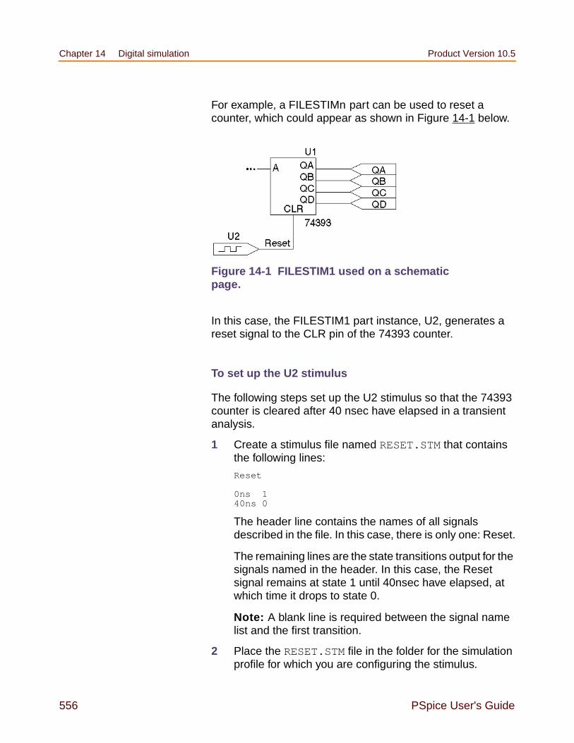
Chapter 14 Digital simulation Product Version 10.5
556 PSpice User's Guide
For example, a FILESTIMn part can be used to reset acounter, which could appear as shown in Figure 14-1 below.
In this case, the FILESTIM1 part instance, U2, generates areset signal to the CLR pin of the 74393 counter.
To set up the U2 stimulus
The following steps set up the U2 stimulus so that the 74393counter is cleared after 40 nsec have elapsed in a transientanalysis.
1 Create a stimulus file named RESET.STM that containsthe following lines:
Reset
0ns 140ns 0
The header line contains the names of all signalsdescribed in the file. In this case, there is only one: Reset.
The remaining lines are the state transitions output for thesignals named in the header. In this case, the Resetsignal remains at state 1 until 40nsec have elapsed, atwhich time it drops to state 0.
Note: A blank line is required between the signal namelist and the first transition.
2 Place the RESET.STM file in the folder for the simulationprofile for which you are configuring the stimulus.
Figure 14-1 FILESTIM1 used on a schematicpage.

Product Version 10.5 Steps for simulating digital circuits
PSpice User's Guide 557
3 Associate this file with the digital stimulus instance, U2,by setting U2’s FILENAME property to RESET.STM.
4 Define the signal named Reset in RESET.STM as theoutput of U2 by setting U2’s SIGNAME property to Reset.Since the labeled wire connecting U2 with the 74393counter is also named Reset, it is also acceptable to leaveSIGNAME undefined.

Chapter 14 Digital simulation Product Version 10.5
558 PSpice User's Guide
Defining simulation time
To set up the transient analysis
1 From Capture’s PSpice menu, choose New SimulationProfile.
2 Enter a name for the new simulation profile.
3 Click OK.
4 In the Analysis Type list box on the Analysis tab, selectTime Domain (Transient).
5 In the Run to Time text box, type the duration of thetransient analysis.
6 Click OK.
Adjusting simulation parameters
Use the Options tab of the Simulation Settings dialog box toadjust the simulation behavior of your circuit’s digital devices.

Product Version 10.5 Adjusting simulation parameters
PSpice User's Guide 559
To access the digital settings in the Options tab
1 From Capture’s PSpice menu, choose Edit SimulationProfile.
2 Click the Options tab.
3 In the Category list box, select Gate-level simulation.
Each of the dialog box settings is described in thefollowing sections. For additional options, see Outputcontrol options on page 573.

Chapter 14 Digital simulation Product Version 10.5
560 PSpice User's Guide
Selecting propagation delays
All digital devices—including primitives and library models—perform simulations using either minimum, typical, maximumor worst-case (min/max) timing characteristics. You can setthe delay circuit-wide or on individual device instances.
Note: Propagation delay modeling is not available in PSpiceA/D Basics
Circuit-wide propagation delays
You can set these to minimum, typical, maximum or variablewithin the min/max range for digital worst-case timingsimulation on the Options tab of the Simulation Settings dialogbox.
To specify the delay level circuit-wide
1 From Capture’s PSpice menu, choose Edit SimulationProfile.
2 Click the Options tab.
3 In the Category list box, select Gate-level simulation.
Part instance propagation delays
You can set the propagation delay mode on an individualdevice, thereby overriding the circuit-wide delay mode.
To override the circuit-wide default on an individual part
1 Set the part’s MNTYMXDLY property from 1 to 4 where
1 = minimum2 = typical3 = maximum4 = worst-case (min/max)

Product Version 10.5 Adjusting simulation parameters
PSpice User's Guide 561
By default, MNTYMXDLY is set to 0, which tellsPSpice A/D to use the circuit-wide value defined in theOptions tab.

Chapter 14 Digital simulation Product Version 10.5
562 PSpice User's Guide
Initializing flip-flops
To initialize all flip-flops and latches
Select one of the three Flip-flop Initialization choices on theOptions tab:
If set to X, all flip-flops and latches produce an X(unknown state) until explicitly set or cleared, or untila known state is clocked in.
Note: The X initialization is the safest setting, sincemany devices do not power up to a known state.However, the 0 and 1 settings are useful in situationswhere the initial state of the flip-flop is unimportant tothe function of the circuit, such as a toggle flip-flop ina frequency divider.
If set to 0, all such devices are cleared.
If set to 1, all such devices are preset.
Refer to the online PSpice Reference Guide for moreinformation about flip-flops and latches.
Starting the simulation
To start the simulation
From the PSpice menu, choose Run.
After PSpice A/D completes the simulation, the graphicalwaveform analyzer starts automatically.
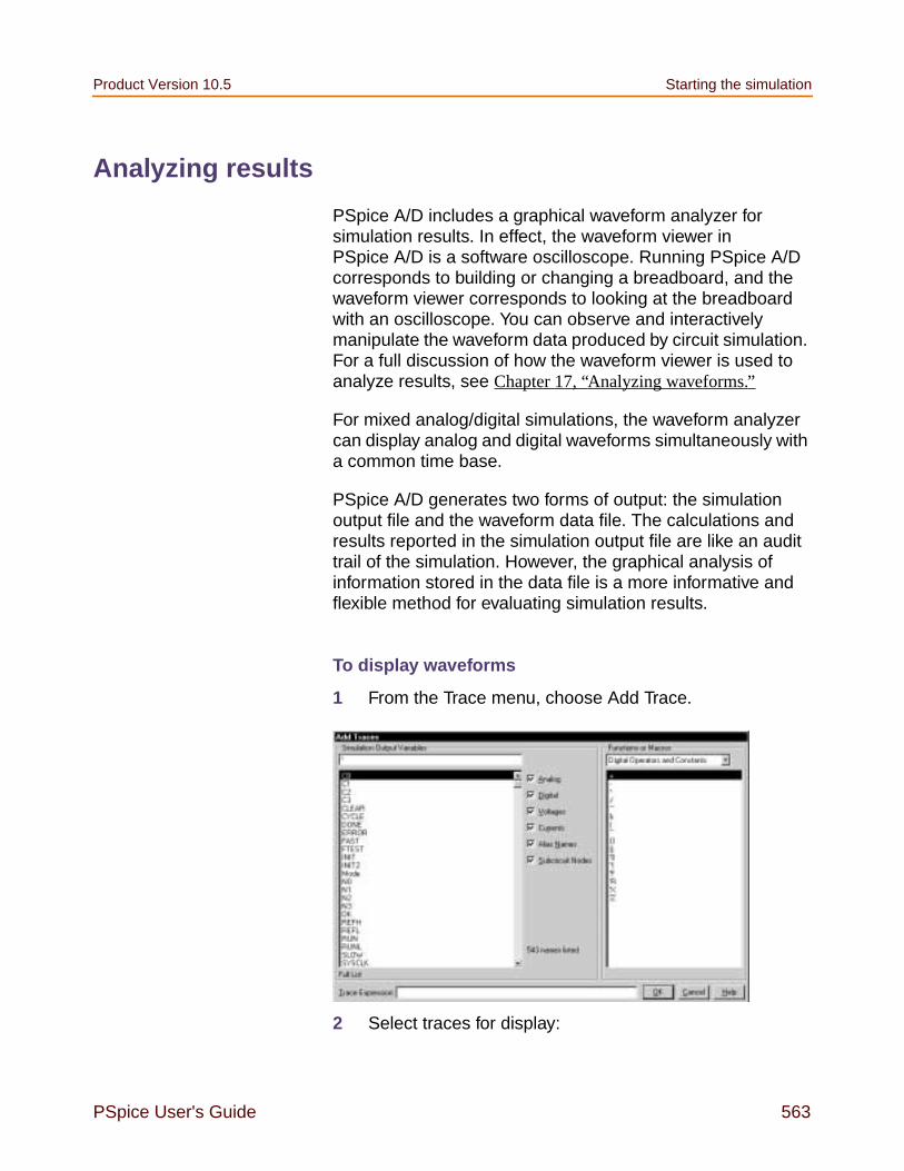
Product Version 10.5 Starting the simulation
PSpice User's Guide 563
Analyzing results
PSpice A/D includes a graphical waveform analyzer forsimulation results. In effect, the waveform viewer inPSpice A/D is a software oscilloscope. Running PSpice A/Dcorresponds to building or changing a breadboard, and thewaveform viewer corresponds to looking at the breadboardwith an oscilloscope. You can observe and interactivelymanipulate the waveform data produced by circuit simulation.For a full discussion of how the waveform viewer is used toanalyze results, see Chapter 17, “Analyzing waveforms.”
For mixed analog/digital simulations, the waveform analyzercan display analog and digital waveforms simultaneously witha common time base.
PSpice A/D generates two forms of output: the simulationoutput file and the waveform data file. The calculations andresults reported in the simulation output file are like an audittrail of the simulation. However, the graphical analysis ofinformation stored in the data file is a more informative andflexible method for evaluating simulation results.
To display waveforms
1 From the Trace menu, choose Add Trace.
2 Select traces for display:

Chapter 14 Digital simulation Product Version 10.5
564 PSpice User's Guide
In the Simulation Output Variables list, click anywaveforms you want to display. Each appears in theTrace Expressions box at the bottom.
Construct expressions by selecting operators,functions and/or macros from the Functions orMacros list, and output variables in the SimulationOutput Variables list.
You can also type trace expressions directly into theTrace Expression text box. A typical set of entriesmight be:
IN1 IN2 Q1 Q2
Note: Use spaces or commas to separate the outputvariables you place in the Trace Expressions list.
3 Click OK.
Waveforms for the selected output variables appear.
For detailed information on how to add digital traces, seeDigital trace expressions on page 703.
Adding digital signals to a plot
When defining digital trace expressions, you can include anycombination of digital signals, buses, signal constants, busconstants, digital operators, macros and the Time sweepvariable.
The following rules apply:
An arithmetic or logical operation between two busoperands results in a bus value that is wide enough tocontain the result.
An arithmetic or logical operation between a bus operandand a signal operand results in a bus value.
The syntax for expressing a digital output variable orexpression is:
digital_output_variable[;display_name]
or
Product Version 10.5 Starting the simulation
PSpice User's Guide 565
digital_expression[;display_name]
To add a digital trace expression
1 In the Add Traces dialog box, make sure you select theDigital check box.
2 Do one of the following:
In the Simulation Output Variables list, click thesignal you want to display.
In the Trace Expression text box, create a digitalexpression by either typing the expression, or byselecting digital output variables from the SimulationOutput Variables list and digital operators from theDigital Operators and Functions list.
3 If you want to label a signal with a name that is differentfrom the output variable:
a. Click in the Trace Expression text box after the lastcharacter in the signal name.
b. Type ;display_name where display_name is thename of the label.
Example: U2:Y;OUT1where U2:Y is the output variable. On the plot, the signalis labeled OUT1.
Table 14-9
This placeholder... Means this...
digital_output_variable
output variable from theSimulation Output Variable list(Digital check box selected)
digital_expression expression using digital outputvariables and operators
display_name(optional)
text string (name) to label thesignal on the plot, instead ofusing the default outputvariable notation

Chapter 14 Digital simulation Product Version 10.5
566 PSpice User's Guide
Adding buses to a waveform plot
You can evaluate and display a set of up to 32 signals as a buseven if the selected signals were not originally a bus.This is done by following the same procedure already given foradding digital signals to the plot. However, when adding a bus,be sure to enclose the list of signals in braces: .
Q3 Q2 Q1 Q2
The complete syntax is as follows:
signal_list[;[display_name][;radix]]
or
bus_prefix[msb:lsb][;[display_name][;radix]]
Table 14-10
This placeholder... Means this...
signal_list comma- or space-separated list ofup to 32 digital node names, insequence from high order to loworder
bus_prefix[msb:lsb] alternate way to express up to 32signals in the bus
display_name(optional)
text string (name) to label the buson the plot, instead of using thedefault output variable notation
Note: To change the radix withoutchanging the display name,be sure to include twoconsecutive semicolons.Example:A3,A2,A1,A0;;radix
radix(optional)
numbering system in which todisplay bus values

Product Version 10.5 Starting the simulation
PSpice User's Guide 567
Valid entries for radix are shown in the following table.
To add a bus expression
1 In the Add Traces dialog box, in the Functions and Macroslist, choose Digital Operators and Constants.
2 Click the entry.
3 In the Simulation Output Variables list, select the signalsin high-order to low-order sequence.
4 If you want to label the bus with a name that is differentfrom the default:
a. Click in the Trace Expression text box after the lastcharacter in the bus name.
b. Type ;display_name where display_name is thename of the label.
5 If you want to set the radix to something different from thedefault:
a. Click in the Trace Expression text box after the lastcharacter in the expression.
b. Type one of the following where radix is a value fromTable 14-11:
If you specified a display_name, then type;radix.
Table 14-11
For this numbering system... Use thisnotation...
Binary (base 2) B
Decimal (base 10) D
Hexadecimal (base 16) H or X
Octal (base 8) O (the letter)

Chapter 14 Digital simulation Product Version 10.5
568 PSpice User's Guide
If you did not specify a display_name, thentype ;;radix (two semicolons preceding theradix value).
Examples:
Q2,Q1,Q0;A;O specifies a 3-bit bus whose mostsignificant bit is Q2. PSpice A/D labels the plot A, andvalues appear in octal notation.
a3,a2,a1,a0;;d specifies a 4-bit bus. On the plot,values appear in decimal notation. Since no display nameis specified, PSpice A/D uses the signal list as a label.
a[3:0] is equivalent to a3,a2,a1,a0

Product Version 10.5 Starting the simulation
PSpice User's Guide 569
Tracking timing violations and hazards
When there are problems with your design, such assetup/hold violations, pulse-width violations, or worst-casetiming hazards, PSpice A/D saves messages to the simulationoutput file or data file. You can select messages and have theassociated waveforms and detailed message textautomatically appear. The messaging feature is discussedfurther in Tracking digital simulation messages on page 687 ofChapter 17, “Analyzing waveforms.”
PSpice A/D can also detect persistent hazards that may havea potential effect on a primary circuit output or on the internalstate of the design.
Note: This feature is not available in PSpice A/D Basics
Persistent hazards
Digital problems are usually either timing violations or timinghazards. Timing violations include SETUP, HOLD andminimum pulse WIDTH violations of componentspecifications. This type of violation may produce a change inthe state behavior of the design, and potentially in the answer.However, the effects of many of these errors are short-livedand do not influence the final circuit results.
For example, consider an asynchronous data change on theinput to flip-flop FF1 in Figure 14-2 below. The data change istoo close to the clock edge e1, resulting in a SETUP violation.In a hardware implementation, the output of FF1 may or maynot change. However, some designs are not sensitive to thisindividual missed data because the next clock edge (e2 in thisexample) latches the data. The designer must judge the

Chapter 14 Digital simulation Product Version 10.5
570 PSpice User's Guide
significance of timing errors, accounting for the overallbehavior of the design.
Timing hazards are most easily identified by simulating adesign in worst-case timing mode, usually close to its criticaltiming limits. Under such conditions, PSpice A/D reportsconditions such as AMBIGUITY CONVERGENCE hazards.Again, these may or may not pose a problem to the operationof the design.
However, there are identifiable cases that cause majorproblems. An example of a major problem is shown inFigure 14-3 below. Due to the simultaneous arrival of twotiming ambiguities (having unrelated origins, therefore nothingin common) at the inputs to gate G1, PSpice A/D reports theoccurrence as an AMBIGUITY CONVERGENCE hazard. Thismeans that the output of G1 may glitch.
Note that the output fans out to two devices, G2 and L1. Theeffects of a glitch on G1 in this case do not reach the circuit
...
...
e1 e2
D
C
Q
~Q
D
C
Q
~Q
FF1 FF2
O1
O2
O3
S
Figure 14-2 Circuit with a timing error.
Figure 14-3 Circuit with a timing ambiguity
0
Product Version 10.5 Starting the simulation
PSpice User's Guide 571
output P1, because that path is not sensitized (since the otherinput to G2 is held LO and thus blocks the symptom).However, because G1’s output is also used to clock latch L1,the effects of a glitch could result in visibly incorrect behavioron output P2. This is an example of a persistent hazard.
A persistent hazard is a timing violation or hazard that has apotential effect on a primary (external) circuit output or on theinternal state (stored state or memory elements) of the design.For the design to be considered reliable, you must correctsuch timing hazards.
PSpice A/D fully distinguishes between state uncertainty andtime uncertainty. When a hazard occurs, PSpice A/Dpropagates hazard origin information along with the machinestate through all digital devices. When a hazard propagates toa state-storage device primitive (JKFF, DFF, SRFF, DLTCH,RAM), PSpice A/D reports a PERSISTENT HAZARD.
Simulation condition messages
PSpice A/D produces warning messages in varioussituations, such as those that originate from the digitalCONSTRAINT devices monitoring timing relationships ofdigital nodes. These messages are directed to the simulationoutput file and/or to the waveform data file. Options areavailable for controlling where and how many of thesemessages are generated, as summarized later in this section.
Table 14-12 below summarizes the simulation message types,with a brief description of their meaning. Currently, themessages supported are specific to digital device timingviolations and hazards.
Table 14-12 Simulation condition messages—timing violations
Message type Severity level Meaning
SETUP WARNING Minimum time required for a data signal to be stableprior to the assertion of a clock was not met.
HOLD WARNING Minimum time required for a data signal to be stableafter the assertion of a clock was not met.

Chapter 14 Digital simulation Product Version 10.5
572 PSpice User's Guide
RELEASE WARNING Minimum time required for a signal that has goneinactive (usually a control such as CLEAR) to remaininactive before the asserting clock edge was not met.
WIDTH WARNING Minimum pulse width specification for a signal was notsatisfied; that is, a pulse that was too narrow wasobserved on the node.
FREQUENCY WARNING Minimum or maximum frequency specification for asignal was not satisfied. Minimum frequency violationsindicate that the period of the measured signal is toolong, while maximum frequency violations describesignals changing too rapidly.
GENERAL INFO Boolean expression described within the GENERALconstraint checker was evaluated and produced a trueresult.
Table 14-12 Simulation condition messages—timing violations
Message type Severity level Meaning
Table 14-13 Simulation condition messages—hazards
Message type Severity level Meaning
AMBIGUITYCONVERGENCE
WARNING Convergence of conflicting rising and falling states(timing ambiguities) arrived at the inputs of a primitiveand produced a pulse (glitch) on the output. SeeChapter 16, “Digital worst-case timing analysis” formore information.
CUMULATIVEAMBIGUITY
WARNING Signal ambiguities are additive, increased bypropagation through each level of logic in the circuit.The ambiguities associated with both edges of apulse increased to the point where they overlapped,which PSpice A/D reports as a cumulative ambiguityhazard. See Chapter 16, “Digital worst-case timinganalysis” for more information.

Product Version 10.5 Starting the simulation
PSpice User's Guide 573
Output control options
Four control options are available for managing the generationof simulation condition messages. These are described inTable 14-14.
To access these commands, select the Options tab in theSimulation Settings dialog box. You can set NOOUTMSG andNOPRBMSG by selecting the Output file Category. You canset DIGERRDEFAULT and DIGERRLIMIT by selecting the
SUPPRESSEDGLITCH
WARNING Pulse applied to the input of a primitive that is shorterthan the active propagation delay was ignored byPSpice A/D; significance depends on the nature ofthe circuit. There might be a problem either with thestimulus, or with the path delay configuration of thecircuit. See Chapter 16, “Digital worst-case timinganalysis” for more information.
NET-STATECONFLICT
WARNING Two or more outputs attempted to drive a net todifferent states, which PSpice A/D reports as an X(unknown) state. This usually results from improperselection of a bus driver’s enable inputs.
ZERO-DELAY-OSCILLATION
FATAL Output of a primitive changed more than 50 timeswithin a single digital time step. PSpice A/D abortedthe run.
DIGITAL INPUTVOLTAGE
SERIOUS Voltage on a digital pin was out of range, whichmeans PSpice A/D used the state with a voltagerange closest to the input voltage and continued thesimulation.
PERSISTENTHAZARD
SERIOUS Effects of any of the aforementioned logic hazardswere able to propagate to either an external port or toany storage device in the circuit. See Persistenthazards on page 569 for more information.
Table 14-13 Simulation condition messages—hazards
Message type Severity level Meaning

Chapter 14 Digital simulation Product Version 10.5
574 PSpice User's Guide
Gate-level simulation Category and clicking AdvancedOptions.
Severity levels
PSpice A/D assigns one of four severity levels to themessages:
FATAL
SERIOUS
WARNING
INFO (informational)
FATAL conditions cause PSpice A/D to cancel the simulation.Under all other severity levels, PSpice A/D continues to run.
Table 14-14 Simulation message output control options
This option... Means this...
NOOUTMSG Suppresses the recording ofsimulation condition messages inthe simulation output file.
NOPRBMSG Suppresses the recording ofsimulation condition messages inthe waveform data file.
DIGERRDEFAULT=<n> Establishes a default limit, n, tothe number of condition messagesthat may be generated by anydigital device that has a constraintchecker primitive without a localdefault. If global or local defaultsare unspecified, there is no limit.
DIGERRLIMIT=<n> Establishes an upper limit, n, forthe total number of conditionmessages that may be generatedby any digital device. If this limit isexceeded, PSpice A/D aborts therun. By default, the total number ofmessages is 20.

Product Version 10.5 Starting the simulation
PSpice User's Guide 575
The severity levels are used to filter the classes of messagesthat are displayed when loading a data file.

Chapter 14 Digital simulation Product Version 10.5
576 PSpice User's Guide

PSpice User's Guide 577
15
Mixed analog/digital simulation
Chapter overview
This chapter describes how PSpice A/D runs mixedanalog/digital simulations and includes the following sections:
Interconnecting analog and digital parts on page 578
Interface subcircuit selection by PSpice on page 579
Specifying digital power supplies on page 583
Interface generation and node names on page 589
Note: This entire chapter describes features that are notincluded in PSpice.

Chapter 15 Mixed analog/digital simulation Product Version 10.5
578 PSpice User's Guide
Interconnecting analog and digital parts
Prior to simulation, netlisting translates the part instances andnets defined in your schematic into parts connected by nodes.The standard simulation netlist contains a flat view of thecircuit. You can also create hierarchical netlists. PSpice A/Dextracts the definitions for all parts modeled as subcircuits,viewing parts as a collection of primitive parts and nodeconnections.
The digital primitives that make up a digital part determine theway that PSpice A/D processes an analog/digital interface tothat part. Specifically, the I/O model for each digital primitiveconnected at the interface gives PSpice A/D the necessaryinformation.
PSpice A/D recognizes three types of nodes: analog nodes,digital nodes, and interface nodes. The node type isdetermined by the types of parts connected to it. If all of theparts connected to a node are analog, then it is an analognode. If all of the parts are digital, then it is a digital node. Ifthere is a combination of analog and digital parts, then it is aninterface node.
PSpice A/D automatically breaks interface nodes into onepurely analog and one or more digital nodes by inserting oneor more analog/digital interface subcircuits.
PSpice A/D also automatically connects a power supply to theinterface subcircuit to complete the generation of the interface.
To view simulation results at an analog/digital interface in yourschematic using the graphical waveform analyzer:
Place a marker on the appropriate interface net. Theadditional nodes created by PSpice A/D remaintransparent.
View results in PSpice A/D by selecting traces from theoutput variable list (from the Trace menu, choose AddTrace). If you use this approach, note the namesPSpice A/D generates for the new nodes. To find outmore, see Interface generation and node names onpage 589.

Product Version 10.5 Interface subcircuit selection by PSpice
PSpice User's Guide 579
Interface subcircuit selection by PSpice
Analog-to-digital (AtoD) and digital-to-analog (DtoA) interfacesubcircuits handle the translation between analog voltages/impedances and digital states, or vice-versa. The maincomponent of an interface subcircuit is either a PSpice N part(digital input: digital-to-analog) or a PSpice O (that’s the letterO, not the numeral zero) part (digital output: analog-to-digital).
PSpice N and O parts are neatly packaged into interfacesubcircuits in the model library. The standard model libraryshipped with your software installation includes interfacesubcircuits for each of the supported logic families: TTL,CD4000 series CMOS and high-speed CMOS (HC/HCT),ECL 10K, and ECL 100K. This frees you from ever having todefine them yourself when using parts in the standard library.If you are creating custom digital parts in technologies otherthan those provided in the standard model library, you mayneed to create your own interface subcircuits.
Note: To search for particular parts in the standard PSpicelibraries, see the online PSpice Library List.
Every digital primitive comprising the subcircuit description ofa digital part has an I/O model describing its loading anddriving characteristics. The name of the interface subcircuitactually inserted by PSpice A/D is specified by the I/O modelof the digital primitive at the interface. The I/O model hasparameters for up to four analog-to-digital (AtoD) and fourdigital-to-analog (DtoA) subcircuit names.
You can choose among four interface levels of subcircuitmodels, depending on the simulation accuracy you need. Insome cases you may need more accurate simulations of theinput/output stages of a digital part, while in other cases, asimpler, smaller model is enough.
Digital parts provided in the standard libraries only useinterface levels 1 and 2. With the exception of the HC/HCTseries (described below), levels 3 and 4 reference the samesubcircuits as levels 1 and 2. Table 15 below summarizes thefour interface levels.

Chapter 15 Mixed analog/digital simulation Product Version 10.5
580 PSpice User's Guide
The difference between levels 1 and 2 only occurs in the AtoDinterfaces, described below. In all cases, the level 1 DtoAinterface is the same as the level 2 DtoA interface, except thatthe level 2 DtoA interface does not generate intermediate R,F, and X levels.
The OrCAD libraries provide two different DtoA models in theHC/HCT series: the simple model and the elaborate model.You can use the simple model by specifying level 1 or 2, theelaborate model by specifying level 3 or 4. The elaboratemodel is noticeably slower than the simple model, so youshould only use it if you are using a power supply level otherthan 5.0 volts.
The HC/HCT level 1 and 2 DtoA models produce accurate I-Vcurves given a fixed power supply of 5.0 volts and atemperature of 25°C. The level 3 and 4 DtoA models produceaccurate I-V curves over the acceptable range of powersupply voltages (2-6 volts), and they include temperaturederating.
Level 1 interface
The level 1 AtoD interface generates intermediate logic levels(R, F, X) between the voltage ranges VILMAX and VIHMIN(specific voltages depend on the technology you are using). Asteadily rising voltage on the input of the AtoD will transitionfrom 0 to R at VILMAX and from R to 1 at VIHMIN. The F levelis output for steadily falling voltages in a similar manner. The
Table 15-1 Interface subcircuit models
Level Subcircuits Definition
1 AtoD1/DtoA1 AtoD generates intermediate R, F,and X levels
2 AtoD2/DtoA2 AtoD does not generateintermediate R, F, and X levels
3 AtoD3/DtoA3 (same as level 1)
4 AtoD4/DtoA4 (same as level 2)

Product Version 10.5 Interface subcircuit selection by PSpice
PSpice User's Guide 581
X level is produced if the input voltage starts in the thresholdregion or doubles back into a previously crossed threshold.
Level 1 (the default) strictly maps logic levels onto thechanging input voltage. The exact switching voltage isassumed to be anywhere between VILMAX and VIHMIN dueto temperature or power supply variations. Thus, it providesmore accurate, less optimistic results.
This behavior may not be appropriate when the input rise andfall times are long, or when the input voltage never leaves thethreshold region. If this is the case, you may want to use thelevel 2 interface.
Level 2 interface
The level 2 AtoD interface transitions directly from 0 to 1 and1 to 0 without passing through intermediate R, F, or X levels.An exact switching voltage is assumed (again, the specificvoltage depends on the technology you are using). It providesa more optimistic, and therefore less accurate, response thanlevel 1. Level 2’s behavior is appropriate when the inputvoltage oscillates around the threshold voltage.
Note: You can avoid simulations that get bogged down withthe greater detail of R, F, and X states around theseoscillations. You may want to specify level 2 on onlythose parts for which this behavior is critical to asuccessful simulation. This is described in Setting thedefault A/D interface below.

Chapter 15 Mixed analog/digital simulation Product Version 10.5
582 PSpice User's Guide
Setting the default A/D interface
For mixed-signal simulation, you can select the AtoD andDtoA interface level circuit-wide and on individual partinstances.
To select the default interface level circuit-wide, selectone of the four Default A/D interfaces in the SimulationSettings dialog box by selecting the Gate-level simulationcategory under the Options tab. Part instances with theIO_LEVEL property set to 0 use this value.
You can override the circuit-wide default on an individualpart by specifying an IO_LEVEL property from 1 to 4,where:
For example, you can tell the simulator to use the level 2interface subcircuits for a 7400 part by setting the IO_LEVELproperty to 2. All other part instances continue to use thecircuit-wide setting. By default, IO_LEVEL is set to 0, whichtells the simulator to use the circuit-wide level defined in theGate-level simulation category in the Simulation Settingsdialog box.
1: AtoD1 and DtoA1 (default)
2: AtoD2 and DtoA2
3: AtoD3 and DtoA3
4: AtoD4 and DtoA4

Product Version 10.5 Interface subcircuit selection by PSpice
PSpice User's Guide 583
Specifying digital power supplies
Digital power supplies are used to power interface subcircuitsthat are automatically created by PSpice A/D when simulatinganalog/digital interfaces. They are specified as follows:
PSpice A/D can instantiate them automatically.
You can create your own digital power supplies and placethem in your design.
When using parts from the standard libraries in your design,you can usually have PSpice A/D automatically create thenecessary digital power supply. If you use custom digital partscreated in technologies other than those provided in thestandard model library, you may need to create your owndigital power supplies.
Because digital power supplies are used only by analog/digitalinterface subcircuits, digital power supplies are not needed fordigital-only designs. We recommend avoiding placing a powersupply to a digital-only design because it may increasesimulation time and memory usage.
Default power supply selection by PSpice A/D
When PSpice A/D encounters an analog/digital interface, itcreates the appropriate interface subcircuit and power supplyaccording to the I/O model referenced by the digital part. TheI/O model is specific to the digital part’s logic family. The powersupply provides reference or drive voltage for the analog sideof the interface.
By default, PSpice A/D inserts one power supply subcircuit forevery logic family in which a digital primitive is involved with ananalog/digital interface. These power supply subcircuitscreate the digital power and ground nodes that are thedefaults for all parts in that family. If multiple digital primitivesfrom the same logic family are involved with analog/digitalinterfaces, one instance of the power supply subcircuit iscreated with all primitives connected to the power supplynodes.

Chapter 15 Mixed analog/digital simulation Product Version 10.5
584 PSpice User's Guide
Table 15-2 summarizes the default node names and values.For instance, TTL power supplies have a default value of 5.0volts at analog/digital interfaces.
Table 15-2 Default digital power/ground pin connections
The PSPICEDEFAULTNET pin properties have the samedefault values as the digital power and ground nodes createdby the default power supply. These node assignments arepassed from the part instance to the digital primitivesdescribing its behavior, connecting any digital primitiveaffected by an analog connection to the correct power supply.
The default I/O models and power supply subcircuits arefound in DIG_IO.LIB. The four default power supplies providedin the model library are DIGIFPWR (TTL), CD4000_PWR(CD4000 series CMOS), ECL_10K_PWR (ECL 10K), andECL_100K_PWR (ECL 100K).
Logicfamily
Digital power/ground pin properties
Default digital power/groundnodes
TTL PSPICEDEFAULTNET(PWR)
PSPICEDEFAULTNET(GND)
$G_DPWR (5.0 volts)$G_DGND (0 volts)
CD4000 PSPICEDEFAULTNET(VDD)
PSPICEDEFAULTNET (VSS)
$G_CD4000_VDD (5 volts)$G_CD4000_VSS (0 volts)
ECL 10K PSPICEDEFAULTNET (VEE)
PSPICEDEFAULTNET(VCC1)
PSPICEDEFAULTNET(VCC2)
$G_ECL_10K_VEE (-5.2 volts)$G_ECL_10K_VCC1 (0 volts)$G_ECL_10K_VCC2 (0 volts)
ECL100K
PSPICEDEFAULTNET (VEE)
PSPICEDEFAULTNET(VCC1)
PSPICEDEFAULTNET(VCC2)
$G_ECL_100K_VEE (-4.5 volts)$G_ECL_100K_VCC1 (0 volts)$G_ECL_100K_VCC2 (0 volts)

Product Version 10.5 Interface subcircuit selection by PSpice
PSpice User's Guide 585
Creating custom digital power supplies
Each digital part model has optional digital power and groundnodes that you can use to specify custom power supplies. Todo this, use one of the digital power supplies listed in Table15-3 below in your design and redefine the digital powersupply nodes.
Table 15-3 Digital power supply parts in SPECIAL.OLB
When creating custom power supplies, you can refer to thepower supply definitions in DIG_IO.LIB for examples of powersupply subcircuit definitions. The properties relevant tocreating custom power supplies are shown in Table 15-4.
Table 15-4 Digital power supply properties
Part type(PSpice A/D X model)
Part name
CD4000 power supply CD4000_PWR
TTL power supply DIGIFPWR
ECL 10K power supply ECL_10K_PWR
ECL 100K power supply ECL_100K_PWR
Part name Property Description
CD4000_PWR VOLTAGE CD4000 series CMOS powersupply voltage
PSPICEDEFAULTNET CD4000 series CMOS hiddenpower supply pins for VDD andVSS
DIGIFPWR VOLTAGE TTL power supply voltage
PSPICEDEFAULTNET TTL hidden power (PWR) andground (GND) pins

Chapter 15 Mixed analog/digital simulation Product Version 10.5
586 PSpice User's Guide
To create a custom digital power supply
Note: This procedure applies to all logic families.
1 Place the appropriate power supply part listed in Table15-3 in your design (by logic family).
2 Rename the power supply power and ground pins(PSPICEDEFAULTNET properties).
3 Reset the power supply power and ground voltages asrequired.
4 For any digital part instance that uses the power supply,set its appropriate PSPICEDEFAULTNET pin propertiesto the power and ground pins created by the secondarypower supply.
Overriding CD4000 power supply voltage throughout a design
Designs using CD4000 parts often require power supplyvoltages other than the default 5.0 volts supplied by thestandard CD4000_PWR power supply part. If needed, youcan override the power supply voltage for all CD4000 parts ina design.
The default power supply nodes used by CD4000 parts arenamed $G_CD4000_VDD and $G_CD4000_VSS as createdby the power supply subcircuit CD4000_PWR. This supplydefaults to 5.0 volts. You can override the voltage across thesetwo nodes by defining values for the parameters namedCD4000_VDD and CD4000_VSS that are referenced by theCD4000_PWR subcircuit definition.
ECL_10K_PWRECL_100K_PWR
VEEVCC1VCC2
ECL power supply voltages
PSPICEDEFAULTNET ECL hidden power supply pins forVEE, VCC1 and VCC2
Part name Property Description

Product Version 10.5 Interface subcircuit selection by PSpice
PSpice User's Guide 587
To change the CD4000_PWR power supply to 12 volts,referenced to ground:
1 Place an instance of the PARAM pseudopart fromSPECIAL.OLB.
2 Create a new PARAM property as follows:
CD4000_VDD = 12.0V
DC4000_VSS is left at its default of 0 volts.
If the reference voltage also needs to be reset, the samemethod can be used to define the CD4000_VSS parameter bysetting this property of the same PARAM instance. Forexample, if you want the supplies to go between -5 volts and+5 volts (a difference of 10 volts), set CD4000_VSS to -5V andCD4000_VDD to +10V; as a result, CD4000_VDD is 10 voltsabove CD4000_VSS, or +5 volts.
Creating a secondary CD4000, TTL, or ECL power supply
Designs using CD4000, TTL, or ECL parts may require powersupply voltages in addition to the default 5.0 volts supplied bythe standard CD4000_PWR power supply part.
To create a secondary power supply for any one of theCD4000, TTL, or ECL technologies, you must place theappropriate power supply part and create user-defined nodeswith a new voltage value.
Note: Designs with TTL and ECL parts rarely requiresecondary power supplies. If needed, however, youcan use this procedure to add a secondary powersupply for TTL and ECL parts.
To create and use a secondary CD4000 power supply withnodes MY_VDD and MY_VSS and a voltage of 3.5 volts:
1 Place the CD4000_PWR power supply and modify theappropriate pin properties as follows:
VOLTAGE = 3.5VPSPICEDEFAULTNET = MY_VDDPSPICEDEFAULTNET = MY_VSS

Chapter 15 Mixed analog/digital simulation Product Version 10.5
588 PSpice User's Guide
2 Select a CD4000 part in the schematic to which the newpower supply should apply, then change the appropriatepin properties as follows:
PSPICEDEFAULTNET = MY_VDDPSPICEDEFAULTNET = MY_VSS

Product Version 10.5 Interface subcircuit selection by PSpice
PSpice User's Guide 589
Interface generation and node names
The majority of the interface generation process involvesPSpice A/D determining whether analog and digital primitivesare connected, and if so, inserting an interface subcircuit foreach digital connection. This turns the interface node into apurely analog node, which now connects to the analogterminal of the interface subcircuit. To complete the originalconnection, PSpice A/D creates a new digital node betweenthe digital terminal of the interface subcircuit and the digitalprimitive.
Because PSpice A/D must create new digital nodes, it mustgive them unique names. These node names are used in theoutput variables in the list of viewable traces when you chooseAdd Trace from the Trace menu. Name generation followsthese rules:
The analog node retains the name of the original interfacenode—either the labeled wire name in the design, or thenode name automatically generated for an unlabeledwire.
Each new digital node name consists of the labeled wirename in the design or the node name automaticallygenerated for an unlabeled wire, appended with $AtoD or$DtoA. If the node is attached to more than one digitalpart, the second digital node is appended with $AtoD2 or$DtoA2, and so on.
Figure 15-1 below shows a fragment of a mixed analog/digitalcircuit before and after the interface subcircuits have beenadded. The wires labeled 1 and 2 in the schematicrepresentation are the interface nets connecting analog anddigital parts. These translate to interface nodes, which are

Chapter 15 Mixed analog/digital simulation Product Version 10.5
590 PSpice User's Guide
processed by PSpice A/D to create the circuit fragment shownin the PSpice A/D representation.
After interface generation, node 1 is a purely analog node,connecting the resistor, transistor, and the analog inputs ofboth AtoD subcircuits. Node 2 is also a purely analog node,connecting the resistor and the analog output of the DtoAinterface. You can see that PSpice A/D inserted two newdigital nodes, 1$AtoD and 1$AtoD2, which connect theoutputs of the AtoD interfaces to the inverter inputs. It alsocreated one digital node, 2$DtoA, to connect the output of U1to the digital input of the DtoA interface.
The interface subcircuits PSpice A/D automatically generatesare listed in the simulation output file under the section namedGenerated AtoD and DtoA Interfaces. For the example inFigure 15-1, this section would appear in the simulation outputfile as shown in Figure 15-2 below.
Figure 15-1 Mixed analog/digital circuit beforeand after interface generation.
schematic representation
PSpice A/D representation

Product Version 10.5 Interface subcircuit selection by PSpice
PSpice User's Guide 591
The lines that begin with “Moving…from analog node” indicatethe new digital node names that were generated. Below eachof these are the interface subcircuit calls inserted byPSpice A/D.
In this example, the subcircuits named AtoD_STD andDtoA_STD are obtained from the I/O model that is referencedby the inverter primitive inside the subcircuit describing the7404 part. The CAPACITANCE, DRVL (low-level drivingresistance), and DRVH (high-level driving resistance)subcircuit parameter values come from the same I/O model.
After the interface subcircuit calls, PSpice A/D inserts one ormore interface power supply subcircuits. The subcircuit nameis specified in the I/O model for the digital primitive at theinterface. In this example, PSpice A/D inserted DIGIFPWR,which is the power supply subcircuit used by all TTL models inthe model library. DIGIFPWR creates the global nodes$G_DPWR and $G_DGND, which are the default nodes usedby each TTL part.
**** Generated AtoD and DtoA Interfaces ****** Analog/Digital interface for node 1** Moving X1.U1:.A from analog node 1 to new digital node * 1$AtoDX$1_AtoD1 1 1$AtoD $G_DPWR $G_DGND AtoD_STD+ PARAMS: CAPACITANCE= 0* Moving X2.U1:.A from analog node 1 to new digital node * 1$AtoD2X$1_AtoD2 1 1$AtoD $G_DPWR $G_DGND AtoD_STD+ PARAMS: CAPACITANCE= 0** Analog/Digital interface for node 2*** Moving X1.U1.Y from analog node 2 to new digital node * 2$DtoAX$2_DtoA1 2$DtoA 2 $G_DPWR $G_DGND DtoA_STD+ PARAMS: DRVL=0 DRVH=0 CAPACITANCE=0** Analog/Digital interface power supply subcircuit*X$DIGIFPWR 0 DIGIFPWR
.END ;(end of AtoD and DtoA interfaces)
Figure 15-2 Simulation output for mixed analog/digitalcircuit.

Chapter 15 Mixed analog/digital simulation Product Version 10.5
592 PSpice User's Guide

PSpice User's Guide 593
16
Digital worst-case timinganalysis
This chapter deals with worst-case timing analysis andincludes the following sections:
Digital worst-case timing on page 594
Starting digital worst-case timing analysis on page 596
Simulator representation of timing ambiguity on page 596
Propagation of timing ambiguity on page 598
Identification of timing hazards on page 599
Convergence hazard on page 599
Critical hazard on page 600
Cumulative ambiguity hazard on page 601
Reconvergence hazard on page 603
Glitch suppression due to inertial delay on page 605
Methodology on page 606
Note: This entire chapter describes features that are notincluded in PSpice.

Chapter 16 Digital worst-case timing analysis Product Version 10.5
594 PSpice User's Guide
Digital worst-case timing
Manufacturers of electronic components generally specifycomponent parameters (such as propagation delays in thecase of logic devices) as having tolerances. These areexpressed as either an operating range, or as a spread arounda typical operating point. The designer then has someindication of how much deviation from typical one mightexpect for any of these particular component delay values.
Realizing that any two (or more) instances of a particular typeof component may have propagation delay values anywherewithin the published range, designers are faced with theproblem of ensuring that their products are fully functionalwhen they are built with combinations of components havingdelay specifications that fall (perhaps randomly) anywherewithin this range.
Historically, this has been done by making simulation runsusing minimum (MIN), typical (TYP), and maximum (MAX)delays, and verifying that the product design is functional atthese extremes. But, while this is useful to some extent, itdoes not uncover circuit design problems that occur only withcertain combinations of slow and fast parts. True digitalworst-case simulation, as provided by PSpice A/D, does justthat.
Other tools called timing verifiers are sometimes used in thedesign process to identify problems that are indigenous tocircuit definition. They yield analyses that are inherentlypattern-independent and often pessimistic in that they tend tofind more problems than will truly exist. In fact, they do notconsider the actual usage of the circuit under an appliedstimulus.
PSpice A/D does not provide this type of static timingverification. Digital worst-case timing simulation, as providedby PSpice A/D, is a pattern-dependent mechanism that allowsa designer to locate timing problems subject to the constraintsof a specific applied stimulus.
Note: Digital worst-case timing analysis is not availablePSpice A/D Basics.

Product Version 10.5 Digital worst-case timing
PSpice User's Guide 595
Digital worst-case analysis compared to analog worst-case analysis
Digital worst-case timing simulation is different from analogworst-case analysis in several ways. Analog worst-caseanalysis is implemented as a sensitivity analysis for eachparameter which has a tolerance, followed by a projectedworst-case simulation with each parameter set to its minimumor maximum value. This type of analysis is general since anytype of variation caused by any type of parameter tolerancecan be studied. But it is time consuming since a separatesimulation is required for each parameter. This does notalways produce true worst-case results, since the algorithmassumes that the sensitivity is monotonic over the tolerancerange.
The techniques used for digital worst-case timing simulationare not compatible with analog worst-case analysis. It istherefore not possible to do combined analog/digitalworst-case analysis and simulation and get the correct results.PSpice A/D allows digital worst-case simulation ofmixed-signal and all-digital circuits; any analog sections aresimulated with nominal values.
Systems containing embedded analog-within-digital sectionsdo not give accurate worst-case results; they may beoptimistic or pessimistic. This is because analog simulationcan not model a signal that will change voltage at an unknownpoint within some time interval.

Chapter 16 Digital worst-case timing analysis Product Version 10.5
596 PSpice User's Guide
Starting digital worst-case timing analysis
To set up a digital worst-case timing analysis:
1 In the Simulation Settings dialog box, click the Optionstab.
See Setting up analyses on page 373 for a description ofthe Simulation Settings dialog box.
2 Under Category, select Gate-level Simulation.
3 In the Timing Mode frame, check Worst-case (min/max)
4 In the Initialize all flip-flops drop-down list, select X.
5 Set the Default I/O level for A/D interfaces to 1.
6 Click OK.
7 Start the simulation as described in Starting a simulationon page 385.
Simulator representation of timing ambiguity
PSpice A/D uses the five-valued state representation0,1,R,F,X, where R and F represent rising and fallingtransitions, respectively. Any R or F transitions can be thoughtof as ambiguity regions. Although the starting and final statesare known (example: R is a 0 → 1 transition), the exact time ofthe transition is not known, except to say that it occurssomewhere within the ambiguity region. The ambiguityregion is the time interval between the earliest and the latesttime that a transition could occur.
Timing ambiguities propagate through digital devices viawhatever paths are sensitized to the specific transitionsinvolved. This is normal logic behavior. The delay values(MIN, TYP, or MAX) skew the propagation of such signals bywhatever amount of propagation delay is associated with eachprimitive instance.
When worst-case (MIN/MAX) timing operation is selected,both the MIN and the MAX delay values are used to compute

Product Version 10.5 Simulator representation of timing ambiguity
PSpice User's Guide 597
the duration of the timing ambiguity result that represents aprimitive’s output change.
For example, consider the model of a BUF device in thefollowing figure.
U5 BUF $G_DPWR $G_DGND IN1 OUT1 ; BUFFER model+ T_BUF IO_STD
.MODEL T_BUF UGATE ( ; BUF timing model+ TPLHMN=15ns TPLHTY=25ns TPLHMX=40ns+ TPHLMN=12ns TPHLTY=20ns TPHLMX=35ns)
Figure 16-1 Timing ambiguity example one.
The application of the instantaneous 0-1 transition at 5nsec inthis example produces a corresponding output result. Giventhe delay specifications in the timing model, the output edgeoccurs at a MIN of 15nsec later and a MAX of 40nsec later.The region of ambiguity for the output response is from 20 to45nsec (from TPLHMN and TPLHMX values). Similarcalculations apply to a 1-0 transition at the input, usingTPHLMN and TPHLMX values.
205 45

Chapter 16 Digital worst-case timing analysis Product Version 10.5
598 PSpice User's Guide
Propagation of timing ambiguity
As signals propagate through the circuit, ambiguity iscontributed by each primitive having a nonzero MIN/MAXdelay spread. Consider the following example that uses thedelay values of the previous BUF model.
Figure 16-2 Timing ambiguity example two.
This accumulation of ambiguity may have adverse effects onproper circuit operation. In the following example, considerambiguity on the data input to a flip-flop.
Figure 16-3 Timing ambiguity example three.
The simulator must predict an X output, because it is notknown with any certainty when the data input actually madethe 0-1 transition. If the cumulative ambiguity present in thedata signal had been less, the 1 state would be latched upcorrectly.
Figure 16-4 illustrates the case of unambiguous data change(settled before the clock could transition) being latched up bya clock signal with some ambiguity. The Q output will change,but the time of its transition is a function of both the clock’sambiguity and that contributed by the flip-flop MIN/MAXdelays.
Figure 16-4 Timing ambiguity example four.
520 45
35 85
QD
C
QD
C

Product Version 10.5 Identification of timing hazards
PSpice User's Guide 599
Identification of timing hazards
Timing hazard is the term applied to situations where theresponse of a device cannot be properly predicted because ofuncertainty in the arrival times of signals applied to its inputs.
For example, Figure 16-5 below shows the following signaltransitions (0-1, 1-0) being applied to the AND gate.
Figure 16-5 Timing hazard example.
The state of the output does not (and should not) change,since at no time do both input states qualify the gate, and thearrival times of the transitions are known.
Convergence hazard
In cases where there are ambiguities associated with thesignal transitions 0-R-1 and 1-F-0—which have a certainamount of overlap—it is no longer certain which of thetransitions happens first.
The output could pulse (0-1-0) at some point because theinput states may qualify the gate. On the other hand, theoutput could remain stable at the 0 state. This is called aconvergence hazard because the reason for the glitchoccurrence is the convergence of the conflicting ambiguities attwo primitive inputs.
Gate primitives (including LOGICEXP primitives) that arepresented with simultaneous opposing R and F levels mayproduce a pulse of the form 0-R-0 or 1-F-1.
For example, a two-input AND gate with the inputs shown inFigure 16-6 below, produces the output shown.
Figure 16-6 Convergence hazard example.

Chapter 16 Digital worst-case timing analysis Product Version 10.5
600 PSpice User's Guide
This output (0-R-0) should be interpreted as a possiblesingle pulse, no longer than the duration of the R level.
Note: Other types of primitives, such as flip-flops, mayproduce an X instead of an R-0 or F-1 in response to aconvergence hazard.
The actual device’s output may or may not change, dependingon the transition times of the inputs.
Critical hazard
It is important to note that the glitch predicted could propagatethrough the circuit and may cause incorrect operation. If theglitch from a timing hazard becomes latched up in an internalstate (such as flip-flop or ram), or if it causes an incorrect stateto be latched up, it is called a critical hazard because itdefinitely causes incorrect operation.
Otherwise, the hazard may pose no problem. Figure 16-7below shows the same case as above, driving the data inputto a latch.
Figure 16-7 Critical hazard example.
As long as the glitch always occurs well before the leadingedge of the clock input, it will not cause a problem.
QD
C

Product Version 10.5 Identification of timing hazards
PSpice User's Guide 601
Cumulative ambiguity hazard
In worst-case mode, simple signal propagation through thenetwork will result in a buildup of ambiguity along the pathsbetween synchronization points. See Glitch suppression due toinertial delay on page 605. The cumulative ambiguity isillustrated in Figure 16-8.
Figure 16-8 Cumulative ambiguity hazard example one.
The rising and falling transitions applied to the input of thebuffer have a 1nsec ambiguity. The delay specifications of thebuffer indicate that an additional 2nsec of ambiguity is addedto each edge as they propagate through the device. Noticethat the duration of the stable state 1 has diminished due tothe accumulation of ambiguity.
Figure 16-9 shows the effects of additional cumulativeambiguity.
Figure 16-9 Cumulative ambiguity hazard example two.
The X result is predicted here because the ambiguity of therising edge propagating through the device has increased tothe point where it will overlap the later falling edge ambiguity.Specifically, the rising edge should occur between 3nsec and12nsec; but, the subsequent falling edge applied to the inputpredicts that the output starts to fall at 10nsec. This situationis called a cumulative ambiguity hazard.
Another cause of cumulative ambiguity hazard involvescircuits with asynchronous feedback. The simulation of suchcircuits under worst-case timing constraints yields an overlypessimistic result due to the unbounded accumulation of
1 2 8 9
TPxxMN=1
2 5 9 12
TPxxMX=3
TPxxMN=1
2 5 9 12 3 10
12
19
TPxxMX=7

Chapter 16 Digital worst-case timing analysis Product Version 10.5
602 PSpice User's Guide
ambiguity in the feedback path. A simple example of this effectis shown in Figure 16-10.
Figure 16-10 Cumulative ambiguity hazard examplethree.
Due to the accumulation of ambiguity in the loop, the outputsignal will eventually become X, because the ambiguities ofthe rising and falling edges overlap. However, in the hardwareimplementation of this circuit, a continuous phase shift withrespect to absolute time is what will actually occur (assumingnormal deviations of the rise and fall delays from the nominalvalues).
Note: If this signal were used to clock another circuit, it wouldbecome the reference and the effects of the phase shiftcould be ignored. You can do this by setting the NANDgate’s model parameter, MNTYMXDLY=2 to utilizetypical delay values for that one gate only (all otherdevices continue to operate in worst-case mode).
OSC
OSC

Product Version 10.5 Identification of timing hazards
PSpice User's Guide 603
Reconvergence hazard
PSpice A/D recognizes situations where signals having acommon origin reconverge on the inputs of a single device. InFigure 16-11, the relative timing relationship between the twopaths (U2, U3) is important.
Figure 16-11 Reconvergence hazard example one.
Given the delay values shown, it is impossible for the clock tochange before the data input, since the MAX delay of the U2path is smaller than the MIN delay of the U3 path. In otherwords, the overlap of the two ambiguity regions could notactually occur.
PSpice A/D recognizes this type of situation and does notproduce the overly pessimistic result of latching an X state intothe Q-output of U4. This factors out the 15 nsec of commonambiguity attributed to U1 from the U2 and U3 signals (seeFigure 16-12).
Figure 16-12 Reconvergence hazard example two.
The result in Figure 16-12 does not represent what is actuallypropagated at U2 and U3, but is a computation to determinethat U2 must be stable at the earliest time U3 might change.This is why an X level should not be latched.
55 90
t=015 30
QD
C
25 60
TPLHMN=15TPLHMX=30
TPLHMN=40TPLHMX=60
TPLHMN=10TPLHMX=30
U1 U3
U2
U4
25 45
55 75
U2
U3

Chapter 16 Digital worst-case timing analysis Product Version 10.5
604 PSpice User's Guide
In the event that discounting the common ambiguity does notpreclude latching the X (or, in the case of simple gates,predicting a glitch), the situation is called a reconvergencehazard. This is the same as a convergence hazard with theconflicting signal ambiguities having a common origin.
To use digital worst-case simulation effectively, find the areasof the circuit where signal timing is most critical and useconstraint checkers where appropriate. These devices identifyspecific timing violations, taking into account the actual signalambiguities (resulting from the elements’ MIN/MAX delaycharacteristics). See the online PSpice Reference Guide formore information about digital primitives.
The most common areas of concern include:
data/clock signal relationships
clock pulse-widths
bus arbitration timing
Signal ambiguities that converge (or reconverge) on wirednets or buses with multiple drivers may also produce hazardsin a manner similar to the behavior of logic gates. In suchcases, PSpice A/D factors out any common ambiguity beforereporting the existence of a hazard condition.
The use of constraint checkers to validate signal behavior andinteraction in these areas of your design identifies timingproblems early in the design process. Otherwise, atiming-related failure is only identifiable when the circuit doesnot produce the expected simulation results. SeeMethodology on page 606 for information on digitalworst-case timing simulation methodology.

Product Version 10.5 Identification of timing hazards
PSpice User's Guide 605
Glitch suppression due to inertial delay
Signal propagation through digital primitives is performed bythe simulator subject to constraints such as the primitive’sfunction, delay parameter values, and the frequency of theapplied stimulus. These constraints are applied both in thecontext of a normal, well-behaved stimulus, and a stimulusthat represents timing hazards.
Timing hazards may not necessarily result in the prediction ofan X or glitch output from a primitive; these are due to thedelay characteristics of the primitive, which PSpice A/Dmodels using the concept of inertial delay.
A device presented with a combination of rising and fallinginput transitions (assuming no other dominant inputs)produces a glitch due to the uncertainty of the arrival times ofthe transitions (see Figure 16-13).
Figure 16-13 Glitch suppression example one.
However, when the duration of the conflicting input stimulus isless than the inertial delay of the device, the X result isautomatically suppressed by the simulator because it wouldbe overly pessimistic (see Figure 16-14).
In the analysis of reconvergent fanout cases (where commonambiguity is recognized), it is possible that conflicting signalambiguities may still overlap at the inputs to a primitive, evenafter factoring out the commonality. In such cases, where the
Figure 16-14 Glitch suppression example two.

Chapter 16 Digital worst-case timing analysis Product Version 10.5
606 PSpice User's Guide
amount of overlap is less than the inertial delay of the device,the prediction of a glitch is also suppressed by the simulator(see Figure 16-15).
In this case, factoring out the 15nsec common ambiguity stillresults in a 5nsec overlap of conflicting states. The glitch issuppressed, however, because 5nsec is less thanTPLHMX-TPLHMN (the computed inertial delay value of theAND gate, 6nsec).
Note: Glitch suppression can be overridden by setting thepulse-width rejection threshold parameter (TPWRT) inthe device’s I/O Model.
Methodology
Note: This is not intended to be a comprehensive discussionof the application of digital worst-case timing simulationin the design process. Rather, it is a suggested startingpoint for understanding the results of your simulation.
Combining component tolerances and the circuit design’sfunctional response to a specific stimulus presents achallenge. You must make sure that all the finished circuits willoperate properly. Well-designed systems have a high degreeof immunity from the effects of varying combinations ofindividual component tolerances.
Digital worst-case timing simulation can help identify designproblems, depending upon the nature of the stimulus appliedto the design. You can use the simulation of signalpropagation through the network to observe the timing
25 75
55 90
TPLHMN=40TPLHMX=60
TPLHMN=10TPLHMX=45
15 30TPLHMN=4TPLHMX=10
Figure 16-15 Glitch suppression example three.

Product Version 10.5 Methodology
PSpice User's Guide 607
relationships among various devices and make adjustmentsto the design.
Digital worst-case timing simulation does not yield suchresults without an applied stimulus; it is not a static timinganalysis tool. The level of confidence that you establish foryour design’s timing-dependent characteristics is directly afunction of the applied stimulus.
Generally, the most productive way to define a stimulus is touse functional testing: a stimulus designed to operate thedesign in a normal manner, exercising all of the importantfeatures in combination with a practical set of data. Forexample, if you were designing a digital ADDER circuit, youwould probably want to ensure that no timing race conditionsexisted in the carry logic.
Your timing simulation methodology should include these keysteps:
Accurate specification of device delay characteristics.
Functional specification of circuit behavior, including all“don’t care” states or conditions.
A set of stimuli designed to verify the operation of allfunctions of the design.
One common design verification strategy is stepwiseidentification of the sections of the design that are to beexercised by particular subsets of the stimulus, followed byverification of the response against the functionalspecification.
Complete this phase using normal (not digital worst-case)simulation, with typical delays selected for the elements. Thecrucial metric here is the state response of the design. Notethat (with rare exception) this response consists of definedstates and does not include X’s.
The second phase of design verification is to use digitalworst-case simulation, reapplying the functionally correctstimulus, and comparing the resulting state response to thatobtained during normal simulation. For example, in the caseof a convergence or reconvergence hazard, look for conflicting

Chapter 16 Digital worst-case timing analysis Product Version 10.5
608 PSpice User's Guide
rise/fall inputs. In the case of cumulative ambiguity, look forsuccessive ambiguity regions merging within two edgesforming a pulse. Investigate differences at primaryobservation points (such as circuit outputs and internal statevariables)—particularly those due to X states (such as criticalhazards)—to determine their cause.
Starting at those points, use the waveform analyzer and thecircuit schematic to trace back through the network. Continueuntil you find the reason for the hazard.
After you identify the appropriate paths and know the relativetiming of the paths, you can do either of the following:
Modify the stimulus (in the case of a simple convergencehazard) to rearrange the relative timing of the signalsinvolved.
Note: Modifying the stimulus is not generally effective forreconvergent hazards, because the problem is betweenthe source of the reconvergent fanout and the location ofthe hazard. In this case, discounting the commonambiguity did not preclude the hazard.
Change one or both of the path delays to rearrange therelative timing, by adding or removing logic, or bysubstituting component types with components that havedifferent delay characteristics.
In the case of the cumulative ambiguity hazard, the most likelysolution is to shorten the path involved. You can do this ineither of two ways:
Add a synchronization point to the logic, such as aflip-flop—or gating the questionable signal with a clock(having well-controlled ambiguity)—before its ambiguitycan grow to unmanageable duration.
Substitute faster components in the path, so that thebuildup of ambiguity happens more slowly.

PSpice User's Guide 609
Part four: Viewing results
Part four describes the ways to view simulation results.
Chapter 17, “Analyzing waveforms,” describes how toperform graphical waveform analysis of simulationresults.
Chapter 18, “Measurement expressions,” describes howto put together measurement expressions using themeasurement definitions included with PSpice. ThePower Users section includes instructions on how tocompose your own measurement definitions.
Chapter 19, “Other output options,” describes the specialsymbols you can place on your schematic to generateadditional information to the PSpice output file, PSpicewindow, and to digital test vector files.

Chapter Part four: Viewing results Product Version 10.5
610 PSpice User's Guide

PSpice User's Guide 611
17
Analyzing waveforms
Chapter overview
This chapter describes how to perform graphical waveformanalysis of simulation results in PSpice. This chapter includesthe following:
Overview of waveform analysis on page 612
Setting up waveform analysis on page 617
Viewing waveforms on page 622
Viewing large data files on page 650
Using simulation data from multiple files on page 658
Analog example on page 665
Mixed analog/digital tutorial on page 669
User interface features for waveform analysis onpage 674
Tracking digital simulation messages on page 687
Trace expressions on page 689

Chapter 17 Analyzing waveforms Product Version 10.5
612 PSpice User's Guide
Overview of waveform analysis
You can use the waveform analysis features of PSpice tovisually analyze and interactively manipulate the waveformsgenerated from the simulation data.
PSpice uses high-resolution graphics so you can view theresults of a simulation both on the screen and in printed form.On the screen, waveforms appear as plots displayed in Probewindows within the PSpice workspace.
In effect, waveform analysis is a software oscilloscope.Performing a PSpice simulation corresponds to building orchanging a breadboard, and performing waveform analysiscorresponds to looking at the breadboard with anoscilloscope.
With waveform analysis you can:
View simulation results in multiple Probe windows
Compare simulation results from multiple circuit designsin a single Probe window
Display simple voltages, currents, and noise data
Display complex arithmetic expressions that use thebasic measurements
Display Fourier transforms of voltages and currents, or ofarithmetic expressions involving voltages and currents
For mixed analog/digital simulations, display analog anddigital waveforms simultaneously with a common timebase
Add text labels and other annotation symbols forclarification
PSpice generates two forms of output: the simulation outputfile and the waveform data file. The calculations and resultsreported in the simulation output file act as an audit trail of thesimulation. However, the graphical analysis of information inthe waveform data file is the most informative and flexiblemethod for evaluating simulation results.

Product Version 10.5 Chapter overview
PSpice User's Guide 613
Elements of a plot
A single plot consists of the analog (lower) area and the digital(upper) area.
You can display multiple plots simultaneously. If you displayonly analog waveforms, the entire plot will be an analog area.Likewise, if you display only digital waveforms, the entire plotwill be a digital area.
Figure 17-1 Analog and digital areas of a plot.
digitalarea
analogarea

Chapter 17 Analyzing waveforms Product Version 10.5
614 PSpice User's Guide
Elements of a Probe window
A Probe window is a separately managed waveform displayarea. A Probe window can include multiple analog and digitalplots. Figure 17-2 shows two plots displayed together.
Because a Probe window is a window object, you canminimize and maximize windows, or move and scale thewindows, within the PSpice workspace. The toolbar in theProbe window applies to the active window.
Tip
From the View menu, choose Toolbar to display orhide the toolbar.
You can display information from one or more waveform datafiles in one Probe window. After the first file is loaded, you canload other files into the same Probe window by appendingthem in PSpice (using the Append Waveform command underthe File menu).
Figure 17-2 Two Probe windows.
window A
window B(active)

Product Version 10.5 Chapter overview
PSpice User's Guide 615
Managing multiple Probe windows
You can open any number of Probe windows. Each Probewindow is a tab on the worksheet displayed in the middle ofthe workspace.
The same waveform data file can be displayed in more thanone Probe window. You can tile the windows to compare data.
Only one Probe window is active at any given time. It isidentified by a highlighted title bar or a topmost tab. Menu,keyboard, and mouse operations affect only the active Probewindow. You can switch to another Probe window by clickinganother tab or title bar.
Printing multiple windows
You can print all or selected Probe windows, with up to ninewindows on a single page. When you choose Print from theFile menu, a list of all open Probe windows appears. EachProbe window is identified by the unique identifier inparentheses in its title bar.
The arrangement of Probe windows on the page can becustomized using the Page Setup dialog box. You can print ineither portrait (vertical) or landscape (horizontal) orientation.You can also use Print Preview to view all of the Probewindows as they will appear when printed.
Toggling between display modes
You can choose from two different display modes in PSpice:default and alternate.
The default display mode in PSpice includes the main Probewindow, plus the output window and the simulation statuswindow. This provides all possible information about thesimulation run and contains all of the toolbars and settings.
The alternate display mode shows only the Probe window withany waveforms that have been plotted. This mode gives youonly the plots you are interested in seeing without theadditional simulation data normally provided by PSpice. By

Chapter 17 Analyzing waveforms Product Version 10.5
616 PSpice User's Guide
default, the alternate display mode is set to be visible at alltimes.
The toolbar and window settings are saved for each mode.Any changes you make in the settings will become the newdefault the next time you choose that display mode.
The alternate display mode can be very handy when you wantto see the waveforms superimposed on the schematicdiagram for easy debugging and testing of the circuit. You cancustomize the alternate display mode to view various toolbarsor other PSpice windows, according to your own preferences.
To toggle between the standard and the alternate displaymodes
1 From the View menu, choose Alternate Display or clickthe Alternate Display toolbar button.
Keeping the Probe window visible at all times
Like any other application running under Windows, the PSpicewindow will remain in the forefront of the desktop only as longas it is the active window. In order to keep the PSpice windowvisible at all times, you can use the push pin feature.
By keeping the Probe window on top of other active windows,you can easily view the schematic page at the same time yousee the corresponding waveform for that circuit. This allowsyou to cross-probe quickly and easily without having toactivate the Probe window each time.
Note: The push pin button is a toggle: clicking on it when it isenabled will disable the “on top” function.
To make the Probe window visible at all times
1 Click the push pin button in the toolbar.
Product Version 10.5 Chapter overview
PSpice User's Guide 617
Setting up waveform analysis
Setting up colors
You can configure Probe display and print colors in:
The configuration file, PSPICE.INI
The Probe Options dialog box
For information on how to use the available colors and colororder in a Probe window, see Configuring trace color schemeson page 620.
Editing display and print colors in the PSPICE.INI file
In the file, you can control the following print and display colorsettings for Probe windows:
The colors used to display traces
The colors used for the Probe window foreground andbackground
The order colors are used to display traces
The number of colors used to display traces
To edit display and print colors in the PSPICE.INI file
Note: After editing PSPICE.INI, you must restart PSpicebefore your changes will take effect.
1 In a standard text editor (such as Notepad), openPSPICE.INI. (This file should be located in the\tools\PSpice directory under the main OrCAD programinstallation.)
2 Scroll to the [PROBE DISPLAY COLORS] or[PROBE PRINTER COLORS] section of the file.
3 Add or modify a color entry. See Table 17-1 on page 619for a description of color entries and their default values.

Chapter 17 Analyzing waveforms Product Version 10.5
618 PSpice User's Guide
Colors for all items are specified as<item name>=<color>.
The item names and what they represent are listed inTable 17-1 on page 619. Valid item names include:
BACKGROUND
FOREGROUND
TRACE_1 through TRACE_12
Here are the color names you can specify:
4 If you added or deleted trace number entries, setNUMTRACECOLORS=n to the new number of traces,where n is between 1 and 12. This item represents thenumber of trace colors displayed on the screen or printedbefore the color order repeats.
black blue
brightblue brightcyan
brightgreen brightmagenta
brightred brightwhite
brightyellow brown
cyan darkblue
darkcyan darkgray
darkgreen darkmagenta
darkpink darkred
green lightblue
lightgray lightgreen
magenta mustard
orange pink
purple red
white yellow

Product Version 10.5 Chapter overview
PSpice User's Guide 619
5 Save the file.
Note: When you want to copy Probe plots to the clipboardand then paste them into a black and white document,choose the Change All Colors to Black option underForeground in the Copy to Clipboard–Color Filterdialog box (from the Window menu, choose Copy toClipboard).
Table 17-1 Default waveform viewing colors.
Item Name Description Default
BACKGROUND specifies the color ofwindow background
BLACK
FOREGROUND specifies the defaultcolor for items notexplicitly specified
WHITE
TRACE_1 specifies the firstcolor used for tracedisplay
BRIGHTGREEN
TRACE_2 specifies the secondcolor used for tracedisplay
BRIGHTRED
TRACE_3 specifies the thirdcolor used for tracedisplay
BRIGHTBLUE
TRACE_4 specifies the fourthcolor used for tracedisplay
BRIGHTYELLOW
TRACE_5 specifies the fifthcolor used for tracedisplay
BRIGHTMAGENTA
TRACE_6 specifies the sixthcolor used for tracedisplay
BRIGHTCYAN

Chapter 17 Analyzing waveforms Product Version 10.5
620 PSpice User's Guide
Configuring trace color schemes
In the Probe Options dialog box, you can set options for howthe available colors and the color order specified in thePSPICE.INI file are used to display the traces in a Probewindow. You can use:
a different color for each trace
the same color for all the traces that belong to the samey-axis
the available colors in sequence for each y-axis
the same color for all the traces that belong to the samewaveform data file
For information on what the default available colors and colororder are and how to change them, see Editing display andprint colors in the PSPICE.INI file on page 617.
To configure trace color schemes in the Probe Optionsdialog box
1 From the Tools menu, choose Options to display theProbe Options dialog box.

Product Version 10.5 Chapter overview
PSpice User's Guide 621
2 Under Trace Color Scheme, choose one of the followingoptions:
3 Click OK.
PSpice saves the selected color scheme for futurewaveform analyses.
Table 17-2
Choose this option... To do this...
Normal Use a different color for each trace(for up to 12 traces, depending onthe number of colors set in thePSPICE.INI file).
Match Axis Use the same color for all the tracesthat belong to the same y-axis. Thetitle of the axis (by default, 1, 2, etc.)is the same color as its traces.
Sequential Per Axis Use the available colors insequence for each y-axis.
Unique by File Use the same color for all the tracesin one Probe window that belong tothe same waveform data file.

Chapter 17 Analyzing waveforms Product Version 10.5
622 PSpice User's Guide
Viewing waveforms
If you are using Capture, you can either view waveformsautomatically after you run a simulation, or you can monitorthe progress of the simulation as it is running.
You do not need to exit PSpice if you are finished examiningthe simulation results for one circuit and want to begin a newsimulation from within Capture. However, PSpice unloads theold waveform data file for a circuit each time that you run a newsimulation of the circuit. After the simulation is complete, thenew or updated waveform data file is loaded for viewing.
Setting up waveform display from Capture
You can configure the way you want to view the waveforms inPSpice by defining display settings in the Probe Window tabin the Simulation Settings dialog box.
The display settings in the Probe Window tab are explained inthe following table.

Product Version 10.5 Chapter overview
PSpice User's Guide 623
Table 17-3
Viewing waveforms while simulating
While a simulation is in progress, you can monitor the resultsfor the data section being written by PSpice. This function isonly available when the Display Probe window duringsimulation option is enabled in the Probe Window tab of theSimulation Settings dialog box.
To monitor results during a simulation
1 From Capture’s PSpice menu, choose Edit SimulationProfile to display the Simulation Settings dialog box.
2 Click the Probe Window tab.
This setting... Enables this type of waveform display...
Display Probewindow whenprofile isopened.
Waveforms are displayed only when a.DAT file is opened from within PSpice.
Display Probewindow... duringsimulation.
Waveforms are displayed as thesimulation progresses (“marchingwaveforms”).
Display Probewindow... aftersimulation hascompleted.
Waveforms are displayed only after the fullsimulation has completed and all data hasbeen calculated.
Show... Allmarkers onopenschematics.
Waveforms are displayed for those netsthat have markers attached in theschematic.
Show... Lastplot.
Waveforms are displayed according to thelast display configuration that was used inthe Probe window.
Show...Nothing.
No waveforms are displayed.

Chapter 17 Analyzing waveforms Product Version 10.5
624 PSpice User's Guide
3 Select Display Probe window and then click duringsimulation.
4 Click OK to close the Simulation Settings dialog box.
5 From the PSpice menu, choose Run to start thesimulation.
One Probe window is displayed in monitor mode.
Note: If you open a new Probe window (from the Windowmenu, choose New Window) while monitoring the data,the new window also starts in monitor mode because it isassociated with the same waveform data file.
Note: During a multi-run simulation (such as MonteCarlo, parametric, or temperature), PSpice displays onlythe data for the most recent run in the Probe window.
6 Do one of the following to select the waveforms to bemonitored:
From PSpice’s Trace menu, choose Add, and enterone or more trace expressions.
From Capture’s PSpice menu, point to Markers, thenchoose and place one or more markers.
For more information, see Using schematic pagemarkers to add traces on page 626.
The Probe window monitors the waveforms for as long asthe most recent data section is being written. After thatdata section is finished, the window changes to manualmode. To see the full set of runs, you must update thedisplay by using the Add Trace command under the Tracemenu.
Configuring update intervals
You can define the frequency at which PSpice updates thewaveform display as follows:
At fixed time intervals (every n sec)
According to the percentage of simulation completed(every n %), where n is user-defined

Product Version 10.5 Chapter overview
PSpice User's Guide 625
The default setting (Auto) updates traces each time PSpicegets new data from a simulation.
To change the update interval
1 From the Tools menu, choose Options.
2 In the Auto-Update Interval frame, choose the intervaltype (sec or %), then type the interval in the text box.
Interacting with waveform analysis during simulation
The functions that change the x-axis domain (that set a newx-axis variable) can not be accessed while the simulation isrunning. If you have enabled the display of waveforms duringsimulation and wish to reconfigure the x-axis settings (asexplained below), you must wait until the simulation run hasfinished.
The following table shows how to enable the functions thatchange the x-axis domain.
Table 17-4
Enable this function... By doing this...
Fast Fourier transforms 1. From the Plot menu, choose AxisSettings.
2. In the Processing Options frame,select Fourier.
Performance analysis 1. From the Plot menu, choose AxisSettings.
2. In the Processing Options frame,select Performance Analysis.
New x-axis variable 1. From the Plot menu, choose AxisSettings, then click the X Axistab.
2. Click the Axis Variable button.
3. In the X Axis Variable dialog box,specify a new x-axis variable.

Chapter 17 Analyzing waveforms Product Version 10.5
626 PSpice User's Guide
Pausing a simulation and viewing waveforms
You can pause a simulation to analyze waveforms before thesimulation is finished. After you pause the simulation, you caneither resume the simulation or end it.
To pause a simulation
1 From PSpice’s Simulation menu, choose Pause.
2 In the Probe window, view the waveforms generatedbefore you paused the simulation.
3 Do one of the following:
From the Simulation menu, choose Run to resumethe simulation.
From the Simulation menu, choose Stop to stop thesimulation.
Using schematic page markers to add traces
You can place markers on a schematic page to identify thenodes for which you want waveforms displayed in Probe. SeeTrace expressions on page 689 for ways to add traces withinPSpice.
You can place markers:
Goal function evaluation 1. From the Trace menu, select EvalGoal Function.
2. In the Evaluate Goal Function(s)dialog box, specify a goalfunction.
Load a completed datasection
1. From the File menu, chooseAppend Waveform (.DAT).
2. Select a .DAT file to append.
Table 17-4
Enable this function... By doing this...

Product Version 10.5 Chapter overview
PSpice User's Guide 627
Before simulation, to limit results written to the waveformdata file and automatically display those traces in PSpice.
During or after simulation, with PSpice A/D running, toautomatically display traces in the active Probe window.
After simulation, the color of the marker you place is the sameas its corresponding waveform analysis trace. If you changethe color of the trace, the color of the marker on the schematicpage changes accordingly.
The Markers submenu also provides options for controllingthe display of marked results in PSpice, after initial markerplacement, and during or after simulation.
Power markers allow you to measure the power dissipation ofa particular device. You can use these markers in the sameway you use current and voltage markers. Power markers areannotated with “W” and are placed on devices that havePSpice models. The corresponding power dissipationwaveforms for the devices will be calculated and displayed inProbe.
Place markers on subcircuit nodes. This allows you to performcross-probing between the front-end design entry tool andPSpice at the lower level circuits of a hierarchical design.

Chapter 17 Analyzing waveforms Product Version 10.5
628 PSpice User's Guide
To place markers on a schematic page
1 From Capture’s PSpice menu, point to Markers, thenchoose the marker type you want to place. (Some of themarkers are from the Advanced submenu.)
Table 17-5
Waveform Markers menucommand
Advanced submenucommand
voltage Voltage Level not required
voltagedifferential
Voltage Differential not required
current Current Into Pin not required
digital signal Voltage Level not required
dB1 Advanced db Magnitude ofVoltagedb Magnitude ofCurrent
phase1 Advanced Phase of VoltagePhase of Current
group delay1 Advanced Group Delay of VoltageGroup Delay of Current
real1 Advanced Real Part of VoltageReal Part of Current
imaginary1 Advanced Imaginary Part ofVoltageImaginary Part ofCurrent
power Power Dissipation not required

Product Version 10.5 Chapter overview
PSpice User's Guide 629
2 Point to the wires or pins you wish to mark and click toplace the chosen markers.
3 Right-click and select End Mode to stop placing markers.
4 If you have not simulated the circuit yet, from the PSpicemenu, choose Run.
After simulation, the color of the marker is the same as itscorresponding waveform analysis trace. If you change thecolor of the trace, the color of the marker changesaccordingly.
To hide or delete marked results
1 From Capture’s PSpice menu, point to Markers, thenchoose one of the following:
1. You can use these markers instead of the built-in functionsprovided in output variable expressions (see Table 17-18 onpage 700). However, these markers are only available afterdefining a simulation profile for an AC Sweep/Noise analysis.
Table 17-6
Choose thisoption...
To do this...
Hide All Hide traces in the waveform analysisdisplay for all markers placed on anypage or level of the schematic.
Delete All Remove all markers from the schematicand all corresponding traces from thewaveform analysis display.

Chapter 17 Analyzing waveforms Product Version 10.5
630 PSpice User's Guide
Using display control
You can create displays to save the contents of a Probewindow. You can view a display again at a later time with adifferent simulation so long as the new simulation hasidentically named variables.
Once the display is saved, you can copy it, edit it, and delete it.
To save a display
1 Set up the plots, traces, labels, and axes in the Probewindow you want to save.
2 From the Window menu, choose Display Control.
The Display Control dialog box appears.
3 Click on the Displays tab.
4 In the New Name text box, type a name for the display.
5 Do one of the following:
To save the display in the current .PRB file, clickSave.
To save the display in another .PRB file, click SaveTo. Specify the name and location of the file. ClickOK.

Product Version 10.5 Chapter overview
PSpice User's Guide 631
6 Click Close.
To copy a display
1 From the Window menu, choose Display Control.
The Display Control dialog box appears.
2 Click on the Displays tab.
3 Click the name of the display to copy.
4 Click Copy To.
5 Specify the name and location of the copied display.
6 Click OK.
7 Click Close.
To delete a display
1 From the Window menu, choose Display Control.
The Display Control dialog box appears.
2 Click on the Displays tab.
3 Do one of the following:
To delete a display from the current .PRB file, clickthe name, then click Delete.
To delete a display from a global or remote .PRB file,click Delete From, then select the .PRB file.
4 Click Close.
To use a saved display
1 From the Window menu, choose Display Control.
The Display Control dialog box appears.
2 Click on the Displays tab.
3 Do one of the following:
To use a display listed here, click the name.

Chapter 17 Analyzing waveforms Product Version 10.5
632 PSpice User's Guide
To use a display from another .PRB, click Load.Select the file. Click OK. Click the name of thedisplay.
4 Click Restore.
Note: You can use a saved display to display traces as longas the current data file has variables with the samenames as the variables in the display file.
To load displays from another .PRB file
1 From the Window menu, choose Display Control.
The Display Control dialog box appears.
2 Click on the Displays tab.
3 Click Load.
4 Select the file.
5 Click OK.

Product Version 10.5 Chapter overview
PSpice User's Guide 633
Using plot window templates
PSpice provides plot window templates that allow you tocreate and reuse custom displays in Probe using definedarguments. A plot window template is a plot window consistingof one or more arguments used to represent node voltage, pincurrent, power or digital names within a display. An argumentprovides the means to replace a fixed node voltage or pincurrent name with a node voltage or pin current name youchoose.
You can create unique plot window templates for a particulardesign or general templates that can be applied to variousdesigns. A set of some of the more commonly used templatesare predefined and included with PSpice.
To work with plot window templates, from the Window menu,choose Display Control, and click the Templates tab. Here youcan customize plot window templates in various ways.
Creating a plot window template
In order to create and save a new plot window template, youmust first set up the active plot window in Probe with theconfiguration you want. The active plot window will be thebasis for the template properties you save.

Chapter 17 Analyzing waveforms Product Version 10.5
634 PSpice User's Guide
Note: A plot window template that is saved to a simulationprofile that you define cannot be used with markers inOrCAD Capture. The list of plot window templatesdisplayed in PSpice includes user-defined templates,but the list in OrCAD Capture does not show these. Toview user-defined templates in OrCAD Capture, youmust copy the templates to either the local or global.PRB file.
To create a new plot window template
1 In PSpice, from the Window menu, choose DisplayControl.
2 Click the Templates tab.
3 In the New Name text box, enter the name for the newtemplate you want to create.
4 Click Save or Save To.

Product Version 10.5 Chapter overview
PSpice User's Guide 635
The Save Plot Window Template – Step 1 of 2 dialog boxappears.
5 In the Description text box, type in a description for thetemplate, if you would like one. (This is optional.)
6 If you clicked Save To, choose the .PRB file you wish tosave the template to by selecting the appropriate radiobutton under the Save Template In frame. (The default isthe local .PRB file. For the Save function, the Local File isthe only option.)
Local File – the .PRB file for the current simulation inPSpice.
Global File – the .PRB file to be used globally for allProbe displays.
Other File – another .PRB file stored elsewhere onyour hard disk or network drive. Use the Browsebutton to locate the file on a particular drive.
7 Click the Next> button.

Chapter 17 Analyzing waveforms Product Version 10.5
636 PSpice User's Guide
The Save Plot Window Template – Step 2 of 2 dialog boxappears. The number of Node/Pin Name arguments thatare listed here is determined by the current display.
8 Define the association of each argument by selecting thenode or pin name from the drop-down list under thecolumn Node/Pin Name.
This drop-down list shows all of the available nodevoltage, pin current, power or digital names. If thedrop-down list does not appear, click in the text box toactivate the drop-down button.
9 For each argument, set the Type of argument to be usedby selecting the argument name from the drop-down listunder the column Type.
This drop-down list shows all of the available argumenttypes (any, current, power, voltage). If the drop-down listdoes not appear, click in the text box to activate thedrop-down button.
10 For each argument, under the Description column, type ina description for the argument, if you would like one. (Thisis optional.)
The description you enter here will be displayed in thestatus line of Capture when placing a marker associatedwith the argument.
11 If desired, change the order of the arguments by using theArrow buttons to move an argument up or down in thelisting. Or, you can delete an argument by selecting it andclicking the Delete button.

Product Version 10.5 Chapter overview
PSpice User's Guide 637
12 Click Finish.
Note: At least one argument is required to create a plotwindow template. The maximum number of argumentsallowed is the number of unique node voltage, pincurrent, power or digital names in the active display.
Modifying a plot window template
Modifying a plot window template is essentially the same ascreating a new template. In order to modify a plot windowtemplate, that particular template must be the active plotwindow in Probe. If the active display is not the template youwant to modify, use the Restore button to make a differenttemplate the active display in Probe
To modify a plot window template
1 From the Window menu, choose Display Control.
2 Click the Templates tab.
3 Select the template you want to modify by clicking on itsname in the list of loaded templates. If the template youare looking for is not in the list, use the Restore button tomake it the active display.

Chapter 17 Analyzing waveforms Product Version 10.5
638 PSpice User's Guide
4 Click the Save button to display the Save Plot WindowTemplate – Step 1 of 2 dialog box.
5 Make the desired changes, then click Next to display theSave Plot Window Template – Step 2 of 2 dialog box.
6 Make the desired changes, then click Finish.
The modifications will be saved and the display will beupdated automatically.
Note: If an argument assignment no longer applies becausethe node voltage, pin current, power or digital namesare mapped to an argument that has changed, theninformation regarding that argument will not beavailable in the Step 2 of 2 dialog box.

Product Version 10.5 Chapter overview
PSpice User's Guide 639
Deleting a plot window template
You can easily delete a plot window template from the list ofloaded templates. This does not erase the template from yoursystem. It only removes it from the list of templates you canaccess and erases it from the .PRB file.
To delete a plot window template
1 From the Window menu, choose Display Control.
2 Click the Templates tab.
3 Click on the name of the plot window template you wantto delete.
4 Click Delete.
Copying a plot window template
You can copy a plot window template into another .PRB file tomake it available for use later with that file.
To copy a plot window template
1 From the Window menu, choose Display Control.
2 Click the Templates tab.
3 Click on the name of the plot window template you wantto copy.
4 Click Copy To.
The Probe File for Save Template dialog box appears.
5 Choose the .PRB file you wish to save the template to byselecting the appropriate radio button under the SaveTemplate In frame. (The default is the local .PRB file.)
Local File – the .PRB file for the current simulation inPSpice.
Global File – the .PRB file to be used globally for allProbe displays.

Chapter 17 Analyzing waveforms Product Version 10.5
640 PSpice User's Guide
Other File – another .PRB file stored elsewhere onyour hard disk or network drive. Use the Browsebutton to locate the file on a particular drive.
6 Click OK.
Restoring a plot window template
In order to make a plot window template the active display inProbe, you must restore it. This process recalls a previouslydefined plot window template and sets up a new plot windowin Probe using the arguments associated with that template.In order for the arguments in the template to apply, you mustreplace the node voltage names or pin current names for eachargument contained in the restored template.
Note: You can only restore plot window templates that arealready loaded. If you want to restore a plot windowtemplate that does not appear in the list, you must firstload it.
To restore a plot window template
1 From the Window menu, choose Display Control.
2 Click the Templates tab.
3 Click Restore.

Product Version 10.5 Chapter overview
PSpice User's Guide 641
The Restore Plot Window Template dialog box appears.
4 Reassign the node voltage names or pin current namesfor each argument in the list.
5 Click OK.
A new Probe window will be created and the restored plotwindow template will be displayed.
Note: You may also restore a plot window template bychoosing the Add Trace command from the Tracemenu, and then selecting Plot Window Templates fromthe drop-down list in the Functions or Macros frame.
Viewing the properties of a plot window template
You can view the properties of a plot window template andchange the description fields for the template or arguments itcontains.
Note: A plot window template that is saved to a simulationprofile that you define cannot be used with markers inOrCAD Capture. The list of plot window templatesdisplayed in PSpice includes user-defined templates,but the list in OrCAD Capture does not show these. Toview user-defined templates in OrCAD Capture, you

Chapter 17 Analyzing waveforms Product Version 10.5
642 PSpice User's Guide
must copy the templates to either the local or global.PRB file.
To view the properties of a plot window template
1 From the Window menu, choose Display Control.
2 Click the Templates tab.
3 Click on the name of the plot window template you wantto view.
4 Click Properties.
The Plot Window Template Properties dialog boxappears.
5 Change the Description field for the template, or changethe description for any of the Arguments, as desired.
6 Click Finish to exit and save any changes.
Note: When viewing the properties of a template, you canonly edit the description fields. No other changes areallowed. If you want to modify the arguments orassignments, you need to modify the template.

Product Version 10.5 Chapter overview
PSpice User's Guide 643
Loading a plot window template
You can load a plot window template from another .PRB file,and add it to the list of available templates. When you load atemplate, you do not make it the active display in Probe. Youare only adding it to the list of available templates. (To view thenewly loaded template, you need to restore it.)
If a duplicate template is loaded, then the one you are loadingwill replace the current one in the list. If you close the data fileand reopen it, any plot window templates that you loadedearlier will have to be loaded again to make them available.(Loaded templates are not saved with the data file.)
To load a plot window template
1 From the Window menu, choose Display Control.
2 Click the Templates tab.
3 Clck Load.
The Load Displays dialog box appears.
4 Locate the .PRB file that contains the plot windowtemplate you want to load.
5 Select the file and then choose Open.
The loaded templates will be listed in the Display Controldialog box.
Placing plot window template markers in Capture
Place a marker in Capture that represents a plot windowtemplate. The marker will restore the associated templatewhen you run the simulation in PSpice. Markers for plotwindow templates are distinguished from other markers (for

Chapter 17 Analyzing waveforms Product Version 10.5
644 PSpice User's Guide
voltage, current, or power) by being square rather than roundin shape.
A simulation profile must be active in order to place a markerfor a plot window template. The analysis type defined in theprofile will determine what type of template will be loaded(either for AC, DC or transient analysis).
When placing a plot window template marker, the argumentdescription for the template being placed will appear in thestatus bar of Capture. Markers will continue to be placed untilall arguments for the template have been satisfied. If an activesimulation exists, then the template markers will turn black;otherwise, they will remain gray.
If an argument type is set to "Any" rather than a specific type,the marker type will depend on the marker placement location.If a marker is placed on a pin, then it will be assumed to be acurrent marker. If a marker is placed on a node, it will beassumed to be a voltage marker. If a marker is placed on adevice, it will be assumed to be a power marker.
To place a plot window template marker
1 In Capture, from the PSpice menu, choose Markers, thenselect Plot Window Templates.

Product Version 10.5 Chapter overview
PSpice User's Guide 645
The Plot Window Templates dialog box appears.
2 Click on the template you want to associate with themarker you will place.
3 Click the Place button.
A plot window template marker will appear and beattached to the cursor.
4 Place the marker at a particular location on the schematicpage.
5 Continue to place markers at the appropriate locationsuntil all the arguments for the template have beensatisfied.
Note: PSpice does not have to be running in order for you toplace a marker for a plot window template. The list ofloaded templates comes from either the defaultPSPICE.PRB file or from the .PRB file for the activeprofile, if that exists.
Caution
Plot Window Templates are displayed properlyonly if one template is added at a time. Therefore,in a situation where multiple Plot WindowTemplates are added before simulation, all the

Chapter 17 Analyzing waveforms Product Version 10.5
646 PSpice User's Guide
templates will be ignored. In cases wheresimulation is done first and markers are addedlater on, every thing works fine, since only onePlot Window Template gets added at a time.
Limiting waveform data file size
When PSpice performs a simulation, it creates a waveformdata file. The size of this file for a transient analysis is roughlyequal to:
(# transistors)·(# simulation time points)·24 bytes
The size for other analysis types is about 2.5 times smaller.For long runs, especially transient runs, this can generatewaveform data files that are several megabytes in size. Evenif this does not cause a problem with disk space, largewaveform data files take longer to read in and take longer todisplay traces on the screen.
You can limit waveform data file size by:
placing markers on your schematic before simulation andhaving PSpice restrict the saved data to these markersonly
excluding data for internal subcircuits
suppressing simulation output
Limiting file size using markers
One reason that waveform data files are large is that, bydefault, PSpice stores all net voltages and device currentsfor each step (for example, time or frequency points).However, if you have placed markers on your schematic priorto simulation, PSpice can save only the results for the markedwires and pins.

Product Version 10.5 Chapter overview
PSpice User's Guide 647
To limit file size using markers
1 From Capture’s PSpice menu, choose Edit SimulationProfile to display the Simulation Settings dialog box.
2 Click the Data Collection tab.
3 In the Data Collection Options frame, choose the desiredoption for each type of marker (Voltages, Currents,Power, Digital, Noise).
4 Check the Save data in the CSDF format (.CSD) if youwant the data to be stored in this format.
5 Click OK to close the Simulation Settings dialog box.
Table 17-7
Option Description
All All data will be collected and stored.(This is the default setting.)
All but InternalSubcircuits
All data will be collected and storedexcept for internal subcircuits ofhierarchical designs (top level data only).
At Markers only Data will only be collected and storedwhere markers are placed.
None No data will be collected.

Chapter 17 Analyzing waveforms Product Version 10.5
648 PSpice User's Guide
6 From the PSpice menu, point to Markers, then choose themarker type you want to place.
The color of the marker on the schematic page is thesame as its corresponding waveform analysis trace. Ifyou change the color of the trace, the color of the markerchanges accordingly.
7 Point to the wires or pins you wish to mark and click toplace the chosen markers.
8 Right-click and select End Mode to stop placing markers.
9 From the PSpice menu, choose Run to start thesimulation.
When the simulation is complete, the correspondingwaveforms for the marked nodes or devices will bedisplayed in Probe.
Limiting file size by excluding internal subcircuit data
By default, PSpice saves data for all internal nodes anddevices in subcircuit models in a design. You can exclude datafor internal subcircuit nodes and devices.

Product Version 10.5 Chapter overview
PSpice User's Guide 649
To limit file size by excluding data for internal subcircuits
1 From the Capture PSpice menu, choose Edit SimulationProfile to display the Simulation Settings dialog box.
2 Click the Data Collection tab.
3 In the Data Collection Options frame, choose All butInternal Subcircuits for each marker type.
4 Click OK to close the Simulation Settings dialog box.
5 From the PSpice menu, choose Run to start thesimulation.
Limiting file size by suppressing the first partof simulation output
Long transient simulations create large waveform data filesbecause PSpice stores many data points. You can suppress apart of the data from a transient run by setting the simulationanalysis to start the output at a time later than 0. This does notaffect the transient calculations themselves—these alwaysstart at time 0. This delay only suppresses the output for thefirst part of the simulation.
Note: Suppressing part of the data from a run also limits thesize of the PSpice output file.

Chapter 17 Analyzing waveforms Product Version 10.5
650 PSpice User's Guide
To limit file size by suppressing the first part of transientsimulation output
1 From Capture’s PSpice menu, choose Edit SimulationProfile to display the Simulation Settings dialog box.
2 Click the Analysis tab.
3 From the Analysis type list, select theTime Domain (Transient) option.
4 In the Start saving data after text box, type a delay time.
5 Click OK to close the Simulation Settings dialog box.
6 From the PSpice menu, choose Run to start thesimulation.
The simulation begins, but no data is stored until after thedelay has elapsed.
Viewing large data files
At times there are situations where you cannot reduce the sizeof the data file being generated, but would like to load largedata files on to the Probe for viewing the trace.
As PSpice depends on system memory for loading anddisplaying any trace, if the data file is so large that cannot beloaded, the trace does not get displayed at all. Usually datafiles with size greater than 2 GB are considered to be largedata files. Whether a data file can be categorized as largedepends on the size of the data file and the number of traceswithin the data file. For example, a data file that has 10 tracesand is of 2 GB may not be a large data file. But if a data filehas single trace and is of 2 GB or more, it can be termed as alarge data file.
Important
By default, any data file with more than 1 million datapoints per trace is considered as large data file byPSpice.
To load and view data files with more than 1 million datapoints, PSpice provides you with the following options.

Product Version 10.5 Chapter overview
PSpice User's Guide 651
Displaying fewer data points
Displaying partial trace
Displaying fewer data points
If a data file is too large to be loaded on to PSpice, you canchoose to display the complete trace that has been createdusing a fewer data points.
For example, if the complete trace uses 3 million data points,the trace displayed on the probe window will be created usingonly 1 million data points.
In this option though the complete trace is displayed, it is notvery accurate. The number of data points used to constructthe complete trace depends on the system memory availablefor loading data points. By default, the limit is set to 1 milliondata points per part of the trace. If required you can increasethis limit. For more information see, Changing threshold forlarge data file.
Displaying partial trace
Another method of loading and displaying a large data file onto PSpice, is to break the complete trace into multiple smaller

Chapter 17 Analyzing waveforms Product Version 10.5
652 PSpice User's Guide
parts. You can then view each part separately in the PSpiceprobe window. See the figure below.
Number of parts into which the complete trace can be dividedis governed by the number of data points in the trace.
For example, if a complete trace has 4.5 million data points,and at any given point of time PSpice is configured to load only1 million data points, the complete trace will be divided into 5parts. First four part traces will be of 1 million data points eachand the last part trace will be of 500000 data points.
The size of the partial trace is also influenced by the numberof data points per part. By default, the limit is set to 1 milliondata points per part of the trace. If required you can increase
Complete Trace
Complete trace broken in 5 parts
Part 1 ofthe trace
Part 2 ofthe trace
Part 3 ofthe trace
Part 4 ofthe trace
Part 5 ofthe trace
Figure 17-3 Displaying partial traces

Product Version 10.5 Chapter overview
PSpice User's Guide 653
this limit. For more information see, Changing threshold forlarge data file.
When you display partial traces, marching waveforms are notsupported.
You can also use the Load Next Part button in the Probetoolbar for loading and viewing the next part of the trace. The
Select this toload the nextpart of the trace
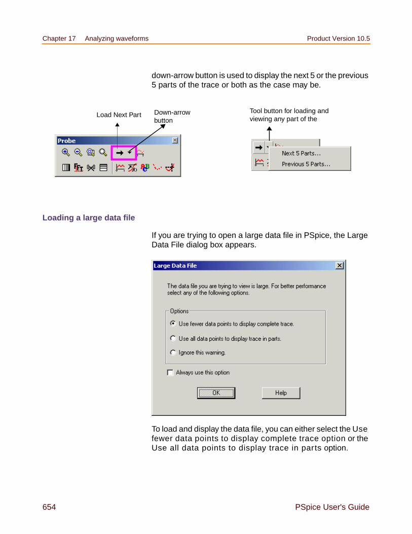
Chapter 17 Analyzing waveforms Product Version 10.5
654 PSpice User's Guide
down-arrow button is used to display the next 5 or the previous5 parts of the trace or both as the case may be.
Loading a large data file
If you are trying to open a large data file in PSpice, the LargeData File dialog box appears.
To load and display the data file, you can either select the Usefewer data points to display complete trace option or theUse all data points to display trace in parts option.
Load Next PartTool button for loading andviewing any part of the
Down-arrowbutton

Product Version 10.5 Chapter overview
PSpice User's Guide 655
To load the complete data file, select the Ignore this warningoption. When you select this option, the data file may or maynot get loaded depending on your system memory.
For example, on some machines a data file with 5 million datapoints may open without any problems while on some othermachine the same data file might be too large to be loaded inone go.
To make your selection the default setting, select the Alwaysuse this option check box. Once this check box is selected,next time when you try to open a large data file, the Large DataFile dialog box does not appear. Instead, the option selectedby you previously is used to open the large data file.
Switching Modes
While viewing the trace from a large data file, you can switchfrom one mode to another using one of the following methods.
Using the View drop-down menu
a. From the View menu in PSpice select Large DataFile Mode.
b. In the Large Data File Mode submenu, select themode in which you want to view the trace. The modecurrently selected, has a check mark against it.
Select Display Fewer Data Points when youwant to view the complete trace that may not bevery accurate.
Select Display in parts when you want to viewthe partial but an accurate representation of thetrace.
Using the toolbar

Chapter 17 Analyzing waveforms Product Version 10.5
656 PSpice User's Guide
a. To switch modes, select the Toggle Large DataFile Mode button in the Probe toolbar.
Changing threshold for large data file
By default, in PSpice any data file with more than 1 milliondata points is categorized as a large data (.dat) file. As auser you can modify this threshold by specifying a higher thenumber of data points in the Probe Settings dialog box.
Important
You cannot reduce the limit to lower than 1 milliondata points.
To increase the number of data points complete the followingsteps:
1 From the Tools menu is PSpice choose Options.
Note: This option is enabled only if a .dat or .sim fileis open in PSpice.
Toggle Large DataFile Mode

Product Version 10.5 Chapter overview
PSpice User's Guide 657
2 Select the Large Data File tab.
3 In the Data points in one part text box specify thedesired number of data points and click OK.
The changes you have made in the Probe Setting dialogbox, will be effective from the next session.
Caution
Any changes to the threshold for defining largedata file should be made keeping in account yoursystem memory so as to avoid failure in openingdata files. For example, on a machine low onsystem memory, a data file or a part of data filewith 2 million data points might fail to open. Onthe other hand, for a high-end machine a limit of3 million data points might work fine.

Chapter 17 Analyzing waveforms Product Version 10.5
658 PSpice User's Guide
Using simulation data from multiple files
You can load simulation data from multiple files into the sameProbe window by appending waveform data files.
When more than one waveform data file is loaded, you canadd traces using all loaded data, data from only one file, orindividual data sections from one or more files.
Appending waveform data files
To append a waveform data file
1 In PSpice, from the File menu, chooseAppend Waveform (.DAT).
2 Select a *.DAT file to append, and click OK.
3 If the file has multiple sections of data for the selectedanalysis type, the Available Sections dialog box appears.Do one of the following:
Click the sections you want to use.
Click the All button to use all sections.
4 Click OK.

Product Version 10.5 Chapter overview
PSpice User's Guide 659
Importing traces
Besides using the simulation data from .DAT files, you canalso import trace information stored in other file formats. UsingPSpice you can import the traces stored in a tabular format ina .txt file or a .csv file.
To import a trace
1 From the File drop-down menu choose Import.
2 In the Import File dialog box, select the text file to beimported in PSpice.
The Import Traces dialog box appears. All the nodeslisted in the source file are listed in the X-axis drop-downlist and the Available Nodes list.
3 In the Import Traces dialog box, specify the name and thelocation of the .DAT file in which the imported trace is tobe stored.
4 From the X-Axis drop-down list box, select the node nameto be plotted on the X-Axis.
5 Specify a name for the X-axis. Select one of the followingoptions for naming the X-axis.
a. Time
Traces in tabular format

Chapter 17 Analyzing waveforms Product Version 10.5
660 PSpice User's Guide
b. Frequency
c. Sweep Variable: When you select Sweep Variable,you need to specify the variable name in the enabledtext box.
6 From the Available Traces list box, select the traces thatare to be imported in PSpice.
7 Click Add.
8 The selected traces appear in the Import Trace list box. Toimport all the traces available in the source file, click theAdd All.
9 Select OK to import the selected trace(s) into thespecified data file.

Product Version 10.5 Chapter overview
PSpice User's Guide 661
Important
Renaming of X-axis is useful when you want toimport a trace and append it to an existing data filefor comparing traces. To be able to append twotraces successfully, you need to ensure that for boththe traces the range and the name of the variableplotted on the X-axis should be same.
Adding traces from specific loaded waveform data files
If two or more waveform data files have identical simulationoutput variables, trace expressions that include thosevariables generate traces for each file. However, you canspecify which waveform data file to use in the traceexpression. You can also determine which waveform data filewas used to generate a specific trace.
To add a trace from a specific loaded waveform data file
1 In PSpice, from the Trace menu, choose Add Trace todisplay the Add Traces dialog box.
The Simulation Output Variables list in the Add Tracesdialog box contains the output variables for all loadedwaveform data files.
2 In the Trace Expression text box, type an expressionusing the following syntax:
trace_expression@fn
where n is the numerical order (from left to right) of thewaveform data file as it appears in the PSpice title bar, or
trace_expression@s@fn
where s is a specific data section of a specific waveformdata file.
Example: To plot the V(1) output for data section 1 fromthe second data file loaded, type the following traceexpression:
V(1)@1@f2

Chapter 17 Analyzing waveforms Product Version 10.5
662 PSpice User's Guide
You can also use the name of the loaded data file tospecify it. For example, to plot the V(1) output for all datasections of a loaded data file, MYFILE.DAT, type thefollowing trace expression:
V(1)@"MYFILE.DAT"
3 Click OK.
To identify the source file for an individual trace
1 In the trace legend, double-click the symbol for the traceyou want to identify (Figure 17-4).
The Section Information dialog box appears, containingthe trace name and—if there is more than one waveformdata file loaded in the plot—the full path for the file fromwhich the trace was generated.
Also listed is information about the simulation thatgenerated the waveform data file and the number of datapoints used (Figure 17-5).
Figure 17-5 Section information message box.
Figure 17-4 Trace legendsymbols.
trace symbols

Product Version 10.5 Chapter overview
PSpice User's Guide 663
Saving simulation results in ASCII format
The default waveform data file format is binary. However, youcan save the waveform data file in the Common SimulationData Format (CSDF) instead.
Caution
Data files saved in the CSDF format are two ormore times the size of binary files.
When you first open a CSDF data file, PSpice converts it backto the .DAT format. This conversion takes two or more timesas long as opening a .DAT file. PSpice saves the new .DAT filefor future use.
To save simulation results in ASCII format
1 From PSpice’s Simulation menu, choose Edit Profile todisplay the Simulation Settings dialog box.
2 Click the Data Collection tab.
3 Select Save data in the CSDF format (.CSD).
4 Click OK.

Chapter 17 Analyzing waveforms Product Version 10.5
664 PSpice User's Guide
PSpice writes simulation results to the waveform data filein ASCII format (as *.CSD instead of *.DAT), following theCSDF convention.

Product Version 10.5 Chapter overview
PSpice User's Guide 665
Analog example
In this section, basic techniques for performing waveformanalysis are demonstrated using the analog circuitEXAMPLE.OPJ.
The example project EXAMPLE.OPJ is provided with yourinstalled programs. When shipped, EXAMPLE.OPJ is set upwith multiple analyses. For this example, the AC sweep, DCsweep, Monte Carlo/worst-case, and small-signal transferfunction analyses have been disabled. The specification foreach of these disabled analyses remains intact. To run themfrom Capture in the future, from the PSpice menu, choose EditSimulation Profile and enable the analyses.
Figure 17-6 Example schematic EXAMPLE.OPJ.
Running the simulation
The simulation is run with the Bias Point Detail, Temperature,and Transient analyses enabled. The temperature analysis isset to 35 degrees. The transient analysis is setup as follows:
Print Step 20nsFinal Time 1000nsEnable Fourier selected

Chapter 17 Analyzing waveforms Product Version 10.5
666 PSpice User's Guide
Center Frequency 1MegOutput Vars V(OUT2)
Note: When you run a Fourier analysis using PSpice asspecified in this example, PSpice writes the results tothe PSpice output file (*.OUT). You can also use Probewindows to display the Fourier transform of any traceexpression by using the FFT capability in PSpice. Tofind out more, refer to the online PSpice Help.
To start the simulation
1 From Capture’s File menu, point to Open and chooseProject.
2 Open the following project in your installation directory:
\TOOLS\PSPICE\CAPTURE_SAMPLES\ANASIM\EXAMPLE\EXAMPLE.OPJ
3 From the PSpice menu, choose Run to start thesimulation.
If PSpice is set to show traces for all markers on startup,you will see the V(OUT1) and V(OUT2) traces when theProbe window displays. To clear these traces from theplot, from the Trace menu, choose Delete All Traces.
PSpice generates a binary waveform data file containing theresults of the simulation. A new Probe window appears with

Product Version 10.5 Chapter overview
PSpice User's Guide 667
the waveform data file EXAMPLE.DAT already loaded(Figure 17-7).
Because this sample project was set up as a transientanalysis type, the data currently loaded are the results of thetransient analysis.
Note: In this sample, the voltage markers for OUT1 andOUT2 are already placed in the design. If the markersare not placed prior to simulating, you can display thewaveforms later, as explained below in Displayingvoltages on nets.
Displaying voltages on nets
After selected an analysis, voltages on nets and currents intodevice pins can be displayed in the Probe windows usingeither schematic markers or output variables (as will bedemonstrated in this example).
Figure 17-7 Waveform display for EXAMPLE.DAT.

Chapter 17 Analyzing waveforms Product Version 10.5
668 PSpice User's Guide
To display the voltages at the OUT1 and OUT2 nets usingoutput variables
1 From the Trace menu, choose Add Trace to display theAdd Traces dialog box.
The Simulation Output Variables frame displays a list ofvalid output variables.
2 Click V(OUT1) and V(OUT2), then click OK. The Probewindow should look similar to Figure 17-7.

Product Version 10.5 Chapter overview
PSpice User's Guide 669
Mixed analog/digital tutorial
In this tutorial, you will use PSpice A/D to simulate a simple,mixed analog/digital circuit. You will then analyze the outputby:
simultaneously displaying analog and digital traces alonga common time axis, and
displaying digital data values and features unique tomixed analog/digital circuit analysis, such asidentification of digital nets inserted by PSpice A/D.
About digital states
All digital states are supported in PSpice A/D. Logic levelsappear as shown below.
Nets with the Z strength (at any level) are displayed as a tripleline as shown below.
0 XFR1
displays and prints reddisplays and prints yellow
Zdisplays and prints blue

Chapter 17 Analyzing waveforms Product Version 10.5
670 PSpice User's Guide
About the oscillator circuit
The circuit you will simulate and analyze is a mixedanalog/digital oscillator using Schmitt trigger inverters, anopen-collector output inverter, a standard inverter, a JKflip-flop, a resistor, and a capacitor. The design is shown inFigure 17-8.
The circuit uses a one-bit digital stimulus device, DSTIM1. Thedevice is connected to the rest of the circuit by a single pin andcreates a reset pulse, which resets the flip-flop.
Setting up the design
Set up and simulate the oscillator circuit using Capture.
To open the design file
1 From Capture’s File menu, point to Open and chooseProject.
2 Open the following project in your OrCAD installationdirectory:
\TOOLS\PSPICE\CAPTURE_SAMPLES\MIXSIM\OSC\OSC.OPJ
To clear markers
1 From Capture’s PSpice menu, point to Markers andchoose Delete All.
Figure 17-8 Mixed analog/digital oscillator

Product Version 10.5 Chapter overview
PSpice User's Guide 671
Running the simulation
To run the simulation
1 From Capture’s PSpice menu, choose Edit SimulationProfile and set the Run To Time to 5us.
2 From Capture’s PSpice menu, choose Run.
Because the oscillator circuit used here has been run withonly a transient analysis, PSpice automatically selectsthe transient analysis data section from the waveformdata file. This means that the Available Selection dialogbox is skipped and a Probe window appears immediately.
Analyzing simulation results
To view the clock input to the inverter
1 From PSpice’s Trace menu, choose Add Trace to displaythe Add Traces dialog box.
2 In the Simulation Output Variables list, click V(U3A:A) toplot the input voltage to the inverter.
3 Click OK.
To add a second y-axis to avoid analog trace overlap
1 From the Plot menu, choose Axis Settings to display theAxis Settings dialog box.
The X Axis tab is active by default.
Note: You can also open the X Axis tab in the AxisSettings dialog box by double-clicking the x-axis in theProbe window.

Chapter 17 Analyzing waveforms Product Version 10.5
672 PSpice User's Guide
a. In the Data Range frame, choose User Defined andset the range from 0us to 5us, if this is not alreadyset.
b. In the Scale frame, select Linear, if this is not alreadyset.
2 Click the Y Axis tab.
Note: You can also open the Y Axis tab in the AxisSettings dialog box by double-clicking the y-axis in theProbe window.
a. In the Data Range frame, choose User Defined andset the range from -5 to 5. This will change the rangefor the current y-axis.
b. Click OK.
Note: In the Y Axis Settings dialog box, you can changethe settings for another y-axis by selecting it from the YAxis Number box.
3 From the Plot menu, choose Add Y Axis.
The Probe window display should now look likeFigure 17-9 below.
Figure 17-9 Voltage at inverter input with y-axis

Product Version 10.5 Chapter overview
PSpice User's Guide 673
Note that the V(U3A:A) label at the bottom of the plot ispreceded by a boxed 1. This indicates that the far-left y-axisapplies to the V(U3A:A) waveform.
To view traces for V(CLK), RESET, and OUT
1 From the Trace menu, choose Add Trace to display theAdd Traces dialog box.
2 In the Simulation Output Variables list, click V(U1A:CLK),RESET, and OUT.
The trace names appear in the Trace Expression text box.
Note: You can add up to 75 digital traces to the digitalportion of the plot. If you add more traces than can bedisplayed, PSpice A/D scrolls the traces upwards so youcan see the last trace added. A + character in front ofthe highest or lowest trace name indicates that there aremore traces above or below the marked traces.
3 Click OK to plot the traces.
The plot displays a digital area above the analog area asshown in Figure 17-10 below.
Figure 17-10 Mixed analog/digital oscillator results.

Chapter 17 Analyzing waveforms Product Version 10.5
674 PSpice User's Guide
User interface features for waveform analysis
PSpice provides direct manipulation techniques and shortcutsfor analyzing waveform data. These techniques are describedbelow.
Many of the menu commands in PSpice have equivalentkeyboard shortcuts. For instance, after placing a selectionrectangle in the analog portion of the plot, you can type Ctrl+Ainstead of choosing Area from the View menu. For a list ofshortcut keys, see the online PSpice Help.
Zoom regions
PSpice provides a direct manipulation method for marking thezoom region in either the digital or the analog area of the plot.
To zoom in or out
1 Do one of the following on the toolbar:
Click the View In toolbar button to zoom in by afactor of 2 around the point you specify.
Click the View Out toolbar button to zoom out bya factor of 2 around the point you specify.
To zoom in the digital area using the mouse
1 In the digital area, drag the mouse pointer left or right toproduce two vertical bars.
Note: Click the mouse anywhere on the plot to removethe vertical bars without zooming.
zoom bars (digital)

Product Version 10.5 Chapter overview
PSpice User's Guide 675
2 From the View menu, point to Zoom, then choose Area.
PSpice changes the plot display to the area in betweenthe selection bars. If the plot includes an analog area, it iszoomed in as well.
To zoom in the analog area using the mouse
1 Drag the mouse pointer to make a selection rectangle asshown below.
Note: Click anywhere on the plot to remove the selectionrectangle without zooming.
2 From the View menu, point to Zoom, then choose Area.
PSpice changes the plot to display the region within theselection rectangle. The digital portion of the display, ifpresent, is also zoomed.
selection rectangle (analog)

Chapter 17 Analyzing waveforms Product Version 10.5
676 PSpice User's Guide
Scrolling traces
By default, when a plot is zoomed or when a digital plotcontains more traces than can be displayed in the visible area,standard scroll bars appear to the right or at the bottom of theplot area as necessary. These can be used to pan through thedata. You can configure scroll bars so they are always presentor are never displayed.
To configure scroll bars
1 In PSpice, from the Tools menu, choose Options.
2 In the Use Scroll Bars frame, choose one of the scrollbars options, as described below.
Sizing digital plots
Sizing bars can be used to change the digital plot size insteadof choosing Digital Size from the Plot menu. The digital tracename sizing bar is at the left vertical boundary of the digitalplot. If an analog plot area is displayed simultaneously with thedigital plot, there is an additional plot sizing bar at the bottomhorizontal boundary of the digital plot.
Choose thisoption...
To do this...
Auto Have scroll bars appear when a plot iszoomed or when additional traces aredisplayed in the plot but are not visible(default).
Never Never display scroll bars. This modeprovides maximum plot size and is usefulon VGA and other low resolution displays.
Always Display scroll bars at all times. However,they are disabled if the corresponding axisis full scale.

Product Version 10.5 Chapter overview
PSpice User's Guide 677
To set the digital plot size using the mouse
1 Display at least one digital trace and one analog trace inthe Probe window for which you want to set the digitalsize.
2 To change the bottom position of the digital Probewindow, do the following:
a. Place the mouse pointer between the analog anddigital parts of the plot.
b. Click the plot separator.
c. Drag the plot separator until you have the digital sizeyou want.
3 To change the left side of the digital Probe window, do thefollowing:
a. Place the mouse pointer at the left edge of the digitalProbe window you want to resize.
b. Click the left edge.
c. Drag the left edge of the digital Probe window toadjust the space available for displaying digital tracenames.
To set the digital plot size using menu options
1 Display at least one digital trace in the plot for which youwant to set the digital size.
2 From the Plot menu, choose Digital Size.
3 In the Digital Size dialog box, set the following:
Percentage of Plot to be Digital
Length of Digital Trace Name
4 Click OK.

Chapter 17 Analyzing waveforms Product Version 10.5
678 PSpice User's Guide
Modifying trace expressions and labels
You can modify trace expressions, text labels, and ellipselabels that are currently displayed within the Probe window,thus eliminating the need to delete and recreate any of theseobjects.
1 To place a label, click Plot, point to Label and then choosethe desired type of object you want to place.
For information about adding labels (including text, line,poly-line, arrow, box, circle, ellipse, and mark), refer to theonline PSpice Help.
To modify trace expressions
1 Click the trace name to select it (selection is indicated bya color change).
2 From the Edit menu, choose Modify Object.
Note: You can also double-click the trace name to modifythe trace expression.
3 In the Modify Trace dialog box, edit the trace expressionjust as you would when adding a trace.
For more information on adding traces, see Adding tracesfrom specific loaded waveform data files on page 661 andTo add traces using output variables on page 690.
To modify text and ellipse labels
1 Click the text or ellipse to select it (selection is indicatedby a color change).
2 From the Edit menu, choose Modify Object.
Note: You can also double-click a text or ellipse label tomodify it.
3 Edit the label by doing one of the following:
In the Ellipse Label dialog box, change the inclinationangle.

Product Version 10.5 Chapter overview
PSpice User's Guide 679
In the Text Label dialog box, change the text label.
Moving and copying trace names and expressions
Trace names and expressions can be selected and moved orcopied, either within the same Probe window or to anotherProbe window.
To copy or move trace names and expressions
1 Click one or more (Shift+click) trace names. Selectedtrace names are highlighted.
2 From the Edit menu, choose Copy or Cut to save the tracenames and expressions to the clipboard. Cut removestrace names and traces from the Probe window.
3 In the Probe window where traces are to be added, doone of the following:
To add trace names to the end of the currentlydisplayed set, choose Paste from the Edit menu.
To add traces before a currently displayed tracename, select the trace name and then choose Pastefrom the Edit menu.
4 Click OK.
Tip
When adding a trace to a Probe window, you canmake the trace display name different from the traceexpression:
a. From the Trace menu, choose Add Trace.
b. In the Trace Expression text box, enter a traceexpression using the syntax:
trace_expression[;display_name]
Here are some considerations when copying or moving tracenames and expressions into a different Probe window:

Chapter 17 Analyzing waveforms Product Version 10.5
680 PSpice User's Guide
If the new Probe window is reading the same waveformdata file, the copied or moved trace names andexpressions display traces that are identical to theoriginal selection set.
If the new Probe window is reading a different waveformdata file, the copied or moved names and expressionsdisplay different traces generated from the new data.
For example, suppose two waveform data files,MYSIM.DAT and YOURSIM.DAT each contain a V(2)waveform. Suppose also that two Probe windows arecurrently displayed where window A is loaded withMYSIM.DAT, and window B is loaded with YOURSIM.DAT.
When V(2) is copied from window A to window B, thetrace looks different because it is determined by datafrom YOURSIM.DAT instead of MYSIM.DAT.
Copying and moving labels
Labels can be selected and moved or copied, either within thesame Probe window or to another Probe window.
For information about adding labels (including text, line,poly-line, arrow, box, circle, ellipse, and mark), refer to theonline PSpice Help.
To copy labels
1 Select one or more (Shift+click) labels, or select multiplelabels by drawing a selection rectangle. Selected labelsare highlighted.
2 From the Edit menu, choose Copy or Cut to save thelabels to the clipboard.
Cut removes labels from the Probe window.
3 Switch to the Probe window where labels are to beadded, and from the Edit menu, choose Paste.
4 Click on the new location to place the labels.

Product Version 10.5 Chapter overview
PSpice User's Guide 681
To move labels
1 Select one or more (Shift+click) labels, or select multiplelabels by drawing a selection rectangle. Selected labelsare highlighted.
2 Move the labels by dragging them to a new location.
Tabulating trace data values
You can generate a table of data points reflecting one or moretraces in the Probe window and use this information in adocument or spreadsheet.
To view the trace data values table
1 Select one or more (Shift+click) trace names. Selectedtrace names are highlighted.
2 From the Edit menu, choose Copy or Cut to save the tracedata point values to the Clipboard.
Cut removes traces from the Probe window.
3 In Clipboard Viewer, from the Display menu, chooseeither Text or OEM Text.
To export the data points to other applications
1 Select one or more (Shift+click) trace names. Selectedtrace names are highlighted.
2 From the Edit menu, choose Copy or Cut to save the tracedata point values to the Clipboard.
Cut removes traces from the Probe window.
3 Paste the data from the Clipboard into a text editor, aspreadsheet program, or a technical computing program(such as Mathcad).
4 Save the file.
Note: Saving the data directly to a file from Clipboard Viewercan create superfluous data at the beginning of the file.

Chapter 17 Analyzing waveforms Product Version 10.5
682 PSpice User's Guide
Using cursors
When one or more traces are displayed, you can use cursorsto display the exact coordinates of two points on the sametrace, or points on two different traces. In addition, differencesare shown between the corresponding coordinate values forthe two cursors.
Displaying cursors
To display both cursors
1 From the Trace menu, point to Cursor, then chooseDisplay.
The Probe Cursor window appears, showing the currentposition of the cursor on the x-axis and y-axis. As youmove the cursors, the values in the cursor box change.You can move the cursor box anywhere over the Probewindow by dragging the box to another location.
In the analog area of the plot (if any), both cursors areinitially placed on the trace listed first in the trace legend.The corresponding trace symbol is outlined with a dashedline.
In the digital area of the plot (if any), both cursors areinitially placed on the trace named first along the y-axis.The corresponding trace name is outlined with a dashedline.
Moving cursors
To move cursors along a trace using menu commands
1 From the Trace menu, point to Cursor, then choose Peak,Trough, Slope, Min, Max, Point, or Search.
For more information about the cursor commands, refer to theonline PSpice Help.

Product Version 10.5 Chapter overview
PSpice User's Guide 683
To move cursors along a trace using the mouse
1 Use the right and left mouse buttons as described inTable 17-8 below.
Note: For a family of curves (such as from a nested DCsweep), you can use the mouse or the arrow keys tomove the cursor to one of the other curves in the family.You can also click the desired curve.
To move cursors along a trace using the keyboard
1 Use key combinations as described in Table 17-9 below.
Table 17-8 Mouse actions for cursor control
Click this... To do this with the cursors...
cursor assignment
Left-click the analog tracesymbol or digital tracename.
Associate the first cursor withthe selected trace.
Right-click the analogtrace symbol or digitaltrace name.
Associate the second cursorwith the selected trace.
cursor movement
Left-click in the displayarea.
Move the first cursor to theclosest trace segment at theX position.
Right-click in the displayarea.
Move the second cursor to theclosest trace segment at theX position.
Table 17-9 Key combinations for cursor control
Us this keycombination...
To do this with the cursors...
Ctrl+Left arrow key andCtrl+Right arrow key
Change the trace associatedwith the first cursor.

Chapter 17 Analyzing waveforms Product Version 10.5
684 PSpice User's Guide
Applying cursors to a different trace
If you want to apply the cursors to a different trace, click thetrace symbol in the plot legend for the trace you want tochange to.
If you are displaying a large number of traces, and the symbolis not shown for the trace you want to apply the cursors to, youcan apply the cursors to that trace in one of the following ways:
To apply the cursors to a different trace
1 Click in the cursor box to freeze the cursor locations onthe current trace.
2 After freezing the cursor locations, right-click on the newtrace you want to apply the cursors to.
- or -
Shift+Ctrl+Left arrow keyand Shift+Ctrl+Rightarrow key
Change the trace associatedwith the second cursor.
Left arrow key and Rightarrow key
Move the first cursor along thetrace.
Shift+Left arrow key andShift+Right arrow key
Move the second cursor alongthe trace.
Home Move the first cursor to thebeginning of the trace.
Shift+Home Move the second cursor to thebeginning of the trace.
End Move the first cursor to the endof the trace.
Shift+End Move the second cursor to theend of the trace.
Table 17-9 Key combinations for cursor control,
Us this keycombination...
To do this with the cursors...

Product Version 10.5 Chapter overview
PSpice User's Guide 685
1 From the Trace menu, choose Cursor, then chooseFreeze to freeze the cursor locations on the curren trace.
2 After freezing the cursor locations, right-click on the newtrace you want to apply the cursors to.
- or -
1 Press and hold the Shift key while right-clicking on thenew trace you want to apply the cursors to.
For more information about the cursor commands, refer to theonline PSpice Help.
Example: using cursors
Figure 17-11 shows both cursors positioned on the Out signalin the digital area of a plot, and both cursors on the V(1)waveform in the analog area of the plot.
Cursor 1 is positioned on the first trough (dip) of the V(1)waveform. Cursor 2 is positioned on the second peak of thesame waveform.
Note: To position a cursor on the next trough of a waveform,from the Trace menu, point to Cursor, then chooseTrough. To position a cursor on the next peak of a
Figure 17-11 Cursors positioned on a trough and peak ofV(1)
cursor 1
cursor 2results
results
analogwaveformw/cursors
digitalsignalw/cursors

Chapter 17 Analyzing waveforms Product Version 10.5
686 PSpice User's Guide
waveform, from the Trace menu, point to Cursor, thenchoose Peak.
In the Probe Cursor window, cursor 1 and cursor 2coordinates are displayed (A1 and A2, respectively) with theirdifference shown in the bottom line (dif). The logic state of theOut signal is also displayed to the right of the cursorcoordinates.
The mouse buttons are also used to associate each cursorwith a different trace by clicking appropriately on either theanalog trace symbol in the legend or on the digital trace name(see Table 17-8 on page 683). These are outlined in thepattern corresponding to the associated cursor’s crosshairpattern. Given the example in Figure 17-11, right-clicking theV(2) symbol will associate cursor 2 with the V(2) waveform.The analog legend now appears as shown below.
The Probe Cursor window also updates the A2 coordinates toreflect the X and Y values corresponding to the V(2)waveform.
For more information about cursors, refer to the online PSpiceHelp.
cursor 1 cursor 2

Product Version 10.5 Chapter overview
PSpice User's Guide 687
Tracking digital simulation messages
PSpice A/D provides explanatory messages for errors thatoccur during a digital simulation with their correspondingwaveforms. You can view messages from:
the Simulation Message Summary dialog box, or
the waveform display.
See Simulation condition messages on page 571 forinformation on the message types that can be displayed byPSpice A/D.
Message tracking from the message summary
A message summary is available for simulations wherediagnostics have been logged to the waveform data file. Youcan display the message summary:
When loading a waveform data file (click OK when theSimulation Errors dialog box appears).
Anytime by choosing Simulation Messages from the Viewmenu.
The Simulation Message Summary dialog box
The Simulation Message Summary dialog box lists messageheader information.
You can filter the messages displayed in the list by selecting aseverity level from the Minimum Severity Level drop-downmenu. Messages are categorized (in decreasing order of
Chapter 17 Analyzing waveforms Product Version 10.5
688 PSpice User's Guide
severity) as FATAL, SERIOUS, WARNING, or INFO(informational).
When you select a severity level, the Message Summarydisplays only those messages with the chosen severity orhigher. By default, the minimum severity level displayed isSERIOUS.
Example: If you select WARNING as the minimum severitylevel, the Simulation Message Summary dialog box willdisplay WARNING, SERIOUS, and FATAL messages.
To display waveforms associated with messages
1 In the Simulation Message Summary dialog box,double-click a message.
For most message conditions, a Probe window appearsthat contains the waveforms associated with thesimulation condition, along with detailed message text.
Persistent hazards
If a PERSISTENT HAZARD message is displayed, two plotsappear (see Figure 17-12), containing the following:
the waveforms that initially caused the timing violation orhazard (lower plot)

Product Version 10.5 Trace expressions
PSpice User's Guide 689
the primary outputs or internal state devices to which thecondition has propagated (upper plot)
Message tracking from the waveform
Trace segments with associated diagnostics are displayed inthe foreground color specified in your PSPICE.INI file. Thiscolor is different from those used for standard state transitions.
To display explanatory message text
1 Double-click within the tagged region of a trace.
Trace expressions
Traces are referred to by output variable names. Outputvariables are similar to the PSpice output variables specifiedin the Simulation Settings dialog box for noise, Monte Carlo,worst-case, transfer function, and Fourier analyses. However,there are additional alias forms that are valid for traceexpressions. Both forms are discussed here.
Figure 17-12 Waveform display for a persistent hazard.
Chapter 17 Analyzing waveforms Product Version 10.5
690 PSpice User's Guide
To add traces using output variables
1 From the Trace menu, choose Add Trace to display theAdd Traces dialog box.
2 Construct a trace expression using any combination ofthese controls:
In the Simulation Output Variables frame, click outputvariables.
You can display a subset of the available simulationoutput variables by selecting or clearing the variabletype check boxes in the Simulation Output Variablesframe. Variable types not generated by the circuitsimulation are dimmed.
In the Functions or Macros frame, select operators,functions, constants, or macros.
In the Trace Expression text box, type in or editoutput variables, operators, functions, constants, ormacros.
For more information about trace expressions, seeAnalog trace expressions on page 700 and Digitaltrace expressions on page 703.
3 If you want to change the name of the trace expression asit displays in the Probe window, use the following syntax:
trace expression;display name
4 Click OK.
Basic output variable form
This form is representative of those used for specifying somePSpice analyses.

Product Version 10.5 Trace expressions
PSpice User's Guide 691
<output>[AC suffix](<name>[,name])
Table 17-10
This placeholder... Means this...
<output> type of output quantity: V for voltageor I for current (digital values do notrequire a prefix)
[AC suffix]* quantity to be reported for an ACanalysis. For a list of valid ACsuffixes, see Table 17-14 onpage 695
<name>[,name] specifies either the net or(+ net, - net) pair for which thevoltage is to be reported, or thedevice for which a current isreported, where:
net specifies either the net orpin id (<fully qualified devicename>:<pin name>)
device name specifies the fullyqualified device name; for a listof device types, see Table 17-15on page 697 and Table 17-16on page 697
A fully qualified device nameconsists of the full hierarchical pathfollowed by the device’s referencedesignator. For information aboutthe syntax for voltage outputvariables, see Voltage on page 376.

Chapter 17 Analyzing waveforms Product Version 10.5
692 PSpice User's Guide
Output variable form for device terminals
This form can only be specified for trace expressions. Theprimary difference between this and the basic form is that theterminal symbol appears before the net or device namespecification (whereas the basic form treats this as the pinname within the pin id).
<output>[terminal]*[AC suffix](<name>[,name])
Table 17-12 on page 693 summarizes the valid outputformats. Table 17-13 on page 695 provides examples of
Table 17-11
Thisplaceholder...
Means this...
<output> type of output quantity: V for voltage, Ifor current, or N for noise (digital valuesdo not require a prefix)
[terminal]* one or more terminals for devices withmore than two terminals; for a list ofterminal IDs, see Table 17-16 onpage 697
[AC suffix]* quantity to be reported for an ACanalysis; for a list of valid AC suffixes,see Table 17-14 on page 695
<name>[,<name>])
net, net pair, or fully qualified devicename; for a list of device types, seeTable 17-15 on page 697 andTable 17-16 on page 697

Product Version 10.5 Trace expressions
PSpice User's Guide 693
equivalent output variables. Note that some of the outputvariable formats are unique to trace expressions.
Table 17-12 Output variable formats
Format Meaning
Voltage variables
V[ac](< +analog net > [,< -analog net>])
Voltage between +and - analog netids
V<pin name>[ac](< device >) Voltage at pinname of a device
V< x >[ac](< 3 or 4-terminal device>)
Voltage atnon-groundedterminal x of a3 or 4-terminaldevice
V< z >[ac](< transmission linedevice >)
Voltage at end z ofa transmissionline device (z iseither A or B)
Current variables
I[ac](< device >) Current into adevice
I< x >[ac](< 3 or 4-terminal device >) Current intoterminal x of a3 or 4-terminaldevice
I< z >[ac](< transmission line device>)
Current into end zof a transmissionline device (z iseither A or B)
Digital signal and bus variables
< digital net >[;< display name >] Digital state atdigital net labeledas display name

Chapter 17 Analyzing waveforms Product Version 10.5
694 PSpice User's Guide
< digital net >*[;< display name >][;< radix >]
Digital bus labeledas display nameand of specifiedradix
Sweep variables
< DC sweep variable > name of anyvariable used inthe DC sweepanalysis
FREQUENCY AC analysis sweepvariable
TIME transient analysissweep variable
Noise variables
V[db](ONOISE) totalRMS-summednoise at output net
V[db](INOISE) total equivalentnoise at inputsource
NTOT(ONOISE) sum of all noisecontributors in thecircuit
N< noise type >(< device name >) contribution fromnoise type ofdevice name tothe total outputnoise1
1. See Table 17-17 on page 698 for a complete list of noise typesby device type. For information about noise output variableequations, the units used to represent noise quantities in traceexpressions, and a noise analysis example, see AnalyzingNoise in the Probe window on page 452.
Table 17-12 Output variable formats, continued
Format Meaning

Product Version 10.5 Trace expressions
PSpice User's Guide 695
Table 17-13 Examples of output variable formats
A basic form An aliasequivalent
Meaning
V(NET3,NET2) (same) voltage between analog netslabeled NET3 and NET2
V(C1:1) V1(C1) voltage at pin1 of capacitorC1
VP(Q2:B) VBP(Q2) phase of voltage at base ofbipolar transistor Q2
V(T32:A) VA(T32) voltage at port A oftransmission line T32
I(M1:D) ID(M1) current through drain ofMOSFET device M1
QA (same) digital state at net QA
IN1, IN2, IN3;MYBUS;X
(same) digital bus made of 3 digitalnets (IN1, IN2, IN3) namedMYBUS displayed inhexadecimal
VIN (same) voltage source named VIN
FREQUENCY (same) AC analysis sweep variable
NFID(M1) (same) flicker noise from MOSFETM1
Table 17-14 Output variable AC suffixes
Suffix Meaning of output variables
none magnitude
DB magnitude in decibels
G group delay (-dPHASE/dFREQUENCY)
I imaginary part
M magnitude
P phase in degrees

Chapter 17 Analyzing waveforms Product Version 10.5
696 PSpice User's Guide
R real part
Table 17-14 Output variable AC suffixes
Suffix Meaning of output variables

Product Version 10.5 Trace expressions
PSpice User's Guide 697
Table 17-15 Device names for two-terminal device types
Two-terminal device type1
1. The pin name for two-terminal devices is either 1 or 2.
Device type letter
capacitor C
diode D
voltage-controlled voltage source2
2. The controlling inputs for these devices are not consideredterminals.
E
current-controlled current source2 F
voltage-controlled current source2 G
current-controlled voltage source2 H
independent current source I
inductor L
resistor R
voltage-controlled switch2 S
independent voltage source V
current-controlled switch2 W
Table 17-16 Terminal IDs by three & four-terminal devicetype
Three & four-terminaldevice type
Device typeletter
Terminal IDs
GaAs MOSFET B D (drain)
G (gate)
S (source)
Junction FET J D (drain)
G (gate)
S (source)

Chapter 17 Analyzing waveforms Product Version 10.5
698 PSpice User's Guide
MOSFET M D (drain)
G (gate)
S (source)
B (bulk, substrate)
Bipolar transistor Q C (collector)
B (base)
E (emitter)
S (substrate)
transmission line T A (near side)
B (far side)
IGBT Z C (collector)
G (gate)
E (emitter)
Table 17-16 Terminal IDs by three & four-terminal devicetype
Three & four-terminaldevice type
Device typeletter
Terminal IDs
Table 17-17 Noise types by device type
Device type Noisetypes1
Meaning
B (GaAsFET) FIDRDRGRSSIDTOT
flicker noisethermal noise associated with RDthermal noise associated with RGthermal noise associated with RSshot noisetotal noise
D (diode) FIDRSSIDTOT
flicker noisethermal noise associated with RSshot noisetotal noise

Product Version 10.5 Trace expressions
PSpice User's Guide 699
Digital Input RHIRLOTOT
thermal noise associated with RHIthermal noise associated with RLOtotal noise
Digital Output TOT total noise
J (JFET) FIDRDRGRSSIDTOT
flicker noisethermal noise associated with RDthermal noise associated with RGthermal noise associated with RSshot noisetotal noise
M (MOSFET) FIDRBRDRGRSSIDTOT
flicker noisethermal noise associated with RBthermal noise associated with RDthermal noise associated with RGthermal noise associated with RSshot noisetotal noise
Q (BJT) FIBRBRCRESIBSICTOT
flicker noisethermal noise associated with RBthermal noise associated with RCthermal noise associated with REshot noise associated with base currentshot noise associated with collector currenttotal noise
R (resistor) TOT total noise
Iswitch TOT total noise
Vswitch TOT total noise
1. These variables report the contribution of the specified device’s noise to the total output noise inunits of V2/Hz. This means that the sum of all device noise contributions is equal to the total outputnoise in V2/Hz, NTOT(ONOISE).
Table 17-17 Noise types by device type

Chapter 17 Analyzing waveforms Product Version 10.5
700 PSpice User's Guide
Analog trace expressions
Trace expression aliases
Analog trace expressions vary from the output variables usedin simulation analyses because analog net values can bespecified by:
<output variable>[;display name]
as opposed to the <output variable> format used inanalyses. With this format, the analog trace expression can bedisplayed in the analog legend with an optional alias.
Arithmetic functions
Arithmetic expressions of analog output variables use thesame operators as those used in simulation analyses (bymeans of part property definitions in Capture). You can alsoinclude intrinsic functions in expressions. The intrinsicfunctions available for trace expressions are similar to thoseavailable for PSpice math expressions, but with somedifferences, as shown in Table 17-18. A complete list ofPSpice arithmetic functions can be found in Table 3-4 onpage 126.
Table 17-18 Analog arithmetic functions for traceexpressions
Probefunction
Description Available inPSpice?
ABS(x) |x| YES
SGN(x) +1 (if x>0), 0 (if x=0), -1 (ifx<0)
YES
SQRT(x) x1/2 YES
EXP(x) ex YES
LOG(x) ln(x) YES
LOG10(x) log(x) YES
M(x) magnitude of x YES

Product Version 10.5 Trace expressions
PSpice User's Guide 701
P(x) phase of x (degrees) YES
R(x) real part of x YES
IMG(x) imaginary part of x YES
G(x) group delay of x (seconds) NO
PWR(x,y) |x|y YES
SIN(x) sin(x) YES
COS(x) cos(x) YES
TAN(x) tan(x) YES
ATAN(x)ARCTAN(x)
tan-1 (x) YES
d(x) derivative of x with respect tothe x-axis variable
YES1
s(x) integral of x over the range ofthe x-axis variable
YES2
AVG(x) running average of x over therange of the x-axis variable
NO
AVGX(x,d) running average of x fromX_axis_value(x)-d toX_axis_value(x)
NO
RMS(x) running RMS average of xover the range of the x-axisvariable
NO
DB(x) magnitude in decibels of x NO
MIN(x) minimum of the real part of x NO
MAX(x) maximum of the real part of x NO
Table 17-18 Analog arithmetic functions for traceexpressions, continued
Probefunction
Description Available inPSpice?

Chapter 17 Analyzing waveforms Product Version 10.5
702 PSpice User's Guide
Note: For AC analysis, PSpice uses complex arithmetic toevaluate trace expressions. If the result of theexpression is complex, then its magnitude is displayed.
Rules for numeric values suffixes
Explicit numeric values are entered in trace expressions in thesame form as in simulation analyses (by means of partproperties in Capture), with the following exceptions:
Suffixes M and MEG are replaced with m (milli, 1E-3) andM (mega, 1E+6), respectively.
MIL and mil are not supported.
With the exception of the m and M scale suffixes, PSpiceis not case sensitive; therefore, upper and lower casecharacters are equivalent.
Example: V(5) and v(5) are equivalent in traceexpressions.
Unit suffixes are only used to label the axis; they never affectthe numerical results. Therefore, it is always safe to leave offa unit suffix.
ENVMIN(x,d)
Envelope of x.Valley lowsselected have a minimumnumber of d consecutivedatapoints.
NO
ENVMAX(x,d)
Envelope of x. Peaksselected have a minimumnumber of d consecutivedatapoints.
NO
1. In PSpice, this function is called DDT(x).
2. In PSpice, this function is called SDT(x).
Table 17-18 Analog arithmetic functions for traceexpressions, continued
Probefunction
Description Available inPSpice?

Product Version 10.5 Trace expressions
PSpice User's Guide 703
Example: The quantities 2e-3, 2mV, and .002v all have thesame numerical value. For axis labeling purposes, PSpicerecognizes that the second and third forms are in volts,whereas the first is dimensionless.
PSpice also knows that W=V·A, V=W/A, and A=W/V. So, if youadd this trace:
V(5)*ID(M13)
the axis values are labeled with W.
For a demonstration of analog trace presentation, see Analogexample on page 665
The units to use for trace expressions are shown in Table17-19.
Digital trace expressions
Digital output variables in trace expressions vary from thoseused in simulation analyses as follows:
Digital net values are specified by:
<digital net>[;display name]
as opposed to the <digital net> format used foranalyses. With this format, the digital signal can bedisplayed on the digital plot with an optional alias.
Table 17-19 Output units for trace expressions
Symbol Unit
V volt
A amps
W watt
d degree (of phase)
s second
Hz hertz

Chapter 17 Analyzing waveforms Product Version 10.5
704 PSpice User's Guide
The output from several digital nets can be collected intoa single output of higher radix known as a bus.
Example: You can request that four bus lines be displayedtogether as one hexadecimal digit. You can combine upto 32 digital signals into a bus.
A bus is formed by enclosing a list of digital net names(separated by blanks or commas) within bracesaccording to the format:
The elements of the bus definition, taken left to right,specify the output values of the bus from high order to loworder.
Example: Q2, Q1, Q0 specifies a 3-bit bus whosehigh-order bit is the digital value at net Q2.
By definition, a digital signal is any digital net value or alogical expression involving digital nets. For the digital outputvariable formats described earlier, you can use a digital signalexpression everywhere a net name is expected. You can alsoform buses into expressions using both logical and arithmeticoperators.
As a result, the generalized form for defining a digital trace is:
<digital trace expression> [;display name [;radix]]
Exception: You can display your radix designation option withthe digital trace expression by leaving the display name blankand using the following syntax:
digital trace expression;;radix
<high-order net> [mid-order net]* <low-ordernet>
Table 17-20
Thisplaceholder...
Means this...
digital traceexpression
expression of digital buses ordigital signals.

Product Version 10.5 Trace expressions
PSpice User's Guide 705
Table 17-21 presents the operators available for digital signaland bus expressions listed in order of precedence (high tolow).
display name name that will be displayed on thescreen; if no display name isspecified, the actual traceexpression is used; if a displayname is given, it is available foruse in subsequent tracedefinitions.
radix applies only to bus expressionsand denotes the radix in whichthe bus value is to be displayed;the radix is specified as:
H or X hexadecimal (default)D decimalO octalB binary
Table 17-21 Digital logical and arithmetic operators
Operator Meaning
() grouping
~ logical complement
* multiplication (bus values only)
/ division (bus values only)
+ addition (bus values only)
- subtraction (bus values only)
& and
^ exclusive or
| or
Table 17-20
Thisplaceholder...
Means this...

Chapter 17 Analyzing waveforms Product Version 10.5
706 PSpice User's Guide
An arithmetic or logical operation between two bus operandsresults in a bus value that is as wide as is necessary to containthe result. Prior to the operation, if necessary, the shorteroperand is extended to the width of the longer operand byzero-filling on the high-order end.
An arithmetic or logical operation between a bus operand anda signal operand results in a bus value. Prior to the operation,the signal is converted to a bus of width one, then extended ifnecessary.
You can use signal constants in signal expressions. Specifythem as shown in Table 17-22.
You can use bus constants in bus expressions. Specify themas strings of the form:
Table 17-22 Signal constants for digital traceexpressions
SignalConstant
Meaning
’0 low
’1 high
’F falling
’R rising
’X unknown
’Z high impedance

Product Version 10.5 Trace expressions
PSpice User's Guide 707
r'ddd
For a procedural discussion of digital trace expressions, seeAnalyzing results on page 563 in the Digital simulationchapter.
For a discussion and demonstration of digital tracepresentation, complete the Mixed analog/digital tutorial onpage 669.
Table 17-23
Thisplaceholder...
Means this...
r case-insensitive radix specifier (x,h, d, o, or b)
ddd string of digits appropriate to thespecified radix
Table 17-24 Example notations for bus constants:
This notation... Has this radix...
x'3FFFF hexadecimal
h'5a hexadecimal
d'79 decimal
o'177400 octal
b'100110 binary

Chapter 17 Analyzing waveforms Product Version 10.5
708 PSpice User's Guide

PSpice User's Guide 709
18
Measurement expressions
Chapter overview
This chapter describes how to put together measurementexpressions using the measurement definitions included withPSpice. The Power Users section includes instructions onhow to compose your own measurement definitions.
Measurements overview on page 710
Measurement strategy on page 711
Procedure for creating measurement expressions onpage 712
Example on page 714
For power users on page 721

Chapter 18 Measurement expressions Product Version 10.5
710 PSpice User's Guide
Measurements overview
Measurement expressions evaluate the characteristics of awaveform. A measurement expression is made by choosingthe waveform and the waveform calculation you want toevaluate.
The waveform calculation is defined by a measurementdefinition such as rise time, bandpass bandwidth, minimumvalue, and maximum value.
For example, if you want to measure the risetime of your circuitoutput voltage, use the following expression:
Risetime(v(out))
For a list of the PSpice measurement definitions, seeMeasurement definitions included in PSpice on page 718.
You can also create your own custom measurementdefinitions. See Creating custom measurement definitions onpage 721 in the Power Users section of this chapter.

Product Version 10.5 Chapter overview
PSpice User's Guide 711
Measurement strategy
Start with a circuit created in Capture and a workingPSpice simulation.
Decide what you want to measure.
Select the measurement definition that matches thewaveform characteristics you want to measure.
Insert the output variable (whose waveform you want tomeasure) into the measurement definition, to form ameasurement expression.
Test the measurement expression.

Chapter 18 Measurement expressions Product Version 10.5
712 PSpice User's Guide
Procedure for creating measurement expressions
Setup
Before you create a measurement expression:
1 Design a circuit in Capture.
2 Set up a PSpice simulation:
Time Domain (transient)
DC Sweep
AC Sweep/Noise
3 Run the circuit in PSpice.
Make sure the circuit is valid and you have the results youexpect.
Composing a measurement expression
These steps show you how to create a measurementexpression in PSpice.
First select a measurement definition, and then select outputvariables to measure. The two combined become ameasurement expression.
Work in the Simulation Results view in PSpice. In the sidetoolbar, click on .
1 From the Trace menu in PSpice, select Measurements.
The Measurements dialog box appears.
2 Select the measurement definition you want to evaluate.
3 Click Eval (evaluate).
The Arguments for Measurement Evaluation dialogbox appears.
4 Click the Name of trace to search button.

Product Version 10.5 Chapter overview
PSpice User's Guide 713
The Traces for Measurement Arguments dialog boxappears.
Note: You will only be using the Simulation OutputVariables list on the left side. Ignore the Functions orMacros list.
5 Uncheck the output types you don’t need (if you want tosimplify the list).
6 Click on the output variable you want to evaluate.
The output variable appears in the Trace Expressionfield.
7 Click OK.
The Arguments for Measurement Evaluation dialogbox reappears with the output variable you chose in theName of trace to search field.
8 Click OK.
Your new measurement expression is evaluated anddisplayed in the PSpice window.
9 Click OK in the Display Measurement Evaluationpop-up box to continue working in PSpice.
Your new measurement expression is saved, but it nolonger displays in the window. The only way to getanother graphical display is to redo these steps.
You can see a numerical evaluation by following the nextsteps.
Viewing the results of measurement evaluations
1 From the View menu in PSpice, select MeasurementResults.
The Measurement Results table displays below the plotwindow.
2 Click the box in the Evaluate column.
The PSpice calculation for your measurement expressionappears in the Value column.

Chapter 18 Measurement expressions Product Version 10.5
714 PSpice User's Guide
Example
First you select a measurement definition, and then you selectan output variable to measure. The two combined become ameasurement expression.
Work in the Simulation Results view in PSpice. In the sidetoolbar, click on .
1 From the Trace menu in PSpice, select Measurements.
The Measurements dialog box appears.
2 Select the measurement definition you want to evaluate.
3 Click Eval (evaluate).
The Arguments for Measurement Evaluation dialogbox appears.
4 Click the Name of trace to search button.

Product Version 10.5 Chapter overview
PSpice User's Guide 715
The Traces for Measurement Arguments dialog boxappears.
Note: You will only be using the Simulation OutputVariables list on the left side. Ignore the Functions orMacros list.

Chapter 18 Measurement expressions Product Version 10.5
716 PSpice User's Guide
5 Uncheck the output types you don’t need (if you want tosimplify the list).
6 Click on the output variable you want to evaluate.
The output variable appears in the Trace Expressionfield.
7 Click OK.
The Arguments for Measurement Evaluation dialogbox reappears with the output variable you chose in theName of trace to search field.
8 Click OK.
Your new measurement expression is evaluated anddisplayed in the PSpice window.

Product Version 10.5 Chapter overview
PSpice User's Guide 717
9 Click OK in the Display Measurement Evaluationpop-up box to continue working in PSpice.
Your new measurement expression is saved, but does notdisplay in the window. The only way to get anothergraphical display is to redo these steps. You can see anumerical evaluation by following the next steps.
10 Click Close.
Viewing the results of measurement evaluations.
1 From the View menu, select Measurement Results.
The Measurement Results table displays below the plotwindow.
2 Click the box in the Evaluate column.
A check mark appears in the Evaluate column check boxand the PSpice calculation for your measurementexpression appears in the Value column.

Chapter 18 Measurement expressions Product Version 10.5
718 PSpice User's Guide
Measurement definitions included in PSpice
Definition Finds the. . .
Bandwidth Bandwidth of a waveform (you choose dB level)
Bandwidth_Bandpass_3dB Bandwidth (3dB level) of a waveform
Bandwidth_Bandpass_3dB_XRange Bandwidth (3dB level) of a waveform over aspecified X-range
CenterFrequency Center frequency (dB level) of a waveform
CenterFrequency_XRange Center frequency (dB level) of a waveform over aspecified X-range
ConversionGain Ratio of the maximum value of the first waveform tothe maximum value of the second waveform
ConversionGain_XRange Ratio of the maximum value of the first waveform tothe maximum value of the second waveform over aspecified X-range
Cutoff_Highpass_3dB High pass bandwidth (for the given dB level)
Cutoff_Highpass_3dB_XRange High pass bandwidth (for the given dB level)
Cutoff_Lowpass_3dB Low pass bandwidth (for the given dB level)
Cutoff_Lowpass_3dB_XRange Low pass bandwidth (for the given dB level) over aspecified range
DutyCycle Duty cycle of the first pulse/period
DutyCycle_XRange Duty cycle of the first pulse/period over a range
Falltime_NoOvershoot Falltime with no overshoot.
Falltime_StepResponse Falltime of a negative-going step response curve
Falltime_StepResponse_XRange Falltime of a negative-going step response curveover a specified range
GainMargin Gain (dB level) at the first 180-degree out-of-phasemark
Max Maximum value of the waveform
Max_XRange Maximum value of the waveform within thespecified range of X
Min Minimum value of the waveform

Product Version 10.5 Chapter overview
PSpice User's Guide 719
Min_XRange Minimum value of the waveform within thespecified range of X
NthPeak Value of a waveform at its nth peak
Overshoot Overshoot of a step response curve
Overshoot_XRange Overshoot of a step response curve over aspecified range
Peak Value of a waveform at its nth peak
Period Period of a time domain signal
Period_XRange Period of a time domain signal over a specifiedrange
PhaseMargin Phase margin
PowerDissipation_mW Total power dissipation in milli-watts during thefinal period of time (can be used to calculate totalpower dissipation, if the first waveform is theintegral of V(load)
Pulsewidth Width of the first pulse
Pulsewidth_XRange Width of the first pulse at a specified range
Q_Bandpass Calculates Q (center frequency / bandwidth) of abandpass response at the specified dB point
Q_Bandpass_XRange Calculates Q (center frequency / bandwidth) of abandpass response at the specified dB point andthe specified range
Risetime_NoOvershoot Risetime of a step response curve with noovershoot
Risetime_StepResponse Risetime of a step response curve
Risetime_StepResponse_XRange Risetime of a step response curve at a specifiedrange
SettlingTime Time from <begin_x> to the time it takes a stepresponse to settle within a specified band
SettlingTime_XRange Time from <begin_x> to the time it takes a stepresponse to settle within a specified band andwithin a specified range
Definition Finds the. . .

Chapter 18 Measurement expressions Product Version 10.5
720 PSpice User's Guide
SlewRate_Fall Slew rate of a negative-going step response curve
SlewRate_Fall_XRange Slew rate of a negative-going step response curveover an X-range
SlewRate_Rise Slew rate of a positive-going step response curve
SlewRate_Rise_XRange Slew rate of a positive-going step response curveover an X-range
Swing_XRange Difference between the maximum and minimumvalues of the waveform within the specified range
XatNthY Value of X corresponding to the nth occurrence ofthe given Y_value, for the specified waveform
XatNthY_NegativeSlope Value of X corresponding to the nth negative slopecrossing of the given Y_value, for the specifiedwaveform
XatNthY_PercentYRange Value of X corresponding to the nth occurrence ofthe waveform crossing the given percentage of itsfull Y-axis range; specifically, nth occurrence ofY=Ymin+(Ymax-Ymin)*Y_pct/100
XatNthY_Positive Slope Value of X corresponding to the nth positive slopecrossing of the given Y_value, for the specifiedwaveform
YatFirstX Value of the waveform at the beginning of theX_value range
YatLastX Value of the waveform at the end of the X_valuerange
YatX Value of the waveform at the given X_value
YatX_PercentXRange Value of the waveform at the given percentage ofthe X-axis range
ZeroCross X-value where the Y-value first crosses zero
ZeroCross_XRange X-value where the Y-value first crosses zero at thespecified range
Definition Finds the. . .

Product Version 10.5 For power users
PSpice User's Guide 721
For power users
Creating custom measurement definitions
Measurement definitions establish rules to locate interestingpoints and compute values for a waveform. In order to do this,a measurement definition needs:
A measurement definition name
A marked point expression
These are the calculations that compute the final point onthe waveform.
One or more search commands
These commands specify how to search for theinteresting points.
Strategy
1 Decide what you want to measure.
2 Examine the waveforms you have and choose whichpoints on the waveform are needed to calculate themeasured value.
3 Compose the search commands to find and mark thedesired points.
4 Use the marked points in the Marked Point Expressionsto calculate the final value for the waveform.
5 Test the search commands and measurements.
Note: An easy way to create a new definition:From the PSpice Trace menu, select Measurements toopen the Measurements dialog box, then:
Select the definition most similar to your needs
Click Copy and follow the prompts to renameand edit.

Chapter 18 Measurement expressions Product Version 10.5
722 PSpice User's Guide
Writing a new measurement definition
1 From the PSpice Trace menu, choose Measurements.
The Measurements dialog box appears.
2 Click New.
The New Measurement dialog box appears.
3 Type a name for the new measurement in the NewMeasurement name field.
Make sure local file is selected.
This stores the new measurement in a .prb file local to thedesign.
4 Click OK.
The Edit New Measurement dialog box appears.
5 Type in the marked expression.
6 Type in any comments you want.
7 Type in the search function.
Note: For syntax information, see Measurement definitionsyntax on page 725
Your new measurement definition is now listed in theMeasurements dialog box.
Using the new measurement definition
Your new measurement definition is now listed in theMeasurements dialog box.
Note: For steps on using a definition in a measurementexpression to evaluate a trace, see Composing ameasurement expression on page 712.
Definition example
1 From the PSpice Trace menu, choose Measurements.
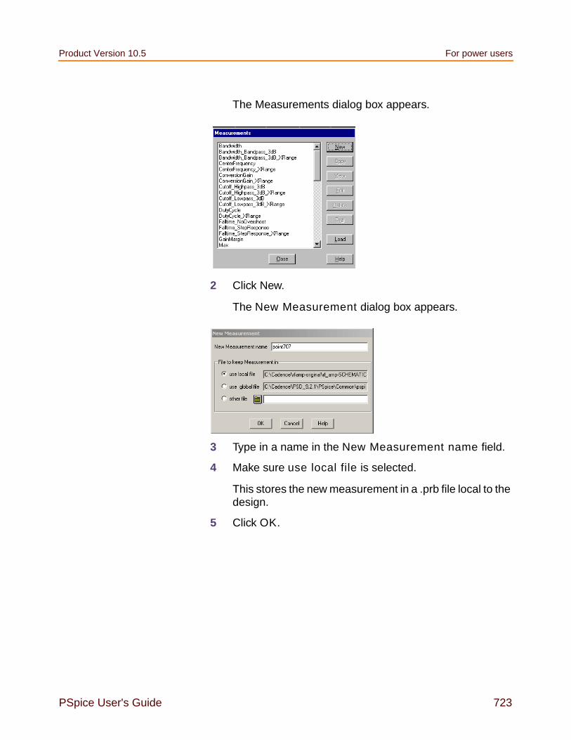
Product Version 10.5 For power users
PSpice User's Guide 723
The Measurements dialog box appears.
2 Click New.
The New Measurement dialog box appears.
3 Type in a name in the New Measurement name field.
4 Make sure use local file is selected.
This stores the new measurement in a .prb file local to thedesign.
5 Click OK.

Chapter 18 Measurement expressions Product Version 10.5
724 PSpice User's Guide
The Edit New Measurement dialog box appears.
6 Type in the marked expression:
point707(1) = y1
7 Type in the search function.
1|Search forward level(70.7%, p) !1;
Note: The search function is enclosed within curlybraces.
Always place a semicolon at the end of the last searchfunction.
8 Type in any explanatory comments you want:
*
*#Desc#* Find the .707 value of the trace.
*
*#Arg1#* Name of trace to search
*
Note: For syntax information, see Measurement definitionsyntax on page 725.
Using the new measurement definition
Your new measurement definition is now listed in theMeasurements dialog box.
marked pointexpression
comments
search function

Product Version 10.5 For power users
PSpice User's Guide 725
For an example of using a definition in a measurementexpression to evaluate a trace, see Example on page 714.
Measurement definition syntax
Check out the existing measurement definitions in PSpice forsyntax examples.
1 From the Trace menu in PSpice, chooseMeasurements.
The Measurement dialog box appears.
2 Highlight any example, and select View to examine thesyntax.
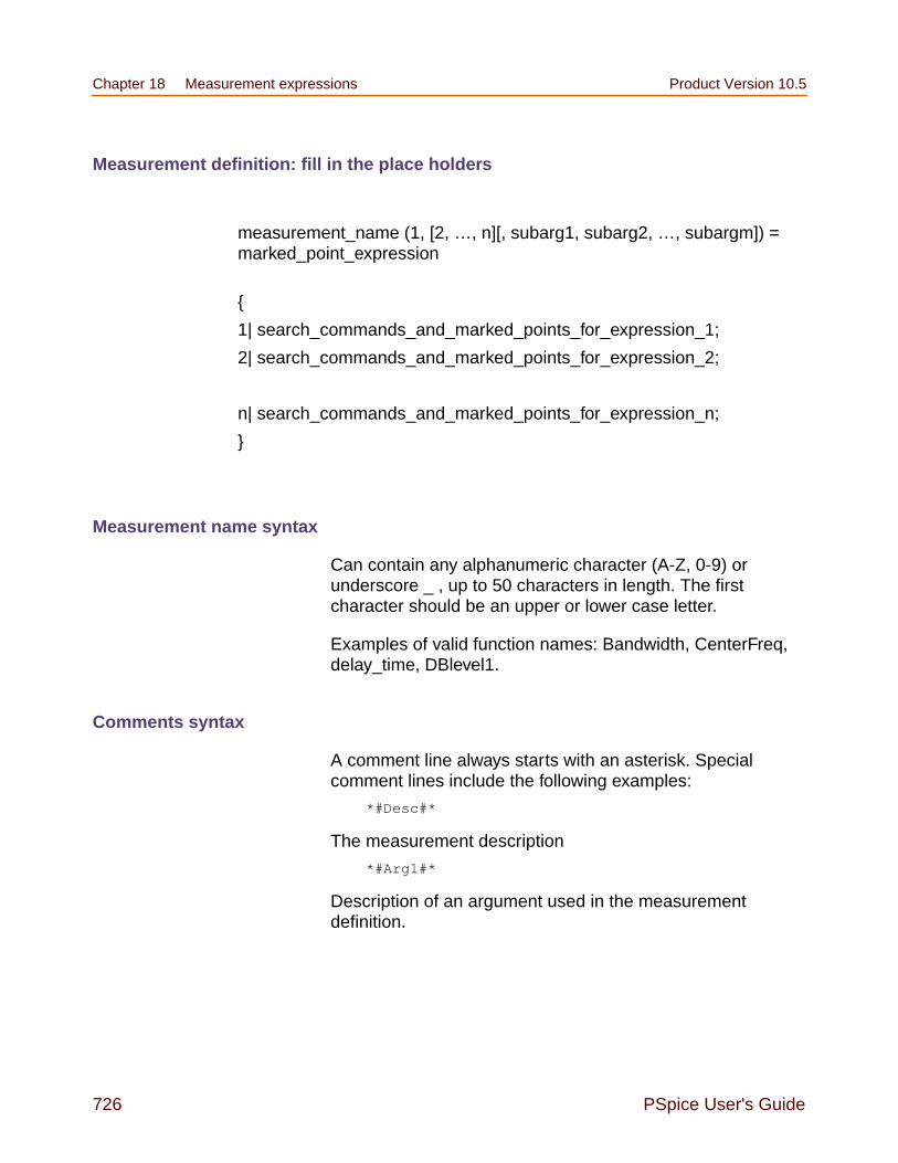
Chapter 18 Measurement expressions Product Version 10.5
726 PSpice User's Guide
Measurement definition: fill in the place holders
Measurement name syntax
Can contain any alphanumeric character (A-Z, 0-9) orunderscore _ , up to 50 characters in length. The firstcharacter should be an upper or lower case letter.
Examples of valid function names: Bandwidth, CenterFreq,delay_time, DBlevel1.
Comments syntax
A comment line always starts with an asterisk. Specialcomment lines include the following examples:
*#Desc#*
The measurement description
*#Arg1#*
Description of an argument used in the measurementdefinition.
measurement_name (1, [2, …, n][, subarg1, subarg2, …, subargm]) =marked_point_expression
1| search_commands_and_marked_points_for_expression_1;
2| search_commands_and_marked_points_for_expression_2;
n| search_commands_and_marked_points_for_expression_n;

Product Version 10.5 For power users
PSpice User's Guide 727
These comment lines will be used in dialog boxes, such as theArguments for Measurement Evaluation box.
Marked Point Expressions syntax
A marked point expression calculates a single value, which isthe value of the measurement, based on the X and Ycoordinates of one or more marked points on a curve. Themarked points are found by the search command.
All the arithmetic operators (+, -, *, /, ( ) ) and all the functionsthat apply to a single point (for example, ABS(), SGN(), SIN(),SQRT() ) can be used in marked point expressions.
The result of the expression is one number (a real value).
Marked point expressions differ from a regular expression inthe following ways:
Marked point coordinate values (for example, x1, y3), areused instead of simulation output variables (v(4), ic(Q1)).
Multiple-point functions such as d(), s(), AVG(), RMS(),MIN(), and MAX() cannot be used.
Complex functions such as M(), P(), R(), IMG(), and G()cannot be used.
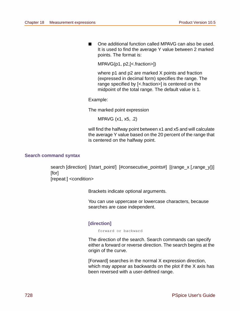
Chapter 18 Measurement expressions Product Version 10.5
728 PSpice User's Guide
One additional function called MPAVG can also be used.It is used to find the average Y value between 2 markedpoints. The format is:
MPAVG(p1, p2,[<.fraction>])
where p1 and p2 are marked X points and fraction(expressed in decimal form) specifies the range. Therange specified by [<.fraction>] is centered on themidpoint of the total range. The default value is 1.
Example:
The marked point expression
MPAVG (x1, x5, .2)
will find the halfway point between x1 and x5 and will calculatethe average Y value based on the 20 percent of the range thatis centered on the halfway point.
Search command syntax
Brackets indicate optional arguments.
You can use uppercase or lowercase characters, becausesearches are case independent.
[direction]forward or backward
The direction of the search. Search commands can specifyeither a forward or reverse direction. The search begins at theorigin of the curve.
[Forward] searches in the normal X expression direction,which may appear as backwards on the plot if the X axis hasbeen reversed with a user-defined range.
search [direction] [/start_point/] [#consecutive_points#] [(range_x [,range_y])][for][repeat:] <condition>

Product Version 10.5 For power users
PSpice User's Guide 729
Forward is the default direction.
[/start_point/]
The starting point to begin a search. The current point is thedefault.
[#consecutive points#]
Defines the number of consecutive points required for acondition to be met. Usage varies for individual conditions; thedefault is 1.
A peak is a data point with one neighboring data point on bothsides that has a lower Y value than the data point.
If [#consecutive_points#] is 2 and <condition> is PEak, thenthe peak searched for is a data point with two neighboringdata points on both sides with lower Y values than the markeddata point.
[(range_x[,range_y])]
Specifies the range of values to confine the search.
The range can be specified as floating-point values, as apercent of the full range, as marked points, or as anexpression of marked points. The default range is all pointsavailable.
Use this… To start the search at this…
^ the first point in the search range
Begin the first point in the search range
$ the last point in the search range
End the last point in the search range
xn a marked point number
or an expression of marked points, forexample,
x1(x1 - (x2 - x1) / 2)

Chapter 18 Measurement expressions Product Version 10.5
730 PSpice User's Guide
Examples
[for] [repeat:]
Specifies which occurrence of <condition> to find.
If repeat is greater than the number of found instances of<condition>, then the last <condition> found is used.
Example
The argument:
2:LEvel
would find the second level crossing.
<condition>
Must be exactly one of the following:
LEvel(value[,posneg])
SLope[(posneg)]
PEak
TRough
MAx
MIn
POint
This range… Means this…
(1n,200n) X range limited from 1e-9 to 200e-9,Y range defaults to full range
(1.5,20e-9,0,1m)
both X and Y ranges are limited
(5m,1,10%,90%)
both X and Y ranges are limited
(0%,100%,1,3) full X range, limited Y range
(,,1,3) full X range, limited Y range
(,30n) X range limited only on upper end

Product Version 10.5 For power users
PSpice User's Guide 731
XValue(value)
Each <condition> requires just the first 2 characters of theword. For example, you can shorten LEvel to LE.
If a <condition> is not found, then either the cursor is notmoved or the goal function is not evaluated.
LEvel(value[,posneg])
[,posneg] Finds the next Y value crossing at the specified level.This can be between real data points, in which case aninterpolated artificial point is created.
At least [#consecutive_points#]-1 points following the levelcrossing point must be on the same side of the level crossingfor the first point to count as the level crossing.
[,posneg] can be Positive (P), Negative (P), or Both (B). Thedefault is Both.
(value) can take any of the following forms:
Value form Example
a floating number 1e5
100n
1
a percentage of full range 50%
a marked point
or an expression ofmarked points
x1
y1
(x1-x2)/2
a value relative tostartvalue
.-3 ⇒ startvalue -3
.+3 ⇒ startvalue +3
a db value relative tostartvalue
.-3db ⇒ 3db below startvalue
.+3db ⇒ 3db above startvalue
a value relative to max ormin
max-3 ⇒ maxrng -3
min+3 ⇒ minrng +3

Chapter 18 Measurement expressions Product Version 10.5
732 PSpice User's Guide
decimal point ( . )
A decimal point ( . ) represents the Y value of the last pointfound using a search on the current trace expression of thegoal function. If this is the first search command, then itrepresents the Y value of the startpoint of the search.
SLope[(posneg)]
Finds the next maximum slope (positive or negative asspecified) in the specified direction.
[(posneg)] refers to the slope going Positive (P), Negative (N),or Both (B). If more than the next [#consecutive_points#]points have zero or opposite slope, the Slope function doesnot look any further for the maximum slope.
Positive slope means increasing Y value for increasing indicesof the X expression.
The point found is an artificial point halfway between the twodata points defining the maximum slope.
The default [(posneg)] is Positive.
PEak
Finds the nearest peak. At least [#consecutive_points#] pointson each side of the peak must have Y values less than thepeak Y value.
TRough
Finds nearest negative peak. At least [#consecutive_points#]points on each side of the trough must have Y values greaterthan the trough Y value.
MAx
Finds the greatest Y value for all points in the specified Xrange. If more than one maximum exists (same Y values),then the nearest one is found.
a db value relative to maxor min
max-3db ⇒ 3db below maxrng
min+3db ⇒ 3db above minrng
Value form Example

Product Version 10.5 For power users
PSpice User's Guide 733
MAx is not affected by [direction], [#consecutive_points#], or[repeat:].
MIn
Finds the minimum Y value for all points in the specified Xrange.
MIn is not affected by [direction], [#consecutive_points#], or[repeat:].
POint
Finds the next data point in the given direction.
XValue(value)
Finds the first point on the curve that has the specified X axisvalue.
The (value) is a floating-point value or percent of full range.
XValue is not affected by [direction], [#consecutive_points#],[(range_x [,range_y])], or [repeat:].
(value) can take any of the following forms:
Value form Example
a floating number 1e5
100n
1
a percentage of full range 50%
a marked point
or an expression ofmarked points
x1
y1
(x1+x2)/2
a value relative tostartvalue
.-3 ⇒ startvalue -3
.+3 ⇒ startvalue +3
a db value relative tostartvalue
.-3db ⇒ 3db below startvalue
.+3db ⇒ 3db above startvalue

Chapter 18 Measurement expressions Product Version 10.5
734 PSpice User's Guide
Syntax example
The measurement definition is made up of:
A measurement name
A marked point expression
One or more search commands enclosed within curlybraces
This example also includes comments about:
The measurement definition
What arguments it expects when used
A sample command line for its usage
a value relative to max ormin
max-3 ⇒ maxrng -3
min+3 ⇒ minrng +3
Value form Example

Product Version 10.5 For power users
PSpice User's Guide 735
Any line beginning with an asterisk is considered a commentline.
The name of the measurement is Risetime. Risetime will take1 argument, a trace name (as seen from the comments).
The first search function searches forward (positive xdirection) for the point on the trace where the waveformcrosses the 10% point in a positive direction. That point’s Xand Y coordinates will be marked and saved as point 1.
The second search function searches forward in the positivedirection for the point on the trace where the waveformcrosses the 90% mark. That point’s X and Y coordinates willbe marked and saved as point 2.
The marked point expression is x2-x1. This means themeasurement calculates the X value of point 2 minus the Xvalue of point 1 and returns that number.
Risetime definitionRisetime(1) = x2-x1
*
*#Desc#* Find the difference between the X valueswhere the trace first
*#Desc#* crosses 10% and then 90% of its maximumvalue with a positive
*#Desc#* slope.
*#Desc#* (i.e. Find the risetime of a stepresponse curve with no
*#Desc#* overshoot. If the signal has overshoot,use GenRise().)
*
*#Arg1#* Name of trace to search
*
* Usage:
*Risetime(<trace name>)
*
1|Search forward level(10%, p) !1
Search forward level(90%, p) !2;

Chapter 18 Measurement expressions Product Version 10.5
736 PSpice User's Guide

PSpice User's Guide 737
19
Other output options
Chapter overview
This chapter describes how to output results in addition tothose normally written to the data file or output file.
Viewing analog results in the PSpice window onpage 738 explains how to monitor the numerical valuesfor voltages or currents on up to three nets in your circuitas the simulation proceeds.
Writing additional results to the PSpice output file onpage 739 explains how to generate additional line plotsand tables of voltage and current values to the PSpiceoutput file.
Creating test vector files on page 743 explains how tosave digital output states to a file that you can use later asinput to another circuit.

Chapter 19 Other output options Product Version 10.5
738 PSpice User's Guide
Viewing analog results in the PSpice window
Capture provides a special WATCH1 part that lets you monitorvoltage values for up to three nets in your schematic as a DCsweep, AC sweep or transient analysis proceeds. Results aredisplayed in PSpice.
To display voltage values in the PSpice window
1 Place and connect a WATCH1 part (from the PSpicelibrary SPECIAL.OLB) on an analog net.
2 Double-click the WATCH1 part instance to display theParts spreadsheet.
3 In the ANALYSIS property column, type DC, AC, or TRAN(transient) for the type of analysis results you want to see.
4 Enter values in the LO and HI properties columns todefine the lower and upper bounds, respectively, on thevalues you expect to see on this net.
Note: If the results move outside of the specified bounds,PSpice pauses the simulation so that you can investigatethe behavior.
5 Repeat steps 1 through 4 for up to two more WATCH1instances.
6 Start the simulation.
For example, in the schematic fragment shown below,WATCH1 parts are connected to the Mid and Vcc nets. After

Product Version 10.5 Writing additional results to the PSpice output file
PSpice User's Guide 739
starting the simulation, PSpice displays voltages on the Midand Vcc nets.
Writing additional results to the PSpice output file
Capture provides special parts that let you save additionalsimulation results to the PSpice output file as eitherline-printer plots or tables.
To view the PSpice output file after running a simulation:
1 From the Simulation menu, choose Examine Output.
Generating plots of voltage and current values
You can generate voltage and current line-printer plots for anyDC sweep, AC sweep, or transient analysis.
To generate plots of voltage or current to the output file
1 Place and connect any of the following parts (from thePSpice library SPECIAL.OLB).
Table 19-1
Use this part... To plot this...
VPLOT1 Voltage on the net that thepart terminal is connected to.

Chapter 19 Other output options Product Version 10.5
740 PSpice User's Guide
2 Double-click the part instance to display the Partsspreadsheet.
3 Click the property name for the analysis type that youwant plotted: DC, AC, or TRAN.
4 In the columns for the analysis type that you want plotted(DC, AC or TRAN), type any non-blank value such as Y,YES or 1.
5 If you selected the AC analysis type, enable an outputformat:
a. Click the property name for one of the followingoutput formats: MAG (magnitude), PHASE, REAL,IMAG (imaginary), or DB.
b. Type any non-blank value such as Y, YES or 1.
c. Repeat Step a and Step b for as many AC outputformats as you want to see plotted.
Note: If you do not enable a format, PSpice defaults toMAG.
6 Repeat steps 2 through 5 for any additional analysistypes you want plotted.
Note: If you do not enable an analysis type, PSpice reportsthe transient results.
VPLOT2 Voltage differential betweenthe two nets that the partterminals are connected to.
IPLOT Current through a net. (Insertthis part in series, like acurrent meter.)
Table 19-1
Use this part... To plot this...

Product Version 10.5 Writing additional results to the PSpice output file
PSpice User's Guide 741
Generating tables of voltage and current values
You can generate tables of voltage and current values on netsfor any DC sweep, AC sweep, or transient analysis.
To generate tables of voltage or current to the output file
1 Place and connect any of the following parts (from thePSpice library SPECIAL.OLB).
2 Double-click the part instance to display the Partsspreadsheet.
3 Click the property name for the analysis type that youwant tabulated: DC, AC, or TRAN.
4 In the columns for the analysis type that you want plotted(DC, AC or TRAN), type any non-blank value such as Y,YES or 1.
5 If you selected the AC analysis type, enable an outputformat.
a. Click the property name for one of the followingoutput formats: MAG (magnitude), PHASE, REAL,IMAG (imaginary), or DB.
b. Type any non-blank value such as Y, YES or 1.
Table 19-2
Use this part... To tabulate this...
VPRINT1 Voltage on the net that thepart terminal is connected to.
VPRINT2 Voltage differential betweenthe two nets that the partterminals are connected to.
IPRINT Current through a cut in thenet. (Insert this part in series,like a current meter.)

Chapter 19 Other output options Product Version 10.5
742 PSpice User's Guide
c. Repeat Step a and Step b for as many AC outputformats as you want to see tabulated.
Note: If you do not enable a format, PSpice defaults toMAG.
6 Repeat steps 2 through 5 for any additional analysistypes you want plotted.
Note: If you do not enable an analysis type, PSpice reportsthe transient results.
Generating tables of digital state changes
You can generate a table of digital state changes during atransient analysis for any net.
To generate a table of digital state changes to the outputfile
1 Place a PRINTDGTLCHG part (from the PSpicelibrary SPECIAL.OLB) and connect it to the net that youare interested in.

Product Version 10.5 Writing additional results to the PSpice output file
PSpice User's Guide 743
Creating test vector files
Capture provides a special VECTOR part that lets you savedigital simulation results to a vector file. Whenever any netwith an attached VECTOR part changes state, PSpice writesa line of time-value data to the vector file using the sameformat as the file stimulus device. This means that you canuse the vector file to drive inputs for another simulation. To findout about vector file syntax, refer to the online PSpiceReference Guide.
To find out about setting up digital stimuli, see Defining adigital stimulus on page 543.
To generate a test vector file from your circuit
1 Place a VECTORn part (from the PSpice librarySPECIAL.OLB) and connect it to a wire or bus at theoutput of a digital part instance.
2 Double-click the VECTORn part instance to display theParts spreadsheet.
3 Set the part properties as described below.
Table 19-3
For thisproperty...
Define this...
POS Column position in the file.Valid values range from 1 to255.
double-click here toedit the POS property
double-click here toedit all properties
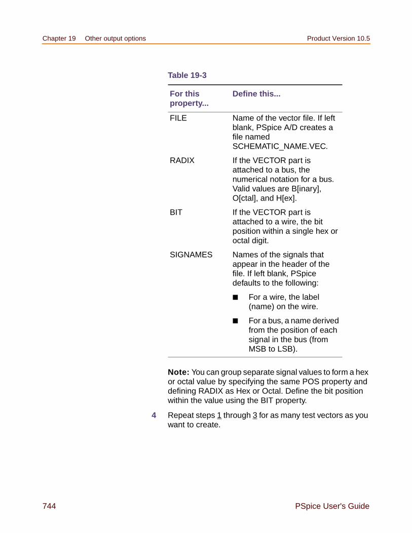
Chapter 19 Other output options Product Version 10.5
744 PSpice User's Guide
Note: You can group separate signal values to form a hexor octal value by specifying the same POS property anddefining RADIX as Hex or Octal. Define the bit positionwithin the value using the BIT property.
4 Repeat steps 1 through 3 for as many test vectors as youwant to create.
FILE Name of the vector file. If leftblank, PSpice A/D creates afile namedSCHEMATIC_NAME.VEC.
RADIX If the VECTOR part isattached to a bus, thenumerical notation for a bus.Valid values are B[inary],O[ctal], and H[ex].
BIT If the VECTOR part isattached to a wire, the bitposition within a single hex oroctal digit.
SIGNAMES Names of the signals thatappear in the header of thefile. If left blank, PSpicedefaults to the following:
For a wire, the label(name) on the wire.
For a bus, a name derivedfrom the position of eachsignal in the bus (fromMSB to LSB).
Table 19-3
For thisproperty...
Define this...

PSpice User's Guide 745
A
Setting initial state
Appendix overview
This appendix includes the following sections:
Save and load bias point on page 746
Setpoints on page 748
Setting initial conditions on page 750

Chapter A Setting initial state Product Version 10.5
746 PSpice User's Guide
Save and load bias point
Save Bias Point and Load Bias Point are used to save andrestore bias point calculations in successive PSpicesimulations.
Note: Save/Load Bias Point feature is not available inPSpice A/D Basics.
Saving and restoring bias point calculations can decreasesimulation times when large circuits are run multiple times andcan aid convergence. If the circuit uses high gain components,or if the circuit’s behavior is nonlinear around the bias point,this feature is not useful.
Save/Load Bias Point affect the following types of analyses:
transient
DC
AC
Save bias point
Save bias point is a simulation control function that allows youto save the bias point data from one simulation for use as initialconditions in subsequent simulations. Once bias point data issaved to a file, you can use the load bias point function to usethe data for another simulation.
To use save bias point
1 In the Simulation Settings dialog box, click the Analysistab.
See Setting up analyses on page 373 for a description ofthe Analysis Setup dialog box.
2 Under Options, select Save Bias Point.
3 Complete the Save Bias Point dialog box.
4 Click OK.

Product Version 10.5 Appendix overview
PSpice User's Guide 747
Load bias point
Load bias point is a simulation control function that allows youto set the bias point as an initial condition. A common reasonfor giving PSpice initial conditions is to select one out of two ormore stable operating points (set or reset for a flip-flop, forexample).
To use load bias point
1 Run a simulation using the Save Bias Point option in theSimulation Settings dialog box.
See Setting up analyses on page 373 for a description ofthe Analysis Setup dialog box.
2 Before running another simulation, click the Analysis tabin the Simulation Settings dialog box.
3 Under Options, select Load Bias Point.
4 Specify a bias point file to load. Include the path if the fileis not located in your working directory, or use the Browsebutton to find the file.
5 Click OK.

Chapter A Setting initial state Product Version 10.5
748 PSpice User's Guide
Setpoints
Pseudocomponents that specify initial conditions are calledsetpoints. These apply to the analog portion of your circuit.
Figure A-1 Setpoints.
The example in Figure A-1 includes the following:
Using IC symbols sets the initial conditions for the bias pointonly. It does not affect the DC sweep. If your circuit designcontains both an IC symbol and a NODESET symbol for thesame net, the NODESET symbol is ignored.
To specify the initial condition, edit the value of the VALUEproperty to the desired initial condition. PSpice attaches avoltage source with a 0.0002 ohm series resistance to eachnet to which an IC symbol is connected. The voltages areclamped this way for the entire bias point calculation.
NODESET1 is a one-pin symbol which helps calculate thebias point by providing a initial guess for some net.NODESET2 is a two-pin symbol which helps calculate thebias point between two nets. Some or all of the circuit’s netsmay be given an initial guess. NODESET symbols areeffective for the bias point (both small-signal and transient biaspoints) and for the first step of the DC sweep. It has no effectduring the rest of the DC sweep or during the transientanalysis itself.
IC1 a one-pin symbol that allows you toset the initial condition on a net forboth small-signal and transient biaspoints
IC2 a two-pin symbol that allows you toset initial condition between two nets

Product Version 10.5 Appendix overview
PSpice User's Guide 749
Unlike the IC pseudocomponents, NODESET provides onlyan initial guess for some net voltages. It does not clamp thosenodes to the specified voltages. However, by providing aninitial guess, NODESET symbols may be used to break the tie(in a flip-flop, for instance) and make it come up in a desiredstate. To guess at the bias point, enter the initial guess in theValue text box for the VALUE property. PSpice A/D attaches avoltage source with a 0.0002 ohm series resistance to eachnet to which an IC symbol is connected.
These pseudocomponents are netlisted as PSpice A/D .ICand .NODESET commands. Refer to these commands in theonline PSpice Reference Guide for more information.Setpoints can be created for inductor currents and capacitorvoltages using the IC property described in Setting initialconditions on page 750.

Chapter A Setting initial state Product Version 10.5
750 PSpice User's Guide
Setting initial conditions
The IC property allows initial conditions to be set oncapacitors and inductors. These conditions are applied duringall bias point calculations. However, if you select the SkipInitial Transient Solution check box in the Transient AnalysisSetup dialog box, the bias point calculation is skipped and thesimulation proceeds directly with transient analysis atTIME=0. Devices with the IC property defined start with thespecified voltage or current value; however, all other suchdevices have an initial voltage or current of 0.
Note: Skipping the bias point calculation can make thetransient analysis subject to convergence problems.
Applying an IC property for a capacitor has the same effect asapplying one of the pseudocomponents IC1 or IC2 across itsnodes. PSpice attaches a voltage source with a 0.002 ohmseries resistance in parallel with the capacitor. The IC propertyallows the user to associate the initial condition with a device,while the IC1 and IC2 pseudocomponents allow theassociation to be with a node or node pair. See Setpoints onpage 748 for more information about IC1 and IC2.
In the case of initial currents through inductors, theassociation is only with a device, and so there are nocorresponding pseudocomponents. The internalimplementation is analogous to the capacitor. PSpiceattaches a current source with a 1 Gohm parallel resistance inseries with the inductor.

PSpice User's Guide 751
B
Convergence and “time step toosmall errors”
Appendix overview
This appendix discusses common errors and convergenceproblems in PSpice.
Introduction on page 752
Diagnostics on page 756
Bias Point (DC) Convergence on page 757
DC Sweep Convergence on page 762
Transient Convergence on page 763

Chapter B Convergence and “time step too small errors” Product Version 10.5
752 PSpice User's Guide
Introduction
In order to calculate the bias point, DC sweep and transientanalysis for analog devices PSpice must solve a set ofnonlinear equations which describe the circuit's behavior. Thisis accomplished by using an iterative technique—theNewton-Raphson algorithm—which starts by having an initialapproximation to the solution and iteratively improves it untilsuccessive voltages and currents converge to the same result.
In a few cases PSpice cannot find a solution to the nonlinearcircuit equations. This is generally called a “convergenceproblem” because the symptom is that the Newton-Raphsonrepeating series cannot converge onto a consistent set ofvoltages and currents. The following discussion gives somebackground on the algorithms in PSpice and some guidelinesfor avoiding convergence problems.
The transient analysis has the additional possibility of beingunable to continue because the time step required becomestoo small from something in the circuit moving too fast. This isalso discussed below.
Note: The AC and noise analyses are linear and do not usean iterative algorithm, so the following discussion doesnot apply to them. Digital devices are evaluated usingboolean algebra; this discussion does not apply tothem either.
Newton-Raphson requirements
The Newton-Raphson algorithm is guaranteed to convergeto a solution. However, this guarantee has some conditions:
1 The nonlinear equations must have a solution.
2 The equations must be continuous.
3 The algorithm needs the equations' derivatives.
4 The initial approximation must be close enough to thesolution.
Each of these can be taken in order. Remember that thePSpice algorithms are used in computer hardware that has

Product Version 10.5 Appendix overview
PSpice User's Guide 753
finite precision and finite dynamic range that produce theselimits:
Voltages and currents in PSpice are limited to +/-1e10volts and amps.
Derivatives in PSpice are limited to 1e14.
The arithmetic used in PSpice is double precision andhas 15 digits of accuracy.
Is there a solution?
Yes, for any physically realistic circuit. However, it is notdifficult to set up a circuit that has no solution within the limitsof PSpice numerics.
Consider, for example, a voltage source of one megavoltconnected to a resistor of one micro-ohm. This circuit does nothave a solution within the dynamic range of currents (+/- 1e10amps). Here is another example:
V1 1, 0 5vD1 1, 0 DMOD.MODEL DMOD(IS=1e-16)
The problem here is that the diode model has no seriesresistance. To find out more about the diode equations, referto the Analog Devices chapter in the online PSpiceReference Guide.
It can be shown that the current through a diode is:
I = IS*eV/(N*k*T/q)
N defaults to one and k*T at room temperature is about .025volts. So, in this example the current through the diode wouldbe:
I = 1e-16*e200 = 7.22e70 amps
This circuit also does not have a solution within the limits of thedynamic range of PSpice. In general, be careful ofcomponents without limits built into them. Extra care isneeded when using the expressions for controlled sources(such as for behavioral modeling). It is easy to writeexpressions with very large values.

Chapter B Convergence and “time step too small errors” Product Version 10.5
754 PSpice User's Guide
Are the equations continuous?
The device equations built into PSpice are continuous. Thefunctions available for behavioral modeling are alsocontinuous (there are several functions, such as int(x), whichcannot be added because of this). So, for physically realisticcircuits the equations can also be continuous. Exceptions thatcome are usually from exceeding the limits of the numerics inPSpice. This example tries to approximate an ideal switchusing the diode model:
.MODEL DMOD(IS=1e-16 N=1e-6)
The current through this diode is:
I = 1e-16*eV/(N*.025) = 1e-16*eV/25e-9
Because the denominator in the exponential is so small, thecurrent I is essentially zero for V < 0 and almost infinite forV > 0. Even if there are external components that limit thecurrent, the “knee” of the diode's I-V curve is so sharp that itis almost a discontinuity.
Note: Avoid unrealistic model parameters. Behavioralmodeling expressions need extra care.
Are the derivatives correct?
The device equations built into PSpice include the derivatives,and these are correct. Depending on the device, the physicalmeaning of the derivatives can be small-signal conductance,transconductance or gain.
Unrealistic model parameters can exceed the limit of 1e14,but it requires some effort. The main thing to look at is thebehavioral modeling expressions, especially those havingdenominators.
Discontinuities in models characteristics and their derivativescause:
1 Ambiguity in calculation of derivatives at point ofdiscontinuity.
2 Conductance calculated in nth iteration cannot become agood guess for next iteration.

Product Version 10.5 Appendix overview
PSpice User's Guide 755
3 Sudden switching of operating regions (example diodeswitching from off to on) and hence false convergence.
Note: Transient analysis convergence failures are usually dueto model discontinuities or unrealistic circuit, source, orparasitic modeling.
Is the initial approximation close enough?
Newton-Raphson is guaranteed to converge only if theanalysis is started close to the answer. Also, there is nomeasurement that can tell how close is close enough.
PSpice gets around this by making heavy use of continuity.Each analysis starts from a known solution and uses avariable step size to find the next solution. If the next solutiondoes not converge PSpice reduces the step size, falls backand tries again.
Incorrect initial estimates can cause convergence failure oreven false convergence. Consider following scenarios:
Power electronic circuits may NOT require tightcurrent/voltage tolerances. Setting the value of ABSTOLto 1u will help in the case of circuits that have currentsthat are larger than several amps.
Unless the circuit conducts kilo-Amperes of current,however, setting ABSTOL to a value that is greater than1u will cause more convergence problems than it willsolve.
PSpice does not always converge when relaxedtolerances are used. For example, setting the toleranceoption, RELTOL, to a value which is greater than .01 canactually cause convergence problems
Setting GMIN to a value between 1n and 10n will oftensolve convergence problems.
Setting GMIN to a value, which is greater than 10n, maycause convergence problems.

Chapter B Convergence and “time step too small errors” Product Version 10.5
756 PSpice User's Guide
Diagnostics
If PSpice encounters a convergence problem it inserts into theoutput file a message that looks like the following.
The message always includes the banner (ERROR --convergence problem ...) and the trailer (Last nodevoltages tried were ...). It cannot include all three ofthe middle blocks.
The Last node voltages tried... trailer shows thevoltages tried at the last Newton-Raphson iteration. If any ofthe nodes have unreasonable large values this is a clue thatthese nodes are related to the problem. “These voltages failedto converge” lists the specific nodes which did not settle ontoconsistent values. It also shows their values for the last twoiterations. “These supply currents failed converge” does thesame for currents through voltage sources and inductors. Ifany of the listed numbers are +/- 1e10 then that is anindication that the value is being clipped from anunreasonable value. Finally, “These devices failed toconverge” shows devices whose terminal currents or corefluxes did not settle onto consistent values.
The message gives a clue as to the part of the circuit which iscausing the problem. Looking at those devices and/or nodesfor the problems discussed above is recommended.
ERROR -- Convergence problem in transient analysis at Time = 7.920E-03Time step = 47.69E-15, minimum allowable step size = 300.0E-15
These voltages failed to converge:
V(x2.23) = 1230.23 / -68.4137V(x2.25) = -1211.94 / 86.6888
These supply currents failed to converge:
I(X2.L1) = -36.6259 / 2.25682I(X2.L2) = -36.5838 / 2.29898
These devices failed to converge:
X2.DCR3 X2.DCR4 x2.ktr X2.Q1 X2.Q2Last node voltages tried were:
NODE VOLTAGE NODE VOLTAGE NODE VOLTAGE NODE VOLTAGE( 1) 25.2000 ( 3) 4.0000 ( 4) 0.0000 ( 6) 25.2030(x2.23) 1230.2000 (X2.24) 9.1441 (x2.25) -1211.9000 (X2.26) 256.9700(X2.28) -206.6100 (X2.29) 75.4870 (X2.30) -25.0780 (X2.31) 26.2810(X3.34) 1.771E-06 (X3.35) 1.0881 (X3.36) .4279 (X2.XU1.6) 1.2636

Product Version 10.5 Bias Point (DC) Convergence
PSpice User's Guide 757
Bias Point (DC) Convergence
The hardest part of the whole process is getting started, thatis, finding the bias point. PSpice first tries with the powersupplies set to 100%. A solution is not guaranteed, but mostof the time the PSpice algorithm finds one. If not, then thepower supplies are cut back to almost zero. They are cut to alevel small enough that all nonlinearities are turned off.When the circuit is linear a solution can be found (very nearzero, of course). Then, PSpice works its way back up to 100%power supplies using a variable step size.
Once a bias point is found, the transient analysis can be run.It starts from a known solution (the bias point) and stepsforward in time. The step size is variable and is reduced asneeded to find further solutions.
In case the circuit fails to converge, you should first check thecircuit topology and connectivity, followed by modelling ofcircuit components, and finally check if Pspice options are setproperly.
Checking circuit topology and connectivity
Make sure that all of the circuit connections are valid.Check for incorrect node numbering or dangling nodes.Also, verify component polarity.
Check for syntax mistakes. Make sure that you used thecorrect PSPICE units (i.e. MEG for 1E6, not M, whichmeans mili in simulations).
PSpice checks for the following conditions and providesmessages if they occur:
“Floating node" or "No DC path to ground"messages:
Make sure that there's a DC path from everynode to ground.
Make sure that there are at least twoconnections at every node.

Chapter B Convergence and “time step too small errors” Product Version 10.5
758 PSpice User's Guide
Make sure that capacitors and/or currentsources are not connected in series.
Make sure that no (groups of) nodes are isolatedfrom ground by current sources and/orcapacitors.
"Voltage source or inductor loop" message:
Make sure that there are no loops of onlyinductors and/or voltage sources.
Place the ground (node 0) somewhere in the circuit. Becareful when you use floating grounds (e.g. chassisground); you may need to connect a large resistor fromthe floating node to ground. All nodes will be reported asfloating if "0 ground" is not used.
Make sure that voltage/current generators use realisticvalues, and verify that the syntax is correct.
Make sure that dependent source gains are correct, andthat E/G element expressions are reasonable. Verify thatdivision by zero or LOG(0) cannot occur.
Make sure that there are no unrealistic modelparameters; especially if you have manually entered themodel into the netlist.
Avoid using digital components, unless really necessary.Initialize the nodes with valid digital value to ensure thestate is not ambiguous.
Modelling circuit components
Semiconductors
The first consideration for semiconductors is to avoidphysically unrealistic model parameters. As PSpice stepsthe power supplies up, it has to step carefully through theturn on transition for each device. In the diode exampleabove, for the setting N=1e-6, the knee of the I-V curvewould be too sharp for PSpice to maintain its continuitywithin the power supply step size limit of 1e-6.
Behavioral modeling expressions

Product Version 10.5 Bias Point (DC) Convergence
PSpice User's Guide 759
Range limits: Voltages and currents in PSpice arelimited to the range +/- 1e10. Care must be taken that theoutput of expressions falls within this range. This isespecially important when one is building an electricalanalog of a mechanical, hydraulic or other type of system.
Source limits: Another consideration is that thecontrolled sources must turn off when the supplies arealmost 0 (.001%). There is special code in PSpice which"squelches" the controlled sources in a continuous waynear 0 supplies. However, care should still be taken usingexpressions that have denominators. Take, for example, aconstant power load:
GLOAD 3, 5 VALUE = 2Watts/V(3,5)
The first repeating series starts with V(3,5) = 0 and thecurrent through GLOAD would be infinite (actually, thecode in PSpice which does the division clips the result toa finite value). The "squelching" code is required to be asmooth and well-behaved function.
Note: The "squelching" code cannot be "strong" enoughto suppress dividing by 0.
The result is that GLOAD does not turn off near 0 powersupplies. A better way is described in the application noteModeling Constant Power Loads. The "squelching" codeis sufficient for turning off all expressions except thosehaving denominators. In general, though, it is goodpractice to constrain expressions having the LIMITfunction to keep results within physically realistic bounds.
Example: A first approximation to an OPAMP that has anopen loop gain of 100,000 is:
VOPAMP 3, 5 VALUE = V(in+,in-)*1e5
This has the undesirable property that there is no limit onthe output.
A better expression is:
VOPAMP 3, 5 VALUE = +LIMIT(V(in+,in-)*1e5,15v,-15v
where the output is limited to +/- 15 volts.
Unguarded p-n junctions

Chapter B Convergence and “time step too small errors” Product Version 10.5
760 PSpice User's Guide
A second consideration is to avoid "unguarded" p-njunctions (no series resistance).
No leakage resistance
A third consideration is to avoid situations, which couldhave an ideal current source pushing current into areverse-biased p-n junction without a shunt resistance.p-n junctions in PSpice have (almost) no leakageresistance and would cause the junction's voltage to gobeyond 1e10 volts.
Switches
PSpice switches have gain in their transition region. Ifseveral are cascaded then the cumulative gain can easilyexceed the derivative limit of 1e14. This can happenwhen modeling simple logic gates using totem-poleswitches and there are several gates cascaded in series.Usually a cascade of two switches works but three ormore can cause trouble.
PSpice Options
Increase ITL1 to 400 in the .OPTIONS statement.
Example: .OPTIONS ITL1=400
This increases the number of DC iterations that PSpicewill perform before it gives up. In all but the most complexcircuits, further increases in ITL1 won't typically aidconvergence.
Add .NODESETs
Example: .NODESET V(6)=0
Use NODESETs to set node voltages to the nearestreasonable guess at their DC values, particularly atnodes that are isolated by high impedances, and at nodesthat are inputs to high gain devices. NODESETs do not"fix" the voltages at these nodes. They hold thesevoltages at the specified value while the rest of the circuitconverges to a reasonably stable point, and then"releases" these voltages for a few more iterations to findthe final, complete solution. Removing these voltages

Product Version 10.5 Bias Point (DC) Convergence
PSpice User's Guide 761
from the initial iterations, when voltages and currents arevarying widely helps PSpice achieve convergence.
STEPGMIN
Specifying the circuit analysis option STEPGMIN enablesthis (either using .OPTION STEPGMIN in the netlist, or bymaking the appropriate choice from the PSpice/EditSimulation Profile… menu command, Options tab). Whenenabled, the GMIN stepping algorithm is applied after thecircuit fails to converge with the power supplies at 100percent, and if GMIN stepping also fails, the supplies arethen cut back to almost zero and then stepped up.
GMIN stepping attempts to find a solution by starting therepeating cycle with a large value of GMIN, initially1.0e10 times the nominal value. If a solution is found atthis setting it then reduces GMIN by a factor of 10, andtries again. This continues until either GMIN is back to thenominal value, or until PSpice fails to converge at one ofthe GMIN values on the way. In the latter case, GMIN isrestored to the nominal value and the power supplies arestepped.
Power supply stepping
As previously discussed, PSpice uses a proprietaryalgorithm which finds a continuous path from zero powersupplies levels to 100%. It starts at almost zero (.001%)power supplies levels and works its way back up to the100% levels. The minimum step size is 1e-6 (.0001%).The first repeating series of the first step starts at zero forall voltages. So modeling expressions, especially thosehaving denominators that include voltages should bechecked carefully.
Set PREORDER in Simulation Profiles options
This is important while editing schematic for marginallyconvergent circuits. Setting PREORDER reducesdependency on the netlisting order thereby ensuring thatthe non convergence error does not occur because of thechange in the netlisting order.

Chapter B Convergence and “time step too small errors” Product Version 10.5
762 PSpice User's Guide
DC Sweep Convergence
The DC sweep uses a hybrid approach. It uses the bias pointalgorithm (varying the power supplies) to get started. Forsubsequent steps it uses the previous solution as the initialapproximation. The sweep step is not variable, however. If asolution cannot be found at a step then the bias pointalgorithm is used for that step.
The whole process relies heavily on continuity. It also requiresthat the circuit be linear when the supplies are turned off.
Circuit topology and connectivity
This is same as in DC analysis. See Checking circuit topologyand connectivity on page 757.
Modelling Checks
This is same as in DC analysis. Modelling circuit componentson page 758.
PSpice Options
Set ITL2=100 in the .OPTIONS statement.
Example: .OPTIONS ITL2=100
This increases the number of DC iterations that PSpicewill attempt before it gives up.
Increase or decrease the step values, which are used inthe .DC sweep.
Example:
.DC VCC 0 1 .1 becomes .DC VCC 0 1 .01
Discontinuities in the PSpice models can causeconvergence problems. The use of larger steps may helpto bypass the discontinuities, while the use of smallersteps may help PSpice find the intermediate answers,which will be used to find the point, which doesn'tconverge. In some cases, smaller steps can improve

Product Version 10.5 Transient Convergence
PSpice User's Guide 763
convergence, because they help PSpice find a "path"from the valid DC solution at one point to the valid solutionat the next.
Do not use the DC sweep analysis.
Example:.DC VCC 0 5 .1
VCC 1 0
becomes
.TRAN .01 1
VCC 1 0 PULSE 0 5 0 1
In many cases, it is preferable to use the transientanalysis to ramp the appropriate voltage and/or currentsources. The transient analysis tends to be more robust,and is sometimes faster.
Transient Convergence
The transient analysis starts using a known solution - the biaspoint. It then uses the most recent solution as the first guessfor each new time point. If necessary, the time step is cut backto keep the new time point close enough that the first guessallows the Newton-Raphson repeating series to converge.The time step is also adjusted to keep the integration ofcharges and fluxes accurate enough.
In theory the same considerations which were noted for thebias point calculation apply to the transient analysis. However,in practice they show up during the bias point calculation firstand, hence, are corrected before a transient analysis is run.
The transient analysis can fail to complete if the time step getstoo small. This can have two different effects:
1 The Newton-Raphson iterations would not converge evenfor the smallest time step size, or
2 Something in the circuit is moving faster than can beaccommodated by the minimum step size.
The message PSpice puts into the output file specifies whichcondition occurred.

Chapter B Convergence and “time step too small errors” Product Version 10.5
764 PSpice User's Guide
Circuit topology and connectivity
Avoid using digital components, unless really necessary.Initialize the nodes with valid digital value to ensure noambiguous state. These can cause time-step issues(time-step may unnecessary go too small) and hencetransient convergence issue.
Use RC snubbers around diodes.
Add Capacitance for all semiconductor junctions (if nospecific value is known: CJO=3pF for diodes, CJC &CJE=5pF for BJTs, CGS and CGD=5pF for JFETs andGaAsFETs, CGDO & CGSO=5pF for MOSFETs if nospecific value is known).
Add realistic circuit and element parasitics.
Look for waveforms that transition vertically (up or down)at the point during which the analysis halts. These are thekey nodes, which should be examined for problems.
Increase the rise/fall times of the PULSE sources; e.g.from 1f to 1u.
Example:VCC 1 0 PULSE 0 1 0 1f 1f
becomes
VCC 1 0 PULSE 0 1 0 1U 1U
An effort should be made to smooth strongnon-linearities. The pulse times should be realistic, notideal. If no rise or fall time values are given, or if 0 isspecified, the rise and fall times will be set to the TSTEPvalue in the .TRAN statement (set in the Output FileOptions of the Time Domain (Transient) analysis settingsin the simulation profile.
Ensure that there is no unreasonably large capacitor orinductor
If the transient analysis fails at the first time point thenusually there is an unreasonably large capacitor orinductor. Usually this is due to a typographical error.Consider the following capacitor:
C 1 3, 0 1Ouf

Product Version 10.5 Transient Convergence
PSpice User's Guide 765
"1O" (has the letter O) should have been "10." This capacitorhas a value of one farad, not 10 microfarads. An easy way tocatch these is to use the LIST option (on the .OPTIONScommand).
LIST
The LIST option can echo back all the devices into the outputfile that have their values in scientific notation.
That makes it easy to spot any unusual values. This kind ofproblem does not show up during the bias point calculationbecause capacitors and inductors do not participate in thebias point.
Similar comments apply to the parasitic capacitanceparameters in transistor (and diode) models. These arenormally echoed to the output file (the NOMOD optionsuppresses the echo but the default is to echo). As in the LISToutput, the model parameters are echoed in scientific notationmaking it easy to spot unusual values. A further diagnostic isto ask for the detailed operating bias point (.TRAN/OP)information.
.TRAN/OP
This lists the small-signal parameters for each semiconductordevice including the calculated parasitic capacitances.
Realistically Model Circuit; add parasitics, especially stray/junction capacitance
The idea here is to smooth any strong non-linearties ordiscontinuities. This may be accomplished via the addition ofcapacitance to various nodes and verifying that allsemiconductor junctions have capacitance. Other tips include:
Bipolar transistors substrate junction
The UC Berkeley SPICE contains an unfortunateconvention for the substrate node of bipolar transistors.The collector-substrate p-n junction has no DCcomponent. If the capacitance model parameters are

Chapter B Convergence and “time step too small errors” Product Version 10.5
766 PSpice User's Guide
specified (e.g., CJS) then the junction has(voltage-dependent) capacitance but no DC current. Thiscan lead to a sneaky problem: if the junction isinadvertently forward-biased it can create a very largecapacitance. The capacitance goes as a power of thejunction voltage. Normal junctions cannot sustain muchforward voltage because a large current flows. Thecollector-substrate junction is an exception because ithas no DC current. If this happens it usually shows up atthe first time step. It can be spotted turning on the detailedoperating point information (.TRAN/OP) and looking atthe calculated value of CJS for bipolar transistors. Thewhole problem can be prevented by using the PSpicemodel parameter ISS. This parameter "turns on" the DCcurrent for the substrate junction.
Parasitic capacitances
It is important that switching times be nonzero. This isassured if devices have parasitic capacitances. Thesemiconductor model libraries in PSpice have suchcapacitances. If switches and/or controlled sources areused, then care should be taken to assure that nosections of circuitry can try to switch in zero time. Inpractice this means that if any positive feedback loopsexist (such as a Schmidt trigger built out of switches) thensuch loops should include capacitances.
Another way of saying all this is that during transientanalysis the circuit equations must be continuous overtime (just as during the bias point calculation theequations must be continuous with the power supplylevel).
Inductors and transformers
While the impedance of capacitors gets lower at highfrequencies (and small time steps) the impedance ofinductors gets higher.
Note: The inductors in PSpice have an infinitebandwidth.
Real inductors have a finite bandwidth due to eddycurrent losses and/or skin effect. At high frequencies theeffective inductance drops.

Product Version 10.5 Transient Convergence
PSpice User's Guide 767
Another way to say this is that physical inductors have afrequency at which their Q begins to roll off. The inductorsin PSpice have no such limit. This can lead to very fastspikes as transistors (and diodes) connected to inductorsturn on and off. The fast spikes, in turn, can force PSpiceto take unrealistically small time steps.
It is recommended that all inductors have a parallelresistor (series resistance is good for modeling DCeffects but does not limit the inductor's bandwidth). Theparallel resistor gives a good model for eddy current lossand limits the bandwidth of the inductor. The size ofresistor should be set to be equal to the inductor'simpedance at the frequency at which its Q begins to rolloff. The value of this resistor can be calculated using thefollowing formula:
where f is the roll-off frequency.
Adding parallel resistors limits the inductor impedance athigh frequencies.
Example:
A common one milli-henry iron core inductor begins to rolloff at no less than 100KHz. A good resistor value to usein parallel is then R = 2*p*100e3*.001 = 628 ohms. Belowthe roll-off frequency the inductor dominates; above it theresistor does. This keeps the width of spikes frombecoming unreasonably narrow.
PSpice options
TIME, the simulation time during transient analysis, is adouble precision variable which gives it about 15 digits ofaccuracy. The dynamic range is set to be 15 digits minus thenumber of digits of accuracy required by RELTOL. For adefault value of RELTOL = .001 (.1% or 3 digits) this gives 15-3= 12 digits. This means that the minimum time step is theoverall run time (TSTOP) divided by 1e12. The dynamic rangeis large but finite.
It is possible to exceed this dynamic range in some circuits.Consider, for example, a timer circuit which charges up a
R 2 Π× f× L×=

Chapter B Convergence and “time step too small errors” Product Version 10.5
768 PSpice User's Guide
100uF capacitor to provide a delay of 100 seconds. At acertain threshold a comparator turns on a power MOSFET.The overall simulation time is 100 seconds. For defaultRELTOL this gives us a minimum time step of 100picoseconds. If the comparator and other circuitry hasportions that switch in a nanosecond then PSpice needs stepsof less than 100 picoseconds to calculate the transitionaccurately.
Set RELTOL=.01 in the .OPTIONS statement.
Example:.OPTIONS RELTOL=.01
This option is encouraged for most simulations, since thereduction of Reltol can increase the simulation speed by10 to 50%. Only a minor loss in accuracy usually results.A useful recommendation is to set Reltol to .01 for initialsimulations, and then reset it to its default value of .001when you have the simulation running the way you like itand a more accurate answer is required. Setting Reltol toa value less than .001 is generally not required.
Reduce the accuracy of ABSTOL/VNTOL ifcurrent/voltage levels allow it.
Example:.OPTION ABSTOL=1N VNTOL=1M
Abstol and Vntol should be set to about 8 orders ofmagnitude below the level of the maximum voltage andcurrent. The default values are Abstol=1pA andVntol=1uV. These values are generally associated with ICdesigns.
Increase ITL4, but to no more than 100, in the .OPTIONSstatement.
Example: .OPTIONS ITL4=40
This increases the number of transient iterations thatPSpice will attempt at each time point before it gives up.This is particularly effective at solving convergenceproblems when the simulation needs to cover a long timeperiod, and fast transitions occur within the circuit during

Product Version 10.5 Transient Convergence
PSpice User's Guide 769
that time. Values greater than 100 won't usually bringconvergence; unnecessarily large values can cause.
Skipping the bias point
The SKIPBP option for the transient analysis skips thebias point calculation. In this case the transient analysishas no known solution to start from and, therefore, is notassured of converging at the first time point. Because ofthis, its use is not recommended. Its inclusion in PSpiceis to maintain compatibility with UC Berkeley SPICE.SKIPBP has the same meaning as UIC in BerkeleySPICE. UIC is not needed in order to specify initialconditions.
It should be used as a last resort if there is trouble gettingthe transient analysis to start because the DC operatingpoint can't be calculated. The initial guess for dc could bemade from results of such transient analysis; and thentransient analysis could be re-run with operating point.You should add any applicable .IC and IC= initialconditions statements to assist in the initial stages of thetransient analysis. Be careful when you set initialconditions, for a poor setting may cause convergencedifficulties.
Increasing the ABSTOL and CHGTOL
While modeling a mechanical system with an RC circuit,where capacitors are in the order of Farad and currentimpulses is around 10x A, increase CHGTOL andABSTOL by six order of magnitude. For example, changeCHGTOL from 0.01e-012 to0.01e-006. Simulate thecircuit and then start tightening the ABSTOL andCHGTOL values until a convergence error is generated.Once a convergence error is generated, you can revertone step to get the solution.
Set the DIGSTEPBACK option
.OPTIONS DIGSTEPBACK
Setting this option might prove useful in cases where yourhave convergence problems in a circuits with digitalcomponents and you are trying to converge usingSolver 1.

Chapter B Convergence and “time step too small errors” Product Version 10.5
770 PSpice User's Guide
Though setting DIGSTEPBACK option might work, it isrecommended that you should use solver 0 simulationalgorithm to obtain a solution.
Tip
Solver 1 and Solver 0 are two matrix solvingalgorithms used by PSpice. By default, Solver 1 thathas better convergence property, is used. But attimes, for a circuit with convergence problemschanging the simulation algorithm to Solver 0 helps.To change the simulation algorithm from Solver 1 toSolver 0, open the circuit in the schematic editor.From the PSpice menu choose Edit SimulationProfile. In the Simulation Settings dialog box,select the Options tab. Select the AdvancedOptions button. In the Advanced Analog Optionsdialog box, change the Simulation algorithm fromdefault to 0.

PSpice User's Guide 771
C
Importing Spice Models
Appendix Overview
This appendix covers the process to be followed for importingSpice models downloaded from a web site, into PSpice andmaking them ready to be used in a circuit. The sectionscovered in this appendix are:
Introduction on page 772
Importing text models on page 772
Generating Part Symbols on page 773
Configuring new model library on page 779
Editing Model Editor created symbols on page 781

Chapter C Importing Spice Models Product Version 10.5
772 PSpice User's Guide
Introduction
Usually, the Spice models downloaded from a Vendor’s website cannot be used directly in PSpice. This document coversthe steps to be covered before you can successfully use thedownloaded models for designing your circuits.
Before you can use the simulation models downloaded from aweb site in your design, you need to perform following steps:
Importing text models
Generating Part Symbols
Configuring new model library
Importing text models
To import the downloaded Spice models into PSpice, youneed to perform the following steps.
1 Rename the downloaded model to have the .MODextension.
Note: Renaming is required only if the downloadedmodel does not have a .MOD extension. For example,renaming will be required if the download model has a .txtextension.
2 Launch the Model Editor.
3 Open a new or your custom model library.
4 From the Model menu, choose Import.
5 In the Open dialog box, select the downloaded model withthe .MOD extension and select Open.
Note: Only the first model in the .MOD file is imported.Therefore, it is recommended that the .MOD file shouldnot have more than one model.
6 From the file Menu, choose Save As. In the Save Asdialog box, specify the name and location of new modellibrary as

Product Version 10.5 Generating Part Symbols
PSpice User's Guide 773
<installation_directory>\tools\Pspice\library\userlib.
Note: It is preferable to create you own USERLIB libraryfolder to store all of your custom part and model librariesfor better library management. It is important that youback up your custom libraries and projects on a regularbasis to avoid loss of work.
Generating Part Symbols
After you have imported the downloaded model into PSpice,you need to generate part symbols for the model. You canassociate a model to a symbol either by Creating NewSymbols or by Using symbols from an existing symbol libraryor by Using Model Import wizard.
Creating New Symbols
You can create Capture symbols for the imported/downloadedmodels. Using Model Editor you can either create parts for allthe models in a library or you can enable the auto partgeneration feature in Model Editor, such that part is createdevery time you save a model.
Creating symbol for the complete library
1 Open the Model Editor.
2 From the Tools menu, choose Options.
3 Select Capture as the schematic editor and close theOptions dialog box.

Chapter C Importing Spice Models Product Version 10.5
774 PSpice User's Guide
4 From the File menu, choose Export to Capture PartLibrary.
5 Specify the location of the model library (.LIB) for whichyou want the symbols to be created.
6 Specify the location of the part library (.OLB) to becreated and select OK.
7 A message box appears displaying status of part creationprocess. Select OK to close the message box.
Note: Any errors or warning messages that aregenerated during the part creation, are saved in a log filenamed <library_name>.err. Referring to thecontents of the .err file might be helpful, in cases wherepart creating fails.
Creating symbol for a model
1 From the Tools menu, choose Options.
2 To enable part creation every time you save a model,select the Always Create Part when Saving Modelcheck box.
3 Select Capture as the schematic editor.
4 Using the Save Part To group box, specify the library inwhich the new part should be saved and close theOptions dialog box.
After making the modifications in the Options dialog box, asymbol will be generated for the part every time you save the

Product Version 10.5 Generating Part Symbols
PSpice User's Guide 775
changes in your custom model. The generated symbol willhave the same name as that of the simulation model. Thename and location of the part library (.OLB) will be same asthat of the model library (.LIB).
Important
If the downloaded Spice model is of .SUBCKT type,the Model Editor generates a rectangular symbol.You can edit the Model Editor generated symbolshapes. For more information, see Editing ModelEditor created symbols.
Using symbols from an existing symbol library
Instead of creating a new symbol from scratch, you can use asymbol from an existing part library, and associate it with thedownloaded model. Using symbols from an existing libraryinvolves following steps:
Copying the symbol
Copying parts within the same library
Copying a part to another library
Modifying the IMPLEMENTATION property
Before you can use a part symbol from an existing OLB, youneed to know the type of simulation model attached with thesource part. If the original part symbol is attached to a devicecharacteristic curves-based PSpice model, you only need tomodify the implementation property. In case the original partsymbol is attached to a template-based PSpice model, youwill need to add the IMPLEMENTATION and thePSPICETEMPLATE property to the copied model.
Caution
It is recommended that unless you are verycomfortable with different types of simulationmodels supported by PSpice, you should avoidsituations where PSPICETEMPLATE propertyneeds to be changed. You can either create

Chapter C Importing Spice Models Product Version 10.5
776 PSpice User's Guide
symbols using the Model Editor or if you want tocopy a symbol, select a symbol of same type andchange the IMPLEMENTATION property.
Copying the symbol
Before you copy the part symbol, it is recommended that youcreate a custom Userlib folder to store your custom symboland model libraries. Create a sub folder in the pspice foldercalled Userlib to store your custom libraries.
− To create a new library in Capture, from the File menu,choose New and then from the submenu, choose Library.
Copying parts within the same library
Capture does not allow direct copying and pasting of a part inthe same library. Therefore, you need to complete thefollowing steps:
1 In Capture, open the symbol library from which you wantto copy the symbol. From the File menu, choose Openand then choose Library.
2 Click on the part to be copied so that it becomeshighlighted.
3 From the Edit menu choose Copy.
4 Right-click on the part you just copied and selectRename.
5 Type in the name of the new part and click OK.
6 From the Edit menu, choose Paste to paste the originalpart back into the library.
Copying a part to another library
1 Open two part libraries in Capture. First, the sourcelibrary from which the part is to be copied and the second,the destination library to which the model is to be copied.From the File menu, choose Open | Library.

Product Version 10.5 Generating Part Symbols
PSpice User's Guide 777
2 In the Project Manager for the symbol library, position thelibraries in a way to enable dragging the part from onelibrary to another.
3 While holding down the Ctrl key, drag and drop therequired part from the source library to the destinationlibrary.
Note: Alternatively, you can copy the desired part with'Edit | Copy' and 'Edit | Paste' commands.
4 Right click on the part you just copied, select Rename,and give the part the desired part name.
Modifying the IMPLEMENTATION property
If you have used existing part symbols, you must ensure thatthe symbols you have copied and renamed point to the correctmodel. The part to model referencing is done using theImplementation property.
1 To edit the value of the IMPLEMENTATION property,open the property editor by double clicking on the part.Alternatively, right-click on the part and from the popupmenu choose Edit Properties.
2 In the Property Editor dialog box, ensure that theImplementation Type is set to PSpice Model.
3 Change the value of the Implementation property to thename specified in the model library (.LIB) file.
Note: In case IMPLEMENTATION property is not alreadypresent, click New Row. In the Add New Row dialogbox, specify Name as Implementation and Value asthe name of the simulation model in the .LIB file.
Important
You need not specify any value in theIMPLEMENTATION PATH field, because PSpice willsearch the model only in the libraries that areconfigured for the project. Model libraries will besearched in the same sequence as listed in theLibrary Files list box in the Libraries tab of thesimulation setting dialog box.

Chapter C Importing Spice Models Product Version 10.5
778 PSpice User's Guide
Adding PSPICETEMPLATE property
The PSPICE TEMPLATE property is required if you want tosimulate the part. This property defines the PSpice syntaxrequired for the netlisting the part. This property is notrequired for parts based on PSpice provided templates. Fordetailed information on PSPICETEMPLATE property, seePSPICETEMPLATE on page 263.
Using Model Import wizard
If you are using Model Editor from release 10.5, you can usethe Model Import wizard either to generate a symbol for theimported model or to associate an existing model to theimported symbol.
Launching Model Import wizard
You can invoke Model Import wizard, using one of themethods listed below.
Using File menu
a. From the File menu in Model Editor, choose ModelImport Wizard [Capture].
Using Tools menu
a. From the Tools menu, choose Options.
b. Select the Always Create Part When SavingModel check box.
c. Select the Pick symbols manually check box.
d. Click OK.
Model Import wizard is launced whenever you savethe model.
Associating Model
If you launch Model Import wizard from the File menu, in thefirst page of the wizard, you need to specify the path to the

Product Version 10.5 Configuring new model library
PSpice User's Guide 779
input simulation library as well as the location of thedestination symbol library and click Next.
Model Import wizard starts the process of associate a symbolto the downloaded simulation model.
In the Associate/Replace Symbol page of the wizard, you canview the symbol associated with the downloaded model and ifrequired, replace it with the symbol of your own choice.
1 Select the Replace Symbol button.
Note: If no symbol was associated to the model by theModel Import wizard, use the Associate Symbol buttonthat is available instead of the Replace Symbol button.
2 In the Select Matching page of the wizard, specify thepath to the symbol library containing the symbol to beassociated with the downloaded model.
3 From the Matching Symbols list, select the symbol thatyou want to associate with the downloaded model andclick the Save Symbol button.
4 In the Associate/Replace Symbol page, the selectedsymbol name appears against the downloaded modelname. Click Finish to save your changes to the symbollibrary.
When you use the Model Import wizard to generate orassociate symbols to a downloaded model, all the requiredproperties, such as IMPLEMENTATION TYPE,IMPLEMENTATION, and PSPICETEMPLATE, are alsoupdated. Therefore, you need not modify these propertiesmanually.
Configuring new model library
After you have generated the part library for a new/customizedmodel library, you need to make the model library available tothe design. To ensure this you need to add the model librarycontaining your custom simulation models to the projectsimulation profile.
1 In Capture, open your Analog or Mixed-Circuit project.

Chapter C Importing Spice Models Product Version 10.5
780 PSpice User's Guide
2 From the PSpice menu choose Edit Simulation Profile.
3 Select the Configuration Files tab.
4 In the Category list box, select Library.
5 In the Filename text box, specify the location of the modellibrary.
6 To make the library available to all designs, click Add asGlobal. If you want the library to be used only in thecurrent design, select Add to Design and close theSimulation Settings dialog box.
Note: Instead of editing a simulation profile, you can alsocreate a new simulation profile. To do this, choose NewSimulation Profile from the PSpice menu in Capture.

Product Version 10.5 Editing Model Editor created symbols
PSpice User's Guide 781
Editing Model Editor created symbols
Depending on the model definition, different symbol shapesare generated by the Model Editor. Regular symbol shapesare generated for the standard PSpice primitive models thatare defined using the .MODEL statement. For devices based ona more complicated subcircuit model definition, .SUBCKT, ageneric rectangle is created that interfaces with the subcircuitmodel.
For example, if the downloaded simulation model is anOPAMP model defined using a.SUBCKT statement, thesymbol generated by the Model Editor will be a genericrectangular graphic with pins attached.
In such cases, you can edit the symbol created by the ModelEditor. This section demonstrates the steps for editing thesymbol generated using the Model Editor for an OPAMPsimulation model LF442A.MOD, downloaded from theNational Semiconductor’s web site. LF442A is a Dual LowPower JFET Input Operational Amplifier. After you downloadthe simulation model, use the Model Editor to generate thepart symbol, as explained in the Generating Part Symbolssection.
1 After the symbol generation is complete, open the ModelEditor created symbol library in Capture.
e. Launch Capture. From the Start menu choosePrograms > Release OrCAD 10.0 > Capture.
f. From the File menu in Capture, choose Open >Library.
2 Double click on the part for which the symbol is to bemodified.

Chapter C Importing Spice Models Product Version 10.5
782 PSpice User's Guide
The part symbol appears as shown below.
Instead of a regular triangular graphic, a rectangulargraphic is generated. The numbers inside the rectangleare the pin names and the numbers outside the rectanglerepresent pin numbers.
You will now edit the Model Editor generated symbol tohave a triangular shape.
3 Delete the shape within the dotted line.
4 Redraw the required figure.For an OPAMP the required figure is a triangle.
a. From the Place menu, choose Line.
b. Draw a triangle as shown below.
Note: For detailed procedure see the Editing partgraphics section in Chapter 5, Creating parts formodels of the PSpice User Guide.
5 Reposition the pins such that the inverting and the noninverting inputs are on the top left and bottom left of themodified symbol. The positive power supply should be onthe top and the negative power supply at the bottom. The

Product Version 10.5 Editing Model Editor created symbols
PSpice User's Guide 783
Output pin should be placed to the right of the modifiedsymbol.
For repositioning pins you need to refer to the pin namesas well as the model definition. This is because the pinnames are used for model definition.
The relevant section from the model definition for LF442Arelating pin names is shown below:
Reposition the OPAMP pins as shown in the figure below:
Using the line tool, draw lines to join pin numbers 3 and 4to the modified symbol.
6 You can also change the pin numbers and the pin typeusing the Pin Properties dialog box.

Chapter C Importing Spice Models Product Version 10.5
784 PSpice User's Guide
Important
Do not change the pin name because pin names areused in the model library (.lib) file for modeldefinition.
7 After modifying the symbol as per your specifications,save the symbol and the part library.
You can now use the modified symbol in your design.
For more details on creating custom parts see, Editing partgraphics and Basing new parts on a custom set of parts inChapter 5, Creating parts for models.

PSpice User's Guide 785
D
PSpice SLPS Interface
What is PSpice SLPS Interface?
PSpice SLPS Interface is an interface tool that links PSpice tothe MATLAB modeling tool and also to Simulink systemsimulator, provided by The Mathworks. This interface tool hasbeen developed in partnership with Cybernet Systems Co Ltd.
PSpice is a SPICE-based simulator used for simulatingelectrical and electronic circuits, and The Mathworks tools areused for system designing. PSpice SLPS interface integratesthese two simulators to provide a simulation flow that can beused to design any kind of system with electronicsub-systems.
Circuits with PSpice models can now be included in systemmodel. PSpice SLPS Interface allows users to substituteelectronic blocks in PSpice, while the rest of the design issimulated using MATLAB or Simulink. As a result, you cannow use a single prototype to co-simulate the electrical andmechanical systems. Co-simulation environment allows tosimulate whole system with more realistic element modelsbefore trial manufacturing.
To go through the step by step instructions for using PSpiceSLPS Interface, see PSpice SLPS Interface User's Guide.You can download this user guide fromhttp://www.cybernet.co.jp/slps/download.

Chapter D PSpice SLPS Interface Product Version 10.5
786 PSpice User's Guide
How to get PSpice SLPS Interface?
You can download the latest version of PSpice SLPS Interfacefrom http://www.cybernet.co.jp/slps/download.
To be able to use PSpice SLPS Interface, you need to acquireSLPS license from Cadence, and should have the followingcombination of The Mathworks and OrCAD products installedon your system:
The Mathworks products (R13 or higher)
MATLAB 6.5
Simulink 5.0
OrCAD products (R10.0 Service Pack 2 or higher)
R10.0 SP 2 Capture (CIS)
R10.0 SP 2 PSpice A/D
Instead of above two products you can also install one ofthe following Unison products.
R10.0 Unison EE
R10.0 Unison Ultra

PSpice User's Guide 787
Index
.ALS file, 388
.CIR files, 49
.DAT files, 53, 646, 658, 663
.INC files, 52, 202, 204
.LIB files, 51
.mcp file, 502
.NET files, 48
.OUT files, 53, 75
.PRB files, 630–632
.STL files, 51, 477
.STM files, 51
AA/D Basics, 24A/D Lite, PSpice product, 26, 30ABM
ABM (analog behavioral modeling),275–326
ABM part templates, 280ABM.OLB, 277basic components, 281, 284basic controlled sources, 326behavioral, 120cautions and recommendations for
simulation, 320Chebyshev filters, 281, 286, 324control system parts, 281
custom parts, 326expression parts, 283, 299frequency domain device models, 315frequency domain parts, 315, 321frequency table parts, 307, 317, 325instantaneous models, 309, 320integrators and differentiators, 282, 290Laplace transform, 282, 296, 307, 315,
322limiters, 281, 285math functions, 282, 299mathematical expressions, 307overview, 276placing and specifying ABM parts, 278PSpice A/D-equivalent parts, 307–308signal names, 275simulation accuracy, 325syntax, 308table look-up, 282, 291, 307, 313triode modeling example, 303
AC stimulus property, 441AC sweep analysis, 372, 438–447
about, 438displaying simulation results, 90example, 88, 444introduction, 40noise analysis, 372, 448–456setup, 88, 438, 442

Index Product Version 10.5
788 PSpice User's Guide
stimulus, 439treatment of nonlinear devices, 446
accelerator keys, see online PSpice HelpACMAG stimulus property, 441ACPHASE stimulus property, 441Advanced Analog Options dialog box, 383advanced analysis libraries, 38, 113algorithms
see also modelsanalog and digital in PSpice A/D, 24built in to PSpice, 151Newton-Raphson, 752solution algorithms, 383
ambiguitycumulative hazard, 572
analog behavioral modeling, see ABManalog parts, see partsanalyses
AC sweep, 88, 372, 438–447bias point, 73, 372, 429–430DC sensitivity, 372, 434DC sweep, 76, 372, 420–427digital worst-case timing, 594–608Fourier, 372, 493frequency response, 372Monte Carlo, 373, 506–527noise, 372, 448–456overview, 40, 372parametric, 93, 373, 457–458, 466performance analysis, 101, 461sensitivity/worst-case, 373, 528–538setup, 373small-signal DC transfer, 372, 431–433statistical, see Monte Carlo or sensitivity
/ worst-case analysestemperature, 373, 467–468transient, 83, 372, 471–494types, 40–44, 372
appendingwaveform data files in Probe, 614, 658
approximation, problems, 755arithmetic functions for Probe, 700ASCII waveform data, 663
AtoD interface, see mixed analog/digitalcircuits
BBasics, overview, 25bias point
save/load, 746bias point detail analysis, 429–430
example, 73introduction, 40
bipolar transistorssee also parts
Bode plotexample, 91using plot window templates, 41, 633
Boolean expression example, 362
Ccapacitors, see partsCapture
see also OrCAD Capture User’s GuideAdd Library button, 65advanced markers, 90bias point analysis setup, 429Create PSpice Project dialog box, 64Parts Spreadsheet, 70Place Part dialog box, 65Property Editor, 70simulate a circuit from, 74starting Model Editor from, 178starting Stimulus Editor from, 478
Model Import Wizard, 240causal, 294, 323charge storage nets, 347circuit file (.CIR), 49
simulating multiple circuits, 395color printing, waveforms, 617COMMANDn stimulus property (digital),
554Common Simulation Data Format (CSDF),
663components, see parts, 117

Product Version 10.5 Index
PSpice User's Guide 789
configuring, 620model libraries, 202–210overview, 52stimulus files, 477strength scale, 350waveform display, 622waveform update intervals, 624
connection, node, 145continuous equations
problems, 754convergence hazard, 572convergence hazard, digital worst-case
timing, 599convergence problems
approximations, 755continuous equations, 754derivatives, 754diagnostics, 756Newton-Raphson requirements, 752
Create Subcircuit Format Netlist command,160, 196
CreatingAdvanced Analysis-enabled Pspice
models, 171parameterized models, 171
Creating Capture parts, 238Creating models
based on device characteristic curves,166
based on PSpice templates, 171creating parts
interactive mode, 240critical hazard, digital worst-case timing,
600CSDF, Common Simulation Data Format,
663cursors, waveform analysis, 682custom part creation for models, 254
using the Model Editor, 237
Ddata collection, limiting, 647data collection, limiting file size, 647
DC analysesdisplaying simulation results, 78see also DC sweep analysis, bias point
detail analysis, small-signal DCtransfer analysis, DC sensitivityanalysis
DC sensitivity analysis, 372, 434introduction, 40
DC stimulus property, 424DC sweep analysis, 372, 420–427
about, 421curve families, 426example, 76introduction, 40nested, 424setting up, 76stimulus, 423
DELAY stimulus property (digital), 552derivative
problems, 754design
preparing for simulation, 46, 108DESIGN_NAME-ROOT_SCHEMATIC_NA
ME.NET, 48DESIGN_NAME-ROOT_SCHEMATIC_NA
ME-PROFILE_NAME.SIM.CIR, 49developer’s kit, PSpice (call Customer
Support), 29Device Equations Developer’s Kit (call
Customer Support), 29device noise, 449, 452Device types
characteristic curves-based, 170template-based, 173
device typesbreakout parts, 119E and G devices, 308Model Editor, 170, 173passive parts, 117PSpice-equivalent parts, 307three- and four-terminal, 381
devices, see parts or modelsdiagnostic problems, 756

Index Product Version 10.5
790 PSpice User's Guide
dialog boxAdvanced Analog Options, 383Arguments for Measurement
Evaluation, 714Display Control (Probe), 630Display Measurement Evaluation, 717Measurements, 714Simulation Message Summary, 687Traces for Measurement Arguments,
715DIG_GND stimulus property (digital), 553DIG_PWR stimulus property (digital), 553DIGDRVF (strengths), 351DIGDRVZ (strengths), 351DIGERRDEFAULT (simulation option), 574DIGERRLIMIT (simulation option), 574DIGIOLVL (simulation option), 337digital device modeling, 329–366
digital primitives list, ??–334digital primitives syntax, 334example "U" device declaration, 337functional behavior, 331inertial delay, 343input/output characteristics, 346–357
AtoD and DtoA subcircuits, 353charge storage on nets, 352configuring the strength scale, 350controlling overdrive, 352defining output strengths, 350I/O model, 346I/O model parameters, 348
internal delay functions, 343overview, 330propagation delay calculation, 342timing characteristics, 339–344timing model, 339
unspecified propagation delaysunspecified timing constraints, 341
transport delay, 344digital primitives
see also partsinput (N device), 354output (O device), 354
propagation delays, see timing modelsyntax, 334timing model, see timing model
digital signals, see tracesdigital simulation, ??–575
adding digital trace expressions, 565ambiguity convergence hazard, 570analyzing results, 563controlling warning messages, 571displaying waveforms, 563hazard messages, 572inertial delay, 343initialization options, 562internal delay functions, 343messages, 571output control options, 573plotting results, 564, 566propagation delays, see timing modelseverity level messages, 574states, 350, 541strengths, 350timing characteristics, 339–344timing model, 339
timing constraints, unspecified, 341timing violation messages, 571timing violations and hazards, 569transport delay, 344vector file, 743waveform display, 669, 700, 703worst-case timing, 594
digital worst-case timing, 594–608ambiguity in the feedback path, 602ambiguity region, 596compared to analog worst-case, 595constraint checkers, 604constraints of applied stimulus, 594convergence hazard, 572, 599convergence hazard example, 599critical hazard, 600critical hazard example, 600cumulative ambiguity hazard, 572, 601cumulative ambiguity hazard examples,
601

Product Version 10.5 Index
PSpice User's Guide 791
glitch suppression, 573glitch suppression due to inertial delay,
605glitch suppression examples, 605methodology, 606MIN/MAX delay spread, 598mixed-signal and all-digital circuits, 595no combined analog/digital worst-case
analysis, 595pattern-dependent mechanism, 594reconvergence hazard, 603reconvergence hazard example, 603setup, 596timing ambiguity, 596timing ambiguity examples, 597–598timing hazard example, 599
DIGMNTYMX (simulation option), 596DIGMNTYSCALE (simulation option), 340DIGOVRDRV (simulation option), 352DIGPOWER (I/O model), 347DIGTYMXSCALE (simulation option), 340diodes, see partsDisplay Control dialog box, 630display modes
alternate (plots only), 615default (standard), 615
documentationconventions, 20online help, 21online PSpice Library List, 116
example entries, 115online PSpice Quick Reference, 23online PSpice Reference Guide, 22online PSpice User’s Guide, 21
documentatonOrCAD Capture User’s Guide, 23
DRVH (I/O model parameter), 591DRVH (I/O model), 347, 351DRVL (I/O model parameter), 591DRVL (I/O model), 347, 351DRVZ (I/O model), 347DtoA interface, see mixed analog/digital
circuits
Eexamples and tutorials, 601
"U" device declarations, 337ABM expression part examples, 300–
303AC sweep analysis, 88, 444analog waveform analysis, 663bias point detail analysis, 73Chebyshev filter and Monte Carlo
analysis, 521Chebyshev filter parts, 287–289circuit creation, 64creating a digital model, 358, 366–368creating AA enabled PSpice model, 187creating parts using the Model Editor,
246DC sweep analysis, 76digital worst-case timing ambiguity,
597–598digital worst-case timing reconvergence
hazard, 603EMULT part example, 311EVALUE part example, 310Fourier analysis, 666frequency response vs. arbitrary
parameter, 464FTABLE part example, 293glitch suppression, 605glitch suppression,digital worst-case
timing, 605GMULT part example, 312GVALUE part example, 311hysteresis curves with transient
analysis, 492Laplace transform, 316Laplace transform part examples, 296–
298measurement definition example, 722measurement definition syntax, 734–
735measurement expressions, 714–720mixed analog/digital waveform analysis,
669

Index Product Version 10.5
792 PSpice User's Guide
mixed signal oscillator circuit, 670–673modeling a triode (ABM), 303Monte Carlo analysis, 512noise analysis, 453parametric analysis, 93, 459, 464performance analysis, 101, 459PSPICETEMPLATE part property, 267–
271simulations, 63–103temperature analysis, 665transient analysis, 83, 665using the Model Editor, 180–187, 195using the Stimulus Editor, 479worst-case analysis, 531worst-case timing, digital, see digital
worst-case timing examplesexport
waveform data, 681expressions, 124
see also parametersABM, 307functions, 126–129specifying, 124waveform analysis, 700
Ffile
Monte Carlo Parameter (.mcp), 502files
appending waveform files, 658circuit (.CIR), 49configuring, 52generated by Capture, 48generated by PSpice, 53include (.INC), 52, 202, 204limiting data collection, 647limiting waveform file size, 646, 650, 663model library (.LIB), 50netlist (.NET), 48output (.OUT), 53Probe windows (.PRB), 630–632stimulus (.STM, .STL), 51, 477user-configurable, 50
waveform (.DAT), 53, 646, 658with simulation results, 53
flat netlistcreating, 388overview, 385
flicker noise, 452flip-flops
initialization options, 562floating node, 146FORMAT stimulus property (digital), 553Fourier analysis, 372, 493
displaying Fourier transform, 666example, 666FFT (Fast Fourier Transform), 494fundamental Fourier period, 494introduction, 42print step, 494
FREQUENCY output variable, 694functions
waveform analysis, 700
GGaAsFETs, see partsglitch suppression, 573, 605global parameters, 121goal functions, see measurementsgraph, see plot, Probe window, traces,
waveform analysisground
see also parts, 111missing, 146missing DC path to, 146
group delay (output variable AC suffix), 695
Hhardware requirements for PSpice
software, 30help online, 21hierarchical netlist
creating, 388customizing, 390no cross-probing from a subcircuit, 387

Product Version 10.5 Index
PSpice User's Guide 793
overview, 386SUBPARAM part, 387
histograms, 521how to use the user’s guide, 20hysteresis curves, 492
II/O model, 334–335, 346, 579
and switching times (TSW), 348DIGPOWER, 347DRVH, 347DRVL, 347DRVZ, 347INLD, 346INR, 347OUTLD, 346parameter summary, 348TPWRT, 343, 347TSTOREMN, 347
IC (property), 750icon
in Simulation Manager, 410push pin, 616
imaginary part (output variable AC suffix),695
importing traces, 659include files (.INC)
configuring, 52, 202with model definitions, 204
inductor coupling, see partsinductors
see also partsinertial delay, 343initial conditions, 746, 750INLD (I/O model), 346input noise, total, 452INR (I/O model), 347instance models
and the Model Editor, 177changing model references, 199editing, 179reusing, 200saving for global use, 179
interface subcircuits, 353, 578, 591and I/O models, 335, 579and power supplies, 578CAPACITANCE, 354customized, 353DRVH, 354DRVL, 354IO_LEVEL, 334N device (digital input), 354O device (digital output), 354syntax, 354
IO_LEVELinterface subcircuit parameter, 334part property, 272stimulus property (digital), 553
IO_MODEL stimulus property (digital), 553
JJFETs, see parts
Kkeyboard shortcuts, see online PSpice Help
LLaplace transforms and non-causality, 323large data files, 650
displaying fewer data points, 651displaying partial trace, 651threshold, 656viewing options, 650
latchesinitialization options, 562
librariessee also model librariesadding to design, 65changing from design to global, 206changing from profile to design, 206changing from profile to global, 206configuring, 202handling duplicate model names, 205model, 152

Index Product Version 10.5
794 PSpice User's Guide
package, 52parts (.OLB), 52parts and models listpath name to PSpice part libraries, 65search order, 204, 208searching for models, 203
library list (separate online document), 22,116
example entries, 115Lite, PSpice A/D product, 26, 30loading delay, 342
Mmacromodel (subcircuit), 51magnitude (output variable AC suffix), 695markers, 646
displaying traces, 78for limiting waveform data file size, 646for waveform display, 626placing on schematic, 628plot window template markers, 643
measurement, 461expressions, 710in performance analysis, 463overview, 710results, 713single data point, 463strategy, 711
measurement definitioncreating custom definitions, 721example, 722list, 718selecting and evaluating, 712syntax, 725writing a new definition, 722
measurement expressioncomposing, 712creating, 712list of definitions, 718measurement definition, 712output variables, 712setup, 712Simulation Results view, 712
value in PSpice, 713viewing in PSpice, 713
menu and shortcuts reference, 23messages, simulation, 571mixed analog/digital circuits, 358, 372
I/O models, 579interconnecting analog and digital parts,
578interface subcircuits, 272, 578IO_LEVEL property, 272power supplies, 578, 591waveform display, 669, 700, 703
MNTYMXDLYpart property, 273timing model parameter, 334
model and part libraries, see library listModel Editor
about, 47, 193analyzing model parameter effects, 168changing
.MODEL definitions, 194
.SUBCKT definitions, 194model names, 194
creating AA enabled PSpice model, 187creating parts, 246creating parts for models, 175, 237
custom, 254example, 195fitting models, 169from the schematic page editor, 177starting stand-alone, 165supported device types, 170, 173testing and verifying models, 167tutorial, 180–187using data sheet information, 168viewing performance curves, 170ways to use, 164
model librariesabout, 50, 152adding to the configuration, 205analog list of, 142configurating, 153configuring, 52, 144, 202, 204

Product Version 10.5 Index
PSpice User's Guide 795
digital list of, 143directory search path, 210duplicate model names, 205for part creation, 235global vs. design vs. profile, 153, 206how PSpice searches them, 203nested, 154NOM.LIB, 155preparing for part creation, 235search order, 204, 208
model list, see library listMODEL property, 151, 260models
analog behavioral modeling (ABM),275–326
built-in, 36changing associations to parts, 199creating parts for
custom, 254using the Model Editor, 175, 237
creating with the Model Editor, 193defined as
parameter sets, 151subcircuits, 151, 196
digital device modeling, 329–366digital I/O characteristics, 346–357digital timing characteristics, 339–344global vs. design vs. profile, 153instance, 177, 199–200organization, 152preparing for part creation, 235saving as design
using the Model Editor, 177testing/verifying (Model Editor-created),
167tools to create, 160ways to create/edit, 161
Monte CarloHistory support, 498reusing parameter values, 500saving parameter values, 498
Monte Carlo analysis, 373, 506–527collating functions, 504
histograms, 521introduction, 43model parameter values reports, 497output control, 497tutorial, 512using the Model Editor, 195waveform reports, 503with temperature analysis, 505
Monte Carlp Parameter (.mcp) file, 502MOSFETs, see partsmultiple y-axes, waveform analysis, 463
Nnetlist
creating flat, 388creating hierarchical, 388creating subcircuit format, 392creating the netlist, 388customizing hierarchical, 390failure to netlist, 110file (.NET), 48flat, overview, 385hierarchical, no subcircuit
cross-probing, 387hierarchical, overview, 386hierarchical, subcircuit limitations, 387passing parameters to subcircuits, 386PSPICETEMPLATE property, 386subcircuit format, 392templates, 386, 393
Newton-Raphson requirements, 752node
connection, 145floating, 146interface, 578
noise analysis, 372, 448–456about, 40, 449device noise, 449example, 453flicker noise, 452noise equations, 452setup, 448, 450shot noise, 452

Index Product Version 10.5
796 PSpice User's Guide
thermal noise, 452total output and input noise, 449units of measure, 453viewing results, 453viewing simulation results, 452waveform analysis output variables, 452
noise units, 453non AA enabled PSpice models, 155non-causal, 293, 323nonlinear devices
in AC sweep analysis, 446NOOUTMSG (simulation option), 574NOPRBMSG (simulation option), 574
OOFFTIME stimulus property (digital), 553online help, 21online PSpice Advanced Analysis Library
List, 23ONTIME stimulus property (digital), 553on-top window display, 616OPPVAL stimulus property (digital), 553options
DIGERRDEFAULT, 574DIGERRLIMIT, 574DIGIOLVL, 337DIGMNTYMX, 596DIGMNTYSCALE, 340DIGOVRDRV, 352DIGTYMXSCALE, 340NOOUTMSG, 574NOPRBMSG, 574RELTOL, 325SOLVER, 383
OrCAD Capture, see CaptureOUTLD (I/O model), 346output file (.OUT), 53
control parts, 739messages, 571negative current values, 75tables and plots, 739viewing from PSpice, 75
output noise, total, 452
output variables, 376–382arithmetic expressions, 700digital signals and buses, 704digital trace expression, 704noise (waveform analysis), 452selecting, 712waveform analysis, 689, 703, 705waveform analysis functions, 700
output window, 399
PPARAM example, 460Parameterized models, 157parameterized parts, 38, 113parameters
distribution, 39, 114global, 121–123interactive simulations, 400–408optimizable, 38, 114passing to subcircuits, 386runtime, 400, 404–408simulations, interactive, 400smoke, 38, 114SUBPARAM, 387tolerance, 38–39, 114
parametric analysis, 373, 457–466analyzing waveform families, 97example, 93, 459, 464frequency response vs. arbitrary
parameter, 464introduction, 43, 459minimum circuit requirements, 458multi-run analysis, 459performance analysis, 459–462, 465setting up, 94setting up analysis, 458swept variables, 458temperature analysis, 373, 467transient analysis requirement, 458
partspins, 274
part and model libraries, see library listpart wizard

Product Version 10.5 Index
PSpice User's Guide 797
using custom parts, 254parts
attaching models to, 259behavioral, 120bipolar transistors, 119, 170, 173, 381,
698–699breakout, 118capacitors, 117, 119, 380Chebyshev filters, 521comparator, 170controlled sources, 326creating custom parts, 175creating for models
custom parts, 254using the Model Editor, 175, 237
creating new stimulus parts, 483current source, 380
controlled, 307, 326current-controlled, 380DC current source, 133voltage-controlled, 380
Darlington model transistors, 170DC voltage source, 133digital primitives, 331, 359digital primitives list, ??–334digital source, 133diodes, 170, 173, 380, 698editing graphics, 256finding, 115GaAsFETs, 119, 381, 697–698grid spacing
graphics, 258pins, 258
ground, 111IGBTs, 119, 170, 173, 381, 698imaginary part, 695in library lists, 112inductor coupling, 119inductors, 119, 380IO_LEVEL property, 272JFETs, 119, 126–127, 136, 170, 173,
381, 697, 699logic propagation delays, 560
Lossy transmission line TLOSSY, 117magnetic core, nonlinear, 171, 173MNTYMXDLY property, 273MODEL property, 260models, 259MOSFETs, 119, 381, 698–699naming conventions, 114non-simulation, 264nonlinear magnetic core, 171, 173opamp (operational amplifier), 170, 173output control, 111, 739PARAM, 122passive, 117pins, 145, 258, 270power supply, 591
A/D interfaces, 133analog, 133custom CD4000, 585, 587custom ECL, 585, 587custom TTL, 585, 587DC source, 133default digital power supply
selection, 583digital, 133, 585, 587
preparing model libraries for partcreation, 235
primitives, digital, 359properties for simulation, 262PSPICEDEFAULTNET property, 274PSPICETEMPLATE property, 263real part, 696regulator, 170, 173resistors, 117, 119, 380, 699saving as global
using the Model Editor, 175, 237simulation control, 111simulation parts, 111simulation properties, 232stimulus, 111switches, 699
current-controlled, 119, 380voltage-controlled, 119, 380
transformers, 117, 119

Index Product Version 10.5
798 PSpice User's Guide
transmission lines, 117–118, 382, 698unmodeled, 140voltage comparator, 170voltage reference, 170voltage regulator, 170, 173voltage source, 380
controlled, 307, 326current-controlled, 380voltage-controlled, 380
ways to create for models, 233zero ground (SOURCE.OLB), 67$G_DGND (reserved global net), 591$G_DPWR (reserved global net), 591ABMn and ABMn/I (ABM), 283, 300ABS (ABM), 282, 299AGND (ground), 146ARCTAN (ABM), 282, 299ATAN (ABM), 282, 299BANDPASS (ABM), 281, 288BANDREJ (ABM), 281, 289BBREAK (GaAsFETs), 119CBREAK (capacitors), 119CD4000_PWR (digital power), 133CD4000_PWR parts (power supply),
585CONST (ABM), 281, 284CONSTRAINT digital primitive, 120, 364COS (ABM), 282, 299CVAR (capacitors), 117DBREAK (diodes), 119DIFF (ABM), 281, 284DIFFER (ABM), 282, 290DIGCLOCK (digital stimulus), 138DIGCLOCK digital stimulus, 543, 552DIGIFPWR (digital power), 134DIGIFPWR (power supply), 585, 591DIGSTIM (digital stimulus), 138DIGSTIM digital stimulus, 544E (ABM controlled analog source), 326ECL_100K_PWR (digital power), 134ECL_100K_PWR (power supply), 585ECL_10K_PWR (digital power), 134ECL_10K_PWR (power supply), 585
EFREQ (ABM), 307, 317EGND (ground), 146ELAPLACE (ABM), 307, 315EMULT (ABM), 307, 311ESUM (ABM), 307, 311ETABLE (ABM), 307, 313EVALUE (ABM), 307, 309–310EXP (ABM), 282, 299F (ABM controlled analog source), 326FILESTIM (digital stimulus), 139, 554FTABLE (ABM), 282, 292G (ABM controlled analog source), 326GAIN (ABM), 281, 284GFREQ (ABM), 307, 317GLAPLACE (ABM), 307, 315GLIMIT (ABM), 281, 285GMULT (ABM), 307, 311GSUM (ABM), 307, 311GTABLE (ABM), 307, 313GVALUE (ABM), 307, 309–310H (ABM controlled analog source), 326HIPASS (ABM), 281, 288IAC (AC stimulus), 440ICn (initial condition), 748ICn (initial conditions), 748ICn (simulation control), 748IDC (DC stimulus), 133, 423INTEG (ABM), 282, 290IPLOT (write current plot), 739IPRINT (write current table), 741ISRC (analog stimulus), 133, 138, 423,
440ISTIM (transient stimulus), 136JBREAK (JFETs), 119, 126–127, 136K_LINEAR (transformer), 117KBREAK (inductor coupling), 119KCOUPLEn (coupled transmission
lines), 118LAPLACE (ABM), 282, 296LBREAK (inductors), 119LIMIT (ABM), 281, 285LOG (ABM), 282, 299LOG10 (ABM), 282, 299

Product Version 10.5 Index
PSpice User's Guide 799
LOGICEXP digital primitive, 120LOGICEXP primitive, 358LOPASS (ABM), 281, 287MBREAK (MOSFETs), 119MULT (ABM), 281, 284NODESETn (initial bias point), 748NODESETn (initial conditions), 748PINDLY digital primitive, 120, 358PRNTDGTLCHG (write digital state
changes), 742PWR (ABM), 282, 299PWRS (ABM), 282, 299QBREAK (bipolar transistors), 119RBREAK (resistors), 119RVAR (resistor), 117SBREAK (voltage-controlled switches),
119SIN (ABM), 282, 299SOFTLIM (ABM), 281, 285SQRT (ABM), 282, 299STIMn (digital stimulus), 138STIMn digital stimulus, 553SUM (ABM), 281, 284T (ideal transmission line), 117TABLE (ABM), 282, 291TAN (ABM), 282, 299TLOSSY (Lossy transmission line), 117TnCOUPLEDx (coupled transmission
line), 118VAC (AC stimulus), 135, 440VDC (DC stimulus), 133, 135, 423VECTOR (write digital vector file), 743VEXP (transient stimulus), 136VPLOTn (write voltage plot), 739VPRINTn (write voltage table), 741VPULSE (transient stimulus), 136VPWL (transient stimulus), 136VPWL_F_N_TIMES (transient
stimulus), 136VPWL_F_RE_FOREVER (transient
stimulus), 136VPWL_N_TIMES (transient stimulus),
136
VPWL_RE_FOREVER (transientstimulus), 136
VSFFM (transient stimulus), 136VSIN (transient stimulus), 136VSRC (analog stimulus), 133, 135, 138,
440VSRC stimulus, 423VSTIM (analog stimulus), 136VSTIM (transient stimulus), 136VSTIM stimulus part, 84WATCH1 (view output variable), 738WBREAK (current-controlled switches),
119XFRM_LINEAR (transformer), 117XFRM_NONLINEAR (transformer), 119ZBREAK (IGBTs), 119
parts list, see library listperformance analysis, 459
example, 101measurements, 461
performance package solution algorithms,383
phase (output variable AC suffix), 695piecewise linear (PWL) stimulus, 479, 484pins, see partsplot window template
copying, 639creating, 633deleting, 639loading, 643modifying, 637placing markers in Capture, 643restoring, 640viewing properties of, 641
plotssee also Probe windows, waveform
analysis, traces, markers, plotwindow templates
analog area, 613arithmetic expressions for digital traces,
703arithmetic functions for traces, 700buses, adding, 566

Index Product Version 10.5
800 PSpice User's Guide
color, 617cursors, 682digital area, 613digital traces, adding, 564export data, 681sizing, 676templates, 633waveform analysis, 613y-axes, 671
power supplies, see parts, power supplyprinting
in color, 617Probe windows
see also plots, waveform analysis, plotwindow templates
.PRB files, 630–632arithmetic expressions for digital traces,
703arithmetic functions for traces, 700buses, adding, 566color, 617configure waveform viewdigital traces, adding, 564display control, 630displaying on the schematic page, 616exporting data, 681making visible at all times, 616managing multiple windows, 615multiple y-axes, 671noise analysis, 452plot update methods, 678plots, 613printing Probe windows, 615reusing with different simulations, 630saving window contents, 630scrolling, 676setting colors, 617sizing plots, 676tabulating trace data values, 681traces, displaying, 78using cursors, 682–686y-axes, 671zoom regions, 674
probes, see markersPROFILE_NAME.CIR, 49propagation delay, see timing modelPSpice models, 155Pspice online help, 21PSpice products
Device Equations Developer’s Kit(DEDK), 29
evaluation version (PSpice A/D Lite), 26,30
feature comparison, 26minimum hardware requirements, 30PSpice (analog circuits only), 25PSpice A/D, 24, 36PSpice A/D Basics, 25PSpice A/D Lite, 26, 30student version (PSpice A/D Lite), 26,
30using with other programs, 46
PSpice SLPS Interfacedocumentation, 785download, 786overview, 785
PSPICE.INI file, editing, 617PSPICEDEFAULTNET property, 274PSPICETEMPLATE part property, 263–
271examples, 267–271importance in netlist, 386naming conventions, 265pin callout in subcircuits, 271regular characters, 264required for simulation, 386special characters, 266syntax, 264
push pin button, 616PWL (piecewise linear) stimulus, 479, 484
Qquick reference card (separate online
document), 23

Product Version 10.5 Index
PSpice User's Guide 801
Rreal part (output variable AC suffix), 696Reference Guide (separate online
document), 22regular PSpice models, 155RELTOL (simulation option), 325resistors, see partsROOT_SCHEMATIC_NAME.NET, 48run data, see traces, waveform analysis,
output file, output variables, andsimulation results
RunFor text box (transient analysis), 402runtime parameters
changing original values, 405list of, 404SCHEDULE expression syntax, 405–
406scheduling changes to, 406
Ssaving data
as ASCII text, 663in the CSDF, 663
SCHEDULE (expression), 406schematic
assign names to off-page connectors,70
assign names to parts, 70assign net names, 69change part values (numbers), 71connect parts, 68create a new PSpice project, 64label nets, 69label off-page connectors, 70move text associated with a part, 66place a ground part, (SOURCE.OLB),
67place a part, 65–66place a voltage source, 65place off-page connectors, 67place the zero ground part, 67place wires, 68
rotate a part, 67SOURCE.OLB ’0’ part (ground), 67zero ground (GND) part, 67
schematic page editor, see Capturescrolling, Probe windows, 676shortcut keys, see online PSpice Helpshot noise, 452simulation
about, 36algorithm choices (SOLVER), 383analysis
setup, 373simulation profile, 373types, 372
analysis window, 399batch jobs, 395bias point, 746devices window, 399digital, see digital simulation, 539example
AC sweep analysis, 88bias point analysis, 73circuit creation, 64DC sweep analysis, 76parametric analysis, 93performance analysis, 101transient analysis, 83
failure to start, 110hazard messages, 572initial conditions, 746, 750interactive, 400interrupt and change parameters, 404management, 409–418messages, 399, 571multiple circuit files, 395multiple setups in one circuit file, 395output file (.OUT), 75part properties, 262–274
IO_LEVEL, 272MNTYMXDLY, 273PSPICEDEFAULTNET, 274PSPICETEMPLATE, 263
pauses vs. stops, 401

Index Product Version 10.5
802 PSpice User's Guide
resultsfiles, 53output file, 737–744using markers, 578viewing, 415waveforms, 563–568, 611–668
runtime parameters, 400, 404–408scheduling parameter changes, 406scheduling runtime parameter changes,
406setup checklist, 108solution algorithms (SOLVER), 383starting, 385starting from Capture, 394starting outside of Capture, 394status window, 396timing violation messages, 571troubleshooting checklist, 110variable values log (Analysis window),
399watch variable window, 399
Simulation Manager, 409–418accessing it, 410adding a simulation to the queue, 414attaching PSpice to a simulation, 415error handling, 413functionality vs. PSpice product, 412icon explanations, 410job status explanations, 410–412launching from the Start menu, 410multiple simulations, setting up, 413overview, 409setting options, 415starting, stopping, pausing simulations,
414simulation models, 155Simulation Settings dialog box
AC sweep/noise analysis, 89bias point analysis, 73DC sweep analysis, 76parametric analysis, 95transient (time domain) analysis, 86
small-signal DC transfer analysis, 40, 372,431–433
smokeadding smoke information, 212BJT, 220Darlington Transistor, 229diode, 219IGBT, 222JFET, 223MOSFET, 226OPAMP, 224parameters, 218Voltage Regulator, 228
solution algorithms (SOLVER), 383SOLVER, 383standard PSpice libraries, 37, 112STARTVAL stimulus property (digital), 553states, digital, 350, 541statistical analyses, see Monte Carlo or
sensitivity / worst-case analysesSTIMTYPE property, 483Stimulus Editor, 476–487
about, 46, 476adjusting trace scale settings, 478configuring stimulus files, 477creating new stimulus parts, 483defining analog stimuli, 136defining digital inputs, 544defining stimuli, 478deleting traces (from graph), 485editing a stimulus, 484example, 84, 481manual stimulus configuration, 485–487PWL stimulus example, 479removing traces (from file), 485starting from outside of Capture, 485starting in Capture, 478stimulus files, 477
stimulus filesconfiguring, 52, 202, 477
stimulus generation, 474manually configuring, 485
stimulus, adding
Product Version 10.5 Index
PSpice User's Guide 803
AC sweep, 439bus transitions (digital), 547clock transitions (digital), 546DC sweep, 423for multiple analysis types, 137loops (digital), 551signal transitions (digital), 544time-domain voltage, 83transient (analog/mixed-signal), 474transient (digital), 543
subcircuits, 151analog/digital interface, 578creating .SUBCKT definitions from
designs, 160creating .SUBCKT definitions from
schematics, 196netlist, 51, 392no Probe markers in hierarchical netlist,
387passing parameters to, SUBPARAM,
386tools to create, 160ways to create/edit, 161see also models
SUBPARAM part, 387switches
see also partssyntax
ABM, 308digital primitives, 334measurement definition, 725
comments, 726example, 734–735marked point expressions, 727names, 726search command, 728
PSPICETEMPLATE, 264SCHEDULE expression, 406see also online Reference Guide
Ttemperature analysis, 373, 467–468
default temperature, 468
example, 665introduction, 43, 468setting up analysis, 467with statistical analyses, 505
templateABM parts, 280netlisting, 386part editor, 308, 312plot window, 633–645
TEMPLATE propertyand non-simulation parts, 264
template-based PSpice models, 157test node mapping, 218test vector file, 743thermal noise, 452TIME (Probe output variable), 694time domain analysis, see transient analysisTIMESTEP stimulus property (digital), 554timing model, 334–335, 339
hold times (TH), 339inertial delay, 343loading delay, 342propagation delays, 339, 560
calculation, 342DIGMNTYSCALE, 340DIGTYMXSCALE, 340MNTYMXDLY, 273, 334unspecified, 340
pulse widths (TW), 339setup times (TSU), 339switching times (TSW), 339transport delay, 344unspecified timing constraints, 341
timing violations and hazardsconvergence, 572cumulative ambiguity, 572persistent hazards, 569
total noise, 449TPWRT (I/O model), 343, 347trace color schemes, 620traces
see also output variables, plots, Probewindows, and waveform analysis

Index Product Version 10.5
804 PSpice User's Guide
adding, 53, 78, 661, 690appending, 658arithmetic expressions, 700, 703deleting from graph, 485direct manipulation, 674displaying, 78, 86importing, 659markers, 646output variables, 689placing a cursor on, 80removing from file, 485source data for a specific trace, 662
transformerssee also parts
transient analysis, 372, 471–494analog, 472–494bias point solution, 757convergence problems, 752digital, 372, 558example, 83–87, 665extending runtime, 401–403Fourier analysis, 372FTABLE DELAY property, 293hysteresis curves, 492internal time steps, 490introduction, 42, 472Maximum Time Step, 490minimum requirements, 472pausing at TSTOP, 402print step, 490response, 487–489RunFor text box, 402runtime parameters, 406setting up, 85, 472, 487Stimulus Editor, 476stimulus generation, 474switching circuits, 491TIME (sweep variable), 694time step analog vs. digital, 490transient (time) response, 487–489TSTOP, 401–402
transistorssee parts, bipolar transistors
see parts, GaAsFETssee parts, JFETssee parts, MOSFETs
transmission lines, see partstransport delay, 344triode example, 303troubleshooting
checklist, 110missing DC path to ground, 146missing ground, 146performance analysis, 463unconfigured libraries and files, 144unmodeled parts, 140unmodeled pins, 145
TSTOP, 401extending a transient analysis, 402–403
TSTOREMN (I/O model), 347TTL, 591
Uunmodeled
parts, 140pins, 145
Vvector file, 743voltage sources
negative current values, 75see also parts
Wwaveform analysis
about, 45add markers in Capture, 90configuring update intervals, 624configuring waveform view, 622cursors, 682digital display name, 705digital signals and buses, 704displaying simulation results, 78, 90

Product Version 10.5 Index
PSpice User's Guide 805
expressions,arithmetic expressions,700
functions, 700hysteresis curves, 492interacting with waveform during
simulation, 625limiting waveform data file size, 646markers, 626messages, 571monitor results during simulation, 623multiple y-axes, 463output variables, 689, 703
for noise, 452overview, 612performance analysis, 101, 459placing a cursor on a trace, 80plot, 613printing Probe windows, 615setting colors, 617traces
adding, 53, 78, 564, 661, 690deleting from graph, 485displaying, 674source data for a specific trace, 662tabulating data values, 681using output variables, 689
viewing waveform of paused simulation,626
waveform data file formats, 53, 663waveform families, 97, 426y-axes, 671
WIDTH stimulus property (digital), 553worst-case analysis, 373, 528–538
collating functions, 504example, 531hints, 535introduction, 43model parameter values reports, 497output control, 497overview, 528timing, digital, 594–608waveform reports, 503with temperature analysis, 505
worst-case timing analysis, digital, 594–608
Yy-axis
adding a second y-axis, 671
Zzoom regions, Probe windows, 674

Index Product Version 10.5
806 PSpice User's Guide