ps - theo claasen dac 2000 - 1 first-time-right silicon, but…. to the right specification theo...
TRANSCRIPT
PS
- Theo C
laase
n D
AC
20
00
- 1
First-time-right silicon, but….to the right specification
Theo A.C.M. ClaasenChief Technology OfficerPhilips Semiconductors
PS
- Theo C
laase
n D
AC
20
00
- 2
Content
•Consumer systems as driver of design technology•The design crisis and its solution: reuse•Generations of reuse•How to get the specifications right before making
the chip– Rapid silicon prototyping
•Conclusions
PS
- Theo C
laase
n D
AC
20
00
- 3
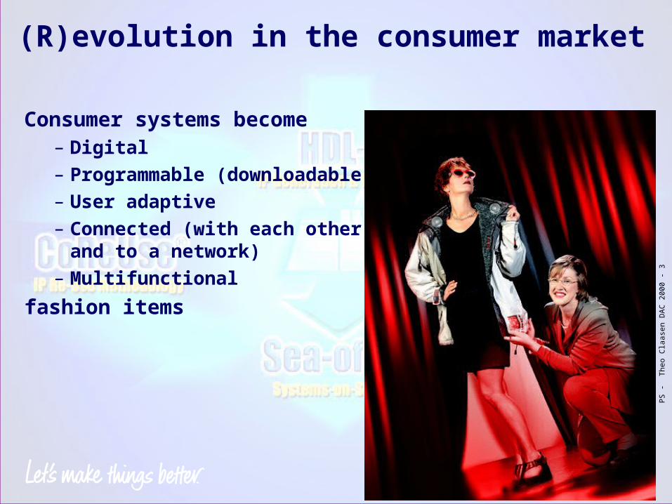
(R)evolution in the consumer market
Consumer systems become– Digital– Programmable (downloadable)– User adaptive– Connected (with each other
and to a network)– Multifunctional
fashion items

PS
- Theo C
laase
n D
AC
20
00
- 4
Example

PS
- Theo C
laase
n D
AC
20
00
- 5
The environment
•Same functions wanted– At home – On the move– In the office
•All the time, anywhere•With consistency of
– Data – User interface

PS
- Theo C
laase
n D
AC
20
00
- 6
Consequences for design
• IC design needs to handle– Integrated systems (SoC)– Increasing complexity– Fast time to market (too late = no business)– Hardware and software– High processing speed and / or low power
•This requires a design process that is– Predictable in time and performance– Efficient
•The key elements of such a design process are – High level of re-use– Silicon prototyping
So what about the design crisis?
PS
- Theo C
laase
n D
AC
20
00
- 7
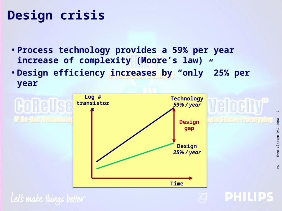
Design crisis
•Process technology provides a 59% per year increase of complexity (Moore’s law)
•Design efficiency increases by “only” 25% per year
Log # transistors
Time
Technology 59% /
year
Design 25% / year
Designgap
PS
- Theo C
laase
n D
AC
20
00
- 8
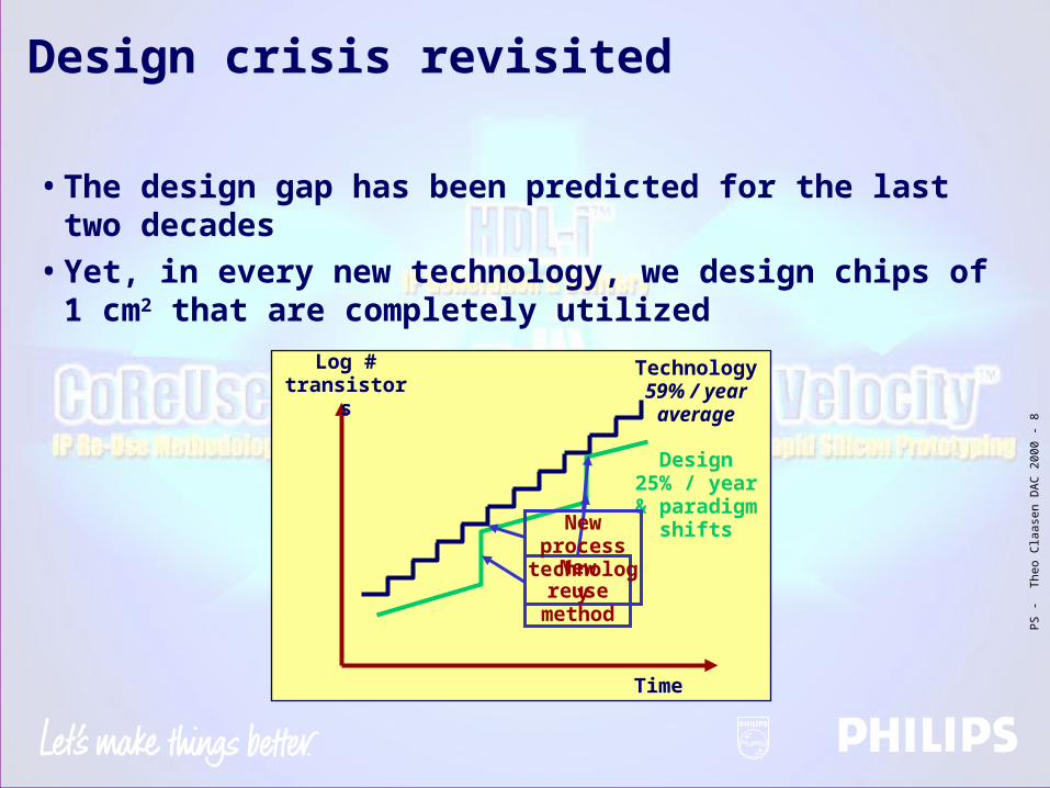
Design crisis revisited
•The design gap has been predicted for the last two decades
•Yet, in every new technology, we design chips of 1 cm2 that are completely utilized
Log # transistors
Time
Technology 59% /
year averageDesign
25% / year &
paradigm shifts
New reuse
method
New process
technology

PS
- Theo C
laase
n D
AC
20
00
- 9
Reuse
Reuse comes in generations
Generation Reuse element Status
1st Standard cells Well established
2nd IP blocks Being introduced
3rd Architecture Emerging
4th IC Early research

PS
- Theo C
laase
n D
AC
20
00
- 1
0
Conditions for reuse
•A consistent methodology– Standards
• Interconnection of elements• File and directory structure• Test
– Guidelines• Design (power, clock)• Test• Debug
CoReUse®
standardsCoReUse®
constraintsWrapping of a core Contents of a core
Directory structure
All views present
& consistent
File name convention
s
All soft, firm
or hard rules
Previous + all
maintenance
rules
All CoReUse® guideline
s

PS
- Theo C
laase
n D
AC
20
00
- 1
1
Conditions for reuse
•A consistent methodology•A comprehensive library of reuse elements
– Compliant with the methodology– Proven on silicon (individually and in combination)

PS
- Theo C
laase
n D
AC
20
00
- 1
2
Conditions for reuse
•A consistent methodology•A comprehensive library of reuse elements•Development tools•Rapid silicon prototyping

PS
- Theo C
laase
n D
AC
20
00
- 1
3
Rapid silicon prototyping
• It is no use to have “first-time-right” silicon if it was not designed with the right specification
•Specifications can only be right after extensive simulation
– With real data– In a real environment
•Simulation– Needs to be bit-accurate– Should comprise hours of data (at 100Mhz = 4.1011
cycles)– Debugs both hardware and software
•The only simulation that is fast enough is using silicon
– Running at (almost) same speed– Having one-to-one mapping to actual silicon

PS
- Theo C
laase
n D
AC
20
00
- 1
4
Rapid silicon prototypingDesign cycle benefits
RSP Design ProcessProductionRelease
Conventional Design Process (1st time right Si)ProductionRelease
SW Development and Validation
Silicon FabricationHW Development and Validation
Placement, Routing & Physical Verification
•Faster chip development– More than 50% total design cycle reduction – True HW / SW co-development
•Higher probability of first-pass success
PS
- Theo C
laase
n D
AC
20
00
- 1
5
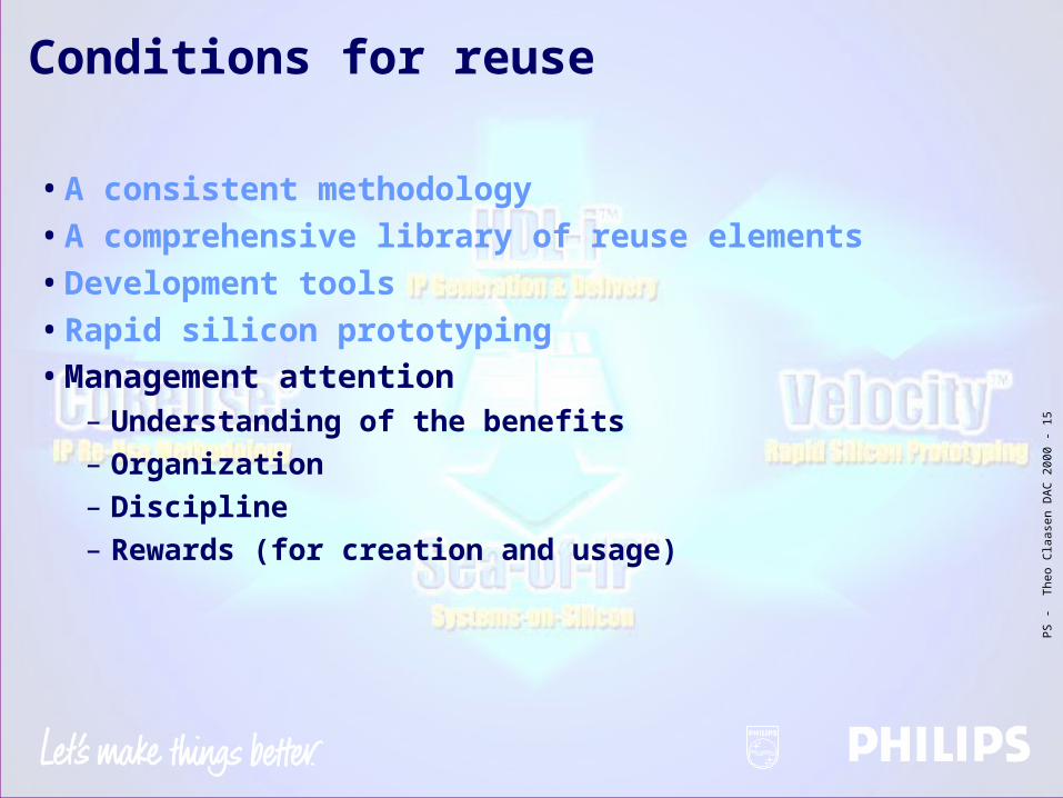
•Management attention– Understanding of the benefits– Organization– Discipline– Rewards (for creation and usage)
Conditions for reuse
•A consistent methodology•A comprehensive library of reuse elements•Development tools•Rapid silicon prototyping
PS
- Theo C
laase
n D
AC
20
00
- 1
6
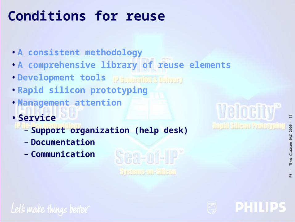
•Service– Support organization (help desk)– Documentation– Communication
Conditions for reuse
•A consistent methodology•A comprehensive library of reuse elements•Development tools•Rapid silicon prototyping•Management attention
PS
- Theo C
laase
n D
AC
20
00
- 1
7
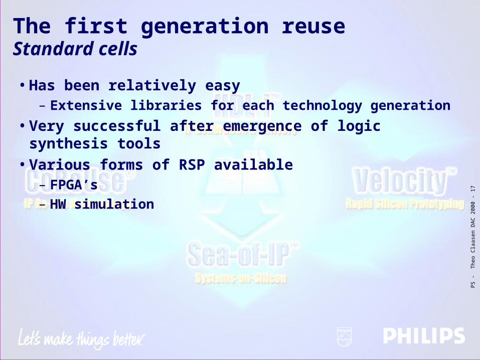
The first generation reuseStandard cells
•Has been relatively easy– Extensive libraries for each technology generation
•Very successful after emergence of logic synthesis tools
•Various forms of RSP available– FPGA’s– HW simulation

PS
- Theo C
laase
n D
AC
20
00
- 1
8
Standard cells
Industry status
Methodology Sea of gates
Library elements Standard cellsI/O’s
Tools Logic synthesisPlace / route
RSP FPGAHW simulators

PS
- Theo C
laase
n D
AC
20
00
- 1
9
The second generation reuseIP blocks (virtual components)
•Virtual components have been around for some time•Limited success so far, except for specific blocks
– CPU cores– DSP cores– Memories– Some periphery devices
•Major problems– Slow emergence of standards (VSIA)– Business models and liabilities (VCX)– Rapid silicon prototyping– Support and service
•Extension to SW reusable modules needed– Speeding up HW design brings SW on critical path

PS
- Theo C
laase
n D
AC
20
00
- 2
0
IP reuse
Industry status PhilipsSemiconductors
Methodology VSIA CoReUseTM (HW)MoReUse
(SW)
Library elements CPU, DSP, etc ReUse library
Tools IP synthesisBlock place / route
HDL-I (IP generation& delivery)ASIC Design Flow
RSP FPGAHW simulators
VLSI VelocityTM
Sea-
of-IP

PS
- Theo C
laase
n D
AC
20
00
- 2
1
PS
- Theo C
laase
n D
AC
20
00
- 2
2
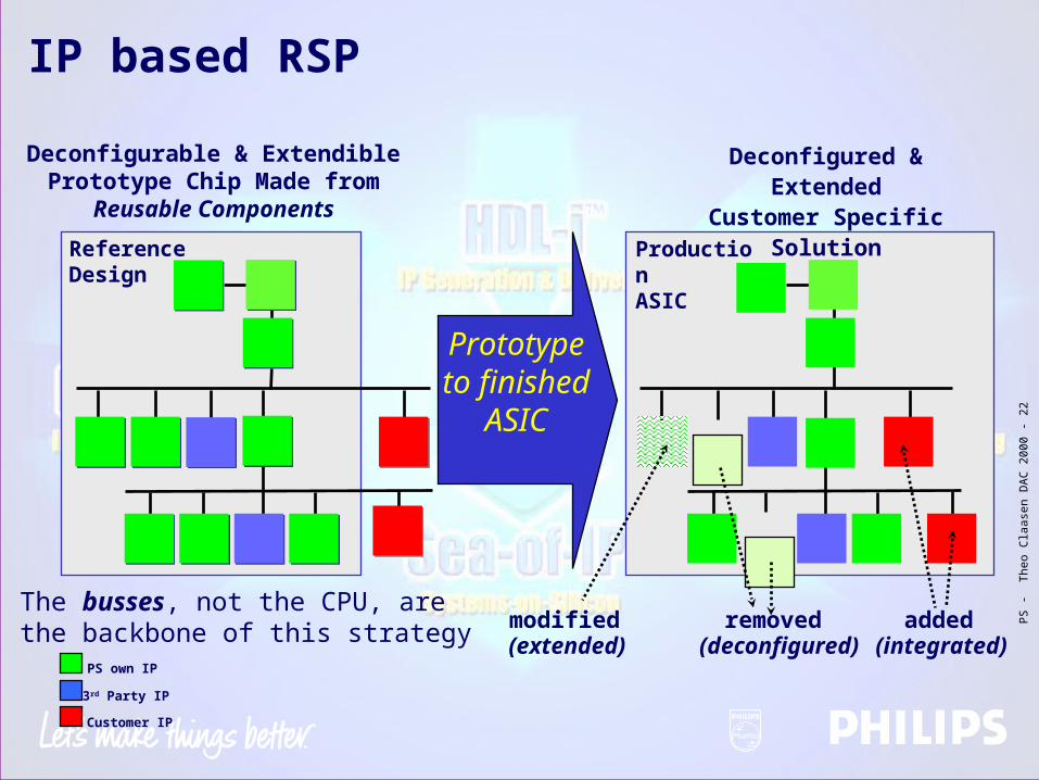
IP based RSP
Reference Design
Deconfigurable & Extendible Prototype Chip Made from
Reusable Components
PS own IP
3rd Party IP
Customer IP
The busses, not the CPU, are the backbone of this strategy
Prototype to
finished ASIC
added (integrated)
modified (extended)
removed (deconfigured)
ProductionASIC
Deconfigured & Extended
Customer Specific Solution

PS
- Theo C
laase
n D
AC
20
00
- 2
3
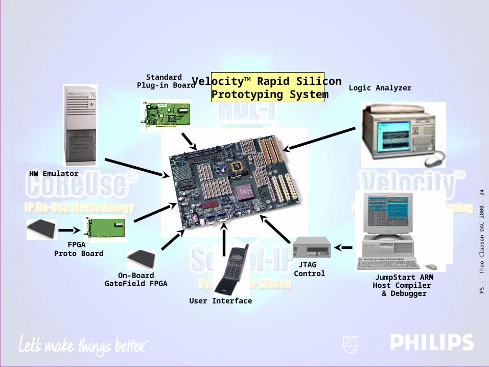
VLSI VelocityTM
The RSP7 board and development system
•From system-on-a-benchtop to system-on-a-chip– Wealth of development functionality supporting system,
chip and software development
Logic Analyzer
HW Emulator
Standard Plug-in Board
On-BoardGateField FPGA
JTAG Control
JumpStart ARMHost Compiler
& Debugger
Velocity™ Rapid Silicon Prototyping System
User Interface
FPGA Proto Board
PS
- Theo C
laase
n D
AC
20
00
- 2
4
Logic Analyzer
HW Emulator
FPGA Proto Board
Standard Plug-in Board
JumpStart ARMHost Compiler
& DebuggerUser Interface
On-BoardGateField FPGA
JTAG Control
Velocity™ Rapid Silicon Prototyping System

PS
- Theo C
laase
n D
AC
20
00
- 2
5
The third generation reuseArchitectures (Silicon System Platform)
•Silicon System Platform– Flexible architecture for hardware and software– Specific (programmable) components– Bus architecture– Software modules– Rules and guidelines for design of HW and SW
•Has been successful in PC’s– Dominance of a few players who specify and control
architecture
•Application domain specific (difference in constraints)
– Speed (compute power)– Dissipation– Costs– Real / non-real time data
PS
- Theo C
laase
n D
AC
20
00
- 2
6
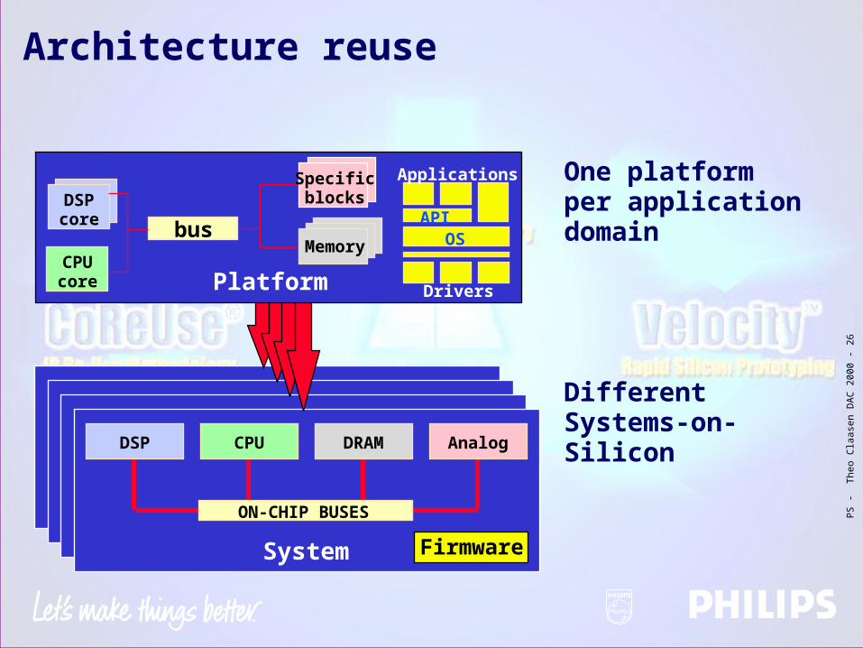
Architecture reuse
System
DSP
ON-CHIP BUSES
CPU DRAM Analog
Firmware
Different Systems-on-Silicon
Platform
DSP core
CPU core
bus Memory
Specificblocks
OSAPI
Applications
Drivers
One platform per application domain

PS
- Theo C
laase
n D
AC
20
00
- 2
7
Architecture reuse
Industry status PhilipsSemiconductors
Methodology Only for PC Nexperia
Library elements NexperiaDVP & SCP libraries
Tools Full custom Sea of IPCosy
RSP NAPA
PS
- Theo C
laase
n D
AC
20
00
- 2
8
NexperiaTM
•Application domain specific (e.g. digital video, digital audio, telecom handsets) architectural concept for programmable functions, comprising
– Processors (CPU for control and DSP for streaming data)
– Connected with low-speed and high-speed busses to a shared memory
– A comprehensive set of peripherals– Software components ranging from drivers and API
to application modules
•Scalable from high end to low end– Cost– Performance– Features

PS
- Theo C
laase
n D
AC
20
00
- 2
9
TM-xxxxTM-xxxx D$
D$
I$I$
TriMedia CPU
DEVICE I/P BLOCKDEVICE I/P BLOCK
DEVICE I/P BLOCKDEVICE I/P BLOCK
DEVICE I/P BLOCKDEVICE I/P BLOCK
. . .
DVP System Silicon
VLIW Media Processor:• 100 to 300+ MHz• 32-bit or 64-bit
NexperiaSystem Busses• PI bus• Memory bus• 32-128 bit
PI
BU
S
SDRAMSDRAM
MMIMMI
DV
P M
EM
OR
Y
BU
S
DEVICE I/P BLOCKDEVICE I/P BLOCK
PRxxxxPRxxxxD$
D$
I$I$
MIPS CPU
DEVICE I/P BLOCKDEVICE I/P BLOCK. . .
DEVICE I/P BLOCKDEVICE I/P BLOCK
PI
BU
S
General Purpose RISC Processor• 50 to 300+ MHz• 32-bit or 64-bitLibrary of Device Blocks• Imagecoprocessors
• DSPs• UART• 1394• USB
•…and more
TriMediaTMMIPSTM
NexperiaTM DVPHardware architecture
Flexible architecture for digital video applications

PS
- Theo C
laase
n D
AC
20
00
- 3
0
NexperiaTM
Scalability
VLIWVLIW
SDRAMSDRAM
MMIMMI
TriMedia CPU + Device blocks when
control functions areminimal
MIPS CPU +Trimedia CPU replacing some Device blocks
RISCRISC
SDRAMSDRAM
VLIWVLIWMMIMMI
• Single architecture, multiple product configurations– Processor core options - TM32, TM64, MIPS32, MIPS64 ...– Device block options
• Highly programmable to weakly programmable
MIPS CPU +Device blocks +
Software
RISCRISC
SDRAMSDRAM
MMIMMI

PS
- Theo C
laase
n D
AC
20
00
- 3
1
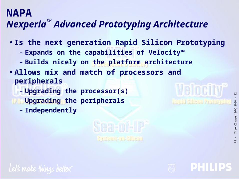
NAPANexperiaTM Advanced Prototyping Architecture
PS
- Theo C
laase
n D
AC
20
00
- 3
2
NAPANexperiaTM Advanced Prototyping Architecture• Is the next generation Rapid Silicon Prototyping
– Expands on the capabilities of Velocity™– Builds nicely on the platform architecture
•Allows mix and match of processors and peripherals
– Upgrading the processor(s)– Upgrading the peripherals– Independently

PS
- Theo C
laase
n D
AC
20
00
- 3
3
The NAPA system
Start with a platform architecturewith two processors(a CPU and a DSP) and amemory controller.
Add a high speed bus to accommodate a high speed memory interface for streaming data.
DMA Gate MM/S DMA Gate M/SM
M/S M/S
M M
M M
•••
Peripheral M/S
MEMCProcessorPeriph Processor Periph
PeripheralM/S Peripheral M/S PeripheralM/S
Peripheral M/S PeripheralM/S Peripheral M/S PeripheralM/S
Crossover Bridge M/SM/S
Bridge Bridge
Peripheral M/S PeripheralM/S Peripheral M/S PeripheralM/S
•••
•••
•••

PS
- Theo C
laase
n D
AC
20
00
- 3
4
MEMCProcessorPeriph
Tunnel
MEMCProcessor Periph
Tunnel
•••
Peripheral M/S Peripheral MM/S Peripheral M/SM PeripheralM/S
Peripheral M/S Peripheral MM/S Peripheral M/SM PeripheralM/S
DMA Gate MM/S DMA Gate M/SM
Crossover Bridge M/SM/S
Bridge Tunnel Bridge
Peripheral M/S Peripheral M/SM/S Peripheral M/SM/S PeripheralM/S
•••
•••
•••
BridgeBridge
(optional)
Split the system into logical parts by using bridges and tunnelsBridge: no latency modest speed
Tunnel: some latency high speed In many systems
one of the memory controllers will be disabled
The NAPA system
PS
- Theo C
laase
n D
AC
20
00
- 3
5
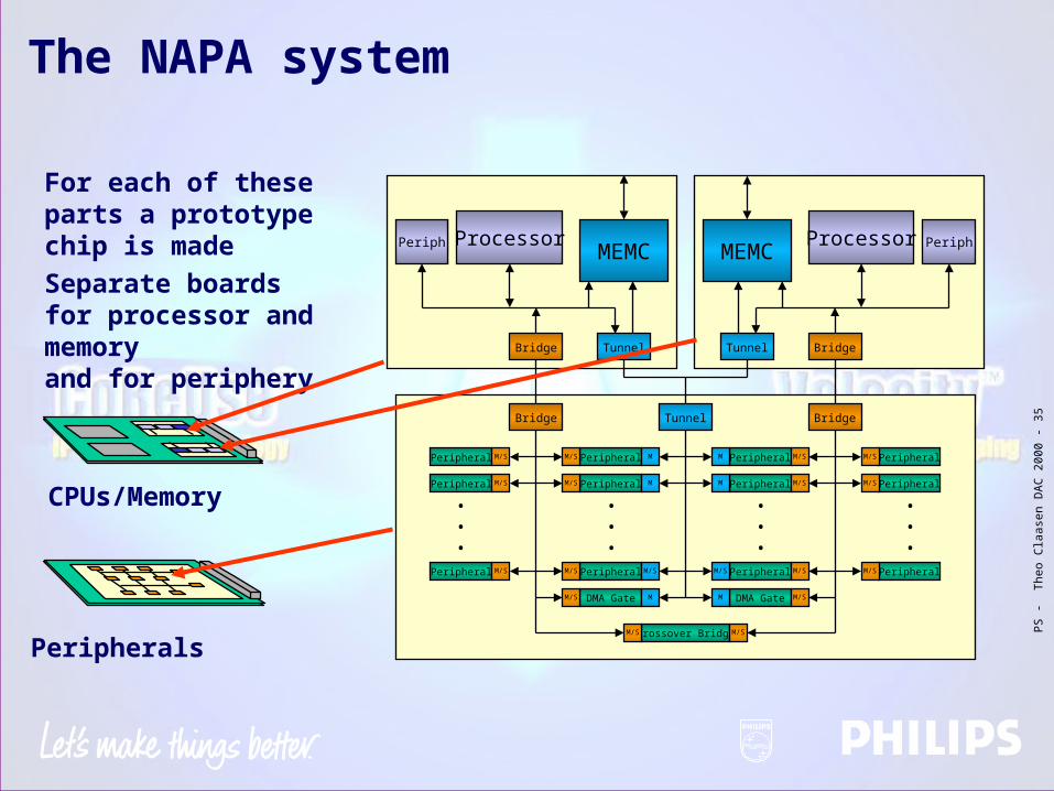
The NAPA system
MEMCProcessor Periph
Tunnel
For each of these parts a prototype chip is made MEMC
ProcessorPeriph
Tunnel
Separate boards for processor and memoryand for periphery
•••
Peripheral M/S Peripheral MM/S Peripheral M/SM PeripheralM/S
Peripheral M/S Peripheral MM/S Peripheral M/SM PeripheralM/S
DMA Gate MM/S DMA Gate M/SM
Crossover Bridge M/SM/S
Bridge Bridge
Peripheral M/S Peripheral M/SM/S Peripheral M/SM/S PeripheralM/S
•••
•••
•••
Tunnel
Bridge Bridge
Peripherals
CPUs/Memory

PS
- Theo C
laase
n D
AC
20
00
- 3
6
NAPA card cage
CPUs/Memory
Peripherals
Peripherals
FPGA cardBackplane allows probing and logic analyzer connections
Cards can be inserted in any order

PS
- Theo C
laase
n D
AC
20
00
- 3
7
MEMCProcessorPeriph
Tunnel
MEMCProcessor Periph
Tunnel
•••
Peripheral M/S Peripheral MM/S Peripheral M/SM PeripheralM/S
Peripheral M/S Peripheral MM/S Peripheral M/SM PeripheralM/S
DMA Gate MM/S DMA Gate M/SM
Crossover Bridge M/SM/S
Bridge Tunnel Bridge
Peripheral M/S Peripheral M/SM/S Peripheral M/SM/S PeripheralM/S
•••
•••
•••
BridgeBridge
Building an IC from the prototypeASIC or CSIC
MEMCProcessorPeriph
Tunnel
MEMCProcessor Periph
Tunnel
•••
Peripheral M/S Peripheral MM/S Peripheral M/SM PeripheralM/S
Peripheral M/S Peripheral MM/S Peripheral M/SM PeripheralM/S
DMA Gate MM/S DMA Gate M/SM
Crossover Bridge M/SM/S
Bridge Tunnel Bridge
Peripheral M/S Peripheral M/SM/S Peripheral M/SM/S PeripheralM/S
•••
•••
•••
BridgeBridge
Put it all together
PS
- Theo C
laase
n D
AC
20
00
- 3
8
MEMCProcessorPeriph
Tunnel
MEMCProcessor Periph
Tunnel
•••
Peripheral M/S Peripheral MM/S Peripheral M/SM PeripheralM/S
Peripheral M/S Peripheral MM/S Peripheral M/SM PeripheralM/S
DMA Gate MM/S DMA Gate M/SM
Crossover Bridge M/SM/S
Bridge Tunnel Bridge
Peripheral M/S Peripheral M/SM/S Peripheral M/SM/S PeripheralM/S
•••
•••
•••
BridgeBridge
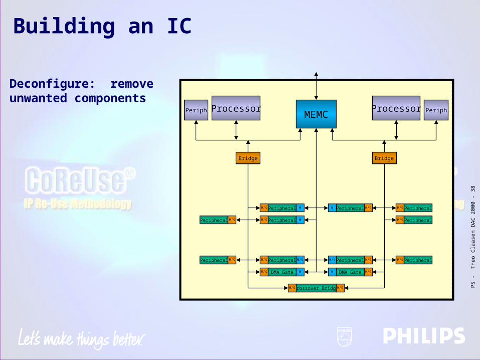
Building an IC
Deconfigure: remove unwanted components
MEMCProcessorPeriph Processor Periph
Peripheral MM/S Peripheral M/SM PeripheralM/S
Peripheral M/S Peripheral MM/S PeripheralM/S
DMA Gate MM/S DMA Gate M/SM
Crossover Bridge M/SM/S
Peripheral M/S Peripheral M/SM/S Peripheral M/SM/S PeripheralM/S
BridgeBridge
PS
- Theo C
laase
n D
AC
20
00
- 3
9
MEMCProcessorPeriph Processor Periph
Peripheral MM/S Peripheral M/SM PeripheralM/S
Peripheral M/S Peripheral MM/S PeripheralM/S
DMA Gate MM/S DMA Gate M/SM
Crossover Bridge M/SM/S
Peripheral M/S Peripheral M/SM/S Peripheral M/SM/S PeripheralM/S
BridgeBridge
Building an IC
Extend: add prototyped (FPGA) components
This will provide the database for the chip MEMC
ProcessorPeriph Processor Periph
Peripheral MM/S Peripheral M/SM PeripheralM/S
Peripheral M/S Peripheral MM/S PeripheralM/S
DMA Gate MM/S DMA Gate M/SM
Crossover Bridge M/SM/S
Peripheral M/S Peripheral M/SM/S Peripheral M/SM/S PeripheralM/S
BridgeBridge
Peripheral M/S Peripheral MM/S
PeripheralM/SPeripheralM/S

PS
- Theo C
laase
n D
AC
20
00
- 4
0
The fourth generation reuseIC reuse
•We need to go to 100M+ transistor chips in deep sub-micron
•Mask costs get very expensive•Too expensive to spin silicon
– For correcting design errors– For correcting specification errors– For designing variants
•Basic technology: retargetable / reconfigurable systems
•No methodology yet•A number of start ups develop technology

PS
- Theo C
laase
n D
AC
20
00
- 4
1
IC reuse
•Problems to be addressed– Silicon efficiency (area)– Compiler efficiency (code size and speed)– Computational efficiency (speed)– HW / SW co-design– Reconfigurable interconnectivity– SW design for reuse
•No prototyping issues anymore•Guaranteed fast time-to-market

PS
- Theo C
laase
n D
AC
20
00
- 4
2
Conclusions
•Consumer IC’s generate the need for fast and efficient design methods
•The design efficiency increases slower than Moore’s law•New generations of reuse technology are the solution to
the corresponding design gap• IP reuse is emerging•The next wave will be architecture reuse
(Silicon System Platforms)•Rapid silicon prototyping is an essential element of
these reuse technologies•The new wave may be IC reuse with retargetable
architectures