proximity capacitive touch sensor controller mpr031...
TRANSCRIPT
MPR03XRev 7, 7/2012
Freescale SemiconductorData Sheet: Technical DataAn Energy Efficient Solution by Freescale
© 2008, 2009, 2011, 2012 Freescale Semiconductor, Inc. All rights reserved.
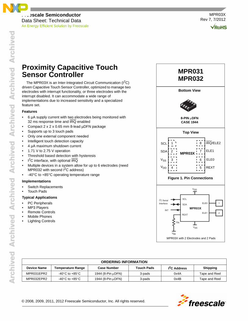
Proximity Capacitive TouchSensor Controller
The MPR03X is an Inter-Integrated Circuit Communication (I2C) driven Capacitive Touch Sensor Controller, optimized to manage two electrodes with interrupt functionality, or three electrodes with the interrupt disabled. It can accommodate a wide range of implementations due to increased sensitivity and a specialized feature set.
Features
• 6 µA supply current with two electrodes being monitored with 32 ms response time and IRQ enabled
• Compact 2 x 2 x 0.65 mm 8-lead µDFN package• Supports up to 3 touch pads• Only one external component needed• Intelligent touch detection capacity• 4 µA maximum shutdown current• 1.71 V to 2.75 V operation• Threshold based detection with hysteresis• I2C interface, with optional IRQ• Multiple devices in a system allow for up to 6 electrodes (need
MPR032 with second I2C address)• -40°C to +85°C operating temperature range
Implementations
• Switch Replacements• Touch Pads
Typical Applications
• PC Peripherals• MP3 Players• Remote Controls• Mobile Phones• Lighting Controls
ORDERING INFORMATION
Device Name Temperature Range Case Number Touch Pads I2C Address Shipping
MPR031EPR2 -40C to +85C 1944 (8-Pin DFN) 3-pads 0x4A Tape and Reel
MPR032EPR2 -40C to +85C 1944 (8-Pin DFN) 3-pads 0x4B Tape and Reel
MPR031MPR032
Top View
Figure 1. Pin Connections
Bottom View
8-PIN DFNCASE 1944
1SCL
2
3
8
7
6
54
SDA
VSS
VDD
IRQ/ELE2
ELE1
ELE0
REXT
MPR03X
InterfaceI²C Serial
VSS
SDA
SCL
MPR03X
ELE0
ELE1
VDD
INT
1
2
VSS
75k
REXT
MPR03X with 2 Electrodes and 2 Pads

1 Device Overview
1.1 Introduction
MPR03X is a small outline, low profile, low voltage touch sensor controller in a 2 mm x 2 mm DFN which manages up to three touch pad electrodes. An I2C interface communicates with the host controller at data rates up to 400 kbits/sec. An optional interrupt output advises the host of electrode status changes. The interrupt output is a multiplexed with the third electrode output, so using the interrupt output reduces the number of electrode inputs to two. The MPR03X includes three levels of input signal filtering to detect pad input condition changes due to touch without any processing by the application.
1.2 Internal Block Diagram
Figure 2. Functional Block Diagram
ELE0
ELE1
ELE2
0
1
2
0 1 2Current SourceMultiplexor
InputSourceM
ultiplexor
Iref
3 Set Source CurrentMirror
Iset
Select Chan
SelectChan
Set Input Channel
Sel Set GroundedElectrodes
10 Bit ADC
EnableConvert
ClockData
10 ADC Result8MHzStart ConversionShutdown
2
4
2
InterruptController
I²CInterface
32 kHzOscillator
UserRegisters
DebouncedResults
MagnitudeComparator
AverageFiltered
DebounceResult
Debounce Filter Registers4 x Max Registers4 x SumRegisters4 x Min Registers
SDASCL
IRQ SET
CLR
Shutdown
DebounceInterval
DebounceCount
SampleInterval
SampleCount
Debounceand
SampleCounters
AverageFilteredSampleResult
Sample Filter RegistersMax RegisterSumRegisterMin Register
Set Source Current
Set Input Channel
ADC Result
8MHz
Start ConversionShutdown
8 MHzOscillator
Shutdown
ADCController
Traffic
SDASCL
IRQ
32 kHz8 MHz
Set GroundedElectrodes
Number ofElectrodes
Un-TouchedBaseline
Filter
0V
REXT
MPR03X
Sensors2 Freescale Semiconductor

2 External Signal Description
2.1 Device Pin AssignmentTable 1 shows the pin assignment for the MPR03X. For a more detailed description of the functionality of each pin, refer to the appropriate chapter.
The package available for the MPR03X is a 2 x 2 mm 8 pin DFN. The package and pinout is shown in Figure 3.
Figure 3. Package Pinouts
2.2 Recommended System Connections
The MPR03X Capacitive Touch Sensor Controller requires one external passive component. As shown in Table 1, the REXT line should have a 75 kconnected from the pin to GND. This resistor needs to be 1% tolerance.
In addition to the one resistor, a bypass capacitor of 10 µF should always be used between the VDD and VSS lines and a 4.7 k pull-up resistor should be included on the IRQ. Note: This condition is when pin 8 is used for interrupt indication and not for electrode sensing.
The remaining two connections are SCL and SDA. Depending on the specific application, each of these control lines can be used by connecting them to a host controller. In the most minimal system, the SCL and SDA must be connected to a master I2C interface to communicate with the MPR03X. All of the connections for the MPR03X are shown by the schematic in Figure 4.
Table 1. Device Pin Assignment
Pin Name Function
1 SCL I2C Serial Clock Input
2 SDA I2C Serial Data I/O
3 VSS Ground
4 VDD Positive Supply Voltage
5 REXT Reference ResistorConnect a 75 k ±1% resistor from REXT to VSS
6 ELE0 Electrode 0
7 ELE1 Electrode 1
8 IRQ/ELE2 Interrupt Output or Touch Electrode Input 2IRQ is the active-low open-drain interrupt output
1SCL
2
3
8
7
6
54
SDA
VSS
VDD
IRQ/ELE2
ELE1
ELE0
REXT
MPR03X
InterfaceI²C Serial
3
VSS
SDA
SCL
MPR03X
ELE0
ELE1
IRQ/ELE2
1
2
VSS
75k
VDD
REXT
MPR03X
SensorsFreescale Semiconductor 3

Figure 4. Recommended System Connections Schematic
2.3 Serial Interface
The MPR03X uses an I2C Serial Interface. The I2C protocol implementation and the specifics of communicating with the Touch Sensor Controller are detailed in the following sections.
2.3.1 Serial-Addressing
The MPR03X operates as a slave that sends and receives data through an I2C 2-wire interface. The interface uses a Serial Data Line (SDA) and a Serial Clock Line (SCL) to achieve bi-directional communication between master(s) and slave(s). A master (typically a microcontroller) initiates all data transfers to and from the MPR03X, and it generates the SCL clock that synchronizes the data transfer.
The MPR03X SDA line operates as both an input and an open-drain output. A pull-up resistor, typically 4.7k, is required on SDA. The MPR03X SCL line operates only as an input. A pull-up resistor, typically 4.7k, is required on SCL if there are multiple masters on the 2-wire interface, or if the master in a single-master system has an open-drain SCL output.
Each transmission consists of a START condition (Figure 5) sent by a master, followed by the MPR03X’s 7-bit slave address plus R/W bit, a register address byte, one or more data bytes, and finally a STOP condition.
Figure 5. Wire Serial Interface Timing Details
2.3.2 Start and Stop Conditions
Both SCL and SDA remain high when the interface is not busy. A master signals the beginning of a transmission with a START (S) condition by transitioning SDA from high to low while SCL is high. When the master has finished communicating with the slave, it issues a STOP (P) condition by transitioning SDA from low to high while SCL is high. The bus is then free for another transmission.
Figure 6. Bit Transfer
SCL
SDA
tLOW
tHIGH
tFtRtHD STA
tHD DATtHD STA
tSU DAT tSU STA
tBUF
tSU STO
STARTCONDITION
STOPCONDITION
REPEATED STARTCONDITION
STARTCONDITION
DATA LINE STABLEDATA VALID CHANGE OF
DATA ALLOWED
SDA
SCL
MPR03X
Sensors4 Freescale Semiconductor

2.3.3 Bit Transfer
One data bit is transferred during each clock pulse (Figure 7). The data on SDA must remain stable while SCL is high.
Figure 7. Stop and Start Conditions
2.3.4 Acknowledge
The acknowledge bit is a clocked 9th bit (Figure 8) which the recipient uses to handshake receipt of each byte of data. Thus each byte transferred effectively requires 9 bits. The master generates the 9th clock pulse, and the recipient pulls down SDA during the acknowledge clock pulse, such that the SDA line is stable low during the high period of the clock pulse. When the master is transmitting to the MPR03X, the MPR03X generates the acknowledge bit, since the MPR03X is the recipient. When the MPR03X is transmitting to the master, the master generates the acknowledge bit, since the master is the recipient.
Figure 8. Acknowledge
2.3.5 The Slave Address
The MPR03X has a 7-bit long slave address (Figure 9). The bit following the 7-bit slave address (bit eight) is the R/W bit, which is low for a write command and high for a read command.
Figure 9. Slave Address
The MPR03X monitors the bus continuously, waiting for a START condition followed by its slave address. When a MPR03X recognizes its slave address, it acknowledges and is then ready for continued communication.
The MPR031 and MPR032 slave addresses are show in Table 2.
Table 2.
Part Number I2C Address
MPR031 0x4A
MPR032 0x4B
STARTCONDITION
SDA
SCL
STOPCONDITION
PS
STARTCONDITION
SDABY TRANSMITTER
S
1 2 8 9
CLOCK PULSE FORACKNOWLEDGEMENT
SDABY RECEIVER
SCL
SDA1 R/W ACK
MSB
SCL
0 10 0 1 0
MPR03X
SensorsFreescale Semiconductor 5
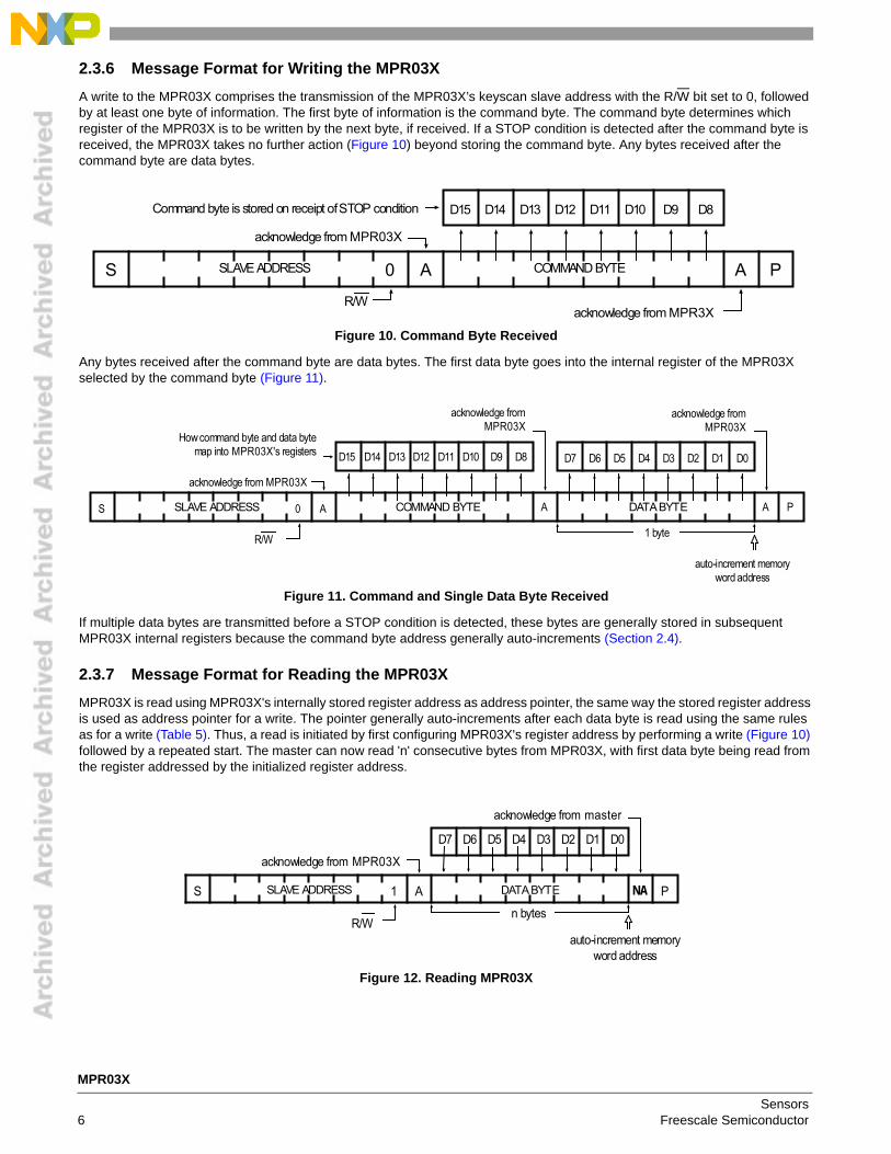
2.3.6 Message Format for Writing the MPR03X
A write to the MPR03X comprises the transmission of the MPR03X’s keyscan slave address with the R/W bit set to 0, followed by at least one byte of information. The first byte of information is the command byte. The command byte determines which register of the MPR03X is to be written by the next byte, if received. If a STOP condition is detected after the command byte is received, the MPR03X takes no further action (Figure 10) beyond storing the command byte. Any bytes received after the command byte are data bytes.
Figure 10. Command Byte Received
Any bytes received after the command byte are data bytes. The first data byte goes into the internal register of the MPR03X selected by the command byte (Figure 11).
Figure 11. Command and Single Data Byte Received
If multiple data bytes are transmitted before a STOP condition is detected, these bytes are generally stored in subsequent MPR03X internal registers because the command byte address generally auto-increments (Section 2.4).
2.3.7 Message Format for Reading the MPR03X
MPR03X is read using MPR03X's internally stored register address as address pointer, the same way the stored register address is used as address pointer for a write. The pointer generally auto-increments after each data byte is read using the same rules as for a write (Table 5). Thus, a read is initiated by first configuring MPR03X's register address by performing a write (Figure 10) followed by a repeated start. The master can now read 'n' consecutive bytes from MPR03X, with first data byte being read from the register addressed by the initialized register address.
Figure 12. Reading MPR03X
S A A P0SLAVE ADDRESS COMMAND BYTE
acknowledge from MPR03X
R/Wacknowledge from MPR3X
D15 D14 D13 D12 D11 D10 D9 D8Command byte is stored on receipt ofSTOP condition
S A A A P0SLAVE ADDRESS COMMAND BYTE DATABYTE
acknowledge from MPR03X
R/W 1 byte
auto-increment memoryword address
D15 D14 D13 D12 D11 D10 D9 D8 D1 D0D3 D2D5 D4D7 D6
Howcommand byte and data bytemap into MPR03X's registers
acknowledge fromMPR03X
acknowledge fromMPR03X
S A A P1SLAVE ADDRESS DATABYTE
R/Wn bytes
auto-increment memoryword address
D1 D0D3 D2D5 D4D7 D6
acknowledge from MPR03X
acknowledge from master
NA
MPR03X
Sensors6 Freescale Semiconductor

2.3.8 Operation with Multiple Master
The application should use repeated starts to address the MPR03X to avoid bus confusion between I2C masters.On a I2C bus, once a master issues a start/repeated start condition, that master owns the bus until a stop condition occurs. If a master that does not own the bus attempts to take control of that bus, then improper addressing may occur. An address may always be rewritten to fix this problem. Follow I2C protocol for multiple master configurations.
2.4 Register Address Map
Table 3. Register Address Map
Register Register AddressBurst Mode
Auto-Increment Address
Touch Status Register 0x00
Register Address + 1
ELE0 Filtered Data Low Register 0x02
ELE0 Filtered Data High Register 0x03
ELE1 Filtered Data Low Register 0x04
ELE1 Filtered Data High Register 0x05
ELE2 Filtered Data Low Register 0x06
ELE2 Filtered Data High Register 0x07
ELE0 Baseline Value Register 0x1A
ELE1 Baseline Value Register 0x1B
ELE2 Baseline Value Register 0x1C
Max Half Delta Register 0x26
Noise Half Delta Register 0x27
Noise Count Limit Register 0x28
ELE0 Touch Threshold Register 0x29
ELE0 Release Threshold Register 0x2A
ELE1 Touch Threshold Register 0x2B
ELE1 Release Threshold Register 0x2C
ELE2 Touch Threshold Register 0x2D
ELE2 Release Threshold Register 0x2E
AFE Configuration Register 0x41
Filter Configuration Register 0x43
Electrode Configuration Register 0x44 0x00
MPR03X
SensorsFreescale Semiconductor 7

3 Functional Overview
3.1 Introduction
The MPR03X has an analog front, a digital filter, and a touch recognition system. This data interpretation can be done many different ways but the method used in the MPR03X is explained in this chapter.
3.2 Understanding the Basics
MPR03X is a touch pad controller which manages two or three touch pad electrodes. An I²C interface communicates with the host, and an optional interrupt output advises the host of electrode status changes. The interrupt output is a multiplexed function with the third electrode input, so using the interrupt output reduces the number of electrode inputs to two.
The primary application for MPR03X is the management of user interface touch pads. Monitoring touch pads involves detecting small changes of pad capacitance. MPR03X incorporates a self calibration function which continually adjusts the baseline capacitance for each individual electrode. Therefore, the host only has to configure the delta thresholds to interpret a touch or release.
MPR03X uses a state machine to operate a capacitive measurement engine to analyze the electrodes and determine whether a pad has been touched or released. Between measurements the MPR03X draws negligible current. The application controls MPR03X's configuration, making trade-offs between noise rejection, touch response time, and power consumption.
3.3 Implementation
The touch sensor system can be tailored to specific applications by varying the following: a capacitance detector, a raw data low pass filter, a baseline management system, and a touch detection system. In the following sections, the functionality and configuration of each block will be described.
Electrodes can be connected to the MPR03X in two different configurations, one with an IRQ and one without (Figure 13).
Figure 13. MPR03X Pad and Interrupt Connection Options
1
2
3
ELE0
ELE1
ELE2
InterfaceI²C Serial
VSS
SDA
SCL
MPR03X
ELE0
ELE1
VDD
INT
1
2
SDA
SCL
MPR03X
VDD
InterfaceI²C Serial
VSS
VSS
75k
REXT
VSS
75k
REXT
MPR03X with 2 Electrodes and 2 Pads MPR03X with 3 Electrodes and 3 Pads
MPR03X
Sensors8 Freescale Semiconductor
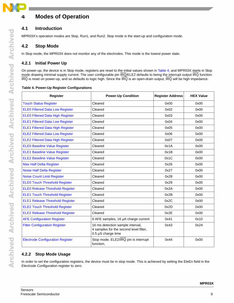
4 Modes of Operation
4.1 Introduction
MPR03X’s operation modes are Stop, Run1, and Run2. Stop mode is the start-up and configuration mode.
4.2 Stop Mode
In Stop mode, the MPR03X does not monitor any of the electrodes. This mode is the lowest power state.
4.2.1 Initial Power Up
On power-up, the device is in Stop mode, registers are reset to the initial values shown in Table 4, and MPR03X starts in Stop mode drawing minimal supply current. The user configurable pin IRQ/ELE2 defaults to being the interrupt output IRQ function. IRQ is reset on power-up, and so defaults to logic high. Since the IRQ is an open-drain output, IRQ will be high impedance.
4.2.2 Stop Mode Usage
In order to set the configuration registers, the device must be in stop mode. This is achieved by setting the EleEn field in the Electrode Configuration register to zero.
Table 4. Power-Up Register Configurations
Register Power-Up Condition Register Address HEX Value
Touch Status Register Cleared 0x00 0x00
ELE0 Filtered Data Low Register Cleared 0x02 0x00
ELE0 Filtered Data High Register Cleared 0x03 0x00
ELE1 Filtered Data Low Register Cleared 0x04 0x00
ELE1 Filtered Data High Register Cleared 0x05 0x00
ELE2 Filtered Data Low Register Cleared 0x06 0x00
ELE2 Filtered Data High Register Cleared 0x07 0x00
ELE0 Baseline Value Register Cleared 0x1A 0x00
ELE1 Baseline Value Register Cleared 0x1B 0x00
ELE2 Baseline Value Register Cleared 0x1C 0x00
Max Half Delta Register Cleared 0x26 0x00
Noise Half Delta Register Cleared 0x27 0x00
Noise Count Limit Register Cleared 0x28 0x00
ELE0 Touch Threshold Register Cleared 0x29 0x00
ELE0 Release Threshold Register Cleared 0x2A 0x00
ELE1 Touch Threshold Register Cleared 0x2B 0x00
ELE1 Release Threshold Register Cleared 0x2C 0x00
ELE2 Touch Threshold Register Cleared 0x2D 0x00
ELE2 Release Threshold Register Cleared 0x2E 0x00
AFE Configuration Register 6 AFE samples, 16 µA charge current 0x41 0x10
Filter Configuration Register 16 ms detection sample interval, 4 samples for the second level filter,0.5 µS charge time
0x43 0x24
Electrode Configuration Register Stop mode. ELE2/IRQ pin is interrupt function,
0x44 0x00
MPR03X
SensorsFreescale Semiconductor 9

4.3 Run1 ModeIn Run1 Mode, the MPR03X monitors 1, 2, or 3 electrodes which are connected to a user defined array of touch pads. When only 1 or 2 electrodes are selected, the IRQ/ELE2 pin is automatically configured as an open drain interrupt output.
When 3 electrodes are selected in Run1 Mode, the IRQ/ELE2 pin becomes the third electrode input, ELE2 (Figure 14).
Figure 14. Electrode/Pad Connections in Run Mode
4.4 Run2 Mode
In Run2 Mode, all enabled electrodes act as a single electrode by internally connecting the electrode pins together. The entire surface of all the touch pads is used as a single pad, increasing the total area of the conductor.
When 2 electrodes are selected in Run2 Mode, the IRQ/ELE2 pin is automatically configured as an open drain interrupt output. When 3 electrodes are selected, the IRQ/ELE2 pin becomes the third electrode input, ELE2 (Figure 15).
Figure 15. Electrode/Pad Connections in Area Detection Mode
4.5 Electrode Configuration Register
The Electrode Configuration Register manages the configuration of the Electrode outputs in addition to the mode of the part. The address of the Electrode Configuration Register is 0x44.
Figure 16. Electrode Configuration Register
7 6 5 4 3 2 1 0
R 0CalLock ModeSel EleEn
W
Reset: 0 0 0 0 0 0 0 0
= Unimplemented
ELE0
ELE1 CapacitanceMeasurement
Engine
Filtersand
TouchDetectionELE2
3
1
2
Run1 Mode with 3 Electrodes
INT Interrupt
Run1 Mode with 2 Electrodes
ELE1
ELE0CapacitanceMeasurement
EngineFiltersand
TouchDetection
1
2
INT Interrupt
Run1 Mode with 1 Electrode
ELE0 CapacitanceMeasurement
EngineFiltersand
TouchDetection
1
ELE0
ELE1
INT
CapacitanceMeasurement
Engine
Filtersand
TouchDetectionELE2 Interrupt
Run2 Mode to 2 Pads
3
1
2 ELE1
ELE0CapacitanceMeasurement
EngineFiltersand
TouchDetection
Run2 Mode to 3 Pads
1
2
MPR03X
Sensors10 Freescale Semiconductor
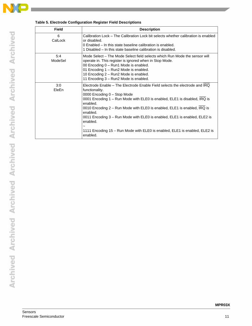
Table 5. Electrode Configuration Register Field Descriptions
Field Description
6CalLock
Calibration Lock – The Calibration Lock bit selects whether calibration is enabled or disabled.0 Enabled – In this state baseline calibration is enabled.1 Disabled – In this state baseline calibration is disabled.
5:4ModeSel
Mode Select – The Mode Select field selects which Run Mode the sensor will operate in. This register is ignored when in Stop Mode.00 Encoding 0 – Run1 Mode is enabled.01 Encoding 1 – Run2 Mode is enabled.10 Encoding 2 – Run2 Mode is enabled.11 Encoding 3 – Run2 Mode is enabled.
3:0EleEn
Electrode Enable – The Electrode Enable Field selects the electrode and IRQ functionality.0000 Encoding 0 – Stop Mode0001 Encoding 1 – Run Mode with ELE0 is enabled, ELE1 is disabled, IRQ is enabled.0010 Encoding 2 – Run Mode with ELE0 is enabled, ELE1 is enabled, IRQ is enabled.0011 Encoding 3 – Run Mode with ELE0 is enabled, ELE1 is enabled, ELE2 is enabled.~1111 Encoding 15 – Run Mode with ELE0 is enabled, ELE1 is enabled, ELE2 is enabled.
MPR03X
SensorsFreescale Semiconductor 11
5 Output Mechanisms
5.1 Introduction
The MPR03X has three outputs: the touch status, values from the second level filter (Section 8.3), and the calibrated baseline values. The application can either use the touch status or a combination of second level filter data with the baseline data to determine when a touch occurs.
5.2 Touch Status
Each Electrode has an associated single bit that denotes whether or not the pad is currently touched. This output is generated using the touch threshold and release threshold registers to determine when a pad is considered touched or untouched. Configuration of this system is discussed in Section 9.
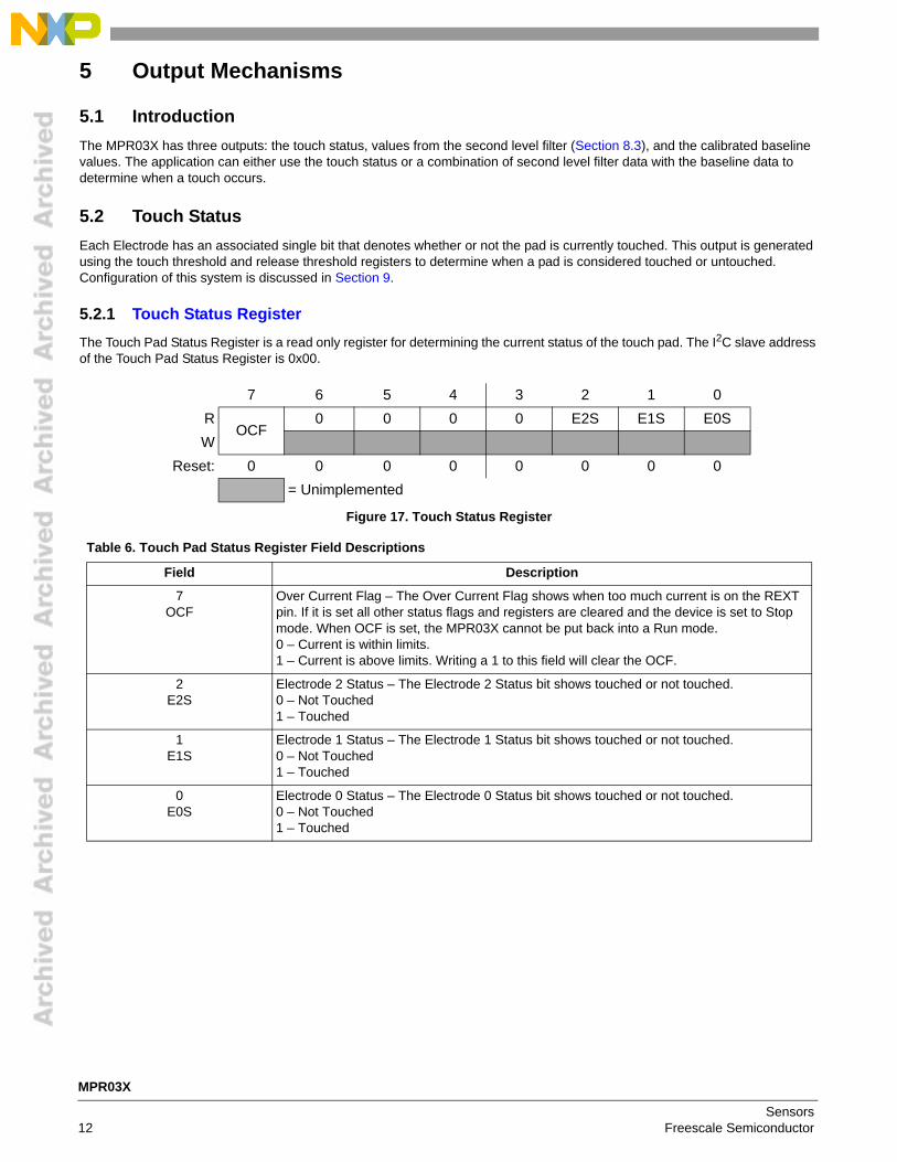
5.2.1 Touch Status Register
The Touch Pad Status Register is a read only register for determining the current status of the touch pad. The I2C slave address of the Touch Pad Status Register is 0x00.
Figure 17. Touch Status Register
7 6 5 4 3 2 1 0
ROCF
0 0 0 0 E2S E1S E0S
W
Reset: 0 0 0 0 0 0 0 0
= Unimplemented
Table 6. Touch Pad Status Register Field Descriptions
Field Description
7OCF
Over Current Flag – The Over Current Flag shows when too much current is on the REXT pin. If it is set all other status flags and registers are cleared and the device is set to Stop mode. When OCF is set, the MPR03X cannot be put back into a Run mode.0 – Current is within limits.1 – Current is above limits. Writing a 1 to this field will clear the OCF.
2E2S
Electrode 2 Status – The Electrode 2 Status bit shows touched or not touched.0 – Not Touched1 – Touched
1E1S
Electrode 1 Status – The Electrode 1 Status bit shows touched or not touched.0 – Not Touched1 – Touched
0E0S
Electrode 0 Status – The Electrode 0 Status bit shows touched or not touched.0 – Not Touched1 – Touched
MPR03X
Sensors12 Freescale Semiconductor

5.3 Filtered Data
Each electrode has an associated filtered output. This output is generated through register settings and a low pass filter implementation (Section 8.4).
5.3.1 Filtered Data Low Register
The Filtered Data Low register contains the data on each of the electrodes. It is paired with the Filtered Data High register for reading the 10 bit A/D value. The address of the ELE0 Filtered Data Low register is 0x02. The address of the ELE1 Filtered Data Low register is 0x04. The address of the ELE2 Filtered Data Low register is 0x06.
Figure 18. Filtered Data Low Register
5.3.2 Filtered Data High Register
The Filtered Data High register contains the data on each of the electrodes. It is paired with the Filtered Data Low register for reading the 10 bit A/D value. The address of the ELE0 Filtered Data High register is 0x03. The address of the ELE1 Filtered Data High register is 0x05. The address of the ELE2 Filtered Data High register is 0x07.
Figure 19. Filtered Data High Register
7 6 5 4 3 2 1 0
R FDLB
W
Reset: 0 0 0 0 0 0 0 0
= Unimplemented
Table 7. Filtered Data Low Register Field Descriptions
Field Description
7:0FDLB
Filtered Data Low Byte – The Filtered Data Low Byte displays the lower 8 bits of the 10 bit filtered A/D reading.00000000 Encoding 0~11111111 Encoding 255
7 6 5 4 3 2 1 0
R 0 0 0 0 0 0 FDHB
W
Reset: 0 0 0 0 0 0 0 0
= Unimplemented
Table 8. Filtered Data High Register Field Descriptions
Field Description7:0
FDHBFiltered Data High Bits – The Filtered Data High Bits displays the higher 2 bits of the 10 bit filtered A/D reading.00 Encoding 0~11 Encoding 3
MPR03X
SensorsFreescale Semiconductor 13
5.4 Baseline Values
In addition to the second level filter data, the data from the baseline filter (or third level filter) is also displayed. In this case, the least two significant bits are removed before the 10-bit value is displayed in the register.
5.4.1 Baseline Value Register
The Baseline Value register contains the third level filtered data on each of the electrodes. It is a truncated 10 bit A/D value displayed in the 8 bit register. The address of the ELE0 Baseline Value register is 0x1A. The address of the ELE1 Baseline Value register is 0x1B. The address of the ELE2 Baseline Value register is 0x1C.
Figure 20. Filtered Data High Register
7 6 5 4 3 2 1 0
R BV
W
Reset: 0 0 0 0 0 0 0 0
= Unimplemented
Table 9. Filtered Data High Register Field Descriptions
Field Description
7:0BV
Baseline Value – The Baseline Value byte displays the higher 8 bits of the 10 bit baseline value.00000000 Encoding 0 – The 10 bit baseline value is between 0 and 3.~11111111 Encoding 255 – The 10 bit baseline value is between 1020 and 1023.
MPR03X
Sensors14 Freescale Semiconductor
6 Interrupts
6.1 Introduction
The MPR03X has one interrupt output that is triggered on any touch related event. The interrupts trigger on both the up or down motion of a finger as defined by a set of configurable thresholds.
6.2 Triggering an Interrupt
An interrupt is asserted any time data changes in the Touch Status Register (Section 5.2). This means that if an electrode touch or release occurs, an interrupt will alert the application of the change.
6.3 Interrupt Handling
The MPR03X has one interrupt output that is asserted on any touch related event. The interrupts trigger on both the up or down motion of a finger as defined by a set of configurable thresholds as described in Section 9. To service an interrupt, the application must read the Touch Status Register (Section 5.2) and determine the current condition of the system. As soon as an I2C read takes place the MPR03X will release the interrupt.
6.4 IRQ Pin
The IRQ pin is an open-drain latching interrupt output which requires an external pull-up resistor. The pin will latch down based on the conditions in Section 6.2. The pin will de-assert when an I2C transaction reads from the MPR03X.
MPR03X
SensorsFreescale Semiconductor 15

7 Theory of Operation
7.1 IntroductionThe MPR03X utilizes the principle that a capacitor holds a fixed amount of charge at a specific electric potential. Both the implementation and the configuration will be described in this section.
7.2 Capacitance MeasurementThe basic measurement technique used by the MPR03X is to charge up the capacitor C on one electrode input with a DC current I for a time T (the charge time). Before measurement, the electrode input is grounded, so the electrode voltage starts from 0 V and charges up with a slope, Equation 1, where C is the pad capacitance on the electrode (Figure 21). All of the other electrodes are grounded during this measurement. At the end of time T, the electrode voltage is measured with a 10 bit ADC. The voltage is inversely proportional to capacitance according to Equation 2.The electrode is then discharged back to ground at the same rate it was charged.
Equation 1
Equation 2
Figure 21. MPR03X Electrode Measurement Charging Pad Capacitance
When measuring capacitance there are some inherent restrictions due to the methodology used. On the MPR03X the voltage after charging must be in the range that is shown in Figure 22.
Figure 22.
C
I
dt
dV
C
TIV
Electrode Charge Time T
V
Ele
ctro
deV
olta
ge
ElectrodeCharging
ElectrodeDischarging
Electrode voltage measured here
2TElectrode Discharge Time
Valid ADC Values vs. VDD
0
100
200
300
400
500
600
700
800
900
1.71 1.91 2.11 2.31 2.51 2.71VDD (V)
ADC
Coun
ts
ADChigh
ADCmid
ADClow
MPR03X
Sensors16 Freescale Semiconductor

The valid operating range of the electrode charging source is 0.7V to (VDD-.7)V. This means that for a given VDD the valid ADC (voltage visible to the digital interface) range is given by
, Equation 3
and
. Equation 4
These equations are represented in the graph. In the nominal case of VDD = 1.8V the ADC range is shown below in Table 10.
Any ADC counts outside of the range shown are invalid and settings must be adjusted to be within this range. If capacitance variation is of importance for an application after the current output, charge time and supply voltage are determined then the following equations can be used. The valid range for capacitance is calculated by using the minimum and maximum ADC values in the capacitance equation. Substituting the low and high ADC equations into the capacitance equation yields the equations for the minimum and maximum capacitance values which are
and . Equation 5
7.3 Sensitivity
The sensitivity of the MPR03X is relative to the capacitance range being measured. Given the ADC value, current and time settings capacitance can be calculated,
. Equation 6
For a given capacitance the sensitivity can be measured by taking the derivative of this equation. The result of this is the following equation, representing the change in capacitance per one ADC count, where the ADC in the equation represents the current value.
Equation 7
This relationship is shown in the following graph by taking the midpoints off all possible ranges by varying the current and time settings. The midpoint is assumed to be 512 for ADC and the nominal supply voltage of 1.8V is used.
Table 10.
VDD ADChigh ADClow ADCmid
1.8 625.7778 398.2222 512
10247.
DDlow V
ADC
10247.
DD
DDhigh V
VADC
7.
DD
low V
TIC
7.
TIChigh
ADCV
TIC
DD
1024
2
1024
ADCV
TI
dADC
dC
DD
MPR03X
SensorsFreescale Semiconductor 17

Figure 23.
Smaller amounts of change indicate increased sensitivity for the capacitance sensor. Some sample values are shown in Table 11.
In the above cases, the capacitance is assumed to be in the middle of the range for specific settings. Within the capacitance range the equation is nonlinear, thus the sensitivity is best with the lowest capacitance. This graph shows the sensitivity derivative reading across the valid range of capacitances for a set I, T, and VDD. For simple small electrodes (that are approximately 21 pF) and a nominal 1.8V supply the following graph is representative of this effect.
Figure 24.
Table 11.
pF Sensitivity (pF/ADC count)
10 -0.01953
100 -0.19531
Sensitivity vs. Midpoint Capacitance for VDD = 1.8 V
-5
-4.5
-4
-3.5
-3
-2.5
-2
-1.5
-1
-0.5
0500 1000 1500 2000 2500
Midpoint Capacitance (pF)
Sens
itivi
ty(p
F/AD
CC
ount
) dC/dADC @cmid (pF/1 ADC Count)
0
Sensitivity vs. Capacitance for VDD = 1.8 V and I =36 μA and T = .5 μS
0
0.01
0.02
0.03
0.04
0.05
0.06
0.07
0.08
0.09
0.1
10 12 14 16 18 20 22 24 26 28 30
Sens
itivi
ty(p
F/A
DC
Cou
nt)
Maximum
Minimum
C/ADC
Capacitance
MPR03X
Sensors18 Freescale Semiconductor

7.4 Configuration
From the implementation above, there are two elements that can be configured to yield a wide range of capacitance readings ranging from 0.455 pF to 2874.39 pF. The two configurable components are the electrode charge current and the electrode charge time.
The electrode charge current can be configured to equal a range of values between 1 A and 63 A. This value is set in the CDC in the AFE Configuration register (Section 7.4.1).
The electrode charge time can be configured to equal a range of values between 500 ns and 32 S. This value is set in the CDT in the Filter Configuration Register (Section 8.3.1).
7.4.1 AFE Configuration Register
The AFE (Analog Front End) Configuration Register is used to set both the Charge/Discharge Current and the number of samples taken in the lowest level filter. The address of the AFE Configuration Register is 0x41.
Figure 25. AFE Configuration Register
7 6 5 4 3 2 1 0
RFFI CDC
W
Reset: 0 0 0 1 0 0 0 0
= Unimplemented
Table 12. AFE Configuration Register Field Descriptions
Field Description7:6FFI
First Filter Iterations – The first filter iterations field selects the number of samples taken as input to the first level of filtering.00 Encoding 0 – Sets samples taken to 601 Encoding 1 – Sets samples taken to 1010 Encoding 2 – Sets samples taken to 1811 Encoding 3 – Sets samples taken to 34
5:0CDC
Charge Discharge Current – The Charge Discharge Current field selects the supply current to be used when charging and discharging an electrode.000000 Encoding 0 – Disables Electrode Charging000001 Encoding 1 – Sets the current to 1uA~111111 Encoding 63 – Sets the current to 63uA
MPR03X
SensorsFreescale Semiconductor 19

8 Filtering
8.1 Introduction
The MPR03X has three levels of filtering. The first and second level filters will allow the application to condition the signal for undesired input variation. The third level filter can be configured to reject touch stimulus and be used as a baseline for touch detection. Each level of filtering will be further described in this section.
8.2 First Level
The first level filter is designed to filter high frequency noise by averaging samples taken over short periods of time. The number of samples can be configured to equal a set of values ranging from 6 to 34 samples. This value is set by the FFI in the AFE Configuration Register (Section 7.4.1). The timing of this filter is also determined by the configuration of the electrode charge time in the Filter Configuration Register (Section 8.3.1).
Note that the electrode charge time must be configured for the capacitance in the application. The resulting value will affect the period of the first level filter.
8.3 Second Level
The second level filter is designed to filter low frequency noise and reject false touches due to inconsistent data. The number of samples can be configured to equal a set of values ranging from 4 to 18. This value is set by the SFI in the Filter Configuration Register (Section 8.3.1). The timing of this filter is also determined by the configuration of ESI in the Filter Configuration Register (Section 8.3.1).
Note that the ESI (Electrode Sample Interval) must be configured to accommodate the low power requirements of a system. Thus, the resulting value will affect the period of the second level filter.
The raw data from the second level of filtering is output in the Filtered Data High and Filtered Data Low registers, as shown in Section 5.3.
8.3.1 Filter Configuration Register
The Filter Configuration register is used to set the electrode charge/discharge time (CDT), second level filter iteration (SFI), and electrode sample intervals (ESI). The address of the Electrode Configuration Register is 0x43.
Figure 26. Filter Configuration Register
7 6 5 4 3 2 1 0
RCDT SFI ESI
W
Reset: 0 0 1 0 0 1 0 0
= Unimplemented
MPR03X
Sensors20 Freescale Semiconductor

8.4 Third Level Filter
The Third Level Filter is designed for varying implementations. It can be used as either an additional low pass filter for the electrode data or a baseline for touch detection. For it to function as a baseline filter, it must be used in conjunction with the touch detection system described in the next chapter. To use the filter as an additional layer for low pass filtering, the touch detection system must be disabled by setting all of the touch thresholds to zero (refer to Section 9.2). Although, in most cases the third level of filter will be used as a baseline filter. The primary difference between these implementations is this: if a touch is detected the baseline filter will hold its current value until the touch is released. The touch/release configuration will be described in Chapter 9.
When a touch is not currently detected, the baseline filter will operate based on a few conditions. These are configured through a set of registers including the Max Half Delta Register, the Noise Half Delta Register, and the Noise Count Limit.
8.4.1 Max Half Delta Register
The Max Half Delta register is used to set the Max Half Delta for the Third Level Filter. The address of the Max Half Delta Register is 0x26.
Figure 27. Max Half Delta Register
Table 13. Filter Configuration Register Field Descriptions
Field Description7:5
CDTCharge Discharge Time – The Charge Discharge Time field selects the amount of time an electrode charges and discharges.000 Encoding 0 – Invalid001 Encoding 1 – Time is set to 0.5 s010 Encoding 2 – Time is set to 1 s~111 Encoding 7 – Time is set to 32 s.
4:3SFI
Second Filter Iterations – The Second Filter Iterations field selects the number of samples taken for the second level filter.00 Encoding 0 – Number of samples is set to 401 Encoding 1 – Number of samples is set to 610 Encoding 2 – Number of samples is set to 1011 Encoding 3 – Number of samples is set to 18
2:0ESI
Electrode Sample Interval – The Electrode Sample Interval field selects the period between samples used for the second level of filtering.000 Encoding 0 – Period set to 1 ms001 Encoding 1 – Period set to 2 ms~111 Encoding 7 – Period set to 128 ms
7 6 5 4 3 2 1 0
R 0 0MHD
W
Reset: 0 0 0 0 0 0 0 0
= Unimplemented
Table 14. Max Half Delta Register Field Descriptions
Field Description5:0
MHDMax Half Delta – The Max Half Delta determines the largest magnitude of variation to pass through the third level filter.000000 DO NOT USE THIS CODE000001 Encoding 1 – Sets the Max Half Delta to 1~111111 Encoding 63 – Sets the Max Half Delta to 63
MPR03X
SensorsFreescale Semiconductor 21

8.4.2 Noise Half Delta Register
The Noise Half Delta register is used to set the Noise Half Delta for the third level filter. The address of the Noise Half Delta Register is 0x27.
Figure 28. Noise Half Delta Register
8.4.3 Noise Count Limit Register
The Noise Count Limit register is used to set the Noise Count Limit for the Third Level Filter. The address of the Noise Half Delta Register is 0x28.
Figure 29. Noise Count Limit Register
7 6 5 4 3 2 1 0
R 0 0NHD
W
Reset: 0 0 0 0 0 0 0 0
= Unimplemented
Table 15. Noise Half Delta Register Field Descriptions
Field Description5:0
NHDNoise Half Delta – The Noise Half Delta determines the incremental change when non-noise drift is detected.000000 DO NOT USE THIS CODE000001 Encoding 1 – Sets the Noise Half Delta to 1~111111 Encoding 63 – Sets the Noise Half Delta to 63
7 6 5 4 3 2 1 0
R 0 0 0 0NCL
W
Reset: 0 0 0 0 0 0 0 0
= Unimplemented
Table 16. Noise Count Limit Register Field Descriptions
Field Description3:0
NCLNoise Count Limit – The Noise Count Limit determines the number of samples consecutively greater than the Max Half Delta necessary before it can be determined that it is non-noise.0000 Encoding 0 – Sets the Noise Count Limit to 1 (every time over Max Half Delta)0001 Encoding 1 – Sets the Noise Count Limit to 2 consecutive samples over Max Half Delta~1111 Encoding 15 – Sets the Noise Count Limit to 15 consecutive samples over Max Half Delta
MPR03X
Sensors22 Freescale Semiconductor

9 Touch Detection9.1 Introduction
The MPR03X uses a threshold based system to determine when touches occur. This section will describe that mechanism.
9.2 Thresholds
When a touch pad is pressed, an increase in capacitance will be generated. The resulting effect will be a reduction in the ADC counts. When the difference between the second level filter value and the third level filter value is significant, the system will detect a touch. When a touch is detected, there are a couple of effects: the third level filter output becomes fixed (refer to Section 8.4), an interrupt is generated (refer to Section 6), and the touch status register (Section 5.2) is updated.
The touch detection system is controlled using two threshold registers for each independent electrode. The Touch Threshold register represents the delta at which the system will trigger a touch. The Release Threshold represents the difference at which a release would be detected. In either case the system will respond by changing the previously mentioned items.
9.2.1 Touch Threshold Register
The Touch Threshold Register is used to set the touch threshold for each of the electrodes. The address of the ELE0 Touch Threshold Register is 0x29. The address of the ELE1 Touch Threshold Register is 0x2B. The address of the ELE2 Touch Threshold Register is 0x2D.
Figure 30. Touch Threshold Register
9.2.2 Release Threshold Register
The Release Threshold Register is used to set the release threshold for each of the electrodes. The address of the ELE0 Release Threshold Register is 0x2A. The address of the ELE1 Release Threshold Register is 0x2C. The address of the ELE2 Release Threshold Register is 0x2E.
Figure 31. Release Threshold Register
7 6 5 4 3 2 1 0
RTTH
W
Reset: 0 0 0 0 0 0 0 0
= Unimplemented
Table 17. Touch Threshold Register Field Descriptions
Field Description7:0TTH
Touch Threshold – The Touch Threshold Byte sets the trip point for detecting a touch.00000000 Encoding 0~11111111 Encoding 255
7 6 5 4 3 2 1 0
RRTH
W
Reset: 0 0 0 0 0 0 0 0
= Unimplemented
Table 18. Release Threshold Register Field Descriptions
Field Description7:0
RTHRelease Threshold – The Release Threshold Byte sets the trip point for detecting a touch.00000000 Encoding 0~11111111 Encoding 255
MPR03X
SensorsFreescale Semiconductor 23

Appendix A Electrical Characteristics
A.1 IntroductionThis section contains electrical and timing specifications.
A.2 Absolute Maximum RatingsAbsolute maximum ratings are stress ratings only, and functional operation at the maxima is not guaranteed. Stress beyond the limits specified in Table 19 may affect device reliability or cause permanent damage to the device. For functional operating conditions, refer to the remaining tables in this section. This device contains circuitry protecting against damage due to high static voltage or electrical fields; however, it is advised that normal precautions be taken to avoid application of any voltages higher than maximum-rated voltages to this high-impedance circuit.
A.3 ESD and Latch-up Protection Characteristics
Normal handling precautions should be used to avoid exposure to static discharge.
Qualification tests are performed to ensure that these devices can withstand exposure to reasonable levels of static without suffering any permanent damage. During the device qualification ESD stresses were performed for the Human Body Model (HBM), the Machine Model (MM) and the Charge Device Model (CDM).
A device is defined as a failure if after exposure to ESD pulses the device no longer meets the device specification. Complete DC parametric and functional testing is performed per the applicable device specification at room temperature followed by hot temperature, unless specified otherwise in the device specification.
Table 19. Absolute Maximum Ratings - Voltage (with respect to VSS)
Rating Symbol Value Unit
Supply Voltage VDD -0.3 to +2.9 V
Input VoltageSCL, SDA, IRQ
VIN VSS - 0.3 to VDD + 0.3 V
Operating Temperature Range TSG -40 to +85 °C
Storage Temperature Range TSG -40 to +125 °C
Table 20. ESD and Latch-up Test Conditions
Rating Symbol Value Unit
Human Body Model (HBM) VESD ±4000 V
Machine Model (MM) VESD ±200 V
Charge Device Model (CDM) VESD ±500 V
Latch-up current at TA = 85°C ILATCH ±100 mA
MPR03X
Sensors24 Freescale Semiconductor
A.4 DC CharacteristicsThis section includes information about power supply requirements and I/O pin characteristics.
1. Parameters tested 100% at final test at room temperature; limits at -40°C and +85°C verified by characterization, not tested in production2. Limits verified by characterization, not tested in production
A.5 AC Characteristics
1. Parameters tested 100% at final test at room temperature; limits at -40°C and +70°C verified by characterization, not tested in production2. Limits verified by characterization, not tested in production.
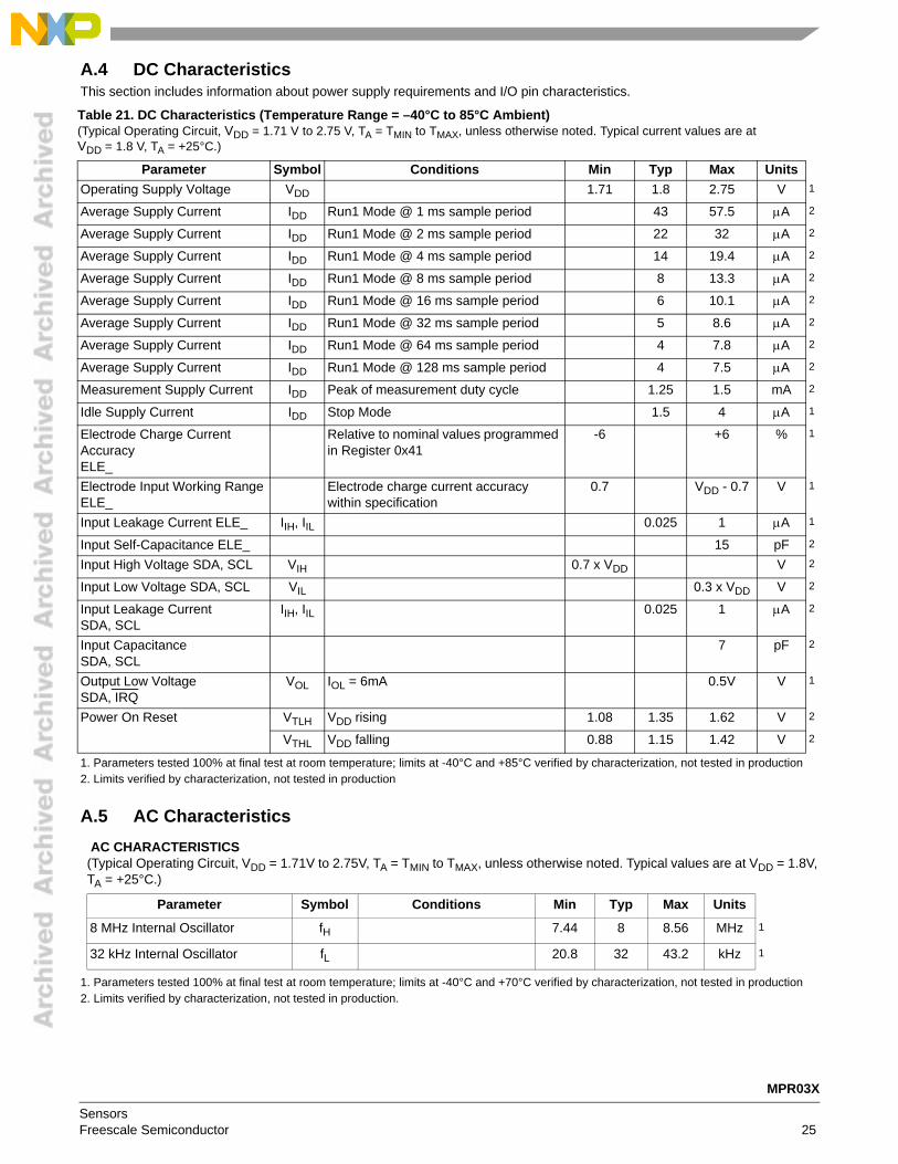
Table 21. DC Characteristics (Temperature Range = –40°C to 85°C Ambient)(Typical Operating Circuit, VDD = 1.71 V to 2.75 V, TA = TMIN to TMAX, unless otherwise noted. Typical current values are at VDD = 1.8 V, TA = +25°C.)
Parameter Symbol Conditions Min Typ Max Units
Operating Supply Voltage VDD 1.71 1.8 2.75 V 1
Average Supply Current IDD Run1 Mode @ 1 ms sample period 43 57.5 A 2
Average Supply Current IDD Run1 Mode @ 2 ms sample period 22 32 A 2
Average Supply Current IDD Run1 Mode @ 4 ms sample period 14 19.4 A 2
Average Supply Current IDD Run1 Mode @ 8 ms sample period 8 13.3 A 2
Average Supply Current IDD Run1 Mode @ 16 ms sample period 6 10.1 A 2
Average Supply Current IDD Run1 Mode @ 32 ms sample period 5 8.6 A 2
Average Supply Current IDD Run1 Mode @ 64 ms sample period 4 7.8 A 2
Average Supply Current IDD Run1 Mode @ 128 ms sample period 4 7.5 A 2
Measurement Supply Current IDD Peak of measurement duty cycle 1.25 1.5 mA 2
Idle Supply Current IDD Stop Mode 1.5 4 A 1
Electrode Charge Current Accuracy ELE_
Relative to nominal values programmed in Register 0x41
-6 +6 % 1
Electrode Input Working Range ELE_
Electrode charge current accuracy within specification
0.7 VDD - 0.7 V 1
Input Leakage Current ELE_ IIH, IIL 0.025 1 A 1
Input Self-Capacitance ELE_ 15 pF 2
Input High Voltage SDA, SCL VIH 0.7 x VDD V 2
Input Low Voltage SDA, SCL VIL 0.3 x VDD V 2
Input Leakage Current SDA, SCL
IIH, IIL 0.025 1 A 2
Input Capacitance SDA, SCL
7 pF 2
Output Low Voltage SDA, IRQ
VOL IOL = 6mA 0.5V V 1
Power On Reset VTLH VDD rising 1.08 1.35 1.62 V 2
VTHL VDD falling 0.88 1.15 1.42 V 2
AC CHARACTERISTICS(Typical Operating Circuit, VDD = 1.71V to 2.75V, TA = TMIN to TMAX, unless otherwise noted. Typical values are at VDD = 1.8V, TA = +25°C.)
Parameter Symbol Conditions Min Typ Max Units
8 MHz Internal Oscillator fH 7.44 8 8.56 MHz 1
32 kHz Internal Oscillator fL 20.8 32 43.2 kHz 1
MPR03X
SensorsFreescale Semiconductor 25

A.6 I2C AC CharacteristicsThis section includes information about I2C AC Characteristics.
Table 22. I2C AC Characteristics(Typical Operating Circuit, VDD = 1.71 V to 2.75 V, TA = TMIN to TMAX, unless otherwise noted. Typical current values are at VDD = 1.8 V, TA = +25°C.)
Parameter Symbol Conditions Min Typ Max Units
Serial Clock Frequency fSCL 400 kHz 1
Bus Free Time Between a STOP and a START Condition
tBUF 1.3 µs 2
Hold Time, (Repeated) START Condition tHD, STA 0.6 µs 2
Repeated START Condition Setup Time tSU, STA 0.6 µs 2
STOP Condition Setup Time tSU, STO 0.6 µs 2
Data Hold Time tHD, DAT 0.9 µs 2
Data Setup Time tSU, DAT 100 ns 2
SCL Clock Low Period tLOW 1.3 µs 2
SCL Clock High Period tHIGH 0.7 µs 2
Rise Time of Both SDA and SCL Signals, Receiving
tR 20+0.1Cb
300 ns 2
Fall Time of Both SDA and SCL Signals, Receiving
tF 20+0.1Cb
300 ns 2
Fall Time of SDA Transmitting tF.TX 20+0.1Cb
250 ns 2
Pulse Width of Spike Suppressed tSP 25 ns 2
Capacitive Load for Each Bus Line Cb 400 pF 2
MPR03X
Sensors26 Freescale Semiconductor

Appendix B Brief Register Descriptions
REGISTER Abrv FieldsREGISTERADDRESS
Initial Value
Touch Status Register TS OCF E2S E1S E0S 0x00 0x00
ELE0 Filtered Data Low Register E0FDL E0FDLB 0x02 0x00
ELE0 Filtered Data High Register E0FDH E0FDHB 0x03 0x00
ELE1 Filtered Data Low Register E1FDL E1FDLB 0x04 0x00
ELE1 Filtered Data High Register E1FDH E1FDHB 0x05 0x00
ELE2 Filtered Data Low Register E2FDL E2FDLB 0x06 0x00
ELE2 Filtered Data High Register E2FDH E2FDHB 0x07 0x00
ELE0 Baseline Value Register E0BV E0BV 0x1A 0x00
ELE1 Baseline Value Register E1BV E1BV 0x1B 0x00
ELE2 Baseline Value Register E2BV E2BV 0x1C 0x00
Max Half Delta Register MHD MHD 0x26 0x00
Noise Half Delta Register NHD NHD 0x27 0x00
Noise Count Limit Register NCL NCL 0x28 0x00
ELE0 Touch Threshold Register E0TTH E0TTH 0x29 0x00
ELE0 Release Threshold Register E0RTH E0RTH 0x2A 0x00
ELE1 Touch Threshold Register E1TTH E1TTH 0x2B 0x00
ELE1 Release Threshold Register E1RTH E1RTH 0x2C 0x00
ELE2 Touch Threshold Register E2TTH E2TTH 0x2D 0x00
ELE2 Release Threshold Register E2RTH E2RTH 0x2E 0x00
AFE Configuration Register AFEC FFI CDC 0x41 0x08
Filter Configuration Register FC CDT SFI ESI 0x43 0x04
Electrode Configuration Register EC CalLock
ModeSel EleEn 0x44 0x00
MPR03X
SensorsFreescale Semiconductor 27

Appendix C Ordering Information
C.1 Ordering Information
This section contains ordering information for MPR03X devices.
C.2 Device Numbering Scheme
All Proximity Sensor Products have a similar numbering scheme. The below diagram explains what each part number in the family represents.
ORDERING INFORMATION
Device Name Temperature Range Case Number Touch Pads I2C Address Shipping
MPR031EPR2 -40C to +85C 1944 (8-Pin DFN) 3-pads 0x4A Tape and Reel
MPR032EPR2 -40C to +85C 1944 (8-Pin DFN) 3-pads 0x4B Tape and Reel
M
Status(M = Fully Qualified, P = Preproduction)
PR
Proximity Sensor Product
EE X P
Number of Electrodes(03 = 3 electrode device)
Package Designator
Version
(Q = QFN, EJ = TSSOP, EP = µDFN)
MPR03X
Sensors28 Freescale Semiconductor

PACKAGE DIMENSIONS
PAGE 1 OF 3
MPR03X
SensorsFreescale Semiconductor 29
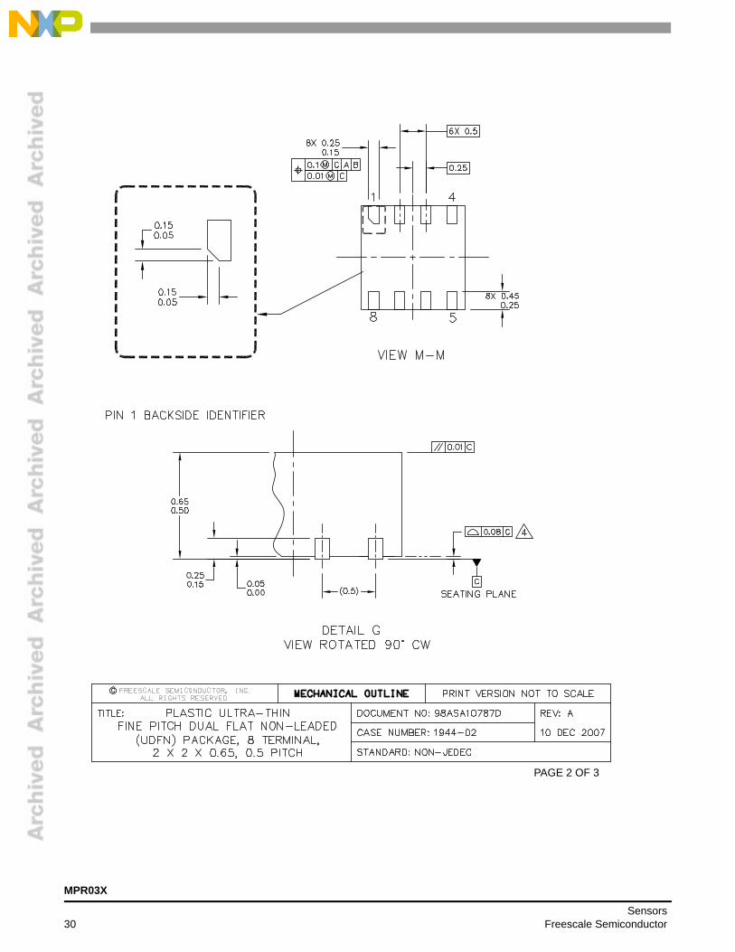
PAGE 2 OF 3
MPR03X
Sensors30 Freescale Semiconductor
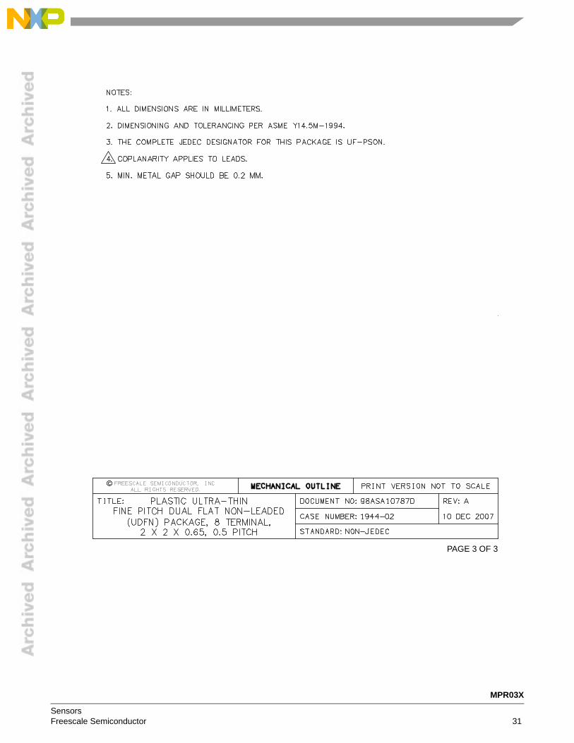
PAGE 3 OF 3
MPR03X
SensorsFreescale Semiconductor 31

MPR03X
Sensors32 Freescale Semiconductor
Table 23. Revision History
Revision number
Revision date
Description of changes
7 07/2011 • Changed Figure 25 AFE Configuration Register Reset From: 0 0 0 0 0 0 0 0, To: 0 0 0 1 0 0 0 0 • Changed Figure 26 Filter Configuration Register Reset From: 0 0 0 0 0 0 0 0, To: 0 0 1 0 0 1 0 0

MPR03XRev. 77/2012
How to Reach Us:
Home Page:www.freescale.com
Web Support:http://www.freescale.com/support
Information in this document is provided solely to enable system and software
implementers to use Freescale products. There are no express or implied copyright
licenses granted hereunder to design or fabricate any integrated circuits based on the
information in this document.
Freescale reserves the right to make changes without further notice to any products
herein. Freescale makes no warranty, representation, or guarantee regarding the
suitability of its products for any particular purpose, nor does Freescale assume any
liability arising out of the application or use of any product or circuit, and specifically
disclaims any and all liability, including without limitation consequential or incidental
damages. “Typical” parameters that may be provided in Freescale data sheets and/or
specifications can and do vary in different applications, and actual performance may
vary over time. All operating parameters, including “typicals,” must be validated for each
customer application by customer’s technical experts. Freescale does not convey any
license under its patent rights nor the rights of others. Freescale sells products pursuant
to standard terms and conditions of sale, which can be found at the following address:
store.esellerate.net/store/Policy.asSelectorpx?Selector=RT&s=STR0326182960&pc.
Freescale, the Freescale logo, AltiVec, C-5, CodeTest, CodeWarrior, ColdFire, C-Ware,
Energy Efficient Solutions logo, Kinetis, mobileGT, PowerQUICC, Processor Expert,
QorIQ, Qorivva, StarCore, Symphony, and VortiQa are trademarks of Freescale
Semiconductor, Inc., Reg. U.S. Pat. & Tm. Off. Airfast, BeeKit, BeeStack, ColdFire+,
CoreNet, Flexis, MagniV, MXC, Platform in a Package, QorIQ Qonverge, QUICC
Engine, Ready Play, SafeAssure, SMARTMOS, TurboLink, Vybrid, and Xtrinsic are
trademarks of Freescale Semiconductor, Inc. All other product or service names are the
property of their respective owners.
© 2012 Freescale Semiconductor, Inc.