properties and applications of metastable precious metal
TRANSCRIPT

Properties and applications of metastable precious metal
intermetallic compounds
Supitcha Supansomboon B.Sc. (Materials Science) and M.Eng (Materials Technology)
A thesis submitted in fulfilment of the requirements for
the degree of Doctor of Philosophy in Science
Institute for Nanoscale Technology
School of Physics and Advanced Materials
University of Technology, Sydney
2014

i
Certificate of original authorship
I certify that the work in this thesis has not previously been submitted for a degree nor has it been submitted as part of requirements for a degree except as fully acknowledged within the text.
I also certify that the thesis has been written by me. Any help that I have received in my research work and the preparation of the thesis itself has been acknowledged. In addition, I certify that all information sources and literature used are indicated in the thesis.
Supitcha Supansomboon

ii
Acknowledgements
First and foremost, I would like to express my sincere gratitude to my principle supervisor, Professor Michael Cortie. My precious journey began when he gave me the opportunity in November 2007 to explore precious metals during a visit to UTS. I have not been able to find the best words to show my sincere gratitude and to thank him for his support, encouragement, motivation, enthusiasm, patience and immense knowledge that he offered me along this journey, but I am truly grateful for his ongoing confidence in my work and abilities. I also could not have asked for better role models. I would like to say thank you to my co-supervisor, Dr Annette Dowd, who has advised, inspired me but also has been patient in assisting me on TEM. I would like to thank all my internal assessors, Assoc. Prof. Kendal McGuffie, Dr Gregory Heness and Dr Matthew Arnold, for their comments and kind suggestions. I would like to thank Dr Vicki Keast from the University of Newcastle in regards to the brilliant discussions, suggestions and the knowledge regarding coloured intermetallic compounds and Professor Candace Lang from Macquarie University for sharing her knowledge and expertise regarding platinum alloys and compounds. They have greatly fulfilled my precious journey.
Along this precious journey, I could not have achieved this without the assistance of a special community at the University of Technology Sydney (UTS) and numerous external individuals who offered me priceless contributions. I would like to thank each and everyone who assisted over the past few years. Dr Richard Wuhrer not only taught and showed me how to use SEM efficiently, but also encouraged me with his kindness. Geoff McCredie spent many hours patiently teaching and supporting me to produce precious samples. He also modified instruments whenever required. Dr Angus Gentle shared his knowledge and support on magnetron sputtering, optical property measurements and the fitting model and I thank him for his understanding and patience. Mark Berkahn advised me on XRD and its analysis. Katie McBean assisted in the operation of SEM and facilitated the use of instruments at MAU. Dr Norman Booth assisted in the metallographic specimen preparation and also with the optical microscope. Dr Ronald Shimmon, Jean-Pierre Guerbois and Greg Dalsanto assisted in the set up of furnaces. Adam Sikorski taught and gave me such a wonderful technique for TEM preparations. Shaun Bulcock and Dr Hongwei Liu taught and assisted me to operate the TEM effectively. Dr Qinfen Gu and Dr Justin Kimpton, who are powder diffraction beamline scientists, assisted in the set- up and operation at the Australian Synchrotron.
I would like to extend my sincere thanks to the other staff within the; School of Physics and Advanced Materials (PAM) at UTS, Microstructural Analysis Unit (MAU) at UTS, Australian Centre for Microscopy and Microanalysis (ACMM) at the University of Sydney, and the Australian Synchrotron for facilitating the use of the instruments and all of the support throughout the years. I also extend my thanks to Mintek, South Africa for donating bulk samples of coloured precious metals.

iii
Most importantly, my journey could not have happened without the financial support given by a Royal Thai government scholarship, offered by the Ministry of Science and Technology. It has been an excellent opportunity to have the opportunity to gain more knowledge and experiences abroad in Australia.
Since I have been away from my home country, I have never felt that I have had to walk this journey alone. There were dozens of people who have helped and encouraged me along the way. All INT people present and past, Dr Dakrong Pissuwan, Dr Abbas Maaroof, Dr Martin Blader, Dr Burak Cankurtaran, Dr Jonathan Edgar, Dr Dylan Riessen, Dr Jonathan Mak, Dr Alex Porkovitch, Dr Vijay Bhatia, Dr Tim Lucey, Valerio Taraschi, Jose Aguilar, Nikta Shahcheraghi, Daniel Golestan, Fadi Bonnie, David McPherson, Shirin-Rose King, Daniel King, Carsten Steinel, Aaron Colusso, Angelo Garruzzo, Dr Sujeewa De Silva and Dr Shaoli Zhu. Thank you for all the discussion, support and friendship you offered me. I would like to thank all fellow colleagues, Dr Barry Liu, Innocent Macha and Elisabeth Meijer, whom I had the opportunity of working with as demonstrators in chemistry and in the materials laboratory. It has been such an enriching experience for my future career. I would like to say special thanks to Professor Tony Moon who has supported and encouraged my friends and I through countless and varied issues since the very beginning. I would like to thank the Minister Counsellor for Education at the Royal Thai Embassy, Canberra; Ms. Thanida Techachokvivat, Ms.Kaewta Srisung and Mrs.Kamonwan Sattayayut, as well as the staff from Office of Educational Affairs for all the assistance and facilitation regarding the financial support as well as all documentation processes required in Thailand.
Even though I lived away from my immediate family in Thailand, I had such a huge and magnificent family in Sydney. Settling down in Sydney for the first time would not have been as smooth as it was without the assistance from my friends. I would like to say a special thank you to Chanthakorn Ketwong and Sopita Thientospol. I also thank you for your constant assistance and friendship all along the journey. My accommodation in Sydney made me feel like I was at home. Thank you for being lovely housemates and being helpful in everything;Arin Tjintana, Kevin Tan, Albert Saputra and Karina Saputra.
Friends who I have known from Insearch since my first year, Daiki Hagino, Jaeseok Ahn, Siriwat Sakarin and Thanh Hung Nguyen, have also spent time and showed support to each other along our respective journeys. We are like a part of each other’s families. I would like to say thank you to Assist.Prof. Watcharin Jinwuth, Dr Pholchai Chotiprayanakul, Sakkaphan Ritjan, Chayapol Moemeng, Woraporn Kanjanawong, Duangkaew Theerasin, Jakkrit Sintunava, Chotika Jindaapirat, Ruamporn Jitjurjun, Dr Akitomo Kawasaki, Pornwan Pornprasitpol, Piti Roglertjanya, Dr Suwin Sandu, Pakawat Pupatwibul, Suphinya Panyasi, Chalakorn Karupongsiri, Busayasachee Puang-Ngern, Suranan Anantachaisilp, Dr Chanick Wangphanich, Shakuntala Anuruang, Tipajin Thaipisutikul, Sanya Khruahong, Sumavalee Chindapol, Nantira Pookhao, Songsin Teerakunpisut, Arpar Nateprapai, Pareena Lertsurawat, Dee Le and Dessie Wanda for your interesting, useful and discussions, as well as for your encouragement and friendship. I would like to thank to Aunty Ying-Utumporn Jaturawong
iv
and Uncle Odd-Pornchai Dechsri for your kindness and the delicious food for you provide my friends and I. Last but not least, I would like to thank my close supporters in Sydney. I would like to especially thank you for your support, your encouragement, for caring for each other’s mental wellbeing and for the friendship through my journey to Dr Khanokon Amprayn, Dr Sutinee Sinutok, Ponlachart Chotikarn, Dr Sirinut Sawatdeenarunat, Supannada Chotipant, and Angelica Casado. I also would like to thank all the people I have met and who I shared experiences along my journey including; fellow PhD students either at UTS or other universities in Australia, fellow Thai government scholarship students, UTS Thai society and UTS PoLSA.
Before starting this precious journey, I could not forget all my teachers and friends from Sainumtip School, Satriwithaya School, Srinakharinwirot University and King Mongkut's University of Technology Thonburi who built my background and passion to pursue my studies. I would like to say a special thank you to Professor Narongrit Sombatsompop, and Assist.Prof. Thongdee Leksophee. I also would like to thank my colleagues and former students from the Faculty of Science, Srinakharinwirot University as well for all your ongoing understanding and encouragement, especially Assoc. Prof. Sawat Pannau, Assist. Prof. Natthapong Phinichka, Supinya Wongsriruksa and Janraem Plangsakron.
I am very grateful to Yani Andrutsopulos, Dr Massimiliano Cannalire, Michael Binder, Wray Menzies, Max Doerfler and especially Peter Tulii for your support, inspiration and guidance especially in improving my English along with your patience. I unfortunately cannot mention all my friends in this section, however, I would also like to extend my thanks to all of my friends from all over Sydney and also the world, who have been right there beside me throughout this challenging experience.
I would not have completed this journey without the understanding, encouragement, wholehearted and generous support and patience from my lovely family. I cannot express enough how much I would like to acknowledge all of you. I would not be who I am today without all of you. Thank you so much to my dad, mom, aunty Daengnoi and sisters-P’Pong and P’Prang.
The purpose of my precious journey was to investigate precious metal alloys and compounds. Throughout my journey, not only did I achieve this purpose, but also I gained far greater precious experiences and friendships here in Australia.

v
Table of Contents Certificate of original authorship _______________________________________________ i
Acknowledgements __________________________________________________________ ii
Table of Contents ___________________________________________________________ v
Abstract _________________________________________________________________ viii
Publications and conference presentations arising from this work ______________________ x
List of Figures _____________________________________________________________ xii
List of Tables ____________________________________________________________ xxii
Chapter 1: Introduction _______________________________________________________ 1
Chapter 2: Literature review ___________________________________________________ 6
2.1 General: precious metal alloys and intermetallic compounds _____________________ 7
2.1.1 Definition of precious metal alloys and intermetallic compounds ______________ 7
2.1.2 Applications of precious metals and their alloys and intermetallic compounds ___ 8
2.2 Optical properties of materials ___________________________________________ 13
2.2.1 The colour of metallic materials _______________________________________ 13
2.2.2 The CIE-L*-a*-b* colour coordinate system _____________________________ 14
2.2.3 Dielectric function _________________________________________________ 15
2.2.4 Plasmon resonances in precious metal nanoparticles _______________________ 17
2.3 Specific precious metal alloys ____________________________________________ 18
2.4 Specific precious metal intermetallic compounds _____________________________ 22
2.4.1 Colour of pure phases _______________________________________________ 22
2.4.2 Alloying effects ___________________________________________________ 27
2.5 Nanoporous precious metal sponges _______________________________________ 29
2.5.1 Nanoporous gold (np-Au) ____________________________________________ 32
2.5.2 Nanoporous silver (np-Ag) ___________________________________________ 33
2.5.3 Nanoporous platinum (np-Pt) _________________________________________ 34
2.5.4 Nanoporous palladium (np-Pd) _______________________________________ 35

vi
Chapter 3: General Experimental ______________________________________________ 37
3.1 Overview _________________________________________________________ 38
3.2 Materials preparation ________________________________________________ 39
3.2.1 Magnetron sputtering ____________________________________________ 39
3.2.2 Heat treatment __________________________________________________ 41
3.3 Materials characterization ____________________________________________ 42
3.3.1 X-ray diffraction ___________________________________________________ 42
3.3.2 Scanning Electron Microscopy (SEM) __________________________________ 46
3.3.3 Transmission Electron Microscopy (TEM) ______________________________ 47
3.3.4 Determination of optical properties ____________________________________ 50
Chapter 4: The AuAl2-PtAl2 system ____________________________________________ 53
4.1 Background __________________________________________________________ 54
4.1.1 Review of the fabrication and applications of AuAl2 and PtAl2 ______________ 54
4.1.2 Review of the optical properties of AuAl2 and PtAl2 _______________________ 59
4.2 Objective of this chapter ________________________________________________ 63
4.3 Experimental details specific to this chapter _________________________________ 63
4.4 Results and discussion __________________________________________________ 65
4.4.1 Single layer films of coloured intermetallic compounds ____________________ 65
4.4.2 Bi-layers of coloured intermetallic compounds ___________________________ 85
4.4.3 Multi-layer films of coloured intermetallic compounds _____________________ 88
4.5 Conclusion __________________________________________________________ 117
Chapter 5: Nanoporous platinum sponges ______________________________________ 119
5.1 Background _________________________________________________________ 120
5.2 Objectives of this chapter ______________________________________________ 127
5.3 Experimental detail specific to this chapter ________________________________ 127
5.4 Results and discussion _________________________________________________ 130
5.4.1 Effect of composition ______________________________________________ 130
vii
5.4.2 Effect of temperature ______________________________________________ 137
5.4.3 Effect of deposition time ___________________________________________ 144
5.4.4 Effect of deposition rate ____________________________________________ 145
5.4.5 Effect of de-alloying parameters _____________________________________ 149
5.4.6 Comparison between my nanoporous Pt sponges and those in the literature ____ 150
5.5 Conclusion __________________________________________________________ 157
Chapter 6: Conclusions and future work _______________________________________ 158
6.1 The AuAl2-PtAl2 system _______________________________________________ 159
6.2 Nanoporous platinum sponges __________________________________________ 161
References _______________________________________________________________ 163
viii
Abstract
Precious metal alloys and compounds have myriad applications in the fast-expanding horizons of the commercial and industrial worlds. They are also fascinating topics for scientific research. These materials have a long history, with gold and silver amongst the very earliest metals used by humans. Over the past millennia, the primary applications of the precious metals and their alloys have been in the ever-lucrative jewellery manufacturing industry. The traditional alloys have been perfected in over three thousand years of experience. However, in the recent past, precious metal alloys and compounds have also found themselves a crucial place of pride in the burgeoning ‘advanced materials’ sector. Gold-based and platinum-based alloys and compounds are amongst the candidates being investigated for serving in those applications. In the present project I sought to explore how gold aluminide and platinum aluminide could be developed for further innovative applications. In particular, I initially became interested in the optical properties of these materials, with a view to developing their application in the jewellery industry. The PtxAl alloys are, however, also useful as precursors for producing nanoporous metal sponges. The availability of such samples from the first part of the project encouraged me to consider technological applications of the aluminides in the chemical catalysis industry in the second part of the project. The two parts are linked by virtue of starting with the same materials, which are fabricated and mostly characterized the same way. In both cases the samples are fabricated as thin films by direct-current magnetron sputtering and then various techniques are used to characterize their chemical composition, structures, morphologies and specific properties. The main difference comes only at the very end of each part, with the first group of materials being evaluated on their optical properties and the second on their sponge-forming properties.
My work is developed around two hypotheses. First, I hypothesized that the compounds PtAl2 (brassy yellow) and AuAl2 (metallic purple) can be alloyed to yield a range of intermediate colours. It is generally stated that these compounds would be immiscible but I proposed that a series of metastable solid solutions could be formed by means of magnetron sputtering. Secondly, I hypothesised that the preparation of nanoporous platinum sponges from metastable (PtxAl) precursors would produce a different result than producing them from well-crystallized precursors, and that this could be exploited to provide a new way to control the morphology of such sponges.
The work has showed that the attractive colours of the intermetallic compounds AuAl2 (‘purple gold’) and PtAl2 (‘golden platinum’) can be combined or mixed to produce an interesting colour spectrum. This may be of interest to the jewellery industry. A series of metastable solid solutions could be formed by using the magnetron sputtering technique, which enables users to produce any desired stoichiometry. In addition, procedures to reliably

ix
produce pure AuAl2 and PtAl2 thin films have been established. These have lattice parameters of 0.599 nm and 0.594 nm respectively, which are similar to those of bulk samples produced by vacuum arc melting. Addition control may be obtained by designing multilayer stacks of these intermetallic compound films, with both bi-layer and multi-layer films being produced in the present project. It was also shown that a metastable solid solution of Au and Pt could be formed by sputtering, with a co-deposited film of 54 at.%Au- 46 at.%Pt film forming a solid solution with a lattice parameter of 0.401 nm, which lies between that of pure Au films (0.408 nm) and pure Pt films (0.394 nm). This metastable solid solution could be reacted with a pure Al film to form a metastable solid solution of (Au,Pt)Al2 after annealing. However, thin film stacks of AuAl2 and PtAl2 may be a better choice to tune colours of these two compounds as they are easier to control.
Next I showed that Pt-Al alloys and intermetallic compounds can be de-alloyed in alkaline solutions to produce nanoporous platinum sponges. These nanoscale sponges can be used as chemical catalysts although I did not pursue this aspect myself. Rather, in this part of the project I considered how the microstructure of the precursor alloys could control the morphology of subsequent sponges. Once again, metastable precursors could be prepared by using magnetron sputtering, and produced a different morphology of sponges compared to those produced from well-crystallized precursors. Other processing parameters have also been studied. It was found that mole fraction ( Al) of Al in the precursor and the deposition temperature are the two most important factors. Precursors with Al < 0.60 did not form sponges after either deposition at elevated or room temperature. 'Mud-cracked' mesoporous sponges could be formed by preparing precursors with Al =0.67 and deposited at elevated temperature. The Pt8Al21 and meta-stable phase ( -phase) were formed in precursors with 0.67< Al < 0.90 that had been deposited at elevated temperature. In this case de-alloying produced classic isotropic fibrous sponges. Disordered and fragile masses were obtained when precursors with Al > 0.90 were de-alloyed. These had originally consisted of a mixture of PtAl6 and pure Al. It was also found that precursors that had been deposited at room temperature produced very different sponge morphologies to those that had been deposited at elevated temperature: in this case the amorphous precursors with 0.67 < Al <0.96 produced sponge morphologies ranging from pinhole to unusual isotropic foamy. This work has shown that different morphologies of nanoporous platinum sponges can be produced by controlling the processing parameters. These sponges might be considered for use in specific catalytic or sensor applications because they can be fabricated using simple and cost-effective production techniques.

x
Publications and conference presentations arising from this work Publications
1. Supansomboon, S., Bhatia, V., Thorogood, G., Dowd, A., and Cortie, M.B., Advanced precious metal alloys, Materials Australia, 2011. 44 (4): p.41-46.
2. Keast, V.J., Birt, K., Koch, C.T., Supansomboon, S., and Cortie, M.B., The role of plasmons and interband transitions in the color of AuAl2, AuIn2, and AuGa2. Applied Physics Letters, 2011. 99(11): p. 111908.
3. Keast, V.J., Zwan, B., Supansomboon, S., Cortie, M.B., and Person, P.O.Å., AuAl2 and PtAl2 as potential plasmonic materials. Journal of Alloys and Compounds, 2013. 577: p. 581-586.
4. McPherson, D.J., Supansomboon, S., Zwan, B., Keast, V.J., Cortie, D.L., Gentle, A., Dowd, A., and Cortie, M.B., Strategies to control the spectral properties of Au–Ni thin films. Thin Solid Films, 2014. 551: p. 200-204.
5. Supansomboon, S., Porkovich, A., Dowd, A. Arnold, M.D., and Cortie, M.B., Effect of precursor stoichiometry on the morphology of nanoporous platinum sponges. ACS Applied Materials & Interfaces, 2014. 6(12): p. 9411-9417.
6. Supansomboon, S., Dowd, A., Lingen, E. van der, Keast, V.J., and Cortie, M.B., Coatings of coloured intermetallic compounds for decorative and technological applications, Materials Forum (accepted, 2014).
7. Supansomboon, S., Dowd, A., Gentle, A., Keast, V.J., Lingen, E. van der, and M.B. Cortie, Thin films of PtAl2 and AuAl2 by solid-state reactive synthesis (being prepared for submission).
Conference presentations
1. Supansomboon, S., Dowd, A., and Cortie, M.B., Phase relationships in the PtAl2-AuAl2 system, 35th Condensed Matter and Materials Meeting, 1-4 February, 2011 Charles Sturt University, Wagga Wagga, New South Wales, Australia. (Poster presentation)
2. Supansomboon, S., Dowd, A., and Cortie, M.B., Optical properties of nanoscale bi-layers of the coloured intermetallic compounds Al2Pt and Al2Au, the 10th Asia-Pacific Microscopy Conference (APMC10), the 2012 International Conference on Nanoscience and Nanotechnology (ICONN2012) and the 22nd Australian Conference on Microscopy and Microanalysis (ACMM22), 5 – 9 February 2012, the Perth Convention & Exhibition Centre, Western Australia, Australia. (Poster presentation)
xi
3. Supansomboon, S., Dowd, A., and Cortie, M.B., Thin film stacks of the colored intermetallic compounds Al2Au and Al2Pt, Gold 2012, 5-8 September 2012, Keio Plaza Hotel Tokyo, Tokyo, Japan. (Poster presentation)
4. Supansomboon, S., Dowd, A., and Cortie, M.B., Colored intermetallic compounds for gems and jewelry application, The 3rd International Gem and Jewelry Conference, 12-16 December, 2012, the Imperial Queen's Park Hotel, Bangkok, Thailand (Oral presentation)
5. Supansomboon, S., Dowd, A., and Cortie, M.B., Coatings of coloured intermetallic compounds: AuAl2 and PtAl2 for decorative and technological applications, Materials Innovation in Surface Engineering, 19-21 November 2013, University of South Australia, Adelaide, South Australia, Australia (Oral presentation)
6. Supansomboon, S., Gentle, A., Dowd, A., and Cortie, M.B., Nanoscale bi-layers of coloured intermetallic compounds, Australian Nanotechnology Network Early Career Workshop, 10-11 July 2014, University of Technology, Sydney, New South Wales, Australia. (Poster presentation)
7. Supansomboon, S., Dowd, A., and Cortie, M.B., Formation of nanoporous platinum sponges by de-alloying AlxPt, The 3rd Biennial Conference of the Combined Australian Materials Societies (CAMS 2014), 26-28 November 2014, Charles Perkins Centre, University of Sydney, New South Wales, Australia. (Oral presentation)
xii
List of Figures Figure 1.1 Periodic table of elements ........................................................................................ 2
Figure 1.2 Crystal structure of precious metals (a) face-centered cubic (FCC) and (b) close-packed hexagonal (HCP) [4] ...................................................................................................... 3
Figure 2.1 Schematic representation of the mechanism of photon absorption (a) and emission (b) for metallic materials [35] ................................................................................................. 14
Figure 2.2 CIE L*a*b* colour space [38] ................................................................................ 15
Figure 2.3 Imaginary part of the interband dielectric constant as function of energy (a) Au-Ag and (b) Au-Cu [39]................................................................................................................... 16
Figure 2.4 Imaginary part of the interband dielectric constant and energy of Ag-Cu series (a) Cu-rich and (b) Ag-rich [39] .................................................................................................... 17
Figure 2.6 Relationship between colour and composition in the Au-Ag-Cu system[62] ........ 19
Figure 2.7 Comparison of coloured rings from different precious metal alloys [61] ............. 20
Figure 2.8 Reflectivity curves of gold and its alloys (a) gold-silver alloys and (b) gold-palladium alloys [63] ............................................................................................................... 22
Figure 2.9 Crystal structures of coloured binary intermetallic compounds (a) Caesium chloride structure and (b) Calcium fluoride (Courtesy CrystalMaker Software Ltd, UK) ...... 23
Figure 2.10 Reflectivity curves of coloured gold intermetallic compounds: AuAl2 (curve 1), AuIn2 (curve 2) and AuGa2 (curve 3) [63] ............................................................................... 24
Figure 2.11 CIE a* and b* colour coordinates of alloys along the 18 carat pseudo-binary, and position of phase fields [70] ..................................................................................................... 29
Figure 2.12 Classification of nanoporous metals[76] .............................................................. 31
Figure 2.13 Nanoporous gold by dealloying Au-Ag (a) Model for dealloying [7], (b) SEM micrograph of nanoporous gold by dealloying Au-Ag in nitric acid [89] and (c) Simulated porous structure of nanogold which made from Au0.35Ag0.65 precursor [90] .......................... 32
Figure 2.14 Nanoporous silver generated from Ag-Al precursors (a) –Al rich region and (b) –Al and Ag2Al region [116] .................................................................................................. 34
Figure 2.15 Nanoporous platinum produced by co-sputtered PtxSi1-x amorphous film for different initial compositions (a) Pt0.10Si0.90 as deposited (b) isotropic open-cell foam (c) Pt0.34Si0.66 as deposited (d) anisotropic columnar-type foam (e) Pt0.33 Si0.67 as deposited and (f) anisotropic Voronoi [133] ........................................................................................................ 35
Figure 2.16 Nanoporous palladium by dealloying in various precursors (a) Pd-Co [146] (b) Pd-Ni [139] and (c) Pd-Cu [142] ............................................................................................. 36

xiii
Figure 3.1 A schematic diagram of magnetron sputtering mechanism .................................. 39
Figure 3.2 Relationship between sputter yield and atomic number of elements for argon ion energy at 400 eV [155] ............................................................................................................ 40
Figure 3.3 A co-deposition technique during sputtering process, photograph taken during the present project .......................................................................................................................... 40
Figure 3.4 Tube furnace for post-deposition annealing treatment ........................................... 41
Figure 3.5 Schematic of an X-ray diffractometer in the Bragg-Brentano configuration [156]43
Figure 3.6 Schematic diagram of XRD (a) conventional -2 geometry and (b) grazing angle geometry [160] ......................................................................................................................... 44
Figure 3.7 (a) High temperature furnace and (b) platinum heater bar with cavity [165] ....... 45
Figure 3.8 Information in powder diffraction pattern [167] .................................................... 45
Figure 3.9 A field emission scanning electron microscope (Zeiss Supra 55VP)..................... 47
Figure 3.10 Cross section preparation for TEM (a) schematic of stack sample prepared using the sandwich technique and (b) Interface of thin film after polishing with diamond of 1 m (the arrow indicate the location of the glue line) [175] ........................................................... 49
Figure 3.11 An optical model of a thin film sample [177] ...................................................... 51
Figure 3.12 Diagram of the process for ellipsometry data analysis [178] ............................... 52
Figure 4.1 Phase diagram of Al-Au system by Okamoto, H.(1991) [182] .............................. 54
Figure 4.2 Phase diagram of Al-Pt system by McAlister, A.J. and Kahan, D.J.(1986) [182] . 55
Figure 4.3 Purple gold by investment casting (Courtesy JARAD Project by Srinakharinwirot University, Bangkok Fashion City under the Ministry of Industry of Thailand, Thailand) .... 56
Figure 4.4 AuAl2- carat purple gold (top row) and AuIn2 - blue gold (bottom row) (Courtesy Co. Reischauer GmbH, Idar Oberstein, Germany) [6] ............................................ 56
Figure 4.5 Bi-metal casting (a) 950 Pd casting with injected wax for the 2nd bi-metal casting process step and (b) Bi-metal castings of 14k blue gold (left) and 18k purple gold (right) with 950 Pd (Courtesy Vendorafa-Lombardi Srl, Valenza,Italy) [6] .............................................. 57
Figure 4.6 Purple gold by powder metallurgy process (Courtesy Lee Hwa Jewellery, Singapore) [186] ...................................................................................................................... 57
Figure 4.7 Purple glory gemstone-like AuAl2 casting in setting on ring (courtesy M.B Cortie) [180] ......................................................................................................................................... 57
Figure 4.8 Platigems and Platigem jewellery (Courtesy Mintek, South Africa) [187]............ 58

xiv
Figure 4.9 AuAl2-coated items made by depositing onto sterling silver costume jewellery by the present author [181] ........................................................................................................... 58
Figure 4.10 Reflectivity of gold intermetallic compounds from experiment (solid curve) and calculation (dashed curved) [191] ............................................................................................ 60
Figure 4.11 Dielectric function of gold intermetallic compounds; 1 (solid curve) and 2
(dashed curved) [191] .............................................................................................................. 60
Figure 4.12 Dielectric function of ordered intermetallic compounds [192] ............................ 61
Figure 4.13 Reflectivity of ordered intermetallic compounds comparing with experimental reflectivity of PtAl2 thin film [192] ......................................................................................... 61
Figure 4.14 Comparison CIE Lab colour coordinates of AuAl2, Au0.5Pt0.5Al2, Au0.25Pt0.75Al2 and PtAl2 [192]................................................................................................. 61
Figure 4.15 CIE L*a*b* colour gamut of Au-Ni-Au tri layer in reflection [203] ................... 62
Figure 4.16 Deposition rate of aluminium, gold and platinum as function of current ............ 64
Figure 4.17 X-ray patterns of Pt-Al compound films by co-sputtering using varying current level of aluminium, PtAl2 are formed by using current at 0.395 A (yellow pattern) ..................................................................................................................................... 66
Figure 4.18 Morphology of Pt-Al compound films (a) PtAl400 (b) PtAl395 (c) PtAl360 and (d) PtAl335 .......................................................................................................................... 67
Figure 4.19 Comparison of reflectance spectra of PtAl2 in bulk and film ............................... 68
Figure 4.20 Comparison of morphology of surfaces of PtAl2 in (a) bulk and (b) film ........... 68
Figure 4.21 Comparison of X-ray patterns of PtAl2 in bulk and film...................................... 69
Figure 4.22 X-Ray patterns of Au-Al compounds ................................................................... 70
Figure 4.23 Morphologies of Au-Al films produced by using different power levels on the gold target (a) 16 W (sample AuAl040) in low magnification, (b) 16 W (sample AuAl040) in high magnification, (c) 26 W (sample AuAl060) in low magnification, (d) 26 W (sample AuAl060) in high magnification and (e) 21 W (sample AuAl050) ............................................. 71
Figure 4.24 Reflectance spectra of Au-Al compounds ............................................................ 72
Figure 4.25 Comparison of X-Ray patterns of AuAl2, deposited at different temperature ..... 73
Figure 4.26 Microstructure of AuAl2 films, deposited at different temperatures (a) below 400 C and (b) at 400 C ......................................................................................... 73
Figure 4.27 Comparison of reflectance spectra of AuAl2 in bulk and film ............................. 74
Figure 4.28 Morphologies of AuAl2 bulk sample by (a) SEM and (b) LM............................. 74

xv
Figure 4.29 Morphologies of AuAl2 thin film (a) plan view and (b) cross-section ................. 75
Figure 4.30 X-ray patterns of AuAl2 in bulk and thin film samples ........................................ 75
Figure 4.31 Diagram illustrating the process for fabricating coloured intermetallic compounds by controlling the chemical composition and thickness of (a) PtAl2 film and (b) AuAl2 film 76
Figure 4.32 Cross-sections of the thin films of the binary intermetallic compounds after annealing at 400 C (a) AuAl2 and (b) PtAl2 ........................................................................... 76
Figure 4.33 X-ray patterns of colour intermetallic compounds in different thicknesses of film (a) PtAl2 films and (b) AuAl2 films ......................................................................................... 77
Figure 4.34 Reflectance (R) and transmittance (T) spectra of PtAl2 films (Exp) with model fitted (Model Fit) to different thicknesses of film (a) 100 nm and (b) 40 nm ......................... 78
Figure 4.35 Reflectance and transmittance spectra of AuAl2 films with model fitted to different thicknesses (a) 100 nm and (b) 40 nm ...................................................................... 79
Figure 4.36 Dielectric functions of coloured intermetallic compounds by reflectance and transmission data (a) PtAl2 and (b) AuAl2 ............................................................................... 80
Figure 4.37 Colour of simulated thin films in CIE L*a*b* space, with the colour of each film rendered into the surface of a spherical data point. Both reflectance (yellow) and transmittance (grey) modes are shown for the different thicknesses (a) front view (b) top view and (c) perspective view .......................................................................................................... 82
Figure 4.38 Colour of simulated thin films in CIE L*a*b* space, with the colour of each film rendered into the surface of a spherical data point. Both reflectance (purple) and transmittance (yellow-green) mode in different thickness of film are shown (a) front view (b) top view and (c) perspective view ........................................................................................... 83
Figure 4.39 Dielectric functions of coloured intermetallic compounds found by analysis of ellipsometric data (a) PtAl2 and (b) AuAl2 .............................................................................. 84
Figure 4.40 The two kinds of bi-layer films produced (a) AuAl2/PtAl2 and (b) PtAl2/AuAl2 85
Figure 4.41 The reflectance spectra of bi-layers of AuAl2/PtAl2 ............................................ 85
Figure 4.42 Cross-section of bi-layers films of PtAl2/AuAl2 before annealing (a) In lens mode and (b) backscatter mode ......................................................................................................... 86
Figure 4.43 Cross-section of PtAl2/AuAl2 film after annealing under vacuum at 400 °C (a) for 24 hours and (b) for 48 hours........................................................................................ 86
Figure 4.44 Calculated reflectance (a) and colour (b) of 200 nm PtAl2 film that has been over-coated with indicated thickness of AuAl2 ................................................................................ 87

xvi
Figure 4.45 Calculated reflectance (a) and colour (b) of 200 nm AuAl2 film that has been over-coated with indicated thickness of PtAl2 ......................................................................... 87
Figure 4.46 Schematic illustration of the arrangements of the four-layer films of Al-Au-Pt (a) Au on the top and (b) Pt on the top .......................................................................................... 88
Figure 4.47 Cross-sections of four-layer films of Al-Au-Pt with Au on the top, as deposited at 25 °C (a) In lens and (b) RBSD ............................................................................................... 89
Figure 4.48 Cross-sections of four-layer films of Al-Au-Pt with Au on the top, after annealing at 400 °C (a) SEM:In lens mode (b) SEM:RBSD mode and (c) TEM .................................... 90
Figure 4.49 Cross-sections of four-layer films of Al-Au-Pt with Pt on the top, after annealing at 400 °C (a) SEM and (b) TEM .............................................................................................. 90
Figure 4.50 The reflectance spectra from the front side of a four-layered film of Al-Au-Pt (Au on the top) as deposited at 25 °C before and after annealing. Data for a pure gold film of 30 nm thickness is shown for comparison ............................................................................... 91
Figure 4.51 The reflectance spectra from the back side of the above four-layered film, before and after annealing ................................................................................................................... 92
Figure 4.52 The reflectance spectra from the front side of a four-layered film of Al-Au-Pt (Pt on the top) as depositing at 25 °C before and after annealing. Data for a pure platinum thin film of 30 nm thickness is shown for comparison ................................................................... 92
Figure 4.53 The reflectance spectra from the back side of the above four-layered film, before and after annealing ................................................................................................................... 93
Figure 4.54 X-ray patterns of four-layer films of AlAuPt comparing the structure before and after annealing at 400 °C (a) pure gold layer on the top and (b) pure platinum layer on the top (both were deposited at 25 C), with patterns for AuAl2 and PtAl2films shown for comparison.................................................................................................................................................. 94
Figure 4.55 The arrangement of the six-layered films (a) Al-Au-Pt and (b) Al-Au ................ 95
Figure 4.56 Cross-section views of the six-layer film of Al-Au-Pt after annealing at 400 °C (a) SEM-In lens (b) SEM-RBSD and (c) TEM ....................................................................... 96
Figure 4.57 The reflectance spectra of the top of the six-layer film of Al-Au-Pt (Pt on the top) after annealing .......................................................................................................................... 96
Figure 4.58 The X-ray pattern of the six-layer film of Al-Au-Pt after annealing, with patterns for PtAl2 and AuAl2 films shown for comparison ................................................................... 97
Figure 4.59 Cross-sections of six-layer films of Al-Au (a) before annealing-In lens, (b) before annealing – RBSD, (c) after annealing at 400 °C – In lens and (d) after annealing at 400 °C – RBSD ....................................................................................................................................... 97
xvii
Figure 4.60 The X-ray pattern of the six-layer film of Al-Au before and after annealing, with patterns for AuAl2 films shown for comparison ...................................................................... 98
Figure 4.61 The different arrangements of eight-layer films of Al-Au-Pt (a) 50 nm each layer, Au on the top and (b) 50 nm each layer, Pt on the top ............................................................ 98
Figure 4.62 Cross-sectional views of eight-layered films of Al-Au-Pt (a) before annealing-In lens, (b) before annealing – RBSD, (c) after annealing at 400 °C – In lens and (d) after annealing at 400 °C – RBSD ................................................................................................... 99
Figure 4.63 The X-ray pattern of eight multi-layers films of Al-Au-Pt (Pt on the top) after annealing, comparing with PtAl2 film .................................................................................... 100
Figure 4.64 The reflectance spectrum of the surface of eight multi-layers films of Al-Au-Pt (Pt on the top) after annealing, comparing with a single PtAl2 film ...................................... 100
Figure 4.65 The morphologies of eight multi-layer films of Al-Au-Pt which Au on the top after annealing at 400 °C (a) cross-sectional area and (b) surface area ................................. 101
Figure 4.66 The X-ray pattern of the eight-layered films of Al-Au-Pt (Au on the top) after annealing. A pattern for a simple AuAl2 film is shown for comparison ................................ 101
Figure 4.67 The reflectance spectrum of the surface of the eight-layer film of Al-Au-Pt (Au on the top) after annealing, in comparison to that of a simple, single-layer AuAl2 film ....... 102
Figure 4.68 The arrangement of eight-layered films of Al-Au-Pt with each layer being 25 nm thick (Au on the top) .............................................................................................................. 102
Figure 4.69 The X-ray patterns of the eight-layered sample produced with half the deposition time of the standard eight-layered sample of Al-Au-Pt (Au on the top), both before and after annealing, compared with that of a simple, single-layer AuAl2 film..................................... 103
Figure 4.70 The cross-sectional view of the eight-layer films of Al-Au-Pt in which layer thickness was halved, (a) before annealing and (b) after annealing at 400 °C for 30 minute 104
Figure 4.71 Average integrated peak areas of PtAl2 and/or AuAl2 over the (111), (200), (220) and (311) peaks as a function of temperature ........................................................................ 105
Figure 4.72 Peak area of four layers stack formed by depositing pure metals at (111) of PtAl2 and AuAl2............................................................................................................................... 105
Figure 4.73 The design of stacks consisting of co-deposited precious metals and aluminium (a) precious metals on the bottom (Al/(Au,Pt) ), (b) precious metals on the top ( (Au,Pt)/Al) and (c) co-depositing precious metals on the top but with half the thickness ....................... 106
Figure 4.74 A comparison of X-ray patterns of thin films of (Au,Pt) solid solution to those pure Au and pure Pt ............................................................................................................... 107
xviii
Figure 4.75 X-ray patterns of different arrangements of stacks made of a layer of co-deposited Au and Pt, and Al, before and after annealing ................................................. 108
Figure 4.76 X-ray patterns of an Al/(Au,Pt) sample, followed by annealing at various temperatures ........................................................................................................................... 108
Figure 4.77 Comparison of X-ray patterns of an Al/(Au,Pt) sample, followed by annealing at 400 C and 500 C ................................................................................................................. 109
Figure 4.78 Comparison of the X-ray diffraction patterns obtained after annealing the stacks with 20, 60 and 120 nm of (Au,Pt) at 400 C ........................................................................ 110
Figure 4.79 X-ray patterns of a mixed AuAl2/PtAl2 sample formed by co-depositing Au and Pt onto Al. The fitted pattern was obtained by Rietveld refinement on a PtAl2 structure ..... 111
Figure 4.80 Cross-section of the Al/(Au,Pt) sample with 20 nm of co-deposited (Au,Pt) with EDS elemental scan and mapping.......................................................................................... 112
Figure 4.81 High resolution TEM images of the Al/(Au,Pt) sample with 20 nm of co-deposited (Au,Pt) (a) top layer and (b) bottom layer ............................................................. 113
Figure 4.82 The reflectance spectra of the 65 at.% Al-23 at.% Pt-12 at.% Au sample on its front and back sides, compared with the front side of the sample before annealing and that of a pure PtAl2 film .................................................................................................................... 114
Figure 4.83 The reflectance spectra of 56 at.% Al-22 at.% Pt-22 at.% Au on its front and back sides, compared with the front side of the sample before annealing and a pure AuAl2 film . 114
Figure 4.84 X-ray diffraction patterns of samples made by co-depositing Au and Pt on top of an Al layer (a) 65 at.% Al - 23 at.% Pt - 12 at.% Au and (b) 56 at.% Al - 22 at.% Pt - 22 at.% Au. Data for before and after annealing, and for pure PtAl2 and pure AuAl2 is shown ........ 115
Figure 4.85 Lattice parameter and peak area of Al/(Au,Pt) sample as a function of temperature (a) Lattice parameter of (Au,Pt)Al2 in Al/(Au,Pt) sample and (b) peak area of (Au,Pt)Al2 phase (111) and Pt2Al3 (002) ............................................................................... 117
Figure 5.1 Various techniques for nanoporous platinum fabrication [207] ........................... 120
Figure 5.2 Pt-Al phase diagram [237] .................................................................................... 121
Figure 5.3 The different lattice types of the intermetallic compounds in the Pt-Al binary system [229] ...................................................................................................... 122
Figure 5.4 Effect of Al content on structure of sponges produced from precursors with Al > 0.80 (a) X-ray diffraction pattern of increasing amount of Al, (b) X-ray diffraction patterns of de-alloyed Pt sponges (c) and (d) SEM micrograph of isotropic foamy Pt sponge from precursor with Al = 0.88 and 0.85 respectively (e) TEM micrograph of Pt sponge from precursor with Al = 0.88 [239] .............................................................................................. 124

xix
Figure 5.5 Simulation of the de-alloying of the sponges by using Monte Carlo model as a function of Al (a) Morphologies of sponges in various aluminium content (b) Ratio of surface atoms to total atoms of sponges ( ) and Al remaining in sponge. (c) Average mean and Gaussian curvatures of sponges. (d) Effect of Lennard-Jones temperature on the de-alloying of a starting alloy with Al = 0.80. This work was performed by my co-authors [239] ......... 125
Figure 5.6 Three distinct morphologies of nanoporous platinum as correlated with co-sputtering parameter, initial alloy composition and thickness [133] ..................................... 126
Figure 5.7 Effect of de-alloying system on ligament size of nanoporous platinum from different alloy systems (a) ligament sizes of different noble metal-aluminium with de-alloying with 5% HCl and 20% NaOH and (b) ligament sizes of platinum-gold-copper alloys with varying noble metal content ........................................................................................... 126
Figure 5.8 Nanoporous platinum produced from Pt0.20Cu0.80, then de-alloyed in 93%H2SO4 and coarsened at different temperatures (a) 250 C (b) 300 C (c) 400 C and (d) 500 C [246] ....................................................................................................................................... 127
Figure 5.9 De-alloying process on Pt-Al precursor (a) Bubble of H2 on Pt-Al precursor immersing in alkali solution and (b) model of aluminium removing from Pt-Al precursor [239] ....................................................................................................................................... 128
Figure 5.10 Flowchart showing preparation of Pt-Al precursors and the subsequent nanoporous platinum .............................................................................................................. 129
Figure 5.11 Pt-Al precursor film deposited at 400 C with Al 0.50 (a) XRD patterns comparing with other phases from calculated and database and (b) SEM micrograph after de-alloying showing that a nanoporous sponge did not form ..................................................... 130
Figure 5.12 Pt-Al precursor film deposited at 400 C with Al 0.60 (a) XRD patterns comparing with Pt2Al3 from database (b) SEM micrograph before de-alloying (c) SEM micrograph after de-alloying.................................................................................................. 131
Figure 5.13 Pt-Al precursor film deposited at 400 C with Al = 0.67 (a) XRD patterns comparing with Pt2Al3 from database and (b) reflectance spectra ........................................ 132
Figure 5.14 ‘Mud-cracked’ sponges produced by de-alloying sample with Al = 0.67 (a) a porous and cracked film (b) cross-sectional view and (c) curled up porous and cracked film at low magnification .................................................................................................................. 132
Figure 5.15 TEM micrographs of de-alloyed samples with Al = 0.67 .................................. 133
Figure 5.16 Pt-Al precursor film with 0.67< Al < 0.80 (a) XRD patterns of precursors with Al = 0.78 (deposited at 400 C) and precursors with Al = 0.75 (deposited at room
temperature then crystallized by heating ~400 C), comparing with Pt8Pt21 from database and reported phase (b) crystallization of phase at ~360 C on heating up precursor with Al = 0.75 (c) morphology of Pt-Al precursor with Al = 0.78 as deposited (d) SEM micrograph of

xx
isotropic fibrous sponges in plain view and (e) SEM micrograph of isotropic fibrous sponges in cross-sectional view ........................................................................................................... 134
Figure 5.17 Pt-Al precursor film deposited at 400 C with Al = 0.82 (a) (a) XRD patterns comparing with Al-rich phases from database and phase (b) and (c) SEM micrograph of isotropic fibrous sponges ....................................................................................................... 135
Figure 5.18 Pt-Al precursor film deposited at 400 C with Al > 0.90 (a) XRD pattern comparing with PtAl6 and Al from database (b) SEM micrograph as deposited (c) SEM micrograph after de-alloying (d) TEM de-alloying and (e) High resolution TEM after de-alloying .................................................................................................................................. 136
Figure 5.19 XRD patterns of the precursors were deposited at room temperature with Al = 0.67 ...................................................................................................................... 137
Figure 5.20 Morphology of partially de-alloyed sponges produced from the precursors were deposited at room temperature with Al = 0.67 (a) plan view and (b) cross-sectional view .. 138
Figure 5.21 Morphology of sponge produced from a precursor with Al 0.75 that had been deposited at room temperature ............................................................................................... 138
Figure 5.22 Morphology of Pt-Al precursors, deposited at room temperature with Al > 0.80 (a) as deposited (b) Al 0.83 after de-alloying (c) Al 0.88 after de-alloying (d) Al 0.96 after de-alloying and (e) curled up porous Pt sponge and shown cross-sectional view ........ 139
Figure 5.23 TEM mapping on Pt-Al precursors, deposited at room temperature with Al = 0.92 ........................................................................................................................ 140
Figure 5.24 TEM-EDS analysis through the cross-sectional area of Pt-Al precursors, deposited at room temperature with Al = 0.92. The presence of Cu is due to redeposited materials during PIPS ............................................................................................................ 140
Figure 5.25 Distribution of pore sizes from Pt-Al precursor with different mole fraction of Al (a) Al = 0.83 (b) Al = 0.88 and (c) Al = 0.96 ....................................................................... 141
Figure 5.26 TEM micrograph of sponge formed from precursor with Al 0.88 (a) a continuous network of Pt surrounding the void and (b) lattice fringe image at high resolution................................................................................................................................................ 142
Figure 5.27 Comparison of X-ray diffraction pattern between samples with Al > 0.80, which were deposited at room temperature and above 400 °C and the sample with Al = 0.82, which was deposited at elevated temperature ................................................................................... 143
Figure 5.28 Morphologies of samples with Al >0.80, which were deposited at room temperature, then annealed at various temperatures followed by de-alloying process in alkali solution (a) as deposited at room temperature (b) annealed at 100 °C (c) annealed at 200 °C (d) annealed at 300 °C (e) annealed at 400 °C and (f) annealed at 500°C............................. 144
xxi
Figure 5.29 Morphologies of samples with Al =0.83, which were deposited at room temperature with various deposition times (a) 5 minutes (b) 10 minutes and (c) 30 minutes................................................................................................................................................ 145
Figure 5.30 Pinhole sponge produced from precursors that deposited at room temperature with high deposition rate of Pt in various Al contents (a) Al 0.62 (b) Al 0.67 and (c) Al 0.69 and (d) preferential dissolution along grain boundaries ................................................ 146
Figure 5.31 Foamy sponge produced from precursors that deposited at room temperature with high deposition rate of Pt in various Al contents (a) Al 0.71 (b) Al 0.74 (c) Al 0.77 and (d) view of interior of sponge through walls of crack ........................................................... 147
Figure 5.32 Morphologies of samples that deposited at room temperature with current level of Pt at 0.005 A (a) partly foamy sponges and (b) fragile sponges ............................................ 148
Figure 5.33 Morphologies of samples that deposited at room temperature with current level of Pt at 0.025 A (a) foamy sponges and (b) transparency foamy sponges film ......................... 148
Figure 5.34 Morphologies of samples that deposited at room temperature with different current level of Pt (a) 0.050 A and (b) 0.075 A ..................................................................... 148
Figure 5.35 Foamy sponges produced from precursors that deposited at room temperature with Al = 0.96, then de-alloying by different solutions (a) 0.2M NaOH and (b) 0.2M Na2CO3
................................................................................................................................................ 149
Figure 5.36 Foamy sponges from precursors that deposited at room temperature with Al = 0.92, then de-alloying by using Na2CO3 with different de-alloying times (a) 1 minute (b) 3 minutes (c) 5 minutes (d) 10 minutes and (e) 15 minutes...................................................... 150

xxii
List of Tables
Table 1.1 Structure and lattice constant of precious metals [1-3] .............................................. 3
Table 1.2 Selected properties of precious metals [1-3].............................................................. 4
Table 2.1 Comparison between alloys and intermetallic compounds........................................ 7
Table 2.2 Definition of caratage in gold content [1] .................................................................. 9
Table 2.3 Varied content of alloying elements of carat gold alloys for jewellery [12] ............. 9
Table 2.4 Selected properties and applications of carat gold alloys in jewellery [12] ............ 10
Table 2.5 Onset of interband transition of selected coloured intermetallic compounds [41, 42].................................................................................................................................................. 17
Table 2.6 Coloured carat gold alloys based on the Au-Ag-Cu system [66] ............................ 21
Table 2.7 Coloured binary intermetallic compounds with CsCl and CaF2 structure [68] ....... 24
Table 2.8 Ternary coloured intermetallic compounds based on a precious metal [68] ........... 25
Table 2.9 Quaternary coloured intermetallic compounds based on a precious metal [68] ...... 27
Table 2.10 Classification of nanoporous materials and their properties [74] .......................... 30
Table 3.1 Sputter yields (atoms/ion) as a function of argon ion energy of selected metals [154] ......................................................................................................................................... 40
Table 4.1 Pt-Al films fabricated by co-sputtering using varying currents on the aluminium target. (The current on the platinum target was fixed at 0.125 A or the power was fixed at ~ 55-57 W) ............................................................................................................................... 66
Table 4.2 Au-Al films fabricated by co-sputtering using varying current level of gold. (Power of Al was 204 W or current ~0.443-0.452 A) .......................................................................... 70
Table 4.3 Quantitative chemical analysis by EDS of Au-Al compounds ................................ 70
Table 4.4 Conditions, colour and XRD results of Au-Al films ............................................... 72
Table 4.5 A comparison of the CIE XYZ and CIE L*a*b* colour coordinates of thin film and bulk samples of PtAl2 and AuAl2 ............................................................................................ 81
Table 4.6 Deposition conditions for the four-layer films of Al-Au-Pt .................................... 89
Table 4.7 Deposition conditions for the six-layered films of Al-Au-Pt .................................. 95
Table 4.8 Deposition conditions of eight-layer films of Al-Au-Pt. Each layer is 50 nm thick 99

xxiii
Table 4.9 Deposition conditions of eight-layered film of Al-Au-Pt in which each layer is 25 nm thick ................................................................................................................................. 103
Table 4.10 Chemical composition of a stack of Al/(Au,Pt) with various thicknesses of precious metals, measured after annealing at 400 °C for 60 minutes .................................... 110
Table 5.1 List of nanoporous Pt produced by other research works ...................................... 152
Table 5.2 List of nanoporous Pt produced by this research project ....................................... 155

1
Chapter 1
Introduction

2
The term 'precious metal' describes a noble-metal that is valuable and rare. There are eight precious metals: gold (Au), silver (Ag), platinum (Pt), iridium (Ir), palladium (Pd), rhodium (Rh), ruthenium (Ru) and osmium (Os). These eight precious metals occur close together in periods 5 and 6 (groups VIII and Ib) of the periodic table (Figure 1.1). Gold and silver are the best known of these but the platinum group metals or PGMs are also considered to be precious metals. The precious metals have unique properties such as high lustre, resistance to oxidation, high electrical conductivity and, in some cases, attractive strength at high temperature.
Figure 1.1 Periodic table of elements
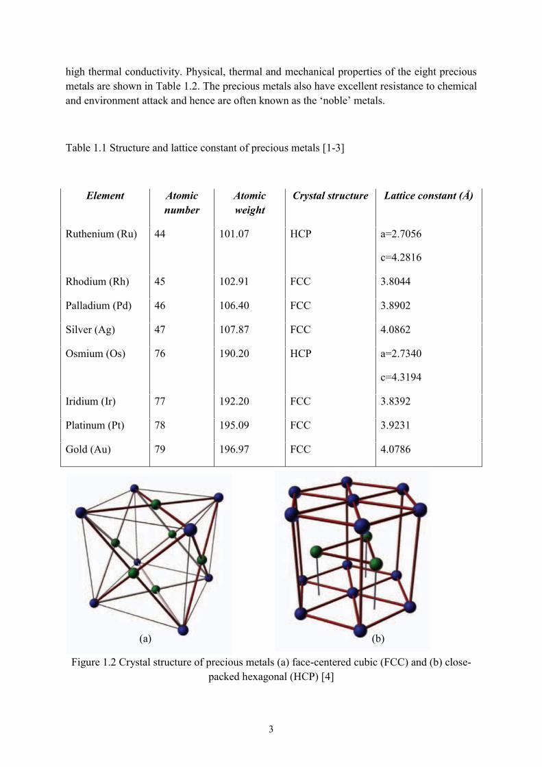
All physical and chemical properties depend on atomic and crystal structure. Except for osmium and ruthenium (which are close-packed hexagonal, HCP) the precious metals are face-centred cubic, FCC. The two different crystal structures are shown in Figure 1.2. In Table 1.1 the atomic numbers, atomic weights, crystal structures and lattice constants of the eight precious metals are summarized. It can be seen that most of the precious metal family share similar properties although Ag and Au stand out for their low electrical resistivity and
Other nonmetals
Halogen
Noble gas
Alkali metals
Alkaline earth metals
Transition metals
Post -transition metals
Metalloid
Unknown properties
Lanthanide
Actinide
Precious metals
3
high thermal conductivity. Physical, thermal and mechanical properties of the eight precious metals are shown in Table 1.2. The precious metals also have excellent resistance to chemical and environment attack and hence are often known as the ‘noble’ metals.
Table 1.1 Structure and lattice constant of precious metals [1-3]
Element Atomic number
Atomic weight
Crystal structure Lattice constant (Å)
Ruthenium (Ru) 44 101.07 HCP a=2.7056
c=4.2816
Rhodium (Rh) 45 102.91 FCC 3.8044
Palladium (Pd) 46 106.40 FCC 3.8902
Silver (Ag) 47 107.87 FCC 4.0862
Osmium (Os) 76 190.20 HCP a=2.7340
c=4.3194
Iridium (Ir) 77 192.20 FCC 3.8392
Platinum (Pt) 78 195.09 FCC 3.9231
Gold (Au) 79 196.97 FCC 4.0786
(a) (b)
Figure 1.2 Crystal structure of precious metals (a) face-centered cubic (FCC) and (b) close-packed hexagonal (HCP) [4]

4
Table 1.2 Selected properties of precious metals [1-3]
Properties Ru Rh Pd Ag Os Ir Pt Au
Density at 20 °C (g/cm3)
12.45 12.41 12.02 10.49 22.61 22.65 21.45 19.32
Melting point ( C) 2310 1963 1552 961 3045 2447 1769 1064
Boiling point ( C) 3900 3700 2900 2210 5020 4500 3800 2808
Electrical resistivity at 0 °C · cm
6.80 4.33 9.93 1.59 8.12 4.71 9.85 2.06
Thermal conductivity at 0-100 °C (W/m K)
105 150 76 425.0 87 148 73 315.5
Linear coefficient of thermal expansion (10-6/°C)
9.1 8.3 11.1 19.68 6.1 6.8 9.1 14.16
Tensile strength (MPa)-As worked wire
496 1379-1586
324-414
290 - 2070-2480
207-241
207-221
Hardness (HV)-Annealed wire
200-350
120-140
37-44 25-30 300-670
200-240
37-42 25-27
Gold and silver have of course been used for thousands of years, but use of the PGMs is more recent and dates from the 19th Century. Platinum has become an important substance in many industrial applications. However, use of pure metals causes some limitation in properties (in particular the tensile strength and hardness of the pure elements is rather low) and the precious metals are therefore commonly used in commercial and industrial applications as alloys or compounds. Alloying between the precious metals and with other elements has been developed to gain alternative properties for use in both decorative and industrial applications. These mixtures may take the form of conventional alloys, intermetallic compounds, or blends of the two. Historically, the initial applications of precious metals and their alloys or compounds have been in jewellery manufacture and dentistry. Technological development to make the use of precious metals and their alloys or compounds more efficient in those industries continues. However, the precious metals have more recently been applied in many other applications, for example electronics, catalysis, fuel cells, environmental remediation, the automobile industry, aerospace, optical devices, plating and coating, medical and pharmaceutical products. Precious metal alloys and compounds therefore continue to be an interesting subject.

5
There are several interesting groups of precious metal alloys and intermetallic compounds and they are usually classified according to their majority component, e.g. gold-based, platinum-based etc., or according to the field of application, dental alloys, jewellery alloys, etc. Precious metal alloys and compounds have been investigated in many different aspects, many of which are summarized in the literature review in Chapter 2.
In the present research work the precious metal alloys and compounds have been fabricated in the form of thin films by direct-current magnetron sputtering. The chemical composition, structures and morphologies of those resultant thin films have been characterized by various techniques which are explained in Chapter 3.
The main aims of this project have been to develop new applications of the precious metals. In respect of the jewellery industry, which is of great economic importance in my home country of Thailand, I have tried to find new and interesting technologies and alloys. My main hypothesis in this part of the project has been that the distinctly different colours of the various precious metal aluminides can be combined to yield new colour effects for jewellery. In particular, I hypothesized that the compounds PtAl2 (brassy yellow) and AuAl2 (metallic purple) can be alloyed to yield a range of intermediate colours. It is generally stated [5, 6] that these compounds would be immiscible but I proposed that a series of metastable solid solutions could be formed by means of magnetron sputtering. Chapter 4 is dedicated to this part of my project, the coloured intermetallic compounds of AuAl2 and PtAl2. Due to their distinct metallic colours, they are especially interesting for jewellery and decorative design purposes. AuAl2 can also be used in spectrally-selective coatings while PtAl2 is able to be used as corrosion or oxidation resistant coatings, particularly at high temperatures.
Precious metals alloys have uses beyond the jewellery industry however. The Pt-Al and Au-Al alloys and intermetallic compounds can be de-alloyed to form nanoporous sponges of Pt and Au respectively. These have potential applications in the chemical industry as catalysts and sensors [7]. In the second part of my project I have tried to understand how the microstructure of precursor alloys can control the morphology of subsequent sponges. My hypothesis has been that preparation of sponges from metastable precursors will produce a different result than producing them from well-crystallized precursors. Chapter 5 deals with the second theme, which is particularly related to platinum-aluminium intermetallics in general and the nanoporous platinum sponges that can be formed by de-alloying them in alkali solution.
Each of these chapters contains more specific literature reviews and experiments. The overall conclusion and future works are presented in Chapter 6.

6
Chapter 2
Literature review

7
There are many interesting precious metal alloys and compounds and many practical applications for them. The present research is focused on two themes: (i) coloured precious metal alloys and intermetallic compounds and (ii) nanoporous precious metal sponges. The work is motivated overall by the hypothesis that a better understanding of the binary and ternary phase relationships within precious metal systems will enable the design and fabrication of materials with specific and improved properties. In this Chapter I provide a summary of what is already known on these topics.
2.1 General: precious metal alloys and intermetallic compounds
2.1.1 Definition of precious metal alloys and intermetallic compounds The precious metals can combine with one or more other elements to produce either
alloys or intermetallic compounds. The term “alloy” is generally reserved for a material basically comprised of a complete or partial solid solution of two or more elements, possibly also containing a minor volume fraction of ceramic or intermetallic compounds. The crystal structure and properties of the alloy are closely related to those of the base elements, possibly somewhat modified by any minor phase or phases present. In contrast, the term “intermetallic compound” is used to designate a combination of two or more elements in definite proportions that form a new phase, with its own distinctive crystal structure and properties[8]. The bonding of intermetallic compounds is generally considered to be between metallic and covalent in nature[9]. Some pairs of intermetallic compounds are mutually soluble and can form a continuous range of isostructural compositions, in which case the term “intermetallic alloy” is sometimes used. A comparison between definition of alloys and intermetallic compounds are shown in Table 2.1.
Table 2.1 Comparison between alloys and intermetallic compounds
Alloys Intermetallic compounds
Complete or partial solid solution Form a new phase
Crystal structure and properties are closely related to base elements
Distinctive crystal structure and properties
8
2.1.2 Applications of precious metals and their alloys and intermetallic compounds
Precious metals and their alloys and compounds have a long history of uses in a wide range of applications. Although these have advanced far beyond the original use as a means to show off wealth, beauty and achievement, their use in jewellery remains economically very important.
Jewellery The major proportion of gold and silver consumption is for jewellery applications.
Gold, silver and platinum (and their alloys) are the main precious metals which have been used in this application. The content of precious metals is a key consideration. The Ag-Cu system is the most commonly used basis for silver alloys. 'Sterling silver' or '925Ag', which contains 92.5 wt.% Ag and 7.5 wt.% Cu, is the most typical silver alloy used in jewellery manufacturing. '835Ag' and '800Ag' are also used [10, 11]. The permissible content of gold is varied more than for the other precious metals and depends on regional market preferences or product niche. The term caratage refers to the proportion of pure gold, expressed on a scale of zero to 24, with 24 being 100% Au. (In North America the spelling 'karat' and 'karatage' may be used with 'carat' in those regions being reserved as a unit of mass for gemstones). Fineness (gold content expressed in parts out of thousand) or weight percentage (of Au) is also used, especially for bulk materials. The most popular common caratage levels are shown in Table 2.2. The best-known gold alloys are based on the ternary alloy system of Au-Ag-Cu and the quaternary alloy system of Au-Ag-Cu-Zn. The compositions of gold alloys are varied for jewellery according to the colour, mechanical properties and processability required and some of them are shown in Table 2.3. The physical properties and applications of gold alloys are summarized in Table 2.4. Nickel and palladium have been used as alloying additions to make so-called white gold alloys [12, 13]. The 990Au-Ti alloy has been developed to provide acceptable mechanical properties at a very high caratage [14, 15].
Platinum alloys in jewellery usually have 90 wt.% of Pt or higher. The '950Pt' and '900Pt' alloys are common levels of fineness of platinum which have been accepted in jewellery manufacture. The alloying elements which commonly used in platinum are palladium, ruthenium, cobalt, copper and iridium. For instance, 95%Pt-5%Cu and 95%Pt-5%Ru are used as general purpose wrought alloys while 95%Pt-5%Co and 95%Pt-5%Pd are suitable for casting in jewellery application [1, 16, 17].
9
Table 2.2 Definition of caratage in gold content [1]
Carat Fineness Percentage of pure gold
24 1000 100
23.76 990 99
22 916.6 91.66
21 875 87.5
20 833.3 83.3
18 750 75
15 625 62.5
14 585 58.5
12 500 50
10 416 41.6
9 375 37.5
8 333.3 33.3
Table 2.3 Varied content of alloying elements of carat gold alloys for jewellery [12]
Carat Gold content (wt.%) Content of alloy components (wt.%)
22 91.66 Ag 0-6, Cu 2-8.3
18 75 Ag 0-20, Cu 5-25
14 58.5 Ag 0-41.5, Cu 0-33.5, Zn 0-10
9 37.5 Ag 0-56, Cu 4-60, Zn 0-15
8 33.3 Ag 0-58.5, Cu 4-60, Zn 0-15

10
Table 2.4 Selected properties and applications of carat gold alloys in jewellery [12]
Carat Fineness Au/Ag,
(rest Cu) colour
Melting range ( C)
Density (g/cm3)
Hardness (HV)
Applications*
1 2 3 4 5 6 7 8 9
18
750/40 red 880-900 15.1 160 X X X
750/90 reddish 870-890 15.3 150 X X X X X X X
750/125 yellow 850-890 15.4 140 X X X X X X X X
750/150 pale yellow 890-920 15.5 130 X X X X X X X X
750/200 pale yellow 900-970 15.8 90 X
14
585/40 reddish 900-920 13.0 130 X X X X X X X
585/45 (+Zn)
yellow 835-860 13.0 100 X X X X X X
585/100 reddish yellow
820-870 13.3 140 X X X X
585/200 yellow 830-850 13.6 170 X
585/260 pale yellow 830-850 13.7 160 X X X X
585/300 pale yellow 820-890 13.9 140 X X X X X X X
585/340 green yellow 860-940 14.0 120 X X X X X X X X
585/415 green yellow 1015-1020
14.3 50 X
9
375/90 reddish 870-930 11.2 120 X X X X
375/60 yellow 870-950 11.0 95 X X X X
375/150 pale yellow 800-860 10.5 100 X X X X X
8
333/90 reddish 890-930 10.9 110 X X X X
333/75 yellow 850-910 10.9 105 X X X X
333/120 pale yellow 800-860 10.5 100 X X X X X
*Applications: 1Rings and brooches; 2 Deep pulling work; 3 Pressing work; 4 Enamelling; 5 Casting; 6 Chains and lattice work; 7 Blanks for minting; 8 Wedding bands; 9 Pipes and seamless

11
Dentistry The precious metal alloys used in dentistry range from Ag-Pd-based ('low noble
alloys' to Au-Pt based ('high noble alloys'). These are used as restorative materials as well as in applications such as prosthetic appliances including inlays, crowns, and bridges. Alloying additions are used to enhance or control properties such as mechanical strength, castability, chemical stability, biocompatibility and colour. As in jewellery, the Au-Ag-Cu system is the basic coloured gold alloy used in dentistry. Au-Ag-Cu-PGM alloys have been developed to enhance tarnish and corrosion resistance of gold-based alloys in the oral environment. Platinum and palladium are the PGMs which are also usually contained in dental alloys. Low carat gold alloys for dental applications might not contain copper, with typically palladium and indium or tin (Au-Pd-In or Au-Pd-Sn) being used instead [18]. However, palladium may cause a reaction in patients who are allergic or hypersensitive, particularly in Europe. Pd –free Au-Pt based high noble dental alloys have therefore been investigated. Ag-Au-Pt-Cu has also been studied for dental applications [19]. Furthermore, dental gold alloys containing platinum but no silver or copper have also been developed. Au-Pt-X (X= In, Sn, Fe, Zn) and Au-Pt-In-Y (Y=Sn, Fe, Zn) are examples of such dental alloys [20, 21].
Medical uses Precious metals are excellent candidates for certain medical applications. Similarly to
dental application, biocompatibility, corrosion resistance and durability are the key for use in medical implants of various types. However precious metals or their compounds have also been used in biomedical fields such as therapeutics and diagnostics. For example, silver and its compounds have bactericidal properties and can be used as an antibacterial agent in wound care and medical devices in order to prevent the bacterial infections [22, 23]. Gold compounds have been used in drugs for rheumatoid arthritis, anticancer and antimicrobial activity [24, 25]. A platinum compound (cisplatin) is well-known and widely used for its anti-cancer effect. Platinum group metals, particularly platinum and platinum alloys, have also been used in a wide range of medical devices, components and implants. (The Cochlear bionic ear, for example, uses Pt electrodes). Pt-Ir alloy is used for electrode material in medical appliances such as pacemakers, defibrillators and electrophysiology catheters. The tip of the guidewire in balloon angioplasty is usually made of Pt-W while Pt-Co can be used for small tubular devices or stents. Other metals in platinum group metals in wire form are used as microcoils for neurovascular devices. Rhodium foil is used as a filter inside X-ray mammography equipment [26, 27].
Electronics and electrical technology Precious metals usually have good electrical and thermal conductivity properties with
silver being the best electrical and thermal conductor of all metals. The electrical conductivity of silver is 6.30 x 10⁷ S/m while gold is 4.10 x 10⁷ S/m at 20 C. Thermal conductivity of silver and gold is approximately 428 and 318 W/m K respectively [3, 28]. Although gold is
12
not quite as good as silver, it has better corrosion resistance and remains an excellent conductor of heat and electricity. The platinum group metals also have relatively good electrical conductivity and durability. Precious metals and their alloys have been used in electronic components (connectors, contacts, printed circuit boards or PCB), electrical switches (switches, contacts, relays and circuit breakers) and electrical devices (e.g. multi-layer ceramic capacitors which are crucial to functioning in cars, mobile phones, computers, televisions and aircraft). The precious metals in electronic applications can be used in various forms including bulk materials, bimetals, and surface coatings (electroplated, sputtered, evaporated, pastes, lacquers and solder connections). AgPd alloys or even pure Pd are used as conductive material in multi-layer ceramic capacitors. AgCu-base alloys are used for vacuum brazing in electronics or as 'silver solder'. Other elements (Zn, Sn, Cd, Pd, Mn and P) are added to the base alloy to yield compositions like AgCuZn, AgCuZn, AgCuZnCd and AgCuP. Pure silver and its alloys including AgCu, AgNi, AgW, AgMo and composite materials such as Ag-CdO, Ag-SnO2, Ag-ZnO, Ag-graphite, and Ag-WC are also used for electrical contacts [10, 29, 30]. Gold thin and thick films are commonly used as conductors in electronics. Gold wire ("bonding wire") is also used to interconnect microprocessor chips to their 'packaging frame'. Gold and its alloys are also used in different applications and conditions. AuNi, AuCo and AuAg alloys are used as contact materials for low voltage switches while binary or ternary alloys of Au with Ag, Pd or Cu are used at higher voltages. AuPt and AuAgPt alloys are also used for electrical contacts under heavily corrosive conditions. AuCr2 is used as resistor material in corrosive environments and has a stable temperature coefficient of resistance (TCR) between -20 and +40 C [11, 13, 31].
Platinum group metals and their alloys have also demonstrated excellent properties for use in some electronic applications. For example, PtCo alloy has good magnetic properties and is a candidate for magneto-optic data storage and hard drives. PtRh alloys serve as high temperature thermocouples and windings for high temperature due to their high melting points and stability [17, 26, 32].
Catalysts Precious metal catalysts based on palladium, platinum, gold, silver, rhodium and
ruthenium have been used in various industries due to their high activity, selectivity and stability. Silver is an excellent oxidation catalyst while gold and platinum group metals are used in a variety of reactions for applications including pollution control, chemical processing and fuel cells. Catalysts may be used in the form of nanoparticles of precious metals or their alloys and compounds, or as nanostructured films of precious metals or de-alloyed sponges of precious metals (often with other transition metals). AuPd catalyst is now used commercially in vinyl acetate production. Pt-Al2O3, PtIr and PtRe play a role in the petrochemical industry while PtRh is mainly used as an automobile catalyst. PtCoCr, PtCoFe, PtRu or PtNi alloys are cathode catalysts in fuel cells [11, 31, 33, 34].
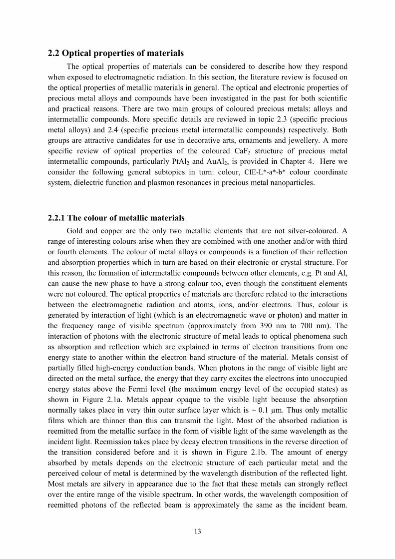
13
2.2 Optical properties of materials The optical properties of materials can be considered to describe how they respond
when exposed to electromagnetic radiation. In this section, the literature review is focused on the optical properties of metallic materials in general. The optical and electronic properties of precious metal alloys and compounds have been investigated in the past for both scientific and practical reasons. There are two main groups of coloured precious metals: alloys and intermetallic compounds. More specific details are reviewed in topic 2.3 (specific precious metal alloys) and 2.4 (specific precious metal intermetallic compounds) respectively. Both groups are attractive candidates for use in decorative arts, ornaments and jewellery. A more specific review of optical properties of the coloured CaF2 structure of precious metal intermetallic compounds, particularly PtAl2 and AuAl2, is provided in Chapter 4. Here we consider the following general subtopics in turn: colour, CIE-L*-a*-b* colour coordinate system, dielectric function and plasmon resonances in precious metal nanoparticles.
2.2.1 The colour of metallic materials Gold and copper are the only two metallic elements that are not silver-coloured. A
range of interesting colours arise when they are combined with one another and/or with third or fourth elements. The colour of metal alloys or compounds is a function of their reflection and absorption properties which in turn are based on their electronic or crystal structure. For this reason, the formation of intermetallic compounds between other elements, e.g. Pt and Al, can cause the new phase to have a strong colour too, even though the constituent elements were not coloured. The optical properties of materials are therefore related to the interactions between the electromagnetic radiation and atoms, ions, and/or electrons. Thus, colour is generated by interaction of light (which is an electromagnetic wave or photon) and matter in the frequency range of visible spectrum (approximately from 390 nm to 700 nm). The interaction of photons with the electronic structure of metal leads to optical phenomena such as absorption and reflection which are explained in terms of electron transitions from one energy state to another within the electron band structure of the material. Metals consist of partially filled high-energy conduction bands. When photons in the range of visible light are directed on the metal surface, the energy that they carry excites the electrons into unoccupied energy states above the Fermi level (the maximum energy level of the occupied states) as shown in Figure 2.1a. Metals appear opaque to the visible light because the absorption normally takes place in very thin outer surface layer which is ~ 0.1 m. Thus only metallic films which are thinner than this can transmit the light. Most of the absorbed radiation is reemitted from the metallic surface in the form of visible light of the same wavelength as the incident light. Reemission takes place by decay electron transitions in the reverse direction of the transition considered before and it is shown in Figure 2.1b. The amount of energy absorbed by metals depends on the electronic structure of each particular metal and the perceived colour of metal is determined by the wavelength distribution of the reflected light. Most metals are silvery in appearance due to the fact that these metals can strongly reflect over the entire range of the visible spectrum. In other words, the wavelength composition of reemitted photons of the reflected beam is approximately the same as the incident beam.

14
Copper appears red-orange while gold appears yellow since some energy associated with photons having short wavelengths is not reemitted as visible light, therefore the resulting emerging light does not contain those wavelengths and its colour changes accordingly. For these two metals, the part of the incident radiation absorbed is short wavelengths such as green and blue. These metals scatter the incident light predominantly in the yellow-orange, orange and red wavelengths [35].
Figure 2.1 Schematic representation of the mechanism of photon absorption (a) and emission (b) for metallic materials [35]
2.2.2 The CIE-L*-a*-b* colour coordinate system The colour of materials is associated with the physics of electromagnetic radiation in the visible range and the perception of colour by the human eye and brain. Sir Isaac Newton developed the first circular diagram of colour (the colour wheel) which is based on red, yellow and blue in 1666. Since then the colour wheel has been further developed, and the current one includes hue, saturation and brightness to provide more details about colour. An accurate colour measurement is required to define colour appearance or colour difference. In this project the CIE LAB system is used to specify colour. The Commission Internationale de l’Éclairage (CIE) is the international authority on light, illumination, colour and colour spaces which was established in 1913. In the beginning, CIE XYZ colour space was used to represent possible colours but the values of the XYZ coordinate system do not match the sensitivity of the human eye very well. Consequently, CIE LAB or CIE L*a*b* was defined in 1976. In this scale colour 'distances' are correlated with the sensitivity of the average human eye. The CIE LAB model is shown in Figure 2.2. The three coordinates of CIE LAB are the brightness or lightness of the colour (L*) and the chromaticity indices a* and b*. The brightness increases from the bottom to the top (L*=0 indicate black and L*=100 indicates
(a) (b)
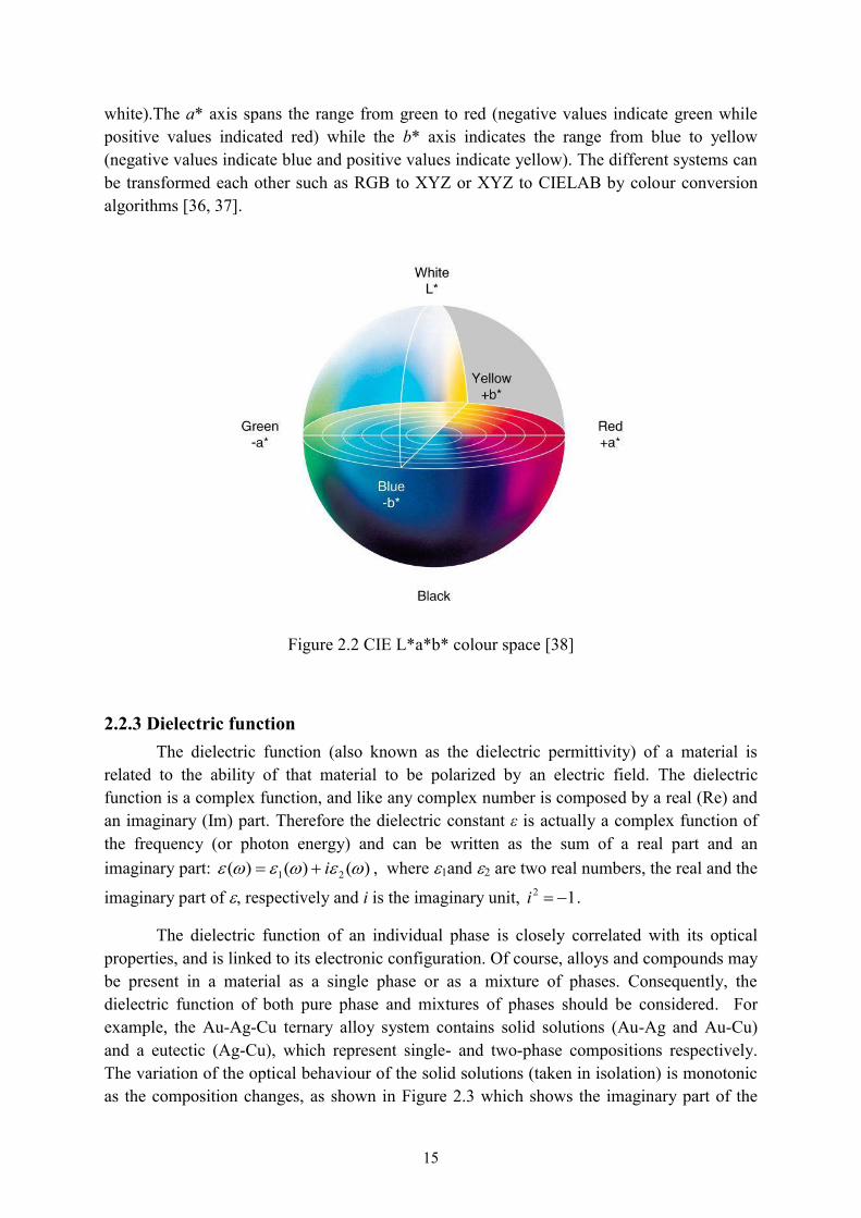
15
white).The a* axis spans the range from green to red (negative values indicate green while positive values indicated red) while the b* axis indicates the range from blue to yellow (negative values indicate blue and positive values indicate yellow). The different systems can be transformed each other such as RGB to XYZ or XYZ to CIELAB by colour conversion algorithms [36, 37].
Figure 2.2 CIE L*a*b* colour space [38]
2.2.3 Dielectric function The dielectric function (also known as the dielectric permittivity) of a material is
related to the ability of that material to be polarized by an electric field. The dielectric function is a complex function, and like any complex number is composed by a real (Re) and an imaginary (Im) part. Therefore the dielectric constant is actually a complex function of the frequency (or photon energy) and can be written as the sum of a real part and an imaginary part: )()()( 21 i , where 1and 2 are two real numbers, the real and the
imaginary part of , respectively and i is the imaginary unit, 12i .
The dielectric function of an individual phase is closely correlated with its optical properties, and is linked to its electronic configuration. Of course, alloys and compounds may be present in a material as a single phase or as a mixture of phases. Consequently, the dielectric function of both pure phase and mixtures of phases should be considered. For example, the Au-Ag-Cu ternary alloy system contains solid solutions (Au-Ag and Au-Cu) and a eutectic (Ag-Cu), which represent single- and two-phase compositions respectively. The variation of the optical behaviour of the solid solutions (taken in isolation) is monotonic as the composition changes, as shown in Figure 2.3 which shows the imaginary part of the

16
interband dielectric constant as a function of photon energy of Au-Ag (with varied Ag content in at.%) and Au-Cu (with varied Cu content in at.%). For a solid solution or single phase, the continuous shift of the absorption edge with concentration over the entire range is displayed. The absorption spectrum moves and modifies its shape gradually as the composition changes. However, once the compositional bounds of the solid solution are exceeded the material will separate into two phases. The interband dielectric constant is shown in Figure 2.4 for two cases for the Ag-Cu eutectic: Cu-rich and Ag-rich. In these cases, the optical characteristic of the two phase composition is determined by volume fractions of the two phases [39, 40]. Table 2.5 shows the onset of interband transitions in some of the coloured intermetallic compounds which have CaF2 structure [41, 42]. The imaginary part of the optical constants of pure phases can be calculated by the ab initio method, and then the real part obtained by means of the Kramers-Kronig relations.
Figure 2.3 Imaginary part of the interband dielectric constant as function of energy (a) Au-Ag and (b) Au-Cu [39]
94 at% Ag 62 at% Ag
21 at% Ag 41 at% Ag
(a)
70 at% Cu 40 at% Cu
12 at% Cu 25 at% Cu
81 at% Cu
(b)

17
Figure 2.4 Imaginary part of the interband dielectric constant and energy of Ag-Cu series (a) Cu-rich and (b) Ag-rich [39]
Table 2.5 Onset of interband transition of selected coloured intermetallic compounds [41, 42]
Onset of interband transition, in electron volts (eV)
AuAl2 2.2
AuGa2 2.0
AuIn2 1.7
PtAl2 2.8
PtGa2 2.5-4.5
2.2.4 Plasmon resonances in precious metal nanoparticles Nanoparticles of noble metals, in particular Au and Ag, have been studied for their
optical properties because they can support a plasmon resonance in the visible and near-infrared regions of the spectrum. Plasmon resonances are optical phenomena that can occur when conduction electrons couple with photons to produce an oscillation of charge at the surface of a metal. The position of the resonance can modified by varying the nanoparticle size and shape [43]. Moreover, Au and Ag can be easily formed into complex nanostructures by chemical, physical and lithographic methods [44] which facilitates these studies. Some
55 at% Cu 94 at% Cu
(a)
6 at% Cu 8 at% Cu
30 at% Cu 43 at% Cu
(b)

18
studies by Blaber et al. have compared the different elements [45, 46]. Numerous hybrid or alloyed nanoparticle systems, containing for example, Cu, Pt or Pd in addition to the Au or Ag, have also been investigated [47-52]. The plasmon resonances of alloyed and intermetallic nanoparticles are interesting because the behaviour of such hybrids is different from that of the bulk materials. For example, Au and Pt have poor miscibility in bulk materials [53] but they can form a solid solution in nanoparticles smaller than about 5 nm [54, 55]. A similar result holds for Au and Fe [56]. In the case of ordered intermetallic compounds, Cu3Au is normally ordered up to 240 C in bulk materials [53] but if the nanoparticle size is less than 5 nm, ordered Cu3Au would not be formed [57]. Hybrid nanoparticles of the coinage metals have been investigated due to the strong plasmon resonance of the constituent elements, with Au-Ag and Ag-Au core-shell particles having been investigated since early work in 1964 by Morris and Collins [58, 59]. Multi-shell structures such as Au-Ag-Au-Ag can also be formed and they have interesting optical properties. For example, there is a sequence of colour changes in multi-shell Au/Ag colloids. These start from gold colloid which is red, but after overcoating with Ag the colloid becomes yellow due to the plasmon resonance being blue shifted. Then Au-Ag-Au, produced by adding a layer of Au, has a deep blue colour due to red-shifting of the resonance. Lastly, if a layer of Ag is added to make Au-Ag-Au-Ag, resonance blue-shifts again to give an orange colour [59]. Moreover, hybrids with platinum group metals including Au-Pd, Au-Pt and Ag-PGMs have been studied as well as hybrids with magnetic metals Au-Ni, Au-Fe, Au-Co and Ag-Ni.
2.3 Specific precious metal alloys The ternary phase diagram of Au-Ag-Cu (the three 'coinage metals') is the most basic
and best-known gold alloy system. The colours of these three elements are totally different. The reflectance curves are shown in Figure 2.5. Reflectance of silver is close to 100 % over the visible range thus silver appears white while reflectance of copper and gold is large at yellow-red wavelengths and smaller in the blue-green region. Due to the difference in position of the reflection edges of these two metals, copper is reddish/orange and gold is yellow [60]. Varied colours, such as yellow, white, “red” and “green”, can be obtained using different compositions of Au, Ag, Cu, sometimes with minor alloying additions of other elements. Addition of copper makes the alloy reddish while addition of silver gives the alloy a greenish to whitish hue, as shown in Figure 2.6. Some coloured rings from different precious metal alloys are shown in Figure 2.7 [61]. Consideration of caratage is also important in consideration of coloured gold alloys used in jewellery. A range of variously coloured gold alloys can be produced at each caratage level [32-34], although there is obviously more flexibility at the lower carat levels. Alloys at the 9 carat level can be “white”, different shades of yellow from pale to rich yellow, greenish, and even pink and “red”, 14 carat gold alloys can be pale green, yellow and red while 18 carat gold alloys can be green-yellow, or different shades of yellow, pink and red. In 22 carat gold alloys the colours can be yellow, deep yellow and pink, however, as gold content increases above 22 carat (22/24, or 91.6%Au), the yellow colour of gold usually dominates. The colour of some carat gold alloys based on the Au-Ag-Cu system is shown in Table 2.6. Addition of up to 15 wt.% Zn in the
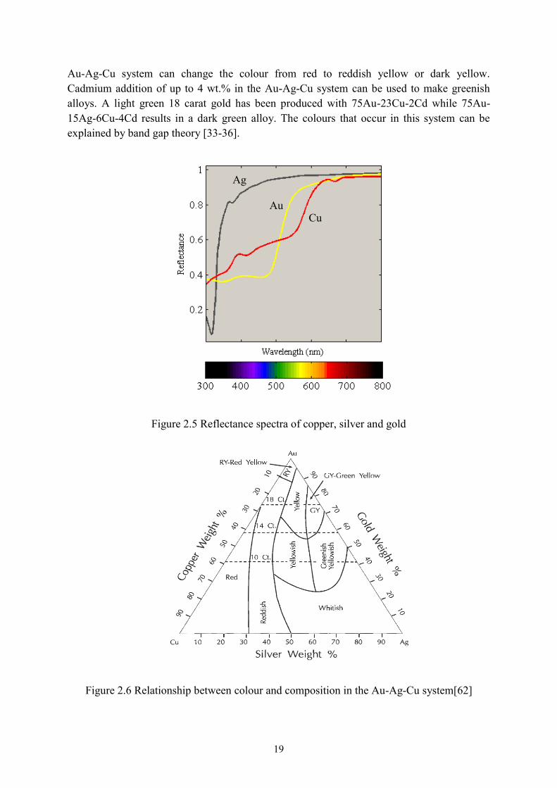
19
Au-Ag-Cu system can change the colour from red to reddish yellow or dark yellow. Cadmium addition of up to 4 wt.% in the Au-Ag-Cu system can be used to make greenish alloys. A light green 18 carat gold has been produced with 75Au-23Cu-2Cd while 75Au-15Ag-6Cu-4Cd results in a dark green alloy. The colours that occur in this system can be explained by band gap theory [33-36].
Figure 2.5 Reflectance spectra of copper, silver and gold
Figure 2.6 Relationship between colour and composition in the Au-Ag-Cu system[62]
Cu Au
Ag
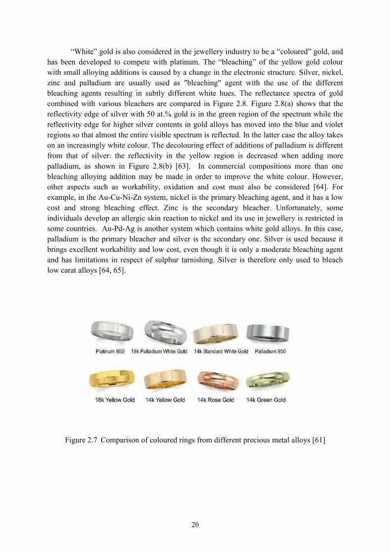
20
“White” gold is also considered in the jewellery industry to be a “coloured” gold, and has been developed to compete with platinum. The “bleaching” of the yellow gold colour with small alloying additions is caused by a change in the electronic structure. Silver, nickel, zinc and palladium are usually used as "bleaching" agent with the use of the different bleaching agents resulting in subtly different white hues. The reflectance spectra of gold combined with various bleachers are compared in Figure 2.8. Figure 2.8(a) shows that the reflectivity edge of silver with 50 at.% gold is in the green region of the spectrum while the reflectivity edge for higher silver contents in gold alloys has moved into the blue and violet regions so that almost the entire visible spectrum is reflected. In the latter case the alloy takes on an increasingly white colour. The decolouring effect of additions of palladium is different from that of silver: the reflectivity in the yellow region is decreased when adding more palladium, as shown in Figure 2.8(b) [63]. In commercial compositions more than one bleaching alloying addition may be made in order to improve the white colour. However, other aspects such as workability, oxidation and cost must also be considered [64]. For example, in the Au-Cu-Ni-Zn system, nickel is the primary bleaching agent, and it has a low cost and strong bleaching effect. Zinc is the secondary bleacher. Unfortunately, some individuals develop an allergic skin reaction to nickel and its use in jewellery is restricted in some countries. Au-Pd-Ag is another system which contains white gold alloys. In this case, palladium is the primary bleacher and silver is the secondary one. Silver is used because it brings excellent workability and low cost, even though it is only a moderate bleaching agent and has limitations in respect of sulphur tarnishing. Silver is therefore only used to bleach low carat alloys [64, 65].
Figure 2.7 Comparison of coloured rings from different precious metal alloys [61]

21
Table 2.6 Coloured carat gold alloys based on the Au-Ag-Cu system [66]
Carat Gold wt.% Silver wt.% Copper wt.% Colour
22
91.6 8.4 - Yellow
91.6 5.5 2.8 Yellow
91.6 3.2 5.1 Deep yellow
91.6 - 8.4 Pink/rose
18
75.0 25.0 - Green-yellow
75.0 16.0 9.0 Pale yellow, 2N
75.0 12.5 12.5 Yellow, 3N
75.0 9.0 16.0 Pink, 4N
75.0 4.5 20.5 Red, 5N
14
58.5 41.5 - Pale green
58.5 30.0 11.5 Yellow
58.5 9.0 32.5 Red
9
37.5 62.5 - White
37.5 55.0 7.5 Pale yellow
37.5 42.5 20.0 Yellow
37.5 31.25 31.25 Rich yellow
37.5 20.0 42.5 Pink
37.5 7.5 55.0 Red

22
(a) (b)
Figure 2.8 Reflectivity curves of gold and its alloys (a) gold-silver alloys and (b) gold-palladium alloys [63]
2.4 Specific precious metal intermetallic compounds
2.4.1 Colour of pure phases Some precious intermetallic compounds have attractive fundamental properties such
as high hardness, high wear resistance, good oxidation resistance or specialized electronic properties [67]. A few of them display beautiful colours that are not found in the metallic elements [67, 68]. The coloured intermetallic compounds require a highly symmetrical crystalline structure in order to ensure that electron band structure allows sp-d hybridization. The coloured binary intermetallic compounds which have B2 (cP2 or CsCl) and C1 (cF12 or CaF2) crystal structure the best-known examples [67, 68]. The crystal structure of CsCl and CaF2 are shown in Figure 2.9 (a) and (b) respectively. Table 2.7 shows some examples of coloured binary intermetallic compounds with these crystal structures. PdIn is red and PdMg, PdAl are yellow in B2 type, PtAl2 PtGa2 and PtIn2 are yellow, AuAl2 is purple and AuGa2
Curve 1 Fine gold Curve 2 Silver with 50 at% gold Curve 3 Silver with 10 at% gold Curve 4 Silver with 5 at% gold Curve 5 Fine silver
Curve 1 Fine gold Curve 2 Gold with 5 at% palladium Curve 3 Gold with 10 at% palladium Curve 4 Gold with 20 at% palladium Curve 5 Gold with 30 at% palladium Curve 6 Fine palladium
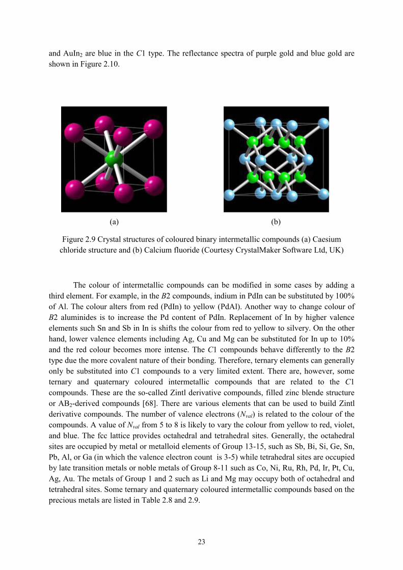
23
and AuIn2 are blue in the C1 type. The reflectance spectra of purple gold and blue gold are shown in Figure 2.10.
(a) (b)
Figure 2.9 Crystal structures of coloured binary intermetallic compounds (a) Caesium chloride structure and (b) Calcium fluoride (Courtesy CrystalMaker Software Ltd, UK)
The colour of intermetallic compounds can be modified in some cases by adding a third element. For example, in the B2 compounds, indium in PdIn can be substituted by 100% of Al. The colour alters from red (PdIn) to yellow (PdAl). Another way to change colour of B2 aluminides is to increase the Pd content of PdIn. Replacement of In by higher valence elements such Sn and Sb in In is shifts the colour from red to yellow to silvery. On the other hand, lower valence elements including Ag, Cu and Mg can be substituted for In up to 10% and the red colour becomes more intense. The C1 compounds behave differently to the B2 type due the more covalent nature of their bonding. Therefore, ternary elements can generally only be substituted into C1 compounds to a very limited extent. There are, however, some ternary and quaternary coloured intermetallic compounds that are related to the C1 compounds. These are the so-called Zintl derivative compounds, filled zinc blende structure or AB2-derived compounds [68]. There are various elements that can be used to build Zintl derivative compounds. The number of valence electrons (Nval) is related to the colour of the compounds. A value of Nval from 5 to 8 is likely to vary the colour from yellow to red, violet, and blue. The fcc lattice provides octahedral and tetrahedral sites. Generally, the octahedral sites are occupied by metal or metalloid elements of Group 13-15, such as Sb, Bi, Si, Ge, Sn, Pb, Al, or Ga (in which the valence electron count is 3-5) while tetrahedral sites are occupied by late transition metals or noble metals of Group 8-11 such as Co, Ni, Ru, Rh, Pd, Ir, Pt, Cu, Ag, Au. The metals of Group 1 and 2 such as Li and Mg may occupy both of octahedral and tetrahedral sites. Some ternary and quaternary coloured intermetallic compounds based on the precious metals are listed in Table 2.8 and 2.9.

24
Table 2.7 Coloured binary intermetallic compounds with CsCl and CaF2 structure [68]
CsCl CaF2
Compound Colour Compound Colour
FeAl Brown CoSi2 Dark blue
CoAl Yellow NiSi2 Gray blue
CoGa Yellow PtAl2 Yellow
NiAl Blue PtGa2 Yellow
NiGa Bluish PtIn2 Yellow
PdIn Red AuAl2 Purple
PdMg Yellow AuGa2 Blue
PdAl Yellow AuIn2 Blue
Figure 2.10 Reflectivity curves of coloured gold intermetallic compounds: AuAl2 (curve 1), AuIn2 (curve 2) and AuGa2 (curve 3) [63]
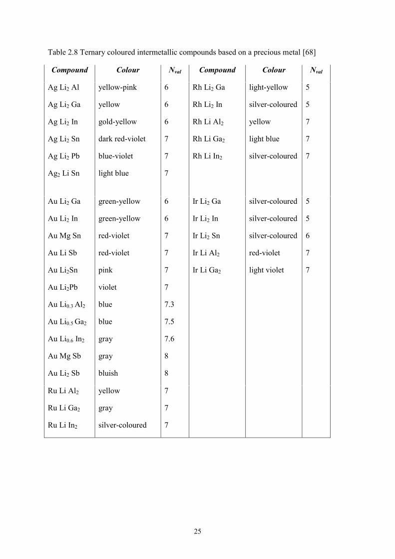
25
Table 2.8 Ternary coloured intermetallic compounds based on a precious metal [68]
Compound Colour Nval Compound Colour Nval
Ag Li2 Al
Ag Li2 Ga
Ag Li2 In
Ag Li2 Sn
Ag Li2 Pb
Ag2 Li Sn
yellow-pink
yellow
gold-yellow
dark red-violet
blue-violet
light blue
6
6
6
7
7
7
Rh Li2 Ga
Rh Li2 In
Rh Li Al2
Rh Li Ga2
Rh Li In2
light-yellow
silver-coloured
yellow
light blue
silver-coloured
5
5
7
7
7
Au Li2 Ga
Au Li2 In
Au Mg Sn
Au Li Sb
Au Li2Sn
Au Li2Pb
Au Li0.3 Al2
Au Li0.5 Ga2
Au Li0.6 In2
Au Mg Sb
Au Li2 Sb
green-yellow
green-yellow
red-violet
red-violet
pink
violet
blue
blue
gray
gray
bluish
6
6
7
7
7
7
7.3
7.5
7.6
8
8
Ir Li2 Ga
Ir Li2 In
Ir Li2 Sn
Ir Li Al2
Ir Li Ga2
silver-coloured
silver-coloured
silver-coloured
red-violet
light violet
5
5
6
7
7
Ru Li Al2
Ru Li Ga2
Ru Li In2
yellow
gray
silver-coloured
7
7
7

26
Table 2.8 Ternary coloured intermetallic compounds based on a precious metal (cont.) [68]
Compound Colour Nval Compound Colour Nval
Pd2 Li Ge
Pd2 Li Sn
Pd2 Li Pb
Pd Li2 Al
Pd Li2 Ga
Pd Li2 In
Pd Li2 Ge
Pd Li2 Sn
Pd Li2 Pb
Pd Mg Sn
Pd Li Al2
Pd Li Ga2
Pd Li In2
Pd Li2 Sb
Pd Mg Sb
Pd Mg1.5 Sb
Pd Mg2 Sb
brown-yellow
brown-yellow
brown-yellow
rose
brass-yellow
brown-yellow
yellow
yellow
brown-yellow
brown-yellow
violet
silver-coloured
silver-coloured
brass-yellow
violet
light violet
blue-gray
5
5
5
5
5
5
6
6
6
6
7
7
7
7
7
8
9
Pt Li2 Al
Pt Li2 Ga
Pt Li2 In
Pt Li2 Sn
Pt Mg Sn
Pt Li Al2
Pt Li Ga2
Pt Li In2
Pt Li2 Sb
Pt Mg Sb
bright-yellow
bright-yellow
brass-yellow
yellow
reddish-brown
copper-red
brown-pink
pink
brass-yellow
violet
5
5
5
6
6
7
7
7
7
7

27
Table 2.9 Quaternary coloured intermetallic compounds based on a precious metal [68]
Compound Colour Nval
Pd Li Mg Sn
Pd Li Mg Sb
red-violet
gray-blue
7
8
Pt Li0.5 Mg Sn
Pt Li0.5 Mg0.5 Sn
Pt Li Mg Sn
Pt Li Mg0.5 Sb
Pt Li0.5 Mg Sb
Pt Li Mg Sb
dark red
pink
copper-red
copper-red
dark blue-violet
red-violet
6.5
6.5
7
7
7.5
8
Ir Li Mg Sn gray-blue 7
Au Li Mg Sn gray 7
2.4.2 Alloying effects The addition of alloying elements plays a role to enhance the properties of precious
metal alloys and compounds as well as to change their colour. As mentioned above, in the well-known alloys based on Au-Ag-Cu, the typical alloying elements used for a colour effect are copper (reddening), silver (greening) and zinc, nickel and palladium (whitening). However, colour changes in other precious metal alloys and compound systems have also been investigated. The Au-Cu-Al alloy known as Spangold is interesting because of its surface texture. There are two different colours based on 18 carat gold alloy. The alloy 76% Au-19%Cu-5%Al (wt.%) is yellow while the alloy of 76%Au-18%Cu-6%Al is pinkish [69]. The colour of Au-Cu-Al systems have been studied by measuring and plotting CIE a* and b* colour coordinates of compositions along the 18 carat pseudo-binary as shown in Figure 2.11. Starting from Au-Cu, the -phase alloys show a red-gold colour, which changes to yellow when Al content increases. When the composition reaches the -phase, the yellow colour shifts to a pink/apricot colour. At higher Al content, when the -phase replaces the -phase, the colour turns to silver. Finally, some purple AuAl2 can be formed in this system. However, the end point of the 18 carat pseudo-binary is actually a two phase Al + AuAl2 mixture, in which the colour will be lighter purple due to the bleaching effect of the Al. Another composition, 61%Al-24%Cu-15%Au contains the phase AuAl2, CuAl and CuAl2. These phases are respectively pink, tan and yellow as seen with light microscopy [70].
The optical properties and effect of indium additions on Au-Pt based dental alloys were studied [20]. The samples were prepared by melting in a high-frequency induction

28
furnace, then cold rolled followed by a homogenizing heat treatment at high temperature. There were two systems of sample alloys with different chemical composition. The first system was binary Au-Pt (AP5: 95 at%Au-5 at%Pt and AP10: 90 at%Au-10 at%Pt). Another system was ternary Au-Pt-In (AP10-In2: 88at%Au-10 at%Pt-2 at%In and AP10-In4: 88 at.%Au-10 at.%Pt-4 at.%In). The spectral reflectance for the incident CIE standard illuminant D65 was collected as a function of the wavelength at 10 nm intervals from 360 to 740 nm. Three coordinates L*, a* and b* colour space were determined. The reflectances of Au, Pt and binary Au-Pt alloys were compared. The pronounced step near 520 nm (approximately 2.4 eV) in the spectral reflectance-wavelength curve for pure gold, which is responsible for the rich yellow colour of gold, became less pronounced with increasing platinum content. This is due to the decolouring (“bleaching”) effect of Pt on Au. In ternary Au-Pt-In, the addition of a small amount of indium to Au-Pt alloy increased the reflectance in the long-wavelength range and decreased the reflectance in the short-wavelength range of the visible spectrum. The number of valence electrons per atom (e/a) of the ternary Au-Pt-In increased with increasing indium content. This change caused an increase in both chromaticity indices including a* and b* values, which gave a gold tinge to the alloy.
In later research, Au-Pt-based ternary alloys containing a small amount of In, Sn, Fe, Zn and quaternary alloys containing 2 at% In and a small amount of Sn, Fe, Zn were investigated, with a focus on colour variations by CIELAB, chroma and hue values[21]. The addition of Sn, Fe, In slightly increased chromaticity index a* which giving a very light tint of red but significantly increased chromaticity index b* which increased yellow colour. This effect was strongest in Fe, and the addition of Fe only was obviously sufficient to increase lightness. Fe was therefore the most effective addition to give a bright yellow colour. On the other hand, the addition of Zn did not change colour coordinates in these alloys. The chroma depended on chromaticity index b*, and the addition of Fe increased the chroma most effectively, followed by Sn and In additions. The chromas in the quaternary alloys were greater than those ternary alloys. The hue angle, h was not influenced by the alloying addition. Another quaternary Ag-Au-Pt-Cu alloy system was also investigated [19]. The samples of quaternary Ag-Au-Pt-Cu containing 10at% Pt and 10-35 at% Au were prepared in a high frequency induction furnace under an argon atmosphere. The optical properties and microstructures were analysed by spectrophotometric colorimetry, optical microscopy and electron probe microanalysis. The Ag-Au-Pt-Cu alloys annealed at 850 °C were composed of a major phase of the Ag-Au rich matrix and minor phase of the Pt-Cu rich small grains embedded in the matrix. The Pt-Cu rich phase was almost colourless. The Ag-Au rich matrix therefore controlled the colour of the quaternary alloys. Three-dimensional colour coordinates including L* (lightness), a* (red-green) and b* (yellow-blue) in CIELAB varied as Au/Ag atomic ratio in alloy. Increasing Au/Ag atomic ratio from 0.130 to 0.996, the L* value decreased from 90.4 to 86.9 and b* value increased from 8.0 to 14.4 whereas the a* value did not vary significantly. This gave a pale yellow colour. It also found that the chroma (C*) is mainly caused by systematic increase in yellowness of the Ag-Au-Pt-Cu alloys with increasing Au/Ag atomic ratio.
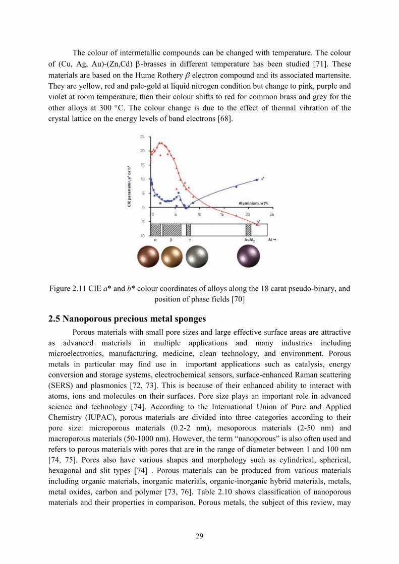
29
The colour of intermetallic compounds can be changed with temperature. The colour of (Cu, Ag, Au)-(Zn,Cd) -brasses in different temperature has been studied [71]. These materials are based on the Hume Rothery electron compound and its associated martensite. They are yellow, red and pale-gold at liquid nitrogen condition but change to pink, purple and violet at room temperature, then their colour shifts to red for common brass and grey for the other alloys at 300 C. The colour change is due to the effect of thermal vibration of the crystal lattice on the energy levels of band electrons [68].
Figure 2.11 CIE a* and b* colour coordinates of alloys along the 18 carat pseudo-binary, and position of phase fields [70]
2.5 Nanoporous precious metal sponges Porous materials with small pore sizes and large effective surface areas are attractive
as advanced materials in multiple applications and many industries including microelectronics, manufacturing, medicine, clean technology, and environment. Porous metals in particular may find use in important applications such as catalysis, energy conversion and storage systems, electrochemical sensors, surface-enhanced Raman scattering (SERS) and plasmonics [72, 73]. This is because of their enhanced ability to interact with atoms, ions and molecules on their surfaces. Pore size plays an important role in advanced science and technology [74]. According to the International Union of Pure and Applied Chemistry (IUPAC), porous materials are divided into three categories according to their pore size: microporous materials (0.2-2 nm), mesoporous materials (2-50 nm) and macroporous materials (50-1000 nm). However, the term “nanoporous” is also often used and refers to porous materials with pores that are in the range of diameter between 1 and 100 nm [74, 75]. Pores also have various shapes and morphology such as cylindrical, spherical, hexagonal and slit types [74] . Porous materials can be produced from various materials including organic materials, inorganic materials, organic-inorganic hybrid materials, metals, metal oxides, carbon and polymer [73, 76]. Table 2.10 shows classification of nanoporous materials and their properties in comparison. Porous metals, the subject of this review, may

30
be prepared by techniques such as galvanic replacement reaction, the combination of block copolymer template with deposition, chemical reduction of metal ions, hydrothermal synthesis method, powder metallurgy, filter casting, potential-controlled anodization, electroplating, electrodeposition, surfactant emulsion template, wet-chemical strategy and template-printing method. However, de-alloying is the most popular method for preparing nanoporous metals because it is a simple and effective method for fabricating structures with a three-dimensional (3D) bicontinuous nanostructure and open nanoporosity, large surface areas and excellent physical, mechanical and chemical properties [76, 77].
De-alloying is defined as an alloy corrosion process in which a selective electrolytic dissolution of one component from solid solution takes place. The less noble metal is removed and the more stable element is retained in a porous structure. The crucial factors to be considered when attempting to form nanoporous structures by de-alloying are whether the precursor is a homogeneous single phase (desirable), there is sufficient galvanic series difference of the alloy components (essential), that the composition is above the parting limit (essential) and that rapid surface diffusion of the noble metal components can take place essential) [78, 79]. There are various examples of nanoporous metals (NPMs) fabricated by the de-alloying method. Nanoporous metals are divided into three main groups: three dimensional nanoporous metals, low-dimensional nanoporous metals and nanoporous metal-based composites. A classification of these nanoporous metals is shown in Figure 2.12 [76, 80]. In this chapter we focus on nanoporous metals, particularly nanoporous precious metals including nanoporous gold (np-Au), nanoporous silver (np-Ag), nanoporous platinum (np-Pt) and nanoporous palladium (np-Pd).
Table 2.10 Classification of nanoporous materials and their properties [74]
Polymer Carbon Glass Oxides Metal
Pore size Meso-macro Micro-meso Meso-macro Micro-meso Meso-macro
Surface area/Porosity
Low >0.6
High 0.3-0.6
Low 0.3-0.6
Medium 0.3-0.6
Low 0.1-0.7
Permeability Low-medium Low-medium High Low-medium High
Strength Medium Low Strong Weak-medium
Strong
Thermal stability
Low High Good Medium-high
High
Chemical stability
Low-medium High High Very high High
Costs Low High High Medium Medium
Life Short Long Long Long Long

31
Nanoporous metals (NPMs)
Three-dimensional nanoporous metals Low-dimensional nanoporous metals Nanoporous metal-based composites
Nanoporous nanowires
(np-Au, np-PtCo, np-PtNi)
Nanoporous nanotubes
(np-Au, np-AuAg)
Nanoporous nanoparticles
Nanoporous nanoshells
Np-Au-based composites
-Metal-decorated np-Au composites (Pt@np-Au, Ag@np-Au, Au@np-Au, Ni@np Au, Sn@np-Au) -Metal oxide-decorated np-Au composites (TiO2@np-Au, Al2O3@np-Au, MnO2@np-Au) -Polymer-decorated np-Au composites (PPy@np-Au)
Np-Cu-based composites
(Au@np-Cu, Ag@np-Cu, Nanotubular mesoporous PtCu and PdCu)
Np-Ag-based composites
(Nanotubular mesoporous PtAg and PdAg)
Nanoporous metals
(np-Au, np-Ag, np-Cu, np-Pt, np-Pd, np-Ni)
Nanoporous alloys
- np-Au-based alloys (np-AuAg, np-AuPd)
- np-Pt-based alloys (np-PtAu, np-PtRu, np-PtNi)
- np-Pd-based alloys (np-PdCu, np-PdNi)
Figure 2.12 Classification of nanoporous metals[76]

32
(a) (b) (c)
2.5.1 Nanoporous gold (np-Au) Nanoporous gold has a long history as it was used in an ancient technique for gilding
Au-Cu items by the Indians of pre-Columbian Central America: copper was removed or converted to a surface film of copper oxide and, after annealing, the spongy gold-rich surface regions remaining after de-alloying became a shiny gold layer [81]. In the 1960s, Au-Cu was the focus of a transmission electron microscopy (TEM) study into corrosion by Pickering and Swann [82]. The Au-Cu binary alloy system is suitable for gaining a fundamental understanding of the selective dissolution process due to solid solution miscibility of Au and Cu over the entire composition range. It is known that the nature of the electrolyte is one of the important factors for the de-alloying process. The interaction between alloy and electrolyte influences the atomic dissolution and diffusion. De-alloying in the Au-Cu system has been studied in several electrolytes including sodium chloride (NaCl) [83], sodium sulfate (Na2SO4) and sulfuric acid (H2SO4) [84-86], and nitric acid (HNO3) [87, 88]. Similarly to the Au-Cu system, the Au-Ag system is also able to generate nanoporous gold. Actually, the Au-Ag system is now probably the most well-known model system for understanding de-alloying mechanisms [89]. In 1970s, de-alloying Au0.50Ag0.50 alloy in nitric acid was studied by Forty [81]. Ag is first dissolved in the electrolyte and gold forms a porous structure which shows a morphology of gold islands and silver channels as shown in the model in Figure 2.13 (a). Later Erlebacher et al. showed that de-alloying Au0.26Ag0.74 in nitric acid also forms a porous network of interconnected ligaments, shown in Figure 2.13 (b) [89]. Modeling and simulation are employed to study the formation of the 3D nanoporosity as shown in Figure 2.13 (c) The 3D image also shows the interconnections of the gold ligaments and nanopore channels [89, 90].
Figure 2.13 Nanoporous gold by dealloying Au-Ag (a) Model for dealloying [7], (b) SEM micrograph of nanoporous gold by dealloying Au-Ag in nitric acid [89] and (c) Simulated
porous structure of nanogold which made from Au0.35Ag0.65 precursor [90]
Another early study into the de-alloying of Ag from Au-Ag alloy was conducted by Sieradzki and Newman [91]. There are many subsequent publications which deal with the parameters for generating nanoporous gold by de-alloying Au-Ag precursor. These show that it is possible to control the pore size and morphology, which are related to the surface area and which, in turn, affect the chemical, physical and mechanical properties of nanoporous

33
metals. The main parameters for controlling nanoporosity are applied potential [92-94], electrolyte pH and concentration [94-96], composition of noble metals [95, 97-100] dealloying time and temperature [94, 101, 102] and annealing treatment [98, 103, 104].
Apart from Au-Cu and Au-Ag, np-Au may also be produced by de-alloying many other Au-based alloys. For example, the Au-Zn system may be used to fabricate nanoporous gold. The electrochemical alloying and de-alloying methods are general methods for preparing nanoporous gold from Au-Zn [105-107]. The Au-Al system is one of the other interesting candidates, and there have been several studies of nanoporous sponges made from it. Cortie et al. produced mesoporous gold sponges by de-alloying an AuAl2 precursor in alkaline solution. The AuAl2 precursor could be either a bulk materials or a thin film. The bulk AuAl2 samples came in solid buttons which were produced by a vacuum-arc furnace while AuAl2 thin films were produced by dc magnetron sputtering technique. The gold sponges have a high specific surface area, with an average pore diameter of 2-20 nm [108, 109]. Zhang et al. reported that nanoporous gold ribbons can be fabricated from Al-Au alloys through rapid solidification and de-alloying as an alternative simple method for nanoporous gold. The morphology of nanoporous gold ribbons depends on the phase composition [110, 111]. Wang et al. investigated the formation of nanoporous gold by de-alloying AuAl2 precursor in various kinds of inorganic and organic acid solutions which can influence the de-alloying process and morphology. It was found that the de-alloying kinetics in organic acids are slower than in inorganic acids [112].
2.5.2 Nanoporous silver (np-Ag) Nanoporous silver may become useful for some commercial applications because it is
cheaper than other precious metals. There may, for example, be possibilities in regard to optical applications [113, 114]. The Ag-Al binary alloy is an efficient precursor for fabricating nanoporous silver by de-alloying. Zhang et al reported that nanoporous silver films were fabricated using a DC magnetron co-sputtering to deposit Ag and Al, followed by chemical de-alloying. After de-alloying, a uniform 3-D open continuous porous network with ligament and channel width between 10 nm-50 nm was formed [115]. Nanoporous silver has also been produced by de-alloying of melt-spun Ag-Al alloys in acidic or alkaline solution [116-119]. It was found that a nanoporous silver ribbon with open, bicontinuous ligament-channel structure was generated. As with np-Au, the composition of the precursor alloys and de-alloying solutions has some influence on the formation and morphology of the sponge. Precursors in the Ag-Al system usually contain two phases: –Al solid solution (which can contain up to 25 at.% Ag at elevated temperatures) and Ag2Al intermetallic compound, with 40-100 at.%Al overall. The dissolution rate of –Al was faster than Ag2Al at room temperature. Consequently, nanoporous silver structure was mostly formed in the former –Al regions from their content of dissolved Ag. SEM images in figure 2.14 show morphologies of the two phases after the de-alloying process. A higher de-alloying temperature could leach more Al out of the Ag2Al [120].

34
(a) (b)
Figure 2.14 Nanoporous silver generated from Ag-Al precursors (a) –Al rich region and (b) –Al and Ag2Al region [116]
Solution concentration and de-alloying time are two important factors to control the pore size of nanoporous silver. Qiu reported that a higher acid concentration or a shorter de-alloying time resulted in smaller pores within nanoporous silver. A smaller pore gave a better result for Surface-Enhanced Raman Scattering (SERS) [121].
The Ag-Cu system is also suitable for use as a precursor binary alloy for producing nanoporous silver by de-alloying, even though, under equilibrium conditions at room temperature, these two elements exhibit only negligible mutual solid solubility. There are several methods for fabricating nanoporous silver from Ag-Cu alloy but a key first step is to prepare a metastable solid solution of the two elements. This could be achieved by mechanical alloying [122] or rapid solidification [123]. Thereafter the Cu can be selectively removed by, for example, supercritical CO2 solvent [114] or electrochemical selective dissolution [123]. The Ag-Zn binary alloy is another alternative system to produce nanoporous silver film, in this case by two steps of electrochemical formation followed by electrochemical de-alloying [106, 124]. Similar methods have been used to obtain nanoporous silver with the Ag-Sn system [125]. Apart from binary metal systems, some metal/salt composites such as Ag/CaCO3 have also been reported to be possible precursors for fabricating nanoporous silver [126].
2.5.3 Nanoporous platinum (np-Pt)
Nanoporous platinum is another attractive nanoporous precious metal, particularly because of its catalytic properties. Pickering et al investigated Pt-Co and Pt-Fe exposed to HCl gas at elevated temperatures and found that microporous platinum was formed [127]. Pugh et al. successfully produced nanoporous platinum with a pore size of approximately 3.4 nm by electrochemical de-alloying of Pt-Cu foil in H2SO4 [128]. Pt0.25Cu0.75 was a suitable precursor for the purpose of achieving this pore size. Nanoporous platinum with even higher surface area can be fabricated by a two-step process at room temperature which is related to the electrodeposition and electrochemical de-alloying from Pt-Cu alloy [129, 130]. Similarly,
35
in Pt-Zn alloy a two-step process can be used to produce a nanoporous platinum with high surface area [131]. Thorp et al found that amorphous PtxSi1-x films can also be used as precursor to produce nanoporous platinum by electrochemical de-alloying in hydrofluoric acid (HF) solutions [132]. A pore size of 5-20 nm was produced. Antoniou et al investigated the morphologies of nanoporous platinum formed from the Pt-Si system by varying the deposition parameters including initial composition, thickness, and sputter bias conditions. They found that there are three different morphologies: isotropic open cell foam, anisotropic columnar and Voronoi-type foam [133]. Examples of these nanoporous platinum morphologies are shown in Figure 2.15. The Pt-Al system is another interesting precursor for generating nanoporous platinum by de-alloying. In this case a parting threshold at about Pt0.40Al0.60 in NaOH was observed [134].
Figure 2.15 Nanoporous platinum produced by co-sputtered PtxSi1-x amorphous film for different initial compositions (a) Pt0.10Si0.90 as deposited (b) isotropic open-cell foam (c)
Pt0.34Si0.66 as deposited (d) anisotropic columnar-type foam (e) Pt0.33 Si0.67 as deposited and (f) anisotropic Voronoi [133]
2.5.4 Nanoporous palladium (np-Pd) Nanoporous palladium can be formed by chemical de-alloying of binary alloys in processes analogous to those discussed above for the other precious metals. There are two factors to be considered for nanoporous palladium formation. Firstly, the standard electrode potential of the sacrificial element must be lower than that of palladium in order to obtain dissolution easily. Another factor is that the binary alloy should form a single solid solution phase in precursor. Therefore, iron (Fe), cobalt (Co) and nickel (Ni) were selected for a study by Hakamada et al. [135-137]. Bulk samples of these binary alloys were prepared by arc melting, followed by electrochemical de-alloying in H2SO4 solution. It was found, for example, that Pd0.20Co0.80 could be de-alloyed to form a nanoporous structure with pore and
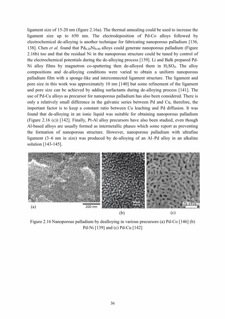
36
(a) (c) (b)
ligament size of 15-20 nm (figure 2.16a). The thermal annealing could be used to increase the ligament size up to 650 nm. The electrodeposition of Pd-Co alloys followed by electrochemical de-alloying is another technique for fabricating nanoporous palladium [136, 138]. Chen et al. found that Pd0.20Ni0.80 alloys could generate nanoporous palladium (Figure 2.16b) too and that the residual Ni in the nanoporous structure could be tuned by control of the electrochemical potentials during the de-alloying process [139]. Li and Balk prepared Pd-Ni alloy films by magnetron co-sputtering then de-alloyed them in H2SO4. The alloy compositions and de-alloying conditions were varied to obtain a uniform nanoporous palladium film with a sponge-like and interconnected ligament structure. The ligament and pore size in this work was approximately 10 nm [140] but some refinement of the ligament and pore size can be achieved by adding surfactants during de-alloying process [141]. The use of Pd-Cu alloys as precursor for nanoporous palladium has also been considered. There is only a relatively small difference in the galvanic series between Pd and Cu, therefore, the important factor is to keep a constant ratio between Cu leaching and Pd diffusion. It was found that de-alloying in an ionic liquid was suitable for obtaining nanoporous palladium (Figure 2.16 (c)) [142]. Finally, Pt-Al alloy precursors have also been studied, even though Al-based alloys are usually formed as intermetallic phases which some report as preventing the formation of nanoporous structure. However, nanoporous palladium with ultrafine ligament (3–6 nm in size) was produced by de-alloying of an Al–Pd alloy in an alkaline solution [143-145].
.
Figure 2.16 Nanoporous palladium by dealloying in various precursors (a) Pd-Co [146] (b) Pd-Ni [139] and (c) Pd-Cu [142]

37
Chapter 3
General Experimental

38
3.1 Overview Precious metal alloys and compounds can be produced by several methods. These
methods include conventional casting, vacuum arc melting or powder metallurgy for making bulk samples, and chemical vapour deposition (CVD) and physical vapour deposition (PVD) for making nanoscale films. Thin film technology is an attractive method to produce nanoscale materials due to its low materials cost and reduced energy consumption compared to the production of bulk materials. In addition, nanoscale materials are interesting because their properties are sometimes different from bulk materials. Thin films have been widely used in electronic devices, optical coating, instrument hard coating, sensors, solar cell, magnetic materials, catalysts and decorative applications [147-154].
There are two main processes of thin film deposition: CVD and PVD [155]. There are several CVD processes such as Atmospheric Pressure Chemical Vapour Deposition (APCVD), Low Pressure Chemical Vapour Deposition (LPCVD), Metal-Organic Chemical Vapour Deposition (MOCVD), Plasma Enhanced Chemical Vapour Deposition (PECVD), Laser Chemical Vapour Deposition (LCVD), Photochemical Vapour Deposition (PCVD), and Chemical Beam Epitaxy (CBE) [154, 155]. The PVD process options are divided into two categories: evaporation and sputtering. Sputtering is a unique deposition process. This type of deposition uses high energy gaseous atoms to eject atomic sized solid materials from a source and transfer them to form a surface layer on a substrate. The technique of magnetron sputtering is very useful for fabricating thin films of elements, alloys or compounds, and two materials can be readily co-sputtered if needed. The thin films which are obtained by sputtering have high purity, fully dense microstructure, uniformity and good adhesion. Magnetron sputtering can be reproduced with a high degree of control.
Therefore, in the experiments described in the present PhD, precious metal alloys and compounds have been mainly fabricated as thin films by PVD with the magnetron co-sputtering technique. Sputtered films are generally poorly crystalline if deposited at room temperature and, in most cases heat treatment has been applied here during deposition or after deposition. These precious metal alloy and compound films were characterized by a variety of techniques for chemical composition, crystal structure, morphology and optical properties. There are two main groups of precious metals alloys and compounds in this doctoral project. These are (a) the intermetallic compounds of AuAl2 and PtAl2 and (b) the many intermetallic compounds in the Pt-Al system. The present chapter explains the general experimental techniques which are common to all the chapters of this thesis. Specific details relevant to individual alloy systems will be given in their own chapters.
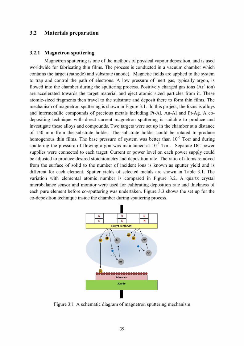
39
3.2 Materials preparation
3.2.1 Magnetron sputtering Magnetron sputtering is one of the methods of physical vapour deposition, and is used worldwide for fabricating thin films. The process is conducted in a vacuum chamber which contains the target (cathode) and substrate (anode). Magnetic fields are applied to the system to trap and control the path of electrons. A low pressure of inert gas, typically argon, is flowed into the chamber during the sputtering process. Positively charged gas ions (Ar+ ion) are accelerated towards the target material and eject atomic sized particles from it. These atomic-sized fragments then travel to the substrate and deposit there to form thin films. The mechanism of magnetron sputtering is shown in Figure 3.1. In this project, the focus is alloys and intermetallic compounds of precious metals including Pt-Al, Au-Al and Pt-Ag. A co-depositing technique with direct current magnetron sputtering is suitable to produce and investigate these alloys and compounds. Two targets were set up in the chamber at a distance of 150 mm from the substrate holder. The substrate holder could be rotated to produce homogenous thin films. The base pressure of system was better than 10-6 Torr and during sputtering the pressure of flowing argon was maintained at 10-3 Torr. Separate DC power supplies were connected to each target. Current or power level on each power supply could be adjusted to produce desired stoichiometry and deposition rate. The ratio of atoms removed from the surface of solid to the number of incident ions is known as sputter yield and is different for each element. Sputter yields of selected metals are shown in Table 3.1. The variation with elemental atomic number is compared in Figure 3.2. A quartz crystal microbalance sensor and monitor were used for calibrating deposition rate and thickness of each pure element before co-sputtering was undertaken. Figure 3.3 shows the set up for the co-deposition technique inside the chamber during sputtering process.
Figure 3.1 A schematic diagram of magnetron sputtering mechanism
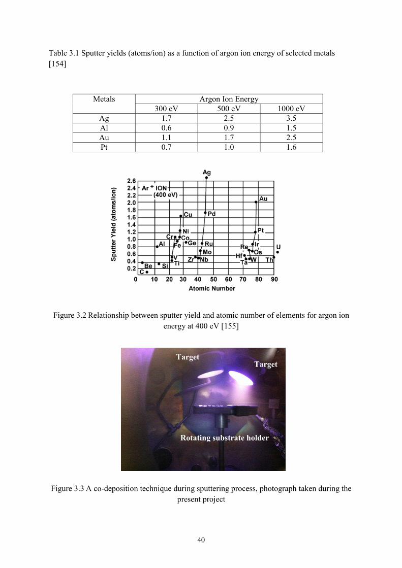
40
Table 3.1 Sputter yields (atoms/ion) as a function of argon ion energy of selected metals [154]
Metals Argon Ion Energy 300 eV 500 eV 1000 eV
Ag 1.7 2.5 3.5 Al 0.6 0.9 1.5 Au 1.1 1.7 2.5 Pt 0.7 1.0 1.6
Figure 3.2 Relationship between sputter yield and atomic number of elements for argon ion energy at 400 eV [155]
Figure 3.3 A co-deposition technique during sputtering process, photograph taken during the present project
Target Target
Rotating substrate holder

41
Several substrates have been used in the present project, including microscope glass slides, silicon wafers, tantalum foil and austenitic stainless steel foil. The microscope glass slide were cleaned by sonication in detergent solution for 15-20 minutes, then rinsed with water, then rinsed with distilled water and finally being dried under N2. The silicon wafer and metallic substrates were cleaned by sonication in acetone, then rinsed with acetone or ethanol and, finally, dried under N2.
3.2.2 Heat treatment The formation of thin films is associated with nucleation and growth processes. There
are three main steps: (1) a target of the chosen material is used to generate a flux of appropriate atomic or molecular species; (2) these species are transported to the substrate and (3) a solid deposit is formed on the substrate. In many cases an annealing treatment is required to crystallize the sample, remove defects, and grow the grains. Annealing may also cause subsequent phase transformations and colour changes. I used two different methods of annealing in the present project.
The first method used halogen lamps located within the chamber to heat the sample during deposition. Thermocouples were used to monitor and control the temperature. Thin film samples were then heated up to an appropriate temperature during the sputtering process.
Another method was to anneal the sample using a tube furnace. This method is a post-deposition process. After deposition, thin film samples were cut into small segments, covered with a protective piece of microscope glass slide and wrapped with aluminium foil. Then the wrapped samples were placed in ceramic boat crucible. The tube furnace was then purged with a stream of N2 gas during annealing. Copper shavings were also placed in the tube furnace in order to reduce oxidation in the samples. The tube furnace set up for post-deposition annealing treatment is shown in Figure 3.4.
Figure 3.4 Tube furnace for post-deposition annealing treatment

42
3.3 Materials characterization Thin films of precious metal alloys and compounds were fabricated using several deposition conditions. In many cases these samples also had various forms of post-deposition processing. The microstructures and properties of these nanoscale films have been investigated by various techniques including X-ray diffraction (XRD) - using both a laboratory instrument and synchrotron radiation, scanning electron microscopy (SEM), and transmission electron microscopy (TEM). Spectrophotometry, ellipsometry and computer modelling were used for investigating optical properties.
3.3.1 X-ray diffraction X-ray diffraction is a non-destructive analytical technique for the study of crystal structures and atomic spacing. XRD is also commonly used for identification of crystalline materials and analysis of the proportion of phases present. The interaction between X-rays and electrons of atoms leads to wave interference and the phenomenon of diffraction which can be expressed by Bragg’s law, sin2dn , where n is an integer, is the wavelength of the incident x-ray beam, d is the spacing between the planes in atomic lattice and is the diffraction angle. Constructive interference or diffraction only occurs when Bragg’s law is satisfied. A diffraction pattern is obtained by diffraction from different planes of atoms at a specific angle. Both the angle of diffraction and the intensity of the diffracted peak are unique for each material and can be identified like fingerprints. Diffraction patterns are usually plotted as intensity against Bragg angle (2 ). An unknown sample is primarily identified by comparing with known standards in the power diffraction database which contains basic information including chemical formula, name of substance, crystallographic data, data on specimen and data on diffraction pattern [156, 157].The significant diffraction pattern components are peak position, peak intensity and peak shape. These three components are related to the crystal structure of material including unit cell parameters, atomic parameters and crystallinity. Peak width (often taken as Full Width at Half Maximum (FWHM)) is also important for estimating particle or grain size and residual strain. It can be obtained by fitting a peak with Gaussian, Lorentzian, Gaussian-Lorentzian functions. Generally, a source of X-rays and a suitable detector are required for the power diffraction technique. The X-rays are usually generated using one of two different sources. The first is laboratory X-ray instrumentation or conventional X-ray source which is the most commonly used source of x-rays. These devices use an X-ray sealed tube of a specific metal target to generate electromagnetic radiation. The second source is synchrotron radiation which is generated by high energy electrons which are confined in a storage ring. Those electrons accelerate in a circular orbit and emit electromagnetic radiation [158, 159]. In this project, both laboratory-based instrumentation and synchrotron radiation were used for analyzing samples. The Rietveld refinement technique has been used for analyzing X-ray powder diffraction data as well as determining lattice parameters.

43
Laboratory X-ray instrumentation The laboratory-based instrumentation or diffractometer consists of a source of radiation, a monochromator to ensure a single wavelength, slits to adjust the shape and size of the beam, a sample, a detector to record the diffraction pattern and a goniometer to adjust the sample and the detector positions. The sample rotates at a constant angular velocity while detector rotates at double angular velocity around the sample in order to detect Bragg-reflected waves. A schematic of a X-ray diffractometer is shown in Figure 3.5. A Siemens D5000 X-ray diffractometer which used Cu K radiation (where is taken as 1.54184 Å) has been used for this project (actually there are two closely situated wavelengths K 1 and K 2 but in most cases in the present project the peaks are broad enough to obscure this fact). The grazing incidence mode has been applied for the thin film samples. The grazing incidence technique uses a very small incident angle of X-ray beam on the specimen (typically 0.1 -3.0 ) in order to obtain as much signal as possible from the thin film and as little as possible from the substrate of the film. The diffracted beam will be parallel focused onto slits in front of a detector [160]. Figure 3.6 shows a comparison of the basic principle of grazing incidence technique for thin film geometry and the conventional -2 geometry. A scintillator with photomultiplier was used as a detector. In this research, the angle of incidence was set at 0.5 while the divergence slit was 0.2 . The diffractometer was operated at 40 kV and 30 mA. The 2 range was between 20 and 90 , and counts were accumulated for 3 seconds at each step. Diffrac Plus software was used for data collection. Phase identification could also be performed using the search and match features of this software in combination with the JC-PDF database.
Figure 3.5 Schematic of an X-ray diffractometer in the Bragg-Brentano configuration [156]
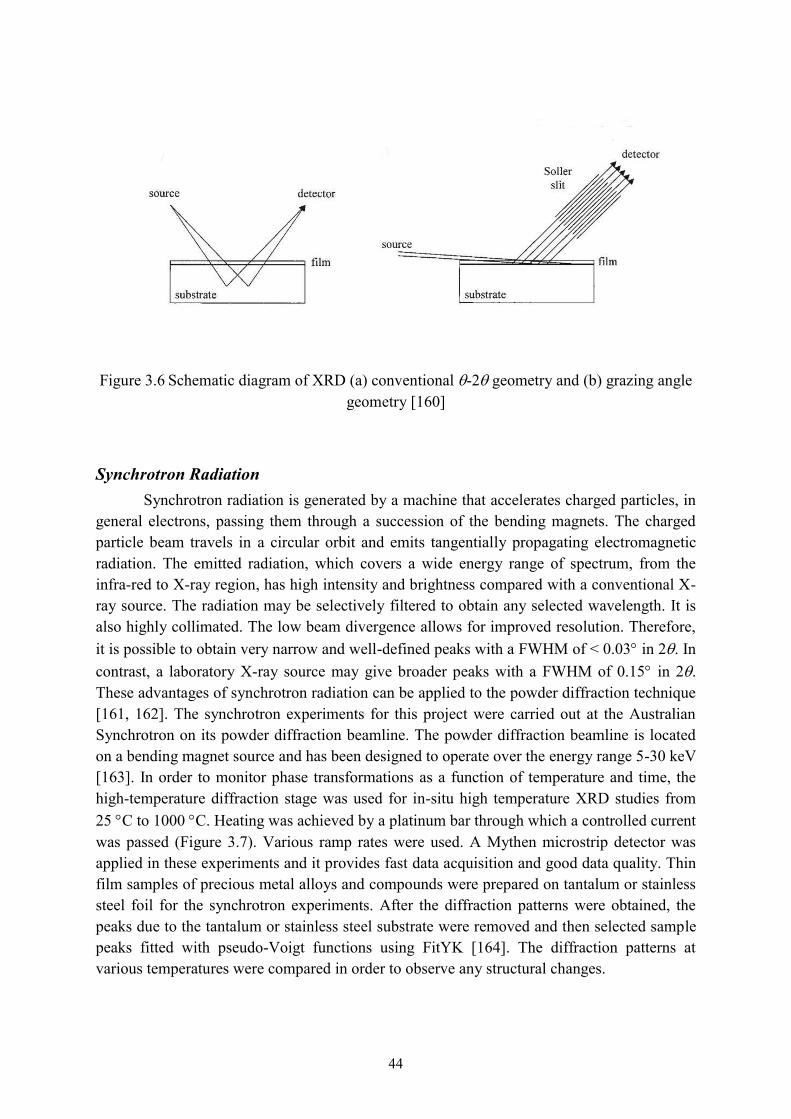
44
Figure 3.6 Schematic diagram of XRD (a) conventional -2 geometry and (b) grazing angle geometry [160]
Synchrotron Radiation Synchrotron radiation is generated by a machine that accelerates charged particles, in general electrons, passing them through a succession of the bending magnets. The charged particle beam travels in a circular orbit and emits tangentially propagating electromagnetic radiation. The emitted radiation, which covers a wide energy range of spectrum, from the infra-red to X-ray region, has high intensity and brightness compared with a conventional X-ray source. The radiation may be selectively filtered to obtain any selected wavelength. It is also highly collimated. The low beam divergence allows for improved resolution. Therefore, it is possible to obtain very narrow and well-defined peaks with a FWHM of < 0.03 in 2 . In contrast, a laboratory X-ray source may give broader peaks with a FWHM of 0.15 in 2 . These advantages of synchrotron radiation can be applied to the powder diffraction technique [161, 162]. The synchrotron experiments for this project were carried out at the Australian Synchrotron on its powder diffraction beamline. The powder diffraction beamline is located on a bending magnet source and has been designed to operate over the energy range 5-30 keV [163]. In order to monitor phase transformations as a function of temperature and time, the high-temperature diffraction stage was used for in-situ high temperature XRD studies from 25 C to 1000 C. Heating was achieved by a platinum bar through which a controlled current was passed (Figure 3.7). Various ramp rates were used. A Mythen microstrip detector was applied in these experiments and it provides fast data acquisition and good data quality. Thin film samples of precious metal alloys and compounds were prepared on tantalum or stainless steel foil for the synchrotron experiments. After the diffraction patterns were obtained, the peaks due to the tantalum or stainless steel substrate were removed and then selected sample peaks fitted with pseudo-Voigt functions using FitYK [164]. The diffraction patterns at various temperatures were compared in order to observe any structural changes.
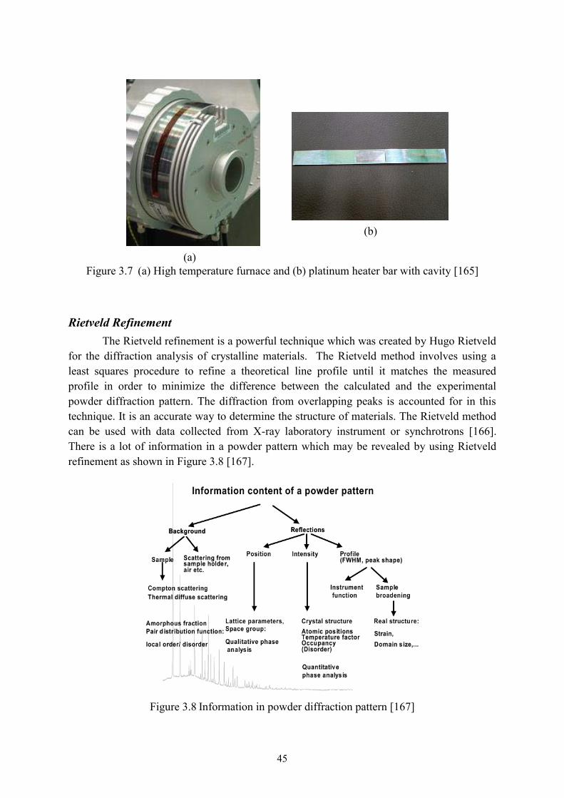
45
(a)
(b)
Figure 3.7 (a) High temperature furnace and (b) platinum heater bar with cavity [165]
Rietveld Refinement The Rietveld refinement is a powerful technique which was created by Hugo Rietveld for the diffraction analysis of crystalline materials. The Rietveld method involves using a least squares procedure to refine a theoretical line profile until it matches the measured profile in order to minimize the difference between the calculated and the experimental powder diffraction pattern. The diffraction from overlapping peaks is accounted for in this technique. It is an accurate way to determine the structure of materials. The Rietveld method can be used with data collected from X-ray laboratory instrument or synchrotrons [166]. There is a lot of information in a powder pattern which may be revealed by using Rietveld refinement as shown in Figure 3.8 [167].
Figure 3.8 Information in powder diffraction pattern [167]

46
3.3.2 Scanning Electron Microscopy (SEM) Scanning electron microscopy is a powerful facility for analysing surfaces by using a
focused beam of electrons. The electrons interact with atoms in the sample and generate a variety of signals such as secondary electrons (SE), backscattered electrons (BSE), characteristic X-rays, Auger electrons and cathodoluminescence [168]. These signals can be detected and provide information about the sample including microstructure, morphology, grain orientation, and chemical composition. SEM produces high-resolution images with reasonable depth-of-field. For this project, secondary electrons, backscattered electrons and characteristic X-rays were used. Secondary electrons and backscattered electrons are primarily used for imaging samples. Secondary electrons are the most common signal for image formation and provide information on morphology and topography while backscattered electrons provide either compositional or topographic information. Backscattered electrons are valuable for showing contrast in composition in multiphase samples. Backscattered electrons are reflected or back-scattered out of the specimen by elastic scattering during interaction with specimen atoms. Regions of high average atomic number generate a greater number of backscattered electrons than regions of lower atomic number and are hence brighter in the image. Characteristic X-rays result from the electrons of the electron beam interacting with the inner orbit electrons of the sample. The incoming electron may eject an inner-shell electron thereby leaving a vacancy. An outer shell electron then falls into the vacancy and the atom emits an X-ray having energy equal to the energy difference between two shells. The energy or wavelength of the x-ray can be detected by spectrometers. Energy dispersive spectrometers (EDS) are most commonly used in SEMs [169].
In the present project I mainly used a Zeiss Supra 55VP, which is shown in figure 3.9. This is a field emission scanning electron microscope (FESEM) which has high resolution imaging. It was mainly used to obtain topographical, morphological and compositional information from samples in this project. The microscope was operated on high vacuum mode with an acceleration voltage at 5-20 kV. A higher acceleration voltage and the In-lens secondary electron detector were used for the high resolution imaging. The backscattered electron detector was used to obtain lower resolution images showing atomic number contrast. The Oxford EDS system was used for elemental characterization. In this case a lower acceleration voltage and a higher working distance were employed. Also used in this project was a Zeiss Evo LS15, which is a thermionic tungsten electron gun SEM. This SEM is also equipped with a Bruker EDS Quantax 400 with silicon drift detector (SDD) which allows for high speed elemental analysis, however, the resolution available on images was inferior to that on the 55VP.
There were several types of samples in this project, including bulk materials, thin films and small particles, all on different supporting materials and substrates. Therefore, samples have been prepared in a variety of ways for SEM. In all case they had to be electrically connected to the sample holder using conductive tape or silver paint to prevent or minimize sample charging. Aluminium stubs proved convenient to use as a sample holder in many cases. These stubs can be modified for a particular type of specimen. For example, bulk
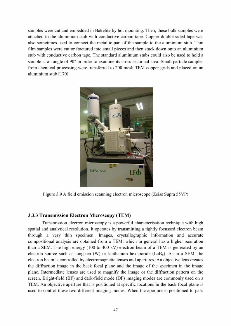
47
samples were cut and embedded in Bakelite by hot mounting. Then, these bulk samples were attached to the aluminium stub with conductive carbon tape. Copper double-sided tape was also sometimes used to connect the metallic part of the sample to the aluminium stub. Thin film samples were cut or fractured into small pieces and then stuck down onto an aluminium stub with conductive carbon tape. The standard aluminium stubs could also be used to hold a sample at an angle of 90 in order to examine its cross-sectional area. Small particle samples from chemical processing were transferred to 200 mesh TEM copper grids and placed on an aluminium stub [170].
Figure 3.9 A field emission scanning electron microscope (Zeiss Supra 55VP)
3.3.3 Transmission Electron Microscopy (TEM) Transmission electron microscopy is a powerful characterisation technique with high spatial and analytical resolution. It operates by transmitting a tightly focussed electron beam through a very thin specimen. Images, crystallographic information and accurate compositional analysis are obtained from a TEM, which in general has a higher resolution than a SEM. The high energy (100 to 400 kV) electron beam of a TEM is generated by an electron source such as tungsten (W) or lanthanum hexaboride (LaB6). As in a SEM, the electron beam is controlled by electromagnetic lenses and apertures. An objective lens creates the diffraction image in the back focal plane and the image of the specimen in the image plane. Intermediate lenses are used to magnify the image or the diffraction pattern on the screen. Bright-field (BF) and dark-field mode (DF) imaging modes are commonly used on a TEM. An objective aperture that is positioned at specific locations in the back focal plane is used to control these two different imaging modes. When the aperture is positioned to pass
48
only the transmitted or un-diffracted electrons, the resulting image is referred to as a bright-field (BF) image. The aperture absorbs electrons that are scattered. In this case the contrast in the sample is roughly proportional to the absorption of the transmitted beam, so empty regions appear bright and dense regions appear dark. In contrast, when the aperture is positioned to pass only specific diffracted electrons, the image is referred to as dark-field (DF) image. In this case the diffracting regions of the specimen appear bright while other regions are dark [171, 172]. Scanning transmission electron microscopy (STEM) mode works on the same principle as a SEM. Secondary electrons, backscattered electrons and X-rays are produced similarly to the SEM but a STEM has a higher signal level and better spatial resolution. The transmitted or diffracted beams are detected with various detectors on the column axis. Transmitted electrons are collected on the axis to create the bright field. An annular dark-field detector can be used in the STEM mode to obtain high-angle annular dark-field (HAADF) or Z-contrast imaging. Furthermore, X-rays generated from electron excitations in the specimen can be also used for microanalysis and elemental mapping by EDS [173].
Three different TEMs were used in this project. The Philips CM12 is a conventional analytic TEM. It was operated with LaB6 source at various accelerating voltages from 20-120 kV. BF/DF imaging and diffraction mode can be obtained and displayed via a CCD camera. The sample holder is double tilt holder with -60 to +60 . A maximum resolution is approximately 0.5 nm. The other two TEMs were used with the assistance of Dr. Annette Dowd. The JEOL 1400 is operated with a high brightness LaB6 electron source at an accelerating voltage in the range 40 to 120 kV. It is equipped with a Gatan large-area camera. STEM imaging with BF/DF imaging can be obtained and high-definition diffraction patterns can be acquired. A JEOL EDS system is used for X-ray microanalysis and elemental profiling and mapping. The point resolution is 0.38 nm and lattice resolution is 0.2 nm. The JEOL 2200 FS is a high resolution TEM with a 200 kV field emission gun and a built-in Omega filter to produce energy-filtered imaging and chemical analyses of specimens. TEM images with BF/DF imaging and diffraction patterns can be acquired on its Gatan Ultrascan CCD camera. STEM mode can be performed BF and HAADF imaging. An advanced EDS analysis permits point, line scan and area mapping with X-ray signals. The point and lattice resolution are 0.23 nm and 0.1 nm respectively.
TEM specimens must be very thin in order to be transparent to electrons, certainly not more than 100 nm for the present types of materials. So sample preparation is a crucial process for TEM. There were two different types of specimen prepared in this project: thin films and fine particles/sponges. For thin film specimens, a cross sectional area was often prepared in order to study the internal structure. The 'sandwich' technique was applied to prepare the cross-sections. Thin film samples, which had been deposited on a Si wafer, were prepared and cut into two pieces by a diamond scribe. The dimensions were approximately 3 mm x 1 mm. Two Si wafer pieces were also prepared with the same dimensions as the sample. The two coated surfaces were then placed face-to-face and the two additional pieces of Si wafer attached to the backside of each piece to provide more structural support. The four pieces were then glued as stack-like sandwiches by using epoxy resin. Figure 3.10 shows

49
the schematic of a stack sandwich sample and interface of the thin film. The glued sandwich was placed into an oven at 120 C for 30 minutes. After that, the sandwich was attached to a polishing stub using 'crystal bond' adhesive. This is used for temporary bonding and can be dissolved later using acetone. The stub is mounted on to tripod polisher and polishing begun with abrasive paper (grit size 1200), followed by diamond lapping film from 30 m, 9 m, 3
m and 1 m respectively. Once one side is smooth, shiny and scratch-free, the sample can be removed and cleaned with acetone. The next step was to prepare the other side of sample for polishing. A piece of Si wafer was placed on the polishing stub with cyanoacrylate glue as a base for the specimen. The stub with Si wafer base is mounted back on to a tripod polisher. The legs of the tripod are adjusted to position the glass plate parallel to the Si wafer surface, and then the surface is polished with 30 m diamond lapping film. After that the sample was attached to the polished side facing down on Si wafer using cyanoacrylate glue and was left overnight. The process of polishing began with the abrasive paper for aligning the sample. The tripod polisher was adjusted to generate a thin wedge, where a wedge angle of about 0.5 was introduced. Next, the sample is polished again with diamond lapping film from 30 m, 9
m, 3 m and 1 m. When it is sufficiently thin, the sample is transferred to a slot copper grid which was compatible with the TEM sample holder. Finally, the sample was gently thinned to electron transparency using a 691Gatan precision ion polishing system (PIPS). An argon ion beam bombards the thin sample and sputters away material until the sample is thin enough for electron transparency [174]. Several variables can be controlled including voltage, angle of incidence and sample rotation. The ion gun is operated at approximately 3.5 keV. The angle of incidence is set at 8 either above or below the sample. The sample rotation speed was 2-3 rpm. Preparation of the fine particle samples involved far less processing than the thin films. The fine particles were first suspended in liquid (ethanol or water) then transferred to a holey carbon-coated copper 200 mesh grid for TEM observation.
Figure 3.10 Cross section preparation for TEM (a) schematic of stack sample prepared using the sandwich technique and (b) Interface of thin film after polishing with diamond of 1 m
(the arrow indicate the location of the glue line) [175]
(a) (b)
(a)
(b) (c)

50
3.3.4 Determination of optical properties Optical properties of metals are determined by the way light interacts with their surfaces as well as by the role of human perception to see the colour or lustre. In this project, thin films in several nanoscale thicknesses have been fabricated. Their optical properties are interesting to study, particularly those of the coloured intermetallic compounds. The colours of these intermetallic compounds are exceptional compared to the usual silver or silver-grey of most metals. Reflection and transmission as a function of wavelength and angle of incident radiation is measured using a spectrophotometer or an ellipsometer. Ellipsometry analysis software (WVASE32) was employed to model and analyze the reflectance, transmission and the ellipsometric data. These data were used to extract the dielectric function (n and k) of each material. The OpenFilters software was also used in this research project in order to indicate colour of these thin films in the Commission Internationale de l’Éclairage (CIE) system and to predict the properties of various designs of stack. In this section, the optical measurement tools and techniques used in my project are described.
Spectrophotometry Spectrophotometry is the quantitative measurement of the reflection or transmission as function of wavelength when the light interacts with materials. Measurements are conducted using a spectrophotometer. The spectrophotometer consists of three elements: (a) a light source for providing illumination of the appropriate wavelengths, (b) a monochromator for selecting the precise wavelength of interest and (c) a detector for measuring the amount of light reflected or transmitted by the sample [176]. A Perkin Elmer Lambda 950 spectrophotometer with a universal reflectance accessory (URA) was used in this project. This spectrophotometer has a double beam and a double monochromator and can take measurements from the near-ultraviolet (300 nm) through to the near-infrared (2500 nm). Tungsten-halogen or deuterium lamps are used as light sources.
Ellipsometry Ellipsometry is an optical measurement technique that measures the change in polarized light after light is reflected from or transmitted through a sample. Ellipsometry measures the amplitude ratio ( ) and phase difference ( ) between light waves known as p- and s-polarized light waves. In the present project the ellipsometer was primarily used to determine thickness and optical constants of various thin film samples. The optical constants are obtained from the data by constructing an optical model using the WVASE software. Two ellipsometry parameters ( , ) are defined from the ratio of the amplitude reflection coefficients for p- and s-polarization or defined by iexptan .The optical model for thin film sample as shown in Figure 3.11, is expressed by equation 3.1.
),,,,(exptan 0210 dNNNi (Equation 3.1)
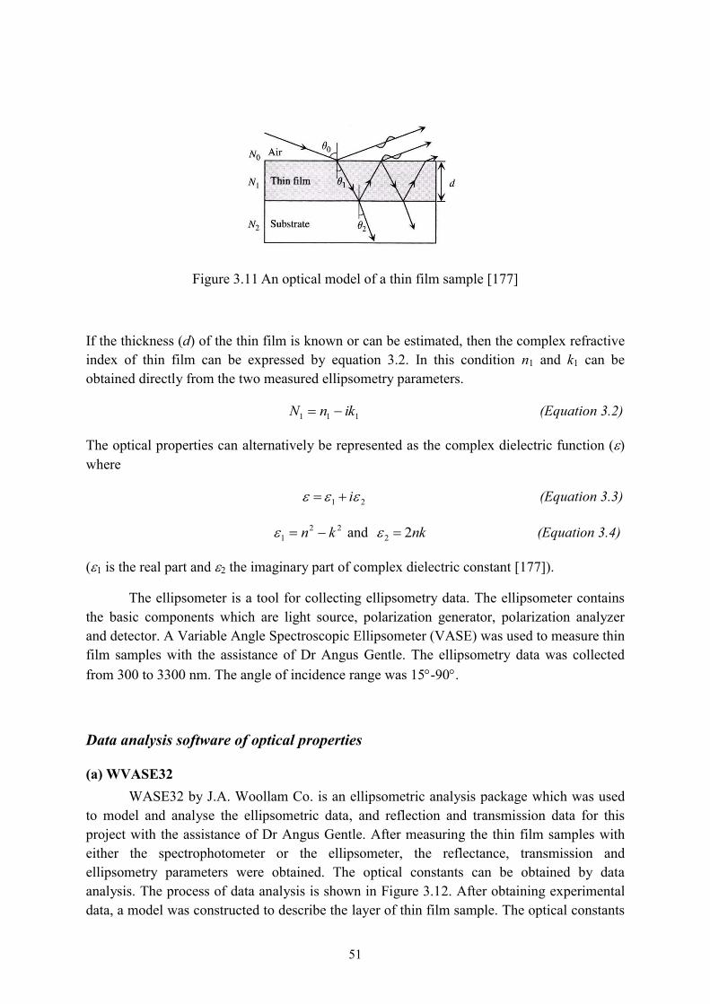
51
Figure 3.11 An optical model of a thin film sample [177]
If the thickness (d) of the thin film is known or can be estimated, then the complex refractive index of thin film can be expressed by equation 3.2. In this condition n1 and k1 can be obtained directly from the two measured ellipsometry parameters.
111 iknN (Equation 3.2)
The optical properties can alternatively be represented as the complex dielectric function ( ) where
21 i (Equation 3.3)
221 kn and nk22 (Equation 3.4)
( 1 is the real part and 2 the imaginary part of complex dielectric constant [177]).
The ellipsometer is a tool for collecting ellipsometry data. The ellipsometer contains the basic components which are light source, polarization generator, polarization analyzer and detector. A Variable Angle Spectroscopic Ellipsometer (VASE) was used to measure thin film samples with the assistance of Dr Angus Gentle. The ellipsometry data was collected from 300 to 3300 nm. The angle of incidence range was 15 -90 .
Data analysis software of optical properties
(a) WVASE32 WASE32 by J.A. Woollam Co. is an ellipsometric analysis package which was used to model and analyse the ellipsometric data, and reflection and transmission data for this project with the assistance of Dr Angus Gentle. After measuring the thin film samples with either the spectrophotometer or the ellipsometer, the reflectance, transmission and ellipsometry parameters were obtained. The optical constants can be obtained by data analysis. The process of data analysis is shown in Figure 3.12. After obtaining experimental data, a model was constructed to describe the layer of thin film sample. The optical constants

52
were obtained by fitting the ellipsometric data or reflection and transmission data with a Lorentz oscillator model which retained Kramers-Kronig consistency.
Figure 3.12 Diagram of the process for ellipsometry data analysis [178]
(b) OpenFilters OpenFilters is an open-source package. It was used to create multilayer models of thin films and to calculate the expected optical properties including reflection, transmission, absorption and colour. The dielectric functions used in OpenFilters were either those obtained in this project by measurement, or in some cases, data from the literature. After a thin film stack had been designed, its colour was calculated in XYZ, xyY, L*a*b* and L*u*v* colour spaces using the appropriated angle, illuminant and observer defined by the CIE system [179].

53
Chapter 4
The AuAl2-PtAl2 system

54
4.1 Background The colours of precious metal alloys and compounds were discussed in Section 2.2. Apart from being of decorative value, these materials are exploited in engineering and industrial applications for their specialised optical properties. As mentioned, coloured intermetallic compounds with CaF2 crystal structure are also well-known especially AuAl2, which is known as "amethyst" or "purple gold" or "purple glory" [180] and the bright yellow compound PtAl2, which is sometimes known as "platigem". In this chapter I focus on these two coloured intermetallic compounds and, in particular, show how they can be combined to produce a range of new metallic colours.
4.1.1 Review of the fabrication and applications of AuAl2 and PtAl2 AuAl2 and PtAl2 are coloured intermetallic compounds with the CaF2 crystal
structure. There is some commercial interest in them particularly for jewellery and decorative applications [5, 6, 64, 180, 181]. Their bright metallic colours are attractive: AuAl2 is deep purple while PtAl2 is golden yellow. Both of these compounds can only be formed in a very narrow range of stoichiometry, centred on 33 at.% of Au or Pt as shown in Figure 4.1 and 4.2. For this reason, it is challenging to achieve their unique colours.
Figure 4.1 Phase diagram of Al-Au system by Okamoto, H.(1991) [182]
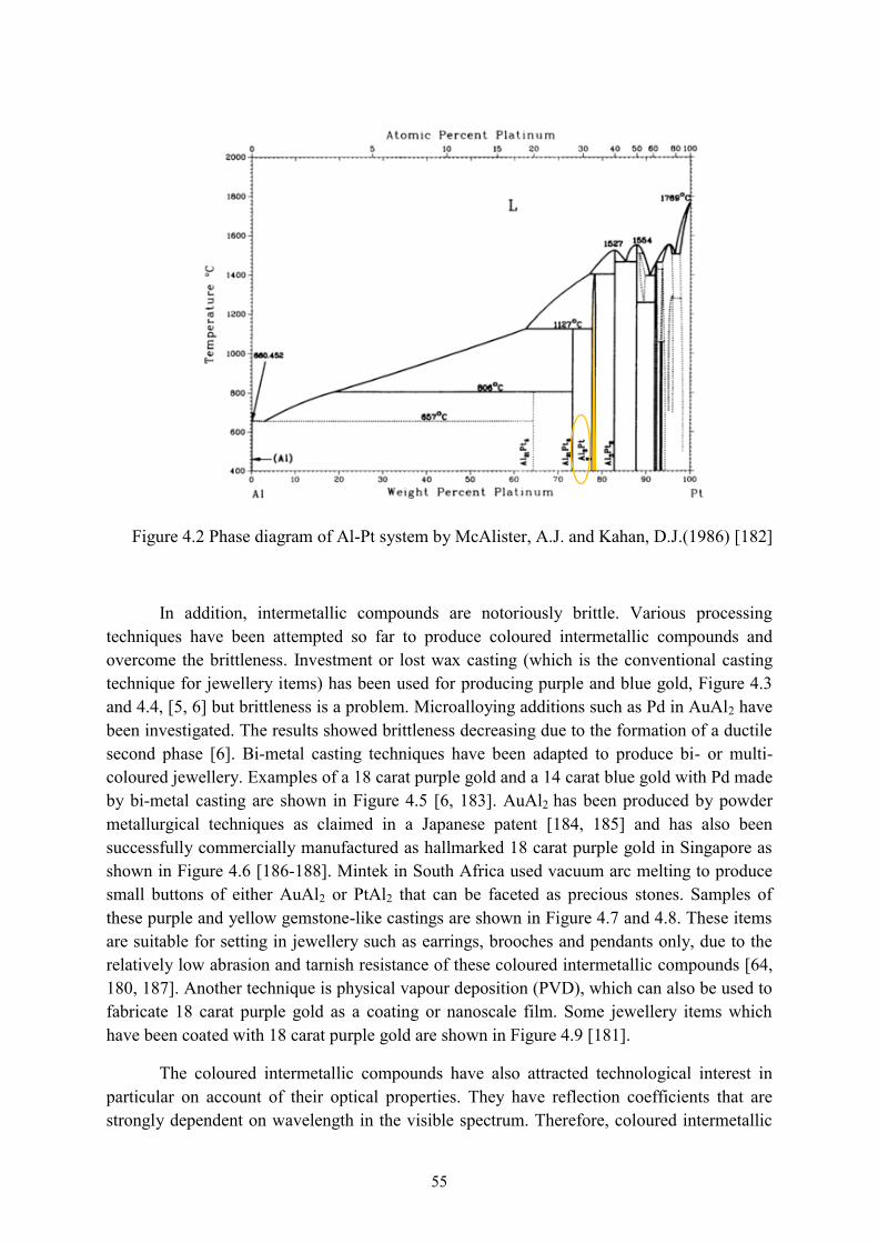
55
Figure 4.2 Phase diagram of Al-Pt system by McAlister, A.J. and Kahan, D.J.(1986) [182]
In addition, intermetallic compounds are notoriously brittle. Various processing techniques have been attempted so far to produce coloured intermetallic compounds and overcome the brittleness. Investment or lost wax casting (which is the conventional casting technique for jewellery items) has been used for producing purple and blue gold, Figure 4.3 and 4.4, [5, 6] but brittleness is a problem. Microalloying additions such as Pd in AuAl2 have been investigated. The results showed brittleness decreasing due to the formation of a ductile second phase [6]. Bi-metal casting techniques have been adapted to produce bi- or multi-coloured jewellery. Examples of a 18 carat purple gold and a 14 carat blue gold with Pd made by bi-metal casting are shown in Figure 4.5 [6, 183]. AuAl2 has been produced by powder metallurgical techniques as claimed in a Japanese patent [184, 185] and has also been successfully commercially manufactured as hallmarked 18 carat purple gold in Singapore as shown in Figure 4.6 [186-188]. Mintek in South Africa used vacuum arc melting to produce small buttons of either AuAl2 or PtAl2 that can be faceted as precious stones. Samples of these purple and yellow gemstone-like castings are shown in Figure 4.7 and 4.8. These items are suitable for setting in jewellery such as earrings, brooches and pendants only, due to the relatively low abrasion and tarnish resistance of these coloured intermetallic compounds [64, 180, 187]. Another technique is physical vapour deposition (PVD), which can also be used to fabricate 18 carat purple gold as a coating or nanoscale film. Some jewellery items which have been coated with 18 carat purple gold are shown in Figure 4.9 [181].
The coloured intermetallic compounds have also attracted technological interest in particular on account of their optical properties. They have reflection coefficients that are strongly dependent on wavelength in the visible spectrum. Therefore, coloured intermetallic

56
compounds including AuAl2 and PtAl2 have potential application as spectrally-selective coatings [189, 190]. Spectrally-selective coatings can, for example, be applied on windows for energy conservation. AuAl2 films which were prepared by co-deposition direct current magnetron sputtering have been investigated as a spectrally selective coating for windows, but were found to be uncompetitive with gold films [181]. It has also been predicted that nanostructures of AuAl2 and PtAl2 should manifest a localized surface plasmon resonance [181, 191, 192].
Figure 4.3 Purple gold by investment casting (Courtesy JARAD Project by Srinakharinwirot University, Bangkok Fashion City under the Ministry of Industry of Thailand, Thailand)
Figure 4.4 AuAl2- carat purple gold (top row) and AuIn2 - blue gold (bottom row) (Courtesy Co. Reischauer GmbH, Idar Oberstein, Germany) [6]

57
(a) (b)
Figure 4.5 Bi-metal casting (a) 950 Pd casting with injected wax for the 2nd bi-metal casting process step and (b) Bi-metal castings of 14k blue gold (left) and 18k purple gold (right) with
950 Pd (Courtesy Vendorafa-Lombardi Srl, Valenza,Italy) [6]
Figure 4.6 Purple gold by powder metallurgy process (Courtesy Lee Hwa Jewellery, Singapore) [186]
Figure 4.7 Purple glory gemstone-like AuAl2 casting in setting on ring (courtesy M.B Cortie) [180]

58
Figure 4.8 Platigems and Platigem jewellery (Courtesy Mintek, South Africa) [187]
Figure 4.9 AuAl2-coated items made by depositing onto sterling silver costume jewellery by the present author [181]

59
Other technological applications are also being investigated or are already in use. AuAl2 has potential applications as a superconductor or resistor [193, 194] while PtAl2 can be used as a corrosion or oxidation resistant coating, particularly for high-temperature turbine blades [67]. Furthermore, aluminium-containing precious metal compounds, including AuAl2 and PtAl2, are suitable precursors for preparing mesoporous metals. It is possible to use these sponges as catalysts, electrodes or sensors [108, 109, 195-197].
4.1.2 Review of the optical properties of AuAl2 and PtAl2
Dielectric functions The dielectric functions of coloured precious intermetallic compounds, especially
those with the CaF2 structure, have been previously investigated with particular interest in AuAl2 [41, 181, 191, 192, 198-202] and PtAl2 [192, 199, 200]. The imaginary part of the optical constants of the pure phase can also be estimated by Density Functional Theory calculations, and then the real part can be obtained by means of the Kramers-Kronig relations, and the colour explained in terms of an interband transition. In a typical experimental study, AuAl2 was prepared by melting pure metals in sealed evacuated quartz tubes and zone refining. It was reported that interband transitions appeared at 2.2 eV [41]. In another study of AuAl2, this time made by arc melting, the transition was at 2.125 eV. Similar compounds such as PtAl2 can be made by substituting platinum for gold. In a typical study, bulk samples were also prepared by arc-melting. The onset of the interband transition of PtAl2 was at 2.834 eV [199].
As described in the literature review the dielectric properties of materials can be described by their n and k, or 1 and 2. As part of this PhD project I participated in a study conducted by Dr Vicki Keast of University of Newcastle to determine the optical properties of AuAl2 and PtAl2 by a combination of measurement and modelling by density functional theory. The experimental and calculated reflectivity of gold intermetallic compounds are compared in Figure 4.10. It was found that the reflectivity spectra for AuAl2, AuGa2 and AuIn2 are quite similar but the dielectric function of AuAl2 is significantly different, as shown in Figure 4.11. The 1 of AuAl2 crosses zero at 2 eV. It has a bulk plasma frequency that is in the optical region and provides the purple colour [191]. Furthermore, optical properties of AuAl2, Au0.5Pt0.5Al2, Au0.25Pt0.75Al2 and PtAl2 were also investigated by calculation. It was found that the main peak in 2 increases in energy as the gold content decreases as shown in Figure 4.12. The calculated reflectivity spectra of these compounds are compared to experimental data in Figure 4.13. The CIELAB colour coordinates were obtained by calculation and are compared for these four compounds (Figure 4.14) [192].

60
Figure 4.10 Reflectivity of gold intermetallic compounds from experiment (solid curve) and
calculation (dashed curved) [191]
Figure 4.11 Dielectric function of gold intermetallic compounds; 1 (solid curve) and 2
(dashed curved) [191]

61
Figure 4.12 Dielectric function of ordered intermetallic compounds [192]
Figure 4.13 Reflectivity of ordered intermetallic compounds comparing with experimental reflectivity of PtAl2 thin film [192]
Figure 4.14 Comparison CIE Lab colour coordinates of AuAl2, Au0.5Pt0.5Al2, Au0.25Pt0.75Al2 and PtAl2 [192]

62
As a side-project, I also collaborated with colleagues on verifying an idea for tuning the colour of Au-Ni mixtures and alloys. In this project we fabricated nanoscale thin film stacks of Au-Ni. Here my role was to assist with the fabrication and measurements, and to supply specific samples used in the analysis. We have found that the optical properties of the alternating Au/Ni films are controlled by varying the number and thickness of the layers of stacks fabricated from the constituent elements. The colour gamut of tri-layer of Au-Ni-Au is shown Figure 4.15 [203]. If the layers are thin enough to permit some transmission of light, then the colours will mix and new effects occur. I also applied this strategy to thin films stacks of AuAl2 and PtAl2 (see later).
Figure 4.15 CIE L*a*b* colour gamut of Au-Ni-Au tri layer in reflection [203]
Plasmon resonances in AuAl2 and PtAl2
As mentioned previously, many intermetallic compounds with the CaF2 crystal structure are strongly coloured. These properties will also have an effect on any plasmon resonances in the nanoparticles. It has also been predicted that nanostructures of AuAl2 and PtAl2 should manifest a localized surface plasmon resonance. In AuAl2, which has a purple colour, it has been predicted that nanoparticles would have two broad plasmon resonances centred on about 2-2.5 eV [181] while PtAl2, which is yellow, is associated with a bulk plasmon at about 3 eV [192].
Alloying effects Unfortunately, the coloured intermetallic compounds with CaF2 crystal structure, in
particular blue and purple gold, are brittle and have a low corrosion resistance. This must be considered when using these materials for any technological purpose. Further alloying additions have been proposed as a way to solve these drawbacks of blue and purple gold. The influence of alloying additions on these properties as well as colour effects was investigated. Blue (AuGa2 and AuIn2) and purple gold (AuAl2) share the same crystal structure (CaF2).

63
The brittleness in these intermetallic compounds can be reduced by ternary alloying additions of, for example, palladium, copper or silver. One problem is that in most cases the desirable colour fades when the third element is included. Platinum is an interesting element which could potentially be added to the coloured gold compounds. This is because platinum forms coloured intermetallic compounds with the same crystal structure and stoichiometry PtX2 (X=Al, Ga, In) as the blue and purple gold. Platinum can therefore potentially exchange for gold in the same atom ratio of (Au,Pt)X2. This has been reported to occur in the compounds with indium. With increasing platinum content the colour changes from blue (AuIn2) to apricot (PtIn2) [5]. Furthermore, the brittleness decreases, possibly because precipitation of the PtIn2 results in grain refinement of blue gold matrix. A colour change effect by substitutional alloying addition must also be considered. For example, micro-alloying additions increase the fracture resistance without affecting the colour of 14 carat blue gold and 18 carat purple gold. Overall, the material performance is improved when micro-alloying additions and third element additions like palladium are used in these coloured intermetallic compounds [6]. However, the question of how to improve corrosion resistance of blue and purple gold by alloying additions is still open. An attempt has been made to modify the colour of yellow platinum (PtAl2) with additions of between 5 and 25 wt.% Cu [189]. In that case all samples were prepared by vacuum-arc melting under an argon atmosphere. The optical properties were determined by the reflection spectrophotometer in the wavelength range 450-900 nm. CIELAB colour coordinates a* and b* were calculated from the measured data in order to describe the colour of the intermetallic compound. It was found that the effect of increasing the copper content was to change the colour of the compound from the brass-yellow of PtAl2 through orange to copper-pink. The colour change was said to be related to an increase in the lattice parameter suggesting that solid solution alloying had occurred.
4.2 Objective of this chapter Gold and platinum have the same face-centred cubic (FCC) structure, have similar
physical properties, electronegativity and atomic diameter, and form the XAl2 compound with the same CaF2 or cF12 (Pearson symbol) crystal structure. It might be expected that the two compounds would exhibit unlimited mutual solubility. However, no Au-Pt-Al ternary section appears to be available in the literature and so the nature of the microstructures along the isopleth connecting these two compounds was unknown. AuAl2 and PtAl2 are fully metallic and have attractive colours. This raises the interesting issues of (i) whether AuAl2 and PtAl2 are mutually soluble or, if not, (ii) whether mixed microstructures of these two compounds could be used to tune the colour between these two coloured end-points.
4.3 Experimental details specific to this chapter Thin films of AuAl2 and PtAl2 were prepared by direct current (DC) magnetron
sputtering in high vacuum. The films were deposited onto glass, silicon, stainless steel or tantalum foil substrates. The glass slides were cleaned with detergent solution for 15-20
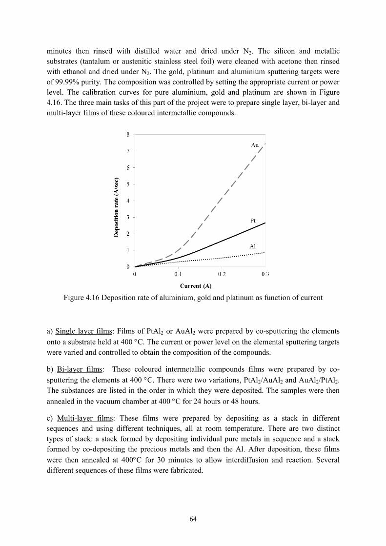
64
minutes then rinsed with distilled water and dried under N2. The silicon and metallic substrates (tantalum or austenitic stainless steel foil) were cleaned with acetone then rinsed with ethanol and dried under N2. The gold, platinum and aluminium sputtering targets were of 99.99% purity. The composition was controlled by setting the appropriate current or power level. The calibration curves for pure aluminium, gold and platinum are shown in Figure 4.16. The three main tasks of this part of the project were to prepare single layer, bi-layer and multi-layer films of these coloured intermetallic compounds.
Figure 4.16 Deposition rate of aluminium, gold and platinum as function of current
a) Single layer films: Films of PtAl2 or AuAl2 were prepared by co-sputtering the elements onto a substrate held at 400 C. The current or power level on the elemental sputtering targets were varied and controlled to obtain the composition of the compounds.
b) Bi-layer films: These coloured intermetallic compounds films were prepared by co-sputtering the elements at 400 C. There were two variations, PtAl2/AuAl2 and AuAl2/PtAl2. The substances are listed in the order in which they were deposited. The samples were then annealed in the vacuum chamber at 400 C for 24 hours or 48 hours.
c) Multi-layer films: These films were prepared by depositing as a stack in different sequences and using different techniques, all at room temperature. There are two distinct types of stack: a stack formed by depositing individual pure metals in sequence and a stack formed by co-depositing the precious metals and then the Al. After deposition, these films were then annealed at 400 C for 30 minutes to allow interdiffusion and reaction. Several different sequences of these films were fabricated.

65
For comparison purposes bulk samples of PtAl2 and AuAl2 were produced by melting pure gold or platinum with aluminium in a vacuum arc furnace. These bulk samples were prepared by Mintek in South Africa. The composition and morphology of the samples were analysed by light microscopy (LM), X-ray diffraction (XRD) in grazing incidence mode, scanning electron microscopy (SEM) with an energy dispersive spectrometry (EDS) and transmission electron microscopy (TEM). An in situ diffraction experiment in a synchrotron was also carried out in order to investigate the conversion of multi-layers of the elements into intermetallic compounds. In this case the samples were heated from room temperature to 1250 C at 50 °C/min and cooled afterwards at the same rate.
The optical transmittance and reflectance of the films were obtained using a Perkin-Elmer Lambda 950 UV/VIS spectrophotometer in the spectral range of 300 to 2500 nm. The optical constants (n and k, or equivalently 1 and 2) were also extracted from data measured at different angles by using a Variable Angle Spectroscopic Ellipsometer (VASE).The WVASE32 program from J.A. Woollam Co.,US, was applied to calculate the dielectric functions from the measured optical properties. The computer program OpenFilters [179] was used to simulate the colours of various designs of film using the measured dielectric functions.
4.4 Results and discussion
4.4.1 Single layer films of coloured intermetallic compounds The coloured intermetallic compounds PtAl2 and AuAl2 have a very narrow range of
stability. Successful synthesis required careful adjustment of the current or power level during sputtering. Nevertheless, pure phase PtAl2 and AuAl2 films were fabricated successfully.
Platinum aluminide fabrication The fabrication of PtAl2 is quite difficult because it is formed in a very narrow range of composition. Also, other phases in the Pt-Al system such as Pt8Al21 and Pt2Al3 can be formed in the composition range near to PtAl2. Consequently, during sputtering, the current applied to the platinum target was fixed at 0.125 A, but that of the aluminium target was varied between 0.200 and 0.400 A. The compounds obtained were closely correlated with the current used. When aluminium content (ie. current) increased, the phases formed changed from Pt2Al Pt5Al3 PtAl Pt2Al3 PtAl2 Pt8Al21 as shown in Table 4.1 and the X-ray patterns in Figure 4.17. The morphologies of the various Pt-Al coatings are compared in Figure 4.18.
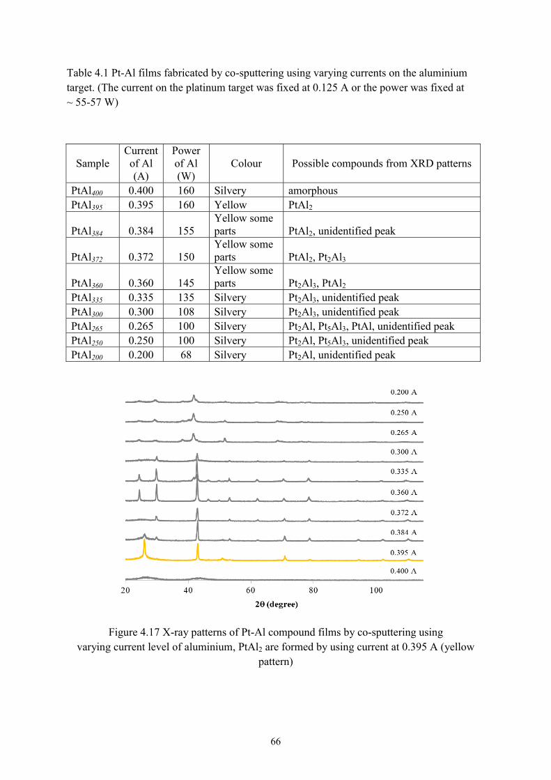
66
Table 4.1 Pt-Al films fabricated by co-sputtering using varying currents on the aluminium target. (The current on the platinum target was fixed at 0.125 A or the power was fixed at ~ 55-57 W)
Sample Current of Al (A)
Power of Al (W)
Colour Possible compounds from XRD patterns
PtAl400 0.400 160 Silvery amorphous PtAl395 0.395 160 Yellow PtAl2
PtAl384 0.384 155 Yellow some parts PtAl2, unidentified peak
PtAl372 0.372 150 Yellow some parts PtAl2, Pt2Al3
PtAl360 0.360 145 Yellow some parts Pt2Al3, PtAl2
PtAl335 0.335 135 Silvery Pt2Al3, unidentified peak PtAl300 0.300 108 Silvery Pt2Al3, unidentified peak PtAl265 0.265 100 Silvery Pt2Al, Pt5Al3, PtAl, unidentified peak PtAl250 0.250 100 Silvery Pt2Al, Pt5Al3, unidentified peak PtAl200 0.200 68 Silvery Pt2Al, unidentified peak
Figure 4.17 X-ray patterns of Pt-Al compound films by co-sputtering using varying current level of aluminium, PtAl2 are formed by using current at 0.395 A (yellow
pattern)
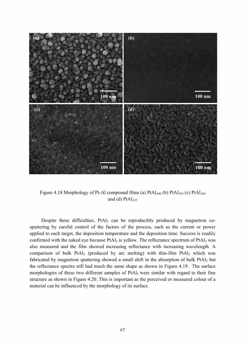
67
Figure 4.18 Morphology of Pt-Al compound films (a) PtAl400 (b) PtAl395 (c) PtAl360 and (d) PtAl335
Despite these difficulties, PtAl2 can be reproducibly produced by magnetron co-sputtering by careful control of the factors of the process, such as the current or power applied to each target, the deposition temperature and the deposition time. Success is readily confirmed with the naked eye because PtAl2 is yellow. The reflectance spectrum of PtAl2 was also measured and the film showed increasing reflectance with increasing wavelength. A comparison of bulk PtAl2 (produced by arc melting) with thin-film PtAl2 which was fabricated by magnetron sputtering showed a small shift in the absorption of bulk PtAl2 but the reflectance spectra still had much the same shape as shown in Figure 4.19. The surface morphologies of these two different samples of PtAl2 were similar with regard to their fine structure as shown in Figure 4.20. This is important as the perceived or measured colour of a material can be influenced by the morphology of its surface.
100 nm
100 nm 100 nm
100 nm
(a) (b)
(c) (d)
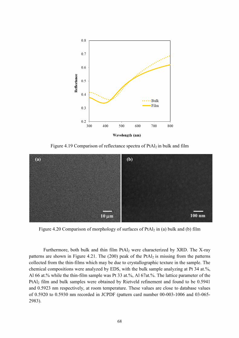
68
Figure 4.19 Comparison of reflectance spectra of PtAl2 in bulk and film
Figure 4.20 Comparison of morphology of surfaces of PtAl2 in (a) bulk and (b) film
Furthermore, both bulk and thin film PtAl2 were characterized by XRD. The X-ray patterns are shown in Figure 4.21. The (200) peak of the PtAl2 is missing from the patterns collected from the thin-films which may be due to crystallographic texture in the sample. The chemical compositions were analyzed by EDS, with the bulk sample analyzing at Pt 34 at.%, Al 66 at.% while the thin-film sample was Pt 33 at.%, Al 67at.%. The lattice parameter of the PtAl2 film and bulk samples were obtained by Rietveld refinement and found to be 0.5941 and 0.5923 nm respectively, at room temperature. These values are close to database values of 0.5920 to 0.5930 nm recorded in JCPDF (pattern card number 00-003-1006 and 03-065-2983).
10 m 100 nm
(a) (b)
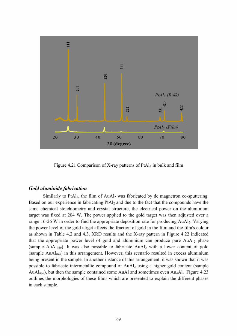
69
Figure 4.21 Comparison of X-ray patterns of PtAl2 in bulk and film
Gold aluminide fabrication Similarly to PtAl2, the film of AuAl2 was fabricated by dc magnetron co-sputtering. Based on our experience in fabricating PtAl2 and due to the fact that the compounds have the same chemical stoichiometry and crystal structure, the electrical power on the aluminium target was fixed at 204 W. The power applied to the gold target was then adjusted over a range 16-26 W in order to find the appropriate deposition rate for producing AuAl2. Varying the power level of the gold target affects the fraction of gold in the film and the film's colour as shown in Table 4.2 and 4.3. XRD results and the X-ray pattern in Figure 4.22 indicated that the appropriate power level of gold and aluminium can produce pure AuAl2 phase (sample AuAl050). It was also possible to fabricate AuAl2 with a lower content of gold (sample AuAl040) in this arrangement. However, this scenario resulted in excess aluminium being present in the sample. In another instance of this arrangement, it was shown that it was possible to fabricate intermetallic compound of AuAl2 using a higher gold content (sample AuAl060), but then the sample contained some AuAl and sometimes even Au4Al. Figure 4.23 outlines the morphologies of these films which are presented to explain the different phases in each sample.

70
Table 4.2 Au-Al films fabricated by co-sputtering using varying current level of gold. (Power of Al was 204 W or current ~0.443-0.452 A)
Samples Power of Au (W)
Current of Au (A)
Colour Possible compounds from XRD patterns
AuAl060 26 0.062 Purple (dull) AuAl2, AuAl, Au4Al AuAl050 21 0.052 Reddish Purple AuAl2 AuAl040 16 0.041 Pale purple AuAl2, Al
Table 4.3 Quantitative chemical analysis by EDS of Au-Al compounds
AuAl060 AuAl050 AuAl040
Au (at %) 40 38 28
Al (at %) 60 62 72
Figure 4.22 X-Ray patterns of Au-Al compounds

71
Figure 4.23 Morphologies of Au-Al films produced by using different power levels on the gold target (a) 16 W (sample AuAl040) in low magnification, (b) 16 W (sample AuAl040) in
high magnification, (c) 26 W (sample AuAl060) in low magnification, (d) 26 W (sample AuAl060) in high magnification and (e) 21 W (sample AuAl050)
1 m
(a)
100 nm
(b)
1 m
(c)
200 nm
(d)
200 nm
(e)

72
All of the above samples are purple to the naked eye but they do have slightly different hues. The reflectance spectra are compared in Figure 4.24. All of the spectra show a dip in reflectance at ~ 550 nm (green) but the dip is more pronounced in the spectrum of sample AuAl050 (the pure AuAl2). Thus this film is a more intense reddish purple. AuAl040 is composed of AuAl2 and Al whereas AuAl060 has AuAl2 as the matrix phase with small amounts of the other phases such as AuAl and Au4Al in the film. The addition of these other phases (which are believed to be silvery-grey in colour like most intermetallic compounds) affected the colour of these samples. Therefore, the spectra of the impure samples showed a reduced reflectance compared to that of the sample of pure AuAl2 phase.
Figure 4.24 Reflectance spectra of Au-Al compounds
Table 4.4 Conditions, colour and XRD results of Au-Al films
The effect of the various deposition parameters was investigated. The power or current level is the major factor that must be controlled for fabricating the appropriate
Sample Power of Au
(watts)
Deposition time (min)
Assumed thickness
(nm)
Temperature (°C)
colour XRD
AuAl2_S1
21 10 300 < 400 Pale purple AuAl2
AuAl2_S2
21 10 300 400 Reddish purple
AuAl2
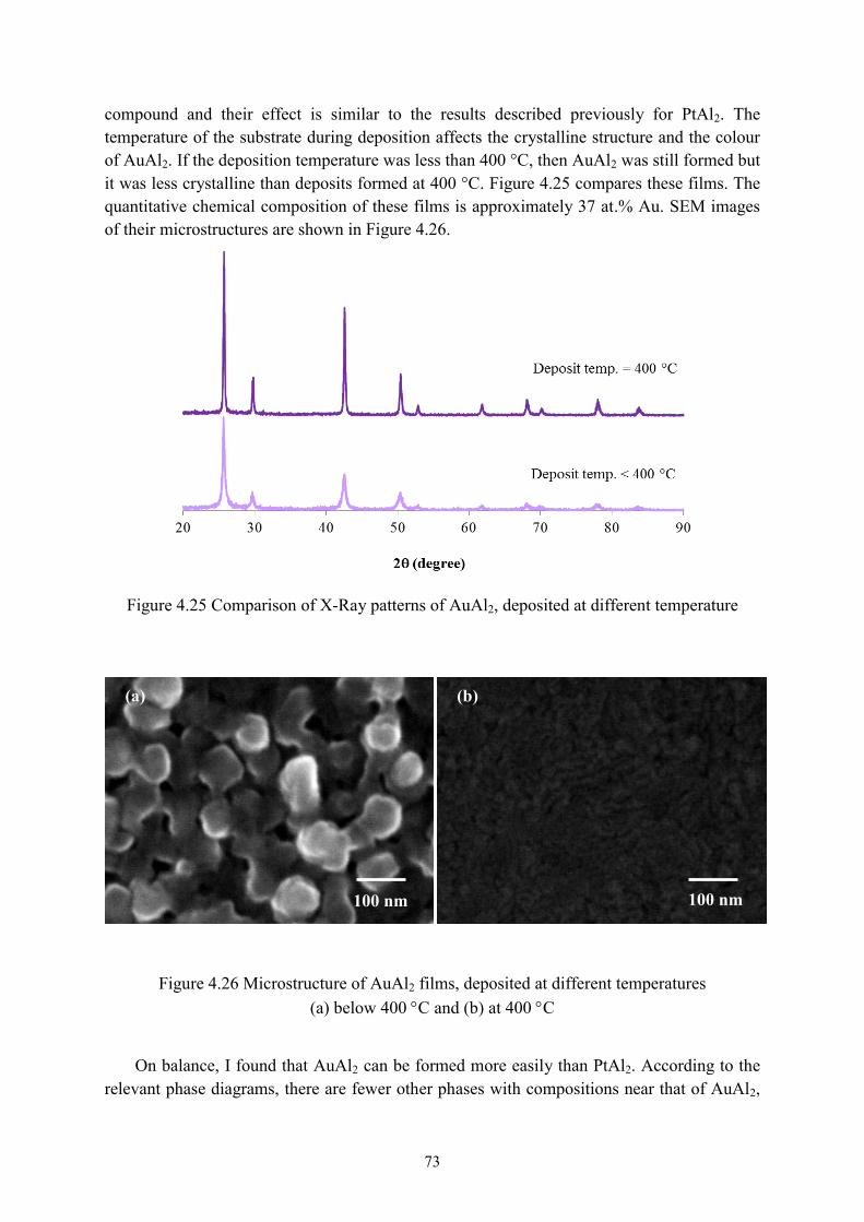
73
compound and their effect is similar to the results described previously for PtAl2. The temperature of the substrate during deposition affects the crystalline structure and the colour of AuAl2. If the deposition temperature was less than 400 °C, then AuAl2 was still formed but it was less crystalline than deposits formed at 400 °C. Figure 4.25 compares these films. The quantitative chemical composition of these films is approximately 37 at.% Au. SEM images of their microstructures are shown in Figure 4.26.
Figure 4.25 Comparison of X-Ray patterns of AuAl2, deposited at different temperature
Figure 4.26 Microstructure of AuAl2 films, deposited at different temperatures (a) below 400 C and (b) at 400 C
On balance, I found that AuAl2 can be formed more easily than PtAl2. According to the
relevant phase diagrams, there are fewer other phases with compositions near that of AuAl2,
100 nm
(a)
100 nm
(b)

74
in contrast to the situation for PtAl2. The results showed that AuAl2 could be formed even when using different power levels, deposition times and deposition temperatures, with some AuAl2 formed in each case even though the purple hue of films varied a bit. In addition, the reflectance curves of AuAl2 which was produced by arc melting (bulk) and AuAl2 which was fabricated by magnetron sputtering (film) are of similar form although the film has a stronger colour because it has a slightly higher reflection in the violet and red regions, and less reflection in green, as shown in Figure 4.27. However, the morphologies of the two different forms of AuAl2 sample are different, shown in Figure 4.28 and 4.29. A dendritic structure can be observed in the AuAl2 bulk sample with some segregation of Al, which had most likely occurred during solidification. In contrast, the morphology of AuAl2 film is dense and homogeneous.
Figure 4.27 Comparison of reflectance spectra of AuAl2 in bulk and film
Figure 4.28 Morphologies of AuAl2 bulk sample by (a) SEM and (b) LM
10 m
(a)
50 m
(b)

75
Figure 4.29 Morphologies of AuAl2 thin film (a) plan view and (b) cross-section
Additionally, both bulk and thin film AuAl2 were characterized by XRD. The X-ray patterns are shown in Figure 4.30. The chemical compositions were analysed by EDS, Au 33 at.% and Al 67 at.% in bulk as well as Au 34 at.% and Al 66 at.% in film. The lattice parameter of the AuAl2 film and bulk samples were obtained by Rietveld refinement and found to be 0.5993 and 0.5999 nm respectively, at room temperature. These values are in agreement with the 0.5995 to 0.5999 nm recorded in Pearson’s Handbook of Crystallographic Data for Intermetallic Phases [204] and JCPDF (pattern card number 00-017-0877 and 03-065-2984).
Figure 4.30 X-ray patterns of AuAl2 in bulk and thin film samples
100 nm
(a)
100 nm
(b)
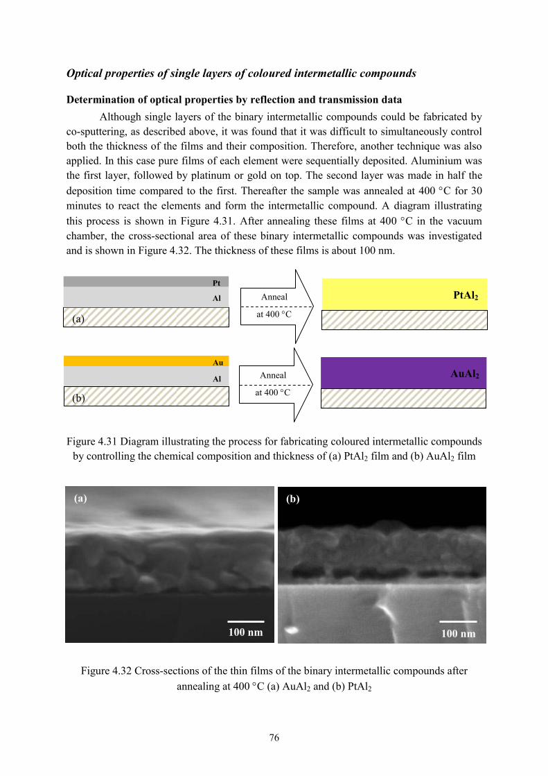
76
100 nm 100 nm
Optical properties of single layers of coloured intermetallic compounds
Determination of optical properties by reflection and transmission data Although single layers of the binary intermetallic compounds could be fabricated by
co-sputtering, as described above, it was found that it was difficult to simultaneously control both the thickness of the films and their composition. Therefore, another technique was also applied. In this case pure films of each element were sequentially deposited. Aluminium was the first layer, followed by platinum or gold on top. The second layer was made in half the deposition time compared to the first. Thereafter the sample was annealed at 400 C for 30 minutes to react the elements and form the intermetallic compound. A diagram illustrating this process is shown in Figure 4.31. After annealing these films at 400 C in the vacuum chamber, the cross-sectional area of these binary intermetallic compounds was investigated and is shown in Figure 4.32. The thickness of these films is about 100 nm.
Figure 4.31 Diagram illustrating the process for fabricating coloured intermetallic compounds by controlling the chemical composition and thickness of (a) PtAl2 film and (b) AuAl2 film
Figure 4.32 Cross-sections of the thin films of the binary intermetallic compounds after annealing at 400 C (a) AuAl2 and (b) PtAl2
Anneal
at 400 C
Pt
Al
PtAl2
(a)
(a) (b)
Anneal
at 400 C
Al
Au
(b)
AuAl2
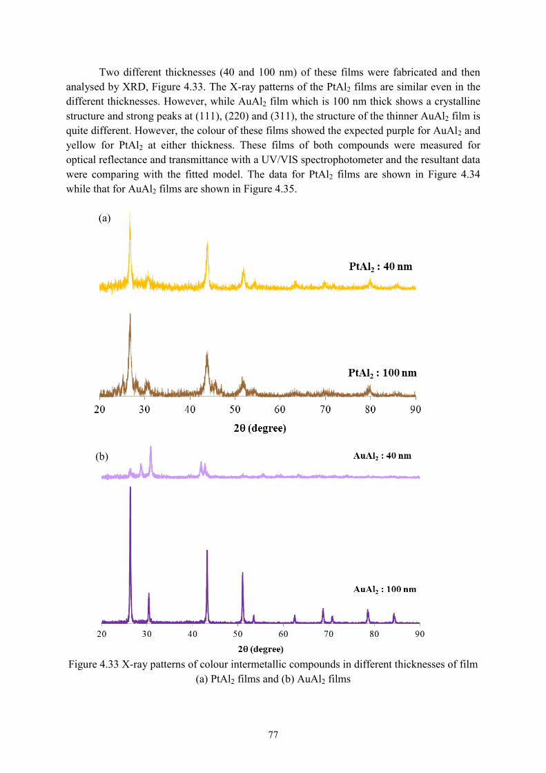
77
Two different thicknesses (40 and 100 nm) of these films were fabricated and then analysed by XRD, Figure 4.33. The X-ray patterns of the PtAl2 films are similar even in the different thicknesses. However, while AuAl2 film which is 100 nm thick shows a crystalline structure and strong peaks at (111), (220) and (311), the structure of the thinner AuAl2 film is quite different. However, the colour of these films showed the expected purple for AuAl2 and yellow for PtAl2 at either thickness. These films of both compounds were measured for optical reflectance and transmittance with a UV/VIS spectrophotometer and the resultant data were comparing with the fitted model. The data for PtAl2 films are shown in Figure 4.34 while that for AuAl2 films are shown in Figure 4.35.
Figure 4.33 X-ray patterns of colour intermetallic compounds in different thicknesses of film (a) PtAl2 films and (b) AuAl2 films
(b)
(a)

78
Figure 4.34 Reflectance (R) and transmittance (T) spectra of PtAl2 films (Exp) with model fitted (Model Fit) to different thicknesses of film (a) 100 nm and (b) 40 nm
100
nm
(a)
(a)
(b)

79
Figure 4.35 Reflectance and transmittance spectra of AuAl2 films with model fitted to different thicknesses (a) 100 nm and (b) 40 nm
(a)
(b)

80
The complex refractive indices, n and k, (and equivalently 1 and 2) of these coloured intermetallic compound films were obtained by using the WVASE32 software. The dielectric constants of these coloured intermetallic compound films are compared with the optical properties data from the bulk samples (which had been prepared by arc-melting in an argon atmosphere [199]) in Figure 4.36. The shapes of the dielectric functions are broadly similar for PtAl2 except for the fact that the 1 for the thin film crosses the X-axis whereas that for the bulk samples apparently does not. This crossing would be associated with a localized plasmon resonance. However, there is a bigger discrepancy in the case of AuAl2, possibly due to a difference in microstructure between the two samples. The 1 peaks present at ~ 3.25 eV in PtAl2 and ~2.75 eV in AuAl2.
Figure 4.36 Dielectric functions of coloured intermetallic compounds by reflectance and transmission data (a) PtAl2 and (b) AuAl2
(b)
(a)
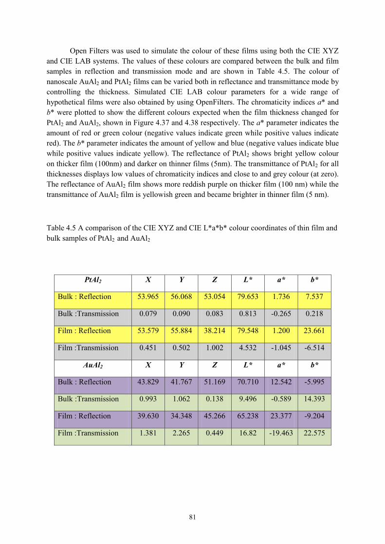
81
Open Filters was used to simulate the colour of these films using both the CIE XYZ and CIE LAB systems. The values of these colours are compared between the bulk and film samples in reflection and transmission mode and are shown in Table 4.5. The colour of nanoscale AuAl2 and PtAl2 films can be varied both in reflectance and transmittance mode by controlling the thickness. Simulated CIE LAB colour parameters for a wide range of hypothetical films were also obtained by using OpenFilters. The chromaticity indices a* and b* were plotted to show the different colours expected when the film thickness changed for PtAl2 and AuAl2, shown in Figure 4.37 and 4.38 respectively. The a* parameter indicates the amount of red or green colour (negative values indicate green while positive values indicate red). The b* parameter indicates the amount of yellow and blue (negative values indicate blue while positive values indicate yellow). The reflectance of PtAl2 shows bright yellow colour on thicker film (100nm) and darker on thinner films (5nm). The transmittance of PtAl2 for all thicknesses displays low values of chromaticity indices and close to and grey colour (at zero). The reflectance of AuAl2 film shows more reddish purple on thicker film (100 nm) while the transmittance of AuAl2 film is yellowish green and became brighter in thinner film (5 nm).
Table 4.5 A comparison of the CIE XYZ and CIE L*a*b* colour coordinates of thin film and bulk samples of PtAl2 and AuAl2
PtAl2 X Y Z L* a* b*
Bulk : Reflection 53.965 56.068 53.054 79.653 1.736 7.537
Bulk :Transmission 0.079 0.090 0.083 0.813 -0.265 0.218
Film : Reflection 53.579 55.884 38.214 79.548 1.200 23.661
Film :Transmission 0.451 0.502 1.002 4.532 -1.045 -6.514
AuAl2 X Y Z L* a* b*
Bulk : Reflection 43.829 41.767 51.169 70.710 12.542 -5.995
Bulk :Transmission 0.993 1.062 0.138 9.496 -0.589 14.393
Film : Reflection 39.630 34.348 45.266 65.238 23.377 -9.204
Film :Transmission 1.381 2.265 0.449 16.82 -19.463 22.575
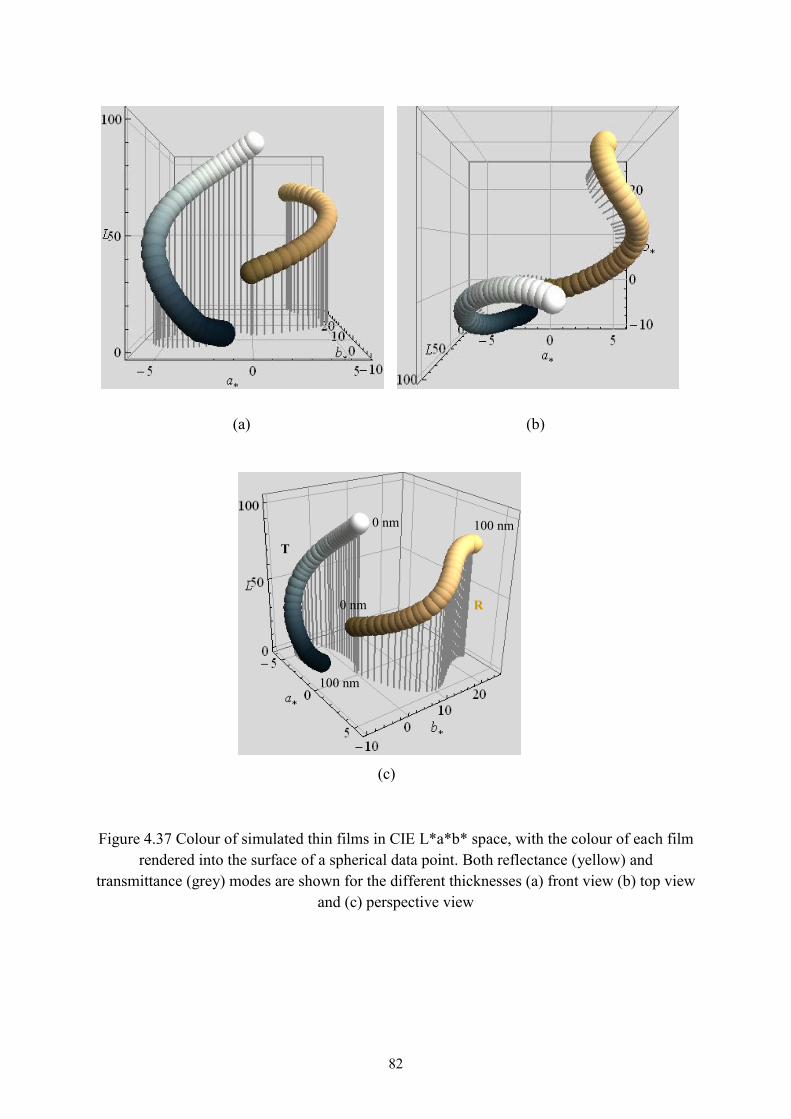
82
Figure 4.37 Colour of simulated thin films in CIE L*a*b* space, with the colour of each film
rendered into the surface of a spherical data point. Both reflectance (yellow) and transmittance (grey) modes are shown for the different thicknesses (a) front view (b) top view
and (c) perspective view
(a) (b)
(c)
0 nm
0 nm
100 nm
100 nm
R
T
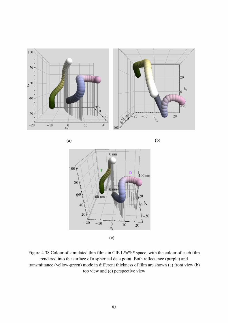
83
Figure 4.38 Colour of simulated thin films in CIE L*a*b* space, with the colour of each film
rendered into the surface of a spherical data point. Both reflectance (purple) and transmittance (yellow-green) mode in different thickness of film are shown (a) front view (b)
top view and (c) perspective view
(a) (b)
(c)
100 nm
100 nm
0 nm
0 nm
T R
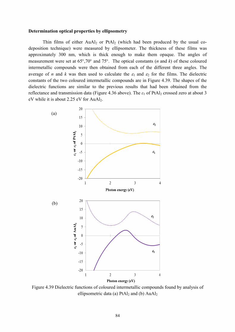
84
Determination optical properties by ellipsometry
Thin films of either AuAl2 or PtAl2 (which had been produced by the usual co-deposition technique) were measured by ellipsometer. The thickness of these films was approximately 300 nm, which is thick enough to make them opaque. The angles of measurement were set at 65 ,70 and 75 . The optical constants (n and k) of these coloured intermetallic compounds were then obtained from each of the different three angles. The average of n and k was then used to calculate the 1 and 2 for the films. The dielectric constants of the two coloured intermetallic compounds are in Figure 4.39. The shapes of the dielectric functions are similar to the previous results that had been obtained from the reflectance and transmission data (Figure 4.36 above). The 1 of PtAl2 crossed zero at about 3 eV while it is about 2.25 eV for AuAl2.
Figure 4.39 Dielectric functions of coloured intermetallic compounds found by analysis of ellipsometric data (a) PtAl2 and (b) AuAl2
(a)
(b)
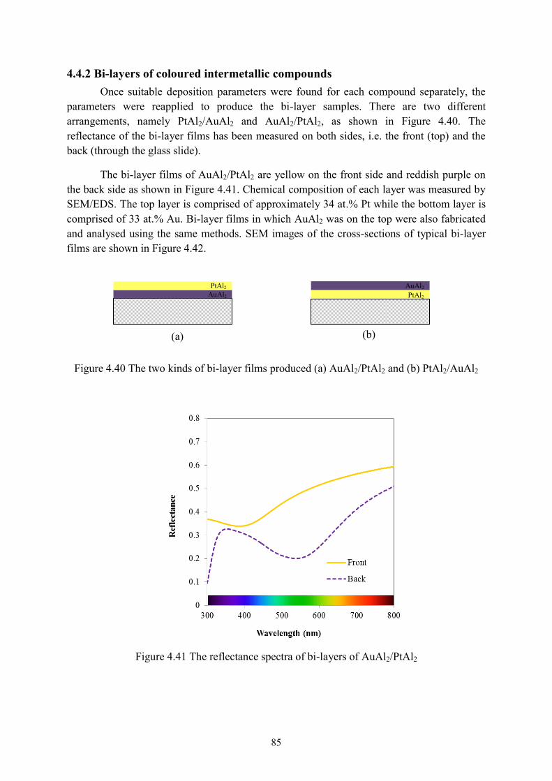
85
(a) (b)
4.4.2 Bi-layers of coloured intermetallic compounds Once suitable deposition parameters were found for each compound separately, the
parameters were reapplied to produce the bi-layer samples. There are two different arrangements, namely PtAl2/AuAl2 and AuAl2/PtAl2, as shown in Figure 4.40. The reflectance of the bi-layer films has been measured on both sides, i.e. the front (top) and the back (through the glass slide).
The bi-layer films of AuAl2/PtAl2 are yellow on the front side and reddish purple on the back side as shown in Figure 4.41. Chemical composition of each layer was measured by SEM/EDS. The top layer is comprised of approximately 34 at.% Pt while the bottom layer is comprised of 33 at.% Au. Bi-layer films in which AuAl2 was on the top were also fabricated and analysed using the same methods. SEM images of the cross-sections of typical bi-layer films are shown in Figure 4.42.
Figure 4.40 The two kinds of bi-layer films produced (a) AuAl2/PtAl2 and (b) PtAl2/AuAl2
Figure 4.41 The reflectance spectra of bi-layers of AuAl2/PtAl2
AuAl2 PtAl2
PtAl2 AuAl2

86
100 nm
(b)
100 nm
(a)
Figure 4.42 Cross-section of bi-layers films of PtAl2/AuAl2 before annealing (a) In lens mode and (b) backscatter mode
Both coloured intermetallic compounds share the same CaF2 structure or cF12 (Pearson symbol) crystal structure. They have similar physical properties. Furthermore, platinum and gold have same face-centred cubic (FCC) structure, similar electronegativity and atomic diameter. Therefore, it was initially considered that the two compounds might exhibit unlimited mutual solubility. Post-deposition heat treatment was applied to the above bi-layer samples to see whether the two phases would interdiffuse. The annealing temperature was at 400 C for 24 hours or 48 hours under vacuum. Contrary to our initial expectation, the two compounds seem to be nearly mutually insoluble. The cross-sections of these films after annealing were observed and shown in Figure 4.43.
Figure 4.43 Cross-section of PtAl2/AuAl2 film after annealing under vacuum at 400 °C (a) for 24 hours and (b) for 48 hours
100 nm
(a)
100 nm
(b)
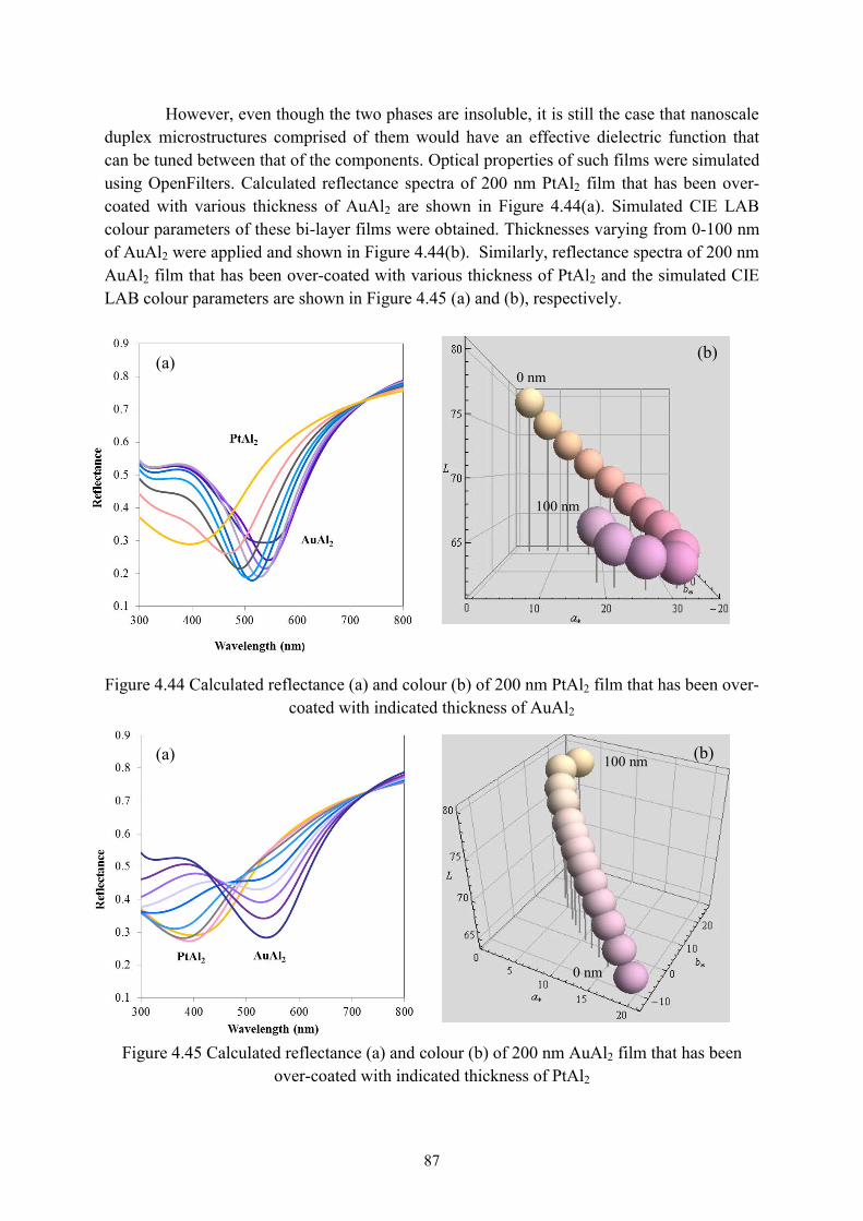
87
100
(b) (a)
(a)
However, even though the two phases are insoluble, it is still the case that nanoscale duplex microstructures comprised of them would have an effective dielectric function that can be tuned between that of the components. Optical properties of such films were simulated using OpenFilters. Calculated reflectance spectra of 200 nm PtAl2 film that has been over-coated with various thickness of AuAl2 are shown in Figure 4.44(a). Simulated CIE LAB colour parameters of these bi-layer films were obtained. Thicknesses varying from 0-100 nm of AuAl2 were applied and shown in Figure 4.44(b). Similarly, reflectance spectra of 200 nm AuAl2 film that has been over-coated with various thickness of PtAl2 and the simulated CIE LAB colour parameters are shown in Figure 4.45 (a) and (b), respectively.
Figure 4.44 Calculated reflectance (a) and colour (b) of 200 nm PtAl2 film that has been over-coated with indicated thickness of AuAl2
Figure 4.45 Calculated reflectance (a) and colour (b) of 200 nm AuAl2 film that has been over-coated with indicated thickness of PtAl2
(b) 0 nm
100 nm
(b)
0 nm
100 nm
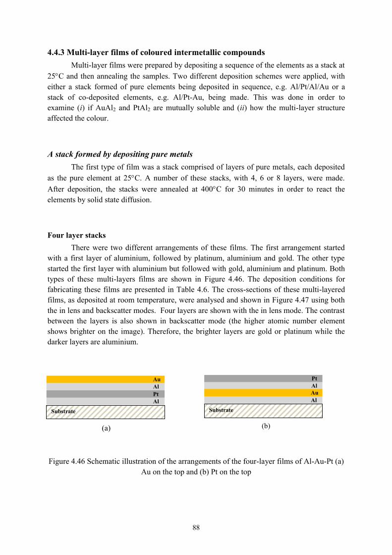
88
(b) (a)
4.4.3 Multi-layer films of coloured intermetallic compounds Multi-layer films were prepared by depositing a sequence of the elements as a stack at
25 C and then annealing the samples. Two different deposition schemes were applied, with either a stack formed of pure elements being deposited in sequence, e.g. Al/Pt/Al/Au or a stack of co-deposited elements, e.g. Al/Pt-Au, being made. This was done in order to examine (i) if AuAl2 and PtAl2 are mutually soluble and (ii) how the multi-layer structure affected the colour.
A stack formed by depositing pure metals The first type of film was a stack comprised of layers of pure metals, each deposited
as the pure element at 25 C. A number of these stacks, with 4, 6 or 8 layers, were made. After deposition, the stacks were annealed at 400 C for 30 minutes in order to react the elements by solid state diffusion.
Four layer stacks There were two different arrangements of these films. The first arrangement started with a first layer of aluminium, followed by platinum, aluminium and gold. The other type started the first layer with aluminium but followed with gold, aluminium and platinum. Both types of these multi-layers films are shown in Figure 4.46. The deposition conditions for fabricating these films are presented in Table 4.6. The cross-sections of these multi-layered films, as deposited at room temperature, were analysed and shown in Figure 4.47 using both the in lens and backscatter modes. Four layers are shown with the in lens mode. The contrast between the layers is also shown in backscatter mode (the higher atomic number element shows brighter on the image). Therefore, the brighter layers are gold or platinum while the darker layers are aluminium.
Figure 4.46 Schematic illustration of the arrangements of the four-layer films of Al-Au-Pt (a) Au on the top and (b) Pt on the top
Substrate
Al Pt Al Au
Substrate
Al
Pt Al Au

89
100 nm
(a)
100 nm
(b)
Table 4.6 Deposition conditions for the four-layer films of Al-Au-Pt
Layer order
Metal targets Current (A) Deposition time
1 Al 0.4 5 minutes 2 Pt or Au 0.1 2 minutes 3 Al 0.4 5 minutes 4 Au or Pt 0.1 2 minutes
After that, these films were annealed at 400 C for 30 minutes. The result was that the four distinct layers merged to become only two layers, as seen in SEM images taken in both in lens and backscatter mode in Figure 4.48 and Figure 4.49. TEM images also showed the two separate layers quite clearly.
Figure 4.47 Cross-sections of four-layer films of Al-Au-Pt with Au on the top, as deposited at 25 °C (a) In lens and (b) RBSD
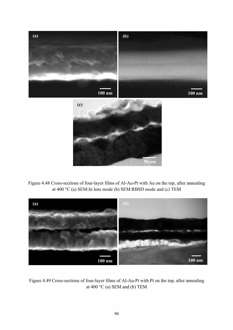
90
100 nm
(a)
100 nm
(b)
50 nm
(c)
100 nm
(a)
100 nm
(b)
Figure 4.48 Cross-sections of four-layer films of Al-Au-Pt with Au on the top, after annealing at 400 °C (a) SEM:In lens mode (b) SEM:RBSD mode and (c) TEM
Figure 4.49 Cross-sections of four-layer films of Al-Au-Pt with Pt on the top, after annealing at 400 °C (a) SEM and (b) TEM

91
The colour of these films changed substantially after annealing at 400 °C. To measure this change a glass slide was used as the substrate. The reflectance spectra of both sides of the samples were then measured by spectrophotometer in the visible region before and after annealing. The four-layer films which had gold on the top were greenish yellow before annealing. Their colour was noticeably different to that of a 30 nm pure gold film that was used as a comparator. After annealing, the film on the top turned reddish purple. A comparison of the spectra of the four-layer films which had gold on the top is shown in Figure 4.50 before annealing and after annealing. Data for the thin film of gold is shown for comparison. According to their cross-sectional views, the four-layer films have been converted to two layers during annealing. Therefore, the back side of these films was also measured, through the glass slide substrate. Figure 4.51 shows the different of reflectance spectra between before and after annealing.
The other type of four-layer film had platinum on the top. These were silvery before annealing, with the colour no different to that of a 30 nm film of pure platinum used as a comparator. After annealing the upper layer turned yellow, as shown in Figure 4.52. In contrast, the back side of these films turned from silvery to purple after annealing, as shown in Figure 4.53. The X-ray patterns of these films are compared after deposition at 25 C (before annealing) and after annealing at 400 C. The results indicated that AuAl2 or PtAl2 was formed on the top of the sample, depending on which element was uppermost in the stack, Figure 4.54, and that they did not interdiffuse.
Figure 4.50 The reflectance spectra from the front side of a four-layered film of Al-Au-Pt (Au on the top) as deposited at 25 °C before and after annealing. Data for a pure gold film of
30 nm thickness is shown for comparison

92
Figure 4.51 The reflectance spectra from the back side of the above four-layered film, before and after annealing
Figure 4.52 The reflectance spectra from the front side of a four-layered film of Al-Au-Pt (Pt on the top) as depositing at 25 °C before and after annealing. Data for a pure platinum thin
film of 30 nm thickness is shown for comparison

93
Figure 4.53 The reflectance spectra from the back side of the above four-layered film, before and after annealing
50 nm (a)
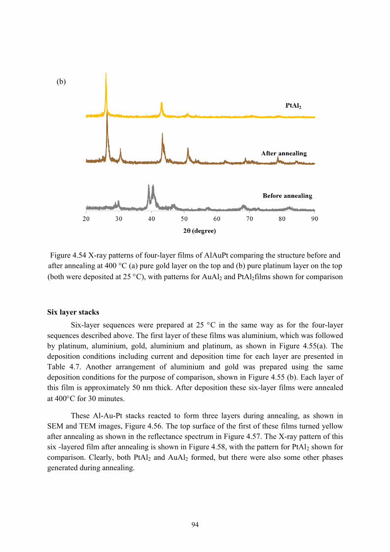
94
Figure 4.54 X-ray patterns of four-layer films of AlAuPt comparing the structure before and after annealing at 400 °C (a) pure gold layer on the top and (b) pure platinum layer on the top (both were deposited at 25 C), with patterns for AuAl2 and PtAl2films shown for comparison
Six layer stacks Six-layer sequences were prepared at 25 C in the same way as for the four-layer
sequences described above. The first layer of these films was aluminium, which was followed by platinum, aluminium, gold, aluminium and platinum, as shown in Figure 4.55(a). The deposition conditions including current and deposition time for each layer are presented in Table 4.7. Another arrangement of aluminium and gold was prepared using the same deposition conditions for the purpose of comparison, shown in Figure 4.55 (b). Each layer of this film is approximately 50 nm thick. After deposition these six-layer films were annealed at 400 C for 30 minutes.
These Al-Au-Pt stacks reacted to form three layers during annealing, as shown in SEM and TEM images, Figure 4.56. The top surface of the first of these films turned yellow after annealing as shown in the reflectance spectrum in Figure 4.57. The X-ray pattern of this six -layered film after annealing is shown in Figure 4.58, with the pattern for PtAl2 shown for comparison. Clearly, both PtAl2 and AuAl2 formed, but there were also some other phases generated during annealing.
(b)
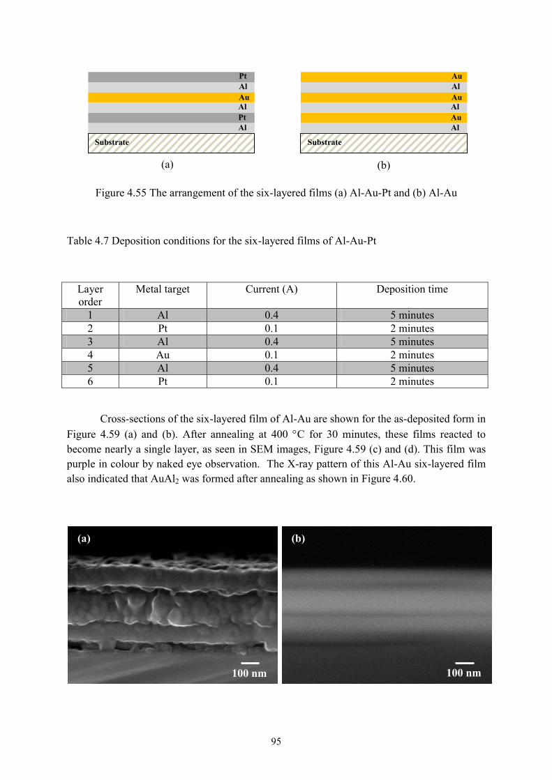
95
(a) (b)
100 nm
(a)
100 nm
(b)
Figure 4.55 The arrangement of the six-layered films (a) Al-Au-Pt and (b) Al-Au
Table 4.7 Deposition conditions for the six-layered films of Al-Au-Pt
Layer order
Metal target Current (A) Deposition time
1 Al 0.4 5 minutes 2 Pt 0.1 2 minutes 3 Al 0.4 5 minutes 4 Au 0.1 2 minutes 5 Al 0.4 5 minutes 6 Pt 0.1 2 minutes
Cross-sections of the six-layered film of Al-Au are shown for the as-deposited form in Figure 4.59 (a) and (b). After annealing at 400 C for 30 minutes, these films reacted to become nearly a single layer, as seen in SEM images, Figure 4.59 (c) and (d). This film was purple in colour by naked eye observation. The X-ray pattern of this Al-Au six-layered film also indicated that AuAl2 was formed after annealing as shown in Figure 4.60.
Substrate
Al Pt
Au Al Pt
Al
Substrate
Al Au Al Au Al Au

96
100 nm
(c)
Figure 4.56 Cross-section views of the six-layer film of Al-Au-Pt after annealing at 400 °C (a) SEM-In lens (b) SEM-RBSD and (c) TEM
Figure 4.57 The reflectance spectra of the top of the six-layer film of Al-Au-Pt (Pt on the top) after annealing

97
100 nm
(a)
100 nm
(b)
200 nm
(c)
200 nm
(d)
Figure 4.58 The X-ray pattern of the six-layer film of Al-Au-Pt after annealing, with patterns for PtAl2 and AuAl2 films shown for comparison
Figure 4.59 Cross-sections of six-layer films of Al-Au (a) before annealing-In lens, (b) before annealing – RBSD, (c) after annealing at 400 °C – In lens and (d) after annealing at 400 °C –
RBSD
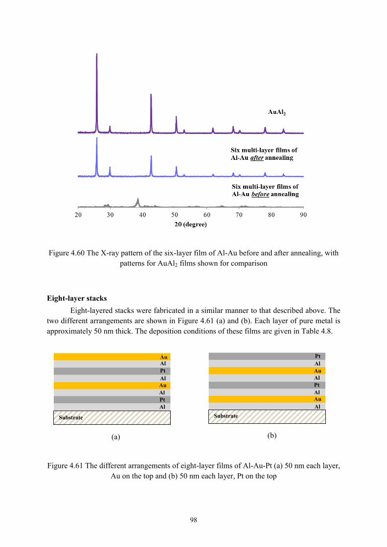
98
(b) (a)
Figure 4.60 The X-ray pattern of the six-layer film of Al-Au before and after annealing, with patterns for AuAl2 films shown for comparison
Eight-layer stacks Eight-layered stacks were fabricated in a similar manner to that described above. The two different arrangements are shown in Figure 4.61 (a) and (b). Each layer of pure metal is approximately 50 nm thick. The deposition conditions of these films are given in Table 4.8.
Figure 4.61 The different arrangements of eight-layer films of Al-Au-Pt (a) 50 nm each layer, Au on the top and (b) 50 nm each layer, Pt on the top
Al Pt Al Au Al Pt
Au Al
Substrate Substrate
Al
Au
Pt Al
Al Au Al Pt

99
100 nm
(a)
100 nm
(b)
100 nm
(c)
100 nm
(d)
Table 4.8 Deposition conditions of eight-layer films of Al-Au-Pt. Each layer is 50 nm thick
Layer order
Metal target Current (A) Deposition time
1 Al 0.4 5 minutes 2 Au or Pt 0.1 2 minutes 3 Al 0.4 5 minutes 4 Pt or Au 0.1 2 minutes 5 Al 0.4 5 minutes 6 Au or Pt 0.1 2 minutes 7 Al 0.4 5 minutes 8 Pt or Au 0.1 2 minutes
Figure 4.62 Cross-sectional views of eight-layered films of Al-Au-Pt (a) before annealing-In lens, (b) before annealing – RBSD, (c) after annealing at 400 °C – In lens and (d) after
annealing at 400 °C – RBSD
The cross-section of the eight-layer film which had platinum on the top is shown before and after annealing in Figure 4.62. The chemical inhomogeneity of the eight layers is

100
much reduced by annealing to the extent that the sample seems to consist for the most part of only four layers. However, the X-ray result of these films, Figure 4.63, indicated that it was the PtAl phase, not PtAl2, that formed after annealing. In support of this, the reflectance spectrum of this films, Figure 4.64, did not indicate a yellow colour.
Figure 4.63 The X-ray pattern of eight multi-layers films of Al-Au-Pt (Pt on the top) after annealing, comparing with PtAl2 film
Figure 4.64 The reflectance spectrum of the surface of eight multi-layers films of Al-Au-Pt (Pt on the top) after annealing, comparing with a single PtAl2 film

101
100 nm
(a)
100 nm
(b)
The other type of eight-layered films, with gold on the top, also reacted to four layers after annealing under the same conditions, Figure 4.65 (a). The flat surface area of these films is homogenous, shown in Figure 4.65 (b). Their X-ray pattern indicated that AuAl2 was formed after annealing process, as shown in Figure 4.66. The flat surface also turned purple after annealing, as shown as reflectance spectrum in Figure 4.67.
Figure 4.65 The morphologies of eight multi-layer films of Al-Au-Pt which Au on the top after annealing at 400 °C (a) cross-sectional area and (b) surface area
Figure 4.66 The X-ray pattern of the eight-layered films of Al-Au-Pt (Au on the top) after annealing. A pattern for a simple AuAl2 film is shown for comparison

102
Figure 4.67 The reflectance spectrum of the surface of the eight-layer film of Al-Au-Pt (Au on the top) after annealing, in comparison to that of a simple, single-layer AuAl2 film
The effect of the thickness of the individual layers was also investigated. An eight-layer film was prepared by using half the deposition times of the previous eight-layer film with the gold on top. The thickness of each layer was approximately 25 nm. The stack and deposition conditions of these films are shown in Figure 4.68 and Table 4.9, respectively. The X-ray patterns of these films are shown for the condition before annealing and after annealing at 400 C. The X-ray results indicated that AuAl2 was formed, Figure 4.69. Similarly to the thicker eight-layer films, four separate layers developed after annealing at 400 C for 30 minutes. The cross-sectional views of these multi-layered films before and after annealing are shown in Figure 4.70.
Figure 4.68 The arrangement of eight-layered films of Al-Au-Pt with each layer being 25 nm thick (Au on the top)
Al
Al Al
Substrate
Pt Au Pt Au
Al
Al Al Al
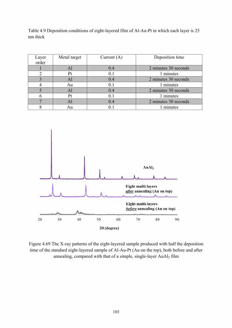
103
Table 4.9 Deposition conditions of eight-layered film of Al-Au-Pt in which each layer is 25 nm thick
Layer order
Metal target Current (A) Deposition time
1 Al 0.4 2 minutes 30 seconds 2 Pt 0.1 1 minutes 3 Al 0.4 2 minutes 30 seconds 4 Au 0.1 1 minutes 5 Al 0.4 2 minutes 30 seconds 6 Pt 0.1 1 minutes 7 Al 0.4 2 minutes 30 seconds 8 Au 0.1 1 minutes
Figure 4.69 The X-ray patterns of the eight-layered sample produced with half the deposition time of the standard eight-layered sample of Al-Au-Pt (Au on the top), both before and after
annealing, compared with that of a simple, single-layer AuAl2 film
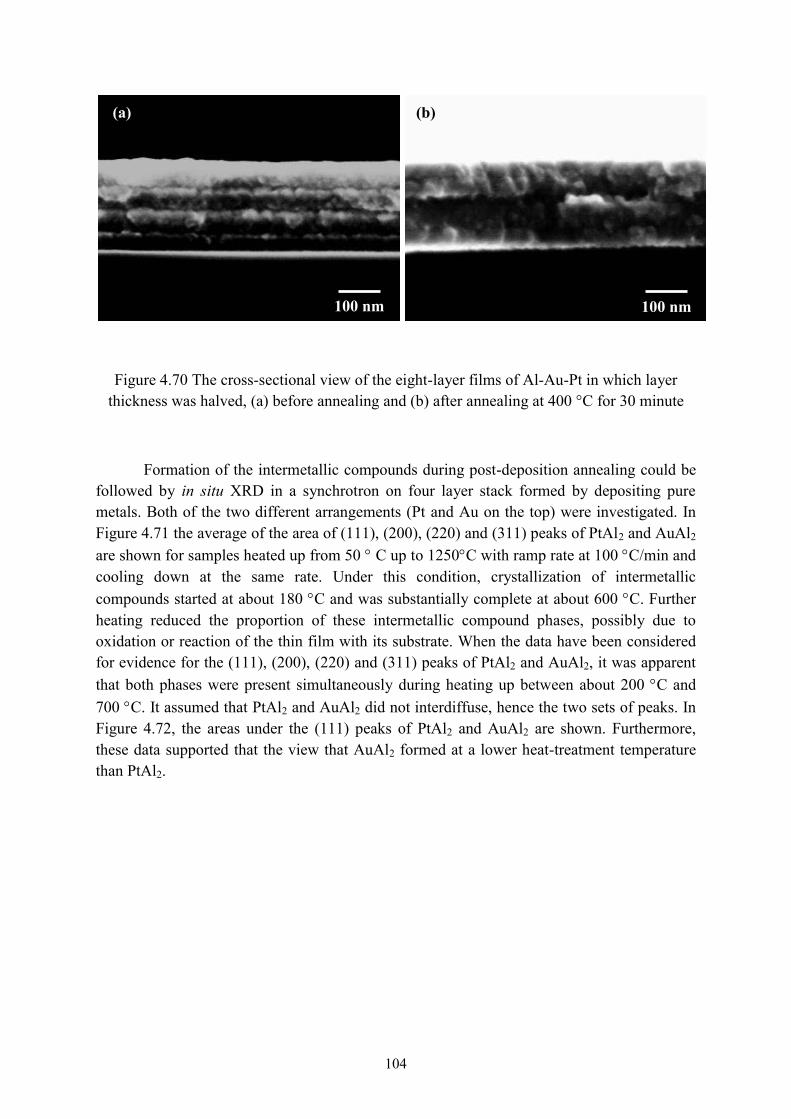
104
100 nm
(a)
100 nm
(b)
Figure 4.70 The cross-sectional view of the eight-layer films of Al-Au-Pt in which layer thickness was halved, (a) before annealing and (b) after annealing at 400 °C for 30 minute
Formation of the intermetallic compounds during post-deposition annealing could be followed by in situ XRD in a synchrotron on four layer stack formed by depositing pure metals. Both of the two different arrangements (Pt and Au on the top) were investigated. In Figure 4.71 the average of the area of (111), (200), (220) and (311) peaks of PtAl2 and AuAl2 are shown for samples heated up from 50 C up to 1250 C with ramp rate at 100 C/min and cooling down at the same rate. Under this condition, crystallization of intermetallic compounds started at about 180 C and was substantially complete at about 600 C. Further heating reduced the proportion of these intermetallic compound phases, possibly due to oxidation or reaction of the thin film with its substrate. When the data have been considered for evidence for the (111), (200), (220) and (311) peaks of PtAl2 and AuAl2, it was apparent that both phases were present simultaneously during heating up between about 200 C and 700 C. It assumed that PtAl2 and AuAl2 did not interdiffuse, hence the two sets of peaks. In Figure 4.72, the areas under the (111) peaks of PtAl2 and AuAl2 are shown. Furthermore, these data supported that the view that AuAl2 formed at a lower heat-treatment temperature than PtAl2.
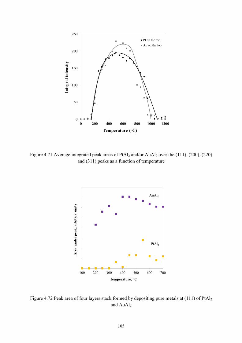
105
Figure 4.71 Average integrated peak areas of PtAl2 and/or AuAl2 over the (111), (200), (220) and (311) peaks as a function of temperature
Figure 4.72 Peak area of four layers stack formed by depositing pure metals at (111) of PtAl2 and AuAl2

106
(c)
(b) (a)
A stack formed by co-depositing precious metals The second strategy was to form a stack of co-deposited Au and Pt, interleaved with a layer of pure Al. The co-deposited layer was designed to be 50 at.% Au and 50 at.% Pt at various thicknesses ranging from 20 nm to 120 nm. Deposition was carried out at room temperature. After that the films were annealed in a tube furnace at 400 C for 60 minutes. Different sequences of these layers were investigated. The designs of these films are shown in Figure 4.73 (a) and (b). The effect of the thickness of co-deposited precious metals was also investigated. This was done by reducing the deposition time, Figure 4.73 (c).
Figure 4.73 The design of stacks consisting of co-deposited precious metals and aluminium (a) precious metals on the bottom (Al/(Au,Pt) ), (b) precious metals on the top ( (Au,Pt)/Al)
and (c) co-depositing precious metals on the top but with half the thickness
The composition of Au-Pt in the co-deposited films was verified by EDS and XRD. The composition in the 120 nm thick film was 54 at.% Au and 46 at.% Pt. When compared to those of pure Au and pure Pt, the X-ray pattern of this film, Figure 4.74, indicates that a solid solution of the two elements had formed with a lattice parameter of 0.4006 nm which lies between pure Au films (0.4077 nm for our Au films, compared to a literature value of 0.4079 nm for the bulk) and pure Pt films (0.3935 nm for our Pt films, compared to a literature value of 0.3924 nm for the bulk). Therefore, from Vegard’s rule, a lattice parameter of 0.4006 nm would be expected for a solid solution. Under equilibrium conditions Au and Pt do not form a solid solution at room temperature, however metastable solid solutions in this system can certainly be found, as for example after quenching alloy samples from elevated temperatures. In the present case, the freshly deposited material has not had any time to attain equilibrium and so is in the form of a metastable fcc solid solution. After the co-deposited Au-Pt was successfully produced, a single layer of pure Al film was deposited following the procedure which was described previously.
Substrate
Al
50 at.% Au + 50 at.% Pt
Substrate
Al
50 at.% Au + 50 at.% Pt
Substrate
Al
50 at.% Au + 50 at.% Pt
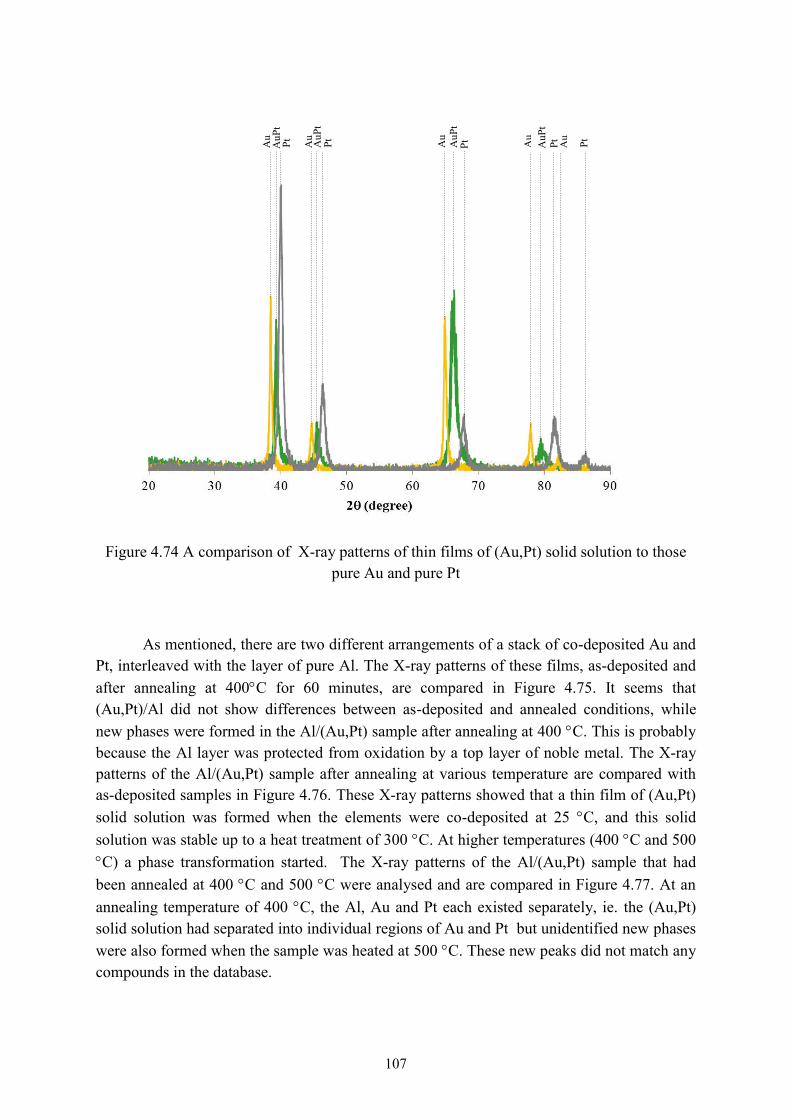
107
Figure 4.74 A comparison of X-ray patterns of thin films of (Au,Pt) solid solution to those pure Au and pure Pt
As mentioned, there are two different arrangements of a stack of co-deposited Au and Pt, interleaved with the layer of pure Al. The X-ray patterns of these films, as-deposited and after annealing at 400 C for 60 minutes, are compared in Figure 4.75. It seems that (Au,Pt)/Al did not show differences between as-deposited and annealed conditions, while new phases were formed in the Al/(Au,Pt) sample after annealing at 400 C. This is probably because the Al layer was protected from oxidation by a top layer of noble metal. The X-ray patterns of the Al/(Au,Pt) sample after annealing at various temperature are compared with as-deposited samples in Figure 4.76. These X-ray patterns showed that a thin film of (Au,Pt) solid solution was formed when the elements were co-deposited at 25 C, and this solid solution was stable up to a heat treatment of 300 C. At higher temperatures (400 C and 500 C) a phase transformation started. The X-ray patterns of the Al/(Au,Pt) sample that had
been annealed at 400 C and 500 C were analysed and are compared in Figure 4.77. At an annealing temperature of 400 C, the Al, Au and Pt each existed separately, ie. the (Au,Pt) solid solution had separated into individual regions of Au and Pt but unidentified new phases were also formed when the sample was heated at 500 C. These new peaks did not match any compounds in the database.
Au
AuP
t
Pt
Au
Au
Au
Au
AuP
t
AuP
t
AuP
t
Pt
Pt
Pt
Pt

108
Figure 4.75 X-ray patterns of different arrangements of stacks made of a layer of co-deposited Au and Pt, and Al, before and after annealing
Figure 4.76 X-ray patterns of an Al/(Au,Pt) sample, followed by annealing at various temperatures

109
Figure 4.77 Comparison of X-ray patterns of an Al/(Au,Pt) sample, followed by annealing at 400 C and 500 C
Three different thicknesses (120, 60 and 20 nm) of co-deposited Au-Pt on the top layer were analysed by XRD after annealing at 400 C, Figure 4.78. These samples were also analysed by EDS, Table 4.10. The X-ray patterns showed that different compounds had been formed. As mentioned previously, for the Al/(Au,Pt) film with 120 nm of co-deposited Au-Pt, the Al, Au and Pt were separated after annealing at 400 C. In contrast, the Al/(Au,Pt) film with 60 nm of co-deposited Au-Pt mainly formed PtAl compounds after annealing. The un-identified peak marked as ‘*’ is assumed to be pure gold. The composition of Al/(Au,Pt) with 60 nm of co-deposited Au-Pt sample was 45 at.% Al, 44 at.% Pt and 11 at.% Au. Interestingly, Al/(Au,Pt) with 20 nm of co-deposited Au-Pt formed a phase with cF12 structure. EDS analysis of this sample indicated that its composition was 65 at.% Al, 23 at.% Pt and 12 at.% Au. In Figure 4.79, Rietveld analysis of this sample yielded a lattice parameter of a= 0.5952 nm, which close to a value of 0.5958 nm that could expected form applying Vegard’s Law to a mixture of AuAl2 and PtAl2 in the composition ratio of the film.
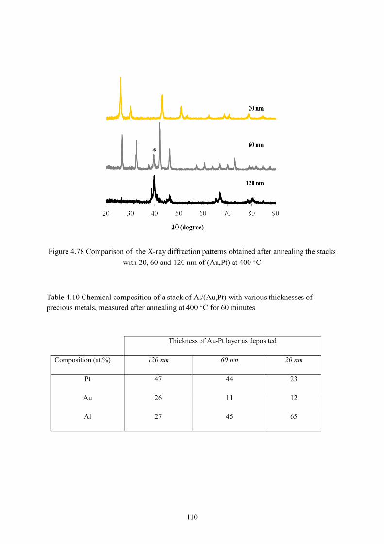
110
Figure 4.78 Comparison of the X-ray diffraction patterns obtained after annealing the stacks with 20, 60 and 120 nm of (Au,Pt) at 400 C
Table 4.10 Chemical composition of a stack of Al/(Au,Pt) with various thicknesses of precious metals, measured after annealing at 400 °C for 60 minutes
Thickness of Au-Pt layer as deposited
Composition (at.%) 120 nm 60 nm 20 nm
Pt 47 44 23
Au 26 11 12
Al 27 45 65
*

111
Figure 4.79 X-ray patterns of a mixed AuAl2/PtAl2 sample formed by co-depositing Au and Pt onto Al. The fitted pattern was obtained by Rietveld refinement on a PtAl2 structure
A cross-sectional microstructure of Al/(Au,Pt) with 20 nm of co-deposited (Au,Pt) was analysed by TEM including EDS elemental scan and mapping, Figure 4.80. It is clear that in this case an Au-Pt-Al solid solution was formed. The top layer of the surface contains Pt, Au and Al. It is polycrystalline and lattice fringe image is shown in Figure 4.81 (a). The deeper part has a slightly higher concentration of Au while the surface is Pt rich. The bottom part of sample contains an Al-rich layer which is amorphous, Figure 4.81(b). There appears to be some mass transfer of the film to the Si boundary.

112
Figure 4.80 Cross-section of the Al/(Au,Pt) sample with 20 nm of co-deposited (Au,Pt) with EDS elemental scan and mapping

113
(b)
Figure 4.81 High resolution TEM images of the Al/(Au,Pt) sample with 20 nm of co-deposited (Au,Pt) (a) top layer and (b) bottom layer
An Al/(Au,Pt) sample with 20 nm of co-deposited (Au,Pt) (65 at.% Al- 23 at.% Pt-12 at.% Au overall) was deposited onto a glass slide so that the optical properties of both sides of the film could be observed. After annealing, this sample was yellow on both sides by naked eye observation. In Figure 4.82 I compare the reflectance spectra of both sides of this sample after annealing with that of the front side before it had been annealed and with that of a pure PtAl2 film which was prepared by the co-sputtering technique described previously. Although the reflectivity is overall a bit lower than for the pure PtAl2 film, it is clear that annealing has produced a XAl2-type compound right through the film.
The amount of gold was increased in another sample (also with 20 nm thickness of (Au,Pt). In this case the overall analysis was 56 at.% Al-22 at.% Pt-22 at.% Au). After annealing the back side of sample was purple while the top was silvery. The reflectance spectra of this sample are shown in Figure 4.83. The reflectance of the sample before annealing and that of pure AuAl2 film was prepared by co-sputtering are shown for comparison.
The X-ray diffraction patterns of both samples before and after annealing are compared with each other and with pure PtAl2 and pure AuAl2 in Figure 4.84. From this data it seems that the 65 at.% Al- 23 at.% Pt-12 at.% Au sample formed (Au,Pt)Al2 after annealing. However, the increased amount of Au and decreased amount of Al in sample 56 at.% Al-22 at.% Pt-22 at.% Au has led to the formation of one or more phases in addition to the (Au,Pt)Al2.
0.298 nm
{200}
(a)
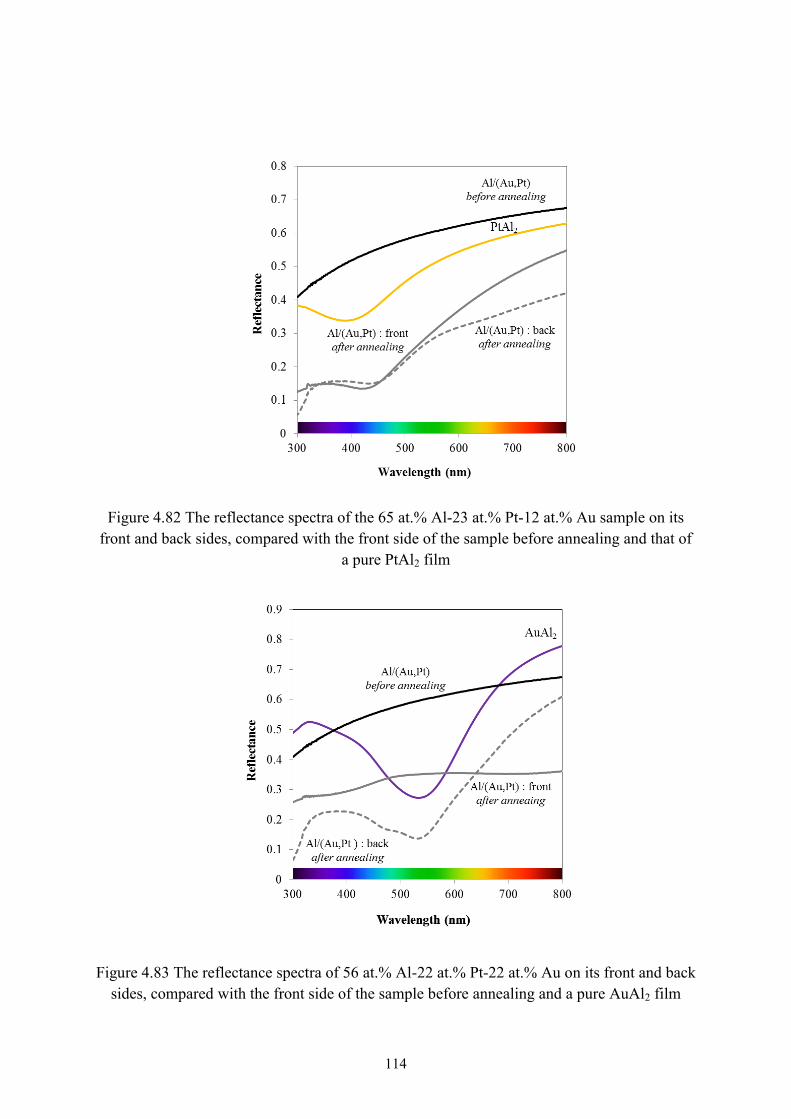
114
Figure 4.82 The reflectance spectra of the 65 at.% Al-23 at.% Pt-12 at.% Au sample on its front and back sides, compared with the front side of the sample before annealing and that of
a pure PtAl2 film
Figure 4.83 The reflectance spectra of 56 at.% Al-22 at.% Pt-22 at.% Au on its front and back sides, compared with the front side of the sample before annealing and a pure AuAl2 film

115
(a)
(b)
Figure 4.84 X-ray diffraction patterns of samples made by co-depositing Au and Pt on top of an Al layer (a) 65 at.% Al - 23 at.% Pt - 12 at.% Au and (b) 56 at.% Al - 22 at.% Pt - 22 at.%
Au. Data for before and after annealing, and for pure PtAl2 and pure AuAl2 is shown

116
(a)
An Al/(Au,Pt) sample consisting of ~200 nm of Al followed by a co-deposition of a combination of 54 at.% Au and 46 at.% Pt with ~100 nm thickness was fabricated on austenitic stainless steel foil. The formation of the intermetallic compounds during post-deposition treatment was examined in this sample using X-ray diffraction in a synchrotron beamline. This sample was heated from 30 °C up to 1000° C with ramp rate at 3 °C/min. The peaks of Pt and Al elements are visible up to a temperature of 310 ° C. The lattice parameter of Au is similar to that of Al and was obscured by the peak of the relatively thick Al underlayer. At 312 °C the peaks of a cF12 phase appear with a lattice parameter of 0.599 nm. In Figure 4.85 (a), the high temperature lattice parameters of AuAl2 (purple line) and PtAl2 (yellow line) have been provided by extrapolating from room temperature using an estimate of 13x10-6 K-1 for the coefficient of thermal expansion. The (Au,Pt)Al2 phase has a lattice parameter intermediate between that of AuAl2 and PtAl2. The value is very close to what might have been expected by applying Vegard's rule to a mixed solid solution of (Au,Pt)Al2. When the temperature reaches above 350 °C, Pt2Al3 phase appeared while (Au,Pt)Al2 phase is decreased as shown in Figure 4.85(b). However, the lattice parameter of the (Au,Pt)Al2 phase was increased to the value expected for AuAl2. Clearly, the Pt content of the original (Au,Pt)Al2 phase has transferred to the newly formed Pt2Al3 phase, leaving the remaining (Au,Pt)Al2 gold-rich. Raising temperature up at about 380°C, (Au,Pt)Al2 completely disappeared and AuAl and other PtxAly compounds were possibly formed. Only an isothermal experiment could prove that the mixed (Au,Pt)Al2 phase is actually metastable, but this seems the most probable situation. The sequence of reactions as this sample approaches equilibrium is probably:
(Au,Pt)+Al (Au,Pt)Al2 AuAl2 + Pt2Al3 AuAl +PtxAly + Pt2Al3

117
(b)
Figure 4.85 Lattice parameter and peak area of Al/(Au,Pt) sample as a function of temperature (a) Lattice parameter of (Au,Pt)Al2 in Al/(Au,Pt) sample and (b) peak area of
(Au,Pt)Al2 phase (111) and Pt2Al3 (002)
4.5 Conclusion Coloured intermetallic compounds are attractive particularly in jewellery and
decorative applications. Two well-known coloured intermetallic compounds are purple gold (AuAl2) and golden platinum (PtAl2). These two coloured intermetallic compounds share the CaF2 or cF12crystal structure. Since the two compounds share the same structure and have similar lattice parameters they might be expected to show unlimited mutual solubility by the Hume-Rothery rules. The Pt-Au-Al ternary phase diagram appears to have not yet been constructed so I investigated the situation myself. There are two interesting issues to be highlighted: (i) whether AuAl2 and PtAl2 are mutually soluble, or not, and (ii) if not, then whether nanoscale duplex microstructures comprised of these two compounds could be used to tune the colour between that of the components.
The very narrow range of stoichiometry is a challenge for the fabrication of samples of these unique coloured intermetallic compounds. Nevertheless, with care, PVD with the co-sputtering technique has been applied to produce them. Several types of layers and arrangements of these coloured intermetallic thin films were designed. Pure single layers of AuAl2 and PtAl2 were successfully fabricated and compared with data from bulk samples made externally by vacuum arc melting. The colour of these thin films can be tuned by controlling their thickness. Bi-layers and multilayers of coloured intermetallic compounds have been produced in order to explore two interesting issues mentioned previously.
Considering the first issue, are AuAl2 and PtAl2 mutually soluble? Examination of the bi-layers of AuAl2/PtAl2 and of stacks formed by depositing pure metals showed clearly that, if the two coloured intermetallic compounds are formed separately, then they will not subsequently interdiffuse. This shows that the equilibrium situation is one of mutual immiscibility, as suggested by Klotz [5]. However, metastable solid solutions of either Au

118
and Pt, or AuAl2 and PtAl2, may be prepared by magnetron co-deposition at room temperature. The present work has also served to highlight that quite precise control of the deposition and heat-treatment parameters is required to produce the desired phases, in terms of film composition as well as time and temperature of the post-temperature heat-treatment.
The second issue was what the possible range of colours would be if tuned between that of the two coloured intermetallic compounds. It is certainly possible to produce metastable solid solution of AuAl2-PtAl2with a corresponding range of intermediate colours. However, it should also be recognized that very similar colours can be presented to an external observer by either mutual solid solutions of the (Au,Pt)Al2 type or by phase mixtures of AuAl2 and PtAl2. The mixing effect in this ternary system is similar to that occurring in the binary Au-Ni system in which a range of equivalent colour effects can be achieved by true alloying or by a two-phase mixture of the elements [203]. Since a (Au,Pt)Al2 solid solution is actually metastable and may decompose during heat-treatments, it is suggested here that multi-layers of pure AuAl2 and PtAl2 are the preferred option. These would be stable under equilibrium conditions and immiscible. Either way, however, a range of attractive intermediate colour effects can be achieved using these two intermetallic compounds.

119
Chapter 5
Nanoporous platinum sponges
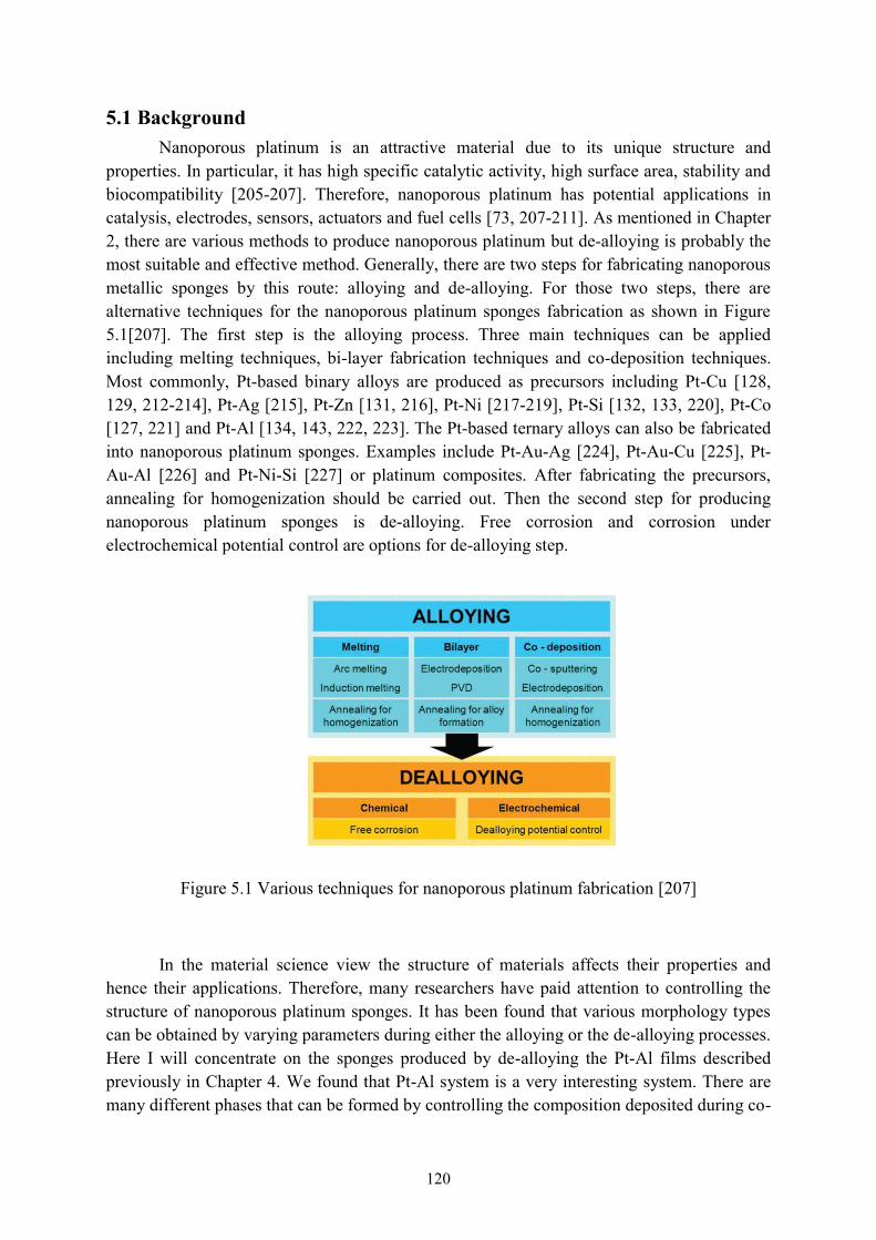
120
5.1 Background Nanoporous platinum is an attractive material due to its unique structure and
properties. In particular, it has high specific catalytic activity, high surface area, stability and biocompatibility [205-207]. Therefore, nanoporous platinum has potential applications in catalysis, electrodes, sensors, actuators and fuel cells [73, 207-211]. As mentioned in Chapter 2, there are various methods to produce nanoporous platinum but de-alloying is probably the most suitable and effective method. Generally, there are two steps for fabricating nanoporous metallic sponges by this route: alloying and de-alloying. For those two steps, there are alternative techniques for the nanoporous platinum sponges fabrication as shown in Figure 5.1[207]. The first step is the alloying process. Three main techniques can be applied including melting techniques, bi-layer fabrication techniques and co-deposition techniques. Most commonly, Pt-based binary alloys are produced as precursors including Pt-Cu [128, 129, 212-214], Pt-Ag [215], Pt-Zn [131, 216], Pt-Ni [217-219], Pt-Si [132, 133, 220], Pt-Co [127, 221] and Pt-Al [134, 143, 222, 223]. The Pt-based ternary alloys can also be fabricated into nanoporous platinum sponges. Examples include Pt-Au-Ag [224], Pt-Au-Cu [225], Pt-Au-Al [226] and Pt-Ni-Si [227] or platinum composites. After fabricating the precursors, annealing for homogenization should be carried out. Then the second step for producing nanoporous platinum sponges is de-alloying. Free corrosion and corrosion under electrochemical potential control are options for de-alloying step.
Figure 5.1 Various techniques for nanoporous platinum fabrication [207]
In the material science view the structure of materials affects their properties and hence their applications. Therefore, many researchers have paid attention to controlling the structure of nanoporous platinum sponges. It has been found that various morphology types can be obtained by varying parameters during either the alloying or the de-alloying processes. Here I will concentrate on the sponges produced by de-alloying the Pt-Al films described previously in Chapter 4. We found that Pt-Al system is a very interesting system. There are many different phases that can be formed by controlling the composition deposited during co-

121
sputtering. Other parameters applied during the alloying and de-alloying processes were also studied.
The Pt-Al binary alloy system was selected for use as the precursor for producing nanoporous platinum by de-alloying. The Pt-Al phase diagram is quite complex with intermetallic compounds including Pt5Al21, Pt8Al21, PtAl2, Pt2Al3, PtAl, , Pt5Al3, Pt2Al and Pt3Al as shown in Figure 5.2 [228]. These compounds have different crystal structures such as cubic, trigonal, tetragonal, hexagonal and orthorhombic, Figure 5.3 [229]. Some metastable phases such as PtAl6, PtAl5, PtAl4, Pt6Al21 and PtAl3 have also been reported [228, 230-234]. For example the tetragonal PtAl5 or phase was found in as-quenched samples [234]. The trigonal PtAl4, or more probably cubic Pt5Al21 as previously reported [229, 230, 235, 236], formed by peritectic reaction at approximately 800 C from PtAl3 while Pt6Al21 phase transforms into Pt5Al21 during heat treatment at 200 C for several hours [230]. Another metastable phase is orthorhombic PtAl6 which can be preserved close to the melting point of the alloy [231]. Besides thermal history, the Pt concentration is also a key factor controlling the formation of PtAl6, PtAl5, PtAl2 and Pt2Al3 intermetallic phases [232].
Figure 5.2 Pt-Al phase diagram [237]
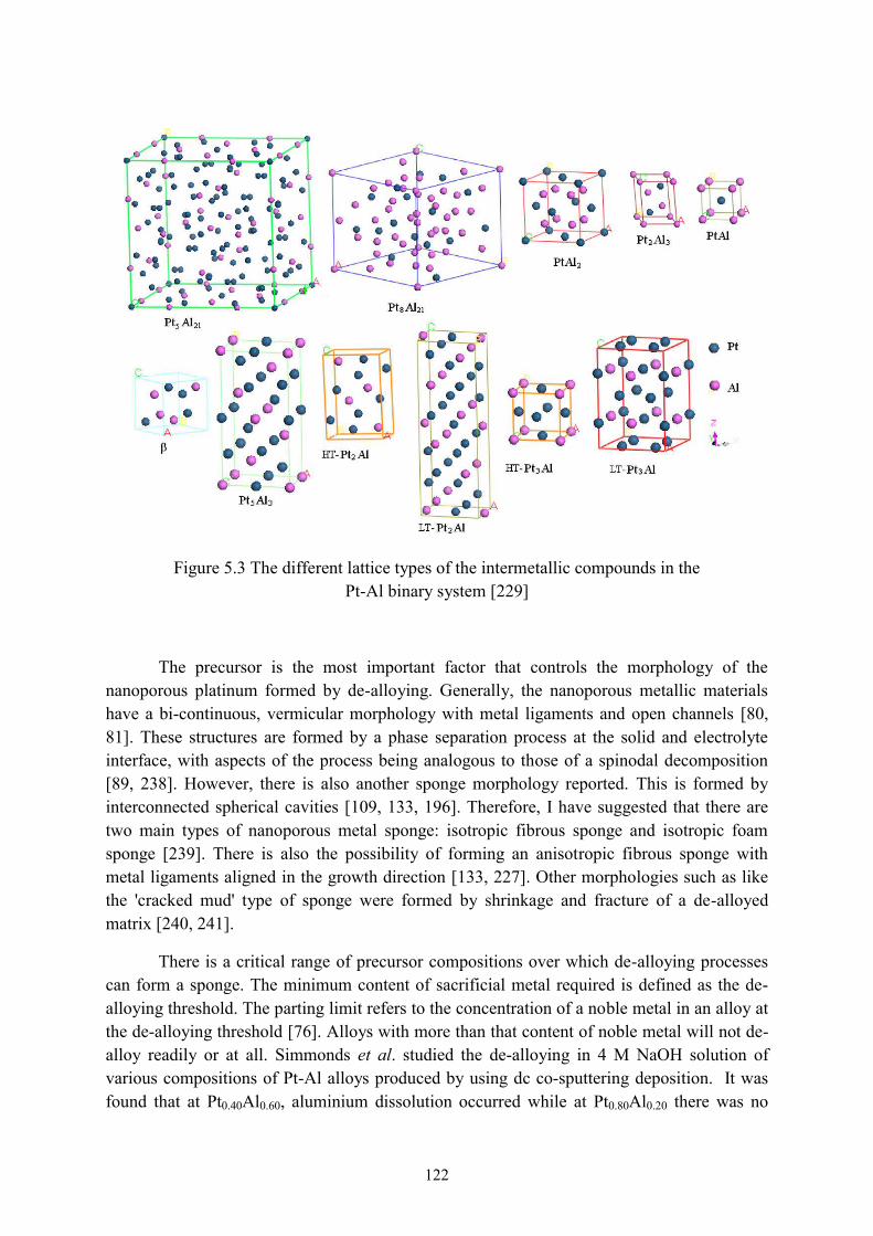
122
Figure 5.3 The different lattice types of the intermetallic compounds in the Pt-Al binary system [229]
The precursor is the most important factor that controls the morphology of the nanoporous platinum formed by de-alloying. Generally, the nanoporous metallic materials have a bi-continuous, vermicular morphology with metal ligaments and open channels [80, 81]. These structures are formed by a phase separation process at the solid and electrolyte interface, with aspects of the process being analogous to those of a spinodal decomposition [89, 238]. However, there is also another sponge morphology reported. This is formed by interconnected spherical cavities [109, 133, 196]. Therefore, I have suggested that there are two main types of nanoporous metal sponge: isotropic fibrous sponge and isotropic foam sponge [239]. There is also the possibility of forming an anisotropic fibrous sponge with metal ligaments aligned in the growth direction [133, 227]. Other morphologies such as like the 'cracked mud' type of sponge were formed by shrinkage and fracture of a de-alloyed matrix [240, 241].
There is a critical range of precursor compositions over which de-alloying processes can form a sponge. The minimum content of sacrificial metal required is defined as the de-alloying threshold. The parting limit refers to the concentration of a noble metal in an alloy at the de-alloying threshold [76]. Alloys with more than that content of noble metal will not de-alloy readily or at all. Simmonds et al. studied the de-alloying in 4 M NaOH solution of various compositions of Pt-Al alloys produced by using dc co-sputtering deposition. It was found that at Pt0.40Al0.60, aluminium dissolution occurred while at Pt0.80Al0.20 there was no

123
evidence of aluminium dissolution occurring [134]. Cortie et al. reported that mesoporous platinum with pores size in range 2 to 20 nm can be produced from PtAlx (x 2) precursor. PtAlx was prepared by co-depositing the elements using high vacuum dc magnetron sputtering, then the film was de-alloyed in 0.5 M NaOH solution [109]. Nahm et al. studied the effect of Al content on nanoporous platinum thin film produced from a Pt-Al precursor. PtxAl1-x (x 0.27, 0.52, and 0.76) were prepared by rf magnetron co-sputtering method. The nanoporous platinum structure was formed by electrochemical dissolution of Al in 0.5 M H2SO4. It was found that Pt0.52Al0.48 showed both enhanced catalytic activity and mechanical stability after 500 cycles[223]. In general, these previous studies have showed that the mole fraction of active metal, A must be more than the parting limit, which is approximately 0.5 [242-244]. A value of A in the range of about 0.65 to 0.88 is most suitable for formation of nanoscale sponges for PtAlx [109, 143, 245].
In addition, however, the different atomic ratios of noble and active metals may result in the formation of different intermetallic phases in the precursor. This may also have an influence on the morphology of sponges. Recently, we published the effect of precursor stoichiometry on the morphology of nanoporous platinum sponges[239]. In this publication we examined whether this control of microstructure can be used to influence the morphology of the nanoporous platinum film formed after de-alloying. For this work I fabricated PtAlx thin film precursors with mole fraction of Al between 0.30 and 0.90 at various deposition temperatures and my experimental work on these samples forms the bulk of the Results section of the present Chapter. It was found that the precursors that had been deposited at elevated temperatures and with mole fraction of Al between 0.65 and 0.90 produced the classic isotropic fibrous sponges. However isotropic foamy sponges can be produced from precursors that were deposited at room temperature. We concluded that the formation of fibrous sponge requires an equilibrated precursor while foamy morphologies will be formed if the precursor is metastable. The effect of increasing Al content ( Al > 0.80) on the structure of sponges is shown in Figure 5.4 [239]. The crystallinity of the Pt sponges decreased when
Al was increased towards 0.88. Furthermore, it has found using in situ X-ray diffraction in a synchrotron experiment that the relative proportion of and PtAl4 depends on the thermal history.
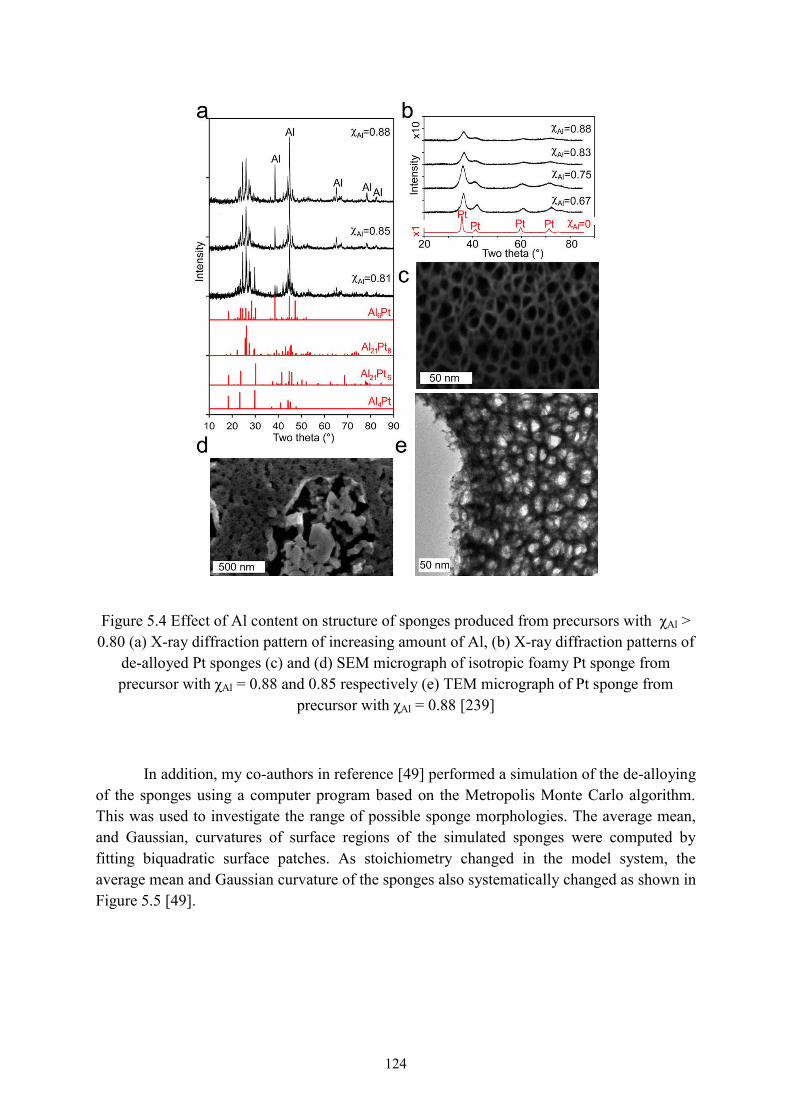
124
Figure 5.4 Effect of Al content on structure of sponges produced from precursors with Al > 0.80 (a) X-ray diffraction pattern of increasing amount of Al, (b) X-ray diffraction patterns of
de-alloyed Pt sponges (c) and (d) SEM micrograph of isotropic foamy Pt sponge from precursor with Al = 0.88 and 0.85 respectively (e) TEM micrograph of Pt sponge from
precursor with Al = 0.88 [239]
In addition, my co-authors in reference [49] performed a simulation of the de-alloying of the sponges using a computer program based on the Metropolis Monte Carlo algorithm. This was used to investigate the range of possible sponge morphologies. The average mean, and Gaussian, curvatures of surface regions of the simulated sponges were computed by fitting biquadratic surface patches. As stoichiometry changed in the model system, the average mean and Gaussian curvature of the sponges also systematically changed as shown in Figure 5.5 [49].

125
Figure 5.5 Simulation of the de-alloying of the sponges by using Monte Carlo model as a function of Al (a) Morphologies of sponges in various aluminium content (b) Ratio of surface
atoms to total atoms of sponges ( ) and Al remaining in sponge. (c) Average mean and Gaussian curvatures of sponges. (d) Effect of Lennard-Jones temperature on the de-alloying
of a starting alloy with Al = 0.80. This work was performed by my co-authors [239]
Apart from the initial alloy composition, other factors including deposition parameters, de-alloying solution and the de-alloying temperatures and times are also able to control the microstructure of nanoporous metals, especially the characteristic size of ligaments and channels [80, 207]. Antoniou et al. synthesized nanoporous platinum through electrochemical de-alloying in HF solution from co-sputtered PtxSi1-x amorphous films. It was found that the three different morphologies of nanoporous platinum could be obtained by varying the deposition parameters including composition and sputter bias conditions. These distinct morphologies are shown in Figure 5.6 as correlated with alloy composition, thickness and sputter bias conditions [133]. Kloke et al. reported the effect of de-alloying solution on ligament size as shown in Figure 5.7. The ligament sizes of different alloy systems and different (alkaline and acidic solutions) de-alloying solutions were compared [207]. Abburi et al. fabricated nanoporous platinum by chemical de-alloying of co-sputtered Pt-Cu films that had been coarsened at various temperatures. It was shown that the coarsening temperature had an influence on the pore size of nanoporous platinum. Pt0.20Cu0.80 de-alloyed in 93%H2SO4 and coarsened at 250, 300,400, and 500 C yielded pore sizes of <5, 5-10, 25 and 35 nm respectively as shown in Figure 5.8. It was also found that the optimum de-alloying time was 15 minutes on 150 nm thick film of Pt0.20Cu0.80 [246].

126
Figure 5.6 Three distinct morphologies of nanoporous platinum as correlated with co-sputtering parameter, initial alloy composition and thickness [133]
Figure 5.7 Effect of de-alloying system on ligament size of nanoporous platinum from different alloy systems (a) ligament sizes of different noble metal-aluminium with de-
alloying with 5% HCl and 20% NaOH and (b) ligament sizes of platinum-gold-copper alloys with varying noble metal content
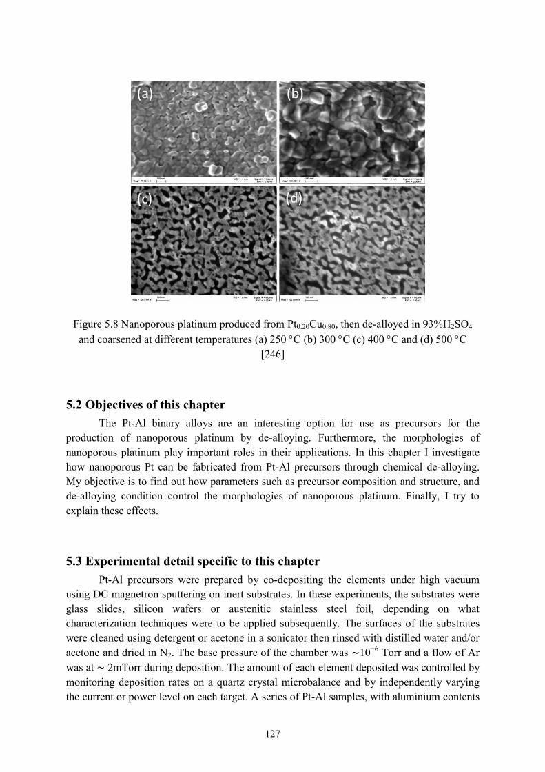
127
Figure 5.8 Nanoporous platinum produced from Pt0.20Cu0.80, then de-alloyed in 93%H2SO4 and coarsened at different temperatures (a) 250 C (b) 300 C (c) 400 C and (d) 500 C
[246]
5.2 Objectives of this chapter The Pt-Al binary alloys are an interesting option for use as precursors for the
production of nanoporous platinum by de-alloying. Furthermore, the morphologies of nanoporous platinum play important roles in their applications. In this chapter I investigate how nanoporous Pt can be fabricated from Pt-Al precursors through chemical de-alloying. My objective is to find out how parameters such as precursor composition and structure, and de-alloying condition control the morphologies of nanoporous platinum. Finally, I try to explain these effects.
5.3 Experimental detail specific to this chapter Pt-Al precursors were prepared by co-depositing the elements under high vacuum
using DC magnetron sputtering on inert substrates. In these experiments, the substrates were glass slides, silicon wafers or austenitic stainless steel foil, depending on what characterization techniques were to be applied subsequently. The surfaces of the substrates were cleaned using detergent or acetone in a sonicator then rinsed with distilled water and/or acetone and dried in N2. The base pressure of the chamber was 10 6 Torr and a flow of Ar was at 2mTorr during deposition. The amount of each element deposited was controlled by monitoring deposition rates on a quartz crystal microbalance and by independently varying the current or power level on each target. A series of Pt-Al samples, with aluminium contents

128
varying from 50 at.% to 98 at.% were prepared. The deposition temperature was at room temperature or 400 C. Some samples, which had been co-deposited at room temperature, were subsequently annealed at temperatures from 100 to 500 C in a tube furnace with N2
flow. De-alloying of selected samples was carried out by immersing those samples in 0.2 M NaOH or 0.2 M Na2CO3 solution. During the de-alloying process, aluminium is removed and bubbles of H2 formed, as illustrated in Figure 5.9. It was assumed that process was complete once bubbling stopped. Pt-Al precursors and de-alloying samples were prepared in various series in order to investigate the effect of processing parameters on morphology of nanoporous platinum. A flowchart of various parameters during sputtering (Al composition control, deposition rate, deposition time, deposition temperature, and annealing temperature) and de-alloying process (de-alloying solution and de-alloying time) for this experiment is displayed in Figure 5.10.
Figure 5.9 De-alloying process on Pt-Al precursor (a) Bubble of H2 on Pt-Al precursor immersing in alkali solution and (b) model of aluminium removing from Pt-Al precursor
[239]
Two sources of X-ray diffraction were used to characterize the samples. The first one was a Siemens D5000 Diffractometer using Cu K radiation ( = 0.154184 nm and the incidence angle was set at 0.5°). The second source was on the powder diffraction beamline at the Australian Synchrotron using a standard flat plate arrangement inside an Anton Paar furnace with an argon atmosphere ( = 0.1261 nm, the incident angle of 2° and beam cross-section 4 mm × 0.2 mm). The morphology of the samples was obtained by imaging on a Zeiss Supra 55VP SEM. Selected precursors and de-alloyed samples were also characterised by TEM (Philips CM120 and, for precise EDS analysis and hi-resolution imaging, on a 200 kV JEOL 2200FS).
5 mm
(a) (b)
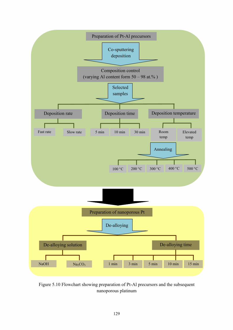
129
Figure 5.10 Flowchart showing preparation of Pt-Al precursors and the subsequent nanoporous platinum
Deposition time Deposition temperature Deposition rate
Fast rate Elevated temp
Room temp
Preparation of Pt-Al precursors
10 min 5 min 30 min
100 C 200 C 300 C 400 C 500 C
Annealing
Co-sputtering deposition
Slow rate
Composition control (varying Al content form 50 – 98 at.% )
Selected samples
De-alloying
Preparation of nanoporous Pt
De-alloying solution De-alloying time
NaOH Na2CO3 1 min 3 min 5 min 10 min 15 min
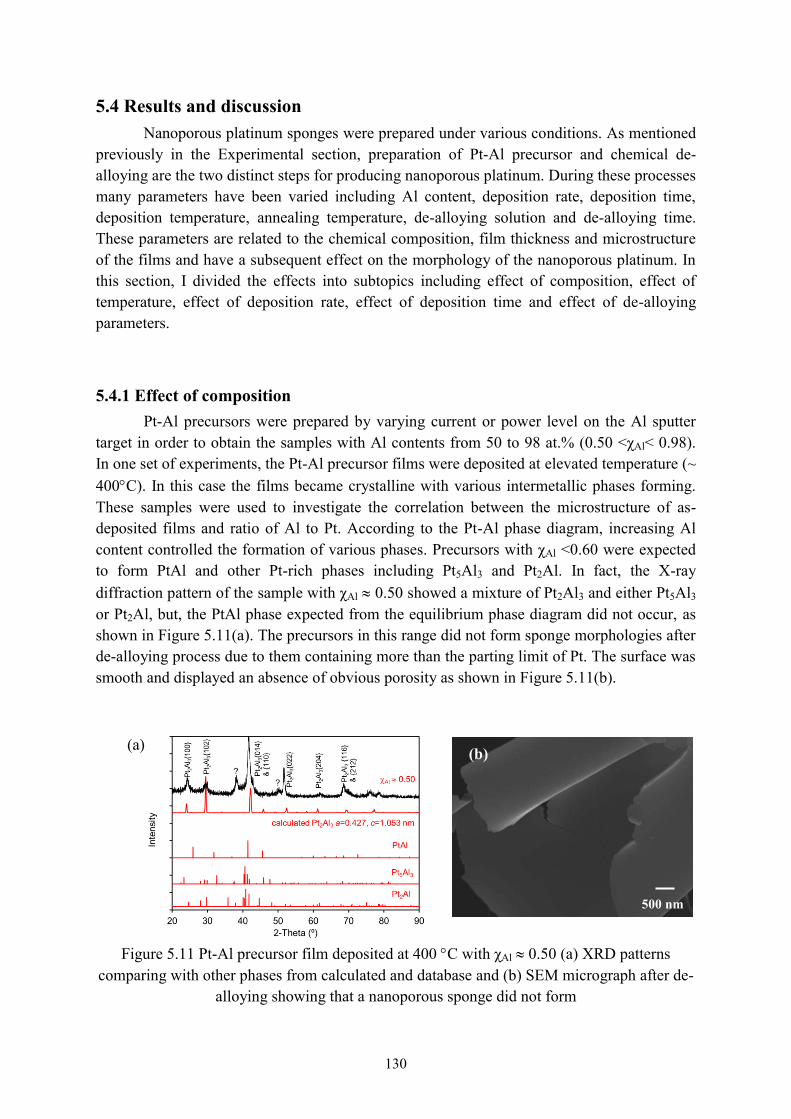
130
5.4 Results and discussion Nanoporous platinum sponges were prepared under various conditions. As mentioned previously in the Experimental section, preparation of Pt-Al precursor and chemical de-alloying are the two distinct steps for producing nanoporous platinum. During these processes many parameters have been varied including Al content, deposition rate, deposition time, deposition temperature, annealing temperature, de-alloying solution and de-alloying time. These parameters are related to the chemical composition, film thickness and microstructure of the films and have a subsequent effect on the morphology of the nanoporous platinum. In this section, I divided the effects into subtopics including effect of composition, effect of temperature, effect of deposition rate, effect of deposition time and effect of de-alloying parameters.
5.4.1 Effect of composition Pt-Al precursors were prepared by varying current or power level on the Al sputter target in order to obtain the samples with Al contents from 50 to 98 at.% (0.50 < Al< 0.98). In one set of experiments, the Pt-Al precursor films were deposited at elevated temperature (~ 400 C). In this case the films became crystalline with various intermetallic phases forming. These samples were used to investigate the correlation between the microstructure of as-deposited films and ratio of Al to Pt. According to the Pt-Al phase diagram, increasing Al content controlled the formation of various phases. Precursors with Al <0.60 were expected to form PtAl and other Pt-rich phases including Pt5Al3 and Pt2Al. In fact, the X-ray diffraction pattern of the sample with Al 0.50 showed a mixture of Pt2Al3 and either Pt5Al3 or Pt2Al, but, the PtAl phase expected from the equilibrium phase diagram did not occur, as shown in Figure 5.11(a). The precursors in this range did not form sponge morphologies after de-alloying process due to them containing more than the parting limit of Pt. The surface was smooth and displayed an absence of obvious porosity as shown in Figure 5.11(b).
Figure 5.11 Pt-Al precursor film deposited at 400 C with Al 0.50 (a) XRD patterns comparing with other phases from calculated and database and (b) SEM micrograph after de-
alloying showing that a nanoporous sponge did not form
(a)
500 nm
(b)
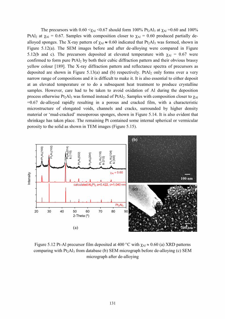
131
The precursors with 0.60 < Al <0.67 should form 100% Pt2Al3 at Al =0.60 and 100% PtAl2 at Al = 0.67. Samples with composition closer to Al = 0.60 produced partially de-alloyed sponges. The X-ray pattern of Al 0.60 indicated that Pt2Al3 was formed, shown in Figure 5.12(a). The SEM images before and after de-alloying were compared in Figure 5.12(b and c). The precursors deposited at elevated temperature with Al = 0.67 were confirmed to form pure PtAl2 by both their cubic diffraction pattern and their obvious brassy yellow colour [189]. The X-ray diffraction pattern and reflectance spectra of precursors as deposited are shown in Figure 5.13(a) and (b) respectively. PtAl2 only forms over a very narrow range of compositions and it is difficult to make it. It is also essential to either deposit at an elevated temperature or to do a subsequent heat treatment to produce crystalline samples. However, care had to be taken to avoid oxidation of Al during the deposition process otherwise Pt2Al3 was formed instead of PtAl2. Samples with composition closer to Al =0.67 de-alloyed rapidly resulting in a porous and cracked film, with a characteristic microstructure of elongated voids, channels and cracks, surrounded by higher density material or ‘mud-cracked’ mesoporous sponges, shown in Figure 5.14. It is also evident that shrinkage has taken place. The remaining Pt contained some internal spherical or vermicular porosity to the solid as shown in TEM images (Figure 5.15).
Figure 5.12 Pt-Al precursor film deposited at 400 C with Al 0.60 (a) XRD patterns comparing with Pt2Al3 from database (b) SEM micrograph before de-alloying (c) SEM
micrograph after de-alloying
(a)
100 nm
(b)
200 nm
(c)

132
Figure 5.13 Pt-Al precursor film deposited at 400 C with Al = 0.67 (a) XRD patterns comparing with Pt2Al3 from database and (b) reflectance spectra
Figure 5.14 ‘Mud-cracked’ sponges produced by de-alloying sample with Al = 0.67 (a) a porous and cracked film (b) cross-sectional view and (c) curled up porous and cracked film at
low magnification
100 (b)
200 nm
(a)
100 nm
(b)
20 m (c)

133
Figure 5.15 TEM micrographs of de-alloyed samples with Al = 0.67
Next I consider precursors in the range 0.67 < Al <0.80. According to the equilibrium phase diagram, there are two mixed phase regions in this range. A mixture of PtAl2 and Pt8Al21 should be formed in range of 0.67 < Al <0.72, and then close to 100% Pt8Al21 at about
Al = 0.73. Another mixed phase region of Pt8Al21 and PtAl4 should be formed in range 0.73 < Al <0.80, followed by close to 100% PtAl4 at about Al = 0.80. In this range, phase formation is complicated due to the possible formation of the metastable intermetallic compounds which were mentioned previously. The precursors with Al = 0.78 formed Pt8Al21 as indicated by XRD patterns comparing with JCPDF database in Figure 5.16(a). The peak marked ‘*’ in the samples deposited at elevated temperature could be due to the metastable phase or (PtAl5) [234]. A sample with Al = 0.75 deposited at room temperature and heated in a synchrotron X-ray diffraction experiment at 3 °C·min 1, crystallized at about 360 °C, Figure 5.16 (b). The peaks were formed in this sample were similar to those reported for phase. The peaks marked ‘V’ in this sample are probably due to Pt8Al21 formation. De-alloying of precursors with 0.67 < Al <0.80 that deposited at elevated temperature produced isotropic fibrous sponges. The morphologies as deposited and de-alloyed are shown in Figure 5.16 (c), (d) and (e).
When the precursors contained Al > 0.80, the microstructure should contain Al with PtAl4[247]. The presence of Al was confirmed by XRD in samples with Al = 0.82, as shown in Figure 5.17(a). However, the most obvious phase in this sample was instead of PtAl4.The precursor with Al = 0.82 still produced classic isotropic fibrous sponges, Figure 5.17 (b) and (c). Finally, the precursors with Al > 0.90 that deposited at elevated temperature were rapidly de-alloyed. There was no sponge formed, but the Pt component formed a disordered and fragile mass. The XRD pattern indicated that PtAl6 and pure Al were formed as shown in Figure 5.18 (a) and the SEM micrograph of the as deposited material also showed the Al crystals before de-alloying process in Figure 5.18 (b). SEM and TEM micrographs of

134
samples de-alloyed from the precursors Al > 0.90 are shown in Figure 5.18 (c) – (e). SEM images showed a low density and disordered mass of very friable Pt and TEM images showed that the filaments of Pt are actually comprised of equiaxed Pt nanocrystals. The Al content of de-alloyed samples was analysed by EDS on TEM. It was found that the Al was of the order of 0.10 to 0.15, in agreement with values in the literature [143, 248]. Evidently, there is always a residual Al content that is encapsulated by Pt.
Figure 5.16 Pt-Al precursor film with 0.67< Al < 0.80 (a) XRD patterns of precursors with Al = 0.78 (deposited at 400 C) and precursors with Al = 0.75 (deposited at room
temperature then crystallized by heating ~400 C), comparing with Pt8Pt21 from database and reported phase (b) crystallization of phase at ~360 C on heating up precursor with Al = 0.75 (c) morphology of Pt-Al precursor with Al = 0.78 as deposited (d) SEM micrograph of isotropic fibrous sponges in plain view and (e) SEM micrograph of isotropic fibrous sponges
in cross-sectional view
(a)
100
200
300
400
500
Tem
pera
ture
(C
)
2-Theta 10 20 30
(b)
100 nm
(c)
100 nm
(d)
100 nm
(e)
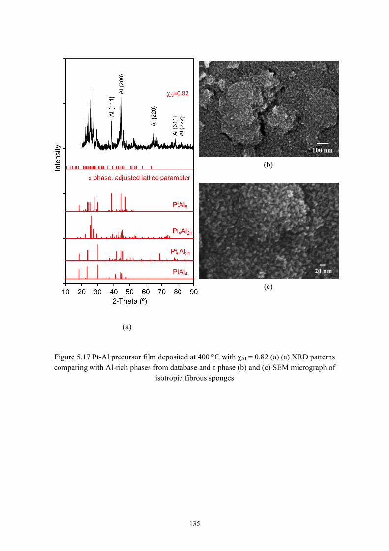
135
Figure 5.17 Pt-Al precursor film deposited at 400 C with Al = 0.82 (a) (a) XRD patterns comparing with Al-rich phases from database and phase (b) and (c) SEM micrograph of
isotropic fibrous sponges
100
(b)
(e)
(a)
100 nm
20 nm
(c)
(b)

136
Figure 5.18 Pt-Al precursor film deposited at 400 C with Al > 0.90 (a) XRD pattern comparing with PtAl6 and Al from database (b) SEM micrograph as deposited (c) SEM
micrograph after de-alloying (d) TEM de-alloying and (e) High resolution TEM after de-alloying
(d) (e)
(a)
200 nm
(b)
200 nm
(c)

137
5.4.2 Effect of temperature In this project, the Pt-Al precursors were prepared using deposition either at elevated
temperature (~ 400 C) or at room temperature. The precursor films deposited at elevated temperature were previously discussed in the section on the effect of composition. In the present section I compare what happens when similar compositions are deposited instead at room temperature. The situation for precursor films that had been deposited at room temperature but then annealed (prior to de-alloying) at various temperatures between 100 C and 500 C is also discussed.
Effect of deposition temperature The most noticeable difference was that, while the Pt-Al precursor films deposited at
elevated temperature were crystalline with a variety of phases present, those deposited at room temperature were nearly amorphous. However in both cases, samples with Al <0.60 de-alloyed rather slowly, with a slow production of H2 bubbles and they did not form sponges. It was previously mentioned that, in the case of the crystalline samples, there was a marked change in sponge morphology at compositions close to Al = 0.67. According to equilibrium phase diagram, the crystalline Pt-Al precursors should have been 100% PtAl2 at Al = 0.67 and, indeed, the brassy yellow PtAl2 phase would have been expected to have formed at elevated temperature [109, 249]. However, samples with the 1Pt:2Al composition that had been produced at room temperature were not crystalline as shown Figure 5.19. Furthermore, de-alloying of these samples produced a different kind of sponge from the porous and cracked film made from crystalline samples of this composition. Instead, the precursors with
Al = 0.67 that had been deposited at room temperature produced partially de-alloyed ‘pinhole’ sponges as shown in Figure 5.20 (a). A cross-sectional view down one of the cavities in the film is shown in Figure 5.20 (b).
Figure 5.19 XRD patterns of the precursors were deposited at room temperature with Al = 0.67
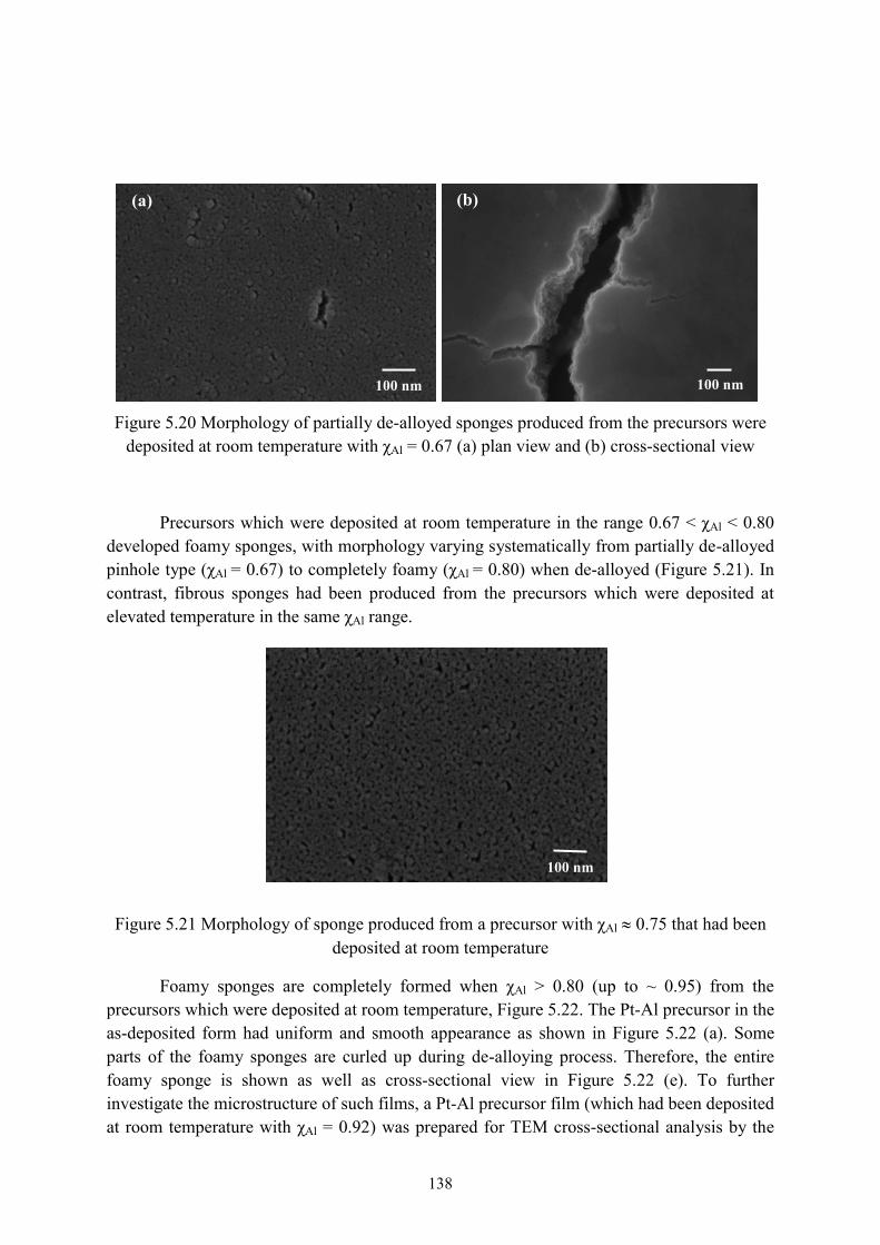
138
Figure 5.20 Morphology of partially de-alloyed sponges produced from the precursors were deposited at room temperature with Al = 0.67 (a) plan view and (b) cross-sectional view
Precursors which were deposited at room temperature in the range 0.67 < Al < 0.80 developed foamy sponges, with morphology varying systematically from partially de-alloyed pinhole type ( Al = 0.67) to completely foamy ( Al = 0.80) when de-alloyed (Figure 5.21). In contrast, fibrous sponges had been produced from the precursors which were deposited at elevated temperature in the same Al range.
Figure 5.21 Morphology of sponge produced from a precursor with Al 0.75 that had been deposited at room temperature
Foamy sponges are completely formed when Al > 0.80 (up to ~ 0.95) from the precursors which were deposited at room temperature, Figure 5.22. The Pt-Al precursor in the as-deposited form had uniform and smooth appearance as shown in Figure 5.22 (a). Some parts of the foamy sponges are curled up during de-alloying process. Therefore, the entire foamy sponge is shown as well as cross-sectional view in Figure 5.22 (e). To further investigate the microstructure of such films, a Pt-Al precursor film (which had been deposited at room temperature with Al = 0.92) was prepared for TEM cross-sectional analysis by the
100 nm
(a)
100 nm
(b)
100 nm

139
sandwich technique. Elemental mapping in the TEM of this sample showed that the film was homogenous in composition. Evidently, it had formed a solid solution during deposition at room temperature (Figure 5.23 and Figure 5.24).
Figure 5.22 Morphology of Pt-Al precursors, deposited at room temperature with Al > 0.80 (a) as deposited (b) Al 0.83 after de-alloying (c) Al 0.88 after de-alloying (d) Al 0.96
after de-alloying and (e) curled up porous Pt sponge and shown cross-sectional view
100 nm
(a)
100 nm
(b)
100 nm
(e)
(c)
100 nm
(d)
100 nm

140
Figure 5.23 TEM mapping on Pt-Al precursors, deposited at room temperature with Al = 0.92
Figure 5.24 TEM-EDS analysis through the cross-sectional area of Pt-Al precursors, deposited at room temperature with Al = 0.92. The presence of Cu is due to redeposited
materials during PIPS
Similarly to the precursors deposited at elevated temperature, the Al content of samples deposited at room temperature also had an influence on the pore size of the sponges. When Al content was increased, the pore sizes of the sponges also became larger. The pore size distribution of nanoporous Pt that had been produced from Pt-Al precursors with different mole fractions of Al are compared in Figure 5.25. The average pore size in nanoporous Pt that had been produced from Pt-Al precursors with Al = 0.83 was 14.4 ± 1.8 nm, that of Pt-Al precursors with Al = 0.88 was 18.0 ± 4.9 nm nd that of Pt-Al precursors with Al = 0.96 was 35.6 ±4.9 nm. Furthermore, TEM micrographs of sponge from precursors
100 nm

141
with Al 0.88, Figure 5.26, show that Pt is in the form of a continuous and low density filament network that surrounds the voids.
Figure 5.25 Distribution of pore sizes from Pt-Al precursor with different mole fraction of Al (a) Al = 0.83 (b) Al = 0.88 and (c) Al = 0.96
(d
100
(c)

142
Figure 5.26 TEM micrograph of sponge formed from precursor with Al 0.88 (a) a continuous network of Pt surrounding the void and (b) lattice fringe image at high resolution
Effect of annealing The Pt-Al precursor films that had been deposited at room temperature produced isotropic foamy sponges when de-alloyed. This type of sponge is noticeably different in appearance to the isotropic fibrous sponges produced from precursors deposited at elevated temperature. In this section, I investigate the effect of post-deposition (but pre-de-alloying) annealing temperatures from 100 C to 500 C applied to selected samples produced by deposition at room temperature. These were the same compositions that produced foamy sponges when de-alloyed directly from the as-deposited (at room temperature) condition. It was found that the samples with Al > 0.80 which were deposited at room temperature and then heated above 400 °C crystallized to form the same phases ( phase and Al) as the samples with Al > 0.80 deposited at elevated temperature. The XRD patterns of samples with
Al > 0.80, which were deposited at room temperature and then heated 400 °C and 500 °C were compared with the sample with Al = 0.82 which was deposited at elevated temperature as shown in Figure 5.27. The morphologies of the sponges stayed foamy as the annealing temperature was raised, but it was noticeable that the pore size became quite bimodal, Figure 5.28. Probably Al-rich regions were formed during the crystallization which was nearly completely dissolved away during the de-alloying process leaving the large voids observed.
(a) (b)
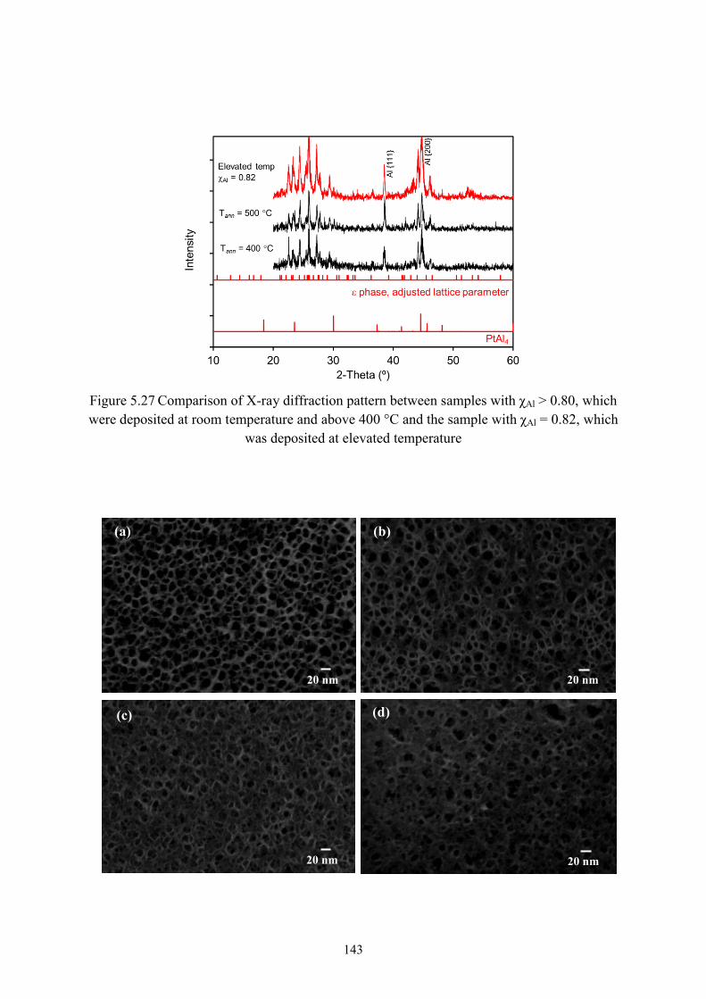
143
(a)
20 nm
Figure 5.27 Comparison of X-ray diffraction pattern between samples with Al > 0.80, which were deposited at room temperature and above 400 °C and the sample with Al = 0.82, which
was deposited at elevated temperature
20 nm
(c)
20 nm
(b)
(d)
20 nm
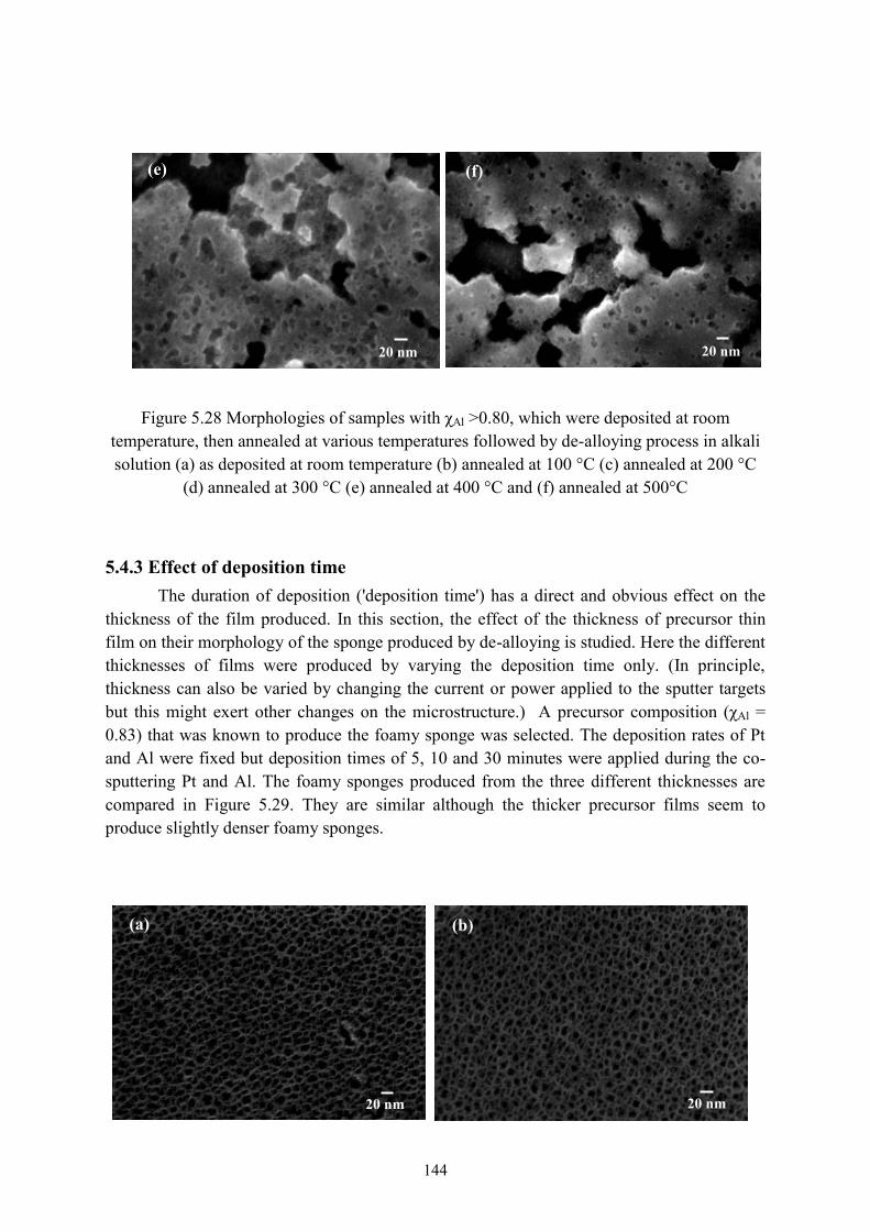
144
Figure 5.28 Morphologies of samples with Al >0.80, which were deposited at room temperature, then annealed at various temperatures followed by de-alloying process in alkali solution (a) as deposited at room temperature (b) annealed at 100 °C (c) annealed at 200 °C
(d) annealed at 300 °C (e) annealed at 400 °C and (f) annealed at 500°C
5.4.3 Effect of deposition time The duration of deposition ('deposition time') has a direct and obvious effect on the thickness of the film produced. In this section, the effect of the thickness of precursor thin film on their morphology of the sponge produced by de-alloying is studied. Here the different thicknesses of films were produced by varying the deposition time only. (In principle, thickness can also be varied by changing the current or power applied to the sputter targets but this might exert other changes on the microstructure.) A precursor composition ( Al = 0.83) that was known to produce the foamy sponge was selected. The deposition rates of Pt and Al were fixed but deposition times of 5, 10 and 30 minutes were applied during the co-sputtering Pt and Al. The foamy sponges produced from the three different thicknesses are compared in Figure 5.29. They are similar although the thicker precursor films seem to produce slightly denser foamy sponges.
20 nm
(e)
20 nm
(f)
20 nm
(a) (b)
20 nm

145
Figure 5.29 Morphologies of samples with Al =0.83, which were deposited at room temperature with various deposition times (a) 5 minutes (b) 10 minutes and (c) 30 minutes
5.4.4 Effect of deposition rate In this section, the deposition rates of the two elements were controlled by adjusting power or current on each target to obtain the appropriate composition. Previously, the current level of Pt target was fixed and only the current levels of aluminium were varied. In this section I also varied the rate of deposition of Pt (by controlling the current on the Pt target) to see if that had any effect on the morphology of the foamy sponges. A series of Pt-Al precursors was deposited at room temperature with twice the current (fast rate, 0.050 A) for comparing to those samples that had been deposited at room temperature formerly (slow rate, 0.025 A). The deposition rate of Pt did not affect the precursors with Al < 0.60 since they hardly de-alloyed anyway and these samples will not be discussed further. Samples with compositions closer to Al = 0.60 started producing partially de-alloyed pinhole sponges and developed increasingly more open sponges until the composition approached Al = 0.70, as shown in Figure 5.30 (a), (b) and (c). These samples also show that the de-alloying process is not uniform over the surface and that there appears to be preferential attack and penetration into the alloy along grain boundaries in Figure 5.30 (d).
The precursors which were deposited at room temperature with a high deposition rate of Pt, start to produce true foamy sponges when Al > 0.70. The surface of such a precursor in the as-deposited state is smooth, dense and featureless. After de-alloying, foamy sponges were formed, with the sponge morphology becoming more pronounced when Al contents were increased. SEM micrographs show the development of foamy sponges from Al 0.71, 0.74 and 0.77 in Figure 5.31 (a), (b) and (c) respectively. The interior of this latter foamy sponge is revealed within the crack in Figure 5.31 (d).
(c)
20 nm

146
Figure 5.30 Pinhole sponge produced from precursors that deposited at room temperature with high deposition rate of Pt in various Al contents (a) Al 0.62 (b) Al 0.67 and (c) Al
0.69 and (d) preferential dissolution along grain boundaries
(a)
100 nm
(b)
100 nm
(c)
100 nm
(d)
200 nm
(a)
20 nm
(b)
20 nm
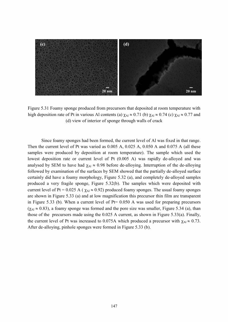
147
Figure 5.31 Foamy sponge produced from precursors that deposited at room temperature with high deposition rate of Pt in various Al contents (a) Al 0.71 (b) Al 0.74 (c) Al 0.77 and
(d) view of interior of sponge through walls of crack
Since foamy sponges had been formed, the current level of Al was fixed in that range. Then the current level of Pt was varied as 0.005 A, 0.025 A, 0.050 A and 0.075 A (all these samples were produced by deposition at room temperature). The sample which used the lowest deposition rate or current level of Pt (0.005 A) was rapidly de-alloyed and was analysed by SEM to have had Al 0.98 before de-alloying. Interruption of the de-alloying followed by examination of the surfaces by SEM showed that the partially de-alloyed surface certainly did have a foamy morphology, Figure 5.32 (a), and completely de-alloyed samples produced a very fragile sponge, Figure 5.32(b). The samples which were deposited with current level of Pt = 0.025 A ( Al 0.92) produced foamy sponges. The usual foamy sponges are shown in Figure 5.33 (a) and at low magnification this precursor thin film are transparent in Figure 5.33 (b). When a current level of Pt= 0.050 A was used for preparing precursors ( Al 0.83), a foamy sponge was formed and the pore size was smaller, Figure 5.34 (a), than those of the precursors made using the 0.025 A current, as shown in Figure 5.33(a). Finally, the current level of Pt was increased to 0.075A which produced a precursor with Al 0.73. After de-alloying, pinhole sponges were formed in Figure 5.33 (b).
(c)
20 nm
(d)
20 nm
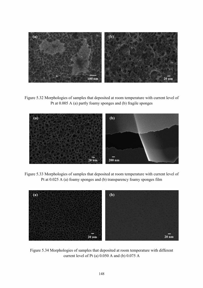
148
Figure 5.32 Morphologies of samples that deposited at room temperature with current level of Pt at 0.005 A (a) partly foamy sponges and (b) fragile sponges
Figure 5.33 Morphologies of samples that deposited at room temperature with current level of Pt at 0.025 A (a) foamy sponges and (b) transparency foamy sponges film
Figure 5.34 Morphologies of samples that deposited at room temperature with different current level of Pt (a) 0.050 A and (b) 0.075 A
(a)
100 nm
(b)
20 nm
(a)
20 nm
(b)
200 nm
20 nm
(b) (a)
20 nm

149
5.4.5 Effect of de-alloying parameters Previously, I examined the effect of varying process parameters during the co-
sputtering deposition. In this section, I focus on the effect of varying the de-alloying parameters. De-alloying solution and de-alloying time were the two obvious parameters to investigate. Selected precursors that produced foamy sponges were immersed in two different de-alloying solutions. Alkaline solutions are usually used for the fabrication of nanoporous metals by de-alloying Al-based alloy precursors. Here I used 0.2 M sodium hydroxide (NaOH) and 0.2 M sodium carbonate (Na2CO3) as de-alloying solutions. NaOH solution is strongly basic while Na2CO3 solutions are weakly basic. Using Na2CO3 for de-alloying Pt-Al precursor took a longer time than for NaOH because the dissolution rate of Al slower in Na2CO3 than in NaOH [250]. However, the morphologies of foamy sponges produced by de-alloying using either NaOH or Na2CO3 are similar as shown in Figure 5.35. For the slower dissolution rate of Al in Na2CO3 it became possible to consider the optimal de-alloying time. The dissolution rate is very high in the beginning of immersion, followed by a period of reduced activity, caused perhaps by the formation of a protective layer of Pt or H2 bubbles. After that, the protective layer was slowly removed. A series of foamy sponges from precursors that had been deposited at room temperature with Al = 0.92, then de-alloyed by using Na2CO3 with different de-alloying times (1, 3, 5, 10 and 15 minutes) are shown in Figure 5.36. In general, however, all the sponges have a similar appearance.
Figure 5.35 Foamy sponges produced from precursors that deposited at room temperature with Al = 0.96, then de-alloying by different solutions (a) 0.2M NaOH and (b) 0.2M Na2CO3
(a)
100 nm
(b)
100 nm
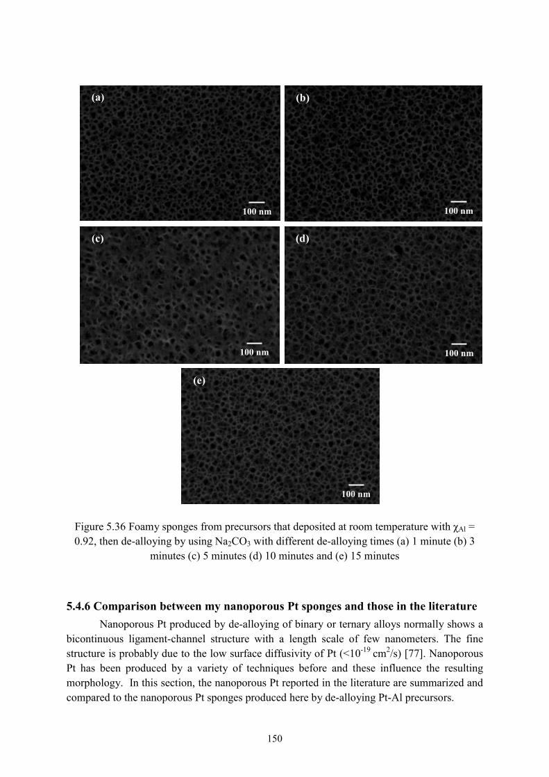
150
Figure 5.36 Foamy sponges from precursors that deposited at room temperature with Al = 0.92, then de-alloying by using Na2CO3 with different de-alloying times (a) 1 minute (b) 3
minutes (c) 5 minutes (d) 10 minutes and (e) 15 minutes
5.4.6 Comparison between my nanoporous Pt sponges and those in the literature Nanoporous Pt produced by de-alloying of binary or ternary alloys normally shows a bicontinuous ligament-channel structure with a length scale of few nanometers. The fine structure is probably due to the low surface diffusivity of Pt (<10-19 cm2/s) [77]. Nanoporous Pt has been produced by a variety of techniques before and these influence the resulting morphology. In this section, the nanoporous Pt reported in the literature are summarized and compared to the nanoporous Pt sponges produced here by de-alloying Pt-Al precursors.
(a)
100 nm
(b)
100 nm
(c)
100 nm
(d)
100 nm
(e)
100 nm
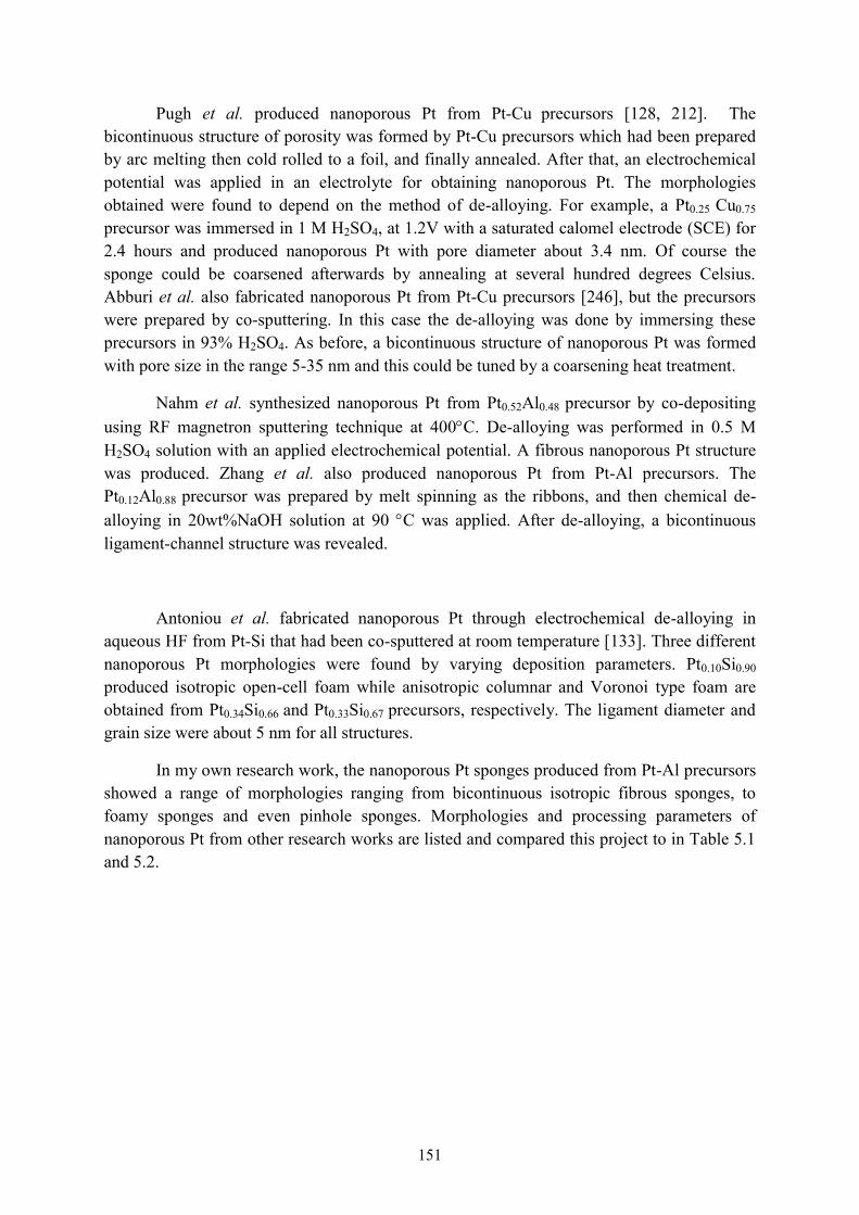
151
Pugh et al. produced nanoporous Pt from Pt-Cu precursors [128, 212]. The bicontinuous structure of porosity was formed by Pt-Cu precursors which had been prepared by arc melting then cold rolled to a foil, and finally annealed. After that, an electrochemical potential was applied in an electrolyte for obtaining nanoporous Pt. The morphologies obtained were found to depend on the method of de-alloying. For example, a Pt0.25 Cu0.75 precursor was immersed in 1 M H2SO4, at 1.2V with a saturated calomel electrode (SCE) for 2.4 hours and produced nanoporous Pt with pore diameter about 3.4 nm. Of course the sponge could be coarsened afterwards by annealing at several hundred degrees Celsius. Abburi et al. also fabricated nanoporous Pt from Pt-Cu precursors [246], but the precursors were prepared by co-sputtering. In this case the de-alloying was done by immersing these precursors in 93% H2SO4. As before, a bicontinuous structure of nanoporous Pt was formed with pore size in the range 5-35 nm and this could be tuned by a coarsening heat treatment.
Nahm et al. synthesized nanoporous Pt from Pt0.52Al0.48 precursor by co-depositing using RF magnetron sputtering technique at 400 C. De-alloying was performed in 0.5 M H2SO4 solution with an applied electrochemical potential. A fibrous nanoporous Pt structure was produced. Zhang et al. also produced nanoporous Pt from Pt-Al precursors. The Pt0.12Al0.88 precursor was prepared by melt spinning as the ribbons, and then chemical de-alloying in 20wt%NaOH solution at 90 C was applied. After de-alloying, a bicontinuous ligament-channel structure was revealed.
Antoniou et al. fabricated nanoporous Pt through electrochemical de-alloying in aqueous HF from Pt-Si that had been co-sputtered at room temperature [133]. Three different nanoporous Pt morphologies were found by varying deposition parameters. Pt0.10Si0.90
produced isotropic open-cell foam while anisotropic columnar and Voronoi type foam are obtained from Pt0.34Si0.66 and Pt0.33Si0.67 precursors, respectively. The ligament diameter and grain size were about 5 nm for all structures.
In my own research work, the nanoporous Pt sponges produced from Pt-Al precursors showed a range of morphologies ranging from bicontinuous isotropic fibrous sponges, to foamy sponges and even pinhole sponges. Morphologies and processing parameters of nanoporous Pt from other research works are listed and compared this project to in Table 5.1 and 5.2.

152
Table 5.1 List of nanoporous Pt produced by other research works
Composition Precursor preparation De-alloying process Morphology Reference
Pt0.25 Cu0.75 Arc melting/cold rolled /annealing
De-alloying potential control in 1 M H2SO4 at 1.2 V SCE for 2.4 hours
Pugh 2003 [128]
Pt0.25 Cu0.75 Arc melting/cold rolled /annealing De-alloying potential control in 1 M H2SO4 at 1.2 V SCE for 2.4 hours/ heat treatment at 500 °C for 60 minutes
Pugh 2003 [128]
Pt0.20Cu0.80 Arc melting/cold rolled /annealing De-alloying potential control in 1 M HClO4 at 1.24 V NHE for 20 hours/ heat treatment at 800 °C for 15 minutes
Pugh 2005 [212]
Pt0.20Cu0.80
Arc melting/cold rolled /annealing De-alloying potential control in 1 M H2SO4 at 0.692 V with NHE for 24 hours / heat treatment at 500 °C for 30 minute
Pugh 2005 [212]

153
Table 5.1 List of nanoporous Pt produced by other research works (cont.)
Composition Precursor preparation De-alloying process Morphology Reference
Pt0.20 Cu0.80 Co-sputtering technique
Free corrosion in 93% H2SO4/ heat treatment at 400 C
Abburi 2012 [246]
Pt0.33 Al0.67 Co-depositing using dc magnetron sputtering technique at 400 C
Free corrosion in 0.5 M NaOH
Cortie 2006 [109]
Pt0.52Al0.48 Co-depositing using rf magnetron sputtering technique at 400 C
De-alloying potential control in 0.5 M H2SO4
Nahm 2009 [223]
Pt0.12Al0.88 Melt spinning Free corrosion in 20wt%NaOH solution at 90 C
Zhang 2009 [143]
(d)
100
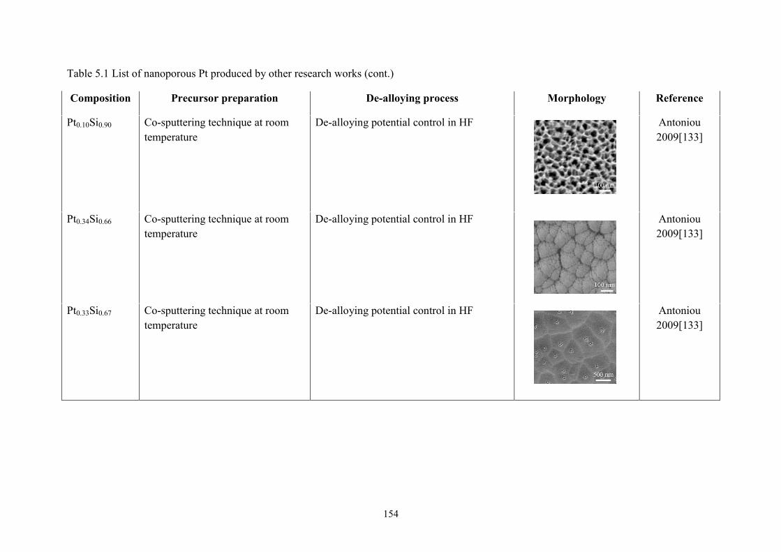
154
Table 5.1 List of nanoporous Pt produced by other research works (cont.)
Composition Precursor preparation De-alloying process Morphology Reference
Pt0.10Si0.90 Co-sputtering technique at room temperature
De-alloying potential control in HF
Antoniou 2009[133]
Pt0.34Si0.66 Co-sputtering technique at room temperature
De-alloying potential control in HF
Antoniou 2009[133]
Pt0.33Si0.67 Co-sputtering technique at room temperature
De-alloying potential control in HF
Antoniou 2009[133]
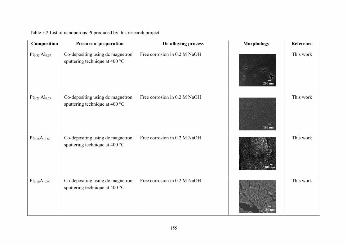
155
Table 5.2 List of nanoporous Pt produced by this research project
Composition Precursor preparation De-alloying process Morphology Reference
Pt0.33 Al0.67 Co-depositing using dc magnetron sputtering technique at 400 C
Free corrosion in 0.2 M NaOH
This work
Pt0.22 Al0.78 Co-depositing using dc magnetron sputtering technique at 400 C
Free corrosion in 0.2 M NaOH
This work
Pt0.18Al0.82 Co-depositing using dc magnetron sputtering technique at 400 C
Free corrosion in 0.2 M NaOH
This work
Pt0.10Al0.90 Co-depositing using dc magnetron sputtering technique at 400 C
Free corrosion in 0.2 M NaOH
This work
100 nm
200 nm
100 nm
100 nm

156
Table 5.2 List of nanoporous Pt produced by this research project (cont.)
Composition Precursor preparation De-alloying process Morphology Reference
Pt0.12 Al0.88 Co-depositing using dc magnetron sputtering technique at room temperature (current level =0.025 A for Pt)
Free corrosion in 0.2 M NaOH or Na2CO3
This work
Pt0.04 Al0.96 Co-depositing using dc magnetron sputtering technique at room temperature (current level =0.025 A for Pt)
Free corrosion in 0.2 M NaOH or Na2CO3
This work
Pt0.31Al0.69 Co-depositing using dc magnetron sputtering technique at room temperature (current level =0.050 A for Pt)
Free corrosion in 0.2 M NaOH or Na2CO3
This work
Pt0.23Al0.77 Co-depositing using dc magnetron sputtering technique at room temperature (current level =0.050 A for Pt)
Free corrosion in 0.2 M NaOH or Na2CO3
This work
100 nm
20 nm
200 nm
100 nm
157
5.5 Conclusion Nanoporous platinum has received considerable attention due to its various
applications, real or potential, in catalysis, biomedical stimulation electrodes, sensors, mechanical actuators and fuel cells. There are several methods by which it can be prepared and in each of these there are a range of process parameters that can be adjusted. In this project, nanoporous platinum was fabricated by first making Pt-Al precursors by co-deposition using dc magnetron sputtering under high vacuum and the de-alloying them using alkaline solutions. The properties of nanoporous platinum are very likely to be closely related to their microstructure. Therefore I have examined the ways in which process parameters might control the characteristics of nanoporous platinum. It was discovered stoichiometry of the precursor is the primary controlling factor, followed by the temperature at which it had been deposited. The stoichiometry controls which phases form which in turn has an effect on the sponge morphology. The effect of the Al content can be summarized into discrete intervals:
(i) Precursors with Al < 0.60 did not form sponges either after deposition at elevated or room temperature,
(ii) Precursors with Al = 0.67 and deposited at elevated temperature produced 'mud-cracked' mesoporous sponges,
(iii) Precursors with 0.67< Al < 0.90 at produced at elevated temperature produced classic isotropic fibrous sponges. In this range, the complex phases including Al-rich phases such as Pt8Al21 and meta-stable phase ( phase or PtAl5) were formed.
(iv) Precursors with Al > 0.90 produced a disordered and fragile mass instead of a mechanical robust sponge. Also, these precursors contained a mixture between PtAl6 and pure Al.
(v) Precursors that had been deposited at room temperature produced different morphologies of Pt sponges to those that had been deposited at elevated temperature.
(vi) In the room temperature case, the sponge morphology changed from pinhole to unusual isotropic foamy sponges in the range 0.67 < Al <0.96.
(vii) Precursors which had been deposited at room temperature are amorphous and become crystalline after annealing at 400-500 C. De-alloying of such heat-treated samples still produced foamy sponges but some oxide formation occurred on the surface during heat treatment process.
(viii) The deposition rate of noble metal, Pt in this case, has influence on the characteristics of nanoporous platinum sponges. At high deposition rate of Pt, the precursors with 0.60 < Al < 0.70 produce pinhole sponge type. When the precursors with Al > 0.70 isotropic foamy sponges started to form.

158
Chapter 6
Conclusions and future work

159
Precious metal alloys and their intermetallic compounds have some unique technological properties. They find applications in fields as varied as dentistry, medicine, electronics and electrical technology, and catalysis. In addition, the gold- and platinum-based materials are highly valued for use in jewellery and decorative applications due to the combination of their corrosion resistance, appearance, ductility and rarity. Although there are many interesting precious metal alloys and compounds, in this present research project I focused on the gold - platinum - aluminium system. The overall motivation of this present research work is first to better understand the binary and ternary phase relationships within this ternary system and second to investigate how methods of fabrication might be optimized to enhance their properties.
The results can be divided into two parts:
In the first part I investigated coloured intermetallic compounds of AuAl2 and PtAl2, mainly for jewellery applications. There may, however, be some other applications for coatings of these materials as well, for example spectrally-selective coatings for AuAl2 and corrosion or oxidation resistant coatings for PtAl2.
The second part of the project was on platinum-aluminium intermetallic compounds for making nanoporous platinum sponges, and on the sponges themselves. These sponges have great potential in catalyst and sensor applications.
I used physical vapour deposition in both parts of the project to make most of my samples. Specifically, I used direct current magnetron co-sputtering in a vacuum system to fabricate thin films of the alloys and intermetallic compounds of this project. Part of this project involved a systematic investigation of the deposition conditions and post-deposition heat treatments. The films were characterized in terms of their microstructures and properties by various techniques including X-ray diffraction (using both a laboratory instrument and a synchrotron), scanning electron microscopy, and transmission electron microscopy with energy dispersive spectroscopy. The optical properties of these intermetallic compounds were observed by spectrophotometry and ellipsometry. Computer modelling was also used for investigating their optical properties. In this present chapter I present a summary of the overall conclusions of my project. The most promising aspects for future work are also suggested.
6.1 The AuAl2-PtAl2 system The coloured intermetallic compounds AuAl2 and PtAl2 have the CaF2 (also
designated as cF12) crystal structure. They are of practical and scientific interest because of their unique colours (purple and yellow respectively) which are completely different from the colours of their components.
Gold and platinum have the same fcc structure and have similar electronegativity and atomic diameter so might be expected to exhibit unlimited mutual solubility. However, their binary phase diagram shows that they are, in fact, nearly mutually insoluble, at least under

160
equilibrium conditions. There is no ternary phase diagram of Au-Pt-Al available in the literature and therefore the relationship between AuAl2 and PtAl2 was unknown. For these reasons, two interesting issues were raised (i) whether AuAl2 and PtAl2 are mutually soluble, or not, and (ii) whether solid solutions or mixed microstructures of these two compounds could be used to tune the colour between purple and yellow end-points.
The first task of this part of the investigation was to develop means to fabricate pure AuAl2 and PtAl2 thin films by co-sputtering techniques. Due to the very narrow ranges of stability in their binary phase diagrams this required tight control of the appropriate composition. The aluminium content should be about 66-67 at.% in order to form these coloured intermetallic compounds. Their compositions were controlled by setting the appropriate current or power level during sputtering. Pure AuAl2 and PtAl2 thin films were successfully fabricated. These coloured intermetallic compound thin films were then compared with bulk samples of PtAl2 and AuAl2 that had been produced by melting pure gold or platinum with aluminium in a vacuum arc furnace by an outside organization.
The compositions and lattice parameters of the AuAl2 films and bulk samples were very similar. The reflectance curves of AuAl2 of both thin films and bulk samples were similar but the film sample had a stronger colour because it had a slightly higher reflection in the violet and red regions, and less reflection in the green. However, the microstructures of the two different forms of AuAl2 sample were completely different. The AuAl2 bulk sample showed a dendritic structure with some segregation of aluminium while the AuAl2 thin film was dense and homogeneous.
The chemical compositions and lattice parameters of the thin film and bulk PtAl2 samples were also reasonably similar. The reflectance curves of PtAl2 for both thin films and bulk samples were similar too except that the film sample showed a small shift in the absorption relative to bulk PtAl2. The microstructures of these two samples were similar, being relatively homogenous with a very fine structure.
The measured optical properties of these coloured intermetallic compounds were used in simulations in order to show the range of colours that could be obtained in these films by varying their thicknesses.
The second task of this part of the investigation was to design and fabricate multilayer structures in order to explore the interesting issues mentioned above. Bi-layer and multi-layer films of coloured intermetallic compounds were prepared in various arrangements. Bi-layer films of PtAl2/AuAl2 and AuAl2/PtAl2 seem to be nearly mutually insoluble after post-deposition heat treatment. Multi-layer films of Au, Pt and Al with a stack formed by depositing pure metals were also fabricated. It was found in this case that separate domains of AuAl2 and PtAl2 were formed after post-deposition heat treatment. From this result, it is clear that, when two coloured intermetallic compounds are formed separately, they do not interdiffuse later. A stack formed by co-depositing Au and Pt followed by Al was another strategy that was followed for this investigation. As mentioned, Au and Pt are immiscible under equilibrium conditions at temperatures below 1260 °C, nevertheless a metastable
161
mutual solid solution of these two compounds may be prepared by magnetron sputtering. The co-deposited film of 54 at.%Au and 46 at.%Pt film formed a solid solution with a lattice parameter of 0.4006 nm which lies between that of the pure Au films (0.4077 nm) and the pure Pt films (0.3935 nm). After post-deposition heat-treatment this metastable film reacted with the layer of Al to form a metastable solid solution of (Au,Pt)Al2. This solid solution had optical properties intermediate between those of AuAl2 and PtAl2.
An alternate strategy for tuning the colour was to form very thin film stacks of pure AuAl2 and pure PtAl2. Provided that the layers are so thin that light can penetrate through the top layer, then some mixing of the colours is possible. Similar hues can be obtained by this means as with the metastable (Au,Pt)Al2 solid solutions. Overall, the present work has shown that the composition and colour of the coatings can be controlled by deposition and heat-treatment parameters, and that the desired phases (AuAl2, PtAl2 or (Au,Pt)Al2) can be produced as required.
This work has shown that the use of thin films of the coloured intermetallic compounds might be an alternative approach for the jewellery industry. The use of thin films solves the problem of the bulk intermetallic compounds being very brittle, and it solves a potential caratage problem in the case of the PtAl2 : this is because PtAl2 (78.3 wt.% Pt) has too low a Pt content to satisfy the usual industry standards of 90 or 95wt.% Pt. However, if PtAl2 is applied together with conventional Pt alloys the composite item will still be hallmarkable as Pt. Thus there is no limitation for item design in this case. This is less of a problem for AuAl2 because that contains 75.8 wt.% Au, which already satisfies the popular 18 carat (75 wt.% Au) standard. Nevertheless, even 22 carat (91.7 wt.% Au) items can benefit from the inclusion of thin films of AuAl2 by this means.
Finally, this work has shown that a range of interesting colour effects can be obtained by two different strategies: metastable films of (Au,Pt)Al2 and stacks of very thin films of AuAl2 and PtAl2. The incorporation of other coloured intermetallic compounds could be considered in any future work on this subject.
6.2 Nanoporous platinum sponges A variety of metals such as gold, nickel, copper etc. can be prepared in meso- or
nanoporous forms. Nanoporous platinum is one of the most interesting of the nanoporous metals because of its catalytic properties and hence numerous applications. The binary alloys and intermetallic compounds of the Pt-Al system are attractive candidates to use as precursors for fabricating nanoporous platinum by the de-alloying method. In the present work Pt-Al precursors were prepared by co-deposition using dc magnetron sputtering and this was followed by de-alloying in alkaline solutions. The aim of this part of the research was to discover how parameters (during either precursor preparation or de-alloying) control the morphologies of the resulting nanoporous platinum. In particular I sought to discover what the factor was that changed the sponge morphology from the usual fibrous type reported by most other investigators to the foamy type usually produced in our research group.
162
X-ray diffraction, either with a laboratory instrument or the Australian Synchrotron, was used to characterize the precursors. Scanning electron microscope and transmission electron microscope with elemental analysis were also used to examine selected precursors and de-alloyed samples.
It was found that stoichiometry of the precursor and the deposition temperature played an important role in controlling the nanoporous platinum sponge morphology. The Pt-Al stoichiometry and the temperature controlled which phases formed and hence sponge morphology after de-alloying. If Al is the mole fraction of Al then the situation in respect of stoichiometry and deposition temperature can be summarized as follows:
Precursors with Al < 0.60 did not form sponges either after deposition at elevated temperature or at room temperature. Their content of Al is below the ‘parting limit’. Precursors with Al = 0.67 and deposited at elevated temperature produced 'mud-cracked' mesoporous sponges while precursors with 0.67< Al < 0.90 produced at elevated temperature produced classic isotropic fibrous sponges. In this range, Pt8Al21 and meta-stable phase ( phase or PtAl5), which are complex phases with Al-rich phases, were formed. When precursors with Al > 0.90 were dealloyed then a disordered and fragile mass of Pt sponge was obtained. These precursors contained a mixture between PtAl6 and pure Al. The deposition temperature is another important parameter effecting morphologies of platinum sponges. It was discovered that precursors that had been deposited at room temperature produced very different morphologies to those that had been deposited at elevated temperature. In the precursors that had been deposited at room temperature, the sponge morphology changed from pinhole to unusual isotropic foamy sponges in the range 0.67 < Al <0.96. The precursors which had been deposited at room temperature are amorphous and after heat treatment at more than 400 C they became crystalline. After de-alloying these heat treated and crystalline samples, foamy sponges are still produced but some oxide formations appeared on the surface.
Finally, the deposition rate of noble metal also has an influence on the morphology of sponges. At high deposition rates of Pt, the precursors with 0.60 < Al < 0.70 produced pinhole sponge types while isotropic foamy sponges started to form at the precursors with Al > 0.70.
No actual testing of the catalytic power of these sponges was done in the present project. This would be a good thing to follow up with in future work. The present work has shown that fabrication of a Pt-Al precursor followed by de-alloying might be an alternative option for producing nanoporous platinum for catalytic, optical and electrochemical applications. This process may be less complex than currently available methods and it offers the prospect of obtaining various morphologies by controlling processing parameters. Other properties of these sponges including mechanical, optical, sensing, actuation, electrical, thermal and magnetic properties should be considered in future investigations. It is also obvious that this method could be applied to produce sponges from other binary or ternary alloy systems.

163
References 1. Grimwade, M., Introduction to Precious Metals. 2009, Maine, USA: Brynmorgen
Press. 2. Keefe, J.C., A brief introduction to precious metals. The AMMTIAC Quarterly, 2007.
2(1): p. 9-14. 3. Robertson, A.R., Precious Metals and Their Uses, Preciuos Metals, Properties and
Selection: Nonferrous Alloys and Special-Purpose Materials, in ASM Handbook. 1990, ASM International. p. 688-698.
4. Petkov, K., et al., Efficient LBM visual simulation on face-centered cubic lattices. Visualization and Computer Graphics, IEEE Transactions on, 2009. 15(5): p. 802-814.
5. Klotz, U.E., Metallurgy and processing of coloured gold intermetallics – Part I: Properties and surface processing. Gold Bulletin, 2010. 43(4-10).
6. Bühner, J.F., A. Basso, and M. Poliero, Metallurgy and processing of coloured gold intermetallics – Part II: Investment casting and related alloy design. Gold Bulletin, 2010. 43(1): p. 11-20.
7. Wittstock, A., J. Biener, and J. Erlebacher, Nanoporous Gold: From an Ancient Technology to a High-Tech Material. 2012: Royal Society of Chemistry.
8. Sauthoff, G., Intermetallics. Materials Science and Technology. 2006: Wiley-VCH Verlag GmbH & Co. KGaA.
9. Sauthoff, G., Intermetallics. Ullmann's Encyclopedia of Industrial Chemistry. 2000: Wiley-VCH Verlag GmbH & Co. KGaA.
10. Brumby, A., et al., Silver, Silver Compounds, and Silver Alloys, in Ullmann's Encyclopedia of Industrial Chemistry. 2000, Wiley-VCH Verlag GmbH & Co. KGaA.
11. Fieberg, M., H. Renner, and G. Schlamp, Silver, Gold, and Other Noble Metals, in digital Encyclopedia of Applied Physics. 2003, WILEY-VCH Verlag GmbH & Co KGaA.
12. Renner, H., et al., Gold, Gold Alloys, and Gold Compounds, in Ullmann's Encyclopedia of Industrial Chemistry. 2000, Wiley-VCH Verlag GmbH & Co. KGaA.
13. Russell, A.M. and K.L. Lee, Cu, Ag, and Au, in Structure-Property Relations in Nonferrous Metals. 2005, John Wiley & Sons, Inc. p. 302-336.
14. Gafner, G., The development of 990 gold-titanium, and its production, use, and properties. Journal of the Southern African Institute of Mining and Metallurgy, 1989. 89(6): p. 173-181.
15. Rapson, W.S., The metallurgy of the coloured carat gold alloys. Gold Bulletin, 1990. 23(4): p. 125-134.
16. Renner, H., et al., Platinum Group Metals and Compounds, in Ullmann's Encyclopedia of Industrial Chemistry. 2000, Wiley-VCH Verlag GmbH & Co. KGaA.
17. ElGuindy, M., Platinum Group Metals: Alloying, Properties, and Applications, in Encyclopedia of Materials: Science and Technology, K.H.J. Buschow, et al., Editors. 2001, Elsevier: Oxford. p. 7117-7121.
18. Knosp, H., M. Nawax, and M. Stumke, Dental gold alloys : Composition, properties and applications. Gold Bulletin, 1981. 14(2): p. 57-64.
19. Shiraishi, T., et al., Optical properties and microstructures of Pd-free Ag–Au–Pt–Cu dental alloys. Journal of Materials Science, 2009. 44(11): p. 2796-2804.

164
20. Shiraishi, T., et al., Optical properties of Au-Pt and Au-Pt-In alloys. Gold Bulletin, 2001. 34(4): p. 129-133.
21. Shiraishi, T., et al., Variations of color with alloying elements in Pd-free Au-Pt-based high noble dental alloys. Materials Science and Engineering: B, 2007. 140(3): p. 147-152.
22. Lansdown, A.B.G., Silver I: its antibacterial properties and mechanism of action. Journal of wound care, 2002. 11(4): p. 125-130.
23. Shukla, M.K., et al., Synthesis and characterization of agar-based silver nanoparticles and nanocomposite film with antibacterial applications. Bioresource Technology, 2012. 107(0): p. 295-300.
24. Pricker, S., Medical uses of gold compounds: Past, present and future. Gold Bulletin, 1996. 29(2): p. 53-60.
25. Keel, T., R. Holliday, and T. Harper, Gold for good : Gold and nanotechnology in the age of innovation. 2010, World Gold Council: London. p. 1-20.
26. Seymour, R.J. and J. O'Farrelly, Platinum-Group Metals, in Kirk-Othmer Encyclopedia of Chemical Technology. 2000, John Wiley & Sons, Inc.
27. Cowley, A. and B. Woodward, A healthy future: Platinum in medical applications. Platinum Metals Review, 2011. 55(2): p. 98-107.
28. Serway, R.A., Principles of Physics. second edition ed. 1998: Saunders College Pub. 954.
29. Renner, H., Precious Metals, in Alloys, F. Habashi, Editor. 1998, Wiley-VCH Verlag GmbH. p. 223-241.
30. Corrigan, D.A., Silver, in Van Nostrand's Scientific Encyclopedia. 2005, John Wiley & Sons, Inc.
31. Cohn, J.G., E.W. Stern, and S.F. Etris, Gold and Gold Compounds, in Kirk-Othmer Encyclopedia of Chemical Technology. 2000, John Wiley & Sons, Inc.
32. Libby, L., Platinum and Platinum Group, in Van Nostrand's Scientific Encyclopedia. 2005, John Wiley & Sons, Inc.
33. Gasteiger, H.A. and N.M. Markovi , Just a dream—or future reality? Science, 2009. 324(5923): p. 48-49.
34. Muroi, T., Role of Precious Metal Catalysts, in Noble Metals Y.-H. Su, Editor. 2012: Available from: http://www.intechopen.com/books/noble-metals/role-of-preciousmetal-catalysts.
35. Callister, W.D., Materials Science and Engineering: An Introduction. 7th ed. 2007: John Wiley & Sons Canada, Limited.
36. Hunt, R.W.G., R. Pointer, and M. Pointer, Measuring Colour. 2011: Wiley. 37. Shevell, S.K., The Science of Color. 2003: Elsevier Science. 38. CIE L* a* b* Color Space [cited 2014 2014/05/25]; Available from:
http://www.shopkmsa.com. 39. Rivory, J., Comparative study of the electronic structure of noble-metal-noble-metal
alloys by optical spectroscopy. Physical Review B, 1977. 15(6): p. 3119. 40. Roberts, E.F.I., K.M. Clarke, and R. Hunt, Optical properties of alloys. Materials
Science and Engineering, 1980. 42: p. 71-80. 41. Vishnubhatla, S.S. and J.P. Jan, Optical properties of the intermetallic compounds
AuAl2, AuGa2 and AuIn2. Philosophical Magazine, 1967. 16(139): p. 45 - 50. 42. Kim, K.J., et al., Optical properties and electronic structures of the intermetallic
compounds AuGa2and PtGa2. Physical Review B, 1990. 42(14): p. 8813. 43. Wang, H., et al., Cu Nanoshells: Effects of Interband Transitions on the Nanoparticle
Plasmon Resonance. The Journal of Physical Chemistry B, 2005. 109(39): p. 18218-18222.

165
44. Stokes, N., A.M. McDonagh, and M.B. Cortie, Preparation of nanoscale gold structures by nanolithography. Gold Bulletin, 2007. 40(4): p. 310-320.
45. Blaber, M.G., et al., Plasmon absorption in nanospheres: A comparison of sodium, potassium, aluminium, silver and gold. Physica B-Condensed Matter, 2007. 394(2): p. 184-187.
46. Blaber, M.G., M.D. Arnold, and M.J. Ford, A review of the optical properties of alloys and intermetallics for plasmonics Journal of Physics: Condensed Matter 2010. 22(14): p. 3201.
47. Alayoglu, S., et al., Ru-Pt core-shell nanoparticles for preferential oxidation of carbon monoxide in hydrogen. Nature Materials, 2008. 7(4): p. 333 - 338.
48. Bracey, C.L., P.R. Ellis, and G.J. Hutchings, Application of copper–gold alloys in catalysis: current status and future perspectives. Chemical Society Reviews, 2009. 38: p. 2231-2243.
49. Habas, S.E., et al., Shaping binary metal nanocrystals through epitaxial seeded growth. Nature Materials, 2007. 6: p. 692-697.
50. Habrioux, A., et al., Activity of platinum gold alloys for glucose electrooxidation in biofuel cells. The Journal of Physical Chemistry B, 2007. 111(34): p. 10329-10333.
51. Lee, Y.W., et al., One-step synthesis of Au@Pd core shell nanooctahedron. Journal of the American Chemical Society, 2009. 131(47): p. 17036-17037.
52. Yan, J.M., et al., One-step seeding growth of magnetically recyclable Au@Co core shell nanoparticles: highly efficient catalyst for hydrolytic dehydrogenation of ammonia borane. Journal of the American Chemical Society, 2010. 132(15): p. 5326-532.
53. Murray, J.L., Alloy Phase Diagrams. ASM Handbook. Vol. 3. 2002, Materials Park, Ohio: ASM Materials International.
54. Bond, G.C., The electronic structure of platinum-gold alloy particles. Platinum Metals Review, 2007. 51(2): p. 63-68.
55. Xiao, S., et al., Size effect on alloying ability and phase stability of immiscible bimetallic nanoparticles. European Physical Journal B 2006. 54(4): p. 479-484.
56. Fernandez, C.D., et al., Coupling between magnetic and optical properties of stable Au-Fe solid solution nanoparticles. Nanotechnology, 2010. 21(16): p. 165701.
57. Yasuda, H. and H. Mori, Effect of cluster size on the chemical ordering in nanometer-sized Au-75at%Cu alloy clusters. Zeitschrift für Physik D Atoms, Molecules and Clusters, 1996. 37: p. 181-186.
58. Morriss, R.H. and L.F. Collins, Optical properties of multilayer colloids. Journal of Chemical Physics 1964. 41: p. 3357.
59. Rodriguez-Gonzalez, B., et al., Multishell bimetallic AuAg nanoparticles: synthesis, structure and optical properties. Journal of Materials Chemistry, 2005. 15(17): p. 1755-1759.
60. Poole, R.T., The colour of the noble metals. Physics Education, 1983. 18(6): p. 280. 61. Nobel metals color chart. [cited 2013 2013/08/21]; Available from:
http://www.jwestdesigns.com/nobelmetals/metalcolorchart.html. 62. Leuser, J., Üder die Bensonderheiten der Edelmetallegierungen im Schmuckgewerbe.
Metall, 1949. 3(7-8): p. 105-110. 63. Saeger, K.E. and J. Rodies, The colour of gold and its alloys: The mechanism of
variation in optical properties. Gold Bulletin, 1977. 10(1): p. 10-14. 64. Cretu, C. and L. Van der, Elma Coloured gold alloys. Gold Bulletin, 1999. 32(4): p.
115-126. 65. Henderson, S. and D. Manchanda, White gold alloys: Colour measurement and
grading. Gold Bulletin, 2005. 38(2): p. 55-67.
166
66. Yu, J., et al., Nanoporous metals by dealloying multicomponent metallic glasses. Chemistry of Materials, 2008. 20(14): p. 4548-4550.
67. Wolff, I.M., Precious Metal Compounds, in Intermetallic Compounds - Principles and Practice-Volume 3 : Progress, J.H. Westbrook and R.L. Fleischer, Editors. 2002, John Wiley & Sons, Ltd.
68. Steinemann, S.G., W. Wolf, and R. Podloucky, Colour and Optical Properties, in Intermetallic Compounds - Principles and Practice-Volume 3 : Progress, J.H. Westbrook and R.L. Fleischer, Editors. 2002, John Wiley & Sons, Ltd.
69. Cortie, M., et al., Spangold: A jewellery alloy with an innovative surface finish. Gold Technology, 1994(4): p. 30-36.
70. Bhatia, V.K., et al., The aluminium-copper-gold ternary system. Gold Bulletin, 2009. 42(3): p. 201-208.
71. Muldawer, L., Spectral reflectivity as a function of temperature of beta -Brass type alloys. Physical Review, 1962. 127(5): p. 1551.
72. Ding, Y. and M. Chen, Nanoporous metals for catalytic and optical applications. MRS Bulletin, 2009. 34(08): p. 569-576.
73. Zhang, J. and C.M. Li, Nanoporous metals: Fabrication strategies and advanced electrochemical applications in catalysis, sensing and energy systems. Chemical Society Reviews, 2012. 41(21): p. 7016-7031.
74. Lu, G.Q. and G.X.S. Zhao, Nanoporous Materials: Science and Engineering. 2004: Imperial College Press.
75. Zhao, X.S., et al., Templating methods for preparation of porous structures. Journal of Materials Chemistry, 2006. 16(7): p. 637-648.
76. Xu, Q., Nanoporous Materials: Synthesis and Applications. 2013: Taylor & Francis. 77. Ding, Y. and Z. Zhang, Nanoporous Metals, in Springer Handbook of Nanomaterials,
R. Vajtai, Editor. 2013, Springer Berlin Heidelberg. p. 779-818. 78. Newman, R.C., et al., Alloy corrosion. MRS Bulletin, 1999. 24(07): p. 24-28. 79. Weissmüller, J., et al., Nanoporous metals by alloy corrosion: Formation and
mechanical properties. MRS Bulletin, 2009. 34(08): p. 577-586. 80. Vajtai, R., Springer Handbook of Nanomaterials. 2013: Springer. 81. Forty, A.J., Corrosion micromorphology of noble metal alloys and depletion gilding.
Nature, 1979. 282(5739): p. 597-598. 82. Pickering, H.W. and P.R. Swann, Electron metallography of chemical attack upon
some alloys susceptible to stress corrosion cracking. Corrosion, 1963. 19(11): p. 373t-389t.
83. Chen, J.S., M. Salmeron, and T.M. Devine, Intergranular and transgranular stress corrosion cracking of Cu-30Au. Corrosion Science, 1993. 34(12): p. 2071-2097.
84. Parks Jr, B.W., J.D. Fritz, and H.W. Pickering, The difference in the electrochemical behavior of the ordered and disordered phases of Cu3Au. Scripta Metallurgica, 1989. 23(6): p. 951-956.
85. Moffat, T.P., F.R.F. Fan, and A.J. Bard, Electrochemical and scanning tunneling microscopic study of dealloying of Cu3Au. Journal of The Electrochemical Society, 1991. 138(11): p. 3224-3235.
86. Ateya, B.G., J.D. Fritz, and H.W. Pickering, Kinetics of dealloying of a copper 5 atomic percent gold alloy. Journal of The Electrochemical Society, 1997. 144(8): p. 2606-2613.
87. Morrish, R., K. Dorame, and A.J. Muscat, Formation of nanoporous Au by dealloying AuCu thin films in HNO3. Scripta Materialia, 2011. 64(9): p. 856-859.
167
88. Shulga, O.V., et al., Preparation and characterization of porous gold and its application as a platform for immobilization of acetylcholine esterase. Chemistry of Materials, 2007. 19(16): p. 3902-3911.
89. Erlebacher, J., et al., Evolution of nanoporosity in dealloying. Nature, 2001. 410(6827): p. 450-453.
90. Fujita, T., et al., Three-dimensional morphology of nanoporous gold. Applied Physics Letters, 2008. 92(25).
91. Newman, R.C. and K. Sieradzki, Corrosion science. MRS Bulletin, 1999. 24(07): p. 12-15.
92. Corcoran, S.G., D.G. Wiesler, and K. Sieradzki, An in situ small angle neutron scattering investigation of Ag0.7Au0.3 dealloying under potential control. MRS Online Proceedings Library, 1996. 451: p. 93-98.
93. Senior, N.A. and R.C. Newman, Synthesis of tough nanoporous metals by controlled electrolytic dealloying. Nanotechnology, 2006. 17(9): p. 2311.
94. Xu, C., et al., Low temperature CO oxidation over unsupported nanoporous gold. Journal of the American Chemical Society, 2007. 129(1): p. 42-43.
95. Chen-Wiegart, Y.-C.K., et al., Effect of Ag–Au composition and acid concentration on dealloying front velocity and cracking during nanoporous gold formation. Acta Materialia, 2013. 61(15): p. 5561-5570.
96. Lee, K.J., et al., Structural evolution of Ag–Au nanoplates by pH controlled galvanic displacement. Current Applied Physics, 2012. 12, Supplement 2: p. S53-S58.
97. Lu, X., et al., Dealloying of Au–Ag thin films with a composition gradient: Influence on morphology of nanoporous Au. Thin Solid Films, 2007. 515(18): p. 7122-7126.
98. Seker, E., M.L. Reed, and M.R. Begley, A thermal treatment approach to reduce microscale void formation in blanket nanoporous gold films. Scripta Materialia, 2009. 60(6): p. 435-438.
99. Oppenheim, I.C., et al., In situ scanning tunneling microscopy of corrosion of silver-gold alloys. Science, 1991. 254(5032): p. 687-689.
100. Sieradzki, K. and R.C. Newman, Alloying silver and gold; applying electrochemical potential. 1990, Google Patents.
101. Liu, Z., et al., Electrocatalytic oxidation of d-glucose at nanoporous Au and Au–Ag alloy electrodes in alkaline aqueous solutions. Electrochimica Acta, 2009. 54(28): p. 7286-7293.
102. Qian, L.H. and M.W. Chen, Ultrafine nanoporous gold by low-temperature dealloying and kinetics of nanopore formation. Applied Physics Letters, 2007. 91(8): p. 083105-1-3.
103. Qian, L.H., et al., Surface Enhanced Raman scattering of nanoporous gold: Smaller pore sizes stronger enhancements. Applied Physics Letters, 2007. 90(15): p. 153120-1-3.
104. Wang, D., J. Ihlemann, and P. Schaaf, Complex patterned gold structures fabricated via laser annealing and dealloying. Applied Surface Science, 2014. 302: p. 74-78.
105. Huang, J.F. and I.W. Sun, Fabrication and surface functionalization of nanoporous gold by electrochemical alloying/dealloying of Au–Zn in an ionic liquid, and the self-assembly of L-cysteine monolayers. Advanced Functional Materials, 2005. 15(6): p. 989-994.
106. Jia, F., et al., Nanoporous metal (Cu, Ag, Au) films with high surface area: General fabrication and preliminary electrochemical performance. The Journal of Physical Chemistry C, 2007. 111(24): p. 8424-8431.

168
107. Dong, H. and X. Cao, Nanoporous gold thin film: Fabrication, structure evolution, and electrocatalytic activity. The Journal of Physical Chemistry C, 2009. 113(2): p. 603-609.
108. Cortie, M.B., A.I. Maaroof, and G.B. Smith, Electrochemical capacitance of mesoporous gold. Gold Bulletin, 2005. 38(1): p. 14-22.
109. Cortie, M.B., et al., Nanoscale coatings of AuAlx and PtAlx and their mesoporous elemental derivatives. Current Applied Physics, 2006. 6(3): p. 440-443.
110. Zhang, Z., et al., Nanoporous gold ribbons with bimodal channel size distributions by chemical dealloying of Al Au alloys. The Journal of Physical Chemistry C, 2009. 113(4): p. 1308-1314.
111. Zhang, Q., et al., A benign route to fabricate nanoporous gold through electrochemical dealloying of Al–Au alloys in a neutral solution. Electrochimica Acta, 2009. 54(26): p. 6190-6198.
112. Wang, X., et al., Dealloying of single-phase Al2Au to nanoporous gold ribbon/film with tunable morphology in inorganic and organic acidic media. Applied Surface Science, 2012. 258(22): p. 9073-9079.
113. Evanoff, D.D. and G. Chumanov, Synthesis and optical properties of silver nanoparticles and arrays. A European Journal of Chemical Physics and Physical Chemistry, 2005. 6(7): p. 1221-1231.
114. Morrish, R. and A.J. Muscat, Nanoporous silver with controllable optical properties formed by chemical dealloying in supercritical CO2. Chemistry of Materials, 2009. 21(16): p. 3865-3870.
115. Zhang, W.Y., et al., Porous metals and metallic foams, in MetFoam 2007: Porous metals and metallic foams : Proceedings of the fifth international conference on porous metals and metallic foams, L.P. Lefebvre, J. Banhart, and D.C. Dunand, Editors. 2008, DEStech Publications Incorporated: Montreal Canada.
116. Wang, X., et al., Influence of alloy composition and dealloying solution on the formation and microstructure of monolithic nanoporous silver through chemical dealloying of Al Ag alloys. The Journal of Physical Chemistry C, 2009. 113(30): p. 13139-13150.
117. Xu, C., et al., Dealloying to nanoporous silver and its implementation as a template material for construction of nanotubular mesoporous bimetallic nanostructures. A European Journal of Chemical Physics and Physical Chemistry, 2010. 11(15): p. 3320-3328.
118. Kim, M.-S. and H. Nishikawa, Fabrication of nanoporous silver and microstructural change during dealloying of melt-spun Al–20 at.%Ag in hydrochloric acid. Journal of Materials Science, 2013. 48(16): p. 5645-5652.
119. Song, T.T., et al., Microstructure and phase evolution during the dealloying of bi-phase Al–Ag alloy. Corrosion Science, 2013. 68: p. 256-262.
120. Detsi, E., et al., Fine-tuning the feature size of nanoporous silver. Crystal Engineering Communications 2012. 14(17): p. 5402-5406.
121. Qiu, H., et al., Dealloying Ag–Al Alloy to prepare nanoporous silver as a substrate for surface-enhanced raman scattering: Effects of structural evolution and surface modification. A European Journal of Chemical Physics and Physical Chemistry, 2011. 12(11): p. 2118-2123.
122. Spassov, T., et al., Mechanochemical synthesis, thermal stability and selective electrochemical dissolution of Cu–Ag solid solutions. Journal of Alloys and Compounds, 2009. 478(1–2): p. 232-236.
123. Li, G., et al., Nanoporous Ag prepared from the melt-spun Cu-Ag alloys. Solid State Sciences, 2011. 13(7): p. 1379-1384.

169
124. Yeh, F.-H., et al., Formation of porous silver by electrochemical alloying/dealloying in a water-insensitive zinc chloride-1-ethyl-3-methyl imidazolium chloride ionic liquid. The Journal of Physical Chemistry B, 2006. 110(11): p. 5215-5222.
125. Su, L. and Y.X. Gan, Nanoporous Ag and Ag–Sn anodes for energy conversion in photochemical fuel cells. Nano Energy, 2012. 1(1): p. 159-163.
126. Luechinger, N.A., S.G. Walt, and W.J. Stark, Printable nanoporous silver membranes. Chemistry of Materials, 2010. 22(17): p. 4980-4986.
127. Pickering, H.W. and Y.S. Kim, De-alloying at elevated temperatures and at 298 k-similarities and differences. Corrosion Science, 1982. 22(7): p. 621-635.
128. Pugh, D.V., A. Dursun, and S.G. Corcoran, Formation of nanoporous platinum by selective dissolution of Cu from Cu0.75Pt0.25. Journal of Materials Research, 2003. 18(01): p. 216-221.
129. Liu, H., et al., High surface area nanoporous platinum: facile fabrication and electrocatalytic activity. Nanotechnology, 2006. 17(9): p. 2167.
130. Xu, Q., et al., Facile fabrication of nanoporous platinum by alloying–dealloying process and its application in glucose sensing. Sensors and Actuators B: Chemical, 2012. 173: p. 716-723.
131. Huang, J.-F. and I.W. Sun, Formation of nanoporous platinum by selective anodic dissolution of PtZn surface alloy in a lewis acidic zinc chloride-1-ethyl-3-methylimidazolium chloride ionic liquid. Chemistry of Materials, 2004. 16(10): p. 1829-1831.
132. Thorp, J.C., et al., Formation of nanoporous noble metal thin films by electrochemical dealloying of PtxSi1 x. Applied Physics Letters, 2006. 88(3).
133. Antoniou, A., et al., Controlled nanoporous Pt morphologies by varying deposition parameters. Applied Physics Letters, 2009. 95(7).
134. Simmonds, M.C., et al., The observation of a threshold in the de-alloying of sputter-deposited PtxAl1-x alloy thin films. Corrosion Science, 1998. 40(1): p. 43-48.
135. Hakamada, M. and M. Mabuchi, Fabrication of nanoporous palladium by dealloying and its thermal coarsening. Journal of Alloys and Compounds, 2009. 479(1–2): p. 326-329.
136. Hakamada, M. and M. Mabuchi, Preparation of nanoporous palladium by dealloying: Anodic polarization behaviors of Pd-M (M=Fe, Co, Ni) alloys. Materials Transcations, 2009. 50(3): p. 431-435.
137. Hakamada, M. and M. Mabuchi, Fabrication, microstructure, and properties of nanoporous Pd, Ni, and their alloys by dealloying. Critical Reviews in Solid State and Materials Sciences, 2013. 38(4): p. 262-285.
138. Tominaka, S. and T. Osaka, Nanoporous PdCo catalyst for microfuel cells: Electrodeposition and dealloying. Advances in Physical Chemistry, 2011. 2011: p. 13.
139. Chen, L., et al., Nanoporous PdNi bimetallic catalyst with enhanced electrocatalytic performances for electro-oxidation and oxygen reduction reactions. Advanced Functional Materials, 2011. 21(22): p. 4364-4370.
140. Li, W.-C. and T.J. Balk, Preparation and hydrogen absorption/desorption of nanoporous palladium thin films. Materials, 2009. 2(4): p. 2496-2509.
141. Li, W.C. and T.J. Balk, Achieving finer pores and ligaments in nanoporous palladium–nickel thin films. Scripta Materialia, 2010. 62(3): p. 167-169.
142. Li, W., et al., Well-defined nanoporous palladium for electrochemical reductive dechlorination. Physical Chemistry Chemical Physics, 2011. 13(13): p. 5565-5568.
143. Zhang, Z., et al., Generalized fabrication of nanoporous metals (Au, Pd, Pt, Ag, and Cu) through chemical dealloying. The Journal of Physical Chemistry C, 2009. 113(29): p. 12629-12636.

170
144. Wang, X., et al., High catalytic activity of ultrafine nanoporous palladium for electro-oxidation of methanol, ethanol, and formic acid. Electrochemistry Communications, 2009. 11(10): p. 1896-1899.
145. Wang, X., et al., Electrochemical catalytic activities of nanoporous palladium rods for methanol electro-oxidation. Journal of Power Sources, 2010. 195(19): p. 6740-6747.
146. Hakamada, M., et al., Hydrogen storage properties of nanoporous palladium fabricated by dealloying. The Journal of Physical Chemistry C, 2010. 114(2): p. 868-873.
147. Ameen, J.G., J. Funari, and J.A. Goldfuss, Thin film electronic device. 1991, Google Patents.
148. Espinosa, H.D., B.C. Prorok, and M. Fischer, A methodology for determining mechanical properties of freestanding thin films and MEMS materials. Journal of the Mechanics and Physics of Solids, 2003. 51(1): p. 47-67.
149. Xi, J.Q., et al., Optical thin-film materials with low refractive index for broadband elimination of Fresnel reflection. Nature Photonics, 2007. 1: p. 176-179.
150. Pulker, H.K., Characterization of optical thin films. Applied Optics, 1979. 18(12): p. 1969-1977.
151. Musil, J., Hard and superhard nanocomposite coatings. Surface and Coatings Technology, 2000. 125(1–3): p. 322-330.
152. Kaneo, M., U. Tsuyoshi, and L.V. Panina, Recent advances of micro magnetic sensors and sensing application. Sensors and Actuators A: Physical, 1997. 59(1–3): p. 1-8.
153. Yimit, A., et al., Thin film composite optical waveguides for sensor applications: A review. Talanta, 2005. 65(5): p. 1102-1109.
154. Seshan, K., Handbook of Thin-Film Deposition Processes and Techniques - Principles, Methods, Equipment and Applications 2nd ed. 2002: William Andrew Publishing/Noyes.
155. Wasa, K., M. Kitabatake, and H. Adachi, Thin Film Materials Technology - Sputtering of Compound Materials. 2004: William Andrew Publishing/Noyes.
156. Lifshin, E., X-Ray Characterization of Materials. 2008: Wiley. 157. Ramachandran, V.S. and J.J. Beaudoin, Handbook of Analytical Techniques in
Concrete Science and Technology: Principles, Techniques and Applications. 2000: Elsevier Science.
158. David, W.I.F., et al., Structure Determination From Powder Diffraction Data. 2006: OUP Oxford.
159. Pecharsky, V. and P. Zavalij, Fundamentals of Powder Diffraction and Structural Characterization of Materials. 2nd ed. 2009: Springer.
160. Friedbacher, G. and H. Bubert, Surface and Thin Film Analysis: A Compendium of Principles, Instrumentation, and Applications. 2011: Wiley.
161. Catlow, C.R.A.G.G.N., Applications of Synchrotron Radiation. 1990, Glasgow; New York: Blackie ; Distributed in the USA by Chapman and Hall.
162. Ezquerra, T.A., A. Nogales, and M. Gomez, Applications of Synchrotron Light to Scattering and Diffraction in Materials and Life Sciences. 2009: Springer.
163. Technical information (Powder). 2014 [cited 2014/04/28; Available from: https://www.synchrotron.org.au/index.php/aussyncbeamlines/powder-diffraction/technical-information.
164. Wojdyr, M., Fityk: A general-purpose peak fitting program. Journal of Applied Crystallography, 2010. 43(5-1): p. 1126-1128.
165. Environments for powder diffraction. [cited 2014/04/28; Available from: https://www.synchrotron.org.au/index.php/aussyncbeamlines/powder-diffraction/samples/environments.

171
166. Will, G., Powder Diffraction: The Rietveld Method and the Two-Stage Method to Determine and Refine Crystal Structures from Powder Diffraction Data. 2006: Springer.
167. Dinnebier, R., Rietveld refinement from powder diffraction data, in IUCr Commission on Powder Diffraction Newsletter. 2001, International Union of crystallography.
168. Zhou, W. and Z.L. Wang, Scanning Microscopy for Nanotechnology: Techniques and Applications. 2007: Springer.
169. Gabriel, B.L. and A.S.f. Metals, SEM: A User's Manual for Materials Science. 1985: American Society for Metals.
170. Echlin, P., Handbook of Sample Preparation for Scanning Electron Microscopy and X-Ray Microanalysis. 2011: Springer.
171. Fultz, B. and J. Howe, Transmission Electron Microscopy and Diffractometry of Materials. 3rd ed. 2008: Springer Berlin Heidelberg.
172. Egerton, R., Physical Principles of Electron Microscopy: An Introduction to TEM, SEM, and AEM. 2006: Springer.
173. Pennycook, S.J. and P.D. Nellist, Scanning Transmission Electron Microscopy: Imaging and Analysis. 2011: Springer.
174. Williams, D.B. and C.B. Carter, Transmission Electron Microscopy: A Textbook for Materials Science. 2009: Springer.
175. Ayache, J., et al., Sample Preparation Handbook for Transmission Electron Microscopy: Techniques. 2010: Springer.
176. Bashford, C.L. and D.A. Harris, Spectrophotometry & Spectrofluorimetry: A Practical Approach. 1987: IRL Press.
177. Fujiwara, H., Spectroscopic Ellipsometry: Principles and Applications. 2007: Wiley. 178. Data analysis. 2014 [cited 2014 2014/05/25]; Available from:
http://www.jawoollam.com. 179. Larouche, S. and L. Martinu, OpenFilters: open-source software for the design,
optimization, and synthesis of optical filters. Applied Opitcs, 2008. 47(13): p. C219-C230.
180. Cahn, R.W., Materials science: A precious stone that isn't. Nature, 1998. 396(6711): p. 523-524.
181. Supansomboon, S., A. Maaroof, and M.B. Cortie, "Purple glory": The optical properties and technology of AuAl2 coating. Gold Bulletin, 2008. 41(4): p. 296-304.
182. ASM Handbook Volume 3: Alloy Phase Diagrams, ed. H. Baker. 1992: ASM International.
183. Wongpreedee, K., et al., Purple gold: Past, present, and future to ductile intermetallics, in Gold 2006: New Industrial Applications for Gold. 2006, World Gold Council: Limrick, Ireland.
184. Miyama, S., Purple sintered gold alloy for ornamentation, JPS62240729. 1987, Seiko Instr & Electronics Ltd.
185. Yamasaki, S., N. Ishii, and K. Sawada, Noble metal ornament member and its production method, and ornament part and accessory part, JP 2003183710A. 2003, Ishifuku Metal Ind Co Ltd.
186. Purple gold products. 2010 [cited 2010; Available from: http://www.leehwajewellery.com/.
187. Corti, C.W., Blue, Black and Purple! The Special Colours of Gold, in The International Jewellery Symposium. 2006: St Petersburg.
188. Loh, P.C., Jewelry alloy compositions, US6929776. 2005, Innomart Pte Ltd. 189. Hurly, J. and P.T. Wedepohl, Optical properties of coloured platinum intermetallic
compounds. Journal of Materials Science, 1993. 28(20): p. 5648-5653.

172
190. Tütüncü, H.M., et al., First-principles study of electronic and dynamical properties of AuAl2. physica status solidi (c), 2004. 1(11): p. 3027-3030.
191. Keast, V.J., et al., The role of plasmons and interband transitions in the color of AuAl2, AuIn2, and AuGa2. Applied Physics Letters, 2011. 99(11): p. 111908.
192. Keast, V.J., et al., AuAl2 and PtAl2 as potential plasmonic materials. Journal of Alloys and Compounds, 2013. 577: p. 581-586.
193. Vechten, D., et al., The superconductive energy gaps of thin-film AuAl2and AuIn2. Journal of Low Temperature Physics, 1983. 51(3): p. 329-346.
194. Morohashi, S.i., et al., AuAl2 thin film resistors for Josephson integrated circuits. Japanese Journal of Applied Physics, 1982. 21(11): p. L661-L663.
195. Maaroof, A.I., M.B. Cortie, and G.B. Smith, Optical properties of mesoporous gold films. Journal of Optics A: Pure and Applied Optics, 2005. 7(7): p. 303-309.
196. Cortie, M.B., et al., Mesoporous gold sponge. Australian Journal of Chemistry, 2007. 60(7): p. 524-527.
197. Mortari, A., et al., Mesoporous gold electrodes for sensors based on electrochemical double layer capacitance. Sensors and Actuators B: Chemical, 2007. 123(1): p. 262-268.
198. Blaber, M.G. and et al., Optical properties of intermetallic compounds from first principles calculations: a search for the ideal plasmonic material. Journal of Physics: Condensed Matter, 2009. 21(14): p. 144211.
199. Chen, L.Y. and D.W. Lynch, The optical properties of AuAl2 and PtAl2. Physica Status Solidi (b), 1988. 148(1): p. 387-394.
200. Gupta, A. and R.S. Gupta, Electronic and optical properties of AuAl2 and PtAl2. Physica Status Solidi (b), 1991. 168(2): p. 455-465.
201. Inagaki, T., E.T. Arakawa, and T.A. Callcott, Optical properties of diffusion-formed Au2Al. Journal of Applied Physics, 1981. 52(9): p. 5597-5602.
202. Philipp, H.R., AuAl2: Optical properties and consideration as a transparent electrode material. Physica Status Solidi (a), 1982. 69(2): p. 547-551.
203. McPherson, D.J., et al., Strategies to control the spectral properties of Au–Ni thin films. Thin Solid Films, 2014. 551: p. 200-204.
204. Villars, P., Pearson's Handbook of Crystallographic Data for Intermetallic Phases: Ac - Au37Zr3. 1. 1991: Materials Information Society.
205. Subhramannia, M. and V.K. Pillai, Shape-dependent electrocatalytic activity of platinum nanostructures. Journal of Materials Chemistry, 2008. 18(48): p. 5858-5870.
206. Shiju, N.R. and V.V. Guliants, Recent developments in catalysis using nanostructured materials. Applied Catalysis A: General, 2009. 356(1): p. 1-17.
207. Kloke, A., et al., Strategies for the fabrication of porous platinum electrodes. Advanced Materials, 2011. 23(43): p. 4976-5008.
208. Peng, X.S., et al., Fabrication and electrochemical properties of novel nanoporous platinum network electrodes. Chemical Communications, 2004(24): p. 2872-2873.
209. Park, S., H. Boo, and T.D. Chung, Electrochemical non-enzymatic glucose sensors. Analytica Chimica Acta, 2006. 556(1): p. 46-57.
210. Han, J.-H., et al., Electrochemical oxidation of hydrogen peroxide at nanoporous platinum electrodes and the application to glutamate microsensor. Electrochimica Acta, 2006. 52(4): p. 1788-1791.
211. Toghill, K.E. and R.G. Compton, Electrochemical non-enzymatic glucose sensors: A perspective and an evaluation. International Journal of Electrochemical Science, 2010. 5(9): p. 1246-1301.

173
212. Pugh, D.V., A. Dursun, and S.G. Corcoran, Electrochemical and morphological characterization of Pt–Cu dealloying. Journal of The Electrochemical Society, 2005. 152(11): p. B455-B459.
213. Kloke, A., et al., Cyclic electrodeposition of PtCu alloy: Facile fabrication of highly porous platinum electrodes. Advanced Materials, 2012. 24(21): p. 2916-2921.
214. Xu, C., et al., A hierarchical nanoporous PtCu alloy as an oxygen-reduction reaction electrocatalyst with high activity and durability. Chem Plus Chem, 2014. 79(1): p. 107-113.
215. Jin, H.J., et al., Macroscopically strong nanoporous Pt prepared by dealloying. Advanced Engineering Materials, 2007. 9(10): p. 849-854.
216. Kerzenmacher, S., et al., Raney-platinum film electrodes for potentially implantable glucose fuel cells. Part 1: Nickel-free glucose oxidation anodes. Journal of Power Sources, 2010. 195(19): p. 6516-6523.
217. Gebhardt, U., J.R. Rao, and G.J. Richter, A special type of raney-alloy catalyst used in compact biofuel cells. Journal of Applied Electrochemistry, 1976. 6(2): p. 127-134.
218. Chen, S., et al., Spectroscopic and morphological studies on the electrooxidation of Pt–Ni alloys in HCl solution. Journal of Electroanalytical Chemistry, 2009. 628(1–2): p. 55-59.
219. Wu, Y., et al., A Strategy for designing a concave Pt–Ni alloy through controllable chemical etching. Angewandte Chemie International Edition, 2012. 51(50): p. 12524-12528.
220. Jung, H.Y., et al., Towards engineering nanoporous platinum thin Films for highly efficient catalytic applications. Advanced Energy Materials, 2011. 1(6): p. 1126-1132.
221. Liu, L., et al., Nanoporous Pt Co alloy nanowires: Fabrication, characterization, and electrocatalytic properties. Nano Letters, 2009. 9(12): p. 4352-4358.
222. Kim, C., et al., Formation of nanoporous Pt thin films by electrochemical dissolution. Electronic Materials Letters, 2008. 4(2): p. 75-77.
223. Nahm, C., et al., Nanoporous Pt thin films with superior catalytic activities by the electrochemical dissolution of Al. Metals and Materials International, 2009. 15(6): p. 989-992.
224. Jin, H.-J., et al., Nanoporous Au Pt alloys as large strain electrochemical actuators. Nano Letters, 2009. 10(1): p. 187-194.
225. Xu, C., et al., Dealloying to nanoporous Au/Pt alloys and their structure sensitive electrocatalytic properties. Physical Chemistry Chemical Physics, 2010. 12(1): p. 239-246.
226. Xu, J., et al., Fabrication of bi-modal nanoporous bimetallic Pt-Au alloy with excellent electrocatalytic performance towards formic acid oxidation. Green Chemistry, 2011. 13(7): p. 1914-1922.
227. Li, H., et al., Synthesis and characterization of nanoporous Pt–Ni alloys. Applied Physics Letters, 2009. 95(20).
228. McAlister, A.J. and D.J. Kahan, The Al Pt (Aluminum-Platinum) system. Bulletin of Alloy Phase Diagrams, 1986. 7(1): p. 47-51.
229. Feng, J., et al., Stability, thermal and mechanical properties of PtxAly compounds. Materials & Design, 2011. 32(6): p. 3231-3239.
230. Piatti, G. and G. Pellegrini, The structure of the unidirectionally solidified Al-Al21Pt5 eutectic alloys. Journal of Materials Science, 1980. 15(9): p. 2403-2408.
231. Chattopadhyay, K. and P. Ramachandrarao, Metastable phase formation and decomposition in a rapidly solidified aluminium-platinum alloy. Materials Science and Engineering, 1979. 38(1): p. 7-17.
174
232. Kovács, A., P.B. Barna, and J.L. Lábár, The nucleation and growth of intermetallic Al–Pt phases in co-deposited thin films. Thin Solid Films, 2003. 433(1–2): p. 78-81.
233. Murarka, S.P., I.A. Blech, and H.J. Levinstein, Thin film interaction in aluminum and platinum. Journal of Applied Physics, 1976. 47(12): p. 5175-5181.
234. Tonejc, A.M. and A. Bonefa i , Non-equilibrium phases in Al-rich Al-Pt alloys. Journal of Materials Science, 1974. 9(4): p. 523-526.
235. Wu, K. and Z. Jin, Thermodynamic assessment of the Al-Pt binary system. Journal of Phase Equilibria, 2000. 21(3): p. 221-226.
236. Kim, D.E., et al., First-principles calculations and thermodynamic modeling of the Al–Pt binary system. Calphad, 2011. 35(1): p. 20-29.
237. McAlister, A.J. and D.J. Kahan, Al Pt. Bulletin of Alloy Phase Diagrams, 1986. 7(1): p. 82-84.
238. Crowson, D.A., D. Farkas, and S.G. Corcoran, Geometric relaxation of nanoporous metals: The role of surface relaxation. Scripta Materialia, 2007. 56(11): p. 919-922.
239. Supansomboon, S., et al., Effect of precursor stoichiometry on the morphology of nanoporous platinum sponges. ACS Applied Materials & Interfaces, 2014. 6(12): p. 9411-9417.
240. Liu, W.B., et al., Influence of dealloying solution on the microstructure of monolithic nanoporous copper through chemical dealloying of Al 30 at.% Cu alloy. International Journal of Electrochemical Science, 2012. 7(9): p. 7993-8006.
241. Okman, O. and J.W. Kysar, Fabrication of crack-free blanket nanoporous gold thin films by galvanostatic dealloying. Journal of Alloys and Compounds, 2011. 509(22): p. 6374-6381.
242. Pickering, H.W., Characteristic features of alloy polarization curves. Corrosion Science, 1983. 23(10): p. 1107-1120.
243. Sieradzki, K., Curvature effects in alloy dissolution. Journal of The Electrochemical Society, 1993. 140(10): p. 2868-2872.
244. Smith, A.J. and D.L. Trimm, The preparation of skeletal catalysts. Annual Review of Materials Research, 2005. 35(1): p. 127-142.
245. Galinski, H., et al., Dealloying of platinum-aluminum thin films: Dynamics of pattern formation. Physical Review Letters, 2011. 107(22): p. 225503.
246. Abburi, A., N. Abrams, and W. Yeh, Synthesis of nanoporous platinum thin films and application as hydrogen sensor. Journal of Porous Materials, 2012. 19(5): p. 543-549.
247. Wörle, M., et al., On the structure and twinning of PtAl4. Journal of Alloys and Compounds, 2008. 455(1-2): p. 130-136.
248. Ji, H., et al., Formation, control and functionalization of nanoporous silver through changing dealloying media and elemental doping. Crystal Engineering Communications, 2011. 13(7): p. 2617-2628.
249. Furrer, A. and R. Spolenak, Colors of thin films of binary and ternary gold- and platinum-based alloys. Acta Materialia, 2014. 66(0): p. 241-250.
250. Vargel, C., Corrosion of Aluminium. 2004: Elsevier.