properties and applications of high-mobility
TRANSCRIPT

INSTITUTE OF PHYSICS PUBLISHING JOURNAL OF PHYSICS: CONDENSED MATTER
J. Phys.: Condens. Matter 16 (2004) R553–R580 PII: S0953-8984(04)59021-5
TOPICAL REVIEW
Properties and applications of high-mobilitysemiconducting nanotubes
T Durkop, B M Kim1 and M S Fuhrer2
Department of Physics and Center for Superconductivity Research, University of Maryland,College Park, MD 20742, USA
E-mail: [email protected]
Received 30 December 2003Published 23 April 2004Online at stacks.iop.org/JPhysCM/16/R553DOI: 10.1088/0953-8984/16/18/R01
AbstractExperiments to determine the resistivity and charge-carrier mobility insemiconducting carbon nanotubes are reviewed. Electron transport experimentson long chemical-vapour-deposition-grown semiconducting carbon nanotubesare interpreted in terms of diffusive transport in a field-effect transistor.This allows for extraction of the field-effect and saturation mobilities forhole carriers, as well as an estimate of the intrinsic hole mobility of thenanotubes. The intrinsic mobility can exceed 100 000 cm2 V−1 s−1 atroom temperature, which is greater than any other known semiconductor.Scanned-probe experiments show a low degree of disorder in chemical-vapour-deposition-grown semiconducting carbon nanotubes compared withlaser-ablation produced nanotubes, and show conductivity and mean-free-pathconsistent with the high mobility values seen in transport experiments. Theapplication of high-mobility semiconducting nanotubes to charge detection andmemory is also reviewed; it is shown that single electronic charges may bedetected with a semiconducting nanotube field-effect transistor at operatingtemperatures up to 200 K.
(Some figures in this article are in colour only in the electronic version)
Contents
1. Introduction to carbon nanotubes 5541.1. Electronic structure: metallic and semiconducting nanotubes 5541.2. Predictions for transport experiments: mobility and mean-free-path 558
1 Present address: Department of Mechanical Engineering and Applied Mechanics, University of Pennsylvania,Philadelphia, PA 19104, USA.2 Author to whom any correspondence should be addressed.
0953-8984/04/180553+28$30.00 © 2004 IOP Publishing Ltd Printed in the UK R553

R554 Topical Review
2. Nanotube synthesis and device fabrication 5602.1. Nanotube synthesis 5602.2. Nanotube device fabrication 562
3. Experiments on single-walled carbon nanotubes 5633.1. Transport in single-walled carbon nanotube field-effect transistors 5633.2. Scanned probe experiments 569
4. Charge detection with carbon nanotubes 5714.1. Devices and fabrication 5724.2. Hysteresis and memory 5724.3. Single-electron memory 5744.4. Detecting single electrons with a single nanotube defect 575
5. Conclusions 578Acknowledgments 578References 578
1. Introduction to carbon nanotubes
Multiwalled carbon nanotubes (MWNTs), initially dubbed ‘helical microtubules of graphiticcarbon’ (Iijima 1991), were discovered by Iijima while researching methods of producingfullerenes. Using transmission electron microscopy (TEM) he discovered unusual fibres in thesoot produced by an arc discharge between carbon electrodes, and identified them as seamless,concentrically nested, tubular sheets of graphite. Soon methods were developed to producesingle-walled carbon nanotubes (SWNTs), i.e. nanotubes that consist of only a single sheet ofgraphite, by Iijima and Ichihashi (1993) and Bethune et al (1993). The production of SWNTs inlarge quantities by laser ablation (Thess et al 1996) spurred research on this material, revealingoutstanding electrical, thermal and mechanical properties.
1.1. Electronic structure: metallic and semiconducting nanotubes
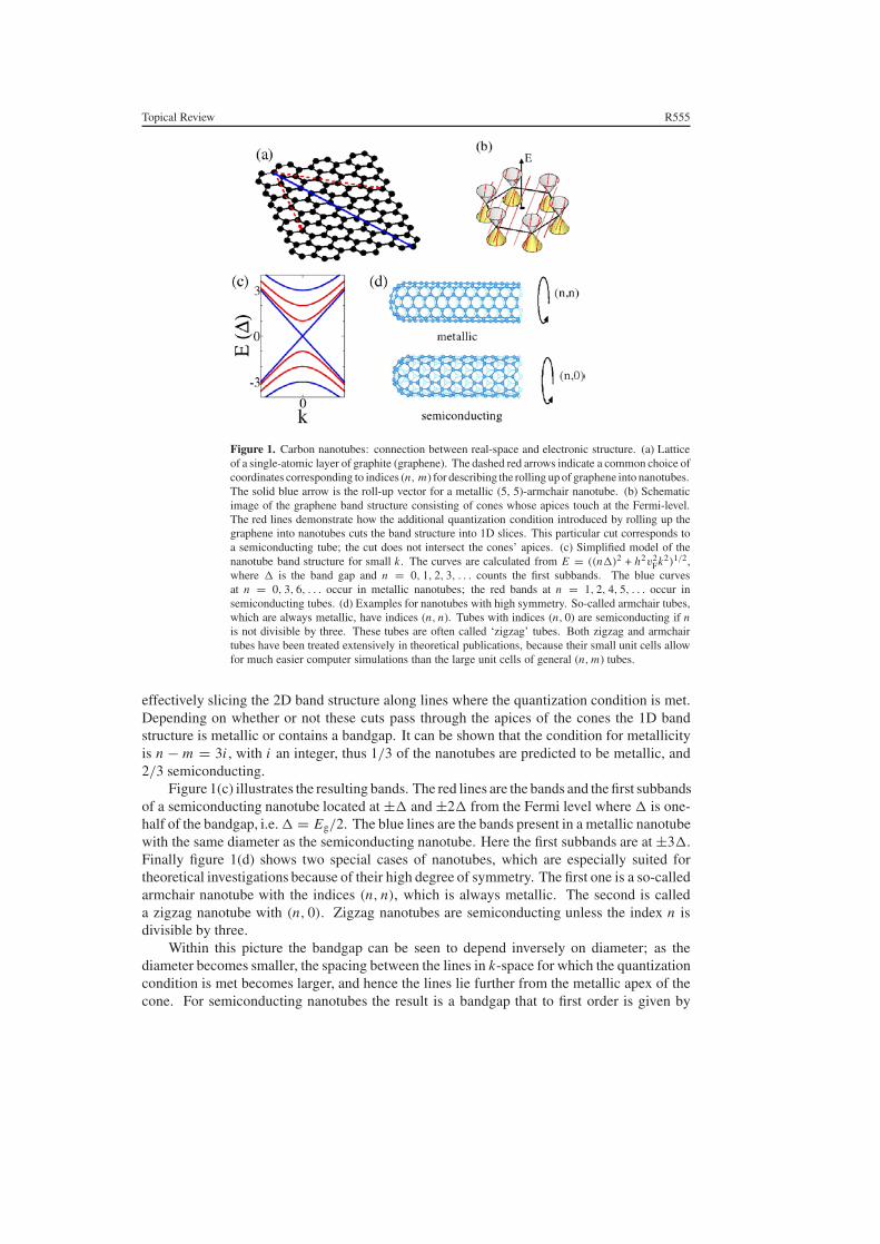
At the time of the discovery of carbon nanotubes (CNTs) there were already theoreticaldiscussions of their possible atomic and electronic structure (Hamada et al 1992, Mintmireet al 1992, Saito et al 1992b). A carbon nanotube can be seen as a single sheet of graphenethat has been rolled up along a direction given by the circumference vector c = na1 + ma2, orsimply (n, m), where a1 and a2 are the lattice vectors in graphene (see figure 1(a)). Dependingon the indices n and m the nanotube can be either metallic or semiconducting (Hamada et al1992, Saito et al 1992a, 1992b): if the difference between n and m is divisible by three thenanotube is metallic, otherwise it is semiconducting. This behaviour occurs because by rollingup a sheet of graphite the electron wavefunctions are subjected to an additional quantizationcondition, essentially ‘cutting’ 1D slices out of the formerly 2D band structure of graphene.
Here we present a simple picture of a carbon nanotube band structure which containsthe relevant features needed for understanding the rest of this article. A simple tight-bindingmodel for the π and π∗ graphene bands was formulated by Wallace (1947). We furthersimplify this description by looking at just the low-energy portion of the band structure, whichwe approximate as cones with apices at the K point in the graphene Brillouin zone. We take theslope of the cones to be a constant vF ≈ 8 × 107 cm s−1 (see figure 1(b)). This approximationignores the ‘trigonal warping’ of the bands, i.e. the different slope of the bands in the K–Kand K–� directions in k-space. It also fails for higher energy (and hence smaller diameternanotubes) due to the non-linearity of the bands. The nanotube band structure is then obtainedfrom the quantization of the circumferential wavevector, i.e. c ·kr = 2π i , where i is an integer,
Topical Review R555
Figure 1. Carbon nanotubes: connection between real-space and electronic structure. (a) Latticeof a single-atomic layer of graphite (graphene). The dashed red arrows indicate a common choice ofcoordinates corresponding to indices (n, m) for describing the rolling up of graphene into nanotubes.The solid blue arrow is the roll-up vector for a metallic (5, 5)-armchair nanotube. (b) Schematicimage of the graphene band structure consisting of cones whose apices touch at the Fermi-level.The red lines demonstrate how the additional quantization condition introduced by rolling up thegraphene into nanotubes cuts the band structure into 1D slices. This particular cut corresponds toa semiconducting tube; the cut does not intersect the cones’ apices. (c) Simplified model of thenanotube band structure for small k. The curves are calculated from E = ((n�)2 + h2v2
Fk2)1/2,where � is the band gap and n = 0, 1, 2, 3, . . . counts the first subbands. The blue curvesat n = 0, 3, 6, . . . occur in metallic nanotubes; the red bands at n = 1, 2, 4, 5, . . . occur insemiconducting tubes. (d) Examples for nanotubes with high symmetry. So-called armchair tubes,which are always metallic, have indices (n, n). Tubes with indices (n, 0) are semiconducting if nis not divisible by three. These tubes are often called ‘zigzag’ tubes. Both zigzag and armchairtubes have been treated extensively in theoretical publications, because their small unit cells allowfor much easier computer simulations than the large unit cells of general (n, m) tubes.
effectively slicing the 2D band structure along lines where the quantization condition is met.Depending on whether or not these cuts pass through the apices of the cones the 1D bandstructure is metallic or contains a bandgap. It can be shown that the condition for metallicityis n − m = 3i , with i an integer, thus 1/3 of the nanotubes are predicted to be metallic, and2/3 semiconducting.
Figure 1(c) illustrates the resulting bands. The red lines are the bands and the first subbandsof a semiconducting nanotube located at ±� and ±2� from the Fermi level where � is one-half of the bandgap, i.e. � = Eg/2. The blue lines are the bands present in a metallic nanotubewith the same diameter as the semiconducting nanotube. Here the first subbands are at ±3�.Finally figure 1(d) shows two special cases of nanotubes, which are especially suited fortheoretical investigations because of their high degree of symmetry. The first one is a so-calledarmchair nanotube with the indices (n, n), which is always metallic. The second is calleda zigzag nanotube with (n, 0). Zigzag nanotubes are semiconducting unless the index n isdivisible by three.
Within this picture the bandgap can be seen to depend inversely on diameter; as thediameter becomes smaller, the spacing between the lines in k-space for which the quantizationcondition is met becomes larger, and hence the lines lie further from the metallic apex of thecone. For semiconducting nanotubes the result is a bandgap that to first order is given by

R556 Topical Review
Figure 2. Examples of the gate-voltage dependence of the conductance through a SWNT at roomtemperature for a metallic nanotube (a) and a semiconducting nanotube (b).
Eg = 2� = 0.7/d eV nm−1, where d is the nanotube diameter independent of the particularchirality (Kane and Mele 1997). If one takes into account the curvature of the graphene sheetin a nanotube there is an additional contribution to the gap proportional to d−2, which alsocauses metallic nanotubes with indices other than (n, n) to have a small bandgap of around0.05 eV or less (Hamada et al 1992, Kane and Mele 1997).
After these theoretical predictions had been made it took several years before it waspossible to verify them experimentally by making electrical contacts to single nanotubes andtest whether they showed metallic or semiconducting behaviour. (A detailed description ofnanotube devices and their fabrication is given in section 2.2.) The first devices made withsingle metallic nanotubes or bundles of a few nanotubes were presented by Tans et al (1997) andBockrath et al (1997). Their devices showed Coulomb-blockade effects at low temperaturesand Ohmic behaviour without dependence on applied gate voltage at higher temperatures (fora good review of Coulomb-blockade and other low-temperature effects see Kouwenhovenet al (1997)). The first investigation of single semiconducting SWNTs was published byTans et al (1998). Their devices show the oft-reproduced behaviour of a field-effect-transistor(FET) at room temperature that makes semiconducting SWNTs so interesting for possiblemicroelectronics applications: the conductivity of these devices can be turned off by applyinga gate voltage.
Figure 2(a) shows a plot of the gate voltage dependence of the conductance of a metallicnanotube device at room temperature. While applying a constant bias-voltage along thenanotube, the gate voltage is being varied. The current is largely independent of gate voltage.Figure 2(b) shows the same plot for a device made from a semiconducting nanotube. Clearlythis device can be turned off by applying a positive gate voltage; conductance changes of overfive orders of magnitude between on and off states have been seen (Martel et al 1998).
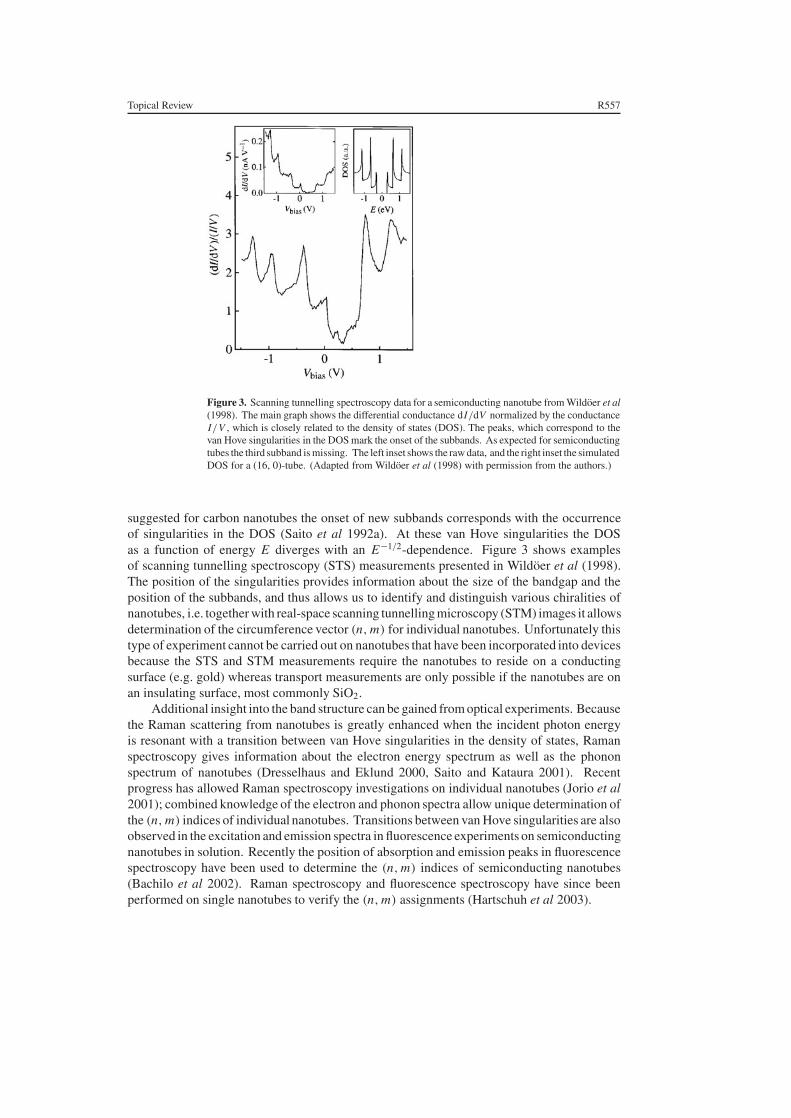
Although transport experiments can demonstrate the existence of an energy gap (Tanset al 1998) and can provide information about the low-lying excitations in the nanotube(Bockrath et al 1997, Tans et al 1997), they do not give the details of the band structure, forexample the onset of various subbands. One method of verifying the theoretical predictions(Hamada et al 1992, Mintmire et al 1992, Saito et al 1992b) is to use tunnelling measurementsprobing the density of states (DOS). The first measurements of this kind on SWNTs werepublished by Odom et al (1998), Wildoer et al (1998). In a 1D electron system like the one
Topical Review R557
Figure 3. Scanning tunnelling spectroscopy data for a semiconducting nanotube from Wildoer et al(1998). The main graph shows the differential conductance dI/dV normalized by the conductanceI/V , which is closely related to the density of states (DOS). The peaks, which correspond to thevan Hove singularities in the DOS mark the onset of the subbands. As expected for semiconductingtubes the third subband is missing. The left inset shows the raw data, and the right inset the simulatedDOS for a (16, 0)-tube. (Adapted from Wildoer et al (1998) with permission from the authors.)
suggested for carbon nanotubes the onset of new subbands corresponds with the occurrenceof singularities in the DOS (Saito et al 1992a). At these van Hove singularities the DOSas a function of energy E diverges with an E−1/2-dependence. Figure 3 shows examplesof scanning tunnelling spectroscopy (STS) measurements presented in Wildoer et al (1998).The position of the singularities provides information about the size of the bandgap and theposition of the subbands, and thus allows us to identify and distinguish various chiralities ofnanotubes, i.e. together with real-space scanning tunnelling microscopy (STM) images it allowsdetermination of the circumference vector (n, m) for individual nanotubes. Unfortunately thistype of experiment cannot be carried out on nanotubes that have been incorporated into devicesbecause the STS and STM measurements require the nanotubes to reside on a conductingsurface (e.g. gold) whereas transport measurements are only possible if the nanotubes are onan insulating surface, most commonly SiO2.
Additional insight into the band structure can be gained from optical experiments. Becausethe Raman scattering from nanotubes is greatly enhanced when the incident photon energyis resonant with a transition between van Hove singularities in the density of states, Ramanspectroscopy gives information about the electron energy spectrum as well as the phononspectrum of nanotubes (Dresselhaus and Eklund 2000, Saito and Kataura 2001). Recentprogress has allowed Raman spectroscopy investigations on individual nanotubes (Jorio et al2001); combined knowledge of the electron and phonon spectra allow unique determination ofthe (n, m) indices of individual nanotubes. Transitions between van Hove singularities are alsoobserved in the excitation and emission spectra in fluorescence experiments on semiconductingnanotubes in solution. Recently the position of absorption and emission peaks in fluorescencespectroscopy have been used to determine the (n, m) indices of semiconducting nanotubes(Bachilo et al 2002). Raman spectroscopy and fluorescence spectroscopy have since beenperformed on single nanotubes to verify the (n, m) assignments (Hartschuh et al 2003).
R558 Topical Review
1.2. Predictions for transport experiments: mobility and mean-free-path
Within the Drude model the conductivity σ is defined by σ = j/E = ne2τ/m, where j is thecurrent density, E the electric field, n the charge carrier density, e the absolute value of theelectronic charge, τ the momentum scattering rate and m the effective mass of the carriers. Inone dimension, we have σ = GL and n = N/L, where G is the conductance, L the lengthof the sample and N the number of carriers. The quantity µ = eτ/m = σ/ne is the mobility,and has the same units in any dimension.
Mobility measures the momentum scattering rate of carriers, and therefore is offundamental interest in understanding the scattering processes in a given system. In addition,the mobility of charge carriers in the FET channel is one of the most important parametersdetermining the performance of an FET. Mobility ultimately determines the high-frequencyperformance of the FET, and is also important for the determination of the transconductanceand drive current. Nanotube FETs (NT-FETs) have been proposed for a variety of applicationsincluding chemical sensors (Besteman et al 2003, Chen et al 2003, Star et al 2003) andsingle-electron memories (Fuhrer et al 2002, Kim et al 2002a); in these applications mobilitydetermines the sensitivity of the NT-FET to charge or chemical species.
In this section we will discuss theoretical and experimental results on the conductivity ofmetallic and semiconducting nanotubes. In section 3.1.2 we will discuss the determination ofthe mobility directly from the transistor characteristics of a NT-FET, and when this analysis isapplicable.
Mobility is difficult to define for a metallic nanotube, since it is not clear whether therelevant charge density should be measured from the subband bottom or the band bottom. Inaddition, the nearly flat bands at the Fermi level imply a near-infinite effective mass. However,the mean free path may be defined unambiguously, and we will use this quantity to comparetheoretical and experimental results for the conductivity of metallic and semiconductingnanotubes.
In one dimension, the maximum conductance is quantized: in the absence of scatteringthe conductance is Gmax = e2/h (Datta 1995) for each conductance mode, where h isPlanck’s constant. For the nanotube, with two bands with two spins, Gmax = 4e2/h. Inan imperfect wire with scattering (neglecting quantum interference) the conductance is givenby G−1 = G−1
max + G−1wire, where Gwire = GmaxT/(1 − T ) and T is the transmission probability
for the wire (Datta 1995). The mean free path l is the length of wire over which T = 1/2 orGwire = Gmax. This allows us to relate the conductance to the mean free path by the relationl/L = Gwire/Gmax, where L is the length of the nanotube. The mobility is related to the meanfree path: µ = Gwire L/ne = Gmaxl/ne.
The observation of conductances which are an appreciable fraction of Gmax in metallicnanotubes with lengths exceeding 5 µm (Kong et al 1999) indicates mean free paths of atleast a few micrometres. This is in good agreement with theoretical predictions of 10 µm ormore (White and Todorov 1998). Similarly, high conductances in semiconducting nanotubes(Rosenblatt et al 2002, Javey et al 2003) indicate mean-free-paths of at least hundreds ofnanometres. These results have also been corroborated by electrostatic force microscopy(EFM) as described in section 3.2.2.
Only a small number of publications have attempted to predict the mobility insemiconducting nanotubes. McEuen et al (1999) made general arguments that backscatteringwould be greatly suppressed in metallic nanotubes relative to semiconducting nanotubes:interband backscattering is suppressed by a symmetry in metallic nanotubes which is notpresent in semiconducting nanotubes at low doping. However, at high doping semiconductingnanotubes should be expected to have similar conductivity to metallic nanotubes. From this
Topical Review R559
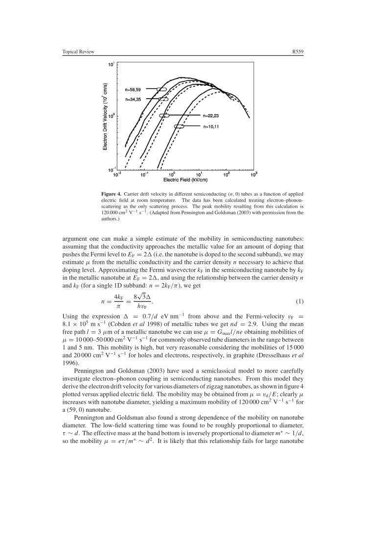
Figure 4. Carrier drift velocity in different semiconducting (n, 0) tubes as a function of appliedelectric field at room temperature. The data has been calculated treating electron–phonon-scattering as the only scattering process. The peak mobility resulting from this calculation is120 000 cm2 V−1 s−1. (Adapted from Pennington and Goldsman (2003) with permission from theauthors.)
argument one can make a simple estimate of the mobility in semiconducting nanotubes:assuming that the conductivity approaches the metallic value for an amount of doping thatpushes the Fermi level to EF = 2� (i.e. the nanotube is doped to the second subband), we mayestimate µ from the metallic conductivity and the carrier density n necessary to achieve thatdoping level. Approximating the Fermi wavevector kF in the semiconducting nanotube by kF
in the metallic nanotube at EF = 2�, and using the relationship between the carrier density nand kF (for a single 1D subband: n = 2kF/π), we get
n = 4kF
π= 8
√3�
hvF. (1)
Using the expression � = 0.7/d eV nm−1 from above and the Fermi-velocity vF =8.1 × 10⁵ m s−1 (Cobden et al 1998) of metallic tubes we get nd = 2.9. Using the meanfree path l = 3 µm of a metallic nanotube we can use µ = Gmaxl/ne obtaining mobilities ofµ = 10 000–50 000 cm2 V−1 s−1 for commonly observed tube diameters in the range between1 and 5 nm. This mobility is high, but very reasonable considering the mobilities of 15 000and 20 000 cm2 V−1 s−1 for holes and electrons, respectively, in graphite (Dresselhaus et al1996).
Pennington and Goldsman (2003) have used a semiclassical model to more carefullyinvestigate electron–phonon coupling in semiconducting nanotubes. From this model theyderive the electron drift velocity for various diameters of zigzag nanotubes, as shown in figure 4plotted versus applied electric field. The mobility may be obtained from µ = vd/E ; clearly µ
increases with nanotube diameter, yielding a maximum mobility of 120 000 cm2 V−1 s−1 fora (59, 0) nanotube.
Pennington and Goldsman also found a strong dependence of the mobility on nanotubediameter. The low-field scattering time was found to be roughly proportional to diameter,τ ∼ d . The effective mass at the band bottom is inversely proportional to diameter m∗ ∼ 1/d ,so the mobility µ = eτ/m∗ ∼ d2. It is likely that this relationship fails for large nanotube

R560 Topical Review
diameters when the subband spacing � becomes smaller than the temperature or some disorderstrength. Still, this analysis suggests that larger diameter nanotubes may be optimal for high-mobility applications.
At higher carrier velocities, it is expected that more channels will be open for scattering,and the carrier mean free path will be reduced. This is evident in the calculations of Penningtonand Goldsman (see figure 4), where a peak in the drift velocity is seen as a function of electricfield. Such a reduction in mean free path has been observed in metallic nanotubes (Yao et al2000) and interpreted as due to the efficient emission of ∼160 meV zone-boundary phonons.Park et al (2003) used a scanned contact probe to verify that the mean free path for phononscattering at low velocities in a metallic nanotube is a few micrometres, while at high velocitiesit is shortened to ∼10 nm.
2. Nanotube synthesis and device fabrication
2.1. Nanotube synthesis
There are two fundamentally different types of method of growing carbon nanotubes for devicefabrication. The first class of methods tends to produce large amounts of nanotubes, usually asnanotube-containing soot, from which the nanotubes are deposited onto substrates for devicefabrication after being purified. The second class of methods synthesizes the nanotubes directlyon a substrate by first depositing some kind of catalyst and then exposing it to carbon-containingfeedstock gas.
The methods of the former kind were the first available procedures for nanotube synthesis.The initial discovery of multiwalled nanotubes (Iijima 1991) was made using an arc-dischargebetween two carbon electrodes. The earliest methods for the production of SWNTs (Bethuneet al 1993, Iijima and Ichihashi 1993) also used an arc-discharge method. The first methodused for the production of large quantities of CNTs (Thess et al 1996) was laser-ablation; inthis method a carbon target doped with a catalyst consisting of powdered Ni and Co is heated to1000 ◦C in vacuum and then bombarded with laser pulses resulting in a high yield of SWNTswith a narrow diameter distribution.
More recently the so-called HiPCO method (Bronikowski et al 2001) has further increasedthe quantities in which nanotubes can be produced. The acronym HiPCO stands for high-pressure decomposition of CO gas. Here CO gas with a small amount of added Fe(CO)5 issprayed through a nozzle into a reactor at 1050 ◦C and 30 atm. The Fe(CO)5 provides themetal to form tiny catalyst droplets while the CO is the feedstock material.
All these methods produce relatively large quantities of SWNTs that can be of high qualitywith few defects if the synthesis parameters are properly optimized. However, one commonfeature is the contamination of the products with amorphous carbon (‘soot’) and leftovercatalyst. Furthermore the nanotubes tend to occur in thick bundles of several tens to severalhundreds of nanotubes. For the fabrication of electronic devices (see section 2.2) the nanotubesneed to be separated from each other and cleaned from the amorphous carbon residue. Althoughthere are many ways of cleaning the tubes, the most prominent method is that described in Liuet al (1998), which purifies the nanotube soot using nitric acid, the resulting nanotubes areusually fairly short (not more than a few micrometres) and often contain a significant numberof defects due to the harsh cleaning procedures.
For electronics devices it is often desirable to investigate longer nanotubes and—especiallyif one is interested in the intrinsic properties of nanotubes—highly defect-free nanotubes. Forthis type of application growth methods producing CNTs directly on substrates (Dai et al1996a, Fonseca et al 1997, Kong et al 1998a) are often better suited. In particular Dai et al
Topical Review R561
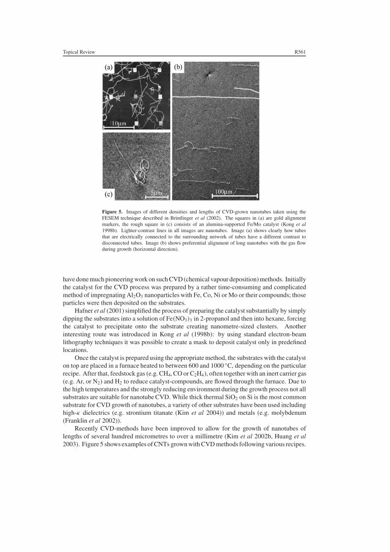
Figure 5. Images of different densities and lengths of CVD-grown nanotubes taken using theFESEM technique described in Brintlinger et al (2002). The squares in (a) are gold alignmentmarkers, the rough square in (c) consists of an alumina-supported Fe/Mo catalyst (Kong et al1998b). Lighter-contrast lines in all images are nanotubes. Image (a) shows clearly how tubesthat are electrically connected to the surrounding network of tubes have a different contrast todisconnected tubes. Image (b) shows preferential alignment of long nanotubes with the gas flowduring growth (horizontal direction).
have done much pioneering work on such CVD (chemical vapour deposition) methods. Initiallythe catalyst for the CVD process was prepared by a rather time-consuming and complicatedmethod of impregnating Al2O3 nanoparticles with Fe, Co, Ni or Mo or their compounds; thoseparticles were then deposited on the substrates.
Hafner et al (2001) simplified the process of preparing the catalyst substantially by simplydipping the substrates into a solution of Fe(NO3)3 in 2-propanol and then into hexane, forcingthe catalyst to precipitate onto the substrate creating nanometre-sized clusters. Anotherinteresting route was introduced in Kong et al (1998b): by using standard electron-beamlithography techniques it was possible to create a mask to deposit catalyst only in predefinedlocations.
Once the catalyst is prepared using the appropriate method, the substrates with the catalyston top are placed in a furnace heated to between 600 and 1000 ◦C, depending on the particularrecipe. After that, feedstock gas (e.g. CH4, CO or C2H4), often together with an inert carrier gas(e.g. Ar, or N2) and H2 to reduce catalyst-compounds, are flowed through the furnace. Due tothe high temperatures and the strongly reducing environment during the growth process not allsubstrates are suitable for nanotube CVD. While thick thermal SiO2 on Si is the most commonsubstrate for CVD growth of nanotubes, a variety of other substrates have been used includinghigh-κ dielectrics (e.g. strontium titanate (Kim et al 2004)) and metals (e.g. molybdenum(Franklin et al 2002)).
Recently CVD-methods have been improved to allow for the growth of nanotubes oflengths of several hundred micrometres to over a millimetre (Kim et al 2002b, Huang et al2003). Figure 5 shows examples of CNTs grown with CVD methods following various recipes.
R562 Topical Review
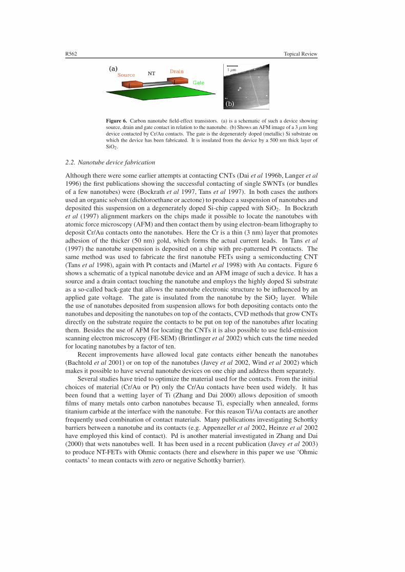
Figure 6. Carbon nanotube field-effect transistors. (a) is a schematic of such a device showingsource, drain and gate contact in relation to the nanotube. (b) Shows an AFM image of a 3 µm longdevice contacted by Cr/Au contacts. The gate is the degenerately doped (metallic) Si substrate onwhich the device has been fabricated. It is insulated from the device by a 500 nm thick layer ofSiO2.
2.2. Nanotube device fabrication
Although there were some earlier attempts at contacting CNTs (Dai et al 1996b, Langer et al1996) the first publications showing the successful contacting of single SWNTs (or bundlesof a few nanotubes) were (Bockrath et al 1997, Tans et al 1997). In both cases the authorsused an organic solvent (dichloroethane or acetone) to produce a suspension of nanotubes anddeposited this suspension on a degenerately doped Si-chip capped with SiO2. In Bockrathet al (1997) alignment markers on the chips made it possible to locate the nanotubes withatomic force microscopy (AFM) and then contact them by using electron-beam lithography todeposit Cr/Au contacts onto the nanotubes. Here the Cr is a thin (3 nm) layer that promotesadhesion of the thicker (50 nm) gold, which forms the actual current leads. In Tans et al(1997) the nanotube suspension is deposited on a chip with pre-patterned Pt contacts. Thesame method was used to fabricate the first nanotube FETs using a semiconducting CNT(Tans et al 1998), again with Pt contacts and (Martel et al 1998) with Au contacts. Figure 6shows a schematic of a typical nanotube device and an AFM image of such a device. It has asource and a drain contact touching the nanotube and employs the highly doped Si substrateas a so-called back-gate that allows the nanotube electronic structure to be influenced by anapplied gate voltage. The gate is insulated from the nanotube by the SiO2 layer. Whilethe use of nanotubes deposited from suspension allows for both depositing contacts onto thenanotubes and depositing the nanotubes on top of the contacts, CVD methods that grow CNTsdirectly on the substrate require the contacts to be put on top of the nanotubes after locatingthem. Besides the use of AFM for locating the CNTs it is also possible to use field-emissionscanning electron microscopy (FE-SEM) (Brintlinger et al 2002) which cuts the time neededfor locating nanotubes by a factor of ten.
Recent improvements have allowed local gate contacts either beneath the nanotubes(Bachtold et al 2001) or on top of the nanotubes (Javey et al 2002, Wind et al 2002) whichmakes it possible to have several nanotube devices on one chip and address them separately.
Several studies have tried to optimize the material used for the contacts. From the initialchoices of material (Cr/Au or Pt) only the Cr/Au contacts have been used widely. It hasbeen found that a wetting layer of Ti (Zhang and Dai 2000) allows deposition of smoothfilms of many metals onto carbon nanotubes because Ti, especially when annealed, formstitanium carbide at the interface with the nanotube. For this reason Ti/Au contacts are anotherfrequently used combination of contact materials. Many publications investigating Schottkybarriers between a nanotube and its contacts (e.g. Appenzeller et al 2002, Heinze et al 2002have employed this kind of contact). Pd is another material investigated in Zhang and Dai(2000) that wets nanotubes well. It has been used in a recent publication (Javey et al 2003)to produce NT-FETs with Ohmic contacts (here and elsewhere in this paper we use ‘Ohmiccontacts’ to mean contacts with zero or negative Schottky barrier).
Topical Review R563
3. Experiments on single-walled carbon nanotubes
3.1. Transport in single-walled carbon nanotube field-effect transistors
Despite considerable research effort the details of electronic transport in semiconductingSWNTs are not yet clear. The initial publications showing experimental data from NT-FETsalready disagreed upon the explanation of the transistor behaviour. While Tans et al (1998)developed a model similar to a BARITT-diode (Sze 1981),which basically consists of two back-to-back Schottky barriers, the description initially given by Avouris and co-workers (Martel et al1998) is based on the model of a conventional MOSFET with a diffusive channel (Sze 1981).From the characteristics of a NT-FET (analogous to a p-channel MOSFET, see figure 2(b))it is clear that the charge carriers have to be holes. However, in the model presented in Tanset al (1998) the holes are injected into the nanotube from the contacts, whereas according toMartel et al (1998) they are intrinsic to the nanotube. Martel used the gate-voltage-dependentconductance of his NT-FETs to calculate a mobility of ∼20 cm2 V−1 s−1, much lower thanthe mobility of p-silicon (∼450 cm2 V−1 s−1). As shown below, this mobility estimate wasincorrect, due to the influence of Schottky barriers at the contacts. Recently Ohmic contactsto semiconducting nanotubes have allowed the intrinsic transport properties to be probed.
3.1.1. Ohmic or Schottky contacts? While researchers had been able to produce devicesfrom metallic nanotubes that were close to the fundamental limit of resistance for nanotubes(6.5 k�) (Liang et al 2001), until recently the lowest resistances reported for semiconductingnanotubes were some 100 k�, with 1 M� being more typical, suggesting the presence ofsome kind of barrier, either in the semiconducting nanotube itself (McEuen et al 1999), orat the contacts. Furthermore, several experiments corroborated the idea of Schottky contactsdirectly. Freitag et al (2001) found that an AFM tip with applied positive bias-voltage placednear one of the contact of a NT-FET with Cr/Au contacts had much stronger influence on thedevice behaviour than a tip placed elsewhere on the device. Bachtold et al (2001) measuredthe behaviour of Au-contacted CNTs on top of Al/Al2O3 microstrips acting as gates, with goodagreement of the device characteristics with theoretical models based on the Schottky-contactpicture developed in Leonard and Tersoff (2000) and Odintsov (2000). Similarly, Deryckeet al (2002) and Martel et al (1998) found evidence for barriers at the contacts of their NT-FETs. Gathering all this information Heinze et al (2002) presented theoretical predictionsabout the behaviour of NT-Schottky-barrier transistors which are then found to be followedwell by Ti/Au-contacted devices by Appenzeller et al (2002).
Figure 7 shows an overview of the results of Appenzeller et al. Figure 7(a) describesthe subthreshold behaviour for a NT-FET, showing the source–drain current I as a functionof applied gate voltage Vg for three different source–drain voltages Vsd. The current dependson applied Vsd as expected for a Schottky-barrier transistor. The subthreshold swing, whichis defined as S = (d log G/dVg)
−1 (mV/decade), is shown in the inset in figure 7(a). Forconventional MOSFETs it is expected to be proportional to the temperature (Sze 1981):S ≈ 2.3 kBT/e, where kB is Boltzmann’s constant and e the electron charge. For a Schottky-barrier FET in which tunnelling through the Schottky barrier dominates the current, S isexpected to be largely temperature independent (Appenzeller et al 2002, Heinze et al 2002) asobserved here (at least below 200 K), though a weak temperature dependence can result fromthermally assisted tunnelling (Appenzeller et al 2004). Finally the scaling of S with gate-oxide thickness is different for Schottky-barrier FETs and conventional FETs. Figure 7(b)shows how the values for S obtained by Appenzeller et al and other groups follow theexpected behaviour for Schottky-barrier transistors much better than the behaviour expected

R564 Topical Review
(c)
Figure 7. Schottky barriers in NT-FETs from Appenzeller et al (2002). (a) Subthreshold swingS in the I–Vg curve for a back-gated device on SiO2 under different bias voltages and at differenttemperatures (inset). The temperature independence (below 200 K) of S and the bias-voltagedependence of the current in the subthreshold regime indicate the presence of Schottky barriers.(b) Scaling of S with effective oxide thickness (oxide thickness corrected for dielectric constant ofthe materials used) for back-gated devices of different lengths, on different dielectrics and preparedby different groups. The scaling agrees with a Schottky barrier model but not with a traditionalMOSFET model. (c) Band structure schematic for a Schottky barrier NT-FET (a) without and(b) with applied bias voltage. (Adapted from Appenzeller et al (2002) with permission from theauthors.)
for traditional MOSFETs. All this evidence taken together suggests that many NT-FETs areSchottky-barrier transistors with a band structure similar to the one shown schematically infigure 7(c) (also adapted from Appenzeller et al (2002)).
However, it is not clear that all NT-FETs should have Schottky barriers at the electrodes.It was shown (Leonard and Tersoff 2000) that the work function difference between the metalelectrode and nanotube is dominant in determining whether a Schottky barrier is present; inthe one-dimensional nanotube interface dipoles cannot be completely screened (Leonard andTersoff 2002). Thus the choice of a large work-function metal should provide Ohmic contactto the valence band. The work function of nanotubes is about 4.5 eV (Tans et al 1998), so ametal with work function greater than ∼4.5 eV + Eg/2 should provide Ohmic contact to thevalence band.
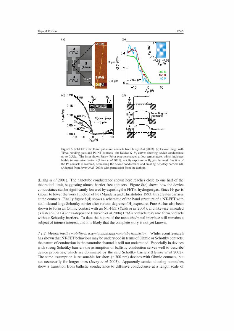
Palladium is a promising material with a high work function that at the same time wetsnanotubes (Zhang and Dai 2000). Javey et al (2003) fabricated NT-FETs with Ohmic contactsby depositing Pd-contact pads onto CNTs and annealing the devices in Ar. Figure 8(a)shows a diagram of these Pd-contacted NT-FETs, while figure 8(b) shows I–Vg curves ofsuch a device and the inset shows the signature of Fabry–Perot oscillations measured at lowtemperatures, analogous to those seen in metallic nanotubes for very low contact resistances
Topical Review R565
(a) (b)
(c) (d)
3 µm
0.3 µm
Figure 8. NT-FET with Ohmic palladium contacts from Javey et al (2003). (a) Device image withTi/Au bonding pads and Pd NT contacts. (b) Device G–Vg curves showing device conductanceup to 0.5G0. The inset shows Fabry–Perot type resonances at low temperature, which indicateshighly transmissive contacts (Liang et al 2001). (c) By exposure to H2 gas the work function ofthe Pd contacts is lowered, decreasing the device conductance and creating Schottky barriers (d).(Adapted from Javey et al (2003) with permission from the authors.)
(Liang et al 2001). The nanotube conductance shown here reaches close to one half of thetheoretical limit, suggesting almost barrier-free contacts. Figure 8(c) shows how the deviceconductance can be significantly lowered by exposing the FET to hydrogen gas. Since H2 gas isknown to lower the work function of Pd (Mandelis and Christofides 1993) this creates barriersat the contacts. Finally figure 8(d) shows a schematic of the band structure of a NT-FET withno, little and large Schottky barrier after various degrees of H2 exposure. Pure Au has also beenshown to form an Ohmic contact with an NT-FET (Yaish et al 2004), and likewise annealed(Yaish et al 2004) or as-deposited (Durkop et al 2004) Cr/Au contacts may also form contactswithout Schottky barriers. To date the nature of the nanotube/metal interface still remains asubject of intense interest, and it is likely that the complete story is not yet known.
3.1.2. Measuring the mobility in a semiconducting nanotube transistor. While recent researchhas shown that NT-FET behaviour may be understood in terms of Ohmic or Schottky contacts,the nature of conduction in the nanotube channel is still not understood. Especially in deviceswith strong Schottky barriers the assumption of ballistic conduction serves well to describedevice properties, which are dominated by the said Schottky barriers (Heinze et al 2002).The same assumption is reasonable for short (∼300 nm) devices with Ohmic contacts, butnot necessarily for longer ones (Javey et al 2003). Apparently semiconducting nanotubesshow a transition from ballistic conductance to diffusive conductance at a length scale of

R566 Topical Review
a few micrometres. It is not yet known what scattering mechanisms govern this regime ofdiffusive conductance. One of the parameters that allows us to draw conclusions about thedetails of the conductance is mobility.
The dependence of the mobility on temperature, applied voltages and other physicalquantities provides information about scattering mechanisms, charge density, impurities andmany materials parameters. For comprehensive reviews of mobility in semiconductors see forexample Sze (1981), Schroder (1998), Seeger (2002). There are several different methods ofmeasuring mobility. The most common method measures the so-called Hall-mobility. Thismethod, however, cannot be used in 1D systems such as carbon nanotubes. Here one has to usemethods that are based on the behaviour of devices, especially NT-FETs: following the Drudemodel the mobility is given by µ = σ/q . In a 1D system the conductivity is given by σ = GL,where G is the device conductance and L its length. The charge density q can be calculatedfrom the capacitance per length cg between the device and the gate controlling the device andthe applied gate voltage. Allowing for a non-zero threshold this gives q = cg(Vg − Vth).This relationship is valid in linear response (small Vsd) such that non-equilibrium carriers arenot injected from source or drain, and at gate voltages above the threshold (i.e. Vg < Vth
for p-type devices that turn on for negative Vg). We also assume that the gate capacitanceis much smaller than the quantum capacitance of the nanotube (see below), such that thequantum capacitance may be neglected. The relationship ignores thermally activated carriers,which may be significant for small (Vg − Vth) and high temperature. Most importantly, thisrelationship assumes cg and Vth do not vary appreciably along the length of the channel, whichrequires L � t , the dielectric thickness. Few nanotube devices studied in the literature satisfythis last criterion.
From this approach we get the expression for the mobility that is closest to the intrinsicmobility of a nanotube:
µ = L
cg
G
Vg − Vth. (2)
Here G should be the conductance of the channel only. It is appropriate to approximate G bythe total device conductance here only if the channel conductance is much smaller than thecontact conductance, i.e. this formula provides meaningless results in the case of Schottky-barrier transistors, in which the contact conductance is small. This formula for the mobility isanalogous to what is known as the effective mobility in conventional FETs (Schroder 1998).It is only applicable if Vth can be determined unambiguously. If this is not the case one canstill calculate the so-called field-effect mobility:
µFE = L
cg
∂G
∂Vg. (3)
Equations (2) and (3) are equivalent only in the case that G is linearly proportional to Vg − Vth.However, in many materials, G is sub-linear in Vg, and equation (3) typically underestimatesthe mobility.
The third method of measuring the mobility is not as reliable as the first two, but since itprobes different aspects of the device behaviour it is useful to independently verify the resultsobtained with the first two formulae. This approach measures the saturation mobility µsat
using the saturation current at high bias-voltages:
µsat = 2L
Bcg
Id,sat
(Vg − Vth)2. (4)
The main problem with this approach is the presence of the body factor B , which accounts fordependence of Vth on the position along the device. Even for conventional MOSFETs B is not

Topical Review R567
(a) (c)
(b) (d)
Figure 9. Ultralong NT-FET. (a) FE-SEM image of a 325 µm long device. The scale bar is100 µm long. (b) Conductance G as a function of gate voltage Vg curves for this device at differenttemperatures. The hysteresis in the curves is discussed in section 5. Only the decreasing-Vg portionof the data is used for further analysis in this figure and figure 10. (c) G2 versus Vg for this device.Straight lines indicate G ∼ (Vg − Vth)
1/2 and are used to calculate Vth. (d) Subthreshold behaviourof this device. The temperature dependence of the subthreshold swing S is shown in the inset (seealso Durkop et al 2004).
very well understood, much less for carbon nanotubes. Whenever this formula is applied toNT-FETs below, it is assumed that B is unity. Normally the saturation mobility underestimatesthe mobility (Schroder 1998).
Due to the requirements to have channel length much greater than dielectric thickness, andnegligible Schottky barriers at the contacts, there are few published results of measurementsof mobility in nanotubes. Recently Durkop et al (2004) were able to fabricate very long(L > 300 µm) semiconducting nanotube FETs in which the channel resistance dominatedthe transport through the device. Figure 9(a) shows such a device. The length L = 325 µmbetween contacts, and the diameter d = 3.9 nm. Figure 9(b) shows the conductance of thedevice as a function of gate voltage. As can be seen from figure 9(c) the conductance G of thisdevice follows the empirical relationship G2 ∼ (Vth − Vg), which allows fitting to determinethe threshold voltage Vth.
It is notable that the conductance at Vg = −10 V exceeds 1.4 µS at room temperature.Assuming zero contact resistance, i.e. G = Gwire, this conductance corresponds to a 1Dconductivity σ of 4.6 × 10⁻⁸ S cm (finite contact resistance would imply greater σ ). If thisnanotube is single-walled, or multi-walled with the current largely carried by the outer wall atlow bias (Collins et al 2001), then the electronic mean-free path l is given by σ/2G0 = 2.9 µm,where G0 is the conductance quantum, approximately 77.5 µS. Finite contact resistance wouldimply a larger σ and, thus, a larger l. This analysis already suggests that the measured resistanceis the nanotube resistance; if contact resistance (e.g. from Schottky barriers) was dominant thiswould imply a much longer mean-free path.
R568 Topical Review
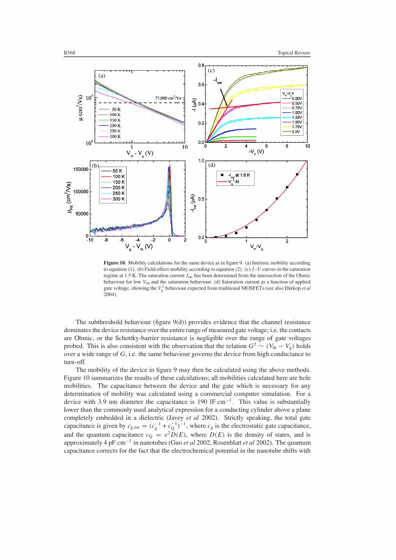
(a)(c)
(b) (d)
Figure 10. Mobility calculations for the same device as in figure 9. (a) Intrinsic mobility accordingto equation (1). (b) Field-effect mobility according to equation (2). (c) I–V curves in the saturationregime at 1.5 K. The saturation current Isat has been determined from the intersection of the Ohmicbehaviour for low Vsd and the saturation behaviour. (d) Saturation current as a function of appliedgate voltage, showing the V 2
g behaviour expected from traditional MOSFETs (see also Durkop et al2004).
The subthreshold behaviour (figure 9(d)) provides evidence that the channel resistancedominates the device resistance over the entire range of measured gate voltage; i.e. the contactsare Ohmic, or the Schottky-barrier resistance is negligible over the range of gate voltagesprobed. This is also consistent with the observation that the relation G2 ∼ (Vth − Vg) holdsover a wide range of G, i.e. the same behaviour governs the device from high conductance toturn-off.
The mobility of the device in figure 9 may then be calculated using the above methods.Figure 10 summarizes the results of these calculations; all mobilities calculated here are holemobilities. The capacitance between the device and the gate which is necessary for anydetermination of mobility was calculated using a commercial computer simulation. For adevice with 3.9 nm diameter the capacitance is 190 fF cm−1. This value is substantiallylower than the commonly used analytical expression for a conducting cylinder above a planecompletely embedded in a dielectric (Javey et al 2002). Strictly speaking, the total gatecapacitance is given by cg,tot = (c−1
g + c−1Q )−1, where cg is the electrostatic gate capacitance,
and the quantum capacitance cQ = e2 D(E), where D(E) is the density of states, and isapproximately 4 pF cm−1 in nanotubes (Guo et al 2002, Rosenblatt et al 2002). The quantumcapacitance corrects for the fact that the electrochemical potential in the nanotube shifts with
Topical Review R569
added charge. Since the two contributions to the gate capacitance add inversely, the smallestcapacitance limits the total capacitance. In the devices discussed here, cg � cQ and hencecg,tot ≈ cg. Quantum capacitance is, however, important in devices with thin high-κ gatedielectrics (Javey et al 2002, Kim et al 2004).
Figure 10(a) shows the intrinsic mobility calculated according to equation (1). As expectedfrom the power-law behaviour of the conductance it shows a power-law dependence itself,reaching values of over 100 000 cm2 V−1 s−1 for low gate voltages. The field-effect mobilityaccording to equation (2) is shown in figure 10(b). Like in conventional MOSFETs (Schroder1998), it peaks for low gate voltages. For this device the peak is at 79 000 cm2 V−1 s−1 at roomtemperature. Finally, figures 10(c) demonstrates the saturation behaviour of the device I–Vcurves, and figure 10(d) shows the square-law behaviour of equation (3) (i.e. Isat ∼ V 2
g ) used toextract the saturation mobility of 55 000 cm2 V−1 s−1. Because of the length of this device, theelectric field is less than 300 V cm−1, much lower than the fields at which significant mobilitydecreases are expected (Pennington and Goldsman 2003). For comparison, the Ohmicallycontacted, much shorter devices investigated in Javey et al (2003) show a saturation mobilityof 4000 cm2 V−1 s−1; however, it is possible that contact resistance plays a role here, and it isalso not clear that the devices are in the low-field limit.
The mobility values in semiconducting carbon nanotubes exceed those of other materialsand devices when measured at room temperature. The highest intrinsic mobility at roomtemperature of any semiconductor is the electron mobility in InSb, 77 000 cm2 V−1 s−1
(Hrostowski et al 1955) (measured as Hall-mobility). Typical field-effect mobilities of Sidevices are around 1000 cm2 V−1 s−1 (Takagi et al 1994). The semiconductor with the highesthole mobility is PbTe with 4000 cm2 V−1 s−1 (Sze 1981).
3.2. Scanned probe experiments
While transport experiments as described in the previous section can provide much informationabout the properties of a nanotube as a whole, they cannot test for local variations along thenanotube, for example to test for the influence of defects on the electronic structure or theshape of the potential drop along a nanotube. On insulating substrates, which are prerequisitefor the fabrication of nanotube-devices, it is virtually impossible to use techniques like STMthat rely on electric current for their feedback mechanisms. The methods of choice for imagingnanotube devices, therefore, are techniques derived from AFM.
3.2.1. Scanned gate microscopy. In scanned gate microscopy (SGM) a voltage is applied toa conducting AFM tip (see figure 11(a)). Thus, the tip—without touching the nanotube—actsas a local gate to the devices being imaged (Bachtold et al 2000, Tans and Dekker 2000). Thesignal that is recorded is the current through the device. This technique is very well suitedfor probing the local response of a nanotube device to gate voltage. Metallic nanotubes arefound to be insensitive to local gating (Bachtold et al 2000) (as they are to global gating),although local defects in metallic nanotubes may be sensitive to the local gate (Bockrath et al2001). Freitag et al (2001) used this technique to investigate NT-FETs. Their results showedthat nanotubes were much more sensitive to gating near the positive contact than in the centreof the nanotube, suggesting the presence of a Schottky barrier at the contacts. Similar resultswere presented by Radosavljevic et al (2002) showing the presence of contact barriers in n-typeNT-FETs.
The second type of information that can be gained from SGM measurements shows theinfluence of disorder on the electronic structure of a nanotube. Measurements performed byTans and Dekker (2000) and Bachtold et al (2000) show that the response of the nanotube

R570 Topical Review
Figure 11. (a) Scanned gate microscopy (SGM): a gate voltage Vtip is applied to the AFM tip. Thecurrent through the device at a given bias voltage Vbias is recorded as a function of the tip position.The back-gate is used with a constant voltage to put the device into a certain region of its I–Vgcharacteristic. (b) Alternating-current electrostatic force microscopy (AC-EFM): while the tube isbiased with Vbias at a frequency ω and gated with a fixed Vg the tip is used to probe the local electricfield around the tube. Using a lock-in technique the tip amplitude at ω, proportional to the localAC potential of the nanotube, is recorded as a function of the tip position.
to an applied positive gate voltage is not uniform along the nanotube, suggesting potentialvariations along the device (Tans and Dekker 2000). Freitag et al (2002) were able to estimatethe magnitude of the potential variations as 20–50 meV for ‘strong’ defects. Weaker defectscould also be observed using a large positive voltage applied to the tip (Freitag et al 2002,Kalinin et al 2002) (a technique termed scanning impedance microscopy or ‘SIM’). Bockrathet al (2001) were able to identify defects in metallic nanotubes from their reaction to SGM.
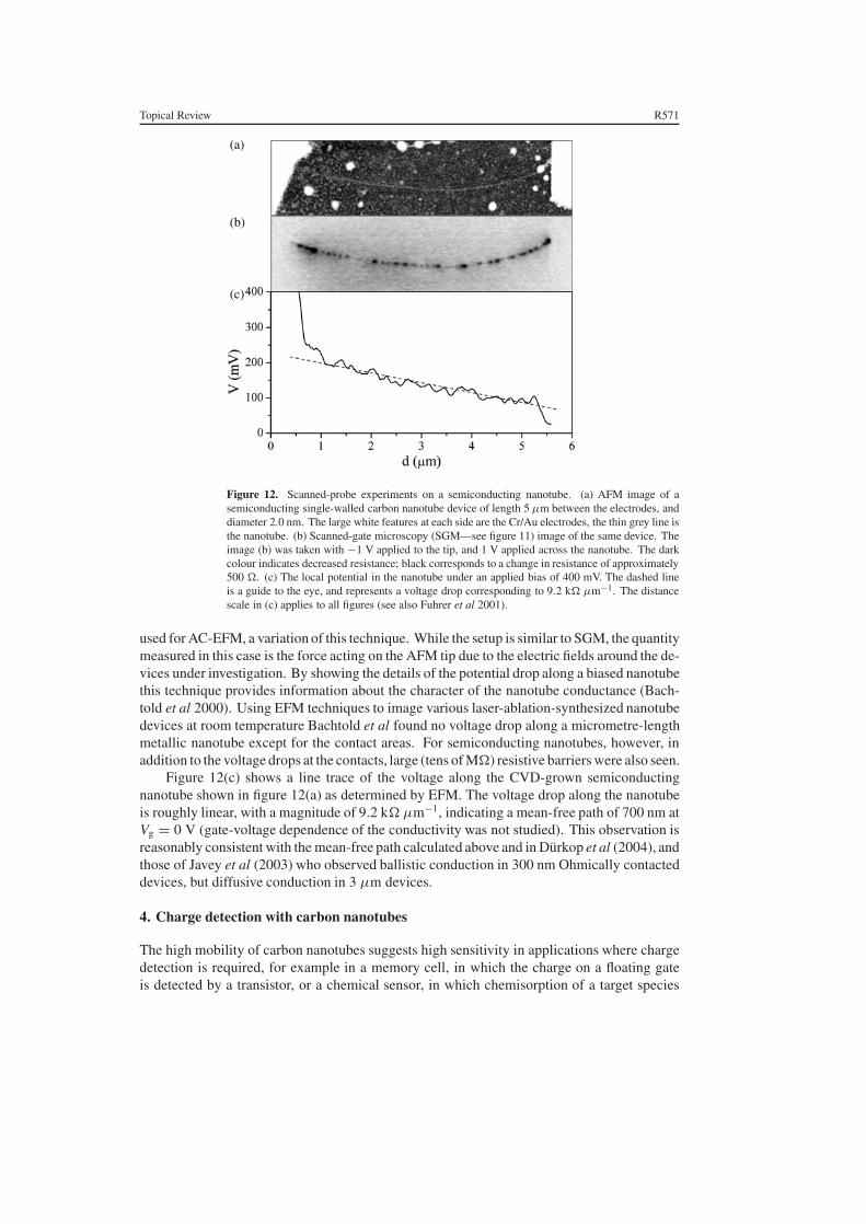
Figure 12(a) shows an AFM image of a CVD-grown nanotube of diameter 2.0 nm andlength 5 µm between electrodes. Figure 12(b) shows a scanned gate microscopy image of thisnanotube. A series of spots are seen along the nanotube, corresponding to areas which aresensitive to the tip gate. The maximum variation in resistance when the tip is over the nanotubeis approximately 500 �, corresponding to changes in transmission probability of less than10%. These changes are significantly smaller than the many M� resistance variations seenby Bachtold et al in semiconducting nanotubes grown by laser ablation, indicating smallerdisorder in these CVD-grown nanotubes (Fuhrer et al 2001).
3.2.2. Electrostatic force microscopy. Electrostatic force microscopy (EFM) images the elec-trostatic potential around conducting materials. Figure 11(b) shows a schematic of the setup
Topical Review R571
(a)
(b)
(c)
Figure 12. Scanned-probe experiments on a semiconducting nanotube. (a) AFM image of asemiconducting single-walled carbon nanotube device of length 5 µm between the electrodes, anddiameter 2.0 nm. The large white features at each side are the Cr/Au electrodes, the thin grey line isthe nanotube. (b) Scanned-gate microscopy (SGM—see figure 11) image of the same device. Theimage (b) was taken with −1 V applied to the tip, and 1 V applied across the nanotube. The darkcolour indicates decreased resistance; black corresponds to a change in resistance of approximately500 �. (c) The local potential in the nanotube under an applied bias of 400 mV. The dashed lineis a guide to the eye, and represents a voltage drop corresponding to 9.2 k� µm−1. The distancescale in (c) applies to all figures (see also Fuhrer et al 2001).
used for AC-EFM, a variation of this technique. While the setup is similar to SGM, the quantitymeasured in this case is the force acting on the AFM tip due to the electric fields around the de-vices under investigation. By showing the details of the potential drop along a biased nanotubethis technique provides information about the character of the nanotube conductance (Bach-told et al 2000). Using EFM techniques to image various laser-ablation-synthesized nanotubedevices at room temperature Bachtold et al found no voltage drop along a micrometre-lengthmetallic nanotube except for the contact areas. For semiconducting nanotubes, however, inaddition to the voltage drops at the contacts, large (tens of M�) resistive barriers were also seen.
Figure 12(c) shows a line trace of the voltage along the CVD-grown semiconductingnanotube shown in figure 12(a) as determined by EFM. The voltage drop along the nanotubeis roughly linear, with a magnitude of 9.2 k� µm−1, indicating a mean-free path of 700 nm atVg = 0 V (gate-voltage dependence of the conductivity was not studied). This observation isreasonably consistent with the mean-free path calculated above and in Durkop et al (2004), andthose of Javey et al (2003) who observed ballistic conduction in 300 nm Ohmically contacteddevices, but diffusive conduction in 3 µm devices.
4. Charge detection with carbon nanotubes
The high mobility of carbon nanotubes suggests high sensitivity in applications where chargedetection is required, for example in a memory cell, in which the charge on a floating gateis detected by a transistor, or a chemical sensor, in which chemisorption of a target species

R572 Topical Review
produces a charge detected by a transistor. Charge detection with an individual NT-FEThas been explored by constructing a crude floating-gate memory device where charges arestored in traps in the SiO2 gate dielectric. Charge is reversibly injected and removed from thedielectric by applying a moderate voltage (<10 V) across the dielectric between nanotube andsubstrate. It is found that in this type of NT-FET memory discrete charge states correspondingto differences of a single electronic charge are observed, and can be written, read and erasedat temperatures up to 100 K, with changes in current of more than 50 nA. A device consistingof a single NT-FET containing a single defect is discussed in section 4.4; in this device aregular series of discrete charge states allows a quantitative analysis of the capacitances of thenanotube and gate to the charge trap.
4.1. Devices and fabrication
The carbon nanotubes discussed in this section were synthesized via chemical vapourdeposition following the methods outlined in section 2.1; more details may be found in Fuhreret al (2002). Source and drain Cr/Au electrical contacts to the nanotube were fabricatedvia electron-beam lithography; the conducting Si substrate acts as a gate electrode. Roomtemperature and low temperature electrical measurements were carried out with the samplesmounted on a cryostat in flowing helium gas.
4.2. Hysteresis and memory
Figure 13(a) shows an atomic force microscope topograph of the NT-FET described in thissection; the nanotube has a length L = 4.8 µm and a diameter d = 2.7 nm as determinedfrom the height profile of this image. Figure 13(b) shows the drain current I as a function ofgate voltage Vg with Vsd = 500 mV applied to the source electrode. As the gate voltage isswept back and forth between +10 and −10 V, a large hysteresis is evident in the I–Vg curves;the threshold gate voltage Vth at which the nanotube begins to conduct is shifted by more than6 V. Figure 13(c) demonstrates that this hysteresis may be used as the basis of a stable memoryat room temperature. Here the state of the device is read at Vsd = 500 mV, Vg = −1 V,and written and erased with pulses of the gate voltage to ±8 V. A current of >1 µA may beswitched. After an initial slow decay (∼50 s) the current remains constant; the hold time ofthe memory exceeds 5000 s.
From the linear portion of the G(Vg) curve we determine the field-effect mobility(equation (3)). Using the gate capacitance determined directly from low-temperature Coulombblockade measurements, Cg = 54 aF, and the slope dG/dVg = ∼2.2 µS V−1 determined fromthe linear portion of the I–Vg curves in figure 13(b), we calculate the field-effect mobility ofholes to be ∼9000 cm2 V−1 s−1. This mobility is significantly smaller than that found abovein section 3.1.2, and likely indicates a significant role of the contacts in the resistance of thisshorter device. Still, this compares very favourably with conventional FETs.
The shift in the threshold voltage of the NT-FET indicates a reconfiguration of the chargeenvironment of the transistor under an applied gate voltage. Such a reconfiguration of chargecan happen in one of two ways: either charges present in the system move in the gate field,or new charges are injected into the system from the conducting electrodes or channel. Thesetwo mechanism result in an opposite ‘sign’ of the hysteresis loop, i.e. positive gate voltageincreases the threshold voltage in the case of charge injection, but decreases the thresholdvoltage in the case of mobile charges. This indicates that charge injection is responsible forthe hysteresis in these nanotube devices. Because of the device geometry, it is posited that thesource of injected charge is the nanotube itself, rather than the gate or source/drain contacts,

Topical Review R573
Figure 13. NT-FET as a memory device. (a) AFM image of the device. (b) I (Vg) behaviour atroom temperature and applied bias of 500 mV; a pronounced hysteresis is evident. (c) By applyingVg pulses the device can be switched from between the two branches of the hysteresis loop resultingin a change in device current. The current is stable for minutes after writing (see also Fuhrer et al2002).
because the electric field is much higher at the nanotube than at the electrodes or Si/SiO2
interface. An estimate of the electric field at the nanotube/SiO2 interface of 0.3 V nm−1 atVg = 10 V indicates that charge injection into the SiO2 would reasonably be expected; theelectric field is comparable to the breakdown electric field for SiO2 of ∼0.25 V nm−1. (Notethat ‘breakdown field’ is typically quoted as breakdown voltage divided by dielectric thicknessand does not include the dielectric constant κ , so a breakdown field of 1.0 V nm−1 for SiO2
with κ ≈ 4 is equivalent to an internal electric field of 0.25 V nm−1.)Note that the nature of the charges in SiO2 is not elucidated by these experiments. The
charges may be related to the so-called anomalous positive charge observed in MOS capacitors,whereby stressing of the capacitor was observed to cause formation of positive charge centreswhich could subsequently be filled or emptied by electron injection (Fischetti et al 1982a,1982b). Other researchers have also observed hysteresis in NT-FETs. Radosavljevic et al(2002) observed similar effects as those reported here, with similar interpretation, i.e. that thehysteresis results from electrons injected into SiO2 from the nanotube. Bradley et al (2003)intentionally caused hysteresis by coating NT-FETs with polymer containing mobile ions.Kim et al (2003) found that the hysteresis could be affected by high-temperature annealing orcoating the nanotube with a polymer such as poly(methyl methacrylate), and proposed that thehysteresis was due to charge trapping by surface-bound water molecules near the nanotube.Water and water-related species are known to affect the anomalous positive charge,but differentgroups have reported conflicting results on the exact role of water in charge trapping in SiO2
(Fischetti et al 1982b). A similar non-volatile memory based on charge storage in a thick SiO2
gate dielectric was reported in organic thin-film transistors; in this parallel-plate geometry
R574 Topical Review
(a)
(b)
Figure 14. Single-electron memory operation. (a) Current–gate voltage Isd(Vg) curves of thedevice shown in figure 12 at a temperature of 20 K and bias voltage 500 mV. Two branches ofthe Isd(Vg) curves are evident, with discrete switching between the branches occurring in certainintervals of Vg. The branches correspond to two charge states of the dielectric differing by oneelectronic charge. (b) Memory operation of the device. The current level is read at Vg = −2.25 V,and gate voltage pulses to Vg = −1.5 V (−3.0 V) are used to write (erase) the memory (see alsoFuhrer et al 2002).
Vg = 100 V (E ≈ 0.03 V nm−1) was sufficient to polarize the SiO2 dielectric (Katz et al2002). The same sign hysteresis was observed as in our case, also suggesting injection ofcharge into the dielectric.
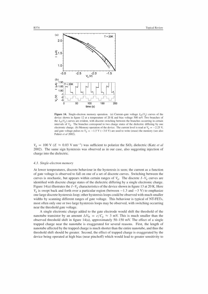
4.3. Single-electron memory
At lower temperatures, discrete behaviour in the hysteresis is seen; the current as a functionof gate voltage is observed to fall on one of a set of discrete curves. Switching between thecurves is stochastic, but appears within certain ranges of Vg. The discrete I–Vg curves areidentified with discrete charge states of the dielectric differing by a single electronic charge.Figure 14(a) illustrates the I–Vg characteristics of the device shown in figure 13 at 20 K. HereVg is swept back and forth over a particular region (between −1.3 and −3 V) to emphasizeone large discrete hysteresis loop; other hysteresis loops could be observed with much smallerwidths by scanning different ranges of gate voltage. This behaviour is typical of NT-FETs,most often only one or two large hysteresis loops may be observed, with switching occurringnear the threshold gate voltage.
A single electronic charge added to the gate electrode would shift the threshold of thenanotube transistor by an amount �Vth = e/Cg ≈ 3 mV. This is much smaller than theobserved threshold shift in figure 14(a), approximately 50–150 mV. The effect of a singletrapped charge near the nanotube is exaggerated for several reasons. First, the length ofnanotube affected by the trapped charge is much shorter than the entire nanotube, and thus thethreshold shift should be greater. Second, the effect of trapped charge is exaggerated by thedevice being operated at high bias (near pinchoff) which would lead to greater sensitivity to
Topical Review R575
charges near the source electrode. The fact that the spacing in gate voltage between the twocurves in figure 14(a) varies significantly, becoming larger nearer the threshold (more positivegate voltage) argues that pinchoff is important; indeed, at the upper end of the gate voltagerange the source–drain bias (500 mV) is comparable to the difference between the gate voltage(−1.5 to −3.0 V) and the threshold voltage (∼−1.1 V), and pinchoff should be significant.
Figure 14(b) demonstrates memory operation of the device at 20 K. The drain current ismeasured at a gate voltage of −2.25 V and a source–drain bias of 500 mV. The drain currentis switched between high and low states by application of a gate voltage pulse of ±0.75 V(relative to the −2.25 V baseline). The difference in current between high and low states isapproximately 60 nA. The memory is stable for at least 100 s.
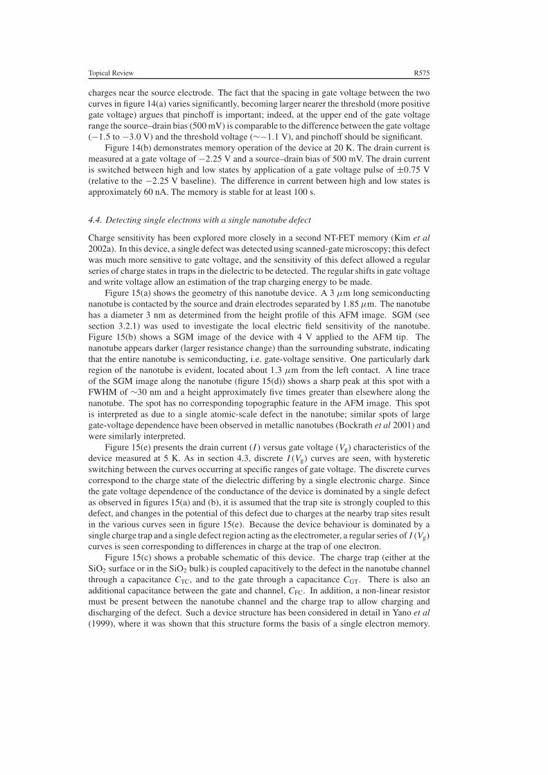
4.4. Detecting single electrons with a single nanotube defect
Charge sensitivity has been explored more closely in a second NT-FET memory (Kim et al2002a). In this device, a single defect was detected using scanned-gate microscopy; this defectwas much more sensitive to gate voltage, and the sensitivity of this defect allowed a regularseries of charge states in traps in the dielectric to be detected. The regular shifts in gate voltageand write voltage allow an estimation of the trap charging energy to be made.
Figure 15(a) shows the geometry of this nanotube device. A 3 µm long semiconductingnanotube is contacted by the source and drain electrodes separated by 1.85 µm. The nanotubehas a diameter 3 nm as determined from the height profile of this AFM image. SGM (seesection 3.2.1) was used to investigate the local electric field sensitivity of the nanotube.Figure 15(b) shows a SGM image of the device with 4 V applied to the AFM tip. Thenanotube appears darker (larger resistance change) than the surrounding substrate, indicatingthat the entire nanotube is semiconducting, i.e. gate-voltage sensitive. One particularly darkregion of the nanotube is evident, located about 1.3 µm from the left contact. A line traceof the SGM image along the nanotube (figure 15(d)) shows a sharp peak at this spot with aFWHM of ∼30 nm and a height approximately five times greater than elsewhere along thenanotube. The spot has no corresponding topographic feature in the AFM image. This spotis interpreted as due to a single atomic-scale defect in the nanotube; similar spots of largegate-voltage dependence have been observed in metallic nanotubes (Bockrath et al 2001) andwere similarly interpreted.
Figure 15(e) presents the drain current (I ) versus gate voltage (Vg) characteristics of thedevice measured at 5 K. As in section 4.3, discrete I (Vg) curves are seen, with hystereticswitching between the curves occurring at specific ranges of gate voltage. The discrete curvescorrespond to the charge state of the dielectric differing by a single electronic charge. Sincethe gate voltage dependence of the conductance of the device is dominated by a single defectas observed in figures 15(a) and (b), it is assumed that the trap site is strongly coupled to thisdefect, and changes in the potential of this defect due to charges at the nearby trap sites resultin the various curves seen in figure 15(e). Because the device behaviour is dominated by asingle charge trap and a single defect region acting as the electrometer, a regular series of I (Vg)
curves is seen corresponding to differences in charge at the trap of one electron.Figure 15(c) shows a probable schematic of this device. The charge trap (either at the
SiO2 surface or in the SiO2 bulk) is coupled capacitively to the defect in the nanotube channelthrough a capacitance CTC, and to the gate through a capacitance CGT. There is also anadditional capacitance between the gate and channel, CFC. In addition, a non-linear resistormust be present between the nanotube channel and the charge trap to allow charging anddischarging of the defect. Such a device structure has been considered in detail in Yano et al(1999), where it was shown that this structure forms the basis of a single electron memory.

R576 Topical Review
(a) (b)
(c) (d)
(e) (f)
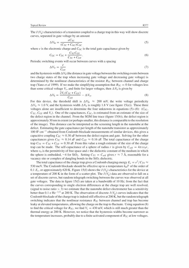
Figure 15. Single atomic-scale defect in a semiconducting nanotube. (a) AFM image of the device;the large white areas are Cr/Au contacts, the thin white line is the nanotube, with diameter 3.0 nmand length 1.85 µm between electrodes. (b) Scanned-gate microscopy (SGM—see figure 11)image of the device. (c) Schematic of the device (see text). (d) SGM shows the resistance changeas a function of position along the nanotube; i.e. a line trace through image (b). The resistancechange at the point marked with the arrow in (a), (b) and (d) is ∼5 times larger than in the rest of thenanotube. The point marked with the arrow is identified as an atomic-scale defect in the nanotube.(e) Drain current I as a function of gate voltage Vg for the nanotube device at a temperature of 5 K.Five discrete I (Vg) curves are seen, with no intermediate values of I . Four hysteresis loops areevident in the figure. Several sweeps back and forth over Vg ranges 5–7.8, 3.5–6.8, 2.5–6 and 1–5 Vare shown with the respective ranges highlighted in green, red, blue and pink, respectively; theseranges were chosen to sweep out the four hysteresis loops. �Vth indicates the shift in Vg betweenthe I (Vg) curves; �Vth ≈ 200 mV. �Vw indicates the shift in Vg between the jumps between I (Vg)
curves; �Vw ≈ 1 V. (f) I versus Vg at a temperature of 200 K plotted as scattered points. Randomswitching between curves was observed as VG was swept back and forth between 3 and 8 V.
Topical Review R577
The I (Vg) characteristics of a transistor coupled to a charge trap in this way will show discretecurves, separated in gate voltage by an amount
�Vth = eCTC
(CTC + CGC)CGC(5)
where e is the electronic charge and CGC is the total gate capacitance given by
CGC = CFC +CTCCGT
CTC + CGT. (6)
Periodic switching events will occur between curves with a spacing
�Vw = e
CGT(7)
and the hysteresis width �Vh (the distance in gate voltage between the switching events betweentwo charge states of the trap when increasing gate voltage and decreasing gate voltage) isdetermined by the nonlinear characteristics of the resistor RTC between channel and chargetrap (Yano et al 1999). If we make the simplifying assumption that RTC = 0 for voltages lessthan some critical voltage Vc, and finite for larger voltages, then �Vh is given by
�Vh = 2Vc(CTC + CGT)
CGT− �Vw. (8)
For this device, the threshold shift is �Vth ≈ 200 mV, the write voltage periodicity�Vw ≈ 1.0 V, and the hysteresis width �Vh is roughly 1.8 V (see figure 15(e)). These threevoltages alone are insufficient to determine the four unknowns in equations (5)–(8): (CFC,CTC, CGT and Vc). One of the capacitances, CFC, is estimated from an estimate of the size ofthe defect region in the channel. From the SGM line trace (figure 15(b)), the defect region isapproximately 30 nm in extent (or perhaps smaller, this distance is comparable to the resolutionof the image). This distance can be interpreted as the screening length in the nanotube at thedefect. Estimating the gate capacitance per length of the nanotube transistor as approximately100 fF cm−1 obtained from Coulomb-blockade measurements of similar devices, this gives acapacitive coupling CFC ≈ 0.30 aF between the defect region and gate. Solving for the othercapacitances gives CTC ≈ 0.14 aF and CGT ≈ 0.16 aF. The total capacitance of the chargetrap CTT = CTC + CGT = 0.30 aF. From this value a rough estimate of the size of the chargetrap can be made. The self-capacitance of a sphere of radius r is given by Cself = 4πεε0r ,where ε0 is the permittivity of free space and ε the dielectric constant of the medium in whichthe sphere is embedded, ∼4 for SiO2. Setting CTT = Cself gives r ≈ 7 Å, reasonable for avacancy site or complex of dangling bonds in the SiO2 dielectric.
The total capacitance of the charge trap gives a Coulomb charging energy Ec = e2/CTT ≈530 meV. The Coulomb blockade should be effective up to a temperature kBT of the order of0.1 Ec, or approximately 620 K. Figure 15(f) shows the I (Vg) characteristics for the device ata temperature of 200 K in the form of a scatter plot. The I (Vg) data are observed to fall on aset of discrete curves, but random telegraph switching between the curves was observed at allgate voltages. The data in figure 15(f) are taken at a bandwidth of 10 Hz; from the fact thatthe curves corresponding to single electron differences at the charge trap are well resolved,(signal to noise ratio > 3) we estimate that the nanotube defect electrometer has a sensitivitybetter than 0.1 e Hz−1/2 at 200 K. The observation of discrete I (Vg) curves indicates that theCoulomb blockade of the charge trap is indeed still effective at 200 K, but the random telegraphswitching indicates that the nonlinear resistance RTC between channel and trap has becomeleaky at elevated temperatures, allowing the charge on the trap to fluctuate. Using equation (8)to find the critical voltage for RTC, we find Vc = 430 mV, which is still much greater than thethermal energy at 200 K. However, we notice that the hysteresis widths become narrower asthe temperature increases, probably due to a finite activated component of RTC at low voltages.
R578 Topical Review
5. Conclusions
Recent advances have allowed the fabrication of long, Ohmically contacted semiconductingcarbon nanotube transistors. These devices have been used to measure the intrinsic carriermobility in the nanotube channel; the mobility exceeds 100 000 cm2 V−1 s−1 at roomtemperature and low doping, higher than any other known semiconductor at room temperature.Scanned-probe experiments on semiconducting nanotubes help to elucidate the disorder presentin various types of nanotubes. Large conduction barriers are often observed in solution-deposited semiconducting nanotubes; however in CVD nanotubes grown on-chip, the degreeof disorder is apparently lower. Electrostatic force microscopy has been used to directly verifylong mean free paths in CVD-grown semiconducting nanotubes, consistent with transportexperiments. The results indicate that semiconducting nanotubes should be an excellentmaterial for a number of semiconductor applications,especially in high-speed transistors wheremobility is crucial.
Semiconducting nanotube field-effect transistors have been used to inject and detectelectrons trapped in the SiO2 gate dielectric. Single-electron sensitivity is seen, and unusualdevices enable single-electron detection up to 200 K, with a sensitivity of better than0.1 e Hz−1/2. The results suggest that semiconducting nanotubes may find applications asexquisite sensors of e.g. chemical or biochemical species, in which a chemical signal istranslated into charge. Single molecule detection appears feasible with such a device.
Acknowledgments
This research was supported by ARDA and the Office of Naval Research through grantN000140110995, the Director of Central Intelligence Postdoctoral Research FellowshipProgram, and the National Science Foundation through grant DMR-0102950. The authorswould like to thank the coauthors of the original works reviewed here: Todd Brintlinger,Raymond Chan, Yung-Fu Chen, Enrique Cobas, Manu Forero, Stephanie Getty, Paul McEuenand Alex Zettl. The authors also thank Gary Pennington and Neil Goldsman for usefulconversations.
References
Appenzeller J, Knoch J, Derycke V, Martel R, Wind S and Avouris P 2002 Phys. Rev. Lett. 89 126801Appenzeller J, Radosavljevic M, Knoch J and Avouris P 2004 Phys. Rev. Lett. 92 048301Bachilo S M, Strano M S, Kittrell C, Hauge R H, Smalley R E and Weisman R B 2002 Science 298 2361–6Bachtold A, Fuhrer M S, Plyasunov S, Forero M, Anderson E H, Zettl A and McEuen P 2000 Phys. Rev. Lett. 84
6082–5Bachtold A, Hadley P, Nakanishi T and Dekker C 2001 Science 294 1317–20Besteman K, Lee J-O, Wiertz F G M, Heering H A and Dekker C 2003 Nano Lett. 3 727–30Bethune D S, Kiang C H, deVries M S, Gorman G, Savoy R, Vazquez J and Beyers R 1993 Nature 363 605–7Bockrath M, Cobden D H, McEuen P L, Chopra N G, Zettl A, Thess A and Smalley R E 1997 Science 275 1922–5Bockrath M, Liang W, Bozovic D, Hafner J H, Lieber C M, Tinkham M and Park H 2001 Science 291 283–5Bradley K, Cumings J, Star A, Gabriel J-C P and Gruner G 2003 Nano Lett. 3 639–41Brintlinger T, Chen Y-F, Durkop T, Cobas E, Fuhrer M S, Barry J D and Melngailis J 2002 Appl. Phys. Lett. 81
2454–6Bronikowski M J, Willis P A, Colbert D T, Smith K A and Smalley R E 2001 J. Vac. Sci. Technol. A 19 1800–5Chen R J, Bangsaruntip S, Drouvalakis K A, Kam N W S, Shim M, Li Y, Kim W, Utz P J and Dai H 2003 Proc. Natl
Acad. Sci. 100 4984–9Cobden D H, Bockrath M, Chopra N G, Zettl A, McEuen P L, Rinzler A G, Thess A and Smalley R E 1998 Physica
B 249–251 132–5Collins P G, Arnold M S and Avouris P 2001 Science 292 706–13

Topical Review R579
Dai H, Rinzler A G, Nikolaev P, Thess A, Colbert D T and Smalley R E 1996a Chem. Phys. Lett. 260 471–5Dai H, Wong E W and Lieber C M 1996b Science 272 523–6Datta S 1995 Electron Transport in Mesoscopic Systems (Cambridge: Cambridge University Press)Derycke V, Martel R, Appenzeller J and Avouris P 2002 Appl. Phys. Lett. 80 2773–5Dresselhaus M S, Dresselhaus G and Eklund P C 1996 Science of Fullerenes and Carbon Nanotubes (San Diego, CA:
Academic)Dresselhaus M S and Eklund P C 2000 Adv. Phys. 49 705–814Durkop T, Getty S A, Cobas E and Fuhrer M S 2004 Nano Lett. 4 35–9Fischetti M V, Gastaldi R, Maggioni F and Modelli A 1982a J. Appl. Phys. 53 3129–35Fischetti M V, Gastaldi R, Maggioni F and Modelli A 1982b J. Appl. Phys. 53 3136–44Fonseca A, Hernadi K, Piedigrosso P, Biro L P, Lazarescu S D, Lambin P, Thiry P A, Bernaerts D and Nagy J B 1997
Proc. Symp. on Recent Advances in the Chemistry and Physics of Fullerenes and Related Materials vol 4,ed K M Kadish and R S Ruoff (Pennington, NJ: Electrochemical Society) pp 884–906
Franklin N R, Wang Q, Tombler T W, Javey A, Shim M and Dai H 2002 Appl. Phys. Lett. 81 913–5Freitag M, Johnson A T, Kalinin S V and Bonnell D A 2002 Phys. Rev. Lett. 89 216801Freitag M, Radosavljevic M, Zhou Y and Johnson A T 2001 Appl. Phys. Lett. 79 3326–8Fuhrer M S, Forero M, Zettl A and McEuen P L 2001 Electronic Properties of Molecular Nanostructures vol 592,
ed H Kuzmany, J Fink, M Mehring and S Roth (New York: American Institute of Physics) pp 401–4Fuhrer M S, Kim B M, Chen Y-F, Durkop T and Brintlinger T 2002 Nano Lett. 2 755–9Guo J, Goasguen S, Lundstrom M and Datta S 2002 Appl. Phys. Lett. 81 1486–8Hafner J H, Cheung C-L, Oosterkamp T H and Lieber C M 2001 J. Phys. Chem. B 105 743–6Hamada N, Sawada S and Oshiyama A 1992 Phys. Rev. Lett. 68 1579–81Hartschuh A, Pedrosa H N, Novotny L and Krauss T D 2003 Science 301 1354–6Heinze S, Tersoff J, Martel R, Derycke V, Appenzeller J and Avouris P 2002 Phys. Rev. Lett. 89 106801Hrostowski H J, Morin F J, Geballe T H and Wheatley G H 1955 Phys. Rev. 100 1672–6Huang S, Cai X and Liu J 2003 J. Am. Chem. Soc. 125 5636–7Iijima S 1991 Nature 354 56–8Iijima S and Ichihashi T 1993 Nature 363 603–15Javey A, Guo J, Wang Q, Lundstrom M and Dai H 2003 Nature 424 654–7Javey A, Kim H, Brink M, Wang Q, Ural A, Gu J, McIntyre P, McEuen P L, Lundstrom M and Dai H 2002 Nat.
Mater. 1 241–6Jorio A, Saito R, Hafner J H, Lieber C M, Hunter M, McClure T, Dresselhaus G and Dresselhaus M S 2001 Phys.
Rev. Lett. 86 1118–21Kalinin S V, Bonnell D A, Freitag M and Johnson A T 2002 Appl. Phys. Lett. 81 5219–21Kane C L and Mele E J 1997 Phys. Rev. Lett. 78 1932–5Katz H E, Hong X M, Dodabalapur A and Sarpeshkar R 2002 J. Appl. Phys. 91 1572–6Kim B M, Brintlinger T, Cobas E, Zheng H, Fuhrer M S, Yu Z, Droopad R, Ramdani J and Eisenbeiser K 2004 Appl.
Phys. Lett. 84 1946–8Kim B M, Chen Y F and Fuhrer M S 2002a The Exciting World of Nanocages and Nanotubes vol 12, ed P Kamat,
D Guldi and K Kadish (Pennington, NJ: Electrochemical Society) pp 541–8Kim W, Choi H C, Shim M, Li Y, Wang D and Dai H 2002b Nano Lett. 2 703–8Kim W, Javey A, Vermesh O, Wang Q, Li Y and Dai H 2003 Nano Lett. 3 193–8Kong J, Cassell A M and Dai H 1998a Chem. Phys. Lett. 292 567–74Kong J, Soh H T, Cassell A M, Quate C F and Dai H 1998b Nature 395 878–81Kong J, Zhou C, Morpurgo A, Soh H T, Quate C F, Marcus C and Dai H 1999 Appl. Phys. A 69 305–8Kouwenhoven L R, Marcus C M, McEuen P L, Tarucha S, Westervelt R and Wingreen N S 1997 Proc. NATO
Advanced Study Institute on Mesoscopic Electron Transport vol E345, ed L L Sohn, L P Kouwenhoven andG Schon (Dordrecht: Kluwer) pp 105–214
Langer L, Bayot V, Grivei E, Issi J-P, Heremans J P, Olk C H, Stockman L, Haesendonck C V and Bruynseraede Y 1996Phys. Rev. Lett. 76 479–82
Leonard F and Tersoff J 2000 Phys. Rev. Lett. 84 4693–6Leonard F and Tersoff J 2002 Appl. Phys. Lett. 81 4835–7Liang W, Bockrath M, Bozovic D, Hafner J H, Tinkham M and Park H 2001 Nature 411 665–9Liu J, Rinzler A G, Dai H, Hafner J H, Bradley R K, Boul P J, Lu A, Iverson T, Shelimov K, Huffman C B,
Rodriguez-Macias F, Shon Y-S, Lee T R, Colbert D T and Smalley R E 1998 Science 280 1253–6Mandelis A and Christofides C 1993 Physics, Chemistry, and Technology of Solid State Gas Sensor Devices (New York:
Wiley)Martel R, Schmidt T, Shea H R, Hertel T and Avouris P 1998 Appl. Phys. Lett. 73 2447–9

R580 Topical Review
McEuen P L, Bockrath M, Cobden D H, Yoon Y-G and Louie S G 1999 Phys. Rev. Lett. 83 5098–101Mintmire J W, Dunlap B I and White C T 1992 Phys. Rev. Lett. 68 631–4Odintsov A A 2000 Phys. Rev. Lett. 85 150–3Odom T W, Huang J-L, Kim P and Lieber C M 1998 Nature 391 62–4Park J-Y, Rosenblatt S, Yaish Y, Sazonova V, Ustunel H, Braig S, Arias T A, Brouwer P W and McEuen P L 2003
http://xxx.lanl.gov/abs/cond-mat/0309641Pennington G and Goldsman N 2003 Phys. Rev. B 68 045426Radosavljevic M, Freitag M, Thadani K V and Johnson A T 2002 Nano Lett. 2 761–4Rosenblatt S, Yaish Y, Park J, Gore J, Sazonova V and McEuen P L 2002 Nano Lett. 2 869–72Saito R, Fujita M, Dresselhaus G and Dresselhaus M S 1992a Appl. Phys. Lett. 60 2204–6Saito R, Fujita M, Dresselhaus G and Dresselhaus M S 1992b Phys. Rev. B 46 1804–11Saito R and Kataura H 2001 Carbon Nanotubes (Springer Topics in Applied Physics vol 80) ed G Dresselhaus,
M S Dresselhaus and Ph Avouris (Berlin: Springer) pp 213–47Schroder D K 1998 Semiconductor Material and Device Characterization (New York: Wiley)Seeger K 2002 Semiconductor Physics: an Introduction (Berlin: Springer)Star A, Gabriel J-C P, Bradley K and Gruner G 2003 Nano Lett. 3 459–63Sze S M 1981 Physics of Semiconductor Devices (New York: Wiley)Takagi S, Toriumi A, Iwase M and Tango H 1994 IEEE Trans. Electron Devices 41 2357–62Tans S J and Dekker C 2000 Nature 404 834–5Tans S J, Devoret M H, Dai H, Thess A, Smalley R E, Georliga L J and Dekker C 1997 Nature 386 474–7Tans S J, Verschueren R M and Dekker C 1998 Nature 393 49–52Thess A, Lee R, Nikolaev P, Dai H, Petit P, Robert J, Xu C, Lee Y H, Kim S G, Rinzler A G, Colbert D T, Scuseria G E,
Tomanek D, Fischer J E and Smalley R E 1996 Science 273 483–7Wallace P R 1947 Phys. Rev. 71 622–34White C T and Todorov T N 1998 Nature 393 240–2Wildoer J W G, Venema L C, Rinzler A G, Smalley R E and Dekker C 1998 Nature 391 59–62Wind S J, Appenzeller J, Martel R, Derycke V and Avouris P 2002 Appl. Phys. Lett. 80 3817–9Yaish Y, Park J-Y, Rosenblatt S, Sazonova V, Brink M and McEuen P L 2004 Phys. Rev. Lett. 92 046401Yano K, Ishii T, Sano T, Mine T, Murai F, Hashimoto T, Kobayashi T, Kure T and Seki K 1999 Proc. IEEE 87 633–51Yao Z, Kane C L and Dekker C 2000 Phys. Rev. Lett. 84 2941–4Zhang Y and Dai H 2000 Appl. Phys. Lett. 77 3015–7