project report bel ghaziabad 6 months training
DESCRIPTION
Report on 6 months training in BEL GhaziaabadTRANSCRIPT
Project Report on
STATUS MONITORING CARD
submitted as a part of course curriculum for
Bachelor of Technology in
Electronics and Communication Engineering
Submitted to Submitted by
( Session: 2009-2013 )Department of Electronics and CommunicationWORLD COLLEGE OF TECHNOLOGY AND
MANAGEMENT
CERTIFICATE OF EXAMINATION
1

This is to certify that we have examined the Training report on
________________________________________submitted by , student of
final year B.Tech(Electronics and Communication Engg.).We hereby accord
our approval of it as an Industial Training carried out and presented in a
manner required for partial fulfillment for the Bachelor of Technology
(Electronics and Communication) degree of Maharshi Daynand University
(Rohtak). This approval does not necessarily endorse or accept every statement
made, opinion expressed or conclusion drawn as recorded in the Training
report; it only signifies the acceptance of the Training report for the purpose for
which it is submitted.
(Name) (Name) (Name)
Examiner (Internal) Examiner (External ) HOD (E&CE)
Date Date Date
Acknowledgement
2
We are grateful to the authorities of Bharat Electronics Limited, Ghaziabad
for having permitted us to go ahead with the Training on Status Monitoring
Card in partial fulfillment of Bachelor of Technology (Electronics and
Communication Engg.) degree syllabus of Maharshi Daynand
University(Rohtak.)
I am very thankful to Mr. Ajay Dagar, Head of the department of Electronics
& Communication Engineering for approving our Training , timely
encouragement and supervision.
I take this opportunity to express my sincere gratitude towards Mr.
R.N.TYAGI, SE, HRD, Bharat Electronics Limited, Ghaziabad for
accepting my letter and allowing me to complete my training at Bharat
Electronics.
I am extremely grateful to Er. JEEVESH PACHORI , MGR (D & E-
R), Bharat Electronics Limited, for permitting me to join RADAR
department.
Further I would like to thank Mr. ANKIT DHIMAN, DE (D&E-R) for
their kind help extended during the entire period of training and for their time to
time guidance and help extended during each stage our project.
Finally, I would like to thank each and every member of BEL family for
making me feel comfortable and helping me in every possible manner.
Date
DECLARATION
3
I, , student of B.TECH 8th Semester, studying at World College Of Technology
and Management, hereby declare that the six months training report on
“Automation and Robotics” is been completed.
The information and data given in the report is authentic to the best of my
knowledge.
The training report is not being submitted to any other University for award of
any other Degree, Diploma and Fellowship.
DATE: Kumar Saurav
4
SYNOPSIS
Under the Supervision of
(21 JAN 2013-14 JULY 2013)
SUBMITTED BY :-
5

Introduction
BHARAT ELECTRONICS LIMITED (BEL), the premier electronics company in India which has the distinction of being the first defence PSU to acquire operational “Navaratna” status was established in 1954 to meet the specialized electronic need of Indian Defence Services. Over the year it has grown into a multi-product, multi-technology, multi-unit company serving the need of customers in diverse fields. BEL offers products and services in a wide spectrum fields like Radars, Military communication, Naval systems, EW systems, Telecommunication, Sound and Vision broadcasting, Opto-electronics, Tank electronics, Solar and photovoltaic systems, Information technology, software and electronic components.
Besides having Seven state of art manufacturing units spread across the length and breadth of the country. BEL has a network of regional offices, marketing centres and service centres. BEL has also two offices in New York and Singapore, primarily for pronouncement of components and materials. BEL has two joint venture companies GE-BE Limited and MULTITONE Ltd. BEL also has a subsidiary named BEL-DELFT Electronics Ltd at Pune.
BEL has independent R & D division in all its unit and spend over 5% of its annual turnover on R & D. It has also set up Central Research Lab (CRL) at Bangalore and New Delhi to undertake blue sky research. About 60% of BEL’s turnover accursed from products developed either in house or in association with DRDO labs.
BEL has adopted the Total Quality Management (TQM) approach. All the divisions/units of BEL have obtained ISO:9000 accreditation. ISO:14001 accreditation has been attained by Ghaziabad unit and the engineering services division of Bangalore unit.
BEL has been successfully increasing its contribution in the field of civilian electronics, the most visible being the solar powered LED based traffic signal system and the electronic voting machine. Other Civilian products include the GPS based fish finder, Telemedicine system, PC motherboards and the computer. BEL also sets up communication network on turnkey basis. One such network is been set up in Andhra Pradesh.
6

Over the years, BEL has grown from strength to strength, surmounting the obstacles and challenges that lay in its path with resilience and determination backed by a professional management and dedicated workforce.
DESCRIPTION OF PROJECT :-
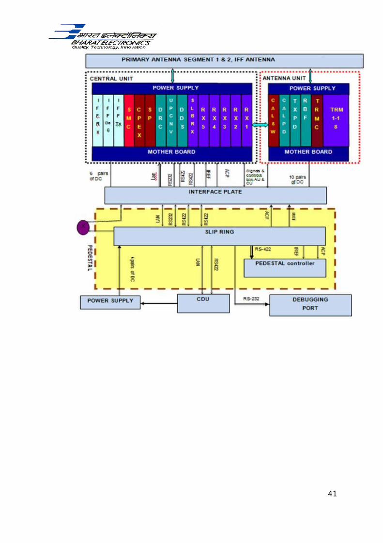
The 3D Low Level Light Weight ASLESHA Radar project is going on in Bharat Electronics Limited . We are working on STATUS MONITORING CARD (SMC) which is a part of sub system of Aslesha Radar. The various sub systems of Aslesha Radar are given below :-
Sub Systems of ASLESHA
1. Semi Active Array Antenna
2. Central Unit
3. Pedestal
4. Quadripod
5. CDU and accessories
6. Power Supply System
7

STATUS MONITORING CARD (SMC)
As all the radar electronics is on rotating sensorhead, monitoring the status
signals of each module plays very critical role during field testing . SMC
module provides the status of all the modules in the Central Unit (CU) to the
remotely located Commander Display Unit (CDU) .
The Status Monitoring card is realized using a low- cost, and low-density
FPGA device and 386COTs based processor. The voltages from the Power
Converter module are sensed using the Digital Output from the ADC, and the
voltage status representation in the CDU indicates the corresponding DC-DC
Converter failure. Also, the voltages status is represented in three levels like:
Normal, Low, and Failure conditions.
The status signals from the other modules like DDS,DRS,UPC etc are
buffered and the sample data is sensed using the FPGA and reported to the
CDP using the RS232 interface from the board processor .
The status signals from DDS, indicates the component level failure of
50MHz Oven
Controlled Crystal Oscillator (OCXO), and the DDS device. In the case of UPC, the failure Status of 60 MHz OCXO and the mixer output are provided .Also the status of the power divider input is indicated using another set of signals as PDL01 and PDL02. An IFF reset signal is provided based on the command from CDU.
8

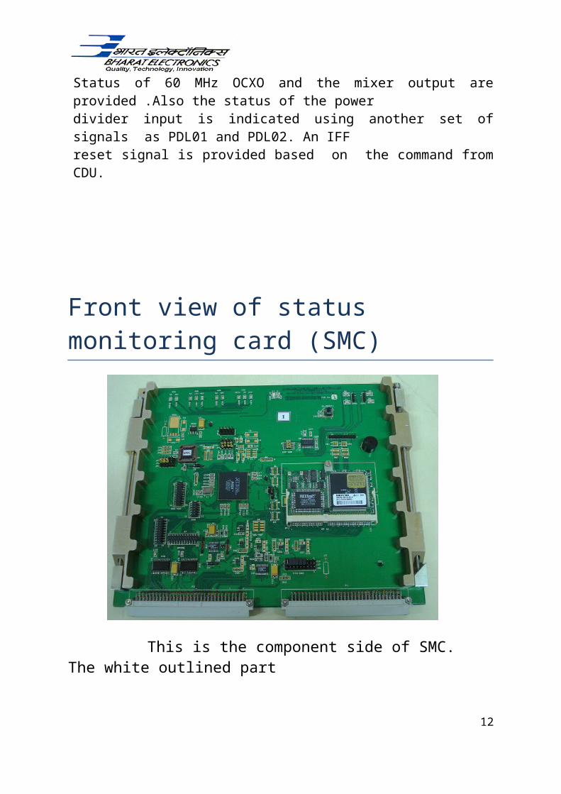
Front view of status monitoring card (SMC)
This is the component side of SMC. The white outlined part shown includes Microcontroller and FPGA .The microcontroller used in SMC became obsolete which is used for the serial communication between FPGA and CDU . Now we are implementing UART (Universal Asynchronous Receiver Transmitter) in FPGA using RS232 Serial Communication byVHDL coding .
9

Table of Contents
Serial No. Topic Page No.
SYNOPSIS 5
Chapter 1 Introduction to Organisation 12
Chapter 2 Various Departments 20
Chapter 3 Project Work 26 3D Low Level Light Weight ASLESHA
Radar
Salient Features
Technical Specifications
ECCM features
Physical Specifications
Block diagram of ASLESHA radar
Sub systems of ASLESHA
Chapter 4 Project Work 32 SMC
UART
a) What is UART ?
b) Why do we need UART ?
c) description
33
36
10

FPGA
a) Applications of FPGA
b) Diagram of FPGA
VHDL Programming
a) VHDL code for clock
b) RTL view of clock
c) Waveform for clock
d) VHDL code for transmitting data
e) RTL view of transmitting data
43
47
48
49
50
51
52
53
11
CHAPTER -1
12
Introduction to organization
BHARAT ELECTRONICS LIMITED (BEL), the premier electronics company in India
which has the distinction of being the first defense PSU to acquire operational “Navaratna”
status was established in 1954 to meet the specialized electronic need of Indian Defense
Services. Over the year it has grown into a multi-product, multi-technology, multi-unit
company serving the need of customers in diverse fields. BEL offers products and services in
a wide spectrum fields like Radars, Military communication, Naval systems, EW systems,
Telecommunication, Sound and Vision broadcasting, Opto-electronics, Tank electronics,
Solar and photovoltaic systems, Information technology, software and electronic components.
Besides having Seven state of art manufacturing units spread across the length and
breadth of the country. BEL has a network of regional offices, marketing centers and service
centers. BEL has also two offices in New York and Singapore, primarily for pronouncement
of components and materials. BEL has two joint venture companies GE-BE Limited and
MULTITONE Ltd. BEL also has a subsidiary named BEL-DELFT Electronics Ltd at Pune.
BEL has independent R & D division in all its unit and spend over 5% of its
annual turnover on R & D. It has also set up Central Research Lab (CRL) at Bangalore and
New Delhi to undertake blue sky research. About 60% of BEL’s turnover accursed from
products developed either in house or in association with DRDO labs.
BEL has adopted the Total Quality Management (TQM) approach. All the
divisions/units of BEL have obtained ISO:9000 accreditation. ISO:14001 accreditation has
been attained by Ghaziabad unit and the engineering services division of Bangalore unit.
13
BEL has been successfully increasing its contribution in the field of civilian
electronics, the most visible being the solar powered LED based traffic signal system and
the electronic voting machine. Other Civilian products include the GPS based fish finder,
Telemedicine system, PC motherboards and the computer. BEL also sets up communication
network on turnkey basis. One such network is been set up in Andhra Pradesh.
Over the years, BEL has grown from strength to strength, surmounting the obstacles
and challenges that lay in its path with resilience and determination backed by a
professional management and dedicated workforce.
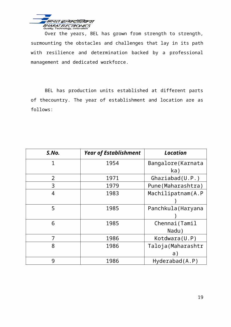
BEL has production units established at different parts of thecountry. The year of
establishment and location are as follows:
S.No. Year of Establishment Location
1 1954 Bangalore(Karnataka)
2 1971 Ghaziabad(U.P.)3 1979 Pune(Maharashtra)4 1983 Machilipatnam(A.P)5 1985 Panchkula(Haryana)6 1985 Chennai(Tamil Nadu)7 1986 Kotdwara(U.P)8 1986 Taloja(Maharashtra)9 1986 Hyderabad(A.P)
14
LOCATION OF BEL UNITS IN INDIA
15

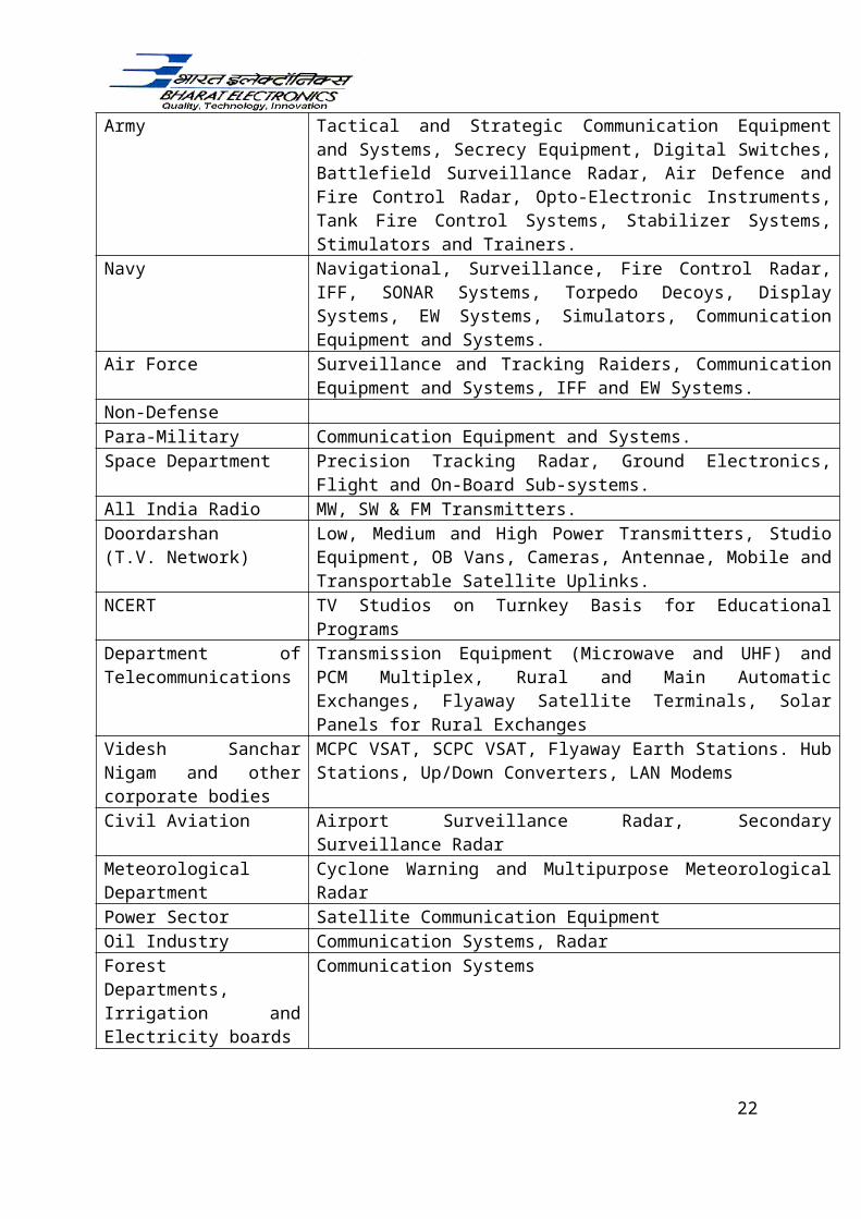
Customer Profile & BEL Product Range
DefenceArmy Tactical and Strategic Communication Equipment and Systems, Secrecy
Equipment, Digital Switches, Battlefield Surveillance Radar, Air Defence and Fire Control Radar, Opto-Electronic Instruments, Tank Fire Control Systems, Stabilizer Systems, Stimulators and Trainers.
Navy Navigational, Surveillance, Fire Control Radar, IFF, SONAR Systems, Torpedo Decoys, Display Systems, EW Systems, Simulators, Communication Equipment and Systems.
Air Force Surveillance and Tracking Raiders, Communication Equipment and Systems, IFF and EW Systems.
Non-DefensePara-Military Communication Equipment and Systems.Space Department Precision Tracking Radar, Ground Electronics, Flight and On-Board Sub-
systems.All India Radio MW, SW & FM Transmitters.Doordarshan(T.V. Network)
Low, Medium and High Power Transmitters, Studio Equipment, OB Vans, Cameras, Antennae, Mobile and Transportable Satellite Uplinks.
NCERT TV Studios on Turnkey Basis for Educational ProgramsDepartment of Telecommunications
Transmission Equipment (Microwave and UHF) and PCM Multiplex, Rural and Main Automatic Exchanges, Flyaway Satellite Terminals, Solar Panels for Rural Exchanges
Videsh Sanchar Nigam and other corporate bodies
MCPC VSAT, SCPC VSAT, Flyaway Earth Stations. Hub Stations, Up/Down Converters, LAN Modems
Civil Aviation Airport Surveillance Radar, Secondary Surveillance RadarMeteorological Department Cyclone Warning and Multipurpose Meteorological Radar
Power Sector Satellite Communication EquipmentOil Industry Communication Systems, RadarForest Departments, Irrigation and Electricity boards
Communication Systems
16

Components
Defence Transmitting Tubes, Microwave Tubes, Lasers, Batteries, Semiconductors-Discrete, Hybrid and Integrated Circuits
Non-Defence
All India Radio, Doordarshan(TV Network), Department of Telecommunications and Civil Industries
Transmitting Tubes, Microwave Tubes, and Vacuum Tubes
Entertainment Industry B/W TV Tubes, Silicon Transistors, Integrated Circuits, Bipolar and
CMOS, Piezo Electric Crystals, Ceramic Capacitors and SAW Filters
Telephone Industry Integrated Circuits, Crystals
Switching Industry Vacuum Interrupters
Instrumentation Industry Liquid Crystal Displays
Medical & Health Care X-ray Tubes
Systems/Network
It includes Identity Card Systems Software, Office Automation Software, LCD On-line Public Information Display Systems and Communication Networks / VSAT Networks.
FORMATION OF THE UNIT
PRODUCT RANGE
The product ranges today of the company are:
Radar Systems
3-Dimensional High Power Static and Mobile Radar for the Air Force.
17
Low Flying Detection Radar for both the Army and the Air force.
Tactical Control Radar Systems for the Army
Battlefield Surveillance Radar for the Army
IFF Mk-X Radar systems for the Defence and Export
ASR/MSSR systems for Civil Aviation.
Radar & allied systems Data Processing Systems.
Communications
Digital Static Tropo scatter Communication Systems for the Air Force.
Digital Mobile Tropo scatter Communication System for the Air Force and Army.
VHF, UHF & Microwave Communication Equipment.
Bulk Encryption Equipment.
Turnkey Communication Systems Projects for defence & civil users.
Static and Mobile Satellite Communication Systems for Defence
Telemetry/Tele-control Systems.
Antennae
Antennae for Radar, Terrestrial & Satellite Communication Systems.
Antennae for TV Satellite Receive and Broadcast applications.
Antennae for Line-of-sight Microwave Communication Systems.
Microwave Component
Active Microwave components like LNAs, Synthesizer, Receivers etc.
Passive Microwave components like Double Balanced Mixers, etc
Most of these products and systems are the result of a harmonious combination of
technology absorbed under ToT from abroad, Defence R&D Laboratories and BEL's own
design and development efforts.
18
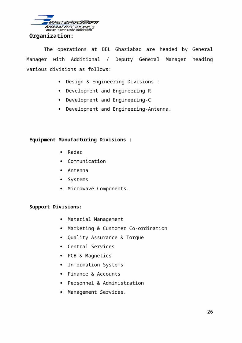
Organization:
The operations at BEL Ghaziabad are headed by General Manager with Additional /
Deputy General Manager heading various divisions as follows:
Design & Engineering Divisions :
Development and Engineering-R
Development and Engineering-C
Development and Engineering-Antenna.
Equipment Manufacturing Divisions :
Radar
Communication
Antenna
Systems
Microwave Components.
Support Divisions:
Material Management
Marketing & Customer Co-ordination
Quality Assurance & Torque
Central Services
PCB & Magnetics
Information Systems
Finance & Accounts
Personnel & Administration
Management Services.
19

CHAPTER - 2
DEPARTMENTS
20

TEST EQUIPMENT AND AUTOMATION DEPARTMENT
TEST EQUIPMENT SUPPORT (TES)
Main functions are:
Develops technical support to other departments.
Repair of equipment in case of failure.
Maintenance of equipments.
Periodic calibration of equipments.
This section deals with testing and the calibration of electronic equipments only the standards
of this department are calibrated by National Physics Laboratory (NPL).
AUTOMATION TEST EQUIPMENT (ATE)
Component testing gives faults of various discrete components of a PCB.
Integrated circuits tester tests various IC’s.
Functional testing compares output to decide whether the function is being
performed to the desired level of accuracy.
P.C.B. FABRICATION DEPARTMENT
PCB is abbreviated form of printed circuit board. As the name suggests, in a PCB the electrical
circuit is printed on a glass epoxy board. This reduces the complex writing network whose
trouble shooting in case of shorting or misconnection is not easy.
Types of PCB’s:
Single Sided: Having circuit pattern only on one side of the board.
Double Sided: Having circuit pattern on both sides of the board
Additionally Multilayered PCBs are also manufactured which use Surface Mounting Technology
during process of assembly.
QUALITY CONTROL WORKS
21
According to some laid down standards, the quality control department ensures the quality of
the product.
The raw materials and components etc. purchased are inspected according to the
specifications by the IG department. Similarly QC works department inspects all the items
manufactured in the factory.
The fabrication inspection checks all the fabricated parts and ensures that these are made as
per the part drawing. Plating, Painting and stenciling etc are done and checked as per the BEL
standards.
The assembly inspection department inspects all the assembled parts such as PCB, cable
assembly, cable form, modules, racks and shelters as per latest documents and BEL standards.
The mistakes in the PCB can be categorized as:
D&E mistake
Shop mistake
Inspection mistake
A process card is attached to each PCB under inspection. Any error in the PCB is entered into
the process card by certain codes specified for each error or defect.
After mistake is detected, following actions are taken:
Observation is made.
Object code is given.
Division code is given.
Change code is prepared.
Recommended action is taken.
WORKS ASSEMBLY
This department plays an important role in the production. Its main function is to assemble
various components, equipment’s and instruments in a particular procedure. It has two sections:-
PCB assembly and Electronic assembly.
In PCB assembly, the different types of PCB are assembled as per BEL standards. PCB is
received from the PCB department on which soldering of component is done either by hand
soldering or wave soldering.
22

HAND SOLDERING: In case of hand soldering, soldering is done manually.
WAVE SOLDERING: Wave soldering is a procedure in which PCB’s are fed to the
wave soldering machine from the opening on one side and the soldering is done by machine and
after the soldering is done PCB’s are collected from the another opening of the machine and after
that cleaning is done.
MAGNETICS DEPARTMENT
In the magnetics department different types of transformers and coils are manufactured,
which are used in the various defence equipments i.e. radar, communication equipments. This
department basically consists of three sections.
PRODUCTION CONTROL
Basic function of production control is to plan the production of transformer and coils as
per the requirement of respective division (Radar & Communication). This department is divided
into two groups-
Planning
Planning store
WORKS (PRODUCTION)
Production of transformers and coils are being carried out by the works departments.
Following process are required for the manufacturing of transformer/coils-
Preparation of former
Winding
Insulation
Tape
Sleeve
Impregnation
Mechanical Assembly
Enveloping
Moulding
Oil filling
Painting
23

Stencilling
Types of Transformer :
Following types of transformers are being manufactured in this department-
Air and Oil cool transformers Pulse transformers Air core type Moulding type transformers P.C.B. Mounting transformers
QUALITY CONTROL
After manufacturing the transformer /coils the otem is offered to the inspection
department to check the electrical parameters (DCR,No load current, full load current, dielectric
strength, inductance, insulation resistance and mechanical dimension) as mention in the GA Drawing
of the product.
MICROWAVE LABORATORY
This section undertakes:
Manufacturing of films and microwave components to meet internal requirements.
Testing of low power antenna for which test-site is about 100 Km from the factory at Sohna.
The main component testing in this department is:
Oscillators
Amplifiers
Mixers
Radiation elements (e.g. Feeders)
Microwave components (e.g. Isolators, circulators, waveguides etc.)
Filters (e.g. LPF, BPF, Uniplexers, and Multiplexers etc.)
Functioning of component is listed below:
24

Frequency response
Noise figure
VSWR
Directivity and coupling
Power measurements
Various instruments in the lab are:
Adaptor
Attenuator
Coupler
Mixer
Detector
DEVELOPMENT AND ENGINEERING (D & E) DEPARTMENT
As the name suggests D&E dept. performs the function of development and engineering of the
requirements of the company’s customers which are mainly national defence organizations. There
are five sections in this dept. – Radar1, Radar2, Communication, Antennae and Data Handling. The
five sections work in co-ordination with each other and give an aggregate result as output of D&E
dept. and this output is send as an report to the CRL (Central Research Laboratory) where the
requirements of the customers framed by D & E are considered and a software is developed fulfilling
all the requirements.
The pace of development and technological obsolescence in the field of electronics necessitates
a strong Research and Development base. This is all the more important in the area of Defence
Electronics. BEL Ghaziabad has since its inception laid a heavy emphasis on indigenous Research
and Development.
25
CHAPTER - 3
Project Review
26

3D LOW LEVEL LIGHT WEIGHT ASLESHA RADAR
3d low level light weight aslesha radar used for measuring the three dimensions that are
distance ,angle and height of the target . It is light in weight & can be carried from one place
to another easily .It has many features which are explained below :-
Salient Features
S-Band 3D surveillance for aerial targets at low and medium altitude
Detection and tracking of fighter aircraft, helicopters, slow moving
micro-light aircraft Helicopters and UAVs
Track while scan of up to 100 targets
Integrated IFF
Extensive BIT
Enabled for networking with Integrated Asterix protocol
TECHINCAL SPECIFICATIONS
Radiated RF power 1100 W (peak), 110 W (Av)
Radar instrumented range 60 Km
Target detection range 50 Km for 2 sqm RCS
27
Height coverage 30 m to 6000 m (AGL)
Elevation coverage 0˚ to 30˚
Accuracy
Range < 50 m
Azimuth <0.5˚
Height ± 500m
Resolution
Range <150 m
Azimuth < 7˚
ECCM FEATURES
Wide RF Band width
Very low antenna side lobes
LPI Tx wave form
Digital pulse compression
Burst-to- burst frequency agility
Auto selection of least jammed channel
JSP and jammer angle estimation
28

Physical Characteristics
Radar Weight : <205Kg (Unpacked), excluding power source
: <250 Kg (Packed with Soft Cases)
: <380 Kg (Packed with Hard cases)
Modular for ease of transportation and quick assembly / dismantling
Capability to carry modules under-slung by helicopter
Ease of assembly and dismantling at remote site of small dimensions with minimum
manpower.
Environment
Temperature : -30°C to 50°C
Humidity : Upto 90% at 40°C
Winds : Operation up to 50 Knots & Survival up to 70 Knots
Operation in rain, snowfall, dust etc
BLOCK DIAGRAM OF RADAR
29
Sub Systems of ASLESHA
30

Semi Active Array Antenna
Central Unit
Pedestal
Quadripod
CDU and accessories
Power Supply System
Planar Antenna
Break down details
– Array Segment 1
– Array Segment 2
– Array Antenna Frame
Antenna unit consists of 18 linear arrays each consisting of 2 sub
arrays fed by a 1:2 power divider.
1.7 m cable with BMA female connector connects the antenna unit to
the planar array.
31

CHAPTER - 4
PROJECT WORK
STATUS MONITORING CARD
32
The status monitoring card is a small part of Central Unit which is sub system of ASLESHA
basically it gives health status of the incoming signal and transmit the status to the remotely
located Commanders Display Unit (CDU).
As all the radar electronics is on rotating sensor head, monitoring the status signals of each
module plays very critical role during field testing . SMC module provides the status of all
the modules in the Central Unit (CU) to the remotely located Commander Display Unit
(CDU) .
The Status Monitoring card is realized using a low- cost, and low-density FPGA device
and 386COTs based processor. The voltages from the Power Converter module are sensed
using the Digital Output from the ADC, and the voltage status representation in the CDU
indicates the corresponding DC-DC Converter failure. Also, the voltages status is
represented in three levels like: Normal, Low, and Failure conditions.
The status signals from the other modules like DDS,DRS,UPC etc are buffered and the
sample data is sensed using the FPGA and reported to the CDP using the RS232 interface
from the board processor .
The status signals from DDS, indicates the component level failure of 50MHz Oven
Controlled Crystal Oscillator (OCXO), and the DDS device. In the case of UPC, the failure
Status of 60 MHz OCXO and the mixer output are provided .Also the status of the power
divider input is indicated using another set of signals as PDL01 and PDL02. An IFF
reset signal is provided based on the command from CDU.
STATUS MONITORING CARD
33

FRONT VIEW OF STATUS MONITORING CARD
34
SMC
DDSUPC
CDPIFF
Power Converter
RS232
Reset
DRC
10
Temp
Reset
400MHz Card status
6
Receivers

This is the component side of SMC. The white outlined part shown includes
Microcontroller and FPGA .The microcontroller used in SMC became obsolete which is
used for the serial communication between FPGA and CDU . Now we are implementing
UART (Universal Asynchronous Receiver Transmitter) in FPGA using RS232 Serial
Communication by VHDL coding .
UART (Universal Asynchronous Receiver & Transmitter)
35

What is a UART?
The UART (universal asynchronous receiver and transmitter) module provides asynchronous
serial communication with external devices such as modems and other computers. The
UART can be used to control the process of breaking parallel data from the PC down into
serial data that can be transmitted and vice versa for receiving data. The UART allows the
devices to communicate without the need to be synchronized.
The UART consists of one receiver module and one transmitter module. Those two modules
have separate inputs and outputs for most of their control lines, the lines that are shared by
both modules are the bi-directional data bus, master clock (mclkx16) and reset.
WHY DO WE NEED A UART?
1) Control the receiving and transmitting time of the data:
Since the data stream has no clock, data recovery depends on the transmitting device
and the receiving device operating at close to the same bit rate. The UART receiver is
responsible for the synchronization of the serial data stream and the recovery of data
characters.
2) Increase the accuracy and decrease the effect of the noise:
The UART system can tolerate a moderate amount of system noise without losing any
information.
36

Schematic of UART
Implementation of a digital UART by VHDL
VHDL can be used for the behavioral level design implementation of a digital UART and
offers several advantages.
The advantages of using VHDL to implement UART:
VHDL allows us to describe the function of the transmitter in a more behavior
manner rather than focus on its actual implementation at the gate level.
VHDL makes the design implementation easier to read and understand, they also
provide the ability to easily describe dependencies between various processes that
usually occur in such complex event-driven systems.
37

It is easier to test the UART by the VHDL simulation and find out if any
discrepancy occurs.
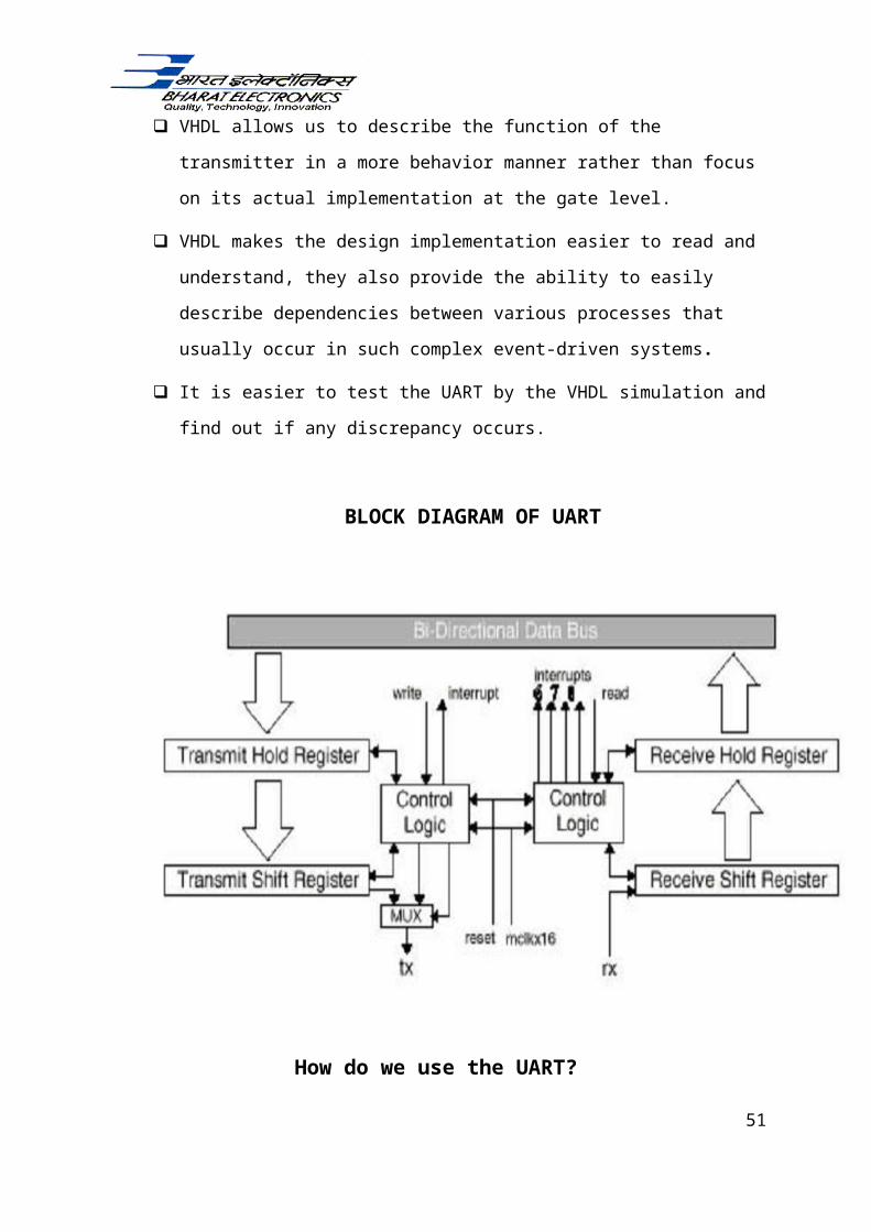
BLOCK DIAGRAM OF UART
How do we use the UART?
The use of the UART can be confusing at first but is rather straightforward once an
understanding of the UART is acquired. To begin, let us take a look at the UART data
format. This implementation of the UART transmits in blocks of 11 bits; 1 leading low start
bit, 1 trailing high stop bit, 1 parity bit and 8 data bits. The UART data format is shown
below.
The UART data format
38
The transmit and receive line of the UART are held high while no transmission/reception is
taking place. In the transmission of a sequence the active low start bit indicates to the
receiving UART that a new sequence of data is on its way. This causes the receiving UART
to take the next 8 bits as the transmitted data and the bit after that as the parity of these 8
data-bits. Lastly, a high stop bit is used to indicate the end of a block. The parity can be set
as even or odd and is used to indicate whether or not there has been an error in the received
data bits. Note that errors can still occur even if the parity bit indicates no parity errors. For
example, if the transmitted sequence is "11110000" and the parity is set as even, the parity bit
that would be transmitted with the sequence would be '0'.
If the received sequence is "11101000", the calculated parity of this sequence also equals the
transmitted parity bit of '0', thereby fooling the receiving UART into thinking that there were
no errors in transmission.
The top-level schematic of the transmit and receive module are shown
39
The signals and their respective description
40
FPGA
WHAT IS FPGA?
FIELD PROGRAMMABLE GATE ARRAY
A field-programmable gate array (FPGA) is an integrated circuit designed to be
configured by a customer or a designer after manufacturing—hence "field-programmable".
The FPGA configuration is generally specified using a hardware description language (HDL),
similar to that used for an application-specific integrated circuit (ASIC) . FPGAs have large
resources of logic gates and RAM blocks to implement complex digital computations. As
FPGA designs employ very fast IOs and bidirectional data buses it becomes a challenge to
verify correct timing of valid data within setup time and hold time. FPGAs can be used to
implement any logical function that an ASIC could perform. FPGAs contain programmable
41

logic components called "logic blocks", and a hierarchy of reconfigurable interconnects that
allow the blocks to be "wired together"—somewhat like many (changeable) logic gates that
can be inter-wired in (many) different configurations. Logic blocks can be configured to
perform complex combinational functions, or merely simple logic gates like AND and XOR.
In most FPGAs, the logic blocks also include memory elements, which may be simple flip-
flops or more complete blocks of memory.
Common FPGA Applications
Video & Image Processing Aerospace and Defense
o Avionics/DO-254
o MILCOM
o Missiles & Munitions
o Secure Solutions
o Space
Audio
o Connectivity Solutions
o Portable Electronics
o Radio
o Digital Signal Processing (DSP)
Automotive
o High Resolution Video
o Image Processing
o Vehicle Networking and Connectivity
o Automotive Infotainment
42

Broadcast
o Real-Time Video Engine
o Edge QAM
o Encoders
o Displays
o Switches and Routers
Consumer Electronics
o Digital Displays
o Digital Cameras
o Multi-function Printers
o Portable Electronics
o Set-top Boxes
Data Center
o Servers
o Security
o Routers
o Switches
o Gateways
o Load Balancing
43
High Performance Computing
o Servers
o Super Computers
o SIGINT Systems
o High-end RADARS
o High-end Beam Forming Systems
Industrial
o Industrial Imaging
o Industrial Networking
o Motor Control
Medical
o Ultrasound
o CT Scanner
o MRI
o X-ray
o PET
o Surgical Systems
Security
o Industrial Imaging
o Secure Solutions
o Image Processing Video
44

o Video Over IP Gateway
o Digital Displays
o Industrial Imaging
DIAGRAMS OF FPGA
45

VHDL PROGRAMMING
VHDL is very high speed integrated circuit Hardware Description Language.
We had created two programs using VHDL coding in QUARTUS 2 software.
In first program we generate a clock signal of 9600kbps baud rate for transmission of
data.
The frequency of Base Band signal is 50MHz.
The time period for 9600kbps signal is 104.2nS.
For Base Band signal the counter will count 1 pulse in 20nS, Now for time period of
104.2nS the counter will count up to 6 pulses .
Now for first 6 pulses the output clock will be HIGH and for next 6 pulses it will be
LOW.
46

The clock will be low and high alternatively after every 6 pulse duration.
Thus clock signal of required Baud Rate is generated.
Now we will write the VHDL code for Clock generation and Transmitting data in
QUARTUS 2 software .
VHDL CODE FOR CLOCK
library ieee;
use ieee.std_logic_1164.all;
use ieee.std_logic_arith.all;
use ieee.std_logic_unsigned.all;
entity baudrate is
port( clock : in std_logic;
p : out std_logic);
end baudrate;
architecture behavior of baudrate is
begin
process(clock)
47
variable count :natural:=0;
begin
if ( clock'event and clock='1') then
if( count<6)then
count:=count +1 ;
p<= '1';
elsif( count<12)then
p<= '0';
count:=count+1;
else
count:=0;
end if;
end if ;
end process;
end behavior;
RTL VIEW OF CLOCK
48

This is the Register Transistor Logic (RTL) diagram of clock at required Baud Rate.
WAVE FORM FOR CLOCK
49

50
VHDL CODE FOR TRANSMITTING DATA
library ieee;
use ieee.std_logic_1164.all;
use ieee.std_logic_unsigned.all;
entity bufferrr is
port(d,clk : in std_logic; y : out std_logic);
end bufferrr;
architecture behavioural of bufferrr is
signal i : std_logic_vector(7 downto 0);
begin
process(d)
begin
if(clk'event and clk='1') then
for k in 7 downto 0 loop
i(k) <= d;
end loop;
if(clk'event and clk='1') then
for k in 7 downto 0 loop
y<= i(k);
end loop;
end if;
end if;
end process;
end behavioural;
51

RTL VIEW FOR TRANSMITTING DATA
d and clk are the input and y is the output .In this basically two D-flip flops are connected in
cascade to transmit data and clk signal is used for enabling the flip flop .
The waveform of transmitting data that is generated by simulation of code in QUARTUS 2
software is shown :
52

53