programming reference guide - hilscher.com · programming reference guide netx 51/52 ... 4.1.3...
TRANSCRIPT

Programming Reference Guide
netX 51/52
Hilscher Gesellschaft für Systemautomation mbH www.hilscher.com
DOC120215PRG04EN | Revision 4 | English | 2015-01 | Released | Public

Introduction 2/414
netX 51/52 | Programming Reference Guide DOC120215PRG04EN | Revision 4 | English | 2015-01 | Released | Public © Hilscher, 2012-2015
Table of Contents
1 Introduction.............................................................................................................................................4 1.1 About this Document......................................................................................................................4 1.2 List of Revisions .............................................................................................................................4 1.3 Terms, Abbreviations and Definitions ............................................................................................5 1.4 References to Documents..............................................................................................................5 1.5 Legal Notes ....................................................................................................................................6
1.5.1 Copyright ........................................................................................................................................... 6 1.5.2 Important Notes................................................................................................................................. 6 1.5.3 Exclusion of Liability .......................................................................................................................... 7 1.5.4 Export ................................................................................................................................................ 7
2 Naming Conventions .............................................................................................................................8
3 System Functions ..................................................................................................................................9 3.1 ACCESS_KEY – Access Protection ............................................................................................12 3.2 NETX_REV – netX Revision........................................................................................................14 3.3 IO Configuration ...........................................................................................................................15 3.4 HIF IO Configuration ....................................................................................................................32 3.5 MEM_PIO – Memory PIO Mode Controller..................................................................................58 3.6 RESET – Reset Controller ...........................................................................................................60 3.7 Clock Control – Clock Generation and Control ............................................................................61 3.8 WDG - Watchdog .........................................................................................................................69 3.9 SYS_STAT – System Status........................................................................................................71 3.10 NETX_LIC – netX License ...........................................................................................................77
4 Memory Controller ...............................................................................................................................79 4.1 External Memory ..........................................................................................................................79
4.1.1 External Memory Areas ................................................................................................................... 79 4.1.2 SRAM Device .................................................................................................................................. 80 4.1.3 SDRAM Device ............................................................................................................................... 87
4.2 Internal SRAM..............................................................................................................................96 4.2.1 INTRAM Areas ................................................................................................................................ 96 4.2.2 INTRAM Parity Control .................................................................................................................... 96
5 Dual-Port Memory ..............................................................................................................................102 5.1 Software Interface ......................................................................................................................102 5.2 DPM Window Mapping...............................................................................................................102 5.3 DPM Access Tunnel...................................................................................................................104 5.4 DPM Registers Definition ...........................................................................................................105 5.5 Handshake Registers.................................................................................................................168
6 xPIC – Peripheral Interface Controller .............................................................................................196 6.1 General Structure.......................................................................................................................196 6.2 xPIC Debug Unit ........................................................................................................................196 6.3 xPIC_VIC – xPIC Vectored Interrupt Controller .........................................................................197 6.4 xPIC_TIMER ..............................................................................................................................208 6.5 xPIC Watchdog ..........................................................................................................................214
7 Peripheral Functions..........................................................................................................................218 7.1 GPIOs – General Purpose IOs and Timers ...............................................................................218 7.2 PIO – Programmable Input Output ............................................................................................231 7.3 ARM_TIMER ..............................................................................................................................232 7.4 IO-Link Interface.........................................................................................................................239 7.5 UART – Universal Asynchronous Receiver Transmitter............................................................250 7.6 SPI – Serial Peripheral Interface................................................................................................262 7.7 QSPI/SQI – Serial Quad I/O.......................................................................................................275 7.8 I2C – Serial I2C-Interface...........................................................................................................291 7.9 CAN Interface.............................................................................................................................304 7.10 SYSTIME – System time with IEEE 1588 functionality..............................................................321 7.11 CORDIC Unit..............................................................................................................................323 7.12 MMIO – Multiplex Matrix IOs......................................................................................................325 7.13 USB – Serial USB-Interface.......................................................................................................325 7.14 VIC – Vectored Interrupt Controller............................................................................................348

Introduction 3/414
netX 51/52 | Programming Reference Guide DOC120215PRG04EN | Revision 4 | English | 2015-01 | Released | Public © Hilscher, 2012-2015
8 Communication Functions ................................................................................................................355 8.1 PHY – Controller for internal PHY..............................................................................................355 8.2 PTR_FIFO – Pointer FIFO .........................................................................................................364 8.3 Buffer Management Unit (BMU).................................................................................................369 8.4 NFIFO Controller........................................................................................................................375 8.5 CRC – Configurable CRC-Generator.........................................................................................383 8.6 ARM_to_XPEC_IRQ..................................................................................................................385
9 DMA CONTROLLER ...........................................................................................................................386 9.1 Functional Overview...................................................................................................................386 9.2 Functional Description................................................................................................................387 9.3 Software Interface ......................................................................................................................389
9.3.1 Programming the DMA Controller ................................................................................................. 389 9.3.2 Programming a DMA Channel....................................................................................................... 390 9.3.3 Interrupt Requests Generation ...................................................................................................... 393 9.3.4 Data Flow Control for DMA Channel ............................................................................................. 394
9.4 Register Definition......................................................................................................................395 9.4.1 Base Address Area: DMAC_CH.................................................................................................... 395 9.4.2 Base Address Area: DMAC_REG ................................................................................................. 400
10 ARM System Control and Configuration Registers........................................................................407 10.1 CP15 Registers Summary..........................................................................................................407 10.2 CP15 Registers Description.......................................................................................................407
11 Appendix .............................................................................................................................................412 11.1 List of Tables..............................................................................................................................412 11.2 List of Figures.............................................................................................................................413 11.3 Contacts .....................................................................................................................................414

Introduction 4/414
netX 51/52 | Programming Reference Guide DOC120215PRG04EN | Revision 4 | English | 2015-01 | Released | Public © Hilscher, 2012-2015
1 Introduction 1.1 About this Document This manual describes all available registers of the netX 51/netX 52. You will find the register addresses and the bit descriptions.
1.2 List of Revisions
Rev Date Name Chapter Revision
1 2012-02-14 JZ all Created
2 2013-08-13 HH 9.2 Section Functional Description: AHB Master priority updated.
3 2013-08-29 HH 5.4 Register DPM_IF_CFG, bits CS_CTRL: description updated.
5.4 Register DPM_ADDR_CFG, bits CFG_WIN_ADDR_CFG: description updated.
4 2014-01-13 HH 3.7 Register CLKOUT_DIV: Explanation and example added.
7.6 Register SPI_INT_MSK_SET_CLR: ‘Interrupt is cleared’ added.
Table 1: List of Revisions

Introduction 5/414
netX 51/52 | Programming Reference Guide DOC120215PRG04EN | Revision 4 | English | 2015-01 | Released | Public © Hilscher, 2012-2015
1.3 Terms, Abbreviations and Definitions
Term Description
DPM Dual-Port Memory
HIF Host InterFace
INTRAM INTernal SRAM
XiP EXecution in Place
xMAC Flexible Media Access Controller
xPEC Flexible Protocol Execution Controller
xPIC Flexible Peripheral Interface Controller
MMIO Multiplex Matrix IOs
VIC Vectored Interrupt Controller
BMU Buffer Management Unit
eMI external Memory Interface
Table 2: Terms, Abbreviations and Definitions
All variables, parameters, and data used in this manual have the LSB/MSB (“Intel”) data format. This
corresponds to the convention of the Microsoft C Compiler.
All IP addresses in this document have host byte order.
1.4 References to Documents This document refers to the following documents:
[1] Hilscher Gesellschaft für Systemautomation mbH: Technical Data Reference Guide, netX 51/52, Step B, Revision 2, english, 2013
Table 3: References to Documents

Introduction 6/414
netX 51/52 | Programming Reference Guide DOC120215PRG04EN | Revision 4 | English | 2015-01 | Released | Public © Hilscher, 2012-2015
1.5 Legal Notes
1.5.1 Copyright
© Hilscher, 2012-2015, Hilscher Gesellschaft für Systemautomation mbH
All rights reserved.
The images, photographs and texts in the accompanying material (user manual, accompanying texts, documentation, etc.) are protected by German and international copyright law as well as international trade and protection provisions. You are not authorized to duplicate these in whole or in part using technical or
mechanical methods (printing, photocopying or other methods), to manipulate or transfer using electronic systems without prior written consent. You are not permitted to make changes to copyright notices, markings, trademarks or ownership declarations. The included diagrams do not take the patent situation into
account. The company names and product descriptions included in this document may be trademarks or brands of the respective owners and may be trademarked or patented. Any form of further use requires the explicit consent of the respective rights owner.
1.5.2 Important Notes
The user manual, accompanying texts and the documentation were created for the use of the products by
qualified experts, however, errors cannot be ruled out. For this reason, no guarantee can be made and neither juristic responsibility for erroneous information nor any liability can be assumed. Descriptions, accompanying texts and documentation included in the user manual do not present a guarantee nor any
information about proper use as stipulated in the contract or a warranted feature. It cannot be ruled out that the user manual, the accompanying texts and the documentation do not correspond exactly to the described features, standards or other data of the delivered product. No warranty or guarantee regarding the
correctness or accuracy of the information is assumed.
We reserve the right to change our products and their specification as well as related user manuals, accompanying texts and documentation at all times and without advance notice, without obligation to report
the change. Changes will be included in future manuals and do not constitute any obligations. There is no entitlement to revisions of delivered documents. The manual delivered with the product applies.
Hilscher Gesellschaft für Systemautomation mbH is not liable under any circumstances for direct, indirect,
incidental or follow-on damage or loss of earnings resulting from the use of the information contained in this publication.

Introduction 7/414
netX 51/52 | Programming Reference Guide DOC120215PRG04EN | Revision 4 | English | 2015-01 | Released | Public © Hilscher, 2012-2015
1.5.3 Exclusion of Liability
The software was produced and tested with utmost care by Hilscher Gesellschaft für Systemautomation mbH
and is made available as is. No warranty can be assumed for the performance and flawlessness of the software for all usage conditions and cases and for the results produced when utilized by the user. Liability for any damages that may result from the use of the hardware or software or related documents, is limited to
cases of intent or grossly negligent violation of significant contractual obligations. Indemnity claims for the violation of significant contractual obligations are limited to damages that are foreseeable and typical for this type of contract.
It is strictly prohibited to use the software in the following areas:
for military purposes or in weapon systems;
for the design, construction, maintenance or operation of nuclear facilities;
in air traffic control systems, air traffic or air traffic communication systems;
in life support systems;
in systems in which failures in the software could lead to personal injury or injuries leading to death.
We inform you that the software was not developed for use in dangerous environments requiring fail-proof control mechanisms. Use of the software in such an environment occurs at your own risk. No liability is assumed for damages or losses due to unauthorized use.
1.5.4 Export
The delivered product (including the technical data) is subject to export or import laws as well as the
associated regulations of different counters, in particular those of Germany and the USA. The software may not be exported to countries where this is prohibited by the United States Export Administration Act and its additional provisions. You are obligated to comply with the regulations at your personal responsibility. We
wish to inform you that you may require permission from state authorities to export, re-export or import the product.

Naming Conventions 8/414
netX 51/52 | Programming Reference Guide DOC120215PRG04EN | Revision 4 | English | 2015-01 | Released | Public © Hilscher, 2012-2015
2 Naming Conventions Generally for the various functions and parts of a microcontroller a number of acronyms come into play. For ease of use, in this reference guide a consistent naming scheme is introduced to all the netX register names
which will be used throughout. A full list of register names can be found in appendix A.
The naming of the registers is carried out as follows: The first component determines the register group, e.g. GPIO or DPM, etc., while the subsequent parts, separated by underscores "_", specify the function of the
particular register more detailed. Note that the word "register" will never occur in the name as it does not yield any additional information.
Sometimes the notation [m-n] will be used to indicate a set of registers ranging from m to n, e.g. IRQ_XP[0-3]
stands for the (sequence of) registers IRQ_XP0, IRQ_XP1, IRQ_XP2 and IRQ_XP3.

System Functions 9/414
netX 51/52 | Programming Reference Guide DOC120215PRG04EN | Revision 4 | English | 2015-01 | Released | Public © Hilscher, 2012-2015
3 System Functions This chapter lists major system functions, like IO configuration, clock- and reset control, watchdog and status, access protection, etc.
The following table is a summary of the registers, related to these functions.
ARM Address Register Name Short Description
0x1018c100 IO_CFG IO Config Register
0x1018c104 IO_CFG_MSK IO Config Mask Register
0x1018c108 IO_CFG2 IO Config2 Register
0x1018c10c IO_CFG2_MSK IO Config2 Mask Register
0x1018c110 RESET_CTRL Reset Control Register
0x1018c118 ARM_CLK_RATE_MUL_ADD Rate Multiplier Add Value of System Clock
0x1018c11c USB12_CLK_RATE_MUL_ADD Rate Multiplier Add Value of 12MHz USB clock
0x1018c120 FB0CLK_RATE_MUL_ADD Rate Multiplier Add Value
0x1018c124 FB0CLK_DIV Rate Multiplier Predivider
0x1018c128 FB1CLK_RATE_MUL_ADD Rate Multiplier Add Value
0x1018c12c FB1CLK_DIV Rate Multiplier Predivider
0x1018c130 CLKOUT_RATE_MUL_ADD Rate Multiplier Add Value
0x1018c134 CLKOUT_DIV Rate Multiplier Predivider
0x1018c138 CLK_EN Global Clock Enable Register
0x1018c13c CLK_EN_MSK Global Clock Enable Mask Register
0x1018c144 ONLY_PORN Firmware Status register
0x1018c148 NETX_REV netX Revision Register
0x1018c150 SAMPLE_AT_NRES IO Sampled at Reset Status Register
0x1018c154 NETX_STATUS netX System Status Configuration Register
0x1018c158 RDY_RUN_CFG netX RDY/RUN IO System Status Configuration Register
0x1018c15c SYSTEM_STATUS netX System Status Register
0x1018c160 NETX_LIC_ID netX License ID Register
0x1018c164 NETX_LIC_FLAGS0 netX License Flags 0 Register
0x1018c168 NETX_LIC_FLAGS1 netX License Flags 1 Register
0x1018c16c NETX_LIC_ERRORS0 netX License Errors 0 Status Register
0x1018c170 NETX_LIC_ERRORS1 netX License Errors 1 Status Register
0x1018c17c ACCESS_KEY ASIC Control Locking access-key Register
0x1018c200 MMIO0_CFG Multiplex Matrix Configuration Register for MMIO0
0x1018c204 MMIO1_CFG Multiplex Matrix Configuration Register for MMIO1
0x1018c208 MMIO2_CFG Multiplex Matrix Configuration Register for MMIO2
0x1018c20c MMIO3_CFG Multiplex Matrix Configuration Register for MMIO3
0x1018c210 MMIO4_CFG Multiplex Matrix Configuration Register for MMIO4
0x1018c214 MMIO5_CFG Multiplex Matrix Configuration Register for MMIO5
0x1018c218 MMIO6_CFG Multiplex Matrix Configuration Register for MMIO6
0x1018c21c MMIO7_CFG Multiplex Matrix Configuration Register for MMIO7
0x1018c220 MMIO8_CFG Multiplex Matrix Configuration Register for MMIO8
0x1018c224 MMIO9_CFG Multiplex Matrix Configuration Register for MMIO9
0x1018c228 MMIO10_CFG Multiplex Matrix Configuration Register for MMIO10
0x1018c22c MMIO11_CFG Multiplex Matrix Configuration Register for MMIO11
0x1018c230 MMIO12_CFG Multiplex Matrix Configuration Register for MMIO12
0x1018c234 MMIO13_CFG Multiplex Matrix Configuration Register for MMIO13

System Functions 10/414
netX 51/52 | Programming Reference Guide DOC120215PRG04EN | Revision 4 | English | 2015-01 | Released | Public © Hilscher, 2012-2015
0x1018c238 MMIO14_CFG Multiplex Matrix Configuration Register for MMIO14
0x1018c23c MMIO15_CFG Multiplex Matrix Configuration Register for MMIO15
0x1018c240 MMIO16_CFG Multiplex Matrix Configuration Register for MMIO16
0x1018c244 MMIO17_CFG Multiplex Matrix Configuration Register for MMIO17
0x1018c248 MMIO18_CFG Multiplex Matrix Configuration Register for MMIO18
0x1018c24c MMIO19_CFG Multiplex Matrix Configuration Register for MMIO19
0x1018c250 MMIO20_CFG Multiplex Matrix Configuration Register for MMIO20
0x1018c254 MMIO21_CFG Multiplex Matrix Configuration Register for MMIO21
0x1018c258 MMIO22_CFG Multiplex Matrix Configuration Register for MMIO22
0x1018c25c MMIO23_CFG Multiplex Matrix Configuration Register for MMIO23
0x1018c260 MMIO24_CFG Multiplex Matrix Configuration Register for MMIO24
0x1018c264 MMIO25_CFG Multiplex Matrix Configuration Register for MMIO25
0x1018c268 MMIO26_CFG Multiplex Matrix Configuration Register for MMIO26
0x1018c26c MMIO27_CFG Multiplex Matrix Configuration Register for MMIO27
0x1018c270 MMIO28_CFG Multiplex Matrix Configuration Register for MMIO28
0x1018c274 MMIO29_CFG Multiplex Matrix Configuration Register for MMIO29
0x1018c278 MMIO30_CFG Multiplex Matrix Configuration Register for MMIO30
0x1018c27c MMIO31_CFG Multiplex Matrix Configuration Register for MMIO31
0x1018c280 MMIO32_CFG Multiplex Matrix Configuration Register for MMIO32
0x1018c284 MMIO33_CFG Multiplex Matrix Configuration Register for MMIO33
0x1018c288 MMIO34_CFG Multiplex Matrix Configuration Register for MMIO34
0x1018c28c MMIO35_CFG Multiplex Matrix Configuration Register for MMIO35
0x1018c290 MMIO36_CFG Multiplex Matrix Configuration Register for MMIO36
0x1018c294 MMIO37_CFG Multiplex Matrix Configuration Register for MMIO37
0x1018c298 MMIO38_CFG Multiplex Matrix Configuration Register for MMIO38
0x1018c29c MMIO39_CFG Multiplex Matrix Configuration Register for MMIO39
0x1018c2a0 MMIO40_CFG Multiplex Matrix Configuration Register for MMIO40
0x1018c2a4 MMIO41_CFG Multiplex Matrix Configuration Register for MMIO41
0x1018c2a8 MMIO42_CFG Multiplex Matrix Configuration Register for MMIO42
0x1018c2ac MMIO43_CFG Multiplex Matrix Configuration Register for MMIO43
0x1018c2b0 MMIO44_CFG Multiplex Matrix Configuration Register for MMIO44
0x1018c2b4 MMIO45_CFG Multiplex Matrix Configuration Register for MMIO45
0x1018c2b8 MMIO46_CFG Multiplex Matrix Configuration Register for MMIO46
0x1018c2bc MMIO47_CFG Multiplex Matrix Configuration Register for MMIO47
0x1018c2c0 MMIO48_CFG Multiplex Matrix Configuration Register for MMIO48
0x1018c2c4 MMIO_PIO_OUT_LINE_CFG0 MMIO PIO Line Output Level Register of MMIO 0 to 31
0x1018c2c8 MMIO_PIO_OUT_LINE_CFG1 MMIO PIO Line Output Level Register of MMIO 32 to 48
0x1018c2cc MMIO_PIO_OE_LINE_CFG0 MMIO PIO Line Output Enable Register of MMIO 0 to 31
0x1018c2d0 MMIO_PIO_OE_LINE_CFG1 MMIO PIO Line Output Enable Register of MMIO 32 to 48
0x1018c2d4 MMIO_IN_LINE_STATUS0 MMIO Input Line Register of MMIO 0 to 31
0x1018c2d8 MMIO_IN_LINE_STATUS1 MMIO Input Line Register of MMIO 32 to 48
0x1018c2dc MMIO_IS_PIO_STATUS0 MMIO Mode Line Register of MMIO 0 to 31
0x1018c2e0 MMIO_IS_PIO_STATUS1 MMIO Mode Line Register of MMIO 32 to 48
0x1018c540 HIF_IO_CFG HIF IO Config Register
0x1018c544 HIF_PIO_CFG HIF PIO Mode Configuration Register
0x1018c548 HIF_PIO_OUT0 HIF PIO Output State Configuration Register 0

System Functions 11/414
netX 51/52 | Programming Reference Guide DOC120215PRG04EN | Revision 4 | English | 2015-01 | Released | Public © Hilscher, 2012-2015
0x1018c54c HIF_PIO_OUT1 HIF PIO Output State Configuration Register 1
0x1018c550 HIF_PIO_OE0 HIF PIO Output Enable Configuration Register 0
0x1018c554 HIF_PIO_OE1 HIF PIO Output Enable Configuration Register 1
0x1018c558 HIF_PIO_IN0 HIF PIO Input State Register 0
0x1018c55c HIF_PIO_IN1 HIF PIO Input State Register 1
0x1018c564 HIF_PIO_IRQ_RAW HIF PIO Raw (Before Masking) IRQ Status Register
0x1018c568 HIF_PIO_IRQ_ARM_MASK_SET HIF PIO Interrupt Mask Register for netX Internal ARM
0x1018c56c HIF_PIO_IRQ_ARM_MASK_RESET HIF PIO Interrupt Mask Reset Register for netX Internal ARM
0x1018c570 HIF_PIO_IRQ_ARM_MASKED HIF PIO Masked Interrupt Status Register for netX Internal ARM
0x1018c574 HIF_PIO_IRQ_XPIC_MASK_SET HIF PIO Interrupt Mask Register for netX Internal xPIC
0x1018c578 HIF_PIO_IRQ_XPIC_MASK_RESET HIF PIO Interrupt Mask Reset Register for netX Internal xPIC
0x1018c57c HIF_PIO_IRQ_XPIC_MASKED HIF PIO Masked Interrupt Status Register for netX Internal xPIC
0x1018c5b0 WDG_TRIG netX System Watchdog Trigger Register
0x1018c5b4 WDG_CNTR netX System Watchdog Register
0x1018c5b8 WDG_IRQ_TIMEOUT netX System Wachtdog Interrupt Timout Register
0x1018c5bc WDG_RESET_TIMEOUT netX System Watchdog Reset Timeout Register
0x101c01c0 MEM_D_PIO_OE_SET_CLEAR PIO Mode Output-Enable Set and Clear Register for MEM_D_31..16 IOs
0x101c01c4 MEM_D_PIO_OUT_SET_CLEAR PIO Mode Output-Level Set and Clear Register for MEM_D_31..16 IOs
0x101c01c8 MEM_D_PIO_IN PIO Input Status Register for MEM_D IOs
Table 4: System Functions Registers

System Functions 12/414
netX 51/52 | Programming Reference Guide DOC120215PRG04EN | Revision 4 | English | 2015-01 | Released | Public © Hilscher, 2012-2015
3.1 ACCESS_KEY – Access Protection Writing to any register in the CTRL or MMIO_CTRL address area is protected by the netX Access Key to avoid undesired changes e.g. by crashed software. The following table shows these protected registers:
ARM Address Register Name Short Description
0x1018c100 IO_CFG IO Config Register
0x1018c104 IO_CFG_MSK IO Config Mask Register
0x1018c108 IO_CFG2 IO Config2 Register
0x1018c10c IO_CFG2_MSK IO Config2 Mask Register
0x1018c110 RESET_CTRL Reset Control Register
0x1018c118 ARM_CLK_RATE_MUL_ADD Rate Multiplier Add Value of System Clock
0x1018c11c USB12_CLK_RATE_MUL_ADD Rate Multiplier Add Value of 12MHz USB clock
0x1018c120 FB0CLK_RATE_MUL_ADD Rate Multiplier Add Value
0x1018c124 FB0CLK_DIV Rate Multiplier Predivider
0x1018c128 FB1CLK_RATE_MUL_ADD Rate Multiplier Add Value
0x1018c12c FB1CLK_DIV Rate Multiplier Predivider
0x1018c130 CLKOUT_RATE_MUL_ADD Rate Multiplier Add Value
0x1018c134 CLKOUT_DIV Rate Multiplier Predivider
0x1018c138 CLK_EN Global Clock Enable Register
0x1018c13c CLK_EN_MSK Global Clock Enable Mask Register
0x1018c144 ONLY_PORN Firmware Status Register
0x1018c148 NETX_REV netX Revision Register
0x1018c200 MMIO0_CFG Multiplex Matrix Configuration Register for MMIO0
… … …
0x1018c2c0 MMIO48_CFG Multiplex Matrix Configuration Register for MMIO48
0x1018c540 HIF_IO_CFG HIF IO Config Register
Table 5: ACCESS_KEY Protected Registers
For writing to one of these registers, the software must perform the following sequence:
1. read out access key from ACCESS_KEY register
2. write back access key to ACCESS_KEY register
3. write desired value to this register
The access key will become invalid after each access to any register in the CTRL or MMIO_CTRL address area and has to be read and written again for subsequent accesses.
Note: Since netX 51/52 there are 3 separated instances of access-key-protection logic: One for ARM, one for xPIC and one shared by all other netX system masters. That allows ARM and XPIC
running access-key read-write sequence and configuration access without any synchronisation or locking completely independent.
Before netX 51/52 a sequence started by one master (e.g. ARM) became invalid when
interrupted by another master (e.g. xPIC). That was changed: ARM and xPIC are able to remove protection without being influenced by each other (or by any other master). Once an access-key-sequence was performed protected configuration registers are only writable for the
master which performed it.
To allow access to protected register for other masters (e.g. XPECs or SYSDEBUG) the third instance of access-key-protection logic is implemented. This is shared by all masters except
ARM and xPIC. When more than one of these masters should use this, locking must be done in software to avoid sequence of one master being interrupted by another. Access-key read and write address is the same for all masters. However, ARM-key is only readable or writable by

System Functions 13/414
netX 51/52 | Programming Reference Guide DOC120215PRG04EN | Revision 4 | English | 2015-01 | Released | Public © Hilscher, 2012-2015
ARM, xPIC-key only by xPIC and shared key only by all other masters but never by ARM or xPIC.
ACCESS_KEY – ASIC Control Locking Access-Key Register 0x1018c17c
31 30 29 28 27 26 25 24 23 22 21 20 19 18 17 16 15 14 13 12 11 10 9 8 7 6 5 4 3 2 1 0
reserved ACCESS_KEY
Bits Name Description R/W Default
31:16 - reserved R 0x0
15:0 ACCESS_KEY Locking access-key for next write access. R/W 0x0

System Functions 14/414
netX 51/52 | Programming Reference Guide DOC120215PRG04EN | Revision 4 | English | 2015-01 | Released | Public © Hilscher, 2012-2015
3.2 NETX_REV – netX Revision
NETX_REV – netX Revision Register 0x1018c148
This register contains information about netX hardware and bootloader revision.
31 30 29 28 27 26 25 24 23 22 21 20 19 18 17 16 15 14 13 12 11 10 9 8 7 6 5 4 3 2 1 0
reserved NETX_VERSION
Bits Name Description R/W Default
31:8 - reserved R 0x0
7:0 NETX_VERSION
netX 51/52 revision number: Hardware reset values of netX version register is: 0x01: netx100, netx500 0x01: netx50 0x02: netx5_mpw 0x41: netx5 0x50: netx10 0x05: netx51/52 Further netX revisions should increment (netx: 0x06). This register is changed to Hilscher netX bootloader revision by ROM-code: Hardware reset values should differ from Hilscher values! netX50 revision number starts with ”B” (0x42). 0x41: netx500 0x42: netx50 0x42: netx100 0x41: netx5 0x42: netx10 0x42: netx51/52
R 0x5

System Functions 15/414
netX 51/52 | Programming Reference Guide DOC120215PRG04EN | Revision 4 | English | 2015-01 | Released | Public © Hilscher, 2012-2015
3.3 IO Configuration To keep the chip package small, the netX51 uses shared IO pads, which are configurable for multiplexing different functions to the same pad. Two general methods of pad multiplexing are distinguished: synchronous and asynchronous multiplexing.
Synchronous multiplexing is configured by one MMIO*_CFG register for each of the 49 MMIO pads. The Multiplexing Matrix unit inside netX51 allows selecting one of 98 internal functions for each MMIO pad. Synchronous multiplexing does only work with signals derived from the same clock.
Some signals that do not run on 100MHz system clock are multiplexed asynchronously. Asynchronous multiplexing offers less pad sharing combinations and is configured by only registers IO_CFG and IO_CFG2. The following table shows the asynchronously shared pads:
Pad
Standard
function. Option1 Option2 Option3 Option4
Signal Select signal Signal Select signal Signal Select signal Signal Select signal Signal
MMIO0 MMIO0 SEL_FO0_A FO0_RD
MMIO1 MMIO1 SEL_FO0_A FO0_TD SEL_XM0_TX XM0_TX SEL_XM0_TXOUT_AND_SWE
XM0_TX_ECLK
MMIO2 MMIO2 SEL_FO0_A FO0_FN_EN SEL_XM0_ECLK XM0_ECLK SEL_FB0CLK_A FB0CLK
MMIO3 MMIO3 SEL_XM1_MII0 XM1_MII_RXD0 SEL_FO1_A FO1_RD
MMIO4 MMIO4 SEL_XM1_MII0 XM1_MII_TXD0 SEL_FO1_A FO1_TD SEL_XM1_TX XM1_TX SEL_XM1_TXOUT_AND_SWE
XM1_TX_ECLK
MMIO5 MMIO5 SEL_FO1_A FO1_FN_EN SEL_XM1_ECLK XM1_ECLK SEL_FB1CLK_A FB1CLK
MMIO6 MMIO6 SEL_FB0CLK_B FB0CLK_B SEL_FO0_A FO0_SD SEL_XM0_TXOE XM0_TXOE SEL_XM0_TXOE_AND_SWE
XM0_TXOE_ECLK
MMIO7 MMIO7 SEL_FB1CLK_B FB1CLK_B SEL_FO1_A FO1_SD SEL_XM1_TXOE XM1_TXOE SEL_XM1_TXOE_AND_SWE
XM1_TXOE_ECLK
MMIO8 MMIO8 SEL_XM0_MII0 XM0_MII_RXCLK SEL_PHY_DEVEL PHY0_RXDV SEL_ETH_MMIO2 ETH_MMIO_RXCLK
MMIO9 MMIO9 SEL_XM0_MII0 XM0_MII_RXD0 SEL_PHY_DEVEL PHY0_TXEN SEL_ETH_MMIO0 ETH_MMIO_RXD0
MMIO10 MMIO10 SEL_XM0_MII0 XM0_MII_RXD1 SEL_PHY_DEVEL PHY0_RXCLK SEL_ETH_MMIO0 ETH_MMIO_RXD1
MMIO11 MMIO11 SEL_XM0_MII0 XM0_MII_RXD2 SEL_PHY_DEVEL PHY0_TXCLK SEL_ETH_MMIO1 ETH_MMIO_RXD2
MMIO12 MMIO12 SEL_XM0_MII0 XM0_MII_RXD3 SEL_PHY_DEVEL PHY1_RXDV SEL_ETH_MMIO1 ETH_MMIO_RXD3
MMIO13 MMIO13 SEL_XM0_MII0 XM0_MII_RXDV SEL_PHY_DEVEL PHY1_TXEN SEL_ETH_MMIO0 ETH_MMIO_RXDV
MMIO14 MMIO14 SEL_XM0_MII1 XM0_MII_RXER SEL_PHY_DEVEL PHY1_RXCLK SEL_ETH_MMIO3 ETH_MMIO_RXER
MMIO15 MMIO15 SEL_XM0_MII0 XM0_MII_TXCLK SEL_PHY_DEVEL PHY1_TXCLK SEL_ETH_MMIO0 ETH_MMIO_TXCLK
MMIO16 MMIO16 SEL_XM0_MII0 XM0_MII_TXD0 SEL_ETH_MMIO0 ETH_MMIO_TXD0
MMIO17 MMIO17 SEL_XM0_MII0 XM0_MII_TXD1 SEL_ETM ETM_TRACECLK SEL_ETH_MMIO0 ETH_MMIO_TXD1
MMIO18 MMIO18 SEL_XM0_MII0 XM0_MII_TXD2 SEL_ETM ETM_TRACESYNC SEL_ETH_MMIO1 ETH_MMIO_TXD2
MMIO19 MMIO19 SEL_XM0_MII0 XM0_MII_TXD3 SEL_ETM ETM_DBGRQ SEL_ETH_MMIO1 ETH_MMIO_TXD3
MMIO20 MMIO20 SEL_XM0_MII0 XM0_MII_TXEN SEL_ETM ETM_DBGACK SEL_ETH_MMIO0 ETH_MMIO_TXEN
MMIO21 MMIO21 SEL_XM0_MII3 XM0_MII_TXER SEL_ETM ETM_PIPESTAT0 SEL_ETH_MMIO5 ETH_MMIO_TXER
MMIO22 MMIO22 SEL_XM0_MII2 XM0_MII_COL SEL_ETM ETM_PIPESTAT1 SEL_ETH_MMIO4 ETH_MMIO_COL
MMIO23 MMIO23 SEL_XM0_MII2 XM0_MII_CRS SEL_ETM ETM_PIPESTAT2 SEL_ETH_MMIO4 ETH_MMIO_CRS
MMIO24 MMIO24 SEL_XM1_MII0 XM1_MII_RXCLK SEL_ETM ETM_TRACEPKT0
MMIO25 MMIO25 SEL_XM1_MII0 XM1_MII_RXD1 SEL_ETM ETM_TRACEPKT1
MMIO26 MMIO26 SEL_XM0_MII4 XM0_MII_IRQ SEL_ETM ETM_TRACEPKT2
MMIO27 MMIO27 SEL_XM1_MII4 XM1_MII_IRQ SEL_ETM ETM_TRACEPKT3
MMIO28 MMIO28 SEL_XM1_MII0 XM1_MII_RXD2 SEL_ETM ETM_TRACEPKT4
MMIO29 MMIO29 SEL_XM1_MII0 XM1_MII_RXD3 SEL_ETM ETM_TRACEPKT5
MMIO30 MMIO30 SEL_XM1_MII0 XM1_MII_RXDV SEL_ETM ETM_TRACEPKT6
MMIO31 MMIO31 SEL_XM1_MII1 XM1_MII_RXER SEL_ETM ETM_TRACEPKT7
MMIO32 MMIO32 SEL_XM1_MII0 XM1_MII_TXCLK SEL_FO0_B FO0_FN_EN_B SEL_ETM ETM_TRACEPKT8
MMIO33 MMIO33 SEL_XM1_MII0 XM1_MII_TXD1 SEL_FO0_B FO0_RD_B SEL_ETM ETM_TRACEPKT9
MMIO34 MMIO34 SEL_XM1_MII0 XM1_MII_TXD2 SEL_FO0_B FO0_SD_B SEL_ETM ETM_TRACEPKT10
MMIO35 MMIO35 SEL_XM1_MII0 XM1_MII_TXD3 SEL_FO0_B FO0_TD_B SEL_ETM ETM_TRACEPKT11
MMIO36 MMIO36 SEL_XM1_MII0 XM1_MII_TXEN SEL_FO1_B FO1_FN_EN_B SEL_ETM ETM_TRACEPKT12
MMIO37 MMIO37 SEL_XM1_MII3 XM1_MII_TXER SEL_FO1_B FO1_RD_B SEL_ETM ETM_TRACEPKT13
MMIO38 MMIO38 SEL_XM1_MII2 XM1_MII_COL SEL_FO1_B FO1_SD_B SEL_ETM ETM_TRACEPKT14
MMIO39 MMIO39 SEL_XM1_MII2 XM1_MII_CRS SEL_FO1_B FO1_TD_B SEL_ETM ETM_TRACEPKT15
Table 6: MMIO Asynchronously Multiplexed Functions Pinning Table

System Functions 16/414
netX 51/52 | Programming Reference Guide DOC120215PRG04EN | Revision 4 | English | 2015-01 | Released | Public © Hilscher, 2012-2015
The select signals are set in registers IO_CFG and IO_CFG2. Their priority in the table above rises from left to right, i.e. “Option 4” has the highest priority, and “Option 1” has the lowest priority, but has higher priority
than the standard function. If none of the options is activated, the standard function applies automatically.
By default (after reset or power on), all MMIOs are configured for PIO input mode, which is a new feature (since netX10) and allows to directly control (configured as output) or read (configures as input) the signal
state of an MMIO signal through appropriate registers.

System Functions 17/414
netX 51/52 | Programming Reference Guide DOC120215PRG04EN | Revision 4 | English | 2015-01 | Released | Public © Hilscher, 2012-2015
IO_CFG – IO Config Register 0x1018c100
The following register is used for selects of output pin multiplexing. By setting the appropriate bits of IO_CFG register, the desired functions can be activated.
Selects can only be activated, if appropriate bit of IO_CFG_MSK is set. Bits will be reset according to the
IO_CFG_MSK register if a new mask is correctly written.
If no select signal for asynchronous pad multiplexing is set in register IO_CFG, the functionality of the pad will be defined by the appropriate MMIO_CFG register:
IO_CFG register is protected by the netX access key mechanism; changing this register is only possible by the following sequence:
1. read out access key from ACCESS_KEY register
2. write back access key to ACCESS_KEY register
3. write desired value to this register
31 30 29 28 27 26 25 24 23 22 21 20 19 18 17 16 15 14 13 12 11 10 9 8 7 6 5 4 3 2 1 0
reserved
ME
M_D
31T
O16
_PIO
_EN
US
B2J
TA
G_E
N
SE
L_F
O1
_B
SE
L_F
O1
_A
SE
L_F
B1C
LK_B
SE
L_F
B1C
LK_A
SE
L_X
M1_
EC
LK
SE
L_X
M1_
TX
OE
SE
L_X
M1_
TX
SE
L_F
O0
_B
SE
L_F
O0
_A
SE
L_F
B0C
LK_B
SE
L_F
B0C
LK_A
SE
L_X
M0_
EC
LK
SE
L_X
M0_
TX
OE
SE
L_X
M0_
TX
Bits Name Description R/W Default
31:16 - reserved R 0x0
15 MEM_D31TO16_PIO_EN PIO mode enable for MEM_D31 to MEM_D16. View ’extmem_pio_ctrl’ area for more details.
R/W 0x0
14 USB2JTAG_EN
global enable of USB2JTAG debug feature: Note: Addionally USB2JTAG debugging requires an enable from USB_DEV module, which is only active, if USB_DEV module is running and connection is established (s. usb_dev_cfg-usb_to_jtag_enable). Unless both enables are active, ARM-JTAG is controlled by netx JT_* pins.
R/W 0x0
13 SEL_FO1_B select Fiber Optics of PHY1 at position B (s. pinning table) R/W 0x0
12 SEL_FO1_A select Fiber Optics of PHY1 at position A (s. pinning table) R/W 0x0
11 SEL_FB1CLK_B select pad for fieldbus-clk1 at position B (s. pinning table) R/W 0x0
10 SEL_FB1CLK_A select pad for fieldbus-clk1 at position A (s. pinning table) R/W 0x0
9 SEL_XM1_ECLK select pad for xMAC1 eclk (s. pinning table) R/W 0x0
8 SEL_XM1_TXOE select pad for xMAC1 tx-bitstream direct output enable (s. pinning table)
R/W 0x0
7 SEL_XM1_TX select pad for xMAC1 tx-bitstream direct output (s. pinning table) R/W 0x0
6 SEL_FO0_B select Fiber Optics of PHY0 at position B (s. pinning table) R/W 0x0
5 SEL_FO0_A select Fiber Optics of PHY0 at position A (s. pinning table) R/W 0x0
4 SEL_FB0CLK_B select pad for fieldbus-clk0 at position B (s. pinning table) R/W 0x0
3 SEL_FB0CLK_A select pad for fieldbus-clk0 at position A (s. pinning table) R/W 0x0
2 SEL_XM0_ECLK select pad for xMAC0 eclk (s. pinning table) R/W 0x0
1 SEL_XM0_TXOE select pad for xMAC0 tx-bitstream direct output enable (s. pinning table)
R/W 0x0
0 SEL_XM0_TX select pad for xMAC0 tx-bitstream direct output (s. pinning table) R/W 0x0

System Functions 18/414
netX 51/52 | Programming Reference Guide DOC120215PRG04EN | Revision 4 | English | 2015-01 | Released | Public © Hilscher, 2012-2015
IO_CFG_MSK – IO Config Mask Register 0x1018c104
The IO_CFG_MSK register might be used to lock special IO configurations for restricted netX devices. Any bit of the IO_CFG register can only be set, if the corresponding mask bit in the IO_CFG_MSK register is set either.
This register is lockable by netX locking algorithm. It will be only reset on Power on, not on normal system nres. The IO_CFG register will change according to this register if a new mask is correctly written (netX locking algorithm).
This register is protected by the netX access-key mechanism; changing this register is only possible by the following sequence:
1. read out access-key from ACCESS_KEY register
2. write back access-key to ACCESS_KEY register
3. write desired value to this register
31 30 29 28 27 26 25 24 23 22 21 20 19 18 17 16 15 14 13 12 11 10 9 8 7 6 5 4 3 2 1 0
reserved
ME
M_D
31T
O16
_PIO
_EN
US
B2J
TA
G_E
N
SE
L_F
O1
_B
SE
L_F
O1
_A
SE
L_F
B1C
LK_B
SE
L_F
B1C
LK_A
SE
L_X
M1_
EC
LK
SE
L_X
M1_
TX
OE
SE
L_X
M1_
TX
SE
L_F
O0
_B
SE
L_F
O0
_A
SE
L_F
B0C
LK_B
SE
L_F
B0C
LK_A
SE
L_X
M0_
EC
LK
SE
L_X
M0_
TX
OE
SE
L_X
M0_
TX
Bits Name Description R/W Default
31:16 - reserved R 0x0
15 MEM_D31TO16_PIO_EN PIO mode enable for MEM_D31 to MEM_D16. View ’extmem_pio_ctrl’ area for more details.
R/W 0x1
14 USB2JTAG_EN
internal enable of USB2JTAG debug feature: Note: Addionally USB2JTAG debugging requires an enable from USB_DEV module, which is only active, if USB_DEV module is running and connection is established (s. usb_dev_cfg-usb_to_jtag_enable). Unless both enables are active, ARM-JTAG is controlled by netx JT_* pins.
R/W 0x1
13 SEL_FO1_B select Fiber Optics of PHY1 at position B (s. pinning table) R/W 0x1
12 SEL_FO1_A select Fiber Optics of PHY1 at position A (s. pinning table) R/W 0x1
11 SEL_FB1CLK_B select pad for fieldbus-clk1 at position B (s. pinning table) R/W 0x1
10 SEL_FB1CLK_A select pad for fieldbus-clk1 at position A (s. pinning table) R/W 0x1
9 SEL_XM1_ECLK select pad for xMAC1 eclk (s. pinning table) R/W 0x1
8 SEL_XM1_TXOE select pad for xMAC1 tx-bitstream direct output enable (s. pinning table)
R/W 0x1
7 SEL_XM1_TX select pad for xMAC1 tx-bitstream direct output (s. pinning table) R/W 0x1
6 SEL_FO0_B select Fiber Optics of PHY0 at position B (s. pinning table) R/W 0x1
5 SEL_FO0_A select Fiber Optics of PHY0 at position A (s. pinning table) R/W 0x1
4 SEL_FB0CLK_B select pad for fieldbus-clk0 at position B (s. pinning table) R/W 0x1
3 SEL_FB0CLK_A select pad for fieldbus-clk0 at position A (s. pinning table) R/W 0x1
2 SEL_XM0_ECLK select pad for xMAC0 eclk (s. pinning table) R/W 0x1
1 SEL_XM0_TXOE select pad for xMAC0 tx-bitstream direct output enable (s. pinning table)
R/W 0x1
0 SEL_XM0_TX select pad for xMAC0 tx-bitstream direct output (s. pinning table) R/W 0x1

System Functions 19/414
netX 51/52 | Programming Reference Guide DOC120215PRG04EN | Revision 4 | English | 2015-01 | Released | Public © Hilscher, 2012-2015
IO_CFG2 – IO Config2 Register 0x1018c108
The following register is used for selects of output pin multiplexing. By setting the appropriate bits of IO_CFG2 register, the desired functions can be activated.
Selects can only be activated, if appropriate bit of IO_CFG2_MSK is set. Bits will be reset according to the
IO_CFG2_MSK register if a new mask is correctly written.
If no select signal for asynchronous pad multiplexing is set in register IO_CFG2, the functionality of the pad will be defined by the appropriate MMIO_CFG register:
IO_CFG register is protected by the netX access key mechanism; changing this register is only possible by the following sequence:
1. read out access key from ACCESS_KEY register
2. write back access key to ACCESS_KEY register
3. write desired value to this register
Note: Selecting MMIO40..47 on HIF IOs:
Selecting MMIO40..47 on HIF IOs is done by programming related MMIO to non-PIO function in MMIO_CTRL address area.
E.g.: Programming MMIO40 as MMIO-PIO: HIF_D16 will be HIF IO.
Programming MMIO40 to non-PIO function (e.g. xm0_io0) will switch HIF_D16 to MMIO (XM0_IO0) function.
PIO function of MMIO40..47 is not available via MMIO_CTRL address area. PIO function of related HIF-IOs must be configured inside HIF_IO_CTRL address area.
Note: HIF IO configuration must be done inside HIF_IO_CFG register (area HIF_IO_CTRL).
31 30 29 28 27 26 25 24 23 22 21 20 19 18 17 16 15 14 13 12 11 10 9 8 7 6 5 4 3 2 1 0
reserved
SE
L_S
QI
SE
L_E
TM
SE
L_I2
C_M
MIO
NS
EL_
CLK
OU
T_M
MIO
48
SE
L_P
HY
_DE
VE
L
SEL_ETH_MII
SE
L_X
M1_
MII
SE
L_X
M0_
MII
SE
L_IO
LIN
K7
SE
L_IO
LIN
K6
SE
L_IO
LIN
K5
SE
L_IO
LIN
K4
SE
L_IO
LIN
K3
SE
L_IO
LIN
K2
SE
L_IO
LIN
K1
SE
L_IO
LIN
K0
Bits Name Description R/W Default
31:24 - reserved R 0x0
23 SEL_SQI
select pins for SQI SIO2 and SIO3 signal (s. pinning table) - activates spi0_sio2/3 at mem_a18/19 - switches mem_a18/19 function to pads MEM_A22/23 - deactivates spi0_sio2/3 inputs from multiplex matrix (however
R/W 0x0
22 SEL_ETM select pins for ETM9 (s. pinning table) R/W 0x0
21 SEL_I2C_MMIO select I2C0 via MMIOs instead of dedicated I2C_SDA/I2C_SCL-pads
R/W 0x0
20 NSEL_CLKOUT_MMIO48
not-select CLKOUT as MMIO48. 0: CLKOUT is MMIO48, 1: CLKOUT is clock. Note: CLKOUT is MMIO48 as default after reset, i.e. undriven input.
R/W 0x0
19 SEL_PHY_DEVEL select PHY development outputs (s. pinning table) R/W 0x0
18:14 SEL_ETH_MII select pads for ETH external MII pins (s. pinning table): 0: no select
R/W 0x0

System Functions 20/414
netX 51/52 | Programming Reference Guide DOC120215PRG04EN | Revision 4 | English | 2015-01 | Released | Public © Hilscher, 2012-2015
Bits Name Description R/W Default
1: sel_eth_mmio_3,0: select MMIO pins for RMII (rxd[1:0],rxdv,rxer,txclk,txd[1:0],txen)
2: sel_eth_mmio_1:0: select MMIO pins for minimum data transfer in phy mode (rxd,rxdv,txclk,txd,txen)
3: sel_eth_mmio_2:0: select at MMIO also rxclk pin for mac mode (rxclk)
4: sel_eth_mmio_3:0: select at MMIO also RX error signal (rxer)
5: sel_eth_mmio_4:0: select at MMIO also collision and carrier sense (col,crs)
6: sel_eth_mmio_5:0: select at MMIO also TX error signal (txer)
7: sel_eth_hif1_3,0: select HIFpos1 pins for RMII (rxd[1:0],rxdv,rxer,txclk,txd[1:0],txen)
8: sel_eth_hif1_1:0: select HIFpos1 pins for minimum data transfer in phy mode (rxd,rxdv,txclk,txd,txen)
9: sel_eth_hif1_2:0: select at HIFpos1 also rxclk pin for mac mode (rxclk)
10: sel_eth_hif1_3:0: select at HIFpos1 also RX error signal (rxer)
11: sel_eth_hif1_4:0: select at HIFpos1 also collision and carrier sense (col,crs)
12: sel_eth_hif1_5:0: sel_eth_hif1_5: select at HIFpos1 also TX error signal (txer)
13: sel_eth_hif2_3,0: select HIFpos2 pins for RMII (rxd[1:0],rxdv,rxer,txclk,txd[1:0],txen)
14: sel_eth_hif2_1:0: select HIFpos2 pins for minimum data transfer in phy mode (rxd,rxdv,txclk,txd,txen)
15: sel_eth_hif2_2:0: select at HIFpos2 also rxclk pin for mac mode (rxclk)
16: sel_eth_hif2_3:0: select at HIFpos2 also RX error signal (rxer)
17: sel_eth_hif2_4:0: select at HIFpos2 also collision and carrier sense (col,crs)
18: sel_eth_hif2_5:0: select at HIFpos2 also TX error signal (txer)
19: sel_eth_hif3_3,0: select HIFpos3 pins for RMII (rxd[1:0],rxdv,rxer,txclk,txd[1:0],txen)
20: sel_eth_hif3_1:0: select HIFpos3 pins for minimum data transfer in phy mode (rxd,rxdv,txclk,txd,txen)
21: sel_eth_hif3_2:0: select at HIFpos3 also rxclk pin for mac mode (rxclk)
22: sel_eth_hif3_3:0: select at HIFpos3 also RX error signal (rxer)
23: sel_eth_hif3_4:0: select at HIFpos3 also collision and carrier sense (col,crs)
24: sel_eth_hif3_5:0: select at HIFpos3 also TX error signal (txer)
13:11 SEL_XM1_MII
select pads for xMAC1 external MII pins (s. pinning table): 0: no select 1: sel_xm1_mii0 : select pins for minimum data transfer
(rxclk,rxd,rxdv,txclk,txd,txen) 2: sel_xm1_mii1:0: select also RX error signal (rxer) 3: sel_xm1_mii2:0: select also collision and carrier sense
(col,crs) 4: sel_xm1_mii3:0: select also TX error signal (txer) 5: sel_xm1_mii4:0: select also interrupt input (irq)
R/W 0x0
10:8 SEL_XM0_MII
select pads for xMAC0 external MII pins (s. pinning table): 0: no select 1: sel_xm0_mii0 : select pins for minimum data transfer
(rxclk,rxd,rxdv,txclk,txd,txen) 2: sel_xm0_mii1:0: select also RX error signal (rxer) 3: sel_xm0_mii2:0: select also collision and carrier sense
(col,crs) 4: sel_xm0_mii3:0: select also TX error signal (txer) 5: sel_xm0_mii4:0: select also interrupt input (irq)
R/W 0x0
7 SEL_IOLINK7 select IO-Link7(wakeup, txd, txoe, rxd) instead of gpio28..31 (before Multiplexmatrix)
R/W 0x0
6 SEL_IOLINK6 select IO-Link6(wakeup, txd, txoe, rxd) instead of gpio24..27 (before Multiplexmatrix)
R/W 0x0
5 SEL_IOLINK5 select IO-Link5(wakeup, txd, txoe, rxd) instead of gpio20..23 (before Multiplexmatrix)
R/W 0x0
4 SEL_IOLINK4 select IO-Link4(wakeup, txd, txoe, rxd) instead of gpio16..19 R/W 0x0

System Functions 21/414
netX 51/52 | Programming Reference Guide DOC120215PRG04EN | Revision 4 | English | 2015-01 | Released | Public © Hilscher, 2012-2015
Bits Name Description R/W Default
(before Multiplexmatrix)
3 SEL_IOLINK3 select IO-Link3(wakeup, txd, txoe, rxd) instead of gpio12..15 (before Multiplexmatrix)
R/W 0x0
2 SEL_IOLINK2 select IO-Link2(wakeup, txd, txoe, rxd) instead of gpio8..11 (before Multiplexmatrix)
R/W 0x0
1 SEL_IOLINK1 select IO-Link1(wakeup, txd, txoe, rxd) instead of gpio4..7 (before Multiplexmatrix)
R/W 0x0
0 SEL_IOLINK0 select IO-Link0(wakeup, txd, txoe, rxd) instead of gpio0..3 (before Multiplexmatrix)
R/W 0x0
IO_CFG2_MSK – IO Config2 Mask Register 0x1018c10c
The IO_CFG2_MSK register might be used to lock special IO configurations for restricted netX devices. Any bit of the IO_CFG2 register can only be set, if the corresponding mask bit in the IO_CFG2_MSK register is
set either.
This register is lockable by netX locking algorithm. It will be only reset on Power on, not on normal system nres. The IO_CFG2 register will change according to this register if a new mask is correctly written (netX
locking algorithm).
This register is protected by the netX access-key mechanism; changing this register is only possible by the following sequence:
1. read out access-key from ACCESS_KEY register
2. write back access-key to ACCESS_KEY register
3. write desired value to this register
Note: Selecting MMIO40..47 on HIF IOs:
Selecting MMIO40..47 on HIF IOs is done by programming related MMIO to non-PIO function in
MMIO_CTRL address area.
E.g.: Programming MMIO40 as MMIO-PIO: HIF_D16 will be HIF IO.
Programming MMIO40 to non-PIO function (e.g. xm0_io0) will switch HIF_D16 to MMIO
(XM0_IO0) function.
PIO function of MMIO40..47 is not available via MMIO_CTRL address area. PIO function of related HIF-IOs must be configured inside HIF_IO_CTRL address area.
Note: HIF IO configuration must be done inside HIF_IO_CFG register (area HIF_IO_CTRL).
31 30 29 28 27 26 25 24 23 22 21 20 19 18 17 16 15 14 13 12 11 10 9 8 7 6 5 4 3 2 1 0
reserved
SE
L_S
QI
SE
L_E
TM
SE
L_I2
C_M
MIO
NS
EL_
CLK
OU
T_M
MIO
48
SE
L_P
HY
_DE
VE
L
SEL_ETH_MII
SE
L_X
M1_
MII
SE
L_X
M0_
MII
SE
L_IO
LIN
K7
SE
L_IO
LIN
K6
SE
L_IO
LIN
K5
SE
L_IO
LIN
K4
SE
L_IO
LIN
K3
SE
L_IO
LIN
K2
SE
L_IO
LIN
K1
SE
L_IO
LIN
K0
Bits Name Description R/W Default
31:24 - reserved R 0x0
23 SEL_SQI select pins for SQI SIO2 and SIO3 signal (s. pinning table) R/W 0x1

System Functions 22/414
netX 51/52 | Programming Reference Guide DOC120215PRG04EN | Revision 4 | English | 2015-01 | Released | Public © Hilscher, 2012-2015
Bits Name Description R/W Default
- activates spi0_sio2/3 at mem_a18/19 - switches mem_a18/19 function to pads MEM_A22/23 - deactivates spi0_sio2/3 inputs from multiplex matrix (however
22 SEL_ETM select pins for ETM9 (s. pinning table) R/W 0x1
21 SEL_I2C_MMIO select I2C0 via MMIOs instead of dedicated I2C_SDA/I2C_SCL-pads
R/W 0x1
20 NSEL_CLKOUT_MMIO48
not-select CLKOUT as MMIO48. 0: CLKOUT is MMIO48, 1: CLKOUT is clock. Note: CLKOUT is MMIO48 as default after reset, i.e. undriven input.
R/W 0x1
19 SEL_PHY_DEVEL select PHY development outputs (s. pinning table) R/W 0x1
18:14 SEL_ETH_MII
select pads for ETH external MII pins (s. pinning table): 0: no select 1: sel_eth_mmio_3,0: select MMIO pins for RMII
(rxd[1:0],rxdv,rxer,txclk,txd[1:0],txen) 2: sel_eth_mmio_1:0: select MMIO pins for minimum data
transfer in phy mode (rxd,rxdv,txclk,txd,txen) 3: sel_eth_mmio_2:0: select at MMIO also rxclk pin for mac
mode (rxclk) 4: sel_eth_mmio_3:0: select at MMIO also RX error signal
(rxer) 5: sel_eth_mmio_4:0: select at MMIO also collision and
carrier sense (col,crs) 6: sel_eth_mmio_5:0: select at MMIO also TX error signal
(txer) 7: sel_eth_hif1_3,0: select HIFpos1 pins for RMII
(rxd[1:0],rxdv,rxer,txclk,txd[1:0],txen) 8: sel_eth_hif1_1:0: select HIFpos1 pins for minimum data
transfer in phy mode (rxd,rxdv,txclk,txd,txen) 9: sel_eth_hif1_2:0: select at HIFpos1 also rxclk pin for mac
mode (rxclk) 10: sel_eth_hif1_3:0: select at HIFpos1 also RX error signal
(rxer) 11: sel_eth_hif1_4:0: select at HIFpos1 also collision and
carrier sense (col,crs) 12: sel_eth_hif1_5:0: sel_eth_hif1_5: select at HIFpos1 also TX
error signal (txer) 13: sel_eth_hif2_3,0: select HIFpos2 pins for RMII
(rxd[1:0],rxdv,rxer,txclk,txd[1:0],txen) 14: sel_eth_hif2_1:0: select HIFpos2 pins for minimum data
transfer in phy mode (rxd,rxdv,txclk,txd,txen) 15: sel_eth_hif2_2:0: select at HIFpos2 also rxclk pin for mac
mode (rxclk) 16: sel_eth_hif2_3:0: select at HIFpos2 also RX error signal
(rxer) 17: sel_eth_hif2_4:0: select at HIFpos2 also collision and
carrier sense (col,crs) 18: sel_eth_hif2_5:0: select at HIFpos2 also TX error signal
(txer) 19: sel_eth_hif3_3,0: select HIFpos3 pins for RMII
(rxd[1:0],rxdv,rxer,txclk,txd[1:0],txen) 20: sel_eth_hif3_1:0: select HIFpos3 pins for minimum data
transfer in phy mode (rxd,rxdv,txclk,txd,txen) 21: sel_eth_hif3_2:0: select at HIFpos3 also rxclk pin for mac
mode (rxclk) 22: sel_eth_hif3_3:0: select at HIFpos3 also RX error signal
(rxer) 23: sel_eth_hif3_4:0: select at HIFpos3 also collision and
carrier sense (col,crs) 24: sel_eth_hif3_5:0: select at HIFpos3 also TX error signal
(txer)
R/W 0x1f
13:11 SEL_XM1_MII
select pads for xMAC1 external MII pins (s. pinning table): 0: no select 1: sel_xm1_mii0 : select pins for minimum data transfer
(rxclk,rxd,rxdv,txclk,txd,txen) 2: sel_xm1_mii1:0: select also RX error signal (rxer) 3: sel_xm1_mii2:0: select also collision and carrier sense
(col,crs) 4: sel_xm1_mii3:0: select also TX error signal (txer) 5: sel_xm1_mii4:0: select also interrupt input (irq)
R/W 0x7
10:8 SEL_XM0_MII select pads for xMAC0 external MII pins (s. pinning table): 0: no select
R/W 0x7

System Functions 23/414
netX 51/52 | Programming Reference Guide DOC120215PRG04EN | Revision 4 | English | 2015-01 | Released | Public © Hilscher, 2012-2015
Bits Name Description R/W Default
1: sel_xm0_mii0 : select pins for minimum data transfer (rxclk,rxd,rxdv,txclk,txd,txen)
2: sel_xm0_mii1:0: select also RX error signal (rxer) 3: sel_xm0_mii2:0: select also collision and carrier sense
(col,crs) 4: sel_xm0_mii3:0: select also TX error signal (txer) 5: sel_xm0_mii4:0: select also interrupt input (irq)
7 SEL_IOLINK7 select IO-Link7(wakeup, txd, txoe, rxd) instead of gpio28..31 (before Multiplexmatrix)
R/W 0x1
6 SEL_IOLINK6 select IO-Link6(wakeup, txd, txoe, rxd) instead of gpio24..27 (before Multiplexmatrix)
R/W 0x1
5 SEL_IOLINK5 select IO-Link5(wakeup, txd, txoe, rxd) instead of gpio20..23 (before Multiplexmatrix)
R/W 0x1
4 SEL_IOLINK4 select IO-Link4(wakeup, txd, txoe, rxd) instead of gpio16..19 (before Multiplexmatrix)
R/W 0x1
3 SEL_IOLINK3 select IO-Link3(wakeup, txd, txoe, rxd) instead of gpio12..15 (before Multiplexmatrix)
R/W 0x1
2 SEL_IOLINK2 select IO-Link2(wakeup, txd, txoe, rxd) instead of gpio8..11 (before Multiplexmatrix)
R/W 0x1
1 SEL_IOLINK1 select IO-Link1(wakeup, txd, txoe, rxd) instead of gpio4..7 (before Multiplexmatrix)
R/W 0x1
0 SEL_IOLINK0 select IO-Link0(wakeup, txd, txoe, rxd) instead of gpio0..3 (before Multiplexmatrix)
R/W 0x1
MMIO0_CFG – IO-Multiplex Matrix Configuration Register for MMIO0 0x1018c200 MMIO1_CFG – IO-Multiplex Matrix Configuration Register for MMIO1 0x1018c204 … MMIO39_CFG – IO-Multiplex Matrix Configuration Register for MMIO39 0x1018c29c
Some bits of these registers are protected by the netX access-key mechanism; changing them is only possible by the following sequence:
1. read out access-key from ACCESS_KEY register
2. write back access-key to ACCESS_KEY register
3. write desired value to this register
Core-inputs not mapped to any MMIO will be assigned to 0. If one core-connection is mapped to more than
one MMIO, the core-input-state will be these ORed MMIO-states.
For signal selection coding (MMIO*_SEL) look at the MMIO*_SEL Coding table below.

System Functions 24/414
netX 51/52 | Programming Reference Guide DOC120215PRG04EN | Revision 4 | English | 2015-01 | Released | Public © Hilscher, 2012-2015
31 30 29 28 27 26 25 24 23 22 21 20 19 18 17 16 15 14 13 12 11 10 9 8 7 6 5 4 3 2 1 0
reserved
ST
AT
US
_IN
_RO
PIO
_O
UT
PIO
_O
E
reserved
MM
IO_I
N_I
NV
MM
IO_
OU
T_I
NV
rese
rved
MMIO_SEL
Bits Name Description R/W Default
31:19 - reserved R 0x0
18 STATUS_IN_RO current input status of mmio[0-39], could also be read from ’mmio_in_line_status’ register
R/W 0x0
17 PIO_OUT
PIO mode output drive level of mmio[0-39], could also be programmd by ’mmio_pio_out_line_cfg’ register (not protected) Changing this bit will also change according bit in ’mmio_pio_out_line_cfg register’.
R/W 0x0
16 PIO_OE
PIO mode output enable of mmio[0-39], could also be programmd by mmio_pio_oe_line_cfg register (not protected) Changing this bit will also change according bit in ’mmio_pio_oe_line_cfg register’.
R/W 0x0
15:10 - reserved R 0x0
9 MMIO[0-39]_IN_INV 1: invert input signal; 0: keep original signal polarity (access-key-protected)
R/W 0x0
8 MMIO[0-39]_OUT_INV 1: invert output signal; 0: keep original signal polarity (access-key-protected)
R/W 0x0
7 - reserved R 0x0
6:0 MMIO[0-39]_SEL MMIO[0-39] signal selection (access-key-protected). (Default: s.Table MMIO*_SEL Coding)
R/W -
The coding of MMIO*_SEL is as follows:
Coding netX internal function
(core connection)
signal type functional group Default of
0x00 XM0_IO0 bidirectional Fieldbus0 0x01 XM0_IO1 bidirectional Fieldbus0 0x02 XM0_IO2 bidirectional Fieldbus0 0x03 XM0_IO3 bidirectional Fieldbus0 0x04 XM0_IO4 bidirectional Fieldbus0 0x05 XM0_IO5 bidirectional Fieldbus0 0x06 XM0_RX input Fieldbus0 0x07 XM0_TX_OUT tristatable output Fieldbus0 0x08 XM1_IO0 bidirectional Fieldbus1 0x09 XM1_IO1 bidirectional Fieldbus1 0x0a XM1_IO2 bidirectional Fieldbus1 0x0b XM1_IO3 bidirectional Fieldbus1 0x0c XM1_IO4 bidirectional Fieldbus1 0x0d XM1_IO5 bidirectional Fieldbus1 0x0e XM1_RX input Fieldbus1 0x0f XM1_TX_OUT tristatable output Fieldbus1 0x10 GPIO0 bidirectional GPIO/IO-Link MMIO0 0x11 GPIO1 bidirectional GPIO/IO-Link MMIO1 0x12 GPIO2 bidirectional GPIO/IO-Link MMIO2 0x13 GPIO3 bidirectional GPIO/IO-Link MMIO3 0x14 GPIO4 bidirectional GPIO/IO-Link MMIO4 0x15 GPIO5 bidirectional GPIO/IO-Link MMIO5 0x16 GPIO6 bidirectional GPIO/IO-Link MMIO6 0x17 GPIO7 bidirectional GPIO/IO-Link MMIO7 0x18 GPIO8 bidirectional GPIO/IO-Link MMIO8 0x19 GPIO9 bidirectional GPIO/IO-Link MMIO9 0x1a GPIO10 bidirectional GPIO/IO-Link MMIO10 0x1b GPIO11 bidirectional GPIO/IO-Link MMIO11 0x1c GPIO12 bidirectional GPIO/IO-Link MMIO12 0x1d GPIO13 bidirectional GPIO/IO-Link MMIO13 0x1e GPIO14 bidirectional GPIO/IO-Link MMIO14 0x1f GPIO15 bidirectional GPIO/IO-Link MMIO15 0x20 GPIO16 bidirectional GPIO/IO-Link MMIO16

System Functions 25/414
netX 51/52 | Programming Reference Guide DOC120215PRG04EN | Revision 4 | English | 2015-01 | Released | Public © Hilscher, 2012-2015
0x21 GPIO17 bidirectional GPIO/IO-Link MMIO17 0x22 GPIO18 bidirectional GPIO/IO-Link MMIO18 0x23 GPIO19 bidirectional GPIO/IO-Link MMIO19 0x24 GPIO20 bidirectional GPIO/IO-Link MMIO20 0x25 GPIO21 bidirectional GPIO/IO-Link MMIO21 0x26 GPIO22 bidirectional GPIO/IO-Link MMIO22 0x27 GPIO23 bidirectional GPIO/IO-Link MMIO23 0x28 GPIO24 bidirectional GPIO/IO-Link MMIO24 0x29 GPIO25 bidirectional GPIO/IO-Link MMIO25 0x2a GPIO26 bidirectional GPIO/IO-Link MMIO26 0x2b GPIO27 bidirectional GPIO/IO-Link MMIO27 0x2c GPIO28 bidirectional GPIO/IO-Link MMIO28 0x2d GPIO29 bidirectional GPIO/IO-Link MMIO29 0x2e GPIO30 bidirectional GPIO/IO-Link MMIO30 0x2f GPIO31 bidirectional GPIO/IO-Link MMIO31 0x30 PHY0_LED0 always driven output INT_PHY_CTRL0 link 0x31 PHY0_LED1 always driven output INT_PHY_CTRL0 trans 0x32 PHY0_LED2 always driven output INT_PHY_CTRL0 speed100 0x33 PHY0_LED3 always driven output INT_PHY_CTRL0 duplex 0x34 PHY1_LED0 always driven output INT_PHY_CTRL1 link 0x35 PHY1_LED1 always driven output INT_PHY_CTRL1 trans 0x36 PHY1_LED2 always driven output INT_PHY_CTRL1 speed100 0x37 PHY1_LED3 always driven output INT_PHY_CTRL1 duplex 0x38 MII_MDC always driven output MDIO 0x39 MII_MDIO bidirectional MDIO 0x3a SPI0_CS2N bidirectional SPI0 3rd chip select 0x3b SPI0_SIO2_MMIO bidirectional SPI0 0x3c SPI0_SIO3_MMIO bidirectional SPI0 0x3d SPI1_CLK bidirectional SPI1 0x3e SPI1_CS0N bidirectional SPI1 0x3f SPI1_CS1N bidirectional SPI1 0x40 SPI1_CS2N bidirectional SPI1 0x41 SPI1_MISO bidirectional SPI1 0x42 SPI1_MOSI bidirectional SPI1 0x43 I2C0_SCL_MMIO bidirectional I2C 0x44 I2C0_SDA_MMIO bidirectional I2C 0x45 I2C1_SCL bidirectional I2C 0x46 I2C1_SDA bidirectional I2C 0x47 XC_SAMPLE0 input Trigger/Latch Unit 0x48 XC_SAMPLE1 input Trigger/Latch Unit 0x49 XC_TRIGGER0 tristatable output Trigger/Latch Unit 0x4a XC_TRIGGER1 tristatable output Trigger/Latch Unit 0x4b UART0_CTSN input UART 0 MMIO32 0x4c UART0_RTSN tristatable output UART 0 MMIO33 0x4d UART0_RXD input UART 0 MMIO34 0x4e UART0_TXD tristatable output UART 0 MMIO35 0x4f UART1_CTSN input UART 1 MMIO36 0x50 UART1_RTSN tristatable output UART 1 MMIO37 0x51 UART1_RXD input UART 1 MMIO38 0x52 UART1_TXD tristatable output UART 1 MMIO39 0x53 UART2_CTSN input UART 2 0x54 UART2_RTSN tristatable output UART 2 0x55 UART2_RXD input UART 2 0x56 UART2_TXD tristatable output UART 2 0x57 CAN_RX input CAN 0x58 CAN_TX always driven output CAN 0x59 MEM_RDY input MEM IF ready/busy input 0x5a PIO0 bidirectional PIO 0x5b PIO1 bidirectional PIO 0x5c PIO2 bidirectional PIO 0x5d PIO3 bidirectional PIO 0x5e PIO4 bidirectional PIO 0x5f PIO5 bidirectional PIO 0x60 PIO6 bidirectional PIO 0x61 PIO7 bidirectional PIO 0x7f PIO MODE use MMIO PIO line registers PIO function MMIO[40-48]
Table 7: MMIO*_SEL Coding

System Functions 26/414
netX 51/52 | Programming Reference Guide DOC120215PRG04EN | Revision 4 | English | 2015-01 | Released | Public © Hilscher, 2012-2015
MMIO40_CFG – IO-Multiplex Matrix Configuration Register for MMIO40 0x1018c2a0 MMIO41_CFG – IO-Multiplex Matrix Configuration Register for MMIO41 0x1018c2a4 … MMIO47_CFG – IO-Multiplex Matrix Configuration Register for MMIO48 0x1018c2bc
Some bits of these registers are protected by the netX access-key mechanism; changing them is only possible by the following sequence:
1. read out access-key from ACCESS_KEY register
2. write back access-key to ACCESS_KEY register
3. write desired value to this register
Core-inputs not mapped to any MMIO will be assigned to 0. If one core-connection is mapped to more than
one MMIO, the core-input-state will be these ORed MMIO-states.
For signal selection coding (MMIO*_SEL) look at the MMIO*_SEL Coding table above.
Note: MMIO40 signal is a multiplex option of HIF_D8 and has no PIO function.
MMIO41 signal is a multiplex option of HIF_D9 and has no PIO function.
MMIO42 signal is a multiplex option of HIF_D10 and has no PIO function.
MMIO43 signal is a multiplex option of HIF_D11 and has no PIO function.
MMIO44 signal is a multiplex option of HIF_D12 and has no PIO function.
MMIO45 signal is a multiplex option of HIF_D13 and has no PIO function.
MMIO46 signal is a multiplex option of HIF_D14 and has no PIO function.
MMIO47 signal is a multiplex option of HIF_D15 and has no PIO function.
31 30 29 28 27 26 25 24 23 22 21 20 19 18 17 16 15 14 13 12 11 10 9 8 7 6 5 4 3 2 1 0
reserved
ST
AT
US
_IN
_RO
reserved
MM
IO_I
N_I
NV
MM
IO_
OU
T_I
NV
rese
rved
MMIO_SEL
Bits Name Description R/W Default
31:19 - reserved R 0x0
18 STATUS_IN_RO current input status of mmio[40-47], could also be read from ’mmio_in_line_status’ register
R/W 0x0
17:10 - reserved R 0x0
9 MMIO[40-47]_IN_INV 1: invert input signal; 0: keep original signal polarity (access-key-protected)
R/W 0x0
8 MMIO[40-47]_OUT_INV 1: invert output signal; 0: keep original signal polarity (access-key-protected)
R/W 0x0
7 - reserved R 0x0
6:0 MMIO[40-47]_SEL
MMIO[40-47] signal selection and multiplex function enable (access-key-protected). MMIO[40-47] signal is a multiplex option of HIF_D[8-15] and will be selected when this bit-field is programmed to non-PIO MMIO function. PIO mode does not exist for this MMIO[40-47] signal. Default value 0x7f deselects MMIO[40-47] multiplex option.
R/W 0x7f

System Functions 27/414
netX 51/52 | Programming Reference Guide DOC120215PRG04EN | Revision 4 | English | 2015-01 | Released | Public © Hilscher, 2012-2015
MMIO48_CFG – IO-Multiplex Matrix Configuration Register for MMIO48 0x1018c2c0
Some bits of these registers are protected by the netX access-key mechanism; changing them is only possible by the following sequence:
1. read out access-key from ACCESS_KEY register
2. write back access-key to ACCESS_KEY register
3. write desired value to this register
Core-inputs not mapped to any MMIO will be assigned to 0. If one core-connection is mapped to more than
one MMIO, the core-input-state will be these ORed MMIO-states.
For signal selection coding (MMIO*_SEL) look at the MMIO*_SEL Coding table above.
31 30 29 28 27 26 25 24 23 22 21 20 19 18 17 16 15 14 13 12 11 10 9 8 7 6 5 4 3 2 1 0
reserved
ST
AT
US
_IN
_RO
PIO
_O
UT
PIO
_O
E
reserved
MM
IO_I
N_I
NV
MM
IO_
OU
T_I
NV
rese
rved
MMIO_SEL
Bits Name Description R/W Default
31:19 - reserved R 0x0
18 STATUS_IN_RO current input status of mmio48, could also be read from ’mmio_in_line_status’ register
R/W 0x0
17 PIO_OUT
PIO mode output drive level of mmio48, could also be programmd by ’mmio_pio_out_line_cfg’ register (not protected) Changing this bit will also change according bit in ’mmio_pio_out_line_cfg register’.
R/W 0x0
16 PIO_OE
PIO mode output enable of mmio48, could also be programmd by mmio_pio_oe_line_cfg register (not protected) Changing this bit will also change according bit in ’mmio_pio_oe_line_cfg register’.
R/W 0x0
15:10 - reserved R 0x0
9 MMIO_IN_INV 1: invert input signal; 0: keep original signal polarity (access-key-protected)
R/W 0x0
8 MMIO_OUT_INV 1: invert output signal; 0: keep original signal polarity (access-key-protected)
R/W 0x0
7 - reserved R 0x0
6:0 MMIO_SEL mmio48 signal selection (default: PIO mode, access-key-protected).
R/W 0x7f

System Functions 28/414
netX 51/52 | Programming Reference Guide DOC120215PRG04EN | Revision 4 | English | 2015-01 | Released | Public © Hilscher, 2012-2015
MMIO_PIO_OUT_LINE_CFG0 – MMIO PIO Line Output Level Register of MMIO 0 to 31 0x1018c2c4
Changing bits here will change ’pio_out’ bit of related MMIO*_CFG register. Changes there will change
related bit inside this register.
Note: This register is not protected by netX access-key algorithm.
31 30 29 28 27 26 25 24 23 22 21 20 19 18 17 16 15 14 13 12 11 10 9 8 7 6 5 4 3 2 1 0
LINE
Bits Name Description R/W Default
31:0 LINE
MMIO output state if related MMIO is in PIO mode. If related MMIO is not in PIO mode, programmed setting is ignored. Bit 0 controls MMIO0, bit 1 controls MMIO1, ...
R/W 0x0
MMIO_PIO_OUT_LINE_CFG1 – MMIO PIO Line Output Level Register of MMIO 32 to 48 0x1018c2c8
Changing bits here will change ’pio_out’ bit of related MMIO*_CFG register. Changes there will change
related bit inside this register.
Note: This register is not protected by netX access-key algorithm.
Note MMIO40 has no PIO function. Settings of related bit 8 inside this register will be ignored.
MMIO41 has no PIO function. Settings of related bit 9 inside this register will be ignored.
MMIO42 has no PIO function. Settings of related bit 10 inside this register will be ignored.
MMIO43 has no PIO function. Settings of related bit 11 inside this register will be ignored.
MMIO44 has no PIO function. Settings of related bit 12 inside this register will be ignored.
MMIO45 has no PIO function. Settings of related bit 13 inside this register will be ignored.
MMIO46 has no PIO function. Settings of related bit 14 inside this register will be ignored.
MMIO47 has no PIO function. Settings of related bit 15 inside this register will be ignored.
31 30 29 28 27 26 25 24 23 22 21 20 19 18 17 16 15 14 13 12 11 10 9 8 7 6 5 4 3 2 1 0
reserved LINE
Bits Name Description R/W Default
31:17 - reserved R 0x0
16:0 LINE
MMIO output state if related MMIO is in PIO mode. If related MMIO is not in PIO mode, programmed setting is ignored. Bit 0 controls MMIO32, bit 1 controls MMIO33, ...
R/W 0x0

System Functions 29/414
netX 51/52 | Programming Reference Guide DOC120215PRG04EN | Revision 4 | English | 2015-01 | Released | Public © Hilscher, 2012-2015
MMIO_PIO_OE_LINE_CFG0 – MMIO PIO Line Output Enable Register of MMIO 0 to 31 0x1018c2cc
Changing bits here will change ’pio_oe’ bit of related MMIO*_CFG register. Changes there will change
related bit inside this register.
Note: This register is not protected by netX access-key algorithm.
31 30 29 28 27 26 25 24 23 22 21 20 19 18 17 16 15 14 13 12 11 10 9 8 7 6 5 4 3 2 1 0
LINE
Bits Name Description R/W Default
31:0 LINE
MMIO output enable if related MMIO is in PIO mode. If related MMIO is not in PIO mode, programmed setting is ignored. Bit 0 controls MMIO0, Bit 1 controls MMIO1, ...
R/W 0x0
MMIO_PIO_OE_LINE_CFG1 – MMIO PIO Line Output Enable Register of MMIO 32 to 48 0x1018c2d0
Changing bits here will change ’pio_oe’ bit of related MMIO*_CFG register. Changes there will change related bit inside this register.
Note: This register is not protected by netX access-key algorithm.
Note MMIO40 has no PIO function. Settings of related bit 8 inside this register will be ignored.
MMIO41 has no PIO function. Settings of related bit 9 inside this register will be ignored.
MMIO42 has no PIO function. Settings of related bit 10 inside this register will be ignored.
MMIO43 has no PIO function. Settings of related bit 11 inside this register will be ignored.
MMIO44 has no PIO function. Settings of related bit 12 inside this register will be ignored.
MMIO45 has no PIO function. Settings of related bit 13 inside this register will be ignored.
MMIO46 has no PIO function. Settings of related bit 14 inside this register will be ignored.
MMIO47 has no PIO function. Settings of related bit 15 inside this register will be ignored.
31 30 29 28 27 26 25 24 23 22 21 20 19 18 17 16 15 14 13 12 11 10 9 8 7 6 5 4 3 2 1 0
reserved LINE
Bits Name Description R/W Default
31:17 - reserved R 0x0
16:0 LINE
MMIO output enable if related MMIO is in PIO mode. If related MMIO is not in PIO mode, programmed setting is ignored. Bit 0 controls MMIO32, Bit 1 controls MMIO33, ...
R/W 0x0

System Functions 30/414
netX 51/52 | Programming Reference Guide DOC120215PRG04EN | Revision 4 | English | 2015-01 | Released | Public © Hilscher, 2012-2015
MMIO_IN_LINE_STATUS0 – MMIO Input Line Register of MMIO 0 to 31 0x1018c2d4
31 30 29 28 27 26 25 24 23 22 21 20 19 18 17 16 15 14 13 12 11 10 9 8 7 6 5 4 3 2 1 0
LINE
Bits Name Description R/W Default
31:0 LINE sampled MMIO input state. Does not depend whether MMIO is in PIO mode or not. Bit 0 monitors MMIO0, Bit 1 monitors MMIO1, ...
R 0x0
MMIO_IN_LINE_STATUS1 – MMIO Input Line Register of MMIO 32 to 48 0x1018c2d8
31 30 29 28 27 26 25 24 23 22 21 20 19 18 17 16 15 14 13 12 11 10 9 8 7 6 5 4 3 2 1 0
reserved LINE
Bits Name Description R/W Default
31:17 - reserved R 0x0
16:0 LINE sampled MMIO input state. Does not depend whether MMIO is in PIO mode or not. Bit 0 monitors MMIO32, Bit 1 monitors MMIO33, ...
R 0x0
MMIO_IS_PIO_STATUS0 – MMIO Mode Line Register of MMIO 0 to 31 0x1018c2dc
Note: IO Mode can be enabled or disabled in MMIO_CFG registers.
31 30 29 28 27 26 25 24 23 22 21 20 19 18 17 16 15 14 13 12 11 10 9 8 7 6 5 4 3 2 1 0
LINE
Bits Name Description R/W Default
31:0 LINE
Bit 0 shows status of MMIO0, Bit 1 shows status of MMIO1, ... 0: related MMIO is not in PIO mode (is assigned to core
functionality). 1: related MMIO is in PIO mode (is not assigned to core
functionality).
R 0x0
MMIO_IS_PIO_STATUS1 – MMIO Mode Line Register of MMIO 32 to 48 0x1018c2e0
Note: PIO Mode can be enabled or disabled in MMIO_CFG registers.

System Functions 31/414
netX 51/52 | Programming Reference Guide DOC120215PRG04EN | Revision 4 | English | 2015-01 | Released | Public © Hilscher, 2012-2015
Note MMIO40 has no PIO function. When related bit 8 inside this register is set, MMIO40 will be
active on HIF_D8.
MMIO41 has no PIO function. When related bit 9 inside this register is set, MMIO 41 will be active on HIF_D9.
MMIO42 has no PIO function. When related bit 10 inside this register is set, MMIO42 will be active on HIF_D10.
MMIO43 has no PIO function. When related bit 11 inside this register is set, MMIO43 will be
active on HIF_D11.
MMIO44 has no PIO function. When related bit 12 inside this register is set, MMIO44 will be active on HIF_D12.
MMIO45 has no PIO function. When related bit 13 inside this register is set, MMIO45 will be active on HIF_D13.
MMIO46 has no PIO function. When related bit 14 inside this register is set, MMIO46 will be
active on HIF_D14.
MMIO47 has no PIO function. When related bit 15 inside this register is set, MMIO47 will be active on HIF_D15.
31 30 29 28 27 26 25 24 23 22 21 20 19 18 17 16 15 14 13 12 11 10 9 8 7 6 5 4 3 2 1 0
reserved LINE
Bits Name Description R/W Default
31:17 - reserved R 0x0
16:0 LINE
Bit 0 shows status of MMIO32, Bit 1 shows status of MMIO33, ... 0: related MMIO is not in PIO mode (is assigned to core
functionality). 1: related MMIO is in PIO mode (is not assigned to core
functionality).
R 0x0

System Functions 32/414
netX 51/52 | Programming Reference Guide DOC120215PRG04EN | Revision 4 | English | 2015-01 | Released | Public © Hilscher, 2012-2015
3.4 HIF IO Configuration
HIF_IO_CFG – HIF IO Config Register 0x1018c540
Selects of HIF pin multiplexing. . See pin table in the netX51 Technical Reference Guide for details.This
configuration must be set up according to external netX connection before any access to external logic.
HIF_IO_CFG register is protected by the netX access key mechanism; changing this register is only possible by the following sequence:
1. read out access key from ACCESS_KEY register
2. write back access key to ACCESS_KEY register
3. write desired value to this register
Note: Be very careful programming this register. False settings may cause permanent damage on netX or devices connected to HIF-IOs.
31 30 29 28 27 26 25 24 23 22 21 20 19 18 17 16 15 14 13 12 11 10 9 8 7 6 5 4 3 2 1 0
NE
TX
50_I
O_C
OM
P_R
O
reserved
EN
_HIF
_WD
G_
SY
S_H
IF_D
19
EN
_HIF
_R
DY
_PIO
_MI
reserved S
EL_
HIF
_A_W
IDT
H
rese
rved
EN
_HIF
_SD
RA
M_M
I
HIF
_MI_
CF
G
SE
L_D
PM
_SE
RIA
L_S
PO
SE
L_D
PM
_SE
RIA
L_S
PH
SE
L_D
PM
_SE
RIA
L
SE
L_H
IF_D
PM
Bits Name Description R/W Default
31 NETX50_IO_COMP_RO
Status (read-only) of current netx50-IO-compatibility setting. netX50 compatibility setting basically protects netx51/52 IOs HIF_AHI0 and HIF_AHI1 when used for netX50-drop-in-replacement of existing netX50 designs. False programming could cause permanent damage to netx51/52. State of net50 IO comptibility setting affects HIF IO signal mapping. IO compatibility setting can be changed inside ’misc_asic_ctrl’ register of ASIC_CTRL address area. For further details view ’misc_asic_ctrl’ register description.
R/W 0x0
30:26 - reserved R 0x0
25 EN_HIF_WDG_SYS_HIF_D19
Enable ’wdg_active’/’WDGACT’-signal of netx system watchdog on HIF_D19. When this bit is set HIF_D19 will be set to output mode and provide watchdog-active signal. However this will have no effect when HIF_D19 is used for another function. For parallel DPM with watchdog HIF_D19 must be set to PIO mode inside DPM module. Note: netX system watch can be programmed inside address area ’WATCHDOG’/’NETX_WDG_AREA’.
R/W 0x0
24 EN_HIF_RDY_PIO_MI
Enable HIF_RDY for PIO usage. Note: This bit must be disabled if HIF_RDY is used as
EXT_BUS RDY (extension bus ready input). Note: This bit is ignored if HIF is DPM. Use DPM RDY
configuration if HIF_RDY should be used as PIO together with DPM functionallity.
R/W 0x1
23:12 - reserved R 0x0

System Functions 33/414
netX 51/52 | Programming Reference Guide DOC120215PRG04EN | Revision 4 | English | 2015-01 | Released | Public © Hilscher, 2012-2015
Bits Name Description R/W Default
11:8 SEL_HIF_A_WIDTH
Select HIF MI address width. Selecting smaller address bus width will allow PIO usage on related IOs when not used otherwise (e.g. as SDRAM control signals, see en_hif_sdram_mi). HIF-MI address lines above A15 are shared on high data lines. They are only available when hif_mi_cfg is set for 8 or 16 bit data MI, not for 32 bit data interface. Additionally address signal mapping depends on programmed netX50 compatibility setting (netx50_io_comp_ro): netX50b IOs HIF_AHI0,1 are not available in netX50 compatibility mode. Following settings are valid for all modes: Lines Range netX50b IOs Function Comment 0000: 11 2k HIF_A0..10 A0..A10
ext_a0..ext_a100001: 12 4k HIF_A0..11 A0..A11 + ext_a11 0010: 13 8k HIF_A0..12 A0..A12 + ext_a12 0011: 14 16k HIF_A0..13 A0..A13 + ext_a13 0100: 15 32k HIF_A0..14 A0..A14 + ext_a14 0101: 16 64k HIF_A0..15 A0..A15 + ext_a15 Following settings are only for 32 bit data when netX50 compatibility is disabled (A0,1 are rather byte-enable signals BE0 and BE2 than address lines here): Lines Range netX50b IOs Function Comment 0110: 17 128k HIF_A0..15 A0..A15
ext_a0..ext_a15 HIF_AHI0 A16 + ext_a16_d320111: 18 256k HIF_A0..15 A0..A15 HIF_AHI0,1 A16,A17 + ext_a17_d32 Following settings are valid for all 8 or 16 bit data modes but not for 32 bit data and do not depend on netX50 compatibility setting: Lines Range netX50b IOs Function Comment 0110: 17 128k HIF_A0..15 A0..A15
ext_a0..ext_a15 HIF_D20 A16 + ext_a16 0111: 18 256k HIF_A0..15 A0..A15 HIF_D20,21 A16,A17 + ext_a17 1000: 19 512k HIF_A0..15 A0..A15 HIF_D20..22 A16..18 + ext_a18 1001: 20 1M HIF_A0..15 A0..A15 HIF_D20..23 A16..19 + ext_a19 1010: 21 2M HIF_A0..15 A0..A15 HIF_D20..24 A16..20 + ext_a20 1011: 22 4M HIF_A0..15 A0..A15 HIF_D20..25 A16..21 + ext_a21 Following settings are valid for 8 or 16 bit data mode when netX50-compatibility is activated: Lines Range netX50b IOs Function Comment 1100: 23 8M HIF_A0..15 A0..A15
ext_a0..ext_a15 HIF_D20..25 A16..21
ext_a16..ext_a21
HIF_D26 A22 + ext_a22_nx50
1101: 24 16M HIF_A0..15 A0..A15 HIF_D20..25 A16..21 HIF_D26,27 A22,A23 +
ext_a23_nx50 1110: 25 32M HIF_A0..15 A0..A15 HIF_D20..25 A16..21 HIF_D26,27 A22,A23 HIF_D18 A24 +
ext_a24_nx50 Following settings are valid for 8 or 16 bit data mode when not in netX50-compatibility mode: Lines Range netX50b IOs Function Comment 1100: 23 8M HIF_A0..15 A0..A15 ext_a0..ext_a15 HIF_D20..25 A16..21 ext_a16..ext_a21
R/W 0x0

System Functions 34/414
netX 51/52 | Programming Reference Guide DOC120215PRG04EN | Revision 4 | English | 2015-01 | Released | Public © Hilscher, 2012-2015
Bits Name Description R/W Default
HIF_AHI0 A22 + ext_a22 1101: 24 16M HIF_A0..15 A0..A15 HIF_D20..25 A16..21 HIF_AHI0,1 A22,A23 + ext_a23 1110: 25 32M HIF_A0..15 A0..A15 HIF_D20..25 A16..21 HIF_AHI0,1 A22,A23 HIF_BHE3 A24 + ext_a24 Note: CS3 and A24 are shared on HIF_BHE3 when not in
netX50-compatibility mode. CS3 must be disabled when A24 shall be used. If CS3 shall be used, A24 must not be used (i.e. 1110 is forbidden) and HIF_BHE3 must be programmed as high driven output by PIO registers additionally (to ensure inactive signal state when CS3 is used as chip-select but not enabled by software yet).
Note: To use high HIF_D lines as PIOs, select non-32bit HIF MI (hif_mi_cfg) and limit address width here.
Note: When ’en_hif_sdram_mi’ bit is set, HIF_A13..15 and HIF_AHI0,1 are not available as PIOs even if according bits are set here. They are used for SDRAM controlling.
Note: For parallel DPM, address line PIO usage depends on programmed DPM address range (config inside area DPM).
Note: To use all address lines as PIOs, MI function can be disabled (set ’hif_mi_cfg’ to ’11’).
7 - reserved R 0x0
6 EN_HIF_SDRAM_MI
Enable HIF IOs for SDRAM Memory Interface configuration. The netX50 compatibility mode must be disable before SDRAM can be used on HIF IOs. HIF-SDRAM Chip-Select is generated on HIF_CS0N when this bit is set. ExtBus Chip-Select area 0 is not available then. Ready-Signal for ExtBus is never available when SDRAM is enabled here. If enabled following IOs are used as outputs for SDRAM (netx51/52, partial shared with SRAM/FLASH ctrl signals): netX51/52 IO Function Comment HIF_A0..12 SD_A0..12 Shared SDRAM/FLASH/SRAM
address lines, small SDRAM devices do not need all lines.
HIF_D0..31 SD_D0..31 Shared SDRAM/FLASH/SRAM data lines. Detailed data signal mapping depends
on selected data width. View table at hif_mi_cfg for details.
HIF_A14 SD_BA0 Only during SDRAM access, usable as FLASH/SRAM A14 simultaneously.
HIF_A15 SD_BA1 Only during SDRAM access, usable as FLASH/SRAM A15 simultaneously.
HIF_AHI0 SD_RASN Only during SDRAM access, usable as FLASH/SRAM A16 simultaneously.
HIF_AHI1 SD_CASN Only during SDRAM access, usable as FLASH/SRAM A17 simultaneously.
HIF_A13 SD_DQM0N Only during SDRAM access, usable as FLASH/SRAM A13 simultaneously.
HIF_BHE1 SD_DQM1N Only during SDRAM access, usable as FLASH/SRAM BHE1 simultaneously.
HIF_RDN SD_DQM2N Only for 32bit data during SDRAM access, usable asFLASH/SRAM nRD simultaneously.
HIF_BHE3 SD_DQM3N Only for 32bit data during SDRAM access, usable as FLASH/SRAM BHE3 simultaneously.
HIF_WRN SD_WEN Only during SDRAM access, usable as FLASH/SRAM nWR simultaneously.
R/W 0x0

System Functions 35/414
netX 51/52 | Programming Reference Guide DOC120215PRG04EN | Revision 4 | English | 2015-01 | Released | Public © Hilscher, 2012-2015
Bits Name Description R/W Default
HIF_CS0N SD_CSN ExtBus CS0 not available HIF_RDY SD_CKE ExtBus Ready never available
when SDRAM enabled HIF_SDCLK SD_CLK HIF SDRAM clock Note: For SDRAM usage, ’hif_mi_cfg’ must be configured for
16 or 32 bit MI. SDRAM is not available when set to 8bit MI.
Note: HIF_A lines used for SDRAM will always be driven when this bit is set. This does not depend on programmed value of ’sel_hif_a_width’ bit field. However ’sel_hif_a_width’ must be set wide enough for SDRAM row and column addressing (depending on used SDRAM device).
5:4 HIF_MI_CFG
Global HIF IO Memory Interface usage configuration. Extensionbus/HIF-Memory-Interface and must be enabled and data width selected here before memory devices like SRAM/FLASH/SDRAM-lite can be used on HIF. Settings: 00: HIF IOs are used as 8 bit MI.
Used HIF IOs: HIF_D7..0, HIF_A10..0, HIF_RDN, HIF_WRN. Other HIF IOs can be used as PIOs, serial DPM or Ethernet MAC simultaneously. SDRAM function is not available as SDRAM always requires 16 or 32 data lines. Up to 4 Chip-Selects are provided (they are PIO by default, view notes): Ready (HIF_RDY) and IRQ (HIF_DIRQ) input can be used optionally.
01: HIF IOs are used as 16 bit MI (together with serial DPM possible). Used HIF IOs: Same as in 8 bit mode (setting ’00’) plus D15..8 and HIF_BHE1. However location of data line 8 to 15 depends on setting of netX50 compatibility (view table above). SDRAM function is available when netX50 compatibility is disabled.
10: HIF IOs are used as 32 bit MI (no DPM and no Ethernet possible). Used HIF IOs: HIF_D31..0, HIF_A10..0, HIF_RDN, HIF_WRN, HIF_BHE1, HIF_BHE3. All others can be used as PIOs. Only 2 Chip-Selects are provided in 32bit data mode (CS2 and CS3 are not available): CS0: HIF_CS0N (SDRAM or ExtBus CS0) CS1: HIF_DIRQ (ExtBus CS1)
11: No MI usage. HIF IOs can be used as PIOs or for parallel DPM.
HIF Extension-bus signal mapping for SRAM/FLASH or SDRAM function depends on current netX50-compatibility setting and data width selection of this bit-field: netx51/52 IO
8 bit data
16 bit data
8 bit data
16 bit data
SDRAM
32 bit data
SDRAM
comment
netX50 comp.
netX50 comp.
not netX50
not netX50
16bit not netX50.
32bit
HIF_A0
A0
BE0/A0
A0
BE0/A0
A0 BE0
A0
HIF_A1
A1
A1
A1
A1
(n4) BE2
A1
HIF_A2
A2
A2
A2
A2
(n4) A2
(n4)
HIF_A3
A3
A3
A3
A3
(n4) A3
(n4)
HIF_A4
A4
A4
A4
A4
(n4) A4
(n4)
HIF_A5
A5
A5
A5
A5
(n4) A5
(n4)
HIF_A6
A6
A6
A6
A6
(n4) A6
(n4)
(n4) (n4)
R/W 0x3

System Functions 36/414
netX 51/52 | Programming Reference Guide DOC120215PRG04EN | Revision 4 | English | 2015-01 | Released | Public © Hilscher, 2012-2015
Bits Name Description R/W Default
HIF_A7 A7 A7 A7 A7 A7 HIF_A8
A8
A8
A8
A8
(n4) A8
(n4)
HIF_A9
A9
A9
A9
A9
(n4) A9
(n4)
HIF_A10
A10
A10
A10
A10
(n4) A10
(n4)
HIF_A11
A11
A11
A11
A11
(n4) A11
(n4)
HIF_A12
(n2) A12
(n2) A12
(n2) A12
(n2) A12
(n4) (n2) A12
(n4)
HIF_A13
(n2) A13
(n2) A13
(n2) A13
(n2) A13
DQM0
(n2) A13
DQM0
HIF_A14
(n2) A14
(n2) A14
(n2) A14
(n2) A14
BA0 (n2) A14
BA0
HIF_A15
(n2) A15
(n2) A15
(n2) A15
(n2) A15
BA1 (n2) A15
BA1
HIF_AHI0
-
-
A22
A22
RAS A16
RAS
HIF_AHI1
-
-
A23
A23
CAS A17
CAS
HIF_D0
D0
D0
D0
D0
(n4) D0
(n4)
HIF_D1
D1
D1
D1
D1
(n4) D1
(n4)
HIF_D2
D2
D2
D2
D2
(n4) D2
(n4)
HIF_D3
D3
D3
D3
D3
(n4) D3
(n4)
HIF_D4
D4
D4
D4
D4
(n4) D4
(n4)
HIF_D5
D5
D5
D5
D5
(n4) D5
(n4)
HIF_D6
D6
D6
D6
D6
(n4) D6
(n4)
HIF_D7
D7
D7
D7
D7
(n4) D7
(n4)
HIF_D8
D8
(n1)
(n1)
D16
(n4) (n3)
HIF_D9
D9
(n1)
(n1)
D17
(n4) (n3)
HIF_D10
D10
(n1)
(n1)
D18
(n4) (n3)
HIF_D11
D11
(n1)
(n1)
D19
(n4) (n3)
HIF_D12
D12
(n1)
(n1)
D26
(n4) (n3)
HIF_D13
D13
(n1)
(n1)
D27
(n4) (n3)
HIF_D14
D14
(n1)
(n1)
D30
(n4) (n3)
HIF_D15
D15
(n1)
(n1)
D31
(n4) (n3)
HIF_D16
D8
(n4) D8
(n4) (n3)
HIF_D17
D9
(n4) D9
(n4) (n3)
HIF_D18
(n2) A24
D10
(n4) D10
(n4) (n3)
HIF_D19
D11
(n4) D11
(n4) (n3)
HIF_D20
(n2) A16
(n2) A16
(n2) A16
(n2) A16
D20
(n4)
HIF_D21
(n2) A17
(n2) A17
(n2) A17
(n2) A17
D21
(n4)
(n4)

System Functions 37/414
netX 51/52 | Programming Reference Guide DOC120215PRG04EN | Revision 4 | English | 2015-01 | Released | Public © Hilscher, 2012-2015
Bits Name Description R/W Default
HIF_D22 (n2) A18
(n2) A18
(n2) A18
(n2) A18
D22
HIF_D23
(n2) A19
(n2) A19
(n2) A19
(n2) A19
D23
(n4)
HIF_D24
(n2) A20
(n2) A20
(n2) A20
(n2) A20
D24
(n4)
HIF_D25
(n2) A21
(n2) A21
(n2) A21
(n2) A21
D25
(n4)
HIF_D26
(n2) A22
(n2) A22
D12
(n4) D12
(n4) (n3)
HIF_D27
(n2) A23
(n2) A23
D13
(n4) D13
(n4) (n3)
HIF_D28
CS2
CS2
CS2
CS2
D28
(n4)
HIF_D29
CS1
CS1
CS1
CS1
D29
(n4)
HIF_D30
CS3
CS3
D14
(n4) D14
(n4) (n3)
HIF_D31
D15
(n4) D15
(n4) (n3)
HIF_BHE1
BHE/BE1
BHE/BE1
DQM1
BHE/BE1
DQM1
(n3)
HIF_BHE3
(n6)A24/CS3
(n6)A24/CS3
BE3
DQM3
(n3)
HIF_CSN
CS0
CS0
CS0
CS0
CSN CS0
CSN (n3)
HIF_RDN
RDN
RDN
RDN
RDN
RDN
DQM2
(n3)
HIF_WRN
WRN
WRN
WRN
WRN
WEN
WRN
WEN
(n3)
HIF_RDY
(n2) RDY
(n2) RDY
(n2) RDY
(n2) RDY
CKE (n2) RDY
CKE (n3)
HIF_DIRQ
CS1
(n3)
HIF_SDCLK
CLK CLK (n3)
----------- -----------------
-----------------
-----------------
-----------------
------- ------------------
------- --------
comment
Should only be used for netX50 drop-in-re- placement
Should only be used for netX50 drop-in-re- placement. Byte address
sDPM, MMIO or HIF-ETH can be used with this
sDPM, MMIO or HIF-ETH can be used with this byte address
word addr. no RDY
all IOs used no sDPM, no MMIO, no ETH byte address only 2 CS
word addr. no RDY
Table Notes: (n1): IOs could be used for serial DPM, MMIO or as part of HIF-Ethernet MAC in current mode. (n2): Optional, (depends on further configuration, e.g. ’sel_hif_a_width’ bit-field). (n3): Attention: Mapping of data-lines is reorderd and does not match Naming of HIF_D IOs. (n4): for SDRAM same function like ’16 bit data not netX50’

System Functions 38/414
netX 51/52 | Programming Reference Guide DOC120215PRG04EN | Revision 4 | English | 2015-01 | Released | Public © Hilscher, 2012-2015
Bits Name Description R/W Default
column. (n5): for SDRAM same function like ’32 bit data not netX50’ column. (n6): Must be configured for one of these functions. Not possible at the same time. Note: When netX50 compatible, 8 and 16 bit devices can be
shared. When not netX50 compatible, 8 and 16 and 32 bit devices can be shared.
Note: Configuration of single SRAM/FLASH Chip-Select usage must be done additionally in HIF related ASYNCMEM_CTRL address area. By default, all Chip-Selects are disabled and available for PIO usage. If any external memory is used, Chip-Select configuration must be done before the first access to external memory. Otherwise netX or memory devices could be damaged. In HIF related ASYNCMEM_CTRL no data width must be configured which exceeds globally enabled data width of this bit-field.
Note: If upper address lines above HIF_A10 are not used as PIOs, this must be configured in bits ’sel_hif_a_width’.
Note: If HIF is configured as parallel DPM (’sel_hif_dpm’ set and ’sel_dpm_serial’ not set), HIF IOs are not available for Memory Interface usage and programmed value of ’hif_mi_cfg’-bits is ignored.
Note: If HIF is configured as serial DPM (’sel_hif_dpm’ set and ’sel_dpm_serial’ set), HIF IOs are not available for 32 bit Memory Interface. Programmed value ’10’ will be ignored in this case.
Note: SDRAM Chip-Select is multiplext with SRAM/FLASH Chip-Select 0 on HIF_CSN. If ’en_hif_sdram_mi’ is set and SRAM/FLASH Chip-Select 0 enabled in HIF related ASYNCMEM_CTRL address area, SDRAM Chip-Select gains priority and SRAM/FLASH Chip-Select 0 will not be available.
3 SEL_DPM_SERIAL_SPO
select serial DPM mode SPI clock polarity (sel_hif_dpm and sel_dpm_serial must be set). 0: Serial clock idle state is low. 1: Serial clock idle state is high.
R/W 0x0
2 SEL_DPM_SERIAL_SPH
select serial DPM mode SPI clock phase (sel_hif_dpm and sel_dpm_serial must be set). 0: Serial data sampling on first serial clock edge. 1: Serial data sampling on second serial clock edge.
R/W 0x0
1 SEL_DPM_SERIAL
Select serial (SPI) DPM mode (ignored if sel_hif_dpm not set). Note: Serial DPM is mapped to HIF_D8..11 with optional IRQs
on HIF_D12..15. It can be used together with 8 or 16 bit Memory Interface or Ethernet on HIF IOs but not with 32bit HIF MI (hif_mi_cfg) or HIF-MMIOs (serial DPM: MMIO40..43, serial DPM IRQs: MMIO44, 45). PIO usage of HIF_D12..15 is configured inside DPM ’dpm_pio_cfg’ registers. PIO function of all other HIF IOs result from other bit fields of ’hif_io_cfg’ register.
Note: For serial DPM host IRQs can be generated on HIF_D30 and HIF_D31 IOs.
R/W 0x0
0 SEL_HIF_DPM
select HIF pins for DPM Note: For parallel DPM IO configuration use config registers in
address area DPM. Note: Parallel DPM fast/service IRQ functionallity (SIRQ/FIQ)
on HIF_SDCLK is controlled by en_hif_sdram_mi bit
Note: For parallel DPM host IRQs can be generated on HIF_DIRQ and HIF_SDCLK IOs.
Note: For parallel DPM HIF PIO function muse be configured inside ’dpm_pio_cfg’ registers for all HIF IOs.
R/W 0x0

System Functions 39/414
netX 51/52 | Programming Reference Guide DOC120215PRG04EN | Revision 4 | English | 2015-01 | Released | Public © Hilscher, 2012-2015
HIF_PIO_CFG – HIF PIO Mode Configuration Register 0x1018c544
Note: MMIO40..47 are shared with HIF IOs. For details view description of IO_CFG2 register inside chapter 3.3 (IO Configuration).
31 30 29 28 27 26 25 24 23 22 21 20 19 18 17 16 15 14 13 12 11 10 9 8 7 6 5 4 3 2 1 0
NE
TX
50_P
IO_R
EG
_CO
MP
rese
rved
FIL
TE
R_I
RQ
S
rese
rved
IRQ
_PIO
72_
CF
G
IRQ
_PIO
47_
CF
G
IRQ
_PIO
40_
CF
G
IRQ
_PIO
36_
CF
G
IRQ
_PIO
35_
CF
G
reserved
FIL
TE
R_E
N_I
N
SE
L_E
N_I
N
IN_C
TR
L
Bits Name Description R/W Default
31 NETX50_PIO_REG_COMP
netX50 HIF-PIO configuration register compatibility. This bit controlles netX50 compatibility for HIF PIO programming. When this bit is set hif_pio_out and hif_pio_oe registers are in netX50 compatibility mode. netx51/52 register
netX50 compatible function
hif_pio_out0 DPM_ARM_IO_DATA0
write: output level, read: IO input state of HIF-PIO63..32
hif_pio_out1 DPM_ARM_IO_DATA1
write: output level, read: IO input state of HIF-PIO85..64
hif_pio_oe0 DPM_ARM_IO_DRV_EN0
output driver for HIF-PIO63..32
hif_pio_oe1 DPM_ARM_IO_DRV_EN1
output driver for HIF-PIO85..64
Note: hif_pio_in0/1 are not supported in netx50-PIO-compatibility mode. These registers do not exist in netX50. Note: For further details see hif_pio_out and hif_pio_oe registers descriptions. Note: netX50 PIO configuration register compatibility is not effected by global netx50_io_comp setting. PIO programming can even be done netx50 compatible when netx50_io_comp is disabled.
R/W 0x1
30:28 - reserved R 0x0
27 FILTER_IRQS
Filtering of HIF PIO inputs for IRQ generation. By default filtering is applied on HIF PIO inputs before IRQ generation. 0 Spikes on PIOs will not be supressed for HIF PIO IRQ generation. 1 Spikes up to 10ns on HIF PIOs will be suppressed by sample stages for HIF PIO IRQ generation. That causes 10ns additionally IRQ latency.
R/W 0x1
26 - reserved R 0x0
25:24 IRQ_PIO72_CFG
HIF PIO72 configuration (netx51/52: HIF_D27) IRQ Mode Function 00 low level active IRQ 01 high level active IRQ 10 falling edge active IRQ 11 rising edge active IRQ For IRQ usage the related IO should be in PIO input mode (i.e. unused in current HIF configuration programmed in ’hif_io_cfg’ register and related PIO output enable must be ’0’). Spikes on related PIO can be suppressed by ’filter_irqs’ bit. Note: HIF PIO IRQs can be assigned and monitored in hif_pio_irq registers further down.
R/W 0x0

System Functions 40/414
netX 51/52 | Programming Reference Guide DOC120215PRG04EN | Revision 4 | English | 2015-01 | Released | Public © Hilscher, 2012-2015
Bits Name Description R/W Default
23:22 IRQ_PIO47_CFG HIF PIO47 configuration (netx51/52: HIF_DIRQ) IRQ (coding like irq_pio72_cfg bit field)
R/W 0x0
21:20 IRQ_PIO40_CFG HIF PIO40 configuration (netx51/52: HIF_D18) IRQ (coding like irq_pio72_cfg bit field)
R/W 0x0
19:18 IRQ_PIO36_CFG HIF PIO36 configuration (netx51/52: HIF_D16) IRQ (coding like irq_pio72_cfg bit field)
R/W 0x0
17:16 IRQ_PIO35_CFG HIF PIO35 configuration (netx51/52: HIF_D17) IRQ (coding like irq_pio72_cfg bit field)
R/W 0x0
15:4 - reserved R 0x0
3 FILTER_EN_IN
HIF PIO Input sampling enable (EN_IN) filter. 0 Spikes will not be supressed for EN_IN. 1 Spikes up tp 10ns will be suppressed by HIF PIO EN_IN sample stages. Note: Spike supression can only done for EN_IN input (HIF_D16/PIO36 or HIF_D4/PIO77). There is no spike supression for data inputs of ’hif_pio_in0,1’ registers.
R/W 0x1
2 SEL_EN_IN HIF PIO Input sampling enable select. 0: HIF_D16/PIO36 is HIF PIO sample enable signal EN_IN 1: HIF_D4/PIO77 is HIF PIO sample enable signal EN_IN
R/W 0x0
1:0 IN_CTRL
HIF PIO Input sampling mode. HIF input status registers hif_pio_in0,1 can be configured by programming these bits. Mode Function 00 pio_in registers show HIF IO states sampled at power-
on-reset release. 01 HIF IO states are sampled continuously (each netX
system clock cycle) 10 HIF IO states are sampling is done each system clock
cycle when enable signal EN_IN(selected by sel_en_in bit) level is low.
11 HIF IO states are sampling is done each system clock cycle when enable signal EN_IN(selected by sel_en_in bit) level is high.
others reserved Note: Settings 00 to 11 are netX 50 compatible (netX 50 register DPM_ARM_IO_MODE1.IN_CONTROL). Note: Power-on-reset states will not be lost when ’in_ctrl’ is set to a value not 0. Note: Power-on-reset states can be used to read pullup/down configuration of HIF-IOs. However, be careful using reset sampled values of HIF data lines when SDRAM is connected: When Reset is done during SDRAM read access, SDRAM device will keep driving data bus. Pull-up/down values will be overdriven by that. Note: netx51/52 MEM IOs are also sampled at nres. Related registers are located in ASIC_CTRL address area.
R/W 0x0

System Functions 41/414
netX 51/52 | Programming Reference Guide DOC120215PRG04EN | Revision 4 | English | 2015-01 | Released | Public © Hilscher, 2012-2015
HIF_PIO_OUT0 – HIF PIO Output State Configuration Register 0 0x1018c548
All unused HIF signals can be used as PIOs. IOs will be driven to the programmed state if appropriate enable bit is set in HIF_PIO_OE0 register.
PIO mode driving of HIF-IOs used in current HIF/EXT_BUS Memory Interface configuration is not possible.
This register can be programmed in netX50 compatibility mode depending on current setting of HIF_PIO_CFG.netX50_pio_reg_comp bit. When netX50 compatibility mode is enabled (this is default), this register behaves like netX50 DPM_ARM_IO_DATA0 register and controlles HIF PIO63 to PIO32.
The function is then Input or Output Data of each I/O Pin:
Read:
0: Physical Input Level is 0
1: Physical Input Level is 1
Write:
0: Sets the output pin level to 0 when configured as output
1: Sets the output pin level to 1 when configured as output
Note: This register can be read or written by 8, 16 or 32 bit access for netx50-compatibility.
The following bit-description is for disabled netX50 PIO programming compatibility.
31 30 29 28 27 26 25 24 23 22 21 20 19 18 17 16 15 14 13 12 11 10 9 8 7 6 5 4 3 2 1 0
HIF
_D3
1
HIF
_D3
0
HIF
_D2
9
HIF
_D2
8
HIF
_D2
7
HIF
_D2
6
HIF
_D2
5
HIF
_D2
4
HIF
_D2
3
HIF
_D2
2
HIF
_D2
1
HIF
_D2
0
HIF
_D1
9
HIF
_D1
8
HIF
_D1
7
HIF
_D1
6
HIF
_D1
5
HIF
_D1
4
HIF
_D1
3
HIF
_D1
2
HIF
_D1
1
HIF
_D1
0
HIF
_D9
HIF
_D8
HIF
_D7
HIF
_D6
HIF
_D5
HIF
_D4
HIF
_D3
HIF
_D2
HIF
_D1
HIF
_D0
Bits Name Description R/W Default
31 HIF_D31 PIO output drive level of HIF_D31 signal or PIO63 in netx50-PIO-comp. mode.
R/W 0x0
30 HIF_D30 PIO output drive level of HIF_D30 signal or PIO62 in netx50-PIO-comp. mode.
R/W 0x0
29 HIF_D29 PIO output drive level of HIF_D29 signal or PIO61 in netx50-PIO-comp. mode.
R/W 0x0
28 HIF_D28 PIO output drive level of HIF_D28 signal or PIO60 in netx50-PIO-comp. mode.
R/W 0x0
27 HIF_D27 PIO output drive level of HIF_D27 signal or PIO59 in netx50-PIO-comp. mode.
R/W 0x0
26 HIF_D26 PIO output drive level of HIF_D26 signal or PIO58 in netx50-PIO-comp. mode.
R/W 0x0
25 HIF_D25 PIO output drive level of HIF_D25 signal or PIO57 in netx50-PIO-comp. mode.
R/W 0x0
24 HIF_D24 PIO output drive level of HIF_D24 signal or PIO56 in netx50-PIO-comp. mode.
R/W 0x0
23 HIF_D23 PIO output drive level of HIF_D23 signal or PIO55 in netx50-PIO-comp. mode.
R/W 0x0
22 HIF_D22 PIO output drive level of HIF_D22 signal or PIO54 in netx50-PIO-comp. mode.
R/W 0x0
21 HIF_D21 PIO output drive level of HIF_D21 signal or PIO53 in netx50-PIO-comp. mode.
R/W 0x0
20 HIF_D20 PIO output drive level of HIF_D20 signal or PIO52 in netx50-PIO-comp. mode.
R/W 0x0
19 HIF_D19 PIO output drive level of HIF_D19 signal or PIO51 in netx50-PIO-comp. mode.
R/W 0x0
18 HIF_D18 PIO output drive level of HIF_D18 signal or PIO50 in netx50- R/W 0x0

System Functions 42/414
netX 51/52 | Programming Reference Guide DOC120215PRG04EN | Revision 4 | English | 2015-01 | Released | Public © Hilscher, 2012-2015
Bits Name Description R/W Default
PIO-comp. mode.
17 HIF_D17 PIO output drive level of HIF_D17 signal or PIO49 in netx50-PIO-comp. mode.
R/W 0x0
16 HIF_D16 PIO output drive level of HIF_D16 signal or PIO48 in netx50-PIO-comp. mode.
R/W 0x0
15 HIF_D15 PIO output drive level of HIF_D15 signal or PIO47 in netx50-PIO-comp. mode.
R/W 0x0
14 HIF_D14 PIO output drive level of HIF_D14 signal or PIO46 in netx50-PIO-comp. mode.
R/W 0x0
13 HIF_D13 PIO output drive level of HIF_D13 signal or PIO45 in netx50-PIO-comp. mode.
R/W 0x0
12 HIF_D12 PIO output drive level of HIF_D12 signal or PIO44 in netx50-PIO-comp. mode.
R/W 0x0
11 HIF_D11 PIO output drive level of HIF_D11 signal or PIO43 in netx50-PIO-comp. mode.
R/W 0x0
10 HIF_D10 PIO output drive level of HIF_D10 signal or PIO42 in netx50-PIO-comp. mode.
R/W 0x0
9 HIF_D9 PIO output drive level of HIF_D9 signal or PIO41 in netx50-PIO-comp. mode.
R/W 0x0
8 HIF_D8 PIO output drive level of HIF_D8 signal or PIO40 in netx50-PIO-comp. mode.
R/W 0x0
7 HIF_D7 PIO output drive level of HIF_D7 signal or PIO39 in netx50-PIO-comp. mode.
R/W 0x0
6 HIF_D6 PIO output drive level of HIF_D6 signal or PIO38 in netx50-PIO-comp. mode.
R/W 0x0
5 HIF_D5 PIO output drive level of HIF_D5 signal or PIO37 in netx50-PIO-comp. mode.
R/W 0x0
4 HIF_D4 PIO output drive level of HIF_D4 signal or PIO36 in netx50-PIO-comp. mode.
R/W 0x0
3 HIF_D3 PIO output drive level of HIF_D3 signal or PIO35 in netx50-PIO-comp. mode.
R/W 0x0
2 HIF_D2 PIO output drive level of HIF_D2 signal or PIO34 in netx50-PIO-comp. mode.
R/W 0x0
1 HIF_D1 PIO output drive level of HIF_D1 signal or PIO33 in netx50-PIO-comp. mode.
R/W 0x0
0 HIF_D0 PIO output drive level of HIF_D0 signal or PIO32 in netx50-PIO-comp. mode.
R/W 0x0

System Functions 43/414
netX 51/52 | Programming Reference Guide DOC120215PRG04EN | Revision 4 | English | 2015-01 | Released | Public © Hilscher, 2012-2015
HIF_PIO_OUT1 – HIF PIO Output State Configuration Register 1 0x1018c54c
All unused HIF signals can be used as PIOs. IOs will be driven to the programmed state if appropriate enable bit is set in HIF_PIO_OE1 register.
PIO mode driving of HIF-IOs used in current HIF/EXT_BUS Memory Interface configuration is not possible.
This register can be programmed in netX50 compatibility mode depending on current setting of HIF_PIO_CFG.netX50_pio_reg_comp bit. When netX50 compatibility mode is enabled (this is default), this register behaves like netX50 DPM_ARM_IO_DATA1 register and controlles HIF PIO85 to PIO64 (only
register bits 21 to 0 are valid then).
The function is then Input or Output Data of each I/O Pin:
Read:
0: Physical Input Level is 0
1: Physical Input Level is 1
Write:
0: Sets the output pin level to 0 when configured as output
1: Sets the output pin level to 1 when configured as output
Note: This register can be read or written by 8, 16 or 32 bit access for netx50-compatibility.
The following bit-description is for disabled netX50 PIO programming compatibility.
31 30 29 28 27 26 25 24 23 22 21 20 19 18 17 16 15 14 13 12 11 10 9 8 7 6 5 4 3 2 1 0
HIF
_SD
CLK
HIF
_DIR
Q
HIF
_RD
Y
HIF
_CS
N
HIF
_WR
N
HIF
_RD
N
HIF
_BH
E1
HIF
_BH
E3
rese
rved
NX
50_P
IO8
5TO
82
HIF
_AH
I1
HIF
_AH
I0
HIF
_A15
HIF
_A14
HIF
_A13
HIF
_A12
HIF
_A11
HIF
_A10
HIF
_A9
HIF
_A8
HIF
_A7
HIF
_A6
HIF
_A5
HIF
_A4
HIF
_A3
HIF
_A2
HIF
_A1
HIF
_A0
Bits Name Description R/W Default
31 HIF_SDCLK PIO output drive level of HIF_SDCLK signal (not available in netx50-PIO-comp. mode).
R/W 0x0
30 HIF_DIRQ PIO output drive level of HIF_DIRQ signal (not available in netx50-PIO-comp. mode).
R/W 0x0
29 HIF_RDY PIO output drive level of HIF_RDY signal (not available in netx50-PIO-comp. mode).
R/W 0x0
28 HIF_CSN PIO output drive level of HIF_CSN signal (not available in netx50-PIO-comp. mode).
R/W 0x0
27 HIF_WRN PIO output drive level of HIF_WRN signal (not available in netx50-PIO-comp. mode).
R/W 0x0
26 HIF_RDN PIO output drive level of HIF_RDN signal (not available in netx50-PIO-comp. mode).
R/W 0x0
25 HIF_BHE1 PIO output drive level of HIF_BHE1 signals (not available in netx50-PIO-comp. mode).
R/W 0x0
24 HIF_BHE3 PIO output drive level of HIF_BHE3 signals (not available in netx50-PIO-comp. mode).
R/W 0x0
23:22 - reserved R 0x0
21:18 NX50_PIO85TO82 Output drive leve of HIF PIO85 to 82 in netx50-PIO-comp. mode signal (not available for netx51/52 PIO mode).
R/W 0x0
17 HIF_AHI1 PIO output drive level of HIF_AHI1 signal when netx50-IO-comp. disabled or PIO81 in netx50-PIO-comp. mode.
R/W 0x0
16 HIF_AHI0 PIO output drive level of HIF_AHI0 signal when netx50-IO-comp. disabled or PIO80 in netx50-PIO-comp. mode.
R/W 0x0

System Functions 44/414
netX 51/52 | Programming Reference Guide DOC120215PRG04EN | Revision 4 | English | 2015-01 | Released | Public © Hilscher, 2012-2015
Bits Name Description R/W Default
15 HIF_A15 PIO output drive level of HIF_A15 signal or PIO79 in netx50-PIO-comp. mode.
R/W 0x0
14 HIF_A14 PIO output drive level of HIF_A14 signal or PIO78 in netx50-PIO-comp. mode.
R/W 0x0
13 HIF_A13 PIO output drive level of HIF_A13 signal or PIO77 in netx50-PIO-comp. mode.
R/W 0x0
12 HIF_A12 PIO output drive level of HIF_A12 signal or PIO76 in netx50-PIO-comp. mode.
R/W 0x0
11 HIF_A11 PIO output drive level of HIF_A11 signal or PIO75 in netx50-PIO-comp. mode.
R/W 0x0
10 HIF_A10 PIO output drive level of HIF_A10 signal or PIO74 in netx50-PIO-comp. mode.
R/W 0x0
9 HIF_A9 PIO output drive level of HIF_A9 signal or PIO73 in netx50-PIO-comp. mode.
R/W 0x0
8 HIF_A8 PIO output drive level of HIF_A8 signal or PIO72 in netx50-PIO-comp. mode.
R/W 0x0
7 HIF_A7 PIO output drive level of HIF_A7 signal or PIO71 in netx50-PIO-comp. mode.
R/W 0x0
6 HIF_A6 PIO output drive level of HIF_A6 signal or PIO70 in netx50-PIO-comp. mode.
R/W 0x0
5 HIF_A5 PIO output drive level of HIF_A5 signal or PIO69 in netx50-PIO-comp. mode.
R/W 0x0
4 HIF_A4 PIO output drive level of HIF_A4 signal or PIO68 in netx50-PIO-comp. mode.
R/W 0x0
3 HIF_A3 PIO output drive level of HIF_A3 signal or PIO67 in netx50-PIO-comp. mode.
R/W 0x0
2 HIF_A2 PIO output drive level of HIF_A2 signal or PIO66 in netx50-PIO-comp. mode.
R/W 0x0
1 HIF_A1 PIO output drive level of HIF_A1 signal or PIO65 in netx50-PIO-comp. mode.
R/W 0x0
0 HIF_A0 PIO output drive level of HIF_A0 signal or PIO64 in netx50-PIO-comp. mode.
R/W 0x0

System Functions 45/414
netX 51/52 | Programming Reference Guide DOC120215PRG04EN | Revision 4 | English | 2015-01 | Released | Public © Hilscher, 2012-2015
HIF_PIO_OE0 – HIF PIO Output Enable Configuration Register 0 0x1018c550
All unused HIF signals can be used as PIOs. IOs will be driven to the output state programmed in HIF_PIO_OUT0 register.
PIO mode driving of HIF-IOs used in current HIF/EXT_BUS Memory Interface configuration is not possible.
This register can be programmed in netX50 compatibility mode depending on current setting of HIF_PIO_CFG.netX50_pio_reg_comp bit. When netX50 compatibility mode is enabled (this is default), this register behaves like netX50 DPM_ARM_IO_DRV_EN0 register and controlles HIF PIO63 to PIO32.
The function is then Driver output enable of each I/O Pin:
0: Output driver disabled
1: Output driver enabled
Note: This register can be read or written by 8, 16 or 32 bit access for netx50-compatibility.
The following bit-description is for disabled netX50 PIO programming compatibility.
31 30 29 28 27 26 25 24 23 22 21 20 19 18 17 16 15 14 13 12 11 10 9 8 7 6 5 4 3 2 1 0
HIF
_D3
1
HIF
_D3
0
HIF
_D2
9
HIF
_D2
8
HIF
_D2
7
HIF
_D2
6
HIF
_D2
5
HIF
_D2
4
HIF
_D2
3
HIF
_D2
2
HIF
_D2
1
HIF
_D2
0
HIF
_D1
9
HIF
_D1
8
HIF
_D1
7
HIF
_D1
6
HIF
_D1
5
HIF
_D1
4
HIF
_D1
3
HIF
_D1
2
HIF
_D1
1
HIF
_D1
0
HIF
_D9
HIF
_D8
HIF
_D7
HIF
_D6
HIF
_D5
HIF
_D4
HIF
_D3
HIF
_D2
HIF
_D1
HIF
_D0
Bits Name Description R/W Default
31 HIF_D31 PIO output enable of HIF_D31 signal or PIO63 in netx50-PIO-comp. mode.
R/W 0x0
30 HIF_D30 PIO output enable of HIF_D30 signal or PIO62 in netx50-PIO-comp. mode.
R/W 0x0
29 HIF_D29 PIO output enable of HIF_D29 signal or PIO61 in netx50-PIO-comp. mode.
R/W 0x0
28 HIF_D28 PIO output enable of HIF_D28 signal or PIO60 in netx50-PIO-comp. mode.
R/W 0x0
27 HIF_D27 PIO output enable of HIF_D27 signal or PIO59 in netx50-PIO-comp. mode.
R/W 0x0
26 HIF_D26 PIO output enable of HIF_D26 signal or PIO58 in netx50-PIO-comp. mode.
R/W 0x0
25 HIF_D25 PIO output enable of HIF_D25 signal or PIO57 in netx50-PIO-comp. mode.
R/W 0x0
24 HIF_D24 PIO output enable of HIF_D24 signal or PIO56 in netx50-PIO-comp. mode.
R/W 0x0
23 HIF_D23 PIO output enable of HIF_D23 signal or PIO55 in netx50-PIO-comp. mode.
R/W 0x0
22 HIF_D22 PIO output enable of HIF_D22 signal or PIO54 in netx50-PIO-comp. mode.
R/W 0x0
21 HIF_D21 PIO output enable of HIF_D21 signal or PIO53 in netx50-PIO-comp. mode.
R/W 0x0
20 HIF_D20 PIO output enable of HIF_D20 signal or PIO52 in netx50-PIO-comp. mode.
R/W 0x0
19 HIF_D19 PIO output enable of HIF_D19 signal or PIO51 in netx50-PIO-comp. mode.
R/W 0x0
18 HIF_D18 PIO output enable of HIF_D18 signal or PIO50 in netx50-PIO-comp. mode.
R/W 0x0
17 HIF_D17 PIO output enable of HIF_D17 signal or PIO49 in netx50-PIO-comp. mode.
R/W 0x0

System Functions 46/414
netX 51/52 | Programming Reference Guide DOC120215PRG04EN | Revision 4 | English | 2015-01 | Released | Public © Hilscher, 2012-2015
Bits Name Description R/W Default
16 HIF_D16 PIO output enable of HIF_D16 signal or PIO48 in netx50-PIO-comp. mode.
R/W 0x0
15 HIF_D15 PIO output enable of HIF_D15 signal or PIO47 in netx50-PIO-comp. mode.
R/W 0x0
14 HIF_D14 PIO output enable of HIF_D14 signal or PIO46 in netx50-PIO-comp. mode.
R/W 0x0
13 HIF_D13 PIO output enable of HIF_D13 signal or PIO45 in netx50-PIO-comp. mode.
R/W 0x0
12 HIF_D12 PIO output enable of HIF_D12 signal or PIO44 in netx50-PIO-comp. mode.
R/W 0x0
11 HIF_D11 PIO output enable of HIF_D11 signal or PIO43 in netx50-PIO-comp. mode.
R/W 0x0
10 HIF_D10 PIO output enable of HIF_D10 signal or PIO42 in netx50-PIO-comp. mode.
R/W 0x0
9 HIF_D9 PIO output enable of HIF_D9 signal or PIO41 in netx50-PIO-comp. mode.
R/W 0x0
8 HIF_D8 PIO output enable of HIF_D8 signal or PIO40 in netx50-PIO-comp. mode.
R/W 0x0
7 HIF_D7 PIO output enable of HIF_D7 signal or PIO39 in netx50-PIO-comp. mode.
R/W 0x0
6 HIF_D6 PIO output enable of HIF_D6 signal or PIO38 in netx50-PIO-comp. mode.
R/W 0x0
5 HIF_D5 PIO output enable of HIF_D5 signal or PIO37 in netx50-PIO-comp. mode.
R/W 0x0
4 HIF_D4 PIO output enable of HIF_D4 signal or PIO36 in netx50-PIO-comp. mode.
R/W 0x0
3 HIF_D3 PIO output enable of HIF_D3 signal or PIO35 in netx50-PIO-comp. mode.
R/W 0x0
2 HIF_D2 PIO output enable of HIF_D2 signal or PIO34 in netx50-PIO-comp. mode.
R/W 0x0
1 HIF_D1 PIO output enable of HIF_D1 signal or PIO33 in netx50-PIO-comp. mode.
R/W 0x0
0 HIF_D0 PIO output enable of HIF_D0 signal or PIO32 in netx50-PIO-comp. mode.
R/W 0x0

System Functions 47/414
netX 51/52 | Programming Reference Guide DOC120215PRG04EN | Revision 4 | English | 2015-01 | Released | Public © Hilscher, 2012-2015
HIF_PIO_OE1 – HIF PIO Output Enable Configuration Register 1 0x1018c554
All unused HIF signals can be used as PIOs. IOs will be driven to the output state programmed in in HIF_PIO_OUT1 register.
PIO mode driving of HIF-IOs used in current HIF/EXT_BUS Memory Interface configuration is not possible.
This register can be programmed in netX50 compatibility mode depending on current setting of HIF_PIO_CFG.netX50_pio_reg_comp bit. When netX50 compatibility mode is enabled (this is default), this register behaves like netX50 DPM_ARM_IO_DRV_EN1 register and controlles HIF PIO85 to PIO64 (only
register bits 21 to 0 are valid then).
The function is then Driver output enable of each I/O Pin:
0: Output driver disabled
1: Output driver enabled
Note: This register can be read or written by 8, 16 or 32 bit access for netx50-compatibility.
The following bit-description is for disabled netX50 PIO programming compatibility.
31 30 29 28 27 26 25 24 23 22 21 20 19 18 17 16 15 14 13 12 11 10 9 8 7 6 5 4 3 2 1 0
HIF
_SD
CLK
HIF
_DIR
Q
HIF
_RD
Y
HIF
_CS
N
HIF
_WR
N
HIF
_RD
N
HIF
_BH
E1
HIF
_BH
E3
rese
rved
NX
50_P
IO8
5TO
82
HIF
_AH
I1
HIF
_AH
I0
HIF
_A15
HIF
_A14
HIF
_A13
HIF
_A12
HIF
_A11
HIF
_A10
HIF
_A9
HIF
_A8
HIF
_A7
HIF
_A6
HIF
_A5
HIF
_A4
HIF
_A3
HIF
_A2
HIF
_A1
HIF
_A0
Bits Name Description R/W Default
31 HIF_SDCLK PIO output enable of HIF_SDCLK signal (not available in netx50-PIO-comp. mode).
R/W 0x0
30 HIF_DIRQ PIO output enable of HIF_DIRQ signal (not available in netx50-PIO-comp. mode).
R/W 0x0
29 HIF_RDY PIO output enable of HIF_RDY signal (not available in netx50-PIO-comp. mode).
R/W 0x0
28 HIF_CSN PIO output enable of HIF_CSN signal (not available in netx50-PIO-comp. mode).
R/W 0x0
27 HIF_WRN PIO output enable of HIF_WRN signal (not available in netx50-PIO-comp. mode).
R/W 0x0
26 HIF_RDN PIO output enable of HIF_RDN signal (not available in netx50-PIO-comp. mode).
R/W 0x0
25 HIF_BHE1 PIO output enable of HIF_BHE1 signals (not available in netx50-PIO-comp. mode).
R/W 0x0
24 HIF_BHE3 PIO output enable of HIF_BHE3 signals (not available in netx50-PIO-comp. mode).
R/W 0x0
23:22 - reserved R 0x0
21:18 NX50_PIO85TO82 Output enable of HIF PIO85 to 82 in netx50-PIO-comp. mode signal (not available for netx51/52 PIO mode).
R/W 0x0
17 HIF_AHI1 PIO output enable of HIF_AHI1 signal when netx50-IO-comp. disabled or PIO81 in netx50-PIO-comp. mode.
R/W 0x0
16 HIF_AHI0 PIO output enable of HIF_AHI0 signal when netx50-IO-comp. disabled or PIO80 in netx50-PIO-comp. mode.
R/W 0x0
15 HIF_A15 PIO output enable of HIF_A15 signal or PIO79 in netx50-PIO-comp. mode.
R/W 0x0
14 HIF_A14 PIO output enable of HIF_A14 signal or PIO78 in netx50-PIO-comp. mode.
R/W 0x0
13 HIF_A13 PIO output enable of HIF_A13 signal or PIO77 in netx50-PIO-comp. mode.
R/W 0x0
12 HIF_A12 PIO output enable of HIF_A12 signal or PIO76 in netx50-PIO- R/W 0x0

System Functions 48/414
netX 51/52 | Programming Reference Guide DOC120215PRG04EN | Revision 4 | English | 2015-01 | Released | Public © Hilscher, 2012-2015
Bits Name Description R/W Default
comp. mode.
11 HIF_A11 PIO output enable of HIF_A11 signal or PIO75 in netx50-PIO-comp. mode.
R/W 0x0
10 HIF_A10 PIO output enable of HIF_A10 signal or PIO74 in netx50-PIO-comp. mode.
R/W 0x0
9 HIF_A9 PIO output enable of HIF_A9 signal or PIO73 in netx50-PIO-comp. mode.
R/W 0x0
8 HIF_A8 PIO output enable of HIF_A8 signal or PIO72 in netx50-PIO-comp. mode.
R/W 0x0
7 HIF_A7 PIO output enable of HIF_A7 signal or PIO71 in netx50-PIO-comp. mode.
R/W 0x0
6 HIF_A6 PIO output enable of HIF_A6 signal or PIO70 in netx50-PIO-comp. mode.
R/W 0x0
5 HIF_A5 PIO output enable of HIF_A5 signal or PIO69 in netx50-PIO-comp. mode.
R/W 0x0
4 HIF_A4 PIO output enable of HIF_A4 signal or PIO68 in netx50-PIO-comp. mode.
R/W 0x0
3 HIF_A3 PIO output enable of HIF_A3 signal or PIO67 in netx50-PIO-comp. mode.
R/W 0x0
2 HIF_A2 PIO output enable of HIF_A2 signal or PIO66 in netx50-PIO-comp. mode.
R/W 0x0
1 HIF_A1 PIO output enable of HIF_A1 signal or PIO65 in netx50-PIO-comp. mode.
R/W 0x0
0 HIF_A0 PIO output enable of HIF_A0 signal or PIO64 in netx50-PIO-comp. mode.
R/W 0x0

System Functions 49/414
netX 51/52 | Programming Reference Guide DOC120215PRG04EN | Revision 4 | English | 2015-01 | Released | Public © Hilscher, 2012-2015
HIF_PIO_IN0 – HIF PIO Input State Register 0 0x1018c558
IO input states can be read here regardless whether IO is used in current HIF/EXT_BUS Memory Interface configuration.
HIF IO sampling behaviour can be programmed by ’in_ctrl’ bits of ’HIF_PIO_CFG’ register.
Note: netX50-PIO-compatibility mode does not cover this register. Input status will always be given as
listed below.
31 30 29 28 27 26 25 24 23 22 21 20 19 18 17 16 15 14 13 12 11 10 9 8 7 6 5 4 3 2 1 0
HIF
_D3
1
HIF
_D3
0
HIF
_D2
9
HIF
_D2
8
HIF
_D2
7
HIF
_D2
6
HIF
_D2
5
HIF
_D2
4
HIF
_D2
3
HIF
_D2
2
HIF
_D2
1
HIF
_D2
0
HIF
_D1
9
HIF
_D1
8
HIF
_D1
7
HIF
_D1
6
HIF
_D1
5
HIF
_D1
4
HIF
_D1
3
HIF
_D1
2
HIF
_D1
1
HIF
_D1
0
HIF
_D9
HIF
_D8
HIF
_D7
HIF
_D6
HIF
_D5
HIF
_D4
HIF
_D3
HIF
_D2
HIF
_D1
HIF
_D0
Bits Name Description R/W Default
31 HIF_D31 PIO input state of HIF_D31 signal. R 0x0
30 HIF_D30 PIO input state of HIF_D30 signal. R 0x0
29 HIF_D29 PIO input state of HIF_D29 signal. R 0x0
28 HIF_D28 PIO input state of HIF_D28 signal. R 0x0
27 HIF_D27 PIO input state of HIF_D27 signal. R 0x0
26 HIF_D26 PIO input state of HIF_D26 signal. R 0x0
25 HIF_D25 PIO input state of HIF_D25 signal. R 0x0
24 HIF_D24 PIO input state of HIF_D24 signal. R 0x0
23 HIF_D23 PIO input state of HIF_D23 signal. R 0x0
22 HIF_D22 PIO input state of HIF_D22 signal. R 0x0
21 HIF_D21 PIO input state of HIF_D21 signal. R 0x0
20 HIF_D20 PIO input state of HIF_D20 signal. R 0x0
19 HIF_D19 PIO input state of HIF_D19 signal. R 0x0
18 HIF_D18 PIO input state of HIF_D18 signal. R 0x0
17 HIF_D17 PIO input state of HIF_D17 signal. R 0x0
16 HIF_D16 PIO input state of HIF_D16 signal. R 0x0
15 HIF_D15 PIO input state of HIF_D15 signal. R 0x0
14 HIF_D14 PIO input state of HIF_D14 signal. R 0x0
13 HIF_D13 PIO input state of HIF_D13 signal. R 0x0
12 HIF_D12 PIO input state of HIF_D12 signal. R 0x0
11 HIF_D11 PIO input state of HIF_D11 signal. R 0x0
10 HIF_D10 PIO input state of HIF_D10 signal. R 0x0
9 HIF_D9 PIO input state of HIF_D9 signal. R 0x0
8 HIF_D8 PIO input state of HIF_D8 signal. R 0x0
7 HIF_D7 PIO input state of HIF_D7 signal. R 0x0
6 HIF_D6 PIO input state of HIF_D6 signal. R 0x0
5 HIF_D5 PIO input state of HIF_D5 signal. R 0x0
4 HIF_D4 PIO input state of HIF_D4 signal. R 0x0
3 HIF_D3 PIO input state of HIF_D3 signal. R 0x0
2 HIF_D2 PIO input state of HIF_D2 signal. R 0x0
1 HIF_D1 PIO input state of HIF_D1 signal. R 0x0
0 HIF_D0 PIO input state of HIF_D0 signal. R 0x0

System Functions 50/414
netX 51/52 | Programming Reference Guide DOC120215PRG04EN | Revision 4 | English | 2015-01 | Released | Public © Hilscher, 2012-2015
HIF_PIO_IN1 – HIF PIO Input State Register 1 0x1018c55c
IO input states can be read here regardless whether IO is used in current HIF/EXT_BUS Memory Interface configuration.
Note: netX50-PIO-compatibility mode does not cover this register. Input status will always be given as
listed below.
31 30 29 28 27 26 25 24 23 22 21 20 19 18 17 16 15 14 13 12 11 10 9 8 7 6 5 4 3 2 1 0
HIF
_SD
CLK
HIF
_DIR
Q
HIF
_RD
Y
HIF
_CS
N
HIF
_WR
N
HIF
_RD
N
HIF
_BH
E1
HIF
_BH
E3
reserved
HIF
_AH
I1
HIF
_AH
I0
HIF
_A15
HIF
_A14
HIF
_A13
HIF
_A12
HIF
_A11
HIF
_A10
HIF
_A9
HIF
_A8
HIF
_A7
HIF
_A6
HIF
_A5
HIF
_A4
HIF
_A3
HIF
_A2
HIF
_A1
HIF
_A0
Bits Name Description R/W Default
31 HIF_SDCLK PIO input state of HIF_SDCLK signal. R 0x0
30 HIF_DIRQ PIO input state of HIF_DIRQ signal. R 0x0
29 HIF_RDY PIO input state of HIF_RDY signal. R 0x0
28 HIF_CSN PIO input state of HIF_CSN signal. R 0x0
27 HIF_WRN PIO input state of HIF_WRN signal. R 0x0
26 HIF_RDN PIO input state of HIF_RDN signal. R 0x0
25 HIF_BHE1 PIO input state of HIF_BHE1 signals. R 0x0
24 HIF_BHE3 PIO input state of HIF_BHE3 signals. R 0x0
23:18 - reserved R 0x0
17 HIF_AHI1 PIO input state of HIF_AHI1 signal (not available when netX50 compatible).
R 0x0
16 HIF_AHI0 PIO input state of HIF_AHI0 signal (not available when netX50 compatible).
R 0x0
15 HIF_A15 PIO input state of HIF_A15 signal. R 0x0
14 HIF_A14 PIO input state of HIF_A14 signal. R 0x0
13 HIF_A13 PIO input state of HIF_A13 signal. R 0x0
12 HIF_A12 PIO input state of HIF_A12 signal. R 0x0
11 HIF_A11 PIO input state of HIF_A11 signal. R 0x0
10 HIF_A10 PIO input state of HIF_A10 signal. R 0x0
9 HIF_A9 PIO input state of HIF_A9 signal. R 0x0
8 HIF_A8 PIO input state of HIF_A8 signal. R 0x0
7 HIF_A7 PIO input state of HIF_A7 signal. R 0x0
6 HIF_A6 PIO input state of HIF_A6 signal. R 0x0
5 HIF_A5 PIO input state of HIF_A5 signal. R 0x0
4 HIF_A4 PIO input state of HIF_A4 signal. R 0x0
3 HIF_A3 PIO input state of HIF_A3 signal. R 0x0
2 HIF_A2 PIO input state of HIF_A2 signal. R 0x0
1 HIF_A1 PIO input state of HIF_A1 signal. R 0x0
0 HIF_A0 PIO input state of HIF_A0 signal. R 0x0

System Functions 51/414
netX 51/52 | Programming Reference Guide DOC120215PRG04EN | Revision 4 | English | 2015-01 | Released | Public © Hilscher, 2012-2015
HIF_PIO_IRQ_RAW – HIF PIO Raw (Before Masking) IRQ Status Register 0x1018c564
If bit is set, the according interrupt is asserted.
Interrupt status can be cleared by writing ones to this register.
Each IRQ source can be assigned either to xPIC or to ARM (or to both) by the following registers.
IRQ clearing has lower priority than IRQ set when done simultanously.
Note: Spikes up tp 10ns will be suppressed by HIF PIO IRQ sample stages.
Note: HIF PIO interrupt function can be configured in the HIF_PIO_CFG register.
Note: HIF PIO IRQs are combined with DPM IRQs and Handshake-Cell (HANDSHACKE_CTRL) IRQs.
31 30 29 28 27 26 25 24 23 22 21 20 19 18 17 16 15 14 13 12 11 10 9 8 7 6 5 4 3 2 1 0
reserved
IRQ
_PIO
72
IRQ
_PIO
47
IRQ
_PIO
40
IRQ
_PIO
36
IRQ
_PIO
35
Bits Name Description R/W Default
31:5 - reserved R 0x0
4 IRQ_PIO72 HIF PIO72 (netx51/52: HIF_D27) IRQ R 0x0
3 IRQ_PIO47 HIF PIO47 (netx51/52: HIF_DIRQ) IRQ R 0x0
2 IRQ_PIO40 HIF PIO40 (netx51/52: HIF_D18) IRQ R 0x0
1 IRQ_PIO36 HIF PIO36 (netx51/52: HIF_D16) IRQ R 0x0
0 IRQ_PIO35 HIF PIO35 (netx51/52: HIF_D17) IRQ R 0x0

System Functions 52/414
netX 51/52 | Programming Reference Guide DOC120215PRG04EN | Revision 4 | English | 2015-01 | Released | Public © Hilscher, 2012-2015
HIF_PIO_IRQ_ARM_MASK_SET – HIF PIO Interrupt Mask Register for netX Internal ARM 0x1018c568
Write access with ’1’ sets interrupt mask bit (enables interrupt request for corresponding interrupt source).
Write access with ’0’ does not influence this bit.
Read access shows actual interrupt mask.
If bit is set, the according interrupt will activate the IRQ for netX internal ARM.
Interrupt status can be cleared by writing ones to the HIF_PIO_IRQ_RAW register.
To release IRQ for netX internal ARM without clearing interrupt in module, reset according mask bit to 0.
Note: Spikes up tp 10ns will be suppressed by HIF PIO IRQ sample stages.
Note: HIF PIO interrupt function can be configured in the HIF_PIO_CFG register.
Note: HIF PIO IRQs are combined with DPM IRQs and Handshake-Cell (HANDSHACKE_CTRL)
IRQs.
31 30 29 28 27 26 25 24 23 22 21 20 19 18 17 16 15 14 13 12 11 10 9 8 7 6 5 4 3 2 1 0
reserved
IRQ
_PIO
72
IRQ
_PIO
47
IRQ
_PIO
40
IRQ
_PIO
36
IRQ
_PIO
35
Bits Name Description R/W Default
31:5 - reserved R 0x0
4 IRQ_PIO72 HIF PIO72 (netx51/52: HIF_D27) IRQ R/W 0x0
3 IRQ_PIO47 HIF PIO47 (netx51/52: HIF_DIRQ) IRQ R/W 0x0
2 IRQ_PIO40 HIF PIO40 (netx51/52: HIF_D18) IRQ R/W 0x0
1 IRQ_PIO36 HIF PIO36 (netx51/52: HIF_D16) IRQ R/W 0x0
0 IRQ_PIO35 HIF PIO35 (netx51/52: HIF_D17) IRQ R/W 0x0

System Functions 53/414
netX 51/52 | Programming Reference Guide DOC120215PRG04EN | Revision 4 | English | 2015-01 | Released | Public © Hilscher, 2012-2015
HIF_PIO_IRQ_ARM_MASK_RESET – HIF PIO Interrupt Mask Reset Register for netX Internal ARM 0x1018c56c
Write access with ’1’ resets interrupt mask bit (disables interrupt request for corresponding interrupt source).
Write access with ’0’ does not influence this bit.
Read access shows actual interrupt mask.
If bit is set, the according interrupt will activate the IRQ for netX internal ARM if asserted.
Interrupt status can be cleared by writing ones to the HIF_PIO_IRQ_RAW register.
To release IRQ for netX internal ARM without clearing interrupt in module, reset according mask bit to 0.
Note: Spikes up tp 10ns will be suppressed by HIF PIO IRQ sample stages.
Note: HIF PIO interrupt function can be configured in the HIF_PIO_CFG register.
Note: HIF PIO IRQs are combined with DPM IRQs and Handshake-Cell (HANDSHACKE_CTRL)
IRQs.
31 30 29 28 27 26 25 24 23 22 21 20 19 18 17 16 15 14 13 12 11 10 9 8 7 6 5 4 3 2 1 0
reserved
IRQ
_PIO
72
IRQ
_PIO
47
IRQ
_PIO
40
IRQ
_PIO
36
IRQ
_PIO
35
Bits Name Description R/W Default
31:5 - reserved R 0x0
4 IRQ_PIO72 HIF PIO72 (netx51/52: HIF_D27) IRQ R/W 0x0
3 IRQ_PIO47 HIF PIO47 (netx51/52: HIF_DIRQ) IRQ R/W 0x0
2 IRQ_PIO40 HIF PIO40 (netx51/52: HIF_D18) IRQ R/W 0x0
1 IRQ_PIO36 HIF PIO36 (netx51/52: HIF_D16) IRQ R/W 0x0
0 IRQ_PIO35 HIF PIO35 (netx51/52: HIF_D17) IRQ R/W 0x0

System Functions 54/414
netX 51/52 | Programming Reference Guide DOC120215PRG04EN | Revision 4 | English | 2015-01 | Released | Public © Hilscher, 2012-2015
HIF_PIO_IRQ_ARM_MASKED – HIF PIO Masked Interrupt Status Register for netX Internal ARM 0x1018c570
If bit is set, if the according mask bit is set in HIF_PIO_IRQ_ARM_MASK-register and the according interrupt
is asserted.
IRQ for netX internal ARM signal is asserted if at least one bit is set here.
Interrupt status can be cleared by writing ones to the HIF_PIO_IRQ_RAW register.
To release IRQ for netX internal ARM signal without clearing interrupt in module, reset according mask bit to 0.
Note: Spikes up tp 10ns will be suppressed by HIF PIO IRQ sample stages.
Note: HIF PIO interrupt function can be configured in the HIF_PIO_CFG register.
Note: HIF PIO IRQs are combined with DPM IRQs and Handshake-Cell (HANDSHACKE_CTRL)
IRQs.
31 30 29 28 27 26 25 24 23 22 21 20 19 18 17 16 15 14 13 12 11 10 9 8 7 6 5 4 3 2 1 0
reserved
IRQ
_PIO
72
IRQ
_PIO
47
IRQ
_PIO
40
IRQ
_PIO
36
IRQ
_PIO
35
Bits Name Description R/W Default
31:5 - reserved R 0x0
4 IRQ_PIO72 HIF PIO72 (netx51/52: HIF_D27) IRQ R 0x0
3 IRQ_PIO47 HIF PIO47 (netx51/52: HIF_DIRQ) IRQ R 0x0
2 IRQ_PIO40 HIF PIO40 (netx51/52: HIF_D18) IRQ R 0x0
1 IRQ_PIO36 HIF PIO36 (netx51/52: HIF_D16) IRQ R 0x0
0 IRQ_PIO35 HIF PIO35 (netx51/52: HIF_D17) IRQ R 0x0

System Functions 55/414
netX 51/52 | Programming Reference Guide DOC120215PRG04EN | Revision 4 | English | 2015-01 | Released | Public © Hilscher, 2012-2015
HIF_PIO_IRQ_XPIC_MASK_SET – HIF PIO Interrupt Mask Register for netX Internal xPIC 0x1018c574
Write access with ’1’ sets interrupt mask bit (enables interrupt request for corresponding interrupt source).
Write access with ’0’ does not influence this bit.
Read access shows actual interrupt mask.
If bit is set, the according interrupt will activate the IRQ for netX internal xPIC.
Interrupt status can be cleared by writing ones to the HIF_PIO_IRQ_RAW register.
To release IRQ for netX internal xPIC without clearing interrupt in module, reset according mask bit to 0.
Note: Spikes up tp 10ns will be suppressed by HIF PIO IRQ sample stages.
Note: HIF PIO interrupt function can be configured in the HIF_PIO_CFG register.
Note: HIF PIO IRQs are combined with DPM IRQs and Handshake-Cell (HANDSHACKE_CTRL)
IRQs.
31 30 29 28 27 26 25 24 23 22 21 20 19 18 17 16 15 14 13 12 11 10 9 8 7 6 5 4 3 2 1 0
reserved
IRQ
_PIO
72
IRQ
_PIO
47
IRQ
_PIO
40
IRQ
_PIO
36
IRQ
_PIO
35
Bits Name Description R/W Default
31:5 - reserved R 0x0
4 IRQ_PIO72 HIF PIO72 (netx51/52: HIF_D27) IRQ R/W 0x0
3 IRQ_PIO47 HIF PIO47 (netx51/52: HIF_DIRQ) IRQ R/W 0x0
2 IRQ_PIO40 HIF PIO40 (netx51/52: HIF_D18) IRQ R/W 0x0
1 IRQ_PIO36 HIF PIO36 (netx51/52: HIF_D16) IRQ R/W 0x0
0 IRQ_PIO35 HIF PIO35 (netx51/52: HIF_D17) IRQ R/W 0x0

System Functions 56/414
netX 51/52 | Programming Reference Guide DOC120215PRG04EN | Revision 4 | English | 2015-01 | Released | Public © Hilscher, 2012-2015
HIF_PIO_IRQ_XPIC_MASK_RESET – HIF PIO Interrupt Mask Reset Register for netX Internal xPIC 0x1018c578
Write access with ’1’ resets interrupt mask bit (disables interrupt request for corresponding interrupt source).
Write access with ’0’ does not influence this bit.
Read access shows actual interrupt mask.
If bit is set, the according interrupt will activate the IRQ for netX internal xPIC if asserted.
Interrupt status can be cleared by writing ones to the HIF_PIO_IRQ_RAW register.
To release IRQ for netX internal xPIC without clearing interrupt in module, reset according mask bit to 0.
Note: Spikes up tp 10ns will be suppressed by HIF PIO IRQ sample stages.
Note: HIF PIO interrupt function can be configured in the HIF_PIO_CFG register.
Note: HIF PIO IRQs are combined with DPM IRQs and Handshake-Cell (HANDSHACKE_CTRL)
IRQs.
31 30 29 28 27 26 25 24 23 22 21 20 19 18 17 16 15 14 13 12 11 10 9 8 7 6 5 4 3 2 1 0
reserved
IRQ
_PIO
72
IRQ
_PIO
47
IRQ
_PIO
40
IRQ
_PIO
36
IRQ
_PIO
35
Bits Name Description R/W Default
31:5 - reserved R 0x0
4 IRQ_PIO72 HIF PIO72 (netx51/52: HIF_D27) IRQ R/W 0x0
3 IRQ_PIO47 HIF PIO47 (netx51/52: HIF_DIRQ) IRQ R/W 0x0
2 IRQ_PIO40 HIF PIO40 (netx51/52: HIF_D18) IRQ R/W 0x0
1 IRQ_PIO36 HIF PIO36 (netx51/52: HIF_D16) IRQ R/W 0x0
0 IRQ_PIO35 HIF PIO35 (netx51/52: HIF_D17) IRQ R/W 0x0

System Functions 57/414
netX 51/52 | Programming Reference Guide DOC120215PRG04EN | Revision 4 | English | 2015-01 | Released | Public © Hilscher, 2012-2015
HIF_PIO_IRQ_XPIC_MASKED – HIF PIO Masked Interrupt Status Register for netX Internal xPIC 0x1018c57c
If bit is set, if the according mask bit is set in HIF_PIO_IRQ_XPIC_MASK-register and the according interrupt
is asserted.
IRQ for netX internal xPIC signal is asserted if at least one bit is set here.
Interrupt status can be cleared by writing ones to the HIF_PIO_IRQ_RAW register.
To release IRQ for netX internal xPIC signal without clearing interrupt in module, reset according mask bit to 0.
Note: Spikes up tp 10ns will be suppressed by HIF PIO IRQ sample stages.
Note: HIF PIO interrupt function can be configured in the HIF_PIO_CFG register.
Note: HIF PIO IRQs are combined with DPM IRQs and Handshake-Cell (HANDSHACKE_CTRL)
IRQs.
31 30 29 28 27 26 25 24 23 22 21 20 19 18 17 16 15 14 13 12 11 10 9 8 7 6 5 4 3 2 1 0
reserved
IRQ
_PIO
72
IRQ
_PIO
47
IRQ
_PIO
40
IRQ
_PIO
36
IRQ
_PIO
35
Bits Name Description R/W Default
31:5 - reserved R 0x0
4 IRQ_PIO72 HIF PIO72 (netx51/52: HIF_D27) IRQ R 0x0
3 IRQ_PIO47 HIF PIO47 (netx51/52: HIF_DIRQ) IRQ R 0x0
2 IRQ_PIO40 HIF PIO40 (netx51/52: HIF_D18) IRQ R 0x0
1 IRQ_PIO36 HIF PIO36 (netx51/52: HIF_D16) IRQ R 0x0
0 IRQ_PIO35 HIF PIO35 (netx51/52: HIF_D17) IRQ R 0x0

System Functions 58/414
netX 51/52 | Programming Reference Guide DOC120215PRG04EN | Revision 4 | English | 2015-01 | Released | Public © Hilscher, 2012-2015
3.5 MEM_PIO – Memory PIO Mode Controller
MEM_D_PIO_OE_SET_CLEAR – PIO Mode Output-Enable Set and Clear Register for MEM_D_31..16 IOs 0x101c01c0
Output enables can be set or cleared by writing ones to the appropriate bit-field. PIO function can be shared easily by different tasks or CPUs that way. Reading this register will return the current PIO driving state in
both bit fields.
Attention:
Hardware could be damaged when any CS-area of MEM-interface is in 32bit mode and PIO mode is enabled!
Before using MEM_D31..16 as PIOs, this must be enabled inside IO_CFG first. Be careful doing
this: PIO settings will have higher priority on MEM-Interface when PIO mode is enabled inside ’IO_CFG’ and SDRAM or any Extmem CS-area is in 32bit mode (i.e. using MEM_D32..16 at the same time for memory access).
Only upper 16 data MEM_D_31..16 lines can be used as PIOs. Hence it is allowed to configure SDRAM and Extmem of MEM-Interface in a way where MEM_D31 to 16 are not used: i.e. SDRAM can be disabled or in 16 bit mode (EXT_SDRAM_CFG_CTRL) and Extmem CS areas
can be disabled, in 8bit or in 16bit mode (EXT_ASYNCMEM_SRAM0_CTRL to EXT_ASYNCMEM_SRAM3_CTRL). However all 32bit modes are forbidden.
HIF-memory interface is not affected by all this.
Note: If ’set’ and ’clear’ is programmed to ’1’ for the same IO in a single access, clear will win.
31 30 29 28 27 26 25 24 23 22 21 20 19 18 17 16 15 14 13 12 11 10 9 8 7 6 5 4 3 2 1 0
CLEAR SET
Bits Name Description R/W Default
31:16 CLEAR Disable PIO output driving of related MEM_D31..16 signal by writing a 1 here.
R/W 0x0
15:0 SET Enable PIO output driving of related MEM_D31..16 signal by writing a 1 here.
R/W 0x0

System Functions 59/414
netX 51/52 | Programming Reference Guide DOC120215PRG04EN | Revision 4 | English | 2015-01 | Released | Public © Hilscher, 2012-2015
MEM_D_PIO_OUT_SET_CLEAR – PIO Mode Output-Level Set and Clear Register for MEM_D_31..16 IOs 0x101c01c4
Please view attention-note of ’MEM_D_PIO_OE_SET_CLEAR’ register.
Output levels can be set or cleared by writing ones to the appropriate bit-field. PIO function can be shared easily by different tasks or CPUs that way. Reading this register will return the current PIO output level in both bit fields.
MEM_D IOs will be driven to programmed output-level, when PIO mode is selected from MEM_D31..16 by MEM_D_PIO_cfg register and output-enable is set for related IO (MEM_D_PIO_OE_SET_CLEAR).
Note: If ’set’ and ’clear’ is programmed to ’1’ for the same IO in a single access, clear will win.
31 30 29 28 27 26 25 24 23 22 21 20 19 18 17 16 15 14 13 12 11 10 9 8 7 6 5 4 3 2 1 0
CLEAR SET
Bits Name Description R/W Default
31:16 CLEAR Disable PIO output level of related MEM_D31..16 signal by writing a 1 here.
R/W 0x0
15:0 SET Enable PIO output level of related MEM_D31..16 signal by writing a 1 here.
R/W 0x0
MEM_D_PIO_IN – PIO Input Status Register for MEM_D IOs 0x101c01c8
31 30 29 28 27 26 25 24 23 22 21 20 19 18 17 16 15 14 13 12 11 10 9 8 7 6 5 4 3 2 1 0
IN reserved
Bits Name Description R/W Default
31:16 IN Current input-status of related MEM_D31..16 IO. R 0x0
15:0 - reserved R 0x0

System Functions 60/414
netX 51/52 | Programming Reference Guide DOC120215PRG04EN | Revision 4 | English | 2015-01 | Released | Public © Hilscher, 2012-2015
3.6 RESET – Reset Controller This register controls the reset functions of the netX chip and indicates the reset state. The reset state shows which resets have occurred, allowing the firmware to detect which resets were active. In order to determine the source of the last reset, the firmware should evaluate and reset these bits during its start sequence. After
a power on reset, the RESET_CTRL register is cleared completely.
This register is protected by the netX access key mechanism; changing this register is only possible by the following sequence:
1. read out access key from ACCESS_KEY register
2. write back access key to ACCESS_KEY register
3. write desired value to this register
RESET_CTRL – Reset Control Register 0x1018c110
31 30 29 28 27 26 25 24 23 22 21 20 19 18 17 16 15 14 13 12 11 10 9 8 7 6 5 4 3 2 1 0
reserved
EN
_RE
S_R
EQ
_O
UT
RE
S_R
EQ
_O
UT
RE
S_R
EQ
_F
IRM
WA
RE
FIR
MW
AR
E_S
TA
TU
S3
FIR
MW
AR
E_S
TA
TU
S2
FIR
MW
AR
E_S
TA
TU
S1
FIR
MW
AR
E_S
TA
TU
S0
reserved
RE
S_F
IRM
WA
RE
RE
S_H
OS
T
RE
S_W
DO
G
RE
S_I
N
Bits Name Description R/W Default
31:27 - reserved R 0x0
26 EN_RES_REQ_OUT this bit enables the programmable reset R/W 0x0
25 RES_REQ_OUT (software reset) programmable reset sets the reset on the external pin
R/W 0x0
24 RES_REQ_FIRMWARE (software reset) writing a ”1” sets the reset request to reset the whole system (write only)
R/W 0x0
23 FIRMWARE_STATUS3 readable and writable bit to save the firmware status; only a PowerOn Reset will clear this bit
R/W 0x0
22 FIRMWARE_STATUS2 readable and writable bit to save the firmware status; only a PowerOn Reset will clear this bit
R/W 0x0
21 FIRMWARE_STATUS1 readable and writable bit to save the firmware status; only a PowerOn Reset will clear this bit
R/W 0x0
20 FIRMWARE_STATUS0 readable and writable bit to save the firmware status; only a PowerOn Reset will clear this bit
R/W 0x0
19:4 - reserved R 0x0
3 RES_FIRMWARE reset from FIRMWARE (software reset), after reading write back a ”1” to clear the status bit
R/W 0x0
2 RES_HOST reset from Hostinterface/DPM, after reading write back a ”1” to clear the status bit
R/W 0x0
1 RES_WDOG reset from System WDG, after reading write back a ”1” to clear the status bit
R/W 0x0
0 RES_IN reset from external pin, after reading write back a ”1” to clear the status bit
R/W 0x0

System Functions 61/414
netX 51/52 | Programming Reference Guide DOC120215PRG04EN | Revision 4 | English | 2015-01 | Released | Public © Hilscher, 2012-2015
3.7 Clock Control – Clock Generation and Control The netX51 provides modules in the 100MHz system clock domain that can separately be switched off, which may be done for power saving reasons, if some of these modules are not used in specific applications.
Clock module enabling / disabling is done through register CLK_EN, which, also allows enabling two fieldbus
clocks. These clocks are derived from an internal 400MHz clock by rate multipliers, allowing low jitter clocks, for fieldbus systems with a frequency that can not directly be derived from the 100MHz system clock. With netX51, an external oscillator can be saved in that case, due to the additional rate multipliers.
ARM_CLK_RATE_MUL_ADD – Rate Multiplier Add Value of System Clock 0x1018c118
This register might be used to change internal system frequency (100MHz of ARM and system).
Be careful when changing this value, as proper netX functionality is only qualified for the default value.
This register is lockable by netX locking algorithm. It will be only reset on Power on, not on normal system nres.
This register is protected by the netX access key mechanism; changing this register is only possible by the following sequence:
4. read out access key from ACCESS_KEY register
5. write back access key to ACCESS_KEY register
6. write desired value to this register
31 30 29 28 27 26 25 24 23 22 21 20 19 18 17 16 15 14 13 12 11 10 9 8 7 6 5 4 3 2 1 0
reserved ARMCLK_RATE_MUL_ADD
Bits Name Description R/W Default
31:9 - reserved R 0x0
8:0 ARMCLK_RATE_MUL_ADD
This value is added each clk400 cycle to armclk_rate_mul to generate armclk. Change value according to formula: armclk_rate_mul_add = [freq in MHz] / 200 * 2^9. Note: SDRAM data sampling loopback clock bypass is reconfiguret automatically if clock rate is set below 80MHz (view SDRAM timing controll register description).
R/W 0x100

System Functions 62/414
netX 51/52 | Programming Reference Guide DOC120215PRG04EN | Revision 4 | English | 2015-01 | Released | Public © Hilscher, 2012-2015
USB12_CLK_RATE_MUL_ADD – Rate Multiplier Add Value of 12MHz USB Clock 0x1018c11c
This register is protected by the netX access key mechanism; changing this register is only possible by the following sequence:
1. read out access key from ACCESS_KEY register
2. write back access key to ACCESS_KEY register
3. write desired value to this register
31 30 29 28 27 26 25 24 23 22 21 20 19 18 17 16 15 14 13 12 11 10 9 8 7 6 5 4 3 2 1 0
reserved USB12CLK_RATE_MUL_ADD
Bits Name Description R/W Default
31:16 - reserved R 0x0
15:0 USB12CLK_RATE_MUL_ADD
This value is added each clk400 cycle to usb12clk_rate_mul to generate usb12clk. Change value according to formula: usb12clk_rate_mul_add = [freq in MHz] / 400 * 2^16
R/W 0x7ae
FB0CLK_RATE_MUL_ADD – Rate Multiplier Add Value 0x1018c120
Fieldbus0 clock is generated by internal 400MHz rate multiplier. At some fieldbus-frequencies, this clock has less jitter, than the xMAC generated output clock. xMAC fieldbus outputs (xm0_tx_out, xm0_tx_oe) can optionally (IO_CONFIG-sel_xm0_eclk) be sampled by an extra register running on this clock, resulting in
jitter less fieldbus outputs.
Alternatively to this internally generated clock, an external clock (xm0_eclk) can be used to make xMAC outputs jitter free (CLK_EN-fb0). Using external clocks to resample xMAC outputs requires modified xMAC
software.
This register is protected by the netX access key mechanism; changing this register is only possible by the following sequence:
1. read out access key from ACCESS_KEY register
2. write back access key to ACCESS_KEY register
3. write desired value to this register
Note: netX100/netX500 usage of this address: ADCCLK_RATE_MUL_ADD
31 30 29 28 27 26 25 24 23 22 21 20 19 18 17 16 15 14 13 12 11 10 9 8 7 6 5 4 3 2 1 0
FB0CLK_RATE_MUL_ADD
Bits Name Description R/W Default
31:0 FB0CLK_RATE_MUL_ADD
This value is added each clk400 cycle to fb0clk_rate_mul to generate fb0clk. Values bigger 0x80000000 are not allowed for proper rate_mul functionality. fb0clk_rate_mul_add[31:30] == 2’b11 define a special mode, where rate_mul is is forwarding its input clock. Change value according to formula: fb0clk_rate_mul_add = [freq in MHz] / 400 * 2^32 * (fb0clk_div+1)
R/W 0x0

System Functions 63/414
netX 51/52 | Programming Reference Guide DOC120215PRG04EN | Revision 4 | English | 2015-01 | Released | Public © Hilscher, 2012-2015
FB0CLK_DIV – Rate Multiplier Predivider 0x1018c124
Fieldbus0 clock is generated from internal 400MHz by a predivider combined with a rate multiplier. At some fieldbus-frequencies, this clock has less jitter, than the xMAC generated output clock. xMAC fieldbus output (xm0_tx_out) can optionally (IO_CONFIG-sel_xm0_eclk) be sampled by an extra register running on this
clock, resulting in jitter less fieldbus outputs.
Alternatively to this internally generated clock, an external clock (xm0_eclk) can be used to make xMAC output jitter free (CLK_EN-fb0). Using external clocks to resample xMAC outputs requires modified xMAC
software.
This register is protected by the netX access key mechanism; changing this register is only possible by the following sequence:
1. read out access key from ACCESS_KEY register
2. write back access key to ACCESS_KEY register
3. write desired value to this register
31 30 29 28 27 26 25 24 23 22 21 20 19 18 17 16 15 14 13 12 11 10 9 8 7 6 5 4 3 2 1 0
reserved VAL
Bits Name Description R/W Default
31:8 - reserved R 0x0
7:0 VAL
Fieldbus 0 Predivider value: The value + 1 must be programmed, i.e. val=0 leads to no predivision Change value according to formula: fb0clk_div = (400 / [freq in MHz] * fb0clk_rate_mul_add / 2^32) - 1
R/W 0x0

System Functions 64/414
netX 51/52 | Programming Reference Guide DOC120215PRG04EN | Revision 4 | English | 2015-01 | Released | Public © Hilscher, 2012-2015
FB1CLK_RATE_MUL_ADD – Rate Multiplier Add Value 0x1018c128
Fieldbus1 clock is generated by internal 400MHz rate multiplier. At some fieldbus-frequencies, this clock has less jitter, than the xMAC generated output clock. xMAC fieldbus outputs (xm1_tx_out, xm1_tx_oe) can optionally (IO_CONFIG-sel_xm1_eclk) be sampled by an extra register running on this clock, resulting in
jitter less fieldbus outputs.
Alternatively to this internally generated clock, an external clock (xm1_eclk) can be used to make xMAC outputs jitter free (CLK_EN-fb1). Using external clocks to resample xMAC outputs requires modified xMAC
software.
This register is protected by the netX access key mechanism; changing this register is only possible by the following sequence:
1. read out access key from ACCESS_KEY register
2. write back access key to ACCESS_KEY register
3. write desired value to this register
31 30 29 28 27 26 25 24 23 22 21 20 19 18 17 16 15 14 13 12 11 10 9 8 7 6 5 4 3 2 1 0
FB1CLK_RATE_MUL_ADD
Bits Name Description R/W Default
31:0 FB1CLK_RATE_MUL_ADD
This value is added each clk400 cycle to fb1clk_rate_mul to generate fb1clk. Values bigger 0x80000000 are not allowed for proper rate_mul functionality. fb1clk_rate_mul_add[31:30] == 2’b11 define a special mode, where rate_mul is is forwarding its input clock. Change value according to formula: fb1clk_rate_mul_add = [freq in MHz] / 400 * 2^32 * (fb1clk_div+1)
R/W 0x0

System Functions 65/414
netX 51/52 | Programming Reference Guide DOC120215PRG04EN | Revision 4 | English | 2015-01 | Released | Public © Hilscher, 2012-2015
FB1CLK_DIV – Rate Multiplier Predivider 0x1018c12c
Fieldbus1 clock is generated from internal 400MHz by a predivider combined with a rate multiplier. At some fieldbus-frequencies, this clock has less jitter, than the xMAC generated output clock. xMAC fieldbus output (xm1_tx_out) can optionally (IO_CONFIG-sel_xm1_eclk) be sampled by an extra register running on this
clock, resulting in jitter less fieldbus outputs.
Alternatively to this internally generated clock, an external clock (xm1_eclk) can be used to make xMAC output jitter free (CLK_EN-fb1). Using external clocks to resample xMAC outputs requires modified xMAC
software.
This register is protected by the netX access key mechanism; changing this register is only possible by the following sequence:
1. read out access key from ACCESS_KEY register
2. write back access key to ACCESS_KEY register
3. write desired value to this register
31 30 29 28 27 26 25 24 23 22 21 20 19 18 17 16 15 14 13 12 11 10 9 8 7 6 5 4 3 2 1 0
reserved VAL
Bits Name Description R/W Default
31:8 - reserved R 0x0
7:0 VAL
Fieldbus 1 Predivider value: The value + 1 must be programmed, i.e. val=0 leads to no predivision Change value according to formula: fb1clk_div = (400 / [freq in MHz] * fb1clk_rate_mul_add / 2^32) - 1
R/W 0x0
CLKOUT_RATE_MUL_ADD – Rate Multiplier Add Value 0x1018c130
Clkout clock is generated by internal 400MHz rate multiplier.
This register is protected by the netX access key mechanism; changing this register is only possible by the following sequence:
1. read out access key from ACCESS_KEY register
2. write back access key to ACCESS_KEY register
3. write desired value to this register
31 30 29 28 27 26 25 24 23 22 21 20 19 18 17 16 15 14 13 12 11 10 9 8 7 6 5 4 3 2 1 0
CLKOUT_RATE_MUL_ADD
Bits Name Description R/W Default
31:0 CLKOUT_RATE_MUL_ADD
This value is added each clk400 cycle to clkout_rate_mul to generate clkout. Values bigger 0x80000000 are not allowed for proper rate_mul functionality. clkout_rate_mul_add[31:30] == 2’b11 define a special mode, where rate_mul is is forwarding its input clock. Change value according to formula: clkout_rate_mul_add = [freq in MHz] / 400 * 2^32 * (clkout_div+1)
R/W 0x0

System Functions 66/414
netX 51/52 | Programming Reference Guide DOC120215PRG04EN | Revision 4 | English | 2015-01 | Released | Public © Hilscher, 2012-2015
CLKOUT_DIV – Rate Multiplier Predivider 0x1018c134
The netX 51/52 CLK_OUT module provides a special mode for exact clock generation without any clock period jitter introduced by rate multiplier. Clkout clock is generated from internal 400MHz by a predivider combined with a rate multiplier.
This register is protected by the netX access key mechanism; changing this register is only possible by the following sequence:
1. read out access key from ACCESS_KEY register
2. write back access key to ACCESS_KEY register
3. write desired value to this register
Setting the "Rate Multiplier Add Value" register (clkout_rate_mul_add) to 0xc0000000 will forward the
400Mhz clock directly to the clkout divider. This allows generation of a clock with an accuracy of 2.5ns. Taken from the register definition: clkout_rate_mul_add[31:30] == 2'b11 define a special mode, where rate_mul is is forwarding its input clock. Thus clkout_rate_mul_add[31:30] must be set to 2'b11, to enable
this special mode.
Example (generating a 8 Mhz clock):
1. Set clkout_rate_mul_add to 0xc0000000 (special mode)
2. Set clkout_div to 0x31 ((400 Mhz/8 Mhz)-1)
31 30 29 28 27 26 25 24 23 22 21 20 19 18 17 16 15 14 13 12 11 10 9 8 7 6 5 4 3 2 1 0
reserved VAL
Bits Name Description R/W Default
31:8 - reserved R 0x0
7:0 VAL
clkout Predivider value: The value + 1 must be programmed, i.e. val=0 leads to no predivision Change value according to formula: clkout_div = (400 / [freq in MHz] * clkout_rate_mul_add / 2^32) - 1
R/W 0x0

System Functions 67/414
netX 51/52 | Programming Reference Guide DOC120215PRG04EN | Revision 4 | English | 2015-01 | Released | Public © Hilscher, 2012-2015
CLK_EN – Global Clock Enable Register 0x1018c138
Use this registers to disable modules completely for power saving purposes.
Changes will only have effect if according bit in CLK_EN_MSK-register is set. Bits will be reset according to the CLK_EN_MSK-register, if a new mask is correctly written (netX locking algorithm).
Note: For low power consumption at power on, all switchable clocks are disabled after reset and muss
be enabled before module usage.
This register is protected by the netX access key mechanism; changing this register is only possible by the
following sequence:
1. read out access key from ACCESS_KEY register
2. write back access key to ACCESS_KEY register
3. write desired value to this register
31 30 29 28 27 26 25 24 23 22 21 20 19 18 17 16 15 14 13 12 11 10 9 8 7 6 5 4 3 2 1 0
reserved
DP
M
DM
A
XP
IC
XC
_MIS
C
rese
rved
FB
1
FB
0
rese
rved
XM
AC
1
XM
AC
0
rese
rved
TP
EC
1
TP
EC
0
rese
rved
RP
EC
1
RP
EC
0
Bits Name Description R/W Default
31:20 - reserved R 0x0
19 DPM enables clock for DPM R/W 0x0
18 DMA enables clock for DMA-Ctrl R/W 0x0
17 XPIC enables clock for XPIC R/W 0x0
16 XC_MISC enables clock for misc. XC logic (XC-DMAC, XC-SR, XC-BUFMAN
R/W 0x0
15:14 - reserved R 0x0
13 FB1 enables clock for fieldbus1 1: use internally generated fb1clk to resample xMAC1 outputs 0: use external xm1_eclk to resample xMAC outputs
R/W 0x0
12 FB0 enables clock for fieldbus0 1: use internally generated fb0clk to resample xMAC0 outputs 0: use external xm0_eclk to resample xMAC outputs
R/W 0x0
11:10 - reserved R 0x0
9 XMAC1 enables clock for xMAC1 R/W 0x0
8 XMAC0 enables clock for xMAC0 R/W 0x0
7:6 - reserved R 0x0
5 TPEC1 enables clock for tPEC1 R/W 0x0
4 TPEC0 enables clock for tPEC0 R/W 0x0
3:2 - reserved R 0x0
1 RPEC1 enables clock for rPEC1 R/W 0x0
0 RPEC0 enables clock for rPEC0 R/W 0x0

System Functions 68/414
netX 51/52 | Programming Reference Guide DOC120215PRG04EN | Revision 4 | English | 2015-01 | Released | Public © Hilscher, 2012-2015
CLK_EN_MSK – Global Clock Enable Mask Register 0x1018c13c
This register allows disabling modules for different netX-versions.
This register is lockable by netX locking algorithm. It will be only reset on Power on, not on normal system nres. The CLK_EN-register will change according to this register if a new mask is correctly written (netX
locking algorithm).
This register is protected by the netX access key mechanism; changing this register is only possible by the following sequence:
1. read out access key from ACCESS_KEY register
2. write back access key to ACCESS_KEY register
3. write desired value to this register
31 30 29 28 27 26 25 24 23 22 21 20 19 18 17 16 15 14 13 12 11 10 9 8 7 6 5 4 3 2 1 0
reserved
DP
M
DM
A
XP
IC
XC
_MIS
C
rese
rved
FB
1
FB
0
rese
rved
XM
AC
1
XM
AC
0
rese
rved
TP
EC
1
TP
EC
0
rese
rved
RP
EC
1
RP
EC
0
Bits Name Description R/W Default
31:20 - reserved R 0x0
19 DPM enables clock for DPM R/W 0x1
18 DMA enables clock for DMA-Ctrl R/W 0x1
17 XPIC enables clock for XPIC R/W 0x1
16 XC_MISC enables clock for misc. XC logic (XC-DMAC, XC-SR, XC-BUFMAN
R/W 0x1
15:14 - reserved R 0x0
13 FB1 enables clock for fieldbus1 1: use internally generated fb1clk to resample xMAC1 outputs 0: use external xm1_eclk to resample xMAC outputs
R/W 0x1
12 FB0 enables clock for fieldbus0 1: use internally generated fb0clk to resample xMAC0 outputs 0: use external xm0_eclk to resample xMAC outputs
R/W 0x1
11:10 - reserved R 0x0
9 XMAC1 enables clock for xMAC1 R/W 0x1
8 XMAC0 enables clock for xMAC0 R/W 0x1
7:6 - reserved R 0x0
5 TPEC1 enables clock for tPEC1 R/W 0x1
4 TPEC0 enables clock for tPEC0 R/W 0x1
3:2 - reserved R 0x0
1 RPEC1 enables clock for rPEC1 R/W 0x1
0 RPEC0 enables clock for rPEC0 R/W 0x1

System Functions 69/414
netX 51/52 | Programming Reference Guide DOC120215PRG04EN | Revision 4 | English | 2015-01 | Released | Public © Hilscher, 2012-2015
3.8 WDG - Watchdog The netX system watchdog is used for supervision of the netX status. After power on reset, the watchdog timer is disabled. The firmware has to load the watchdog timer registers with two timeout values in order to arm the watchdog, which then has to be retriggered continuously.
One of the registers is used for setting a timeout which will generate an interrupt. The register for the second value comes in, when the first timeout has occurred. When the counter (which starts when the first timeout value is reached) reaches the second timeout value, a system reset is initiated.
The timer has a fixed time base of 100µs. The timeouts can be configured in a wide range. The following formula is used to calculate the desired values:
TIRQ = WDG_IRQ_TIMEOUT x 100 µs
TRESET = (WDG_IRQ_TIMEOUT + WDG_RESET_TIMEOUT) x 100 µs
The timeout register values are always loaded into the watchdog timer when the timer is being retriggered.
To turn off a running watch dog, the used timeout register has to be set to zero.
WDG_TRIG – netX System Watchdog Trigger Register 0x1018c5b0
The watchdog access code is generated by a pseudo random generator.
Note: WDGACT signal on netX IO HIF_D19 must be configured additionally inside ’HIF_IO_CFG’ register (area HIF_IO_CTRL).
31 30 29 28 27 26 25 24 23 22 21 20 19 18 17 16 15 14 13 12 11 10 9 8 7 6 5 4 3 2 1 0
WR
ITE
_EN
AB
LE
rese
rved
WD
G_C
OU
NT
ER
_TR
IGG
ER
_W
rese
rved
IRQ
_RE
Q_W
AT
CH
DO
G
reserved WDG_ACCESS_CODE
Bits Name Description R/W Default
31 WRITE_ENABLE Write enable bit for timeout register: As long as this bit is not set all write accesses to the timeout register are ignored.
R/W 0x0
30:29 - reserved R 0x0
28 WDG_COUNTER_TRIGGER_W
Watchdog trigger bit: Bit must be set to trigger the watchdog counter. When read, this bit is always ’0’
R/W 0x0
27:25 - reserved R 0x0
24 IRQ_REQ_WATCHDOG IRQ request of watchdog, writing 1 deletes IRQ R/W 0x0
23:20 - reserved R 0x0
19:0 WDG_ACCESS_CODE
Watchdog access code for triggering. A read access gives the next 16 bit code for trigger. A write access with correct access code will trigger the watchdog counter.
R/W 0x0

System Functions 70/414
netX 51/52 | Programming Reference Guide DOC120215PRG04EN | Revision 4 | English | 2015-01 | Released | Public © Hilscher, 2012-2015
WDG_CNTR – netX System Watchdog Register 0x1018c5b4
The counter value is decremented each 10000 system clock cycles.
31 30 29 28 27 26 25 24 23 22 21 20 19 18 17 16 15 14 13 12 11 10 9 8 7 6 5 4 3 2 1 0
reserved WDG_COUNTER
Bits Name Description R/W Default
31:17 - reserved R 0x0
16:0 WDG_COUNTER Actual watchdog counter value R 0x0
WDG_IRQ_TIMEOUT – netX System Wachtdog Interrupt Timout Register 0x1018c5b8
Note: Write access to the register is only possible when the WR_ENABLE bit in the Watchdog Trigger
Register WDG_TRIG is set
31 30 29 28 27 26 25 24 23 22 21 20 19 18 17 16 15 14 13 12 11 10 9 8 7 6 5 4 3 2 1 0
reserved WDG_IRQ_TIMEOUT
Bits Name Description R/W Default
31:16 - reserved R 0x0
15:0 WDG_IRQ_TIMEOUT Watchdog interrupt timeout The total netx_sys_irq timeout for a netX clock of 100MHz is: wdg_irq_timeout * 100µs
R/W 0x0
WDG_RESET_TIMEOUT – netX System Watchdog Reset Timeout Register 0x1018c5bc
Note: Write access to the register is only possible when the WR_ENABLE bit in the Watchdog Trigger
Register WDG_TRIG is set
31 30 29 28 27 26 25 24 23 22 21 20 19 18 17 16 15 14 13 12 11 10 9 8 7 6 5 4 3 2 1 0
reserved WDG_RES_TIMEOUT
Bits Name Description R/W Default
31:16 - reserved R 0x0
15:0 WDG_RES_TIMEOUT Watchdog reset request timeout The total reset timeout for a netX clock of 100MHz is: (wdg_irq_timeout + wdg_res_timeout) * 100µs
R/W 0x0

System Functions 71/414
netX 51/52 | Programming Reference Guide DOC120215PRG04EN | Revision 4 | English | 2015-01 | Released | Public © Hilscher, 2012-2015
3.9 SYS_STAT – System Status The general status of a netX based system is displayed by the System LED(s). It is recommended to use a dual LED here, but two single LEDs can also be used. The general definition of this LED is:
RDY yellow
o The netX with operating system is running.
RUN green
o The user application is running without errors.
However, after booting a firmware, the LEDs are firmware controlled and their behaviour is hence completely application- or firmware specific.
ONLY_PORN – Firmware Status Register 0x1018c144
This register is not reset by SW resets, only PORn will reset this register.
This register is protected by the netX access key mechanism; changing this register is only possible by the
following sequence:
1. read out access key from ACCESS_KEY register
2. write back access key to ACCESS_KEY register
3. write desired value to this register
31 30 29 28 27 26 25 24 23 22 21 20 19 18 17 16 15 14 13 12 11 10 9 8 7 6 5 4 3 2 1 0
ONLY_PORN
Bits Name Description R/W Default
31:0 ONLY_PORN netX Firmware status R/W 0x0

System Functions 72/414
netX 51/52 | Programming Reference Guide DOC120215PRG04EN | Revision 4 | English | 2015-01 | Released | Public © Hilscher, 2012-2015
SAMPLE_AT_NRES – IO Sampled at Reset Status Register. 0x1018c150
Note: Configure sample_at_nres (sar_*)-IOs with pullups or down resistors to configure netX environment (e.g. DPM enable, DPM serial mode selection…). Related IOs are not driven by
netX by default. For correct functionality ensure that they are also not driven by external devices during netX power up and reset.
Note: MI data lines are not used for sample at nres: When reset is done during SDRAM read access,
SDRAM device will keep driving data bus. Pull-up/down values will be overdriven by that.
31 30 29 28 27 26 25 24 23 22 21 20 19 18 17 16 15 14 13 12 11 10 9 8 7 6 5 4 3 2 1 0
SA
R_M
EM
_SD
CK
E
SA
R_M
EM
_SD
CA
S_N
SA
R_M
EM
_SD
RA
S_N
SA
R_M
EM
_SD
WE
_N
SA
R_M
EM
_DQ
M3
SA
R_M
EM
_DQ
M2
SA
R_M
EM
_DQ
M1
SA
R_M
EM
_DQ
M0
SA
R_M
EM
_A23
SA
R_M
EM
_A22
SA
R_M
EM
_A21
SA
R_M
EM
_A20
SA
R_M
EM
_A19
SA
R_M
EM
_A18
SA
R_M
EM
_A17
SA
R_M
EM
_A16
SA
R_M
EM
_A15
SA
R_M
EM
_A14
SA
R_M
EM
_A13
SA
R_M
EM
_A12
SA
R_M
EM
_A11
SA
R_M
EM
_A10
SA
R_M
EM
_A9
SA
R_M
EM
_A8
SA
R_M
EM
_A7
SA
R_M
EM
_A6
SA
R_M
EM
_A5
SA
R_M
EM
_A4
SA
R_M
EM
_A3
SA
R_M
EM
_A2
SA
R_M
EM
_A1
SA
R_M
EM
_A0
Bits Name Description R/W Default
31 SAR_MEM_SDCKE Sampled input level of IO ’mem_sdcke’ at power on reset R 0x0
30 SAR_MEM_SDCAS_N Sampled input level of IO ’mem_sdcas_n’ at power on reset R 0x0
29 SAR_MEM_SDRAS_N Sampled input level of IO ’mem_sdras_n’ at power on reset R 0x0
28 SAR_MEM_SDWE_N Sampled input level of IO ’mem_sdwe_n’ at power on reset R 0x0
27 SAR_MEM_DQM3 Sampled input level of IO ’mem_dqm3’ at power on reset R 0x0
26 SAR_MEM_DQM2 Sampled input level of IO ’mem_dqm2’ at power on reset R 0x0
25 SAR_MEM_DQM1 Sampled input level of IO ’mem_dqm1’ at power on reset R 0x0
24 SAR_MEM_DQM0 Sampled input level of IO ’mem_dqm0’ at power on reset R 0x0
23 SAR_MEM_A23 Sampled input level of IO ’mem_a23’ at power on reset R 0x0
22 SAR_MEM_A22 Sampled input level of IO ’mem_a22’ at power on reset R 0x0
21 SAR_MEM_A21 Sampled input level of IO ’mem_a21’ at power on reset R 0x0
20 SAR_MEM_A20 Sampled input level of IO ’mem_a20’ at power on reset R 0x0
19 SAR_MEM_A19 Sampled input level of IO ’mem_a19’ at power on reset R 0x0
18 SAR_MEM_A18 Sampled input level of IO ’mem_a18’ at power on reset R 0x0
17 SAR_MEM_A17 Sampled input level of IO ’mem_a17’ at power on reset R 0x0
16 SAR_MEM_A16 Sampled input level of IO ’mem_a16’ at power on reset R 0x0
15 SAR_MEM_A15 Sampled input level of IO ’mem_a15’ at power on reset R 0x0
14 SAR_MEM_A14 Sampled input level of IO ’mem_a14’ at power on reset R 0x0
13 SAR_MEM_A13 Sampled input level of IO ’mem_a13’ at power on reset R 0x0
12 SAR_MEM_A12 Sampled input level of IO ’mem_a12’ at power on reset R 0x0
11 SAR_MEM_A11 Sampled input level of IO ’mem_a11’ at power on reset R 0x0
10 SAR_MEM_A10 Sampled input level of IO ’mem_a10’ at power on reset R 0x0
9 SAR_MEM_A9 Sampled input level of IO ’mem_a9’ at power on reset R 0x0
8 SAR_MEM_A8 Sampled input level of IO ’mem_a8’ at power on reset R 0x0
7 SAR_MEM_A7 Sampled input level of IO ’mem_a7’ at power on reset R 0x0
6 SAR_MEM_A6 Sampled input level of IO ’mem_a6’ at power on reset R 0x0
5 SAR_MEM_A5 Sampled input level of IO ’mem_a5’ at power on reset R 0x0

System Functions 73/414
netX 51/52 | Programming Reference Guide DOC120215PRG04EN | Revision 4 | English | 2015-01 | Released | Public © Hilscher, 2012-2015
Bits Name Description R/W Default
4 SAR_MEM_A4 Sampled input level of IO ’mem_a4’ at power on reset R 0x0
3 SAR_MEM_A3 Sampled input level of IO ’mem_a3’ at power on reset R 0x0
2 SAR_MEM_A2 Sampled input level of IO ’mem_a2’ at power on reset R 0x0
1 SAR_MEM_A1 Sampled input level of IO ’mem_a1’ at power on reset R 0x0
0 SAR_MEM_A0 Sampled input level of IO ’mem_a0’ at power on reset R 0x0

System Functions 74/414
netX 51/52 | Programming Reference Guide DOC120215PRG04EN | Revision 4 | English | 2015-01 | Released | Public © Hilscher, 2012-2015
NETX_STATUS – netX System Status Configuration Register 0x1018c154
This Register was implemented in Hilscher HIF module originally. From Hilscher Program Reference Guide: The general status of a netX based system is usually indicated by the System LED, which can either consist of a dual LED or two single LEDs. Access to this register is not protected by any locking or access protection
algorithm.
netX50/100/500 Change Note:
The netX50/100/500 SYS_STA register was byte acessible. This changed: This register is only 32bit accessible.
In netx50/100/500, write access to bits 0...15 of SYS_STA register can generate an IRQ to
external host CPU.
As the register now is 32bit accessible only, this is changed to whole register access. I.e. any write access to this register will generate a host IRQ if enabled.
To change the upper 16 bits of this register without host IRQ generation, use register RDY_RUN_CFG.
Note: Changing bits here will also change RDY_RUN_CFG register bits.
Note: Bits 0..3 and 8..15 are read-only-mirrored to DPM/Host Status register DPM_HOST_SYS_STAT (Area DPM). Read-only bits 4...7 can be programmed by DPM/Host Status register DPM_HOST_SYS_STAT (Area DPM).
31 30 29 28 27 26 25 24 23 22 21 20 19 18 17 16 15 14 13 12 11 10 9 8 7 6 5 4 3 2 1 0
reserved
RU
N_D
RV
RD
Y_D
RV
reserved
RU
N_P
OL
RD
Y_P
OL
RU
N_I
N
RD
Y_I
N
NETX_STA_CODE
HO
ST
_ST
AT
E_
RO
NE
TX
_ST
AT
E
RU
N
RD
Y
Bits Name Description R/W Default
31:26 - reserved R 0x0
25 RUN_DRV Driver enable for RUN LED. Enables output driver when set. R/W 0x0
24 RDY_DRV Driver enable for RDY LED. Enables output driver when set. R/W 0x0
23:20 - reserved R 0x0
19 RUN_POL Output polarity RUN LED; outsig = RUN exor RUN_POL. R/W 0x0
18 RDY_POL Output polarity RDY LED; outsig = RDY exor RDY_POL. R/W 0x0
17 RUN_IN Physical input signal level at RUN pin (read-only). R/W 0x1
16 RDY_IN Physical input signal level at RDY pin (read-only). R/W 0x1
15:8 NETX_STA_CODE
netX Status Code. The netX status codes are software defined. The predefined code values are: F0h: Status after power on reset. Note: These bits are read-only-mirrored to DPM/Host Status register dpm_sys_sta (DPM_HOST_SYS_STAT) (Area DPM). Changing these bits can produce a IRQ to host CPU.
R/W 0xf0

System Functions 75/414
netX 51/52 | Programming Reference Guide DOC120215PRG04EN | Revision 4 | English | 2015-01 | Released | Public © Hilscher, 2012-2015
Bits Name Description R/W Default
7:4 HOST_STATE_RO
Host Status Code. User defined status is read only here. These bits can be programmed by DPM/Host Status register dpm_sys_sta (DPM_HOST_SYS_STAT) (Area DPM).
R 0x0
3:2 NETX_STATE
User defined status bits. Note: These bits are read-only-mirrored to DPM/Host Status register dpm_sys_sta (DPM_HOST_SYS_STAT) (Area DPM). Changing these bits can produce a IRQ to host CPU.
R/W 0x0
1 RUN
Signal Level of the RUN LED output. Note: This bit is read-only-mirrored to DPM/Host Status register dpm_sys_sta (DPM_HOST_SYS_STAT) (Area DPM). Changing this bit can produce a IRQ to host CPU.
R/W 0x0
0 RDY
Signal level of the RDY LED output. Note: This bit is read-only-mirrored to DPM/Host Status register dpm_sys_sta (DPM_HOST_SYS_STAT) (Area DPM). Changing this bit can produce a IRQ to host CPU.
R/W 0x0
RDY_RUN_CFG – netX RDY/RUN IO System Status Configuration Register 0x1018c158
RDY/RUN signal programming was implemented in Hilscher HIF module originally. From Hilscher Program Reference Guide: The general status of a netX based system is usually indicated by the System LED, which can either consist of a dual LED or two single LEDs. Access to this register is not protected by any locking or
access protection algorithm.
Note: Use this register to change the upper 16 bits of NETX_STATUS register witout host IRQ
generation. For further information see NETX_STATUS register description. Changing bits here will also change NETX_STATUS register bits, however no host IRQ will be generated.
31 30 29 28 27 26 25 24 23 22 21 20 19 18 17 16 15 14 13 12 11 10 9 8 7 6 5 4 3 2 1 0
reserved
RU
N_D
RV
RD
Y_D
RV
reserved
RU
N_P
OL
RD
Y_P
OL
RU
N_I
N
RD
Y_I
N
reserved
RU
N
RD
Y
Bits Name Description R/W Default
31:26 - reserved R 0x0
25 RUN_DRV Driver enable for RUN LED. Enables output driver when set. R/W 0x0
24 RDY_DRV Driver enable for RDY LED. Enables output driver when set. R/W 0x0
23:20 - reserved R 0x0
19 RUN_POL Output polarity RUN LED; outsig = RUN exor RUN_POL. R/W 0x0
18 RDY_POL Output polarity RDY LED; outsig = RDY exor RDY_POL. R/W 0x0
17 RUN_IN Physical input signal level at RUN pin (read-only). R/W 0x1
16 RDY_IN Physical input signal level at RDY pin (read-only). R/W 0x1
15:2 - reserved R 0x0
1 RUN Signal Level of the RUN LED output. R/W 0x0
0 RDY Signal level of the RDY LED output. R/W 0x0

System Functions 76/414
netX 51/52 | Programming Reference Guide DOC120215PRG04EN | Revision 4 | English | 2015-01 | Released | Public © Hilscher, 2012-2015
SYSTEM_STATUS – netX System Status Register 0x1018c15c
This register provides information of special netX system events, e.g: System related interrupt activity, Abort activity.
Abort status flag can be cleared by writing a ’1’ to the according bits.
IRQ status flags can be cleared by writing a ’1’ to the according bits.
31 30 29 28 27 26 25 24 23 22 21 20 19 18 17 16 15 14 13 12 11 10 9 8 7 6 5 4 3 2 1 0
reserved
PA
RIT
Y_E
RR
OR
_IR
Q_S
TA
TU
S
ME
M_T
O_I
RQ
_S
TA
TU
S
EX
TB
US
_TO
_IR
Q_S
TA
TU
S
rese
rved
Bits Name Description R/W Default
31:4 - reserved R 0x0
3 PARITY_ERROR_IRQ_STATUS
Current status of parity error IRQ R 0x0
2 MEM_TO_IRQ_STATUS
Current status of MEM-Bus Ready Timeout IRQ. Note: This IRQ is controlled/cleared by EXT_RDY_CFG register (area ext_asyncmem_ctrl). MEM_RDY is a multiplex-matrix signal.
R 0x0
1 EXTBUS_TO_IRQ_STATUS
Current status of HIF-Extension Bus Ready Timeout IRQ. Note: This IRQ is controlled/cleared by EXT_RDY_CFG register (area hif_asyncmem_ctrl).
R 0x0
0 - reserved R 0x0

System Functions 77/414
netX 51/52 | Programming Reference Guide DOC120215PRG04EN | Revision 4 | English | 2015-01 | Released | Public © Hilscher, 2012-2015
3.10 NETX_LIC – netX License
NETX_LIC_ID – netX License ID Register 0x1018c160
This register contains license information read from security memory during boot phase
31 30 29 28 27 26 25 24 23 22 21 20 19 18 17 16 15 14 13 12 11 10 9 8 7 6 5 4 3 2 1 0
ID
Bits Name Description R/W Default
31:0 ID License ID from security memory R 0x0
NETX_LIC_FLAGS0 – netX License Flags 0 Register 0x1018c164
This register is part of netX licence error detection mechanism. If netX software requested an unavailable
licence, this will be flagged in NETX_LIC_ERRORS0 register.
31 30 29 28 27 26 25 24 23 22 21 20 19 18 17 16 15 14 13 12 11 10 9 8 7 6 5 4 3 2 1 0
FLAGS
Bits Name Description R/W Default
31:0 FLAGS License flag bits from security memory R 0x0
NETX_LIC_FLAGS1 – netX License Flags 1 Register 0x1018c168
This register is part of netX licence error detection mechanism. If netX software requested an unavailable licence, this will be flagged in NETX_LIC_ERRORS1 register.
31 30 29 28 27 26 25 24 23 22 21 20 19 18 17 16 15 14 13 12 11 10 9 8 7 6 5 4 3 2 1 0
FLAGS
Bits Name Description R/W Default
31:0 FLAGS License flag bits from security memory R 0x0

System Functions 78/414
netX 51/52 | Programming Reference Guide DOC120215PRG04EN | Revision 4 | English | 2015-01 | Released | Public © Hilscher, 2012-2015
NETX_LIC_ERRORS0 – netX License Errors 0 Status Register 0x1018c16c
This register is part of netX licence error detection mechanism. If netX software requested a licence not provided by NETX_LIC_FLAGS0, this will be flagged here. This register contains 0 in case of no license error.
31 30 29 28 27 26 25 24 23 22 21 20 19 18 17 16 15 14 13 12 11 10 9 8 7 6 5 4 3 2 1 0
ERR_RO
Bits Name Description R/W Default
31:0 ERR_RO License error bits set in case of license mismatch according to netx_lic_flags0 (OR of all occured errors)
R 0x0
NETX_LIC_ERRORS1 – netX License Errors 1 Status Register 0x1018c170
This register is part of netX licence error detection mechanism. If netX software requested a licence not provided by NETX_LIC_FLAGS1, this will be flagged here. This register contains 0 in case of no license error.
31 30 29 28 27 26 25 24 23 22 21 20 19 18 17 16 15 14 13 12 11 10 9 8 7 6 5 4 3 2 1 0
ERR_RO
Bits Name Description R/W Default
31:0 ERR_RO License error bits set in case of license mismatch according to netx_lic_flags1 (OR of all occured errors)
R 0x0

Memory Controller 79/414
netX 51/52 | Programming Reference Guide DOC120215PRG04EN | Revision 4 | English | 2015-01 | Released | Public © Hilscher, 2012-2015
4 Memory Controller 4.1 External Memory There are two completely independent eMIs (external Memory Interface) inside netX51: One connected to the MEM_-IOs of netX51 and a second one connected to the HIF_IOs.
Important: HIF-IOs provide many different functions (e.g. netX DPM, MMIOs) and are widely shared. This
is described in an extra documentation in detail (HIF_IO_CTRL).
4.1.1 External Memory Areas
The following table provides a MEM-eMI related address area overview for external memory:
ARM Address Area Short Description
0x80000000 – 0x9FFFFFFF SDRAM Chip Select Area
0xC0000000 – 0xC3FFFFFF SRAM/FLASH Chip Select Area 0
0xC4000000 – 0xC7FFFFFF SRAM/FLASH Chip Select Area 1
0xC8000000 – 0xCBFFFFFF SRAM/FLASH Chip Select Area 2
Table 8: MEM-eMI related Address Areas for External Memory
The following table provides a HIF-eMI related address area overview for external memory:
ARM Address Area Short Description
0x40000000 – 0x5FFFFFFF SDRAM Chip Select Area
0x60000000 – 0x63FFFFFF SRAM/FLASH Chip Select Area 0
0x64000000 – 0x67FFFFFF SRAM/FLASH Chip Select Area 1
0x68000000 – 0x6BFFFFFF SRAM/FLASH Chip Select Area 2
0x6C000000 – 0x6FFFFFFF SRAM/FLASH Chip Select Area 3
Table 9: HIF-eMI related Address Areas for External Memory

Memory Controller 80/414
netX 51/52 | Programming Reference Guide DOC120215PRG04EN | Revision 4 | English | 2015-01 | Released | Public © Hilscher, 2012-2015
4.1.2 SRAM Device
MEM-eMI provides 3 completely independent chip-select areas for SRAM. Simultaneous usage of different
configurations concerning data width or access timing is possible. E.g. chip-select 0 can be connected to an 8bit SRAM device with 80ns data access time while chip-select 1 can be connected to a 16bit device with 200ns data access time.
HIF-eMI supports 8, 16 and 32 bit SRAM devices. However signal mapping vary and some configurations are mutually exclusive. E.g. using 32bit SRAM will limit SRAM address area to 256kB, provides only 2 chip-select areas and no ready input. Additionally data-lines are ordered differently in 32 and 8 or 16bit modes.
An additional documentation will be provided for HIF setup (HIF_IO_CTRL). Read this carefully before using and designing of HIF-eMI.
The following table provides a registers overview for SRAM Device controlling.
ARM Address Register Name Short Description
0x101c0100 EXT_ASYNCMEM_SRAM0_CTRL Control Register for External Bus Interface and Wait-States for Chip-Select 0 Area
0x101c0104 EXT_ASYNCMEM_SRAM1_CTRL Control Register for External Bus Interface and Wait-States for Chip-Select 1 Area
0x101c0108 EXT_ASYNCMEM_SRAM2_CTRL Control Register for External Bus Interface and Wait-States for Chip-Select 2 Area
0x101c0110 EXT_ASYNCMEM_CS0_APM_CTRL Asynchronous Page Mode (APM) Control Register for ExtMem0 Chip-Select Area
0x101c0120 EXT_ASYNCMEM_RDY_CFG External Memory Ready Control Register
0x101c0124 EXT_ASYNCMEM_RDY_STATUS External Memory Ready Status Register
0x101c0200 HIF_ASYNCMEM_SRAM0_CTRL Control Register for External Bus Interface and Wait-States for Chip-Select 0 Area
0x101c0204 HIF_ASYNCMEM_SRAM1_CTRL Control Register for External Bus Interface and Wait-States for Chip-Select 1 Area
0x101c0208 HIF_ASYNCMEM_SRAM2_CTRL Control Register for External Bus Interface and Wait-States for Chip-Select 2 Area
0x101c020c HIF_ASYNCMEM_SRAM3_CTRL Control Register for External Bus Interface and Wait-States for ExtMem1 Chip-Select 3 Area
0x101c0210 HIF_ASYNCMEM_CS0_APM_CTRL Asynchronous Page Mode (APM) Control Register for ExtMem0 Chip-Select Area
0x101c0220 HIF_ASYNCMEM_RDY_CFG External Memory Ready Control Register
0x101c0224 HIF_ASYNCMEM_RDY_STATUS External Memory Ready Status Register
Table 10: SRAM Controller Registers

Memory Controller 81/414
netX 51/52 | Programming Reference Guide DOC120215PRG04EN | Revision 4 | English | 2015-01 | Released | Public © Hilscher, 2012-2015
EXT_ASYNCMEM_SRAM0_CTRL – EXT_ASYNCMEM Control Register for Chip-Select 0 Area 0x101c0100 EXT_ASYNCMEM_SRAM1_CTRL – EXT_ASYNCMEM Control Register for Chip-Select 1 Area 0x101c0104 EXT_ASYNCMEM_SRAM2_CTRL – EXT_ASYNCMEM Control Register for Chip-Select 2 Area 0x101c0108 HIF_ASYNCMEM_SRAM0_CTRL – HIF_ASYNCMEM Control Register for Chip-Select 0 Area 0x101c0200 HIF_ASYNCMEM_SRAM1_CTRL – HIF_ASYNCMEM Control Register for Chip-Select 1 Area 0x101c0204 HIF_ASYNCMEM_SRAM2_CTRL – HIF_ASYNCMEM Control Register for Chip-Select 2 Area 0x101c0208 HIF_ASYNCMEM_SRAM3_CTRL – HIF_ASYNCMEM Control Register for Chip-Select 3 Area 0x101c020c
External addresses are always byte addresses.
For additional byte-enables/DQM signals view netX pinout documentation.
For all wait state configuration 1 cycle is 1 netx system clock cycle, i.e. 10ns for netX running on 100MHz at
normal operation.
Note: Pause and data width configuration is compatible to netx500/100 and netx50.
31 30 29 28 27 26 25 24 23 22 21 20 19 18 17 16 15 14 13 12 11 10 9 8 7 6 5 4 3 2 1 0
RE
AD
Y_E
N
ST
AT
IC_
CS
NO
_P_P
OS
T_S
EQ
_RD
NO
_P_P
RE
_SE
Q_R
D
rese
rved
DW
IDT
H
reserved
P_P
OS
T
reserved
P_P
RE
rese
rved
WS
Bits Name Description R/W Default
31 READY_EN
Ready Signal Enable. 0: Access timing is only controlled by Wait-State and Pre/Post-
Pause configuration above. 1: Use external ready input to stretch Wait-State phase.
Wait-States and Pre/Post-Pauses will be done according to configuration above. However Wait-State phase can be extended by an external device by holding netX ready input inactive. Data access cycle is done after external device sets netX ready input to active state.
Note: An external device must assert ready to inactive state while Wait-States phase is running (defined by ws in this register). Ready input sampling and latency takes 20ns. Hence ws must be set to a value greater than 2 for proper functionality using ready. The value must be increased if there is a ready setup time of the ready generating external device.
Note: For detailed ready input configuration and handling view ext_rdy_cfg register description.
R/W 0x0
30 STATIC_CS
Static chip-select signal generation. 0: No static chip-select signal generation 1: Static chip-select signal generation enabled (e.g. for i80
displays). All chip-select signals will return to inactive (high) level when no access is performed by default (when this bit is not set). However some devices (e.g. some i80 displays) require subsequent access without chip-select becoming inactive in
R/W 0x0

Memory Controller 82/414
netX 51/52 | Programming Reference Guide DOC120215PRG04EN | Revision 4 | English | 2015-01 | Released | Public © Hilscher, 2012-2015
Bits Name Description R/W Default
between. For that purpose ’static_cs’ bit can be set. Chip-select will remain active once an access was performed to this chip-select address-area until an access targets another chip-select address-area. Hence, for proper i80 sequence, software must avoid that the current access sequence is interrupted by an access to another chip-select area (including SDRAM access of this memory interface), e.g. cause by interrupt execution, other masters or SDRAM refresh generation. To release chip-select to idle state, - access another chip-select area of this memory interface or - clear the ’static_cs’ bit of this chip-select area or - disable this chip-select area (set ’dwidth’ to ’11’). Note: Clearing the ’static_cs’-bit while an access is running to
this chip-select area will have no impact on the current access. However disabling the whole chip-select area while an access is running could lead to an invalid access.
Note: This is a new feature since netx51/52.
29 NO_P_POST_SEQ_RD
No Post-Pause insertion between sequential reads. 0: Post-Pause will be inserted after each read access. 1: Disable Post-Pause between sequential reads. Note: Default setting ’0’ is for netx100/50 compatibility only. Typically there is no need of Post-Pause insertion between sequential reads. A Post-Pause will always be inserted if the next access addresses another chip-select area, is a write access or is not predictable by the memory controller.
R/W 0x0
28 NO_P_PRE_SEQ_RD
No Pre-Pause insertion between sequential reads. 0: Pre-Pause will be inserted after each read access. 1: Disable Pre-Pause between sequential reads. Note: default setting ’0’ is for netx100/50 compatibility only. Typically there is no need of Pre-Pause insertion between sequential reads.
R/W 0x0
27:26 - reserved R 0x0
25:24 DWIDTH
Data bus width of ExtMem[0-3] area. 00 : 8bit memory device connected to this chip-select address area. 01 : 16bit memory device connected to this chip-select
address area. 10 : 32bit memory device connected to this chip-select
address area. 11 : memory is disabled, related chip-select signal can be
used for other purpose (e.g. as PIO). Note: Chip-selects are disabled by default. However it could be
possible that they are enabled during netX boot phase to search for boot device. View bootloader information for this.
Note: When chip-select is disabled related netX IO can be used for other functions. View memory interface multiplex options or netX pinning for more information.
Note: All access to disabled chip-select area will be ignored. No wait will be generated to requesting master. Read data will be unvalid. External MI signal states will not change.
R/W 0x3
23:18 - reserved R 0x0
17:16 P_POST
Post-Pause (0 - 3 cycles) of ExtMem[0-3] area. Additional wait-states to match memory device Output-Disable or Address-Hold times. If programmed value is not 0, this Post-Pause will be inserted at external access end after Wait-State phase and data access cycle. Address, chip-select and byte-enable signals will remain stable in this phase. but nRD-signal and nWR-signal will become inactive high. After write access netX memory controller will always insert at least 1 Post-Pause cycle to generate positive edge on nWR-signal.
R/W 0x3
15:10 - reserved R 0x0

Memory Controller 83/414
netX 51/52 | Programming Reference Guide DOC120215PRG04EN | Revision 4 | English | 2015-01 | Released | Public © Hilscher, 2012-2015
Bits Name Description R/W Default
9:8 P_PRE
Pre-Pause (0 - 3 cycles) of ExtMem[0-3] area. Additional wait-states to match memory device setup times. If programmed value is not 0, this Pre-Pause will be inserted at external access start before Wait-State phase is started. Address, chip-select and byte-enable signals will be stable in this phase. but nRD-signal and nWR-signal remains inactive high. Note: The Pre-Pause could be extended by 1 cycle under certain conditions by netX memory controller. E.g. this becomes necessary for some access sequences (e.g. write-after-read or chip-select area change) to avoid collisions on external data bus.
R/W 0x3
7:6 - reserved R 0x0
5:0 WS
Wait-States (0 - 63 cycles) of ExtMem[0-3] area. During read access nRD-signal active low phase is ws+1. During write access nWR-signal active low phase is ws+1.. Address, chip-select and byte-enable signals remain stable in this phase. After ws wait-cycles have passed signals remain stable and final data-access cycle is done. To match memory device data access time tACC: program WS=ceil(tACC/10ns)-1.
R/W 0x3f

Memory Controller 84/414
netX 51/52 | Programming Reference Guide DOC120215PRG04EN | Revision 4 | English | 2015-01 | Released | Public © Hilscher, 2012-2015
EXT_ASYNCMEM_CS0_APM_CTRL – EXT_ASYNCMEM Asynchronous Page Mode (APM) Control Register for ExtMem0 chip-select area 0x101c0110 HIF_ASYNCMEM_CS0_APM_CTRL – HIF_ASYNCMEM Asynchronous Page Mode (APM) Control Register for ExtMem0 chip-select area 0x101c0210
Only ExtMem0 chip-select area supports fast Asynchronous-Page-Mode (APM) Access.
31 30 29 28 27 26 25 24 23 22 21 20 19 18 17 16 15 14 13 12 11 10 9 8 7 6 5 4 3 2 1 0
reserved
AP
M_
CF
G
reserved WS_APM
Bits Name Description R/W Default
31:11 - reserved R 0x0
10:8 APM_CFG
APM configuration. 000 : read bursts are disabled 001 : 1 D-word (4 byte) address boundary for APM 010 : 2 D-word (8 byte) address boundary for APM 011 : 4 D-word (16 byte) address boundary for APM 100 : 8 D-word (32 byte) address boundary for APM 101 : 16 D-word (64 byte) address boundary for APM 110 : 32 D-word (128 byte) address boundary for APM all other settings are reserved. APM burst length programming is related to system address boundaries. For correct programming device data width and page size must be considdered. Examples: 8 bit device providing 4 word page: Page size is 1 D-word. Hence program ’000’. 16 bit device providing 8 word page: Page size is 4 D-word. Hence program ’011’. 32 bit device providing 32 word page: Page size is 32 D-word. Hence program ’110’. Note: When device page size exceeds 32 D-words (128 byte), set ’apm_cfg’ bit field to ’110’.
R/W 0x0
7:4 - reserved R 0x0
3:0 WS_APM
APM read burst wait-states (0 - 15 cycles). If APM is enabled by apm_cfg-bits, first read access is done with number of wait-states programmed in extsram0_ctrl register. Following read accesses to ExtMem0 chip-select area are done with wait-states programmed here until APM-accesses are terminated. If netX runs internal read bursts only netX address lines will change. chip-select and nRD signals will remain active low. APM accesses are terminated if chip-select of ExtMem0 address area becomes inactive, if write access is done between read accesses or if read access is leaving APM address boundary. Note: Chip-select remains active low after read even if no further access is currently requested by netX. Chip-select will become inactive, if access to another external chip-select area is requested or if external memory bus is shared with SDRAM and netX SDRAM controller performs access or refresh cycles.
R/W 0xf

Memory Controller 85/414
netX 51/52 | Programming Reference Guide DOC120215PRG04EN | Revision 4 | English | 2015-01 | Released | Public © Hilscher, 2012-2015
EXT_ASYNCMEM_RDY_CFG – EXT_ASYNCMEM Ready Control Register 0x101c0120 HIF_ASYNCMEM_RDY_CFG – HIF_ASYNCMEM Ready Control Register 0x101c0220
Note: Timeout is generated if ready usage is enabled by the EXT_ASYNCMEM_SRAM*_CTRL
(HIF_ASYNCMEM_SRAM*_CTRL) registers and is not asserted to active state within 10us.
31 30 29 28 27 26 25 24 23 22 21 20 19 18 17 16 15 14 13 12 11 10 9 8 7 6 5 4 3 2 1 0
reserved
RD
Y_T
O_D
IS
rese
rved
RD
Y_T
O_I
RQ
_EN
rese
rved
RD
Y_F
ILT
ER
rese
rved
RD
Y_A
CT
_LE
VE
L
Bits Name Description R/W Default
31:12 - reserved R 0x0
11 RDY_TO_DIS
Ready Timeout Disable By default ready timeout is enabled. Timeout is generated if ready usage is enabled by the extsramX_ctrl registers and is not asserted to active state within 10us (1024 system clocks). If an external device requires even longer response time, ready timeout can be disabled by setting this bit. However be careful: If ready is not asserted anytime, netX system will stall. Escape from this can only be achieved by Hardware Reset (e.g. by system watchdog timeout). 0: Ready timeout is enabled. 1: Ready timeout is disabled.
R/W 0x0
10:9 - reserved R 0x0
8 RDY_TO_IRQ_EN
Ready Timeout IRQ Enable 0: No IRQ generation in case of ready timeout. 1: generate an IRQ in case of ready timeout. Note: Ready Timeout IRQ is part of netX System Status IRQ (view system_status register in area asic_ctrl and VIC registers)
R/W 0x0
7:6 - reserved R 0x0
5:4 RDY_FILTER
Ready Input Filter. Ready input filtering is implemented to avoid false ready active detection especially if ready signal is not always driven and ready active state is realized by pull-up or down resistors. 00: Ready active state is detected after ready signal is sampled
once in active state (no filtering). 01: Ready active state is detected after ready signal is
consecutively sampled twice in active state. 10: Ready active state is detected after ready signal is
consecutively sampled 3 times in active state. 11: Ready active state is detected after ready signal is
consecutively sampled 4 times in active state. Note: If ready is sampled in inactive state, active state counting
will restart at zero. Note: If ready input filering is enabled, access time will be
increased at least by filer time (ready is sampled any 10ns).
R/W 0x0
3:1 - reserved R 0x0
0 RDY_ACT_LEVEL Ready Active Level 0: Ready is active low / stall access while ready input is high. 1: Ready is active high / stall access while ready input is low.
R/W 0x1

Memory Controller 86/414
netX 51/52 | Programming Reference Guide DOC120215PRG04EN | Revision 4 | English | 2015-01 | Released | Public © Hilscher, 2012-2015
EXT_ASYNCMEM_RDY_STATUS – EXT_ASYNCMEM Ready Status Register 0x101c0124 HIF_ASYNCMEM_RDY_STATUS – HIF_ASYNCMEM Ready Status Register 0x101c0224
Note: Timeout is generated if ready usage is enabled by the EXT_ASYNCMEM_SRAM*_CTRL
(HIF_ASYNCMEM_SRAM*_CTRL) registers and is not asserted to active state within 10us.
31 30 29 28 27 26 25 24 23 22 21 20 19 18 17 16 15 14 13 12 11 10 9 8 7 6 5 4 3 2 1 0
RD
Y_T
O_E
RR
rese
rved
RD
Y_T
O_E
RR
_C
S
rese
rved
RDY_TO_ERR_ADR
Bits Name Description R/W Default
31 RDY_TO_ERR
Ready Timeout Error. This bit is set if a ready timeout error is detected. The external address and chip-select will be logged then in the lower bits of this register. An IRQ/Abort will be generated if enabled by the ext_rdy_cfg register. Writing a ’1’ here will reset this bit and the IRQ. Note: If multiple timeouts are detected, the first timeout address
and chip-select will be logged. Note: Ready Timeout IRQ is part of netX System Status IRQ
(view system_status register in area asic_ctrl and VIC registers)
R 0x0
30 - reserved R 0x0
29:28 RDY_TO_ERR_CS Ready timeout error chip-select logging. R 0x0
27 - reserved R 0x0
26:0 RDY_TO_ERR_ADR Ready timeout error address logging. R 0x0

Memory Controller 87/414
netX 51/52 | Programming Reference Guide DOC120215PRG04EN | Revision 4 | English | 2015-01 | Released | Public © Hilscher, 2012-2015
4.1.3 SDRAM Device
As mentioned above, there are two completely independent eMIs (external Memory Interface): one
connected to the MEM_-IOs and the second one connected to the HIF-IOs. There is a difference between the SDRAM controllers of the MEM-eMI and the HIF-eMI:
The MEM-eMI SDRAM controller is a high-performance multi-channel and multi-cache controller as known
from netx100 and netx50. Related to netx50 some performance-optimisations were done: Mainly there are 2 separated channels for ARM data and instructions now which will increase ARM performance on SDRAM significantly.
The SDRAM controller of the HIF-eMI is a single-channel SDRAM-lite controller known from netx10 however containing 16 or 32 data-bits (netX10: 8 or 16 data-bits).
Note: Using HIF-SDRAM for multi-master purpose or running xPIC or ARM-code there is possible but
will lead to much less performance in comparison to MEM-eMI. Giving a general performance ratio between HIF-SDRAM and MEM-SDRAM is not possible as it depends on application. For
higher performance it is recommended to use MEM-SDRAM.
The following table provides a register overview for SDRAM controlling.
ARM Address Register Name Short Description
0x101c0140 EXT_SDRAM_CFG_CTRL External SDRAM Configuration Control Register
0x101c0144 EXT_SDRAM_TIMING_CTRL External SDRAM Timing Control Register
0x101c0148 EXT_SDRAM_MODE External SDRAM Mode Register
0x101c0240 HIF_SDRAM_CFG_CTRL HIF SDRAM Configuration Control Register
0x101c0244 HIF_SDRAM_TIMING_CTRL HIF SDRAM Timing Control Register
0x101c0248 HIF_SDRAM_MODE HIF SDRAM Mode Register
0x101c0180 MEM_PRIO_TIMSLOT_CTRL Memory Priority Timeslot Control Register
0x101c0184 MEM_PRIO_ACCESS_CTRL Memory Priority Access Control Register
Table 11: SDRAM Controller Registers

Memory Controller 88/414
netX 51/52 | Programming Reference Guide DOC120215PRG04EN | Revision 4 | English | 2015-01 | Released | Public © Hilscher, 2012-2015
4.1.3.1 SDRAM Config Registers
EXT_SDRAM_CFG_CTRL – EXT_SDRAM Configuration Control Register 0x101c0140 HIF_SDRAM_CFG_CTRL – HIF_SDRAM Configuration Control Register 0x101c0240
For initializing procedure netX SDRAM controller, view description of ’ctrl_en’ bit inside this register.
31 30 29 28 27 26 25 24 23 22 21 20 19 18 17 16 15 14 13 12 11 10 9 8 7 6 5 4 3 2 1 0
RE
FR
ES
H_S
TA
TU
S
SD
RA
M_R
EA
DY
reserved
RE
FR
ES
H_M
OD
E
reserved
CT
RL_
EN
EX
TC
LK_E
N
SD
RA
M_P
WD
N
DB
US
32
reserved
CO
LUM
NS
rese
rved
RO
WS
rese
rved
BA
NK
S
Bits Name Description R/W Default
31 REFRESH_STATUS
Refresh status flag. Refresh behaviour changed from netx100/500/50: SDRAM controller now has an additional high priority refresh mode (view refresh_mode bit description). There is no need to guarantee sufficient SDRAM refresh generation by checking this bit by software any longer (necessary for netx100/500/50 depending on application). It is only for information purpose for netX10 or later. This bit can be reset by writing ’0’ to it. Note: This bit is writable but can also be changed by hardware.
R/W 0x0
30 SDRAM_READY
SDRAM ready. This bit is set to 1 if SDRAM is ready for access. If sdram_general_ctrl.ctrl_en == 0 or sdram_general_ctrl.sdram_pwdn == 0 sdram_ready will be low. It will be set to 1 after SDRAM has been initialized or after power down wake up. Note: This bit is a read only status flag.
R/W 0x0
29:26 - reserved R 0x0
25:24 REFRESH_MODE
Refresh request generation mode. Refresh behaviour changed from netx100/500/50: SDRAM controller now has an additional high priority refresh mode. Refresh generation has lower priority than accesses on external memory interface normally. That means refreshes do not block data access. To avoid data loss under all conditions without checking critical situations by software a high priority refresh mode is implemented for netX10 and later: If there was too much traffic to SDRAM to run refreshes according to programmed refresh_mode the controller changes to high priority refresh mode automatically. In this mode the controller generates immediately as many refreshes as required to avoid imminent data loss. After that the controller falls back to low priority refresh generation automatically. In normal low priority refresh mode refreshes can be collected. That means single refreshes are not necessarily done in programmed average refresh interval (t_REFI in sdram_timing_ctrl register). However the controller ensures by hardware that t_REFI is kept as mean refresh interval for a certain number of subsequent refreshes. This number of refreshes that will be collected to a long term refresh sequence can be programmed in this bit field. The following refresh request generation mode can be programmed: 00 : fix interval: expect one refresh any programmed refresh
period (sdram_timing_ctrl.t_REFI) 01 : collect up to 8 refreshes (default) 10 : collect up to 16 refreshes 11 : collect up to 2047 refreshes Note: Typically SDRAM devices do not require a fix refresh interval. Collecting more refreshes will lead to improved performance (as high priority refresh mode blocking normal access is entered
R/W 0x1

Memory Controller 89/414
netX 51/52 | Programming Reference Guide DOC120215PRG04EN | Revision 4 | English | 2015-01 | Released | Public © Hilscher, 2012-2015
Bits Name Description R/W Default
more often when only few refreshes can be collected). Hence, it is recommended setting this bit field to ’11’ (collecting up to 2047 refreshes). Note: Entering high priority refresh mode typically occurs when SDRAM becomes system performance bottleneck. To detect this, a status bit (refresh_status) will be set when high priority refresh mode was entered. It can be used for debugging or system status information purpose.
23:20 - reserved R 0x0
19 CTRL_EN
Global SDRAM controller enable. Note: The sdram_timing_ctrl and the sdram_mr register can only be changed while this bit is 0. Initializing and enabling SDRAM should be done as follows: A. Special attention must be done before enabling SDRAM after
netX reset without power supply was disabled (e.g. pressing some kind of reset button). In this case a reset could be done while a SDRAM read burst was performed. As SDRAM clock will be disabled immediately in case of reset external SDRAM device will keep driving data-lines. To free data lines at least 10 SDRAM clock cycles must be performed. This should be done by enabling (extclk_en-bit set and ctrl_en-bit set) the controller and disabling again (ctrl_en-bit cleared) before really enabling SDRAM and before any other access to external memory devices sharing SDRAM data-lines (e.g. parallel flash devices).
B. If SDRAM was already enabled: Disable SDRAM controller by setting the ctrl_en-bit to 0. Ensure that no netX system master is trying to access SDRAM address area. Otherwise related master will be stalled (no ready) until re-enabling SDRAM.
1. Configure the sdram_timing_ctrl register: All timing parameters of the t_* bit fields must be taken from SDRAM device data sheet. All other timing parameters like clock and sample phases are provided by Hilscher.
2. Configure the sdram_mr register: Typically only setting of correct CAS-Latency is required (CL2 or CL3 supported by netX SDRAM controller). CL2 provides better performance an should be preferred. Please read description of the sdram_mr register for further details.
3. Configure the sdram_general_ctrl (this) register and enable the controller by setting the ’ctrl_en’ bit. The values for ’banks’, ’rows’ and ’columns’ depend on the used SDRAM device and must be taken from the related data sheet.
4. Wait until ’sdram_ready’ status bit is set before accessing SDRAM device.
------------------------------------ After enable, the controller will run the following SDRAM initialisation procedure (100MHz, 1 cycle = 10ns). command cycles time comment NOP 20050 200.5us running sd_clk
(if extclk_en), *cs low, cke high)
PRECH ALL,NOP
1+15 10ns + 150ns
7x(AUTO REF,NOP)
7x(1+31) 7x(10ns + 310ns)
AUTO REF,NOP
1+22 10ns + 220ns
LOAD MREG,NOP
1+3 10ns + 30ns with settings done by the sdram_mr registers
ACTIVATE 1 10ns first access if requested, sdram_ready will be set to 1 here
R/W 0x0

Memory Controller 90/414
netX 51/52 | Programming Reference Guide DOC120215PRG04EN | Revision 4 | English | 2015-01 | Released | Public © Hilscher, 2012-2015
Bits Name Description R/W Default
------------------------------------ Attention: Accesses requested to SDRAM address area when the controller is not enabled or before SDRAM initialisation procedure was finished (before sdram_ready bit is 1) will be blocked (no ready). This could cause system freezing. Note: The external SDRAM clock will not run if the controller is disabled.
18 EXTCLK_EN
external SDRAM clock enable 0 : SDRAM clock disabled (default) 1 : SDRAM clock enabled Note: The external SDRAM clock will not run if the controller is disabled.
R/W 0x0
17 SDRAM_PWDN
SDRAM power down If this bit is set, the controller will move SDRAM to power down self refresh mode (no data loss) and stop the external SDRAM clock. Return from power-down mode can be done by clearing this bit.
R/W 0x0
16 DBUS32 SDRAM data bus width 0 : SDRAM data bus is 16 bit wide (default) 1 : SDRAM data bus is 32 bit wide
R/W 0x0
15:11 - reserved R 0x0
10:8 COLUMNS
Number of SDRAM device columns and address lines. 000 : 256 columns, address lines A0..A7 (default) 001 : 512 columns, address lines A0..A8 010 : 1k columns, address lines A0..A9 011 : 2k columns, address lines A0..A9,A11 100 : 4k columns, address lines A0..A9,A11,A12 All others: reserved
R/W 0x0
7:6 - reserved R 0x0
5:4 ROWS
Number of SDRAM device rows and address lines. 00 : 2k rows, address lines A0..A10 (default) 01 : 4k rows, address lines A0..A11 10 : 8k rows, address lines A0..A12 11 : 16k rows, address lines A0..A13
R/W 0x0
3:2 - reserved R 0x0
1:0 BANKS
Number of SDRAM device banks and address lines. 00 : 2 banks, address line A14 (=BA0) 01 : 4 banks, address lines A15, A14 (=BA1, BA0)(default) All others: reserved
R/W 0x1
EXT_SDRAM_TIMING_CTRL – EXT_SDRAM Timing Control Register 0x101c0144 HIF_SDRAM_TIMING_CTRL – HIF_SDRAM Timing Control Register 0x101c0244
Changes can only be done, if the SDRAM controller is disabled (EXT(HIF)_SDRAM_CFG_CTRL.ctrl_en==0)
to avoid configuration problems.
Please view description of ’ctrl_en’ bit inside EXT(HIF)_SDRAM_CFG_CTRL register for initializing-procedure of netX SDRAM controller.
Note: For correct SDRAM function it is absolutely necessary to set following SDRAM timing
parameters (does not depend on used SDRAM device):
Bit field: MEM_SDCLK_PHASE: 2
Bit field: DATA_SAMPLE_PHASE: 1
Bit: MEM_SDCLK_SSNEG: 1

Memory Controller 91/414
netX 51/52 | Programming Reference Guide DOC120215PRG04EN | Revision 4 | English | 2015-01 | Released | Public © Hilscher, 2012-2015
31 30 29 28 27 26 25 24 23 22 21 20 19 18 17 16 15 14 13 12 11 10 9 8 7 6 5 4 3 2 1 0
rese
rved
BY
PA
SS
_NE
G_
DE
LAY
rese
rved
DA
TA
_SA
MP
LE_P
HA
SE
ME
M_S
DC
LK_S
SN
EG
ME
M_S
DC
LK_P
HA
SE
rese
rved
T_R
EF
I
T_RFC
rese
rved
T_RAS
T_R
P
T_W
R
rese
rved
T_R
CD
Bits Name Description R/W Default
31:29 - reserved R 0x0
28 BYPASS_NEG_DELAY
Bypass data sample clock phase shift. 0: use phase shifted (negative delayed) SDRAM loopback clock
for data sampling. 1: bypass phase shift logic for SDRAM data sampling. Use
SDRAM loopback clock for data sampling. Bypass must be used for system clock frequencies <= 80MHz (rate_mull_add <= 0xC0). If this bit is programmed with ’0’ by software but system clock frequency is below 80MHz, it will be changed to ’1’ to enable bypass automatically. When system frequency is changed to a rate more than 80MHz, the bit is released to ’0’ again. This allows entering netX power save mode entry and leave without reconfiguring this bit by software. However take care that no SDRAM access is running at the moment of system clock frequency change around the 80MHz border. Note: The bit will always remain ’1’ if it is programmed high. Note: This bit is writable but can also be changed by hardware.
R/W 0x0
27 - reserved R 0x0
26:24 DATA_SAMPLE_PHASE
Data sample clock phase shift. 0..5: adjustable phase-shift for data sampling SDRAM loopback clock (clk_sdloopback) depending on external capacitive load and SDRAM access time (t_AC). The phase can be shifted in 1.25ns steps. clk_sdloopback will internally rise (sample SDRAM read data) at the data_sample_phase+4th clk400 edge after rise of external MEM_SDCLK (including external capacitive load). For correct settings, the delays depending on external capacitive have to be respected. Data sampling has to be done at least 8ns after internal changes of SDRAM ctrl-signals (MEM_SD*-signals, driven by clk_memsig).
R/W 0x3
23 MEM_SDCLK_SSNEG
MEM_SDCLK start sample with negative clk400 edge for MEM_SDCLK phase shift 1: clk_memsig will be sampled for MEM_SDCLK-generation
internally first on negedge of clk400 0: clk_memsig will be sampled for MEM_SDCLK-generation
internally first on posedge of clk400. Evaluation purpose only - don’t use this setting!
R/W 0x1
22:20 MEM_SDCLK_PHASE
MEM_SDCLK phase shift. 0..5: adjustable phase-shift for external SDRAM clock depending on external capacitive load on MEM_SDCLK-signal to match SDRAM signals setup times. The phase can be shifted in 1.25ns steps. MEM_SDCLK will internally rise at the mem_sdclk_phase+2nd clk400 edge after internal changes of SDRAM signals (MEM_SD*-signals, MI address and data buses driven by clk_memsig), where the 1st egde is defined by the mem_sdclk_ssneg-bit. For correct settings delays depending on external capacitive load have to be respected.
R/W 0x0
19:18 - reserved R 0x0
17:16 T_REFI
Average periodic refresh interval (3.90 us * 2^t_REFI 00 : 3.90 us 01 : 7.80 us (default) 10 : 15.60 us
R/W 0x1

Memory Controller 92/414
netX 51/52 | Programming Reference Guide DOC120215PRG04EN | Revision 4 | English | 2015-01 | Released | Public © Hilscher, 2012-2015
Bits Name Description R/W Default
11 : 31.20 us Note: Typically refresh of SDRAM devices is specified by a certain number of refreshes that must be performed within a certain time. E.g. 8192 refreshes for 64ms. Dividing the time by the number of refreshes leads to the average periodic refresh interval. E.g. 64ms/8192 = 7.8us. Please view also description of ’refresh_mode’ of ’sdram_general_ctrl’ register for details.
15:12 T_RFC
REFRESH to next command time (clk = tRFC + 4) 0000 : 4 clks 0001 : 5 clks and so on 1111 : 19 clks (default)
R/W 0xf
11 - reserved R 0x0
10:8 T_RAS
ACTIVE to PRECHARGE command time (clk = t_RAS + 3) 000 : 3 clks 001 : 4 clks and so on 111 : 10 clks (default) Note: If Active-to-Active-command-period (t_RC) exceeds t_RAS+t_RP, set t_RAS and t_RP in a way that the following condition is met: t_RAS+t_RP>=t_RC.
R/W 0x7
7:6 T_RP
Precharge command period time (PRECHARGE to next command) 00 : 1 clk 01 : 2 clks 10 : 3 clks (default) 11 : reserved Note: For Active-to-Active-command-period (t_RC) view note at t_RAS.
R/W 0x3
5:4 T_WR
Write recovery time (last write data to PRECHARGE) 00 : 1 clk 01 : 2 clks 10 : 3 clks (default) 11 : reserved
R/W 0x3
3:2 - reserved R 0x0
1:0 T_RCD
ACTIVE to READ or WRITE time (RAS to CAS, clk = t_RCD) This value will be also taken as t_RRD (ACTIVE bank A to ACTIVE bank B time) 00 : 1 clk 01 : 2 clks 10 : 3 clks (default) 11 : reserved
R/W 0x3
EXT_SDRAM_MODE – EXT_SDRAM Mode Register 0x101c0148 HIF_SDRAM_MODE – HIF_SDRAM Mode Register 0x101c0248
Changes can only be done, if the SDRAM controller is disabled (EXT(HIF)_SDRAM_CFG_CTRL.ctrl_en==0)
to avoid configuration problems.
The SDRAM Mode Registers of the used SDRAM device will be set after enabling the SDRAM controller in the 200us SDRAM memory initialisation procedure. It is part of the SDRAM device and programmed by the
LOAD MODE REGISTER command.
For details of SDRAM Mode Register view datasheet of used SDRAM device.
Please view description of ’ctrl_en’ bit inside EXT(HIF)_SDRAM_CFG_CTRL register for initializing-
procedure of netX SDRAM controller.

Memory Controller 93/414
netX 51/52 | Programming Reference Guide DOC120215PRG04EN | Revision 4 | English | 2015-01 | Released | Public © Hilscher, 2012-2015
31 30 29 28 27 26 25 24 23 22 21 20 19 18 17 16 15 14 13 12 11 10 9 8 7 6 5 4 3 2 1 0
reserved MR
Bits Name Description R/W Default
31:14 - reserved R 0x0
13:0 MR
SDRAM Mode Register. CAS latency bits are typically located in MR[6:4]. Only CL2 and CL3 are supported, not CL1; default is CL3 Burst Length in MR[2:0] is read only here. Burst length depends on data bus width programmed in sdram_general_ctrl.dbus16 register bit The netX10 controller supports only Burst Length 8 (default) for 8bit SDRAM interface and 4 for 16bit SDRAM interface. Note: SDRAM devices where burst length is not located in Mode Register bits MR[2:0] are not supported by netX SDRAM controller. However these devices are not common. Note: This bit is writable but can also be changed by hardware.
R/W 0x33

Memory Controller 94/414
netX 51/52 | Programming Reference Guide DOC120215PRG04EN | Revision 4 | English | 2015-01 | Released | Public © Hilscher, 2012-2015
4.1.3.2 SDRAM Priority Arbitration
Note: There is no priority arbitration for HIF-eMI due to single channel SDRAM-lite
MEM_PRIO_TIMSLOT_CTRL – Memory Priority Timeslot Control Register 0x101c0180
Note: Any master can access in one timeslot ((ts_accessrate_mX*ts_length_mX)/64) + 1 times (i.e. at
maximum (ts_accessrate_mX)/64 bandwidth on external memory bus, ts_accessrate_mX is programmed by MEM_PRIO_ACCESS_CTRL register).
Priority control will watch data accesses on external memory data bus (SDRAM and non
SDRAM), including pauses on non SDRAM-accesses, not including control commands to SDRAM. Any master requesting more accesses will be forced to wait for the remaining timeslot.
Programmable timeslots are:
ts_length = 0 : 64 systen clock cycles (i.e 0.64us at 100MHz)
ts_length = 1 : 128 systen clock cycles (i.e 1.28us at 100MHz)
ts_length = 2 : 256 systen clock cycles (i.e 2.56us at 100MHz)
ts_length = 3 : 512 systen clock cycles (i.e 5.12us at 100MHz)
ts_length = 4 : 1024 systen clock cycles (i.e 10.24us at 100MHz)
ts_length = 5 : 2048 systen clock cycles (i.e 20.48us at 100MHz)
ts_length = 6 : 4096 systen clock cycles (i.e 40.96us at 100MHz)
ts_length = 7 : 8192 systen clock cycles (i.e 81.92us at 100MHz)
For netx51/52 only SDRAM accesses are regarded for timeslot priority, SRAM/FLASH accesses are not. Master numbering here is not identical with global system master numbering as external memory is not
available for all masters. (Not available for DPM, XC data and system channel and ARM TCM channels).
Master channel m0: xPIC data channel (highest priority)
Master channel m1: xPIC instruction channel
Master channel m2: ARM AHB channel - data access
Master channel m3: ARM AHB channel - instruction fetch
Master channel m4: Shared channel for OSAC, SYSDEBUG and System DMA (lowest priority)
31 30 29 28 27 26 25 24 23 22 21 20 19 18 17 16 15 14 13 12 11 10 9 8 7 6 5 4 3 2 1 0
reserved
TS
_LE
NG
TH
_SH
AR
ED
_MI
rese
rved
TS
_LE
NG
TH
_AR
MI_
MI
rese
rved
TS
_LE
NG
TH
_AR
MD
_MI
rese
rved
TS
_LE
NG
TH
_XP
ICI_
MI
rese
rved
TS
_LE
NG
TH
_XP
ICD
_MI
Bits Name Description R/W Default
31:19 - reserved R 0x0
18:16 TS_LENGTH_SHARED_MI
0..7: the timeslot of master m4 is on external memory interface 64*2^ts_length_shared_mi systen clock cycles
R/W 0x7
15 - reserved R 0x0
14:12 TS_LENGTH_ARMI_MI 0..7: the timeslot of master m3 is on external memory interface 64*2^ts_length_armi_mi systen clock cycles
R/W 0x7

Memory Controller 95/414
netX 51/52 | Programming Reference Guide DOC120215PRG04EN | Revision 4 | English | 2015-01 | Released | Public © Hilscher, 2012-2015
Bits Name Description R/W Default
11 - reserved R 0x0
10:8 TS_LENGTH_ARMD_MI 0..7: the timeslot of master m2 is on external memory interface 64*2^ts_length_armd_mi systen clock cycles
R/W 0x7
7 - reserved R 0x0
6:4 TS_LENGTH_XPICI_MI 0..7: the timeslot of master m1 is on external memory interface 64*2^ts_length_xpici_mi systen clock cycles
R/W 0x7
3 - reserved R 0x0
2:0 TS_LENGTH_XPICD_MI 0..7: the timeslot of master m0 is on external memory interface 64*2^ts_length_xpicd_mi systen clock cycles
R/W 0x7
MEM_PRIO_ACCESS_CTRL – Memory Priority Access Control Register 0x101c0184
For detailed priority controlling read note at MEM_PRIO_ACCESS_CTRL-register description.
For netx51/52 only SDRAM accesses are regarded for timeslot priority, SRAM/FLASH accesses are not. Master numbering here is not identical with global system master numbering as external memory is not available for all masters. (Not available for DPM, XC data and system channel and ARM TCM channels).
Master channel m0: xPIC data channel (highest priority)
Master channel m1: xPIC instruction channel
Master channel m2: ARM AHB channel - data access
Master channel m3: ARM AHB channel - instruction fetch
Master channel m4: Shared channel for OSAC, SYSDEBUG and System DMA (lowest priority)
31 30 29 28 27 26 25 24 23 22 21 20 19 18 17 16 15 14 13 12 11 10 9 8 7 6 5 4 3 2 1 0
rese
rved
TS
_AC
CE
SS
RA
TE
_SH
AR
ED
_MI
TS
_AC
CE
SS
RA
TE
_AR
MI_
MI
TS
_AC
CE
SS
RA
TE
_AR
MD
_MI
TS
_AC
CE
SS
RA
TE
_XP
ICI_
MI
TS
_AC
CE
SS
RA
TE
_XP
ICD
_MI
Bits Name Description R/W Default
31:30 - reserved R 0x0
29:24 TS_ACCESSRATE_SHARED_MI
0..63: master m4 is alowed to request ((ts_accessrate_shared_mi*ts_length_shared_mi)/64) + 1 accesses on external memory
R/W 0x3f
23:18 TS_ACCESSRATE_ARMI_MI
0..63: master m3 is alowed to request ((ts_accessrate_armi_mi*ts_length_armi_mi)/64) + 1 accesses on external memory
R/W 0x3f
17:12 TS_ACCESSRATE_ARMD_MI
0..63: master m2 is alowed to request ((ts_accessrate_armd_mi*ts_length_armd_mi)/64) + 1 accesses on external memory
R/W 0x3f
11:6 TS_ACCESSRATE_XPICI_MI
0..63: master m1 is alowed to request ((ts_accessrate_xpici_mi*ts_length_xpici_mi)/64) + 1 accesses on external memory
R/W 0x3f
5:0 TS_ACCESSRATE_XPICD_MI
0..63: master m0 is alowed to request ((ts_accessrate_xpicd_mi*ts_length_xpicd_mi)/64) + 1 accesses on external memory
R/W 0x3f

Memory Controller 96/414
netX 51/52 | Programming Reference Guide DOC120215PRG04EN | Revision 4 | English | 2015-01 | Released | Public © Hilscher, 2012-2015
4.2 Internal SRAM
4.2.1 INTRAM Areas
The following table shows address overview for INTRAM memory:
ARM Address Area Size (Assigned to…) Short Description
0x08000000 – 0x0801FFFF 128KByte(ARM) INTRAM0
0x08020000 – 0x0803FFFF 128KByte(ARM) INTRAM1
0x08040000 – 0x0804FFFF 64KByte(ARM) INTRAM2
0x08050000 – 0x0805FFFF 64KByte(ARM) INTRAM3
0x08060000 – 0x0806FFFF 64KByte(ARM) INTRAM4
0x08070000 – 0x08077FFF 32KByte(xPIC Instr) INTRAM5
0x08078000 – 0x0807FFFF 32KByte(xPIC Data) INTRAM6
0x08080000 – 0x0808FFFF 64KByte(XC0) INTRAM7
0x08090000 – 0x0809FFFF 64KByte(XC1) INTRAM8
0x080A0000 – 0x080A7FFF 32KByte(DPM) INTRAMHS
Table 12: INTRAM Memory Layout
Note: All INTRAM block start addresses shown are addresses via standard ARM966 system interface
(segment address 0x08000000). All INTRAM blocks are also accessible via ITCM (segment
address 0x00000000) and D-TCM (segment address 0x04000000) interface of ARM966 core. To realize that all INTRAM blocks have mirror start addresses. For example to access INTRAM1 via I-TCM interface the start address is 0x00020000 and via D-TCM interface is
0x04020000.
4.2.2 INTRAM Parity Control
For netX51, all the ten INTRAM blocks has parity RAM, it will be known when individual bits are flipped. The following table shows a summary of the parity registers. By default, the parity function is disabled.
ARM Address Register Name Short Description
0x1018c740 PARITY_ENABLE Enable Parity Check for Different Intram Areas
0x1018c744 PARITY_ABORT_ENABLE Enable Parity Abort for Different Intram Areas
0x1018c748 PARITY_ERROR_MEM_STATUS Parity Status Register
0x1018c74c PARITY_ERROR_ACC_STATUS Parity Error Address Register
0x1018c750 PARITY_IRQ_RAW Raw IRQ
0x1018c754 PARITY_IRQ_MASKED Masked IRQ
0x1018c758 PARITY_IRQ_MSK_SET IRQ Enable Mask
0x1018c75c PARITY_IRQ_MSK_RESET IRQ Disable Mask
Table 13: INTRAM Parity Registers

Memory Controller 97/414
netX 51/52 | Programming Reference Guide DOC120215PRG04EN | Revision 4 | English | 2015-01 | Released | Public © Hilscher, 2012-2015
PARITY_ENABLE – Enable Parity Check for Different Intram Areas 0x1018c740
When bit is set the parity error detection is enabled. I.e. in case of parity failure the parity-interrupt will be asserted to ARM and the access address and master will be logged inside the ’PARITY_ERROR_ACCESS’ register.
The IRQ generation does not depend on accessing (parity error generating) master. E.g. ARM will receive IRQ when parity failure is result of an xPIC access.
31 30 29 28 27 26 25 24 23 22 21 20 19 18 17 16 15 14 13 12 11 10 9 8 7 6 5 4 3 2 1 0
reserved
INT
RA
M9
INT
RA
M8
INT
RA
M7
INT
RA
M6
INT
RA
M5
INT
RA
M4
INT
RA
M3
INT
RA
M2
INT
RA
M1
INT
RA
M0
Bits Name Description R/W Default
31:10 - reserved R 0x0
9 INTRAM9 enable parity check for intram9/intramhs R/W 0x0
8 INTRAM8 enable parity check for intram8 R/W 0x0
7 INTRAM7 enable parity check for intram7 R/W 0x0
6 INTRAM6 enable parity check for intram6 R/W 0x0
5 INTRAM5 enable parity check for intram5 R/W 0x0
4 INTRAM4 enable parity check for intram4 R/W 0x0
3 INTRAM3 enable parity check for intram3 R/W 0x0
2 INTRAM2 enable parity check for intram2 R/W 0x0
1 INTRAM1 enable parity check for intram1 R/W 0x0
0 INTRAM0 enable parity check for intram0 R/W 0x0

Memory Controller 98/414
netX 51/52 | Programming Reference Guide DOC120215PRG04EN | Revision 4 | English | 2015-01 | Released | Public © Hilscher, 2012-2015
PARITY_ABORT_ENABLE – Enable Parity Abort for Different Interam Areas 0x1018c744
When bit is set, HRESP/Abort will be asserted for accessing master. Related PARITY_ENABLE-bit must be also active for this (abort will be generated when bit is set here and inside ’PARITY_ENABLE’ register).
31 30 29 28 27 26 25 24 23 22 21 20 19 18 17 16 15 14 13 12 11 10 9 8 7 6 5 4 3 2 1 0
reserved
INT
RA
M9
INT
RA
M8
INT
RA
M7
INT
RA
M6
INT
RA
M5
INT
RA
M4
INT
RA
M3
INT
RA
M2
INT
RA
M1
INT
RA
M0
Bits Name Description R/W Default
31:10 - reserved R 0x0
9 INTRAM9 enable parity abort for intram9/intramhs R/W 0x0
8 INTRAM8 enable parity abort for intram8 R/W 0x0
7 INTRAM7 enable parity abort for intram7 R/W 0x0
6 INTRAM6 enable parity abort for intram6 R/W 0x0
5 INTRAM5 enable parity abort for intram5 R/W 0x0
4 INTRAM4 enable parity abort for intram4 R/W 0x0
3 INTRAM3 enable parity abort for intram3 R/W 0x0
2 INTRAM2 enable parity abort for intram2 R/W 0x0
1 INTRAM1 enable parity abort for intram1 R/W 0x0
0 INTRAM0 enable parity abort for intram0 R/W 0x0

Memory Controller 99/414
netX 51/52 | Programming Reference Guide DOC120215PRG04EN | Revision 4 | English | 2015-01 | Released | Public © Hilscher, 2012-2015
PARITY_ERROR_MEM_STATUS – Parity Status Register 0x1018c748
Parity error status for each intram is logged inside this register. Logging is always done, even when related bit is not set inside ’PARITY_ENABLE’ register.
Status can be cleared by writing ’1s’.
Note: Reading uninitialized data from INTRAM will produce parity errors as parity matches data only
when the related data was written before (there is no automatic RAM initialisazion after netX
reset).
Note: Parity of netX intram covers 32bit data only. Writing 8 or 16bit words will result a parity update over the whole 32bit (4 byte address boundary) word, this data was written to considering the
resulting data.
Example:
Address 0x100 contains 0xabe01234, i.e. current parity is ’1’ (13 bits are set)
Byte-write access to 0x101, write data is 0x57
Resulting 32bit word at 0x100 is 0xabe05734 (16 bits are set)
i.e. parity bit will be updated to ’0’.
Bit errors outside the new written data will not be covered by parity check then. However they will be very rare. To avoid them completely write only 32bit words.
31 30 29 28 27 26 25 24 23 22 21 20 19 18 17 16 15 14 13 12 11 10 9 8 7 6 5 4 3 2 1 0
reserved
INT
RA
M9
INT
RA
M8
INT
RA
M7
INT
RA
M6
INT
RA
M5
INT
RA
M4
INT
RA
M3
INT
RA
M2
INT
RA
M1
INT
RA
M0
Bits Name Description R/W Default
31:10 - reserved R 0x0
9 INTRAM9 parity status for intram9/intramhs R/W 0x0
8 INTRAM8 parity status for intram8 R/W 0x0
7 INTRAM7 parity status for intram7 R/W 0x0
6 INTRAM6 parity status for intram6 R/W 0x0
5 INTRAM5 parity status for intram5 R/W 0x0
4 INTRAM4 parity status for intram4 R/W 0x0
3 INTRAM3 parity status for intram3 R/W 0x0
2 INTRAM2 parity status for intram2 R/W 0x0
1 INTRAM1 parity status for intram1 R/W 0x0
0 INTRAM0 parity status for intram0 R/W 0x0
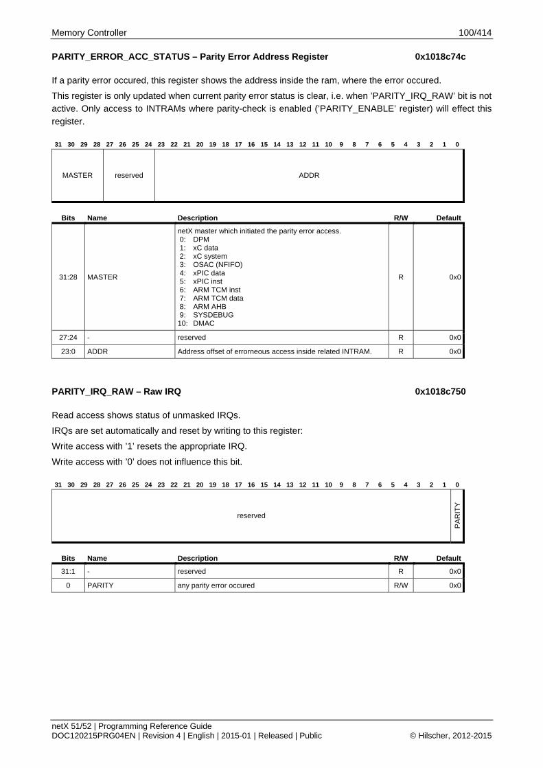
Memory Controller 100/414
netX 51/52 | Programming Reference Guide DOC120215PRG04EN | Revision 4 | English | 2015-01 | Released | Public © Hilscher, 2012-2015
PARITY_ERROR_ACC_STATUS – Parity Error Address Register 0x1018c74c
If a parity error occured, this register shows the address inside the ram, where the error occured.
This register is only updated when current parity error status is clear, i.e. when ’PARITY_IRQ_RAW’ bit is not active. Only access to INTRAMs where parity-check is enabled (’PARITY_ENABLE’ register) will effect this
register.
31 30 29 28 27 26 25 24 23 22 21 20 19 18 17 16 15 14 13 12 11 10 9 8 7 6 5 4 3 2 1 0
MASTER reserved ADDR
Bits Name Description R/W Default
31:28 MASTER
netX master which initiated the parity error access. 0: DPM 1: xC data 2: xC system 3: OSAC (NFIFO) 4: xPIC data 5: xPIC inst 6: ARM TCM inst 7: ARM TCM data 8: ARM AHB 9: SYSDEBUG 10: DMAC
R 0x0
27:24 - reserved R 0x0
23:0 ADDR Address offset of errorneous access inside related INTRAM. R 0x0
PARITY_IRQ_RAW – Raw IRQ 0x1018c750
Read access shows status of unmasked IRQs.
IRQs are set automatically and reset by writing to this register:
Write access with ’1’ resets the appropriate IRQ.
Write access with ’0’ does not influence this bit.
31 30 29 28 27 26 25 24 23 22 21 20 19 18 17 16 15 14 13 12 11 10 9 8 7 6 5 4 3 2 1 0
reserved
PA
RIT
Y
Bits Name Description R/W Default
31:1 - reserved R 0x0
0 PARITY any parity error occured R/W 0x0

Memory Controller 101/414
netX 51/52 | Programming Reference Guide DOC120215PRG04EN | Revision 4 | English | 2015-01 | Released | Public © Hilscher, 2012-2015
PARITY_IRQ_MASKED – Masked IRQ 0x1018c754
Show status of masked IRQs (as connected to ARM/xPIC).
31 30 29 28 27 26 25 24 23 22 21 20 19 18 17 16 15 14 13 12 11 10 9 8 7 6 5 4 3 2 1 0
reserved
PA
RIT
Y
Bits Name Description R/W Default
31:1 - reserved R 0x0
0 PARITY any parity error occured R 0x0
PARITY_IRQ_MSK_SET – IRQ Enable Mask 0x1018c758
The IRQ mask enables interrupt requests for corresponding interrupt sources.
As its bits might be changed by different software tasks, the IRQ mask register is not writable directly, but by
set and reset masks:
Write access with ’1’ sets interrupt mask bit.
Write access with ’0’ does not influence this bit.
Read access shows actual interrupt mask.
Attention: Before activating interrupt mask, delete old pending interrupts by writing the same value to
PARITY_IRQ_RAW.
31 30 29 28 27 26 25 24 23 22 21 20 19 18 17 16 15 14 13 12 11 10 9 8 7 6 5 4 3 2 1 0
reserved
PA
RIT
Y
Bits Name Description R/W Default
31:1 - reserved R 0x0
0 PARITY any parity error occured R/W 0x0
PARITY_IRQ_MSK_RESET – IRQ Disable Mask 0x1018c75c
This is the corresponding reset mask to disable interrupt requests for corresponding interrupt sources:
Write access with ’1’ resets interrupt mask bit.
Write access with ’0’ does not influence this bit.
Read access shows actual interrupt mask.
31 30 29 28 27 26 25 24 23 22 21 20 19 18 17 16 15 14 13 12 11 10 9 8 7 6 5 4 3 2 1 0
reserved
PA
RIT
Y
Bits Name Description R/W Default
31:1 - reserved R 0x0
0 PARITY any parity error occured R/W 0x0

Dual-Port Memory 102/414
netX 51/52 | Programming Reference Guide DOC120215PRG04EN | Revision 4 | English | 2015-01 | Released | Public © Hilscher, 2012-2015
5 Dual-Port Memory The Dual-Port Memory (DPM) interface is used for allowing data transfer between the netX and an external host system. Unlike standard DPM, the netX51 DPM is a virtual Dual-Port memory, which appears as a
linear memory to the host side, while accesses to the DPM are redirected up to four different memory areas, making the whole netX functionality accessible.
The netX DPM interface can either be a parallel DPM interface based on standard SRAM access protocol
extended by ready handshake mechanism or a high speed serial DPM interface based on standard Motorola SPI. Selection is done by an external mode pin. Furthermore the interface is widely configurable by configuration registers which can be set by software running on host device.
DPM interface is located on HIF-IOs for netX51. These IOs can also be used as memory interface. It is possible to use serial DPM together with 16 bit or 8 bit external memory on netx51. However it is neither possible using parallel DPM with external memory nor using serial DPM with 32 bit memory.
The netX51 DPM interface supports 3 different parallel modes and a high speed serial mode. Selection of either serial or parallel DPM (default is parallel) is done through register HIF_IO_CFG. For detailed information about DPM, please refer to the appropriate chapter of the “netX51 Technical Reference Guide”.
5.1 Software Interface DPM interface parameters like parallel mode data width, data endianness, address mapping, signal timing, interrupt handling and PIO control can be accessed by the host processor.
By default, all DPM configuration registers are mapped to the first 256 bytes (address 0x00 to 0xFF) of the
external DPM address range. The default bus width is 8 Bit and all basic configuration registers only use the Least Significant Byte which allows host processors with 8-Bit interface as well as pure 16-Bit (no Byte access possible) hosts to access the DPM configuration and adapt the interface to their needs (e.g bus
width, RDY/BUSY signal modes, endianness, etc.) without the need for pre-configuration by firmware or second stage loader (which is still possible though).
For netX50 compatibility this configuration area can be relocated to the end of the external address range
(last 256 bytes) or completely switched off.
Depending on DPM mode, bus width and address range, there are almost always a number of host interface signals which are not used by the host and can be used as Programmable IOs (PIO).
5.2 DPM Window Mapping For netX51 only DPM Configuration Window is enabled by default, all other windows are disabled. The netX51 Configuration Window is located on the lowest 256 bytes of external DPM address-space by default.
Address mapping expands external access address to an internal 32 bit wide netX address. External
address range of netX51 DPM can be split off in 4 sub-regions (DPM address windows). External to internal address mapping and several features (e.g. read-ahead, byte-collecting) can be programmed for each window individually.
Following basic rules must be regarded when configuring netX DPM window mapping:
Used (not disabled) windows must be configured address ascending:
win_end0 < win_end1 < win_end2 < win_end3 < win_end4
A window can be disabled by setting the appropriate win_end register value to 0.
Window mapping and size can be configured in 256 byte steps.
First external address of window n: win_end(n-1)
Last external address of window n: win_end(n) - 1
Window size calculation of window n:

Dual-Port Memory 103/414
netX 51/52 | Programming Reference Guide DOC120215PRG04EN | Revision 4 | English | 2015-01 | Released | Public © Hilscher, 2012-2015
win_size(n) = win_end(n) - win_end(n-1) [bytes]
First internal address of window n:
win_page(n) + ((win_map(n) + win_end(n-1)) & 0x000FFFFF)
Last internal address of window n:
win_page(n) + ((win_map(n) + win_end(n) - 1) & 0x000FFFFF)
win_end(0) is fixed to 0x100
If low configuration window 0 is used, start of first enable data window is 0x100
If high configuration window 0 is used, last 256 bytes of external address range will be mapped there.
This will be done with higher priority when a data windows end-address is programmed to external address range (i.e. is programmed for highest addresses).
Remapping of one window (changing appropriate dpm_win_map register value) without changing its
size (changing appropriate dpm_win_end register value) does not affect the other windows.
Changing the size of one window (changing appropriate dpm_win_end register value) will change location and mapping of all other windows above.
Note: In the rules above window(n-1) is the preceding enabled window of window n.
The following figure shows a DPM window mapping example with low configuration window 0.
Figure 1: DPM Window Mapping Example

Dual-Port Memory 104/414
netX 51/52 | Programming Reference Guide DOC120215PRG04EN | Revision 4 | English | 2015-01 | Released | Public © Hilscher, 2012-2015
5.3 DPM Access Tunnel DPM Access Tunnel is a small (64 bytes) special map-able DPM Window which can be laid over any normal DPM Window and also over DPM Configuration Window 0.
Externally the Access Tunnel base can be mapped to any available 64 byte boundary. It allows access to 15
DWords of a 64 byte target area netX internally. The last external DWord can be used to configure target area base.
There are 2 registers inside DPM Configuration Window 0 for programming DPM Access Tunnel. For further
details view register description DPM_TUNNEL_CFG and DPM_ITBADDR.
Internal target area can be write-protected and protected against re-mapping by host. Protection status can be read from Configuration DWord by host.
DPM Access Tunnel can be used for dynamic access to small netX internal address areas (e.g. for special module configuration, status or Handshake Cell access) without reconfiguring other DPM Windows.
Figure 2: DPM Access Tunnel

Dual-Port Memory 105/414
netX 51/52 | Programming Reference Guide DOC120215PRG04EN | Revision 4 | English | 2015-01 | Released | Public © Hilscher, 2012-2015
5.4 DPM Registers Definition The following table is a summary of the Dual-Port Memory Configuration Window registers.
Note: The given DPM Win0 address is the address offset inside DPM configuration window for host
access. This window can be mapped to the last 256 bytes of the external DPM address space.
DPM Win0 Address
ARM Address Register Name Short Description
0x00 0x1018c000 DPM_CFG0X0 DPM IO Control Register 0
0x04 0x1018c004 DPM_IF_CFG DPM Interface Configuration Register
0x08 0x1018c008 DPM_PIO_CFG0 DPM PIO Configuration Register0
0x0c 0x1018c00c DPM_PIO_CFG1 DPM PIO Configuration Register1
0x10 0x1018c010 DPM_ADDR_CFG DPM External Address Configuration Register
0x14 0x1018c014 DPM_TIMING_CFG DPM Timing and Access Configuration Register
0x18 0x1018c018 DPM_RDY_CFG DPM Ready (DPM_RDY) Signal Configuration Register
0x1c 0x1018c01c DPM_STATUS DPM Status Register
0x20 0x1018c020 DPM_STATUS_ERR_RESET DPM Error Status Reset Register
0x24 0x1018c024 DPM_STATUS_ERR_ADDR DPM Error Address Status Register
0x28 0x1018c028 DPM_MISC_CFG DPM Configuration Register for some Special Functions
0x2c 0x1018c02c DPM_IO_CFG_MISC DPM IO Configuration Register
0x38 0x1018c038 DPM_TUNNEL_CFG DPM Access Tunnel Configuration Register
0x3c 0x1018c03c DPM_ITBADDR DPM Access Tunnel (DATunnel) netX Internal Target Base Address (ITBAddr) Configuration Register
0x40 0x1018c040 DPM_WIN1_END DPM Window 1 End Address Configuration Register
0x44 0x1018c044 DPM_WIN1_MAP DPM Window 1 Address Map Configuration Register
0x48 0x1018c048 DPM_WIN2_END DPM Window 2 End Address Configuration Register
0x4c 0x1018c04c DPM_WIN2_MAP DPM Window 2 Address Map Configuration Register
0x50 0x1018c050 DPM_WIN3_END DPM Window 3 End Address Configuration Register
0x54 0x1018c054 DPM_WIN3_MAP DPM Window 3 Address Map Configuration Register
0x58 0x1018c058 DPM_WIN4_END DPM Window 4 End Address Configuration Register
0x5c 0x1018c05c DPM_WIN4_MAP DPM Window 4 Address Map Configuration Register
0x80 0x1018c080 DPM_IRQ_RAW DPM Raw (Before Masking) IRQ Status Register
0x84 0x1018c084 DPM_IRQ_ARM_MASK_SET DPM Interrupt Mask Register for netX Internal ARM-CPU
0x88 0x1018c088 DPM_IRQ_ARM_MASK_RESET DPM Interrupt Mask Reset Register for netX Internal ARM-CPU
0x8c 0x1018c08c DPM_IRQ_ARM_MASKED DPM Masked Interrupt Status Register for netX Internal ARM-CPU
0x90 0x1018c090 DPM_IRQ_XPIC_MASK_SET DPM Interrupt Mask Register for netX Internal xPIC-CPU
0x94 0x1018c094 DPM_IRQ_XPIC_MASK_RESET DPM Interrupt Mask Reset Register for netX Internal xPIC-CPU
0x98 0x1018c098 DPM_IRQ_XPIC_MASKED DPM Masked Interrupt Status Register for netX Internal xPIC-CPU
0x9c 0x1018c09c DPM_IRQ_FIQ_MASK_SET DPM Interrupt Mask Register for Fast netX Interrupt Output Signal (DPM_FIQ/HIF_SIRQ)
0xa0 0x1018c0a0 DPM_IRQ_FIQ_MASK_RESET DPM Interrupt Mask Reset Register for Fast netX Interrupt Output Signal (DPM_FIQ/HIF_SIRQ)
0xa4 0x1018c0a4 DPM_IRQ_FIQ_MASKED DPM Masked Interrupt Status Register for Fast netX Interrupt Output Signal (DPM_FIQ/HIF_SIRQ)
0xa8 0x1018c0a8 DPM_IRQ_IRQ_MASK_SET DPM Interrupt Mask Register for Normal netX Interrupt Output Signal (DPM_IRQ/HIF_DIRQ)
0xac 0x1018c0ac DPM_IRQ_IRQ_MASK_RESET DPM Interrupt Mask Reset Register for Normal netX Interrupt Output Signal (DPM_IRQ/HIF_DIRQ)
0xb0 0x1018c0b0 DPM_IRQ_IRQ_MASKED DPM Masked Interrupt Status Register for Normal netX Interrupt Output Signal (DPM_IRQ/HIF_DIRQ)
0xb8 0x1018c0b8 DPM_SW_IRQ DPM Register for Software Interrupt Generation to Host and netX Interrupt Targets
0xc0 0x1018c0c0 DPM_HOST_WDG_HOST_TIMEOUT
Address reserved for netX50 DPM_HOST_WDG_HOST_TIMEOUT

Dual-Port Memory 106/414
netX 51/52 | Programming Reference Guide DOC120215PRG04EN | Revision 4 | English | 2015-01 | Released | Public © Hilscher, 2012-2015
0xc4 0x1018c0c4 DPM_HOST_WDG_HOST_TRIG Address reserved for netX50 DPM_HOST_WDG_HOST_TRIG
0xc8 0x1018c0c8 DPM_HOST_WDG_ARM_TIMEOUT
Address reserved for netX50 DPM_HOST_WDG_ARM_TIMEOUT
0xcc 0x1018c0cc DPM_SYS_STA_BIGEND16 DPM System Status Information Register in Big Endianess 16 Data Mapping
0xd0 0x1018c0d0 DPM_HOST_TMR_CTRL Address reserved for netX50 DPM_HOST_TMR_CTRL
0xd4 0x1018c0d4 DPM_HOST_TMR_START_VAL Address reserved for netX50 DPM_HOST_TMR_START_VAL
0xd8 0x1018c0d8 DPM_HOST_SYS_STAT DPM System Status Information Register
0xdc 0x1018c0dc DPM_HOST_RESET_REQ DPM Reset Request Register
0xe0 0x1018c0e0 DPM_HOST_INT_STAT0 1st netX50 Compatible DPM Interrupt Status Register (Related to DPM_HOST_INT_EN0-Register)
0xe8 0x1018c0e8 DPM_HOST_INT_STAT2 2nd netX50 Compatible DPM Interrupt Status Register (Related to DPM_HOST_INT_EN2-Register)
0xf0 0x1018c0f0 DPM_HOST_INT_EN0 DPM Handshake Interrupt Enable Register
0xf4 0x1018c0f4 DPM_NETX_VERSION_BIGEND16
DPM netX Version Register in Big Endianess 16 Data Mapping
0xf8 0x1018c0f8 DPM_HOST_INT_EN2 netX50 compatible Interrupt Enable Register No. 2
0xfc 0x1018c0fc DPM_NETX_VERSION DPM netX Version Register
Table 14: Dual-Port Memory Configuration Window Registers
DPM_CFG0X0 – DPM IO Control Register 0 0x1018c000
This register is accessible in any DPM-mode (8, 16, 32 bit, SRAM, Intel, Motorola, little endian, big endian)
by access to DPM address 0. Basic DPM settings are configurable here to make higher addresses accessible.
To avoid instable system configurations, global changes of important configuration registers must be
confirmed (re)writing ’mode’ bit field of this register. Please view ’mode’ description for details.
31 30 29 28 27 26 25 24 23 22 21 20 19 18 17 16 15 14 13 12 11 10 9 8 7 6 5 4 3 2 1 0
reserved
EN
DIA
N
MODE
Bits Name Description R/W Default
31:6 - reserved R 0x0
5:4 ENDIAN
Endianess of 32 bit (DWord) address alignment (B0: least significant byte, B3: most significant byte): coding Address A+3 A+2 A+1 A+0 00 little endian B3 B2 B1 B0 01 16 bit big endian B2 B3 B0 B1 10 32 bit big endian B0 B1 B2 B3 11 reserved Little endian is used netX inside. If big endian host device is used, set to this 01 or 10 according to host device data width.
R/W 0x0
3:0 MODE
Basic DPM interface mode: Additionally writing to this bit field will confirm global interface configuration changes: Interface configuration can not always be written one single access (e.g. in 8 bit data mode changing of ’dpm_if_cfg’ is not possible in one single access as there are more than 8 bits for congifuration). However changing interface configuration by more than one single access could lead to instable interfaces. This is avoided by following procedure: For proper interface configuration, values of important interface configuration registers are buffered in temporary registers first. Interface configuration is changed finaly by (re)writing ’mode’ bits. There is no need to realy change a prior programmed ’mode’ setting, interface change is done when low byte of this registers is target of a write acceess.
R/W 0x0

Dual-Port Memory 107/414
netX 51/52 | Programming Reference Guide DOC120215PRG04EN | Revision 4 | English | 2015-01 | Released | Public © Hilscher, 2012-2015
Bits Name Description R/W Default
Temporary registers which must be confirmed by this are: - All bits of ’dpm_if_cfg’ register. - Address compartor configuration: All ’addr_cmp_a*’ bit fields in ’dpm_addr_cfg’ register. Note: Interface configuration confirm must be done regardless wether programmed by host via external interfaces or by internal ARM via internal INTLOGIC configuration channel. DPM interface mode must be further configured in ’dpm_if_cfg’ register. Data width and address multiplexing mode must be configure here. Supported basic DPM modes are: 0000 8 bit data non multiplexed mode.
DPM_D7..0 are used as data lines, DPM_D31..8 can be used as PIOs (+24 PIOs). DPM_D17 can be used as Address-Enable DPM_AEN/DPM_ALE.
0001 reserved. 0010 8 bit data multiplexed mode.
DPM_D7..0 are used as address and data lines, DPM_D17 as ALE. DPM_A7..0 and DPM_D31..8 can be used as PIOs (+31 PIOs). DPM_A10..8 will used as address lines. DPM_A19..11 can used as address lines (depending on selectde ’addr_range’. High address lines will be sampled at the same time when lower address bits are latched from DPM_D7..0.
0011 reserved. 0100 16 bit data non multiplexed mode.
DPM_D15..0 are used as data lines, DPM_D31..16 can be used as PIOs (+16 PIOs). DPM_D17 can be used as Address-Enable DPM_AEN/DPM_ALE.
0101 reserved. 0110 16 bit data multiplexed mode with 2 byte-enables on
separated lines. DPM_D15..0 are used as address and data lines, DPM_D17 as ALE. DPM_A15..0 and DPM_D31..16 can be used as PIOs (+31 PIOs). Two byte-enable signals can be used additionally. View register ’dpm_if_cfg’ ’be_sel’. DPM_A19..16 can used as address lines (depending on selectde ’addr_range’. High address lines will be sampled at the same time when lower address bits are latched from DPM_D15..0.
0111 reserved 1000 32 bit data non multiplexed mode.
DPM_D0..32 are used as data lines. DPM_A15 or DPM_AH1 can be used as Address-Enable DPM_AEN/DPM_ALE.
1001 reserved. 1010 32 bit data multiplexed mode with 4 byte-enables on
separated lines. DPM_D31..0 are used as address and data lines, DPM_A15 or DPM_AH1 as ALE. Four byte-enable signals can be used additionally. View register ’dpm_if_cfg’ ’be_sel’.
: reserved. 1111 reserved. Note: For DPM modes with less than 32 bit data, write data could not written immediate to netX memory or registers (’byte_area’ and ’dis_rd_latch’ of ’dpm_win1_map’ register).
DPM_IF_CFG – DPM Interface Configuration Register 0x1018c004
DPM interface mode must be basically configured in ’DPM_CFG0X0’ register. Interface configuration is split up into two registers to support setup from external host CPU when DPM is in 8 bit non-multiplexed default
mode after reset.

Dual-Port Memory 108/414
netX 51/52 | Programming Reference Guide DOC120215PRG04EN | Revision 4 | English | 2015-01 | Released | Public © Hilscher, 2012-2015
However this does not work for all interfaces. E.g. for modes where DPM_WRN is not write trigger this is not possible. Interface setup must be done by netX internal CPU then.
To avoid instable system configurations, changes of this registers must be confirmed (re)writing ’mode’ bit field of DPM_CFG0X0 register. Please view ’mode’ description there for details.
Host connection isa_bhe3_is_mem
cs16n
cs_ctrl addr_sh aen_pol aen_sel be_wr_dis
be_rd_dis
be_pol be_sel dir_ctrl dpm_cfg0x0.mode
Intel, 8bit (SRAM) 0 0 x x 0 x x x 0 0 0x0 Intel, 16bit,byte-write 0 0 0 x 0 0 1 0 1 1 0x4 Intel, 16bit,byte-enable (SRAM) 0 0 0 x 0 0 0 0 0 0 0x4 Intel, 32bit,byte-write 0 0 0 x 0 0 1 0 0 1 0x8 Intel, 32bit,byte-enable (SRAM) 0 0 0 x 0 0 0 0 0 0 0x8 Intel, 8bit multiplexed 0 0 x 1 1 x x x 0 0 0x2 Intel, 16bit mul. netx50: no BEs 0 0 0 1 1 1 1 x 0 0 0x6 Intel, 16bit mul. byte-write 0 0 1 1 1 0 1 0 1 1 0x6 Intel, 16bit mul. 2BEs, byte-addr 0 0 0 1 1 0 0 0 0 0 0x6 Intel, 16bit mul. 2BEs, word-addr 0 0 1 1 1 0 0 0 0 0 0x6 Intel, 32bit mul. netx50: byte-addr 0 0 0 1 1 0 1 0 0 1 0xa Intel, 32bit mul. byte-write DWord-addr 0 0 1 1 1 0 1 0 0 1 0xa Intel, 32bit mul. 4BEs, byte-addr 0 0 0 1 1 0 0 0 0 0 0xa Intel, 32bit mul. 4BEs, DWord-addr 0 0 1 1 1 0 0 0 0 0 0xa TI OMAP, 16bit non-multiplexed 0 0 0 x 0 0 0 0 0 0 0x4 TI OMAP, 16bit multiplexed 0 0 1 0 1 0 0 0 0 0 0x6 Motorola, 8bit (6800) 0 0 x x 0 0 0 1 1 2 0x0 Motorola, 16bit 0 0 0 x 0 0 0 0 0 2 0x4 Motorola, 16bit (68000) 0 0 0 0 1 0 0 0 0 2 0x4 Motorola, 32bit 0 0 0 x 0 0 0 0 0 2 0x8 Motorola, 8bit multiplexed 0 0 x x 0 0 0 1 1 2 0x2 Motorola, 16bit mul.netx50: byte-addr 0 0 0 1 1 0 0 0 0 2 0x6 Motorola, 16bit mul.word-addr 0 0 1 1 1 0 0 0 0 2 0x6 Motorola, 32bit mul.netx50: byte-addr 0 0 0 1 1 0 0 0 0 2 0xa Motorola, 32bit mul.DWord-addr 0 0 1 1 1 0 0 0 0 2 0xa ISA, 8bit 0 4 x 0 1 0 0 0 0 0 0x0 ISA, 16bit 1 4 0 0 1 0 0 0 0 0 0x4
Table 15: DPM_IF_CFG Register Config Table
31 30 29 28 27 26 25 24 23 22 21 20 19 18 17 16 15 14 13 12 11 10 9 8 7 6 5 4 3 2 1 0
reserved
ISA
_BH
E3_
IS_M
EM
CS
16N
reserved
CS
_CT
RL
AD
DR
_SH
AE
N_P
OL
AE
N_S
EL
BE_POL
BE
_WR
_DIS
BE
_RD
_DIS
rese
rved
BE
_SE
L
rese
rved
DIR
_CT
RL
Bits Name Description R/W Default
31:25 - reserved R 0x0
24 ISA_BHE3_IS_MEMCS16N
ISA usage of BHE3 signal. Warning: ISA memcs16n signal is an ISA slave output signal. I.e. it is drive by netX when this bit is enabled. This could cause permanent damage to netX or host when interface is not ISA. Settings: 0: BHE3 is used as byte-enable or PIO and input by default. 1: BHE3 is used as ISA memcs16n signal and driven by netX.
Signal is driven low when DPM is selected by Chip-Select decoding logic (cs_ctrl) and 16 bit data mode is selected. Signal is never driven active high. High level is reached by external pull up resistor.
R/W 0x0
23:19 - reserved R 0x0
18:16 CS_CTRL Chip-Select controlling. Chip access can be additionally controlled for all settings by
R/W 0x0

Dual-Port Memory 109/414
netX 51/52 | Programming Reference Guide DOC120215PRG04EN | Revision 4 | English | 2015-01 | Released | Public © Hilscher, 2012-2015
Bits Name Description R/W Default
address comparator. View ’addr_cmp_a*’ bit fields of ’dpm_addr_cfg’ register. 000: Use 1 low active Chip-Select signal (DPM_CSN). 001: Use 2 low active Chip-Select signals (DPM_CSN or
DPM_BHE1n must be low). 010: Use high active Chip-Select signal (DPM_CSN). 011: Use 2 high active Chip-Select signals (DPM_CSN or
DPM_BHE1n must be high). 100: No Chip-Select signal. Behaves like DPM_CSN is
permanent active. 111: Chip access is disabled. Address comparator is ignored. others: reserved Note: Internal address-comparator is part of netX DPM Chip-Select decoding logic. View ’addr_cmp_a*’ bit fields of ’dpm_addr_cfg’ register. Set address comparator mask to ’0’ to disable.
15 ADDR_SH
Address is Byte address or shifted according to selected data size. This bit is irrelevant in 8 bit data modes. Address comparator logic works always with unshifted address. 0 Address is always Byte address (not shifted).
In 16 bit data modes: Address bit 0 can be used as low byte-enable or can be ignored. In 32 bit data modes: Address bits 1,0 can be used as byte-enables or can be ignored. Use ’be_sel’ to select byte-enables and ’be_wr_dis’ or ’be_rd_dis’ to ignore them.
1 Address is shifted according to programmed data width. In 16 bit data modes: Address from host starting at A0 (or AD0 when multiplexed ) is 16 bit word address. In 32 bit data modes: Address from host starting at A0 (or AD0 when multiplexed ) is 32 bit word address.
R/W 0x0
14 AEN_POL
Address-Enable active level polarity. 0: Address is latched while ALE-signal is low (i.e. low active
ALE/AEN). 1: Address is latched while ALE-signal is high (i.e. high active
ALE/AEN). In non-multiplexed modes, address is only latched when chip-select is additionally active (as programmed in ’cs_ctrl’). In multiplexed modes, address latching is not controlled by chip-select. Address is latched all time when ALE is active then.
R/W 0x0
13:12 AEN_SEL
Address-Enable (AEN-modes) or Address-Latch-Enable (multiplexed modes) Control. 00: No additional Address controlling function. 01: netx50 compatibe Address controlling signal selection: For 8 or 16 bit data modes: AEN on DPM_D17. For 32 bit data modes: AEN on HIF_A15 (up to 32kB address space for non-multiplexed modes). 10: Not netx50 compatibe Address controlling signal selection for 32 bit data modes: For 8 or 16 bit data modes identically to setting ’01’: AEN on DPM_D17. For 32 bit data modes: AEN on HIF_AHI1 (up to 128kB address space for non-multiplexed modes). 11: reserved. Note: In multiplexed modes read or write access will not be started netX internally while address-phase is active. ALE signal must return to idle state first.
R/W 0x0
11:8 BE_POL
DPM access byte-enable active level polarity. byte-enable active polarity can be set for each data byte separately. byte-enable signals can be selected by ’be_sel’. Bits inside this bit field are associated as follows: Bit data lines be_pol[0] D[7:0] be_pol[1] D[15:8] be_pol[2] D[23:16] be_pol[3] D[31:24] Function: 0: BE signals are low active byte-enables. 1: BE signals are high active byte-enables (e.g. 8 bit Motorola
6800).
R/W 0x0
7 BE_WR_DIS DPM write access byte-enable configuration. 0: byte-enables will be used on write access, only data lines
R/W 0x0

Dual-Port Memory 110/414
netX 51/52 | Programming Reference Guide DOC120215PRG04EN | Revision 4 | English | 2015-01 | Released | Public © Hilscher, 2012-2015
Bits Name Description R/W Default
of enabled bytes will be written. 1: byte-enables will be ignored on write access, all used data
lines will be written. Note: Do not set this bit when ’dir_ctrl’ is set to nWR-mode (’01’). Byte-Write-Strobes are essentially in this case. Note: This bit is ignored for 8 bit data modes when ’be_sel’ bit is not set.
6 BE_RD_DIS
DPM read access byte-enable configuration. 0: byte-enables will be used on read access, only data lines of
enabled bytes will be driven. 1: byte-enables will be ignored on read access, all used data
lines will be driven. Note: Do not set this bit when ’dir_ctrl’ is set to nRW-mode (’10’). Byte-Write-Strobes are essentially in this case. Note: This bit is ignored for 8 bit data modes when ’be_sel’ bit is not set.
R/W 0x0
5 - reserved R 0x0
4 BE_SEL
DPM access byte-enable signal selection. byte-enables can located on different netX IOs - netx50 compatibility. Basically BE signals depend on selected data width (cfg0x0). setting data width D[31:24] D[23:16] D[15:8] D[7:0] 0 8bit - 0 16bit BHE1n A0 0 32bit BHE3n A1 BHE1n A0 --------- ------------- ----------- ----------- ---------- -------- 1 8bit BHE1n 1 16bit BHE3n WRn 1 32bit BHE3n A1 BHE1n A0 For 32 bit data interfaces only following byte-enable combinatzions are valid - others will cause unpredictable behaviour (na: not active): BE3 BE2 BE1 BE0 netX internal write access
width active active active active 32 bit access to 32 bit word
address active active na na 16 bit access to 32 bit word
address + 2 na na active active 16 bit access to 32 bit word
address active na na na 8 bit access to 32 bit word
address + 3 na active na na 8 bit access to 32 bit word
address + 2 na na active na 8 bit access to 32 bit word
address + 1 na na na active 8 bit access to 32 bit word
address na na na na access ignored Note: Target address in table above is related to little endianess. Offsets inside a 32 bit data word will be different for other endianess settings (view ’dpm_cfg0x0’ register). Note: For 8 bit data modes this bit must only be set when an additional byte-enable Signal is required (e.g. Motorola 6800). Do not set ’be_sel’ and ignore for read and write (be_wr_dis, be_rd_dis) - DPM Ready geneartion will care for BHE1n anyhow. Note: This bit is irrelevant for 32 bit data modes. Note: Internal read access data width is always 32 bit.
R/W 0x0
3:2 - reserved R 0x0
1:0 DIR_CTRL
DPM access direction control. 00: dedicated low active read- and write control signals (RDn +
WRn) with optional byte-enables. byte-enables have address character i.e. they must be stable while read- or write-control
R/W 0x0

Dual-Port Memory 111/414
netX 51/52 | Programming Reference Guide DOC120215PRG04EN | Revision 4 | English | 2015-01 | Released | Public © Hilscher, 2012-2015
Bits Name Description R/W Default
signal is active. byte-enables are not used as Strobe signals. A read-access is started when RDn signal becomes active low at access start. Address, Chip-Select and byte-enable signals must be stable then. A write-access is done when WRn becomes inactive high at access end. Address, Chip-Select, data and byte-enable signals must be stable then. Ready/Busy signal is asserted when RDn or WRn is active. This setting can be used for standard SRAM interfaces.
01: RDn is direction signal nRW (signal high: write, low: read).For read byte-enables have address character i.e. they must be stable when RDn becomes low. For write byte-enables have strobe character i.e. Address, Data and RDn must be stable when they become inactive at access end.. A read-access is started when RDn signal becomes low at access start. Address, Chip-Select and byte-enable signals must be stable then. A write-access is done when byte-enables becomes inactive at access end. Address, Chip-Select, data and RDn signals must be stable then. Ready/Busy signal is asserted when RDn is low or byte-enables are active. This setting is typically used for Intel-like interfaces with Byte-Write-Strope signals..
10: RDn is direction signal nWR (signal low: write, high: read).byte-enables have strobe character for both read and write i.e. Address, and RDn must be stable when they become active at access start. These signals must remain stable until byte-enables become inactive at access end. For write data must be stable then. Ready/Busy signal is asserted when at least one byte-enables is active. This setting is typically used for Motorola-like interfaces with Byte-Write-Strope signals.
DPM_PIO_CFG0 – DPM PIO Configuration Register0 0x1018c008
Signals to be used as PIOs when netX DPM is active must be selected here or in ’DPM_PIO_CFG1’ register.
Since netx51/52 PIO function will not be automatically activated depending on other settings. E.g. DPM_D31..8 can not be used automatically when 8 bit data mode is selected.
31 30 29 28 27 26 25 24 23 22 21 20 19 18 17 16 15 14 13 12 11 10 9 8 7 6 5 4 3 2 1 0
SEL_D_PIO
Bits Name Description R/W Default
31:0 SEL_D_PIO Use related DPM_D-pin as PIO pin. R/W 0x0

Dual-Port Memory 112/414
netX 51/52 | Programming Reference Guide DOC120215PRG04EN | Revision 4 | English | 2015-01 | Released | Public © Hilscher, 2012-2015
DPM_PIO_CFG1 – DPM PIO Configuration Register1 0x1018c00c
PIO usage of DPM_SIRQ, DPM_DIRQ and DPM_RDY has moved from ’DPM_IO_CFG_MISC’ to this register since netx51/52.
Signals to be used as PIOs when netX DPM is active must be selected here or in ’DPM_PIO_CFG0’ register.
31 30 29 28 27 26 25 24 23 22 21 20 19 18 17 16 15 14 13 12 11 10 9 8 7 6 5 4 3 2 1 0
SE
L_S
IRQ
_PIO
SE
L_D
IRQ
_PIO
SE
L_R
DY
_PIO
SE
L_W
RN
_PIO
SE
L_R
DN
_PIO
SE
L_C
SN
_PIO
SE
L_B
HE
3_P
IO
SE
L_B
HE
1_P
IO
reserved SEL_A_PIO
Bits Name Description R/W Default
31 SEL_SIRQ_PIO
Use DPM_SIRQ-pin as PIO pin. Note: For serial DPM this bit is related to netx51/52 IO HIF_D13. Setting of for HIF_D13 inside ’dpm_pio_cfg0 register is ignored then. I.e. this bit must be programmed to ’0’ for DPM_SIRQ/FIQ usage regardless whether serial or parallel DPM is used.
R/W 0x1
30 SEL_DIRQ_PIO
Use DPM_DIRQ-pin as PIO pin. Note: For serial DPM this bit is related to netx51/52 IO HIF_D12. Setting of for HIF_D12 inside ’dpm_pio_cfg0 register is ignored then. I.e. this bit must be programmed to ’0’ for DPM_DIRQ/IRQ usage regardless whether serial or parallel DPM is used.
R/W 0x1
29 SEL_RDY_PIO Use DPM_RDY-pin as PIO pin. RDY is by default PIO to avoid RDY-conflicts during reset.
R/W 0x1
28 SEL_WRN_PIO Use DPM_WRN-pin as PIO pin. R/W 0x0
27 SEL_RDN_PIO Use DPM_RDN-pin as PIO pin. R/W 0x0
26 SEL_CSN_PIO Use DPM_CSN-pin as PIO pin. R/W 0x0
25 SEL_BHE3_PIO Use DPM_BHE3-pin as PIO pin. R/W 0x0
24 SEL_BHE1_PIO Use DPM_BHE1-pin as PIO pin. R/W 0x0
23:20 - reserved R 0x0
19:0 SEL_A_PIO
Use related DPM_A-pin as PIO pin. Note: PIO selects for DPM_A19..18 are only used for test purpose here. To select PIO function of high DPM_A lines which are multiplexed on DPM_D23..22 use related bits of ’sel_d_pio’ Bit field in ’dpm_pio_cfg0’ register. DPM_A17..16 are treated in the same way in netx50 compatibility mode (located on DPM_D21..20 then). However they are located on HIF_AHI1..0 when netx50 compatibility is globally disabled (ASIC_CTRL-area).
R/W 0x0

Dual-Port Memory 113/414
netX 51/52 | Programming Reference Guide DOC120215PRG04EN | Revision 4 | English | 2015-01 | Released | Public © Hilscher, 2012-2015
DPM_ADDR_CFG – DPM External Address Configuration Register 0x1018c010
Note: Address compare logic as part of netX DPM Chip-Select decoding logic is a new netx51/52 feature.
31 30 29 28 27 26 25 24 23 22 21 20 19 18 17 16 15 14 13 12 11 10 9 8 7 6 5 4 3 2 1 0
AD
DR
_CM
P_A
19
AD
DR
_CM
P_A
18
AD
DR
_CM
P_A
17
AD
DR
_CM
P_A
16
AD
DR
_CM
P_A
15
AD
DR
_CM
P_A
14
AD
DR
_CM
P_A
13
AD
DR
_CM
P_A
12
AD
DR
_CM
P_A
11
reserved
CF
G_W
IN_A
DD
R_C
FG
AD
DR
_RA
NG
E
Bits Name Description R/W Default
31:30 ADDR_CMP_A19
Address comparator controlling for DPM_A19. Like netx50 an internal address comparator is provided by netx51/52 DPM. Address compare logic is compatible to netx50 address comparator; however programming differs: Programming for each address line must be done by a 2-bit field. Additionally A11 is included now. Related input DPM_SEL_A11 is located on HIF_D31 for netx51/52. ----------------------------------------------------------------------- To avoid instable system configurations, changes of ’addr_cmp_a*’ bit fields of this registers must be confirmed by (re)writing ’mode’ bit field of dpm_cfg0x0 register. View ’mode’ description there for details. ----------------------------------------------------------------------- Supported settings for each address line of address compare are: coding compare compare with comment 00 disabled - 01 enabled netX input input state of DPM_SEL_A19
(HIF_D18) 10 enabled logic 0 11 enabled logic 1 Set all ’addr_cmp_a*’ bit fields to ’00’ to disable address comparator for Chip-Select decoding logic. Whole address comparator result will be always true then. Note: Address comparator is not affected by programmed ’addr_range’. Address bits exceeding selected address range ’addr_range’ will also be compared when mask bits are set here. Note: This is a new netx51/52 feature.
R/W 0x0
29:28 ADDR_CMP_A18
Address comparator controlling for DPM_A18. Programming is done like described for ’addr_cmp_a19’ bit field. Related compare input for A18 is DPM_SEL_A18 (located on HIF_D30).
R/W 0x0
27:26 ADDR_CMP_A17
Address comparator controlling for DPM_A17. Programming is done like described for ’addr_cmp_a19’ bit field. Related compare input for A17 is DPM_SEL_A17 (located on HIF_D29).
R/W 0x0
25:24 ADDR_CMP_A16
Address comparator controlling for DPM_A16. Programming is done like described for ’addr_cmp_a19’ bit field. Related compare input for A16 is DPM_SEL_A16 (located on HIF_D28).
R/W 0x0
23:22 ADDR_CMP_A15
Address comparator controlling for DPM_A15. Programming is done like described for ’addr_cmp_a19’ bit field. Related compare input for A15 is DPM_SEL_A15 (located on HIF_D27).
R/W 0x0
21:20 ADDR_CMP_A14 Address comparator controlling for DPM_A14. R/W 0x0

Dual-Port Memory 114/414
netX 51/52 | Programming Reference Guide DOC120215PRG04EN | Revision 4 | English | 2015-01 | Released | Public © Hilscher, 2012-2015
Bits Name Description R/W Default
Programming is done like described for ’addr_cmp_a19’ bit field. Related compare input for A14 is DPM_SEL_A14 (located on HIF_D26).
19:18 ADDR_CMP_A13
Address comparator controlling for DPM_A13. Programming is done like described for ’addr_cmp_a19’ bit field. Related compare input for A13 is DPM_SEL_A13 (located on HIF_D25).
R/W 0x0
17:16 ADDR_CMP_A12
Address comparator controlling for DPM_A12. Programming is done like described for ’addr_cmp_a19’ bit field. Related compare input for A12 is DPM_SEL_A12 (located on HIF_D24).
R/W 0x0
15:14 ADDR_CMP_A11
Address comparator controlling for DPM_A11. Programming is done like described for ’addr_cmp_a19’ bit field. Related compare input for A11 is DPM_SEL_A11 (located on HIF_D31). Note: A11 is not part of netx50 address compare logic.
R/W 0x0
13:6 - reserved R 0x0
5:4 CFG_WIN_ADDR_CFG
Location of the DPM Configuration Window (Window 0). Supported settings are: 00: Low Configuration Window: The Configuration Window is
located in the first 256 bytes of external DPM address range (0x0 to 0xff). It is located before the first enabled Data Window (1 to 4).
01: High Configuration Window: The Configuration Window is located in the last 256 bytes of external DPM address range.
Example: 'addr_range' is 8kB: Configuration Window is located in 0x1F00..0x1FFF.
10: reserved. 11: Configuration Window is disabled for external DPM access.
Full DPM address range can be used for Windows 1 to 4. Note: The Configuration Window 0 has higher priority than normal DPM Window. The location of the Configuration Window does not depend on the Data Window configuration (the setting of the 'dpm_winX_end' or 'dpm_winX_map' registers). I.e. for setting '00' (low Configuration Window) the first enabled Data Window starts at address 0x100. For setting '01' (high Configuration Window) it would hide the last 256 bytes of the last enabled Data Window when this is configured to end on the last external address. The Configuration Window 0 has lower priority than Access Tunnel. I.e. the Access Tunnel could be laid over the configuration window.
R/W 0x0
3:0 ADDR_RANGE
DPM external address range. coding Byte Address range address used signals 0000 reserved 0001 reserved 0010 2KB address range DPM_A[10:0] 0011 4KB address range DPM_A[11:0] 0100 8KB address range DPM_A[12:0] 0101 16KB address range DPM_A[13:0] 0110 32KB address range DPM_A[14:0] 0111 64KB address range DPM_A[15:0] 1000 128KB address range DPM_A[16:0] 1001 256KB address range DPM_A[17:0] 1010 512KB address range DPM_A[18:0] 1011 1024KB address range DPM_A[19:0] : reserved 1111 reserved This setting is related to Byte address. I.e. it is not possible to expand address rage by setting the ’addr_sh’ bit inside the ’dpm_if_cfg’ register. However required address lines will decrease by 1 (16 bit data modes) or 2 (32 bit data modes) when the ’addr_sh’ bit is set. For chip-select generation by internal address compare logic: Address lines used for chip-select decoding (’addr_cmp’ bit fields) must not be regarded for this setting. Example:
R/W 0x2

Dual-Port Memory 115/414
netX 51/52 | Programming Reference Guide DOC120215PRG04EN | Revision 4 | English | 2015-01 | Released | Public © Hilscher, 2012-2015
Bits Name Description R/W Default
16kB (A[13:0]) DPM, A[17:14] for chip-select generation, A[19:18] unused: Set ’addr_range’ to 5, ’addr_cmp_a17’ to ’addr_cmp_a14’ to ’10’ or ’11’ (depending on your compare value) and all other ’addr_cmp_a*’ bit fields to ’00’. For multiplexed modes: If programmed address range exceeds number of data lines, high address bits will be sampled from DPM_A lines starting above last used data line. High address will be sampled at the same moment when low address bits are sampled from data lines. Example 1: 8 bit data multiplexed mode, 1024KB address range programmed and ’aen_pol’ is set to 0: Address bits A7..0 are sampled from DPM_D7..0 before DPM_ALE is released to 1. Address bits A19..8 are sampled from DPM_A19..8 also before DPM_ALE is released to 1. Example 2: 16 bit data multiplexed mode, 1024KB address range programmed, ’aen_pol’ is set to 0 and ’addr_sh’ is set to 1: Address bits A16..1 are sampled from DPM_D15..0 before DPM_ALE is released to 1. Address bits A19..17 are sampled from DPM_A18..16 also before DPM_ALE is released to 1. I.e. a 19 bit word address is carried on DPM_D15..0 and DPM_A18..16 and is left-shifted internally by 1 to resolve a byte address.

Dual-Port Memory 116/414
netX 51/52 | Programming Reference Guide DOC120215PRG04EN | Revision 4 | English | 2015-01 | Released | Public © Hilscher, 2012-2015
DPM_TIMING_CFG – DPM Timing and Access Configuration Register 0x1018c014
31 30 29 28 27 26 25 24 23 22 21 20 19 18 17 16 15 14 13 12 11 10 9 8 7 6 5 4 3 2 1 0
SD
PM
_MIS
O_E
AR
LY
EN
_DP
M_S
ER
IAL_
SQ
I
reserved
RD
_BU
RS
T_E
N
T_RDS
rese
rved
FIL
TE
R
T_O
SA
Bits Name Description R/W Default
31 SDPM_MISO_EARLY
Serial DPM early MISO (read-data) generation. Serial DPM based on standard SPI changes read data on the edge following the sampling clock edge, i.e. works on both serial clock edges. That avoids hold timing errors on MISO-data but decreases maximum serial data rate on the other hand. Hence, for fast serial data rates this bit must be set. MISO hold times will always be positive but could get very short then. For details view netX timing characteristics. 0: Change MISO on the clock edge following the sampling
edge. 1: Change MISO on the sampling edge. Note: Sampling and generating clock edges are determined by serial DPM mode (clock phase and polarity). Related configuration must be done outside DPM module. Note: Hold timings can be relaxed by decreasing serial clock rate when this bit is not set. When this bit is set, MISO hold timing does not depend on serial clock rate. Note: This is a new netx51/52 feature.
R/W 0x0
30 EN_DPM_SERIAL_SQI
When DPM ist in serial mode (’dpm_status.sel_dpm_serial’ active), serial DPM can be switched to SQI-compatible 4-bit mode. Note: Netx DPM changes serial configuration immediately when this bit is changed. Hence do not change this bit by a longer serial sequence from host. E.g.: Change from SPI to SQI from host-side when host: 1.: Set this bit by SPI write sequence from host. 2.: Terminate sequence after the byte containing this bit was
written. 3.: Ensure that host has completed writing this byte serially
(host transfer could last even when related commands are already finished, e.g. due to FIFOs inside host SPI module).
4.: Change host to SQI. 5.: Continue acessing netX DPM in SQI mode. Note: This bit has no effect when DPM is in parallel mode. Note: This is a new netx51/52 feature.
R/W 0x0
29:8 - reserved R 0x0
7 RD_BURST_EN
Read burst enable. Read bursts are subsequent read accesses without toggeling chip-select or read-enable in between. They are supported for non-multiplexed modes only.
R/W 0x0
6:4 T_RDS
Read data setup time (in steps of 10ns). If DPM_RDY is used (rdy_mode != 0), DPM_RDY is generated t_rds*10ns after read data is stored on data bus. Without DPM_RDY use (rdy_mode == 0) read access error is detected if access terminates before t_rds*10ns passed after read data generation. Valid settings are: 0..7. Note: Read data access time will increased by t_rds * 10ns if t_rds is not 0.
R/W 0x2
3 - reserved R 0x0

Dual-Port Memory 117/414
netX 51/52 | Programming Reference Guide DOC120215PRG04EN | Revision 4 | English | 2015-01 | Released | Public © Hilscher, 2012-2015
Bits Name Description R/W Default
2 FILTER
Filter DPM Control Signals. If this bit is set, DPM signals Chip-Select, Read-Enable and Write-Enable (and Address latch enable if multiplexed Parallel DPM modes are used) are filtered for spike suppression. 0: no spike suppression. 1: Spikes < 10ns are suppressed, read data access time
increased by 10ns. Note: Data, address and byte-enable inputs are not filtered and must be stable when sampled. I.e. during the last 20ns of a write access and at the first 10ns of read access start. Note: Read data access time is increased by 10ns if this bit is set.
R/W 0x1
1:0 T_OSA
Address Setup Time (t_osa * 10ns). Address sampling can be delayed for read and write accesses by this parameter. E.g. host device asserts Chip-Select, Read-Enable and address lines simultaneously but some address lines are not stable while Chip-Select and Read-Enable are both low, set t_osa to delay address sampling by t_osa * 10ns. When data direction is controlled by RDn line (’if_cfg.dir_ctrl’ not ’00’) and byte-enables are used for read (’if_cfg.be_rd_dis’ not set), a read access is initiated when active byte-enable signals are detected stable for t_osa netX clock periods. Valid settings are: 0..3. Note: Read data access time will increased by t_osa * 10ns if t_osa is not 0.
R/W 0x3

Dual-Port Memory 118/414
netX 51/52 | Programming Reference Guide DOC120215PRG04EN | Revision 4 | English | 2015-01 | Released | Public © Hilscher, 2012-2015
DPM_RDY_CFG – DPM Ready (DPM_RDY) Signal Configuration Register 0x1018c018
31 30 29 28 27 26 25 24 23 22 21 20 19 18 17 16 15 14 13 12 11 10 9 8 7 6 5 4 3 2 1 0
reserved
RD
Y_T
O_C
FG
RD
Y_S
IG_
MO
DE
RD
Y_D
RV
_MO
DE
RD
Y_P
OL
Bits Name Description R/W Default
31:6 - reserved R 0x0
5:4 RDY_TO_CFG
Ready Timeout Configuration. Ready Timeout detection can controlled this bit. For further information see descrition of rdy_to_err bit of dpm_status register. 00: Ready Timeout after 2048 netx system clock cycles (i.e.
20.48us, not netx50 compatible) 01: Ready Timeout after 256 netx system clock cycles (i.e.
2.56us, netx50 compatible) 10: reserved 11: Ready Timeout disabled. The value programmed here is ignored for serial DPM with stream-type ’ready-polling’. In this mode no ready-timeout will be generated to avoid additional status checking. A ready-polling timeout counter should be implemented in serial DPM host application. Note: This is a new netx51/52 feature.
R/W 0x0
3 RDY_SIG_MODE
Ready signal mode. 1: DPM_RDY is generated as ready/acknowledge pulse.
In this mode, DPM_RDY is only in active state at access end to sign that host device is allowed to finish the current access. If no access to DPM is done or if host device runs DPM access but is not allowed to finish it yet, DPM_RDY will remain in inactive state.
0: DPM_RDY is generated as wait/busy state signal. In this mode, DPM_RDY becomes active at access start and will remain active while host device is not allowed to finish the current access. If no access to DPM is done or if host device runs DPM access and allowed to finish it and continue access generation, DPM_RDY will be in inactive state.
R/W 0x0
2:1 RDY_DRV_MODE
Ready generation mode. 00: ready signal generation is disabled (High-Impedance
mode). 01: ready is driven when active and inactive. Never highZ.
(Push-Pull mode) 10: ready is driven when active and for a short time when
inactive-phase starts for fast busy to ready signal state change (Sustain-Tristate mode).Inactive-phase ready driving time (tRPm02, tRPm12) depends on rdy_sig_mode: For rdy_sig_mode=0 this time (tRPm02) is 10ns. For rdy_sig_mode=1 this time (tRPm12) depends on programmed input signal filtering (register dpm_timing_cfg bit filter): If filtering is disabled tRPm12 is 20ns to 30ns, if input filtering is enabled, tRPm12 is 30ns to 40ns.
11: ready is only driven when cycle active (Open-Drain/Open-Source mode).
Note: Mode 2 and 3 are reordered in comparison to netX100/500/50.
R/W 0x0
0 RDY_POL Ready signal ready-state polarity. 1: DPM is ready when external RDY-signal is high. 0: DPM is busy when external RDY-signal is high.
R/W 0x1

Dual-Port Memory 119/414
netX 51/52 | Programming Reference Guide DOC120215PRG04EN | Revision 4 | English | 2015-01 | Released | Public © Hilscher, 2012-2015
DPM_STATUS – DPM Status Register 0x1018c01c
DPM access errors can generate IRQ for host device (view DPM IRQ registers further down). For error handling, the address an error occurred with is logged in DPM_STATUS_ERR_ADDR register. Error bits can be cleared by access TO DPM_STATUS_ERR_RESET register.
Note for ’bus_conflict_rd_addr_err’, ’bus_conflict_rd_err’ and ’bus_conflict_wr_err’:
Bus-conflict error detection is basically implemented as debug feature. Detected errors could be
result of hazardous signals, incorrect configured DPM mode or not supported host interfaces. However there could some be some applications where error detection is too strict (see description of ’dis_bus_conflict_err_detect’ of ’dpm_misc_cfg’). For that reason bus-conflict error
behaviour can be controlled by ’dis_bus_conflict_err_detect’ of ’DPM_MISC_CFG’ register. However, status bits inside this register (and inside ’dpm_status_err_reset’) will always be set when an error was detected.
When error detection is enabled (’dis_bus_conflict_err_detect’ is not set), an error-access will be aborted (ready-signal will be set to ready state when used) and DPM will wait for idle bus (dir_mode==0: deselected or read and write control signal inactive, dir_mode!=0: deselected or
all byte-enables inactive). The error IRQ (’dpm_err’) will be asserted. Read data of related access will be unvalid and write data will be junked.
When error detection is disabled (’dis_bus_conflict_err_detect’ is set) bus-conflict errors do not
assert the ’dpm_err’ IRQ, erroneous access will not be aborted and DPM will not wait for bus idle state. I.e. the erroneous access will be finished as read or write. However consequences of an error access are not predictable: Read or write data or address could be invalid.
Error detection is disabled by default after power on and must be enabled before usage.
Note for ’rdy_to_err’, ’wr_err’ and ’rd_err’:
These errors are basically set when an host access is too fast to be handled by netX internally.
NetX internal access times depend on target address area. However there are some address areas where other netX modules have higher access priority than DPM (especially local memories of netX internal CPUs like xPEC or xPIC). Fore these address areas access times
could become unpredictable (depending on application running netX inside). Especially when using host devices without ready-signal handshaking (i.e. also serial DPM) where netX access times could not be met under all conditions error detection handling becomes mandatory. It is
recommended to check for errors after each access. In error-case the last access must be repeated. If an error occurs permanently the host must stretch external DPM access by inserting wait states. For all other DPM connections this error detection should only be a debug feature.
Behaviour of ’wr_err’ and ’rd_err’ can be additionally controlled by ’dis_access_err_halt’ of ’dpm_misc_cfg’ register:
When error detection is enabled (’dis_access_err_halt’ is not set), all read-access after
occurrence of a read-error and all write-access after occurrence of a write-error will be ignored. Error states must be reset first before new accesses are performed internally. This is implemented to protect netX from unpredictable results of access errors.
However some applications always require access to netX internal address area (e.g. as DPM configuration window 0 for error handling was disabled). For this purpose error-detection could be disabled.
DPM error IRQ (’dpm_err’) and error-staus flags will always be set in error case independent of ’dis_access_err_halt’.

Dual-Port Memory 120/414
netX 51/52 | Programming Reference Guide DOC120215PRG04EN | Revision 4 | English | 2015-01 | Released | Public © Hilscher, 2012-2015
Error detection is disabled by default after power on and must be enabled before usage.
Note: Errors could be avoided by programming input filtering, burst support or timing.
That can be configured by DPM_TIMING_CFG register.
Note: Serial DPM status send on the first byte of a serial access by netX is reordered and
bus_conflict-errors are omitted (as they are related to parallel DPM only). Serial DPM status byte is transferred MSB first and contains following information (serial DPM protokol was completely revised for netx51/52 and this is a new netx51/52 feature):
bit of first serial byte status information
7 (MSB) 0
6 0
5 0
4 sel_dpm_serial
3 rdy_to_err
2 wr_err
1 rd_err
0 (LSB) unlocked
31 30 29 28 27 26 25 24 23 22 21 20 19 18 17 16 15 14 13 12 11 10 9 8 7 6 5 4 3 2 1 0
reserved
SE
L_D
PM
_SE
RIA
L
BU
S_C
ON
FLI
CT
_RD
_AD
DR
_ER
R
BU
S_C
ON
FLI
CT
_RD
_ER
R
BU
S_C
ON
FLI
CT
_WR
_ER
R
RD
Y_T
O_E
RR
WR
_ER
R
RD
_ER
R
UN
LOC
KE
D
Bits Name Description R/W Default
31:8 - reserved R 0x0
7 SEL_DPM_SERIAL
DPM_MODE configuration input state. 0: DPM is in parallel mode (DPM_MODE configuration input is
low). 1: DPM is in serial mode (DPM_MODE configuration input is
high).
R 0x0
6 BUS_CONFLICT_RD_ADDR_ERR
Parallel DPM read access address change bus error detected. This bit is set if address lines change (after filtering if enabled) during a read access while burst support is not enabled. byte-enables are not included in this error-detection. Note: For additional information view note in register description header.
R 0x0
5 BUS_CONFLICT_RD_ERR
Parallel DPM read access bus error detected. This bit is set if a read access was started and signals change to write access states. I.e. for dir_mode 0: Write-control (nWR) signal becomes active (low, after filtering if enabled) during a read access. I.e. for dir_mode 1: Direction line (nRD) signal changes to write (low, after filtering if enabled) during a read access. Note: For additional information view note in register description header.
R 0x0

Dual-Port Memory 121/414
netX 51/52 | Programming Reference Guide DOC120215PRG04EN | Revision 4 | English | 2015-01 | Released | Public © Hilscher, 2012-2015
Bits Name Description R/W Default
4 BUS_CONFLICT_WR_ERR
Parallel DPM write access bus error detected. This bit is set if a write access was started and signals change to read access states. I.e. for dir_mode 0: Read-control (nRD) signal becomes active (low, after filtering if enabled) during a write access. I.e. for dir_mode 2: Direction line (nRD) signal changes to read (low, after filtering if enabled) during a write access. Note: For additional information view note in register description header.
R 0x0
3 RDY_TO_ERR
DPM_RDY Timeout Error Status Flag. This error could occur if host device tries to access permanently busy netX address area (e.g. netX xPEC program RAM while xPEC is running). To avoid host device stalling DPM_RDY signal is released to ready state after 2048 or 256 system clock cycles (i.e. 20.48us or 2.56us) at least. 1: Last access went to netX busy address and was broken to
avoid host device stalling. 0: Access was finished successfully by DPM_RDY assertion to
ready state. Note: For additional information view note in register description header. Note: This flag is not affected by ’dpm_firmware_irq’ registers.
R 0x0
2 WR_ERR
DPM Write Error Status Flag. Write errors occur if ready signal (DPM_RDY) is not respected by host device and external DPM write access terminated before data could be stored. In some cases certain netX address areas could be busy for not predictable time. If DPM_RDY is not used, check for write error after write access to these areas. In case of write error this bit is set immediately after the appropriate write access. Repeat the write access until no error occurs. 1: The external DPM write access was too fast to store write
data. Repeat the write access. 0: Write access terminated without error. Note: For additional information view note in register description header.
R 0x0
1 RD_ERR
DPM Read Error Status Flag. Read errors occur if ready signal (DPM_RDY) is not respected by host device and external DPM read access terminated before read data could be asserted on the external DPM data bus (view also t_rds in dpm_timing_cfg register). In case of read error this bit is set immediately after the appropriate read access. Repeat the read access until no error occurs. 1: The external DPM read access was too fast. Repeat the read
access. 0: Read data OK. Note: For additional information view note in register description header.
R 0x0
0 UNLOCKED
DPM is locked during netX power up and boot phase. DPM access to other addresses than these DPM control address area cannot be done before this bit is set to 1. Poll for 1 after power up or reset.
R 0x0
DPM_STATUS_ERR_RESET – DPM Error Status Reset Register. 0x1018c020
Each flags can be reset by writing a ’1’ to it. For fast error detection for DPM interfaces without ready usage, reset-on-read-function can be enabled for this register.
Note: If reset-on-read-function is enabled, this register must be read with a single access as bits are
cleared immediately after the access. You should always use a byte access in this case.

Dual-Port Memory 122/414
netX 51/52 | Programming Reference Guide DOC120215PRG04EN | Revision 4 | English | 2015-01 | Released | Public © Hilscher, 2012-2015
Note: View DPM_STATUS register for detailed error description.
Note: Reset-on-read-function is controlled by enable_flag_reset_on_rd-bit in DPM_MISC_CFG-register.
Note: In cases where internal access time is not predictable and host provides no ready function, it is
recommended to enable reset-on-read-function. There is only one access necessary for error detection and clearing this flag then.
31 30 29 28 27 26 25 24 23 22 21 20 19 18 17 16 15 14 13 12 11 10 9 8 7 6 5 4 3 2 1 0
reserved
BU
S_C
ON
FLI
CT
_RD
_AD
DR
ER
RR
ST
BU
S_C
ON
FLI
CT
_RD
_ER
R_
RS
TB
US
_CO
NF
LIC
T_W
R_E
RR
_R
ST
RD
Y_T
O_E
RR
_R
ST
WR
_ER
R_R
ST
RD
_ER
R_
RS
T
rese
rved
Bits Name Description R/W Default
31:7 - reserved R 0x0
6 BUS_CONFLICT_RD_ADDR_ERR_RST
Parallel DPM read access address change bus error detected. R/W 0x0
5 BUS_CONFLICT_RD_ERR_RST
Parallel DPM read access bus error detected. R/W 0x0
4 BUS_CONFLICT_WR_ERR_RST
Parallel DPM write access bus error detected. R/W 0x0
3 RDY_TO_ERR_RST DPM_RDY timeout error. R/W 0x0
2 WR_ERR_RST DPM write error detection bit with auto reset function. For fast read error detection this bit can be checked after each read access. If it was set, the read access must be repeated.
R/W 0x0
1 RD_ERR_RST DPM read error detection bit with auto reset function. For fast write error detection this bit can be checked after each write access. If it was set, the write access must be repeated.
R/W 0x0
0 - reserved R 0x0
DPM_STATUS_ERR_ADDR – DPM Error Address Status Register 0x1018c024
31 30 29 28 27 26 25 24 23 22 21 20 19 18 17 16 15 14 13 12 11 10 9 8 7 6 5 4 3 2 1 0
reserved ERR_ADDR
Bits Name Description R/W Default
31:20 - reserved R 0x0
19:0 ERR_ADDR
Access error address. Address of first erroneous access. IRQ handler can use this value to repeat failed accesses after error bits are set in dpm_status or dpm_status_err_reset register. However, only DPM Read Error (rd_err), DPM Write Error (wr_err) and DPM_RDY Timeout Error (rdy_to_err) are cared for address logging. This register is only valid if one of the error bits is set and should be read before error bits are cleared. If no error bit is set, it is updated each access to the current address.
R 0x0

Dual-Port Memory 123/414
netX 51/52 | Programming Reference Guide DOC120215PRG04EN | Revision 4 | English | 2015-01 | Released | Public © Hilscher, 2012-2015
Bits Name Description R/W Default
Note: Address status during bus conflict errors will not be logged. Bus conflict error status information is for debug purpose of unstable systems. Purpose of this register is primarily access error handling for systems without ready usage.
DPM_MISC_CFG – DPM Configuration Register for Some Special Functions 0x1018c028
31 30 29 28 27 26 25 24 23 22 21 20 19 18 17 16 15 14 13 12 11 10 9 8 7 6 5 4 3 2 1 0
reserved
DIS
_BU
S_C
ON
FLI
CT
_ER
R_D
ET
EC
T
DIS
_AC
CE
SS
_ER
R_H
AL
T
EN
AB
LE_F
LAG
_R
ES
ET
_ON
_RD
Bits Name Description R/W Default
31:3 - reserved R 0x0
2 DIS_BUS_CONFLICT_ERR_DETECT
This bit controls bus-error-detection. When this bit is set, detected bus errors will only be flagged inside ’dpm_status’ register without further action. When this bit is cleared, dpm-error IRQ will be asserted and erroneous accesses are terminated (or ignored) in error case additionally. View also ’bus_conflict’ status bits and description of ’dpm_status’ register for details. Note: This bit is set by default, but it is strongly recommended to clear it. However keeping this bit set could be helpful for debugging, netx50 compatibility or when DPM configuration window 0 is disabled and not available for error handling. Note: This bit could become necessary to be set for modes with direction signal where byte-enables change (nearly) simultanously to direction signal (e.g. old Motorola 8bit CPUs). In this case DPM could detect an error at read access end when direction line is already sampled inactive while byte-enables are still sampled active. Note: This is a new netx51/52 feature.
R/W 0x1
1 DIS_ACCESS_ERR_HALT
Disable halt after access-errors where detected. When this bit is set access-error-detection (’rd_err’, ’wr_err’ and ’rdy_to_err’ status bits of ’dpm_status’ register) will be set in error case but following accesses to netX internal address area will not be blocked. Error IRQs will be generated. Note: This bit is set by default, but it is strongly recommended to clear it. However keeping this bit set could be helpful for debugging, netx50 compatibility or when DPM configuration window 0 is disabled and not available for error handling. Note: IRQ ’dpm_err’ is asserted in case of access-errors even when this bit is set. Note: This is a new netx51/52 feature.
R/W 0x1
0 ENABLE_FLAG_RESET_ON_RD
Enable Status Flag Reset by reading the ’dpm_status_err_reset’ register. When enable_flag_reset_on_rd-bit is set to ’1’, there is only one access necessary for error detection and clearing the error status bits. In cases where internal access time is not predictable and host provides no ready function, it is recommended to enable reset-on-read-function to minimize traffic.
R/W 0x0

Dual-Port Memory 124/414
netX 51/52 | Programming Reference Guide DOC120215PRG04EN | Revision 4 | English | 2015-01 | Released | Public © Hilscher, 2012-2015
DPM_IO_CFG_MISC – DPM IO Configuration Register 0x1018c02c
PIO usage of DPM_SIRQ, DPM_DIRQ and DPM_RDY has moved from this register to register ’DPM_PIO_CFG1’ since netx51/52.
Signals which should be used as PIOs when netX DPM is active must be selected there.
31 30 29 28 27 26 25 24 23 22 21 20 19 18 17 16 15 14 13 12 11 10 9 8 7 6 5 4 3 2 1 0
reserved
FIQ
_O
EC
FIQ
_PO
L
IRQ
_O
EC
IRQ
_PO
L
reserved
Bits Name Description R/W Default
31:8 - reserved R 0x0
7 FIQ_OEC
FIQ/SIRQ output enable controlled. 0: FIQ/SIRQ signal is always driven. 1: FIQ/SIRQ signal is only driven when active. Inactive level
must be realized by external pull-up or pull-down resistor.
R/W 0x1
6 FIQ_POL FIQ/SIRQ signal polarity. 0: FIQ/SIRQ is active low. 1: FIQ/SIRQ is active high.
R/W 0x0
5 IRQ_OEC
IRQ output enable controlled. 0: IRQ/DIRQ signal is always driven. 1: IRQ/DIRQ signal is only driven when active. Inactive level
must be realized by external pull-up or pull-down resistor.
R/W 0x1
4 IRQ_POL IRQ/DIRQ signal polarity. 0: IRQ/DIRQ is active low. 1: IRQ/DIRQ is active high.
R/W 0x0
3:0 - reserved R 0x0

Dual-Port Memory 125/414
netX 51/52 | Programming Reference Guide DOC120215PRG04EN | Revision 4 | English | 2015-01 | Released | Public © Hilscher, 2012-2015
DPM_TUNNEL_CFG – DPM Access Tunnel Configuration Register 0x1018c038
DPM Access Tunnel (DATunnel) is a 64 byte (16DWord) address window which can be mapped on any 64 byte boundary of the external visible address space.
In the last DWord (15) of DATunnel a netX Internal 32 bit Target Base Address (ITBAddr) matching a 64 byte
boundary can be programmed.
By DWords 0..14 netX data starting at ITBAddr can be accessed then (read-only functionality can be configured by ’wp_data’ bit).
For access to netX data with ITBAddr DWord offset 15, bits 5 to 2 of programmed ITBAddr are interpreted as mapping value. This value will be added to internal access address before tunnelling (wrapping around at the 64 byte boundary). Hence it is possible to access always 15 of the 16 netX DWord while the missing one can
be selected by an appropriate mapping value.
ITBAddr can also be programmed or read from netX using dpm_itbaddr register. Also ITBAddr can be write-protected from host by a configuration bit (wp_itbaddr) of this register.
External to internal address mapping for DATunnel area can be calculated by following formula:
INAAdr = (ITBAddr & 0xffffffc0) + ((EDAAdr + ITBAddr) & 0x3C)
With:
INAAdr: Internal netX Access Address
ITBAddr: Internal netX 32 bit Tunnel Target Base Address
EDAAdr: External DPM Access Address
Condition for DATunnel access is:
EDAAdr>>6 equals value of bit field ’base’ from this register.
To map netX internal DWord N to invisible last external DWord (15), use mapping value
map = (N - 15) & 0xf on bits 5 to 2.
Internal to external address offset inside DATunnel area for internal DWord N can be calculated by following formula:
External offset = (N*4 - map*4) & 0x3C = (N*4 - ITBAddr) & 0x3C
Example 1:
Access to netX sys_time module by host via DATunnel on external DPM addresses are starting at 0x240.
- Set bit field ’base’ of this register to 9 (0x240>>6), set enable bit (and write protection
depending on application). DATunnel now is enabled on external DPM addresses 0x240 to 0x27f.
- ITBAddr of netX51 sys_time module is 0x1018c590. For direct DATunnel to this address, host
must write 0x1018c590 to external DPM address 0x27c. This can be done e.g. by four byte accesses to 0x27c, 0x27d, 0x27e and 0x27f or by two 16 bit accesses to 0x27c and 0x27e.
Now sys_time module registers 0 to 14 can be accessed on external DPM address 0x240 to
0x27b.
Example 2:
Register 15 of sys_time is hidden by ITBAddr configuration on 0x27c in example 1 but must
also be accessed. However, sys_time Register 6 is never kind of interest.

Dual-Port Memory 126/414
netX 51/52 | Programming Reference Guide DOC120215PRG04EN | Revision 4 | English | 2015-01 | Released | Public © Hilscher, 2012-2015
- Configure this register like described in example 1.
- To map Register 6 (Module offset 6*4) to external offset 0x3C (hidden data on DWord 15), the following rule must be complied:
0x3C + map*4 = 6*4.
That leads to a mapping value of:
map*4 = (6*4 - 0x3C) & 0x3C = 1C
Hence, write 0x1018c5AC to DATunnel DWord 15 (external DPM address 0x27c) to map
sys_time Register 6 to hidden DWord 15.
INAAdr now will be derived from EDAAdr before tunneling as follows:
INAAdr = 0x101c1000 + ((EDAAdr + 0x1C) & 0x3C)
External offset of Module DWord N results from:
External offset = (N*4 - 0x1C) & 0x3C
Register 15 of sys_time unit now can be accessed by external DPM address 0x240+((0xf*4-
0x1C) & 0x3C) = 0x260 (i.e. Tunnel DWord 8).
Register 0 of sys_time unit now can be accessed by external DPM address 0x240+((0x0*4-0x1C) & 0x3C) = 0x264 (i.e. Tunnel DWord 9).
Register 1 of sys_time unit now can be accessed by external DPM address 0x240+((0x1*4-0x1C) & 0x3C) = 0x268 (i.e. Tunnel DWord 10). and so on.
Register 6 of sys_time unit can not be accessed as it is hidden by ITBAddr configuration on
0x27c (i.e. Tunnel DWord 15).
Register 7 of sys_time unit now can be accessed by external DPM address 0x240+((0x7*4-0x1C) & 0x3C) = 0x240 (i.e. Tunnel DWord 0).
Note: Access to netX ITBAddr data is done without read ahead and with byte collecting (view ADR_DPM_WIN1_MAP for details).
Note: Configuration Window 0 access detection has higher priority than normal DPM Window
detection but lower priority than Access Tunnel access detection.

Dual-Port Memory 127/414
netX 51/52 | Programming Reference Guide DOC120215PRG04EN | Revision 4 | English | 2015-01 | Released | Public © Hilscher, 2012-2015
31 30 29 28 27 26 25 24 23 22 21 20 19 18 17 16 15 14 13 12 11 10 9 8 7 6 5 4 3 2 1 0
reserved BASE
DIS
_RD
_LA
TC
H
BY
TE
_AR
EA
TU
NN
EL
_ALL
EN
AB
LE
WP
_IT
BA
DD
R
WP
_DA
TA
Bits Name Description R/W Default
31:20 - reserved R 0x0
19:6 BASE
DPM Access Tunnel (DATunnel) Base Address divided by 64 on external visible address space. Note: Default setting for tunnel base is starting on external address 0x100.
R/W 0x4
5 DIS_RD_LATCH
Disabled read data latch for Tunnel. View ’dis_rd_latch’ of ’dpm_win1_map’ register for details. Note: This is a new netx51/52 feature.
R/W 0x0
4 BYTE_AREA
Tunnel is byte area or not. View ’byte_area’ of ’dpm_win1_map’ register for details. Note: This is a new netx51/52 feature.
R/W 0x0
3 TUNNEL_ALL
Enable/disable external access to Internal Target Base Address (ITBAddr) Configuration Register. If this bit is set Internal Target Base Address (ITBAddr) configuration is not available at tunnel offset 0x3C. All 64 tunnel target bytes can be accessed then (no hidden register). Target mapping and address (base and map) will not be changed when enable or disabled. Note: This is a new netx51/52 feature.
R/W 0x0
2 ENABLE Enable/disable Access Tunnel function. R/W 0x0
1 WP_ITBADDR
ITBAddr is write-protected from host. If this bit is set, ITBAddr (Internal netX 32 bit Tunnel Target Base Address) can only be changed from netX side using dpm_itbaddr address. Write accesses to DWords 0 to 14 of DATunnel will be ignored.
R/W 0x0
0 WP_DATA
Access Tunnel function is write-protected from data access (DWords 0 to 14 of DATunnel). Write accesses to DWords 0 to 14 of DATunnel will be ignored. Data write protection for host is enabled by default and can be disabled by clearing this bit.
R/W 0x1

Dual-Port Memory 128/414
netX 51/52 | Programming Reference Guide DOC120215PRG04EN | Revision 4 | English | 2015-01 | Released | Public © Hilscher, 2012-2015
DPM_ITBADDR – DPM Access Tunnel (DATunnel) netX Internal Target Base Address (ITBAddr) Configuration Register 0x1018c03c
For DPM Access Tunnel (DATunnel) function view description of dpm_tunnel_cfg register.
This register contains ITBAddr value that can also be changed by host on last offset 0x3c (last DWord) of external DATunnel area (defined by bit field ’base’ in ’dpm_tunnel_cfg’ register). However this register can also be write-protected from host if bit ’wp_itbaddr’ in ’dpm_tunnel_cfg’ register is set.
Write protection bits of DATunnel configured in ’dpm_tunnel_cfg’ register can also be read from this register. Host can read access rights from these bits on last DWord of external DATunnel address area.
31 30 29 28 27 26 25 24 23 22 21 20 19 18 17 16 15 14 13 12 11 10 9 8 7 6 5 4 3 2 1 0
BASE MAP
WP
_IT
BA
DD
R_
RO
WP
_D
AT
A_
RO
Bits Name Description R/W Default
31:6 BASE Internal netX Tunnel Target Base Address (ITBAddr) divided by 64. View description of dpm_tunnel_cfg register.
R/W 0x0
5:2 MAP Mapping part of ITBAddr. View description of dpm_tunnel_cfg register.
R/W 0x0
1 WP_ITBADDR_RO
ITBAddr is write-protected from host. This is a read-only bit here. Its setting can be changed in ’dpm_tunnel_cfg’ register. View description of dpm_tunnel_cfg register.
R/W 0x0
0 WP_DATA_RO
Access Tunnel function is write-protected from data access (DWords 0 to 14 of DATunnel). This is a read-only bit here. Its setting can be changed in ’dpm_tunnel_cfg’ register. View description of dpm_tunnel_cfg register.
R/W 0x1

Dual-Port Memory 129/414
netX 51/52 | Programming Reference Guide DOC120215PRG04EN | Revision 4 | English | 2015-01 | Released | Public © Hilscher, 2012-2015
DPM_WIN1_END – DPM Window 1 End Address Configuration Register 0x1018c040 DPM_WIN2_END – DPM Window 2 End Address Configuration Register 0x1018c048 DPM_WIN3_END – DPM Window 3 End Address Configuration Register 0x1018c050 DPM_WIN4_END – DPM Window 4 End Address Configuration Register 0x1018c058
Smallest DPM window configuration unit is 128 bytes (i.e. lowest 7 bits of address configuration are always 0).
At address 0x0 DPM configuration window is mapped after reset (length: 256 bytes, containing all DPM
addresses defined here). Each window starts at window end address of the preceding window. Hence external window 1 start address is 0x100; window 2 starts at value programmed in this register and so on.
Windows with programmed end addresses exceeding external address range (view DPM_ADDR_CFG) can
not be accessed by host device.
Note: Configuration Window 0 access detection has higher priority than normal DPM Window
detection but lower priority than Access Tunnel access detection.
Note: Since netX10 window configuration can be done in steps of 128 bytes. In netx5 only steps of 256 bytes are possible.
Note: Since netX10 there are 4 programmable DPM windows provided. Only for netX5 there are 5 windows.
31 30 29 28 27 26 25 24 23 22 21 20 19 18 17 16 15 14 13 12 11 10 9 8 7 6 5 4 3 2 1 0
reserved WIN_END reserved
Bits Name Description R/W Default
31:21 - reserved R 0x0
20:7 WIN_END
Window n End Address divided by 128. Last external address is win_end*128-1. Setting win_end to 0 will disable this window. If programmed external address range (DPM_ADDR_CFG) is smaller than maximum external address range, access addresses will be zero-expanded for upper unused address lines before window match detection.
R/W 0x0
6:0 - reserved R 0x0

Dual-Port Memory 130/414
netX 51/52 | Programming Reference Guide DOC120215PRG04EN | Revision 4 | English | 2015-01 | Released | Public © Hilscher, 2012-2015
DPM_WIN1_MAP – DPM Window 1 Address Map Configuration Register 0x1018c044 DPM_WIN2_MAP – DPM Window 2 Address Map Configuration Register 0x1018c04c DPM_WIN3_MAP – DPM Window 3 Address Map Configuration Register 0x1018c054 DPM_WIN4_MAP – DPM Window 4 Address Map Configuration Register 0x1018c05c
Smallest DPM window configuration unit is 128 bytes (i.e. lowest 8 bits of address configuration are always 0).
For further information, please view description of ’DPM_WIN*_END’ register.
Note: Since netX10 window pages of 1MB is supported. For netX5 this was not necessary as all netX5 addresses are in bound of 1MB.
31 30 29 28 27 26 25 24 23 22 21 20 19 18 17 16 15 14 13 12 11 10 9 8 7 6 5 4 3 2 1 0
WIN_PAGE WIN_MAP
rese
rved
DIS
_RD
_LA
TC
H
WIN
_MA
P_A
LT
RE
AD
_AH
EA
D
BY
TE
_AR
EA
Bits Name Description R/W Default
31:20 WIN_PAGE
Window n address page. Internal address space of netX is divided in 1MB pages. Changing win_map allows addressing inside the whole currently set page. Example: Window n starts at 0x400 of external DPM address range (i.e. programmed win_end value of window (n-1) and targets netX address 0x01808000. The programmed value for the related page is 0x018.
R/W 0x18
19:7 WIN_MAP
Window n Address Mapping. Internal access address HADDR to netX logic is combined by DPM interface by: HADDR[31:20]: win_page HADDR[19:0]: mapped DPM address. This part of address is defined by programmed win_map value for each window. The value to be programmed is address bits 19 to 0 of netX internal window start address minus start address of the external window (i.e. end address of preceding window) . Example: Window n starts at 0x400 of external DPM address range (i.e. programmed win_end value of window (n-1) and targets netX address 0x01808000. For address calculation only lower 20 bits of netX address are relevant, i.e. 0x08000. The complete 20 bit address map value is then:0x08000-0x400=0x07C00. Hence the programmed 13 bit value must be 0x07C00>>7=0xf8.
R/W 0x0
6:5 - reserved R 0x0
4 DIS_RD_LATCH
Window n read data latch disable. By default all netX internal read access are done as 32 bit access and read data is latched inside DPM interface. This is done to provide data consistence when host is connected by an interface smaller than 32 bit. Read data latch is updated (new read form netX logic) when host read address is changing to another 32 bit address or if host read access repeats reading the same data within the 32 bit address boundary of prior accesses (e.g. polling). Reading 32 bit status information from netX should be done with byte latching (Example 1). Read data latch can be disabled by setting this bit to avoid special handling of byte (or 16 bit) data streams (Example 2).
R/W 0x0

Dual-Port Memory 131/414
netX 51/52 | Programming Reference Guide DOC120215PRG04EN | Revision 4 | English | 2015-01 | Released | Public © Hilscher, 2012-2015
Bits Name Description R/W Default
Example 1: Enabled read data latching (default, ’dis_rd_latch’ bit ist not set): Reading 32 bit systime from netX without data latching will fail when DPM is not 32 bit wide. Considering an 8 bit DPM interface would lead to 4 single host byte read accesses for complete systime. Without data latching systime will be re-read for each byte requested by host. This will lead to invalid data as systime will change between single reads. When data latching is enabled, systime will be read from netX at the first host byte read access. Following 3 host byte reads will receive data from DPM data latch which contains complete 32 bit systime value read at the first access. Host will receive valid systime data. Example 2 Disabled read data latching (’dis_rd_latch’ bit is set): Reading a byte stream could fail when it is appended by an application running netX inside could fail. Considering an netX application providing 13 bytes starting at a 32 bit boundary for host and host is reading these bytes. After that netX application is appending new data bytes 14 to 20. When data read latch is enabled host will receive bytes 14 to 16 from data latch. However these bytes are not valid any longer as netX application changed them in background. In this case data latching must be disabled. However reading byte streams is also possible with enabled data latch. In this case host must always read full 32 bit data words (i.e. restart with byte 13 when reading the second part of the stream). Note: When read data latch is disable ’read_ahead’ bit should not be set for the same window. Otherwise access timing could decrease dramatically (does not apply to setting of another window). Note: All netX internal read access are performed as 32 bit access. Note: This is a new netx51/52 feature. Behaviour of older netX versions (e.g. netX10) is similar to default setting 0. No functional changes are done for default case.
3:2 WIN_MAP_ALT
Window n Alternative Address Mapping Configuration. Alternative Address Mapping can be generated by Triple Buffer Managers inside HANDSHAKE_CTRL unit. Coding: 00 : Alternative Address Mapping disabled. 01 : Alternative Address Mapping enabled: Use Triple Buffer
Manager 0 from HANDSHAKE_CTRL unit. 10 : Alternative Address Mapping enabled: Use Triple Buffer
Manager 1 from HANDSHAKE_CTRL unit. 11 : reserved If Alternative Address Mapping is enabled, mapping value is taken according to buffer status of related HANDSHAKE_CTRL Triple Buffer Manager as follows. buffer status used mapping value 00 (buffer 0) win_map entry of this register 01 (buffer 1) Alternative win_map value 1 of related
HANDSHAKE_CTRL Triple Buffer Manager. 10 (buffer 2) Alternative win_map value 2 of related
HANDSHAKE_CTRL Triple Buffer Manager. 11 (invalid buffer) win_map entry of this register Note: Alternative Triple Buffer Manager win_map values can be programmed in HANDSHAKE_CTRL address area.
R/W 0x0
1 READ_AHEAD
Read ahead. If this bit is set, read ahead will be done. This will minimize read cycle time if ready generation is used but could cause problems with read sensitive logic (e.g. FIFOs). Note: Read-ahead should not be enabled when ’dis_rd_latch’ bit is set for the same window. Otherwise access timing could decrease dramatically (does not apply to setting of another window).
R/W 0x0
0 BYTE_AREA
Window is byte-write area. 1: Target area of this window is byte accessible. Any write
access are done immediately internally. 0: Target area of this window is 32 bit accessible. Single write
R/W 0x0

Dual-Port Memory 132/414
netX 51/52 | Programming Reference Guide DOC120215PRG04EN | Revision 4 | English | 2015-01 | Released | Public © Hilscher, 2012-2015
Bits Name Description R/W Default
accesses are collected until a 32 bit data word (DWord) is received completely from host (write-byte-collecting). Data is written to netX target address when the 32bit data word is complete.
Note: Since netx51/52 write-byte-collecting buffer is cleared when host is leaving the current 4-byte-address-boundary (e.g. changing address from 0x103 to 0x104). That means all sub-DWord access which should make up the whole DWord must target the same 4-byte-boundary. In prior DPM versions only the last written data determined netX internal access address and there was no check whether all prior written data was written to the same DWord. The address-boundary check is implemented to avoid write-byte-collecting getting confused by single DPM access errors (e.g. by a single missing byte-write). Note: The setting of this bit does not affect read functionality. For details see ’dis_rd_latch’ bit description.
DPM_IRQ_RAW – DPM Raw (Before Masking) IRQ Status Register 0x1018c080
If a bit is set, the related interrupt is asserted.
Interrupts must be reset in interrupt generating module. Interrupts cannot be cleared here.
Important: There are two completely independent sets of IRQ registers:
IRQ register-set 1: DPM_IRQ_RAW (and related registers e.g. DPM_IRQ_IRQ_* registers).
IRQ register-set 2: DPM_HOST_INT_* registers (netx50 compatible register set:
DPM_HOST_INT_EN0, DPM_HOST_INT_EN2, DPM_HOST_INT_STAT0, DPM_HOST_INT_STAT2).
Programming (masking or clearing IRQs) of one register-set has no impact to the other register-
set even if some IRQs can be found in both sets (e.g. com0).
Note: The ’dpm_sw’ IRQ can be controlled by the ’DPM_SW_IRQ’ register for each IRQ target differently, i.e. there are 4 different ’dpm_sw’ IRQs internally, one for each IRQ target. However
’dpm_sw’ will be set inside the ’DPM_IRQ_RAW’ register here when the ’dpm_sw’ is activated for at least one IRQ target. But each IRQ target obtains only the ’dpm_sw’ IRQ state programmed for this target inside the ’DPM_SW_IRQ’ register. For an example, please view
description of ’DPM_SW_IRQ’ register.
Note: The ’test’ function is obsolte since netx51/52, the ’dpm_sw’ bit can be used instead of this.
Note: The ’firmware’ IRQ can be used to flag handshake and netX firmware system status events to
the host. Firmware IRQ generation can be controlled by DPM_HOST_INT_EN0 register. Detailed firmware IRQ status can be read from DPM_HOST_INT_STAT0 register.
Note: For all netX modules which are capable generating IRQs for ARM and xPIC, ARM-IRQ is taken
here.

Dual-Port Memory 133/414
netX 51/52 | Programming Reference Guide DOC120215PRG04EN | Revision 4 | English | 2015-01 | Released | Public © Hilscher, 2012-2015
31 30 29 28 27 26 25 24 23 22 21 20 19 18 17 16 15 14 13 12 11 10 9 8 7 6 5 4 3 2 1 0
rese
rved
OS
AC
CA
N
TR
IGG
ER
_LT
DM
AC
SY
SS
TA
TE
INT
_PH
Y
rese
rved
MS
YN
C1
MS
YN
C0
XP
IC_D
EB
UG
rese
rved
CO
M1
CO
M0
GP
IO
FIR
MW
AR
E
rese
rved
I2C
SP
I
US
B
UA
RT
2
UA
RT
1
UA
RT
0
WA
TC
HD
OG
GP
IO31
SY
ST
IME
_S
SY
ST
IME
_NS
GP
IO_T
IME
R
rese
rved
DP
M_E
RR
DP
M_S
W
Bits Name Description R/W Default
31 - reserved R 0x0
30 OSAC raw OSAC interrupt R 0x0
29 CAN raw CAN interrupt R 0x0
28 TRIGGER_LT raw Trigger-Latch interrupt R 0x0
27 DMAC raw DMA-Controller interrupt R 0x0
26 SYSSTATE raw combined licence error and MI timeout interrupt R 0x0
25 INT_PHY raw combined internal PHY 0 / PHY 1 interrupt R 0x0
24:23 - reserved R 0x0
22 MSYNC1 raw motion synchronization channel 1 (= |xpec1_irq[15:12]) interrupt
R 0x0
21 MSYNC0 raw motion synchronization channel 0 (= |xpec0_irq[15:12]) interrupt
R 0x0
20 XPIC_DEBUG raw xPIC Debug interrupt R 0x0
19 - reserved R 0x0
18 COM1 raw communication channel 1 (= |xpec1_irq[11:0]) interrupt R 0x0
17 COM0 raw communication channel 0 (= |xpec0_irq[11:0]) interrupt R 0x0
16 GPIO raw combined GPIO 0-30 / IOLINK interrupt R 0x0
15 FIRMWARE raw combined handshake-cell and SYS_STA firmware interrupt R 0x0
14 - reserved R 0x0
13 I2C raw combined I2C 0 and I2C 1 interrupt R 0x0
12 SPI raw combined SPI 0 / SQI, SPI 1 interrupt R 0x0
11 USB raw USB interrupt R 0x0
10 UART2 raw UART 2 interrupt R 0x0
9 UART1 raw UART 1 interrupt R 0x0
8 UART0 raw UART 0 interrupt R 0x0
7 WATCHDOG raw combined Watchdog from WDG_SYS and XPIC_WDG module interrupt
R 0x0
6 GPIO31 raw external GPIO 31 interrupt R 0x0
5 SYSTIME_S raw ARM_TIMER systime_s/systime_uc_s interrupt R 0x0
4 SYSTIME_NS raw ARM_TIMER systime_ns/systime_uc_ns interrupt R 0x0
3 GPIO_TIMER raw GPIO Timer 0..4 interrupt R 0x0
2 - reserved R 0x0
1 DPM_ERR raw DPM access error interrupt R 0x0
0 DPM_SW raw software IRQ for netX IRQ targets (e.g. ARM, xPIC) interrupt
R 0x0

Dual-Port Memory 134/414
netX 51/52 | Programming Reference Guide DOC120215PRG04EN | Revision 4 | English | 2015-01 | Released | Public © Hilscher, 2012-2015
DPM_IRQ_ARM_MASK_SET – DPM Interrupt Mask Register for netX Internal ARM-CPU0x1018c084
Write access with ’1’ sets related interrupt mask bits (enables interrupt request for corresponding interrupt source).
Write access with ’0’ does not influence related interrupt mask bit.
Read access shows actual interrupt mask.
If a mask bit is set, the related interrupt will activate the IRQ for netX internal ARM-CPU.
Interrupts must be reset in interrupt generating module. Interrupts cannot be cleared here.
To release IRQ for netX internal ARM-CPU without clearing interrupt in module, reset related mask bit to 0.
Note: For further information, please view description of ’DPM_IRQ_RAW’ register.
31 30 29 28 27 26 25 24 23 22 21 20 19 18 17 16 15 14 13 12 11 10 9 8 7 6 5 4 3 2 1 0
rese
rved
OS
AC
CA
N
TR
IGG
ER
_LT
DM
AC
SY
SS
TA
TE
INT
_PH
Y
rese
rved
MS
YN
C1
MS
YN
C0
XP
IC_D
EB
UG
rese
rved
CO
M1
CO
M0
GP
IO
FIR
MW
AR
E
rese
rved
I2C
SP
I
US
B
UA
RT
2
UA
RT
1
UA
RT
0
WA
TC
HD
OG
GP
IO31
SY
ST
IME
_S
SY
ST
IME
_NS
GP
IO_T
IME
R
rese
rved
DP
M_E
RR
DP
M_S
W
Bits Name Description R/W Default
31 - reserved R 0x0
30 OSAC set OSAC interrupt mask for netX internal ARM-CPU R/W 0x0
29 CAN set CAN interrupt mask for netX internal ARM-CPU R/W 0x0
28 TRIGGER_LT set Trigger-Latch interrupt mask for netX internal ARM-CPU R/W 0x0
27 DMAC set DMA-Controller interrupt mask for netX internal ARM-CPU R/W 0x0
26 SYSSTATE set combined licence error and MI timeout interrupt mask for netX internal ARM-CPU
R/W 0x0
25 INT_PHY set combined internal PHY 0 / PHY 1 interrupt mask for netX internal ARM-CPU
R/W 0x0
24:23 - reserved R 0x0
22 MSYNC1 set motion synchronization channel 1 (= |xpec1_irq[15:12]) interrupt mask for netX internal ARM-CPU
R/W 0x0
21 MSYNC0 set motion synchronization channel 0 (= |xpec0_irq[15:12]) interrupt mask for netX internal ARM-CPU
R/W 0x0
20 XPIC_DEBUG set xPIC Debug interrupt mask for netX internal ARM-CPU R/W 0x0
19 - reserved R 0x0
18 COM1 set communication channel 1 (= |xpec1_irq[11:0]) interrupt mask for netX internal ARM-CPU
R/W 0x0
17 COM0 set communication channel 0 (= |xpec0_irq[11:0]) interrupt mask for netX internal ARM-CPU
R/W 0x0
16 GPIO set combined GPIO 0-30 / IOLINK interrupt mask for netX internal ARM-CPU
R/W 0x0
15 FIRMWARE set combined handshake-cell and SYS_STA firmware interrupt mask for netX internal ARM-CPU
R/W 0x0
14 - reserved R 0x0
13 I2C set combined I2C 0 and I2C 1 interrupt mask for netX internal ARM-CPU
R/W 0x0
12 SPI set combined SPI 0 / SQI, SPI 1 interrupt mask for netX internal ARM-CPU
R/W 0x0
11 USB set USB interrupt mask for netX internal ARM-CPU R/W 0x0
10 UART2 set UART 2 interrupt mask for netX internal ARM-CPU R/W 0x0
9 UART1 set UART 1 interrupt mask for netX internal ARM-CPU R/W 0x0

Dual-Port Memory 135/414
netX 51/52 | Programming Reference Guide DOC120215PRG04EN | Revision 4 | English | 2015-01 | Released | Public © Hilscher, 2012-2015
Bits Name Description R/W Default
8 UART0 set UART 0 interrupt mask for netX internal ARM-CPU R/W 0x0
7 WATCHDOG set combined Watchdog from WDG_SYS and XPIC_WDG module interrupt mask for netX internal ARM-CPU
R/W 0x0
6 GPIO31 set external GPIO 31 interrupt mask for netX internal ARM-CPU R/W 0x0
5 SYSTIME_S set ARM_TIMER systime_s/systime_uc_s interrupt mask for netX internal ARM-CPU
R/W 0x0
4 SYSTIME_NS set ARM_TIMER systime_ns/systime_uc_ns interrupt mask for netX internal ARM-CPU
R/W 0x0
3 GPIO_TIMER set GPIO Timer 0..4 interrupt mask for netX internal ARM-CPU R/W 0x0
2 - reserved R 0x0
1 DPM_ERR set DPM access error interrupt mask for netX internal ARM-CPU R/W 0x0
0 DPM_SW set software IRQ for netX IRQ targets (e.g. ARM, xPIC) interrupt mask for netX internal ARM-CPU
R/W 0x0
DPM_IRQ_ARM_MASK_RESET – DPM Interrupt Mask Reset Register for netX Internal ARM-CPU 0x1018c088
Write access with ’1’ resets related interrupt mask bits (disables interrupt request for corresponding interrupt source).
Write access with ’0’ does not influence related interrupt mask bit.
Read access shows actual interrupt mask.
If a mask bit is set, the related interrupt will activate the IRQ for netX internal ARM-CPU.
Interrupts must be reset in interrupt generating module. Interrupts cannot be cleared here.
To release IRQ for netX internal ARM-CPU without clearing interrupt in module, reset related mask bit to 0.
Note: For further information, please view description of ’DPM_IRQ_RAW’ register.
31 30 29 28 27 26 25 24 23 22 21 20 19 18 17 16 15 14 13 12 11 10 9 8 7 6 5 4 3 2 1 0
rese
rved
OS
AC
CA
N
TR
IGG
ER
_LT
DM
AC
SY
SS
TA
TE
INT
_PH
Y
rese
rved
MS
YN
C1
MS
YN
C0
XP
IC_D
EB
UG
rese
rved
CO
M1
CO
M0
GP
IO
FIR
MW
AR
E
rese
rved
I2C
SP
I
US
B
UA
RT
2
UA
RT
1
UA
RT
0
WA
TC
HD
OG
GP
IO31
SY
ST
IME
_S
SY
ST
IME
_NS
GP
IO_T
IME
R
rese
rved
DP
M_E
RR
DP
M_S
W
Bits Name Description R/W Default
31 - reserved R 0x0
30 OSAC reset OSAC interrupt mask for netX internal ARM-CPU R/W 0x0
29 CAN reset CAN interrupt mask for netX internal ARM-CPU R/W 0x0
28 TRIGGER_LT reset Trigger-Latch interrupt mask for netX internal ARM-CPU R/W 0x0
27 DMAC reset DMA-Controller interrupt mask for netX internal ARM-CPU R/W 0x0
26 SYSSTATE reset combined licence error and MI timeout interrupt mask for netX internal ARM-CPU
R/W 0x0
25 INT_PHY reset combined internal PHY 0 / PHY 1 interrupt mask for netX internal ARM-CPU
R/W 0x0
24:23 - reserved R 0x0
22 MSYNC1 reset motion synchronization channel 1 (= |xpec1_irq[15:12]) interrupt mask for netX internal ARM-CPU
R/W 0x0
21 MSYNC0 reset motion synchronization channel 0 (= |xpec0_irq[15:12]) interrupt mask for netX internal ARM-CPU
R/W 0x0
20 XPIC_DEBUG reset xPIC Debug interrupt mask for netX internal ARM-CPU R/W 0x0
19 - reserved R 0x0

Dual-Port Memory 136/414
netX 51/52 | Programming Reference Guide DOC120215PRG04EN | Revision 4 | English | 2015-01 | Released | Public © Hilscher, 2012-2015
Bits Name Description R/W Default
18 COM1 reset communication channel 1 (= |xpec1_irq[11:0]) interrupt mask for netX internal ARM-CPU
R/W 0x0
17 COM0 reset communication channel 0 (= |xpec0_irq[11:0]) interrupt mask for netX internal ARM-CPU
R/W 0x0
16 GPIO reset combined GPIO 0-30 / IOLINK interrupt mask for netX internal ARM-CPU
R/W 0x0
15 FIRMWARE reset combined handshake-cell and SYS_STA firmware interrupt mask for netX internal ARM-CPU
R/W 0x0
14 - reserved R 0x0
13 I2C reset combined I2C 0 and I2C 1 interrupt mask for netX internal ARM-CPU
R/W 0x0
12 SPI reset combined SPI 0 / SQI, SPI 1 interrupt mask for netX internal ARM-CPU
R/W 0x0
11 USB reset USB interrupt mask for netX internal ARM-CPU R/W 0x0
10 UART2 reset UART 2 interrupt mask for netX internal ARM-CPU R/W 0x0
9 UART1 reset UART 1 interrupt mask for netX internal ARM-CPU R/W 0x0
8 UART0 reset UART 0 interrupt mask for netX internal ARM-CPU R/W 0x0
7 WATCHDOG reset combined Watchdog from WDG_SYS and XPIC_WDG module interrupt mask for netX internal ARM-CPU
R/W 0x0
6 GPIO31 reset external GPIO 31 interrupt mask for netX internal ARM-CPU
R/W 0x0
5 SYSTIME_S reset ARM_TIMER systime_s/systime_uc_s interrupt mask for netX internal ARM-CPU
R/W 0x0
4 SYSTIME_NS reset ARM_TIMER systime_ns/systime_uc_ns interrupt mask for netX internal ARM-CPU
R/W 0x0
3 GPIO_TIMER reset GPIO Timer 0..4 interrupt mask for netX internal ARM-CPU
R/W 0x0
2 - reserved R 0x0
1 DPM_ERR reset DPM access error interrupt mask for netX internal ARM-CPU
R/W 0x0
0 DPM_SW reset software IRQ for netX IRQ targets (e.g. ARM, xPIC) interrupt mask for netX internal ARM-CPU
R/W 0x0

Dual-Port Memory 137/414
netX 51/52 | Programming Reference Guide DOC120215PRG04EN | Revision 4 | English | 2015-01 | Released | Public © Hilscher, 2012-2015
DPM_IRQ_ARM_MASKED – DPM Masked Interrupt Status Register for netX Internal ARM-CPU 0x1018c08c
A bit is set, when the related mask bit is set in ’DPM_IRQ_ARM_MASK’-register and the related interrupt is
asserted.
IRQ for netX internal ARM-CPU is asserted if at least one bit is set here.
Interrupts must be reset in interrupt generating module. Interrupts cannot be cleared here.
To release IRQ for netX internal ARM-CPU without clearing interrupt in module, reset related mask bit to 0.
Note: For further information, please view description of ’DPM_IRQ_RAW’ register.
31 30 29 28 27 26 25 24 23 22 21 20 19 18 17 16 15 14 13 12 11 10 9 8 7 6 5 4 3 2 1 0
rese
rved
OS
AC
CA
N
TR
IGG
ER
_LT
DM
AC
SY
SS
TA
TE
INT
_PH
Y
rese
rved
MS
YN
C1
MS
YN
C0
XP
IC_D
EB
UG
rese
rved
CO
M1
CO
M0
GP
IO
FIR
MW
AR
E
rese
rved
I2C
SP
I
US
B
UA
RT
2
UA
RT
1
UA
RT
0
WA
TC
HD
OG
GP
IO31
SY
ST
IME
_S
SY
ST
IME
_NS
GP
IO_T
IME
R
rese
rved
DP
M_E
RR
DP
M_S
W
Bits Name Description R/W Default
31 - reserved R 0x0
30 OSAC masked OSAC interrupt state for netX internal ARM-CPU R 0x0
29 CAN masked CAN interrupt state for netX internal ARM-CPU R 0x0
28 TRIGGER_LT masked Trigger-Latch interrupt state for netX internal ARM-CPU R 0x0
27 DMAC masked DMA-Controller interrupt state for netX internal ARM-CPU
R 0x0
26 SYSSTATE masked combined licence error and MI timeout interrupt state for netX internal ARM-CPU
R 0x0
25 INT_PHY masked combined internal PHY 0 / PHY 1 interrupt state for netX internal ARM-CPU
R 0x0
24:23 - reserved R 0x0
22 MSYNC1 masked motion synchronization channel 1 (= |xpec1_irq[15:12]) interrupt state for netX internal ARM-CPU
R 0x0
21 MSYNC0 masked motion synchronization channel 0 (= |xpec0_irq[15:12]) interrupt state for netX internal ARM-CPU
R 0x0
20 XPIC_DEBUG masked xPIC Debug interrupt state for netX internal ARM-CPU R 0x0
19 - reserved R 0x0
18 COM1 masked communication channel 1 (= |xpec1_irq[11:0]) interrupt state for netX internal ARM-CPU
R 0x0
17 COM0 masked communication channel 0 (= |xpec0_irq[11:0]) interrupt state for netX internal ARM-CPU
R 0x0
16 GPIO masked combined GPIO 0-30 / IOLINK interrupt state for netX internal ARM-CPU
R 0x0
15 FIRMWARE masked combined handshake-cell and SYS_STA firmware interrupt state for netX internal ARM-CPU
R 0x0
14 - reserved R 0x0
13 I2C masked combined I2C 0 and I2C 1 interrupt state for netX internal ARM-CPU
R 0x0
12 SPI masked combined SPI 0 / SQI, SPI 1 interrupt state for netX internal ARM-CPU
R 0x0
11 USB masked USB interrupt state for netX internal ARM-CPU R 0x0
10 UART2 masked UART 2 interrupt state for netX internal ARM-CPU R 0x0
9 UART1 masked UART 1 interrupt state for netX internal ARM-CPU R 0x0
8 UART0 masked UART 0 interrupt state for netX internal ARM-CPU R 0x0
7 WATCHDOG masked combined Watchdog from WDG_SYS and XPIC_WDG R 0x0

Dual-Port Memory 138/414
netX 51/52 | Programming Reference Guide DOC120215PRG04EN | Revision 4 | English | 2015-01 | Released | Public © Hilscher, 2012-2015
Bits Name Description R/W Default
module interrupt state for netX internal ARM-CPU
6 GPIO31 masked external GPIO 31 interrupt state for netX internal ARM-CPU
R 0x0
5 SYSTIME_S masked ARM_TIMER systime_s/systime_uc_s interrupt state for netX internal ARM-CPU
R 0x0
4 SYSTIME_NS masked ARM_TIMER systime_ns/systime_uc_ns interrupt state for netX internal ARM-CPU
R 0x0
3 GPIO_TIMER masked GPIO Timer 0..4 interrupt state for netX internal ARM-CPU
R 0x0
2 - reserved R 0x0
1 DPM_ERR masked DPM access error interrupt state for netX internal ARM-CPU
R 0x0
0 DPM_SW masked software IRQ for netX IRQ targets (e.g. ARM, xPIC) interrupt state for netX internal ARM-CPU
R 0x0
DPM_IRQ_XPIC_MASK_SET – DPM Interrupt Mask Register for netX Internal xPIC-CPU0x1018c090
Write access with ’1’ sets related interrupt mask bits (enables interrupt request for corresponding interrupt
source).
Write access with ’0’ does not influence related interrupt mask bit.
Read access shows actual interrupt mask.
If a mask bit is set, the related interrupt will activate the IRQ for netX internal xPIC-CPU.
Interrupts must be reset in interrupt generating module. Interrupts cannot be cleared here.
To release IRQ for netX internal xPIC-CPU without clearing interrupt in module, reset related mask bit to 0.
Note: For further information, please view description of ’DPM_IRQ_RAW’ register.
31 30 29 28 27 26 25 24 23 22 21 20 19 18 17 16 15 14 13 12 11 10 9 8 7 6 5 4 3 2 1 0
rese
rved
OS
AC
CA
N
TR
IGG
ER
_LT
DM
AC
SY
SS
TA
TE
INT
_PH
Y
rese
rved
MS
YN
C1
MS
YN
C0
XP
IC_D
EB
UG
rese
rved
CO
M1
CO
M0
GP
IO
FIR
MW
AR
E
rese
rved
I2C
SP
I
US
B
UA
RT
2
UA
RT
1
UA
RT
0
WA
TC
HD
OG
GP
IO31
SY
ST
IME
_S
SY
ST
IME
_NS
GP
IO_T
IME
R
rese
rved
DP
M_E
RR
DP
M_S
W
Bits Name Description R/W Default
31 - reserved R 0x0
30 OSAC set OSAC interrupt mask for netX internal xPIC-CPU R/W 0x0
29 CAN set CAN interrupt mask for netX internal xPIC-CPU R/W 0x0
28 TRIGGER_LT set Trigger-Latch interrupt mask for netX internal xPIC-CPU R/W 0x0
27 DMAC set DMA-Controller interrupt mask for netX internal xPIC-CPU R/W 0x0
26 SYSSTATE set combined licence error and MI timeout interrupt mask for netX internal xPIC-CPU
R/W 0x0
25 INT_PHY set combined internal PHY 0 / PHY 1 interrupt mask for netX internal xPIC-CPU
R/W 0x0
24:23 - reserved R 0x0
22 MSYNC1 set motion synchronization channel 1 (= |xpec1_irq[15:12]) interrupt mask for netX internal xPIC-CPU
R/W 0x0
21 MSYNC0 set motion synchronization channel 0 (= |xpec0_irq[15:12]) interrupt mask for netX internal xPIC-CPU
R/W 0x0
20 XPIC_DEBUG set xPIC Debug interrupt mask for netX internal xPIC-CPU R/W 0x0
19 - reserved R 0x0

Dual-Port Memory 139/414
netX 51/52 | Programming Reference Guide DOC120215PRG04EN | Revision 4 | English | 2015-01 | Released | Public © Hilscher, 2012-2015
Bits Name Description R/W Default
18 COM1 set communication channel 1 (= |xpec1_irq[11:0]) interrupt mask for netX internal xPIC-CPU
R/W 0x0
17 COM0 set communication channel 0 (= |xpec0_irq[11:0]) interrupt mask for netX internal xPIC-CPU
R/W 0x0
16 GPIO set combined GPIO 0-30 / IOLINK interrupt mask for netX internal xPIC-CPU
R/W 0x0
15 FIRMWARE set combined handshake-cell and SYS_STA firmware interrupt mask for netX internal xPIC-CPU
R/W 0x0
14 - reserved R 0x0
13 I2C set combined I2C 0 and I2C 1 interrupt mask for netX internal xPIC-CPU
R/W 0x0
12 SPI set combined SPI 0 / SQI, SPI 1 interrupt mask for netX internal xPIC-CPU
R/W 0x0
11 USB set USB interrupt mask for netX internal xPIC-CPU R/W 0x0
10 UART2 set UART 2 interrupt mask for netX internal xPIC-CPU R/W 0x0
9 UART1 set UART 1 interrupt mask for netX internal xPIC-CPU R/W 0x0
8 UART0 set UART 0 interrupt mask for netX internal xPIC-CPU R/W 0x0
7 WATCHDOG set combined Watchdog from WDG_SYS and XPIC_WDG module interrupt mask for netX internal xPIC-CPU
R/W 0x0
6 GPIO31 set external GPIO 31 interrupt mask for netX internal xPIC-CPU R/W 0x0
5 SYSTIME_S set ARM_TIMER systime_s/systime_uc_s interrupt mask for netX internal xPIC-CPU
R/W 0x0
4 SYSTIME_NS set ARM_TIMER systime_ns/systime_uc_ns interrupt mask for netX internal xPIC-CPU
R/W 0x0
3 GPIO_TIMER set GPIO Timer 0..4 interrupt mask for netX internal xPIC-CPU R/W 0x0
2 - reserved R 0x0
1 DPM_ERR set DPM access error interrupt mask for netX internal xPIC-CPU R/W 0x0
0 DPM_SW set software IRQ for netX IRQ targets (e.g. ARM, xPIC) interrupt mask for netX internal xPIC-CPU
R/W 0x0

Dual-Port Memory 140/414
netX 51/52 | Programming Reference Guide DOC120215PRG04EN | Revision 4 | English | 2015-01 | Released | Public © Hilscher, 2012-2015
DPM_IRQ_XPIC_MASK_RESET – DPM Interrupt Mask Reset Register for netX Internal xPIC-CPU 0x1018c094
Write access with ’1’ resets related interrupt mask bits (disables interrupt request for corresponding interrupt
source).
Write access with ’0’ does not influence related interrupt mask bit.
Read access shows actual interrupt mask.
If a mask bit is set, the related interrupt will activate the IRQ for netX internal xPIC-CPU.
Interrupts must be reset in interrupt generating module. Interrupts cannot be cleared here.
To release IRQ for netX internal xPIC-CPU without clearing interrupt in module, reset related mask bit to 0.
Note: For further information, please view description of ’DPM_IRQ_RAW’ register.
31 30 29 28 27 26 25 24 23 22 21 20 19 18 17 16 15 14 13 12 11 10 9 8 7 6 5 4 3 2 1 0
rese
rved
OS
AC
CA
N
TR
IGG
ER
_LT
DM
AC
SY
SS
TA
TE
INT
_PH
Y
rese
rved
MS
YN
C1
MS
YN
C0
XP
IC_D
EB
UG
rese
rved
CO
M1
CO
M0
GP
IO
FIR
MW
AR
E
rese
rved
I2C
SP
I
US
B
UA
RT
2
UA
RT
1
UA
RT
0
WA
TC
HD
OG
GP
IO31
SY
ST
IME
_S
SY
ST
IME
_NS
GP
IO_T
IME
R
rese
rved
DP
M_E
RR
DP
M_S
W
Bits Name Description R/W Default
31 - reserved R 0x0
30 OSAC reset OSAC interrupt mask for netX internal xPIC-CPU R/W 0x0
29 CAN reset CAN interrupt mask for netX internal xPIC-CPU R/W 0x0
28 TRIGGER_LT reset Trigger-Latch interrupt mask for netX internal xPIC-CPU R/W 0x0
27 DMAC reset DMA-Controller interrupt mask for netX internal xPIC-CPU R/W 0x0
26 SYSSTATE reset combined licence error and MI timeout interrupt mask for netX internal xPIC-CPU
R/W 0x0
25 INT_PHY reset combined internal PHY 0 / PHY 1 interrupt mask for netX internal xPIC-CPU
R/W 0x0
24:23 - reserved R 0x0
22 MSYNC1 reset motion synchronization channel 1 (= |xpec1_irq[15:12]) interrupt mask for netX internal xPIC-CPU
R/W 0x0
21 MSYNC0 reset motion synchronization channel 0 (= |xpec0_irq[15:12]) interrupt mask for netX internal xPIC-CPU
R/W 0x0
20 XPIC_DEBUG reset xPIC Debug interrupt mask for netX internal xPIC-CPU R/W 0x0
19 - reserved R 0x0
18 COM1 reset communication channel 1 (= |xpec1_irq[11:0]) interrupt mask for netX internal xPIC-CPU
R/W 0x0
17 COM0 reset communication channel 0 (= |xpec0_irq[11:0]) interrupt mask for netX internal xPIC-CPU
R/W 0x0
16 GPIO reset combined GPIO 0-30 / IOLINK interrupt mask for netX internal xPIC-CPU
R/W 0x0
15 FIRMWARE reset combined handshake-cell and SYS_STA firmware interrupt mask for netX internal xPIC-CPU
R/W 0x0
14 - reserved R 0x0
13 I2C reset combined I2C 0 and I2C 1 interrupt mask for netX internal xPIC-CPU
R/W 0x0
12 SPI reset combined SPI 0 / SQI, SPI 1 interrupt mask for netX internal xPIC-CPU
R/W 0x0
11 USB reset USB interrupt mask for netX internal xPIC-CPU R/W 0x0
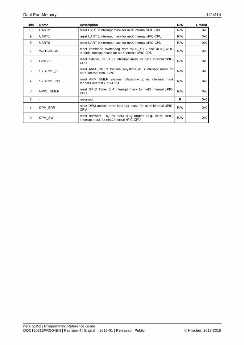
Dual-Port Memory 141/414
netX 51/52 | Programming Reference Guide DOC120215PRG04EN | Revision 4 | English | 2015-01 | Released | Public © Hilscher, 2012-2015
Bits Name Description R/W Default
10 UART2 reset UART 2 interrupt mask for netX internal xPIC-CPU R/W 0x0
9 UART1 reset UART 1 interrupt mask for netX internal xPIC-CPU R/W 0x0
8 UART0 reset UART 0 interrupt mask for netX internal xPIC-CPU R/W 0x0
7 WATCHDOG reset combined Watchdog from WDG_SYS and XPIC_WDG module interrupt mask for netX internal xPIC-CPU
R/W 0x0
6 GPIO31 reset external GPIO 31 interrupt mask for netX internal xPIC-CPU
R/W 0x0
5 SYSTIME_S reset ARM_TIMER systime_s/systime_uc_s interrupt mask for netX internal xPIC-CPU
R/W 0x0
4 SYSTIME_NS reset ARM_TIMER systime_ns/systime_uc_ns interrupt mask for netX internal xPIC-CPU
R/W 0x0
3 GPIO_TIMER reset GPIO Timer 0..4 interrupt mask for netX internal xPIC-CPU
R/W 0x0
2 - reserved R 0x0
1 DPM_ERR reset DPM access error interrupt mask for netX internal xPIC-CPU
R/W 0x0
0 DPM_SW reset software IRQ for netX IRQ targets (e.g. ARM, xPIC) interrupt mask for netX internal xPIC-CPU
R/W 0x0

Dual-Port Memory 142/414
netX 51/52 | Programming Reference Guide DOC120215PRG04EN | Revision 4 | English | 2015-01 | Released | Public © Hilscher, 2012-2015
DPM_IRQ_XPIC_MASKED – DPM Masked Interrupt Status Register for netX Internal xPIC-CPU 0x1018c098
A bit is set, when the related mask bit is set in ’DPM_IRQ_XPIC_MASK’-register and the related interrupt is
asserted.
IRQ for netX internal xPIC-CPU is asserted if at least one bit is set here.
Interrupts must be reset in interrupt generating module. Interrupts cannot be cleared here.
To release IRQ for netX internal xPIC-CPU without clearing interrupt in module, reset related mask bit to 0.
Note: For further information, please view description of ’DPM_IRQ_RAW’ register.
31 30 29 28 27 26 25 24 23 22 21 20 19 18 17 16 15 14 13 12 11 10 9 8 7 6 5 4 3 2 1 0
rese
rved
OS
AC
CA
N
TR
IGG
ER
_LT
DM
AC
SY
SS
TA
TE
INT
_PH
Y
rese
rved
MS
YN
C1
MS
YN
C0
XP
IC_D
EB
UG
rese
rved
CO
M1
CO
M0
GP
IO
FIR
MW
AR
E
rese
rved
I2C
SP
I
US
B
UA
RT
2
UA
RT
1
UA
RT
0
WA
TC
HD
OG
GP
IO31
SY
ST
IME
_S
SY
ST
IME
_NS
GP
IO_T
IME
R
rese
rved
DP
M_E
RR
DP
M_S
W
Bits Name Description R/W Default
31 - reserved R 0x0
30 OSAC masked OSAC interrupt state for netX internal xPIC-CPU R 0x0
29 CAN masked CAN interrupt state for netX internal xPIC-CPU R 0x0
28 TRIGGER_LT masked Trigger-Latch interrupt state for netX internal xPIC-CPU R 0x0
27 DMAC masked DMA-Controller interrupt state for netX internal xPIC-CPU
R 0x0
26 SYSSTATE masked combined licence error and MI timeout interrupt state for netX internal xPIC-CPU
R 0x0
25 INT_PHY masked combined internal PHY 0 / PHY 1 interrupt state for netX internal xPIC-CPU
R 0x0
24:23 - reserved R 0x0
22 MSYNC1 masked motion synchronization channel 1 (= |xpec1_irq[15:12]) interrupt state for netX internal xPIC-CPU
R 0x0
21 MSYNC0 masked motion synchronization channel 0 (= |xpec0_irq[15:12]) interrupt state for netX internal xPIC-CPU
R 0x0
20 XPIC_DEBUG masked xPIC Debug interrupt state for netX internal xPIC-CPU R 0x0
19 - reserved R 0x0
18 COM1 masked communication channel 1 (= |xpec1_irq[11:0]) interrupt state for netX internal xPIC-CPU
R 0x0
17 COM0 masked communication channel 0 (= |xpec0_irq[11:0]) interrupt state for netX internal xPIC-CPU
R 0x0
16 GPIO masked combined GPIO 0-30 / IOLINK interrupt state for netX internal xPIC-CPU
R 0x0
15 FIRMWARE masked combined handshake-cell and SYS_STA firmware interrupt state for netX internal xPIC-CPU
R 0x0
14 - reserved R 0x0
13 I2C masked combined I2C 0 and I2C 1 interrupt state for netX internal xPIC-CPU
R 0x0
12 SPI masked combined SPI 0 / SQI, SPI 1 interrupt state for netX internal xPIC-CPU
R 0x0
11 USB masked USB interrupt state for netX internal xPIC-CPU R 0x0
10 UART2 masked UART 2 interrupt state for netX internal xPIC-CPU R 0x0
9 UART1 masked UART 1 interrupt state for netX internal xPIC-CPU R 0x0
8 UART0 masked UART 0 interrupt state for netX internal xPIC-CPU R 0x0
7 WATCHDOG masked combined Watchdog from WDG_SYS and XPIC_WDG R 0x0

Dual-Port Memory 143/414
netX 51/52 | Programming Reference Guide DOC120215PRG04EN | Revision 4 | English | 2015-01 | Released | Public © Hilscher, 2012-2015
Bits Name Description R/W Default
module interrupt state for netX internal xPIC-CPU
6 GPIO31 masked external GPIO 31 interrupt state for netX internal xPIC-CPU
R 0x0
5 SYSTIME_S masked ARM_TIMER systime_s/systime_uc_s interrupt state for netX internal xPIC-CPU
R 0x0
4 SYSTIME_NS masked ARM_TIMER systime_ns/systime_uc_ns interrupt state for netX internal xPIC-CPU
R 0x0
3 GPIO_TIMER masked GPIO Timer 0..4 interrupt state for netX internal xPIC-CPU
R 0x0
2 - reserved R 0x0
1 DPM_ERR masked DPM access error interrupt state for netX internal xPIC-CPU
R 0x0
0 DPM_SW masked software IRQ for netX IRQ targets (e.g. ARM, xPIC) interrupt state for netX internal xPIC-CPU
R 0x0
DPM_IRQ_FIQ_MASK_SET – DPM Interrupt Mask Register for Fast netX Interrupt Output Signal (DPM_FIQ/HIF_SIRQ) 0x1018c09c
Write access with ’1’ sets related interrupt mask bits (enables interrupt request for corresponding interrupt source).
Write access with ’0’ does not influence related interrupt mask bit.
Read access shows actual interrupt mask.
If a mask bit is set, the related interrupt will activate the IRQ for fast netX interrupt output signal
(DPM_FIQ/HIF_SIRQ).
Interrupts must be reset in interrupt generating module. Interrupts cannot be cleared here.
To release IRQ for fast netX interrupt output signal (DPM_FIQ/HIF_SIRQ) without clearing interrupt in
module, reset related mask bit to 0.
Note: For further information, please view description of ’DPM_IRQ_RAW’ register.
31 30 29 28 27 26 25 24 23 22 21 20 19 18 17 16 15 14 13 12 11 10 9 8 7 6 5 4 3 2 1 0
rese
rved
OS
AC
CA
N
TR
IGG
ER
_LT
DM
AC
SY
SS
TA
TE
INT
_PH
Y
rese
rved
MS
YN
C1
MS
YN
C0
XP
IC_D
EB
UG
rese
rved
CO
M1
CO
M0
GP
IO
FIR
MW
AR
E
rese
rved
I2C
SP
I
US
B
UA
RT
2
UA
RT
1
UA
RT
0
WA
TC
HD
OG
GP
IO31
SY
ST
IME
_S
SY
ST
IME
_NS
GP
IO_T
IME
R
rese
rved
DP
M_E
RR
DP
M_S
W
Bits Name Description R/W Default
31 - reserved R 0x0
30 OSAC set OSAC interrupt mask for fast netX interrupt output signal (DPM_FIQ/HIF_SIRQ)
R/W 0x0
29 CAN set CAN interrupt mask for fast netX interrupt output signal (DPM_FIQ/HIF_SIRQ)
R/W 0x0
28 TRIGGER_LT set Trigger-Latch interrupt mask for fast netX interrupt output signal (DPM_FIQ/HIF_SIRQ)
R/W 0x0
27 DMAC set DMA-Controller interrupt mask for fast netX interrupt output signal (DPM_FIQ/HIF_SIRQ)
R/W 0x0
26 SYSSTATE set combined licence error and MI timeout interrupt mask for fast netX interrupt output signal (DPM_FIQ/HIF_SIRQ)
R/W 0x0
25 INT_PHY set combined internal PHY 0 / PHY 1 interrupt mask for fast netX interrupt output signal (DPM_FIQ/HIF_SIRQ)
R/W 0x0
24:23 - reserved R 0x0

Dual-Port Memory 144/414
netX 51/52 | Programming Reference Guide DOC120215PRG04EN | Revision 4 | English | 2015-01 | Released | Public © Hilscher, 2012-2015
Bits Name Description R/W Default
22 MSYNC1 set motion synchronization channel 1 (= |xpec1_irq[15:12]) interrupt mask for fast netX interrupt output signal (DPM_FIQ/HIF_SIRQ)
R/W 0x0
21 MSYNC0 set motion synchronization channel 0 (= |xpec0_irq[15:12]) interrupt mask for fast netX interrupt output signal (DPM_FIQ/HIF_SIRQ)
R/W 0x0
20 XPIC_DEBUG set xPIC Debug interrupt mask for fast netX interrupt output signal (DPM_FIQ/HIF_SIRQ)
R/W 0x0
19 - reserved R 0x0
18 COM1 set communication channel 1 (= |xpec1_irq[11:0]) interrupt mask for fast netX interrupt output signal (DPM_FIQ/HIF_SIRQ)
R/W 0x0
17 COM0 set communication channel 0 (= |xpec0_irq[11:0]) interrupt mask for fast netX interrupt output signal (DPM_FIQ/HIF_SIRQ)
R/W 0x0
16 GPIO set combined GPIO 0-30 / IOLINK interrupt mask for fast netX interrupt output signal (DPM_FIQ/HIF_SIRQ)
R/W 0x0
15 FIRMWARE set combined handshake-cell and SYS_STA firmware interrupt mask for fast netX interrupt output signal (DPM_FIQ/HIF_SIRQ)
R/W 0x0
14 - reserved R 0x0
13 I2C set combined I2C 0 and I2C 1 interrupt mask for fast netX interrupt output signal (DPM_FIQ/HIF_SIRQ)
R/W 0x0
12 SPI set combined SPI 0 / SQI, SPI 1 interrupt mask for fast netX interrupt output signal (DPM_FIQ/HIF_SIRQ)
R/W 0x0
11 USB set USB interrupt mask for fast netX interrupt output signal (DPM_FIQ/HIF_SIRQ)
R/W 0x0
10 UART2 set UART 2 interrupt mask for fast netX interrupt output signal (DPM_FIQ/HIF_SIRQ)
R/W 0x0
9 UART1 set UART 1 interrupt mask for fast netX interrupt output signal (DPM_FIQ/HIF_SIRQ)
R/W 0x0
8 UART0 set UART 0 interrupt mask for fast netX interrupt output signal (DPM_FIQ/HIF_SIRQ)
R/W 0x0
7 WATCHDOG set combined Watchdog from WDG_SYS and XPIC_WDG module interrupt mask for fast netX interrupt output signal (DPM_FIQ/HIF_SIRQ)
R/W 0x0
6 GPIO31 set external GPIO 31 interrupt mask for fast netX interrupt output signal (DPM_FIQ/HIF_SIRQ)
R/W 0x0
5 SYSTIME_S set ARM_TIMER systime_s/systime_uc_s interrupt mask for fast netX interrupt output signal (DPM_FIQ/HIF_SIRQ)
R/W 0x0
4 SYSTIME_NS set ARM_TIMER systime_ns/systime_uc_ns interrupt mask for fast netX interrupt output signal (DPM_FIQ/HIF_SIRQ)
R/W 0x0
3 GPIO_TIMER set GPIO Timer 0..4 interrupt mask for fast netX interrupt output signal (DPM_FIQ/HIF_SIRQ)
R/W 0x0
2 - reserved R 0x0
1 DPM_ERR set DPM access error interrupt mask for fast netX interrupt output signal (DPM_FIQ/HIF_SIRQ)
R/W 0x0
0 DPM_SW set software IRQ for netX IRQ targets (e.g. ARM, xPIC) interrupt mask for fast netX interrupt output signal (DPM_FIQ/HIF_SIRQ)
R/W 0x0

Dual-Port Memory 145/414
netX 51/52 | Programming Reference Guide DOC120215PRG04EN | Revision 4 | English | 2015-01 | Released | Public © Hilscher, 2012-2015
DPM_IRQ_FIQ_MASK_RESET – DPM Interrupt Mask Reset Register for Fast netX Interrupt Output Signal (DPM_FIQ/HIF_SIRQ) 0x1018c0a0
Write access with ’1’ resets related interrupt mask bits (disables interrupt request for corresponding interrupt
source).
Write access with ’0’ does not influence related interrupt mask bit.
Read access shows actual interrupt mask.
If a mask bit is set, the related interrupt will activate the IRQ for fast netX interrupt output signal (DPM_FIQ/HIF_SIRQ).
Interrupts must be reset in interrupt generating module. Interrupts cannot be cleared here.
To release IRQ for fast netX interrupt output signal (DPM_FIQ/HIF_SIRQ) without clearing interrupt in module, reset related mask bit to 0.
Note: For further information, please view description of ’DPM_IRQ_RAW’ register.
31 30 29 28 27 26 25 24 23 22 21 20 19 18 17 16 15 14 13 12 11 10 9 8 7 6 5 4 3 2 1 0
rese
rved
OS
AC
CA
N
TR
IGG
ER
_LT
DM
AC
SY
SS
TA
TE
INT
_PH
Y
rese
rved
MS
YN
C1
MS
YN
C0
XP
IC_D
EB
UG
rese
rved
CO
M1
CO
M0
GP
IO
FIR
MW
AR
E
rese
rved
I2C
SP
I
US
B
UA
RT
2
UA
RT
1
UA
RT
0
WA
TC
HD
OG
GP
IO31
SY
ST
IME
_S
SY
ST
IME
_NS
GP
IO_T
IME
R
rese
rved
DP
M_E
RR
DP
M_S
W
Bits Name Description R/W Default
31 - reserved R 0x0
30 OSAC reset OSAC interrupt mask for fast netX interrupt output signal (DPM_FIQ/HIF_SIRQ)
R/W 0x0
29 CAN reset CAN interrupt mask for fast netX interrupt output signal (DPM_FIQ/HIF_SIRQ)
R/W 0x0
28 TRIGGER_LT reset Trigger-Latch interrupt mask for fast netX interrupt output signal (DPM_FIQ/HIF_SIRQ)
R/W 0x0
27 DMAC reset DMA-Controller interrupt mask for fast netX interrupt output signal (DPM_FIQ/HIF_SIRQ)
R/W 0x0
26 SYSSTATE reset combined licence error and MI timeout interrupt mask for fast netX interrupt output signal (DPM_FIQ/HIF_SIRQ)
R/W 0x0
25 INT_PHY reset combined internal PHY 0 / PHY 1 interrupt mask for fast netX interrupt output signal (DPM_FIQ/HIF_SIRQ)
R/W 0x0
24:23 - reserved R 0x0
22 MSYNC1 reset motion synchronization channel 1 (= |xpec1_irq[15:12]) interrupt mask for fast netX interrupt output signal (DPM_FIQ/HIF_SIRQ)
R/W 0x0
21 MSYNC0 reset motion synchronization channel 0 (= |xpec0_irq[15:12]) interrupt mask for fast netX interrupt output signal (DPM_FIQ/HIF_SIRQ)
R/W 0x0
20 XPIC_DEBUG reset xPIC Debug interrupt mask for fast netX interrupt output signal (DPM_FIQ/HIF_SIRQ)
R/W 0x0
19 - reserved R 0x0
18 COM1 reset communication channel 1 (= |xpec1_irq[11:0]) interrupt mask for fast netX interrupt output signal (DPM_FIQ/HIF_SIRQ)
R/W 0x0
17 COM0 reset communication channel 0 (= |xpec0_irq[11:0]) interrupt mask for fast netX interrupt output signal (DPM_FIQ/HIF_SIRQ)
R/W 0x0
16 GPIO reset combined GPIO 0-30 / IOLINK interrupt mask for fast netX interrupt output signal (DPM_FIQ/HIF_SIRQ)
R/W 0x0
15 FIRMWARE reset combined handshake-cell and SYS_STA firmware interrupt mask for fast netX interrupt output signal (DPM_FIQ/HIF_SIRQ)
R/W 0x0
14 - reserved R 0x0

Dual-Port Memory 146/414
netX 51/52 | Programming Reference Guide DOC120215PRG04EN | Revision 4 | English | 2015-01 | Released | Public © Hilscher, 2012-2015
Bits Name Description R/W Default
13 I2C reset combined I2C 0 and I2C 1 interrupt mask for fast netX interrupt output signal (DPM_FIQ/HIF_SIRQ)
R/W 0x0
12 SPI reset combined SPI 0 / SQI, SPI 1 interrupt mask for fast netX interrupt output signal (DPM_FIQ/HIF_SIRQ)
R/W 0x0
11 USB reset USB interrupt mask for fast netX interrupt output signal (DPM_FIQ/HIF_SIRQ)
R/W 0x0
10 UART2 reset UART 2 interrupt mask for fast netX interrupt output signal (DPM_FIQ/HIF_SIRQ)
R/W 0x0
9 UART1 reset UART 1 interrupt mask for fast netX interrupt output signal (DPM_FIQ/HIF_SIRQ)
R/W 0x0
8 UART0 reset UART 0 interrupt mask for fast netX interrupt output signal (DPM_FIQ/HIF_SIRQ)
R/W 0x0
7 WATCHDOG reset combined Watchdog from WDG_SYS and XPIC_WDG module interrupt mask for fast netX interrupt output signal (DPM_FIQ/HIF_SIRQ)
R/W 0x0
6 GPIO31 reset external GPIO 31 interrupt mask for fast netX interrupt output signal (DPM_FIQ/HIF_SIRQ)
R/W 0x0
5 SYSTIME_S reset ARM_TIMER systime_s/systime_uc_s interrupt mask for fast netX interrupt output signal (DPM_FIQ/HIF_SIRQ)
R/W 0x0
4 SYSTIME_NS reset ARM_TIMER systime_ns/systime_uc_ns interrupt mask for fast netX interrupt output signal (DPM_FIQ/HIF_SIRQ)
R/W 0x0
3 GPIO_TIMER reset GPIO Timer 0..4 interrupt mask for fast netX interrupt output signal (DPM_FIQ/HIF_SIRQ)
R/W 0x0
2 - reserved R 0x0
1 DPM_ERR reset DPM access error interrupt mask for fast netX interrupt output signal (DPM_FIQ/HIF_SIRQ)
R/W 0x0
0 DPM_SW reset software IRQ for netX IRQ targets (e.g. ARM, xPIC) interrupt mask for fast netX interrupt output signal (DPM_FIQ/HIF_SIRQ)
R/W 0x0

Dual-Port Memory 147/414
netX 51/52 | Programming Reference Guide DOC120215PRG04EN | Revision 4 | English | 2015-01 | Released | Public © Hilscher, 2012-2015
DPM_IRQ_FIQ_MASKED – DPM Masked Interrupt Status Register for Fast netX Interrupt Output Signal (DPM_FIQ/HIF_SIRQ). 0x1018c0a4
A bit is set, when the related mask bit is set in ’DPM_IRQ_FIQ_MASK’-register and the related interrupt is
asserted.
IRQ for fast netX interrupt output signal (DPM_FIQ/HIF_SIRQ) is asserted if at least one bit is set here.
Interrupts must be reset in interrupt generating module. Interrupts cannot be cleared here.
To release IRQ for fast netX interrupt output signal (DPM_FIQ/HIF_SIRQ) without clearing interrupt in module, reset related mask bit to 0.
Note: For further information, please view description of ’DPM_IRQ_RAW’ register.
31 30 29 28 27 26 25 24 23 22 21 20 19 18 17 16 15 14 13 12 11 10 9 8 7 6 5 4 3 2 1 0
rese
rved
OS
AC
CA
N
TR
IGG
ER
_LT
DM
AC
SY
SS
TA
TE
INT
_PH
Y
rese
rved
MS
YN
C1
MS
YN
C0
XP
IC_D
EB
UG
rese
rved
CO
M1
CO
M0
GP
IO
FIR
MW
AR
E
rese
rved
I2C
SP
I
US
B
UA
RT
2
UA
RT
1
UA
RT
0
WA
TC
HD
OG
GP
IO31
SY
ST
IME
_S
SY
ST
IME
_NS
GP
IO_T
IME
R
rese
rved
DP
M_E
RR
DP
M_S
W
Bits Name Description R/W Default
31 - reserved R 0x0
30 OSAC masked OSAC interrupt state for fast netX interrupt output signal (DPM_FIQ/HIF_SIRQ)
R 0x0
29 CAN masked CAN interrupt state for fast netX interrupt output signal (DPM_FIQ/HIF_SIRQ)
R 0x0
28 TRIGGER_LT masked Trigger-Latch interrupt state for fast netX interrupt output signal (DPM_FIQ/HIF_SIRQ)
R 0x0
27 DMAC masked DMA-Controller interrupt state for fast netX interrupt output signal (DPM_FIQ/HIF_SIRQ)
R 0x0
26 SYSSTATE masked combined licence error and MI timeout interrupt state for fast netX interrupt output signal (DPM_FIQ/HIF_SIRQ)
R 0x0
25 INT_PHY masked combined internal PHY 0 / PHY 1 interrupt state for fast netX interrupt output signal (DPM_FIQ/HIF_SIRQ)
R 0x0
24:23 - reserved R 0x0
22 MSYNC1 masked motion synchronization channel 1 (= |xpec1_irq[15:12]) interrupt state for fast netX interrupt output signal (DPM_FIQ/HIF_SIRQ)
R 0x0
21 MSYNC0 masked motion synchronization channel 0 (= |xpec0_irq[15:12]) interrupt state for fast netX interrupt output signal (DPM_FIQ/HIF_SIRQ)
R 0x0
20 XPIC_DEBUG masked xPIC Debug interrupt state for fast netX interrupt output signal (DPM_FIQ/HIF_SIRQ)
R 0x0
19 - reserved R 0x0
18 COM1 masked communication channel 1 (= |xpec1_irq[11:0]) interrupt state for fast netX interrupt output signal (DPM_FIQ/HIF_SIRQ)
R 0x0
17 COM0 masked communication channel 0 (= |xpec0_irq[11:0]) interrupt state for fast netX interrupt output signal (DPM_FIQ/HIF_SIRQ)
R 0x0
16 GPIO masked combined GPIO 0-30 / IOLINK interrupt state for fast netX interrupt output signal (DPM_FIQ/HIF_SIRQ)
R 0x0
15 FIRMWARE masked combined handshake-cell and SYS_STA firmware interrupt state for fast netX interrupt output signal (DPM_FIQ/HIF_SIRQ)
R 0x0
14 - reserved R 0x0
13 I2C masked combined I2C 0 and I2C 1 interrupt state for fast netX interrupt output signal (DPM_FIQ/HIF_SIRQ)
R 0x0
12 SPI masked combined SPI 0 / SQI, SPI 1 interrupt state for fast netX R 0x0

Dual-Port Memory 148/414
netX 51/52 | Programming Reference Guide DOC120215PRG04EN | Revision 4 | English | 2015-01 | Released | Public © Hilscher, 2012-2015
Bits Name Description R/W Default
interrupt output signal (DPM_FIQ/HIF_SIRQ)
11 USB masked USB interrupt state for fast netX interrupt output signal (DPM_FIQ/HIF_SIRQ)
R 0x0
10 UART2 masked UART 2 interrupt state for fast netX interrupt output signal (DPM_FIQ/HIF_SIRQ)
R 0x0
9 UART1 masked UART 1 interrupt state for fast netX interrupt output signal (DPM_FIQ/HIF_SIRQ)
R 0x0
8 UART0 masked UART 0 interrupt state for fast netX interrupt output signal (DPM_FIQ/HIF_SIRQ)
R 0x0
7 WATCHDOG masked combined Watchdog from WDG_SYS and XPIC_WDG module interrupt state for fast netX interrupt output signal (DPM_FIQ/HIF_SIRQ)
R 0x0
6 GPIO31 masked external GPIO 31 interrupt state for fast netX interrupt output signal (DPM_FIQ/HIF_SIRQ)
R 0x0
5 SYSTIME_S masked ARM_TIMER systime_s/systime_uc_s interrupt state for fast netX interrupt output signal (DPM_FIQ/HIF_SIRQ)
R 0x0
4 SYSTIME_NS masked ARM_TIMER systime_ns/systime_uc_ns interrupt state for fast netX interrupt output signal (DPM_FIQ/HIF_SIRQ)
R 0x0
3 GPIO_TIMER masked GPIO Timer 0..4 interrupt state for fast netX interrupt output signal (DPM_FIQ/HIF_SIRQ)
R 0x0
2 - reserved R 0x0
1 DPM_ERR masked DPM access error interrupt state for fast netX interrupt output signal (DPM_FIQ/HIF_SIRQ)
R 0x0
0 DPM_SW masked software IRQ for netX IRQ targets (e.g. ARM, xPIC) interrupt state for fast netX interrupt output signal (DPM_FIQ/HIF_SIRQ)
R 0x0

Dual-Port Memory 149/414
netX 51/52 | Programming Reference Guide DOC120215PRG04EN | Revision 4 | English | 2015-01 | Released | Public © Hilscher, 2012-2015
DPM_IRQ_IRQ_MASK_SET – DPM Interrupt Mask Register for Normal netX Interrupt Output Signal (DPM_IRQ/HIF_DIRQ) 0x1018c0a8
Write access with ’1’ sets related interrupt mask bits (enables interrupt request for corresponding interrupt
source).
Write access with ’0’ does not influence related interrupt mask bit.
Read access shows actual interrupt mask.
If a mask bit is set, the related interrupt will activate the IRQ for normal netX interrupt output signal (DPM_IRQ/HIF_DIRQ).
Interrupts must be reset in interrupt generating module. Interrupts cannot be cleared here.
To release IRQ for normal netX interrupt output signal (DPM_IRQ/HIF_DIRQ) without clearing interrupt in module, reset related mask bit to 0.
Note: For further information, please view description of ’DPM_IRQ_RAW’ register.
31 30 29 28 27 26 25 24 23 22 21 20 19 18 17 16 15 14 13 12 11 10 9 8 7 6 5 4 3 2 1 0
rese
rved
OS
AC
CA
N
TR
IGG
ER
_LT
DM
AC
SY
SS
TA
TE
INT
_PH
Y
rese
rved
MS
YN
C1
MS
YN
C0
XP
IC_D
EB
UG
rese
rved
CO
M1
CO
M0
GP
IO
FIR
MW
AR
E
rese
rved
I2C
SP
I
US
B
UA
RT
2
UA
RT
1
UA
RT
0
WA
TC
HD
OG
GP
IO31
SY
ST
IME
_S
SY
ST
IME
_NS
GP
IO_T
IME
R
rese
rved
DP
M_E
RR
DP
M_S
W
Bits Name Description R/W Default
31 - reserved R 0x0
30 OSAC set OSAC interrupt mask for normal netX interrupt output signal (DPM_IRQ/HIF_DIRQ)
R/W 0x0
29 CAN set CAN interrupt mask for normal netX interrupt output signal (DPM_IRQ/HIF_DIRQ)
R/W 0x0
28 TRIGGER_LT set Trigger-Latch interrupt mask for normal netX interrupt output signal (DPM_IRQ/HIF_DIRQ)
R/W 0x0
27 DMAC set DMA-Controller interrupt mask for normal netX interrupt output signal (DPM_IRQ/HIF_DIRQ)
R/W 0x0
26 SYSSTATE set combined licence error and MI timeout interrupt mask for normal netX interrupt output signal (DPM_IRQ/HIF_DIRQ)
R/W 0x0
25 INT_PHY set combined internal PHY 0 / PHY 1 interrupt mask for normal netX interrupt output signal (DPM_IRQ/HIF_DIRQ)
R/W 0x0
24:23 - reserved R 0x0
22 MSYNC1 set motion synchronization channel 1 (= |xpec1_irq[15:12]) interrupt mask for normal netX interrupt output signal (DPM_IRQ/HIF_DIRQ)
R/W 0x0
21 MSYNC0 set motion synchronization channel 0 (= |xpec0_irq[15:12]) interrupt mask for normal netX interrupt output signal (DPM_IRQ/HIF_DIRQ)
R/W 0x0
20 XPIC_DEBUG set xPIC Debug interrupt mask for normal netX interrupt output signal (DPM_IRQ/HIF_DIRQ)
R/W 0x0
19 - reserved R 0x0
18 COM1 set communication channel 1 (= |xpec1_irq[11:0]) interrupt mask for normal netX interrupt output signal (DPM_IRQ/HIF_DIRQ)
R/W 0x0
17 COM0 set communication channel 0 (= |xpec0_irq[11:0]) interrupt mask for normal netX interrupt output signal (DPM_IRQ/HIF_DIRQ)
R/W 0x0
16 GPIO set combined GPIO 0-30 / IOLINK interrupt mask for normal netX interrupt output signal (DPM_IRQ/HIF_DIRQ)
R/W 0x0
15 FIRMWARE set combined handshake-cell and SYS_STA firmware interrupt mask for normal netX interrupt output signal (DPM_IRQ/HIF_DIRQ)
R/W 0x0
14 - reserved R 0x0

Dual-Port Memory 150/414
netX 51/52 | Programming Reference Guide DOC120215PRG04EN | Revision 4 | English | 2015-01 | Released | Public © Hilscher, 2012-2015
Bits Name Description R/W Default
13 I2C set combined I2C 0 and I2C 1 interrupt mask for normal netX interrupt output signal (DPM_IRQ/HIF_DIRQ)
R/W 0x0
12 SPI set combined SPI 0 / SQI, SPI 1 interrupt mask for normal netX interrupt output signal (DPM_IRQ/HIF_DIRQ)
R/W 0x0
11 USB set USB interrupt mask for normal netX interrupt output signal (DPM_IRQ/HIF_DIRQ)
R/W 0x0
10 UART2 set UART 2 interrupt mask for normal netX interrupt output signal (DPM_IRQ/HIF_DIRQ)
R/W 0x0
9 UART1 set UART 1 interrupt mask for normal netX interrupt output signal (DPM_IRQ/HIF_DIRQ)
R/W 0x0
8 UART0 set UART 0 interrupt mask for normal netX interrupt output signal (DPM_IRQ/HIF_DIRQ)
R/W 0x0
7 WATCHDOG set combined Watchdog from WDG_SYS and XPIC_WDG module interrupt mask for normal netX interrupt output signal (DPM_IRQ/HIF_DIRQ)
R/W 0x0
6 GPIO31 set external GPIO 31 interrupt mask for normal netX interrupt output signal (DPM_IRQ/HIF_DIRQ)
R/W 0x0
5 SYSTIME_S set ARM_TIMER systime_s/systime_uc_s interrupt mask for normal netX interrupt output signal (DPM_IRQ/HIF_DIRQ)
R/W 0x0
4 SYSTIME_NS set ARM_TIMER systime_ns/systime_uc_ns interrupt mask for normal netX interrupt output signal (DPM_IRQ/HIF_DIRQ)
R/W 0x0
3 GPIO_TIMER set GPIO Timer 0..4 interrupt mask for normal netX interrupt output signal (DPM_IRQ/HIF_DIRQ)
R/W 0x0
2 - reserved R 0x0
1 DPM_ERR set DPM access error interrupt mask for normal netX interrupt output signal (DPM_IRQ/HIF_DIRQ)
R/W 0x0
0 DPM_SW set software IRQ for netX IRQ targets (e.g. ARM, xPIC) interrupt mask for normal netX interrupt output signal (DPM_IRQ/HIF_DIRQ)
R/W 0x0

Dual-Port Memory 151/414
netX 51/52 | Programming Reference Guide DOC120215PRG04EN | Revision 4 | English | 2015-01 | Released | Public © Hilscher, 2012-2015
DPM_IRQ_IRQ_MASK_RESET – DPM Interrupt Mask Reset Register for Normal netX Interrupt Output Signal (DPM_IRQ/HIF_DIRQ) 0x1018c0ac
Write access with ’1’ resets related interrupt mask bits (disables interrupt request for corresponding interrupt
source).
Write access with ’0’ does not influence related interrupt mask bit.
Read access shows actual interrupt mask.
If a mask bit is set, the related interrupt will activate the IRQ for normal netX interrupt output signal (DPM_IRQ/HIF_DIRQ).
Interrupts must be reset in interrupt generating module. Interrupts cannot be cleared here.
To release IRQ for normal netX interrupt output signal (DPM_IRQ/HIF_DIRQ) without clearing interrupt in module, reset related mask bit to 0.
Note: For further information, please view description of ’DPM_IRQ_RAW’ register.
31 30 29 28 27 26 25 24 23 22 21 20 19 18 17 16 15 14 13 12 11 10 9 8 7 6 5 4 3 2 1 0
rese
rved
OS
AC
CA
N
TR
IGG
ER
_LT
DM
AC
SY
SS
TA
TE
INT
_PH
Y
rese
rved
MS
YN
C1
MS
YN
C0
XP
IC_D
EB
UG
rese
rved
CO
M1
CO
M0
GP
IO
FIR
MW
AR
E
rese
rved
I2C
SP
I
US
B
UA
RT
2
UA
RT
1
UA
RT
0
WA
TC
HD
OG
GP
IO31
SY
ST
IME
_S
SY
ST
IME
_NS
GP
IO_T
IME
R
rese
rved
DP
M_E
RR
DP
M_S
W
Bits Name Description R/W Default
31 - reserved R 0x0
30 OSAC reset OSAC interrupt mask for normal netX interrupt output signal (DPM_IRQ/HIF_DIRQ)
R/W 0x0
29 CAN reset CAN interrupt mask for normal netX interrupt output signal (DPM_IRQ/HIF_DIRQ)
R/W 0x0
28 TRIGGER_LT reset Trigger-Latch interrupt mask for normal netX interrupt output signal (DPM_IRQ/HIF_DIRQ)
R/W 0x0
27 DMAC reset DMA-Controller interrupt mask for normal netX interrupt output signal (DPM_IRQ/HIF_DIRQ)
R/W 0x0
26 SYSSTATE reset combined licence error and MI timeout interrupt mask for normal netX interrupt output signal (DPM_IRQ/HIF_DIRQ)
R/W 0x0
25 INT_PHY reset combined internal PHY 0 / PHY 1 interrupt mask for normal netX interrupt output signal (DPM_IRQ/HIF_DIRQ)
R/W 0x0
24:23 - reserved R 0x0
22 MSYNC1 reset motion synchronization channel 1 (= |xpec1_irq[15:12]) interrupt mask for normal netX interrupt output signal (DPM_IRQ/HIF_DIRQ)
R/W 0x0
21 MSYNC0 reset motion synchronization channel 0 (= |xpec0_irq[15:12]) interrupt mask for normal netX interrupt output signal (DPM_IRQ/HIF_DIRQ)
R/W 0x0
20 XPIC_DEBUG reset xPIC Debug interrupt mask for normal netX interrupt output signal (DPM_IRQ/HIF_DIRQ)
R/W 0x0
19 - reserved R 0x0
18 COM1 reset communication channel 1 (= |xpec1_irq[11:0]) interrupt mask for normal netX interrupt output signal (DPM_IRQ/HIF_DIRQ)
R/W 0x0
17 COM0 reset communication channel 0 (= |xpec0_irq[11:0]) interrupt mask for normal netX interrupt output signal (DPM_IRQ/HIF_DIRQ)
R/W 0x0
16 GPIO reset combined GPIO 0-30 / IOLINK interrupt mask for normal netX interrupt output signal (DPM_IRQ/HIF_DIRQ)
R/W 0x0
15 FIRMWARE reset combined handshake-cell and SYS_STA firmware interrupt mask for normal netX interrupt output signal
R/W 0x0

Dual-Port Memory 152/414
netX 51/52 | Programming Reference Guide DOC120215PRG04EN | Revision 4 | English | 2015-01 | Released | Public © Hilscher, 2012-2015
Bits Name Description R/W Default
(DPM_IRQ/HIF_DIRQ)
14 - reserved R 0x0
13 I2C reset combined I2C 0 and I2C 1 interrupt mask for normal netX interrupt output signal (DPM_IRQ/HIF_DIRQ)
R/W 0x0
12 SPI reset combined SPI 0 / SQI, SPI 1 interrupt mask for normal netX interrupt output signal (DPM_IRQ/HIF_DIRQ)
R/W 0x0
11 USB reset USB interrupt mask for normal netX interrupt output signal (DPM_IRQ/HIF_DIRQ)
R/W 0x0
10 UART2 reset UART 2 interrupt mask for normal netX interrupt output signal (DPM_IRQ/HIF_DIRQ)
R/W 0x0
9 UART1 reset UART 1 interrupt mask for normal netX interrupt output signal (DPM_IRQ/HIF_DIRQ)
R/W 0x0
8 UART0 reset UART 0 interrupt mask for normal netX interrupt output signal (DPM_IRQ/HIF_DIRQ)
R/W 0x0
7 WATCHDOG reset combined Watchdog from WDG_SYS and XPIC_WDG module interrupt mask for normal netX interrupt output signal (DPM_IRQ/HIF_DIRQ)
R/W 0x0
6 GPIO31 reset external GPIO 31 interrupt mask for normal netX interrupt output signal (DPM_IRQ/HIF_DIRQ)
R/W 0x0
5 SYSTIME_S reset ARM_TIMER systime_s/systime_uc_s interrupt mask for normal netX interrupt output signal (DPM_IRQ/HIF_DIRQ)
R/W 0x0
4 SYSTIME_NS reset ARM_TIMER systime_ns/systime_uc_ns interrupt mask for normal netX interrupt output signal (DPM_IRQ/HIF_DIRQ)
R/W 0x0
3 GPIO_TIMER reset GPIO Timer 0..4 interrupt mask for normal netX interrupt output signal (DPM_IRQ/HIF_DIRQ)
R/W 0x0
2 - reserved R 0x0
1 DPM_ERR reset DPM access error interrupt mask for normal netX interrupt output signal (DPM_IRQ/HIF_DIRQ)
R/W 0x0
0 DPM_SW reset software IRQ for netX IRQ targets (e.g. ARM, xPIC) interrupt mask for normal netX interrupt output signal (DPM_IRQ/HIF_DIRQ)
R/W 0x0

Dual-Port Memory 153/414
netX 51/52 | Programming Reference Guide DOC120215PRG04EN | Revision 4 | English | 2015-01 | Released | Public © Hilscher, 2012-2015
DPM_IRQ_IRQ_MASKED – DPM Masked Interrupt Status Register for Normal netX Interrupt Output Signal (DPM_IRQ/HIF_DIRQ) 0x1018c0b0
A bit is set, when the related mask bit is set in ’DPM_IRQ_IRQ_MASK’-register and the related interrupt is
asserted.
IRQ for normal netX interrupt output signal (DPM_IRQ/HIF_DIRQ) is asserted if at least one bit is set here.
Interrupts must be reset in interrupt generating module. Interrupts cannot be cleared here.
To release IRQ for normal netX interrupt output signal (DPM_IRQ/HIF_DIRQ) without clearing interrupt in module, reset related mask bit to 0.
Note: For further information, please view description of ’DPM_IRQ_RAW’ register.
31 30 29 28 27 26 25 24 23 22 21 20 19 18 17 16 15 14 13 12 11 10 9 8 7 6 5 4 3 2 1 0
rese
rved
OS
AC
CA
N
TR
IGG
ER
_LT
DM
AC
SY
SS
TA
TE
INT
_PH
Y
rese
rved
MS
YN
C1
MS
YN
C0
XP
IC_D
EB
UG
rese
rved
CO
M1
CO
M0
GP
IO
FIR
MW
AR
E
rese
rved
I2C
SP
I
US
B
UA
RT
2
UA
RT
1
UA
RT
0
WA
TC
HD
OG
GP
IO31
SY
ST
IME
_S
SY
ST
IME
_NS
GP
IO_T
IME
R
rese
rved
DP
M_E
RR
DP
M_S
W
Bits Name Description R/W Default
31 - reserved R 0x0
30 OSAC masked OSAC interrupt state for normal netX interrupt output signal (DPM_IRQ/HIF_DIRQ)
R 0x0
29 CAN masked CAN interrupt state for normal netX interrupt output signal (DPM_IRQ/HIF_DIRQ)
R 0x0
28 TRIGGER_LT masked Trigger-Latch interrupt state for normal netX interrupt output signal (DPM_IRQ/HIF_DIRQ)
R 0x0
27 DMAC masked DMA-Controller interrupt state for normal netX interrupt output signal (DPM_IRQ/HIF_DIRQ)
R 0x0
26 SYSSTATE masked combined licence error and MI timeout interrupt state for normal netX interrupt output signal (DPM_IRQ/HIF_DIRQ)
R 0x0
25 INT_PHY masked combined internal PHY 0 / PHY 1 interrupt state for normal netX interrupt output signal (DPM_IRQ/HIF_DIRQ)
R 0x0
24:23 - reserved R 0x0
22 MSYNC1 masked motion synchronization channel 1 (= |xpec1_irq[15:12]) interrupt state for normal netX interrupt output signal (DPM_IRQ/HIF_DIRQ)
R 0x0
21 MSYNC0 masked motion synchronization channel 0 (= |xpec0_irq[15:12]) interrupt state for normal netX interrupt output signal (DPM_IRQ/HIF_DIRQ)
R 0x0
20 XPIC_DEBUG masked xPIC Debug interrupt state for normal netX interrupt output signal (DPM_IRQ/HIF_DIRQ)
R 0x0
19 - reserved R 0x0
18 COM1 masked communication channel 1 (= |xpec1_irq[11:0]) interrupt state for normal netX interrupt output signal (DPM_IRQ/HIF_DIRQ)
R 0x0
17 COM0 masked communication channel 0 (= |xpec0_irq[11:0]) interrupt state for normal netX interrupt output signal (DPM_IRQ/HIF_DIRQ)
R 0x0
16 GPIO masked combined GPIO 0-30 / IOLINK interrupt state for normal netX interrupt output signal (DPM_IRQ/HIF_DIRQ)
R 0x0
15 FIRMWARE masked combined handshake-cell and SYS_STA firmware interrupt state for normal netX interrupt output signal (DPM_IRQ/HIF_DIRQ)
R 0x0
14 - reserved R 0x0
13 I2C masked combined I2C 0 and I2C 1 interrupt state for normal netX interrupt output signal (DPM_IRQ/HIF_DIRQ)
R 0x0

Dual-Port Memory 154/414
netX 51/52 | Programming Reference Guide DOC120215PRG04EN | Revision 4 | English | 2015-01 | Released | Public © Hilscher, 2012-2015
Bits Name Description R/W Default
12 SPI masked combined SPI 0 / SQI, SPI 1 interrupt state for normal netX interrupt output signal (DPM_IRQ/HIF_DIRQ)
R 0x0
11 USB masked USB interrupt state for normal netX interrupt output signal (DPM_IRQ/HIF_DIRQ)
R 0x0
10 UART2 masked UART 2 interrupt state for normal netX interrupt output signal (DPM_IRQ/HIF_DIRQ)
R 0x0
9 UART1 masked UART 1 interrupt state for normal netX interrupt output signal (DPM_IRQ/HIF_DIRQ)
R 0x0
8 UART0 masked UART 0 interrupt state for normal netX interrupt output signal (DPM_IRQ/HIF_DIRQ)
R 0x0
7 WATCHDOG masked combined Watchdog from WDG_SYS and XPIC_WDG module interrupt state for normal netX interrupt output signal (DPM_IRQ/HIF_DIRQ)
R 0x0
6 GPIO31 masked external GPIO 31 interrupt state for normal netX interrupt output signal (DPM_IRQ/HIF_DIRQ)
R 0x0
5 SYSTIME_S masked ARM_TIMER systime_s/systime_uc_s interrupt state for normal netX interrupt output signal (DPM_IRQ/HIF_DIRQ)
R 0x0
4 SYSTIME_NS masked ARM_TIMER systime_ns/systime_uc_ns interrupt state for normal netX interrupt output signal (DPM_IRQ/HIF_DIRQ)
R 0x0
3 GPIO_TIMER masked GPIO Timer 0..4 interrupt state for normal netX interrupt output signal (DPM_IRQ/HIF_DIRQ)
R 0x0
2 - reserved R 0x0
1 DPM_ERR masked DPM access error interrupt state for normal netX interrupt output signal (DPM_IRQ/HIF_DIRQ)
R 0x0
0 DPM_SW masked software IRQ for netX IRQ targets (e.g. ARM, xPIC) interrupt state for normal netX interrupt output signal (DPM_IRQ/HIF_DIRQ)
R 0x0

Dual-Port Memory 155/414
netX 51/52 | Programming Reference Guide DOC120215PRG04EN | Revision 4 | English | 2015-01 | Released | Public © Hilscher, 2012-2015
DPM_SW_IRQ – DPM Register for Software Interrupt Generation to Host and netX Interrupt Targets 0x1018c0b8
Host and netX masters can generate an interrupt to netX interrupt targets (e.g. ARM-VIC, xPIC-VIC) or DPM
IRQ signals by this register.
To propagate interrupt states from this register to the interrupt target the ’dpm_sw’ bit must be set inside the appropriate interrupt mask (e.g. ’DPM_IRQ_ARM_MASK_SET’ register).
Example:
The ’dpm_sw’ IRQs can be used by the host to flag one IRQ to the ARM by setting the arm-
dpm_sw and another IRQ to the xPIC by setting the xpic-dpm_sw. The ARM can use at the same time the irq-dpm_sw to flag an IRQ to the host while the xPIC could use the fiq-dpm_sw to flag another IRQ to the host.
Note: For each netX interrupt target there is a set and a reset bit provided to avoid read-modify-write sequences. When both (set and reset) bits are set for the same target, the related interrupt will be set (set will win). Reset bits are always 0 on read. Set-bits shows current interrupt status
when read.
Note: This register is a new netx51/52 feature.
31 30 29 28 27 26 25 24 23 22 21 20 19 18 17 16 15 14 13 12 11 10 9 8 7 6 5 4 3 2 1 0
reserved
RE
SE
T_
IRQ
RE
SE
T_F
IQ
RE
SE
T_X
PIC
RE
SE
T_A
RM
reserved
SE
T_I
RQ
SE
T_F
IQ
SE
T_X
PIC
SE
T_A
RM
Bits Name Description R/W Default
31:12 - reserved R 0x0
11 RESET_IRQ Reset ’dpm_sw’ IRQ for IRQ-signal (always 0 when read) R/W 0x0
10 RESET_FIQ Reset ’dpm_sw’ IRQ for FIQ-signal (always 0 when read) R/W 0x0
9 RESET_XPIC Reset ’dpm_sw’ IRQ for xPIC (always 0 when read) R/W 0x0
8 RESET_ARM Reset ’dpm_sw’ IRQ for ARM (always 0 when read) R/W 0x0
7:4 - reserved R 0x0
3 SET_IRQ Set ’dpm_sw’ IRQ for IRQ-signal (current ’dpm_sw’ status for IRQ when read)
R/W 0x0
2 SET_FIQ Set ’dpm_sw’ IRQ for FIQ-signal (current ’dpm_sw’ status for FIQ when read)
R/W 0x0
1 SET_XPIC Set ’dpm_sw’ IRQ for xPIC (current ’dpm_sw’ status for xPIC when read)
R/W 0x0
0 SET_ARM Set ’dpm_sw’ IRQ for ARM (current ’dpm_sw’ status for ARM when read)
R/W 0x0

Dual-Port Memory 156/414
netX 51/52 | Programming Reference Guide DOC120215PRG04EN | Revision 4 | English | 2015-01 | Released | Public © Hilscher, 2012-2015
DPM_HOST_WDG_HOST_TIMEOUT – Address reserved for netX50 0x1018c0c0
31 30 29 28 27 26 25 24 23 22 21 20 19 18 17 16 15 14 13 12 11 10 9 8 7 6 5 4 3 2 1 0
ZERO_RO
Bits Name Description R/W Default
31:0 ZERO_RO reserved for netx50 DPM_HOST_WDG_HOST_TIMEOUT. R 0x0
DPM_HOST_WDG_HOST_TRIG – Address reserved for netX50 0x1018c0c4
31 30 29 28 27 26 25 24 23 22 21 20 19 18 17 16 15 14 13 12 11 10 9 8 7 6 5 4 3 2 1 0
ZERO_RO
Bits Name Description R/W Default
31:0 ZERO_RO reserved for netx50 DPM_HOST_WDG_HOST_TRIG. R 0x0
DPM_HOST_WDG_ARM_TIMEOUT – Address reserved for netX50 0x1018c0c8
31 30 29 28 27 26 25 24 23 22 21 20 19 18 17 16 15 14 13 12 11 10 9 8 7 6 5 4 3 2 1 0
ZERO_RO
Bits Name Description R/W Default
31:0 ZERO_RO reserved for netx50 DPM_HOST_WDG_ARM_TIMEOUT. R 0x0

Dual-Port Memory 157/414
netX 51/52 | Programming Reference Guide DOC120215PRG04EN | Revision 4 | English | 2015-01 | Released | Public © Hilscher, 2012-2015
DPM_SYS_STA_BIGEND16 – DPM System Status Information Register in Big Endianess 16 Data Mapping 0x1018c0cc
This register is read-only, using DPM_HOST_SYS_STAT for programming.
This register can be used for firmware status information.
Reading this register data can be done from uninitialized DPM interface in the same way as reading netX version (DPM_NETX_VERSION_BIGEND16, DPM_NETX_VERSION) by using
DPM_SYS_STA_BIGEND16 register.
31 30 29 28 27 26 25 24 23 22 21 20 19 18 17 16 15 14 13 12 11 10 9 8 7 6 5 4 3 2 1 0
reserved
HO
ST
_ST
AT
E_
SW
AP
_RO
NE
TX
_ST
AT
E_S
WA
P_R
O
RU
N_R
O
RD
Y_R
O
NE
TX
_ST
A_C
OD
E_S
WA
P_R
O
Bits Name Description R/W Default
31:16 - reserved R 0x0
15:12 HOST_STATE_SWAP_RO
Bit field for Hilscher firmware compatibility. R 0x0
11:10 NETX_STATE_SWAP_RO
Bit field for Hilscher firmware compatibility. R 0x0
9 RUN_RO Output state of netX RUN LED IO. R 0x0
8 RDY_RO Output state of netX RDY LED IO. R 0x0
7:0 NETX_STA_CODE_SWAP_RO
Bit field for Hilscher firmware compatibility. R 0x0
DPM_HOST_TMR_CTRL – Address reserved for netX50 0x1018c0d0
31 30 29 28 27 26 25 24 23 22 21 20 19 18 17 16 15 14 13 12 11 10 9 8 7 6 5 4 3 2 1 0
ZERO_RO
Bits Name Description R/W Default
31:0 ZERO_RO reserved for netx50 DPM_HOST_TMR_CTRL. R 0x0
DPM_HOST_TMR_START_VAL – Address reserved for netX50 0x1018c0d4
31 30 29 28 27 26 25 24 23 22 21 20 19 18 17 16 15 14 13 12 11 10 9 8 7 6 5 4 3 2 1 0
ZERO_RO
Bits Name Description R/W Default
31:0 ZERO_RO reserved for netx50 DPM_HOST_TMR_START_VAL. R 0x0

Dual-Port Memory 158/414
netX 51/52 | Programming Reference Guide DOC120215PRG04EN | Revision 4 | English | 2015-01 | Released | Public © Hilscher, 2012-2015
DPM_HOST_SYS_STAT – DPM System Status Information Register 0x1018c0d8
This register can be used for firmware status information.
Reading this register data can be done from uninitialized DPM interface in the same way as reading netX version (DPM_NETX_VERSION_BIGEND16, DPM_NETX_VERSION) by using
DPM_SYS_STA_BIGEND16 register.
Note: This register is compatible to netx50 DPM_HOST_SYS_STAT register
31 30 29 28 27 26 25 24 23 22 21 20 19 18 17 16 15 14 13 12 11 10 9 8 7 6 5 4 3 2 1 0
reserved NETX_STA_CODE_RO
HO
ST
_ST
AT
E
NE
TX
_ST
AT
E_
RO
RU
N_R
O
RD
Y_R
O
Bits Name Description R/W Default
31:16 - reserved R 0x0
15:8 NETX_STA_CODE_RO Bit field for Hilscher firmware compatibility (read only). Note: This bit field can be changed by rdy_run_cfg-register inside ASIC_CTRL address area.
R/W 0x0
7:4 HOST_STATE Bit field for Hilscher firmware compatibility. Note: This bit field can be read also at rdy_run_cfg-register inside ASIC_CTRL address area.
R/W 0x0
3:2 NETX_STATE_RO Bit field for Hilscher firmware compatibility. Note: This bit field can be changed by rdy_run_cfg-register inside ASIC_CTRL address area.
R/W 0x0
1 RUN_RO Output state of netX RUN LED IO. Note: This bit field can be changed by rdy_run_cfg-register inside ASIC_CTRL address area.
R/W 0x0
0 RDY_RO Output state of netX RDY LED IO. Note: This bit field can be changed by rdy_run_cfg-register inside ASIC_CTRL address area.
R/W 0x0

Dual-Port Memory 159/414
netX 51/52 | Programming Reference Guide DOC120215PRG04EN | Revision 4 | English | 2015-01 | Released | Public © Hilscher, 2012-2015
DPM_HOST_RESET_REQ – DPM Reset Request Register 0x1018c0dc
Note: This register is compatible to netx50 DPM_HOST_RESET_REQ register
31 30 29 28 27 26 25 24 23 22 21 20 19 18 17 16 15 14 13 12 11 10 9 8 7 6 5 4 3 2 1 0
reserved RESET_KEY
Bits Name Description R/W Default
31:8 - reserved R 0x0
7:0 RESET_KEY
Reset key sequence register. A netx hardware reset is generated if the following sequence is written to this register: 1st access: write 0x00 2nd access: write 0x01 3rd access: write 0x03 4th access: write 0x07 5th access: write 0x0f 6th access: write 0x1f 7th access: write 0x3f 8th access: write 0x7f Reading this register will provide the next write data. Hence it is also possible performing 8 times a read-write sequence to this register. However read could be omitted. Note: The sequence must not interrupted by any other write access to any other DPM register. Read access have no influence. Note: For netx10 a 9th access (write 0xff) was necessary to performe a reset This access is not netx50 compatible and not required any longer since netx51/52.
R/W 0x0

Dual-Port Memory 160/414
netX 51/52 | Programming Reference Guide DOC120215PRG04EN | Revision 4 | English | 2015-01 | Released | Public © Hilscher, 2012-2015
DPM_HOST_INT_STAT0 – 1st netX50 Compatible DPM Interrupt Status Register (Related to DPM_HOST_INT_EN0’-Register). 0x1018c0e0
Writing a ’1’ to an IRQ flag will clear the Interrupt. This is always done even if related bit inside
‘DPM_HOST_INT_EN0’-register is not set (this is compatible to netX50).
Important: There are two completely independent sets of IRQ registers:
IRQ register-set 1: DPM_IRQ_RAW (and related registers e.g. DPM_IRQ_IRQ_* registers).
IRQ register-set 2: DPM_HOST_INT_* registers (netx50 compatible register set: DPM_HOST_INT_EN0, DPM_HOST_INT_EN2, DPM_HOST_INT_STAT0,
DPM_HOST_INT_STAT2).
Programming (masking or clearing IRQs) of one register-set has no impact to the other register-set even if some IRQs can be found in both sets (e.g. com0).
Note: This register is compatible to netx50 DPM_HOST_INT_STAT0 register; however some unused IRQs have been removed.
31 30 29 28 27 26 25 24 23 22 21 20 19 18 17 16 15 14 13 12 11 10 9 8 7 6 5 4 3 2 1 0
INT
_RE
Q
RE
S_M
EM
_LC
K_R
O
RE
S_W
DG
_N
ET
X_R
O
RD
Y_T
IME
OU
T
rese
rved
SY
S_S
TA
RE
S_T
MR
_R
O
rese
rved
IRQ_VECTOR
HS
_EV
EN
T15
HS
_EV
EN
T14
HS
_EV
EN
T13
HS
_EV
EN
T12
HS
_EV
EN
T11
HS
_EV
EN
T10
HS
_EV
EN
T9
HS
_EV
EN
T8
HS
_EV
EN
T7
HS
_EV
EN
T6
HS
_EV
EN
T5
HS
_EV
EN
T4
HS
_EV
EN
T3
HS
_EV
EN
T2
HS
_EV
EN
T1
HS
_EV
EN
T0
Bits Name Description R/W Default
31 INT_REQ
Interrupt Request for IRQs handled in this register. 0: No Interrupts to host requested by IRQ sources handled in
this register. 1: IRQ sources handled in this register request a host IRQ. Note: This bit is masked by INT_EN-bit in dpm_firmware_irq_mask register. For propagation of INT_REQ to host, ARM or xPIC, INT_EN-bit must be set and firmware IRQ must be activated in related dpm_irq_* register.
R/W 0x0
30 RES_MEM_LCK_RO reserved for Memory Lock IRQ flag (not available in this netX version).
R/W 0x0
29 RES_WDG_NETX_RO reserved for netX supervision Watchdog Timeout IRQ flag (not available in this netX version).
R/W 0x0
28 RDY_TIMEOUT DPM_RDY timeout error was detected. Note: This flag is not affected by ’dpm_status_err’ registers.
R/W 0x0
27 - reserved R 0x0
26 SYS_STA System Status Change IRQ flag. R/W 0x0
25 RES_TMR_RO reserved for Timer IRQ flag (not available in this netX version). R/W 0x0
24 - reserved R 0x0
23:16 IRQ_VECTOR
Interrupt Vector according to status flags generated by enabled IRQ sources. Code IRQ status 0x00 No IRQ. ---- ------- 0x07 trigger_lt (related to DPM_HOST_INT_STA2.trigger_lt). 0x0a sync1 (related to DPM_HOST_INT_STA2.sync1)
R/W 0x0

Dual-Port Memory 161/414
netX 51/52 | Programming Reference Guide DOC120215PRG04EN | Revision 4 | English | 2015-01 | Released | Public © Hilscher, 2012-2015
Bits Name Description R/W Default
. 0x0b sync0 (related to DPM_HOST_INT_STA2.sync0)
. 0x0e com1 (related to DPM_HOST_INT_STA2.com1)
. 0x0f com0 (related to DPM_HOST_INT_STA2.com0)
. ---- ------- 0x10 Handshake Cell 0 IRQ. 0x11 Handshake Cell 1 IRQ. 0x12 Handshake Cell 2 IRQ. 0x13 Handshake Cell 3 IRQ. 0x14 Handshake Cell 4 IRQ. 0x15 Handshake Cell 5 IRQ. 0x16 Handshake Cell 6 IRQ. 0x17 Handshake Cell 7 IRQ. 0x18 Handshake Cell 8 IRQ. 0x19 Handshake Cell 9 IRQ. 0x1a Handshake Cell 10 IRQ. 0x1b Handshake Cell 11 IRQ. 0x1c Handshake Cell 12 IRQ. 0x1d Handshake Cell 13 IRQ. 0x1e Handshake Cell 14 IRQ. 0x1f Handshake Cell 15 IRQ. ---- ------- 0x67 RDY_TIMEOUT IRQ 0x70 SYS_STA IRQ Other values are reserved. Note: The current IRQ state in VECTOR depends only on the single IRQ enable bits. It does not depend on global IRQ enable INT_EN. VECTOR shows always the highest priority enabled flagged IRQ even is INT_EN is ’0’.
15 HS_EVENT15 Handshake Event 15 IRQ Enable flag. R/W 0x0
14 HS_EVENT14 Handshake Event 14 IRQ Enable flag. R/W 0x0
13 HS_EVENT13 Handshake Event 13 IRQ Enable flag. R/W 0x0
12 HS_EVENT12 Handshake Event 12 IRQ Enable flag. R/W 0x0
11 HS_EVENT11 Handshake Event 11 IRQ Enable flag. R/W 0x0
10 HS_EVENT10 Handshake Event 10 IRQ Enable flag. R/W 0x0
9 HS_EVENT9 Handshake Event 9 IRQ Enable flag. R/W 0x0
8 HS_EVENT8 Handshake Event 8 IRQ Enable flag. R/W 0x0
7 HS_EVENT7 Handshake Event 7 IRQ Enable flag. R/W 0x0
6 HS_EVENT6 Handshake Event 6 IRQ Enable flag. R/W 0x0
5 HS_EVENT5 Handshake Event 5 IRQ Enable flag. R/W 0x0
4 HS_EVENT4 Handshake Event 4 IRQ Enable flag. R/W 0x0
3 HS_EVENT3 Handshake Event 3 IRQ Enable flag. R/W 0x0
2 HS_EVENT2 Handshake Event 2 IRQ Enable flag. R/W 0x0
1 HS_EVENT1 Handshake Event 1 IRQ Enable flag. R/W 0x0
0 HS_EVENT0 Handshake Event 0 IRQ Enable flag. R/W 0x0

Dual-Port Memory 162/414
netX 51/52 | Programming Reference Guide DOC120215PRG04EN | Revision 4 | English | 2015-01 | Released | Public © Hilscher, 2012-2015
DPM_HOST_INT_STAT2 – 2nd netX50 Compatible DPM Interrupt Status Register (Related to ’DPM_HOST_INT_EN2’-Register) 0x1018c0e8
All IRQs from this register are also part of ’DPM_HOST_INT_STAT.IRQ_VECTOR’ bit-field.
Important: This is a read-only status register. IRQs can not be cleared here: In contrast to ‘DPM_HOST_INT_STAT0’ -register writing ’1’s will have no effect. IRQs are straight forwarded
from IRQ generating units (e.g. ’trigger_lt’-IRQ from netX trigger-sample-unit).
Important: There are two completely independent sets of IRQ registers:
IRQ register-set 1: DPM_IRQ_RAW (and related registers e.g. DPM_IRQ_IRQ_* registers).
IRQ register-set 2: DPM_HOST_INT_* registers (netx50 compatible register set: DPM_HOST_INT_EN0, DPM_HOST_INT_EN2, DPM_HOST_INT_STAT0, DPM_HOST_INT_STAT2).
Programming (masking or clearing IRQs) of one register-set has no impact to the other register-set even if some IRQs can be found in both sets (e.g. com0).
Note: This register is compatible to netx50 DPM_HOST_INT_STAT2 register; however some unused
IRQs have been removed.
31 30 29 28 27 26 25 24 23 22 21 20 19 18 17 16 15 14 13 12 11 10 9 8 7 6 5 4 3 2 1 0
reserved
TR
IGG
ER
_LT
rese
rved
MS
YN
C1
MS
YN
C0
rese
rved
CO
M1
CO
M0
Bits Name Description R/W Default
31:9 - reserved R 0x0
8 TRIGGER_LT trigger-Latch interrupt. R 0x0
7:6 - reserved R 0x0
5 MSYNC1 motion synchronization channel 1 (= |xpec1_irq[15:12]) interrupt. R 0x0
4 MSYNC0 motion synchronization channel 0 (= |xpec0_irq[15:12]) interrupt. R 0x0
3:2 - reserved R 0x0
1 COM1 communication channel 1 (= |xpec1_irq[11:0]) interrupt. R 0x0
0 COM0 communication channel 0 (= |xpec0_irq[11:0]) interrupt. R 0x0

Dual-Port Memory 163/414
netX 51/52 | Programming Reference Guide DOC120215PRG04EN | Revision 4 | English | 2015-01 | Released | Public © Hilscher, 2012-2015
DPM_HOST_INT_EN0 – DPM Handshake Interrupt Enable Register. 0x1018c0f0
Only netX50 compatible DPM_HOST_INT_STAT0 registers are related to settings of this register.
Note: This register is compatible to netx50 DPM_HOST_INT_EN0 register; however some unused
IRQs have been removed.
Note: HS_EVENT-bits are not read-only. This is netX50 compliant. Recent netX50 Documentation marks HS_EVENT-bits as read-only. This is a dokumentation error. For netX50 compatibility,
these bits can also be controlled from netX-side in HANDSHAKE_CTRL address area.
31 30 29 28 27 26 25 24 23 22 21 20 19 18 17 16 15 14 13 12 11 10 9 8 7 6 5 4 3 2 1 0
INT
_EN
RE
S_M
EM
_LC
K_R
O
RE
S_W
DG
_N
ET
X_R
O
RD
Y_T
IME
OU
T
rese
rved
SY
S_S
TA
RE
S_T
MR
_R
O
reserved H
S_E
VE
NT
15
HS
_EV
EN
T14
HS
_EV
EN
T13
HS
_EV
EN
T12
HS
_EV
EN
T11
HS
_EV
EN
T10
HS
_EV
EN
T9
HS
_EV
EN
T8
HS
_EV
EN
T7
HS
_EV
EN
T6
HS
_EV
EN
T5
HS
_EV
EN
T4
HS
_EV
EN
T3
HS
_EV
EN
T2
HS
_EV
EN
T1
HS
_EV
EN
T0
Bits Name Description R/W Default
31 INT_EN
Interrupt Enable for IRQs handled in this register. Only if this bit is set, global firmware IRQ will be asserted to host CPU, ARM or xPIC by dpm_irq_* registers. 0: No Interrupts to host, ARM or xPIC are generated by IRQ
sources handled in this register. 1: Enabled IRQ sources handled in this register generate a
host, ARM or xPIC IRQ if asserted. Note: Enable bits for single IRQ events are not affected if this bit is set or reset.
R/W 0x0
30 RES_MEM_LCK_RO reserved for Memory Lock IRQ (not available in this netX version).
R/W 0x0
29 RES_WDG_NETX_RO reserved for netX supervision Watchdog Timeout IRQ (not available in this netX version).
R/W 0x0
28 RDY_TIMEOUT Enable for ’dpm_firmware_irq_raw.RDY_TIMEOUT’ bit. R/W 0x0
27 - reserved R 0x0
26 SYS_STA System Status Change IRQ Enable. R/W 0x0
25 RES_TMR_RO reserved for Timer IRQ (not available in this netX version). R/W 0x0
24:16 - reserved R 0x0
15 HS_EVENT15 Handshake Event 15 IRQ Enable (also netX-controllable by HANDSHAKE_CTRL, netX50 comp.).
R/W 0x0
14 HS_EVENT14 Handshake Event 14 IRQ Enable (also netX-controllable by HANDSHAKE_CTRL, netX50 comp.).
R/W 0x0
13 HS_EVENT13 Handshake Event 13 IRQ Enable (also netX-controllable by HANDSHAKE_CTRL, netX50 comp.).
R/W 0x0
12 HS_EVENT12 Handshake Event 12 IRQ Enable (also netX-controllable by HANDSHAKE_CTRL, netX50 comp.).
R/W 0x0
11 HS_EVENT11 Handshake Event 11 IRQ Enable (also netX-controllable by HANDSHAKE_CTRL, netX50 comp.).
R/W 0x0
10 HS_EVENT10 Handshake Event 10 IRQ Enable (also netX-controllable by HANDSHAKE_CTRL, netX50 comp.).
R/W 0x0
9 HS_EVENT9 Handshake Event 9 IRQ Enable (also netX-controllable by HANDSHAKE_CTRL, netX50 comp.).
R/W 0x0
8 HS_EVENT8 Handshake Event 8 IRQ Enable (also netX-controllable by HANDSHAKE_CTRL, netX50 comp.).
R/W 0x0

Dual-Port Memory 164/414
netX 51/52 | Programming Reference Guide DOC120215PRG04EN | Revision 4 | English | 2015-01 | Released | Public © Hilscher, 2012-2015
Bits Name Description R/W Default
7 HS_EVENT7 Handshake Event 7 IRQ Enable (also netX-controllable by HANDSHAKE_CTRL, netX50 comp.).
R/W 0x0
6 HS_EVENT6 Handshake Event 6 IRQ Enable (also netX-controllable by HANDSHAKE_CTRL, netX50 comp.).
R/W 0x0
5 HS_EVENT5 Handshake Event 5 IRQ Enable (also netX-controllable by HANDSHAKE_CTRL, netX50 comp.).
R/W 0x0
4 HS_EVENT4 Handshake Event 4 IRQ Enable (also netX-controllable by HANDSHAKE_CTRL, netX50 comp.).
R/W 0x0
3 HS_EVENT3 Handshake Event 3 IRQ Enable (also netX-controllable by HANDSHAKE_CTRL, netX50 comp.).
R/W 0x0
2 HS_EVENT2 Handshake Event 2 IRQ Enable (also netX-controllable by HANDSHAKE_CTRL, netX50 comp.).
R/W 0x0
1 HS_EVENT1 Handshake Event 1 IRQ Enable (also netX-controllable by HANDSHAKE_CTRL, netX50 comp.).
R/W 0x0
0 HS_EVENT0 Handshake Event 0 IRQ Enable (also netX-controllable by HANDSHAKE_CTRL, netX50 comp.).
R/W 0x0

Dual-Port Memory 165/414
netX 51/52 | Programming Reference Guide DOC120215PRG04EN | Revision 4 | English | 2015-01 | Released | Public © Hilscher, 2012-2015
DPM_NETX_VERSION_BIGEND16 – DPM netX Version Register in Big Endianess 16 Data Mapping 0x1018c0f4
This registers content is mirrored form ASIC_CTRL register area and can be set during netX booting phase
by netX firmware.
This register is not valid if unlocked bit is not set in DPM_STATUS register.
Together with DPM_NETX_VERSION register, full 32 bit version can be read by any host device, even if
DPM interface is not initialized yet.
Bytes byte1 and byte3 can be always read here even if DPM is uninitialized (8 bit default from DPM_CFG0X0 after power on) and host device has 8, 16 or 32 bit data width. 8 bit DPM 16 bit DPM 32 bit DPM byte 0 (D7:0) byte read this address +1 adr_dpm_netx_version adr_dpm_netx_version byte 1 (D15:8) byte read this address +0 byte read this address DWord read this address byte 2 (D23:16) byte read this address +3 adr_dpm_netx_version adr_dpm_netx_version byte 3 (D31:24) byte read this address +2 byte read this address +2 byte read this address +0 31 30 29 28 27 26 25 24 23 22 21 20 19 18 17 16 15 14 13 12 11 10 9 8 7 6 5 4 3 2 1 0
NE
TX
_VE
RS
ION
_BY
TE
2_S
WA
P
NE
TX
_VE
RS
ION
_BY
TE
3_S
WA
P
NE
TX
_VE
RS
ION
_BY
TE
0_S
WA
P
NE
TX
_VE
RS
ION
_BY
TE
1_S
WA
P
Bits Name Description R/W Default
31:24 NETX_VERSION_BYTE2_SWAP
netX version bits 24 to 16. R 0x0
23:16 NETX_VERSION_BYTE3_SWAP
netX version bits 31 to 24. R 0x0
15:8 NETX_VERSION_BYTE0_SWAP
netX version bits 8 to 0. R 0x0
7:0 NETX_VERSION_BYTE1_SWAP
netX version bits 16 to 8. R 0x0

Dual-Port Memory 166/414
netX 51/52 | Programming Reference Guide DOC120215PRG04EN | Revision 4 | English | 2015-01 | Released | Public © Hilscher, 2012-2015
DPM_HOST_INT_EN2 – netX50 compatible Interrupt Enable Register No.2. 0x1018c0f8
Only netx50 compatible ‘DPM_HOST_INT_STAT2’ registers are related to settings of this register.
Important: There are two completely independent sets of IRQ registers:
IRQ register-set 1: DPM_IRQ_RAW (and related registers e.g. DPM_IRQ_IRQ_* registers).
IRQ register-set 2: DPM_HOST_INT_* registers (netx50 compatible register set: DPM_HOST_INT_EN0, DPM_HOST_INT_EN2, DPM_HOST_INT_STAT0,
DPM_HOST_INT_STAT2).
Programming (masking or clearing IRQs) of one register-set has no impact to the other register-set even if some IRQs can be found in both sets (e.g. com0).
Note: This register is compatible to netx50 DPM_HOST_INT_EN2 register; however some unused IRQs have been removed.
31 30 29 28 27 26 25 24 23 22 21 20 19 18 17 16 15 14 13 12 11 10 9 8 7 6 5 4 3 2 1 0
reserved
TR
IGG
ER
_LT
rese
rved
MS
YN
C1
MS
YN
C0
rese
rved
CO
M1
CO
M0
Bits Name Description R/W Default
31:9 - reserved R 0x0
8 TRIGGER_LT Enable of trigger-Latch interrupt for ’dpm_firmware_irq_raw’ registers.
R/W 0x0
7:6 - reserved R 0x0
5 MSYNC1 Enable of motion synchronization channel 1 (= |xpec1_irq[15:12]) interrupt for ’dpm_firmware_irq_raw’ registers.
R/W 0x0
4 MSYNC0 Enable of motion synchronization channel 0 (= |xpec0_irq[15:12]) interrupt for ’dpm_firmware_irq_raw’ registers.
R/W 0x0
3:2 - reserved R 0x0
1 COM1 Enable of communication channel 1 (= |xpec1_irq[11:0]) interrupt for ’dpm_firmware_irq_raw’ registers.
R/W 0x0
0 COM0 Enable of communication channel 0 (= |xpec0_irq[11:0]) interrupt for ’dpm_firmware_irq_raw’ registers.
R/W 0x0

Dual-Port Memory 167/414
netX 51/52 | Programming Reference Guide DOC120215PRG04EN | Revision 4 | English | 2015-01 | Released | Public © Hilscher, 2012-2015
DPM_NETX_VERSION – DPM netX Version Register 0x1018c0fc
This register is mirrored from ASIC_CTRL register area and can be set during netX booting phase by netX firmware.
This register is not valid if unlocked bit is not set in DPM_STATUS register.
Together with DPM_NETX_VERSION_BIGEND16 register, full 32 bit version can be read by any host device, even if DPM interface is not initialized yet.
Bytes byte0 and byte2 can be always read here even if DPM is uninitialized (8 bit default from
DPM_CFG0X0 after power on) and host device has 8, 16 or 32 bit data width. 8 bit DPM 16 bit DPM 32 bit DPM byte 0 (D7:0) byte read this address +0 byte read this address DWord read this address byte 1 (D15:8) byte read this address +1 adr_dpm_netx_version_bigend16 adr_dpm_netx_version_bigend16 byte 2 (D23:16) byte read this address +2 byte read this address +2 byte read this address +0 byte 3 (D31:24) byte read this address +3 adr_dpm_netx_version_bigend16 adr_dpm_netx_version_bigend16
31 30 29 28 27 26 25 24 23 22 21 20 19 18 17 16 15 14 13 12 11 10 9 8 7 6 5 4 3 2 1 0
NETX_VERSION_BYTE3 NETX_VERSION_BYTE2 NETX_VERSION_BYTE1 NETX_VERSION_BYTE0
Bits Name Description R/W Default
31:24 NETX_VERSION_BYTE3 netX version bits 31 to 24. R 0x0
23:16 NETX_VERSION_BYTE2 netX version bits 24 to 16. R 0x0
15:8 NETX_VERSION_BYTE1 netX version bits 16 to 8. R 0x0
7:0 NETX_VERSION_BYTE0 netX version bits 8 to 0. R 0x0

Dual-Port Memory 168/414
netX 51/52 | Programming Reference Guide DOC120215PRG04EN | Revision 4 | English | 2015-01 | Released | Public © Hilscher, 2012-2015
5.5 Handshake Registers The handshake cells are located within the INTRAMHS and can be mapped to any 256 byte border. The handshake data width can be set to 8bit or 16bit.
16 Bit Handshake Data
31 30 29 28 27 26 25 24 23 22 21 20 19 18 17 16 15 14 13 12 11 10 9 8 7 6 5 4 3 2 1 0
HOSTNETX_DATA [15:0] NETXHOST_DATA [15:0]
Bits Name Description R/W Default
31:16 HOSTNETX_DATA[15:0] Handshake Data Flags host to netX [15:0] R 0x00
15:0 NETXHost_DATA[15:0] Handshake Data Flags netX to host [15:0] R/W 0x00
8 Bit Handshake Data
31 30 29 28 27 26 25 24 23 22 21 20 19 18 17 16 15 14 13 12 11 10 9 8 7 6 5 4 3 2 1 0
HOSTNETX_DATA [7:0] NETXHOST_DATA [7:0] DATA_MEMORY[15:8] DATA_MEMORY [7:0]
Bits Name Description R/W Default
31:24 HOSTNETX_DATA[7:0] Handshake Data Flags host to netX [7:0] R 0x00
23:16 NETXHOST_DATA[7:0] Handshake Data Flags netX to host [7:0] R/W 0x00
15:8 DATA_MEMORY [15:8] Data Memory [15:8] R/W 0x00
7:0 DATA_MEMORY [7:0] Data Memory [7:0] R/W 0x00
The following figure shows the16bit DPM handshake interaction.
Figure 3: 16bit DPM Handshake Interaction

Dual-Port Memory 169/414
netX 51/52 | Programming Reference Guide DOC120215PRG04EN | Revision 4 | English | 2015-01 | Released | Public © Hilscher, 2012-2015
The following table is a summary of all handshake configuration registers:
ARM Address Register Name Short Description
0x1018c300 HANDSHAKE_BASE_ADDR Handshake Cell Address Base Configuration Register
0x1018c310 HANDSHAKE_DPM_IRQ_RAW_CLEAR Handshake Cell Raw Interrupt for DPM Register
0x1018c314 HANDSHAKE_DPM_IRQ_MASKED Handshake Cell Masked Interrupt for DPM Register
0x1018c318 HANDSHAKE_DPM_IRQ_MSK_SET Handshake Cell Interrupt Mask Enable for DPM Register
0x1018c31c HANDSHAKE_DPM_IRQ_MSK_RESET Handshake Cell Interrupt Mask Disable for DPM Register
0x1018c320 HANDSHAKE_ARM_IRQ_RAW_CLEAR Handshake Cell Raw Interrupt for ARM Register
0x1018c324 HANDSHAKE_ARM_IRQ_MASKED Handshake Cell Masked Interrupt for ARM Register
0x1018c328 HANDSHAKE_ARM_IRQ_MSK_SET Handshake Cell Interrupt Mask Enable for ARM Register
0x1018c32c HANDSHAKE_ARM_IRQ_MSK_RESET Handshake Cell Interrupt Mask Disable for ARM Register
0x1018c330 HANDSHAKE_XPIC_IRQ_RAW_CLEAR Handshake Cell Raw Interrupt for xPIC Register
0x1018c334 HANDSHAKE_XPIC_IRQ_MASKED Handshake Cell Masked Interrupt for xPIC Register
0x1018c338 HANDSHAKE_XPIC_IRQ_MSK_SET Handshake Cell Interrupt Mask Enable for xPIC Register
0x1018c33c HANDSHAKE_XPIC_IRQ_MSK_RESET Handshake Cell Interrupt Mask Disable for xPIC Register
0x1018c380 HANDSHAKE_HSC0_CTRL Handshake Cell 0 Control Register
0x1018c384 HANDSHAKE_HSC1_CTRL Handshake Cell 1 Control Register
0x1018c388 HANDSHAKE_HSC2_CTRL Handshake Cell 2 Control Register
0x1018c38c HANDSHAKE_HSC3_CTRL Handshake Cell 3 Control Register
0x1018c390 HANDSHAKE_HSC4_CTRL Handshake Cell 4 Control Register
0x1018c394 HANDSHAKE_HSC5_CTRL Handshake Cell 5 Control Register
0x1018c398 HANDSHAKE_HSC6_CTRL Handshake Cell 6 Control Register
0x1018c39c HANDSHAKE_HSC7_CTRL Handshake Cell 7 Control Register
0x1018c3a0 HANDSHAKE_HSC8_CTRL Handshake Cell 8 Control Register
0x1018c3a4 HANDSHAKE_HSC9_CTRL Handshake Cell 9 Control Register
0x1018c3a8 HANDSHAKE_HSC10_CTRL Handshake Cell 10 Control Register
0x1018c3ac HANDSHAKE_HSC11_CTRL Handshake Cell 11 Control Register
0x1018c3b0 HANDSHAKE_HSC12_CTRL Handshake Cell 12 Control Register
0x1018c3b4 HANDSHAKE_HSC13_CTRL Handshake Cell 13 Control Register
0x1018c3b8 HANDSHAKE_HSC14_CTRL Handshake Cell 14 Control Register
0x1018c3bc HANDSHAKE_HSC15_CTRL Handshake Cell 15 Control Register
0x1018c3c0 HANDSHAKE_BUF_MAN0_CTRL Handshake Triple Buffer Manager 0 Control Register
0x1018c3c4 HANDSHAKE_BUF_MAN0_STATUS_CTRL_NETX
Handshake Triple Buffer Manager 0 netX Status and Control Register
0x1018c3c8 HANDSHAKE_BUF_MAN0_STATUS_CTRL_HOST
Handshake Triple Buffer Manager 0 Host Status Register
0x1018c3cc HANDSHAKE_BUF_MAN0_WIN_MAP DPM Window Address Map Alternative Configuration Register for Handshake Triple Buffer Manager 0
0x1018c3d0 HANDSHAKE_BUF_MAN1_CTRL Handshake Triple Buffer Manager 1 Control Register
0x1018c3d4 HANDSHAKE_BUF_MAN1_STATUS_CTRL_NETX
Handshake Triple Buffer Manager 1 netX Status and Control Register
0x1018c3d8 HANDSHAKE_BUF_MAN1_STATUS_CTRL_HOST
Handshake Triple Buffer Manager 1 Host Status Register
0x1018c3dc HANDSHAKE_BUF_MAN1_WIN_MAP DPM Window Address Map Alternative Configuration Register for Handshake Triple Buffer Manager 1
Table 16: Handshake Configuration Registers

Dual-Port Memory 170/414
netX 51/52 | Programming Reference Guide DOC120215PRG04EN | Revision 4 | English | 2015-01 | Released | Public © Hilscher, 2012-2015
HANDSHAKE_BASE_ADDR – Handshake Cell Address Base Configuration Register 0x1018c300
Handshake Cells are located in INTRAMHS and can be mapped to any 256 byte border.
Related master of an access to Handshake Cells is detected by the access to one of three INTRAMHS Mirrors:
Access via INTRAMHS dpm_mirror is interpreted by Handshake Cells as DPM access. This is regardless whether the access was really initiated by DPM master or not. E.g. if xPIC uses dpm_mirror of INTRAMHS for Handshake Cell access, this will be interpreted as DPM access and not as xPIC access.
INTRAMHS can be accessed by 4 different mirrors which are sub address areas of area HANDSHAKE. Furthermore HANDSHAKE address area is mirrored multiple inside whole netX address area. Each HANDSHAKE address area provides all 4 INTRAMHS mirrors.
There is one INTRAMHS mirror for each IRQ capable system master (DPM, xPIC, ARM) and one to access whole INTRAMHS area without any influence to HANDSHAKE_CTRL unit. However, each system master is able to address each INTRAMHS mirror. IRQs are always generated in dependency of mirror addressed by
a master on access. IRQ generation does not depend on the master running an access.
Handshake Cell Setup example:
4. Configure Handshake Cell area offset (e.g. offset 0x200, set base256 to 0x2).
5. Configure used Handshake Cell width (8bit or 16 bit) in ’HANDSHAKE_HSCx_CTRL’ registers.
6. Configure used Handshake Cells master association (e.g. ARM<->DPM) in ’HANDSHAKE_HSCx_CTRL’ registers.
Example: typical ARM<-> DPM Handshake interaction:
1. ARM writes request to Handshake Cell N (address: intramhs_arm_mirror+base256*256+N*4). -> DPM receives IRQ
2. DPM reads Handshake Cell N (address: intramhs_dpm_mirror+base256*256+N*4). -> DPM IRQ clear.
3. DPM writes acknowledge to Handshake Cell N (address: intramhs_dpm_mirror+base256*256+N*4).
-> ARM receives IRQ
4. ARM reads Handshake Cell N (address: intramhs_dpm_mirror+base256*256+N*4). -> ARM IRQ clear.
31 30 29 28 27 26 25 24 23 22 21 20 19 18 17 16 15 14 13 12 11 10 9 8 7 6 5 4 3 2 1 0
EN
AB
LE
NE
TX
50_C
OM
P
reserved BASE256 ZERO_RO
Bits Name Description R/W Default
31 ENABLE
Global Handshake Cell address compare logic enable. 0: All Handshake Cell features like IRQ generation or tripple-
buffer controlling are disabled. special HCS2 bits come from INTRAMHS and not from shadow logic. Handshake Cells behave like standard memory.
1: Handshake Cell features are enabled for Handshake Cells which are enabled (mode!=0). Special HCS2 bits come from from shadow logic and not from INTRAMHS (independent of mode-setting of HSC2).
R/W 0x0

Dual-Port Memory 171/414
netX 51/52 | Programming Reference Guide DOC120215PRG04EN | Revision 4 | English | 2015-01 | Released | Public © Hilscher, 2012-2015
Bits Name Description R/W Default
30 NETX50_COMP
Netx50 compatibility for Handshake Cell IRQ generation. 1: Handshake Cell IRQ generation is netx50 compatible
(default). 0: Handshake Cell IRQ generation is netx10 (not netx50)
compatible. This bit effects the behavior of Handshake Cell IRQ generation globally for all enabled Cells. For details and difference between netx50 and netx10 Handshake Cell IRQ behavior view ’handshake_hsc0_ctrl’ register desription. Note: This is a new netx51/52 feature.
R/W 0x1
29:15 - reserved R 0x0
14:8 BASE256 Address base configuration in 256 byte steps inside INTRAMHS R/W 0x0
7:0 ZERO_RO Low address bits not configurable R/W 0x0

Dual-Port Memory 172/414
netX 51/52 | Programming Reference Guide DOC120215PRG04EN | Revision 4 | English | 2015-01 | Released | Public © Hilscher, 2012-2015
HANDSHAKE_DPM_IRQ_RAW_CLEAR – Handshake Cell Raw Interrupt for DPM Register0x1018c310
Read access shows status of unmasked IRQs. IRQs are set automatically and reset by writing to this register:
Write access with ’1’ clears the appropriate IRQ.
Write access with ’0’ does not influence this bit.
Note: DPM related IRQ status can also be read from DPM_HOST_INT_STAT0 register (area DPM).
DPM related IRQs can also be cleared from DPM_HOST_INT_STAT0 register (area DPM).
DPM related IRQ masks can also be read from DPM_HOST_INT_EN0 register (area DPM).
31 30 29 28 27 26 25 24 23 22 21 20 19 18 17 16 15 14 13 12 11 10 9 8 7 6 5 4 3 2 1 0
reserved
HS
C15
HS
C14
HS
C13
HS
C12
HS
C11
HS
C10
HS
C9
HS
C8
HS
C7
HS
C6
HS
C5
HS
C4
HS
C3
HS
C2
HS
C1
HS
C0
VECTOR
Bits Name Description R/W Default
31:24 - reserved R 0x0
23 HSC15 Handshake Cell 15 IRQ. R/W 0x0
22 HSC14 Handshake Cell 14 IRQ. R/W 0x0
21 HSC13 Handshake Cell 13 IRQ. R/W 0x0
20 HSC12 Handshake Cell 12 IRQ. R/W 0x0
19 HSC11 Handshake Cell 11 IRQ. R/W 0x0
18 HSC10 Handshake Cell 10 IRQ. R/W 0x0
17 HSC9 Handshake Cell 9 IRQ. R/W 0x0
16 HSC8 Handshake Cell 8 IRQ. R/W 0x0
15 HSC7 Handshake Cell 7 IRQ. R/W 0x0
14 HSC6 Handshake Cell 6 IRQ. R/W 0x0
13 HSC5 Handshake Cell 5 IRQ. R/W 0x0
12 HSC4 Handshake Cell 4 IRQ. R/W 0x0
11 HSC3 Handshake Cell 3 IRQ. R/W 0x0
10 HSC2 Handshake Cell 2 IRQ. R/W 0x0
9 HSC1 Handshake Cell 1 IRQ. R/W 0x0
8 HSC0 Handshake Cell 0 IRQ. R/W 0x0
7:0 VECTOR
Interrupt Vector generated by masked DPM IRQ flags. These bits are mirrored from handshake_dpm_irq_masked register. Priority and Coding is compliant to netx50 HIF Handshake IRQ Vector: 0x00 : No IRQ. 0x10 : Handshake Cell 0 IRQ. 0x11 : Handshake Cell 1 IRQ. 0x12 : Handshake Cell 2 IRQ. 0x13 : Handshake Cell 3 IRQ. 0x14 : Handshake Cell 4 IRQ. 0x15 : Handshake Cell 5 IRQ. 0x16 : Handshake Cell 6 IRQ. 0x17 : Handshake Cell 7 IRQ. 0x18 : Handshake Cell 8 IRQ. 0x19 : Handshake Cell 9 IRQ. 0x1a : Handshake Cell 10 IRQ. 0x1b : Handshake Cell 11 IRQ. 0x1c : Handshake Cell 12 IRQ. 0x1d : Handshake Cell 13 IRQ. 0x1e : Handshake Cell 14 IRQ. 0x1f : Handshake Cell 15 IRQ. 0x20..0xff : reserved.
R/W 0x0

Dual-Port Memory 173/414
netX 51/52 | Programming Reference Guide DOC120215PRG04EN | Revision 4 | English | 2015-01 | Released | Public © Hilscher, 2012-2015
HANDSHAKE_DPM_IRQ_MASKED – Handshake Cell Masked Interrupt for DPM Register0x1018c314
Show status of masked IRQs (as connected to DPM/host).
Note: DPM related IRQ status can also be read from DPM_HOST_INT_STAT0 register (area DPM).
DPM related IRQs can also be cleared from DPM_HOST_INT_STAT0 register (area DPM).
DPM related IRQ masks can also be read from DPM_HOST_INT_EN0 register (area DPM).
31 30 29 28 27 26 25 24 23 22 21 20 19 18 17 16 15 14 13 12 11 10 9 8 7 6 5 4 3 2 1 0
reserved
HS
C15
HS
C14
HS
C13
HS
C12
HS
C11
HS
C10
HS
C9
HS
C8
HS
C7
HS
C6
HS
C5
HS
C4
HS
C3
HS
C2
HS
C1
HS
C0
VECTOR
Bits Name Description R/W Default
31:24 - reserved R 0x0
23 HSC15 Handshake Cell 15 IRQ. R 0x0
22 HSC14 Handshake Cell 14 IRQ. R 0x0
21 HSC13 Handshake Cell 13 IRQ. R 0x0
20 HSC12 Handshake Cell 12 IRQ. R 0x0
19 HSC11 Handshake Cell 11 IRQ. R 0x0
18 HSC10 Handshake Cell 10 IRQ. R 0x0
17 HSC9 Handshake Cell 9 IRQ. R 0x0
16 HSC8 Handshake Cell 8 IRQ. R 0x0
15 HSC7 Handshake Cell 7 IRQ. R 0x0
14 HSC6 Handshake Cell 6 IRQ. R 0x0
13 HSC5 Handshake Cell 5 IRQ. R 0x0
12 HSC4 Handshake Cell 4 IRQ. R 0x0
11 HSC3 Handshake Cell 3 IRQ. R 0x0
10 HSC2 Handshake Cell 2 IRQ. R 0x0
9 HSC1 Handshake Cell 1 IRQ. R 0x0
8 HSC0 Handshake Cell 0 IRQ. R 0x0
7:0 VECTOR
Interrupt Vector generated by masked DPM IRQ flags. Priority and Coding is compliant to netx50 HIF Handshake IRQ Vector: 0x00 : No IRQ. 0x10 : Handshake Cell 0 IRQ. 0x11 : Handshake Cell 1 IRQ. 0x12 : Handshake Cell 2 IRQ. 0x13 : Handshake Cell 3 IRQ. 0x14 : Handshake Cell 4 IRQ. 0x15 : Handshake Cell 5 IRQ. 0x16 : Handshake Cell 6 IRQ. 0x17 : Handshake Cell 7 IRQ. 0x18 : Handshake Cell 8 IRQ. 0x19 : Handshake Cell 9 IRQ. 0x1a : Handshake Cell 10 IRQ. 0x1b : Handshake Cell 11 IRQ. 0x1c : Handshake Cell 12 IRQ. 0x1d : Handshake Cell 13 IRQ. 0x1e : Handshake Cell 14 IRQ. 0x1f : Handshake Cell 15 IRQ. 0x20..0xff : reserved.
R 0x0

Dual-Port Memory 174/414
netX 51/52 | Programming Reference Guide DOC120215PRG04EN | Revision 4 | English | 2015-01 | Released | Public © Hilscher, 2012-2015
HANDSHAKE_DPM_IRQ_MSK_SET – Handshake Cell Interrupt Mask Enable for DPM Register 0x1018c318
The IRQ mask enables interrupt requests for corresponding interrupt sources. As its bits might be changed
by different software tasks, the IRQ mask register is not writable directly, but by set and reset masks:
Write access with ’1’ sets interrupt mask bit (enables interrupt request for corresponding interrupt source).
Write access with ’0’ does not influence this bit.
Read access shows actual interrupt mask.
Attention:
Before activating interrupt mask, delete old pending interrupts by writing the same value to HANDSHAKE_DPM_IRQ_RAW_CLEAR.
Note: DPM related IRQ status can also be read from DPM_HOST_INT_STAT0 register (area DPM).
DPM related IRQs can also be cleared from DPM_HOST_INT_STAT0 register (area DPM).
DPM related IRQ masks can also be read from DPM_HOST_INT_EN0 register (area DPM).
31 30 29 28 27 26 25 24 23 22 21 20 19 18 17 16 15 14 13 12 11 10 9 8 7 6 5 4 3 2 1 0
reserved
HS
C15
HS
C14
HS
C13
HS
C12
HS
C11
HS
C10
HS
C9
HS
C8
HS
C7
HS
C6
HS
C5
HS
C4
HS
C3
HS
C2
HS
C1
HS
C0
reserved
Bits Name Description R/W Default
31:24 - reserved R 0x0
23 HSC15 Handshake Cell 15 IRQ. R/W 0x0
22 HSC14 Handshake Cell 14 IRQ. R/W 0x0
21 HSC13 Handshake Cell 13 IRQ. R/W 0x0
20 HSC12 Handshake Cell 12 IRQ. R/W 0x0
19 HSC11 Handshake Cell 11 IRQ. R/W 0x0
18 HSC10 Handshake Cell 10 IRQ. R/W 0x0
17 HSC9 Handshake Cell 9 IRQ. R/W 0x0
16 HSC8 Handshake Cell 8 IRQ. R/W 0x0
15 HSC7 Handshake Cell 7 IRQ. R/W 0x0
14 HSC6 Handshake Cell 6 IRQ. R/W 0x0
13 HSC5 Handshake Cell 5 IRQ. R/W 0x0
12 HSC4 Handshake Cell 4 IRQ. R/W 0x0
11 HSC3 Handshake Cell 3 IRQ. R/W 0x0
10 HSC2 Handshake Cell 2 IRQ. R/W 0x0
9 HSC1 Handshake Cell 1 IRQ. R/W 0x0
8 HSC0 Handshake Cell 0 IRQ. R/W 0x0
7:0 - reserved R 0x0

Dual-Port Memory 175/414
netX 51/52 | Programming Reference Guide DOC120215PRG04EN | Revision 4 | English | 2015-01 | Released | Public © Hilscher, 2012-2015
HANDSHAKE_DPM_IRQ_MSK_RESET – Handshake Cell Interrupt Mask Disable for DPM Register 0x1018c31c
This is the corresponding reset mask to disable interrupt requests for corresponding interrupt sources:
Write access with ’1’ resets interrupt mask bit (disables interrupt request for corresponding interrupt source).
Write access with ’0’ does not influence this bit.
Read access shows actual interrupt mask.
Note: DPM related IRQ status can also be read from DPM_HOST_INT_STAT0 register (area DPM).
DPM related IRQs can also be cleared from DPM_HOST_INT_STAT0 register (area DPM).
DPM related IRQ masks can also be read from DPM_HOST_INT_EN0 register (area DPM).
31 30 29 28 27 26 25 24 23 22 21 20 19 18 17 16 15 14 13 12 11 10 9 8 7 6 5 4 3 2 1 0
reserved
HS
C15
HS
C14
HS
C13
HS
C12
HS
C11
HS
C10
HS
C9
HS
C8
HS
C7
HS
C6
HS
C5
HS
C4
HS
C3
HS
C2
HS
C1
HS
C0
reserved
Bits Name Description R/W Default
31:24 - reserved R 0x0
23 HSC15 Handshake Cell 15 IRQ. R/W 0x0
22 HSC14 Handshake Cell 14 IRQ. R/W 0x0
21 HSC13 Handshake Cell 13 IRQ. R/W 0x0
20 HSC12 Handshake Cell 12 IRQ. R/W 0x0
19 HSC11 Handshake Cell 11 IRQ. R/W 0x0
18 HSC10 Handshake Cell 10 IRQ. R/W 0x0
17 HSC9 Handshake Cell 9 IRQ. R/W 0x0
16 HSC8 Handshake Cell 8 IRQ. R/W 0x0
15 HSC7 Handshake Cell 7 IRQ. R/W 0x0
14 HSC6 Handshake Cell 6 IRQ. R/W 0x0
13 HSC5 Handshake Cell 5 IRQ. R/W 0x0
12 HSC4 Handshake Cell 4 IRQ. R/W 0x0
11 HSC3 Handshake Cell 3 IRQ. R/W 0x0
10 HSC2 Handshake Cell 2 IRQ. R/W 0x0
9 HSC1 Handshake Cell 1 IRQ. R/W 0x0
8 HSC0 Handshake Cell 0 IRQ. R/W 0x0
7:0 - reserved R 0x0

Dual-Port Memory 176/414
netX 51/52 | Programming Reference Guide DOC120215PRG04EN | Revision 4 | English | 2015-01 | Released | Public © Hilscher, 2012-2015
HANDSHAKE_ARM_IRQ_RAW_CLEAR – Handshake Cell Raw Interrupt for ARM Register0x1018c320
Read access shows status of unmasked IRQs. IRQs are set automatically and reset by writing to this register:
Write access with ’1’ resets the appropriate IRQ.
Write access with ’0’ does not influence this bit.
31 30 29 28 27 26 25 24 23 22 21 20 19 18 17 16 15 14 13 12 11 10 9 8 7 6 5 4 3 2 1 0
reserved
HS
C15
HS
C14
HS
C13
HS
C12
HS
C11
HS
C10
HS
C9
HS
C8
HS
C7
HS
C6
HS
C5
HS
C4
HS
C3
HS
C2
HS
C1
HS
C0
VECTOR
Bits Name Description R/W Default
31:24 - reserved R 0x0
23 HSC15 Handshake Cell 15 IRQ. R/W 0x0
22 HSC14 Handshake Cell 14 IRQ. R/W 0x0
21 HSC13 Handshake Cell 13 IRQ. R/W 0x0
20 HSC12 Handshake Cell 12 IRQ. R/W 0x0
19 HSC11 Handshake Cell 11 IRQ. R/W 0x0
18 HSC10 Handshake Cell 10 IRQ. R/W 0x0
17 HSC9 Handshake Cell 9 IRQ. R/W 0x0
16 HSC8 Handshake Cell 8 IRQ. R/W 0x0
15 HSC7 Handshake Cell 7 IRQ. R/W 0x0
14 HSC6 Handshake Cell 6 IRQ. R/W 0x0
13 HSC5 Handshake Cell 5 IRQ. R/W 0x0
12 HSC4 Handshake Cell 4 IRQ. R/W 0x0
11 HSC3 Handshake Cell 3 IRQ. R/W 0x0
10 HSC2 Handshake Cell 2 IRQ. R/W 0x0
9 HSC1 Handshake Cell 1 IRQ. R/W 0x0
8 HSC0 Handshake Cell 0 IRQ. R/W 0x0
7:0 VECTOR
Interrupt Vector generated by masked ARM IRQ flags. These bits are mirrored from handshake_arm_irq_masked register. Priority and Coding is compliant to netx50 HIF Handshake IRQ Vector: 0x00 : No IRQ. 0x10 : Handshake Cell 0 IRQ. 0x11 : Handshake Cell 1 IRQ. 0x12 : Handshake Cell 2 IRQ. 0x13 : Handshake Cell 3 IRQ. 0x14 : Handshake Cell 4 IRQ. 0x15 : Handshake Cell 5 IRQ. 0x16 : Handshake Cell 6 IRQ. 0x17 : Handshake Cell 7 IRQ. 0x18 : Handshake Cell 8 IRQ. 0x19 : Handshake Cell 9 IRQ. 0x1a : Handshake Cell 10 IRQ. 0x1b : Handshake Cell 11 IRQ. 0x1c : Handshake Cell 12 IRQ. 0x1d : Handshake Cell 13 IRQ. 0x1e : Handshake Cell 14 IRQ. 0x1f : Handshake Cell 15 IRQ. 0x20..0xff : reserved.
R/W 0x0

Dual-Port Memory 177/414
netX 51/52 | Programming Reference Guide DOC120215PRG04EN | Revision 4 | English | 2015-01 | Released | Public © Hilscher, 2012-2015
HANDSHAKE_ARM_IRQ_MASKED – Handshake Cell Masked Interrupt for ARM Register0x1018c324
Show status of masked IRQs (as connected to ARM).
31 30 29 28 27 26 25 24 23 22 21 20 19 18 17 16 15 14 13 12 11 10 9 8 7 6 5 4 3 2 1 0
reserved H
SC
15
HS
C14
HS
C13
HS
C12
HS
C11
HS
C10
HS
C9
HS
C8
HS
C7
HS
C6
HS
C5
HS
C4
HS
C3
HS
C2
HS
C1
HS
C0
VECTOR
Bits Name Description R/W Default
31:24 - reserved R 0x0
23 HSC15 Handshake Cell 15 IRQ. R 0x0
22 HSC14 Handshake Cell 14 IRQ. R 0x0
21 HSC13 Handshake Cell 13 IRQ. R 0x0
20 HSC12 Handshake Cell 12 IRQ. R 0x0
19 HSC11 Handshake Cell 11 IRQ. R 0x0
18 HSC10 Handshake Cell 10 IRQ. R 0x0
17 HSC9 Handshake Cell 9 IRQ. R 0x0
16 HSC8 Handshake Cell 8 IRQ. R 0x0
15 HSC7 Handshake Cell 7 IRQ. R 0x0
14 HSC6 Handshake Cell 6 IRQ. R 0x0
13 HSC5 Handshake Cell 5 IRQ. R 0x0
12 HSC4 Handshake Cell 4 IRQ. R 0x0
11 HSC3 Handshake Cell 3 IRQ. R 0x0
10 HSC2 Handshake Cell 2 IRQ. R 0x0
9 HSC1 Handshake Cell 1 IRQ. R 0x0
8 HSC0 Handshake Cell 0 IRQ. R 0x0
7:0 VECTOR
Interrupt Vector generated by masked ARM IRQ flags. Priority and Coding is compliant to netx50 HIF Handshake IRQ Vector: 0x00 : No IRQ. 0x10 : Handshake Cell 0 IRQ. 0x11 : Handshake Cell 1 IRQ. 0x12 : Handshake Cell 2 IRQ. 0x13 : Handshake Cell 3 IRQ. 0x14 : Handshake Cell 4 IRQ. 0x15 : Handshake Cell 5 IRQ. 0x16 : Handshake Cell 6 IRQ. 0x17 : Handshake Cell 7 IRQ. 0x18 : Handshake Cell 8 IRQ. 0x19 : Handshake Cell 9 IRQ. 0x1a : Handshake Cell 10 IRQ. 0x1b : Handshake Cell 11 IRQ. 0x1c : Handshake Cell 12 IRQ. 0x1d : Handshake Cell 13 IRQ. 0x1e : Handshake Cell 14 IRQ. 0x1f : Handshake Cell 15 IRQ. 0x20..0xff : reserved.
R 0x0

Dual-Port Memory 178/414
netX 51/52 | Programming Reference Guide DOC120215PRG04EN | Revision 4 | English | 2015-01 | Released | Public © Hilscher, 2012-2015
HANDSHAKE_ARM_IRQ_MSK_SET – Handshake Cell Interrupt Mask Enable for ARM Register 0x1018c328
The IRQ mask enables interrupt requests for corresponding interrupt sources. As its bits might be changed
by different software tasks, the IRQ mask register is not writable directly, but by set and reset masks:
Write access with ’1’ sets interrupt mask bit (enables interrupt request for corresponding interrupt source).
Write access with ’0’ does not influence this bit.
Read access shows actual interrupt mask.
Attention:
Before activating interrupt mask, delete old pending interrupts by writing the same value to HANDSHAKE_ARM_IRQ_RAW_CLEAR.
31 30 29 28 27 26 25 24 23 22 21 20 19 18 17 16 15 14 13 12 11 10 9 8 7 6 5 4 3 2 1 0
reserved
HS
C15
HS
C14
HS
C13
HS
C12
HS
C11
HS
C10
HS
C9
HS
C8
HS
C7
HS
C6
HS
C5
HS
C4
HS
C3
HS
C2
HS
C1
HS
C0
reserved
Bits Name Description R/W Default
31:24 - reserved R 0x0
23 HSC15 Handshake Cell 15 IRQ. R/W 0x0
22 HSC14 Handshake Cell 14 IRQ. R/W 0x0
21 HSC13 Handshake Cell 13 IRQ. R/W 0x0
20 HSC12 Handshake Cell 12 IRQ. R/W 0x0
19 HSC11 Handshake Cell 11 IRQ. R/W 0x0
18 HSC10 Handshake Cell 10 IRQ. R/W 0x0
17 HSC9 Handshake Cell 9 IRQ. R/W 0x0
16 HSC8 Handshake Cell 8 IRQ. R/W 0x0
15 HSC7 Handshake Cell 7 IRQ. R/W 0x0
14 HSC6 Handshake Cell 6 IRQ. R/W 0x0
13 HSC5 Handshake Cell 5 IRQ. R/W 0x0
12 HSC4 Handshake Cell 4 IRQ. R/W 0x0
11 HSC3 Handshake Cell 3 IRQ. R/W 0x0
10 HSC2 Handshake Cell 2 IRQ. R/W 0x0
9 HSC1 Handshake Cell 1 IRQ. R/W 0x0
8 HSC0 Handshake Cell 0 IRQ. R/W 0x0
7:0 - reserved R 0x0

Dual-Port Memory 179/414
netX 51/52 | Programming Reference Guide DOC120215PRG04EN | Revision 4 | English | 2015-01 | Released | Public © Hilscher, 2012-2015
HANDSHAKE_ARM_IRQ_MSK_RESET – Handshake Cell Interrupt Mask Disable for ARM Register 0x1018c32c
This is the corresponding reset mask to disable interrupt requests for corresponding interrupt sources:
Write access with ’1’ resets interrupt mask bit (disables interrupt request for corresponding interrupt source).
Write access with ’0’ does not influence this bit.
Read access shows actual interrupt mask.
31 30 29 28 27 26 25 24 23 22 21 20 19 18 17 16 15 14 13 12 11 10 9 8 7 6 5 4 3 2 1 0
reserved
HS
C15
HS
C14
HS
C13
HS
C12
HS
C11
HS
C10
HS
C9
HS
C8
HS
C7
HS
C6
HS
C5
HS
C4
HS
C3
HS
C2
HS
C1
HS
C0
reserved
Bits Name Description R/W Default
31:24 - reserved R 0x0
23 HSC15 Handshake Cell 15 IRQ. R/W 0x0
22 HSC14 Handshake Cell 14 IRQ. R/W 0x0
21 HSC13 Handshake Cell 13 IRQ. R/W 0x0
20 HSC12 Handshake Cell 12 IRQ. R/W 0x0
19 HSC11 Handshake Cell 11 IRQ. R/W 0x0
18 HSC10 Handshake Cell 10 IRQ. R/W 0x0
17 HSC9 Handshake Cell 9 IRQ. R/W 0x0
16 HSC8 Handshake Cell 8 IRQ. R/W 0x0
15 HSC7 Handshake Cell 7 IRQ. R/W 0x0
14 HSC6 Handshake Cell 6 IRQ. R/W 0x0
13 HSC5 Handshake Cell 5 IRQ. R/W 0x0
12 HSC4 Handshake Cell 4 IRQ. R/W 0x0
11 HSC3 Handshake Cell 3 IRQ. R/W 0x0
10 HSC2 Handshake Cell 2 IRQ. R/W 0x0
9 HSC1 Handshake Cell 1 IRQ. R/W 0x0
8 HSC0 Handshake Cell 0 IRQ. R/W 0x0
7:0 - reserved R 0x0

Dual-Port Memory 180/414
netX 51/52 | Programming Reference Guide DOC120215PRG04EN | Revision 4 | English | 2015-01 | Released | Public © Hilscher, 2012-2015
HANDSHAKE_XPIC_IRQ_RAW_CLEAR – Handshake Cell Raw Interrupt for xPIC Register0x1018c330
Read access shows status of unmasked IRQs. IRQs are set automatically and reset by writing to this register:
Write access with ’1’ resets the appropriate IRQ.
Write access with ’0’ does not influence this bit.
31 30 29 28 27 26 25 24 23 22 21 20 19 18 17 16 15 14 13 12 11 10 9 8 7 6 5 4 3 2 1 0
reserved
HS
C15
HS
C14
HS
C13
HS
C12
HS
C11
HS
C10
HS
C9
HS
C8
HS
C7
HS
C6
HS
C5
HS
C4
HS
C3
HS
C2
HS
C1
HS
C0
VECTOR
Bits Name Description R/W Default
31:24 - reserved R 0x0
23 HSC15 Handshake Cell 15 IRQ. R/W 0x0
22 HSC14 Handshake Cell 14 IRQ. R/W 0x0
21 HSC13 Handshake Cell 13 IRQ. R/W 0x0
20 HSC12 Handshake Cell 12 IRQ. R/W 0x0
19 HSC11 Handshake Cell 11 IRQ. R/W 0x0
18 HSC10 Handshake Cell 10 IRQ. R/W 0x0
17 HSC9 Handshake Cell 9 IRQ. R/W 0x0
16 HSC8 Handshake Cell 8 IRQ. R/W 0x0
15 HSC7 Handshake Cell 7 IRQ. R/W 0x0
14 HSC6 Handshake Cell 6 IRQ. R/W 0x0
13 HSC5 Handshake Cell 5 IRQ. R/W 0x0
12 HSC4 Handshake Cell 4 IRQ. R/W 0x0
11 HSC3 Handshake Cell 3 IRQ. R/W 0x0
10 HSC2 Handshake Cell 2 IRQ. R/W 0x0
9 HSC1 Handshake Cell 1 IRQ. R/W 0x0
8 HSC0 Handshake Cell 0 IRQ. R/W 0x0
7:0 VECTOR
Interrupt Vector generated by masked xPIC IRQ flags. These bits are mirrored from handshake_xpic_irq_masked register. Priority and Coding is compliant to netx50 HIF Handshake IRQ Vector: 0x00 : No IRQ. 0x10 : Handshake Cell 0 IRQ. 0x11 : Handshake Cell 1 IRQ. 0x12 : Handshake Cell 2 IRQ. 0x13 : Handshake Cell 3 IRQ. 0x14 : Handshake Cell 4 IRQ. 0x15 : Handshake Cell 5 IRQ. 0x16 : Handshake Cell 6 IRQ. 0x17 : Handshake Cell 7 IRQ. 0x18 : Handshake Cell 8 IRQ. 0x19 : Handshake Cell 9 IRQ. 0x1a : Handshake Cell 10 IRQ. 0x1b : Handshake Cell 11 IRQ. 0x1c : Handshake Cell 12 IRQ. 0x1d : Handshake Cell 13 IRQ. 0x1e : Handshake Cell 14 IRQ. 0x1f : Handshake Cell 15 IRQ. 0x20..0xff : reserved.
R/W 0x0

Dual-Port Memory 181/414
netX 51/52 | Programming Reference Guide DOC120215PRG04EN | Revision 4 | English | 2015-01 | Released | Public © Hilscher, 2012-2015
HANDSHAKE_XPIC_IRQ_MASKED – Handshake Cell Masked Interrupt for xPIC Register0x1018c334
Show status of masked IRQs (as connected to ARM/xPIC).
31 30 29 28 27 26 25 24 23 22 21 20 19 18 17 16 15 14 13 12 11 10 9 8 7 6 5 4 3 2 1 0
reserved H
SC
15
HS
C14
HS
C13
HS
C12
HS
C11
HS
C10
HS
C9
HS
C8
HS
C7
HS
C6
HS
C5
HS
C4
HS
C3
HS
C2
HS
C1
HS
C0
VECTOR
Bits Name Description R/W Default
31:24 - reserved R 0x0
23 HSC15 Handshake Cell 15 IRQ. R 0x0
22 HSC14 Handshake Cell 14 IRQ. R 0x0
21 HSC13 Handshake Cell 13 IRQ. R 0x0
20 HSC12 Handshake Cell 12 IRQ. R 0x0
19 HSC11 Handshake Cell 11 IRQ. R 0x0
18 HSC10 Handshake Cell 10 IRQ. R 0x0
17 HSC9 Handshake Cell 9 IRQ. R 0x0
16 HSC8 Handshake Cell 8 IRQ. R 0x0
15 HSC7 Handshake Cell 7 IRQ. R 0x0
14 HSC6 Handshake Cell 6 IRQ. R 0x0
13 HSC5 Handshake Cell 5 IRQ. R 0x0
12 HSC4 Handshake Cell 4 IRQ. R 0x0
11 HSC3 Handshake Cell 3 IRQ. R 0x0
10 HSC2 Handshake Cell 2 IRQ. R 0x0
9 HSC1 Handshake Cell 1 IRQ. R 0x0
8 HSC0 Handshake Cell 0 IRQ. R 0x0
7:0 VECTOR
Interrupt Vector generated by masked xPIC IRQ flags. Priority and Coding is compliant to netx50 HIF Handshake IRQ Vector: 0x00 : No IRQ. 0x10 : Handshake Cell 0 IRQ. 0x11 : Handshake Cell 1 IRQ. 0x12 : Handshake Cell 2 IRQ. 0x13 : Handshake Cell 3 IRQ. 0x14 : Handshake Cell 4 IRQ. 0x15 : Handshake Cell 5 IRQ. 0x16 : Handshake Cell 6 IRQ. 0x17 : Handshake Cell 7 IRQ. 0x18 : Handshake Cell 8 IRQ. 0x19 : Handshake Cell 9 IRQ. 0x1a : Handshake Cell 10 IRQ. 0x1b : Handshake Cell 11 IRQ. 0x1c : Handshake Cell 12 IRQ. 0x1d : Handshake Cell 13 IRQ. 0x1e : Handshake Cell 14 IRQ. 0x1f : Handshake Cell 15 IRQ. 0x20..0xff : reserved.
R 0x0

Dual-Port Memory 182/414
netX 51/52 | Programming Reference Guide DOC120215PRG04EN | Revision 4 | English | 2015-01 | Released | Public © Hilscher, 2012-2015
HANDSHAKE_XPIC_IRQ_MSK_SET – Handshake Cell Interrupt Mask Enable for xPIC Register 0x1018c338
The IRQ mask enables interrupt requests for corresponding interrupt sources. As its bits might be changed
by different software tasks, the IRQ mask register is not writable directly, but by set and reset masks:
Write access with ’1’ sets interrupt mask bit (enables interrupt request for corresponding interrupt source).
Write access with ’0’ does not influence this bit.
Read access shows actual interrupt mask.
Attention:
Before activating interrupt mask, delete old pending interrupts by writing the same value to HANDSHAKE_XPIC_IRQ_RAW_CLEAR.
31 30 29 28 27 26 25 24 23 22 21 20 19 18 17 16 15 14 13 12 11 10 9 8 7 6 5 4 3 2 1 0
reserved
HS
C15
HS
C14
HS
C13
HS
C12
HS
C11
HS
C10
HS
C9
HS
C8
HS
C7
HS
C6
HS
C5
HS
C4
HS
C3
HS
C2
HS
C1
HS
C0
reserved
Bits Name Description R/W Default
31:24 - reserved R 0x0
23 HSC15 Handshake Cell 15 IRQ. R/W 0x0
22 HSC14 Handshake Cell 14 IRQ. R/W 0x0
21 HSC13 Handshake Cell 13 IRQ. R/W 0x0
20 HSC12 Handshake Cell 12 IRQ. R/W 0x0
19 HSC11 Handshake Cell 11 IRQ. R/W 0x0
18 HSC10 Handshake Cell 10 IRQ. R/W 0x0
17 HSC9 Handshake Cell 9 IRQ. R/W 0x0
16 HSC8 Handshake Cell 8 IRQ. R/W 0x0
15 HSC7 Handshake Cell 7 IRQ. R/W 0x0
14 HSC6 Handshake Cell 6 IRQ. R/W 0x0
13 HSC5 Handshake Cell 5 IRQ. R/W 0x0
12 HSC4 Handshake Cell 4 IRQ. R/W 0x0
11 HSC3 Handshake Cell 3 IRQ. R/W 0x0
10 HSC2 Handshake Cell 2 IRQ. R/W 0x0
9 HSC1 Handshake Cell 1 IRQ. R/W 0x0
8 HSC0 Handshake Cell 0 IRQ. R/W 0x0
7:0 - reserved R 0x0

Dual-Port Memory 183/414
netX 51/52 | Programming Reference Guide DOC120215PRG04EN | Revision 4 | English | 2015-01 | Released | Public © Hilscher, 2012-2015
HANDSHAKE_XPIC_IRQ_MSK_RESET – Handshake Cell Interrupt Mask Disable for xPIC Register 0x1018c33c
This is the corresponding reset mask to disable interrupt requests for corresponding interrupt sources:
Write access with ’1’ resets interrupt mask bit (disables interrupt request for corresponding interrupt source).
Write access with ’0’ does not influence this bit.
Read access shows actual interrupt mask.
31 30 29 28 27 26 25 24 23 22 21 20 19 18 17 16 15 14 13 12 11 10 9 8 7 6 5 4 3 2 1 0
reserved
HS
C15
HS
C14
HS
C13
HS
C12
HS
C11
HS
C10
HS
C9
HS
C8
HS
C7
HS
C6
HS
C5
HS
C4
HS
C3
HS
C2
HS
C1
HS
C0
reserved
Bits Name Description R/W Default
31:24 - reserved R 0x0
23 HSC15 Handshake Cell 15 IRQ. R/W 0x0
22 HSC14 Handshake Cell 14 IRQ. R/W 0x0
21 HSC13 Handshake Cell 13 IRQ. R/W 0x0
20 HSC12 Handshake Cell 12 IRQ. R/W 0x0
19 HSC11 Handshake Cell 11 IRQ. R/W 0x0
18 HSC10 Handshake Cell 10 IRQ. R/W 0x0
17 HSC9 Handshake Cell 9 IRQ. R/W 0x0
16 HSC8 Handshake Cell 8 IRQ. R/W 0x0
15 HSC7 Handshake Cell 7 IRQ. R/W 0x0
14 HSC6 Handshake Cell 6 IRQ. R/W 0x0
13 HSC5 Handshake Cell 5 IRQ. R/W 0x0
12 HSC4 Handshake Cell 4 IRQ. R/W 0x0
11 HSC3 Handshake Cell 3 IRQ. R/W 0x0
10 HSC2 Handshake Cell 2 IRQ. R/W 0x0
9 HSC1 Handshake Cell 1 IRQ. R/W 0x0
8 HSC0 Handshake Cell 0 IRQ. R/W 0x0
7:0 - reserved R 0x0

Dual-Port Memory 184/414
netX 51/52 | Programming Reference Guide DOC120215PRG04EN | Revision 4 | English | 2015-01 | Released | Public © Hilscher, 2012-2015
HANDSHAKE_HSC0_CTRL – Handshake Cell 0 Control Register 0x1018c380 HANDSHAKE_HSC1_CTRL – Handshake Cell 1 Control Register 0x1018c384 HANDSHAKE_HSC2_CTRL – Handshake Cell 2 Control Register 0x1018c388 HANDSHAKE_HSC3_CTRL – Handshake Cell 3 Control Register 0x1018c38c HANDSHAKE_HSC4_CTRL – Handshake Cell 4 Control Register 0x1018c390 HANDSHAKE_HSC5_CTRL – Handshake Cell 5 Control Register 0x1018c394 HANDSHAKE_HSC6_CTRL – Handshake Cell 6 Control Register 0x1018c398 HANDSHAKE_HSC7_CTRL – Handshake Cell 7 Control Register 0x1018c39c HANDSHAKE_HSC8_CTRL – Handshake Cell 8 Control Register 0x1018c3a0 HANDSHAKE_HSC9_CTRL – Handshake Cell 9 Control Register 0x1018c3a4 HANDSHAKE_HSC10_CTRL – Handshake Cell 10 Control Register 0x1018c3a8 HANDSHAKE_HSC11_CTRL – Handshake Cell 11 Control Register 0x1018c3ac HANDSHAKE_HSC12_CTRL – Handshake Cell 12 Control Register 0x1018c3b0 HANDSHAKE_HSC13_CTRL – Handshake Cell 13 Control Register 0x1018c3b4 HANDSHAKE_HSC14_CTRL – Handshake Cell 14 Control Register 0x1018c3b8 HANDSHAKE_HSC15_CTRL – Handshake Cell 15 Control Register 0x1018c3bc
Handshake data width can be configured individually for each Handshake Cell.
In the ’mode’ bit field each Handshake Cell can be enabled or disabled and a handshake path (i.e. participating masters) can be configured individually.
When a Handshake Cell is enabled there are certain bytes writable only by certain related masters (view
’mode’ description).
Handshake Cell data mapping and read-only behavior is netx50 compatible. Handshake Cell IRQ generation can be done netx50 or netx10 compatible by programming the ’netx50_comp’ bit inside the
’HANDSHAKE_BASE_ADDR’ register. Default is netx50 behavior.
Handshake Cell IRQ behavior of netx10:
A Handshake Cell IRQ will always be generated when data is written to any part (byte, 16bit or 32bit
word) of the 32bit area the related Handshake Cell is located (inside INTRAMHS). I.e. an IRQ is also generated when data is written to read-only or data-memory parts of the 32bit Handshake Cell area.
A Handshake Cell IRQ will always be cleared when data is read from any part of the 32bit Handshake
Cell area.
Handshake Cell IRQ behavior of netx50:
A Handshake Cell IRQ will only be generated when data is written to the participating part (8bit
Handshake Cell: byte, 16bit Handshake Cell: 16bit word) of the 32bit area the related Handshake Cell is located (inside INTRAMHS) which is not read-only. I.e. an IRQ is not generated when data is written to read-only or data-memory parts of the 32bit Handshake Cell area.
A Handshake Cell IRQ will only be cleared when data is read from any participating read-only part of the 32bit Handshake Cell area. I.e. also a byte-read from a 16bit Handshake Cell read-only part will clear the related IRQ.

Dual-Port Memory 185/414
netX 51/52 | Programming Reference Guide DOC120215PRG04EN | Revision 4 | English | 2015-01 | Released | Public © Hilscher, 2012-2015
31 30 29 28 27 26 25 24 23 22 21 20 19 18 17 16 15 14 13 12 11 10 9 8 7 6 5 4 3 2 1 0
reserved
WID
TH
rese
rved
MO
DE
Bits Name Description R/W Default
31:5 - reserved R 0x0
4 WIDTH
Handshake Cell [0-15] Width. Coding: 0: 8 bit handshake width. 1: 16 bit handshake width.
R/W 0x0
3:2 - Reserved R 0x0
1:0 MODE
Handshake Cell [0-15] Mode. Coding: 00: Handshake Cell [0-15] is disabled
Related memory data is accessible without any restriction; no IRQs are generated at any access.
01: Use Handshake Cell [0-15] for handshaking between DPM and ARM 8bit handshaking (’width’ configuration is 0):
DPM write data in data bits 31..24, bits 23..16 are read-only. ARM write data in data bits 23..16, bits 31..24 are read-only. Data bits 15..0 are standard data memory. 16bit handshaking (’width’ configuration is 1): DPM write data in data bits 31..16, bits 15..0 are read-only. ARM write data in data bits 15..0, bits 31..16 are read-only. 10: Use Handshake Cell [0-15] for handshaking between DPM and xPIC 8bit handshaking (’width’ configuration is 0): DPM write data in data bits 31..24, bits 23..16 are read-only, 15..0 is standard data memory xPIC write data in data bits 23..16, bits 31..24 are read-only, 15..0 is standard data memory Data bits 15..0 are standard data memory. 16bit handshaking (’width’ configuration is 1): DPM write data in data bits 31..16, bits 15..0 are read-only. xPIC write data in data bits 15..0, bits 31..16 are read-only. 11: Use Handshake Cell [0-15] for handshaking between ARM and xPIC 8bit handshaking (’width’ configuration is 0): ARM write data in data bits 31..24, bits 23..16 are read-only, 15..0 is standard data memory xPIC write data in data bits 23..16, bits 31..24 are read-only, 15..0 is standard data memory Data bits 15..0 are standard data memory. 16bit handshaking (’width’ configuration is 1): ARM write data in data bits 31..16, bits 15..0 are read-only. xPIC write data in data bits 15..0, bits 31..16 are read-only.
R/W 0x0

Dual-Port Memory 186/414
netX 51/52 | Programming Reference Guide DOC120215PRG04EN | Revision 4 | English | 2015-01 | Released | Public © Hilscher, 2012-2015
HANDSHAKE_BUF_MAN0_CTRL – Handshake Triple Buffer Manager 0 Control Register0x1018c3c0
Handshake Triple Buffer Manager 0 can be associated to Handshake Cell 2 HCF_PD_OUT_CMD/NCF_PD_OUT_ACK-bits for Host controlled DPM output data handling and DPM auto buffer window change.
Note: DPM auto buffer window change configuration is controlled inside DPM address area at window
map registers.
31 30 29 28 27 26 25 24 23 22 21 20 19 18 17 16 15 14 13 12 11 10 9 8 7 6 5 4 3 2 1 0
reserved
BU
F_D
AM
_C
FG
RE
SE
T
HS
C2_
AU
TO
_PD
_OU
T
Bits Name Description R/W Default
31:4 - reserved R 0x0
3:2 BUF_DAM_CFG
Handshake Triple Buffer Manager 0 DPM Address Mapping Configuration. This bit field can be used to select DPM address mapping value manually or controlled by current buffer state of Handshake Triple Buffer Manager 0. Current buffer state of Handshake Triple Buffer Manager 0 can be determined and controlled in ’handshake_buf_man0_status_ctrl_netx’ and ’handshake_buf_man0_status_ctrl_host’ register. Coding: 00 : Use mapping value programmed in DPM configuration
registers (i.e. buffer 0) 01 : Use alternative mapping 1 value programmed in
’handshake_buf_man0_win_map.win_map_buf1’. 10 : Use alternative mapping 2 value programmed in
’handshake_buf_man0_win_map.win_map_buf2’. 11 : Generate window mapping by current buffer state of
Handshake Triple Buffer Manager 0. Note: Settings 00..10 can be used to control Window mapping manually.
R/W 0x0
1 RESET
Handshake Triple Buffer Manager 0 FSM Reset. Note: This bit is cleared automatically (it is writable but can also be changed by hardware).
R/W 0x0
0 HSC2_AUTO_PD_OUT
Handshake Cell 2 Handshake Triple Buffer Manager 0 action enable for HCF_PD_OUT_CMD/NCF_PD_OUT_ACK. If this bit is set, Triple Buffer Manager 0 is used for Host controlled DPM output data handling and DPM auto buffer window change. NCF_PD_OUT_ACK-bit of Handshake Cell 2 is then controlled by Hardware and read-only for software. The following steps will be performed automatically by hardware after buffer change was requested by host: 1. Current host write buffer is released and a new host write buffer is requested. DPM window mapping is changed according to new host write buffer (must be enabled in DPM address area). 2. Handshake Cell 2 NCF_PD_OUT_ACK-bit is changed to state of Handshake Cell 2 HCF_PD_OUT_CMD-bit. to confirm new valid write buffer for host. Buffer change request event triggering this process: Host writes Handshake Cell 2 and host written data HCF_PD_OUT_CMD-bit 6 is not equal to current Handshake Cell 2 NCF_PD_OUT_ACK-
R/W 0x0

Dual-Port Memory 187/414
netX 51/52 | Programming Reference Guide DOC120215PRG04EN | Revision 4 | English | 2015-01 | Released | Public © Hilscher, 2012-2015
Bits Name Description R/W Default
bit (netX writable bit). Note: Location of HCF_PD_OUT_CMD/NCF_PD_OUT_ACK bits inside the 32 bit Handshake DWord depends on programmed width of Handshake Cell 2 (’adr_handshake_hsc2_ctrl.width’): - 16 bit handshake width of Handshake Cell 2: HCF_PD_OUT_CMD: located in bit 22 (6+16) of HS
DWord. HCF_PD_OUT_ACK: located in bit 6 (6+0) of HS
DWord. - 8 bit handshake width of Handshake Cell 2: HCF_PD_OUT_CMD: located in bit 30 (6+24) of HS
DWord. HCF_PD_OUT_ACK: located in bit 22 (6+16) of HS
DWord. Note: IRQ generation of Handshake Cell 2 for ARM and xPIC is not affected by this bit. ARM or xPIC receive IRQ when DPM/host requests output buffer change and Handshake Cell 2 IRQ is enabled for DPM and ARM or xPIC (handshake_hsc2_ctrl.mode is ’01’ or ’10’). DPM/host receives IRQ after buffer change is performed by Handshake Triple Buffer Manager 1 if Handshake Cell 2 IRQ is enabled for DPM (handshake_hsc2_ctrl.mode is ’01’ or ’10’).

Dual-Port Memory 188/414
netX 51/52 | Programming Reference Guide DOC120215PRG04EN | Revision 4 | English | 2015-01 | Released | Public © Hilscher, 2012-2015
HANDSHAKE_BUF_MAN0_STATUS_CTRL_NETX – Handshake Triple Buffer Manager 0 netX Status and Control Register 0x1018c3c4
On read this register provides current status of netX side of Handshake Triple Buffer Manager 0. Buffer
requests can be done by writing this register.
Handshake Triple Buffer Manager 0 can be associated to Handshake Cell 2 Bits 6 and 22 (16+6) for Host controlled DPM output data handling and DPM auto buffer window change.
Note: DPM auto buffer window change configuration is controlled inside DPM address area at window map registers.
31 30 29 28 27 26 25 24 23 22 21 20 19 18 17 16 15 14 13 12 11 10 9 8 7 6 5 4 3 2 1 0
reserved
CM
D
rese
rved
BU
F_
RO
Bits Name Description R/W Default
31:6 - reserved R 0x0
5:4 CMD
Handshake Triple Buffer Manager 0 Command for netX buffer. Command coding: 00 : nop/idle 01 : request new read buffer 10 : request new write buffer 11 : release current buffer Note: This bit field will be reset to nop/idle automatically after command was performed (it is writable but can also be changed by hardware).
R/W 0x0
3:2 - reserved R 0x0
1:0 BUF_RO
Handshake Triple Buffer Manager 0 valid netX Buffer. Coding: 00 : Buffer 0 valid. 01 : Buffer 1 valid. 10 : Buffer 2 valid. 11 : No buffer is valid. Note: This bit field is read only accessible.
R/W 0x3

Dual-Port Memory 189/414
netX 51/52 | Programming Reference Guide DOC120215PRG04EN | Revision 4 | English | 2015-01 | Released | Public © Hilscher, 2012-2015
HANDSHAKE_BUF_MAN0_STATUS_CTRL_HOST – Handshake Triple Buffer Manager 0 Host Status Register 0x1018c3c8
On read this register provides current status of host side of Handshake Triple Buffer Manager 0. Buffer
requests can be done by writing this register.
Handshake Triple Buffer Manager 0 can be associated to Handshake Cell 2 Bits 6 and 22 (16+6) for Host controlled DPM output data handling and DPM auto buffer window change.
Note: DPM auto buffer window change configuration is controlled inside DPM address area at window map registers.
31 30 29 28 27 26 25 24 23 22 21 20 19 18 17 16 15 14 13 12 11 10 9 8 7 6 5 4 3 2 1 0
reserved
CM
D
rese
rved
BU
F_
RO
Bits Name Description R/W Default
31:6 - reserved R 0x0
5:4 CMD
Handshake Triple Buffer Manager 1 Command for host buffer. Command coding: 00 : nop/idle 01 : request new read buffer 10 : request new write buffer 11 : release current buffer Note: This bit field will be reset to nop/idle automatically after command was performed (it is writable but can also be changed by hardware).
R 0x0
3:2 - reserved R 0x0
1:0 BUF_RO
Handshake Triple Buffer Manager 0 valid Host Buffer. If DPM auto buffer window change for host controlled DPM input data handling is enabled, this bit field defines which mapping value is used. Coding: 00 : Buffer 0 valid (mapping value programmed inside DPM
module is used if auto window mapping is enabled). 01 : Buffer 1 valid (mapping value programmed from
’handshake_buf_man1_win_map.win_map_buf1’ is used if auto window mapping is enabled).
10 : Buffer 2 valid (mapping value programmed from ’handshake_buf_man1_win_map.win_map_buf2’ is used if auto window mapping is enabled).
11 : No buffer is valid (mapping value programmed inside DPM module is used if auto window mapping is enabled).
Note: This bit field is read only accessible.
R 0x0

Dual-Port Memory 190/414
netX 51/52 | Programming Reference Guide DOC120215PRG04EN | Revision 4 | English | 2015-01 | Released | Public © Hilscher, 2012-2015
HANDSHAKE_BUF_MAN0_WIN_MAP – DPM Window Address Map Alternative Configuration Register for Handshake Triple Buffer Manager 0 0x1018c3cc
Handshake Triple Buffer Manager 0 can be associated to Handshake Cell 2 Bits 6 and 22 (16+6) for Host
controlled DPM output data handling and DPM auto buffer window change.
Note: DPM auto buffer window change configuration is controlled inside DPM address area at window
map registers.
If DPM auto buffer window change is enabled, buffer 0 related DPM window mapping is window mapping programmed for related window in DPM address are.
31 30 29 28 27 26 25 24 23 22 21 20 19 18 17 16 15 14 13 12 11 10 9 8 7 6 5 4 3 2 1 0
rese
rved
WIN_MAP_BUF2
rese
rved
WIN_MAP_BUF1
Bits Name Description R/W Default
31:29 - reserved R 0x0
28:16 WIN_MAP_BUF2
Buffer 2 of Handshake Triple Buffer Manager 0 Alternative DPM Window Address Map. This win_map entry is used if DPM auto buffer window change is enabled and if Buffer 2 of Handshake Triple Buffer Manager 0 is valid.
R/W 0x0
15:13 - reserved R 0x0
12:0 WIN_MAP_BUF1
Buffer 1 of Handshake Triple Buffer Manager 0 Alternative DPM Window Address Map. This win_map entry is used if DPM auto buffer window change is enabled and if Buffer 1 of Handshake Triple Buffer Manager 0 is valid.
R/W 0x0

Dual-Port Memory 191/414
netX 51/52 | Programming Reference Guide DOC120215PRG04EN | Revision 4 | English | 2015-01 | Released | Public © Hilscher, 2012-2015
HANDSHAKE_BUF_MAN1_CTRL – Handshake Triple Buffer Manager 1 Control Register0x1018c3d0
Handshake Triple Buffer Manager 1 can be associated to Handshake Cell 2 HCF_PD_IN_CMD/NCF_PD_IN_ACK-bits for Host controlled DPM input data handling and DPM auto buffer window change.
Note: DPM auto buffer window change configuration is controlled inside DPM address area at window
map registers.
31 30 29 28 27 26 25 24 23 22 21 20 19 18 17 16 15 14 13 12 11 10 9 8 7 6 5 4 3 2 1 0
reserved
BU
F_D
AM
_C
FG
RE
SE
T
HS
C2_
AU
TO
_PD
_IN
Bits Name Description R/W Default
31:4 - reserved R 0x0
3:2 BUF_DAM_CFG
Handshake Triple Buffer Manager 1 DPM Address Mapping Configuration. This bit field can be used to select DPM address mapping value manually or controlled by current buffer state of Handshake Triple Buffer Manager 1. Current buffer state of Handshake Triple Buffer Manager 1 can be determined and controlled in ’handshake_buf_man1_status_ctrl_netx’ and ’handshake_buf_man1_status_ctrl_host’ register. Coding: 00 : Use mapping value programmed in DPM configuration
registers (i.e. buffer 0) 01 : Use alternative mapping 1 value programmed in
’handshake_buf_man1_win_map.win_map_buf1’. 10 : Use alternative mapping 2 value programmed in
’handshake_buf_man1_win_map.win_map_buf2’. 11 : Generate window mapping by current buffer state of
Handshake Triple Buffer Manager 1. Note: Settings 00..10 can be used to control Window mapping manually.
R/W 0x0
1 RESET
Handshake Triple Buffer Manager 1 FSM Reset. Note: This bit is cleared automatically (it is writable but can also be changed by hardware).
R/W 0x0
0 HSC2_AUTO_PD_IN
Handshake Cell 2 Handshake Triple Buffer Manager 1 action enable for HCF_PD_IN_CMD/NCF_PD_IN_ACK. If this bit is set, Triple Buffer Manager 1 is used for Host controlled DPM input data handling and DPM auto buffer window change. NCF_PD_IN_ACK-bit of Handshake Cell 2 is then controlled by Hardware and read-only for software. The following steps will be performed automatically by hardware after buffer change was requested by host: 1. New read buffer (last ARM written buffer) is requested for host. DPM window mapping is changed according to new host read buffer (must be enabled in DPM address area). 2. Handshake Cell 2 NCF_PD_IN_ACK-bit is changed to state of Handshake Cell 2 HCF_PD_IN_CMD-bit to confirm new valid read data for host. Buffer change request event triggering this process: Host writes Handshake Cell 2 and host written data HCF_PD_IN_CMD-bit is not equal to current Handshake Cell 2 HCF_PD_IN_ACK-bit.
R/W 0x0

Dual-Port Memory 192/414
netX 51/52 | Programming Reference Guide DOC120215PRG04EN | Revision 4 | English | 2015-01 | Released | Public © Hilscher, 2012-2015
Bits Name Description R/W Default
Note: Location of HCF_PD_IN_CMD/NCF_PD_IN_ACK bits inside the 32 bit Handshake DWord depends on programmed width of Handshake Cell 2 (’adr_handshake_hsc2_ctrl.width’): - 16 bit handshake width of Handshake Cell 2: HCF_PD_IN_CMD: located in bit 23 (7+16) of HS
DWord. HCF_PD_IN_ACK: located in bit 7 (7+0) of HS
DWord. - 8 bit handshake width of Handshake Cell 2: HCF_PD_IN_CMD: located in bit 31 (7+24) of HS
DWord. HCF_PD_IN_ACK: located in bit 23 (7+16) of HS
DWord. Note: IRQ generation of Handshake Cell 2 for ARM and xPIC is not affected by this bit. ARM or xPIC receive IRQ when DPM/host requests input buffer change and Handshake Cell 2 IRQ is enabled for DPM and ARM or xPIC (handshake_hsc2_ctrl.mode is ’01’ or ’10’). DPM/host receives IRQ after buffer change is performed by Handshake Triple Buffer Manager 1 if Handshake Cell 2 IRQ is enabled for DPM (handshake_hsc2_ctrl.mode is ’01’ or ’10’).

Dual-Port Memory 193/414
netX 51/52 | Programming Reference Guide DOC120215PRG04EN | Revision 4 | English | 2015-01 | Released | Public © Hilscher, 2012-2015
HANDSHAKE_BUF_MAN1_STATUS_CTRL_NETX – Handshake Triple Buffer Manager 1 netX Status and Control Register 0x1018c3d4
On read this register provides current status of netX side of Handshake Triple Buffer Manager 1. Buffer
requests can be done by writing this register.
Handshake Triple Buffer Manager 1 can be associated to Handshake Cell 2 Bits 6 and 22 (16+6) for Host controlled DPM input data handling and DPM auto buffer window change.
Note: DPM auto buffer window change configuration is controlled inside DPM address area at window map registers.
31 30 29 28 27 26 25 24 23 22 21 20 19 18 17 16 15 14 13 12 11 10 9 8 7 6 5 4 3 2 1 0
reserved
CM
D
rese
rved
BU
F_
RO
Bits Name Description R/W Default
31:6 - reserved R 0x0
5:4 CMD
Handshake Triple Buffer Manager 1 Command for netX buffer. Command coding: 00 : nop/idle 01 : request new read buffer 10 : request new write buffer 11 : release current buffer Note: This bit field will be reset to nop/idle automatically after command was performed (it is writable but can also be changed by hardware).
R/W 0x0
3:2 - reserved R 0x0
1:0 BUF_RO
Handshake Triple Buffer Manager 1 valid netX Buffer. Coding: 00 : Buffer 0 valid. 01 : Buffer 1 valid. 10 : Buffer 2 valid. 11 : No buffer is valid. Note: This bit field is read only accessible.
R/W 0x3

Dual-Port Memory 194/414
netX 51/52 | Programming Reference Guide DOC120215PRG04EN | Revision 4 | English | 2015-01 | Released | Public © Hilscher, 2012-2015
HANDSHAKE_BUF_MAN1_STATUS_CTRL_HOST – Handshake Triple Buffer Manager 1 Host Status Register 0x1018c3d8
On read this register provides current status of host side of Handshake Triple Buffer Manager 1. Buffer
requests can be done by writing this register.
Handshake Triple Buffer Manager 1 can be associated to Handshake Cell 2 Bits 6 and 22 (16+6) for host controlled DPM input data handling and DPM auto buffer window change.
Note: DPM auto buffer window change configuration is controlled inside DPM address area at window map registers.
31 30 29 28 27 26 25 24 23 22 21 20 19 18 17 16 15 14 13 12 11 10 9 8 7 6 5 4 3 2 1 0
reserved
CM
D
rese
rved
BU
F_
RO
Bits Name Description R/W Default
31:6 - reserved R 0x0
5:4 CMD
Handshake Triple Buffer Manager 1 Command for host buffer. Command coding: 00 : nop/idle 01 : request new read buffer 10 : request new write buffer 11 : release current buffer Note: This bit field will be reset to nop/idle automatically after command was performed (it is writable but can also be changed by hardware).
R 0x0
3:2 - reserved R 0x0
1:0 BUF_RO
Handshake Triple Buffer Manager 1 valid Host Buffer. If DPM auto buffer window change for host controlled DPM input data handling is enabled, this bit field defines which mapping value is used. Coding: 00 : Buffer 0 valid (mapping value programmed inside DPM
module is used if auto window mapping is enabled). 01 : Buffer 1 valid (mapping value programmed from
’handshake_buf_man1_win_map.win_map_buf1’ is used if auto window mapping is enabled).
10 : Buffer 2 valid (mapping value programmed from ’handshake_buf_man1_win_map.win_map_buf2’ is used if auto window mapping is enabled).
11 : No buffer is valid (mapping value programmed inside DPM module is used if auto window mapping is enabled).
Note: This bit field is read only accessible.
R 0x0

Dual-Port Memory 195/414
netX 51/52 | Programming Reference Guide DOC120215PRG04EN | Revision 4 | English | 2015-01 | Released | Public © Hilscher, 2012-2015
HANDSHAKE_BUF_MAN1_WIN_MAP – DPM Window Address Map Alternative Configuration Register for Handshake Triple Buffer Manager 1 0x1018c3dc
Handshake Triple Buffer Manager 1 can be associated to Handshake Cell 2 Bits 7 and 23 (16+7) for Host
controlled DPM input data handling and DPM auto buffer window change.
Note: DPM auto buffer window change configuration is controlled inside DPM address area at window
map registers.
If DPM auto buffer window change is enabled, buffer 1 related DPM window mapping is window mapping programmed for related window in DPM address are.
31 30 29 28 27 26 25 24 23 22 21 20 19 18 17 16 15 14 13 12 11 10 9 8 7 6 5 4 3 2 1 0
rese
rved
WIN_MAP_BUF2
rese
rved
WIN_MAP_BUF1
Bits Name Description R/W Default
31:29 - reserved R 0x0
28:16 WIN_MAP_BUF2
Buffer 2 of Handshake Triple Buffer Manager 1 Alternative DPM Window Address Map. This win_map entry is used if DPM auto buffer window change is enabled and if Buffer 2 of Handshake Triple Buffer Manager 1 is valid.
R/W 0x0
15:13 - reserved R 0x0
12:0 WIN_MAP_BUF1
Buffer 1 of Handshake Triple Buffer Manager 1 Alternative DPM Window Address Map. This win_map entry is used if DPM auto buffer window change is enabled and if Buffer 1 of Handshake Triple Buffer Manager 1 is valid.
R/W 0x0

xPIC – Peripheral Interface Controller 196/414
netX 51/52 | Programming Reference Guide DOC120215PRG04EN | Revision 4 | English | 2015-01 | Released | Public © Hilscher, 2012-2015
6 xPIC – Peripheral Interface Controller 6.1 General Structure The xPIC core is a generic 32-Bit RISC processor with Harvard architecture. To ensure maximal calculation power and fast deterministic response, the xPIC core has its own local SRAM, consisting of 8 KByte program memory and 8 KByte data memory.
The local PRAM is mapped to address area 0x00000000 – 0x00001fff for the xPIC only, the same address area as the DRAM (for data access). The ARM / System access this ram from 0x10180000 – 0x10181fff for preloading (preload window). This (ARM-) preloading is only possible if the xPIC is in HOLD. The xPIC can
not access the PRAM within this preload window.
The local DRAM is mapped to address area 0x00000000 – 0x00001fff for the xPIC only the same address area as the PRAM (for instruction access). The ARM / System access this ram from 0x10280000 –
0x10281fff for preloading and data exchange. This (ARM-) access is possible if the xPIC is in HOLD or is not in HOLD. The xPIC can access the DRAM within this preload window too but this is very slow.
The DRAM should NOT be used for data exchange between xPIC and any other AHB master during runtime
since this may cause undeterministic waitstates blocking the AHB channel.
The Arithmetic Logical Unit (ALU) and Address Unit together with 13 Working Registers are the “heart” of the xPIC processor, which has a 32-bit instruction and a 32-bit data bus resulting in a 32-bit address space,
allowing the xPIC to access the complete netX51 internal memory range.
6.2 xPIC Debug Unit The debug unit starts and stops the xPIC Core. A hardware reset is possible with the debug unit. There are two hardware breakpoints for debug. The breakpoints can create an interrupt to the host CPU. Software
breakpoints and singlestep mode are set and reset in the debug unit. The status of xPIC break and break reasons can be polled also.
The functions of the debugging unit are accessible through registers in the netX51 address space.

xPIC – Peripheral Interface Controller 197/414
netX 51/52 | Programming Reference Guide DOC120215PRG04EN | Revision 4 | English | 2015-01 | Released | Public © Hilscher, 2012-2015
6.3 xPIC_VIC – xPIC Vectored Interrupt Controller Two interrupt types are available in xPIC: (Normal) Interrupt Request (IRQ) and Fast Interrupt Request (FIQ).
The Interrupts are controlled by the xPIC Vectored Interrupt Controller (xPIC_VIC). There are 16 interrupt sources out of 64 selectable. All sources can be triggered manually for software interrupt and debug. The
vector table must be stored in memory.
The following table shows a summary of XPIC_VIC related registers.
ARM Address Register Name Short Description
0x10140900 XPIC_VIC_CONFIG XPIC VIC Config Register
0x10140904 XPIC_VIC_RAW_INTR0 XPIC VIC Raw0 Interrupt Status Register
0x10140908 XPIC_VIC_RAW_INTR1 XPIC VIC Raw1 Interrupt Status Register
0x1014090c XPIC_VIC_SOFTINT0_SET XPIC VIC Software0 Interrupt Set Register
0x10140910 XPIC_VIC_SOFTINT1_SET XPIC VIC Software1 Interrupt Set Register
0x10140914 XPIC_VIC_SOFTINT0_RESET XPIC VIC Software0 Interrupt Reset Register
0x10140918 XPIC_VIC_SOFTINT1_RESET XPIC VIC Software1 Interrupt Reset Register
0x1014091c XPIC_VIC_FIQ_ADDR XPIC VIC FIQ Vector Address 0 Register
0x10140920 XPIC_VIC_IRQ_ADDR XPIC VIC Normal IRQ Address Register
0x10140924 XPIC_VIC_VECTOR_ADDR XPIC VIC IRQ Vector Address
0x10140928 XPIC_VIC_TABLE_BASE_ADDR XPIC VIC IRQ Table Base Address
0x1014092c XPIC_VIC_FIQ_VECT_CONFIG XPIC VIC FIQ Vector Config Register
0x10140930 XPIC_VIC_VECT_CONFIG0 XPIC VIC IRQ Vector0 Config Register
0x10140934 XPIC_VIC_VECT_CONFIG1 XPIC VIC IRQ Vector1 Config Register
0x10140938 XPIC_VIC_VECT_CONFIG2 XPIC VIC IRQ Vector2 Config Register
0x1014093c XPIC_VIC_VECT_CONFIG3 XPIC VIC IRQ Vector3 Config Register
0x10140940 XPIC_VIC_VECT_CONFIG4 XPIC VIC IRQ Vector4 Config Register
0x10140944 XPIC_VIC_VECT_CONFIG5 XPIC VIC IRQ Vector5 Config Register
0x10140948 XPIC_VIC_VECT_CONFIG6 XPIC VIC IRQ Vector6 Config Register
0x1014094c XPIC_VIC_VECT_CONFIG7 XPIC VIC IRQ Vector7 Config Register
0x10140950 XPIC_VIC_VECT_CONFIG8 XPIC VIC IRQ Vector8 Config Register
0x10140954 XPIC_VIC_VECT_CONFIG9 XPIC VIC IRQ Vector9 Config Register
0x10140958 XPIC_VIC_VECT_CONFIG10 XPIC VIC IRQ Vector10 Config Register
0x1014095c XPIC_VIC_VECT_CONFIG11 XPIC VIC IRQ Vector11 Config Register
0x10140960 XPIC_VIC_VECT_CONFIG12 XPIC VIC IRQ Vector12 Config Register
0x10140964 XPIC_VIC_VECT_CONFIG13 XPIC VIC IRQ Vector13 Config Register
0x10140968 XPIC_VIC_VECT_CONFIG14 XPIC VIC IRQ Vector14 Config Register
0x1014096c XPIC_VIC_VECT_CONFIG15 XPIC VIC IRQ Vector15 Config Register
0x10140970 XPIC_VIC_DEFAULT0 XPIC Default Interrupt Vector Select0
0x10140974 XPIC_VIC_DEFAULT1 XPIC Default Interrupt Vector Select1
0x10140978 XPIC_VIC_FIQ_DEFAULT0 XPIC Default Interrupt Vector Select0 for FIQ
0x1014097c XPIC_VIC_FIQ_DEFAULT1 XPIC Default Interrupt Vector Select1 for FIQ
Table 17: xPIC-VIC Registers

xPIC – Peripheral Interface Controller 198/414
netX 51/52 | Programming Reference Guide DOC120215PRG04EN | Revision 4 | English | 2015-01 | Released | Public © Hilscher, 2012-2015
XPIC_VIC_CONFIG – XPIC VIC Configuration Register 0x10140900
Use XPIC_VIC_CONFIG register to enable or disable xPIC VIC.
31 30 29 28 27 26 25 24 23 22 21 20 19 18 17 16 15 14 13 12 11 10 9 8 7 6 5 4 3 2 1 0
reserved
TA
BLE
EN
AB
LE
Bits Name Description R/W Default
31:2 - reserved R 0x0
1 TABLE
use far or near Table 0 = Base Pointer Addr for IRQ Jmp Table + (n*4) DWORD Table 1 = Base Pointer Addr for IRQ Jmp Table + (n*16) 4 DWORD Table n = IRQ vector number
R/W 0x0
0 ENABLE global enable of xPIC VIC (0: disable/ 1: enable) R/W 0x0

xPIC – Peripheral Interface Controller 199/414
netX 51/52 | Programming Reference Guide DOC120215PRG04EN | Revision 4 | English | 2015-01 | Released | Public © Hilscher, 2012-2015
XPIC_VIC_RAW_INTR0 – XPIC VIC Raw0 Interrupt Status Register 0x10140904
The XPIC_VIC_RAW_INTR0 register provides the status of the source raw interrupts (and software interrupts) to the interrupt controller.
31 30 29 28 27 26 25 24 23 22 21 20 19 18 17 16 15 14 13 12 11 10 9 8 7 6 5 4 3 2 1 0
RE
SE
RV
ED
31
OS
AC
CA
N
TR
IGG
ER
_LT
DM
AC
SY
SS
TA
TE
INT
_PH
Y
MS
YN
C3
MS
YN
C2
MS
YN
C1
MS
YN
C0
CO
M3
CO
M2
CO
M1
CO
M0
GP
IO
HIF
RE
SE
RV
ED
14
I2C
SP
I
US
B
UA
RT
2
UA
RT
1
UA
RT
0
WA
TC
HD
OG
GP
IO31
SY
ST
IME
_S
TIM
ER
2
GP
IO_T
IME
R
TIM
ER
1
TIM
ER
0
SW
0
Bits Name Description R/W Default
31 RESERVED31 reserved for netX compatibility for ADC0 or ADC1 R 0x0
30 OSAC OSAC nfifo or scheduler R 0x0
29 CAN CAN IRQ R 0x0
28 TRIGGER_LT trigger_lt R 0x0
27 DMAC DMA controller R 0x0
26 SYSSTATE License error or extmem_timeout R 0x0
25 INT_PHY Interrupt from internal Phy R 0x0
24 MSYNC3 reserved for SW IRQ from ARM to xPIC R 0x0
23 MSYNC2 reserved for netX compatibility (msync2) R 0x0
22 MSYNC1 Motion synchronization channel 1 (= |xpec0_irq[15:12]) R 0x0
21 MSYNC0 Motion synchronization channel 0 (= |xpec0_irq[15:12]) R 0x0
20 COM3 reserved (com3) R 0x0
19 COM2 reserved for netX compatibility (com2) R 0x0
18 COM1 Communication channel 1 (= |xpec0_irq[11:0]) R 0x0
17 COM0 Communication channel 0 (= |xpec0_irq[11:0]) R 0x0
16 GPIO Other external Interrupts from GPIO 0-30 / IOLINK R 0x0
15 HIF combined HIF interrupt: DPM, Handshake-Cells (HANDSHAKE_CTRL) and HIF PIOs (HIF_IO_CTRL)
R 0x0
14 RESERVED14 reserved for netX compatibility (LCD) R 0x0
13 I2C combined I2C0, I2C1 interrupt R 0x0
12 SPI combined SPI0, SPI1 interrupt R 0x0
11 USB USB interrupt R 0x0
10 UART2 UART 2 R 0x0
9 UART1 UART 1 R 0x0
8 UART0 UART 0 -> Diagnostic channel, Windows CE required R 0x0
7 WATCHDOG Watchdog IRQ from XPIC_WDG module R 0x0
6 GPIO31 external interrupt 31, Windows CE required (NMI) R 0x0
5 SYSTIME_S systime_s/systime_uc_s IRQ from ARM_TIMER module R 0x0
4 TIMER2 xPIC Timer2 from XPIC_TIMER Module R 0x0
3 GPIO_TIMER GPIO Timer0-4 (sep. gpio_irq registers for ARM(intlogic) and xPIC(intlogic_motion))
R 0x0
2 TIMER1 xPIC Timer1 from XPIC_TIMER Module R 0x0
1 TIMER0 xPIC Timer0 from XPIC_TIMER Module Real time operating system timer, Windows CE required
R 0x0
0 SW0 Reserved for Software Interrupt R 0x0

xPIC – Peripheral Interface Controller 200/414
netX 51/52 | Programming Reference Guide DOC120215PRG04EN | Revision 4 | English | 2015-01 | Released | Public © Hilscher, 2012-2015
XPIC_VIC_RAW_INTR1 – XPIC VIC Raw1 Interrupt Status Register 0x10140908
The XPIC_VIC_RAW_INTR1 register provides the status of the source raw interrupts to the interrupt controller.
31 30 29 28 27 26 25 24 23 22 21 20 19 18 17 16 15 14 13 12 11 10 9 8 7 6 5 4 3 2 1 0
MIS
ALI
GN
OS
AC
_SC
HE
DU
LER
OS
AC
_N
FIF
O
ET
H
RE
SE
RV
ED
27
RE
SE
RV
ED
26
RE
SE
RV
ED
25
RE
SE
RV
ED
24
GP
IO6
GP
IO5
GP
IO4
GP
IO3
GP
IO2
GP
IO1
GP
IO0
GP
IO_T
IME
R1
GP
IO_T
IME
R0
SP
I1
SP
I0
GP
IO_T
IME
R4
GP
IO_T
IME
R3
GP
IO_T
IME
R2
GP
IO16
GP
IO15
GP
IO14
GP
IO13
GP
IO12
GP
IO11
GP
IO10
GP
IO9
GP
IO8
GP
IO7
Bits Name Description R/W Default
31 MISALIGN xPIC data misalignment R 0x0
30 OSAC_SCHEDULER osac_scheduler R 0x0
29 OSAC_NFIFO osac_nfifo R 0x0
28 ETH ETH module R 0x0
27 RESERVED27 reserved R 0x0
26 RESERVED26 reserved R 0x0
25 RESERVED25 reserved R 0x0
24 RESERVED24 reserved R 0x0
23 GPIO6 gpio6 R 0x0
22 GPIO5 gpio5 R 0x0
21 GPIO4 gpio4 R 0x0
20 GPIO3 gpio3 R 0x0
19 GPIO2 gpio2 R 0x0
18 GPIO1 gpio1 R 0x0
17 GPIO0 gpio0 R 0x0
16 GPIO_TIMER1 gpio_timer1 R 0x0
15 GPIO_TIMER0 gpio_timer0 R 0x0
14 SPI1 spi1 R 0x0
13 SPI0 spi0 R 0x0
12 GPIO_TIMER4 gpio_timer4 R 0x0
11 GPIO_TIMER3 gpio_timer3 R 0x0
10 GPIO_TIMER2 gpio_timer2 R 0x0
9 GPIO16 gpio16 R 0x0
8 GPIO15 gpio15 R 0x0
7 GPIO14 gpio14 R 0x0
6 GPIO13 gpio13 R 0x0
5 GPIO12 gpio12 R 0x0
4 GPIO11 gpio11 R 0x0
3 GPIO10 gpio10 R 0x0
2 GPIO9 gpio9 R 0x0
1 GPIO8 gpio8 R 0x0
0 GPIO7 gpio7 R 0x0

xPIC – Peripheral Interface Controller 201/414
netX 51/52 | Programming Reference Guide DOC120215PRG04EN | Revision 4 | English | 2015-01 | Released | Public © Hilscher, 2012-2015
XPIC_VIC_SOFTINT0_SET – XPIC VIC Software0 Interrupt Set Register 0x1014090c
Write access with '1' sets corresponding software interrupt bit.
Write access with '0' does not influence this bit.
Read access shows actual software interrupt status
31 30 29 28 27 26 25 24 23 22 21 20 19 18 17 16 15 14 13 12 11 10 9 8 7 6 5 4 3 2 1 0
RE
SE
RV
ED
31
OS
AC
CA
N
TR
IGG
ER
_LT
DM
AC
SY
SS
TA
TE
INT
_PH
Y
MS
YN
C3
MS
YN
C2
MS
YN
C1
MS
YN
C0
CO
M3
CO
M2
CO
M1
CO
M0
GP
IO
HIF
RE
SE
RV
ED
14
I2C
SP
I
US
B
UA
RT
2
UA
RT
1
UA
RT
0
WA
TC
HD
OG
GP
IO31
SY
ST
IME
_S
TIM
ER
2
GP
IO_T
IME
R
TIM
ER
1
TIM
ER
0
SW
0
Bits Name Description R/W Default
31 RESERVED31 reserved for netX compatibility for ADC0 or ADC1 R/W 0x0
30 OSAC OSAC nfifo or scheduler R/W 0x0
29 CAN CAN IRQ R/W 0x0
28 TRIGGER_LT trigger_lt R/W 0x0
27 DMAC DMA controller R/W 0x0
26 SYSSTATE License error or extmem_timeout R/W 0x0
25 INT_PHY Interrupt from internal Phy R/W 0x0
24 MSYNC3 reserved for SW IRQ from ARM to xPIC R/W 0x0
23 MSYNC2 reserved for netX compatibility (msync2) R/W 0x0
22 MSYNC1 Motion synchronization channel 1 (= |xpec0_irq[15:12]) R/W 0x0
21 MSYNC0 Motion synchronization channel 0 (= |xpec0_irq[15:12]) R/W 0x0
20 COM3 reserved (com3) R/W 0x0
19 COM2 reserved for netX compatibility (com2) R/W 0x0
18 COM1 Communication channel 1 (= |xpec0_irq[11:0]) R/W 0x0
17 COM0 Communication channel 0 (= |xpec0_irq[11:0]) R/W 0x0
16 GPIO Other external Interrupts from GPIO 0-30 / IOLINK R/W 0x0
15 HIF combined HIF interrupt: DPM, Handshake-Cells (HANDSHAKE_CTRL) and HIF PIOs (HIF_IO_CTRL)
R/W 0x0
14 RESERVED14 reserved for netX compatibility (LCD) R/W 0x0
13 I2C combined I2C0, I2C1 interrupt R/W 0x0
12 SPI combined SPI0, SPI1 interrupt R/W 0x0
11 USB USB interrupt R/W 0x0
10 UART2 UART 2 R/W 0x0
9 UART1 UART 1 R/W 0x0
8 UART0 UART 0 -> Diagnostic channel, Windows CE required R/W 0x0
7 WATCHDOG Watchdog IRQ from XPIC_WDG module R/W 0x0
6 GPIO31 external interrupt 31, Windows CE required (NMI) R/W 0x0
5 SYSTIME_S systime_s/systime_uc_s IRQ from ARM_TIMER module R/W 0x0
4 TIMER2 xPIC Timer2 from XPIC_TIMER Module R/W 0x0
3 GPIO_TIMER GPIO Timer0-4 (sep. gpio_irq registers for ARM(intlogic) and xPIC(intlogic_motion))
R/W 0x0
2 TIMER1 xPIC Timer1 from XPIC_TIMER Module R/W 0x0
1 TIMER0 xPIC Timer0 from XPIC_TIMER Module Real time operating system timer, Windows CE required
R/W 0x0
0 SW0 Reserved for Software Interrupt R/W 0x0

xPIC – Peripheral Interface Controller 202/414
netX 51/52 | Programming Reference Guide DOC120215PRG04EN | Revision 4 | English | 2015-01 | Released | Public © Hilscher, 2012-2015
XPIC_VIC_SOFTINT1_SET – XPIC VIC Software1 Interrupt Set Register 0x10140910
Write access with '1' sets corresponding software interrupt bit.
Write access with '0' does not influence this bit.
Read access shows actual software interrupt status.
31 30 29 28 27 26 25 24 23 22 21 20 19 18 17 16 15 14 13 12 11 10 9 8 7 6 5 4 3 2 1 0
MIS
ALI
GN
OS
AC
_SC
HE
DU
LER
OS
AC
_N
FIF
O
ET
H
RE
SE
RV
ED
27
RE
SE
RV
ED
26
RE
SE
RV
ED
25
RE
SE
RV
ED
24
GP
IO6
GP
IO5
GP
IO4
GP
IO3
GP
IO2
GP
IO1
GP
IO0
GP
IO_T
IME
R1
GP
IO_T
IME
R0
SP
I1
SP
I0
GP
IO_T
IME
R4
GP
IO_T
IME
R3
GP
IO_T
IME
R2
GP
IO16
GP
IO15
GP
IO14
GP
IO13
GP
IO12
GP
IO11
GP
IO10
GP
IO9
GP
IO8
GP
IO7
Bits Name Description R/W Default
31 MISALIGN xPIC data misalignment R/W 0x0
30 OSAC_SCHEDULER osac_scheduler R/W 0x0
29 OSAC_NFIFO osac_nfifo R/W 0x0
28 ETH ETH module R/W 0x0
27 RESERVED27 reserved R/W 0x0
26 RESERVED26 reserved R/W 0x0
25 RESERVED25 reserved R/W 0x0
24 RESERVED24 reserved R/W 0x0
23 GPIO6 gpio6 R/W 0x0
22 GPIO5 gpio5 R/W 0x0
21 GPIO4 gpio4 R/W 0x0
20 GPIO3 gpio3 R/W 0x0
19 GPIO2 gpio2 R/W 0x0
18 GPIO1 gpio1 R/W 0x0
17 GPIO0 gpio0 R/W 0x0
16 GPIO_TIMER1 gpio_timer1 R/W 0x0
15 GPIO_TIMER0 gpio_timer0 R/W 0x0
14 SPI1 spi1 R/W 0x0
13 SPI0 spi0 R/W 0x0
12 GPIO_TIMER4 gpio_timer4 R/W 0x0
11 GPIO_TIMER3 gpio_timer3 R/W 0x0
10 GPIO_TIMER2 gpio_timer2 R/W 0x0
9 GPIO16 gpio16 R/W 0x0
8 GPIO15 gpio15 R/W 0x0
7 GPIO14 gpio14 R/W 0x0
6 GPIO13 gpio13 R/W 0x0
5 GPIO12 gpio12 R/W 0x0
4 GPIO11 gpio11 R/W 0x0
3 GPIO10 gpio10 R/W 0x0
2 GPIO9 gpio9 R/W 0x0
1 GPIO8 gpio8 R/W 0x0
0 GPIO7 gpio7 R/W 0x0

xPIC – Peripheral Interface Controller 203/414
netX 51/52 | Programming Reference Guide DOC120215PRG04EN | Revision 4 | English | 2015-01 | Released | Public © Hilscher, 2012-2015
XPIC_VIC_SOFTINT0_RESET – XPIC VIC Software0 Interrupt Reset Register 0x10140914
Write access with '1' reset the corresponding software interrupt bit.
Write access with '0' does not influence this bit.
Read access shows actual software interrupt status.
31 30 29 28 27 26 25 24 23 22 21 20 19 18 17 16 15 14 13 12 11 10 9 8 7 6 5 4 3 2 1 0
RE
SE
RV
ED
31
OS
AC
CA
N
TR
IGG
ER
_LT
DM
AC
SY
SS
TA
TE
INT
_PH
Y
MS
YN
C3
MS
YN
C2
MS
YN
C1
MS
YN
C0
CO
M3
CO
M2
CO
M1
CO
M0
GP
IO
HIF
RE
SE
RV
ED
14
I2C
SP
I
US
B
UA
RT
2
UA
RT
1
UA
RT
0
WA
TC
HD
OG
GP
IO31
SY
ST
IME
_S
TIM
ER
2
GP
IO_T
IME
R
TIM
ER
1
TIM
ER
0
SW
0
Bits Name Description R/W Default
31 RESERVED31 reserved for netX compatibility for ADC0 or ADC1 R/W 0x0
30 OSAC OSAC nfifo or scheduler R/W 0x0
29 CAN CAN IRQ R/W 0x0
28 TRIGGER_LT trigger_lt R/W 0x0
27 DMAC DMA controller R/W 0x0
26 SYSSTATE License error or extmem_timeout R/W 0x0
25 INT_PHY Interrupt from internal Phy R/W 0x0
24 MSYNC3 reserved for SW IRQ from ARM to xPIC R/W 0x0
23 MSYNC2 reserved for netX compatibility (msync2) R/W 0x0
22 MSYNC1 Motion synchronization channel 1 (= |xpec0_irq[15:12]) R/W 0x0
21 MSYNC0 Motion synchronization channel 0 (= |xpec0_irq[15:12]) R/W 0x0
20 COM3 reserved (com3) R/W 0x0
19 COM2 reserved for netX compatibility (com2) R/W 0x0
18 COM1 Communication channel 1 (= |xpec0_irq[11:0]) R/W 0x0
17 COM0 Communication channel 0 (= |xpec0_irq[11:0]) R/W 0x0
16 GPIO Other external Interrupts from GPIO 0-30 / IOLINK R/W 0x0
15 HIF combined HIF interrupt: DPM, Handshake-Cells (HANDSHAKE_CTRL) and HIF PIOs (HIF_IO_CTRL)
R/W 0x0
14 RESERVED14 reserved for netX compatibility (LCD) R/W 0x0
13 I2C combined I2C0, I2C1 interrupt R/W 0x0
12 SPI combined SPI0, SPI1 interrupt R/W 0x0
11 USB USB interrupt R/W 0x0
10 UART2 UART 2 R/W 0x0
9 UART1 UART 1 R/W 0x0
8 UART0 UART 0 -> Diagnostic channel, Windows CE required R/W 0x0
7 WATCHDOG Watchdog IRQ from XPIC_WDG module R/W 0x0
6 GPIO31 external interrupt 31, Windows CE required (NMI) R/W 0x0
5 SYSTIME_S systime_s/systime_uc_s IRQ from ARM_TIMER module R/W 0x0
4 TIMER2 xPIC Timer2 from XPIC_TIMER Module R/W 0x0
3 GPIO_TIMER GPIO Timer0-4 (sep. gpio_irq registers for ARM(intlogic) and xPIC(intlogic_motion))
R/W 0x0
2 TIMER1 xPIC Timer1 from XPIC_TIMER Module R/W 0x0
1 TIMER0 xPIC Timer0 from XPIC_TIMER Module Real time operating system timer, Windows CE required
R/W 0x0
0 SW0 Reserved for Software Interrupt R/W 0x0

xPIC – Peripheral Interface Controller 204/414
netX 51/52 | Programming Reference Guide DOC120215PRG04EN | Revision 4 | English | 2015-01 | Released | Public © Hilscher, 2012-2015
XPIC_VIC_SOFTINT1_RESET – XPIC VIC Software1 Interrupt Reset Register 0x10140918
Write access with '1' reset the corresponding software interrupt bit.
Write access with '0' does not influence this bit.
Read access shows actual software interrupt status.
31 30 29 28 27 26 25 24 23 22 21 20 19 18 17 16 15 14 13 12 11 10 9 8 7 6 5 4 3 2 1 0
MIS
ALI
GN
OS
AC
_SC
HE
DU
LER
OS
AC
_N
FIF
O
ET
H
RE
SE
RV
ED
27
RE
SE
RV
ED
26
RE
SE
RV
ED
25
RE
SE
RV
ED
24
GP
IO6
GP
IO5
GP
IO4
GP
IO3
GP
IO2
GP
IO1
GP
IO0
GP
IO_T
IME
R1
GP
IO_T
IME
R0
SP
I1
SP
I0
GP
IO_T
IME
R4
GP
IO_T
IME
R3
GP
IO_T
IME
R2
GP
IO16
GP
IO15
GP
IO14
GP
IO13
GP
IO12
GP
IO11
GP
IO10
GP
IO9
GP
IO8
GP
IO7
Bits Name Description R/W Default
31 MISALIGN xPIC data misalignment R/W 0x0
30 OSAC_SCHEDULER osac_scheduler R/W 0x0
29 OSAC_NFIFO osac_nfifo R/W 0x0
28 ETH ETH module R/W 0x0
27 RESERVED27 reserved R/W 0x0
26 RESERVED26 reserved R/W 0x0
25 RESERVED25 reserved R/W 0x0
24 RESERVED24 reserved R/W 0x0
23 GPIO6 gpio6 R/W 0x0
22 GPIO5 gpio5 R/W 0x0
21 GPIO4 gpio4 R/W 0x0
20 GPIO3 gpio3 R/W 0x0
19 GPIO2 gpio2 R/W 0x0
18 GPIO1 gpio1 R/W 0x0
17 GPIO0 gpio0 R/W 0x0
16 GPIO_TIMER1 gpio_timer1 R/W 0x0
15 GPIO_TIMER0 gpio_timer0 R/W 0x0
14 SPI1 spi1 R/W 0x0
13 SPI0 spi0 R/W 0x0
12 GPIO_TIMER4 gpio_timer4 R/W 0x0
11 GPIO_TIMER3 gpio_timer3 R/W 0x0
10 GPIO_TIMER2 gpio_timer2 R/W 0x0
9 GPIO16 gpio16 R/W 0x0
8 GPIO15 gpio15 R/W 0x0
7 GPIO14 gpio14 R/W 0x0
6 GPIO13 gpio13 R/W 0x0
5 GPIO12 gpio12 R/W 0x0
4 GPIO11 gpio11 R/W 0x0
3 GPIO10 gpio10 R/W 0x0
2 GPIO9 gpio9 R/W 0x0
1 GPIO8 gpio8 R/W 0x0
0 GPIO7 gpio7 R/W 0x0

xPIC – Peripheral Interface Controller 205/414
netX 51/52 | Programming Reference Guide DOC120215PRG04EN | Revision 4 | English | 2015-01 | Released | Public © Hilscher, 2012-2015
XPIC_VIC_FIQ_ADDR – XPIC VIC FIQ Vector Address 0 Register 0x1014091c
The XPIC_VIC_FIQ_ADDR register contains the Interrupt Service Routine (ISR) address of the FIQ interrupt.
31 30 29 28 27 26 25 24 23 22 21 20 19 18 17 16 15 14 13 12 11 10 9 8 7 6 5 4 3 2 1 0
VAL
Bits Name Description R/W Default
31:0 VAL FIQ handler address R/W 0x0
XPIC_VIC_IRQ_ADDR – XPIC VIC Normal IRQ Address Register 0x10140920
The XPIC_VIC_IRQ_ADDR register contains the Interrupt Service Routine (ISR) address of the normal IRQ interrupt.
31 30 29 28 27 26 25 24 23 22 21 20 19 18 17 16 15 14 13 12 11 10 9 8 7 6 5 4 3 2 1 0
VAL
Bits Name Description R/W Default
31:0 VAL IRQ handler address R/W 0x0
XPIC_VIC_VECTOR_ADDR – XPIC VIC IRQ Vector Address 0x10140924
Read access get actuel highest prior IRQ.
Read access get XPIC_VIC_TABLE_BASE_ADDR + IRQ Number * (4/16) (near or far Table).
31 30 29 28 27 26 25 24 23 22 21 20 19 18 17 16 15 14 13 12 11 10 9 8 7 6 5 4 3 2 1 0
VAL
Bits Name Description R/W Default
31:0 VAL IRQ vector address R 0x0
XPIC_VIC_TABLE_BASE_ADDR – XPIC VIC IRQ Table Base Address 0x10140928
This register contains the Base Pointer Address for IRQ Jump Table.
31 30 29 28 27 26 25 24 23 22 21 20 19 18 17 16 15 14 13 12 11 10 9 8 7 6 5 4 3 2 1 0
VAL
Bits Name Description R/W Default
31:0 VAL IRQ Table base address R/W 0x0

xPIC – Peripheral Interface Controller 206/414
netX 51/52 | Programming Reference Guide DOC120215PRG04EN | Revision 4 | English | 2015-01 | Released | Public © Hilscher, 2012-2015
XPIC_VIC_FIQ_VECT_CONFIG – XPIC VIC FIQ Vector Config Register 0x1014092c
XPIC_VIC_FIQ_VECT_CONFIG registers select FIQ interrupt source and set if it is enabled.
31 30 29 28 27 26 25 24 23 22 21 20 19 18 17 16 15 14 13 12 11 10 9 8 7 6 5 4 3 2 1 0
reserved
SE
LEC
T_F
IQ_D
EF
AU
LT
EN
AB
LE
INT_SOURCE
Bits Name Description R/W Default
31:8 - reserved R 0x0
7 SELECT_FIQ_DEFAULT 1 = select default vector for fiq (overwrite the int_source selection)
R/W 0x0
6 ENABLE vector interrupt enable R/W 0x0
5:0 INT_SOURCE INT_SOURCE 0-64 R/W 0x0
XPIC_VIC_VECT_CONFIG0 – XPIC VIC IRQ Vector0 Config Register(Highest Priority)0x10140930 XPIC_VIC_VECT_CONFIG1 – XPIC VIC IRQ Vector1 Config Register 0x10140934 XPIC_VIC_VECT_CONFIG2 – XPIC VIC IRQ Vector2 Config Register 0x10140938 XPIC_VIC_VECT_CONFIG3 – XPIC VIC IRQ Vector3 Config Register 0x1014093c XPIC_VIC_VECT_CONFIG4 – XPIC VIC IRQ Vector4 Config Register 0x10140940 XPIC_VIC_VECT_CONFIG5 – XPIC VIC IRQ Vector5 Config Register 0x10140944 XPIC_VIC_VECT_CONFIG6 – XPIC VIC IRQ Vector6 Config Register 0x10140948 XPIC_VIC_VECT_CONFIG7 – XPIC VIC IRQ Vector7 Config Register 0x1014094c XPIC_VIC_VECT_CONFIG8 – XPIC VIC IRQ Vector8 Config Register 0x10140950 XPIC_VIC_VECT_CONFIG9 – XPIC VIC IRQ Vector9 Config Register 0x10140954 XPIC_VIC_VECT_CONFIG10 – XPIC VIC IRQ Vector10 Config Register 0x10140958 XPIC_VIC_VECT_CONFIG11 – XPIC VIC IRQ Vector11 Config Register 0x1014095c XPIC_VIC_VECT_CONFIG12 – XPIC VIC IRQ Vector12 Config Register 0x10140960 XPIC_VIC_VECT_CONFIG13 – XPIC VIC IRQ Vector13 Config Register 0x10140964 XPIC_VIC_VECT_CONFIG14 – XPIC VIC IRQ Vector14 Config Register 0x10140968 XPIC_VIC_VECT_CONFIG15 – XPIC VIC IRQ Vector15 Config Register(Lowest Priority) 0x1014096c
XPIC_VIC_VECT_CONFIG 0-15 registers select interrupt source and set if it is enabled.
For all interrupt sources (wired-OR), XPIC_VIC_VECT_CONFIG0 has the highest priority, while XPIC_VIC_VECT_CONFIG15 has the lowest priority.
31 30 29 28 27 26 25 24 23 22 21 20 19 18 17 16 15 14 13 12 11 10 9 8 7 6 5 4 3 2 1 0
reserved
EN
AB
LE
INT_SOURCE
Bits Name Description R/W Default
31:7 - reserved R 0x0
6 ENABLE vector interrupt enable R/W 0x0
5:0 INT_SOURCE INT_SOURCE 0-64 R/W 0x0

xPIC – Peripheral Interface Controller 207/414
netX 51/52 | Programming Reference Guide DOC120215PRG04EN | Revision 4 | English | 2015-01 | Released | Public © Hilscher, 2012-2015
XPIC_VIC_DEFAULT0 – XPIC Default Interrupt Vector Select0 0x10140970
31 30 29 28 27 26 25 24 23 22 21 20 19 18 17 16 15 14 13 12 11 10 9 8 7 6 5 4 3 2 1 0
VAL
Bits Name Description R/W Default
31:0 VAL select int0 - int31 (wired-OR) 1-selected 0-not selected
R/W 0x0
XPIC_VIC_DEFAULT1 – XPIC Default Interrupt Vector Select1 0x10140974
31 30 29 28 27 26 25 24 23 22 21 20 19 18 17 16 15 14 13 12 11 10 9 8 7 6 5 4 3 2 1 0
VAL
Bits Name Description R/W Default
31:0 VAL select int32 - int63 (wired-OR) 1-selected 0-not selected
R/W 0x0
XPIC_VIC_FIQ_DEFAULT0 – XPIC Default Interrupt Vector Select0 for FIQ 0x10140978
31 30 29 28 27 26 25 24 23 22 21 20 19 18 17 16 15 14 13 12 11 10 9 8 7 6 5 4 3 2 1 0
VAL
Bits Name Description R/W Default
31:0 VAL select int0 - int31 (wired-OR) 1-selected 0-not selected
R/W 0x0
XPIC_VIC_FIQ_DEFAULT1 – XPIC Default Interrupt Vector Select1 for FIQ 0x1014097c
31 30 29 28 27 26 25 24 23 22 21 20 19 18 17 16 15 14 13 12 11 10 9 8 7 6 5 4 3 2 1 0
VAL
Bits Name Description R/W Default
31:0 VAL select int32 - int63 (wired-OR) 1-selected 0-not selected
R/W 0x0

xPIC – Peripheral Interface Controller 208/414
netX 51/52 | Programming Reference Guide DOC120215PRG04EN | Revision 4 | English | 2015-01 | Released | Public © Hilscher, 2012-2015
6.4 xPIC_TIMER The xPIC Timer module contains 3 timers with 3 independent interrupt sources. Each timer has one preload register and one timer register and can be configured in 3 different modes.
It is also possible to trigger the motion encoder unit with each timer in each mode. Additional there is a
systime seconds compare function in the xPIC timer unit which also can generate an interrupt.
The following table shows a summary of all registers related to xPIC timers.
ARM Address Register Name Short Description
0x10140880 XPIC_TIMER_CONFIG_TIMER0 xPIC TIMER Config Register0
0x10140884 XPIC_TIMER_CONFIG_TIMER1 xPIC TIMER Config Register1
0x10140888 XPIC_TIMER_CONFIG_TIMER2 xPIC TIMER Config Register2
0x1014088c XPIC_TIMER_PRELOAD_TIMER0 xPIC TIMER Timer 0 Preload
0x10140890 XPIC_TIMER_PRELOAD_TIMER1 xPIC TIMER Timer 1 Preload
0x10140894 XPIC_TIMER_PRELOAD_TIMER2 xPIC TIMER Timer 2 Preload
0x10140898 XPIC_TIMER_TIMER0 xPIC TIMER Timer 0
0x1014089c XPIC_TIMER_TIMER1 xPIC TIMER Timer 1
0x101408a0 XPIC_TIMER_TIMER2 xPIC TIMER Timer 2
0x101408a4 XPIC_TIMER_IRQ_RAW xPIC_TIMER Raw IRQ Register
0x101408a8 XPIC_TIMER_IRQ_MASKED xPIC_TIMER Masked IRQ Register
0x101408ac XPIC_TIMER_IRQ_MSK_SET xPIC_TIMER Interrupt Mask Enable
0x101408b0 XPIC_TIMER_IRQ_MSK_RESET xPIC_TIMER Interrupt Mask Disable
0x101408b4 XPIC_TIMER_SYSTIME_S xPIC_TIMER Upper SYSTIME Register
0x101408b8 XPIC_TIMER_SYSTIME_NS xPIC_TIMER Lower SYSTIME Register
0x101408bc XPIC_TIMER_COMPARE_SYSTIME_S_VALUE xPIC_TIMER SYSTIME Sec Compare Register
0x101408c0 XPIC_TIMER_SYSTIME_UC_S xPIC_TIMER Upper SYSTIME_UC Register
0x101408c4 XPIC_TIMER_SYSTIME_UC_NS xPIC_TIMER Lower SYSTIME_UC Register
0x101408c8 XPIC_TIMER_COMPARE_SYSTIME_UC_S_VALUE xPIC_TIMER SYSTIME_UC Sec Compare Register
Table 18: xPIC_TIMER Registers
XPIC_TIMER_CONFIG_TIMER0 – xPIC TIMER Config Register0 0x10140880 XPIC_TIMER_CONFIG_TIMER1 – xPIC TIMER Config Register1 0x10140884 XPIC_TIMER_CONFIG_TIMER2 – xPIC TIMER Config Register2 0x10140888
31 30 29 28 27 26 25 24 23 22 21 20 19 18 17 16 15 14 13 12 11 10 9 8 7 6 5 4 3 2 1 0
reserved
MO
DE
Bits Name Description R/W Default
31:2 reserved - R 0x0
1:0 MODE
2’b00 : Timer stops at 0 2’b01 : Timer is preload with value from preload register at 0 2’b10 : Timer (value) compare with systime (once) 2’b11 : Timer (value) compare with systime_uc (once)
R/W 0x0

xPIC – Peripheral Interface Controller 209/414
netX 51/52 | Programming Reference Guide DOC120215PRG04EN | Revision 4 | English | 2015-01 | Released | Public © Hilscher, 2012-2015
XPIC_TIMER_PRELOAD_TIMER0 – xPIC TIMER Timer 0 Preload 0x1014088c XPIC_TIMER_PRELOAD_TIMER1 – xPIC TIMER Timer 1 Preload 0x10140890 XPIC_TIMER_PRELOAD_TIMER2 – xPIC TIMER Timer 2 Preload 0x10140894
31 30 29 28 27 26 25 24 23 22 21 20 19 18 17 16 15 14 13 12 11 10 9 8 7 6 5 4 3 2 1 0
VAL
Bits Name Description R/W Default
31:0 VAL preload value R/W 0x0
XPIC_TIMER_TIMER0 – xPIC TIMER Timer 0 0x10140898 XPIC_TIMER_TIMER1 – xPIC TIMER Timer 1 0x1014089c XPIC_TIMER_TIMER2 – xPIC TIMER Timer 2 0x101408a0
31 30 29 28 27 26 25 24 23 22 21 20 19 18 17 16 15 14 13 12 11 10 9 8 7 6 5 4 3 2 1 0
VAL
Bits Name Description R/W Default
31:0 VAL actual value of timer / systime compare value R/W 0x0
XPIC_TIMER_IRQ_RAW – xPIC_TIMER Raw IRQ Register 0x101408a4
Read access shows status of unmasked IRQs. IRQs are set automatically and reset by writing to this
register:
Write access with ’1’ resets the appropriate IRQ.
Write access with ’0’ does not influence this bit.
31 30 29 28 27 26 25 24 23 22 21 20 19 18 17 16 15 14 13 12 11 10 9 8 7 6 5 4 3 2 1 0
reserved
SY
ST
IME
_UC
_S_I
RQ
SY
ST
IME
_S_I
RQ
TIM
ER
2_IR
Q
TIM
ER
1_IR
Q
TIM
ER
0_IR
Q
Bits Name Description R/W Default
31:5 - reserved R 0x0
4 SYSTIME_UC_S_IRQ Systime_uc_s Interrupt R/W 0x0
3 SYSTIME_S_IRQ Systime_s Interrupt R/W 0x0
2 TIMER2_IRQ Timer 2 Interrupt R/W 0x0
1 TIMER1_IRQ Timer 1 Interrupt R/W 0x0
0 TIMER0_IRQ Timer 0 Interrupt R/W 0x0

xPIC – Peripheral Interface Controller 210/414
netX 51/52 | Programming Reference Guide DOC120215PRG04EN | Revision 4 | English | 2015-01 | Released | Public © Hilscher, 2012-2015
XPIC_TIMER_IRQ_MASKED – xPIC_TIMER Masked IRQ Register 0x101408a8
Shows status of masked IRQs (as connected to xPIC)
31 30 29 28 27 26 25 24 23 22 21 20 19 18 17 16 15 14 13 12 11 10 9 8 7 6 5 4 3 2 1 0
reserved
SY
ST
IME
_UC
_S_I
RQ
SY
ST
IME
_S_I
RQ
TIM
ER
2_IR
Q
TIM
ER
1_IR
Q
TIM
ER
0_IR
Q
Bits Name Description R/W Default
31:5 - reserved R 0x0
4 SYSTIME_UC_S_IRQ Systime_uc_s Interrupt R 0x0
3 SYSTIME_S_IRQ Systime_s Interrupt R 0x0
2 TIMER2_IRQ Timer 2 Interrupt R 0x0
1 TIMER1_IRQ Timer 1 Interrupt R 0x0
0 TIMER0_IRQ Timer 0 Interrupt R 0x0
XPIC_TIMER_IRQ_MSK_SET – xPIC_TIMER Interrupt Mask Enable 0x101408ac
The IRQ mask enables interrupt requests for corresponding interrupt sources. As its bits might be changed by different software tasks, the IRQ mask register is not writable directly, but by set and reset masks:
Write access with ’1’ sets interrupt mask bit (enables interrupt request for corresponding interrupt source).
Write access with ’0’ does not influence this bit.
Read access shows actual interrupt mask.
Attention:
Before activating interrupt mask, delete old pending interrupts by writing the same value to
XPIC_TIMER _IRQ_RAW
31 30 29 28 27 26 25 24 23 22 21 20 19 18 17 16 15 14 13 12 11 10 9 8 7 6 5 4 3 2 1 0
reserved
SY
ST
IME
_UC
_S_I
RQ
SY
ST
IME
_S_I
RQ
TIM
ER
2_IR
Q
TIM
ER
1_IR
Q
TIM
ER
0_IR
Q
Bits Name Description R/W Default
31:5 - reserved R 0x0
4 SYSTIME_UC_S_IRQ Systime_uc_s Interrupt R/W 0x0
3 SYSTIME_S_IRQ Systime_s Interrupt R/W 0x0
2 TIMER2_IRQ Timer 2 Interrupt R/W 0x0
1 TIMER1_IRQ Timer 1 Interrupt R/W 0x0
0 TIMER0_IRQ Timer 0 Interrupt R/W 0x0

xPIC – Peripheral Interface Controller 211/414
netX 51/52 | Programming Reference Guide DOC120215PRG04EN | Revision 4 | English | 2015-01 | Released | Public © Hilscher, 2012-2015
XPIC_TIMER_IRQ_MSK_RESET – xPIC_TIMER Interrupt Mask Disable 0x101408b0
This is the corresponding reset mask to disable interrupt requests for corresponding interrupt sources:
Write access with ’1’ resets interrupt mask bit (disables interrupt request for corresponding interrupt source).
Write access with ’0’ does not influence this bit.
Read access shows actual interrupt mask.
31 30 29 28 27 26 25 24 23 22 21 20 19 18 17 16 15 14 13 12 11 10 9 8 7 6 5 4 3 2 1 0
reserved
SY
ST
IME
_UC
_S_I
RQ
SY
ST
IME
_S_I
RQ
TIM
ER
2_IR
Q
TIM
ER
1_IR
Q
TIM
ER
0_IR
Q
Bits Name Description R/W Default
31:5 - reserved R 0x0
4 SYSTIME_UC_S_IRQ Systime_uc_s Interrupt R/W 0x0
3 SYSTIME_S_IRQ Systime_s Interrupt R/W 0x0
2 TIMER2_IRQ Timer 2 Interrupt R/W 0x0
1 TIMER1_IRQ Timer 1 Interrupt R/W 0x0
0 TIMER0_IRQ Timer 0 Interrupt R/W 0x0

xPIC – Peripheral Interface Controller 212/414
netX 51/52 | Programming Reference Guide DOC120215PRG04EN | Revision 4 | English | 2015-01 | Released | Public © Hilscher, 2012-2015
XPIC_TIMER_SYSTIME_S – xPIC_TIMER Upper SYSTIME Register 0x101408b4
To allow consistent values of systime_s and systime_ns, lower bits of systime is latched to systime_ns, when systime_s is read.
This register should be dedicated to accesses via xPIC.
ARM software should access systime via ARM_TIMER_SYSTIME_S.
Host software should access systime via DPM at systime_s.
31 30 29 28 27 26 25 24 23 22 21 20 19 18 17 16 15 14 13 12 11 10 9 8 7 6 5 4 3 2 1 0
VAL
Bits Name Description R/W Default
31:0 VAL Systime high: Sample systime_ns at read access to systime_s. Value is incremented, if systime_ns reaches systime_border.
R 0x0
XPIC_TIMER_SYSTIME_NS – xPIC_TIMER Lower SYSTIME Register 0x101408b8
To allow consistent values of systime_s and systime_ns, lower bits of systime is latched to systime_ns, when systime_s is read.
If no systime_s is read before (e.g. at 2nd read access of systime_ns), the actual value of systime_ns is
read.
This register should be dedicated to accesses via xPIC.
ARM software should access systime via ARM_TIMER_SYSTIME_NS.
Host software should access systime via DPM at systime_ns.
31 30 29 28 27 26 25 24 23 22 21 20 19 18 17 16 15 14 13 12 11 10 9 8 7 6 5 4 3 2 1 0
VAL
Bits Name Description R/W Default
31:0 VAL
Systime low: Sample systime_ns at read access to systime_s. Without sample read systime_s, read the actual value of systime_ns.
R 0x0
XPIC_TIMER_COMPARE_SYSTIME_S_VALUE – xPIC_TIMER SYSTIME Sec Compare Register 0x101408bc
31 30 29 28 27 26 25 24 23 22 21 20 19 18 17 16 15 14 13 12 11 10 9 8 7 6 5 4 3 2 1 0
VAL
Bits Name Description R/W Default
31:0 VAL Compare value with systime_s (seconds): Systime_s_compare_irq is set, if systime_s matches.
R/W 0x0

xPIC – Peripheral Interface Controller 213/414
netX 51/52 | Programming Reference Guide DOC120215PRG04EN | Revision 4 | English | 2015-01 | Released | Public © Hilscher, 2012-2015
XPIC_TIMER_SYSTIME_UC_S – xPIC_TIMER Upper SYSTIME_UC Register 0x101408c0
To allow consistent values of systime_uc_s and systime_uc_ns, lower bits of systime_uc is latched to systime_uc_ns, when systime_uc_s is read.
This register should be dedicated to accesses via xPIC.
ARM software should access systime_uc via ARM_TIMER_SYSTIME_UC_S.
Host software should access systime_uc via DPM at systime_uc_s.
31 30 29 28 27 26 25 24 23 22 21 20 19 18 17 16 15 14 13 12 11 10 9 8 7 6 5 4 3 2 1 0
VAL
Bits Name Description R/W Default
31:0 VAL
Systime_uc high: Sample systime_uc_ns at read access to systime_uc_s. Value is incremented, if systime_uc_ns reaches systime_uc_border.
R 0x0
XPIC_TIMER_SYSTIME_UC_NS – xPIC_TIMER Lower SYSTIME_UC Register 0x101408c4
To allow consistent values of systime_uc_s and systime_uc_ns, lower bits of systime_uc is latched to systime_uc_ns, when systime_uc_s is read.
If no systime_uc_s is read before (e.g. at 2nd read access of systime_uc_ns), the actual value of
systime_uc_ns is read.
This register should be dedicated to accesses via xPIC.
ARM software should access systime_uc via ARM_TIMER_SYSTIME_UC_NS.
Host software should access systime_uc via DPM at systime_uc_ns.
31 30 29 28 27 26 25 24 23 22 21 20 19 18 17 16 15 14 13 12 11 10 9 8 7 6 5 4 3 2 1 0
VAL
Bits Name Description R/W Default
31:0 VAL
Systime_uc low: Sample systime_uc_ns at read access to systime_uc_s. Without sample read systime_uc_s, read the actual value of systime_uc_ns.
R 0x0
XPIC_TIMER_COMPARE_SYSTIME_UC_S_VALUE – xPIC_TIMER SYSTIME_UC Sec Compare Register 0x101408c8
31 30 29 28 27 26 25 24 23 22 21 20 19 18 17 16 15 14 13 12 11 10 9 8 7 6 5 4 3 2 1 0
VAL
Bits Name Description R/W Default
31:0 VAL Compare value with systime_uc_s (seconds): systime_uc_s_compare_irq is set, if systime_uc_s matches.
R/W 0x0

xPIC – Peripheral Interface Controller 214/414
netX 51/52 | Programming Reference Guide DOC120215PRG04EN | Revision 4 | English | 2015-01 | Released | Public © Hilscher, 2012-2015
6.5 xPIC Watchdog The XPIC_WDG (xPIC watchdog) unit serves as an external system observer that signals a hardware or software failure. Once activated the watchdog must be “fed” by the xPIC program in order to keep it “quiet”. If the watchdog is not fed within a defined time, the system is assumed to be failed. The failure can be reported
in two different ways:
Generate an interrupt for the xPIC
Generate an interrupt for the ARM
The following table shows a summary of xPIC_WDG registers.
ARM Address Register Name Short Description
0x10140a00 XPIC_WDG_TRIG xPIC Watchdog Trigger Register
0x10140a04 XPIC_WDG_COUNTER xPIC Watchdog Counter Register
0x10140a08 XPIC_WDG_XPIC_IRQ_TIMEOUT xPIC Watchdog xPIC Interrupt Timout Register
0x10140a0c XPIC_WDG_ARM_IRQ_TIMEOUT xPIC Watchdog ARM Interrupt Timout Register
0x10140a10 XPIC_WDG_IRQ_RAW xPIC Watchdog Raw Interrupt Register
0x10140a14 XPIC_WDG_IRQ_MASKED xPIC Watchdog Masked IRQ Register
0x10140a18 XPIC_WDG_IRQ_MSK_SET xPIC Watchdog Interrupt Mask Enable
0x10140a1c XPIC_WDG_IRQ_MSK_RESET xPIC Watchdog Interrupt Mask Disable
Table 19: xPIC Watchdog Registers
XPIC_WDG_TRIG – netX xPIC Watchdog Trigger Register 0x10140a00
The watchdog access code is generated by a pseudo random generator.
31 30 29 28 27 26 25 24 23 22 21 20 19 18 17 16 15 14 13 12 11 10 9 8 7 6 5 4 3 2 1 0
WR
ITE
_EN
AB
LE
rese
rved
WD
G_C
OU
NT
ER
_TR
IGG
ER
_W
rese
rved
IRQ
_RE
Q_W
AT
CH
DO
G
reserved WDG_ACCESS_CODE
Bits Name Description R/W Default
31 WRITE_ENABLE Write enable bit for timeout register: As long as this bit is not set all write accesses to the timeout register are ignored.
R/W 0x0
30:29 - reserved R 0x0
28 WDG_COUNTER_TRIGGER_W
Watchdog trigger bit: Bit must be set to trigger the watchdog counter. When read, this bit is always ’0’
R/W 0x0
27:25 - reserved R 0x0
24 IRQ_REQ_WATCHDOG xPIC IRQ request of watchdog, writing 1 deletes IRQ to xPIC R/W 0x0
23:20 - reserved R 0x0
19:0 WDG_ACCESS_CODE
Watchdog access code for triggering. A read access gives the next 16 bit code for trigger. A write access with correct access code will trigger the watchdog counter.
R/W 0x0

xPIC – Peripheral Interface Controller 215/414
netX 51/52 | Programming Reference Guide DOC120215PRG04EN | Revision 4 | English | 2015-01 | Released | Public © Hilscher, 2012-2015
XPIC_WDG_COUNTER – netX xPIC Watchdog Counter Register 0x10140a04
The counter value is decremented each 10000 system clock cycles.
31 30 29 28 27 26 25 24 23 22 21 20 19 18 17 16 15 14 13 12 11 10 9 8 7 6 5 4 3 2 1 0
reserved VAL
Bits Name Description R/W Default
31:17 - reserved R 0x0
16:0 VAL
Actual watchdog counter value: Bit 16 shows: 1: Watchdog is counting down from xpic_irq_timeout to 0 for
xPIC-IRQ 0: Watchdog is counting down from arm_irq_timeout to 0 for
ARM-IRQ
R 0x0
XPIC_WDG_XPIC_IRQ_TIMEOUT – netX xPIC Watchdog xPIC Interrupt Timout Register0x10140a08
XPIC_WDG_XPIC_IRQ_TIMEOUT or XPIC_WDG_ARM_IRQ_TIMEOUT must be nonzero to enable watchdog.
31 30 29 28 27 26 25 24 23 22 21 20 19 18 17 16 15 14 13 12 11 10 9 8 7 6 5 4 3 2 1 0
reserved VAL
Bits Name Description R/W Default
31:16 - reserved R 0x0
15:0 VAL Watchdog interrupt timeout The total xpic_irq timeout for a netX clock of 100MHz is: xpic_wdg_xpic_irq_timeout * 100µs
R/W 0x0
XPIC_WDG_ARM_IRQ_TIMEOUT – netX xPIC Watchdog ARM Interrupt Timout Register0x10140a0c
XPIC_WDG_XPIC_IRQ_TIMEOUT or XPIC_WDG_ARM_IRQ_TIMEOUT must be nonzero to enable
watchdog.
31 30 29 28 27 26 25 24 23 22 21 20 19 18 17 16 15 14 13 12 11 10 9 8 7 6 5 4 3 2 1 0
reserved VAL
Bits Name Description R/W Default
31:16 - reserved R 0x0
15:0 VAL Watchdog ARM interrupt timeout The total arm_irq timeout for a netX clock of 100MHz is: (xpic_wdg_xpic_irq_timeout + xpic_wdg_arm_irq_timeout) * 100µs
R/W 0x0

xPIC – Peripheral Interface Controller 216/414
netX 51/52 | Programming Reference Guide DOC120215PRG04EN | Revision 4 | English | 2015-01 | Released | Public © Hilscher, 2012-2015
XPIC_WDG_IRQ_RAW – xPIC Watchdog Raw Interrupt Register 0x10140a10
Read access shows status of unmasked IRQs. IRQs are set automatically and reset by writing to this register:
Write access with ’1’ resets the appropriate IRQ.
Write access with ’0’ does not influence this bit.
31 30 29 28 27 26 25 24 23 22 21 20 19 18 17 16 15 14 13 12 11 10 9 8 7 6 5 4 3 2 1 0
reserved
G_A
RM
Bits Name Description R/W Default
31:1 - reserved R 0x0
0 WDG_ARM_IRQ Interrupt from xPIC Watchdog to ARM R/W 0x0
XPIC_WDG_IRQ_MASKED – xPIC Watchdog Masked IRQ Register 0x10140a14
Show status of masked IRQs (as connected to xPIC).
31 30 29 28 27 26 25 24 23 22 21 20 19 18 17 16 15 14 13 12 11 10 9 8 7 6 5 4 3 2 1 0
reserved
WD
G_A
RM
_IR
Bits Name Description R/W Default
31:1 - reserved R 0x0
0 WDG_ARM_IRQ Interrupt from xPIC Watchdog to ARM R 0x0
XPIC_WDG_IRQ_MSK_SET – xPIC Watchdog Interrupt Mask Enable 0x10140a18
The IRQ mask enables interrupt requests for corresponding interrupt sources. As its bits might be changed
by different software tasks, the IRQ mask register is not writable directly, but by set and reset masks:
Write access with ’1’ sets interrupt mask bit (enables interrupt request for corresponding interrupt source).
Write access with ’0’ does not influence this bit.
Read access shows actual interrupt mask.
Attention:
Before activating interrupt mask, delete old pending interrupts by writing the same value to XPIC_WDG_IRQ_RAW.
31 30 29 28 27 26 25 24 23 22 21 20 19 18 17 16 15 14 13 12 11 10 9 8 7 6 5 4 3 2 1 0
reserved
WD
G_A
RM
_IR
Bits Name Description R/W Default
31:1 - reserved R 0x0
0 WDG_ARM_IRQ Interrupt from xPIC Watchdog to ARM R/W 0x0

xPIC – Peripheral Interface Controller 217/414
netX 51/52 | Programming Reference Guide DOC120215PRG04EN | Revision 4 | English | 2015-01 | Released | Public © Hilscher, 2012-2015
XPIC_WDG_IRQ_MSK_RESET – xPIC Watchdog Interrupt Mask Disable 0x10140a1c
This is the corresponding reset mask to disable interrupt requests for corresponding interrupt sources:
Write access with ’1’ resets interrupt mask bit (disables interrupt request for corresponding interrupt source).
Write access with ’0’ does not influence this bit.
Read access shows actual interrupt mask.
31 30 29 28 27 26 25 24 23 22 21 20 19 18 17 16 15 14 13 12 11 10 9 8 7 6 5 4 3 2 1 0
reserved
WD
G_A
RM
IRQ
Bits Name Description R/W Default
31:1 - reserved R 0x0
0 WDG_ARM_IRQ Interrupt from xPIC Watchdog to ARM R/W 0x0

Peripheral Functions 218/414
netX 51/52 | Programming Reference Guide DOC120215PRG04EN | Revision 4 | English | 2015-01 | Released | Public © Hilscher, 2012-2015
7 Peripheral Functions 7.1 GPIOs – General Purpose IOs and Timers The neX51 provides 32 general purpose IOs (GPIOs) and 5 timers. Each GPIO is associated with a 32 Bit register (GPIO_THRSH_CAPT) and can be configured to much functionality that is not achievable with one register (e.g.: different capture and PWM modi). The following table shows a summary of all GPIO- and
Timer related registers: ARM Address (GPIO_MOTION)
ARM Address (GPIO)
Register Name Short Description
0x10140400 0x1018ca00 GPIO_CFG0 GPIO 0 Configuration Register
0x10140404 0x1018ca04 GPIO_CFG1 GPIO 1 Configuration Register
0x10140408 0x1018ca08 GPIO_CFG2 GPIO 2 Configuration Register
0x1014040c 0x1018ca0c GPIO_CFG3 GPIO 3 Configuration Register
0x10140410 0x1018ca10 GPIO_CFG4 GPIO 4 Configuration Register
0x10140414 0x1018ca14 GPIO_CFG5 GPIO 5 Configuration Register
0x10140418 0x1018ca18 GPIO_CFG6 GPIO 6 Configuration Register
0x1014041c 0x1018ca1c GPIO_CFG7 GPIO 7 Configuration Register
0x10140420 0x1018ca20 GPIO_CFG8 GPIO 8 Configuration Register
0x10140424 0x1018ca24 GPIO_CFG9 GPIO 9 Configuration Register
0x10140428 0x1018ca28 GPIO_CFG10 GPIO 10 Configuration Register
0x1014042c 0x1018ca2c GPIO_CFG11 GPIO 11 Configuration Register
0x10140430 0x1018ca30 GPIO_CFG12 GPIO 12 Configuration Register
0x10140434 0x1018ca34 GPIO_CFG13 GPIO 13 Configuration Register
0x10140438 0x1018ca38 GPIO_CFG14 GPIO 14 Configuration Register
0x1014043c 0x1018ca3c GPIO_CFG15 GPIO 15 Configuration Register
0x10140440 0x1018ca40 GPIO_CFG16 GPIO 16 Configuration Register
0x10140444 0x1018ca44 GPIO_CFG17 GPIO 17 Configuration Register
0x10140448 0x1018ca48 GPIO_CFG18 GPIO 18 Configuration Register
0x1014044c 0x1018ca4c GPIO_CFG19 GPIO 19 Configuration Register
0x10140450 0x1018ca50 GPIO_CFG20 GPIO 20 Configuration Register
0x10140454 0x1018ca54 GPIO_CFG21 GPIO 21 Configuration Register
0x10140458 0x1018ca58 GPIO_CFG22 GPIO 22 Configuration Register
0x1014045c 0x1018ca5c GPIO_CFG23 GPIO 23 Configuration Register
0x10140460 0x1018ca60 GPIO_CFG24 GPIO 24 Configuration Register
0x10140464 0x1018ca64 GPIO_CFG25 GPIO 25 Configuration Register
0x10140468 0x1018ca68 GPIO_CFG26 GPIO 26 Configuration Register
0x1014046c 0x1018ca6c GPIO_CFG27 GPIO 27 Configuration Register
0x10140470 0x1018ca70 GPIO_CFG28 GPIO 28 Configuration Register
0x10140474 0x1018ca74 GPIO_CFG29 GPIO 29 Configuration Register
0x10140478 0x1018ca78 GPIO_CFG30 GPIO 30 Configuration Register
0x1014047c 0x1018ca7c GPIO_CFG31 GPIO 31 Configuration Register
0x10140480 0x1018ca80 GPIO_THRSH_CAPT0 GPIO 0 Threshold or Capture Register
0x10140484 0x1018ca84 GPIO_THRSH_CAPT1 GPIO 1 Threshold or Capture Register
0x10140488 0x1018ca88 GPIO_THRSH_CAPT2 GPIO 2 Threshold or Capture Register
0x1014048c 0x1018ca8c GPIO_THRSH_CAPT3 GPIO 3 Threshold or Capture Register
0x10140490 0x1018ca90 GPIO_THRSH_CAPT4 GPIO 4 Threshold or Capture Register
0x10140494 0x1018ca94 GPIO_THRSH_CAPT5 GPIO 5 Threshold or Capture Register
0x10140498 0x1018ca98 GPIO_THRSH_CAPT6 GPIO 6 Threshold or Capture Register

Peripheral Functions 219/414
netX 51/52 | Programming Reference Guide DOC120215PRG04EN | Revision 4 | English | 2015-01 | Released | Public © Hilscher, 2012-2015
0x1014049c 0x1018ca9c GPIO_THRSH_CAPT7 GPIO 7 Threshold or Capture Register
0x101404a0 0x1018caa0 GPIO_THRSH_CAPT8 GPIO 8 Threshold or Capture Register
0x101404a4 0x1018caa4 GPIO_THRSH_CAPT9 GPIO 9 Threshold or Capture Register
0x101404a8 0x1018caa8 GPIO_THRSH_CAPT10 GPIO 10 Threshold or Capture Register
0x101404ac 0x1018caac GPIO_THRSH_CAPT11 GPIO 11 Threshold or Capture Register
0x101404b0 0x1018cab0 GPIO_THRSH_CAPT12 GPIO 12 Threshold or Capture Register
0x101404b4 0x1018cab4 GPIO_THRSH_CAPT13 GPIO 13 Threshold or Capture Register
0x101404b8 0x1018cab8 GPIO_THRSH_CAPT14 GPIO 14 Threshold or Capture Register
0x101404bc 0x1018cabc GPIO_THRSH_CAPT15 GPIO 15 Threshold or Capture Register
0x101404c0 0x1018cac0 GPIO_THRSH_CAPT16 GPIO 16 Threshold or Capture Register
0x101404c4 0x1018cac4 GPIO_THRSH_CAPT17 GPIO 17 Threshold or Capture Register
0x101404c8 0x1018cac8 GPIO_THRSH_CAPT18 GPIO 18 Threshold or Capture Register
0x101404cc 0x1018cacc GPIO_THRSH_CAPT19 GPIO 19 Threshold or Capture Register
0x101404d0 0x1018cad0 GPIO_THRSH_CAPT20 GPIO 20 Threshold or Capture Register
0x101404d4 0x1018cad4 GPIO_THRSH_CAPT21 GPIO 21 Threshold or Capture Register
0x101404d8 0x1018cad8 GPIO_THRSH_CAPT22 GPIO 22 Threshold or Capture Register
0x101404dc 0x1018cadc GPIO_THRSH_CAPT23 GPIO 23 Threshold or Capture Register
0x101404e0 0x1018cae0 GPIO_THRSH_CAPT24 GPIO 24 Threshold or Capture Register
0x101404e4 0x1018cae4 GPIO_THRSH_CAPT25 GPIO 25 Threshold or Capture Register
0x101404e8 0x1018cae8 GPIO_THRSH_CAPT26 GPIO 26 Threshold or Capture Register
0x101404ec 0x1018caec GPIO_THRSH_CAPT27 GPIO 27 Threshold or Capture Register
0x101404f0 0x1018caf0 GPIO_THRSH_CAPT28 GPIO 28 Threshold or Capture Register
0x101404f4 0x1018caf4 GPIO_THRSH_CAPT29 GPIO 29 Threshold or Capture Register
0x101404f8 0x1018caf8 GPIO_THRSH_CAPT30 GPIO 30 Threshold or Capture Register
0x101404fc 0x1018cafc GPIO_THRSH_CAPT31 GPIO 31 Threshold or Capture Register
0x10140500 0x1018cb00 GPIO_CNTR0_CTRL GPIO Counter0 Control Register
0x10140504 0x1018cb04 GPIO_CNTR1_CTRL GPIO Counter1 Control Register
0x10140508 0x1018cb08 GPIO_CNTR2_CTRL GPIO Counter2 Control Register
0x1014050c 0x1018cb0c GPIO_CNTR3_CTRL GPIO Counter3 Control Register
0x10140510 0x1018cb10 GPIO_CNTR4_CTRL GPIO Counter4 Control Register
0x10140514 0x1018cb14 GPIO_CNTR0_MAX GPIO Counter0 Max Value
0x10140518 0x1018cb18 GPIO_CNTR1_MAX GPIO Counter1 Max Value
0x1014051c 0x1018cb1c GPIO_CNTR2_MAX GPIO Counter2 Max Value
0x10140520 0x1018cb20 GPIO_CNTR3_MAX GPIO Counter3 Max Value
0x10140524 0x1018cb24 GPIO_CNTR4_MAX GPIO Counter4 Max Value
0x10140528 0x1018cb28 GPIO_CNTR0_CNT GPIO Counter0 Current Value
0x1014052c 0x1018cb2c GPIO_CNTR1_CNT GPIO Counter1 Current Value
0x10140530 0x1018cb30 GPIO_CNTR2_CNT GPIO Counter2 Current Value
0x10140534 0x1018cb34 GPIO_CNTR3_CNT GPIO Counter3 Current Value
0x10140538 0x1018cb38 GPIO_CNTR4_CNT GPIO Counter4 Current Value
0x1014053c 0x1018cb3c GPIO_OUT GPIO Output Register
0x10140540 0x1018cb40 GPIO_IN GPIO Input Register
0x10140544 0x1018cb44 GPIO_IRQ_RAW GPIO Raw IRQ Register
0x10140548 0x1018cb48 GPIO_IRQ_MSK GPIO Masked IRQ Register
0x1014054c 0x1018cb4c GPIO_IRQ_MSK_SET GPIO Interrupt Mask Set
0x10140550 0x1018cb50 GPIO_IRQ_MSK_RESET GPIO Interrupt Mask Reset
0x10140554 0x1018cb54 CNTR_IRQ_RAW Counter Raw IRQ Register

Peripheral Functions 220/414
netX 51/52 | Programming Reference Guide DOC120215PRG04EN | Revision 4 | English | 2015-01 | Released | Public © Hilscher, 2012-2015
0x10140558 0x1018cb58 CNTR_IRQ_MSK Counter Masked IRQ Register
0x1014055c 0x1018cb5c CNTR_IRQ_MSK_SET Counter Interrupt Mask Set
0x10140560 0x1018cb60 CNTR_IRQ_MSK_RESET Counter Interrupt Mask Reset
Table 20: GPIO- and Timer Related Registers
GPIOs have the following features:
Each GPIO can be configured individually as input or output, inverted or none inverted.
Each GPIO can be assigned to one of the Timers or the System Time in order to be used as capture input or PWM output.
Each GPIO can generate an interrupt, when it is configured in one of the capture modes.
Each GPIO has its own configuration register GPIO_CFGi, which can be used to read or write the corresponding IO configuration individually. All inputs can be read in the GPIO_IN register; respectively can
be written in the GPIO_OUT register.
If a GPIO is to generate an Interrupt then the corresponding interrupt request bit must be set in the GPIO_IRQ_MSK_SET register. To disable any GPIO IRQ, the corresponding bit must be set in the
GPIO_IRQ_MSK_RESET register. When a GPIO generates an interrupt, then the corresponding bit in register GPIO_IRQ_RAW will be automatically set.
The five internal timers, realized by 32-Bit Counters, can be configured to:
count from zero to a maximum value and backward (symmetric Mode)
count from zero to a maximum value and set back to zero (asymmetric Mode)
single shot or count continuously
generate an interrupt if it reaches zero
count external events
set back to zero by an external event
capture the timer value by an external event
generate a PWM signal by comparing the timer value to a threshold
Any GPIO can be assigned as external event, which can be a rising or falling edge or a high or low level at
the GPIO by setting the inverting bit at the GPIO configuration register. The counter value can be read and overwritten at any time.

Peripheral Functions 221/414
netX 51/52 | Programming Reference Guide DOC120215PRG04EN | Revision 4 | English | 2015-01 | Released | Public © Hilscher, 2012-2015
GPIO_CFG0 – GPIO 0 Configuration Register 0x10140400 (GPIO_MOTION) 0x1018ca00 (GPIO) GPIO_CFG1 – GPIO 1 Configuration Register 0x10140404 (GPIO_MOTION) 0x1018ca04 (GPIO) … GPIO_CFG31 – GPIO 31 Configuration Register 0x1014047c (GPIO_MOTION) 0x1018ca7c (GPIO)
These registers are accessible via intlogic and intlogic_motion address area.
31 30 29 28 27 26 25 24 23 22 21 20 19 18 17 16 15 14 13 12 11 10 9 8 7 6 5 4 3 2 1 0
reserved
CO
UN
T_R
EF
INV
MODE
Bits Name Description R/W Default
31:8 - reserved R 0x0
7:5 COUNT_REF
counter reference 000: counter 0 001: counter 1 010: counter 2 011: counter 3 100: counter 4 111: sys_time (global system time)
R/W 0x0
4 INV 1: invert input/output value 0: don’t invert input/output
R/W 0x0
3:0 MODE
defines the gp input or output mode - depends on iocfg Input modi : 0000: read mode 0001: capture continued at rising edge (allows gpio_irq on
each capture) 0010: capture once at rising edge (reset gpio_irq (in intlogic or
intlogic_motion) to capture again) 0011: capture once at high level (reset gpio_irq (in intlogic or
intlogic_motion) to capture again) Output modi: 0100: set to 0 0101: set to 1 0110: set to gpio_line[0] 0111: pwm mode, direct treshold update (might cause hazards
on output) Multi pin modi: 1111: pwm2-mode with treshold update at counter=0 from gpio_tc[n+1] register (hazard-free)
R/W 0x0

Peripheral Functions 222/414
netX 51/52 | Programming Reference Guide DOC120215PRG04EN | Revision 4 | English | 2015-01 | Released | Public © Hilscher, 2012-2015
GPIO_THRSH_CAPT0 – GPIO 0 Threshold or Capture Register 0x10140480 (GPIO_MOTION) 0x1018ca80 (GPIO) GPIO_THRSH CAPT1 – GPIO 1 Threshold or Capture Register 0x10140484 (GPIO_MOTION) 0x1018ca84 (GPIO) … GPIO_THRSH_CAPT31 – GPIO 31 Threshold or Capture Register 0x101404fc (GPIO_MOTION) 0x1018cafc (GPIO)
These registers are accessible via intlogic and intlogic_motion address area.
31 30 29 28 27 26 25 24 23 22 21 20 19 18 17 16 15 14 13 12 11 10 9 8 7 6 5 4 3 2 1 0
VAL
Bits Name Description R/W Default
31:0 VAL
Treshold/Capture register: PWM mode (treshold): The counter threshold value equals the number of inactive clockcylces per period (cycles with pwm=0). Therefore it is interpreted different in symmetrical and asymmetrical counter mode: Asymmetrical mode (sawtooth): pwm = (counter >= gpio_tc) Symmetrical mode (triangle) : counter is compared with gpio_tc[31:1], gpio_tc[0] prolonges the inactive phase by 1 cc only while upcounting. This allows running 10ns resolution even in symmetrical mode. Capture mode (capture register) In capture mode this register holds the captured counter value.
R/W 0x0

Peripheral Functions 223/414
netX 51/52 | Programming Reference Guide DOC120215PRG04EN | Revision 4 | English | 2015-01 | Released | Public © Hilscher, 2012-2015
GPIO_CNTR0_CTRL – GPIO Counter 0 Control 0x10140500 (GPIO_MOTION) 0x1018cb00 (GPIO) GPIO_CNTR1_CTRL – GPIO Counter 1 Control 0x10140504 (GPIO_MOTION) 0x1018cb04 (GPIO) GPIO_CNTR2_CTRL – GPIO Counter 2 Control 0x10140508 (GPIO_MOTION) 0x1018cb08 (GPIO) GPIO_CNTR3_CTRL – GPIO Counter 3 Control 0x1014050c (GPIO_MOTION) 0x1018cb0c (GPIO) GPIO_CNTR4_CTRL – GPIO Counter 4 Control 0x10140510 (GPIO_MOTION) 0x1018cb10 (GPIO)
These registers are accessible via intlogic and intlogic_motion address area.
31 30 29 28 27 26 25 24 23 22 21 20 19 18 17 16 15 14 13 12 11 10 9 8 7 6 5 4 3 2 1 0
reserved GPIO_REF
EV
EN
T_A
CT
ON
CE
SE
L_E
VE
NT
IRQ
_EN
SY
M_N
AS
YM
RU
N
Bits Name Description R/W Default
31:12 - reserved R 0x0
11:7 GPIO_REF gpio reference (0 - 31) R/W 0x0
6:5 EVENT_ACT
Define action of selected external event (dependant on sel_event, gpio_ref) 00: count every clock cycle, ignore external events 01: count only on external event (edge or level according to
sel_event bit) 10: enable watchdog mode of counter (external event resets
without IRQ, overflow generates IRQ). 11: enable automatic run by external event (set run bit at
external event, used for DC-DC PWM in once mode)
R/W 0x0
4 ONCE 1: count once (reset run bit after 1 period) 0: count continue
R/W 0x0
3 SEL_EVENT select external event 0: high level, invert gpio in gpio_cfg register to select low level 1: pos. edge, invert gpio in gpio_cfg register to select neg. edge
R/W 0x0
2 IRQ_EN 1: enable interrupt request on sel_event 0: disable interrupt request
R/W 0x0
1 SYM_NASYM 1: symmetric mode (triangle) 0: asymmetric mode (sawtooth)
R/W 0x0
0 RUN 1: start counter, counter is running 0: stop counter
R/W 0x0

Peripheral Functions 224/414
netX 51/52 | Programming Reference Guide DOC120215PRG04EN | Revision 4 | English | 2015-01 | Released | Public © Hilscher, 2012-2015
GPIO_CNTR0_MAX – GPIO Counter 0 Maximum Value 0x10140514 (GPIO_MOTION) 0x1018cb14 (GPIO) GPIO_CNTR1_MAX – GPIO Counter 1 Maximum Value 0x10140518 (GPIO_MOTION) 0x1018cb18 (GPIO) GPIO_CNTR2_MAX – GPIO Counter 2 Maximum Value 0x1014051c (GPIO_MOTION) 0x1018cb1c (GPIO) GPIO_CNTR3_MAX – GPIO Counter 3 Maximum Value 0x10140520 (GPIO_MOTION) 0x1018cb20 (GPIO) GPIO_CNTR4_MAX – GPIO Counter 4 Maximum Value 0x10140524 (GPIO_MOTION) 0x1018cb24 (GPIO)
These registers are accessible via intlogic and intlogic_motion address area. 31 30 29 28 27 26 25 24 23 22 21 20 19 18 17 16 15 14 13 12 11 10 9 8 7 6 5 4 3 2 1 0
VAL
Bits Name Description R/W Default
31:0 VAL Asymmetric mode: counting period in cc + 1 Symmetric mode: counting period in cc
R/W 0x0
GPIO_CNTR0_CNT – GPIO Counter 0 Current Value 0x10140528 (GPIO_MOTION) 0x1018cb28 (GPIO) GPIO_CNTR1_CNT – GPIO Counter 1 Current Value 0x1014052c (GPIO_MOTION) 0x1018cb2c (GPIO) GPIO_CNTR2_CNT – GPIO Counter 2 Current Value 0x10140530 (GPIO_MOTION) 0x1018cb30 (GPIO) GPIO_CNTR3_CNT – GPIO Counter 3 Current Value 0x10140534 (GPIO_MOTION) 0x1018cb34 (GPIO) GPIO_CNTR4_CNT – GPIO Counter 4 Current Value 0x10140538 (GPIO_MOTION) 0x1018cb38 (GPIO)
These registers are accessible via intlogic and intlogic_motion address area.
31 30 29 28 27 26 25 24 23 22 21 20 19 18 17 16 15 14 13 12 11 10 9 8 7 6 5 4 3 2 1 0
VAL
Bits Name Description R/W Default
31:0 VAL curent counter value R/W 0x0

Peripheral Functions 225/414
netX 51/52 | Programming Reference Guide DOC120215PRG04EN | Revision 4 | English | 2015-01 | Released | Public © Hilscher, 2012-2015
GPIO_OUT – GPIO Output Register 0x1014053c (GPIO_MOTION) 0x1018cb3c (GPIO)
This register is accessible via intlogic and intlogic_motion address area.
31 30 29 28 27 26 25 24 23 22 21 20 19 18 17 16 15 14 13 12 11 10 9 8 7 6 5 4 3 2 1 0
VAL
Bits Name Description R/W Default
31:0 VAL GPIO[31:0] output values R/W 0x0
GPIO_IN – GPIO Input Register 0x10140540 (GPIO_MOTION) 0x1018cb40 (GPIO)
This register is accessible via intlogic and intlogic_motion address area.
31 30 29 28 27 26 25 24 23 22 21 20 19 18 17 16 15 14 13 12 11 10 9 8 7 6 5 4 3 2 1 0
VAL
Bits Name Description R/W Default
31:0 VAL GPIO[31:0] input values R 0x0

Peripheral Functions 226/414
netX 51/52 | Programming Reference Guide DOC120215PRG04EN | Revision 4 | English | 2015-01 | Released | Public © Hilscher, 2012-2015
GPIO_IRQ_RAW – GPIO Raw IRQ Register 0x10140544 (GPIO_MOTION) 0x1018cb44 (GPIO)
Read access shows status of unmasked IRQs. IRQs are set automatically and reset by writing to this
register:
Write access with ’1’ resets the appropriate IRQ.
Write access with ’0’ does not influence this bit.
31 30 29 28 27 26 25 24 23 22 21 20 19 18 17 16 15 14 13 12 11 10 9 8 7 6 5 4 3 2 1 0
GP
IO31
GP
IO30
GP
IO29
GP
IO28
GP
IO27
GP
IO26
GP
IO25
GP
IO24
GP
IO23
GP
IO22
GP
IO21
GP
IO20
GP
IO19
GP
IO18
GP
IO17
GP
IO16
GP
IO15
GP
IO14
GP
IO13
GP
IO12
GP
IO11
GP
IO10
GP
IO9
GP
IO8
GP
IO7
GP
IO6
GP
IO5
GP
IO4
GP
IO3
GP
IO2
GP
IO1
GP
IO0
Bits Name Description R/W Default
31 GPIO31 interrupt bit for GPIO31 R/W 0x0
30 GPIO30 interrupt bit for GPIO30 R/W 0x0
29 GPIO29 interrupt bit for GPIO29 R/W 0x0
28 GPIO28 interrupt bit for GPIO28 R/W 0x0
27 GPIO27 interrupt bit for GPIO27 R/W 0x0
26 GPIO26 interrupt bit for GPIO26 R/W 0x0
25 GPIO25 interrupt bit for GPIO25 R/W 0x0
24 GPIO24 interrupt bit for GPIO24 R/W 0x0
23 GPIO23 interrupt bit for GPIO23 R/W 0x0
22 GPIO22 interrupt bit for GPIO22 R/W 0x0
21 GPIO21 interrupt bit for GPIO21 R/W 0x0
20 GPIO20 interrupt bit for GPIO20 R/W 0x0
19 GPIO19 interrupt bit for GPIO19 R/W 0x0
18 GPIO18 interrupt bit for GPIO18 R/W 0x0
17 GPIO17 interrupt bit for GPIO17 R/W 0x0
16 GPIO16 interrupt bit for GPIO16 R/W 0x0
15 GPIO15 interrupt bit for GPIO15 R/W 0x0
14 GPIO14 interrupt bit for GPIO14 R/W 0x0
13 GPIO13 interrupt bit for GPIO13 R/W 0x0
12 GPIO12 interrupt bit for GPIO12 R/W 0x0
11 GPIO11 interrupt bit for GPIO11 R/W 0x0
10 GPIO10 interrupt bit for GPIO10 R/W 0x0
9 GPIO9 interrupt bit for GPIO9 R/W 0x0
8 GPIO8 interrupt bit for GPIO8 R/W 0x0
7 GPIO7 interrupt bit for GPIO7 R/W 0x0
6 GPIO6 interrupt bit for GPIO6 R/W 0x0
5 GPIO5 interrupt bit for GPIO5 R/W 0x0
4 GPIO4 interrupt bit for GPIO4 R/W 0x0
3 GPIO3 interrupt bit for GPIO3 R/W 0x0
2 GPIO2 interrupt bit for GPIO2 R/W 0x0
1 GPIO1 interrupt bit for GPIO1 R/W 0x0
0 GPIO0 interrupt bit for GPIO0 R/W 0x0

Peripheral Functions 227/414
netX 51/52 | Programming Reference Guide DOC120215PRG04EN | Revision 4 | English | 2015-01 | Released | Public © Hilscher, 2012-2015
GPIO_IRQ_MSK –GPIO Masked IRQ Register 0x10140548 (GPIO_MOTION) 0x1018cb48 (GPIO)
This register exists twice for intlogic (ARM) and intlogic_motion (xPIC) address area.
Read access shows status of masked IRQs (as connected to VIC/ARM for intlogic or as connected to XPIC_VIC/xPIC for intlogic_motion).
31 30 29 28 27 26 25 24 23 22 21 20 19 18 17 16 15 14 13 12 11 10 9 8 7 6 5 4 3 2 1 0
GPIO
Bits Name Description R/W Default
31:0 GPIO One bit per GPIO R 0x0
GPIO_IRQ_MSK_SET – GPIO Interrupt Enable 0x1014054c (GPIO_MOTION) 0x1018cb4c (GPIO)
The IRQ mask register exists twice for intlogic (ARM) and intlogic_motion (xPIC) address area.
The intlogic IRQ mask enables interrupt requests for ARM; the intlogic_motion IRQ mask enables interrupt requests for xPIC.
As the single bits might be changed by different software tasks, the IRQ mask register is not writable directly, but by set and reset masks:
Write access with ’1’ sets interrupt mask bit (enables interrupt request for corresponding interrupt source).
Write access with ’0’ does not influence this bit.
Read access shows actual interrupt mask.
Attention:
Before activating interrupt mask, delete old pending interrupts by writing the same value to
GPIO_IRQ_RAW.
31 30 29 28 27 26 25 24 23 22 21 20 19 18 17 16 15 14 13 12 11 10 9 8 7 6 5 4 3 2 1 0
GPIO
Bits Name Description R/W Default
31:0 GPIO One bit per GPIO R/W 0x0

Peripheral Functions 228/414
netX 51/52 | Programming Reference Guide DOC120215PRG04EN | Revision 4 | English | 2015-01 | Released | Public © Hilscher, 2012-2015
GPIO_IRQ_MSK_RESET – GPIO Interrupt Disable 0x10140550 (GPIO_MOTION) 0x1018cb50 (GPIO)
This is the corresponding reset mask to disable interrupt requests for corresponding interrupt sources.
As GPIO_IRQ_MSK_SET this address exists twice for intlogic (ARM) and intlogic_motion (xPIC) address area.
Write access with ’1’ resets interrupt mask bit (disables interrupt request for corresponding interrupt source).
Write access with ’0’ does not influence this bit.
Read access shows actual interrupt mask.
31 30 29 28 27 26 25 24 23 22 21 20 19 18 17 16 15 14 13 12 11 10 9 8 7 6 5 4 3 2 1 0
GPIO
Bits Name Description R/W Default
31:0 GPIO One bit per GPIO R/W 0x0
CNTR_IRQ_RAW –Counter Raw IRQ Register 0x10140554 (GPIO_MOTION) 0x1018cb54 (GPIO)
Read access shows status of unmasked IRQs. IRQs are set automatically and reset by writing to this register:
Write access with ’1’ resets the appropriate IRQ.
Write access with ’0’ does not influence this bit.
31 30 29 28 27 26 25 24 23 22 21 20 19 18 17 16 15 14 13 12 11 10 9 8 7 6 5 4 3 2 1 0
reserved
CN
T4
CN
T3
CN
T2
CN
T1
CN
T0
Bits Name Description R/W Default
31:5 - reserved R 0x0
4 CNT4 interrupt bit for counter4 R/W 0x0
3 CNT3 interrupt bit for counter3 R/W 0x0
2 CNT2 interrupt bit for counter2 R/W 0x0
1 CNT1 interrupt bit for counter1 R/W 0x0
0 CNT0 interrupt bit for counter0 R/W 0x0

Peripheral Functions 229/414
netX 51/52 | Programming Reference Guide DOC120215PRG04EN | Revision 4 | English | 2015-01 | Released | Public © Hilscher, 2012-2015
CNTR_IRQ_MSK – Counter Masked IRQ Register 0x10140558(GPIO_MOTION) 0x1018cb58 (GPIO)
This register exists twice for intlogic (ARM) and intlogic_motion (xPIC) address area.
Read access shows status of masked IRQs (as connected to VIC/ARM for intlogic or as connected to XPIC_VIC/xPIC for intlogic_motion)
31 30 29 28 27 26 25 24 23 22 21 20 19 18 17 16 15 14 13 12 11 10 9 8 7 6 5 4 3 2 1 0
reserved
CN
T4
CN
T3
CN
T2
CN
T1
CN
T0
Bits Name Description R/W Default
31:5 - reserved R 0x0
4 CNT4 interrupt bit for counter4 R 0x0
3 CNT3 interrupt bit for counter3 R 0x0
2 CNT2 interrupt bit for counter2 R 0x0
1 CNT1 interrupt bit for counter1 R 0x0
0 CNT0 interrupt bit for counter0 R 0x0
CNTR_IRQ_MSK_SET – Counter Interrupt Request Mask Enable 0x1014055c (GPIO_MOTION) 0x1018cb5c (GPIO)
The IRQ mask register exists twice for intlogic (ARM) and intlogic_motion (xPIC) address area.
The intlogic IRQ mask enables interrupt requests for ARM; the intlogic_motion IRQ mask enables interrupt requests for xPIC.
As the single bits might be changed by different software tasks, the IRQ mask register is not writable directly, but by set and reset masks:
Write access with ’1’ sets interrupt mask bit (enables interrupt request for corresponding interrupt source).
Write access with ’0’ does not influence this bit.
Read access shows actual interrupt mask.
Attention:
Before activating interrupt mask, delete old pending interrupts by writing the same value to
cnt_irq_raw.
31 30 29 28 27 26 25 24 23 22 21 20 19 18 17 16 15 14 13 12 11 10 9 8 7 6 5 4 3 2 1 0
reserved
CN
T4
CN
T3
CN
T2
CN
T1
CN
T0
Bits Name Description R/W Default
31:5 - reserved R 0x0
4 CNT4 counter4 interrupt mask bit R/W 0x0
3 CNT3 counter3 interrupt mask bit R/W 0x0
2 CNT2 counter2 interrupt mask bit R/W 0x0
1 CNT1 counter1 interrupt mask bit R/W 0x0
0 CNT0 counter0 interrupt mask bit R/W 0x0

Peripheral Functions 230/414
netX 51/52 | Programming Reference Guide DOC120215PRG04EN | Revision 4 | English | 2015-01 | Released | Public © Hilscher, 2012-2015
CNTR_IRQ_MSK_RESET – Counter Interrupt Request Mask Disable0x10140560 (GPIO_MOTION) 0x1018cb60 (GPIO)
This is the corresponding reset mask to disable interrupt requests for corresponding interrupt sources.
As irq_msk_set this address exists twice for intlogic (ARM) and intlogic_motion (xPIC) address area.
Write access with ’1’ resets interrupt mask bit (disables interrupt request for corresponding interrupt source).
Write access with ’0’ does not influence this bit.
Read access shows actual interrupt mask.
31 30 29 28 27 26 25 24 23 22 21 20 19 18 17 16 15 14 13 12 11 10 9 8 7 6 5 4 3 2 1 0
reserved
CN
T4
CN
T3
CN
T2
CN
T1
CN
T0
Bits Name Description R/W Default
31:5 - reserved R 0x0
4 CNT4 counter4 interrupt mask bit R/W 0x0
3 CNT3 counter3 interrupt mask bit R/W 0x0
2 CNT2 counter2 interrupt mask bit R/W 0x0
1 CNT1 counter1 interrupt mask bit R/W 0x0
0 CNT0 counter0 interrupt mask bit R/W 0x0

Peripheral Functions 231/414
netX 51/52 | Programming Reference Guide DOC120215PRG04EN | Revision 4 | English | 2015-01 | Released | Public © Hilscher, 2012-2015
7.2 PIO – Programmable Input Output Besides the Host interface PIOs, the netX51 provides 8 standard PIOs (PIO0 – 7), which are configured by the following three registers:
ARM Address Register Name Short Description
0x1018c530 PIO_IN PIO Input Register
0x1018c534 PIO_OUT PIO Output Register
0x1018c538 PIO_OUT_EN PIO Output Enable Register
Table 21: PIO Registers
PIO_IN – PIO Input Register 0x1018c530
Each PIO input status can also be read from dedicated PIOx input state register.
31 30 29 28 27 26 25 24 23 22 21 20 19 18 17 16 15 14 13 12 11 10 9 8 7 6 5 4 3 2 1 0
reserved VAL
Bits Name Description R/W Default
31:8 - reserved R 0x0
7:0 VAL PIO input states (LSB: PIO0). R 0x0
PIO_OUT – PIO Output Register 0x1018c534
Each PIOs output drive level can also be programmed by dedicated PIOx output drive level register.
31 30 29 28 27 26 25 24 23 22 21 20 19 18 17 16 15 14 13 12 11 10 9 8 7 6 5 4 3 2 1 0
reserved VAL
Bits Name Description R/W Default
31:8 - reserved R 0x0
7:0 VAL PIO output drive levels (LSB: PIO0). R/W 0x0
PIO_OUT_EN – PIO Output Enable Register 0x1018c538
Each PIOs output enable can also be programmed by dedicated PIOx output enable register.
31 30 29 28 27 26 25 24 23 22 21 20 19 18 17 16 15 14 13 12 11 10 9 8 7 6 5 4 3 2 1 0
reserved VAL
Bits Name Description R/W Default
31:8 - reserved R 0x0
7:0 VAL PIO output enables (LSB: PIO0). R/W 0x0

Peripheral Functions 232/414
netX 51/52 | Programming Reference Guide DOC120215PRG04EN | Revision 4 | English | 2015-01 | Released | Public © Hilscher, 2012-2015
7.3 ARM_TIMER The following table shows a summary of all registers related to ARM timers.
ARM Address Register Name Short Description
0x101c0380 ARM_TIMER_CONFIG_TIMER0 ARM TIMER Config Register0
0x101c0384 ARM_TIMER_CONFIG_TIMER1 ARM TIMER Config Register1
0x101c0388 ARM_TIMER_PRELOAD_TIMER0 ARM TIMER Timer 0
0x101c038c ARM_TIMER_PRELOAD_TIMER1 ARM TIMER Timer 1
0x101c0390 ARM_TIMER_TIMER0 ARM TIMER Timer 0
0x101c0394 ARM_TIMER_TIMER1 ARM TIMER Timer 1
0x101c0398 ARM_TIMER_SYSTIME_S ARM_TIMER Upper SYSTIME Register
0x101c039c ARM_TIMER_SYSTIME_NS ARM_TIMER Lower SYSTIME Register
0x101c03a0 ARM_TIMER_SYSTIME_NS_COMPARE SYSTIME Nano Sec Compare Value
0x101c03a4 ARM_TIMER_SYSTIME_S_COMPARE SYSTIME Sec Compare Value
0x101c03a8 ARM_TIMER_SYSTIME_UC_S ARM_TIMER Upper SYSTIME_UC Register
0x101c03ac ARM_TIMER_SYSTIME_UC_NS ARM_TIMER Lower SYSTIME_UC Register
0x101c03b0 ARM_TIMER_SYSTIME_UC_NS_COMPARE SYSTIME_UC Nano Sec Compare Value
0x101c03b4 ARM_TIMER_SYSTIME_UC_S_COMPARE SYSTIME_UC Sec Compare Value
0x101c03b8 ARM_TIMER_IRQ_RAW ARM_TIMER Raw IRQ Register
0x101c03bc ARM_TIMER_IRQ_MASKED ARM_TIMER Masked IRQ Register
0x101c03c0 ARM_TIMER_IRQ_MSK_SET ARM_TIMER Interrupt Mask Enable
0x101c03c4 ARM_TIMER_IRQ_MSK_RESET ARM_TIMER Interrupt Mask Disable
Table 22: ARM Timers Registers
ARM_TIMER_CONFIG_TIMER0 – ARM TIMER Config Register0 0x101c0380 ARM_TIMER_CONFIG_TIMER1 – ARM TIMER Config Register1 0x101c0384
31 30 29 28 27 26 25 24 23 22 21 20 19 18 17 16 15 14 13 12 11 10 9 8 7 6 5 4 3 2 1 0
reserved M
OD
E
Bits Name Description R/W Default
31:2 - reserved R 0x0
1:0 MODE
Timer0/1 2’b00 : Timer stops at 0 2’b01 : Timer is preload with value from preload register at 0 2’b10 : Timer (value) compare with systime (once) 2’b11 : Timer (value) compare with systime_uc (once)
R/W 0x0
ARM_TIMER_PRELOAD_TIMER0 – ARM TIMER Timer 0 0x101c0388 ARM_TIMER_PRELOAD_TIMER1 – ARM TIMER Timer 1 0x101c038c
31 30 29 28 27 26 25 24 23 22 21 20 19 18 17 16 15 14 13 12 11 10 9 8 7 6 5 4 3 2 1 0
VAL
Bits Name Description R/W Default
31:0 VAL preload value R/W 0x0

Peripheral Functions 233/414
netX 51/52 | Programming Reference Guide DOC120215PRG04EN | Revision 4 | English | 2015-01 | Released | Public © Hilscher, 2012-2015
ARM_TIMER_TIMER0 – ARM TIMER Timer 0 0x101c0390 ARM_TIMER_TIMER1 – ARM TIMER Timer 1 0x101c0394
31 30 29 28 27 26 25 24 23 22 21 20 19 18 17 16 15 14 13 12 11 10 9 8 7 6 5 4 3 2 1 0
VAL
Bits Name Description R/W Default
31:0 VAL actual value of timer / systime compare value R/W 0x0
ARM_TIMER_SYSTIME_S – ARM_TIMER Upper SYSTIME Register 0x101c0398
To allow consistent values of systime_s and systime_ns, lower bits of systime is latched to systime_ns, when
systime_s is read.
This register should be dedicated to accesses via ARM.
xPIC software should access systime via XPIC_TIMER_SYSTIME_S.
Host software should access systime via DPM at systime_s.
31 30 29 28 27 26 25 24 23 22 21 20 19 18 17 16 15 14 13 12 11 10 9 8 7 6 5 4 3 2 1 0
VAL
Bits Name Description R/W Default
31:0 VAL Systime high: Sample systime_ns at read access to systime_s. Value is incremented, if systime_ns reaches systime_border.
R 0x0
ARM_TIMER_SYSTIME_NS – ARM_TIMER Lower SYSTIME Register 0x101c039c
To allow consistent values of systime_s and systime_ns, lower bits of systime is latched to systime_ns, when systime_s is read.
If no systime_s is read before (e.g. at 2nd read access of systime_ns), the actual value of systime_ns is read.
This register should be dedicated to accesses via ARM.
xPIC software should access systime via XPIC_TIMER_SYSTIME_NS.
Host software should access systime via DPM at systime_ns.
31 30 29 28 27 26 25 24 23 22 21 20 19 18 17 16 15 14 13 12 11 10 9 8 7 6 5 4 3 2 1 0
VAL
Bits Name Description R/W Default
31:0 VAL
Systime low: Sample systime_ns at read access to systime_s. Without sample read systime_s, read the actual value of systime_ns.
R 0x0

Peripheral Functions 234/414
netX 51/52 | Programming Reference Guide DOC120215PRG04EN | Revision 4 | English | 2015-01 | Released | Public © Hilscher, 2012-2015
ARM_TIMER_SYSTIME_NS_COMPARE – SYSTIME Nano Sec Compare Value 0x101c03a0
31 30 29 28 27 26 25 24 23 22 21 20 19 18 17 16 15 14 13 12 11 10 9 8 7 6 5 4 3 2 1 0
VAL
Bits Name Description R/W Default
31:0 VAL compare value with systime_ns (nano seconds) set adr_arm_timer_irq_raw-systime_ns_irq if systime_ns is reached
R/W 0x0
ARM_TIMER_SYSTIME_S_COMPARE – SYSTIME Sec Compare Value 0x101c03a4
31 30 29 28 27 26 25 24 23 22 21 20 19 18 17 16 15 14 13 12 11 10 9 8 7 6 5 4 3 2 1 0
VAL
Bits Name Description R/W Default
31:0 VAL
Compare value with systime_s (seconds): Write value, then reset irq_raw-systime_s_irq to activate compare machine. adr_arm_timer_irq_raw-systime_s_irq is set, if systime_s matches.
R/W 0x0
ARM_TIMER_SYSTIME_UC_S – ARM_TIMER Upper SYSTIME_UC Register 0x101c03a8
To allow consistent values of systime_uc_s and systime_uc_ns, lower bits of systime_uc is latched to systime_uc_ns, when systime_uc_s is read.
This register should be dedicated to accesses via ARM.
xPIC software should access systime_uc via XPIC_TIMER_SYSTIME_UC_S.
Host software should access systime_uc via DPM at systime_uc_s.
31 30 29 28 27 26 25 24 23 22 21 20 19 18 17 16 15 14 13 12 11 10 9 8 7 6 5 4 3 2 1 0
VAL
Bits Name Description R/W Default
31:0 VAL
Systime_uc high: Sample systime_uc_ns at read access to systime_uc_s. Value is incremented, if systime_uc_ns reaches systime_uc_border.
R 0x0

Peripheral Functions 235/414
netX 51/52 | Programming Reference Guide DOC120215PRG04EN | Revision 4 | English | 2015-01 | Released | Public © Hilscher, 2012-2015
ARM_TIMER_SYSTIME_UC_NS – ARM_TIMER Lower SYSTIME_UC Register 0x101c03ac
To allow consistent values of systime_uc_s and systime_uc_ns, lower bits of systime_uc is latched to systime_uc_ns, when systime_uc_s is read.
If no systime_uc_s is read before (e.g. at 2nd read access of systime_uc_ns), the actual value of
systime_uc_ns is read.
This register should be dedicated to accesses via ARM.
xPIC software should access systime_uc via XPIC_TIMER_SYSTIME_UC_NS.
Host software should access systime_uc via DPM at systime_uc_ns.
31 30 29 28 27 26 25 24 23 22 21 20 19 18 17 16 15 14 13 12 11 10 9 8 7 6 5 4 3 2 1 0
VAL
Bits Name Description R/W Default
31:0 VAL
Systime_uc low: Sample systime_uc_ns at read access to systime_uc_s. Without sample read systime_uc_s, read the actual value of systime_uc_ns.
R 0x0
ARM_TIMER_SYSTIME_UC_NS_COMPARE – SYSTIME_UC Nano Sec Compare Value0x101c03b0
31 30 29 28 27 26 25 24 23 22 21 20 19 18 17 16 15 14 13 12 11 10 9 8 7 6 5 4 3 2 1 0
VAL
Bits Name Description R/W Default
31:0 VAL compare value with systime_uc_ns (nano seconds) set adr_arm_timer_irq_raw-systime_uc_ns_irq if systime_uc_ns is reached
R/W 0x0
ARM_TIMER_SYSTIME_UC_S_COMPARE – SYSTIME_UC Sec Compare Value 0x101c03b4
31 30 29 28 27 26 25 24 23 22 21 20 19 18 17 16 15 14 13 12 11 10 9 8 7 6 5 4 3 2 1 0
VAL
Bits Name Description R/W Default
31:0 VAL
Compare value with systime_uc_s (seconds): Write value, then reset irq_raw-systime_uc_s_irq to activate compare machine. adr_arm_timer_irq_raw-systime_uc_s_irq is set, if systime_uc_s matches.
R/W 0x0

Peripheral Functions 236/414
netX 51/52 | Programming Reference Guide DOC120215PRG04EN | Revision 4 | English | 2015-01 | Released | Public © Hilscher, 2012-2015
ARM_TIMER_IRQ_RAW – ARM_TIMER Raw IRQ Register 0x101c03b8
Read access shows status of unmasked IRQs. IRQs are set automatically and reset by writing to this register:
Write access with ’1’ resets the appropriate IRQ.
Write access with ’0’ does not influence this bit.
31 30 29 28 27 26 25 24 23 22 21 20 19 18 17 16 15 14 13 12 11 10 9 8 7 6 5 4 3 2 1 0
reserved
SY
ST
IME
_UC
_S_I
RQ
SY
ST
IME
_UC
_NS
_IR
Q
SY
ST
IME
_S_I
RQ
SY
ST
IME
_NS
_IR
Q
TIM
ER
1_IR
Q
TIM
ER
0_IR
Q
Bits Name Description R/W Default
31:6 - reserved R 0x0
5 SYSTIME_UC_S_IRQ Systime_uc sec Interrupt R/W 0x0
4 SYSTIME_UC_NS_IRQ Systime_uc ns Interrupt R/W 0x0
3 SYSTIME_S_IRQ Systime sec Interrupt R/W 0x0
2 SYSTIME_NS_IRQ Systime ns Interrupt R/W 0x0
1 TIMER1_IRQ Timer 1 Interrupt R/W 0x0
0 TIMER0_IRQ Timer 0 Interrupt R/W 0x0
ARM_TIMER_IRQ_MASKED – ARM_TIMER Masked IRQ Register 0x101c03bc
Shows status of masked IRQs (as connected to ARM/xPIC)
31 30 29 28 27 26 25 24 23 22 21 20 19 18 17 16 15 14 13 12 11 10 9 8 7 6 5 4 3 2 1 0
reserved
SY
ST
IME
_UC
_S_I
RQ
SY
ST
IME
_UC
_NS
_IR
Q
SY
ST
IME
_S_I
RQ
SY
ST
IME
_NS
_IR
Q
TIM
ER
1_IR
Q
TIM
ER
0_IR
Q
Bits Name Description R/W Default
31:6 - reserved R 0x0
5 SYSTIME_UC_S_IRQ Systime_uc sec Interrupt R 0x0
4 SYSTIME_UC_NS_IRQ Systime_uc ns Interrupt R 0x0
3 SYSTIME_S_IRQ Systime sec Interrupt R 0x0
2 SYSTIME_NS_IRQ Systime ns Interrupt R 0x0
1 TIMER1_IRQ Timer 1 Interrupt R 0x0
0 TIMER0_IRQ Timer 0 Interrupt R 0x0

Peripheral Functions 237/414
netX 51/52 | Programming Reference Guide DOC120215PRG04EN | Revision 4 | English | 2015-01 | Released | Public © Hilscher, 2012-2015
ARM_TIMER_IRQ_MSK_SET – ARM_TIMER Interrupt Mask Set 0x101c03c0
The IRQ mask enables interrupt requests for corresponding interrupt sources. As its bits might be changed by different software tasks, the IRQ mask register is not writable directly, but by set and reset masks:
Write access with ’1’ sets interrupt mask bit (enables interrupt request for corresponding interrupt source).
Write access with ’0’ does not influence this bit.
Read access shows actual interrupt mask.
Attention:
Before activating interrupt mask, delete old pending interrupts by writing the same value to ARM_TIMER_IRQ_RAW.
31 30 29 28 27 26 25 24 23 22 21 20 19 18 17 16 15 14 13 12 11 10 9 8 7 6 5 4 3 2 1 0
reserved
SY
ST
IME
_UC
_S_I
RQ
SY
ST
IME
_UC
_NS
_IR
Q
SY
ST
IME
_S_I
RQ
SY
ST
IME
_NS
_IR
Q
TIM
ER
1_IR
Q
TIM
ER
0_IR
Q
Bits Name Description R/W Default
31:6 - reserved R 0x0
5 SYSTIME_UC_S_IRQ Systime_uc sec Interrupt R/W 0x0
4 SYSTIME_UC_NS_IRQ Systime_uc ns Interrupt R/W 0x0
3 SYSTIME_S_IRQ Systime sec Interrupt R/W 0x0
2 SYSTIME_NS_IRQ Systime ns Interrupt R/W 0x0
1 TIMER1_IRQ Timer 1 Interrupt R/W 0x0
0 TIMER0_IRQ Timer 0 Interrupt R/W 0x0

Peripheral Functions 238/414
netX 51/52 | Programming Reference Guide DOC120215PRG04EN | Revision 4 | English | 2015-01 | Released | Public © Hilscher, 2012-2015
ARM_TIMER_IRQ_MSK_RESET – ARM_TIMER Interrupt Mask Reset 0x101c03c4
This is the corresponding reset mask to disable interrupt requests for corresponding interrupt sources:
Write access with ’1’ resets interrupt mask bit (disables interrupt request for corresponding interrupt source).
Write access with ’0’ does not influence this bit.
Read access shows actual interrupt mask.
31 30 29 28 27 26 25 24 23 22 21 20 19 18 17 16 15 14 13 12 11 10 9 8 7 6 5 4 3 2 1 0
reserved
SY
ST
IME
_UC
_S_I
RQ
SY
ST
IME
_UC
_NS
_IR
Q
SY
ST
IME
_S_I
RQ
SY
ST
IME
_NS
_IR
Q
TIM
ER
1_IR
Q
TIM
ER
0_IR
Q
Bits Name Description R/W Default
31:6 - reserved R 0x0
5 SYSTIME_UC_S_IRQ Systime_uc sec Interrupt R/W 0x0
4 SYSTIME_UC_NS_IRQ Systime_uc ns Interrupt R/W 0x0
3 SYSTIME_S_IRQ Systime sec Interrupt R/W 0x0
2 SYSTIME_NS_IRQ Systime ns Interrupt R/W 0x0
1 TIMER1_IRQ Timer 1 Interrupt R/W 0x0
0 TIMER0_IRQ Timer 0 Interrupt R/W 0x0

Peripheral Functions 239/414
netX 51/52 | Programming Reference Guide DOC120215PRG04EN | Revision 4 | English | 2015-01 | Released | Public © Hilscher, 2012-2015
7.4 IO-Link Interface The netX51 is equipped with eight programmable serial XLINK controllers, connected to the Multiplex Matrix, which can, together with the xPIC, operate as I/O-Link Master Controllers.
The following table shows a summary of all registers of IO_Link.
ARM Address Register Name Short Description
0x10140700 XLINK0_XLINK_CFG XLINK0 Configuration Register
0x10140704 XLINK0_XLINK_TX XLINK0 Transmit Register
0x10140708 XLINK0_XLINK_RX XLINK0 RX Register
0x1014070c XLINK0_XLINK_STAT XLINK0 Status Register and IO Control
0x10140710 XLINK1_XLINK_CFG XLINK1 Configuration Register
0x10140714 XLINK1_XLINK_TX XLINK1 Transmit Register
0x10140718 XLINK1_XLINK_RX XLINK1 RX Register
0x1014071c XLINK1_XLINK_STAT XLINK1 Status Register and IO Control
0x10140720 XLINK2_XLINK_CFG XLINK2 Configuration Register
0x10140724 XLINK2_XLINK_TX XLINK2 Transmit Register
0x10140728 XLINK2_XLINK_RX XLINK2 RX Register
0x1014072c XLINK2_XLINK_STAT XLINK2 Status Register and IO Control
0x10140730 XLINK3_XLINK_CFG XLINK3 Configuration Register
0x10140734 XLINK3_XLINK_TX XLINK3 Transmit Register
0x10140738 XLINK3_XLINK_RX XLINK3 RX Register
0x1014073c XLINK3_XLINK_STAT XLINK3 Status Register and IO Control
0x10140740 XLINK4_XLINK_CFG XLINK4 Configuration Register
0x10140744 XLINK4_XLINK_TX XLINK4 Transmit Register
0x10140748 XLINK4_XLINK_RX XLINK4 RX Register
0x1014074c XLINK4_XLINK_STAT XLINK4 Status Register and IO Control
0x10140750 XLINK5_XLINK_CFG XLINK5 Configuration Register
0x10140754 XLINK5_XLINK_TX XLINK5 Transmit Register
0x10140758 XLINK5_XLINK_RX XLINK5 RX Register
0x1014075c XLINK5_XLINK_STAT XLINK5 Status Register and IO Control
0x10140760 XLINK6_XLINK_CFG XLINK6 Configuration Register
0x10140764 XLINK6_XLINK_TX XLINK6 Transmit Register
0x10140768 XLINK6_XLINK_RX XLINK6 RX Register
0x1014076c XLINK6_XLINK_STAT XLINK6 Status Register and IO Control
0x10140770 XLINK7_XLINK_CFG XLINK7 Configuration Register
0x10140774 XLINK7_XLINK_TX XLINK7 Transmit Register
0x10140778 XLINK7_XLINK_RX XLINK7 RX Register
0x1014077c XLINK7_XLINK_STAT XLINK7 Status Register and IO Control
0x10140780 IO_LINK_IRQ_RAW IO-Link Raw Iterrupts
0x10140784 IO_LINK_IRQ_MASKED IO-Link Masked IRQ Register
0x10140788 IO_LINK_IRQ_MSK_SET IO-Link Interrupt Mask Enable
0x1014078c IO_LINK_IRQ_MSK_RESET IO-Link Interrupt Mask Disable
0x10140790 IO_LINK_IRQ_ENABLE IO-Link Processor Enable
Table 23: IO_Link Registers

Peripheral Functions 240/414
netX 51/52 | Programming Reference Guide DOC120215PRG04EN | Revision 4 | English | 2015-01 | Released | Public © Hilscher, 2012-2015
XLINK0_XLINK_CFG – XLINK0 Configuration Register 0x10140700 XLINK1_XLINK_CFG – XLINK1 Configuration Register 0x10140710 XLINK2_XLINK_CFG – XLINK2 Configuration Register 0x10140720 XLINK3_XLINK_CFG – XLINK3 Configuration Register 0x10140730 XLINK4_XLINK_CFG – XLINK4 Configuration Register 0x10140740 XLINK5_XLINK_CFG – XLINK5 Configuration Register 0x10140750 XLINK6_XLINK_CFG – XLINK6 Configuration Register 0x10140760 XLINK7_XLINK_CFG – XLINK7 Configuration Register 0x10140770
31 30 29 28 27 26 25 24 23 22 21 20 19 18 17 16 15 14 13 12 11 10 9 8 7 6 5 4 3 2 1 0
END_SPL
ST
AR
T_S
PL
BITS2REC
CN
T_D
A
BC
LK2O
E_E
N
FB
_EN
XLI
NK
_EN
RATE_INC
Bits Name Description R/W Default
31:28 END_SPL end sample point for receive data R/W 0xb
27:24 START_SPL
start sample point for receive data a sample period is defined as 1/16 of the bitrate period range: 0x0 - 0xf note: settings for start_spl and end_spl should always fulfill the condition: (start_spl < end_spl)
R/W 0x4
23:20 BITS2REC count of bits to receive note: the reset value expect: 1stopbit, 8databits, 1paritybit and 1stopbit
R/W 0xa
19 CNT_DA test feature, do not set this bit! R/W 0x0
18 BCLK2OE_EN test feature, do not set this bit! R/W 0x0
17 FB_EN test feature, enable internal feedback R/W 0x0
16 XLINK_EN disable the output enable, and activity R/W 0x0
15:0 RATE_INC
bitrate compare value for bit clock counter (bit_cnt) BITRATE = 100e6/(rate_inc) typical settings for IOLINK: BIT_RATE rate_inc clock period calc: 1/BIT_RATE4800 0x5160 208,33 us 208,3333us 38400 0xa2b 26,04 us 26,04167us 230400 0x1b1 4,34 us 4,340278us ... invalid: 0 0 0 0
R/W 0x1b

Peripheral Functions 241/414
netX 51/52 | Programming Reference Guide DOC120215PRG04EN | Revision 4 | English | 2015-01 | Released | Public © Hilscher, 2012-2015
XLINK0_XLINK_TX – XLINK0 Transmit Register 0x10140704 XLINK1_XLINK_TX – XLINK1 Transmit Register 0x10140714 XLINK2_XLINK_TX – XLINK2 Transmit Register 0x10140724 XLINK3_XLINK_TX – XLINK3 Transmit Register 0x10140734 XLINK4_XLINK_TX – XLINK4 Transmit Register 0x10140744 XLINK5_XLINK_TX – XLINK5 Transmit Register 0x10140754 XLINK6_XLINK_TX – XLINK6 Transmit Register 0x10140764 XLINK7_XLINK_TX – XLINK7 Transmit Register 0x10140774
31 30 29 28 27 26 25 24 23 22 21 20 19 18 17 16 15 14 13 12 11 10 9 8 7 6 5 4 3 2 1 0
reserved
IDLE
_RO
RD
Y_R
O
HOLD
Bits Name Description R/W Default
31:18 - reserved R 0x0
17 IDLE_RO indicates no activity on tx R/W 0x1
16 RDY_RO TX buffer ready (valid on ready) 0 TX buffer not ready 1 TX buffer ready
R/W 0x1
15:0 HOLD
hold register format for a valid serial DATA sequence: <-ctrl.DATA-><------------------- serial DATA --------------------> { END_BIT:1 }[{STOPBIT:1}{DATABITS max. 12:0101..0010}{STARTBIT:0}] notes: ENDBIT is a hardware marker to stop the shifting, and will not be transmitted. this condition implied, than all other not used bits should be zero
R/W 0x0

Peripheral Functions 242/414
netX 51/52 | Programming Reference Guide DOC120215PRG04EN | Revision 4 | English | 2015-01 | Released | Public © Hilscher, 2012-2015
XLINK0_XLINK_RX – XLINK0 RX Register 0x10140708 XLINK1_XLINK_RX – XLINK1 RX Register 0x10140718 XLINK2_XLINK_RX – XLINK2 RX Register 0x10140728 XLINK3_XLINK_RX – XLINK3 RX Register 0x10140738 XLINK4_XLINK_RX – XLINK4 RX Register 0x10140748 XLINK5_XLINK_RX – XLINK5 RX Register 0x10140758 XLINK6_XLINK_RX – XLINK6 RX Register 0x10140768 XLINK7_XLINK_RX – XLINK7 RX Register 0x10140778
Writing to the register, reset the ready bit, the overflow bit and the sampling error bit
31 30 29 28 27 26 25 24 23 22 21 20 19 18 17 16 15 14 13 12 11 10 9 8 7 6 5 4 3 2 1 0
reserved
SP
L_E
RR
_RO
OV
F_E
RR
_RO
RX
D_R
O
rese
rved
RD
Y_R
O
HOLD_RO
Bits Name Description R/W Default
31:22 - reserved R 0x0
21 SPL_ERR_RO
sampling error detected if the amount of sampled bits (HI or LOW) do not fulfill the condition: (end_spl - start_spl) < (count of HI/LOW bits)
R/W 0x0
20 OVF_ERR_RO overflow error on received data R/W 0x0
19 RXD_RO current status of rx data R/W 0x0
18:17 - reserved R 0x0
16 RDY_RO RX buffer ready (valid on ready) 0 RX buffer not ready 1 RX buffer ready
R/W 0x0
15:0 HOLD_RO
RX byte (when valid) hold[15:0] is used to shift in RX(LSB first!) the amount of shifted bits is defined by bits2rec shift order is bit15 downto bit0
R/W 0xffff

Peripheral Functions 243/414
netX 51/52 | Programming Reference Guide DOC120215PRG04EN | Revision 4 | English | 2015-01 | Released | Public © Hilscher, 2012-2015
XLINK0_XLINK_STAT – XLINK0 Status Register and IO Control 0x1014070c XLINK1_XLINK_STAT – XLINK1 Status Register and IO Control 0x1014071c XLINK2_XLINK_STAT – XLINK2 Status Register and IO Control 0x1014072c XLINK3_XLINK_STAT – XLINK3 Status Register and IO Control 0x1014073c XLINK4_XLINK_STAT – XLINK4 Status Register and IO Control 0x1014074c XLINK5_XLINK_STAT – XLINK5 Status Register and IO Control 0x1014075c XLINK6_XLINK_STAT – XLINK6 Status Register and IO Control 0x1014076c XLINK7_XLINK_STAT – XLINK7 Status Register and IO Control 0x1014077c
Writing to this register set the bit clock counter to zero!
31 30 29 28 27 26 25 24 23 22 21 20 19 18 17 16 15 14 13 12 11 10 9 8 7 6 5 4 3 2 1 0
reserved
FIL
TE
R_E
N
SE
T_W
AK
EU
P
SE
T_T
XO
E
SE
T_T
X
IO_M
OD
E
TX
OE
_RO
RX
O_R
O
TX
O_
RO
BIT
_CLK
_RO
BIT_CNT_RO
Bits Name Description R/W Default
31:25 - reserved R 0x0
24 FILTER_EN enable 3 majority ruling filter R/W 0x1
23 SET_WAKEUP set the wakeup port R/W 0x0
22 SET_TXOE set the tx output enable R/W 0x0
21 SET_TX set the tx port, R/W 0x0
20 IO_MODE enable the io mode on tx and wakeup 0 : disable io function on tx, txoe, wakeup 1 : enable io function on tx, txoe, wakeup
R/W 0x0
19 TXOE_RO status of tx output enable R/W 0x0
18 RXO_RO status of rx input R/W 0x0
17 TXO_RO status of tx output R/W 0x0
16 BIT_CLK_RO status of bit clock signal R/W 0x0
15:0 BIT_CNT_RO status of bit clock counter R/W 0x0

Peripheral Functions 244/414
netX 51/52 | Programming Reference Guide DOC120215PRG04EN | Revision 4 | English | 2015-01 | Released | Public © Hilscher, 2012-2015
IO_LINK_IRQ_RAW – IO-Link Raw Interrupts 0x10140780
Read access shows status of unmasked IRQs. IRQs are set automatically and reset by writing to this register:
Write access with ’1’ resets the appropriate IRQ.
Write access with ’0’ does not influence this bit.
31 30 29 28 27 26 25 24 23 22 21 20 19 18 17 16 15 14 13 12 11 10 9 8 7 6 5 4 3 2 1 0
rese
rved
XLI
NK
7_S
HIF
T_
EN
XLI
NK
7_R
X_N
EX
T
XLI
NK
7_T
X_N
EX
T
rese
rved
XLI
NK
6_S
HIF
T_
EN
XLI
NK
6_R
X_N
EX
T
XLI
NK
6_T
X_N
EX
T
rese
rved
XLI
NK
5_S
HIF
T_
EN
XLI
NK
5_R
X_N
EX
T
XLI
NK
5_T
X_N
EX
T
rese
rved
XLI
NK
4_S
HIF
T_
EN
XLI
NK
4_R
X_N
EX
T
XLI
NK
4_T
X_N
EX
T
rese
rved
XLI
NK
3_S
HIF
T_
EN
XLI
NK
3_R
X_N
EX
T
XLI
NK
3_T
X_N
EX
T
rese
rved
XLI
NK
2_S
HIF
T_
EN
XLI
NK
2_R
X_N
EX
T
XLI
NK
2_T
X_N
EX
T
rese
rved
XLI
NK
1_S
HIF
T_
EN
XLI
NK
1_R
X_N
EX
T
XLI
NK
1_T
X_N
EX
T
rese
rved
XLI
NK
0_S
HIF
T_
EN
XLI
NK
0_R
X_N
EX
T
XLI
NK
0_T
X_N
EX
T
Bits Name Description R/W Default
31 - reserved R 0x0
30 XLINK7_SHIFT_EN shift_en interrupt R/W 0x0
29 XLINK7_RX_NEXT rx_next interrupt R/W 0x0
28 XLINK7_TX_NEXT tx_next interrupt R/W 0x0
27 - reserved R 0x0
26 XLINK6_SHIFT_EN shift_en interrupt R/W 0x0
25 XLINK6_RX_NEXT rx_next interrupt R/W 0x0
24 XLINK6_TX_NEXT tx_next interrupt R/W 0x0
23 - reserved R 0x0
22 XLINK5_SHIFT_EN shift_en interrupt R/W 0x0
21 XLINK5_RX_NEXT rx_next interrupt R/W 0x0
20 XLINK5_TX_NEXT tx_next interrupt R/W 0x0
19 - reserved R 0x0
18 XLINK4_SHIFT_EN shift_en interrupt R/W 0x0
17 XLINK4_RX_NEXT rx_next interrupt R/W 0x0
16 XLINK4_TX_NEXT tx_next interrupt R/W 0x0
15 - reserved R 0x0
14 XLINK3_SHIFT_EN shift_en interrupt R/W 0x0
13 XLINK3_RX_NEXT rx_next interrupt R/W 0x0
12 XLINK3_TX_NEXT tx_next interrupt R/W 0x0
11 - reserved R 0x0
10 XLINK2_SHIFT_EN shift_en interrupt R/W 0x0
9 XLINK2_RX_NEXT rx_next interrupt R/W 0x0
8 XLINK2_TX_NEXT tx_next interrupt R/W 0x0
7 - reserved R 0x0
6 XLINK1_SHIFT_EN shift_en interrupt R/W 0x0
5 XLINK1_RX_NEXT rx_next interrupt R/W 0x0
4 XLINK1_TX_NEXT tx_next interrupt R/W 0x0
3 - reserved R 0x0
2 XLINK0_SHIFT_EN shift_en interrupt R/W 0x0
1 XLINK0_RX_NEXT rx_next interrupt R/W 0x0
0 XLINK0_TX_NEXT tx_next interrupt R/W 0x0

Peripheral Functions 245/414
netX 51/52 | Programming Reference Guide DOC120215PRG04EN | Revision 4 | English | 2015-01 | Released | Public © Hilscher, 2012-2015
IO_LINK_IRQ_MASKED – IO-Link Masked IRQ Register 0x10140784
Shows status of masked IRQs (as connected to ARM/xPIC)
31 30 29 28 27 26 25 24 23 22 21 20 19 18 17 16 15 14 13 12 11 10 9 8 7 6 5 4 3 2 1 0
rese
rved
XLI
NK
7_S
HIF
T_
EN
XLI
NK
7_R
X_N
EX
T
XLI
NK
7_T
X_N
EX
T
rese
rved
XLI
NK
6_S
HIF
T_
EN
XLI
NK
6_R
X_N
EX
T
XLI
NK
6_T
X_N
EX
T
rese
rved
XLI
NK
5_S
HIF
T_
EN
XLI
NK
5_R
X_N
EX
T
XLI
NK
5_T
X_N
EX
T
rese
rved
XLI
NK
4_S
HIF
T_
EN
XLI
NK
4_R
X_N
EX
T
XLI
NK
4_T
X_N
EX
T
rese
rved
XLI
NK
3_S
HIF
T_
EN
XLI
NK
3_R
X_N
EX
T
XLI
NK
3_T
X_N
EX
T
rese
rved
XLI
NK
2_S
HIF
T_
EN
XLI
NK
2_R
X_N
EX
T
XLI
NK
2_T
X_N
EX
T
rese
rved
XLI
NK
1_S
HIF
T_
EN
XLI
NK
1_R
X_N
EX
T
XLI
NK
1_T
X_N
EX
T
rese
rved
XLI
NK
0_S
HIF
T_
EN
XLI
NK
0_R
X_N
EX
T
XLI
NK
0_T
X_N
EX
T
Bits Name Description R/W Default
31 - reserved R 0x0
30 XLINK7_SHIFT_EN shift_en interrupt R 0x0
29 XLINK7_RX_NEXT rx_next interrupt R 0x0
28 XLINK7_TX_NEXT tx_next interrupt R 0x0
27 - reserved R 0x0
26 XLINK6_SHIFT_EN shift_en interrupt R 0x0
25 XLINK6_RX_NEXT rx_next interrupt R 0x0
24 XLINK6_TX_NEXT tx_next interrupt R 0x0
23 - reserved R 0x0
22 XLINK5_SHIFT_EN shift_en interrupt R 0x0
21 XLINK5_RX_NEXT rx_next interrupt R 0x0
20 XLINK5_TX_NEXT tx_next interrupt R 0x0
19 - reserved R 0x0
18 XLINK4_SHIFT_EN shift_en interrupt R 0x0
17 XLINK4_RX_NEXT rx_next interrupt R 0x0
16 XLINK4_TX_NEXT tx_next interrupt R 0x0
15 - reserved R 0x0
14 XLINK3_SHIFT_EN shift_en interrupt R 0x0
13 XLINK3_RX_NEXT rx_next interrupt R 0x0
12 XLINK3_TX_NEXT tx_next interrupt R 0x0
11 - reserved R 0x0
10 XLINK2_SHIFT_EN shift_en interrupt R 0x0
9 XLINK2_RX_NEXT rx_next interrupt R 0x0
8 XLINK2_TX_NEXT tx_next interrupt R 0x0
7 - reserved R 0x0
6 XLINK1_SHIFT_EN shift_en interrupt R 0x0
5 XLINK1_RX_NEXT rx_next interrupt R 0x0
4 XLINK1_TX_NEXT tx_next interrupt R 0x0
3 - reserved R 0x0
2 XLINK0_SHIFT_EN shift_en interrupt R 0x0
1 XLINK0_RX_NEXT rx_next interrupt R 0x0
0 XLINK0_TX_NEXT tx_next interrupt R 0x0

Peripheral Functions 246/414
netX 51/52 | Programming Reference Guide DOC120215PRG04EN | Revision 4 | English | 2015-01 | Released | Public © Hilscher, 2012-2015
IO_LINK_IRQ_MSK_SET – IO-Link Interrupt Mask Enable 0x10140788
The IRQ mask enables interrupt requests for corresponding interrupt sources. As its bits might be changed by different software tasks, the IRQ mask register is not writable directly, but by set and reset masks:
Write access with ’1’ sets interrupt mask bit (enables interrupt request for corresponding interrupt source).
Write access with ’0’ does not influence this bit.
Read access shows actual interrupt mask.
Attention:
Before activating interrupt mask, delete old pending interrupts by writing the same value to IO_LINK_IRQ_RAW.
31 30 29 28 27 26 25 24 23 22 21 20 19 18 17 16 15 14 13 12 11 10 9 8 7 6 5 4 3 2 1 0
rese
rved
XLI
NK
7_S
HIF
T_
EN
XLI
NK
7_R
X_N
EX
T
XLI
NK
7_T
X_N
EX
T
rese
rved
XLI
NK
6_S
HIF
T_
EN
XLI
NK
6_R
X_N
EX
T
XLI
NK
6_T
X_N
EX
T
rese
rved
XLI
NK
5_S
HIF
T_
EN
XLI
NK
5_R
X_N
EX
T
XLI
NK
5_T
X_N
EX
T
rese
rved
XLI
NK
4_S
HIF
T_
EN
XLI
NK
4_R
X_N
EX
T
XLI
NK
4_T
X_N
EX
T
rese
rved
XLI
NK
3_S
HIF
T_
EN
XLI
NK
3_R
X_N
EX
T
XLI
NK
3_T
X_N
EX
T
rese
rved
XLI
NK
2_S
HIF
T_
EN
XLI
NK
2_R
X_N
EX
T
XLI
NK
2_T
X_N
EX
T
rese
rved
XLI
NK
1_S
HIF
T_
EN
XLI
NK
1_R
X_N
EX
T
XLI
NK
1_T
X_N
EX
T
rese
rved
XLI
NK
0_S
HIF
T_
EN
XLI
NK
0_R
X_N
EX
T
XLI
NK
0_T
X_N
EX
T
Bits Name Description R/W Default
31 - reserved R 0x0
30 XLINK7_SHIFT_EN shift_en interrupt R/W 0x0
29 XLINK7_RX_NEXT rx_next interrupt R/W 0x0
28 XLINK7_TX_NEXT tx_next interrupt R/W 0x0
27 - reserved R 0x0
26 XLINK6_SHIFT_EN shift_en interrupt R/W 0x0
25 XLINK6_RX_NEXT rx_next interrupt R/W 0x0
24 XLINK6_TX_NEXT tx_next interrupt R/W 0x0
23 - reserved R 0x0
22 XLINK5_SHIFT_EN shift_en interrupt R/W 0x0
21 XLINK5_RX_NEXT rx_next interrupt R/W 0x0
20 XLINK5_TX_NEXT tx_next interrupt R/W 0x0
19 - reserved R 0x0
18 XLINK4_SHIFT_EN shift_en interrupt R/W 0x0
17 XLINK4_RX_NEXT rx_next interrupt R/W 0x0
16 XLINK4_TX_NEXT tx_next interrupt R/W 0x0
15 - reserved R 0x0
14 XLINK3_SHIFT_EN shift_en interrupt R/W 0x0
13 XLINK3_RX_NEXT rx_next interrupt R/W 0x0
12 XLINK3_TX_NEXT tx_next interrupt R/W 0x0
11 - reserved R 0x0
10 XLINK2_SHIFT_EN shift_en interrupt R/W 0x0
9 XLINK2_RX_NEXT rx_next interrupt R/W 0x0
8 XLINK2_TX_NEXT tx_next interrupt R/W 0x0
7 - reserved R 0x0
6 XLINK1_SHIFT_EN shift_en interrupt R/W 0x0
5 XLINK1_RX_NEXT rx_next interrupt R/W 0x0

Peripheral Functions 247/414
netX 51/52 | Programming Reference Guide DOC120215PRG04EN | Revision 4 | English | 2015-01 | Released | Public © Hilscher, 2012-2015
Bits Name Description R/W Default
4 XLINK1_TX_NEXT tx_next interrupt R/W 0x0
3 - reserved R 0x0
2 XLINK0_SHIFT_EN shift_en interrupt R/W 0x0
1 XLINK0_RX_NEXT rx_next interrupt R/W 0x0
0 XLINK0_TX_NEXT tx_next interrupt R/W 0x0

Peripheral Functions 248/414
netX 51/52 | Programming Reference Guide DOC120215PRG04EN | Revision 4 | English | 2015-01 | Released | Public © Hilscher, 2012-2015
IO_LINK_IRQ_MSK_RESET – IO-Link Interrupt Mask Disable 0x1014078c
This is the corresponding reset mask to disable interrupt requests for corresponding interrupt sources:
Write access with ’1’ resets interrupt mask bit (disables interrupt request for corresponding interrupt source).
Write access with ’0’ does not influence this bit.
Read access shows actual interrupt mask.
31 30 29 28 27 26 25 24 23 22 21 20 19 18 17 16 15 14 13 12 11 10 9 8 7 6 5 4 3 2 1 0
rese
rved
XLI
NK
7_S
HIF
T_
EN
XLI
NK
7_R
X_N
EX
T
XLI
NK
7_T
X_N
EX
T
rese
rved
XLI
NK
6_S
HIF
T_
EN
XLI
NK
6_R
X_N
EX
T
XLI
NK
6_T
X_N
EX
T
rese
rved
XLI
NK
5_S
HIF
T_
EN
XLI
NK
5_R
X_N
EX
T
XLI
NK
5_T
X_N
EX
T
rese
rved
XLI
NK
4_S
HIF
T_
EN
XLI
NK
4_R
X_N
EX
T
XLI
NK
4_T
X_N
EX
T
rese
rved
XLI
NK
3_S
HIF
T_
EN
XLI
NK
3_R
X_N
EX
T
XLI
NK
3_T
X_N
EX
T
rese
rved
XLI
NK
2_S
HIF
T_
EN
XLI
NK
2_R
X_N
EX
T
XLI
NK
2_T
X_N
EX
T
rese
rved
XLI
NK
1_S
HIF
T_
EN
XLI
NK
1_R
X_N
EX
T
XLI
NK
1_T
X_N
EX
T
rese
rved
XLI
NK
0_S
HIF
T_
EN
XLI
NK
0_R
X_N
EX
T
XLI
NK
0_T
X_N
EX
T
Bits Name Description R/W Default
31 - reserved R 0x0
30 XLINK7_SHIFT_EN shift_en interrupt R/W 0x0
29 XLINK7_RX_NEXT rx_next interrupt R/W 0x0
28 XLINK7_TX_NEXT tx_next interrupt R/W 0x0
27 - reserved R 0x0
26 XLINK6_SHIFT_EN shift_en interrupt R/W 0x0
25 XLINK6_RX_NEXT rx_next interrupt R/W 0x0
24 XLINK6_TX_NEXT tx_next interrupt R/W 0x0
23 - reserved R 0x0
22 XLINK5_SHIFT_EN shift_en interrupt R/W 0x0
21 XLINK5_RX_NEXT rx_next interrupt R/W 0x0
20 XLINK5_TX_NEXT tx_next interrupt R/W 0x0
19 - reserved R 0x0
18 XLINK4_SHIFT_EN shift_en interrupt R/W 0x0
17 XLINK4_RX_NEXT rx_next interrupt R/W 0x0
16 XLINK4_TX_NEXT tx_next interrupt R/W 0x0
15 - reserved R 0x0
14 XLINK3_SHIFT_EN shift_en interrupt R/W 0x0
13 XLINK3_RX_NEXT rx_next interrupt R/W 0x0
12 XLINK3_TX_NEXT tx_next interrupt R/W 0x0
11 - reserved R 0x0
10 XLINK2_SHIFT_EN shift_en interrupt R/W 0x0
9 XLINK2_RX_NEXT rx_next interrupt R/W 0x0
8 XLINK2_TX_NEXT tx_next interrupt R/W 0x0
7 - reserved R 0x0
6 XLINK1_SHIFT_EN shift_en interrupt R/W 0x0
5 XLINK1_RX_NEXT rx_next interrupt R/W 0x0
4 XLINK1_TX_NEXT tx_next interrupt R/W 0x0
3 - reserved R 0x0
2 XLINK0_SHIFT_EN shift_en interrupt R/W 0x0
1 XLINK0_RX_NEXT rx_next interrupt R/W 0x0
0 XLINK0_TX_NEXT tx_next interrupt R/W 0x0

Peripheral Functions 249/414
netX 51/52 | Programming Reference Guide DOC120215PRG04EN | Revision 4 | English | 2015-01 | Released | Public © Hilscher, 2012-2015
IO_LINK_IRQ_ENABLE – IO-Link Processor Enable 0x10140790
Enable all IRQs for xPIC and/or ARM
31 30 29 28 27 26 25 24 23 22 21 20 19 18 17 16 15 14 13 12 11 10 9 8 7 6 5 4 3 2 1 0
reserved
XP
IC_E
N
AR
M_E
N
Bits Name Description R/W Default
31:2 - reserved R 0x0
1 XPIC_EN enable interrupts to xPIC R/W 0x1
0 ARM_EN enable interrupts to ARM R/W 0x0

Peripheral Functions 250/414
netX 51/52 | Programming Reference Guide DOC120215PRG04EN | Revision 4 | English | 2015-01 | Released | Public © Hilscher, 2012-2015
7.5 UART – Universal Asynchronous Receiver Transmitter The following table shows a summary of all registers of UART0, UART1 and UART2.
ARM Address Register Name Short Description
0x1018c600 UART0_DATA UART0 Data Register
0x1018c604 UART0_STAT UART0 Status Register
0x1018c608 UART0_LINE_CTRL UART0 Line Control Register
0x1018c60c UART0_BAUD_DIV_MSB UART0 Baud Rate Divisor MSB
0x1018c610 UART0_BAUD_DIV_LSB UART0 Baud Rate Divisor LSB
0x1018c614 UART0_CTRL UART0 Control Register
0x1018c618 UART0_FLAG UART0 Flag Register
0x1018c61c UART0_INT_ID UART0 Interrupt Identification Register
0x1018c620 UART0_IRDA_LO_PWR_CNTR UART0 IrDA Low Power Counter Register
0x1018c624 UART0_RTS_CTRL UART0 RTS Control Register
0x1018c628 UART0_RTS_LEAD_CYC UART0 RTS Leading Cycles
0x1018c62c UART0_RTS_TRAIL_CYC UART0 RTS Trailing Cycles
0x1018c630 UART0_OUT_DRV_EN UART0 UART Output Driver Enable Register
0x1018c634 UART0_BAUD_MODE_CTRL UART0 Baud Rate Mode Control Register
0x1018c638 UART0_RX_FIFO_IRQ_LVL UART0 RX FIFO Trigger Level and RX-DMA Enable
0x1018c63c UART0_TX_FIFO_IRQ_LVL UART0 TX FIFO Trigger Level and TX-DMA Enable
0x1018c640 UART1_DATA UART1 Data Register
0x1018c644 UART1_STAT UART1 Status Register
0x1018c648 UART1_LINE_CTRL UART1 Line Control Register
0x1018c64c UART1_BAUD_DIV_MSB UART1 Baud Rate Divisor MSB
0x1018c650 UART1_BAUD_DIV_LSB UART1 Baud Rate Divisor LSB
0x1018c654 UART1_CTRL UART1 Control Register
0x1018c658 UART1_FLAG UART1 Flag Register
0x1018c65c UART1_INT_ID UART1 Interrupt Identification Register
0x1018c660 UART1_IRDA_LO_PWR_CNTR UART1 IrDA Low Power Counter Register
0x1018c664 UART1_RTS_CTRL UART1 RTS Control Register
0x1018c668 UART1_RTS_LEAD_CYC UART1 RTS Leading Cycles
0x1018c66c UART1_RTS_TRAIL_CYC UART1 RTS Trailing Cycles
0x1018c670 UART1_OUT_DRV_EN UART1 UART Output Driver Enable Register
0x1018c674 UART1_BAUD_MODE_CTRL UART1 Baud Rate Mode Control Register
0x1018c678 UART1_RX_FIFO_IRQ_LVL UART1 RX FIFO Trigger Level and RX-DMA Enable
0x1018c67c UART1_TX_FIFO_IRQ_LVL UART1 TX FIFO Trigger Level and TX-DMA Enable
0x1018c680 UART2_DATA UART2 Data Register
0x1018c684 UART2_STAT UART2 Status Register
0x1018c688 UART2_LINE_CTRL UART2 Line Control Register
0x1018c68c UART2_BAUD_DIV_MSB UART2 Baud Rate Divisor MSB
0x1018c690 UART2_BAUD_DIV_LSB UART2 Baud Rate Divisor LSB
0x1018c694 UART2_CTRL UART2 Control Register
0x1018c698 UART2_FLAG UART2 Flag Register
0x1018c69c UART2_INT_ID UART2 Interrupt Identification Register
0x1018c6a0 UART2_IRDA_LO_PWR_CNTR UART2 IrDA Low Power Counter Register
0x1018c6a4 UART2_RTS_CTRL UART2 RTS Control Register
0x1018c6a8 UART2_RTS_LEAD_CYC UART2 RTS Leading Cycles

Peripheral Functions 251/414
netX 51/52 | Programming Reference Guide DOC120215PRG04EN | Revision 4 | English | 2015-01 | Released | Public © Hilscher, 2012-2015
0x1018c6ac UART2_RTS_TRAIL_CYC UART2 RTS Trailing Cycles
0x1018c6b0 UART2_OUT_DRV_EN UART2 UART Output Driver Enable Register
0x1018c6b4 UART2_BAUD_MODE_CTRL UART2 Baud Rate Mode Control Register
0x1018c6b8 UART2_RX_FIFO_IRQ_LVL UART2 RX FIFO Trigger Level and RX-DMA Enable
0x1018c6bc UART2_TX_FIFO_IRQ_LVL UART2 TX FIFO Trigger Level and TX-DMA Enable
Table 24: UARTs Registers
UART0_DATA – UART 0 Data Register 0x1018c600 UART1_DATA – UART 1 Data Register 0x1018c640 UART2_DATA – UART 2 Data Register 0x1018c680
These registers are the send and receive registers for the UARTs.
For data to be transmitted:
If the FIFOs are enabled, data written to this location is pushed onto the 16 byte deep transmit FIFO.
If the FIFOs are not enabled, data is stored into the transmitter holding register.
The write operation initiates transmission from the UART. The data is prefixed with a start bit, appended with
the appropriate parity bit (if parity is enabled), and a stop bit. The resultant word is then transmitted. Before you can send any data you have to enable the UARTi_TXD or UARTi_RTS driver (see UART_OUT_DRV_EN register).
For received data:
If the FIFOs are enabled, the data byte is extracted and a 3-bit status (break, frame and parity) is pushed onto the 11-bit wide receive FIFO.
If the FIFOs are not enabled, the data byte and status are stored in the receiving holding register (the bottom of the receive FIFO).
The received data must be read first from UART_DATA registers, followed by the status error associated
with the data from UART_STAT registers. This read sequence cannot be reversed. The UART must be disabled before any of the control registers are reprogrammed.
31 30 29 28 27 26 25 24 23 22 21 20 19 18 17 16 15 14 13 12 11 10 9 8 7 6 5 4 3 2 1 0
reserved BE
PE
FE
DATA
Bits Name Description R/W Default
31:11 - reserved R 0x0
10 BE Break Error, read only, mirrored from uart_stat, to handle in DMA-read-out data
R 0x0
9 PE Parity Error, read only, mirrored from uart_stat, to handle in DMA-read-out data
R 0x0
8 FE Framing Error, read only, mirrored from uart_stat, to handle in DMA-read-out data
R 0x0
7:0 DATA data read or written from the interface R/W 0x0

Peripheral Functions 252/414
netX 51/52 | Programming Reference Guide DOC120215PRG04EN | Revision 4 | English | 2015-01 | Released | Public © Hilscher, 2012-2015
UART0_STAT – UART 0 Status Register 0x1018c604 UART1_STAT – UART 1 Status Register 0x1018c644 UART2_STAT – UART 2 Status Register 0x1018c684
Receive status is read from UART_STAT registers. The status information corresponds to the data character read from UART_DATA registers prior to reading UART_STAT registers. A write to UART_STAT registers
clears the framing, parity, break and overrun errors. All the bits are cleared to 0 on reset.
The received data character must be read first from UART_DATA before reading the error status associated with that data character from UART_STAT. This read sequence cannot be reversed, since the status register
UART_STAT is updated only when a read occurs from the data register UART_DATA.
31 30 29 28 27 26 25 24 23 22 21 20 19 18 17 16 15 14 13 12 11 10 9 8 7 6 5 4 3 2 1 0
reserved
OE
BE
PE
FE
Bits Name Description R/W Default
31:4 reserved - R 0x00
3 OE
Overrun Error The FIFO contents remain valid since no further data is written when the FIFO is full, only the contents of the shift register are overwritten. The ARM must now read the data in order to empty the FIFO. 0: after a write to UART_STAT register. 1: if data is received and the FIFO is already full.
R/W 0
2 BE
Break Error In FIFO mode, this error is associated with the character at the top of the FIFO. When a break occurs, only one 0 character is loaded into the FIFO. The next character is only enabled after the receive data input goes to 1 (marking state) and the next valid start bit is received. 0: after a write to UART_STAT register. 1: if a break condition was detected, indicating that the received data input was held LOW for longer than a full-word transmis- sion time (defined as start, data, parity and stop bits).
R/W 0
1 PE
Parity Error In FIFO mode, this error is associated with the character at the top of the FIFO. 0: by a write to UART_STAT register. 1: it indicates that the parity of the received data character does not match the parity selected in UART_LINE_CTRL (bit 2).
R/W 0
0 FE
Framing Error In FIFO mode, this error is associated with the character at the top of the FIFO. 0: by a write to UART_STAT register. 1: it indicates that the received character did not have a valid stop bit (a valid stop bit is 1).
R/W 0

Peripheral Functions 253/414
netX 51/52 | Programming Reference Guide DOC120215PRG04EN | Revision 4 | English | 2015-01 | Released | Public © Hilscher, 2012-2015
UART0_LINE_CTRL – UART 0 Line Control Register 0x1018c608 UART1_LINE_CTRL – UART 1 Line Control Register 0x1018c648 UART2_LINE_CTRL – UART 2 Line Control Register 0x1018c688
31 30 29 28 27 26 25 24 23 22 21 20 19 18 17 16 15 14 13 12 11 10 9 8 7 6 5 4 3 2 1 0
reserved
WLE
N
FE
N
ST
P2
EP
S
PE
N
BR
K
Bits Name Description R/W Default
31:7 reserved - R 0x00
6:5 WLEN
Word length. The bits indicate the number of data bits transmitted or received in a frame as follows: 00 : 5 bits 01 : 6 bits 10 : 7 bits 11 : 8 bits
R/W 00
4 FEN
Enable FIFOs. 0: the FIFOs are disabled (character mode) that is, the FIFOs become 1-byte-deep holding registers. 1: transmit and receive FIFO buffers are enabled (FIFO mode).
R/W 0
3 STP2
Two Stop Bits Select. The receive logic does not check for two stop bits being received. 1: two stop bits are transmitted at the end of the frame.
R/W 0
2 EPS
Even Parity Select. This bit has no effect when parity is disabled by Parity Enable (bit 1) being cleared to 0. 1: even parity generation and checking is performed during transmission and reception, which checks for an even num- ber of 1 in data and parity bits. 0: odd parity is performed which checks for an odd number of 1.
R/W 0
1 PEN Parity Enable. 0: parity is disabled and no parity bit added to the data frame. 1: parity checking and generation is enabled.
R/W 0
0 BRK
Send Break. 0: for normal use this bit must be cleared to 0. 1: a low level is continually output on the uart_txd output, after completing transmission of the current character. This bit must be asserted for at least one complete frame transmis- sion time in order to generate a break condition. The transmit FIFO contents remain unaffected during a break condition.
R/W 0

Peripheral Functions 254/414
netX 51/52 | Programming Reference Guide DOC120215PRG04EN | Revision 4 | English | 2015-01 | Released | Public © Hilscher, 2012-2015
UART Baud Rate Generation
Depending on the UART_BAUD_MODE_CTRL[0] bit the baud rate is calculated by the following formulas:
BAUDDIV = ( 100 MHz / (16 • BaudRate) ) – 1 (UART_BAUD_MODE_CTRL[0] = 0)
BAUDDIV = ( (Baud Rate • 16) / 100 MHz ) • 216 . (UART_BAUD_MODE_CTRL[0] = 1)
The maximum Baud rate is 3.125 MBaud.
UART0_BAUD_DIV_MSB – UART 0 Baud Rate Divisor MSB 0x1018c60c UART1_BAUD_DIV_MSB – UART 1 Baud Rate Divisor MSB 0x1018c64c UART2_BAUD_DIV_MSB – UART 2 Baud Rate Divisor MSB 0x1018c68c
31 30 29 28 27 26 25 24 23 22 21 20 19 18 17 16 15 14 13 12 11 10 9 8 7 6 5 4 3 2 1 0
reserved BAUDDIVMSB
Bits Name Description R/W Default
31:8 Reserved - R 0x00
7:0 BAUDDIV_MSB Baud Rate Divisor [15:8]. Most significant byte of baud rate divisor (BAUDDIV).
R/W 0x00
UART0_BAUD_DIV_LSB – UART 0 Baud Rate Divisor LSB 0x1018c610 UART1_BAUD_DIV_LSB – UART 1 Baud Rate Divisor LSB 0x1018c650 UART2_BAUD_DIV_LSB – UART 2 Baud Rate Divisor LSB 0x1018c690
31 30 29 28 27 26 25 24 23 22 21 20 19 18 17 16 15 14 13 12 11 10 9 8 7 6 5 4 3 2 1 0
reserved BAUD_DIV_LSB
Bits Name Description R/W Default
31:8 reserved - R 0x00
7:0 BAUDDIV_LSB Baud Rate Divisor [7:0]. Least significant byte of baud rate divisor (BAUDDIV).
R/W 0x00
Note 1: The data values of the UART_BAUD_DIV_MSB and UART_BAUD_DIV_LSB registers are first
stored into a shadow register. Only after a write to the UART_LINE_CTRL register the programmed baudrate is used by the UART baudrate generator.
Note 2: A divisor value of zero is illegal, and so no transmission or reception will occur.

Peripheral Functions 255/414
netX 51/52 | Programming Reference Guide DOC120215PRG04EN | Revision 4 | English | 2015-01 | Released | Public © Hilscher, 2012-2015
UART0_CTRL – UART 0 Control Register 0x1018c614 UART1_CTRL – UART 1 Control Register 0x1018c654 UART2_CTRL – UART 2 Control Register 0x1018c694
31 30 29 28 27 26 25 24 23 22 21 20 19 18 17 16 15 14 13 12 11 10 9 8 7 6 5 4 3 2 1 0
reserved
TX
_RX
_LO
OP
LBE
RT
IE
TIE
RIE
MS
IE
SIR
LP
SIR
EN
UA
RT
EN
Bits Name Description R/W Default
31:9 reserved - R 0x00
8 TX_RX_LOOP internal loop (TX -> RX) (test purpose only). R/W 0
7 LBE
Loop back enable. This bit is cleared to 0 on reset, which disables the loop back mode. Loop Back is only in IrDA mode possible.
R/W 0
6 RTIE Receive timeout interrupt enable. 1: the receive timeout interrupt is enabled.
R/W 0
5 TIE Transmit interrupt enable. 1: the transmit interrupt is enabled.
R/W 0
4 RIE Receive interrupt enable. 1: the receive interrupt is enabled.
R/W 0
3 MSIE Modem status interrupt enable. 1: the modem status interrupt is enabled.
R/W 0
2 SIRLP
IrDA SIR low power mode. This bit selects the IrDA encoding mode. 0: low level bits are transmitted as an active high pulse with a width of 3 / 16 the of the bit period. 1: low level bits are transmitted with a pulse width which is 3 times the period of the IrLPBaud16 input signal, regardless of the selected bit rate. Setting this bit uses less power, but may reduce transmission distance.
R/W 0
1 SIREN
SIR enable. 1: the IrDA SIR Endec is enabled. This bit has no effect if the UART is not enabled by bit 0 being set to 1. When the IrDA SIR Endec is enabled, data is transmitted and received on nSIROUT and SIRIN. Uart_txd remains in the marking state (set to 1). Signal transitions or modem status inputs will have no effect. When the IrDA SIR Endec is disabled, nSIROUT remains cleared to 0 (no light pulse generated), and signal transitions on SIRIN will have no effect.
R/W 0
0 UARTEN
UART enable. If this bit is set to 1, the UART is enabled. Data transmission and reception occurs for either UART signals or SIR signals according to the setting of SIR Enable (bit 1).
R/W 0

Peripheral Functions 256/414
netX 51/52 | Programming Reference Guide DOC120215PRG04EN | Revision 4 | English | 2015-01 | Released | Public © Hilscher, 2012-2015
UART0_FLAG – UART 0 Flag Register 0x1018c618 UART1_FLAG – UART 1 Flag Register 0x1018c658 UART2_FLAG – UART 2 Flag Register 0x1018c698
31 30 29 28 27 26 25 24 23 22 21 20 19 18 17 16 15 14 13 12 11 10 9 8 7 6 5 4 3 2 1 0
reserved
TX
FE
RX
FF
TX
FF
RX
FE
BU
SY
DC
D
DS
R
CT
S
Bits Name Description R/W Default
31:8 reserved - R 0x00
7 TXFE
Transmit FIFO empty. The meaning of this bit depends on the state of the FEN bit in the UART_LINE_CTRL register. If the FIFO is disabled, this bit is set when the transmit holding register is empty. If the FIFO is enabled, the TXFE bit is set when the transmit FIFO is empty.
R 0
6 RXFF
Receive FIFO full. The meaning of this bit depends on the state of the FEN bit in the UART_LINE_CTRL register. If the FIFO is disabled, this bit is set when the receive holding register is full. If the FIFO is enabled, the RXFF bit is set when the receive FIFO is full.
R 0
5 TXFF
Transmit FIFO full. The meaning of this bit depends on the state of the FEN bit in the UART_LINE_CTRL register. If the FIFO is disabled, this bit is set when the transmit holding register is full. If the FIFO is enabled, the TXFF bit is set when the transmit FIFO is full.
R 0
4 RXFE
Receive FIFO empty. The meaning of this bit depends on the state of the FEN bit in the UART_LINE_CTRL register. If the FIFO is disabled, this bit is set when the receive holding register is empty. If the FIFO is enabled, the RXFE bit is set when the receive FIFO is empty.
R 0
3 BUSY
UART busy. If this bit is set to 1, the UART is busy transmitting data. This bit remains set until the complete byte, including all the stop bits, has been sent from the shift register. This bit is set as soon as the transmit FIFO becomes non-empty (regardless of whether the UART is enabled or not).
R 0
2 DCD Data carrier detect. This bit is actually not supported. Always read as 0.
R 0
1 DSR Data set ready. This bit is actually not supported. Always read as 0.
R 0
0 CTS
Clear to send. This bit is the complement of the modem status input pin UARTi_CTS. That is (when CTS_POL of UART_RTS_CTRL register is not set) the bit is 1 when the modem status input is 0. When CTS_POL of UART_RTS_CTRL register is set to 1 this bit is inverted.
R 0

Peripheral Functions 257/414
netX 51/52 | Programming Reference Guide DOC120215PRG04EN | Revision 4 | English | 2015-01 | Released | Public © Hilscher, 2012-2015
UART0_INT_ID – UART 0 Interrupt Identification Register 0x1018c61c UART1_INT_ID – UART 1 Interrupt Identification Register 0x1018c65c UART2_INT_ID – UART 2 Interrupt Identification Register 0x1018c69c
UART_INT_ID is the interrupt identification register/interrupt clear register. The memory location has different functions. Interrupt status is read from UART_INT_ID. A write to this register clears the modem status
interrupt.
31 30 29 28 27 26 25 24 23 22 21 20 19 18 17 16 15 14 13 12 11 10 9 8 7 6 5 4 3 2 1 0
reserved
RT
IS
TIS
RIS
MIS
Bits Name Description R/W Default
31:4 reserved - R 0x00
3 RTIS Receive timeout interrupt status. 1: if the receive timeout interrupt is asserted.
R/W 0
2 TIS Transmit interrupt status. 1: if the transmit interrupt is asserted.
R/W 0
1 RIS Receive interrupt status. 1: if the receive interrupt is asserted.
R/W 0
0 MIS Modem Interrupt Status. 1: if the modem status interrupt is asserted.
R/W 0
Interrupts
There are four different interrupts generated by the UART. They are combined into a single interrupt request which is an OR function of the individual masked sources. This output is connected to the system interrupt controller VIC to provide another level of masking on an individual peripheral basis. The combined UART
interrupt is asserted if any of the four individual interrupts above are asserted and enabled.
The transmit- and receive- dataflow interrupts have been separated from the status interrupts. This allows to be used in a DMA controller, so that data can be read or written in response to just the FIFO trigger levels.
The status of the individual interrupt sources can be read from UART_INT_ID.
The modem status interrupt is asserted if the modem status line UARTi_CTS change. It is cleared by writing to the UART_INT_ID register.
The receive interrupt changes state when one of the following events occurs:
If the FIFOs are enabled and the receive FIFO is half or more full (it contains eight or more words), then the receive interrupt is asserted HIGH. The receive interrupt is cleared by reading data from the
receive FIFO until it becomes less than half full. By changing the value of UART_RX_FIFO_IRQ_LVL register you can change the interrupt trigger level.
If the FIFOs are disabled (have a depth of one location) and data is received thereby filling the
location, the receive interrupt is asserted HIGH. The receive interrupt is cleared by performing a single read of the receive FIFO.
The transmit interrupt changes state when one of the following events occurs:
If the FIFOs are enabled and the transmit FIFO is at least half empty (it has space for eight or more words), then the transmit interrupt is asserted HIGH. It is cleared by filling the transmit FIFO to more than half full. By changing the value of UART_TX_FIFO_IRQ_LVL register you can change the
interrupt trigger level.
If the FIFOs are disabled (have a depth of one location) and there is no data present in the transmitters single location, the transmit FIFO is asserted HIGH. It is cleared by performing a single
write to the transmitter FIFO.

Peripheral Functions 258/414
netX 51/52 | Programming Reference Guide DOC120215PRG04EN | Revision 4 | English | 2015-01 | Released | Public © Hilscher, 2012-2015
The transmit interrupt is not qualified with the UART Enable signal, which allows operation in one of two ways. Data can be written to the transmit FIFO prior to enabling the UART and the interrupts. Alternatively,
the UART and interrupts can be enabled so that data can be written to the transmit FIFO by an interrupt service routine.
The receive timeout interrupt is asserted when the receive FIFO is not empty and no further data is
received over a 32-bit period. The receive timeout interrupt is cleared when the FIFO becomes empty through reading all the data (or by reading the holding register).
UART0_IRDA_LO_PWR_CNTR – UART 0 IrDA Low Power Counter Register 0x1018c620 UART1_IRDA_LO_PWR_CNTR – UART 1 IrDA Low Power Counter Register 0x1018c660 UART2_IRDA_LO_PWR_CNTR – UART 2 IrDA Low Power Counter Register 0x1018c6a0
UART_IRDA_LO_PWR_CNTR is the IrDA low-power counter register. This is an 8-bit read/write register that
stores the low-power counter divisor value used to generate the internal IrLPBaud16 (16*Baudrate=IrLPBaud16) signal.
31 30 29 28 27 26 25 24 23 22 21 20 19 18 17 16 15 14 13 12 11 10 9 8 7 6 5 4 3 2 1 0
reserved ILPDVSR
Bits Name Description R/W Default
31:8 reserved - R 0x00
7:0 ILPDVSR IrDA Low Power Divisor [7:0]. 8-bit low-power divisor value.
R/W 0x00
The low power divisor value is calculated as follows:
ILPDVSR = ( 100MHz / 16*Baudrate ) – 1
Note: Zero is an illegal value. Programming a zero value will result in no IrLPBaud16 pulses being
generated.

Peripheral Functions 259/414
netX 51/52 | Programming Reference Guide DOC120215PRG04EN | Revision 4 | English | 2015-01 | Released | Public © Hilscher, 2012-2015
UART0_RTS_CTRL – UART 0 RTS Control Register 0x1018c624 UART1_RTS_CTRL – UART 1 RTS Control Register 0x1018c664 UART2_RTS_CTRL – UART 2 RTS Control Register 0x1018c6a4
31 30 29 28 27 26 25 24 23 22 21 20 19 18 17 16 15 14 13 12 11 10 9 8 7 6 5 4 3 2 1 0
reserved
ST
ICK
CT
S_P
OL
CT
S_C
TR
RT
S_P
OL
MO
D2
CO
UN
T
RT
S
AU
TO
Bits Name Description R/W Default
31:8 reserved - R 0x00
7 STICK
Parity bit works as stick bit. 0 : the parity bit not stick and normally calculated. 1 : parity bit is the inverted bit EPS of UART_LINE_CTRL register.
R/W 0
6 CTS_POL CTS polarity. 0 : CTS input is active low. 1 : CTS input is active high.
R/W 0
5 CTS_CTR
CTS control. 0 : the UART starts transmitting regardless CTS input pin. 1 : the UART starts transmitting only if the CTS input signal is active. After each character which has been send the UART checks if the CTS input is still active. If it is active it continues transmitting otherwise it will wait for the CTS input.
R/W 0
4 RTS_POL RTS polarity. 0 : RTS output is active low. 1 : RTS output is active high.
R/W 0
3 MOD2
There are two modes you can choose when AUT0 is set to 1. 0 : After every character which has been send the internal state machine goes into the trail state which means that the bit stream is stopped for a while (see UART_RTS_TRAIL_CYC register). 1 :The internal state machine goes only into the trail state when the transmit FIFO is empty.
R/W 0
2 COUNT
RTS counter time base. 0 : the internal counter bases on baud times. 1 : the forerun and trail cycles of RTS Signal are counted is system clock cycles (100 MHz).
R/W 0
1 RTS If AUTO=0 then the RTS output is set by this bit. R/W 0
0 AUTO
0 : RTS output is controlled directly by bit 1 of UART_RTS_CTRL register. 1 : RTS output is automatically assigned by the internal state machine. See also bit 2-6 of UART_RTS_CTRL register.
R/W 0
UART0_RTS_LEAD_CYC – UART 0 RTS Leading Cycles 0x1018c628 UART1_RTS_LEAD_CYC – UART 1 RTS Leading Cycles 0x1018c668 UART2_RTS_LEAD_CYC – UART 2 RTS Leading Cycles 0x1018c6a8
31 30 29 28 27 26 25 24 23 22 21 20 19 18 17 16 15 14 13 12 11 10 9 8 7 6 5 4 3 2 1 0
reserved LEAD_CYC
Bits Name Description R/W Default
31:8 reserved - R 0x00
7:0 LEAD_CYC Number of leading cycles in system clocks or baud rate cycles. R/W 0x00

Peripheral Functions 260/414
netX 51/52 | Programming Reference Guide DOC120215PRG04EN | Revision 4 | English | 2015-01 | Released | Public © Hilscher, 2012-2015
UART0_RTS_TRAIL_CYC – UART 0 RTS Trailing Cycles 0x1018c62c UART1_RTS_TRAIL_CYC – UART 1 RTS Trailing Cycles 0x1018c66c UART2_RTS_TRAIL_CYC – UART 2 RTS Trailing Cycles 0x1018c6ac
31 30 29 28 27 26 25 24 23 22 21 20 19 18 17 16 15 14 13 12 11 10 9 8 7 6 5 4 3 2 1 0
reserved TRAIL_CYC
Bits Name Description R/W Default
31:8 Reserved - R 0x00
7:0 TRAIL_CYC Number of trail cycles in system clocks or baud rate cycles. R/W 0x00
UART0_OUT_DRV_EN – UART 0 Output Driver Enable Register 0x1018c630 UART1_OUT_DRV_EN – UART 1 Output Driver Enable Register 0x1018c670 UART2_OUT_DRV_EN – UART 2 Output Driver Enable Register 0x1018c6b0
31 30 29 28 27 26 25 24 23 22 21 20 19 18 17 16 15 14 13 12 11 10 9 8 7 6 5 4 3 2 1 0
reserved
DR
VR
TS
DR
VT
X
Bits Name Description R/W Default
31:2 reserved - R 0x00
1 DRVRTS This bit enables the driver for UARTi_RTS output pin. R/W 0
0 DRVTX This bit enables the driver for UARTi_TXD output pin. R/W 0
UART0_BAUD_MODE_CTRL – UART 0 Baud Rate Mode Control Register 0x1018c634 UART1_BAUD_MODE_CTRL – UART 1 Baud Rate Mode Control Register 0x1018c674 UART2_BAUD_MODE_CTRL – UART 2 Baud Rate Mode Control Register 0x1018c6b4
31 30 29 28 27 26 25 24 23 22 21 20 19 18 17 16 15 14 13 12 11 10 9 8 7 6 5 4 3 2 1 0
reserved
BA
UD
_RA
TE
_MO
DE
Bits Name Description R/W Default
31:1 reserved - R 0x00
0 BAUD_RATE_MODE Sets the generation method of baudrate. See the 'BAUDDIV' of UART_BAUD_DIV registers for calculating the baudrate. 0

Peripheral Functions 261/414
netX 51/52 | Programming Reference Guide DOC120215PRG04EN | Revision 4 | English | 2015-01 | Released | Public © Hilscher, 2012-2015
UART0_RX_FIFO_IRQ_LVL – UART 0 RX FIFO Trigger Level and RX-DMA Enable 0x1018c638 UART1_RX_FIFO_IRQ_LVL – UART 1 RX FIFO Trigger Level and RX-DMA Enable 0x1018c678 UART2_RX_FIFO_IRQ_LVL – UART 2 RX FIFO Trigger Level and RX-DMA Enable 0x1018c6b8
31 30 29 28 27 26 25 24 23 22 21 20 19 18 17 16 15 14 13 12 11 10 9 8 7 6 5 4 3 2 1 0
reserved
RX
DM
A
RFIRQLEVEL
Bits Name Description R/W Default
31:6 reserved - R 0x00
5 RXDMA
Enable DMA-requests for RX-fifo-data. A request will be generated if RX-FIFO is not empty and uart_ctrl. uartEN (module enable) is set. Burst request to DMA-Ctrl will be done if the RX-FIFO contains at least 4 words (set DMA-burst-size to 4) If this bit is reset or the module is disabled, DMA-request will also be reset. single transfer request: RX-FIFO contains 1 byte or more, burst request: 4 bytes or more note: set dmac_ch_ctrl.SBSize = 1 (i.e. burst size: 4) in the DMA module
R/W 0
4:0 RFIRQLEVEL
IRQ trigger level of the receive FIFO. Choose a number between 1 and 16. The UART receive interrupt will be set if the number of received bytes in the receive FIFO are greater than or equal RFIRQLEVEL.
R/W 0x08
UART0_TX_FIFO_IRQ_LVL – UART 0 TX FIFO Trigger Level and TX-DMA Enable 0x1018c63c UART1_TX_FIFO_IRQ_LVL – UART 1 TX FIFO Trigger Level and TX-DMA Enable 0x1018c67c UART2_TX_FIFO_IRQ_LVL – UART 2 TX FIFO Trigger Level and TX-DMA Enable 0x1018c6bc
31 30 29 28 27 26 25 24 23 22 21 20 19 18 17 16 15 14 13 12 11 10 9 8 7 6 5 4 3 2 1 0
reserved
TX
DM
A
RFIRQLEVEL
Bits Name Description R/W Default
31:6 reserved - R 0x00
5 TXDMA
Enable DMA-requests for TX-fifo-data. A request will be generated if TX-FIFO is not full and uart_ctrl.uartEN (module enable) is set. Burst request to DMA-Ctrl will be done if at least 4 words are writable to the TX-FIFO (set DMA-burst-size to 4) If this bit is reset or the module is disabled, DMA-request will also be reset. note: set dmac_ch_ctrl.DBSize = 1 (i.e. burst size: 4) in the DMA module
R/W 0
4:0 TFIRQLEVEL
IRQ trigger level of the transmit FIFO. Choose a number between 1 and 16. The UART transmit interrupt will be set if the number of transmitted bytes in the transmit FIFO are less than TFIRQLEVEL.
R/W 0x08

Peripheral Functions 262/414
netX 51/52 | Programming Reference Guide DOC120215PRG04EN | Revision 4 | English | 2015-01 | Released | Public © Hilscher, 2012-2015
7.6 SPI – Serial Peripheral Interface The netX51 is equipped with one independent, DMA capable SPI unit. To allow the generation of netX51 code that is still compatible with the SPI unit of the netX100/500, a set of four additional legacy registers was implemented, located at 0x10140830 – 0x1014083c. However, in order to fully use the features of the SPI
unit, the new register sets (0x10140800 - 0x10140828) must be used.
The following table shows a summary of SPI registers.
ARM Address Register Name Short Description
0x10140800 SPI_CTRL0 SPI Control Register 0
0x10140804 SPI_CTRL1 SPI Control Register 1
0x10140808 SPI_DATA SPI Data Register
0x1014080c SPI_STAT SPI Status Register
0x10140810 SPI_CLK_PRE_SCL SPI Clock Prescale Register
0x10140814 SPI_INT_MSK_SET_CLR SPI Interrupt Mask Set or Clear Register
0x10140818 SPI_RAW_INT_STAT SPI RAW Interrupt Status Register
0x1014081c SPI_MASK_INT_STAT SPI Masked Interrupt Status Register
0x10140820 SPI_INT_CLR SPI Interrupt Clear Register
0x10140824 SPI_IRQ_CPU_SEL Interrupt CPU Select Register
0x10140828 SPI_DMA_CTRL SPI DMA Control Register
0x10140830 SPI_LGY_DATA SPI Legacy Data Register
0x10140834 SPI_LGY_STAT SPI Legacy Status Register
0x10140838 SPI_LGY_CTRL SPI Legacy Control Register
0x1014083c SPI_LGY_INT_CTRL SPI Legacy Interrupt Control Register
Table 25: SPI Registers
SPI_ CTRL0 – SPI Control Register 0 0x10140800
Registers 0x10140830 – 0x1014083c can be used instead of registers 0x10140800 - 0x10140824 to keep netx51 software compliant to netx100/500.
31 30 29 28 27 26 25 24 23 22 21 20 19 18 17 16 15 14 13 12 11 10 9 8 7 6 5 4 3 2 1 0
NE
TX
100_
CO
MP
rese
rved
SLA
VE
_SIG
_EA
RLY
FIL
TE
R_I
N
rese
rved
FO
RM
AT
reserved SCK_MULADD
SP
H
SP
O
rese
rved
DATASIZE
Bits Name Description R/W Default
31 NETX100_COMP use netx100/500-compatible SPI mode: 0: start transfer after writing data 1: start transfer after setting CR_write or CR_read
R/W 0x1
30:29 - reserved R 0x0
28 SLAVE_SIG_EARLY
Generate MISO in slavemode 1 spi_sck clock edge earlier than Spec-defined. This is to compensate Pad/sampling-delays on fast data rates. If filter_in is enabled, it takes in worst case 3 system clocks to generate MISO after SCK. If filter_in is disabled, it takes in worst case 2 system clocks to generate MISO after SCK.
R/W 0x0
27 FILTER_IN Receive-data is sampled every 10ns (100MHz system clock). If R/W 0x0

Peripheral Functions 263/414
netX 51/52 | Programming Reference Guide DOC120215PRG04EN | Revision 4 | English | 2015-01 | Released | Public © Hilscher, 2012-2015
Bits Name Description R/W Default
this bit is set, the stored receive value will be the result of a majority decision of the three sampling points around a SPI-clock edge (if two or more ’1s! were sampled a ’1’ will be stored, else a ’0’ will be stored. In slave mode FSS and SPI-clock edges will also be detected by oversampling if this bit is set: An edge will be detected if the majority-result of thre subsequent sampled values toggles. Input filtering should be used for sck_muladd<=0x200 (i.e. below 12.5MHz). For higher frequencies stable signal phases are too short.
26 - reserved R 0x0
25:24 FORMAT frame format 00: Motorola SPI frame format 01..11: reserved
R/W 0x0
23:20 - reserved R 0x0
19:8 SCK_MULADD
Serial clock rate multiply add value for master spi_sck generation. spi_sck-frequency: f_spi_sck = (sck_muladd * 100)/4096 [MHz]. Default value 0x800 equals 50MHz SPI clock rate. All serial clock rates are derived from 100MHz netX system clock. Hence all serial clock phases are multiples of 10ns. That leads to non-constant serial clock phases when a clock rate is programmed which can not generated by 100MHz/(2*n) without remainder. E.g. programming 0x4CC here will lead to a mean clock-rate of 30MHz however single clock high and low phase of 10ns and clock periods of 30ns will occur. This must be considered for serial device selection. E.g. using a 30MHz device which requires 33ns minimum clock period and a duty cycle of 50% will fail. Note. If sck_muladd is set to zero, SPI transfer will freeze. in slave-mode SPI-clock must not exceed (system-frequency/4) if correct data sampling should be always guaranteed.
R/W 0x800
7 SPH
serial clock phase (netx500: CR_ncpha) 1: sample data at second clock edge edge, data is generated
half a clock phase before sampling 0: sample data at first clock edge edge, data is generated half a
clock phase before sampling
R/W 0x0
6 SPO serial clock polarity (netx500: CR_cpol) 0: idle: clock is low, first edge is rising 1: idle: clock is high, first edge is falling
R/W 0x0
5:4 - reserved R 0x0
3:0 DATASIZE
DSS: data size select (transfer size = datasize + 1 bits) 0000...0010: reserved 0011: 4 bit 0100: 5 bit ... 0111: 8 bit ... 1111: 16 bit Note: 16 bit TX-data-loss bug of netX50/netX5 is fixed since netX10.
R/W 0x7

Peripheral Functions 264/414
netX 51/52 | Programming Reference Guide DOC120215PRG04EN | Revision 4 | English | 2015-01 | Released | Public © Hilscher, 2012-2015
SPI_ CTRL1 – SPI Control Register 1 0x10140804
Registers 0x10140830 – 0x1014083c can be used instead of registers 0x10140800 - 0x10140824 to keep netx51 software compliant to netx100/500.
31 30 29 28 27 26 25 24 23 22 21 20 19 18 17 16 15 14 13 12 11 10 9 8 7 6 5 4 3 2 1 0
rese
rved
RX
_FIF
O_C
LR
RX
_FIF
O_W
M
rese
rved
TX
_FIF
O_
CLR
TX
_FIF
O_W
M
reserved
FS
S_S
TA
TIC
FSS reserved
SO
D
MS
SS
E
LBM
Bits Name Description R/W Default
31:29 - reserved R 0x0
28 RX_FIFO_CLR extended: writing ”1” to this bit will clear the receive-FIFOs R/W 0x0
27:24 RX_FIFO_WM receive FIFO watermark for IRQ-generation R/W 0x8
23:21 - reserved R 0x0
20 TX_FIFO_CLR extended: writing ”1” to this bit will clear the transmit-FIFOs There must be at least 1 system-clock idle after clear before writing new data to the FIFO.
R/W 0x0
19:16 TX_FIFO_WM transmit FIFO watermark for IRQ-generation R/W 0x8
15:12 - reserved R 0x0
11 FSS_STATIC
SPI static chipselect 0: SPI-chipselect will be toggled automatically at data frame
begin/end according to fss and FRF0 1: SPI-chipselect will be set statically according to fss and
FRF0 If fss is set to statically, fss must be toggled manually after each data frame in Motorola SPI mode when SPH is 0 for spec compatibility!
R/W 0x0
10:8 FSS
extended: Frame or slave select (up to 3 devices can be assigned directly, up to 8 devices can be assigned if an external demultiplexer is used if device is master. For active low slave select (e.g. Motorola SPI frame format) the bits will be inverted before output. If device is slave, the programmed value is a mask to selet which slave-fss-input should be considered. e.g.: ”010” : fss[1] is slave frame or select input.
R/W 0x0
7:4 - reserved R 0x0
3 SOD
slave mode output disable (to connect multibe slaves to opne master) 0: SPI-MISO can be driven in slave mode 1: SPI-MISO is not driven in slave mode
R/W 0x0
2 MS mode select: 0: device is configured as master 1: device is configured as slave
R/W 0x0
1 SSE SPI enable. 0: interface disabled 1: interface enabled
R/W 0x0
0 LBM
loop back mode 0: internal loop back disabled 1: internal loop back enabled, spi_cr0.filter_in must be set for
loopback function
R/W 0x0

Peripheral Functions 265/414
netX 51/52 | Programming Reference Guide DOC120215PRG04EN | Revision 4 | English | 2015-01 | Released | Public © Hilscher, 2012-2015
SPI_DATA – SPI Data Register 0x10140808
Registers 0x10140830 – 0x1014083c can be used instead of registers 0x10140800 - 0x10140824 to keep netx51 software compliant to netx100/500.
Read access: received data byte is delivered from receive FIFO.
Write access: send data byte is written to send FIFO.
Both, receive and transmit FIFO have a depth of 16.
31 30 29 28 27 26 25 24 23 22 21 20 19 18 17 16 15 14 13 12 11 10 9 8 7 6 5 4 3 2 1 0
reserved DATA
Bits Name Description R/W Default
31:17 - reserved R 0x0
16:0 DATA
Transmit data, must be right aligned on writing, only bits according to spi_cr0.DSS are considered Receive data will be delivered right aligned, unused bits (spi_cr0.DSS < 0xF) will be ”0”. In slavemode transmit data is requested from the FIFO when the last bit of the current transfer-word ist set to spi_miso. If no next transimt data could be read from the FIFO until current words last bit was transfered, FIFO underrun will occure if FSS does not go inactive (last word was transfer end) at the next detected spi_sck-edge.
R/W 0x0

Peripheral Functions 266/414
netX 51/52 | Programming Reference Guide DOC120215PRG04EN | Revision 4 | English | 2015-01 | Released | Public © Hilscher, 2012-2015
SPI_STAT – SPI Status Register 0x1014080c
Registers 0x10140830 – 0x1014083c can be used instead of registers 0x10140800 - 0x10140824 to keep netx51 software compliant to netx100/500.
SPI master mode: MISO-input-data will be stored in the receive FIFO, transmit FIFO generates MOSI-output-
data.
SPI slave mode: MOSI-input-data will be stored in the receive FIFO, transmit FIFO generates MISO-output-data.
Shows the current status of the spi interface.
Both, receive and transmit FIFO have a depth of 16.
31 30 29 28 27 26 25 24 23 22 21 20 19 18 17 16 15 14 13 12 11 10 9 8 7 6 5 4 3 2 1 0
RX
_FIF
O_E
RR
_U
ND
R
RX
_FIF
O_E
RR
_O
VF
L
rese
rved
RX
_FIF
O_L
EV
EL
TX
_FIF
O_E
RR
_U
ND
R
TX
_FIF
O_E
RR
_O
VF
L
rese
rved
TX
_FIF
O_L
EV
EL
reserved
BS
Y
RF
F
RN
E
TN
F
TF
E
Bits Name Description R/W Default
31 RX_FIFO_ERR_UNDR extended: receive FIFO underrun error occured, data is lost R 0x0
30 RX_FIFO_ERR_OVFL extended: receive FIFO overflow error occured, data is lost R 0x0
29 - reserved R 0x0
28:24 RX_FIFO_LEVEL extended: receive FIFO level (number of received words to read out are left in FIFO)
R 0x0
23 TX_FIFO_ERR_UNDR extended: transmit FIFO underrun error occured, data is lost R 0x0
22 TX_FIFO_ERR_OVFL extended: transmit FIFO overflow error occured, data is lost R 0x0
21 - reserved R 0x0
20:16 TX_FIFO_LEVEL extended: transmit FIFO level (number of words to transmit are left in FIFO)
R 0x0
15:5 - reserved R 0x0
4 BSY device busy (1 if data is currently transmitted/received or the transmit FIFO is not empty)
R 0x0
3 RFF receive FIFO is full (1 if full) R 0x0
2 RNE receive FIFO is not empty (0 if empty) R 0x0
1 TNF transmit FIFO is not full (0 if full) R 0x0
0 TFE transmit FIFO is empty (1 if empty) R 0x0

Peripheral Functions 267/414
netX 51/52 | Programming Reference Guide DOC120215PRG04EN | Revision 4 | English | 2015-01 | Released | Public © Hilscher, 2012-2015
SPI_CLK_PRE_SCL – SPI Clock Prescale Register 0x10140810
No clock predeviding is done.
31 30 29 28 27 26 25 24 23 22 21 20 19 18 17 16 15 14 13 12 11 10 9 8 7 6 5 4 3 2 1 0
reserved CPSDVSR
Bits Name Description R/W Default
31:8 - reserved R 0x0
7:0 CPSDVSR obsolet R/W 0x0
SPI_INT_MSK_SET_CLR – SPI Interrupt Mask Set or Clear 0x10140814
Registers 0x10140830 – 0x1014083c can be used instead of registers 0x10140800 - 0x10140824 to keep
netx51 software compliant to netx100/500.
The value of this register is used for AND-masking the raw interrupt register. When a bit is set, the corresponding interrupt is routed to the interrupt controller. In addition, the corresponding interrupt is cleared.
Different to the other netX modules, the SPI interrupt mask is written directly and not by set- and reset-masks.
Note: The functionality of the SPI control register SPI_INT_MSK_SET_CLR is similar to the
corresponding QSPI register SQI_IRQ_MASK. However in contrast to
SPI_INT_MSK_SET_CLR, setting bits in SQI_IRQ_MASK does not clear the corresponding interrupt.
Both receive and transmit FIFO have a depth of 16.
31 30 29 28 27 26 25 24 23 22 21 20 19 18 17 16 15 14 13 12 11 10 9 8 7 6 5 4 3 2 1 0
reserved
TX
EIM
RX
FIM
RX
NE
IM
TX
IM
RX
IM
RT
IM
RO
RIM
Bits Name Description R/W Default
31:7 - reserved R 0x0
6 TXEIM transmit FIFO empty interrupt mask (for netx100/500 compliance)
R/W 0x0
5 RXFIM receive FIFO full interrupt mask (for netx100/500 compliance) R/W 0x0
4 RXNEIM receive FIFO not empty interrupt mask (for netx100/500 compliance)
R/W 0x0
3 TXIM transmit FIFO interrupt mask R/W 0x0
2 RXIM receive FIFO interrupt mask R/W 0x0
1 RTIM receive timeout interrupt mask R/W 0x0
0 RORIM receive FIFO overrun interrupt mask R/W 0x0

Peripheral Functions 268/414
netX 51/52 | Programming Reference Guide DOC120215PRG04EN | Revision 4 | English | 2015-01 | Released | Public © Hilscher, 2012-2015
SPI_RAW_INT_STAT – SPI RAW Interrupt Status Register 0x10140818
Registers 0x10140830 – 0x1014083c can be used instead of registers 0x10140800 - 0x10140824 to keep netx51 software compliant to netx100/500.
This register holds the raw interrupt status before masking has been applied. Interrupt is cleared by
writing”1” to the according bit of SPI_INT_CLR register. FIFO-state interrupts are cleared automatically if interrupt criteria is no longer true.
Both, receive and transmit FIFO have a depth of 16.
31 30 29 28 27 26 25 24 23 22 21 20 19 18 17 16 15 14 13 12 11 10 9 8 7 6 5 4 3 2 1 0
reserved
TX
ER
IS
RX
FR
IS
RX
NE
RIS
TX
RIS
RX
RIS
RT
RIS
RO
RR
IS
Bits Name Description R/W Default
31:7 - reserved R 0x0
6 TXERIS
unmasked transmit FIFO empty interrupt state (for netx100/500 compliance) 1: transmit FIFO is empty 0: transmit FIFO is not empty
R 0x0
5 RXFRIS
unmasked receive FIFO full interrupt state (for netx100/500 compliance) 1: receive FIFO is full 0: receive FIFO is not full
R 0x0
4 RXNERIS
unmasked receive FIFO not empty interrupt state (for netx100/500 compliance) 1: receive FIFO is not empty 0: receive FIFO is empty
R 0x0
3 TXRIS unmasked transmit FIFO interrupt state 1: transmit FIFO level is below spi_cr1.tx_fifo_wm 0: transmit FIFO equals or is higher than spi_cr1.tx_fifo_wm
R 0x0
2 RXRIS unmasked receive FIFO interrupt state 1: receive FIFO is higher than spi_cr1.rx_fifo_wm 0: receive FIFO is equals or is below spi_cr1.rx_fifo_wm
R 0x0
1 RTRIS
unmasked receive timeout interrupt state timeout period are 32 SPI-clock periods depending on adr_spi_cr0.SCR 1: receive FIFO is not empty and not read out in the passed
timeout period 0: receive FIFO is empty or read during the last timout period
R 0x0
0 RORRIS unmasked receive FIFO overrun interrupt state 1: receive FIFO overun error ocuured 0: no receive FIFO overrun error occured
R 0x0

Peripheral Functions 269/414
netX 51/52 | Programming Reference Guide DOC120215PRG04EN | Revision 4 | English | 2015-01 | Released | Public © Hilscher, 2012-2015
SPI_MSK_INT_STAT – SPI Mask Interrupt Status Register 0x1014081c
Registers 0x10140830 – 0x1014083c can be used instead of registers 0x10140800 - 0x10140824 to keep netx51 software compliant to netx100/500.
Both receive and transmit FIFO have a depth of 16.
31 30 29 28 27 26 25 24 23 22 21 20 19 18 17 16 15 14 13 12 11 10 9 8 7 6 5 4 3 2 1 0
reserved
TX
EM
IS
RX
FM
IS
RX
NE
MIS
TX
MIS
RX
MIS
RT
MIS
RO
RM
IS
Bits Name Description R/W Default
31:7 - reserved R 0x0
6 TXEMIS masked transmit FIFO empty interrupt state (for netx100/500 compliance)
R 0x0
5 RXFMIS masked receive FIFO full interrupt state (for netx100/500 compliance)
R 0x0
4 RXNEMIS masked receive FIFO not empty interrupt state (for netx100/500 compliance)
R 0x0
3 TXMIS masked transmit FIFO interrupt state R 0x0
2 RXMIS masked receive FIFO interrupt state R 0x0
1 RTMIS masked receive timeout interrupt state R 0x0
0 RORMIS masked receive FIFO overrun interrupt state R 0x0
SPI_INT_CLR – SPI Interrupt Clear Register 0x10140820
Registers 0x10140830 – 0x1014083c can be used instead of registers 0x10140800 - 0x10140824 to keep netx51 software compliant to netx100/500.
Interrupt is cleard by writing”1” to the according bit. FIFO-state interrupts are cleared automatically if interrupt criteria is no longer true.
31 30 29 28 27 26 25 24 23 22 21 20 19 18 17 16 15 14 13 12 11 10 9 8 7 6 5 4 3 2 1 0
reserved
TX
EIC
RX
FIC
RX
NE
IC
TX
IC
RX
IC
RT
IC
RO
RIC
Bits Name Description R/W Default
31:7 - reserved R 0x0
6 TXEIC clear transmit FIFO empty interrupt (for netx100/500 compliance)
R/W 0x0
5 RXFIC clear receive FIFO full interrupt (for netx100/500 compliance) R/W 0x0
4 RXNEIC clear receive FIFO not empty interrupt (for netx100/500 compliance)
R/W 0x0
3 TXIC PL022 extention: clear transmit FIFO interrupt R/W 0x0
2 RXIC PL022 extention: clear receive FIFO interrupt R/W 0x0
1 RTIC clear receive FIFO overrun interrupt R/W 0x0
0 RORIC clear receive FIFO overrun interrupt writing ’1’ here will clear the receive FIFO
R/W 0x0

Peripheral Functions 270/414
netX 51/52 | Programming Reference Guide DOC120215PRG04EN | Revision 4 | English | 2015-01 | Released | Public © Hilscher, 2012-2015
SPI_IRQ_CPU_SEL – Interrupt CPU Select Register 0x10140824
Select CPU (xPIC or ARM), which gets Interrupts from this SPI instance.
31 30 29 28 27 26 25 24 23 22 21 20 19 18 17 16 15 14 13 12 11 10 9 8 7 6 5 4 3 2 1 0
reserved
XP
IC
AR
M
Bits Name Description R/W Default
31:2 - reserved R 0x0
1 XPIC Enable for IRQ signal to xPIC R/W 0x0
0 ARM Enable for IRQ signal to ARM R/W 0x1
SPI_DMA_CTRL – SPI DMA Control Register 0x10140828
Only single transfer requests will be generated by this module.
31 30 29 28 27 26 25 24 23 22 21 20 19 18 17 16 15 14 13 12 11 10 9 8 7 6 5 4 3 2 1 0
reserved
TX
DM
AE
RX
DM
AE
Bits Name Description R/W Default
31:2 - reserved R 0x0
1 TXDMAE
enable DMA for SPI-transmit data A request will be generated if TX-FIFO is not full and spi_cr1.SSE (module enable) is set. Burst request to DMA-Ctrl will be done if at least 4 words are writable to the TX-FIFO (set DMA-burst-size to 4) If this bit is reset or the module is disabled, DMA-request will also be reset. note: set adr_dmac_chctrl.SBSize = 1 (i.e. burst size: 4) in the DMA module
R/W 0x0
0 RXDMAE
enable DMA for SPI-receive data A request will be generated if RX-FIFO is not empty and spi_cr1.SSE (module enable) is set. Burst request to DMA-Ctrl will be done if the RX-FIFO contains at least 4 words (set DMA-burst-size to 4) If this bit is reset or the module is disabled, DMA-request will also be reset. note: set adr_dmac_chctrl.SBSize = 1 (i.e. burst size: 4) in the DMA module
R/W 0x0

Peripheral Functions 271/414
netX 51/52 | Programming Reference Guide DOC120215PRG04EN | Revision 4 | English | 2015-01 | Released | Public © Hilscher, 2012-2015
Legacy Registers:
SPI_LGY_DATA – SPI Legacy Data Register 0x10140830
Registers 0x10140830 – 0x1014083c can be used instead of registers 0x10140800 - 0x10140824 to keep netx51 software compliant to netx100/500.
2 data bytes with valid bits: During write-access DATA_BYTE_1 and DR_VALID1 must not be used; DR_VALID0 must be set.
In netx50 and later versions both, receive and transmit FIFO have a depth of 16; fill-values are fixed to 4. To
keep software compatible, not more than 8 bytes should be in netx100/500-FIFOs.
31 30 29 28 27 26 25 24 23 22 21 20 19 18 17 16 15 14 13 12 11 10 9 8 7 6 5 4 3 2 1 0
reserved
DR
_VA
LID
1
DR
_VA
LID
0 DATA_BYTE_1 DATA_BYTE_0
Bits Name Description R/W Default
31:18 - reserved R 0x0
17 DR_VALID1 obsolet, always 0 R/W 0x0
16 DR_VALID0 valid bit for data_byte_0 This bit shows if data_byte_0 Is valid and must be set during FIFO write access
R/W 0x0
15:8 DATA_BYTE_1 obsolet, don’t use R/W 0x0
7:0 DATA_BYTE_0 data byte 0 R/W 0x0

Peripheral Functions 272/414
netX 51/52 | Programming Reference Guide DOC120215PRG04EN | Revision 4 | English | 2015-01 | Released | Public © Hilscher, 2012-2015
SPI_LGY_STAT – SPI Legacy Status Register 0x10140834
Show the actual status of the spi interface. Bits 24..18 show occured interrupts, writing ones into these bits deletes the interrupts. Writing into other bits has no effect.
In netx50 and later versions both, receive and transmit FIFO have a depth of 16; fill-values are fixed to 4. To
keep software compatible, not more than 8 bytes should be in netx100/500-FIFOs.
31 30 29 28 27 26 25 24 23 22 21 20 19 18 17 16 15 14 13 12 11 10 9 8 7 6 5 4 3 2 1 0
reserved
SR
_SE
LEC
TE
D
SR
_OU
T_F
ULL
SR
_OU
T_E
MP
TY
SR
_OU
T_F
W
SR
_OU
T_F
UE
L
SR
_IN
_FU
LL
SR
_IN
_RE
CD
AT
A
SR
_IN
_FU
EL
SR_OUT_FUEL_VAL SR_IN_FUEL_VAL
Bits Name Description R/W Default
31:26 - reserved R 0x0
25 SR_SELECTED external master has access to spi-interface R 0x0
24 SR_OUT_FULL output FIFO is full .This is only with netx100/500 an IRQ. R 0x0
23 SR_OUT_EMPTY output FIFO is empty in slave mode. (equals adr_spi_ris.txeris in netx50 and later versions)
R 0x0
22 SR_OUT_FW netx is writing data to fast into output FIFO. This is only with netx100/500 an IRQ. (equals adr_spi_sr.tx_fifo_err_ovfl in netx50 and later versions)
R 0x0
21 SR_OUT_FUEL adjustable fill value of output FIFO reached (equals adr_spi_ris.TXRIS in netx50 and later versions)
R 0x0
20 SR_IN_FULL input FIFO is full (equals adr_spi_ris.rxfris in netx50 and later versions)
R 0x0
19 SR_IN_RECDATA valid data bytes in input FIFO (equals adr_spi_ris.rxneris in netx50 and later versions)
R 0x0
18 SR_IN_FUEL adjustable fill value of input FIFO reached (equals adr_spi_ris.RXRIS in netx50 and later versions)
R 0x0
17:9 SR_OUT_FUEL_VAL output FIFO fill vlaue (number of bytes) R 0x0
8:0 SR_IN_FUEL_VAL input FIFO fill value (number of bytes) R 0x0

Peripheral Functions 273/414
netX 51/52 | Programming Reference Guide DOC120215PRG04EN | Revision 4 | English | 2015-01 | Released | Public © Hilscher, 2012-2015
SPI_LGY_CTRL – SPI Legacy Control Register 0x10140838
31 30 29 28 27 26 25 24 23 22 21 20 19 18 17 16 15 14 13 12 11 10 9 8 7 6 5 4 3 2 1 0
CR
_EN
CR
_MS
CR
_CP
OL
CR
_NC
PH
A
CR
_BU
RS
T
CR
_BU
RS
TD
EL
AY
CR
_CLR
_OU
TF
IFO
CR
_CLR
_IN
FIF
O
reserved
CS
_MO
DE
CR_SS
CR
_WR
ITE
CR
_RE
AD
rese
rved
CR_SPEED
CR
_SO
FT
RE
SE
T
Bits Name Description R/W Default
31 CR_EN 1:enable 0:disable spi interface R/W 0x0
30 CR_MS 1:master mode 0:slave mode R/W 0x0
29 CR_CPOL 1:falling edge of spi_sck is primary 0:rising edge of spi_sck is primary
R/W 0x0
28 CR_NCPHA
SPI clock phase mode (Note: meaning of this bit is inverted to functionality of bit SPH in spi_cr0 register): 0:change data to secondary spi_sck edge data are active to primary spi_sck edge 1:change data to primary spi_sck edge data are active to secondary spi_sck edge
R/W 0x0
27:25 CR_BURST netx100/netx500 only, obsolet in later versions: burst lenght = 2^CR_burst
R/W 0x0
24:22 CR_BURSTDELAY netx100/netx500 only, obsolet in later versions: delay between transmittion of 2 data bytes (0 to 7 SCK cycles)
R/W 0x0
21 CR_CLR_OUTFIFO clear output FIFO R/W 0x0
20 CR_CLR_INFIFO clear input FIFO R/W 0x0
19:12 - reserved R 0x0
11 CS_MODE
1: chip select is generated automatically by the internal state machine
0: chip select is directly controlled by software (see bits CR_ss).
R/W 0x0
10:8 CR_SS external slave select R/W 0x0
7 CR_WRITE netx100/netx500 only, in later versions always ”1”: 1: enable spi interface write data
R/W 0x0
6 CR_READ netx100/netx500 only, in later versions always ”1”: 1: enable spi interface read data
R/W 0x0
5 - reserved R 0x0
4:1 CR_SPEED
clock devider for SPI clock (2 - 2^16) If SPI Clock-rate is changed by adr_spi_cr0.SCR, this value will not be updated an may be incorrect There are 16 different SPI Clocks to choose: 0000: 0,025 MHz Note: Not compatible to netx100/500. ”0000”
freezes spi_clk in netx100/500. 0001: 0,05 MHz 0010: 0,1 MHz 0011: 0,2 MHz 0100: 0,5 MHz 0101: 1 MHz 0110: 1,25 MHz 0111: 2 MHz 1000: 2,5 MHz 1001: 3,3333 MHz 1010: 5 MHz 1011:10 MHz 1100:12,5 MHz 1101:16,6666 MHz 1110:25 MHz 1111:50 MHz
R/W 0x0
0 CR_SOFTRESET write only: no function in netx100/netx500; later Versions: clears IRQs and FIFOs
R/W 0x0

Peripheral Functions 274/414
netX 51/52 | Programming Reference Guide DOC120215PRG04EN | Revision 4 | English | 2015-01 | Released | Public © Hilscher, 2012-2015
SPI_LGY_INT_CTRL – SPI Legacy Interrupt Control Register 0x1014083c
In netx50 and later versions both, receive and transmit FIFO have a depth of 16; fill-values are fixed to 4. To keep software compatible, not more than 8 bytes should be in netx100/500-FIFOs.
31 30 29 28 27 26 25 24 23 22 21 20 19 18 17 16 15 14 13 12 11 10 9 8 7 6 5 4 3 2 1 0
reserved
IR_O
UT
_F
ULL
_E
N
IR_O
UT
_EM
PT
Y_E
N
IR_O
UT
_F
W_E
N
IR_O
UT
_F
UE
L_E
N
IR_I
N_F
ULL
_EN
IR_I
N_R
EC
DA
TA
_EN
IR_I
N_F
UE
L_E
N
IR_OUT_FUEL IR_IN_FUEL
Bits Name Description R/W Default
31:25 - reserved R 0x0
24 IR_OUT_FULL_EN IRQ enable for irq_spi(6), netx100/netx500 only, always ”0” in later versions
R/W 0x0
23 IR_OUT_EMPTY_EN IRQ enable for irq_spi(5) (equals adr_spi_imsc.rxeim in netx50 and later versions)
R/W 0x0
22 IR_OUT_FW_EN IRQ enable for irq_spi(4), netx100/netx500 only, always ”0” in later versions
R/W 0x0
21 IR_OUT_FUEL_EN IRQ enable for irq_spi(3) (equals adr_spi_imsc.TXIM in netx50 and later versions)
R/W 0x0
20 IR_IN_FULL_EN IRQ enable for irq_spi(2) (equals adr_spi_imsc.txfim in netx50 and later versions)
R/W 0x0
19 IR_IN_RECDATA_EN IRQ enable for irq_spi(1) (equals adr_spi_imsc.txneim in netx50 and later versions)
R/W 0x0
18 IR_IN_FUEL_EN IRQ enable for irq_spi(0) (equals adr_spi_imsc.RXIM in netx50 and later versions)
R/W 0x0
17:9 IR_OUT_FUEL adjustable watermark level of output FIFO R/W 0x0
8:0 IR_IN_FUEL adjustable watermark level of input FIFO R/W 0x0

Peripheral Functions 275/414
netX 51/52 | Programming Reference Guide DOC120215PRG04EN | Revision 4 | English | 2015-01 | Released | Public © Hilscher, 2012-2015
7.7 QSPI/SQI – Serial Quad I/O The netX51 QSPI/SQI (Serial Quad I/O) module provides standard SPI with one receive and one transmit data line as well as 2 bit Dual SPI and Serial Quad IO (SQI, i.e. Quad SPI). In all modes master functionality is implemented. Slave functionality is not available.
Standard SPI functionality and programming is compatible to netX50 SPI master however netX100 software compatibility is not longer supported by this module. Several new features like dummy cycles or half duplex modes necessary for SQI are also available for standard SPI.
For SQI devices a high speed eXecute-in-Place (XiP, SQIROM) mode is implemented. In this mode data from a SQI device is readable similar to a linear external memory (e.g a parallel FLASH device) for all netX system masters. A dedicated 16MByte address area (0x0c000000~0x0cffffff) is provided therefore. In this
mode CPU code can be run directly from an SQI device without being copied into RAM before.
Before SQIROM function can be used, SQIROM mode must be enabled and configured inside the SQI_SQIROM_CFG register. Before doing this, the SQI device must be initialized to 4-bit Read mode. Only
SPI modes 0 and 3 are supported for SQIROM usage.
Standard SPI and SQI transfer generation is not available when SQIROM mode is enabled. SQIROM function is only available for devices connected to chip-select signal 0.
The following table shows a summary of SQI module registers.
ARM Address Register Name Short Description
0x1018c5c0 SQI_CTRL0 SQI Control Register 0
0x1018c5c4 SQI_CTRL1 SQI Control Register 1
0x1018c5c8 SQI_DATA SQI Data Register
0x1018c5cc SQI_STAT Read Only SQI Status Register
0x1018c5d0 SQI_TCR SQI Transfer Control
0x1018c5d4 SQI_IRQ_MASK SQI Interrupt Mask Set or Clear Register
0x1018c5d8 SQI_IRQ_RAW SQI Interrupt State Before Masking Register (Raw Interrupt)
0x1018c5dc SQI_IRQ_MASKED SQI Masked Interrupt Status Register
0x1018c5e0 SQI_IRQ_CLEAR SQI Interrupt Clear Register (For Compatibility To NetX10/50 SPI Module)
0x1018c5e4 SQI_IRQ_CPU_SEL SQI Interrupt CPU Select Register
0x1018c5e8 SQI_DMACR SQI DMA Control Register
0x1018c5f0 SQI_PIO_OUT SQI PIO Output Level Control Register
0x1018c5f4 SQI_PIO_OE SQI PIO Output Enable Control Register
0x1018c5f8 SQI_PIO_IN SQI PIO Input Status Register
0x1018c5fc SQI_SQIROM_CFG SQIROM Mode Configuration
Table 26: SQI Registers

Peripheral Functions 276/414
netX 51/52 | Programming Reference Guide DOC120215PRG04EN | Revision 4 | English | 2015-01 | Released | Public © Hilscher, 2012-2015
SQI_CTRL0 – SQI Control Register 0 0x1018c5c0
This register is compatible to netX50 and netX10 SPI module. However, there are some additional settings possible. SQI module is provides only master functionality, hence slave settings are omitted. Compatible mode for netx100 is not supported by SQI module.
31 30 29 28 27 26 25 24 23 22 21 20 19 18 17 16 15 14 13 12 11 10 9 8 7 6 5 4 3 2 1 0
reserved
FIL
TE
R_I
N
rese
rved
SIO
_CF
G
rese
rved
SCK_MULADD
SC
K_P
HA
SE
SC
K_P
OL
rese
rved
DATASIZE
Bits Name Description R/W Default
31:28 - reserved R 0x0
27 FILTER_IN
Receive-data is sampled every 10ns (100MHz system clock). If this bit is set, the stored receive value will be the result of a majority decision of the three sampling points around a sck clock edge (if two or more ’1s! were sampled a ’1’ will be stored, else a ’0’ will be stored. Input filtering should be used for sck_muladd<=0x200 (i.e. below 12.5MHz). For higher frequencies stable signal phases are too short.
R/W 0x0
26:24 - reserved R 0x0
23:22 SIO_CFG
SQI IO configuration. Default is all IOs are in PIO input mode. Coding 00: only SIO2,3 are controllable as PIOs (2-bit SPI or Standard
Motorola SPI), 01: all SQP IOs are used for transfers (4-bit SPI/SQI). 10: reserved 11: all SQI IOs are controllable as PIOs
R/W 0x0
21:20 - reserved R 0x0
19:8 SCK_MULADD
serial clock rate multiply add value for sck generation. sck-frequency: f_sck = (sck_muladd * 100)/4096 [MHz]. Default value 0x800 equals 50MHz clock rate. Note: If sck_muladd is set to zero, transfer will freeze. Note: SQIROM (XiP) serial clock rate ust be programmed in ’sqi_sqirom_cfg’ register.
R/W 0x800
7 SCK_PHASE
serial clock phase 1: sample data at second clock edge, data is generated half a
clock phase before sampling 0: sample data at first clock edge, data is generated half a clock
phase before sampling
R/W 0x0
6 SCK_POL serial clock polarity 0: idle: clock is low, first edge is rising 1: idle: clock is high, first edge is falling
R/W 0x0
5:4 - reserved R 0x0
3:0 DATASIZE
data size select for standard Motorola SPI mode. This bit field is unused in 2- and 4-bit SPI modes (running always byte transfers). (transfer size = datasize + 1 bits) 0000...0010: reserved 0011: 4 bit 0100: 5 bit ... 0111: 8 bit ... 1111: 16 bit
R/W 0x7

Peripheral Functions 277/414
netX 51/52 | Programming Reference Guide DOC120215PRG04EN | Revision 4 | English | 2015-01 | Released | Public © Hilscher, 2012-2015
SQI_CTRL1 – SQI Control Register 1 0x1018c5c4
This register is compatible to netX50 and netX10 SPI module. However, there are some additional settings possible. SQI module is provides only master functionality, hence slave settings are omitted.
31 30 29 28 27 26 25 24 23 22 21 20 19 18 17 16 15 14 13 12 11 10 9 8 7 6 5 4 3 2 1 0
rese
rved
RX
_FIF
O_C
LR
RX
_FIF
O_W
M
rese
rved
TX
_FIF
O_
CLR
TX
_FIF
O_W
M
rese
rved
SP
I_T
RA
NS
_CT
RL
FS
S_S
TA
TIC
FSS reserved
SQ
I_E
N
rese
rved
Bits Name Description R/W Default
31:29 - reserved R 0x0
28 RX_FIFO_CLR Writing ”1” to this bit will clear the receive-FIFO. This bit will be reset automatically by hardware. It is always ’0’ on read.
R/W 0x0
27:24 RX_FIFO_WM
receive FIFO watermark for IRQ-generation. If receive FIFO watermark IRQ is enabled (’RXIM’ bit is set in ’sqi_irq_mask’ register), transfers will be stopped when receive FIFO runs full. Transfers will be continued after receive data is read from receive FIFO. This is done to avoid receive FIFO overflows. If receive FIFO watermark IRQ is disabled (’RXIM’ bit is not set in ’sqi_irq_mask’ register), transfers will not be stopped when receive FIFO runs full. In this case receive FIFO overrun could occur. This is compatible to netX50 behavior and allows writing data in full duplex mode without reading receive FIFO.
R/W 0x8
23:21 - reserved R 0x0
20 TX_FIFO_CLR Writing ”1” to this bit will clear the transmit-FIFO. This bit will be reset automatically by hardware. It is always ’0’ on read.
R/W 0x0
19:16 TX_FIFO_WM transmit FIFO watermark for IRQ-generation R/W 0x8
15:13 - reserved R 0x0
12 SPI_TRANS_CTRL
Transfer Control for standard Motorola SPI (default: disabled) This bit is only used for for standard Motorola SPI (register ’sqi_tcr’ ’mode’-bits) in full duplex and half duplex transmit mode. If this bit is set, SPI transfer then is controlled by ’start_transfer’ and ’transfer_size’ of register ’sqi_tcr’. If this bit is not set (default), SPI transfers start immediately after transfer data was written to TX FIFO (this is SPI module compatible). Settings of ’start_transfer’ and ’transfer_size’ of register ’sqi_tcr’ then remain unaffected and are ignored. If this bit is set and SPI is used in receive mode (full duplex or half duplex receive mode set by bit field ’duplex’ in register ’sqi_tcr’), transfers will be stopped when receive FIFO runs full. Transfers will be continued after receive data is read from receive FIFO. This is done to avoid receive FIFO overflows.
R/W 0x0
11 FSS_STATIC
SQI static chipselect 0: chipselect will be generated automatically at data frame
begin/end according to fss and datasize 1: chipselect will be set statically according to fss If fss is set to statically, fss must be toggled manually after each data frame in Motorola SPI mode when sck_phase is 0 for spec compatibility!
R/W 0x0
10:8 FSS
Frame slave select (up to 3 devices can be assigned directly, up to 8 devices can be assigned if an external demultiplexer is used). This signal is active low, so the bits will be inverted before output to the SQI pins.
R/W 0x0
7:2 - reserved R 0x0

Peripheral Functions 278/414
netX 51/52 | Programming Reference Guide DOC120215PRG04EN | Revision 4 | English | 2015-01 | Released | Public © Hilscher, 2012-2015
Bits Name Description R/W Default
1 SQI_EN
SQI enable. 0: interface disabled 1: interface enabled Note: Standard SQI/SPI function is not available if SQIROM/XiP function is selected by ’enable’ bit of ’sqi_sqirom_cfg’ register (see description of ’sqi_sqirom_cfg’ register).
R/W 0x0
0 - reserved R 0x0
SQI_DATA – SQI Data Register (DR) 0x1018c5c8
Read access: received data byte is delivered from receive FIFO
Write access: send data byte is written to send FIFO.
Both receive and transmit FIFO have a depth of 16.
31 30 29 28 27 26 25 24 23 22 21 20 19 18 17 16 15 14 13 12 11 10 9 8 7 6 5 4 3 2 1 0
DATA
Bits Name Description R/W Default
31:0 DATA
Transmit data, must be right aligned on writing. In Standard SPI mode only bits according to sqi_cr0.datasize are being transferred. In SQI mode data must be written in full DWords (i.e. software needs to collect four bytes prior to writing). Unused bytes won’t be transferred and may be padded at will (number of transfered bytes depends on sqi_tcr.transfer_size). Receive data will be delivered right aligned in both modes, unused bits will be ”0”.
R/W 0x0

Peripheral Functions 279/414
netX 51/52 | Programming Reference Guide DOC120215PRG04EN | Revision 4 | English | 2015-01 | Released | Public © Hilscher, 2012-2015
SQI_STAT – Read Only SQI Status Register 0x1018c5cc
SQI master mode: MISO-input-data will be stored in the receive FIFO, transmit FIFO generates MOSI-output-data. . SQI_STAT register shows the current status of the SQI interface.
31 30 29 28 27 26 25 24 23 22 21 20 19 18 17 16 15 14 13 12 11 10 9 8 7 6 5 4 3 2 1 0
RX
_FIF
O_E
RR
_U
ND
R
RX
_FIF
O_E
RR
_O
VF
L
rese
rved
RX
_FIF
O_L
EV
EL
TX
_FIF
O_E
RR
_U
ND
R
TX
_FIF
O_E
RR
_O
VF
L
rese
rved
TX
_FIF
O_L
EV
EL
SQ
IRO
M_D
ISA
BLE
D_E
RR
SQ
IRO
M_W
RIT
E_E
RR
SQ
IRO
M_T
IME
OU
T_E
RR
reserved
BU
SY
RX
_FIF
O_
FU
LL
RX
_FIF
O_N
OT
_E
MP
TY
TX
_FIF
O_
NO
T_
FU
LL
TX
_FIF
O_E
MP
TY
Bits Name Description R/W Default
31 RX_FIFO_ERR_UNDR Receive FIFO underrun error occurred, data is lost. This status flag is cleared by clearing RX FIFO (’sqi_cr1’ register).
R 0x0
30 RX_FIFO_ERR_OVFL Receive FIFO overflow error occurred, data is lost. This status flag is cleared by clearing RX FIFO (’sqi_cr1’ register).
R 0x0
29 - reserved R 0x0
28:24 RX_FIFO_LEVEL Receive FIFO level (number of received words to read out are left in FIFO).
R 0x0
23 TX_FIFO_ERR_UNDR Transmit FIFO underrun error occurred, data is lost. This status flag is cleared by clearing TX FIFO (’sqi_cr1’ register).
R 0x0
22 TX_FIFO_ERR_OVFL Transmit FIFO overflow error occurred, data is lost. This status flag is cleared by clearing TX FIFO (’sqi_cr1’ register).
R 0x0
21 - reserved R 0x0
20:16 TX_FIFO_LEVEL Transmit FIFO level (number of words to transmit are left in FIFO).
R 0x0
15 SQIROM_DISABLED_ERR
Access to SQIROM area detected while SQIROM was disabled. To enable SQIROM functionality set ’enable’ bit in ’sqi_sqirom_cfg’ register. This bit can be used to determine the reason for ’sqirom_error’ IRQ assertion. This status flag is only cleared by writing a ’1’ here.
R 0x0
14 SQIROM_WRITE_ERR
Write access to SQIROM area detected. SQIROM area is read only. This bit can be used to determine the reason for ’sqirom_error’ IRQ assertion. This status flag is only cleared by writing a ’1’ here.
R 0x0
13 SQIROM_TIMEOUT_ERR
Timeout during SQIROM area read detected. A timeout results from a fix level on netX serial clock IO. Check IO multiplexing configuration and ensure that serial clock output is not clamped. This bit can be used to determine the reason for ’sqirom_error’ IRQ assertion. This status flag is only cleared by writing a ’1’ here. SQIROM function must be disabled and enabled again to reset module internal state machines after this bit has ben set (register ’sqirom_cfg’, reset and set again ’enable’ bit).
R 0x0
12:5 - reserved R 0x0
4 BUSY Device is busy (1 if data is currently transmitted/received or the transmit FIFO is not empty).
R 0x0
3 RX_FIFO_FULL Receive FIFO is full (1 if full). R 0x0
2 RX_FIFO_NOT_EMPTY Receive FIFO is not empty (0 if empty). R 0x0

Peripheral Functions 280/414
netX 51/52 | Programming Reference Guide DOC120215PRG04EN | Revision 4 | English | 2015-01 | Released | Public © Hilscher, 2012-2015
Bits Name Description R/W Default
1 TX_FIFO_NOT_FULL Transmit FIFO is not full (0 if full). R 0x0
0 TX_FIFO_EMPTY Transmit FIFO is empty (1 if empty). R 0x0

Peripheral Functions 281/414
netX 51/52 | Programming Reference Guide DOC120215PRG04EN | Revision 4 | English | 2015-01 | Released | Public © Hilscher, 2012-2015
SQI_TCR – SQI Transfer Control 0x1018c5d0
Module address offset 0x10 is reserved in netX10/50 SPI module. No compatibility problems by using this address for new register
This register must not be changed while a transfer is running (’busy’ bit in register ’SQI_STAT’ is ’1’) to avoid
corrupted transfers causing hardware damage.
31 30 29 28 27 26 25 24 23 22 21 20 19 18 17 16 15 14 13 12 11 10 9 8 7 6 5 4 3 2 1 0
rese
rved
MS
_BY
TE
_FIR
ST
MS
_BIT
_FIR
ST
DU
PLE
X
MO
DE
ST
AR
T_
TR
AN
SF
ER
TX
_OE
TX
_OU
T
rese
rved
TRANSFER_SIZE
Bits Name Description R/W Default
31:30 - reserved R 0x0
29 MS_BYTE_FIRST
Most significant byte first 2- and 4-bit mode: Writing ”1” to this bit will use most significant byte first in DWords In Standard Motorola SPI mode this bit is ignored. Endianess of a transferred 32-bit word can be controlled by this bit. Default 0 is little endianess.
R/W 0x0
28 MS_BIT_FIRST
Most significant bit first 2- and 4-bit mode: Writing ”1” to this bit will transfer most significant bit first In Standard Motorola SPI mode this bit is ignored.
R/W 0x1
27:26 DUPLEX
Transfer type selection (default is ’11’ for SPI compatibility). 00: dummy.
Generates ’transfer_size’ + 1 serial clock periods. No change of RX and TX FIFOs. Data lines (standard Motorola SPI mode: SPI_MOSI) are controlled by ’tx_oe’ and ’tx_out’.
01: half duplex receive Receives ’transfer_size’ + 1 words. In 2-bit and 4-bit mode TX-FIFO will be cleared and are not available during reveive. In standard SPI mode SPI_MOSI is controlled by ’tx_oe’ and ’tx_out’. There is no need to fill the TX-FIFO with dummy TX-data to receive RX-data. TX FIFOs are not changed and are always available.
10: half duplex transmit Transmits ’transfer_size’ + 1 words. In 2-bit and 4-bit mode RX-FIFO will be cleared and are not available during receive. In standard SPI mode SPI_MISO input is ignored. RX-FIFO is available and remains unchanged.
11: full duplex (Standard Motorola SPI mode only, reserved in 2-bit and 4-bit modes) This is full duplex standard Motorola SPI mode always transmitting and receiving data. Transmit data is taken from TX-FIFO, receive data is stored in RX-FIFO.
Note: If ’11’ is set in 2-bit or 4-bit mode, this is treated as ’receive’ (like ’01’ setting). Note: If there was a FIFO error (overrun, underrun) before changing to ’01’ or ’10’ the FIFO error status bits in register ’sqi_sr’ are not cleared by half duplex modes FIFO clearing.
R/W 0x3
25:24 MODE
SPI/SQI Mode selection 00: Standard Motorola SPI mode. 01: 2-bit SPI mode 10: 4-bit SPI mode 11: reserved
R/W 0x0
23 START_TRANSFER Transfer start signal Writing a ”1” starts the transfer of transfer_size bytes.
R/W 0x0

Peripheral Functions 282/414
netX 51/52 | Programming Reference Guide DOC120215PRG04EN | Revision 4 | English | 2015-01 | Released | Public © Hilscher, 2012-2015
Bits Name Description R/W Default
Also starts transfer of dummy cycles. This bit will be reset automatically by hardware and is always ’0’ on read. It is only writable after a transfer sequence is finished or if the transfer sequence is terminated by a FIFO clear. Note: A transfer sequence is finished completely when ’busy’ bit in ’sqi_sr’ register is not set. Note: For standard Motorola SPI mode, this function can be controlled by ’spi_trans_ctrl’ bit in ’sqi_cr1’ register (for SPI module compatibility).
22 TX_OE Output driver enable in dummy or standard SPI receive-only mode Writing a ”1” enables the output drivers of the data pins in dummy mode.
R/W 0x0
21 TX_OUT Output level in dummy or standard SPI receive-only mode. This bit selects the output level when the output driver is enabled in dummy mode.
R/W 0x0
20:19 - reserved R 0x0
18:0 TRANSFER_SIZE
Number of bytes within the current SQI transaction (transfer_size+1). Program (actual number of bytes - 1) in SQI modes or (number of dummy clock cycles - 1) Example: 0x00000: one byte / dummy cycle ... 0x7ffff: 512k bytes / dummy cycles This bit field counts down during transfer with each transferred word/byte or dummy cycle. It is only writable after a transfer sequence is finished or if the transfer sequence is terminated by a FIFO clear. Hence, it is writable but can also be changed by hardware. A running transfer sequence can be terminated by FIFO clearing (register ’sqi_cr1’). This may be necessary if a read sequence has to be terminated. Example: A half duplex write transfer of 128k bytes was programmed but there is not enough write data. To terminate this write sequence, clear TX FIFO. If there is an external transfer running at the moment of clearing the FIFO, this transfer will not be broken and finished with the last bit to be transferred. Note: A transfer sequence is finished completely when ’busy’ bit in ’sqi_sr’ register is not set. TBD Note: TBD In 4-bit SQI mode it is only allowed to programm 1 to 4 bytes or sizes in multiples of TBD full DWords. So, valid values in 4-bit mode are: 0, 1, 2, 3, 7, 11, ..., (4n - 1)
R/W 0x0

Peripheral Functions 283/414
netX 51/52 | Programming Reference Guide DOC120215PRG04EN | Revision 4 | English | 2015-01 | Released | Public © Hilscher, 2012-2015
SQI_IRQ_MASK – SQI Interrupt Mask Set or Clear Register 0x1018c5d4
The value of this register is used for AND-masking the raw interrupt register. When a bit is set, the corresponding interrupt is routed to the interrupt controller. Different to the other netX modules, the SQI-IRQ mask is written directly and not by set- and reset-masks.
For detailed IRQ behavior and function view ‘SQI_IRQ_RAW’ register.
31 30 29 28 27 26 25 24 23 22 21 20 19 18 17 16 15 14 13 12 11 10 9 8 7 6 5 4 3 2 1 0
reserved
SQ
IRO
M_
ER
RO
R
TR
AN
S_E
ND
TX
EIM
RX
FIM
RX
NE
IM
TX
IM
RX
IM
RT
IM
RO
RIM
Bits Name Description R/W Default
31:9 - reserved R 0x0
8 SQIROM_ERROR SQIROM error interrupt mask R/W 0x0
7 TRANS_END transfer end interrupt mask R/W 0x0
6 TXEIM transmit FIFO empty interrupt mask (for netx100/500 compliance)
R/W 0x0
5 RXFIM receive FIFO full interrupt mask (for netx100/500 compliance) R/W 0x0
4 RXNEIM receive FIFO not empty interrupt mask (for netx100/500 compliance)
R/W 0x0
3 TXIM transmit FIFO interrupt mask R/W 0x0
2 RXIM receive FIFO interrupt mask R/W 0x0
1 RTIM receive timeout interrupt mask R/W 0x0
0 RORIM receive FIFO overrun interrupt mask R/W 0x0

Peripheral Functions 284/414
netX 51/52 | Programming Reference Guide DOC120215PRG04EN | Revision 4 | English | 2015-01 | Released | Public © Hilscher, 2012-2015
SQI_IRQ_RAW – SQI Interrupt State Before Masking Register (Raw Interrupt) 0x1018c5d8
This register holds the raw interrupt status before masking has been applied. Writing ’1’ will clear the corresponding interrupt.
Note: Both receive and transmit FIFO have a depth of 16.
Note: IRQ flags can also be cleared by using SQI_IRQ_CLEAR for SPI module compatibility.
31 30 29 28 27 26 25 24 23 22 21 20 19 18 17 16 15 14 13 12 11 10 9 8 7 6 5 4 3 2 1 0
reserved
SQ
IRO
M_
ER
RO
R
TR
AN
S_E
ND
TX
ER
IS
RX
FR
IS
RX
NE
RIS
TX
RIS
RX
RIS
RT
RIS
RO
RR
IS
Bits Name Description R/W Default
31:9 - reserved R 0x0
8 SQIROM_ERROR
SQIROM error interrupt state 1: SQIROM access error detected.
This IRQ is asserted when an error occurs on a SQIROM access. Detailed error information is provided by SQIROM error bit in register ’sqi_sr’. For error handling both, this IRQ bit and bits in register ’sqi_sr’ must be cleared.
0: no SQIROM error detected.
R 0x0
7 TRANS_END
unmasked transfer end interrupt state (related to Bit ’busy’ of ’sqi_sr’ register) 1: transfer finished. Bit ’busy’ of ’sqi_sr’ register has become
inactive. 0: transfer finished not finished. Bit ’busy’ of ’sqi_sr’ register is
active.
R 0x0
6 TXERIS
unmasked transmit FIFO empty interrupt state (for netx100/500 compliance) 1: transmit FIFO is empty 0: transmit FIFO is not empty
R 0x0
5 RXFRIS
unmasked receive FIFO full interrupt state (for netx100/500 compliance) 1: receive FIFO is full 0: receive FIFO is not full
R 0x0
4 RXNERIS
unmasked receive FIFO not empty interrupt state (for netx100/500 compliance) 1: receive FIFO is not empty 0: receive FIFO is empty
R 0x0
3 TXRIS unmasked transmit FIFO interrupt state 1: transmit FIFO level is below sqi_cr1.tx_fifo_wm 0: transmit FIFO equals or is higher than sqi_cr1.tx_fifo_wm
R 0x0
2 RXRIS
unmasked receive FIFO interrupt state 1: receive FIFO is higher than sqi_cr1.rx_fifo_wm 0: receive FIFO is equals or is below sqi_cr1.rx_fifo_wm Note: View description of register ’sqi_cr1’ for bits ’spi_trans_ctrl’ and ’rx_fifo_wm’ for receive FIFO behavior before programming this IRQ.
R 0x0
1 RTRIS
unmasked receive timeout interrupt state timeout period are 32 SQI-clock periods depending on adr_sqi_cr0.SCR 1: receive FIFO is not empty and not read out in the passed
timeout period 0: receive FIFO is empty or read during the last timeout period
R 0x0
0 RORRIS unmasked receive FIFO overrun interrupt state 1: receive FIFO overrun error occurred 0: no receive FIFO overrun error occurred
R 0x0

Peripheral Functions 285/414
netX 51/52 | Programming Reference Guide DOC120215PRG04EN | Revision 4 | English | 2015-01 | Released | Public © Hilscher, 2012-2015
SQI_IRQ_MASKED – SQI Masked Interrupt Status Register 0x1018c5dc
If one of these bits is set, the SQI device interrupt will be asserted to the interrupt controller. For a detailed IRQ description, view SQI_IRQ_RAW register.
31 30 29 28 27 26 25 24 23 22 21 20 19 18 17 16 15 14 13 12 11 10 9 8 7 6 5 4 3 2 1 0
reserved
SQ
IRO
M_
ER
RO
R
TR
AN
S_E
ND
TX
EM
IS
RX
FM
IS
RX
NE
MIS
TX
MIS
RX
MIS
RT
MIS
RO
RM
IS
Bits Name Description R/W Default
31:9 - reserved R 0x0
8 SQIROM_ERROR masked SQIROM error interrupt state R 0x0
7 TRANS_END masked transfer end interrupt state R 0x0
6 TXEMIS masked transmit FIFO empty interrupt state (for netx100/500 compliance)
R 0x0
5 RXFMIS masked receive FIFO full interrupt state (for netx100/500 compliance)
R 0x0
4 RXNEMIS masked receive FIFO not empty interrupt state (for netx100/500 compliance)
R 0x0
3 TXMIS masked transmit FIFO interrupt state R 0x0
2 RXMIS masked receive FIFO interrupt state R 0x0
1 RTMIS masked receive timeout interrupt state R 0x0
0 RORMIS masked receive FIFO overrun interrupt state R 0x0

Peripheral Functions 286/414
netX 51/52 | Programming Reference Guide DOC120215PRG04EN | Revision 4 | English | 2015-01 | Released | Public © Hilscher, 2012-2015
SQI_IRQ_CLEAR – SQI Interrupt Clear Register (for Compatibility to netX10/50 SPI Module) 0x1018c5e0
This register is always ’0’ on read.
Note: IRQ flags can also be cleared by writing SQI_IRQ_RAW register.
31 30 29 28 27 26 25 24 23 22 21 20 19 18 17 16 15 14 13 12 11 10 9 8 7 6 5 4 3 2 1 0
reserved
SQ
IRO
M_
ER
RO
R
TR
AN
S_E
ND
TX
EIC
RX
FIC
RX
NE
IC
TX
IC
RX
IC
RT
IC
RO
RIC
Bits Name Description R/W Default
31:9 - reserved R 0x0
8 SQIROM_ERROR clear SQIROM error interrupt R/W 0x0
7 TRANS_END clear transfer end interrupt R/W 0x0
6 TXEIC clear transmit FIFO empty interrupt (for netx100/500 compliance)
R/W 0x0
5 RXFIC clear receive FIFO full interrupt (for netx100/500 compliance) R/W 0x0
4 RXNEIC clear receive FIFO not empty interrupt (for netx100/500 compliance)
R/W 0x0
3 TXIC PL022 extension: clear transmit FIFO interrupt R/W 0x0
2 RXIC PL022 extension: clear receive FIFO interrupt R/W 0x0
1 RTIC clear receive FIFO overrun interrupt R/W 0x0
0 RORIC clear receive FIFO overrun interrupt writing ’1’ here will clear the receive FIFO
R/W 0x0
SQI_IRQ_CPU_SEL – SQI Interrupt CPU Select Register 0x1018c5e4
Select CPU (xPIC or ARM), which gets Interrupts from this SQI instance.
31 30 29 28 27 26 25 24 23 22 21 20 19 18 17 16 15 14 13 12 11 10 9 8 7 6 5 4 3 2 1 0
reserved
XP
IC
AR
M
Bits Name Description R/W Default
31:2 - reserved R 0x0
1 XPIC Enable for IRQ signal to xPIC R/W 0x0
0 ARM Enable for IRQ signal to ARM R/W 0x1

Peripheral Functions 287/414
netX 51/52 | Programming Reference Guide DOC120215PRG04EN | Revision 4 | English | 2015-01 | Released | Public © Hilscher, 2012-2015
SQI_DMACR – SQI DMA Control Register 0x1018c5e8
Only single transfer requests will be generated by this module.
31 30 29 28 27 26 25 24 23 22 21 20 19 18 17 16 15 14 13 12 11 10 9 8 7 6 5 4 3 2 1 0
reserved
TX
_DM
A_E
N
RX
_DM
A_E
N
Bits Name Description R/W Default
31:2 - reserved R 0x0
1 TX_DMA_EN
enable DMA for SQI-transmit data A request will be generated if TX-FIFO is not full and sqi_cr1.SSE (module enable) is set. Burst request to DMA-Ctrl will be done if at least 4 words are writable to the TX-FIFO (set DMA-burst-size to 4) If this bit is reset or the module is disabled, DMA-request will also be reset. note: set adr_dmac_chctrl.SBSize = 1 (i.e. burst size: 4) in the DMA module
R/W 0x0
0 RX_DMA_EN
Enable DMA for SQI-receive data A request will be generated if RX-FIFO is not empty and sqi_cr1.SSE (module enable) is set. Burst request to DMA-Ctrl will be done if the RX-FIFO contains at least 4 words (set DMA-burst-size to 4) If this bit is reset or the module is disabled, DMA-request will also be reset. note: set adr_dmac_chctrl.SBSize = 1 (i.e. burst size: 4) in the DMA module
R/W 0x0
SQI_PIO_OUT – SQI PIO Output Level Control Register 0x1018c5f0
IO PIO mode is controlable by SQI_CTRL0 register bits ’sio_cfg’.
PIO input signal states are never filtered (SQI_CTRL0 bit ’filter_in’).
Note: SQI module must be enabled by register SQI_CTRL0 bit ’sqi_en’ for SQI IOs driving in PIO
mode.
31 30 29 28 27 26 25 24 23 22 21 20 19 18 17 16 15 14 13 12 11 10 9 8 7 6 5 4 3 2 1 0
reserved
SIO
3
SIO
2
MIS
O
MO
SI
CSN
SC
LK
Bits Name Description R/W Default
31:8 - reserved R 0x0
7 SIO3 SIO3 output state R/W 0x0
6 SIO2 SIO2 output state R/W 0x0
5 MISO MISO/SIO1 output state R/W 0x0
4 MOSI MOSI/SIO0 output state R/W 0x0
3:1 CSN Chip-select/FSS output state {CS2, CS1, CS0} R/W 0x7
0 SCLK Serial SPI Clock output state. R/W 0x0

Peripheral Functions 288/414
netX 51/52 | Programming Reference Guide DOC120215PRG04EN | Revision 4 | English | 2015-01 | Released | Public © Hilscher, 2012-2015
SQI_PIO_OE – SQI PIO Output Enable Control Register 0x1018c5f4
IO PIO mode is controlable by SQI_CTRL0 register bits ’sio_cfg’.
Note: SQI module must be enabled by register SQI_CTRL0 bit ’sqi_en’ for SQI IOs driving in PIO
mode.
31 30 29 28 27 26 25 24 23 22 21 20 19 18 17 16 15 14 13 12 11 10 9 8 7 6 5 4 3 2 1 0
reserved
SIO
3
SIO
2
MIS
O
MO
SI
CSN
SC
LK
Bits Name Description R/W Default
31:8 - reserved R 0x0
7 SIO3 SIO3 output enable R/W 0x0
6 SIO2 SIO2 output enable R/W 0x0
5 MISO MISO/SIO1 output enable R/W 0x0
4 MOSI MOSI/SIO0 output enable R/W 0x0
3:1 CSN Chip-select/FSS output enable {CS2, CS1, CS0} R/W 0x0
0 SCLK Serial SPI Clock output enable R/W 0x0
SQI_PIO_IN – SQI PIO Input Status Register 0x1018c5f8
IO PIO mode is controllable by SQI_CTRL0 register bits ’sio_cfg’.
31 30 29 28 27 26 25 24 23 22 21 20 19 18 17 16 15 14 13 12 11 10 9 8 7 6 5 4 3 2 1 0
reserved
SIO
3
SIO
2
MIS
O
MO
SI
CSN
SC
LK
Bits Name Description R/W Default
31:8 - reserved R 0x0
7 SIO3 SIO3 input state R 0x0
6 SIO2 SIO2 input state R 0x0
5 MISO MISO/SIO1 input state R 0x0
4 MOSI MOSI/SIO0 input state R 0x0
3:1 CSN Chip-select/FSS input state {CS2, CS1, CS0} R 0x0
0 SCLK Serial SPI Clock input state R 0x0
SQI_SQIROM_CFG – SQIROM Mode Configuration Register 0x1018c5fc
This mode supports the ’eXecute in Place’ (XiP) feature of SQI flash chips. The position of the command
byte and the address nibbles as well as the the number of address nibbles and dummy cycles can be configured with this register. It is also possible to change the clock divider to support a wide range of frequencies for the serial clock output.
Note: Before enabling this mode, the SQI flash chip needs to be in 4 bit command mode, otherwise
the module is not able to fetch datafrom the flash.

Peripheral Functions 289/414
netX 51/52 | Programming Reference Guide DOC120215PRG04EN | Revision 4 | English | 2015-01 | Released | Public © Hilscher, 2012-2015
Note: When enabled, the SQI module is completely blocked, e.g. other SQI or SPI transactions are
not possible.
Note: The chip select signal of the flash must be connected to sqi_cs0.
31 30 29 28 27 26 25 24 23 22 21 20 19 18 17 16 15 14 13 12 11 10 9 8 7 6 5 4 3 2 1 0
CLK_DIV_VAL re
serv
ed
T_C
SH
rese
rved
DU
MM
Y_C
YC
LES
CMD_BYTE
rese
rved
AD
DR
_BIT
S
AD
DR
_NIB
BLE
S
AD
DR
_BE
FO
RE
_CM
D
EN
AB
LE
Bits Name Description R/W Default
31:24 CLK_DIV_VAL
clk400 will be divided by (clk_div_val+3) for sqirom_clk generation Default setting ’2’ is 80MHz. Maximum serial clock rate (programming ’0’) is 133MHz. Serial clock period (t_sck) will be (clk_div_val+3)*2.5ns. Clock high and low Phase will be generated symmetrical.
R/W 0x2
23:22 - reserved R 0x0
21:20 T_CSH
Minimum SQI Chips-select-high (idle) time: (t_csh+1) * t_sck (according to clk_div_val). Programmable values are 0 to 3. Change this parameter if used SQI device requires minimum Chips-select-high times exceeding 1 serial clock period. Required timing must be taken from used SQI device datasheet. Note: Serial clock will not toggle when device is not selected. Hence only Chip-select-active timing has to be considered.
R/W 0x0
19 - reserved R 0x0
18:16 DUMMY_CYCLES
Selects the number of dummy cycles before data will be sampled from the SQI chip. 000 : 0 cycles 001 : 1 cycle 010 : 2 cycles (default) ... 111 : 7 cycles
R/W 0x2
15:8 CMD_BYTE
This byte is transferred to the SQI chip as the command sequence. The address-command order can be controlled by the ’addr_before_cmd’ bit.
R/W 0x0
7 - reserved R 0x0
6:4 ADDR_BITS
Number of address bits used to generate the address for the SQI chip. This depends on the size of the SQI chip. 000 : 20 bits (1MByte/8MBit device) (default) 001 : 21 bits (2MByte/16MBit device) 010 : 22 bits (4MByte/32MBit device) 011 : 23 bits (8MByte/64MBit device) 100 : 24 bits (16MByte/128MBit device) 101 - 111 : reserved
R/W 0x0
3:2 ADDR_NIBBLES
Number of nibbles to transfer as the address to the SQI chip. This depends on the command format of the SQI chip. The address-command order can be controlled by the ’addr_before_cmd’ bit. Most significant address bits will be transmitted in the first address nibble. Least significant address bits will be transmitted in the last address nibble. 00 : 5 nibbles 01 : 6 nibbles (default) 10 : 7 nibbles 11 : 8 nibbles
R/W 0x1
1 ADDR_BEFORE_CMD When set to ’1’ the address nibbles will be transferred before the R/W 0x0

Peripheral Functions 290/414
netX 51/52 | Programming Reference Guide DOC120215PRG04EN | Revision 4 | English | 2015-01 | Released | Public © Hilscher, 2012-2015
Bits Name Description R/W Default
command byte. Otherwise the address is transferred first.
0 ENABLE
Enables the SQIROM mode of the SQI module. The SQI chip needs to be initialized to accept 4 bit read-command before activating the SQIROM mode. Note: This bit is also used to switch between SQIROM/XiP and standard SQI/SPI function. If this bit is set, standard SQI/SPI function is not available. SQIROM/XiP function does not depend on programmed value of ’sqi_en’ bit in ’sqi_cr1’ register. If Multiplexmatrix provides SQI functionality, this is only available in standard SQI/SPI but not for SQIROM/XiP usage. SQIROM/XiP function is only provided on dedicated non-Multiplexmatrix SQI IOs but not as Multiplexmatrix function even if standard SQI is provided there.
R/W 0x0

Peripheral Functions 291/414
netX 51/52 | Programming Reference Guide DOC120215PRG04EN | Revision 4 | English | 2015-01 | Released | Public © Hilscher, 2012-2015
7.8 I2C – Serial I2C-Interface The netX51 is equipped with two I2C modules. The I2C module provides the following registers for configuration and data access:
ARM Address Register Name Short Description
0x1018c6c0 I2C0_MASTER_CTRL I2C0 Master Control Register
0x1018c6c4 I2C0_SLAVE_CTRL I2C0 Slave Control Register
0x1018c6c8 I2C0_MASTER_CMD I2C0 Master Command Register
0x1018c6cc I2C0_MASTER_DATA I2C0 Master Data Register
0x1018c6d0 I2C0_SLAVE_DATA I2C0 Slave Data Register
0x1018c6d4 I2C0_MASTER_FIFO_CTRL I2C0 Master FIFO Control Register
0x1018c6d8 I2C0_SLAVE_FIFO_CTRL I2C0 Slave FIFO Control Register
0x1018c6dc I2C0_STAT I2C0 Status Register
0x1018c6e0 I2C0_INT_MSK_SET_CLR I2C0 Interrupt Mask Set or Clear Register
0x1018c6e4 I2C0_RAW_INT_STAT I2C0 RAW Interrupt Status Register
0x1018c6e8 I2C0_MSK_INT_STAT I2C0 Mask Interrupt Status Register
0x1018c6ec I2C0_DMA_CTRL I2C0 DMA Control Register
0x1018c6f0 I2C0_PIO Direct I2C0 IO Access Controlling
0x1018c700 I2C1_MASTER_CTRL I2C1 Master Control Register
0x1018c704 I2C1_SLAVE_CTRL I2C1 Slave Control Register
0x1018c708 I2C1_MASTER_CMD I2C1 Master Command Register
0x1018c70c I2C1_MASTER_DATA I2C1 Master Data Register
0x1018c710 I2C1_SLAVE_DATA I2C1 Slave Data Register
0x1018c714 I2C1_MASTER_FIFO_CTRL I2C1 Master FIFO Control Register
0x1018c718 I2C1_SLAVE_FIFO_CTRL I2C1 Slave FIFO Control Register
0x1018c71c I2C1_STAT I2C1 Status Register
0x1018c720 I2C1_INT_MSK_SET_CLR I2C1 Interrupt Mask Set or Clear Register
0x1018c724 I2C1_RAW_INT_STAT I2C1 RAW Interrupt Status Register
0x1018c728 I2C1_MSK_INT_STAT I2C1 Mask Interrupt Status Register
0x1018c72c I2C1_DMA_CTRL I2C1 DMA Control Register
0x1018c730 I2C1_PIO Direct I2C1 IO Access Controlling
Table 27: I2C Registers
Note: This module is not compatible to the netX100/netX500 I2C module.

Peripheral Functions 292/414
netX 51/52 | Programming Reference Guide DOC120215PRG04EN | Revision 4 | English | 2015-01 | Released | Public © Hilscher, 2012-2015
I2C0_MASTER_CTRL – I2C0 Master Control Register 0x1018c6c0 I2C1_MASTER_CTRL – I2C1 Master Control Register 0x1018c700
31 30 29 28 27 26 25 24 23 22 21 20 19 18 17 16 15 14 13 12 11 10 9 8 7 6 5 4 3 2 1 0
reserved
RS
T_I
2C
PIO
_MO
DE
reserved SADR MODE
EN
_I2C
Bits Name Description R/W Default
31:18 - reserved R 0x0
17 RST_I2C
Reset detected I2C bus states. Current state of I2C bus (e.g. master arbitration) is provided by ’i2c_sr’ register. Some bus states like bus-master-arbitration-detection is always performed, even when I2C module is disable. This is done to avoid conflicts with other masters. E.g.: Another I2C master is running while netX I2C is changed from disabled to enabled: In this case netX I2C module will wait for other masters STOP before it tries to access bus. However it could be possible that netX I2C master detected START which never generates a STOP (e.g. as generating master is crashed or non-standard I2C sequences were performed in PIO mode). This bit can be used to set netX I2C module back to I2C bus master and also clear other bus states manually. However be carefull doing this. All running I2C sequences of other devices will fail when a transfer is started to a non-idle I2C bus. Note: View ’i2c_sr’ register description for effected status bits. Note: This bit is always 0 when read. Note: This is a new netx51/52 feature.
R/W 0x0
16 PIO_MODE
If this bit is set, SCL and SDA will be directly controllable by i2c_pio-register to access non I2C compatible devices. In pio-mode the I2C-controller statemachine is disabled, so no FIFO-action is done no IRQs occur and no DMA-controlling is possible.
R/W 0x0
15:11 - reserved R 0x0
10:4 SADR
7-bit Slave address send after (r)START: For 10-bit addressing, the first byte (10bit-start ”11110”, MSB[9:8] must be programmed here, second start byte (slave address LSBs) must be top of the master FIFO (i2c_mdr). This register must be rewritten (even if value does not change) if another 10-bit addressed slave shall be addressed (run 2-byte start sequence). It must not be rewritten before repeated START on the same 10-bit addressed slave (run 1-byte start sequence e.g. write to read change).
R/W 0x0
3:1 MODE
I2C-speed-mode: If this device is used only as slave, mode should be set to the maximum data rate generated by the fastest master on the I2C-bus for appropriate input filtering and spike suppression 000: Fast/Standard-mode, 50kbit/s 001: Fast/Standard-mode, 100kbit/s 010: Fast/Standard-mode, 200kbit/s 011: Fast/Standard-mode, 400kbit/s 100: Fast/Standard-mode, 800kbit/s 101: Fast/Standard-mode, 1.2Mbit/s 110: High-speed-mode, 1.7Mbit/s 111: High-speed-mode, 3.4Mbit/s)
R/W 0x0
0 EN_I2C
Global I2C controller enable 1: Enable I2C-controller 0: Disable I2C-controller Note: I2C bus state detections ’bus_master’ and ’started’ are even done when module is disabled. View ’i2c_stat’ register for details. Note:
R/W 0x0

Peripheral Functions 293/414
netX 51/52 | Programming Reference Guide DOC120215PRG04EN | Revision 4 | English | 2015-01 | Released | Public © Hilscher, 2012-2015
Bits Name Description R/W Default
Disabling the I2C module while a transfer is running will take back this I2C module form the bus immediately and not generate a STOP. Internal I2C state machine will be set back to initial/idle state.
I2C0_SLAVE_CTRL – I2C0 Slave Control Register 0x1018c6c4 I2C1_SLAVE_CTRL – I2C1 Slave Control Register 0x1018c704
31 30 29 28 27 26 25 24 23 22 21 20 19 18 17 16 15 14 13 12 11 10 9 8 7 6 5 4 3 2 1 0
reserved
AU
TO
RE
SE
T_A
C_S
TA
RT
rese
rved
AC
_GC
AL
L
AC
_ST
AR
T
AC
_SR
X
reserved
SID
10
SID
Bits Name Description R/W Default
31:21 - reserved R 0x0
20 AUTORESET_AC_START
auto reset ac_start (ac_start must be set again after any (r)START) 0: ac_start will not be automatically reset (netx50 compatible) 1: reset ac_start after this slave acknowledged a starts
sequence
R/W 0x0
19 - reserved R 0x0
18 AC_GCALL General Call acknowledge: 0: do not generate acknowledge after General Call 1: generate acknowledge after General Call
R/W 0x0
17 AC_START
Enable start sequence acknowledge: The start byte (2 bytes if sid10 is set) will be acknowledged if the received address matches the sid-bits. If master requests a read transfer, slave FIFO read access is done immediately after acknowledge, so valid data must be present in the slave FIFO before acknowledge is enabled. If autoreset_ac_start is enabled, this bit will reset automatically by the controller. If autoreset_ac_start is not enabled, this bit should be reset by software after the start sequence was acknowledged to avoid acknowledge and FIFO errors after next (r)START. 0: do not generate acknowledge after start sequence. 1: generate acknowledge after start sequence. Note: This bit is writable but can also be changed by hardware.
R/W 0x0
16 AC_SRX
Enable slave-receive-data acknowledge: 0: do not generate acknowledge on receive bytes. 1: generate acknowledge on receive bytes. No acknowledge will be generated on receive data if the slave FIFO is full.
R/W 0x0
15:11 - reserved R 0x0
10 SID10 10-bit Slave device ID: 0: listen for 7bit slave address after (r)START 1: listen for 10bit slave address after (r)START
R/W 0x0
9:0 SID Slave device ID: External masters can address this device by this address.
R/W 0x0

Peripheral Functions 294/414
netX 51/52 | Programming Reference Guide DOC120215PRG04EN | Revision 4 | English | 2015-01 | Released | Public © Hilscher, 2012-2015
I2C0_MASTER_CMD – I2C0 Master Command Register 0x1018c6c8 I2C1_MASTER_CMD – I2C1 Master Command Register 0x1018c708
31 30 29 28 27 26 25 24 23 22 21 20 19 18 17 16 15 14 13 12 11 10 9 8 7 6 5 4 3 2 1 0
reserved ACPOLLMAX
rese
rved
TSIZE reserved CMD
NW
R
Bits Name Description R/W Default
31:28 - reserved R 0x0
27:20 ACPOLLMAX
acpollmax+1 (1...256) tries for start sequence acknowledge polling: For 7-bit addressed acknowledge polling START and the first byte containing the slave address (i2c_mcr.sadr) will be repeated up to acpollmax+1 times until a slave generates acknowledge. If no acknowledge is received within acpollmax+1 tries, the cmd_err IRQ will be generated. For 10-bit-addressed slaves, the 2-byte start sequence is done. The second address-byte (LSBs) must be top of the master FIFO (i2c_mdr). This byte must not be regarded by the value programmed in tsize for subsequent transfers. This value will count down during acknowledge polling after each start sequence. Note: This bit is writable but can also be changed by hardware.
R/W 0x0
19:18 - reserved R 0x0
17:8 TSIZE
Transfer tsize+1 bytes (1...1024): If no acknowledge was generated by slave (receiver), write transfers will be terminated and the cmd_err IRQ will be generated. For 10-bit-addressed slaves, the second start-byte (LSBs) must be top of the master FIFO. This byte must not be regarded by the value programmed here for subsequent transfers. This value will count down during transfers after each byte. Note: This bit is writable but can also be changed by hardware.
R/W 0x0
7:4 - reserved R 0x0
3:1 CMD
I2C sequence command: All commands will either generate the cmd_ok IRQ or the cmd_err IRQ. Successful command termination will always generate cmd_ok IRQ. If a command could not be finished successfully, cmd_err IRQ will be set. For 10-bit-addressed slaves, the second start-byte (LSBs) must be top of the master FIFO. 000: START: generate (r)START-condition. 001: S_AC: acknowledge-polling: generate up to acpollmax+1
START-sequences (until acknowledged by slave). 010: S_AC_T: run S_AC, then transfer tsize+1 bytes from/to
master FIFO. Not to be continued. 011: S_AC_TC: run S_AC, then transfer tsize+1 bytes from/to
master FIFO. To be continued. 100: CT: Continued transfer not to be continued. 101: CTC: Continued transfer to be continued. 110: STOP generate STOP-condition. 111: IDLE nothing to do, last command finished, break
current command. Sequences including not to be continued transfers (S_AC_T, CT) will generate no acknowledge (if read) after last the received byte (read transfer ends). To be continued transfers (S_AC_TC, CTC) will generate acknowledge after the last received byte and must be followed by CT or CTC. Before continued transfers (CT, CTC) a command including START (START, S_AC, S_AC_T, S_AC_TC) must be done to generate a valid I2C sequence.. View i2c_mdr description for FIFO error handling. STOP must always be done by software to free the bus after transfer end. STOP is not included in any command sequence and never done automatically by this device. Some commands are handled as sequences (i.e after setting S_AC_T, first S_AC, later CT will be seen when read out). Note: It is not necessary to poll for IDLE here before setting up a
R/W 0x7

Peripheral Functions 295/414
netX 51/52 | Programming Reference Guide DOC120215PRG04EN | Revision 4 | English | 2015-01 | Released | Public © Hilscher, 2012-2015
Bits Name Description R/W Default
new command. However it is necessary to wait for assertion of cmd_ok or cmd_err status flags of i2c_irqsr register. Note: This bit is writable but can also be changed by hardware.
0 NWR
Transfer direction: 0: cmd will be done as write. 1: cmd will be done as read. Master FIFO-requests (IRQ and DMA) are generated depending this direction flag.
R/W 0x0
I2C0_MASTER_DATA – I2C0 Master Data Register (Master FIFO) 0x1018c6cc I2C1_MASTER_DATA – I2C1 Master Data Register (Master FIFO) 0x1018c70c
There is only one FIFO for both, receive and transmit master data with a depth of 16 bytes. For master write access, data send by the master is delivered from the FIFO, for master read access data received by the master is stored in the FIFO.
In case of imminent data transfer failure (read transfer and FIFO is full or write transfer and FIFO is empty), the cmd_err IRQ will be set after the last byte that could be transmitted. No FIFO-underrun or overflow will occur. i2c_master_cmd.tsize+1 will show amount of not transmitted data.
In case of master write transfer direction, either the FIFO can be filled and the transfer may be completed (CTC, CT) or the transfer can be broken (rSTART, STOP).
In case of master read transfer direction, the command will terminate when the FIFO is full. The last read
byte will be acknowledged and stored in the FIFO. After reading out data from the FIFO the transfer must be completed (CTC, CT) to flag read data end (no acknowledge at last byte). STOP or rSTART will fail if next read data MSB is 0 (as the next bit already driven by the slave is 0).
31 30 29 28 27 26 25 24 23 22 21 20 19 18 17 16 15 14 13 12 11 10 9 8 7 6 5 4 3 2 1 0
reserved MDATA
Bits Name Description R/W Default
31:8 - reserved R 0x0
7:0 MDATA
I2C master transmit or receive data: Write data will be removed from the FIFO after receiving slave has generated the according acknowledge. Not acknowledged write data will not be removed from the FIFO.
R/W 0x0

Peripheral Functions 296/414
netX 51/52 | Programming Reference Guide DOC120215PRG04EN | Revision 4 | English | 2015-01 | Released | Public © Hilscher, 2012-2015
I2C0_SLAVE_DATA – I2C0 Slave Data Register (Slave FIFO) 0x1018c6d0 I2C1_SLAVE_DATA – I2C1 Slave Data Register (Slave FIFO) 0x1018c710
There is only one FIFO for both, receive and transmit slave data with a depth of 16 bytes. For master read
access, data send by the slave is delivered from the FIFO, for master write access data received by the slave is stored in the FIFO.
A transfer is initiated after detection of I2C-start-sequence to the device address (i2c_slave_ctrl.sid, sreq
IRQ) which is acknowledged by this device (i2c_slave_ctrl.ac_start). For read transfers send data is read from the FIFO immediately after acknowledge was detected on the I2C-bus. SDA will be driven with next data MSB immediately after acknowledge SCL high phase.
In case of master read transfer and slave FIFO underrun, corrupted data will be send to the master and the fifo_err IRQ will be set.
In case of master write transfer and slave FIFO is full, no acknowledge will be generated for the last received
byte. No FIFO overflow will occur but the last transferred byte (not acknowledged) will be lost and has to be send again by the master.
31 30 29 28 27 26 25 24 23 22 21 20 19 18 17 16 15 14 13 12 11 10 9 8 7 6 5 4 3 2 1 0
reserved SDATA
Bits Name Description R/W Default
31:8 - reserved R 0x0
7:0 SDATA I2C slave transmit or receive data: i2c_scr.ac_start must be handled correctly by software to avoid FIFO errors after (r)START.
R/W 0x0
I2C0_MASTER_FIFO_CTRL – I2C0 Master FIFO Control Register 0x1018c6d4 I2C1_MASTER_FIFO_CTRL – I2C1 Master FIFO Control Register 0x1018c714
31 30 29 28 27 26 25 24 23 22 21 20 19 18 17 16 15 14 13 12 11 10 9 8 7 6 5 4 3 2 1 0
reserved
MF
IFO
_CL
R
reserved MFIFO_WM
Bits Name Description R/W Default
31:9 - reserved R 0x0
8 MFIFO_CLR Clear master data FIFO, write only bit. Note: This bit is writable but can also be changed by hardware.
R/W 0x0
7:4 - reserved R 0x0
3:0 MFIFO_WM
Master FIFO watermark for mfifo_req IRQ generation: If master is transmitter (enabled and nwr==0-command), mfifo_req IRQ is generated if mfifo_level<mfifo_wm. If master is receiver (enabled and nwr==1-command), mfifo_req IRQ is generated if mfifo_level>mfifo_wm. Setting the watermark to 0 at transfer end avoids further IRQ generation.
R/W 0x0

Peripheral Functions 297/414
netX 51/52 | Programming Reference Guide DOC120215PRG04EN | Revision 4 | English | 2015-01 | Released | Public © Hilscher, 2012-2015
I2C0_SLAVE_FIFO_CTRL – I2C0 Slave FIFO Control Register 0x1018c6d8 I2C1_SLAVE_FIFO_CTRL – I2C1 Slave FIFO Control Register 0x1018c718
31 30 29 28 27 26 25 24 23 22 21 20 19 18 17 16 15 14 13 12 11 10 9 8 7 6 5 4 3 2 1 0
reserved
SF
IFO
_CLR
reserved SFIFO_WM
Bits Name Description R/W Default
31:9 - reserved R 0x0
8 SFIFO_CLR Clear slave data FIFO, write only bit. Note: This bit is writable but can also be changed by hardware.
R/W 0x0
7:4 - reserved R 0x0
3:0 SFIFO_WM
Slave FIFO Watermark for sfifo_req IRQ generation: If slave is transmitter (start sequence with set read bit was acknowledged by this slave), sfifo_req IRQ is generated if sfifo_level<sfifo_wm. If slave is not transmitter (is receiver or not selected), sfifo_req IRQ is generated if sfifo_level>sfifo_wm
R/W 0x0
I2C0_STAT – I2C0 Status Register 0x1018c6dc I2C1_STAT – I2C1 Status Register 0x1018c71c
31 30 29 28 27 26 25 24 23 22 21 20 19 18 17 16 15 14 13 12 11 10 9 8 7 6 5 4 3 2 1 0
SD
A_S
TA
TE
SC
L_S
TA
TE
rese
rved
SID
10_A
CE
D
GC
ALL
_AC
ED
NW
R_A
CE
D
LAS
T_A
C
SLA
VE
_AC
CE
SS
ST
AR
TE
D
NW
R
BU
S_M
AS
TE
R
SF
IFO
_ER
R_
UN
DR
SF
IFO
_ER
R_
OV
FL
SF
IFO
_FU
LL
SF
IFO
_EM
PT
Y
rese
rved
SFIFO_LEVEL
MF
IFO
_ER
R_
UN
DR
MF
IFO
_ER
R_
OV
FL
MF
IFO
_FU
LL
MF
IFO
_EM
PT
Y
rese
rved
MFIFO_LEVEL
Bits Name Description R/W Default
31 SDA_STATE SDA signal state sampled and filtered from bus (e.g. to detect bus blockings)
R 0x0
30 SCL_STATE SCL signal state sampled and filtered from bus (e.g. to detect bus blockings)
R 0x0
29:28 - reserved R 0x0
27 SID10_ACED
Master detected that a 10-bit addressed slave acknowledge the 2-byte start sequence. Master will generate only first START-byte during rSTART. 0: SDA was high i.e no acknowledge. 1: SDA was low i.e acknowledge). This status bit will be cleared when an module reset by ’i2c_mcr.rst_i2c’ bit is performed.
R 0x0
26 GCALL_ACED
Received General Call was acknowledged (General Call was done and i2c_scr.ac_gcall is set). 0: SDA was high i.e no acknowledge. 1: SDA was low i.e acknowledge). This status bit will be cleared when an module reset by ’i2c_mcr.rst_i2c’ bit is performed.
R 0x0
25 NWR_ACED
Last transfer direction (nwr-bit during start-byte with address matching this slave) acknowledged by this slave to handle slave FIFO (0: write; 1: read). Slave FIFO-requests (IRQ and DMA) are generated depending this direction flag This status bit will be cleared when an module reset by ’i2c_mcr.rst_i2c’ bit is performed.
R 0x0

Peripheral Functions 298/414
netX 51/52 | Programming Reference Guide DOC120215PRG04EN | Revision 4 | English | 2015-01 | Released | Public © Hilscher, 2012-2015
Bits Name Description R/W Default
24 LAST_AC
Last acknowledge detected on bus: 0: SDA was high i.e no acknowledge. 1: SDA was low i.e acknowledge). This status bit will be cleared when an module reset by ’i2c_mcr.rst_i2c’ bit is performed.
R 0x0
23 SLAVE_ACCESS
0: No slave access on this device (reset at START or STOP). 1: A master addressed this slave device (set if start-byte with
address matching this slave). This status bit will be cleared when an module reset by ’i2c_mcr.rst_i2c’ bit is performed.
R 0x0
22 STARTED
START condition detection: 0: bus is idle (Stop was detected, not started). 1: (r)START was detected on bus. For multi-master purpose this detection is also done, if this device is not enabled to get current bus state after enable. This status bit will be cleared when an module reset by ’i2c_mcr.rst_i2c’ bit is performed.
R 0x0
21 NWR
Transfer direction detected after last (s)START. 0: write 1: read. This bit is reset to 0 during START and does not care for slave acknowledge. This status bit will be cleared when an module reset by ’i2c_mcr.rst_i2c’ bit is performed.
R 0x0
20 BUS_MASTER
Status: Master side of this module is master of I2C bus. 0: Master lost bus arbitration, bus is busy by another master. 1: Master gains bus arbitration or bus is idle. For multi-master purpose this detection is also done, if this device is not enabled to get current bus state after enable. This status bit will be cleared when an module reset by ’i2c_mcr.rst_i2c’ bit is performed.
R 0x0
19 SFIFO_ERR_UNDR slave FIFO underrun error occurred, data is lost R 0x0
18 SFIFO_ERR_OVFL slave FIFO overflow error occurred, data is lost R 0x0
17 SFIFO_FULL slave FIFO is full (1 if full) R 0x0
16 SFIFO_EMPTY slave FIFO is empty (1 if empty) R 0x0
15 - reserved R 0x0
14:10 SFIFO_LEVEL slave FIFO level (0..16) R 0x0
9 MFIFO_ERR_UNDR master FIFO underrun error occurred, data is lost R 0x0
8 MFIFO_ERR_OVFL master FIFO overflow error occurred, data is lost R 0x0
7 MFIFO_FULL master FIFO is full (1 if full) R 0x0
6 MFIFO_EMPTY master FIFO is empty (1 if empty) R 0x0
5 - reserved R 0x0
4:0 MFIFO_LEVEL master FIFO level (0..16) R 0x0

Peripheral Functions 299/414
netX 51/52 | Programming Reference Guide DOC120215PRG04EN | Revision 4 | English | 2015-01 | Released | Public © Hilscher, 2012-2015
I2C0_INT_MSK_SET_CLR – I2C0 Interrupt Mask Set or Clear Register 0x1018c6e0 I2C1_INT_MSK_SET_CLR – I2C1 Interrupt Mask Set or Clear Register 0x1018c720
These bits have AND-mask character (only if mask bit is set, the appropriate IRQ generates the module
IRQ). Enabling (writing ’1’ and prior mask was”0”) will clear according raw IRQ-state if it was set before.
For detailed IRQ-description view I2C_RAW_INT_STAT.
31 30 29 28 27 26 25 24 23 22 21 20 19 18 17 16 15 14 13 12 11 10 9 8 7 6 5 4 3 2 1 0
reserved
SR
EQ
SF
IFO
_RE
Q
MF
IFO
_RE
Q
BU
S_B
US
Y
FIF
O_E
RR
CM
D_E
RR
CM
D_O
K
Bits Name Description R/W Default
31:7 - reserved R 0x0
6 SREQ Slave request interrupt mask. R/W 0x0
5 SFIFO_REQ Slave FIFO action request interrupt mask. R/W 0x0
4 MFIFO_REQ Master FIFO action request interrupt mask. R/W 0x0
3 BUS_BUSY External I2C-bus is busy interrupt mask. R/W 0x0
2 FIFO_ERR FIFO error interrupt mask. R/W 0x0
1 CMD_ERR Command error interrupt mask. R/W 0x0
0 CMD_OK Command OK interrupt mask. R/W 0x0

Peripheral Functions 300/414
netX 51/52 | Programming Reference Guide DOC120215PRG04EN | Revision 4 | English | 2015-01 | Released | Public © Hilscher, 2012-2015
I2C0_RAW_INT_STAT – I2C0 RAW Interrupt Status Register 0x1018c6e4 I2C1_RAW_INT_STAT – I2C1 RAW Interrupt Status Register 0x1018c724
I2C interrupt state register (raw interrupt before masking).
Writing '1' will clear according IRQ.
31 30 29 28 27 26 25 24 23 22 21 20 19 18 17 16 15 14 13 12 11 10 9 8 7 6 5 4 3 2 1 0
reserved
SR
EQ
SF
IFO
_RE
Q
MF
IFO
_RE
Q
BU
S_B
US
Y
FIF
O_E
RR
CM
D_E
RR
CM
D_O
K
Bits Name Description R/W Default
31:7 - reserved R 0x0
6 SREQ
Unmasked slave request interrupt state: Purpose: set up slave FIFO. 1: external master was running START-sequence and
requested this slave. 0: slave is not requested.
R/W 0x0
5 SFIFO_REQ
Unmasked slave FIFO action request interrupt state: Purpose: slave FIFO should be updated. 1: slave FIFO request: i2c_sr.sfifo_level is above or below
i2c_sfifo_cr.sfifo_wm (view description i2c_sfifo_cr). 0: slave FIFO state not critical
R/W 0x0
4 MFIFO_REQ
Unmasked master FIFO action request interrupt state: Purpose: master FIFO should be updated. 1: master FIFO request: i2c_sr.mfifo_level is above or below
i2c_mfifo_cr.mfifo_wm (view description i2c_mfifo_cr). 0: master FIFO state not critical
R/W 0x0
3 BUS_BUSY
Unmasked external I2C-bus is busy interrupt state: Purpose: detect I2C-bus arbitration loss. 1: master did not gain requested bus access due to another
master accessing the bus. 0: bus is idle or no transfer is requested by this master.
R/W 0x0
2 FIFO_ERR
Unmasked FIFO error interrupt state: Purpose: detect FIFO errors/transfer failures. 1: FIFO error occurred, check i2c_sr for details. 0: FIFOs ok.
R/W 0x0
1 CMD_ERR
Unmasked command error interrupt state: Purpose: check last command termination. 1: last command finished erroneous. 0: command not finished, no command or command finished
successfully.
R/W 0x0
0 CMD_OK
Unmasked command OK interrupt state: Purpose: check last command termination. 1: last command finished successfully. 0: command not finished, no command or command finished
erroneous.
R/W 0x0

Peripheral Functions 301/414
netX 51/52 | Programming Reference Guide DOC120215PRG04EN | Revision 4 | English | 2015-01 | Released | Public © Hilscher, 2012-2015
I2C0_MSK_INT_STAT – I2C0 Mask Interrupt Status Register 0x1018c6e8 I2C1_MSK_INT_STAT – I2C1 Mask Interrupt Status Register 0x1018c728
Read only I2C masked interrupt state register.
If one of these bits is set, the I2C IRQ will be asserted to the Interrupt-Controller.
For detailed IRQ-description view I2C_RAW_INT_STAT.
31 30 29 28 27 26 25 24 23 22 21 20 19 18 17 16 15 14 13 12 11 10 9 8 7 6 5 4 3 2 1 0
reserved
SR
EQ
SF
IFO
_RE
Q
MF
IFO
_RE
Q
BU
S_B
US
Y
FIF
O_E
RR
CM
D_E
RR
CM
D_O
K
Bits Name Description R/W Default
31:7 - reserved R 0x0
6 SREQ Masked slave request interrupt state. R 0x0
5 SFIFO_REQ Masked slave FIFO action request interrupt state. R 0x0
4 MFIFO_REQ Masked master FIFO action request interrupt state. R 0x0
3 BUS_BUSY Masked external I2C-bus is busy interrupt state. R 0x0
2 FIFO_ERR Masked FIFO error interrupt state. R 0x0
1 CMD_ERR Masked command error interrupt state. R 0x0
0 CMD_OK Masked command OK interrupt state. R 0x0

Peripheral Functions 302/414
netX 51/52 | Programming Reference Guide DOC120215PRG04EN | Revision 4 | English | 2015-01 | Released | Public © Hilscher, 2012-2015
I2C0_DMA_CTRL – I2C0 DMA Control Register 0x1018c6ec I2C1_DMA_CTRL – I2C1 DMA Control Register 0x1018c72c
DMA transfer size to/from I2C-module: byte.
DMA burst length to/from I2C-module: 4.
DMA burst requests are generated if the according FIFO contains more than 4 bytes (receive case), or if there are more than 4 bytes writable to the according FIFO (transmit case).
DMA single transfer requests are generated if the according FIFO contains more than 1 byte (receive case), or if there is more than 1 byte writable to the according FIFO (transmit case).
No further DMA requests will be generated if all transmit data was written to the master FIFO and
flowcontrolling is done by this module (for master data only). Once all data is written to the master FIFO last burst/single request is generated for the DMA controller.
If the DMA-Controller flags transfer end by setting DMACTC (terminal count) the appropriate bit will be
cleared.
If one of the bits of this register is set to 0 by software and a DMA-transfer was requested before, one last transfer will be done by the DMA-Controller to reset DMA-request signals.
31 30 29 28 27 26 25 24 23 22 21 20 19 18 17 16 15 14 13 12 11 10 9 8 7 6 5 4 3 2 1 0
reserved
SD
MA
B_E
N
SD
MA
S_E
N
MD
MA
B_E
N
MD
MA
S_E
N
Bits Name Description R/W Default
31:4 - reserved R 0x0
3 SDMAB_EN Enable DMA burst requests for I2C slave data. Flowcontrolling must be done my DMA-Controller. Note: This bit is writable but can also be changed by hardware.
R/W 0x0
2 SDMAS_EN Enable DMA single requests for I2C slave data. Flowcontrolling must be done my DMA-Controller. Note: This bit is writable but can also be changed by hardware.
R/W 0x0
1 MDMAB_EN
Enable DMA burst requests for I2C master data. Note: This bit is writable but can also be changed by hardware. Flowcontrolling may be done my DMA-Controller or by I2C-controller controlled by decrementing i2c_cmd.tsize.
R/W 0x0
0 MDMAS_EN
Enable DMA single requests for I2C master data. Flowcontrolling may be done my DMA-Controller or by I2C-controller controlled by decrementing i2c_cmd.tsize Note: This bit is writable but can also be changed by hardware.
R/W 0x0

Peripheral Functions 303/414
netX 51/52 | Programming Reference Guide DOC120215PRG04EN | Revision 4 | English | 2015-01 | Released | Public © Hilscher, 2012-2015
I2C0_PIO – Direct I2C0 IO Access Controlling 0x1018c6f0 I2C1_PIO – Direct I2C1 IO Access Controlling 0x1018c730
The i2c signals SCL and SDA can be directly controlled by this register if in I2C_MASTER_CTRL-register
pio_mode is enabled.
In pio-mode the I2C-controller statemachine is disabled, so no FIFO-action is done, no IRQs occure and no DMA-controlling is possible.
Warning:
I2C-signals SCL and SDA are never driven active high by i2c specification. High-level should be
done by pad pullup and setting the appropriate output enable to 0 (scl_oe, sda_oe) instead of active high level driving to avoid external driving conflicts.
31 30 29 28 27 26 25 24 23 22 21 20 19 18 17 16 15 14 13 12 11 10 9 8 7 6 5 4 3 2 1 0
reserved
SD
A_I
N_R
O
SD
A_O
E
SD
A_O
UT
rese
rved
SC
L_IN
_RO
SC
L_O
E
SC
L_O
UT
Bits Name Description R/W Default
31:7 - reserved R 0x0
6 SDA_IN_RO SDA input state (read only) R/W 0x1
5 SDA_OE SDA output enable 0: don’t drive SDA, switch pad to highZ. 1: drive SDA, switch pad to programmed sda_out-state
R/W 0x0
4 SDA_OUT driving level (1: high, 0: low) of SDA if output is enabled (sda_oe is set)
R/W 0x0
3 - reserved R 0x0
2 SCL_IN_RO SCL input state (read only) R/W 0x1
1 SCL_OE SCL output enable 0: dont drive SCL, switch pad to highZ. 1: drive SCL, switch pad to programmed scl_out-state
R/W 0x0
0 SCL_OUT driving level (1: high, 0: low) of SCL if output is enabled (scl_oe is set)
R/W 0x0

Peripheral Functions 304/414
netX 51/52 | Programming Reference Guide DOC120215PRG04EN | Revision 4 | English | 2015-01 | Released | Public © Hilscher, 2012-2015
7.9 CAN Interface The netX51 is equipped with a new module: CAN control. The following table shows a summary of all registers related to CAN controller.
ARM Address Register Name Short Description
0x1018c900 CANCTRL_MODE CAN Mode Register
0x1018c904 CANCTRL_COMMAND CAN Command Register
0x1018c908 CANCTRL_STATUS CAN Status Register
0x1018c90c CANCTRL_IRQ CAN Interrupt Register
0x1018c910 CANCTRL_IRQ_EN CAN Interrupt Enable Register
0x1018c914 CANCTRL_NOT_EXTENDED_ACCEPTANCE_MASK0
CAN Not Extended Acceptance Mask0
0x1018c918 CANCTRL_BUS_TIMING0 CAN Bus Timing Register 0
0x1018c91c CANCTRL_BUS_TIMING1 CAN Bus Timing Register 1
0x1018c928 CANCTRL_NOT_EXTENDED_DATA0 CAN Not Extended Data0
0x1018c92c CANCTRL_ARB_LOST_CAPTURE CAN Arbitration Lost Capture Register
0x1018c930 CANCTRL_ERR_CODE_CAPTURE CAN Error Code Capture Register
0x1018c934 CANCTRL_ERR_WARNING_LIMIT CAN Error Warning Limit Register
0x1018c938 CANCTRL_RX_ERROR_CNT CAN RX Error Counter Register
0x1018c93c CANCTRL_TX_ERROR_CNT CAN TX Error Counter Register
0x1018c940 CANCTRL_DATA0 CAN Data Register 0
0x1018c944 CANCTRL_DATA1 CAN Data Register 1
0x1018c948 CANCTRL_DATA2 CAN Data Register 2
0x1018c94c CANCTRL_DATA3 CAN Data Register 3
0x1018c950 CANCTRL_DATA4 CAN Data Register 4
0x1018c954 CANCTRL_DATA5 CAN Data Register 5
0x1018c958 CANCTRL_DATA6 CAN Data Register 6
0x1018c95c CANCTRL_DATA7 CAN Data Register 7
0x1018c960 CANCTRL_DATA8 CAN Data Register 8
0x1018c964 CANCTRL_DATA9 CAN Data Register 9
0x1018c968 CANCTRL_DATA10 CAN Data Register 10
0x1018c96c CANCTRL_DATA11 CAN Data Register 11
0x1018c970 CANCTRL_DATA12 CAN Data Register 12
0x1018c974 CANCTRL_RX_MESSAGE_CNT CAN RX Message Counter Register
0x1018c97c CANCTRL_MODE_CONTROL CAN Mode Control Register
0x1018c980 CANCTRL_ARM_XPIC_IRQ_ENABLE CAN IRQ Enable Register for ARM and XPIC
Table 28: CAN Controller Registers

Peripheral Functions 305/414
netX 51/52 | Programming Reference Guide DOC120215PRG04EN | Revision 4 | English | 2015-01 | Released | Public © Hilscher, 2012-2015
CANCTRL_MODE – CAN Mode Register 0x1018c900
31 30 29 28 27 26 25 24 23 22 21 20 19 18 17 16 15 14 13 12 11 10 9 8 7 6 5 4 3 2 1 0
reserved
AC
CE
PT
AN
CE
_M
OD
E
SE
LFT
ES
T
LIS
TE
N_M
OD
E
RE
SE
T_M
OD
E
Bits Name Description R/W Default
31:4 - reserved R 0x0
3 ACCEPTANCE_MODE
Acceptance Filter Mode 1 single; the single acceptance filter option is enabled (one filter with the length of 32 bit is active) 0 dual; the dual acceptance filter option is enabled (two filters, each with the length of 16 bit are active)
R/W 0x0
2 SELFTEST
Self Test Mode 1 self test; in this mode a full node test is possible without any other active node on the bus using the self reception request command; the CAN controller will perform a successful transmission, even if there is no acknowledge received 0 normal; an acknowledge is required for successful transmission
R/W 0x0
1 LISTEN_MODE
Listen Only Mode 1 listen only; in this mode the CAN controller would give no acknowledge to the CAN-bus, even if a message is received successfully; the error counters are stopped at the current value 0 normal
R/W 0x0
0 RESET_MODE
Reset Mode 1 reset; detection of a set reset mode bit results in aborting the current transmission/reception of a message and entering the reset mode 0 normal; on the `1-to-0’ transition of the reset mode bit, the CAN controller returns to the operating mode
R/W 0x1

Peripheral Functions 306/414
netX 51/52 | Programming Reference Guide DOC120215PRG04EN | Revision 4 | English | 2015-01 | Released | Public © Hilscher, 2012-2015
CANCTRL_COMMAND – CAN Command Register 0x1018c904
31 30 29 28 27 26 25 24 23 22 21 20 19 18 17 16 15 14 13 12 11 10 9 8 7 6 5 4 3 2 1 0
reserved
SE
LF_R
X_R
EQ
UE
ST
CLR
_O
VE
RR
UN
RE
LEA
SE
_RX
_B
UF
AB
OR
T_
TX
TX
_RE
QU
ES
T
Bits Name Description R/W Default
31:5 - reserved R 0x0
4 SELF_RX_REQUEST
Self Reception Request, self-clearing 1 present; a message shall be transmitted and received simultaneously Setting tx_request and self_rx_request simultaneously will ignore the set self_rx_request bit.
W 0x0
3 CLR_OVERRUN Clear Data Overrun, self-clearing 1 clear; the data overrun status bit is cleared, shall be used together with release_rx_buf to release invalid buffer
W 0x0
2 RELEASE_RX_BUF
Release Receive Buffer, self-clearing 1 released; the receive buffer, representing the message memory space in the RXFIFO is released
W 0x0
1 ABORT_TX
Abort Transmission, self-clearing 1 present; if not already in progress, a pending transmission request is cancelled Setting the command bits tx_request and abort_tx simultaneously results in sending the transmit message once. No re-transmission will be performed in the event of an error or arbitration lost (single-shot transmission).
W 0x0
0 TX_REQUEST Transmission Request, self-clearing 1 present; a message shall be transmitted
W 0x0

Peripheral Functions 307/414
netX 51/52 | Programming Reference Guide DOC120215PRG04EN | Revision 4 | English | 2015-01 | Released | Public © Hilscher, 2012-2015
CANCTRL_STATUS – CAN Status Register 0x1018c908
31 30 29 28 27 26 25 24 23 22 21 20 19 18 17 16 15 14 13 12 11 10 9 8 7 6 5 4 3 2 1 0
reserved
BU
S_S
TA
TU
S
ER
RO
R_
ST
AT
US
TX
_ST
AT
US
RX
_ST
AT
US
TX
_CO
MP
LET
E
TX
_BU
F_S
TA
TU
S
OV
ER
RU
N
RX
_BU
F_S
TA
TU
S
Bits Name Description R/W Default
31:8 - reserved R 0x0
7 BUS_STATUS
Bus Status 1 bus-off; the CAN controller is not involved in bus activities 0 bus-on; the CAN controller is involved in bus activities
R 0x0
6 ERROR_STATUS
Error Status 1 error; at least one of the error counters has reached or exceeded the CPU warning limit defined by the Error Warning Limit Register (EWLR) 0 ok; both error counters are below the warning limit
R 0x0
5 TX_STATUS
Transmit Status 1 transmit; the CAN controller is transmitting a message 0 idle
R 0x0
4 RX_STATUS
Receive Status 1 receive; the CAN controller is receiving a message 0 idle
R 0x0
3 TX_COMPLETE
Transmission Complete 1 complete; last requested transmission has been successfully completed 0 incomplete; previously requested transmission is not yet completed
R 0x0
2 TX_BUF_STATUS
Transmit Buffer Status 1 released; the CPU may write a message into the transmit buffer 0 locked; the CPU cannot access the transmit buffer ; a message is either waiting for transmission or is in the process of being transmitted
R 0x0
1 OVERRUN
Data Overrun Status 1 overrun; a message was lost because there was not enough space for that message in the RXFIFO 0 absent; no data overrun has occurred since the last clear data overrun command was given
R 0x0
0 RX_BUF_STATUS
Receive Buffer Status 1 full; one or more complete messages are available in the RXFIFO 0 empty; no message is available
R 0x0

Peripheral Functions 308/414
netX 51/52 | Programming Reference Guide DOC120215PRG04EN | Revision 4 | English | 2015-01 | Released | Public © Hilscher, 2012-2015
CANCTRL_IRQ – CAN Interrupt Register 0x1018c90c
Reading the register will clear all bits except rx_irq.
31 30 29 28 27 26 25 24 23 22 21 20 19 18 17 16 15 14 13 12 11 10 9 8 7 6 5 4 3 2 1 0
reserved
BU
S_E
RR
OR
_IR
Q
AR
B_L
OS
T_I
RQ
ER
R_P
AS
SIV
E_I
RQ
rese
rved
OV
ER
RU
N_I
RQ
WA
RN
ING
_IR
Q
TX
_IR
Q
RX
_IR
Q
Bits Name Description R/W Default
31:8 - reserved R 0x0
7 BUS_ERROR_IRQ
Bus Error Interrupt 1 set; this bit is set when the CAN controller detects an error on the CAN-bus and the bus_error_irq_en bit is set within the interrupt enable register, will only get active again if canctrl_err_code_capture register is read 0 reset
R 0x0
6 ARB_LOST_IRQ
Arbitration Lost Interrupt 1 set; this bit is set when the CAN controller lost the arbitration and becomes a receiver and the arb_lost_irq_en bit is set within the interrupt enable register, will only get active again if canctrl_arb_lost_capture register is read 0 reset
R 0x0
5 ERR_PASSIVE_IRQ
Error Passive Interrupt 1 set; this bit is set whenever the CAN controller has reached the error passive status (at least one error counter exceeds the protocol-defined level of 127) or if the CAN controller is in the error passive status and enters the error active status again and the err_passive_irq_en bit is set within the interrupt enable register 0 reset
R 0x0
4 - reserved R 0x0
3 OVERRUN_IRQ
Data Overrun Interrup 1 set; this bit is set on a `0-to-1’ transition of the data overrun status bit and the overrun_irq_en bit is set within the interrupt enable register 0 reset
R 0x0
2 WARNING_IRQ
Error Warning Interrupt 1 set; this bit is set on every change (set and clear) of either the error status or bus status bits and the warning_irq_en bit is set within the interrupt enable register 0 reset
R 0x0
1 TX_IRQ
Transmit Interrupt 1 set; this bit is set whenever the transmit buffer status changes from `0-to-1’ (released) and the tx_irq_en bit is set within the interrupt enable register 0 reset
R 0x0
0 RX_IRQ
Receive Interrupt 1 set; this bit is set while the receive FIFO is not empty and the rx_irq_en bit is set within the interrupt enable register 0 reset; no more message is available within the RXFIFO
R 0x0

Peripheral Functions 309/414
netX 51/52 | Programming Reference Guide DOC120215PRG04EN | Revision 4 | English | 2015-01 | Released | Public © Hilscher, 2012-2015
CANCTRL_IRQ_EN – CAN Interrupt Enable Register 0x1018c910
In not extended mode: acceptance_code_0.
31 30 29 28 27 26 25 24 23 22 21 20 19 18 17 16 15 14 13 12 11 10 9 8 7 6 5 4 3 2 1 0
reserved
BU
S_E
RR
OR
_IR
Q_E
N
AR
B_L
OS
T_I
RQ
_EN
ER
R_P
AS
SIV
E_I
RQ
_EN
rese
rved
OV
ER
RU
N_I
RQ
_EN
WA
RN
ING
_IR
Q_E
N
TX
_IR
Q_E
N
RX
_IR
Q_E
N
Bits Name Description R/W Default
31:8 - reserved R 0x0
7 BUS_ERROR_IRQ_EN
Bus Error Interrupt Enable 1 enabled; if an bus error has been detected, the CAN controller requests the respective interrupt 0 disabled
R/W 0x0
6 ARB_LOST_IRQ_EN
Arbitration Lost Interrupt Enable 1 enabled; if the CAN controller has lost arbitration, the respective interrupt is requested 0 disabled
R/W 0x0
5 ERR_PASSIVE_IRQ_EN
Error Passive Interrupt Enable 1 enabled; if the error status of the CAN controller changes from error active to error passive or vice versa, the respective interrupt is requested 0 disabled
R/W 0x0
4 - reserved R 0x0
3 OVERRUN_IRQ_EN
Data Overrun Interrupt Enable 1 enabled; if the data overrun status bit is set (see status register; Table 14), the CAN controller requests the respective interrupt 0 disabled
R/W 0x0
2 WARNING_IRQ_EN
Error Warning Interrupt Enable 1 enabled; if the error or bus status change (see status register), the CAN controller requests the respective interrupt 0 disabled
R/W 0x0
1 TX_IRQ_EN
Transmit Interrupt Enable 1 enabled; when a message has been successfully transmitted or the transmit buffer is accessible again (e.g. after an abort transmission command), the CAN controller requests the respective interrupt 0 disabled
R/W 0x0
0 RX_IRQ_EN
Receive Interrupt Enable 1 enabled; when the receive buffer status is `full’ the CAN controller requests the respective interrupt 0 disabled
R/W 0x0

Peripheral Functions 310/414
netX 51/52 | Programming Reference Guide DOC120215PRG04EN | Revision 4 | English | 2015-01 | Released | Public © Hilscher, 2012-2015
CANCTRL_NOT_EXTENDED_ACCEPTANCE_MASK0 – CAN Not Extended Acceptance Mask0 0x1018c914
31 30 29 28 27 26 25 24 23 22 21 20 19 18 17 16 15 14 13 12 11 10 9 8 7 6 5 4 3 2 1 0
CANCTRL_NOT_EXTENDED_ACCEPTANCE_MASK0
Bits Name Description R/W Default
31:0 CANCTRL_NOT_EXTENDED_ACCEPTANCE_MASK0
0x0
CANCTRL_BUS_TIMING0 – CAN Bus Timing Register 0 0x1018c918
Only writeable in reset mode.
In not extended mode: acceptance_mask_0.
31 30 29 28 27 26 25 24 23 22 21 20 19 18 17 16 15 14 13 12 11 10 9 8 7 6 5 4 3 2 1 0
reserved S
YN
C_J
UM
P_W
IDT
H
PRESCALER
Bits Name Description R/W Default
31:11 - reserved R 0x0
10:9 SYNC_JUMP_WIDTH
Synchronization Jump Width To compensate for phase shifts between clock oscillators of different bus controllers, any bus controller must re-synchronize on any relevant signal edge of the current transmission. The synchronization jump width defines the maximum number of clock cycles a bit period may be shortened or lengthened by one re-synchronization: tSJW = tscl * (sync_jump_width + 1)
R/W 0x0
8:0 PRESCALER
Baud Rate Prescaler The period of the CAN system clock tscl is programmable and determines the individual bit timing. The CAN system clock is calculated using the following equation: tscl = tCLK * prescaler with tCLK = 10 ns
R/W 0x0

Peripheral Functions 311/414
netX 51/52 | Programming Reference Guide DOC120215PRG04EN | Revision 4 | English | 2015-01 | Released | Public © Hilscher, 2012-2015
CANCTRL_BUS_TIMING1 – CAN Bus Timing Register 1 0x1018c91c
Only writeable in reset mode.
31 30 29 28 27 26 25 24 23 22 21 20 19 18 17 16 15 14 13 12 11 10 9 8 7 6 5 4 3 2 1 0
reserved TSEG2
OV
ER
SA
MP
LIN
G
rese
rved
TSEG1
Bits Name Description R/W Default
31:13 - reserved R 0x0
12:8 TSEG2
Time Segment 2 (TSEG2) TSEG2 determine the number of clock cycles per bit period and the location of the sample point, where: tTSEG2 = tscl * (tseg2 + 1)
R/W 0x0
7 OVERSAMPLING
Sampling 1 triple; the bus is sampled three times; recommended for low/medium speed buses (class A and B) where filtering spikes on the bus line is beneficial 0 single; the bus is sampled once; recommended for high speed buses (SAE class C)
R/W 0x0
6 - reserved R 0x0
5:0 TSEG1
Time Segment 1 (TSEG1) TSEG1 determine the number of clock cycles per bit period and the location of the sample point, where: tSYNCSEG = 1 * tscl tTSEG1 = tscl * (tseg1 + 1)
R/W 0x0
CANCTRL_NOT_EXTENDED_DATA0 – CAN Not Extended Data0 0x1018c928
31 30 29 28 27 26 25 24 23 22 21 20 19 18 17 16 15 14 13 12 11 10 9 8 7 6 5 4 3 2 1 0
CANCTRL_NOT_EXTENDED_DATA0
Bits Name Description R/W Default
31:0 CANCTRL_NOT_EXTENDED_DATA0
0x0

Peripheral Functions 312/414
netX 51/52 | Programming Reference Guide DOC120215PRG04EN | Revision 4 | English | 2015-01 | Released | Public © Hilscher, 2012-2015
CANCTRL_ARB_LOST_CAPTURE – CAN Arbitration Lost Capture Register 0x1018c92c
This register contains information about the bit position of losing arbitration.
Reading the register will clear all bits.
In not extended mode: data1.
31 30 29 28 27 26 25 24 23 22 21 20 19 18 17 16 15 14 13 12 11 10 9 8 7 6 5 4 3 2 1 0
reserved POSITION
Bits Name Description R/W Default
31:5 - reserved R 0x0
4:0 POSITION
Positon where arbitration was lost Decimal value Position 00 arbitration lost in bit 1 of identifier 01 arbitration lost in bit 2 of identifier 02 arbitration lost in bit 3 of identifier 03 arbitration lost in bit 4 of identifier 04 arbitration lost in bit 5 of identifier 05 arbitration lost in bit 6 of identifier 06 arbitration lost in bit 7 of identifier 07 arbitration lost in bit 8 of identifier 08 arbitration lost in bit 9 of identifier 09 arbitration lost in bit 10 of identifier 10 arbitration lost in bit 11 of identifier 11 arbitration lost in bit SRTR; (bit RTR for
standard frame messages) 12 arbitration lost in bit IDE 13 arbitration lost in bit 12 of identifier; extended
frame messages only 14 arbitration lost in bit 13 of identifier; extended
frame messages only 15 arbitration lost in bit 14 of identifier; extended
frame messages only 16 arbitration lost in bit 15 of identifier; extended
frame messages only 17 arbitration lost in bit 16 of identifier; extended
frame messages only 18 arbitration lost in bit 17 of identifier; extended
frame messages only 19 arbitration lost in bit 18 of identifier; extended
frame messages only 20 arbitration lost in bit 19 of identifier; extended
frame messages only 21 arbitration lost in bit 20 of identifier; extended
frame messages only 22 arbitration lost in bit 21 of identifier; extended
frame messages only 23 arbitration lost in bit 22 of identifier; extended
frame messages only 24 arbitration lost in bit 23 of identifier; extended
frame messages only 25 arbitration lost in bit 24 of identifier; extended
frame messages only 26 arbitration lost in bit 25 of identifier; extended
frame messages only 27 arbitration lost in bit 26 of identifier; extended
frame messages only 28 arbitration lost in bit 27 of identifier; extended
frame messages only 29 arbitration lost in bit 28 of identifier; extended
frame messages only 30 arbitration lost in bit 29 of identifier; extended
frame messages only 31 arbitration lost in bit RTR; extended frame
messages only
R 0x0

Peripheral Functions 313/414
netX 51/52 | Programming Reference Guide DOC120215PRG04EN | Revision 4 | English | 2015-01 | Released | Public © Hilscher, 2012-2015
CANCTRL_ERR_CODE_CAPTURE – CAN Error Code Capture Register 0x1018c930
This register contains information about the type and location of errors on the bus.
Reading the register will clear all bits.
In not extended mode: data2.
31 30 29 28 27 26 25 24 23 22 21 20 19 18 17 16 15 14 13 12 11 10 9 8 7 6 5 4 3 2 1 0
reserved
ER
R_C
OD
E
DIR
EC
TIO
N
SEGMENT
Bits Name Description R/W Default
31:8 - reserved R 0x0
7:6 ERR_CODE
Error code Binary value Code 00 bit error 01 form error 10 stuff error 11 other type of error
R 0x0
5 DIRECTION Direction 1 RX; error occurred during reception 0 TX; error occurred during transmission
R 0x0
4:0 SEGMENT
Frame segment where error was detected Binary value Segment 00011 start of frame 00010 ID.28 to ID.21 00110 ID.20 to ID.18 00100 bit SRTR 00101 bit IDE 00111 ID.17 to ID.13 01111 ID.12 to ID.5 01110 ID.4 to ID.0 01100 bit RTR 01101 reser ved bit 1 01001 reser ved bit 0 01011 data length code 01010 data field 01000 CRC sequence 11000 CRC delimiter 11001 acknowledge slot 11011 acknowledge delimiter 11010 end of frame 10010 intermission 10001 active error flag 10110 passive error flag 10011 tolerate dominant bits 10111 error delimiter 11100 overload flag
R 0x0
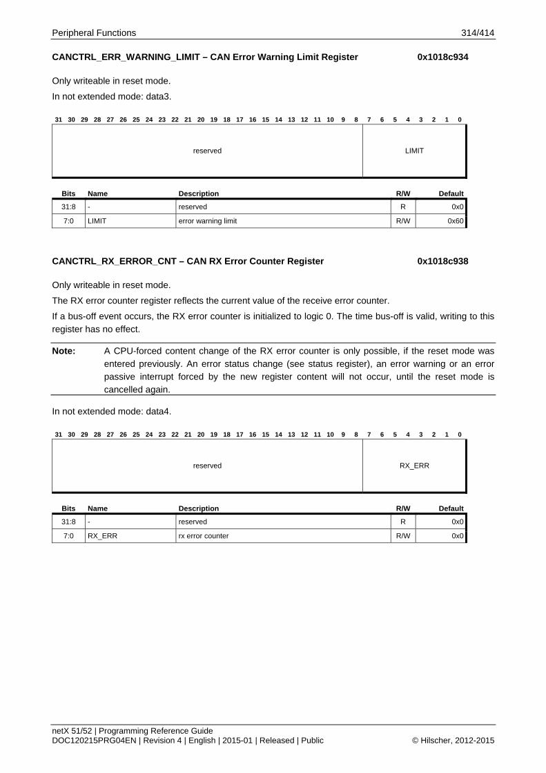
Peripheral Functions 314/414
netX 51/52 | Programming Reference Guide DOC120215PRG04EN | Revision 4 | English | 2015-01 | Released | Public © Hilscher, 2012-2015
CANCTRL_ERR_WARNING_LIMIT – CAN Error Warning Limit Register 0x1018c934
Only writeable in reset mode.
In not extended mode: data3.
31 30 29 28 27 26 25 24 23 22 21 20 19 18 17 16 15 14 13 12 11 10 9 8 7 6 5 4 3 2 1 0
reserved LIMIT
Bits Name Description R/W Default
31:8 - reserved R 0x0
7:0 LIMIT error warning limit R/W 0x60
CANCTRL_RX_ERROR_CNT – CAN RX Error Counter Register 0x1018c938
Only writeable in reset mode.
The RX error counter register reflects the current value of the receive error counter.
If a bus-off event occurs, the RX error counter is initialized to logic 0. The time bus-off is valid, writing to this
register has no effect.
Note: A CPU-forced content change of the RX error counter is only possible, if the reset mode was
entered previously. An error status change (see status register), an error warning or an error passive interrupt forced by the new register content will not occur, until the reset mode is
cancelled again.
In not extended mode: data4.
31 30 29 28 27 26 25 24 23 22 21 20 19 18 17 16 15 14 13 12 11 10 9 8 7 6 5 4 3 2 1 0
reserved RX_ERR
Bits Name Description R/W Default
31:8 - reserved R 0x0
7:0 RX_ERR rx error counter R/W 0x0

Peripheral Functions 315/414
netX 51/52 | Programming Reference Guide DOC120215PRG04EN | Revision 4 | English | 2015-01 | Released | Public © Hilscher, 2012-2015
CANCTRL_TX_ERROR_CNT – CAN TX Error Counter Register 0x1018c93c
Only writeable in reset mode.
The TX error counter register reflects the current value of the transmit error counter.
If a bus-off event occurs, the TX error counter is initialized to 127 to count the minimum protocol-defined time
(128 occurrences of the bus-free signal). Reading the TX error counter during this time gives information about the status of the bus-off recovery.
If bus-off is active, a write access to TXERR in the range from 0 to 254 clears the bus-off flag and the
controller will wait for one occurrence of 11 consecutive recessive bits (bus-free) after the reset mode has been cleared.
Writing 255 to TXERR allows initiating a CPU-driven bus-off event. It should be noted that a CPU-forced
content change of the TX error counter is only possible, if the reset mode was entered previously. An error or bus status change (see status register), an error warning or an error passive interrupt forced by the new register content will not occur until the reset mode is cancelled again. After leaving the reset mode, the new
TX counter content is interpreted and the bus-off event is performed in the same way, as if it was forced by a bus error event. That means, that the reset mode is entered again, the TX error counter is initialized to 127, the RX counter is cleared and all concerned status and interrupt register bits are set.
Clearing of reset mode now will perform the protocol-defined bus-off recovery sequence (waiting for 128 occurrences of the bus-free signal).
If the reset mode is entered again before the end of bus-off recovery (TXERR > 0), bus-off keeps active and
TXERR is frozen.
In not extended mode: data5.
31 30 29 28 27 26 25 24 23 22 21 20 19 18 17 16 15 14 13 12 11 10 9 8 7 6 5 4 3 2 1 0
reserved TX_ERR
Bits Name Description R/W Default
31:8 - reserved R 0x0
7:0 TX_ERR tx error counter R/W 0x0
CANCTRL_DATA0 – CAN Data Register 0 0x1018c940
This register has multiple functions depending on reset mode and read or write access. Reset mode: R/W: Read or write acceptance code 0 Operating mode: R: Standard frame: Read RX frame information Extended frame: Read RX frame information W: Standard frame: Write TX frame information Extended frame: Write TX frame information
In not extended mode: data6.
31 30 29 28 27 26 25 24 23 22 21 20 19 18 17 16 15 14 13 12 11 10 9 8 7 6 5 4 3 2 1 0
reserved DATA
Bits Name Description R/W Default
31:8 - reserved R 0x0
7:0 DATA register content (rx data, tx data or acceptance code) R/W 0x0

Peripheral Functions 316/414
netX 51/52 | Programming Reference Guide DOC120215PRG04EN | Revision 4 | English | 2015-01 | Released | Public © Hilscher, 2012-2015
CANCTRL_DATA1 – CAN Data Register 1 0x1018c944
This register has multiple functions depending on reset mode and read or write access. Reset mode: R/W: Read or write acceptance code 1 Operating mode: R: Standard frame: Read RX identifier 1 Extended frame: Read RX identifier 1 W: Standard frame: Write TX identifier 1 Extended frame: Write TX identifier 1
In not extended mode: data7.
31 30 29 28 27 26 25 24 23 22 21 20 19 18 17 16 15 14 13 12 11 10 9 8 7 6 5 4 3 2 1 0
reserved DATA
Bits Name Description R/W Default
31:8 - reserved R 0x0
7:0 DATA register content (rx data, tx data or acceptance code) R/W 0x0
CANCTRL_DATA2 – CAN Data Register 2 0x1018c948
This register has multiple functions depending on reset mode and read or write access. Reset mode: R/W: Read or write acceptance code 2 Operating mode: R: Standard frame: Read RX identifier 2 Extended frame: Read RX identifier 2 W: Standard frame: Write TX identifier 2 Extended frame: Write TX identifier 2
In not extended mode: data8.
31 30 29 28 27 26 25 24 23 22 21 20 19 18 17 16 15 14 13 12 11 10 9 8 7 6 5 4 3 2 1 0
reserved DATA
Bits Name Description R/W Default
31:8 - reserved R 0x0
7:0 DATA register content (rx data, tx data or acceptance code) R/W 0x0
CANCTRL_DATA3 – CAN Data Register 3 0x1018c94c
This register has multiple functions depending on reset mode and read or write access. Reset mode: R/W: Read or write acceptance code 3 Operating mode: R: Standard frame: Read RX data 1 Extended frame: Read RX identifier 3 W: Standard frame: Write TX data 1 Extended frame: Write TX identifier 3
In not extended mode: data9.
31 30 29 28 27 26 25 24 23 22 21 20 19 18 17 16 15 14 13 12 11 10 9 8 7 6 5 4 3 2 1 0
reserved DATA
Bits Name Description R/W Default
31:8 - reserved R 0x0
7:0 DATA register content (rx data, tx data or acceptance code) R/W 0x0

Peripheral Functions 317/414
netX 51/52 | Programming Reference Guide DOC120215PRG04EN | Revision 4 | English | 2015-01 | Released | Public © Hilscher, 2012-2015
CANCTRL_DATA4 – CAN Data Register 4 0x1018c950
This register has multiple functions depending on reset mode and read or write access. Reset mode: R/W: Read or write acceptance mask 0 Operating mode: R: Standard frame: Read RX data 2 Extended frame: Read RX identifier 4 W: Standard frame: Write TX data 2 Extended frame: Write TX identifier 4 31 30 29 28 27 26 25 24 23 22 21 20 19 18 17 16 15 14 13 12 11 10 9 8 7 6 5 4 3 2 1 0
reserved DATA
Bits Name Description R/W Default
31:8 - reserved R 0x0
7:0 DATA register content (rx data, tx data or acceptance mask) R/W 0x0
CANCTRL_DATA5 – CAN Data Register 5 0x1018c954
This register has multiple functions depending on reset mode and read or write access. Reset mode: R/W: Read or write acceptance mask 1Operating mode: R: Standard frame: Read RX data 3 Extended frame: Read RX data 1 W: Standard frame: Write TX data 3 Extended frame: Write TX data 1 31 30 29 28 27 26 25 24 23 22 21 20 19 18 17 16 15 14 13 12 11 10 9 8 7 6 5 4 3 2 1 0
reserved DATA
Bits Name Description R/W Default
31:8 - reserved R 0x0
7:0 DATA register content (rx data, tx data or acceptance mask) R/W 0x0
CANCTRL_DATA6 – CAN Data Register 6 0x1018c958
This register has multiple functions depending on reset mode and read or write access. Reset mode: R/W: Read or write acceptance mask 2Operating mode: R: Standard frame: Read RX data 4 Extended frame: Read RX data 2 W: Standard frame: Write TX data 4 Extended frame: Write TX data 2 31 30 29 28 27 26 25 24 23 22 21 20 19 18 17 16 15 14 13 12 11 10 9 8 7 6 5 4 3 2 1 0
reserved DATA
Bits Name Description R/W Default
31:8 - reserved R 0x0
7:0 DATA register content (rx data, tx data or acceptance mask) R/W 0x0

Peripheral Functions 318/414
netX 51/52 | Programming Reference Guide DOC120215PRG04EN | Revision 4 | English | 2015-01 | Released | Public © Hilscher, 2012-2015
CANCTRL_DATA7 – CAN Data Register 7 0x1018c95c
This register has multiple functions depending on reset mode and read or write access. Reset mode: R/W: Read or write acceptance mask 3Operating mode: R: Standard frame: Read RX data 5 Extended frame: Read RX data 3 W: Standard frame: Write TX data 5 Extended frame: Write TX data 3 31 30 29 28 27 26 25 24 23 22 21 20 19 18 17 16 15 14 13 12 11 10 9 8 7 6 5 4 3 2 1 0
reserved DATA
Bits Name Description R/W Default
31:8 - reserved R 0x0
7:0 DATA register content (rx data, tx data or acceptance mask) R/W 0x0
CANCTRL_DATA8 – CAN Data Register 8 0x1018c960
This register has multiple functions depending on reset mode and read or write access. Reset mode: R/W: reserved Operating mode: R: Standard frame: Read RX data 6 Extended frame: Read RX data 4 W: Standard frame: Write TX data 6 Extended frame: Write TX data 4 31 30 29 28 27 26 25 24 23 22 21 20 19 18 17 16 15 14 13 12 11 10 9 8 7 6 5 4 3 2 1 0
reserved DATA
Bits Name Description R/W Default
31:8 - reserved R 0x0
7:0 DATA register content (rx data or tx data) R/W 0x0
CANCTRL_DATA9 – CAN Data Register 9 0x1018c964
This register has multiple functions depending on reset mode and read or write access. Reset mode: R/W: reserved Operating mode: R: Standard frame: Read RX data 7 Extended frame: Read RX data 5 W: Standard frame: Write TX data 7 Extended frame: Write TX data 5 31 30 29 28 27 26 25 24 23 22 21 20 19 18 17 16 15 14 13 12 11 10 9 8 7 6 5 4 3 2 1 0
reserved DATA
Bits Name Description R/W Default
31:8 - reserved R 0x0
7:0 DATA register content (rx data or tx data) R/W 0x0

Peripheral Functions 319/414
netX 51/52 | Programming Reference Guide DOC120215PRG04EN | Revision 4 | English | 2015-01 | Released | Public © Hilscher, 2012-2015
CANCTRL_DATA10 – CAN Data Register 10 0x1018c968
This register has multiple functions depending on reset mode and read or write access. Reset mode: R/W: reserved Operating mode: R: Standard frame: Read RX data 8 Extended frame: Read RX data 6 W: Standard frame: Write TX data 8 Extended frame: Write TX data 6 31 30 29 28 27 26 25 24 23 22 21 20 19 18 17 16 15 14 13 12 11 10 9 8 7 6 5 4 3 2 1 0
reserved DATA
Bits Name Description R/W Default
31:8 - reserved R 0x0
7:0 DATA register content (rx data or tx data) R/W 0x0
CANCTRL_DATA11 – CAN Data Register 11 0x1018c96c
This register has multiple functions depending on reset mode and read or write access. Reset mode: R/W: reserved Operating mode: R: Standard frame: reserved Extended frame: Read RX data 7 W: Standard frame: reserved Extended frame: Write TX data 7 31 30 29 28 27 26 25 24 23 22 21 20 19 18 17 16 15 14 13 12 11 10 9 8 7 6 5 4 3 2 1 0
reserved DATA
Bits Name Description R/W Default
31:8 - reserved R 0x0
7:0 DATA register content (rx data or tx data) R/W 0x0
CANCTRL_DATA12 – CAN Data Register 12 0x1018c970
This register has multiple functions depending on reset mode and read or write access. Reset mode: R/W: reserved Operating mode: R: Standard frame: reserved Extended frame: Read RX data 8 W: Standard frame: reserved Extended frame: Write TX data 8 31 30 29 28 27 26 25 24 23 22 21 20 19 18 17 16 15 14 13 12 11 10 9 8 7 6 5 4 3 2 1 0
reserved DATA
Bits Name Description R/W Default
31:8 - reserved R 0x0
7:0 DATA register content (rx data or tx data) R/W 0x0

Peripheral Functions 320/414
netX 51/52 | Programming Reference Guide DOC120215PRG04EN | Revision 4 | English | 2015-01 | Released | Public © Hilscher, 2012-2015
CANCTRL_RX_MESSAGE_CNT – CAN RX Message Counter Register 0x1018c974
Reflect the number of messages available within the RXFIFO. The value is incremented with each receive event and decremented by the release receive buffer command. After any reset event, this register is cleared.
31 30 29 28 27 26 25 24 23 22 21 20 19 18 17 16 15 14 13 12 11 10 9 8 7 6 5 4 3 2 1 0
reserved RX_MSG_CNT
Bits Name Description R/W Default
31:7 - reserved R 0x0
6:0 RX_MSG_CNT rx message counter R 0x0
CANCTRL_MODE_CONTROL – CAN Mode Control Register 0x1018c97c
Only writeable in reset mode.
31 30 29 28 27 26 25 24 23 22 21 20 19 18 17 16 15 14 13 12 11 10 9 8 7 6 5 4 3 2 1 0
reserved
MO
DE
reserved
Bits Name Description R/W Default
31:8 - reserved R 0x0
7 MODE
0: BasicCAN mode, 1: PeliCAN mode recommended value is 1 (PeliCAN mode), The here given register map of all registers of the CAN controller is valid for PeliCAN only.
R 0x0
6:0 - reserved R 0x0
CANCTRL_ARM_XPIC_IRQ_ENABLE – CAN IRQ Enable Register for ARM and XPIC 0x1018c980
31 30 29 28 27 26 25 24 23 22 21 20 19 18 17 16 15 14 13 12 11 10 9 8 7 6 5 4 3 2 1 0
reserved
XP
IC_I
RQ
_EN
AB
LE
AR
M_I
RQ
_EN
AB
LE
Bits Name Description R/W Default
31:2 - reserved R 0x0
1 XPIC_IRQ_ENABLE enable for XPIC IRQ R/W 0x1
0 ARM_IRQ_ENABLE enable for ARM IRQ R/W 0x1

Peripheral Functions 321/414
netX 51/52 | Programming Reference Guide DOC120215PRG04EN | Revision 4 | English | 2015-01 | Released | Public © Hilscher, 2012-2015
7.10 SYSTIME – System time with IEEE 1588 functionality The following table shows a summary of all registers related to system time generation.
ARM Address Register Name Short Description
0x1018c590 SYSTIME_SYSTIME_S Upper SYSTIME Register
0x1018c594 SYSTIME_SYSTIME_NS Lower SYSTIME Register
0x1018c598 SYS_TIME_NS_BOR SYSTIME Border Register
0x1018c59c SYS_TIME_NS_ADD_UP SYSTIME Count Register
0x1018c5a0 SYSTIME_UC_SYSTIME_S Upper SYSTIME Register
0x1018c5a4 SYSTIME_UC_SYSTIME_NS Lower SYSTIME Register
0x1018c5a8 SYS_TIME_NS_BOR SYSTIME Border Register
0x1018c5ac SYS_TIME_NS_ADD_UP SYSTIME Count Register
Table 29: SYSTIME Registers
SYSTIME_SYSTIME_S – SYSTIME Upper SYSTIME Register 0x1018c590 SYSTIME_UC_SYSTIME_S – SYSTIME_UC Upper SYSTIME Register 0x1018c5a0
To allow consistent values of systime_s and systime_ns, lower bits of systime is latched to systime_ns, when systime_s is read.
This register should be dedicated to accesses via DPM.
ARM software should access systime via ARM_TIMER_SYSTIME_S.
xPIC software should access systime via XPIC_TIMER_SYSTIME_S.
31 30 29 28 27 26 25 24 23 22 21 20 19 18 17 16 15 14 13 12 11 10 9 8 7 6 5 4 3 2 1 0
SYSTIME_S
Bits Name Description R/W Default
31:0 SYSTIME_S systime high value is incremented, if systime_ns reaches systime_border Sample systime_ns at read access to systime_s.
R/W 0x0

Peripheral Functions 322/414
netX 51/52 | Programming Reference Guide DOC120215PRG04EN | Revision 4 | English | 2015-01 | Released | Public © Hilscher, 2012-2015
SYSTIME_SYSTIME_NS – SYSTIME Lower SYSTIME Register 0x1018c594 SYSTIME_UC_SYSTIME_NS – SYSTIME_UC Lower SYSTIME Register 0x1018c5a4
To allow consistent values of systime_s and systime_ns, lower bits of systime is latched to systime_ns, when
systime_s is read.
If no systime_s is read before (or at 2nd read access of systime_ns), the actual value of systime_ns is read.
This register should be dedicated to accesses via DPM.
ARM software should access systime via ARM_TIMER_SYSTIME_NS.
xPIC software should access systime via XPIC_TIMER_SYSTIME_NS.
31 30 29 28 27 26 25 24 23 22 21 20 19 18 17 16 15 14 13 12 11 10 9 8 7 6 5 4 3 2 1 0
SYSTIME_NS
Bits Name Description R/W Default
31:0 SYSTIME_NS
Systime low: Sample systime_ns at read access to systime_s. Without sample read systime_s, read the actual value of systime_ns.
R/W 0x0
SYS_TIME_NS_BOR – SYSTIME SYSTIME Border Register 0x1018c598 SYS_TIME_NS_BOR – SYSTIME_UC SYSTIME Border Register 0x1018c5a8
31 30 29 28 27 26 25 24 23 22 21 20 19 18 17 16 15 14 13 12 11 10 9 8 7 6 5 4 3 2 1 0
SYSTIME_BORDER
Bits Name Description R/W Default
31:0 SYSTIME_BORDER
Systime border for lower systime: systime_ns counts from 0 to this value (inlcuded), i.e. systime_ns counts modulo (systime_border + 1) Attention: the border value Bit 3 to 1 must be b’1111 (hex f) for all netX systime - match functions
R/W 0x3b9ac9ff
SYS_TIME_NS_ADD_UP – SYSTIME SYSTIME Count Register 0x1018c59c SYS_TIME_NS_ADD_UP – SYSTIME_UC SYSTIME Count Register 0x1018c5ac
31 30 29 28 27 26 25 24 23 22 21 20 19 18 17 16 15 14 13 12 11 10 9 8 7 6 5 4 3 2 1 0
SYSTIME_COUNT_VALUE
Bits Name Description R/W Default
31:0 SYSTIME_COUNT_VALUE
Each clock cycle (systime_count_value >> 28) will be added to systime (rate multiplier for IEEE1588). Value 0x10000000 can be used for counting in 10ns (ethernet clock) steps.
R/W 0xa0000000

Peripheral Functions 323/414
netX 51/52 | Programming Reference Guide DOC120215PRG04EN | Revision 4 | English | 2015-01 | Released | Public © Hilscher, 2012-2015
7.11 CORDIC Unit To improve the performance of the data processing and control algorithms of ARM or xPIC CPUs, the netX51 is equipped with a special CORDIC (CoOrdinate Rotation Digital Computer) based hardware unit, which dramatically speeds up the calculation of transcendental functions such as sin, cos, sqrt.
The following table is a summary of CORDIC related registers.
ARM Address Register Name Short Description
0x10140000 CORDIC_CTRL CORDIC Control Register
0x10140004 CORDIC_X_REG CORDIC Argument and Result Register X
0x10140008 CORDIC_Y_REG CORDIC Argument and Result Register Y
0x1014000c CORDIC_Z_REG CORDIC Argument and Result Register Z
Table 30: CORDIC Unit Registers
CORDIC_CTRL – CORDIC Control Register 0x10140000
This register controls the precision and the mode of operation. It is also used to start the CORDIC.
31 30 29 28 27 26 25 24 23 22 21 20 19 18 17 16 15 14 13 12 11 10 9 8 7 6 5 4 3 2 1 0
reserved
TA
RG
ET
_AX
IS
reserved
ST
AR
T
Bits Name Description R/W Default
31:7 - reserved R 0x0
6:5 TARGET_AXIS
specifies which register (component of the vector) is driven towards the target value of 0. 01: vectoring mode. Rotate until Y=0. 10: rotation mode. Rotate until Z=0.
R/W 0x2
4:1 - reserved R 0x0
0 START
1: start calculation. this bit is reset to zero by the CORDIC once it finished calculation. This bit is writable but can also be changed by hardware. Reading the resolution registers while the CORDIC is running yields undefined values
R/W 0x0
CORDIC_X_REG – CORDIC Argument and Result Register X 0x10140004
31 30 29 28 27 26 25 24 23 22 21 20 19 18 17 16 15 14 13 12 11 10 9 8 7 6 5 4 3 2 1 0
ARGUMENT
Bits Name Description R/W Default
31:0 ARGUMENT x-component of input vector R/W 0x0

Peripheral Functions 324/414
netX 51/52 | Programming Reference Guide DOC120215PRG04EN | Revision 4 | English | 2015-01 | Released | Public © Hilscher, 2012-2015
CORDIC_Y_REG – CORDIC Argument and Result Register Y 0x10140008
31 30 29 28 27 26 25 24 23 22 21 20 19 18 17 16 15 14 13 12 11 10 9 8 7 6 5 4 3 2 1 0
ARGUMENT
Bits Name Description R/W Default
31:0 ARGUMENT y-component of input vector R/W 0x0
CORDIC_Z_REG – CORDIC Argument and Result Register Z 0x1014000c
31 30 29 28 27 26 25 24 23 22 21 20 19 18 17 16 15 14 13 12 11 10 9 8 7 6 5 4 3 2 1 0
ARGUMENT
Bits Name Description R/W Default
31:0 ARGUMENT input angle R/W 0x0

Peripheral Functions 325/414
netX 51/52 | Programming Reference Guide DOC120215PRG04EN | Revision 4 | English | 2015-01 | Released | Public © Hilscher, 2012-2015
7.12 MMIO – Multiplex Matrix IOs For MMIO Configuration options see chapter IO Configuration on page 15.
7.13 USB – Serial USB-Interface The following table shows a summary of all USB registers:
ARM Address Register Name Short Description
0x1018c800 USB_DEV_CFG USB Device Configuration Register
0x1018c804 USB_DEV_STATUS USB Device Status Register
0x1018c808 USB_DEV_VENDOR_FEATURES USB Vendor Feature Status Register
0x1018c80c USB_DEV_IRQ_MASK USB Device Interrupt Mask Register
0x1018c810 USB_DEV_IRQ_RAW USB Device Raw Interrupt Status Register
0x1018c814 USB_DEV_IRQ_MASKED USB Device Masked Interrupt Status Register
0x1018c840 USB_DEV_ENUM_RAM_DESCRIPTORS_BASE USB Device Descriptor Start
0x1018c844 USB_DEV_ENUM_RAM_DESCRIPTORS_END USB Device Descriptor End
0x1018c848 USB_DEV_ENUM_RAM_STRING_DESCRIPTORS_BASE
USB String Descriptor Start
0x1018c87c USB_DEV_ENUM_RAM_STRING_DESCRIPTORS_END
USB String Descriptor End
0x1018c880 USB_DEV_FIFO_CTRL_CONF USB Device FIFO Configuration Register
0x1018c884 USB_DEV_FIFO_CTRL_ERROR USB Device FIFOs Error Status Register
0x1018c888 USB_DEV_FIFO_CTRL_CONTROL_EP_RX_LEN
USB Device Endpoint 0 - Control OUT, FIFO 0 Length Register
0x1018c88c USB_DEV_FIFO_CTRL_CONTROL_EP_RX_STAT
USB Device Endpoint 0 - Control OUT, FIFO 0 Status Register
0x1018c890 USB_DEV_FIFO_CTRL_CONTROL_EP_TX_LEN
USB Device Endpoint 0 - Control IN, FIFO 1 Length Register
0x1018c894 USB_DEV_FIFO_CTRL_CONTROL_EP_TX_STAT
USB Device Endpoint 0 - Control IN, FIFO 1 Status Register
0x1018c898 USB_DEV_FIFO_CTRL_INTERRUPT_EP_TX_LEN
USB Device Endpoint 1 - Interrupt IN, FIFO 2 Length Register
0x1018c89c USB_DEV_FIFO_CTRL_INTERRUPT_EP_TX_STAT
USB Device Endpoint 1 - Control IN, FIFO 2 Status Register
0x1018c8a0 USB_DEV_FIFO_CTRL_UART_EP_RX_LEN USB Device Endpoint 2 - UART RX (OUT), FIFO 3 length Register
0x1018c8a4 USB_DEV_FIFO_CTRL_UART_EP_RX_STAT USB Device Endpoint 2 - UART RX (OUT), FIFO 3 Status Register
0x1018c8a8 USB_DEV_FIFO_CTRL_UART_EP_TX_LEN USB Device Endpoint 3 - UART TX (IN), FIFO 4 Length Register
0x1018c8ac USB_DEV_FIFO_CTRL_UART_EP_TX_STAT USB Device Endpoint 3 - UART TX (IN), FIFO 4 Status Register
0x1018c8b0 USB_DEV_FIFO_CTRL_JTAG_EP_RX_LEN USB Device Endpoint 4 - JTAG RX (OUT), FIFO 5 Length Register
0x1018c8b4 USB_DEV_FIFO_CTRL_JTAG_EP_RX_STAT USB Device Endpoint 4 - JTAG RX (OUT), FIFO 5 Status Register
0x1018c8b8 USB_DEV_FIFO_CTRL_JTAG_EP_TX_LEN USB Device Endpoint 5 - JTAG TX (IN), FIFO 6 Length Register
0x1018c8bc USB_DEV_FIFO_CTRL_JTAG_EP_TX_STAT USB Device Endpoint 5 - JTAG TX (IN), FIFO 6 Status Register
0x1018c8c0 USB_DEV_CONTROL_OUT_DATA USB Device FIFO: Control endpoint OUT.
0x1018c8c4 USB_DEV_CONTROL_IN_DATA USB Device FIFO: Control endpoint IN.
0x1018c8c8 USB_DEV_INTERRUPT_DATA USB Device FIFO: Endpoint 1 - Interrupt IN
0x1018c8cc USB_DEV_UART_RX_DATA USB Device FIFO: Endpoint 2 - UART RX
0x1018c8d0 USB_DEV_UART_TX_DATA USB Device FIFO: Endpoint 3 - UART TX
0x1018c8d4 USB_DEV_JTAG_RX_DATA USB Device FIFO: Endpoint 4 - JTAG RX
0x1018c8d8 USB_DEV_JTAG_TX_DATA USB Device FIFO: Endpoint 5 - JTAG TX
Table 31: USB Registers

Peripheral Functions 326/414
netX 51/52 | Programming Reference Guide DOC120215PRG04EN | Revision 4 | English | 2015-01 | Released | Public © Hilscher, 2012-2015
USB_DEV_CFG – USB Device Configuration Register 0x1018c800
This register configures the USB device functions. It allows to entirely disabling the USB core and the USB to JTAG bridge.
31 30 29 28 27 26 25 24 23 22 21 20 19 18 17 16 15 14 13 12 11 10 9 8 7 6 5 4 3 2 1 0
reserved
DIS
CO
NN
_TIM
EO
UT
rese
rved
US
B_D
EV
_RE
SE
T
US
B_T
O_J
TA
G_
EN
AB
LE
US
B_C
OR
E_E
NA
BLE
Bits Name Description R/W Default
31:6 - reserved R 0x0
5:4 DISCONN_TIMEOUT
These bits define the timeout used to detect a disconnection from the USB host. This is done monitoring the Start-of-Frames. The user may choose between the following timeouts: 00 : 4 ms (for testing purposes) 01 : 131 ms 10 : 262 ms 11 : 524 ms (default) Note: Changing the timeout to a lower value while a timeout is
in progress may \ result in the desired timeout + 1048 ms. So, be sure to set the timeout while the core is disabled.
R/W 0x3
3 - reserved R 0x0
2 USB_DEV_RESET Writing a ’1’ to this bit will reset the USB core and JTAG module. The user must deassert the bit manually.
R/W 0x0
1 USB_TO_JTAG_ENABLE
When set, the USB to JTAG module is active. This bit in combination with usb2jtag_en in the ’io_config’ register controls whether or not to use the JTAG features of the USB core. To have control over the JTAG pins of the internal system through USB the following conditions must be met: The ’usb2jtag_en’ bit in ’io_config’ must be set, the USB core must be enabled, this bit must be set, the USB host must have done a full enumeration (i.e. the USB core is in state configured) and a valid JTAG mode, speed and enable must have been set through the vendor feature mechanism by the USB host. If and only if all these conditions are met, the external JTAG pins are being disabled and the pins of the JTAG TAP controller are routed to the USB core.
R/W 0x1
0 USB_CORE_ENABLE Writing a ’1’ to this bit will enable the USB core. R/W 0x0

Peripheral Functions 327/414
netX 51/52 | Programming Reference Guide DOC120215PRG04EN | Revision 4 | English | 2015-01 | Released | Public © Hilscher, 2012-2015
USB_DEV_STATUS – USB Device Status Register 0x1018c804
This register represents various status information of the USB core and its FIFOs.
31 30 29 28 27 26 25 24 23 22 21 20 19 18 17 16 15 14 13 12 11 10 9 8 7 6 5 4 3 2 1 0
reserved
US
B_D
ISC
ON
NE
CT
ED
US
B_C
ON
NE
CT
ED
US
B_B
US
_RE
SE
T
US
B_C
ON
FIG
UR
ED
US
B_A
DD
RE
SS
ED
US
B_B
US
Y
Bits Name Description R/W Default
31:6 - reserved R 0x0
5 USB_DISCONNECTED This bit is set when the device is currently disconnected. R 0x0
4 USB_CONNECTED This bit is set when the device has successfully been configured.
R 0x0
3 USB_BUS_RESET This bit is set when the bus is held in reset state (i.e. the FIFOs are held in reset).
R 0x0
2 USB_CONFIGURED This bit is set as soon as the USB host has configured the core. R 0x0
1 USB_ADDRESSED This bit is set as soon as the USB host set a valid address. R 0x0
0 USB_BUSY This bit is set while an USB transfer is active. R 0x0
USB_DEV_VENDOR_FEATURES – USB Vendor Feature Status Register 0x1018c808
This register represents the last valid vendor features that the USB Host has set.
31 30 29 28 27 26 25 24 23 22 21 20 19 18 17 16 15 14 13 12 11 10 9 8 7 6 5 4 3 2 1 0
reserved VENDOR_FEATURES
Bits Name Description R/W Default
31:16 - reserved R 0x0
15:0 VENDOR_FEATURES The last valid vendor features set by the host. R 0x0

Peripheral Functions 328/414
netX 51/52 | Programming Reference Guide DOC120215PRG04EN | Revision 4 | English | 2015-01 | Released | Public © Hilscher, 2012-2015
USB_DEV_IRQ_MASK – USB Device Interrupt Mask Register 0x1018c80c
The value of this register is used for AND-masking the raw interrupt register. When a bit is set, the corresponding interrupt is routed to the interrupt controller. Different to other netX modules, the USB IRQ mask is written directly and not by set- and reset-masks. For a detailed IRQ description see
USB_DEV_IRQ_RAW.
31 30 29 28 27 26 25 24 23 22 21 20 19 18 17 16 15 14 13 12 11 10 9 8 7 6 5 4 3 2 1 0
reserved
DE
VIC
E_D
ISC
ON
NE
CT
ED
DE
VIC
E_C
ON
NE
CT
ED
UA
RT
_RX
_Z
LP_
RE
CE
IVE
D
rese
rved
UA
RT
_RX
_T
RA
NS
AC
TIO
N_R
EC
EIV
ED
UA
RT
_T
X_T
RA
NS
AC
TIO
N_S
EN
T
JTA
G_R
X_
TR
AN
SA
CT
ION
_RE
CE
IVE
D
JTA
G_T
X_
TR
AN
SA
CT
ION
_SE
NT
rese
rved
UA
RT
_RX
_PA
CK
ET
_RE
CE
IVE
D
UA
RT
_T
X_P
AC
KE
T_S
EN
T
JTA
G_R
X_P
AC
KE
T_R
EC
EIV
ED
JTA
G_T
X_P
AC
KE
T_S
EN
T
JTA
G_S
RS
T_R
EQ
UE
ST
ED
RE
SE
T_D
ET
EC
TE
D
rese
rved
DR
OP
PE
D_
FR
AM
E
CR
C16
_ER
RO
R
FIF
O_O
VE
RF
LO
W_U
ND
ER
RU
N_E
RR
UA
RT
_T
X_F
IFO
_EM
PT
Y
UA
RT
_T
X_F
IFO
_FU
LL
UA
RT
_RX
_F
IFO
_EM
PT
Y
UA
RT
_RX
_F
IFO
_FU
LL
Bits Name Description R/W Default
31:25 - reserved R 0x0
24 DEVICE_DISCONNECTED Device disconnected interrupt mask. R/W 0x0
23 DEVICE_CONNECTED Device connected interrupt mask. R/W 0x0
22 UART_RX_ZLP_RECEIVED UART rx zero length packet received interrupt mask. R/W 0x0
21:20 - reserved R 0x0
19 UART_RX_TRANSACTION_RECEIVED
UART rx transaction received interrupt mask. R/W 0x0
18 UART_TX_TRANSACTION_SENT
UART tx transaction sent interrupt mask. R/W 0x0
17 JTAG_RX_TRANSACTION_RECEIVED
JTAG rx transaction received interrupt mask. R/W 0x0
16 JTAG_TX_TRANSACTION_SENT
JTAG tx transaction sent interrupt mask. R/W 0x0
15:14 - reserved R 0x0
13 UART_RX_PACKET_RECEIVED
UART rx packet received interrupt mask. R/W 0x0
12 UART_TX_PACKET_SENT UART tx packet sent interrupt mask. R/W 0x0
11 JTAG_RX_PACKET_RECEIVED
JTAG rx packet received interrupt mask. R/W 0x0
10 JTAG_TX_PACKET_SENT JTAG tx packet sent interrupt mask. R/W 0x0
9 JTAG_SRST_REQUESTED JTAG system reset request detected interrupt mask R/W 0x0
8 RESET_DETECTED Reset detected interrupt mask. R/W 0x0
7 - reserved R 0x0
6 DROPPED_FRAME Dropped frame occurred interrupt mask. R/W 0x0
5 CRC16_ERROR CRC16 error in USB packet occurred interrupt mask. R/W 0x0
4 FIFO_OVERFLOW_UNDERRUN_ERR
FIFO overflow or underrun error interrupt mask. R/W 0x0
3 UART_TX_FIFO_EMPTY UART tx FIFO empty interrupt mask. R/W 0x0
2 UART_TX_FIFO_FULL UART tx FIFO full interrupt mask. R/W 0x0
1 UART_RX_FIFO_EMPTY UART rx FIFO empty interrupt mask. R/W 0x0
0 UART_RX_FIFO_FULL UART rx FIFO full interrupt mask. R/W 0x0

Peripheral Functions 329/414
netX 51/52 | Programming Reference Guide DOC120215PRG04EN | Revision 4 | English | 2015-01 | Released | Public © Hilscher, 2012-2015
USB_DEV_IRQ_RAW – USB Device Raw Interrupt Status Register 0x1018c810
This register holds the raw interrupt status before masking has been applied. Writing ’1’ will clear the corresponding interrupt.
31 30 29 28 27 26 25 24 23 22 21 20 19 18 17 16 15 14 13 12 11 10 9 8 7 6 5 4 3 2 1 0
reserved
DE
VIC
E_D
ISC
ON
NE
CT
ED
DE
VIC
E_C
ON
NE
CT
ED
UA
RT
_RX
_Z
LP_
RE
CE
IVE
D
rese
rved
UA
RT
_RX
_T
RA
NS
AC
TIO
N_R
EC
EIV
ED
UA
RT
_T
X_T
RA
NS
AC
TIO
N_S
EN
T
JTA
G_R
X_
TR
AN
SA
CT
ION
_RE
CE
IVE
D
JTA
G_T
X_
TR
AN
SA
CT
ION
_SE
NT
rese
rved
UA
RT
_RX
_PA
CK
ET
_RE
CE
IVE
D
UA
RT
_T
X_P
AC
KE
T_S
EN
T
JTA
G_R
X_P
AC
KE
T_R
EC
EIV
ED
JTA
G_T
X_P
AC
KE
T_S
EN
T
JTA
G_S
RS
T_R
EQ
UE
ST
ED
RE
SE
T_D
ET
EC
TE
D
rese
rved
DR
OP
PE
D_
FR
AM
E
CR
C16
_ER
RO
R
FIF
O_O
VE
RF
LO
W_U
ND
ER
RU
N_E
RR
UA
RT
_T
X_F
IFO
_EM
PT
Y
UA
RT
_T
X_F
IFO
_FU
LL
UA
RT
_RX
_F
IFO
_EM
PT
Y
UA
RT
_RX
_F
IFO
_FU
LL
Bits Name Description R/W Default
31:25 - reserved R 0x0
24 DEVICE_DISCONNECTED
Unmasked device disconnected interrupt state: The device has been disconnected from the host, i.e. receiving periodic SOFs timed out.
R/W 0x0
23 DEVICE_CONNECTED Unmaksed device connected interrupt state: The device has been connected and has been successfully addressed and configured by the host.
R/W 0x0
22 UART_RX_ZLP_RECEIVED
Unmaksed UART rx zero length packet received interrupt mask: This IRQ is generated whenever a zero length packet has been received on the UART rx channel. This is useful to determine if the USB host supports sending of ZLPs.
R/W 0x0
21:20 - reserved R 0x0
19 UART_RX_TRANSACTION_RECEIVED
Unmaksed UART rx transaction received interrupt state: A transaction on the UART receive FIFO has completed. This IRQ is useful, when the FIFO is in transaction mode.
R/W 0x0
18 UART_TX_TRANSACTION_SENT
Unmaksed UART tx transaction sent interrupt state: A transaction on the UART transmit FIFO has been sent to the USB host. This IRQ is useful, when the FIFO is in transaction mode.
R/W 0x0
17 JTAG_RX_TRANSACTION_RECEIVED
Unmasked JTAG rx transaction received interrupt state: A transaction on the JTAG receive FIFO has completed. This IRQ is useful, when the FIFO is in transaction mode. The FIFO is normally not under user control.
R/W 0x0
16 JTAG_TX_TRANSACTION_SENT
Unmaksed JTAG tx transaction sent interrupt state: A transaction on the JTAG transmit FIFO has been sent to the USB host. The FIFO is normally not under user control. This IRQ is useful, when the FIFO is in packet control mode.
R/W 0x0
15:14 - reserved R 0x0
13 UART_RX_PACKET_RECEIVED
Unmasked UART rx packet received interrupt state: A packet in the UART receive FIFO has arrived. This IRQ is useful, when the FIFO is in packet or transaction mode.
R/W 0x0
12 UART_TX_PACKET_SENT
Unmasked UART tx packet sent interrupt state: A packet in the UART transmit FIFO has been sent to the USB host. This IRQ is useful, when the FIFO is in packet or transaction mode.
R/W 0x0
11 JTAG_RX_PACKET_RECEIVED
Unmasked JTAG rx packet received interrupt state: A packet in the JTAG receive FIFO has arrived. This IRQ is useful, when the FIFO is in packet or transaction mode. The FIFO is normally not under user control.
R/W 0x0
10 JTAG_TX_PACKET_SENT
Unmasked JTAG tx packet sent interrupt state: A packet in the JTAG transmit FIFO has been sent to the USB
R/W 0x0

Peripheral Functions 330/414
netX 51/52 | Programming Reference Guide DOC120215PRG04EN | Revision 4 | English | 2015-01 | Released | Public © Hilscher, 2012-2015
Bits Name Description R/W Default
host. The FIFO is normally not under user control. This IRQ is useful, when the FIFO is in packet control mode.
9 JTAG_SRST_REQUESTED
Unmakesd JTAG system reset request detected interrupt state: This IRQ is generated, when the USB Host software requested a system reset. \
R/W 0x0
8 RESET_DETECTED
Unmasked reset detected interrupt state: This bit is set, when the USB core detected a reset condition on the bus. This means that all FIFOs have been reset and the user should check FIFO states before reading again. This bit is set, when the USB core detected a halted condition. This may happen on bus errors or when the host explicitly requests it.
R/W 0x0
7 - reserved R 0x0
6 DROPPED_FRAME
Unmasked dropped frame interrupt state: A dropped frame has been detected, i.e. an endpoint buffer was not free when the host started to transfer a new packet. Operation continues normally, because the host will resend the packet later. This interrupt is meant as an information to the user’s software.
R/W 0x0
5 CRC16_ERROR Unmasked CRC16 error in USB packet interrupt state: A CRC16 mismatch in a USB packet has been detected. The corresponding packet has been dropped.
R/W 0x0
4 FIFO_OVERFLOW_UNDERRUN_ERR
Unmasked FIFO overflow or underrun error interrupt state: An overflow or underrun of one of the endpoint FIFOs has occurred. The user needs to check the usb_dev_fifo_ctrl_error register for details.
R/W 0x0
3 UART_TX_FIFO_EMPTY Unmasked UART transmit FIFO empty interrupt state: When set the transmit FIFO of the UART channel is empty.
R/W 0x0
2 UART_TX_FIFO_FULL Unmasked UART transmit FIFO full interrupt state: When set the transmit FIFO of the UART channel is full.
R/W 0x0
1 UART_RX_FIFO_EMPTY Unmasked UART receive FIFO empty interrupt state: When set the receive FIFO of the UART channel is empty.
R/W 0x0
0 UART_RX_FIFO_FULL Unmasked UART receive FIFO full interrupt state: When set the receive FIFO of the UART channel is full.
R/W 0x0

Peripheral Functions 331/414
netX 51/52 | Programming Reference Guide DOC120215PRG04EN | Revision 4 | English | 2015-01 | Released | Public © Hilscher, 2012-2015
USB_DEV_IRQ_MASKED – USB Device Masked Interrupt Status Register 0x1018c814
If one of these bits is set, the USB device interrupt will be asserted to the interrupt controller. For a detailed IRQ description, please view USB_DEV_IRQ_RAW.
31 30 29 28 27 26 25 24 23 22 21 20 19 18 17 16 15 14 13 12 11 10 9 8 7 6 5 4 3 2 1 0
reserved
DE
VIC
E_D
ISC
ON
NE
CT
ED
DE
VIC
E_C
ON
NE
CT
ED
UA
RT
_RX
_Z
LP_
RE
CE
IVE
D
rese
rved
UA
RT
_RX
_T
RA
NS
AC
TIO
N_R
EC
EIV
ED
UA
RT
_T
X_T
RA
NS
AC
TIO
N_S
EN
T
JTA
G_R
X_
TR
AN
SA
CT
ION
_RE
CE
IVE
D
JTA
G_T
X_
TR
AN
SA
CT
ION
_SE
NT
rese
rved
UA
RT
_RX
_PA
CK
ET
_RE
CE
IVE
D
UA
RT
_T
X_P
AC
KE
T_S
EN
T
JTA
G_R
X_P
AC
KE
T_R
EC
EIV
ED
JTA
G_T
X_P
AC
KE
T_S
EN
T
JTA
G_S
RS
T_R
EQ
UE
ST
ED
RE
SE
T_D
ET
EC
TE
D
rese
rved
DR
OP
PE
D_
FR
AM
E
CR
C16
_ER
RO
R
FIF
O_O
VE
RF
LO
W_U
ND
ER
RU
N_E
RR
UA
RT
_T
X_F
IFO
_EM
PT
Y
UA
RT
_T
X_F
IFO
_FU
LL
UA
RT
_RX
_F
IFO
_EM
PT
Y
UA
RT
_RX
_F
IFO
_FU
LL
Bits Name Description R/W Default
31:25 - reserved R 0x0
24 DEVICE_DISCONNECTED Masked device disconnected interrupt state. R 0x0
23 DEVICE_CONNECTED Masked device connected interrupt state. R 0x0
22 UART_RX_ZLP_RECEIVED Maksed UART rx zero length packet received interrupt state. R 0x0
21:20 - reserved R 0x0
19 UART_RX_TRANSACTION_RECEIVED
Masked UART rx transaction received interrupt state. R 0x0
18 UART_TX_TRANSACTION_SENT
Masked UART tx transaction sent interrupt state. R 0x0
17 JTAG_RX_TRANSACTION_RECEIVED
Masked JTAG rx transaction received interrupt mask. R 0x0
16 JTAG_TX_TRANSACTION_SENT
Masked JTAG tx transaction sent interrupt mask. R 0x0
15:14 - reserved R 0x0
13 UART_RX_PACKET_RECEIVED
Masked UART rx packet received interrupt state. R 0x0
12 UART_TX_PACKET_SENT Masked UART tx packet sent interrupt state. R 0x0
11 JTAG_RX_PACKET_RECEIVED
Masked JTAG rx packet received interrupt state. R 0x0
10 JTAG_TX_PACKET_SENT Masked JTAG tx packet sent interrupt state. R 0x0
9 JTAG_SRST_REQUESTED Makesd JTAG system reset request detected interrupt state. R 0x0
8 RESET_DETECTED Masked reset detected interrupt state. R 0x0
7 - reserved R 0x0
6 DROPPED_FRAME Masked dropped frame interrupt state R 0x0
5 CRC16_ERROR Masked CRC16 error in USB packet interrupt state. R 0x0
4 FIFO_OVERFLOW_UNDERRUN_ERR
Masked FIFO overflow or underrun error interrupt state. R 0x0
3 UART_TX_FIFO_EMPTY Masked UART transmit FIFO empty interrupt state. R 0x0
2 UART_TX_FIFO_FULL Masked UART transmit FIFO full interrupt state. R 0x0
1 UART_RX_FIFO_EMPTY Masked UART receive FIFO empty interrupt state. R 0x0
0 UART_RX_FIFO_FULL Masked UART receive FIFO full interrupt state. R 0x0

Peripheral Functions 332/414
netX 51/52 | Programming Reference Guide DOC120215PRG04EN | Revision 4 | English | 2015-01 | Released | Public © Hilscher, 2012-2015
USB_DEV_ENUM_RAM_DESCRIPTORS_BASE – USB Device Descriptor Start 0x1018c840 USB_DEV_ENUM_RAM_DESCRIPTORS_END – USB Device Descriptor End 0x1018c844
Device descriptor configuration start-/end address in the enumeration RAM.
The layout of the RAM area is as following:
Enumeration RAM Addr Byte(s) Function
0x1018c840 0 Vendor ID (low)
0x1018c841 1 Vendor ID (high)
0x1018c842 2 Product ID (low)
0x1018c843 3 Product ID (high)
0x1018c844 4 Device release number (low)
0x1018c845 5 Device release number (high)
Device descriptor
0x1018c846 6 Configuration characteristics
0x1018c847 7 Maximum power consumption Configuration descriptor
Table 32: USB Device Descriptor Layout
USB_DEV_ENUM_RAM_STRING_DESCRIPTORS_BASE – USB String Descriptor Start0x1018c848 USB_DEV_ENUM_RAM_STRING_DESCRIPTORS_END – USB String Descriptor End 0x1018c87c
String descriptor start-/end address in the enumeration RAM.
The layout of the RAM area is as following:
Enumeration RAM Addr Byte(s) Function
0x1018c848 0 Vendor string descriptor length
0x1018c849 1 Vendor string descriptor type
0x1018c84a ~ 0x1018c859 2 ~ 17 Vendor string
Vendor string descriptor
0x1018c85a 18 Product string descriptor length
0x1018c85b 19 Product string descriptor type
0x1018c85c ~ 0x1018c86b 20 ~ 35 Product string
Product string descriptor
0x1018c86c 36 S/N string descriptor length
0x1018c86d 37 S/N string descriptor type
0x1018c86e ~ 0x1018c87d 38 ~ 53 S/N string
S/N string descriptor
Table 33: USB String Descriptor Layout

Peripheral Functions 333/414
netX 51/52 | Programming Reference Guide DOC120215PRG04EN | Revision 4 | English | 2015-01 | Released | Public © Hilscher, 2012-2015
USB_DEV_FIFO_CTRL_CONF – USB Device FIFO Configuration Register 0x1018c880
This register configures the FIFOs of the USB core. The user can select one of three modes for each FIFO. It is also possible to enable the DMA control signals for the UART RX and TX FIFOs.
Receive direction (USB naming: OUT transfer) is meant from USB host TO netX. Transmit direction (USB
naming: IN transfer) is meant FROM netX to USB host.
In stream mode, receive direction all successfully received data from the USB host is directly stored in the FIFO and can be read out by the system CPU. Packets from the USB host are accepted as long as there is
space left in the FIFO. Received Zero-Length-Packtes will be ignored and not signalized. In addition to FIFO stati IRQs a packet received IRQ will also be generated on newly received packets.
In stream mode, transmit direction all data put into the FIFO by the system CPU will be transferred at will.
This means, there is no way to control packet borders. Data is being transferred on request by the USB host. Zero-Length-Packets will never be sent to the USB host. When no data to be sent is available, the core will send a NAK handshake to the USB host. When configured to stream mode with ZLPs, a ZLP packet will be
sent when the last transferred packet has been 64 bytes long and the FIFO has no data to be transferred when the Host requests an IN transaction. In addition to FIFO stati IRQs a packet sent IRQ will also be generated on sent packets.
In packet mode, receive direction a new packet sent by the USB host is only accepted when the rx_len register has been read after the packet reception. Received Zero-Length-Packtes will be ignored and not signalized. In addition to FIFO stati IRQs a packet received IRQ will also be generated on newly received
packets.
In transaction mode, receive direction the FIFO operates on transactions. A transaction is finished whenever the first packet with a size less than 64 bytes or a Zero-Length-Packet arrives. Packet received IRQs will be
generated on all packet receptions. The transaction received IRQ will be generated when the transaction is finished. To accept the next transaction, the rx_len register must be read.
Packet and transaction modes in transmit direction are identical. To achieve single packet transmissions a
transaction size of 64 bytes must be programmed. The behaviour when the programmed transaction is finished and the USB host request an IN transfer depends on the configuration of the ’transaction_no_zlp’ bit. When set, no Zero-Length-Packets will be generated, otherwise a ZLP will be sent if needed (i.e. the last
transferred packet had a packet size of 64 bytes). After sending the ZLP, NAKs will be generated for IN requests. Should the FIFO get empty during a programmed transaction or not a full 64 byte packet is available in the FIFO, a NAK handshake will be generated for IN requests. This ensures that a transaction
will not be considered finished by the USB host before the programmed size has been transferred. In addition to FIFO stati IRQs a packet sent and transaction sent IRQ will also be generated on sent packets / completed transactions.
The default configuration of the UART channel is stream mode with ZLPs in both directions.
The JTAG channel may only be reconfigured when not used for JTAG communication (i.e. USB host configured JTAG bypass mode). For normal system operation they need to be configured in stream mode.
Note: To use the DMA controller, the dma_en bits must be enabled here. Otherwise no DMAC
handshake signals will be generated.
For correct operation with the DMAC the following sequence must be maintained:
Stream mode: just read or write the data to the FIFO. Flow controller must be the DMAC.
Packet mode, receive: Program read of data, afterwards the rx_len register must be read by
the DMAC (will also be signalized to the DMAC by the FIFO). Flow controller is the USB core (peripheral controlled).

Peripheral Functions 334/414
netX 51/52 | Programming Reference Guide DOC120215PRG04EN | Revision 4 | English | 2015-01 | Released | Public © Hilscher, 2012-2015
Packet mode, transmit: The tx_len register with the control information must be programmed
by the DMAC first (will also be signalized to the DMAC), after that feed the data. Flow controller is the USB core (peripheral controlled).
Transaction mode, receive: same as packet mode, receive.
Transaction mode, transmit: same as packet mode, transmit.
31 30 29 28 27 26 25 24 23 22 21 20 19 18 17 16 15 14 13 12 11 10 9 8 7 6 5 4 3 2 1 0
rese
rved
JTA
G_R
X_
NA
K_
ALL
UA
RT
_RX
_N
AK
_ALL
MA
X_T
RA
NS
AC
TIO
N_L
EN
RESET
DM
A_U
AR
T_T
X_S
TR
EA
M_B
UR
ST
_ON
LY
DM
A_E
N_U
AR
T_T
X
DM
A_E
N_U
AR
T_R
X
MO
DE
_JT
AG
_TX
MO
DE
_JT
AG
_RX
MO
DE
_UA
RT
_T
X
MO
DE
_UA
RT
_R
X
MO
DE
_IN
TE
RR
UP
T
Bits Name Description R/W Default
31:29 - reserved R 0x0
28 JTAG_RX_NAK_ALL
NAK all received packets on the JTAG channel. When set, all further received packets on the JTAG channel will be NAKed. This is useful when changing the FIFO mode on the fly is needed.
R/W 0x0
27 UART_RX_NAK_ALL
NAK all received packets on the UART channel. When set, all further received packets on the UART channel will be NAKed. This is useful when changing the FIFO mode on the fly is needed.
R/W 0x0
26:20 MAX_TRANSACTION_LEN
Maximum transaction length in 64 byte quantums: Only used for the Rx-FIFOs in transaction mode. If an incoming transaction reaches (max_transaction_len * 64) bytes, the transaction will be split on this boundary, i.e. it will be handled as if the host sent a transaction of this size followed by another transaction with the rest. This condition will be signaled by the ’transaction_max_reached’ bit in the corresponding ’rx_len’ register for the first transaction. Additionally, the ’transaction_continued’ bit will be set in the following transaction. For a transaction lengt of exactly the configured size the ’transaction_continued’ bit in the following transaction will not be set. Configuring ’0’ will not limit the transaction length.
R/W 0x0
19:13 RESET
Endpoint reset: Writing a ’1’ to a bit resets the corresponding endpoint FIFO. Resets must be manually cleared by the user. Bit to FIFO mapping: Bit FIFO 0 Endpoint 0 Control OUT (FIFO 0) 1 Endpoint 0 Control IN (FIFO 1) 2 Endpoint 1 Interrupt IN (FIFO 2) 3 Endpoint 2 UART Rx (FIFO 3) 4 Endpoint 3 UART Tx (FIFO 4) 5 Endpoint 4 JTAG Rx (FIFO 5) 6 Endpoint 5 JTAG Tx (FIFO 6)
R/W 0x0
12 DMA_UART_TX_STREAM_BURST_ONLY
Configures usage of DMAC single requests of the UART TX FIFO: When set to ’1’ the DMAC logic of the UART TX FIFO will only generate burst requests to the DMAC when the FIFO is configured to stream mode. This is to overcome limitations of the current DMA controller implementation that only accepts
R/W 0x1

Peripheral Functions 335/414
netX 51/52 | Programming Reference Guide DOC120215PRG04EN | Revision 4 | English | 2015-01 | Released | Public © Hilscher, 2012-2015
Bits Name Description R/W Default
burst requests for DMAC controlled memory to peripheral transfers. Note: If active, the FIFO may not be filled completely by the DMAC in some situations due to the lack of working single requests.
11 DMA_EN_UART_TX Enables DMA control on UART TX channel. R/W 0x0
10 DMA_EN_UART_RX
Enables DMA control on UART RX channel. Note: The maximum transaction length may be configured with the max_transaction_len bits. The total buffer size of the DMAC request must also satisfy this limit.
R/W 0x0
9:8 MODE_JTAG_TX Selects the mode of Endpoint 5 - JTAG TX (IN), FIFO 6. For details see ’mode_interrupt’.
R/W 0x0
7:6 MODE_JTAG_RX Selects the mode of Endpoint 4 - JTAG RX (OUT), FIFO 5. For details see ’mode_interrupt’.
R/W 0x0
5:4 MODE_UART_TX Selects the mode of Endpoint 3 - UART TX (IN), FIFO 4. For details see ’mode_interrupt’.
R/W 0x1
3:2 MODE_UART_RX Selects the mode of Endpoint 2 - UART RX (OUT), FIFO 3. For details see ’mode_interrupt’.
R/W 0x1
1:0 MODE_INTERRUPT
Selects the mode of Endpoint 1 - Interrupt IN, FIFO 2. Each FIFO is configured by two bits to select between the following modes: binary mode 2’b00 stream-mode (i.e. all valid data will be directly
transferred.) 2’b01 stream-mode with zero-length-packets 2’b10 packet-mode (packet-based transfers) 2’b11 transaction-mode (transaction-based with
preprogrammed transfer size) Note: When a FIFO is used in TX direction, packet-mode and transction-mode is identical. The behaviour is configured when programming the corresponding FIFO tx_len register. UART RX and TX are fully user definable (see text above), but should operate in a mode with ZLP generation for CDC drivers to work properly (i.e. stream mode with ZLP, packet or transaction mode with no_zlp unset). JTAG RX and TX may be switched, when the USB host has switched to JTAG bypass mode (see text above), otherwise they must be kept in stream mode.
R/W 0x3
USB_DEV_FIFO_CTRL_ERROR – USB Device FIFOs Error Status Register 0x1018c884
This register holds the overflow and underrun flags of all FIFOs. To reset a flag the corresponding FIFO must
be reset.
31 30 29 28 27 26 25 24 23 22 21 20 19 18 17 16 15 14 13 12 11 10 9 8 7 6 5 4 3 2 1 0
reserved UNDERRUN reserved OVERFLOW
Bits Name Description R/W Default
31:23 - reserved R 0x0
22:16 UNDERRUN Combined underrun flags for FIFOs 6-0. R 0x0
15:7 - reserved R 0x0
6:0 OVERFLOW Combined overflow flags for FIFOs 6-0. R 0x0

Peripheral Functions 336/414
netX 51/52 | Programming Reference Guide DOC120215PRG04EN | Revision 4 | English | 2015-01 | Released | Public © Hilscher, 2012-2015
USB_DEV_FIFO_CTRL_CONTROL_EP_RX_LEN – USB Device Endpoint 0 - Control OUT, FIFO 0 Length Register 0x1018c888
This register holds the fill levels and other status information of FIFO 0.
Use this register for debug purposes only.
31 30 29 28 27 26 25 24 23 22 21 20 19 18 17 16 15 14 13 12 11 10 9 8 7 6 5 4 3 2 1 0
rese
rved
TRANSACTION_LEN reserved PACKET_LEN
Bits Name Description R/W Default
31:29 - reserved R 0x0
28:16 TRANSACTION_LEN
Read only: When a transaction has finished, this is the actual size, otherwise 0. Note: In case the USB host sends a transaction bigger than 8128 bytes (8k - 64), the transaction will be split on this boundary (i.e. it will be handled as if the host sent a transaction with size 8128, followed by another transaction with the rest).
R 0x0
15:7 - reserved R 0x0
6:0 PACKET_LEN Size of the last received packet. This is a read only status bit field.
R 0x0
USB_DEV_FIFO_CTRL_CONTROL_EP_RX_STAT – USB Device Endpoint 0 - Control OUT, FIFO 0 Status Register 0x1018c88c
This register holds the fill levels and other status information of FIFO 0.
Use this register for debug purposes only.
31 30 29 28 27 26 25 24 23 22 21 20 19 18 17 16 15 14 13 12 11 10 9 8 7 6 5 4 3 2 1 0
FU
LL
EM
PT
Y
TR
AN
SA
CT
ION
_AC
TIV
E
PA
CK
ET
_TR
AN
SF
ER
_AC
TIV
E
reserved FILL_LEVEL
Bits Name Description R/W Default
31 FULL FIFO is full (including data not yet acked by USB core). R 0x0
30 EMPTY FIFO is empty (excluding data not yet acked by USB core). R 0x0
29 TRANSACTION_ACTIVE A transaction is currently active. R 0x0
28 PACKET_TRANSFER_ACTIVE
A packet transfer is currently active. This bit is active when the host currently sends a packet that isn’t valid yet.
R 0x0
27:9 - reserved R 0x0
8:0 FILL_LEVEL Fill level of the FIFO (excluding non-acked data). R 0x0

Peripheral Functions 337/414
netX 51/52 | Programming Reference Guide DOC120215PRG04EN | Revision 4 | English | 2015-01 | Released | Public © Hilscher, 2012-2015
USB_DEV_FIFO_CTRL_CONTROL_EP_TX_LEN – USB Device Endpoint 0 - Control IN, FIFO 1 Length Register 0x1018c890
This register holds the fill levels and other status information of FIFO 1.
Use this register for debug purposes only.
31 30 29 28 27 26 25 24 23 22 21 20 19 18 17 16 15 14 13 12 11 10 9 8 7 6 5 4 3 2 1 0
TR
AN
SA
CT
ION
_NO
_Z
LP
rese
rved
TRANSACTION_LEN reserved PACKET_LEN
Bits Name Description R/W Default
31 TRANSACTION_NO_ZLP When set to ’1’ no ZLP will be sent, when a transaction is finished. This bit will be reset automatically by hardware and is always ’0’ on read.
R/W 0x0
30:29 - reserved R 0x0
28:16 TRANSACTION_LEN
Read: Number of bytes left in the programmed transfer. Write: The actual size of the transaction. Set to 0 to abort a running transcation. Note: This bit field is writable but can also be changed by hardware.
R/W 0x0
15:7 - reserved R 0x0
6:0 PACKET_LEN Size of the last sent packet. This is a read only status bit field. R/W 0x0
USB_DEV_FIFO_CTRL_CONTROL_EP_TX_STAT – USB Device Endpoint 0 - Control IN, FIFO 1 Status Register 0x1018c894
This register holds the fill levels and other status information of FIFO 1.
Use this register for debug purposes only.
31 30 29 28 27 26 25 24 23 22 21 20 19 18 17 16 15 14 13 12 11 10 9 8 7 6 5 4 3 2 1 0
FU
LL
EM
PT
Y
TR
AN
SA
CT
ION
_AC
TIV
E
reserved FILL_LEVEL
Bits Name Description R/W Default
31 FULL FIFO is full (including data still needed by USB core). R 0x0
30 EMPTY FIFO is empty (including data still needed by USB core). R 0x0
29 TRANSACTION_ACTIVE A transaction is currently active. No further transaction may be programmed.
R 0x0
28:9 - reserved R 0x0
8:0 FILL_LEVEL Fill level of the FIFO (including data currently in transit). R 0x0

Peripheral Functions 338/414
netX 51/52 | Programming Reference Guide DOC120215PRG04EN | Revision 4 | English | 2015-01 | Released | Public © Hilscher, 2012-2015
USB_DEV_FIFO_CTRL_INTERRUPT_EP_TX_LEN – USB Device Endpoint 1 - Interrupt IN, FIFO 2 Length Register 0x1018c898
This register is used to program or abort a transaction.
Note: It is not allowed to re-program a transaction while it is active. Only an abort is allowed.
Note: A new transaction may only program when the last transaction is finished (i.e. check
’transaction_active’ flag in the tx_stat register).
31 30 29 28 27 26 25 24 23 22 21 20 19 18 17 16 15 14 13 12 11 10 9 8 7 6 5 4 3 2 1 0
TR
AN
SA
CT
ION
_NO
_Z
LP
rese
rved
TRANSACTION_LEN reserved PACKET_LEN
Bits Name Description R/W Default
31 TRANSACTION_NO_ZLP When set to ’1’ no ZLP will be sent, when a transaction is finished. This bit will be reset automatically by hardware and is always ’0’ on read.
R/W 0x0
30:29 - reserved R 0x0
28:16 TRANSACTION_LEN
Read: Number of bytes left in the programmed transfer. Write: The actual size of the transaction. Set to 0 to abort a running transcation. Note: This bit field is writable but can also be changed by hardware.
R/W 0x0
15:7 - reserved R 0x0
6:0 PACKET_LEN Size of the last sent packet. This is a read only status bit field. R/W 0x0
USB_DEV_FIFO_CTRL_INTERRUPT_EP_TX_STAT – USB Device Endpoint 1 - Control IN, FIFO 2 Status Register 0x1018c89c
This register holds the fill levels and other status information of FIFO 2.
31 30 29 28 27 26 25 24 23 22 21 20 19 18 17 16 15 14 13 12 11 10 9 8 7 6 5 4 3 2 1 0
FU
LL
EM
PT
Y
TR
AN
SA
CT
ION
_AC
TIV
E
reserved FILL_LEVEL
Bits Name Description R/W Default
31 FULL FIFO is full (including data still needed by USB core). R 0x0
30 EMPTY FIFO is empty (including data still needed by USB core). R 0x0
29 TRANSACTION_ACTIVE A transaction is currently active. No further transaction may be programmed.
R 0x0
28:9 - reserved R 0x0
8:0 FILL_LEVEL Fill level of the FIFO (including data currently in transit). R 0x0

Peripheral Functions 339/414
netX 51/52 | Programming Reference Guide DOC120215PRG04EN | Revision 4 | English | 2015-01 | Released | Public © Hilscher, 2012-2015
USB_DEV_FIFO_CTRL_UART_EP_RX_LEN – USB Device Endpoint 2 - UART RX (OUT), FIFO 3 Length Register. 0x1018c8a0
This register holds the status information of FIFO 3. It is also used to acknowledge a transaction or packet
reception.
31 30 29 28 27 26 25 24 23 22 21 20 19 18 17 16 15 14 13 12 11 10 9 8 7 6 5 4 3 2 1 0
TR
AN
SA
CT
ION
_CO
NT
INU
ED
TR
AN
SA
CT
ION
_MA
X_R
EA
CH
ED
rese
rved
TRANSACTION_LEN reserved PACKET_LEN
Bits Name Description R/W Default
31 TRANSACTION_CONTINUED
This transaction is a continuation of the last transaction. R 0x0
30 TRANSACTION_MAX_REACHED
This transaction reached the configured maximum transaction length. Following data will be put into the next transaction.
R 0x0
29 - reserved R 0x0
28:16 TRANSACTION_LEN
When a transaction has finished, this is the actual size, otherwise 0. Note: In case the USB host sends a transaction bigger than 8128 bytes (8k - 64), the transaction will be split on this boundary (i.e. it will be handled as if the host sent a transaction with size 8128, followed by another transaction with the rest).
R 0x0
15:7 - reserved R 0x0
6:0 PACKET_LEN Size of the last received packet. R 0x0

Peripheral Functions 340/414
netX 51/52 | Programming Reference Guide DOC120215PRG04EN | Revision 4 | English | 2015-01 | Released | Public © Hilscher, 2012-2015
USB_DEV_FIFO_CTRL_UART_EP_RX_STAT – USB Device Endpoint 2 - UART RX (OUT), FIFO 3 Status Register 0x1018c8a4
This register holds the fill levels and other status information of FIFO 3.
31 30 29 28 27 26 25 24 23 22 21 20 19 18 17 16 15 14 13 12 11 10 9 8 7 6 5 4 3 2 1 0
FU
LL
EM
PT
Y
TR
AN
SA
CT
ION
_AC
TIV
E
PA
CK
ET
_TR
AN
SF
ER
_AC
TIV
E
reserved FILL_LEVEL
Bits Name Description R/W Default
31 FULL FIFO is full (including data not yet acked by USB core). R 0x0
30 EMPTY FIFO is empty (excluding data not yet acked by USB core). R 0x0
29 TRANSACTION_ACTIVE A transaction is currently active. No further transaction may be programmed.
R 0x0
28 PACKET_TRANSFER_ACTIVE
A packet transfer is currently active. This bit is active when the host currently sends a packet that isn’t valid yet.
R 0x0
27:9 - reserved R 0x0
8:0 FILL_LEVEL Fill level of the FIFO (excluding non-acked data). R 0x0

Peripheral Functions 341/414
netX 51/52 | Programming Reference Guide DOC120215PRG04EN | Revision 4 | English | 2015-01 | Released | Public © Hilscher, 2012-2015
USB_DEV_FIFO_CTRL_UART_EP_TX_LEN – USB Device Endpoint 3 - UART TX (IN), FIFO 4 Length Register 0x1018c8a8
This register is used to program or abort a transaction.
Note: It is not allowed to re-program a transaction while it is active. Only an abort is allowed.
Note: A new transaction may only program when the last transaction is finished (i.e. check
’transaction_active’ flag in the tx_stat register).
31 30 29 28 27 26 25 24 23 22 21 20 19 18 17 16 15 14 13 12 11 10 9 8 7 6 5 4 3 2 1 0
TR
AN
SA
CT
ION
_NO
_Z
LP
rese
rved
TRANSACTION_LEN reserved PACKET_LEN
Bits Name Description R/W Default
31 TRANSACTION_NO_ZLP When set to ’1’ no ZLP will be sent, when a transaction is finished. This bit will be reset automatically by hardware and is always ’0’ on read.
R/W 0x0
30:29 - reserved R 0x0
28:16 TRANSACTION_LEN
Read: Number of bytes left in the programmed transfer. Write: The actual size of the transaction. Set to 0 to abort a running transcation. Note: This bit field is writable but can also be changed by hardware.
R/W 0x0
15:7 - reserved R 0x0
6:0 PACKET_LEN Size of the last sent packet. This is a read only status bit field. R/W 0x0
USB_DEV_FIFO_CTRL_UART_EP_TX_STAT – USB Device Endpoint 3 - UART TX (IN), FIFO 4 Status Register 0x1018c8ac
This register holds the fill levels and other status information of FIFO 4.
31 30 29 28 27 26 25 24 23 22 21 20 19 18 17 16 15 14 13 12 11 10 9 8 7 6 5 4 3 2 1 0
FU
LL
EM
PT
Y
TR
AN
SA
CT
ION
_AC
TIV
E
reserved FILL_LEVEL
Bits Name Description R/W Default
31 FULL FIFO is full (including data still needed by USB core). R 0x0
30 EMPTY FIFO is empty (including data still needed by USB core). R 0x0
29 TRANSACTION_ACTIVE A transaction is currently active. No further transaction may be programmed.
R 0x0
28:9 - reserved R 0x0
8:0 FILL_LEVEL Fill level of the FIFO (including data currently in transit). R 0x0

Peripheral Functions 342/414
netX 51/52 | Programming Reference Guide DOC120215PRG04EN | Revision 4 | English | 2015-01 | Released | Public © Hilscher, 2012-2015
USB_DEV_FIFO_CTRL_JTAG_EP_RX_LEN – USB Device Endpoint 4 - JTAG RX (OUT), FIFO 5 Length Register 0x1018c8b0
This register holds the status information of FIFO 5. It is also used to acknowledge a transaction or packet
reception.
31 30 29 28 27 26 25 24 23 22 21 20 19 18 17 16 15 14 13 12 11 10 9 8 7 6 5 4 3 2 1 0
TR
AN
SA
CT
ION
_CO
NT
INU
ED
TR
AN
SA
CT
ION
_MA
X_R
EA
CH
ED
rese
rved
TRANSACTION_LEN reserved PACKET_LEN
Bits Name Description R/W Default
31 TRANSACTION_CONTINUED
This transaction is a continuation of the last transaction. R 0x0
30 TRANSACTION_MAX_REACHED
This transaction reached the configured maximum transaction length. Following data will be put into the next transaction.
R 0x0
29 - reserved R 0x0
28:16 TRANSACTION_LEN
When a transaction has finished, this is the actual size, otherwise 0. Note: In case the USB host sends a transaction bigger than 8128 bytes (8k - 64), the transaction will be split on this boundary (i.e. it will be handled as if the host sent a transaction with size 8128, followed by another transaction with the rest).
R 0x0
15:7 - reserved R 0x0
6:0 PACKET_LEN Size of the last received packet. R 0x0

Peripheral Functions 343/414
netX 51/52 | Programming Reference Guide DOC120215PRG04EN | Revision 4 | English | 2015-01 | Released | Public © Hilscher, 2012-2015
USB_DEV_FIFO_CTRL_JTAG_EP_RX_STAT – USB Device Endpoint 4 - JTAG RX (OUT), FIFO 5 Status Register 0x1018c8b4
This register holds the fill levels and other status information of FIFO 5.
31 30 29 28 27 26 25 24 23 22 21 20 19 18 17 16 15 14 13 12 11 10 9 8 7 6 5 4 3 2 1 0
FU
LL
EM
PT
Y
TR
AN
SA
CT
ION
_AC
TIV
E
PA
CK
ET
_TR
AN
SF
ER
_AC
TIV
E
reserved FILL_LEVEL
Bits Name Description R/W Default
31 FULL FIFO is full (including data not yet acked by USB core). R 0x0
30 EMPTY FIFO is empty (excluding data not yet acked by USB core). R 0x0
29 TRANSACTION_ACTIVE A transaction is currently active. No further transaction may be programmed.
R 0x0
28 PACKET_TRANSFER_ACTIVE
A packet transfer is currently active. This bit is active when the host currently sends a packet that isn’t valid yet.
R 0x0
27:9 - reserved R 0x0
8:0 FILL_LEVEL Fill level of the FIFO (excluding non-acked data). R 0x0

Peripheral Functions 344/414
netX 51/52 | Programming Reference Guide DOC120215PRG04EN | Revision 4 | English | 2015-01 | Released | Public © Hilscher, 2012-2015
USB_DEV_FIFO_CTRL_JTAG_EP_TX_LEN – USB Device Endpoint 5 - JTAG TX (IN), FIFO 6 Length Register 0x1018c8b8
This register is used to program or abort a transaction.
Note: It is not allowed to re-program a transaction while it is active. Only an abort is allowed.
Note: A new transaction may only programm when the last transaction is finished (i.e. check
’transaction_active’ flag in the tx_stat register).
31 30 29 28 27 26 25 24 23 22 21 20 19 18 17 16 15 14 13 12 11 10 9 8 7 6 5 4 3 2 1 0
TR
AN
SA
CT
ION
_NO
_Z
LP
rese
rved
TRANSACTION_LEN reserved PACKET_LEN
Bits Name Description R/W Default
31 TRANSACTION_NO_ZLP When set to ’1’ no ZLP will be sent, when a transaction is finished. This bit will be reset automatically by hardware and is always ’0’ on read.
R/W 0x0
30:29 - reserved R 0x0
28:16 TRANSACTION_LEN
Read: Number of bytes left in the programmed transfer. Write: The actual size of the transaction. Set to 0 to abort a running transcation. Note: This bit field is writable but can also be changed by hardware.
R/W 0x0
15:7 - reserved R 0x0
6:0 PACKET_LEN Size of the last sent packet. This is a read only status bit field. R/W 0x0
USB_DEV_FIFO_CTRL_JTAG_EP_TX_STAT – USB Device Endpoint 5 - JTAG TX (IN), FIFO 6 Status Register 0x1018c8bc
This register holds the fill levels and other status information of FIFO 6.
31 30 29 28 27 26 25 24 23 22 21 20 19 18 17 16 15 14 13 12 11 10 9 8 7 6 5 4 3 2 1 0
FU
LL
EM
PT
Y
TR
AN
SA
CT
ION
_AC
TIV
E
reserved FILL_LEVEL
Bits Name Description R/W Default
31 FULL FIFO is full (including data still needed by USB core). R 0x0
30 EMPTY FIFO is empty (including data still needed by USB core). R 0x0
29 TRANSACTION_ACTIVE A transaction is currently active. No further transaction may be programmed.
R 0x0
28:9 - reserved R 0x0
8:0 FILL_LEVEL Fill level of the FIFO (including data currently in transit). R 0x0

Peripheral Functions 345/414
netX 51/52 | Programming Reference Guide DOC120215PRG04EN | Revision 4 | English | 2015-01 | Released | Public © Hilscher, 2012-2015
USB_DEV_CONTROL_OUT_DATA – USB Device FIFO: Control Endpoint OUT 0x1018c8c0
This FIFO holds the data of the control endpoint. Direction is OUT, meaning data sent from USB host to device arrives here. The FIFO is handled by the USB core itself and should not be read or written from the ARM.
Note: Reading and writing to this register while the USB module sees a reset condition on the bus
results in unexpected data, because the FIFOs are held in reset state.
31 30 29 28 27 26 25 24 23 22 21 20 19 18 17 16 15 14 13 12 11 10 9 8 7 6 5 4 3 2 1 0
reserved FIFO_DATA
Bits Name Description R/W Default
31:8 - reserved R 0x0
7:0 FIFO_DATA R/W 0x0
USB_DEV_CONTROL_IN_DATA – USB Device FIFO: Control Endpoint IN 0x1018c8c4
This FIFO holds the data of the control endpoint. Direction is IN, meaning data that should be sent from USB device to host must be placed here. The FIFO is handled by the USB core itself and should not be read or written from the ARM.
Note: Reading and writing to this register while the USB module sees a reset condition on the bus
results in unexpected data, because the FIFOs are held in reset state.
31 30 29 28 27 26 25 24 23 22 21 20 19 18 17 16 15 14 13 12 11 10 9 8 7 6 5 4 3 2 1 0
reserved FIFO_DATA
Bits Name Description R/W Default
31:8 - reserved R 0x0
7:0 FIFO_DATA R/W 0x0
USB_DEV_INTERRUPT_DATA – USB Device FIFO: Endpoint 1 - Interrupt IN 0x1018c8c8
This FIFO holds the data of the interrupt endpoint. Direction is IN, meaning data placed here is sent to the USB host.
Note: Reading and writing to this register while the USB module sees a reset condition on the bus
results in unexpected data, because the FIFOs are held in reset state.
31 30 29 28 27 26 25 24 23 22 21 20 19 18 17 16 15 14 13 12 11 10 9 8 7 6 5 4 3 2 1 0
reserved FIFO_DATA
Bits Name Description R/W Default
31:8 - reserved R 0x0
7:0 FIFO_DATA R/W 0x0

Peripheral Functions 346/414
netX 51/52 | Programming Reference Guide DOC120215PRG04EN | Revision 4 | English | 2015-01 | Released | Public © Hilscher, 2012-2015
USB_DEV_UART_RX_DATA – USB Device FIFO: Endpoint 2 - UART RX 0x1018c8cc
This FIFO holds the data of the bulk endpoint used for UART communication. Direction is OUT, meaning data from the USB host arrives here. This FIFO may be used by the user application.
Note: Reading and writing to this register while the USB module sees a reset condition on the bus
results in unexpected data, because the FIFOs are held in reset state.
31 30 29 28 27 26 25 24 23 22 21 20 19 18 17 16 15 14 13 12 11 10 9 8 7 6 5 4 3 2 1 0
reserved FIFO_DATA
Bits Name Description R/W Default
31:8 - reserved R 0x0
7:0 FIFO_DATA R/W 0x0
USB_DEV_UART_TX_DATA – USB Device FIFO: Endpoint 3 - UART TX 0x1018c8d0
This FIFO holds the data of the bulk endpoint used for UART communication. Direction is IN, meaning data
placed here is sent to the USB host. This FIFO may be used by the user application.
Note: Reading and writing to this register while the USB module sees a reset condition on the bus
results in unexpected data, because the FIFOs are held in reset state.
31 30 29 28 27 26 25 24 23 22 21 20 19 18 17 16 15 14 13 12 11 10 9 8 7 6 5 4 3 2 1 0
reserved FIFO_DATA
Bits Name Description R/W Default
31:8 - reserved R 0x0
7:0 FIFO_DATA R/W 0x0

Peripheral Functions 347/414
netX 51/52 | Programming Reference Guide DOC120215PRG04EN | Revision 4 | English | 2015-01 | Released | Public © Hilscher, 2012-2015
USB_DEV_JTAG_RX_DATA – USB Device FIFO: Endpoint 4 - JTAG RX 0x1018c8d4
This FIFO holds the data of the bulk endpoint used for JTAG communication. Direction is OUT, meaning data from the USB host arrives here. The FIFO is handled by the USB JTAG core itself and should not be read or written from the ARM.
Note: Reading and writing to this register while the USB module sees an reset condition on the bus
results in unexpected data, because the FIFOs are held in reset state.
31 30 29 28 27 26 25 24 23 22 21 20 19 18 17 16 15 14 13 12 11 10 9 8 7 6 5 4 3 2 1 0
reserved FIFO_DATA
Bits Name Description R/W Default
31:8 - reserved R 0x0
7:0 FIFO_DATA R/W 0x0
USB_DEV_JTAG_TX_DATA – USB Device FIFO: Endpoint 5 - JTAG TX 0x1018c8d8
This FIFO holds the data of the bulk endpoint used for JTAG communication. Direction is IN, meaning data placed here is sent to the USB host. The FIFO is handled by the USB JTAG core itself and should not be read or written from the ARM.
Note: Reading and writing to this register while the USB module sees a reset condition on the bus
results in unexpected data, because the FIFOs are held in reset state.
31 30 29 28 27 26 25 24 23 22 21 20 19 18 17 16 15 14 13 12 11 10 9 8 7 6 5 4 3 2 1 0
reserved FIFO_DATA
Bits Name Description R/W Default
31:8 - reserved R 0x0
7:0 FIFO_DATA R/W 0x0

Peripheral Functions 348/414
netX 51/52 | Programming Reference Guide DOC120215PRG04EN | Revision 4 | English | 2015-01 | Released | Public © Hilscher, 2012-2015
7.14 VIC – Vectored Interrupt Controller The following table shows a summary of all VIC registers:
ARM Address Register Name Short Description
0x101ff000 VIC_IRQ_STAT IRQ Status Register
0x101ff004 VIC_FIQ_STAT FIQ Status Register
0x101ff008 VIC_RAW_INT_STAT Raw Interrupt Status Register
0x101ff00c VIC_INT_SEL Interrupt Select Register
0x101ff010 VIC_INT_EN Interrupt Enable Register
0x101ff014 VIC_INT_EN_CLR Interrupt Enable Clear Register
0x101ff018 VIC_SWI Software Interrupt Register
0x101ff01c VIC_SWI_CLR Software Interrupt Clear Register
0x101ff020 VIC_PROT_EN Protection Enable Register
0x101ff030 VIC_VECT_ADDR Vector Address Register
0x101ff034 VIC_DFLT_VECT_ADDR Default Vector Address Register
0x101ff100 VIC_VECT_ADDR0 Vector Address Register 0
0x101ff104 VIC_VECT_ADDR1 Vector Address Register 1
0x101ff108 VIC_VECT_ADDR2 Vector Address Register 2
0x101ff10c VIC_VECT_ADDR3 Vector Address Register 3
0x101ff110 VIC_VECT_ADDR4 Vector Address Register 4
0x101ff114 VIC_VECT_ADDR5 Vector Address Register 5
0x101ff118 VIC_VECT_ADDR6 Vector Address Register 6
0x101ff11c VIC_VECT_ADDR7 Vector Address Register 7
0x101ff120 VIC_VECT_ADDR8 Vector Address Register 8
0x101ff124 VIC_VECT_ADDR9 Vector Address Register 9
0x101ff128 VIC_VECT_ADDR10 Vector Address Register 10
0x101ff12c VIC_VECT_ADDR11 Vector Address Register 11
0x101ff130 VIC_VECT_ADDR12 Vector Address Register 12
0x101ff134 VIC_VECT_ADDR13 Vector Address Register 13
0x101ff138 VIC_VECT_ADDR14 Vector Address Register 14
0x101ff13c VIC_VECT_ADDR15 Vector Address Register 15
0x101ff200 VIC_VECT_CTRL0 Vector Control Register 0
0x101ff204 VIC_VECT_CTRL1 Vector Control Register 1
0x101ff208 VIC_VECT_CTRL2 Vector Control Register 2
0x101ff20c VIC_VECT_CTRL3 Vector Control Register 3
0x101ff210 VIC_VECT_CTRL4 Vector Control Register 4
0x101ff214 VIC_VECT_CTRL5 Vector Control Register 5
0x101ff218 VIC_VECT_CTRL6 Vector Control Register 6
0x101ff21c VIC_VECT_CTRL7 Vector Control Register 7
0x101ff220 VIC_VECT_CTRL8 Vector Control Register 8
0x101ff224 VIC_VECT_CTRL9 Vector Control Register 9
0x101ff228 VIC_VECT_CTRL10 Vector Control Register 10
0x101ff22c VIC_VECT_CTRL11 Vector Control Register 11
0x101ff230 VIC_VECT_CTRL12 Vector Control Register 12
0x101ff234 VIC_VECT_CTRL13 Vector Control Register 13
0x101ff238 VIC_VECT_CTRL14 Vector Control Register 14
0x101ff23c VIC_VECT_CTRL15 Vector Control Register 15
Table 34: VIC Registers

Peripheral Functions 349/414
netX 51/52 | Programming Reference Guide DOC120215PRG04EN | Revision 4 | English | 2015-01 | Released | Public © Hilscher, 2012-2015
VIC_IRQ_STAT – VIC IRQ Status Register 0x101ff000
The VIC_IRQ_STAT register provides the status of the interrupts after registers VIC_INT_EN and VIC_INT_SEL are configured. When an IRQ interrupt occurs, the corresponding bit of the interrupt source will be set to 1.
31 30 29 28 27 26 25 24 23 22 21 20 19 18 17 16 15 14 13 12 11 10 9 8 7 6 5 4 3 2 1 0
RE
SE
RV
ED
31
OS
AC
CA
N
TR
IGG
ER
_LT
DM
AC
SY
SS
TA
TE
INT
_PH
Y
MS
YN
C3
MS
YN
C2
MS
YN
C1
MS
YN
C0
CO
M3
CO
M2
CO
M1
CO
M0
GP
IO
HIF
RE
SE
RV
ED
14
I2C
SP
I
US
B
UA
RT
2
UA
RT
1
UA
RT
0
WA
TC
HD
OG
GP
IO31
SY
ST
IME
_S
SY
ST
IME
_NS
GP
IO_T
IME
R
TIM
ER
1
TIM
ER
0
SW
0
Bits Name Description R/W Default
31 RESERVED31 reserved for netX compatibility for ADC0 or ADC1 R 0x0
30 OSAC OSAC R 0x0
29 CAN CAN IRQ R 0x0
28 TRIGGER_LT trigger_lt R 0x0
27 DMAC DMA controller R 0x0
26 SYSSTATE License error or extmem_timeout or parity error see asic_ctrl-system_status
R 0x0
25 INT_PHY Interrupt from internal Phy R 0x0
24 MSYNC3 reserved for SW IRQ from xPIC to ARM R 0x0
23 MSYNC2 reserved for netX compatibility (msync2) R 0x0
22 MSYNC1 Motion synchronization channel 1 (= |xpec1_irq[15:12]) R 0x0
21 MSYNC0 Motion synchronization channel 0 (= |xpec0_irq[15:12]) R 0x0
20 COM3 xPIC Debug R 0x0
19 COM2 reserved for netX compatibility (com2) R 0x0
18 COM1 Communication channel 1 (= |xpec1_irq[11:0]) R 0x0
17 COM0 Communication channel 0 (= |xpec0_irq[11:0]) R 0x0
16 GPIO other external Interrupts from GPIO 0-30 / IOLINK R 0x0
15 HIF
combined HIF interrupt: - DPM module IRQs for ARM, - Handshake-Cells for ARM (HANDSHAKE_CTRL), - HIF PIOs (HIF_IO_CTRL) - HIF ETH (ETH)
R 0x0
14 RESERVED14 reserved R 0x0
13 I2C combined I2C0, I2C1 interrupt R 0x0
12 SPI combined SPI0, SPI1 interrupt R 0x0
11 USB USB interrupt R 0x0
10 UART2 UART 2 R 0x0
9 UART1 UART 1 R 0x0
8 UART0 UART 0 -> Diagnostic channel, Windows CE required R 0x0
7 WATCHDOG Watchdog IRQ from WDG_SYS and XPIC_WDG module R 0x0
6 GPIO31 external interrupt 31, Windows CE required (NMI) R 0x0
5 SYSTIME_S systime_s/systime_uc_s IRQ from ARM_TIMER module R 0x0
4 SYSTIME_NS systime_ns/systime_uc_ns IRQ from ARM_TIMER module R 0x0
3 GPIO_TIMER GPIO Timer 0..4 (sep. gpio_irq registers for ARM(intlogic) and xPIC(intlogic_motion))
R 0x0
2 TIMER1 ARM Timer1 from ARM_TIMER Module R 0x0

Peripheral Functions 350/414
netX 51/52 | Programming Reference Guide DOC120215PRG04EN | Revision 4 | English | 2015-01 | Released | Public © Hilscher, 2012-2015
Bits Name Description R/W Default
1 TIMER0 ARM Timer0 from ARM_TIMER Module Real time operating system timer, Windows CE required
R 0x0
0 SW0 Reserved for Software Interrupt R 0x0
VIC_FIQ_STAT – VIC FIQ Status Register 0x101ff004
The VIC_FIQ_STAT register provides the status of a FIQ interrupt if the register VIC_INT_EN is enabled and the register VIC_INT_SEL select a FIQ interrupt. When a FIQ interrupt occurs, the corresponding bit of the
interrupt source will be set to 1.
31 30 29 28 27 26 25 24 23 22 21 20 19 18 17 16 15 14 13 12 11 10 9 8 7 6 5 4 3 2 1 0
RE
SE
RV
ED
31
OS
AC
CA
N
TR
IGG
ER
_LT
DM
AC
SY
SS
TA
TE
INT
_PH
Y
MS
YN
C3
MS
YN
C2
MS
YN
C1
MS
YN
C0
CO
M3
CO
M2
CO
M1
CO
M0
GP
IO
HIF
RE
SE
RV
ED
14
I2C
SP
I
US
B
UA
RT
2
UA
RT
1
UA
RT
0
WA
TC
HD
OG
GP
IO31
SY
ST
IME
_S
SY
ST
IME
_NS
GP
IO_T
IME
R
TIM
ER
1
TIM
ER
0
SW
0
Bits Name Description R/W Default
31:0 VIC_FIQ_STAT Fast Interrupt Status R 0x0
VIC_RAW_INT_STAT – VIC Raw Interrupt Status Register 0x101ff008
The VIC_RAW_INT_STAT register provides the status of the source interrupts (and software interrupts) to the interrupt controller.
31 30 29 28 27 26 25 24 23 22 21 20 19 18 17 16 15 14 13 12 11 10 9 8 7 6 5 4 3 2 1 0
RE
SE
RV
ED
31
OS
AC
CA
N
TR
IGG
ER
_LT
DM
AC
SY
SS
TA
TE
INT
_PH
Y
MS
YN
C3
MS
YN
C2
MS
YN
C1
MS
YN
C0
CO
M3
CO
M2
CO
M1
CO
M0
GP
IO
HIF
RE
SE
RV
ED
14
I2C
SP
I
US
B
UA
RT
2
UA
RT
1
UA
RT
0
WA
TC
HD
OG
GP
IO31
SY
ST
IME
_S
SY
ST
IME
_NS
GP
IO_T
IME
R
TIM
ER
1
TIM
ER
0
SW
0
Bits Name Description R/W Default
31:0 VIC_RAW_INT_STAT Raw Interrupt Status R 0x0
VIC_INT_SEL – VIC Interrupt Select Register 0x101ff00c
The VIC_INT_SEL register selects whether the corresponding interrupt source generates an FIQ or an IRQ
interrupt.
31 30 29 28 27 26 25 24 23 22 21 20 19 18 17 16 15 14 13 12 11 10 9 8 7 6 5 4 3 2 1 0
RE
SE
RV
ED
31
OS
AC
CA
N
TR
IGG
ER
_LT
DM
AC
SY
SS
TA
TE
INT
_PH
Y
MS
YN
C3
MS
YN
C2
MS
YN
C1
MS
YN
C0
CO
M3
CO
M2
CO
M1
CO
M0
GP
IO
HIF
RE
SE
RV
ED
14
I2C
SP
I
US
B
UA
RT
2
UA
RT
1
UA
RT
0
WA
TC
HD
OG
GP
IO31
SY
ST
IME
_S
SY
ST
IME
_NS
GP
IO_T
IME
R
TIM
ER
1
TIM
ER
0
SW
0
Bits Name Description R/W Default
31:0 VIC_INT_SEL Selects type of interrupt for interrupt request: 1: FIQ interrupt 0: IRQ interrupt
R/W 0x0

Peripheral Functions 351/414
netX 51/52 | Programming Reference Guide DOC120215PRG04EN | Revision 4 | English | 2015-01 | Released | Public © Hilscher, 2012-2015
VIC_INT_EN – VIC Interrupt Enable Register 0x101ff010
The VIC_INT_EN register enables the interrupt request lines, by unmasking the interrupt sources for the IRQ interrupt. Clearing these bits is only possible by writing to the VIC_INT_EN_CLR - VIC Interrupt Enable Clear Register.
31 30 29 28 27 26 25 24 23 22 21 20 19 18 17 16 15 14 13 12 11 10 9 8 7 6 5 4 3 2 1 0
RE
SE
RV
ED
31
OS
AC
CA
N
TR
IGG
ER
_LT
DM
AC
SY
SS
TA
TE
INT
_PH
Y
MS
YN
C3
MS
YN
C2
MS
YN
C1
MS
YN
C0
CO
M3
CO
M2
CO
M1
CO
M0
GP
IO
HIF
RE
SE
RV
ED
14
I2C
SP
I
US
B
UA
RT
2
UA
RT
1
UA
RT
0
WA
TC
HD
OG
GP
IO31
SY
ST
IME
_S
SY
ST
IME
_NS
GP
IO_T
IME
R
TIM
ER
1
TIM
ER
0
SW
0
Bits Name Description R/W Default
31:0 VIC_INT_EN
Enable the interrupt request lines. Read: 0: Interrupt disabled. 1: Interrupt enabled. Allows interrupt request to processor. Write: 0: no effect. 1: set the bit
R/W 0x0
VIC_INT_EN_CLR – VIC Interrupt Enable Clear Register 0x101ff014
The VIC_INT_EN_CLR register is for clearing bits in the VIC_INT_EN register. Writing a one bit will
result in clearing the corresponding bit in the VIC_INT_EN - VIC Interrupt Enable Register.
31 30 29 28 27 26 25 24 23 22 21 20 19 18 17 16 15 14 13 12 11 10 9 8 7 6 5 4 3 2 1 0
RE
SE
RV
ED
31
OS
AC
CA
N
TR
IGG
ER
_LT
DM
AC
SY
SS
TA
TE
INT
_PH
Y
MS
YN
C3
MS
YN
C2
MS
YN
C1
MS
YN
C0
CO
M3
CO
M2
CO
M1
CO
M0
GP
IO
HIF
RE
SE
RV
ED
14
I2C
SP
I
US
B
UA
RT
2
UA
RT
1
UA
RT
0
WA
TC
HD
OG
GP
IO31
SY
ST
IME
_S
SY
ST
IME
_NS
GP
IO_T
IME
R
TIM
ER
1
TIM
ER
0
SW
0
Bits Name Description R/W Default
31:0 VIC_INT_EN_CLR Clear bits in the VIC_INT_EN register. 0: has no effect. 1: clears the corresponding bit in the VIC_INT_EN register.
W 0x0

Peripheral Functions 352/414
netX 51/52 | Programming Reference Guide DOC120215PRG04EN | Revision 4 | English | 2015-01 | Released | Public © Hilscher, 2012-2015
VIC_SWI – VIC Software Interrupt Register 0x101ff018
The VIC_SWI register is used to generate software interrupts. Setting a bit generates a software interrupt for the specific source before interrupt masking. 31 30 29 28 27 26 25 24 23 22 21 20 19 18 17 16 15 14 13 12 11 10 9 8 7 6 5 4 3 2 1 0
RE
SE
RV
ED
31
OS
AC
CA
N
TR
IGG
ER
_LT
DM
AC
SY
SS
TA
TE
INT
_PH
Y
MS
YN
C3
MS
YN
C2
MS
YN
C1
MS
YN
C0
CO
M3
CO
M2
CO
M1
CO
M0
GP
IO
HIF
RE
SE
RV
ED
14
I2C
SP
I
US
B
UA
RT
2
UA
RT
1
UA
RT
0
WA
TC
HD
OG
GP
IO31
SY
ST
IME
_S
SY
ST
IME
_NS
GP
IO_T
IME
R
TIM
ER
1
TIM
ER
0
SW
0
Bits Name Description R/W Default
31:0 VIC_SWI
Setting a bit generates a software interrupt for the specific source before interrupt masking. Read: 0: Software Interrupt inactive(reset). 1: Software Interrupt active. Write: 0: has no effect. 1: software interrupt enabled.
R/W 0x0
VIC_SWI_CLR – VIC Software Interrupt Clear Register 0x101ff01c
The VIC_SWI_CLR register clears bits in the VIC_SWI register.
31 30 29 28 27 26 25 24 23 22 21 20 19 18 17 16 15 14 13 12 11 10 9 8 7 6 5 4 3 2 1 0
RE
SE
RV
ED
31
OS
AC
CA
N
TR
IGG
ER
_LT
DM
AC
SY
SS
TA
TE
INT
_PH
Y
MS
YN
C3
MS
YN
C2
MS
YN
C1
MS
YN
C0
CO
M3
CO
M2
CO
M1
CO
M0
GP
IO
HIF
RE
SE
RV
ED
14
I2C
SP
I
US
B
UA
RT
2
UA
RT
1
UA
RT
0
WA
TC
HD
OG
GP
IO31
SY
ST
IME
_S
SY
ST
IME
_NS
GP
IO_T
IME
R
TIM
ER
1
TIM
ER
0
SW
0
Bits Name Description R/W Default
31:0 VIC_SWI_CLR Clear corresponding bits in the VIC_SWI register. 0: has no effect. 1: software interrupt disabled in the VIC_SWI register.
W 0x0
VIC_PROT_EN – VIC Protection Enable Register 0x101ff020
netX51 does not support protected mode, so this register is unused.
31 30 29 28 27 26 25 24 23 22 21 20 19 18 17 16 15 14 13 12 11 10 9 8 7 6 5 4 3 2 1 0
reserved
PR
OT
EC
TIO
N
Bits Name Description R/W Default
31:1 - reserved R 0x0
0 PROTECTION 0: VIC registers are accessable 1: VIC registers are not accessable
R/W 0x0

Peripheral Functions 353/414
netX 51/52 | Programming Reference Guide DOC120215PRG04EN | Revision 4 | English | 2015-01 | Released | Public © Hilscher, 2012-2015
VIC_VECT_ADDR – VIC Vector Address Register 0x101ff030
The VIC_VECT_ADDR register contains the Interrupt Service Routine (ISR) address of the currently active interrupt.
Any writes to this register clear the interrupt.
Note: Reading from this register provides the address of the ISR, and indicates to the priority
hardware that the interrupt is being serviced. Writing to this register indicates to the priority
hardware that the interrupt has been serviced.
The register should be used as follows:
The ISR reads the VIC_VECT_ADDR register when an IRQ interrupt is generated.
At the end of the ISR, the VIC_VECT_ADDR register is written to, to update the priority hardware.
Reading or writing to the register at other times can cause incorrect operation.
31 30 29 28 27 26 25 24 23 22 21 20 19 18 17 16 15 14 13 12 11 10 9 8 7 6 5 4 3 2 1 0
VECT_ADDR
Bits Name Description R/W Default
31:0 VECT_ADDR address of the currently active ISR handler Any writes to this register clear the current interrupt.
R/W 0x0
VIC_DFLT_VECT_ADDR – VIC Default Vector Address Register 0x101ff034
The VIC_DFLT_VECT_ADDR register contains the default ISR address. 31 30 29 28 27 26 25 24 23 22 21 20 19 18 17 16 15 14 13 12 11 10 9 8 7 6 5 4 3 2 1 0
DEF_VECT_ADDR
Bits Name Description R/W Default
31:0 DEF_VECT_ADDR address of the default ISR handler R/W 0x0

Peripheral Functions 354/414
netX 51/52 | Programming Reference Guide DOC120215PRG04EN | Revision 4 | English | 2015-01 | Released | Public © Hilscher, 2012-2015
VIC_VECT_ADDR0 – VIC Vector Address Register 0 0x101ff100 VIC_VECT_ADDR1 – VIC Vector Address Register 1 0x101ff104 VIC_VECT_ADDR2 – VIC Vector Address Register 2 0x101ff108 VIC_VECT_ADDR3 – VIC Vector Address Register 3 0x101ff10c VIC_VECT_ADDR4 – VIC Vector Address Register 4 0x101ff110 VIC_VECT_ADDR5 – VIC Vector Address Register 5 0x101ff114 VIC_VECT_ADDR6 – VIC Vector Address Register 6 0x101ff118 VIC_VECT_ADDR7 – VIC Vector Address Register 7 0x101ff11c VIC_VECT_ADDR8 – VIC Vector Address Register 8 0x101ff120 VIC_VECT_ADDR9 – VIC Vector Address Register 9 0x101ff124 VIC_VECT_ADDR10 – VIC Vector Address Register 10 0x101ff128 VIC_VECT_ADDR11 – VIC Vector Address Register 11 0x101ff12c VIC_VECT_ADDR12 – VIC Vector Address Register 12 0x101ff130 VIC_VECT_ADDR13 – VIC Vector Address Register 13 0x101ff134 VIC_VECT_ADDR14 – VIC Vector Address Register 14 0x101ff138 VIC_VECT_ADDR15 – VIC Vector Address Register 15 0x101ff13c
The VIC_VECT_ADDR0-15 registers contain the ISR vector addresses. These registers must only be
updated when the relevant interrupts are disabled. Receive an interrupt while the vector address is being written to can result in unpredictable behavior.
31 30 29 28 27 26 25 24 23 22 21 20 19 18 17 16 15 14 13 12 11 10 9 8 7 6 5 4 3 2 1 0
VECT_ADDR0-15
Bits Name Description R/W Default
31:0 VECT_ADDR0-15 ISR vector addresses R/W 0x0
VIC_VECT_CTRL0 – VIC Vector Control 0 Register 0x101ff200 VIC_VECT_CTRL1 – VIC Vector Control 1 Register 0x101ff204 VIC_VECT_CTRL2 – VIC Vector Control 2 Register 0x101ff208 VIC_VECT_CTRL3 – VIC Vector Control 3 Register 0x101ff20c VIC_VECT_CTRL4 – VIC Vector Control 4 Register 0x101ff210 VIC_VECT_CTRL5 – VIC Vector Control 5 Register 0x101ff214 VIC_VECT_CTRL6 – VIC Vector Control 6 Register 0x101ff218 VIC_VECT_CTRL7 – VIC Vector Control 7 Register 0x101ff21c VIC_VECT_CTRL8 – VIC Vector Control 8 Register 0x101ff220 VIC_VECT_CTRL9 – VIC Vector Control 9 Register 0x101ff224 VIC_VECT_CTRL10 – VIC Vector Control 10 Register 0x101ff228 VIC_VECT_CTRL11 – VIC Vector Control 11 Register 0x101ff22c VIC_VECT_CTRL12 – VIC Vector Control 12 Register 0x101ff230 VIC_VECT_CTRL13 – VIC Vector Control 13 Register 0x101ff234 VIC_VECT_CTRL14 – VIC Vector Control 14 Register 0x101ff238 VIC_VECT_CTRL15 – VIC Vector Control 15 Register 0x101ff23c
VIC_VECT_CTRL0-15 registers select interrupt source and set if it is enabled. 31 30 29 28 27 26 25 24 23 22 21 20 19 18 17 16 15 14 13 12 11 10 9 8 7 6 5 4 3 2 1 0
reserved
EN
AB
LE
INT_SOURCE
Bits Name Description R/W Default
31:6 - reserved R 0x0
5 ENABLE Enables vector interrupt. This bit is cleared on reset. R/W 0x0
4:0 INT_SOURCE interrupt source select You can select any of the 32 interrupt sources.
R/W 0x0

Communication Functions 355/414
netX 51/52 | Programming Reference Guide DOC120215PRG04EN | Revision 4 | English | 2015-01 | Released | Public © Hilscher, 2012-2015
8 Communication Functions 8.1 PHY – Controller for internal PHY This chapter describes the registers used to parameterize the integrated 10/100MBit Ethernet PHY. The PHY_CTRL register is used to access the internal signals of the integrated PHY unit, while the other registers belong to the MII-Management Unit (MIIMU). The MIIMU allows handling a standard MDIO
interface (s. IEEE 802.3) used to access the internal registers of the integrated Ethernet PHY or of optional external Ethernet PHYs. The following table shows a summary of these registers.
ARM Address Register Name Short Description
0x1018c114 PHY_CTRL PHY Control Register
0x1018c500 INT_PHY_CTRL0_MIIMU MDIO FSM Interface Controlling for netX Internal PHY0
0x1018c504 INT_PHY_CTRL0_MIIMU_SW MDIO Software Interface Controlling for netX Internal PHY0
0x1018c508 INT_PHY_CTRL0_LED PHY0 LED Cnfig and Status Register
0x1018c50c INT_PHY_CTRL0_ENHANCED_LINK_DETECTION
PHY0 Enhanced Link Detection Config Register
0x1018c510 INT_PHY_CTRL1_MIIMU MDIO FSM Interface Controlling for netX Internal PHY1
0x1018c514 INT_PHY_CTRL1_MIIMU_SW MDIO Software Interface Controlling for netX Internal PHY1
0x1018c518 INT_PHY_CTRL1_LED PHY1 LED Config and Status Register
0x1018c51c INT_PHY_CTRL1_ENHANCED_LINK_DETECTION
PHY1 Enhanced Link Detection Config Register
0x1018c520 MIIMU_RXTX MDIO FSM Interface Controlling for netX External PHY
0x1018c524 MIIMU_SW MDIO Software Interface Controlling for netX Internal PHY
Table 35: PHY and MIIMU Registers
PHY_CTRL – PHY Control Register 0x1018c114
This register contains all static connectors of the NEC Ethernet PHY.
Usually the PHY reads these values only during reset, which can be controlled by Bit31.
This register is NOT protected by the netX access-key mechanism.
In total the programming sequence should be:
a: write new value with bit phy_reset=1
b: wait for proper reset of PHY(~100us)
c: write new value with bit phy_reset=0
31 30 29 28 27 26 25 24 23 22 21 20 19 18 17 16 15 14 13 12 11 10 9 8 7 6 5 4 3 2 1 0
PH
Y_R
ES
ET
PH
Y_S
IM_B
YP
PH
Y_I
NV
_FO
_FN
_EN
rese
rved
PH
Y_A
DD
RE
SS
rese
rved
PH
Y1_
EN
AB
LE
rese
rved
PH
Y1
_AU
TO
MD
IX
PH
Y1_
FX
MO
DE
PH
Y1_
MO
DE
rese
rved
PH
Y0_
EN
AB
LE
rese
rved
PH
Y0
_AU
TO
MD
IX
PH
Y0_
FX
MO
DE
PH
Y0_
MO
DE
Bits Name Description R/W Default
31 PHY_RESET Hardware reset for PHY 1: reset (connected to RESETB PHY input and inverted before)
R/W 0x1
30 PHY_SIM_BYP
PHY Power up Bypass (only used for simulation issues) 0: normal 1: bypass Bit is synchronized to phyclk and drives pwruprstbyp pin of PHY, which bypasses Power Up Reset of PHY for faster simulation.
R/W 0x0
29 PHY_INV_FO_FN_EN inverts Fiberoptic output enables fo0_fn_en and fo1_fn_en R/W 0x0

Communication Functions 356/414
netX 51/52 | Programming Reference Guide DOC120215PRG04EN | Revision 4 | English | 2015-01 | Released | Public © Hilscher, 2012-2015
Bits Name Description R/W Default
28 - reserved R 0x0
27:24 PHY_ADDRESS Bits 4:1 of PHY mdio-address. Bit0 defines 1st or 2nd internal PHY
R/W 0x0
23:22 - reserved R 0x0
21 PHY1_ENABLE PHY1 enable R/W 0x0
20:18 - reserved R 0x0
17 PHY1_AUTOMDIX PHY1 Enables AutoMDIX state machine R/W 0x0
16 PHY1_FXMODE PHY1 100BASE-FX mode (phy_mode must be 01x) R/W 0x0
15:12 PHY1_MODE PHY1 Mode: Coding is similar to phy0_mode.
R/W 0x6
11:10 - reserved R 0x0
9 PHY0_ENABLE PHY0 enable R/W 0x0
8:6 - reserved R 0x0
5 PHY0_AUTOMDIX PHY0 Enables AutoMDIX state machine R/W 0x0
4 PHY0_FXMODE PHY0 100BASE-FX mode (phy_mode must be 01x) R/W 0x0
3:0 PHY0_MODE
PHY0 Mode - TBD: Reset Wert ’Renesas: Don’t use (This is for testing)’ -> OK?: Default mode is ’power-down’. Mode Speed Duplex Auto-Negotiation 0000 10BaseT Half Auto-Negotiation
disabled. 0001 10BaseT Full Auto-Negotiation
disabled. 0010 100BaseTX/FX Half Auto-Negotiation
disabled. CRS is active
during Transmitand Receive.
0011 100BaseTX/FX Full Auto-Negotiation disabled.
CRS is activeduring Receive.
0100 100BaseT Half Auto-Negotiation enabled.
advertised CRS is activeduring Transmitand Receive.
0101 100BaseT Half Auto-Negotiation enabled.
Repeater mode. advertised CRS is activeduring Receive.
0110 Power Down. Power Downmode. In thismode the PHYwakes up
in Power-Downmode.
Don’t use (This isfor testing).
0111 All Both Auto-Negotiation enabled.
1000 All Forced Full in Quick Auto-Negotiation enabled,
parallel detect Bits 1 and 0determine timing.
1001 All Forced Full in Quick Auto-Negotiation enabled,
parallel detect Bits 1 and 0determine timing.
1010 All Forced Full in Quick Auto-Negotiation enabled,
parallel detect Bits 1 and 0determine timing.
1011 All Forced Full in Quick Auto-Negotiation
R/W 0x6

Communication Functions 357/414
netX 51/52 | Programming Reference Guide DOC120215PRG04EN | Revision 4 | English | 2015-01 | Released | Public © Hilscher, 2012-2015
Bits Name Description R/W Default
enabled, parallel detect Bits 1 and 0
determine timing. IEEE compatible
timing 1100 All Half in parallel Quick Auto-
Negotiation enabled,
detect (standard) Bits 1 and 0determine timing.
1101 All Half in parallel Quick Auto-Negotiation enabled,
detect (standard) Bits 1 and 0determine timing.
1110 All Half in parallel Quick Auto-Negotiation enabled.,
detect (standard) Bits 1 and 0determine timing
1111 Loopback / Loopback mode.The Phy starts inloopback mode
Isolate with the 0.14 bitset. In this modethe Phy must
be configuredthrough the SMIinterface and
manually enabledby clearing bit0.14. Until then it
runs in loopbackmode and isisolated from the
line. Apart fromBit 0.14 the Phy isconfigured as
with Phymode =0111.

Communication Functions 358/414
netX 51/52 | Programming Reference Guide DOC120215PRG04EN | Revision 4 | English | 2015-01 | Released | Public © Hilscher, 2012-2015
INT_PHY_CTRL0_MIIMU – MDIO FSM Interface Controlling for netX Internal PHY0 0x1018c500 INT_PHY_CTRL1_MIIMU – MDIO FSM Interface Controlling for netX Internal PHY1 0x1018c510
Note: Function is similar to old MIIMU unit register MIIMU_RXTX.
Note: MDC period changed from 800/400ns to 400/220ns since netx51/52.
Note: Loopback for purpose is provided by miimu_sw register and also performed in non-software-
mode when enabled.
31 30 29 28 27 26 25 24 23 22 21 20 19 18 17 16 15 14 13 12 11 10 9 8 7 6 5 4 3 2 1 0
DATA PHYADDR REGADDR
RT
A
rese
rved
MD
C_P
ER
IOD
OP
MO
DE
PR
EA
MB
LE
SN
RD
Y
Bits Name Description R/W Default
31:16 DATA Data to or from PHY register R/W 0x0
15:11 PHYADDR PHY address R/W 0x0
10:6 REGADDR Register address R/W 0x0
5 RTA Read Turn Around field: 0: one bit 1: two bits
R/W 0x0
4 - reserved R 0x0
3 MDC_PERIOD
MDC period: 0: 220ns 1: 400ns Note: Renesas PHY MDIO clock frequency is specified 5MHz max. However set MDIO clock period to 220ns to guarante function under all conditions.
R/W 0x0
2 OPMODE Operation mode: 0: read 1: write
R/W 0x0
1 PREAMBLE Send preamble R/W 0x0
0 SNRDY Start not ready R/W 0x0

Communication Functions 359/414
netX 51/52 | Programming Reference Guide DOC120215PRG04EN | Revision 4 | English | 2015-01 | Released | Public © Hilscher, 2012-2015
INT_PHY_CTRL0_MIIMU_SW – MDIO Software Interface Controlling for netX Internal PHY0 0x1018c504 INT_PHY_CTRL1_MIIMU_SW – MDIO Software Interface Controlling for netX Internal PHY1 0x1018c514
Note: Function is similar to old MIIMU unit register ’MIIMU_SW’, however data output enable was removed as it is not necessary for MDIO interface to internal PHY (due to non-bidirectional data
signal).
31 30 29 28 27 26 25 24 23 22 21 20 19 18 17 16 15 14 13 12 11 10 9 8 7 6 5 4 3 2 1 0
reserved
LOO
PB
AC
K
MD
I_R
O
rese
rved
MD
O
MD
C
rese
rved
EN
AB
LE
Bits Name Description R/W Default
31:9 - reserved R 0x0
8 LOOPBACK
MDIO-data-out to data-in loopback for test purpose. 0: no loopback, MDIO-data-in comes from internal PHY. 1: loopback, MDIO-data-in comes from current MDIO-data-out. Note: Loopback can also be used in non-software-mode.
R/W 0x0
7 MDI_RO current MDI value R/W 0x0
6 - reserved R 0x0
5 MDO MDO value for software mode R/W 0x0
4 MDC MDC value for software mode R/W 0x0
3:1 - reserved R 0x0
0 ENABLE Enables software mode: MDC, MDO and MDOE are set by software.
R/W 0x0

Communication Functions 360/414
netX 51/52 | Programming Reference Guide DOC120215PRG04EN | Revision 4 | English | 2015-01 | Released | Public © Hilscher, 2012-2015
INT_PHY_CTRL0_LED – PHY0 LED Config and Status Register 0x1018c508 INT_PHY_CTRL1_LED – PHY1 LED Config and Status Register 0x1018c518
31 30 29 28 27 26 25 24 23 22 21 20 19 18 17 16 15 14 13 12 11 10 9 8 7 6 5 4 3 2 1 0
reserved INTERVAL
rese
rved
MO
DE
LED
1
LED
0
SP
EE
D10
0_R
O
SP
EE
D10
_RO
LIN
K_R
O
DU
PLE
X_R
O
TX
_AC
TIV
E_
RO
RX
_AC
TIV
E_R
O
Bits Name Description R/W Default
31:16 - reserved R 0x0
15:12 INTERVAL
flashing interval in 10 ms steps, only valid in modes b10 and b11 0..15 = 10..160 ms Note: For simulation and test purpose interval step is 1us instead of 10ms when quick_count is used.
R/W 0x4
11:10 - reserved R 0x0
9:8 MODE
flashing mode: 00: Disabled
LED0/1: programmable by led0,led1 bits. Default: Off. 01: Static
LED0=PHY.link_status LED1=PHY.receive_activity | PHY.transmit_activity
10: Flashing LED0=PHY.link LED1=PHY.receive_activity | PHY.transmit_activity, if (PHY.receive_activity | transmit_activity)==1 then LED1 is inverted in flash intervals).
11: Combined LED0=off: no link, LED0=on: link, no activity, LED0 toggeling: link, activity LED1=off
Note: On means high-driven. Off means low-driven.
R/W 0x0
7 LED1
In mode ’00’ this bit can be used to control LED1 manually (0:off, 1:on). In other modes this bit is not writable and shows calculated signal from PHY_LED statemachine for LED1.
R/W 0x0
6 LED0 Same as led1 for LED0. R/W 0x0
5 SPEED100_RO
Read only: Inverted state of low active PHY output PxSPEED100LED. It shows that operation speed is 100Mbps or during Auto-Negotiation. The signal will go inactive when operating speed is 10Mbps or during line isolation.
R/W 0x0
4 SPEED10_RO Read only: Inverted state of low active PHY output PxSPEED10LED. It shows that operation speed is 10Mbps.
R/W 0x0
3 LINK_RO Read only: Inverted state of low active PHY output PxLINKLED. It shows that PHY detects a valid link.
R/W 0x0
2 DUPLEX_RO Read only: Inverted state of low active PHY output PxDUPLEXLED. It shows that link is operating in full-duplex mode.
R/W 0x0
1 TX_ACTIVE_RO
Read only: Inverted state of low active PHY output PxTXLED. It shows that CRS is active at transmit. When CRS becomes inactive, the signal output is extended by 128 ms.
R/W 0x0
0 RX_ACTIVE_RO
Read only: Inverted state of low active PHY output PxRXLED. It shows that CRS is active at receive. When CRS becomes inactive, the signal output is extended by 128 ms.
R/W 0x0

Communication Functions 361/414
netX 51/52 | Programming Reference Guide DOC120215PRG04EN | Revision 4 | English | 2015-01 | Released | Public © Hilscher, 2012-2015
INT_PHY_CTRL0_ENHANCED_LINK_DETECTION – PHY0 Enhanced Link Detection Config Register 0x1018c50c INT_PHY_CTRL1_ENHANCED_LINK_DETECTION – PHY1 Enhanced Link Detection Config Register 0x1018c51c
Enhanced link detection is necessary with old PHYs, which do not support proper link down detection.
At these PHYs a broken link can be detected according to mii_rxerr signal.
New Renesas PHYs (Nephrite) should already support proper link detection.
31 30 29 28 27 26 25 24 23 22 21 20 19 18 17 16 15 14 13 12 11 10 9 8 7 6 5 4 3 2 1 0
ELD
_BA
D_L
INK
_RO
COUNTER_RO THRESHOLD SUB ADD
Bits Name Description R/W Default
31 ELD_BAD_LINK_RO status of enhanced link detection (read only) This bit is a copy of xmac_status_shared-eld_bad_link.
R/W 0x0
30:19 COUNTER_RO
Actual ehl-counter value (read only): Once per mii_rxclk incoming mii_rxerr signal is evaluated and counter is increased by add in case of mii_rx_err=1 or decreased by sub otherwise. Counter can by reset by xPEC using xpec_statcfg or xmac_config_shared register.
R/W 0x0
18:7 THRESHOLD Threshold to compare with counter: Set bad_link if counter>threshold, reset bad_link by XC-software.
R/W 0x800
6:5 SUB Value substraced in case of mii_rx_err=0 R/W 0x1
4:0 ADD Value added in case of mii_rx_err=1 R/W 0x10

Communication Functions 362/414
netX 51/52 | Programming Reference Guide DOC120215PRG04EN | Revision 4 | English | 2015-01 | Released | Public © Hilscher, 2012-2015
MIIMU_RXTX – MDIO FSM Interface Controlling for netX External PHY 0x1018c520
Note: Loopback for purpose is provided by MIIMU_SW register and also performed in non-software-mode when enabled.
Note: Prior phy_nres-bit was removed. PHY reset must be done by register ASIC_CTRL.phy_control.
31 30 29 28 27 26 25 24 23 22 21 20 19 18 17 16 15 14 13 12 11 10 9 8 7 6 5 4 3 2 1 0
DATA PHYADDR REGADDR
RT
A
rese
rved
MD
C_P
ER
IOD
OP
MO
DE
PR
EA
MB
LE
SN
RD
Y
Bits Name Description R/W Default
31:16 DATA Data to or from PHY register R/W 0x0
15:11 PHYADDR PHY address R/W 0x0
10:6 REGADDR Register address R/W 0x0
5 RTA Read Turn Around field: 0: one bit 1: two bits
R/W 0x0
4 - reserved R 0x0
3 MDC_PERIOD MDC period: 1: 800ns 0: 400ns
R/W 0x0
2 OPMODE Operation mode: 1: write 0: read
R/W 0x0
1 PREAMBLE Send preamble R/W 0x0
0 SNRDY Start not ready R/W 0x0

Communication Functions 363/414
netX 51/52 | Programming Reference Guide DOC120215PRG04EN | Revision 4 | English | 2015-01 | Released | Public © Hilscher, 2012-2015
MIIMU_SW – MDIO Software Interface Controlling for netX Internal PHY 0x1018c524
Note: Function is similar to old MIIMU unit register ’MIIMU_SW’, however data output enable was removed as it is not necessary for MDIO interface to internal PHY (due to non-bidirectional data
signal).
31 30 29 28 27 26 25 24 23 22 21 20 19 18 17 16 15 14 13 12 11 10 9 8 7 6 5 4 3 2 1 0
reserved
LOO
PB
AC
K
MD
I_R
O
MD
OE
MD
O
MD
C
rese
rved
EN
AB
LE
Bits Name Description R/W Default
31:9 - reserved R 0x0
8 LOOPBACK
MDIO-data-out to data-in loopback for test purpose. 0: no loopback, MDIO-data-in comes from internal PHY. 1: loopback, MDIO-data-in comes from current MDIO-data-out. Note: Loopback can also be used in non-software-mode.
R/W 0x0
7 MDI_RO current MDI value R/W 0x0
6 MDOE MDOE value for software mode R/W 0x0
5 MDO MDO value for software mode R/W 0x0
4 MDC MDC value for software mode R/W 0x0
3:1 - reserved R 0x0
0 ENABLE Enables software mode: MDC, MDO and MDOE are set by software.
R/W 0x0

Communication Functions 364/414
netX 51/52 | Programming Reference Guide DOC120215PRG04EN | Revision 4 | English | 2015-01 | Released | Public © Hilscher, 2012-2015
8.2 PTR_FIFO – Pointer FIFO The task of the Pointer FIFO module is to support handling of different data buffers in a multiprocessor system. Basically, it consists of a set of 32 FIFOs, which can be accessed by all processors. Each FIFO can replace a linked list, which is usually used to handle data channels between the processors. Accessing the
Pointer FIFO is much faster and more predictable than using linked lists, as processors do not have to wait for each other before changing a linked list.
Some FIFOs are already used by some communication protocols (e.g. Ethernet uses some FIFOs for
communication with ARM-CPU and some others internally when supporting a switch function), but basically the software is completely free to assign different FIFOs to different data channels between processors. The following table shows a summy of PTR_FIFO registers.
ARM Address Register Name Short Description
0x1018b800 PTR_FIFO_BASE Pointer FIFO Table Start
0x1018b87c PTR_FIFO_END Pointer FIFO Table End
0x1018b880 PTR_FIFO_BOR_BASE Pointer FIFO Upper Borders Table Start
0x1018b8fc PTR_FIFO_BOR_END Pointer FIFO Upper Borders Table End
0x1018b900 PTR_FIFO_RESET Pointer FIFO Reset Vector
0x1018b904 PTR_FIFO_FULL Pointer FIFO Full Vector
0x1018b908 PTR_FIFO_EMPTY Pointer FIFO Empty Vector
0x1018b90c PTR_FIFO_OVF Pointer FIFO Overflow Vector
0x1018b910 PTR_FIFO_UDR Pointer FIFO Underrun Vector
0x1018b980 PTR_FIFO_FILL_LVL_BASE Pointer FIFO Fill-Level Table Start
0x1018b9fc PTR_FIFO_FILL_LVL_END Pointer FIFO Fill-Level Table End
0x10100000 PTR_FIFO_BASE Pointer FIFO Motion Table Start
0x1010007c PTR_FIFO_END Pointer FIFO Motion Table End
0x10100080 PTR_FIFO_BOR_BASE Pointer FIFO Motion Upper Borders Table Start
0x101000fc PTR_FIFO_BOR_END Pointer FIFO Motion Upper Borders Table End
0x10100100 PTR_FIFO_RESET Pointer FIFO Motion Reset Vector
0x10100104 PTR_FIFO_FULL Pointer FIFO Motion Full Vector
0x10100108 PTR_FIFO_EMPTY Pointer FIFO Motion Empty Vector
0x1010010c PTR_FIFO_OVF Pointer FIFO Motion Overflow Vector
0x10100110 PTR_FIFO_UDR Pointer FIFO Motion Underrun Vector
0x10100180 PTR_FIFO_FILL_LVL_BASE Pointer FIFO Motion Fill-Level Table Start
0x101001fc PTR_FIFO_FILL_LVL_END Pointer FIFO Motion Fill-Level Table End
Table 36: PTR_FIFO Registers

Communication Functions 365/414
netX 51/52 | Programming Reference Guide DOC120215PRG04EN | Revision 4 | English | 2015-01 | Released | Public © Hilscher, 2012-2015
PTR_FIFO_BASE – POINTER_FIFO Table Start 0x1018b800 PTR_FIFO_BASE – POINTER_FIFO_MOTION Table Start 0x10100000
The PTR_FIFO_BASE register provides the write/read interface for data into/out of the corresponding pointer
FIFO.
Each of the following 32 addresses accesses a FIFO.
31 30 29 28 27 26 25 24 23 22 21 20 19 18 17 16 15 14 13 12 11 10 9 8 7 6 5 4 3 2 1 0
FIFO_DATA
Bits Name Description R/W Default
31:0 FIFO_DATA In/output data to/from FIFO: write access: write data to FIFO read access: read data from FIFO
R/W 0x0
PTR_FIFO_END – POINTER_FIFO Table End 0x1018b87c PTR_FIFO_END – POINTER_FIFO_MOTION Table End 0x1010007c
31 30 29 28 27 26 25 24 23 22 21 20 19 18 17 16 15 14 13 12 11 10 9 8 7 6 5 4 3 2 1 0
PFIFO_END
Bits Name Description R/W Default
31:0 PFIFO_END 0x0
PTR_FIFO_BOR_BASE – POINTER_FIFO Upper Borders Table Start 0x1018b880 PTR_FIFO_BOR_BASE – POINTER_FIFO_MOTION Upper Borders Table Start 0x10100080
The sizes of all FIFOs are programmable. The total size of all FIFOs must not exceed 3200 dwords. Each of the following 32 addresses accesses the upper border of the appropriate FIFO in a 3200x32 bit RAM. All
upper borders should be rising with number of FIFO. Each FIFO starts at the upper border + 1 of the preceding FIFO and ends at its upper border.
If a border between two FIFOs is moved, the adjacent FIFOs should be reset first.
31 30 29 28 27 26 25 24 23 22 21 20 19 18 17 16 15 14 13 12 11 10 9 8 7 6 5 4 3 2 1 0
reserved BORDER
Bits Name Description R/W Default
31:12 - reserved R 0x0
11:0 BORDER last address of RAM used by appropriate FIFO, = (first address-1) of next FIFO. Default depth of all FIFOs is 100.
R/W 0x0

Communication Functions 366/414
netX 51/52 | Programming Reference Guide DOC120215PRG04EN | Revision 4 | English | 2015-01 | Released | Public © Hilscher, 2012-2015
PTR_FIFO_BOR_END – POINTER_FIFO Upper Borders Table End 0x1018b8fc PTR_FIFO_BOR_END – POINTER_FIFO_MOTION Upper Borders Table End 0x101000fc
31 30 29 28 27 26 25 24 23 22 21 20 19 18 17 16 15 14 13 12 11 10 9 8 7 6 5 4 3 2 1 0
PFIFO_BORDER_END
Bits Name Description R/W Default
31:0 PFIFO_BORDER_END 0x0
PTR_FIFO_RESET – POINTER_FIFO Pointer FIFO Reset Vector 0x1018b900 PTR_FIFO_RESET – POINTER_FIFO_MOTION Pointer FIFO Reset Vector 0x10100100
This register allows resetting each of 32 FIFOs, i.e. set read and write pointer to lower border of FIFO, reset full, overflow, underrun flag and set empty flag.
The reset flag of adjacent FIFOs should be set before resizing the FIFO.
31 30 29 28 27 26 25 24 23 22 21 20 19 18 17 16 15 14 13 12 11 10 9 8 7 6 5 4 3 2 1 0
RESET_FIFO
Bits Name Description R/W Default
31:0 RESET_FIFO Reset Vector, 1 bit per FIFO: 1: reset FIFO 0: normal work mode
R/W 0x0
PTR_FIFO_FULL – POINTER_FIFO Pointer FIFO Full Vector 0x1018b904 PTR_FIFO_FULL – POINTER_FIFO_MOTION Pointer FIFO Full Vector 0x10100104
This read only address shows the fifo_full flag of each FIFO.
31 30 29 28 27 26 25 24 23 22 21 20 19 18 17 16 15 14 13 12 11 10 9 8 7 6 5 4 3 2 1 0
FIFO_FULL
Bits Name Description R/W Default
31:0 FIFO_FULL FIFO full vector, 1 bit per FIFO R 0x0

Communication Functions 367/414
netX 51/52 | Programming Reference Guide DOC120215PRG04EN | Revision 4 | English | 2015-01 | Released | Public © Hilscher, 2012-2015
PTR_FIFO_EMPTY – POINTER_FIFO Pointer FIFO Empty Vector 0x1018b908 PTR_FIFO_EMPTY – POINTER_FIFO_MOTION Pointer FIFO Empty Vector 0x10100108
This read only address shows the fifo_empty flag of each FIFO.
31 30 29 28 27 26 25 24 23 22 21 20 19 18 17 16 15 14 13 12 11 10 9 8 7 6 5 4 3 2 1 0
FIFO_EMPTY
Bits Name Description R/W Default
31:0 FIFO_EMPTY FIFO empty vector, 1 bit per FIFO R 0x0
PTR_FIFO_OVF – POINTER_FIFO Pointer FIFO Overflow Vector 0x1018b90c PTR_FIFO_OVF – POINTER_FIFO_MOTION Pointer FIFO Overflow Vector 0x1010010c
This read only address shows the fifo_overflow flag of each FIFO.
If the FIFO had an overflow, it should be reset.
31 30 29 28 27 26 25 24 23 22 21 20 19 18 17 16 15 14 13 12 11 10 9 8 7 6 5 4 3 2 1 0
FIFO_OVERFLOW
Bits Name Description R/W Default
31:0 FIFO_OVERFLOW FIFO overflow vector, 1 bit per FIFO R 0x0
PTR_FIFO_UDR – POINTER_FIFO Pointer FIFO Underrun Vector 0x1018b910 PTR_FIFO_UDR – POINTER_FIFO_MOTION Pointer FIFO Underrun Vector 0x10100110
This read only address shows the fifo_underrun flag of each FIFO.
If the FIFO had an underrun, it should be reset.
31 30 29 28 27 26 25 24 23 22 21 20 19 18 17 16 15 14 13 12 11 10 9 8 7 6 5 4 3 2 1 0
FIFO_UNDERRUN
Bits Name Description R/W Default
31:0 FIFO_UNDERRUN FIFO underrun vector, 1 bit per FIFO R 0x0

Communication Functions 368/414
netX 51/52 | Programming Reference Guide DOC120215PRG04EN | Revision 4 | English | 2015-01 | Released | Public © Hilscher, 2012-2015
PTR_FIFO_FILL_LVL_BASE – POINTER_FIFO Fill-Level Table Start 0x1018b980 PTR_FIFO_FILL_LVL_BASE – POINTER_FIFO_MOTION Fill-Level Table Start 0x10100180
Each of the following 32 addresses reads the fill-level of the appropriate FIFO.
31 30 29 28 27 26 25 24 23 22 21 20 19 18 17 16 15 14 13 12 11 10 9 8 7 6 5 4 3 2 1 0
reserved FILL_LEVEL
Bits Name Description R/W Default
31:10 - reserved R 0x0
9:0 FILL_LEVEL actual number of words in appropriate FIFO (not valid, if FIFO had an overflow or underrun)
R 0x0
PTR_FIFO_FILL_LVL_END – POINTER_FIFO Fill-Level Table End 0x1018b9fc PTR_FIFO_FILL_LVL_END – POINTER_FIFO_MOTION Fill-Level Table End 0x101001fc
31 30 29 28 27 26 25 24 23 22 21 20 19 18 17 16 15 14 13 12 11 10 9 8 7 6 5 4 3 2 1 0
PFIFO_FILL_LEVEL_END
Bits Name Description R/W Default
31:0 PFIFO_FILL_LEVEL_END
0x0

Communication Functions 369/414
netX 51/52 | Programming Reference Guide DOC120215PRG04EN | Revision 4 | English | 2015-01 | Released | Public © Hilscher, 2012-2015
8.3 Buffer Management Unit (BMU) The Buffer Management Unit (BMU) supports handling of different data buffers in a multiprocessor system. It does the distribution of the most current data to all processors (contrary to the Pointer FIFO that handles sequences of data buffers between certain processors).
The most primitive case of distribution of the most current data is between two processors by the well-known Triple-Buffer-Algorithm. As our system consists of four channels (ARM, Host-CPU/HIF, xPEC0 and xPEC1) with the appropriate processors, the BMU hardware is enhanced to a 'Penta Buffer Manager' (in general: n
processors need n+1 buffers). Each processor can request the BMU for a read (or write) buffer and gets back the number of the most actual (or not used by others) buffer.
If realizing this data distribution in software, the handshake between processors wastes a lot of calculation
performance. Especially when one CPU works much slower, the faster CPU spends many cycles waiting for an acknowledge. In contrary, the Buffer Manager directly returns the number of the optimum buffer, which can easily be translated to the physical memory address.
The semaphore mode of the Buffer Manager is a reduced n-buffer mode, where only buf_nr=0 (you get the semaphore) and buf_nr=7 (you do not get the semaphore) are returned. A read-request requests the semaphore; write- or release-requests release the semaphore.
The Buffer Manager Module inside the netX51 consists of 16 Buffer Controllers (channels). Each Buffer Controller can handle a Penta-Buffer between up to four processors. All Buffer Controllers work completely independent and can be used in completely independent software tasks.
Some Buffer Controllers are already used by some communication protocols (e.g. EtherCAT uses up to 8 Buffer Controllers with up to 8 Sync-Managers), but in general the software is completely free to assign different Buffer Controllers to different data channels between processors.
The following table shows a summary of buffer management unit registers.
ARM Address Register Name Short Description
0x1018be00 BUF_MAN_RPEC0 BMU Port of 1st Master (xPEC0)
0x1018be04 BUF_MAN_RPEC1 BMU Port of 2nd Master (xPEC1)
0x1018be08 BUF_MAN_BMU BMU-Port of 3rd Master (Intlogic Address Area) or 4th Master (Intlogic-Motion Address Area)
0x10100600 BUF_MAN_MOTION_RPEC0 BMU Port of 1st Master (xPEC0)
0x10100604 BUF_MAN_MOTION_RPEC1 BMU Port of 2nd Master (xPEC1)
0x10100608 BUF_MAN_MOTION_BMU BMU-Port of 3rd Master (Intlogic Address Area) or 4th Master (Intlogic-Motion Address Area)
Table 37: Buffer Management Unit (BMU) Registers

Communication Functions 370/414
netX 51/52 | Programming Reference Guide DOC120215PRG04EN | Revision 4 | English | 2015-01 | Released | Public © Hilscher, 2012-2015
BUF_MAN_RPEC0 – BUF_MAN BMU Port of 1st Master (xPEC0) 0x1018be00 BUF_MAN_MOTION_RPEC0 – BUF_MAN_MOTION BMU Port of 1st Master (xPEC0) 0x10100600
This register address allows to access 16 buffer controllers, where each one handles buffer numbers (0..4)
between up to four processors. Due to the complex functionality in one register address, bits have different meaning depending on request type and mode.
Getting a new buffer always happens with two command accesses:
1st: Write access: Tell the buf_manager the channel(s) (0..15) and whether you request read or write buffer. Wait for two clock cycles, until new buffer number is calculated after any write access.
2nd: Read access: Read the buffer number (0..4).
This register is also accessible directly by xPEC0 with higher priority. Do not use this address, if xPEC0 uses the buffer manager.
31 30 29 28 27 26 25 24 23 22 21 20 19 18 17 16 15 14 13 12 11 10 9 8 7 6 5 4 3 2 1 0
reserved
SM
_UP
DA
TE
_DIS
SM
_UP
DA
TE
_EN
RE
SE
T
PA
RA
LLE
L_M
OD
E
SE
MA
PH
OR
E_
MO
DE
RE
Q_
TY
PE
rese
rved
BUF_NR
Bits Name Description R/W Default
31:12 - reserved R 0x0
11 SM_UPDATE_DIS De-activate SM_auto_update mode by writing 1 to this bit. R/W 0x0
10 SM_UPDATE_EN
Activate SM_auto_update mode by writing 1 to this bit: In SM_auto_update mode the requested buffer numbers of buffer managers 0..7 will automatically be programmed to the FMMU_SM unit.
R/W 0x0
9 RESET Reset buf_manager controller of selected channel (buf_nr). This bit will automatically be reset.
R/W 0x0
8 PARALLEL_MODE
Activate parallel mode by writing 1 to this bit (other bits are ignored). To return to normal mode, write 0xffff0000 to this register. In parallel mode, the behaviour of all bits of this register changes completely. Parallel mode write access: 15.. 0: Request bits of all 16 channels:
1: request new buffer or semaphore. 0: don’t request buffer or semaphore.
31..16: wr bits of all 16 channels: 1: request write buffer or semaphore. 0: request read buffer or semaphore.
Parallel mode read access: 1,0: Actual buffer number of channel 0. ... 31,30: Actual buffer number of channel 15. In parallel mode, the number of masters is limited to 2, resulting in 3 buffers per channel. In parallel mode, buffers cannot be released without requesting new buffer numbers.
R/W 0x0
7 SEMAPHORE_MODE
Activate ’semaphore mode’ for this buf_nr by writing 1 to this bit. To return from semaphore-mode reset this channel. In semaphore mode only buf_nr=0 (this master gets the semaphore) or buf_nr=7 (master does not get semaphore) are returned. Requesting or releasing a semaphore (by req_type) is allowed while switching to semaphore mode.
R/W 0x0
6:5 REQ_TYPE
Request type bits are write-only: 00: request read buffer (or semaphore) 01: request write buffer (or release semaphore) 10: release write buffer (or release semaphore) 11: do not request new buffer or semaphore (used to only
R/W 0x0

Communication Functions 371/414
netX 51/52 | Programming Reference Guide DOC120215PRG04EN | Revision 4 | English | 2015-01 | Released | Public © Hilscher, 2012-2015
Bits Name Description R/W Default
change channel)
4 - reserved R 0x0
3:0 BUF_NR Write access: number of buf_manager controller (0..15) Read access: number of buffer (0..m+1), where m is the
number of masters using this buf_manager R/W 0x7

Communication Functions 372/414
netX 51/52 | Programming Reference Guide DOC120215PRG04EN | Revision 4 | English | 2015-01 | Released | Public © Hilscher, 2012-2015
BUF_MAN_RPEC1 – BUF_MAN BMU Port of 2nd Master (xPEC1) 0x1018be04 BUF_MAN_MOTION_RPEC1 – BUF_MAN_MOTION BMU Port of 2nd Master (xPEC1) 0x10100604
This register address allows to access 16 buffer controllers, where each one handles buffer numbers (0..4)
between up to four processors. Due to the complex functionality in one register address, bits have different meaning depending on request type and mode.
Getting a new buffer always happens with two command accesses:
1st: Write access: Tell the buf_manager the channel(s) (0..15) and whether you request read or write buffer. Wait for two clock cycles, until new buffer number is calculated after any write access.
2nd: Read access: Read the buffer number (0..4).
This register is also accessible directly by xPEC1 with higher priority. Do not use this address, if xPEC1 uses the buffer manager.
31 30 29 28 27 26 25 24 23 22 21 20 19 18 17 16 15 14 13 12 11 10 9 8 7 6 5 4 3 2 1 0
reserved
SM
_UP
DA
TE
_DIS
SM
_UP
DA
TE
_EN
RE
SE
T
PA
RA
LLE
L_M
OD
E
SE
MA
PH
OR
E_
MO
DE
RE
Q_
TY
PE
rese
rved
BUF_NR
Bits Name Description R/W Default
31:12 - reserved R 0x0
11 SM_UPDATE_DIS De-activate SM_auto_update mode by writing 1 to this bit. R/W 0x0
10 SM_UPDATE_EN
Activate SM_auto_update mode by writing 1 to this bit: In SM_auto_update mode the requested buffer numbers of buffer managers 0..7 will automatically be programmed to the FMMU_SM unit.
R/W 0x0
9 RESET Reset buf_manager controller of selected channel (buf_nr). This bit will automatically be reset.
R/W 0x0
8 PARALLEL_MODE
Activate parallel mode by writing 1 to this bit (other bits are ignored). To return to normal mode, write 0xffff0000 to this register. In parallel mode, the behaviour of all bits of this register changes completely. Parallel mode write access: 15.. 0: Request bits of all 16 channels:
1: request new buffer or semaphore. 0: don’t request buffer or semaphore.
31..16: wr bits of all 16 channels: 1: request write buffer or semaphore. 0: request read buffer or semaphore.
Parallel mode read access: 1,0: Actual buffer number of channel 0. ... 31,30: Actual buffer number of channel 15. In parallel mode, the number of masters is limited to 2, resulting in 3 buffers per channel. In parallel mode, buffers cannot be released without requesting new buffer numbers.
R/W 0x0
7 SEMAPHORE_MODE
Activate ’semaphore mode’ for this buf_nr by writing 1 to this bit. To return from semaphore-mode reset this channel. In semaphore mode only buf_nr=0 (this master gets the semaphore) or buf_nr=7 (master does not get semaphore) are returned. Requesting or releasing a semaphore (by req_type) is allowed while switching to semaphore mode.
R/W 0x0
6:5 REQ_TYPE
Request type bits are write-only: 00: request read buffer (or semaphore) 01: request write buffer (or release semaphore) 10: release write buffer (or release semaphore) 11: do not request new buffer or semaphore (used to only
R/W 0x0

Communication Functions 373/414
netX 51/52 | Programming Reference Guide DOC120215PRG04EN | Revision 4 | English | 2015-01 | Released | Public © Hilscher, 2012-2015
Bits Name Description R/W Default
change channel)
4 - reserved R 0x0
3:0 BUF_NR Write access: number of buf_manager controller (0..15) Read access: number of buffer (0..m+1), where m is the
number of masters using this buf_manager R/W 0x7

Communication Functions 374/414
netX 51/52 | Programming Reference Guide DOC120215PRG04EN | Revision 4 | English | 2015-01 | Released | Public © Hilscher, 2012-2015
BUF_MAN_BMU – BUF_MAN BMU-Port of 3rd Master (Intlogic Address Area) or 4th Master (Intlogic-Motion Address Area) 0x1018be08 BUF_MAN_MOTION_BMU – BUF_MAN_MOTION BMU-Port of 3rd Master (Intlogic Address Area) or 4th Master (Intlogic-Motion Address Area) 0x10100608
This register address allows to access 16 buffer controllers, where each one handles buffer numbers (0..4) between up to four processors. Due to the complex functionality in one register address, bits have different meaning depending on request type and mode.
Getting a new buffer always happens with two command accesses:
1st: Write access: Tell the buf_manager the channel(s) (0..15) and whether you request read or write buffer. Wait for two clock cycles, until new buffer number is calculated after any write access.
2nd: Read access: Read the buffer number (0..4).
31 30 29 28 27 26 25 24 23 22 21 20 19 18 17 16 15 14 13 12 11 10 9 8 7 6 5 4 3 2 1 0
reserved
RE
SE
T
PA
RA
LLE
L_M
OD
E
SE
MA
PH
OR
E_
MO
DE
RE
Q_
TY
PE
rese
rved
BUF_NR
Bits Name Description R/W Default
31:10 - reserved R 0x0
9 RESET Reset buf_manager controller of selected channel (buf_nr). This bit will automatically be reset.
R/W 0x0
8 PARALLEL_MODE
Activate parallel mode by writing 1 to this bit (other bits are ignored). To return to normal mode, write 0xffff0000 to this register. In parallel mode, the behaviour of all bits of this register changes completely. Parallel mode write access: 15.. 0: Request bits of all 16 channels:
1: request new buffer or semaphore. 0: don’t request buffer or semaphore.
31..16: wr bits of all 16 channels: 1: request write buffer or semaphore. 0: request read buffer or semaphore.
Parallel mode read access: 1,0: Actual buffer number of channel 0. ... 31,30: Actual buffer number of channel 15. In parallel mode, the number of masters is limited to 2, resulting in 3 buffers per channel. In parallel mode, buffers cannot be released without requesting new buffer numbers.
R/W 0x0
7 SEMAPHORE_MODE
Activate ’semaphore mode’ for this buf_nr by writing 1 to this bit. To return from semaphore-mode reset this channel. In semaphore mode only buf_nr=0 (this master gets the semaphore) or buf_nr=7 (master does not get semaphore) are returned. Requesting or releasing a semaphore (by req_type) is allowed while switching to semaphore mode.
R/W 0x0
6:5 REQ_TYPE
Request type bits are write-only: 00: request read buffer (or semaphore) 01: request write buffer (or release semaphore) 10: release write buffer (or release semaphore) 11: do not request new buffer or semaphore (used to only
change channel)
R/W 0x0
4 - reserved R 0x0
3:0 BUF_NR Write access: number of buf_manager controller (0..15) Read access: number of buffer (0..m+1), where m is the
number of masters using this buf_manager R/W 0x7

Communication Functions 375/414
netX 51/52 | Programming Reference Guide DOC120215PRG04EN | Revision 4 | English | 2015-01 | Released | Public © Hilscher, 2012-2015
8.4 NFIFO Controller The NFIFO module is a small controller that handles many FIFOs (here limited to 1014) with all configuration and status data held in system memory. Each FIFO can be read or written by and atomic access. For the software this makes a FIFO access easy to handle, faster and saves synchronisation efforts if data is
exchanged between different tasks or processors.
The NFIFO stores neither status information nor data in dedicated NFIFO memories or registers. One non interruptable access to a FIFO of the NFIFO controller will lead to upto 5 memory accesses of the NFIFO
controller to memory.
All FIFOs are highly configurable, i.e. position in memory, size, access size (byte, word, dword) and a watermark are programmable for each FIFO separately.
Figure 4: NFIFO Block Diagram
The NFIFO has one BASE_CONFIG register pointing to a memory area, where status and config information of each FIFO is stored within 3 DWords. In the following some details of these status/config Bits are
explained:
base (32)bottom (13) watm (13)
mas (2)0
1
n-1
n x
3DW
din/dout 01
n-1
n D
W
read data
SW defined
8 / 16 / 32
fifo_nr(10)r/w(1) 1x
base_config(28) 1x
write (13) fill (13) stat (6)
write data
wr/rd_sen (4)
Figure 5: NFIFO Data Pointer Structure

Communication Functions 376/414
netX 51/52 | Programming Reference Guide DOC120215PRG04EN | Revision 4 | English | 2015-01 | Released | Public © Hilscher, 2012-2015
BASE_CONFIG
31 30 29 28 27 26 25 24 23 22 21 20 19 18 17 16 15 14 13 12 11 10 9 8 7 6 5 4 3 2 1 0
BASE M
AS
reserved
WATM
reserved
BOTTOM
UN
DR
EM
W
EM
PT
Y
WRITE
OV
FL
FM
W
FU
LL
FILL
Note: The first two DWords of a FIFO’s BASE_CONFIG contain pure configuration data and are only
read by NFIFO controller. The third DWord is read and afterwards updated.
Status bits UNDR, EMW, EMPTY, OVFL, FMW and FULL are only updated by NFIFO controller
(except bit FULL in case of BOTTOM=max), i.e. wrong status information from software setup will be ignored and corrected at next FIFO access.
BASE: A 30 bit base address pointer allows placing the FIFO to any DWord address inside the system memory. The other pointers (bottom, write) are related to this base-pointer.
MAS: The Memory Access Size defines the width of the FIFO. Allowed values are b00: byte, b01: word, b10: dword. BOTTOM, WRITE and WATM are values given in number of entries, i.e. they depend on MAS.
BOTTOM: A 13 bit bottom pointer defines the size (-1) of the FIFO, i.e. the maximum size will be 8k entries (bytes, words, dwords depending on MAS).
Example1: BOTTOM=0: FIFO has size of 1, i.e. can only contain 0 or 1 entries.
Example2: BOTTOM=h1fff: FIFO has size of h2000=8192=8k entries.
WRITE: The write pointer points to the actually written data inside the FIFO memory. It is updated by NFIFO controller after a write access to the FIFO.
Example: WRITE=1, MAS=0: The next data written to the FIFO will be stored at address (BASE<<2)+1. The previously written data is stored at address (BASE<<2).
FILL: The Fill-Level is updated by NFIFO controller after each read or write access to the appropriate
FIFO. Together with write pointer it allows calculating the read pointer that points to the actually read data inside FIFO memory.
In case of maximum FIFO size (BOTTOM=h1fff) the status bit FULL together with FILL defines
the Fill-Level of the FIFO. In all other cases the status bits are not read by NFIFO controller (only updated as software status information).
Example1: FILL=1, WRITE=1, MAS=2: The next data written to the FIFO will be stored at
address (BASE<<2)+4. The next data read from the FIFO is taken from address (BASE<<2).
Example2: FILL=2, WRITE=1, MAS=2: The next data written to the FIFO will be stored at
address (BASE<<2)+4. The next data read from the FIFO is taken from address (BASE<<2)+(BOTTOM<<2).
Example3: FILL=2, WRITE=1, MAS=0: The next data (byte) written to the FIFO will be stored at
address (BASE<<2)+1. The next data read from the FIFO is taken from address (BASE<<2)+BOTTOM.
Status: The 6 typical FIFO status bits are:

Communication Functions 377/414
netX 51/52 | Programming Reference Guide DOC120215PRG04EN | Revision 4 | English | 2015-01 | Released | Public © Hilscher, 2012-2015
FULL: FIFO is full.
EMPTY: FIFO is empty.
OVFL: Overflow, i.e. someone tried to write data after FIFO was full. Data will never be written, when FIFO is full, i.e. the last written data will be lost, old data in the FIFO stays consistent. To reset the OVFL flag, write to the appropriate position inside
BASE_CONFIG (or perform a FIFO reset by initializing the complete BASE_CONFIG data) while not accessing the FIFO.
UNDR: Underrun, i.e. someone tried to read data when FIFO was empty. In this case the
FIFO need not be reset, if it is still empty. To reset the UNDR flag, write to the appropriate position inside BASE_CONFIG (or perform a FIFO reset by initializing the complete BASE_CONFIG data) while not accessing the FIFO.
WATM: A 13 bit Watermark allows setting two additional status Bits: FMW: Full minus watermark, i.e. watermark or less entries are free EMW: Empty minus watermark, i.e. watermark or less entries are in the FIFO
Example1: WATM=0: EMW=EMPTY is zero, when there is at least 1 entry in the FIFO, FMW=FULL is zero, when there is at least 1 free entry in the FIFO.
Example2: WATM=3: EMW is zero, when there are at least 4 entries in the FIFO and FMW is
zero, when there are at least 4 free entries in the FIFO.
Example3: WATM=BOTTOM: EMW behaves like not FULL, FMW behaves like not EMPTY.
The following table shows a summary of all NFIFO registers.
ARM Address Register Name Short Description
0x10200000 NFIFO_CONFIG NFIFO Config Register
0x1020000c NFIFO_IRQ_RAW Raw IRQ
0x10200010 NFIFO_IRQ_ARM_MASKED Masked IRQ of ARM
0x10200014 NFIFO_IRQ_ARM_MSK_SET ARM IRQ Mask Set
0x10200018 NFIFO_IRQ_ARM_MSK_RESET ARM IRQ Mask Reset
0x1020001c NFIFO_IRQ_XPIC_MASKED Masked IRQ of xPIC
0x10200020 NFIFO_IRQ_XPIC_MSK_SET xPIC IRQ Mask Set
0x10200024 NFIFO_IRQ_XPIC_MSK_RESET xPIC IRQ Mask Reset
0x10200028 NFIFO_FIFO_START Start of NFIFO FIFO Access Addresses
0x10200ffc NFIFO_FIFO_END End of NFIFO FIFO Access Addresses
Table 38: NFIFO Registers

Communication Functions 378/414
netX 51/52 | Programming Reference Guide DOC120215PRG04EN | Revision 4 | English | 2015-01 | Released | Public © Hilscher, 2012-2015
NFIFO_CONFIG – NFIFO Config Register 0x10200000
’BASE_CONFIG’ is a pointer to start of NFIFO configuration area in memory.
The configuration area must be setup by software, before using a FIFO.
Each FIFO-configuration entry consists of 3 DW and contains the following:
mem-DW0: base(31:2),mas(1:0) mem-DW1: wr_sen(31:30),wr_swc(29),watm(28:16),rd_sen(15:14),rd_swc(13),bottom(12:0) mem-DW2: undr(31),emw(30),empty(29),write(28:16),ovfl(15),fmw(14),full(13),fill(12:0)
This allows FIFOs of up to 8k entries each.
The first DWords mem-DW0 and mem-DW1 are only read by NFIFO controller.
To reset a FIFO, reinit the configuration entries mem-DW0..2.
31 30 29 28 27 26 25 24 23 22 21 20 19 18 17 16 15 14 13 12 11 10 9 8 7 6 5 4 3 2 1 0
BASE_CONFIG
rese
rved
Bits Name Description R/W Default
31:2 BASE_CONFIG Pointer to base_config R/W 0x0
1:0 - reserved R 0x0
NFIFO_IRQ_RAW – Raw IRQ 0x1020000c
Read access shows status of unmasked IRQs. IRQs are set automatically and reset by writing to this register:
Write access with ’1’ resets the appropriate IRQ.
Write access with ’0’ does not influence this bit.
31 30 29 28 27 26 25 24 23 22 21 20 19 18 17 16 15 14 13 12 11 10 9 8 7 6 5 4 3 2 1 0
reserved
AH
BL_
ER
RO
R
WR
ITE
RE
AD
FIF
O_A
CT
IVE
reserved
Bits Name Description R/W Default
31:9 - reserved R 0x0
8 AHBL_ERROR AHBL returned HRESP=1 (abort) R/W 0x0
7 WRITE any write access happened to any FIFO R/W 0x0
6 READ any read access happened to any FIFO R/W 0x0
5 FIFO_ACTIVE to unlock the scheduler after locking_req R/W 0x0
4:0 - reserved R 0x0

Communication Functions 379/414
netX 51/52 | Programming Reference Guide DOC120215PRG04EN | Revision 4 | English | 2015-01 | Released | Public © Hilscher, 2012-2015
NFIFO_IRQ_ARM_MASKED – Masked IRQ of ARM 0x10200010
Shows status of masked IRQs as connected to ARM.
31 30 29 28 27 26 25 24 23 22 21 20 19 18 17 16 15 14 13 12 11 10 9 8 7 6 5 4 3 2 1 0
reserved
AH
BL_
ER
RO
R
WR
ITE
RE
AD
FIF
O_A
CT
IVE
reserved
Bits Name Description R/W Default
31:9 - reserved R 0x0
8 AHBL_ERROR AHBL returned HRESP=1 (abort) R 0x0
7 WRITE any write access happened to any FIFO R 0x0
6 READ any read access happened to any FIFO R 0x0
5 FIFO_ACTIVE to unlock the scheduler after locking_req R 0x0
4:0 - reserved R 0x0
NFIFO_IRQ_ARM_MSK_SET – ARM IRQ Mask Set 0x10200014
The ARM IRQ mask enables interrupt requests for corresponding interrupt sources to the ARM processor. As its bits might be changed by different software tasks, the IRQ mask register is not writable directly, but by
set and reset masks:
Write access with ’1’ sets interrupt mask bit.
Write access with ’0’ does not influence this bit.
Read access shows actual interrupt mask.
Attention: Before activating interrupt mask, delete old pending interrupts by writing the same value to
NFIFO_IRQ_RAW.
31 30 29 28 27 26 25 24 23 22 21 20 19 18 17 16 15 14 13 12 11 10 9 8 7 6 5 4 3 2 1 0
reserved
AH
BL_
ER
RO
R
WR
ITE
RE
AD
FIF
O_A
CT
IVE
reserved
Bits Name Description R/W Default
31:9 - reserved R 0x0
8 AHBL_ERROR AHBL returned HRESP=1 (abort) R/W 0x0
7 WRITE any write access happened to any FIFO R/W 0x0
6 READ any read access happened to any FIFO R/W 0x0
5 FIFO_ACTIVE to unlock the scheduler after locking_req R/W 0x0
4:0 - reserved R 0x0

Communication Functions 380/414
netX 51/52 | Programming Reference Guide DOC120215PRG04EN | Revision 4 | English | 2015-01 | Released | Public © Hilscher, 2012-2015
NFIFO_IRQ_ARM_MSK_RESET – ARM IRQ Mask Reset 0x10200018
This is the corresponding reset mask to disable interrupt requests for corresponding interrupt sources:
Write access with ’1’ resets interrupt mask bit.
Write access with ’0’ does not influence this bit.
Read access shows actual interrupt mask.
31 30 29 28 27 26 25 24 23 22 21 20 19 18 17 16 15 14 13 12 11 10 9 8 7 6 5 4 3 2 1 0
reserved
AH
BL_
ER
RO
R
WR
ITE
RE
AD
FIF
O_A
CT
IVE
reserved
Bits Name Description R/W Default
31:9 - reserved R 0x0
8 AHBL_ERROR AHBL returned HRESP=1 (abort) R/W 0x0
7 WRITE any write access happened to any FIFO R/W 0x0
6 READ any read access happened to any FIFO R/W 0x0
5 FIFO_ACTIVE to unlock the scheduler after locking_req R/W 0x0
4:0 - reserved R 0x0
NFIFO_IRQ_XPIC_MASKED – Masked IRQ of xPIC 0x1020001c
Shows status of masked IRQs as connected to xPIC.
31 30 29 28 27 26 25 24 23 22 21 20 19 18 17 16 15 14 13 12 11 10 9 8 7 6 5 4 3 2 1 0
reserved
AH
BL_
ER
RO
R
WR
ITE
RE
AD
FIF
O_A
CT
IVE
reserved
Bits Name Description R/W Default
31:9 - reserved R 0x0
8 AHBL_ERROR AHBL returned HRESP=1 (abort) R 0x0
7 WRITE any write access happened to any FIFO R 0x0
6 READ any read access happened to any FIFO R 0x0
5 FIFO_ACTIVE to unlock the scheduler after locking_req R 0x0
4:0 - reserved R 0x0

Communication Functions 381/414
netX 51/52 | Programming Reference Guide DOC120215PRG04EN | Revision 4 | English | 2015-01 | Released | Public © Hilscher, 2012-2015
NFIFO_IRQ_XPIC_MSK_SET – xPIC IRQ Mask Set 0x10200020
The xPIC IRQ mask enables interrupt requests for corresponding interrupt sources to the xPIC processor. As its bits might be changed by different software tasks, the IRQ mask register is not writable directly, but by set and reset masks:
Write access with ’1’ sets interrupt mask bit.
Write access with ’0’ does not influence this bit.
Read access shows actual interrupt mask.
Attention: Before activating interrupt mask, delete old pending interrupts by writing the same value to NFIFO_IRQ_RAW.
31 30 29 28 27 26 25 24 23 22 21 20 19 18 17 16 15 14 13 12 11 10 9 8 7 6 5 4 3 2 1 0
reserved
AH
BL_
ER
RO
R
WR
ITE
RE
AD
FIF
O_A
CT
IVE
reserved
Bits Name Description R/W Default
31:9 - reserved R 0x0
8 AHBL_ERROR AHBL returned HRESP=1 (abort) R/W 0x0
7 WRITE any write access happened to any FIFO R/W 0x0
6 READ any read access happened to any FIFO R/W 0x0
5 FIFO_ACTIVE to unlock the scheduler after locking_req R/W 0x0
4:0 - reserved R 0x0
NFIFO_IRQ_XPIC_MSK_RESET – xPIC IRQ Mask Reset 0x10200024
This is the corresponding reset mask to disable interrupt requests for corresponding interrupt sources:
Write access with ’1’ resets interrupt mask bit.
Write access with ’0’ does not influence this bit.
Read access shows actual interrupt mask.
31 30 29 28 27 26 25 24 23 22 21 20 19 18 17 16 15 14 13 12 11 10 9 8 7 6 5 4 3 2 1 0
reserved
AH
BL_
ER
RO
R
WR
ITE
RE
AD
FIF
O_A
CT
IVE
reserved
Bits Name Description R/W Default
31:9 - reserved R 0x0
8 AHBL_ERROR AHBL returned HRESP=1 (abort) R/W 0x0
7 WRITE any write access happened to any FIFO R/W 0x0
6 READ any read access happened to any FIFO R/W 0x0
5 FIFO_ACTIVE to unlock the scheduler after locking_req R/W 0x0
4:0 - reserved R 0x0

Communication Functions 382/414
netX 51/52 | Programming Reference Guide DOC120215PRG04EN | Revision 4 | English | 2015-01 | Released | Public © Hilscher, 2012-2015
NFIFO_FIFO_START – Start of NFIFO FIFO Access Addresses 0x10200028
The following DW-addresses are associated with FIFOs:
Read accesses to an address in this area are reading from the appropriate FIFO, write accesses to an address in this area are writing to the appropriate FIFO.
The number of FIFOs is limited by this address area to 1014.
31 30 29 28 27 26 25 24 23 22 21 20 19 18 17 16 15 14 13 12 11 10 9 8 7 6 5 4 3 2 1 0
NFIFO_FIFO[0]
Bits Name Description R/W Default
31:0 NFIFO_FIFO 0x0
NFIFO_FIFO_END – End of NFIFO FIFO Access Addresses 0x10200ffc
31 30 29 28 27 26 25 24 23 22 21 20 19 18 17 16 15 14 13 12 11 10 9 8 7 6 5 4 3 2 1 0
NFIFO_FIFO[1013]
Bits Name Description R/W Default
31:0 NFIFO_FIFO 0x0

Communication Functions 383/414
netX 51/52 | Programming Reference Guide DOC120215PRG04EN | Revision 4 | English | 2015-01 | Released | Public © Hilscher, 2012-2015
8.5 CRC – Configurable CRC-Generator The CRC Generator supports generation of Cyclic Redundancy Checksums (CRC) with programmable polynomial and size (up to 32-bit). All data must be written sequentially to CRC_IN_DATA register (which can be done by DMA unit), then the CRC can simply be read from CRC_VAL register. The following table
shows all CRC related registers.
ARM Address Register Name Short Description
0x1018c580 CRC_VAL CRC Register
0x1018c584 CRC_IN_DATA CRC data in Register
0x1018c588 CRC_POLYNOMIAL CRC Polynomial Register
0x1018c58c CRC_CFG CRC config Register
Table 39: CRC Registers
CRC_VAL – CRC Register 0x1018c580
31 30 29 28 27 26 25 24 23 22 21 20 19 18 17 16 15 14 13 12 11 10 9 8 7 6 5 4 3 2 1 0
CRC_VAL
Bits Name Description R/W Default
31:0 CRC_VAL CRC value Upper bits should be masked, if crc_len is smaller than 31
R/W 0x0
CRC_IN_DATA – CRC data in Register 0x1018c584
31 30 29 28 27 26 25 24 23 22 21 20 19 18 17 16 15 14 13 12 11 10 9 8 7 6 5 4 3 2 1 0
reserved CRC_DATA_IN
Bits Name Description R/W Default
31:8 - reserved R 0x0
7:0 CRC_DATA_IN CRC input bits R/W 0x0
CRC_POLYNOMIAL – CRC Polynomial Register 0x1018c588
31 30 29 28 27 26 25 24 23 22 21 20 19 18 17 16 15 14 13 12 11 10 9 8 7 6 5 4 3 2 1 0
CRC_POLYNOMIAL
Bits Name Description R/W Default
31:0 CRC_POLYNOMIAL crc polynomial (default:Ethenet CRC32) Most significant bit of polynome is always one, thus not considered.
R/W 0x4c11db7

Communication Functions 384/414
netX 51/52 | Programming Reference Guide DOC120215PRG04EN | Revision 4 | English | 2015-01 | Released | Public © Hilscher, 2012-2015
CRC_CFG – CRC config Register 0x1018c58c
31 30 29 28 27 26 25 24 23 22 21 20 19 18 17 16 15 14 13 12 11 10 9 8 7 6 5 4 3 2 1 0
reserved
CR
C_I
N_
MS
B_L
OW
CR
C_N
OF
_BIT
S
CR
C_D
IRE
CT
_D
IV
CR
C_S
HIF
T_
RIG
HT
CRC_LEN
Bits Name Description R/W Default
31:11 - reserved R 0x0
10 CRC_IN_MSB_LOW
swap crc_data_in, only usefull when calculating multiple bits in parallel (crc_nof_bits > 0): 1: msb of incoming bits is data_in[0], 0: msb is data_in[crc_nof_bits_m1] (msb=first bit in data-stream)
R/W 0x0
9:8 CRC_NOF_BITS number of bits to be calculated in parallel (00: 1, 01: 2, 10; 4, 11: 8)
R/W 0x0
7 CRC_DIRECT_DIV 1: calculate direct polynolial division without n zeros after frame, usefull for parity calculation
R/W 0x0
6 CRC_SHIFT_RIGHT 1: shift crc right R/W 0x0
5:0 CRC_LEN Length of CRC - 1 R/W 0x0

Communication Functions 385/414
netX 51/52 | Programming Reference Guide DOC120215PRG04EN | Revision 4 | English | 2015-01 | Released | Public © Hilscher, 2012-2015
8.6 ARM_to_XPEC_IRQ The following two registers indicate the interrupt requests between xPECs and ARM.
ARM Address Register Name Short Description
0x1018be20 IRQ_XP0 IRQ_XPEC 0
0x1018be24 IRQ_XP1 IRQ_XPEC 1
Table 40: ARM to XPEC IRQ Registers
IRQ_XP0 – IRQ_XPEC 0 0x1018be20
31 30 29 28 27 26 25 24 23 22 21 20 19 18 17 16 15 14 13 12 11 10 9 8 7 6 5 4 3 2 1 0
ARM_IRQ RTPEC0_IRQ
Bits Name Description R/W Default
31:16 ARM_IRQ set by arm ; reset by xpec R/W 0x0
15:0 RTPEC0_IRQ set by xpec ; reset by arm R/W 0x0
IRQ_XP1 – IRQ_XPEC 1 0x1018be24
31 30 29 28 27 26 25 24 23 22 21 20 19 18 17 16 15 14 13 12 11 10 9 8 7 6 5 4 3 2 1 0
ARM_IRQ RTPEC1_IRQ
Bits Name Description R/W Default
31:16 ARM_IRQ set by arm ; reset by xpec R/W 0x0
15:0 RTPEC1_IRQ set by xpec ; reset by arm R/W 0x0

DMA CONTROLLER 386/414
netX 51/52 | Programming Reference Guide DOC120215PRG04EN | Revision 4 | English | 2015-01 | Released | Public © Hilscher, 2012-2015
9 DMA CONTROLLER The DMA (Direct Memory Access) controller manages data transfers between DMA slaves and memory slaves without using the ARM CPU, allowing fast data transfers that do not affect CPU load.
9.1 Functional Overview A slave is a device that is selected by a controlling master as either the source or the target for a transfer. A
slave can also begin a service request, using an interrupt. There are three types of slaves: memory, I/O, and DMA.
The DMA controller is designed to work with 32-bit AHBL (Advanced High-performance Bus Light) bus
system and is functionally compatible to the ARM Master DMA Controller (PL081). The DMA controller is designed to use only one master channel in the SoC system.
The DMA controller can support up to three DMA channels. Each DMA channel can be programmed for
various features, such as transfer size, synchronized and unsynchronized transfer control, interrupt generation, memory and I/O address space, and address change direction.
Typical Applications
Optimized memory copy function
Optimized peripheral data block transfer function
Periodical data transfer to slave/master (e.g. CCD sensor, TFT display, et al)
Features
ARM DMAC software and register compatible
1 AHBL (32 -Bit) master port, for DMA transfer and list operations
1 AHBL (32 -Bit) slave port, for programming interface
3 DMA channels with separated linked lists
4 word (32 -Bit) FIFO per channel
Linked list operation support on each channel
Incrementing or non-incrementing addressing for source and destination (support FIFO read and write).
Software programmable DMA channel priority strategy. Hardware priority (0 highest, 2 lowest) or priority lists (last served channel gets new lowest priority).
Programmable burst size
Memory-to-memory, memory-to-peripheral, peripheral-to-memory and peripheral-to-peripheral DMA transfers.
DMAC or peripheral flow control. Support peripheral DMA flow control signals (request, last burst )
Error and finish interrupt generation
Interrupt masking, clear interrupt
32-, 16- and 8-Bit support for source and destination in all combinations.
Hardware DMA channels priority. Each DMA channel has a specific hardware priority. DMA channel 0 has the highest priority and channel 2 has the lowest priority.
Programmable Interrupt capabilities
Non supported Features of the DMAC
AHB protected transfers (user mode, buffer able, cacheable)
AHB lock transfers

DMA CONTROLLER 387/414
netX 51/52 | Programming Reference Guide DOC120215PRG04EN | Revision 4 | English | 2015-01 | Released | Public © Hilscher, 2012-2015
Limitation to 3 channels due to area optimization
No big-endian support
9.2 Functional Description The following section provides a detailed description of DMA controller and its features.
The three channel DMA controller supports the following transactions in the netX51 SoC:
Peripheral to memory transfer
Memory to peripheral transfer
Peripheral to peripheral transfer
Memory to memory transfer
Each channel supports a unidirectional up to 32-Bit DMA transfer for a single source and destination address.
Therefore a bidirectional transfer requires one stream for transmit and one for receive.
The source and destination address can be either a memory region or a peripheral device of the netX51. The DMA controller is programmed by the ARM CPU via the AHBL slave interface.
Bus Transfer Widths on the AHB Master Interface
The default bus width for the AHB master is 32-bit. Source and destination transfers can be of differing widths, and can be the same width or narrower than the physical bus width. The DMA Controller packs or unpacks data obverse the programming parameters.
Little-Endian Format
The DMA Controller supports little-endian addressing only. Internally, the DMAC treats all data as a stream of bytes instead of 16-bit or 32-bit quantities.
Note: To avoid byte swapping of the data always address the peripheral interfaces in 32-bit mode.
DMA Channel Priority
The DMA channel priority is fixed. DMA channel 0 has the highest priority and DMA channel 2 has the lowest
priority. If the DMA controller is transferring data for the lower priority channel and afterwards the higher priority channel goes active, it completes the number of transfers delegated to the master interface by the lower priority channel before switching over to transfer data for the higher priority channel.
AHB Masters Priority in netX 51 System
The netX51 SoC has eight AHB masters in total (3x ARM966, 2x xPIC, HIF, DMA controller and XC unit). Due to the netX51 bus matrix all master can operate in parallel, if no shared resources used. If these
masters come into conflict by accessing the same resources (e.g. external memory), the bus matrix solves this conflict by a fix priority for each master. The priority sequence (highest to lowest is as follows:
1. HIF/DPM
2. XC data
3. XC system
4. Reserved
5. XPIC data
6. XPIC instruction
7. ARM instruction TCM
8. ARM data TCM

DMA CONTROLLER 388/414
netX 51/52 | Programming Reference Guide DOC120215PRG04EN | Revision 4 | English | 2015-01 | Released | Public © Hilscher, 2012-2015
9. ARM system
10. Reserved
11. DMA
netX 51 Performance Considerations
The following system considerations are recommended to reduce the latency and to improve the
performance of the netX51 SoC:
Reduce conflicts a priory by separating software of the system processors (ARM966 and XC) running in different memory areas.
Internal memory is faster than SDRAM, which is faster than flash or SRAM. Keep often used functions/data in internal memory.
Different masters (especially ARM-instruction and ARM-data) should be assigned to different SDRAM-
Banks (e.g. 8M SDRAM with 4 banks: bank0 from address 0 to 2M-1, bank1 from address 2M to 4M-1, …). In detail: SDRAM/DDRAM is devided in banks and each bank consists of rows (e.g. 4 banks of 512
rows of 1k Dwords). Each bank has 1 active row. If the address of an SDRAM access points inside one of these active rows, the accesses will be very fast. If it points to a non-active row, the access will be about 10 times slower (precharging losses). The software mapping will dramatically influence these
precharging losses. E.g.: In a worst case scenario code and data are mapped to the same SDRAM bank and the CPU accesses code and data alternating. In this case each access requires activating a new row, i.e. the
maximum precharging losses. By simply mapping code and data in different banks, the same software can be speed up by a factor of upto 10.
If feasible, use separated memory areas for data storage and liked list information.
All memory transactions should be 32 bits wide to improve bus efficiency.
All external peripherals with a word size less than 32 bits must contain byte or half word packing hardware, so all transactions can be made 32 bits wide. Internal peripherals should always be access
in a 32bit word length.
Slow peripherals should contain a FIFO, so data can be transferred using burst transfers.
Interrupt Generation Logic
The DMAC controller generates a combined interrupt output as an OR function of the individual interrupt requests.
The vector interrupt controller (VIC) has an OR function of all peripherals itself and provides masking the
DMA interrupt for the fast interrupt request (FIQ) and the general interrupt request (IRQ) of the ARM CPU of each interrupt source. For further information, refer register description for the DMA controller and the vector interrupt controller.

DMA CONTROLLER 389/414
netX 51/52 | Programming Reference Guide DOC120215PRG04EN | Revision 4 | English | 2015-01 | Released | Public © Hilscher, 2012-2015
9.3 Software Interface This chapter describes the DMA registers and provides details required for programming the DMA in the netX51 SoC.
9.3.1 Programming the DMA Controller
The DMA controller is programmed by an external AHB master through his AHB slave interface. The access to the programming registers of the DMA controller should be 32 bits wide to avoid mismatch settings, generated by the automatic packing or unpacking of data by the AHB masters (e.g. ARM966). For further
details refer the register description in section Register Definition.
Enabling the DMA Controller
The DMA controller could be enabled by setting the [DMACENABLE] bit to the value 1 in the DMA
configuration register (DMAC_CFG).
Disabling the DMA Controller
The DMA controller should be disabled by the following procedure:
Evaluate the status in the channel enable register (DMAC_CH_EN) and ensure that all three DMA channels are not active. If any channels are active, deactivate each channel first (see section: Disabling a DMA channel).
Disable the DMA controller by writing the value 0 to the [DMACENABLE] bit in the DMA configuration register (DMAC_CFG).
Enabling a DMA Channel
A DMA channel is enabled by setting the channel Enable [E] bit to value 1 in the corresponding channel configuration register ({DMAC_CH0, DMAC_CH1, DMAC_CH2 } DMAC_CH_CFG).
The channel should be initialized properly before its activation. The DMA controller should be enabled first.
Disabling a DMA Channel
To disable a DMA channel set the Enable [E] bit to value 0 in the corresponding channel configuration register ({DMAC_CH0, DMAC_CH1, DMAC_CH2 } DMAC_CH_CFG).
To avoid data loss consider the active [A] bit and the halt [H] bit information in the relevant channel configuration register or wait until the transfer is complete, so the channel will automatically be disabled.
Note: Disabling a DMA channel without data losses
To disable a DMA channel without data loss in the FIFO, follow the procedure below:
1. Set the channel Halt [H] bit to value 1 in the corresponding channel configuration register.
This causes any subsequent DMA requests to be ignored.
2. Read the Active [A] bit in the relevant channel configuration register, until it is reset by the controller to value 0.
3. Set the enable [E] bit to value 0 in the relevant channel configuration register (DMAC_CH_CFG).

DMA CONTROLLER 390/414
netX 51/52 | Programming Reference Guide DOC120215PRG04EN | Revision 4 | English | 2015-01 | Released | Public © Hilscher, 2012-2015
9.3.2 Programming a DMA Channel
To program a DMA channel follow the procedure below:
1. Choose a free DMA channel with the priority required (DMA channel 0 has the highest priority, and DMA channel 2 the lowest priority). Usually cannels 0 and 1 are used to handle a peripheral module (rx and tx of one of USB, SPI, SQI, UART, I2C). Channel 2 should be used to handle a list of memory
to memory transfers.
2. Clear any pending interrupts of the used channel by writing to the Interrupt Terminal Count Clear Register (DMAC_INT_TC_CLR) and writing to the Interrupt Error Clear Register
(DMAC_INT_ERR_CLR) with the value 1.
3. Set the source address for the transfer data in the Source Address Registers (DMAC_CH_SRC_ADDR) of the corresponding channel.
4. Set the destination address for the transfer data in the Destination Address Registers (DMAC_CH_DEST_ADDR) of the corresponding channel.
5. If the transfer data has a single packet, the value 0 should be programmed into the Next Link List Item
(LLI) register (DMAC_CH_LINK) of the corresponding channel. Otherwise, program the address where the next LLI is stored in the system memory. Be sure that all Link List Item are correctly set before and the last link is terminated by the value 0 to finish the linked transfer properly (see chapter
Programming the DMA channel for link list transfer).
6. Set the Channel Control Registers (DMAC_CH_CTRL) of the used channel with proper control parameters.
7. Set the Channel Configuration Registers (DMAC_CH_CFG) of the used channel with proper configuration parameters and enable the corresponding DMA channel.
DMA Channel Transfer Address Generation
Each DMA channel supports an incremental or non-incremental address generation during a DMA transfer of data packets. Address wrapping is not supported and bursts do not cross the 1KB address boundary.
Building a Link List DMA transfer
The DMA controller supports a link list transfer on each channel. The benefit of a link list transfer is that source and destination areas must not have contiguous areas in memory, so the distributed data in the system memory could be collected by the DMA controller during a transfer automatically. To use this feature
a special structure must be build to link the data packets. This structure is called a list of Link List Item (LLI).
Linked List Items (LLI) Structure
The structure of a single LLI obtains of four words (32bit x 4 data). These words are organized in the
following order:
Figure 6: DMA Channel Linked List Items Structure
The head (first LLI) of a link list is stored in the corresponding channel register. All other link list items are stored in the memory where the link address is pointed on.

DMA CONTROLLER 391/414
netX 51/52 | Programming Reference Guide DOC120215PRG04EN | Revision 4 | English | 2015-01 | Released | Public © Hilscher, 2012-2015
After a complete transfer the corresponding channel of the DMA controller updates this four register with the next LLI information and starts the DMA transfer again automatically. This is resumed, until the link address
to the next element has the value 0.
Figure 7: Link List DMA transfer
Note: The Channel Configuration Register (DMAC_CH_CFG) is not part of the linked list item. The
settings of this register are valid for all linked list DMA transfers and should not changed during
the transfer of the active channel.
Programming a DMA Channel using a List of LLI
To program a DMA channel using a LLI structure, follow the procedure below:
Prepare the list of LLIs for the complete DMA transfer to the memory (as shown in the example Illustration above). Each linked list item contains four words, which must be stored continuously in the
system memory.
o source address (offset: 0x0)
o destination address (offset: 0x4)
o pointer to next LLI (offset: 0x8)
o control word (offset: 0xC)
Ensure that the last LLI has the value 0 programmed in the pointer to next LLI.
Select an inactive DMA channel and write the first linked list item information to the relevant DMA channel registers.
Set the channel configuration information to the channel Configuration Register (DMAC_CH_CFG)
and write the value 1 to the Channel Enable [E] bit. Ensure that the DMA controller is active.

DMA CONTROLLER 392/414
netX 51/52 | Programming Reference Guide DOC120215PRG04EN | Revision 4 | English | 2015-01 | Released | Public © Hilscher, 2012-2015
The DMA controller starts the transfers of the first LLI, and proceeds back-to-back with each linked list item, until the last LLI element is reached. After finishing all LLI transfers, the DMA controller deactivates the
channel automatically.
An interrupt can be generated after finishing the transfer of each LLI. To activate this function the Terminal count interrupt enable bit [I] should be set for the relevant LLI element of the linked list structure. If interrupts
are enabled, the software should service the interrupt request by setting the relevant bit in the DMA interrupt terminal count clear register (DMAC_INT_TC_CLR). For more information refer the next section and the section “Interrupt generation logic”.

DMA CONTROLLER 393/414
netX 51/52 | Programming Reference Guide DOC120215PRG04EN | Revision 4 | English | 2015-01 | Released | Public © Hilscher, 2012-2015
9.3.3 Interrupt Requests Generation
Interrupt requests generation can be activated for an error occurred on the AHB master transfer, or for a
finished transfer of the corresponding LLI settings. All interrupts of each channel could be masked separately on the corresponding bit in the channel configuration registers (DMAC_CH_CFG) and channel control registers (DMAC_CH_CTRL). The Interrupt status registers gather the requests of all channels and enable
software to service the corresponding request. To find the source of an interrupt request, the software should evaluate the interrupt error status register (DMAC_INT_ERR_STAT) and/or interrupt terminal count status register (DMAC_INT_TC_STAT) depending on the active interrupts.
Evaluation procedure of DMA interrupts
1. Ensure the DMA interrupt is enabled in the interrupt enable register (VIC_INT_EN) of the vector interrupt controller and the fast interrupt (FIQ) or/and the general interrupt (IRQ) is activated in the
ARM966 processor. Activate the interrupts in the channel configuration registers (DMAC_CH_CFG) and channel control registers (DMAC_CH_CTRL).
2. If an interrupt occurred, the ARM966 processor branches the programmed interrupt vector address
and enters the interrupt service routine.
3. The service routine should evaluate the interrupt status register (DMAC_INT_STAT) to determine the channel that generated the interrupt. If more than one channel is active, it is recommended that to
check the highest prior channel first.
4. After detecting the channel responsible for the request, the service routine should distinguish whether the interrupt request is generated due to the end of the transfer or owing to a transfer error.
5. Reset the corresponding interrupt by writing the value 1 to the relevant bit in the interrupt terminal count clear register (DMAC_INT_TC_CLR) or interrupt error clear register (DMAC_INT_ERR_CLR) and return from the interrupt service routine.

DMA CONTROLLER 394/414
netX 51/52 | Programming Reference Guide DOC120215PRG04EN | Revision 4 | English | 2015-01 | Released | Public © Hilscher, 2012-2015
9.3.4 Data Flow Control for DMA Channel
The DMA controller supports three main data flow sequences for each channel:
Peripheral-to-memory or memory-to-peripheral data flow control
Peripheral-to-peripheral data flow control
Memory-to-memory DMA data flow control
Data flow control procedure
To setup a DMA channels for a data flow control, follow the procedure below:
1. Enable the DMA controller, and program the corresponding channel configuration registers
(DMAC_CH_CFG) and channel control registers (DMAC_CH_CTRL). Set the flow control bit [FlowCntrl] in the channel configuration registers (DMAC_CH_CFG) according to the data flow control requirements.
2. Wait for a DMA request by the peripheral.
3. If a DMA request is generated by the peripheral, the DMA controller starts transferring data depending on the programmed parameters (see register description for further details). If an error occurs while
transferring the data, an error interrupt is generated and the DMA channel is disabled, and the data flow sequence ends. For error analyzing procedures, consider the used peripherals register descriptions (e.g. UART, I2C, SPI).
4. If the DMA controller is performing the data flow, the transfer count is automatically decremented and the transfer is finished when reaching a 0 in the transfer size bit [TransferSize] in the channel control registers (DMAC_CH_CTRL). Otherwise the transfer will be terminated by the peripheral in hardware.

DMA CONTROLLER 395/414
netX 51/52 | Programming Reference Guide DOC120215PRG04EN | Revision 4 | English | 2015-01 | Released | Public © Hilscher, 2012-2015
9.4 Register Definition The DMAC has three address areas for each channel (DMAC_CH0, DMAC_CH1, DMAC_CH2) and one common address area (DMAC_REG).
9.4.1 Base Address Area: DMAC_CH
The following tables define the registers of the three DMA channels. The same registers exist for all three channels at base addresses 0x1018d100, 0x1018d120, and 0x1018d140.
ARM Address Register Name Short Description
0x1018d100 DMAC_CH0_SRC_ADDR Channel0 Source Address Registers
0x1018d104 DMAC_CH0_DEST_ADDR Channel0 Destination Address Registers
0x1018d108 DMAC_CH0_LINK Channel0 Linked List Item Register
0x1018d10c DMAC_CH0_CTRL Channel0 Control Registers
0x1018d110 DMAC_CH0_CFG Channel0 Configuration Registers
0x1018d120 DMAC_CH1_SRC_ADDR Channel1 Source Address Registers
0x1018d124 DMAC_CH1_DEST_ADDR Channel1 Destination Address Registers
0x1018d128 DMAC_CH1_LINK Channel1 Linked List Item Register
0x1018d12c DMAC_CH1_CTRL Channel1 Control Registers
0x1018d130 DMAC_CH1_CFG Channel1 Configuration Registers
0x1018d140 DMAC_CH2_SRC_ADDR Channel2 Source Address Registers
0x1018d144 DMAC_CH2_DEST_ADDR Channel2 Destination Address Registers
0x1018d148 DMAC_CH2_LINK Channel2 Linked List Item Register
0x1018d14c DMAC_CH2_CTRL Channel2 Control Registers
0x1018d150 DMAC_CH2_CFG Channel2 Configuration Registers
Table 41: DMAC_CH Registers
DMAC_CH0_SRC_ADDR – DMAC_CH0 Channel Source Address Registers 0x1018d100 DMAC_CH1_SRC_ADDR – DMAC_CH1 Channel Source Address Registers 0x1018d120 DMAC_CH2_SRC_ADDR – DMAC_CH2 Channel Source Address Registers 0x1018d140
31 30 29 28 27 26 25 24 23 22 21 20 19 18 17 16 15 14 13 12 11 10 9 8 7 6 5 4 3 2 1 0
DMACCHSRCADDR
Bits Name Description R/W Default
31:0 DMACCHSRCADDR DMA source address R/W 0x0
DMAC_CH0_DEST_ADDR – DMAC_CH0 Channel Destination Address Registers 0x1018d104 DMAC_CH1_DEST_ADDR – DMAC_CH1 Channel Destination Address Registers 0x1018d124 DMAC_CH2_DEST_ADDR – DMAC_CH2 Channel Destination Address Registers 0x1018d144
31 30 29 28 27 26 25 24 23 22 21 20 19 18 17 16 15 14 13 12 11 10 9 8 7 6 5 4 3 2 1 0
DMACCHDESTADDR
Bits Name Description R/W Default
31:0 DMACCHDESTADDR DMA destination address R/W 0x0

DMA CONTROLLER 396/414
netX 51/52 | Programming Reference Guide DOC120215PRG04EN | Revision 4 | English | 2015-01 | Released | Public © Hilscher, 2012-2015
DMAC_CH0_LINK – DMAC_CH0 Channel Linked List Item Register 0x1018d108 DMAC_CH1_LINK – DMAC_CH1 Channel Linked List Item Register 0x1018d128 DMAC_CH2_LINK – DMAC_CH2 Channel Linked List Item Register 0x1018d148
31 30 29 28 27 26 25 24 23 22 21 20 19 18 17 16 15 14 13 12 11 10 9 8 7 6 5 4 3 2 1 0
LLIADDR
rese
rved
Bits Name Description R/W Default
31:2 LLIADDR Linked list item. Bits [31:2] of the address for the next LLI. Address bits [1:0] are 0.
R/W 0x0
1:0 - reserved R 0x0
DMAC_CH0_CTRL – DMAC_CH0 Channel Control Registers 0x1018d10c DMAC_CH1_CTRL – DMAC_CH1 Channel Control Registers 0x1018d12c DMAC_CH2_CTRL – DMAC_CH2 Channel Control Registers 0x1018d14c
31 30 29 28 27 26 25 24 23 22 21 20 19 18 17 16 15 14 13 12 11 10 9 8 7 6 5 4 3 2 1 0
I PROT DI
SI
rese
rved
AR
M_E
Q
DW
IDT
H
SW
IDT
H
DBSIZE SBSIZE TRANSFERSIZE
Bits Name Description R/W Default
31 I Terminal count interrupt enable bit. It controls whether the current LLI is expected to trigger the terminal count interrupt.
R/W 0x0
30:28 PROT Protection. R/W 0x0
27 DI Destination increment. When set the destination address is incremented after each transfer.
R/W 0x0
26 SI Source increment. When set the source address is incremented after each transfer.
R/W 0x0
25 - reserved R 0x0
24 ARM_EQ
Set equal behavior to arm implementation This bit should always be set to 1 (default of 0 is from historical reasons). This bit changes 2 behavioural details: 1. ARM_EQ=1: ignore single requests in DMA-controlled Memory-to-Peripheral accesses. ARM_EQ=0: handle single requests like burst requests (in this case DBSize should be 1 access). Note: In DMA-controlled Memory-to-Peripheral mode only burst request signals are allowed. The behaviour of single requests (from peripheral to DMAC) is not defined. Modules generating single requests anyways might use ARM_EQ=0 in combination with DBSize=000. 2. ARM_EQ=1: Always read 0 from TransferSize in this register. ARM_EQ=0: Read some internal value for debug purposes
R/W 0x0
23:21 DWIDTH
Destination transfer width: The source and destination widths can be different from each other. The hardware automatically packs and unpacks the data as required. _________________________ bit_value data_width ------------------------- 000 8-bit 001 16-bit 010 32-bit =========================
R/W 0x0
20:18 SWIDTH Source transfer width: R/W 0x0

DMA CONTROLLER 397/414
netX 51/52 | Programming Reference Guide DOC120215PRG04EN | Revision 4 | English | 2015-01 | Released | Public © Hilscher, 2012-2015
Bits Name Description R/W Default
The source and destination widths can be different from each other. The hardware automatically packs and unpacks the data as required. _________________________ bit_value data_width ------------------------- 000 8-bit 001 16-bit 010 32-bit =========================
17:15 DBSIZE
Destination burst size: Indicates the number of transfers which make up a destination burst transfer request. This value must be set to the burst size of the destination peripheral, or if the destination is memory, to the memory boundary size. The burst size is the amount of data that is transferred when the DMACxBREQ signal goes active in the destination peripheral. The burst size is not related to the AHB HBURST signal. Note: If flow controller is DMAC and destination is a peripheral, only bursts are transferred to the peripheral (DMACxSREQ is ignored if set by peripheral). The source burst size has no such limitation. ________________________________ bit_value burst_transfer_size -------------------------------- 000 1 001 4 010 8 011 16 100 32 101 64 110 128 111 256 ================================
R/W 0x0
14:12 SBSIZE
Source burst size: Indicates the number of transfers which make up a source burst. This value must be set to the burst size of the source peripheral, or if the source is memory, to the memory boundary size. The burst size is the amount of data that is transferred when the DMACxBREQ signal goes active in the source peripheral. The burst size is not related to the AHB HBURST signal. ________________________________ bit_value burst_transfer_size -------------------------------- 000 1 001 4 010 8 011 16 100 32 101 64 110 128 111 256 ================================
R/W 0x0
11:0 TRANSFERSIZE
Transfer size: For writes, this field indicates the number of (Source width) transfers to perform when the DMAC is the flow controller. For reads, the transfer size indicates the number of transfers completed on the destination bus. Reading the register when the channel is active does not give useful information, as by the time that the software has processed the value read, the channel might have progressed. It is intended to be used only when a channel is enabled and then disabled. If the DMAC controller is not the flow controller the transfer size should be set to 0.
R/W 0x0

DMA CONTROLLER 398/414
netX 51/52 | Programming Reference Guide DOC120215PRG04EN | Revision 4 | English | 2015-01 | Released | Public © Hilscher, 2012-2015
DMAC_CH0_CFG – DMAC_CH0 Channel Configuration Registers 0x1018d110 DMAC_CH1_CFG – DMAC_CH1 Channel Configuration Registers 0x1018d130 DMAC_CH2_CFG – DMAC_CH2 Channel Configuration Registers 0x1018d150
31 30 29 28 27 26 25 24 23 22 21 20 19 18 17 16 15 14 13 12 11 10 9 8 7 6 5 4 3 2 1 0
reserved H
A
L ITC
IE
FLO
WC
NT
RL
rese
rved
DE
ST
PE
RIP
HE
RA
L
rese
rved
SR
CP
ER
IPH
ER
AL
E
Bits Name Description R/W Default
31:19 - reserved R 0x0
18 H
Halt: 0 = allow DMA requests 1 = ignore further source DMA requests. The contents of the channels FIFO are drained. This value can be used with the Active and Channel Enable bits to cleanly disable a DMA channel.
R/W 0x0
17 A
Active: 0 = there is no data in the FIFO of the channel 1 = the FIFO of the channel has data. (ro) This value can be used with the Halt and Channel Enable bits to cleanly disable a DMA channel.
R/W 0x0
16 L Lock. When set this bit enables locked transfers. R/W 0x0
15 ITC Terminal count interrupt mask. When cleared this bit masks out the terminal count interrupt of the relevant channel.
R/W 0x0
14 IE Interrupt error mask. When cleared this bit masks out the error interrupt of the relevant channel.
R/W 0x0
13:11 FLOWCNTRL
Flow control and transfer type. This value is used to indicate the flow controller and transfer type. The flow controller can be the DMAC, the source peripheral, or the destination peripheral. The transfer type can be either memory-to-memory, memory-to-peripheral, peripheral-to-memory, or peripheral-to-peripheral. _______________________________________________________________________ bit_value transfer_type controller ----------------------------------------------------------------------- 000 Memory-to-memory DMAC 001 Memory-to-peripheral DMAC 010 Peripheral-to-memorys DMAC 011 Source peripheral-to-destination peripheral DMAC 100 Source peripheral-to-destination peripheral Destination peripheral 101 Memory-to-peripheral Peripheral 110 Peripheral-to-memory Peripheral 111 Source peripheral-to-destination peripheral Source peripheral ========================================================================
R/W 0x0
10 - reserved R 0x0
9:6 DESTPERIPHERAL
Destination peripheral. This value selects the DMA destination request peripheral. This field is ignored if the destination of the transfer is to memory. _____________________________ select_value module ----------------------------- 0 reserved 1 sqi_tx 2 reserved 3 spi1_tx 4 reserved 5 uart0_tx 6 reserved 7 uart1_tx 8 reserved 9 uart2_tx 10 reserved
R/W 0x0

DMA CONTROLLER 399/414
netX 51/52 | Programming Reference Guide DOC120215PRG04EN | Revision 4 | English | 2015-01 | Released | Public © Hilscher, 2012-2015
Bits Name Description R/W Default
11 eth_tx 12 i2c_master_mode 13 i2c_slave_mode 14 reserved 15 usb_dev_uart_tx =============================
5 - reserved R 0x0
4:1 SRCPERIPHERAL
Source peripheral. This value selects the DMA source request peripheral. This field is ignored if the source of the transfer is from memory. _____________________________ select_value module ----------------------------- 0 sqi_rx 1 reserved 2 spi1_rx 3 reserved 4 uart0_rx 5 reserved 6 uart1_rx 7 reserved 8 uart2_rx 9 reserved 10 eth_rx 11 reserved 12 i2c_master_mode 13 i2c_slave_mode 14 usb_dev_uart_rx 15 reserved =============================
R/W 0x0
0 E
Channel enable. Reading this bit indicates whether a channel is currently enabled or disabled: 0 = channel disabled 1 = channel enabled. The Channel Enable bit status can also be found by reading the DMACEnbldChns register. A channel is enabled by setting this bit. Before enabling a single channel the DMA controller must be enabled globally by setting the DMACENABLE bit in the dmac_config register. Enabling a channel while the controller is disabled leads to undefined behavior. A channel can be disabled by clearing the Enable bit. This causes the current AHB transfer (if one is in progress) to complete and the channel is then disabled. Any data in the channels FIFO is lost. Restarting the channel by simply setting the Channel Enable bit has unpredictable effects and the channel must be fully re-initialized. The channel is also disabled, and Channel Enable bit cleared, when the last LLI is reached or if a channel error is encountered. If a channel has to be disabled without losing data in a channels FIFO the Halt bit must be set so that further DMA requests are ignored. The Active bit must then be polled until it reaches 0, indicating that there is no data left in the channels FIFO. Finally the Channel Enable bit can be cleared.
R/W 0x0

DMA CONTROLLER 400/414
netX 51/52 | Programming Reference Guide DOC120215PRG04EN | Revision 4 | English | 2015-01 | Released | Public © Hilscher, 2012-2015
9.4.2 Base Address Area: DMAC_REG
ARM Address Register Name Short Description
0x1018d800 DMAC_INT_STAT Interrupt Status Register
0x1018d804 DMAC_INT_TC_STAT Interrupt Terminal Count Status Register
0x1018d808 DMAC_INT_TC_CLR Interrupt Terminal Count Clear Register
0x1018d80c DMAC_INT_ERR_STAT Interrupt Error Status Register
0x1018d810 DMAC_INT_ERR_CLR Interrupt Error Clear Register
0x1018d814 DMAC_RAW_INT_TC_STAT Raw Interrupt Terminal Count Status Register
0x1018d818 DMAC_RAW_INT_ERR_STAT Raw Interrupt Error Status Register
0x1018d81c DMAC_CH_EN Channel Enable Register
0x1018d820 DMAC_SW_BURST_REQ Software Burst Request Register
0x1018d824 DMAC_SW_SINGLE_REQ Software Single Request Register
0x1018d828 DMAC_SW_LAST_BURST_REQ Software Last Burst Request Register
0x1018d82c DMAC_SW_LAST_SINGLE_REQ
Software Last Single Request Register
0x1018d830 DMAC_CFG Configuration Register
0x1018d834 DMAC_SYNC Sync Register
Table 42: DMAC_REG Registers
DMAC_INT_STAT – Interrupt Status Register 0x1018d800
31 30 29 28 27 26 25 24 23 22 21 20 19 18 17 16 15 14 13 12 11 10 9 8 7 6 5 4 3 2 1 0
reserved
DM
AC
INT
_C
H2
DM
AC
INT
_C
H1
DM
AC
INT
_C
H0
Bits Name Description R/W Default
31:3 - reserved R 0x0
2 DMACINT_CH2 Status of DMA channel 2 - interrupt after masking. 1’b1 indicates an active interrupt request.
R 0x0
1 DMACINT_CH1 Status of DMA channel 1 - interrupt after masking. 1’b1 indicates an active interrupt request.
R 0x0
0 DMACINT_CH0 Status of DMA channel 0 - interrupt after masking. 1’b1 indicates an active interrupt request.
R 0x0

DMA CONTROLLER 401/414
netX 51/52 | Programming Reference Guide DOC120215PRG04EN | Revision 4 | English | 2015-01 | Released | Public © Hilscher, 2012-2015
DMAC_INT_TC_STAT – Interrupt Terminal Count Status Register 0x1018d804
31 30 29 28 27 26 25 24 23 22 21 20 19 18 17 16 15 14 13 12 11 10 9 8 7 6 5 4 3 2 1 0
reserved
DM
AC
INT
TC
_CH
2
DM
AC
INT
TC
_CH
1
DM
AC
INT
TC
_CH
0
Bits Name Description R/W Default
31:3 - reserved R 0x0
2 DMACINTTC_CH2 Status of DMA channel 2 - terminal count interrupt after masking. 1’b1 indicates an active interrupt request.
R 0x0
1 DMACINTTC_CH1 Status of DMA channel 1 - terminal count interrupt after masking. 1’b1 indicates an active interrupt request.
R 0x0
0 DMACINTTC_CH0 Status of DMA channel 0 - terminal count interrupt after masking. 1’b1 indicates an active interrupt request.
R 0x0
DMAC_INT_TC_CLR – Interrupt Terminal Count Clear Register 0x1018d808
31 30 29 28 27 26 25 24 23 22 21 20 19 18 17 16 15 14 13 12 11 10 9 8 7 6 5 4 3 2 1 0
reserved
DM
AC
INT
TC
CL
R_C
H2
DM
AC
INT
TC
CL
R_C
H1
DM
AC
INT
TC
CL
R_C
H0
Bits Name Description R/W Default
31:3 - reserved R 0x0
2 DMACINTTCCLR_CH2 Writing a 1’b1 Bit clears the terminal count interrupt of the specific channel 2 ,1’b0 have no effect.
W 0x0
1 DMACINTTCCLR_CH1 Writing a 1’b1 Bit clears the terminal count interrupt of the specific channel 1 ,1’b0 have no effect.
W 0x0
0 DMACINTTCCLR_CH0 Writing a 1’b1 Bit clears the terminal count interrupt of the specific channel 0 ,1’b0 have no effect.
W 0x0

DMA CONTROLLER 402/414
netX 51/52 | Programming Reference Guide DOC120215PRG04EN | Revision 4 | English | 2015-01 | Released | Public © Hilscher, 2012-2015
DMAC_INT_ERR_STAT – Interrupt Error Status Register 0x1018d80c
31 30 29 28 27 26 25 24 23 22 21 20 19 18 17 16 15 14 13 12 11 10 9 8 7 6 5 4 3 2 1 0
reserved
DM
AC
INT
ER
R_
CH
2
DM
AC
INT
ER
R_
CH
1
DM
AC
INT
ER
R_
CH
0
Bits Name Description R/W Default
31:3 - reserved R 0x0
2 DMACINTERR_CH2 Status of DMA channel 2 - error interrupt after masking. 1’b1 indicates an active interrupt request.
R 0x0
1 DMACINTERR_CH1 Status of DMA channel 1 - error interrupt after masking. 1’b1 indicates an active interrupt request.
R 0x0
0 DMACINTERR_CH0 Status of DMA channel 0 - error interrupt after masking. 1’b1 indicates an active interrupt request.
R 0x0
DMAC_INT_ERR_CLR – Interrupt Error Clear Register 0x1018d810
31 30 29 28 27 26 25 24 23 22 21 20 19 18 17 16 15 14 13 12 11 10 9 8 7 6 5 4 3 2 1 0
reserved
DM
AC
INT
ER
RC
LR_C
H2
DM
AC
INT
ER
RC
LR_C
H1
DM
AC
INT
ER
RC
LR_C
H0
Bits Name Description R/W Default
31:3 - reserved R 0x0
2 DMACINTERRCLR_CH2 Writing a 1’b1 Bit clears the error interrupt of the specific channel 2 ,1’b0 have no effect.
W 0x0
1 DMACINTERRCLR_CH1 Writing a 1’b1 Bit clears the error interrupt of the specific channel 1 ,1’b0 have no effect.
W 0x0
0 DMACINTERRCLR_CH0 Writing a 1’b1 Bit clears the error interrupt of the specific channel 0 ,1’b0 have no effect.
W 0x0

DMA CONTROLLER 403/414
netX 51/52 | Programming Reference Guide DOC120215PRG04EN | Revision 4 | English | 2015-01 | Released | Public © Hilscher, 2012-2015
DMAC_RAW_INT_TC_STAT – Raw Interrupt Terminal Count Status Register 0x1018d814
31 30 29 28 27 26 25 24 23 22 21 20 19 18 17 16 15 14 13 12 11 10 9 8 7 6 5 4 3 2 1 0
reserved
DM
AC
RA
WIN
TT
C_C
H2
DM
AC
RA
WIN
TT
C_C
H1
DM
AC
RA
WIN
TT
C_C
H0
Bits Name Description R/W Default
31:3 - reserved R 0x0
2 DMACRAWINTTC_CH2 Status of DMA channel 2 - terminal count interrupt prior to masking. 1’b1 indicates an active interrupt request.
R 0x0
1 DMACRAWINTTC_CH1 Status of DMA channel 1 - terminal count interrupt prior to masking. 1’b1 indicates an active interrupt request.
R 0x0
0 DMACRAWINTTC_CH0 Status of DMA channel 0 - terminal count interrupt prior to masking. 1’b1 indicates an active interrupt request.
R 0x0
DMAC_RAW_INT_ERR_STAT – Raw Interrupt Error Status Register 0x1018d818
31 30 29 28 27 26 25 24 23 22 21 20 19 18 17 16 15 14 13 12 11 10 9 8 7 6 5 4 3 2 1 0
reserved
DM
AC
RA
WIN
TE
RR
_CH
2
DM
AC
RA
WIN
TE
RR
_CH
1
DM
AC
RA
WIN
TE
RR
_CH
0
Bits Name Description R/W Default
31:3 - reserved R 0x0
2 DMACRAWINTERR_CH2 Status of DMA channel 2 - error interrupt prior to masking. 1’b1 indicates an active interrupt request.
R 0x0
1 DMACRAWINTERR_CH1 Status of DMA channel 1 - error interrupt prior to masking. 1’b1 indicates an active interrupt request.
R 0x0
0 DMACRAWINTERR_CH0 Status of DMA channel 0 - error interrupt prior to masking. 1’b1 indicates an active interrupt request.
R 0x0
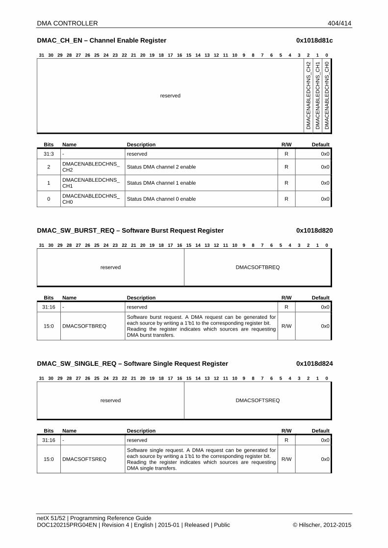
DMA CONTROLLER 404/414
netX 51/52 | Programming Reference Guide DOC120215PRG04EN | Revision 4 | English | 2015-01 | Released | Public © Hilscher, 2012-2015
DMAC_CH_EN – Channel Enable Register 0x1018d81c
31 30 29 28 27 26 25 24 23 22 21 20 19 18 17 16 15 14 13 12 11 10 9 8 7 6 5 4 3 2 1 0
reserved
DM
AC
EN
AB
LED
CH
NS
_CH
2
DM
AC
EN
AB
LED
CH
NS
_CH
1
DM
AC
EN
AB
LED
CH
NS
_CH
0
Bits Name Description R/W Default
31:3 - reserved R 0x0
2 DMACENABLEDCHNS_CH2
Status DMA channel 2 enable R 0x0
1 DMACENABLEDCHNS_CH1
Status DMA channel 1 enable R 0x0
0 DMACENABLEDCHNS_CH0
Status DMA channel 0 enable R 0x0
DMAC_SW_BURST_REQ – Software Burst Request Register 0x1018d820
31 30 29 28 27 26 25 24 23 22 21 20 19 18 17 16 15 14 13 12 11 10 9 8 7 6 5 4 3 2 1 0
reserved DMACSOFTBREQ
Bits Name Description R/W Default
31:16 - reserved R 0x0
15:0 DMACSOFTBREQ
Software burst request. A DMA request can be generated for each source by writing a 1’b1 to the corresponding register bit. Reading the register indicates which sources are requesting DMA burst transfers.
R/W 0x0
DMAC_SW_SINGLE_REQ – Software Single Request Register 0x1018d824
31 30 29 28 27 26 25 24 23 22 21 20 19 18 17 16 15 14 13 12 11 10 9 8 7 6 5 4 3 2 1 0
reserved DMACSOFTSREQ
Bits Name Description R/W Default
31:16 - reserved R 0x0
15:0 DMACSOFTSREQ
Software single request. A DMA request can be generated for each source by writing a 1’b1 to the corresponding register bit. Reading the register indicates which sources are requesting DMA single transfers.
R/W 0x0

DMA CONTROLLER 405/414
netX 51/52 | Programming Reference Guide DOC120215PRG04EN | Revision 4 | English | 2015-01 | Released | Public © Hilscher, 2012-2015
DMAC_SW_LAST_BURST_REQ – Software Last Burst Request Register 0x1018d828
31 30 29 28 27 26 25 24 23 22 21 20 19 18 17 16 15 14 13 12 11 10 9 8 7 6 5 4 3 2 1 0
reserved DMACSOFTLBREQ
Bits Name Description R/W Default
31:16 - reserved R 0x0
15:0 DMACSOFTLBREQ
Software last burst request. A DMA request can be generated for each source by writing a 1’b1 to the corresponding register bit. Reading the register indicates which sources are requesting DMA last burst transfers.
R/W 0x0
DMAC_SW_LAST_SINGLE_REQ – Software Last Single Request Register 0x1018d82c
31 30 29 28 27 26 25 24 23 22 21 20 19 18 17 16 15 14 13 12 11 10 9 8 7 6 5 4 3 2 1 0
reserved DMACSOFTLSREQ
Bits Name Description R/W Default
31:16 - reserved R 0x0
15:0 DMACSOFTLSREQ
Software last single request. A DMA request can be generated for each source by writing a 1’b1 to the corresponding register bit. Reading the register indicates which sources are requesting DMA last single transfers.
R/W 0x0
DMAC_CFG – Configuration Register 0x1018d830
31 30 29 28 27 26 25 24 23 22 21 20 19 18 17 16 15 14 13 12 11 10 9 8 7 6 5 4 3 2 1 0
reserved
DM
AC
EN
AB
LE
Bits Name Description R/W Default
31:1 - reserved R 0x0
0 DMACENABLE DMAC enable: 0 = disabled 1 = enabled. This bit is reset to 0. Disabling the DMAC reduces power consumption.
R/W 0x0

DMA CONTROLLER 406/414
netX 51/52 | Programming Reference Guide DOC120215PRG04EN | Revision 4 | English | 2015-01 | Released | Public © Hilscher, 2012-2015
DMAC_SYNC – Sync Register 0x1018d834
DMA synchronization logic for DMA request signals enabled or disabled A 1’b0 bit indicates that the synchronization logic for the DMACBREQ[15:0], DMACSREQ[15:0], DMACLBREQ[15:0], and DMACLSREQ[15:0] request signals is enabled.
A HIGH bit indicates that the synchronization logic is disabled.
31 30 29 28 27 26 25 24 23 22 21 20 19 18 17 16 15 14 13 12 11 10 9 8 7 6 5 4 3 2 1 0
reserved
DIS
_SY
NC
_US
B_T
X
DIS
_SY
NC
_US
B_R
X
DIS
_SY
NC
_I2C
0_T
X
DIS
_SY
NC
_I2C
0_R
X
DIS
_SY
NC
_ET
H_T
X
DIS
_SY
NC
_ET
H_R
X
DIS
_SY
NC
_UA
RT
2_T
X
DIS
_SY
NC
_UA
RT
2_R
X
DIS
_SY
NC
_UA
RT
1_T
X
DIS
_SY
NC
_UA
RT
1_R
X
DIS
_SY
NC
_UA
RT
0_T
X
DIS
_SY
NC
_UA
RT
0_R
X
DIS
_SY
NC
_SP
I1_T
X
DIS
_SY
NC
_SP
I1_R
X
DIS
_SY
NC
_SQ
I_T
X
DIS
_SY
NC
_SQ
I_R
X
Bits Name Description R/W Default
31:16 - reserved R 0x0
15 DIS_SYNC_USB_TX disable sync register for USB transmit requests R/W 0x0
14 DIS_SYNC_USB_RX disable sync register for USB receive requests R/W 0x0
13 DIS_SYNC_I2C0_TX disable sync register for I2C transmit requests R/W 0x0
12 DIS_SYNC_I2C0_RX disable sync register for I2C receive requests R/W 0x0
11 DIS_SYNC_ETH_TX disable sync register for ETH transmit requests R/W 0x0
10 DIS_SYNC_ETH_RX disable sync register for ETH receive requests R/W 0x0
9 DIS_SYNC_UART2_TX disable sync register for UART1 transmit requests R/W 0x0
8 DIS_SYNC_UART2_RX disable sync register for UART1 receive requests R/W 0x0
7 DIS_SYNC_UART1_TX disable sync register for UART1 transmit requests R/W 0x0
6 DIS_SYNC_UART1_RX disable sync register for UART1 receive requests R/W 0x0
5 DIS_SYNC_UART0_TX disable sync register for UART0 transmit requests R/W 0x0
4 DIS_SYNC_UART0_RX disable sync register for UART0 receive requests R/W 0x0
3 DIS_SYNC_SPI1_TX disable sync register for SPI1 transmit requests R/W 0x0
2 DIS_SYNC_SPI1_RX disable sync register for SPI1 receive requests R/W 0x0
1 DIS_SYNC_SQI_TX disable sync register for SPI0 transmit requests R/W 0x0
0 DIS_SYNC_SQI_RX disable sync register for SPI0 receive requests R/W 0x0

ARM System Control and Configuration Registers 407/414
netX 51/52 | Programming Reference Guide DOC120215PRG04EN | Revision 4 | English | 2015-01 | Released | Public © Hilscher, 2012-2015
10 ARM System Control and Configuration Registers These registers which are called CP15 registers are accessible using special ARM instructions.
CP15 registers enable configuration of the Tightly-Coupled Memory (TCM) and write buffer and other
ARM966E-S system options such as big-endian or little-endian operation.
For more details about the TCM and other system options see ARM966E-S Technical Reference Manual.
10.1 CP15 Registers Summary The ARM966E-S coprocessor 15 registers are described in the following sections:
c0 ID Code Register, TCM Size Register
c1 Control Register
c7 Core Control Register
c13 Trace Process Identifier Register
Note: 1. Register c0 provides access to more than one register. The register access depends on the
value of the Opcode_2 field. See the register descriptions in the following section for more information.
2. c2-c6, c8-c12 and c14 are reserved.
10.2 CP15 Registers Description
c0 – ID Code Register
31 30 29 28 27 26 25 24 23 22 21 20 19 18 17 16 15 14 13 12 11 10 9 8 7 6 5 4 3 2 1 0
IMPLEMENTER Major
revision
AR
CH
ITE
CT
UR
E
PART NUMBER Minor
revision
Bits Name Description R/W Default
31:24 IMPLEMENTER ASCII code of implementer trademark R 0x41
23:20 Major revision Major specification revision R 0x2
19:16 ARCHITECTURE Architecture (ARMv5TE) R 0x5
15:4 PART NUMBER Part number R 0x966
3:0 Minor revision Minor specification revision R 0x1
This is a read-only register that returns the 32-bit device ID code.
You can access the ID Code Register by reading CP15 register c0 with the Opcode_2 field set to any value other than 2. For example: MRC p15,0,<Rd>,c0,c0,0 ;returns ID Code Register

ARM System Control and Configuration Registers 408/414
netX 51/52 | Programming Reference Guide DOC120215PRG04EN | Revision 4 | English | 2015-01 | Released | Public © Hilscher, 2012-2015
c0 – TCM Size Register
31 30 29 28 27 26 25 24 23 22 21 20 19 18 17 16 15 14 13 12 11 10 9 8 7 6 5 4 3 2 1 0
reserved DTCM_size reserved
DT
CM
_abs
ent
reserved ITCM_size reserved
ITC
M_a
bsen
t
rese
rved
Bits Name Description R/W Default
31:23 reserved - R 0x00
22:18 DTCM_size
The data TCM size is configurable in the range 0 bytes to 64 MB: b00000 = 0 byte b00001 = 1KB b00010 = 2KB b00011 = 4KB b00100 = 8KB b00101 = 16KB b00110 = 32KB b00111 = 64KB b01000 = 128KB b01001 = 256KB b01010 = 512KB b01011 = 1 MB b01100 = 2 MB b01101 = 4 MB b01110 = 8 MB b01111 = 16 MB b10000 = 32 MB b10001 = 64 MB The supported sizes are 0 and 2nKB for n = 0 to 16
R 0x04
17:15 reserved - R 0x00
14 DTCM_absent 1 : absent 0: present R 0
13:11 reserved - R 0x00
10:6 ITCM_size
The instruction TCM size is configurable in the range 0 bytes to 64 MB: b00000 = 0 byte b00001 = 1KB b00010 = 2KB b00011 = 4KB b00100 = 8KB b00101 = 16KB b00110 = 32KB b00111 = 64KB b01000 = 128KB b01001 = 256KB b01010 = 512KB b01011 = 1 MB b01100 = 2 MB b01101 = 4 MB b01110 = 8 MB b01111 = 16 MB b10000 = 32 MB b10001 = 64 MB The supported sizes are 0 and 2nKB for n = 0 to 16
R 0x04
5:3 reserved - R 0x00
2 ITCM_absent 1 : absent 0: present R 0
1:0 reserved - R 0x00
The TCM Size Register is a read-only register that returns the size of the Instruction and Data TCM attached to the ARM966E-S processor.
The TCM Size Register can be accessed by reading CP15 register c0 with the Opcode_2 field set to 2. For
example: MRC p15,0,<Rd>,c0,c0,2 ;returns Tightly-Coupled Memory Size Register

ARM System Control and Configuration Registers 409/414
netX 51/52 | Programming Reference Guide DOC120215PRG04EN | Revision 4 | English | 2015-01 | Released | Public © Hilscher, 2012-2015
c1 – Control Register
31 30 29 28 27 26 25 24 23 22 21 20 19 18 17 16 15 14 13 12 11 10 9 8 7 6 5 4 3 2 1 0
SBZ LT
SB
Z
V I SBO B SBO W D A
SB
Z
Bits Name Description R/W Default
31:16 SBZ(should be zero) Reserved. When read, returns an unpredictable value. When written, should be zero.
R 0x00
15 LT
Load PC Thumb disable bit:: 0 = loading PC sets the T bit 1 = loading PC does not set the T bit (ARMv4 behavior). Reset clears this bit
R/W 0
14 SBZ(should be zero) Reserved. When read, returns an Unpredictable value. When written, should be zero.
R/W 0
13 V
Location of exception vectors: 0 = Normal exception vectors selected, address range = 0x0000 0000 to 0x0000 001C 1 = High exception vectors selected, address range = 0xFFFF 0000 to 0xFFFF 001C . At Reset, the VINITHI pins determine the value of this bit.
R/W 0
12 I
Instruction TCM enable: 0 = All accesses to the instruction memory space access the AMBA AHB 1 = All accesses to the fixed instruction memory space access the instruction TCM interface. At Reset, the INITRAM pins determine the value of this bit.
R/W 0
11:8 SBO(should be one) Reserved. Should be One. R 00
7 B Endianness: 0 = Little-endian operation 1 = Big-endian operation.
R/W 0
6:4 SBO(should be one) Reserved. Should be One. R 0
3 W
BIU write buffer enable:
0 = All stores to the AMBA AHB are treated as nonbufferable
1 = All stores to the fixed bufferable space of the AMBA AHB
are treated as buffered writes.
Reset clears this bit.
R/W 0
2 D Data TCM enable. At Reset, the INITRAM pins determine the value of this bit.
R/W 0
1 A
Address alignment fault checking enable:
0 = Fault checking of address alignment disabled
1 = Fault checking of address alignment enabled.
Reset clears this bit.
R/W 0
0 SBZ(should be zero) Reserved. When read, returns an Unpredictable value. When written, should be zero.
R 0
This register contains the global control bits of the ARM966E-S processor. All reserved bits must either be written with zero or one, as indicated, or written using read-modify-write. The reserved bits have an
Unpredictable value when read. To read and write this register, use the instructions: MRC p15,0,<Rd>,c1,c0,0 ;read control register MCR p15,0,<Rd>,c1,c0,0 ;write control register

ARM System Control and Configuration Registers 410/414
netX 51/52 | Programming Reference Guide DOC120215PRG04EN | Revision 4 | English | 2015-01 | Released | Public © Hilscher, 2012-2015
c7 – Core Control Register
You can use a write to this register, to perform wait for interrupt and drain write buffer operations.
Wait for interrupt
This operation enables the ARM966E-S processor to enter a low-power standby mode. When the operation
is invoked, the clock enable to the processor core is negated until either an interrupt or a debug request occurs. This function is invoked by a write to Register 7. The following ARM instruction causes this to occur: MCR p15,0,<Rd>,c7,c0,4 ;wait for interrupt
Note: This is the preferred encoding that must be used by new software. For compatibility with
existing software, ARM966E-S processor also supports the following ARM instruction that has the same affect:
MCR p15,0,<Rd>,c15,c8,2 ;wait for interrupt
This stalls the processor from the time that the instruction is executed until nFIQ, nIRQ, or EDBGRQ are asserted. Also, if the debugger sets the debug request bit in the EmbeddedICE-RT control register then this
causes the wait-for-interrupt condition to terminate.
In the case of nFIQ and nIRQ, the processor core is woken up regardless of whether the interrupts are enabled or disabled (that is, independent of the I and F bits in the processor CPSR). The debug-related
waking only occurs if DBGEN is HIGH, that is, only when debug is enabled.
If interrupts are enabled, the ARM9E-S core is guaranteed to take the interrupt before executing the instruction after the wait for interrupt. If debug request is used to wake up the system, the processor enters
debug-state before executing any more instructions.
Wait for interrupt does not prevent the write buffer from emptying.
Drain write buffers
This CP15 operation causes instruction execution to be stalled until the AHB and TCM write buffers are emptied. This operation is useful in real-time applications where the processor must be sure that a write to a peripheral has completed before program execution continues. An example is where a peripheral in a
bufferable region is the source of an interrupt. When the interrupt has been serviced, the request must be removed before interrupts can be re-enabled. This can be ensured if a drain write buffer operation separates the store to the peripheral and the enable interrupt functions.
The drain write buffer operation is invoked by a write to Register 7 using the following ARM instruction: MCR p15,0,<Rd>,c7,c10,4 ;drain write buffer
Note: This stalls the processor core until any outstanding accesses in the write buffers have been
completed, that is, until all data has been written to memory.

ARM System Control and Configuration Registers 411/414
netX 51/52 | Programming Reference Guide DOC120215PRG04EN | Revision 4 | English | 2015-01 | Released | Public © Hilscher, 2012-2015
C13 – Trace Process Identifier Register
31 30 29 28 27 26 25 24 23 22 21 20 19 18 17 16 15 14 13 12 11 10 9 8 7 6 5 4 3 2 1 0
Trace process ID
Bits Name Description R/W Default
31:0 Trace process ID Trace process ID R/W 0x00
This register enables the real-time trace tools to identify the currently executing process in multitasking
environments.
The ETMPROCID[31:0] pins reflect the contents of the Trace Process Identifier Register.
Note: Writing to the Trace Process Identifier Register sets the ETMPROCIDWR signal for one clock
cycle.
Here are ARM instructions that you can use to access the Trace Process Identifier Register: MRC p15,0,<Rd>,c13,{c0–c15} ;Read Trace Process Identifier Register MCR p15,0,<Rd>,c13,{c0–c15} ;write Trace Process Identifier Register

Appendix 412/414
netX 51/52 | Programming Reference Guide DOC120215PRG04EN | Revision 4 | English | 2015-01 | Released | Public © Hilscher, 2012-2015
11 Appendix 11.1 List of Tables Table 1: List of Revisions .................................................................................................................................................... 4 Table 2: Terms, Abbreviations and Definitions.................................................................................................................... 5 Table 3: References to Documents..................................................................................................................................... 5 Table 4: System Functions Registers................................................................................................................................ 11 Table 5: ACCESS_KEY Protected Registers .................................................................................................................... 12 Table 6: MMIO Asynchronously Multiplexed Functions Pinning Table.............................................................................. 15 Table 7: MMIO*_SEL Coding ............................................................................................................................................ 25 Table 8: MEM-eMI related Address Areas for External Memory ....................................................................................... 79 Table 9: HIF-eMI related Address Areas for External Memory.......................................................................................... 79 Table 10: SRAM Controller Registers ............................................................................................................................... 80 Table 11: SDRAM Controller Registers............................................................................................................................. 87 Table 12: INTRAM Memory Layout................................................................................................................................... 96 Table 13: INTRAM Parity Registers .................................................................................................................................. 96 Table 14: Dual-Port Memory Configuration Window Registers ....................................................................................... 106 Table 15: DPM_IF_CFG Register Config Table .............................................................................................................. 108 Table 16: Handshake Configuration Registers................................................................................................................ 169 Table 17: xPIC-VIC Registers ......................................................................................................................................... 197 Table 18: xPIC_TIMER Registers ................................................................................................................................... 208 Table 19: xPIC Watchdog Registers ............................................................................................................................... 214 Table 20: GPIO- and Timer Related Registers................................................................................................................ 220 Table 21: PIO Registers .................................................................................................................................................. 231 Table 22: ARM Timers Registers .................................................................................................................................... 232 Table 23: IO_Link Registers............................................................................................................................................ 239 Table 24: UARTs Registers............................................................................................................................................. 251 Table 25: SPI Registers .................................................................................................................................................. 262 Table 26: SQI Registers .................................................................................................................................................. 275 Table 27: I2C Registers .................................................................................................................................................. 291 Table 28: CAN Controller Registers ................................................................................................................................ 304 Table 29: SYSTIME Registers ........................................................................................................................................ 321 Table 30: CORDIC Unit Registers................................................................................................................................... 323 Table 31: USB Registers................................................................................................................................................. 325 Table 32: USB Device Descriptor Layout ........................................................................................................................ 332 Table 33: USB String Descriptor Layout ......................................................................................................................... 332 Table 34: VIC Registers .................................................................................................................................................. 348 Table 35: PHY and MIIMU Registers .............................................................................................................................. 355 Table 36: PTR_FIFO Registers....................................................................................................................................... 364 Table 37: Buffer Management Unit (BMU) Registers ...................................................................................................... 369 Table 38: NFIFO Registers ............................................................................................................................................. 377 Table 39: CRC Registers ................................................................................................................................................ 383 Table 40: ARM to XPEC IRQ Registers .......................................................................................................................... 385 Table 41: DMAC_CH Registers ...................................................................................................................................... 395 Table 42: DMAC_REG Registers.................................................................................................................................... 400

Appendix 413/414
netX 51/52 | Programming Reference Guide DOC120215PRG04EN | Revision 4 | English | 2015-01 | Released | Public © Hilscher, 2012-2015
11.2 List of Figures Figure 1: DPM Window Mapping Example...................................................................................................................... 103 Figure 2: DPM Access Tunnel......................................................................................................................................... 104 Figure 3: 16bit DPM Handshake Interaction.................................................................................................................... 168 Figure 4: NFIFO Block Diagram...................................................................................................................................... 375 Figure 5: NFIFO Data Pointer Structure.......................................................................................................................... 375 Figure 6: DMA Channel Linked List Items Structure ....................................................................................................... 390 Figure 7: Link List DMA transfer...................................................................................................................................... 391

Appendix 414/414
netX 51/52 | Programming Reference Guide DOC120215PRG04EN | Revision 4 | English | 2015-01 | Released | Public © Hilscher, 2012-2015
11.3 Contacts
Headquarters
Germany Hilscher Gesellschaft für Systemautomation mbH Rheinstrasse 15 65795 Hattersheim Phone: +49 (0) 6190 9907-0 Fax: +49 (0) 6190 9907-50 E-Mail: [email protected]
Support Phone: +49 (0) 6190 9907-99 E-Mail: [email protected]
Subsidiaries
China Hilscher Systemautomation (Shanghai) Co. Ltd. 200010 Shanghai Phone: +86 (0) 21-6355-5161 E-Mail: [email protected]
Support Phone: +86 (0) 21-6355-5161 E-Mail: [email protected]
France Hilscher France S.a.r.l. 69500 Bron Phone: +33 (0) 4 72 37 98 40 E-Mail: [email protected]
Support Phone: +33 (0) 4 72 37 98 40 E-Mail: [email protected]
India Hilscher India Pvt. Ltd. Pune, Delhi, Mumbai Phone: +91 8888 750 777 E-Mail: [email protected]
Italy Hilscher Italia S.r.l. 20090 Vimodrone (MI) Phone: +39 02 25007068 E-Mail: [email protected]
Support Phone: +39 02 25007068 E-Mail: [email protected]
Japan Hilscher Japan KK Tokyo, 160-0022 Phone: +81 (0) 3-5362-0521 E-Mail: [email protected]
Support Phone: +81 (0) 3-5362-0521 E-Mail: [email protected]
Korea Hilscher Korea Inc. Seongnam, Gyeonggi, 463-400 Phone: +82 (0) 31-789-3715 E-Mail: [email protected]
Switzerland Hilscher Swiss GmbH 4500 Solothurn Phone: +41 (0) 32 623 6633 E-Mail: [email protected]
Support Phone: +49 (0) 6190 9907-99 E-Mail: [email protected]
USA Hilscher North America, Inc. Lisle, IL 60532 Phone: +1 630-505-5301 E-Mail: [email protected]
Support Phone: +1 630-505-5301 E-Mail: [email protected]