programmable controller fp1 - autopack
TRANSCRIPT
PROGRAMMABLE CONTROLLER
FP1
is a global brand name of Matsushita Electric Works.
Hardware
BEFORE BEGINNING
This manual and everything described in it are copyrighted. You may not copy this manual, in whole or part, withoutwritten consent of Matsushita Electric Works, Ltd.
Matsushita Electric Works, Ltd. pursues a policy of continuous improvement of the design and performance of itsproducts, therefore, we reserve the right to change the manual/product without notice. In no event will MatsushitaElectric Works, Ltd. be liable for direct, special, incidental, or consequential damage resulting from any defect in theproduct or its documentation, even if advised of the possibility of such damages.
If physical defects caused by distribution are found, Matsushita Electric Works, Ltd., will replace/repair the productfree of charge. Exceptions include:
• When physical defects are due to different usage/treatment of the product other thandescribed in the manual.
• When physical defects are due to defective equipment other than the distributed product.• When physical defects are due to modifications/repairs by someone other than Matsushita
Electric Works, Ltd.• When physical defects are due to natural disasters.
LIMITED WARRANTY
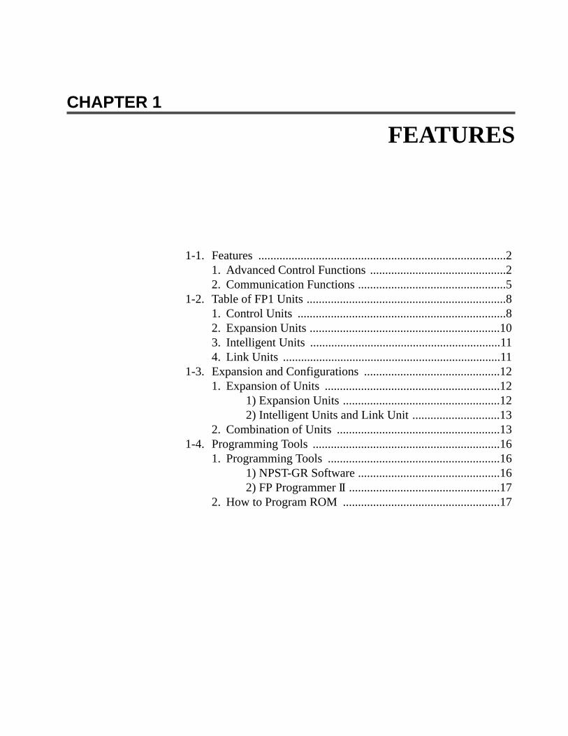
CONTENTSCHAPTER 1: FEATURES
1-1. Features ................................................................................................................ 21. Advanced Control Functions .......................................................................... 22. Communication Functions .............................................................................. 5
1-2. Table of FP1 Units ............................................................................................... 81. Control Units .................................................................................................. 82. Expansion Units ............................................................................................ 103. Intelligent Units ............................................................................................ 114. Link Units ..................................................................................................... 11
1-3. Expansion and Configurations ........................................................................... 121. Expansion of Units ....................................................................................... 12
1) Expansion Units ..................................................................................... 122) Intelligent Units and Link Unit .............................................................. 13
2. Combination of Units ................................................................................... 131-4. Programming Tools ............................................................................................ 16
1. Programming Tools ...................................................................................... 161) NPST-GR Software ................................................................................ 162) FP Programmer II ................................................................................... 17
2. How to Program ROM ................................................................................. 17
CHAPTER 2: SPECIFICATIONS
2-1. Parts Terminology and Functions ....................................................................... 221. Control Unit ................................................................................................... 22
1) C14 and C16 Series................................................................................. 222) C24, C40, C56, and C72 Series .............................................................. 23
2. Expansion Unit .............................................................................................. 241) E8 and E16 Series .................................................................................. 242) E24 and E40 Series ................................................................................. 24
3. Intelligent Unit............................................................................................... 251) FP1 A/D Converter Unit ......................................................................... 252) FP1 D/A Converter Unit ......................................................................... 25
4. Link Unit........................................................................................................ 261) FP1 Transmitter Master Unit .................................................................. 262) FP1 I/O Link Unit ................................................................................... 273) C-NET Adapter S1 Type......................................................................... 28
2-2. Specifications ...................................................................................................... 291. General Specifications ....................................................................................292. Performance Specifications of Control Unit and Expansion Unit................. 31
1) Control Specifications............................................................................. 312) Input Specifications of Control Unit and Expansion Unit ...................... 323) Output Specifications of Control Unit and Expansion Unit ................... 33
3. Performance Specifications of Intelligent Unit ............................................. 351) FP1 A/D Converter Unit ......................................................................... 352) FP1 D/A Converter Unit ......................................................................... 35
4. Performance Specifications of Link Unit ...................................................... 361) FP1 Transmitter Master Unit .................................................................. 36
CONTENTS
2) FP1 I/O Link Unit ................................................................................... 363) C-NET Adapter S1 Type......................................................................... 36
5. Dimensions .................................................................................................... 371) Control Unit ............................................................................................ 372) Expansion Unit........................................................................................ 373) Intelligent Unit ........................................................................................ 384) Link Unit ................................................................................................. 38
CHAPTER 3: INSTALLATION AND WIRING
3-1. Installation ...........................................................................................................401. Panel Mounting ..............................................................................................402. DIN Rail Mounting ........................................................................................403. Cautions .........................................................................................................41
3-2. Expansion ............................................................................................................421. Expansion Cable ............................................................................................422. Unit Expansion ..............................................................................................42
3-3. Wiring ..................................................................................................................431. Crimp Terminal .............................................................................................432. Wiring Power Supply ....................................................................................43
1) Wiring Example for Power Supply Terminal .........................................432) Power Supply Lines ................................................................................443) Momentary Power Drop .........................................................................444) Safety ......................................................................................................44
3. Input Terminals of Control Unit and Expansion Unit ...................................451) Wiring Example for Input Terminals ......................................................452) Description ..............................................................................................453) Input Wiring Examples ...........................................................................464) Input Terminal Layouts ..........................................................................47
4. Output Terminals of Control Unit and Expansion Unit ................................491) Wiring Example for Output Terminals ...................................................492) Description ..............................................................................................493) Output Wiring Examples ........................................................................504) Output Terminal Layouts ........................................................................51
5. Wiring the FP1 A/D Converter Unit...............................................................531) Wiring for Voltage Input .........................................................................532) Wiring for Current Input..........................................................................53
6. Wiring the FP1 D/A Converter Unit...............................................................541) Wiring for Voltage Output.......................................................................542) Wiring for Current Output .......................................................................54
7. Wiring the FP1 Transmitter Master Unit........................................................558. Wiring the FP1 I/O Link Unit.........................................................................55
1) Cable Specifications ................................................................................55
CHAPTER 4: BEFORE PROGRAMMING
4-1. Operating Principles of the Programmable Controller.........................................581. Basic Configuration........................................................................................582. Basic Operation ..............................................................................................60
4-2. How to Program the Programmable Controller ...................................................621. Making a Ladder Diagram..............................................................................622. Relays and Timer/Counter Contacts in the FP1 .............................................633. I/O Allocation in the FP1................................................................................65
4-3. Programming with NPST-GR Software...............................................................67
CONTENTS
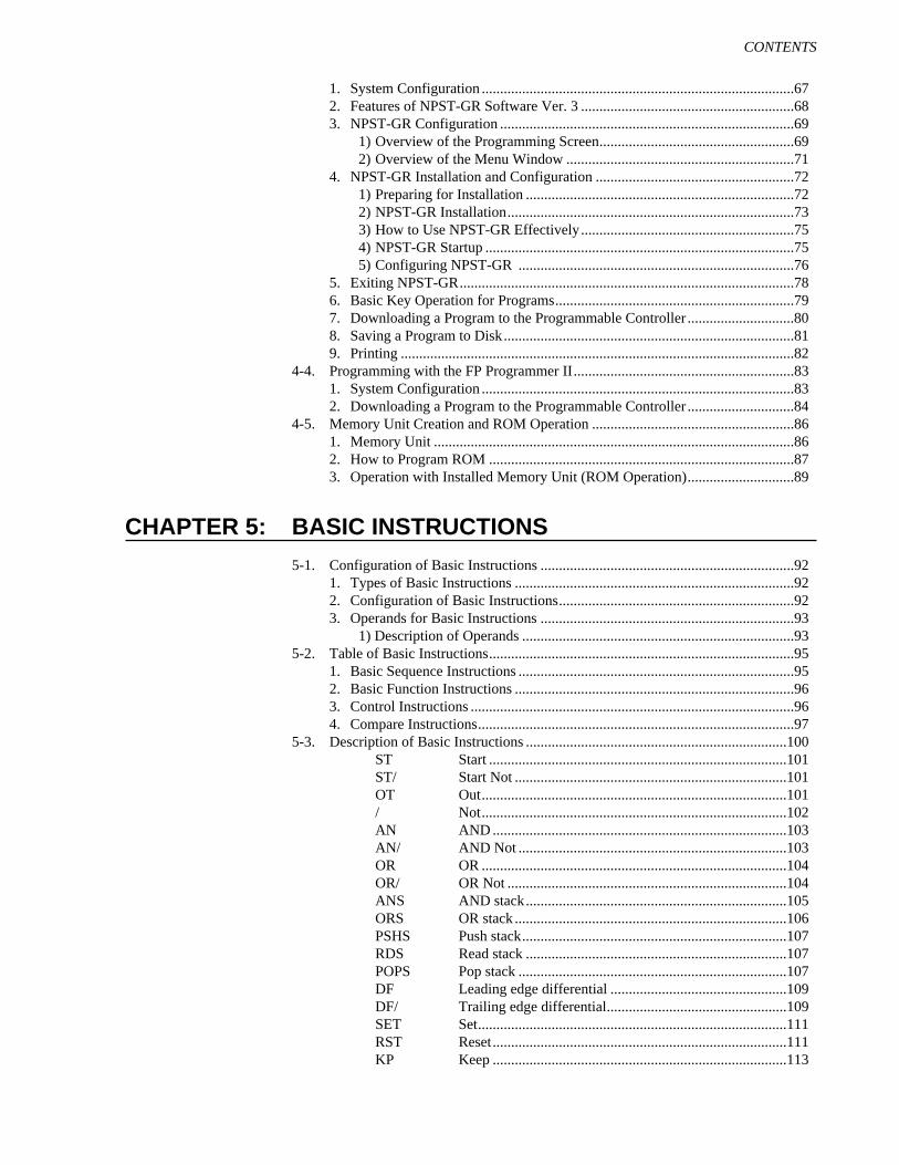
1. System Configuration .....................................................................................672. Features of NPST-GR Software Ver. 3 ..........................................................683. NPST-GR Configuration ................................................................................69
1) Overview of the Programming Screen.....................................................692) Overview of the Menu Window ..............................................................71
4. NPST-GR Installation and Configuration ......................................................721) Preparing for Installation .........................................................................722) NPST-GR Installation..............................................................................733) How to Use NPST-GR Effectively..........................................................754) NPST-GR Startup ....................................................................................755) Configuring NPST-GR ...........................................................................76
5. Exiting NPST-GR...........................................................................................786. Basic Key Operation for Programs.................................................................797. Downloading a Program to the Programmable Controller .............................808. Saving a Program to Disk...............................................................................819. Printing ...........................................................................................................82
4-4. Programming with the FP Programmer II............................................................831. System Configuration .....................................................................................832. Downloading a Program to the Programmable Controller .............................84
4-5. Memory Unit Creation and ROM Operation .......................................................861. Memory Unit ..................................................................................................862. How to Program ROM ...................................................................................873. Operation with Installed Memory Unit (ROM Operation).............................89
CHAPTER 5: BASIC INSTRUCTIONS
5-1. Configuration of Basic Instructions .....................................................................921. Types of Basic Instructions ............................................................................922. Configuration of Basic Instructions................................................................923. Operands for Basic Instructions .....................................................................93
1) Description of Operands ..........................................................................935-2. Table of Basic Instructions...................................................................................95
1. Basic Sequence Instructions ...........................................................................952. Basic Function Instructions ............................................................................963. Control Instructions ........................................................................................964. Compare Instructions......................................................................................97
5-3. Description of Basic Instructions .......................................................................100ST Start .................................................................................101ST/ Start Not ..........................................................................101OT Out...................................................................................101/ Not...................................................................................102AN AND ................................................................................103AN/ AND Not .........................................................................103OR OR ...................................................................................104OR/ OR Not ............................................................................104ANS AND stack.......................................................................105ORS OR stack ..........................................................................106PSHS Push stack........................................................................107RDS Read stack .......................................................................107POPS Pop stack .........................................................................107DF Leading edge differential ................................................109DF/ Trailing edge differential.................................................109SET Set....................................................................................111RST Reset................................................................................111KP Keep ................................................................................113
CONTENTS
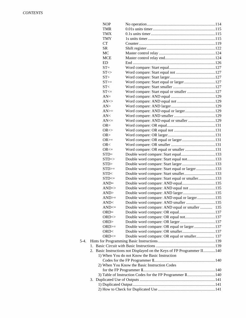
NOP No operation....................................................................114TMR 0.01s units timer ..............................................................115TMX 0.1s units timer ................................................................115TMY 1s units timer ...................................................................115CT Counter............................................................................119SR Shift register ....................................................................122MC Master control relay ........................................................124MCE Master control relay end..................................................124ED End ..................................................................................126ST= Word compare: Start equal..............................................127ST<> Word compare: Start equal not .......................................127ST> Word compare: Start larger .............................................127ST>= Word compare: Start equal or larger ...............................127ST< Word compare: Start smaller ..........................................127ST<= Word compare: Start equal or smaller ............................127AN= Word compare: AND equal ............................................129AN<> Word compare: AND equal not ......................................129AN> Word compare: AND larger............................................129AN>= Word compare: AND equal or larger..............................129AN< Word compare: AND smaller .........................................129AN<= Word compare: AND equal or smaller ...........................129OR= Word compare: OR equal................................................131OR<> Word compare: OR equal not .........................................131OR> Word compare: OR larger...............................................131OR>= Word compare: OR equal or larger .................................131OR< Word compare: OR smaller ............................................131OR<= Word compare: OR equal or smaller ..............................131STD= Double word compare: Start equal..................................133STD<> Double word compare: Start equal not............................133STD> Double word compare: Start larger .................................133STD>= Double word compare: Start equal or larger ...................133STD< Double word compare: Start smaller...............................133STD<= Double word compare: Start equal or smaller.................133AND= Double word compare: AND equal.................................135AND<> Double word compare: AND equal not ..........................135AND> Double word compare: AND larger ................................135AND>= Double word compare: AND equal or larger ..................135AND< Double word compare: AND smaller .............................135AND<= Double word compare: AND equal or smaller ............ 135ORD= Double word compare: OR equal....................................137ORD<> Double word compare: OR equal not..............................137ORD> Double word compare: OR larger ...................................137ORD>= Double word compare: OR equal or larger .....................137ORD< Double word compare: OR smaller.................................137ORD<= Double word compare: OR equal or smaller.................. 137
5-4. Hints for Programming Basic Instructions.........................................................1391. Basic Circuit with Basic Instructions ...........................................................1392. Basic Instructions not Displayed on the Keys of FP Programmer II............140
1) When You do not Know the Basic Instruction Codes for the FP Programmer II.............................................................140
2) When You Know the Basic Instruction Codes for the FP Programmer II........................................................................140
3) Table of Instruction Codes for the FP Programmer II............................1403. Duplicated Use of Outputs ...........................................................................141
1) Duplicated Output ..................................................................................1412) How to Check for Duplicated Use .........................................................141
CONTENTS
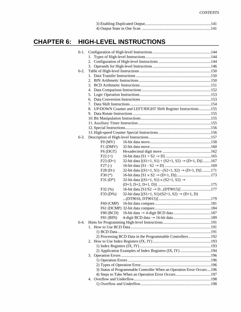
3) Enabling Duplicated Output...................................................................1414) Output State in One Scan ......................................................................141
CHAPTER 6: HIGH-LEVEL INSTRUCTIONS
6-1. Configuration of High-level Instructions ...........................................................1441. Types of High-level Instructions ..................................................................1442. Configuration of High-level Instructions .....................................................1443. Operands for High-level Instructions ...........................................................146
6-2. Table of High-level Instructions ........................................................................1501. Data Transfer Instructions ............................................................................1502. BIN Arithmetic Instructions .........................................................................1503. BCD Arithmetic Instructions........................................................................1514. Data Comparison Instructions ......................................................................1525. Logic Operation Instructions ........................................................................1536. Data Conversion Instructions .......................................................................1537. Data Shift Instructions ..................................................................................1548. UP/DOWN Counter and LEFT/RIGHT Shift Register Instructions ............1559. Data Rotate Instructions ...............................................................................15510. Bit Manipulation Instructions.......................................................................15511. Auxiliary Timer Instruction..........................................................................15512. Special Instructions.......................................................................................15613. High-speed Counter Special Instructions .....................................................156
6-3. Description of High-level Instructions ...............................................................157F0 (MV) 16-bit data move..............................................................158F1 (DMV) 32-bit data move..............................................................160F6 (DGT) Hexadecimal digit move .................................................162F22 (+) 16-bit data [S1 + S2 → D] ..............................................165F23 (D+) 32-bit data [(S1+1, S1) + (S2+1, S2) → (D+1, D)] ........167F27 (-) 16-bit data [S1 - S2 → D] ...............................................169F28 (D-) 32-bit data [(S1+1, S1) - (S2+1, S2) → (D+1, D)] .........171F30 (*) 16-bit data [S1 × S2 → (D+1, D)]...................................173F31 (D*) 32-bit data [(S1+1, S1) × (S2+1, S2) →
(D+3, D+2, D+1, D)] ......................................................175F32 (%) 16-bit data [S1/S2 → D...(DT9015)] ..............................177F33 (D%) 32-bit data [(S1+1, S1)/(S2+1, S2) → (D+1, D)
...(DT9016, DT9015)] .....................................................179F60 (CMP) 16-bit data compare.........................................................181F61 (DCMP) 32-bit data compare.........................................................184F80 (BCD) 16-bit data → 4-digit BCD data ......................................187F81 (BIN) 4-digit BCD data → 16-bit data ......................................189
6-4. Hints for Programming High-level Instructions.................................................1911. How to Use BCD Data .................................................................................191
1) BCD Data...............................................................................................1912) Processing BCD Data in the Programmable Controllers.......................192
2. How to Use Index Registers (IX, IY) ...........................................................1931) Index Registers (IX, IY) ........................................................................1932) Application Examples of Index Registers (IX, IY) ...............................194
3. Operation Errors ...........................................................................................1961) Operation Errors ....................................................................................1962) Types of Operation Error .......................................................................1963) Status of Programmable Controller When an Operation Error Occurs ....1964) Steps to Take When an Operation Error Occurs....................................197
4. Overflow and Underflow..............................................................................1981) Overflow and Underflow .......................................................................198
CONTENTS
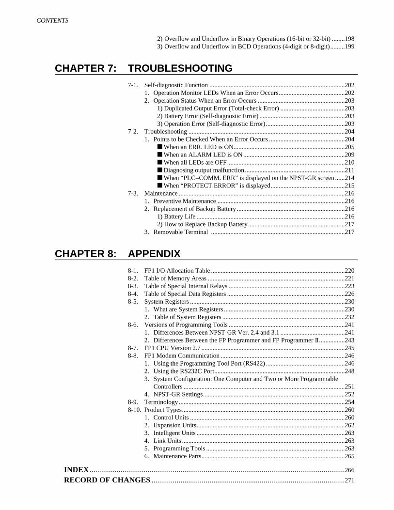
2) Overflow and Underflow in Binary Operations (16-bit or 32-bit) ........1983) Overflow and Underflow in BCD Operations (4-digit or 8-digit).........199
CHAPTER 7: TROUBLESHOOTING
7-1. Self-diagnostic Function ....................................................................................2021. Operation Monitor LEDs When an Error Occurs.........................................2022. Operation Status When an Error Occurs ......................................................203
1) Duplicated Output Error (Total-check Error) ........................................2032) Battery Error (Self-diagnostic Error) .....................................................2033) Operation Error (Self-diagnostic Error) .................................................203
7-2. Troubleshooting .................................................................................................2041. Points to be Checked When an Error Occurs ...............................................204
When an ERR. LED is ON.....................................................................205 When an ALARM LED is ON...............................................................209 When all LEDs are OFF.........................................................................210 Diagnosing output malfunction..............................................................211 When “PLC=COMM. ERR” is displayed on the NPST-GR screen ......214 When “PROTECT ERROR” is displayed..............................................215
7-3. Maintenance .......................................................................................................2161. Preventive Maintenance ...............................................................................2162. Replacement of Backup Battery ...................................................................216
1) Battery Life ............................................................................................2162) How to Replace Backup Battery............................................................217
3. Removable Terminal ...................................................................................217
CHAPTER 8: APPENDIX
8-1. FP1 I/O Allocation Table ...................................................................................2208-2. Table of Memory Areas .....................................................................................2218-3. Table of Special Internal Relays ........................................................................2238-4. Table of Special Data Registers .........................................................................2268-5. System Registers ................................................................................................230
1. What are System Registers ...........................................................................2302. Table of System Registers ............................................................................232
8-6. Versions of Programming Tools ........................................................................2411. Differences Between NPST-GR Ver. 2.4 and 3.1 ........................................2412. Differences Between the FP Programmer and FP Programmer II ................243
8-7. FP1 CPU Version 2.7 .........................................................................................2458-8. FP1 Modem Communication .............................................................................246
1. Using the Programming Tool Port (RS422) .................................................2462. Using the RS232C Port.................................................................................2483. System Configuration: One Computer and Two or More Programmable
Controllers ....................................................................................................2514. NPST-GR Settings........................................................................................252
8-9. Terminology .......................................................................................................2548-10. Product Types.....................................................................................................260
1. Control Units ................................................................................................2602. Expansion Units............................................................................................2623. Intelligent Units ............................................................................................2634. Link Units .....................................................................................................2635. Programming Tools ......................................................................................2636. Maintenance Parts.........................................................................................265
INDEX ....................................................................................................................................266
RECORD OF CHANGES ....................................................................................................271
CONTENTS
CHAPTER 1
FEATURES
1-1. Features ..................................................................................21. Advanced Control Functions .............................................22. Communication Functions .................................................5
1-2. Table of FP1 Units ..................................................................81. Control Units .....................................................................82. Expansion Units ...............................................................103. Intelligent Units ...............................................................114. Link Units ........................................................................11
1-3. Expansion and Configurations .............................................121. Expansion of Units ..........................................................12
1) Expansion Units ....................................................122) Intelligent Units and Link Unit .............................13
2. Combination of Units ......................................................131-4. Programming Tools ..............................................................16
1. Programming Tools .........................................................161) NPST-GR Software ...............................................162) FP Programmer II ..................................................17
2. How to Program ROM ....................................................17
2
1-1. Features
1-1. Features
1. Advanced Control Functions
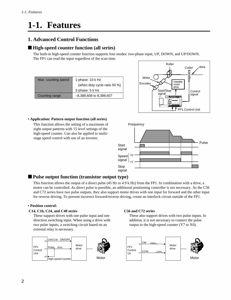
High-speed counter function (all series)The built-in high-speed counter function supports four modes: two-phase input, UP, DOWN, and UP/DOWN.The FP1 can read the input regardless of the scan time.
• Application: Pattern output function (all series)
Pulse output function (transistor output type)This function allows the output of a direct pulse (45 Hz to 4.9 k Hz) from the FP1. In combination with a drive, amotor can be controlled. As direct pulse is possible, an additional positioning controller is not necessary. As the C56and C72 series have two pulse outputs, they also support motor drives with one input for forward and the other inputfor reverse driving. To prevent incorrect forward/reverse driving, create an interlock circuit outside of the FP1.
• Position control:C56 and C72 series
These also support drives with two pulse inputs. Inaddition, it is not necessary to connect the pulseoutput to the high-speed counter (Y7 to X0).
C14, C16, C24, and C40 seriesThese support drives with one pulse input and onedirection switching input. When using a drive withtwo pulse inputs, a switching circuit based on anexternal relay is necessary.
Pulse
Frequency
Startsignal
"""
Y0
Y1
Speedsignal
Stopsignal
This function allows the setting of a maximum ofeight output patterns with 15 level settings of thehigh-speed counter. Can also be applied to multi-stage speed control with use of an inverter.
Max. counting speed
Counting range
1-phase: 10 k Hz
(when duty cycle ratio 50 %)
2-phase: 5 k Hz
–8,388,608 to 8,388,607
Y0CW/CCW
Y7
X0
Pulse
High-speed counter
ON/OFF
FP1ControlUnit
Motordrive
Y7
Y6
CCW
FP1ControlUit
Motordrive
CW
Motor Motor
Roller
Encoder
Motor
Start/Stopsignal
Cutter
Variablemotordrive
Wire
Controlsignal
FP1 Control Unit
3
1-1. Features
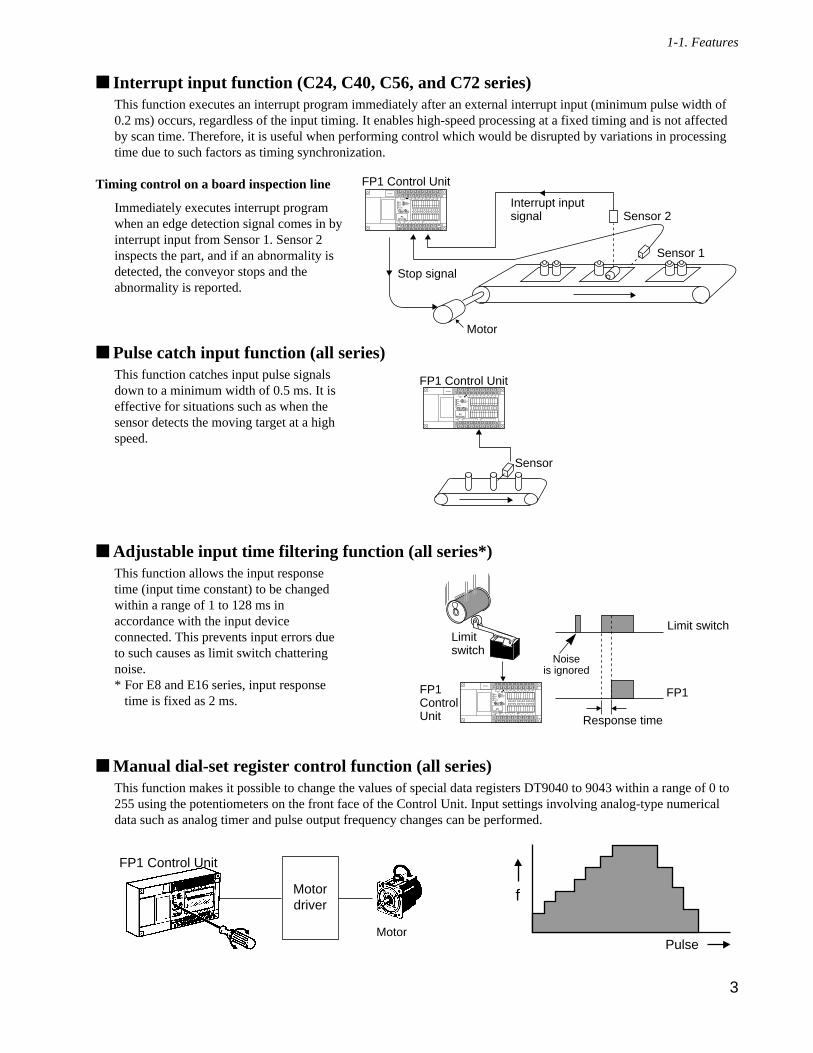
Interrupt input function (C24, C40, C56, and C72 series)This function executes an interrupt program immediately after an external interrupt input (minimum pulse width of0.2 ms) occurs, regardless of the input timing. It enables high-speed processing at a fixed timing and is not affectedby scan time. Therefore, it is useful when performing control which would be disrupted by variations in processingtime due to such factors as timing synchronization.
Timing control on a board inspection line
Immediately executes interrupt programwhen an edge detection signal comes in byinterrupt input from Sensor 1. Sensor 2inspects the part, and if an abnormality isdetected, the conveyor stops and theabnormality is reported.
Pulse catch input function (all series)This function catches input pulse signalsdown to a minimum width of 0.5 ms. It iseffective for situations such as when thesensor detects the moving target at a highspeed.
Adjustable input time filtering function (all series*)This function allows the input responsetime (input time constant) to be changedwithin a range of 1 to 128 ms inaccordance with the input deviceconnected. This prevents input errors dueto such causes as limit switch chatteringnoise.* For E8 and E16 series, input response
time is fixed as 2 ms.
Manual dial-set register control function (all series)This function makes it possible to change the values of special data registers DT9040 to 9043 within a range of 0 to255 using the potentiometers on the front face of the Control Unit. Input settings involving analog-type numericaldata such as analog timer and pulse output frequency changes can be performed.
FP1 Control Unit
Sensor 2
Sensor 1
Interrupt input signal
Stop signal
Motor
COM0
COM1
COM2
COM3
COM4
COM5
COM6
COM7
+ -24V DC
F.G.
COMF
89
EAB
CD(+)-
COM7
01
623
45(+)-
RUNREMOTEPROG.
V0
max.min.
RUN
PROG.
ERR.
ALRAM
BATTERY
V1
max.
PCFP1-C24
24V DC+
-
min.
Sensor
FP1 Control UnitCOM
0COM
1COM
2COM
3COM
4COM
5COM
6COM
7+ -
24V DCF.G.
COMF
89
EAB
CD(+)-
COM7
01
623
45(+)-
RUNREMOTEPROG.
V0
max.min.
RUN
PROG.
ERR.
ALRAM
BATTERY
V1
max.
PCFP1-C24
24V DC+
-
min.
Response time
Limit switch
FP1FP1ControlUnit
COM0
COM1
COM2
COM3
COM4
COM5
COM6
COM7
+ -24V DC
F.G.
COMF
89
EAB
CD(+)-
COM7
01
623
45(+)-
RUNREMOTEPROG.
V0
max.min.
RUN
PROG.
ERR.
ALRAM
BATTERY
V1
max.
PCFP1-C24
24V DC+
-
min.
Limitswitch
f
Pulse
Motordriver
Noiseis ignored
Motor
FP1 Control Unit
4
1-1. Features
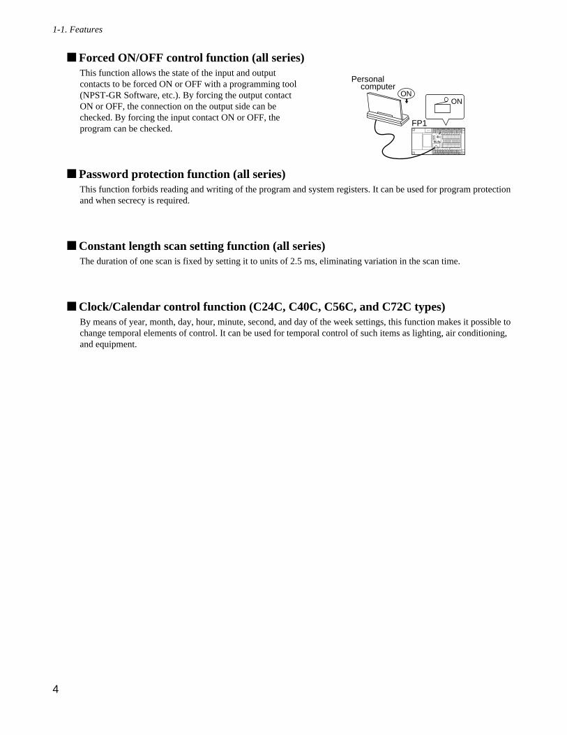
Forced ON/OFF control function (all series)This function allows the state of the input and outputcontacts to be forced ON or OFF with a programming tool(NPST-GR Software, etc.). By forcing the output contactON or OFF, the connection on the output side can bechecked. By forcing the input contact ON or OFF, theprogram can be checked.
Password protection function (all series)This function forbids reading and writing of the program and system registers. It can be used for program protectionand when secrecy is required.
Constant length scan setting function (all series)The duration of one scan is fixed by setting it to units of 2.5 ms, eliminating variation in the scan time.
Clock/Calendar control function (C24C, C40C, C56C, and C72C types)By means of year, month, day, hour, minute, second, and day of the week settings, this function makes it possible tochange temporal elements of control. It can be used for temporal control of such items as lighting, air conditioning,and equipment.
COM0
COM1
COM2
COM3
COM4
COM5
COM6
COM7
+ -24V DC
F.G.
COMF
89
EAB
CD(+)-
COM7
01
623
45(+)-
RUNREMOTEPROG.
V0
max.min.
RUN
PROG.
ERR.
ALRAM
BATTERY
V1
max.
PCFP1-C24
24V DC+
-
min.
FP1
Personal computer
ONON
5
1-1. Features
2. Communication Functions
Computer link function (MEWTOCOL)This function allows the reading and writing of FP1 contact information and data register content from a hostcomputer. It can be used for such applications as data collection and the monitoring of operating conditions.
Communication between one computer and one FP1 Control Unit• Using RS232C port (C24C, C40C, C56C, and C72C types)
The RS232C port can be used for direct connection to apersonal computer, allowing the easy performance of a 1:1computer link.
• Using programming tools connector (RS422 port) (all series)The RS422 port can also be used for a 1:1 computer link byconnecting it through an RS422/232C Adapter.
Note:
Communication between one computer and 32 FP1 Control Units
Using a C-NET Adapter, a maximum of 32 FP1 units can be connected with one personal computer. If a bar codereader is connected via the RS232C port, this system can be used for collection of various production controlinformation.
• Refer to C-NET LINK UNIT Technical Manual for details about computer link function.
COM0
COM1
COM2
COM3
COM4
COM5
COM6
COM7
+ -24V DC
F.G.
COMF
89
EAB
CD(+)-
COM7
01
623
45(+)-
RUNREMOTEPROG.
V0
max.min.
RUN
PROG.
ERR.
ALRAM
BATTERY
V1
max.
24V DC+
-
min.
FP1 Control Unit
PCC-NET
ADAPTER ONOFF
ON
ON
ABCDEF
ABCDEFGHI
AB ABCD
PCC-NET
ADAPTER ONOFF
ON
ON
ABCDEF
ABCDEFGHI
ABCOM0
COM1
COM2
COM3
COM4
COM5
COM6
COM7
+ -24V DC
F.G.
COMF
89
EAB
CD(+)-
COM7
01
623
45(+)-
RUNREMOTEPROG.
V0
max.min.
RUN
PROG.
ERR.
ALRAM
V1
max.
24V DC+
-
min.
PCC-NET
ADAPTER ONOFF
ON
ON
ABCDEF
ABCDEFGHI
AB
ABCDEFGHI
ABCDEFGHI
ABCDEFGHI
ABCDEFGHI
AB
Bar code reader
Personalcomputer
C-NETAdapterstandard type
FP1Control Unit
C-NET AdapterS1 type C-NET
AdapterS1 type
A maximum of 32 FP1s can be connected.
When using control units equipped with RS232C port(C24C, C40C, C56C, and C72C types), variouscombinations can be created by making a computerlink through the RS422 port and connecting anotherdevice to the RS232C port.
COM0
COM1
COM2
COM3
COM4
COM5
COM6
COM7
+ -24V DC
F.G.
COMF
89
EAB
CD(+)-
COM7
01
623
45(+)-
RUNREMOTEPROG.
V0
max.min.
RUN
PROG.
ERR.
ALRAM
BATTERY
V1
max.
PCFP1-C24
24V DC+
-
min.
FP1 Control Unit
RS232C port
I.O.P.abcd
abcd abcd
When connected to an I.O.P. using the computer linkfunction, the I.O.P.’s data can be read as the FP1’sinternal relay or data register data. This can be usedfor such operations as production control.
FP1 Control Unit
RS232C port
COM0
COM1
COM2
COM3
COM4
COM5
COM6
COM7
+ -24V DC
F.G.
COMF
89
EAB
CD(+)-
COM7
01
623
45(+)-
RUNREMOTEPROG.
V0
max.min.
RUN
PROG.
ERR.
ALRAM
BATTERY
V1
max.
PCFP1-C24
24V DC+
-
min.
Personal computer
FP1Control Unit
Programming toolsconnector (RS422 port)
COM0
COM1
COM2
COM3
COM4
COM5
COM6
COM7
+ -24V DC
F.G.
COMF
89
EAB
CD(+)-
COM7
01
623
45(+)-
RUNREMOTEPROG.
V0
max.min.
RUN
PROG.
ERR.
ALRAM
BATTERY
V1
max.
PCFP1-C24
24V DC+
-
min.
Personal computer
RS232CRS422
RS422/232C Adapter
6
1-1. Features
Modem communication (C24, C40, C56, and C72 series)Using a modem, data transfer and long-distance communication between a personal computer and an FP1 unit canbe performed. This can be done even when using NPST-GR Software. Select a cable in accordance with thespecifications of the modem used.
MEWNET-TR (Remote I/O Control) systemI/O information can be exchanged between a master and several slave stations at a remote site. A maximum of 80inputs and 64 outputs can be controlled by 2 master units (C24, C40, C56 and C72 series) one transmitter masterunit supports a total communication distance of 700 m using twisted pair cable. Master to master communication isalso available.• Master-slave communication
• Master-master communication
COM0
COM1
COM2
COM3
COM4
COM5
COM6
COM7
+ -24V DC
F.G.
COMF
89
EAB
CD(+)-
COM7
01
623
45(+)-
RUNREMOTEPROG.
V0
max.min.
RUN
PROG.
ERR.
ALRAM
BATTERY
V1
max.
PCFP1-C24
24V DC+
-
min.
FP1 Control UnitF.G. + - F.G.+ -
24V DC RS485
POWER
COM.
ALARM
TRNET
MODE SW.ONOFF
1 2 3 4 5 6
Matsushita Electric Works, Ltd.
MONITOR SW.
INPUT UNITOUTPUT UNIT
0 71 2 3 4 5 6
8 F9 A B C D E
FP1 Transmitter Master Unit
Master A
COM0
COM1
COM2
COM3
COM4
COM5
COM6
COM7
+ -24V DC
F.G.
COMF
89
EAB
CD(+)-
COM7
01
623
45(+)-
RUNREMOTEPROG.
V0
max.min.
RUN
PROG.
ERR.
ALRAM
BATTERY
V1
max.
PCFP1-C24
24V DC+
-
min.
FP1 Control UnitF.G. + - F.G.+ -
24V DC RS485
POWER
COM.
ALARM
TRNET
MODE SW.ONOFF
1 2 3 4 5 6
Matsushita Electric Works, Ltd.
MONITOR SW.
INPUT UNITOUTPUT UNIT
0 71 2 3 4 5 6
8 F9 A B C D E
FP1 Transmitter Master Unit
Master B
Twisted pair cable or 2-conductor cable
COM0
COM1
COM2
COM3
COM4
COM5
COM6
COM7
+ -24V DC
F.G.
COMF
89
EAB
CD(+)-
COM7
01
623
45(+)-
RUNREMOTEPROG.
V0
max.min.
RUN
PROG.
ERR.
ALRAM
BATTERY
V1
max.
PCFP1-C24
24V DC+
-
min.
FP1 Control UnitF.G. + - F.G.+ -
24V DC RS485
POWER
COM.
ALARM
TRNET
MODE SW.ONOFF
1 2 3 4 5 6
Matsushita Electric Works, Ltd.
MONITOR SW.
INPUT UNITOUTPUT UNIT
0 71 2 3 4 5 6
8 F9 A B C D E
FP1 Transmitter Master Unit
I/O Transmitter Unit (4-point)
Masterstation
Slave stationsNAIS FP I/O TRANSMITTER UNIT 4-OUTPUT (T1 O.5 A NPN) AFP87527
ab ab ab ab
Matsushita Electronic Works, Ltd
POWER COM. ALARM
TRNET
I/O Transmitter Unit (8-point)
I/O Transmitter Unit (16-point)
Max. 700 m with twisted pair cable
NAIS FP I/O TRANSMITTER UNIT 16-OUTPUT (T1 O.5 A NPN) AFP87524
ab ab ab ab ab ab ab ab ab ab ab ab ab ab ab ab
Matsushita Electronic Works, Ltd
POWER COM. ALARM
TRNET
NAIS FP I/O TRANSMITTER UNIT 8-INPUT (24 V DC) AFP87521
ab ab ab ab ab ab ab abMatsushita Electronic Works, Ltd
POWER COM. ALARM
TRNET
When shipped,32 inputs32 output
FP1 Control UnitCOM
0COM
1COM
2COM
3COM
4COM
5COM
6COM
7+ -
24V DCF.G.
COMF
89
EAB
CD(+)-
COM7
01
623
45(+)-
RUNREMOTEPROG.
V0
max.min.
RUN
PROG.
ERR.
ALARM
BATTERY
V1
max.
PCFP1-C24
24V DC+
-
min.
Personal computer
NPST-GR Software
Modem Modem
Public telephone line
RS422/232CAdapter
7
1-1. Features
MEWNET-F (Remote I/O Control) systemUsing a FP1 I/O link unit, this function allows the exchange of I/O information with the host FP seriesprogrammable controller through a two-conductor cable.
• Refer to REMOTE I/O SYSTEM Technical Manual for details about I/O link function (remote I/O controlfunction).
General communication using RS232C port (C24C, C40C, C56C, and C72C types)
COM0
COM1
COM2
COM3
COM4
COM5
COM6
COM7
+ -24V DC
F.G.
COMF
89
EAB
CD(+)-
COM7
01
623
45(+)-
RUNREMOTEPROG.
V0
max.min.
RUN
PROG.
ERR.
ALRAM
BATTERY
V1
max.
PCFP1-C24
24V DC+
-
min.
FP1 Control Unit
RS232C port
Nationalabc
abc
abc
abc
Bar-code reader
Printer
Image checker
This function allows data input and outputwhen connected to a device having an RS232Cport. Data reading from a bar code reader, dataoutput to a printer, and bilateral data exchangewith the image checker are all possible.
ABCDE
AB
ABC
ABCDE AB
ABAB
PCFP!
I/O LINKABC AB
National FP I/O TERMINAL BOARDABCDEFGHIJ ABCDEFGHIJ ABCDEFGHIJ
ABCDEFGHIJ ABCDEFGHIJ
National
ab ab ab ab ab ab ab ab ab ab ab ab ab ab ab ab
ab ab abab
abcdefg abcdefgCOM
0COM
1COM
2COM
3COM
4COM
5COM
6COM
7+ -
24V DCF.G.
COMF
89
EAB
CD(+)-
COM7
01
623
45(+)-
RUNREMOTEPROG.
V0
max.min.
RUN
PROG.
ERR.
ALRAM
V1
max.
PCFP1-C24
24V DC+
-
min.
Master Unit
FP1 Control Unit
FP1 I/O Link Unit
FP I/O Terminal Board
FP I/OTerminal Unit
Slave Unit
Masterstation
Slave stations
FP3 or FP5
POWER CPU
National
FP3
POWER
FP3 or FP5
8
1-2. Table of FP1 Units
1-2. Table of FP1 Units
1. Control Units
C14
C16
C24
Description
EEPROM
EEPROM
RAM
RAM
14
Input: 8
Output: 6
16
Input: 8
Output: 8
24
Input: 16
Output: 8
24
Input: 16
Output: 8
Operatingvoltage 24 V DC
100 V to
240 V AC
24 V DC
100 V to
240 V AC
24 V DC
100 V to
240 V AC
24 V DC
100 V to
240 V AC
Input type Relay
Transistor (NPN open collector)
Transistor (PNP open collector)
Relay
Transistor (NPN open collector)
Transistor (PNP open collector)
Relay
Transistor (NPN open collector)
Transistor (PNP open collector)
Relay
Transistor (NPN open collector)
Relay
Transistor (NPN open collector)
Transistor (PNP open collector)
Relay
Transistor (NPN open collector)
Relay
Transistor (NPN open collector)
Transistor (PNP open collector)
Relay
Transistor (NPN open collector)
Relay
Transistor (NPN open collector)
Transistor (PNP open collector)
Relay
Transistor (NPN open collector)
Relay
Transistor (NPN open collector)
Transistor (PNP open collector)
Relay
Transistor (NPN open collector)
Relay
Transistor (NPN open collector)
Transistor (PNP open collector)
Relay
Transistor (NPN open collector)
Part number AFP12313B
AFP12343B
AFP12353B
AFP12317B
AFP12347B
AFP12357B
AFP12113B
AFP12143B
AFP12153B
AFP12112B
AFP12142B
AFP12117B
AFP12147B
AFP12157B
AFP12116B
AFP12146B
AFP12213B
AFP12243B
AFP12253B
AFP12212B
AFP12242B
AFP12217B
AFP12247B
AFP12257B
AFP12216B
AFP12246B
AFP12213CB
AFP12243CB
AFP12253CB
AFP12212CB
AFP12242CB
AFP12217CB
AFP12247CB
AFP12257CB
AFP12216CB
AFP12246CB
Sink/source
Sink/source
Sink/source
Source
Sink/source
Source
Sink/source
Source
Sink/source
Source
Sink/source
Source
Sink/source
Source
Standard
types
Standard
types
Standard
types
C24C types
(with
RS232C
port and
Clock/
Calender
function)
Series Built-in memory
I/O point Output type
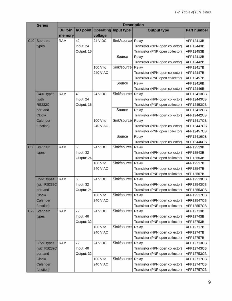
9
1-2. Table of FP1 Units
C40
C56
C72
RAM
RAM
RAM
RAM
RAM
RAM
40
Input: 24
Output: 16
40
Input: 24
Output: 16
56
Input: 32
Output: 24
56
Input: 32
Output: 24
72
Input: 40
Output: 32
72
Input: 40
Output: 32
24 V DC
100 V to
240 V AC
24 V DC
100 V to
240 V AC
24 V DC
100 V to
240 V AC
24 V DC
100 V to
240 V AC
24 V DC
100 V to
240 V AC
24 V DC
100 V to
240 V AC
Relay
Transistor (NPN open collector)
Transistor (PNP open collector)
Relay
Transistor (NPN open collector)
Relay
Transistor (NPN open collector)
Transistor (PNP open collector)
Relay
Transistor (NPN open collector)
Relay
Transistor (NPN open collector)
Transistor (PNP open collector)
Relay
Transistor (NPN open collector)
Relay
Transistor (NPN open collector)
Transistor (PNP open collector)
Relay
Transistor (NPN open collector)
Relay
Transistor (NPN open collector)
Transistor (PNP open collector)
Relay
Transistor (NPN open collector)
Transistor (PNP open collector)
Relay
Transistor (NPN open collector)
Transistor (PNP open collector)
Relay
Transistor (NPN open collector)
Transistor (PNP open collector)
Relay
Transistor (NPN open collector)
Transistor (PNP open collector)
Relay
Transistor (NPN open collector)
Transistor (PNP open collector)
Relay
Transistor (NPN open collector)
Transistor (PNP open collector)
Relay
Transistor (NPN open collector)
Transistor (PNP open collector)
AFP12413B
AFP12443B
AFP12453B
AFP12412B
AFP12442B
AFP12417B
AFP12447B
AFP12457B
AFP12416B
AFP12446B
AFP12413CB
AFP12443CB
AFP12453CB
AFP12412CB
AFP12442CB
AFP12417CB
AFP12447CB
AFP12457CB
AFP12416CB
AFP12446CB
AFP12513B
AFP12543B
AFP12553B
AFP12517B
AFP12547B
AFP12557B
AFP12513CB
AFP12543CB
AFP12553CB
AFP12517CB
AFP12547CB
AFP12557CB
AFP12713B
AFP12743B
AFP12753B
AFP12717B
AFP12747B
AFP12757B
AFP12713CB
AFP12743CB
AFP12753CB
AFP12717CB
AFP12747CB
AFP12757CB
Sink/source
Source
Sink/source
Source
Sink/source
Source
Sink/source
Source
Sink/source
Sink/source
Sink/source
Sink/source
Sink/source
Sink/source
Sink/source
Sink/source
Standard
types
C40C types
(with
RS232C
port and
Clock/
Calender
function)
Standard
types
C56C types
(with RS232C
port and
Clock/
Calender
function)
Standard
types
C72C types
(with RS232C
port and
Clock/
Calender
function)
DescriptionOperatingvoltage
Input type Part numberSeries
Built-in memory
I/O point Output type
10
1-2. Table of FP1 Units
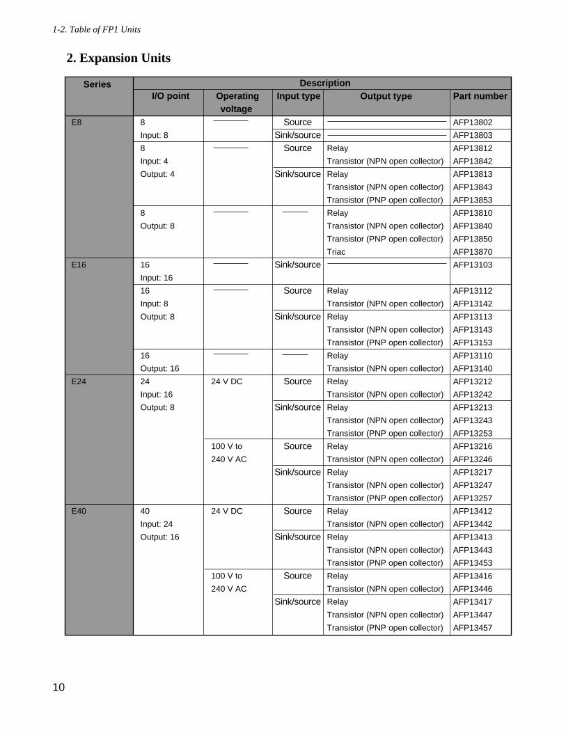
2. Expansion Units
E8
E16
E24
E40
8
Input: 8
8
Input: 4
Output: 4
8
Output: 8
16
Input: 16
16
Input: 8
Output: 8
16
Output: 16
24
Input: 16
Output: 8
40
Input: 24
Output: 16
24 V DC
100 V to
240 V AC
24 V DC
100 V to
240 V AC
Relay
Transistor (NPN open collector)
Relay
Transistor (NPN open collector)
Transistor (PNP open collector)
Relay
Transistor (NPN open collector)
Transistor (PNP open collector)
Triac
Relay
Transistor (NPN open collector)
Relay
Transistor (NPN open collector)
Transistor (PNP open collector)
Relay
Transistor (NPN open collector)
Relay
Transistor (NPN open collector)
Relay
Transistor (NPN open collector)
Transistor (PNP open collector)
Relay
Transistor (NPN open collector)
Relay
Transistor (NPN open collector)
Transistor (PNP open collector)
Relay
Transistor (NPN open collector)
Relay
Transistor (NPN open collector)
Transistor (PNP open collector)
Relay
Transistor (NPN open collector)
Relay
Transistor (NPN open collector)
Transistor (PNP open collector)
AFP13802
AFP13803
AFP13812
AFP13842
AFP13813
AFP13843
AFP13853
AFP13810
AFP13840
AFP13850
AFP13870
AFP13103
AFP13112
AFP13142
AFP13113
AFP13143
AFP13153
AFP13110
AFP13140
AFP13212
AFP13242
AFP13213
AFP13243
AFP13253
AFP13216
AFP13246
AFP13217
AFP13247
AFP13257
AFP13412
AFP13442
AFP13413
AFP13443
AFP13453
AFP13416
AFP13446
AFP13417
AFP13447
AFP13457
SourceSink/source
Source
Sink/source
Sink/source
Source
Sink/source
Source
Sink/source
Source
Sink/source
Source
Sink/source
Source
Sink/source
DescriptionOperatingvoltage
Input type Part numberSeries
I/O point Output type
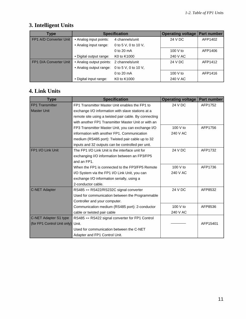
3. Intelligent Units
4. Link Units
FP1 Transmitter
Master Unit
FP1 I/O Link Unit
C-NET Adapter
C-NET Adapter S1 type
(for FP1 Control Unit only)
Operating voltage24 V DC
100 V to
240 V AC
24 V DC
100 V to
240 V AC
24 V DC
100 V to
240 V AC
Part number AFP1752
AFP1756
AFP1732
AFP1736
AFP8532
AFP8536
AFP15401
Type Specification FP1 Transmitter Master Unit enables the FP1 to
exchange I/O information with slave stations at a
remote site using a twisted pair cable. By connecting
with another FP1 Transmitter Master Unit or with an
FP3 Transmitter Master Unit, you can exchange I/O
information with another FP1. Communication
medium (RS485 port): Twisted pair cable up to 32
inputs and 32 outputs can be controlled per unit.
The FP1 I/O Link Unit is the interface unit for
exchanging I/O information between an FP3/FP5
and an FP1.
When the FP1 is connected to the FP3/FP5 Remote
I/O System via the FP1 I/O Link Unit, you can
exchange I/O information serially, using a
2-conductor cable.
RS485 ↔ RS422/RS232C signal converter
Used for communication between the Programmable
Controller and your computer.
Communication medium (RS485 port): 2-conductor
cable or twisted pair cable
RS485 ↔ RS422 signal converter for FP1 Control
Unit.
Used for communication between the C-NET
Adapter and FP1 Control Unit.
FP1 A/D Converter Unit
FP1 D/A Converter Unit
• Analog input points:
• Analog input range:
• Digital output range:
• Analog output points:
• Analog output range:
• Digital input range:
24 V DC
100 V to
240 V AC
24 V DC
100 V to
240 V AC
AFP1402
AFP1406
AFP1412
AFP1416
4 channels/unit
0 to 5 V, 0 to 10 V,
0 to 20 mA
K0 to K1000
2 channels/unit
0 to 5 V, 0 to 10 V,
0 to 20 mA
K0 to K1000
Type Specification Operating voltage Part number
11
1-2. Table of FP1 Units
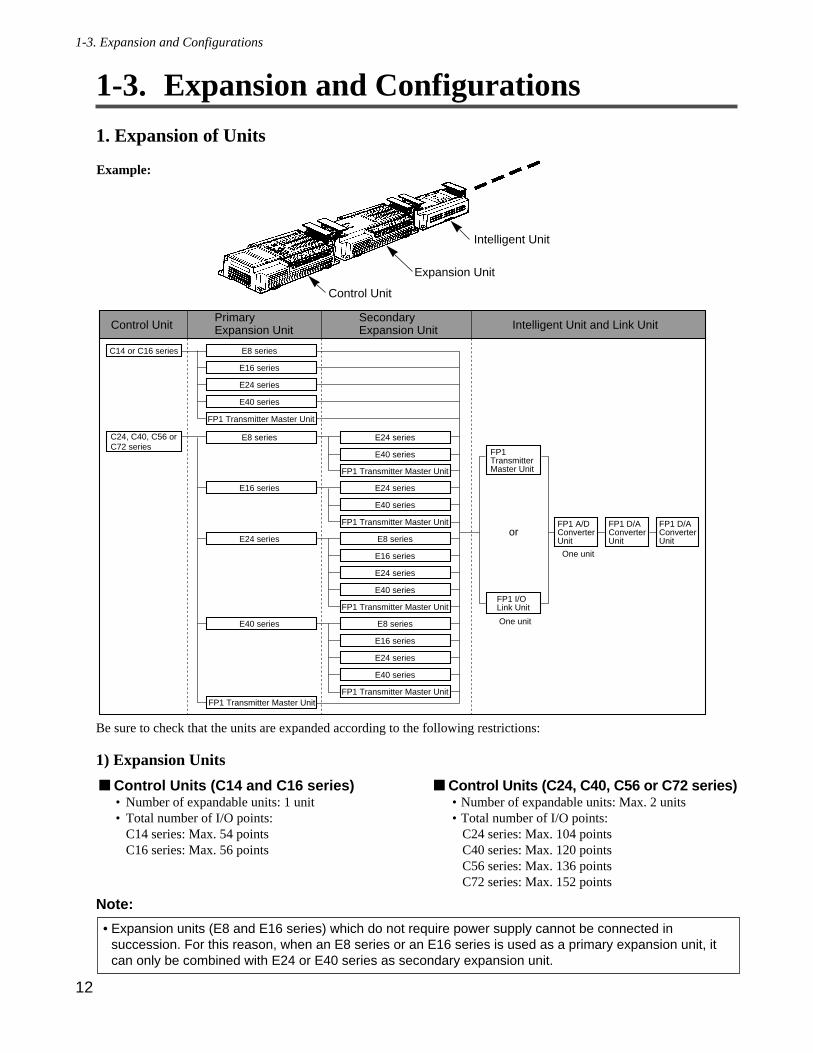
12
1-3. Expansion and Configurations
1-3. Expansion and Configurations
1. Expansion of Units
Be sure to check that the units are expanded according to the following restrictions:
1) Expansion Units
Note:
• Expansion units (E8 and E16 series) which do not require power supply cannot be connected insuccession. For this reason, when an E8 series or an E16 series is used as a primary expansion unit, itcan only be combined with E24 or E40 series as secondary expansion unit.
Control Units (C24, C40, C56 or C72 series)• Number of expandable units: Max. 2 units• Total number of I/O points:
C24 series: Max. 104 pointsC40 series: Max. 120 pointsC56 series: Max. 136 pointsC72 series: Max. 152 points
Control Units (C14 and C16 series)• Number of expandable units: 1 unit• Total number of I/O points:
C14 series: Max. 54 pointsC16 series: Max. 56 points
C14 or C16 series E8 series
E16 series
E24 series
E40 series
E8 series
E16 series
E24 series
E40 series
E24 series
E40 series
E24 series
E40 series
E8 series
E16 series
E24 series
E40 series
E8 series
E16 series
E24 series
E40 series
FP1 D/AConverter Unit
FP1 D/AConverter Unit
C24, C40, C56 orC72 series
FP1 I/O Link Unit
One unit
FP1 A/DConverter Unit
One unit
or
Control UnitPrimary Expansion Unit
Secondary Expansion Unit Intelligent Unit and Link Unit
FP1 Transmitter Master UnitFP1 Transmitter Master Unit
FP1 Transmitter Master Unit
FP1 Transmitter Master Unit
FP1 Transmitter Master UnitFP1 Transmitter Master Unit
FP1 Transmitter Master Unit
Control Unit
Expansion Unit
Intelligent Unit
Example:
13
1-3. Expansion and Configurations
2) Intelligent Units and Link Unit
• Number of expandable units together:FP1 A/D Converter Unit: 1 unit; FP1 D/A Converter Unit: 2 units; FP1 Transmitter Master Unit and FP1 I/O Link Unit:1 of each unit; FP1 I/O Link Unit: 1 unit
• There are no restrictions on the order of connection of intelligent units and link unit.
2. Combination of Units
14
16
22
24
30
32
38
40
48
54
56
8
8
8
12
16
16
8
12
16
8
16
24
8
16
24
16
20
24
24
24
24
16
24
32
32
24
28
32
32
32
32
32
36
40
24
32
40
6
8
14
10
6
8
16
12
8
22
14
6
24
16
8
16
12
8
14
16
16
24
16
8
16
24
20
16
22
24
24
24
20
16
32
24
16
C14
C16
C14
C24
C16
C14
C16
C24
C14
C40
C16
C24
C24
C40
C14
C56
C16
C24
C40
8
8
8
8
8
16
8
8
8
8
8
8
8
8
8
16
16
16
8
24
8
16
16
16
16
24
24
24
8
32
8
16
16
16
24
24
24
6
8
6
6
6
8
8
8
8
6
6
6
8
8
8
8
8
8
6
16
8
8
8
8
8
16
16
16
6
24
8
8
8
8
16
16
16
E8
E8
E16
E16
E8
E24
E24
E16
E24
E8
E40
E40
E24
E16
0
4
8
0
4
8
0
8
16
0
8
16
0
4
8
16
16
0
8
16
16
0
4
8
24
24
16
16
16
0
8
16
8
4
0
8
4
0
16
8
0
16
8
0
8
4
0
8
8
16
8
0
8
8
4
0
16
16
8
8
8
16
8
0
E8 0
4
8
8
4
0
Total Input Output Series Input Output Series Input Output Series Input OutputRequested I/O point Control Unit Primary Expansion Unit Secondary Expansion Unit
14
1-3. Expansion and Configurations
64
72
80
88
40
32
40
48
40
32
36
40
40
48
40
44
48
40
44
48
32
40
48
40
48
56
48
40
48
56
48
40
44
48
56
56
48
52
56
48
52
56
40
48
56
24
32
24
16
24
32
28
24
32
24
32
28
24
32
28
24
40
32
24
40
32
24
32
40
32
24
32
40
36
32
32
32
40
36
32
40
36
32
48
40
32
C24
C40
C56
C72
C24
C40
C56
C24
C40
C56
C72
C24
C40
C56
C72
16
16
16
16
24
32
32
32
40
16
16
16
16
24
24
24
32
32
32
16
16
16
24
24
24
24
32
40
40
40
16
24
24
24
24
32
32
32
40
40
40
8
8
8
8
16
24
24
24
32
8
8
8
8
16
16
16
24
24
24
8
8
8
16
16
16
16
24
32
32
32
8
16
16
16
16
24
24
24
32
32
32
E40
E24
E24
E8
E24
E40
E24
E16
E40
E40
E24
E24
E8
E40
E24
E40
E24
E16
24
16
16
16
16
0
4
8
16
24
24
24
16
16
16
0
8
16
24
24
24
24
16
16
16
16
0
4
8
24
16
24
24
24
16
16
16
0
8
16
16
8
8
8
8
8
4
0
8
16
16
16
8
8
8
16
8
0
16
16
16
16
8
8
8
8
8
4
0
16
8
16
16
16
8
8
8
16
8
0
Total Input Output Series Input Output Series Input Output Series Input OutputRequested I/O point Control Unit Primary Expansion Unit Secondary Expansion Unit
E16
E24
E8
E8
E16
E16
E24
E24
E8
E8
0
8
16
16
0
4
8
0
4
8
0
8
16
0
8
16
16
16
0
4
8
0
4
8
16
8
0
8
8
4
0
8
4
0
16
8
0
16
8
0
8
8
8
4
0
8
4
0
15
1-3. Expansion and Configurations
96
104
112
120
128
136
152
48
56
64
56
48
56
64
56
64
64
64
56
60
64
56
60
64
56
64
72
64
56
64
72
72
72
72
64
68
72
64
72
80
80
80
88
48
40
32
40
48
40
32
40
40
40
40
48
44
40
48
44
40
56
48
40
48
56
48
40
48
48
48
56
52
48
64
56
48
56
56
64
C40
C56
C72
C24
C40
C56
C72
C56
C72
C40
C56
C72
C72
C56
C72
C72
24
24
24
32
32
32
32
40
16
24
32
32
32
32
40
40
40
32
32
32
40
40
40
40
24
32
40
40
40
40
40
40
40
32
40
40
16
16
16
24
24
24
24
32
8
16
24
24
24
24
32
32
32
24
24
24
32
32
32
32
16
24
32
32
32
32
32
32
32
24
32
32
E40
E40
E24
E24
E40
E40
E24
E40
E24
E40
E40
E24
E40
E40
E24
E40
E40
E40
E40
E40
24
24
24
24
16
16
16
16
24
24
16
24
24
24
16
16
16
24
24
24
24
16
16
16
24
24
16
24
24
24
24
24
24
24
24
24
16
16
16
16
8
8
8
8
16
16
8
16
16
16
8
8
8
16
16
16
16
8
8
8
16
16
8
16
16
16
16
16
16
16
16
16
Total Input Output Series Input Output Series Input Output Series Input OutputRequested I/O point Control Unit Primary Expansion Unit Secondary Expansion Unit
E16
E16
E40
E24
E24
E8
E8
E16
E16
E40
E24
E24
E8
E16
E40
E24
E40
0
8
16
0
8
16
24
16
16
0
4
8
0
4
8
0
8
16
0
8
16
24
16
16
0
4
8
0
8
16
24
16
24
16
8
0
16
8
0
16
8
8
8
4
0
8
4
0
16
8
0
16
8
0
16
8
8
8
4
0
16
8
0
16
8
16
16
1-4. Programming Tools
1-4. Programming Tools System Configurations of Programming Tools
1. Programming ToolsProgram editing can be done with a commercially available personal computer and FP Programmer II.
1) NPST-GR Software
Using the NPST-GR program editing software, programs can be easily created with any personal computer on hand.
Necessary tools• Computer: Commercially available personal computer (IBM PC-AT or 100% compatible machine)
System required:- Main memory: 550 KB or more free- EMS: 800 KB or more free- Hard disk space: 2 MB or more - Operating System: MS-DOS Ver. 3.30 or later- Video mode (Display mode): EGA or VGA
• NPST-GR Software Ver. 3: AFP266538
Note:
• RS232C cable (3 m / 9.843 ft.): AFB85833/AFB85853• RS422/232C Adapter: AFP8550• FP1 Peripheral Cable:
0.5 m / 1.640 ft.: AFP152053 m / 9.843 ft.: AFP1523
• The .EXE files in NPST-GR Software are compressed in the system disks. When installingNPST-GR, you will have to expand them.
COM0
COM1
COM2
COM3
COM4
COM5
COM6
COM7
+ -24V DC
F.G.
COMF
89
EAB
CD(+)-
COM7
01
623
45(+)-
RUNREMOTEPROG.
V0
max.min.
RUN
PROG.
ERR.
ALRAM
BATTERY
V1
max.
PCFP1-C24
24V DC+
-
min.
FP1 Control Unit
NPST-GR Software
FPProgrammer II
Commercially available personal computer(IBM PC-AT or 100% compatible)
FP1MEMORY UNIT
MATUSITAELECTRIC WORKS. LTD
MADE IN JAPAN
FP1MEMORY UNIT
MATUSITAELECTRIC WORKS. LTDMADE IN JAPAN
Nationalabcdefg abcdefg
abcdefg
abcdefg
abcdefg
FP1MEMORY UNIT
MATUSITAELECTRIC WORKS. LTDMADE IN JAPAN
FP ROM Writer
Memory(EPROM)
FP ROM WriterSocket Adapter
Master Memory(EEPROM)
PC
RS422/232C ADAPTER
Matsushita Electric Works, Ltd.
Made in Japan
• POWER
• TXD(–)
• RXD(–)
RS
422
RS
232C
RS422/232CAdapter
FP1 Peripheral Cable
FP1 Peripheral Cable
RS232C cable
FP PROGRAMMER
STX•WX
ANY•WY
ORR•WR
OTL•WL
FN/PFL
NOTDT/Ld
STKIX/IY
TMT•SV
CTC•EV
(BIN)K/H
=C
DD
<E
>F
SHIFTSC
8 9 A B
4 5 6 7
0 1 2 3
(-)OP
SRC
READ
(HELP)CLR
ACLR (DELT)INST
ENT WRT
17
1-4. Programming Tools
Notes:
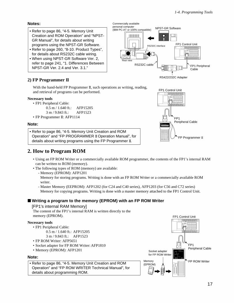
2) FP Programmer II
With the hand-held FP Programmer II, such operations as writing, reading,and retrieval of programs can be performed.
Necessary tools• FP1 Peripheral Cable:
0.5 m / 1.640 ft.: AFP152053 m / 9.843 ft.: AFP1523
• FP Programmer II: AFP1114
Note:
2. How to Program ROM• Using an FP ROM Writer or a commercially available ROM programmer, the contents of the FP1’s internal RAM
can be written to ROM (memory).• The following types of ROM (memory) are available:
- Memory (EPROM): AFP1201Memory for storing programs. Writing is done with an FP ROM Writer or a commercially available ROMwriter.
- Master Memory (EEPROM): AFP1202 (for C24 and C40 series), AFP1203 (for C56 and C72 series)Memory for copying programs. Writing is done with a master memory attached to the FP1 Control Unit.
Writing a program to the memory (EPROM) with an FP ROM Writer[FP1’s internal RAM Memory]The content of the FP1’s internal RAM is written directly to thememory (EPROM).
Necessary tools• FP1 Peripheral Cable:
0.5 m / 1.640 ft.: AFP152053 m / 9.843 ft.: AFP1523
• FP ROM Writer: AFP5651• Socket adapter for FP ROM Writer: AFP1810• Memory (EPROM): AFP1201
Note:• Refer to page 86, “4-5. Memory Unit Creation and ROM
Operation” and “FP ROM WRITER Technical Manual”, fordetails about programming ROM.
• Refer to page 86, “4-5. Memory Unit Creation and ROMOperation” and “FP PROGRAMMER II Operation Manual”, fordetails about writing programs using the FP Programmer II.
• Refer to page 86, “4-5. Memory UnitCreation and ROM Operation” and “NPST-GR Manual”, for details about writingprograms using the NPST-GR Software.
• Refer to page 260, “8-10. Product Types”,for details about RS232C cable wiring.
• When using NPST-GR Software Ver. 2,refer to page 241, “1. Differences BetweenNPST-GR Ver. 2.4 and Ver. 3.1.”
COM0
COM1
COM2
COM3
COM4
COM5
COM6
COM7
+ -24V DC
F.G.
COMF
89
EAB
CD(+)-
COM7
01
623
45(+)-
RUNREMOTEPROG.
V0
max.min.
RUN
PROG.
ERR.
ALRAM
BATTERY
V1
max.
24V DC+
-
min.
FP1 Control Unit
FP1Peripheral Cable
FP Programmer II
FP PROGRAMMER
STX•WX
ANY•WY
ORR•WR
OTL•WL
FN/PFL
NOTDT/Ld
STKIX/IY
TMT•SV
CTC•EV
(BIN)K/H
=C
DD
<E
>F
SHIFTSC
8 9 A B
4 5 6 7
0 1 2 3
(-)OP
SRC
READ
(HELP)CLR
ACLR (DELT)INST
ENT WRT
RS232C interface
RS232C cable
Rear view
FP1 PeripheralCable
NPST-GR Software
COM0
COM1
COM2
COM3
COM4
COM5
COM6
COM7
+ -24V DC
F.G.
COMF
89
EAB
CD(+)-
COM7
01
623
45(+)-
RUNREMOTEPROG.
V0
max.min.
RUN
PROG.
ERR.
ALRAM
BATTERY
V1
max.
24V DC+
-
min.
FP1 Control Unit
RS422/232C ADAPTERAFP8536
National
MATUSITA ELECTRIC WORKS. LTDMADE IN JAPAN
POWERTXD(-)RXD(-)
RS
422RS
232C
RS422/232C Adapter
Commercially availablepersonal computer(IBM PC-AT or 100% compatible)
COM0
COM1
COM2
COM3
COM4
COM5
COM6
COM7
+ -24V DC
F.G.
COMF
89
EAB
CD(+)-
COM7
01
623
45(+)-
RUNREMOTEPROG.
V0
max.min.
RUN
PROG.
ERR.
ALRAM
BATTERY
V1
max.
24V DC+
-
min.
Nationalabcdefg abcdefg
abcdefg
abcdefg
abcdefg
FP1MEMORY UNIT
MATUSITAELECTRIC WORKS. LTDMADE IN JAPAN
FP1 Control Unit
FP1Peripheral Cable
FP ROM Writer
Socket adapterfor FP ROM Writer
Memory(EPROM)
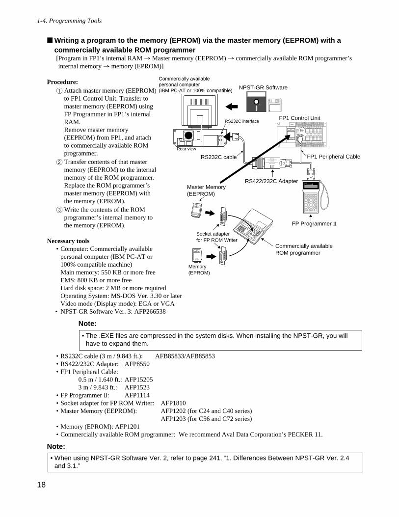
Writing a program to the memory (EPROM) via the master memory (EEPROM) with acommercially available ROM programmer[Program in FP1’s internal RAM → Master memory (EEPROM) → commercially available ROM programmer’sinternal memory → memory (EPROM)]
Procedure:1 Attach master memory (EEPROM)
to FP1 Control Unit. Transfer tomaster memory (EEPROM) usingFP Programmer in FP1’s internalRAM.Remove master memory(EEPROM) from FP1, and attachto commercially available ROMprogrammer.
2 Transfer contents of that mastermemory (EEPROM) to the internalmemory of the ROM programmer.Replace the ROM programmer’smaster memory (EEPROM) withthe memory (EPROM).
3Write the contents of the ROMprogrammer’s internal memory tothe memory (EPROM).
Necessary tools• Computer: Commercially available
personal computer (IBM PC-AT or100% compatible machine)Main memory: 550 KB or more freeEMS: 800 KB or more freeHard disk space: 2 MB or more requiredOperating System: MS-DOS Ver. 3.30 or laterVideo mode (Display mode): EGA or VGA
• NPST-GR Software Ver. 3: AFP266538
Note:
• RS232C cable (3 m / 9.843 ft.): AFB85833/AFB85853• RS422/232C Adapter: AFP8550• FP1 Peripheral Cable:
0.5 m / 1.640 ft.: AFP152053 m / 9.843 ft.: AFP1523
• FP Programmer II: AFP1114• Socket adapter for FP ROM Writer: AFP1810• Master Memory (EEPROM): AFP1202 (for C24 and C40 series)
AFP1203 (for C56 and C72 series)• Memory (EPROM): AFP1201• Commercially available ROM programmer: We recommend Aval Data Corporation’s PECKER 11.
Note:
• When using NPST-GR Software Ver. 2, refer to page 241, “1. Differences Between NPST-GR Ver. 2.4and 3.1.”
• The .EXE files are compressed in the system disks. When installing the NPST-GR, you willhave to expand them.
18
1-4. Programming Tools
RS232C interface
RS232C cable
Rear view
FP1 Peripheral Cable
NPST-GR Software
COM0
COM1
COM2
COM3
COM4
COM5
COM6
COM7
+ -24V DC
F.G.
COMF
89
EAB
CD(+)-
COM7
01
623
45(+)-
RUNREMOTEPROG.
V0
max.min.
RUN
PROG.
ERR.
ALRAM
BATTERY
V1
max.
24V DC+
-
min.
FP1 Control Unit
RS422/232C ADAPTERAFP8536
National
MATUSITA ELECTRIC WORKS. LTDMADE IN JAPAN
POWERTXD(-)RXD(-)
RS
422RS
232C
RS422/232C Adapter
Commercially availablepersonal computer(IBM PC-AT or 100% compatible)
FP1MEMORY UNIT
MATUSITAELECTRIC WORKS. LTDMADE IN JAPAN
Socket adapterfor FP ROM Writer
Memory(EPROM)
FP Programmer II
FP1MEMORY UNIT
MATUSITAELECTRIC WORKS. LTD
MADE IN JAPAN
Commercially availableROM programmer
Master Memory(EEPROM)
FP1MEMORY UNIT
MATUSITAELECTRIC WORKS. LTD
MADE IN JAPAN
FP PROGRAMMER
STX•WX
ANY•WY
ORR•WR
OTL•WL
FN/PFL
NOTDT/Ld
STKIX/IY
TMT•SV
CTC•EV
(BIN)K/H
=C
DD
<E
>F
SHIFTSC
8 9 A B
4 5 6 7
0 1 2 3
(-)OP
SRC
READ
(HELP)CLR
ACLR (DELT)INST
ENT WRT
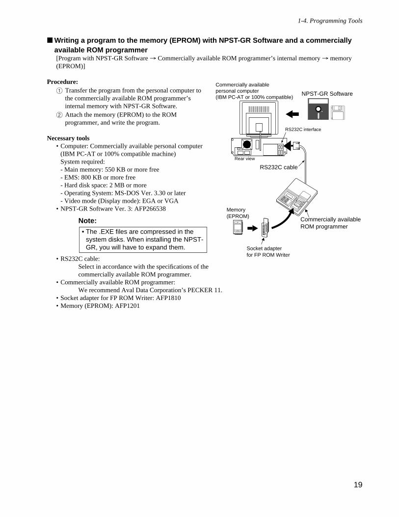
Writing a program to the memory (EPROM) with NPST-GR Software and a commerciallyavailable ROM programmer[Program with NPST-GR Software → Commercially available ROM programmer’s internal memory → memory(EPROM)]
Procedure:1 Transfer the program from the personal computer to
the commercially available ROM programmer’sinternal memory with NPST-GR Software.
2 Attach the memory (EPROM) to the ROMprogrammer, and write the program.
Necessary tools• Computer: Commercially available personal computer
(IBM PC-AT or 100% compatible machine)System required:- Main memory: 550 KB or more free- EMS: 800 KB or more free- Hard disk space: 2 MB or more - Operating System: MS-DOS Ver. 3.30 or later- Video mode (Display mode): EGA or VGA
• NPST-GR Software Ver. 3: AFP266538
Note:
• RS232C cable:Select in accordance with the specifications of thecommercially available ROM programmer.
• Commercially available ROM programmer: We recommend Aval Data Corporation’s PECKER 11.
• Socket adapter for FP ROM Writer: AFP1810• Memory (EPROM): AFP1201
• The .EXE files are compressed in thesystem disks. When installing the NPST-GR, you will have to expand them.
19
1-4. Programming Tools
RS232C interface
RS232C cable
Rear view
NPST-GR Software
Commercially availablepersonal computer(IBM PC-AT or 100% compatible)
Socket adapterfor FP ROM Writer
Memory(EPROM)
FP1MEMORY UNIT
MATUSITAELECTRIC WORKS. LTD
MADE IN JAPAN
Commercially availableROM programmer

20
CHAPTER 2
SPECIFICATIONS
2-1. Parts Terminology and Functions..........................................221. Control Unit......................................................................22
1) C14 and C16 Series ...............................................222) C24, C40, C56, and C72 Series .............................23
2. Expansion Unit .................................................................241) E8 and E16 Series .................................................242) E24 and E40 Series................................................24
3. Intelligent Unit..................................................................251) FP1 A/D Converter Unit........................................252) FP1 D/A Converter Unit........................................25
4. Link Unit ..........................................................................261) FP1 Transmitter Master Unit .................................262) FP1 I/O Link Unit..................................................273) C-NET Adapter S1 Type .......................................28
2-2. Specifications ........................................................................291. General Specifications......................................................292. Performance Specifications of Control Unit
and Expansion Unit ..........................................................311) Control Specifications ...........................................312) Input Specifications of Control Unit
and Expansion Unit................................................323) Output Specifications of Control Unit
and Expansion Unit................................................333. Performance Specifications of Intelligent Unit ................35
1) FP1 A/D Converter Unit........................................352) FP1 D/A Converter Unit........................................35
4. Performance Specifications of Link Unit .........................361) FP1 Transmitter Master Unit .................................362) FP1 I/O Link Unit..................................................363) C-NET Adapter S1 Type .......................................36
5. Dimensions .......................................................................371) Control Unit ...........................................................372) Expansion Unit ......................................................373) Intelligent Unit.......................................................384) Link Unit................................................................38
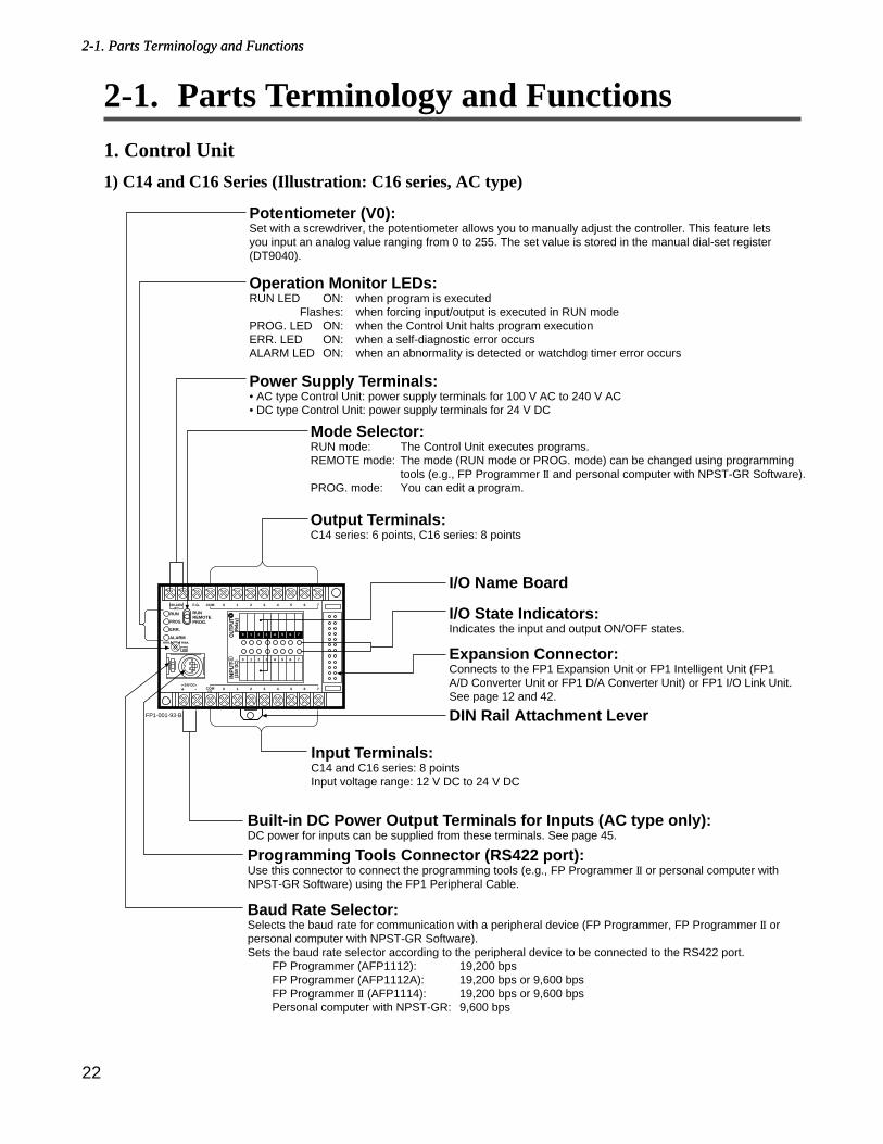
22
2-1. Parts Terminology and Functions
2-1. Parts Terminology and Functions
1. Control Unit
1) C14 and C16 Series (Illustration: C16 series, AC type)
0 1 2 3 4 5 6 7
0 1 2 3 4 5 6 7
COM 0 1 2 3 4 5 6 7F.G.100-240VAC
RUN
PROG.
ERR.
ALARM
RUNREMOTEPROG.
COM 0 1 2 3 4 5 6 7
OUT
PUT
INP
UT
XY
(Rel
ay)
(24V
DC
)
+ (+)-24V DC
V0
max.min.
FP1-001-93-B
2-1. Parts Terminology and Functions
Programming Tools Connector (RS422 port):Use this connector to connect the programming tools (e.g., FP Programmer II or personal computer withNPST-GR Software) using the FP1 Peripheral Cable.
Baud Rate Selector:Selects the baud rate for communication with a peripheral device (FP Programmer, FP Programmer II orpersonal computer with NPST-GR Software).Sets the baud rate selector according to the peripheral device to be connected to the RS422 port.
FP Programmer (AFP1112): 19,200 bps FP Programmer (AFP1112A): 19,200 bps or 9,600 bpsFP Programmer II (AFP1114): 19,200 bps or 9,600 bpsPersonal computer with NPST-GR: 9,600 bps
Potentiometer (V0):Set with a screwdriver, the potentiometer allows you to manually adjust the controller. This feature letsyou input an analog value ranging from 0 to 255. The set value is stored in the manual dial-set register(DT9040).
Operation Monitor LEDs:RUN LED ON: when program is executed
Flashes: when forcing input/output is executed in RUN modePROG. LED ON: when the Control Unit halts program executionERR. LED ON: when a self-diagnostic error occursALARM LED ON: when an abnormality is detected or watchdog timer error occurs
Mode Selector:RUN mode: The Control Unit executes programs.REMOTE mode: The mode (RUN mode or PROG. mode) can be changed using programming
tools (e.g., FP Programmer II and personal computer with NPST-GR Software).PROG. mode: You can edit a program.
Power Supply Terminals:• AC type Control Unit: power supply terminals for 100 V AC to 240 V AC• DC type Control Unit: power supply terminals for 24 V DC
Output Terminals:C14 series: 6 points, C16 series: 8 points
I/O Name Board
I/O State Indicators:Indicates the input and output ON/OFF states.
Expansion Connector:Connects to the FP1 Expansion Unit or FP1 Intelligent Unit (FP1A/D Converter Unit or FP1 D/A Converter Unit) or FP1 I/O Link Unit.See page 12 and 42.
DIN Rail Attachment Lever
Input Terminals:C14 and C16 series: 8 pointsInput voltage range: 12 V DC to 24 V DC
Built-in DC Power Output Terminals for Inputs (AC type only):DC power for inputs can be supplied from these terminals. See page 45.
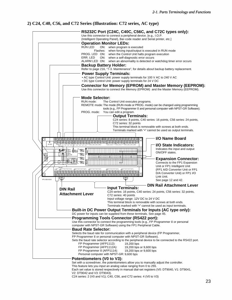
23
2-1. Parts Terminology and Functions
2) C24, C40, C56, and C72 Series (Illustration: C72 series, AC type)
0
RUNREMOTEPROG.
OU
TPU
TIN
PU
TX
Y
(Rel
ay)
(12-
24V
DC
)
V0
max.min.RUN
PROG.
ERR.
ALARM
1 2 3 4 5 6 7 8 9 A B C D E F 0 1 2 3 4 5 6 7 8 9 A B C D E F 0 1 2 3
0 1 2 3 4 5 6 7 8 9 A B C D E F 0 1 2 3 4 5 6 7 8 9 A B C D E F 0 1 2 3V1
max.min.
V2
max.min.
V3
max.min.
BATTERYCOM
01
23 COM
45
67 COM
89
AFB
CD
ECOM
89
AFB
CD
ECOM
0COM
1COM
2COM
3COM
4COM
5COM
6COM
7L N
100-240V ACF.G.
COMF
89
EAB
CD(+)-
COM7
01
623
45(+)-
COMF
89
EAB
CD(+)-
COM7
01
623
45(+)-
COM7
01
623
45(+)-
24V DC+
-
FP1-002-93-B
RS232C Port (C24C, C40C, C56C, and C72C types only):Use this connector to connect a peripheral device. [e.g., I.O.P. (Intelligent Operating Panel), Bar-code reader and Serial printer, etc.]
Operation Monitor LEDs:RUN LED
PROG. LED ERR. LED ALARM LED
Backup Battery Holder:Refer to page 216, “7-3. Maintenance”, for details about backup battery replacement.
Power Supply Terminals:• AC type Control Unit: power supply terminals for 100 V AC to 240 V AC• DC type Control Unit: power supply terminals for 24 V DC
Connector for Memory (EPROM) and Master Memory (EEPROM):Use this connector to connect the Memory (EPROM) and the Master Memory (EEPROM).
Mode Selector:RUN mode: REMOTE mode:
PROG. mode: Output Terminals:C24 series: 8 points, C40 series: 16 points, C56 series: 24 points, C72 series: 32 pointsThis terminal block is removable with screws at both ends.Terminals marked with “•” cannot be used as output terminals.
I/O Name Board
I/O State Indicators:Indicates the input and output ON/OFF states.
Expansion Connector:Connects to the FP1 Expansion Unit or FP1 Intelligent Unit (FP1 A/D Converter Unit or FP1 D/A Converter Unit) or FP1 I/O Link Unit. See page 12 and 42.
DIN Rail Attachment LeverInput Terminals:C24 series: 16 points, C40 series: 24 points, C56 series: 32 points, C72 series: 40 pointsInput voltage range: 12V DC to 24 V DCThis terminal block is removable with screws at both ends.Terminals marked with “•” cannot be used as input terminals.
Built-in DC Power Output Terminals for Inputs (AC type only):DC power for inputs can be supplied from these terminals. See page 45.
Programming Tools Connector (RS422 port):Use this connector to connect the programming tools (e.g., FP Programmer II or personal computer with NPST-GR Software) using the FP1 Peripheral Cable.
Baud Rate Selector:Selects the baud rate for communication with a peripheral device (FP Programmer, FP Programmer II or personal computer with NPST-GR Software).Sets the baud rate selector according to the peripheral device to be connected to the RS422 port.
FP Programmer (AFP1112): FP Programmer (AFP1112A): FP Programmer II (AFP1114): Personal computer with NPST-GR:
Potentiometers (V0 to V3):Set with a screwdriver, the potentiometers allow you to manually adjust the controller. This feature lets you input an analog value ranging from 0 to 255.Each set value is stored respectively in manual dial-set registers (V0: DT9040, V1: DT9041, V2: DT9042 and V3: DT9043).C24 series: 2 (V0 and V1); C40, C56, and C72 series: 4 (V0 to V3)
The Control Unit executes programs.The mode (RUN mode or PROG. mode) can be changed using programming tools (e.g., FP Programmer II and personal computer with NPST-GR Software). You can edit a program.
when program is executedwhen forcing input/output is executed in RUN modewhen the Control Unit halts program executionwhen a self-diagnostic error occurswhen an abnormality is detected or watchdog timer error occurs
19,200 bps19,200 bps or 9,600 bps19,200 bps or 9,600 bps9,600 bps
DIN Rail Attachment Lever
ON:Flashes:
ON:ON:ON:
2-1. Parts Terminology and Functions
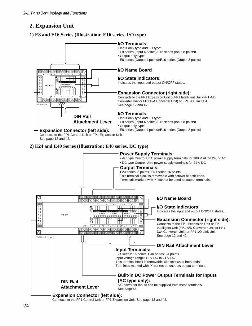
24
2-1. Parts Terminology and Functions
2. Expansion Unit
1) E8 and E16 Series (Illustration: E16 series, I/O type)
2) E24 and E40 Series (Illustration: E40 series, DC type)
OUT
PUT
INPU
TX
Y
(Tr)
(24V
DC
) 0 1 2 3 4 5 6 7 8 9 A B C D E F 0 1 2 3
0 1 2 3 4 5 6 7 8 9 A B C D E F 0 1 2 3
COM0
12
734
56
COM8
COM9
COMA
COMB
COMC
COMD
COME
COMF
+ -24V DC
F.G.
COMF
89
EAB
CD(+)-
COM7
01
623
45(+)-
COM7
01
623
45(+)-
FP1-E40
FP1-004-93-B
0 1 2 3 4 5 6 7
0 1 2 3 4 5 6 7
COM 0 1 2 3 4 5 6 7
COM 0 1 2 3 4 5 6 7
OU
TPU
TIN
PU
TXY
(Rel
ay)
(24V
DC
)
(+)
FP1-E16
FP1-003-93-B
2-1. Parts Terminology and Functions
I/O Terminals:• Input only type and I/O type:
E8 series (Input 4 points)/E16 series (Input 8 points)• Output only type:
E8 series (Output 4 points)/E16 series (Output 8 points)
I/O Name Board
I/O State Indicators:Indicates the input and output ON/OFF states.
Expansion Connector (right side):Connects to the FP1 Expansion Unit or FP1 Intelligent Unit (FP1 A/DConverter Unit or FP1 D/A Converter Unit) or FP1 I/O Link Unit.See page 12 and 42.
I/O Terminals:• Input only type and I/O type:
E8 series (Input 4 points)/E16 series (Input 8 points)• Output only type:
E8 series (Output 4 points)/E16 series (Output 8 points)
DIN RailAttachment Lever
Expansion Connector (left side):Connects to the FP1 Control Unit or FP1 Expansion Unit.See page 12 and 42.
Expansion Connector (left side):Connects to the FP1 Control Unit or FP1 Expansion Unit. See page 12 and 42.
Power Supply Terminals:• AC type Control Unit: power supply terminals for 100 V AC to 240 V AC• DC type Control Unit: power supply terminals for 24 V DC
Output Terminals:E24 series: 8 points, E40 series 16 pointsThis terminal block is removable with screws at both ends.Terminals marked with “•” cannot be used as output terminals.
Input Terminals:E24 series: 16 points, E40 series: 24 pointsInput voltage range: 12 V DC to 24 V DCThis terminal block is removable with screws at both ends.Terminals marked with “•” cannot be used as output terminals.
Built-in DC Power Output Terminals for Inputs(AC type only):DC power for inputs can be supplied from these terminals.See page 45.
DIN RailAttachment Lever
I/O Name Board
I/O State Indicators:Indicates the input and output ON/OFF states.
Expansion Connector (right side):Connects to the FP1 Expansion Unit or FP1Intelligent Unit (FP1 A/D Converter Unit or FP1D/A Converter Unit) or FP1 I/O Link Unit.See page 12 and 42.
DIN Rail Attachment Lever
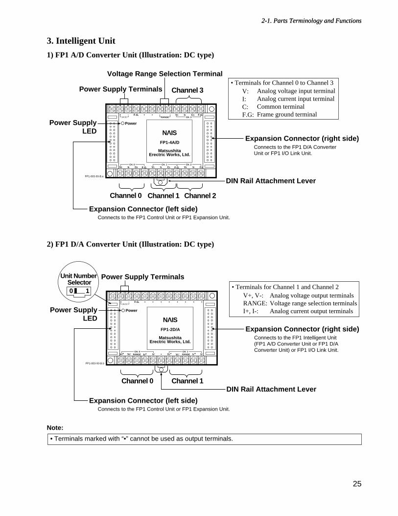
25
2-1. Parts Terminology and Functions
3. Intelligent Unit
1) FP1 A/D Converter Unit (Illustration: DC type)
2) FP1 D/A Converter Unit (Illustration: DC type)
Note:
• Terminals marked with “•” cannot be used as output terminals.
F.G.
RANGE I0+
FP1-2D/A
MatsushitaErectric Works, Ltd.
FP1-003-93-B.b
Power
NAIS
+ -24V DC
V0+ V0- V1+ V1-I0- I1-RANGE I1+CH. 1CH. 0
Channel 0 Channel 1
Power Supply Terminals
DIN Rail Attachment Lever
Power SupplyLED
Unit Number Selector0 1
Expansion Connector (left side) Connects to the FP1 Control Unit or FP1 Expansion Unit.
Expansion Connector (right side)Connects to the FP1 Intelligent Unit(FP1 A/D Converter Unit or FP1 D/AConverter Unit) or FP1 I/O Link Unit.
• Terminals for Channel 1 and Channel 2V+, V-: RANGE: I+, I-:
Analog voltage output terminalsVoltage range selection terminalsAnalog current output terminals
F.G. V3 I3 C3 F.G.
C0 F.G.
FP1-4A/D
MatsushitaErectric Works, Ltd.
FP1-003-93-B.a
Power
NAIS
+ -24V DC CH. 3RANGE
V0 I0 C1 F.G.V1 I1 C2V2 I2CH. 2CH. 1CH. 0
Power Supply Terminals
DIN Rail Attachment Lever
Channel 3
Voltage Range Selection Terminal
Power SupplyLED
Expansion Connector (left side)
Expansion Connector (right side)Connects to the FP1 D/A ConverterUnit or FP1 I/O Link Unit.
• Terminals for Channel 0 to Channel 3V:I: C: F.G:
Analog voltage input terminalAnalog current input terminalCommon terminalFrame ground terminal
Connects to the FP1 Control Unit or FP1 Expansion Unit.
Channel 0 Channel 1 Channel 2
2-1. Parts Terminology and Functions
26
2-1. Parts Terminology and Functions
4. Link Unit
1) FP1 Transmitter Master Unit
Notes:
• The operation mode selectors are set to all OFF position when shipped.• Operation mode selector upper state is “OFF( )” and the lower state is “ON ( )”.• Be sure to power is OFF when changing the switch position.
Frame ground Terminal
DIN Rail Attachment Lever
POWER
COM.
ALARM
Station monitor LEDsON: Connected to the slave stationFlashing: Cased by a communication error
at this slave station numberOFF: Not connected to the slave station
RS485 Interface Interface for MEWNET-TR communication using twisted pair cable
F.G. + - F.G.+ -24V DC RS485
SelectorNumber Description
ONOFF
Selector position
1 2 3 4 5 6
Remote I/O control disabled, Master B of I/O linkRemote I/O control enabled, Master A of I/O linkStart (continues I/O control operation)StopTerminal stationNot a terminal stationON when an I/O link error occursNot settingPatternNO. 1PatternNO. 2PatternNO. 3
System configuration selectionOutput opration condition during a communication errorTerminal station setting
Error flag (R9036) setting
I/O allocation setting (use I/O address for expansion board)
Operation mode selector setting
Descriptions
Power is suppliedPower is not suppliedNormal communication status (Flash in approx. 0.2 s intervals)Not communicatingA communication error occurred at the slave station. The normal slave station continues I/O control operation. (Flash in approx. 1 s intervals)A communication error with a slave stationStation number setting errorError on FP-M transmitter master board (MEWNET-TR)Normal
ON:OFF:Flashing:ON:Flashing slowly:
OFF:Flashing: ON:OFF:
Operation Monitor LEDs
LED
Expansion Connector
Connected to the FP1 Control Unit using expansion cable
TRNET
MODE SW.ONOFF
1 2 3 4 5 6
Matsushita Electric Works, Ltd.
MONITOR SW.
INPUT UNITOUTPUT UNIT
0 71 2 3 4 5 6
8 F9 A B C D E
Power supply terminal(AC type/DC type)
Selector for station monitor LEDs(MONITOR SW.)
Selects the unit type (input or output)of station monitor LEDs
"""
Expansion ConnectorConnects to the FP1 MEWNET-TR master unit using expansion cable
Function
1
2
3
4
5 and 6 32 inputs:32 outputs:48 inputs:32 outputs:24 inputs:16 outputs:
X70 to X8FY70 to Y8FX30 to X47, X50 to X67Y30 to Y3F, Y50 to Y5FX30 to X47 or X50 to X67Y30 to Y3F or Y50 to Y5F
ONOFF
ONOFF
ONOFF
–
ON
OFF
OFF
ON
ON
POWER
COM.
ALARM
ONOFF
1 2 3 4 5 6
F.G. + - F.G.L N100V - 240 VAC 240 V DC
AC type DC type
2-1. Parts Terminology and Functions
2) FP1 I/O Link Unit
F.G. + - F.G.
FP1-003-93-B.c
+ -24V DC RS485
Power Supply Terminals (AC type/DC type)
DIN Rail Attachment Lever
01234567
89
01234567
89
STATION NO.POWER
COM.
ALARMPC
FP1
I/O LINK MODE SW.ONOFF
1 2 3 4
Station Number Selector: Set the slave station number of the Remote I/O System. Setting range: 01 to 32
Expansion Connector (right side) Connects to the FP1 Intelligent Unit (FP1 A/D Converter Unit or FP1 D/A Converter Unit).
RS485 Interface For connecting a communication cable.
Expansion Connector (left side) Connects to the FP1 Control Unit or FP1 Expansion Unit.
Switch
Number
1 & 2
3
Specification
OFF OFF
ON ON
Switch position
1 2 3 4
Not a terminal station
Terminal station
Stop
Start (maintains its
output condition)
Terminal station
setting
Slave station output
condition during
a communication
error
OFF
ON
Mode Selector Switches
Power (POWER)
Communication
(COM.)
Alarm (ALARM)
Descriptions
When power is supplied
When power is not supplied
Not communicating
Communicating (Normal)
Remote I/O control halted,
caused by a communication
error at the slave station.
Abnormal condition
Unit error
Station number setting error
Normal unit
ON:
OFF:
ON:
Flashing:
Flashing slowly:
OFF:
ON:
Flashing:
OFF:
Operation Monitor LEDs Indicate communication status and operation modes.
LED
"""
27
2-1. Parts Terminology and Functions2-1. Parts Terminology and Functions
3) C-NET Adapter S1 Type
" " "
RS485 InterfaceConnects to the RS485 interface on the C-NET Adapter orother C-NET Adapter S1 Type using transmission cable (shielded twisted pair or 2-conductor cable).
POWER LED (green)Flashes: OFF:
Send Data Monitor LED(green)Flashes: OFF:
Receive Data Monitor LED(green)ON: OFF:
TERMINATE SwitchTurn this switch ON when the adapter is installed at terminal station.
DIN Rail Attachment Lever
CableConnects the cable to the programming tools connector (RS422 port) of FP1 Control Unit.
RS422 port
when receiving powerwhen not receiving power
when sendingwhen not sending
when receivingwhen not receiving
C-NETADAPTERS1-TYPE ON
OFF
RD
SD
POWER
TERMINATE
NAIS
F. G
+ -RS485
28
2-1. Parts Terminology and Functions
29
2-2. Specifications
2-2. Specifications
1. General Specifications
Ambient temperature
Ambient humidity
Storage temperature
Storage humidity
Breakdown voltage
Insulation resistance
Vibration resistance
Shock resistance
Noise immunity
Operating condition
Rated
operating
voltage
Operating
voltage range
0˚C to +55˚C/32˚F to +131˚F
30 % to 85 % RH (non-condensing)
–20˚C to +70˚C/–4˚F to +158˚F
30 % to 85 % RH (non-condensing)
AC type: 1,500 Vrms for 1 min
Between AC terminal and Frame ground terminal
DC type: 500 Vrms for 1 min
Between DC terminal and Frame ground terminal
Min. 100 MΩ (measured with a 500 V DC megger) Between AC terminal and Frame ground terminal
Between DC terminal and Frame ground terminal
10 Hz to 55 Hz, 1 cycle/min: double amplitude of 0.75 mm/0.030 in., 10 min on 3 axes
Shock of 98 m/s2 or more, 4 times on 3 axes
1,000 Vp-p with pulse widths 50 ns and 1 µs (based on in-house measurements)
Free from corrosive gases and excessive dust
AC type: 100 V to 240 V AC
DC type: 24 V DC
AC type: 85 V to 264 V AC
DC type: 20.4 V to 26.4 V DC
Control Unit
(all series)
Expansion Unit
(E24 and E40
series only)
FP1 A/D
Converter Unit
FP1 D/A
Converter Unit
FP1 Transmitter
Master Unit
FP1 I/O
Link Unit
Control Unit
(all series)
Expansion Unit
(E24 and E40
series only)
FP1 A/D
Converter Unit
FP1 D/A
Converter Unit
FP1 Transmitter
Master Unit
FP1 I/O
Link Unit
Item Description
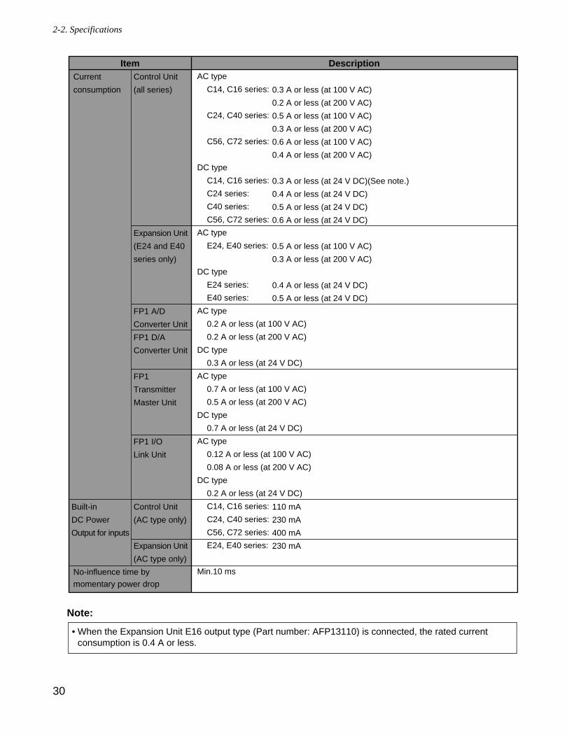
30
2-2. Specifications
Note:
• When the Expansion Unit E16 output type (Part number: AFP13110) is connected, the rated currentconsumption is 0.4 A or less.
Current
consumption
Built-in
DC Power
Output for inputs
No-influence time bymomentary power drop
AC type
C14, C16 series:
C24, C40 series:
C56, C72 series:
DC type
C14, C16 series:
C24 series:
C40 series:
C56, C72 series:
AC type
E24, E40 series:
DC type
E24 series:
E40 series:
AC type
0.2 A or less (at 100 V AC)
0.2 A or less (at 200 V AC)
DC type
0.3 A or less (at 24 V DC)
AC type
0.7 A or less (at 100 V AC)
0.5 A or less (at 200 V AC)
DC type
0.7 A or less (at 24 V DC)
AC type
0.12 A or less (at 100 V AC)
0.08 A or less (at 200 V AC)
DC type
0.2 A or less (at 24 V DC)
C14, C16 series:
C24, C40 series:
C56, C72 series:
E24, E40 series:
Min.10 ms
Control Unit
(all series)
Expansion Unit
(E24 and E40
series only)
FP1 A/D
Converter Unit
FP1 D/A
Converter Unit
FP1
Transmitter
Master Unit
FP1 I/O
Link Unit
Control Unit
(AC type only)
Expansion Unit
(AC type only)
0.3 A or less (at 100 V AC)
0.2 A or less (at 200 V AC)
0.5 A or less (at 100 V AC)
0.3 A or less (at 200 V AC)
0.6 A or less (at 100 V AC)
0.4 A or less (at 200 V AC)
0.3 A or less (at 24 V DC)(See note.)
0.4 A or less (at 24 V DC)
0.5 A or less (at 24 V DC)
0.6 A or less (at 24 V DC)
0.5 A or less (at 100 V AC)
0.3 A or less (at 200 V AC)
0.4 A or less (at 24 V DC)
0.5 A or less (at 24 V DC)
110 mA
230 mA
400 mA
230 mA
Item Description
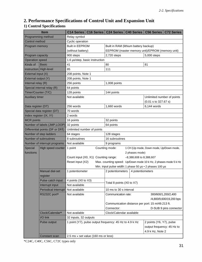
31
2-2. Specifications
2. Performance Specifications of Control Unit and Expansion Unit1) Control Specifications
Programming method
Control method
Program memory
Program capacity
Operation speed
Kinds of
instruction
External input (X)
External output (Y)
Internal relay (R)
Special internal relay (R)
Timer/Counter (T/C)
Auxiliary timer
Data register (DT)
Special data register (DT)
Index register (IX, IY)
MCR points
Number of labels (JMP,LOOP)
Differential points (DF or DF/ )
Number of step ladders
Number of subroutines
Number of interrupt programs
Special
functions
High speed counter
Manual dial-set
register
Pulse catch input
Interrupt input
Periodical interrupt
RS232C port*
Clock/Calendar*
I/O link
Pulse output
Constant scan
Relay symbol
Cyclic operation
Built in EEPROM
(without battery)
900 steps
1.6 µs/step, basic instruction
41
85
208 points, Note 1
208 points, Note 1
256 points
64 points
128 points
Not available
256 words
70 words
2 words
16 points
32 points
Unlimited number of points
64 stages
8 subroutines
Not available
1 point
Count input (X0, X1)
Reset input (X2)
1 potentiometer
4 points (X0 to X3)
Not available
Not available
Not available
Not available
32 inputs, 32 outputs
1 point (Y7), pulse output frequency: 45 Hz to 4.9 k Hz
2.5 ms × set value (160 ms or less)
Built in RAM (lithium battery backup)
EEPROM (master memory unit)/EPROM (memory unit)
2,720 steps
80
111
1,008 points
144 points
1,660 words
32 points
64 points
128 stages
16 subroutines
9 programs
2 potentiometers
Total 8 points (X0 to X7)
10 ms to 30 s interval
Communication rate:
Communication distance per port:
Connector:
Clock/Calendar available
5,000 steps
81
Unlimited number of points
(0.01 s to 327.67 s)
6,144 words
2 points (Y6, Y7), pulse
output frequency: 45 Hz to
4.9 k Hz, Note 2
Basic
High-level
C14 Series C16 Series C24 Series C40 Series C56 Series C72 Series
*C24C, C40C, C56C, C72C types only
Counting mode:
Counting range:
Max. counting speed:
Min. input pulse width:
1 CH (Up mode, Down mode, Up/Down mode,
2 phases mode)
–8,388,608 to 8,388,607
Up/Down mode 10 k Hz, 2 phases mode 5 k Hz
1 phase 50 µs • 2 phases 100 µs
300/600/1,200/2,400
/4,800/9,600/19,200 bps
15 m/49.213 ft.
D-SUB 9 pins connector
4 potentiometers
Item
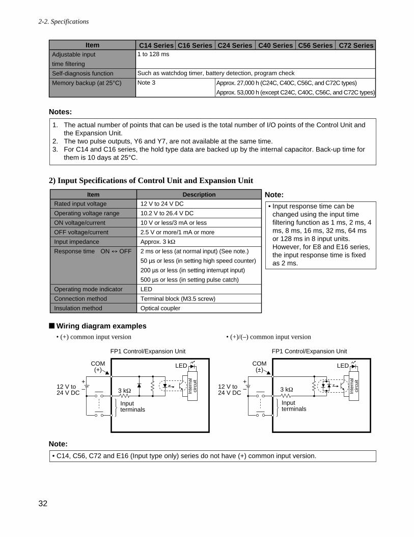
32
2-2. Specifications
Notes:
2) Input Specifications of Control Unit and Expansion Unit
Wiring diagram examples
Note:
• C14, C56, C72 and E16 (Input type only) series do not have (+) common input version.
+– 3 kΩ"
12 V to24 V DC
COM(+)
Inputterminals
"""
FP1 Control/Expansion Unit
• (+) common input version
+– 3 kΩ"12 V to
24 V DC
COM(±)
Inputterminals
"""
Inte
rnal
circ
uit
FP1 Control/Expansion Unit
• (+)/(–) common input version
Inte
rnal
circ
uit
LED LED
Rated input voltage
Operating voltage range
ON voltage/current
OFF voltage/current
Input impedance
Response time
Operating mode indicator
Connection method
Insulation method
12 V to 24 V DC
10.2 V to 26.4 V DC
10 V or less/3 mA or less
2.5 V or more/1 mA or more
Approx. 3 kΩ
2 ms or less (at normal input) (See note.)
50 µs or less (in setting high speed counter)
200 µs or less (in setting interrupt input)
500 µs or less (in setting pulse catch)
LED
Terminal block (M3.5 screw)
Optical coupler
ON ↔ OFF
Item Description
1. The actual number of points that can be used is the total number of I/O points of the Control Unit andthe Expansion Unit.
2. The two pulse outputs, Y6 and Y7, are not available at the same time.3. For C14 and C16 series, the hold type data are backed up by the internal capacitor. Back-up time for
them is 10 days at 25°C.
C14 Series C16 Series C24 Series C40 Series C56 Series C72 SeriesAdjustable input
time filtering
Self-diagnosis function
Memory backup (at 25°C)
1 to 128 ms
Such as watchdog timer, battery detection, program check
Note 3 Approx. 27,000 h (C24C, C40C, C56C, and C72C types)
Approx. 53,000 h (except C24C, C40C, C56C, and C72C types)
Item
Note:
• Input response time can bechanged using the input timefiltering function as 1 ms, 2 ms, 4ms, 8 ms, 16 ms, 32 ms, 64 msor 128 ms in 8 input units.However, for E8 and E16 series,the input response time is fixedas 2 ms.
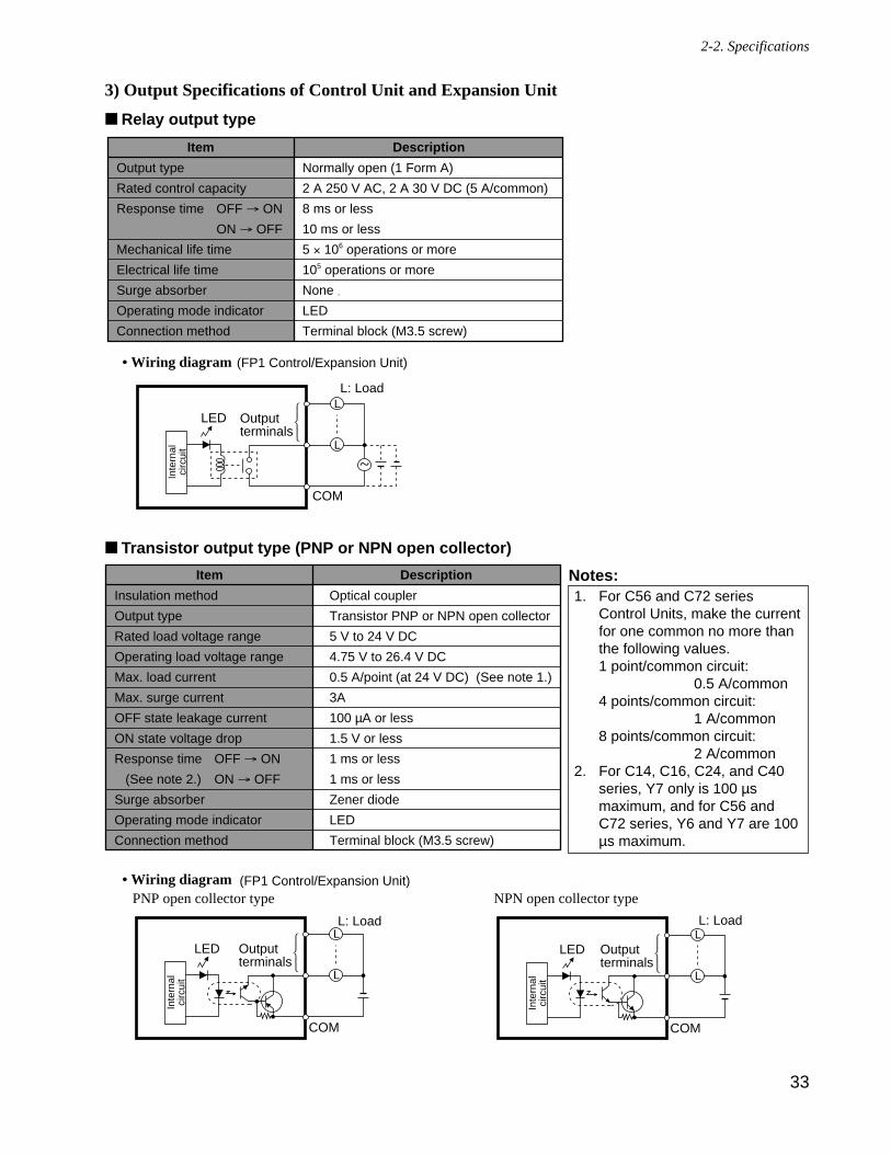
33
2-2. Specifications
3) Output Specifications of Control Unit and Expansion Unit
Relay output type
Transistor output type (PNP or NPN open collector)
(FP1 Control/Expansion Unit)
L
Inte
rnal
circ
uit
"""
Outputterminals
• Wiring diagram
L
COM
L
Inte
rnal
circ
uit
"""
Outputterminals
L
COM
L: Load L: Load
NPN open collector typePNP open collector type
LEDLED
1. For C56 and C72 seriesControl Units, make the currentfor one common no more thanthe following values.1 point/common circuit:
0.5 A/common4 points/common circuit:
1 A/common8 points/common circuit:
2 A/common2. For C14, C16, C24, and C40
series, Y7 only is 100 µsmaximum, and for C56 andC72 series, Y6 and Y7 are 100µs maximum.
Insulation method
Output type
Rated load voltage range
Operating load voltage range
Max. load current
Max. surge current
OFF state leakage current
ON state voltage drop
Response time
(See note 2.)
Surge absorber
Operating mode indicator
Connection method
Optical coupler
Transistor PNP or NPN open collector
5 V to 24 V DC
4.75 V to 26.4 V DC
0.5 A/point (at 24 V DC) (See note 1.)
3A
100 µA or less
1.5 V or less
1 ms or less
1 ms or less
Zener diode
LED
Terminal block (M3.5 screw)
OFF → ON
ON → OFF
Item Description
(FP1 Control/Expansion Unit)
L
Inte
rnal
circ
uit
"""
Outputterminals
• Wiring diagram
L
~
COM
L: Load
LED
Output type
Rated control capacity
Response time
Mechanical life time
Electrical life time
Surge absorber
Operating mode indicator
Connection method
Normally open (1 Form A)
2 A 250 V AC, 2 A 30 V DC (5 A/common)
8 ms or less
10 ms or less
5 × 10⁶ operations or more
105 operations or more
None
LED
Terminal block (M3.5 screw)
OFF → ON
ON → OFF
Item Description
Notes:
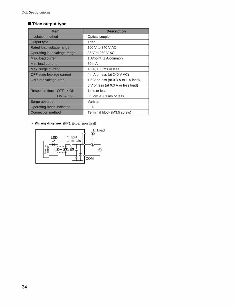
34
2-2. Specifications
Triac output type
L
Inte
rnal
circ
uit
"""
Outputterminals
L
COM
L: Load
(FP1 Expansion Unit)• Wiring diagram
~
LED
Insulation method
Output type
Rated load voltage range
Operating load voltage range
Max. load current
Min. load current
Max. surge current
OFF state leakage current
ON state voltage drop
Response time
Surge absorber
Operating mode indicator
Connection method
Optical coupler
Triac
100 V to 240 V AC
85 V to 250 V AC
1 A/point, 1 A/common
30 mA
15 A, 100 ms or less
4 mA or less (at 240 V AC)
1.5 V or less (at 0.3 A to 1 A load),
5 V or less (at 0.3 A or less load)
1 ms or less
0.5 cycle + 1 ms or less
Varister
LED
Terminal block (M3.5 screw)
OFF → ON
ON → OFF
Item Description
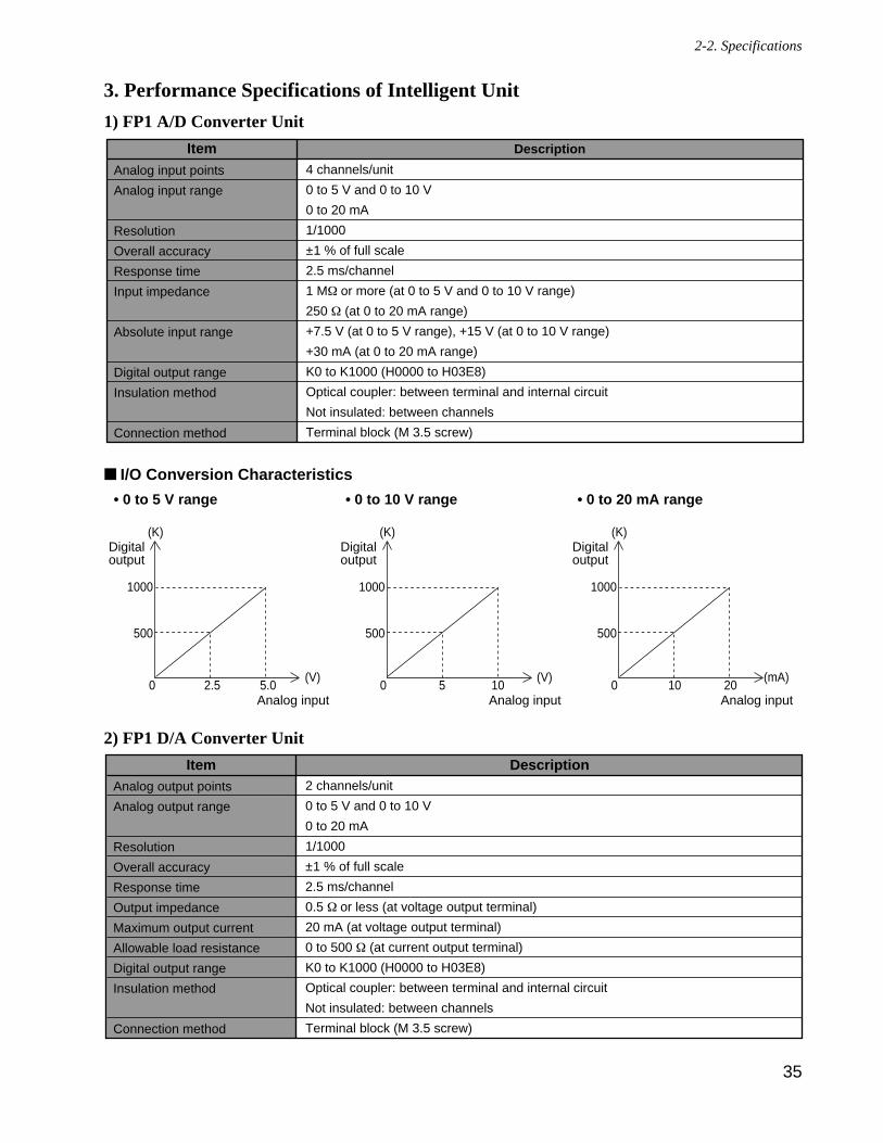
35
2-2. Specifications
3. Performance Specifications of Intelligent Unit
1) FP1 A/D Converter Unit
I/O Conversion Characteristics
2) FP1 D/A Converter Unit
Analog output points
Analog output range
Resolution
Overall accuracy
Response time
Output impedance
Maximum output current
Allowable load resistance
Digital output range
Insulation method
Connection method
2 channels/unit
0 to 5 V and 0 to 10 V
0 to 20 mA
1/1000
±1 % of full scale
2.5 ms/channel
0.5 Ω or less (at voltage output terminal)
20 mA (at voltage output terminal)
0 to 500 Ω (at current output terminal)
K0 to K1000 (H0000 to H03E8)
Optical coupler: between terminal and internal circuit
Not insulated: between channels
Terminal block (M 3.5 screw)
DescriptionItem
1000
500
2.5 5.0
Digitaloutput
Analog input
(K)
(V)
• 0 to 5 V range
1000
500
5 10
Digitaloutput
Analog input
(K)
(V)
• 0 to 10 V range
1000
500
10 20
Digitaloutput
Analog input
(K)
(mA)
• 0 to 20 mA range
0 0 0
Analog input points
Analog input range
Resolution
Overall accuracy
Response time
Input impedance
Absolute input range
Digital output range
Insulation method
Connection method
4 channels/unit
0 to 5 V and 0 to 10 V
0 to 20 mA
1/1000
±1 % of full scale
2.5 ms/channel
1 MΩ or more (at 0 to 5 V and 0 to 10 V range)
250 Ω (at 0 to 20 mA range)
+7.5 V (at 0 to 5 V range), +15 V (at 0 to 10 V range)
+30 mA (at 0 to 20 mA range)
K0 to K1000 (H0000 to H03E8)
Optical coupler: between terminal and internal circuit
Not insulated: between channels
Terminal block (M 3.5 screw)
DescriptionItem
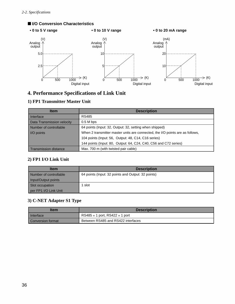
36
2-2. Specifications
I/O Conversion Characteristics
4. Performance Specifications of Link Unit
1) FP1 Transmitter Master Unit
2) FP1 I/O Link Unit
3) C-NET Adapter S1 Type
RS485 × 1 port, RS422 × 1 port
Between RS485 and RS422 interfaces
Interface
Conversion format
Item Description
64 points (Input: 32 points and Output: 32 points)
1 slot
Number of controllable
Input/Output points
Slot occupation
per FP1 I/O Link Unit
DescriptionItem
Interface
Data Transmission velocity
Number of controllable
I/O points
Transmission distance
RS485
0.5 M bps
64 points (Input: 32, Output: 32, setting when shipped)
When 2 transmitter master units are connected, the I/O points are as follows,
104 points (Input: 56, Output: 48, C14, C16 series)
144 points (Input: 80, Output: 64, C24, C40, C56 and C72 series)
Max. 700 m (with twisted pair cable)
DescriptionItem
5.0
2.5
500 1000
Analogoutput
Digital input
(V)
(K)
• 0 to 5 V range
10
5
500 1000
Analogoutput
Digital input
(V)
(K)
• 0 to 10 V range
20
10
500 1000
Analogoutput
Digital input
(mA)
(K)
• 0 to 20 mA range
0 0 0
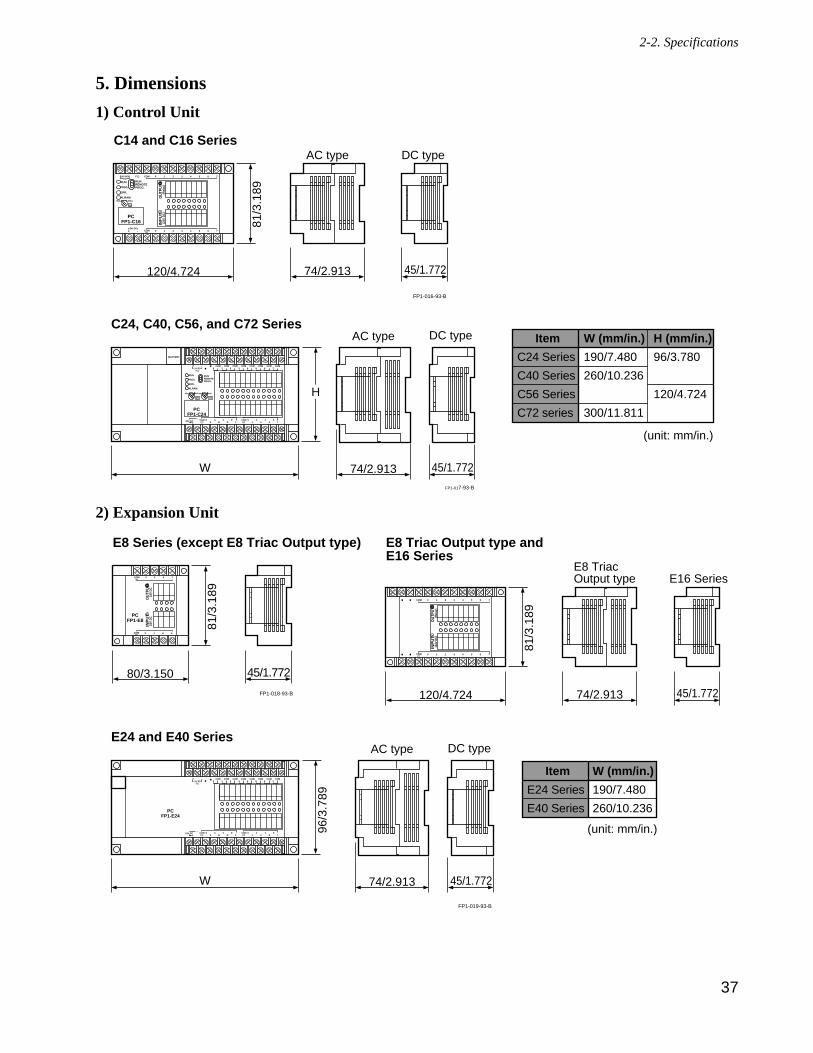
5. Dimensions
1) Control Unit
2) Expansion Unit
E24 Series
E40 Series
W (mm/in.)
190/7.480
260/10.236
(unit: mm/in.)
ItemCOM
0COM
1COM
2COM
3COM
4COM
5COM
6COM
7+ -
24V DCF.G.
COMF
89
EAB
CD(+)-
COM7
01
623
45(+)-
E24 and E40 Series
W 74/2.913 45/1.772
AC type DC type
PCFP1-E24
FP1-019-93-B
24V DC+
- 96/3
.789
COM 0 1 2 3 4 5 6 7
COM 0 1 2 3 4 5 6 7
OU
TPU
TIN
PU
TXY
(Rel
ay)
(24V
DC
)
(+)
E8 Triac Output type and E16 Series
120/4.724 74/2.913
81/3
.189
45/1.772
E8 Triac Output type E16 SeriesCOM 4 5 6 7
COM 0 1 2 3
OU
TPU
TIN
PU
TXY
24V
DC
(+)
PCFP1-E8
E8 Series (except E8 Triac Output type)
80/3.150
81/3
.189
45/1.772
(+)
24V
DC
FP1-018-93-B
C24 Series
C40 Series
C56 Series
C72 series
W (mm/in.)
190/7.480
260/10.236
300/11.811
H (mm/in.)
96/3.780
120/4.724
(unit: mm/in.)
Item
COM0
COM1
COM2
COM3
COM4
COM5
COM6
COM7
+ -24V DC
F.G.
COMF
89
EAB
CD(+)-
COM7
01
623
45(+)-
RUNREMOTEPROG.
V0
max.min.
RUN
PROG.
ERR.
ALRAM
BATTERY
V1
max.
C24, C40, C56, and C72 Series
W 74/2.913 45/1.772
AC type DC type
PCFP1-C24
H
FP1-017-93-B
24V DC+
-
min.
COM 0 1 2 3 4 5 6 7F.G.100-240VAC
RUN
PROG.
ERR.
ALRAM
RUNREMOTEPROG.
COM 0 1 2 3 4 5 6 7
OU
TPU
TIN
PU
TXY
(Rel
ay)
(24V
DC
)
+ (+)-24V DC
V0
max.min.
PCFP1-C16
C14 and C16 Series
120/4.724 74/2.91381
/3.1
8945/1.772
AC type DC type
FP1-016-93-B
37
2-2. Specifications
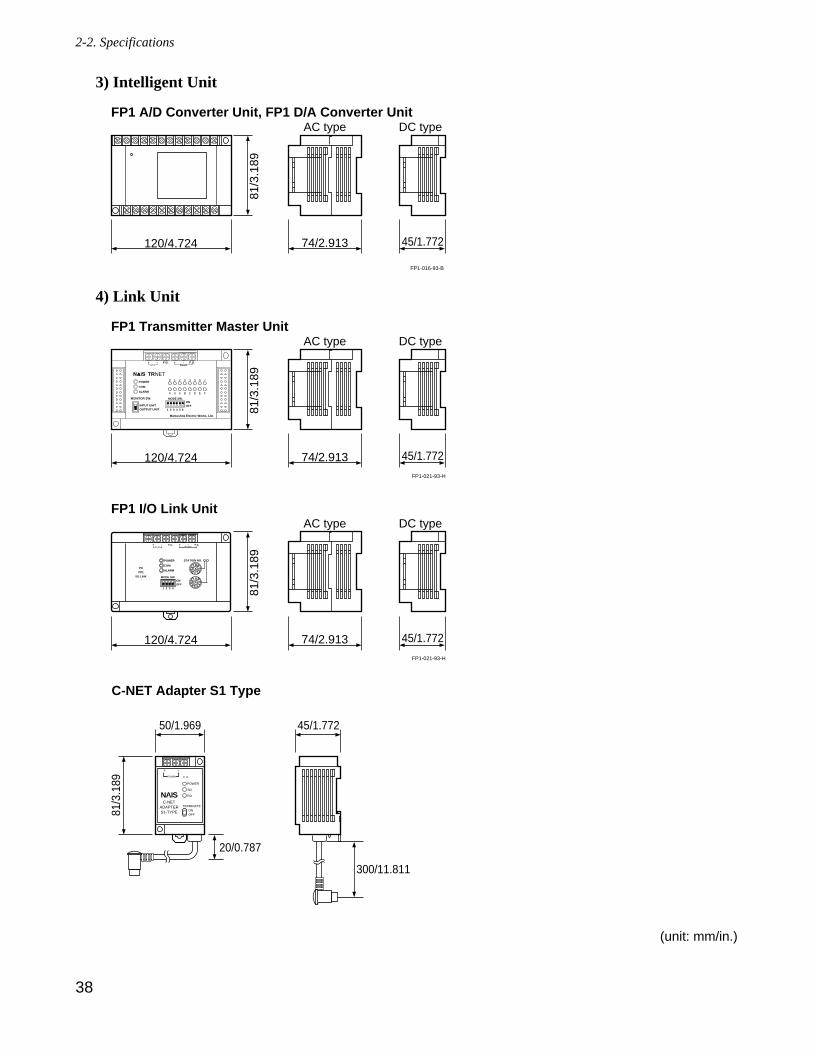
3) Intelligent Unit
4) Link Unit
C-NETADAPTERS1-TYPE ON
OFF
RD
SD
POWER
TERMINATE
NAIS
F. G
+ -RS485
45/1.77250/1.969
81/3
.189
20/0.787
300/11.811
C-NET Adapter S1 Type
FP1 I/O Link Unit
120/4.724 74/2.913
81/3
.189
45/1.772
AC type DC type
FP1-021-93-H
F.G. + - F.G.+ -24V DC RS485
01234567
89
01234567
89
STATION NO.POWER
COM.
ALARMPC
FP1
I/O LINK MODE SW.ONOFF
1 2 3 4
FP1 Transmitter Master Unit
120/4.724 74/2.913
81/3
.189
45/1.772
AC type DC type
FP1-021-93-H
POWER
COM.
ALARM
F.G. + - F.G.+ -24V DC RS485
TRNET
MODE SW.ONOFF
1 2 3 4 5 6
Matsushita Electric Works, Ltd.
MONITOR SW.
INPUT UNITOUTPUT UNIT
0 71 2 3 4 5 6
8 F9 A B C D E
FP1 A/D Converter Unit, FP1 D/A Converter Unit
120/4.724 74/2.91381
/3.1
8945/1.772
AC type DC type
FP1-016-93-B
38
2-2. Specifications
(unit: mm/in.)
CHAPTER 3
INSTALLATION AND WIRING
3-1. Installation ............................................................................401. Panel Mounting ...............................................................402. DIN Rail Mounting ..........................................................403. Cautions ...........................................................................41
3-2. Expansion .............................................................................421. Expansion Cable ..............................................................422. Unit Expansion ................................................................42
3-3. Wiring ...................................................................................431. Crimp Terminal ................................................................432. Wiring Power Supply ......................................................43
1) Wiring Example for Power Supply Terminal ........432) Power Supply Lines ..............................................443) Momentary Power Drop .......................................444) Safety ....................................................................44
3. Input Terminals of Control Unit and Expansion Unit .....451) Wiring Example for Input Terminals ....................452) Description ............................................................453) Input Wiring Examples .........................................464) Input Terminal Layouts .........................................47
4. Output Terminals of Control Unit and Expansion Unit ...491) Wiring Example for Output Terminals .................492) Description ............................................................493) Output Wiring Examples .......................................504) Output Terminal Layouts ......................................51
5. Wiring the FP1 A/D Converter Unit.................................531) Wiring for Voltage Input........................................532) Wiring for Current Input ........................................53
6. Wiring the FP1 D/A Converter Unit.................................541) Wiring for Voltage Output .....................................542) Wiring for Current Output .....................................54
7. Wiring the FP1 Transmitter Master Unit ..........................558. Wiring the FP1 I/O Link Unit...........................................55
1) Cable Specifications...............................................55
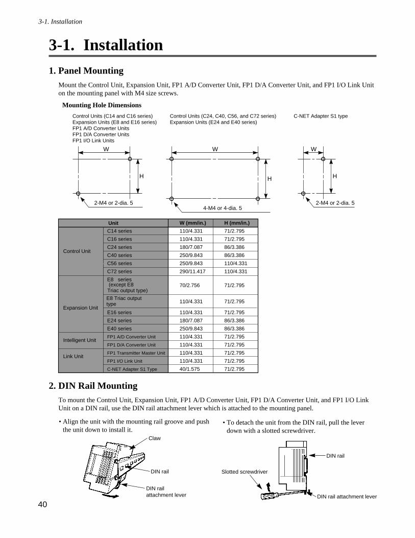
40
3-1. Installation
1. Panel MountingMount the Control Unit, Expansion Unit, FP1 A/D Converter Unit, FP1 D/A Converter Unit, and FP1 I/O Link Uniton the mounting panel with M4 size screws.
Mounting Hole Dimensions
2. DIN Rail MountingTo mount the Control Unit, Expansion Unit, FP1 A/D Converter Unit, FP1 D/A Converter Unit, and FP1 I/O LinkUnit on a DIN rail, use the DIN rail attachment lever which is attached to the mounting panel.
• To detach the unit from the DIN rail, pull the leverdown with a slotted screwdriver.
• Align the unit with the mounting rail groove and pushthe unit down to install it.
Control Unit
Expansion Unit
Intelligent Unit
Link Unit
W (mm/in.)
110/4.331
110/4.331
180/7.087
250/9.843
250/9.843
290/11.417
70/2.756
110/4.331
110/4.331
180/7.087
250/9.843
110/4.331
110/4.331
110/4.331
110/4.331
40/1.575
C14 series
C16 series
C24 series
C40 series
C56 series
C72 series
E8 series
E16 series
E24 series
E40 series
FP1 A/D Converter Unit
FP1 D/A Converter Unit
FP1 Transmitter Master Unit
FP1 I/O Link Unit
C-NET Adapter S1 Type
H (mm/in.)
71/2.795
71/2.795
86/3.386
86/3.386
110/4.331
110/4.331
71/2.795
71/2.795
71/2.795
86/3.386
86/3.386
71/2.795
71/2.795
71/2.795
71/2.795
71/2.795
(except E8 Triac output type)
E8 Triac outputtype
Unit
Control Units (C14 and C16 series)Expansion Units (E8 and E16 series)FP1 A/D Converter UnitsFP1 D/A Converter UnitsFP1 I/O Link Units
Control Units (C24, C40, C56, and C72 series)Expansion Units (E24 and E40 series)
2-M4 or 2-dia. 5
W
H
4-M4 or 4-dia. 5
W
H
2-M4 or 2-dia. 5
W
H
C-NET Adapter S1 type
3-1. Installation
Claw
DIN rail
DIN rail
Slotted screwdriver
DIN railattachment lever DIN rail attachment lever
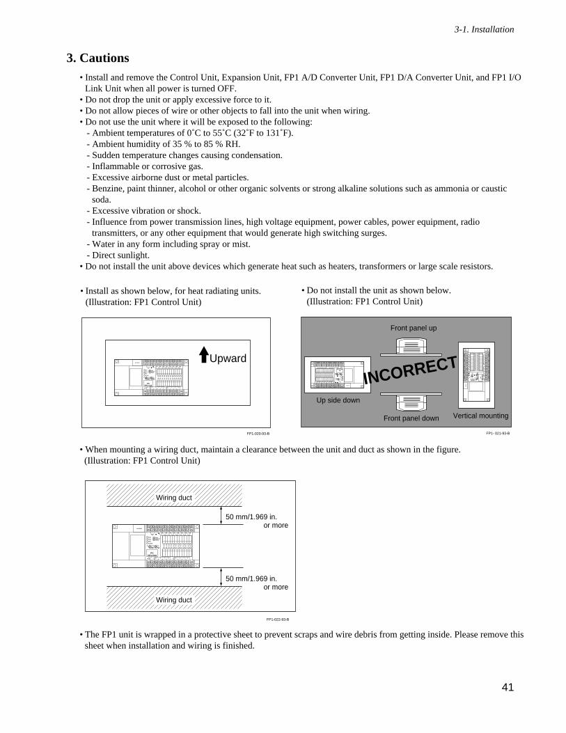
41
3. Cautions• Install and remove the Control Unit, Expansion Unit, FP1 A/D Converter Unit, FP1 D/A Converter Unit, and FP1 I/O
Link Unit when all power is turned OFF.• Do not drop the unit or apply excessive force to it.• Do not allow pieces of wire or other objects to fall into the unit when wiring.• Do not use the unit where it will be exposed to the following:
- Ambient temperatures of 0˚C to 55˚C (32˚F to 131˚F).- Ambient humidity of 35 % to 85 % RH.- Sudden temperature changes causing condensation.- Inflammable or corrosive gas.- Excessive airborne dust or metal particles.- Benzine, paint thinner, alcohol or other organic solvents or strong alkaline solutions such as ammonia or caustic
soda.- Excessive vibration or shock.- Influence from power transmission lines, high voltage equipment, power cables, power equipment, radio
transmitters, or any other equipment that would generate high switching surges.- Water in any form including spray or mist.- Direct sunlight.
• Do not install the unit above devices which generate heat such as heaters, transformers or large scale resistors.
• When mounting a wiring duct, maintain a clearance between the unit and duct as shown in the figure.(Illustration: FP1 Control Unit)
• The FP1 unit is wrapped in a protective sheet to prevent scraps and wire debris from getting inside. Please remove thissheet when installation and wiring is finished.
COM0
COM1
COM2
COM3
COM4
COM5
COM6
COM7
+ -24V DC
F.G.
COMF
89
EAB
CD(+)-
COM7
01
623
45(+)-
RUNREMOTEPROG.
V0
max.min.
RUN
PROG.
ERR.
ALRAM
BATTERY
V1
max.
PCFP1-C24
24V DC+
-
min.
FP1-022-93-B
Wiring duct
Wiring duct
50 mm/1.969 in. or more
50 mm/1.969 in. or more
Up side down
Vertical mounting
Front panel up
Front panel down
FP1- 021-93-B
CO
M0
CO
M1
CO
M2
CO
M3
CO
M4
CO
M5
CO
M6
CO
M7
+-
24V
DCF.
G.
CO
MF
89
EA
BC
D(+
) -C
OM
70
16
23
45
(+) -
RU
NR
EM
OTE
PR
OG
.
V0
max
.m
in.R
UN
PRO
G.
ER
R.
AL
RA
M
BA
TT
ER
Y
V1
max
.
PC
FP
1-C
2424
V D
C +
-min
.
COM0
COM1
COM2
COM3
COM4
COM5
COM6
COM7
+-24V DC
F.G.
COMF
89
E AB
CD (+) -
COM7
01
6 23
45 (+) -
RUNREMOTEPROG.
V0
max. min.
RUN
PROG.
ERR.
ALRAM
BATTERY
V1
max.
PCFP1-C24
24V DC+
-
min. INCORRECTCOM0
COM1
COM2
COM3
COM4
COM5
COM6
COM7
+ -24V DC
F.G.
COMF
89
EAB
CD(+)-
COM7
01
623
45(+)-
RUNREMOTEPROG.
V0
max.min.
RUN
PROG.
ERR.
ALRAM
BATTERY
V1
max.
PCFP1-C24
24V DC+
-
min.
Upward
FP1-020-93-B
• Do not install the unit as shown below.(Illustration: FP1 Control Unit)
• Install as shown below, for heat radiating units.(Illustration: FP1 Control Unit)
3-1. Installation
42
3-2. Expansion
1. Expansion Cable
2. Unit Expansion• Connect the Control Unit to the Expansion Unit, Intelligent unit (FP1 A/D Converter Unit, FP1 D/A Converter Unit)
or FP1 I/O Link Unit using Expansion Cable that folds out of sight and out of the way. In addition, concealing theExpansion Cable helps avoid the potentially adverse effects of electrical noise.
Notes:
• A maximum of two Expansion Units, one FP1 A/D Converter Unit, two FP1 D/A Converter Units, and oneFP1 I/O Link Unit can be simultaneously connected to one Control Unit.
• There are no restrictions on the order in which units are connected.• An E8 series and E16 series Expansion Unit cannot be connected in succession.Refer to page 11, “1-3. Expansion and Configurations”, for details about combination of units.
Control Unit
Expansion Unit
Expansion Unit
Control Unit
Expansion Unit
Expansion Unit
Left
Left
Right
Right
ExpansionCable
ExpansionCable
Right
CORRECT INCORRECT
Left
Left
ExpansionCable
Right
Example: Example:• Units must be connected left toright of each unit, therefore,please use the Expansion Cable(30 cm/0.984 ft.: AFP15103, 50cm/1.640 ft.: AFP15105) when theunits are aligned as shown in theright illustration.
Cable length
7 cm/0.230 ft.
30 cm/0.984 ft.
50 cm/1.640 ft.
Part number
AFP15101
AFP15103
AFP15105
3-2. Expansion
• The Expansion Cable can be concealed inthe between the units.
Control Unit
Example:
Expansion Unit
Cable length
Control Unit Expansion Cable Expansion Unit
43
3-3. Wiring
1. Crimp Terminal• M3.5 screws are used for the I/O terminal block.• Use of crimp terminals is recommended for wiring to the terminals.• Be sure to connect the cables and the interface terminals correctly using crimp terminals.• Suitable crimp terminals are ring terminals, insulated ring terminals and fork terminals.
2. Wiring Power Supply
1) Wiring Example for Power Supply Terminal
• Operating power is not required for E8 and E16 series Expansion Units.
Operating Voltage
Grounding• The FP1 has sufficient noise resistance under low noise level conditions. However, ground the FP1 unit for safety.• When grounding, an earth-ground resistance of 100 Ω or less is recommended to limit the effect of noise due to
electromagnetic interference.• Do not use a grounding wire that is shared with other devices.
FP1unit
Otherdevice
Correct
FP1unit
Otherdevice
Incorrect
Rated operating voltage
Operating voltage range
100 V to 240 V AC
85 V to 264 V AC
24 V DC
20.4 V to 26.4 V DC
Item AC type DC type
F.G.100-240 VAC
100 V to 240 V AC
AC type
F.G.24 V DC
24 V DC
DC type100 V to 240 V AC
AC type
+ -
L N
F.G.100-240 V AC
24 V DC
DC type
F.G.24 V DC
+ -
FP1-024-93-B
• FP1 Control Unit (C24, C40, C56, and C72 series)FP1 Expansion Unit (E24 and E40 series)
• FP1 Control Unit (C14 and C16 series), FP1 A/D Converter Unit, FP1 D/A Converter Unit, and FP1 I/O Link Unit
Hole: 3.7 to 4.3/0.146 to 0.169 dia.7.
2/0.
283
or le
ss
(unit: mm/in.)FP1-023-93-B
3-3. Wiring
2) Power Supply Lines
• The power supply lines for the FP1, I/O devices and motorized devices should be isolated as shown below.• Design the power supply lines for the Control Unit, Expansion Unit, and Intelligent units (FP1 A/D Converter Unit
and FP1 D/A Converter Unit) and FP1 I/O Link Unit so that the power for each can be turned ON and OFF at thesame time.
• Use twisted pair cable with 2 mm2 or larger conductors as the power supply lines.• Excessive noise and line voltage fluctuations can result in FP1 CPU misoperation or in system shutdown. To
prevent accidents caused by noise and line voltage fluctuations, be sure to employ countermeasures (such as use ofan insulated transformer, etc.) when wiring the power supply lines.
3) Momentary Power Drop
• The FP1 is not influenced by momentary power drops (less than 10 ms).
4) Safety
• In certain applications, malfunction may occur for the following reasons.Power on timing differences between the FP1 Control Unit and I/O or motorized devices.An operation time lag when a momentary power drop occurs.Abnormality in the FP1, power supply circuit, or other devices.
• In order to prevent malfunction from resulting in system shutdown, the following special attention is required.Start up sequence:
The FP1 should be operated after all of the outside devices are energized. To keep this sequence, the followingmeasures are recommended. Set the Mode selector from PROG. mode to RUN mode after power is supplied to all of the outside devices.Program the FP1 so as to disregard the inputs and outputs until the outside devices are energized.
Emergency stop circuit:Add an emergency stop circuit to controlled devices in order to prevent a system shutdown or an irreparableaccident when malfunction occurs.
Interlock circuit:When two motions that are opposed to each other are controlled, add an interlock circuit between theprogrammable controller's outputs and the control device.Example: When a motor clockwise/counter-clockwise operation is controlled, provide an interlock circuit that preventsclockwise and counter-clockwise signals from inputting into the motor at the same time.
Motorizeddevice
I/O device
FP1Control
Unit
FP1Expansion
Unit
Circuitbreaker
Circuitbreaker
Insulatedtransformer
Twisted pair cables
FP1-025-93-B
Circuit breaker
FP1Intelligent
Unit
44
3-3. Wiring
Example:
45
3. Input Terminals of Control Unit and Expansion Unit
1) Wiring Example for Input Terminals(Illustration: FP1 Control Unit)
Note:
2) Description
• Keep the input lines as far away from output lines as possible.• Keep the input lines at least 100 mm/3.937 in. away from the motor and high voltage line.
• Refer to page 29, “1. General Specifications”, for details about built-in DC power output for inputs.• Do not supply power from an exterior source to the built-in DC power output terminal (the part indicated as 24 V
DC+-) of AC type unit.• Do not connect power supplies for inputs together in parallel, and do not connect to another power supply in
parallel.• Refer to page 31, “2. Performance Specifications of Control Unit and Expansion Unit”.
0 2 4 6
1 3 5 724 V DC COM-
+ (±)
8 A C E
9 B D FCOM(±)
Using the external input supply
FP1-028-93-B
Switch Sensor
InternalcircuitOutput
+V
0 V
Externalpower supply:12 V to 24 V DC
0 2 4 6
1 3 5 724 V DC COM-
+ (±)
8 A C E
9 B D FCOM(±)
Using the built-in DC power output for inputs
FP1-027-93-B
Switch Sensor
InternalcircuitOutput
+V
0 V
• If the capacity of the DC type or the power output forinputs are insufficient, use an exterior power supply.
• With the AC type, the built-in DC power output forinputs can be used.
• Do not connect input devices to the input terminals indicated with a “•” symbol.
COM(±) 7
01
623
45
COM(±) F
89
EAB
CD
V0 V1
PCFP1-C24
24V DC+
0 1 2 3 4 5 6 7 8 9 A B
INP
UT
X
(24V
DC
)
FP1-026-93-B
Unit
Input devices
Built-in DC power outputfor inputs
Push buttonswitches
Push buttonswitches
Inputterminals
–
3-3. Wiring
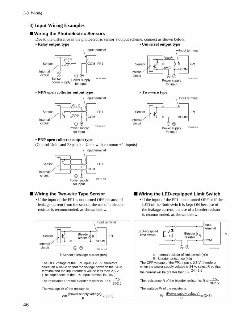
46
3) Input Wiring Examples
Wiring the Photoelectric SensorsDue to the difference in the photoelectric sensor’s output scheme, connect as shown below:• Relay output type • Universal output type
• NPN open collector output type • Two-wire type
• PNP open collector output type(Control Units and Expansion Units with common +/– inputs)
COM
LED-equippedlimit switch FP1
Inputterminal
– +
Bleederresistor
FP1-035-93-B
Rr
COM
Sensor
Internalcircuit
FP1
Input terminal
– +
Bleederresistor
FP1-034-93-B
R
Wiring the LED-equipped Limit Switch• If the input of the FP1 is not turned OFF or if the
LED of the limit switch is kept ON because ofthe leakage current, the use of a bleeder resistoris recommended, as shown below.
Wiring the Two-wire Type Sensor• If the input of the FP1 is not turned OFF because of
leakage current from the sensor, the use of a bleederresistor is recommended, as shown below.
COM
Sensor
Internalcircuit
FP1
Input terminal
–Power supply
for input
FP1-033-93-B +
COM
Sensor
Internalcircuit
FP1
Input terminal
– +Power supply
for input
FP1-032-93-B
COM
Sensor
Internalcircuit
FP1
Input terminal
– +Power supply
for input
FP1-030-93-B
Vcc
0V
+
–
COM
Sensor
Internalcircuit
FP1
Input terminal
– +Power supply
for input
FP1-031-93-B
Vcc
0V
+
–COMSensor
Internalcircuit
FP1
Input terminal
– +Power supply
for input
FP1-029-93-B Sensorpower supply
3-3. Wiring
I: Sensor’s leakage current (mA)
The OFF voltage of the FP1 input is 2.5 V, therefore,select an R value so that the voltage between the COMterminal and the input terminal will be less than 2.5 V.(The impedance of the FP1 input terminal is 3 kΩ.)
The resistance R of the bleeder resistor is : R 7.53I-2.5
The wattage W of the resistor is:
W=(Power supply voltage)2
× (3~5)R
r: Internal resistor of limit switch (kΩ)R: Bleeder resistance (kΩ)
The OFF voltage of the FP1 input is 2.5 V, thereforewhen the power supply voltage is 24 V, select R so that
the current will be greater than I = 24 - 2.5r
The resistance R of the bleeder resistor is: R 7.53I-2.5
The wattage W of the resistor is:
W=(Power supply voltage)2
× (3~5)R
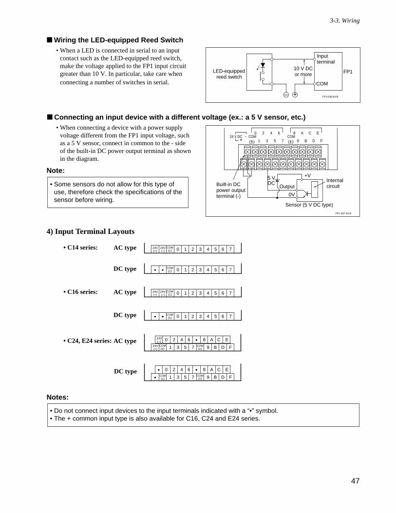
47
Wiring the LED-equipped Reed Switch
Connecting an input device with a different voltage (ex.: a 5 V sensor, etc.)
Note:
4) Input Terminal Layouts
Notes:
• Do not connect input devices to the input terminals indicated with a “•” symbol.• The + common input type is also available for C16, C24 and E24 series.
• C14 series: AC type
• C16 series: AC type
DC type
• C24, E24 series: AC type
DC type
1 3 5 7 9 B D F
2 4 6 A C0 • 8 ECOM(±)
DC type
• 1 3 5 7 9 B D F
2 4 6 A C0 • 8 E•COM(±)
COM(±)
0 1 2 324V(+)
COM(±) 4 5 6 724V
(–)
0 1 2 3COM(±) 4 5 6 7• •
0 1 2 324V(+)
COM(±) 4 5 6 724V
(–)
0 1 2 3COM(±) 4 5 6 7• •
24V(–)
24V(+)
COM(±)
• Some sensors do not allow for this type ofuse, therefore check the specifications of thesensor before wiring.
• When connecting a device with a power supplyvoltage different from the FP1 input voltage, suchas a 5 V sensor, connect in common to the - sideof the built-in DC power output terminal as shownin the diagram.
COM
LED-equippedreed switch
FP1
Inputterminal
– +
10 V DCor more
FP1-036-93-B
• When a LED is connected in serial to an inputcontact such as the LED-equipped reed switch,make the voltage applied to the FP1 input circuitgreater than 10 V. In particular, take care whenconnecting a number of switches in serial.
3-3. Wiring
0 2 4 6
1 3 5 724 V DC COM-
+ (±)
8 A C E
9 B D FCOM(±)
FP1-037-93-B
Sensor (5 V DC type)
InternalcircuitOutput
+V
0V
Built-in DCpower outputterminal (-)
5 VDC
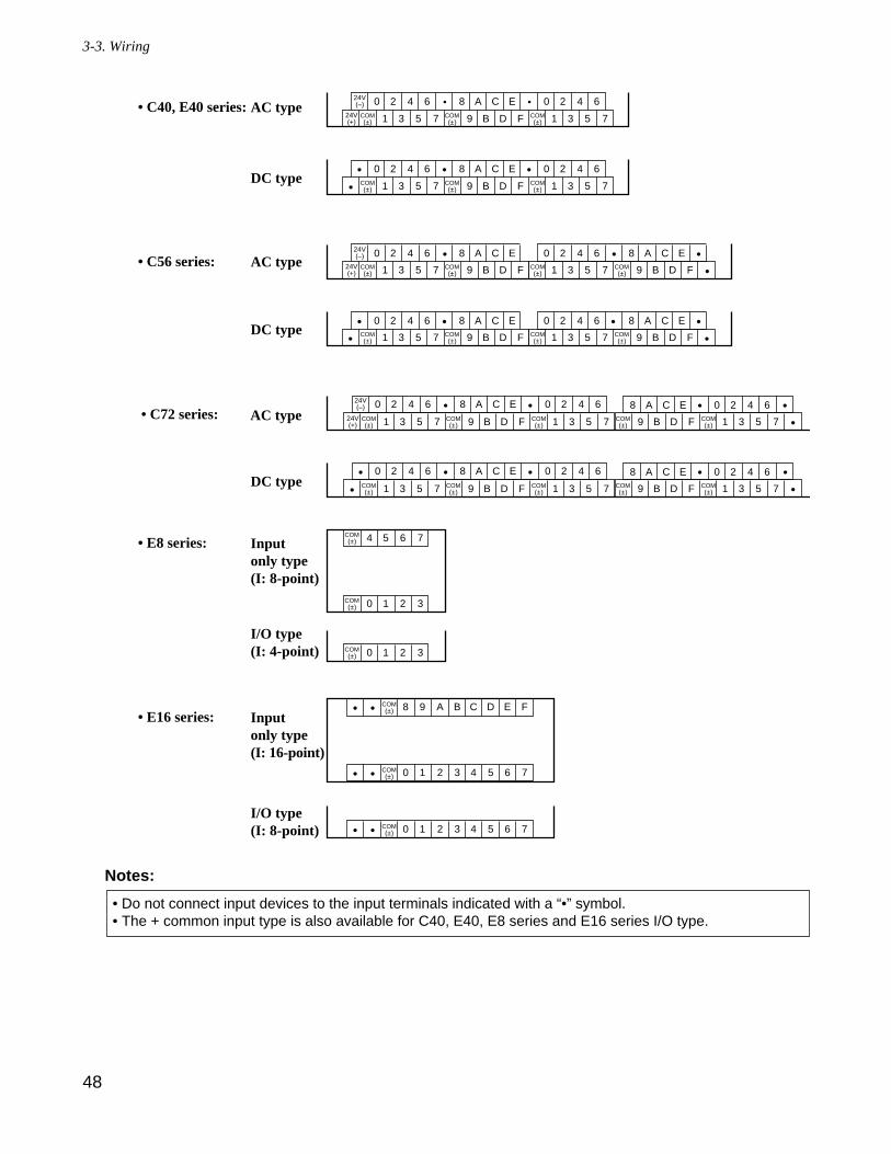
48
Notes:
• Do not connect input devices to the input terminals indicated with a “•” symbol.• The + common input type is also available for C40, E40, E8 series and E16 series I/O type.
• C56 series: AC type
DC type
• C72 series: AC type
DC type
• E8 series:
DC type
Inputonly type(I: 8-point)
I/O type(I: 4-point)
Inputonly type(I: 16-point)
I/O type(I: 8-point)
• E16 series:
51 3 7COM(±)
•0 2 4 624V(+)
24V(–)
COM(±) D9 B F COM
(±) 51 3 7
8 A C E • 0 2 4 6
51 3 7COM(±)
0 2 4 6COM(±) D9 B F COM
(±) 51 3 7
8 A C E 0 2 4 6•
0 2 4 624V(–) 8 A C E 0 2 4 6 8 A C E
51 3 7COM(±)
24V(+)
COM(±) D9 B F COM
(±) 51 3 7 COM(±) D9 B F
0 2 4 6 8 A C E 0 2 4 6 8 A C E
51 3 7COM(±)
COM(±) D9 B F COM
(±) 51 3 7 COM(±) D9 B F
0 2 4 624V(–) 8 A C E 0 2 4 6 8 A C E 0 2 4 6
51 3 7COM(±)
24V(+)
COM(±) D9 B F COM
(±) 51 3 7 COM(±) D9 B F COM
(±) 51 3 7
8 A C E 0 2 4 6
51 3 7COM(±)
COM(±) D9 B F COM
(±) 51 3 7 COM(±) D9 B F COM
(±) 51 3 7
• ••
• • ••
• • • •• •
• • • ••
0 2 4 6 8 A C E 0 2 4 6• • • • •••
• C40, E40 series: AC type
64 5 7COM(±)
20 1 3COM(±)
20 1 3COM(±)
8 9 B C D E• • COM(±) A F
0 1 3 4 5 6• • COM(±) 2 7
0 1 3 4 5 6• • COM(±) 2 7
3-3. Wiring
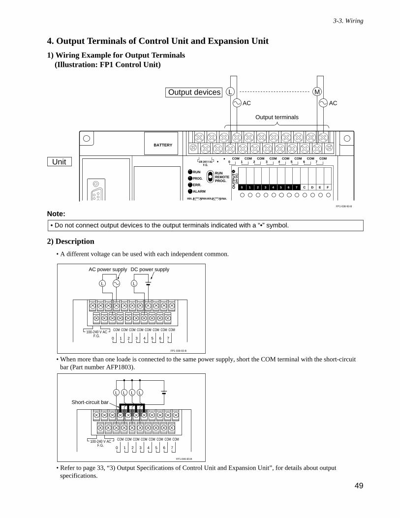
4. Output Terminals of Control Unit and Expansion Unit
1) Wiring Example for Output Terminals(Illustration: FP1 Control Unit)
Note:
2) Description
• A different voltage can be used with each independent common.
• When more than one loade is connected to the same power supply, short the COM terminal with the short-circuitbar (Part number AFP1803).
• Refer to page 33, “3) Output Specifications of Control Unit and Expansion Unit”, for details about outputspecifications.
0
100-240 V AC COM
1
COM
2
COM
3
COM
4
COM
5
COM
6
COM
7
COM
F.G.
L L L L
FP1-040-93-B
Short-circuit bar
0
100-240 V AC COM
1
COM
2
COM
3
COM
4
COM
5
COM
6
COM
7
COM
F.G.
AC power supply DC power supply
FP1-039-93-B
L L
• Do not connect output devices to the output terminals indicated with a “•” symbol.
COM0
COM1
COM2
COM3
COM4
COM5
COM6
COM7100 240 V AC
F.G.
RUNREMOTEPROG.
max.min.
RUN
PROG.
ERR.
ALARM
BATTERY
max.min.
0 1 2 3 4 5 6 7 C D E FOU
TP
UT
Y
(24V
DC
)
Output devices
Output terminals
AC AC
L M
FP1-038-93-B
Unit
49
3-3. Wiring
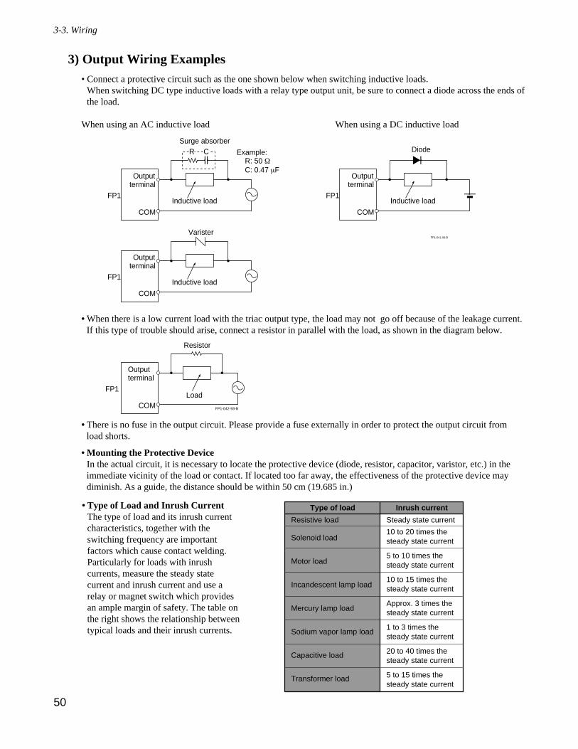
3) Output Wiring Examples• Connect a protective circuit such as the one shown below when switching inductive loads.
When switching DC type inductive loads with a relay type output unit, be sure to connect a diode across the ends ofthe load.
When using an AC inductive load When using a DC inductive load
• When there is a low current load with the triac output type, the load may not go off because of the leakage current.If this type of trouble should arise, connect a resistor in parallel with the load, as shown in the diagram below.
• There is no fuse in the output circuit. Please provide a fuse externally in order to protect the output circuit fromload shorts.
• Mounting the Protective DeviceIn the actual circuit, it is necessary to locate the protective device (diode, resistor, capacitor, varistor, etc.) in theimmediate vicinity of the load or contact. If located too far away, the effectiveness of the protective device maydiminish. As a guide, the distance should be within 50 cm (19.685 in.)
Resistive load
Solenoid load
Motor load
Incandescent lamp load
Mercury lamp load
Sodium vapor lamp load
Capacitive load
Transformer load
Steady state current
10 to 20 times thesteady state current
5 to 10 times thesteady state current
10 to 15 times the steady state current
Approx. 3 times thesteady state current
1 to 3 times the steady state current
20 to 40 times the steady state current
5 to 15 times the steady state current
Type of load Inrush current• Type of Load and Inrush CurrentThe type of load and its inrush currentcharacteristics, together with theswitching frequency are importantfactors which cause contact welding.Particularly for loads with inrushcurrents, measure the steady statecurrent and inrush current and use arelay or magnet switch which providesan ample margin of safety. The table onthe right shows the relationship betweentypical loads and their inrush currents.
COM
FP1
Outputterminal
Load
FP1-042-93-B
Resistor
COM
FP1
Outputterminal
Inductive load
FP1-041-93-B
Surge absorber
Example:R C
COM
FP1
Outputterminal
Inductive load
Diode
COM
FP1
Outputterminal
Inductive load
Varister
R: 50 ΩC: 0.47 µF
50
3-3. Wiring
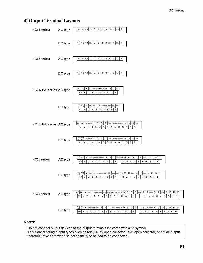
4) Output Terminal Layouts
Notes:
• Do not connect output devices to the output terminals indicated with a “•” symbol.• There are differing output types such as relay, NPN open collector, PNP open collector, and triac output,
therefore, take care when selecting the type of load to be connected.
• C14 series: AC type
• C16 series: AC type
DC type
• C24, E24 series: AC type
DC type
DC type
0 1 2 3 5 6 7•
AC COM COM COM COM COM COM COM COM•AC
F.G. 4
COM COM COM COM COM COM COM COM•0 1 2 3 5 6 7•F.G. 4
24V(+)
24V(–)
0 1 3 42 7AC AC F.G. COM COM COM
0 1 3 42 7F.G. COM COM COM24V(+)
24V(–)
0 1 3 52 7AC AC F.G. COM
0 1 3 52 7F.G. COM24V(+)
24V(–)
4 6
4 6
• C40, E40 series: AC type
B D F 5 73•
• C56 series: AC type
DC type
• C72 series: AC type
DC type
DC type51 3• 7
0 2 4 8 9 A B D E F
COM COM COM COM COM COM COM COM COM
F.G. • • 6 C
24V(+)
24V(–)
51 3• 7ACAC COM COM COM COM COM COM COM COM COM
0 2 4 8 9 A B D E FF.G. • • 6 C
0 1 2 3 5 6 7 •
B D 1 39 5
•
AC COM COM COM COM COM COM COM COM•AC COM COM F COM 7
F.G. 4 •A C 0 48 E 2 6
B D 1 39 5COM COM COM COM COM COM COM COM• F 7
0 1 2 3 5 6 7•F.G. 4
COM COM COM
• •A C 0 48 E 2 6
24V(+)
24V(–)
AC AC COM COM COM COM COM COM COM COM COM 9 COM COM1 COM B D F9
• • 8 A C E0 2 4 6A•• 1 2 3 4 6 75F.G. 0 8 EC
B D F 5 73• COM COM COM COM COM COM COM COM COM 9 COM COM1 COM B D F9
• • 8 A C E0 2 4 6A•• 1 2 3 4 6 75F.G. 0 8 EC
24V(+)
24V(–)
51
3-3. Wiring
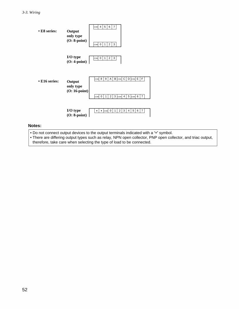
Notes:
• Do not connect output devices to the output terminals indicated with a “•” symbol.• There are differing output types such as relay, NPN open collector, PNP open collector, and triac output,
therefore, take care when selecting the type of load to be connected.
• E8 series: Outputonly type(O: 8-point)
I/O type(O: 4-point)
Outputonly type(O: 16-point)
I/O type(O: 8-point)
• E16 series:
64 5 7COM
20 1 3COM
20 1 3COM
8 9 B C D EA FCOM COM COM
0 1 3 4 5 62 7COM COM COM
0 1 3 4 5 62 7COM• •
52
3-3. Wiring
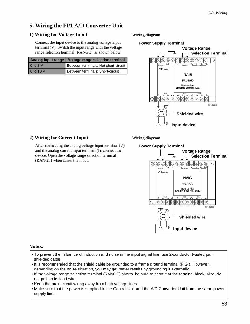
5. Wiring the FP1 A/D Converter Unit
1) Wiring for Voltage Input
Connect the input device to the analog voltage inputterminal (V). Switch the input range with the voltagerange selection terminal (RANGE), as shown below.
2) Wiring for Current Input
After connecting the analog voltage input terminal (V)and the analog current input terminal (I), connect thedevice. Open the voltage range selection terminal(RANGE) when current is input.
Notes:
• To prevent the influence of induction and noise in the input signal line, use 2-conductor twisted pairshielded cable.
• It is recommended that the shield cable be grounded to a frame ground terminal (F.G.). However,depending on the noise situation, you may get better results by grounding it externally.
• If the voltage range selection terminal (RANGE) shorts, be sure to short it at the terminal block. Also, donot pull on its lead wire.
• Keep the main circuit wiring away from high voltage lines .• Make sure that the power is supplied to the Control Unit and the A/D Converter Unit from the same power
supply line.
Analog input range
0 to 5 V
0 to 10 V
Voltage range selection terminal
Between terminals: Not short-circuit
Between terminals: Short-circuit
53
3-3. Wiring
F.G. V3 I3 C3 F.G.
C0 F.G.
FP1-4A/D
MatsushitaErectric Works, Ltd.
FP1-318-93H
Power
NAIS
+ –24V DC CH. 3RANGE
V0 I0 C1 F.G.V1 I1 C2V2 I2CH. 2CH. 1CH. 0
Power Supply TerminalVoltage Range Selection Terminal
Wiring diagram
Shielded wire
Input device
F.G. V3 I3 C3 F.G.
C0 F.G.
FP1-4A/D
MatsushitaErectric Works, Ltd.
FP1-319-93H
Power
NAIS
+ –24V DC CH. 3RANGE
V0 I0 C1 F.G.V1 I1 C2V2 I2CH. 2CH. 1CH. 0
Power Supply TerminalVoltage Range Selection Terminal
Wiring diagram
Shielded wire
Input device
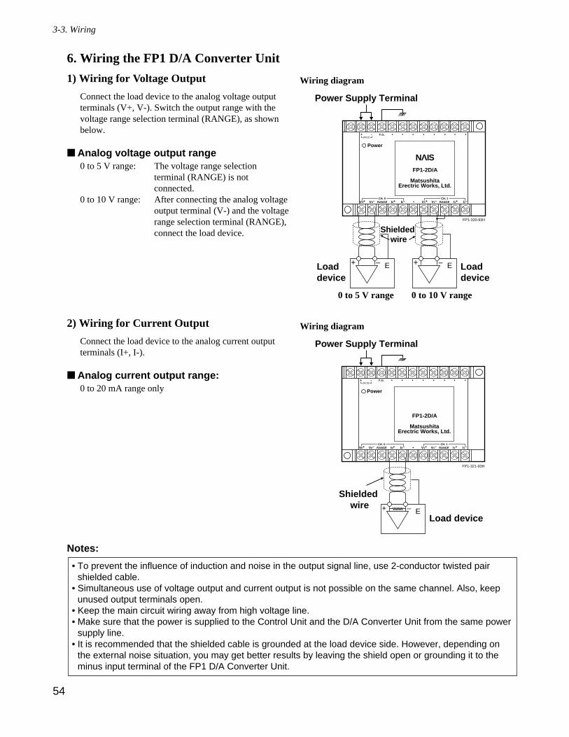
6. Wiring the FP1 D/A Converter Unit
1) Wiring for Voltage Output
Connect the load device to the analog voltage outputterminals (V+, V-). Switch the output range with thevoltage range selection terminal (RANGE), as shownbelow.
Analog voltage output range0 to 5 V range: The voltage range selection
terminal (RANGE) is notconnected.
0 to 10 V range: After connecting the analog voltageoutput terminal (V-) and the voltagerange selection terminal (RANGE),connect the load device.
2) Wiring for Current Output
Connect the load device to the analog current outputterminals (I+, I-).
Analog current output range:0 to 20 mA range only
Notes:
• To prevent the influence of induction and noise in the output signal line, use 2-conductor twisted pairshielded cable.
• Simultaneous use of voltage output and current output is not possible on the same channel. Also, keepunused output terminals open.
• Keep the main circuit wiring away from high voltage line.• Make sure that the power is supplied to the Control Unit and the D/A Converter Unit from the same power
supply line.• It is recommended that the shielded cable is grounded at the load device side. However, depending on
the external noise situation, you may get better results by leaving the shield open or grounding it to theminus input terminal of the FP1 D/A Converter Unit.
54
3-3. Wiring
F.G.
RANGE
FP1-2D/A
MatsushitaErectric Works, Ltd.
FP1-320-93H
Power
NAIS
+ -24V DC
V0+CH. 1CH. 0
Shielded wire
V0– I0+ I0– RANGEV1+ V1– I1+ I1–
0 to 10 V range
+ – E+ – ELoad device
Load device
Power Supply Terminal
Wiring diagram
0 to 5 V range
F.G.
RANGE
FP1-2D/A
MatsushitaErectric Works, Ltd.
FP1-321-93H
Power
+ -24V DC
V0+CH. 1CH. 0
Shielded wire
V0– I0+ I0– RANGEV1+ V1– I1+ I1–
+ – ELoad device
Power Supply Terminal
Wiring diagram
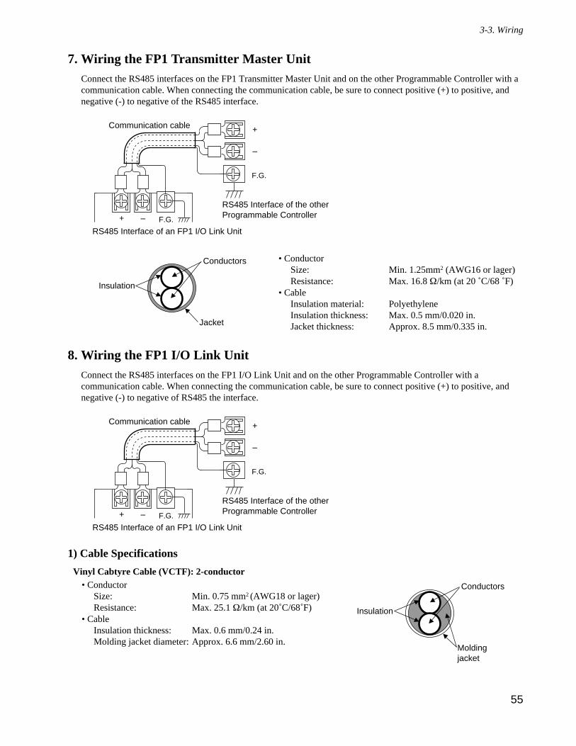
7. Wiring the FP1 Transmitter Master UnitConnect the RS485 interfaces on the FP1 Transmitter Master Unit and on the other Programmable Controller with acommunication cable. When connecting the communication cable, be sure to connect positive (+) to positive, andnegative (-) to negative of the RS485 interface.
8. Wiring the FP1 I/O Link UnitConnect the RS485 interfaces on the FP1 I/O Link Unit and on the other Programmable Controller with acommunication cable. When connecting the communication cable, be sure to connect positive (+) to positive, andnegative (-) to negative of RS485 the interface.
1) Cable Specifications
Vinyl Cabtyre Cable (VCTF): 2-conductor
Conductors
Insulation
Moldingjacket
• ConductorSize: Min. 0.75 mm2 (AWG18 or lager)Resistance: Max. 25.1 Ω/km (at 20˚C/68˚F)
• CableInsulation thickness: Max. 0.6 mm/0.24 in.Molding jacket diameter: Approx. 6.6 mm/2.60 in.
+ – F.G.
F.G.
+
–
RS485 Interface of an FP1 I/O Link Unit
RS485 Interface of the other Programmable Controller
Communication cable
• ConductorSize: Min. 1.25mm2 (AWG16 or lager)Resistance: Max. 16.8 Ω/km (at 20 ˚C/68 ˚F)
• CableInsulation material: PolyethyleneInsulation thickness: Max. 0.5 mm/0.020 in.Jacket thickness: Approx. 8.5 mm/0.335 in.
Conductors
Insulation
Jacket
+ – F.G.
F.G.
+
–
RS485 Interface of an FP1 I/O Link Unit
RS485 Interface of the other Programmable Controller
Communication cable
55
3-3. Wiring
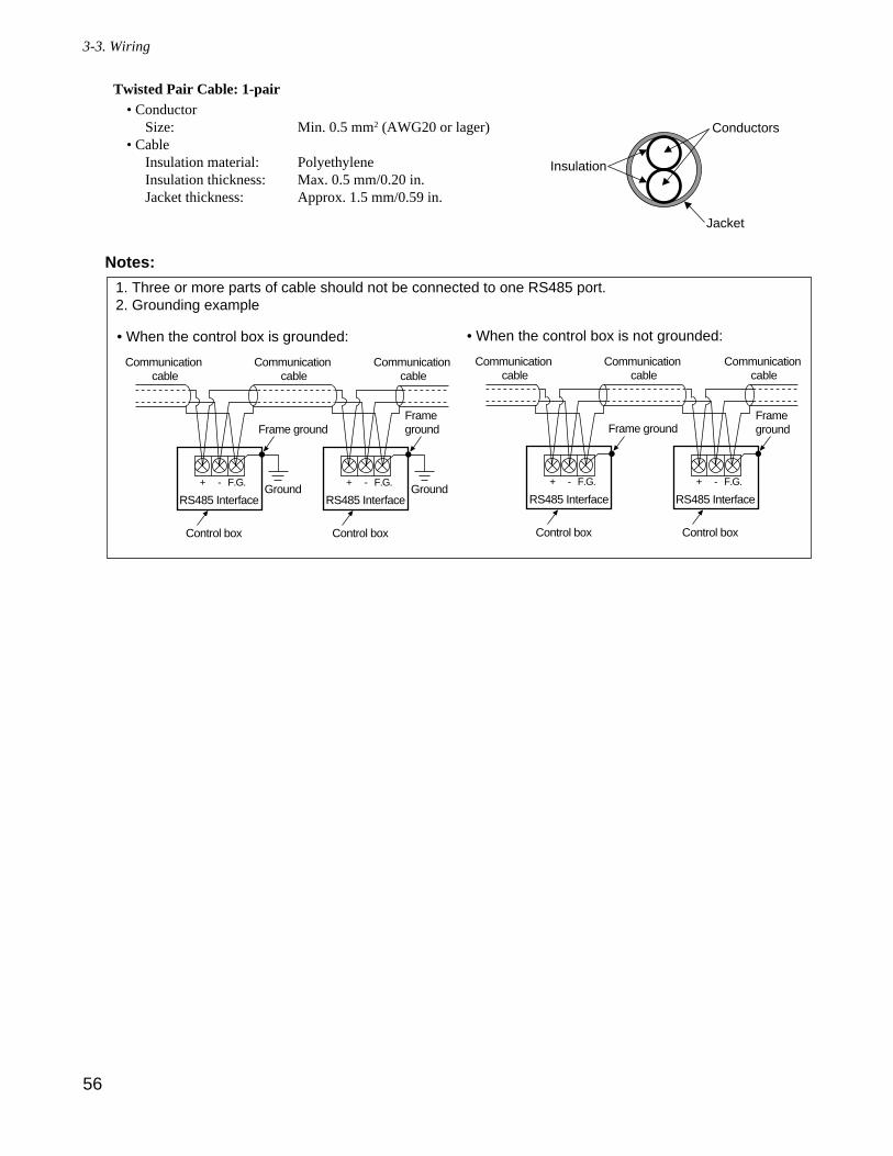
56
3-3. Wiring
Twisted Pair Cable: 1-pair
Notes:
1. Three or more parts of cable should not be connected to one RS485 port.2. Grounding example
Conductors
Insulation
Jacket
• ConductorSize: Min. 0.5 mm2 (AWG20 or lager)
• CableInsulation material: PolyethyleneInsulation thickness: Max. 0.5 mm/0.20 in.Jacket thickness: Approx. 1.5 mm/0.59 in.
+ - F.G.
RS485 InterfaceGround
Control box
Communication cable
Frame ground
+ - F.G.
RS485 InterfaceGround
Control box
Frame ground
Communication cable
Communication cable
• When the control box is grounded:
+ - F.G.
RS485 Interface
Control box
Communication cable
Frame ground
+ - F.G.
RS485 Interface
Control box
Communication cable
Communication cable
• When the control box is not grounded:
Frame ground
CHAPTER 4
BEFORE PROGRAMMING4-1. Operating Principles of the Programmable Controller..........58
1. Basic Configuration..........................................................582. Basic Operation ................................................................60
4-2. How to Program the Programmable Controller ....................621. Making a Ladder Diagram................................................622. Relays and Timer/Counter Contacts in the FP1 ...............633. I/O Allocation in the FP1 .................................................65
4-3. Programming with NPST-GR Software ................................671. System Configuration.......................................................672. Features of NPST-GR Software Ver. 3 .............................683. NPST-GR Configuration ..................................................69
1) Overview of the Programming Screen...................692) Overview of the Menu Window.............................71
4. NPST-GR Installation and Configuration.........................721) Preparing for Installation .......................................722) NPST-GR Installation ............................................733) How to Use NPST-GR Effectively ........................754) NPST-GR Startup...................................................755) Configuring NPST-GR ..........................................76
5. Exiting NPST-GR .............................................................786. Basic Key Operation for Programs...................................797. Downloading a Program
to the Programmable Controller .......................................808. Saving a Program to Disk.................................................819. Printing .............................................................................82
4-4. Programming with the FP Programmer II..............................831. System Configuration.......................................................832. Downloading a Program
to the Programmable Controller .......................................844-5. Memory Unit Creation and ROM Operation ........................86
1. Memory Unit ....................................................................862. How to Program ROM .....................................................873. Operation with Installed
Memory Unit (ROM Operation).......................................89
58
4-1. Operating Principles of the Programmable Controller
4-1. Operating Principles of theProgrammable Controller
1. Basic Configuration
A programmable controller is composed of four basic sections: 1 CPU, 2 memory, 3 input interface, and 4output interface. An inside look at these sections will help you understand their functions and operation of theprogrammable controller.
NPST-GR Software
FPProgrammer II
Personal computer
Programming tools
Output field devices
Inverter(variable speed drive)
Segmentindicators
Indicators
Buzzers
Programmable Controller
Input field devices
Limit switches
Manual operatingswitches
Photoelectric sensors
Inductiveproximity switches
Encoders
Digital switches
Power supply
Relays
Solenoids
3
Inputinter-face
4
Outputinter-face
2-aMemory for operand
1 CPU(Central Processing Unit)
2-bSystemregister
2-cMemory for program
Power supply
FP PROGRAMMER
STX•WX
ANY•WY
ORR•WR
OTL•WL
FN/PFL
NOTDT/Ld
STKIX/IY
TMT•SV
CTC•EV
(BIN)K/H
=C
DD
<E
>F
SHIFTSC
8 9 A B
4 5 6 7
0 1 2 3
(-)OP
SRC
READ
(HELP)CLR
ACLR (DELT)INST
ENT WRT
59
4-1. Operating Principles of the Programmable Controller
Functions of the Four Sections
11 CPU (Central Processing Unit) Controls the operation of the programmable controller including the I/Os according to the program
22MemoryMemory areas where the program and information needed for operation of the programmable controller arestored.
Types of Memory22 -a: Memory for operands
The memory area for storing operand data (external input relays, timer/counter set value, and dataregisters, etc.). Data for the program to handle and the data from and to field devices are centralized in thisarea.Refer to page 93, for details about operands.
22 -b: System registerThe memory area for storing the system settings of programmable controllers. Information in this areadecides the operand characteristics, advanced control function availabilities, and so on. The systemregisters can be set using an FP Programmer II or personal computer using NPST-GR Software.
22 -c: Memory for programThe memory area to store the program for execution. Programs are written using an FP Programmer II orpersonal computer using NPST-GR Software.
33 Input interfaceInterface that receives data from the field device and transfers it to the memory for operands.
44 Output interfaceInterface that outputs data from the memory for operands to the field devices.
4-1. Operating Principles of the Programmable Controller
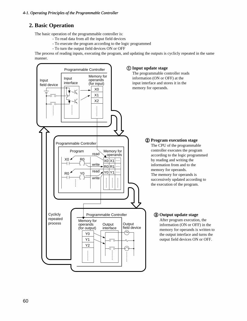
60
4-1. Operating Principles of the Programmable Controller
2. Basic OperationThe basic operation of the programmable controller is:
- To read data from all the input field devices- To execute the program according to the logic programmed- To turn the output field devices ON or OFF
The process of reading inputs, executing the program, and updating the outputs is cyclicly repeated in the samemanner.
.........
X0
X1
X2
.........
.........
Inputfield device
Inputinterface
Memory foroperands (for input)
Programmable Controller
X0 R0
R0 Y0read
write
X0
R0
Y0
.........
write
read
X1
R1
Y1
.........
....
....
....
.........
.......
Program Memory foroperands
Programmable Controller
Y0
Y1
Y2
.........
Memory foroperands (for output)
.........
~Outputinterface
Outputfield device
Programmable Controller
.........
Cycliclyrepeatedprocess
4-1. Operating Principles of the Programmable Controller
11 Input update stageThe programmable controller readsinformation (ON or OFF) at theinput interface and stores it in thememory for operands.
22 Program execution stageThe CPU of the programmablecontroller executes the programaccording to the logic programmedby reading and writing theinformation from and to thememory for operands. The memory for operands issuccessively updated according tothe execution of the program.
33 Output update stageAfter program execution, theinformation (ON or OFF) in thememory for operands is written tothe output interface and turns theoutput field devices ON or OFF.
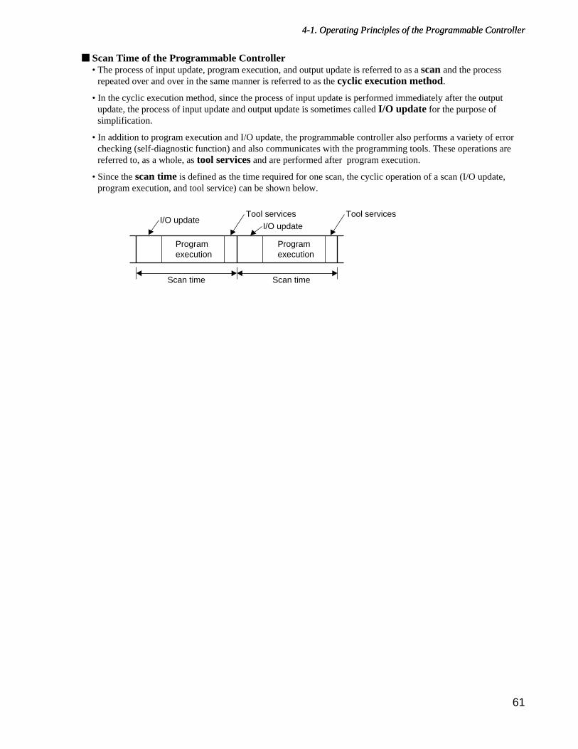
Scan Time of the Programmable Controller• The process of input update, program execution, and output update is referred to as a scan and the process
repeated over and over in the same manner is referred to as the cyclic execution method.
• In the cyclic execution method, since the process of input update is performed immediately after the outputupdate, the process of input update and output update is sometimes called I/O update for the purpose ofsimplification.
• In addition to program execution and I/O update, the programmable controller also performs a variety of errorchecking (self-diagnostic function) and also communicates with the programming tools. These operations arereferred to, as a whole, as tool services and are performed after program execution.
• Since the scan time is defined as the time required for one scan, the cyclic operation of a scan (I/O update,program execution, and tool service) can be shown below.
Programexecution
Programexecution
Scan time Scan time
I/O updateTool services
I/O updateTool services
61
4-1. Operating Principles of the Programmable Controller4-1. Operating Principles of the Programmable Controller
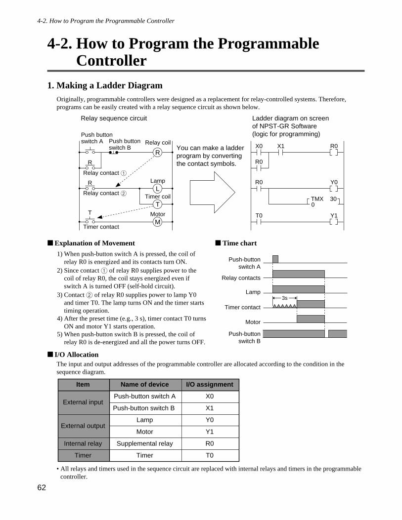
62
4-2. How to Program the Programmable Controller
4-2. How to Program the ProgrammableController
1. Making a Ladder DiagramOriginally, programmable controllers were designed as a replacement for relay-controlled systems. Therefore,programs can be easily created with a relay sequence circuit as shown below.
Explanation of Movement Time chart
I/O AllocationThe input and output addresses of the programmable controller are allocated according to the condition in thesequence diagram.
• All relays and timers used in the sequence circuit are replaced with internal relays and timers in the programmablecontroller.
Item
External input
External output
Internal relay
Timer
Name of device
Push-button switch A
Push-button switch B
Lamp
Motor
Supplemental relay
Timer
I/O assignment
X0
X1
Y0
Y1
R0
T0
Push-buttonswitch A
3sLamp
Timer contact
Motor
Push-buttonswitch B
Relay contacts
1) When push-button switch A is pressed, the coil ofrelay R0 is energized and its contacts turn ON.
2) Since contact 1 of relay R0 supplies power to thecoil of relay R0, the coil stays energized even ifswitch A is turned OFF (self-hold circuit).
3) Contact 2 of relay R0 supplies power to lamp Y0and timer T0. The lamp turns ON and the timer startstiming operation.
4) After the preset time (e.g., 3 s), timer contact T0 turnsON and motor Y1 starts operation.
5) When push-button switch B is pressed, the coil ofrelay R0 is de-energized and all the power turns OFF.
T0 Y1
Ladder diagram on screen of NPST-GR Software (logic for programming)
TMX 300
R0 Y0
R0
X0 R0
Relay sequence circuit
You can make a ladder program by convertingthe contact symbols.
R
Push buttonswitch A Push button
switch BRelay coil
R
R
Relay contact 1
LLamp
TTimer coilRelay contact 2
MMotorT
Timer contact
X1
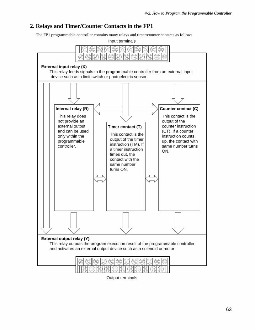
2. Relays and Timer/Counter Contacts in the FP1The FP1 programmable controller contains many relays and timer/counter contacts as follows.
Input terminals
External input relay (X)This relay feeds signals to the programmable controller from an external input device such as a limit switch or photoelectric sensor.
External output relay (Y)This relay outputs the program execution result of the programmable controller and activates an external output device such as a solenoid or motor.
Internal relay (R)
This relay does not provide an external output and can be used only within the programmable controller.
Counter contact (C)
This contact is the output of the counter instruction (CT). If a counter instruction counts up, the contact with same number turns ON.
Timer contact (T)
This contact is the output of the timer instruction (TM). If a timer instruction times out, the contact with the same number turns ON.
Output terminals
63
4-2. How to Program the Programmable Controller4-2. How to Program the Programmable Controller
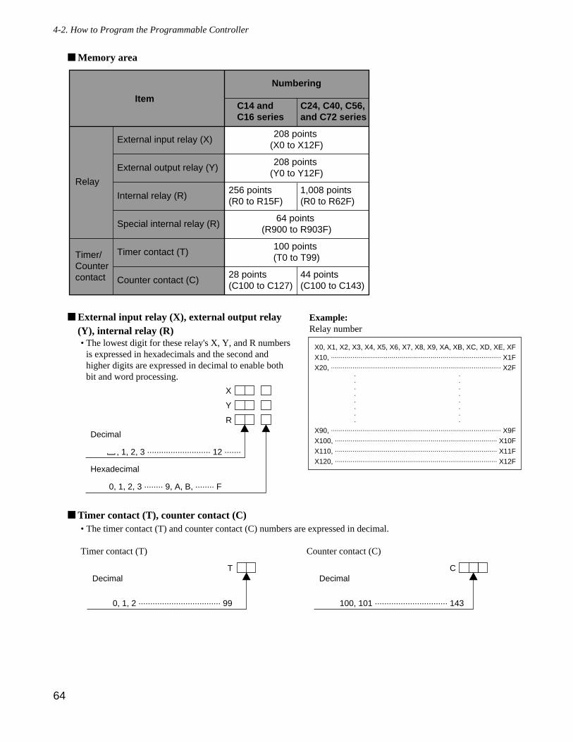
Memory area
External input relay (X), external output relay(Y), internal relay (R)• The lowest digit for these relay's X, Y, and R numbers
is expressed in hexadecimals and the second andhigher digits are expressed in decimal to enable bothbit and word processing.
Timer contact (T), counter contact (C)• The timer contact (T) and counter contact (C) numbers are expressed in decimal.
Timer contact (T) Counter contact (C)
TDecimal
0, 1, 2 ................................... 99
CDecimal
100, 101 ............................... 143
R
Decimal
] , 1, 2, 3 ........................... 12 .......
Hexadecimal
0, 1, 2, 3 ........ 9, A, B, ........ F
Y
X
C14 and C16 series
256 points (R0 to R15F)
28 points (C100 to C127)
C24, C40, C56, and C72 series
1,008 points (R0 to R62F)
44 points (C100 to C143)
Numbering
208 points (X0 to X12F)
208 points (Y0 to Y12F)
64 points (R900 to R903F)
100 points (T0 to T99)
External input relay (X)
External output relay (Y)
Internal relay (R)
Special internal relay (R)
Timer contact (T)
Counter contact (C)
Relay
Timer/Counter contact
Item
64
4-2. How to Program the Programmable Controller
X0, X1, X2, X3, X4, X5, X6, X7, X8, X9, XA, XB, XC, XD, XE, XF
X10, ....................................................................................... X1F
X20, ....................................................................................... X2F
X90, ....................................................................................... X9F
X100, ................................................................................... X10F
X110, ................................................................................... X11F
X120, ................................................................................... X12F
.
.
.
.
.
.
.
.
.
.
.
.
.
.
.
.
Example:Relay number
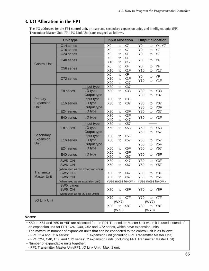
3. I/O Allocation in the FP1The I/O addresses for the FP1 control unit, primary and secondary expansion units, and intelligent units (FP1Transmitter Master Unit, FP1 I/O Link Unit) are assigned as follows.
Notes:
• X50 to X67 and Y50 to Y5F are allocated for the FP1 Transmitter Master Unit when it is used instead ofan expansion unit for FP1 C24, C40, C52 and C72 series, which have expansion units.
• The maximum number of expansion units that can be connected to the control unit is as follows:- FP1 C14 and C16 series: 1 expansion unit (including FP1 Transmitter Master Unit)- FP1 C24, C40, C56 and C72 series: 2 expansion units (including FP1 Transmitter Master Unit)
• Number of expandable units together:- FP1 Transmitter Master Unit/FP1 I/O Link Unit: Max. 1 unit
Unit type
C14 seriesC16 seriesC24 series
C40 series
C56 series
C72 series
E8 series
E16 series
E24 series
E40 series
E8 series
E16 series
E24 series
E40 series
Input typeI/O typeOutput typeInput typeI/O typeOutput typeI/O type
I/O type
Input typeI/O typeOutput typeInput typeI/O typeOutput typeI/O type
I/O type
Control Unit
Primary Expansion Unit
Secondary Expansion Unit
I/O Link Unit
Transmitter Master Unit
Input allocation
X0 X0X0X0 X10 X0X10X0 X10X20X30X30
X30 X30
X30 X30 X40 X50 X50
X50 X50
X50X50X60X30 X50 X30 X50(See notes below.)
X70
X70 (WX7)X80 (WX8)
totototototototototototo
toto
tototototo
toto
tototototo
toto
to
to
to
X7X7XFXFX17XFX1FXFX1FX27X37X33
X3FX37
X3FX3FX47X57X53
X5FX57
X5FX5FX67X47X67
X47X67
X8F
X7F
X8F
Output allocation
SW5: ONSW6: ON
(When used as two expansion units)
SW5: OFFSW6: ON
(When used as an expansion unit)
SW5: variesSW6: ON
(When used as an I/O Link Units)
Y0Y0Y0
Y0
Y0Y10
Y0Y10
Y30Y30
Y30Y30Y30
Y30
Y50Y50
Y50Y50Y50
Y50
Y30Y50
Y30Y50(See notes below.)
Y70
Y70 (WY7)Y80 (WY8)
tototo
to
toto
toto
toto
tototo
to
toto
tototo
to
toto
toto
to
to
to
Y4, Y7Y7Y7
YF
YFY17
YFY1F
Y33Y37
Y37Y3FY37
Y3F
Y53Y57
Y57Y5FY57
Y5F
Y3FY5F
Y3FY5F
Y8F
Y7F
Y8F
65
4-2. How to Program the Programmable Controller
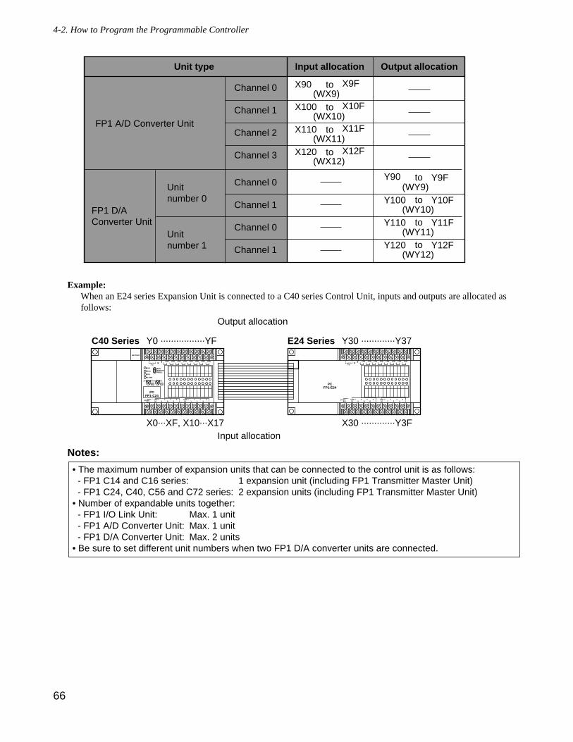
Example:When an E24 series Expansion Unit is connected to a C40 series Control Unit, inputs and outputs are allocated asfollows:
Notes:
• The maximum number of expansion units that can be connected to the control unit is as follows:- FP1 C14 and C16 series: 1 expansion unit (including FP1 Transmitter Master Unit)- FP1 C24, C40, C56 and C72 series: 2 expansion units (including FP1 Transmitter Master Unit)
• Number of expandable units together:- FP1 I/O Link Unit: Max. 1 unit- FP1 A/D Converter Unit: Max. 1 unit- FP1 D/A Converter Unit: Max. 2 units
• Be sure to set different unit numbers when two FP1 D/A converter units are connected.
COM0
COM1
COM2
COM3
COM4
COM5
COM6
COM7
+ -24V DC
F.G.
COMF
89
EAB
CD(+)-
COM7
01
623
45(+)-
RUNREMOTEPROG.
V0
max.min.
RUN
PROG.
ERR.
ALRAM
BATTERY
V1
max.
C40 Series
PCFP1-C24
24V DC+
-
min.
COM0
COM1
COM2
COM3
COM4
COM5
COM6
COM7
+ -24V DC
F.G.
COMF
89
EAB
CD(+)-
COM7
01
623
45(+)-
PCFP1-E24
24V DC+
-
Y0 .................YF E24 Series Y30 .............Y37
Output allocation
X0...XF, X10...X17 X30 .............Y3FInput allocation
Unit type
Channel 0
Channel 1
Channel 2
Channel 3
FP1 A/D Converter Unit
FP1 D/A Converter Unit
Unit number 0
Unit number 1
Channel 0
Channel 1
Channel 0
Channel 1
Input allocation
X90 (WX9)X100 (WX10)X110 (WX11)X120 (WX12)
to
to
to
to
X9F
X10F
X11F
X12F
Output allocation
Y90 (WY9)Y100 (WY10)Y110 (WY11)Y120 (WY12)
Y9F
Y10F
Y11F
Y12F
to
to
to
to
66
4-2. How to Program the Programmable Controller
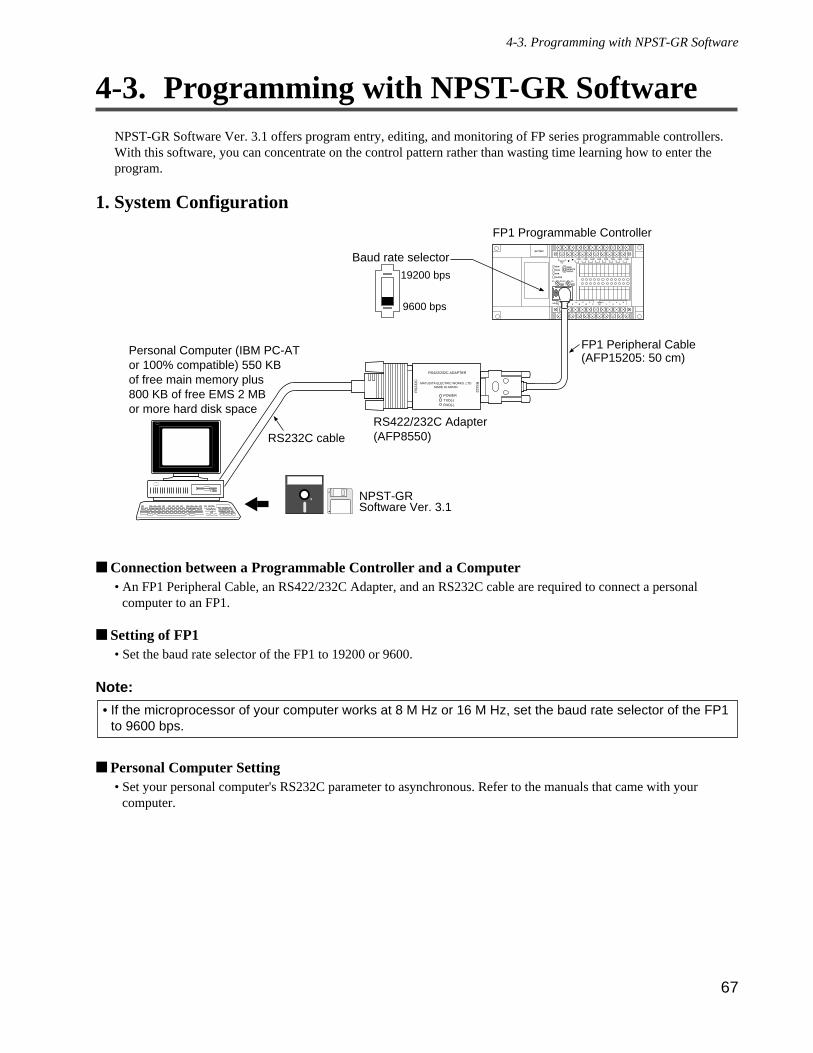
4-3. Programming with NPST-GR SoftwareNPST-GR Software Ver. 3.1 offers program entry, editing, and monitoring of FP series programmable controllers.With this software, you can concentrate on the control pattern rather than wasting time learning how to enter theprogram.
1. System Configuration
Connection between a Programmable Controller and a Computer• An FP1 Peripheral Cable, an RS422/232C Adapter, and an RS232C cable are required to connect a personal
computer to an FP1.
Setting of FP1• Set the baud rate selector of the FP1 to 19200 or 9600.
Note:
Personal Computer Setting• Set your personal computer's RS232C parameter to asynchronous. Refer to the manuals that came with your
computer.
• If the microprocessor of your computer works at 8 M Hz or 16 M Hz, set the baud rate selector of the FP1to 9600 bps.
FP1 Peripheral Cable(AFP15205: 50 cm)
COM0
COM1
COM2
COM3
COM4
COM5
COM6
COM7
+ -24V DC
F.G.
COMF
89
EAB
CD(+)-
COM7
01
623
45(+)-
RUNREMOTEPROG.
V0
max.min.
RUN
PROG.
ERR.
ALRAM
BATTERY
V1
max.
24V DC+
-
min.
FP1 Programmable Controller
NPST-GR Software Ver. 3.1
RS422/232C Adapter(AFP8550)
19200 bps
9600 bps
Baud rate selector
Personal Computer (IBM PC-AT or 100% compatible) 550 KBof free main memory plus800 KB of free EMS 2 MBor more hard disk space
RS232C cable
RS422/232C ADAPTER
MATUSITA ELECTRIC WORKS. LTDMADE IN JAPAN
POWERTXD(-)RXD(-)
RS
422RS
232C
67
4-3. Programming with NPST-GR Software

2. Features of NPST-GR Software Ver. 3NPST-GR Software is a programming support tool for the FP1 programmable controller. The things you can do withthe NPST-GR are briefly introduced in the following:
• ProgrammingNPST-GR provides three programming modes.
- programming by entering ladder symbols: the program will be displayed in ladder diagrams(Ladder symbol mode)
- programming by entering Boolean: the program will be displayed in ladder diagrams(Boolean ladder mode)
- programming by entering Boolean: the program will be displayed in Boolean(Boolean non-ladder mode)
You can create a program using any of these methods and you can change the method any time. The display willchange automatically according to the method you select. With any method, you can create a program by selectinginstructions from the function keys.NPST-GR Software also provides various features which enable effective programming such as the ability tocustomize it to make program creation easier.While creating a program, you can copy, delete, move, and search for a part of the program.
• Comment functionYou can enter comments for relays and output instructions.These comments show you which device the relay corresponds to, or for what application the relay is used.
• Program checkWith the program checking function, you can check the created program for grammatical errors.
• MonitoringTo support programming capability, NPST-GR Software can monitor the program you created and perform a testrun for verifications. You can check the status of relays and registers, and the programmable controller operatingstatus. This makes it easy to perform debugging and field adjustments.
• System register settingYou can set the system registers using NPST-GR Software. Using the screen messages makes option selection andvalue entry much easier.
• DocumentationYou can print-out all the settings you made, such as program and system register settings.
• Data transferYou can transfer the program created with the NPST-GR Software to the programmable controller easily by keyoperation. You can also transfer the data to ROM.
• Data managementYou can save the data to a disk, which is useful for back-ups and temporary storage before transferring the data tothe programmable controller.
68
4-3. Programming with NPST-GR Software
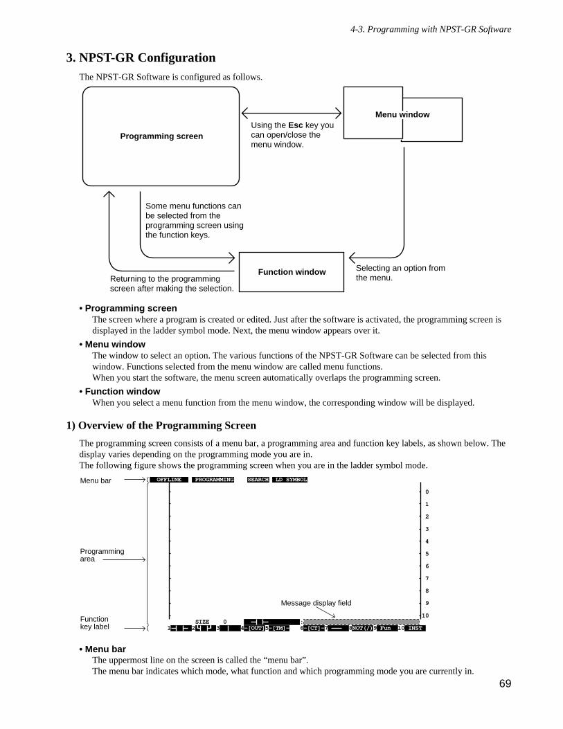
3. NPST-GR ConfigurationThe NPST-GR Software is configured as follows.
• Programming screenThe screen where a program is created or edited. Just after the software is activated, the programming screen isdisplayed in the ladder symbol mode. Next, the menu window appears over it.
• Menu windowThe window to select an option. The various functions of the NPST-GR Software can be selected from thiswindow. Functions selected from the menu window are called menu functions.When you start the software, the menu screen automatically overlaps the programming screen.
• Function windowWhen you select a menu function from the menu window, the corresponding window will be displayed.
1) Overview of the Programming Screen
The programming screen consists of a menu bar, a programming area and function key labels, as shown below. Thedisplay varies depending on the programming mode you are in.The following figure shows the programming screen when you are in the ladder symbol mode.
• Menu barThe uppermost line on the screen is called the “menu bar”.The menu bar indicates which mode, what function and which programming mode you are currently in.
OFFLINE PROGRAMMING SEARCH LD SYMBOL
SIZE 0 : 1 2 3 4-[OUT]5-[TM]- 6-[CT]-7 8NOT(/)9 Fun 10 INST
0
1
2
3
4
5
6
7
8
9
10
Menu bar
Programmingarea
Functionkey label
Message display field
Using the Esc key you can open/close the menu window.
Some menu functions canbe selected from theprogramming screen usingthe function keys.
Returning to the programming screen after making the selection.
Selecting an option fromthe menu.
Programming screen
Function window
Menu window
69
4-3. Programming with NPST-GR Software
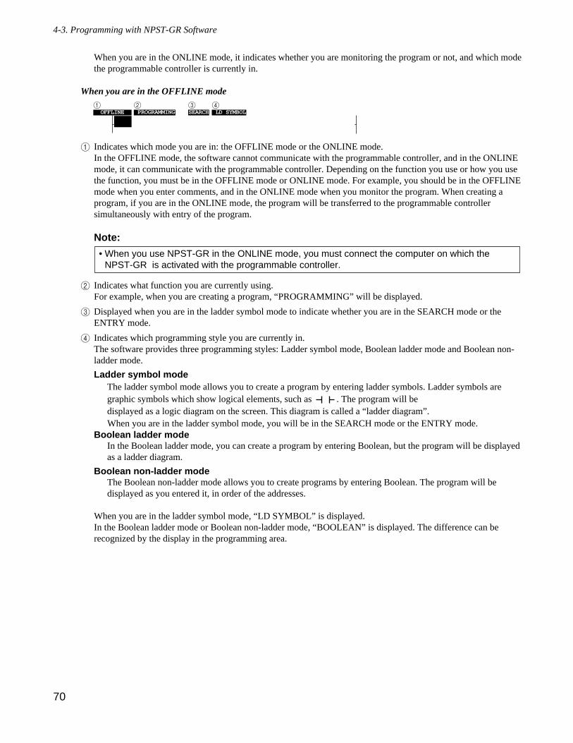
When you are in the ONLINE mode, it indicates whether you are monitoring the program or not, and which modethe programmable controller is currently in.
When you are in the OFFLINE mode
1 Indicates which mode you are in: the OFFLINE mode or the ONLINE mode.In the OFFLINE mode, the software cannot communicate with the programmable controller, and in the ONLINEmode, it can communicate with the programmable controller. Depending on the function you use or how you usethe function, you must be in the OFFLINE mode or ONLINE mode. For example, you should be in the OFFLINEmode when you enter comments, and in the ONLINE mode when you monitor the program. When creating aprogram, if you are in the ONLINE mode, the program will be transferred to the programmable controllersimultaneously with entry of the program.
Note:
2 Indicates what function you are currently using.For example, when you are creating a program, “PROGRAMMING” will be displayed.
3 Displayed when you are in the ladder symbol mode to indicate whether you are in the SEARCH mode or theENTRY mode.
4 Indicates which programming style you are currently in.The software provides three programming styles: Ladder symbol mode, Boolean ladder mode and Boolean non-ladder mode.
Ladder symbol modeThe ladder symbol mode allows you to create a program by entering ladder symbols. Ladder symbols aregraphic symbols which show logical elements, such as . The program will be displayed as a logic diagram on the screen. This diagram is called a “ladder diagram”. When you are in the ladder symbol mode, you will be in the SEARCH mode or the ENTRY mode.
Boolean ladder modeIn the Boolean ladder mode, you can create a program by entering Boolean, but the program will be displayedas a ladder diagram.
Boolean non-ladder modeThe Boolean non-ladder mode allows you to create programs by entering Boolean. The program will bedisplayed as you entered it, in order of the addresses.
When you are in the ladder symbol mode, “LD SYMBOL” is displayed.In the Boolean ladder mode or Boolean non-ladder mode, “BOOLEAN” is displayed. The difference can berecognized by the display in the programming area.
• When you use NPST-GR in the ONLINE mode, you must connect the computer on which theNPST-GR is activated with the programmable controller.
OFFLINE PROGRAMMING SEARCH LD SYMBOL 1 2 3 4
70
4-3. Programming with NPST-GR Software
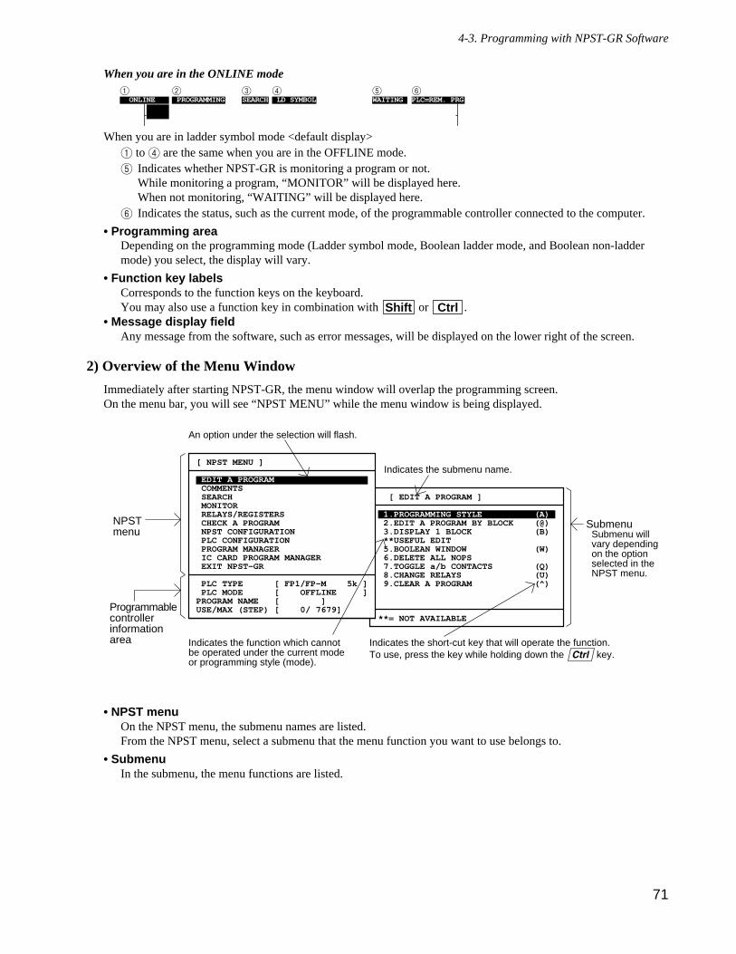
When you are in the ONLINE mode
When you are in ladder symbol mode <default display>1 to4 are the same when you are in the OFFLINE mode.5 Indicates whether NPST-GR is monitoring a program or not.
While monitoring a program, “MONITOR” will be displayed here.When not monitoring, “WAITING” will be displayed here.
6 Indicates the status, such as the current mode, of the programmable controller connected to the computer.
• Programming areaDepending on the programming mode (Ladder symbol mode, Boolean ladder mode, and Boolean non-laddermode) you select, the display will vary.
• Function key labelsCorresponds to the function keys on the keyboard.You may also use a function key in combination with or .
• Message display fieldAny message from the software, such as error messages, will be displayed on the lower right of the screen.
2) Overview of the Menu Window
Immediately after starting NPST-GR, the menu window will overlap the programming screen. On the menu bar, you will see “NPST MENU” while the menu window is being displayed.
• NPST menuOn the NPST menu, the submenu names are listed.From the NPST menu, select a submenu that the menu function you want to use belongs to.
• SubmenuIn the submenu, the menu functions are listed.
[ NPST MENU ]
EDIT A PROGRAM COMMENTS SEARCH [ EDIT A PROGRAM ] MONITOR RELAYS/REGISTERS 1.PROGRAMMING STYLE (A) CHECK A PROGRAM 2.EDIT A PROGRAM BY BLOCK (@) NPST CONFIGURATION 3.DISPLAY 1 BLOCK (B) PLC CONFIGURATION **USEFUL EDIT PROGRAM MANAGER 5.BOOLEAN WINDOW (W) IC CARD PROGRAM MANAGER 6.DELETE ALL NOPS EXIT NPST-GR 7.TOGGLE a/b CONTACTS (Q) 8.CHANGE RELAYS (U) PLC TYPE [ FP1/FP-M 5k ] 9.CLEAR A PROGRAM (^) PLC MODE [ OFFLINE ] PROGRAM NAME [ ] USE/MAX (STEP) [ 0/ 7679] **= NOT AVAILABLE
NPST menu
SubmenuSubmenu will vary depending on the option selected in the NPST menu.
Programmable controllerinformation area
An option under the selection will flash.
Indicates the function which cannot be operated under the current mode or programming style (mode).
Indicates the short-cut key that will operate the function. To use, press the key while holding down the key.
Indicates the submenu name.
CtrlShift
ONLINE PROGRAMMING SEARCH LD SYMBOL WAITING PLC=REM. PRG1 2 3 4 5 6
71
4-3. Programming with NPST-GR Software
• Programmable controller information area
PLC TYPEIndicates the type of programmable controller currently specified.
PLC TYPE: FP1 0.9 kFP1/FP-M 2.7 kFP1/FP-M 5 kFP3 10 kFP3/FP-C 16 kFP5 16 kFP10/FP10S 30 kFP10 60 k
PLC MODEIndicates the operation mode of the programmable controller.When you are in the OFFLINE mode, “OFFLINE” will be displayed here.In the ONLINE mode, the display will vary according to the setting on the programmable controller.
PROGRAM NAMEThe name of program is displayed on the screen. When you create a new program, nothing will be displayed.When you load the program from a disk or the programmable controller, the filename you registered for theprogram will be displayed.
USE/MAX (STEP)Indicates the number of steps (program size). The number of steps you have already used for the program duringediting or creation, and the maximum of number of steps you can use for the program is indicated.
4. NPST-GR Installation and Configuration
1) Preparing for Installation
This section describes how to install the device driver ANSI.SYS. Install the software using the installation program.The installation program is included in the NPST-GR system disk. The installation program cannot start if the devicedriver ANSI.SYS provided with the MS-DOS system disk has been installed in the disk on which you want to installNPST-GR. If ANSI.SYS has not been installed, install ANSI.SYS first and then install NPST-GR.Procedure
1. If the ANSI.SYS file does not exist on the disk on which you want to install NPST-GR, copy the ANSI.SYSfile from the MS-DOS system disk to the hard disk. For example, to copy the ANSI.SYS file to the rootdirectory of the hard disk, insert the MS-DOS system disk into drive A and type the following after the DOSprompt:
COPY A:\ANSI.SYS C:(Enter)2. If the DEVICE command for ANSI.SYS is not included in the CONFIG.SYS file, modify the CONFIG.SYS
file. For example, to add the DEVICE command to the CONFIG.SYS file, type the following at the DOSprompt (C:\):
COPY CONFIG.SYS+CON CONFIG.SYS(Enter)DEVICE=ANSI.SYS(Enter)
Then, press + and press .The CONFIG.SYS file will now contain the new line.
Notes:
• After modifying the CONFIG.SYS file, reset the personal computer so that your changes take effect.• Note that the directory in which the ANSI.SYS exists must match the pathname used for the DEVICE
command.
EnterZCtrl
72
4-3. Programming with NPST-GR Software
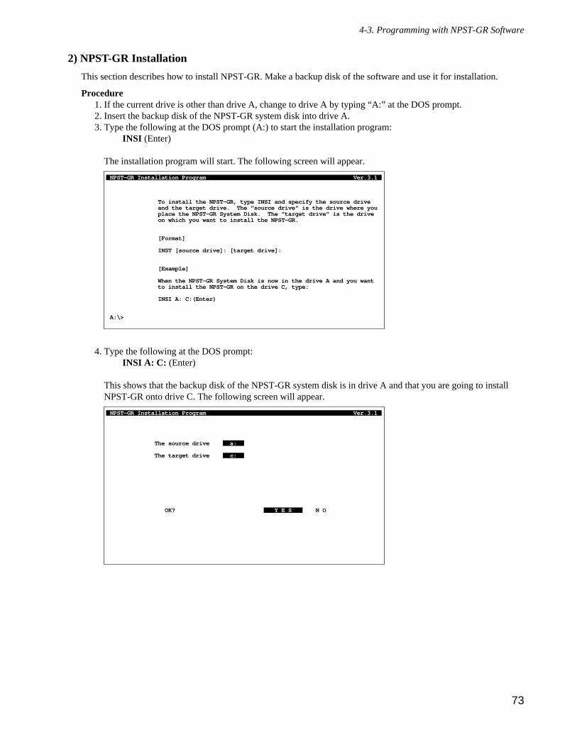
73
4-3. Programming with NPST-GR Software
2) NPST-GR Installation
This section describes how to install NPST-GR. Make a backup disk of the software and use it for installation.
Procedure1. If the current drive is other than drive A, change to drive A by typing “A:” at the DOS prompt.2. Insert the backup disk of the NPST-GR system disk into drive A.3. Type the following at the DOS prompt (A:) to start the installation program:
INSI (Enter)
The installation program will start. The following screen will appear.
4. Type the following at the DOS prompt:INSI A: C: (Enter)
This shows that the backup disk of the NPST-GR system disk is in drive A and that you are going to installNPST-GR onto drive C. The following screen will appear.
NPST-GR Installation Program Ver.3.1
The source drive a:
The target drive c:
OK? Y E S N O
NPST-GR Installation Program Ver.3.1
To install the NPST-GR, type INSI and specify the source drive and the target drive. The "source drive" is the drive where you place the NPST-GR System Disk. The "target drive" is the drive on which you want to install the NPST-GR.
[Format]
INST [source drive]: [target drive]:
[Example]
When the NPST-GR System Disk is now in the drive A and you want to install the NPST-GR on the drive C, type:
INSI A: C:(Enter)
A:\>
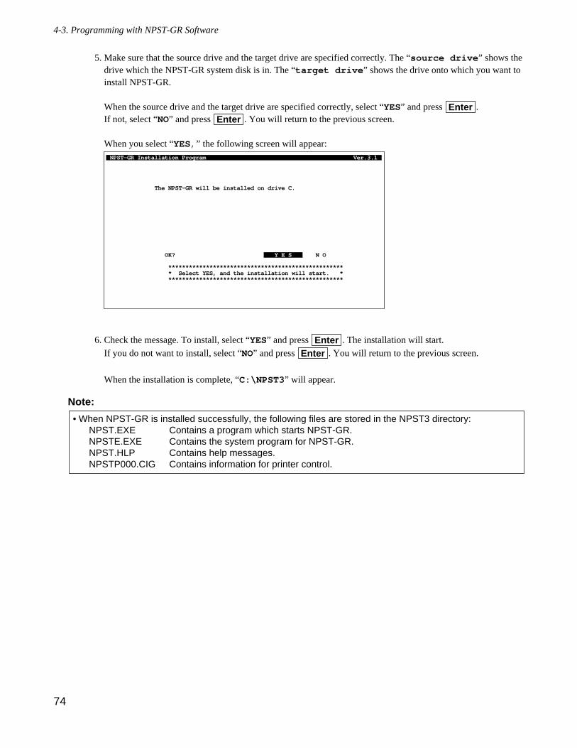
74
4-3. Programming with NPST-GR Software
5. Make sure that the source drive and the target drive are specified correctly. The “source drive” shows thedrive which the NPST-GR system disk is in. The “target drive” shows the drive onto which you want toinstall NPST-GR.
When the source drive and the target drive are specified correctly, select “YES” and press .If not, select “NO” and press . You will return to the previous screen.
When you select “YES,” the following screen will appear:
6. Check the message. To install, select “YES” and press . The installation will start.
If you do not want to install, select “NO” and press . You will return to the previous screen.
When the installation is complete, “C:\NPST3” will appear.
Note:
• When NPST-GR is installed successfully, the following files are stored in the NPST3 directory:NPST.EXE Contains a program which starts NPST-GR.NPSTE.EXE Contains the system program for NPST-GR.NPST.HLP Contains help messages.NPSTP000.CIG Contains information for printer control.
EnterEnter
NPST-GR Installation Program Ver.3.1
The NPST-GR will be installed on drive C.
OK? Y E S N O
*************************************************** * Select YES, and the installation will start. * ***************************************************
EnterEnter
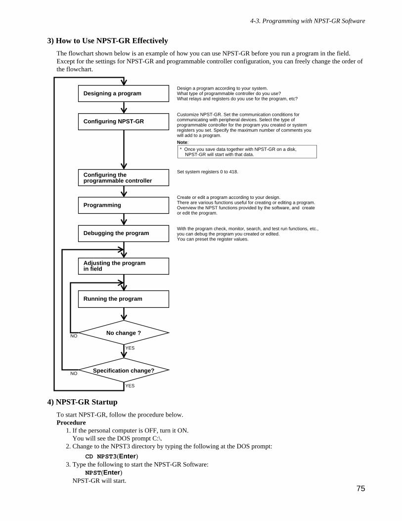
75
4-3. Programming with NPST-GR Software
3) How to Use NPST-GR Effectively
The flowchart shown below is an example of how you can use NPST-GR before you run a program in the field.Except for the settings for NPST-GR and programmable controller configuration, you can freely change the order ofthe flowchart.
4) NPST-GR Startup
To start NPST-GR, follow the procedure below.Procedure
1. If the personal computer is OFF, turn it ON.You will see the DOS prompt C:\.
2. Change to the NPST3 directory by typing the following at the DOS prompt:
CD NPST3(Enter)3. Type the following to start the NPST-GR Software:
NPST(Enter)NPST-GR will start.
Designing a program
Configuring NPST-GR
Configuring the programmable controller
Programming
Debugging the program
Running the program
Adjusting the program in field
No change ?
Specification change?
Design a program according to your system.What type of programmable controller do you use?What relays and registers do you use for the program, etc?
Customize NPST-GR. Set the communication conditions for communicating with peripheral devices. Select the type of programmable controller for the program you created or system registers you set. Specify the maximum number of comments you will add to a program.
Note:
* Once you save data together with NPST-GR on a disk, NPST-GR will start with that data.
Set system registers 0 to 418.
Create or edit a program according to your design.There are various functions useful for creating or editing a program. Overview the NPST functions provided by the software, and create or edit the program.
With the program check, monitor, search, and test run functions, etc., you can debug the program you created or edited.You can preset the register values.
NO
NO
YES
YES
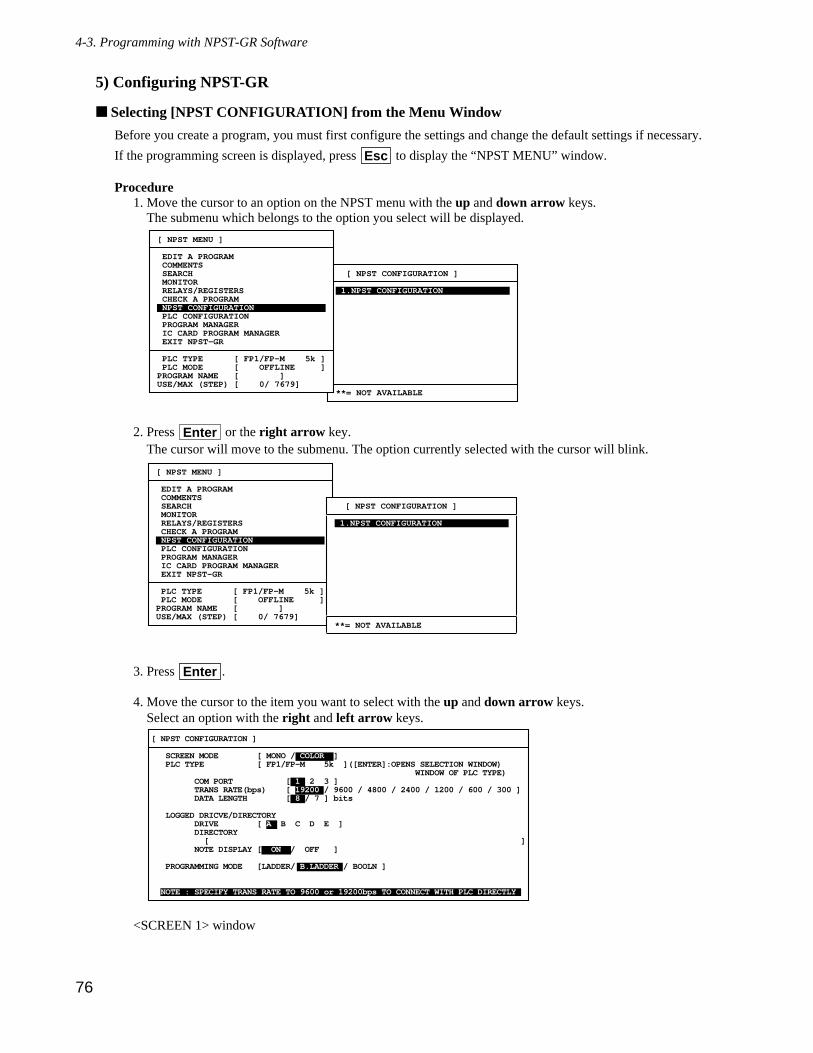
76
4-3. Programming with NPST-GR Software
5) Configuring NPST-GR
Selecting [NPST CONFIGURATION] from the Menu Window
Before you create a program, you must first configure the settings and change the default settings if necessary.
If the programming screen is displayed, press to display the “NPST MENU” window.
Procedure1. Move the cursor to an option on the NPST menu with the up and down arrow keys.
The submenu which belongs to the option you select will be displayed.
2. Press or the right arrow key.The cursor will move to the submenu. The option currently selected with the cursor will blink.
3. Press .
4. Move the cursor to the item you want to select with the up and down arrow keys.Select an option with the right and left arrow keys.
<SCREEN 1> window
[ NPST CONFIGURATION ]
SCREEN MODE [ MONO / COLOR ] PLC TYPE [ FP1/FP-M 5k ]([ENTER]:OPENS SELECTION WINDOW) WINDOW OF PLC TYPE) COM PORT [ 1 2 3 ] TRANS RATE(bps) [ 19200 / 9600 / 4800 / 2400 / 1200 / 600 / 300 ] DATA LENGTH [ 8 / 7 ] bits
LOGGED DRICVE/DIRECTORY DRIVE [ A B C D E ] DIRECTORY [ ] NOTE DISPLAY [ ON / OFF ]
PROGRAMMING MODE [LADDER/ B.LADDER / BOOLN ]
NOTE : SPECIFY TRANS RATE TO 9600 or 19200bps TO CONNECT WITH PLC DIRECTLY
Enter
[ NPST MENU ]
EDIT A PROGRAM COMMENTS SEARCH [ NPST CONFIGURATION ] MONITOR RELAYS/REGISTERS 1.NPST CONFIGURATION CHECK A PROGRAM NPST CONFIGURATION PLC CONFIGURATION PROGRAM MANAGER IC CARD PROGRAM MANAGER EXIT NPST-GR
PLC TYPE [ FP1/FP-M 5k ] PLC MODE [ OFFLINE ] PROGRAM NAME [ ] USE/MAX (STEP) [ 0/ 7679] **= NOT AVAILABLE
Esc
77
4-3. Programming with NPST-GR Software
• SCREEN MODEYou can select the NPST-GR screen mode between color and black/white.
MONO: Displays the screen in black and white.COLOR: Displays the screen in color.
(Black/Cyan/Red/Magenta/Green/Bright Blue/Yellow or Brown/White)
• PLC TYPEBefore setting the configuration of the programmable controller and creating a program, you must specify the type ofprogrammable controller for which you create a program.You can select from;
FP1 0.9 k: FP1 C14/C16 seriesFP1/FP-M 2.7 k: FP1 C24/C40 series and FP-M (2.7 k)FP1/FP-M 5 k: FP1 C56/C72 series and FP-M (5 k)FP3 10 k: FP3 (10 k)FP3/FP-C 16 k: FP3 (16 k) and the FP-C (16 k)FP5 16 k: FP5 (16 k)FP10/FP10S 30 k: FP10 (30 k) and FP10S (30 k)FP10 60 k: FP10 (60 k)
COM PORTSpecify the serial port which is connected to the programmable controller.
1: Use COM PORT 12: Use COM PORT 23: Use COM PORT 3
TRANS RATE (bps)Specify the transmission rate for communication with the programmable controller or modem.Select between 19200, 9600, 4800, 2400, 1200, 600 or 300.For communication with the programmable controller, specify either 19200 or 9600.If the clock frequency is a multiple of five, you must select 19200. If you do not select 19200, NPST-GR will not communicate with the programmable controller.
DATA LENGTHSpecify the data length for communication with the programmable controller.Select either 8-bit or 7-bit.
• LOGGED DRIVE/DIRECTORYSpecify the logged drive when you manage files.
DRIVE/DIRECTORYSpecify the logged directory when you manage files. Include a \ at the beginning and at the end of the directory,eg., \npst\program\.If you omit this, the root directory will be specified.
NOTE DISPLAYSpecify whether file notes, which are the notes entered for a file (such as filename and date), are to bedisplayed when the disk file list is displayed.
ON: Displays the file notes.OFF: Omits displaying the file notes.
• PROGRAMMING MODESelect the programming mode for creating or editing a program.Select from;
LADDER: The ladder symbol modeB.LADDER: The Boolean ladder modeBOOLN: The Boolean non-ladder mode
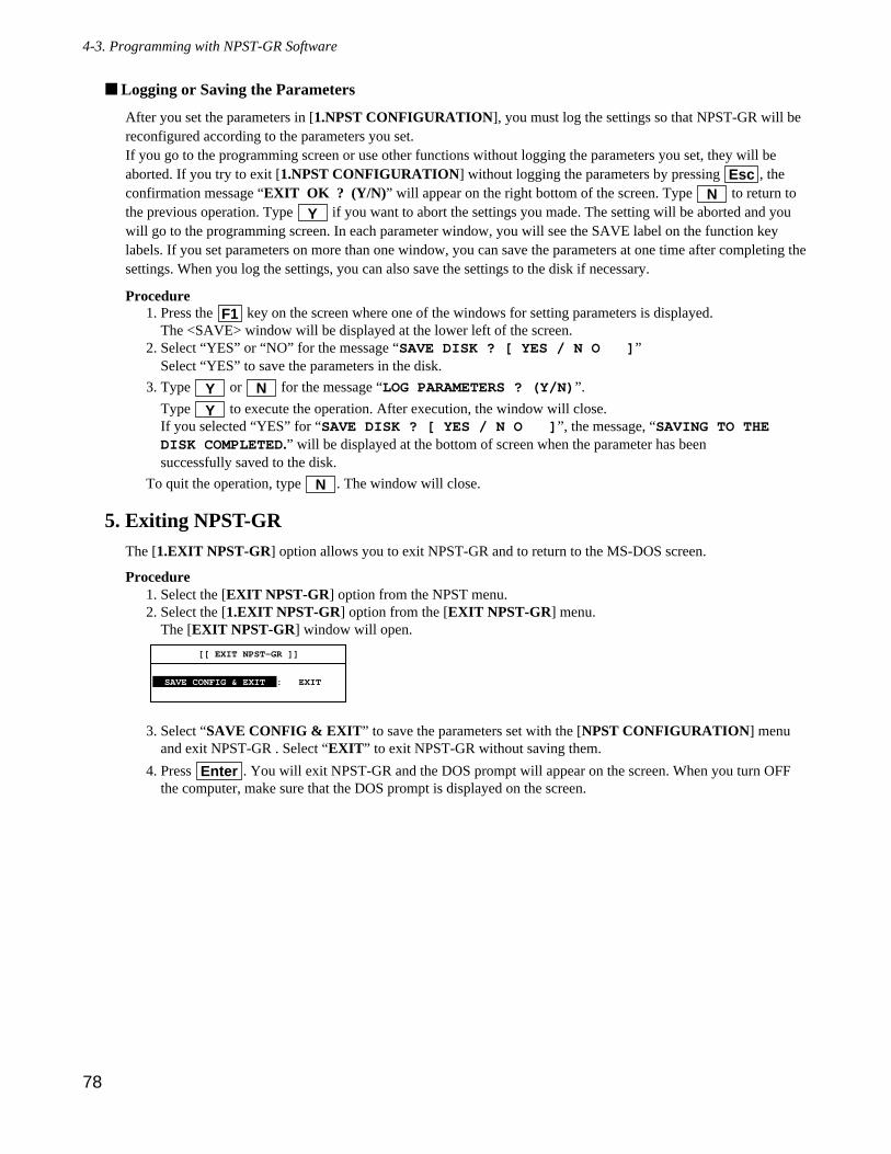
Logging or Saving the Parameters
After you set the parameters in [1.NPST CONFIGURATION], you must log the settings so that NPST-GR will bereconfigured according to the parameters you set. If you go to the programming screen or use other functions without logging the parameters you set, they will beaborted. If you try to exit [1.NPST CONFIGURATION] without logging the parameters by pressing , theconfirmation message “EXIT OK ? (Y/N)” will appear on the right bottom of the screen. Type to return tothe previous operation. Type if you want to abort the settings you made. The setting will be aborted and youwill go to the programming screen. In each parameter window, you will see the SAVE label on the function keylabels. If you set parameters on more than one window, you can save the parameters at one time after completing thesettings. When you log the settings, you can also save the settings to the disk if necessary.
Procedure1. Press the key on the screen where one of the windows for setting parameters is displayed.
The <SAVE> window will be displayed at the lower left of the screen.2. Select “YES” or “NO” for the message “SAVE DISK ? [ YES / N O ]”
Select “YES” to save the parameters in the disk.
3. Type or for the message “LOG PARAMETERS ? (Y/N)”.
Type to execute the operation. After execution, the window will close. If you selected “YES” for “SAVE DISK ? [ YES / N O ]”, the message, “SAVING TO THEDISK COMPLETED.” will be displayed at the bottom of screen when the parameter has been successfully saved to the disk.
To quit the operation, type . The window will close.
5. Exiting NPST-GRThe [1.EXIT NPST-GR] option allows you to exit NPST-GR and to return to the MS-DOS screen.
Procedure1. Select the [EXIT NPST-GR] option from the NPST menu.2. Select the [1.EXIT NPST-GR] option from the [EXIT NPST-GR] menu.
The [EXIT NPST-GR] window will open.
3. Select “SAVE CONFIG & EXIT” to save the parameters set with the [NPST CONFIGURATION] menuand exit NPST-GR . Select “EXIT” to exit NPST-GR without saving them.
4. Press . You will exit NPST-GR and the DOS prompt will appear on the screen. When you turn OFFthe computer, make sure that the DOS prompt is displayed on the screen.
Enter
[[ EXIT NPST-GR ]]
SAVE CONFIG & EXIT : EXIT
N
Y
NY
F1
YN
Esc
78
4-3. Programming with NPST-GR Software
6. Basic Key Operation for ProgramsInput the following program using the ladder symbol mode.
When you first start NPST-GR, you will be in the ladder symbol mode.The [1.PROGRAMMING STYLE] option changes the programming style to the Boolean non-ladder mode.Procedure
1. Select the [EDIT A PROGRAM] option from the NPST menu.2. Select the [1.PROGRAMMING STYLE] option from the [EDIT A PROGRAM] menu.3. Select “BOOLEAN NONLADDER” from the [PROGRAMMING STYLE] window.4. Press .
Program InputInput the program using the function keys. The command language input will be displayed in the input field at thebottom of the screen. It will be interpreted and displayed as an element on the ladder diagram when you press the
key.[Input Deletions]When deleting from the input field...................................Press .When deleting from the ladder diagram display area.......Move the cursor to the location containing the mistake and
press .Refer to the “NPST-GR Software” manual for details.
Del
BS
Enter
Enter
T0 Y1
TMX 300
R0 Y0
R0
X0 R0X1
( ED )
Boolean Non-ladder
Address
0
1
2
3
4
5
6
9
10
11
Instruction
ST X 0
OR R 0
AN/ X 1
OT R 0
ST R 0
OT Y 0
TM X 0
K 30
ST T 0
OT Y 1
ED
Key operation
0
1
4
9
11
F1 F1 0 Enter
F2 F3 0 Enter
F3 F8 F1 1 Enter
F4 F3 0 Enter
F1 F3 0 Enter
F4 F2 0 Enter
F5 F1 0
F1 F1 0 Enter
F1 F4 0 Enter
F4 F2 1 Enter
F10 Ctrl + F3 Enter
3
79
4-3. Programming with NPST-GR Software
7. Downloading a Program to the Programmable ControllerThe [4.LOAD A PROGRAM TO PLC] option downloads the program and/or the I/O comments which are on thescreen of the programmable controller. After you complete the program, you must download the program so that theprogrammable controller executes it.
Notes:
Procedure1. Select the [PROGRAM MANAGER] option from the NPST menu. 2. Select the [4.LOAD A PROGRAM TO PLC] option from the [PROGRAM MANAGER] menu.
The [LOAD TO PLC] window will appear on the screen.
3. If you want to change the communicating station, press + .4. If the programmable controller is in the RUN mode, change to the PROG. Mode.
When the programmable controller is in the REMOTE mode, you can change it by pressing + .5. Specify what you want to load to the programmable controller at “LOAD.”
Select “PROGRAM” to download only the program.Select “I/O CMT” to download only the I/O comments.Select “PROG & I/O CMT” to download both the program and the I/O comments.
6. Specify whether or not to verify the programs.Select “YES” at “VERIFY” with the arrow keys when you want to verify the transferred program with the one displayed on the screen after downloading. Select “NO” if you do not want to verify the program.
7. Press to start downloading.During the download, “LOADING PROGRAM...” will appear on the screen.If you select “YES” at “VERIFY,” the message “VERIFYING PROGRAM...” will appear.When completed successfully, “VERIFY OK” will appear on the bottom of the screen. The number of stepsused for the program will be displayed at the bottom of the screen.
Enter
F6Ctrl
F7Ctrl
[TO PLC] NO.=[ 0 ] RT =[ 1 ] HOME
LOAD [ PROGRAM I/O CMT PROG & I/O CMT ]
VERIFY [ YES NO ]
• The downloaded program will be executed when you set the mode of programmable controller toRUN.
• Before you start operation, make sure that NPST-GR is in the ONLINE mode.
80
4-3. Programming with NPST-GR Software
8. Saving a Program to DiskThe [2.SAVE A PROGRAM TO DISK] option saves the program and/or the I/O comments which exist on thescreen to the disk of your personal computer.Procedure
1. Select the [PROGRAM MANAGER] option from the NPST menu. 2. Select the [2.SAVE A PROGRAM TO DISK] option from the [PROGRAM MANAGER] menu.
A window for saving the program and/or I/O comments will open on the screen. You will see “SAVEPROGRAM” on the menu bar.
3. If you want to change the drive, press .
4. If you want to change the directory, press .5. Enter a filename in the “FILE NAME” area.6. If necessary, enter the information for “FILE NOTE”, “DESIGNER” and “DATE”. These items are
optional and can be skipped. Press the down arrow key to go to the next item.7. Specify what you want to save to the disk at “SAVE.”
Select “PROGRAM” to save only the program.Select “I/O CMT” to save only the I/O comments.Select “PROG & I/O CMT” to save both the program and the I/O comments.
8. Determine which version style you want to save in.Select “Ver.3” to save in the version 3 style.Select “Ver.2” to save in the version 2 style.
9. When you select “Ver.3”, select whether you want to verify the programs.Select “YES” at “VERIFY” with the arrow keys, to verify the saved program with the program on thescreen after saving. Select “NO” if you do not want to verify the program.
10. Press .When you select “Ver.3,” saving will start.
Enter
F8
F6
DRIVE [ A B C D E ] FREE AREA 9617408 DIRECTORY [\PROGRAM\ ]
FILE NAME [ ] FILE NOTE [ ] DESIGNER [ ] DATE [93-12-01] SAVE [ PROGRAM I/O CMT PROG & I/O CMT ] STYLE [ Ver.3 Ver.2 ] VERIFY [ YES N O ] NOTE: [VERIFY] IS INVALID SELECT [VER.2]
Shows the current drive.Shows the current directory.
Shows the memory area size available in the disk.
Select whether the saved program is verified with the original one on the screen after saving.Select whether to save the program in the version 3 style or in the version 2 style.Select whether to save the program, the I/O comments or both.Shows the date which is controlled by the system.Enter the name of the person who design the program.Enter notes about the file.Enter a filename.
Lists existing files in the current directory when pressing F7 .
81
4-3. Programming with NPST-GR Software
9. PrintingThe [A.PRINT OUT] option prints out:
the program displayed on the screen, as a ladder diagram or in Boolean. the list of the relays, registers or control instructions used in the program. the parameters set with the [NPST CONFIGURATION] menu the parameters set for system registers 0 to 418, the I/O map, and the remote I/O map
When you select the [A.PRINT OUT] option, the [PRINT OUT] window will open. First, select what you want toprint out by selecting the “STYLE” option, and start printing by selecting the “PRINT” option. With the defaultsettings, only the program will be printed in the ladder diagram style.
Procedure1. Select the [PROGRAM MANAGER] option from the NPST menu.2. Select the [A.PRINT OUT] option from the [PROGRAM MANAGER] menu.
The [PRINT OUT] window will open.
3. Select “STYLE” in the [PRINT OUT] window.The [STYLE] window will open.
4. Specify what you want to print out in the [STYLE] window.Select “Y” for the item which you want to print. Select “N” not to print it.
5. Press to log the settings in each window and to return to the previous window.You must press on every window on which you made any change. When pressing , you will beasked “SURE?” Type to log the changes you made. To cancel them, type .
6. Select “PRINT” from the [PRINT OUT] window.7. Press . The [PRINT] windows shown right will open.
8. When you want to change the settings in the windows, select the desired options. To select an option, use theright or left arrow key. To go to the next item, press the down arrow key.
9. Press to start printing.Enter
[ PRINT ]
START PAGE [ 1]
START ADDRESS [ 0]
END ADDRESS [ 125]
PAPER SIZE PORT / LAND
PRINT MODE SINGL / CONTIN
HIGH / NORMAL
[ENTER] : EXECUTE.
Enter
NYF1F1
F1
[ STYLE ]
** TITLE Y / N
** LADDER DIAGRAM Y / N
** BOOLEAN Y / N
** RELAY LIST Y / N
NPST CONFIGURATION Y / N
SYSTEM REGISTER Y / N
REMOTE I/O Y / N
** = [ENTER] TO SET THE DETAILS
[PRINT OUT]
STYLE
PRINTER
[ENTER] : EXECUTE.
82
4-3. Programming with NPST-GR Software
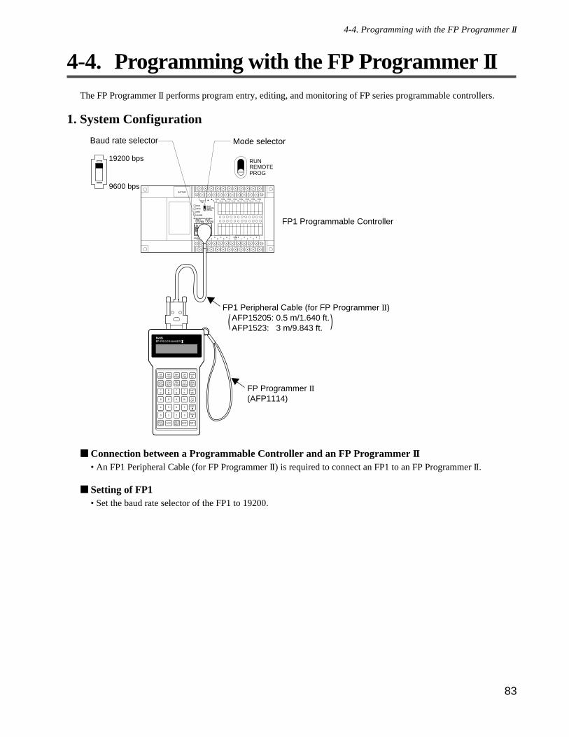
83
4-4. Programming with the FP Programmer II
4-4. Programming with the FP Programmer IIThe FP Programmer II performs program entry, editing, and monitoring of FP series programmable controllers.
1. System Configuration
Connection between a Programmable Controller and an FP Programmer II• An FP1 Peripheral Cable (for FP Programmer II) is required to connect an FP1 to an FP Programmer II.
Setting of FP1• Set the baud rate selector of the FP1 to 19200.
COM0
COM1
COM2
COM3
COM4
COM5
COM6
COM7
+ -24V DC
F.G.
COMF
89
EAB
CD(+)-
COM7
01
623
45(+)-
RUNREMOTEPROG.
V0
max.min.
RUN
PROG.
ERR.
ALRAM
BATTERY
V1
max.
24V DC+
-
min.
FP1 Programmable Controller
FP1 Peripheral Cable (for FP Programmer II)AFP15205: 0.5 m/1.640 ft.AFP1523: 3 m/9.843 ft.
FP Programmer II(AFP1114)
RUNREMOTEPROG
Mode selectorBaud rate selector
19200 bps
9600 bps
FP PROGRAMMER
STX•WX
ANY•WY
ORR•WR
OTL•WL
FN/PFL
NOTDT/Ld
STKIX/IY
TMT•SV
CTC•EV
(BIN)K/H
=C
DD
<E
>F
SHIFTSC
8 9 A B
4 5 6 7
0 1 2 3
(-)OP
SRC
READ
(HELP)CLR
ACLR (DELT)INST
ENT WRT
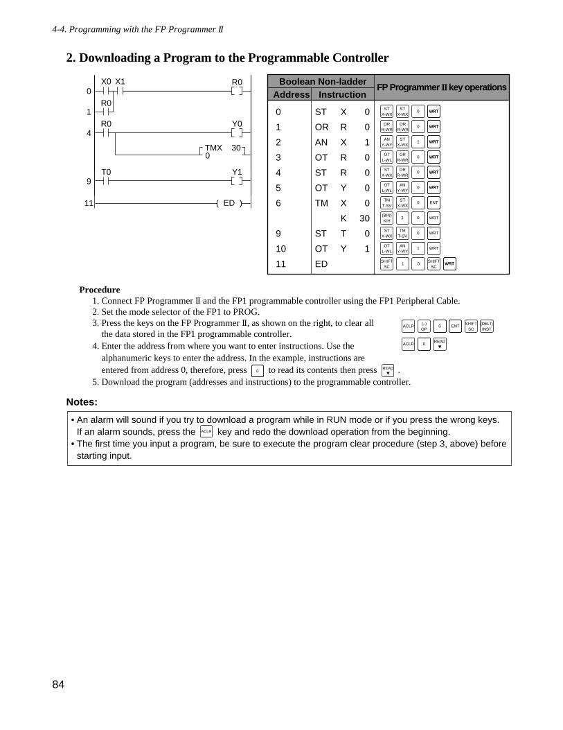
84
4-4. Programming with the FP Programmer II
2. Downloading a Program to the Programmable Controller
Procedure1. Connect FP Programmer II and the FP1 programmable controller using the FP1 Peripheral Cable.2. Set the mode selector of the FP1 to PROG.3. Press the keys on the FP Programmer II, as shown on the right, to clear all
the data stored in the FP1 programmable controller.4. Enter the address from where you want to enter instructions. Use the
alphanumeric keys to enter the address. In the example, instructions areentered from address 0, therefore, press to read its contents then press .
5. Download the program (addresses and instructions) to the programmable controller.
Notes:
• An alarm will sound if you try to download a program while in RUN mode or if you press the wrong keys. If an alarm sounds, press the key and redo the download operation from the beginning.
• The first time you input a program, be sure to execute the program clear procedure (step 3, above) beforestarting input.
ACLR
READ
0
R0 Y0
X0
TMX 300
R0
T0 Y1
R0
( ED )
0
4
1
9
11
X1FP Programmer IIkey operations
Boolean Non-ladderAddress Instruction
OTL-WL
ANY-WY
1 WRT
WRTWRTSHIFT
SC1
ANY-WY
OTL-WL
WRT0 WRT
STX-WX
STX-WX
WRT0 WRT
ORR-WR
WRT0 WRT
STX-WX
ANY-WY
WRT1 WRT
ORR-WR
OTL-WL
WRT0 WRT
STX-WX
TMT-SV
ENT0
(BIN)K/H
WRT0
ORR-WR
3
TMT-SV
STX-WX
WRT0
0SHIFT
SC
ORR-WR
STX-WX
WRT0 WRT
ST X 0
OR R 0
AN X 1
OT R 0
ST R 0
OT Y 0
TM X 0
K 30
ST T 0
OT Y 1
ED
0
1
2
3
4
5
6
9
10
11
0ACLR(DELT)INST
SHIFTSC
ENT(–)OP
0ACLRREAD
85
4-4. Programming with the FP Programmer II
Key Operations for Correcting Input Errors
• Correcting the contents of the program
Procedure example
1. Read the contents of address 3.
2. Clear the display for address 3.
3. Rewrite with the correct instructions.
• Adding/inserting instructions
Procedure example
1. Read the contents of address 3.
2. Insert the new instruction.
• Deleting instructions
Procedure example
1. Read the contents of address 3.
2. Delete.
Inputting Instructions That Are Not on the Key DisplayThere are two ways to input instructions such as the ED (END) instruction and the DF (Leading edge differential)instruction, which are not on the key display.
• Using the HELP function
Procedure example
1. Press the keys shown on the right.
2. Next, press to look for the desired instruction.
3. Input the number for the instruction.Example:The ED instruction.
• Direct input of the instruction code
Example:The ED instruction.
READ
SHIFTSC
(HELP)CLR
1 0 WRT
SHIFTSC
SHIFTSC
WRT01
(HELP)CLR
ORR-WR
OTL-WL
ACLR 3READ
WRT0 WRT
ORR-WR
OTL-WL
ACLR 3READ
0(DELT)INST
SHIFTSC
ACLR 3READ
(DELT)INST
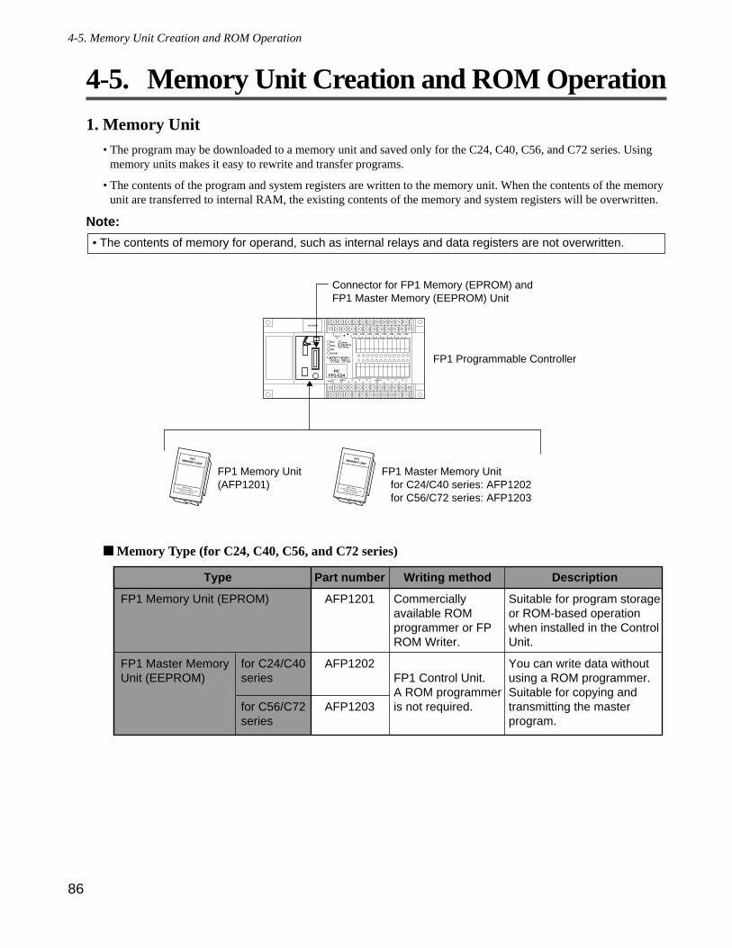
86
4-5. Memory Unit Creation and ROM Operation
4-5. Memory Unit Creation and ROM Operation
1. Memory Unit• The program may be downloaded to a memory unit and saved only for the C24, C40, C56, and C72 series. Using
memory units makes it easy to rewrite and transfer programs.
• The contents of the program and system registers are written to the memory unit. When the contents of the memoryunit are transferred to internal RAM, the existing contents of the memory and system registers will be overwritten.
Note:
Memory Type (for C24, C40, C56, and C72 series)
Type
FP1 Memory Unit (EPROM)
FP1 Master MemoryUnit (EEPROM)
for C24/C40series
for C56/C72series
Part number
AFP1201
AFP1202
AFP1203
Writing method
Commercially available ROM programmer or FP ROM Writer.
FP1 Control Unit. A ROM programmer is not required.
Description
Suitable for program storage or ROM-based operation when installed in the ControlUnit.
You can write data without using a ROM programmer.Suitable for copying and transmitting the masterprogram.
COM0
COM1
COM2
COM3
COM4
COM5
COM6
COM7
+ -24V DC
F.G.
COMF
89
EAB
CD(+)-
COM7
01
623
45(+)-
RUNREMOTEPROG.
V0
max.min.
RUN
PROG.
ERR.
ALRAM
BATTERY
V1
max.
PCFP1-C24
24V DC+
-
min.
Connector for FP1 Memory (EPROM) andFP1 Master Memory (EEPROM) Unit
FP1MEMORY UNIT
MATUSITAELECTRIC WORKS. LTDMADE IN JAPAN
FP1 Memory Unit(AFP1201)
FP1 Programmable Controller
FP1MEMORY UNIT
MATUSITAELECTRIC WORKS. LTDMADE IN JAPAN
FP1 Master Memory Unit for C24/C40 series: AFP1202 for C56/C72 series: AFP1203
• The contents of memory for operand, such as internal relays and data registers are not overwritten.
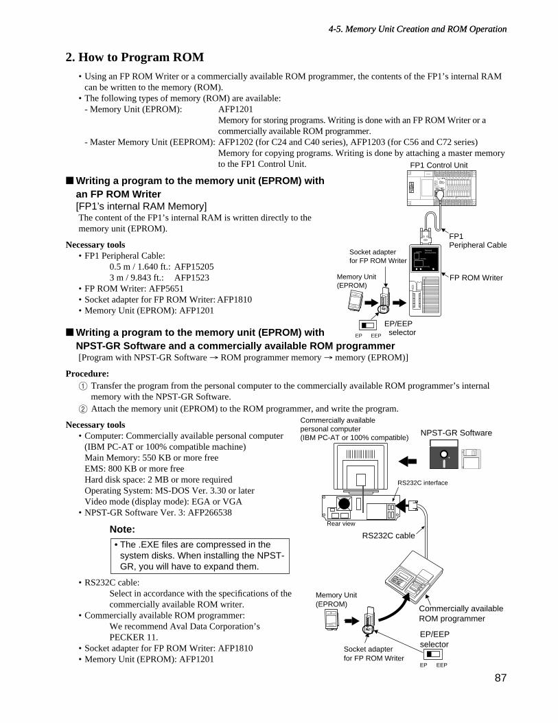
87
4-5. Memory Unit Creation and ROM Operation
2. How to Program ROM• Using an FP ROM Writer or a commercially available ROM programmer, the contents of the FP1’s internal RAM
can be written to the memory (ROM).• The following types of memory (ROM) are available:
- Memory Unit (EPROM): AFP1201Memory for storing programs. Writing is done with an FP ROM Writer or acommercially available ROM programmer.
- Master Memory Unit (EEPROM): AFP1202 (for C24 and C40 series), AFP1203 (for C56 and C72 series)Memory for copying programs. Writing is done by attaching a master memoryto the FP1 Control Unit.
Writing a program to the memory unit (EPROM) withan FP ROM Writer[FP1’s internal RAM Memory]The content of the FP1’s internal RAM is written directly to thememory unit (EPROM).
Necessary tools• FP1 Peripheral Cable:
0.5 m / 1.640 ft.: AFP152053 m / 9.843 ft.: AFP1523
• FP ROM Writer: AFP5651• Socket adapter for FP ROM Writer: AFP1810• Memory Unit (EPROM): AFP1201
Writing a program to the memory unit (EPROM) withNPST-GR Software and a commercially available ROM programmer[Program with NPST-GR Software → ROM programmer memory → memory (EPROM)]
Procedure:1 Transfer the program from the personal computer to the commercially available ROM programmer’s internal
memory with the NPST-GR Software.2 Attach the memory unit (EPROM) to the ROM programmer, and write the program.
Necessary tools• Computer: Commercially available personal computer
(IBM PC-AT or 100% compatible machine)Main Memory: 550 KB or more freeEMS: 800 KB or more freeHard disk space: 2 MB or more requiredOperating System: MS-DOS Ver. 3.30 or laterVideo mode (display mode): EGA or VGA
• NPST-GR Software Ver. 3: AFP266538
Note:
• RS232C cable:Select in accordance with the specifications of thecommercially available ROM writer.
• Commercially available ROM programmer: We recommend Aval Data Corporation’sPECKER 11.
• Socket adapter for FP ROM Writer: AFP1810• Memory Unit (EPROM): AFP1201
• The .EXE files are compressed in thesystem disks. When installing the NPST-GR, you will have to expand them.
4-5. Memory Unit Creation and ROM Operation
RS232C interface
RS232C cable
Rear view
NPST-GR Software
Commercially availablepersonal computer(IBM PC-AT or 100% compatible)
Socket adapterfor FP ROM Writer
Memory Unit(EPROM)
FP1MEMORY UNIT
MATUSITAELECTRIC WORKS. LTD
MADE IN JAPAN
Commercially availableROM programmer
EP EEP
EP/EEPselector
COM0
COM1
COM2
COM3
COM4
COM5
COM6
COM7
+ -24V DC
F.G.
COMF
89
EAB
CD(+)-
COM7
01
623
45(+)-
RUNREMOTEPROG.
V0
max.min.
RUN
PROG.
ERR.
ALRAM
BATTERY
V1
max.
24V DC+
-
min.
Nationalabcdefg abcdefg
abcdefg
abcdefg
abcdefg
FP1MEMORY UNIT
MATUSITAELECTRIC WORKS. LTDMADE IN JAPAN
FP1 Control Unit
FP1Peripheral Cable
FP ROM Writer
Socket adapterfor FP ROM Writer
Memory Unit(EPROM)
EP EEP
EP/EEP selector
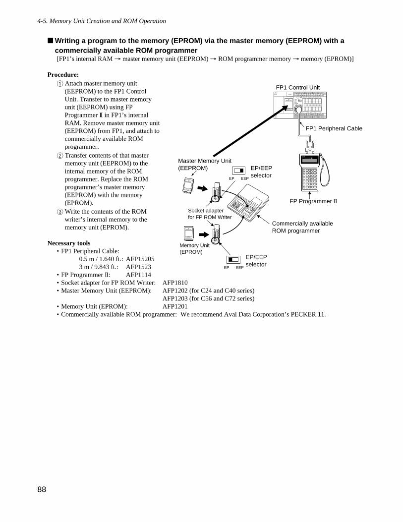
88
4-5. Memory Unit Creation and ROM Operation
Writing a program to the memory (EPROM) via the master memory (EEPROM) with acommercially available ROM programmer[FP1’s internal RAM → master memory unit (EEPROM) → ROM programmer memory → memory (EPROM)]
Procedure:1 Attach master memory unit
(EEPROM) to the FP1 ControlUnit. Transfer to master memoryunit (EEPROM) using FPProgrammer II in FP1’s internalRAM. Remove master memory unit(EEPROM) from FP1, and attach tocommercially available ROMprogrammer.
2 Transfer contents of that mastermemory unit (EEPROM) to theinternal memory of the ROMprogrammer. Replace the ROMprogrammer’s master memory(EEPROM) with the memory(EPROM).
3Write the contents of the ROMwriter’s internal memory to thememory unit (EPROM).
Necessary tools• FP1 Peripheral Cable:
0.5 m / 1.640 ft.: AFP152053 m / 9.843 ft.: AFP1523
• FP Programmer II: AFP1114• Socket adapter for FP ROM Writer: AFP1810• Master Memory Unit (EEPROM): AFP1202 (for C24 and C40 series)
AFP1203 (for C56 and C72 series)• Memory Unit (EPROM): AFP1201• Commercially available ROM programmer: We recommend Aval Data Corporation’s PECKER 11.
FP1 Peripheral Cable
COM0
COM1
COM2
COM3
COM4
COM5
COM6
COM7
+ -24V DC
F.G.
COMF
89
EAB
CD(+)-
COM7
01
623
45(+)-
RUNREMOTEPROG.
V0
max.min.
RUN
PROG.
ERR.
ALRAM
BATTERY
V1
max.
24V DC+
-
min.
FP1 Control Unit
FP1MEMORY UNIT
MATUSITAELECTRIC WORKS. LTDMADE IN JAPAN
Socket adapterfor FP ROM Writer
Memory Unit(EPROM)
FP Programmer II
FP1MEMORY UNIT
MATUSITAELECTRIC WORKS. LTD
MADE IN JAPAN
Commercially availableROM programmer
Master Memory Unit(EEPROM)
FP1MEMORY UNIT
MATUSITAELECTRIC WORKS. LTD
MADE IN JAPAN
EP EEP
EP/EEPselector
EP EEP
EP/EEPselector
FP PROGRAMMER
STX•WX
ANY•WY
ORR•WR
OTL•WL
FN/PFL
NOTDT/Ld
STKIX/IY
TMT•SV
CTC•EV
(BIN)K/H
=C
DD
<E
>F
SHIFTSC
8 9 A B
4 5 6 7
0 1 2 3
(-)OP
SRC
READ
(HELP)CLR
ACLR (DELT)INST
ENT WRT
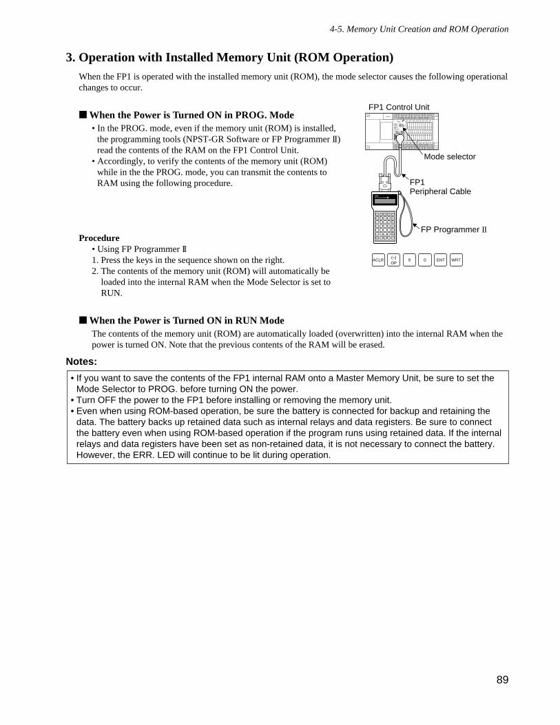
89
4-5. Memory Unit Creation and ROM Operation
3. Operation with Installed Memory Unit (ROM Operation)When the FP1 is operated with the installed memory unit (ROM), the mode selector causes the following operationalchanges to occur.
When the Power is Turned ON in PROG. Mode• In the PROG. mode, even if the memory unit (ROM) is installed,
the programming tools (NPST-GR Software or FP Programmer II)read the contents of the RAM on the FP1 Control Unit.
• Accordingly, to verify the contents of the memory unit (ROM)while in the the PROG. mode, you can transmit the contents toRAM using the following procedure.
Procedure• Using FP Programmer II1. Press the keys in the sequence shown on the right.2. The contents of the memory unit (ROM) will automatically be
loaded into the internal RAM when the Mode Selector is set toRUN.
When the Power is Turned ON in RUN ModeThe contents of the memory unit (ROM) are automatically loaded (overwritten) into the internal RAM when thepower is turned ON. Note that the previous contents of the RAM will be erased.
Notes:
• If you want to save the contents of the FP1 internal RAM onto a Master Memory Unit, be sure to set theMode Selector to PROG. before turning ON the power.
• Turn OFF the power to the FP1 before installing or removing the memory unit.• Even when using ROM-based operation, be sure the battery is connected for backup and retaining the
data. The battery backs up retained data such as internal relays and data registers. Be sure to connectthe battery even when using ROM-based operation if the program runs using retained data. If the internalrelays and data registers have been set as non-retained data, it is not necessary to connect the battery.However, the ERR. LED will continue to be lit during operation.
COM0
COM1
COM2
COM3
COM4
COM5
COM6
COM7
+ -24V DC
F.G.
COMF
89
EAB
CD(+)-
COM7
01
623
45(+)-
RUNREMOTEPROG.
V0
max.min.
RUN
PROG.
ERR.
ALRAM
BATTERY
V1
max.
24V DC+
-
min.
FP1 Control Unit
FP1Peripheral Cable
FP Programmer II
Mode selector
FP PROGRAMMER
STX•WX
ANY•WY
ORR•WR
OTL•WL
FN/PFL
NOTDT/Ld
STKIX/IY
TMT•SV
CTC•EV
(BIN)K/H
=C
DD
<E
>F
SHIFTSC
8 9 A B
4 5 6 7
0 1 2 3
(-)OP
SRC
READ
(HELP)CLR
ACLR (DELT)INST
ENT WRT
(–)OP
WRT09ACLR ENT

90
CHAPTER 5
BASIC INSTRUCTIONS
5-1. Configuration of Basic Instructions ......................................921. Types of Basic Instructions...............................................922. Configuration of Basic Instructions..................................923. Operands for Basic Instructions .......................................93
1) Description of Operands ........................................935-2. Table of Basic Instructions ....................................................95
1. Basic Sequence Instructions .............................................952. Basic Function Instructions ..............................................963. Control Instructions ..........................................................964. Compare Instructions........................................................97
5-3. Description of Basic Instructions ........................................1005-4. Hints for Programming Basic Instructions..........................139
1. Basic Circuit with Basic Instructions .............................1392. Basic Instructions not Displayed
on the Keys of FP Programmer II ...................................1401) When You do not Know the Basic Instruction
Codes for the FP Programmer II ..........................1402) When You Know the Basic Instruction Codes
for the FP Programmer II .....................................1403) Table of Instruction Codes for the
FP Programmer II.................................................1403. Duplicated Use of Outputs .............................................141
1) Duplicated Output................................................1412) How to Check for Duplicated Use.......................1413) Enabling Duplicated Output ................................1414) Output State in One Scan ....................................141
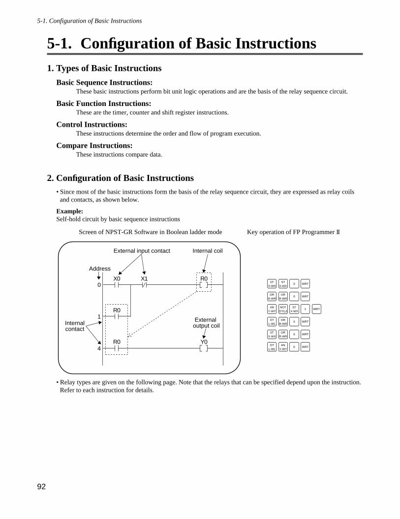
5-1. Configuration of Basic Instructions
1. Types of Basic Instructions
Basic Sequence Instructions:These basic instructions perform bit unit logic operations and are the basis of the relay sequence circuit.
Basic Function Instructions:These are the timer, counter and shift register instructions.
Control Instructions:These instructions determine the order and flow of program execution.
Compare Instructions:These instructions compare data.
2. Configuration of Basic Instructions• Since most of the basic instructions form the basis of the relay sequence circuit, they are expressed as relay coils
and contacts, as shown below.
Example:Self-hold circuit by basic sequence instructions
• Relay types are given on the following page. Note that the relays that can be specified depend upon the instruction.Refer to each instruction for details.
X0 R0
R0 Y0
R0
X1
External input contact Internal coil
Address
External output coilInternal
contact
0
1
4
0
STX-WX
STX-WX
STX-WX
0 WRT
ORR-WR
ORR-WR
0 WRT
ANY-WY
NOTDT/Ld
1
OTL-WL
ORR-WR
WRT
STX-WX
ORR-WR
0 WRT
OTL-WL
ANY-WY
0 WRT
WRT
Key operation of FP Programmer IIScreen of NPST-GR Software in Boolean ladder mode
92
5-1. Configuration of Basic Instructions
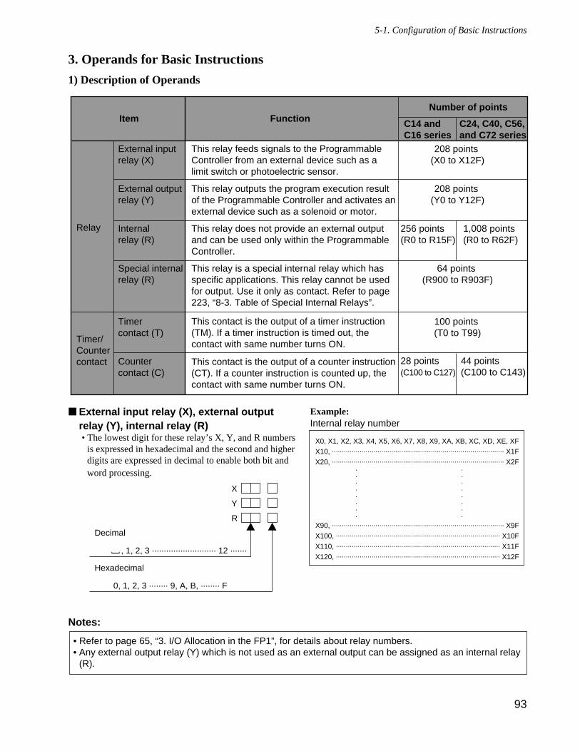
3. Operands for Basic Instructions
1) Description of Operands
External input relay (X), external outputrelay (Y), internal relay (R)• The lowest digit for these relay’s X, Y, and R numbers
is expressed in hexadecimal and the second and higherdigits are expressed in decimal to enable both bit andword processing.
Notes:
• Refer to page 65, “3. I/O Allocation in the FP1”, for details about relay numbers.• Any external output relay (Y) which is not used as an external output can be assigned as an internal relay
(R).
R
Decimal
] , 1, 2, 3 ........................... 12 .......
Hexadecimal
0, 1, 2, 3 ........ 9, A, B, ........ F
Y
X
External input relay (X)
External output relay (Y)
Internal relay (R)
Special internal relay (R)
Timer contact (T)
Counter contact (C)
208 points (X0 to X12F)
208 points (Y0 to Y12F)
64 points (R900 to R903F)
100 points (T0 to T99)
C24, C40, C56, and C72 series
C14 and C16 series
1,008 points (R0 to R62F)
Relay
Timer/Counter contact 44 points
(C100 to C143)
256 points (R0 to R15F)
28 points (C100 to C127)
Item FunctionNumber of points
This relay does not provide an external output and can be used only within the Programmable Controller.
This relay outputs the program execution result of the Programmable Controller and activates an external device such as a solenoid or motor.
This relay feeds signals to the Programmable Controller from an external device such as a limit switch or photoelectric sensor.
This relay is a special internal relay which has specific applications. This relay cannot be used for output. Use it only as contact. Refer to page 223, “8-3. Table of Special Internal Relays”.
This contact is the output of a timer instruction (TM). If a timer instruction is timed out, the contact with same number turns ON.
This contact is the output of a counter instruction (CT). If a counter instruction is counted up, the contact with same number turns ON.
93
5-1. Configuration of Basic Instructions
X0, X1, X2, X3, X4, X5, X6, X7, X8, X9, XA, XB, XC, XD, XE, XF
X10, ....................................................................................... X1F
X20, ....................................................................................... X2F
X90, ....................................................................................... X9F
X100, ................................................................................... X10F
X110, ................................................................................... X11F
X120, ................................................................................... X12F
.
.
.
.
.
.
.
.
.
.
.
.
.
.
.
.
Example:Internal relay number
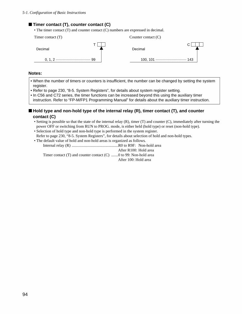
Timer contact (T), counter contact (C)• The timer contact (T) and counter contact (C) numbers are expressed in decimal.
Timer contact (T) Counter contact (C)
Notes:
Hold type and non-hold type of the internal relay (R), timer contact (T), and countercontact (C)• Setting is possible so that the state of the internal relay (R), timer (T) and counter (C), immediately after turning the
power OFF or switching from RUN to PROG. mode, is either held (hold type) or reset (non-hold type).• Selection of hold type and non-hold type is performed in the system register.
Refer to page 230, “8-5. System Registers”, for details about selection of hold and non-hold types.• The default value of hold and non-hold areas is organized as follows.
Internal relay (R) ...............................................R0 to R9F: Non-hold areaAfter R100: Hold area
Timer contact (T) and counter contact (C) .......0 to 99: Non-hold areaAfter 100: Hold area
• When the number of timers or counters is insufficient, the number can be changed by setting the systemregister.
• Refer to page 230, “8-5. System Registers”, for details about system register setting.• In C56 and C72 series, the timer functions can be increased beyond this using the auxiliary timer
instruction. Refer to “FP-M/FP1 Programming Manual” for details about the auxiliary timer instruction.
TDecimal
0, 1, 2 ................................... 99
CDecimal
100, 101 ............................... 143
94
5-1. Configuration of Basic Instructions
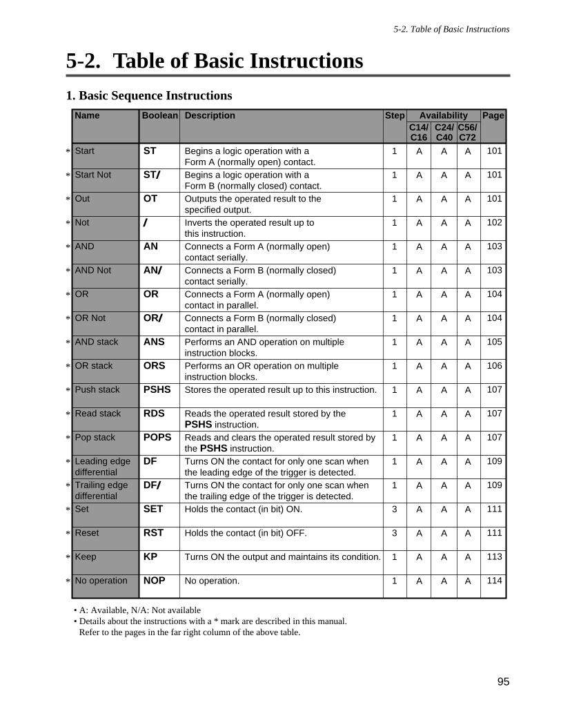
5-2. Table of Basic Instructions
1. Basic Sequence Instructions
• A: Available, N/A: Not available• Details about the instructions with a * mark are described in this manual.
Refer to the pages in the far right column of the above table.
A
A
A
A
A
A
A
A
A
A
A
A
A
A
A
A
A
A
A
A
A
A
A
A
A
A
A
A
A
A
A
A
A
A
A
A
A
A
A
A
A
A
A
A
A
A
A
A
A
A
A
A
A
A
A
A
A
ST
ST/
OT
/
AN
AN/
OR
OR/
ANS
ORS
PSHS
RDS
POPS
DF
DF/
SET
RST
KP
NOP
Begins a logic operation with a Form A (normally open) contact.Begins a logic operation with a Form B (normally closed) contact.Outputs the operated result to the specified output.Inverts the operated result up to this instruction.Connects a Form A (normally open) contact serially.Connects a Form B (normally closed) contact serially.Connects a Form A (normally open) contact in parallel.Connects a Form B (normally closed) contact in parallel.Performs an AND operation on multiple instruction blocks.Performs an OR operation on multiple instruction blocks.Stores the operated result up to this instruction.
Reads the operated result stored by the PSHS instruction.Reads and clears the operated result stored by the PSHS instruction.Turns ON the contact for only one scan when the leading edge of the trigger is detected.Turns ON the contact for only one scan when the trailing edge of the trigger is detected.Holds the contact (in bit) ON.
Holds the contact (in bit) OFF.
Turns ON the output and maintains its condition.
No operation.
1
1
1
1
1
1
1
1
1
1
1
1
1
1
1
3
3
1
1
Start
Start Not
Out
Not
AND
AND Not
OR
OR Not
AND stack
OR stack
Push stack
Read stack
Pop stack
Leading edge differentialTrailing edge differentialSet
Reset
Keep
No operation
C56/C72
AvailabilityC24/C40
C14/C16
101
101
101
102
103
103
104
104
105
106
107
107
107
109
109
111
111
113
114
DescriptionBooleanName Step Page
*
*
*
*
*
*
*
*
*
*
*
*
*
*
*
*
*
*
*
95
5-2. Table of Basic Instructions
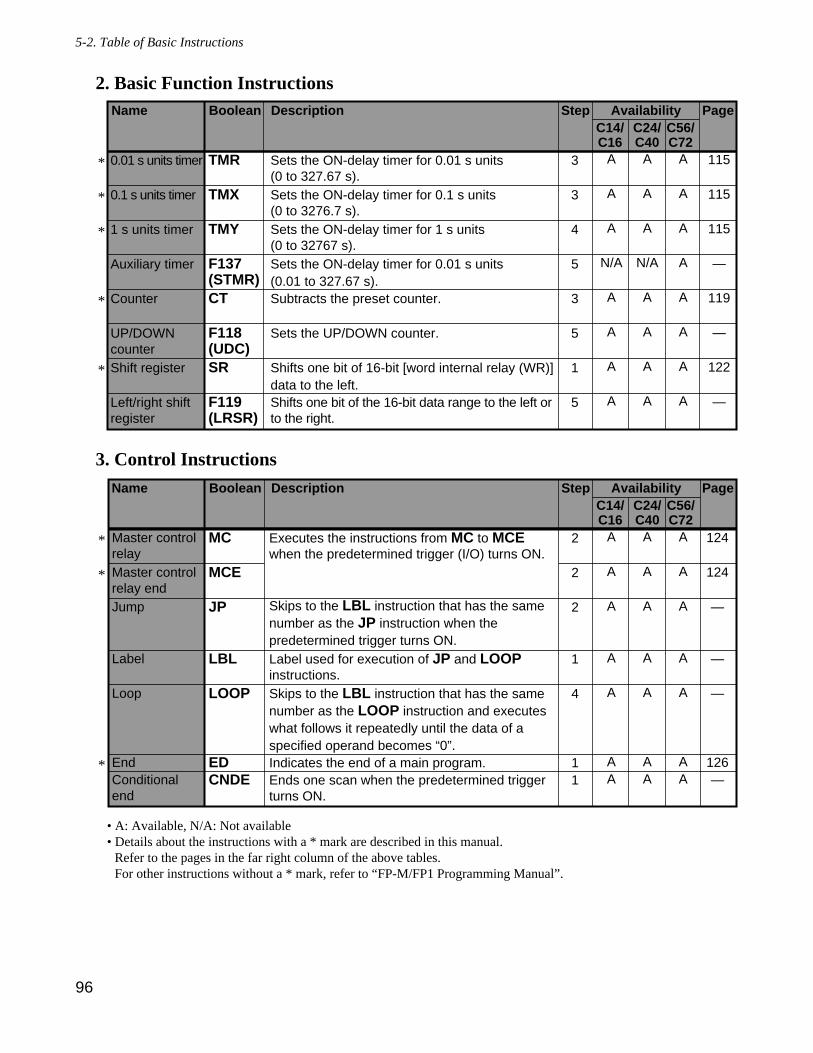
2. Basic Function Instructions
3. Control Instructions
• A: Available, N/A: Not available• Details about the instructions with a * mark are described in this manual.
Refer to the pages in the far right column of the above tables.For other instructions without a * mark, refer to “FP-M/FP1 Programming Manual”.
MC
MCE
JP
LBL
LOOP
ED CNDE
Executes the instructions from MC to MCE when the predetermined trigger (I/O) turns ON.
Skips to the LBL instruction that has the same number as the JP instruction when the predetermined trigger turns ON. Label used for execution of JP and LOOP instructions.Skips to the LBL instruction that has the same number as the LOOP instruction and executes what follows it repeatedly until the data of a specified operand becomes “0”. Indicates the end of a main program.Ends one scan when the predetermined trigger turns ON.
2
2
2
1
4
11
A
A
A
A
A
AA
A
A
A
A
A
AA
124
124
—
—
—
126—
C56/C72
AvailabilityC24/C40
C14/C16
DescriptionBooleanName Step Page
*
*
*
Master control relayMaster control relay endJump
Label
Loop
EndConditional end
A
A
A
A
A
AA
0.01 s units timer
0.1 s units timer
1 s units timer
Auxiliary timer
Counter
UP/DOWN counter Shift register
Left/right shift register
TMR
TMX
TMY
F137 (STMR)CT
F118 (UDC)SR
F119 (LRSR)
Sets the ON-delay timer for 0.01 s units(0 to 327.67 s).Sets the ON-delay timer for 0.1 s units (0 to 3276.7 s). Sets the ON-delay timer for 1 s units (0 to 32767 s). Sets the ON-delay timer for 0.01 s units (0.01 to 327.67 s).Subtracts the preset counter.
Sets the UP/DOWN counter.
Shifts one bit of 16-bit [word internal relay (WR)]data to the left.Shifts one bit of the 16-bit data range to the left or to the right.
3
3
4
5
3
5
1
5
A
A
A
N/A
A
A
A
A
A
A
A
N/A
A
A
A
A
A
A
A
A
A
A
A
A
115
115
115
—
119
—
122
—
*
*
*
*
*
C56/C72
AvailabilityC24/C40
C14/C16
DescriptionBooleanName Step Page
96
5-2. Table of Basic Instructions
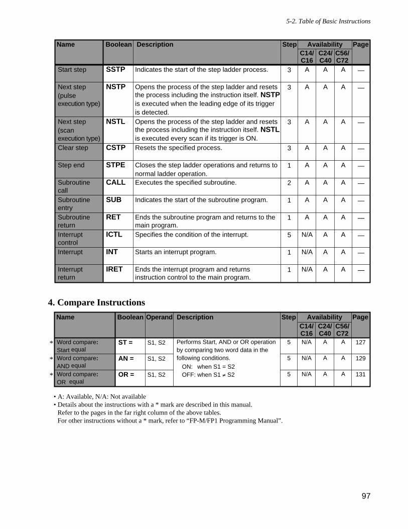
4. Compare Instructions
• A: Available, N/A: Not available• Details about the instructions with a * mark are described in this manual.
Refer to the pages in the far right column of the above tables.For other instructions without a * mark, refer to “FP-M/FP1 Programming Manual”.
N/A
N/A
N/A
A
A
A
A
A
A
Word compare: Start equalWord compare: AND equalWord compare: OR equal
ST =
AN =
OR =
Performs Start, AND or OR operationby comparing two word data in the following conditions.
ON: when S1 = S2OFF: when S1 ≠ S2
5
5
5
S1, S2
S1, S2
S1, S2
127
129
131
*
*
*
C14/C16
PageAvailabilityC56/C72
C24/C40
Description StepOperandBooleanName
Start step
Next step (pulse execution type)
Next step (scan execution type)Clear step
Step end
Subroutine call Subroutine entry Subroutine returnInterrupt controlInterrupt
Interrupt return
SSTP
NSTP
NSTL
CSTP
STPE
CALL
SUB
RET
ICTL
INT
IRET
Indicates the start of the step ladder process.
Opens the process of the step ladder and resets the process including the instruction itself. NSTP is executed when the leading edge of its trigger is detected.Opens the process of the step ladder and resets the process including the instruction itself. NSTL is executed every scan if its trigger is ON. Resets the specified process.
Closes the step ladder operations and returns to normal ladder operation.Executes the specified subroutine.
Indicates the start of the subroutine program.
Ends the subroutine program and returns to the main program.Specifies the condition of the interrupt.
Starts an interrupt program.
Ends the interrupt program and returns instruction control to the main program.
3
3
3
3
1
2
1
1
5
1
1
A
A
A
A
A
A
A
A
N/A
N/A
N/A
A
A
A
A
A
A
A
A
A
A
A
A
A
A
A
A
A
A
A
A
A
A
—
—
—
—
—
—
—
—
—
—
—
C56/C72
AvailabilityC24/C40
C14/C16
DescriptionBooleanName Step Page
97
5-2. Table of Basic Instructions
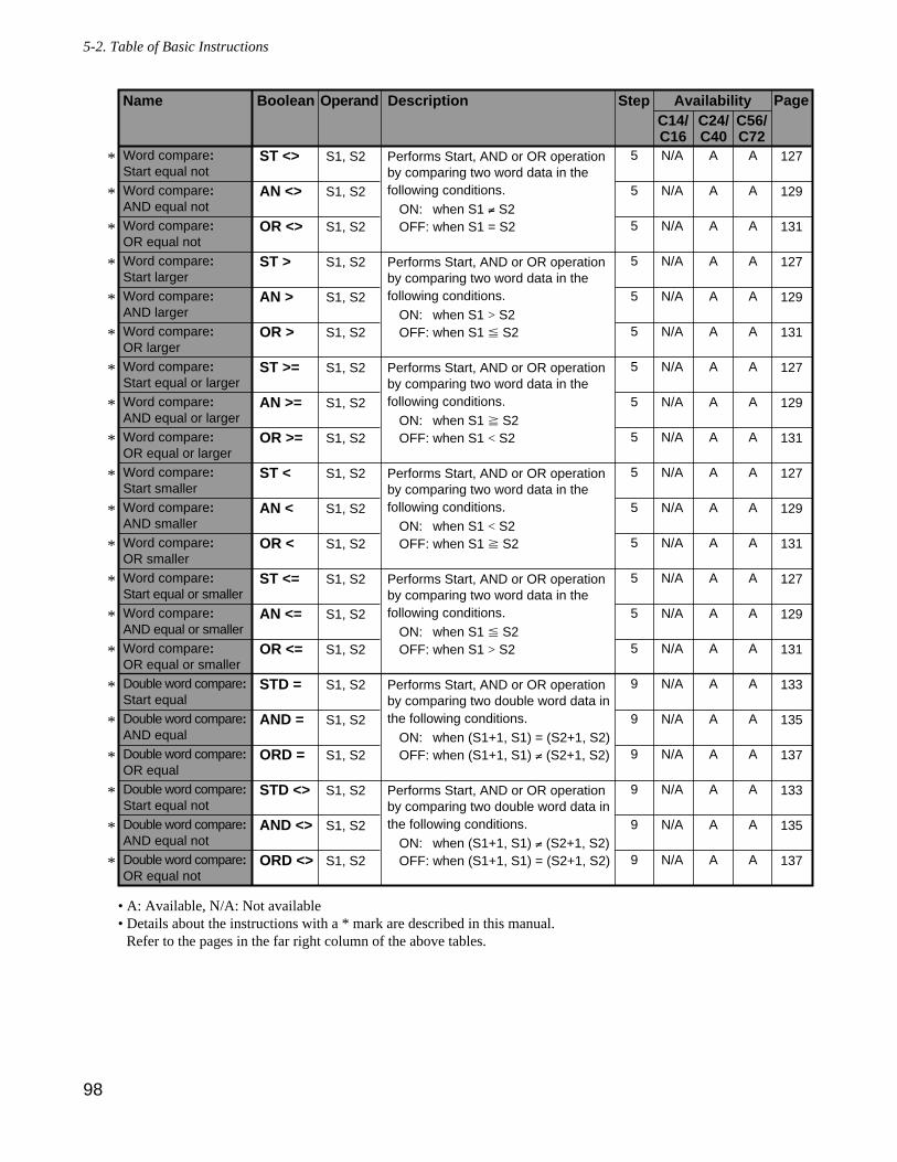
• A: Available, N/A: Not available• Details about the instructions with a * mark are described in this manual.
Refer to the pages in the far right column of the above tables.
N/A
N/A
N/A
N/A
N/A
N/A
N/A
N/A
N/A
N/A
N/A
N/A
N/A
N/A
N/A
N/A
N/A
N/A
N/A
N/A
N/A
A
A
A
A
A
A
A
A
A
A
A
A
A
A
A
A
A
A
A
A
A
A
A
A
A
A
A
A
A
A
A
A
A
A
A
A
A
A
A
A
A
A
C14/C16
Word compare: Start equal not Word compare: AND equal not Word compare: OR equal not Word compare: Start larger Word compare: AND larger Word compare: OR larger Word compare: Start equal or larger Word compare: AND equal or larger Word compare: OR equal or larger Word compare: Start smaller Word compare: AND smaller Word compare: OR smaller Word compare: Start equal or smaller Word compare:AND equal or smaller Word compare: OR equal or smaller Double word compare:Start equal Double word compare: AND equal Double word compare:OR equal Double word compare: Start equal not Double word compare: AND equal not Double word compare:OR equal not
ST <>
AN <>
OR <>
ST >
AN >
OR >
ST >=
AN >=
OR >=
ST <
AN <
OR <
ST <=
AN <=
OR <=
STD =
AND =
ORD =
STD <>
AND <>
ORD <>
Performs Start, AND or OR operation by comparing two word data in the following conditions.
ON: when S1 ≠ S2OFF: when S1 = S2
Performs Start, AND or OR operation by comparing two word data in the following conditions.
ON: when S1 > S2OFF: when S1 S2
Performs Start, AND or OR operation by comparing two word data in the following conditions.
ON: when S1 S2OFF: when S1 < S2
Performs Start, AND or OR operation by comparing two word data in the following conditions.
ON: when S1 < S2OFF: when S1 S2
Performs Start, AND or OR operation by comparing two word data in the following conditions.
ON: when S1 S2OFF: when S1 > S2
Performs Start, AND or OR operation by comparing two double word data in the following conditions.
ON: when (S1+1, S1) = (S2+1, S2)OFF: when (S1+1, S1) ≠ (S2+1, S2)
Performs Start, AND or OR operation by comparing two double word data in the following conditions.
ON: when (S1+1, S1) ≠ (S2+1, S2)OFF: when (S1+1, S1) = (S2+1, S2)
5
5
5
5
5
5
5
5
5
5
5
5
5
5
5
9
9
9
9
9
9
S1, S2
S1, S2
S1, S2
S1, S2
S1, S2
S1, S2
S1, S2
S1, S2
S1, S2
S1, S2
S1, S2
S1, S2
S1, S2
S1, S2
S1, S2
S1, S2
S1, S2
S1, S2
S1, S2
S1, S2
S1, S2
PageAvailabilityC56/C72
C24/C40
127
129
131
127
129
131
127
129
131
127
129
131
127
129
131
133
135
137
133
135
137
Description StepOperandBooleanName
*
*
*
*
*
*
*
*
*
*
*
*
*
*
*
*
*
*
*
*
*
98
5-2. Table of Basic Instructions
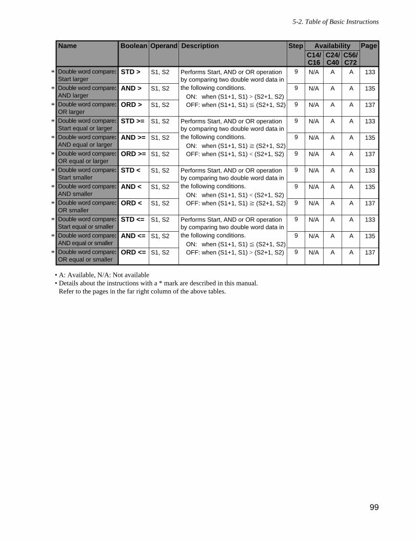
• A: Available, N/A: Not available• Details about the instructions with a * mark are described in this manual.
Refer to the pages in the far right column of the above tables.
133
135
137
133
135
137
133
135
137
133
135
137
C14/C16
PageAvailabilityC56/C72
C24/C40
Description StepOperandBooleanName
*
*
*
*
*
*
*
*
*
*
*
*
STD >
AND >
ORD >
STD >=
AND >=
ORD >=
STD <
AND <
ORD <
STD <=
AND <=
ORD <=
Performs Start, AND or OR operation by comparing two double word data in the following conditions.
ON: when (S1+1, S1) > (S2+1, S2)OFF: when (S1+1, S1) (S2+1, S2)
Performs Start, AND or OR operation by comparing two double word data in the following conditions.
ON: when (S1+1, S1) (S2+1, S2)OFF: when (S1+1, S1) < (S2+1, S2)
Performs Start, AND or OR operation by comparing two double word data in the following conditions.
ON: when (S1+1, S1) < (S2+1, S2)OFF: when (S1+1, S1) (S2+1, S2)
Performs Start, AND or OR operation by comparing two double word data in the following conditions.
ON: when (S1+1, S1) (S2+1, S2)OFF: when (S1+1, S1) > (S2+1, S2)
9
9
9
9
9
9
9
9
9
9
9
9
N/A
N/A
N/A
N/A
N/A
N/A
N/A
N/A
N/A
N/A
N/A
N/A
A
A
A
A
A
A
A
A
A
A
A
A
A
A
A
A
A
A
A
A
A
A
A
A
S1, S2
S1, S2
S1, S2
S1, S2
S1, S2
S1, S2
S1, S2
S1, S2
S1, S2
S1, S2
S1, S2
S1, S2
Double word compare: Start larger Double word compare:AND larger Double word compare:OR larger Double word compare:Start equal or larger Double word compare:AND equal or larger Double word compare: OR equal or larger Double word compare:Start smaller Double word compare: AND smaller Double word compare:OR smaller Double word compare:Start equal or smallerDouble word compare:AND equal or smallerDouble word compare: OR equal or smaller
99
5-2. Table of Basic Instructions
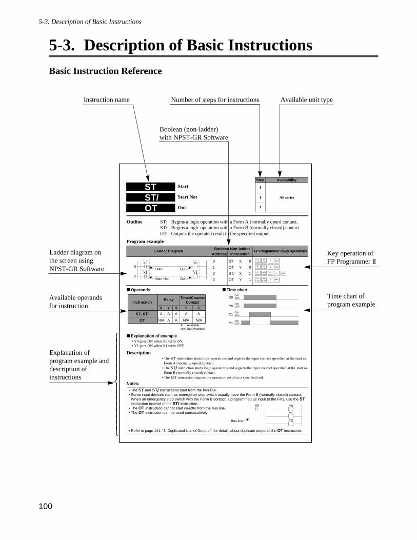
5-3. Description of Basic Instructions
Basic Instruction Reference
100
5-3. Description of Basic Instructions
5-3. Description of Basic Instructions
101
Outline ST: Begins a logic operation with a Form A (normally open) contact.ST/: Begins a logic operation with a Form B (normally closed) contact.OT: Outputs the operated result to the specified output.
Program example
Operands Time chart
Explanation of example• Y0 goes ON when X0 turns ON.• Y1 goes ON when X1 turns OFF.
Description• The ST instruction starts logic operations and regards the input contact specified at the start as
Form A (normally open) contact.• The ST/ instruction starts logic operations and regards the input contact specified at the start as
Form B (normally closed) contact.• The OT instruction outputs the operation result to a specified coil.
Notes:
Timer/CounterContact
C
Relay
TRYX
Instruction
ST, ST/
OT
A A A A A
N/A A A N/A N/A
ONOFFX0
ONOFFY0
ONOFFX1
ONOFFY1
• The ST and ST/ instructions start from the bus line.• Some input devices such as emergency stop switch usually have the Form B (normally closed) contact.
When an emergency stop switch with the Form B contact is programmed as input to the FP1, use the STinstruction instead of the ST/ instruction.
• The OT instruction cannot start directly from the bus line.• The OT instruction can be used consecutively.
• Refer to page 141, “3. Duplicated Use of Outputs”, for details about duplicate output of the OT instruction.
FP Programmer IIkey operations
ST Start
ST/ Start Not
OT Out
AvailabilityStep
1
1
1
All series
Ladder DiagramBoolean Non-ladder
Address Instruction
0X0 Y0
OutStart
2X1 Y1
OutStart Not
STX-WX
STX-WX
STX-WX
0 WRT
OTL-WL
0 WRTAN
Y-WY
NOTDT/Ld
1
OTL-WL
ANY-WY
1 WRT
WRTST
X-WX
0
1
2
3
ST X 0
OT Y 0
ST/ X 1
OT Y 1
X0 Y0
Bus line
Y1
Y2
A: AvailableN/A: Not Available
Instruction name
Ladder diagram onthe screen usingNPST-GR Software
Available operandsfor instruction
Explanation ofprogram example anddescription ofinstructions
Boolean (non-ladder)with NPST-GR Software
Number of steps for instructions Available unit type
Key operation ofFP Programmer II
Time chart ofprogram example
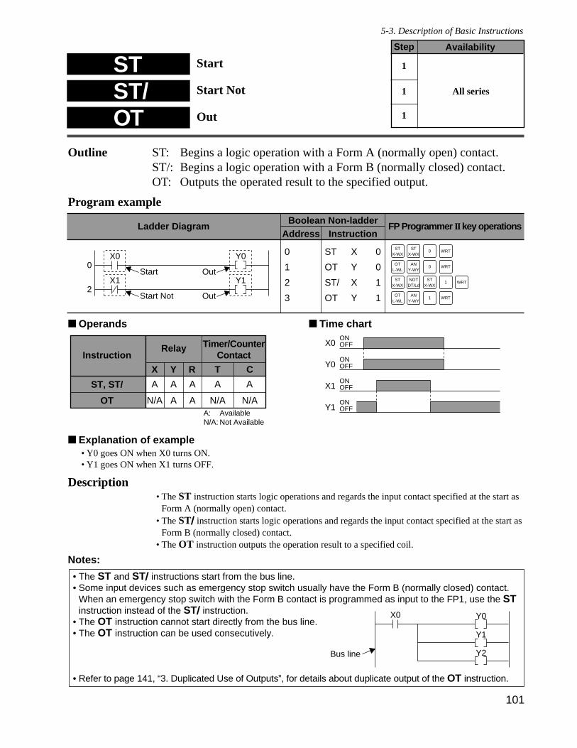
5-3. Description of Basic Instructions
101
Outline ST: Begins a logic operation with a Form A (normally open) contact.ST/: Begins a logic operation with a Form B (normally closed) contact.OT: Outputs the operated result to the specified output.
Program example
Operands Time chart
Explanation of example• Y0 goes ON when X0 turns ON.• Y1 goes ON when X1 turns OFF.
Description• The ST instruction starts logic operations and regards the input contact specified at the start as
Form A (normally open) contact.• The ST/ instruction starts logic operations and regards the input contact specified at the start as
Form B (normally closed) contact.• The OT instruction outputs the operation result to a specified coil.
Notes:
• The ST and ST/ instructions start from the bus line.• Some input devices such as emergency stop switch usually have the Form B (normally closed) contact.
When an emergency stop switch with the Form B contact is programmed as input to the FP1, use the STinstruction instead of the ST/ instruction.
• The OT instruction cannot start directly from the bus line.• The OT instruction can be used consecutively.
• Refer to page 141, “3. Duplicated Use of Outputs”, for details about duplicate output of the OT instruction.
ONOFFX0
ONOFFY0
ONOFFX1
ONOFFY1
Timer/CounterContact
C
Relay
TRYX
Instruction
ST, ST/
OT
A A A A A
N/A A A N/A N/A
FP Programmer IIkey operations
ST Start
ST/ Start Not
OT Out
AvailabilityStep
1
1
1
All series
Ladder DiagramBoolean Non-ladder
Address Instruction
0X0 Y0
OutStart
2X1 Y1
OutStart Not
STX-WX
STX-WX
STX-WX
0 WRT
OTL-WL
0 WRTAN
Y-WY
NOTDT/Ld
1
OTL-WL
ANY-WY
1 WRT
WRTST
X-WX
0
1
2
3
ST X 0
OT Y 0
ST/ X 1
OT Y 1
X0 Y0
Bus line
Y1
Y2
A: AvailableN/A: Not Available
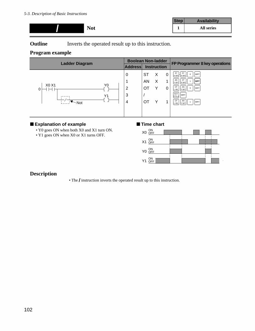
5-3. Description of Basic Instructions
102
Outline Inverts the operated result up to this instruction.
Program example
Explanation of example Time chart• Y0 goes ON when both X0 and X1 turn ON.• Y1 goes ON when X0 or X1 turns OFF.
Description• The / instruction inverts the operated result up to this instruction.
/ NotAvailabilityStep
1 All series
Ladder Diagram FP Programmer IIkey operationsBoolean Non-ladder
Address Instruction
0X0 Y0X1
Y1
Not
STX-WX
STX-WX
STX-WX
0 WRT
ANY-WY
WRT1
OTL-WL
ANY-WY
0 WRT
WRT
OTL-WL
ANY-WY
1 WRT
NOTDT/Ld
WRT
0
1
2
3
4
ST X 0
AN X 1
OT Y 0
/
OT Y 1
ONOFFX0
ONOFFX1
ONOFFY0
ONOFFY1

5-3. Description of Basic Instructions
103
Outline AN: Connects a Form A (normally open) contact serially.AN/: Connects a Form B (normally closed) contact serially.
Program example
Operands Time chart
Explanation of example• Y0 goes ON when both X0 and X1 turn ON and also X2 turns OFF.
Description• Performs a logical AND operation with the results of the immediately preceding serially
connected operation.
Notes:
• Use the AN instruction when the normally open contact (Form A contact) is serially connected. Use theAN/ instruction when the normally closed contact (Form B contact) is serially connected.
• The AN and AN/ instructions can be used consecutively.
ONOFFX0
ONOFFX1
ONOFFX2
ONOFFY0
Timer/CounterContact
C
Relay
TRYX
Instruction
AN, AN/ A A A A AA:N/A: Not Available
Available
AN AND
AN/ AND Not
AvailabilityStep
1
1All series
Ladder Diagram FP Programmer IIkey operationsBoolean Non-ladder
Address Instruction
0X1 Y0
AND AND Not
X2X0
STX-WX
STX-WX
STX-WX
0 WRT
ANY-WY
WRT1
ANY-WY
NOTDT/Ld
WRT
OTL-WL
ANY-WY
0 WRT
STX-WX
WRT2
0
1
2
3
ST X 0
AN X 1
AN/ X 2
OT Y 0
X2 X3
X0 Y0
Y1
X1
X0 Y0X1 X2 X3
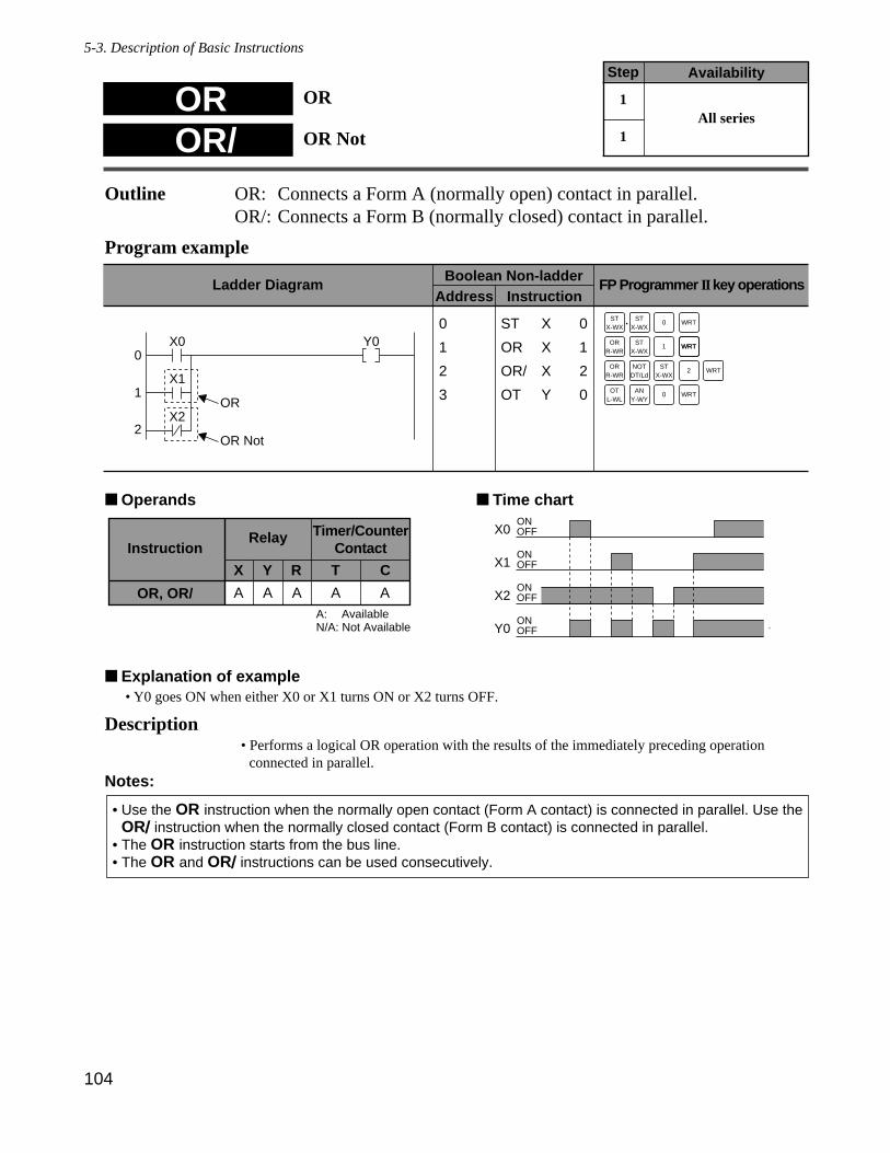
5-3. Description of Basic Instructions
104
Outline OR: Connects a Form A (normally open) contact in parallel.OR/: Connects a Form B (normally closed) contact in parallel.
Program example
Operands Time chart
Explanation of example• Y0 goes ON when either X0 or X1 turns ON or X2 turns OFF.
Description• Performs a logical OR operation with the results of the immediately preceding operation
connected in parallel.Notes:
• Use the OR instruction when the normally open contact (Form A contact) is connected in parallel. Use theOR/ instruction when the normally closed contact (Form B contact) is connected in parallel.
• The OR instruction starts from the bus line.• The OR and OR/ instructions can be used consecutively.
ONOFFX0
ONOFFX1
ONOFFX2
ONOFFY0
Timer/CounterContact
C
Relay
TRYX
Instruction
OR, OR/ A A A A AA:N/A: Not Available
Available
OR OR
OR/ OR Not
Ladder Diagram FP Programmer IIkey operationsBoolean Non-ladder
Address Instruction
0X0 Y0
1X1
ORX2
OR Not2
STX-WX
STX-WX
STX-WX
0 WRT
ORR-WR
WRT1
ORR-WR
NOTDT/Ld
WRT
OTL-WL
ANY-WY
0 WRT
STX-WX
WRT2
0
1
2
3
ST X 0
OR X 1
OR/ X 2
OT Y 0
AvailabilityStep
1
1All series
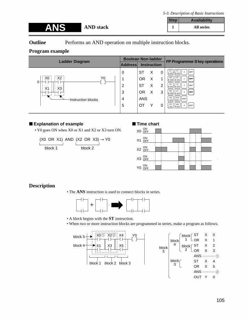
5-3. Description of Basic Instructions
105
Outline Performs an AND operation on multiple instruction blocks.
Program example
Explanation of example Time chart• Y0 goes ON when X0 or X1 and X2 or X3 turn ON.
Description• The ANS instruction is used to connect blocks in series.
• A block begins with the ST instruction.• When two or more instruction blocks are programmed in series, make a program as follows.
X0
X1
X2
X3
X4
X5
Y0
block 4
block 5
block 1 block 2 block 3
1 2 STORSTORANS ............ 1STORANS ............ 2OUT
XXXX
XX
Y
block1
block2
block4
block3
block5
0123
45
0
+
(X0 OR X1) AND (X2 OR X3) → Y0
block 1 block 2
ANS AND stack
Ladder Diagram FP Programmer IIkey operationsBoolean Non-ladder
Address Instruction
0X0 Y0
X1
Instruction blocks
X2
X3
STX-WX
ORR-WR
WRT1 WRT
STX-WX
STX-WX
0 WRT
ANY-WY
STKIX/IY
WRT
OTL-WL
ANY-WY
0 WRT
STX-WX
STX-WX
2 WRT
STX-WX
ORR-WR
WRT3 WRT
0
1
2
3
4
5
ST X 0
OR X 1
ST X 2
OR X 3
ANS
OT Y 0
AvailabilityStep
1 All series
ONOFFX0
ONOFFX1
ONOFFX2
ONOFFX3
ONOFFY0
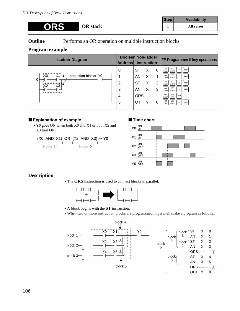
5-3. Description of Basic Instructions
106
Outline Performs an OR operation on multiple instruction blocks.
Program example
Explanation of example Time chart• Y0 goes ON when both X0 and X1 or both X2 and
X3 turn ON.
Description• The ORS instruction is used to connect blocks in parallel.
• A block begins with the ST instruction.• When two or more instruction blocks are programmed in parallel, make a program as follows.
X0 X1
X2 X3
Y0
block 4
block 5
block 1
block 2
block 3
1
2
STANSTANORS ............ 1STANORS ............ 2OUT
XXXX
XX
Y
block1
block2
block4
block3
block5
X4 X5
0123
45
0
+ ###
(X0 AND X1) OR (X2 AND X3) → Y0
block 1 block 2
ORS OR stackAvailabilityStep
1 All series
Ladder Diagram FP Programmer IIkey operationsBoolean Non-ladder
Address Instruction
0X0 Y0
X2
Instruction blocksX1
X3
STX-WX
ANY-WY
WRT1 WRT
STX-WX
STX-WX
0 WRT
ORR-WR
STKIX/IY
WRT
OTL-WL
ANY-WY
0 WRT
STX-WX
STX-WX
2 WRT
STX-WX
ANY-WY
WRT3 WRT
0
1
2
3
4
5
ST X 0
AN X 1
ST X 2
AN X 3
ORS
OT Y 0
ONOFFX0
ONOFFX1
ONOFFX2
ONOFFX3
ONOFFY0
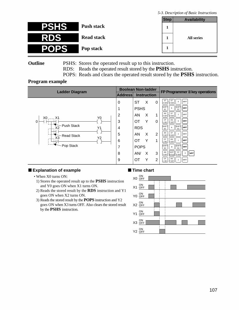
5-3. Description of Basic Instructions
107
Outline PSHS: Stores the operated result up to this instruction.RDS: Reads the operated result stored by the PSHS instruction.POPS: Reads and clears the operated result stored by the PSHS instruction.
Program example
Explanation of example Time chartONOFFX0
ONOFFX1
ONOFFY0
ONOFFX2
ONOFFY1
ONOFFX3
ONOFFY2
• When X0 turns ON:1) Stores the operated result up to the PSHS instruction
and Y0 goes ON when X1 turns ON.2) Reads the stored result by the RDS instruction and Y1
goes ON when X2 turns ON.3) Reads the stored result by the POPS instruction and Y2
goes ON when X3 turns OFF. Also clears the stored resultby the PSHS instruction.
Ladder Diagram FP Programmer IIkey operationsBoolean Non-ladder
Address Instruction
0X0 Y0
Push Stack
X1
X2
X3Read Stack
Pop Stack
Y1
Y2
RDS Read stack
POPS Pop stack
PSHS Push stackAvailabilityStep
1
1
1
All series
SHIFTSC
WRTWRT
STX-WX
STX-WX
0 WRT
ANY-WY
STX-WX
2 WRT
ANY-WY
STX-WX
1 WRT
ANY-WY
OTL-WL
WRT0 WRT
ANY-WY
OTL-WL
ANY-WY
2 WRT
9SHIFT
SC
SHIFTSC
WRTWRTASHIFT
SC
ANY-WY
OTL-WL
WRT1 WRT
SHIFTSC
WRTWRTBSHIFT
SC
WRTWRTNOT
DT/LdST
X-WX3
ST X 0
PSHS
AN X 1
OT Y 0
RDS
AN X 2
OT Y 1
POPS
AN/ X 3
OT Y 2
0
1
2
3
4
5
6
7
8
9
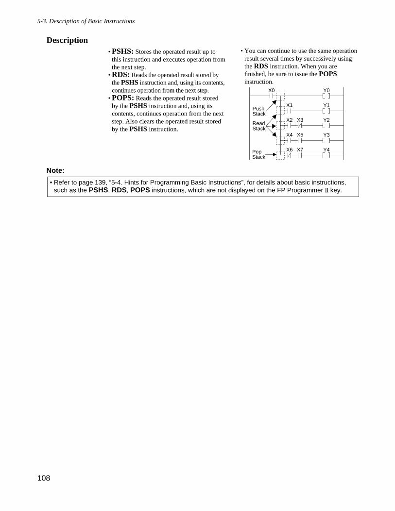
5-3. Description of Basic Instructions
108
Description
Note:
• Refer to page 139, “5-4. Hints for Programming Basic Instructions”, for details about basic instructions,such as the PSHS, RDS, POPS instructions, which are not displayed on the FP Programmer II key.
• PSHS: Stores the operated result up tothis instruction and executes operation fromthe next step.
• RDS: Reads the operated result stored bythe PSHS instruction and, using its contents,continues operation from the next step.
• POPS: Reads the operated result storedby the PSHS instruction and, using itscontents, continues operation from the nextstep. Also clears the operated result storedby the PSHS instruction.
• You can continue to use the same operationresult several times by successively usingthe RDS instruction. When you arefinished, be sure to issue the POPSinstruction.
X0 Y0
X1
Read Stack
Pop Stack
Y1
X2 Y2X3
X4 Y3X5
X6 Y4X7
PushStack
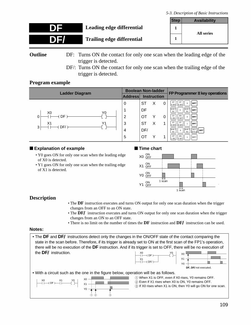
109
5-3. Description of Basic Instructions
DF/ Trailing edge differential
DF Leading edge differential
Outline DF: Turns ON the contact for only one scan when the leading edge of thetrigger is detected.
DF/: Turns ON the contact for only one scan when the trailing edge of thetrigger is detected.
Program example
Explanation of example Time chart
Description• The DF instruction executes and turns ON output for only one scan duration when the trigger
changes from an OFF to an ON state.• The DF/ instruction executes and turns ON output for only one scan duration when the trigger
changes from an ON to an OFF state.• There is no limit on the number of times the DF instruction and DF/ instruction can be used.
Notes:
• The DF and DF/ instructions detect only the changes in the ON/OFF state of the contact comparing thestate in the scan before. Therefore, if its trigger is already set to ON at the first scan of the FP1’s operation,there will be no execution of the DF instruction. And if its trigger is set to OFF, there will be no execution ofthe DF/ instruction.
• With a circuit such as the one in the figure below, operation will be as follows.1When X1 is OFF, even if X0 rises, Y0 remains OFF.2 Even if X1 rises when X0 is ON, Y0 remains OFF.3 If X0 rises when X1 is ON, then Y0 will go ON for one scan.
ONOFFX0
ONOFFX1
ONOFFY0
ONOFFY1
1 scan
1 scan
• Y0 goes ON for only one scan when the leading edgeof X0 is detected.
• Y1 goes ON for only one scan when the trailing edgeof X1 is detected.
Ladder Diagram FP Programmer IIkey operationsBoolean Non-ladder
Address Instruction
0X0 Y0
3X1 Y1
( DF )!
( DF/ )!
OTL-WL
ANY-WY
1 WRT
ANY-WY
OTL-WL
WRT0 WRT
WRTWRTNOT
DT/LdSHIFT
SC0
SHIFTSC
STX-WX
STX-WX
WRT1 WRT
SHIFTSC
WRTWRT0SHIFT
SC
STX-WX
STX-WX
WRT0 WRT0
1
2
3
4
5
ST X 0
DF
OT Y 0
ST X 1
DF/
OT Y 1
AvailabilityStep
1
1All series
Y0X0( DF )!
Y0
X1
X0
X1( DF/ )!
DF, DF/ not executed.
X0 Y0( DF )!
X1
Y0
X1
X0
1 2 3
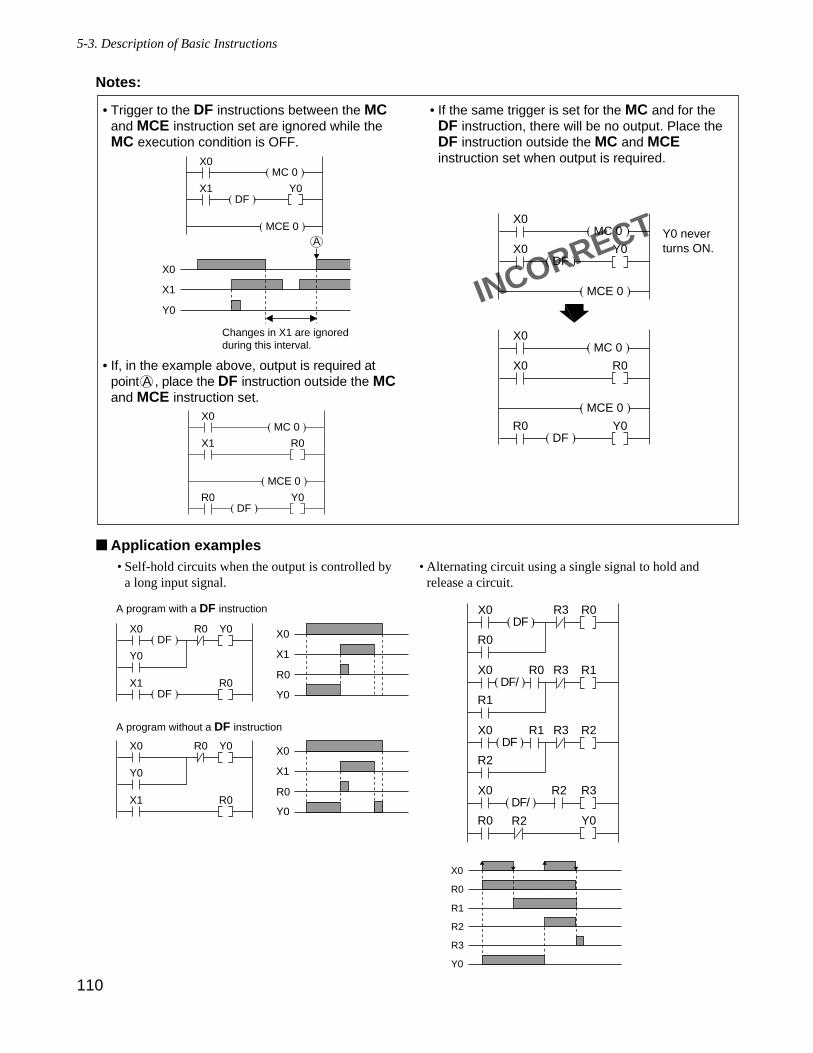
5-3. Description of Basic Instructions
110
Notes:
Application examples
R1
R0
X0
X0 R3( DF/ )!
R0
X0 R0( DF )!
R3
R2
R3
R0 Y0
R1
X0 R1( DF/ )!
R3R0
R2
X0 R2( DF )!
R3R1
R2
R2
Y0
R0
X1
X0
Y0
X1 R0( DF )!
X0 Y0( DF )!
R0
Y0
Y0
A program with a DF instruction
R0
X1
X0
Y0
X1 R0
X0 Y0R0
A program without a DF instruction
• Alternating circuit using a single signal to hold andrelease a circuit.
• Self-hold circuits when the output is controlled bya long input signal.
• Trigger to the DF instructions between the MCand MCE instruction set are ignored while theMC execution condition is OFF.
• If, in the example above, output is required atpoint A , place the DF instruction outside the MCand MCE instruction set.
• If the same trigger is set for the MC and for theDF instruction, there will be no output. Place theDF instruction outside the MC and MCEinstruction set when output is required.
INCORRECT
( MCE 0 )!
X0 Y0( DF )!
X0( MC 0 )!
( MCE 0 )!
X0 R0
X0( MC 0 )!
R0 Y0( DF )!
Y0 never turns ON.
( MCE 0 )!
Y0
X1
X0
X1 Y0( DF )!
X0( MC 0 )!
Changes in X1 are ignoredduring this interval.
A
( MCE 0 )!
X1 R0
X0( MC 0 )!
R0 Y0( DF )!
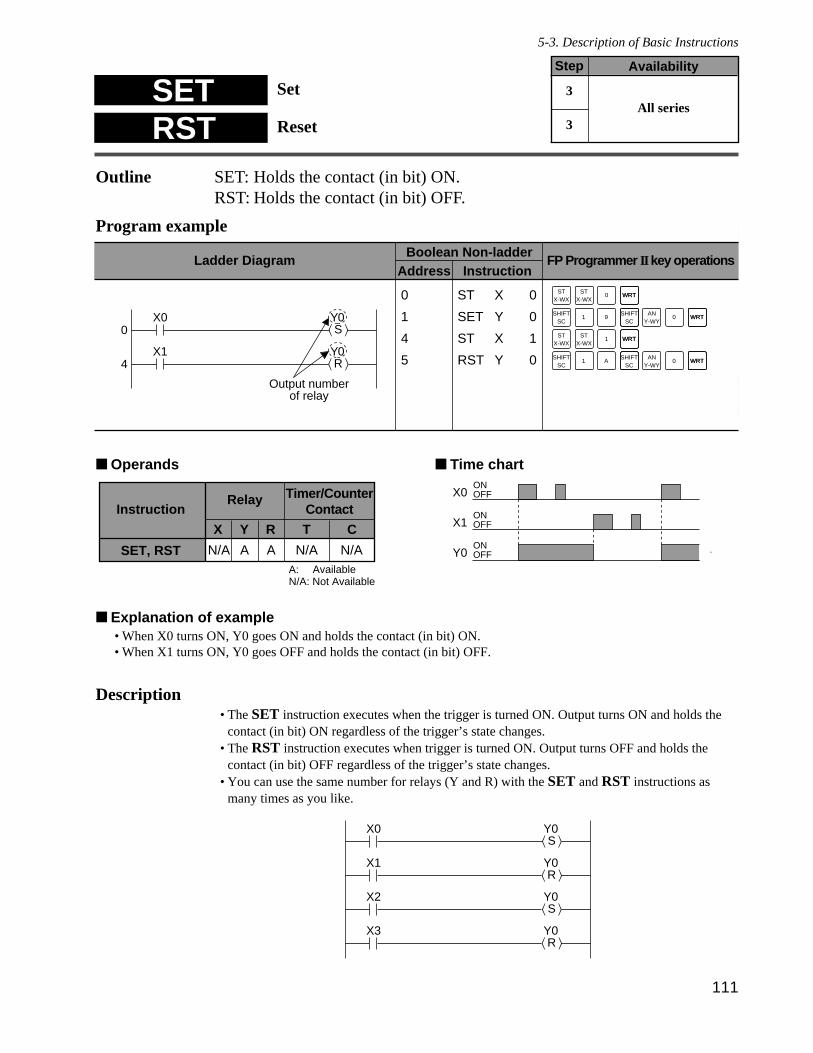
111
5-3. Description of Basic Instructions
SET Set
RST Reset
Outline SET: Holds the contact (in bit) ON.RST: Holds the contact (in bit) OFF.
Program example
Operands Time chart
Explanation of example• When X0 turns ON, Y0 goes ON and holds the contact (in bit) ON.• When X1 turns ON, Y0 goes OFF and holds the contact (in bit) OFF.
Description• The SET instruction executes when the trigger is turned ON. Output turns ON and holds the
contact (in bit) ON regardless of the trigger’s state changes.• The RST instruction executes when trigger is turned ON. Output turns OFF and holds the
contact (in bit) OFF regardless of the trigger’s state changes.• You can use the same number for relays (Y and R) with the SET and RST instructions as
many times as you like.
X0 Y0⟨ S ⟩!
X1 Y0⟨ R ⟩!
X2 Y0⟨ S ⟩!
X3 Y0⟨ R ⟩!
ONOFFX0
ONOFFX1
ONOFFY0
Timer/CounterContact
C
Relay
TRYX
Instruction
SET, RST N/A A A N/A N/AA:N/A: Not Available
Available
Ladder Diagram FP Programmer IIkey operationsBoolean Non-ladder
Address Instruction
0X0 Y0
4X1 Y0
⟨ S ⟩!
⟨ R ⟩!
Output numberof relay
SHIFTSC
1
STX-WX
STX-WX
WRT0 WRT
SHIFTSC
WRTWRT9AN
Y-WY0
STX-WX
STX-WX
WRT1 WRT
SHIFTSC
1SHIFT
SCWRTWRTA
ANY-WY
0
0
1
4
5
ST X 0
SET Y 0
ST X 1
RST Y 0
AvailabilityStep
3
3All series
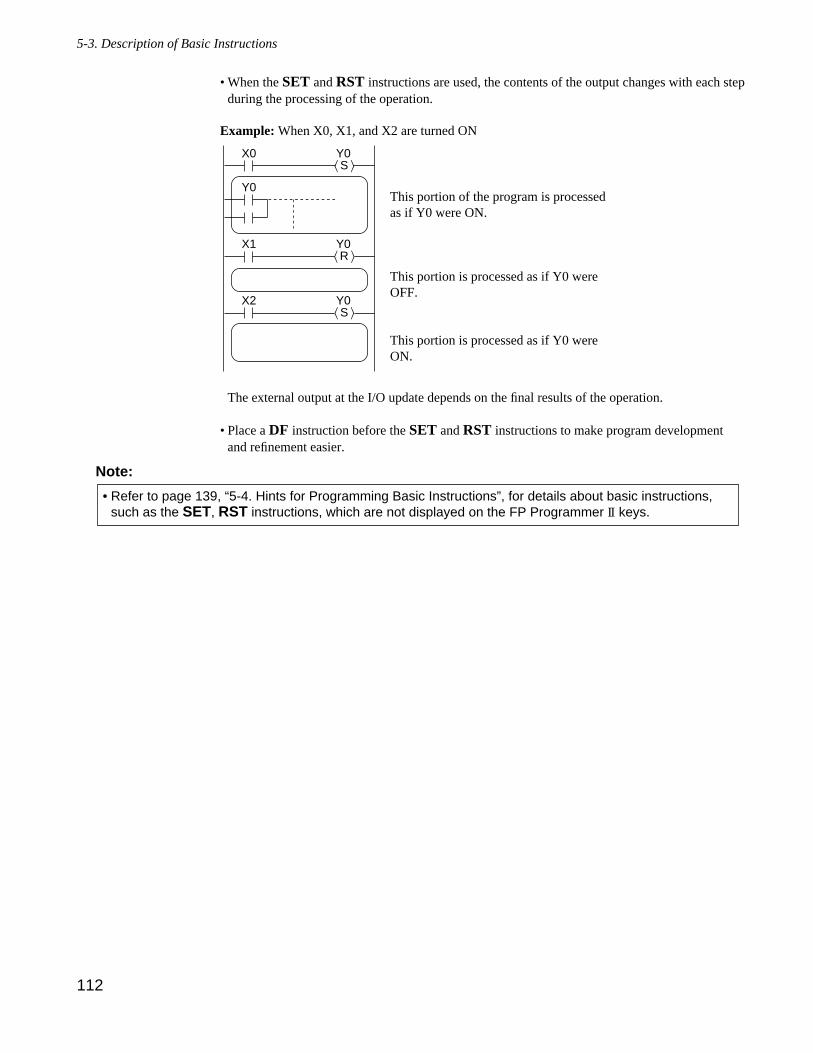
5-3. Description of Basic Instructions
112
• When the SET and RST instructions are used, the contents of the output changes with each stepduring the processing of the operation.
Example: When X0, X1, and X2 are turned ON
The external output at the I/O update depends on the final results of the operation.
• Place a DF instruction before the SET and RST instructions to make program developmentand refinement easier.
Note:
• Refer to page 139, “5-4. Hints for Programming Basic Instructions”, for details about basic instructions,such as the SET, RST instructions, which are not displayed on the FP Programmer II keys.
This portion of the program is processedas if Y0 were ON.
This portion is processed as if Y0 wereOFF.
This portion is processed as if Y0 wereON.
X0 Y0⟨ S ⟩!
X1 Y0⟨ R ⟩!
X2 Y0⟨ S ⟩!
Y0
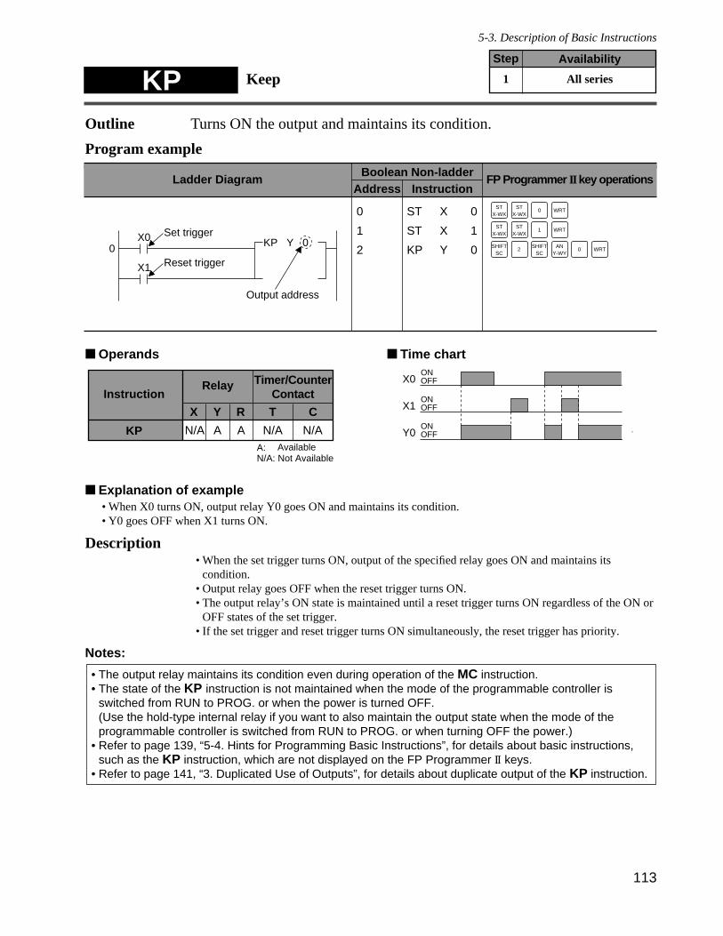
113
5-3. Description of Basic Instructions
Outline Turns ON the output and maintains its condition.
Program example
Operands Time chart
Explanation of example• When X0 turns ON, output relay Y0 goes ON and maintains its condition.• Y0 goes OFF when X1 turns ON.
Description• When the set trigger turns ON, output of the specified relay goes ON and maintains its
condition.• Output relay goes OFF when the reset trigger turns ON.• The output relay’s ON state is maintained until a reset trigger turns ON regardless of the ON or
OFF states of the set trigger.• If the set trigger and reset trigger turns ON simultaneously, the reset trigger has priority.
Notes:
• The output relay maintains its condition even during operation of the MC instruction.• The state of the KP instruction is not maintained when the mode of the programmable controller is
switched from RUN to PROG. or when the power is turned OFF.(Use the hold-type internal relay if you want to also maintain the output state when the mode of theprogrammable controller is switched from RUN to PROG. or when turning OFF the power.)
• Refer to page 139, “5-4. Hints for Programming Basic Instructions”, for details about basic instructions,such as the KP instruction, which are not displayed on the FP Programmer II keys.
• Refer to page 141, “3. Duplicated Use of Outputs”, for details about duplicate output of the KP instruction.
ONOFFX0
ONOFFX1
ONOFFY0
Timer/CounterContact
C
Relay
TRYX
Instruction
KP N/A A A N/A N/AA: N/A: Not Available
Available
KP KeepAvailabilityStep
1 All series
Ladder Diagram FP Programmer IIkey operationsBoolean Non-ladder
Address Instruction
0X0 KP Y 0
X1
Output address
Set trigger
Reset trigger
STX-WX
STX-WX
WRT0
STX-WX
STX-WX
WRT1
SHIFTSC
2SHIFT
SCWRT
ANY-WY
0
0
1
2
ST X 0
ST X 1
KP Y 0
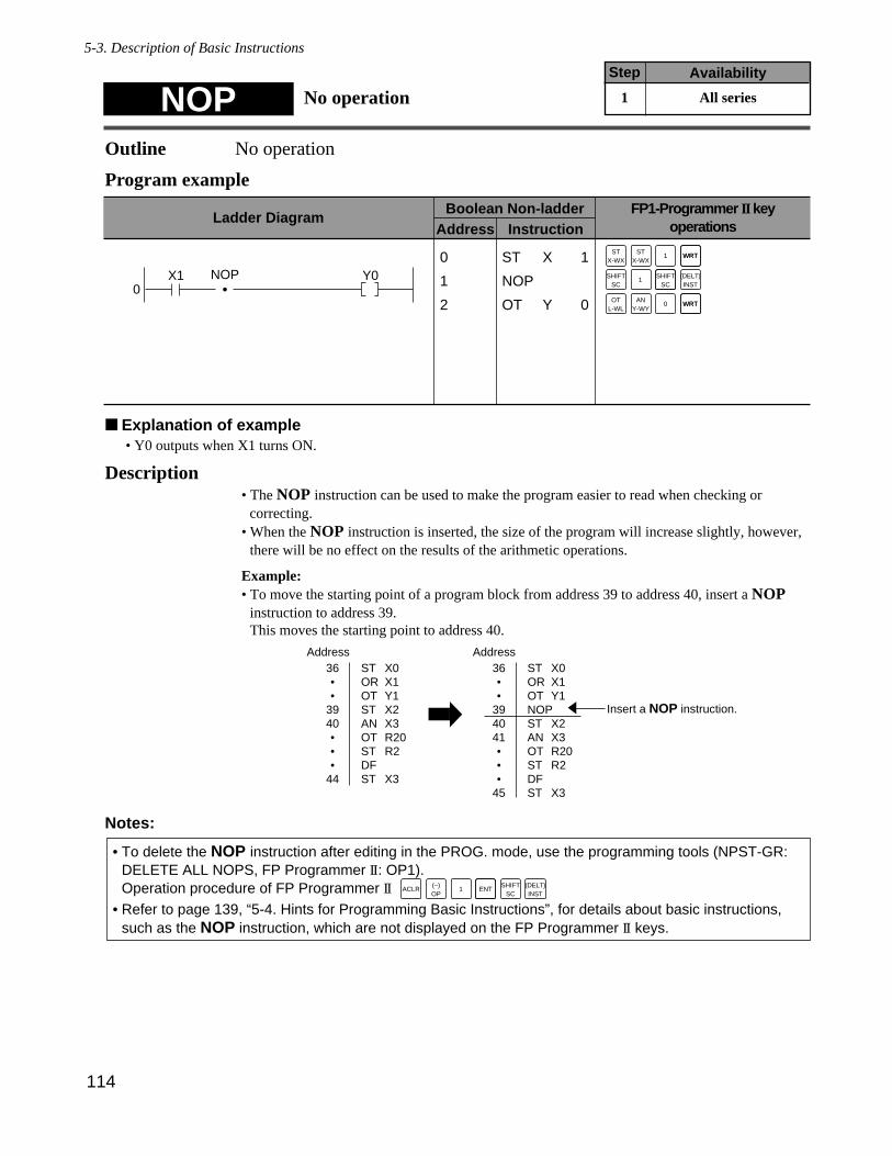
Outline No operation
Program example
Explanation of example• Y0 outputs when X1 turns ON.
Description• The NOP instruction can be used to make the program easier to read when checking or
correcting.• When the NOP instruction is inserted, the size of the program will increase slightly, however,
there will be no effect on the results of the arithmetic operations.
Example:• To move the starting point of a program block from address 39 to address 40, insert a NOP
instruction to address 39.This moves the starting point to address 40.
Notes:
• To delete the NOP instruction after editing in the PROG. mode, use the programming tools (NPST-GR:DELETE ALL NOPS, FP Programmer II: OP1).Operation procedure of FP Programmer II
• Refer to page 139, “5-4. Hints for Programming Basic Instructions”, for details about basic instructions,such as the NOP instruction, which are not displayed on the FP Programmer II keys.
ST OROTSTANOTSTDFST
X0X1Y1X2X3 R20R2
X3
ST OROTNOPSTANOTSTDFST
X0X1Y1
X2X3 R20R2
X3
Insert a NOP instruction.
36••
3940•••
44
Address36••
394041•••
45
Address
NOP No operationAvailabilityStep
1 All series
Ladder DiagramFP1-Programmer IIkey
operationsBoolean Non-ladder
Address Instruction
0X1 Y0NOP
•
STX-WX
STX-WX
WRT1 WRT
ANY-WY
OTL-WL
WRT0 WRT
SHIFTSC
1SHIFT
SC(DELT)INST
0
1
2
ST X 1
NOP
OT Y 0
5-3. Description of Basic Instructions
114
(–)OP
ENT1ACLRSHIFT
SC(DELT)INST
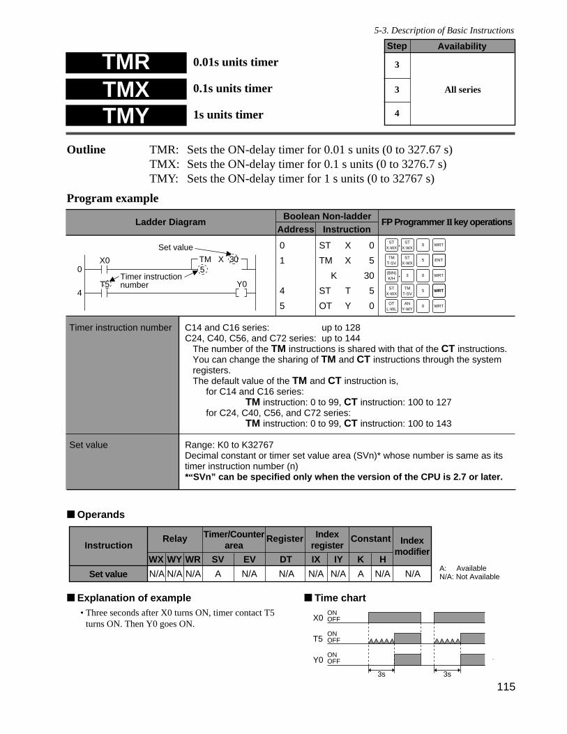
Outline TMR: Sets the ON-delay timer for 0.01 s units (0 to 327.67 s)TMX: Sets the ON-delay timer for 0.1 s units (0 to 3276.7 s)TMY: Sets the ON-delay timer for 1 s units (0 to 32767 s)
Program example
Operands
Explanation of example Time chartONOFFX0
ONOFFT5
ONOFFY0
3s 3s
• Three seconds after X0 turns ON, timer contact T5turns ON. Then Y0 goes ON.
Timer/Counterarea
EV
Relay
SVWRWYWX
Instruction
Set value N/A N/A N/A A N/AA: N/A: Not Available
Register
DT
N/A
IYIX
N/A N/A
HK
A N/A
Constant Indexmodifier
N/A
Indexregister
Available
5-3. Description of Basic Instructions
TMR 0.01s units timer
TMX 0.1s units timer
TMY 1s units timer
Ladder Diagram FP Programmer IIkey operationsBoolean Non-ladder
Address Instruction
0X0
T5
Set value
Timer instruction number
5
Y0
TM X 30
4
STX-WX
TMT-SV
ENT5
STX-WX
STX-WX
0 WRT
OTL-WL
ANY-WY
0 WRT
(BIN)K/H
0 WRT
TMT-SV
STX-WX
WRT5 WRT
3
0
1
4
5
ST X 0
TM X 5
K 30
ST T 5
OT Y 0
AvailabilityStep
3
3
4
All series
Timer instruction number C14 and C16 series: up to 128C24, C40, C56, and C72 series: up to 144
The number of the TM instructions is shared with that of the CT instructions.You can change the sharing of TM and CT instructions through the systemregisters.The default value of the TM and CT instruction is,
for C14 and C16 series:TM instruction: 0 to 99, CT instruction: 100 to 127
for C24, C40, C56, and C72 series:TM instruction: 0 to 99, CT instruction: 100 to 143
Set value Range: K0 to K32767Decimal constant or timer set value area (SVn)* whose number is same as itstimer instruction number (n)*“SVn” can be specified only when the version of the CPU is 2.7 or later.
115
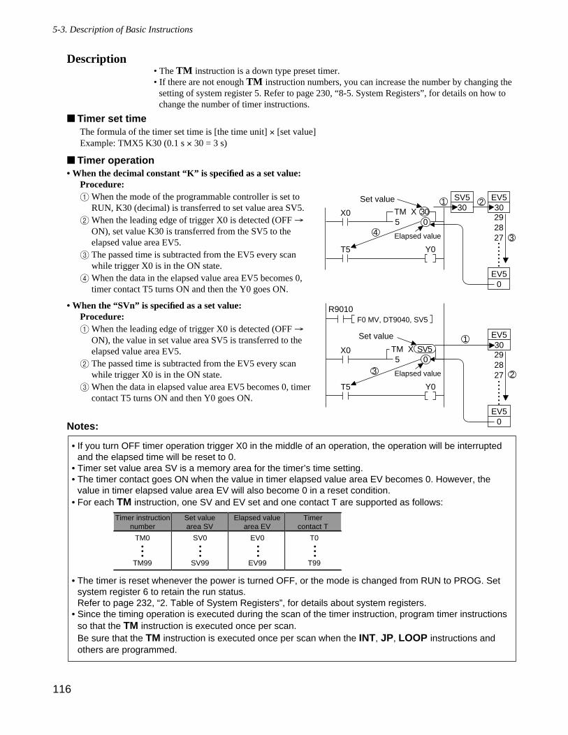
116
5-3. Description of Basic Instructions
Description• The TM instruction is a down type preset timer.• If there are not enough TM instruction numbers, you can increase the number by changing the
setting of system register 5. Refer to page 230, “8-5. System Registers”, for details on how tochange the number of timer instructions.
Timer set timeThe formula of the timer set time is [the time unit] × [set value]Example: TMX5 K30 (0.1 s × 30 = 3 s)
Timer operation• When the decimal constant “K” is specified as a set value:
Procedure:1 When the mode of the programmable controller is set to
RUN, K30 (decimal) is transferred to set value area SV5.2 When the leading edge of trigger X0 is detected (OFF →
ON), set value K30 is transferred from the SV5 to theelapsed value area EV5.
3 The passed time is subtracted from the EV5 every scanwhile trigger X0 is in the ON state.
4 When the data in the elapsed value area EV5 becomes 0,timer contact T5 turns ON and then the Y0 goes ON.
• When the “SVn” is specified as a set value:Procedure:1 When the leading edge of trigger X0 is detected (OFF →
ON), the value in set value area SV5 is transferred to theelapsed value area EV5.
2 The passed time is subtracted from the EV5 every scanwhile trigger X0 is in the ON state.
3 When the data in elapsed value area EV5 becomes 0, timercontact T5 turns ON and then Y0 goes ON.
Notes:
• If you turn OFF timer operation trigger X0 in the middle of an operation, the operation will be interruptedand the elapsed time will be reset to 0.
• Timer set value area SV is a memory area for the timer’s time setting.• The timer contact goes ON when the value in timer elapsed value area EV becomes 0. However, the
value in timer elapsed value area EV will also become 0 in a reset condition.• For each TM instruction, one SV and EV set and one contact T are supported as follows:
• The timer is reset whenever the power is turned OFF, or the mode is changed from RUN to PROG. Setsystem register 6 to retain the run status.Refer to page 232, “2. Table of System Registers”, for details about system registers.
• Since the timing operation is executed during the scan of the timer instruction, program timer instructionsso that the TM instruction is executed once per scan. Be sure that the TM instruction is executed once per scan when the INT, JP, LOOP instructions andothers are programmed.
Timer instructionnumber
Set valuearea SV
Elapsed valuearea EV
TM0 SV0 EV0•••
•••
•••
TM99 SV99 EV99
T0•••
T99
Timercontact T
X0
Set value
5 0TM X 30
21 SV530
EV530
EV50
292827
•••••••
T5 Y0
Elapsed value43
X0
Set value
5 0TM X SV5
2
1 EV530
EV50
292827
•••••••
T5 Y0
Elapsed value3
R9010F0 MV, DT9040, SV5
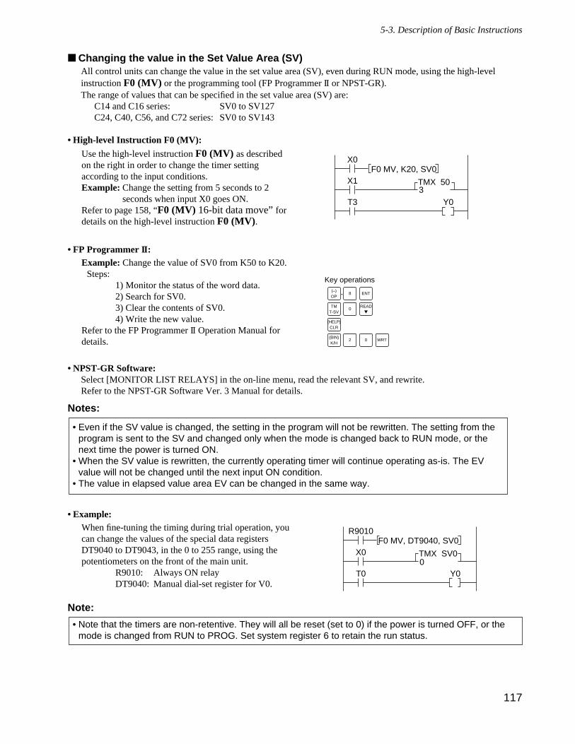
Changing the value in the Set Value Area (SV)All control units can change the value in the set value area (SV), even during RUN mode, using the high-levelinstruction F0 (MV) or the programming tool (FP Programmer II or NPST-GR).The range of values that can be specified in the set value area (SV) are:
C14 and C16 series: SV0 to SV127C24, C40, C56, and C72 series: SV0 to SV143
• High-level Instruction F0 (MV):
• FP Programmer II:
• NPST-GR Software:Select [MONITOR LIST RELAYS] in the on-line menu, read the relevant SV, and rewrite.Refer to the NPST-GR Software Ver. 3 Manual for details.
Notes:
• Example:
Note:
• Note that the timers are non-retentive. They will all be reset (set to 0) if the power is turned OFF, or themode is changed from RUN to PROG. Set system register 6 to retain the run status.
X0
R9010
T0 Y0
F0 MV, DT9040, SV0
TMX SV00
When fine-tuning the timing during trial operation, youcan change the values of the special data registersDT9040 to DT9043, in the 0 to 255 range, using thepotentiometers on the front of the main unit.
R9010: Always ON relayDT9040: Manual dial-set register for V0.
• Even if the SV value is changed, the setting in the program will not be rewritten. The setting from theprogram is sent to the SV and changed only when the mode is changed back to RUN mode, or thenext time the power is turned ON.
• When the SV value is rewritten, the currently operating timer will continue operating as-is. The EVvalue will not be changed until the next input ON condition.
• The value in elapsed value area EV can be changed in the same way.
(–)OP
ENT
TMT-SV
0
8
READ
(BIN)K/H
0 WRT
(HELP)CLR
2
Key operations
Example: Change the value of SV0 from K50 to K20.Steps:
1) Monitor the status of the word data.2) Search for SV0.3) Clear the contents of SV0.4) Write the new value.
Refer to the FP Programmer II Operation Manual fordetails.
X1
X0
T3 Y0
F0 MV, K20, SV0
TMX 503
Use the high-level instruction F0 (MV) as describedon the right in order to change the timer settingaccording to the input conditions.Example: Change the setting from 5 seconds to 2
seconds when input X0 goes ON.Refer to page 158, “F0 (MV) 16-bit data move” fordetails on the high-level instruction F0 (MV).
117
5-3. Description of Basic Instructions
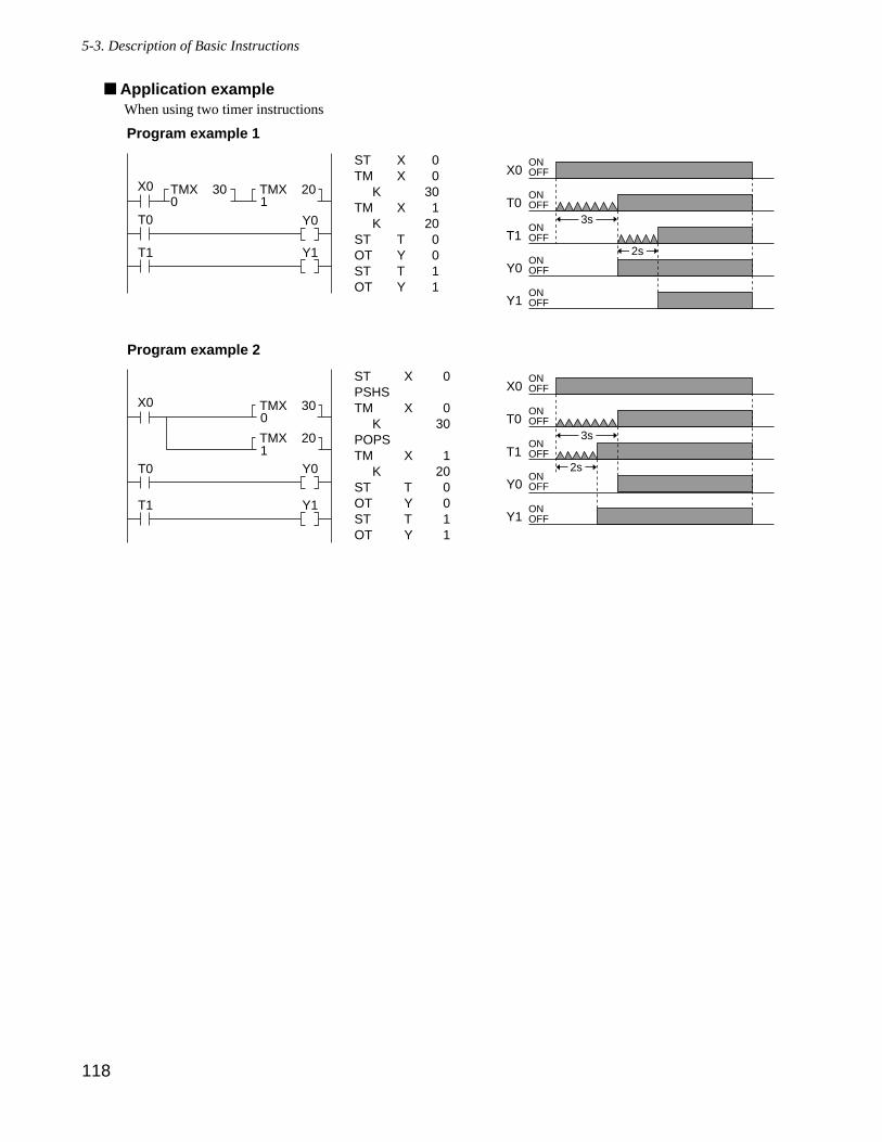
Application exampleWhen using two timer instructions
T0 Y0
X0 TMX 300
ONOFFX0
ONOFFT0
ONOFF
ONOFF
ONOFF
T1
Y0
Y1
3s
2s
STPSHSTM KPOPSTM KSTOTSTOT
X
X
X
TYTY
0
030
1200011
T1 Y1
TMX 201
Program example 2
T0
T1 Y1
TMX 30X0
Y0
TMX 200 1
ONOFFX0
ONOFFT0
ONOFF
ONOFF
ONOFF
T1
Y0
Y1
3s
2s
STTM KTM KSTOTSTOT
XX
X
TYTY
00
301
200011
Program example 1
118
5-3. Description of Basic Instructions
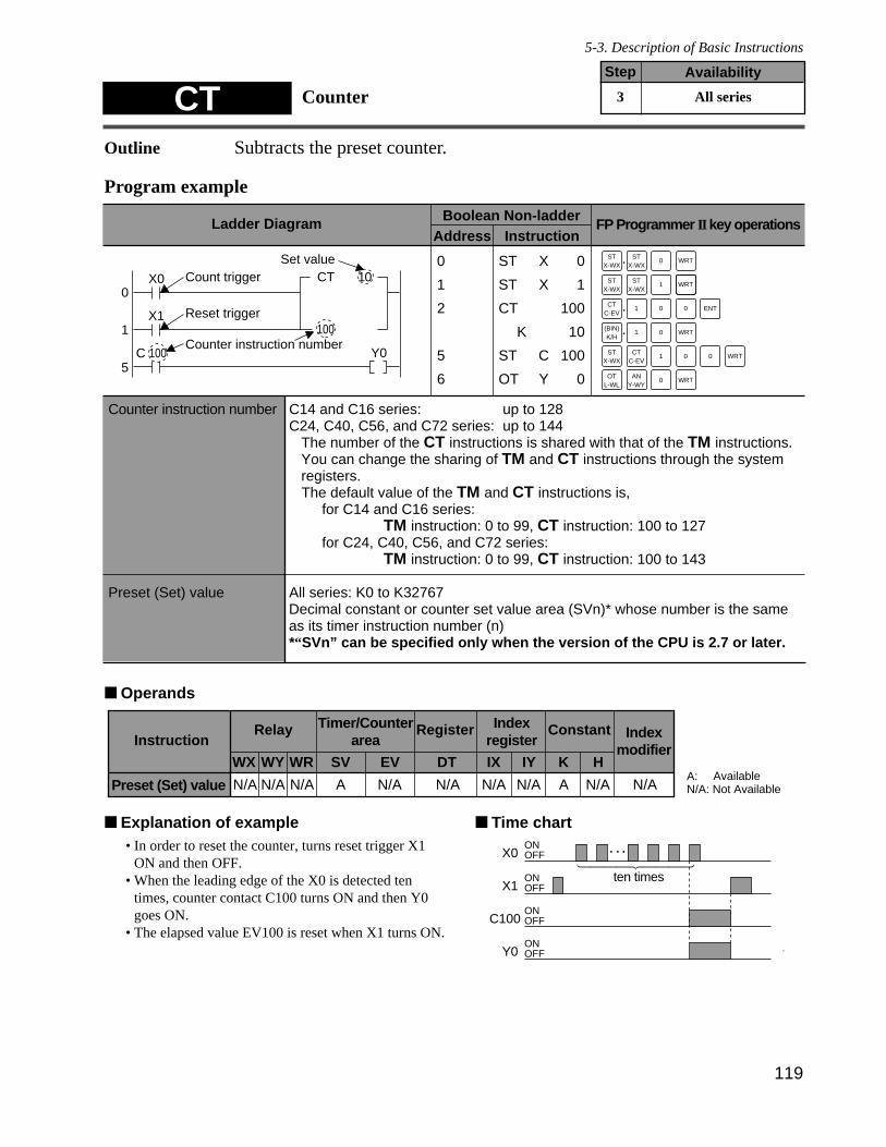
Outline Subtracts the preset counter.
Program example
Operands
Explanation of example Time chartONOFFX0
ONOFFX1
ONOFFC100
ONOFFY0
• ••
##########
ten times
• In order to reset the counter, turns reset trigger X1ON and then OFF.
• When the leading edge of the X0 is detected tentimes, counter contact C100 turns ON and then Y0goes ON.
• The elapsed value EV100 is reset when X1 turns ON.
Timer/Counterarea
EV
Relay
SVWRWYWX
Instruction
Preset (Set) value N/A N/A N/A A N/AA: N/A: Not Available
Register
DT
N/A
IYIX
N/A N/A
HK
A N/A
Constant Indexmodifier
N/A
Indexregister
Available
CT CounterAvailabilityStep
3 All series
Ladder Diagram FP Programmer IIkey operationsBoolean Non-ladder
Address Instruction
0X0 Count trigger
X1
C 100 Y0
CT 10
Reset trigger
Counter instruction number100
Set value
1
5
STX-WX
STX-WX
1 WRT
STX-WX
STX-WX
0 WRT
CTC-EV
OTL-WL
ANY-WY
0 WRT
CTC-EV
STX-WX
1
1 0 0 ENT
(BIN)K/H
01 WRT
0 0 WRT
0
1
2
5
6
ST X 0
ST X 1
CT 100
K 10
ST C 100
OT Y 0
5-3. Description of Basic Instructions
119
Counter instruction number C14 and C16 series: up to 128C24, C40, C56, and C72 series: up to 144
The number of the CT instructions is shared with that of the TM instructions.You can change the sharing of TM and CT instructions through the systemregisters.The default value of the TM and CT instructions is,
for C14 and C16 series:TM instruction: 0 to 99, CT instruction: 100 to 127
for C24, C40, C56, and C72 series:TM instruction: 0 to 99, CT instruction: 100 to 143
Preset (Set) value All series: K0 to K32767Decimal constant or counter set value area (SVn)* whose number is the sameas its timer instruction number (n)*“SVn” can be specified only when the version of the CPU is 2.7 or later.
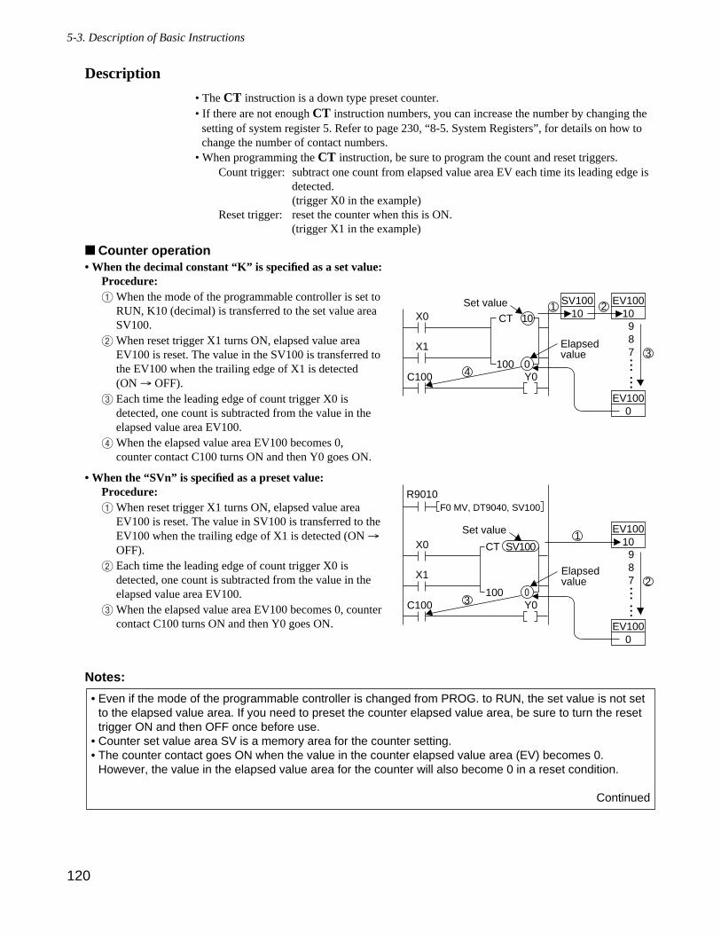
Description
• The CT instruction is a down type preset counter.• If there are not enough CT instruction numbers, you can increase the number by changing the
setting of system register 5. Refer to page 230, “8-5. System Registers”, for details on how tochange the number of contact numbers.
• When programming the CT instruction, be sure to program the count and reset triggers.Count trigger: subtract one count from elapsed value area EV each time its leading edge is
detected. (trigger X0 in the example)
Reset trigger: reset the counter when this is ON.(trigger X1 in the example)
Counter operation• When the decimal constant “K” is specified as a set value:
Procedure:1When the mode of the programmable controller is set to
RUN, K10 (decimal) is transferred to the set value areaSV100.
2When reset trigger X1 turns ON, elapsed value areaEV100 is reset. The value in the SV100 is transferred tothe EV100 when the trailing edge of X1 is detected(ON → OFF).
3 Each time the leading edge of count trigger X0 isdetected, one count is subtracted from the value in theelapsed value area EV100.
4 When the elapsed value area EV100 becomes 0,counter contact C100 turns ON and then Y0 goes ON.
• When the “SVn” is specified as a preset value:Procedure:1 When reset trigger X1 turns ON, elapsed value area
EV100 is reset. The value in SV100 is transferred to theEV100 when the trailing edge of X1 is detected (ON →OFF).
2 Each time the leading edge of count trigger X0 isdetected, one count is subtracted from the value in theelapsed value area EV100.
3 When the elapsed value area EV100 becomes 0, countercontact C100 turns ON and then Y0 goes ON.
Notes:
• Even if the mode of the programmable controller is changed from PROG. to RUN, the set value is not setto the elapsed value area. If you need to preset the counter elapsed value area, be sure to turn the resettrigger ON and then OFF once before use.
• Counter set value area SV is a memory area for the counter setting.• The counter contact goes ON when the value in the counter elapsed value area (EV) becomes 0.
However, the value in the elapsed value area for the counter will also become 0 in a reset condition.
Continued
120
5-3. Description of Basic Instructions
X0
X1
C100 Y0
CT 10
Elapsedvalue
Set value SV10010
EV10010987
EV1000
••••••
4
3100 0
1 2
X0
X1
C100 Y0
CT SV100
Elapsedvalue
Set value EV10010987
EV1000
••••••
3
2100
1
R9010F0 MV, DT9040, SV100
0
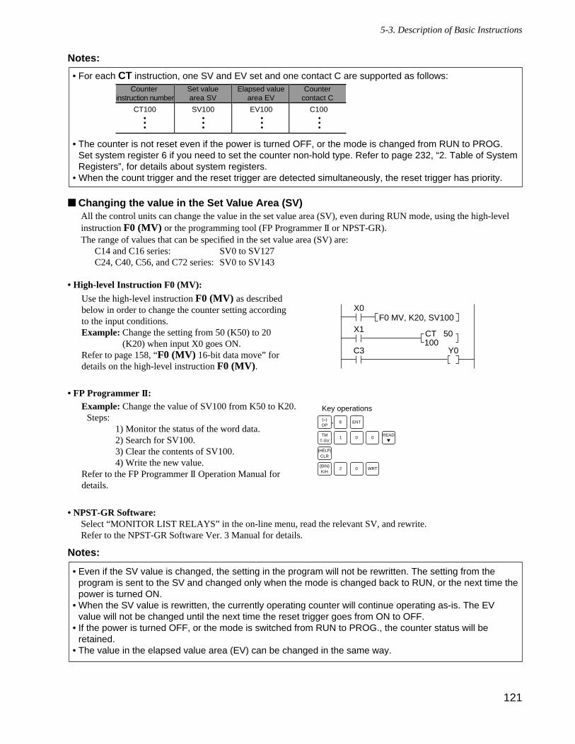
Notes:
Changing the value in the Set Value Area (SV)All the control units can change the value in the set value area (SV), even during RUN mode, using the high-levelinstruction F0 (MV) or the programming tool (FP Programmer II or NPST-GR).The range of values that can be specified in the set value area (SV) are:
C14 and C16 series: SV0 to SV127C24, C40, C56, and C72 series: SV0 to SV143
• High-level Instruction F0 (MV):
• FP Programmer II:
• NPST-GR Software:Select “MONITOR LIST RELAYS” in the on-line menu, read the relevant SV, and rewrite.Refer to the NPST-GR Software Ver. 3 Manual for details.
Notes:
• Even if the SV value is changed, the setting in the program will not be rewritten. The setting from theprogram is sent to the SV and changed only when the mode is changed back to RUN, or the next time thepower is turned ON.
• When the SV value is rewritten, the currently operating counter will continue operating as-is. The EVvalue will not be changed until the next time the reset trigger goes from ON to OFF.
• If the power is turned OFF, or the mode is switched from RUN to PROG., the counter status will beretained.
• The value in the elapsed value area (EV) can be changed in the same way.
TMT-SV
0
(–)OP
ENT
(BIN)K/H
0 WRT
(HELP)CLR
2
8
1 0READ
Key operationsExample: Change the value of SV100 from K50 to K20.Steps:
1) Monitor the status of the word data.2) Search for SV100.3) Clear the contents of SV100.4) Write the new value.
Refer to the FP Programmer II Operation Manual fordetails.
X1
X0
C3 Y0
F0 MV, K20, SV100
CT 50100
Use the high-level instruction F0 (MV) as describedbelow in order to change the counter setting accordingto the input conditions.Example: Change the setting from 50 (K50) to 20
(K20) when input X0 goes ON.Refer to page 158, “F0 (MV) 16-bit data move” fordetails on the high-level instruction F0 (MV).
• For each CT instruction, one SV and EV set and one contact C are supported as follows:
• The counter is not reset even if the power is turned OFF, or the mode is changed from RUN to PROG.Set system register 6 if you need to set the counter non-hold type. Refer to page 232, “2. Table of SystemRegisters”, for details about system registers.
• When the count trigger and the reset trigger are detected simultaneously, the reset trigger has priority.
121
5-3. Description of Basic Instructions
Counter instruction number
Set valuearea SV
Elapsed valuearea EV
CT100 SV100 EV100•••
•••
•••
C100•••
Countercontact C
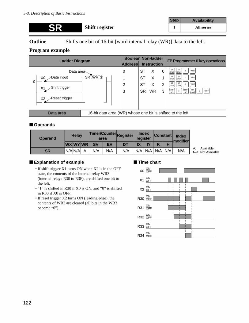
5-3. Description of Basic Instructions
122
Outline Shifts one bit of 16-bit [word internal relay (WR)] data to the left.
Program example
Operands
Explanation of example Time chartONOFFX0
ONOFFX1
ONOFF
ONOFFR30
ONOFF
ONOFF
ONOFF
ONOFF
X2
R31
R32
R33
R34
• If shift trigger X1 turns ON when X2 is in the OFFstate, the contents of the internal relay WR3(internal relays R30 to R3F), are shifted one bit tothe left.
• “1” is shifted in R30 if X0 is ON, and “0” is shiftedin R30 if X0 is OFF.
• If reset trigger X2 turns ON (leading edge), thecontents of WR3 are cleared (all bits in the WR3become “0”).
Timer/Counterarea
EV
Relay
SVWRWYWX
Operand
SR N/A N/A A N/AA: N/A: Not Available
Register
DT
N/A
IYIX
N/A N/A
HK
N/A N/A
Constant Indexmodifier
N/A
Indexregister
AvailableN/A
SR Shift registerAvailabilityStep
1 All series
Ladder Diagram FP Programmer IIkey operationsBoolean Non-ladder
Address Instruction
0X0 Data input
X1
SR WR 3
Shift trigger
Reset trigger
Data area
X2
STX-WX
STX-WX
1 WRT
STX-WX
STX-WX
0 WRT
SHIFTSC
3 WRT
STX-WX
STX-WX
2 WRT
ORR-WR
SHIFTSC
3
0
1
2
3
ST X 0
ST X 1
ST X 2
SR WR 3
16-bit data area (WR) whose one bit is shifted to the leftData area
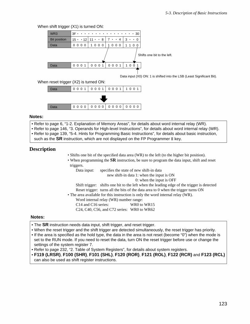
123
5-3. Description of Basic Instructions
Notes:
Description• Shifts one bit of the specified data area (WR) to the left (to the higher bit position).• When programming the SR instruction, be sure to program the data input, shift and reset
triggers.Data input: specifies the state of new shift-in data
new shift-in data 1: when the input is ON0: when the input is OFF
Shift trigger: shifts one bit to the left when the leading edge of the trigger is detectedReset trigger: turns all the bits of the data area to 0 when the trigger turns ON
• The area available for this instruction is only the word internal relay (WR).Word internal relay (WR) number range:C14 and C16 series: WR0 to WR15C24, C40, C56, and C72 series: WR0 to WR62
Notes:
• The SR instruction needs data input, shift trigger, and reset trigger.• When the reset trigger and the shift trigger are detected simultaneously, the reset trigger has priority. • If the area is specified as the hold type, the data in the area is not reset (become “0”) when the mode is
set to the RUN mode. If you need to reset the data, turn ON the reset trigger before use or change thesettings of the system register 7.
• Refer to page 232, “2. Table of System Registers”, for details about system registers.• F119 (LRSR), F100 (SHR), F101 (SHL), F120 (ROR), F121 (ROL), F122 (RCR) and F123 (RCL)
can also be used as shift register instructions.
• Refer to page 6, “1-2. Explanation of Memory Areas”, for details about word internal relay (WR).• Refer to page 146, “3. Operands for High-level Instructions”, for details about word internal relay (WR).• Refer to page 139, “5-4. Hints for Programming Basic Instructions”, for details about basic instruction,
such as the SR instruction, which are not displayed on the FP Programmer II key.
WR3
Bit position
Data 0 0 0 0
15 . . 12
1 0 0 0
11 . . 8
1 0 0 0
7 . . 4
1 1 0 0
3 . . 0
Data
Data
Data
When shift trigger (X1) is turned ON:
Shifts one bit to the left.
Data input (X0) ON: 1 is shifted into the LSB (Least Significant Bit).
When reset trigger (X2) is turned ON:
3F . . . . . . . . . . . . . . . . 30
0 0 0 1 0 0 0 1 0 0 0 1 1 0 0 1
0 0 0 1 0 0 0 1 0 0 0 1 1 0 0 1
0 0 0 0 0 0 0 0 0 0 0 0 0 0 0 0
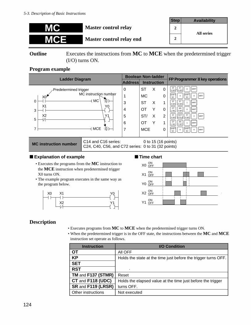
5-3. Description of Basic Instructions
124
MC Master control relay
MCE Master control relay end
AvailabilityStep
2
2All series
Outline Executes the instructions from MC to MCE when the predetermined trigger(I/O) turns ON.
Program example
Explanation of example Time chart
Description• Executes programs from MC to MCE when the predetermined trigger turns ON.• When the predetermined trigger is in the OFF state, the instructions between the MC and MCE
instruction set operate as follows.
InstructionOTKP SETRSTTM and F137 (STMR)CT and F118 (UDC)SR and F119 (LRSR)Other instructions
I/O ConditionAll OFFHolds the state at the time just before the trigger turns OFF.
ResetHolds the elapsed value at the time just before the triggerturns OFF.Not executed
ONOFFX0
ONOFFX1
ONOFF
ONOFF
ONOFF
Y0
X2
Y1
• Executes the programs from the MC instruction tothe MCE instruction when predetermined triggerX0 turns ON.
• The example program executes in the same way asthe program below.
Ladder Diagram FP Programmer IIkey operationsBoolean Non-ladder
Address Instruction
X0
X1( MC 0 )!
Y0
X2 Y1
( MCE 0 )!
Predetermined triggerMC instruction number
0
3
5
7
STX-WX
STX-WX
1 WRT
STX-WX
STX-WX
0 WRT
STX-WX
2 WRT
ANY-WY
OTL-WL
0 WRT
STX-WX
NOTDT/Ld
SHIFTSC
0 WRTSHIFT
SC4
SHIFTSC
0 WRT
ANY-WY
OTL-WL
1 WRT
SHIFTSC
5
0
1
3
4
5
6
7
ST X 0
MC 0
ST X 1
OT Y 0
ST/ X 2
OT Y 1
MCE 0
MC instruction number C14 and C16 series: 0 to 15 (16 points)C24, C40, C56, and C72 series: 0 to 31 (32 points)
X0 X1 Y0
X2 Y1
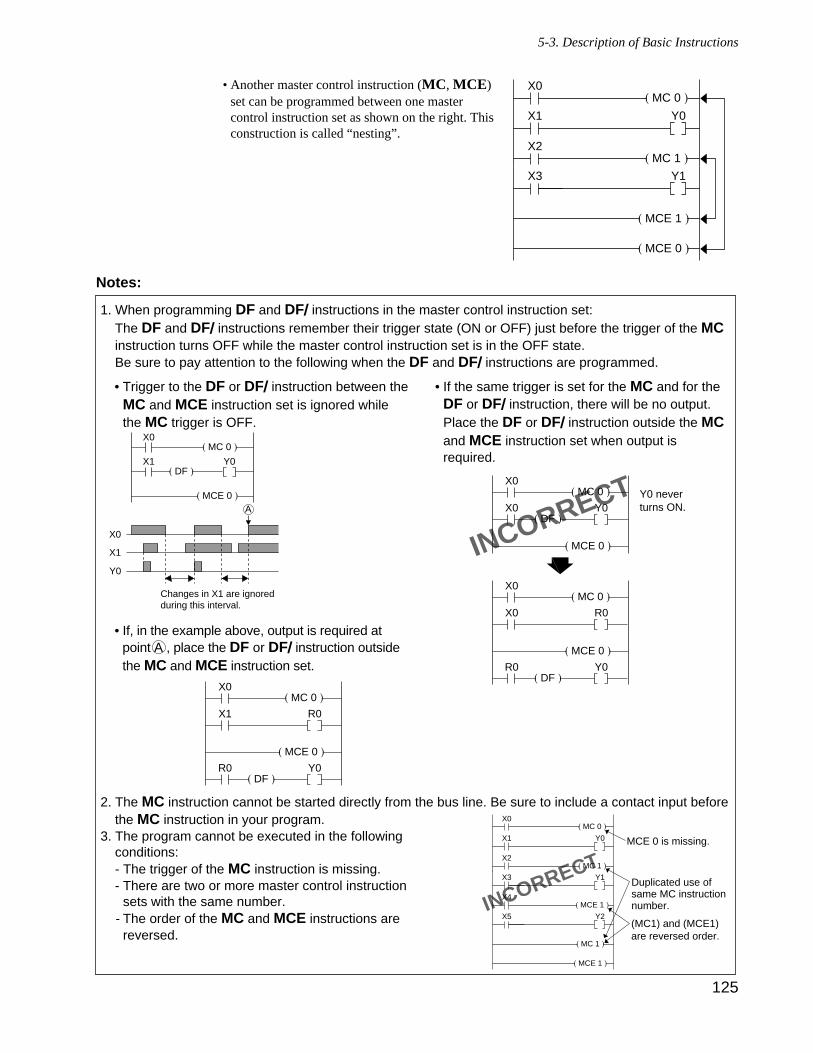
Notes:
X1 Y0
X0( MC 0 )!
( MCE 0 )!
X2( MC 1 )!
( MCE 1 )!
X3 Y1
• Another master control instruction (MC, MCE)set can be programmed between one mastercontrol instruction set as shown on the right. Thisconstruction is called “nesting”.
125
5-3. Description of Basic Instructions
1. When programming DF and DF/ instructions in the master control instruction set:The DF and DF/ instructions remember their trigger state (ON or OFF) just before the trigger of the MCinstruction turns OFF while the master control instruction set is in the OFF state.Be sure to pay attention to the following when the DF and DF/ instructions are programmed.
2. The MC instruction cannot be started directly from the bus line. Be sure to include a contact input beforethe MC instruction in your program.
3. The program cannot be executed in the followingconditions:- The trigger of the MC instruction is missing.- There are two or more master control instruction
sets with the same number.- The order of the MC and MCE instructions are
reversed.
• Trigger to the DF or DF/ instruction between theMC and MCE instruction set is ignored whilethe MC trigger is OFF.
• If, in the example above, output is required atpoint A , place the DF or DF/ instruction outsidethe MC and MCE instruction set.
• If the same trigger is set for the MC and for theDF or DF/ instruction, there will be no output.Place the DF or DF/ instruction outside the MCand MCE instruction set when output isrequired.
( MCE 0 )!
Y0
X1
X0
X1 Y0( DF )!
X0( MC 0 )!
Changes in X1 are ignoredduring this interval.
A
( MCE 0 )!
X1 R0
X0( MC 0 )!
R0 Y0( DF )!
INCORRECT
( MCE 0 )!
X0 Y0( DF )!
X0( MC 0 )!
( MCE 0 )!
X0 R0
X0( MC 0 )!
R0 Y0( DF )!
Y0 never turns ON.
INCORRECTX1 Y0
X0( MC 0 )!
( MCE 1 )!
( MC 1 )!
X2( MC 1 )!
X3 Y1
X4( MCE 1 )!
X5 Y2
MCE 0 is missing.
Duplicated use ofsame MC instructionnumber.
(MC1) and (MCE1)are reversed order.
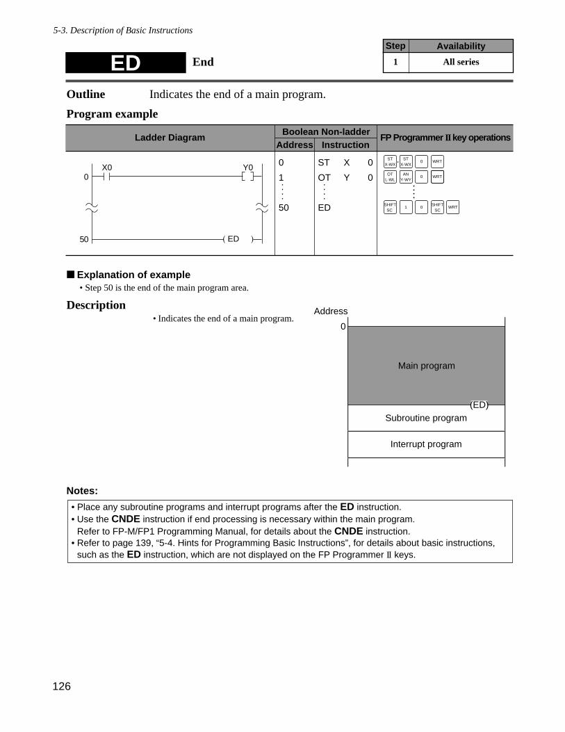
5-3. Description of Basic Instructions
126
Outline Indicates the end of a main program.
Program example
Explanation of example• Step 50 is the end of the main program area.
Description• Indicates the end of a main program.
Notes:
• Place any subroutine programs and interrupt programs after the ED instruction.• Use the CNDE instruction if end processing is necessary within the main program.
Refer to FP-M/FP1 Programming Manual, for details about the CNDE instruction.• Refer to page 139, “5-4. Hints for Programming Basic Instructions”, for details about basic instructions,
such as the ED instruction, which are not displayed on the FP Programmer II keys.
ED EndAvailabilityStep
1 All series
Ladder Diagram FP Programmer IIkey operationsBoolean Non-ladder
Address Instruction
X0
( ED )!
0
50
Y0ST
X-WXST
X-WX0 WRT
ANY-WY
OTL-WL
0 WRT
SHIFTSC
0 WRTSHIFT
SC1
••••
0
1....50
ST X 0
OT Y 0....ED
Main program
Subroutine program
Interrupt program
0
(ED)
Address
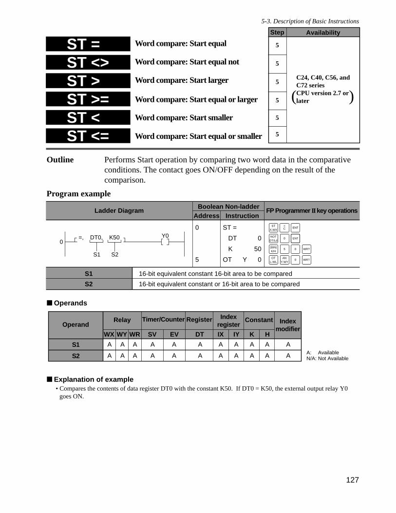
Outline Performs Start operation by comparing two word data in the comparativeconditions. The contact goes ON/OFF depending on the result of thecomparison.
Program example
Operands
Explanation of example• Compares the contents of data register DT0 with the constant K50. If DT0 = K50, the external output relay Y0
goes ON.
Timer/Counter
EV
Relay
SVWRWYWX
Operand
S1 A A A AA: N/A: Not Available
Register
DT
A
IYIX
A A
HK
A A
Constant Indexmodifier
A
Indexregister
Available
A
S2 A A A A A A A A A AA
S1
S2
16-bit equivalent constant 16-bit area to be compared
16-bit equivalent constant or 16-bit area to be compared
Ladder Diagram FP Programmer IIkey operationsBoolean Non-ladder
Address Instruction
0Y0=, DT0, K50
S2S1
STX-WX
ENT
NOTDT/Ld
ENT0
(BIN)K/H
0 WRT
OTL-WL
ANY-WY
0 WRT
5
C=0
5
ST =
DT 0
K 50
OT Y 0
AvailabilityStep
5
5
5
5
5
5
C24, C40, C56, andC72 seriesCPU version 2.7 orlater( )
ST = Word compare: Start equal
ST <> Word compare: Start equal not
Word compare: Start smaller
Word compare: Start larger
ST >= Word compare: Start equal or larger
ST <ST <= Word compare: Start equal or smaller
5-3. Description of Basic Instructions
127
ST >
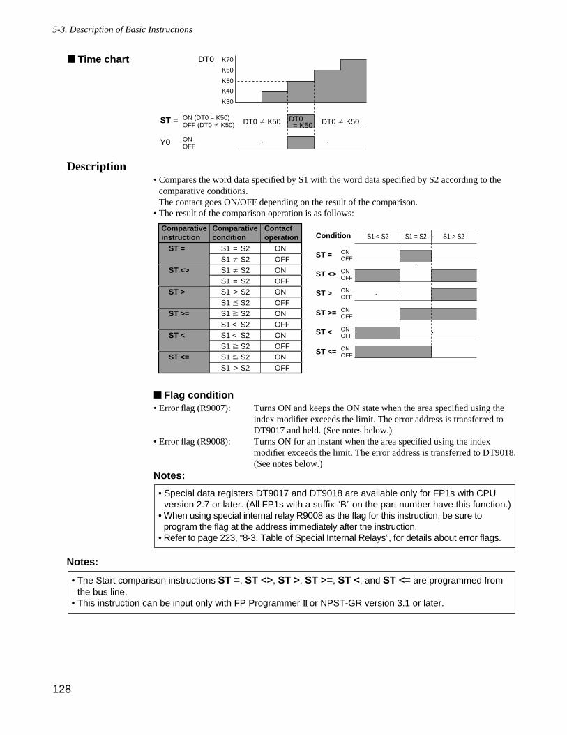
Description• Compares the word data specified by S1 with the word data specified by S2 according to the
comparative conditions.The contact goes ON/OFF depending on the result of the comparison.
• The result of the comparison operation is as follows:
Flag condition• Error flag (R9007): Turns ON and keeps the ON state when the area specified using the
index modifier exceeds the limit. The error address is transferred toDT9017 and held. (See notes below.)
• Error flag (R9008): Turns ON for an instant when the area specified using the indexmodifier exceeds the limit. The error address is transferred to DT9018.(See notes below.)
Notes:
Notes:
• The Start comparison instructions ST =, ST <>, ST >, ST >=, ST <, and ST <= are programmed fromthe bus line.
• This instruction can be input only with FP Programmer II or NPST-GR version 3.1 or later.
• Special data registers DT9017 and DT9018 are available only for FP1s with CPUversion 2.7 or later. (All FP1s with a suffix “B” on the part number have this function.)
• When using special internal relay R9008 as the flag for this instruction, be sure toprogram the flag at the address immediately after the instruction.
• Refer to page 223, “8-3. Table of Special Internal Relays”, for details about error flags.
ON OFF
ST <>
ST =S1 = S1 S1 S1 = S1 > S1 S1 S1 < S1 < S1 S1 S1 >
ONOFFONOFFONOFFONOFFONOFFONOFF
ST =
ST <>
ST >
ST >=
ST <
ST <=
Comparativeinstruction
Comparative condition
ON OFF
ON OFF ST >=
ST >
ON OFF
ON OFF ST <=
ST <
S1 < S2
ON OFF
Contactoperation S1 = S2 S1 > S2Condition
S2S2S2S2S2S2S2S2S2S2S2S2
ON (DT0 = K50)OFF (DT0 K50)
ON OFF
K30
K50
K60
K70
K40
ST =
Y0
DT0
DT0 K50 DT0 K50DT0 = K50
Time chart
128
5-3. Description of Basic Instructions
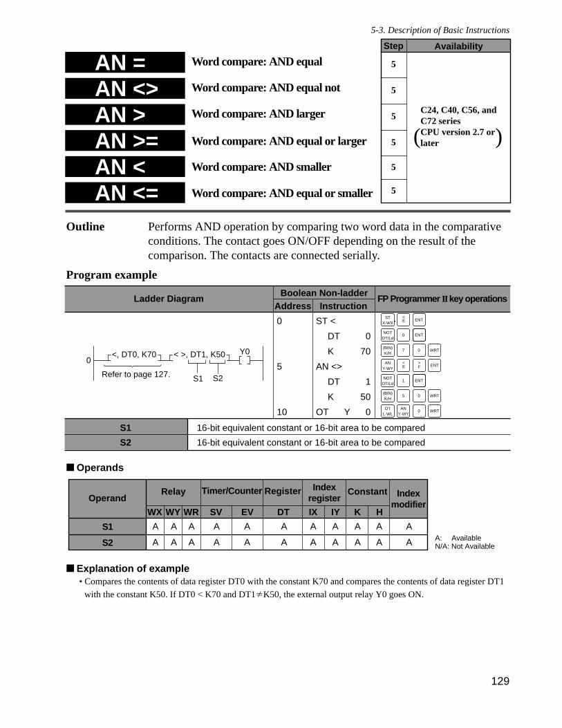
Outline Performs AND operation by comparing two word data in the comparativeconditions. The contact goes ON/OFF depending on the result of thecomparison. The contacts are connected serially.
Program example
Operands
Explanation of example• Compares the contents of data register DT0 with the constant K70 and compares the contents of data register DT1
with the constant K50. If DT0 < K70 and DT1K50, the external output relay Y0 goes ON.
Timer/Counter
EV
Relay
SVWRWYWX
Operand
S1 A A A AA: N/A: Not Available
Register
DT
A
IYIX
A A
HK
A A
Constant Indexmodifier
A
Indexregister
Available
A
S2 A A A A A A A A A AA
AvailabilityStep
5
5
5
5
5
5
C24, C40, C56, andC72 seriesCPU version 2.7 orlater( )
AN = Word compare: AND equal
AN <> Word compare: AND equal not
Word compare: AND smaller
AN > Word compare: AND larger
AN >= Word compare: AND equal or larger
AN <AN <= Word compare: AND equal or smaller
5-3. Description of Basic Instructions
129
S1
S2
16-bit equivalent constant or 16-bit area to be compared
16-bit equivalent constant or 16-bit area to be compared
Ladder Diagram FP Programmer IIkey operationsBoolean Non-ladder
Address Instruction
0Y0<, DT0, K70
S1 S2
< >, DT1, K50
"""""""
Refer to page 127.
STX-WX E ENT
NOTDT/Ld
ENT0
(BIN)K/H
0 WRT7
<
ANY-WY
ENT
OTL-WL
ANY-WY
0 WRT
E<
F>
NOTDT/Ld
ENT1
(BIN)K/H
0 WRT5
0
5
10
ST <
DT 0
K 70
AN <>
DT 1
K 50
OT Y 0
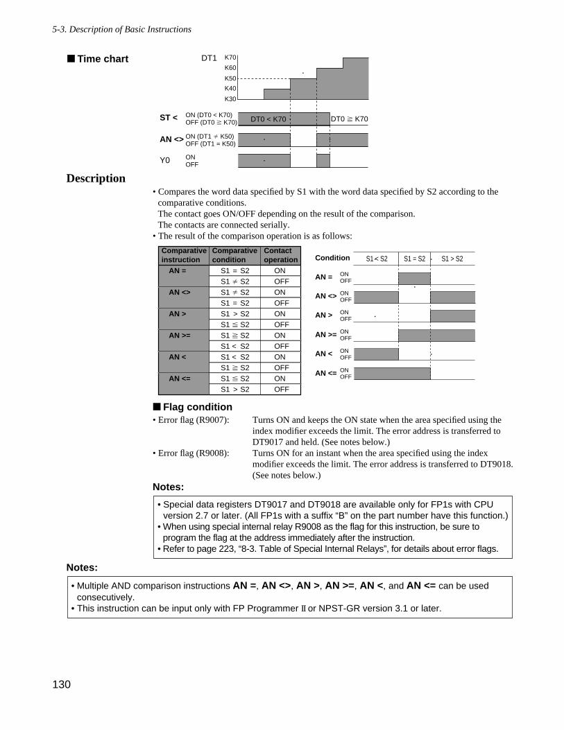
Description• Compares the word data specified by S1 with the word data specified by S2 according to the
comparative conditions.The contact goes ON/OFF depending on the result of the comparison.The contacts are connected serially.
• The result of the comparison operation is as follows:
Flag condition• Error flag (R9007): Turns ON and keeps the ON state when the area specified using the
index modifier exceeds the limit. The error address is transferred toDT9017 and held. (See notes below.)
• Error flag (R9008): Turns ON for an instant when the area specified using the indexmodifier exceeds the limit. The error address is transferred to DT9018.(See notes below.)
Notes:
Notes:
• Multiple AND comparison instructions AN =, AN <>, AN >, AN >=, AN <, and AN <= can be usedconsecutively.
• This instruction can be input only with FP Programmer II or NPST-GR version 3.1 or later.
• Special data registers DT9017 and DT9018 are available only for FP1s with CPUversion 2.7 or later. (All FP1s with a suffix “B” on the part number have this function.)
• When using special internal relay R9008 as the flag for this instruction, be sure toprogram the flag at the address immediately after the instruction.
• Refer to page 223, “8-3. Table of Special Internal Relays”, for details about error flags.
ON OFF
AN <>
AN =ONOFFONOFFONOFFONOFFONOFFONOFF
AN =
AN <>
AN >
AN >=
AN <
AN <=
Comparativeinstruction
Comparative condition
ON OFF
ON OFF AN >=
AN >
ON OFF
ON OFF AN <=
AN <
S1 < S2
ON OFF
Contactoperation S1 = S2 S1 > S2Condition
S1 = S1 S1 S1 = S1 > S1 S1 S1 < S1 < S1 S1 S1 >
S2S2S2S2S2S2S2S2S2S2S2S2
ON (DT0 < K70)OFF (DT0 K70)
ON (DT1 K50)OFF (DT1 = K50)
ON OFF
K30
K50
K60
K70
K40
AN <>
ST <
Y0
DT1
DT0 < K70 DT0 K70
Time chart
130
5-3. Description of Basic Instructions

AvailabilityStep
5
5
5
5
5
5
C24, C40, C56, andC72 seriesCPU version 2.7 orlater( )
Outline Performs OR operation by comparing two word data in the comparativeconditions. The contact goes ON/OFF depending on the result of thecomparison. The contacts are connected in parallel.
Program example
Operands
Explanation of example• Compares the contents of data register DT0 with the constant K50 and compares the contents of data register DT1
with the constant K40. If either DT0 = K50 or DT1 > K40, the external output relay Y0 goes ON.
Timer/Counter
EV
Relay
SVWRWYWX
Operand
S1 A A A AA: N/A: Not Available
Register
DT
A
IYIX
A A
HK
A A
Constant Indexmodifier
A
Indexregister
AvailableA
S2 A A A A A A A A A AA
OR = Word compare: OR equal
OR <> Word compare: OR equal not
Word compare: OR smaller
OR > Word compare: OR larger
OR >= Word compare: OR equal or larger
OR <OR <= Word compare: OR equal or smaller
5-3. Description of Basic Instructions
131
S1
S2
16-bit equivalent constant or 16-bit area to be compared
16-bit equivalent constant or 16-bit area to be compared
Ladder Diagram FP Programmer IIkey operationsBoolean Non-ladder
Address Instruction
0Y0=, DT0, K50
"""""Refer to page 127.
5>, DT1, K40
S1 S2
STX-WX C ENT
NOTDT/Ld
ENT0
(BIN)K/H
0 WRT5
=
ORR-WR
ENT
OTL-WL
ANY-WY
0 WRT
F>
NOTDT/Ld
ENT1
(BIN)K/H
0 WRT4
0
5
10
ST =
DT 0
K 50
OR >
DT 1
K 40
OT Y 0
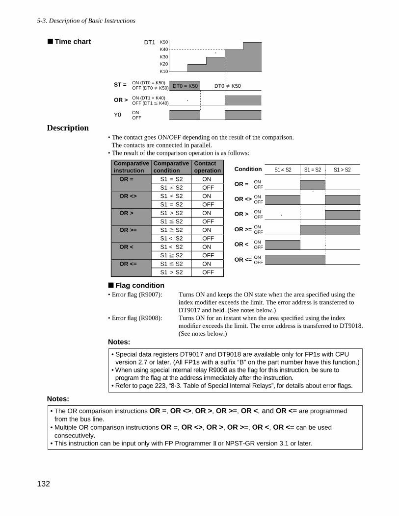
Description• The contact goes ON/OFF depending on the result of the comparison.
The contacts are connected in parallel.• The result of the comparison operation is as follows:
Flag condition• Error flag (R9007): Turns ON and keeps the ON state when the area specified using the
index modifier exceeds the limit. The error address is transferred toDT9017 and held. (See notes below.)
• Error flag (R9008): Turns ON for an instant when the area specified using the indexmodifier exceeds the limit. The error address is transferred to DT9018.(See notes below.)
Notes:
Notes:
• The OR comparison instructions OR =, OR <>, OR >, OR >=, OR <, and OR <= are programmedfrom the bus line.
• Multiple OR comparison instructions OR =, OR <>, OR >, OR >=, OR <, OR <= can be usedconsecutively.
• This instruction can be input only with FP Programmer II or NPST-GR version 3.1 or later.
• Special data registers DT9017 and DT9018 are available only for FP1s with CPUversion 2.7 or later. (All FP1s with a suffix “B” on the part number have this function.)
• When using special internal relay R9008 as the flag for this instruction, be sure toprogram the flag at the address immediately after the instruction.
• Refer to page 223, “8-3. Table of Special Internal Relays”, for details about error flags.
ON OFF
OR <>
OR =ONOFFONOFFONOFFONOFFONOFFONOFF
OR =
OR <>
OR >
OR >=
OR <
OR <=
Comparativeinstruction
Comparative condition
ON OFF
ON OFF OR >=
OR >
ON OFF
ON OFF OR <=
OR <
S1 < S2
ON OFF
Contactoperation S1 = S2 S1 > S2Condition
S1 = S1 S1 S1 = S1 > S1 S1 S1 < S1 < S1 S1 S1 >
S2S2S2S2S2S2S2S2S2S2S2S2
ON (DT0 = K50)OFF (DT0 K50)
ON (DT1 > K40)OFF (DT1 K40)
ON OFF
K10
K30
K40
K50
K20
OR >
ST =
Y0
DT1
DT0 = K50 DT0 K50
Time chart
132
5-3. Description of Basic Instructions
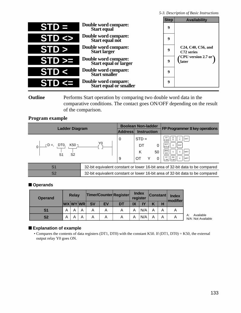
AvailabilityStep
9
9
9
9
9
9
C24, C40, C56, andC72 seriesCPU version 2.7 orlater( )
Outline Performs Start operation by comparing two double word data in thecomparative conditions. The contact goes ON/OFF depending on the resultof the comparison.
Program example
Operands
Explanation of example• Compares the contents of data registers (DT1, DT0) with the constant K50. If (DT1, DT0) = K50, the external
output relay Y0 goes ON.
Timer/Counter
EV
Relay
SVWRWYWX
Operand
S1 A A A AA: N/A: Not Available
Register
DT
A
IYIX
A N/A
HK
A A
Constant Indexmodifier
A
Indexregister
Available
A
S2 A A A A A A N/A A A AA
STD = Double word compare: Start equal
STD <> Double word compare: Start equal not
Double word compare: Start smaller
Double word compare: Start larger
STD >= Double word compare: Start equal or larger
STD <STD <= Double word compare:
Start equal or smaller
5-3. Description of Basic Instructions
133
STD >
S1
S2
32-bit equivalent constant or lower 16-bit area of 32-bit data to be compared
32-bit equivalent constant or lower 16-bit area of 32-bit data to be compared
Ladder Diagram FP Programmer IIkey operationsBoolean Non-ladder
Address Instruction
0Y0D =, DT0, K50
S1 S2
STX-WX C ENTD
OTL-WL
ANY-WY
0 WRT
NOTDT/Ld
ENT0
(BIN)K/H
0 WRT5
D =0
9
STD =
DT 0
K 50
OT Y 0
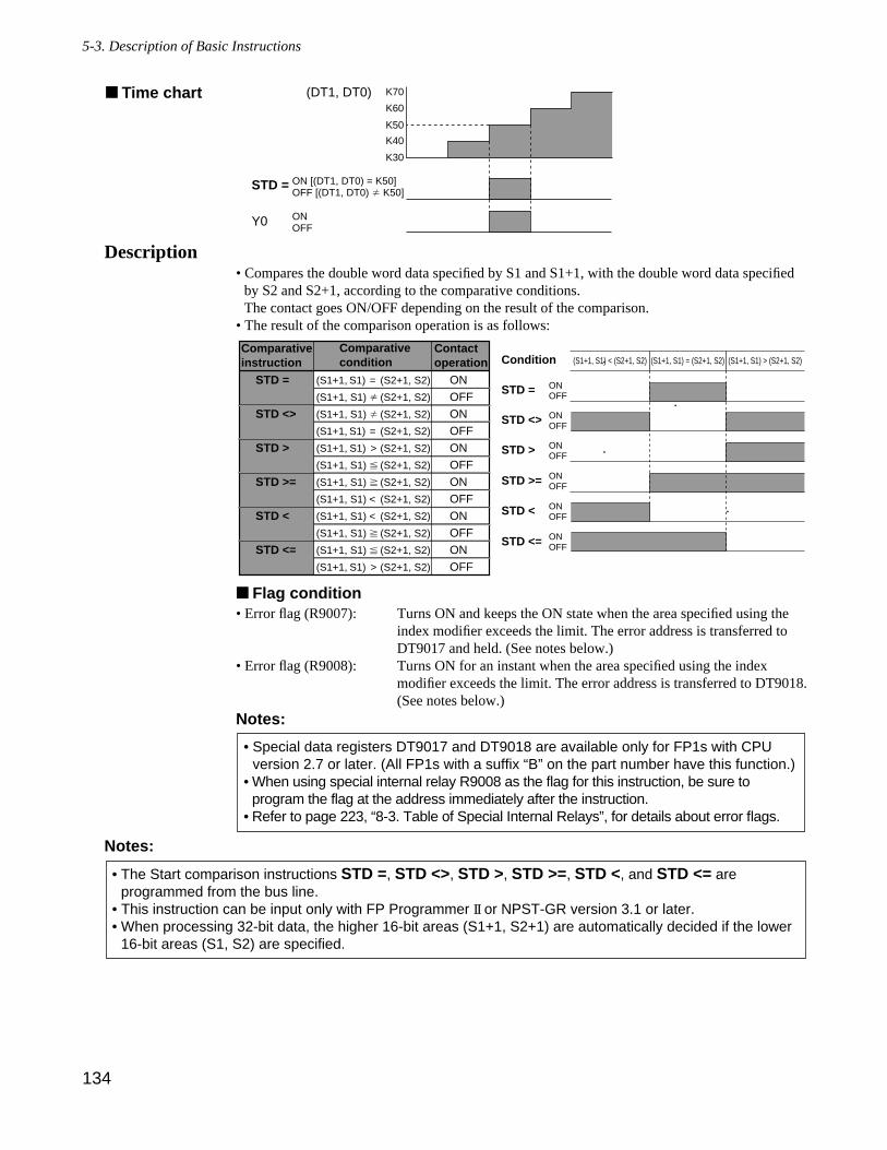
Description• Compares the double word data specified by S1 and S1+1, with the double word data specified
by S2 and S2+1, according to the comparative conditions.The contact goes ON/OFF depending on the result of the comparison.
• The result of the comparison operation is as follows:
Flag condition• Error flag (R9007): Turns ON and keeps the ON state when the area specified using the
index modifier exceeds the limit. The error address is transferred toDT9017 and held. (See notes below.)
• Error flag (R9008): Turns ON for an instant when the area specified using the indexmodifier exceeds the limit. The error address is transferred to DT9018.(See notes below.)
Notes:
Notes:
• The Start comparison instructions STD =, STD <>, STD >, STD >=, STD <, and STD <= areprogrammed from the bus line.
• This instruction can be input only with FP Programmer II or NPST-GR version 3.1 or later.• When processing 32-bit data, the higher 16-bit areas (S1+1, S2+1) are automatically decided if the lower
16-bit areas (S1, S2) are specified.
• Special data registers DT9017 and DT9018 are available only for FP1s with CPUversion 2.7 or later. (All FP1s with a suffix “B” on the part number have this function.)
• When using special internal relay R9008 as the flag for this instruction, be sure toprogram the flag at the address immediately after the instruction.
• Refer to page 223, “8-3. Table of Special Internal Relays”, for details about error flags.
ON OFF
STD <>
STD =ONOFFONOFFONOFFONOFFONOFFONOFF
STD =
STD <>
STD >
STD >=
STD <
STD <=
Comparativeinstruction
Comparative condition
ON OFF
ON OFF STD >=
STD >
ON OFF
ON OFF STD <=
STD <
(S1+1, S1) < (S2+1, S2)
ON OFF
Contactoperation Condition
(S1+1, S1) =
(S1+1, S1)
(S1+1, S1)
(S1+1, S1) =
(S1+1, S1) >
(S1+1, S1)
(S1+1, S1)
(S1+1, S1) <
(S1+1, S1) <
(S1+1, S1)
(S1+1, S1)
(S1+1, S1) >
(S2+1, S2)
(S2+1, S2)
(S2+1, S2)
(S2+1, S2)
(S2+1, S2)
(S2+1, S2)
(S2+1, S2)
(S2+1, S2)
(S2+1, S2)
(S2+1, S2)
(S2+1, S2)
(S2+1, S2)
(S1+1, S1) = (S2+1, S2) (S1+1, S1) > (S2+1, S2)
ON [(DT1, DT0) = K50]OFF [(DT1, DT0) K50]
ON OFF
K30
K50
K60
K70
K40
STD =
Y0
(DT1, DT0) Time chart
134
5-3. Description of Basic Instructions
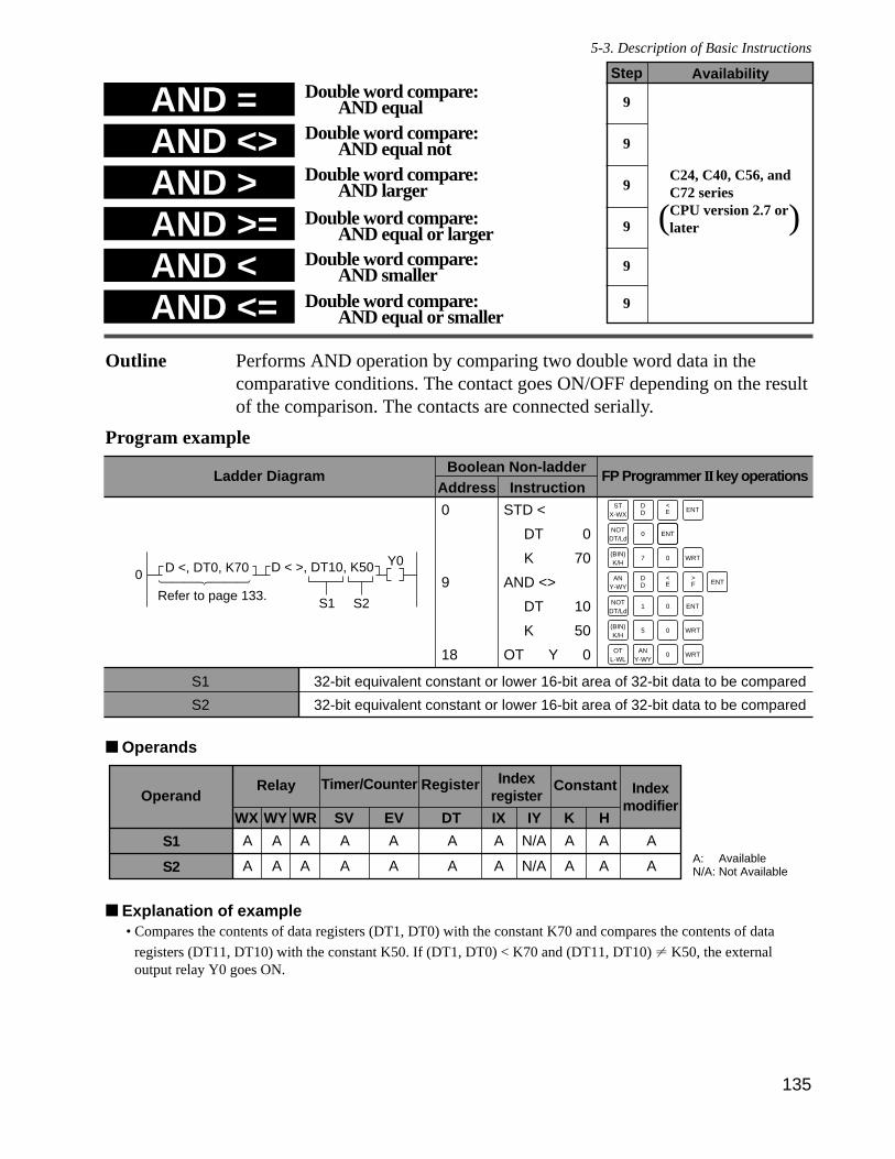
AvailabilityStep
9
9
9
9
9
9
C24, C40, C56, andC72 seriesCPU version 2.7 orlater( )
Outline Performs AND operation by comparing two double word data in thecomparative conditions. The contact goes ON/OFF depending on the resultof the comparison. The contacts are connected serially.
Program example
Operands
Explanation of example• Compares the contents of data registers (DT1, DT0) with the constant K70 and compares the contents of data
registers (DT11, DT10) with the constant K50. If (DT1, DT0) < K70 and (DT11, DT10) K50, the externaloutput relay Y0 goes ON.
Timer/Counter
EV
Relay
SVWRWYWX
Operand
S1 A A A AA: N/A: Not Available
Register
DT
A
IYIX
A N/A
HK
A A
Constant Indexmodifier
A
Indexregister
AvailableA
S2 A A A A A A N/A A A AA
AND = Double word compare: AND equal
AND <> Double word compare: AND equal not
Double word compare: AND smaller
AND > Double word compare: AND larger
AND >= Double word compare: AND equal or larger
AND <AND <= Double word compare:
AND equal or smaller
5-3. Description of Basic Instructions
135
S1
S2
32-bit equivalent constant or lower 16-bit area of 32-bit data to be compared
32-bit equivalent constant or lower 16-bit area of 32-bit data to be compared
Ladder Diagram FP Programmer IIkey operationsBoolean Non-ladder
Address Instruction
0Y0D <, DT0, K70
S1 S2
D < >, DT10, K50
"""""""
Refer to page 133.
0
9
18
STD <
DT 0
K 70
AND <>
DT 10
K 50
OT Y 0
STX-WX E ENTD
NOTDT/Ld
ENT0
ANY-WY
D <
ENTEDD <
F>
OTL-WL
ANY-WY
0 WRT
(BIN)K/H
0 WRT5
NOTDT/Ld
0 ENT1
(BIN)K/H
0 WRT7
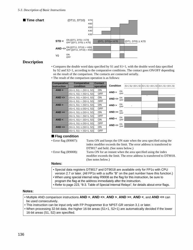
Description• Compares the double word data specified by S1 and S1+1, with the double word data specified
by S2 and S2+1, according to the comparative conditions. The contact goes ON/OFF dependingon the result of the comparison. The contacts are connected serially.
• The result of the comparison operation is as follows:
Flag condition• Error flag (R9007): Turns ON and keeps the ON state when the area specified using the
index modifier exceeds the limit. The error address is transferred toDT9017 and held. (See notes below.)
• Error flag (R9008): Turns ON for an instant when the area specified using the indexmodifier exceeds the limit. The error address is transferred to DT9018.(See notes below.)
Notes:
Notes:
• Multiple AND comparison instructions AND =, AND <>, AND >, AND >=, AND <, and AND <= canbe used consecutively.
• This instruction can be input only with FP Programmer ΙΙ or NPST-GR version 3.1 or later.• When processing 32-bit data, the higher 16-bit areas (S1+1, S2+1) are automatically decided if the lower
16-bit areas (S1, S2) are specified.
• Special data registers DT9017 and DT9018 are available only for FP1s with CPUversion 2.7 or later. (All FP1s with a suffix “B” on the part number have this function.)
• When using special internal relay R9008 as the flag for this instruction, be sure toprogram the flag at the address immediately after the instruction.
• Refer to page 223, “8-3. Table of Special Internal Relays”, for details about error flags.
ON OFF
AND <>
AND =ONOFFONOFFONOFFONOFFONOFFONOFF
AND =
AND <>
AND >
AND >=
AND <
AND <=
Comparativeinstruction
Comparative condition
ON OFF
ON OFF AND >=
AND >
ON OFF
ON OFF AND <=
AND <
(S1+1, S1) < (S2+1, S2)
ON OFF
Contactoperation Condition
(S1+1, S1) =
(S1+1, S1)
(S1+1, S1)
(S1+1, S1) =
(S1+1, S1) >
(S1+1, S1)
(S1+1, S1)
(S1+1, S1) <
(S1+1, S1) <
(S1+1, S1)
(S1+1, S1)
(S1+1, S1) >
(S2+1, S2)
(S2+1, S2)
(S2+1, S2)
(S2+1, S2)
(S2+1, S2)
(S2+1, S2)
(S2+1, S2)
(S2+1, S2)
(S2+1, S2)
(S2+1, S2)
(S2+1, S2)
(S2+1, S2)
(S1+1, S1) = (S2+1, S2) (S1+1, S1) > (S2+1, S2)
ON [(DT1, DT0) < K70]OFF [(DT1, DT0) K70]
ON [(DT11, DT10) K50]OFF [(DT11, DT10) = K50]
ON OFF
K30
K50
K60
K70
K40
AND <>
STD <
Y0
(DT11, DT10)
(DT1, DT0) < K70 (DT1, DT0) K70
Time chart
136
5-3. Description of Basic Instructions
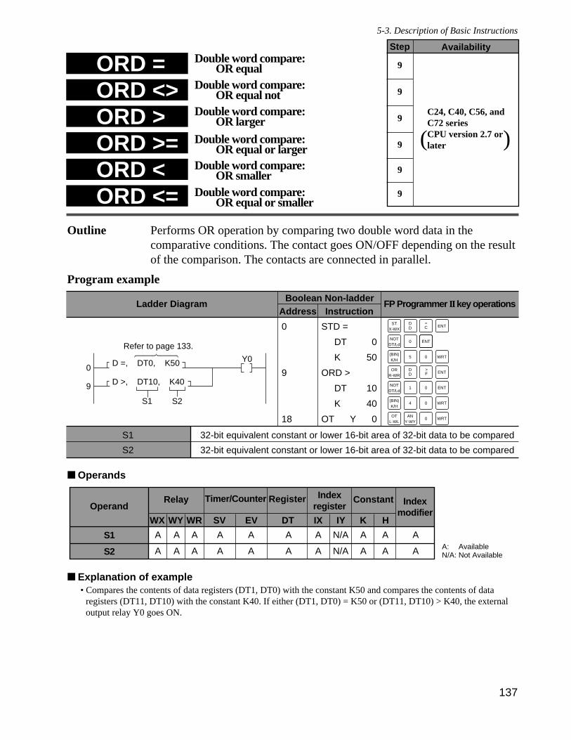
AvailabilityStep
9
9
9
9
9
9
C24, C40, C56, andC72 seriesCPU version 2.7 orlater( )
Outline Performs OR operation by comparing two double word data in thecomparative conditions. The contact goes ON/OFF depending on the resultof the comparison. The contacts are connected in parallel.
Program example
Operands
Explanation of example• Compares the contents of data registers (DT1, DT0) with the constant K50 and compares the contents of data
registers (DT11, DT10) with the constant K40. If either (DT1, DT0) = K50 or (DT11, DT10) > K40, the externaloutput relay Y0 goes ON.
Timer/Counter
EV
Relay
SVWRWYWX
Operand
S1 A A A AA: N/A: Not Available
Register
DT
A
IYIX
A N/A
HK
A A
Constant Indexmodifier
A
Indexregister
Available
A
S2 A A A A A A N/A A A AA
ORD = Double word compare: OR equal
ORD <> Double word compare: OR equal not
Double word compare: OR smaller
ORD > Double word compare: OR larger
ORD >= Double word compare: OR equal or larger
ORD <ORD <= Double word compare:
OR equal or smaller
5-3. Description of Basic Instructions
137
S1
S2
32-bit equivalent constant or lower 16-bit area of 32-bit data to be compared
32-bit equivalent constant or lower 16-bit area of 32-bit data to be compared
Ladder Diagram FP Programmer IIkey operationsBoolean Non-ladder
Address Instruction
0Y0D =, DT0, K50
"""""Refer to page 133.
9 D >, DT10, K40
S1 S2
STX-WX C ENTD
NOTDT/Ld
ENT0
ORR-WR
D =
ENTDD
F>
OTL-WL
ANY-WY
0 WRT
(BIN)K/H
0 WRT4
NOTDT/Ld
0 ENT1
(BIN)K/H
0 WRT5
0
9
18
STD =
DT 0
K 50
ORD >
DT 10
K 40
OT Y 0
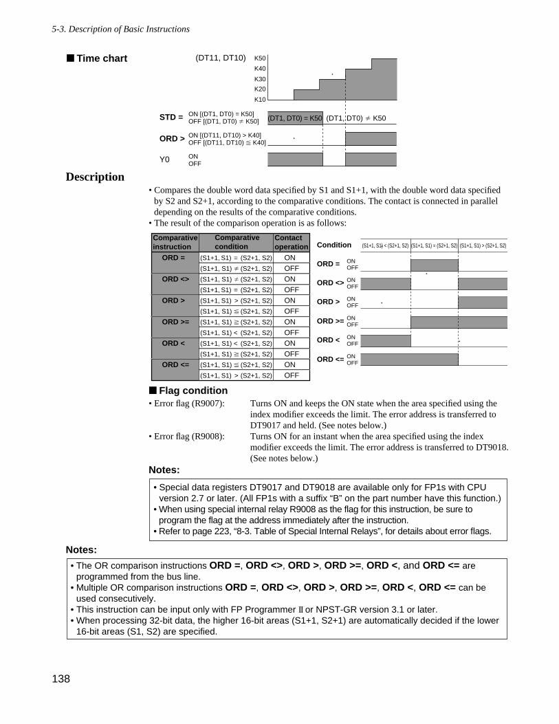
Description• Compares the double word data specified by S1 and S1+1, with the double word data specified
by S2 and S2+1, according to the comparative conditions. The contact is connected in paralleldepending on the results of the comparative conditions.
• The result of the comparison operation is as follows:
Flag condition• Error flag (R9007): Turns ON and keeps the ON state when the area specified using the
index modifier exceeds the limit. The error address is transferred toDT9017 and held. (See notes below.)
• Error flag (R9008): Turns ON for an instant when the area specified using the indexmodifier exceeds the limit. The error address is transferred to DT9018.(See notes below.)
Notes:
Notes:
• The OR comparison instructions ORD =, ORD <>, ORD >, ORD >=, ORD <, and ORD <= areprogrammed from the bus line.
• Multiple OR comparison instructions ORD =, ORD <>, ORD >, ORD >=, ORD <, ORD <= can beused consecutively.
• This instruction can be input only with FP Programmer II or NPST-GR version 3.1 or later.• When processing 32-bit data, the higher 16-bit areas (S1+1, S2+1) are automatically decided if the lower
16-bit areas (S1, S2) are specified.
• Special data registers DT9017 and DT9018 are available only for FP1s with CPUversion 2.7 or later. (All FP1s with a suffix “B” on the part number have this function.)
• When using special internal relay R9008 as the flag for this instruction, be sure toprogram the flag at the address immediately after the instruction.
• Refer to page 223, “8-3. Table of Special Internal Relays”, for details about error flags.
ON OFF
ORD <>
ORD =ONOFFONOFFONOFFONOFFONOFFONOFF
ORD =
ORD <>
ORD >
ORD >=
ORD <
ORD <=
Comparativeinstruction
Comparative condition
ON OFF
ON OFF ORD >=
ORD >
ON OFF
ON OFF ORD <=
ORD <
(S1+1, S1) < (S2+1, S2)
ON OFF
Contactoperation Condition
(S1+1, S1) =
(S1+1, S1)
(S1+1, S1)
(S1+1, S1) =
(S1+1, S1) >
(S1+1, S1)
(S1+1, S1)
(S1+1, S1) <
(S1+1, S1) <
(S1+1, S1)
(S1+1, S1)
(S1+1, S1) >
(S2+1, S2)
(S2+1, S2)
(S2+1, S2)
(S2+1, S2)
(S2+1, S2)
(S2+1, S2)
(S2+1, S2)
(S2+1, S2)
(S2+1, S2)
(S2+1, S2)
(S2+1, S2)
(S2+1, S2)
(S1+1, S1) = (S2+1, S2) (S1+1, S1) > (S2+1, S2)
ON [(DT1, DT0) = K50]OFF [(DT1, DT0) K50]
ON [(DT11, DT10) > K40]OFF [(DT11, DT10) K40]
ON OFF
K10
K30
K40
K50
K20
ORD >
STD =
Y0
(DT11, DT10)
(DT1, DT0) = K50 (DT1, DT0) K50
Time chart
138
5-3. Description of Basic Instructions
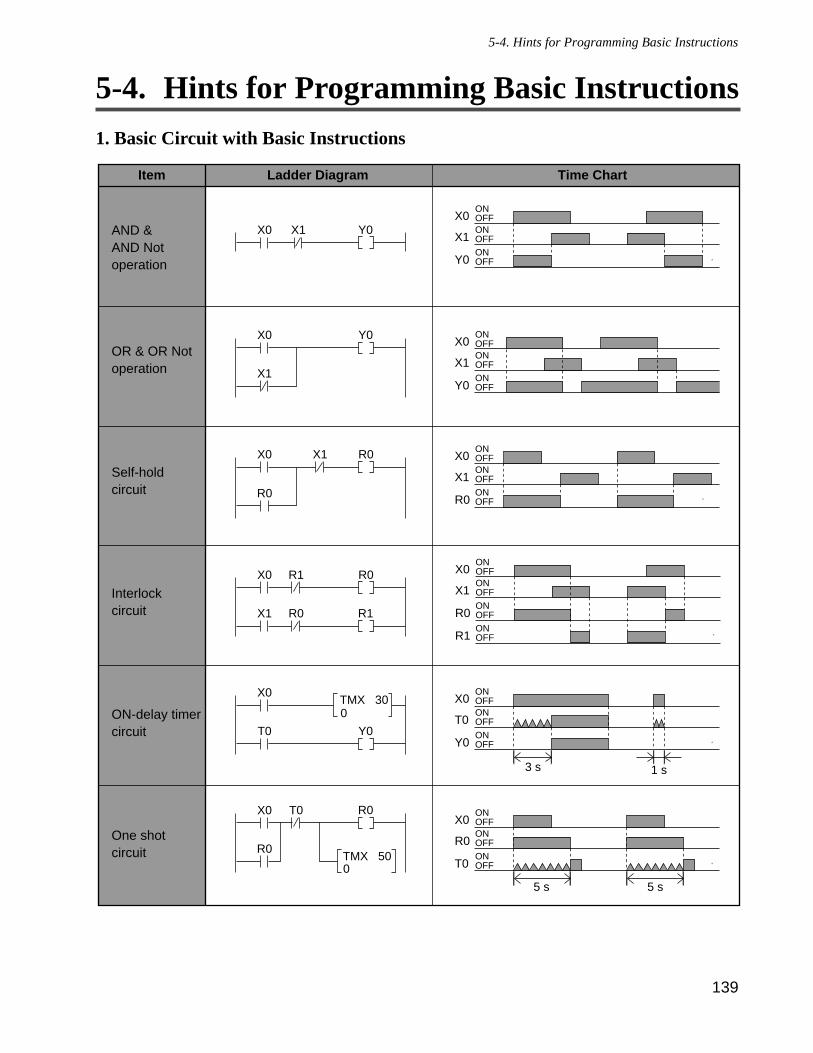
139
5-4. Hints for Programming Basic Instructions
1. Basic Circuit with Basic Instructions
X0 Y0X1
Item Ladder Diagram Time Chart
AND & AND Not operation
OR & OR Notoperation
Self-hold circuit
Interlockcircuit
ON-delay timercircuit
One shot circuit
X0ONOFFX1ONOFFY0
ONOFF
X0ONOFFX1ONOFFY0
ONOFF
X0ONOFFX1
ONOFF
X0ONOFFX1ONOFFR0
ONOFF
X0ONOFFT0ONOFFY0
ONOFF
X0ONOFFR0ONOFFT0
ONOFF
X0 Y0
X1
X0 R0X1
R0
X0 R0R1
X1 R1R0
X0TMX 30
T0 Y0
0
X0
R0
R0
TMX 500
T0
ONOFFR0ONOFFR1
1 s3 s
5 s 5 s
5-4. Hints for Programming Basic Instructions
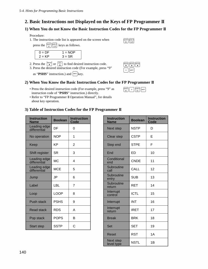
140
2. Basic Instructions not Displayed on the Keys of FP Programmer II
1) When You do not Know the Basic Instruction Codes for the FP Programmer II
Procedure:1. The instruction code list is appeared on the screen when
press the keys as follows.
2. Press the or to find desired instruction code.3. Press the desired instruction code (For example, press “9”
as “PSHS” instruction.) and key.
2) When You Know the Basic Instruction Codes for the FP Programmer II
• Press the desired instruction code (For example, press “9” asinstruction code of “PSHS” instruction.) directly.
• Refer to “FP Programmer II Operation Manual”, for detailsabout key operation.
3) Table of Instruction Codes for the FP Programmer II
Boolean
DF
NOP
KP
SR
MC
MCE
JP
LBL
LOOP
PSHS
RDS
POPS
SSTP
0
1
2
3
4
5
6
7
8
9
A
B
C
Instruction Code
Instruction Name
No operation
Keep
Shift register
Jump
Label
Loop
Push stack
Read stack
Pop stack
Start step
Leading edge differential
Leading edge differentialLeading edge differential
Boolean
NSTP
CSTP
STPE
ED
CNDE
CALL
SUB
RET
ICTL
INT
IRET
BRK
SET
RST
NSTL
D
E
F
10
11
12
13
14
15
16
17
18
19
1A
1B
Instruction Code
Instruction Name
Next step
Clear step
Step end
End
Interrupt
Break
Set
Reset
Conditional endSubroutine callSubroutine entrySubroutine returnInterrupt control
Interrupt return
Next steplevel type
WRT
SRC
READ
0 = DF 1 = NOP2 = KP 3 = SR
SHIFTSC
(HELP)CLR
5-4. Hints for Programming Basic Instructions
SHIFTSC
(HELP)CLR
9 WRT
READ
READ
READ
9SHIFT
SCWRT
SHIFTSC
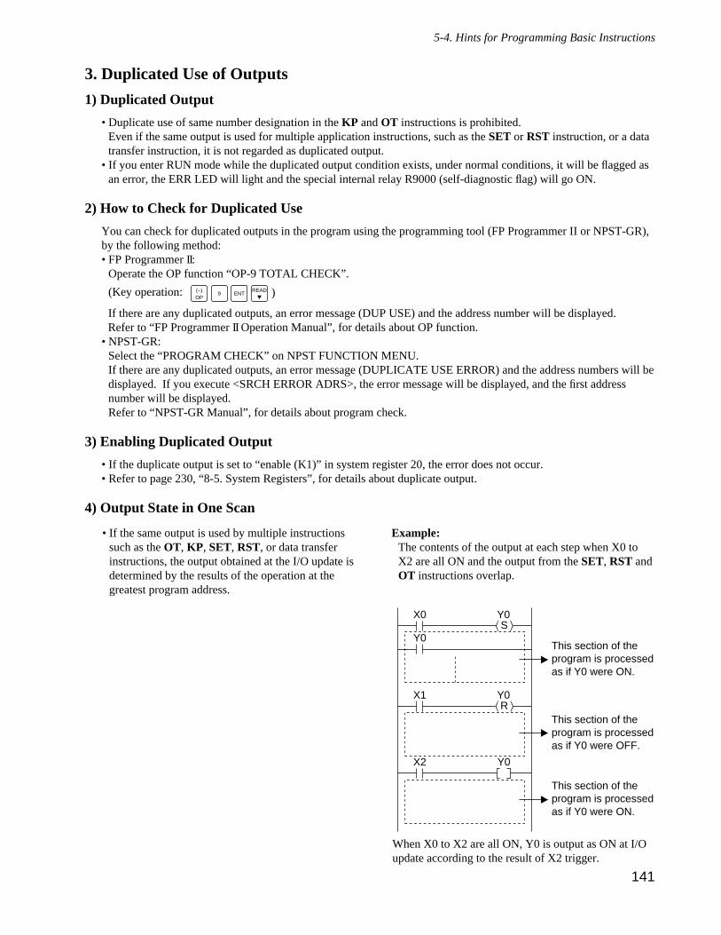
141
3. Duplicated Use of Outputs
1) Duplicated Output
• Duplicate use of same number designation in the KP and OT instructions is prohibited.Even if the same output is used for multiple application instructions, such as the SET or RST instruction, or a datatransfer instruction, it is not regarded as duplicated output.
• If you enter RUN mode while the duplicated output condition exists, under normal conditions, it will be flagged asan error, the ERR LED will light and the special internal relay R9000 (self-diagnostic flag) will go ON.
2) How to Check for Duplicated Use
You can check for duplicated outputs in the program using the programming tool (FP Programmer II or NPST-GR),by the following method:• FP Programmer II:
Operate the OP function “OP-9 TOTAL CHECK”.
(Key operation:
If there are any duplicated outputs, an error message (DUP USE) and the address number will be displayed.Refer to “FP Programmer II Operation Manual”, for details about OP function.
• NPST-GR:Select the “PROGRAM CHECK” on NPST FUNCTION MENU.If there are any duplicated outputs, an error message (DUPLICATE USE ERROR) and the address numbers will bedisplayed. If you execute <SRCH ERROR ADRS>, the error message will be displayed, and the first addressnumber will be displayed.Refer to “NPST-GR Manual”, for details about program check.
3) Enabling Duplicated Output
• If the duplicate output is set to “enable (K1)” in system register 20, the error does not occur.• Refer to page 230, “8-5. System Registers”, for details about duplicate output.
4) Output State in One Scan
• If the same output is used by multiple instructionssuch as the OT, KP, SET, RST, or data transferinstructions, the output obtained at the I/O update isdetermined by the results of the operation at thegreatest program address.
Example:The contents of the output at each step when X0 toX2 are all ON and the output from the SET, RST andOT instructions overlap.
(–)OP
ENTREAD
9 )
5-4. Hints for Programming Basic Instructions
When X0 to X2 are all ON, Y0 is output as ON at I/Oupdate according to the result of X2 trigger.
X0 Y0⟨ S ⟩#
X1 Y0⟨ R ⟩#
X2
Y0
Y0
This section of the program is processed as if Y0 were ON.
This section of the program is processed as if Y0 were OFF.
This section of the program is processed as if Y0 were ON.

142
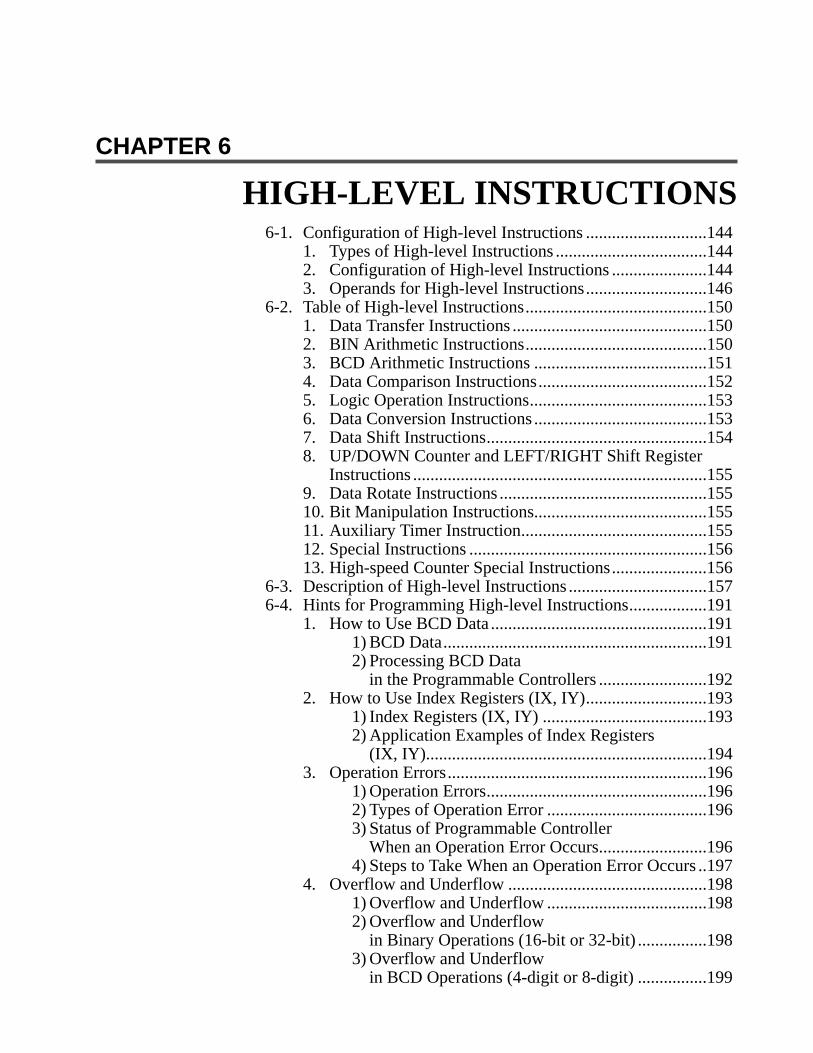
CHAPTER 6
HIGH-LEVEL INSTRUCTIONS6-1. Configuration of High-level Instructions ............................144
1. Types of High-level Instructions ...................................1442. Configuration of High-level Instructions ......................1443. Operands for High-level Instructions............................146
6-2. Table of High-level Instructions..........................................1501. Data Transfer Instructions .............................................1502. BIN Arithmetic Instructions..........................................1503. BCD Arithmetic Instructions ........................................1514. Data Comparison Instructions.......................................1525. Logic Operation Instructions.........................................1536. Data Conversion Instructions ........................................1537. Data Shift Instructions...................................................1548. UP/DOWN Counter and LEFT/RIGHT Shift Register
Instructions ....................................................................1559. Data Rotate Instructions ................................................15510. Bit Manipulation Instructions........................................15511. Auxiliary Timer Instruction...........................................15512. Special Instructions .......................................................15613. High-speed Counter Special Instructions......................156
6-3. Description of High-level Instructions ................................1576-4. Hints for Programming High-level Instructions..................191
1. How to Use BCD Data ..................................................1911) BCD Data.............................................................1912) Processing BCD Data
in the Programmable Controllers .........................1922. How to Use Index Registers (IX, IY)............................193
1) Index Registers (IX, IY) ......................................1932) Application Examples of Index Registers
(IX, IY).................................................................1943. Operation Errors............................................................196
1) Operation Errors...................................................1962) Types of Operation Error .....................................1963) Status of Programmable Controller
When an Operation Error Occurs.........................1964) Steps to Take When an Operation Error Occurs ..197
4. Overflow and Underflow ..............................................1981) Overflow and Underflow .....................................1982) Overflow and Underflow
in Binary Operations (16-bit or 32-bit) ................1983) Overflow and Underflow
in BCD Operations (4-digit or 8-digit) ................199
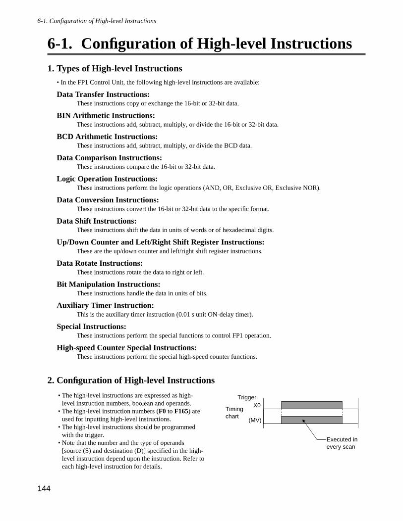
6-1. Configuration of High-level Instructions
1. Types of High-level Instructions• In the FP1 Control Unit, the following high-level instructions are available:
Data Transfer Instructions:These instructions copy or exchange the 16-bit or 32-bit data.
BIN Arithmetic Instructions:These instructions add, subtract, multiply, or divide the 16-bit or 32-bit data.
BCD Arithmetic Instructions:These instructions add, subtract, multiply, or divide the BCD data.
Data Comparison Instructions:These instructions compare the 16-bit or 32-bit data.
Logic Operation Instructions:These instructions perform the logic operations (AND, OR, Exclusive OR, Exclusive NOR).
Data Conversion Instructions:These instructions convert the 16-bit or 32-bit data to the specific format.
Data Shift Instructions:These instructions shift the data in units of words or of hexadecimal digits.
Up/Down Counter and Left/Right Shift Register Instructions:These are the up/down counter and left/right shift register instructions.
Data Rotate Instructions:These instructions rotate the data to right or left.
Bit Manipulation Instructions:These instructions handle the data in units of bits.
Auxiliary Timer Instruction:This is the auxiliary timer instruction (0.01 s unit ON-delay timer).
Special Instructions:These instructions perform the special functions to control FP1 operation.
High-speed Counter Special Instructions:These instructions perform the special high-speed counter functions.
2. Configuration of High-level Instructions
X0
(MV)
Trigger
Timingchart
Executed inevery scan
• The high-level instructions are expressed as high-level instruction numbers, boolean and operands.
• The high-level instruction numbers (F0 to F165) areused for inputting high-level instructions.
• The high-level instructions should be programmedwith the trigger.
• Note that the number and the type of operands[source (S) and destination (D)] specified in the high-level instruction depend upon the instruction. Refer toeach high-level instruction for details.
144
6-1. Configuration of High-level Instructions
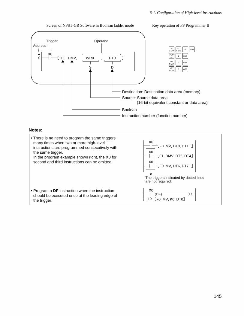
145
6-1. Configuration of High-level Instructions
Notes:
• There is no need to program the same triggersmany times when two or more high-levelinstructions are programmed consecutively withthe same trigger.In the program example shown right, the X0 forsecond and third instructions can be omitted.
• Program a DF instruction when the instructionshould be executed once at the leading edge ofthe trigger.
STX-WX
STX-WX
0 WRT
FN/PFL
ENT1
ORR-WR
NOTDT/Ld
0 WRT
ENT0
0X0
Trigger
F1 DMV, WR0 , DT0
S D
AddressOperand
Destination: Destination data area (memory)
Source: Source data area (16-bit equivalent constant or data area)
Boolean
Instruction number (function number)
Screen of NPST-GR Software in Boolean ladder mode Key operation of FP Programmer II
X0F0 MV, DT0, DT1
X0
X0
X0
F0 MV, K0, DT0
The triggers indicated by dotted lines are not required.
F1 DMV, DT2, DT4
F0 MV, DT6, DT7
(DF) 11
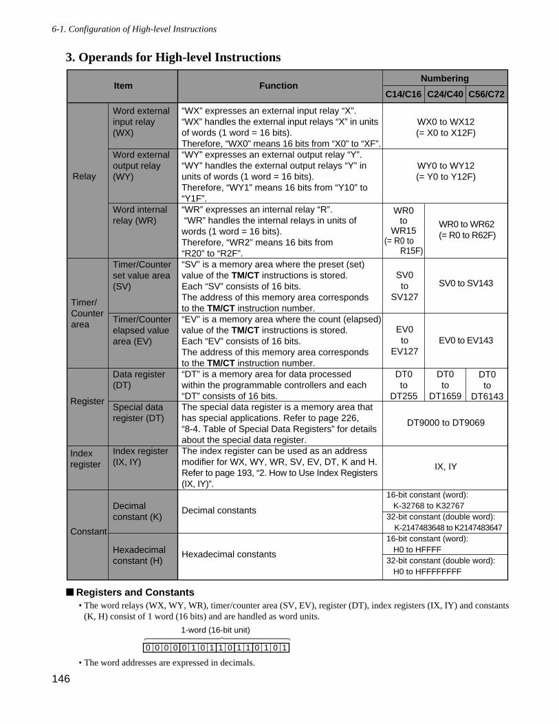
146
6-1. Configuration of High-level Instructions
3. Operands for High-level Instructions
Registers and Constants• The word relays (WX, WY, WR), timer/counter area (SV, EV), register (DT), index registers (IX, IY) and constants
(K, H) consist of 1 word (16 bits) and are handled as word units.
• The word addresses are expressed in decimals.
0 0 0 0 0 1 0 1 1 0 1 1 0 1 0 1
" " " " " " " " " " " " " " " " "
1-word (16-bit unit)
Word external input relay (WX)
Word external output relay (WY)
Word internal relay (WR)
Timer/Counter set value area (SV)
Timer/Counter elapsed value area (EV)
Data register (DT)
Special data register (DT)
Index register (IX, IY)
Decimal constant (K)
Hexadecimal constant (H)
WX0 to WX12(= X0 to X12F)
WY0 to WY12(= Y0 to Y12F)
DT9000 to DT9069
IX, IY
C14/C16
Relay
Timer/Counter area
WR0to
WR15(= R0 to R15F)
Item FunctionNumbering
“WX” expresses an external input relay “X”. “WX” handles the external input relays “X” in units of words (1 word = 16 bits).Therefore, “WX0” means 16 bits from “X0” to “XF”.“WY” expresses an external output relay “Y”. “WY” handles the external output relays “Y” in units of words (1 word = 16 bits).Therefore, “WY1” means 16 bits from “Y10” to “Y1F”.“WR” expresses an internal relay “R”. “WR” handles the internal relays in units of words (1 word = 16 bits).Therefore, “WR2” means 16 bits from “R20” to “R2F”.“SV” is a memory area where the preset (set) value of the TM/CT instructions is stored.Each “SV” consists of 16 bits.The address of this memory area corresponds to the TM/CT instruction number.“EV” is a memory area where the count (elapsed) value of the TM/CT instructions is stored. Each “EV” consists of 16 bits.The address of this memory area corresponds to the TM/CT instruction number.“DT” is a memory area for data processed within the programmable controllers and each “DT” consists of 16 bits.The special data register is a memory area that has special applications. Refer to page 226, “8-4. Table of Special Data Registers” for details about the special data register.The index register can be used as an address modifier for WX, WY, WR, SV, EV, DT, K and H.Refer to page 193, “2. How to Use Index Registers (IX, IY)”.
Decimal constants
Hexadecimal constants
Register
Constant
Index register
C24/C40 C56/C72
WR0 to WR62(= R0 to R62F)
SV0to
SV127
SV0 to SV143
DT0to
DT255
DT0to
DT1659
DT0to
DT6143
16-bit constant (word): K-32768 to K3276732-bit constant (double word): K-2147483648 to K214748364716-bit constant (word): H0 to HFFFF32-bit constant (double word): H0 to HFFFFFFFF
EV0to
EV127EV0 to EV143
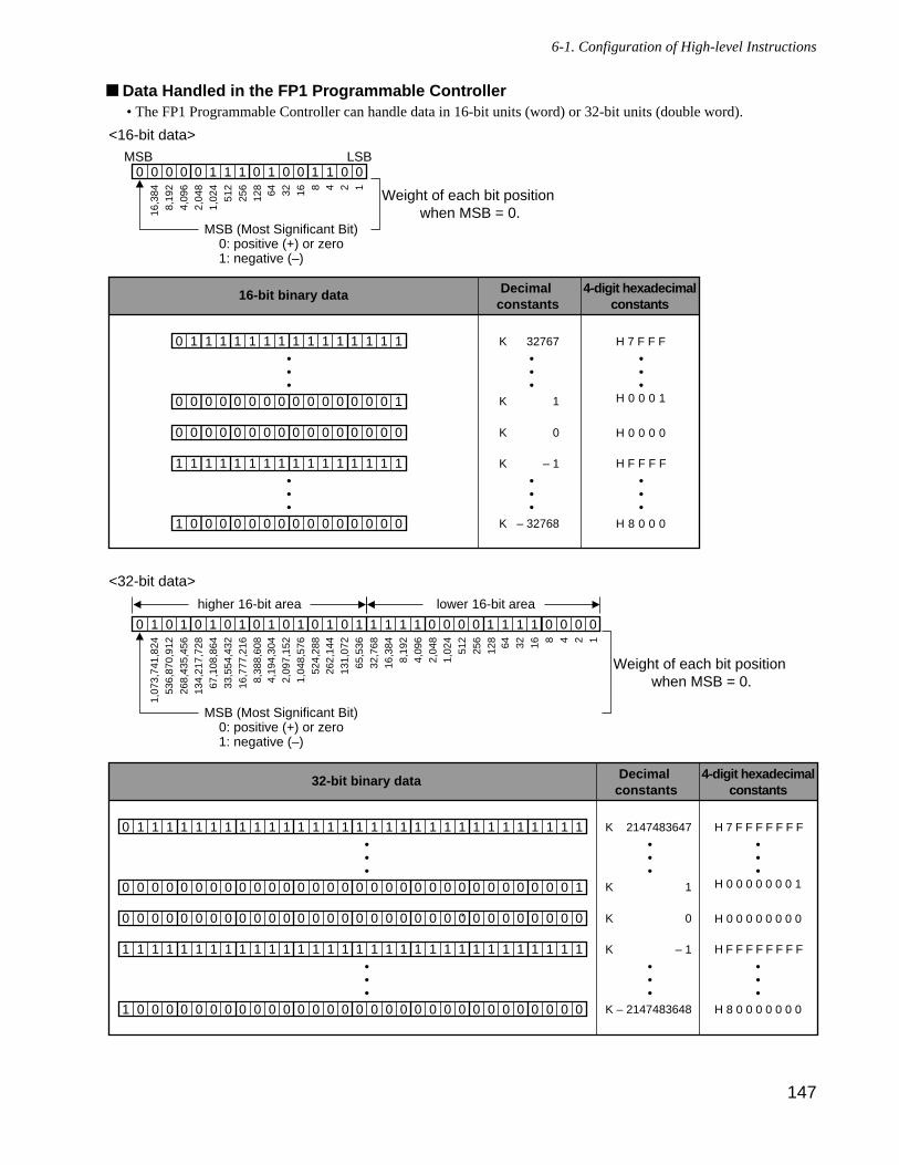
147
6-1. Configuration of High-level Instructions
Data Handled in the FP1 Programmable Controller• The FP1 Programmable Controller can handle data in 16-bit units (word) or 32-bit units (double word).
0 1 1 1 1 1 1 1 1 1 1 1 1 1 1 1 1 1 1 1 1 1 1 1 1 1 1 1 1 1 1 1
0 0 0 0 0 0 0 0 0 0 0 0 0 0 0 0 0 0 0 0 0 0 0 0 0 0 0 0 0 0 0 1
0 0 0 0 0 0 0 0 0 0 0 0 0 0 0 0 0 0 0 0 0 0 0 0 0 0 0 0 0 0 0 0
1 1 1 1 1 1 1 1 1 1 1 1 1 1 1 1 1 1 1 1 1 1 1 1 1 1 1 1 1 1 1 1
1 0 0 0 0 0 0 0 0 0 0 0 0 0 0 0 0 0 0 0 0 0 0 0 0 0 0 0 0 0 0 0
K 2147483647
K 1
K 0
K – 1
K – 2147483648
H 7 F F F F F F F
H 0 0 0 0 0 0 0 1
H 0 0 0 0 0 0 0 0
H F F F F F F F F
H 8 0 0 0 0 0 0 0
32-bit binary data Decimal constants
4-digit hexadecimalconstants
•••
•••
0 1 0 1 0 1 0 1 0 1 0 1 0 1 0 1 1 1 1 1 0 0 0 0 1 1 1 1 0 0 0 0
1,07
3,74
1,82
453
6,87
0,91
226
8,43
5,45
613
4,21
7,72
8
4,19
4,30
42,
097,
152
1,04
8,57
652
4,28
826
2,14
413
1,07
265
,536
32,7
6816
,384
8,19
24,
096
2,04
81,
024
512
256
128 64 32 16 8 4 2 1
MSB (Most Significant Bit)0: positive (+) or zero1: negative (–)
67,1
08,8
6433
,554
,432
16,7
77,2
168,
388,
608
higher 16-bit area lower 16-bit area
<32-bit data>
0 1 1 1 1 1 1 1 1 1 1 1 1 1 1 1
0 0 0 0 0 0 0 0 0 0 0 0 0 0 0 1
0 0 0 0 0 0 0 0 0 0 0 0 0 0 0 0
1 1 1 1 1 1 1 1 1 1 1 1 1 1 1 1
1 0 0 0 0 0 0 0 0 0 0 0 0 0 0 0
K 32767
K 1
K 0
K – 1
K – 32768
H 7 F F F
H 0 0 0 1
H 0 0 0 0
H F F F F
H 8 0 0 0
16-bit binary data Decimal constants
4-digit hexadecimalconstants
•••
•••
0 0 0 0 0 1 1 1 0 1 0 0 1 1 0 016
,384
8,19
24,
096
2,04
8 64 32 16 8 4 2 1
MSB (Most Significant Bit)0: positive (+) or zero1: negative (–)
1,02
451
225
612
8
<16-bit data>
MSB LSB
•••
•••
•••
•••
•••
•••
•••
•••
Weight of each bit position when MSB = 0.
Weight of each bit position when MSB = 0.
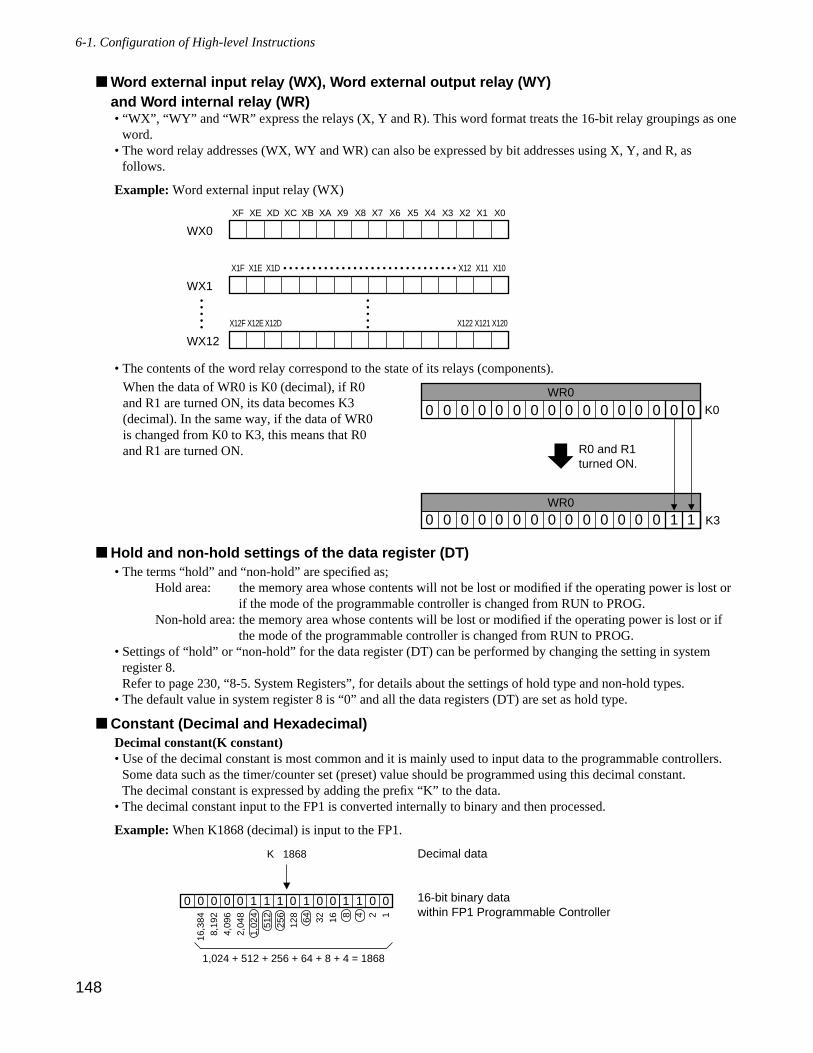
148
6-1. Configuration of High-level Instructions
Word external input relay (WX), Word external output relay (WY) and Word internal relay (WR)• “WX”, “WY” and “WR” express the relays (X, Y and R). This word format treats the 16-bit relay groupings as one
word.• The word relay addresses (WX, WY and WR) can also be expressed by bit addresses using X, Y, and R, as
follows.
Example: Word external input relay (WX)
• The contents of the word relay correspond to the state of its relays (components).
Hold and non-hold settings of the data register (DT)• The terms “hold” and “non-hold” are specified as;
Hold area: the memory area whose contents will not be lost or modified if the operating power is lost orif the mode of the programmable controller is changed from RUN to PROG.
Non-hold area: the memory area whose contents will be lost or modified if the operating power is lost or ifthe mode of the programmable controller is changed from RUN to PROG.
• Settings of “hold” or “non-hold” for the data register (DT) can be performed by changing the setting in systemregister 8.Refer to page 230, “8-5. System Registers”, for details about the settings of hold type and non-hold types.
• The default value in system register 8 is “0” and all the data registers (DT) are set as hold type.
Constant (Decimal and Hexadecimal)Decimal constant(K constant)• Use of the decimal constant is most common and it is mainly used to input data to the programmable controllers.
Some data such as the timer/counter set (preset) value should be programmed using this decimal constant. The decimal constant is expressed by adding the prefix “K” to the data.
• The decimal constant input to the FP1 is converted internally to binary and then processed.
Example: When K1868 (decimal) is input to the FP1.
0 0 0 0 0 1 1 1 0 1 0 0 1 1 0 0
16,3
848,
192
4,09
62,
048 64 32 16 8 4 2 1
Decimal data
16-bit binary datawithin FP1 Programmable Controller
1,02
451
225
612
8
K 1868
1,024 + 512 + 256 + 64 + 8 + 4 = 1868
0 0 0 0 0 0 0 0 0 0 0 0 0 0 0 0
1 10 0 0 0 0 0 0 0 0 0 0 0 0 0WR0
K0
WR0
K3
R0 and R1 turned ON.
When the data of WR0 is K0 (decimal), if R0and R1 are turned ON, its data becomes K3(decimal). In the same way, if the data of WR0is changed from K0 to K3, this means that R0and R1 are turned ON.
•••••
WX0
XF XE XD XC XB XA X9 X8 X7 X6 X5 X4 X3 X2 X1 X0
WX1
X1F X1E X1D X12 X11 X10• • • • • • • • • • • • • • • • • • • • • • • • • • • • • •
WX12
X12F X12E X12D X122 X121 X120
•••••
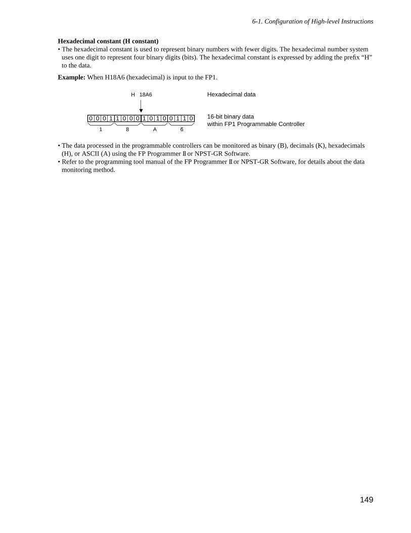
Hexadecimal constant (H constant)• The hexadecimal constant is used to represent binary numbers with fewer digits. The hexadecimal number system
uses one digit to represent four binary digits (bits). The hexadecimal constant is expressed by adding the prefix “H”to the data.
Example: When H18A6 (hexadecimal) is input to the FP1.
• The data processed in the programmable controllers can be monitored as binary (B), decimals (K), hexadecimals(H), or ASCII (A) using the FP Programmer II or NPST-GR Software.
• Refer to the programming tool manual of the FP Programmer II or NPST-GR Software, for details about the datamonitoring method.
0 0 0 1 1 0 0 0 1 0 1 0 0 1 1 0
Hexadecimal data
16-bit binary datawithin FP1 Programmable Controller
H 18A6
1 8 A 6
149
6-1. Configuration of High-level Instructions
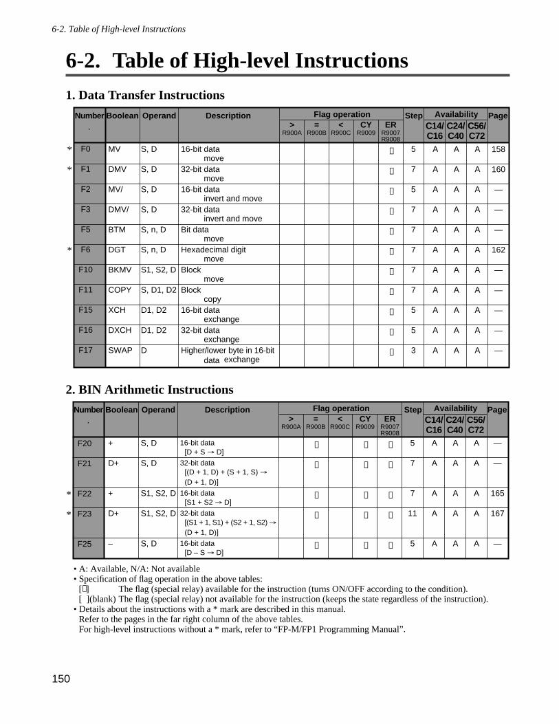
150
6-2. Table of High-level Instructions
6-2. Table of High-level Instructions
1. Data Transfer Instructions
2. BIN Arithmetic Instructions
• A: Available, N/A: Not available• Specification of flag operation in the above tables:
[] The flag (special relay) available for the instruction (turns ON/OFF according to the condition).[ ](blank) The flag (special relay) not available for the instruction (keeps the state regardless of the instruction).
• Details about the instructions with a * mark are described in this manual.Refer to the pages in the far right column of the above tables.For high-level instructions without a * mark, refer to “FP-M/FP1 Programming Manual”.
F20
F21
F22
F23
F25
S, D
S, D
S1, S2, D
S1, S2, D
S, D
16-bit data [D + S → D]
32-bit data [(D + 1, D) + (S + 1, S) → (D + 1, D)]
16-bit data [S1 + S2 → D]
32-bit data [(S1 + 1, S1) + (S2 + 1, S2) → (D + 1, D)]
16-bit data [D – S → D]
+
D+
+
D+
–
5
7
7
11
5
A
A
A
A
A
A
A
A
A
A
A
A
A
A
A
—
—
165
167
—
*
*
Step PageFlag operationDescriptionOperandBooleanNumberER
R9007R9008
CYR9009
<R900C
=R900B
>R900A
AvailabilityC56/C72
C24/C40
C14/C16
5
7
5
7
7
7
7
7
5
5
3
A
A
A
A
A
A
A
A
A
A
A
A
A
A
A
A
A
A
A
A
A
A
A
A
A
A
A
A
A
A
A
A
A
F0
F1
F2
F3
F5
F6
F10
F11
F15
F16
F17
S, D
S, D
S, D
S, D
S, n, D
S, n, D
S1, S2, D
S, D1, D2
D1, D2
D1, D2
D
16-bit data move
32-bit data move
16-bit data invert and move
32-bit data invert and move
Bit data move
Hexadecimal digit move
Block move
Block copy
16-bit data exchange
32-bit data exchange
Higher/lower byte in 16-bit data exchange
MV
DMV
MV/
DMV/
BTM
DGT
BKMV
COPY
XCH
DXCH
SWAP
158
160
—
—
—
162
—
—
—
—
—
Step PageFlag operationDescriptionOperandBooleanNumberER
R9007R9008
CYR9009
<R900C
=R900B
>R900A
AvailabilityC56/C72
C24/C40
C14/C16
*
*
*
151
6-2. Table of High-level Instructions
3. BCD Arithmetic Instructions
• A: Available, N/A: Not available• Specification of flag operation in the above tables:
[] The flag (special relay) available for the instruction (turns ON/OFF according to the condition).[ ](blank) The flag (special relay) not available for the instruction (keeps the state regardless of the instruction).
• Details about the instructions with a * mark are described in this manual.Refer to the pages in the far right column of the above tables.For high-level instructions without a * mark, refer to “FP-M/FP1 Programming Manual”.
F40
F41
F42
F43
F45
F46
S, D
S, D
S1, S2, D
S1, S2, D
S, D
S, D
4-digit BCD data [D + S → D]
8-digit BCD data [(D + 1, D) + (S + 1, S) → (D + 1, D)]
4-digit BCD data [S1 + S2 → D]
8-digit BCD data [(S1 + 1, S1) + (S2 + 1, S2) → (D + 1, D)]
4-digit BCD data [D – S → D]
8-digit BCD data [(D + 1, D) – (S + 1, S) → (D + 1, D)]
B+
DB+
B+
DB+
B–
DB–
5
7
7
11
5
7
A
A
A
A
A
A
A
A
A
A
A
A
A
A
A
A
A
A
—
—
—
—
—
—
Step PageFlag operationDescriptionOperandBooleanNumberER
R9007R9008
CYR9009
<R900C
=R900B
>R900A
AvailabilityC56/C72
C24/C40
C14/C16
F26
F27
F28
F30
F31
F32
F33
F35
F36
F37
F38
S, D
S1, S2, D
S1, S2, D
S1, S2, D
S1, S2, D
S1, S2, D
S1, S2, D
D
D
D
D
32-bit data [(D + 1, D) – (S + 1, S) → (D + 1, D)]
16-bit data [S1 – S2 → D]
32-bit data [(S1 + 1, S1) – (S2 + 1, S2) → "(D + 1, D)]
16-bit data [S1 × S2 → (D + 1, D)]
32-bit data [(S1 + 1, S1) × (S2 + 1, S2) → (D + 3, D + 2, D + 1, D)]
16-bit data [S1/S2 → D...(DT9015)]
32-bit data [(S1 + 1, S1)/(S2 + 1, S2) → (D + 1, D)...(DT9016, DT9015)]
16-bit data increment [D + 1 → D]
32-bit data increment [(D + 1, D) + 1 → (D + 1, D)]
16-bit data decrement [D – 1 → D]
32-bit data decrement [(D + 1, D) –1 → (D + 1, D)]
D–
–
D–
*
D*
%
D%
+1
D+1
–1
D–1
7
7
11
7
11
7
11
3
3
3
3
A
A
A
A
A
A
A
A
A
A
A
A
A
A
A
A
A
A
A
A
A
A
A
A
A
A
N/A
A
N/A
A
A
A
A
—
169
171
173
175
177
179
—
—
—
—
Step PageFlag operationDescriptionOperandBooleanNumberER
R9007R9008
CYR9009
<R900C
=R900B
>R900A
AvailabilityC56/C72
C24/C40
C14/C16
*
*
*
*
*
*
152
6-2. Table of High-level Instructions
4. Data Comparison Instructions
• A: Available, N/A: Not available• Specification of flag operation in the above tables:
[] The flag (special relay) available for the instruction (turns ON/OFF according to the condition).[ ](blank) The flag (special relay) not available for the instruction (keeps the state regardless of the instruction).
• Details about the instructions with a * mark are described in this manual.Refer to the pages in the far right column of the above tables.For high-level instructions without a * mark, refer to “FP-M/FP1 Programming Manual”.
F60
F61
F62
F63
F64
S1, S2
S1, S2
S1, S2, S3S1, S2, S3S1, S2, S3
16-bit data compare
32-bit data compare
16-bit data band compare
32-bit data band compare
Block data compare
CMP
DCMP
WIN
DWIN
BCMP
5
9
7
13
7
A
A
A
A
A
A
A
A
A
A
A
A
A
A
N/A
181
184
—
—
—
Step PageFlag operationDescriptionOperandBooleanNumberER
R9007R9008
CYR9009
<R900C
=R900B
>R900A
AvailabilityC56/C72
C24/C40
C14/C16
*
*
F47
F48
F50
F51
F52
F53
F55
F56
F57
F58
S1, S2, D
S1, S2, D
S1, S2, D
S1, S2, D
S1, S2, D
S1, S2, D
D
D
D
D
4-digit BCD data [S1 – S2 → D]
8-digit BCD data [(S1 + 1, S1) – (S2 + 1, S2) →
(D + 1, D)]
4-digit BCD data [S1 × S2 → (D + 1, D)]
8-digit BCD data [(S1 + 1, S1) × (S2 + 1, S2) → (D + 3, D + 2, D + 1, D)]
4-digit BCD data [S1/S2 → D...(DT9015)]
8-digit BCD data [(S1 + 1, S1)/(S2 + 1, S2) → (D + 1, D)...(DT9016, DT9015)]
4-digit BCD data increment [D + 1 → D]
8-digit BCD data increment [(D + 1, D) + 1 → (D + 1, D)]
4-digit BCD data decrement [D – 1 → D]
8-digit BCD data decrement [(D + 1, D) – 1 → (D + 1, D)]
B–
DB–
B*
DB*
B%
DB%
B+1
DB+1
B–1
DB–1
7
11
7
11
7
11
3
3
3
3
A
A
A
A
A
A
A
A
A
A
A
A
A
A
A
A
A
A
A
A
A
A
A
N/A
A
N/A
A
A
A
A
—
—
—
—
—
—
—
—
—
—
Step PageFlag operationDescriptionOperandBooleanNumberER
R9007R9008
CYR9009
<R900C
=R900B
>R900A
AvailabilityC56/C72
C24/C40
C14/C16
153
6-2. Table of High-level Instructions
5. Logic Operation Instructions
6. Data Conversion Instructions
• A: Available, N/A: Not available• Specification of flag operation in the above tables:
[] The flag (special relay) available for the instruction (turns ON/OFF according to the condition).[ ](blank) The flag (special relay) not available for the instruction (keeps the state regardless of the instruction).
• Details about the instructions with a * mark are described in this manual.Refer to the pages in the far right column of the above tables.For high-level instructions without a * mark, refer to “FP-M/FP1 Programming Manual”.
F70
F71
F72
F73
F74
F75
F76
F77
F78
F80
F81
F82
F83
F84
F85
F86
S1, S2, S3, DS1, S2, D
S1, S2, D
S1, S2, D
S1, S2, D
S1, S2, D
S1, S2, D
S1, S2, D
S1, S2, D
S, D
S, D
S, D
S, D
D
D
D
Block check code calculation
Hexadecimal data → ASCII code
ASCII code → Hexadecimal data
BCD data → ASCII code
ASCII code → BCD data
16-bit data → ASCII code
ASCII code → 16-bit data
32-bit data → ASCII code
ASCII code → 32-bit data
16-bit data → 4-digit BCD data
4-digit BCD data → 16-bit data
32-bit data → 8-digit BCD data
8-digit BCD data → 32-bit data
16-bit data invert
16-bit data two’s complement
32-bit data two’s complement
BCC
HEXA
AHEX
BCDA
ABCD
BINA
ABIN
DBIA
DABI
BCD
BIN
DBCD
DBIN
INV
NEG
DNEG
9
7
7
7
9
7
7
11
11
5
5
7
7
3
3
3
A
A
A
A
A
A
A
A
A
A
A
A
A
A
A
A
A
A
A
A
A
A
A
A
A
A
A
A
A
A
A
A
N/A
N/A
N/A
N/A
N/A
N/A
N/A
N/A
N/A
A
A
A
A
A
A
A
—
—
—
—
—
—
—
—
—
187
189
—
—
—
—
—
Step PageFlag operationDescriptionOperandBooleanNumberER
R9007R9008
CYR9009
<R900C
=R900B
>R900A
AvailabilityC56/C72
C24/C40
C14/C16
*
*
F65
F66
F67
F68
S1, S2, D
S1, S2, D
S1, S2, D
S1, S2, D
16-bit data AND
16-bit data OR
16-bit data exclusive OR
16-bit data exclusive NOR
WAN
WOR
XOR
XNR
7
7
7
7
A
A
A
A
A
A
A
A
A
A
A
A
—
—
—
—
Step PageFlag operationDescriptionOperandBooleanNumberER
R9007R9008
CYR9009
<R900C
=R900B
>R900A
AvailabilityC56/C72
C24/C40
C14/C16
154
6-2. Table of High-level Instructions
7. Data Shift Instructions
• A: Available, N/A: Not available• Specification of flag operation in the above tables:
[] The flag (special relay) available for the instruction (turns ON/OFF according to the condition).[ ](blank) The flag (special relay) not available for the instruction (keeps the state regardless of the instruction).
• For above mentioned instructions, refer to “FP-M/FP1 Programming Manual”.
F100
F101
F105
F106
F110
F111
F112
F113
D, n
D, n
D
D
D1, D2
D1, D2
D1, D2
D1, D2
Right shift of 16-bit data in bit units
Left shift of 16-bit data in bit units
Right shift of one hexadecimal digit (4 bits) of 16-bit data Left shift of one hexadecimal digit (4 bits) of 16-bit data Right shift of one word (16 bits) of 16-bit data range
Left shift of one word (16 bits) of 16-bit data range
Right shift of one hexadecimaldigit (4 bits) of 16-bit data range
Left shift of one hexadecimaldigit (4 bits) of 16-bit data range
SHR
SHL
BSR
BSL
WSHR
WSHL
WBSR
WBSL
5
5
3
3
5
5
5
5
A
A
A
A
A
A
A
A
A
A
A
A
A
A
A
A
A
A
A
A
A
A
A
A
—
—
—
—
—
—
—
—
Step PageFlag operationDescriptionOperandBooleanNumberER
R9007R9008
CYR9009
<R900C
=R900B
>R900A
AvailabilityC56/C72
C24/C40
C14/C16
F87
F88
F89
F90
F91
F92
F93
F94
F95
F96
D
D
D
S, n, D
S, D
S, n, D
S, n, D
S, n, D
S, D
S1, S2, S3
16-bit data absolute
32-bit data absolute
16-bit data sign extension
Decode
16-bit data 7-segment decode
Encode
16-bit data combine
16-bit data distribute
Character → ASCII code
Table data search
ABS
DABS
EXT
DECO
SEGT
ENCO
UNIT
DIST
ASC
SRC
3
3
3
7
5
7
7
7
15
7
A
A
A
A
A
A
A
A
A
A
A
A
A
A
A
A
A
A
A
A
A
A
A
A
A
A
A
A
N/A
A
—
—
—
—
—
—
—
—
—
—
Step PageFlag operationDescriptionOperandBooleanNumberER
R9007R9008
CYR9009
<R900C
=R900B
>R900A
AvailabilityC56/C72
C24/C40
C14/C16
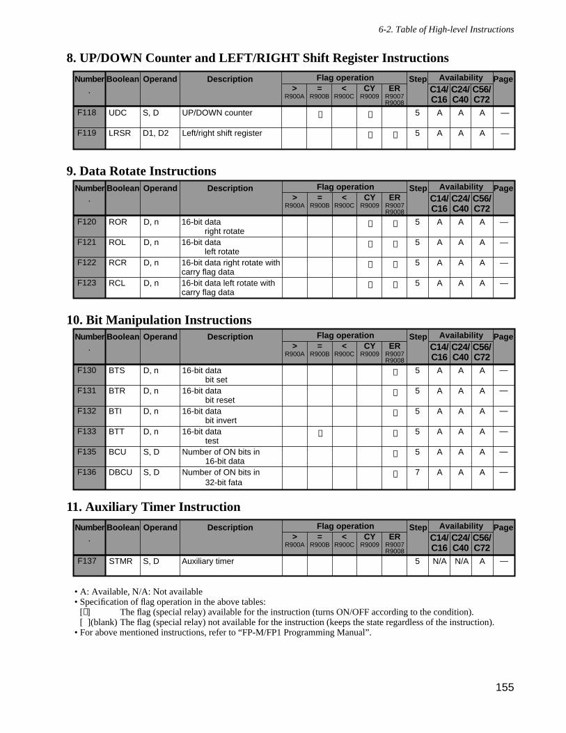
155
6-2. Table of High-level Instructions
8. UP/DOWN Counter and LEFT/RIGHT Shift Register Instructions
9. Data Rotate Instructions
10. Bit Manipulation Instructions
11. Auxiliary Timer Instruction
• A: Available, N/A: Not available• Specification of flag operation in the above tables:
[] The flag (special relay) available for the instruction (turns ON/OFF according to the condition).[ ](blank) The flag (special relay) not available for the instruction (keeps the state regardless of the instruction).
• For above mentioned instructions, refer to “FP-M/FP1 Programming Manual”.
F137 S, D Auxiliary timerSTMR 5 N/A AN/A —
Step PageFlag operationDescriptionOperandBooleanNumberER
R9007R9008
CYR9009
<R900C
=R900B
>R900A
AvailabilityC56/C72
C24/C40
C14/C16
F130
F131
F132
F133
F135
F136
D, n
D, n
D, n
D, n
S, D
S, D
16-bit data bit set
16-bit data bit reset
16-bit data bit invert
16-bit data test
Number of ON bits in 16-bit data
Number of ON bits in 32-bit fata
BTS
BTR
BTI
BTT
BCU
DBCU
5
5
5
5
5
7
A
A
A
A
A
A
A
A
A
A
A
A
A
A
A
A
A
A
—
—
—
—
—
—
Step PageFlag operationDescriptionOperandBooleanNumberER
R9007R9008
CYR9009
<R900C
=R900B
>R900A
AvailabilityC56/C72
C24/C40
C14/C16
F120
F121
F122
F123
D, n
D, n
D, n
D, n
16-bit data right rotate
16-bit data left rotate
16-bit data right rotate with carry flag data16-bit data left rotate with carry flag data
ROR
ROL
RCR
RCL
5
5
5
5
A
A
A
A
A
A
A
A
A
A
A
A
—
—
—
—
Step PageFlag operationDescriptionOperandBooleanNumberER
R9007R9008
CYR9009
<R900C
=R900B
>R900A
AvailabilityC56/C72
C24/C40
C14/C16
F118
F119
S, D
D1, D2
UP/DOWN counter
Left/right shift register
UDC
LRSR
5
5
A
A
A
A
A
A
—
—
Step PageFlag operationDescriptionOperandBooleanNumberER
R9007R9008
CYR9009
<R900C
=R900B
>R900A
AvailabilityC56/C72
C24/C40
C14/C16
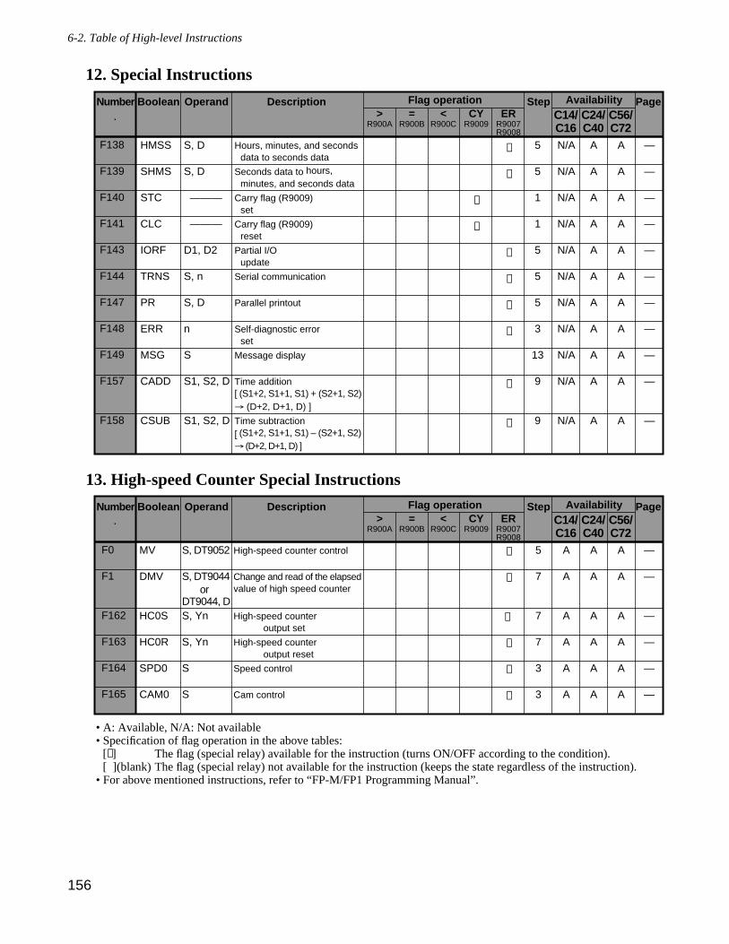
156
6-2. Table of High-level Instructions
12. Special Instructions
13. High-speed Counter Special Instructions
• A: Available, N/A: Not available• Specification of flag operation in the above tables:
[] The flag (special relay) available for the instruction (turns ON/OFF according to the condition).[ ](blank) The flag (special relay) not available for the instruction (keeps the state regardless of the instruction).
• For above mentioned instructions, refer to “FP-M/FP1 Programming Manual”.
F0
F1
F162
F163
F164
F165
S, DT9052
S, DT9044 orDT9044, DS, Yn
S, Yn
S
S
High-speed counter control
Change and read of the elapsed value of high speed counter
High-speed counter output set
High-speed counter output reset
Speed control
Cam control
MV
DMV
HC0S
HC0R
SPD0
CAM0
5
7
7
7
3
3
A
A
A
A
A
A
A
A
A
A
A
A
A
A
A
A
A
A
—
—
—
—
—
—
Step PageFlag operationDescriptionOperandBooleanNumberER
R9007R9008
CYR9009
<R900C
=R900B
>R900A
AvailabilityC56/C72
C24/C40
C14/C16
F138
F139
F140
F141
F143
F144
F147
F148
F149
F157
F158
S, D
S, D
———
———
D1, D2
S, n
S, D
n
S
S1, S2, D
S1, S2, D
Hours, minutes, and seconds data to seconds data
Seconds data to hours, minutes, and seconds data
Carry flag (R9009) set
Carry flag (R9009) reset
Partial I/O update
Serial communication
Parallel printout
Self-diagnostic error set
Message display
Time addition [ (S1+2, S1+1, S1) + (S2+1, S2) → (D+2, D+1, D) ]
Time subtraction [ (S1+2, S1+1, S1) – (S2+1, S2) → (D+2, D+1, D) ]
HMSS
SHMS
STC
CLC
IORF
TRNS
PR
ERR
MSG
CADD
CSUB
5
5
1
1
5
5
5
3
13
9
9
A
A
A
A
A
A
A
A
A
A
A
A
A
A
A
A
A
A
A
A
A
A
N/A
N/A
N/A
N/A
N/A
N/A
N/A
N/A
N/A
N/A
N/A
—
—
—
—
—
—
—
—
—
—
—
Step PageFlag operationDescriptionOperandBooleanNumberER
R9007R9008
CYR9009
<R900C
=R900B
>R900A
AvailabilityC56/C72
C24/C40
C14/C16
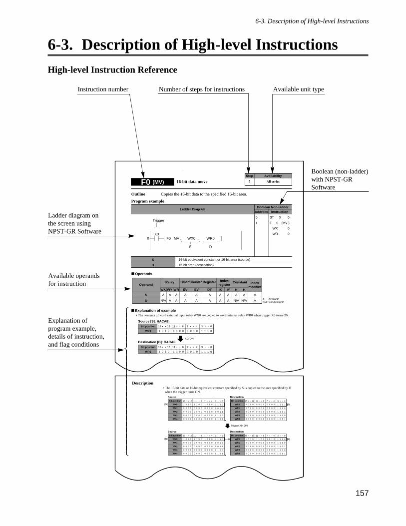
6-3. Description of High-level Instructions
High-level Instruction Reference
6-3. Description of High-level Instructions
157
Instruction number
Ladder diagram onthe screen usingNPST-GR Software
Available operandsfor instruction
Explanation ofprogram example,details of instruction,and flag conditions
Number of steps for instructions Available unit type
Description• The 16-bit data or 16-bit equivalent constant specified by S is copied to the area specified by D
when the trigger turns ON.
Bit position
WX0
WX1
WX2
WX3
WX4
11 8
1 0 1 0 1 1 0 0 1 0 1 0 1 1 1 0
3 0
Source
Trigger X0: ON
15 • • 12 • • • •7 4• •
0 0 0 0 0 0 0 0 0 0 0 0 0 0 1 0
0 0 0 0 0 0 0 0 0 0 0 0 0 0 1 1
0 0 0 0 0 0 0 0 0 0 0 0 0 1 0 0
0 0 0 0 0 0 0 0 0 0 0 0 0 1 0 1
[S]
Bit position
WR0
WR1
WR2
WR3
WR4
11 8
0 0 0 0 0 0 0 0 0 0 0 0 1 1 1 1
3 0
Destination
15 • • 12 • • • •7 4• •
0 0 0 0 0 0 0 0 0 0 0 0 1 1 1 0
0 0 0 0 0 0 0 0 0 0 0 0 1 1 0 1
0 0 0 0 0 0 0 0 0 0 0 0 1 1 0 0
0 0 0 0 0 0 0 0 0 0 0 0 1 0 1 1
[D]
Bit position
WX0
WX1
WX2
WX3
WX4
11 8
1 0 1 0 1 1 0 0 1 0 1 0 1 1 1 0
3 0
Source
15 • • 12 • • • •7 4• •
0 0 0 0 0 0 0 0 0 0 0 0 0 0 1 0
0 0 0 0 0 0 0 0 0 0 0 0 0 0 1 1
0 0 0 0 0 0 0 0 0 0 0 0 0 1 0 0
0 0 0 0 0 0 0 0 0 0 0 0 0 1 0 1
[S]
Bit position
WR0
WR1
WR2
WR3
WR4
11 8
1 0 1 0 1 1 0 0 1 0 1 0 1 1 1 0
3 0
Destination
15 • • 12 • • • •7 4• •
0 0 0 0 0 0 0 0 0 0 0 0 1 1 1 0
0 0 0 0 0 0 0 0 0 0 0 0 1 1 0 1
0 0 0 0 0 0 0 0 0 0 0 0 1 1 0 0
0 0 0 0 0 0 0 0 0 0 0 0 1 0 1 1
[D]
Boolean (non-ladder)with NPST-GRSoftware
6-3. Description of High-level Instructions
Outline Copies the 16-bit data to the specified 16-bit area.
Program example
Operands
Explanation of example• The contents of word external input relay WX0 are copied to word internal relay WR0 when trigger X0 turns ON.
Timer/Counter
EV
Relay
SVWRWYWX
Operand
S A A A AA: N/A: Not Available
Register
DT
A
IYIX
A A
HK
A A
Constant Indexmodifier
A
Indexregister
Available
A
D N/A A A A A A A N/A N/A AA
Bit position
WX0 1 0 1 0 1 1 0 0
11 8
1 0 1 0 1 1 1 0
3 0
Source [S]: HACAE
X0: ON
15 • • 12 • • • •7 4• •
Bit position
WR0 1 0 1 0 1 1 0 0
11 8
1 0 1 0 1 1 1 0
3 0
Destination [D]: HACAE15 • • 12 • • • •7 4• •
F0 (MV) 16-bit data moveAvailabilityStep
5 All series
16-bit equivalent constant or 16-bit area (source)
16-bit area (destination)
Ladder DiagramBoolean Non-ladder
Address Instruction
0X0
F0 MV , WX0 , WR0
S D
Trigger0
1
ST X 0
F 0 (MV )
WX 0
WR 0
S
D
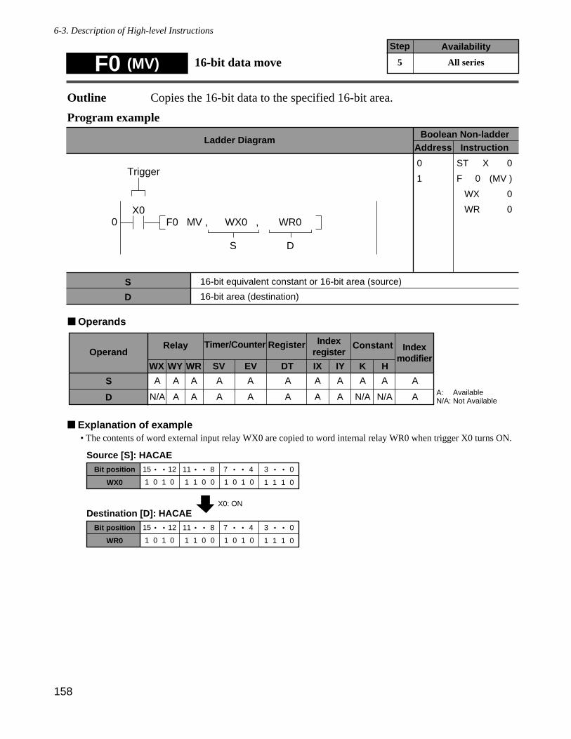
158
6-3. Description of High-level Instructions
Outline Copies the 16-bit data to the specified 16-bit area.
Program example
Operands
Explanation of example• The contents of word external input relay WX0 are copied to word internal relay WR0 when trigger X0 turns ON.
Bit position
WX0 1 0 1 0 1 1 0 0
11 8
1 0 1 0 1 1 1 0
3 0
Source [S]: HACAE
X0: ON
15 • • 12 • • • •7 4• •
Bit position
WR0 1 0 1 0 1 1 0 0
11 8
1 0 1 0 1 1 1 0
3 0
Destination [D]: HACAE15 • • 12 • • • •7 4• •
Timer/Counter
EV
Relay
SVWRWYWX
Operand
S A A A AA: N/A: Not Available
Register
DT
A
IYIX
A A
HK
A A
Constant Indexmodifier
A
Indexregister
Available
A
D N/A A A A A A A N/A N/A AA
F0 (MV) 16-bit data moveAvailabilityStep
5 All series
16-bit equivalent constant or 16-bit area (source)
16-bit area (destination)
Ladder DiagramBoolean Non-ladder
Address Instruction
0X0
F0 MV , WX0 , WR0
S D
Trigger0
1
ST X 0
F 0 (MV )
WX 0
WR 0
S
D
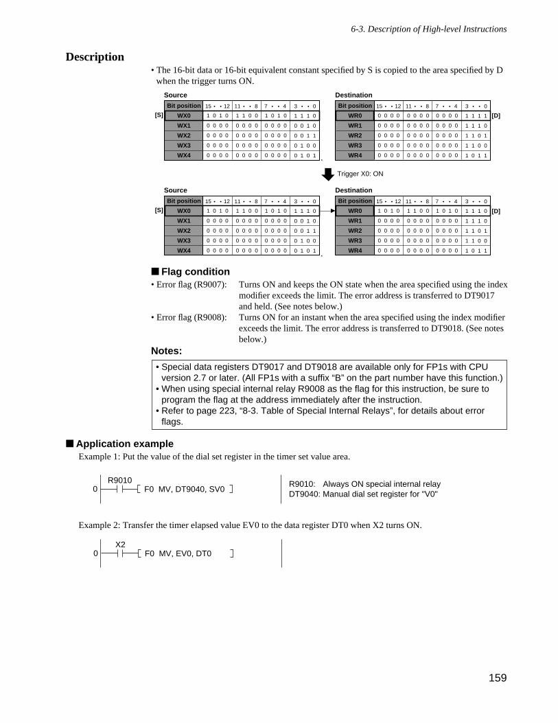
159
6-3. Description of High-level Instructions
Description• The 16-bit data or 16-bit equivalent constant specified by S is copied to the area specified by D
when the trigger turns ON.
Flag condition• Error flag (R9007): Turns ON and keeps the ON state when the area specified using the index
modifier exceeds the limit. The error address is transferred to DT9017and held. (See notes below.)
• Error flag (R9008): Turns ON for an instant when the area specified using the index modifierexceeds the limit. The error address is transferred to DT9018. (See notesbelow.)
Notes:
Application exampleExample 1: Put the value of the dial set register in the timer set value area.
Example 2: Transfer the timer elapsed value EV0 to the data register DT0 when X2 turns ON.
0X2
F0 MV, EV0, DT0
0R9010
F0 MV, DT9040, SV0R9010: Always ON special internal relayDT9040: Manual dial set register for "V0"
• Special data registers DT9017 and DT9018 are available only for FP1s with CPUversion 2.7 or later. (All FP1s with a suffix “B” on the part number have this function.)
• When using special internal relay R9008 as the flag for this instruction, be sure toprogram the flag at the address immediately after the instruction.
• Refer to page 223, “8-3. Table of Special Internal Relays”, for details about errorflags.
Bit position
WX0
WX1
WX2
WX3
WX4
11 8
1 0 1 0 1 1 0 0 1 0 1 0 1 1 1 0
3 0
Source
Trigger X0: ON
15 • • 12 • • • •7 4• •
0 0 0 0 0 0 0 0 0 0 0 0 0 0 1 0
0 0 0 0 0 0 0 0 0 0 0 0 0 0 1 1
0 0 0 0 0 0 0 0 0 0 0 0 0 1 0 0
0 0 0 0 0 0 0 0 0 0 0 0 0 1 0 1
[S]
Bit position
WR0
WR1
WR2
WR3
WR4
11 8
0 0 0 0 0 0 0 0 0 0 0 0 1 1 1 1
3 0
Destination
15 • • 12 • • • •7 4• •
0 0 0 0 0 0 0 0 0 0 0 0 1 1 1 0
0 0 0 0 0 0 0 0 0 0 0 0 1 1 0 1
0 0 0 0 0 0 0 0 0 0 0 0 1 1 0 0
0 0 0 0 0 0 0 0 0 0 0 0 1 0 1 1
[D]
Bit position
WX0
WX1
WX2
WX3
WX4
11 8
1 0 1 0 1 1 0 0 1 0 1 0 1 1 1 0
3 0
Source
15 • • 12 • • • •7 4• •
0 0 0 0 0 0 0 0 0 0 0 0 0 0 1 0
0 0 0 0 0 0 0 0 0 0 0 0 0 0 1 1
0 0 0 0 0 0 0 0 0 0 0 0 0 1 0 0
0 0 0 0 0 0 0 0 0 0 0 0 0 1 0 1
[S]
Bit position
WR0
WR1
WR2
WR3
WR4
11 8
1 0 1 0 1 1 0 0 1 0 1 0 1 1 1 0
3 0
Destination
15 • • 12 • • • •7 4• •
0 0 0 0 0 0 0 0 0 0 0 0 1 1 1 0
0 0 0 0 0 0 0 0 0 0 0 0 1 1 0 1
0 0 0 0 0 0 0 0 0 0 0 0 1 1 0 0
0 0 0 0 0 0 0 0 0 0 0 0 1 0 1 1
[D]
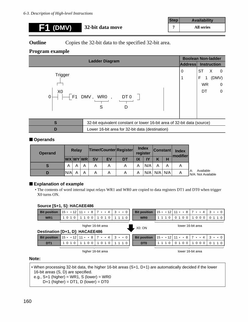
160
6-3. Description of High-level Instructions
Outline Copies the 32-bit data to the specified 32-bit area.
Program example
Operands
Explanation of example• The contents of word internal input relays WR1 and WR0 are copied to data registers DT1 and DT0 when trigger
X0 turns ON.
Note:
• When processing 32-bit data, the higher 16-bit areas (S+1, D+1) are automatically decided if the lower16-bit areas (S, D) are specified.e.g., S+1 (higher) = WR1, S (lower) = WR0
D+1 (higher) = DT1, D (lower) = DT0
Bit position
WR1 1 0 1 0 1 1 0 0
11 8
1 0 1 0 1 1 1 0
3 0
Source [S+1, S]: HACAEE486
X0: ON
15 • • 12 • • • •7 4• •
Bit position
DT1 1 0 1 0 1 1 0 0
11 8
1 0 1 0 1 1 1 0
3 0
Destination [D+1, D]: HACAEE48615 • • 12 • • • •7 4• •
Bit position
WR0 1 1 1 0 0 1 0 0
11 8
1 0 0 0 0 1 1 0
3 015 • • 12 • • • •7 4• •
Bit position
DT0 1 1 1 0 0 1 0 0
11 8
1 0 0 0 0 1 1 0
3 015 • • 12 • • • •7 4• •
"""""""""""""""""""
higher 16-bit area
"""""""""""""""""""
higher 16-bit area
"""""""""""""""""""
lower 16-bit area
"""""""""""""""""""
lower 16-bit area
Timer/Counter
EV
Relay
SVWRWYWX
Operand
S A A A AA: N/A: Not Available
Register
DT
A
IYIX
A N/A
HK
A A
Constant Indexmodifier
A
Indexregister
Available
A
D N/A A A A A A N/A N/A N/A AA
F1 (DMV) 32-bit data moveAvailabilityStep
7 All series
S
D
32-bit equivalent constant or lower 16-bit area of 32-bit data (source)
Lower 16-bit area for 32-bit data (destination)
Ladder DiagramBoolean Non-ladder
Address Instruction
0X0
F1 DMV , WR0 , DT 0
S D
Trigger0
1
ST X 0
F 1 (DMV)
WR 0
DT 0
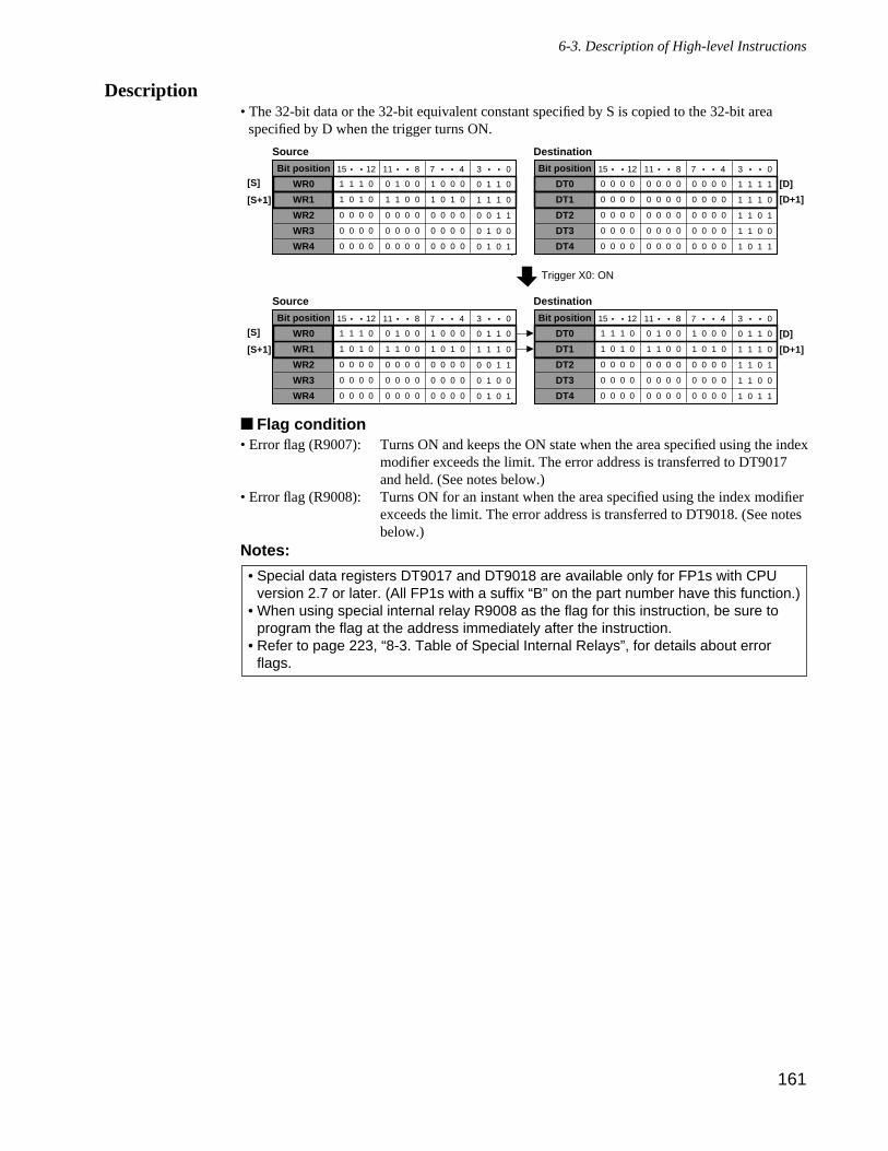
161
6-3. Description of High-level Instructions
Description• The 32-bit data or the 32-bit equivalent constant specified by S is copied to the 32-bit area
specified by D when the trigger turns ON.
Flag condition• Error flag (R9007): Turns ON and keeps the ON state when the area specified using the index
modifier exceeds the limit. The error address is transferred to DT9017and held. (See notes below.)
• Error flag (R9008): Turns ON for an instant when the area specified using the index modifierexceeds the limit. The error address is transferred to DT9018. (See notesbelow.)
Notes:
• Special data registers DT9017 and DT9018 are available only for FP1s with CPUversion 2.7 or later. (All FP1s with a suffix “B” on the part number have this function.)
• When using special internal relay R9008 as the flag for this instruction, be sure toprogram the flag at the address immediately after the instruction.
• Refer to page 223, “8-3. Table of Special Internal Relays”, for details about errorflags.
Bit position
WR0
WR1
WR2
WR3
WR4
11 8
1 1 1 0 0 1 0 0 1 0 0 0 0 1 1 0
3 0
Source
Trigger X0: ON
15 • • 12 • • • •7 4• •
1 0 1 0 1 1 0 0 1 0 1 0 1 1 1 0
0 0 0 0 0 0 0 0 0 0 0 0 0 0 1 1
0 0 0 0 0 0 0 0 0 0 0 0 0 1 0 0
0 0 0 0 0 0 0 0 0 0 0 0 0 1 0 1
[S]
Bit position
DT0
DT1
DT2
DT3
DT4
11 8
0 0 0 0 0 0 0 0 0 0 0 0 1 1 1 1
3 0
Destination
15 • • 12 • • • •7 4• •
0 0 0 0 0 0 0 0 0 0 0 0 1 1 1 0
0 0 0 0 0 0 0 0 0 0 0 0 1 1 0 1
0 0 0 0 0 0 0 0 0 0 0 0 1 1 0 0
0 0 0 0 0 0 0 0 0 0 0 0 1 0 1 1
[D]
Bit position
WR0
WR1
WR2
WR3
WR4
11 8
1 1 1 0 0 1 0 0 1 0 0 0 0 1 1 0
3 0
Source
15 • • 12 • • • •7 4• •
1 0 1 0 1 1 0 0 1 0 1 0 1 1 1 0
0 0 0 0 0 0 0 0 0 0 0 0 0 0 1 1
0 0 0 0 0 0 0 0 0 0 0 0 0 1 0 0
0 0 0 0 0 0 0 0 0 0 0 0 0 1 0 1
[S]
Bit position
DT0
DT1
DT2
DT3
DT4
11 8
1 1 1 0 0 1 0 0 1 0 0 0 0 1 1 0
3 0
Destination
15 • • 12 • • • •7 4• •
1 0 1 0 1 1 0 0 1 0 1 0 1 1 1 0
0 0 0 0 0 0 0 0 0 0 0 0 1 1 0 1
0 0 0 0 0 0 0 0 0 0 0 0 1 1 0 0
0 0 0 0 0 0 0 0 0 0 0 0 1 0 1 1
[D]
[D+1]
[D+1]
[S+1]
[S+1]
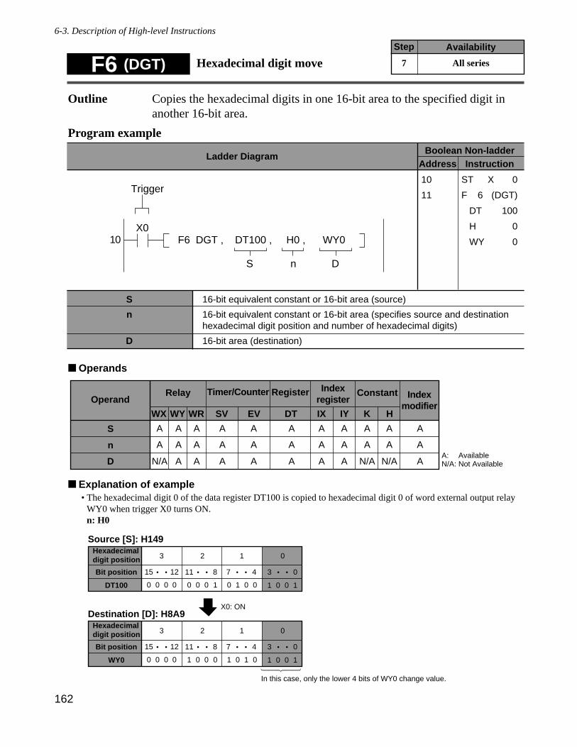
6-3. Description of High-level Instructions
Outline Copies the hexadecimal digits in one 16-bit area to the specified digit inanother 16-bit area.
Program example
Operands
Explanation of example• The hexadecimal digit 0 of the data register DT100 is copied to hexadecimal digit 0 of word external output relay
WY0 when trigger X0 turns ON.n: H0
Bit position
DT100 0 0 0 0 0 0 0 1
11 8
0 1 0 0 1 0 0 1
3 0
Source [S]: H149
X0: ON
15 • • 12 • • • •7 4• •
Hexadecimaldigit position 3 2 1 0
Bit position
WY0 0 0 0 0 1 0 0 0
11 8
1 0 1 0 1 0 0 1
3 0
Destination [D]: H8A9
15 • • 12 • • • •7 4• •
Hexadecimaldigit position 3 2 1 0
In this case, only the lower 4 bits of WY0 change value.
"""""
Timer/Counter
EV
Relay
SVWRWYWX
Operand
S A A A A
A: N/A: Not Available
Register
DT
A
IYIX
A A
HK
A A
Constant Indexmodifier
A
Indexregister
Available
A
n A A A A A A A A A AA
N/A A A A A A A N/A N/A AAD
F6 (DGT) Hexadecimal digit moveAvailabilityStep
7 All series
S
n
D
16-bit equivalent constant or 16-bit area (source)
16-bit equivalent constant or 16-bit area (specifies source and destinationhexadecimal digit position and number of hexadecimal digits)
16-bit area (destination)
Ladder DiagramBoolean Non-ladder
Address Instruction
10X0
F6 DGT , DT100 , H0 , WY0
S D
Trigger
n
10
11
ST X 0
F 6 (DGT)
DT 100
H 0
WY 0
162
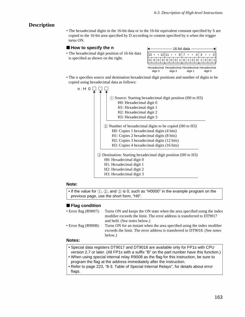
163
6-3. Description of High-level Instructions
Description• The hexadecimal digits in the 16-bit data or in the 16-bit equivalent constant specified by S are
copied to the 16-bit area specified by D according to content specified by n when the triggerturns ON.
How to specify the n• The hexadecimal digit position of 16-bit data
is specified as shown on the right.
• The n specifies source and destination hexadecimal digit positions and number of digits to becopied using hexadecimal data as follows:
Note:
Flag condition• Error flag (R9007): Turns ON and keeps the ON state when the area specified using the index
modifier exceeds the limit. The error address is transferred to DT9017and held. (See notes below.)
• Error flag (R9008): Turns ON for an instant when the area specified using the index modifierexceeds the limit. The error address is transferred to DT9018. (See notesbelow.)
Notes:
• Special data registers DT9017 and DT9018 are available only for FP1s with CPUversion 2.7 or later. (All FP1s with a suffix “B” on the part number have this function.)
• When using special internal relay R9008 as the flag for this instruction, be sure toprogram the flag at the address immediately after the instruction.
• Refer to page 223, “8-3. Table of Special Internal Relays”, for details about errorflags.
• If the value for 1, 2, and 3 is 0, such as “H0000” in the example program on theprevious page, use the short form, “H0”.
1 Source: Starting hexadecimal digit position (H0 to H3) H0: Hexadecimal digit 0 H1: Hexadecimal digit 1 H2: Hexadecimal digit 2 H3: Hexadecimal digit 3
n : H 0
2 Number of hexadecimal digits to be copied (H0 to H3) H0: Copies 1 hexadecimal digits (4 bits) H1: Copies 2 hexadecimal digits (8 bits) H2: Copies 3 hexadecimal digits (12 bits) H3: Copies 4 hexadecimal digits (16 bits)
3 Destination: Starting hexadecimal digit position (H0 to H3) H0: Hexadecimal digit 0 H1: Hexadecimal digit 1 H2: Hexadecimal digit 2 H3: Hexadecimal digit 3
11 8 3 015 • • 12 • • • •7 4• •
0 0 0 0 0 0 0 1 0 1 0 0 1 0 0 1
Hexadecimaldigit 3
Hexadecimaldigit 2
Hexadecimaldigit 1
Hexadecimaldigit 0
16-bit data
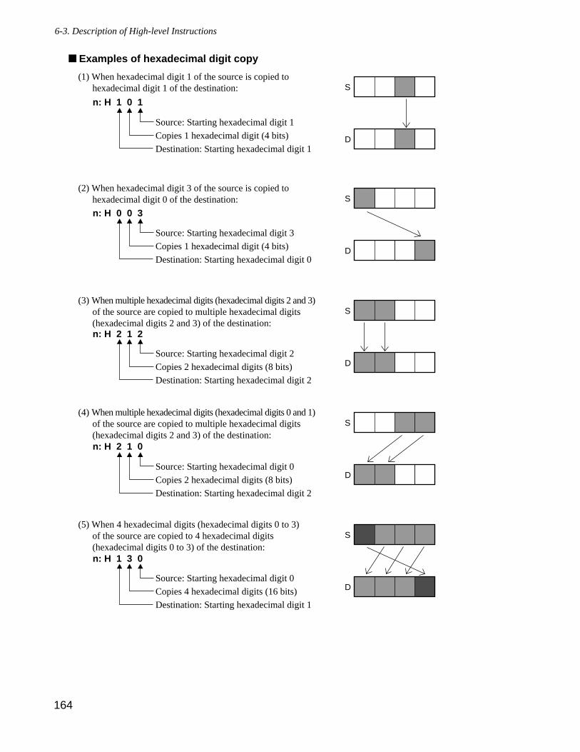
164
6-3. Description of High-level Instructions
Examples of hexadecimal digit copy
S
D
(1) When hexadecimal digit 1 of the source is copied to hexadecimal digit 1 of the destination:
n: H 1 0 1
S
D
(2) When hexadecimal digit 3 of the source is copied to hexadecimal digit 0 of the destination:
n: H 0 0 3
S
D
(3) When multiple hexadecimal digits (hexadecimal digits 2 and 3) of the source are copied to multiple hexadecimal digits (hexadecimal digits 2 and 3) of the destination:n: H 2 1 2
S
D
n: H 2 1 0
(4) When multiple hexadecimal digits (hexadecimal digits 0 and 1)of the source are copied to multiple hexadecimal digits (hexadecimal digits 2 and 3) of the destination:
S
D
n: H 1 3 0
(5) When 4 hexadecimal digits (hexadecimal digits 0 to 3) of the source are copied to 4 hexadecimal digits (hexadecimal digits 0 to 3) of the destination:
Source: Starting hexadecimal digit 1
Copies 1 hexadecimal digit (4 bits)
Destination: Starting hexadecimal digit 1
Source: Starting hexadecimal digit 3
Copies 1 hexadecimal digit (4 bits)
Destination: Starting hexadecimal digit 0
Source: Starting hexadecimal digit 2
Copies 2 hexadecimal digits (8 bits)
Destination: Starting hexadecimal digit 2
Source: Starting hexadecimal digit 0
Copies 2 hexadecimal digits (8 bits)
Destination: Starting hexadecimal digit 2
Source: Starting hexadecimal digit 0
Copies 4 hexadecimal digits (16 bits)
Destination: Starting hexadecimal digit 1
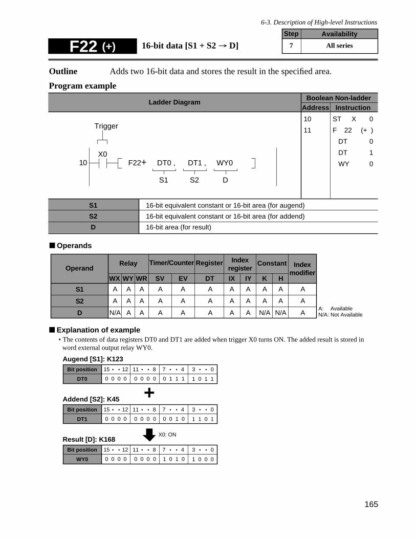
165
F22 (+) 16-bit data [S1 + S2 → D]AvailabilityStep
7 All series
6-3. Description of High-level Instructions
Outline Adds two 16-bit data and stores the result in the specified area.
Program example
Operands
Explanation of example• The contents of data registers DT0 and DT1 are added when trigger X0 turns ON. The added result is stored in
word external output relay WY0.
Bit position
DT1 0 0 0 0 0 0 0 0
11 8
0 0 1 0 1 1 0 1
3 0
Addend [S2]: K45
X0: ON
15 • • 12 • • • •7 4• •
Bit position
WY0 0 0 0 0 0 0 0 0
11 8
1 0 1 0 1 0 0 0
3 0
Result [D]: K16815 • • 12 • • • •7 4• •
Bit position
DT0 0 0 0 0 0 0 0 0
11 8
0 1 1 1 1 0 1 1
3 0
Augend [S1]: K12315 • • 12 • • • •7 4• •
+
Timer/Counter
EV
Relay
SVWRWYWX
Operand
S1 A A A A
A: N/A: Not Available
Register
DT
A
IYIX
A A
HK
A A
Constant Indexmodifier
A
Indexregister
Available
A
S2 A A A A A A A A A AA
N/A A A A A A A N/A N/A AAD
16-bit equivalent constant or 16-bit area (for augend)
16-bit equivalent constant or 16-bit area (for addend)
16-bit area (for result)
Ladder DiagramBoolean Non-ladder
Address Instruction
10X0
F22+ DT0 , DT1 , WY0
S1 D
Trigger
S2
10
11
ST X 0
F 22 (+ )
DT 0
DT 1
WY 0
S1
S2
D
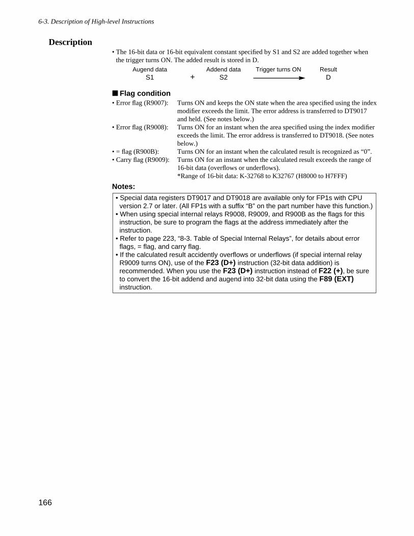
166
Description• The 16-bit data or 16-bit equivalent constant specified by S1 and S2 are added together when
the trigger turns ON. The added result is stored in D.
Flag condition• Error flag (R9007): Turns ON and keeps the ON state when the area specified using the index
modifier exceeds the limit. The error address is transferred to DT9017and held. (See notes below.)
• Error flag (R9008): Turns ON for an instant when the area specified using the index modifierexceeds the limit. The error address is transferred to DT9018. (See notesbelow.)
• = flag (R900B): Turns ON for an instant when the calculated result is recognized as “0”.• Carry flag (R9009): Turns ON for an instant when the calculated result exceeds the range of
16-bit data (overflows or underflows).*Range of 16-bit data: K-32768 to K32767 (H8000 to H7FFF)
Notes:
• Special data registers DT9017 and DT9018 are available only for FP1s with CPUversion 2.7 or later. (All FP1s with a suffix “B” on the part number have this function.)
• When using special internal relays R9008, R9009, and R900B as the flags for thisinstruction, be sure to program the flags at the address immediately after theinstruction.
• Refer to page 223, “8-3. Table of Special Internal Relays”, for details about errorflags, = flag, and carry flag.
• If the calculated result accidently overflows or underflows (if special internal relayR9009 turns ON), use of the F23 (D+) instruction (32-bit data addition) isrecommended. When you use the F23 (D+) instruction instead of F22 (+), be sureto convert the 16-bit addend and augend into 32-bit data using the F89 (EXT)instruction.
Augend data Addend data Trigger turns ON ResultS1 + S2 D
6-3. Description of High-level Instructions
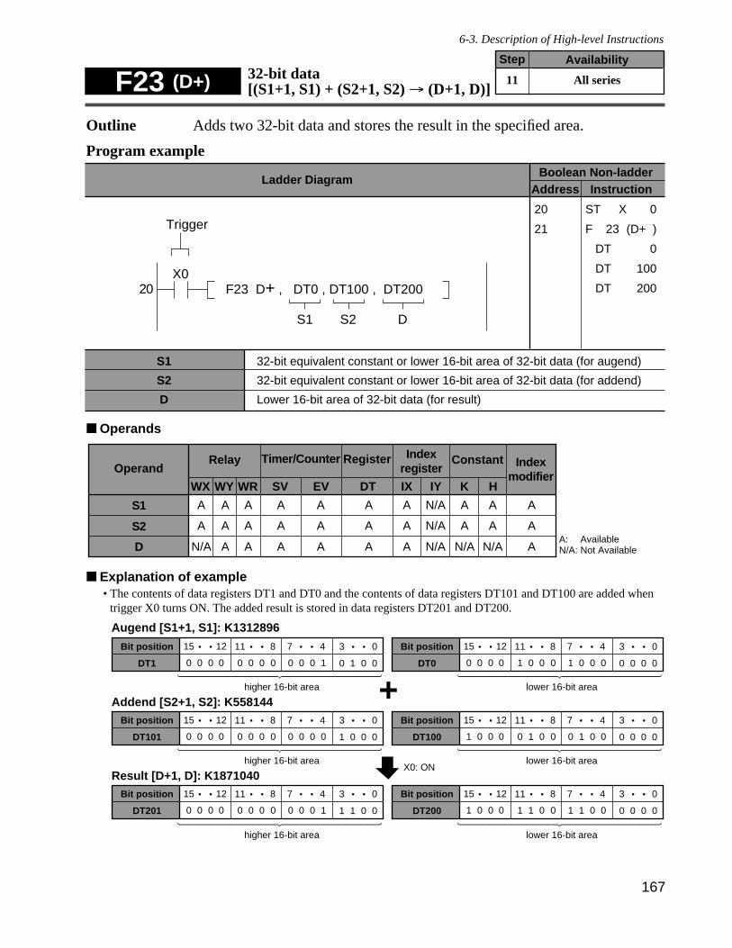
167
Outline Adds two 32-bit data and stores the result in the specified area.
Program example
Operands
Explanation of example• The contents of data registers DT1 and DT0 and the contents of data registers DT101 and DT100 are added when
trigger X0 turns ON. The added result is stored in data registers DT201 and DT200.
Bit position
DT101 0 0 0 0 0 0 0 0
11 8
0 0 0 0 1 0 0 0
3 0
Addend [S2+1, S2]: K558144
X0: ON
15 • • 12 • • • •7 4• •
Bit position
DT201 0 0 0 0 0 0 0 0
11 8
0 0 0 1 1 1 0 0
3 0
Result [D+1, D]: K187104015 • • 12 • • • •7 4• •
Bit position
DT100 1 0 0 0 0 1 0 0
11 8
0 1 0 0 0 0 0 0
3 015 • • 12 • • • •7 4• •
Bit position
DT200 1 0 0 0 1 1 0 0
11 8
1 1 0 0 0 0 0 0
3 015 • • 12 • • • •7 4• •
###################
higher 16-bit area
###################
higher 16-bit area
###################
lower 16-bit area
###################
lower 16-bit area
Bit position
DT1 0 0 0 0 0 0 0 0
11 8
0 0 0 1 0 1 0 0
3 0
Augend [S1+1, S1]: K1312896
15 • • 12 • • • •7 4• • Bit position
DT0 0 0 0 0 1 0 0 0
11 8
1 0 0 0 0 0 0 0
3 015 • • 12 • • • •7 4• •
###################
higher 16-bit area
###################
lower 16-bit area+
Timer/Counter
EV
Relay
SVWRWYWX
Operand
S1 A A A A
A: N/A: Not Available
Register
DT
A
IYIX
A N/A
HK
A A
Constant Indexmodifier
A
Indexregister
Available
A
S2 A A A A A A N/A A A AA
N/A A A A A A N/A N/A N/A AAD
F23 (D+) 32-bit data[(S1+1, S1) + (S2+1, S2) → (D+1, D)]
AvailabilityStep
11 All series
6-3. Description of High-level Instructions
32-bit equivalent constant or lower 16-bit area of 32-bit data (for augend)
32-bit equivalent constant or lower 16-bit area of 32-bit data (for addend)
Lower 16-bit area of 32-bit data (for result)
Ladder DiagramBoolean Non-ladder
Address Instruction
20X0
F23 D+ , DT0 , DT100 , DT200
S1 D
Trigger
S2
20
21
ST X 0
F 23 (D+ )
DT 0
DT 100
DT 200
S1
S2
D
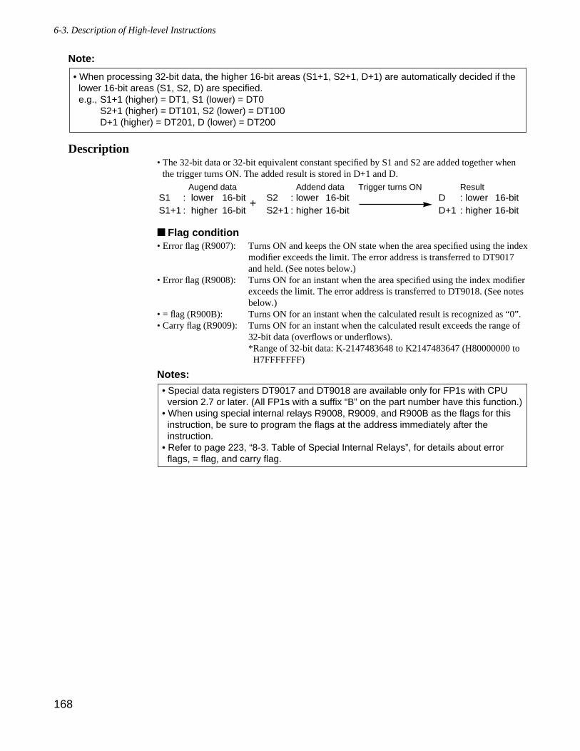
168
Note:
Description• The 32-bit data or 32-bit equivalent constant specified by S1 and S2 are added together when
the trigger turns ON. The added result is stored in D+1 and D.
Flag condition• Error flag (R9007): Turns ON and keeps the ON state when the area specified using the index
modifier exceeds the limit. The error address is transferred to DT9017and held. (See notes below.)
• Error flag (R9008): Turns ON for an instant when the area specified using the index modifierexceeds the limit. The error address is transferred to DT9018. (See notesbelow.)
• = flag (R900B): Turns ON for an instant when the calculated result is recognized as “0”.• Carry flag (R9009): Turns ON for an instant when the calculated result exceeds the range of
32-bit data (overflows or underflows).*Range of 32-bit data: K-2147483648 to K2147483647 (H80000000 toH7FFFFFFF)
Notes:
• Special data registers DT9017 and DT9018 are available only for FP1s with CPUversion 2.7 or later. (All FP1s with a suffix “B” on the part number have this function.)
• When using special internal relays R9008, R9009, and R900B as the flags for thisinstruction, be sure to program the flags at the address immediately after theinstruction.
• Refer to page 223, “8-3. Table of Special Internal Relays”, for details about errorflags, = flag, and carry flag.
Augend data Addend data Trigger turns ON ResultS1 : lower 16-bit S2 : lower 16-bit D : lower 16-bitS1+1 : higher 16-bit
+S2+1 : higher 16-bit D+1 : higher 16-bit
• When processing 32-bit data, the higher 16-bit areas (S1+1, S2+1, D+1) are automatically decided if thelower 16-bit areas (S1, S2, D) are specified.e.g., S1+1 (higher) = DT1, S1 (lower) = DT0
S2+1 (higher) = DT101, S2 (lower) = DT100D+1 (higher) = DT201, D (lower) = DT200
6-3. Description of High-level Instructions
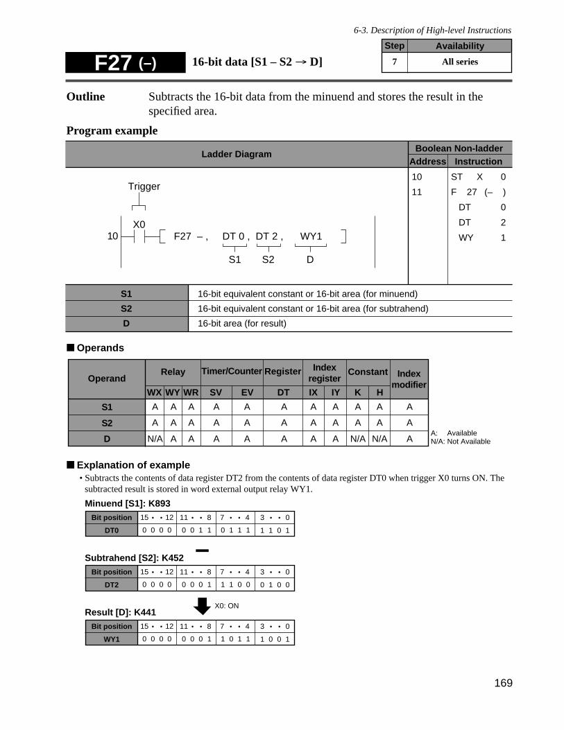
169
Outline Subtracts the 16-bit data from the minuend and stores the result in thespecified area.
Program example
Operands
Explanation of example• Subtracts the contents of data register DT2 from the contents of data register DT0 when trigger X0 turns ON. The
subtracted result is stored in word external output relay WY1.
Bit position
DT2 0 0 0 0 0 0 0 1
11 8
1 1 0 0 0 1 0 0
3 0
Subtrahend [S2]: K452
X0: ON
15 • • 12 • • • •7 4• •
Bit position
WY1 0 0 0 0 0 0 0 1
11 8
1 0 1 1 1 0 0 1
3 0
Result [D]: K44115 • • 12 • • • •7 4• •
Bit position
DT0 0 0 0 0 0 0 1 1
11 8
0 1 1 1 1 1 0 1
3 0
Minuend [S1]: K89315 • • 12 • • • •7 4• •
–
Timer/Counter
EV
Relay
SVWRWYWX
Operand
S1 A A A A
A: N/A: Not Available
Register
DT
A
IYIX
A A
HK
A A
Constant Indexmodifier
A
Indexregister
Available
A
S2 A A A A A A A A A AA
N/A A A A A A A N/A N/A AAD
F27 (–) 16-bit data [S1 – S2 → D]AvailabilityStep
7 All series
6-3. Description of High-level Instructions
16-bit equivalent constant or 16-bit area (for minuend)
16-bit equivalent constant or 16-bit area (for subtrahend)
16-bit area (for result)
Ladder DiagramBoolean Non-ladder
Address Instruction
10X0
F27 – , DT 0 , DT 2 , WY1
S1 D
Trigger
S2
10
11
ST X 0
F 27 (– )
DT 0
DT 2
WY 1
S1
S2
D
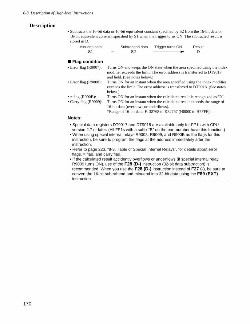
170
Description• Subtracts the 16-bit data or 16-bit equivalent constant specified by S2 from the 16-bit data or
16-bit equivalent constant specified by S1 when the trigger turns ON. The subtracted result isstored in D.
Flag condition• Error flag (R9007): Turns ON and keeps the ON state when the area specified using the index
modifier exceeds the limit. The error address is transferred to DT9017and held. (See notes below.)
• Error flag (R9008): Turns ON for an instant when the area specified using the index modifierexceeds the limit. The error address is transferred to DT9018. (See notesbelow.)
• = flag (R900B): Turns ON for an instant when the calculated result is recognized as “0”.• Carry flag (R9009): Turns ON for an instant when the calculated result exceeds the range of
16-bit data (overflows or underflows).*Range of 16-bit data: K-32768 to K32767 (H8000 to H7FFF)
Notes:
• Special data registers DT9017 and DT9018 are available only for FP1s with CPUversion 2.7 or later. (All FP1s with a suffix “B” on the part number have this function.)
• When using special internal relays R9008, R9009, and R900B as the flags for thisinstruction, be sure to program the flags at the address immediately after theinstruction.
• Refer to page 223, “8-3. Table of Special Internal Relays”, for details about errorflags, = flag, and carry flag.
• If the calculated result accidently overflows or underflows (if special internal relayR9009 turns ON), use of the F28 (D-) instruction (32-bit data subtraction) isrecommended. When you use the F28 (D-) instruction instead of F27 (-), be sure toconvert the 16-bit subtrahend and minuend into 32-bit data using the F89 (EXT)instruction.
Minuend data Subtrahend data Trigger turns ON ResultS1 – S2 D
6-3. Description of High-level Instructions
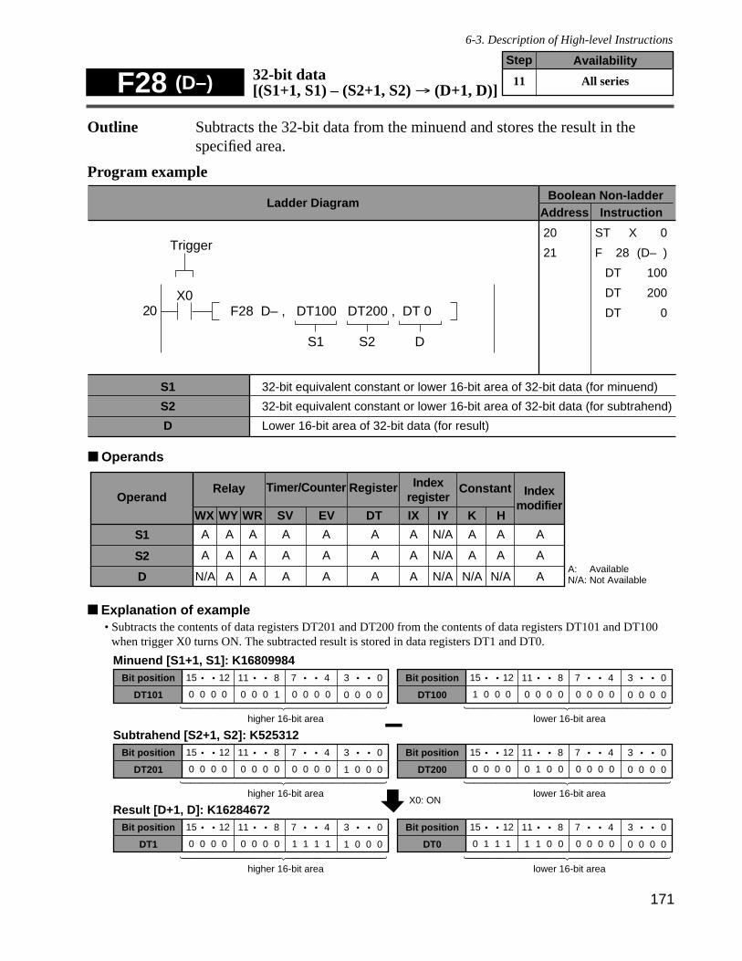
171
Outline Subtracts the 32-bit data from the minuend and stores the result in thespecified area.
Program example
Operands
Explanation of example• Subtracts the contents of data registers DT201 and DT200 from the contents of data registers DT101 and DT100
when trigger X0 turns ON. The subtracted result is stored in data registers DT1 and DT0.
Bit position
DT201 0 0 0 0 0 0 0 0
11 8
0 0 0 0 1 0 0 0
3 0
Subtrahend [S2+1, S2]: K525312
X0: ON
15 • • 12 • • • •7 4• •
Bit position
DT1 0 0 0 0 0 0 0 0
11 8
1 1 1 1 1 0 0 0
3 0
Result [D+1, D]: K1628467215 • • 12 • • • •7 4• •
Bit position
DT200 0 0 0 0 0 1 0 0
11 8
0 0 0 0 0 0 0 0
3 015 • • 12 • • • •7 4• •
Bit position
DT0 0 1 1 1 1 1 0 0
11 8
0 0 0 0 0 0 0 0
3 015 • • 12 • • • •7 4• •
"""""""""""""""""""
higher 16-bit area
"""""""""""""""""""
higher 16-bit area
"""""""""""""""""""
lower 16-bit area
"""""""""""""""""""
lower 16-bit area
Bit position
DT101 0 0 0 0 0 0 0 1
11 8
0 0 0 0 0 0 0 0
3 0
Minuend [S1+1, S1]: K1680998415 • • 12 • • • •7 4• • Bit position
DT100 1 0 0 0 0 0 0 0
11 8
0 0 0 0 0 0 0 0
3 015 • • 12 • • • •7 4• •
"""""""""""""""""""
higher 16-bit area
"""""""""""""""""""
lower 16-bit area–
Timer/Counter
EV
Relay
SVWRWYWX
Operand
S1 A A A A
A: N/A: Not Available
Register
DT
A
IYIX
A N/A
HK
A A
Constant Indexmodifier
A
Indexregister
Available
A
S2 A A A A A A N/A A A AA
N/A A A A A A N/A N/A N/A AAD
F28 (D–) 32-bit data[(S1+1, S1) – (S2+1, S2) → (D+1, D)]
AvailabilityStep
11 All series
6-3. Description of High-level Instructions
32-bit equivalent constant or lower 16-bit area of 32-bit data (for minuend)
32-bit equivalent constant or lower 16-bit area of 32-bit data (for subtrahend)
Lower 16-bit area of 32-bit data (for result)
Ladder DiagramBoolean Non-ladder
Address Instruction
20X0
F28 D– , DT100 DT200 , DT 0
D
Trigger
S2S1
20
21
ST X 0
F 28 (D– )
DT 100
DT 200
DT 0
S1
S2
D
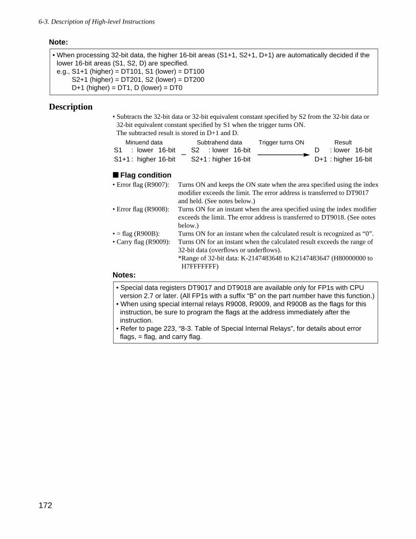
172
Note:
Description• Subtracts the 32-bit data or 32-bit equivalent constant specified by S2 from the 32-bit data or
32-bit equivalent constant specified by S1 when the trigger turns ON.The subtracted result is stored in D+1 and D.
Flag condition• Error flag (R9007): Turns ON and keeps the ON state when the area specified using the index
modifier exceeds the limit. The error address is transferred to DT9017and held. (See notes below.)
• Error flag (R9008): Turns ON for an instant when the area specified using the index modifierexceeds the limit. The error address is transferred to DT9018. (See notesbelow.)
• = flag (R900B): Turns ON for an instant when the calculated result is recognized as “0”.• Carry flag (R9009): Turns ON for an instant when the calculated result exceeds the range of
32-bit data (overflows or underflows).*Range of 32-bit data: K-2147483648 to K2147483647 (H80000000 toH7FFFFFFF)
Notes:
• Special data registers DT9017 and DT9018 are available only for FP1s with CPUversion 2.7 or later. (All FP1s with a suffix “B” on the part number have this function.)
• When using special internal relays R9008, R9009, and R900B as the flags for thisinstruction, be sure to program the flags at the address immediately after theinstruction.
• Refer to page 223, “8-3. Table of Special Internal Relays”, for details about errorflags, = flag, and carry flag.
Minuend data Subtrahend data Trigger turns ON ResultS1 : lower 16-bit S2 : lower 16-bit D : lower 16-bitS1+1 : higher 16-bit
–S2+1 : higher 16-bit D+1 : higher 16-bit
• When processing 32-bit data, the higher 16-bit areas (S1+1, S2+1, D+1) are automatically decided if thelower 16-bit areas (S1, S2, D) are specified.e.g., S1+1 (higher) = DT101, S1 (lower) = DT100
S2+1 (higher) = DT201, S2 (lower) = DT200D+1 (higher) = DT1, D (lower) = DT0
6-3. Description of High-level Instructions
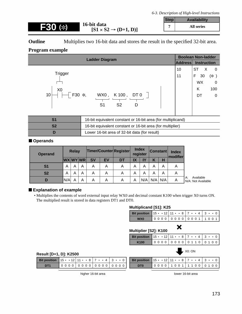
173
Outline Multiplies two 16-bit data and stores the result in the specified 32-bit area.
Program example
Operands
Explanation of example• Multiplies the contents of word external input relay WX0 and decimal constant K100 when trigger X0 turns ON.
The multiplied result is stored in data registers DT1 and DT0.
Bit position
K100 0 0 0 0 0 0 0 0
11 8
0 1 1 0 0 1 0 0
3 0
Multiplier [S2]: K100
X0: ON
15 • • 12 • • • •7 4• •
Bit position
DT0 0 0 0 0 1 0 0 1
11 8
1 1 0 0 0 1 0 0
3 015 • • 12 • • • •7 4• •
Bit position
WX0 0 0 0 0 0 0 0 0
11 8
0 0 0 1 1 0 0 1
3 0
Multiplicand [S1]: K2515 • • 12 • • • •7 4• •
Bit position
DT1 0 0 0 0 0 0 0 0
11 8
0 0 0 0 0 0 0 0
3 0
Result [D+1, D]: K250015 • • 12 • • • •7 4• •
+
"""""""""""""""""""
higher 16-bit area
"""""""""""""""""""
lower 16-bit area
Timer/Counter
EV
Relay
SVWRWYWX
Operand
S1 A A A A
A: N/A: Not Available
Register
DT
A
IYIX
A A
HK
A A
Constant Indexmodifier
A
Indexregister
Available
A
S2 A A A A A A A A A AA
N/A A A A A A N/A N/A N/A AAD
F30 ( ) 16-bit data[S1 × S2 → (D+1, D)]
AvailabilityStep
7 All series
6-3. Description of High-level Instructions
16-bit equivalent constant or 16-bit area (for multiplicand)
16-bit equivalent constant or 16-bit area (for multiplier)
Lower 16-bit area of 32-bit data (for result)
Ladder DiagramBoolean Non-ladder
Address Instruction
10X0
F30 , WX0 , K 100 , DT 0
D
Trigger
S2S1
10
11
ST X 0
F 30 ( )
WX 0
K 100
DT 0
S1
S2
D
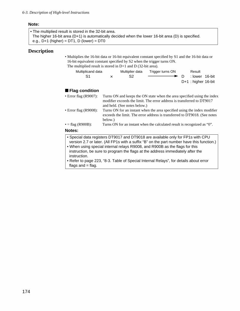
174
Note:
Description• Multiplies the 16-bit data or 16-bit equivalent constant specified by S1 and the 16-bit data or
16-bit equivalent constant specified by S2 when the trigger turns ON.The multiplied result is stored in D+1 and D (32-bit area).
Flag condition• Error flag (R9007): Turns ON and keeps the ON state when the area specified using the index
modifier exceeds the limit. The error address is transferred to DT9017and held. (See notes below.)
• Error flag (R9008): Turns ON for an instant when the area specified using the index modifierexceeds the limit. The error address is transferred to DT9018. (See notesbelow.)
• = flag (R900B): Turns ON for an instant when the calculated result is recognized as “0”.
Notes:
• Special data registers DT9017 and DT9018 are available only for FP1s with CPUversion 2.7 or later. (All FP1s with a suffix “B” on the part number have this function.)
• When using special internal relays R9008, and R900B as the flags for thisinstruction, be sure to program the flags at the address immediately after theinstruction.
• Refer to page 223, “8-3. Table of Special Internal Relays”, for details about errorflags and = flag.
Multiplicand data Multiplier data Trigger turns ON ResultS1 × S2 D : lower 16-bit
D+1 : higher 16-bit
• The multiplied result is stored in the 32-bit area.The higher 16-bit area (D+1) is automatically decided when the lower 16-bit area (D) is specified.e.g., D+1 (higher) = DT1, D (lower) = DT0
6-3. Description of High-level Instructions
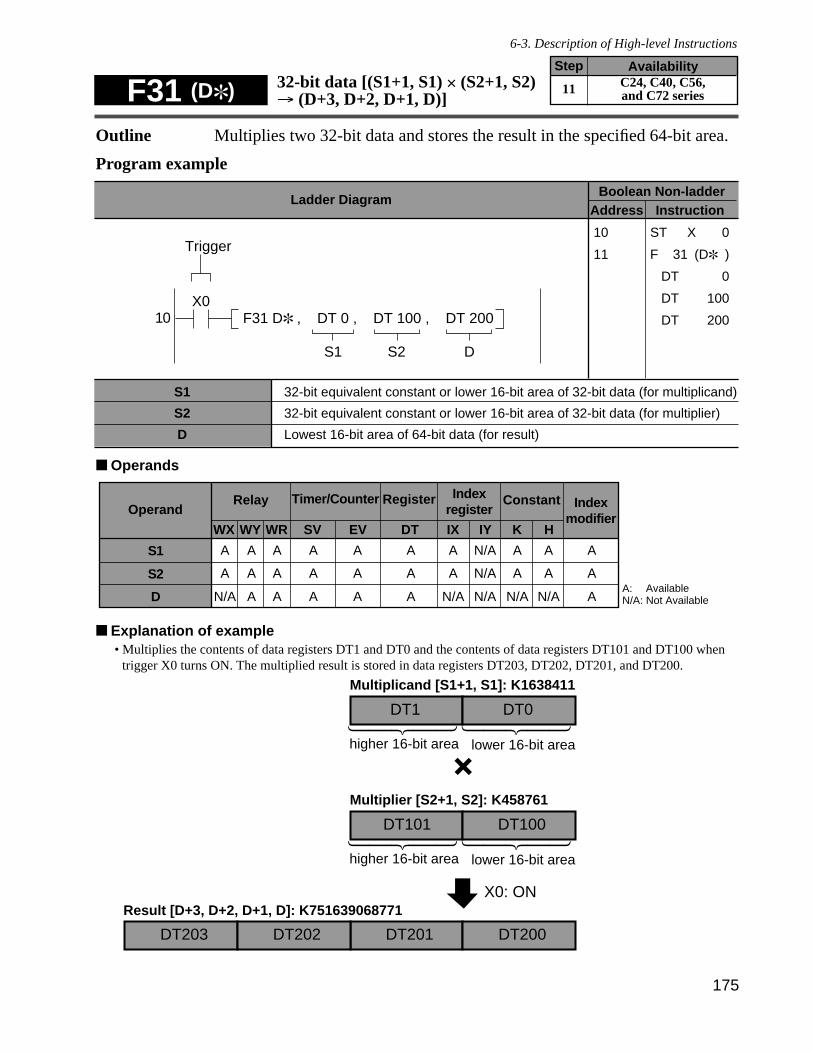
Outline Multiplies two 32-bit data and stores the result in the specified 64-bit area.
Program example
Operands
Explanation of example• Multiplies the contents of data registers DT1 and DT0 and the contents of data registers DT101 and DT100 when
trigger X0 turns ON. The multiplied result is stored in data registers DT203, DT202, DT201, and DT200.
X0: ON
Multiplicand [S1+1, S1]: K1638411
"""""
higher 16-bit area lower 16-bit area
+DT101 DT100
DT201 DT200DT203 DT202
DT1 DT0 """""
Multiplier [S2+1, S2]: K458761
Result [D+3, D+2, D+1, D]: K751639068771
"""""
higher 16-bit area lower 16-bit area
"""""
Timer/Counter
EV
Relay
SVWRWYWX
Operand
S1 A A A A
A: N/A: Not Available
Register
DT
A
IYIX
A N/A
HK
A A
Constant Indexmodifier
A
Indexregister
Available
A
S2 A A A A A A N/A A A AA
N/A A A A A N/A N/A N/A N/A AAD
6-3. Description of High-level Instructions
F31 (D ) 32-bit data [(S1+1, S1) × (S2+1, S2) → (D+3, D+2, D+1, D)]
AvailabilityStep
11 C24, C40, C56, and C72 series
32-bit equivalent constant or lower 16-bit area of 32-bit data (for multiplicand)
32-bit equivalent constant or lower 16-bit area of 32-bit data (for multiplier)
Lowest 16-bit area of 64-bit data (for result)
Ladder DiagramBoolean Non-ladder
Address Instruction
10X0
F31 D , DT 0 , DT 100 , DT 200
D
Trigger
S2S1
10
11
ST X 0
F 31 (D )
DT 0
DT 100
DT 200
S1
S2
D
175
176
Notes:
Description• Multiplies the 32-bit data or 32-bit equivalent constant specified by S1 and the one specified by
S2 when the trigger turns ON.The multiplied result is stored in D+3, D+2, D+1, and D (64-bit area).
Flag condition• Error flag (R9007): Turns ON and keeps the ON state when the area specified using the index
modifier exceeds the limit. The error address is transferred to DT9017and held. (See notes below.)
• Error flag (R9008): Turns ON for an instant when the area specified using the index modifierexceeds the limit. The error address is transferred to DT9018. (See notesbelow.)
• = flag (R900B): Turns ON for an instant when the calculated result is recognized as “0”.
Notes:
• Special data registers DT9017 and DT9018 are available only for FP1s with CPUversion 2.7 or later. (All FP1s with a suffix “B” on the part number have this function.)
• When using special internal relays R9008, and R900B as the flags for thisinstruction, be sure to program the flags at the address immediately after theinstruction.
• Refer to page 223, “8-3. Table of Special Internal Relays”, for details about errorflags and = flag.
Multiplicand data Multiplier data Trigger turns ON Result (64-bit)S1 : lower 16-bit S2 : lower 16-bit DS1+1 : higher 16-bit
×S2+1 : higher 16-bit D+1
D+2D+3
• When processing 32-bit data, the higher 16-bit areas (S1+1, S2+1) are automatically decided if the lower16-bit areas (S1, S2) are specified.e.g., S1+1 (higher) = DT1, S1 (lower) = DT0
S2+1 (higher) = DT101, S2 (lower) = DT100• The multiplied result is stored in the 64-bit area.
The areas (D+3, D+2, D+1) other than the lowest 16-bit area (D) are automatically decided when thelowest 16-bit area is specified.e.g., D = DT200
D+1 = DT201D+2 = DT202D+3 = DT203
6-3. Description of High-level Instructions
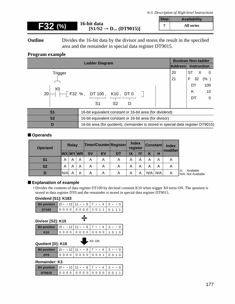
177
Outline Divides the 16-bit data by the divisor and stores the result in the specifiedarea and the remainder in special data register DT9015.
Program example
Operands
Explanation of example• Divides the contents of data register DT100 by decimal constant K10 when trigger X0 turns ON. The quotient is
stored in data register DT0 and the remainder is stored in special data register DT9015.
Bit position
K10 0 0 0 0 0 0 0 0
11 8
0 0 0 0 1 0 1 0
3 0
Divisor [S2]: K10
X0: ON
15 • • 12 • • • •7 4• •
Bit position
DT0 0 0 0 0 0 0 0 0
11 8
0 0 0 1 0 0 1 0
3 0
Quotient [D]: K1815 • • 12 • • • •7 4• •
Bit position
DT100 0 0 0 0 0 0 0 0
11 8
1 0 1 1 0 1 1 1
3 0
Dividend [S1]: K18315 • • 12 • • • •7 4• •
Bit position
DT9015 0 0 0 0 0 0 0 0
11 8
0 0 0 0 0 0 1 1
3 0
Remainder: K315 • • 12 • • • •7 4• •
–
Timer/Counter
EV
Relay
SVWRWYWX
Operand
S1 A A A A
A: N/A: Not Available
Register
DT
A
IYIX
A A
HK
A A
Constant Indexmodifier
A
Indexregister
Available
A
S2 A A A A A A A A A AA
N/A A A A A A A N/A N/A AAD
F32 (%) 16-bit data[S1/S2 → D... (DT9015)]
Availability
All series
Step
7
6-3. Description of High-level Instructions
16-bit equivalent constant or 16-bit area (for dividend)
16-bit equivalent constant or 16-bit area (for divisor)
16-bit area (for quotient), (remainder is stored in special data register DT9015)
Ladder DiagramBoolean Non-ladder
Address Instruction
20X0
F32 % , DT 100 , K10 , DT 0
D
Trigger
S2S1
20
21
ST X 0
F 32 (% )
DT 100
K 10
DT 0
S1
S2
D
178
Description• The 16-bit data or 16-bit equivalent constant specified by S1 is divided by the 16-bit data or 16-
bit equivalent constant specified by S2 when the trigger turns ON.The quotient is stored in D and the remainder is stored in the special data register DT9015.
Flag condition• Error flag (R9007): Turns ON and keeps the ON state,
- when the area specified using the index modifier exceeds the limit.- when the 16-bit equivalent constant or 16-bit data for the divisor
specified by S2 is 0.The error address is transferred to DT9017 and held. (See notes below.)
• Error flag (R9008): Turns ON for an instant,- when the area specified using the index modifier exceeds the limit.- when the 16-bit equivalent constant or 16-bit data for the divisor
specified by S2 is 0.The error address is transferred to DT9018. (See notes below.)
• = flag (R900B): Turns ON for an instant when the calculated result is recognized as “0”.• Carry flag (R9009): Turns ON for an instant when negative minimum value K-32768
(H8000) is divided by K-1 (HFFFF).
Notes:
• Special data registers DT9017 and DT9018 are available only for FP1s with CPUversion 2.7 or later. (All FP1s with a suffix “B” on the part number have this function.)
• When using special internal relays R9008, R9009, and R900B as the flags for thisinstruction, be sure to program the flags at the address immediately after theinstruction.
• Refer to page 223, “8-3. Table of Special Internal Relays”, for details about errorflags, = flag, and carry flag.
• If the calculated result accidently overflows (if special internal relay R9009 turnsON), use of the F33 (D%) instruction (32-bit data division) is recommended. Whenyou use the F33 (D%) instruction instead of F32 (%), be sure to convert the 16-bitdividend and divisor into 32-bit data using the F89 (EXT) instruction.
Dividend data Divisor Trigger turns ON Quotient RemainderS1 ÷ S2 D .... DT9015
6-3. Description of High-level Instructions
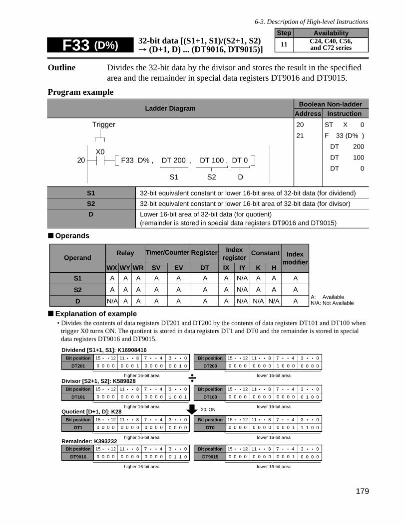
Outline Divides the 32-bit data by the divisor and stores the result in the specifiedarea and the remainder in special data registers DT9016 and DT9015.
Program example
Operands
Explanation of example• Divides the contents of data registers DT201 and DT200 by the contents of data registers DT101 and DT100 when
trigger X0 turns ON. The quotient is stored in data registers DT1 and DT0 and the remainder is stored in specialdata registers DT9016 and DT9015.
Bit position
DT101 0 0 0 0 0 0 0 0
11 8
0 0 0 0 1 0 0 1
3 0
Divisor [S2+1, S2]: K58982815 • • 12 • • • •7 4• •
Bit position
DT1 0 0 0 0 0 0 0 0
11 8
0 0 0 0 0 0 0 0
3 0
Quotient [D+1, D]: K2815 • • 12 • • • •7 4• •
Bit position
DT100 0 0 0 0 0 0 0 0
11 8
0 0 0 0 0 1 0 0
3 015 • • 12 • • • •7 4• •
Bit position
DT0 0 0 0 0 0 0 0 0
11 8
0 0 0 1 1 1 0 0
3 015 • • 12 • • • •7 4• •
###################
higher 16-bit area
###################
higher 16-bit area
###################
lower 16-bit area
###################
lower 16-bit area
Bit position
DT201 0 0 0 0 0 0 0 1
11 8
0 0 0 0 0 0 1 0
3 0
Dividend [S1+1, S1]: K1690841615 • • 12 • • • •7 4• • Bit position
DT200 0 0 0 0 0 0 0 0
11 8
1 0 0 0 0 0 0 0
3 015 • • 12 • • • •7 4• •
###################
higher 16-bit area
###################
lower 16-bit area
Bit position
DT9016 0 0 0 0 0 0 0 0
11 8
0 0 0 0 0 1 1 0
3 0
Remainder: K39323215 • • 12 • • • •7 4• • Bit position
DT9015 0 0 0 0 0 0 0 0
11 8
0 0 0 1 0 0 0 0
3 015 • • 12 • • • •7 4• •
###################
higher 16-bit area
###################
lower 16-bit area
–
X0: ON
Timer/Counter
EV
Relay
SVWRWYWX
Operand
S1 A A A A
A: N/A: Not Available
Register
DT
A
IYIX
A N/A
HK
A A
Constant Indexmodifier
A
Indexregister
Available
A
S2 A A A A A A N/A A A AA
N/A A A A A A N/A N/A N/A AAD
6-3. Description of High-level Instructions
F33 (D%) 32-bit data [(S1+1, S1)/(S2+1, S2)→ (D+1, D) ... (DT9016, DT9015)]
32-bit equivalent constant or lower 16-bit area of 32-bit data (for dividend)
32-bit equivalent constant or lower 16-bit area of 32-bit data (for divisor)
Lower 16-bit area of 32-bit data (for quotient)(remainder is stored in special data registers DT9016 and DT9015)
Ladder DiagramBoolean Non-ladder
Address Instruction
20X0
F33 D% , DT 200 , DT 100 , DT 0
D
Trigger
S2S1
20
21
ST X 0
F 33 (D% )
DT 200
DT 100
DT 0
S1
S2
D
AvailabilityStep
11 C24, C40, C56, and C72 series
179
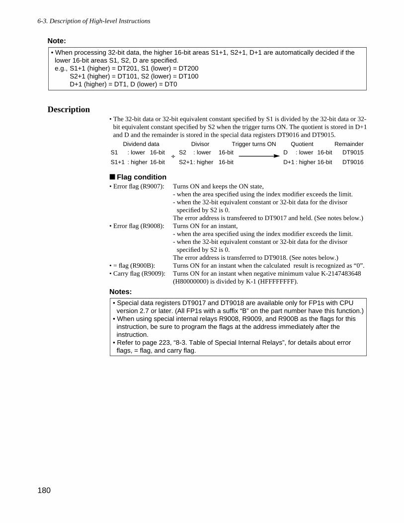
180
Note:
Description• The 32-bit data or 32-bit equivalent constant specified by S1 is divided by the 32-bit data or 32-
bit equivalent constant specified by S2 when the trigger turns ON. The quotient is stored in D+1and D and the remainder is stored in the special data registers DT9016 and DT9015.
Flag condition• Error flag (R9007): Turns ON and keeps the ON state,
- when the area specified using the index modifier exceeds the limit.- when the 32-bit equivalent constant or 32-bit data for the divisor
specified by S2 is 0.The error address is transfeered to DT9017 and held. (See notes below.)
• Error flag (R9008): Turns ON for an instant,- when the area specified using the index modifier exceeds the limit.- when the 32-bit equivalent constant or 32-bit data for the divisor
specified by S2 is 0.The error address is transferred to DT9018. (See notes below.)
• = flag (R900B): Turns ON for an instant when the calculated result is recognized as “0”.• Carry flag (R9009): Turns ON for an instant when negative minimum value K-2147483648
(H80000000) is divided by K-1 (HFFFFFFFF).
Notes:
• Special data registers DT9017 and DT9018 are available only for FP1s with CPUversion 2.7 or later. (All FP1s with a suffix “B” on the part number have this function.)
• When using special internal relays R9008, R9009, and R900B as the flags for thisinstruction, be sure to program the flags at the address immediately after theinstruction.
• Refer to page 223, “8-3. Table of Special Internal Relays”, for details about errorflags, = flag, and carry flag.
Dividend data Divisor Trigger turns ON Quotient RemainderS1 : lower 16-bit ÷ S2 : lower 16-bit D : lower 16-bit DT9015
S1+1 : higher 16-bit S2+1: higher 16-bit D+1 : higher 16-bit DT9016
• When processing 32-bit data, the higher 16-bit areas S1+1, S2+1, D+1 are automatically decided if thelower 16-bit areas S1, S2, D are specified.e.g., S1+1 (higher) = DT201, S1 (lower) = DT200
S2+1 (higher) = DT101, S2 (lower) = DT100D+1 (higher) = DT1, D (lower) = DT0
6-3. Description of High-level Instructions
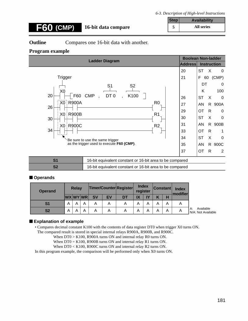
181
Outline Compares one 16-bit data with another.
Program example
Operands
Explanation of example• Compares decimal constant K100 with the contents of data register DT0 when trigger X0 turns ON.
The compared result is stored in special internal relays R900A, R900B, and R900C.When DT0 > K100, R900A turns ON and internal relay R0 turns ON.When DT0 = K100, R900B turns ON and internal relay R1 turns ON.When DT0 < K100, R900C turns ON and internal relay R2 turns ON.
In this program example, the comparison will be performed only when X0 turns ON.
Timer/Counter
EV
Relay
SVWRWYWX
Operand
S1 A A A AA: N/A: Not Available
Register
DT
A
IYIX
A A
HK
A A
Constant Indexmodifier
A
Indexregister
Available
A
S2 A A A A A A A A A AA
6-3. Description of High-level Instructions
S1
S2
16-bit equivalent constant or 16-bit area to be compared
16-bit equivalent constant or 16-bit area to be compared
Ladder DiagramBoolean Non-ladder
Address Instruction
20X0
F60 CMP , DT 0 , K100
S1 S2
Be sure to use the same trigger as the trigger used to execute F60 (CMP).
X0 R0R900A26
X0 R1R900B30
X0 R2R900C34
Trigger
20
21
26
27
29
30
31
33
34
35
37
ST X 0
F 60 (CMP)
DT 0
K 100
ST X 0
AN R 900A
OT R 0
ST X 0
AN R 900B
OT R 1
ST X 0
AN R 900C
OT R 2
F60 (CMP) 16-bit data compareAvailabilityStep
5 All series
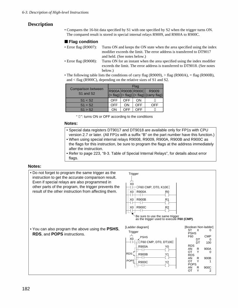
182
Description• Compares the 16-bit data specified by S1 with one specified by S2 when the trigger turns ON.
The compared result is stored in special internal relays R9009, and R900A to R900C.
Flag condition• Error flag (R9007): Turns ON and keeps the ON state when the area specified using the index
modifier exceeds the limit. The error address is transferred to DT9017and held. (See notes below.)
• Error flag (R9008): Turns ON for an instant when the area specified using the index modifierexceeds the limit. The error address is transferred to DT9018. (See notesbelow.)
• The following table lists the conditions of carry flag (R9009), > flag (R900A), = flag (R900B),and < flag (R900C), depending on the relative sizes of S1 and S2.
Notes:
Notes:• Do not forget to program the same trigger as the
instruction to get the accurate comparison result.Even if special relays are also programmed inother parts of the program, the trigger prevents theresult of the other instruction from affecting them.
• You can also program the above using the PSHS,RDS, and POPS instructions.
• Special data registers DT9017 and DT9018 are available only for FP1s with CPUversion 2.7 or later. (All FP1s with a suffix “B” on the part number have this function.)
• When using special internal relays R9008, R9009, R900A, R900B and R900C asthe flags for this instruction, be sure to program the flags at the address immediatelyafter the instruction.
• Refer to page 223, “8-3. Table of Special Internal Relays”, for details about errorflags.
S1 < S2S1 = S2S1 > S2
OFFOFFON
OFFONOFF
ONOFFOFF
OFF
(> flag) (= flag) (< flag) (carry flag)R900A R900B R900C R9009
FlagComparison between
S1 and S2
“ ”: turns ON or OFF according to the conditions
6-3. Description of High-level Instructions
X0F60 CMP, DT0, K100
X0 R0R900A
X0 R1R900B
X0 R2R900C
Trigger
Be sure to use the same trigger as the trigger used to execute F60 (CMP).
X0F60 CMP, DT0, DT100
Y0R900A
Y1R900B
Y2R900C
Trigger
PSHS
RDS
POPS
[Ladder diagram] [Boolean Non-ladder]ST X 0PSHSF60 CMP
DT 0DT 100
RDSAN R 900AOT Y 0RDSAN R 900BOT Y 1POPSAN R 900COT Y 2
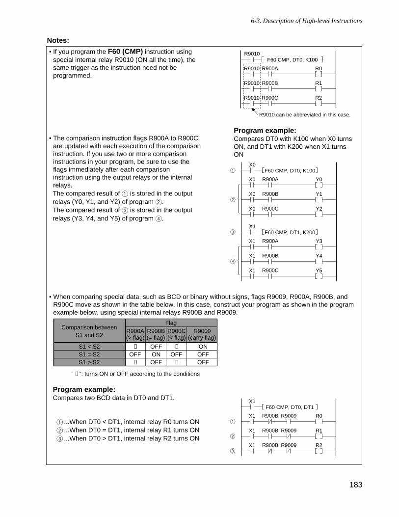
183
Notes:
6-3. Description of High-level Instructions
• If you program the F60 (CMP) instruction usingspecial internal relay R9010 (ON all the time), thesame trigger as the instruction need not beprogrammed.
• The comparison instruction flags R900A to R900Care updated with each execution of the comparisoninstruction. If you use two or more comparisoninstructions in your program, be sure to use theflags immediately after each comparisoninstruction using the output relays or the internalrelays.The compared result of 1 is stored in the outputrelays (Y0, Y1, and Y2) of program 2.The compared result of 3 is stored in the outputrelays (Y3, Y4, and Y5) of program 4.
• When comparing special data, such as BCD or binary without signs, flags R9009, R900A, R900B, andR900C move as shown in the table below. In this case, construct your program as shown in the programexample below, using special internal relays R900B and R9009.
Program example:Compares two BCD data in DT0 and DT1.
1 ...When DT0 < DT1, internal relay R0 turns ON2 ...When DT0 = DT1, internal relay R1 turns ON3 ...When DT0 > DT1, internal relay R2 turns ON
X0F60 CMP, DT0, K100
X0 Y0R900A
X0 Y1R900B
X0 Y2R900C
X1F60 CMP, DT1, K200
X1 Y3R900A
X1 Y4R900B
X1 Y5R900C
1
2
"""""
3
4
"""""
X1F60 CMP, DT0, DT1
X1 R0R900B
X1 R1R900B
X1 R2R900B
1
2
3
R9009
R9009
R9009
Program example:Compares DT0 with K100 when X0 turnsON, and DT1 with K200 when X1 turnsON
R9010F60 CMP, DT0, K100
R9010 R0R900A
R9010 R1R900B
R9010 R2R900C
R9010 can be abbreviated in this case.
S1 < S2S1 = S2S1 > S2
OFF
OFFONOFF
OFF
ONOFFOFF
(> flag) (= flag) (< flag) (carry flag)R900A R900B R900C R9009
FlagComparison between
S1 and S2
“ ”: turns ON or OFF according to the conditions
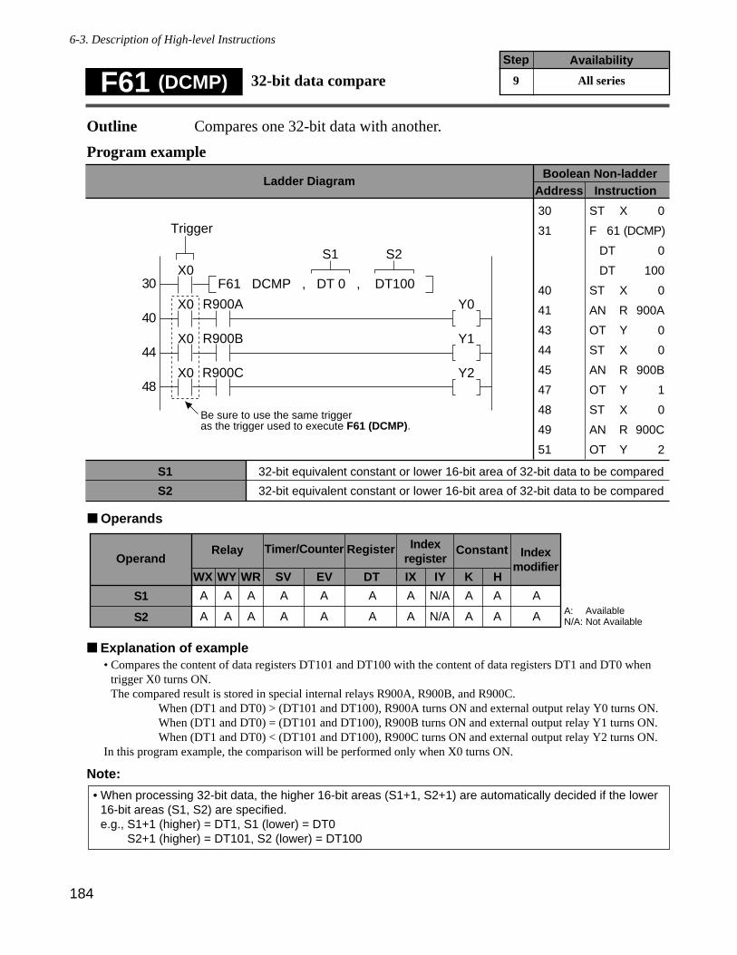
184
Outline Compares one 32-bit data with another.
Program example
Operands
Explanation of example• Compares the content of data registers DT101 and DT100 with the content of data registers DT1 and DT0 when
trigger X0 turns ON.The compared result is stored in special internal relays R900A, R900B, and R900C.
When (DT1 and DT0) > (DT101 and DT100), R900A turns ON and external output relay Y0 turns ON.When (DT1 and DT0) = (DT101 and DT100), R900B turns ON and external output relay Y1 turns ON.When (DT1 and DT0) < (DT101 and DT100), R900C turns ON and external output relay Y2 turns ON.
In this program example, the comparison will be performed only when X0 turns ON.
Note:
• When processing 32-bit data, the higher 16-bit areas (S1+1, S2+1) are automatically decided if the lower16-bit areas (S1, S2) are specified.e.g., S1+1 (higher) = DT1, S1 (lower) = DT0
S2+1 (higher) = DT101, S2 (lower) = DT100
Timer/Counter
EV
Relay
SVWRWYWX
Operand
S1 A A A AA: N/A: Not Available
Register
DT
A
IYIX
A N/A
HK
A A
Constant Indexmodifier
A
Indexregister
Available
A
S2 A A A A A A N/A A A AA
F61 (DCMP) 32-bit data compareAvailabilityStep
9 All series
6-3. Description of High-level Instructions
S1
S2
32-bit equivalent constant or lower 16-bit area of 32-bit data to be compared
32-bit equivalent constant or lower 16-bit area of 32-bit data to be compared
Ladder DiagramBoolean Non-ladder
Address Instruction
30X0
F61 DCMP , DT 0 , DT100
S1 S2
Be sure to use the same trigger as the trigger used to execute F61 (DCMP).
X0 Y0R900A40
X0 Y1R900B44
X0 Y2R900C48
Trigger30
31
40
41
43
44
45
47
48
49
51
ST X 0
F 61 (DCMP)
DT 0
DT 100
ST X 0
AN R 900A
OT Y 0
ST X 0
AN R 900B
OT Y 1
ST X 0
AN R 900C
OT Y 2
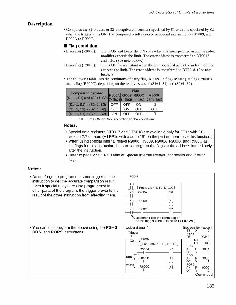
185
Description• Compares the 32-bit data or 32-bit equivalent constant specified by S1 with one specified by S2
when the trigger turns ON. The compared result is stored in special internal relays R9009, andR900A to R900C.
Flag condition• Error flag (R9007): Turns ON and keeps the ON state when the area specified using the index
modifier exceeds the limit. The error address is transferred to DT9017and held. (See note below.)
• Error flag (R9008): Turns ON for an instant when the area specified using the index modifierexceeds the limit. The error address is transferred to DT9018. (See notebelow.)
• The following table lists the conditions of carry flag (R9009), > flag (R900A), = flag (R900B),and < flag (R900C), depending on the relative sizes of (S1+1, S1) and (S2+1, S2).
Notes:
Notes:
• Do not forget to program the same trigger as theinstruction to get the accurate comparison result.Even if special relays are also programmed inother parts of the program, the trigger prevents theresult of the other instruction from affecting them.
• You can also program the above using the PSHS,RDS, and POPS instructions.
Continued
• Special data registers DT9017 and DT9018 are available only for FP1s with CPUversion 2.7 or later. (All FP1s with a suffix “B” on the part number have this function.)
• When using special internal relays R9008, R9009, R900A, R900B, and R900C asthe flags for this instruction, be sure to program the flags at the address immediatelyafter the instruction.
• Refer to page 223, “8-3. Table of Special Internal Relays”, for details about errorflags.
(S1+1, S1) < (S2+1, S2)(S1+1, S1) = (S2+1, S2)(S1+1, S1) > (S2+1, S2)
OFFOFFON
OFFONOFF
ONOFFOFF
OFF
(> flag) (= flag) (< flag) (carry flag)R900A R900B R900C R9009
FlagComparison between
(S1+1, S1) and (S2+1, S2)
“ ”: turns ON or OFF according to the conditions
6-3. Description of High-level Instructions
X0F61 DCMP, DT0, DT100
X0 Y0R900A
X0 Y1R900B
X0 Y2R900C
Trigger
Be sure to use the same trigger as the trigger used to execute F61 (DCMP).
X0F61 DCMP, DT0, DT100
Y0R900A
Y1R900B
Y2R900C
Trigger
PSHS
RDS
POPS
[Ladder diagram] [Boolean Non-ladder]ST X 0PSHSF61 DCMP
DT 0DT 100
RDSAN R 900AOT Y 0RDSAN R 900BOT Y 1POPSAN R 900COT Y 2
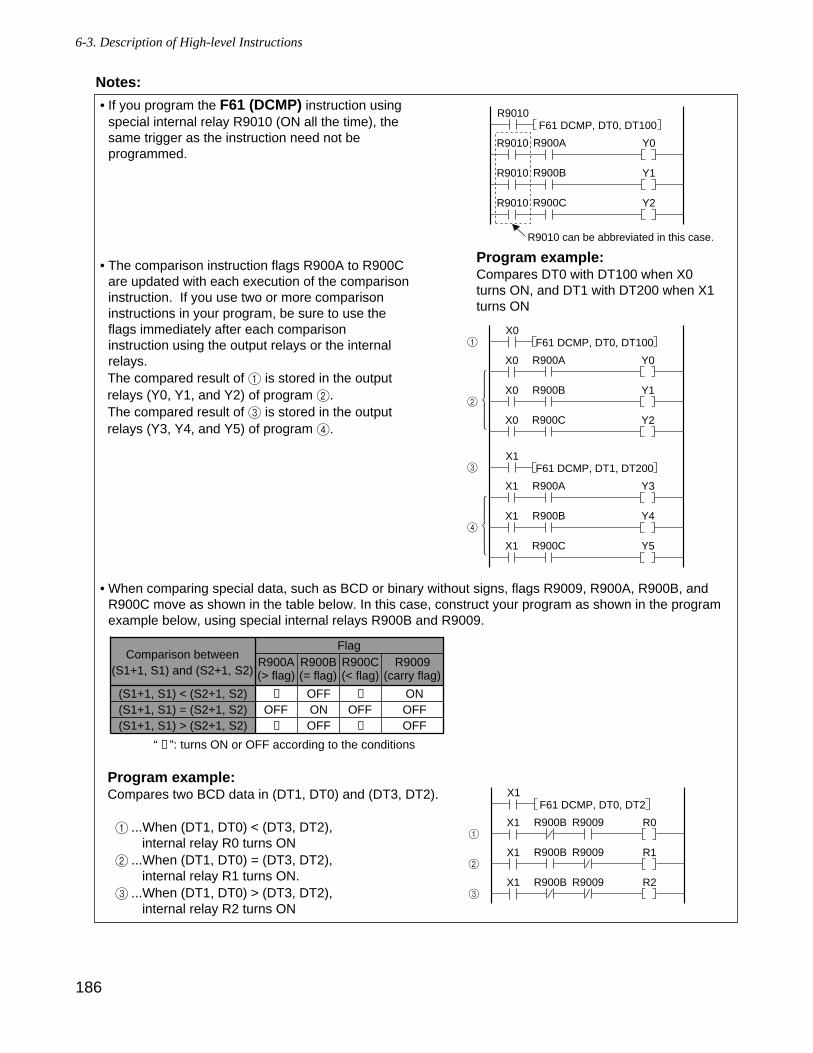
186
Notes:
6-3. Description of High-level Instructions
• If you program the F61 (DCMP) instruction usingspecial internal relay R9010 (ON all the time), thesame trigger as the instruction need not beprogrammed.
• The comparison instruction flags R900A to R900Care updated with each execution of the comparisoninstruction. If you use two or more comparisoninstructions in your program, be sure to use theflags immediately after each comparisoninstruction using the output relays or the internalrelays.The compared result of 1 is stored in the outputrelays (Y0, Y1, and Y2) of program 2.The compared result of 3 is stored in the outputrelays (Y3, Y4, and Y5) of program 4.
• When comparing special data, such as BCD or binary without signs, flags R9009, R900A, R900B, andR900C move as shown in the table below. In this case, construct your program as shown in the programexample below, using special internal relays R900B and R9009.
Program example:Compares two BCD data in (DT1, DT0) and (DT3, DT2).
1 ...When (DT1, DT0) < (DT3, DT2), internal relay R0 turns ON
2 ...When (DT1, DT0) = (DT3, DT2), internal relay R1 turns ON.
3 ...When (DT1, DT0) > (DT3, DT2), internal relay R2 turns ON
X0F61 DCMP, DT0, DT100
X0 Y0R900A
X0 Y1R900B
X0 Y2R900C
X1F61 DCMP, DT1, DT200
X1 Y3R900A
X1 Y4R900B
X1 Y5R900C
1
2
"""""
3
4
"""""
Program example:Compares DT0 with DT100 when X0turns ON, and DT1 with DT200 when X1turns ON
X1F61 DCMP, DT0, DT2
X1 R0R900B
X1 R1R900B
X1 R2R900B
1
2
3
R9009
R9009
R9009
R9010F61 DCMP, DT0, DT100
R9010 Y0R900A
R9010 Y1R900B
R9010 Y2R900C
R9010 can be abbreviated in this case.
(S1+1, S1) < (S2+1, S2)(S1+1, S1) = (S2+1, S2)(S1+1, S1) > (S2+1, S2)
OFF
OFFONOFF
OFF
ONOFFOFF
(> flag) (= flag) (< flag) (carry flag)R900A R900B R900C R9009
FlagComparison between
(S1+1, S1) and (S2+1, S2)
“ ”: turns ON or OFF according to the conditions

187
Outline Converts 16-bit binary data to BCD code that expresses 4-digit decimals.
Program example
Operands
Explanation of example• Converts the contents of timer/counter elapsed value area EV0 to BCD code that expresses 4-digit decimals when
trigger X0 turns ON. The converted data is stored in word external output relay WY0.
Bit position
EV0
Decimal
0 0 0 0 0 0 0 0
11 8
0 0 0 1 0 0 0 0
3 015 • • 12 • • • •7 4• •
K16
Bit position
WY0
BCD H code
0 0 0 0 0 0 0 0
11 8
0 0 0 1 0 1 1 0
3 015 • • 12 • • • •7 4• •
0 0 1 6
X0: ON
Source [S]: K16
Destination [D]: H16 (BCD)
Timer/Counter
EV
Relay
SVWRWYWX
Operand
S A A A AA: N/A: Not Available
Register
DT
A
IYIX
A A
HK
A A
Constant Indexmodifier
A
Indexregister
Available
A
D N/A A A A A A A N/A N/A AA
6-3. Description of High-level Instructions
F80 (BCD) 16-bit data → 4-digit BCD dataAvailabilityStep
5 All series
S
D
16-bit equivalent constant or 16-bit area for storing binary data (source)Available range: K0 to K9999
16-bit area for 4-digit BCD code (destination)
Ladder DiagramBoolean Non-ladder
Address Instruction
10X0
F80 BCD , EV0 , WY0
D
Trigger
S
10
11
ST X 0
F 80 (BCD)
EV 0
WY 0
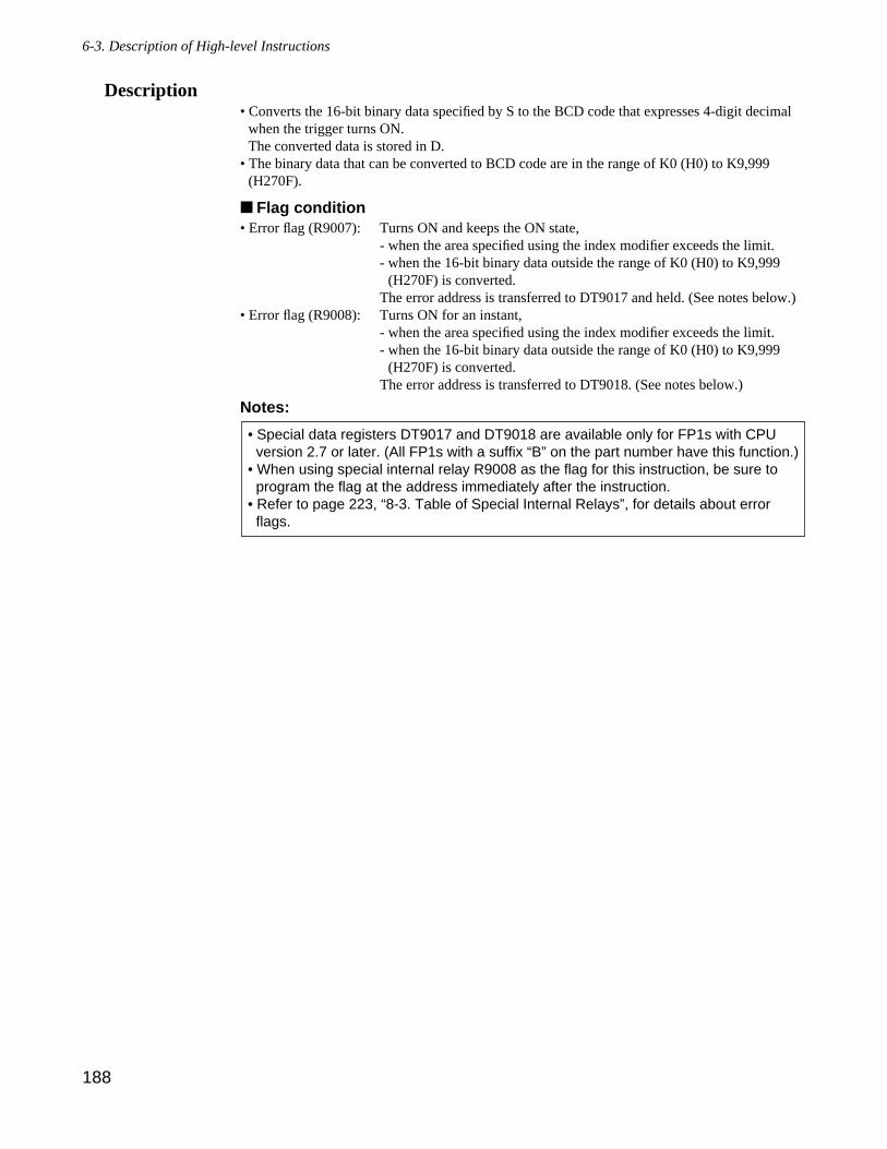
188
Description• Converts the 16-bit binary data specified by S to the BCD code that expresses 4-digit decimal
when the trigger turns ON.The converted data is stored in D.
• The binary data that can be converted to BCD code are in the range of K0 (H0) to K9,999(H270F).
Flag condition• Error flag (R9007): Turns ON and keeps the ON state,
- when the area specified using the index modifier exceeds the limit.- when the 16-bit binary data outside the range of K0 (H0) to K9,999
(H270F) is converted.The error address is transferred to DT9017 and held. (See notes below.)
• Error flag (R9008): Turns ON for an instant,- when the area specified using the index modifier exceeds the limit.- when the 16-bit binary data outside the range of K0 (H0) to K9,999
(H270F) is converted.The error address is transferred to DT9018. (See notes below.)
Notes:
• Special data registers DT9017 and DT9018 are available only for FP1s with CPUversion 2.7 or later. (All FP1s with a suffix “B” on the part number have this function.)
• When using special internal relay R9008 as the flag for this instruction, be sure toprogram the flag at the address immediately after the instruction.
• Refer to page 223, “8-3. Table of Special Internal Relays”, for details about errorflags.
6-3. Description of High-level Instructions
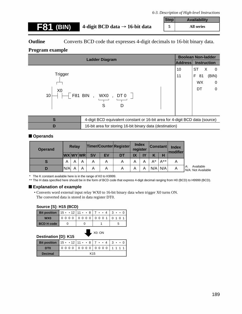
189
Outline Converts BCD code that expresses 4-digit decimals to 16-bit binary data.
Program example
Operands
* The K constant available here is in the range of K0 to K9999.** The H data specified here should be in the form of BCD code that express 4-digit decimal ranging from H0 (BCD) to H9999 (BCD).
Explanation of example• Converts word external input relay WX0 to 16-bit binary data when trigger X0 turns ON.
The converted data is stored in data register DT0.
Bit position
DT0
Decimal
0 0 0 0 0 0 0 0
11 8
0 0 0 0 1 1 1 1
3 015 • • 12 • • • •7 4• •
K15
X0: ON
Source [S]: H15 (BCD)
Destination [D]: K15
Bit position
WX0
BCD H code
0 0 0 0 0 0 0 0
11 8
0 0 0 1 0 1 0 1
3 015 • • 12 • • • •7 4• •
0 0 1 5
Timer/Counter
EV
Relay
SVWRWYWX
Operand
S A A A AA: N/A: Not Available
Register
DT
A
IYIX
A A
HK
A* A**
Constant Indexmodifier
A
Indexregister
Available
A
D N/A A A A A A A N/A N/A AA
6-3. Description of High-level Instructions
F81 (BIN) 4-digit BCD data → 16-bit dataAvailabilityStep
5 All series
S
D
4-digit BCD equivalent constant or 16-bit area for 4-digit BCD data (source)
16-bit area for storing 16-bit binary data (destination)
Ladder DiagramBoolean Non-ladder
Address Instruction
10X0
F81 BIN , WX0 , DT 0
D
Trigger
S
10
11
ST X 0
F 81 (BIN)
WX 0
DT 0
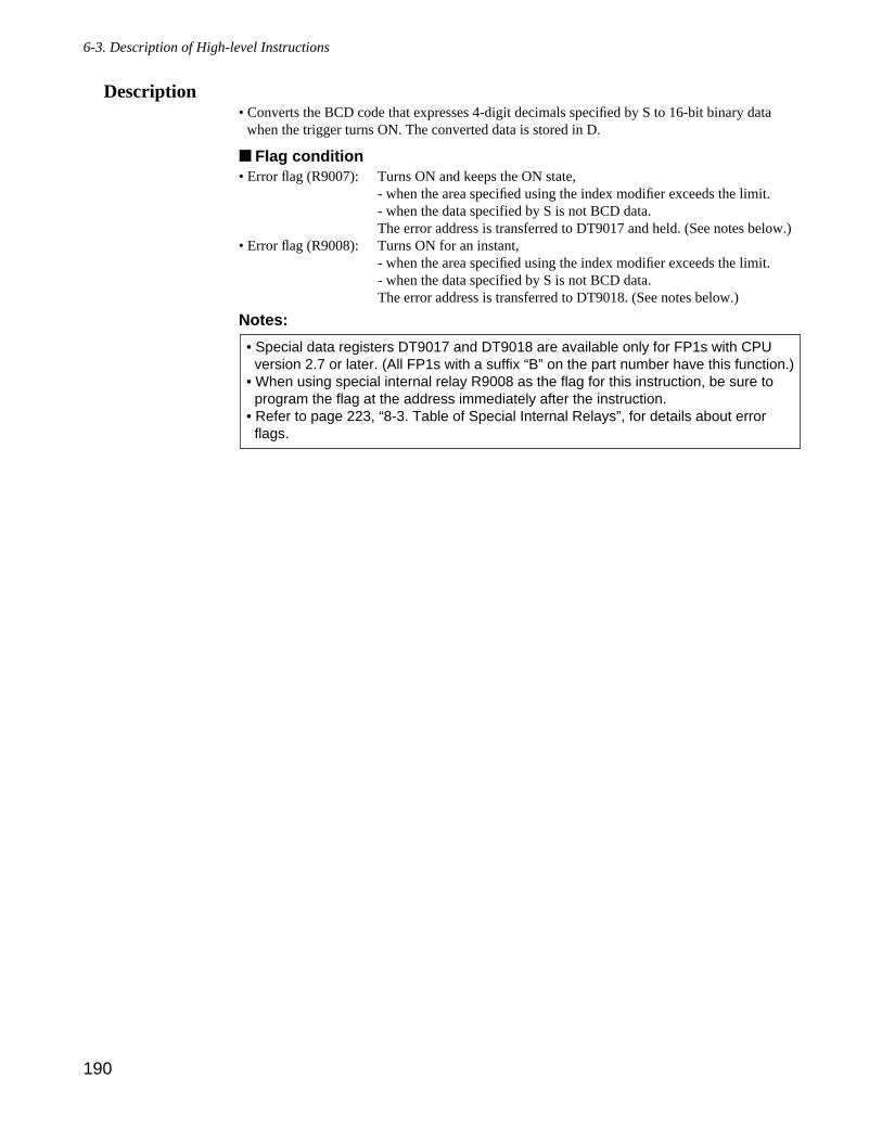
190
Description• Converts the BCD code that expresses 4-digit decimals specified by S to 16-bit binary data
when the trigger turns ON. The converted data is stored in D.
Flag condition• Error flag (R9007): Turns ON and keeps the ON state,
- when the area specified using the index modifier exceeds the limit.- when the data specified by S is not BCD data.The error address is transferred to DT9017 and held. (See notes below.)
• Error flag (R9008): Turns ON for an instant,- when the area specified using the index modifier exceeds the limit.- when the data specified by S is not BCD data.The error address is transferred to DT9018. (See notes below.)
Notes:
• Special data registers DT9017 and DT9018 are available only for FP1s with CPUversion 2.7 or later. (All FP1s with a suffix “B” on the part number have this function.)
• When using special internal relay R9008 as the flag for this instruction, be sure toprogram the flag at the address immediately after the instruction.
• Refer to page 223, “8-3. Table of Special Internal Relays”, for details about errorflags.
6-3. Description of High-level Instructions
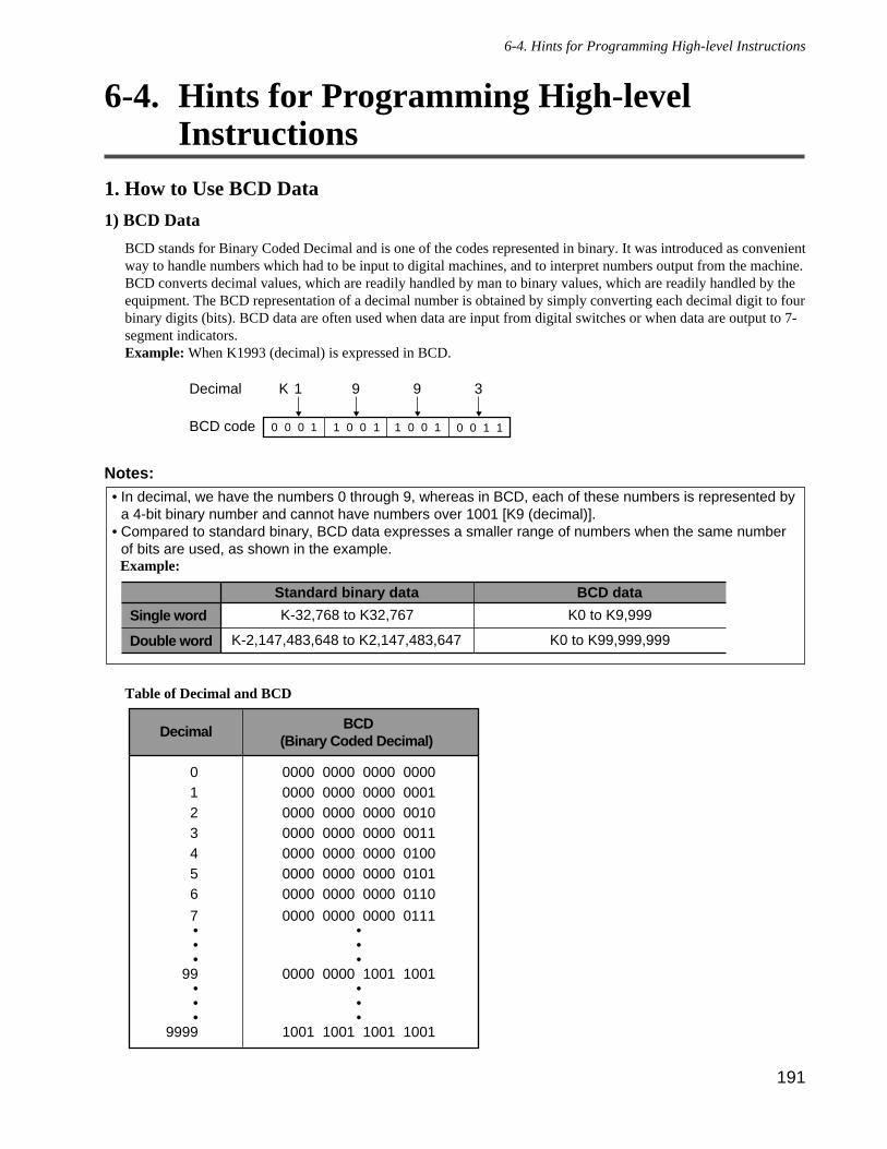
191
6-4. Hints for Programming High-level Instructions
6-4. Hints for Programming High-levelInstructions
1. How to Use BCD Data
1) BCD Data
BCD stands for Binary Coded Decimal and is one of the codes represented in binary. It was introduced as convenientway to handle numbers which had to be input to digital machines, and to interpret numbers output from the machine.BCD converts decimal values, which are readily handled by man to binary values, which are readily handled by theequipment. The BCD representation of a decimal number is obtained by simply converting each decimal digit to fourbinary digits (bits). BCD data are often used when data are input from digital switches or when data are output to 7-segment indicators.Example: When K1993 (decimal) is expressed in BCD.
Notes:
Table of Decimal and BCD
0000 0000 0000 00000000 0000 0000 00010000 0000 0000 00100000 0000 0000 00110000 0000 0000 01000000 0000 0000 01010000 0000 0000 0110
0000 0000 0000 0111•••
0000 0000 1001 1001•••
1001 1001 1001 1001
0123456
7•••
99•••
9999
Decimal BCD(Binary Coded Decimal)
• In decimal, we have the numbers 0 through 9, whereas in BCD, each of these numbers is represented bya 4-bit binary number and cannot have numbers over 1001 [K9 (decimal)].
• Compared to standard binary, BCD data expresses a smaller range of numbers when the same numberof bits are used, as shown in the example.Example:
BCD code 0 0 0 1 1 0 0 1 1 0 0 1 0 0 1 1
Decimal 1 9 9 3K
Standard binary data
Single word K-32,768 to K32,767
BCD data
K0 to K9,999
Double word K-2,147,483,648 to K2,147,483,647 K0 to K99,999,999
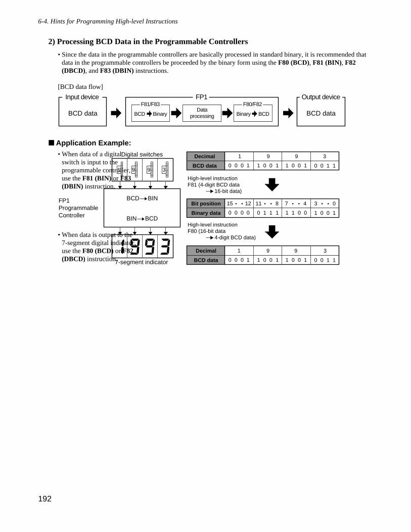
192
6-4. Hints for Programming High-level Instructions
2) Processing BCD Data in the Programmable Controllers
• Since the data in the programmable controllers are basically processed in standard binary, it is recommended thatdata in the programmable controllers be proceeded by the binary form using the F80 (BCD), F81 (BIN), F82(DBCD), and F83 (DBIN) instructions.
[BCD data flow]
Application Example:
High-level instructionF81 (4-digit BCD data 16-bit data)
Bit position
Binary data 0 0 0 0 0 1 1 1
11 8
1 1 0 0 1 0 0 1
3 015 • • 12 • • • •7 4• •
Decimal
BCD data 0 0 0 1 1 0 0 1
9
1 0 0 1 0 0 1 1
31 9
Decimal
BCD data 0 0 0 1 1 0 0 1
9
1 0 0 1 0 0 1 1
31 9
High-level instructionF80 (16-bit data 4-digit BCD data)
FP1 ProgrammableController
Digital switches
7-segment indicator
BCD BIN
BIN BCD
1 9 9 3
Input device Output deviceFP1F81/F83 F80/F82
BCD data BCD dataBCD BinaryData
processing Binary BCD
• When data of a digitalswitch is input to theprogrammable controller,use the F81 (BIN) or F83(DBIN) instruction.
• When data is output to the7-segment digital indicator,use the F80 (BCD) or F82(DBCD) instruction.
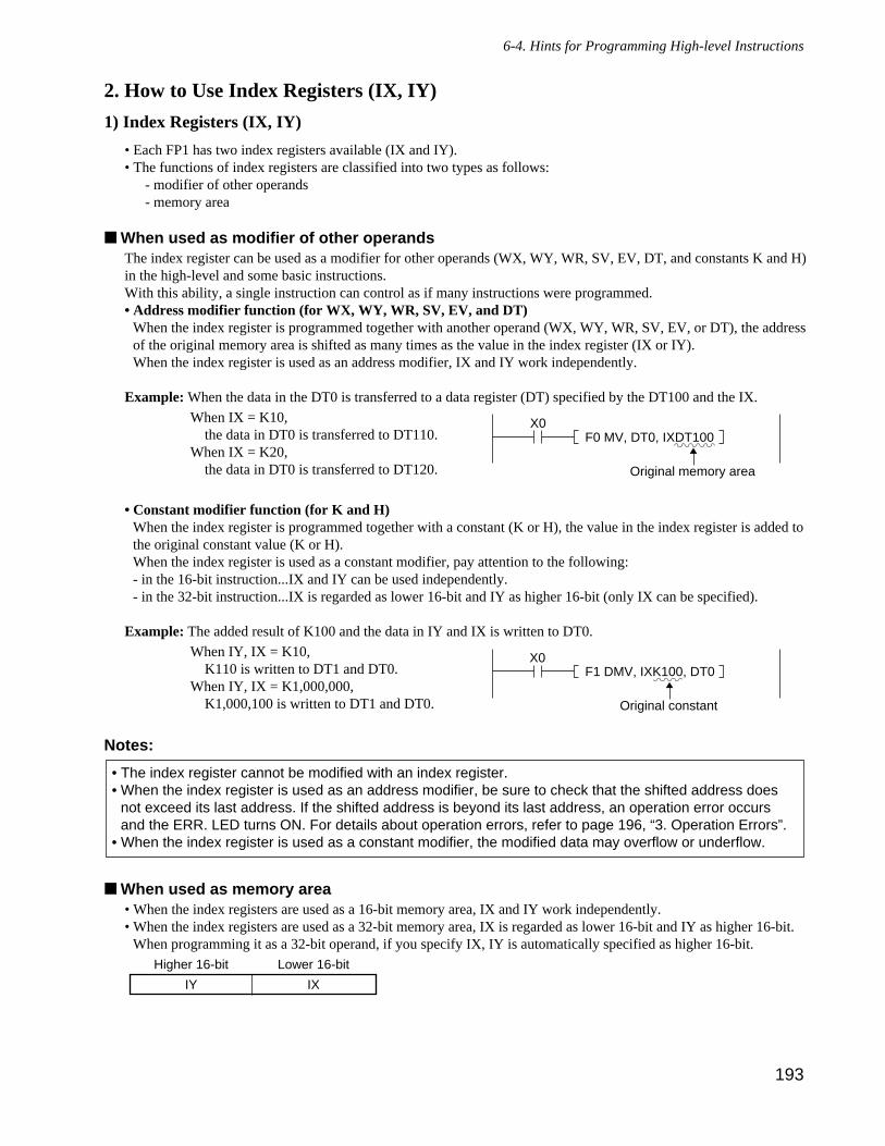
193
6-4. Hints for Programming High-level Instructions
2. How to Use Index Registers (IX, IY)
1) Index Registers (IX, IY)
• Each FP1 has two index registers available (IX and IY).• The functions of index registers are classified into two types as follows:
- modifier of other operands- memory area
When used as modifier of other operandsThe index register can be used as a modifier for other operands (WX, WY, WR, SV, EV, DT, and constants K and H)in the high-level and some basic instructions.With this ability, a single instruction can control as if many instructions were programmed.• Address modifier function (for WX, WY, WR, SV, EV, and DT)
When the index register is programmed together with another operand (WX, WY, WR, SV, EV, or DT), the addressof the original memory area is shifted as many times as the value in the index register (IX or IY).When the index register is used as an address modifier, IX and IY work independently.
Example: When the data in the DT0 is transferred to a data register (DT) specified by the DT100 and the IX.
• Constant modifier function (for K and H)When the index register is programmed together with a constant (K or H), the value in the index register is added tothe original constant value (K or H).When the index register is used as a constant modifier, pay attention to the following:- in the 16-bit instruction...IX and IY can be used independently.- in the 32-bit instruction...IX is regarded as lower 16-bit and IY as higher 16-bit (only IX can be specified).
Example: The added result of K100 and the data in IY and IX is written to DT0.
Notes:
When used as memory area• When the index registers are used as a 16-bit memory area, IX and IY work independently.• When the index registers are used as a 32-bit memory area, IX is regarded as lower 16-bit and IY as higher 16-bit.
When programming it as a 32-bit operand, if you specify IX, IY is automatically specified as higher 16-bit. Higher 16-bit Lower 16-bit
IY IX
• The index register cannot be modified with an index register.• When the index register is used as an address modifier, be sure to check that the shifted address does
not exceed its last address. If the shifted address is beyond its last address, an operation error occursand the ERR. LED turns ON. For details about operation errors, refer to page 196, “3. Operation Errors”.
• When the index register is used as a constant modifier, the modified data may overflow or underflow.
F1 DMV, IXK100, DT0
Original constant
X0When IY, IX = K10, K110 is written to DT1 and DT0.
When IY, IX = K1,000,000, K1,000,100 is written to DT1 and DT0.
X0F0 MV, DT0, IXDT100
Original memory area
When IX = K10, the data in DT0 is transferred to DT110.
When IX = K20, the data in DT0 is transferred to DT120.
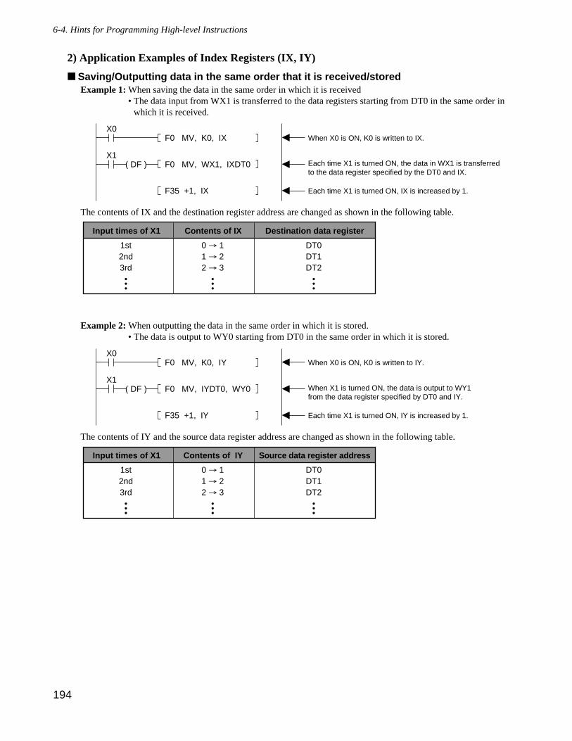
194
6-4. Hints for Programming High-level Instructions
2) Application Examples of Index Registers (IX, IY)
Saving/Outputting data in the same order that it is received/storedExample 1: When saving the data in the same order in which it is received
• The data input from WX1 is transferred to the data registers starting from DT0 in the same order inwhich it is received.
The contents of IX and the destination register address are changed as shown in the following table.
Example 2: When outputting the data in the same order in which it is stored.• The data is output to WY0 starting from DT0 in the same order in which it is stored.
The contents of IY and the source data register address are changed as shown in the following table.
0 → 11 → 22 → 3
•••
1st2nd3rd•••
Input times of X1
DT0DT1DT2
•••
Contents of IY Source data register address
X1F0 MV, IYDT0, WY0( DF )
F35 +1, IY
When X1 is turned ON, the data is output to WY1 from the data register specified by DT0 and IY.
X0F0 MV, K0, IY When X0 is ON, K0 is written to IY.
Each time X1 is turned ON, IY is increased by 1.
0 → 11 → 22 → 3
•••
1st2nd3rd•••
Input times of X1
DT0DT1DT2
•••
Contents of IX Destination data register
X1F0 MV, WX1, IXDT0( DF )
F35 +1, IX
Each time X1 is turned ON, the data in WX1 is transferred to the data register specified by the DT0 and IX.
X0F0 MV, K0, IX When X0 is ON, K0 is written to IX.
Each time X1 is turned ON, IX is increased by 1.
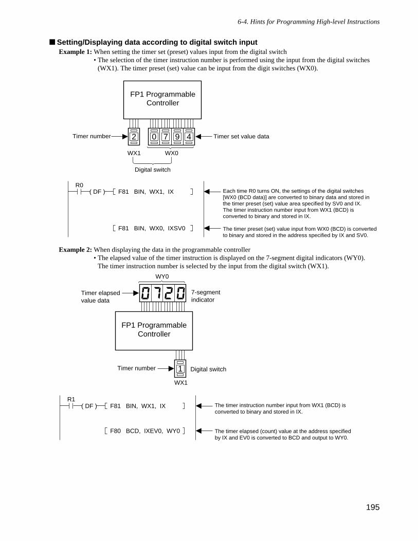
195
6-4. Hints for Programming High-level Instructions
Setting/Displaying data according to digital switch inputExample 1: When setting the timer set (preset) values input from the digital switch
• The selection of the timer instruction number is performed using the input from the digital switches(WX1). The timer preset (set) value can be input from the digit switches (WX0).
Example 2: When displaying the data in the programmable controller• The elapsed value of the timer instruction is displayed on the 7-segment digital indicators (WY0).
The timer instruction number is selected by the input from the digital switch (WX1).
1
FP1 ProgrammableController
Timer number
WX1
WY0
Digital switch
R1F81 BIN, WX1, IX( DF )
F80 BCD, IXEV0, WY0
The timer instruction number input from WX1 (BCD) is converted to binary and stored in IX.
The timer elapsed (count) value at the address specified by IX and EV0 is converted to BCD and output to WY0.
Timer elapsedvalue data
7-segment indicator
2 0 7 9 4
FP1 ProgrammableController
Timer set value dataTimer number
WX1
%%%%%%%
WX0
Digital switch
R0F81 BIN, WX1, IX( DF )
F81 BIN, WX0, IXSV0
Each time R0 turns ON, the settings of the digital switches[WX0 (BCD data)] are converted to binary data and stored in the timer preset (set) value area specified by SV0 and IX.The timer instruction number input from WX1 (BCD) is converted to binary and stored in IX.
The timer preset (set) value input from WX0 (BCD) is converted to binary and stored in the address specified by IX and SV0.
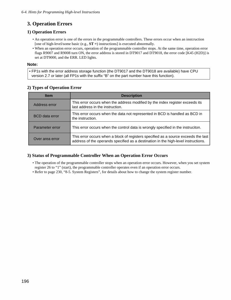
196
6-4. Hints for Programming High-level Instructions
3. Operation Errors
1) Operation Errors
• An operation error is one of the errors in the programmable controllers. These errors occur when an instcruction[one of high-level/some basic (e.g., ST =) instructions] is executed abnormally.
• When an operation error occurs, operation of the programmable controller stops. At the same time, operation errorflags R9007 and R9008 turn ON, the error address is stored in DT9017 and DT9018, the error code [K45 (H2D)] isset at DT9000, and the ERR. LED lights.
Note:
2) Types of Operation Error
3) Status of Programmable Controller When an Operation Error Occurs
• The operation of the programmable controller stops when an operation error occurs. However, when you set systemregister 26 to “1” (start), the programmable controller operates even if an operation error occurs.
• Refer to page 230, “8-5. System Registers”, for details about how to change the system register number.
Item
Address error
BCD data error
Parameter error
Over area error
Description
This error occurs when the address modified by the index register exceeds its last address in the instruction.
This error occurs when the data not represented in BCD is handled as BCD in the instruction.
This error occurs when the control data is wrongly specified in the instruciton.
This error occurs when a block of registers specified as a source exceeds the last address of the operands specified as a destination in the high-level instructions.
• FP1s with the error address storage function (the DT9017 and the DT9018 are available) have CPUversion 2.7 or later (all FP1s with the suffix “B” on the part number have this function).
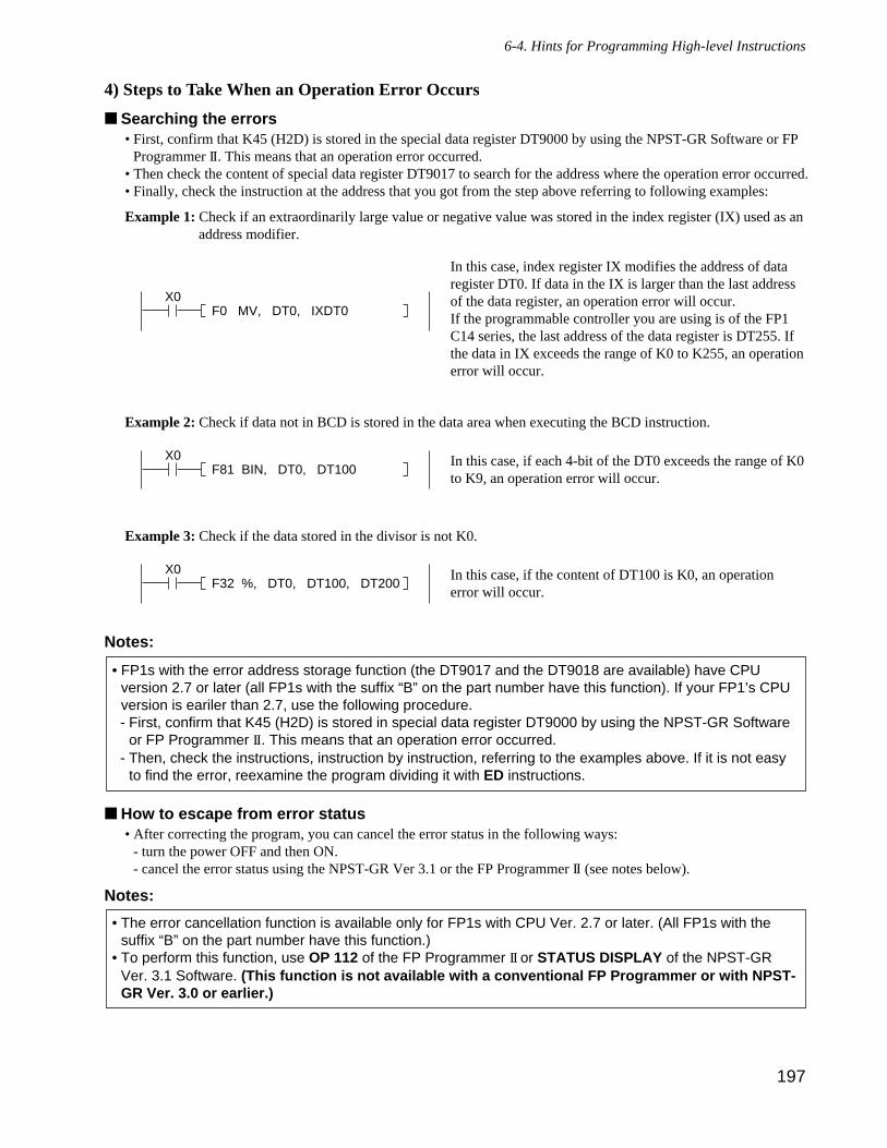
197
6-4. Hints for Programming High-level Instructions
4) Steps to Take When an Operation Error Occurs
Searching the errors• First, confirm that K45 (H2D) is stored in the special data register DT9000 by using the NPST-GR Software or FP
Programmer II. This means that an operation error occurred.• Then check the content of special data register DT9017 to search for the address where the operation error occurred. • Finally, check the instruction at the address that you got from the step above referring to following examples:
Example 1: Check if an extraordinarily large value or negative value was stored in the index register (IX) used as anaddress modifier.
Example 2: Check if data not in BCD is stored in the data area when executing the BCD instruction.
Example 3: Check if the data stored in the divisor is not K0.
Notes:
How to escape from error status• After correcting the program, you can cancel the error status in the following ways:
- turn the power OFF and then ON.- cancel the error status using the NPST-GR Ver 3.1 or the FP Programmer II (see notes below).
Notes:
• The error cancellation function is available only for FP1s with CPU Ver. 2.7 or later. (All FP1s with thesuffix “B” on the part number have this function.)
• To perform this function, use OP 112 of the FP Programmer II or STATUS DISPLAY of the NPST-GRVer. 3.1 Software. (This function is not available with a conventional FP Programmer or with NPST-GR Ver. 3.0 or earlier.)
• FP1s with the error address storage function (the DT9017 and the DT9018 are available) have CPUversion 2.7 or later (all FP1s with the suffix “B” on the part number have this function). If your FP1’s CPUversion is eariler than 2.7, use the following procedure.- First, confirm that K45 (H2D) is stored in special data register DT9000 by using the NPST-GR Software
or FP Programmer II. This means that an operation error occurred.- Then, check the instructions, instruction by instruction, referring to the examples above. If it is not easy
to find the error, reexamine the program dividing it with ED instructions.
In this case, if the content of DT100 is K0, an operationerror will occur.
X0F32 %, DT0, DT100, DT200
In this case, if each 4-bit of the DT0 exceeds the range of K0to K9, an operation error will occur.
X0F81 BIN, DT0, DT100
In this case, index register IX modifies the address of dataregister DT0. If data in the IX is larger than the last addressof the data register, an operation error will occur.If the programmable controller you are using is of the FP1C14 series, the last address of the data register is DT255. Ifthe data in IX exceeds the range of K0 to K255, an operationerror will occur.
X0F0 MV, DT0, IXDT0
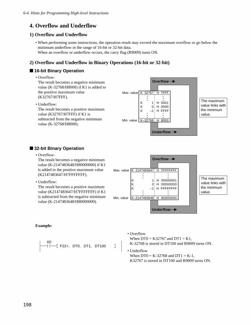
198
6-4. Hints for Programming High-level Instructions
4. Overflow and Underflow
1) Overflow and Underflow
• When performing some instructions, the operation result may exceed the maximum overflow or go below theminimum underflow in the range of 16-bit or 32-bit data.When an overflow or underflow occurs, the carry flag (R9009) turns ON.
2) Overflow and Underflow in Binary Operations (16-bit or 32-bit)
16-bit Binary Operation
32-bit Binary Operation
Example:
• OverflowWhen DT0 = K32767 and DT1 = K1, K-32768 is stored in DT100 and R9009 turns ON.
• UnderflowWhen DT0 = K-32768 and DT1 = K-1, K32767 is stored in DT100 and R9009 turns ON.
X0F22+, DT0, DT1, DT100
Underflow
Overflow
•••
H 7FFFFFFF
K 1 H 00000001K 0 H 00000000K –1 H FFFFFFFF
•••
•••
•••
K 2147483647
The maximumvalue links with the minimumvalue.
Max. value
H 80000000K–2147483648Min. value
• Overflow:The result becomes a negative minimumvalue (K-2147483648/H80000000) if K1is added to the positive maximum value(K2147483647/H7FFFFFFF).
• Underflow:The result becomes a positive maximumvalue (K2147483647/H7FFFFFFF) if K1is subtracted from the negative minimumvalue (K-2147483648/H80000000).
Underflow
Overflow
•••
H 7FFF
K 1 H 0001K 0 H 0000K –1 H FFFF
•••
K–32768 H 8000
•••
•••
K 32767
The maximumvalue links with the minimum value.
Max. value
Min. value
• Overflow:The result becomes a negative minimumvalue (K-32768/H8000) if K1 is added tothe positive maximum value(K32767/H7FFF).
• Underflow:The result becomes a positive maximumvalue (K32767/H7FFF) if K1 issubtracted from the negative minimumvalue (K-32768/H8000).
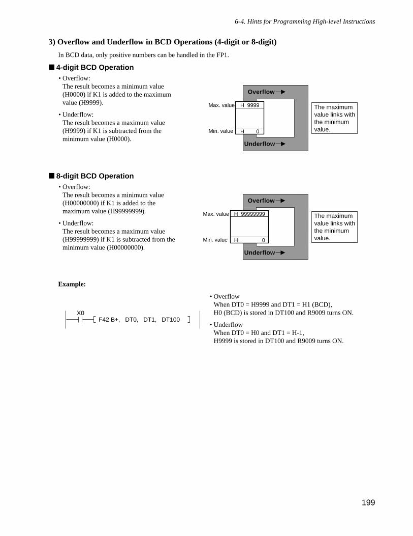
199
6-4. Hints for Programming High-level Instructions
3) Overflow and Underflow in BCD Operations (4-digit or 8-digit)
In BCD data, only positive numbers can be handled in the FP1.
4-digit BCD Operation
8-digit BCD Operation
Example:
• OverflowWhen DT0 = H9999 and DT1 = H1 (BCD), H0 (BCD) is stored in DT100 and R9009 turns ON.
• UnderflowWhen DT0 = H0 and DT1 = H-1, H9999 is stored in DT100 and R9009 turns ON.
X0F42 B+, DT0, DT1, DT100
Underflow
Overflow
H 99999999
H 0
The maximumvalue links with the minimumvalue.
Max. value
Min. value
• Overflow:The result becomes a minimum value(H00000000) if K1 is added to themaximum value (H99999999).
• Underflow:The result becomes a maximum value(H99999999) if K1 is subtracted from theminimum value (H00000000).
Underflow
Overflow
H 9999
H 0
The maximumvalue links with the minimumvalue.
Max. value
Min. value
• Overflow:The result becomes a minimum value(H0000) if K1 is added to the maximumvalue (H9999).
• Underflow:The result becomes a maximum value(H9999) if K1 is subtracted from theminimum value (H0000).

200
CHAPTER 7
TROUBLESHOOTING
7-1. Self-diagnostic Function .....................................................2021. Operation Monitor LEDs When an Error Occurs...........2022. Operation Status When an Error Occurs ........................203
1) Duplicated Output Error (Total-check Error) ......2032) Battery Error (Self-diagnostic Error)...................2033) Operation Error (Self-diagnostic Error)...............203
7-2. Troubleshooting...................................................................2041. Points to be Checked When an Error Occurs .................204
When an ERR. LED is ON ..................................205 When an ALARM LED is ON.............................209 When all LEDs are OFF ......................................210 Diagnosing output malfunction............................211 When “PLC=COMM. ERR” is displayed
on the NPST-GR screen .......................................214 When “PROTECT ERROR” is displayed ...........215
7-3. Maintenance ........................................................................2161. Preventive Maintenance .................................................2162. Replacement of Backup Battery .....................................216
1) Battery Life..........................................................2162) How to Replace Backup Battery..........................217
3. Removable Terminal ......................................................217
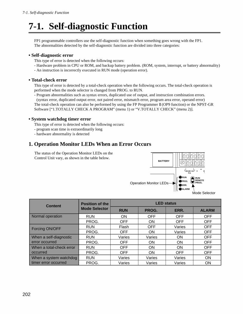
202
7-1. Self-diagnostic Function
7-1. Self-diagnostic FunctionFP1 programmable controllers use the self-diagnostic function when something goes wrong with the FP1. The abnormalities detected by the self-diagnostic function are divided into three categories:
• Self-diagnostic errorThis type of error is detected when the following occurs:- Hardware problem in CPU or ROM, and backup battery problem. (ROM, system, interrupt, or battery abnormality)- An instruction is incorrectly executed in RUN mode (operation error).
• Total-check errorThis type of error is detected by a total-check operation when the following occurs. The total-check operation isperformed when the mode selector is changed from PROG. to RUN. - Program abnormalities such as syntax errors, duplicated use of output, and instruction combination errors.
(syntax error, duplicated output error, not paired error, mismatch error, program area error, operand error)The total-check operation can also be performed by using the FP Programmer II (OP9 function) or the NPST-GRSoftware [“1.TOTALLY CHECK A PROGRAM” (menu 1) or “V.TOTALLY CHECK” (menu 2)].
• System watchdog timer errorThis type of error is detected when the following occurs:- program scan time is extraordinarily long- hardware abnormality is detected
1. Operation Monitor LEDs When an Error Occurs
Content
Normal operation
Forcing ON/OFF
RUNPROG.RUNPROG.RUNPROG.RUNPROG.RUNPROG.
RUN
ONOFFFlashOFF
VariesOFFOFFOFF
VariesVaries
PROG.
OFFONOFFON
VariesONONON
VariesVaries
ERR.
OFFOFF
VariesVaries
ONONONOFF
VariesVaries
ALARM
OFFOFFOFFOFFOFFOFFOFFOFFONON
Position of theMode Selector
When a self-diagnostic error occurredWhen a total-check error occurredWhen a system watchdog timer error occurred
LED status
COM0
COM1 2100 240 V AC
F.G.
RUNREMOTEPROG.
RUN
PROG.
ERR.
ALARM
BATTERY
0 1OU
TP
UT
Y
(24V
DC
)
Operation Monitor LEDs
Mode Selector
The status of the Operation Monitor LEDs on theControl Unit vary, as shown in the table below.
203
7-1. Self-diagnostic Function
2. Operation Status When an Error OccursWhen an error occurs, the FP1 usually stops operating. However, regarding duplicated output errors, a backup batteryabnormality, and operation errors, you can continue operation by changing the system register settings.
1) Duplicated Output Error (Total-check Error)
• If the duplicated use of output is detected, the FP1 stops operating and the ERR. LED turns ON.When you change system register 20 settings using the FP Programmer II or NPST-GR Software, duplicated outputis not regarded as an error and the FP1 continues to operate. In this case, the ERR. LED does not turn ON.
Duplicated output error: system register 20 (K1 or ENAB)[FP Programmer II: K0 (stops operation), K1 (continues operation)][NPST-GR Ver.3.1: DISA (stops operation), ENAB (continues operation)]
2) Battery Error (Self-diagnostic Error)
• If the voltage of the backup battery lowers or if the backup battery disconnects, the ERR. LED turns ON. Battery error: system register 4 (K1 or NO)
[FP Programmer II: K0 (stops operation), K1 (continues operation)][NPST-GR Ver. 3.1: YES (stops operation), NO (continues operation)]
Notes:
3) Operation Error (Self-diagnostic Error)
• When an instruction [high-level and some basic (e.g., ST=) instructions] executes abnormally, an operation erroroccurs. When an operation error occurs, operation of the programmable controller stops and the ERR. LED turnsON. However, when you change system register 26 settings using the FP Programmer II or NPST-GR Software (Ver.3.1or later), the FP1 continues to operate. In this case, even if the FP1 continues to operate, this is regarded as an errorand the ERR. LED stays ON.
Operation error: system register 26 [FP Programmer II: K0 (stops operation), K1 (continues operation)][NPST-GR Ver.3.1: STOP (stops operation), STRT (continues operation)]
• C14 and C16 series FP1s do not have a backup battery. Battery errors occur only for C24, C40, C52, andC72 series FP1s.
• FP1s with the battery error disregarding function have CPU version 2.7 or later (all FP1s with a suffix “B”on the part number have this function).
204
7-2. Troubleshooting
7-2. Troubleshooting
1. Points to be Checked When an Error OccursWhen an abnormality is detected, check the following points.
• If the ERR. LED is turned ON,refer to page 205, When an ERR. LED is ON.
• If the ALARM LED is turned ON,refer to page 209, When an ALARM LED is ON.
• If the all LEDs are turned OFF,refer to page 210, When all LEDs are OFF.
• If the output do not work,refer to page 211, Diagnosing output malfunction.
• If the communication error is detected by the NPST-GR Software,refer to page 214, When “PLC = COMM. ERR” is displayed on the NPST-GR screen.
• If the protect error is detected by the programming tool,refer to page 215, When “PROTECT ERROR” is displayed.
Note:
• Check the entire system including peripheral devices, referring the following:- Observe what is happening. - Check for error repetition.- Check the status of indicators.- Check that power is properly supplied to the programmable controller.- Check whether the trouble detected is in the programmable controller or in other devices.- Check whether the trouble detected is in the I/O section or other parts.- Check whether there is problem with the program or not.
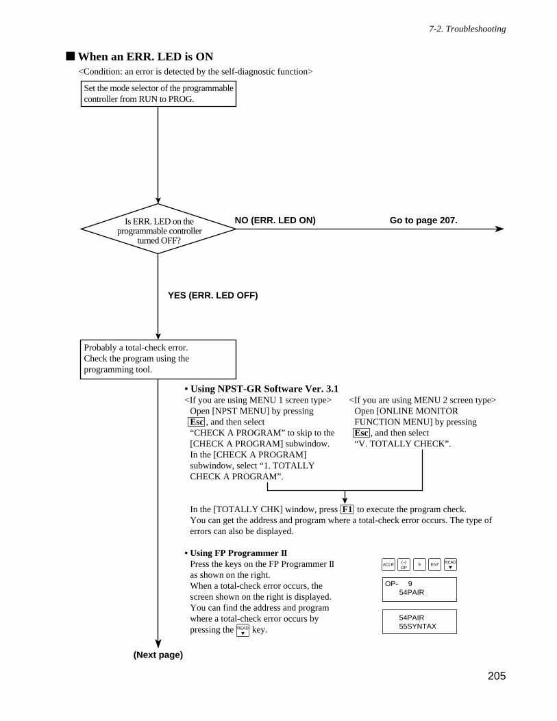
205
7-2. Troubleshooting
When an ERR. LED is ON<Condition: an error is detected by the self-diagnostic function>
Set the mode selector of the programmable controller from RUN to PROG.
Is ERR. LED on the programmable controller
turned OFF?
Probably a total-check error. Check the program using the programming tool.
YES (ERR. LED OFF)
NO (ERR. LED ON)
• Using NPST-GR Software Ver. 3.1<If you are using MENU 1 screen type>
Open [NPST MENU] by pressing Esc , and then select “CHECK A PROGRAM” to skip to the [CHECK A PROGRAM] subwindow.In the [CHECK A PROGRAM] subwindow, select “1. TOTALLY CHECK A PROGRAM”.
In the [TOTALLY CHK] window, press F1 to execute the program check.You can get the address and program where a total-check error occurs. The type of errors can also be displayed.
• Using FP Programmer IIPress the keys on the FP Programmer II as shown on the right.When a total-check error occurs, the screen shown on the right is displayed.You can find the address and program where a total-check error occurs by pressing the key.
<If you are using MENU 2 screen type>Open [ONLINE MONITOR FUNCTION MENU] by pressing Esc , and then select “V. TOTALLY CHECK”.
Go to page 207.
9(–)OP
ACLR ENTREAD
OP- 9 54PAIR
54PAIR55SYNTAX
(Next page)
READ
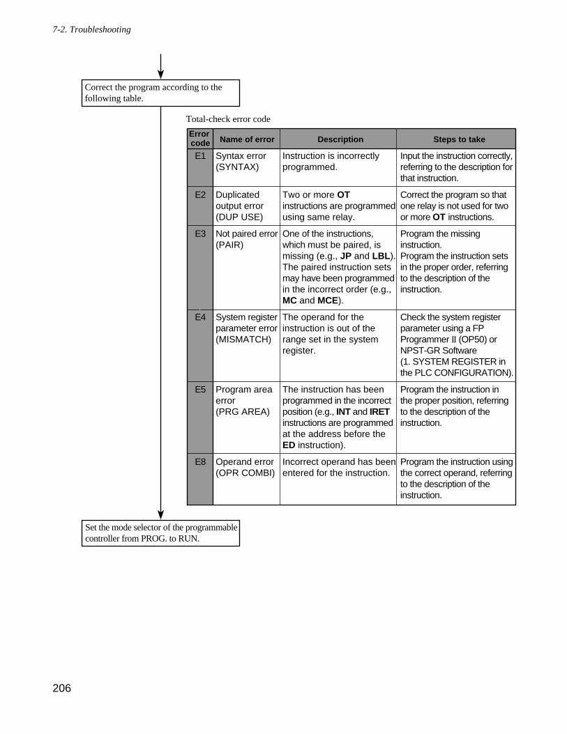
206
7-2. Troubleshooting
Total-check error code
Correct the program according to the following table.
Error code
E1
E2
E3
E4
E5
E8
Name of error
Syntax error (SYNTAX)
Duplicated output error (DUP USE)
Not paired error (PAIR)
System register parameter error (MISMATCH)
Program area error (PRG AREA)
Operand error (OPR COMBI)
Description
Instruction is incorrectly programmed.
Two or more OT instructions are programmed using same relay.
One of the instructions, which must be paired, is missing (e.g., JP and LBL). The paired instruction sets may have been programmed in the incorrect order (e.g., MC and MCE).
The operand for the instruction is out of the range set in the system register.
The instruction has been programmed in the incorrect position (e.g., INT and IRET instructions are programmed at the address before the ED instruction).
Incorrect operand has been entered for the instruction.
Steps to take
Input the instruction correctly, referring to the description forthat instruction.
Correct the program so that one relay is not used for two or more OT instructions.
Program the missing instruction.Program the instruction sets in the proper order, referring to the description of the instruction.
Check the system register parameter using a FP Programmer II (OP50) or NPST-GR Software (1. SYSTEM REGISTER in the PLC CONFIGURATION).
Program the instruction in the proper position, referring to the description of the instruction.
Program the instruction using the correct operand, referring to the description of the instruction.
Set the mode selector of the programmable controller from PROG. to RUN.
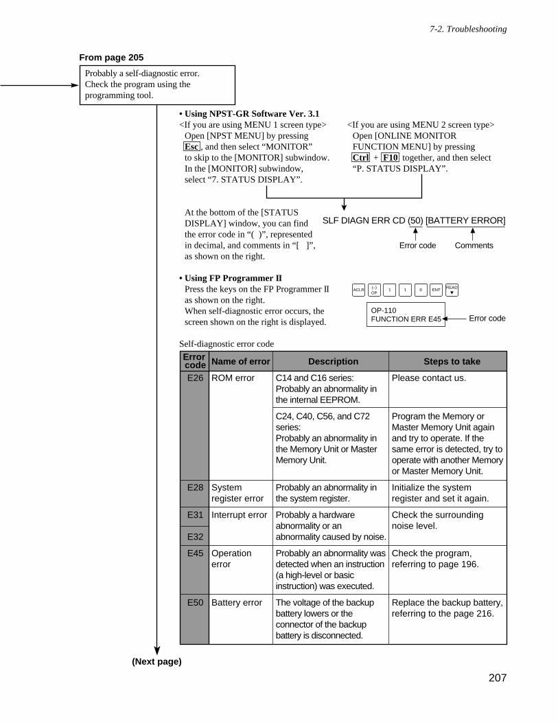
207
7-2. Troubleshooting
Probably a self-diagnostic error. Check the program using the programming tool.
• Using NPST-GR Software Ver. 3.1 <If you are using MENU 1 screen type>
Open [NPST MENU] by pressing Esc , and then select “MONITOR” to skip to the [MONITOR] subwindow.In the [MONITOR] subwindow, select “7. STATUS DISPLAY”.
At the bottom of the [STATUS DISPLAY] window, you can find the error code in “( )”, represented in decimal, and comments in “[ ]”, as shown on the right.
• Using FP Programmer IIPress the keys on the FP Programmer II as shown on the right.When self-diagnostic error occurs, the screen shown on the right is displayed.
Self-diagnostic error code
<If you are using MENU 2 screen type>Open [ONLINE MONITOR FUNCTION MENU] by pressing Ctrl + F10 together, and then select “P. STATUS DISPLAY”.
Error codeE26
E28
E31
E32
E45
E50
Name of error
ROM error
System register error
Interrupt error
Operation error
Battery error
Description
C14 and C16 series: Probably an abnormality in the internal EEPROM.
C24, C40, C56, and C72 series:Probably an abnormality in the Memory Unit or Master Memory Unit.
Probably an abnormality in the system register.
Probably a hardware abnormality or an abnormality caused by noise.
Probably an abnormality was detected when an instruction (a high-level or basic instruction) was executed.
The voltage of the backup battery lowers or the connector of the backup battery is disconnected.
Steps to take
Please contact us.
Program the Memory or Master Memory Unit again and try to operate. If the same error is detected, try to operate with another Memory or Master Memory Unit.
Initialize the system register and set it again.
Check the surroundingnoise level.
Check the program, referring to page 196.
Replace the backup battery, referring to the page 216.
1(–)OP
ACLR 1
OP-110FUNCTION ERR E45
SLF DIAGN ERR CD (50) [BATTERY ERROR]
Error code Comments
0 ENTREAD
Error code
(Next page)
From page 205
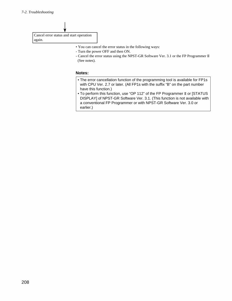
208
7-2. Troubleshooting
Notes:
• The error cancellation function of the programming tool is available for FP1swith CPU Ver. 2.7 or later. (All FP1s with the suffix “B” on the part numberhave this function.)
• To perform this function, use “OP 112” of the FP Programmer II or [STATUSDISPLAY] of NPST-GR Software Ver. 3.1. (This function is not available witha conventional FP Programmer or with NPST-GR Software Ver. 3.0 orearlier.)
Cancel error status and start operation again.
• You can cancel the error status in the following ways:- Turn the power OFF and then ON.- Cancel the error status using the NPST-GR Software Ver. 3.1 or the FP Programmer II (See notes).
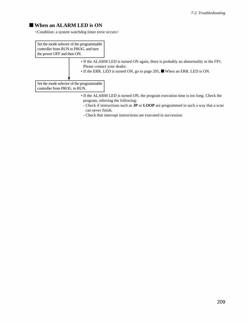
When an ALARM LED is ON<Condition: a system watchdog timer error occurs>
• If the ALARM LED is turned ON again, there is probably an abnormality in the FP1.Please contact your dealer.
• If the ERR. LED is turned ON, go to page 205, When an ERR. LED is ON.
• If the ALARM LED is turned ON, the program execution time is too long. Check theprogram, referring the following:- Check if instructions such as JP or LOOP are programmed in such a way that a scan
can never finish.- Check that interrupt instructions are executed in succession.
Set the mode selector of the programmablecontroller from PROG. to RUN.
Set the mode selector of the programmablecontroller from RUN to PROG. and turnthe power OFF and then ON.
209
7-2. Troubleshooting
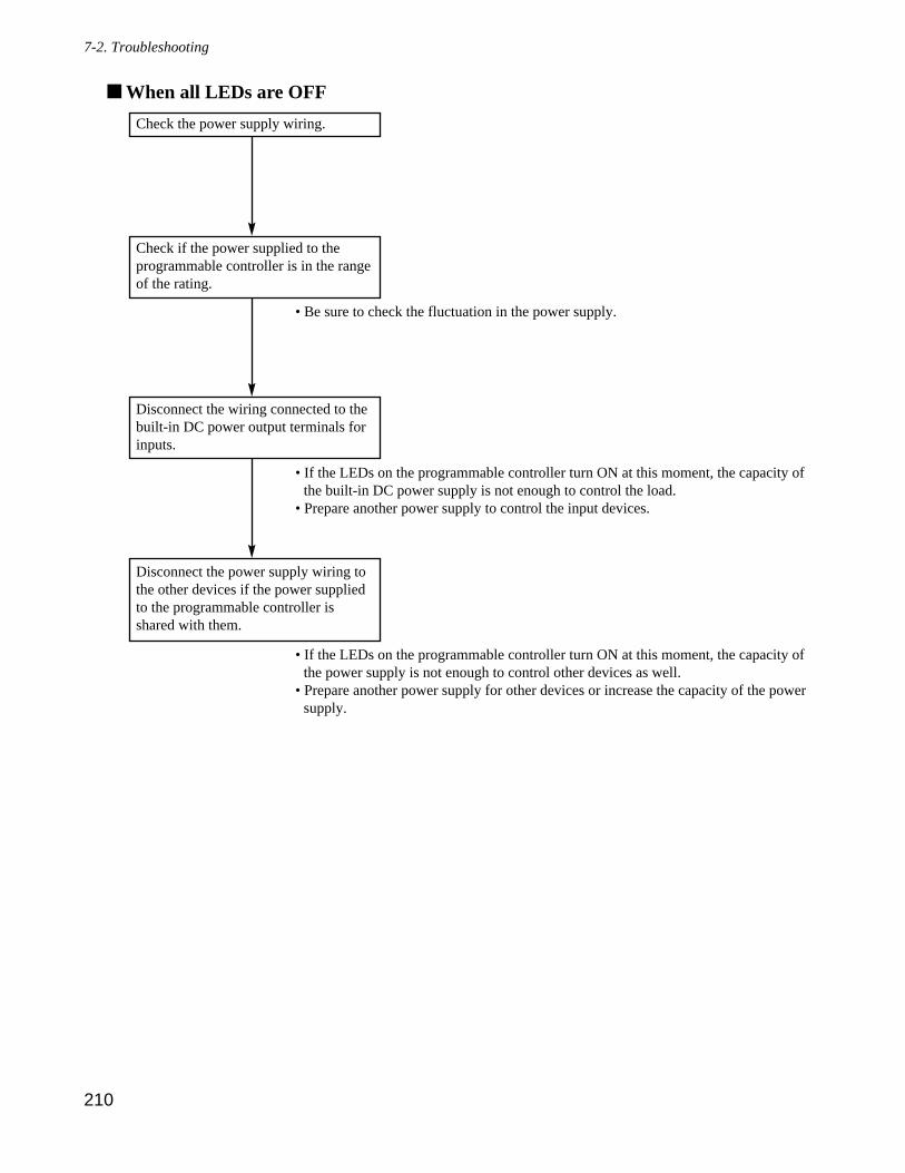
When all LEDs are OFF
• Be sure to check the fluctuation in the power supply.
• If the LEDs on the programmable controller turn ON at this moment, the capacity ofthe built-in DC power supply is not enough to control the load.
• Prepare another power supply to control the input devices.
• If the LEDs on the programmable controller turn ON at this moment, the capacity ofthe power supply is not enough to control other devices as well.
• Prepare another power supply for other devices or increase the capacity of the powersupply.
Disconnect the power supply wiring tothe other devices if the power suppliedto the programmable controller isshared with them.
Disconnect the wiring connected to thebuilt-in DC power output terminals forinputs.
Check if the power supplied to theprogrammable controller is in the rangeof the rating.
Check the power supply wiring.
210
7-2. Troubleshooting
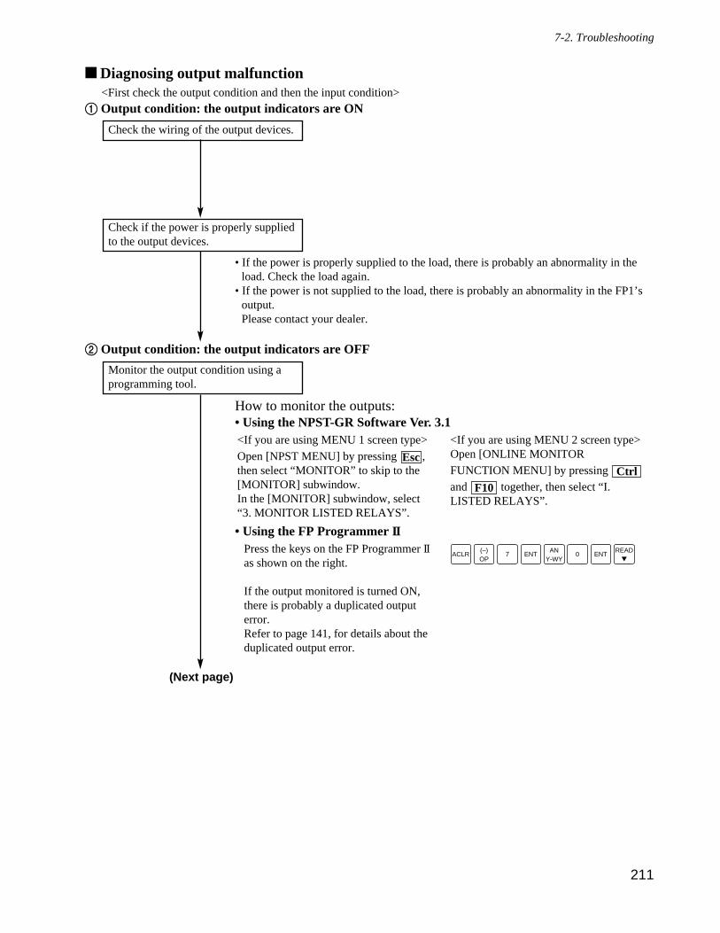
Diagnosing output malfunction<First check the output condition and then the input condition>
11 Output condition: the output indicators are ON
• If the power is properly supplied to the load, there is probably an abnormality in theload. Check the load again.
• If the power is not supplied to the load, there is probably an abnormality in the FP1’soutput. Please contact your dealer.
22 Output condition: the output indicators are OFF
How to monitor the outputs:• Using the NPST-GR Software Ver. 3.1
• Using the FP Programmer II
ACLR(–)OP
7 ENT ENTAN
Y-WY0
READ
Press the keys on the FP Programmer IIas shown on the right.
If the output monitored is turned ON,there is probably a duplicated outputerror.Refer to page 141, for details about theduplicated output error.
<If you are using MENU 1 screen type>Open [NPST MENU] by pressing ,then select “MONITOR” to skip to the[MONITOR] subwindow.In the [MONITOR] subwindow, select“3. MONITOR LISTED RELAYS”.
<If you are using MENU 2 screen type>Open [ONLINE MONITORFUNCTION MENU] by pressing and together, then select “I.LISTED RELAYS”.
F10Ctrl
Esc
Monitor the output condition using aprogramming tool.
Check if the power is properly suppliedto the output devices.
Check the wiring of the output devices.
211
7-2. Troubleshooting
(Next page)
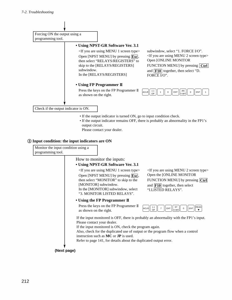
• Using NPST-GR Software Ver. 3.1
• Using FP Programmer II
33 Input condition: the input indicators are ON
How to monitor the inputs:• Using NPST-GR Software Ver. 3.1
• Using the FP Programmer II
If the input monitored is OFF, there is probably an abnormality with the FP1’s input. Please contact your dealer.If the input monitored is ON, check the program again.Also, check for the duplicated use of output or the program flow when a controlinstruction such as MC or JP is used. Refer to page 141, for details about the duplicated output error.
ACLR(–)OP
7 ENT ENTST
X-WX0
READ
Press the keys on the FP Programmer IIas shown on the right.
<If you are using MENU 1 screen type>Open [NPST MENU] by pressing ,then select “MONITOR” to skip to the[MONITOR] subwindow.In the [MONITOR] subwindow, select“3. MONITOR LISTED RELAYS”.
<If you are using MENU 2 screen type>Open the [ONLINE MONITORFUNCTION MENU] by pressing and together, then select“I.LISTED RELAYS”.
F10Ctrl
Esc
Monitor the input condition using aprogramming tool.
• If the output indicator is turned ON, go to input condition check.• If the output indicator remains OFF, there is probably an abnormality in the FP1’s
output circuit.Please contact your dealer.
Check if the output indicator is ON.
ACLR(–)OP
1 0 ENTENTAN
Y-WY10
Press the keys on the FP Programmer IIas shown on the right.
<If you are using MENU 1 screen type>Open [NPST MENU] by pressing ,then select “RELAYS/REGISTERS” toskip to the [RELAYS/REGISTERS]subwindow.In the [RELAYS/REGISTERS]
subwindow, select “1. FORCE I/O”.<If you are using MENU 2 screen type>Open [ONLINE MONITORFUNCTION MENU] by pressing and together, then select “D.FORCE I/O”.
F10Ctrl
Esc
Forcing ON the output using aprogramming tool.
212
7-2. Troubleshooting
(Next page)
44 Input condition: the input indicators are OFF
• If the power is properly supplied to the input terminal, there is probably anabnormality in the FP1’s internal circuit. Please contact your dealer.
• If the power is not properly supplied to the input terminal, there is probably anabnormality in the input device or input power supply. Check the wiring again.
Check that the power is properlysupplied to the input terminals.
Check the wiring of the input devices.
213
7-2. Troubleshooting
When “PLC = COMM. ERR” is displayed on the NPST-GR screen
• NPST-GR baud rate setting
In this window, you can find the baud rate as shown below:TRNS RATE (bps) [19200 / 9600 / 4800 / 2400 / 1200 / 600 / 300 ]
Select a baud rate (19200 or 9600), press the key and select “SAVE DISK ? YES”to register this change onto the disk.
Note:
• Confirm the cable specifications, referring to the following examples:
• Confirm the RS422/232C adapter pin setting, referring to the following:
When shipped from the factory, the pins are set as shown in 1.
Confirm the setting of the personalcomputer referring to the manual foryour computer.
CN1
RS232C Connector
AB
CS
RS
AB
RD AB
SDAB
: Denotes the pin position.
1When the cables described above are used CN1
RS232C Connector
AB
CS
RS
AB
RD AB
SDAB2When a cable with reverse wiring specifications is used
Pin No.1234567820
AbbreviationFG
SD (TXD)RD (RXD)RS (RTS)CS (CTS)DR (DSR)
SGCD (DCD)ER (DTR)
Connected toRS422/232C Adapter
(25 pins male)Pin No.
123456789
AbbreviationCD (DCD)RD (RXD)SD (TXD)ER (DTR)
SGDR (DSR)RS (RTS)CS (CTS)
RI (CI)
Connected toIBM PC-AT
(9 pins female)
RS422/232C Adapter & IBM PC-AT (9 pins)
Pin No.12345678
20
AbbreviationFG
SD (TXD)RD (RXD)RS (RTS)CS (CTS)DR (DSR)
SGCD (DCD)ER (DTR)
Connected toRS422/232C Adapter
(25 pins male)Pin No.
12345678
20
AbbreviationFG
SD (TXD)RD (RXD)RS (RTS)CS (CTS)DR (DSR)
SGCD (DCD)ER (DTR)
Connected toPersonal Computer
(25 pins male)
RS422/232C Adapter & Personal Computer (25 pins)
Check the cable and the RS422/232Cadapter.
• Even when both the NPST-GR and FP1 are set to 19200 bps, sometimes a computercannot communicate with the FP1 properly at 19200 bps. If this happens, changeboth of their settings to 9,600 bps and try again.
19200
9600
19200bps
Baud rate selector
9600bps
• FP1 baud rate settingSet the baud rate using the baud rateselector inside the FP1 Control Unit.
F1
<If you are using MENU 1 screen type>Open [NPST MENU] by pressing the
key, then select “NPSTCONFIGURATION” to skip to the[NPST CONFIGURATION]subwindow. In the [NPSTCONFIGURATION] subwindow, select“1. NPST CONFIGURATION”.
<If you are using MENU 2 screen type>Open [NPST FUNCTION MENU] bypressing the key, then select “Z.NPST CONFIGURATION”.
EscEsc
Check if the baud rate settings of theFP1 and NPST-GR are the same.
214
7-2. Troubleshooting
When “PROTECT ERROR” is displayed 11When memory unit (EPROM) or master memory unit (EEPROM) is installed in the programmable
controllerIf memory unit (EPROM) or master memory unit (EEPROM) is installed on the programmable controller, theprogram cannot be modified.Proceed with program modification as follows:
22When a password is set for the programmable controller
• Using NPST-GR Software Ver. 3.1
In the [SET PLC PASSWORD] window, select ENAB and press the key to setthe mode of the password setting to enable saving and loading of the program.
• Using FP Programmer II
ACLR(–)OP
7 2 ENT 1
1 3 4 WRT2(HELP)
CLR
Password (e.g., “1234”)
Press the keys on the FP Programmer IIas shown on the right.
Enter
<If you are using MENU 1 screen type>Open [NPST MENU] by pressing the
key, and then select “PLCCONFIGURATION” to skip to the [PLCCONFIGURATION] subwindow.In the [PLC CONFIGURATION]subwindow, select “5. SET PLCPASSWORD”.
<If you are using MENU 2 screen type>Open [NPST FUNCTION MENU] bypressing the key in the ONLINEmode, and then select “SET PLCPASSWORD”.
EscEsc
Change the setting of the passwordusing a programming tool.
Save the modified program to thememory unit (EPROM) or mastermemory unit (EEPROM) and startoperation again.(Refer to page 86, “4-5. Memory UnitCreation and ROM Operation”, fordetails about ROM operation.)
Modify the program using aprogramming tool.
First, turn OFF the power of theprogrammable controller.Then, remove the memory unit(EPROM) or the master memory unit(EEPROM) from the programmablecontroller.
215
7-2. Troubleshooting
216
7-3. Maintenance
7-3. MaintenanceAlthough programmable controllers have been designed in such a way to minimize maintenance and offer trouble-free operation, several maintenance aspects should be taken into consideration. If preventive maintenance isperformed periodically, you will minimize the possibility of system malfunctions.
1. Preventive Maintenance
2. Replacement of Backup Battery
1) Battery Life
• When the voltage of the backup battery lowers, special internal relays R9005 and R9006 turn ON and the ERR.LED turns ON. Replace the backup battery within a month after this battery error is detected.
Caution:
• Never throw batteries into a fire. Do not dispose of them in trash that will be incinerated.
Control Units
C24, C40, C56, and C72 standard types
C24C, C40C, C56C, and C72C types
Battery life (at 25˚C/77˚F ambient temperature)
Approx. 53,000 hours (approx. 6 years)
Approx. 27,000 hours (approx. 3 years)
Item
Power supply voltage
Environment
I/O power supply voltage
Mounting condition
Backup battery
Check point
Check the power supply condition by measuring it at the power supply terminals of the programmable controller.
Ambient temperature (e.g., temperature in the control box)Ambient humidity (e.g., humidity in the control box)Is dirt and dust present?
Measure the operating voltage at the input/output terminals.
Are all of the units firmly fixed in place?Are all the terminal screws securely tightened?Are wiring and terminals being properly kept?
Is the backup battery being periodically replaced?
•
•
•
•
•
••
•
•
Criteria for judgement
AC type: 85 V AC to 264 V AC
DC type: 20.4 V DC to 26.4 V DC
Ambient temperature: 0˚C to 55˚C/32˚F to 131˚F
Ambient humidity: 30 % to 85 % RH (no condensation)
Refer to page 43.
Refer to the following. (Part number: AFP1801)
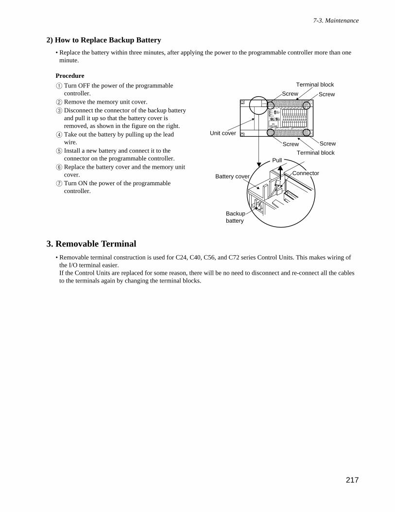
2) How to Replace Backup Battery
• Replace the battery within three minutes, after applying the power to the programmable controller more than oneminute.
Procedure
3. Removable Terminal• Removable terminal construction is used for C24, C40, C56, and C72 series Control Units. This makes wiring of
the I/O terminal easier. If the Control Units are replaced for some reason, there will be no need to disconnect and re-connect all the cablesto the terminals again by changing the terminal blocks.
COM0
COM1
COM2
COM3
COM4
COM5
COM6
COM7
+ -24V DC
F.G.
COMF
89
EAB
CD(+)-
COM7
01
623
45(+)-
RUNREMOTEPROG.
V0
max.min.
RUN
PROG.
ERR.
ALRAM
BATTERY
V1
max.
PCFP1-C24
24V DC+
-
min.
Battery cover
Backupbattery
Connector
Screw
Terminal block
Screw
Screw
Terminal block
Screw
Unit cover
Pull
1 Turn OFF the power of the programmablecontroller.
2 Remove the memory unit cover. 3 Disconnect the connector of the backup battery
and pull it up so that the battery cover isremoved, as shown in the figure on the right.
4 Take out the battery by pulling up the leadwire.
5 Install a new battery and connect it to theconnector on the programmable controller.
6 Replace the battery cover and the memory unitcover.
7 Turn ON the power of the programmablecontroller.
217
7-3. Maintenance

218
CHAPTER 8
APPENDIX
8-1. FP1 I/O Allocation Table ....................................................2208-2. Table of Memory Areas.......................................................2218-3. Table of Special Internal Relays..........................................2238-4. Table of Special Data Registers...........................................2268-5. System Registers .................................................................230
1. What are System Registers .............................................2302. Table of System Registers ..............................................232
8-6. Versions of Programming Tools ..........................................2411. Differences Between NPST-GR Ver. 2.4 and 3.1 ...........2412. Differences Between the FP Programmer
and FP Programmer II .....................................................2438-7. FP1 CPU Version 2.7 ..........................................................2458-8. FP1 Modem Communication ..............................................246
1. Using the Programming Tool Port (RS422) ...................2462. Using the RS232C Port .................................................2483. System Configuration: One Computer and Two or More
Programmable Controllers..............................................2514. NPST-GR Settings ..........................................................252
8-9. Terminology ........................................................................2548-10.Product Types ......................................................................260
1. Control Units ..................................................................2602. Expansion Units..............................................................2623. Intelligent Units ..............................................................2634. Link Units .......................................................................2635. Programming Tools ........................................................2636. Maintenance Parts ..........................................................265
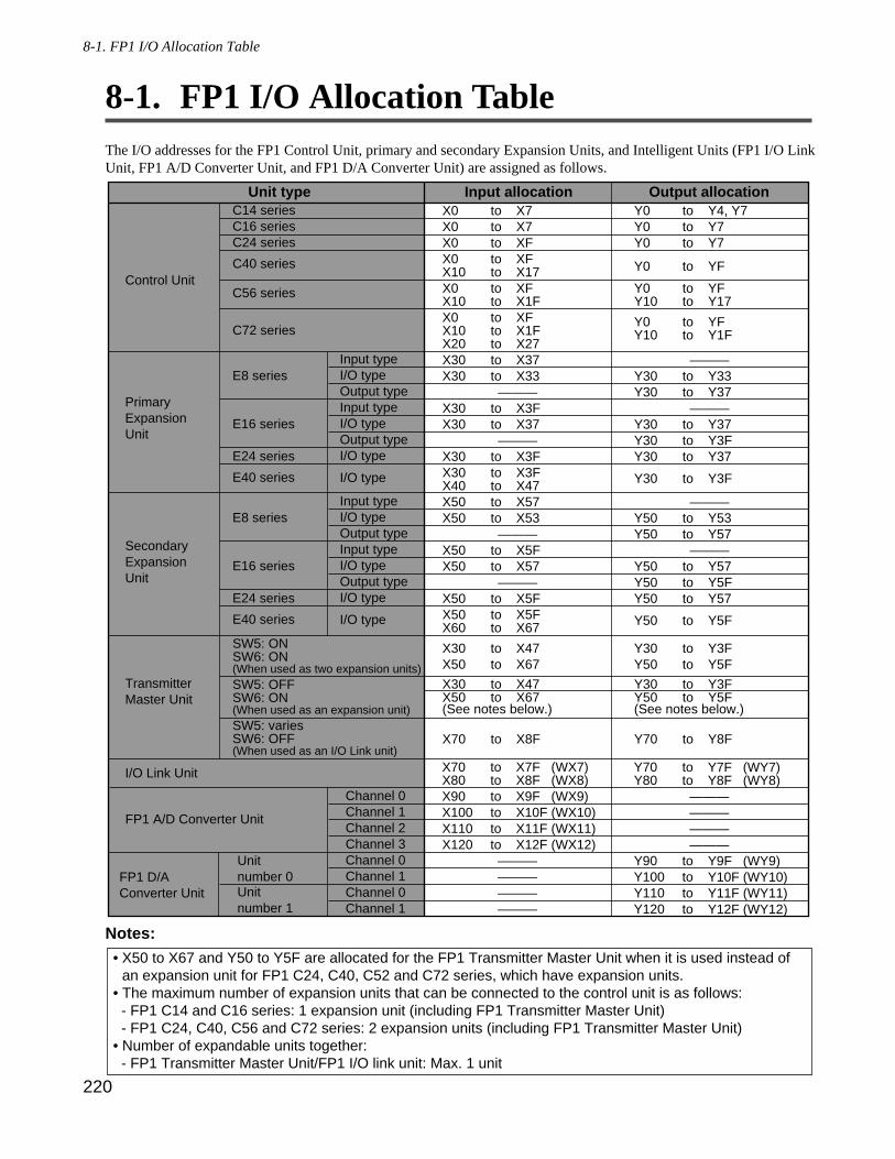
220
8-1. FP1 I/O Allocation Table
8-1. FP1 I/O Allocation TableThe I/O addresses for the FP1 Control Unit, primary and secondary Expansion Units, and Intelligent Units (FP1 I/O LinkUnit, FP1 A/D Converter Unit, and FP1 D/A Converter Unit) are assigned as follows.
Notes:
• X50 to X67 and Y50 to Y5F are allocated for the FP1 Transmitter Master Unit when it is used instead ofan expansion unit for FP1 C24, C40, C52 and C72 series, which have expansion units.
• The maximum number of expansion units that can be connected to the control unit is as follows:- FP1 C14 and C16 series: 1 expansion unit (including FP1 Transmitter Master Unit)- FP1 C24, C40, C56 and C72 series: 2 expansion units (including FP1 Transmitter Master Unit)
• Number of expandable units together:- FP1 Transmitter Master Unit/FP1 I/O link unit: Max. 1 unit
Unit typeC14 seriesC16 seriesC24 series
C40 series
C56 series
C72 series
E8 series
E16 series
E24 series
E40 series
E8 series
E16 series
E24 series
E40 series
SW5: ONSW6: ON(When used as two expansion units)SW5: OFFSW6: ON(When used as an expansion unit)SW5: varies SW6: OFF(When used as an I/O Link unit)
Input typeI/O typeOutput typeInput typeI/O typeOutput typeI/O type
I/O type
Input typeI/O typeOutput typeInput typeI/O typeOutput typeI/O type
I/O type
Control Unit
Primary Expansion Unit
Secondary Expansion Unit
I/O Link Unit
Channel 0Channel 1Channel 2Channel 3Channel 0Channel 1Channel 0Channel 1
FP1 A/D Converter Unit
FP1 D/A Converter Unit
Unit number 0Unit number 1
Input allocationX0 X0X0X0 X10 X0X10X0 X10X20X30X30
X30 X30
X30 X30 X40 X50 X50
X50 X50
X50X50X60
X30X50
X30X50(See notes below.)
X70
X70X80X90X100X110X120
totototototototototototo———
toto———
tototototo———
toto———
tototo
toto
toto
to
toto————————————
totototo
X7X7XFXFX17XFX1FXFX1FX27X37X33
X3FX37
X3FX3FX47X57X53
X5FX57
X5FX5FX67
X47X67
X47X67
X8F
X7F (WX7) X8F (WX8)X9F (WX9)X10F (WX10)X11F (WX11)X12F (WX12)
Output allocationY0Y0Y0
Y0
Y0Y10
Y0Y10
Y30Y30
Y30Y30Y30
Y30
Y50Y50
Y50Y50Y50
Y50
Y30Y50
Y30Y50(See notes below.)
Y70
Y70Y80
Y90Y100Y110Y120
tototo
to
toto
toto
———toto———
tototo
to
———toto———
tototo
to
toto
toto
to
Y4, Y7Y7Y7
YF
YFY17
YFY1F
Y33Y37
Y37Y3FY37
Y3F
Y53Y57
Y57Y5FY57
Y5F
Y3FY5F
Y3FY5F
Y8F
Y7F (WY7)Y8F (WY8)
Y9F (WY9)Y10F (WY10)Y11F (WY11)Y12F (WY12)
totototototo————————————
Transmitter Master Unit
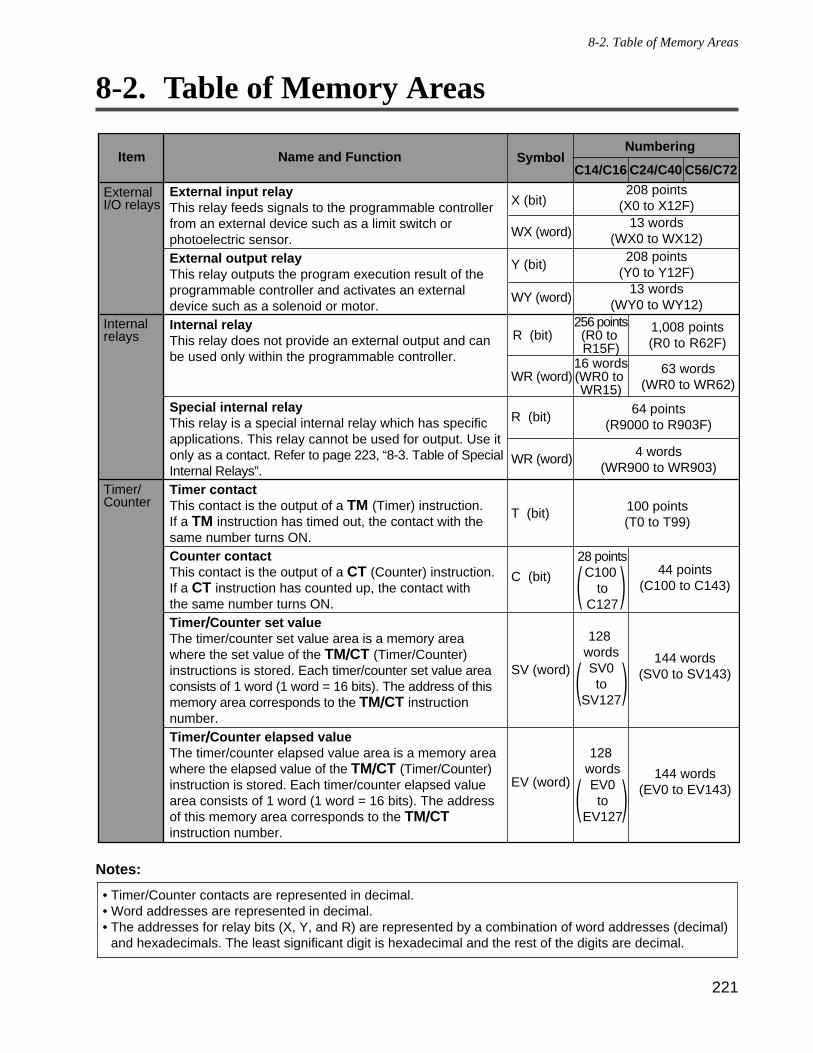
221
8-2. Table of Memory Areas
8-2. Table of Memory Areas
Notes:
• Timer/Counter contacts are represented in decimal.• Word addresses are represented in decimal.• The addresses for relay bits (X, Y, and R) are represented by a combination of word addresses (decimal)
and hexadecimals. The least significant digit is hexadecimal and the rest of the digits are decimal.
External I/O relays
Internal relays
Timer/Counter
Item Name and FunctionNumbering
External input relayThis relay feeds signals to the programmable controller from an external device such as a limit switch or photoelectric sensor.External output relayThis relay outputs the program execution result of the programmable controller and activates an external device such as a solenoid or motor.Internal relayThis relay does not provide an external output and can be used only within the programmable controller.
Special internal relayThis relay is a special internal relay which has specific applications. This relay cannot be used for output. Use it only as a contact. Refer to page 223, “8-3. Table of Special Internal Relays”.Timer contactThis contact is the output of a TM (Timer) instruction. If a TM instruction has timed out, the contact with the same number turns ON.Counter contactThis contact is the output of a CT (Counter) instruction. If a CT instruction has counted up, the contact with the same number turns ON.Timer/Counter set valueThe timer/counter set value area is a memory area where the set value of the TM/CT (Timer/Counter)instructions is stored. Each timer/counter set value area consists of 1 word (1 word = 16 bits). The address of this memory area corresponds to the TM/CT instruction number.Timer/Counter elapsed valueThe timer/counter elapsed value area is a memory area where the elapsed value of the TM/CT (Timer/Counter)instruction is stored. Each timer/counter elapsed value area consists of 1 word (1 word = 16 bits). The address of this memory area corresponds to the TM/CT instruction number.
64 points(R9000 to R903F)
44 points(C100 to C143)
144 words(SV0 to SV143)
Symbol
1,008 points(R0 to R62F)
63 words(WR0 to WR62)
100 points(T0 to T99)
144 words(EV0 to EV143)
X (bit)
WX (word)
Y (bit)
WY (word)
R (bit)
WR (word)
R (bit)
T (bit)
C (bit)
SV (word)
EV (word)
208 points(X0 to X12F)
13 words(WX0 to WX12)
208 points(Y0 to Y12F)
13 words(WY0 to WY12)
4 words(WR900 to WR903)
WR (word)
28 pointsC100
toC127
16 words(WR0 to WR15)
128 wordsSV0to
SV127
128 wordsEV0to
EV127
256 points(R0 to R15F)
C14/C16 C24/C40 C56/C72
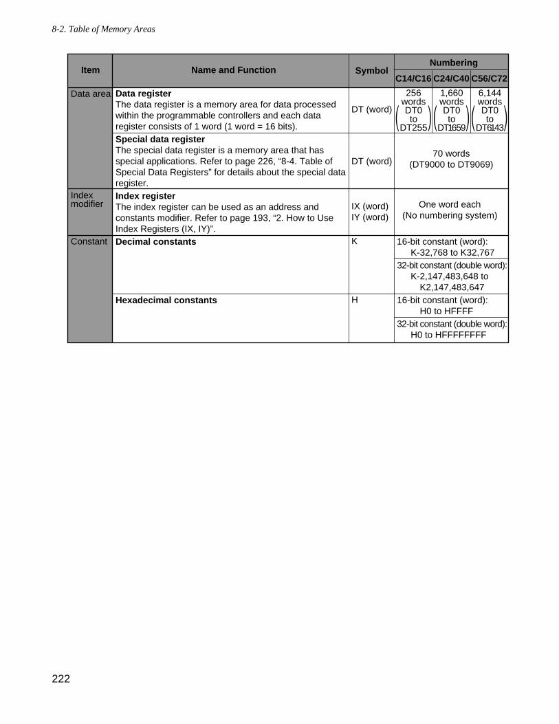
222
C14/C16
Data area
Index modifier
Constant
Item Name and FunctionNumbering
C24/C40 C56/C72Symbol
256wordsDT0to
DT255
70 words(DT9000 to DT9069)
One word each(No numbering system)
16-bit constant (word):K-32,768 to K32,767
32-bit constant (double word):K-2,147,483,648 to
K2,147,483,64716-bit constant (word):
H0 to HFFFF32-bit constant (double word):
H0 to HFFFFFFFF
DT (word)
DT (word)
IX (word)IY (word)
K
H
1,660wordsDT0to
DT1659
6,144wordsDT0to
DT6143
Data registerThe data register is a memory area for data processed within the programmable controllers and each data register consists of 1 word (1 word = 16 bits).Special data registerThe special data register is a memory area that has special applications. Refer to page 226, “8-4. Table ofSpecial Data Registers” for details about the special data register.Index registerThe index register can be used as an address and constants modifier. Refer to page 193, “2. How to Use Index Registers (IX, IY)”.Decimal constants
Hexadecimal constants
8-2. Table of Memory Areas
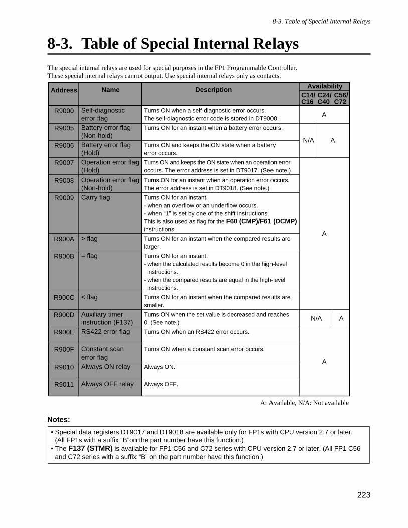
223
8-3. Table of Special Internal Relays
8-3. Table of Special Internal RelaysThe special internal relays are used for special purposes in the FP1 Programmable Controller.These special internal relays cannot output. Use special internal relays only as contacts.
Notes:
• Special data registers DT9017 and DT9018 are available only for FP1s with CPU version 2.7 or later.(All FP1s with a suffix “B”on the part number have this function.)
• The F137 (STMR) is available for FP1 C56 and C72 series with CPU version 2.7 or later. (All FP1 C56and C72 series with a suffix “B” on the part number have this function.)
Address
R9000
R9005
R9006
R9007
R9008
R9009
R900A
R900B
R900C
R900D
R900E
R900F
R9010
R9011
Name
Self-diagnostic error flagBattery error flag (Non-hold)Battery error flag (Hold)Operation error flag (Hold)Operation error flag (Non-hold)Carry flag
> flag
= flag
< flag
Auxiliary timer instruction (F137)RS422 error flag
Constant scan error flagAlways ON relay
Always OFF relay
Description
Turns ON when a self-diagnostic error occurs.The self-diagnostic error code is stored in DT9000.
Turns ON for an instant when a battery error occurs.
Turns ON and keeps the ON state when a battery error occurs.
Turns ON and keeps the ON state when an operation error occurs. The error address is set in DT9017. (See note.)
Turns ON for an instant when an operation error occurs.The error address is set in DT9018. (See note.)
Turns ON for an instant,- when an overflow or an underflow occurs.- when “1” is set by one of the shift instructions.This is also used as flag for the F60 (CMP)/F61 (DCMP) instructions.
Turns ON for an instant when the compared results arelarger.
Turns ON for an instant,- when the calculated results become 0 in the high-levelinstructions.
- when the compared results are equal in the high-levelinstructions.
Turns ON for an instant when the compared results aresmaller.
Turns ON when the set value is decreased and reaches 0. (See note.)
Turns ON when an RS422 error occurs.
Turns ON when a constant scan error occurs.
Always ON.
Always OFF.
AvailabilityC14/C16
C24/C40
N/A
A: Available, N/A: Not available
C56/C72
A
A
A
AN/A
A
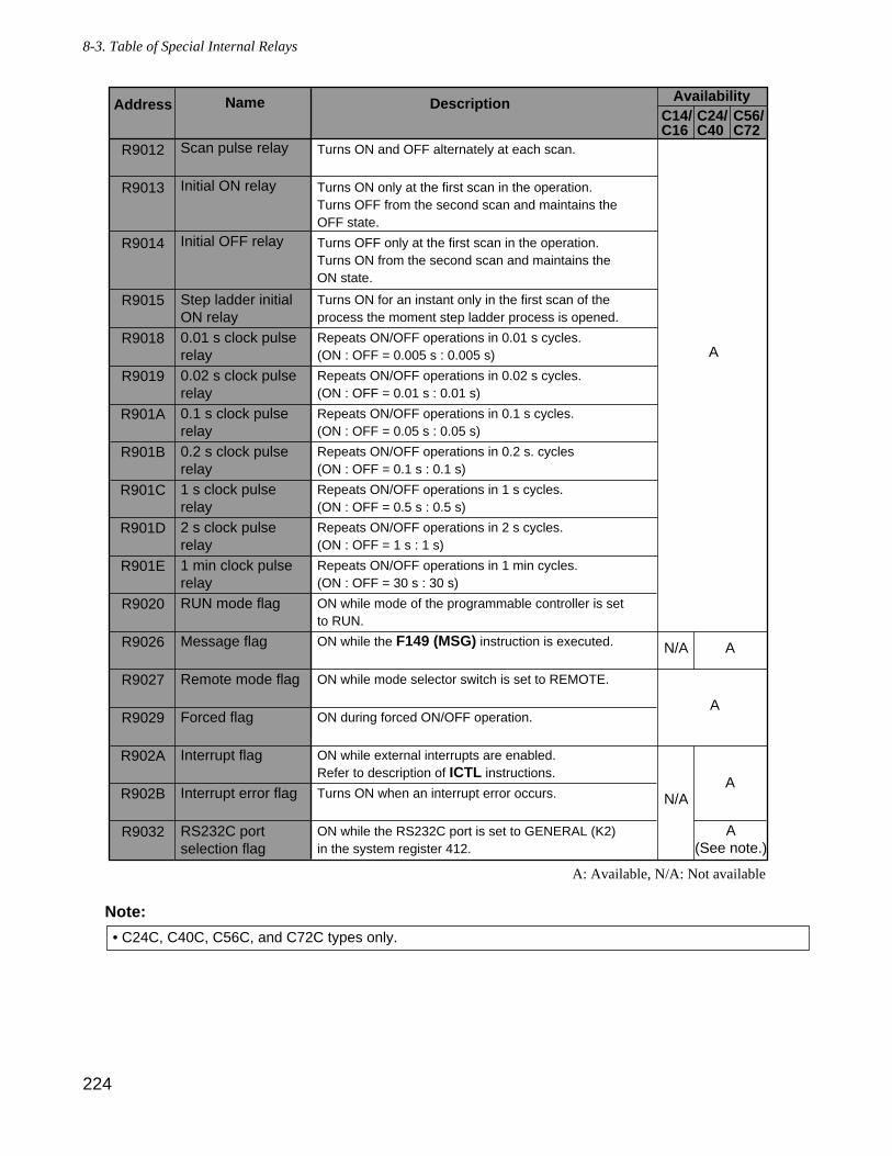
Note:
• C24C, C40C, C56C, and C72C types only.
Address
R9012
R9013
R9014
R9015
R9018
R9019
R901A
R901B
R901C
R901D
R901E
R9020
R9026
R9027
R9029
R902A
R902B
R9032
Name
Scan pulse relay
Initial ON relay
Initial OFF relay
Step ladder initial ON relay0.01 s clock pulse relay0.02 s clock pulse relay0.1 s clock pulse relay0.2 s clock pulse relay1 s clock pulse relay2 s clock pulse relay1 min clock pulse relayRUN mode flag
Message flag
Remote mode flag
Forced flag
Interrupt flag
Interrupt error flag
RS232C port selection flag
Description
Turns ON and OFF alternately at each scan.
Turns ON only at the first scan in the operation.Turns OFF from the second scan and maintains the OFF state.
Turns OFF only at the first scan in the operation.Turns ON from the second scan and maintains the ON state.
Turns ON for an instant only in the first scan of theprocess the moment step ladder process is opened.
Repeats ON/OFF operations in 0.01 s cycles. (ON : OFF = 0.005 s : 0.005 s)
Repeats ON/OFF operations in 0.02 s cycles.(ON : OFF = 0.01 s : 0.01 s)
Repeats ON/OFF operations in 0.1 s cycles.(ON : OFF = 0.05 s : 0.05 s)
Repeats ON/OFF operations in 0.2 s. cycles(ON : OFF = 0.1 s : 0.1 s)
Repeats ON/OFF operations in 1 s cycles.(ON : OFF = 0.5 s : 0.5 s)
Repeats ON/OFF operations in 2 s cycles.(ON : OFF = 1 s : 1 s)
Repeats ON/OFF operations in 1 min cycles.(ON : OFF = 30 s : 30 s)
ON while mode of the programmable controller is set to RUN.
ON while the F149 (MSG) instruction is executed.
ON while mode selector switch is set to REMOTE.
ON during forced ON/OFF operation.
ON while external interrupts are enabled.Refer to description of ICTL instructions.
Turns ON when an interrupt error occurs.
ON while the RS232C port is set to GENERAL (K2) in the system register 412.
AvailabilityC14/C16
C24/C40
A: Available, N/A: Not available
C56/C72
N/A
N/A
A(See note.)
A
A
A
A
224
8-3. Table of Special Internal Relays
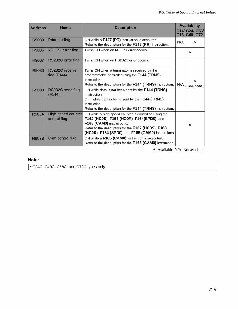
Note:
• C24C, C40C, C56C, and C72C types only.
Address
R9033
R9036
R9037
R9038
R9039
R903A
R903B
Name
Print-out flag
I/O Link error flag
RS232C error flag
RS232C receive flag (F144)
RS232C send flag (F144)
High-speed counter control flag
Cam control flag
Description
ON while a F147 (PR) instruction is executed.Refer to the description for the F147 (PR) instruction.
Turns ON when an I/O Link error occurs.
Turns ON when an RS232C error occurs.
Turns ON when a terminator is received by the programmable controller using the F144 (TRNS) instruction. Refer to the description for the F144 (TRNS) instruction.
ON while data is not been sent by the F144 (TRNS) instruction.OFF while data is being sent by the F144 (TRNS) instruction.Refer to the description for the F144 (TRNS) instruction.
ON while a high-speed counter is controlled using the F162 (HC0S), F163 (HC0R), F164(SPD0), and F165 (CAM0) instructions. Refer to the description for the F162 (HC0S), F163 (HC0R), F164 (SPD0), and F165 (CAM0) instructions.
ON while a F165 (CAM0) instruction is executed.Refer to the description for the F165 (CAM0) instruction.
AvailabilityC14/C16
C24/C40
A: Available, N/A: Not available
C56/C72
N/A
N/AA
(See note.)
A
A
A
225
8-3. Table of Special Internal Relays
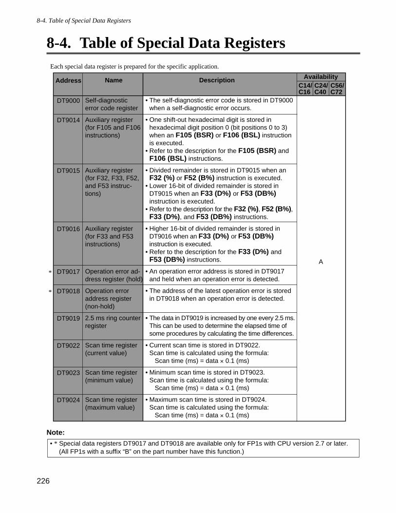
226
8-4. Table of Special Data Registers
8-4. Table of Special Data RegistersEach special data register is prepared for the specific application.
Note:
• * Special data registers DT9017 and DT9018 are available only for FP1s with CPU version 2.7 or later.(All FP1s with a suffix “B” on the part number have this function.)
A
Address
DT9000
DT9014
DT9015
DT9016
DT9017
DT9018
DT9019
DT9022
DT9023
DT9024
Name
Self-diagnostic error code register
Auxiliary register (for F105 and F106 instructions)
Auxiliary register (for F32, F33, F52, and F53 instruc-tions)
Auxiliary register (for F33 and F53 instructions)
Operation error ad-dress register (hold)
Operation error address register (non-hold)
2.5 ms ring counter register
Scan time register (current value)
Scan time register (minimum value)
Scan time register (maximum value)
Description
The self-diagnostic error code is stored in DT9000 when a self-diagnostic error occurs.
One shift-out hexadecimal digit is stored in hexadecimal digit position 0 (bit positions 0 to 3) when an F105 (BSR) or F106 (BSL) instructionis executed.Refer to the description for the F105 (BSR) and F106 (BSL) instructions.
Divided remainder is stored in DT9015 when an F32 (%) or F52 (B%) instruction is executed.Lower 16-bit of divided remainder is stored in DT9015 when an F33 (D%) or F53 (DB%) instruction is executed. Refer to the description for the F32 (%), F52 (B%), F33 (D%), and F53 (DB%) instructions.
Higher 16-bit of divided remainder is stored in DT9016 when an F33 (D%) or F53 (DB%) instruction is executed.Refer to the description for the F33 (D%) and F53 (DB%) instructions.
An operation error address is stored in DT9017 and held when an operation error is detected.
The address of the latest operation error is stored in DT9018 when an operation error is detected.
The data in DT9019 is increased by one every 2.5 ms.This can be used to determine the elapsed time of some procedures by calculating the time differences.
Current scan time is stored in DT9022.Scan time is calculated using the formula: Scan time (ms) = data × 0.1 (ms) Minimum scan time is stored in DT9023.Scan time is calculated using the formula: Scan time (ms) = data × 0.1 (ms)
Maximum scan time is stored in DT9024.Scan time is calculated using the formula: Scan time (ms) = data × 0.1 (ms)
AvailabilityC14/C16
C24/C40
C56/C72
•
•
•
•
•
•
•
•
•
•
•
•
•
•
*
*
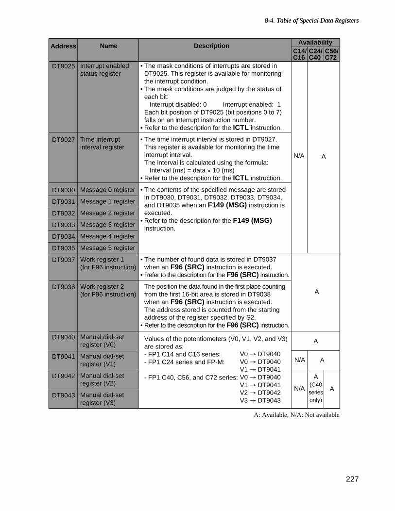
227
8-4. Table of Special Data Registers
A: Available, N/A: Not available
Address
DT9025
DT9027
DT9030
DT9031
DT9032
DT9033
DT9034
DT9035
DT9037
DT9038
DT9040
DT9041
DT9042
DT9043
Name
Interrupt enabled status register
Time interrupt interval register
Message 0 register
Message 1 register
Message 2 register
Message 3 register
Message 4 register
Message 5 register
Work register 1 (for F96 instruction)
Work register 2 (for F96 instruction)
Manual dial-set register (V0)
Manual dial-set register (V1)
Manual dial-set register (V2)
Manual dial-set register (V3)
Description
The mask conditions of interrupts are stored in DT9025. This register is available for monitoring the interrupt condition.The mask conditions are judged by the status of each bit: Interrupt disabled: 0 Interrupt enabled: 1Each bit position of DT9025 (bit positions 0 to 7) falls on an interrupt instruction number.Refer to the description for the ICTL instruction.
The time interrupt interval is stored in DT9027.This register is available for monitoring the time interrupt interval.The interval is calculated using the formula: Interval (ms) = data × 10 (ms)Refer to the description for the ICTL instruction.
The contents of the specified message are stored in DT9030, DT9031, DT9032, DT9033, DT9034, and DT9035 when an F149 (MSG) instruction is executed.Refer to the description for the F149 (MSG) instruction.
The number of found data is stored in DT9037 when an F96 (SRC) instruction is executed.Refer to the description for the F96 (SRC) instruction.
The position the data found in the first place counting from the first 16-bit area is stored in DT9038 when an F96 (SRC) instruction is executed.The address stored is counted from the starting address of the register specified by S2. Refer to the description for the F96 (SRC) instruction.
Values of the potentiometers (V0, V1, V2, and V3) are stored as:- FP1 C14 and C16 series:- FP1 C24 series and FP-M:
- FP1 C40, C56, and C72 series:
AvailabilityC14/C16
C24/C40
C56/C72
•
•
•
•
•
•
•
•
•
•
N/A
A(C40seriesonly)
A
AV0 → DT9040V0 → DT9040V1 → DT9041V0 → DT9040V1 → DT9041V2 → DT9042V3 → DT9043
A
A
N/A
AN/A
8-4. Table of Special Data Registers
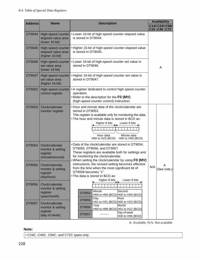
228
8-4. Table of Special Data Registers
Note:
• C24C, C40C, C56C, and C72C types only.
A
A: Available, N/A: Not available
N/A A(See note.)
Lower 16-bit of high-speed counter elapsed value is stored in DT9044.
Higher 16-bit of high-speed counter elapsed value is stored in DT9045.
Lower 16-bit of high-speed counter set value is stored in DT9046.
Higher 16-bit of high-speed counter set value is stored in DT9047.
A register dedicated to control high-speed counter operation.Refer to the description for the F0 (MV) (high-speed counter control) instruction.
Hour and minute data of the clock/calendar are stored in DT9053.This register is available only for monitoring the data.The hour and minute data is stored in BCD as:
Data of the clock/calendar are stored in DT9054, DT9055, DT9056, and DT9057. These registers are available both for settings and for monitoring the clock/calendar.When setting the clock/calendar by using F0 (MV) instructions, the revised setting becomes effective from the time when the most significant bit of DT9058 becomes “1”.The data is stored in BCD as:
•
•
•
•
•
•
•
•
•
•
•
Higher 8 bits Lower 8 bits
Hour dataH00 to H23 (BCD)
Minute data H00 to H59 (BCD)
Higher 8 bits Lower 8 bits
Minute H00 to H59 (BCD)Day H01 to H31 (BCD)Year H00 to H99 (BCD)
Second H00 to H59 (BCD)Hour H00 to H23 (BCD)Month H01 to H12 (BCD)Day of week H00 to H06 (BCD)
DT9054
DT9055
DT9056
DT9057
Address
Description AvailabilityC14/C16
C24/C40
C56/C72
DT9054
DT9055
DT9056
DT9057
DT9044
DT9045
DT9046
DT9047
DT9052
DT9053
High-speed counter elapsed value area (lower 16-bit)
High-speed counter elapsed value area (higher 16-bit)
High-speed counter set value area (lower 16-bit)
High-speed counter set value area (higher 16-bit)
High-speed counter control register
Clock/calendar monitor register
Name
Clock/calendar monitor & setting register (minute/second)
Clock/calendar monitor & setting register (day/hour)
Clock/calendar monitor & setting register (year/month)
Clock/calendar monitor & setting register (day of week)
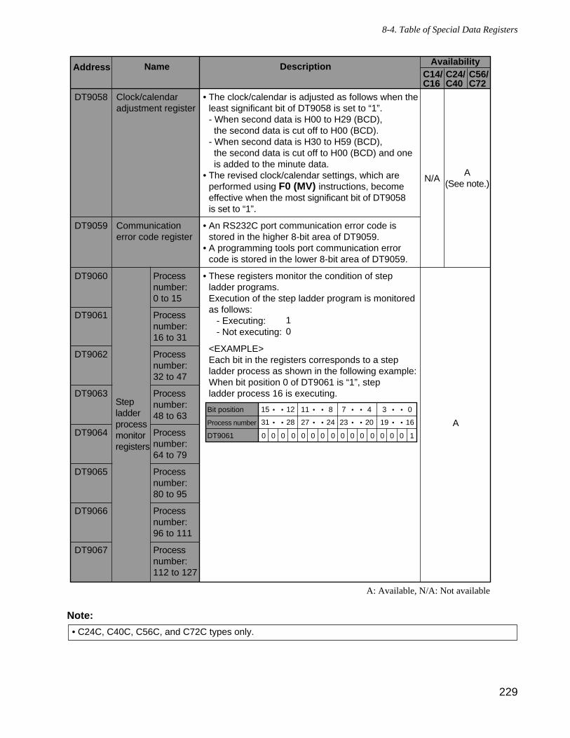
229
8-4. Table of Special Data Registers
Note:
• C24C, C40C, C56C, and C72C types only.
A: Available, N/A: Not available
Address
Name
Description AvailabilityC14/C16
C24/C40
C56/C72
DT9058
DT9059
DT9060
DT9061
DT9062
DT9063
DT9064
DT9065
DT9066
DT9067
Clock/calendar adjustment register
Communication error code register
•
•
•
•
•
The clock/calendar is adjusted as follows when the least significant bit of DT9058 is set to “1”.- When second data is H00 to H29 (BCD), the second data is cut off to H00 (BCD).- When second data is H30 to H59 (BCD), the second data is cut off to H00 (BCD) and one is added to the minute data. The revised clock/calendar settings, which are performed using F0 (MV) instructions, become effective when the most significant bit of DT9058 is set to “1”. An RS232C port communication error code is stored in the higher 8-bit area of DT9059.A programming tools port communication error code is stored in the lower 8-bit area of DT9059.
These registers monitor the condition of step ladder programs.Execution of the step ladder program is monitored as follows: - Executing: - Not executing:
<EXAMPLE>Each bit in the registers corresponds to a step ladder process as shown in the following example:When bit position 0 of DT9061 is “1”, step ladder process 16 is executing.
10
Bit position
Process number
DT9061 0 0 0 0
11 8 3 015 • • 12 • • • •7 4• •
0 0 0 0 0 0 0 0 0 0 0 1
27 24 19 1631 • • 28 • • • •23 20• •
Process number: 0 to 15
Process number: 16 to 31
Process number: 32 to 47
Process number: 48 to 63
Process number: 64 to 79
Process number: 80 to 95
Process number:96 to 111
Process number: 112 to 127
Step ladder process monitor registers
A(See note.)N/A
A
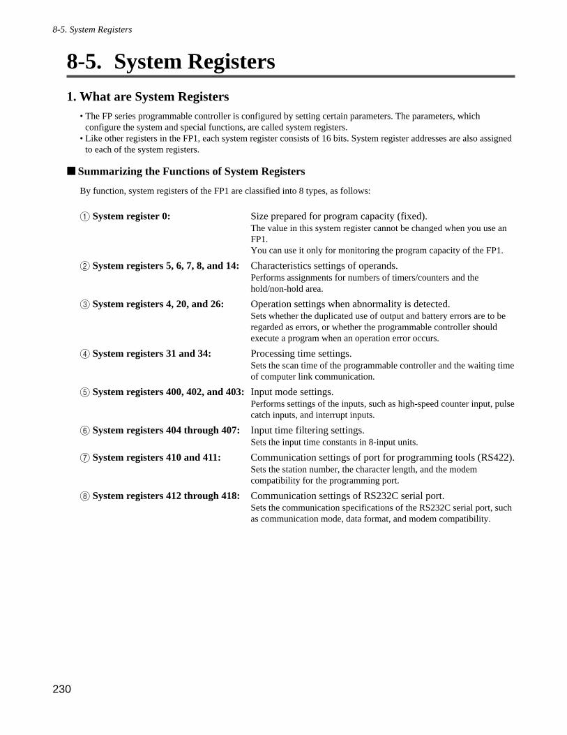
230
8-5. System Registers
8-5. System Registers
1. What are System Registers• The FP series programmable controller is configured by setting certain parameters. The parameters, which
configure the system and special functions, are called system registers. • Like other registers in the FP1, each system register consists of 16 bits. System register addresses are also assigned
to each of the system registers.
Summarizing the Functions of System Registers
By function, system registers of the FP1 are classified into 8 types, as follows:
1 System register 0: Size prepared for program capacity (fixed). The value in this system register cannot be changed when you use anFP1. You can use it only for monitoring the program capacity of the FP1.
2 System registers 5, 6, 7, 8, and 14: Characteristics settings of operands.Performs assignments for numbers of timers/counters and thehold/non-hold area.
3 System registers 4, 20, and 26: Operation settings when abnormality is detected.Sets whether the duplicated use of output and battery errors are to beregarded as errors, or whether the programmable controller shouldexecute a program when an operation error occurs.
4 System registers 31 and 34: Processing time settings.Sets the scan time of the programmable controller and the waiting timeof computer link communication.
5 System registers 400, 402, and 403: Input mode settings.Performs settings of the inputs, such as high-speed counter input, pulsecatch inputs, and interrupt inputs.
6 System registers 404 through 407: Input time filtering settings.Sets the input time constants in 8-input units.
7 System registers 410 and 411: Communication settings of port for programming tools (RS422). Sets the station number, the character length, and the modemcompatibility for the programming port.
8 System registers 412 through 418: Communication settings of RS232C serial port.Sets the communication specifications of the RS232C serial port, suchas communication mode, data format, and modem compatibility.
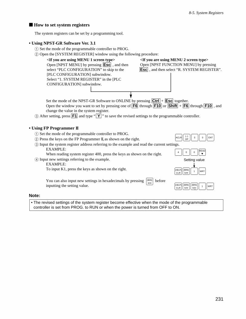
231
8-5. System Registers
How to set system registers
The system registers can be set by a programming tool.
• Using NPST-GR Software Ver. 3.11 Set the mode of the programmable controller to PROG.2 Open the [SYSTEM REGISTER] window using the following procedure:
Set the mode of the NPST-GR Software to ONLINE by pressing Ctrl + Esc together.Open the window you want to set by pressing one of F6 through F10 or Shift + F6 through F10 , andchange the value in the system register.
3 After setting, press F1 and type “ Y ” to save the revised settings to the programmable controller.
• Using FP Programmer II1 Set the mode of the programmable controller to PROG.2 Press the keys on the FP Programmer II, as shown on the right. 3 Input the system register address referring to the example and read the current settings.
EXAMPLE:When reading system register 400, press the keys as shown on the right.
4 Input new settings referring to the example.EXAMPLE:To input K1, press the keys as shown on the right.
You can also input new settings in hexadecimals by pressing beforeinputting the setting value.
Note:
• The revised settings of the system register become effective when the mode of the programmablecontroller is set from PROG. to RUN or when the power is turned from OFF to ON.
(BIN)K/H
<If you are using MENU 1 screen type>Open [NPST MENU] by pressing Esc , and thenselect “PLC CONFIGURATION” to skip to the[PLC CONFIGURATION] subwindow.Select “1. SYSTEM REGISTER” in the [PLCCONFIGURATION] subwindow.
<If you are using MENU 2 screen type>Open [NPST FUNCTION MENU] by pressingEsc , and then select “R. SYSTEM REGISTER”.
ACLR(–)OP
5 0 ENT
04 0READ
(BIN)K/H
1(HELP)
CLRWRT
Setting value
(BIN)K/H
(HELP)
CLRWRT1
(BIN)K/H
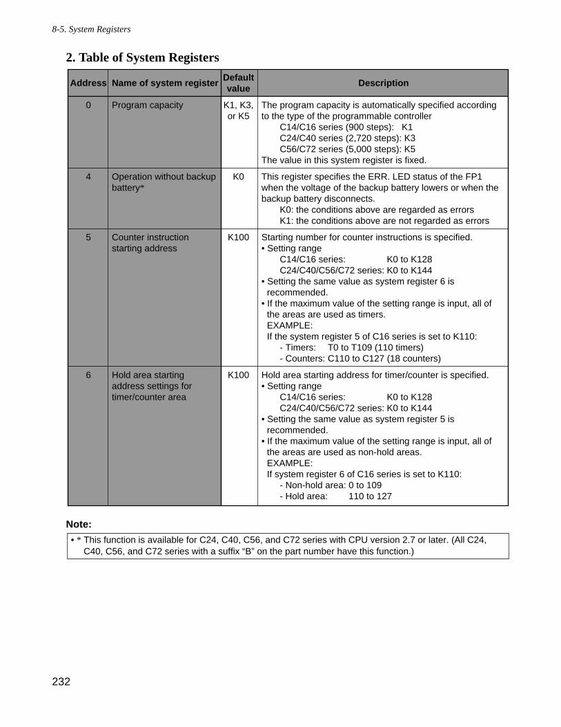
232
8-5. System Registers
2. Table of System Registers
Note:
• * This function is available for C24, C40, C56, and C72 series with CPU version 2.7 or later. (All C24,C40, C56, and C72 series with a suffix “B” on the part number have this function.)
Address
0
4
5
6
Name of system register
Program capacity
Operation without backup battery*
Counter instruction starting address
Hold area starting address settings for timer/counter area
Defaultvalue
K1, K3,or K5
K0
K100
K100
Description
The program capacity is automatically specified according to the type of the programmable controller
C14/C16 series (900 steps): K1
C24/C40 series (2,720 steps): K3C56/C72 series (5,000 steps): K5
The value in this system register is fixed.
This register specifies the ERR. LED status of the FP1 when the voltage of the backup battery lowers or when the backup battery disconnects.
K0: the conditions above are regarded as errorsK1: the conditions above are not regarded as errors
Starting number for counter instructions is specified.• Setting range
C14/C16 series: C24/C40/C56/C72 series:
• Setting the same value as system register 6 is recommended.
• If the maximum value of the setting range is input, all of the areas are used as timers.EXAMPLE:If the system register 5 of C16 series is set to K110:
- Timers:- Counters:
Hold area starting address for timer/counter is specified.• Setting range
C14/C16 series: C24/C40/C56/C72 series:
• Setting the same value as system register 5 is
recommended.• If the maximum value of the setting range is input, all of
the areas are used as non-hold areas.EXAMPLE:If system register 6 of C16 series is set to K110:
- Non-hold area: - Hold area:
K0 to K128K0 to K144
K0 to K128K0 to K144
T0 to T109 (110 timers)C110 to C127 (18 counters)
0 to 109110 to 127
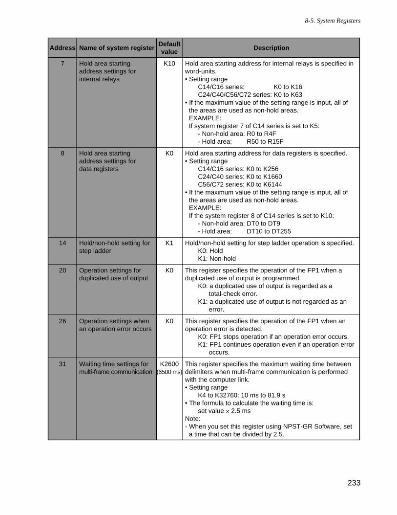
233
8-5. System Registers
Address
7
8
14
20
26
31
Name of system register
Hold area starting address settings for internal relays
Hold area starting address settings for data registers
Hold/non-hold setting for step ladder
Operation settings for duplicated use of output
Operation settings when an operation error occurs
Waiting time settings for multi-frame communication
Defaultvalue
K10
K0
K1
K0
K0
K2600(6500 ms)
Description
Hold area starting address for internal relays is specified in word-units.• Setting range
C14/C16 series:C24/C40/C56/C72 series:
• If the maximum value of the setting range is input, all of the areas are used as non-hold areas.EXAMPLE:If system register 7 of C14 series is set to K5:
- Non-hold area:- Hold area:
Hold area starting address for data registers is specified.• Setting range
C14/C16 series: K0 to K256C24/C40 series: K0 to K1660C56/C72 series: K0 to K6144
• If the maximum value of the setting range is input, all of the areas are used as non-hold areas.EXAMPLE:If the system register 8 of C14 series is set to K10:
- Non-hold area:- Hold area:
Hold/non-hold setting for step ladder operation is specified.K0: HoldK1: Non-hold
This register specifies the operation of the FP1 when a duplicated use of output is programmed.
K0: a duplicated use of output is regarded as a total-check error.K1: a duplicated use of output is not regarded as an error.
This register specifies the operation of the FP1 when an operation error is detected.
K0: FP1 stops operation if an operation error occurs.K1: FP1 continues operation even if an operation error occurs.
This register specifies the maximum waiting time between delimiters when multi-frame communication is performed with the computer link.• Setting range
K4 to K32760: 10 ms to 81.9 s• The formula to calculate the waiting time is:
set value × 2.5 msNote:- When you set this register using NPST-GR Software, set
a time that can be divided by 2.5.
K0 to K16K0 to K63
R0 to R4FR50 to R15F
DT0 to DT9DT10 to DT255
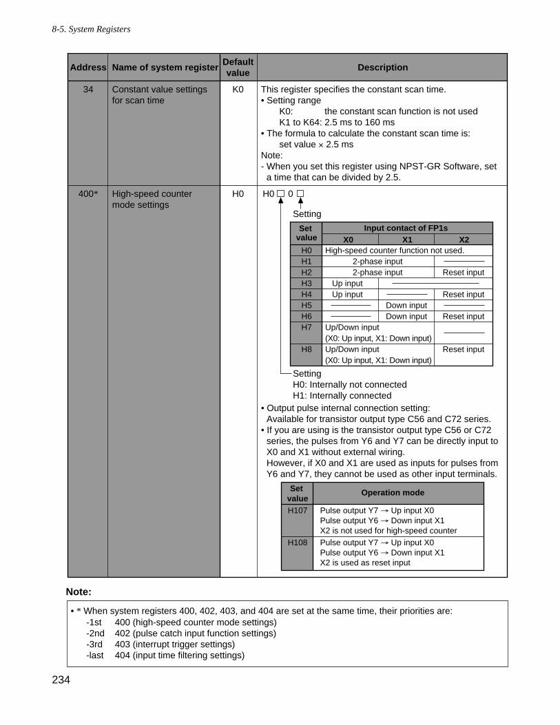
234
8-5. System Registers
Note:
• * When system registers 400, 402, 403, and 404 are set at the same time, their priorities are:-1st 400 (high-speed counter mode settings)-2nd 402 (pulse catch input function settings)-3rd 403 (interrupt trigger settings)-last 404 (input time filtering settings)
Address
34
400*
Name of system register
Constant value settings for scan time
High-speed counter mode settings
Defaultvalue
K0
H0
Description
This register specifies the constant scan time.• Setting range
K0:K1 to K64:
• The formula to calculate the constant scan time is:set value × 2.5 ms
Note:- When you set this register using NPST-GR Software, set
a time that can be divided by 2.5.
the constant scan function is not used2.5 ms to 160 ms
• Output pulse internal connection setting:Available for transistor output type C56 and C72 series.
• If you are using is the transistor output type C56 or C72 series, the pulses from Y6 and Y7 can be directly input to X0 and X1 without external wiring. However, if X0 and X1 are used as inputs for pulses from Y6 and Y7, they cannot be used as other input terminals.
Set valueH107
H108
Operation mode
Pulse output Y7 → Up input X0Pulse output Y6 → Down input X1X2 is not used for high-speed counterPulse output Y7 → Up input X0Pulse output Y6 → Down input X1X2 is used as reset input
Set value
H0H1H2H3H4H5H6H7
H8
High-speed counter function not used. 2-phase input 2-phase input Up input Up input
Up/Down input (X0: Up input, X1: Down input) Up/Down input (X0: Up input, X1: Down input)
Down inputDown input
Reset input
Reset input
Reset input
Reset input
X1 X2X0Input contact of FP1s
Setting
SettingH0: Internally not connectedH1: Internally connected
0H0
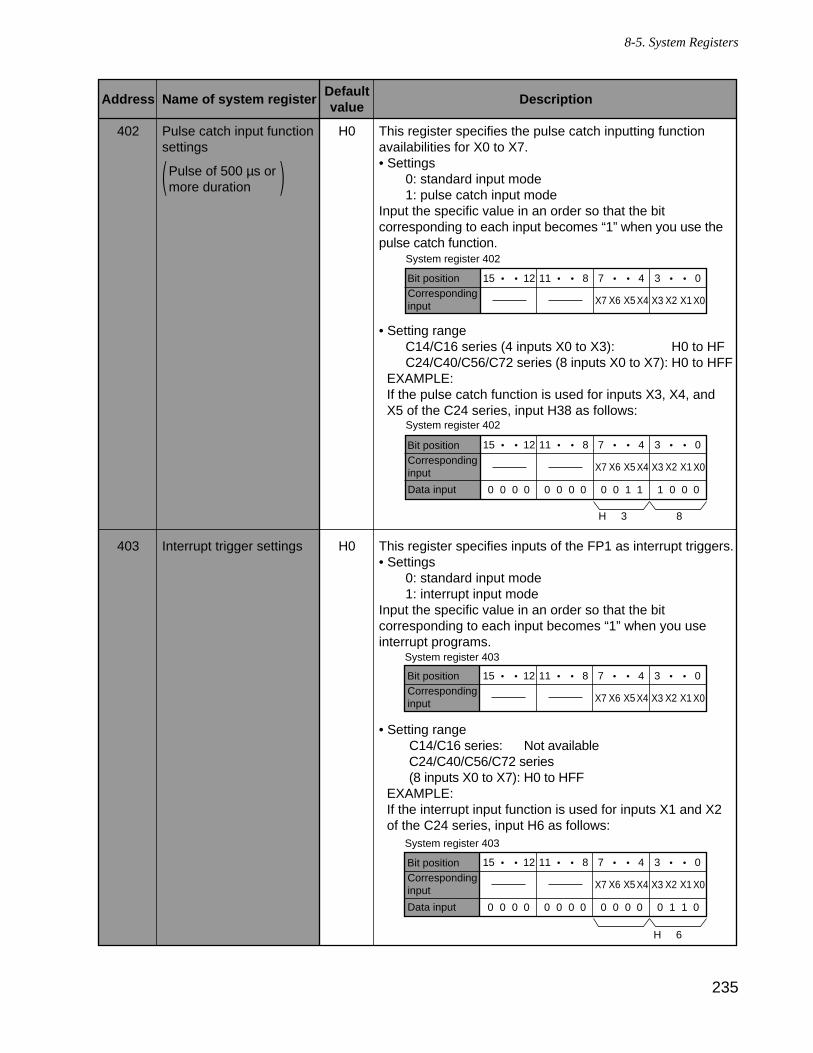
235
8-5. System Registers
Address
402
403
Name of system register
Pulse catch input function settings
Pulse of 500 µs ormore duration
Interrupt trigger settings
Defaultvalue
H0
H0
Description
This register specifies the pulse catch inputting function availabilities for X0 to X7.• Settings
0: standard input mode 1: pulse catch input mode
Input the specific value in an order so that the bit corresponding to each input becomes “1” when you use the pulse catch function.
• Setting rangeC14/C16 series (4 inputs X0 to X3): C24/C40/C56/C72 series (8 inputs X0 to X7):
EXAMPLE:If the pulse catch function is used for inputs X3, X4, and X5 of the C24 series, input H38 as follows:
This register specifies inputs of the FP1 as interrupt triggers.• Settings
0: standard input mode 1: interrupt input mode
Input the specific value in an order so that the bit corresponding to each input becomes “1” when you use interrupt programs.
• Setting range C14/C16 series: Not available C24/C40/C56/C72 series (8 inputs X0 to X7): H0 to HFF
EXAMPLE:If the interrupt input function is used for inputs X1 and X2 of the C24 series, input H6 as follows:
H 6
Bit position 7 4• •
X7 X4X6 X5Correspondinginput
3 0• •11 8• •15 12• •
X3 X0X2 X1
System register 403
Bit positionCorrespondinginput
Data input 0 0 0 0 0 0 0 0 0 0 0 0 0 1 1 0
7 4• •
X7 X4X6 X5
3 0• •11 8• •15 12• •
X3 X0X2 X1
System register 403
Bit position 7 4• •
X7 X4X6 X5Correspondinginput
3 0• •11 8• •15 12• •
X3 X0X2 X1
System register 402
Bit positionCorrespondinginput
Data input 0 0 0 0 0 0 0 0 0 0 1 1 1 0 0 0
H 3 8
7 4• •
X7 X4X6 X5
3 0• •11 8• •15 12• •
X3 X0X2 X1
System register 402
H0 to HFH0 to HFF
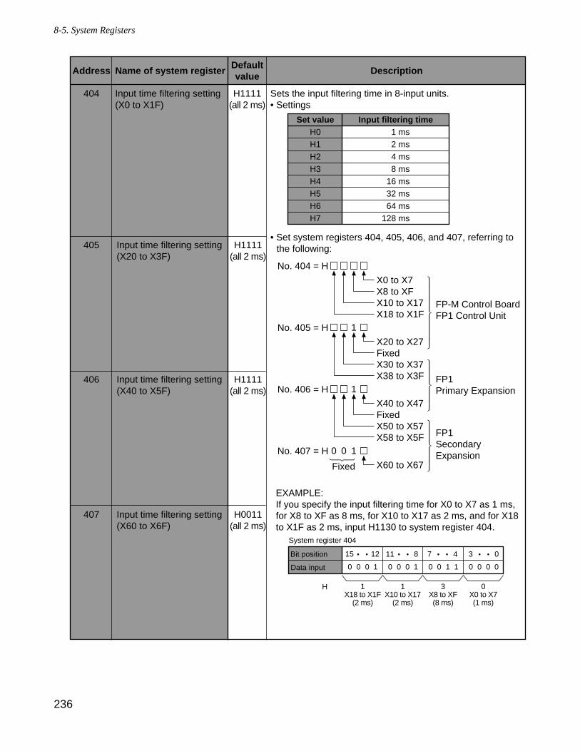
236
8-5. System Registers
Address
404
Name of system register
Input time filtering setting (X0 to X1F)
Defaultvalue
H1111(all 2 ms)
Description
Sets the input filtering time in 8-input units.• Settings
Set valueH0H1H2H3H4H5H6H7
Input filtering time 1 ms 2 ms 4 ms 8 ms 16 ms 32 ms 64 ms128 ms
• Set system registers 404, 405, 406, and 407, referring to the following:
EXAMPLE:If you specify the input filtering time for X0 to X7 as 1 ms, for X8 to XF as 8 ms, for X10 to X17 as 2 ms, and for X18 to X1F as 2 ms, input H1130 to system register 404.
Bit position 11 8 3 015 • • 12 • • • •7 4• •
Data input 0 0 0 1 0 0 0 1 0 0 1 1 0 0 0 0
1X18 to X1F
(2 ms)
1X10 to X17
(2 ms)
3X8 to XF(8 ms)
0X0 to X7(1 ms)
H
System register 404
H1111(all 2 ms)
H1111(all 2 ms)
H0011(all 2 ms)
Input time filtering setting (X20 to X3F)
Input time filtering setting (X40 to X5F)
Input time filtering setting (X60 to X6F)
405
406
407
No. 404 = H
X0 to X7X8 to XFX10 to X17X18 to X1F
FP-M Control BoardFP1 Control Unit
No. 405 = H
X20 to X27FixedX30 to X37X38 to X3F
No. 406 = H
X40 to X47FixedX50 to X57X58 to X5F
No. 407 = H
X60 to X67
1
1
100
Fixed
"""""" "
"""" "
"""" "
"" "
FP1 Primary Expansion
FP1 Secondary Expansion
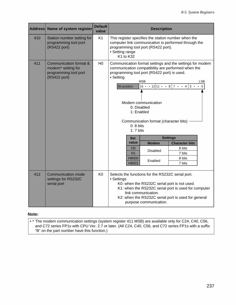
237
8-5. System Registers
Note:
• * The modem communication settings (system register 411 MSB) are available only for C24, C40, C56,and C72 series FP1s with CPU Ver. 2.7 or later. (All C24, C40, C56, and C72 series FP1s with a suffix“B” on the part number have this function.)
Address
410
411
412
Name of system register
Station number setting for programming tool port (RS422 port)
Communication format & modem* setting for programming tool port (RS422 port)
Communication mode settings for RS232C serial port
Defaultvalue
K1
H0
K0
Description
This register specifies the station number when the computer link communication is performed through the programming tool port (RS422 port).• Setting range
K1 to K32
Communication format settings and the settings for modem communication compatibility are performed when the programming tool port (RS422 port) is used.• Setting
Modem communication 0: Disabled 1: Enabled
Communication format (character bits) 0: 8 bits 1: 7 bits
Selects the functions for the RS232C serial port.• Settings
K0: when the RS232C serial port is not used.K1: when the RS232C serial port is used for computer
link communication.K2: when the RS232C serial port is used for general purpose communication.
Bit position 7 4• • 3 0• •11 8• •15 12• •
MSB LSB
Set value
H0H1
H8000H8001
Settings Modem
Disabled
Enabled
Character bits
8 bits7 bits8 bits7 bits
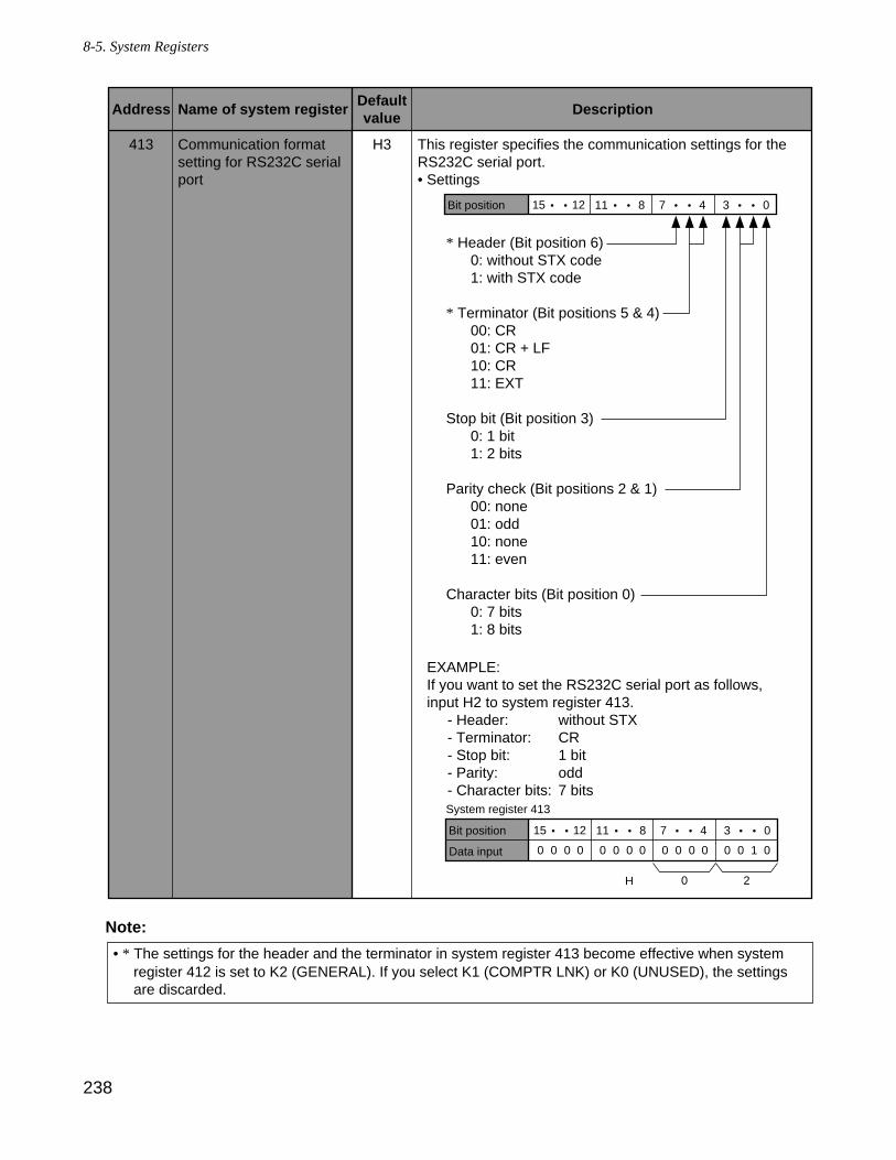
238
8-5. System Registers
Note:
• * The settings for the header and the terminator in system register 413 become effective when systemregister 412 is set to K2 (GENERAL). If you select K1 (COMPTR LNK) or K0 (UNUSED), the settingsare discarded.
Address
413
Name of system register
Communication format setting for RS232C serial port
Defaultvalue
H3
Description
This register specifies the communication settings for the RS232C serial port.• Settings
Bit position 11 8 3 015 • • 12 • • • •7 4• •
Bit position 11 8 3 015 • • 12 • • • •7 4• •
Data input 0 0 0 0 0 0 0 0 0 0 0 0 0 0 1 0
0 2H
System register 413
EXAMPLE:If you want to set the RS232C serial port as follows, input H2 to system register 413.
- Header: - Terminator: - Stop bit: - Parity: - Character bits:
without STXCR1 bitodd7 bits
* Header (Bit position 6) 0: without STX code 1: with STX code
* Terminator (Bit positions 5 & 4) 00: CR 01: CR + LF 10: CR 11: EXT
Stop bit (Bit position 3) 0: 1 bit 1: 2 bits
Parity check (Bit positions 2 & 1) 00: none 01: odd 10: none 11: even
Character bits (Bit position 0) 0: 7 bits 1: 8 bits
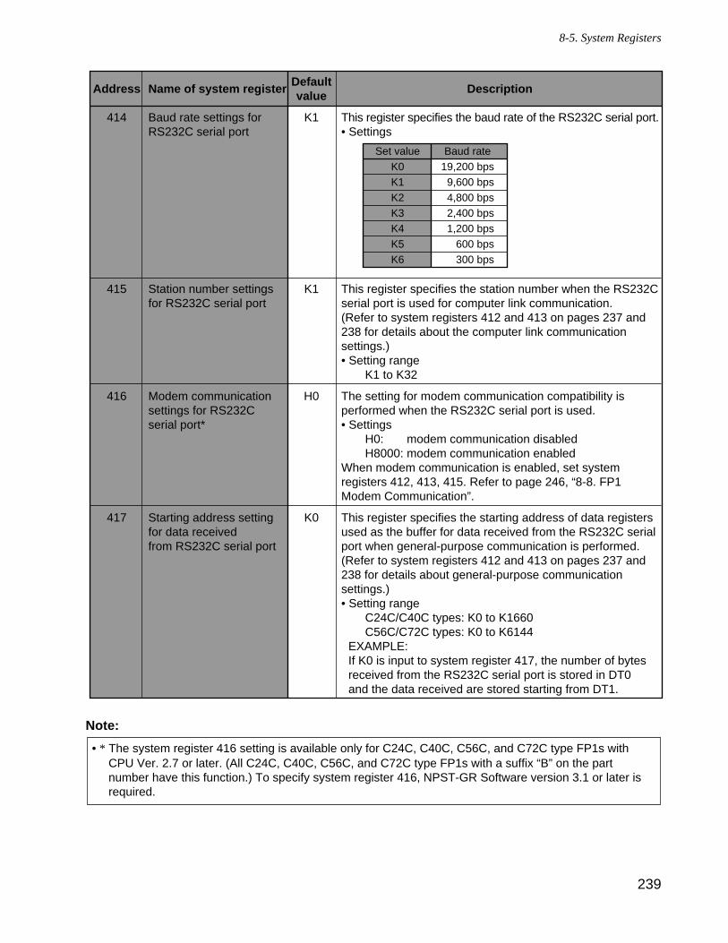
239
8-5. System Registers
Note:
• * The system register 416 setting is available only for C24C, C40C, C56C, and C72C type FP1s withCPU Ver. 2.7 or later. (All C24C, C40C, C56C, and C72C type FP1s with a suffix “B” on the partnumber have this function.) To specify system register 416, NPST-GR Software version 3.1 or later isrequired.
Address
414
415
416
417
Name of system register
Baud rate settings for RS232C serial port
Station number settings for RS232C serial port
Modem communication settings for RS232C serial port*
Starting address setting for data received from RS232C serial port
Defaultvalue
K1
K1
H0
K0
Description
This register specifies the baud rate of the RS232C serial port.• Settings
This register specifies the station number when the RS232C serial port is used for computer link communication. (Refer to system registers 412 and 413 on pages 237 and238 for details about the computer link communicationsettings.)• Setting range
K1 to K32
The setting for modem communication compatibility is performed when the RS232C serial port is used.• Settings
H0: modem communication disabledH8000: modem communication enabled
When modem communication is enabled, set system registers 412, 413, 415. Refer to page 246, “8-8. FP1 Modem Communication”.
This register specifies the starting address of data registers used as the buffer for data received from the RS232C serial port when general-purpose communication is performed. (Refer to system registers 412 and 413 on pages 237 and238 for details about general-purpose communicationsettings.)• Setting range
C24C/C40C types: K0 to K1660C56C/C72C types: K0 to K6144
EXAMPLE:If K0 is input to system register 417, the number of bytes received from the RS232C serial port is stored in DT0 and the data received are stored starting from DT1.
Set valueK0K1K2K3K4K5K6
Baud rate19,200 bps 9,600 bps 4,800 bps 2,400 bps 1,200 bps 600 bps 300 bps
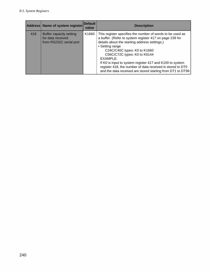
240
8-5. System Registers
Address
418
Name of system register
Buffer capacity setting for data received from RS232C serial port
Defaultvalue
K1660
Description
This register specifies the number of words to be used as a buffer. (Refer to system register 417 on page 239 for details about the starting address settings.)• Setting range
C24C/C40C types: K0 to K1660C56C/C72C types: K0 to K6144
EXAMPLE:If K0 is input to system register 417 and K100 to system register 418, the number of data received is stored to DT0 and the data received are stored starting from DT1 to DT99.
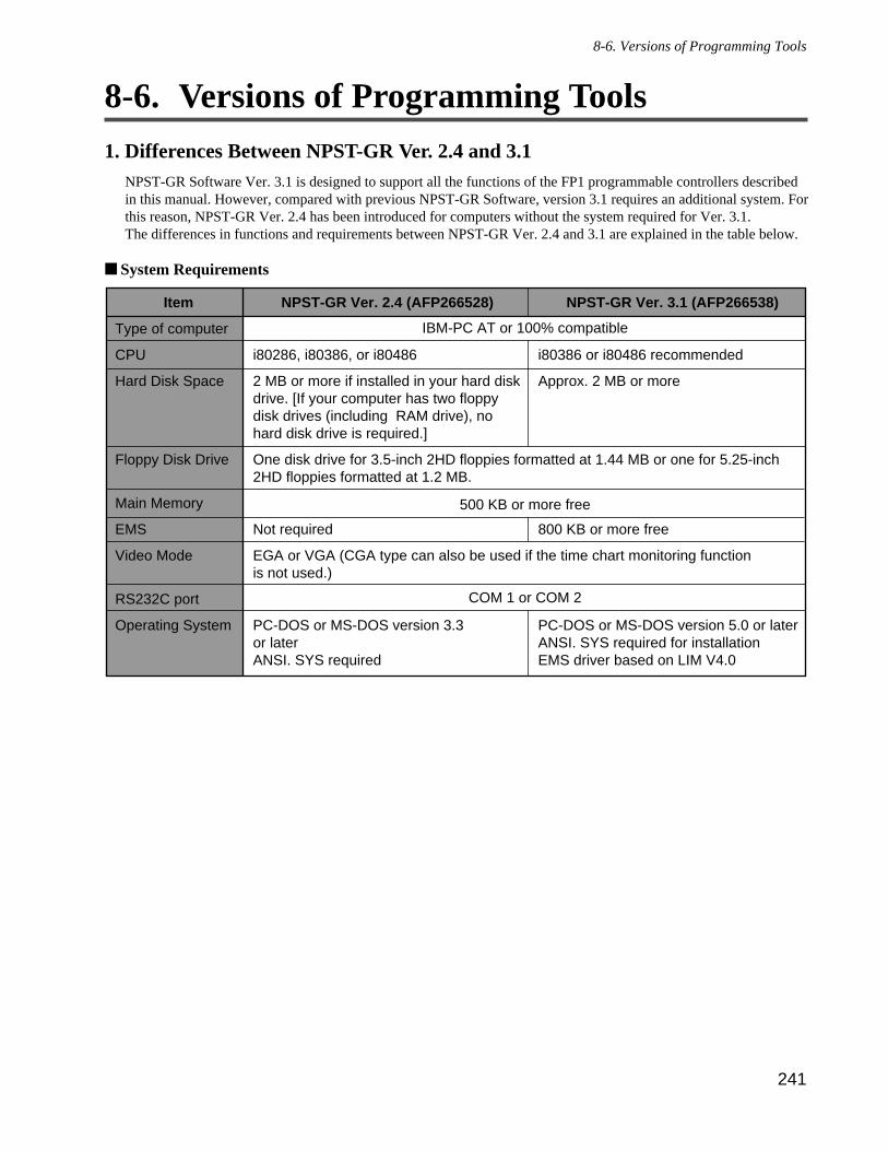
8-6. Versions of Programming Tools
1. Differences Between NPST-GR Ver. 2.4 and 3.1NPST-GR Software Ver. 3.1 is designed to support all the functions of the FP1 programmable controllers describedin this manual. However, compared with previous NPST-GR Software, version 3.1 requires an additional system. Forthis reason, NPST-GR Ver. 2.4 has been introduced for computers without the system required for Ver. 3.1. The differences in functions and requirements between NPST-GR Ver. 2.4 and 3.1 are explained in the table below.
System Requirements
Item
Type of computer
CPU
Hard Disk Space
Floppy Disk Drive
Main Memory
EMS
Video Mode
RS232C port
Operating System
NPST-GR Ver. 2.4 (AFP266528)
i80286, i80386, or i80486
2 MB or more if installed in your hard disk drive. [If your computer has two floppy disk drives (including RAM drive), no hard disk drive is required.]
One disk drive for 3.5-inch 2HD floppies formatted at 1.44 MB or one for 5.25-inch 2HD floppies formatted at 1.2 MB.
Not required
EGA or VGA (CGA type can also be used if the time chart monitoring function is not used.)
PC-DOS or MS-DOS version 3.3 or laterANSI. SYS required
NPST-GR Ver. 3.1 (AFP266538)
i80386 or i80486 recommended
Approx. 2 MB or more
800 KB or more free
PC-DOS or MS-DOS version 5.0 or later ANSI. SYS required for installationEMS driver based on LIM V4.0
IBM-PC AT or 100% compatible
500 KB or more free
COM 1 or COM 2
241
8-6. Versions of Programming Tools
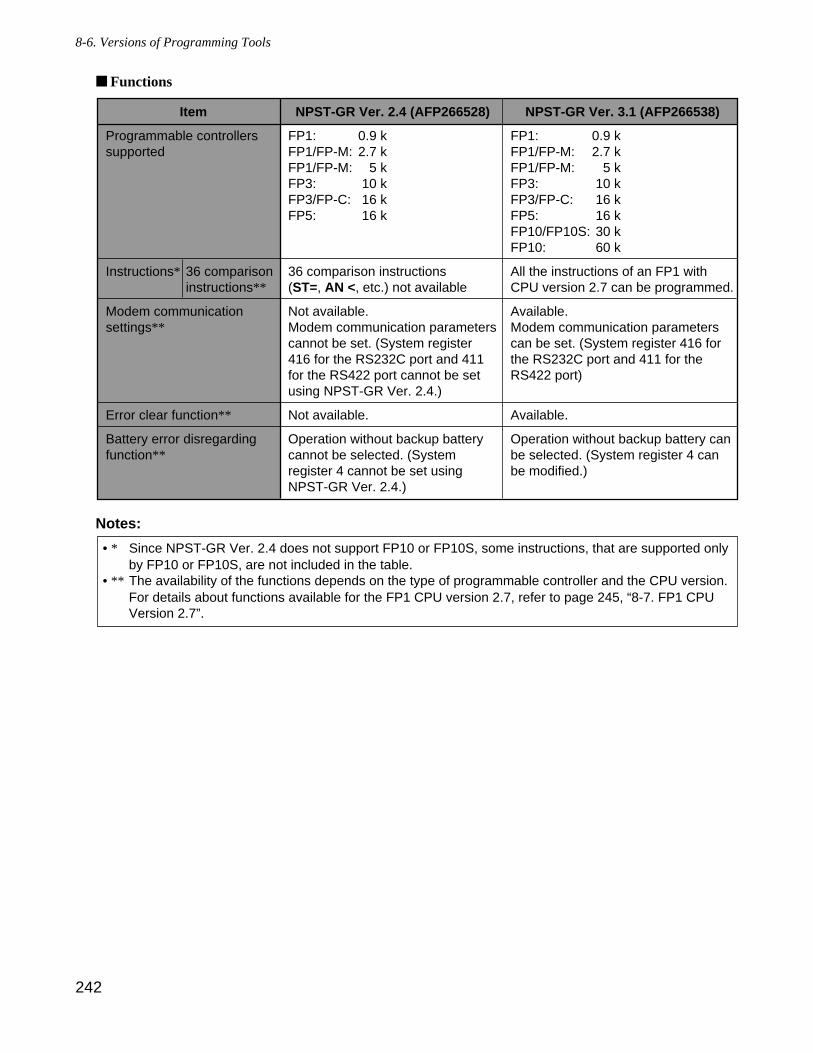
Functions
Notes:
• * Since NPST-GR Ver. 2.4 does not support FP10 or FP10S, some instructions, that are supported onlyby FP10 or FP10S, are not included in the table.
• ** The availability of the functions depends on the type of programmable controller and the CPU version.For details about functions available for the FP1 CPU version 2.7, refer to page 245, “8-7. FP1 CPUVersion 2.7”.
Item
Programmable controllers supported
Instructions*
Modem communication settings**
Error clear function**
Battery error disregarding function**
NPST-GR Ver. 2.4 (AFP266528)
FP1: FP1/FP-M: FP1/FP-M: FP3: FP3/FP-C: FP5:
36 comparison instructions (ST=, AN <, etc.) not available
Not available.Modem communication parameters cannot be set. (System register 416 for the RS232C port and 411 for the RS422 port cannot be set using NPST-GR Ver. 2.4.)
Not available.
Operation without backup battery cannot be selected. (System register 4 cannot be set using NPST-GR Ver. 2.4.)
NPST-GR Ver. 3.1 (AFP266538)
FP1: FP1/FP-M: FP1/FP-M: FP3: FP3/FP-C: FP5: FP10/FP10S: FP10:
All the instructions of an FP1 with CPU version 2.7 can be programmed.
Available.Modem communication parameters can be set. (System register 416 for the RS232C port and 411 for the RS422 port)
Available.
Operation without backup battery can be selected. (System register 4 can be modified.)
36 comparison instructions**
0.9 k2.7 k 5 k
10 k 16 k16 k
0.9 k2.7 k
5 k10 k16 k16 k30 k60 k
242
8-6. Versions of Programming Tools
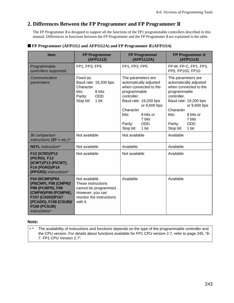
2. Differences Between the FP Programmer and FP Programmer IIThe FP Programmer II is designed to support all the functions of the FP1 programmable controllers described in thismanual. Differences in functions between the FP Programmer and the FP Programmer II are explained in the table.
FP Programmer (AFP1112 and AFP1112A) and FP Programmer II (AFP1114)
Note:
• * The availability of instructions and functions depends on the type of the programmable controller andthe CPU version. For details about functions available for FP1 CPU version 2.7, refer to page 245, “8-7. FP1 CPU Version 2.7”.
Item
Programmablecontrollers supported
Communicationparameters
36 comparison instructions (ST = etc.)*
NSTL instruction*
F12 (ICRD)/P12 (PICRD), F13 (ICWT)/P13 (PICWT), F14 (PGRD)/P14 (PPGRD) instructions*
F64 (BCMP)/P64 (PBCMP), F98 (CMPR)/P98 (PCMPR), F99(CMPW)/P99 (PCMPW), F157 (CADD)/P157 (PCADD), F158 (CSUB)/P158 (PCSUB) instructions*
FP Programmer (AFP1112)
FP1, FP3, FP5
Fixed as:Baud rate: Character bits: Parity: Stop bit:
Not available
Not available
Not available
Not available.These instructionscannot be programmed . However, you can monitor the instructions with it.
FP Programmer (AFP1112A)
FP1, FP3, FP5
The parameters are automatically adjusted when connected to the programmable controller.Baud rate:
Character bits:
Parity: Stop bit:
Not available
Available
Not available
Available
FP Programmer II(AFP1114)
FP-M, FP-C, FP1, FP3, FP5, FP10S, FP10
The parameters are automatically adjusted when connected to the programmable controller.Baud rate:
Character bits:
Parity: Stop bit:
Available
Available
Available
Available
19,200 bps
8 bitsODD1 bit 19,200 bps
or 9,600 bps
8 bits or 7 bitsODD1 bit
19,200 bps or 9,600 bps
8 bits or 7 bitsODD1 bit
243
8-6. Versions of Programming Tools
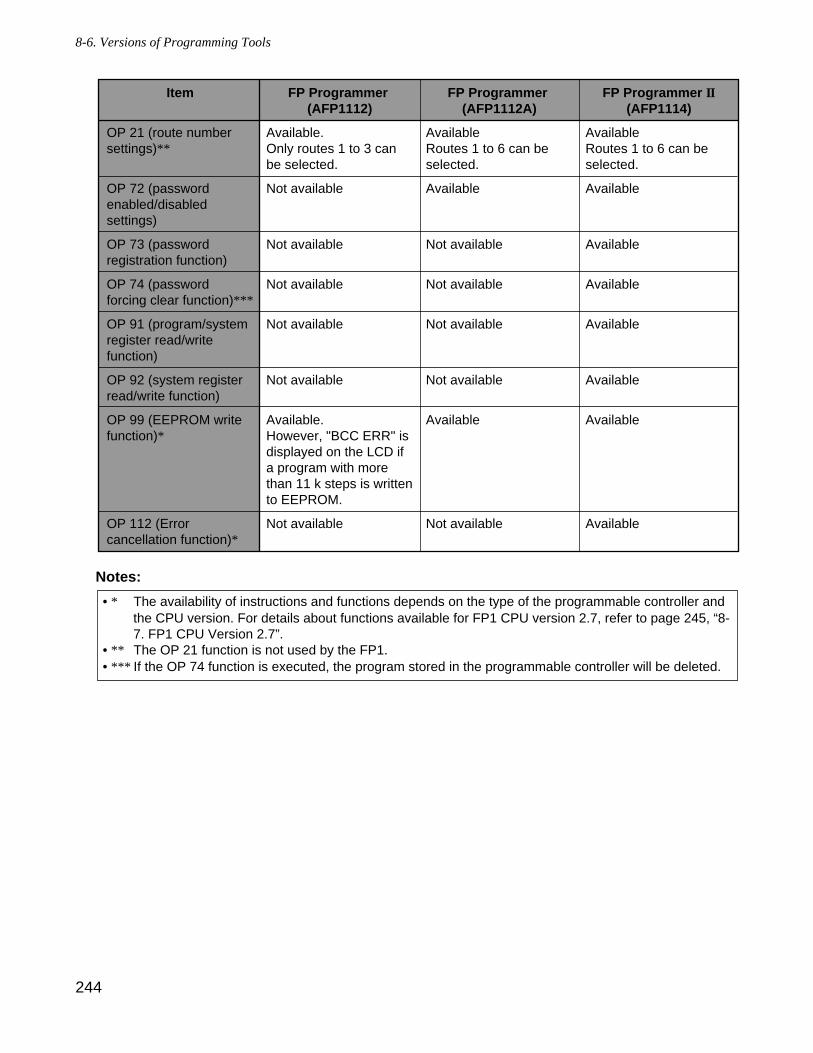
Notes:
• * The availability of instructions and functions depends on the type of the programmable controller andthe CPU version. For details about functions available for FP1 CPU version 2.7, refer to page 245, “8-7. FP1 CPU Version 2.7”.
• ** The OP 21 function is not used by the FP1.• *** If the OP 74 function is executed, the program stored in the programmable controller will be deleted.
Item
OP 21 (route number settings)**
OP 72 (password enabled/disabled settings)
OP 73 (password registration function)
OP 74 (password forcing clear function)***
OP 91 (program/system register read/write function)
OP 92 (system register read/write function)
OP 99 (EEPROM write function)*
OP 112 (Error cancellation function)*
FP Programmer (AFP1112)
Available.Only routes 1 to 3 can be selected.
Not available
Not available
Not available
Not available
Not available
Available.However, "BCC ERR" is displayed on the LCD if a program with more than 11 k steps is written to EEPROM.
Not available
FP Programmer (AFP1112A)
AvailableRoutes 1 to 6 can be selected.
Available
Not available
Not available
Not available
Not available
Available
Not available
FP Programmer II(AFP1114)
AvailableRoutes 1 to 6 can be selected.
Available
Available
Available
Available
Available
Available
Available
244
8-6. Versions of Programming Tools
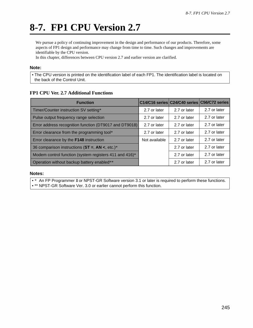
245
8-7. FP1 CPU Version 2.7
8-7. FP1 CPU Version 2.7We pursue a policy of continuing improvement in the design and performance of our products. Therefore, someaspects of FP1 design and performance may change from time to time. Such changes and improvements areidentifiable by the CPU version.In this chapter, differences between CPU version 2.7 and earlier version are clarified.
Note:
FP1 CPU Ver. 2.7 Additional Functions
Notes:
• * An FP Programmer II or NPST-GR Software version 3.1 or later is required to perform these functions.• ** NPST-GR Software Ver. 3.0 or earlier cannot perform this function.
Function
Timer/Counter instruction SV setting*
Pulse output frequency range selection
Error address recognition function (DT9017 and DT9018)
Error clearance from the programming tool*
Error clearance by the F148 instruction
36 comparison instructions (ST =, AN <, etc.)*
Modem control function (system registers 411 and 416)*
Operation without backup battery enabled**
C24/C40 series
2.7 or later
2.7 or later
2.7 or later
2.7 or later
2.7 or later
2.7 or later
2.7 or later
2.7 or later
C56/C72 series
2.7 or later
2.7 or later
2.7 or later
2.7 or later
2.7 or later
2.7 or later
2.7 or later
2.7 or later
C14/C16 series
2.7 or later
2.7 or later
2.7 or later
2.7 or later
Not available
• The CPU version is printed on the identification label of each FP1. The identification label is located onthe back of the Control Unit.
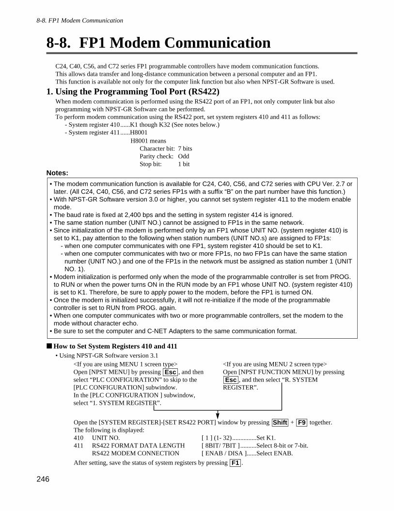
<If you are using MENU 1 screen type>Open [NPST MENU] by pressing , and thenselect “PLC CONFIGURATION” to skip to the[PLC CONFIGURATION] subwindow.In the [PLC CONFIGURATION ] subwindow,select “1. SYSTEM REGISTER”.
<If you are using MENU 2 screen type>Open [NPST FUNCTION MENU] by pressing
, and then select “R. SYSTEMREGISTER”. Esc
Esc
8-8. FP1 Modem CommunicationC24, C40, C56, and C72 series FP1 programmable controllers have modem communication functions.This allows data transfer and long-distance communication between a personal computer and an FP1.This function is available not only for the computer link function but also when NPST-GR Software is used.
1. Using the Programming Tool Port (RS422)When modem communication is performed using the RS422 port of an FP1, not only computer link but alsoprogramming with NPST-GR Software can be performed.To perform modem communication using the RS422 port, set system registers 410 and 411 as follows:
- System register 410......K1 though K32 (See notes below.)- System register 411......H8001
Notes:
How to Set System Registers 410 and 411• Using NPST-GR Software version 3.1
Open the [SYSTEM REGISTER]-[SET RS422 PORT] window by pressing + together. The following is displayed:410 UNIT NO. [ 1 ] (1- 32)...............Set K1.411 RS422 FORMAT DATA LENGTH [ 8BIT/ 7BIT ]..........Select 8-bit or 7-bit.
RS422 MODEM CONNECTION [ ENAB / DISA ]......Select ENAB.
After setting, save the status of system registers by pressing .F1
F9Shift
• The modem communication function is available for C24, C40, C56, and C72 series with CPU Ver. 2.7 orlater. (All C24, C40, C56, and C72 series FP1s with a suffix “B” on the part number have this function.)
• With NPST-GR Software version 3.0 or higher, you cannot set system register 411 to the modem enablemode.
• The baud rate is fixed at 2,400 bps and the setting in system register 414 is ignored.• The same station number (UNIT NO.) cannot be assigned to FP1s in the same network.• Since initialization of the modem is performed only by an FP1 whose UNIT NO. (system register 410) is
set to K1, pay attention to the following when station numbers (UNIT NO.s) are assigned to FP1s:- when one computer communicates with one FP1, system register 410 should be set to K1.- when one computer communicates with two or more FP1s, no two FP1s can have the same station
number (UNIT NO.) and one of the FP1s in the network must be assigned as station number 1 (UNITNO. 1).
• Modem initialization is performed only when the mode of the programmable controller is set from PROG.to RUN or when the power turns ON in the RUN mode by an FP1 whose UNIT NO. (system register 410)is set to K1. Therefore, be sure to apply power to the modem, before the FP1 is turned ON.
• Once the modem is initialized successfully, it will not re-initialize if the mode of the programmablecontroller is set to RUN from PROG. again.
• When one computer communicates with two or more programmable controllers, set the modem to themode without character echo.
• Be sure to set the computer and C-NET Adapters to the same communication format.
H8001 meansCharacter bit: 7 bitsParity check: OddStop bit: 1 bit
246
8-8. FP1 Modem Communication
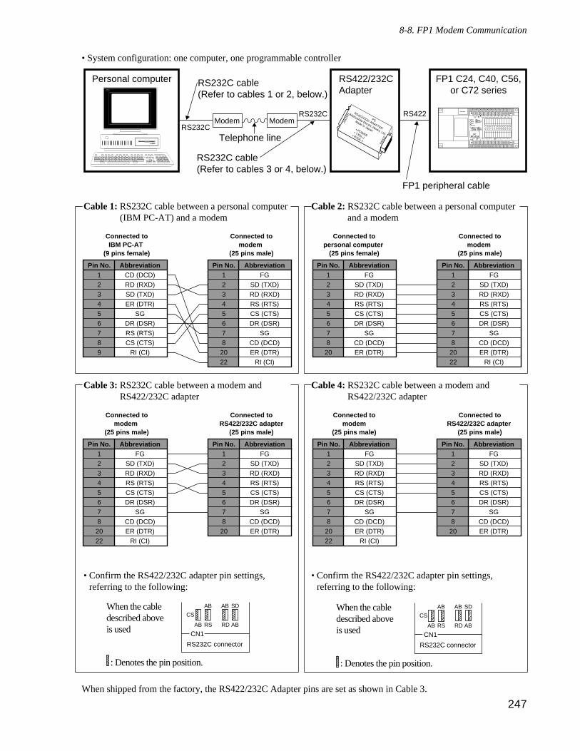
• System configuration: one computer, one programmable controller
When shipped from the factory, the RS422/232C Adapter pins are set as shown in Cable 3.
CN1
RS232C connector
AB
CS
RS
AB
RD AB
SDABWhen the cable described above is used
: Denotes the pin position.
CN1
RS232C connector
AB
CS
RS
AB
RD AB
SDAB
: Denotes the pin position.
When the cable described above is used
• Confirm the RS422/232C adapter pin settings,referring to the following:
• Confirm the RS422/232C adapter pin settings,referring to the following:
Connected tomodem
(25 pins male)
Pin No.1
2
3
4
5
6
7
8
20
AbbreviationFG
SD (TXD)
RD (RXD)
RS (RTS)
CS (CTS)
DR (DSR)
SG
CD (DCD)
ER (DTR)
Pin No.1
2
3
4
5
6
7
8
20
AbbreviationFG
SD (TXD)
RD (RXD)
RS (RTS)
CS (CTS)
DR (DSR)
SG
CD (DCD)
ER (DTR)
Connected toRS422/232C adapter
(25 pins male)
Connected tomodem
(25 pins male)
Connected toRS422/232C adapter
(25 pins male)
Pin No.1
2
3
4
5
6
7
8
20
22
AbbreviationFG
SD (TXD)
RD (RXD)
RS (RTS)
CS (CTS)
DR (DSR)
SG
CD (DCD)
ER (DTR)
RI (CI)
Pin No.1
2
3
4
5
6
7
8
20
22
AbbreviationFG
SD (TXD)
RD (RXD)
RS (RTS)
CS (CTS)
DR (DSR)
SG
CD (DCD)
ER (DTR)
RI (CI)
Cable 3: RS232C cable between a modem andRS422/232C adapter
Cable 4: RS232C cable between a modem andRS422/232C adapter
Connected toIBM PC-AT
(9 pins female)
Pin No.1
2
3
4
5
6
7
8
20
AbbreviationFG
SD (TXD)
RD (RXD)
RS (RTS)
CS (CTS)
DR (DSR)
SG
CD (DCD)
ER (DTR)
Pin No.1
2
3
4
5
6
7
8
9
AbbreviationCD (DCD)
RD (RXD)
SD (TXD)
ER (DTR)
SG
DR (DSR)
RS (RTS)
CS (CTS)
RI (CI)
Connected tomodem
(25 pins male)
Connected topersonal computer
(25 pins female)
Connected tomodem
(25 pins male)
Pin No.1
2
3
4
5
6
7
8
20
22
AbbreviationFG
SD (TXD)
RD (RXD)
RS (RTS)
CS (CTS)
DR (DSR)
SG
CD (DCD)
ER (DTR)
RI (CI)
Pin No.1
2
3
4
5
6
7
8
20
22
AbbreviationFG
SD (TXD)
RD (RXD)
RS (RTS)
CS (CTS)
DR (DSR)
SG
CD (DCD)
ER (DTR)
RI (CI)
Cable 1: RS232C cable between a personal computer(IBM PC-AT) and a modem
Cable 2: RS232C cable between a personal computerand a modem
FP1 C24, C40, C56,or C72 series
PC
RS422/232C ADAPTER
Matsushita Electric Works, Ltd.
Made in Japan
• POWER
• TXD(–)
• RXD(–)
RS
422
RS
232C
RS422/232CAdapter
FP1 peripheral cable
COM0
COM1
COM2
COM3
COM4
COM5
COM6
COM7
+ -24V DC
F.G.
COMF
89
EAB
CD(+)-
COM7
01
623
45(+)-
RUNREMOTEPROG.
V0
max.min.
RUN
PROG.
ERR.
ALRAM
BATTERY
V1
max.
PCFP1-C24
24V DC+
-
min.
RS232C cable(Refer to cables 1 or 2, below.)
Personal computer
RS422
RS232C
RS232C
RS232C cable(Refer to cables 3 or 4, below.)
Telephone line
Modem Modem
247
8-8. FP1 Modem Communication
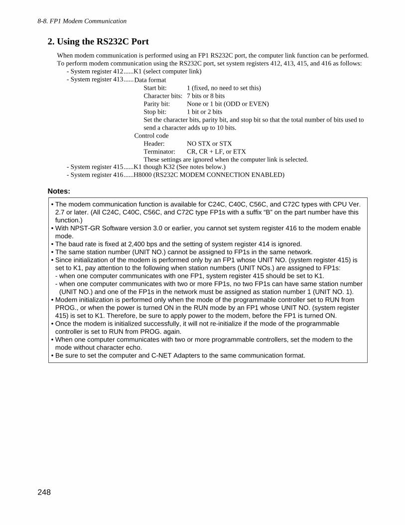
2. Using the RS232C Port When modem communication is performed using an FP1 RS232C port, the computer link function can be performed.To perform modem communication using the RS232C port, set system registers 412, 413, 415, and 416 as follows:
- System register 412......K1 (select computer link)- System register 413......
- System register 415......K1 though K32 (See notes below.)- System register 416......H8000 (RS232C MODEM CONNECTION ENABLED)
Notes:
• The modem communication function is available for C24C, C40C, C56C, and C72C types with CPU Ver.2.7 or later. (All C24C, C40C, C56C, and C72C type FP1s with a suffix “B” on the part number have thisfunction.)
• With NPST-GR Software version 3.0 or earlier, you cannot set system register 416 to the modem enablemode.
• The baud rate is fixed at 2,400 bps and the setting of system register 414 is ignored.• The same station number (UNIT NO.) cannot be assigned to FP1s in the same network.• Since initialization of the modem is performed only by an FP1 whose UNIT NO. (system register 415) is
set to K1, pay attention to the following when station numbers (UNIT NOs.) are assigned to FP1s:- when one computer communicates with one FP1, system register 415 should be set to K1.- when one computer communicates with two or more FP1s, no two FP1s can have same station number
(UNIT NO.) and one of the FP1s in the network must be assigned as station number 1 (UNIT NO. 1).• Modem initialization is performed only when the mode of the programmable controller set to RUN from
PROG., or when the power is turned ON in the RUN mode by an FP1 whose UNIT NO. (system register415) is set to K1. Therefore, be sure to apply power to the modem, before the FP1 is turned ON.
• Once the modem is initialized successfully, it will not re-initialize if the mode of the programmablecontroller is set to RUN from PROG. again.
• When one computer communicates with two or more programmable controllers, set the modem to themode without character echo.
• Be sure to set the computer and C-NET Adapters to the same communication format.
Data formatStart bit: 1 (fixed, no need to set this)Character bits: 7 bits or 8 bitsParity bit: None or 1 bit (ODD or EVEN)Stop bit: 1 bit or 2 bitsSet the character bits, parity bit, and stop bit so that the total number of bits used tosend a character adds up to 10 bits.
Control codeHeader: NO STX or STXTerminator: CR, CR + LF, or ETXThese settings are ignored when the computer link is selected.
248
8-8. FP1 Modem Communication
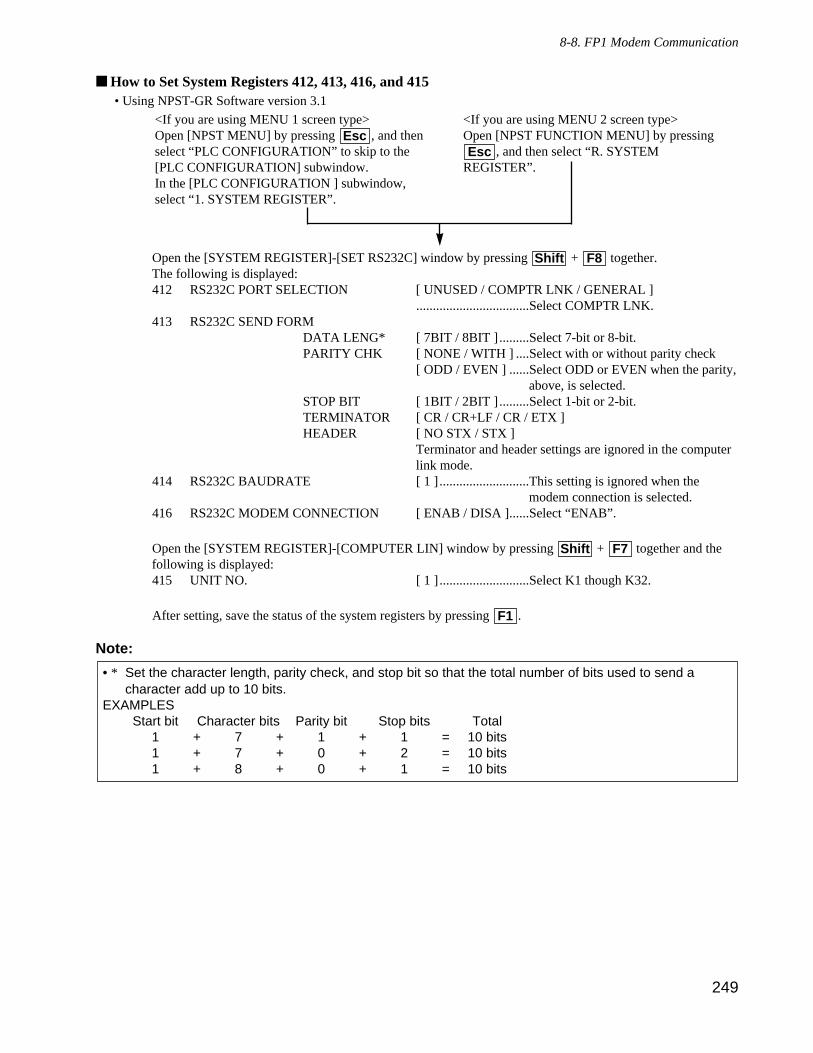
249
8-8. FP1 Modem Communication
How to Set System Registers 412, 413, 416, and 415• Using NPST-GR Software version 3.1
Open the [SYSTEM REGISTER]-[SET RS232C] window by pressing + together. The following is displayed:412 RS232C PORT SELECTION [ UNUSED / COMPTR LNK / GENERAL ]
..................................Select COMPTR LNK.413 RS232C SEND FORM
DATA LENG* [ 7BIT / 8BIT ].........Select 7-bit or 8-bit.PARITY CHK [ NONE / WITH ] ....Select with or without parity check
[ ODD / EVEN ] ......Select ODD or EVEN when the parity,above, is selected.
STOP BIT [ 1BIT / 2BIT ].........Select 1-bit or 2-bit.TERMINATOR [ CR / CR+LF / CR / ETX ]HEADER [ NO STX / STX ]
Terminator and header settings are ignored in the computerlink mode.
414 RS232C BAUDRATE [ 1 ]...........................This setting is ignored when themodem connection is selected.
416 RS232C MODEM CONNECTION [ ENAB / DISA ]......Select “ENAB”.
Open the [SYSTEM REGISTER]-[COMPUTER LIN] window by pressing + together and thefollowing is displayed:415 UNIT NO. [ 1 ] ...........................Select K1 though K32.
After setting, save the status of the system registers by pressing .
Note:
• * Set the character length, parity check, and stop bit so that the total number of bits used to send acharacter add up to 10 bits.
EXAMPLESStart bit Character bits Parity bit Stop bits Total
1 + 7 + 1 + 1 = 10 bits1 + 7 + 0 + 2 = 10 bits1 + 8 + 0 + 1 = 10 bits
F1
F7Shift
F8Shift
<If you are using MENU 1 screen type>Open [NPST MENU] by pressing , and thenselect “PLC CONFIGURATION” to skip to the[PLC CONFIGURATION] subwindow.In the [PLC CONFIGURATION ] subwindow,select “1. SYSTEM REGISTER”.
<If you are using MENU 2 screen type>Open [NPST FUNCTION MENU] by pressing
, and then select “R. SYSTEMREGISTER”. Esc
Esc
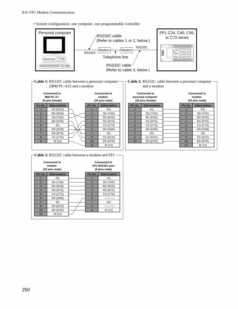
250
8-8. FP1 Modem Communication
• System configuration: one computer, one programmable controller
Connected tomodem
(25 pins male)
Pin No.1
2
3
4
5
6
7
8
9
AbbreviationFG
SD (TXD)
RD (RXD)
RS (RTS)
CS (CTS)
SG
RI (CI)
Connected toFP1 RS232C port
(9 pins male)
Pin No.1
2
3
4
5
6
7
8
20
22
AbbreviationFG
SD (TXD)
RD (RXD)
RS (RTS)
CS (CTS)
DR (DSR)
SG
CD (DCD)
ER (DTR)
RI (CI)
Cable 3: RS232C cable between a modem and FP1
Connected toIBM PC-AT
(9 pins female)
Pin No.1
2
3
4
5
6
7
8
20
AbbreviationFG
SD (TXD)
RD (RXD)
RS (RTS)
CS (CTS)
DR (DSR)
SG
CD (DCD)
ER (DTR)
Pin No.1
2
3
4
5
6
7
8
9
AbbreviationCD (DCD)
RD (RXD)
SD (TXD)
ER (DTR)
SG
DR (DSR)
RS (RTS)
CS (CTS)
RI (CI)
Connected tomodem
(25 pins male)
Connected topersonal computer
(25 pins female)
Connected tomodem
(25 pins male)
Pin No.1
2
3
4
5
6
7
8
20
22
AbbreviationFG
SD (TXD)
RD (RXD)
RS (RTS)
CS (CTS)
DR (DSR)
SG
CD (DCD)
ER (DTR)
RI (CI)
Pin No.1
2
3
4
5
6
7
8
20
22
AbbreviationFG
SD (TXD)
RD (RXD)
RS (RTS)
CS (CTS)
DR (DSR)
SG
CD (DCD)
ER (DTR)
RI (CI)
Cable 1: RS232C cable between a personal computer(IBM PC-AT) and a modem
Cable 2: RS232C cable between a personal computerand a modem
FP1 C24, C40, C56,or C72 series
COM0
COM1
COM2
COM3
COM4
COM5
COM6
COM7
+ -24V DC
F.G.
COMF
89
EAB
CD(+)-
COM7
01
623
45(+)-
RUNREMOTEPROG.
V0
max.min.
RUN
PROG.
ERR.
ALRAM
BATTERY
V1
max.
PCFP1-C24
24V DC+
-
min.
RS232C cable(Refer to cables 1 or 2, below.)
Personal computer
RS232C
RS232C
RS232C cable(Refer to cable 3, below.)
Telephone line
Modem Modem
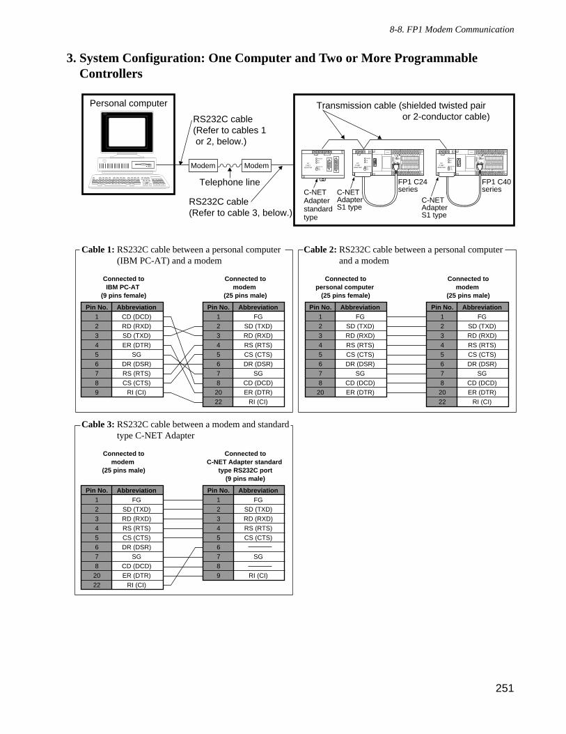
251
8-8. FP1 Modem Communication
3. System Configuration: One Computer and Two or More ProgrammableControllers
Connected tomodem
(25 pins male)
Pin No.1
2
3
4
5
6
7
8
9
AbbreviationFG
SD (TXD)
RD (RXD)
RS (RTS)
CS (CTS)
SG
RI (CI)
Connected toC-NET Adapter standard
type RS232C port(9 pins male)
Pin No.1
2
3
4
5
6
7
8
20
22
AbbreviationFG
SD (TXD)
RD (RXD)
RS (RTS)
CS (CTS)
DR (DSR)
SG
CD (DCD)
ER (DTR)
RI (CI)
Cable 3: RS232C cable between a modem and standardtype C-NET Adapter
Connected toIBM PC-AT
(9 pins female)
Pin No.1
2
3
4
5
6
7
8
20
AbbreviationFG
SD (TXD)
RD (RXD)
RS (RTS)
CS (CTS)
DR (DSR)
SG
CD (DCD)
ER (DTR)
Pin No.1
2
3
4
5
6
7
8
9
AbbreviationCD (DCD)
RD (RXD)
SD (TXD)
ER (DTR)
SG
DR (DSR)
RS (RTS)
CS (CTS)
RI (CI)
Connected tomodem
(25 pins male)
Connected topersonal computer
(25 pins female)
Connected tomodem
(25 pins male)
Pin No.1
2
3
4
5
6
7
8
20
22
AbbreviationFG
SD (TXD)
RD (RXD)
RS (RTS)
CS (CTS)
DR (DSR)
SG
CD (DCD)
ER (DTR)
RI (CI)
Pin No.1
2
3
4
5
6
7
8
20
22
AbbreviationFG
SD (TXD)
RD (RXD)
RS (RTS)
CS (CTS)
DR (DSR)
SG
CD (DCD)
ER (DTR)
RI (CI)
Cable 1: RS232C cable between a personal computer(IBM PC-AT) and a modem
Cable 2: RS232C cable between a personal computerand a modem
RS232C cable(Refer to cables 1 or 2, below.)
Personal computer
RS232C cable(Refer to cable 3, below.)
Telephone line
Modem Modem
COM0
COM1
COM2
COM3
COM4
COM5
COM6
COM7
+ -24V DC
F.G.
COMF
89
EAB
CD(+)-
COM7
01
623
45(+)-
RUNREMOTEPROG.
V0
max.min.
RUN
PROG.
ERR.
ALRAM
BATTERY
V1
max.
24V DC+
-
min.
PCC-NET
ADAPTER ONOFF
ON
ON
ABCDEF
ABCDEFGHI
AB ABCD
PCC-NET
ADAPTER ONOFF
ON
ON
ABCDEF
ABCDEFGHI
AB
C-NETAdapterstandardtype
FP1 C40series
C-NET AdapterS1 type
COM0
COM1
COM2
COM3
COM4
COM5
COM6
COM7
+ -24V DC
F.G.
COMF
89
EAB
CD(+)-
COM7
01
623
45(+)-
RUNREMOTEPROG.
V0
max.min.
RUN
PROG.
ERR.
ALRAM
BATTERY
V1
max.
24V DC+
-
min.
PCC-NET
ADAPTER ONOFF
ON
ON
ABCDEF
ABCDEFGHI
AB
FP1 C24seriesC-NET
AdapterS1 type
Transmission cable (shielded twisted pair or 2-conductor cable)
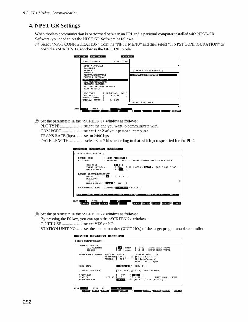
4. NPST-GR SettingsWhen modem communication is performed between an FP1 and a personal computer installed with NPST-GRSoftware, you need to set the NPST-GR Software as follows.1 Select “NPST CONFIGURATION” from the “NPST MENU” and then select “1. NPST CONFIGURATION” to
open the <SCREEN 1> window in the OFFLINE mode.
2 Set the parameters in the <SCREEN 1> window as follows:PLC TYPE ........................select the one you want to communicate with.COM PORT ......................select 1 or 2 of your personal computerTRANS RATE (bps).........set to 2400 bpsDATE LENGTH............... select 8 or 7 bits according to that which you specified for the PLC.
3 Set the parameters in the <SCREEN 2> window as follows:By pressing the F6 key, you can open the <SCREEN 2> window.C-NET USE ......................select YES or NOSTATION UNIT NO. .......set the station number (UNIT NO.) of the target programmable controller.
SAVE INIT LOAD SCRN 1 MODEM INST RELAY FUN 1
OFFLINE NPST CONFG <SCREEN 2>
ADDR 0 SIZE 0 NOP : 1 2 3 4 5 6 7 8 9 10
[ NPST CONFIGURATION ]
COMMENT LENGTH I/O COMMENT [ 12 ] char ( 12-40 ) ENTER EVEN VALUE REMARK [ 20 ] char ( 12-40 ) ENTER EVEN VALUE NUMBER OF COMMENT I/O CMT 14034 CURRENT REG: 0 REGISTER[ 1001 ] word (50 word or more) REMARK [ 700 ] (22 byte/remark) REST : 33543 byte
MENU TYPE [ MENU 1 / MENU 2 ]
DISPLAY LANGUAGE [ ENGLISH ]([ENTER]:OPENS WINDOW)
C-NET USE [ YES / NO ] STATION UNIT NO.[ 1 ] ( 0 - 64 ) UNIT NO=0...HOME MEWNET-H USE [ NONE / USE (RS422) / USE (RS232C)]
SAVE INIT LOAD SCRN 2 MODEM INST RELAY FUN 1
OFFLINE NPST CONFG <SCREEN 1>
ADDR 0 SIZE 0 NOP : 1 2 3 4 5 6 7 8 9 10
[ NPST CONFIGURATION ]
SCREEN MODE [ MONO / COLOR ] PLC TYPE [ FP3/FP-C 16k ]([ENTER]:OPENS SELECTION WINDOW)
COM PORT [ 1 2 ] TRANS RATE(bps) [ 19200 / 9600 / 4800 / 2400 / 1200 / 600 / 300 ] DATA LENGTH [ 8 / 7 ] bit
LOGGED DRICVE/DIRECTORY DRIVE [ A B C D E ] DIRECTORY [ ] NOTE DISPLAY [ ON / OFF ]
PROGRAMMING MODE [LADDER/ B.LADDER / BOOLN ]
NOTE : SPECIFY TRANS RATE TO 9600 or 19200bps TO CONNECT WITH PLC DIRECTLY
OFFLINE NPST MENU BOOLEAN
ADDR 0 SIZE 0 NOP : 1 2 3 4 5 6 7 8 9 10 EXIT
[ NPST MENU ] (Ver. 3.14)
EDIT A PROGRAM COMMENTS SEARCH [ NPST CONFIGURATION ] MONITOR RELAYS/REGISTERS 1.NPST CONFIGURATION CHECK A PROGRAM NPST CONFIGURATION PLC CONFIGURATION PROGRAM MANAGER IC CARD PROGRAM MANAGER EXIT NPST-GR
PLC TYPE [ FP3/FP-C 16k ] PLC MODE [ OFFLINE ] PROGRAM NAME [ ] USE/MAX (STEP) [ 0/ 7679] **= NOT AVAILABLE
252
8-8. FP1 Modem Communication
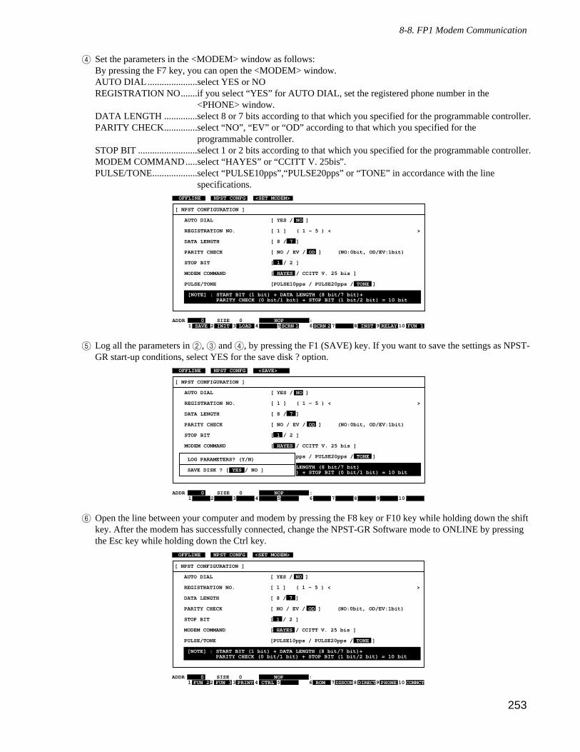
4 Set the parameters in the <MODEM> window as follows:By pressing the F7 key, you can open the <MODEM> window.AUTO DIAL.....................select YES or NOREGISTRATION NO.......if you select “YES” for AUTO DIAL, set the registered phone number in the
<PHONE> window.DATA LENGTH ..............select 8 or 7 bits according to that which you specified for the programmable controller.PARITY CHECK..............select “NO”, “EV” or “OD” according to that which you specified for the
programmable controller.STOP BIT .........................select 1 or 2 bits according to that which you specified for the programmable controller.MODEM COMMAND.....select “HAYES” or “CCITT V. 25bis”.PULSE/TONE...................select “PULSE10pps”,“PULSE20pps” or “TONE” in accordance with the line
specifications.
5 Log all the parameters in 2, 3 and 4, by pressing the F1 (SAVE) key. If you want to save the settings as NPST-GR start-up conditions, select YES for the save disk ? option.
6 Open the line between your computer and modem by pressing the F8 key or F10 key while holding down the shiftkey. After the modem has successfully connected, change the NPST-GR Software mode to ONLINE by pressingthe Esc key while holding down the Ctrl key.
FUN 2 FUN 3 PRINT ROM PHONE CONNCTDISCON
[ NPST CONFIGURATION ]
AUTO DIAL [ YES / NO ]
REGISTRATION NO. [ 1 ] ( 1 - 5 ) < >
DATA LENGTH [ 8 / 7 ]
PARITY CHECK [ NO / EV / OD ] (NO:0bit, OD/EV:1bit)
STOP BIT [ 1 / 2 ]
MODEM COMMAND [ HAYES / CCITT V. 25 bis ]
PULSE/TONE [PULSE10pps / PULSE20pps / TONE ]
[NOTE] : START BIT (1 bit) + DATA LENGTH (8 bit/7 bit)+ PARITY CHECK (0 bit/1 bit) + STOP BIT (1 bit/2 bit) = 10 bit
CTRL DIRECT
OFFLINE NPST CONFG <SET MODEM>
ADDR 0 SIZE 0 NOP : 1 2 3 4 5 6 7 8 9 10
OFFLINE NPST CONFG <SAVE>
ADDR 0 SIZE 0 NOP : 1 2 3 4 5 6 7 8 9 10
[ NPST CONFIGURATION ]
AUTO DIAL [ YES / NO ]
REGISTRATION NO. [ 1 ] ( 1 - 5 ) < >
DATA LENGTH [ 8 / 7 ]
PARITY CHECK [ NO / EV / OD ] (NO:0bit, OD/EV:1bit)
STOP BIT [ 1 / 2 ]
MODEM COMMAND [ HAYES / CCITT V. 25 bis ]
PULSE/TONE [PULSE10pps / PULSE20pps / TONE ]
[NOTE] : START BIT (1 bit) + DATA LENGTH (8 bit/7 bit) PARITY CHECK (0 bit/1 bit) + STOP BIT (0 bit/1 bit) = 10 bit
LOG PARAMETERS? (Y/N)
SAVE DISK ? [ YES / NO ]
SAVE INIT LOAD SCRN 1 INST RELAY FUN 1
OFFLINE NPST CONFG <SET MODEM>
ADDR 0 SIZE 0 NOP : 1 2 3 4 5 6 7 8 9 10 SCRN 2
[ NPST CONFIGURATION ]
AUTO DIAL [ YES / NO ]
REGISTRATION NO. [ 1 ] ( 1 - 5 ) < >
DATA LENGTH [ 8 / 7 ]
PARITY CHECK [ NO / EV / OD ] (NO:0bit, OD/EV:1bit)
STOP BIT [ 1 / 2 ]
MODEM COMMAND [ HAYES / CCITT V. 25 bis ]
PULSE/TONE [PULSE10pps / PULSE20pps / TONE ]
[NOTE] : START BIT (1 bit) + DATA LENGTH (8 bit/7 bit)+ PARITY CHECK (0 bit/1 bit) + STOP BIT (1 bit/2 bit) = 10 bit
253
8-8. FP1 Modem Communication
254
8-9. Terminology
8-9. TerminologyAn alphanumeric value that identifies where data is stored.
The temperature of the air surrounding a system.
A standard system used for designating the size of electrical conductors.Larger gauge numbers have smaller diameter.
A Boolean operation that produces a logic “1” output if all inputs are “1”,and a logic “0” if any input is “0”.
American Standard Code for Information Interchange. ASCII is normallyused when alphanumeric (letters and decimal numbers) and control codes aresent as information to printers, etc. ASCII can be represented using 7 or 8bits and is often expressed in a 2-digit hexadecimal form converted fromspecific binary expressions. ASCII expressed in 2-digit hexadecimals iscalled “ASCII HEX code”. For details about actual ASCII codes, refer to thetable for ASCII.[EXAMPLE] When a letter “M” is expressed in ASCII code:
7-bit ASCII : 1001101 (binary)ASCII HEX code: 4D (hexadecimal)
Not synchronous. Repeated operations that take place in patterns unrelatedover time.
See American Wire Gauge (AWG).
A printed circuit board located in the back of a chassis, that contains a databus, power bus, and mating connectors for units. For FP3, FP5, FP10S andFP10 programmable controllers, two types of backplanes are available:
Master Backplane Expansion Backplane
A device that is kept available to replace something that may fail duringoperation.
A battery or set of batteries that will provide power to the processor memoryonly when system power is lost. C24, C40, C56, and C72 series FP1programmable controllers have a battery backup system.
A condition that exists when the backup battery voltage drops low enough torequire battery replacement. For FP1 C24, C40, C56, and C72 series, theERR. LED turns ON.
Formally defined as the shortest pulse width in data communication.However, usually used to refer to the number of binary bits transmitted persecond (bps) during serial data communication.
See Block Check Code
See Binary Coded Decimal
address:
ambient temperature:
American Wire Gauge (AWG):
AND:
ASCII:
asynchronous:
AWG:
backplane:
backup:
battery backup:
battery low:
baud:
BCC:
BCD:
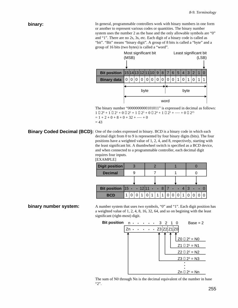
255
8-9. Terminology
In general, programmable controllers work with binary numbers in one formor another to represent various codes or quantities. The binary numbersystem uses the number 2 as the base and the only allowable symbols are “0”and “1”. There are no 2s, 3s, etc. Each digit of a binary code is called as“bit”. “Bit” means “binary digit”. A group of 8 bits is called a “byte” and agroup of 16 bits (two bytes) is called a “word”.
The binary number “0000000000101011” is expressed in decimal as follows:1 × 20 + 1 × 21 + 0 × 22 + 1 × 23 + 0 × 24 + 1 × 25 + ..... + 0 × 215
= 1 + 2 + 0 + 8 + 0 + 32 + ..... + 0= 43
One of the codes expressed in binary. BCD is a binary code in which eachdecimal digit from 0 to 9 is represented by four binary digits (bits). The fourpositions have a weighted value of 1, 2, 4, and 8, respectively, starting withthe least significant bit. A thumbwheel switch is specified as a BCD device,and when connected to a programmable controller, each decimal digitrequires four inputs.[EXAMPLE]
A number system that uses two symbols, “0” and “1”. Each digit position hasa weighted value of 1, 2, 4, 8, 16, 32, 64, and so on begining with the leastsignificant (right-most) digit.
The sum of N0 through Nn is the decimal equivalent of the number in base“2”.
• Z2Zn • • • • Z3 Z1 Z0
Bit position
Z0 × 20 = N0
• 2n • • • • 3 1 0 Base = 2
Z1 × 21 = N1
Z2 × 22 = N2
Z3 × 23 = N3
Zn × 2n = Nn
•••
0
0
1
1Digit position
Decimal 9
3
7
2
0 0
11
1
8
1 0 00
3 0
1
15
0 1
12
1 1 00
7 4
0 0
Bit position
BCD
• • • • • • • •
0 0
11
0
8
0 1 11
3 0
0
15
0
14 13
0
12
0
10
0
9
0
2 1
0
7 4
0
6
1
5Bit position
Binary data
Most significant bit(MSB)
Least significant bit(LSB)
byte byte
word
binary:
Binary Coded Decimal (BCD):
binary number system:
This code is used to detect errors in message transmissions. It is created byExclusive ORing all of the codes from the header though the last textcharacter, then translating the result (8-bit) data into two ASCII characters.
A group of registers used for temporary data storage. This is used for datatransmission and works effectively when there are transmission ratedifferences between sending and receiving devices.
Software errors which will cause unexpected actions.
Power distribution conductors.
The Central Processing Unit is usually referred to as the CPU.The CPU controls system activities of the programmable controller.
A symbol such as a letter of the alphabet or decimal number. An ASCIIcharacter is most commonly used to express characters using binary.
A logical operation that inverts a signal or bit. The complement of “1” is “0”,and the complement of “0” is “1”.
One of the communication methods between a computer and programmablecontrollers. In a computer link, the computer is the host, and it can controlprogrammable controllers using a protocol. For FP series programmablecontrollers, communication between a computer and programmablecontrollers is performed using MEWTOCOL-COM, a half-duplexcommunication protocol. From the computer, you can read, write, or monitordata stored in the memory of a programmable controller.
See Central Processing Unit.
Abbreviation for cathode-ray tube.
Removing errors from a program.
The decimal number system uses the number 10 as the base and theallowable symbols are “0”, “1”, “2”, “3”, “4”, “5”, “6”, “7”, “8”, and “9”.Each digit position has a weighted value of 1, 10, 100, 1000, and so on,begining with the least significant (right-most) digit.
See full-duplex.
Electrically Erasable Programmable Read Only Memory. EEPROM can beprogrammed and erased by electrical pulses.
Erasable Programmable Read Only Memory. EPROM can be reprogrammedafter being entirely erased with the use of an ultra-violet light source.
See First-In-First-Out.
The order that data is written in, and read from registers.
A relay used to detect and remember certain events in the programmablecontroller. In FP series programmable controllers, some of the specialinternal relays are used as flags.
256
8-9. Terminology
Block Check Code (BCC):
buffer:
bug:
bus:
Central Processing Unit:
character:
complement:
computer link:
CPU:
CRT:
debug:
decimal number system:
duplex:
EEPROM:
EPROM:
FIFO:
First-In-First-Out:
flag:
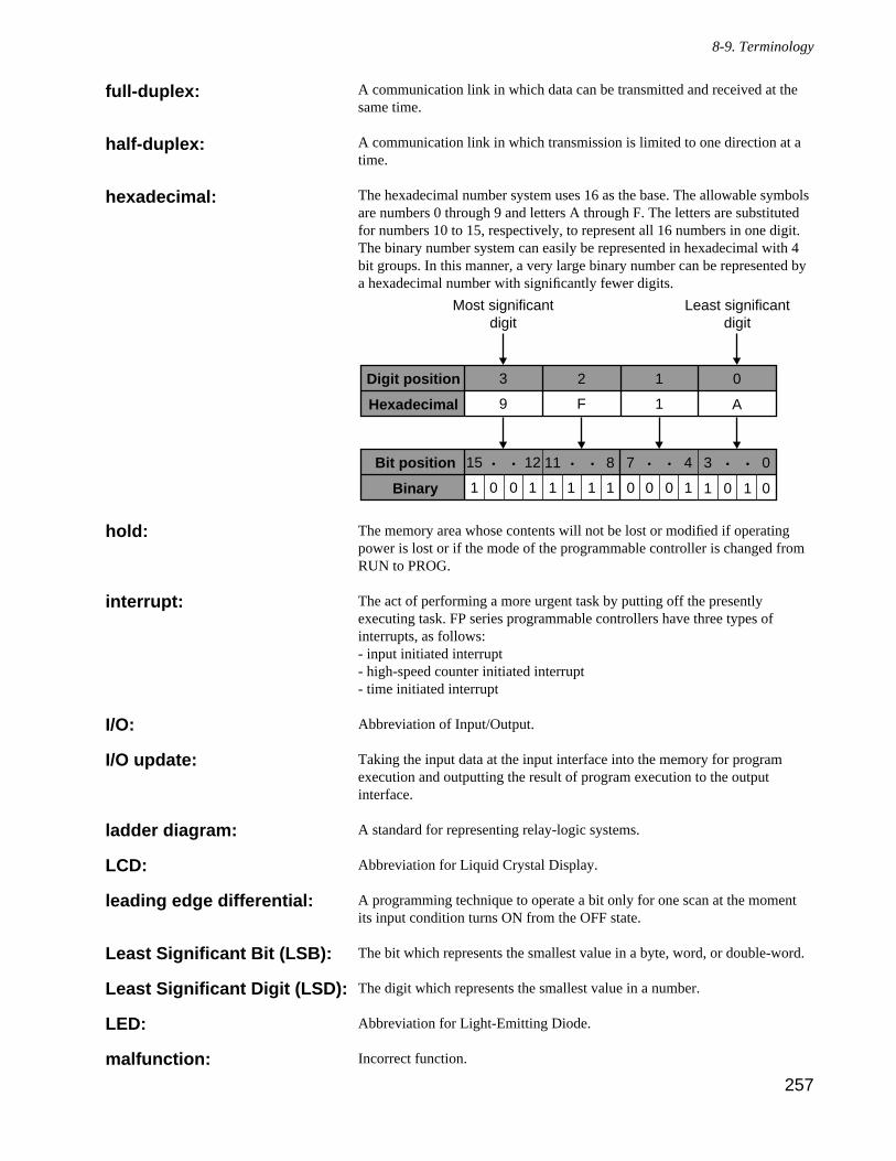
A communication link in which data can be transmitted and received at thesame time.
A communication link in which transmission is limited to one direction at atime.
The hexadecimal number system uses 16 as the base. The allowable symbolsare numbers 0 through 9 and letters A through F. The letters are substitutedfor numbers 10 to 15, respectively, to represent all 16 numbers in one digit.The binary number system can easily be represented in hexadecimal with 4bit groups. In this manner, a very large binary number can be represented bya hexadecimal number with significantly fewer digits.
The memory area whose contents will not be lost or modified if operatingpower is lost or if the mode of the programmable controller is changed fromRUN to PROG.
The act of performing a more urgent task by putting off the presentlyexecuting task. FP series programmable controllers have three types ofinterrupts, as follows:- input initiated interrupt- high-speed counter initiated interrupt- time initiated interrupt
Abbreviation of Input/Output.
Taking the input data at the input interface into the memory for programexecution and outputting the result of program execution to the outputinterface.
A standard for representing relay-logic systems.
Abbreviation for Liquid Crystal Display.
A programming technique to operate a bit only for one scan at the momentits input condition turns ON from the OFF state.
The bit which represents the smallest value in a byte, word, or double-word.
The digit which represents the smallest value in a number.
Abbreviation for Light-Emitting Diode.
Incorrect function.
A
0
1
1Digit position
Hexadecimal 9
3
F
2
0 1
11
1
8
1 1 01
3 0
1
15
0 1
12
1 1 00
7 4
0 0
Bit position
Binary
• • • • • • • •
Most significantdigit
Least significantdigit
257
8-9. Terminology
full-duplex:
half-duplex:
hexadecimal:
hold:
interrupt:
I/O:
I/O update:
ladder diagram:
LCD:
leading edge differential:
Least Significant Bit (LSB):
Least Significant Digit (LSD):
LED:
malfunction:
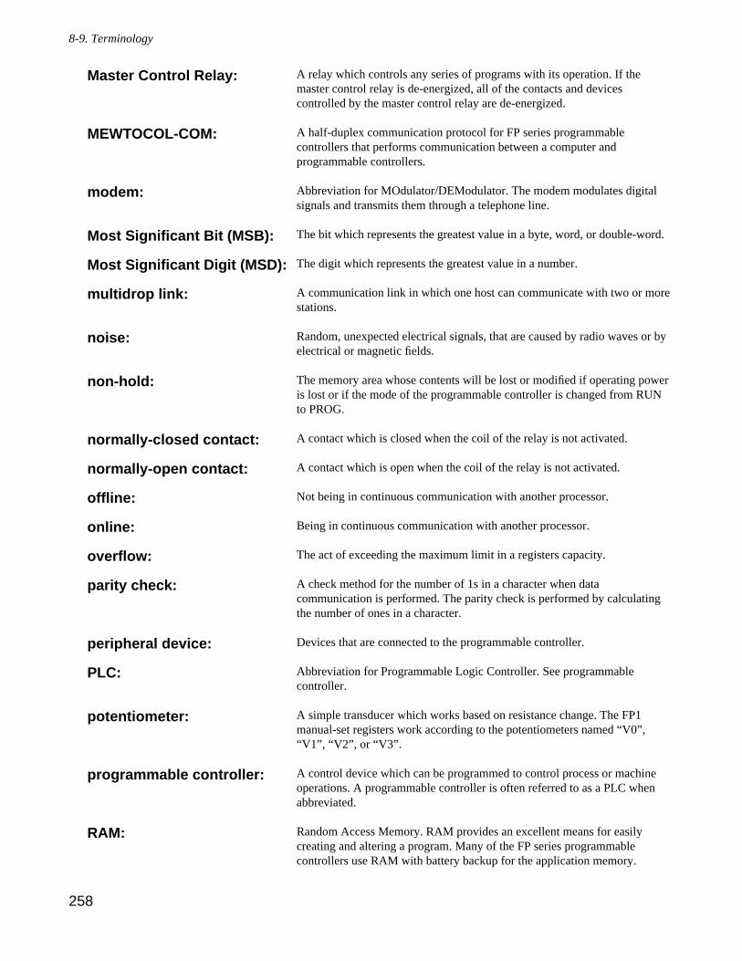
258
8-9. Terminology
A relay which controls any series of programs with its operation. If themaster control relay is de-energized, all of the contacts and devicescontrolled by the master control relay are de-energized.
A half-duplex communication protocol for FP series programmablecontrollers that performs communication between a computer andprogrammable controllers.
Abbreviation for MOdulator/DEModulator. The modem modulates digitalsignals and transmits them through a telephone line.
The bit which represents the greatest value in a byte, word, or double-word.
The digit which represents the greatest value in a number.
A communication link in which one host can communicate with two or morestations.
Random, unexpected electrical signals, that are caused by radio waves or byelectrical or magnetic fields.
The memory area whose contents will be lost or modified if operating poweris lost or if the mode of the programmable controller is changed from RUNto PROG.
A contact which is closed when the coil of the relay is not activated.
A contact which is open when the coil of the relay is not activated.
Not being in continuous communication with another processor.
Being in continuous communication with another processor.
The act of exceeding the maximum limit in a registers capacity.
A check method for the number of 1s in a character when datacommunication is performed. The parity check is performed by calculatingthe number of ones in a character.
Devices that are connected to the programmable controller.
Abbreviation for Programmable Logic Controller. See programmablecontroller.
A simple transducer which works based on resistance change. The FP1manual-set registers work according to the potentiometers named “V0”,“V1”, “V2”, or “V3”.
A control device which can be programmed to control process or machineoperations. A programmable controller is often referred to as a PLC whenabbreviated.
Random Access Memory. RAM provides an excellent means for easilycreating and altering a program. Many of the FP series programmablecontrollers use RAM with battery backup for the application memory.
Master Control Relay:
MEWTOCOL-COM:
modem:
Most Significant Bit (MSB):
Most Significant Digit (MSD):
multidrop link:
noise:
non-hold:
normally-closed contact:
normally-open contact:
offline:
online:
overflow:
parity check:
peripheral device:
PLC:
potentiometer:
programmable controller:
RAM:
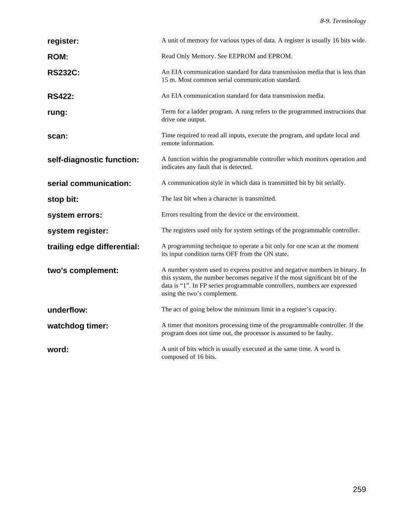
259
8-9. Terminology
A unit of memory for various types of data. A register is usually 16 bits wide.
Read Only Memory. See EEPROM and EPROM.
An EIA communication standard for data transmission media that is less than15 m. Most common serial communication standard.
An EIA communication standard for data transmission media.
Term for a ladder program. A rung refers to the programmed instructions thatdrive one output.
Time required to read all inputs, execute the program, and update local andremote information.
A function within the programmable controller which monitors operation andindicates any fault that is detected.
A communication style in which data is transmitted bit by bit serially.
The last bit when a character is transmitted.
Errors resulting from the device or the environment.
The registers used only for system settings of the programmable controller.
A programming technique to operate a bit only for one scan at the momentits input condition turns OFF from the ON state.
A number system used to express positive and negative numbers in binary. Inthis system, the number becomes negative if the most significant bit of thedata is “1”. In FP series programmable controllers, numbers are expressedusing the two’s complement.
The act of going below the minimum limit in a register’s capacity.
A timer that monitors processing time of the programmable controller. If theprogram does not time out, the processor is assumed to be faulty.
A unit of bits which is usually executed at the same time. A word iscomposed of 16 bits.
register:
ROM:
RS232C:
RS422:
rung:
scan:
self-diagnostic function:
serial communication:
stop bit:
system errors:
system register:
trailing edge differential:
two's complement:
underflow:
watchdog timer:
word:
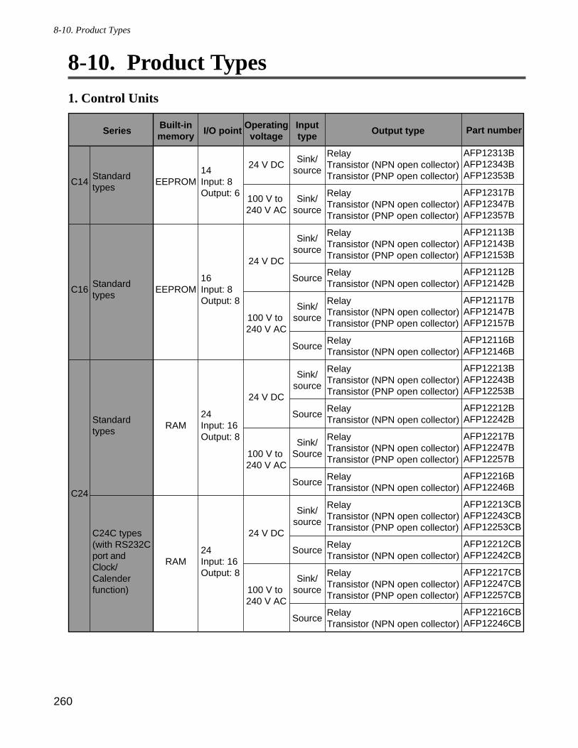
260
8-10. Product Types
8-10. Product Types
1. Control Units
C14
C16
C24
Series
Standard types
Standard types
Standard types
C24C types (with RS232C port andClock/Calender function)
Built-inmemory
EEPROM
EEPROM
RAM
RAM
I/O point
14Input: 8Output: 6
16Input: 8Output: 8
24Input: 16Output: 8
24Input: 16Output: 8
Operatingvoltage
24 V DC
100 V to 240 V AC
24 V DC
100 V to 240 V AC
24 V DC
100 V to 240 V AC
24 V DC
100 V to 240 V AC
Output type
RelayTransistor (NPN open collector)Transistor (PNP open collector)
RelayTransistor (NPN open collector)Transistor (PNP open collector)
RelayTransistor (NPN open collector)Transistor (PNP open collector)
RelayTransistor (NPN open collector)
RelayTransistor (NPN open collector)Transistor (PNP open collector)
RelayTransistor (NPN open collector)
RelayTransistor (NPN open collector)Transistor (PNP open collector)
RelayTransistor (NPN open collector)
RelayTransistor (NPN open collector)Transistor (PNP open collector)
RelayTransistor (NPN open collector)
RelayTransistor (NPN open collector)Transistor (PNP open collector)
RelayTransistor (NPN open collector)
RelayTransistor (NPN open collector)Transistor (PNP open collector)
RelayTransistor (NPN open collector)
Part number
AFP12313BAFP12343BAFP12353B
AFP12317BAFP12347BAFP12357B
AFP12113BAFP12143BAFP12153B
AFP12112BAFP12142B
AFP12117BAFP12147BAFP12157B
AFP12116BAFP12146B
AFP12213BAFP12243BAFP12253B
AFP12212BAFP12242B
AFP12217BAFP12247BAFP12257B
AFP12216BAFP12246B
AFP12213CBAFP12243CBAFP12253CB
AFP12212CBAFP12242CB
AFP12217CBAFP12247CBAFP12257CB
AFP12216CBAFP12246CB
Inputtype
Sink/source
Sink/source
Sink/source
Source
Sink/source
Source
Sink/source
Source
Sink/Source
Source
Sink/source
Source
Sink/source
Source
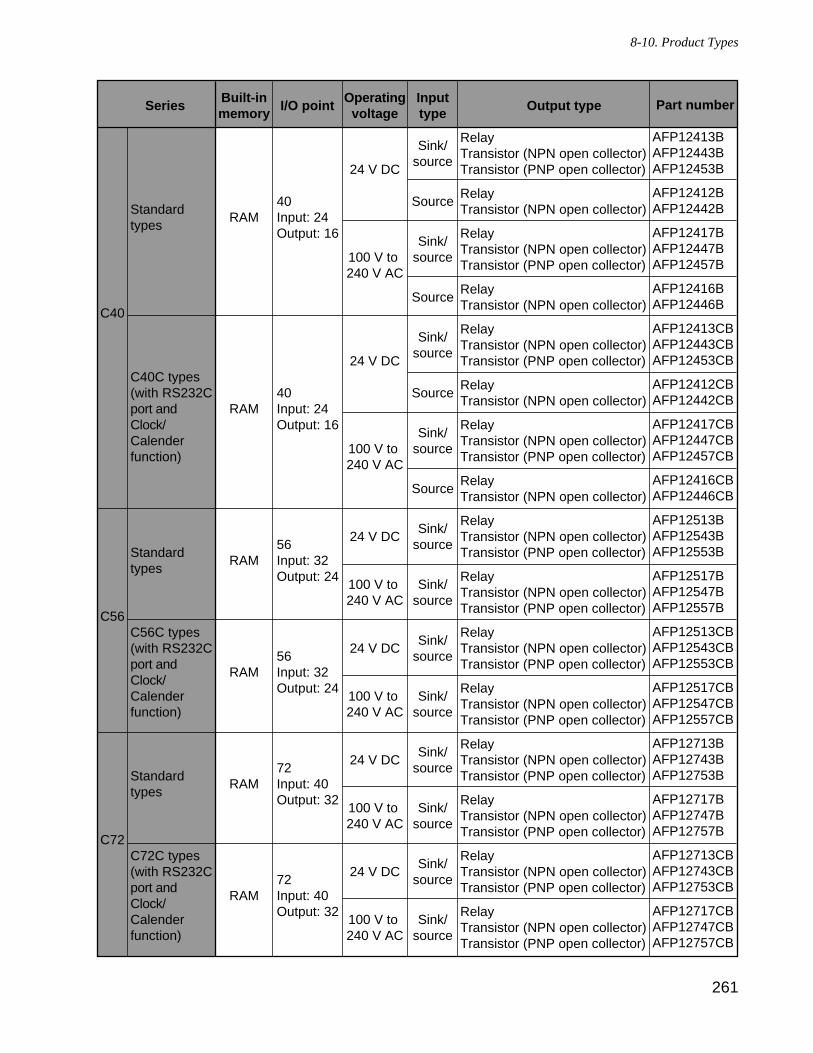
261
8-10. Product Types
C40
C56
C72
Series
Standard types
C40C types (with RS232C port andClock/Calender function)
Standard types
C56C types (with RS232C port andClock/Calender function)
Standard types
C72C types (with RS232C port andClock/Calender function)
Built-inmemory
RAM
RAM
RAM
RAM
RAM
RAM
I/O point
40Input: 24Output: 16
40Input: 24Output: 16
56Input: 32Output: 24
56Input: 32Output: 24
72Input: 40Output: 32
72Input: 40Output: 32
Operatingvoltage
24 V DC
100 V to 240 V AC
24 V DC
100 V to 240 V AC
24 V DC
100 V to 240 V AC
24 V DC
100 V to 240 V AC
24 V DC
100 V to 240 V AC
24 V DC
100 V to 240 V AC
Output type
RelayTransistor (NPN open collector)Transistor (PNP open collector)
RelayTransistor (NPN open collector)
RelayTransistor (NPN open collector)Transistor (PNP open collector)
RelayTransistor (NPN open collector)
RelayTransistor (NPN open collector)Transistor (PNP open collector)
RelayTransistor (NPN open collector)
RelayTransistor (NPN open collector)Transistor (PNP open collector)
RelayTransistor (NPN open collector)
RelayTransistor (NPN open collector)Transistor (PNP open collector)
RelayTransistor (NPN open collector)Transistor (PNP open collector)
RelayTransistor (NPN open collector)Transistor (PNP open collector)
RelayTransistor (NPN open collector)Transistor (PNP open collector)
RelayTransistor (NPN open collector)Transistor (PNP open collector)
RelayTransistor (NPN open collector)Transistor (PNP open collector)
RelayTransistor (NPN open collector)Transistor (PNP open collector)
RelayTransistor (NPN open collector)Transistor (PNP open collector)
Part number
AFP12413BAFP12443BAFP12453B
AFP12412BAFP12442B
AFP12417BAFP12447BAFP12457B
AFP12416BAFP12446B
AFP12413CBAFP12443CBAFP12453CB
AFP12412CBAFP12442CB
AFP12417CBAFP12447CBAFP12457CB
AFP12416CBAFP12446CB
AFP12513BAFP12543BAFP12553B
AFP12517BAFP12547BAFP12557B
AFP12513CBAFP12543CBAFP12553CB
AFP12517CBAFP12547CBAFP12557CB
AFP12713BAFP12743BAFP12753B
AFP12717BAFP12747BAFP12757B
AFP12713CBAFP12743CBAFP12753CB
AFP12717CBAFP12747CBAFP12757CB
Inputtype
Sink/source
Source
Sink/source
Source
Sink/source
Source
Sink/source
Source
Sink/source
Sink/source
Sink/source
Sink/source
Sink/source
Sink/source
Sink/source
Sink/source
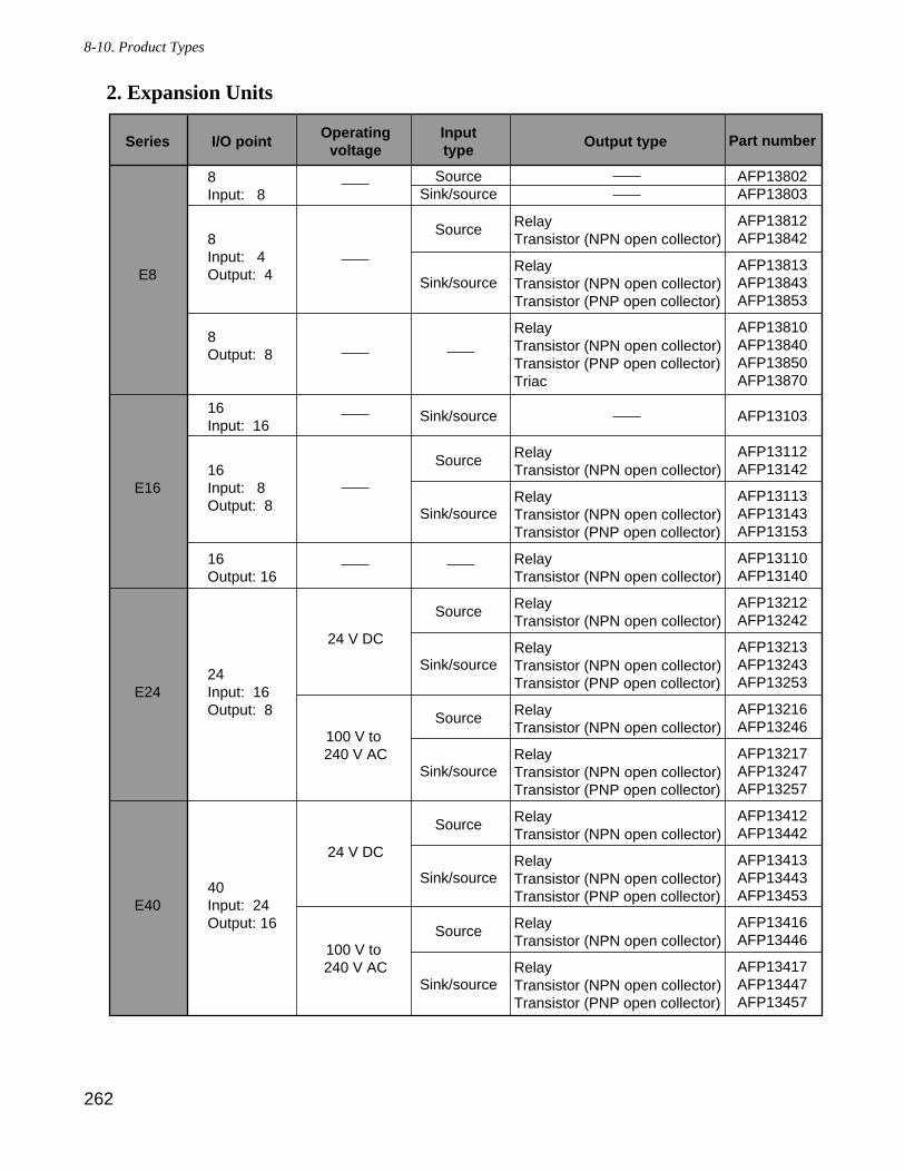
262
8-10. Product Types
2. Expansion Units
Series
E8
E16
E24
E40
I/O point
8Input: 8
8Input: 4Output: 4
8Output: 8
16Input: 16
16Input: 8Output: 8
16Output: 16
24Input: 16Output: 8
40Input: 24Output: 16
Operatingvoltage
24 V DC
100 V to 240 V AC
24 V DC
100 V to 240 V AC
Output type
RelayTransistor (NPN open collector)
RelayTransistor (NPN open collector) Transistor (PNP open collector)
RelayTransistor (NPN open collector) Transistor (PNP open collector) Triac
RelayTransistor (NPN open collector)
RelayTransistor (NPN open collector) Transistor (PNP open collector)
RelayTransistor (NPN open collector)
RelayTransistor (NPN open collector)
RelayTransistor (NPN open collector) Transistor (PNP open collector)
RelayTransistor (NPN open collector)
RelayTransistor (NPN open collector) Transistor (PNP open collector)
RelayTransistor (NPN open collector)
RelayTransistor (NPN open collector) Transistor (PNP open collector)
RelayTransistor (NPN open collector)
RelayTransistor (NPN open collector) Transistor (PNP open collector)
Part number
AFP13802AFP13803
AFP13812AFP13842
AFP13813AFP13843AFP13853
AFP13810AFP13840AFP13850AFP13870
AFP13103
AFP13112AFP13142
AFP13113AFP13143AFP13153
AFP13110AFP13140
AFP13212AFP13242
AFP13213AFP13243AFP13253
AFP13216AFP13246
AFP13217AFP13247AFP13257
AFP13412AFP13442
AFP13413AFP13443AFP13453
AFP13416AFP13446
AFP13417AFP13447AFP13457
Inputtype
SourceSink/source
Source
Sink/source
Sink/source
Source
Sink/source
Source
Sink/source
Source
Sink/source
Source
Sink/source
Source
Sink/source
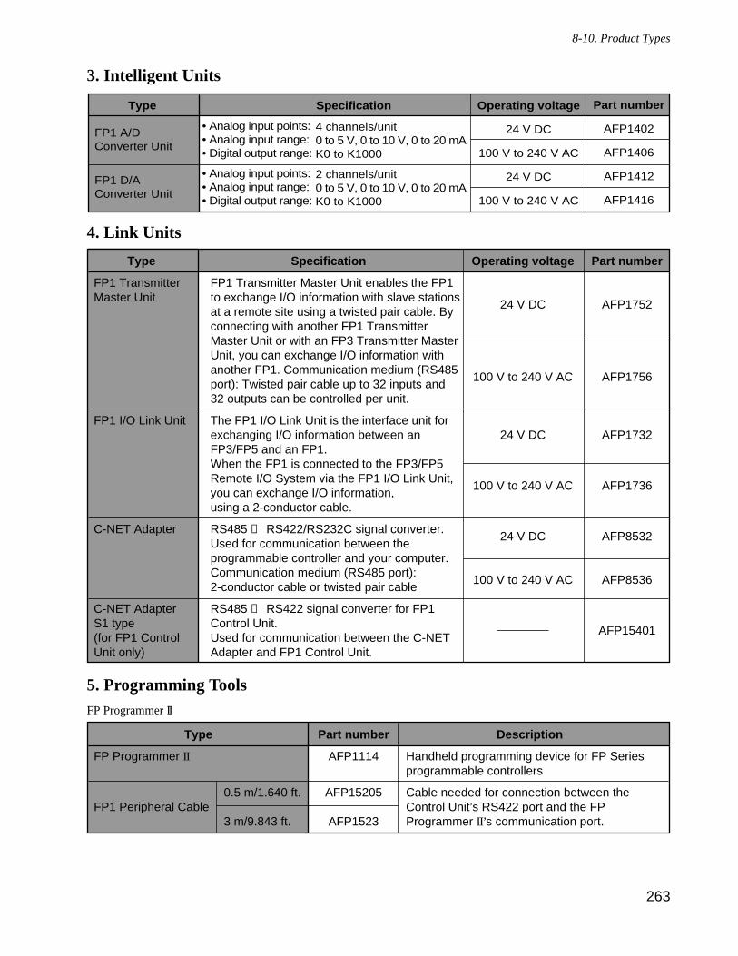
263
8-10. Product Types
3. Intelligent Units
4. Link Units
5. Programming ToolsFP Programmer II
Type
FP Programmer II
FP1 Peripheral Cable
Part number
AFP1114
AFP15205
AFP1523
Description
Handheld programming device for FP Series programmable controllers
Cable needed for connection between the Control Unit’s RS422 port and the FP Programmer II’s communication port.
0.5 m/1.640 ft.
3 m/9.843 ft.
Type
FP1 Transmitter Master Unit
FP1 I/O Link Unit
C-NET Adapter
C-NET Adapter S1 type (for FP1 Control Unit only)
Operating voltage
24 V DC
100 V to 240 V AC
24 V DC
100 V to 240 V AC
24 V DC
100 V to 240 V AC
Part number
AFP1752
AFP1756
AFP1732
AFP1736
AFP8532
AFP8536
AFP15401
Specification
FP1 Transmitter Master Unit enables the FP1 to exchange I/O information with slave stations at a remote site using a twisted pair cable. By connecting with another FP1 Transmitter Master Unit or with an FP3 Transmitter MasterUnit, you can exchange I/O information with another FP1. Communication medium (RS485 port): Twisted pair cable up to 32 inputs and 32 outputs can be controlled per unit.
The FP1 I/O Link Unit is the interface unit for exchanging I/O information between an FP3/FP5 and an FP1.When the FP1 is connected to the FP3/FP5 Remote I/O System via the FP1 I/O Link Unit, you can exchange I/O information, using a 2-conductor cable.
RS485 ↔ RS422/RS232C signal converter.Used for communication between the programmable controller and your computer.Communication medium (RS485 port): 2-conductor cable or twisted pair cable
RS485 ↔ RS422 signal converter for FP1 Control Unit.Used for communication between the C-NET Adapter and FP1 Control Unit.
Type
FP1 A/D Converter Unit
FP1 D/A Converter Unit
Specification
• Analog input points: • Analog input range: • Digital output range:
• Analog input points: • Analog input range: • Digital output range:
Operating voltage
24 V DC
100 V to 240 V AC
24 V DC
100 V to 240 V AC
Part number
AFP1402
AFP1406
AFP1412
AFP1416
4 channels/unit0 to 5 V, 0 to 10 V, 0 to 20 mAK0 to K1000
2 channels/unit0 to 5 V, 0 to 10 V, 0 to 20 mAK0 to K1000
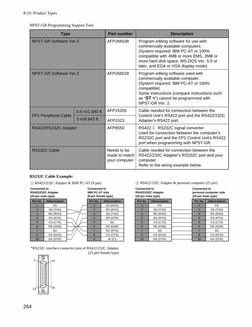
264
8-10. Product Types
NPST-GR Programming Support Tool
RS232C Cable Example:
1 RS422/232C Adapter & IBM PC-AT (9 pin) 2 RS422/232C Adapter & personal computer (25 pin)
Connected toRS422/232C Adapter(25-pin male type)
Connected toIBM PC-AT side(9-pin female type)
Connected toRS422/232C Adapter(25-pin male type)
Connected topersonal computer side(25-pin male type)
Pin No.1
2
3
4
5
6
7
8
20
AbbreviationFG
SD (TXD)
RD (RXD)
RS (RTS)
CS (CTS)
DR (DSR)
SG
CD (DCD)
ER (DTR)
Pin No.1
2
3
4
5
6
7
8
9
AbbreviationCD (DCD)
RD (RXD)
SD (TXD)
ER (DTR)
SG
DR (DSR)
RS (RTS)
CS (CTS)
RI (CI)
Pin No.1
2
3
4
5
6
7
8
20
AbbreviationFG
SD (TXD)
RD (RXD)
RS (RTS)
CS (CTS)
DR (DSR)
SG
CD (DCD)
ER (DTR)
Pin No.1
2
3
4
5
6
7
8
20
AbbreviationFG
SD (TXD)
RD (RXD)
RS (RTS)
CS (CTS)
DR (DSR)
SG
CD (DCD)
ER (DTR)
*RS232C interface connector pins of RS422/232C Adapter (25-pin female type)
1
2513
14
Type
NPST-GR Software Ver.3
NPST-GR Software Ver.2
FP1 Peripheral Cable
RS422/RS232C Adapter
RS232C Cable
Part number
AFP266538
AFP266528
AFP15205
AFP1523
AFP8550
Needs to be made to match your computer
Description
Program editing software for use with commercially available computers.(System required: IBM PC-AT or 100% compatible with 4MB or more EMS, 2MB or more hard disk space, MS-DOS Ver. 5.0 or later, and EGA or VGA display mode)
Program editing software used with commercially available computer.(System required: IBM PC-AT or 100% compatible)Some instructions (compare instructions such as “ST =”) cannot be programmed with NPST-GR Ver. 2.
Cable needed for connection between the Control Unit’s RS422 port and the RS422/232C Adapter’s RS422 port.
RS422 ↔ RS232C signal converter.Used for connection between the computer’s RS232C port and the FP1 Control Unit’s RS422 port when programming with NPST-GR.
Cable needed for connection between the RS422/232C Adapter’s RS232C port and your computer.Refer to the wiring example below.
0.5 m/1.640 ft.
3 m/9.843 ft.
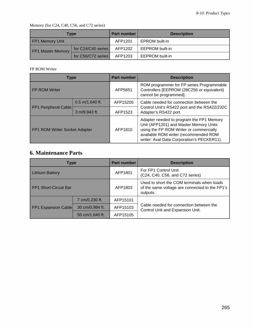
265
8-10. Product Types
Memory (for C24, C40, C56, and C72 series)
FP ROM Writer
6. Maintenance Parts
Type
Lithium Battery
FP1 Short-Circuit Bar
FP1 Expansion Cable
Part number
AFP1801
AFP1803
AFP15101
AFP15103
AFP15105
7 cm/0.230 ft.
30 cm/0.984 ft.
50 cm/1.640 ft.
Description
For FP1 Control Unit (C24, C40, C56, and C72 series)
Used to short the COM terminals when loads of the same voltage are connected to the FP1’s outputs.
Cable needed for connection between the Control Unit and Expansion Unit.
Type
FP ROM Writer
FP1 Peripheral Cable
FP1 ROM Writer Socket Adapter
Part number
AFP5651
AFP15205
AFP1523
AFP1810
0.5 m/1.640 ft.
3 m/9.843 ft.
Description
ROM programmer for FP series Programmable Controllers [EEPROM (28C256 or equivalent) cannot be programmed].
Cable needed for connection between the Control Unit’s RS422 port and the RS422/232C Adapter’s RS422 port.
Adapter needed to program the FP1 Memory Unit (AFP1201) and Master Memory Units using the FP ROM Writer or commercially available ROM writer (recommended ROM writer: Aval Data Corporation’s PECKER11).
Type
FP1 Memory Unit
FP1 Master Memory
Part number
AFP1201
AFP1202
AFP1203
for C24/C40 series
for C56/C72 series
Description
EPROM built-in
EEPROM built-in
EEPROM built-in
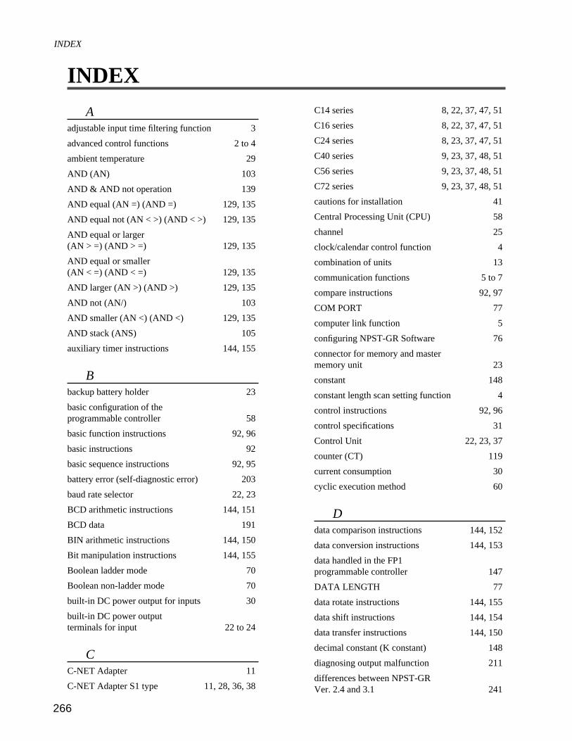
Aadjustable input time filtering function 3
advanced control functions 2 to 4
ambient temperature 29
AND (AN) 103
AND & AND not operation 139
AND equal (AN =) (AND =) 129, 135
AND equal not (AN < >) (AND < >) 129, 135
AND equal or larger(AN > =) (AND > =) 129, 135
AND equal or smaller(AN < =) (AND < =) 129, 135
AND larger (AN >) (AND >) 129, 135
AND not (AN/) 103
AND smaller (AN <) (AND <) 129, 135
AND stack (ANS) 105
auxiliary timer instructions 144, 155
Bbackup battery holder 23
basic configuration of theprogrammable controller 58
basic function instructions 92, 96
basic instructions 92
basic sequence instructions 92, 95
battery error (self-diagnostic error) 203
baud rate selector 22, 23
BCD arithmetic instructions 144, 151
BCD data 191
BIN arithmetic instructions 144, 150
Bit manipulation instructions 144, 155
Boolean ladder mode 70
Boolean non-ladder mode 70
built-in DC power output for inputs 30
built-in DC power outputterminals for input 22 to 24
CC-NET Adapter 11
C-NET Adapter S1 type 11, 28, 36, 38
C14 series 8, 22, 37, 47, 51
C16 series 8, 22, 37, 47, 51
C24 series 8, 23, 37, 47, 51
C40 series 9, 23, 37, 48, 51
C56 series 9, 23, 37, 48, 51
C72 series 9, 23, 37, 48, 51
cautions for installation 41
Central Processing Unit (CPU) 58
channel 25
clock/calendar control function 4
combination of units 13
communication functions 5 to 7
compare instructions 92, 97
COM PORT 77
computer link function 5
configuring NPST-GR Software 76
connector for memory and mastermemory unit 23
constant 148
constant length scan setting function 4
control instructions 92, 96
control specifications 31
Control Unit 22, 23, 37
counter (CT) 119
current consumption 30
cyclic execution method 60
Ddata comparison instructions 144, 152
data conversion instructions 144, 153
data handled in the FP1 programmable controller 147
DATA LENGTH 77
data rotate instructions 144, 155
data shift instructions 144, 154
data transfer instructions 144, 150
decimal constant (K constant) 148
diagnosing output malfunction 211
differences between NPST-GRVer. 2.4 and 3.1 241
INDEX
266
INDEX
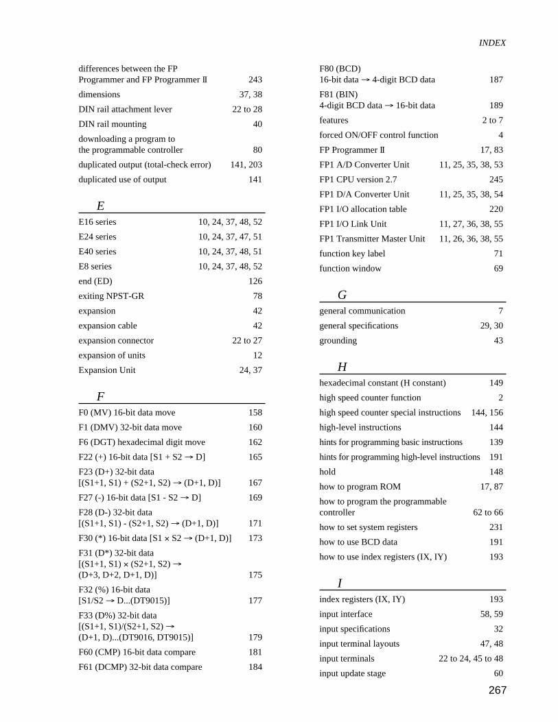
differences between the FPProgrammer and FP Programmer II 243
dimensions 37, 38
DIN rail attachment lever 22 to 28
DIN rail mounting 40
downloading a program tothe programmable controller 80
duplicated output (total-check error) 141, 203
duplicated use of output 141
EE16 series 10, 24, 37, 48, 52
E24 series 10, 24, 37, 47, 51
E40 series 10, 24, 37, 48, 51
E8 series 10, 24, 37, 48, 52
end (ED) 126
exiting NPST-GR 78
expansion 42
expansion cable 42
expansion connector 22 to 27
expansion of units 12
Expansion Unit 24, 37
FF0 (MV) 16-bit data move 158
F1 (DMV) 32-bit data move 160
F6 (DGT) hexadecimal digit move 162
F22 (+) 16-bit data [S1 + S2 → D] 165
F23 (D+) 32-bit data[(S1+1, S1) + (S2+1, S2) → (D+1, D)] 167
F27 (-) 16-bit data [S1 - S2 → D] 169
F28 (D-) 32-bit data[(S1+1, S1) - (S2+1, S2) → (D+1, D)] 171
F30 (*) 16-bit data [S1 × S2 → (D+1, D)] 173
F31 (D*) 32-bit data[(S1+1, S1) × (S2+1, S2) →(D+3, D+2, D+1, D)] 175
F32 (%) 16-bit data [S1/S2 → D...(DT9015)] 177
F33 (D%) 32-bit data[(S1+1, S1)/(S2+1, S2) →(D+1, D)...(DT9016, DT9015)] 179
F60 (CMP) 16-bit data compare 181
F61 (DCMP) 32-bit data compare 184
F80 (BCD) 16-bit data → 4-digit BCD data 187
F81 (BIN) 4-digit BCD data → 16-bit data 189
features 2 to 7
forced ON/OFF control function 4
FP Programmer II 17, 83
FP1 A/D Converter Unit 11, 25, 35, 38, 53
FP1 CPU version 2.7 245
FP1 D/A Converter Unit 11, 25, 35, 38, 54
FP1 I/O allocation table 220
FP1 I/O Link Unit 11, 27, 36, 38, 55
FP1 Transmitter Master Unit 11, 26, 36, 38, 55
function key label 71
function window 69
Ggeneral communication 7
general specifications 29, 30
grounding 43
Hhexadecimal constant (H constant) 149
high speed counter function 2
high speed counter special instructions 144, 156
high-level instructions 144
hints for programming basic instructions 139
hints for programming high-level instructions 191
hold 148
how to program ROM 17, 87
how to program the programmablecontroller 62 to 66
how to set system registers 231
how to use BCD data 191
how to use index registers (IX, IY) 193
Iindex registers (IX, IY) 193
input interface 58, 59
input specifications 32
input terminal layouts 47, 48
input terminals 22 to 24, 45 to 48
input update stage 60
INDEX
267
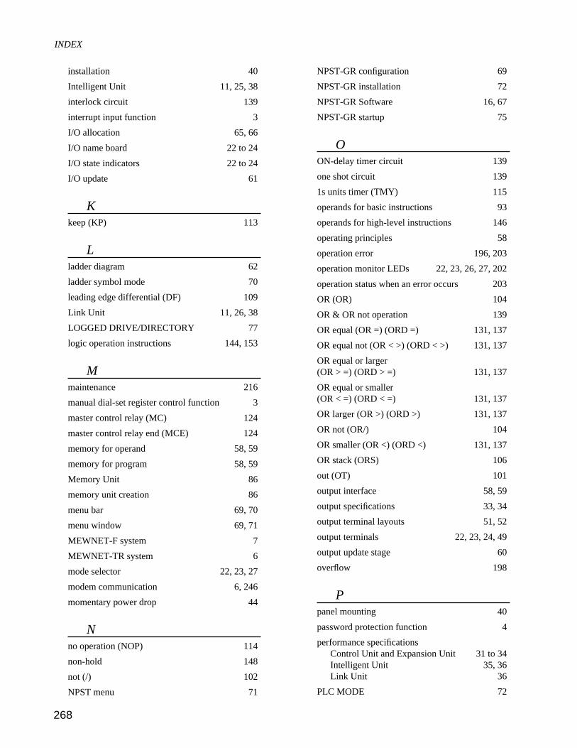
installation 40
Intelligent Unit 11, 25, 38
interlock circuit 139
interrupt input function 3
I/O allocation 65, 66
I/O name board 22 to 24
I/O state indicators 22 to 24
I/O update 61
Kkeep (KP) 113
Lladder diagram 62
ladder symbol mode 70
leading edge differential (DF) 109
Link Unit 11, 26, 38
LOGGED DRIVE/DIRECTORY 77
logic operation instructions 144, 153
Mmaintenance 216
manual dial-set register control function 3
master control relay (MC) 124
master control relay end (MCE) 124
memory for operand 58, 59
memory for program 58, 59
Memory Unit 86
memory unit creation 86
menu bar 69, 70
menu window 69, 71
MEWNET-F system 7
MEWNET-TR system 6
mode selector 22, 23, 27
modem communication 6, 246
momentary power drop 44
Nno operation (NOP) 114
non-hold 148
not (/) 102
NPST menu 71
NPST-GR configuration 69
NPST-GR installation 72
NPST-GR Software 16, 67
NPST-GR startup 75
OON-delay timer circuit 139
one shot circuit 139
1s units timer (TMY) 115
operands for basic instructions 93
operands for high-level instructions 146
operating principles 58
operation error 196, 203
operation monitor LEDs 22, 23, 26, 27, 202
operation status when an error occurs 203
OR (OR) 104
OR & OR not operation 139
OR equal (OR =) (ORD =) 131, 137
OR equal not (OR < >) (ORD < >) 131, 137
OR equal or larger(OR > =) (ORD > =) 131, 137
OR equal or smaller (OR < =) (ORD < =) 131, 137
OR larger (OR >) (ORD >) 131, 137
OR not (OR/) 104
OR smaller (OR <) (ORD <) 131, 137
OR stack (ORS) 106
out (OT) 101
output interface 58, 59
output specifications 33, 34
output terminal layouts 51, 52
output terminals 22, 23, 24, 49
output update stage 60
overflow 198
Ppanel mounting 40
password protection function 4
performance specificationsControl Unit and Expansion Unit 31 to 34Intelligent Unit 35, 36Link Unit 36
PLC MODE 72
INDEX
268
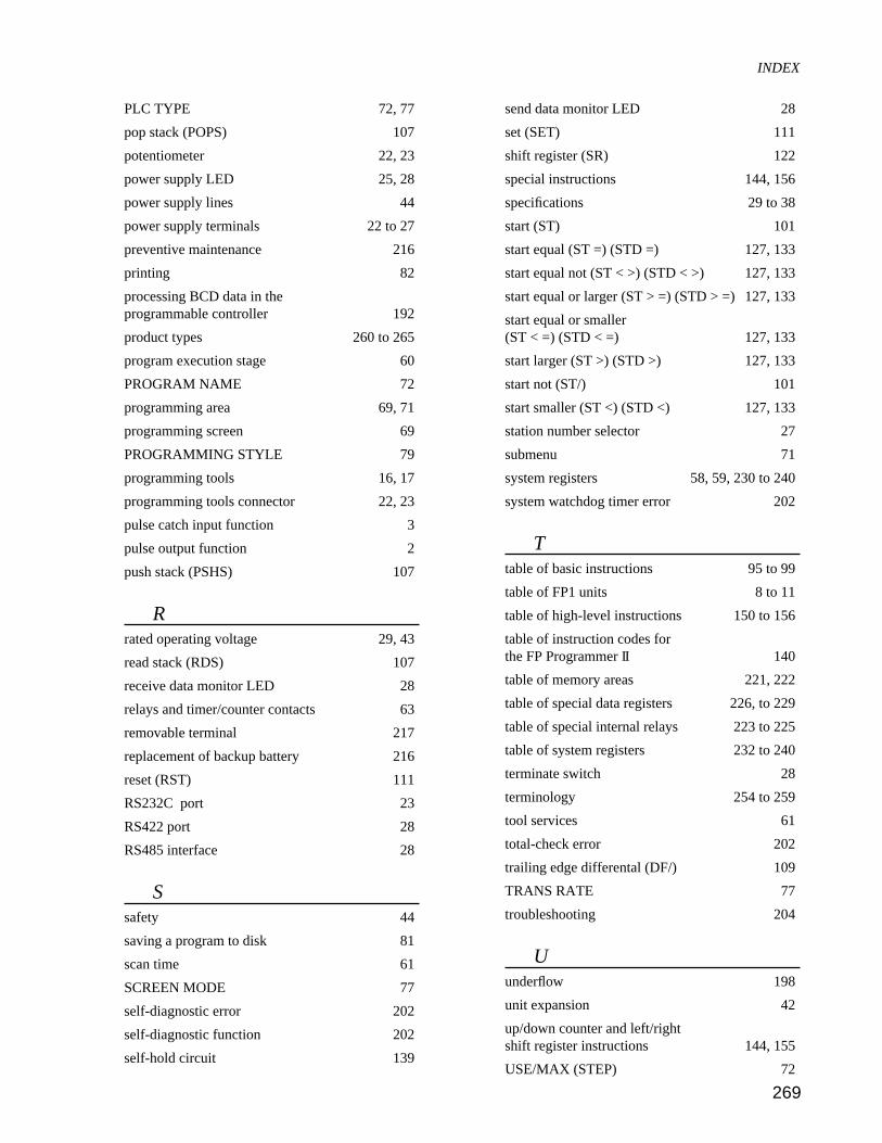
PLC TYPE 72, 77
pop stack (POPS) 107
potentiometer 22, 23
power supply LED 25, 28
power supply lines 44
power supply terminals 22 to 27
preventive maintenance 216
printing 82
processing BCD data in theprogrammable controller 192
product types 260 to 265
program execution stage 60
PROGRAM NAME 72
programming area 69, 71
programming screen 69
PROGRAMMING STYLE 79
programming tools 16, 17
programming tools connector 22, 23
pulse catch input function 3
pulse output function 2
push stack (PSHS) 107
Rrated operating voltage 29, 43
read stack (RDS) 107
receive data monitor LED 28
relays and timer/counter contacts 63
removable terminal 217
replacement of backup battery 216
reset (RST) 111
RS232C port 23
RS422 port 28
RS485 interface 28
Ssafety 44
saving a program to disk 81
scan time 61
SCREEN MODE 77
self-diagnostic error 202
self-diagnostic function 202
self-hold circuit 139
send data monitor LED 28
set (SET) 111
shift register (SR) 122
special instructions 144, 156
specifications 29 to 38
start (ST) 101
start equal (ST =) (STD =) 127, 133
start equal not (ST < >) (STD < >) 127, 133
start equal or larger (ST > =) (STD > =) 127, 133
start equal or smaller (ST < =) (STD < =) 127, 133
start larger (ST >) (STD >) 127, 133
start not (ST/) 101
start smaller (ST <) (STD <) 127, 133
station number selector 27
submenu 71
system registers 58, 59, 230 to 240
system watchdog timer error 202
Ttable of basic instructions 95 to 99
table of FP1 units 8 to 11
table of high-level instructions 150 to 156
table of instruction codes for the FP Programmer II 140
table of memory areas 221, 222
table of special data registers 226, to 229
table of special internal relays 223 to 225
table of system registers 232 to 240
terminate switch 28
terminology 254 to 259
tool services 61
total-check error 202
trailing edge differental (DF/) 109
TRANS RATE 77
troubleshooting 204
Uunderflow 198
unit expansion 42
up/down counter and left/rightshift register instructions 144, 155
USE/MAX (STEP) 72
INDEX
269
Vversions of programming tools 241
voltage range selection terminal 25
WWhen an ALARM LED is ON 209
When all LEDs are OFF 210
When an ERR. LED is ON 205
When “PLC=COMM. ERR” is displayed on the NPST-GR screen 214
When “PROTECT ERROR” is displayed 215
wiring 43 to 56
wiring power supply 43
word external input relay (WX) 148
word external output relay (WY) 148
word internal relay (WR) 148
Z0.1s units timer (TMX) 115
0.01s units timer (TMR) 115
INDEX
270

RECORD OF CHANGES
ACG No. Date Description of Changes
First edition2nd edition
The descriptions of MEWNET-TR are added.
DEC.1993FEB. 1995
ACG-M0051-1ACG-M0051-2
271
RECORD OF CHANGES

272