prof douglas c. hopkins, ph.d. · 2019-04-18 · ©2019 douglas c hopkins [email protected] trends...
TRANSCRIPT

©2019 DOUGLAS C HOPKINS
Trends in Power Electronics Packaging
March 2019
Director – PREES LaboratoryFREEDM System CenterNorth Carolina State Univ.1791 Varsity Dr., Suite 100Raleigh, NC 27606-7571
www.prees.org
FREEDM SYSTEM CENTERAnnual Research Symposium
April 10-12, 2019Duke Energy Hall, Hunt Library
Prof Douglas C. Hopkins, Ph.D.

©2019 DOUGLAS C HOPKINS
New Resource for ERCD Ckt Topology ResearchEpoxy Resin Composite Dielectrics (ERCD)
ERCD ”substrate-less” approaches identified for high voltage (5kV/120µm), high temperature (≤300ºC) and high thermal impedance (10W/mK)
circuit board plotters
LPKF-contac-S4Reliable Through-hole
Plating in the Lab
LPKF ProtoMat S104LPKF® MultiPress S Automatic Lamination
Press
HB05 Manual Wire BonderWedge, ball & ribbon bondingLPKFLPKF ProMask
Pro Legend, UV Lamp Table

©2019 DOUGLAS C HOPKINS
Today, power electronics has strong growth across a board range of power levels. This particularly applies to
increases that improve lives versus enhancing entertainment.
However, increasing density and reducing cost still are the primary goals for all designs, and brings focus on
Functional Integration at the Systems Level.
This Photo by Unknown Author is licensed under CC BY-SA-NC

©2019 DOUGLAS C HOPKINS
The challenge in thermal management will broaden to address essentially point-source heat generation due to higher power
capabilities with shrinking die size …compared to Si die.
Problem?… much smaller WBG devices

©2019 DOUGLAS C HOPKINS
Shrinking power die challenge
Huang in 2004 developed three pertinent figures of
merit [1].
[1] “New Unipolar Switching Power Device Figures of Merit,” Alex Q. Huang, IEEE Electron Device Letters, Vol. 25, No. 5, May 2004
Ec is critical electric breakdown field, µ is electron mobility, ε is dielectric constant, σth is thermal conductivity
High Voltage
CapabilityLow On-State
Resista
nce
Hig
h Sw
itchi
ng
Freq
uenc
y
High Tem
peratureCapability
SiC
GaN
Si
©2019 DOUGLAS C HOPKINS
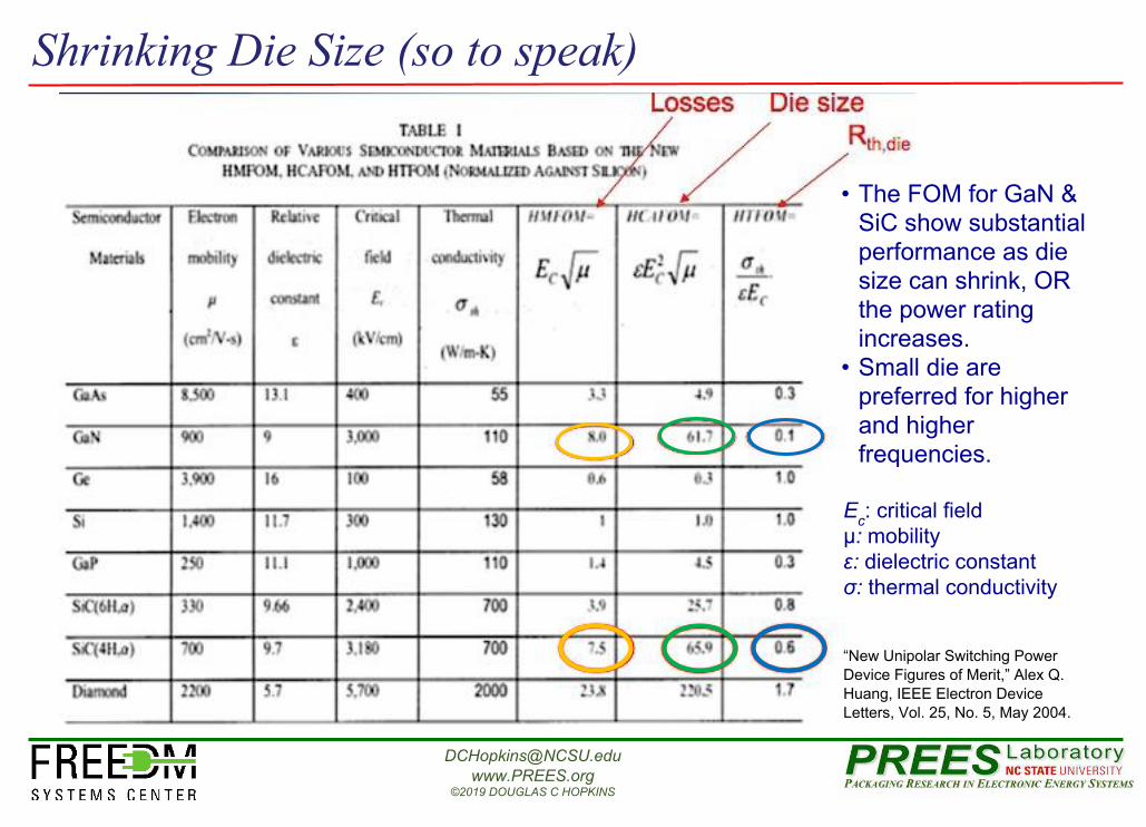
Shrinking Die Size (so to speak)
“New Unipolar Switching Power Device Figures of Merit,” Alex Q. Huang, IEEE Electron Device Letters, Vol. 25, No. 5, May 2004.
• The FOM for GaN & SiC show substantial performance as die size can shrink, OR the power rating increases.
• Small die are preferred for higher and higher frequencies.
Ec: critical fieldµ: mobilityε: dielectric constantσ: thermal conductivity

©2019 DOUGLAS C HOPKINS
High Frequency Potential (e.g. Unipolar - MOSFET)
Comparison is based on hard switched converters with fixed f, I, and V. ZVS for high voltage provides other advantages for SiC.
Since current does not scale, the speed ~ i/c, is significantly increased in WBG devices. Speed measured as di/dt or dv/dt
Graph excerpt w/ permission, A. Q. Huang, “Wide Bandgap Power Devices: Die Size Shrinking and Its Impact on Power Delivery Architecture,” PSMA Webinar,Feb25,2016
The reduction in size supports high frequency operation, but creates a greater challenge in
heat dissipation and Integration.

©2019 DOUGLAS C HOPKINS
Small Die for High Voltage – 9kV design in airSmall Die experiences breakdown at 1,800 V.
(Experimental design at NCSU)Packaging materials have always needed to passivate the chip for voltages greater
than ~150V.
A great emphasis to develop “Medium Voltage” power electronic systems is underway for large and small systems, e.g. portable x-ray equipment to large autonomous trucks.
BACKSIDE• Drain• Collector• Anode
3 mm to 1 cm
3 mm to
1 cm
Guard RingsTOPSIDE
• Gate• Base
50 µm to 350 µm
• Source• Emitter• Cathode
THE THOUGHT METRIC
VIDEO

It’s all about vertically conducting devices
The ‘Ground-Baseplate’ Problem in Packaging

©2019 DOUGLAS C HOPKINS
Ground CouplingEx: V1: 425 Vdc dt: 20ns
V1 D
Si = C (dV/dt )
What is the problem?
DrainSource
Review of mid-point voltage…
SW-Top
SW-Bottom
However, there is a major current path when SW-Top turns on.
+ 425 Vdc
---
Gnd
Gnd
©2019 DOUGLAS C HOPKINS
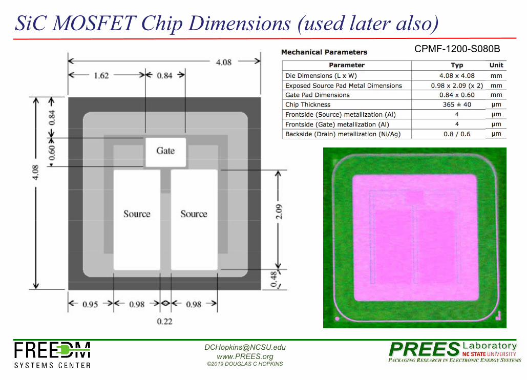
SiC MOSFET Chip Dimensions (used later also)CPMF-1200-S080B

©2019 DOUGLAS C HOPKINS
4mm X 4mm
Bonding pad2.5mm X 2.5mm
Circuit trace5mm X 10mm
0.5mm
Ground Coupling (continued)
Given:FET: Minimum drain area of semiconductor and solder is 4.5mm X 4.5mm = 20.25mm2
+ bonding pad 2.5 X 2.5mm = 6.25mm2
+ circuit trace is 5mm X 10mm = 50mm2
Substrate: Al2O3 (with εr = 9.4) at 635µm thick
What current flows into ‘ground’ from the transistor drain?
Find switching current:Area, A = 20.25+6.25+50 = 76.5 mm2
Distance: d = 0.635 mmCapacitance, C=εr εo A / d = 10 pFi = C (dV/dt ) = 10 pF (425/20ns) i = 0.21 A

©2019 DOUGLAS C HOPKINS
Multi-die Modules
Courtesy: MS Kennedy 1200V/1200A
Add diode and space: X2.2,Multiply by die in parallel: X8,(Add terminal footprint)Then,iT = 0.21 X 2.2 X 9 = 4.2A@20ns(For one side)
Low Inductance Power Module with Blade Connector, Ljubisa D. Stevanovic, Richard A. Beaupre, Eladio C. Delgado, and Arun V. Gowda
Standard packages add even more
©2019 DOUGLAS C HOPKINS
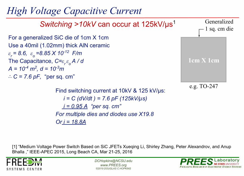
Switching >10kV can occur at 125kV/µs1
High Voltage Capacitive CurrentGeneralized1 sq. cm die
[1] “Medium Voltage Power Switch Based on SiC JFETs Xueqing Li, Shirley Zhang, Peter Alexandrov, and Anup Bhalla ,” IEEE-APEC 2015, Long Beach CA, Mar 21-25, 2016
1cm X 1cm
Find switching current at 10kV & 125 kV/µs: i = C (dV/dt ) = 7.6 pF (125kV/µs) i = 0.95 A “per sq. cm”For multiple dies and diodes use X19.8Or i = 18.8A
e.g. TO-247
For a generalized SiC die of 1cm X 1cmUse a 40mil (1.02mm) thick AlN ceramicεr = 8.6, εo =8.85 X 10⁻¹² F/mThe Capacitance, C=εr εo A / dA = 10-4 m2, d = 10-3m∴ C = 7.6 pF, “per sq. cm”

Thermal performance of metal clad ceramics

©2019 DOUGLAS C HOPKINS
Rth [˚C/W] for 5mmX5mm SiC on
12/25/12 DBCPart Width (mm)
Length (mm)
Thickness (mm)
Device 5 5 0.36Solder 5.1 5.1 0.05Metal 5.7 5.7 0.3Ceramic 6.97 6.97 0.635Metal 7.57 7.57 0.3Solder 7.67 7.67 0.05AlSiC 13.67 13.67 3
COMSOL ValueHeat Flux (W) 100Bottom Plate Temperature 293˚K
Mesh Fine

©2019 DOUGLAS C HOPKINS
Dissertation work of Dr. Haotao Ke, September 2017“3-D Prismatic Packaging Methodologies for Wide Band Gap Power Electronics Modules”
3D Prismatic Packaging – True 3D

©2019 DOUGLAS C HOPKINS
State of Art WorksPlanar 2D power packaging technology
• Flex circuit structure• POL package, SKiN package, etc.
• Embedded structure • AT&S GaNPX, PCB embedded, etc.
• Sandwiched structure • Planar Bond All package, etc.
SKiN module [5]Power Overlay package [4]
GaNPX package[7] PCB embedded module[6]
Planar Bond All[8]
ABB Stacked DBC [1]
“3-D Prismatic Packaging Methodologies for Wide Band Gap Power Electronics Modules,” Dissertation, Dr. Haotao Ke, North Carolina State University, Sept. 2017

©2019 DOUGLAS C HOPKINS
State of Art Works3D power packaging technology
• Device level • Quilt dies, stacked / vertical dies
• Module level • 3D CSP, Power chip on chip, 3D power circuit .
Power chip on chip[11]
Stacked device[13] Vertical connected device[14]3D CSP module[12]
3D Power module[10]
Quilt packaging[9]
“3-D Prismatic Packaging Methodologies for Wide Band Gap Power Electronics Modules,” Dissertation, Dr. Haotao Ke, North Carolina State University, Sept. 2017

©2019 DOUGLAS C HOPKINS
3-D Prismatic PackageObjective
• Investigation of power module topologies in >2D3-D Prismatic package should have:
• Low parasitic inductance• Good thermal performance• High power density• Capability to handle thermal stress brought by high temperature operation, if properly
designed
“3-D Prismatic Packaging Methodologies for Wide Band Gap Power Electronics Modules,” Dissertation, Dr. Haotao Ke, North Carolina State University, Sept. 2017

©2019 DOUGLAS C HOPKINS
References[1] S. Kicin et al., "A new concept of a high-current power module allowing paralleling of many SiC devices assembled exploiting conventional packaging
technologies," 2016 28th International Symposium on Power Semiconductor Devices and ICs (ISPSD), Prague, 2016, pp. 467-470.[2] K. Gould, S. Q. Cai, C. Neft and A. Bhunia, "Liquid Jet Impingement Cooling of a Silicon Carbide Power Conversion Module for Vehicle Applications," in IEEE
Transactions on Power Electronics, vol. 30, no. 6, pp. 2975-2984, June 2015.[3] Z. Cole, B. McGee, J. Stabach, C. B. O'Neal, and B. Passmore (2015) A High Temperature, High Power Density Package for SiC and GaN Power Devices.
Additional Conferences (Device Packaging, HiTEC, HiTEN, & CICMT): July 2015, Vol. 2015, No. HiTEN, pp. 000208-000213.[4] R. Fisher, R. Fillion, J. Burgess and W. Hennessy, "High frequency, low cost, power packaging using thin film power overlay technology," Applied Power
Electronics Conference and Exposition, 1995. APEC '95. Conference Proceedings 1995., Tenth Annual, Dallas, TX, 1995, pp. 12-17 vol.1[5] T. Stockmeier, P. Beckedahl, C. Göbl and T. Malzer, "SKiN: Double side sintering technology for new packages," 2011 IEEE 23rd International Symposium
on Power Semiconductor Devices and ICs, San Diego, CA, 2011, pp. 324-327.[6] C. Neeb, J. Teichrib, R. W. De Doncker, L. Boettcher and A. Ostmann, "A 50 kW IGBT power module for automotive applications with extremely low DC-link
inductance," 2014 16th European Conference on Power Electronics and Applications, Lappeenranta, 2014, pp. 1-10.[7] “3D Embedded Substrate Technologies Increase Density and Performance of Power Supplies”, Internet:
https://www.slideshare.net/DesignWorldOnline/3d-embedded-substrate-technologies-increase-density-and-performance-of-power-supplies, [July 10, 2017].
[8] Z. Liang, "Integrated double sided cooling packaging of planar SiC power modules," 2015 IEEE Energy Conversion Congress and Exposition (ECCE), Montreal, QC, 2015, pp. 4907-4912.
[9] Q. Zheng, D. Kopp, M. A. Khan, P. Fay, A. M. Kriman and G. H. Bernstein, "Investigation of Quilt Packaging Interchip Interconnect With Solder Paste," in IEEE Transactions on Components, Packaging and Manufacturing Technology, vol. 4, no. 3, pp. 400-407, March 2014.
[10] D. C. Hopkins, R. Revis, "Development of a Three Dimensional Power Circuit Package for Aircraft Applications," 1994 ISHM Int’l Symp. on Microelectronics, Boston, MA, pp. 124–128, November 15–17, 1994.
[11] E. Vagnon, P. O. Jeannin, J. C. Crebier and Y. Avenas, "A Bus-Bar-Like Power Module Based on Three-Dimensional Power-Chip-on-Chip Hybrid Integration," in IEEE Transactions on Industry Applications, vol. 46, no. 5, pp. 2046-2055, Sept.-Oct. 2010.
[12] P. Clot, J. F. Zeberli, J. M. Chenuz, F. Ferrando and D. Styblo, "Flip-chip on flex for 3D packaging," Twenty Fourth IEEE/CPMT International Electronics Manufacturing Technology Symposium (Cat. No.99CH36330), Austin, TX, 1999, pp. 36-41.
[13] W. Zhang et al., "A New Package of High-Voltage Cascode Gallium Nitride Device for Megahertz Operation," in IEEE Transactions on Power Electronics, vol. 31, no. 2, pp. 1344-1353, Feb. 2016.
[14] B. Letowski et al., "Towards vertical power device 3D packaging on 8-inch wafer," 2016 28th International Symposium on Power Semiconductor Devices and ICs (ISPSD), Prague, 2016, pp. 135-138.
[15] J. B. Jacobsen and D. C. Hopkins, “Optimally Selecting Packaging Technologies and Circuit Partitions based on Cost and Performance,” Applied Power Electronics Conference, New Orleans, LA, February 6-10, 2000. Plenary Session Paper

©2019 DOUGLAS C HOPKINS
The 3D Power Path ConceptLow inductance is desired for WBG module
• Minimize voltage overshoot• Reduce switching loss
“3-D Prismatic Packaging Methodologies for Wide Band Gap Power Electronics Modules,” Dissertation, Dr. Haotao Ke, North Carolina State University, Sept. 2017

©2019 DOUGLAS C HOPKINS
The 3D Power Path ConceptOptions to lower inductance in 2D
• Minimize each element (L1 ~ L4)• Bring in mutual inductance (M14 & M23)
“3-D Prismatic Packaging Methodologies for Wide Band Gap Power Electronics Modules,” Dissertation, Dr. Haotao Ke, North Carolina State University, Sept. 2017

©2019 DOUGLAS C HOPKINS
The 3D Power Path Concept3D Power path to lower inductance
• Fold output terminal to P/N terminal side• Bring in more mutual inductance cancelation
1
2
3
4
“3-D Prismatic Packaging Methodologies for Wide Band Gap Power Electronics Modules,” Dissertation, Dr. Haotao Ke, North Carolina State University, Sept. 2017

©2019 DOUGLAS C HOPKINS
The 3D Power Path ConceptSimulation verification (Ansoft Q3D)
• Cu trace cross section: 12mil (0.3mm) by 15 mm• Current return point: 60 mm• Spacing: 10mm lateral & 2mm vertical • Extract inductance between Positive (P) and Negative (N) terminals at 1MHz
41.2 nH 28.3 nH
POWEREX CM150DX-24A
“3-D Prismatic Packaging Methodologies for Wide Band Gap Power Electronics Modules,” Dissertation, Dr. Haotao Ke, North Carolina State University, Sept. 2017
©2019 DOUGLAS C HOPKINS
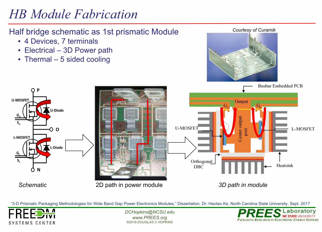
HB Module Fabrication Half bridge schematic as 1st prismatic Module
• 4 Devices, 7 terminals• Electrical – 3D Power path • Thermal – 5 sided cooling
Schematic 2D path in power module 3D path in module
Courtesy of Curamik
“3-D Prismatic Packaging Methodologies for Wide Band Gap Power Electronics Modules,” Dissertation, Dr. Haotao Ke, North Carolina State University, Sept. 2017

©2019 DOUGLAS C HOPKINS
True-3D Module (Phase leg)L2
L1
L3
L4
OUTPUT
POSITIVE
NEGATIVE
S1
S2
Current path in 3D, and Mutual inductance seen
from L1
Inner post
SiC MOSFET& Diodes
Orthogonal DBC Substrate
“3-D Prismatic Packaging Methodologies for Wide Band Gap Power Electronics Modules,” Dissertation, Dr. Haotao Ke, North Carolina State University, Sept. 2017

©2019 DOUGLAS C HOPKINS
Positive
Output
Device
Simulated v. Measured Inductance for HB Module
Impedance test with vector network analyzer• Test with a 3mm wire (1nH) – 7 nH• Test with module – 12 nH• Module inductance between
Positive (P) and Output (O) is ~6nH
ANSYS Q3D impedance extractor• AC RL simulation @ 100MHz• Module inductance between
Positive (P) and Output (O) is 9nH
“3-D Prismatic Packaging Methodologies for Wide Band Gap Power Electronics Modules,” Dissertation, Dr. Haotao Ke, North Carolina State University, Sept. 2017

©2019 DOUGLAS C HOPKINS
Half Bridge Module 3D prismatic structure vs Planar Bond All structure
• Similar electrical performance (resistance / inductance / symmetric current path)• Competitive thermal performance• Potentially better mechanical performance• Much smaller footprint
“3-D Prismatic Packaging Methodologies for Wide Band Gap Power Electronics Modules,” Dissertation, Dr. Haotao Ke, North Carolina State University, Sept. 2017

©2019 DOUGLAS C HOPKINS
True-3D Mounting and Electrical Testing
Impedance test with vector network analyzer •Test w/ 3mm wire(1nH): 7nH•Test w/ module:12nH•3D module L from Pos and Out is ~6nH
50A-to-0Atf=~5ns
50A-to-0Atr=~3ns
Double Pulse Testing
1200V/50ASiC MOSFETs& JBS Diode
“3-D Prismatic Packaging Methodologies for Wide Band Gap Power Electronics Modules,” Dissertation, Dr. Haotao Ke, North Carolina State University, Sept. 2017

©2019 DOUGLAS C HOPKINS
Thermal Simulation of HB ModuleSimulation for half bridge module
• Heatsink simulation (COMSOL)• Material: 85Cu15Zn (UNS 23000 red brass)• Heat source: 15W per chip• Ambient: 25˚C air at 7m/s• Dimension: 1.5 x 1.5 x 7.5 mm pins with 1.5 spacing.
• Simulation result• Max temperature for 3D heatsink: 100 ˚C• Max temperature for planar heatsink: 196 ˚C with 10 ˚C difference between two chips
“3-D Prismatic Packaging Methodologies for Wide Band Gap Power Electronics Modules,” Dissertation, Dr. Haotao Ke, North Carolina State University, Sept. 2017

©2019 DOUGLAS C HOPKINS
Thermal Test of HB ModuleTest of half bridge module
• Thermal test set up:• 20A through L-SBD• Measurement points:
• Tj – Thermistor• Theatsink – Thermal couple / IR• Tambient – Air flow sensor
• Test result:
“3-D Prismatic Packaging Methodologies for Wide Band Gap Power Electronics Modules,” Dissertation, Dr. Haotao Ke, North Carolina State University, Sept. 2017
ºC/W

©2019 DOUGLAS C HOPKINS
Mechanical Simulation of HB Module Ctr PostSimulation for half bridge module
• Inner post simulation (COMSOL)• Material: 85Cu15Zn (UNS 23000 red brass)• Heat source: 200˚C at chip contact• Ambient: 100˚C at bottom• Constrains: Prescribed displacement
• Simulation result• Max von Mises stress: 3 x 10⁸ N/m2• Yield strength of red brass 69-434 Mpa
(depending on post process)
Properties (UNS23000) Metric Imperial
Tensile strength 269-724 MPa 39-105 ksi
Yield strength 69-434 MPa 10-70 ksi
Elongation 55% 55%
Poisson's ratio 0.34 0.34
Elastic modulus 117 GPa 16969 ksi
“3-D Prismatic Packaging Methodologies for Wide Band Gap Power Electronics Modules,” Dissertation, Dr. Haotao Ke, North Carolina State University, Sept. 2017

©2019 DOUGLAS C HOPKINS
3ø Bridge ConceptExample: 3-phase full bridge prismatic module
A B C
POS NEGNEG POS
“3-D Prismatic Packaging Methodologies for Wide Band Gap Power Electronics Modules,” Dissertation, Dr. Haotao Ke, North Carolina State University, Sept. 2017

Ceramics?
New thin dielectrics for Low Cost modules

©2019 DOUGLAS C HOPKINS
Flexible-Ceramic Power Electronics PackagingNEEDS ADDRESSEDHigh Density, Fast Response, Low Voltage, System-in-Package Power Converters- Need Inexpensive converters with good
thermal management- Operate Temp ≤85˚C (similar to PCB)- Suitable for high current GaN
- and wearable power electronics
The 3YSZ Suitable for wearable electronics (<100˚C, <100V) applications
TECHNOLOGY- Thin E-Strate flexible 3YSZ ceramic for:
- High volume roll-to-roll manufacturing- High thermal management for highly dense LV
power converters- Thin 20 & 40 micron
substrates for lowthermal resistance
- Licensed from Corning
Leak
age
curr
ent
Voltage

Epoxy Resin Composite Dielectrics – ERCDsThese provide and opportunity to look at very low cost modules with
embedded components.
“Novel Polymer Substrate-Based 1.2kV / 40A Double-Sided Intelligent Power Module,” Xin Zhao1, Yifan Jiang1, Bo Gao1, Kenji Nishiguchi2, Yoshi Fukawa3, D. C. Hopkins1
1North Carolina State University, 2Risho Kogyo Co., LTD, 3TOYOTech LLC
New Thin Organic Dielectrics for Low Cost Modules

©2019 DOUGLAS C HOPKINS
State-of-art development of WBG power module
SiC Module w/ double-sided cooling by ORNL [1]
• 2.6 nH extracted parastics inductance• Bus up to 600V with >40A capability• Kelvin connections implemented• Gate bonding wire required
[1] F. Yang, et al. Design of a Low Parasitic Inductance SiC Power Module with Double-sided Cooling. APEC 2017, Tampa, FL.[2] S. Hauser. Direct Pressed Die Technology: Increased Power Density and Reliability in Standard Power Module Packages. APEC 2017, Tampa, FL.
SKiN and Direct Pressed Die technology by Semikron [2]
• >20% thermal resistance reduction• 10% reduction in parasitic inductance• >25% improvement in surge current• Improved thermal-cycling based reliability• 1700V/1800A• Challenge on the Press Unit design and
implementation

©2019 DOUGLAS C HOPKINS
[3] M. Roming, et al. 3D packaging advancements drive performance, power and density in power device. White Paper, Junly 2011.[4] Y. Kaji, et al. Novel IGBT Modules with Epoxy Resin Encapsulation and Insulating Metal Baseplate. ISPSD 2016.[5] T. Takahashi, et al. A 1700V-IGBT module and IPM with new insulated metal baseplate (IMB) featuring enhanced isolation properties and thermal conductivity. PCIM Europe 2016.
PowerStack packaging technology by Texas Instruments[3]
• Lower Parasitics between high- and low-side switches
• Improved Power Efficiency• Better Thermal performance• Applicable for lower voltage applications for now
• Insulated-Metal-Baseplate based IPM by Mitsubishi [4, 5]• CTE of insulating resin layer ~17ppm, close to Copper, with
better mechanical stress management• 35% thermal impedance reduction from development of resin • Less interconnection layers for lower profile, up to 55% size
reduction from traditional DBC based module• Better thermal cycling reliability with less cracks during cycling• Heavily depends on the resin interface material
State-of-art development of WBG power module

©2019 DOUGLAS C HOPKINS
Target Application: 1200V / 40A SiC MOSFET and Schottky Diode based Power Module
Criterion for thin dielectric selection for
Criterion for thin dielectric selection for power module substrate applications• Thermal conductivity need not be high, due to thin dielectric• Sufficient breakdown voltage for adequate margin for 1200V SiC MOSFETs• Low leakage current comparable with SiC devices at the same conditions, such
as temperature• High temperature operation similar to SiC devices• High processing temperature to leave margin for assembly processes
Parameters Unit ValueThermal Conductivity W/mK > 3
Breakdown Voltage kV > 3Leakage Current µA ~ 10
Dielectric Constant 1 < 8Operation Temperature oC > 175Processing Temperature oC > 250
From Xin Zhao Presentation: “Novel Polymer Substrate-Based 1.2kV / 40A Double-Sided Intelligent Power Module,” Xin Zhao, Yifan Jiang, Bo Gao, Kenji Nishiguchi, Yoshi Fukawa, Douglas C. Hopkins, IEEE 67th ECTC, Orlando, FL May 30 – Jun 02, 2018

©2019 DOUGLAS C HOPKINS
Epoxy Resin Composite Dielectric by RISHO
Bonding sheet, RCC, Copper-base CCL without glass fabric
Liquid Molding Compound(One-pack type) (1~4W/mK)
Liquid Molding Compound(Two-pack type)(1~7W/mK)
Dielectric layer(Woven Glass cloth reinforced)
Copper Foil
Copper Foil
CCL (CS-XXXX)Cu Clad Laminate
Dielectric layer(B-stage)
(Woven Glass cloth reinforced)
(ES-XXXX)Prepreg Aluminum /Copper plate
Dielectric layerCopper foil
(AC-XXXX)Metal base CCL
Bonding layer(B-stage)
Release film
Release film
(AD-XXXX)Bonding sheet
Bonding layer(B-STAGE)
Release film
Copper foil
(CD-XXXX)Resin Coated Cu
AC-72088W/mK
Al base CCL
AD-7210CD-7210CC-721010W/mK
AC-721010W/mK
AD-7208CD-72088W/mK
HIGH THERMAL CONDUCTIVITY MATERIALS
Courtesy of

©2019 DOUGLAS C HOPKINS
Target Material: Recently developed Epoxy-Resin based dielectric by Risho Kogyo Co., Ltd. – AC-7208
Properties of the Thin Dielectric (measured at 120 µm)
Better Stress Management• CTE closer to copper than traditional
ceramic (4.5 ppm/K ~ 7 ppm/K)• Flexible allowing for stress release
during assembly and service of the module
Investigating Flexible Thin Dielectric as Substrates
Parameter Unite ValueThermal Conductivity W/mK 8
Tg oC 270Modulus GPa 30
Bending Strength MPa 94CTE ppm/oC 9/22Dk / 6.3Df / 0.009
Water Absorption % 0.27Dielectric Strength kV 5.6 @ 120 µm
Parts Thickness/µm
Thermal ConductivityW/m·K
Unit Thermal ConductanceW/m2·oC
Epoxy-resin 80 8 0.1E6Al-2O3 254 23 0.09E6
AlN 254 170 0.67E6
Comparable thermal performance with alumina• Better unit area thermal conductance than alumina• 1/5 unit area thermal conductance of AlN• Lower cost for epoxy-resin substrate
From Xin Zhao Presentation: “Novel Polymer Substrate-Based 1.2kV / 40A Double-Sided Intelligent Power Module,” Xin Zhao, Yifan Jiang, Bo Gao, Kenji Nishiguchi, Yoshi Fukawa, Douglas C. Hopkins, IEEE 67th ECTC, Orlando, FL May 30 – Jun 02, 2018

©2019 DOUGLAS C HOPKINS
• Capable of bonding with Copper on both sides• Copper thickness up to ≤ 0.6 mm• 80 µm dielectric thickness is available
Epoxy Resin Composite Dielectric
Leakage current measured on 80 µm sample with Cu bonded on both sides• 20 µA leakage even at 250 ºC with 1200 V voltage applied• 1 nA leakage at room temperature with > 4kV voltage applied
From Xin Zhao Presentation: “Novel Polymer Substrate-Based 1.2kV / 40A Double-Sided Intelligent Power Module,” Xin Zhao, Yifan Jiang, Bo Gao, Kenji Nishiguchi, Yoshi Fukawa, Douglas C. Hopkins, IEEE 67th ECTC, Orlando, FL May 30 – Jun 02, 2018

©2019 DOUGLAS C HOPKINS
Resource Development for ERCD Topology Research1. ERCD ”substrate-less” approaches identified for high voltage (5kV/120µm), high
temperature (≤300ºC) and high thermal impedance (10W/mK). 2. Materials systems for fluid compatibility, multilayering and metal backing for
investigation of dense high voltage power module structures. 3. Processes and equipment for ERCD systems identified and ordered through
PREES resources.circuit board plotters
LPKF-contac-S4Reliable Through-hole
Plating in the Lab
LPKF ProtoMat S104 LPKF® MultiPress S Automatic Lamination
Press
HB05 Manual Wire BonderWedge, ball & ribbon bondingLPKFLPKF ProMask
Pro Legend, UV Lamp Table

©2019 DOUGLAS C HOPKINS
ERCD Composition
Microstructure of the dielectric at 20,000 magnification• O is corresponding to alumina particles, distributed almost everywhere, N is the AlN
particles, with limited number, C is from the polymer, Cu is from the bonding interface• AlN and alumina particles are also identified by XRD analysis• High thermal conductivity is from the widely distributed alumina particles and few AlN
particles
Al O C
CuN
From Xin Zhao Presentation: “Novel Polymer Substrate-Based 1.2kV / 40A Double-Sided Intelligent Power Module,” Xin Zhao, Yifan Jiang, Bo Gao, Kenji Nishiguchi, Yoshi Fukawa, Douglas C. Hopkins, IEEE 67th ECTC, Orlando, FL May 30 – Jun 02, 2018
©2019 DOUGLAS C HOPKINS
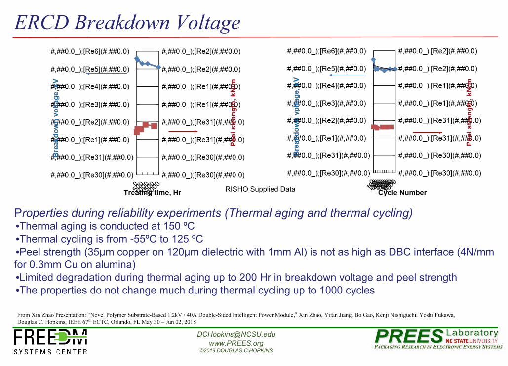
ERCD Breakdown Voltage
Properties during reliability experiments (Thermal aging and thermal cycling)•Thermal aging is conducted at 150 ºC•Thermal cycling is from -55ºC to 125 ºC•Peel strength (35µm copper on 120µm dielectric with 1mm Al) is not as high as DBC interface (4N/mm for 0.3mm Cu on alumina)•Limited degradation during thermal aging up to 200 Hr in breakdown voltage and peel strength•The properties do not change much during thermal cycling up to 1000 cycles
From Xin Zhao Presentation: “Novel Polymer Substrate-Based 1.2kV / 40A Double-Sided Intelligent Power Module,” Xin Zhao, Yifan Jiang, Bo Gao, Kenji Nishiguchi, Yoshi Fukawa, Douglas C. Hopkins, IEEE 67th ECTC, Orlando, FL May 30 – Jun 02, 2018
RISHO Supplied Data

©2019 DOUGLAS C HOPKINS
AC-7208(8W/mK)Product number AC-7208
Dielectric layer thickness 120μm
Thermal cond.(W/mK) 8 Laser flash
Tg(℃) 270 DMA method
Peel strength(kN/m)
1.2 1 oz copper
Solder limit(sec) Over 60 260ºC
CTE(ppm/℃) 9/22 α1/α2
Breakdown(kV) Over 5 JIS C2110
CTI Over 600 IEC method
Flammability V-0equiv. UL94
◆High temperature long term test(@175℃)
◆Thermal cycle test(-40⇔125℃)
After long term test at 175℃ and thermal cycle test, There is no problem in breakdown voltage and peel strength.→ This material also shows high reliability. Courtesy of

©2019 DOUGLAS C HOPKINS
AC-7210(10W/mK)
Product number AC-7210
Dielectric layer thickness 120μm
Thermal cond.(W/mK) 10 Laser flash
method
Tg(℃) 270 DMA method
Peel strength(kN/m)
1.2 1 oz copper
Solder limit(sec) 60< 260℃
CTE(ppm/℃)α1 14/14/14 X/Y/Z
Breakdown voltage (kV) 5< JIS C2110
CTI 600< IEC method
Flammability V-0 equivalent UL94
HIGH TEMPERATURE LONG TERM
RELIABILITY(175℃)
Courtesy of
©2019 DOUGLAS C HOPKINS
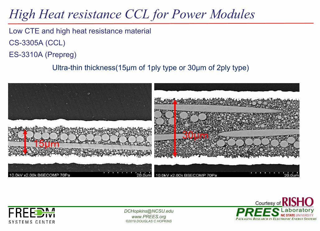
High Heat resistance CCL for Power Modules
Ultra-thin thickness(15μm of 1ply type or 30μm of 2ply type)
Courtesy of
Low CTE and high heat resistance material CS-3305A (CCL)ES-3310A (Prepreg)

©2019 DOUGLAS C HOPKINS
General properties of CS-3305A seriesItem Unit CS-3305A
(E-glass)CS-3305AS
(Low CTE glass)CS-3305AQ
(Quartz glass)
CTE(Other Low CTE glass fabric enables lower CTE)
Y α1 ppm 6~8 2~4 0.5~1
X α1 ppm 6~8 2~4 0.5~1
Z α1 ppm 10~15 10~15 10~15
Glass transitionTemperature (Tg) DMA ℃ Over 300ºC
Water absorption ratio % 0.13
Flexuralstrength(Y-axis)
25℃ MPa 517 660 446
250℃ MPa 415 470 356
Flexuralmodulus(Y-axis)
25℃ GPa 32 35 32
250℃ GPa 16 19 19
Peel strength (Copper) KN/m 0.6 [VLP 1/3oz]
Solder heat resistance(300℃) Sec. over300Courtesy of

©2019 DOUGLAS C HOPKINS
High modulus under high temperature
Tg : Over 300℃
High Tg and high modulus by DMA method
・There is no tanδ peak of CS-3305A → Tg : over 300℃・Storage modulus maintains higher than the other material under the high temperature.
Courtesy of

©2019 DOUGLAS C HOPKINS
5% Weight loss1% Weight loss
Atmosphere:Air Heating rate:10℃/minReference:Al2O3
CS-3305A
Standard FR-4.0(Glass-epoxy resin)
CS-3305A Standard FR-4.0Td(1%) 352℃ 277℃Td(5%) 487℃ 310℃
Thermal decomposition temperature by TGA method
Temperature (℃)
TG (%
) Large improvement
CS-3305A is a long term heat resistance material.
Courtesy of

©2019 DOUGLAS C HOPKINS
CS-3305A Std FR-4.0
Temperature 175℃ 200℃ 150℃
0hr. (Retention)
1.30kN/m(100%)
1.30kN/m(100%)
1.60kN/m(100%)
1500hr. (Retention)
1.27kN/m(98 %)
1.25kN/m (96 %)
1.28kN/m (80 %)
3000hr. (Retention)
1.26kN/m (97 %)
1.20kN/m (92 %)
0.99kN/m (62 %)
Retention of peel strength of copper foil
Time (hr.)
Retention (%
)
Delamination
FR-4.0 200℃ treatment
FR-4.0 175℃ treatmentFR-4.0 150℃ treatment
CS-3305A 175℃ treatment
CS-3305A 200℃ treatment
・ Delamination between copper foil and dielectric layer of standard FR-4.0 was occurred at 175℃.
・ CS-3305A maintained peel strength at 175 and 200℃ even after 3000 hours treatment.
Delamination
Courtesy of

©2019 DOUGLAS C HOPKINS
From: PowerAmerica Short Course Nov 2018Raleigh, NC
650Vdc/20A ½-bridge IPM based on RISHO Substrate

©2019 DOUGLAS C HOPKINS
Parameters:• 650V maximum DC bus voltage• 20A maximum RMS current per device• 400V->200V Half-bridge buck• Internal decoupling capIDEAL: Simulation condition: 10A, 100pF Coss
Overshoot w/o decoupling cap240V @100nH
7V @5nH
Parts:Q1 Q2: IdealC1 C2: 10uF 25V X7RC3: 47nF 1kV X7RR1: 22Ohm 1/8WD1: Ideal HF diodeU1: Ideal isolated HB driver
Overshoot w decoupling cap7V @5nH
650Vdc/20A ½-bridge IPM based on RISHO Substrate

©2019 DOUGLAS C HOPKINS
Thermal analysis w/ first order estimation of losses:Prds = 129m*20A2 = 51.6W @ Tjmax=150˚CPsw = 55uJ*0.5MHz = 27.5W @ 400V, 15APtot = Prds+Psw = 79.1W
Given:Die Pad = 6mm X 3mm, ERCD Substrate thickness = 80µm, Al case thickness = 0.9mm:
Approximating with 45º rule:Asub=(6mm+0.04mm)*(3mm+0.04mm)=18.4mm2
Acase=(6m+0.04mm+0.9mm)*(3mm+0.04mm+0.9mm)=27.3mmRsub=0.08mm/18.4mm2*1000/(10W/m˚C)=0.43 ˚C /WRcase=0.9mm/27.3mm2*1000/(205W/m ˚C)=0.16 ˚C /W
Rtotal = Rchip+Rsub+Rcase = 0.5˚C /W+0.43˚C /W+0.16˚C /W = 1.09˚C/W
At P = 56.5W, Tcase = 40˚C, Tj = 40˚C+79.1W*1.09˚C/W = 126.2˚C, < Tjmax = 150˚C
Thermal Analysis
GaN
qz
T1
T2
ERCDCu w
t
d=1 unit deep
Aluminum Base Plate
Thank you to sponsors:

©2019 DOUGLAS C HOPKINS
Inductance estimation: 1. Power loop: 6.5nH using rectangle estimation 2. Gate loop: 3.8nH using rectangle estimationFor optimal gate driver at Q=1.5 (0.3V overshoot): R= (L/C)-1/2 /Q=2.5 Ω, L=3.8nH, C=Ciss=0.26nFGate driver has Rout = 2.7Ω > 2.5, therefore no Rext is required. Then, simulation shows only 0.26V gate overshoot, well within GaN ratings.
Thank you to GaN Systems, Risho and Electronic Interconnect for supplying parts and processing
Inductance & Performance

©2019 DOUGLAS C HOPKINS
Full SPICE simulation at 400V->200V 20A:Lpwr-loop = 6.5 nHLgate-loop = 3.8 nHCsubstrate cap = 28.9 pF (parallel plate method)Rheatsink = 10Ω sink-to-QsourceResults: Ploss = 42.5W for Q1, Tj=86.3C Ploss = 15.8W for Q2, Tj=57.2CSwitching VDS waveform shows 70 overshoot above the 400V
Parts:Q1 Q2: GS66508BC1 C2: 10uF 25V X7RC3: 47nF 1kV X7RR1: 22Ohm 1/8WD1: CURN101-HF diodeU1: Si8274 isolated HB driverBottom-side cooled 650V E-mode GaN Systems
Buck converter with Q1 as switch and Q2 as sync rect.

Excerpt from: Xin Zhao[1] Presentation: “Novel Polymer Substrate-Based 1.2kV / 40A Double-Sided Intelligent Power Module,” Xin Zhao, Yifan Jiang, Bo Gao, Kenji Nishiguchi, Yoshi Fukawa, Douglas C. Hopkins, IEEE 67th ECTC, Orlando, FL May 30 – Jun 02, 2018
SiC Integrated Power Module Test Design
[1] Now at Univ. of Texas at Austin

©2019 DOUGLAS C HOPKINS
Double Sided Design
SiC MOSFET and diodeMoly Spacer
Main Bus TerminalsTerminals for Auxiliary Power Supply
FunctionalityGate Driver
Digital IsolatorLDO
Substrates on Double Side
• Volume: 35 mm × 15.5 mm × 3mm• Power Devices: CPM2-1200-0025B / CPW5-1200-Z050B• Rating: 800 V/ 40 A• Auxiliary terminals on single side of the module, allowing for both side heat sink attachment, with terminals able to attached on PCB for interconnections
From Xin Zhao Presentation: “Novel Polymer Substrate-Based 1.2kV / 40A Double-Sided Intelligent Power Module,” Xin Zhao, Yifan Jiang, Bo Gao, Kenji Nishiguchi, Yoshi Fukawa, Douglas C. Hopkins, IEEE 67th ECTC, Orlando, FL May 30 – Jun 02, 2018
©2019 DOUGLAS C HOPKINS
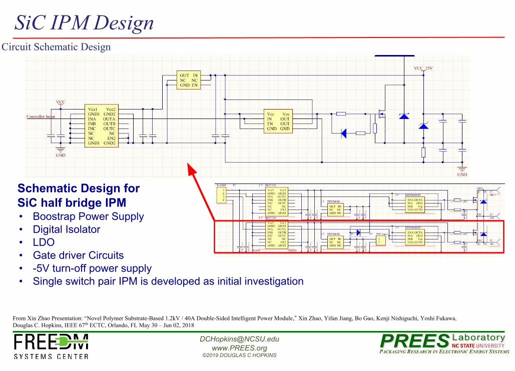
SiC IPM DesignCircuit Schematic Design
Schematic Design forSiC half bridge IPM• Boostrap Power Supply• Digital Isolator• LDO• Gate driver Circuits• -5V turn-off power supply• Single switch pair IPM is developed as initial investigation
From Xin Zhao Presentation: “Novel Polymer Substrate-Based 1.2kV / 40A Double-Sided Intelligent Power Module,” Xin Zhao, Yifan Jiang, Bo Gao, Kenji Nishiguchi, Yoshi Fukawa, Douglas C. Hopkins, IEEE 67th ECTC, Orlando, FL May 30 – Jun 02, 2018

©2019 DOUGLAS C HOPKINS
Simulation of the SiC IPM Design
• Inductance in the entire loop is 0.6 nH.• Diode inductance is larger, since it parallels the MOSFET drain to source.• Applicable for lower losses and higher operation frequency.
Current distribution in the power loop
Summary of extracted parasitics
From Xin Zhao Presentation: “Novel Polymer Substrate-Based 1.2kV / 40A Double-Sided Intelligent Power Module,” Xin Zhao, Yifan Jiang, Bo Gao, Kenji Nishiguchi, Yoshi Fukawa, Douglas C. Hopkins, IEEE 67th ECTC, Orlando, FL May 30 – Jun 02, 2018
Simulation for Parasitic ExtractionPower stage 3D model

©2019 DOUGLAS C HOPKINS
SiC-IPM Layout
Layout design for the SiC half bridge IPM• Interconnections are applied to both top and bottom side of substrates• Interconnection metal in the main power loop is a copmprise between thermal spreading and EMI
nosie reduction• Only the layout (c) and (d) are discussion in the presentation for the single switch module• The layout design is not optimized and the long gate loop trace on the plane, results in excessive
noise during switching• Jumper wire minimizes gate loop length during the fabrication for demonstration of the design
25 mm × 15 mm
From Xin Zhao Presentation: “Novel Polymer Substrate-Based 1.2kV / 40A Double-Sided Intelligent Power Module,” Xin Zhao, Yifan Jiang, Bo Gao, Kenji Nishiguchi, Yoshi Fukawa, Douglas C. Hopkins, IEEE 67th ECTC, Orlando, FL May 30 – Jun 02, 2018
Circuit Layout Design

©2019 DOUGLAS C HOPKINS
SiC IPM Fabrications & MeasurementsModule Assembly & MOSFET Statics Test
The forward and reverse characteristics of SiC MOSFET is similar with data shown on the datasheet[7].
The proposed module fabrication and assembly process, including the topside metallization process of SiC devices, can fully exhibits the initial performance of the SiC devices
From Xin Zhao Presentation: “Novel Polymer Substrate-Based 1.2kV / 40A Double-Sided Intelligent Power Module,” Xin Zhao, Yifan Jiang, Bo Gao, Kenji Nishiguchi, Yoshi Fukawa, Douglas C. Hopkins, IEEE 67th ECTC, Orlando, FL May 30 – Jun 02, 2018
[7] CPM2-1200-0025B DATASHEET

©2019 DOUGLAS C HOPKINS
SiC IPM Fabrications & MeasurementsModule Assembly & Driver Circuits Test
• Flip-chip assembly for SiC MOSFET and Diode
• Underfill applied for 1200V isolation• Large terminals for testing
25 mm × 15 mm
From Xin Zhao Presentation: “Novel Polymer Substrate-Based 1.2kV / 40A Double-Sided Intelligent Power Module,” Xin Zhao, Yifan Jiang, Bo Gao, Kenji Nishiguchi, Yoshi Fukawa, Douglas C. Hopkins, IEEE 67th ECTC, Orlando, FL May 30 – Jun 02, 2018
• Gate pad is on same plane as gate driver, output signal verified for -5V turn-off and 20V turn-on of MOSFET

©2019 DOUGLAS C HOPKINS
Conclusions• Selection Criterion of Thin dielectric substrate material is set up based on design
requirements of 1200V WBG device based IPMs.• A 120µm recently developed flexible epoxy-resin based dielectric, by Risho Kogyo Co.,
Ltd., is investigated, and proved to be suitable for power module substrate in terms of electrical, thermal, mechanical properties, cost, and reliability.
• A high-density half-bridge SiC power module is designed with ultra-low parasitics, utilizing epoxy-resin based dielectric, for high-frequency and low-loss applications.
• Fabrication process of double-side solderable SiC MOSFETs and diodes is developed, capable of deposition of metallization layer up to 2µm.
• A single-switch SiC power module with more functionality is fabricated, allowing for double-side cooling functions, verified by static measurements.
• The proposed substrate material, and designed WBG IPM with ultra-low parasitics, high functionality and double-side cooling is verified and show potential for high frequency and high power density applications.
[7] CPM2-1200-0025B DATASHEET
From Xin Zhao Presentation: “Novel Polymer Substrate-Based 1.2kV / 40A Double-Sided Intelligent Power Module,” Xin Zhao, Yifan Jiang, Bo Gao, Kenji Nishiguchi, Yoshi Fukawa, Douglas C. Hopkins, IEEE 67th ECTC, Orlando, FL May 30 – Jun 02, 2018

Prof. Douglas C. Hopkins, Ph.D.Director – PREES Laboratory
FREEDM System CenterNorth Carolina State Univ.1791 Varsity Dr., Suite 100Raleigh, NC 27606-7571
www.prees.org
End