production and electrical properties of a cuznalmn(sma)/p
TRANSCRIPT

Production and Electrical Properties of aCuZnAlMn(SMA)/p-Si DiodeEMINE ALDIRMAZ ( [email protected] )
Institute of Sciences https://orcid.org/0000-0003-0456-7074M. Güler
Ankara Hacı Bayram Veli Üniversitesi Polatlı Fen Edebiyat Fakültesi: Ankara Haci Bayram VeliUniversitesi Polatli Fen Edebiyat FakultesiE. Güler
Ankara Hacı Bayram Veli Üniversitesi Polatlı Fen Edebiyat Fakültesi: Ankara Haci Bayram VeliUniversitesi Polatli Fen Edebiyat Fakultesi
Research Article
Keywords: CuZnAlMn, Schottky diode, I-V characteristics, C-V characteristics, Illumination, frequencyeffect
Posted Date: March 16th, 2021
DOI: https://doi.org/10.21203/rs.3.rs-295613/v1
License: This work is licensed under a Creative Commons Attribution 4.0 International License. Read Full License

1
Production and Electrical Properties of a CuZnAlMn(SMA)/p-Si Diode
E. Aldirmaz1, M. Güler2, E. Güler2
1University of Amasya, Department of Physics, Amasya, Turkey.
2University of Ankara Hacı Bayram Veli University, Department of Physics, Ankara,
Turkey.
Abstract
In this study, the Cu-23.37%Zn-13.73%Al-2.92%Mn (at.%) alloy was used. Phase
identification was performed with the Scanning electron microscope (SEM), and energy-
dispersive X-ray (EDX). We observed in the austenite phase in Cu-23.37%Zn-13.73%Al-
2.92%Mn (at.%) alloy. To produce a new Schottky diode, CuZnAlMn alloy was exploited as
a Schottky contact on p-type semiconductor silicon substrate. To calculate the characteristics
of the produced diode, current-voltage (I-V), capacitance-voltage (C-V) and conductance-
voltage (G-V) analyzes were taken at room temperature (300 K), in the dark and under
various lights. Using electrical measurements, the diode's ideality factor (n), barrier height
(Φb), and other diode parameters were calculated. Besides, the conductance / capacitance-
voltage (G/C-V) characteristics of the diode were studied and in a wide frequency interval at
room temperature. Also, the capacitance and conductance values strongly rely on the
frequency. From the present experimental results, the obtained diode can be used for
optoelectronic devices.
Keywords: CuZnAlMn, Schottky diode, I-V characteristics, C-V characteristics,
Illumination, frequency effect.
Corresponding author; [email protected]

2
1. Introduction
The existing SMAs (Shape Memory Alloys) are NiTi-, copper-, and ferrous-based
SMAs. Cu-based SMAs are simple to fabricate, handle and are cheaper than NiTi alloys.
They also have superior superelasticity and shape memory effect compared to Fe-based
SMAs. Copper-based SMAs, owing to their excellent properties and low cost, have been
highly attractive to various industries such as aerospace, automotive, and defense industries.
Recently, the Cu-based SMAs have been more widely utilized due to their suitability for
sensing, impact absorption, and vibration damping applications [1-5]. In copper-based
SMAs, the atomic arrangement of the parent-phase change with the composition of the alloy
and the applied effect. The Cu-based shape memory alloys (SMAs), a martensite
transformation usually refers to a transformation from the disorder b.c.c. structure to the
martensite phases. According to the different conditions and chemical composition, the three
types of martensite can be acquired. These phases have structures of 6R, 18R and 2H,
respectively [6-12]. Which phase prevails is dependent upon the electronic concentration
e/a: for the e/a around 1.48, the 9R or 18R structure prevails; for the e/a below 1.48 (around
1.4), the 6R or 12R structure prevails; and for the e/a above 1.5, the 2H structure prevails [6,
7, 13].
Circuit elements based on metal-semiconductor contacts are produced from
semiconductor materials of higher quality day by day and search for new materials are still
going on. Making contacts of metals and alloys on semiconductor materials with advanced
technological methods has facilitated the control of circuit element production. Metal-
semiconductor contacts in semiconductor technology have a major role in the production of
electronic circuit elements. Metal-semiconductor contacts are used in the production of
field-effect transistors, solar cells, Schottky diodes, semiconductor detectors, switching
elements, and microwave mixers. [14-18].

3
At first, the Cu-based SMAs were used as actuators and sensors in household appliances and
electrical equipment. In recent years, the biomedical industry, transportation industry, and
micro-electrical devices [19]. Even Schottky type semiconducting diodes and photodiodes
can be fabricated from Cu-based SMAs with advanced technological methods. Some other
researchers also investigated these properties with different compositions in CuAl based
alloys [20-25].
In this survey, we produced a Schottky device based on a CuZnAlMn SMA.
Nowadays, no such works have been reported for CuZn based alloys. So, a CuZn based
alloy is used for the first time. For this reason, this study will make significant contributions
to the literature. So our main aim was to produce a new Schottky diode by using the
mentioned materials for modern optoelectronics.
2. Experimental details
The alloy with a composition of Cu-23.37%Zn-13.73%Al-2.92%Mn (at.%) was obtained
melted by arc-melting and then induction melting. It was done in an argon atmosphere. The
sample obtained from the alloy was exposed to homogenization at 800 ˚C for 1 hour
followed by water quenching at room temperature. The SEM investigations, prepared
samples were mechanically polished. After polishing, the sample was soaked in the
FeCl3·6H2O methanol with HCl solution etching. Microstructural characterization analysis
was carried out by SEM. The compositions of the prepared samples were analyzed by
(EDX) operating within SEM. The diode was prepared using a p-type silicon (p-Si) wafer
and Cu-23.37%Zn-13.73%Al-2.92%Mn (at.%) alloy. We have used consecutive chemical
baths to clean a p/Si wafer. After the cleaning process, we deposited an ohmic contact to the
backside of the Si wafer by thermal evaporation of the Aluminum (Al) wire. Subsequently,
we performed annealing, to obtain Schottky dot contacts. The prepared CuZnAlMn SMA

4
was thermally evaporated on to the front of p-Si substrate. Finally, CuZnAlMn/p-Si/Al
Schottky diode was fabricated. The contact area of the diode was measured as7.85x10-2 cm2.
The characteristic analyses I–V, C-V and G-V of diod were examined by FYTRONIX 5000
characterization system under changing frequencies. All experimental procedures were
realized at room temperature.
3. Results and discussion
3.1 Microstructure of the alloy
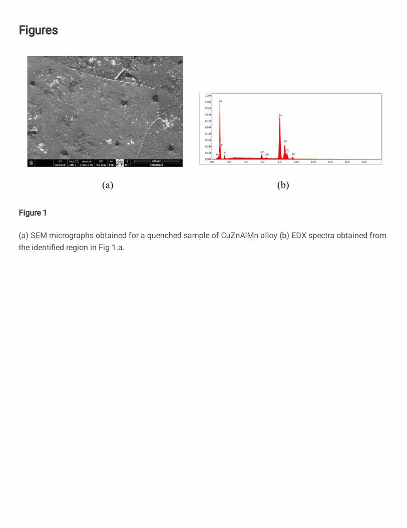
The SEM micrographs in Fig.1 illustrate the microstructure of the Cu-23.37%Zn-
13.73%Al-2.92%Mn alloy. Scanning electron micrograph (Fig. 1.a) indicates the presence
of an austenite phase, which was confirmed through the EDS spectra in Fig. 1.b. In Fig.1,
typical austenite grain boundaries exist for the alloy. It has been found from previous studies
that quenching significantly affects the transformation properties [26-27]. For the Cu-
23.37%Zn-13.73%Al-2.92%Mn alloy, the grain size of the alloy increases with the addition
of Mn. Additionally, we observed that the Mn element prevents the formation of
precipitation in the alloy.
3.2 Electrical Characterization
I–V measurements of the diode can be described by the thermionic emission model.
According to this model, the current can be expressed as [28, 29],
nkT
IRVqII s )(
exp0
for (V ≥ 3kT/q) (1)
Here I0 is given as,
kT
qTAAI b
o exp2 (2)

5
where V is the applied voltage, Rs is the series resistance, q is the electronic charge, n is the
ideality factor, k is the Boltzman's constant, T is the temperature, where A is the Schottky
contact area, A* is the Richardson constant, and Φb is the zero-bias barrier height [30].
The n is given as,
)(ln Id
dV
kT
qn (3)
In general, I-V graphs showing the characteristics of the contact are obtained by
giving positive and negative voltages to the Schottky contacts. The forward bias part of
these graphs, usually shown on the right, indicates that the contact conducts current with
very little resistance. The reverse bias part, which is usually shown on the left of the graph,
displays resistance increment with the relatively blocked current. Fig. 2 gives the I-V curves
of the diode for conditions of dark and different solar light intensities. As seen in Figure 2,
the diode reverses current changes with the light intensity. Also, the reverse current
increases by the increment of light intensity. The photodiodes reverse current increases by
1.83x10⁻³ A under 100 mW /cm2 (applied as the highest light intensity value). This result
shows that electron-hole pairs formation in the depletion layer of a light-illuminated diode.
Moreover, after photogeneration, the charge carriers contribute to the current through the
diode. The current rises due to the generation of the photocurrent, and the current in the zero
bias [31-34] also exists. Besides, this result suggests that the generated CuZnAlMn (SMA) /
p-Si diode current changes depending on the light intensity and thus, it can be used for
different applications in different optoelectronic circuits [35, 36].
From equation 3, the slope of the linear region of the forward-bias ln(I)-V plot gives
the n value. Table 1 lists the results of the Φb and n values obtained from the I-V method
under dark and 100 mW/ cm2 conditions. In their former work, the authors produced a diode
and obtained the n of 3.52 and 3.31 under dark and 100 mW/cm2 respectively while

6
corresponding Φb were 0.58 and 0.59 eV [25]. In another study, the n values for
Au/CuAlMnFe/n-Si/Al diode were obtained to be as 3.92 ± 0.3 and 4.19 ± 0.3 and Φb were
determined as 0.73 ± 0.2 and 0.69 ± 0.2 [21]. So, the n value of our earlier p-type
semiconductor (CuAlMn shape memory alloy diode) is greater than this work [23]. The Φb
value was obtained as 0.58 eV for dark. The variety of the Φb values originate due to the
different compositions of metallic alloys with separate work functions [21, 37]. Thus, the
diodes n was found to be bigger than its ideal value. A large n value indicates that there is a
small insulating layer (oxide, ie chemical pollution) between the metal and the
semiconductor on the rectifier contact side of the diodes [38]. Also, large ideality factors are
related to the magnitude of the ohmic contact resistance which is directly proportional to
factors such as the density of the interfacial states and the magnitude of the series resistance
(Rs) of the neutral zone. [39, 40]. The n and Φb including Rs are found from dV/d(lnI) plot.
Fig. 3 shows the plots calculated from Cheung's method and these parameters of the diode
are summarized in Table 1. The plots in the graphs indicate straight lines. The uniformity of
these parameters found from Cheung's method approves the Rs effect.
Cheung’s method can be obtained by the equation [41],
q
kTnIR
Id
dVs)(ln
(4)
3.3 Photocurrent measurements of the diode
The photocurrent of CuZnAlMn/p-Si/Al Schottky diode was analyzed by equation 5 below
[42, 43],
m
ph API
(5)
In Eq. 5, P denotes the intensity of the light, Iph indicates the photocurrent, A is a constant
and m represents an exponent. The Iph graph according to diode at -4V value is shown in

7
Figure 4. As in Figure 4, photocurrent varies with the intensity of light. It increases by the
increasing light intensity. The slope of the linear photoconductivity graph affords the
numerical m value of 1.23. The m value suggests the occurrence of photoconduction
mechanism by the linear molecular recombination process [21].
The transient photocurrent-time analyses are common techniques to understand the
photoconduction mechanism. Fig.5. shoes the characteristic of transient photocurrent
characteristics for various illuminations. In the turned on illumination, photocurrent
enhances rapidly to a definite position. In its turned off mode, the photocurrent diminishes
suddenly and goes back to its initial position. In this way, this alteration in the current due to
light displays that the produced photodiode has photoconductivity and can therefore be used
as a photodiode or photosensor. [44-46].
3.4 C-V and G/w-V measurements
Measurements of capacitance-voltage (C-V) and conductance-voltage (G/ω-V) for wide
frequencies give valuable info about the basic electrical and dielectric properties of the
prepared CuZnAlMn(SMA)/p-Si Schottky diode. Figure 6.a.b; in a wide frequency range
(10 kHz-1MHz); shows the C-V and G/ω-V characteristics of the produced diode at room
temperature (300 K). In both C-V and G/ω-V graphs of the diode, the measured C-V and
G/ω-V are found to be frequency-dependent. As in Figure 6.a, when frequency increases, the
capacity of the fabricated diode decrease. Further, it becomes almost constant in the negative
voltage region. Unlike capacitance behavior, the measured G value increases after an
increase in frequency (Fig. 6.b). The frequency characteristics for the C and G may be
attributed to the presence of the interface states [47-51]. Because the interface states at low
frequencies can follow the AC signal while they do not follow the AC signal at high
frequencies [52]. So, the interface state capacitance value does not contribute to the total
capacitance value which results only from the space charge capacitance.

8
Also, the Rs of the diode was extracted from admittance measurements. The Rs were
calculated by using the Nicollian and Goetzberger conductance method [52, 53]. The Rs was
obtained from by equation 6,
22
mas
ma ma
GR
G C
(6)
In Eq. 6, Cma and Gma hold for the measured capacitance and conductance, respectively. Fig.
7 outlines the series Rs-V curves for different frequencies. This variation shows that the
electrical loads at the interface can follow the frequency change depending on the applied
voltage.
4. Conclusions
In this survey, copper-based the Cu-23.37%Zn-13.73%Al-2.92%Mn (at.%) alloy was
handled as a Schottky contact. Then, the SMA CuZnAlMn/p-Si/Al Schottky diode was
fabricated. The microstructural properties of the SMA were characterized by SEM and EDS.
The electrical properties of the Schottky diode were analyzed using the data obtained from
the measurements made under different illumination intensities and a wide frequency range.
The usual I-V characteristics and Cheung techniques have been used to explore several
electrical features of the diode in the dark and under different illuminations. Thanks to the
information provided from the I-V graph, we have concluded that the CuZnAlMn/p-Si/Al
Schottky diode we prepared is sensitive to light. Both the C and G measurements were
found to be strongly dependent on bias voltage and frequency for CuZnAlMn/p-Si/Al
Schottky diode structure. According to the presently obtained results, we can also conclude
the photoconductivity behavior of the presently fabricated diode. Therefore, the presently
fabricated Schottky diode is promising for the practical applications of recent
optoelectronics. The results obtained in this study may inspire the production of other
Schottky diodes including different alloying elements.

9
Acknowledgement The author(s) would like to thank the University of Amasya for
providing the financial support, under Grant No. FMB-BAP 15-093.
References
1. J.M. Jani, M. Leary, A. Subic, M.A. Gibson, A Review of Shape Memory Alloy.
Research, Applications and Opportunities, Mater. Des., 1980-2015(56) (2014), pp.
1078-1113
2. K. Otsuka, C.M. Wayman, editor. Shape memory materials. Cambridge: Cambridge
University Press (1998)
3. H. Funakubo, Shape memory alloys. New York: Gordon Breach Sci Pub (1987)
4. T.W. Duerig, K. Melton, D. Stöckel, Engineering aspects of shape memory alloys.
Butterworth-Heinemann (2013)
5. I.N. Qader, M. Kok, F. Dagdelen, Y. Aydogdu, A Review of Smart Materials:
Researches and Applications, El-Cezerî J Sci Eng 6, ( 3) (2019), pp. 755-788
6. Y. Sutou, T. Omori, K. Yamauchi, N. Ono, R. Kainuma, K. Ishida, Effect of grain size
and texture on pseudoelasticity in Cu-Al-Mn-based shape memory wire, Acta Mater., 53
(2005), pp. 4121-4133
7. H. Li, Effect of the Mn Additive on Cu-Zn-Al Shape Memory Alloy, University of
Nevada, Reno, A thesis submitted in partial fulfillment of the requirements for the
degree of Master of Science in Material Science and Engineering , May 2012
8. Y.Q. Jiao, Y.H. Wen, N. Li, J.Q. He, J. Teng, Effect of solution treatment on damping
capacity and shape memory effect of a CuAlMn alloy, J. Alloys Comp., (491) (2010),
pp. 627-630
9. M.A. Morris, High temperature properties of ductile CuAlNi shape memory alloys with
boron additions, Acta Metall. Mater., 40 (1992), pp. 1573-1586

10
10. A. Aydoğdu, Y. Aydoğdu, O. Adıguzel, The influence of ageing on martensite ordering
and stabilization in shape memory Cu-Al-Ni alloys, Mater. Res. Bull., 32 (1997), pp.
507-513.
11. U.S. Mallik, V. Sampath, Influence of aluminum and manganese concentration on the
shape memory characteristics of Cu–Al–Mn shape memory alloys, J. Alloys Comp.,
459 (2008), pp. 142-147
12. R. Kainuma, S. Takahashi, K. Ishida, Thermoelastic martensite and shape memory
effect in ductile Cu–Al–Mn alloys. Metall. Mater. Trans. A 27A, (1996), pp. 2187-2195
13. M. Ahlers, Martensite and equilibrium phases in Cu-Zn and Cu-Zn-Al alloys, Prog.
Mater. Sci., 30 (1986), pp.135-186
14. S.M. Sze, K.K. Ng, Physics of semiconductor devices, 3rd ed., John
Wiley & Sons, Hoboken, New. Jersey (2006)
15. W. Mönch, Electronic Properties of Semiconductor Interfaces (c. 43). Springer,
Heidelberg (2004)
16. B.G. Streetman, S.K. Banerjee, Solid State Electronic Devices (c. 4). Prentice Hall,
New Jersey (2005)
17. D.A. Neamen, B. Pevzner, Semiconductor Physics and Devices: Basic Principles, Irwin
(1992)
18. E.H. Rhoderick, R.H. Williams, Metal-Semiconductor Contacts. Clarendon Press,
Oxford (1988)
19. T. Habu, Applications of shape memory alloys (SMAs) in electrical appliances, (2011)
20. C. Aksu Canbay, A. Tataroglu, A. Dere, Ahmed Al-Ghamdi, F. Yakuphanoglu, A new
shape memory alloy film/p-Si solar light four quadrant detector for solar tracking
applications, J. Alloys Comp., 688 (2016), pp. 762-768

11
21. C. Aksu Canbay, A. Tataroglu, A. Dere, Abdullah G. Al-Sehemi, Abdulkerim
Karabulut, A. Bektas, Ahmed A. Al-Ghamdii, F. Yakuphanoglu, The photo-electrical
performance of the novel CuAlMnFe shape memory alloy film in the diode application,
Mater. Sci. Eng. B, 264 (2021), pp. 114931
22. C. Aksu Canbay, A. Dere, Kwadwo Mensah-Darkwa, Ahmed Al-Ghamdi, Z. Karagoz
Genc, R. K. Gupta, F. Yakuphanoglu, New type of Schottky diode-based Cu–Al–Mn–
Cr shape memory material films, Appl. Phys. A, 122 (2016), pp. 712
23. E. Aldirmaz, M. Guler, E. Guler, A. Dere, A. Tataroglu, Abdullah G. Al-Sehemi,
Ahmed A. Al-Ghamdi, F. Yakuphanoglu, A shape memory alloy based on photodiode
for optoelectronic Applications, J. Alloys Comp., 743 (2018), pp. 227-233
24. C. Aksu Canbay, A. Tataroglu, W.A. Farooq, A. Dere, Abdulkerim Karabulut, M. Atif,
A. Hanif, CuAlMnV shape memory alloy thin film based photosensitive diode, Mater.
Sci. Semicond Process., 107 (2020), 104858
25. E. Aldırmaz, A. Tataroğlu, A. Dere, M. Guler, E. Guler, A. Karabulut, F.
Yakuphanoglu, Cu-Al-Mn shape memory alloy based Schottky diode formed on Si,
Physica B: Conden. Matter., 560 (2019), pp. 261-266
26. V. Sampath, Effect of Thermal Processing on Microstructure and Shape-Memory
Characteristics of a Copper–Zinc–Aluminum Shape-Memory Alloy, Mater. Manufact.
Process., 22 (2007), pp. 9-14
27. F. Dagdelen, T. Gokhan, A. Aydogdu, Y. Aydogdu, O. Adigüzel, Effects of thermal
treatments on transformation behavior in shape-memory Cu-Al-Ni alloys, Mater.
Letters., 57 (2003), pp. 1079-1085
28. S.M. Sze, Physics of Semiconductor Devices, second Ed., Wiley, New York (1981)
29. E.H. Rhoderick, R.H. Williams, Metal-Semiconductor Contacts, second ed., Clarendon,
Oxford (1988)

12
30. S.M. Sze, K.K. Ng, Physics of Semiconductor Devices, third ed., Wiley (2007)
31. H. Aydin, A. Tataroglu, A.A. Al-Ghamdi, F. Yakuphanoglu, F. El-Tantawy, W.A.
Farooq, A novel type heterojunction photodiodes formed junctions of Au/LiZnSnO and
LiZnSnO/p-Si in series, J. Alloys Compd. 625 (2015), pp. 18-25.
32. E.H. Nicollian, A. Goetzberger, MOS conductance technique for measuring surface state
parameters, Appl. Phys. Lett., 7 (1965), pp. 216.
33. J. Singh, Electronic and Optoelectronic Properties of Semiconductor Structures,
Cambridge University Press, New York (2003)
34. D. Wood, Optoelectronic Semiconductor Devices, Prentice Hall, New York (1994)
35. M. Cavas, Al/P-Si/Zno/Al Foto Diyotun Üretimi ve Elektriksel Karakterizasyonu, Sci
Eng. J of Fırat Univ., 29(1) (2017), pp. 325-330
36. I. Yun, Photodiodes-from Fundamentals to Applications, InTech, Croatia (2012)
37. J. H¨olzl, F.K. Schulte, Work function of metals. Solid surface physics, Springer,
Berlin, Heidelberg (1979)
38. A. Kumta, E. Rusli, C.C. Tin, J. Ahn, Desing of field-plate terminated 4H-SiC Schottky
diodes using high-k dielectrics, Microelectronic reliability, 46 (2006), pp. 1295-1302.
39. K. Daw, P. Chattopadhyay, Controll of Barrier Height of MIS Tunnel Diodes Using
Deep Level Impurities, Solid-State Electron, 34 (1991), pp. 367-371
40. F. Aslan, Ö. Güllü, Y. S. Ocak, Ş. Rüzgar, A. Tombak, C. Özaydın, O.Pakma, İ. Arsel,
Organik Arayüzey Tabakalı Al/CuPc /p-InP Kontakların Fabrikasyonu Ve Elektriksel
Parametrelerinin İncelenmesi, Batman Univ. J. Life Sci., 5 (2) (2015), pp. 263-275
41. S.K. Cheung, N.W. Cheung, Extraction of Schottky diode parameters from forward
current-voltage characteristics, Appl. Phys. Lett., 49 (1986), pp. 85-87.

13
42. Yakuphanoğlu F., Faroog A.W, Photoresponse and Electrical Characterization of Photo
Diode based nanofibers ZnO and Si, Mater. Sci. Semiconduc. Process., 14 (2011), pp.
207-211
43. A. Rose, Concepts in Photoconductivity, Interscience, New York (1963)
44. H. Abdel-Khalek, E. Shalaan, Mohamed Abd-El Salam, Ahmed M. El-Mahalawy,
Effect of illumination intensity on the characteristics of Cu(acac)2/n-Si Photodiode,
Synth. Met. 245 (2018), pp. 223-236
45. J.C. Moore, C.V. Thompson, A phenomenological model for the photocurrent transient
relaxation observed in ZnO-based photodetector devices, Sensors, 13 (2013), pp. 9921-
9940
46. A. Dere, M. Soylu, F. Yakuphanoglu, Solar light sensitive photodiode produced using a
coumarin doped bismuth oxide composite, Mater. Sci. Semicond. Process., 90 (2019),
pp. 129-142.
47. E.H. Nicollian, J.R. Brews, MOS Physics and Technology, Wiley, New York (1982)
48. N. Doukhane, B. Birouk, Frequency- and doping-level influence on electric and
dielectric properties of PolySi/SiO2/cSi (MOS) structures, Appl. Phys. A, 124 (3)
(2018), pp. 275
49. R.O. Ocaya, Abdullah G. Al-Sehemi, Ahmed Al-Ghamdi, Farid El-Tantawy, F.
Yakuphanoglu, Organic semicond photosensors, J. Alloys Compd., 702 (2017), pp.
520-530
50. A. Tataroglu, O. Dayan, N. Ozdemir, Z. Serbetci, A.A. Al-Ghamdi, A. Dere, F. El-
Tantawy, F. Yakuphanoglu, Single crystal ruthenium (II) complex dye based
photodiode, Dyes Pigments, 132 (2016), pp. 64-71

14
51. H. Tecimer, H. Uslu, Z.A. Alahmed, F. Yakuphanoglu, S. Altındal, On the frequency
and voltage dependence of admittance characteristics of Al/PTCDA/P-Si (MPS) type
Schottky barrier diodes (SBDs), Compos. Part, B 57 (2014), pp. 25-30
52. Nicollian, E. H., Goetzberger, A., 1967. The Si-SiO2 interface-Electrical properties as
determined by the metal-insulator-silicon conductance technique. Bell System
Technical Journal, 46 (6), pp.1055-1133.
53. E.H. Nicollian, A. Goetzberger, A.D. Lopez, Expedient method of obtaining interface
state properties from MIS conductance measurements, Solid State Electron., 12 (1969),
pp. 937-944

15
Figure Chapter
Fig 1. (a) SEM micrographs obtained for a quenched sample of CuZnAlMn alloy (b) EDX
spectra obtained from the identified region in Fig 1.a.
Fig. 2. I-V plots under dark and different illuminations intensity.
Fig. 3. The plots of dV/d(lnI) versus I for dark and 100 mW/cm2.
Fig. 4. Plot of Iph-P of the diode (at - 4 V). Fig. 5. Transient photocurrent measurements of the diode under -1V.
Fig. 6. As a function of frequency of the diode (a) C/V (b) G/w-V plots.
Fig. 7. In various frequencies of the diode Rs-V plots.
Table Chapter
Table 1. The diode parameters derived from I-V and Cheung's methods.

16
Figures;
(a) (b)
Fig 1. (a) SEM micrographs obtained for a quenched sample of CuZnAlMn alloy (b) EDS
spectra obtained from the identified region in Fig. 1.a.
Fig. 2. I-V plots under dark and different illuminations intensity.

17
Fig. 3. The plots of dV/d(lnI) versus I for dark and 100 mW/cm2.

18
Fig. 4. Plot of Iph-P of the diode (at - 4 V).
Fig. 5. Transient photocurrent measurements of the diode under -1V.

19
(a)
(b)
Fig. 6. As a function of frequency of the diode (a) (C-V) (b) (G/w-V) plots.

20
Fig. 7. In various frequencies of the diode Rs-V plots.

21
Tables;
Table 1. The diode parameters derived from I-V and Cheung's methods.
P
(mW/cm2)
n
(I-V)
Φb (eV)
(I-V)
n
(dV/dlnI)
Rs (Ω)
(dV/dlnI)
Dark 2.9 0.54 2.3 109.23
100 2.7 0.47 1.9 96.06
Figures
Figure 1
(a) SEM micrographs obtained for a quenched sample of CuZnAlMn alloy (b) EDX spectra obtained fromthe identied region in Fig 1.a.

Figure 2
I-V plots under dark and different illuminations intensity.

Figure 3
The plots of dV/d(lnI) versus I for dark and 100 mW/cm2.

Figure 4
Plot of Iph-P of the diode (at - 4 V).

Figure 5
Transient photocurrent measurements of the diode under -1V.

Figure 6
As a function of frequency of the diode (a) C/V (b) G/w-V plots.

Figure 7
In various frequencies of the diode Rs-V plots.