product preview – oct 06, 2016 - elmos.com · rain and light sensor with lin sbc 527.05 product...
TRANSCRIPT

Rain and Light Sensor with LIN SBC 527.05 PRODUCT PREVIEW – Oct 06, 2016
Features
• Rain Sensor with SBC functionality• Very high robustness against environmental influ-
ences• Four input channels for ambient light measurements• High sensitivity.• Configurable µC window watch dog• LIN Transceiver (V2.1, V2.2 SAE J2602, ISO9141)• Two embedded LED Drivers, driving up to 40mA• SPI Interface• Temperature Sensor• Large number of diagnostic functions• Few external components• AEC-Q100 Qualification
Applications
• Optical rain sensing to control wiping systems• Ambient light measurements to control• Headlights• Head-up Displays• Air Conditioning
• Pollution Sensor
General Description
The RL IC (Rain and Light Sensor) is intended for con-trolling an optical sensor unit in automotive wiping sys-tems. It provides two embedded LED drivers for stimuli generation. A special, high-sensitive receiver allows pro-cessing of a diode input signal without total reflection of the send signal, allowing reliable detection of rain. Due to the used HALIOS®-SD measurement method a very high robustness against any environmental impact like sun light, dust, ageing of LEDs is provided. The device has four additional input channels for ambient light measurement.
Ordering Information
Ordering-No. Temp. Range Package
E52705A39B -40°C to +105°C QFN44L7
Typical Operating Circuit
SPI
MISO
MOSI
LEDB
LEDA
GNDL
RS
VBAT
TXD
RXD
GND
LIN
VBAT VS
VD
D
EN
WDIN WatchDog
ALS3
GND
DIV_ON
PV
VD
DA
GPIO
SPI
LINSCI
ATB
µC
VDD
VoltageRegulator
Signal Conditioning
&
ControlLogic
LIN Transc.
Log ALS2
ALS1
ALS0
GPIO
ADC
CSB
SCLK
VD
DD
VREF
GNDA GNDD
ADC
Mux
WDOSC
WDDM
WA
KE
_N
RES_N
TMODE
GNDL
GND
WS
This document contains information on a product under development. Elmos Semiconductor AG reserves the right to change or discontinue this product without notice.
Elmos Semiconductor AG Preliminary Data Sheet QM-No.: 25DS0127E.01

Rain and Light Sensor with LIN SBC 527.05 PRODUCT PREVIEW – Oct 06, 2016
Functional Diagram
ALS
0
AL
S1
AL
S2
AL
S3
RS
ALS AMP
ADCMUX
LEDA
LEDB
CSB
SCLK
MOSI
MISO
VREF VDDA VDDDGNDA GNDD TMODE
ALSMUX
LPFilter
ADC
Converter
SPIShift
Register
ControlRegisters
Digital Control
Digital Signal Processing
LED Driver
Send & ReceiveRegister
Test Control
State Machine
ALIAmbient Light Interface
OSCSupply Monitor
and Reset
Diagnosis signals
ReferencesTemp
SensorTest
RegisterJTAG
Analog Control
Command
HPFilter
GNDL
WS
ATB
ControlReset
Watch Dog
Voltage Regulator
EN
EN
Wakeup
Wake
LIN Module
RSIRain Sensor Interface
VSVBAT
DIV_ON
PV
VDD
WAKE_N
RES_N
EN
WDIN
WDOSC
WDDM
RXD
TXD
LIN
GNDLIN Transceiver
Rain Sensor Module
GN
D
Pin Configuration QFN44L7
1 WDOSC
3 EN
4 TXD
5 RXD
2 WDDM
7 PV
8 GND
9 VDD
6 DIV_ON
10 n.c.
11 VBAT
45 EDP
WDIN 44
n.c. 43
RES_N 42
SCLK 41
MISO 40
MOSI 39
n.c. 38
LEDB 37
GNDL 36
LEDA 35
TMODE 34
12 WAKE_N
13 VS
14 LIN
15 GND
16 n.c.
17 WS
18 CSB
19 VDDD
20 GNDD
21 VDDA
22 GNDA
EDP 33
VREF 31
RS 30
ALS3 29
n.c. 32
ALS1 27
ALS0 26
n.c. 25
ALS2 28
ATB 24
EDP 23
This document contains information on a product under development. Elmos Semiconductor AG reserves the right to change or discontinue this product without notice.
Elmos Semiconductor AG Preliminary Data Sheet QM-No.: 25DS0127E.01 2 / 103

Rain and Light Sensor with LIN SBC 527.05 PRODUCT PREVIEW – Oct 06, 2016
Pin Description QFN44L7
No Name Type Description
1 WDOSC A_I watchdog cycle time configuration
2 WDDM D_I watchdog debug mode; internal pull down
3 EN D_I enable input; internal pull down
4 TXD D_IO data transmit; internal pull up; open drain
5 RXD D_O receive data output; internal pull up; open drain
6 DIV_ON D_I Input to switch on the internal voltage divider; active high; internal pull down
7 PV A_O Voltage divider output
8 GND HV_S ground; additional connected to EDP
9 VDD HV_S peripheral voltage supply
10 n.c. not connected
11 VBAT HV_S Battery supply for the voltage divider
12 WAKE_N A_I local wake up input
13 VS HV_S battery supply voltage
14 LIN HV_A_IO LIN bus terminal
15 GND HV_S ground; additional connected to EDP
16 n.c. not connected
17 WS AD_IO Digital output pin; internal pull down if not configured as digital output or analog pin(digital and analog test bus during test mode)
18 CSB D_I SPI chip select; low active; internal pull up(JTAG pin TMS during test mode)
19 VDDD S Digital supply voltage
20 GNDD S Digital ground
21 VDDA S Analog supply voltage
22 GNDA S Analog ground; additional connected to EDP
23 EDP connected to EDP
24 ATB A_IO not used; internal pull down (analog test bus during test mode)
25 n.c. not connected
26 ALS0 A_I Ambient light input current 0;Input for signal current of Ambient Light Sensor 0
27 ALS1 A_I Ambient light input current 1;Input for signal current of Ambient Light Sensor 1
28 ALS2 A_I Ambient light input current 2;Input for signal current of Ambient Light Sensor 2
29 ALS3 A_I Ambient light input current 3;Input for signal current of Ambient Light Sensor 3
30 RS A_I Rain sensor input current of receiver diode
31 VREF A_O Reference voltage to supply the sensor photo diodes
32 n.c. not connected
33 EDP connected to EDP
34 TMODE D_I Test mode enable; active high; internal pull down; when low the JTAG and TMR are hold in reset
35 LEDA HV_A_O LED driver output; emitting path A
36 GNDL S LEDA/LEDB power ground
This document contains information on a product under development. Elmos Semiconductor AG reserves the right to change or discontinue this product without notice.
Elmos Semiconductor AG Preliminary Data Sheet QM-No.: 25DS0127E.01 3 / 103

Rain and Light Sensor with LIN SBC 527.05 PRODUCT PREVIEW – Oct 06, 2016
No Name Type Description
37 LEDB HV_A_O LED driver output; emitting path B
38 n.c. not connected
39 MOSI D_I SPI serial data input; internal pull down; master out - slave in(JTAG pin TDI during test mode)
40 MISO D_O SPI serial data output; master in - slave out (high-impedance state when CSB=1; always driven when WSFCT=1)(JTAG pin TDO during test mode)
41 SCLK D_I SPI serial clock; internal pull down(JTAG pin TCK during test mode)
42 RES_N D_O reset output; active low; internal pull up
43 n.c. not connected
44 WDIN D_I watchdog trigger input; internal pull down
45 EDP Exposed Die Pad; has to be connected to large copper PCB ground plane for optimal heat dissipation
Note: A = Analog, D = Digital, S = Supply, I = Input, O = Output, B = Bidirectional, HV = High Voltage
This document contains information on a product under development. Elmos Semiconductor AG reserves the right to change or discontinue this product without notice.
Elmos Semiconductor AG Preliminary Data Sheet QM-No.: 25DS0127E.01 4 / 103

Rain and Light Sensor with LIN SBC 527.05 PRODUCT PREVIEW – Oct 06, 2016
1 Functional SafetyThe development of this product is based on a process according to an ISO/TS16949 certified quality management system. Functional safety requirementsaccording to ISO 26262 have not been submitted to ELMOS and therefore have notbeen considered for the development of this product.But due to the comprehensive diagnosis functions the device supports the implementation of functional safety func-tion on system level.
This document contains information on a product under development. Elmos Semiconductor AG reserves the right to change or discontinue this product without notice.
Elmos Semiconductor AG Preliminary Data Sheet QM-No.: 25DS0127E.01 5 / 103

Rain and Light Sensor with LIN SBC 527.05 PRODUCT PREVIEW – Oct 06, 2016
2 Absolute Maximum RatingsTable 2-1: Absolute Maximum Ratings
No. Description Condition Symbol Min Max Unit
1 Supply voltages VDDA and VDDD VDDx,MAX -0.3 3.6 V
2 Voltage at pins related to VDDA:ATB
VA,IO,MAX -0.3 VDDA+0.3but <3.6
V
3 Voltage at pins related to VDDD:SCLK, MISO, MOSI, CSB, WS
VD,IO,MAX -0.3 VDDD+0.3but <3.6
V
4 Voltage at pin VREF VREF,MAX -0.3 3.6 V
5 Voltage at pins related to VREF:RS, ALS0, ALS1, ALS2, ALS3
VREF,IO,MAX -0.3 VREF+0.3but <3.6
V
6 Voltage at pin TMODE VTMODE,MAX -0.3 3.6 V
7 Voltage at pins LEDA and LEDB VLEDx,MAX -0.3 40 V
8 Current into any ALS pin IALSx,MAX - 1.5 mA
9 Current into pin RS IRS,MAX - 1.5 mA
10 Current into digital I/O pins:MOSI, MISO, SCLK, WS, CSB, TMODE
ID,IO,MAX -10 10 mA
11 Junction temperature TJ,MAX -40 150 °C
12 Storage temperature TSTG -40 125 °C
13 DC voltage at pin VS, including load dump continuous VS,DC -0.3 40 V
14 Junction temperature continuous TJUNC -40 150 °C
15 Storage temperature continuous TSTG -55 165 °C
16 DC voltage at pin WAKE_N Ωcontinuous, 3.3k pre-resistor and 22nFcapacitance required,
Ω33k pull-up resistor recommended
VWAKE_N,DC -2 VS + 0.3 V
17 DC current at pin WAKE_N continuous IWAKE_N,DC -10 10 mA
18 DC voltage at pin VDD continuous VDD,DC -0.3 3.6 V
19 DC current at pin VDD continuous IDD,DC -130 1 mA
20 DC input voltage at pin LIN, VBAT continuous VLIN,DC -24 40 V
21 TRAN input voltage at pin LIN, VBAT pulse for max. 500ms VLIN,TRAN -27 40 V
22 DC Voltage Level for pin EN, RES_N, RXD, TXD, WDIN, WDOSC, WDDM, DIV_ON
continuous VIO,DC -0.3 VDD,DC+0.3 V
23 DC Current Level for pin EN, RES_N, RXD, TXD, WDIN, WDOSC, WDDM, DIV_ON
continuous IIO,DC -10 1 mA
Stresses beyond these absolute maximum ratings listed below may cause permanent damage to the device. These are stress ratings only; operation of the device at these or any other conditions beyond those listed in the operational sections of this document is not implied. Exposure to absolute maximum rated conditions for extended periods may affect device reliability. All voltages referred to VGND. Currents flowing into terminals arepositive, those drawn out of a terminal are negative.
This document contains information on a product under development. Elmos Semiconductor AG reserves the right to change or discontinue this product without notice.
Elmos Semiconductor AG Preliminary Data Sheet QM-No.: 25DS0127E.01 6 / 103

Rain and Light Sensor with LIN SBC 527.05 PRODUCT PREVIEW – Oct 06, 2016
3 ESDTable 3-1: ESD Ratings Table
Description Condition Symbol Min Max Unit
ESD HBM protection at pins LIN, VS, WAKE_N
AEC-Q100-002(HBM), C=100pF,
ΩR=1.5k , chip level
VEXT,ESD(HBM)
to GND-8 +8 kV
ESD HBM protection at pins LEDA, LEDB
AEC-Q100-002(HBM), C=100pF,
ΩR=1.5k , chip level
VLED,ESD(HBM) -2 +2 kV
ESD HBM protection at all other pins AEC-Q100-002(HBM), C=100pF,
ΩR=1.5k , chip level
VESD(HBM) -2 +2 kV
ESD CDM protection at all pins AEC-Q100-011Ω(CDM), R=1 chip
level
VESD(CDM) -500 +500 V
ESD system level protection at pin LIN, VS, WAKE_N 1)
IEC 61000-4-2ΩC=150 pF, R=330 ,
system level
VESD(SYS)
to GND-8 +8 kV
1) verified on pin:-LIN with 0pF and 220pF capacitance-VS with 100nF capacitance
Ω Ω-WAKE_N with pre-resistance of 3.3k , 22nF capacitance, 33k pull-up resistance
This document contains information on a product under development. Elmos Semiconductor AG reserves the right to change or discontinue this product without notice.
Elmos Semiconductor AG Preliminary Data Sheet QM-No.: 25DS0127E.01 7 / 103

Rain and Light Sensor with LIN SBC 527.05 PRODUCT PREVIEW – Oct 06, 2016
4 Recommended Operating ConditionsTable 4-1: Recommended Operating Conditions
No. Description Condition Symbol Min Typ Max Unit
1 Supply voltage pin VDDA VDDA 3.1 3.3 3.5 V
2 Supply voltage pin VDDD VDDD 3.1 3.3 3.5 V
3 Difference between supply voltages VDDA and VDDD
VDELTA,VDDx -0.3 0 0.3 V
4 Current into any ALS pin IALSx 1n - 1m A
5 Current into pin RS IRS 1n - 1m A
6 Junction temperature TJ -40 25 125 °C
7 Ambient operating temperature TAMB -40 - 105 °C
8 Full functional range VDD and LIN within limits
VS,FUNC 7 - 18 V
9 Limited functional range due LIN conform-ity, VDD keeps active
-60mA < IDD VS,FL,LR 3.8 - 7 V
10 Limited functional range due to power dis-sipation and LIN conformity
-60mA < IDD VS,FL,HR 18 - 40 V
11 Maximum IO current at each pin, if not spe-cified otherwise
IIO,LUP -10 - 10 mA
12 Watchdog cycle time configuration resist-ance at pin WDOSC
RWDOSC 10 - 100 Ωk
This document contains information on a product under development. Elmos Semiconductor AG reserves the right to change or discontinue this product without notice.
Elmos Semiconductor AG Preliminary Data Sheet QM-No.: 25DS0127E.01 8 / 103

Rain and Light Sensor with LIN SBC 527.05 PRODUCT PREVIEW – Oct 06, 2016
5 Electrical Characteristics(VVDDx = 3.1V to 3.5V, Tamb=-40°C to + 105°C, unless otherwise noted. Typical values are at VVDDx=3.3V and Tamb=+25°C. Positive currents flow into the device pins.)
5.1 Rain Sensor Module
5.1.1 Overview
Table 5.1.1-1: Electrical Parameters Supply
No. Description Condition Symbol Min Typ Max Unit
1 Current consumption of pin VDDA and VDDD at typical mode (rain and automatic ambient light measure-ment mode)1)
MODE[7:0] = 0x60,AUTOM_CFG[7:0] = 0x0F,RSI_CFG1[7:0] = 0x00RSI_CFG2[7:0] = 0x88,VDDA = VDDD = 3.3V,no photo diode current,LEDs are connected and supplied,no communication
IVDD,LOOP 3.8 4.5 5.2 mA
2 Current consumption at pin VDDA and VDDD in sleep mode
VDDA = VDDD = 3.3V IVDD,SM 5 8 11 µA
1) The photo current of photo diodes increases the current consumption of IVDD,LOOP. Additional current consumption of pins LEDA and LEDB mustbe considered.
5.1.2 Supply Monitor
Table 5.1.2-1: Electrical Parameters of Supply Monitor
No. Description Condition Symbol Min Typ Max Unit
1 VDDA voltage threshold to set MON_C_VDDA comparator output from low to high
VDDA rising edge
VPOK,VDDA,RISE 2.75 2.9 3.05 V
2 VDDA voltage threshold to set MON_C_VDDA comparator output from high to low
VDDA falling edge
VPOK,VDDA,FALL 2.7 2.85 3.0 V
3 VDDD voltage threshold to set MON_C_VDDD comparator output from low to high1)
VDDD rising edge
VPOK,VDDD,RISE 2.60 2.8 3.0 V
4 VDDD voltage threshold to set MON_C_VDDD comparator output from high to low1)
VDDD falling edge
VPOK,VDDD,FALL 2.5 2.67 2.85 V
5 VDDA overvoltage threshold VDDA rising andfalling edge
VOV,VDDA 3.55 3.85 4.15 V
6 Diagnosis Voltage of VDDA measured withinternal ADC
VDDA=3.3V;VDDD=3.3V
VDIAG,VDDA,ADC 403 426 449 LSB
7 Diagnosis Voltage of VDDD measured withinternal ADC
VDDA=3.3V;VDDD=3.3V
VDIAG,VDDD,ADC 397 421 445 LSB
1) measured with VDDA = VDDD ramp
This document contains information on a product under development. Elmos Semiconductor AG reserves the right to change or discontinue this product without notice.
Elmos Semiconductor AG Preliminary Data Sheet QM-No.: 25DS0127E.01 9 / 103

Rain and Light Sensor with LIN SBC 527.05 PRODUCT PREVIEW – Oct 06, 2016
5.1.3 References
Table 5.1.3-1: Electrical Parameters of References
No. Description Condition Symbol Min Typ Max Unit
1 Internally generated reference voltage at pin VREF
VREF 1.288 1.388 1.488 V
2 Guaranteed current range supplied by pin VREF*) IVREF -3 - 0.2 mA
3 Current into pin VREF in case of VREF shorted toGND
IVREF,SC,GND -25 -16.3 - mA
4 Current into pin VREF in case of VREF shorted toVDDx
IVREF,SC,VDD - 0.8 2 mA
5 Internally generated reference voltage for ADC VREF,ADC 2.300 2.420 2.500 V*) Not tested in production
5.1.4 Temperature Sensor
Table 5.1.4-1: Electrical Parameters of Temperature Sensor
No. Description Condition Symbol Min Typ Max Unit
1 With ADC measured output voltage of temperat-ure sensor at 25°C
VTEMP,25,ADC 535 577 620 LSB
2 With ADC measured output voltage of temperat-ure sensor at 125°C
VTEMP,125,ADC 373 416 458 LSB
3 With ADC measured slope of temperature sensor output voltage over absolute temperature*)
SLOPEVTEMP,ADC -1.87 -1.57 -1.32 LSB/K
4 Overtemperature threshold at which the chip goesinto overtemperature mode*) 1)
TTHR,OVERTEMP 125 135 145 °C
*) Not tested in production1) The overtemperature condition is measured with the internal temperature sensor, i.e. with the junction temperature
5.1.5 Oscillator
Table 5.1.5-1: Electrical Parameters of Oscillator
No. Description Condition Symbol Min Typ Max Unit
1 Trimmed clk frequency FCLK,TRIM 7.2 8 8.8 MHz
2 Number of trimming positions for FCLK*) NOSC,PROG - 32 -
3 Default untrimmed clk frequency during start up or an uncorrectable ECC error of trim section
FCLK,DEF - 6.2 8 MHz
*) Not tested in production
5.1.6 Ambient Light Interface (ALI)
Table 5.1.6-1: Electrical Parameters of ALI
No. Description Condition Symbol Min Typ Max Unit
1 Valid input range of ALI photo current1) IPHOTO,ILO,GLO 1n - 300u A
2 Gain of ALI amplifier stage Temp >= 25° GALI,LO 3.7 4 4.3 V/V
3 Lower reference current for ALI IREF,ALI,LO 0.296 0.333 0.374 µA
4 Higher reference current for ALI IREF,ALI,HI 32 36 40 µA
5 RatioREF 100 108 116 A/A
This document contains information on a product under development. Elmos Semiconductor AG reserves the right to change or discontinue this product without notice.
Elmos Semiconductor AG Preliminary Data Sheet QM-No.: 25DS0127E.01 10 / 103

Rain and Light Sensor with LIN SBC 527.05 PRODUCT PREVIEW – Oct 06, 2016
No. Description Condition Symbol Min Typ Max Unit
6 Offset voltage of ALI OP1 VOP1,OS -9 - 9 mV
7 output related offset voltages ofboth OPs (including VOP1,OS)
VINC=b0 VALI,OS -55 - 55 mV
8 Systematic offset voltage which can be added to the inverting input of OP1
INC=b1 VINC 20 30 45 mV
9 Difference of ALI output voltage between activated VINC and deactivated VINC at con-stant input current measured with ADC
VINC,OS,ADC = VALI,OUT
(INC=b1) - VALI,OUT (INC=b0),IPHOTO=1µA
VINC,OS,ADC 10 15 21 LSB
10 Diagnose voltage for IREF,ALI,LO measured with ADC
CALI=b1 VDIAG,ALI,LO,ADC 228 354 479 LSB
11 Diagnose voltage for IREF,ALI,HI measured with ADC
CALI=b0 VDIAG,ALI,HI,ADC 249 375 541 LSB
12 Tolerance of VDIAG,ALI,LO, ADC*) TOLVDIAG,ALI,LO -0.05 - 0.05 LSB/L
SB
13 Tolerance of VDIAG,ALI,HI,ADC*) TOLVDIAG,ALI,HI -0.05 - 0.05 LSB/L
SB
14 Measured current at IPHOTO=1nA, known temperature and Vref, without leakage and without further calibration*)
IPHOTO=1nA, Temp < 125°
IMEAS,1n 0.5 - 1.5 nA
15 Measured current at IPHOTO=1µA, known temperature and Vref and without further calibration
IPHOTO=1µA, Temp < 125°
IMEAS,1u 0.5 - 1.5 µA
16 Measured current at IPHOTO=300µA, knowntemperature and Vref and without further calibration
IPHOTO=300µA, Temp < 125°
IMEAS,300u 180 - 440 µA
17 Leakage current into any ALSx pin Temp < 125° ILEAK,ALSX (-5)tbd.
- (2)tbd.
nA
18 Leakage current into RS pin Temp < 125° ILEAK,RS (-5)tbd.
- (2)tbd.
nA
19 Settling time of ALI output voltage*) IPHOTO from 300µA to 1nA. Leakage << 1nA.
tALI,VALID - - 13.1 ms
20 Time between measurement of two con-secutive AUTOMODE ALS measure-ments*) 2)
tALI,AUTOM - 1 - ms
21 Settling timeout of ALS AUTOMODE measurement when condition of settling control is not fulfilled (see LOG_EPS register)*) 2)
tALI,TIMEOUT - 15 - ms
*) Not tested in production1) production test only with 10nA and 300µA2) based on FCLK,TRIM=8MHZ
This document contains information on a product under development. Elmos Semiconductor AG reserves the right to change or discontinue this product without notice.
Elmos Semiconductor AG Preliminary Data Sheet QM-No.: 25DS0127E.01 11 / 103

Rain and Light Sensor with LIN SBC 527.05 PRODUCT PREVIEW – Oct 06, 2016
5.1.7 Rain Sensor Interface (RSI)
Table 5.1.7-1: Electrical Parameters of RSI
No. Description Condition Symbol Min Typ Max Unit
1 Minimum adjustable gain of RSI RSIGAIN[7:4] = 0x0,RUNRSI=b1
GRSI,LO 95.2 99 101.7 ΩdB
2 Maximum adjustable gain of RSI RSIGAIN[7:4] = 0xF,RUNRSI=b1
GRSI,HI 137.2 141 143.7 ΩdB
3 Step width of RSI gain setting GRSI,STEP 1.8 2.8 4 ΩdB
4 Number of trimming positions for gain of RSI*)
NGRSI - 16 - -
5 Modulator frequency of RSI*) 1) FREQ_SHIFT[2:0] = b000 fRSI,MOD 90 100 110 kHz
6 Modulator frequency of RSI with max. frequency shift*) 1)
FREQ_SHIFT[2:0] = b111 fRSI,MOD,LO 76.60 85.11 93.62 kHz
*) Not tested in production1) Min/max limits are derived from FCLK,TRIM
5.1.8 LED Driver
Table 5.1.8-1: Electrical Parameters of LED Driver
No. Description Condition Symbol Min Typ Max Unit
1 Minimal selectable on-current of pins LEDA and LEDB
IW_LEDB[7:4] = 0x0,IW_LEDA[3:0] = 0x0,ILEDx,MIN = ILEDx,measured - ILEDx,LOW
ILEDx,MIN 0.7 2.5 4.3 mA
2 Maximal selectable on-current of pins LEDA and LEDB
IW_LEDB[7:4] = 0xf,IW_LEDA[3:0] = 0xf,ILEDx,MAX = ILEDx,measured - ILEDx,LOW
ILEDx,MAX 32.8 40 47.2 mA
3 On-current step size of pins LEDA and LEDB
ILEDx,STEP 1.8 2.5 3.3 mA
4 Number of trimming positions of ILEDx
*)
NLEDx,STEPS - 16 -
5 Voltage at pins LEDA and LEDB*) VLEDx 0.8 - 18 V
6 Maximum power dissipation at pin LEDA or LEDB*) 1)
PLEDx = VLEDx * ILEDx PLEDx - - 0.71 W
7 Calibrated current slew rate of pins LEDA and LEDB
measured between 20% and 80% of ILEDx
ILEDx,SLEW 40 - 90 mA/us
8 Calibrated idle current flowing into pins LEDx while driver is in off-state
ILEDx,LOW 100 400 1000 µA
*) Not tested in production1) The customer has to make sure to choose a maximum ILEDx according to the voltage drop VLEDx at the pins LEDA and LEDB so that PLEDx does not exceeded this maximum. Otherwise it is possible that the device will heat up to much and enter the over-temperature mode. The worst case duty cycle for pulsed LED current is 50%.
5.1.9 Digital Control
Table 5.1.9-1: Electrical Parameters of Digital Control
No. Description Condition Symbol Min Typ Max Unit
1 min. low time of CSB input to wake-up from sleep mode*) tWAKEUP 75 - - us*) Not tested in production
This document contains information on a product under development. Elmos Semiconductor AG reserves the right to change or discontinue this product without notice.
Elmos Semiconductor AG Preliminary Data Sheet QM-No.: 25DS0127E.01 12 / 103

Rain and Light Sensor with LIN SBC 527.05 PRODUCT PREVIEW – Oct 06, 2016
5.1.10 Digital Signal Processing
Table 5.1.10-1: Electrical Parameters of Digital Signal Processing
No. Description Condition Symbol Min Typ Max Unit
1 WS output level low with normal drive capability
SELDRV = b1,IOL(WS) < 2 mA
VOL(WS) - - 0.1 VDDD
2 WS output level low with less drive cap-ability
SELDRV = b0,IOL,L(WS) < 0.4 mA
VOL,L(WS) - - 0.1 VDDD
3 WS output level high with normal drive capability
SELDRV = b1,IOH(WS) > -2 mA
VOH(WS) 0.9 - - VDDD
4 WS output level high with less drive capability
SELDRV = b0,IOH,L(WS) > -0.4 mA
VOH,L(WS) 0.9 - - VDDD
5 WS pull-down resistor VIN(WS) = VDDD = 3.3V,RPD(WS) = VIN(WS) / IIN(WS)
RPD(WS) 80 115 150 Ωk
6 WS output pulse width when data avail-able signals(DAV) are multiplexed out by WSFCT selection.MISO output pulse width when bit-stream available signal(BSAV) is multi-plexed out by WSFCT selection b011.*)
WSFCT[2:0]=b001 orWSFCT[2:0]=b100 orWSFCT[2:0]=b101 orWSFCT[2:0]=b110
tDAV_PULSE 7.5 1/FCLK,T
RIM
*) Not tested in production
5.1.10.1 Rain sensor data processing
Table 5.1.10.1-1: Electrical Parameters of Rain Sensor Data Processing
No. Description Condition Symbol Min Typ Max Unit
1 -3dB frequency of digital low pass filter of RSI1)
FREQ_SHIFT[2:0] = b000
fRSI,LP 153 170 187 Hz
2 -3dB frequency of digital high pass filterof RSI1)
FREQ_SHIFT[2:0] = b000
fRSI,HP 4.5 5 5.5 Hz
3 frequency of RSI data available pulse at pin WS1)
FREQ_SHIFT[2:0] = b000WSFCT[2:0] = b100,
fRSI,DAV 1406.3 1562.5 1718.8 Hz
1) value is proportional to modulator frequency of RSI
5.1.11 Serial Peripheral Interface (SPI)
Table 5.1.11-1: Electrical Parameters of SPI
No. Description Condition Symbol Min Typ Max Unit
1 CSB, SCLK, MOSI input high to low threshold
VIL(SPI) 0.3 - - VDDD
2 CSB, SCLK, MOSI input low to high threshold
VIH(SPI) - - 0.7 VDDD
3 MISO output level low with normal drive capability
SELDRV = b1,IOL(SPI) < 2 mA
VOL(SPI) - - 0.1 VDDD
4 MISO output level low with less drive capability
SELDRV = b0,IOL,L(SPI) < 0.4 mA
VOL,L(SPI) - - 0.1 VDDD
5 MISO output level high with normal drive capability
SELDRV = b1,IOH(SPI) > -2 mA
VOH(SPI) 0.9 - - VDDD
This document contains information on a product under development. Elmos Semiconductor AG reserves the right to change or discontinue this product without notice.
Elmos Semiconductor AG Preliminary Data Sheet QM-No.: 25DS0127E.01 13 / 103

Rain and Light Sensor with LIN SBC 527.05 PRODUCT PREVIEW – Oct 06, 2016
No. Description Condition Symbol Min Typ Max Unit
6 MISO output level high with less drive capability
SELDRV = b0,IOH,L(SPI) > -0.4 mA
VOH,L(SPI) 0.9 - - VDDD
7 SCLK, MOSI pull-down resistor VIN(SPI) = VDDD = 3.3V,RPD(SPI) = VIN(SPI) / IIN(SPI)
RPD(SPI) 80 115 150 Ωk
8 CSB pull-up resistor VIN(SPI) = 0V, VDDD = 3.3V,RPD(SPI) = VDDD / -IIN(SPI)
RPU(SPI) 80 125 160 Ωk
9 SPI clock frequency CLOAD,MISO ≤ 50pFtSCLK,HIGH ≥ 450ns
fSCLK = 1 /tC(SCLK)
- - 1 MHz
10 MOSI setup time*) 1) tSU(MOSIV) 20 - - ns
11 CSB to MISO time*) 1) tEN(CSBL-MISOV) - - 225 ns
12 SCLK to MISO time*) 1) tA(SCLK-MISOV) - - 80 ns
13 Time between two SPI frames*) 1) tW(CSBH) 1 - - us
14 Maximum allowed time between two SCLK edges*)
tTO(SPI) - - 1 ms
*) Not tested in production1) Also valid when the CSB pin is tied to zero.
5.2 LIN Module
5.2.1 Power Supply and References; pin VS
Table 5.2.1-1: DC Characteristics
No. Description Condition Symbol Min Typ Max Unit
1 current consumption in active mode LIN dominant, IDD=0mA IS,ACT,DOM - 2.5 5 mA
2 current consumption in active mode LIN recessive, IDD=0mA IS,ACT,REC - 1.2 2 mA
3 standby current standby mode,VS =VLIN =VWAKE_N =13.5V,IDD=0mA, TAMB<85°C
IS,STBY - 70 98 µA
4 sleep current sleep mode,LIN recessive,VS =VLIN =VWAKE_N =13.5V,TAMB<40°C
IS,SLEEP - 10 20 µA
5 sleep current sleep mode,LIN recessive,VS =VLIN =VWAKE_N =13.5V,TAMB>40°C
IS,SLEEP,40 - - 25 µA
6 sleep current, LIN is neither recessive nor dominant, not production tested
sleep mode,LIN is floatingVS =VWAKE_N =13.5V, VLIN > VLIN,THDOM
IS,SLEEP,LIN - - 60 µA
7 sleep current in case of low battery sleep mode,LIN recessive,VS =VLIN =VWAKE_N <10.4V
IS,SLEEP,LB 100 µA
This document contains information on a product under development. Elmos Semiconductor AG reserves the right to change or discontinue this product without notice.
Elmos Semiconductor AG Preliminary Data Sheet QM-No.: 25DS0127E.01 14 / 103

Rain and Light Sensor with LIN SBC 527.05 PRODUCT PREVIEW – Oct 06, 2016
5.2.1.1 Charge Pump
Table 5.2.1.1-1: Charge Pump Electrical Parameters
No. Description Condition Symbol Min Typ Max Unit
1 CP is enabled if voltage falls below VS*) VVS,CPON 8.3 - 9.3 V
2 CP is disabled if voltage exceeds VS*) VVS,CPOFF 9.4 - 10.4 V*) Not tested in production
5.2.2 SBC Operating Modes
Table 5.2.2-1: AC Characteristics
No. Description Condition Symbol Min Typ Max Unit
1 debounce filter for active mode transition t2AM 23 25 44 µs
2 debounce filter for standby mode transition t2STBY 23 25 44 µs
3 debounce filter for sleep mode transition t2SLEEP 23 25 44 µs
4 debounce filter for flash mode transition t2FM 2 4 6 µs
5 open window for flash mode acknowledge tFMACK 3 - - µs
6 flash mode time out tFMTO 1.2 2 ms
7 delay for switching off the VDD regulator after entering sleep mode
tDD,OFFDEL 64 128 - µs
5.2.3 Fail Safe System
5.2.3.1 Reset Parameters
Table 5.2.3.1-1: DC Characteristics Reset
No. Description Condition Symbol Min Typ Max Unit
1 power on reset according to pin VS VS,POR 4.0 - 5.0 V
2 power down threshold according to pin VS VS,PD 3.0 - 3.8 V
3 reset assert level at pin VDD VDD,RSTA3.3 2.4 - 2.8 V
4 reset release level at pin VDD VDD,RSTD3.3 2.6 - 3.0 V
5 reset hysteresis at pin VDD*) VDD,RSTD3.3 - VDD,RSTA3.3
VDD,HYST3.3 100 - 400 mV
*) Not tested in production
Table 5.2.3.1-2: AC Characteristic Reset
No. Description Condition Symbol Min Typ Max Unit
1 pin RES_N activation time tRES_N 2 3 5 ms
2 undervoltage debounce time tRES_N,RSTA 60 90 us
5.2.3.2 Monitor Parameters
Table 5.2.3.2-1: DC Characteristics Monitoring
No. Description Condition Symbol Min Typ Max Unit
1 thermal shutdown flag threshold TSHDN 150 - 180 °C
2 thermal shutdown flag hysteresis*) THYST 5 - 22 K*) Not tested in production
This document contains information on a product under development. Elmos Semiconductor AG reserves the right to change or discontinue this product without notice.
Elmos Semiconductor AG Preliminary Data Sheet QM-No.: 25DS0127E.01 15 / 103

Rain and Light Sensor with LIN SBC 527.05 PRODUCT PREVIEW – Oct 06, 2016
Table 5.2.3.2-2: AC Characteristics Monitoring
No. Description Condition Symbol Min Typ Max Unit
1 voltage regulator shut down debounce time tDD,SHDN - 50 - µs
5.2.4 Wake Up
5.2.4.1 Local Wake Up; pin WAKE_N
Table 5.2.4.1-1: DC Characteristics
No. Description Condition Symbol Min Typ Max Unit
1 leakage current VWAKE_N=VS=18V IWAKE_N,LEAK -5 - 5 µA
2 input low level VWAKE_N,INL 2.5 3.0 3.5 V
3 input high level VWAKE_N,INH 3.0 3.5 4.0 V
4 input hysteresis, not production tested! VWAKE_N,HYST 0.2 0.5 0.8 V
5 pull up current VS < 28 V, VWAKE_N = 0 V
IWAKE_N,PU -30 -10 - µA
Table 5.2.4.1-2: AC Characteristics
No. Description Condition Symbol Min Typ Max Unit
1 input debouncing filter time tWAKE_N,DB - - 25 µs
5.2.5 Voltage Regulator; pin VDD
Table 5.2.5-1: DC Characteristics Active Mode
No. Description Condition Symbol Min Typ Max Unit
1 output voltage range active mode VDD,ACT3.3 3.23 3.3 3.37 V
2 output current range with 2% VDD accuracy IDD,ACT60 -60 - - mA
3 output current range with 5% VDD accuracy IDD,ACT100 -100 - - mA
4 output current limitation IDD,LIM -230 - -130 mA
5 Power supply ripplerejection*)
10 Hz to 100 HzCVDD µ = 10 FVS = 14V, IVDD = -15 mA
PSRR 50 dB
*) Not tested in production
Table 5.2.5-2: DC Characteristics Standby Mode
No. Description Condition Symbol Min Typ Max Unit
1 output voltage range*) standby mode VDD,STBY3.3 3.135 3.3 3.465 V
2 output current range*) IDD,STBY -60 - - mA*) Not tested in production
5.2.6 Watchdog
Table 5.2.6-1: AC Characteristics
No. Description Condition Symbol Min Typ Max Unit
1 Ωwatchdog period for 10k resistance RWDOSC Ω=10k tWD,OSC10k 7.2 10 13.2 ms
2 Ωwatchdog period for 100k resistance RWDOSC Ω=100k tWD,OSC100k 88.2 100 112.2 ms
This document contains information on a product under development. Elmos Semiconductor AG reserves the right to change or discontinue this product without notice.
Elmos Semiconductor AG Preliminary Data Sheet QM-No.: 25DS0127E.01 16 / 103

Rain and Light Sensor with LIN SBC 527.05 PRODUCT PREVIEW – Oct 06, 2016
No. Description Condition Symbol Min Typ Max Unit
3 first trigger open window open window after RES_N is released
tWD,FIRST 91 110 135 ms
4 open window duty of tWD,OSCxk dWD,OW - 50 - %
5 closed window duty of tWD,OSCxk dWD,CW - 50 - %
6 watchdog reset time tWD,RES 414 512 645 µs
7 trigger command pulse width tWD,CMD 8 - - µs
5.2.7 LIN Transceiver; pin LIN
Table 5.2.7-1: DC characteristics
No. Description Condition Symbol Min Typ Max Unit
1 functional range LIN transceiver VLIN,VS 7 - 18 V
2 recessive output voltage TXD=1 VLIN,REC VS -1V - VS -
3 dominant output voltage TXD=0, VS=7.0V, RLIN Ω=0.5k to VS
VLIN,DOM - - 1.2 V
4 dominant output voltage TXD=0, VS=18V, RLIN Ω=0.5k to VS
VLIN,DOM1 - - 2.0 V
5 receiver dominant level VLIN,THDOM - - 0.4 VS
6 receiver recessive level VLIN,THREC 0.6 - - VS
7 LIN bus centre voltage VLIN,BUSCNT= (VLIN,THDOM+VLIN,THREC)/2
VLIN,BUSCNT 0.475 - 0.525 VS
8 receiver hysteresis VLIN,THREC- VLIN,THDOM VLIN,HYS - - 0.175 VS
9 output current limitation VLIN = VVS,MAX = 18 V ILIN,LIM 40 - 200 mA
10 pull up resistance RLIN,SLAVE 20 33 60 Ωk
11 leakage current flowing into pin LIN transmitter passive, 7V<VS<18V, 7V<VLIN<18V, VLIN>VS
ILIN,BUSREC - 8 20 µA
12 pull up current flowing out of pin LIN transmitter passive, 7V<VS<18V, VLIN=0V
ILIN,BUSDOM -1 - - mA
13 leakage current, ground disconnected (GND device = VS)
VS=13.5V, 0V<VLIN<18V
ILIN,NOGND -1 - 0.1 mA
14 leakage current, supply disconnected VS=0V, 0V<VLIN<18V ILIN - 8 20 µA
15 leakage current, supply disconnected,T = 85 °C*)
VS=0V, 0V<VLIN<18V ILIN,85 - - 15 µA
16 clamping voltage*) VS=0V, ILIN=1mA VLIN,CLAMP 40 - V*) Not tested in production
Table 5.2.7-2: AC characteristics
No. Description Condition Symbol Min Typ Max Unit
1 input capacitance*) 7V < VS < 18V CLIN,PIN - - 30 pF
2 receive propagation delay tRXD,PDR - - 6 µs
3 receive propagation delay symmetry tRXD,SYM -2 - 2 µs
4 LIN bus pulse receiver debounce time tLIN,DB 0.3 - 6 µs
5 wake-up debounce time tLIN,WU 70 - 150 µs
This document contains information on a product under development. Elmos Semiconductor AG reserves the right to change or discontinue this product without notice.
Elmos Semiconductor AG Preliminary Data Sheet QM-No.: 25DS0127E.01 17 / 103

Rain and Light Sensor with LIN SBC 527.05 PRODUCT PREVIEW – Oct 06, 2016
No. Description Condition Symbol Min Typ Max Unit
6 Duty cycle 1 1) VLIN,THREC(max) =0.744*VS,VLIN,THDOM(max) =0.581*VS,VS=7-18V, tBIT=50µs, DLIN,1=tBUSREC(min)/(2*tBIT)
DLIN,1 0.396 - - -
7 Duty cycle 2 1) VLIN,THREC(min) =0.422*VS, VLIN,THDOM(min) =0.284*VS, VS=7.6-18V, tBIT=50µs, DLIN,2=tBUSREC(max)/(2*tBIT)
DLIN,2 - - 0.581 -
8 Duty cycle 3 1)*)^^ V,LIN,THREC(max) =0.778*VS,VLIN,THDOM(max) =0.616*VS,VS=7-18V, tBIT=96µs, DLIN,3=tBUSREC(min)/(2*tBIT)
DLIN,3 0.417 - - -
9 Duty cycle 4 1) VLIN,THREC(min) =0.389*VS, VLIN,THDOM(min) =0.251*VS, VS=7.6-18V, tBIT=96µs, DLIN,4=tBUSREC(max)/(2*tBIT)
DLIN,4 - - 0.590 -
10 receive data baud rate flash mode, VS=13V BLIN,RXD 250 kBds
11 transmit data baud rate flash mode, VS=13V BLIN,TXD 115 kBds*) Not tested in production
1) Bus load conditions (CLIN,RLIN Ω Ω Ω): 1nF, 1k /6.8nF, 660 /10nF, 500
5.2.8 IO Peripherals
5.2.8.1 Enable; pin EN
Table 5.2.8.1-1: DC Characteristics
No. Description Condition Symbol Min Typ Max Unit
1 input low level range VEN,INL 0 - 0.25 VDD
2 input high level range VEN,INH 0.75 1.0 VDD
3 pull down resistor VEN=VDD REN,PD 80 220 Ωk
4 input leakage VEN=0V IEN,LEAK -5 - 5 µA
5.2.8.2 Transmit Data Input; pin TXD
Table 5.2.8.2-1: DC Characteristics
No. Description Condition Symbol Min Typ Max Unit
1 input low voltage range VTXD,INL 0 - 0.25 VDD
2 input high voltage range VTXD,INH 0.75 - 1.0 VDD
3 output low level range ITXD=1mA VTXD,OUT -0.3 - 0.6 V
4 TXD pull up resistor VTXD=0V RTXD,PU 80 220 Ωk
Table 5.2.8.2-2: AC Characteristics
No. Description Condition Symbol Min Typ Max Unit
1 time out detection of TXD TXD = 0 V, active mode tTXD,TO 6 10 14 ms
This document contains information on a product under development. Elmos Semiconductor AG reserves the right to change or discontinue this product without notice.
Elmos Semiconductor AG Preliminary Data Sheet QM-No.: 25DS0127E.01 18 / 103

Rain and Light Sensor with LIN SBC 527.05 PRODUCT PREVIEW – Oct 06, 2016
5.2.8.3 Receive Data Output; pin RXD
Table 5.2.8.3-1: DC Characteristics
No. Description Condition Symbol Min Typ Max Unit
1 output low level range IRXD=1mA VRXD,OUT -0.3 - 0.6 V
2 pull up resistance VRXD=0V VRXD,PU 3 5 10 Ωk
5.2.8.4 Reset; pin RES_N
Table 5.2.8.4-1: DC Characteristics
No. Description Condition Symbol Min Typ Max Unit
1 output low level range IRES_N=1mA VRES_N,OUT -0.3 - 0.6 V
2 pull up resistance VRES_N=0V IRES_N,PU 3 5 10 Ωk
5.2.8.5 Watchdog Trigger Input; pin WDIN
Table 5.2.8.5-1: DC Characteristics
No. Description Condition Symbol Min Typ Max Unit
1 input low level range VWDIN_INL 0 - 0.25 VDD
2 input high level range VWDIN,INH 0.75 - 1.0 VDD
3 pull down resistance VWDIN=VDD RWDIN,PD 80 220 Ωk
5.2.8.6 Watchdog Cycle Time Configuration; pin WDOSC
Table 5.2.8.6-1: DC Characteristics
No. Description Condition Symbol Min Typ Max Unit
1 reference current VWDOSC = 1 V IWDOSC,REF - 14 - µA
5.2.8.7 Watchdog Debug Mode; pin WDDM
Table 5.2.8.7-1: DC Characteristics
No. Description Condition Symbol Min Typ Max Unit
1 input low level range VWDDM,INL 0 - 0.25 VDD
2 input high level range VWDDM,INH 0.75 - 1.0 VDD
3 input pull down resistance VWDDM=VDD RWDDM,PD 80 220 Ωk
5.2.9 VBAT Voltage divider
Table 5.2.9-1: DC Characteristics
No. Description Condition Symbol Min Typ Max Unit
1 divider ratio 3.3 < VBAT < 18 V DRPV,3.3V 5.86 6 6.04
2 VBAT range of divider linearity LVBAT,3.3V 3.3 18 V
3 divider ratio error*) DREPV -1.5 1.5 %
4 VBAT input current VBAT = 13.8 V IVBAT 150 µA
5 reverse current VBAT = -24 V IVBAT_REV -1 mA
6 Maximum output Voltage at PV 18 V < VBAT < 40 V VPV,MAX,3.3V 1 VDD
7 input low level range VDIV_ON,INL 0 0.25 VDD
8 input high level range VDIV_ON,INH 0.75 1.0 VDD
9 input pull down resistance VDIV_ON=VDD RDIV_ON,PD 80 220 Ωk*) Not tested in production
This document contains information on a product under development. Elmos Semiconductor AG reserves the right to change or discontinue this product without notice.
Elmos Semiconductor AG Preliminary Data Sheet QM-No.: 25DS0127E.01 19 / 103

Rain and Light Sensor with LIN SBC 527.05 PRODUCT PREVIEW – Oct 06, 2016
6 Functional Description
6.1 Rain Sensor Module
6.1.1 Overview
ALS0
MOSI
MISO
LEDB
LEDA
RSWS
VREF
∫dt
ClkGen.
-1/+1
ControlLogic
VoltageReferences
TIA
GNDL
Log
Signalprocessing
SCLK
CSB
SPIALS1
ALS2
ALS3
MU
X
ADC
Figure 6.1.1-1: Simplified functional diagram
The purpose of the Rain Sensor Module is to control an optical sensor unit for rain detection and ambient light measurement. The signal flow is displayed in a simplified functional diagram (figure 6.1.1-1).
6.1.1.1 Rain Sensor InterfaceThe basic principle is a balancing of the light of two led channels (LEDA and LEDB) which are received by one photo diode. Both sending channels send out light pulses triggered by a fixed clock and they are driven by the same current.The photo current will be integrated and compared with a reference signal (Vref). Both channels do not sent the pulses simultaneously. It depends on the value of the integrated voltage. If it is greater than the reference voltage channel LEDB will send, which cause a down integration. When it is lower than reference voltage LEDA will send, which cause an up integration. That will continue until it comes to a steady state in which the integrated voltage value is toggling around the reference value.
Figure 6.1.1.1-1: Principal signals without water drops
This document contains information on a product under development. Elmos Semiconductor AG reserves the right to change or discontinue this product without notice.
Elmos Semiconductor AG Preliminary Data Sheet QM-No.: 25DS0127E.01 20 / 103

Rain and Light Sensor with LIN SBC 527.05 PRODUCT PREVIEW – Oct 06, 2016
Rain drops will disturb the balance due to the reflection change of the surface. The reflected light of one channel will decrease and new equilibrium has to be found.
Figure 6.1.1.1-2: Principal signals with water drops
The input amplifier amplifies the photo current and eliminates the DC current part of the photo current, thus the ambient light.The demodulator blanks out one half of the mirrored input signal. The sign block determines the sign of the current input signal which has to be added in the integrator module. The comparator compares the integrated input signal with the reference voltage and delivers at his output the bit stream. The bit stream is averaged with a digital low pass filter.
The averaged bit stream value is a function of LEDA and LEDB damping. If the photo diode receive the light from both LEDs with the same strength the averaged bit stream value is 0.5. If the light from LEDB is damped by a waterdrop and the light from LEDA not, the averaged bit stream value goes below 0.5. If the light from LEDA is damped by water drop and the light from LEDB not, the averaged bit stream value goes above 0.5.
Am more detailed description of the rain sensor interface can be found in chapter 6.1.7 and 6.1.10.1.
6.1.1.2 Ambient Light InterfaceFor ambient light measurement the Ambient Light Interface (ALI) provides 4+1 channels to read out the current from photo diodes. With a multiplexer the channel is selected. The selected photo current is amplified by a logar-ithmic amplifier with selectable gain and converted to a voltage. This voltage is sampled with an ADC and the digit-ized value is optional averaged over several samples. In chapters 6.1.6 and 6.1.10.2, the ambient light measure-ment is described in detail.
This document contains information on a product under development. Elmos Semiconductor AG reserves the right to change or discontinue this product without notice.
Elmos Semiconductor AG Preliminary Data Sheet QM-No.: 25DS0127E.01 21 / 103

Rain and Light Sensor with LIN SBC 527.05 PRODUCT PREVIEW – Oct 06, 2016
6.1.2 Supply Monitor
POR_VDDD
VDDA
NPOR
POK_VDDA
POK_VDDD
OV_VDDA
+
-
SLEEP_MODE
VDDD
OK
OK
++
-
OV
Supply Monitor
VDIAG,VDDD
VDIAG,VDDA
++
-
NPOR
POK_VDDA
POK_VDDD
OV_VDDA
VBG
Figure 6.1.2-1: Block Diagram of Supply Monitor and Reset Generation
The supply monitor supervises the external supply voltages VDDA and VDDD:• In case any supply voltage is lower than expected, reset will be generated• If VDDA is higher than expected over voltage will be detected
Reset generationBoth supply voltages are compared with a reference voltage.Comparators POR_VDDD use a reference voltage related to the threshold voltage of the implemented MOS tran-sistors. Thus this reference varies over temperature and process parameters.Comparators POK_VDDx use a constant reference voltage derived from the bandgap reference.In order to avoid toggling of the reset signal all comparators contain a hysteresis.
This document contains information on a product under development. Elmos Semiconductor AG reserves the right to change or discontinue this product without notice.
Elmos Semiconductor AG Preliminary Data Sheet QM-No.: 25DS0127E.01 22 / 103

Rain and Light Sensor with LIN SBC 527.05 PRODUCT PREVIEW – Oct 06, 2016
During start-up it is possible, that POK_VDDD is released early, when VDDA < VDDD so that the bandgap voltage is not ready yet. Since POK_VDDA and POK_VDDD are combined reset sources and POK_VDDA is not released in this condition, this poses no problem.In sleep mode the clock of the digital part is switched off. Thus the requirements concerning the supply voltage decrease as there are no timing constrains. Supply voltage has to be sufficiently high to ensure that all registers keep their value. This can be guaranteed with the comparator POR_VDDD. So in sleep mode the output signals of comparators POK_VDDx are not taken into account for reset generation. Thus these comparators are switched off in sleep mode in order to reduce current consumption.
Over voltage detectionAs both supply voltages are generated externally by a single voltage regulator, it is sufficient to check only one sup-ply against over voltage. As shown in figure 6.1.2-1 VDDA is compared to VOV,VDDA with comparator OV_VDDA. When VDDA rises over threshold VOV,VDDA the OVER_VOLTAGE flag is set in register STATUS and the ERROR flag in all result register is set.In order to reduce current consumption in sleep mode, the comparator OV_VDDA is switched of and it's output is disabled. Over voltage will not be detected in sleep mode.
DiagnosisFor diagnosis purpose, the supply voltages can be measured by VDIAG,VDDA (measurement channel 10) and VDIAG,VDDD
(measurement channel 11) via internal ADC. These diagnosis voltages are not available in sleep mode.
This document contains information on a product under development. Elmos Semiconductor AG reserves the right to change or discontinue this product without notice.
Elmos Semiconductor AG Preliminary Data Sheet QM-No.: 25DS0127E.01 23 / 103

Rain and Light Sensor with LIN SBC 527.05 PRODUCT PREVIEW – Oct 06, 2016
6.1.2.1 Power-up and -down Timing Diagram
VDDAVDDD
VBG
NPOR
POK_VDDA
POK_VDDD
BG_OK
CLK
1 2 3 4 56 7
Figure 6.1.2.1-1: Power Timing Diagram
During power-ramp up, several cells ensure a clean start-up of the circuitry. First the POR_VDDD comparator holdsthe whole system in reset until a VDDD crosses the combined threshold voltage of the used MOSFETs (1). At this point, the bandgap-reference is working well enough to generate a stable BG_OK signal. When VBG is stable, BG_OK rises (2) which is ANDed with the supply monitor comparators POK_VDDx, since their thresholds are refer-enced from VBG. BG_OK also enables the oscillator. Only when POK_VDDD and POK_VDDA are also high, the system is released from its reset-state (3).
When the power falls below the power comparator threshold VPOK,VDDA,FALL (4) or VPOK,VDDD,FALL (5) respectively, the system is reset until power rises again. If power falls further the bandgap reference cell signals insufficient power by setting BG_OK to 0 (6), which also stops the oscillator. Finally (7) the NPOR signal ensures the reset when all other analog circuitry cannot work due to low power supply voltage.
During sleep mode the bandgap reference and the oscillator are switched off. Since their reference is missing, the POK_VDDx comparators are also powered-down. The only power monitor remaining is the POR_VDDD compar-ator to ensure information stored in registers is kept. If the device exits the sleep mode due to SPI activity and VDDD or VDDA are below their thresholds, the device is reset as soon BG_OK signal rises.
This document contains information on a product under development. Elmos Semiconductor AG reserves the right to change or discontinue this product without notice.
Elmos Semiconductor AG Preliminary Data Sheet QM-No.: 25DS0127E.01 24 / 103

Rain and Light Sensor with LIN SBC 527.05 PRODUCT PREVIEW – Oct 06, 2016
6.1.3 References
BandgapReference
vbg
VDDA
CurrentReference iconst
iptat
VDDA
bg_ok
VREF
CVREF
+
-
vbg
vref_adc
+
-
vbg
VDDA
VDDA
Figure 6.1.3-1: Block Diagram of References
Function of this block is the generation of reference voltages and currents:• VREF
• VREF,ADC
• reference and bias currents for other blocks
VREF
The internally generated voltage VREF is the output at pin VREF. VREF is intended as reference for external photo diodes and the corresponding interface, Rain Sensor Interface and the Ambient Light Interface.The guaranteed output current range of pin VREF is defined by parameter IVREF.In case of an external short circuit of pin VREF to VDDx or GNDx the current is limited to IVREF,SC,VDD and IVREF,SC,GND respectively.The external decoupling capacitor CVREF should be placed as close as possible to the IC pins VREF and AGND.For diagnosis purpose VREF can be measured by the internal ADC with measurement channel 7.At idle and sleep mode VREF generation is switched off.
This document contains information on a product under development. Elmos Semiconductor AG reserves the right to change or discontinue this product without notice.
Elmos Semiconductor AG Preliminary Data Sheet QM-No.: 25DS0127E.01 25 / 103

Rain and Light Sensor with LIN SBC 527.05 PRODUCT PREVIEW – Oct 06, 2016
VREF,ADC
VREF,ADC is the internal upper reference voltage for the internal ADC. At idle and sleep mode VREF,ADC generation is switched off.
6.1.4 Temperature Sensor
IREF,VTEMP
GND
VTEMP
TEMPERATURE SENSOR
ON / OFF
Figure 6.1.4-1: Block Diagram of Temperature Sensor
Functionality of the temperature sensor is to output the temperature dependent voltage VTEMP. VTEMP is realised by supplying two NPN transistor diodes with the current IREF,VTEMP.At room temperature (25°C) VTEMP is in the range defined by VTEMP,25. The slope of VTEMP over temperature is given by SLOPEVTEMP.VTEMP can be passed to the ADC via the ADC multiplexer (measurement channel 6). VTEMP is automatically meas-ured during an automatic ALI measurement, a burst measurement, RSI measurement, overtemperature mode and when the LED drivers are switched on for coupling factor measurement.The Temperature sensor is switched on and off according to the actual IC operating mode in order to reduce cur-rent consumption in modes, where a temperature measurement is not needed.
6.1.5 Oscillator
OSCILLATOR
ICONST
FOSC[4:0]programmable
CLK
ON / OFF
Figure 6.1.5-1: Block Diagram of Oscillator
This document contains information on a product under development. Elmos Semiconductor AG reserves the right to change or discontinue this product without notice.
Elmos Semiconductor AG Preliminary Data Sheet QM-No.: 25DS0127E.01 26 / 103

Rain and Light Sensor with LIN SBC 527.05 PRODUCT PREVIEW – Oct 06, 2016
The oscillator generates the system clock CLK for the Digital Control block. The frequency FCLK,TRIM is defined by:• internal reference current ICONST
• TRIM Register bits FOSC
During start up of the IC or an uncorrectable ECC error of the trim section, the register bits FOSC contain default data, the corresponding CLK frequency is according to parameter FCLK,DEF.
After start up the calibrated OSC value is readout from OTP and written to register bits FOSC. The corresponding CLK frequency is than according to parameter FCLK,TRIM.
The oscillator is switched off only during sleep mode in order to reduce current consumption where CLK is not needed. During start up the oscillator is switched on.
6.1.6 Ambient Light Interface (ALI)
+
-
ALS3
ALS0
VREF
RS AMBIENT LIGHT INTERFACE
IPHOTO
VCONV+
-
VINC
PD0
PD3
PDRS
ICAL IREF
VALI,OS
INC bit ofDEV_CFGregister
MEASURESPI Command
To RSI
MEASURESPI Command
To ADC
SEL_CAL Bits ofCALIBRATIONregister
VCOMP
RDIAG
To ADC
VOP1,OS
VALI,OUT
VIREF
Figure 6.1.6-1: Block Diagram of ALI
The ambient light interface (ALI) is intended to convert the current of an external photo diode into a voltage.This functionality is realized by three functional units:• input multiplexer• logarithmic current to voltage converter• amplifier stage
Input MultiplexerThe input multiplexer of the ALI block is controlled by the internal state machine. According to the chosen channel setting, the current of the external photo diodes, connected to any ALSx or RS pin, is passed via the multiplexer to
This document contains information on a product under development. Elmos Semiconductor AG reserves the right to change or discontinue this product without notice.
Elmos Semiconductor AG Preliminary Data Sheet QM-No.: 25DS0127E.01 27 / 103

Rain and Light Sensor with LIN SBC 527.05 PRODUCT PREVIEW – Oct 06, 2016
the input of the logarithmic converter. Any not selected ALSx or RS pins are shorted to VREF. If a RSI measure-ment is selected, the current into pin RS is passed to the rain sensor interface.In Idle Mode and Sleep Mode all ALS ans RS pins are shorted to VREF and VREF is not regulated (high ohmic). In Idle Mode VREF is pulled to supply VDDA by a weak current.
Logarithmic ConverterThe input current IPHOTO is logarithmically converted into a voltage VCONV. Valid input current range of IPHOTO depend-ing on IREF and amplifier gain is given by parameter IPHOTO,ILO,GLO.
VINC
For diagnosis purpose an additional systematic offset VINC can be added to the positive input of the logarithmic OP by setting INC bit via DEV_CFG register. This function is described in subchapter 6.1.6.3.1.
VCOMP
To avoid an amplification of VINC by the amplifier, the compensating voltage source VCOMP isimplemented. VCOMP is activated and deactivated together with VINC. Thus activating VINC increasesVALI,OUT by VINC only and not by VINC multiplied by the amplifier gain GALI,LO. Obviously a mismatch between VINC and VCOMP is amplified.
VALI,OS
Figure 6.1.6-1 shows a voltage source VALI,OS. This voltage represents the output related offset voltages ofboth OPs (including VOP1,OS) and in case VINC is activated, additionally the mismatch between VINC and VCOMP.
Current DiagnosisFor diagnosis the reference and calibration current can be passed to an internal resistor RDIAG and can be meas-ured via ADC. This function is described in subchapter 6.1.6.3.2.
Amplifier StageIn order to use the full input range of the connected ADC, VCONV is amplified by the second OP to an appropriate range.
The ALI output voltage VALI,OUT dependent on photo diode current IPHOTO can be calculated as follows:
The parameter VREF is specified in table 5.1.3-1. VINC, VALI,OS and GALI (as GALI,LO) are specified in table 5.1.6-1. If the systematic offset VINC is deactivated, the parameter VINC is zero and can be omitted.The term k T/q is the thermal voltage and consists of the Boltzmann constant k = 1.381 10-23 Ws/K, the absolute temperature T in Kelvin and the elementary charge q = 1.602 10-19 As.The ALI reference current IREF is specified in table 5.1.6-1 as parameter IREF,ALI,LO.
As the input current IPHOTO has to charge several parasitic capacities, a valid measurement can take up to a time of tALI,VAL.
CalibrationThe equation for the ALI output voltage VALI,OUT contains several not precisely specified parameters and depends onthe temperature. For accurate light measurement the system should be calibrated during an end of line test and fre-quently during operation in order to cancel temperature effects. For that reason it is possible to measure the internal calibration current ICAL instead of the photo current IPHOTO via a multiplexer. The calibration procedure is described in subchapter 6.1.6.2.
This document contains information on a product under development. Elmos Semiconductor AG reserves the right to change or discontinue this product without notice.
Elmos Semiconductor AG Preliminary Data Sheet QM-No.: 25DS0127E.01 28 / 103

Rain and Light Sensor with LIN SBC 527.05 PRODUCT PREVIEW – Oct 06, 2016
6.1.6.1 Deviations from logarithmic transfer characteristicSo far the transfer characteristic from input current IPHOTO to the measured output value is described by an ideal log-arithmic behaviour. But there are deviations from this ideal characteristic:
• For low input currents: ESD protection and Input Multiplexer circuitry cause leakage currents. These leakage currents are added to photo diode current IPHOTO of the photo diode selected for measurement. Thus the meas-ured current is the sum of both. Positive leakage currents are defined as currents flowing into the pad which increases the measured value of IPHOTO, negative leakage currents decrease the measured value as depicted in figure 6.1.6.1-1.
Leakage currents are strongly dependent on temperature, thus the leakage currents are rising almost exponentiallyat high temperatures. The leakage current is specified over the full temperature range by parameters ILEAK,ALSX and ILEAK,RS.
Input current IPHOTO
Measured current
Transfer Characteristic without leakage current
IMEAS,NOLEAK
IMEAS,LEAK_NEG
IMEAS,LEAK_POS
Transfer Characteristic with negative leakage current
Transfer Characteristic with positive leakage current
[log scale]
[log scale]
Figure 6.1.6.1-1: Deviations for low input currents
• For high input currents: The current to voltage characteristic of the Log-converter diodes is not ideal logarithmic (e.g. due to intrinsic line resistance). Therefore the measured current value is greater than the real input current IPHOTO. This deviation increase with increasing input current IPHOTO and increasing temperature. So the impact of this deviation can be seen for example on the parameter IMEAS,300u. For currents below 30µA there is no relevant effect on measured value.
This document contains information on a product under development. Elmos Semiconductor AG reserves the right to change or discontinue this product without notice.
Elmos Semiconductor AG Preliminary Data Sheet QM-No.: 25DS0127E.01 29 / 103

Rain and Light Sensor with LIN SBC 527.05 PRODUCT PREVIEW – Oct 06, 2016
Input current IPHOTO
Measured current
Transfer Characteristic with ideal diodes
Transfer Characteristic with real diodes
[log scale]
[log scale]
Current Deviation
Figure 6.1.6.1-2: Deviations for high input currents
6.1.6.2 CalibrationFor accurate light measurement the system should be calibrated. The calibration procedure for ALI measurements has to be divided into two categories:• cyclic calibration during operation of the device• calibration during end of line test of module
In chapter 6.1.6 the following relations between the photo current IPHOTO and the ALI output voltage VALI,OUT are given:
Solving these equations for IPHOTO:
But the application is intended to measure the ambient light and not IPHOTO. So two other characteristics of the ambi-ent light sensor must be considered in order to get the relation between ambient light and the measured value:
A) the optical path from ambient light to the illuminance of the photo diode andB) the transfer characteristic of the connected photo diode (illuminance to photo current)
Simplifying both, A and B, to a linear relation, the influence can be described by adding a constant of proportional-ity. Describing the ambient light by an illuminance ILAL and adding a constant of proportionality CO,PD for the optical path and the photo diode, the above given equations result in:
These equations show, that IREF and CO,PD can be merged to CO,PD,IREF. Additionally this has the advantage that the internal ALI reference current IREF, which varies slightly from chip to chip, is also calibrated. This results in:
This document contains information on a product under development. Elmos Semiconductor AG reserves the right to change or discontinue this product without notice.
Elmos Semiconductor AG Preliminary Data Sheet QM-No.: 25DS0127E.01 30 / 103

Rain and Light Sensor with LIN SBC 527.05 PRODUCT PREVIEW – Oct 06, 2016
The voltages VREF, VINC, VALI,OS and the gain coefficient can be extracted by calibration measurements during operation and of course also during the modules end of line test.The constant of proportionality CO,PD,IREF has to be extracted by a calibration during end of line test of the module at a defined illuminance.
Remark: Instead of converting the measured ALI ADC integer values into voltages it is also possible to directly use the measured ADC integer values for all voltages in calibration formulas.
1E-10 1E-9 1E-8 1E-7 1E-6 1E-5 1E-4 1E-3
-30
-20
-10
0
10
20
30
40
50
60
70
Relative ALI Measurement Error vs. ALI Input Current
rel. ALI Error without ca-
libration [% ]
rel. ALI Error with calibra-
tion during operation [%]
rel. ALI Error with calibra-
tion during operation and
end of line test [% ]
ALI input current [A]
rel. ALI measurement error [%]
Figure 6.1.6.2-1: Example for ALI measurement error with and without calibration
In figure 6.1.6.2-1 the effect of calibration is depicted. A random sample was measured at room temperature. The ALI current was injected into an ALS pin with a SMU with about 2000 current steps. About 1000 measurements percurrent step were done in burst mode and then averaged. For the ALI measurement value calculation without calib-ration the diagnosis ADC measurement value of VREF (measurement channel 7) and the internal temperature ADC measurement value were used. The relative ALI measurement error is the percentage error of the calculated ALI measurement value to the injected ALI current value.
6.1.6.2.1 Calibration during operation: VREF, VINC, VALI,OS
The sum of VREF, VALI,OS and VINC might also have a slight variation over operating conditions. The actual value can be determined by calibration measurements during operation. The term VREF + VINC + VALI,OS can be extracted by twocomplementary calibration measurements CMA and CMB.
For the calibration measurement CMA the photo current IPHOTO as ALI input current will be replaced by internal calib-ration current ICAL (like the gain coefficient calibration measurement described in chapter 6.1.6.2.2). This is done with a multiplexer.
This document contains information on a product under development. Elmos Semiconductor AG reserves the right to change or discontinue this product without notice.
Elmos Semiconductor AG Preliminary Data Sheet QM-No.: 25DS0127E.01 31 / 103

Rain and Light Sensor with LIN SBC 527.05 PRODUCT PREVIEW – Oct 06, 2016
For the complementary calibration measurement CMB the ALI reference current IREF and the internal calibration current ICAL are interchanged in comparison to CMA. This is also realized with a multiplexer. The corresponding ALI output voltages are VALI,OUT,CMA and VALI,OUT,CMB:
Adding up both equations and a following division by 2:
For the CMA measurement the channel 5 (ICAL) has to be measured.For the CMB measurement the CALI bit in the CALIBRATION register must be set and the channel 5 (ICAL) has to be measured.
It should be noted that for activated and deactivated systematic offset VINC a separate calibration is necessary because VINC is zero when systematic offset is deactivated and VALI,OS may differ for the two VINC settings.
6.1.6.2.2 Calibration during operation: gain coefficient
The gain coefficient is proportional to absolute temperature. The actual value can be determined by acalibration measurement during operation.
Selecting a calibration measurement will replace the photo current IPHOTO as ALI input current with an internal calib-ration current through a multiplexer (like the calibration measurement CMA described in chapter 6.1.6.2.1). For such measurement the channel 5 (ICAL) has to be measured. The ALI input current during the calibration measure-ment will be called ICAL and the related ALI output voltage VALI,OUT(ICAL). Thus the equations given above can be writ-ten as:
And solved for the linear coefficient:
The ALI reference current IREF is specified in table 5.1.6-1 as parameter IREF,ALI,LO. The calibration current ICAL is spe-cified in table 5.1.6-1 as parameter IREF,ALI,HI. The current ratio IREF/ICAL has less variance from chip to chip as IREF or ICAL as individual currents. Therefore, the current ratio IREF/ICAL should be used for the calibration calculation, which is specified reciprocal (ICAL/IREF) in the table 5.1.6-1 as parameter RatioREF.The determination of the term VREF+VINC+VALI,OS is described in chapter 6.1.6.2.1. The VINC setting has no direct impact on the gain coefficient. But it should be noted, that the gain coefficient calibration must have the same VINC setting as the VREF+VINC+VALI,OS calibration.
6.1.6.2.3 Calibration during End of Line TestThe calibration during the end of line test of the module must be done at a defined illuminance. In order to extract the constant of proportionality CO,PD,IREF the equations VALI,OUT(ILAL) from chapter 6.1.6.2 can be solved to CO,PD,IREF:
This document contains information on a product under development. Elmos Semiconductor AG reserves the right to change or discontinue this product without notice.
Elmos Semiconductor AG Preliminary Data Sheet QM-No.: 25DS0127E.01 32 / 103

Rain and Light Sensor with LIN SBC 527.05 PRODUCT PREVIEW – Oct 06, 2016
With the known illuminance ILAL and the calibration measurements described in chapter 6.1.6.2.1 and 6.1.6.2.2 all data is available to calculate the constant of proportionality.
It should be noted that the VINC setting for this calibration measurement must be the same as for the VREF+VINC+VALI,OS calibration measurement.
6.1.6.3 Diagnosis6.1.6.3.1 Short Circuit DiagnosisFor inputs ALSx and RS an additional systematic offset VINC can be added to the positive input of the logarithmic OP by setting the bit INC via register DEV_CFG. This functionality is implemented in order to increase the predict-ability of ALI's output voltage VALI,OUT in case of an external short circuit between any ALSx or RS pin, selected for ambient light measurement and any other ALSy, RS or VREF pin.
To examine the effects of a short circuit on the output voltage VALI,OUT, the voltage VALSX of the selected input pin ALSx or RS must be known. From figure 6.1.6-1, the voltage at the negative input of OP1 VOP1,IN,NEG can be derived as follows:
VOP1,OS is the offset voltage of the first ALI OP specified in table 5.1.6-1. Therefore the voltage VALSX at pin ALSx or RS is:
RSW,PASS is the multiplexer switch resistance from selected ASLx or RS pin to the negative input of OP1. IPHOTOX is the photo current of the selected input pin ALSx or RS.
The offset voltage VOS,OP1 can be negative as well as a positive. Therefore, the following statement can be made for the voltage VALSX of the selected input pin ALSx or RS:• If VINC is deactivated (VINC=0V) VALSX can be less or greater than VREF, depending on VOS,OP1 and IPHOTOX.• When VINC is activated VALSX is always greater than VREF, because VINC is at least twice as large than as VOS,OP1
(specified in table 5.1.6-1).• An activation of VINC leads to an increase of VALSX.
For a short circuit to pin VREF which provides the voltage VREF can be concluded:• If VALSX is less than VREF, the current into pin ALSx or RS will increase and thus VALI,OUT will decrease.• For VALSX greater than VREF, a part of the photo current IPHOTOX will be drained into pin VREF. The current into pin
ALSx or RS will decrease and thus VALI,OUT will increase.• An increase of VALSX leads to a decrease of the current into pin ASLx or RS and thus to an increase of VALI,OUT.
Hence a short circuit to pin VREF with activated VINC leads always to an increased VALI,OUT voltage. In contrast to deactivated VINC where the VALI,OUT voltage can be decreased or increased. More importantly, an activation of the voltage VINC leads to an increase of VALI,OUT.
For a short circuit to pin ALSy or RS which is not selected for light measurement the voltage VALSY of that pin must be known:
RSW,SHORT is the multiplexer switch resistance from not selected ASLy or RS pin to the internal VREF voltage. IPHOTOY isthe photo current of the photo diode connected to the not selected ALSy or RS pin.
This document contains information on a product under development. Elmos Semiconductor AG reserves the right to change or discontinue this product without notice.
Elmos Semiconductor AG Preliminary Data Sheet QM-No.: 25DS0127E.01 33 / 103

Rain and Light Sensor with LIN SBC 527.05 PRODUCT PREVIEW – Oct 06, 2016
For a short circuit to pin ALSy or RS which is not selected for light measurement can be concluded:
• If VALSX is less than VALSY, the current into pin ALSx or RS will increase and thus VALI,OUT will decrease:
• For VALSX greater than VALSY, the current into pin ALSx or RS will decrease and thus VALI,OUT will increase:
• An increase of VALSX leads to a decrease of the current into pin ASLx or RS which is selected for light measure-ment and thus to an increase of VALI,OUT.
By comparison to short circuit to pin VREF with a short circuit to pin ALSy or RS which is not selected for light measurement leads not always to an increased VALI,OUT voltage when VINC is activated. But the probability is quite high, because the resistance RSW,PASS is at least 3 times higher than the resistance RSW,SHORT. As with the short cir-cuit to pin VREF, an activation of the voltage VINC leads to an increase of VALI,OUT.
To recognize a short circuit the following procedure is recommended:
1. Measure the ALI ADC result value of the selected ALI channel with deactivated VINC voltage.2. Measure the ALI ADC result value of the selected ALI channel with activated VINC voltage.3. Calculate the difference of ALI ADC values between activated and deactivated VINC voltages.
If no short circuit to an ALSy, RS or VREF pin is present, the measured ALI ADC value difference should (accord-ing to the VALI,OUT equation from chapter 6.1.6) match the specified value VINC,OS,ADC in table 5.1.6-1. To reduce the specified range of VINC,OS,ADC it is a good idea to measure the ALI ADC value difference of the internal ICAL current (ICAL channel 5) at the same time.
If a short circuit to an ALSy, RS or VREF pin is present, a decreased current flows into pin ALSx or RS when VINC isactivated. Therefore the measured ALI ADC value difference must (according to the VALI,OUT equation) be higher than VINC,OS,ADC.
In practice, there is a limitation. The ALI ADC value range has a lower and upper limit, 0 and 1023 LSB. When the measured ALI ADC value with deactivated VINC is in the range between (1023 LSB - VINC,OS,ADC) and 1023 LSB, no firm conclusion can be drawn about a short circuit. The measured ALI ADC value difference can than not rise above VINC,OS,ADC. This restricted detection range is not in the specified ALI measurement range IPHOTO,ILO,GLO. But it can be that the photo current in absolute darkness is measured in this restricted detection range without short cir-cuit.
If the measured ALI ADC value with deactivated VINC is in the restricted detection range from (1023 LSB - VINC,OS,ADC)to 1023, the following cases may be the reason:• Short circuit to an ALSy, RS or VREF pin and a positive voltage of the first ALI OP VOP1,OS. The ALI ADC value
than often is 1023.• Normal ALI ADC measurement value of the selected photo diode in absolute darkness or almost absolute dark-
ness.• An open circuit of the selected ALSx or RS pin when the ALI ADC value is 1023.
To rule out the case for the absolute darkness, it could be reviewed if more ALI channels measure similar values. But the used input pin of the comparing channel should not be adjacent to the originally pin, because it can be affected by the same short circuit.Another possibility is to switch on the RSI LEDs (e.g. via register CALIBRATION) to generate some light for the RS photo diode. If the decoupling between RSI LEDs and ALS photo diodes is not perfect, it is possible that the ALS photo diodes get also some light from the RSI LEDs.
This document contains information on a product under development. Elmos Semiconductor AG reserves the right to change or discontinue this product without notice.
Elmos Semiconductor AG Preliminary Data Sheet QM-No.: 25DS0127E.01 34 / 103

Rain and Light Sensor with LIN SBC 527.05 PRODUCT PREVIEW – Oct 06, 2016
ALI ADC values of the lower limit are not a practical problem. Since the ALI output voltage VALI,OUT is logarithmic, theALI input currents in the lower limit range of the ALI ADC are very high. These input currents are far outside the defined measurement range IPHOTO,ILO,GLO and usually do not occur in reality.
Remark: As explained above selecting VINC increases the voltage at the corresponding ALS input. Thus the connec-ted photo diode is biased in forward direction which causes a forward current inside the diode. The photo current will be decreased by this forward current. The forward current will increase at higher temperatures.
6.1.6.3.2 Current DiagnosisFor diagnosis the ALI reference and calibration current can be passed to an internal resistor RDIAG. The voltage VIREF
over the resistor RDIAG can be measured via ADC with the MEASURE command for channel VIREF (9). At the sametime an automatic ALI measurement must be active or a RSI measurement must be active with a high ALI_FORCE_ON bit. To measure the ALI reference current IREF the bit CALI of register calibration must be one. If bit CALI is zero the ALI calibration current ICAL is measured. The corresponding ADC measurement values for IREF are VDIAG,ALI,LO,ADC and for ICAL VDIAG,ALI,HI,ADC, specified in table 5.1.6-1.
The measured diagnosis voltages depend on absolute process parameters (due to RDIAG) but show only small vari-ation over temperature. Thus a change of reference or calibration current can be easily detected by comparing the actual diagnosis voltage ADC value to the corresponding value VDIAG,ALI,X,CAL stored during calibration at room tem-perature. Tolerances are given by parameters TOLVDIAG,ALI,LO (IREF) and TOLVDIAG,ALI,HI (ICAL) in table 5.1.6-1. The toler-ances are calculated as follows:
6.1.7 Rain Sensor Interface (RSI)
RS
RAIN SENSOR INTERFACE
+
-
RRSI,IU
VREF
+
-BandPass
DC-cancellation
RRSI,G1
RRSI,G2
SWPASS
of ALS MUX
VCONV,RSIRS,AC
IRS
IRS,DC
RSIGAIN
VREF
rsi_on
PDRS
SD-streamDemo-dulator Sign
Integra-tor
Com-parator
clk_demod
Flip-flop
clk_halios
Figure 6.1.7-1: Block Diagram of RSI
The Rain Sensor Interface (RSI) is intended to convert the AC current of the external photo diode connected to pin RS into a voltage. The photo current is passed via ALS-MUX to the RSI.This functionality is realized by following functional units:• Current to voltage converter• DC current cancellation• Adjustable amplifier stage• Bandpass filter• Demodulator• Sign block• Integrator
This document contains information on a product under development. Elmos Semiconductor AG reserves the right to change or discontinue this product without notice.
Elmos Semiconductor AG Preliminary Data Sheet QM-No.: 25DS0127E.01 35 / 103

Rain and Light Sensor with LIN SBC 527.05 PRODUCT PREVIEW – Oct 06, 2016
• Comparator• Flip-flop
Current to voltage converterThe input current IRS,AC is linearly converted into a voltage VCONV,RS.
DC current cancellationFunction of this block is to cancel the DC component IRS,DC of the input photo current IRS. Thus VCONV,RS is fed back via an integrator and a voltage controlled current source.
Adjustable Amplifier StageIn order to use the full input range of the connected ADC, VCONV,RS is amplified to an appropriate range. By register RSI_CFG1.RSIGAIN, overall gain of the RSI can be set to a value between GRSI,LO and GRSI,HI in NGRSI steps of GRSI,STEP.
Bandpass filterThe bandpass filter is intended to reduce noise.
DemodulatorThe demodulator passes the converted input current only during the LED light pulses. The length (integration time) and the phase delay of this conduction period to the LED current pulse is configurable by the register RSI_CFG3.
Sign blockThe demodulated input signal is inverted when the LEDB is active.
IntegratorThe light pulses from LEDA are integrated positive and the light pulses from LEDB are integrated negative.
ComparatorThe comparator works as an 1 Bit-ADC in a SD-loop.
Flip-flopThe flip-flop synchronizes the comparator output with the Halios clock, thereby generating the Sigma-Delta stream (SD-stream) output. The SD-stream output determines which LED is active and is also the measurement output signal (after digital filtering).
Modulator frequency of RSIThe modulator frequency of RSI (Halios clock) can be changed in small steps with the Register RSI_CFG3. That can be useful if an electromagnetic distortion or disturbing external light source, with the same frequency as the modulator frequency or a multiple of it, influences the RSI measurement.
6.1.7.1 RSI ModesThe LED drivers LEDA and LEDB generates current pulses and the LED groups LEDA and LEDB convert these current pulses to light pulses, which are going through the optical paths LEDA and LEDB to the RS photo diode. The optical paths LEDA and LEDB attenuate the light pulses and the RS photo diode convert the received light pulses back to current pulses. These received current pulses are then measured by the rain sensor interface. Thus the purpose of the RSI is to measure the inequality of the attenuation of the two optical paths LEDA and LEDB. Three RSI modes are available with different characteristic curves. The mode is selected with the RSI_MODE bits of register RSI_CFG1.
For optimum measurement results, it is recommended that the RSI is modulated symmetrically. Symmetrically means that the RSI result value (with bypasses highpass filter) is about the half (1024LSB) of the RSI result range when no rain drops are present. Therefore the received pulses from LEDA and LEDB are equal. This happens automatically if the attenuation of both optical paths and both LED currents are equal. In practice it is possible that
This document contains information on a product under development. Elmos Semiconductor AG reserves the right to change or discontinue this product without notice.
Elmos Semiconductor AG Preliminary Data Sheet QM-No.: 25DS0127E.01 36 / 103

Rain and Light Sensor with LIN SBC 527.05 PRODUCT PREVIEW – Oct 06, 2016
the attenuation of on optical path is different from the other path, e.g. caused by a scratch on the wind shield. For that situation it is possible to compensate the different attenuations with different selected LED currents.
6.1.7.1.1 RSI0 - Relative ModeThe measurement principle of the relative mode is to put it simply, that the ratio of the strength of the two received light pulses of channels LEDA and LEDB is formed. Thus the attenuation (damping) of the received LEDA pulse to the received LEDB is measured. Looking at it the other way round, the ratio of the attenuation of the optical paths LEDA and LEDB can be derived.
Therefore in this mode the sensitivity of rain drop recognition is independent from the RSI gain and LED current settings. The sensitivity is almost dependent only on the optical system. For example, a 20% lower received LEDA to LEDB pulse generates always the same measurement result regardless of the received pulse strength.If the RSI amplifier does not saturate, the RSI0 result range always reaches from 100% damped LEDB to LEDA pulse (=-100% LEDA to LEDB) to 100% damped LEDA to LEDB pulse. In figure 6.1.7.1.1-1 the characteristic curvefor the RSI0 mode is shown.
Figure 6.1.7.1.1-1: Characteristic curve of RSI0 mode
Depicted is a simulation with ideal elements of the characteristic curve of RSI0 mode with deactivated digital high-pass filter (BYPASS_HP=b1). The blue line is the part where the received LEDB pulse is lower than the received LEDA pulse. The green line is the part where the received LEDA pulse is lower than the received LEDB pulse.For example, -50% LEDA to LEDB damping means that the received LEDB pulse is attenuated by 50% compared to the received LEDA pulse. Therefore the received LEDA pulse is twice as high as the received LEDB pulse.
At the RSI0 mode a saturation of the amplifier is not reliably recognizable by the RSI0 result values. An overdrive signal does not necessarily generate the minimum or maximum RSI0 result value, but can produce any result value. Hence it is important to keep the RSI amplifier out of saturation. However to get a good signal-to-noise ratio the amplification and LED current should be as high as possible.
To get the optimal RSI gain and LED current setting it is necessary to calculate the maximum amplitude after the RSI amplification. The calculation of the maximum amplitude is based on the following assumptions:• Without raindrops the optical system with the two optical coupling channels LEDA and LEDB is symmetrical.
Therefore the two received photo diodes pulse currents from LEDA and LEDB are equal. The RSI0 result value with bypassed highpass filter (RSI_CFG1.BYPASS_HP=b1) should then be the half (1024LSB) of the RSI result range (0LSB to 2047LSB).
This document contains information on a product under development. Elmos Semiconductor AG reserves the right to change or discontinue this product without notice.
Elmos Semiconductor AG Preliminary Data Sheet QM-No.: 25DS0127E.01 37 / 103

Rain and Light Sensor with LIN SBC 527.05 PRODUCT PREVIEW – Oct 06, 2016
• If a rain drop decouples the LED light, one optical coupling channel (LEDA or LEDB) can be damped by 100% atmost. Thus the measured photo diode pulse current of this channel is also damped by the same factor. The other optical coupling channel remains undamped. A damping of 100% of one channel leads to a RSI0 result value of 0LSB or 2047LSB (with bypassed high-pass filter).
• If a rain drop couples in LED light (no total reflection), one optical coupling channel (LEDA or LEDB) can be increased by 58% at most. Therefore the measured photo diode current of this channel is also increased by the same factor. The other optical coupling channel remains undamped. An increase of 58% of one channel leads toa RSI0 result value of about 600LSB or 1444LSB (with bypassed highpass filter).
With the following formula the max. amplitude after the RSI amplifier URSI0,MAX at RSI0 mode is calculated. ILED is the selected LED current, GRSI is the selected RSI gain and KCOUPLING is the coupling factor of the optical system (described in chapter 6.1.7.2).
To prevent a saturation of the RSI amplifier the allowed amplitude maximum after the amplifier URSI0,MAX,allowed at RSI0 mode is 1,08V. Solve the equation to KCOUPLING and plug in URSI0,MAX,allowed results in:
With that formula it is possible to calculate the maximum allowed coupling factor at a given RSI gain and LED cur-rent. The tables below helps to estimate the right RSI gain and LED current to keep the RSI amplifier out of satura-tion.
Table 6.1.7.1.1-1: Max. coupling factor in dependence on RSI gain at constant LED current and RSI0 mode to get not into saturation
W_LEDx[LSB]
ILED pulse [mA] RSIGAIN[LSB]
GRSI [dBOhm] GRSI [U/I] max. KCOUPLING
[A/A]max. IPHD
pulse [A]
0x7 20 0x0 99.0 89125 6.06E-04 1.21E-05
0x7 20 0x1 101.8 123027 4.39E-04 8.78E-06
0x7 20 0x2 104.6 169824 3.18E-04 6.36E-06
0x7 20 0x3 107.4 234423 2.30E-04 4.61E-06
0x7 20 0x4 110.2 323594 1.67E-04 3.34E-06
0x7 20 0x5 113.0 446684 1.21E-04 2.42E-06
0x7 20 0x6 115.8 616595 8.76E-05 1.75E-06
0x7 20 0x7 118.6 851138 6.34E-05 1.27E-06
0x7 20 0x8 121.4 1174898 4.60E-05 9.19E-07
0x7 20 0x9 124.2 1621810 3.33E-05 6.66E-07
0x7 20 0xA 127.0 2238721 2.41E-05 4.82E-07
0x7 20 0xB 129.8 3090295 1.75E-05 3.49E-07
0x7 20 0xC 132.6 4265795 1.27E-05 2.53E-07
0x7 20 0xD 135.4 5888437 9.17E-06 1.83E-07
0x7 20 0xE 138.2 8128305 6.64E-06 1.33E-07
0x7 20 0xF 141.0 11220185 4.81E-06 9.63E-08
This document contains information on a product under development. Elmos Semiconductor AG reserves the right to change or discontinue this product without notice.
Elmos Semiconductor AG Preliminary Data Sheet QM-No.: 25DS0127E.01 38 / 103

Rain and Light Sensor with LIN SBC 527.05 PRODUCT PREVIEW – Oct 06, 2016
Table 6.1.7.1.1-2: Max. coupling factor in dependence on LED current at constant RSI gain and RSI0 mode to get not into saturation
W_LEDx[LSB]
ILED pulse [mA] RSIGAIN[LSB]
GRSI [dBOhm] GRSI [U/I] max. KCOUPLING
[A/A]max. IPHD
pulse [A]
0x0 0 0x7 118,6 851138 5.08E-04 1.27E-06
0x1 1 0x7 118,6 851138 2.54E-04 1.27E-06
0x2 2 0x7 118,6 851138 1.69E-04 1.27E-06
0x3 3 0x7 118,6 851138 1.27E-04 1.27E-06
0x4 4 0x7 118,6 851138 1.02E-04 1.27E-06
0x5 5 0x7 118,6 851138 8.46E-05 1.27E-06
0x6 6 0x7 118,6 851138 7.25E-05 1.27E-06
0x7 7 0x7 118,6 851138 6.34E-05 1.27E-06
0x8 8 0x7 118,6 851138 5.64E-05 1.27E-06
0x9 9 0x7 118,6 851138 5.08E-05 1.27E-06
0xA 10 0x7 118,6 851138 4.61E-05 1.27E-06
0xB 11 0x7 118,6 851138 4.23E-05 1.27E-06
0xC 12 0x7 118,6 851138 3.90E-05 1.27E-06
0xD 13 0x7 118,6 851138 3.63E-05 1.27E-06
0xE 14 0x7 118,6 851138 3.38E-05 1.27E-06
0xF 15 0x7 118,6 851138 3.17E-05 1.27E-06
6.1.7.1.2 RSI1 - Differential ModeThe measurement principle of the differential RSI1 mode is, that the difference in height of the two received light pulses of the channels LEDB and LEDA is formed. Therefore in this mode the sensitivity of rain drop recognition is also dependent from the RSI gain and LED current settings. So it is possible to get a smaller or higher sensitivity than the relative RSI0 mode.In figure 6.1.7.1.2-1 the characteristic curve of RSI1 mode is shown for all RSI gain settings. It is visible that the RSI1 input range is dependent from the RSI gain. The RSI1 curves are linear in comparison to RSI0 or RSI2 curves.
Figure 6.1.7.1.2-1: Characteristic curve of RSI1 mode
This document contains information on a product under development. Elmos Semiconductor AG reserves the right to change or discontinue this product without notice.
Elmos Semiconductor AG Preliminary Data Sheet QM-No.: 25DS0127E.01 39 / 103

Rain and Light Sensor with LIN SBC 527.05 PRODUCT PREVIEW – Oct 06, 2016
Depicted is a simulation with ideal elements of the characteristic curve of RSI1 mode with deactivated digital high-pass filter (BYPASS_HP=b1) for all RSI gains. The left graph shows the lower RSI gains (0 to 7) and the right graph the higher RSI gains (8 to 15).
It should be noted that in this mode, the current consumption of the LEDs is twice as high as in the relative RSI0 mode with the same LED current setting.
6.1.7.1.3 RSI2 - Alternative Relative ModeThe alternative relative mode is similar to the RSI0 mode. The differences are:• The characteristic curve has another shape.• The noise floor is higher.• The LED current consumption is half as large as the RSI0 mode with the same LED current setting.
In figure 6.1.7.1.3-1 the characteristic curve for the RSI0 mode is shown.
Figure 6.1.7.1.3-1: Characteristic curve of RSI2 mode
Depicted is a simulation with ideal elements of the characteristic curve of RSI1 mode with deactivated digital high-pass filter (BYPASS_HP=b1). The blue line is the part where the received LEDB pulse is lower than the received LEDA pulse. The green line is the part where the received LEDA pulse is lower than the received LEDB pulse.For example, -50% LEDA to LEDB damping means that the received LEDB pulse is attenuated by 50% compared to the received LEDA pulse. Therefore the received LEDA pulse is twice as high as the received LEDB pulse.
6.1.7.2 Coupling Factor MeasurementThe coupling factor of the optical system is one important characteristic and is necessary to calculate the max. gainand LED current settings to get not into saturation of the RSI amplifier. The coupling factor KCOUPLING is defined as quotient of the received photo diode current IPHD and the sent LED current ILED:
The simplest way to measure the coupling factor is to force into the LED group LEDA or LEDB a constant DC cur-rent ILED, e.g. with a source measure unit. The emitted light from the LEDs is going through the optical system and at the photo diode the generated current IPHD is measured. Therefore, a good ammeter is required to measure the small photo diode current IPHD (e.g. 100nA). This measurement must be done at absolute darkness or at constant
This document contains information on a product under development. Elmos Semiconductor AG reserves the right to change or discontinue this product without notice.
Elmos Semiconductor AG Preliminary Data Sheet QM-No.: 25DS0127E.01 40 / 103

Rain and Light Sensor with LIN SBC 527.05 PRODUCT PREVIEW – Oct 06, 2016
ambient light. At constant ambient light the difference photo diode current must be measured between LED current is switched on and off to cancel out unwanted photo diode current, which is generated by ambient light.
This measurement method has several practical drawbacks. It is not easy possible to inject externally current into LEDs and to measure externally the small photo diode current when the module is fully assembled and attached to the optical system. Additional a constant current source and a good ammeter is necessary. Therefore a special mode was implemented to measure the coupling factor at fully installed state without additional meters. In this coupling factor measurement mode it is possible to draw a constant DC current from pins LEDA and LEDB and to measure with the ambient light interface the DC current of the RS photo diode.
The following example shows a possible sequence of coupling factor measurement of the optical path LEDA with ILED = 20mA. This measurement must be made at constant ambient light:1. Switch on the idle LED current ILEDx,LOW of pins LEDA and LEDB with setting bit LED_DRV of register CALIBRA-
TION to b1. The RSI must be inactive (MODE.RUNRSI=b0).2. Measure with the ambient light interface the ADC value of the RS photo diode (channel 4: RS/ALS4). Make a
calibration during operation measurement (described in chapter 6.1.6.2) and calculate the RS photo diode cur-rent IPHD,OFF at LED idle current and constant ambient light.
3. Set bits IW_LEDA of register RSI_CFG2 to 0x7 (20mA).4. Switch on LEDA on-current ILEDx of pin LEDA with setting bit LEDA_ON of register CALIBRATION to b1.5. Measure with the ambient light interface the ADC value of the RS photo diode. Make a calibration during opera-
tion measurement and calculate the RS photo diode current IPHD,ON at the sum of LED idle current and LEDA on-current and at constant ambient light.
6. Switch off LEDA on-current ILEDx of pin LEDA with setting bit LEDA_ON of register CALIBRATION to b0.7. Switch off the idle LED current ILEDx,LOW of pins LEDA and LEDB with setting bit LED_DRV of register CALIBRA-
TION to b0.8. Calculate the difference of RS photo diode current between LEDA on-current and LED idle current:
9. Calculate the coupling factor:
Remark 1: In reality the characteristic curves of photo diodes and LEDs are not always linear. Therefore the coup-ling factor can be different for different LED currents. Additional the selected LED on-current has a variation, spe-cified in Table 5.1.8-1.
Remark 2: The LED drivers are not designed to generate a permanent high DC current. Thus the coupling factor measurement mode should not run continuously with DC current over 20mA per LEDx pin. Note also the increase of junction temperature when LED drivers are switched on.
6.1.8 LED Driver
The two LED drivers for LEDA and LEDB are NMOS current sinks with separately programmable current strength. The current slew rate between on and off state is limited. A small idle-current is implemented which is always flow-ing when the LED drivers are not powered-down. The programmed on-current is added to this idle-current when the active LED channel pulses. The pulsing of each driver is controlled by the synchronized comparator output fromRSI, depending on the selected RSI mode. Additional it is possible to control the LED drivers manually with registerCALIBRATION to generate a DC LED current when RSI mode is not active (MODE.RUNRSI=b0). This can be use-ful for the coupling factor measurement (chapter 6.1.7.2).
The LED drivers are designed to drive up to 4 LEDs per driver, but the maximum number of LEDs is dependent from the LED supply voltage and the characteristics of the LEDs. It is important that the voltage at the pins LEDA and LEDB is kept above the minimum value of VLEDx when the driver is operating. Also the power dissipation of the LED drivers should not be neglected. It increases linear with the LEDx pin voltage and can result to a high temper-ature rise of the device when the LED drivers are activated. A fast temperature change has also an impact on
This document contains information on a product under development. Elmos Semiconductor AG reserves the right to change or discontinue this product without notice.
Elmos Semiconductor AG Preliminary Data Sheet QM-No.: 25DS0127E.01 41 / 103

Rain and Light Sensor with LIN SBC 527.05 PRODUCT PREVIEW – Oct 06, 2016
ambient light measurement results. Counter-measures can be a good thermal coupling to the PCB and a reduction of the LEDx pin voltage with an optional LED series resistor.
6.1.9 Digital Control
The device operation is controlled with a state-machine that handles user initiated and automatic measurement. A sleep mode is also provided to reduce the power consumption of the device if no measurements are needed.A state-diagram is given in figure 6.1.9-1.
The state-machine consist of temporary and permanent states. A temporary state is automatically left after a desired action is finished while a permanent state is kept until an external event enforces a state change.
The following subsections describe the relevant details of each state.
SLEEP
IDLE
State Diagram
RESET
MEASUREMENT OVER TEMP
Cmd SLEEP
CSB=0(tWAKEUP
)
If (TFTM > T
THR,OVERTEMP)
STATUS.OVER_TEMP = 1MEASUREMENTS OFFLED DRIVER OFF
STATUS.OVER_TEMP cleared(allowed when T
FTM < T
THR,OVERTEMP)
Measurement startedALI/RSI orCoupling Factor
Measurementsfinished/stopped
Figure 6.1.9-1: Main state diagram
This document contains information on a product under development. Elmos Semiconductor AG reserves the right to change or discontinue this product without notice.
Elmos Semiconductor AG Preliminary Data Sheet QM-No.: 25DS0127E.01 42 / 103

Rain and Light Sensor with LIN SBC 527.05 PRODUCT PREVIEW – Oct 06, 2016
The device features a digital overtemperature protection that uses the internal temperature sensor and the ALS ADC to monitor the device temperature and watch overtemperature conditions.
The automatic temperature monitoring (FTM = Forced Temperature Measurement) is started automatically when the RSI or ALI measurement loops are started or when the CALIBRATION.LED_DRV bit is set. When the FTM is running a new temperature measurement is requested every 16ms, the result is stored in the VTEMP register.
When a request is pending, the ALS unit executes the temperature measurement at the next available time slot. If aburst measurement is running, it is interrupted for the FTM measurement without discharging the log amplifier of the selected ALS channel. Hence the settle time of the log amplifier is not extended by the FTM measurement.
6.1.9.1 ResetAfter a Reset Event (Power-Up/Power-Watch/SPI Reset Command) the device reads the trim values from the OTP and enters the IDLE state.
Table 6.1.9.1-1: Reset
Blocks/Function Description
Main Function After Reset: Reading the trimming values from the OTP and enter the idle state.
Analog part OFF
ALI-ADC OFF
ALI OFF
RSI-Loop OFF
LEDs OFF
Digital control No access to the registers.All measurements are stopped.Commands are not accepted.
Following states IDLE state
6.1.9.2 Idle ModeIn the IDLE state the device is ready to run but does not execute any measurement. It waits for a new command to execute.
Table 6.1.9.2-1: Idle mode
Blocks/Function Description
Main Function Wait for new commands.
Analog part ON
ALI-ADC OFF
ALI OFF
RSI-Loop OFF
LEDs OFF
Digital control Full access to the registers.All measurements are stopped.Commands are accepted.
Following states -Manual measurement mode (triggered by the SPI Measure Command )-Automatic measurement mode (triggered by setting the AUTOMODE bit in the Mode register)-Sleep Mode (triggered by the SPI Sleep Command)
This document contains information on a product under development. Elmos Semiconductor AG reserves the right to change or discontinue this product without notice.
Elmos Semiconductor AG Preliminary Data Sheet QM-No.: 25DS0127E.01 43 / 103

Rain and Light Sensor with LIN SBC 527.05 PRODUCT PREVIEW – Oct 06, 2016
6.1.9.3 Manual/Burst measurement modeIn this state a single measurement or a burst (ongoing repeated) measurement on a selected channel is executed. The result(s) are written into the ADC-value register. In case of a temperature measurement the result is also writ-ten into the VTEMP-value register.
When a measurement is requested by the user the measurement is queued as the first measurement into the ALS measurement queue. Hence it will become the next ALS measurement to execute. If an automatic temperature measurement (every 16ms) is pending, it will be handled before the requested measurement anyway.
The BUSY bit in the STATUS register is set when the measurement is queued and cleared when the measurementis finished.
When the BURSTMODE bit is set in the MODE register, the measurement is repeatedly executed on the selected channel without any delay between two consecutive measurements. Averaging, as defined with the MEASAVG bits, still applies. The measurements can be stopped with the STOPMEAS command via SPI or resetting the BURSTMODE bit. Automatic temperature measurements are interspersed every 16ms.
Table 6.1.9.3-1: Manual/Burst measurement mode
Blocks/Function Description
Main Function Manual triggered measurement on a single ALS channel
Analog part ON
ALI-ADC ON
ALI ON when an ALI channel is selected.
RSI-Loop ON when the MODE.RUNRSI bit is set.
LEDs ON when the MODE.RUNRSI bit is set.
Digital control Read access to all result registers.Read and write access to all configuration registers.
Following states -Idle mode (entered after the measures was finished or stopped and automatic measurement mode is not active)-Automatic measurement mode when entered from this mode due to a MEASURE command or an automatic temperature measurement-OVER_TEMP when a overtemp condition is recognized
6.1.9.4 Automatic measurement modeThe automatic measurement mode consist of two (mostly) independent measurement loops. The ambient light measurements (ALS) and the rain sensor measurements (RSI).Both loops are configured and run independent of the other.
The ALS automeasure loop makes repeated measures of all selected channels in the AUTOM_CFG register and updates the corresponding data value registers. Each measurement might be the average value according to the value of the AUTOAVG bits in the AVG_CFG register.
The RSI measurement loop performs a rain sensor measurement and provides the demodulated result to the RSIVAL register. The loop can be stopped or continued with setting or resetting the HOLDRSI bit in the MODE register. See RSI_CFG registers for RSI measurement configuration.
To prevent overheating an automatic temperature measurement and validation is interspersed every 16 ms and theresult is stored in the VTEMP register.
This document contains information on a product under development. Elmos Semiconductor AG reserves the right to change or discontinue this product without notice.
Elmos Semiconductor AG Preliminary Data Sheet QM-No.: 25DS0127E.01 44 / 103

Rain and Light Sensor with LIN SBC 527.05 PRODUCT PREVIEW – Oct 06, 2016
Table 6.1.9.4-1: Automatic measurement mode
Blocks/Function Description
Main Function Make repeated measures of all selected channels and update the corresponding data value registers. Make a temperature measurement every 16 ms and update the vtemp register.
Analog part ON
ALS-ADC ON
ALI ON
RSI-Loop ON when the MODE.RUNRSI bit is set.
LEDs ON when the MODE.RUNRSI bit is set.
Digital control Read access to all result registers.Read and write access to all configuration registers.
Following states -Idle mode (triggered by setting the RUNRSI and AUTOMODE bits in the Mode register to '0')-Burst measurement mode (triggered by the SPI measure command )-OVER_TEMP when a overtemp condition is recognised
6.1.9.5 Coupling Factor measurement modeThe coupling factor measurement mode will be entered by setting CALIBRATION.LED_DRV bit to '1'. In this mode the RSI system can be characterized by stimulating the RSI LEDs in combination with a RSI/ALI4 channel meas-urement.
To prevent overheating the automatic temperature measurement and validation is interspersed every 16 ms and the result is stored in the VTEMP register.
Table 6.1.9.5-1: Coupling factor measurement mode
Blocks/Function Description
Main Function The function will be entered setting CALIBRATION.LED_DRV=1 (condition: RUNRSI=0)
Analog part ON
ALS-ADC ON
ALI ON when an ALI channel is selected.
RSI-Loop OFF
LEDs controlled by CALIBRATION.LEDA_ON and CALIBRATION.LEDB_ON
Digital control Read access to all result registers.Read and write access to all configuration registers.
Following states -Idle mode (when CALIBRATION.LED_DRV=0)-OVER_TEMP when a overtemp condition is recognised.
6.1.9.6 Overtemperature ModeOvertemperature mode is entered by the device when an overtemperature condition is detected during a measure-ment (TFTM > TTHR,OVERTEMP). In that case the OVER_TEMP bit in the STATUS register is set. All running measure-ments are stopped and the related hardware modules, i.e. the LED driver, are switched off (power-down).
The automatic temperature measurement is executed as long as the OVER_TEMP bit in the STATUS register is set. The related hardware modules are kept active.
The OVER_TEMP bit in the STATUS register can be cleared if the temperature has recovered under the overtem-perature threshold value. No further measurement requests are accepted until the the OVER_TEMP bit in the STATUS register is cleared.
This document contains information on a product under development. Elmos Semiconductor AG reserves the right to change or discontinue this product without notice.
Elmos Semiconductor AG Preliminary Data Sheet QM-No.: 25DS0127E.01 45 / 103

Rain and Light Sensor with LIN SBC 527.05 PRODUCT PREVIEW – Oct 06, 2016
See also chapter 6.1.9 - Overtemperature Mode .
Table 6.1.9.6-1: Overtemperature Mode
Blocks/Function Description
Main Function Keep the device in a save state while the device cools down after switching off huge parts of the device due to an overtemperature condition.
Analog part ON
ALI-ADC ON
ALI OFF
RSI-Loop OFF
LEDs OFF
Digital control All measurements but the automatic temperature measurement are stopped.No start of measurements is accepted.
Following states Idle mode when the overtemperature condition is gone.
6.1.9.7 Sleep ModeThe sleep mode is entered using a SPI command to reduce power consumption when no measurements or config-urations are made. No condition for FTM measurement (e.g. over temperature) must be active. It shuts down all unused device units including the oscillator.
A low phase of the CSB input not less than tWAKEUP is required for wake-up.
Table 6.1.9.7-1: Sleep mode
Blocks/Function Description
Main Function Low Power Mode to reduce power consumption when no measurements or config-urations are made.
Analog part OFF
ALI-ADC OFF
ALI OFF
RSI-Loop OFF
LEDs OFF
Digital control No access to the device at all.Only wake-up with low phase of CSB is accepted.All measurements need to be stopped before this state can be entered.
Following states Leaving sleep mode (wake-up) returns to the Idle mode.
6.1.9.8 Digital Control RegisterThe next view sections provide information about the device registers and describe their bits.
Table 6.1.9.8-1: Register Description
Register Name Address Description
STATUS 0 Status register of the device.
MODE 1 Device mode settings.
CALIBRATION 2 Device calibration.
DEV_CFG 3 Device configuration.
RSI_CFG1 4 RSI mode and configuration settings.
This document contains information on a product under development. Elmos Semiconductor AG reserves the right to change or discontinue this product without notice.
Elmos Semiconductor AG Preliminary Data Sheet QM-No.: 25DS0127E.01 46 / 103

Rain and Light Sensor with LIN SBC 527.05 PRODUCT PREVIEW – Oct 06, 2016
Register Name Address Description
RSI_CFG2 5 LEDA/LEDB current sink value.
RSI_CFG3 6 RSI timing settings.
RSI_OUT_THR 7 Threshold value of the RSI threshold comparator.
AUTOM_CFG 8 Automatic measurement configuration.
LOG_EPS 9 Acceptable difference of ADC values while settling the ALI-LOG amp.
AVG_CFG 10 Average exponents for ADC measurements.
RSIVALH 14 Most significant bits of the RSI value.
RSIVALL 15 Least significant bits of the RSI value.
ADCVALH 16 Most significant bits of the ADC value register from the last manual measure-ment.
ADCVALL 17 Least significant bits of the ADC value register from the last manual measure-ment.
VTEMPH 18 When "automatic measurement mode", "rain sensor measurement mode", "manual temperature measurement mode" or an over-temperature condition is active, the most significant bits of the temperature measurement.
VTEMPL 19 When "automatic measurement mode", "rain sensor measurement mode", "manual temperature measurement mode" or an over-temperature condition is active, the least significant bits of the temperature measurement.
ALS0H 20 In "automatic measurement mode" the most significant bits of the ambient light sensor 0 value.
ALS0L 21 In "automatic measurement mode" the least significant bits of the ambient light sensor 0 value.
ALS1H 22 In "automatic measurement mode" the most significant bits of the ambient light sensor 1 value.
ALS1L 23 In "automatic measurement mode" the least significant bits of the ambient light sensor 1 value.
ALS2H 24 In "automatic measurement mode" the most significant bits of the ambient light sensor 2 value.
ALS2L 25 In "automatic measurement mode" the least significant bits of the ambient light sensor 2 value.
ALS3H 26 In "automatic measurement mode" the most significant bits of the ambient light sensor 3 value.
ALS3L 27 In "automatic measurement mode" the least significant bits of the ambient light sensor 3 value.
RS/ALS4H 28 In "automatic measurement mode" the most significant bits of the rain sensor out-put value.(Intended for use as fifth ALI channel only)
RS/ALS4L 29 In "automatic measurement mode" the least significant bits of the rain sensor out-put value.(Intended for use as fifth ALI channel only)
ICALH 30 In "automatic measurement mode" the most significant bits of the ALI calibration current value.
ICALL 31 In "automatic measurement mode" the least significant bits of the ALI calibration current value.
This document contains information on a product under development. Elmos Semiconductor AG reserves the right to change or discontinue this product without notice.
Elmos Semiconductor AG Preliminary Data Sheet QM-No.: 25DS0127E.01 47 / 103

Rain and Light Sensor with LIN SBC 527.05 PRODUCT PREVIEW – Oct 06, 2016
Table 6.1.9.8-2: Register STATUS (0) Status register of the device.
MSB LSB
Content DEVRDY RST OVER_TEMP
OVER_VOLTAGE
ECC_ERR Reserved[2:1] BUSY
Reset value 0 1 0 0 0 0 0
Access R R/W R/W R/W R R R
Bit Description DEVRDY : This bit signals that the device is out of the initialisation phase and ready to work.Unless this bit is set AUTOMODE and RUNRSI bits are stored but not executed.Only READ- & WRITE commands are accepted while DEVRDY is not set.RST : This bit is set always after a system reset and also after power up.The bit can be cleared by writing a '1'.OVER_TEMP : Over Temperature occurred.The bit can be cleared by writing a '1' when the over-temp condition has vanished.Refer to chapter 6.1.9 for detailsOVER_VOLTAGE : Over Voltage occurred. This is recorded for user information only because the device is not able to protect itself in this situation.The bit can be cleared by writing a '1'.ECC_ERR : An uncorrectable ECC error was detected in the trim section of the IC. Default trim values are used to reach a save state. The chip is not calibrated in that case and the specified parameters are not guaranteed. The oscillator frequency is FCLK,DEF to ensure a save SPI commu-nication.Reserved[2:1] : Reserved. Read as 0.BUSY : When the busy bit is set, the device processes a pending measure.In the manual measurement mode the bit is reseted when the measurement is finished and the result of the measurement is available.
This document contains information on a product under development. Elmos Semiconductor AG reserves the right to change or discontinue this product without notice.
Elmos Semiconductor AG Preliminary Data Sheet QM-No.: 25DS0127E.01 48 / 103

Rain and Light Sensor with LIN SBC 527.05 PRODUCT PREVIEW – Oct 06, 2016
Table 6.1.9.8-3: Register MODE (1) Device mode settings.
MSB LSB
Content HOLDRSI RUNRSI AUTO-MODE
BURST-MODE
Reserved WSFCT[2:0]
Reset value 0 0 0 0 0 0
Access R/W R/W R/W R/W R R/W
Bit Description HOLDRSI : Writing a '1' to this bit disables the LEDs and pause the HALIOS rain sensor meas-urement.In contrast to clearing the RUNRSI bit, setting HOLDRSI does not reset the low- and highpass filter states. Hence the filter does not need to fully settle when the RSI measurement is rein-voked by clearing HOLDRSI later.RUNRSI : Writing a '1' to this bit enables the LEDs and starts the HALIOS rain sensor loop.Writing a '0' to this bit disables the LEDs, switches off the HALIOS rain sensor measurement andresets the current low- and highpass filter states.Note that manual and automatic measurement of the RS/ALS4 channel is not possible if RUN-RSI is set. Accordingly RUNRSI can not be set if a manual or automatic measurement of the RS/ALS4 channel is running (or possible).AUTOMODE : Writing a '1' to this bit starts the automatic measurement mode.Writing a '0' to this bit stops the automatic measurement mode.Note that automatic measurement of the RS/ALS4 channel is not possible if RUNRSI is set.BURSTMODE : Writing a '1' to this bit forces MEASURE commands to run in burst mode. The burst mode is an endless repeated plain measurement of one channel without automatic settling control.The burst mode is stopped by writing a '0' to this bit or by sending a STOPMEAS command.Reserved : Reserved. Read as zero.WSFCT[2:0] : Function of the WS output pin:b000: No output, pull-down resistor activeb001: Sigma-Delta stream output (SD-stream) of RSI (additional bitstream available pulse BSAVat pin MISO)b010: Only for production test: output of RSI comparatorb011: Output of the digital threshold comparatorb100: Output DAV pulse if a new value from RSI is availableb101: Output DAV pulse if a new measurement value from ALI is available.During overtemperature a pulse is generated for every forced temperature measurement.b110: Output DAV pulse if a new measurement value from ALI or RSI is available (Logical OR combine the outputs of WSFCT b100 and b101)b111: Only for production test: output equals input of pin TMODE
This document contains information on a product under development. Elmos Semiconductor AG reserves the right to change or discontinue this product without notice.
Elmos Semiconductor AG Preliminary Data Sheet QM-No.: 25DS0127E.01 49 / 103

Rain and Light Sensor with LIN SBC 527.05 PRODUCT PREVIEW – Oct 06, 2016
Table 6.1.9.8-4: Register CALIBRATION (2) Device calibration.
MSB LSB
Content Reserved LED_DRV LEDB_ON LEDA_ON CALI CALG CALH CALL
Reset value 0 0 0 0 0 0 0 0
Access R R/W R/W R/W R/W R/W R/W R/W
Bit Description Reserved : Reserved. Read as 0.LED_DRV : LED Drive Control for rain sensor coupling factor measurement0: normal operation1: LEDA and LEDB are controlled by bits 5 and 4Note 1: RSI must be disabled when switching LED_DRV to 1Note 2: FTM will be active when LED_DRV=1Note 3: The bits LEDA_ON and LEDB_ON should be set to zero before LED_DRV is changed. That ensures the specified slope of LEDx current.LEDB_ON : Force LEDB ON0: LEDB is off, idle current ILEDx,LOW is active1: LEDB is on, ILEDx current is activeNote: only applicable when LED_DRV=1 else LED is controlled by RSI logicLEDA_ON : Force LEDA ON0: LEDA is off, idle current ILEDx,LOW is active1: LEDA is on, ILEDx current is activeNote: only applicable when LED_DRV=1 else LED is controlled by RSI logicCALI : Interchange the IREF current with the ICAL current for ALI calibration measurement CMB (described in chapter 6.1.6.2.1).0: normal operation1: IREF and ICAL of ALI are interchangedCALG : Only for production test. Must remain zero.CALH : Only for production test. Must remain zero.CALL : Only for production test. Must remain zero.
Table 6.1.9.8-5: Register DEV_CFG (3) Device configuration.
MSB LSB
Content Reserved[7:3] INC NOPAR-ITY
SELDRV
Reset value 0 0 0 1
Access R R/W R/W R/W
Bit Description INC : Systematic offset of ALI for short circuit detection.NOPARITY : Writing a '1' to this bit disables the processing of the TX parity bit. The ECS bit (parity error) of the status byte (which is send back to the SPI master) is then always '1'.Changes to this bit become valid at the end of the transaction (rising edge of CSB) that changes the bit.SELDRV : Select pad driving strength for MISO and WS:b0: reduced driving strengthb1: normal driving strength
This document contains information on a product under development. Elmos Semiconductor AG reserves the right to change or discontinue this product without notice.
Elmos Semiconductor AG Preliminary Data Sheet QM-No.: 25DS0127E.01 50 / 103

Rain and Light Sensor with LIN SBC 527.05 PRODUCT PREVIEW – Oct 06, 2016
Table 6.1.9.8-6: Register RSI_CFG1 (4) RSI mode and configuration settings.
MSB LSB
Content RSIGAIN[7:4] Reserved[3]
BYPASS_HP
RSI_MODE[1:0]
Reset value 0 0 0 0
Access R/W R R/W R/W
Bit Description RSIGAIN[7:4] : Gain of the RSI input amplifier in 2.8 dB steps.Reserved[3] : Reserved. Read as zero.BYPASS_HP : Bypass the highpass filter within the RSI filter chainb0: no bypass (lowpass + highpass filter)b1: bypass (lowpass filter)RSI_MODE[1:0] : RSI timing mode.b00: relative modeb01: differential modeb10: alternative relative modeb11: do not use; mapped to differential modeNote that RSI_MODE can not be changed if MODE.RUNRSI is set.
Table 6.1.9.8-7: Register RSI_CFG2 (5) LEDA/LEDB current sink value.
MSB LSB
Content IW_LEDB[7:4] IW_LEDA[3:0]
Reset value 0 0
Access R/W R/W
Bit Description IW_LEDB[7:4] : Pulse current step value for LEDB in 2.5mA steps.b0000: 2.5mAb0001: 5.0mA...b1111: 40.0mAIW_LEDA[3:0] : Pulse current step value for LEDA in 2.5mA steps.b0000: 2.5mAb0001: 5.0mA...b1111: 40.0mA
This document contains information on a product under development. Elmos Semiconductor AG reserves the right to change or discontinue this product without notice.
Elmos Semiconductor AG Preliminary Data Sheet QM-No.: 25DS0127E.01 51 / 103

Rain and Light Sensor with LIN SBC 527.05 PRODUCT PREVIEW – Oct 06, 2016
Table 6.1.9.8-8: Register RSI_CFG3 (6) RSI timing settings.
MSB LSB
Content PHASE_DELAY[3:0] SAMPLE_TIME
FREQ_SHIFT[2:0]
Reset value 0 0 0
Access R/W R/W R/W
Bit Description PHASE_DELAY[3:0] : Phase delay of the integration phase of RSI in 125ns steps (demodulator at chapter 6.1.7).b0000: min. phase delay...b1111: max. phase delaySAMPLE_TIME : Length of integration phase of RSI (demodulator at chapter 6.1.7)b0: 3 usb1: 2 usFREQ_SHIFT[2:0] : RSI modulator period (Halios period) [us]:b000: 10,0b001: 10,25...b111: 11,75
Table 6.1.9.8-9: Register RSI_OUT_THR (7) Threshold value of the RSI threshold comparator.
MSB LSB
Content THR_LVL[7:0]
Reset value 0
Access R/W
Bit Description THR_LVL[7:0] : Threshold value of the RSI threshold comparator.The 8-bit value is extended to a 12 bit unsigned value by left padding b0000. It is compared to the output of the RSI filter chain (RSIVAL).If the absolute value of RSIVAL is greater than the extended THR_LVL the comparator outputs alogic '1', otherwise a logic '0'.The output is visible at WS (MODE.WSFCT: 011b)
This document contains information on a product under development. Elmos Semiconductor AG reserves the right to change or discontinue this product without notice.
Elmos Semiconductor AG Preliminary Data Sheet QM-No.: 25DS0127E.01 52 / 103

Rain and Light Sensor with LIN SBC 527.05 PRODUCT PREVIEW – Oct 06, 2016
Table 6.1.9.8-10: Register AUTOM_CFG (8) Automatic measurement configuration.
MSB LSB
Content ALI_FORCE_ON
Reserved ICAL RSIALS4 ALS3 ALS2 ALS1 ALS0
Reset value 0 0 0 0 0 0 0 0
Access R/W R R/W R/W R/W R/W R/W R/W
Bit Description ALI_FORCE_ON : Prevent ALI module from switching on/off as long as a RSI measurement is running. This prevents possible distortion of RSI values.b0: ALI module is switched on if ALI measurement is running and off if ALI measurement is not running.b1: ALI module is switched on as long as RSI or ALI measurement is running. ALI module is switched off if RSI and ALI measurements are not running.Reserved : Reserved. Read as zero.ICAL : When set the ALI calibration current is measured in the automatic measurement loop.When cleared this measurement is skipped.Note: To measure the ALI calibration current additional settings (calibration register) must be made.RSIALS4 : When set the rain sensor diode is measured in the automatic measurement loop. This is intended for using the rain sensor input as fifth ALI channel.This bit can not be set when the RUNRSI bit in the MODE register is set.When cleared the measurement is skipped.ALS3 : When set the ambient light sensor 3 diode is measured in the automatic measurement loop.When cleared this measurement is skipped.ALS2 : When set the ambient light sensor 2 diode is measured in the automatic measurement loop.When cleared this measurement is skipped.ALS1 : When set the ambient light sensor 1 diode is measured in the automatic measurement loop.When cleared this measurement is skipped.ALS0 : When set the ambient light sensor 0 diode is measured in the automatic measurement loop.When cleared this measurement is skipped.
Table 6.1.9.8-11: Register LOG_EPS (9) Acceptable difference of ADC values while settling the ALI-LOG amp.
MSB LSB
Content LOG_EPS[7:0]
Reset value 00000011
Access R/W
Bit Description LOG_EPS[7:0] : ALI Automatic Settling Control.While the ALI-LOG amplifier is settling the end of the settling phase is assumed when two con-secutive ADC measurements have a difference smaller than or equal LOG_EPS. If settling can not be detected within tALI,TIMEOUT the error flag CHN_INVALID will be set in the corresponding channel result register.The settling control is disabled in burst mode.Note 1: LOG_EPS is an unsigned 8-bit value; the absolute value of the difference is taken for thecomparison: if abs(diff) <= LOG_EPS then the channel is assumed to be settled (stable).Note 2: At very low currents it is possible that the automatic settling control settles to early due tothe very small settling slope of ALI output.Note 3: With oscillating currents the automatic settling control settles to a current value between min. and max. current or it does not settle.
This document contains information on a product under development. Elmos Semiconductor AG reserves the right to change or discontinue this product without notice.
Elmos Semiconductor AG Preliminary Data Sheet QM-No.: 25DS0127E.01 53 / 103

Rain and Light Sensor with LIN SBC 527.05 PRODUCT PREVIEW – Oct 06, 2016
Table 6.1.9.8-12: Register AVG_CFG (10) Average exponents for ADC measurements.
MSB LSB
Content TEMPAVG[7:6] MEASAVG[5:3] AUTOAVG[2:0]
Reset value 0 0 0
Access R/W R/W R/W
Bit Description TEMPAVG[7:6] : Exponent of the number of ADC values averaged when an auto. temperature measurement is executed.
The number of ADC values averaged is given by .The maximum number for TEMPAVG is 3 (binary "11"). This results in an averaging of 8 ADC values.MEASAVG[5:3] : Exponent of the number of ADC values averaged when a MEASURE (SPI) command is executed.
The number of ADC values averaged is given by .The maximum number for MEASAVG is 4 (binary "100"). This results in an averaging of 16 ADC values.When a value greater than 4 is written to MEASAVG it will be clipped down to 4.AUTOAVG[2:0] : Exponent of the number of ADC values averaged in the "automatic measure-ment mode"
The number of ADC values averaged is given by .The maximum number for AUTOAVG is 4 (binary "100"). This results in an averaging of 16 ADC values.When a value greater than 4 is written to AUTOAVG it will be clipped down to 4.
Table 6.1.9.8-13: Register RSIVALH (14) Most significant bits of the RSI value.
MSB LSB
Content ERROR INVALID NEW_VAL LED_WRN RSIVAL[11:8]
Reset value 1 0 0 0 0
Access R R R R R
Bit Description ERROR : This bit is always set after a system reset (also after power up), if over temperature/voltage occurs or if an ECC error occurs. Read STATUS register for details.INVALID : The RSI value is out of range. This bit is set when the internal filter logic detects a clamping of the RSI bit stream to zero or to one. This can happen when the damping of one LEDgroup (LEDA/LEDB) becomes too high or one or more LEDs are damaged.NEW_VAL : The New Value Flag (NEW_VAL) is set to '1' when a new value is written to the register, it is cleared to '0' when the value is read via the SPI.LED_WRN : LED Warning Flag:0: no warning1: LEDs controlled by CALIBRATION.LED_DRV bitRSIVAL[11:8] : Most significant bits of the RSI value.Note: RSIVAL[11:0] is a signed number in two's complement format.Note: the RSIVAL range depends on the RSI_CFG1.BYPASS_HP bit:if 0: range between -2048..2047 (HP)if 1: range between 0..2047 (LP)
This document contains information on a product under development. Elmos Semiconductor AG reserves the right to change or discontinue this product without notice.
Elmos Semiconductor AG Preliminary Data Sheet QM-No.: 25DS0127E.01 54 / 103

Rain and Light Sensor with LIN SBC 527.05 PRODUCT PREVIEW – Oct 06, 2016
Table 6.1.9.8-14: Register RSIVALL (15) Least significant bits of the RSI value.
MSB LSB
Content RSIVAL[7:0]
Reset value 0
Access R
Bit Description RSIVAL[7:0] : Least significant bits of the RSI value.Note: RSIVAL[11:0] is a signed number in two's complement format.
Table 6.1.9.8-15: Register ADCVALH (16) Most significant bits of the ADC value register from the last manual measurement.
MSB LSB
Content ERROR CHN_INVALID
NEW_VAL LED_DRV Reserved[3:2] ADCVAL[9:8]
Reset value 1 0 0 0 0 0
Access R R R R R R
Bit Description ERROR : This bit is always set after a system reset (also after power up), if over temperature/voltage occurs or if an ECC error occurs. Read STATUS register for details.CHN_INVALID : Bit is set if the measured Channel is not stable with respect of the selected LOG_EPS value.NEW_VAL : The New Value Flag (NEW_VAL) is set to '1' when a new value is written to the register, it is cleared to '0' when the value is read via the SPI.LED_DRV : LED Warning Flag:0: no warning1: LEDs controlled by CALIBRATION.LED_DRV bitReserved[3:2] : Reserved. Read as 0.ADCVAL[9:8] : Most significant bits of the ADC value
Table 6.1.9.8-16: Register ADCVALL (17) Least significant bits of the ADC value register from the last manual measurement.
MSB LSB
Content ADCVAL[7:0]
Reset value 0
Access R
Bit Description ADCVAL[7:0] : Least significant bits of the ADC value
This document contains information on a product under development. Elmos Semiconductor AG reserves the right to change or discontinue this product without notice.
Elmos Semiconductor AG Preliminary Data Sheet QM-No.: 25DS0127E.01 55 / 103

Rain and Light Sensor with LIN SBC 527.05 PRODUCT PREVIEW – Oct 06, 2016
Table 6.1.9.8-17: Register VTEMPH (18) When "automatic measurement mode", "rain sensor measurement mode", "manual temperature measurement mode" or an over-temperature condition is active, the most significant bits of the temperature measurement.
MSB LSB
Content ERROR Reserved NEW_VAL LED_WRN Reserved[3:2] VTEMP[9:8]
Reset value 1 0 0 0 0 11
Access R R R R R R
Bit Description ERROR : This bit is always set after a system reset (also after power up), if over temperature/voltage occurs or if an ECC error occurs. Read STATUS register for details.Reserved : Reserved. Read as 0.NEW_VAL : The New Value Flag (NEW_VAL) is set to '1' when a new value is written to the register, it is cleared to '0' when the value is read via the SPI.LED_WRN : LED Warning Flag:0: no warning1: LEDs controlled by CALIBRATION.LED_DRV bitReserved[3:2] : Reserved. Read as 0.VTEMP[9:8] : Most significant bits of the VTEMP value
Table 6.1.9.8-18: Register VTEMPL (19) When "automatic measurement mode", "rain sensor measurement mode","manual temperature measurement mode" or an over-temperature condition is active, the least significant bits of the temperature measurement.
MSB LSB
Content VTEMP[7:0]
Reset value 11111111
Access R
Bit Description VTEMP[7:0] : Least significant bits of the VTEMP value
Table 6.1.9.8-19: Register ALS0H (20) In "automatic measurement mode" the most significant bits of the ambient light sensor 0 value.
MSB LSB
Content ERROR CHN_INVALID
NEW_VAL LED_WRN Reserved[1:0] ALS0[9:8]
Reset value 1 0 0 0 0 0
Access R R R R R R
Bit Description ERROR : This bit is always set after a system reset (also after power up), if over temperature/voltage occurs or if an ECC error occurs. Read STATUS register for details.CHN_INVALID : Bit is set if the Channel is not stable with respect to the selected LOG_EPS value.NEW_VAL : The New Value Flag (NEW_VAL) is set to '1' when a new value is written to the register, it is cleared to '0' when the value is read via the SPI.LED_WRN : LED Warning Flag:0: no warning1: LEDs controlled by CALIBRATION.LED_DRV bitReserved[1:0] : Reserved. Read as 0.ALS0[9:8] : Most significant bits of ambient light sensor 0
This document contains information on a product under development. Elmos Semiconductor AG reserves the right to change or discontinue this product without notice.
Elmos Semiconductor AG Preliminary Data Sheet QM-No.: 25DS0127E.01 56 / 103

Rain and Light Sensor with LIN SBC 527.05 PRODUCT PREVIEW – Oct 06, 2016
Table 6.1.9.8-20: Register ALS0L (21) In "automatic measurement mode" the least significant bits of the ambient light sensor 0 value.
MSB LSB
Content ALS1[7:0]
Reset value 0
Access R
Bit Description ALS1[7:0] : Least significant bits of ambient light sensor 0
Table 6.1.9.8-21: Register ALS1H (22) In "automatic measurement mode" the most significant bits of the ambient light sensor 1 value.
MSB LSB
Content ERROR CHN_INVALID
NEW_VAL LED_WRN Reserved[1:0] ALS1[9:8]
Reset value 1 0 0 0 0 0
Access R R R R R R
Bit Description ERROR : This bit is always set after a system reset (also after power up), if over temperature/voltage occurs or if an ECC error occurs. Read STATUS register for details.CHN_INVALID : Bit is set if the Channel is not stable with respect to the selected LOG_EPS value.NEW_VAL : The New Value Flag (NEW_VAL) is set to '1' when a new value is written to the register, it is cleared to '0' when the value is read via the SPI.LED_WRN : 0: no warning1: LEDs controlled by CALIBRATION.LED_DRV bitReserved[1:0] : Reserved. Read as 0.ALS1[9:8] : Most significant bits of ambient light sensor 1
Table 6.1.9.8-22: Register ALS1L (23) In "automatic measurement mode" the least significant bits of the ambient light sensor 1 value.
MSB LSB
Content ALS2[7:0]
Reset value 0
Access R
Bit Description ALS2[7:0] : Least significant bits of ambient light sensor 1
This document contains information on a product under development. Elmos Semiconductor AG reserves the right to change or discontinue this product without notice.
Elmos Semiconductor AG Preliminary Data Sheet QM-No.: 25DS0127E.01 57 / 103

Rain and Light Sensor with LIN SBC 527.05 PRODUCT PREVIEW – Oct 06, 2016
Table 6.1.9.8-23: Register ALS2H (24) In "automatic measurement mode" the most significant bits of the ambient light sensor 2 value.
MSB LSB
Content ERROR CHN_INVALID
NEW_VAL LED_WRN Reserved[1:0] ALS2[9:8]
Reset value 1 0 0 0 0 0
Access R R R R R R
Bit Description ERROR : This bit is always set after a system reset (also after power up), if over temperature/voltage occurs or if an ECC error occurs. Read STATUS register for details.CHN_INVALID : Bit is set if the Channel is not stable with respect to the selected LOG_EPS value.NEW_VAL : The New Value Flag (NEW_VAL) is set to '1' when a new value is written to the register, it is cleared to '0' when the value is read via the SPI.LED_WRN : 0: no warning1: LEDs controlled by CALIBRATION.LED_DRV bitReserved[1:0] : Reserved. Read as 0.ALS2[9:8] : Most significant bits of ambient light sensor 2
Table 6.1.9.8-24: Register ALS2L (25) In "automatic measurement mode" the least significant bits of the ambient light sensor 2 value.
MSB LSB
Content ALS2[7:0]
Reset value 0
Access R
Bit Description ALS2[7:0] : Least significant bits of ambient light sensor 2
Table 6.1.9.8-25: Register ALS3H (26) In "automatic measurement mode" the most significant bits of the ambient light sensor 3 value.
MSB LSB
Content ERROR CHN_INVALD
NEW_VAL LED_WRN Reserved[1:0] ALS3[9:8]
Reset value 1 0 0 0 0 0
Access R R R R R R
Bit Description ERROR : This bit is always set after a system reset (also after power up), if over temperature/voltage occurs or if an ECC error occurs. Read STATUS register for details.CHN_INVALD : Bit is set if the Channel is not stable with respect to the selected LOG_EPS value.NEW_VAL : The New Value Flag (NEW_VAL) is set to '1' when a new value is written to the register, it is cleared to '0' when the value is read via the SPI.LED_WRN : 0: no warning1: LEDs controlled by CALIBRATION.LED_DRV bitReserved[1:0] : Reserved. Read as 0.ALS3[9:8] : Most significant bits of ambient light sensor 3
This document contains information on a product under development. Elmos Semiconductor AG reserves the right to change or discontinue this product without notice.
Elmos Semiconductor AG Preliminary Data Sheet QM-No.: 25DS0127E.01 58 / 103

Rain and Light Sensor with LIN SBC 527.05 PRODUCT PREVIEW – Oct 06, 2016
Table 6.1.9.8-26: Register ALS3L (27) In "automatic measurement mode" the least significant bits of the ambient light sensor 3 value.
MSB LSB
Content ALS3[7:0]
Reset value 0
Access R
Bit Description ALS3[7:0] : Least significant bits of ambient light sensor 3
Table 6.1.9.8-27: Register RS/ALS4H (28) In "automatic measurement mode" the most significant bits of the rain sensor output value.(Intended for use as fifth ALI channel only)
MSB LSB
Content ERROR CHN_INVALID
NEW_VAL LED_WRN Reserved[1:0] ALS4[9:8]
Reset value 1 0 0 0 0 0
Access R R R R R R
Bit Description ERROR : This bit is always set after a system reset (also after power up), if over temperature/voltage occurs or if an ECC error occurs. Read STATUS register for details.CHN_INVALID : Bit is set if the Channel is not stable with respect to the selected LOG_EPS value.NEW_VAL : The New Value Flag (NEW_VAL) is set to '1' when a new value is written to the register, it is cleared to '0' when the value is read via the SPI.LED_WRN : 0: no warning1: LEDs controlled by CALIBRATION.LED_DRV bitReserved[1:0] : Reserved. Read as 0.ALS4[9:8] : Most significant bits of ambient light sensor 4
Table 6.1.9.8-28: Register RS/ALS4L (29) In "automatic measurement mode" the least significant bits of the rain sensor output value.(Intended for use as fifth ALI channel only)
MSB LSB
Content ALS4[7:0]
Reset value 0
Access R
Bit Description ALS4[7:0] : Least significant bits of ambient light sensor 4
This document contains information on a product under development. Elmos Semiconductor AG reserves the right to change or discontinue this product without notice.
Elmos Semiconductor AG Preliminary Data Sheet QM-No.: 25DS0127E.01 59 / 103

Rain and Light Sensor with LIN SBC 527.05 PRODUCT PREVIEW – Oct 06, 2016
Table 6.1.9.8-29: Register ICALH (30) In "automatic measurement mode" the most significant bits of the ALI calib-ration current value.
MSB LSB
Content ERROR CHN_INVALID
NEW_VAL LED_WRN Reserved[1:0] ICAL[9:8]
Reset value 1 0 0 0 0 0
Access R R R R R R
Bit Description ERROR : This bit is always set after a system reset (also after power up), if over temperature/voltage occurs or if an ECC error occurs. Read STATUS register for details.CHN_INVALID : Bit is set if the Channel is not stable with respect to the selected LOG_EPS value.NEW_VAL : The New Value Flag (NEW_VAL) is set to '1' when a new value is written to the register, it is cleared to '0' when the value is read via the SPI.LED_WRN : 0: no warning1: LEDs controlled by CALIBRATION.LED_DRV bitReserved[1:0] : Reserved. Read as 0.ICAL[9:8] : Most significant bits of the ICAL value
Table 6.1.9.8-30: Register ICALL (31) In "automatic measurement mode" the least significant bits of the ALI calib-ration current value.
MSB LSB
Content ICAL[7:0]
Reset value 0
Access R
Bit Description ICAL[7:0] : Least significant bits of the ICAL value
6.1.10 Digital Signal Processing
The digital signal processing of the device consists of two independent but loosely synchronized subsystems, the HALIOS based rain sensor measurement subsystem (RSI) and the ADC based ambient light measurement subsys-tem (ALS). The latter also provides measurement of the internal temperature sensor and internal current reference.
Both subsystems can be enabled independently and run almost independently of each other. The RSI subsystem makes measurements (LED pulses) with a frequency of fRSI,MOD while the ALS subsystem in AUTOMODE measuresthe selected channels in a tALI,AUTOM timing intervals. Note that a channel measurement can consist of more than oneADC measurement due to averaging.
Since the ALS input stage needs to settle, the time needed for an ALS measurement with AUTOMODE or MEAS-URE command is not constant. In extreme situations (i.e. very low currents, oscillating current or large noise) it is possible that the settling time becomes longer than tALI,AUTOM (refer tALI,VALID). Then the next ALI channel measure-ment is delayed to the next tALI,AUTOM interval time.
The ALI control machine contains an automatic digital settling control. The difference of two consecutive ALI ADC measurement values is compared against a threshold value (LOG_EPS) and the ADC value is assumed to be not settled until the difference of two measurements is smaller than or equal the threshold value. The measurement of the channel will be repeated within an interval of tALI,TIMEOUT. If the channel does not settle within this time the error flag CHN_INVALID will be raised in the corresponding channel result register and the ALI control continuous with the next channel. See control register LOG_EPS for details.
This document contains information on a product under development. Elmos Semiconductor AG reserves the right to change or discontinue this product without notice.
Elmos Semiconductor AG Preliminary Data Sheet QM-No.: 25DS0127E.01 60 / 103

Rain and Light Sensor with LIN SBC 527.05 PRODUCT PREVIEW – Oct 06, 2016
When RSI measurement (or coupling factor measurement) is not selected at all, then no LED stimuli signals are generated. Nevertheless the ADC measurements keep the same timing intervals as when RSI measurements are taken.
For more information on ADC averaging, see chapter 6.1.10.2.
6.1.10.1 Rain sensor data processingThe main subsystem is a HALIOS based rain sensor detection. When active, the subsystem generates stimuli pulses for two LEDs as described in Chapter 6.1.7. The received light is used as the input signal for the HALIOS loop.
An overview picture of the RSI subsystem (without SPI interface) is shown in 6.1.10.1-1.
Digital control
RSIntegrator
incl.Demodulation
LPFilter
RS AMP
Digital Signal Processing
LED Driver
BP
RSIRain Sensor Interface
LEDA
LEDB
LED CurrentModulator
HPFilter
ThresholdComparator WS
Bitstream
ControlRegisters
StateMachine
RSIVAL
TH
RLV
L
LEDCR
WSFCT
Triggered
000
001
010
011
100
111
101
110
FF
TMode
RSI or ALI DAV
ALI_DAV
RSI_DAV
0
001
else
BSAV (Bitstream data available)
Internal MISO MISO
1
0
BY
PA
SS
_H
P
Figure 6.1.10.1-1: The RSI measurement unit
The output of the HALIOS loop is a bit stream that corresponds to the amount of received light reflection of the two LEDs. The bit stream is used to select which of the two LEDs is fired next.
To roughly compensate differences in the common reflection received from the two LEDs, the sink current of the LEDs can be adjusted in 16 steps for each LED using the RSI_CFG2 register.
The bit stream from the HALIOS loop is filtered to reconstruct a measure of the received light strength of the LED pulses. The implemented filter chain consists of a decimation, a low-pass and a high-pass filter:
• The decimation filter is realized as a Cascaded-Integrator-Comb-Filter (CIC Filter) and is used to average and decimate the incoming bitstream signal.
• The low-pass filter is realized as a 2nd order Butterworth filter with a corner frequency of fRSI,LP. It is used in com-bination with the CIC filter to reconstruct a measure of the received light energy of the LED pulses.
• The high-pass filter is realized as a 1st-order filter with a corner frequency of fRSI,HP. It is used to roughly detect changes of the received light energy which can be used in combination with the following threshold comparator to estimate the occurrence of rain drops. Both filters run at a sampling frequency of fRSI_DAV which also represents the update frequency of the RSI data. Note: The high-pass filter can be bypassed using the configuration bit RSI_CFG1.BYPASS_HP.
The output of the filter chain is stored in the RSIVAL register for further processing. It is also fed into a threshold comparator. The threshold level of the comparator can be programmed using the 8-bit THR_LVL value in the RSI_OUT_THR register.
This document contains information on a product under development. Elmos Semiconductor AG reserves the right to change or discontinue this product without notice.
Elmos Semiconductor AG Preliminary Data Sheet QM-No.: 25DS0127E.01 61 / 103

Rain and Light Sensor with LIN SBC 527.05 PRODUCT PREVIEW – Oct 06, 2016
Since the filter chain output is a 12 bit signed value, its absolute value is compared to the threshold value. The 8-bitTHR_LVL value is extended by left-padding four binary zeros.
Compout = filterout > THR_LVL
If the absolute of the filter chain output is greater than the extended THR_LVL value, the comparator outputs a logic'1', otherwise a logic '0' The result of the comparison can be routed to the WS pin using the MODE register for fur-ther processing.
6.1.10.2 ADC based measurementThe second subsystem is an ADC based measurement system for up to five ambient light sensors, an integrated temperature sensor and an integrated reference voltage.ADC based measurements can be done in two different ways, "automatic measurement mode" and "manual meas-urement mode".
An overview picture of the ALS subsystem (without SPI interface) is shown in figure 6.1.10.2-1.
ALS0
ALS1
ALS2
ALS3
RS
ALS AMP
ADCMUX
VREF
ALSMUX
ADC
Converter ADCAveraging
Ambient Light Interface
Diagnosis signals
TemperatureSensor
Analog Control
Digital control
ControlRegisters
StateMaschine
References
Figure 6.1.10.2-1: The ADC measurement unit
In the automatic measurement mode the device measures a predefined set of ADC channels periodically. The channels that should be measured are set in the AUTOM_CFG register.
To reduce noise there is the possibility to automatically average a number of measures before providing the result to the user. The number of averages can be set using the AVGEXP[1:0] bits in the AVG_CFG register.
The result of the measurements are provided in the corresponding registers:
• ALS0-3 - for the ambient light sensors 0-3• RS/ALS4 - RS diode used as fifth ambient light sensor. See details below.• ICAL - for the internal ALI calibration current• VTEMP - for the internal temperature sensor
This document contains information on a product under development. Elmos Semiconductor AG reserves the right to change or discontinue this product without notice.
Elmos Semiconductor AG Preliminary Data Sheet QM-No.: 25DS0127E.01 62 / 103

Rain and Light Sensor with LIN SBC 527.05 PRODUCT PREVIEW – Oct 06, 2016
The RSI/ALI4 channel is the device input of the rain sensor, measured using the ALI ADC. This channel is useful when a fifth ALI sensor is required and no rain sensor interface is needed.Selecting this channel for automatic or manual measurement is not possible, when the rain sensor interface is switched on.Accordingly the RUNRSI bit can not be set when this channel is used for automatic or manual measurement.
In the manual measurement mode the user can initialize a one-time measurement with the command MEASURE.
MEASURE takes the channel number as parameter. The applied average is set using the MEASAVG bits in the AVG_CFG register. Note that the number of averages is independent from the value set using the AUTOAVG bits in the same register to allow flexible "single shot" measurements.
With the MEASURE command there are more channels available as in the AUTOMEASURE mode. Refer to table6.1.11.2-2 for a complete list of available channels.
In both modes averaging is done by repeated measurement of a particular channel, before the next channel is pro-cessed. The averaged value for each channel is calculated by:
with
.
The expreg is either TEMPAVG, MEASAVG or AUTOAVG, depending of the executed measurement. These three average exponents can be set in the AVG_CFG register.
Note that this is not a moving average since the intention of this operation is not low pass filtering, but noise reduc-tion.
Since manual measurements are synchronized with running auto-measurements they may not execute immedi-ately. A running manual measure is indicated by the BUSY flag in the status register. When doing a measure in the "manual measurement mode" this flag should be checked to determine if the requested measure was finished.
When the manual measurement is finished the result is available in the ADCVALH/ADCVALL register pair.
A special case of the MEASURE command can be invoked using the BURSTMODE bit in the MODE register.
When this bit is set and a MEASURE command is send to the device, a running AUTOMEASURE isinterrupted and the MEASURE command is executed repeatedly without any delay between consecutive meas-ures.The result is available in the ADCVALH/ADCVALL register pair.
This repeated measure can be stopped by either clearing the BURSTMODE bit in the MODE register or by sendinga STOPMEAS command to the device. An interrupted AUTOMEASURE will be resumed.
6.1.10.3 WS Output FunctionThe function of the WS output pin can be configured using the control register MODE.WSFCT.See the register description for a list of the selectable functions.
A detailed description of the function follows:
This document contains information on a product under development. Elmos Semiconductor AG reserves the right to change or discontinue this product without notice.
Elmos Semiconductor AG Preliminary Data Sheet QM-No.: 25DS0127E.01 63 / 103

Rain and Light Sensor with LIN SBC 527.05 PRODUCT PREVIEW – Oct 06, 2016
Sigma Delta Stream OutputThis function allows to stream out the bitstream of the Rain Sensor Interface. The bitstream is multiplexed to the WS pin and concurrently a bitstream available (BSAV) signal is multiplexed to the MISO Pin of the SPI interface. The BSAV pulse can be used to trigger the sampling of the bitstream.
Output of the digital threshold comparatorThe output of RSI filter chain (low pass/high pass filter) is fed into a digital comparator:If the absolute of the filter chain output is greater than the extended THR_LVL value, the comparator outputs a logic'1', otherwise a logic '0'. The result of the comparison will be routed to the WS pin for further processing. See6.1.10.1 for a detailed description.
Output DAV pulse if a new value from RSI is availableThis function routes the internal RSI data available signal to the WS Pin. The period(fRSI,DAV) of this signal repres-ents the internal sampling frequency of the down-sampled bitstream.
Output DAV pulse if a new measurement value from ALI is available.This function routes the internal ALI data available signal to the WS Pin. The signal will be raised each time an ALI-ADC measurement writes new data to the related result register.Note: During over-temperature state a pulse is generated for every forced temperature measurement.
Output DAV pulse if a new measurement value from ALI or RSI is availableIn this mode the DAV pulses of RSI and ALI are logically OR combined and routed to the WS Pin
Note: If a pulse will be output at WS or MISO (DAV or BSAV pulse) the pulse width will be tDAV_PULSE
6.1.11 Serial Peripheral Interface (SPI)
MSB in b6 .. b
1 in LSB in
tSU(MOSIV)
MSB out b6 .. b
1 out LSB out
tEN(CSBL-MISOV)
tA(SCLK-MISOV)
tW(CSBH)
tC(SCLK)
CSB
SCLK
MOSI
MISO (not valid)
Figure 6.1.11-1: SPI Timing Diagram
The SPI (Serial Peripheral Interface) provides access to the complete control of the device.
6.1.11.1 SPI FormatThis chapter gives detailed information about the different command available for the device.
The device supports 3-wire and 4-wire SPI communication. When using 3-wire SPI the CSB signal must be tied to digital ground. No further precaution is needed.Since CSB is also used for wake-up the device from sleep mode there is no usable sleep mode available with 3-wire SPI. Moreover, since the device can't detect if the CSB pin is used, there is no way to protect the device from executing a SLEEP command accidently send by the SPI master.
This document contains information on a product under development. Elmos Semiconductor AG reserves the right to change or discontinue this product without notice.
Elmos Semiconductor AG Preliminary Data Sheet QM-No.: 25DS0127E.01 64 / 103

Rain and Light Sensor with LIN SBC 527.05 PRODUCT PREVIEW – Oct 06, 2016
Hence 3-wire SPI is not recommended and should be seen as last resort solution when pin count at the SPI masterbecomes a serious issue.
In this chapter all examples are shown for 4-wire SPI.On 4-wire SPI a communication cycle starts with a falling edge on CSB. The communication cycle ends with a rising edge on CSB. This sets the MISO output to high-impedance state and cleans-up the internal SPI state. Pro-cessing of more than one transaction in a communication cycle is possible.
Data is transmitted with most significant bit first (MSB).
All communication is made in form of transactions. The SPI works as a slave only. It never initiates a communica-tion cycle. Hence all transaction starts by the SPI master, sending a sequence of bytes to the device.
As first byte of a transaction a command is expected by the device. A list of available commands is given in chapter6.1.11.2. Depending on the command a data byte is expected as second byte.
Finally the device expects a byte containing a parity bit as MSB. All other bits in this byte are ignored.
The device verifies the received command and data against the parity bit. If the total number of logical ones is not odd, the command is assumed to be corrupted. In this case the device will set the ECS bit in the status byte and does not execute the command.
The parity mechanism can be disabled by setting the NOPARITY bit in the MODE register (see chapter 6.1.9.8). When NOPARITY is set the whole last byte is ignored and the command is always executed (assuming no further errors occur).With NOPARITY set the ECS bit in the status byte is always set, to signal that no successful parity check was done.
• NOTE: For reading data from the device the master doesn't need to provide the parity byte at all. This is due to the fact that reading data can't provide any harm to the device state. Hence the device handle all read com-mands in the same way as when the NOPARITY bit was set. Note that this also means that the ECS bit is set in the status bit of every read command.
Beside the transmitted parity bit the device provides a mechanism to let the SPI master verify that the data was transmitted correct.
When the device receives a bit from the master (MOSI) then the bit is registered in the SPI input register. The inverted bit is send back to the master (MISO). Because the bit is registered first, the bit returned is delayed by one SCLK cycle.
6.1.11.1-1 shows the processing of an 8-bit command as an example.
After CSB has become active (CSB=0) the data provided by the master is registered at every rising edge of SCLK. The most significant bit of the command (C7) is registered with the first rising edge of SLCK and the inverted value of C7 is provided on MISO at the falling edge of SCLK. In 6.1.11.1-1 this is marked with a small arrow.
When the complete command byte (C7-C0) is sent the device sends a status byte including a parity bit (PRX) and four error flags. The PRX bit is generated over all mirrored bits sent to the master and the status byte itself to provide an odd parity.
This document contains information on a product under development. Elmos Semiconductor AG reserves the right to change or discontinue this product without notice.
Elmos Semiconductor AG Preliminary Data Sheet QM-No.: 25DS0127E.01 65 / 103

Rain and Light Sensor with LIN SBC 527.05 PRODUCT PREVIEW – Oct 06, 2016
SCLK
CSB
MISO
MOSI X
Command
Inverted Cmd
X X
Bit No. 7 6 5 4 3 2 1 0 7 6 5 4 3 2 1 0
C7
C7 C0
C6 C5 C4 C3 C2 C1 C0
C6 C5 C4 C3 C2 C1E
ADE
ROE
CS
PTX
PRX
Parity
Parity & Errors
EUC
0
Figure 6.1.11.1-1: Bit echoing and status
Four error flags indicate problems with the command sent. If one of these bits is '1' the appropriate error has occurred. The following bits are defined:
• EUC (Unknown command error): The given command is not known by the device.• EAD (Address error): The given address coded in the command is invalid. This might occur in read & write oper-
ations only.• ERO (Read Only error): An attempt to write to a read only address was made. This might occur in write opera-
tions only.• ECS (Parity error): The command or data doesn't match the (odd) parity bit.Note that ECS is also set when a read command is processed or the NOPARITY bit in the MODE register is set. This is because in this situations no parity check is made at all and hence it can't be successful. However, in this situations the command is still executed.
A further error is signalised when the device received a valid command but is unable to execute it.
• ENE (Not Executable error): The command can not be executed yet.This error is signalised by raising the EUC and EAD bits at the same time. (This normally can't happen because an unknown command does not provide an address at all and hence that address can not be wrong.)An ENE error occurs when a user command tries to execute a command that is not executable in the actual device state, i.e. sending a MEASURE command while another MEASURE command is running. Another popular exampleis sending a SLEEP command while the device is still running RSI or AUTOMODE measurements. When an ENE error occurs the device does not execute the command but raises the EUC and EAD bits in the status, returned to the SPI-master.
6.1.11.1-2 shows an example of a read command. No parity bit is added to the command byte (hence no additionalbyte) because the whole transaction, including the command itself can be verified using the mirrored bits sent back to the master.
After the command is transferred the device starts sending the requested data (D7-D0) followed by the status byte. The position of the parity- and error bits is the same as in the write command shown above. The two MSB's are
This document contains information on a product under development. Elmos Semiconductor AG reserves the right to change or discontinue this product without notice.
Elmos Semiconductor AG Preliminary Data Sheet QM-No.: 25DS0127E.01 66 / 103

Rain and Light Sensor with LIN SBC 527.05 PRODUCT PREVIEW – Oct 06, 2016
constantly set to '0' because no data bit is unsent. (Note: On write commands the LSB of the data byte was assigned to bit 7 of the status byte.)
The ERO bit is always '0' because no write access was made at all. The ECS bit is always '1' as described above.
The only possible error situations that can occur are when an unknown command was received or an invalid address is given by the read command. This is signalled by setting the EUC bit and/or the EAD bit to '1' (marked red for reference).
SCLK
CSB
MISO
MOSI 1 1 A4 A3 A2 A1 A0 X
Inverted Cmd
0 0 A4 A3 A2 A1 A0
Data from Register
D7 D6 D5 D4 D3 D2 D1 D0
X
X
RD_BYTE Cmd
X0 1
Parity & Errors
EAD
PRX
EUC
0
Figure 6.1.11.1-2: Read byte and parity
The SPI features a timeout monitor to prevent communication errors due to missing SCLK edges.During a running transaction the maximum allowed time between two SCLK edges must be less than tTO(SPI).
After this time the transaction is aborted and the SPI is reset to its initial state.
6.1.11.1.1 8 bit commands8-bit commands consist of a single byte of data and an (optional) byte carrying the parity bit send from the SPI-master.6.1.11.1.1-1 shows an example diagram for the RESET command.
After the falling edge of CSB the MISO Signal becomes active. The initial value of the MISO signal is undefined because the device has not received any data to echo yet.The eight bits of the command are provided by the master at the MOSI signal and registered by the slave on the rising edge of SCLK.
On the falling edge of SCLK the received bits are inverted and mirrored at the MISO signal for verification as described in chapter 6.1.11.1.
This document contains information on a product under development. Elmos Semiconductor AG reserves the right to change or discontinue this product without notice.
Elmos Semiconductor AG Preliminary Data Sheet QM-No.: 25DS0127E.01 67 / 103

Rain and Light Sensor with LIN SBC 527.05 PRODUCT PREVIEW – Oct 06, 2016
SCLK
CSB
MISO
MOSI
RESET cmd
0 0 0 0 1 1 0 1
Inverted Cmd
X 1 1 1 1 0 0 1
Bit No. 7 6 5 4 3 2 1 0 7 6 5 4 3 2 1 0
X0 0E
ADE
CS
XP
TX
Parity
Parity & Errors
PRX
EUC
0
Figure 6.1.11.1.1-1: 8-Bit command with parity
When the command byte is transferred (after eight SCLK pulses) the device provides a status byte at the MISO linefor the next eight SCLK pulses while receiving the parity bit as MSB on the MOSI line. Further data on MOSI is ignored for these SCLK pulses.
When the second byte is transferred, the device verifies the command against the parity bit. When this check is successful (the parity over command byte and parity bit is odd) the command is executed.Otherwise either the command is not known by the device or the checksum test has failed. In the first case the EUC bit is set, in the second case the ECS bit is set and the command is abandoned.
When the NOPARITY-bit is set in the MODE register the command is executed after the eight SCLK pulse unless the command is not recognised. In this case the EUC bit is set in the status byte.An example is given in 6.1.11.1.1-2.
This document contains information on a product under development. Elmos Semiconductor AG reserves the right to change or discontinue this product without notice.
Elmos Semiconductor AG Preliminary Data Sheet QM-No.: 25DS0127E.01 68 / 103

Rain and Light Sensor with LIN SBC 527.05 PRODUCT PREVIEW – Oct 06, 2016
SCLK
CSB
MISO
MOSI
RESET cmd
0 0 0 0 1 1 0 1
Inverted Cmd
X 1 1 1 1 0 0 1
Bit No. 7 6 5 4 3 2 1 0 7 6 5 4 3 2 1 0
X0 0E
AD1
X
Parity & Errors
PRX
EUC
0
Figure 6.1.11.1.1-2: 8-Bit command without parity
6.1.11.1.2 Write commandsThe device accepts write commands for 8-bit values. A status byte, including parity- and error bits, is returned by the device after the data transfer.
6.1.11.1.2-1 shows the transfer of a byte to a register.
After the falling edge of CSB the MISO Signal becomes active. The initial value of the MISO signal is undefined because the device has not received any data to echo yet.On the falling edge of SCLK the received bits are inverted and mirrored at the MISO signal for verification.
The write-byte command and data are provided by the master at the MOSI signal and registered by the slave on the rising edge of SCLK.Note that the address of the destination register is embedded into the write-byte command, shown as bits A4 .. A0.
This document contains information on a product under development. Elmos Semiconductor AG reserves the right to change or discontinue this product without notice.
Elmos Semiconductor AG Preliminary Data Sheet QM-No.: 25DS0127E.01 69 / 103

Rain and Light Sensor with LIN SBC 527.05 PRODUCT PREVIEW – Oct 06, 2016
SCLK
CSB
MISO
MOSI
WR_BYTE Cmd
0 1 A4 A3 A2 A1 A0 0
Inverted Cmd
1 0 A4 A3 A2 A1 A0
Data to Register
D7 D6 D5 D4 D3 D2 D1 D0
X
Inverted Data byte
1 D6 D5 D4 D3 D2 D1D7 XD0
XP
TX
Parity & Errors
Parity
ERO
EAD
ECS
PRX
EUC
0
Figure 6.1.11.1.2-1: Write byte command with parity
Finally a byte is transferred with a parity-bit as most-significant-bit.
After transmission of this byte the device verifies the transmitted command & data against the parity bit. When this verification is successful the data byte is assigned to the addressed register and a status byte is sent back to the master.
Otherwise one (or more) of the following errors has occurred• The command is not known by the device. Then the EUC-bit is set in the status byte.• The command tries to write to an invalid address. Then the EAD-bit is set in the status byte.• The command tries to write to a read-only register. Then the ERO-bit is set in the status byte.• The command is correct but can't be executed yet (i.e. trying to set the RSIALS4 bit while RSI is running). Then
the EUC and EAD bits are set to signal an ENE error.• The checksum test has failed. Then the ECS-bit is set in the status byte.In all of these cases the status byte is sent back to the SPI master and no data is written to a register.
Finally, with the rising edge of CSB the MISO signal becomes Hi-Z and the SPI is set to the initial state.
Parity handling can be disabled globally by setting the NOPARITY bit in the mode register. 6.1.11.1.2-2 shows the same transaction as 6.1.11.1.2-1 but with NOPARITY set. Note that the ECS bit is always set as described in chapter 6.1.11.1.
This document contains information on a product under development. Elmos Semiconductor AG reserves the right to change or discontinue this product without notice.
Elmos Semiconductor AG Preliminary Data Sheet QM-No.: 25DS0127E.01 70 / 103

Rain and Light Sensor with LIN SBC 527.05 PRODUCT PREVIEW – Oct 06, 2016
SCLK
CSB
MISO
MOSI
WR_BYTE Cmd
0 1 A4 A3 A2 A1 A0 0
Inverted Cmd
1 0 A4 A3 A2 A1 A0
Data to Register
D7 D6 D5 D4 D3 D2 D1 D0
X
Inverted Data byte
1 D6 D5 D4 D3 D2 D1D7 XD0
X
Parity & Errors
ERO
EAD
1P
RXE
UC0
Figure 6.1.11.1.2-2: Write byte without parity
6.1.11.1.3 Read commandsThe device accepts read commands for 8-bit and 16-bit values.
6.1.11.1.3-1 shows the read operation for a single byte from a register.
After the falling edge of CSB the MISO Signal becomes active. The initial value of the MISO signal is undefined because the device has not received any data to echo yet.On the falling edge of SCLK the received bits are inverted and mirrored at the MISO signal for verification. The last data bit is not mirrored.
The RD_BYTE command is provided by the master at the MOSI signal and registered by the slave on the rising edge of SCLK. Note that the address of the source register is embedded into the RD_BYTE command, shown as bits A4 .. A0.
When the command is transferred (after eight SCLK pulses) the device provides the content of the addressed register at the MISO line for the next eight SCLK pulses.
Finally a status byte is transferred. The status byte has the same content as described in section 6.1.11.1.2.
To keep byte-aligning of the data transmission the LSB of the command is not transferred as MSB in the second byte and hence not observable (this is in contrast to 8-bit and write commands).To get rid of this problem the LSB of the RD_BYTE & RD_WORD commands can be either '0' or '1'. That means it doesn't care.
All data on MOSI is ignored while the device sends data or status bytes.
This document contains information on a product under development. Elmos Semiconductor AG reserves the right to change or discontinue this product without notice.
Elmos Semiconductor AG Preliminary Data Sheet QM-No.: 25DS0127E.01 71 / 103

Rain and Light Sensor with LIN SBC 527.05 PRODUCT PREVIEW – Oct 06, 2016
SCLK
CSB
MISO
MOSI 1 1 A4 A3 A2 A1 A0 X
Inverted Cmd
0 0 A4 A3 A2 A1 A0
Data from Register
D7 D6 D5 D4 D3 D2 D1 D0
X
X
RD_BYTE Cmd
X0 1
Parity & Errors
EAD
PRX
EUC
0
Figure 6.1.11.1.3-1: Read byte command
Note: All read commands do not require sending a parity bit from the SPI master as described in chapter 6.1.11.1.Note: The new value flag (NEW_VAL) of an accessed result register will be cleared either when accessing an even address (high byte) with the RD_BYTE command or when accessing the register with a RD_WORD command.Note: Result registers (addresses 0x0E to 0x1E) are required to be read using the RD_WORD command since onlythe RD_WORD command allows a consistent access to the 16 bit value of the register.
During execution the following errors can occur• The command is not known by the device. Then the EUC-bit is set in the status byte.• The command tries to read from an invalid address. Then the EAD-bit is set in the status byte and a zero data
value (all data bits are '0') is returned.
The RD_WORD command can be used to read a 16 Bit word from two consecutive registers. An example is given in figure 6.1.11.1.3-2.
RD_WORD behaves similar to RD_BYTE but generates only one status byte for the two bytes read. This is useful for reading the register pairs that contains 16- bit values spread over two consecutive registers.
Note that the address bit A0 must be set to '0' for word reads. Otherwise the device will reject the command with anEAD error.
This document contains information on a product under development. Elmos Semiconductor AG reserves the right to change or discontinue this product without notice.
Elmos Semiconductor AG Preliminary Data Sheet QM-No.: 25DS0127E.01 72 / 103

Rain and Light Sensor with LIN SBC 527.05 PRODUCT PREVIEW – Oct 06, 2016
Data from Register A[4:0]
Data from Register A[4:0] + 1
SCLK
CSB
MISO
MOSI
RD_WORD Cmd
1 0 A4 A3 A2 A1 0 X
Inverted Cmd
0 1 A4 A3 A2 A1 1D15
D14
D13
D12
D11
D10
D9
D8
X
XD7
D6
D5
D4
D3
D2
D1
D0 X
Parity & Errors
0 1E
ADP
RXE
UC0
Figure 6.1.11.1.3-2: Read word command
6.1.11.2 SPI CommandsThe following Table 6.1.11.2-1 lists all SPI commands.
Table 6.1.11.2-1: SPI Command Table
Command bit7 bit6 bit5 bit4 bit3 bit2 bit1 bit0 Description
NOP 0 0 0 0 0 0 0 0 No Operation
STOPMEAS 0 0 0 0 1 0 1 0 Stop repeated execution of a MEASURE command when the device is in burst measure.(Doesn't affect MEASURE commands when the device is not in burst mode)
RESET 0 0 0 0 1 1 0 1 Reset complete logic
SLEEP 0 0 1 0 0 1 0 0 Send device to sleep mode. This command is only accepted when the DEVRDY bit in the STATUS register is set and no RSI or ALS measurements are running.
MEASURE 0 0 1 1 CH3 CH2 CH1 CH0 Start a single ADC measurement. This command is only accepted when the DEVRDY bit in the STATUS register is set and no over-temperature condition is pending.
WR_BYTE 0 1 A4 A3 A2 A1 A0 0 Write a 8 bit word
RD_BYTE 1 1 A4 A3 A2 A1 A0 X Read a 8 bit word
RD_WORD 1 0 A4 A3 A2 A1 0 X Read a 16 bit word
Legend :B : b0 clear , b1 set;A4 to A0 : 5 bit address;CH3 to CH0 : ALS ADC measurement channel;X unused
The commands can be divided in 8 bit commands which are executed after reading the command byte (and parity bit, if applicable), and read/write commands where the length is variable and the execution is performed during the transmission.
A special kind of command is the MEASURE command.
This document contains information on a product under development. Elmos Semiconductor AG reserves the right to change or discontinue this product without notice.
Elmos Semiconductor AG Preliminary Data Sheet QM-No.: 25DS0127E.01 73 / 103

Rain and Light Sensor with LIN SBC 527.05 PRODUCT PREVIEW – Oct 06, 2016
While other commands execute when the command (and parity, if applicable) are correct, the MEASURE com-mand only initiates a measurement to be processed at the next possible time slot. This ensures that running AUTOMEASURE measurements are not aborted.
The MEASUREMENT command immediately sets the BUSY bit in the status register. As long as this bit is set the measurement is processing. When the requested measurement has finished the BUSY bit is cleared and the result is transferred to the ADCVAL register.
Note that the rain sensor input may be used as ALS4 input channel. Therefore a MEASUREMENT command for the RS/ALS4 channel is skipped without further notice (i.e. no error is raised) when the rain sensor interface is run-ning (RUNRSI bit is set).
Note that the RSI unit and the ALS4 measurement share the same physical register (accessible via different phys-ical addresses).
The channels that can be measured with the MEASUREMENT command are given in table 6.1.11.2-2 below.
Table 6.1.11.2-2: Channel assignment for the MEASUREMENT command
Channel number Channel name Measured value
0 ALS0 Input current of ambient light sensor 0
1 ALS1 Input current of ambient light sensor 1
2 ALS2 Input current of ambient light sensor 2
3 ALS3 Input current of ambient light sensor 3
4 RS/ALS4 Input current of rain sensor (measured via ALI-ADC)
5 ICAL Internal ALI calibration current,Note: To measure the ALI calibration current additional settings (calibration register) must be made.
6 VTEMP Internal temperature sensor
7 VREF Reference voltage at pin VREF (only for diagnose)
8 RSIINT Output of the RSI integrator (only for diagnose)
9 VIREF Voltage of ALI-IREF current over an internal resistor (only for diagnose)
10 VDDA Internal divided digital supply voltage (only for diagnose)
11 VDDD Internal divided analog supply voltage (only for diagnose)
12 VBG Internal bandgap voltage (only for diagnose)
13 reserved Reserved, do not use
14 reserved Reserved, do not use
15 reserved Reserved, do not use
This document contains information on a product under development. Elmos Semiconductor AG reserves the right to change or discontinue this product without notice.
Elmos Semiconductor AG Preliminary Data Sheet QM-No.: 25DS0127E.01 74 / 103
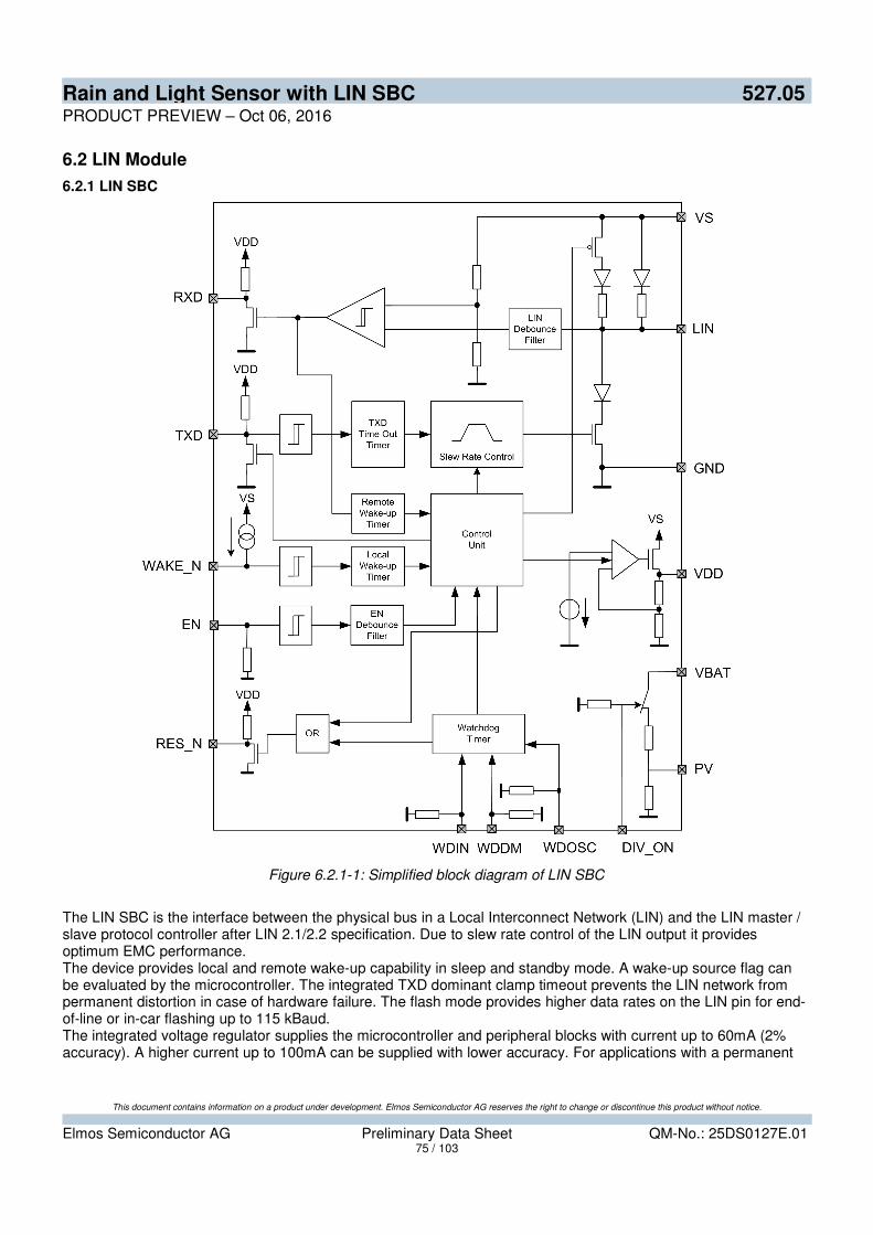
Rain and Light Sensor with LIN SBC 527.05 PRODUCT PREVIEW – Oct 06, 2016
6.2 LIN Module
6.2.1 LIN SBC
Figure 6.2.1-1: Simplified block diagram of LIN SBC
The LIN SBC is the interface between the physical bus in a Local Interconnect Network (LIN) and the LIN master / slave protocol controller after LIN 2.1/2.2 specification. Due to slew rate control of the LIN output it provides optimum EMC performance.The device provides local and remote wake-up capability in sleep and standby mode. A wake-up source flag can be evaluated by the microcontroller. The integrated TXD dominant clamp timeout prevents the LIN network from permanent distortion in case of hardware failure. The flash mode provides higher data rates on the LIN pin for end-of-line or in-car flashing up to 115 kBaud.The integrated voltage regulator supplies the microcontroller and peripheral blocks with current up to 60mA (2% accuracy). A higher current up to 100mA can be supplied with lower accuracy. For applications with a permanent
This document contains information on a product under development. Elmos Semiconductor AG reserves the right to change or discontinue this product without notice.
Elmos Semiconductor AG Preliminary Data Sheet QM-No.: 25DS0127E.01 75 / 103

Rain and Light Sensor with LIN SBC 527.05 PRODUCT PREVIEW – Oct 06, 2016
supplied microcontroller a standby mode with active voltage regulator and low quiescent current consumption is implemented.The cycle time of the integrated window watchdog can be configured by external resistor. For software develop-ment purpose the watchdog can be disabled.The integrated reverse polarity protected 6:1 voltage divider can be connected to the battery supply to measure thesupply voltage with fast response time. To limit the output voltage in case of VBAT over-voltage a clamping to the microcontroller supply voltage is integrated.
6.2.2 Power Supply and References; pin VS
6.2.2.1 Charge PumpAn on chip charge pump is implemented in order to ensure local wake up functionality for VS level below VVS,CPON. The current consumption at pin VS is increased.
The charge pump is switched off if the voltage at pin VS is above VSVS,CPOFF to prevent EMC.
6.2.3 SBC Operating Modes
The LIN SBC provides the following operation modes:• Power-off mode: The battery voltage was falling under the power down threshold level. The voltage regulator is
switched off. The device will be given a power on reset (pin RES_N activated) in case the battery voltage level exceeds the VVS,POR threshold level.
• Power-on mode: The device is powered by a battery voltage above POR reset level and is waiting for activation by pin EN from the microcontroller. The voltage regulator is switched on. The watchdog is active.
• active mode: The physical LIN transceiver is activated. The voltage regulator and the watchdog are active.• Standby mode: The LIN transceiver is switched off. The voltage regulator is active. The watchdog is running.
The wake up sources are enabled. The device consumes low current.• Sleep mode: The LIN transceiver is off, the voltage regulator is shut down and the watchdog is inactive. The
wake up sources are enabled. The device consumes very low current.• Flash mode: The slew rate control and the receiver filter are switched off in order to achieve a high data baud
rate for microcontroller flashing. The voltage regulator and the watchdog are active.
This document contains information on a product under development. Elmos Semiconductor AG reserves the right to change or discontinue this product without notice.
Elmos Semiconductor AG Preliminary Data Sheet QM-No.: 25DS0127E.01 76 / 103

Rain and Light Sensor with LIN SBC 527.05 PRODUCT PREVIEW – Oct 06, 2016
Power-on
VDD: on (±2%, 60mA)
RTerm
= 30kW
RXD: wake up request
RES_N = 0 : tRES_N
TXD: wake up source
Transmitter: off
Active
VDD: on (±2%, 60mA)
RTerm
= 30kW
RXD: receive data output
TXD: transmit data input
transmitter: on
slew rate control: on
Watch dog on
RTerm
: slave termination resistor, connected
between pins LIN and VS
EN = 1
t(EN=1)
> t2AM
switching VS supply on
VS > V
S,POR
local wake up : t(WAKE=0)
> tWAKE,DB
remote wake up : t→(LIN=0 1; afterLIN=0)
> tLIN,WU
Flash
VDD: on (±2%, 60mA)
RTerm
= 30kW
RXD: receive data output
TXD: transmit data input
Transmitter: on
Slew Rate Control: off
Watch dog on
t(FM=1)
> tFMTO
TXD = 0 && no
wake request
t(TXD=0)
> t2SLEEP
EN=1
t(EN=1)
> t2FM
tFMACK,MIN
< t(TXD->1->0->1)
< tFMACK,MAX
EN = 0
t(EN=0)
> t2STBY
Power-off
VS = 0
EN = 1
t(EN=1)
> t2AM
Power Down
VS < V
S,PD
RES_N = 0
Standby
VDD: on (±5%, 60mA)
RTerm
= 30kW
RXD: wake request
TXD: wake up source
Transmitter: off
Watch dog on
Sleep
VDD: off
RES_N = 0
RTerm
=high ohmic
RXD: pull up
TXD: weak pull up
Transmitter: off
Watch dog off
Figure 6.2.3-1: SBC State Diagram
Table 6.2.3-1: Pin Functionality
Mode EN VDD RXD TXD LIN WatchDog
Power-off high imped-ance
off high impedance high impedance high impedance off
Power-on low on strong pull down out-put for wake up request
weak pull up output if remote wake up; strong pull down out-put if local wake up
off on after RES_N is high
Active high on pull up for LIN recess-ive; strong pull down output for LIN domin-ant
high level input for LINrecessive; low level input for LIN dominant
on; slew rate control activated
on
Standby low on strong pull down out-put for wake up request
weak pull up output if remote wake up; strong pull down out-put if local wake up
transmitter offtermination on
on
Sleep low off pull up pull down off off
This document contains information on a product under development. Elmos Semiconductor AG reserves the right to change or discontinue this product without notice.
Elmos Semiconductor AG Preliminary Data Sheet QM-No.: 25DS0127E.01 77 / 103

Rain and Light Sensor with LIN SBC 527.05 PRODUCT PREVIEW – Oct 06, 2016
Mode EN VDD RXD TXD LIN WatchDog
Flash high on pull up for LIN recess-ive; strong pull down output for LIN domin-ant
high level input for LINrecessive; low level input for LIN dominant
on; slew rate control deactivated
on
6.2.3.1 Power-off ModeThe device enters mode Power-off in case the battery voltage is lower than VS,PD voltage level. The voltage regu-lator is switched off and pin RES_N is set L.
6.2.3.2 Power-on ModeWhen the voltage at pin VS exceeds the Power-on-reset threshold voltage VS,POR, the device enters mode Power-on. In that mode voltage regulator is switched on. After pin VDD exceeds VDD,RSTD, RES_N is held low for tRES_N. Withrising edge at RES_N watchdog starts with first open window.Setting pin EN to active HIGH level for a time period of at least t2AM the device enters mode Active.Any wake up request from mode SLEEP is indicated to the interrupt input of the microcontroller by setting the pin RXD to LOW level.The wake up source can be recognized by the microcontroller by reading the level at pin TXD. A weak pull up indic-ates a remote wake up request and strong pull down indicates a local wake up request.Note: The voltage regulator over temperature shut down results in a transition to Power-on mode and the regulator is switched off. The voltage regulator will be switched on, only if the junction temperature falls below the specified temperature hysteresis THYST.In case of undervoltage at regulator, device enters mode Power-On.
6.2.3.3 Active ModeIn mode Active the device is able to transmit and receive data via the LIN bus line. The receiver transfers the detec-ted LIN bus data via pin RXD to the microcontroller: HIGH at a recessive level and LOW at a dominant level on the bus. The receiver has a VS supply related threshold with hysteresis and an integrated filter to suppress bus line EMI. The transmit data at the TXD input is converted by the transmitter into a LIN bus signal. The LIN bus slew rateis optimized to minimize EME. The LIN bus output pin is pulled HIGH via an internal slave termination resistor. For a master application an external resistor in series with a diode should be connected between pin VS on one side and pin LIN on the other side.The device enters mode Active from mode Standby or mode Power-up whenever a HIGH level on pin EN is main-tained for a time of at least t2AM. The device enters mode Active from mode Flash after a time out of tFMTO.The device enters mode Standby from mode Active in case of a LOW-level on pin EN, maintained for a time of at least t2STBY.
6.2.3.4 Standby ModeIn Standby mode the voltage regulator is activated. Also the slave termination resistor at pin LIN is enabled. The watch dog is running.Any wake up request is indicated to the interrupt input of the microcontroller by setting the pin RXD to LOW level.The wake up source can be recognized by the microcontroller by reading the level at pin TXD. A weak pull up indic-ates a remote wake up request and strong pull down indicates a local wake up request.
6.2.3.5 Sleep ModeThe Sleep mode is a very low power mode of the device. The supply current in Sleep mode is typically 5 µA.After entering Standby mode a TXD LOW level for at least t2SLEEP will result in entering Sleep mode. The transition to sleep mode can be performed independently from the actual level on pin LIN or pin WAKE_N. In Sleep mode the voltage regulator is deactivated and becomes high ohmic after a delayed time of tDD,OFFDEL.The transition into mode Sleep is prohibited if a wake up request is pending. The request must be cleared via a transition to mode Active.In Sleep mode the internal slave resistor termination at LIN bus pin is switched off. A power-saving weak pull-up between pins LIN and VS is still present.
This document contains information on a product under development. Elmos Semiconductor AG reserves the right to change or discontinue this product without notice.
Elmos Semiconductor AG Preliminary Data Sheet QM-No.: 25DS0127E.01 78 / 103

Rain and Light Sensor with LIN SBC 527.05 PRODUCT PREVIEW – Oct 06, 2016
The device can be woken up remotely via pin LIN or locally via pin WAKE_N. Debounce filters prevent unwanted wake-up events due to EMI at the inputs of the wake-up sources.
6.2.3.6 Flash ModeFlash mode is initiated by a rising edge on pin EN in Standby mode and a command at pin TXD to prevent trans-ition to Active mode. Flash mode is like Active mode with the exception of disabled LIN bus slew rate control. This is to support high baud rate microcontroller flashing via LIN bus. To enter Flash mode the pin EN must be set HIGHfor at least t2FM and after this the pin TXD must be acknowledge Flash mode access with an LOW pulse tFMACK in time period t2AM . The Flash mode is left to Active mode after time out tFMTO .
Figure 6.2.3.6-1: Flash mode transition timing with TXD acknowledge pulse.
This document contains information on a product under development. Elmos Semiconductor AG reserves the right to change or discontinue this product without notice.
Elmos Semiconductor AG Preliminary Data Sheet QM-No.: 25DS0127E.01 79 / 103
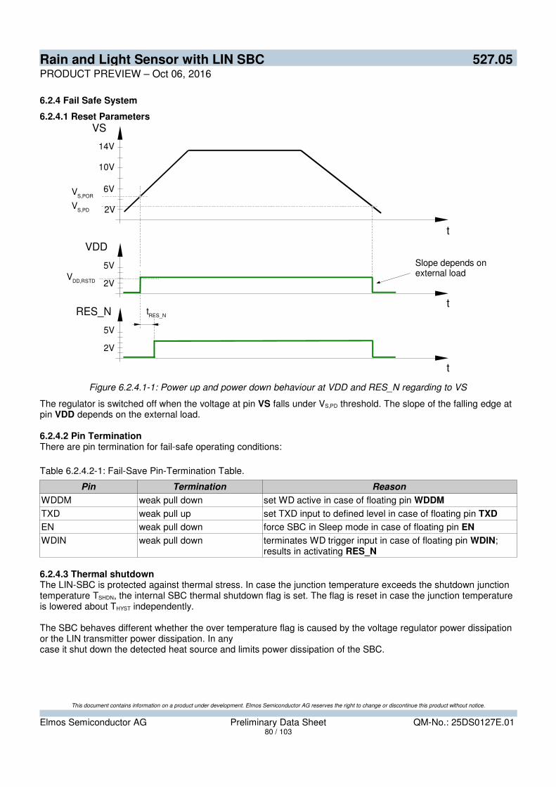
Rain and Light Sensor with LIN SBC 527.05 PRODUCT PREVIEW – Oct 06, 2016
6.2.4 Fail Safe System
6.2.4.1 Reset Parameters
VS
2V
6V
10V
14V
VDD
2V
VS,POR
VS,PD
VDD,RSTD
5V
RES_N
2V
5V
tRES_N
t
t
t
Slope depends on external load
Figure 6.2.4.1-1: Power up and power down behaviour at VDD and RES_N regarding to VS
The regulator is switched off when the voltage at pin VS falls under VS,PD threshold. The slope of the falling edge at pin VDD depends on the external load.
6.2.4.2 Pin TerminationThere are pin termination for fail-safe operating conditions:
Table 6.2.4.2-1: Fail-Save Pin-Termination Table.
Pin Termination Reason
WDDM weak pull down set WD active in case of floating pin WDDM
TXD weak pull up set TXD input to defined level in case of floating pin TXD
EN weak pull down force SBC in Sleep mode in case of floating pin EN
WDIN weak pull down terminates WD trigger input in case of floating pin WDIN; results in activating RES_N
6.2.4.3 Thermal shutdownThe LIN-SBC is protected against thermal stress. In case the junction temperature exceeds the shutdown junction temperature TSHDN, the internal SBC thermal shutdown flag is set. The flag is reset in case the junction temperature is lowered about THYST independently.
The SBC behaves different whether the over temperature flag is caused by the voltage regulator power dissipation or the LIN transmitter power dissipation. In anycase it shut down the detected heat source and limits power dissipation of the SBC.
This document contains information on a product under development. Elmos Semiconductor AG reserves the right to change or discontinue this product without notice.
Elmos Semiconductor AG Preliminary Data Sheet QM-No.: 25DS0127E.01 80 / 103

Rain and Light Sensor with LIN SBC 527.05 PRODUCT PREVIEW – Oct 06, 2016
6.2.4.4 LIN over current protectionThe output current of the LIN transmitter is limited to ILIN,LIM in order to protect the transmitter against short circuit to pin VS .
In order to limit power dissipation caused by the LIN transmitter the LIN BUS is monitored in the dominant state, i.e.TXD=0: If the LIN bus voltage level exceeds VLIN,OV for debouncing time tLIN,OV and the SBC thermal shutdown flag isset the LIN transceiver will be set high ohmic. The LIN over temperature flag is set.
The LIN transmitter transmit TXD again in case the junction temperature is lowered about THYST, i.e. the SBC thermal shut down flag is reset. This also resets the LIN over temperature flag.
Note: The LIN shut down does not result in any state change.
6.2.4.5 Voltage regulator over current protectionIn case of shorts at pin VDD the output current of the voltage regulator is limited to IDD,LIM. In order to limit power dis-sipation of the device the voltage regulator is shut down in case the SBC thermal shutdown is set and the LIN over-voltage flag is not set. A debounce filter of tDD,SHDN is applied to regulator shut down.
The voltage regulator is switched on again in case the junction temperature is lowered about THYST (i.e. SBC thermal shutdown flag is reset) independently of pin EN.
Note: The VDD shut down does result in mode change, if the pin VDD voltage drops below the reset assert threshold level VDD,RSTAXX. In this case the device enters Power-on mode.
6.2.4.6 LIN ground lossIn case of battery voltage loss (pin VS) and ground loss (pin GND) there are no reverse currents from the LIN bus line.
6.2.4.7 Power On ResetThe battery voltage is monitored during power up. If the battery voltage is above VS,POR level the voltage regulator will be switched on and the device enters Power-on mode.
6.2.4.8 System ResetIn case the voltage at pin VDD drops below the reset threshold VDD,RSTAXX the SBC reset pin RES_N is activated andpulled down to GND. This is to reset the host MCU because the peripheral voltage may be unsafely low. The reset pin RES_N is released after the VDD voltage exceeds the reset de-assert level VDD,RSTDXX.
Figure 6.2.4.8-1: RES_N via VDD UV
Behaviour of pin 'RES_N' in case of 'VDD' undervoltage
This document contains information on a product under development. Elmos Semiconductor AG reserves the right to change or discontinue this product without notice.
Elmos Semiconductor AG Preliminary Data Sheet QM-No.: 25DS0127E.01 81 / 103

Rain and Light Sensor with LIN SBC 527.05 PRODUCT PREVIEW – Oct 06, 2016
6.2.4.9 Safe Power DownIn case the battery voltage drops below VS,PD level, operating the LIN-SBC may not be save any more. In this case the device will enter Power-off mode safely. The device powers up again if the battery voltage exceeds VS,POR level again.
6.2.5 Wake Up
In case device is in modi Sleep or Standby there are 2 events to wake up the device:1. Local wake-up with low level at pin WAKE_N.2. Remote wake-up via a dominant bus state of at least tLIN,WU.
6.2.5.1 Local Wake Up; pin WAKE_NThe device can be woke up from modi Standby and Sleep mode via pin WAKE_N. Pulling pin WAKE_N below VWAKE_N,INL level results in a local wake up request.The wake up event is falling edge triggered. This allows the device to enter mode Sleep with pin WAKE_N pulled tolow.The pin WAKE_N is an high voltage input with pull up current source IWAKE_N,PU and an input debouncer with filter time tWAKE_N,DB.If the local wake up is not used in application, the pin WAKE_N has to be connected to pin VS.
Figure 6.2.5.1-1: local wake up in mode Sleep
This document contains information on a product under development. Elmos Semiconductor AG reserves the right to change or discontinue this product without notice.
Elmos Semiconductor AG Preliminary Data Sheet QM-No.: 25DS0127E.01 82 / 103

Rain and Light Sensor with LIN SBC 527.05 PRODUCT PREVIEW – Oct 06, 2016
Figure 6.2.5.1-2: local wake up in mode Standby
6.2.5.2 Remote Wake Up; pin LINThe device can be woke up remotely in modi Standby and Sleep via pin LIN.A falling edge at LIN pin followed by a dominant bus level VLIN,DOM maintained for a time period tLIN,WU followed by a rising edge at LIN results in a remote wake up request.
This document contains information on a product under development. Elmos Semiconductor AG reserves the right to change or discontinue this product without notice.
Elmos Semiconductor AG Preliminary Data Sheet QM-No.: 25DS0127E.01 83 / 103

Rain and Light Sensor with LIN SBC 527.05 PRODUCT PREVIEW – Oct 06, 2016
Figure 6.2.5.2-1: remote wake up in mode Sleep
This document contains information on a product under development. Elmos Semiconductor AG reserves the right to change or discontinue this product without notice.
Elmos Semiconductor AG Preliminary Data Sheet QM-No.: 25DS0127E.01 84 / 103

Rain and Light Sensor with LIN SBC 527.05 PRODUCT PREVIEW – Oct 06, 2016
Figure 6.2.5.2-2: remote wake up in mode Standby
6.2.5.3 Remote and Local Wake Up TransitionIn case of mode Sleep and a wake up occurs the device enters mode Power-on.In case of mode Standby and a wake up occurs the device remains in mode Standby. A transition to mode Sleep isprohibited.
6.2.5.4 Local and Remote Wake Up Source RecognitionThe device latches the information of the wake up source to distinguish between a remote wake up and local wake up.A wake up is signalised with a low level at pin RXD The wake up source can be read on pin TXD in the mode Standby and Power-on. A HIGH level at pin TXD indicates a remote wake-up request (weak pull-up at pin TXD) and a LOW level indicates a local wake-up request (strong pull-down at pin TXD).
6.2.5.5 Wake-Up Flag ResetThe wake up request flag and the wake up source flag are reset after entering mode Active. The signalling at pin TXD and RXD are interrupted when pin EN is set to high in order to check flash mode request at TXD.
This document contains information on a product under development. Elmos Semiconductor AG reserves the right to change or discontinue this product without notice.
Elmos Semiconductor AG Preliminary Data Sheet QM-No.: 25DS0127E.01 85 / 103

Rain and Light Sensor with LIN SBC 527.05 PRODUCT PREVIEW – Oct 06, 2016
6.2.6 Voltage Regulator; pin VDD
The on chip low drop voltage regulator provides the voltage VDD at pin VDD. It supplies the peripheral circuitry of the SBC and the host MCU chip with typical 60mA.
The voltage regulator is activated in all operating modes except in Sleep mode. In Sleep mode the voltage regu-lator is switched off.
The voltage regulator is limited in output current of typical 100mA. The current limitation is always activated.
6.2.7 Watchdog
The watchdog is realized as window watchdog. The watchdog is used to check whether the MCU is still running properly. It runs on watchdog oscillator clock with time base tWD,OSCXX. The MCU will continuously retrigger the watchdog in the open window time tWD,OW by a specific trigger command at pin WDIN and no watchdog error will appear. A correct WD-trigger command in an open window starts the next closed window. Any WD-trigger com-mand in the closed window resets the watchdog and will assert pin RES_N. There is a first trigger latency imple-mented: After RES_N goes high an enlarged open window starts. The first trigger command is allowed to appear latest at tWD,FOW.The watchdog is disabled in state Sleep. The watchdog starts with first open window after re-entering mode Active or Power-on.
Figure 6.2.7-1: WD Trigger in CW
Behaviour of watch dog in case of trigger in closed window.
This document contains information on a product under development. Elmos Semiconductor AG reserves the right to change or discontinue this product without notice.
Elmos Semiconductor AG Preliminary Data Sheet QM-No.: 25DS0127E.01 86 / 103

Rain and Light Sensor with LIN SBC 527.05 PRODUCT PREVIEW – Oct 06, 2016
Figure 6.2.7-2: WD No Trigger In FOW
Behaviour of watch dog in case of missing trigger in open window.
Figure 6.2.7-3: WD No Trigger In OW
Behaviour of watch dog in case of missing trigger in open window.
This document contains information on a product under development. Elmos Semiconductor AG reserves the right to change or discontinue this product without notice.
Elmos Semiconductor AG Preliminary Data Sheet QM-No.: 25DS0127E.01 87 / 103

Rain and Light Sensor with LIN SBC 527.05 PRODUCT PREVIEW – Oct 06, 2016
Figure 6.2.7-4: safe trigger area
safe trigger area for a selected watchdog period:
6.2.7.1 Watchdog Cycle Time ConfigurationThe watchdog cycle time can be configured via the external resistor at pin WDOSC. The typical watchdog oscillatorperiods tWD,OSC is defined by the external resistance RWDOSC by formula:
6.2.7.2 Watchdog ResetIn case a watchdog error appears a reset will be activated on pin RES_N for tWD,RES.
6.2.7.3 Watchdog Debug ModeFor debugging purposes the watchdog can be stopped running by pulling pin WDDM to HIGH. In this case the watchdog timer stops and the actual state remains. After setting pin WDDM to low level the watchdog keeps on running.
6.2.8 LIN Transceiver; pin LIN
6.2.8.1 LIN Physical LayerThe LIN BUS physical interface is realized as a LIN 2.1/2.2 standard high-voltage single wire interface (ISO 9141) for baud rates from 2.4 kBds to 20 kBds. The LIN BUS Interface can be operated in Master or Slave Mode. The LINbus has two logical values; the dominant state (BUS voltage near GND) represents logical LOW level and the recessive state (BUS voltage near VS) represents logical HIGH level. In the recessive state the BUS is pulled high
Ωby an internal pull-up resistor (typ. 30 k ) and a diode in series, so no external pull-up components are required for
This document contains information on a product under development. Elmos Semiconductor AG reserves the right to change or discontinue this product without notice.
Elmos Semiconductor AG Preliminary Data Sheet QM-No.: 25DS0127E.01 88 / 103

Rain and Light Sensor with LIN SBC 527.05 PRODUCT PREVIEW – Oct 06, 2016
slave applications. Master applications require an additional external pull-up resistor and a series diode. The LIN protocol output data stream on the TXD signal is converted into the LIN bus signal through a current limited, wave-shaping low-side driver with control as outlined by the LIN Physical Layer Specification Revision 2.1. The receiver converts the data stream from the bus and outputs it to the pin RXD.
Figure 6.2.8.1-1: LIN transceiver physical layer timing
The LIN transceiver can handle a bus voltage swing from +40 V down to ground and survive -27 V. The device alsoprevents back feed current through the LIN pin to the supply pin in case of a ground shift / loss or supply voltage disconnection.In sleep mode the LIN block requires a very low quiescent current by using a special wake up comparator allowing the remote wake-up via the LIN bus. The sleep mode can be activated during recessive or dominant level of LIN bus line.
6.2.8.2 LIN Flash ModeA Flash mode allows an increasing of the transmit baud rate up to 115 kBaud and the receiver baud rate up to 250 kBaud. The Flash mode can be activated by sending a TXD low pulse acknowledge during the Standby mode change caused by EN = HIGH.
6.2.8.3 LIN TXD Time OutIn order to prevent the LIN bus from being permanent dominant in case of permanent LOW level at pin TXD a TXD time-out timer switches the LIN in recessive mode after time period tTXD,TO. The timer is triggered by a negative edgeon pin TXD and reset by a positive edge on pin TXD.
This document contains information on a product under development. Elmos Semiconductor AG reserves the right to change or discontinue this product without notice.
Elmos Semiconductor AG Preliminary Data Sheet QM-No.: 25DS0127E.01 89 / 103

Rain and Light Sensor with LIN SBC 527.05 PRODUCT PREVIEW – Oct 06, 2016
6.2.9 IO Peripherals
6.2.9.1 Enable; pin ENThe input EN (enable) controls the state transition together with pin TXD. If EN=1 the device enters Active mode after debounce time t2AM.
The enable input is an CMOS level input with pull down resistor REN,PD.
6.2.9.2 Transmit Data Input; pin TXDThe pin TXD is the logic level input for transmitting data. The TXD time out of time period tTXD,TO for low level input signals prevents the LIN bus to be pulled steadily to GND. The TXD is a CMOS level input.
The pin TXD is also an output for wake-up source recognition. It is realized as open drain output with weak pull up resistance to pin VDD.
6.2.9.3 Receive Data Output; pin RXDThe pin RXD is the logic level receive data output of the LIN Transceiver. It also serves for a host MCU local or remote wake up request.
The pin is an open drain output with pull up resistor connected to pin VDD.
6.2.9.4 Reset; pin RES_NThe pin RES_N is a system reset output. It resets the host MCU and the watchdog counter in case one of the fol-lowing reset triggering events occur:• VDD under voltage reset• watchdog trigger failThe reset pin RES_N is activated internally by pulling it to low level.The pin has a pull up resistor connected internally to pin VDD.
6.2.9.5 Watchdog Trigger Input; pin WDINAt pin WDIN the watchdog trigger command has to be launched. The trigger command is a high level pulse of dura-tion tWD,CMD. It must not be launched in the watchdog closed window. It must be launched in the watchdog open win-dow.
The pin WDIN is a CMOS level input with pull down current.
6.2.9.6 Watchdog Cycle Time Configuration; pin WDOSCWith logic level pins the watchdog cycle time can be configured by an external resistor.
6.2.9.7 Watchdog Debug Mode; pin WDDMSetting WDDM to high level stops the watchdog.
The pin WDDM is an CMOS level input with pull down current.
6.2.10 VBAT Voltage divider
The pin DIV_ON is a low voltage input. It is used to switch on or off the internal voltage dividerPV output directly with no time limitation. It is switched on if DIV_ON is high or it is switched off if DIV_ON is low. In Sleep and Standby Mode the DIV_ON functionality is disabled and PV is off. An internal pull-down resistor is imple-mented.
The pin VBAT is a high voltage input pin to supply the internal voltage divider. In an application with battery voltagemonitoring, this pin is connected to Battery via a resistor in series and a capacitor to GND. The typical divider ratio is 1:6. An internal reverse polarity diode is integrated to protect pin VBAT against voltages down to -27V.
This document contains information on a product under development. Elmos Semiconductor AG reserves the right to change or discontinue this product without notice.
Elmos Semiconductor AG Preliminary Data Sheet QM-No.: 25DS0127E.01 90 / 103

Rain and Light Sensor with LIN SBC 527.05 PRODUCT PREVIEW – Oct 06, 2016
For applications with battery monitoring, this pin PV is directly connected to the ADC of a microcontroller. For buf-fering the ADC input an external capacitor is recommended. This pin guarantees a voltage stable output of a VBAT ratio.
Table 6.2.10-1: table of voltage divider
Mode of Operation DIV_ON PV
ACTIVE, FLASH, POWER ON 0 OFF
ACTIVE, FLASH, POWER ON 1 ON
SLEEP, STANDBY - OFF
5 10 15 20 25 30 3530 40
1
2
3
VBAT/V
PV/V
18
3.3
Linear range
3.3
Figure 6.2.10-1: VBAT versus PV
This document contains information on a product under development. Elmos Semiconductor AG reserves the right to change or discontinue this product without notice.
Elmos Semiconductor AG Preliminary Data Sheet QM-No.: 25DS0127E.01 91 / 103

Rain and Light Sensor with LIN SBC 527.05 PRODUCT PREVIEW – Oct 06, 2016
7 Package ReferenceThe E527.05 is available in a Pb free, RoHs compliant, QFN44L7 plastic package according to JEDEC MO-220 VKKD-3. The package is classified to Moisture Sensitivity Level 3 (MSL 3) according to JEDEC J-STD-20C with a soldering peak temperature of (260+5)°C.
Figure 7-1: Package Outline
Note: Contact factory for specific location and type of pin 1 identification.
This document contains information on a product under development. Elmos Semiconductor AG reserves the right to change or discontinue this product without notice.
Elmos Semiconductor AG Preliminary Data Sheet QM-No.: 25DS0127E.01 92 / 103

Rain and Light Sensor with LIN SBC 527.05 PRODUCT PREVIEW – Oct 06, 2016
Table 7-1: Package Characteristics
Description Symbol mm inch
min typ max min typ max
Package height A 0.80 0.9 1.0 0.031 0.035 0.039
Stand off A1 0.00 0.02 0.05 0.000 0.00079 0.002
Thickness of terminal leads, including leadfinish
A3 -- 0.20REF
-- -- 0.0079REF
--
Width of terminal leads b 0.18 0.25 0.30 0.007 0.010 0.012
Package length / width D / E -- 7.00BSC
-- -- 0.276BSC
--
Length /width of exposed pad D2 / E2 5.50 5.56 5.80 0.217 0.223 0.229
Lead pitch e -- 0.5 BSC -- -- 0.020BSC
--
Length of terminal for soldering to sub-strate
L 0.35 0.40 0.45 0.014 0.016 0.018
Number of terminal positions N -- 44 -- -- 44 --
Table 7-2: Thermal Ratings of QFN44L7 Package
No. Description Symbol Value Unit
1 Typical thermal resistance (junction to air) of QFN44L7 packagebased on JEDEC standards:• JESD-51-2 (still air)• JESD-51-5 (exposed pad (EDP) soldered to PCB with
thermal via's)• JESD-51-7 (4-layer PCB)
RTH,JA 24 K/W
This document contains information on a product under development. Elmos Semiconductor AG reserves the right to change or discontinue this product without notice.
Elmos Semiconductor AG Preliminary Data Sheet QM-No.: 25DS0127E.01 93 / 103

Rain and Light Sensor with LIN SBC 527.05 PRODUCT PREVIEW – Oct 06, 2016
8 Marking
8.1 Top Side
Table 8.1-1: Top Side
52705A
XXU YWW*#
Table 8.1-2: Marking of the Devices
Signature Explanation
52705 ELMOS product number
A ELMOS product revision code
XX Production lot number
U Assembler code
YWW Year and week of assembly
* Mask revision code
# ELMOS internal code
8.2 Bottom Side
No marking.
This document contains information on a product under development. Elmos Semiconductor AG reserves the right to change or discontinue this product without notice.
Elmos Semiconductor AG Preliminary Data Sheet QM-No.: 25DS0127E.01 94 / 103

Rain and Light Sensor with LIN SBC 527.05 PRODUCT PREVIEW – Oct 06, 2016
9 Typical Applications
E527.05
MISO
MOSI
LEDB
LEDA
GNDL
RS
VBAT
TXD
RXD
GND LIN
VBAT VS VDD
EN
WDIN
ALS3
GND
DIV_ON
PV
VDDA
ALS2
ALS1
ALS0
CS
SCK
VDDD
VREF
GNDAGNDD
WDOSC
WDDM
WAKE_N
RES_N
LIN Bus
CVBAT
CVLED1
CVDD
RWDOSC
DVLED
RVBAT
PDALS3
PDRS
/LEDRS
CVREF
LEDA
µC
CVDDA
CVDDD
WS
RB
RA
TMODE
CVSUP
ZVSUP
DVS
CVLED2
CVS1
CVS2
ATB
LEDB
PDALS2
PDALS1
PDALS0
GPIO
GPIO
ADC_IN
GPIO
GPIO
SPI
SPI
SPI
SPI
RESET_N
SPI
LIN
SPI
LINGND
VDD
CVDDuC
GND
CLIN1
XLIN
CLIN2Z
PESD1LIN
pin2 24V
pin1 15V
RWAKE_N
Figure 9-1: Typical Application Example
Table 9-1: External Components
Symbol Value Unit Description
CVSUP 68-100 nF ESD blocking capacitor, place near module connector.
ZVSUP 43 V Transient Voltage Suppressor (TVS) diode against over voltage spikes (ESD protection and ISO pulses), e.g. SMAJ36CA or P4SMA43C(A). Place near module connector.
DVLED, DVS Reverse polarity protection diode, e.g. BAS521.
RVBAT 47 Ω ESD protection resistor
CVLED1 100 nF Blocking capacitor
CVLED2 22 µF Capacitor to flatten LED current pulses, value could change. Also tank capacitor to supply LEDs during short disconnection of supply wire.
CVS1 100 nF Blocking capacitor, place near pin VS.
This document contains information on a product under development. Elmos Semiconductor AG reserves the right to change or discontinue this product without notice.
Elmos Semiconductor AG Preliminary Data Sheet QM-No.: 25DS0127E.01 95 / 103

Rain and Light Sensor with LIN SBC 527.05 PRODUCT PREVIEW – Oct 06, 2016
Symbol Value Unit Description
CVS2 min. 22 µF Blocking capacitor against ISO Pulse 2A. Also tank capacitor to sup-ply circuit during short disconnection of supply wire. Max. autarky (disconnection) time with min. specified VBAT voltage VBATMIN can be calculated with:tautarky = CVS2 * (VBATMIN - VD_VS - VS,FUNC MIN) / IVS.VD_VS is the voltage of diode DVS.IVS is the current into pin VS.VS,FUNC MIN is the minimum specified functional range of supply voltage VS.
CVBAT 47 nF ESD protection capacitor
RWAKE_N 33 Ωk ESD protection pull up resistor
CVDDA 220 nF Blocking capacitor, place near pin VDDA
CVDDD 220 nF Blocking capacitor, place near pin VDDD
CVDD 10 µF Buffer capacitor
CVDDuC Blocking capacitor for µC supply, value depends from µC, place near µC supply pin.
RWDOSC Configures the watchdog cycle time, described in chapter Watch-dog.
LEDA, LEDB SFH4250, SFH4253, SFH4243, VSMF9700, VSMF3710, VSMY1940ITX01 or similar types, 3 or 4 LEDs per strand recom-mended.
RA, RB Optional series resistor to reduce power dissipation of 527.05 LED driver, min. voltage at pins LEDA and LEDB is 0.8V.
PDRS SFH2400FA, TEMD7100 or similar types. It is also possible to use the same LED type as photo diode like the sending LEDs. But the LEDs are usually not specified as photo diode. Therefore this char-acteristic is not guaranteed. Capacitance should not be more than 35pF. Place near pin RS and VREF. Net RS is a very sensitive nodeand should be as short as possible.
PDALSx SFH2400, SFH2270R, BPW34, TEMD5020, TEMD6010, TEMD6200, TEMD7000, VBP104 or similar types, capacitance should not be more than 70pF.
CVREF 1 nF VREF Blocking capacitor
CLIN1 220/180 pF 220pF if CLIN2 and PESD1LIN is not used, 180pF if CLIN2 and PSD1LIN is used. By LIN specification the whole capacitance of LIN terminal should be 220pF.
XLIN Ω0 Resistor or optional ferrite to suppress distortion from micro-con-troller.
CLIN2 Optional capacitor if demanded by OEM.
ZPESD1LIN 15/24 V Optional LIN-bus ESD protection diode PESD1LIN for increased ESD requirements of 8KV. Place near LIN Bus connector.
This document contains information on a product under development. Elmos Semiconductor AG reserves the right to change or discontinue this product without notice.
Elmos Semiconductor AG Preliminary Data Sheet QM-No.: 25DS0127E.01 96 / 103

Rain and Light Sensor with LIN SBC 527.05 PRODUCT PREVIEW – Oct 06, 2016
10 Revision History (for manuscript only)Table 10-1: Table of Revisions
Rev. Date Description ofchange
Chapter Who
00 28.05.2015 initial version all BR/ZOE
01 06.10.2016 all chapters reworked all STDI
This document contains information on a product under development. Elmos Semiconductor AG reserves the right to change or discontinue this product without notice.
Elmos Semiconductor AG Preliminary Data Sheet QM-No.: 25DS0127E.01 97 / 103

Rain and Light Sensor with LIN SBC 527.05 PRODUCT PREVIEW – Oct 06, 2016
11 General
11.1 WARNING - Life Support Applications Policy
ELMOS Semiconductor AG is continually working to improve the quality and reliability of its products. Nevertheless,semiconductor devices in general can malfunction or fail due to their inherent electrical sensitivity and vulnerability to physical stress. It is the responsibility of the buyer, when utilizing ELMOS Semiconductor AG products, to observe standards of safety, and to avoid situations in which malfunction or failure of an ELMOS Semiconductor AG Product could cause loss of human life, body injury or damage to property. In development your designs, please ensure that ELMOS Semiconductor AG products are used within specified operating ranges as set forth in the most recent product specifications.
11.2 General Disclaimer
Information furnished by ELMOS Semiconductor AG is believed to be accurate and reliable. However, no respons-ibility is assumed by ELMOS Semiconductor AG for its use, nor for any infringements of patents or other rights of third parties, which may result from its use. No license is granted by implication or otherwise under any patent or patent rights of ELMOS Semiconductor AG. ELMOS Semiconductor AG reserves the right to make changes to this document or the products contained therein without prior notice, to improve performance, reliability, or manufactur-ability .
11.3 Application Disclaimer
Circuit diagrams may contain components not manufactured by ELMOS Semiconductor AG, which are included as means of illustrating typical applications. Consequently, complete information sufficient for construction purposes isnot necessarily given. The information in the application examples has been carefully checked and is believed to beentirely reliable. However, no responsibility is assumed for inaccuracies. Furthermore, such information does not convey to the purchaser of the semiconductor devices described any license under the patent rights of ELMOS Semiconductor AG or others.
This document contains information on a product under development. Elmos Semiconductor AG reserves the right to change or discontinue this product without notice.
Elmos Semiconductor AG Preliminary Data Sheet QM-No.: 25DS0127E.01 98 / 103

Rain and Light Sensor with LIN SBC 527.05 PRODUCT PREVIEW – Oct 06, 2016
12 Contact InfoTable 12-1: Contact Information
HeadquartersELMOS Semiconductor AGHeinrich-Hertz-Str. 1,44227 Dortmund (Germany)
+492317549100 [email protected] www.elmos.de
Sales and Application Support Office North AmericaElmos NA. Inc.32255 Northwestern Highway, Suite 220Farmington Hills, MI 48334 (United States)
+12488653200 [email protected]
Sales and Application Support Office KoreaElmos Korea Co, Ltd.B-1006, U-Space 2, 670 Daewangpangyo-ro,Sampyoung-dong, Bundang-gu, Seongnam-si,Gyeonggi-do, 13494 Korea
+82317141131 [email protected]
Sales and Application Support Office JapanElmos Japan K.K.BR Shibaura N Bldg. 7F3-20-9 Shibaura, Minato-ku,Tokyo 108-0023 Japan
+81334517101 [email protected]
Sales and Application Support Office ChinaElmos Semiconductor Technology (Shanghai) Co., Ltd.Unit 16B, 16F Zhao Feng World Trade Building,No. 369 Jiang Su Road,Chang Ning District,Shanghai, PR China, 200050
+862162197502 [email protected]
Sales and Application Support Office Singa-poreElmos Semiconductor Singapore Pte Ltd.3A International Business Park,1. 09-13 ICON@IBP, Singapore 609935
+6569081261 [email protected]
This document contains information on a product under development. Elmos Semiconductor AG reserves the right to change or discontinue this product without notice.
Elmos Semiconductor AG Preliminary Data Sheet QM-No.: 25DS0127E.01 99 / 103

Rain and Light Sensor with LIN SBC 527.05 PRODUCT PREVIEW – Oct 06, 2016
13 Contents
Table of ContentFeatures.........................................................................................................................................................................1Applications...................................................................................................................................................................1General Description.......................................................................................................................................................1Ordering Information......................................................................................................................................................1Typical Operating Circuit...............................................................................................................................................1Functional Diagram........................................................................................................................................................2Pin Configuration QFN44L7..........................................................................................................................................2Pin Description QFN44L7..............................................................................................................................................31 Functional Safety........................................................................................................................................................52 Absolute Maximum Ratings........................................................................................................................................63 ESD.............................................................................................................................................................................74 Recommended Operating Conditions........................................................................................................................85 Electrical Characteristics............................................................................................................................................9
5.1 Rain Sensor Module...........................................................................................................................................95.1.1 Overview....................................................................................................................................................95.1.2 Supply Monitor...........................................................................................................................................95.1.3 References...............................................................................................................................................105.1.4 Temperature Sensor................................................................................................................................105.1.5 Oscillator..................................................................................................................................................105.1.6 Ambient Light Interface (ALI)...................................................................................................................105.1.7 Rain Sensor Interface (RSI).....................................................................................................................125.1.8 LED Driver................................................................................................................................................125.1.9 Digital Control...........................................................................................................................................125.1.10 Digital Signal Processing.......................................................................................................................13
5.1.10.1 Rain sensor data processing.........................................................................................................135.1.11 Serial Peripheral Interface (SPI)............................................................................................................13
5.2 LIN Module.......................................................................................................................................................145.2.1 Power Supply and References; pin VS....................................................................................................14
5.2.1.1 Charge Pump...................................................................................................................................155.2.2 SBC Operating Modes.............................................................................................................................155.2.3 Fail Safe System......................................................................................................................................15
5.2.3.1 Reset Parameters............................................................................................................................155.2.3.2 Monitor Parameters..........................................................................................................................15
5.2.4 Wake Up...................................................................................................................................................165.2.4.1 Local Wake Up; pin WAKE_N..........................................................................................................16
5.2.5 Voltage Regulator; pin VDD.....................................................................................................................165.2.6 Watchdog.................................................................................................................................................165.2.7 LIN Transceiver; pin LIN..........................................................................................................................175.2.8 IO Peripherals..........................................................................................................................................18
5.2.8.1 Enable; pin EN.................................................................................................................................185.2.8.2 Transmit Data Input; pin TXD..........................................................................................................185.2.8.3 Receive Data Output; pin RXD........................................................................................................195.2.8.4 Reset; pin RES_N............................................................................................................................195.2.8.5 Watchdog Trigger Input; pin WDIN..................................................................................................195.2.8.6 Watchdog Cycle Time Configuration; pin WDOSC.........................................................................195.2.8.7 Watchdog Debug Mode; pin WDDM................................................................................................19
5.2.9 VBAT Voltage divider...............................................................................................................................196 Functional Description..............................................................................................................................................20
6.1 Rain Sensor Module.........................................................................................................................................206.1.1 Overview..................................................................................................................................................20
6.1.1.1 Rain Sensor Interface......................................................................................................................206.1.1.2 Ambient Light Interface....................................................................................................................21
This document contains information on a product under development. Elmos Semiconductor AG reserves the right to change or discontinue this product without notice.
Elmos Semiconductor AG Preliminary Data Sheet QM-No.: 25DS0127E.01 100 / 103

Rain and Light Sensor with LIN SBC 527.05 PRODUCT PREVIEW – Oct 06, 2016
6.1.2 Supply Monitor.........................................................................................................................................226.1.2.1 Power-up and -down Timing Diagram.............................................................................................24
6.1.3 References...............................................................................................................................................256.1.4 Temperature Sensor................................................................................................................................266.1.5 Oscillator..................................................................................................................................................266.1.6 Ambient Light Interface (ALI)...................................................................................................................27
6.1.6.1 Deviations from logarithmic transfer characteristic..........................................................................296.1.6.2 Calibration........................................................................................................................................30
6.1.6.2.1 Calibration during operation: VREF, VINC, VALI,OS.........................................................................316.1.6.2.2 Calibration during operation: gain coefficient..........................................................................326.1.6.2.3 Calibration during End of Line Test.........................................................................................32
6.1.6.3 Diagnosis.........................................................................................................................................336.1.6.3.1 Short Circuit Diagnosis............................................................................................................336.1.6.3.2 Current Diagnosis....................................................................................................................35
6.1.7 Rain Sensor Interface (RSI).....................................................................................................................356.1.7.1 RSI Modes.......................................................................................................................................36
6.1.7.1.1 RSI0 - Relative Mode...............................................................................................................376.1.7.1.2 RSI1 - Differential Mode..........................................................................................................396.1.7.1.3 RSI2 - Alternative Relative Mode.............................................................................................40
6.1.7.2 Coupling Factor Measurement.........................................................................................................406.1.8 LED Driver................................................................................................................................................416.1.9 Digital Control...........................................................................................................................................42
6.1.9.1 Reset................................................................................................................................................436.1.9.2 Idle Mode.........................................................................................................................................436.1.9.3 Manual/Burst measurement mode...................................................................................................446.1.9.4 Automatic measurement mode........................................................................................................446.1.9.5 Coupling Factor measurement mode..............................................................................................456.1.9.6 Overtemperature Mode....................................................................................................................456.1.9.7 Sleep Mode......................................................................................................................................466.1.9.8 Digital Control Register....................................................................................................................46
6.1.10 Digital Signal Processing.......................................................................................................................606.1.10.1 Rain sensor data processing.........................................................................................................616.1.10.2 ADC based measurement..............................................................................................................626.1.10.3 WS Output Function.......................................................................................................................63
6.1.11 Serial Peripheral Interface (SPI)............................................................................................................646.1.11.1 SPI Format.....................................................................................................................................64
6.1.11.1.1 8 bit commands......................................................................................................................676.1.11.1.2 Write commands....................................................................................................................696.1.11.1.3 Read commands....................................................................................................................71
6.1.11.2 SPI Commands..............................................................................................................................736.2 LIN Module.......................................................................................................................................................75
6.2.1 LIN SBC...................................................................................................................................................756.2.2 Power Supply and References; pin VS....................................................................................................76
6.2.2.1 Charge Pump...................................................................................................................................766.2.3 SBC Operating Modes.............................................................................................................................76
6.2.3.1 Power-off Mode................................................................................................................................786.2.3.2 Power-on Mode................................................................................................................................786.2.3.3 Active Mode.....................................................................................................................................786.2.3.4 Standby Mode..................................................................................................................................786.2.3.5 Sleep Mode......................................................................................................................................786.2.3.6 Flash Mode......................................................................................................................................79
6.2.4 Fail Safe System......................................................................................................................................806.2.4.1 Reset Parameters............................................................................................................................806.2.4.2 Pin Termination................................................................................................................................806.2.4.3 Thermal shutdown............................................................................................................................80
This document contains information on a product under development. Elmos Semiconductor AG reserves the right to change or discontinue this product without notice.
Elmos Semiconductor AG Preliminary Data Sheet QM-No.: 25DS0127E.01 101 / 103

Rain and Light Sensor with LIN SBC 527.05 PRODUCT PREVIEW – Oct 06, 2016
6.2.4.4 LIN over current protection..............................................................................................................816.2.4.5 Voltage regulator over current protection........................................................................................816.2.4.6 LIN ground loss................................................................................................................................816.2.4.7 Power On Reset...............................................................................................................................816.2.4.8 System Reset...................................................................................................................................816.2.4.9 Safe Power Down............................................................................................................................82
6.2.5 Wake Up...................................................................................................................................................826.2.5.1 Local Wake Up; pin WAKE_N..........................................................................................................826.2.5.2 Remote Wake Up; pin LIN...............................................................................................................836.2.5.3 Remote and Local Wake Up Transition...........................................................................................856.2.5.4 Local and Remote Wake Up Source Recognition...........................................................................856.2.5.5 Wake-Up Flag Reset........................................................................................................................85
6.2.6 Voltage Regulator; pin VDD.....................................................................................................................866.2.7 Watchdog.................................................................................................................................................86
6.2.7.1 Watchdog Cycle Time Configuration...............................................................................................886.2.7.2 Watchdog Reset...............................................................................................................................886.2.7.3 Watchdog Debug Mode...................................................................................................................88
6.2.8 LIN Transceiver; pin LIN..........................................................................................................................886.2.8.1 LIN Physical Layer...........................................................................................................................886.2.8.2 LIN Flash Mode................................................................................................................................896.2.8.3 LIN TXD Time Out............................................................................................................................89
6.2.9 IO Peripherals..........................................................................................................................................906.2.9.1 Enable; pin EN.................................................................................................................................906.2.9.2 Transmit Data Input; pin TXD..........................................................................................................906.2.9.3 Receive Data Output; pin RXD........................................................................................................906.2.9.4 Reset; pin RES_N............................................................................................................................906.2.9.5 Watchdog Trigger Input; pin WDIN..................................................................................................906.2.9.6 Watchdog Cycle Time Configuration; pin WDOSC.........................................................................906.2.9.7 Watchdog Debug Mode; pin WDDM................................................................................................90
6.2.10 VBAT Voltage divider.............................................................................................................................907 Package Reference..................................................................................................................................................928 Marking.....................................................................................................................................................................94
8.1 Top Side...........................................................................................................................................................948.2 Bottom Side......................................................................................................................................................94
9 Typical Applications..................................................................................................................................................9510 Revision History (for manuscript only)....................................................................................................................9711 General...................................................................................................................................................................98
11.1 WARNING - Life Support Applications Policy................................................................................................9811.2 General Disclaimer.........................................................................................................................................9811.3 Application Disclaimer....................................................................................................................................98
12 Contact Info............................................................................................................................................................9913 Contents...............................................................................................................................................................100
Illustration IndexFigure 6.1.1-1: Simplified functional diagram..............................................................................................................20Figure 6.1.1.1-1: Principal signals without water drops...............................................................................................20Figure 6.1.1.1-2: Principal signals with water drops....................................................................................................21Figure 6.1.2-1: Block Diagram of Supply Monitor and Reset Generation...................................................................22Figure 6.1.2.1-1: Power Timing Diagram....................................................................................................................24Figure 6.1.3-1: Block Diagram of References.............................................................................................................25Figure 6.1.4-1: Block Diagram of Temperature Sensor..............................................................................................26Figure 6.1.5-1: Block Diagram of Oscillator.................................................................................................................26Figure 6.1.6-1: Block Diagram of ALI..........................................................................................................................27Figure 6.1.6.1-1: Deviations for low input currents......................................................................................................29Figure 6.1.6.1-2: Deviations for high input currents....................................................................................................30
This document contains information on a product under development. Elmos Semiconductor AG reserves the right to change or discontinue this product without notice.
Elmos Semiconductor AG Preliminary Data Sheet QM-No.: 25DS0127E.01 102 / 103

Rain and Light Sensor with LIN SBC 527.05 PRODUCT PREVIEW – Oct 06, 2016
Figure 6.1.6.2-1: Example for ALI measurement error with and without calibration...................................................31Figure 6.1.7-1: Block Diagram of RSI..........................................................................................................................35Figure 6.1.7.1.1-1: Characteristic curve of RSI0 mode...............................................................................................37Figure 6.1.7.1.2-1: Characteristic curve of RSI1 mode...............................................................................................39Figure 6.1.7.1.3-1: Characteristic curve of RSI2 mode...............................................................................................40Figure 6.1.9-1: Main state diagram.............................................................................................................................42Figure 6.1.10.1-1: The RSI measurement unit............................................................................................................61Figure 6.1.10.2-1: The ADC measurement unit..........................................................................................................62Figure 6.1.11-1: SPI Timing Diagram..........................................................................................................................64Figure 6.1.11.1-1: Bit echoing and status....................................................................................................................66Figure 6.1.11.1-2: Read byte and parity......................................................................................................................67Figure 6.1.11.1.1-1: 8-Bit command with parity..........................................................................................................68Figure 6.1.11.1.1-2: 8-Bit command without parity.....................................................................................................69Figure 6.1.11.1.2-1: Write byte command with parity..................................................................................................70Figure 6.1.11.1.2-2: Write byte without parity..............................................................................................................71Figure 6.1.11.1.3-1: Read byte command...................................................................................................................72Figure 6.1.11.1.3-2: Read word command..................................................................................................................73Figure 6.2.1-1: Simplified block diagram of LIN SBC..................................................................................................75Figure 6.2.3-1: SBC State Diagram.............................................................................................................................77Figure 6.2.3.6-1: Flash mode transition timing with TXD acknowledge pulse............................................................79Figure 6.2.4.1-1: Power up and power down behaviour at VDD and RES_N regarding to VS..................................80Figure 6.2.4.8-1: RES_N via VDD UV.........................................................................................................................81Figure 6.2.5.1-1: local wake up in mode Sleep...........................................................................................................82Figure 6.2.5.1-2: local wake up in mode Standby.......................................................................................................83Figure 6.2.5.2-1: remote wake up in mode Sleep.......................................................................................................84Figure 6.2.5.2-2: remote wake up in mode Standby...................................................................................................85Figure 6.2.7-1: WD Trigger in CW...............................................................................................................................86Figure 6.2.7-2: WD No Trigger In FOW.......................................................................................................................87Figure 6.2.7-3: WD No Trigger In OW.........................................................................................................................87Figure 6.2.7-4: safe trigger area..................................................................................................................................88Figure 6.2.8.1-1: LIN transceiver physical layer timing...............................................................................................89Figure 6.2.10-1: VBAT versus PV...............................................................................................................................91Figure 7-1: Package Outline........................................................................................................................................92Figure 9-1: Typical Application Example.....................................................................................................................95
This document contains information on a product under development. Elmos Semiconductor AG reserves the right to change or discontinue this product without notice.
Elmos Semiconductor AG Preliminary Data Sheet QM-No.: 25DS0127E.01 103 / 103