presettable up/down counter binary or … 2/12 signal is normally high and the counter reaches its...
TRANSCRIPT
1/12September 2002
MEDIUM SPEED OPERATION : 8MHz (Typ.) at CL = 50pF and VDD - VSS = 10V
MULTI-PACKAGE PARALLEL CLOCKING FOR SYNCHRONOUS HIGH SPEED OUTPUT RESPONSE OR RIPPLE CLOCKING FOR SLOW CLOCK INPUT RISE AND FALL TIMES
"PRESET ENABLE" AND INDIVIDUAL "JAM" INPUTS PROVIDED
BINARY OR DECADE UP/DOWN COUNTING
BCD OUTPUTS IN DECADE MODE QUIESCENT CURRENT SPECIF. UP TO 20V STANDARDIZED SYMMETRICAL OUTPUT
CHARACTERISTICS INPUT LEAKAGE CURRENT
II = 100nA (MAX) AT VDD = 18V TA = 25°C 100% TESTED FOR QUIESCENT CURRENT MEETS ALL REQUIREMENTS OF JEDEC
JESD13B "STANDARD SPECIFICATIONS FOR DESCRIPTION OF B SERIES CMOS DEVICES"
DESCRIPTIONHCF4029B is a monolithic integrated circuitfabricated in Metal Oxide Semiconductortechnology available in DIP and SOP packages. HCF4029B consists of a four stage binary orBCD-decade up/down counter with provisions forlook ahead carry in both counting modes. The
inputs consist of a single CLOCK, CARRY IN(CLOCK ENABLE), BINARY/DECADE, UP/DOWN, PRESET ENABLE, and four individualJAM signals. Q1, Q2, Q3, Q4 and a CARRY OUTsignal are provided as outputs. A high PRESETENABLE signal allows information on the JAMINPUTS to preset the counter to any stateasynchronously with the clock. A low on each JAMline, when the PRESET-ENABLE signal is high,resets the counter to its zero count. The counteradvances one count at the positive transition ofthe clock when the CARRY-IN and PRESETENABLE signals are low. Advancement isinhibited when the CARRY-IN or PRESETENABLE signals are high. The CARRY-OUT
HCF4029BPRESETTABLE UP/DOWN COUNTER
BINARY OR BCD DECADE
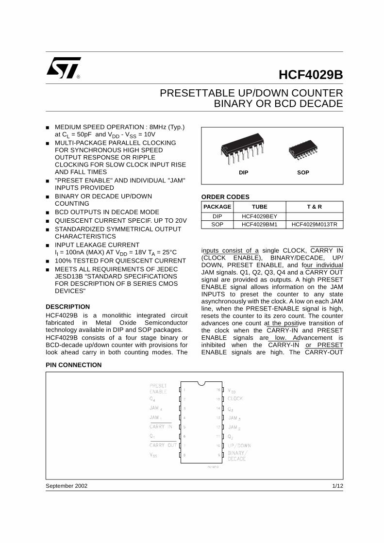
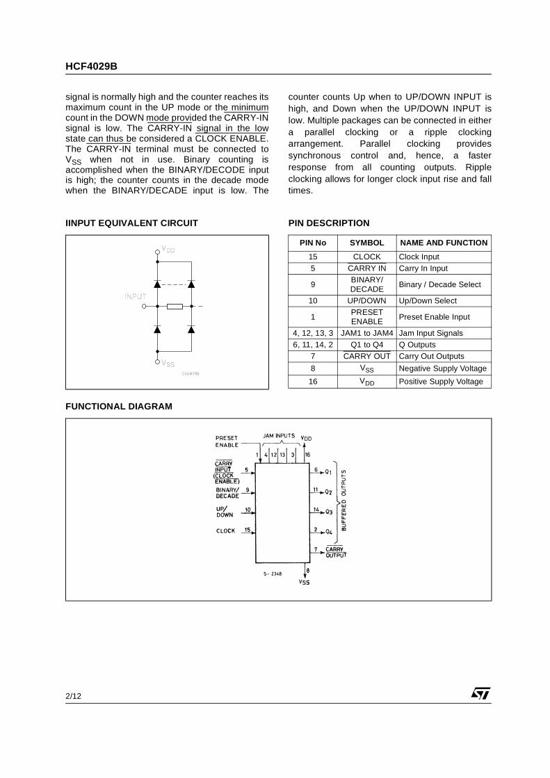
PIN CONNECTION
ORDER CODES
PACKAGE TUBE T & R
DIP HCF4029BEY
SOP HCF4029BM1 HCF4029M013TR
DIP SOP
HCF4029B
2/12
signal is normally high and the counter reaches itsmaximum count in the UP mode or the minimumcount in the DOWN mode provided the CARRY-INsignal is low. The CARRY-IN signal in the lowstate can thus be considered a CLOCK ENABLE.The CARRY-IN terminal must be connected toVSS when not in use. Binary counting isaccomplished when the BINARY/DECODE inputis high; the counter counts in the decade modewhen the BINARY/DECADE input is low. The
counter counts Up when to UP/DOWN INPUT ishigh, and Down when the UP/DOWN INPUT islow. Multiple packages can be connected in eithera parallel clocking or a ripple clockingarrangement. Parallel clocking providessynchronous control and, hence, a fasterresponse from all counting outputs. Rippleclocking allows for longer clock input rise and falltimes.
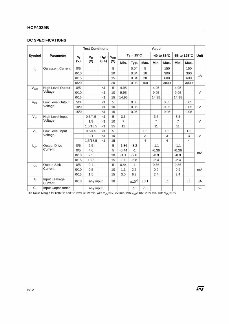
IINPUT EQUIVALENT CIRCUIT PIN DESCRIPTION
FUNCTIONAL DIAGRAM
PIN No SYMBOL NAME AND FUNCTION
15 CLOCK Clock Input
5 CARRY IN Carry In Input
9BINARY/DECADE
Binary / Decade Select
10 UP/DOWN Up/Down Select
1PRESET ENABLE
Preset Enable Input
4, 12, 13, 3 JAM1 to JAM4 Jam Input Signals
6, 11, 14, 2 Q1 to Q4 Q Outputs
7 CARRY OUT Carry Out Outputs
8 VSS Negative Supply Voltage
16 VDD Positive Supply Voltage

HCF4029B
3/12
TRUTH TABLE
X: Don’t Care
TRUTH TABLE
LOGIC DIAGRAM
CLOCK TE PE J Q Q
X X L L L H
L H X Q Q
X X L H H L
H H X Q Q NC
X H X Q Q NC
CONTROL INPUT LOGIC LEVEL ACTION
BIN/DECH Binary Count
L Decade Count
UP/DOWNH Up Count
L Down Count
PRESET ENABLE
H Jam In
L No Jam
CARRY INH No Counter
L Advance counter

HCF4029B
4/12
TIMING CHART - Binary Mode
TIMING CHART - Decade Mode

HCF4029B
5/12
ABSOLUTE MAXIMUM RATINGS
Absolute Maximum Ratings are those values beyond which damage to the device may occur. Functional operation under these conditions is not implied.
All voltage values are referred to VSS pin voltage.
RECOMMENDED OPERATING CONDITIONS
Symbol Parameter Value Unit
VDD Supply Voltage -0.5 to +22 V
VI DC Input Voltage -0.5 to VDD + 0.5 V
II DC Input Current ± 10 mA
PD Power Dissipation per Package 200 mW
Power Dissipation per Output Transistor 100 mW
Top Operating Temperature -55 to +125 °C
Tstg Storage Temperature -65 to +150 °C
Symbol Parameter Value Unit
VDD Supply Voltage 3 to 20 V
VI Input Voltage 0 to VDD V
Top Operating Temperature -55 to 125 °C
HCF4029B
6/12
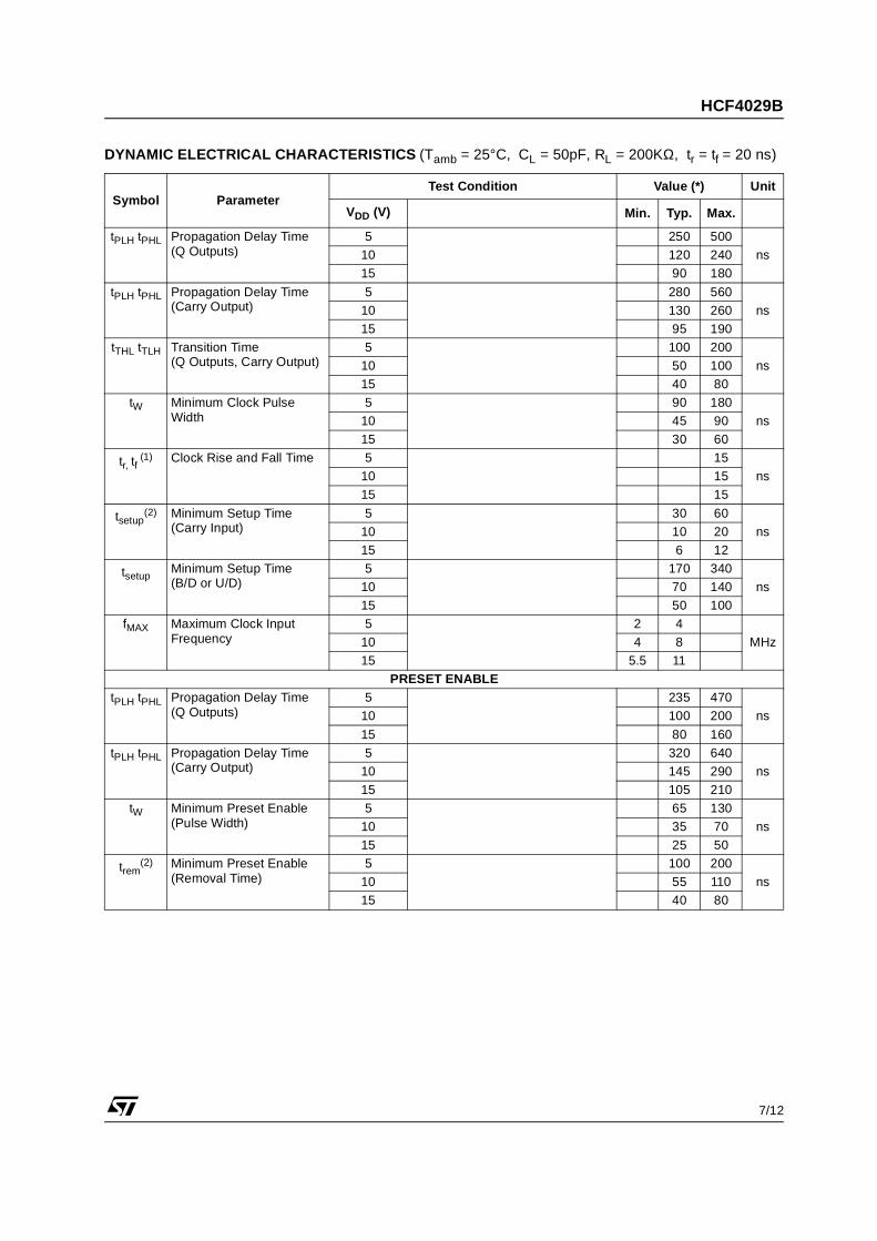
DC SPECIFICATIONS
The Noise Margin for both "1" and "0" level is: 1V min. with VDD=5V, 2V min. with VDD=10V, 2.5V min. with VDD=15V
Symbol Parameter
Test Conditions Value
UnitVI(V)
VO(V)
IO(µA)
VDD(V)
TA = 25°C -40 to 85°C -55 to 125°C
Min. Typ. Max. Min. Max. Min. Max.
IL Quiescent Current 0/5 5 0.04 5 150 150
µA0/10 10 0.04 10 300 300
0/15 15 0.04 20 600 600
0/20 20 0.08 100 3000 3000
VOH High Level Output Voltage
0/5 <1 5 4.95 4.95 4.95
V0/10 <1 10 9.95 9.95 9.95
0/15 <1 15 14.95 14.95 14.95
VOL Low Level Output Voltage
5/0 <1 5 0.05 0.05 0.05
V10/0 <1 10 0.05 0.05 0.05
15/0 <1 15 0.05 0.05 0.05
VIH High Level Input Voltage
0.5/4.5 <1 5 3.5 3.5 3.5
V1/9 <1 10 7 7 7
1.5/18.5 <1 15 11 11 11
VIL Low Level Input Voltage
0.5/4.5 <1 5 1.5 1.5 1.5
V9/1 <1 10 3 3 3
1.5/18.5 <1 15 4 4 4
IOH Output Drive Current
0/5 2.5 5 -1.36 -3.2 -1.1 -1.1
mA0/5 4.6 5 -0.44 -1 -0.36 -0.36
0/10 9.5 10 -1.1 -2.6 -0.9 -0.9
0/15 13.5 15 -3.0 -6.8 -2.4 -2.4
IOL Output Sink Current
0/5 0.4 5 0.44 1 0.36 0.36
mA0/10 0.5 10 1.1 2.6 0.9 0.9
0/15 1.5 15 3.0 6.8 2.4 2.4
II Input Leakage Current
0/18 any input 18 ±10-5 ±0.1 ±1 ±1 µA
CI Input Capacitance any input 5 7.5 pF
HCF4029B
7/12
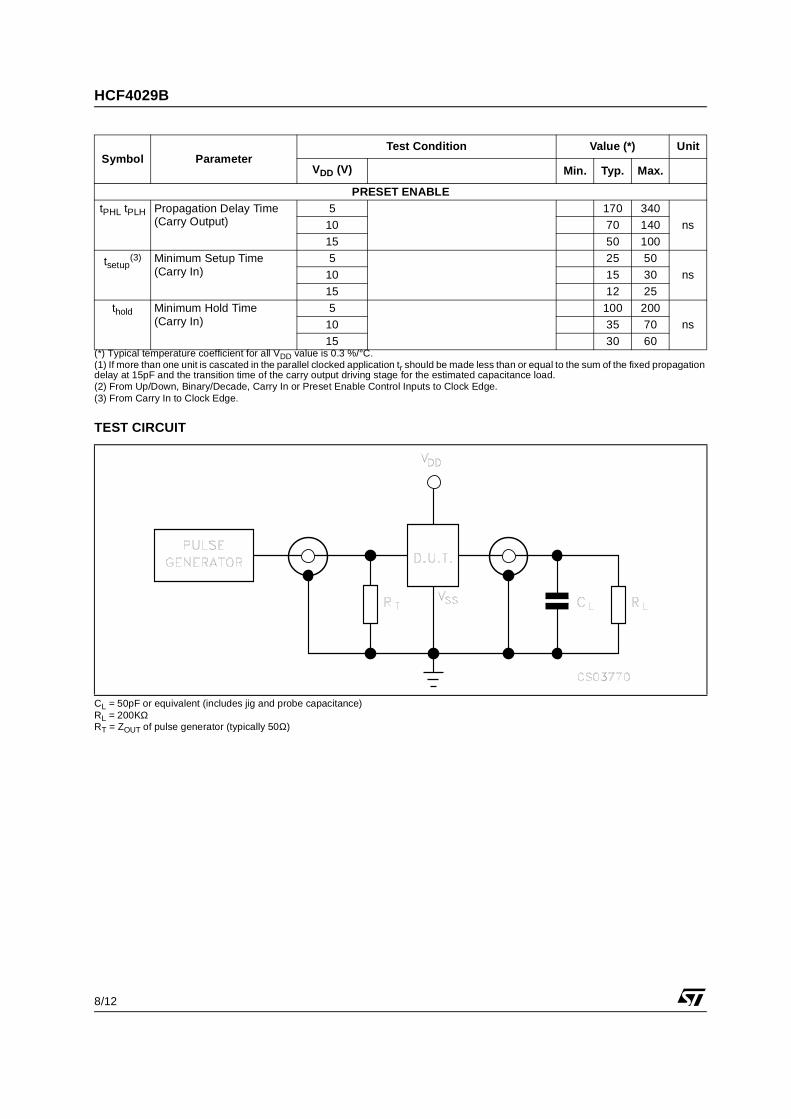
DYNAMIC ELECTRICAL CHARACTERISTICS (Tamb = 25°C, CL = 50pF, RL = 200KΩ, tr = tf = 20 ns)
Symbol ParameterTest Condition Value (*) Unit
VDD (V) Min. Typ. Max.
tPLH tPHL Propagation Delay Time (Q Outputs)
5 250 500
ns10 120 240
15 90 180
tPLH tPHL Propagation Delay Time (Carry Output)
5 280 560
ns10 130 260
15 95 190
tTHL tTLH Transition Time(Q Outputs, Carry Output)
5 100 200
ns10 50 100
15 40 80
tW Minimum Clock Pulse Width
5 90 180
ns10 45 90
15 30 60
tr, tf (1) Clock Rise and Fall Time 5 15
ns10 15
15 15
tsetup(2) Minimum Setup Time
(Carry Input)5 30 60
ns10 10 20
15 6 12
tsetupMinimum Setup Time(B/D or U/D)
5 170 340
ns10 70 140
15 50 100
fMAX Maximum Clock Input Frequency
5 2 4
MHz10 4 8
15 5.5 11
PRESET ENABLEtPLH tPHL Propagation Delay Time
(Q Outputs)5 235 470
ns10 100 200
15 80 160
tPLH tPHL Propagation Delay Time (Carry Output)
5 320 640
ns10 145 290
15 105 210
tW Minimum Preset Enable (Pulse Width)
5 65 130
ns10 35 70
15 25 50
trem(2) Minimum Preset Enable
(Removal Time)5 100 200
ns10 55 110
15 40 80
HCF4029B
8/12
(*) Typical temperature coefficient for all VDD value is 0.3 %/°C.(1) If more than one unit is cascated in the parallel clocked application tr should be made less than or equal to the sum of the fixed propagation delay at 15pF and the transition time of the carry output driving stage for the estimated capacitance load.(2) From Up/Down, Binary/Decade, Carry In or Preset Enable Control Inputs to Clock Edge.(3) From Carry In to Clock Edge.
TEST CIRCUIT
CL = 50pF or equivalent (includes jig and probe capacitance)RL = 200KΩRT = ZOUT of pulse generator (typically 50Ω)
PRESET ENABLEtPHL tPLH Propagation Delay Time
(Carry Output)5 170 340
ns10 70 140
15 50 100
tsetup(3) Minimum Setup Time
(Carry In)5 25 50
ns10 15 30
15 12 25
thold Minimum Hold Time (Carry In)
5 100 200
ns10 35 70
15 30 60
Symbol ParameterTest Condition Value (*) Unit
VDD (V) Min. Typ. Max.
HCF4029B
9/12
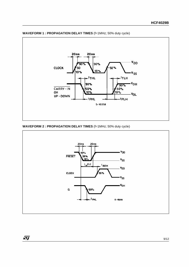
WAVEFORM 1 : PROPAGATION DELAY TIMES (f=1MHz; 50% duty cycle)
WAVEFORM 2 : PROPAGATION DELAY TIMES (f=1MHz; 50% duty cycle)

HCF4029B
10/12
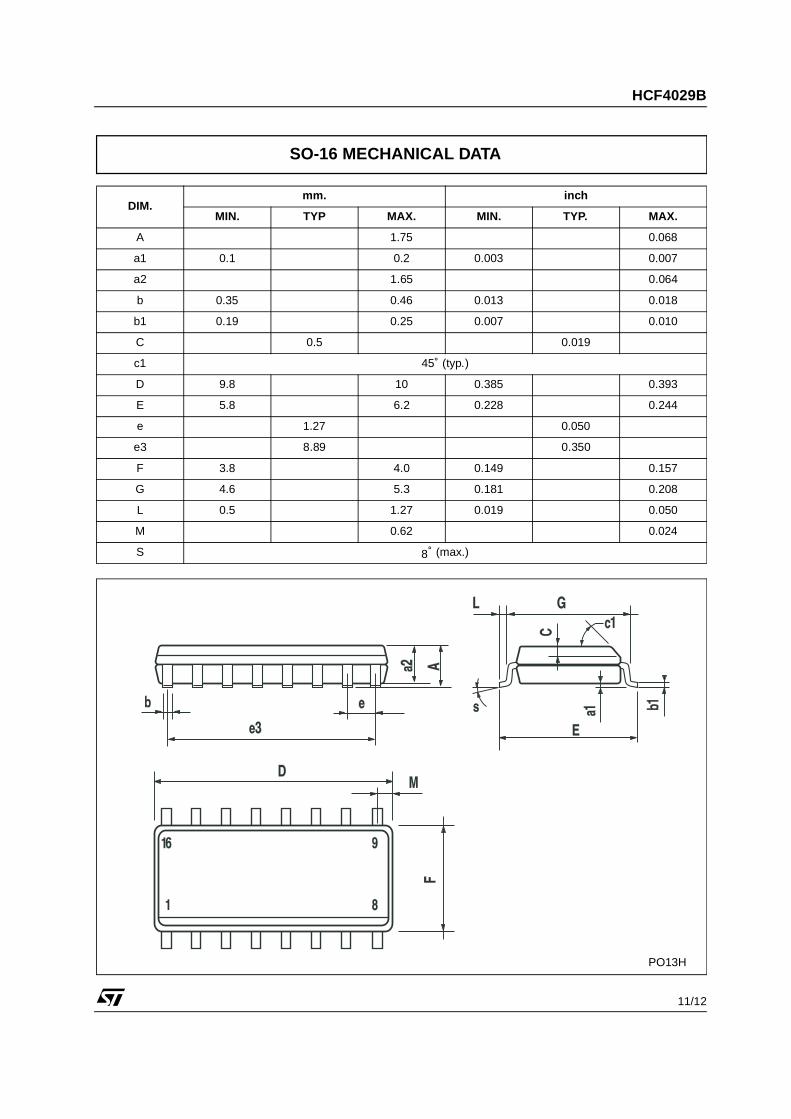
DIM.mm. inch
MIN. TYP MAX. MIN. TYP. MAX.
a1 0.51 0.020
B 0.77 1.65 0.030 0.065
b 0.5 0.020
b1 0.25 0.010
D 20 0.787
E 8.5 0.335
e 2.54 0.100
e3 17.78 0.700
F 7.1 0.280
I 5.1 0.201
L 3.3 0.130
Z 1.27 0.050
Plastic DIP-16 (0.25) MECHANICAL DATA
P001C
HCF4029B
11/12
DIM.mm. inch
MIN. TYP MAX. MIN. TYP. MAX.
A 1.75 0.068
a1 0.1 0.2 0.003 0.007
a2 1.65 0.064
b 0.35 0.46 0.013 0.018
b1 0.19 0.25 0.007 0.010
C 0.5 0.019
c1 45˚ (typ.)
D 9.8 10 0.385 0.393
E 5.8 6.2 0.228 0.244
e 1.27 0.050
e3 8.89 0.350
F 3.8 4.0 0.149 0.157
G 4.6 5.3 0.181 0.208
L 0.5 1.27 0.019 0.050
M 0.62 0.024
S ˚ (max.)
SO-16 MECHANICAL DATA
PO13H
8
HCF4029B
12/12
Information furnished is believed to be accurate and reliable. However, STMicroelectronics assumes no res ponsibility for theconsequences of use of such information nor for any infringement of patents or other rights of third parties which may result f romits use. No license is granted by implication or otherwise under any patent or patent rights of STMicroelectronics. Specificati onsmentioned in this publication are subject to change without notice. This publication supersedes and replaces all informationpreviously supplied. STMicroelectronics products are not authorized for use as critical components in life support devi ces orsystems without express written approval of STMicroelectronics.
© The ST logo is a registered trademark of STMicroelectronics
© 2002 STMicroelectronics - Printed in Italy - All Rights ReservedSTMicroelectronics GROUP OF COMPANIES
Australia - Brazil - Canada - China - Finland - France - Germany - Hong Kong - India - Israel - Italy - Japan - Malaysia - Malta - Morocco Singapore - Spain - Sweden - Switzerland - United Kingdom - United States.
© http://www.st.com