presentation of kavya ullal in icmcc20151033-webinar
TRANSCRIPT

Kavya V. Ullal Dr. Preeta Sharan
Mtech –Student [DEC] Professor
Dept of ECE Dept of ECE
DESIGN AND SIMULATION OF MICRO DISPLACEMENT SENSOR BASED ON MOEMS FOR DETECTION OF ACOUSTIC SIGNALS
The Oxford College of Engineering
PAPER ID: ICMCC20151033

IntroductionMEMS & MOEMSObjective of the ProjectPrinciple of Photonic crystalDesign and modeling of sensors with photonic crystal Principle of mechanical sensor Pre-simulation Software requirementsFurther applicationsConclusionReferences
Contents

• Acoustic is a science that deals with the study of the mechanical waves in gases, liquids, solid including vibration, sound, ultrasound and infrared. Acoustic used in audio and noise industries used in music, medicine, architecture, warfare, industrial production.
• Underwater Acoustics is the study of propagation of sound in water & interaction of mechanical waves that constitute with water & its boundaries.
• Typical frequencies associated with Underwater Acoustics are 10Hz to 1MHz.
• Underwater Acoustics is also known as HYDROACOUSTICS.
• The signal that are used to carry digital information through an underwater channel are acoustic channel. Our main intension in the project is to detect low frequency acoustic signals underwater.
Introduction

• What is MEMS Technology?MEMS technology is based on a number of tools and methodologies, which are used to
form small structures with dimensions in the micrometer scale.MEMS fabrication approach that conveys the advantages of miniaturization, multiple
components, and microelectronics to the design and construction of integrated Electromechanical systems.
• What is MEMS?MEMS or Micro-Electro Mechanical System is a technique of combining Electrical and
Mechanical components together on a chip, to produce a system of miniature dimensions.1.Micro - small size, micro-fabricated structures2.Electro - Electrical signals/control (In/Out)3.Mechanical - Mechanical functionality (Out/In)4.Systems - Structures, Devices, Systems controls
Introduction of mems
(Google)

MOEMS •MOEMS is a promising multi technology for miniaturization of
critical optical systems. It’s a integration of mechanical elements, sensors, actuators, electronics and optics on a common substrate through micro fabrication technology.
•MOEMS sensors can be used in detecting pressure, vibration, displacement, stress etc using photonic sensing technology. MOEMS based mechanical sensors are developed aiming to produce new sensors with improved characteristics, mainly improved sensitivity and stability.
•Micro-opto-electromechanical systems (MOEMS), or optical MEMS, are systems involving micromachining of structures in the micro- to millimeter range whose purposes are to manipulate light.
•It is not a special class of Micro-Electro-Mechanical Systems (MEMS) but in fact it is MEMS merged with Micro-optics which involves sensing or manipulating optical signals on a very small scale size using integrated mechanical, optical, and electrical systems .
Electronics Mechanics
Optics
MEMS
OE OM
MOEMS
(Google)

Objective of the project
• Micro-displacement sensors are used to monitor and control the acoustic signals underwater also in civil, aerospace, and defense.
• Even in submicron levels we can map the displacement occurring in such sensors which find applications in underwater pressure detection and hearing aids which is of growing concern all over the world.

Crystal is a periodic arrangement of atoms and molecules. The pattern in which the atoms and molecules
are repeated in space is the crystal lattice. These allows the light propagate through it.
But in Photonic crystals (PC) the atoms and molecules are replaced by the differing dielectric constants
and the periodic potential by the periodic dielectric functions.
As the PC’s arise from the cooperation of the periodic scatters, thus are called
“CRYSTALS” because of their periodicity
“PHOTONICS” because they act on light
Photonic Crystal based structures are in great demand due to their reliability in sensing application.
In Photonic Crystals the dielectric constant changes in one, two or three dimensions to affect the
propagation of electromagnetic waves inside the structures. These structures are configured in two types
Rods in air configuration
Holes in slab configuration
Introduction to Photonic Crystal

• Structure for which refractive index is a periodic function in space • 1-, 2-, & 3-D photonic crystals are
all 3-D structures• Dimensions refer to number of
dimensions in which the photonic bandgap exists• Dielectric constant modulated in 1,
2, or 3 directions.• Modulation of dielectric constant
on the order of the wavelength of illumination source.
Types of Photonic Crystals1-D photonic
crystal
2-D photonic crystal
3-D photonic crystal
y
y
x
x
z
y(Google)

Defect Engineering •The Photonic Crystal (i.e., rods in air configuration as shown in figure) is designed based on the defect created in the structure.
•There are two types of defects: Point defect and Line defect
1.Point Defect: Formed by removing a single rod from the surface as shown (represented by yellow color in figure)
2.Line defect: Created by the reduction of the row or the column in the PC surface (represented by red color in figure)
(Google)

• The main issue is that of modelling a displacement sensor combining MOEMS along with photonic crystal sensing technology. With the help of this technology we need a sensor with improved sensitivity and stability such that it can be used in detection of the signals or the damage detection of structures.
Problem statement

• The Finite Difference Time Domain MethodThe Finite Difference Time Domain (FDTD) method is an application of the finite difference method, commonly used in
solving differential equations, to solve Maxwell’s equations.
Electromagnetic fields are sampled at discrete points in a space lattice and at discrete points in time and different field components can be obtained at different grid locations. This discretization of equations with second-order accuracy is known as Yee lattice.
Using the two Maxwell’s curl equations, Yee solved both electric and magnetic fields in time and space.
Design and Modeling of Photonic Crystal
............[1]H
Et
����������������������������
............[2]E
H Et
������������������������������������������
1............[3]
Hx Ey Ez
t z y
1............[4]
Ex Hz HyEx
t y z
E��������������
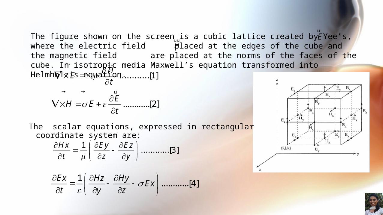
The figure shown on the screen is a cubic lattice created by Yee’s, where the electric field placed at the edges of the cube and the magnetic field are placed at the norms of the faces of the cube. In isotropic media Maxwell’s equation transformed into Helmholz’s equation.
H��������������
The scalar equations, expressed in rectangular coordinate system are:

A sensor is a converter that measures a physical quantity and converts it into a signal which can be read by an observer or by an automatic adaptive system hooked to any instrument for probing. A sensor's sensitivity indicates how much the sensor's output changes when the measured quantity changes. Micro-displacement sensors can act as:
Pressure sensorsVibration and shock sensorsMotion sensors
These sensors can vary drastically in technology, design, performance, sensitivity, application suitability and cost.
Micro-displacement Sensors

• R-Soft (Full Wave) FullWAVE simulation engine is a part of the R-Soft Photonic Suite based on the well-known finite-difference
time-domain (FDTD) technique.
It calculates the electromagnetic field as a function of time and space in a given index structure in response to a
given electromagnetic excitation.
FullWAVE is ideal for studying the propagation of light in a wide variety of photonic structures.
• MEEP MEEP is MIT Electromagnetic Equation Propagation. We use MEEP tool using any Linux distribution such as
Ubuntu. Working of the MEEP tool will be done in the time domain also proving the implementation of Finite
Difference Time Domain Method.
• Mat Lab v7.2 Numerical computing environment and fourth-generation programming language that is Windows 7 compatible.
Required software

Fig. 1: Complete structure of photonic crystal
Fig. 2: The contour map of the index profile is viewed as shown
The design and the simulation is done with the help of the MEEP tool by using the parameters given below,1.Holes in slab configuration2.Hexagonal lattice structure3.Lattice constant ‘a’= 1mm4.Radius of the rods ‘r’ = 0.13mm5.Dielectric constant of Silicon rods = 11.746.Height of the slab is infinity7.Refractive index of the Si = 3.47
The Proposed structure
Fig. 3: The refractive index profile is viewed as shown
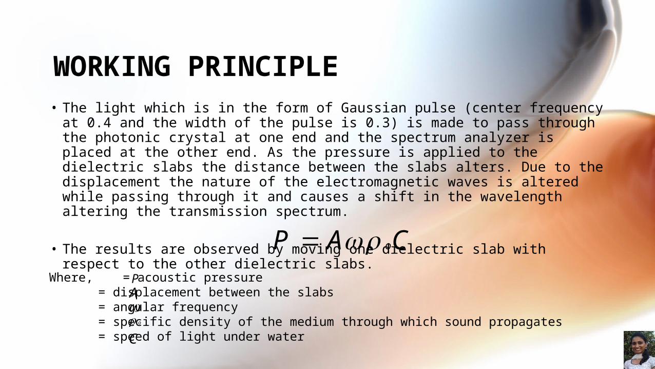
• The light which is in the form of Gaussian pulse (center frequency at 0.4 and the width of the pulse is 0.3) is made to pass through the photonic crystal at one end and the spectrum analyzer is placed at the other end. As the pressure is applied to the dielectric slabs the distance between the slabs alters. Due to the displacement the nature of the electromagnetic waves is altered while passing through it and causes a shift in the wavelength altering the transmission spectrum.
• The results are observed by moving one dielectric slab with respect to the other dielectric slabs.
Where, = acoustic pressure = displacement between the slabs = angular frequency
= specific density of the medium through which sound propagates = speed of light under water
PA
o
oP A C
C
WORKING PRINCIPLE

Graphs plottedThe graphs for transmission spectrum is shown below:The transmission spectrum is observed for the zero micron displacement of the dielectric slabs and also taking 0.1 micron step (increasing and decreasing ) in displacements from 0.1 micron till 0.6 micron displacement.
Fig. 4: Transmission spectrum for zero micron displacement
Fig. 5: Transmission spectrum for 0.1 micron displacement

Fig. 6: Transmission spectrum for 0.2 micron displacement Fig. 7: Transmission spectrum for 0.3 micron displacement
Fig. 6: Transmission spectrum for 0.4 micron displacement Fig. 6: Transmission spectrum for 0.5 micron displacement

results
Combined graph for the Transmission spectrum from zero to 0.5 micron displacement
Displacement Peak wavelength
Amplitude Wavelength shift
0 0.309 35.50.1 0.445 23.75 0.1360.2 0.443 33.5 0.0020.3 0.419 34.5 0.0240.4 0.418 31.8 0.0010.5 0.443 33.7 0.0250.6 0.435 32.6 0.008
• Pressure sensing-structural health monitoring.• Blood pressure measurement of the neonatal baby.• Level / depth sensing of fluids• Flow sensing• Leak testing• Altitude sensing• Hearing aids
Applications
• The modeling and implementation of the photonic crystal mechanical sensor is carried out.
• We infer that the sensing parameter is the shift in wavelength which is dependent directly on the displacement occurred.
• High sensitivity of such MOEMS sensors make it suitable for wide range of applications as mentioned.
Conclusion

• International Conference on Micro-electronics, Communication and Computation, SAN DIEGO, USA, 27th-28th February 2015.“Design and simulation of micro displacement sensor based on moems for detection of acoustic signals”
• International Journal of Electronics and Computer Science Engineering, IJECSE, “Design and Simulation of Micro
Displacement Sensor based on MOEMS for Detection of Acoustic Signals”.
• ETET sessions which is held on 20th & 21st Feb, 2015 at Jyothy Institute of Technology, Bengaluru. “Design and simulation
for the detection of acoustic signals by micro displacement sensor based on moems”.
• 7th Annual KSTA Conference Poster- A Means for Growth February 5-6, 2015, “Blood pressure measurement of the
neonatal baby by using photonic crystal based moems sensors”.
• icOPEN2015 conference have accepted your paper, "Blood Pressure Measurement of the Neonatal baby by using Photonic
Crystal based MOEMS Sensor”. The conference will be held on 14-16 April 2015 in Singapore EXPO, Singapore.
• “Design and simulation of micro displacement sensor based on moems for detection of acoustic signals” . National
Conference on Research and Innovative Development in Aeronautical and Mechanical Engineering, Adhiyamaan College of Engineering Hosur, Hosur, National Conference, Tamil Nadu, March 26-27 2015
PUBLICATIONS
• [1] Z. Xu, L. Cao, C. Gu, Q. He and G. Jin, “Micro displacement sensor based on line-defect resonant cavity in photonic crystal” Opt.Express 14, 298–305 (2006)
• [2]D.Biallo,M.De Sario,A.D’Orazio, “High sensitivity photonic crystal pressure sensor”,Jounal of the European optical society-(2007)
• [3]J. D. Joannopoulos, R. D. Meade, J. N. Winn, Photonic Crystals -Molding the flow of light, Princeton University press, 1995
• [4]O. Levy , B.Z. Steinberg, A. Boag, S. Krylov, I. Goldfarb “Mechanical tuning of two-dimensional photonic crystal cavity by micro Electro mechanical flexures” 25 October 2006
• [5] “Photonic crystal based all-optical pressure sensor”,Yuerui Lu ; SonicMEMS Lab., Cornell Univ., Ithaca, NY, USA, Lal, A.; IEEE conference publications ISBN:978-1-4244-9632-7
• [6] Jack Wu, S. N. Qiu, C. X. Qiu,2 and I. Shih, “A Novel Method for Switching and Tuning of PBG Structures”, Department of Electrical and Computer Engineering McGill ,2004
References

Thank you