predictable quantum efficient detector
TRANSCRIPT

9HSTFMG*afegcj+
ISBN 978-952-60-5462-9 ISBN 978-952-60-5463-6 (pdf) ISSN-L 1799-4934 ISSN 1799-4934 ISSN 1799-4942 (pdf) Aalto University School of Electrical Engineering Department of Signal Processing and Acoustics www.aalto.fi
BUSINESS + ECONOMY ART + DESIGN + ARCHITECTURE SCIENCE + TECHNOLOGY CROSSOVER DOCTORAL DISSERTATIONS
Aalto-D
D 19
9/2
013
Meelis-M
ait Sildoja P
redictable Quantum
Efficient D
etector A
alto U
nive
rsity
Department of Signal Processing and Acoustics
Predictable Quantum Efficient Detector
Meelis-Mait Sildoja
DOCTORAL DISSERTATIONS
��������� ��������������� �������������������� �����������
���������� ������������������������
������������������
������� ������� ����������������� �������� ����������� ���� �����!"��������#��������������$�%��������� ��������������������� ���� ���������&���� ����&��� �$�������������'����������������������� ������� ���������������������������� �����������(�
���������������������� ������������!�������!��"���#���� ��!���$��������!������%������������!��������������%��

�%"�������!"�� �����) ��(�& **�+*���
�������������� (�,� ����-������ �
$����#������&�#�����) ��(�&���� ��-��*���$���� �������.���$�/� %���� (�0��� ��/���$�-���� ����� ���� ���1��� ��� �$�/�%�2������
�""������ (�-� �����%���$�/������+���������� ���� ������"��������$�� ��
��������� ��������������� �������������������� �����������
3�-����4-��� ���5��
+ 6/��784�9�4:�49;:�4��+ 6/��784�9�4:�49;:�4:�!���#�+ /41��7��4;��;�+ /��7��4;��;�!� ���#�+ /��7��4;�;��!���#�����<��� (���=/<+ 6/<�784�9�4:�49;:�4:�
�� ����.��>���*������
,����

�'���������������������($)�)*�&++,,,(-�,,,./�����000)�����) �
�%���������������������� �#�� ��������������������������������� ������������������������
$%'��������������������������������������
�����������������������������������������������
�������������������� �������������������!"#!$�%��&���$#�#&!'��())*+,(-�
-����� ������������������������������#�������� �
���%����"��%'#�����(+��������+,(-� ����� ����� ����(-���������+,(-�
$��#��������"%'����!������1����2(+�'�������+,(-� ���!%�!���������
����!��"� �������������������1�%##���3���!������������2
�'������#��������������������������.������������������ ������������������������������������
����������������������.�������������������������������� ����(�����/����������������01�#���������������������.���������������������������������������������������������������������.�������������������1�2������������3�������������� �/& �0������������������������������� �����������.�����������������������������������������������������1�#���& �������������������������������������������������.������������������������������44�51�#�����������������������������������������6��� �����������������������.�������������������1�%�.�����������.������ ������.��7����������3���������������.������������������������ �������������������� � �������������������������8��8������������.��������� 1� #����������������������������������������������������������� ���������������.��������������������������������������������1�#���������������������� ������ �����������������������.����������������3��������������������� ����������������������� �������1��#��������� ���� ���.����������������������������� ���������������� �������������������������.�������������94:���8�;-+�������4:,�����������������������������3�����������������������1�"�������������.����������������������<������3�������������� ��������� ���������.�����������������<������3�������������� �.��������� ��<��������������� ����:,��������(=,���������������� ������� ����������������������������������1�#���������������������������������������� ��������� ����������� ��������������������������� ������������.����������������� ���������������������� ����������������1������������������������������������ ����������������������������������(,�5�������������� ����������� ��� ���������������������������������1��#������������������ ��������������������������.����������������.����� ���������������������������������.�������������������������������������������� ������������.�����<�������������������������� ����������������1��
��
4��0������������������8��������������������8��������� 8�$������� 8�!��������.��������������8����������������8�!�������������������������
�* 1"������2)4=�);+�:,�;9:+�)� �* 1"� 2)4=�);+�:,�;9:-�:�
�� ��(4))�9)-9� �� 1"������2(4))�9)-9� �� 1"� 2(4))�9)9+�
��������� "%'������2�����7�� ��������� "������!2�����7�� 5���+,(-�
$�!��((;� %������>**���1�*�$'>&�?'>)4=�);+�:,�;9:-�:�

5
Preface
The research work combined into this thesis has been carried out at the
Metrology Research Institute of Aalto University and contains mostly work
during the years 2007-2013 within the scope of the European Metrology
Research Program project Quantum Candela.
I am most grateful to my supervisor, Professor Erkki Ikonen, for his in-
depth guidance, fruitful discussions and for leading me back to trails many
times during the evolvement of the work. In similar way I thank my
instructor, Dr. Farshid Manoocheri, with whom the exciting scientific
collaboration has grown also to good friendship.
I want to thank Dr. Mart Noorma for introducing me the field of optical
metrology and Dr. Toomas Kübarsepp for his guidance and being my first
supervisor during the Tartu period. From the Institute of Physics of Tartu
University I thank Dr. Ants Lõhmus for his help in designing measurement
systems which were essential for many of the valuable experimental results.
I thank all my co-authors from several institutions in Finland and abroad.
From Metrology Resereach Institute and from MIKES I wish to thank Dr.
Mikko Merimaa, Timo Dönsberg and Henrik Mäntynen. My gratitude goes
also to Dr. Lutz Werner and Ingmar Müller from PTB and for Dr. Marek
Smîd and Geiland Porrovecchio from CMI for their kindness and support
during my several visits to Berlin and Prague. The collaborated experiments
in these institutions have had an eye opening for me in many ways. The
scientific support and contribution of Dr. Jarle Gran form Justervesenet
and Dr. Atte Haapalinna from Okmetic Oyj is highly appreciated.
For the warm atmosphere in the Metrology Research Institute I thank all
the previous and present people with whom I have had the pleasure to work
with, especially Dr. Petri Kärhä, Dr. Saulius Nevas, Dr. Tuomas Hieta, Dr.
Maija Ojanen, Dr. Silja Holopainen, Dr. Pasi Manninen, Dr. Markku Vainio,
Dr. Ville Ahtee, Dr. Antti Lamminpää, Dr. Jouni Envall, Dr. Mikko Puranen,
Dr. Marko Laurila, Dr. Tuomas Poikonen, Priit Jaanson, Aigar Vaigu,

6
Maksim Shpak, Tomi Pulli, Teemu Kokki, Teemu Koskinen and Hans
Baumgartner.
My warm gratitude goes to all my close friends with whom the darker days
looked much brighter.
Preliminary examiners Dr. Kathryn Neild and Prof. Edouard Monakhov
are thanked for their efforts and encouraging feedback.
I want to thank also CIMO, Aalto University and Academy of Finland for
the financial support.
Finally, I thank my parents for their support and patience during my years
abroad.
Espoo, November 13, 2013
Meelis-Mait Sildoja

7
Contents
Contents ........................................................................................................ 7
List of Publications ....................................................................................... 9
Author’s contribution ................................................................................... 11
List of abbreviations.................................................................................... 12
List of symbols ............................................................................................ 13
1. Introduction ........................................................................................... 15
1.1 Absolute detector-based techniques of optical power measurements ................................................................................. 16
1.1.1 Optical power scale based on quantum detectors ......................... 16 1.1.2 Optical power scale based on thermal detectors ........................... 19
1.2 Progress of the work .................................................................................................. 22 2. Predictable Quantum Efficient Detector .............................................. 25
2.1 Induced junction photodiodes and charge carrier losses ...................... 26 2.2 Reflectance losses ....................................................................................................... 28
2.2.1 Specular reflectance ...................................................................................... 28 2.2.2 Diffuse reflectance ......................................................................................... 30
2.3 Predicted responsivity .............................................................................................. 30 2.4 Prototype PQED and characterization ............................................................ 31
2.4.1 PQED photodiodes and detector structure ...................................... 31 2.4.2 PQED photodiode uniformity ................................................................. 32 2.4.3 PQED photodiode non-linearity ............................................................ 33 2.4.4 PQED measured specular and diffuse reflectance ........................ 34 2.4.5 PQED measured responsivity .................................................................. 36
2.5 Operability of PQED ................................................................................................. 39 3. Conclusions and outlook ...................................................................... 41
4. References ........................................................................................... 43

8

9
List of Publications
[I] M. Sildoja, F. Manoocheri, and E. Ikonen, “Reducing photodiode reflectance by Brewster-angle operation,” Metrologia, 45, 11–15, 2008.
[II] M. Sildoja, F. Manoocheri, and E. Ikonen, “Reflectance calculations
for a predictable quantum efficient detector,” Metrologia, 46, S151–S154, 2009.
[III] J. Gran, T. Kübarsepp, M. Sildoja, F. Manoocheri, E. Ikonen, and I.
Müller, “Simulations of a predictable quantum efficient detector with PC1D,” Metrologia, 49, S130–S134, 2012.
[IV] M. Sildoja, F. Manoocheri, M. Merimaa, E. Ikonen, I. Müller, L.
Werner, J. Gran, T. Kübarsepp, M. Smîd, and M. L. Rastello, “Predictable quantum efficient detector: I. Photodiodes and predicted responsivity,” Metrologia, 50, 385–394, 2013.
[V] I. Müller, U. Johannsen, U. Linke, L. Socaciu-Siebert, M. Smîd, G.
Porrovecchio, M. Sildoja, F. Manoocheri, E. Ikonen, J. Gran, T. Kübarsepp, G. Brida, and L. Werner, “Predictable quantum efficient detector: II. Characterization and confirmed responsivity,” Metrologia, 50, 395–401, 2013.
[VI] M. Sildoja, T. Dönsberg, H. Mäntynen, M. Merimaa, F. Manoocheri,
and E. Ikonen, “Use of the predictable quantum efficient detector with light sources of uncontrolled state of polarization,” Measurement Science and Technology, accepted.

10

11
Author’s contribution
The research presented in this thesis is mainly carried out at the Metrology
Research Institute of Aalto University School of Electrical Engineering in
close collaboration with the Centre for Metrology and Accreditation
(MIKES). Some of the experiments have been performed at Czech
Metrology Institute (CMI) and Physikalisch-Technische Bundesanstalt
(PTB).
In Publication I the author carried out the calculations and prepared most
of the manuscript.
In Publication II the author developed mathematical routines for the
wedged-trap reflectance, carried out the modelling and prepared the
manuscript.
For publication III the author provided the design parameter values of the
photodiodes used to construct the Predictable Quantum Efficient Detector
(PQED), contributed in defining the simulation result parameters, and
estimated the reflectance loss term and the related uncertainty. The author
contributed to the manuscript preparation.
In publication IV the author designed most of the custom made mechanics,
contributed significantly in building and characterising the PQED detectors,
prepared and carried out most of the experiments, analysed the results,
modelled the reflectance and prepared most of the manuscript.
In Publication V the author had a large contribution in preparing the single
photodiodes for characterization measurements and PQED detectors for
the experiments with cryogenic radiometers. The author participated in
part of the measurements at CMI and PTB. The author replaced one of the
PQED photodiodes broken at PTB during a thunderstorm. The author
contributed to the manuscript preparation.
In Publication VI the author developed most of the mathematical routines,
carried out the modelling and prepared the manuscript.

12
List of abbreviations
CMI Czech Metrology Institute, Czech Republic MIKES Centre for Metrology and Accreditation, Finland NIST National Institute of Standards and Technology, USA NPL National Physical Laboratory, UK PTB Physikalisch-Technische Bundesanstalt, Germany CR cryogenic radiometer CVC current-to-voltage converter DVM digital voltmeter EQD external quantum deficiency EQE external quantum efficiency IQD internal quantum deficiency IQE internal quantum efficiency ppm part per million PQED Predictable Quantum Efficient Detector Si Silicon SiO2 Silicon dioxide

13
List of symbols
c speed of light in vacuum e elementary charge ( ) quantum gain h Planck’s constant ( ) spectrally dependent photocurrent n number of reflections inside trap detector ( ) spectrally dependent optical power ( ) optical power of incident light ( ) optical power of reflected light ( ) measured responsivity ( ) predicted responsivity ( ) ideal responsivity V( ) Luminous sensitivity of human eye
angle between the photodiodes ( ) spectrally dependent internal quantum deficiency ( ) measured external quantum efficiency ( ) predicted external quantum efficiency irradiation wavelength frequency of electromagnetic radiation reflectance ( ) spectral reflectance

14

15
1. Introduction
This thesis gives an overview of the development and analysis of the
Predictable Quantum Efficient Detector (PQED) - a new high-accuracy
optical radiometer based on custom made induced junction silicon
photodiodes. The developed detector is meant to be used as a convenient
primary standard to facilitate traceable measurements in radiometry and
photometry, where the optical power and spectral responsivity are key
quantities.
Radiometry and photometry describe and quantify optical radiation
properties in a systematic manner by defining the associated quantities and
units. After the redefinition of the unit of luminous intensity (candela) in
1979 [1] all the radiometric and photometric quantities in the International
System of Units (SI - Le Système International d’Unités) describing light
source properties are based on optical power expressed by the unit watt.
For radiometric quantities this is simple to understand by the fact that the
intensity of any electromagnetic radiation is expressed through the energy
it carries. By the 1979 definition of the candela the photometric quantities
became linked with their related radiometric quantities. This is done by
defining the photometric base unit candela at a single frequency
(corresponding to the wavelength of about 555 nm) and taking into account
the responsivity of the average human eye using the luminous efficiency
function ( ) at other wavelengths. In this way the definition of the candela
means that the accuracy of any optical measurement quantified, by the
associated SI unit, depends upon the accuracy of optical power
measurement. For this reason the optical power (i.e. radiant flux) is
considered as an essential quantity and the radiometry and photometry
community continues to develop methods to improve the determination of
radiant flux.
Radiant flux can be determined generally by two methods. Firstly, the
source of the radiation is well characterized and the spectral properties of
the emission can be determined through system parameters, or secondly
the sensitivity of the light measuring detector is known and expressed
through some measurable quantity. To ensure an unbroken chain of
dissemination of the optical power scale, any radiometric source or detector
needs to be calibrated against a standard traceable to a primary device. The

16
primary radiometric standard does not require calibration against any
other radiometric standard and is thus considered to be absolute. The
properties of an absolute optical power standard need to be such that the
radiating or detecting properties of the device can be calculated purely by
physical laws based on fundamental constants and/or parameters
independent on the produced or detected radiation.
Absolute standards based on sources are such as black bodies [2-4] or
synchrotron radiation sources [4-6]. There are also developments of single
photon sources based on the correlated photon technique [7-8]. Such
quantum based method of defining the absolute source is a fundamentally
new approach in the field of source based radiometry and research on its
applicability is still on-going [9].
Detector-based standards divide into thermal detectors such as electrical
substitution radiometers and photon-to-electron converting detectors such
as silicon photodiodes. The beginning of contemporary high accuracy
optical radiation measurement era can be considered as the parallel
development of the low-temperature electrical substitution radiometer –
the absolute cryogenic radiometer [10] – and the self-calibration technique
of silicon photodiodes whose responsivity was traceable to fundamental
constants [11]. Both of these developments base on the idea of linking the
optical power scale with the response of an absolute detector. 1.1 Absolute detector-based techniques of optical power
measurements 1.1.1 Optical power scale based on quantum detectors
The most common quantum detectors used in optical radiometry are
silicon based photodiodes. Before 1980’s the silicon photodiodes have been
mainly used as transfer standards traceable to black-body radiation or
electrical substitution radiometer [12].These methods resulted at best with
the relative uncertainty of 0.1 % and required substantial efforts to achieve
such uncertainty level [13]. Typical calibration of a silicon photodetector
yielded uncertainty of more than 1 % [14]. In 1979 Geist [15-16] proposed
that the advanced knowledge of the physics of the silicon material will allow
development of analytical models to predict the quantum efficiency of
silicon photodiodes by linking the responsivity of the photodiode to
fundamental constants and wavelength. Soon after that a self-calibration
technique emerged showing that commercially available silicon based
photodetectors can be used as absolute detectors with standard uncertainty
as low as 0.05 % [11].

17
The photon energy conversion to a measurable amount of charge carriers
is described by the internal quantum efficiency (IQE). The idea behind the
self-calibration method is to measure the internal quantum deficiency
(IQD) - defined as one minus IQE - by applying bias voltages so that the
losses due to recombination of charge carriers are suppressed and the IQE
will reach its saturation. The difference of the responsivities with and
without the bias voltages is then a direct measure of IQD and it shows the
deficiency from the ideal photon-to-electron conversion.
There are two main recombination regions in the conventional diffused
pn-type silicon photodiodes for which different bias voltages have to be
applied to reduce the recombination. The first is in the SiO2/Si surface and
the second is in deeper layers of the bulk after the depletion region [17]. To
reduce the bulk recombination a reverse bias is applied which increases the
depletion region from micrometer range to tens of micrometers and
improves the charge carrier collection efficiency in the volume. The surface
recombination due to minority carriers is reduced by applying oxide bias
voltage via a transparent conductive layer of weak boric acid. It was
assumed that after the removal of the thin solution layer the photodiode
regains its conventional properties. The results of self-calibration technique
were encouraging and some national metrology institutes realized their
primary optical power scale based on this method [18]. Unfortunately it was
discovered that the quantum efficiency of the photodiode decreased after
applying the oxide bias technique making the self-calibration method less
favourable for realizing silicon pn-type photodiodes as absolute detectors
[19-20].
The problems of oxide bias measurements were somewhat alleviated
with the usage of induced junction photodiodes by Zalewski and Duda [21].
Their prototype 4 - element detector showed 0.999 ± 0.002 quantum
efficiency within wavelengths from 400 nm to 700 nm and was promoted
as a 100 % quantum efficient detector. To achieve a uniformly high
quantum efficiency throughout the given wavelengths, reverse bias voltages
of 1.5 V to 50 V had to be applied. Longer wavelengths required higher bias
voltages increasing to more than 100 V at 800 nm. Such high bias voltages
introduced a problem of the increased dark current which sets limits to the
lower end of usable power levels, especially at longer wavelengths. The shift
towards induced junction photodiodes allowed abandoning the oxide bias
technique but the need for reverse bias remained. Detectors based on
Zalewski and Duda’s original design were also commercialized and for some
time they were an industry standard detector [22]. Nevertheless marketing
problems stopped the availability of these devices and a competing
technology based on cryogenic radiometry (CR) combined with trap

18
detectors, usually equipped with high quality Hamamatsu S1337-1010
photodiodes, diminished the need for these detectors. Trap detectors based
on S1337 diodes are further discussed at the end of this section.
More recently a technique of hybrid self-calibration by Gran et al [23] has
been developed. This method implements both purely relative
measurements and a self-calibration technique. The method has shown to
be capable realizing absolute scale based on silicon trap detectors within
standard uncertainty of 0.04 %. The oxide bias method to determine the
front region losses was replaced with relative measurements against
spectrally flat pyroelectric detector. This measurement provides spectral
shape of the detector which can be used to fit the front region losses.
Similar approach is used to estimate the rear surface losses. The hybrid
self-calibration method, however, involves four steps of measurements to
characterize the detector and has not gained wider application in the
radiometry community.
In all of the above cases the loss term associated with the reflectance was
reduced by combining three or more photodiodes into a light trapping
structure [21-22, 24-25]. An example of a three element reflection trap is
shown in Figure 1.
Figure 1. Trap detector consisting of three photodiodes. Five reflections and varying planes of incidence make this type of detector polarization independent.
The low reflectance of such device could be measured either at a single
wavelength (laser based source) or derived from single photodiode
reflectance measurements in the wavelength region of interest (usually
monochromator based source). A more advanced approach to estimate the
reflectance at extended range of wavelengths (UV-VIS-NIR) was to apply a
physical model of thin film analysis [26-27]. This requires the knowledge of
the layered structure of the used photodiodes and the associated material
19
parameters (indices of refraction). The structure of all silicon photodiodes
is similar which allows analogous analytical approach if products of
different manufactures are to be used. The method is to determine the
thickness of the silicon dioxide which covers the bulk silicon and is the only
thin film layer to be considered in the analysis. The model uses Fresnel
equations and interfering multi-reflected beams within the oxide layer
[28-29]. After measuring the reflectance at one or several laser wavelengths
the oxide thickness could be determined and the reflectance at the rest of
the wavelengths could be calculated relying on the oxide thickness gained
by the model. This approach proved to be successful since model
predictions were reliable and initial few measurements were easy to carry
out.
In 1991 Fox introduced the concept of Hamamatsu S1337 silicon
photodiode based transfer standard whose responsivity was highly
predictable once calibrated against high accuracy primary standard only at
a few discrete wavelengths [24]. Though S1337 based detectors are not
absolute, they have quantum efficiency which is close to unity and their
spectral responsivity is calculable throughout wavelengths of about 380 nm
to 1000 nm. Such trap detectors, as they are called, are almost ideal
transfer standards and their implementation in the optical power
measurements has been of enormous importance. The successful
development of the quantum efficiency model [30-32] combined with
calculable reflectance losses allowed easy adoption of the trap detectors
since the rest of the properties generally ascribed for an ideal relative
spectral response standard were met: response over active area is uniform
[33], linear [34-35] and stable with time [24]. Furthermore, the produced
photocurrent has good signal-to-noise ratio and short time constant. All of
this is obtained without applying a reverse bias voltage to the photodiodes.
Those favourable properties have made possible to use trap detectors both
as primary and secondary standards realizing both radiometric and
photometric scales in many NMIs [36-41].
1.1.2 Optical power scale based on thermal detectors High accuracy optical radiation measurement using thermal detectors
started with the development and realization of the absolute cryogenic
radiometer (CR) in 1980’s at NPL [10, 42]. The original device was built for
accurate estimation of the Stefan-Boltzmann constant [42], but with few
modifications the device could be used also for precise optical radiation
measurements. The principle of a cryogenic radiometer (Figure 2) is to
measure the equivalent power of a radiation and an electric current. The

20
absorbing element in the radiometer is intermittently heated by the two
sources. Both sources produce a thermal gradient in the absorbing cavity.
The measurable power introduced by electric current can then be adjusted
such that the temperature rise is equal to that of incident optical radiation.
Based on heating current measurement the optical power can be
determined. In practise the equality of the two heating methods is
determined by electrical heating below and above the optical heating.
Low temperatures in the range of 4 K - 15 K are used to suppress the
background radiation by shielding the cavity from room temperature; to
prevent losses due to resistive heating of leads by using superconductive
wires; to increase the thermal diffusivity of copper for uniform heat flux
and for possibility to use large low reflectance cavity; to limit the thermal
radiation of the cavity to minimum level, plus operating in vacuum
eliminates the convective heat exchange [43].
Figure 2. Example of a liquid helium cooled cryogenic radiometer. Figure from [44].
Typical CR allows optical radiation to be detected within relative standard
uncertainty of 0.005 – 0.01 % [10, 31, 44-48] but the continued
development of these devices has reduced the uncertainty below 0.003%
[49, publication V]. Higher accuracies are achieved due to improved
electrical power measurement, better control of the stray light and
improved Brewster window transmittance estimation. The effect of
Brewster window can be cancelled entirely using a joint Brewster window
with the detector to be calibrated [publication V].

21
Conventionally the optical power scale of CR is transferred to secondary
standards often realized by trap detectors as described in section 1.1.1.
These trap detectors are usually equipped with commercially available high
quality 10 x 10 mm2 silicon photodiodes. The purpose is to deliver the high
accuracy of CR at discrete wavelengths to a continuous wavelength range by
the method of interpolation. First the trap detector is calibrated with CR at
selected wavelengths and then its responsivity is extended to other
wavelengths using similar analytical methods as originally used in self-
calibration technique, i.e. the internal and external losses of the detector
are calculated based upon physical models [30-32].
The calibration of trap detector transfer standards with CR increases the
relative uncertainty to the typical value of 0.01 – 0.02 % [24, 46, 50]. There
are many aspects in the increase of the uncertainty but one is related to the
principal differences how these devices are functioning. CR is spectrally flat,
i.e. it measures the power of the radiation irrelevant of the wavelength.
Photodiodes on the other hand convert photons to charge carriers. The
measured photocurrent depends on the radiation power and also on the
wavelength. To perform high accuracy calibration of trap detector against
CR requires that the irradiation wavelength is precisely known. This is only
achievable with fully monochromatic narrow bandwidth laser lines.
Another criterion for reliable scale transfer is the stability of the light source.
Laser beams can be stabilized to the order of ten ppm over half an hour
[publication V], but monochromator based sources do not reach such low
stability. Monitor detector correction is not sufficient here due to the large
time constant of CR [49]. Also the effect of stray light is dissimilar for
detectors with spectral responsivities of different shape. All of these aspects
would be alleviated if the primary and secondary standards would be both
based on solid state detectors.
The process of calibration requires a sophisticated control mechanism to
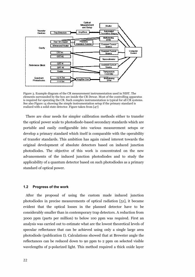
operate the CR and trap detector in a combined manner as shown in Figure
3. Majority of the components are involved in the control mechanism of the
CR.
Though the CR has some advantages - e.g. spectral flatness and wide
wavelength range – its operation is expensive and initial investment into
equipment is rather large. Handling of this equipment requires qualified
personnel familiar with the specific CR. Additionally, CR based
measurements are time consuming due to long preparation time required
to cool down the cavity either by using liquid nitrogen and liquid helium or
by applying mechanical cooling. Another disadvantage of the CR is its poor
transportability. Usually the CR, vacuum pumps, cooling equipment and
dedicated electronics occupy large amount of laboratory space.
22
Figure 3. Example diagram of the CR measurement instrumentation used in NIST. The elements surrounded by the box are inside the CR Dewar. Most of the controlling apparatus is required for operating the CR. Such complex instrumentation is typical for all CR systems. See also Figure 14 showing the simple instrumentation setup if the primary standard is realized with a solid state detector. Figure taken from [47]
There are clear needs for simpler calibration methods either to transfer
the optical power scale to photodiode-based secondary standards which are
portable and easily configurable into various measurement setups or
develop a primary standard which itself is comparable with the operability
of transfer standards. This ambition has again raised interest towards the
original development of absolute detectors based on induced junction
photodiodes. The objective of this work is concentrated on the new
advancements of the induced junction photodiodes and to study the
applicability of a quantum detector based on such photodiodes as a primary
standard of optical power.
1.2 Progress of the work
After the proposal of using the custom made induced junction
photodiodes in precise measurements of optical radiation [51], it became
evident that the optical losses in the planned detector have to be
considerably smaller than in contemporary trap detectors. A reduction from
3000 ppm (parts per million) to below 100 ppm was required. First an
analysis was carried out to estimate what are the lowest theoretical levels of
specular reflectance that can be achieved using only a single large area
photodiode (publication I). Calculations showed that at Brewster angle the
reflectances can be reduced down to 90 ppm to 2 ppm on selected visible
wavelengths of p-polarized light. This method required a thick oxide layer

23
of the order of 3 m on top of silicon to act as antireflection coating on
multiple wavelengths. A hemispherical mirror was proposed to cover the
photodiode to control the diffused part of the reflectance.
A more efficient way to reduce specular reflectance at all visible
wavelengths was proposed in publication II. The low level of reflectance
was achieved using photodiodes in a wedge-like trap structure so that
multiple reflections take place before the light escapes the detector. The
assembly of the photodiodes so that they face each other had the advantage
of collecting also the small fraction of scattered light though it was found
that the diffuse reflectance from such photodiodes is a minor effect.
Analytical estimation showed that photodiodes with oxide-thicknesses of
around 100 nm will be the best to achieve the lowest reflectances. Such a
thin oxide thickness was favoured compared to the m range outcome of
the single photodiode calculation due to the fact that growing a thermal
oxide is a time consuming process.
The advanced modelling of internal quantum deficiency (IQD) of the
produced PQED photodiodes in publication III predicted that as low as
1 ppm charge carrier losses are achievable at liquid nitrogen temperatures
at shorter than 600 nm wavelengths of visible light and below 100 ppm at
wavelengths between 600 nm and 720 nm. The predictions were also
promising at room temperature where the uncertainties of internal losses of
photodiodes were estimated to be below 90 ppm over all visible
wavelengths.
Publication IV describes the structure of the induced junction
photodiodes, covers the design of the prototype PQED and estimates the
predicted responsivity at liquid nitrogen and at room temperature. The
estimated responsivity includes the measurements and calculations of the
reflectance losses combined with the predictions of internal losses of
publication III and gives thorough uncertainty analysis for the results.
The prototype PQED was compared with the present primary standard of
optical power - the cryogenic radiometer – at two laboratories at the
wavelengths of 476 nm, 532 nm and 760 nm. The results are reported in
publication V showing the agreement of measured values with the predicted
results within the expanded standard uncertainty at 95 % confidence level.
This article addresses also the non-linearity and spatial uniformity of
responsivity of individual induced junction photodiodes showing that they
are highly linear and that their spatial uniformity is comparable with the
high quality commercially available silicon photodiodes.
Usually the PQED is operated in a sealed chamber, such as a cryostat, and
the transmission of the light into the chamber is achieved using p-polarized
collimated beam through a Brewster-angled window. Publication VI
24
analyses the reflectance losses and related uncertainty of the room
temperature PQED without a window under the illumination of varied
polarization of light. The outcome was that a simple photocurrent ratio
measurement of individual PQED photodiodes predicts the effects of
polarization through which the reflectance can be estimated. This allows
light sources with any polarization to be used and still maintain similar low
uncertainty that was previously available only for p-polarized light.

25
2. Predictable Quantum Efficient Detector
The responsivity of any quantum detector can be expressed using
elementary charge (e), Planck’s constant (h), speed of light in vacuum (c),
and the vacuum wavelength . If the detector would be ideal no losses
would occur and the listed constants would describe entirely the ideal
responsivity ( ) = / of a photodetector. This comes from the
principle that each absorbed photon produces exactly one charge carrier in
the detector. Photon carries an energy of = . If photon is absorbed it
adds an elementary charge e to the electric current. The energy carried per
unit time by the photons is described by the optical power whereas the
amount of charge carriers per unit time is expressed by the produced
photocurrent. The responsivity of a quantum detector is thus given in units
of amperes per watt.
In reality no detector is perfect and losses take place. These losses can be
divided as reflectance losses and charge carrier losses or external losses and
internal losses. Equation (1) describes the responsivity of a real
photodetector,
( ) = [1 ( )][1 ( )][1 + ( )] . (1)
The loss/gain corrections in square brackets are reflectance – ( ), charge
carrier losses – ( ) , and quantum gain – ( ) . The quantum gain
describes a rare situation where the built-in voltage in the photodiode
accelerates charge carriers and due to impact ionization secondary carriers
are produced. It is many of orders of magnitude weaker contribution than
the loss corrections and thus it is often neglected in calculations [51,
publication III]. As seen from equation (1) the responsivity of a
photodetector can approach the responsivity of an ideal quantum detector
if the loss corrections are minimized to zero. This raises the question if the
losses in advanced quantum detectors can be reduced sufficiently so that
the optical powers measured with such detectors can approach or even
surpass the accuracy of the present primary standard. In the following this
is discussed in more detail showing that remarkably low level losses can be
26
obtained using custom made induced junction photodiodes so that the
uncertainty of the responsivity is of the same order of magnitude as the
absolute values of the loss corrections and are comparable with the
uncertainty of a cryogenic radiometer.
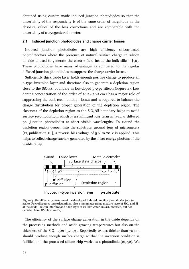
2.1 Induced junction photodiodes and charge carrier losses Induced junction photodiodes are high efficiency silicon-based
photodetectors where the presence of natural surface charge in silicon
dioxide is used to generate the electric field inside the bulk silicon [52].
These photodiodes have many advantages as compared to the regular
diffused junction photodiodes to suppress the charge carrier losses.
Sufficiently thick oxide layer holds enough positive charge to produce an
n-type inversion layer and therefore also to generate a depletion region
close to the SiO2/Si boundary in low-doped p-type silicon (Figure 4). Low
doping concentration of the order of 1012 - 1013 cm-3 has a major role of
suppressing the bulk recombination losses and is required to balance the
charge distribution for proper generation of the depletion region. The
closeness of the depletion region to the SiO2/Si boundary helps to avoid
surface recombination, which is a significant loss term in regular diffused
pn - junction photodiodes at short visible wavelengths. To extend the
depletion region deeper into the substrate, around tens of micrometers
[17, publication III], a reverse bias voltage of 5 V to 20 V is applied. This
helps to collect charge carriers generated by the lower energy photons of the
visible range.
Figure 4. Simplified cross-section of the developed induced junction photodiodes (not to scale). For reflectance loss calculations, also a nanometer range mixture layer of SiO2 and Si at the oxide - silicon interface and a top layer of ice-like water on SiO2 are used, but not depicted here. (Publication IV).
The efficiency of the surface charge generation in the oxide depends on
the processing methods and oxide growing temperatures but also on the
thickness of the SiO2 layer [52, 53]. Reportedly oxides thicker than 70 nm
should produce enough surface charge so that the inversion condition is
fulfilled and the processed silicon chip works as a photodiode [21, 52]. We

27
found that at the used doping concentrations this condition was not true
and oxides thicker than 100 nm have to be used. The exact selection of
oxide thicknesses is discussed in the next section as this affects also the
reflectance properties of the detector.
An additional option to improve the charge carrier collection is to lower
the temperature of the photodiode. At low temperatures the charge carrier
transport is affected less by lattice vibrations allowing photon-generated
electrons and holes to move inside the semiconductor with reduced losses.
Preliminary modelling by Geist et al [51] showed that the temperature of
liquid nitrogen is sufficient to suppress the charge carrier transport losses
to the level of 1 ppm. The temperature of 77 K is considerably easier to
reach than the 4 K – 15 K range where the cryogenic radiometers are
operated.
Thorough modelling of the internal quantum deficiency was carried out
with PC1D solar cell software [54]. Similar software was used in the original
Geist et al work in 2003. Since the PC1D approach is one dimensional, a
more sophisticated 3D Synopsys Sentaurus 1 was used to compare the
results of the two software packages. It was found that PC1D predicts three
to ten times lower losses than the 3D software [publication III]. This is
most probably caused by the fact that the charge carriers have to move a
long distance along the SiO2/Si interface outside the illuminated volume
before being collected by the electrode. The PC1D software cannot estimate
those charge carrier losses. Comparison of two software packages led to the
conclusion that simple one dimensional approach to predict the IQD of an
induced junction photodiode is sufficient, but for reliable uncertainty
estimation the results of PC1D have to be multiplied by ten. Figure 5 depicts
the predicted IQD at room temperature and at 77 K showing that at low
temperature internal losses and their uncertainties smaller than 1 ppm can
be obtained at wavelengths from 400 nm to 600 nm. At longer
wavelengths the absorption coefficient of silicon decreases so that the
charge carrier generation happens beyond the depletion region. This
explains the fast increase of IQD in red and near-IR wavelengths. At room
temperature, where the absorption coefficient is four to nine times larger at
shown wavelengths, the wavelength dependence of the absorption
coefficient allows almost constant IQD at all visible wavelengths.
1 Access to Synopsys Sentarus software was limited during the work.
28
Figure 5. Predicted internal quantum deficiency (IQD) of an induced junction photodiode at the temperatures of 300 K and 77 K with reverse bias voltage of 5 V. The dashed lines show standard uncertainty mainly caused by the reliability of the PC1D software. (Publication III). 2.2 Reflectance losses
2.2.1 Specular reflectance
The specular reflectance of a silicon based photodiode is in the order of
30 % [29] at normal incidence. One method to reduce the reflectance below
100 ppm or even 1 ppm, i.e. to the level similar of the predicted IQD, is to
use a wedged trap configuration so that incident light will reflect multiple
times between the two photodiodes (Figure 6) before escaping the detector
[ 22, 55-57, publication II].
(a) (b) Figure 6. Wedged trap structure reducing specular reflectance: (a) using 7 reflections and (b) using 9 reflections between the photodiodes.
Figure 6 shows the beam path inside 7 - and 9 - reflection trap detectors,
indicating also the angle between the photodiodes. The angle between the
photodiodes is calculable using the following equation

29
= °( ) , (2) where n denotes the number of reflections.
In the alignment process sufficiently high laser power can be used so that
the back reflection becomes observable. For that purpose it is beneficial to
have the reflected beam to nominally follow a similar path as the incident
beam. By adjusting the incoming and outgoing beams close to each other
the PQED can be aligned properly in the measurement system. Correct
positioning of the PQED assures that reflectance losses are similar and
predictable when repeating the experiments.
It is desired to have the reflectance of the detector as small as possible
with minimum number of reflections. High number of reflections increases
the required size of the active area which will have an impact on the cost of
the photodiodes. A more favourable approach is to tailor the oxide
thickness on top of silicon so that it behaves as an antireflection coating.
Further reduction in reflectance can be made if p - polarized light is used.
This condition is usually met since the light polarized in the plane of
incidence is required also for high accuracy measurements with cryogenic
radiometers.
Calculations show that favourably low level of reflectance is achieved over
all visible wavelengths when oxide thicknesses of around 300 nm and
220 nm are used for the upper and lower photodiode, respectively (see
Figure 6). Figure 7 shows the reflectances of such 7 - and 9 - reflection traps
in several orientations of polarization plane indicating significantly lower
reflectance at p - polarized light.
(a) (b) Figure 7. Reflectance of (a) 7-reflection and (b) 9-reflection PQED showing the dependence on the polarization of the incident beam. Using seven reflections and p-polarized light, reflectance below 60 ppm can be achieved over most of the visible wavelengths. Nine reflections will further decrease the reflectance by a factor of about 10. (Publication VI).
Publications II, IV and VI give a thorough overview of the reflectance
properties of the wedged-style trap, estimating also the uncertainties

30
caused by the material parameters and construction tolerances of the trap
[publications IV, VI].
2.2.2 Diffuse reflectance Reflectance of a surface is defined as the ratio of the reflected optical
power (or flux) ( ) relative to the incoming optical power ( ) as given
in equation 3,
( ) = ( )( ). (3)
Reflected power ( ) contains both specular and diffuse parts of the
reflected flux. The models of specular reflectance for silicon photodiodes
have been proven to predict the total reflectance losses with an uncertainty
of 2 · 10-3 [29] using Fresnel equations. That accuracy has been sufficient to
predict reflectance losses of transfer standards meaning that the magnitude
of the diffuse component is sufficiently small compared to the specular
component so that most of the time it can be neglected in the reflectance
loss term of the trap detectors based on silicon photodiodes.
As shown in the previous section, the IQD of induced junction
photodiodes is argued to be predictable with an uncertainty below 1 ppm.
The multireflection trap of Figure 6b can reduce the specular part of the
reflectance to similarly low level. Such small value of reflectance requires
also accurate estimation of the diffuse component. This can be reliably done
using an experimental approach described in section 2.4.4. Even if the
diffuse reflectance of a single photodiode is larger than 1 ppm, the design of
the wedge trap structure where the photodiodes face towards each other
and cover a large solid angle will help to reduce the effect of diffuse
reflectance losses to sub ppm level. 2.3 Predicted responsivity
Equation (1) in the beginning of section 2 describes the responsivity of a
quantum detector. There the combination of factors 1 - ( ) and 1 - ( )
describes the external quantum efficiency (EQE) of the detector, where ( )
is the reflectance loss and ( ) is the internal quantum deficiency. Since ( ) and ( ) are sufficiently small the EQE can be written as 1 - ( ) - ( ).
It is convenient to use the term external quantum deficiency (one minus
EQE) to estimate the efficiency of the incident photon-to-electron
conversion. Then the net effect of loss terms ( ) + ( ) describes the
fractional part of the photons which do not produce charge carriers in the

31
measurement circuit. This is also the basis for the predicted responsivity,
which is related to EQD as
( ) = 1 ( )( ) = ( ) + ( ), (4)
where ( ) is the predicted external quantum deficiency, ( ) is the
predicted responsivity of the PQED and ( ) is the responsivity of an ideal
photodetector.
The uncertainty of the predicted responsivity depends on the uncertainty
of the wavelength and the uncertainties of the components of the EQD, i.e.
the reflectance and IQD. For a stabilized monochromatic light source the
wavelength can be determined with an accuracy better than 1 ppm [58]. The
uncertainties due to calculated reflectance and IQD are determined by the
accuracies of the physical models and the uncertainties of the material
parameters used in these models [publications III, IV]. The uncertainty of
the calculated reflectance can be further reduced by directly measuring the
reflectance using a rather conventional measurement setup [publication IV].
An uncertainty of 1 % in reflectance of 100 ppm would still be sufficient to
determine the relative uncertainty of the responsivity within ~1 ppm. 2.4 Prototype PQED and characterization
2.4.1 PQED photodiodes and detector structure The custom-made induced junction photodiodes were produced using
lightly p - doped <111> oriented silicon wafers with thickness of 525 m.
The measured doping concentration of boron was about 2×1012 cm-3. The
photodiode active area is surrounded by three metal contact rings
(Figure 8). The photocurrent is registered via the innermost and outermost
contacts through which also the bias voltage is applied. The intermediate
‘guard’ is used, when necessary, to suppress the noise due to surface
leakage, which may be relatively large in p-type materials as compared with
n-type materials. The guard ring is then connected to the common ground
which is also the ground potential of the bias voltage.
The prototype PQED was realized using the 7-reflection trap configuration
in order to facilitate the alignment and use the advantage of slightly higher
reflectance during reflectance loss measurements as compared with the
9-reflection trap. Higher reflectance was not considered as a drawback
since it can be estimated with an uncertainty close to the predicted charge
carrier losses.

32
Figure 8. Processed PQED photodiode mounted on the PCB board. Photocurrent is registered using the U.FL connectors. Same contacts are used to apply the bias voltage. The small 4-channel switch routes signals between contacts and allows using different operational modes, when necessary. (Publication IV). 2.4.2 PQED photodiode uniformity
The uniformities of spatial responsivity of the PQED photodiodes were
measured using a computer controlled x-y translator [59, publication V]. To
maintain the clean environment and to be able to carry out measurements
also at low temperatures, the individual photodiodes were installed into a
liquid nitrogen cryostat. The Brewster window and the cryostat were
attached to each other using a flexible bellows. This enabled the movement
of the cryostat without changing the position of the window to cancel the
effect of the non-uniformity of the Brewster window.
The measurements were carried out at the wavelength of 760 nm by
moving the laser spot row by row in 0.5 mm steps across the photodiode
surface. A reference measurement at the central area of the photodiode was
used to normalize the photocurrents for each row to correct any other effect
than the fluctuations in the laser power. The stability of the laser intensity
was monitored and later corrected using a trap detector.
The uniformity of the spatial responsivity is described as a standard
deviation relative to the central area for the photodiode. For the photodiode
with 220 nm oxide thickness it was around 0.045 % whereas for the 300
nm oxide photodiode it was around 0.060 %. The results given here are for
10 V reverse bias to maximise the effect of the internal quantum efficiency
though results at lower reverse bias voltage of 5 V were very similar
[publication V]. The reported spatial uniformities are comparable with
uniformities of high quality commercially available photodiodes such as
Hamamatsu S1337 [60, 61].

33
Figure 9. Example of the relative uniformity of responsivity of the PQED photodiode with the oxide thickness of 220 nm. Scanning was done at room temperature with laser wavelength of 760 nm. Figure from [59].
Figure 9 shows an example of the spatial uniformity of the photodiode
with an oxide thickness of 220 nm indicating a slope-like structure in the
spatial responsivity. Smooth change in responsivity is explainable with the
possible slope in the oxide thickness expected to be present in thermally
grown oxides. A variation of about 0.8 nm in the oxide thickness
corresponds to a change in the relative responsivity of 0.25 % shown in
Figure 9 in the inner part of the photodiode. Similar variations in the oxide
thickness have been measured with ellipsometric technique [61]. This
shows that the spatial non-uniformity of responsivity is strongly related to
the non-uniformity in the oxide thickness and indicates the high spatial
uniformity of charge carrier generation within the PQED photodiode.
A change of 1 nm in oxide thickness affects the responsivity of the
7-reflection PQED by less than 3 ppm over most of the visible wavelengths
increasing to about 10 ppm at short visible wavelengths around 400 nm. 2.4.3 PQED photodiode non-linearity
The linearity of the PQED photodiodes was measured with a setup
described in [62] with modifications to adapt the stabilized DFB laser
(760 nm) into the measurement system. Measurements showed no
significant non-linearity within the standard uncertainty of 30 ppm up to
photocurrents of 160 A (~250 W at 760 nm). Figure 10 shows the results
of the linearity measurement of the PQED photodiode with an oxide
thickness of 300 nm. The non-linearity of a photodiode with an oxide
thickness of 220 nm showed similar behaviour.

34
Figure 10. Non-linearity of a single PQED photodiode with oxide thickness of 300 nm. The measurements were performed at the room temperature with reverse bias voltage of 5 V. Photocurrents were measured up to currents of 160 A (~250 W) at the irradiation wavelength of 760 nm. Within standard uncertainty of 3 × 10 5 no non-linearity was detected.
A photodiode with an oxide thickness of 220 nm was also measured at
higher power levels up to 1 mW. It was discovered that the photodiode
becomes noticeably nonlinear at photocurrents of ~400 A (approximately
600 W at 760 nm). In the PQED the photocurrent is distributed between
two photodiodes, but single photodiode non-linearity measurements are
highly relevant for this case, because (80 ± 10) % of the photocurrent is
produced by the first photodiode. A thorough analysis of the PQED
photodiode spatial uniformity characterization and non-linearity
measurements is given in publication V. 2.4.4 PQED measured specular and diffuse reflectance
Specular reflectance of an assembled PQED was measured at the
wavelengths of 476 nm, 488 nm and 532 nm. Comparing the measured
results with the modelled values indicates a few ppm smaller values as
expected. Figure 11 shows the graph of the predicted reflectance with
standard uncertainty estimation and the measured reflectances at selected
wavelengths.
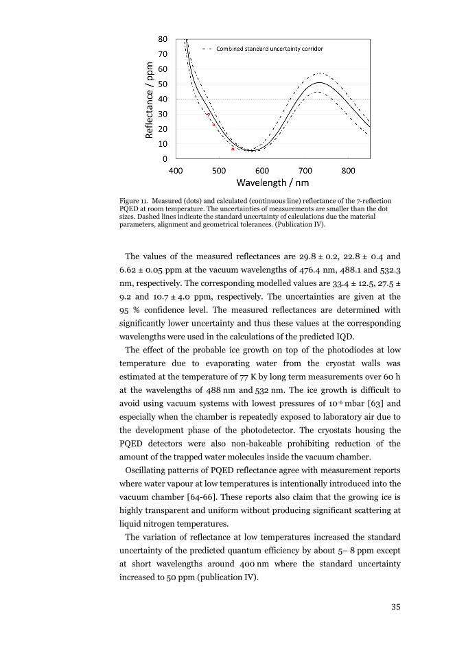
35
Figure 11. Measured (dots) and calculated (continuous line) reflectance of the 7-reflection PQED at room temperature. The uncertainties of measurements are smaller than the dot sizes. Dashed lines indicate the standard uncertainty of calculations due the material parameters, alignment and geometrical tolerances. (Publication IV).
The values of the measured reflectances are 29.8 ± 0.2, 22.8 ± 0.4 and
6.62 ± 0.05 ppm at the vacuum wavelengths of 476.4 nm, 488.1 and 532.3
nm, respectively. The corresponding modelled values are 33.4 ± 12.5, 27.5 ±
9.2 and 10.7 ± 4.0 ppm, respectively. The uncertainties are given at the
95 % confidence level. The measured reflectances are determined with
significantly lower uncertainty and thus these values at the corresponding
wavelengths were used in the calculations of the predicted IQD.
The effect of the probable ice growth on top of the photodiodes at low
temperature due to evaporating water from the cryostat walls was
estimated at the temperature of 77 K by long term measurements over 60 h
at the wavelengths of 488 nm and 532 nm. The ice growth is difficult to
avoid using vacuum systems with lowest pressures of 10-6 mbar [63] and
especially when the chamber is repeatedly exposed to laboratory air due to
the development phase of the photodetector. The cryostats housing the
PQED detectors were also non-bakeable prohibiting reduction of the
amount of the trapped water molecules inside the vacuum chamber.
Oscillating patterns of PQED reflectance agree with measurement reports
where water vapour at low temperatures is intentionally introduced into the
vacuum chamber [64-66]. These reports also claim that the growing ice is
highly transparent and uniform without producing significant scattering at
liquid nitrogen temperatures.
The variation of reflectance at low temperatures increased the standard
uncertainty of the predicted quantum efficiency by about 5– 8 ppm except
at short wavelengths around 400 nm where the standard uncertainty
increased to 50 ppm (publication IV).
36
The diffuse part of the reflected light at room temperature was estimated
by measuring the scattering from a processed silicon wafer which was only
exposed to a clean room environment [67]. The equipment used in this
measurement is routinely used for silicon wafer scattering measurements at
the collaborating company Okmetic Oyj. The measurements revealed low
level of scattering of the order of 0.05 ppm on the photodiode active areas
and slightly increased scattering of 0.5 ppm on the implanted electrodes.
These values demonstrate highly clean surfaces of PQED photodiodes and
indicate that the diffuse component in reflectance is sufficiently small.
Publication IV gives in depth characterization of the PQED reflectance.
The results obtained therein were used to estimate the responsivity and
internal quantum efficiency of the PQED. 2.4.5 PQED measured responsivity
The responsivity of the PQED was measured using two different cryogenic
radiometer systems, one at PTB [publication V] and one at CMI
[48, publication V]. At PTB the advantageous structure of a joint Brewster
window for CR and PQED helped to reduce the uncertainty due to the
losses when the propagating beam goes through the window. At CMI a
more conventional method was used where the CR and PQED were
compared by interchanging the detectors in front of the beam. Both the CR
and PQED had their own Brewster windows in the CMI experiments. The
wavelengths used at PTB measurements were 532 nm and 760 nm, whereas
at CMI only 476 nm was used. A more detailed description of measurement
systems and the related uncertainties are given in publication V, where
tables 2 and 3 list the major uncertainty components of the two CR
measurement systems used to validate the predicted responsivity of PQED.
External quantum deficiency of the PQED is validated by comparing the
predicted EQD (see equation 4) with the measured EQD ( ) as described
by equation (5),
( ) = 1 ( )( ) . (5)
The measured responsivity ( ) is obtained by the equation
( ) = ( )( ) , (6)
where ( ) is the photocurrent measured with the PQED and ( ) is the
optical power of the same beam measured by the cryogenic radiometer.

37
Figure 12 shows the schematic of the PTB system where the PQED and CR
are intermittently aligned into the laser beam using a computer controlled
arc-shaped rail.
Figure 12. PQED responsivity measurement setup at PTB showing the cryogenic radiometer and PQED on an arc-shaped rail behind the joint Brewster window. The magnified section of PQED shows the photodiode arrangement inside a copper holder (semi-transparent area) for efficient heat transfer from the cryostat cold finger to the photodiodes.
The measurements were carried out at room temperature and at liquid
nitrogen temperature. First the responsivity dependence on reverse bias
voltage was determined to adjust the bias voltage so that the PQED would
operate in saturated internal quantum efficiency regime. The photocurrent
dependence on the bias voltage was measured at the wavelengths of 532 nm
and 760 nm at room temperature and at liquid nitrogen temperature. At
532 nm saturation occurred at reverse bias voltages greater than 1 V at both
298 K and 77 K, however at 760 nm this condition was only met at 298 K
whereas a reverse bias greater than 20 V was required at 77 K. This result is
in agreement with the modelled IQD indicating sudden increase of charge
carrier losses above the wavelength of 650 nm. The reason is the reduced
absorption coefficient of silicon at low temperatures [68, 69] which causes
the photons at longer wavelengths to be absorbed beyond the depletion
region deep in the bulk. At room temperature the bias voltage of -5V is
sufficient for saturated quantum efficiency operation at all wavelengths in
the covered range of 400 nm to 800 nm.
The comparison of the measured and predicted external quantum
deficiency of the PQED is shown in Figure 13. The predicted loss described
by the solid line is the sum of the predicted reflectance ( ) and the
predicted internal quantum deficiency ( ). At room temperature the shape

38
of the predicted EQD is affected mostly by the spectral reflectance whereas
its uncertainty is high due to the uncertainty of the predicted IQD. At low
temperature the shape and uncertainty of the predicted EQD from 400 nm
to 750 nm are affected by the reflectance. The predicted IQD at this
wavelength range is below 1 ppm.
Figure 13. Measured and predicted external quantum deficiency (EQD) at room temperature and at liquid nitrogen temperature with reverse bias voltage of 5V. Measurements were made at the wavelengths of 476 nm, 532 nm and 760 nm. The uncertainty bars show expanded uncertainty in the confidence level of 95 %. The points with dashed uncertainty bars indicate predicted and measured EQD and their uncertainties at the reverse bias voltage of 20V.
At longer wavelengths above 750 nm the predicted EQD is mostly affected
by the increased IQD (see Figure 5) due to reduced absorption coefficient of
silicon. The high uncertainty at these wavelengths is caused by the
combination of the reliability of PC1D modelling and the uncertainty of the
absorption coefficient of silicon (see publication IV).
Results in Figure 13 indicate agreement of the predicted responsivity with
the measured responsivity within the uncertainties. Though there seems to
be systematic underestimation of the predicted quantum deficiency the
measurements show typically below 100 ppm EQD with similar order of

39
magnitude uncertainty. Somewhat unexpected results are obtained at low
temperatures where the measured EQD is in the same level with the EQD at
room temperature. This on the other hand indicates that an improved
modelling of the IQD with reduced uncertainty is required since that is by
far the largest component in the uncertainty of the room temperature EQD
[publications III, IV]. Internal quantum deficiency at the room temperature
is estimated to be below 180 ppm (k = 2) due to recombination losses with a
nominal value of about 10 ppm whereas at low temperature a value below
1 ppm is expected. In spite of that the results at room temperature are
comparable with the accuracy of a typical commercial grade CR. This gives
promising indications that calibrations with cryogenic radiometers at
visible wavelengths may be replaceable with PQED devices operated at
room temperature. 2.5 Operability of PQED
The measurement system containing the PQED and a conventional trap
detector at room temperature is comparable with the simple setup of
comparing two trap detectors. A typical measurement scheme is shown in
Figure 14 indicating that only a fraction of the devices is required as
compared to the complicated system needed for CR measurements (see
Figure 3). For photocurrent registration a high accuracy current detection
system is utilized usually consisting of a low noise current-to-voltage
converter (with biasing option for PQED) and digital voltmeter. For precise
alignment and switching of detectors automated translators are used. All of
these devices can be controlled with a computer driven system enabling full
automation of the measurement process.
Figure 14. Simple measurement setup transferring the optical power scale from PQED to trap detectors. CVC – current-to-voltage converter, DVM – digital voltmeter, PC – computer control of the devices.

40

41
3. Conclusions and outlook
A novel photodetector – the Predictable Quantum Efficient Detector
(PQED) – has been designed, constructed and characterised. The PQED
consists of custom made lightly doped induced junction silicon photodiodes,
which significantly reduce the charge carrier losses mainly caused by the
bulk and surface recombination. Two such photodiodes are arranged in a
wedged trap structure to reduce the reflectance losses to similarly low levels
as the internal losses.
Predictions suggest that with optimal conditions the photon-to-electron
conversion is achievable with losses below 1 ppm with similar low
uncertainty at a wide range of visible wavelengths. This requires the
detector operation at liquid nitrogen temperature and within clean
environment preventing any surface contamination of the photodiodes. The
prototype PQED has been designed to closely follow the required
operational conditions to achieve as low uncertainty in the photon-to-
electron conversion process as possible. At low temperature the lowest
external quantum deficiency (EQD) was predicted to be 20 ppm with
10 ppm expanded uncertainty. At room temperature, where the operation
of the PQED is considerably easier, the EQD at the wavelength range from
450 nm to 800 nm was predicted to be below 60 ppm, although with large
uncertainty up to 180 ppm. At shorter wavelengths from 400 nm to 450 nm
the predicted EQE was as high as 260 ppm, but this was caused by the
increase in reflectance, whose expanded uncertainty was typically below 70
ppm. Only at wavelengths below 410 nm the expanded uncertainty
increased above 100 ppm peaking at 400 nm with the value of 140 ppm.
Thus the predicted EQD in room temperature had rather uniform
uncertainty of 120 ppm to 180 ppm (k = 2) throughout all visible
wavelengths caused by EQE whereas the variation in EQE was caused
mainly by the reflectance.
Validation of the PQED has been performed by comparing the detector
against the present primary standard of optical power - the cryogenic
radiometer (CR). The lowest expanded uncertainty achieved by the
validation measurements was 56 ppm. Within that uncertainty the
predicted and measured EQD of the PQED overlapped showing that
available models predicting internal quantum deficiency have become
42
reliable and sufficiently accurate. These results are comparable with the
accuracy of CR, especially when a joint window of the CR and the calibrated
detector is not used, indicating that calibrations with cryogenic radiometers
at visible wavelengths may be replaceable with PQED devices operated at
room temperature. Developments towards this approach are actively
carried out. A compact room temperature PQED is already in prototyping
phase.
There are many improvements to be made to enhance the predictability of
the PQED both at low temperature and at room temperature. For this study
only one-dimensional software PC1D was mostly available. A versatile
three-dimensional software would especially improve the reliability of the
room temperature responsivity values. An improved vacuum system would
reduce the effects causing the time dependence of the reflectance at low
temperature. At long visible wavelengths, where uncertainty of the IQD at
low temperature is large, the improved determination of silicon extinction
coefficient would reduce the uncertainty of the predicted responsivity.
Stability of the PQED is a property to be tested. Regular silicon
photodiodes show drift in responsivity at short visible wavelengths around
400 nm [70, 71]. However the induced junction photodiodes have much
smaller impurity concentration which is believed to be the cause of
instability in diffused photodiodes. For that reason the instability has not
been considered to be significant in PQED detector though further research
has to be carried out.
43
4. References
[1] Comptes rendus de la 16e CGPM (1979)
[2] Blevin W R and Steiner B "Redefinition of the Candela and the Lumen" Metrologia 11 97–104 (1975)
[3] Sapritsky V I "Black-body radiometry" Metrologia 32 411–7 (1995)
[4] Hollandt J, Seidel J, Klein R, Ulm G, Migdall A and Ware M "Primary sources for use in radiometry" Optical Radiometry ed A Parr, J Gardner and R Datla (Amsterdam: Elsevier, Academic) pp 213–90 (2005)
[5] Ulm G "Radiometry with synchrotron radiation" Metrologia 40 S101–S106 (2003)
[6] Klein R, Brandt G, Fliegauf R, Hoehl A, Müller R, Thornagel R, Ulm G, Abo-Bakr M, Feikes J, Hartrott M, Holldack K and Wüstefeld G "Operation of the Metrology Light Source as a primary radiation source standard" Physical Review Special Topics - Accelerators and Beams 11 1–10 (2008)
[7] Klyshko D N "Photons and Nonlinear Optics" (New York: Gordon and Breach) (1988)
[8] Migdall A "Differences Explained in Correlated-Photon Metrology Techniques" Physics Today 52 15 (1999)
[9] Cheung J Y, Chunnilall C J, Woolliams E R, Fox N P, Mountford J R, Wang J and Thomas P J "The quantum candela: a re-definition of the standard units for optical radiation" Journal of Modern Optics 54 373–96 (2007)
[10] Martin J E, Fox N P and Key P J "A cryogenic radiometer for absolute radiometric measurements" Metrologia 21 147–55 (1985)
[11] Zalewski E F and Geist J "Silicon photodiode absolute spectral response self-calibration" Applied Optics 19 1214–6 (1980)
[12] Hengstberger F "The absolute measurement of radiant power" Absolute Radiometry ed F Hengstberger (London: Academic Press) pp 1–117 (1989)
[13] Blevin W R and Brown W J "A Precise Measurement of the Stefan-Boltzmann Constant" Metrologia 7 15–29 (1971)
[14] Geist J, Steiner B, Schaefer R, Zalewski E and Corrons A "Electrically based spectral power measurements through use of a tunable cw laser" Applied Physics Letters 26 309 (1975)

44
[15] Geist J "Quantum efficiency of the p-n junction in silicon as an absolute radiometric standard." Applied optics 18 760–2 (1979)
[16] Geist J "On the possibility of an absolute radiometric standard based on the quantum efficiency of a silicon photodiode" Proc. SPIE, Measurements of Optical Radiations vol 196 ed H P Field, E F Zalewski and F M Zweibaum pp 75–83 (1979)
[17] Geist J, Zalewski E and Schaefer A "Spectral response self-calibration and interpolation of silicon photodiodes" Applied Optics 19 3795–9 (1980)
[18] Geist J "Current Status Of, And Future Directions In, Silicon Photodiode Self-Calibration" Proc. SPIE, Optical Radiation Measurements II vol 119 ed J M Palmer pp 246–56 (1989)
[19] Verdebout J and Booker R L "Degradation of native oxide passivated silicon photodiodes by repeated oxide bias" Journal of Applied Physics 55 406–12 (1984)
[20] Key P J, Fox N P and Rastello M L "Oxide-bias Measurements in the Silicon Photodiode Self-calibration Technique" Metrologia 21 81–7 (1985)
[21] Zalewski E F and Duda C R "Silicon photodiode device with 100% external quantum efficiency" Applied optics 22 2867–73 (1983)
[22] Palmer J M "Alternative Configurations for Trap Detectors" Metrologia 30 327–33 (1993)
[23] Gran J "Accurate and independent spectral response scale based on silicon trap detectors and spectrally invariant detectors" Dissertation for the degree of Doctor Scientiarum, (University of Oslo) (2005)
[24] Fox N "Trap detectors and their properties" Metrologia 28 197–202 (1991)
[25] Bittar A “Extension of a silicon-based detector spectral responsivity scale into the ultraviolet” Metrologia 32 (6), 407 – 500 (1996)
[26] Huen T "Reflectance of thinly oxidized silicon at normal incidence." Applied optics 18 1927–32 (1979)
[27] Saito T, Katori K and Onuki H "Characteristics of semiconductor photodiodes in the VUV region" Physica Scripta 41 783–7 (1990)
[28] Born M and Wolf E "Principles of Optics" (Oxford: Pergamon) (1965)
[29] Haapalinna A, Kärhä P and Ikonen E "Spectral reflectance of silicon photodiodes" Applied optics 37 729–32 (1998)
[30] Gentile T R, Houston J M and Cromer C L "Realization of a scale of absolute spectral response using the National Institute of Standards and Technology high-accuracy cryogenic radiometer" Applied Optics 35 4392–4403 (1996)

45
[31] Werner L, Fischer J, Johannsen U and Hartmann J "Accurate determination of the spectral responsivity of silicon trap detectors between 238 nm and 1015 nm using a laser-based cryogenic radiometer" Metrologia 37 279–84 (2000)
[32] Kübarsepp T, Kärhä P and Ikonen E "Interpolation of the spectral responsivity of silicon photodetectors in the near ultraviolet" Applied optics 39 9–15 (2000)
[33] White M G and Bittar A "Uniformity of Quantum Efficiency of Single and Trap-configured Silicon Photodiodes" Metrologia 30 361–4 (1993)
[34] Fischer J and Fu L "Photodiode nonlinearity measurement with an intensity stabilized laser as a radiation source" Applied Optics 32 4187–90 (1993)
[35] Kübarsepp T, Haapalinna a, Kärhä P and Ikonen E "Nonlinearity measurements of silicon photodetectors." Applied optics 37 2716–22 (1998)
[36] Kärhä P "Trap Detectors and Their Applications in the Realization of Spectral Responsivity, Luminous Intensity and Spectral Irradiance Scales" Thesis for the degree of Doctor of Technology (Helsinki University of Technology) (1997)
[37] Kübarsepp T "Optical radiometry using silicon photodetectors" Thesis for the degree of Doctor of Technology (Helsinki University of Technology) (1999)
[38] Hartree W S, Fox N P and Lambe R P "Towards a detector-based spectral-radiance scale in the near-ultraviolet" Metrologia 32 519–22 (1995)
[39] Larason T, Bruce S and Cromer C "The NIST high accuracy scale for absolute spectral response from 406 nm to 920 nm" Journal of research - National Institute of Standards and Technology 101 133–40 (1996)
[40] Bittar A, Hamlin J D, White M G “A New Detector Based Spectral Responsivity Scale for the 400 nm to 900 nm Wavelength Range” Industrial Research Limited Report 91, Lower Hutt, New Zealand (1993)
[41] Bazkir O and Samadov F "Characterization of silicon photodiode-based trap detectors and establishment of spectral responsivity scale" Optics and Lasers in Engineering 43 131–41 (2005)
[42] Quinn T J and Martin J E "A Radiometric Determination of the Stefan-Boltzmann Constant and Thermodynamic Temperatures between -40 degrees C and +100 degrees C" Philosophical Transactions of the Royal Society A: Mathematical, Physical and Engineering Sciences 316 85–189 (1985)
[43] Fox N "Radiometry with cryogenic radiometers and semiconductor photodiodes" Metrologia 96 535–43 (1995)
[44] Hoyt C C, Miller P J, Foukal P V. and Zalewski E F "Comparison Between A Side-Viewing Cryogenic Radiometer And Self-Calibrated Silicon Photodiodes" Proc. SPIE, Optical Radiation Measurements II vol 1109 ed J M Palmer pp 236–45 (1989)
46
[45] Varpula T, Seppa H and Saari J-M "Optical power calibrator based on a stabilized green He-Ne laser and a cryogenic absolute radiometer" IEEE Transactions on Instrumentation and Measurement 38 558–64 (1989)
[46] Nield K M, Clare J F, Hamlin J D and Bittar A "Calibration of a trap detector against a cryogenic radiometer" Metrologia 35 581–6 (1998)
[47] Gentile T R, Parr A C, Houston J M, Hardis J E and Cromer C L "National Institute of Standards and Technology high-accuracy cryogenic radiometer" Applied Optics 35 1056 – 68(1996)
[48] Fox N P, Haycocks P R, Martin J E and Ul-Haq I "A mechanically cooled portable cryogenic radiometer" Metrologia 32 581–4 (1995)
[49] Stock K D, Hofer H, White M and Fox N P "Lowest uncertainty direct comparison of a mechanically-cooled and a helium-cooled cryogenic radiometer" Metrologia 37 437–9 (2000)
[50] Fox N P and Martin J E "Comparison of two cryogenic radiometers by determining the absolute spectral responsivity of silicon photodiodes with an uncertainty of 0.02%." Applied optics 29 4686–93 (1990)
[51] Geist J, Brida G and Rastello M L "Prospects for improving the accuracy of silicon photodiode self-calibration with custom cryogenic photodiodes" Metrologia 40 S132–S135 (2003)
[52] Hansen T "Silicon UV-photodiodes using natural inversion layers" Physica Scripta 18 471–5 (1978)
[53] Hoem S, Gran J, Sildoja M, Manoocheri F, Ikonen E and Müller I "Physics of self-induced photodiodes" Proc. of NEWRAD 2011 Conference ed S Park and E Ikonen (Hawaii, USA) pp 259–60 (2011)
[54] Clugston D A and Basore P A "PC1D version 5: 32-bit solar cell modelling on personal computers" Proc. 26th IEEE Photovoltaic Specialists Conference (Anaheim, CA) pp 207–10 (1997)
[55] Lehman J H "Pyroelectric Trap Detector for Spectral Responsivity Measurements" Applied Optics 36 9117–8 (1997)
[56] Lehman J, Sauvageau J, Vayshenker I, Cromer C and Foley K "Silicon wedge-trap detector for optical fibre power measurements" Measurement Science and Technology 9 1694–8 (1998)
[57] Canfield L R, Vest R E, Korde R, Schmidtke H and Desor R "Absolute silicon photodiodes for 160 nm to 254 nm photons" Metrologia 35 329–34 (1998)
[58] Quinn T J "Practical realization of the definition of the metre, including recommended radiations of other optical frequency standards (2001)" Metrologia 40 103–33 (2003)

47
[59] Müller I, Brida G, Gran J, Hoem S, Ikonen E, Kübarsepp T, Linke U, Manoocheri F, Sildoja M, Smid M, Socaciu-Siebert L and Werner L "Predictable Quantum Efficient Detector II: Characterization Results" Proc of NEWRAD 2011 Conference ed S Park and E Ikonen (Hawaii, USA) pp 209–10 (2011)
[60] Bittar A and White M G "High-resolution spatial uniformity of surface reflectance and response of silicon photodiodes" Proc. SPIE, 14th Symposium on photonic measurements vol 1712, ed J Schanda and T Lippenyi pp 121–31 (1993)
[61] White M, Lolli L, Brida G, Gran J and Rajteri M "Optical constants and spatial uniformity of thermally grown oxide layer of custom, induced-junction, silicon photodiodes for a predictable quantum efficient detector" Journal of Applied Physics 113 243509 (2013)
[62] Lei F and Fischer J "Characterization of Photodiodes in the UV and Visible Spectral Region Based on Cryogenic Radiometry" Metrologia 30 297–303 (1993)
[63] Berman A "Water vapor in vacuum systems" Vacuum 47 327–32 (1996)
[64] Brown D E, George S M, Huang C, Wong E K L, Rider K B, Smith R S and Kay B D "H 2 O Condensation Coefficient and Refractive Index for Vapor-Deposited Ice from Molecular Beam and Optical Interference Measurements" The Journal of Physical Chemistry 100 4988–95 (1996)
[65] Westley M S, Baratta G A and Baragiola R A "Density and index of refraction of water ice films vapor deposited at low temperatures" The Journal of Chemical Physics 108 3321–6 (1998)
[66] Berland B S, Brown D E, Tolbert M A and George S M "Refractive index and density of vapor-deposited ice" Geophysical Research Letters 22 3493–6 (1995)
[67] Ikonen E, Haapalinna A, Sildoja M and Manoocheri F "Photon-to-electron converter with 1 ppm quantum deficiency" Proc. of Northern Otpics 2009 Conf. (Vilnius, Lithuania) p 114 (2009)
[68] Dash W and Newman R "Intrinsic Optical Absorption in Single-Crystal Germanium and Silicon at 77°K and 300°K" Physical Review 99 1151–5 (1955)
[69] Green M A "Self-consistent optical parameters of intrinsic silicon at 300K including temperature coefficients" Solar Energy Materials and Solar Cells 92 1305–10 (2008)
[70] Werner L "Ultraviolet stability of silicon photodiodes" Metrologia 35 407–11 (1998)
[71] Goebel R and Stock M "Report on the comparison CCPR-K2.b of spectral responsivity measurements in the range 300 nm to 1000 nm" Metrologia 41 02004–89 (2004)

9HSTFMG*afegcj+
ISBN 978-952-60-5462-9 ISBN 978-952-60-5463-6 (pdf) ISSN-L 1799-4934 ISSN 1799-4934 ISSN 1799-4942 (pdf) Aalto University School of Electrical Engineering Department of Signal Processing and Acoustics www.aalto.fi
BUSINESS + ECONOMY ART + DESIGN + ARCHITECTURE SCIENCE + TECHNOLOGY CROSSOVER DOCTORAL DISSERTATIONS
Aalto-D
D 19
9/2
013
Meelis-M
ait Sildoja P
redictable Quantum
Efficient D
etector A
alto U
nive
rsity
Department of Signal Processing and Acoustics
Predictable Quantum Efficient Detector
Meelis-Mait Sildoja
DOCTORAL DISSERTATIONS