precision remote diode digital temperature sensor with ... · lm95245 snis148g – october 2007–...
TRANSCRIPT

LM95245
www.ti.com SNIS148G –OCTOBER 2007–REVISED MARCH 2013
Precision Remote Diode Digital Temperature Sensor with TruTherm® BJT BetaCompensation Technology for 45nm Process
Check for Samples: LM95245
1FEATURES DESCRIPTIONThe LM95245 is an 11-bit digital temperature sensor
2• Remote and Local Temperature Channelswith a 2-wire System Management Bus (SMBus)
• Targeted for Intel 45nm Processor Diodes interface and TruTherm technology that can monitor• Two Formats: −128°C to +127.875°C and 0°C to the temperature of a remote diode as well as its own
255.875°C temperature. The LM95245 can be used to veryaccurately monitor the temperature of external• Digital Filter for Remote Channeldevices such as microprocessors. TruTherm
• Programmable TCRIT and OS Thresholds technology allows the LM95245 to precisely monitor• Programmable Shared Hysteresis Register thermal diodes found in 90 nm and smaller geometry
processes. The LM95245 is specifically targeted for• Diode Fault DetectionIntel processors on 45nm process. LM95245 reports• Mask, Offset, and Status Registers temperature in two different formats for +127.875°C/-
• SMBus 2.0 Compatible Interface, Supports 128°C range and 0°C/255°C range. The LM95245TIMEOUT T_CRIT and OS outputs are asserted when either
unmasked channel exceeds its programmed limit and• Programmable Conversion Rate for Bestcan be used to shutdown the system, to turn on thePower Consumptionsystem fans, or as a microcontroller interrupt function.
• Three-Level Address Pin The current status of the T_CRIT and OS pins can be• Standby Mode One-Shot Conversion Control read back from the status registers via the SMBus
interface. All limits have a shared programmable• Pin-for-Pin Compatible With the LM95235 andhysteresis register.LM86, LM89, LM99The remote temperature channel of the LM95245 has• 8-Pin VSSOP and SOIC Packagesa programmable digital filter. The LM95245 istargeted for a typical Intel® processor on a 45 nm, 65APPLICATIONSnm or 90nm process, and has an offset register for
• Processor/Computer System Thermal maximum flexibility and best accuracy.Management (For Example, Laptops,
The LM95245 has a three-level address pin toDesktops, Workstations, Servers)connect up to 3 devices to the same SMBus master,
• Electronic Test Equipment that is shared with the OS output. The LM95245 has• Office Electronics a programmable conversion rate register and a
standby mode to save power. One conversion can betriggered in standby mode by writing to the one-shotKEY SPECIFICATIONSregister.
• Supply Voltage 3.0 to 3.6 V• Supply Current, Conv. Rate = 1 Hz 350 µA (typ)• Remote Diode Temperature Accuracy
– TA = 25°C to 85°C; TD = 50°C to 105°C, ±0.75°C (max)
– TA = 25°C to 85°C; TD = 40°C to 125°C, ±1.5°C (max)
• Local Temperature Accuracy– TA = 25°C to 100°C, ±2.0 °C (max)
• Conversion Rate, Both Channels 16 to 0.4 Hz
1
Please be aware that an important notice concerning availability, standard warranty, and use in critical applications ofTexas Instruments semiconductor products and disclaimers thereto appears at the end of this data sheet.
2All trademarks are the property of their respective owners.
PRODUCTION DATA information is current as of publication date. Copyright © 2007–2013, Texas Instruments IncorporatedProducts conform to specifications per the terms of the TexasInstruments standard warranty. Production processing does notnecessarily include testing of all parameters.

Control Logic
LocalTemp
Registers
RemoteTemp
Registers
SMBus Serial Interface
6'Converter
3.0V-3.6V
SMBDAT
SMBCLK
Limit &Hyst
Registers
General Config
Registers
Status Registers
RemoteDiode
Selector
D+
D-
LocalDiode Selector
LM95245
TemperatureSensorCircuitry
-+
-+
T_CRIT
IDRegisters
TruTherm & Diode Config
Registers
OS/A0
1
4
6
7
8
5
2
3
LM95245
SMBCLK
SMBDAT
VDD
D-
1
2
3
4 5
6
7
8
GNDOS/A0
D+
T_CRIT
LM95245
SNIS148G –OCTOBER 2007–REVISED MARCH 2013 www.ti.com
Connection Diagram
Top View
Figure 1. VSSOP-8 and SOIC-8 Packagessee package numbers DGK0008A, D0008A
Simplified Block Diagram
Table 1. Pin Descriptions
Pin Name Type DescriptionNumber
Device power supply. Requires bypass capacitor of 10 µF in parallel with 0.1 µF and1 VDD Power 100 pF. Place 100 pF closest to device pin.
2 D+ Analog Input/Output Positive input from the thermal diode.
3 D- Analog Input/Output Negative input from the thermal diode.
4 T_CRIT Digital Output Critical temperature output. Open-drain output requires pull-up resistor. Active low.
5 GND Ground Device ground.
Over-temperature shutdown comparator output or SMBus slave address input. Defaults asan SMBus slave address input that selects one of three addresses. Can be tied to VDD,6 OS/A0 Digital Input/Output GND, or to the middle of a resistor divider connected between VDD and GND. Whenprogrammed as an OS comparator output it is active low and open drain.
7 SMBDAT Digital Input/Output SMBus interface data pin. Open-drain output requires pull-up resistor.
8 SMBCLK Digital Input SMBus interface clock pin.
2 Submit Documentation Feedback Copyright © 2007–2013, Texas Instruments Incorporated
Product Folder Links: LM95245

1
2
3
4
8
7
6
5
LM95245
C1100 pF
R11.3k
SMBDAT
SMBCLKVDD
GND
OS/A0
SMBCLK
SMBDATD+
D-
T_CRIT
Processor
+3.3VStandby
ALERT
SMI
Place close to LM95245
Power SupplyShutdown ControlMain CPU
Voltage
SMBus Master
C2100 pF
C410 µF
C30.1 µF
Place capacitor C2 close to LM95245
R41.3k
R31.3k
R21.3k
LM95245
www.ti.com SNIS148G –OCTOBER 2007–REVISED MARCH 2013
Typical Application
Copyright © 2007–2013, Texas Instruments Incorporated Submit Documentation Feedback 3
Product Folder Links: LM95245

SNP
GND
D1
PIN
GND
PIN
D1
V+
6.5V
D3ESD
CLAMP
D2
V+
GND
ESD
Clamp 6.5VD1
D2
D3
160 k
80 k
LM95245
SNIS148G –OCTOBER 2007–REVISED MARCH 2013 www.ti.com
These devices have limited built-in ESD protection. The leads should be shorted together or the device placed in conductive foamduring storage or handling to prevent electrostatic damage to the MOS gates.
Absolute Maximum Ratings (1) (2)
Supply Voltage, VDD −0.3V to 6.0V
Voltage at SMBDAT, SMBCLK, T_CRIT, OS/A0 Pins −0.5V to 6.0V
Voltage at Other Pins (VDD +0.3V)
Input Current at D− Pin (3) ±1 mA
Input Current at All Other Pins ±5 mA(3)
Output Sink Current, SMBDAT, T_Crit, OS Pins 10 mA
Package Input Current (3) 30 mA
Human Body Model 2500V
ESD Susceptibility (4) Machine Model 250V
Charged Device Model 1000V
Junction Temperature (5) +125°C
Storage Temperature −65°C to +150°C
(1) Absolute Maximum Ratings indicate limits beyond which damage to the device may occur. Operating Ratings indicate conditions forwhich the device is guaranteed to be functional, but do not guarantee specific performance limits. For guaranteed specifications and testconditions, see the Electrical Characteristics. The guaranteed specifications apply only for the test conditions listed. Some performancecharacteristics may degrade when the device is not operated under the listed test conditions. Operation of the device beyond themaximum Operating Ratings is not recommended.
(2) Soldering process must comply with Reflow Temperature Profile specifications. Refer to www.ti.com/packaging. Reflow temperatureprofiles are different for packages containing lead (Pb) than for those that do not.
(3) When the input voltage (VI) at any pin exceeds the power supplies (VI < GND or VI > VDD), the current at that pin should be limited to 5mA. Parasitic components and or ESD protection circuitry are shown in Table 2 for the LM95245's pins. Care should be taken not toforward bias the parasitic diodes on pins 2 and 3. Doing so by more than 50 mV may corrupt the temperature measurements. SNPrefers to Snap-back device.
(4) Human body model (HBM) is a charged 100 pF capacitor discharged into a 1.5 kΩ resistor. Machine model (MM), is a charged 200 pFcapacitor discharged directly into each pin. Charged Device Model (CDM) simulates a pin slowly acquiring charge (such as from adevice sliding down the feeder in an automated assembler) then rapidly being discharged.
(5) Thermal resistance junction-to-ambient when attached to a printed circuit board with 1 oz. foil and no airflow is: θJA for VSSOP-8package = 210°C/WθJA for SOIC-8 package = 168°C/W
Table 2. ESD Protection
Pin No. Label Circuit Pin ESD Protection Structure Circuits
1 VDD B
2 D+ A
3 D− A
4 T_CRIT C Circuit A Circuit B
5 GND B
6 OS/A0 C
7 SMBDAT C
8 SMBCLK C Circuit C
4 Submit Documentation Feedback Copyright © 2007–2013, Texas Instruments Incorporated
Product Folder Links: LM95245
LM95245
www.ti.com SNIS148G –OCTOBER 2007–REVISED MARCH 2013
Operating Ratings (1)
Operating Temperature Range -40°C to +125°C
Electrical Characteristics Temperature Range, TMIN ≤ TA ≤ TMAX -40°C ≤ TA ≤ +85°C
Supply Voltage (VDD) +3.0V to +3.6V
(1) Absolute Maximum Ratings indicate limits beyond which damage to the device may occur. Operating Ratings indicate conditions forwhich the device is guaranteed to be functional, but do not guarantee specific performance limits. For guaranteed specifications and testconditions, see the Electrical Characteristics. The guaranteed specifications apply only for the test conditions listed. Some performancecharacteristics may degrade when the device is not operated under the listed test conditions. Operation of the device beyond themaximum Operating Ratings is not recommended.
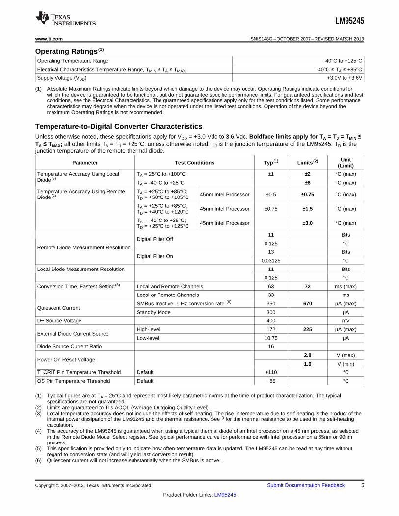
Temperature-to-Digital Converter CharacteristicsUnless otherwise noted, these specifications apply for VDD = +3.0 Vdc to 3.6 Vdc. Boldface limits apply for TA = TJ = TMIN ≤TA ≤ TMAX; all other limits TA = TJ = +25°C, unless otherwise noted. TJ is the junction temperature of the LM95245. TD is thejunction temperature of the remote thermal diode.
UnitParameter Test Conditions Typ (1) Limits (2)(Limit)
Temperature Accuracy Using Local TA = 25°C to +100°C ±1 ±2 °C (max)Diode (3)
TA = -40°C to +25°C ±6 °C (max)
Temperature Accuracy Using Remote TA = +25°C to +85°C; 45nm Intel Processor ±0.5 ±0.75 °C (max)Diode (4) TD = +50°C to +105°C
TA = +25°C to +85°C; 45nm Intel Processor ±0.75 ±1.5 °C (max)TD = +40°C to +120°C
TA = -40°C to +25°C; 45nm Intel Processor ±3.0 °C (max)TD = +25°C to +125°C
11 BitsDigital Filter Off
0.125 °CRemote Diode Measurement Resolution
13 BitsDigital Filter On
0.03125 °C
Local Diode Measurement Resolution 11 Bits
0.125 °C
Conversion Time, Fastest Setting (5) Local and Remote Channels 63 72 ms (max)
Local or Remote Channels 33 ms
SMBus Inactive, 1 Hz conversion rate (6) 350 670 µA (max)Quiescent Current
Standby Mode 300 µA
D− Source Voltage 400 mV
High-level 172 225 µA (max)External Diode Current Source
Low-level 10.75 µA
Diode Source Current Ratio 16
2.8 V (max)Power-On Reset Voltage
1.6 V (min)
T_CRIT Pin Temperature Threshold Default +110 °C
OS Pin Temperature Threshold Default +85 °C
(1) Typical figures are at TA = 25°C and represent most likely parametric norms at the time of product characterization. The typicalspecifications are not guaranteed.
(2) Limits are guaranteed to TI's AOQL (Average Outgoing Quality Level).(3) Local temperature accuracy does not include the effects of self-heating. The rise in temperature due to self-heating is the product of the
internal power dissipation of the LM95245 and the thermal resistance. See () for the thermal resistance to be used in the self-heatingcalculation.
(4) The accuracy of the LM95245 is guaranteed when using a typical thermal diode of an Intel processor on a 45 nm process, as selectedin the Remote Diode Model Select register. See typical performance curve for performance with Intel processor on a 65nm or 90nmprocess.
(5) This specification is provided only to indicate how often temperature data is updated. The LM95245 can be read at any time withoutregard to conversion state (and will yield last conversion result).
(6) Quiescent current will not increase substantially when the SMBus is active.
Copyright © 2007–2013, Texas Instruments Incorporated Submit Documentation Feedback 5
Product Folder Links: LM95245

LM95245
SNIS148G –OCTOBER 2007–REVISED MARCH 2013 www.ti.com
Logic Electrical Characteristics
Digital DC CharacteristicsUnless otherwise noted, these specifications apply for VDD= +3.0 Vdc to 3.6 Vdc. Boldface limits apply for TA = TJ = TMIN toTMAX; all other limits TA= TJ= +25°C, unless otherwise noted.
UnitParameter Test Conditions Typ (1) Limits (2)(Limit)
SMBDAT, SMBCLK INPUTS
VIN(1) Logical “1” Input Voltage 2.1 V (min)
VIN(0) Logical “0” Input Voltage 0.8 V (max)
VIN(HYST) SMBDAT and SMBCLK Digital Input 400 mVHysteresis
IIN(1) Logical “1” Input Current VIN = VDD −0.005 −10 µA (max)
IIN(0) Logical “0” Input Current VIN = 0 V 0.005 +10 µA (max)
CIN Input Capacitance 5 pF
A0 DIGITAL INPUT
VIH Input High Voltage 0.90 × VDD V (min)
0.57 × VDD V (max)VIM Input Middle Voltage
0.43 × VDD V (min)
VIL Input Low Voltage 0.10 × VDD V (max)
IIN(1) Logical “1” Input Current VIN = VDD −0.005 −10 µA (max)
IIN(0) Logical “0” Input Current VIN = 0 V 0.005 +10 µA (max)
CIN Input Capacitance 5 pF
SMBDAT, T_CRIT, OS DIGITAL OUTPUTS
IOH High Level Output Leakage Current VOUT = VDD 10 µA (max)
VOL(T_CRIT, OS) T_CRIT, OS Low Level Output Voltage IOL = 6 mA 0.4 V (max)
IOL = 4 mA 0.4 V (max)VOL(SMBDAT) SMBDAT Low Level Output Voltage IOL = 6 mA 0.6 V (max)
COUT Digital Output Capacitance 5 pF
(1) Typical figures are at TA = 25°C and represent most likely parametric norms at the time of product characterization. The typicalspecifications are not guaranteed.
(2) Limits are guaranteed to TI's AOQL (Average Outgoing Quality Level).
6 Submit Documentation Feedback Copyright © 2007–2013, Texas Instruments Incorporated
Product Folder Links: LM95245

VIH
VIL
SMBCLK
P
S
VIH
VIL
SMBDAT
tBUFtHD;STA
tLOW
tR
tHD;DAT
tHIGH
tF
tSU;DATtSU;STA tSU;STO
PS
LM95245
www.ti.com SNIS148G –OCTOBER 2007–REVISED MARCH 2013
SMBus Digital Switching CharacteristicsUnless otherwise noted, these specifications apply for VDD= +3.0 Vdc to +3.6 Vdc, CL (load capacitance) on output lines = 80pF. Boldface limits apply for TA = TJ = TMIN to TMAX; all other limits TA = TJ = +25°C, unless otherwise noted.The switching characteristics of the LM95245 fully meet or exceed the published specifications of the SMBus version 2.0. Thefollowing parameters are the timing relationships between SMBCLK and SMBDAT signals related to the LM95245. Theyadhere to, but are not necessarily, the SMBus specifications.
UnitParameter Test Conditions Typ (1) Limits (2)(Limit)
100 kHz (max)fSMB SMBus Clock Frequency 10 kHz (min)
4.7 µs (min)tLOW SMBus Clock Low Time from VIN(0)max to VIN(0)max 25 ms (max)
tHIGH SMBus Clock High Time from VIN(1)min to VIN(1)min 4.0 µs (min)
tR,SMB SMBus Rise Time (3) 1 µs (max)
tF,SMB SMBus Fall Time (4) 0.3 µs (max)
CL = 400 pF,tOF Output Fall Time 250 ns (max)IO = 3 mA, (4)
SMBDAT and SMBCLK Time Low for Reset of 25 ms (min)tTIMEOUT Serial Interface (5) 35 ms (max)
tSU;DAT Data In Setup Time to SMBCLK High 250 ns (min)
300 ns (min)tHD;DAT Data Out Stable after SMBCLK Low 1075 ns (max)
Start Condition SMBDAT Low to SMBCLK LowtHD;STA (Start condition hold before the first clock falling 100 ns (min)
edge)
Stop Condition SMBCLK High to SMBDAT LowtSU;STO 100 ns (min)(Stop Condition Setup)
SMBus Repeated Start-Condition Setup Time,tSU;STA 0.6 µs (min)SMBCLK High to SMBDAT Low
SMBus Free Time Between Stop and StarttBUF 1.3 µs (min)Conditions
(1) Typical figures are at TA = 25°C and represent most likely parametric norms at the time of product characterization. The typicalspecifications are not guaranteed.
(2) Limits are guaranteed to TI's AOQL (Average Outgoing Quality Level).(3) The output rise time is measured from (VIN(0)max - 0.15V) to (VIN(1)min + 0.15V).(4) The output fall time is measured from (VIN(1)min + 0.15V) to (VIN(0)max - 0.15V).(5) Holding the SMBDAT and/or SMBCLK lines Low for a time interval greater than tTIMEOUT will reset the LM95245's SMBus state machine,
therefore setting SMBDAT and SMBCLK pins to a high impedance state.
Figure 2. SMBus Communication
Copyright © 2007–2013, Texas Instruments Incorporated Submit Documentation Feedback 7
Product Folder Links: LM95245

LM95245
SNIS148G –OCTOBER 2007–REVISED MARCH 2013 www.ti.com
Typical Performance Characteristics
Thermal Diode Capacitor or PCB Leakage Current Remote Temperature Reading Sensitivity toEffect Remote Diode Temperature Reading Thermal Diode Filter Capacitance, TruTherm Enabled
Figure 3. Figure 4.
Intel Processor on 45nm,Conversion Rate Effect on 65nm, or 90 nm Porcess
Average Power Supply Current Thermal Diode Performance Comparison
Figure 5. Figure 6.
8 Submit Documentation Feedback Copyright © 2007–2013, Texas Instruments Incorporated
Product Folder Links: LM95245

LM95245
www.ti.com SNIS148G –OCTOBER 2007–REVISED MARCH 2013
FUNCTIONAL DESCRIPTION
The LM95245 is a temperature sensor that measures Local and Remote temperature zones. The LM95245 usesa ΔVbe temperature sensing method. A differential voltage, representing temperature, is digitized using a Sigma-Delta analog to digital converter. TruTherm BJT (Transistor) Beta Compensation Technology allows theLM95245 to accurately sense the temperature of a thermal diode found on die fabricated using a sub-micronprocess. For more information on TruTherm Technology see Applications Hints . The LM95245 is compatiblewith the serial SMBus version 2.0 two-wire serial interface.
The LM95245 has OS and TCRIT open-drain digital outputs that indicate the state of the local and remotetemperature readings when compared to user-programmable limits. If enabled, the local temperature iscompared to the user-programmable Local Shared OS and TCRIT Limit Register (Default Value = 85°C). Thecomparison result can trigger the T_CRIT pin and/or the OS pin depending on the settings of the Local TCRITMask and OS Mask bits found in Configuration Register 1. The comparison result can also be read back fromStatus Register 1. If enabled, the remote temperature is compared to the user-programmable Remote TCRITLimit Register (Default Value = 110°C), and the Remote OS Limit Register (Default Value = 85°C) values. Thecomparison result can trigger the T_CRIT pin and/or the OS pin depending on the settings of ConfigurationRegister 1. The following table describes the default temperature settings for each measured temperature thattriggers T_CRIT and/or OS pins:
Output Pin Remote, °C Local, °C
T_CRIT 110 85
OS 85 85
The following table describes the limit register mapping to the T_CRIT and/or OS pins:
Output Pin Remote Local
T_CRIT Remote TCRIT Limit Local Shared OS/TCRIT Limit
OS Remote OS Limit Local Shared OS/TCRIT Limit
The T_CRIT and OS outputs are open-drain, active low.
The remote temperature readings support a programmable digital filter. Based on the settings in ConfigurationRegister 2 a digital filter can be turned on to improve the noise performance of the remote temperature as well asto increase the resolution of the temperature reading. If the filter is enabled the filtered readings are used forTCRIT and OS comparisons. The LM95245 may be placed in low power consumption (Standby) mode by settingthe STOP/RUN bit found in Configuration Register 1. In the Standby mode, the LM95245’s SMBus interfaceremains active while all circuitry not required is turned off. In the Standby mode the host can trigger one round ofconversions by writing to the One-Shot Register. The value written into this register is not kept. Local andRemote temperatures will be converted once and the T_CRIT and OS pins will reflect the comparison resultsbased on this set of conversions results.
All the temperature readings are in 16-bit left-justified word format. The 10-bit plus sign local temperature readingis contained in two 8-bit registers: Local Temp MSB and Local Temp LSB Registers. The remote temperaturesupports both a 13-bit unsigned and a 12-bit plus sign format. These readings are available in theircorresponding registers as described in Table 8. The lower 2-bits of the remote temperature reading will containtemperature information only if the digital filter is enabled. If the digital filter is disabled, these two bits will readback 0.
The signed and unsigned remote temperature readings are available simultaneously in separate registers,therefore allowing both negative temperatures and temperatures 128°C and above to be measured.
All Limit Registers support unsigned temperature format with 1°C LSb resolution. The Local Shared TCRIT andOS Limit Register is 7 bits for limits between 0°C and 127°C. The Remote Temperature TCRIT and OS LimitRegisters are 8 bits each for limits between 0°C and 255°C.
Copyright © 2007–2013, Texas Instruments Incorporated Submit Documentation Feedback 9
Product Folder Links: LM95245

LM95245
SNIS148G –OCTOBER 2007–REVISED MARCH 2013 www.ti.com
CONVERSION SEQUENCE
In the power-up default state the LM95245 takes a maximum of 1 second to convert the Local Temperature,Remote Temperature, and to update all of its registers. Only during the conversion process is the Busy bit (D7) inStatus Register 1 (02h) high. These conversions are addressed in a round-robin sequence. The conversion ratemay be modified by the Conversion Rate bits found in the Conversion Rate Register (R/W: 04h/0Ah). When theconversion rate is modified a delay is inserted between conversions, the actual maximum conversion timeremains at 72 ms. Different conversion rates will cause the LM95245 to draw different amounts of supply currentas shown in Figure 7.
Figure 7. Conversion Rate Effect on Power Supply Current
POWER-ON-DEFAULT STATES
LM95245 always powers up to these known default states. The LM95245 remains in these states until after thefirst conversion.1. Command Register set to 00h2. Conversion Rate register defaults to 02h (1 second).3. Local Temperature set to 0°C until the end of the first conversion4. Remote Diode Temperature set to 0°C until the end of the first conversion5. Remote OS limit default is 55h (85 °C).6. Local Shared and TCRIT limit default is 55h (85 °C).7. Remote TCRIT limit default is 6Eh (110 °C).8. Remote Offset High and Low bytes default to 00h.9. Configuration Register 1 defaults to 00h. This sets the LM95245 as follows:
(a) The STOP/RUN defaults to the active/converting mode.(b) The Local and Remote TCRIT and OS Masks are reset to 0.
10. Configuration Register 2 defaults to 1Fh. This sets the LM95245 as follows:(a) Remote Diode digital filter defaults on.(b) The Remote Diode mode defaults to a typical Intel processor on 45/65/90 nm process.(c) Diode Fault Mask bit for TCRIT defaults to 1.(d) Diode Fault Mask bit for OS defaults to 0.(e) Pin 6 Function defaults to Address Input function (A0).
10 Submit Documentation Feedback Copyright © 2007–2013, Texas Instruments Incorporated
Product Folder Links: LM95245

LM95245
www.ti.com SNIS148G –OCTOBER 2007–REVISED MARCH 2013
SMBus INTERFACE
The LM95245 operates as a slave on the SMBus, so the SMBCLK line is an input and the SMBDAT line isbidirectional. The LM95245 never drives the SMBCLK line and it does not support clock stretching. According toSMBus specifications, the LM95245 has a 7-bit slave address. Three SMBus addresses can be selected byconnecting pin 6 (A0) to either Low, Mid-Supply or High voltages. The address selection table below shows twosets of possible selections for the LM95245CIMM and the LM95245CIMM-1.
LM95245CIMM SMBus Device LM95245CIMM-1 SMBusAddress Device AddressState of the A0 Pin
HEX Binary HEX Binary
Low 18 001 1000 19 001 1001
Mid-Supply 29 010 1001 29 010 1001
High 4C 100 1100 4D 100 1100
The OS/A0 pin, after power-up, defaults as an address select input pin (A0). After power-up, the OS/A0 pin canonly be programmed as an OS output when it is in the “High” state. Therefore, 4Ch is the only valid slaveaddress that can be used when the OS/A0 pin is programmed to function as an OS output. When the OS/A0 pinis programmed to function as an A0 input the LM95245 will immediately detect the state of this pin to determineits SMBus slave address. The LM95245 does not latch the state of the A0 pin when it is functioning as an input.If the OS/A0 pin is not used it must be externally connected through hardware to some state, as shown in thetable, in order to guarantee that the proper address is selected and not in an indeterminate state. The OS/A0does not have an internal pull-up.
DIGITAL FILTER
In order to suppress erroneous remote temperature readings due to noise, the LM95245 incorporates a digitalfilter for the Remote Temperature Channel. The filter is accessed in the Configuration Register 2, bits D2 (FE1)and D1(FE0). The filter can be set according to the following table.
FE1 FE0 Filter Setting
0 0 Filter Off
0 1 Reserved
1 0 Reserved
1 1 Filter On
Filter Impulse and Step Response Curves depicts the filter output in response to a step input and an impulseinput.
Filter Impulse and Step Response Curves
Figure 8. Seventeen and Fifty Degree Step Figure 9. Impulse Response with Input TransientsResponse Less Than 4°C
Copyright © 2007–2013, Texas Instruments Incorporated Submit Documentation Feedback 11
Product Folder Links: LM95245

0 50 100 150 200
SAMPLE NUMBER
TE
MP
ER
AT
UR
E (
o C)
LM95245 with Filter On
LM95245 withFilter Off
25
27
29
31
33
35
37
39
41
43
45
LM95245
SNIS148G –OCTOBER 2007–REVISED MARCH 2013 www.ti.com
Figure 10. Impuse Response with Input Transients Greater Than 4°C
Figure 11 shows the filter in use in a typical Intel processor on a 45/65/90 nm process system. Note that the twocurves have been purposely offset for clarity. Inserting the filter does not induce an offset as shown.
Figure 11. Digital Filter Response in a Typical Intel Processor on a 45nm, 65 nm or 90 nm Process(Filter Curves Were Purposely Offset for Clarity)
TEMPERATURE DATA FORMAT
Temperature data can only be read from the Local and Remote Temperature registers.
Remote temperature data with the digital filter off is represented by an 10-bit plus sign, two's complement wordand 11-bit unsigned binary word with an LSb (Least Significant Bit) equal to 0.125°C. The data format is a leftjustified 16-bit word available in two 8-bit registers. Unused bits report "0".
Remote temperature data with the digital filter on is represented by a 12-bit plus sign, two's complement wordand 13-bit unsigned binary word with an LSb (Least Significant Bit) equal to 0.03125°C (1/32°C). The data formatis a left justified 16-bit word available in two 8-bit registers. Unused bits report "0".
Table 3. 11-Bit, 2's Complement (10-Bit Plus Sign)
Digital OutputTemperature
Binary Hex
+125°C 0111 1101 0000 0000 7D00h
+25°C 0001 1001 0000 0000 1900h
+1°C 0000 0001 0000 0000 0100h
+0.125°C 0000 0000 0010 0000 0020h
0°C 0000 0000 0000 0000 0000h
12 Submit Documentation Feedback Copyright © 2007–2013, Texas Instruments Incorporated
Product Folder Links: LM95245

LM95245
www.ti.com SNIS148G –OCTOBER 2007–REVISED MARCH 2013
Table 3. 11-Bit, 2's Complement (10-Bit PlusSign) (continued)
Digital OutputTemperature
Binary Hex
−0.125°C 1111 1111 1110 0000 FFE0h
−1°C 1111 1111 0000 0000 FF00h
−25°C 1110 0111 0000 0000 E700h
−55°C 1100 1001 0000 0000 C900h
Table 4. 11-Bit, Unsigned Binary
Digital OutputTemperature
Binary Hex
+255.875°C 1111 1111 1110 0000 FFE0h
+255°C 1111 1111 0000 0000 FF00h
+201°C 1100 1001 0000 0000 C900h
+125°C 0111 1101 0000 0000 7D00h
+25°C 0001 1001 0000 0000 1900h
+1°C 0000 0001 0000 0000 0100h
+0.125°C 0000 0000 0010 0000 0020h
0°C 0000 0000 0000 0000 0000h
Table 5. 13-Bit, 2's Complement (12-Bit Plus Sign)
Digital OutputTemperature
Binary Hex
+125°C 0111 1101 0000 0000 7D00h
+25°C 0001 1001 0000 0000 1900h
+1°C 0000 0001 0000 0000 0100h
+0.03125°C 0000 0000 0000 1000 0008h
0°C 0000 0000 0000 0000 0000h
−0.03125°C 1111 1111 1111 1000 FFF8h
−1°C 1111 1111 0000 0000 FF00h
−25°C 1110 0111 0000 0000 E700h
−55°C 1100 1001 0000 0000 C900h
Table 6. 13-Bit, Unsigned Binary
Digital OutputTemperature
Binary Hex
+255.875°C 1111 1111 1110 0000 FFE0h
+255°C 1111 1111 0000 0000 FF00h
+201°C 1100 1001 0000 0000 C900h
+125°C 0111 1101 0000 0000 7D00h
+25°C 0001 1001 0000 0000 1900h
+1°C 0000 0001 0000 0000 0100h
+0.03125°C 0000 0000 0000 1000 0008h
0°C 0000 0000 0000 0000 0000h
Local Temperature data is represented by a 10-bit plus sign, two's complement word with an LSb (LeastSignificant Bit) equal to 0.125°C. The data format is a left justified 16-bit word available in two 8-bit registers.Unused bits will always report "0". Local temperature readings greater than +127.875°C are clamped to+127.875°C, they will not roll-over to negative temperature readings.
Copyright © 2007–2013, Texas Instruments Incorporated Submit Documentation Feedback 13
Product Folder Links: LM95245

Hysteresis
T_CRITOutput Pin
Remote TCRIT Limit
RemoteTemperature
Status bit RCRIT
Remote TCRIT Limit - Hysteresis
LM95245
SNIS148G –OCTOBER 2007–REVISED MARCH 2013 www.ti.com
Table 7. 11-Bit, 2's Complement (10-Bit Plus Sign)
Digital OutputTemperature
Binary Hex
+125°C 0111 1101 0000 0000 7D00h
+25°C 0001 1001 0000 0000 1900h
+1°C 0000 0001 0000 0000 0100h
+0.125°C 0000 0000 0010 0000 0020h
0°C 0000 0000 0000 0000 0000h
−0.125°C 1111 1111 1110 0000 FFE0h
−1°C 1111 1111 0000 0000 FF00h
−25°C 1110 0111 0000 0000 E700h
−55°C 1100 1001 0000 0000 C900h
SMBDAT OPEN-DRAIN OUTPUT
The SMBDAT output is an open-drain output and does not have internal pull-ups. A “high” level will not beobserved on this pin until pull-up current is provided by some external source, typically a pull-up resistor. Choiceof resistor value depends on many system factors but, in general, the pull-up resistor should be as large aspossible without effecting the SMBus desired data rate. This will minimize any internal temperature readingerrors due to internal heating of the LM95245. The maximum resistance of the pull-up to provide a 2.1V highlevel, based on LM95245 specification for High Level Output Current with the supply voltage at 3.0V, is 82 kΩ(5%) or 88.7 kΩ (1%).
T_CRIT OUTPUT AND TCRIT LIMIT
The LM95245's T_CRIT pin is an active-low open-drain output that is triggered when the local and/or the remotetemperature conversion is above the limits defined by the Remote and/or Local Limit registers. The state of theT_CRIT pin will return to the HIGH state when both the Local and Remote temperatures are below the valuesprogrammed into the Limit Registers less the value in the Common Hysteresis Register. Additionally, if theremote temperature exceeds the value in the Remote TCRIT Limit Register the Status Bit for Remote TCRIT(RTCRIT), in Status Register 1, is set to 1. In the same way if the local temperature exceeds the value in theLocal Shared OS and TCRIT Limit Register the Status Bit for the Shared Local OS and TCRIT (LOC) bit inStatus Register 1 is set to 1.The T_CRIT output and the Status Register flags are updated after every Local andRemote temperature conversion. See Figure 12
Figure 12. T_CRIT Comparator Temperature Response Diagram
14 Submit Documentation Feedback Copyright © 2007–2013, Texas Instruments Incorporated
Product Folder Links: LM95245

D7 D6 D5 D4 D3 D2 D1 D0
1 9 1 9
Ackby
LM95245
Start byMaster
R/W
Frame 1Serial Bus Address Byte
Frame 2Command Byte
Ack byLM95245
SMBCLK
SMBDAT A5 A3 A2 A0A6 A4 A1
Stopby
Master
Hysteresis
OSOutput Pin
Remote OS Limit
RemoteTemperature
Status bit ROS
Remote OS Limit - Hysteresis
LM95245
www.ti.com SNIS148G –OCTOBER 2007–REVISED MARCH 2013
OS OUTPUT AND OS LIMIT
The LM95245's OS/A0 pin is selected as an OS digital output as described in SMBus INTERFACE. As an OSpin, it is activated whenever the local and/or remote temperature conversion is above the limits defined by theLimit registers. If the remote temperature exceeds the value in the Remote OS Limit Register the Status Bit forRemote OS (ROS) in Status Register 1 is set to 1. In the same way if the local temperature exceeds the value inthe Local Shared OS and TCRIT Limit Register the Status Bit for the Shared Local OS and TCRIT (LOC) bit inStatus Register 1 is set to 1. The state of the T_CRIT pin output will return to the HIGH state when both theLocal and Remote temperatures are below the values programmed into the Limit Registers less the value in theCommon Hysteresis Register. The OS output and the Status Register flags are updated after every Local andRemote temperature conversion. See Figure 13.
Figure 13. OS Temperature Response Diagram
DIODE FAULT DETECTION
The LM95245 is equipped with operational circuitry designed to detect fault conditions concerning the remotediodes. In the event that the D+ pin is detected as shorted to GND, VDD or D+ is floating, the RemoteTemperature reading is –128.000 °C if signed format is selected and +255.875 °C if unsigned format is selected.In addition, the Status Register 1 bit D2 is set.
COMMUNICATING with the LM95245
SMBus Timing Diagrams for Access of Data (Default Address of 4Ch is Shown)
Figure 14. (a) Serial Bus Write to the Internal Command Register
Copyright © 2007–2013, Texas Instruments Incorporated Submit Documentation Feedback 15
Product Folder Links: LM95245

D7 D6 D5 D4 D3 D2 D1 D0
1 9 1 9
Ackby
LM95245
Start byMaster
RepeatStart byMaster
Frame 1Serial Bus Address Byte
Frame 2Command Byte
Ackby
LM95245
D7 D6 D5 D4 D3 D2 D1 D0
1 9 1 9
Ackby
LM95245Frame 3
Serial Bus Address ByteFrame 4
Data Byte from the LM95245
No Ackby
Master
Stopby
Master
SMBCLK
SMBDAT
SMBCLK (Continued)
SMBDAT (Continued)
R/WA5 A3 A2 A0A6 A4 A1
R/WA5 A3 A2 A0A6 A4 A1
D7 D6 D5 D4 D3 D2 D1 D0
1 9 1 9
Ackby
LM95245
Start byMaster
Frame 1Serial Bus Address Byte
Frame 2Data Byte from the LM95245
NoAckby
Master
SMBCLK
SMBDAT
Stopby
Master
R/WA5 A3 A2 A0A6 A4 A1
D7 D6 D5 D4 D3 D2 D1 D0
1 9 1 9
Ackby
LM95245
Start byMaster
Frame 1Serial Bus Address Byte
Frame 2Command Byte
Ackby
LM95245
D7 D6 D5 D4 D3 D2 D1 D0
1 9
Frame 3Data Byte
Ack by LM95245
Stopby
Master
SMBCLK
SMBDAT
SMBCLK (Continued)
SMBDAT (Continued)
R/WA5 A3 A2 A0A6 A4 A1
LM95245
SNIS148G –OCTOBER 2007–REVISED MARCH 2013 www.ti.com
Figure 15. (b) Serial Bus Write to the Internal Command Register Followed by a Data Byte
Figure 16. (c) Serial Bus byte Read from a Register with the Internal Command Register Preset toDesired Value
Figure 17. (d) Serial Bus Write followed by a Repeat Start and Immediate Read
The data registers in the LM95245 are selected by the Command Register. At power-up the Command Registeris set to “00”, the location for the Read Local Temperature Register. The Command Register latches the lastlocation it was set to. Each data register in the LM95245 falls into one of four types of user accessibility:1. Read only2. Write only
16 Submit Documentation Feedback Copyright © 2007–2013, Texas Instruments Incorporated
Product Folder Links: LM95245

LM95245
www.ti.com SNIS148G –OCTOBER 2007–REVISED MARCH 2013
3. Write/Read same address4. Write/Read different address
A Write to the LM95245 will always include the address byte and the command byte. A write to any registerrequires one data byte.
Reading the LM95245 can take place either of two ways:1. If the location latched in the Command Register is correct (most of the time it is expected that the Command
Register will point to one of the Read Temperature Registers because that will be the data most frequentlyread from the LM95245), then the read can simply consist of an address byte, followed by retrieving the databyte.
2. If the Command Register needs to be set, then an address byte, command byte, repeat start, and anotheraddress byte will accomplish a read.
The data byte has the most significant bit first. At the end of a read, the LM95245 can accept either acknowledgeor No Acknowledge from the Master (No Acknowledge is typically used as a signal for the slave that the Masterhas read its last byte). When retrieving all 11 bits from a previous remote diode temperature measurement, themaster must insure that all 11 bits are from the same temperature conversion. This may be achieved by readingthe MSB register first. The LSB will be locked after the MSB is read. The LSB will be unlocked after being read. Ifthe user reads MSBs consecutively, each time the MSB is read, the LSB associated with that temperature will belocked in and override the previous LSB value locked-in.
SERIAL INTERFACE RESET
In the event that the SMBus Master is RESET while the LM95245 is transmitting on the SMBDAT line, theLM95245 must be returned to a known state in the communication protocol. This may be done in one of twoways:1. When SMBDAT is LOW, the LM95245 SMBus state machine resets to the SMBus idle state if either
SMBDAT or SMBCLK are held low for more than 35 ms (tTIMEOUT). Note that according to SMBusspecification 2.0 all devices are to timeout when either the SMBCLK or SMBDAT lines are held low for 25 -35 ms. Therefore, to insure a timeout of all devices on the bus the SMBCLK or SMBDAT lines must be heldlow for at least 35 ms.
2. When SMBDAT is HIGH, have the master initiate an SMBus start. The LM95245 will respond properly to anSMBus start condition at any point during the communication. After the start the LM95245 will expect anSMBus Address address byte.
ONE-SHOT CONVERSION
The One-Shot register is used to initiate a single conversion and comparison cycle when the device is in standbymode, after which the device returns to standby. This is not a data register and it is the write operation thatcauses the one-shot conversion. The data written to this address is irrelevant and is not stored. A zero willalways be read from this register.
Copyright © 2007–2013, Texas Instruments Incorporated Submit Documentation Feedback 17
Product Folder Links: LM95245

LM95245
SNIS148G –OCTOBER 2007–REVISED MARCH 2013 www.ti.com
LM95245 REGISTERS
Command register selects which registers will be read from or written to. Data for this register should betransmitted during the Command Byte of the SMBus write communication. POR means Power-On Reset.
P0-P7: Command
P7 P6 P5 P4 P3 P2 P1 P0
Command
Table 8. Register Summary
Read Write No. POR Read/Register Name Address Address of Default DescriptionWrite(Hex) (Hex) bits (Hex)
TEMPERATURE SIGNED VALUE REGISTERS
Local Temp MSB 0x00 NA 8 − RO Supports SMBus byte
Local Temp LSB 0x30 NA 3 − RO All unused bits are reported as "0".
Remote Temp MSB – Signed 0x01 NA 8 − RO Supports SMBus byte
Remote Temp LSB – Signed 0x10 NA 5/3 − RO All unused bits are reported as "0".
TEMPERATURE UNSIGNED VALUE REGISTERS
Remote Temp MSB – 0x31 NA 8 − RO Supports SMBus byte readsUnsigned
Remote Temp LSB – 0x32 NA 5/3 − RO All unused bits are reported as "0".Unsigned
DIODE CONFIGURATION REGISTERS
Filter Enable, Diode Model Select, Diode FaultConfiguration Register 2 0xBF 0xBF 5 0x1F R/W Mask; Pin 6 OS/A0 function select
Remote Offset 0x11 0x11 8 0x00 R/W 2's ComplementHigh Byte
Remote Offset 2's Complement0x12 0x12 3 0x00 R/WLow Byte All unused bits are reported as "0".
GENERAL CONFIGURATION REGISTERS
0x03/ 0x09/ STOP/RUN , Remote TCRIT mask, Remote OSConfiguration Register 1 5 0x00 R/W0x09 0x03 mask, Local TCRIT mask, Local OS mask
Conversion Rate 0x04/0x0A 0x04/0x0A 2 0x02 R/W Continuous or specific settings
A write to this register activates one conversion ifOne-Shot NA 0x0F − − WO STOP/RUN bit = 1.
STATUS REGISTERS
Status Register 1 0x02 NA 5 − RO Busy bit, and status bits
Status Register 2 0x33 NA 2 − RO Not Ready bit
LIMIT REGISTERS
0x07/ 0x0D/ Unsigned 0 to 255 °CRemote OS Limit 8 0x55 R/W0x0D 0x07 Default 85 °C
Local Shared OS and T_Crit Unsigned 0 to 127 °C0x20 0x20 7 0x55 R/WLimit Default 85 °C
Unsigned 0 to 255 °CRemote T_Crit Limit 0x19 0x19 8 0x6E R/W Default 110 °C
Common Hysteresis 0x21 0x21 5 0x0A R/W up to 31°C
IDENTIFICATION REGISTERS
Manufacturer ID 0xFE 0x01 RO Always returns 0x01
Revision ID 0xFF 0xB3 RO Returns revision number.
18 Submit Documentation Feedback Copyright © 2007–2013, Texas Instruments Incorporated
Product Folder Links: LM95245

LM95245
www.ti.com SNIS148G –OCTOBER 2007–REVISED MARCH 2013
LOCAL and REMOTE MSB and LSB TEMPERATURE REGISTERS
Table 9. Local Temperature MSB(Read Only Address 00h)
10-bit plus sign format:
BIT D7 D6 D5 D4 D3 D2 D1 D0
Value SIGN 64 32 16 8 4 2 1
Temperature Data: LSb = 1°C.
Table 10. Local Temperature LSB(Read Only Address 30h)
10-bit plus sign format:
BIT D7 D6 D5 D4 D3 D2 D1 D0
Value 0.5 0.25 0.125 0 0 0 0 0
Temperature Data: LSb = 0.125°C.
Table 11. Signed Remote Temperature MSB(Read Only Address 01h)
12-bit plus sign format:
BIT D7 D6 D5 D4 D3 D2 D1 D0
Value SIGN 64 32 16 8 4 2 1
Temperature Data: LSb = 1°C.
Table 12. Signed Remote Temperature LSB, Filter On(Read Only Address 10h)
12-bit plus sign binary formats with filter on:
BIT D7 D6 D5 D4 D3 D2 D1 D0
Value 0.5 0.25 0.125 0.0625 0.03125 0 0 0
Table 13. Signed Remote Temperature LSB, Filter Off(Read Only Address 10h)
12-bit plus sign binary formats with filter off:
BIT D7 D6 D5 D4 D3 D2 D1 D0
Value 0.5 0.25 0.125 0 0 0 0 0
Temperature Data: LSb = 0.125°C filter off or 0.03125°C filter on.
Table 14. Unsigned Remote Temperature MSB(Read Only Address 31h)
13-bit unsigned format:
BIT D7 D6 D5 D4 D3 D2 D1 D0
Value 128 64 32 16 8 4 2 1
Temperature Data: LSb = 1°C.
Table 15. Unsigned Remote Temperature LSB, Filter On(Read Only Address 32h)
13-bit unsigned binary formats with filter on:
BIT D7 D6 D5 D4 D3 D2 D1 D0
Value 0.5 0.25 0.125 0.0625 0.03125 0 0 0
Copyright © 2007–2013, Texas Instruments Incorporated Submit Documentation Feedback 19
Product Folder Links: LM95245

LM95245
SNIS148G –OCTOBER 2007–REVISED MARCH 2013 www.ti.com
Table 16. Unsigned Remote Temperature LSB, Filter Off(Read Only Address 32h)
13-bit unsigned binary formats with filter off:
BIT D7 D6 D5 D4 D3 D2 D1 D0
Value 0.5 0.25 0.125 0 0 0 0 0
Temperature Data: LSb = 0.125°C filter off or 0.03125°C filter on.
For data synchronization purposes, the MSB register should be read first if the user wants to read both MSB and LSB registers. The LSBwill be locked after the MSB is read. The LSB will be unlocked after being read. If the user reads MSBs consecutively, each time the MSBis read, the LSB associated with that temperature will be locked in and override the previous LSB value locked-in.
DIODE CONFIGURATION REGISTERS
Table 17. Configuration Register 2(Read/write Address BFh):
D7 D6 D5 D4 D3 D2 D1 D0
0 OS/A0 Function Select OS Fault Mask T_CRIT Mask TruTherm Select RFE1 RFE0 1
Bits Name Description
7 Reserved Reports "0" when read.
0: Address (A0) function is enabled6 OS/A0 Function Select 1: Over-temperature Shutdown (OS) is enabled
0: Off5 Diode Fault Mask for OS 1: On
0: Off4 Diode Fault Mask for T_CRIT 1: On
0: Selects Diode Model 2, MMBT3904, with TruTherm technology disabled. Note,Remote Diode TruTherm performance in this mode is not guaranteed.3 Mode Select 1: Selects Diode Model 1, A typical Intel Processor, with 45nm, 65 nm or 90 nm
technology, and TruTherm technology enabled.
00: Filter Disable01: Reserved2-1 Remote Filter Enable 10: Reserved11: Filter Enable
0 Reserved Reports "1" when read.
Power up default is 1Fh.
Table 18. Remote Offset High Byte (2's Complement)(R/W Address 11h)
10-bit plus sign format:
BIT D7 D6 D5 D4 D3 D2 D1 D0
Value SIGN 64 32 16 8 4 2 1
Power up default is 00h.
Table 19. Remote Offset Low Byte (2's Complement)(R/W Address 12h)
10-bit plus sign format:
BIT D7 D6 D5 D4 D3 D2 D1 D0
Value 0.50 0.25 0.125 0 0 0 0 0
Power up default is 00h. LSb = 0.125 °C.
20 Submit Documentation Feedback Copyright © 2007–2013, Texas Instruments Incorporated
Product Folder Links: LM95245

LM95245
www.ti.com SNIS148G –OCTOBER 2007–REVISED MARCH 2013
GENERAL CONFIGURATION REGISTERS
Table 20. Configuration Register 1(Read/write Address 03h/09h or 09h/03h):
D7 D6 D5 D4 D3 D2 D1 D0
0 STOP/RUN 0 Remote T_CRIT Mask Remote OS Mask Local T_CRIT Mask Local OS Mask 0
Bits Name Description
7 Reserved Reports "0" when read.
0: Active / Converting6 STOP/RUN 1: Standby
5 Reserved Reports "0" when read.
0: Off4 Remote T_CRIT Mask 1: On
0: Off3 Remote OS Mask 1: On
0: Off2 Local T_CRIT Mask 1: On
0: Off1 Local OS Mask 1: On
0 Reserved Reports "0" when read.
Power up default is 00h.
Table 21. Conversion Rate Register(Read/write Address 04h/0Ah or 0Ah/04h):
2-bit format:
BIT D7 D6 D5 D4 D3 D2 D1 D0
Value 0 0 0 0 0 0 MSb LSb
Bits Name Description
7:2 Reserved Reports "0" when read.
00: Continuous (33 ms typical when remote diode is missing or fault or 63 ms typicalwith remote diode connected)
1:0 Conversion Rate 01: 0.364 seconds10: 1 second11: 2.5 seconds
Power up default is 02h (1 second).
Table 22. One Shot Register(Write Only Address 0Fh):
Writing to this register will start one conversion if the device is in standby mode (i.e. STOP/RUN bit = 1).
Copyright © 2007–2013, Texas Instruments Incorporated Submit Documentation Feedback 21
Product Folder Links: LM95245

LM95245
SNIS148G –OCTOBER 2007–REVISED MARCH 2013 www.ti.com
STATUS REGISTERS
Table 23. Status Register 1(Read Only Address 02h):
D7 D6 D5 D4 D3 D2 D1 D0
Busy 0 0 ROS 0 Diode Fault RTCRIT LOC
Bits Name Description
7 Busy When set to "1" the part is converting.
6-5 Reserved Report "0" when read.
4 ROS Status Bit for Remote OS
3 Reserved Reports "0" when read.
2 Status bit for missing diode (Either D+ is shorted to GND, or VDD; or D+ is floating.)Diode Fault Note: The unsigned registers will report 0°C if read; the signed value registers will report
−128.000°C.
1 RTCRIT Status bit for Remote TCRIT.
0 LOC Status bit for the shared Local OS and TCRIT .
Table 24. Status Register 2(Read Only Address 33h):
D7 D6 D5 D4 D3 D2 D1 D0
Not Ready Reserved 0 0 0 0 0 0
Bits Name Description
7 Not Ready Waiting for 30 ms power-up sequence to end.
6 Reserved Can report "0" or "1" when read.
5-0 Reserved Reports "0" when read.
LIMIT REGISTERS
Table 25. Unsigned Remote OS Limit - 0°C to 255°C(Read/Write Address 07h/0Dh or 0Dh/07h):
D7 D6 D5 D4 D3 D2 D1 D0
128 64 32 16 8 4 2 1
Power on Reset default is 55h (85°C).
Table 26. Unsigned Local Shared OS and T_CRIT Limit - 0°C to 127°C(Read/Write Address 20h):
D7 D6 D5 D4 D3 D2 D1 D0
128 64 32 16 8 4 2 1
Power on Reset default is 55h (85°C).
Table 27. Unsigned Remote T_CRIT Limit - 0°C to 255°C(Read/Write Address 19h):
D7 D6 D5 D4 D3 D2 D1 D0
128 64 32 16 8 4 2 1
Power on Reset default is 6Eh (110°C).
22 Submit Documentation Feedback Copyright © 2007–2013, Texas Instruments Incorporated
Product Folder Links: LM95245

LM95245
www.ti.com SNIS148G –OCTOBER 2007–REVISED MARCH 2013
Table 28. Common Hysteresis Register(Read/Write Address 21h):
D7 D6 D5 D4 D3 D2 D1 D0
0 0 0 16 8 4 2 1
Power on Reset default is 0Ah (10°C).
IDENTIFICATION REGISTERS
Table 29. Manufacturers ID Register(Read Only Address FEh):
Always returns 01h.
D7 D6 D5 D4 D3 D2 D1 D0
0 0 0 0 0 0 0 1
Table 30. Revision ID Register(Read Only Address FFh)
Default is B3h. This register will increment by 1 every time there is a revision to the die by Texas Instruments. The initial revision bits forB3h are shown below.
D7 D6 D5 D4 D3 D2 D1 D0
1 0 1 1 0 0 1 1
Copyright © 2007–2013, Texas Instruments Incorporated Submit Documentation Feedback 23
Product Folder Links: LM95245
qkT
=Vt
= ISxK tVBEV
©§
¹·
x e««¬
ª
»»¼
º-1IF
LM95245
SNIS148G –OCTOBER 2007–REVISED MARCH 2013 www.ti.com
APPLICATIONS HINTS
The LM95245 can be applied easily in the same way as other integrated-circuit temperature sensors, and itsremote diode sensing capability allows it to be used in new ways as well. It can be soldered to a printed circuitboard, and because the path of best thermal conductivity is between the die and the pins, its temperature willeffectively be that of the printed circuit board lands and traces soldered to the LM95245's pins. This presumesthat the ambient air temperature is almost the same as the surface temperature of the printed circuit board; if theair temperature is much higher or lower than the surface temperature, the actual temperature of the LM95245 diewill be at an intermediate temperature between the surface and air temperatures. Again, the primary thermalconduction path is through the leads, so the circuit board temperature will contribute to the die temperature muchmore strongly than will the air temperature.
To measure temperature external to the LM95245's die, use a remote diode. This diode can be located on thedie of a target IC, allowing measurement of the IC's temperature, independent of the LM95245's temperature. Adiscrete diode can also be used to sense the temperature of external objects or ambient air. Remember that adiscrete diode's temperature will be affected, and often dominated, by the temperature of its leads. Most silicondiodes do not lend themselves well to this application. It is recommended that an MMBT3904 transistor base-emitter junction be used with the collector tied to the base. Accuracy using the MMBT3904 is not guaranteed. Forapplications requiring the use of the MMBT3904 use the LM95235.
The LM95245's BJT Beta Compensation TruTherm technology allows accurate sensing of integrated thermaldiodes, such as those found on most processors.
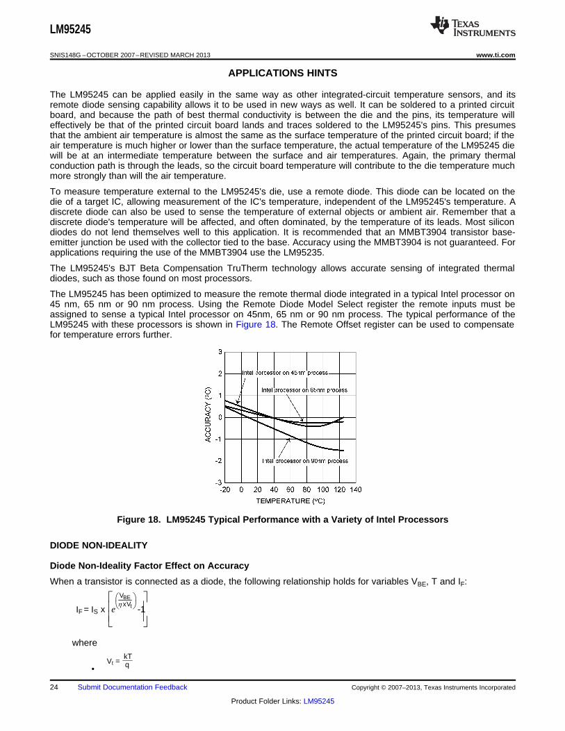
The LM95245 has been optimized to measure the remote thermal diode integrated in a typical Intel processor on45 nm, 65 nm or 90 nm process. Using the Remote Diode Model Select register the remote inputs must beassigned to sense a typical Intel processor on 45nm, 65 nm or 90 nm process. The typical performance of theLM95245 with these processors is shown in Figure 18. The Remote Offset register can be used to compensatefor temperature errors further.
Figure 18. LM95245 Typical Performance with a Variety of Intel Processors
DIODE NON-IDEALITY
Diode Non-Ideality Factor Effect on Accuracy
When a transistor is connected as a diode, the following relationship holds for variables VBE, T and IF:
where
•
24 Submit Documentation Feedback Copyright © 2007–2013, Texas Instruments Incorporated
Product Folder Links: LM95245

=Tq x ' BEV
x kK x ln ¸¹
ᬩ
§ I 2C
I 1C
¸¹
ᬩ
§T =
q x 'VBE
K x k x lnIF2
IF1
¹·
©§x
¹·
©§x= lnq
kTK'VBE
IF2
IF1
=xK tVBEV
©§
¹·
x e««¬
ª
»»¼
ºIF IS
LM95245
www.ti.com SNIS148G –OCTOBER 2007–REVISED MARCH 2013
• q = 1.6×10⁻¹⁹ Coulombs (the electron charge),• T = Absolute Temperature in Kelvin• k = 1.38×10⁻²³ joules/K (Boltzmann's constant),• η is the non-ideality factor of the process the diode is manufactured on,• IS = Saturation Current and is process dependent,• If = Forward Current through the base-emitter junction• VBE = Base-Emitter Voltage drop (1)
In the active region, the -1 term is negligible and may be eliminated, yielding the following equation
(2)
In Equation 2, η and IS are dependant upon the process that was used in the fabrication of the particular diode.By forcing two currents with a very controlled ratio(IF2 / IF1) and measuring the resulting voltage difference, it ispossible to eliminate the IS term. Solving for the forward voltage difference yields the relationship:
(3)
Solving Equation 3 for temperature yields:
(4)
Equation 4 holds true when a diode connected transistor such as the MMBT3904 is used. When this “diode”equation is applied to an integrated diode such as a processor transistor with its collector tied to GND as shownin Figure 19 it will yield a wide non-ideality spread. This wide non-ideality spread is not due to true processvariation but due to the fact that Equation 4 is an approximation.
TruTherm technology uses the transistor (BJT) equation, Equation 5, which is a more accurate representation ofthe topology of the thermal diode found in an FPGA or processor.
(5)
TruTherm should only be enabled when measuring the temperature of a transistor integrated as shown in theprocessor of Figure 19, because Equation 5 only applies to this topology.
Copyright © 2007–2013, Texas Instruments Incorporated Submit Documentation Feedback 25
Product Folder Links: LM95245

x PCBR¸¹
·:62.0=ERT Cº
¨©
§
MMBT3904
LM95245
100 pF PROCESSOR
IR
IF
ICIR
IE = IF
LM95245
100 pF
2
2
3
3
D+
D+
D-
D-
LM95245
SNIS148G –OCTOBER 2007–REVISED MARCH 2013 www.ti.com
Figure 19. Thermal Diode Current Paths
Calculating Total System Accuracy
The voltage seen by the LM95245 also includes the IFRS voltage drop of the series resistance. The non-idealityfactor, η, is the only other parameter not accounted for and depends on the diode that is used for measurement.Since ΔVBE is proportional to both η and T, the variations in η cannot be distinguished from variations intemperature. Since the non-ideality factor is not controlled by the temperature sensor, it will directly add to theinaccuracy of the sensor. For the for Intel processor on 65nm process, Intel specifies a +4.06%/−0.897%variation in η from part to part when the processor diode is measured by a circuit that assumes diode equation,Equation 4, as true. As an example, assume a temperature sensor has an accuracy specification of ±1.0°C at atemperature of 80°C (353 Kelvin) and the processor diode has a non-ideality variation of +4.06%/−0.89%. Theresulting system accuracy of the processor temperature being sensed will be:
TACC = + 1.0°C + (+4.06% of 353 K) = +15.3 °C (6)
andTACC = - 1.0°C + (−0.89% of 353 K) = −4.1 °C (7)
TrueTherm technology uses the transistor equation, Equation 4, resulting in a non-ideality spread that trulyreflects the process variation which is very small. The transistor equation non-ideality spread is ±0.39% for the65nm thermal diode. The resulting accuracy when using TruTherm technology improves to:
TACC = ±0.75°C + (±0.39% of 353 K) = ± 2.16 °C (8)
Intel does not specify the diode model ideality and series resistance of the thermal diodes on 45nm so a similarcomparison cannot be calculated, but lab experiments have shown similar improvement. For the 45nm processorthe ideality spread as specified by Intel is -0.399% to +0.699%. The resulting spread in accuracy when usingTruTherm technology with the thermal diode on Intel processors with 45nm process is:
TACC = -0.75°C + (-0.39% of 353 K) = -2.16 °C (9)
toTACC = +0.75°C + (+0.799% of 353 K) = +4.32 °C (10)
The next error term to be discussed is that due to the series resistance of the thermal diode and printed circuitboard traces. The thermal diode series resistance is specified on most processor data sheets. For Intelprocessors in 45 nm process, this is specified at 4.5Ω typical with a minimum of 3Ω and a maximum of 7Ω. TheLM95245 accommodates the typical series resistance of Intel Processor on 45 nm process. The error that is notaccounted for is the spread of the processor's series resistance. The equation used to calculate the temperatureerror due to series resistance (TER) for the LM95245 is simply:
(11)
26 Submit Documentation Feedback Copyright © 2007–2013, Texas Instruments Incorporated
Product Folder Links: LM95245

LM95245
www.ti.com SNIS148G –OCTOBER 2007–REVISED MARCH 2013
Solving Equation 11 for RPCB equal to -1.5Ω to 2.5Ω results in the additional error due to the spread in this seriesresistance of -0.93°C to +1.55°C. The spread in error cannot be canceled out, as it would require measuringeach individual thermal diode device. This is quite difficult and impractical in a large volume productionenvironment.
Equation 11 can also be used to calculate the additional error caused by series resistance on the printed circuitboard. Since the variation of the PCB series resistance is minimal, the bulk of the error term is always positiveand can simply be cancelled out by subtracting it from the output readings of the LM95245.
Processor Family Transistor Equation ηT, non-ideality Series R,Ωmin typ max
Intel Processor on 45 nm process 0.997 1.001 1.008 4.5
Intel Processor on 65 nm process 0.997 1.001 1.005 4.52
Note: NA = Not Available at publication of this document.
PCB LAYOUT FOR MINIMIZING NOISE
Figure 20. Ideal Diode Trace Layout
In a noisy environment, such as a processor mother board, layout considerations are very critical. Noise inducedon traces running between the remote temperature diode sensor and the LM95245 can cause temperatureconversion errors. Keep in mind that the signal level the LM95245 is trying to measure is in microvolts. Thefollowing guidelines should be followed:1. VDD should be bypassed with a 0.1 µF capacitor in parallel with 100 pF. The 100 pF capacitor should be
placed as close as possible to the power supply pin. A bulk capacitance of approximately 10 µF needs to bein the near vicinity of the LM95245.
2. A 100 pF diode bypass capacitor is recommended to filter high frequency noise but may not be necessary.The LM95245 can handle capacitance up to 3.3 nF (see Typical Performance Curve "Remote TemperatureReading Sensitivity to Thermal Diode Filter Capacitance"). Place the filter capacitors close to the LM95245pins and make sure the traces to this capacitor are matched.
3. Ideally, the LM95245 should be placed within 10 cm of the Processor diode pins with the traces being asstraight, short and identical as possible. Trace resistance of 1Ω can cause as much as 0.62°C of error. Thiserror can be compensated by using simple software offset compensation.
4. Diode traces should be surrounded by a GND guard ring to either side, above and below if possible. ThisGND guard should not be between the D+ and D− lines. In the event that noise does couple to the diodelines it would be ideal if it is coupled common mode. That is equally to the D+ and D− lines.
5. Avoid routing diode traces in close proximity to power supply switching or filtering inductors.6. Avoid running diode traces close to or parallel to high speed digital and bus lines. Diode traces should be
kept at least 2 cm apart from the high speed digital traces.7. If it is necessary to cross high speed digital traces, the diode traces and the high speed digital traces should
cross at a 90 degree angle.8. The ideal place to connect the LM95245's GND pin is as close as possible to the Processors GND
associated with the sense diode.9. Leakage current between D+ and GND and between D+ and D− should be kept to a minimum. Thirteen
nano-amperes of leakage can cause as much as 0.2°C of error in the diode temperature reading. Keepingthe printed circuit board as clean as possible will minimize leakage current.
Copyright © 2007–2013, Texas Instruments Incorporated Submit Documentation Feedback 27
Product Folder Links: LM95245

LM95245
SNIS148G –OCTOBER 2007–REVISED MARCH 2013 www.ti.com
Noise coupling into the digital lines greater than 400 mVp-p (typical hysteresis) and undershoot less than 500 mVbelow GND, may prevent successful SMBus communication with the LM95245. SMBus no acknowledge is themost common symptom, causing unnecessary traffic on the bus. Although the SMBus maximum frequency ofcommunication is rather low (100 kHz max), care still needs to be taken to ensure proper termination within asystem with multiple parts on the bus and long printed circuit board traces. An RC lowpass filter with a 3 dBcorner frequency of about 40 MHz is included on the LM95245's SMBCLK input. Additional resistance can beadded in series with the SMBDAT and SMBCLK lines to further help filter noise and ringing. Minimize noisecoupling by keeping digital traces out of switching power supply areas as well as ensuring that digital linescontaining high speed data communications cross at right angles to the SMBDAT and SMBCLK lines.
28 Submit Documentation Feedback Copyright © 2007–2013, Texas Instruments Incorporated
Product Folder Links: LM95245

LM95245
www.ti.com SNIS148G –OCTOBER 2007–REVISED MARCH 2013
REVISION HISTORY
Changes from Revision F (March 2013) to Revision G Page
• Changed layout of National Data Sheet to TI format .......................................................................................................... 28
Copyright © 2007–2013, Texas Instruments Incorporated Submit Documentation Feedback 29
Product Folder Links: LM95245

PACKAGE OPTION ADDENDUM
www.ti.com 13-Sep-2014
Addendum-Page 1
PACKAGING INFORMATION
Orderable Device Status(1)
Package Type PackageDrawing
Pins PackageQty
Eco Plan(2)
Lead/Ball Finish(6)
MSL Peak Temp(3)
Op Temp (°C) Device Marking(4/5)
Samples
LM95245CIM/NOPB ACTIVE SOIC D 8 95 Green (RoHS& no Sb/Br)
CU SN Level-1-260C-UNLIM 95245CIM
LM95245CIMM NRND VSSOP DGK 8 1000 TBD Call TI Call TI -40 to 125 T45C
LM95245CIMM-1/NOPB ACTIVE VSSOP DGK 8 1000 Green (RoHS& no Sb/Br)
CU SN Level-1-260C-UNLIM -40 to 125 T46C
LM95245CIMM/NOPB ACTIVE VSSOP DGK 8 1000 Green (RoHS& no Sb/Br)
CU SN Level-1-260C-UNLIM -40 to 125 T45C
LM95245CIMMX-1/NOPB ACTIVE VSSOP DGK 8 3500 Green (RoHS& no Sb/Br)
CU SN Level-1-260C-UNLIM -40 to 125 T46C
LM95245CIMMX/NOPB ACTIVE VSSOP DGK 8 3500 Green (RoHS& no Sb/Br)
CU SN Level-1-260C-UNLIM -40 to 125 T45C
LM95245CIMX/NOPB ACTIVE SOIC D 8 2500 Green (RoHS& no Sb/Br)
CU SN Level-1-260C-UNLIM 95245CIM
(1) The marketing status values are defined as follows:ACTIVE: Product device recommended for new designs.LIFEBUY: TI has announced that the device will be discontinued, and a lifetime-buy period is in effect.NRND: Not recommended for new designs. Device is in production to support existing customers, but TI does not recommend using this part in a new design.PREVIEW: Device has been announced but is not in production. Samples may or may not be available.OBSOLETE: TI has discontinued the production of the device.
(2) Eco Plan - The planned eco-friendly classification: Pb-Free (RoHS), Pb-Free (RoHS Exempt), or Green (RoHS & no Sb/Br) - please check http://www.ti.com/productcontent for the latest availabilityinformation and additional product content details.TBD: The Pb-Free/Green conversion plan has not been defined.Pb-Free (RoHS): TI's terms "Lead-Free" or "Pb-Free" mean semiconductor products that are compatible with the current RoHS requirements for all 6 substances, including the requirement thatlead not exceed 0.1% by weight in homogeneous materials. Where designed to be soldered at high temperatures, TI Pb-Free products are suitable for use in specified lead-free processes.Pb-Free (RoHS Exempt): This component has a RoHS exemption for either 1) lead-based flip-chip solder bumps used between the die and package, or 2) lead-based die adhesive used betweenthe die and leadframe. The component is otherwise considered Pb-Free (RoHS compatible) as defined above.Green (RoHS & no Sb/Br): TI defines "Green" to mean Pb-Free (RoHS compatible), and free of Bromine (Br) and Antimony (Sb) based flame retardants (Br or Sb do not exceed 0.1% by weightin homogeneous material)
(3) MSL, Peak Temp. - The Moisture Sensitivity Level rating according to the JEDEC industry standard classifications, and peak solder temperature.
(4) There may be additional marking, which relates to the logo, the lot trace code information, or the environmental category on the device.

PACKAGE OPTION ADDENDUM
www.ti.com 13-Sep-2014
Addendum-Page 2
(5) Multiple Device Markings will be inside parentheses. Only one Device Marking contained in parentheses and separated by a "~" will appear on a device. If a line is indented then it is a continuationof the previous line and the two combined represent the entire Device Marking for that device.
(6) Lead/Ball Finish - Orderable Devices may have multiple material finish options. Finish options are separated by a vertical ruled line. Lead/Ball Finish values may wrap to two lines if the finishvalue exceeds the maximum column width.
Important Information and Disclaimer:The information provided on this page represents TI's knowledge and belief as of the date that it is provided. TI bases its knowledge and belief on informationprovided by third parties, and makes no representation or warranty as to the accuracy of such information. Efforts are underway to better integrate information from third parties. TI has taken andcontinues to take reasonable steps to provide representative and accurate information but may not have conducted destructive testing or chemical analysis on incoming materials and chemicals.TI and TI suppliers consider certain information to be proprietary, and thus CAS numbers and other limited information may not be available for release.
In no event shall TI's liability arising out of such information exceed the total purchase price of the TI part(s) at issue in this document sold by TI to Customer on an annual basis.

TAPE AND REEL INFORMATION
*All dimensions are nominal
Device PackageType
PackageDrawing
Pins SPQ ReelDiameter
(mm)
ReelWidth
W1 (mm)
A0(mm)
B0(mm)
K0(mm)
P1(mm)
W(mm)
Pin1Quadrant
LM95245CIMM VSSOP DGK 8 1000 178.0 12.4 5.3 3.4 1.4 8.0 12.0 Q1
LM95245CIMM-1/NOPB VSSOP DGK 8 1000 178.0 12.4 5.3 3.4 1.4 8.0 12.0 Q1
LM95245CIMM/NOPB VSSOP DGK 8 1000 178.0 12.4 5.3 3.4 1.4 8.0 12.0 Q1
LM95245CIMMX-1/NOPB VSSOP DGK 8 3500 330.0 12.4 5.3 3.4 1.4 8.0 12.0 Q1
LM95245CIMMX/NOPB VSSOP DGK 8 3500 330.0 12.4 5.3 3.4 1.4 8.0 12.0 Q1
LM95245CIMX/NOPB SOIC D 8 2500 330.0 12.4 6.5 5.4 2.0 8.0 12.0 Q1
PACKAGE MATERIALS INFORMATION
www.ti.com 23-Sep-2013
Pack Materials-Page 1

*All dimensions are nominal
Device Package Type Package Drawing Pins SPQ Length (mm) Width (mm) Height (mm)
LM95245CIMM VSSOP DGK 8 1000 210.0 185.0 35.0
LM95245CIMM-1/NOPB VSSOP DGK 8 1000 210.0 185.0 35.0
LM95245CIMM/NOPB VSSOP DGK 8 1000 210.0 185.0 35.0
LM95245CIMMX-1/NOPB VSSOP DGK 8 3500 367.0 367.0 35.0
LM95245CIMMX/NOPB VSSOP DGK 8 3500 367.0 367.0 35.0
LM95245CIMX/NOPB SOIC D 8 2500 367.0 367.0 35.0
PACKAGE MATERIALS INFORMATION
www.ti.com 23-Sep-2013
Pack Materials-Page 2


IMPORTANT NOTICE
Texas Instruments Incorporated and its subsidiaries (TI) reserve the right to make corrections, enhancements, improvements and otherchanges to its semiconductor products and services per JESD46, latest issue, and to discontinue any product or service per JESD48, latestissue. Buyers should obtain the latest relevant information before placing orders and should verify that such information is current andcomplete. All semiconductor products (also referred to herein as “components”) are sold subject to TI’s terms and conditions of salesupplied at the time of order acknowledgment.TI warrants performance of its components to the specifications applicable at the time of sale, in accordance with the warranty in TI’s termsand conditions of sale of semiconductor products. Testing and other quality control techniques are used to the extent TI deems necessaryto support this warranty. Except where mandated by applicable law, testing of all parameters of each component is not necessarilyperformed.TI assumes no liability for applications assistance or the design of Buyers’ products. Buyers are responsible for their products andapplications using TI components. To minimize the risks associated with Buyers’ products and applications, Buyers should provideadequate design and operating safeguards.TI does not warrant or represent that any license, either express or implied, is granted under any patent right, copyright, mask work right, orother intellectual property right relating to any combination, machine, or process in which TI components or services are used. Informationpublished by TI regarding third-party products or services does not constitute a license to use such products or services or a warranty orendorsement thereof. Use of such information may require a license from a third party under the patents or other intellectual property of thethird party, or a license from TI under the patents or other intellectual property of TI.Reproduction of significant portions of TI information in TI data books or data sheets is permissible only if reproduction is without alterationand is accompanied by all associated warranties, conditions, limitations, and notices. TI is not responsible or liable for such altereddocumentation. Information of third parties may be subject to additional restrictions.Resale of TI components or services with statements different from or beyond the parameters stated by TI for that component or servicevoids all express and any implied warranties for the associated TI component or service and is an unfair and deceptive business practice.TI is not responsible or liable for any such statements.Buyer acknowledges and agrees that it is solely responsible for compliance with all legal, regulatory and safety-related requirementsconcerning its products, and any use of TI components in its applications, notwithstanding any applications-related information or supportthat may be provided by TI. Buyer represents and agrees that it has all the necessary expertise to create and implement safeguards whichanticipate dangerous consequences of failures, monitor failures and their consequences, lessen the likelihood of failures that might causeharm and take appropriate remedial actions. Buyer will fully indemnify TI and its representatives against any damages arising out of the useof any TI components in safety-critical applications.In some cases, TI components may be promoted specifically to facilitate safety-related applications. With such components, TI’s goal is tohelp enable customers to design and create their own end-product solutions that meet applicable functional safety standards andrequirements. Nonetheless, such components are subject to these terms.No TI components are authorized for use in FDA Class III (or similar life-critical medical equipment) unless authorized officers of the partieshave executed a special agreement specifically governing such use.Only those TI components which TI has specifically designated as military grade or “enhanced plastic” are designed and intended for use inmilitary/aerospace applications or environments. Buyer acknowledges and agrees that any military or aerospace use of TI componentswhich have not been so designated is solely at the Buyer's risk, and that Buyer is solely responsible for compliance with all legal andregulatory requirements in connection with such use.TI has specifically designated certain components as meeting ISO/TS16949 requirements, mainly for automotive use. In any case of use ofnon-designated products, TI will not be responsible for any failure to meet ISO/TS16949.
Products ApplicationsAudio www.ti.com/audio Automotive and Transportation www.ti.com/automotiveAmplifiers amplifier.ti.com Communications and Telecom www.ti.com/communicationsData Converters dataconverter.ti.com Computers and Peripherals www.ti.com/computersDLP® Products www.dlp.com Consumer Electronics www.ti.com/consumer-appsDSP dsp.ti.com Energy and Lighting www.ti.com/energyClocks and Timers www.ti.com/clocks Industrial www.ti.com/industrialInterface interface.ti.com Medical www.ti.com/medicalLogic logic.ti.com Security www.ti.com/securityPower Mgmt power.ti.com Space, Avionics and Defense www.ti.com/space-avionics-defenseMicrocontrollers microcontroller.ti.com Video and Imaging www.ti.com/videoRFID www.ti-rfid.comOMAP Applications Processors www.ti.com/omap TI E2E Community e2e.ti.comWireless Connectivity www.ti.com/wirelessconnectivity
Mailing Address: Texas Instruments, Post Office Box 655303, Dallas, Texas 75265Copyright © 2016, Texas Instruments Incorporated