pre-silicon verification of tegra image signal … verification of tegra image ... both the csi and...
TRANSCRIPT
Worcester Polytechnic Institute
Pre-Silicon Verification of Tegra Image Signal Processor
Major Qualifying Project
Naumaan Ansari | Stephen Lee | Zhongjie Wu
Submitted To
Tony Cheng Yunqing Chen
Gurdeepak Grewal Rupesh Shah
Advisor
Andrew Klein
3/8/2012 [Some materials have been removed due to confidentiality]
i
AUTHORSHIP
Section Author
Abstract Zhongjie Wu
Executive Summary Naumaan Ansari
1.0 Introduction Stephen Lee
2.0 Background
2.1 NVIDIA Corporation All
2.2 ASIC Design Zhongjie Wu
2.3 Tegra ISP Architecture Naumaan Ansari
2.4 CSI Stephen Lee
2.5 Video Input Zhongjie Wu
2.6 Image Signal Processor Zhongjie Wu
3.0 Power Verification Naumaan Ansari
4.0 CSI Code Coverage Testing Stephen Lee
5.0 Register Initial Value Test Zhongjie Wu
6.0 Random Test for FX Subunit Zhongjie Wu
ii
TABLE OF CONTENTS
Authorship ................................................................................................................................................................ i List of Figures ........................................................................................................................................................ iv
List of Tables .......................................................................................................................................................... iv
Abstract ..................................................................................................................................................................... v
Executive summary ............................................................................................................................................. vi Nomenclature ..................................................................................................................................................... viii 1.0 Introduction ............................................................................................................................................... 1
2.0 Background ................................................................................................................................................ 3
2.1 NVIDIA Corporation and Tegra ...................................................................................................... 3
2.2 ASIC Design and Verification Basics ............................................................................................. 5
2.3 Tegra ISP Architecture Overview .................................................................................................. 8
2.4 Camera Serial Interface ..................................................................................................................... 8
2.5 Video Input .......................................................................................................................................... 10
2.6 Image Signal Processor .................................................................................................................. 10
2.6.1 Overview ..................................................................................................................................... 10
2.6.2 The FX Subunit .......................................................................................................................... 13
3.0 Power Verification ................................................................................................................................ 13
3.1 Introduction ........................................................................................................................................ 13
3.2 Important Concepts ......................................................................................................................... 14
3.2.1 RTL (Register-Transfer Level) ............................................................................................ 14
3.2.2 RTAPI (RunTest Application Programming Interface) ............................................. 14
3.2.3 Clock Gating ............................................................................................................................... 14
3.2.4 Power Verification ................................................................................................................... 14
3.3 Methodology ....................................................................................................................................... 16
3.3.1 Introduction ............................................................................................................................... 16
3.3.2 ISP/CSI/VI Power Verification ........................................................................................... 16
3.3.3 Test Cases ................................................................................................................................... 16
3.3.4 Power Flow ................................................................................................................................ 17
3.4 Results ................................................................................................................................................... 19
3.4.1 Power Test Code ...................................................................................................................... 19
3.4.2 Power Report ............................................................................................................................ 21
3.5 Summary .............................................................................................................................................. 22
4.0 CSI Code Coverage Testing ................................................................................................................ 23
4.1 Introduction ........................................................................................................................................ 23
4.2 Important Concepts ......................................................................................................................... 23
4.2.1 Verdi .............................................................................................................................................. 23
4.2.2 Code Coverage ........................................................................................................................... 23
4.2.3 VCS Pragmas .............................................................................................................................. 25
4.3 Methodology ....................................................................................................................................... 25
4.3.1 Code Coverage ........................................................................................................................... 25
4.3.2 VCS Pragmas .............................................................................................................................. 27
4.4 Results ................................................................................................................................................... 28
4.5 Summary .............................................................................................................................................. 29
iii
5.0 Register Initial Value Tests ............................................................................................................... 30
5.1 Introduction ........................................................................................................................................ 30
5.2 Important Concepts ......................................................................................................................... 30
5.2.1 Register Read and Write Test ............................................................................................. 30
5.2.2 Specification Files .................................................................................................................... 30
5.2.3 The Host1xClassGen.pl Script and related files ............................................................ 30
5.3 Methodology ....................................................................................................................................... 31
5.4 Results ................................................................................................................................................... 33
5.4.1 Modification of Perl Script .................................................................................................... 33
5.4.2 Generated Tests ........................................................................................................................ 34
5.5 Summary ................................................................................... Error! Bookmark not defined. 6.0 Random Test for FX Subunit ............................................................................................................. 34
6.1 Introduction ........................................................................................................................................ 35
6.2 Important Concepts ......................................................................................................................... 35
6.2.1 The FX Subunit .......................................................................................................................... 35
6.2.2 Testbench .................................................................................................................................... 36
6.2.3 Random Constraints ............................................................................................................... 37
6.3 Methodology ....................................................................................................................................... 37
6.4 Result ..................................................................................................................................................... 40
6.5 Summary .............................................................................................................................................. 41
7.0 Conclusion ............................................................................................................................................... 42
Appendix A parse_spec_file Function .................................................................................................... 43
Appendix B Register Initial Value Test Result .................................................................................. 47
Appendix C Power_Basic test .................................................................................................................. 49
Bibliography ......................................................................................................................................................... 51
iv
LIST OF FIGURES
Figure 2.1 NVIDIA's semiconductor development cycle ....................................................................... 6
Figure 2.2 The Verification Model .................................................................................................................. 7
Figure 2.3 CSI/VI/ISP .......................................................................................................................................... 8
Figure 2.4 CSI high level block diagram. [11]............................................................................................. 9
Figure 2.5 ISP physical top-level block diagram [12] .......................................................................... 12
Figure 3.1 RTAPI and C model Comparison............................................................................................. 15
Figure 3.2 Power Verification Test Cases ................................................................................................. 17
Figure 3.3 Power Flow [14] ........................................................................................................................... 18
Figure 3.4 Block Diagram Showing Signal Path [11] ............................................................................ 20
Figure 4.1 Code coverage report for selected signals .......................................................................... 28
Figure 4.2 CSI coverage summary ............................................................................................................... 29
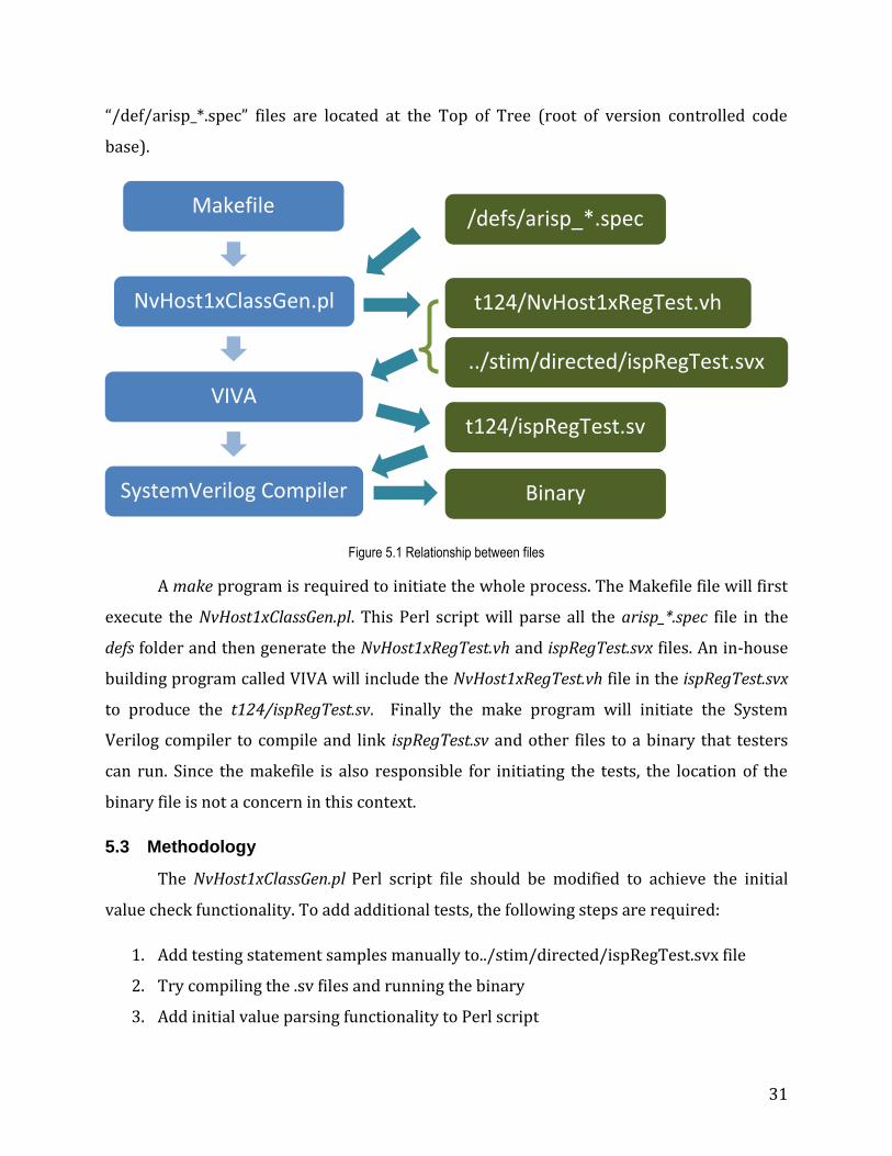
Figure 5.1 Relationship between files ........................................................................................................ 31
Figure 6.1 Functional Diagram of FX subunit ......................................................................................... 35
Figure 6.2 FX random test and related files ............................................................................................. 36
Figure 3 Improved coverage .......................................................................................................................... 41
LIST OF TABLES
Table 2.1 Projected Revenue Split for Q1 and Q2 2012 [2] .................................................................. 3
Table 2.2 CSI Camera Use Case Summary [2] ......................................................................................... 10
Table 2.3 ISP Features ...................................................................................................................................... 11
Table 6.1 FX Subunit Register Specification [12] .................................................................................. 36

v
ABSTRACT
To aid in the development of NVIDIA’s new Tegra processor, we carried out multiple
tasks in the verification phase of the design process as a part of the Image Signal Processor
development team. We developed power verification tests and analyzed the results to meet
specifications. We modified the Camera Serial Interface source code to improve overall
coverage. In addition, we added initial value test features to the register tests. Finally, we
assisted in verifying the Special Effect unit by developing a corresponding random test.
vi
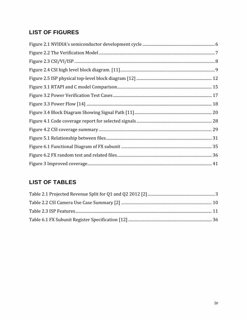
EXECUTIVE SUMMARY
NVIDIA’s Tegra platform is a recently introduced chip family designed for use in
modern phones and tablets. Tegra 3 is the most recent release, with several more versions
slated for production in the future. This project focuses on the verification process of the
Tegra 5 and 6 processors. Verification is a broad topic encompassing many different
aspects of the chip design. More specifically, the goal of this project involves four separate
verification tasks that include power verification, Camera Serial Interface (CSI) code
coverage testing, register initial value testing, and random testing for the special effects
subunit in the Image Signal Processor (ISP). These verification tasks are highly related;
both the CSI and ISP are internal modules of Tegra’s ISP architecture, while power flow
involves both modules. While these four tasks do not constitute the entirety of the ISP
verification, the work done by our project team will help facilitate the overall ISP
verification process.
The first task in this report is power verification of the Tegra processor. In the
electronics industry, power verification is an important process to ensure that products
work at an acceptable power consumption rate. Every year, transistors are getting
significantly smaller. The smaller size is optimal for making smaller devices, but as a result,
engineers encounter power issues. As transistor size decreases, the nominal power
consumption does not decrease proportionally. Since these transistors have become so
small, designers have the ability to package more of them into a product. This results in not
only higher performance, but also higher power consumption. When transistors were
larger, it resulted in a lesser amount of transistors in the same amount of chip area.
The goal of the power verification project is to design and implement a test that
utilizes the Tegra’s ISP device. This is done by writing a test using the C++ programming
language that encompasses the hardware code written for the ISP. This test is then run
through a simulation system designed by NVIDIA. The results from this test are then
analyzed to ensure that the test is designed properly and that desired results are achieved.
vii
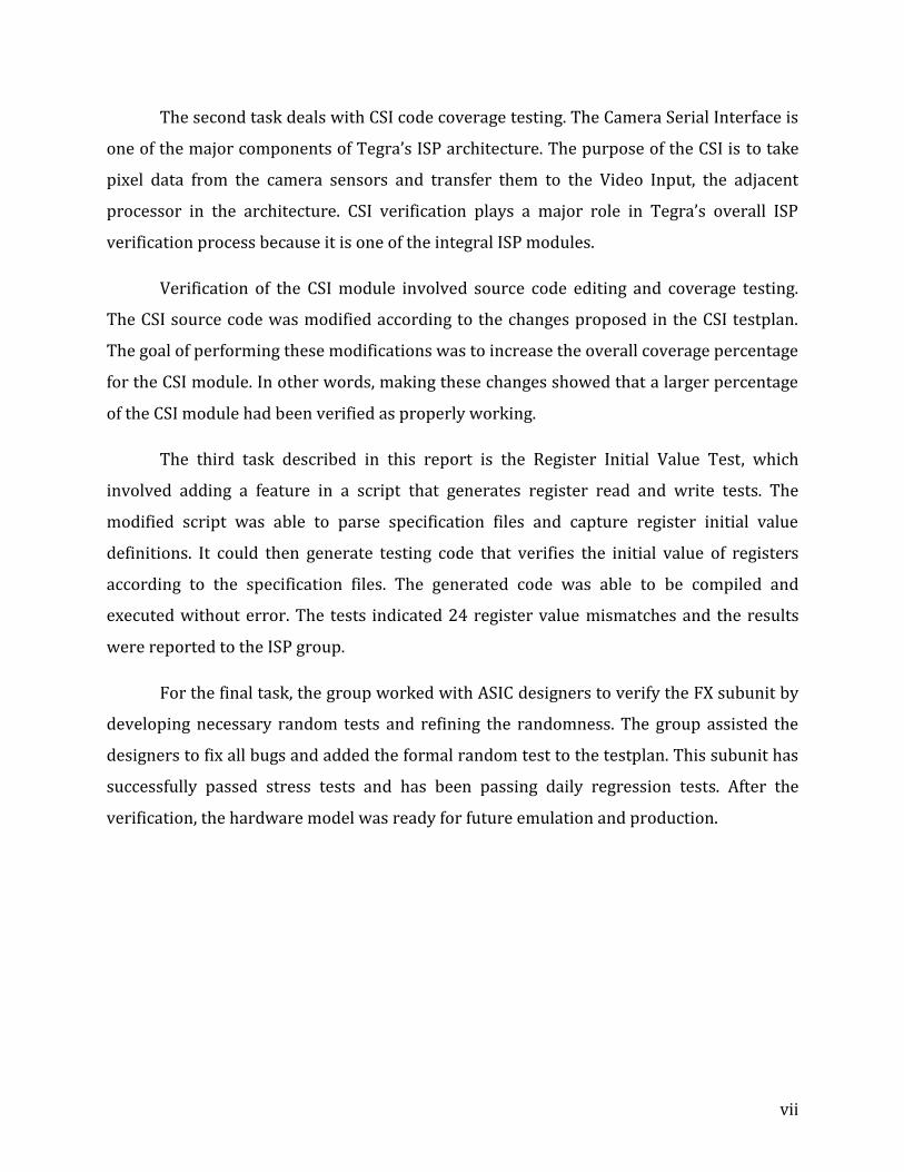
The second task deals with CSI code coverage testing. The Camera Serial Interface is
one of the major components of Tegra’s ISP architecture. The purpose of the CSI is to take
pixel data from the camera sensors and transfer them to the Video Input, the adjacent
processor in the architecture. CSI verification plays a major role in Tegra’s overall ISP
verification process because it is one of the integral ISP modules.
Verification of the CSI module involved source code editing and coverage testing.
The CSI source code was modified according to the changes proposed in the CSI testplan.
The goal of performing these modifications was to increase the overall coverage percentage
for the CSI module. In other words, making these changes showed that a larger percentage
of the CSI module had been verified as properly working.
The third task described in this report is the Register Initial Value Test, which
involved adding a feature in a script that generates register read and write tests. The
modified script was able to parse specification files and capture register initial value
definitions. It could then generate testing code that verifies the initial value of registers
according to the specification files. The generated code was able to be compiled and
executed without error. The tests indicated 24 register value mismatches and the results
were reported to the ISP group.
For the final task, the group worked with ASIC designers to verify the FX subunit by
developing necessary random tests and refining the randomness. The group assisted the
designers to fix all bugs and added the formal random test to the testplan. This subunit has
successfully passed stress tests and has been passing daily regression tests. After the
verification, the hardware model was ready for future emulation and production.
viii
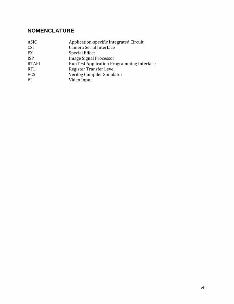
NOMENCLATURE
ASIC Application-specific Integrated Circuit CSI Camera Serial Interface FX Special Effect ISP Image Signal Processor RTAPI RunTest Application Programming Interface RTL Register Transfer Level VCS Verilog Compiler Simulator VI Video Input
1
1.0 INTRODUCTION
Even with the recent introduction of the Tegra 3 in 2011, NVIDIA already has
several future Tegra iterations in various stages of development. These future designs,
comprised of cutting edge and next generation technologies, require extensive testing and
verification before they can be brought to the market. A considerable amount of time is
necessary to complete these tasks, and NVIDIA must ensure that every step in the process
adheres to a tight schedule. This is to make certain that the company is able to introduce
updated versions of Tegra to the mobile market in a timely manner. As additional
technologies are added to the Tegra architecture, the verification process becomes
increasingly complex. The Tegra 5 and 6 architectures in particular will be utilizing
entirely new image signal processor (ISP) architectures. Currently, NVIDIA has several
teams working on the testing and verification of this architecture; the new architecture
makes this process much more complicated than before. Due to the increased workload,
NVIDIA’s verification teams are hard pressed to remain on schedule. It will be the job of
our project team to aid in the verification process of the new ISP architecture.
The ISP is one of the important functionalities of Tegra’s architecture. The ISP itself
contains its own important modules, including the camera serial interface (CSI), video
input (VI), and the ISP module. The ISP verification for the Tegra 5 is currently ongoing
and involves the verification of the CSI, VI, and ISP modules. In addition, power flow
verification must be conducted on the ISP architecture as a whole, which ensures that
power consumption is within expectations. Some of the key remaining issues to be
addressed include CSI verification, ISP verification, and power flow verification.
NVIDIA’s verification teams have already begun the verification process for the
three tasks listed above. Their priorities are currently focused on the large scale task goals
and milestones, with other essential goals and sub-tasks being pushed back due to time
constraints. Although there are several engineers working on the most important
verification tasks, none are able to dedicate time towards completing the various other
essential items. Over time, these unaddressed tasks gradually slow and delay the entire
2
verification process as a whole. These delays must be addressed in a timely manner to stay
in line with the overall Tegra verification plan.
The focus of our project work will be to aid in the verification of the Tegra ISP
architecture. CSI code coverage, register testing, random testing, and power flow
verification are currently four of the more important tasks remaining under the ISP
verification process. These tasks will involve performing power simulation tests, code
coverage tests, random tests, and will also require our team to create totally new
verification tests. By working on these essential tasks, NVIDIA’s engineers will be able to
dedicate more of their time towards completing the largest and most important verification
tasks. This will allow the ISP verification process to proceed more quickly, ultimately
resulting in a faster verification process for the next generation Tegra architecture.
3
2.0 BACKGROUND
2.1 NVIDIA Corporation and Tegra
NVIDIA is an American global technology company founded in 1993 by Jen-Hsun
Huang, Chris Malachowsky, and Curtis Priem. Their products have primarily consisted of
graphics processing units and chipsets. Many of NVIDIA’s achievements are notable; the
company invented the first mainstream multimedia processor (1995), the first high
performance, 128 bit, Direct3D processor (1997), and the first graphics processing unit
(1999), to name a few. Over the past few years, NVIDIA has been increasing its foothold in
the mobile computing market, where the company has been using the Tegra family to
power phones and tablets.
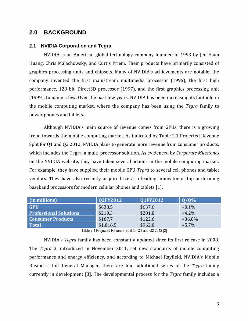
Although NVIDIA’s main source of revenue comes from GPUs, there is a growing
trend towards the mobile computing market. As indicated by Table 2.1 Projected Revenue
Split for Q1 and Q2 2012, NVIDIA plans to generate more revenue from consumer products,
which includes the Tegra, a multi-processor solution. As evidenced by Corporate Milestones
on the NVIDIA website, they have taken several actions in the mobile computing market.
For example, they have supplied their mobile GPU Tegra to several cell phones and tablet
vendors. They have also recently acquired Icera, a leading innovator of top-performing
baseband processors for modern cellular phones and tablets [1].
(in millions) Q2FY2012 Q1FY2012 Q/Q%
GPU $638.5 $637.6 +0.1% Professional Solutions $210.3 $201.8 +4.2% Consumer Products $167.7 $122.6 +36.8% Total $1,016.5 $962.0 +5.7%
Table 2.1 Projected Revenue Split for Q1 and Q2 2012 [2]
NVIDIA’s Tegra family has been constantly updated since its first release in 2008.
The Tegra 3, introduced in November 2011, set new standards of mobile computing
performance and energy efficiency, and according to Michael Rayfield, NVIDIA’s Mobile
Business Unit General Manager, there are four additional series of the Tegra family
currently in development [3]. The developmental process for the Tegra family includes a
4
considerable amount of testing and verification, and this project with NVIDIA will help
facilitate this process.
In 2008, NVIDIA launched Tegra, a family of highly integrated computers on a chip,
or system on a chip (SoC) [1]. The Tegra chip has been utilized on mobile devices such as
netbooks, tablets, and smartphones [4]. As stated in the introduction, NVIDIA has been
shifting towards the mobile computing market in an attempt to garner a foothold over
competitors such as Qualcomm and Texas Instruments. Up until 2008, NVIDIA’s priority
has always been towards the GPU market, in which they have always enjoyed a healthy
share of. Although the benefits of being one of the largest GPU manufacturers in the world
are great, Jen-Hsun Huang, CEO of NVIDIA, believes in venturing into new territory with
Tegra. Huang estimates that the mobile-chip industry will grow to $20 billion by 2015,
around 10 times what it’s currently at. According to him, “If you don’t have a mobile
strategy, you’re in deep turd. If you’re not in mobile processors now, you’re seven years too
late.” [5]
NVIDIA’s goal in creating Tegra has always been to offer an ultra-low-power chip,
with high performance [6]. Tegra’s SoC design is comprised of a CPU, GPU, and a video and
sound processor. The chip currently has the ability to run on multiple operating systems,
with Android, Linux, and Windows being the most common [7].
The first line of Tegra chips released in 2008 was the Tegra APX Series.
Specifications of this chip include an ARM11 MPCore 600MHz CPU, 246 MB memory, 12 MP
camera support, and the ULP (Ultra Low Power) NVIDIA GPU [4]. The original line of Tegra
APX chips were designed specifically for smartphones [4]. Although NVIDIA was
enthusiastic about the release of their new chip families, there were ultimately not many
product integrations, as the chip made its way into only one smartphone and one mp3
player [4]. This setback did not stop Huang, as he states “Creating Tegra was a massive
challenge. Our vision was to create a platform that will enable the 2nd personal computer
revolution – which will be mobile centric, with devices that last days on a single charge, and
yet has the web, high definition media, and computing experiences we’ve come to expect
from our PC.” [8]
5
After the booming success of the iPad, NVIDIA took notice and decided to switch
gears. Although they still maintained chip production for smartphones, the chip designed
for Android tablets became more popular [9]. This chip was known as the Tegra 2. This
chip boasted a dual-core ARM Cortex A9 1 GHZ CPU and 1GB of memory [9]. The Tegra 250
T20 (designed specifically for tablets), is used in around 20 different tablets currently on
the market [9]. The Tegra 2 boasts superior performance and lower power consumption
than the previous generation of Tegra chips.
The next line of chips, the Tegra 3, is double the performance of the Tegra 2. The
Tegra 3 boasts the first quad-core processor found in a tablet currently on the market. The
chip itself is %61 more efficient with battery consumption than the Tegra 2. There are also
a few other differences with these two chips that is further discussed in the next section of
the paper.
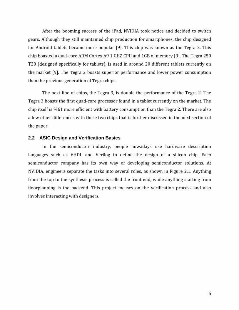
2.2 ASIC Design and Verification Basics
In the semiconductor industry, people nowadays use hardware description
languages such as VHDL and Verilog to define the design of a silicon chip. Each
semiconductor company has its own way of developing semiconductor solutions. At
NVIDIA, engineers separate the tasks into several roles, as shown in Figure 2.1. Anything
from the top to the synthesis process is called the front end, while anything starting from
floorplanning is the backend. This project focuses on the verification process and also
involves interacting with designers.
6
Figure 2.1 NVIDIA's semiconductor development cycle
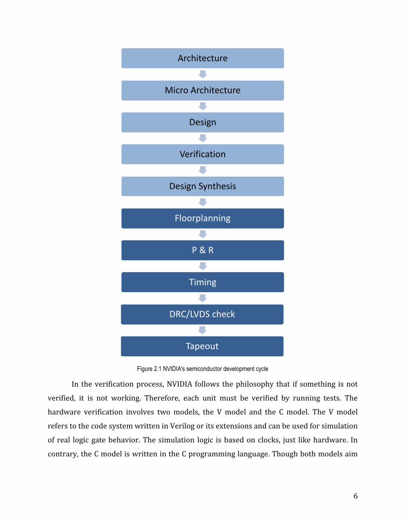
In the verification process, NVIDIA follows the philosophy that if something is not
verified, it is not working. Therefore, each unit must be verified by running tests. The
hardware verification involves two models, the V model and the C model. The V model
refers to the code system written in Verilog or its extensions and can be used for simulation
of real logic gate behavior. The simulation logic is based on clocks, just like hardware. In
contrary, the C model is written in the C programming language. Though both models aim
Architecture
Micro Architecture
Design
Verification
Design Synthesis
Floorplanning
P & R
Timing
DRC/LVDS check
Tapeout
7
to implement the same functionalities, they are very different in the real implementation.
In particular, the C model is simpler and less likely to produce bugs.
Figure 2.2 The Verification Model
Traditionally in the software industry, engineers write tests with finite amounts of
inputs to cover different cases. Ideally the tests should cover each possible input, which is
impossible within the common constraints. In the semiconductor industry, the potential
failing cost of a chip is very high. The industry invented a testing mechanism called random
tests to balance between test coverage and cost.
In random tests, the test environment instantiates both the V and C models. It then
configures them with randomized register values and also feeds them with randomized but
identical data, called the stimulus. Then, the testbench compares the results from the two
models and indicates a test pass if they match completely. The randomized values are not
completely random, but follow a list of constraints defined by verification engineers
according to the architecture document. In this practice, as more random tests are run,
more scenarios are covered.
In the random tests, a user can define the constraints so that only one possible set of
values can be produced. These special cases are referred to as directed tests, which are
Match?
Stimulus
8
usually used to cover the most basic situations and are included in Level 0 test plans (the
most basic tests).
2.3 Tegra ISP Architecture Overview
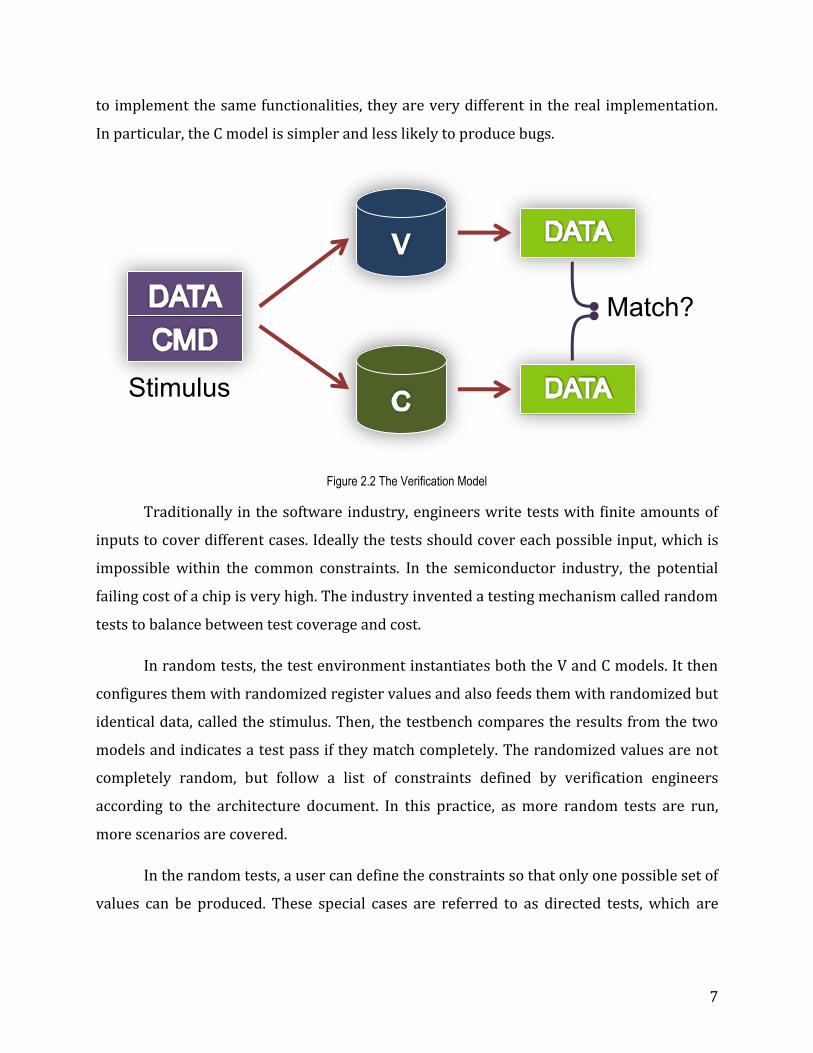
The architecture of the Tegra Image Signal Processor (ISP) is show below in Figure
2.3. The individual modules of the ISP will be explained in further detail in the following
sections. The image first goes through the Camera Serial Interface (CSI) and Video Input
(VI) components of the device and then goes to the ISP, which then delivers it to the
memory interface. The dotted line shows an alternative path the image can take. The job of
the VI is to decide whether or not to send an image to the ISP. If the image is already at a
small enough resolution, the VI can send it directly into memory without going through ISP
filtering. From there, the memory will either keep it or send it back into the ISP for further
modification. This architecture is necessary to keep in mind when approaching all four
tasks.
Figure 2.3 CSI/VI/ISP
2.4 Camera Serial Interface
The Camera Serial Interface is one of the major components of the Tegra’s ISP
architecture. The CSI takes pixel data from the camera sensor (up to two sensors are
supported) and transfers it to the application processor using the MIPI protocol. This
protocol was created by the MIPI Alliance with the goal of defining and promoting open
specifications for mobile interfaces. Currently, NVIDIA uses the CSI2 interface in their
Removed due to confidentiality
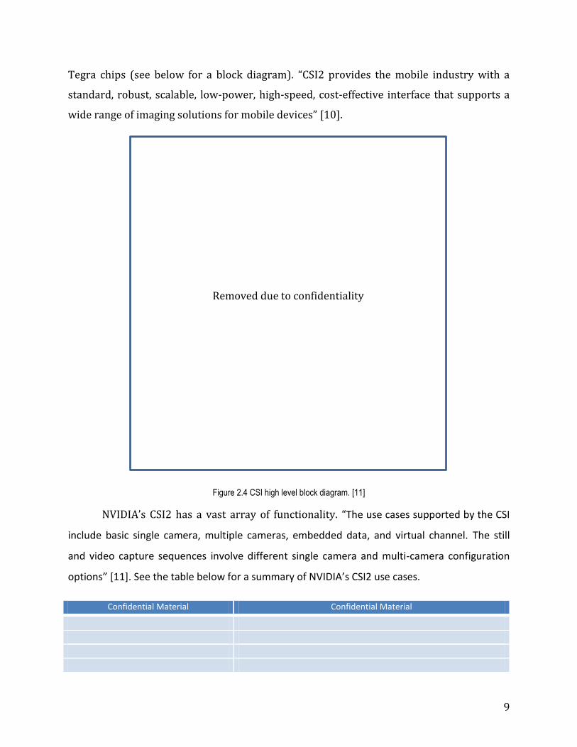
9
Tegra chips (see below for a block diagram). “CSI2 provides the mobile industry with a
standard, robust, scalable, low-power, high-speed, cost-effective interface that supports a
wide range of imaging solutions for mobile devices” [10].
Figure 2.4 CSI high level block diagram. [11]
NVIDIA’s CSI2 has a vast array of functionality. “The use cases supported by the CSI
include basic single camera, multiple cameras, embedded data, and virtual channel. The still
and video capture sequences involve different single camera and multi-camera configuration
options” [11]. See the table below for a summary of NVIDIA’s CSI2 use cases.
Confidential Material Confidential Material
Removed due to confidentiality

10
Table 2.2 CSI Camera Use Case Summary [2]
2.5 Video Input
The Video Input is a unit that controls the flow of image data from the camera.
Located between the CSI and ISP, it directs data either to the ISP for instant processing or
to the memory for post processing.
2.6 Image Signal Processor
2.6.1 Overview
The Image Signal Processor is part of the NVIDIA Tegra microprocessor. It is
responsible for converting raw signals from the camera sensor to other acceptable formats.
The ISP can also perform other digital image processing such as de-noising. This project
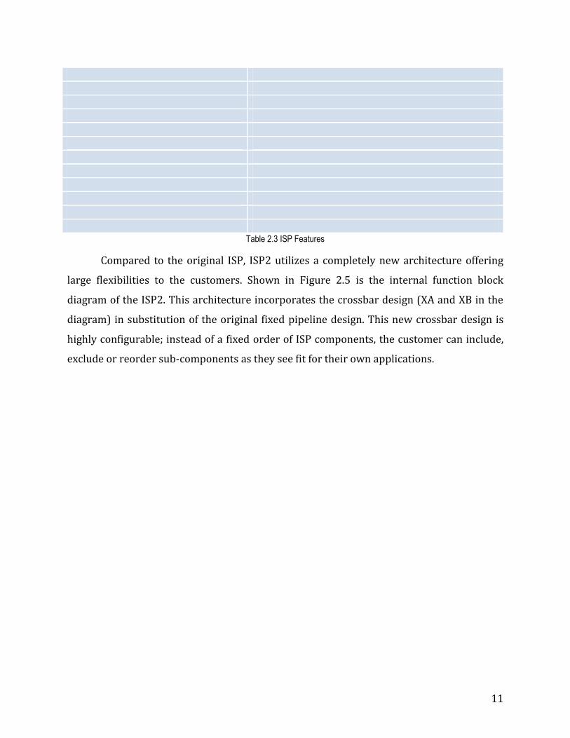
involves the second generation ISP, called ISP2. Table 2.3 shows the ISP2 functionalities.
Confidential Material Confidential Material
11
Table 2.3 ISP Features
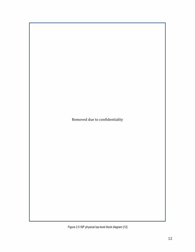
Compared to the original ISP, ISP2 utilizes a completely new architecture offering
large flexibilities to the customers. Shown in Figure 2.5 is the internal function block
diagram of the ISP2. This architecture incorporates the crossbar design (XA and XB in the
diagram) in substitution of the original fixed pipeline design. This new crossbar design is
highly configurable; instead of a fixed order of ISP components, the customer can include,
exclude or reorder sub-components as they see fit for their own applications.
12
Figure 2.5 ISP physical top-level block diagram [12]
Removed due to confidentiality
13
2.6.2 The FX Subunit
As a part of the ISP verification process, we worked with the designer to verify the
Special Effect (FX) subunit. The FX subunit is used to add special polarization, solarization,
negatives, and emboss to the pixels. The first three functions are implemented inside the
same block, since they can be computed with one generic algorithm with minor logic
differences. However, the emboss function is implemented in its own block.
3.0 POWER VERIFICATION
3.1 Introduction
The following task conducted at NVIDIA is the company’s version of power
verification. The company performs this verification process with all of their products, and
this task will involve the power verification of the Tegra ISP. As a result, they have designed
a roadmap to follow in order to successfully accomplish power verification for a product.
This chapter will begin by discussing how power verification is interpreted by NVIDIA, and
then go on to discuss the steps taken to generate a power verification report. This task
involves writing a test using the C++ programming language to run through NVIDIA’s
simulation system. This test incorporates all of the ISP subunits’ hardware code. The goal of
the task was to increase the power efficiency of the ISP device by analyzing the power
report that is produced at the end of running the simulation. Analyzing the report led to
increasing the power efficiency of the ISP’s various subunits. The results of this task are the
overall increase in efficiency of the ISP device. These results are achieved by altering the
subunit RTL code and then re-running the original test to generate a new power report.
Once the efficiency is increased to a certain level, the subunit power values generated by
the report are compared against an ideal C model. Before discussing the steps involved in
this process, there are a few important concepts that need to be established.
14
3.2 Important Concepts
3.2.1 RTL (Register-Transfer Level)
RTL, or Register-Transfer Level, is the circuit designed for a specific piece of
architecture. For example, RTL for the ISP device encompasses all of the logic gates and
various connections involved within the circuit. This RTL is written with System Verilog.
Table 2.3 shows the various subunits involved within the ISP architecture. Each of these
subunits has registers written into RTL. The RTL can be called upon using the C++
programming language. The code written to use RTL is simulated within the RTAPI, which
will be explained in the next section.
3.2.2 RTAPI (RunTest Application Programming Interface)
The RTAPI is a hardware simulation test bench. According to the NVIDIA RTAPI
internal Wikipedia page, “The RunTest API (RTAPI) provides a mechanism to define robust
C++ tests which run equally well in C simulation, mixed C/RTL simulation, top RTL
simulation, emulation, and silicon.” [13] Essentially, the tests written for the RTAPI are a
script of C++ code. The code is then executed in a simulated processor within the RTAPI
environment. The RTAPI can simulate the processor because it contains the RTL of the
architecture involved in the Tegra ISP.
3.2.3 Clock Gating
Clock gating is a process used to decrease power dissipation within a piece of
hardware. The process occurs when a signal is traveling through various forms of logic.
When clock gating is turned on, the signal will be streamlined to its destination in order to
avoid various flip-flops within the logic. Flip-flops involve the switching between two
states, and this very process of switching consumes extra power. If clock gating is disabled,
the flip-flops will not be avoided and overall power consumption will be higher.
3.2.4 Power Verification
The purpose of power verification is to ensure that the power being consumed by a
specific component accurately compares to the C model standard, which assumes ideal
values in an ideal environment. These values are generated after the test shown in Figure
3.1 runs through the RTAPI. In general, the values in the power report will not have the
15
exact values as the C model, but should be within an acceptable margin of error. This error
is determined by NVIDIA’s power verification team, and not by the Tegra ISP team. Figure
3.1 shows how the simple flow of power verification works. If the compared values match,
the RTL will go through further verification. If they do not match, the power verification
report and test code have to be analyzed. This process is further explained in a later
section.
Although observing how the RTAPI and C model are related, observing their
comparisons is not the overall goal of this task. The goal, as stated in section 3.1, is simply
to create the test involved in this comparison and increase the power efficiency of the ISP
subunits. Once the test is optimized for efficiency, the results of the power report are sent
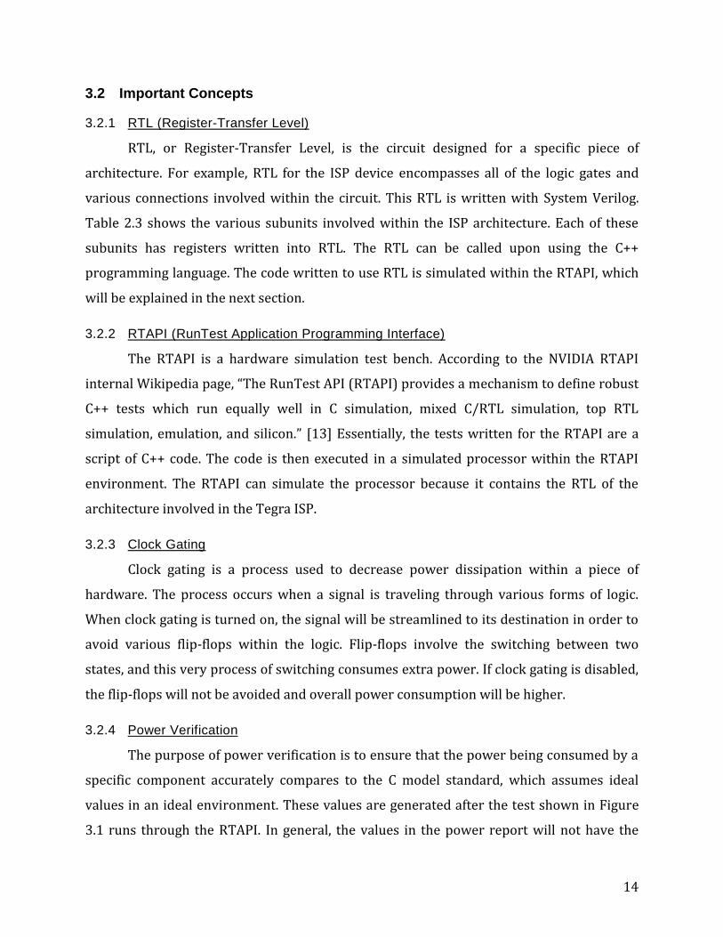
to the power verification team at NVIDIA. The job done by our project group is shown in
the dotted box in Figure 3.1.
Figure 3.1 RTAPI and C model Comparison
Test
16
3.3 Methodology
3.3.1 Introduction
The following methodology will explain the process shown in Figure 3.1. First, the
method in which the power verification is approached in relation to the architecture is
explained. There are two types of test cases that were created and each of them is
explained in the following section. Finally, the method in which these test cases are run
through the RTAPI simulation to generate a power verification report is described.
3.3.2 ISP/CSI/VI Power Verification
The first step in power verification was to investigate the ISP. Figure 2.3 shows how
the ISP/CSI/VI pathways are set up. These three pathways can be split up into two separate
units for the purpose of power verification. The ISP was approached first as a separate unit,
since it was assumed that an image would be inputted directly into the ISP and transferred
to the memory from there. The second unit is the CSI/VI subunit; here, it was assumed that
the image would go through both CSI and VI, and then directly inputted into memory
(bypassing the ISP).
3.3.3 Test Cases
Within the ISP, there are various subunits that were mentioned in the background
(e.g. special effects, de-noising). Enabling these various functions makes the ISP consume
more power. To be as thorough as possible, the test cases had to include an IDLE test and a
stress test. The IDLE test simply tests power flow of the ISP device with all of the various
functions disabled, while the stress test is performed with every function enabled. The
stress test is written differently than the IDLE test because every register must be turned
on, and some registers have sub-registers that also need to be enabled. The IDLE and stress
tests were written by utilizing previously written code from other NVIDIA engineers.
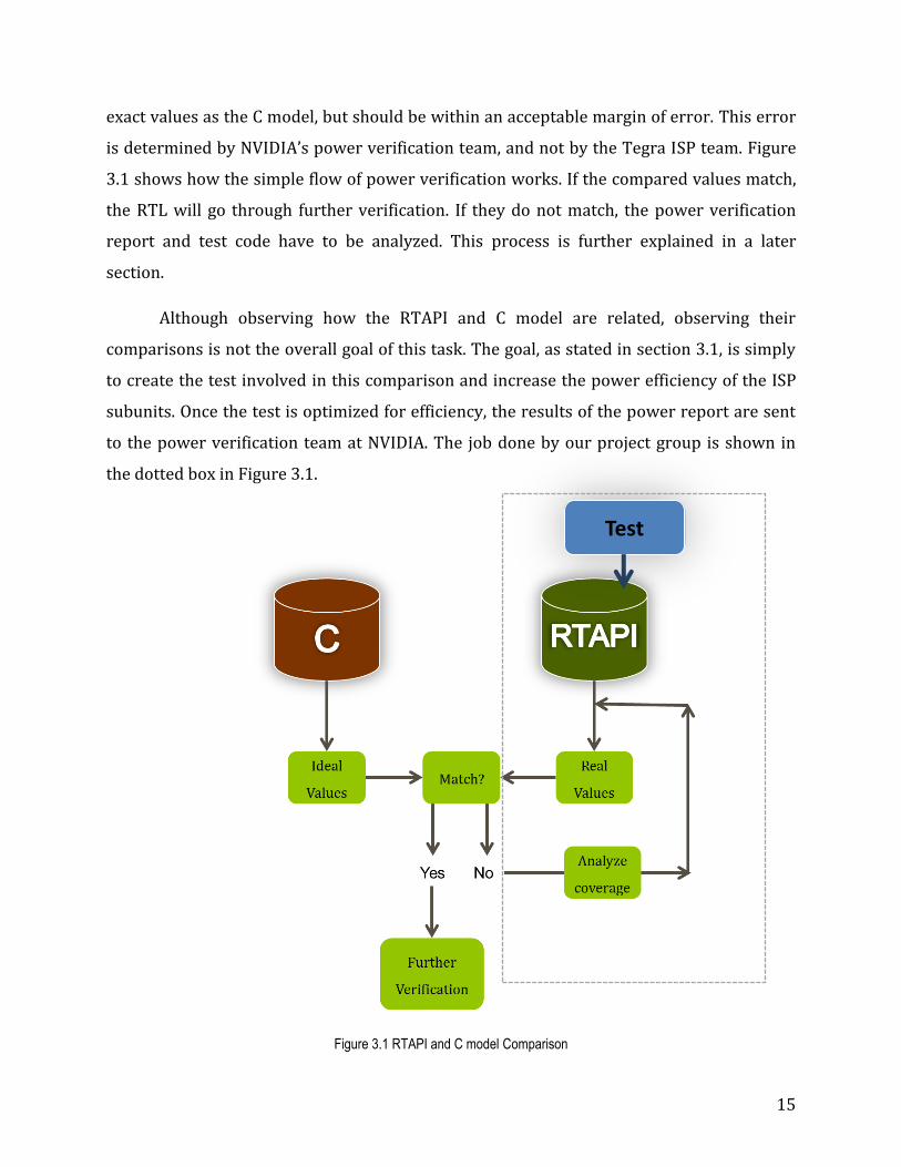
The graphic shown in Figure 3.2 shows a simple breakdown of the two tests
involved. As shown, the IDLE test can also be broken down into two more tests. Section
3.2.3 explained how clock gating is used to bypass various flip-flops in logic circuits. The
IDLE test is written with clock gating enabled, as well as with clock gating disabled. The
17
method in which this is accomplished is further explained in section 3.4. Due to time
constraints, our project group only worked on code related to the IDLE test.
Figure 3.2 Power Verification Test Cases
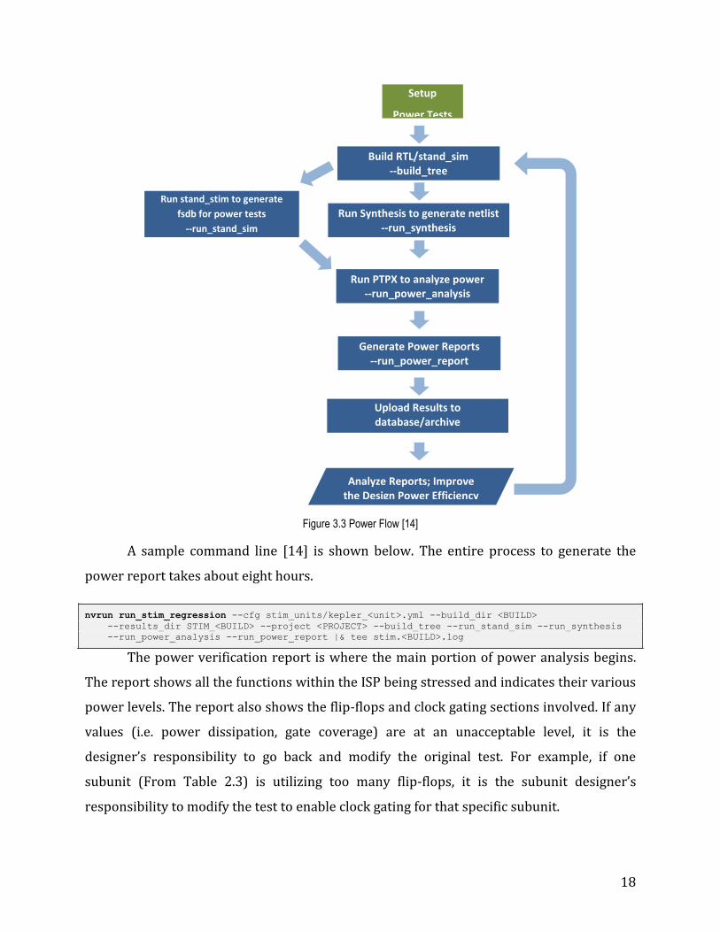
3.3.4 Power Flow
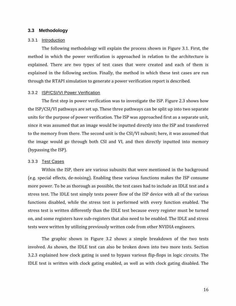
Our project group wrote part of the test for the IDLE test with clock gating enabled.
Figure 3.3 is the process followed to generate the power verification report after this IDLE
test was written. The important power flow steps are shown in the middle of the diagram.
These commands are all put into the command line when running the test, but they each
serve a different purpose. The “build_tree” command simply populates the current tree
with the subunit RTL code. The “run_synthesis” command generates a netlist of all of the
logic gates within the subunit RTL code. For this task, “run_stand_sim” was used to run
tests on RTL by generating fsdb files. Fsdb files are used to look at waveforms through a
program called Verdi (see section 4.2.1). These waveforms are only necessary to look at
once the final goal of increased power efficiency is reached. The “run_power_analysis”
simply runs the power analysis through a process called PrimePower (PTPX). This program
gathers various statistics about the various subunits such as clock gate coverage, which is
necessary for the final goal of increased power efficiency. Finally, the power analysis is then
performed, and from this analysis a report is generated in the form of an Excel file.
18
Figure 3.3 Power Flow [14]
A sample command line [14] is shown below. The entire process to generate the
power report takes about eight hours.
nvrun run_stim_regression --cfg stim_units/kepler_<unit>.yml --build_dir <BUILD>
--results_dir STIM_<BUILD> --project <PROJECT> --build_tree --run_stand_sim --run_synthesis
--run_power_analysis --run_power_report |& tee stim.<BUILD>.log
The power verification report is where the main portion of power analysis begins.
The report shows all the functions within the ISP being stressed and indicates their various
power levels. The report also shows the flip-flops and clock gating sections involved. If any
values (i.e. power dissipation, gate coverage) are at an unacceptable level, it is the
designer’s responsibility to go back and modify the original test. For example, if one
subunit (From Table 2.3) is utilizing too many flip-flops, it is the subunit designer’s
responsibility to modify the test to enable clock gating for that specific subunit.
Run stand_stim to generate
fsdb for power tests
--run_stand_sim
Build RTL/stand_sim --build_tree
Run Synthesis to generate netlist --run_synthesis
Run PTPX to analyze power --run_power_analysis
Generate Power Reports --run_power_report
Upload Results to database/archive
--store_db
Setup
Power Tests
Analyze Reports; Improve the Design Power Efficiency
19
3.4 Results
3.4.1 Power Test Code
A power report was generated from the code shown in Appendix C (IDLE test). This
code is not wholly original. Most of the code is taken from other tests written by various
NVIDIA engineers. The code from Appendix C was written in collaboration with an NVIDIA
engineer named Yunqing Chen. Our project group worked on the code shown below. This is
the configure_crossbar function. This function’s purpose can be shown using Figure 3.4.
The figure shown shows various connections between the subunits within the ISP device.
When coding a test to utilize these subunits, as shown in Figure 3.4, it is necessary to follow
the circular nodes along the black lines, as they are representative of the signal path. For
example, the signal always starts at MR0 (read) and ends at MW0 (write). The signal can go
through any of the subunits in order, as long as they all begin and end with MR0 and MW0
respectively. A snippet of Appendix C shows this below. The code below is from an IDLE
test, which means that all subunits are disabled. As indicated, the signal path simply goes
directly from MR0 to MW0. It is necessary to always go through AP (Area Processor). The
AP subunit is responsible for taking the inputted pixels and converting it into the final
format shown on the smartphone or tablet screen.
configure_crossbar(NV_ISP2_CROSSBAR_A, "MR0 AP");
configure_crossbar(NV_ISP2_CROSSBAR_B, "AP MW0");
20
Figure 3.4 Block Diagram Showing Signal Path [11]
Removed due to confidentiality
21
3.4.2 Power Report
Once the code from Appendix C was run through the RTAPI, a power report was
generated. This report is necessary for the purposes of increasing the power efficiency of
the subunits. It is required to analyze the report to ensure all of the various logic gates are
being utilized. In this power verification task, increasing the efficiency of the un-gated flip-
flops was the main goal. The un-gated flip-flops are a list of all the gates within the subunits
that were not being clock gated. As a result, our project group went into the root code to
check which registers were not clock gated, and inform the original subunit designer of this
error. For example, the following code is a snippet of a subunit register that is not being
clock gated. As shown, the pxl_in_ready register (which belongs to the AP subunit), is flip-
flopping between two states regardless of any incoming signals coming in. This type of
register is reported to the designer as a bug. Once the bugs are all fixed by the original
subunit designers, the original IDLE test can be re-run. The goal of this specific sub-task is
to achieve less than 3% un-gated flip-flops. Whether this goal has been achieved has not yet
been determined until all of the bug fixes are made.
if (!isprstn) begin
pxl_in_ready <= 1'b1;
pxl_in_ready_int <= 1'b1;
end else begin
pxl_in_ready <= pxl_ready_from_local_pipe;
pxl_in_ready_int <= pxl_ready_from_local_pipe;
After the un-gated flip-flops were successfully analyzed, there is further analysis of
the power report required by NVIDIA. Due to time constraints, this could not be done by
our project group. For example, the original IDLE test written in C++ can be modified to
increase power efficiency by modifying the subunit signal path.
22
3.5 Summary
The goal of this task was to increase the efficiency of NVIDIA’s Tegra ISP. The power
test was written in collaboration with Yunqing Chen. Our project group generated a power
report after running the test through the RTAPI. This power report was then analyzed to
increase the clock gating of the un-gated flip-flops. This goal will be met once all of the
subunit designers have submitted their bug fixes. NVIDIA will continue to analyze this
report and increase the power efficiency of the original test. Once this is complete, they will
pass along their results to the power verification team.

23
4.0 CSI CODE COVERAGE TESTING
4.1 Introduction
In the Tegra architecture, the CSI takes pixel data from the camera sensor and
transfers it to the Video Input module for further modifications. Code coverage testing
involves running coverage tests on the CSI source code to ensure all sections of the code
are tested and working properly. This chapter discusses the important concepts,
methodology, and results of code coverage testing. The goal of this task was to increase the
overall coverage for the CSI module, although a set coverage percentage was not given.
Important concepts provides essential background information to help understand this
task, methodology discusses how the task was completed, and results shows the end result
of following the steps outlined in the methodology.
4.2 Important Concepts
4.2.1 Verdi
Verdi Automated Debug System is a software program developed by SpringSoft for
debugging digital designs. The core features of this program include a full waveform
viewer, waveform comparison engine, source code browser, logic schematics and block
diagrams, and finite state machine bubble diagrams. Verdi supports several languages,
including Verlog, VHDL, and System Verilog; in addition, there is support for several
different testbench environments.
4.2.2 Code Coverage
Code coverage describes the percentage of a test’s source code that has been tested.
In general, 100% code coverage is impractical. “Empirical studies of real projects found
that increasing code coverage above 70-80% is time consuming and therefore leads to a
relatively slow bug detection rate” [15]. Several factors should be considered when
deciding on an acceptable code coverage threshold, including cost of failure, available
resources, testable design, and development cycle status. For example, code coverage is
generally higher for products in the medical or transportation industries due to numerous
safety-critical systems and the potential high failure costs.
24
Code coverage can be further subdivided into individual coverage metrics. “A
number of different metrics are used determine how well exercised the code is ….. Most of
the metrics have slight variations and synonyms which can make things a little more
confusing than they need to be” [16]. Some of the more common metrics include
functional, statement, decision, and conditional coverage. A version of functional coverage
was used in performing this coverage testing task.
Functional coverage checks to determine whether or not a function or subroutine in
the program has been called or executed. If a certain function has been called at least once
in the program, then the functional coverage for that function is satisfied. Conversely, if it
is known that certain functions or sections of code are not being utilized, coverage can be
disabled for those sections.
Statement coverage checks are a very rudimentary form of code coverage; basically,
a statement is covered if it is executed. Statement coverage is also commonly referred to as
line, block, or segment coverage. This type of coverage has both its advantages and
disadvantages. “This type of coverage is relatively weak in that even with 100% statement
coverage there may still be serious problems in a program which could be discovered
through the use of other metrics. Even so, the first time that statement coverage is used in
any reasonably sized development effort it is very likely to show up some bugs” [16].
Decision coverage tracks whether or not every edge in a program has been
executed. For example, this type of coverage will track whether or not each branch in an IF
statement has been met as well as not met. Decision coverage can also be referred to as
branch, edge, or arc coverage.
Conditional coverage checks whether or not each Boolean expression has been
evaluated to both true and false. Since Boolean expressions can get increasingly complex,
the following solution offers the best way around the problem: “Condition coverage gets
complicated, and difficult to achieve, as the expression gets complicated. For this reason
there are a number of different ways of reporting condition coverage which try to ensure
that the most important combinations are covered without worrying about less important
combinations” [16].
25
4.2.3 VCS Pragmas
Pragmas serve the purpose of disabling coverage for specific segments of code.
NVIDIA uses the Verilog Compiler Simulator (VCS) software, which has its own specific
pragma syntax. The VCS pragma syntax is shown below; comments need to be added
before and after the code segment for coverage to be disabled. Disabling coverage for
select portions of the code is necessary for a few reasons. Error messages, for example,
require these pragmas. Since the code coverage report is supposed to be generated from
an error-free test, the code snippets in charge of error handling will never be toggled. In
other words, the overall coverage would never be able to reach 100% if pragmas were not
added to the error message code.
// VCS coverage off
(code with disabled coverage)
// VCS coverage on
Pragmas are also useful for disabling code coverage of certain signals in the test (i.e.
SPARE or DEBUG pins). These signals are not used by the test and are usually hardcoded to
a logic low. Like the error handling code, these SPARE and DEBUG signals would never be
toggled in an error-free test and therefore, pragmas are needed to ensure that the coverage
report displays a more accurate overall coverage percentage.
4.3 Methodology
4.3.1 Code Coverage
This section describes the approach used to complete the CSI coverage test. Ideally,
a coverage test will ensure that all sections of the software are executed and verified
(covered) by the code. The CSI testplan outlines the intermediate steps needed in order to
achieve 100% coverage. The following paragraphs list the steps required to perform a
coverage test as well as view the associated coverage report.
The first step in this process was to set a directory to compile the unit coverage
results (i.e. provide a destination directory where the test waveforms can all be dumped).
The “tree.make” file needed to be edited with the desired destination directory (see code
26
below). The first line enables NV_BUILD_COVERAGE, while the second line specifies the
destination directory (there are two directories in this case).
## COVERAGE SETUP
export NV_BUILD_COVERAGE := 1
export NV_BUILD_COVERAGE_FULL_MODULES := vmod/vicluster/csi2 stand_sim/csi2/testbench
The next step was to actually run the test on my own VNC server. To run the test,
the correct command needed to be provided, specifying the test name and if necessary,
other test-specific arguments and options (these arguments and other syntax details are
contained in the test description file). After entering the command and executing the test,
the words “PASS” or “FAIL” appeared in the command line interface, indicating the test
result. See below for the specific command line argument used for this particular test.
`depth`/tools/RunScript/CsiRun.pl -P t124 -dir yuv420CamAVc0SngLnCamBVc0MulFrmTest -rtlarg
"+sensor_rtl=1 +goldFileCheck=1 +viClkFreq=166" -waves yuv420CamAVc0SngLnCamBVc0MulFrmTest -v
csi2
Once the test successfully passed, it was possible to use Verdi to view the signal
waveforms and the corresponding code. One of the main advantages of using Verdi was
that it simplified the debugging and troubleshooting process. For newer or unfamiliar
users, Verdi also made it easy to analyze and follow the code. The correct command must
be issued from the appropriate test directory in order to run Verdi (details on how to do
this are found in the test description file). Any signal within the test code (or multiple
signals, if necessary) can be displayed in the main Verdi waveform window, making it easy
to track how the signal was toggled throughout the test. See the code below for the specific
Verdi command.
qsub run_verdi_csi2
The next task was to run a regression on that test with coverage enabled using the
existing run_regression script. Regression testing is used to ensure that any new changes
made do not create new bugs in other parts of the system. Since this project involved code
editing and tree rebuilding, regression tests were necessary to ensure the system
continued to function without errors. The command to execute the regression test is
shown below. “mailme” ensured that the tester would be mailed the results of the
regression test, “csi_standsim 0” meant to run a level 0 regression test, “coverage” specified
the module, and “coverage_dir” specified the coverage directory.
27
bin/run_regression --mailme csi_standsim 0 --coverage=csi2 --
coverage_dir=coverage_report/run_02132012
Following the regression test was the code coverage report generation (see the command
below). Both the coverage directory and the simv.cm.vdb directory needed to be specified
and some options were added to ensure the code coverage report contained all the types of
coverage.
urg -dir /home/scratch.stelee_t148/stelee_project1_tree1/ap_isp2/coverage_report/run_02132012.vdb
-dir
/home/scratch.stelee_t148/stelee_project1_tree1/ap_isp2/stand_sim/csi2/testbench/t124/simv.cm.vdb
-metric tgl+line+cond -lca
The report generation command would then create a new destination directory for
the code coverage report files and would display the path in the command line interface.
The directory path could then be copied and pasted into an Internet browsing window to
view the coverage report online. Shown below are the code coverage report directory path
and the web address to view the online version of the report.
/home/scratch.stelee_t148/stelee_project1_tree1/ap_isp2/urgReport/dashboard
https://nvtegra/home/scratch.stelee_t148/stelee_project1_tree1/ap_isp2/urgReport/dashboard
4.3.2 VCS Pragmas
This section describes the process of adding pragmas to the existing test code. The
first step was to actually run the coverage test and generate the coverage report before
performing any pragma edits to the code (see the above steps). The coverage report served
as an invaluable resource when deciding where to add pragmas, since it provided detailed
analysis on which signals were adequately covered or not. Verdi’s convenient search
functionality was also useful in relating the signals of the coverage report to their locations
in the actual code, making it easier to figure out where exactly to add in the pragmas. For
this specific project, the main priority was adhering to the CSI testplan, meaning that many
sections of the uncovered code could be ignored if it did not specifically appear in the
testplan (i.e. out of scope at this point in time).
Adding in the pragmas involved editing the System Verilog source files. Once the
changes were made, the test directory needed to be rebuilt using the command shown
below. Once the directories were rebuilt, the new coverage report needed to be generated.
28
The remaining steps involved following the code coverage report generation process as
described in the above paragraphs.
bin/t_make –build t124_standsim_csi2_testbench t124_vmod_vicluster_csi2
4.4 Results
The VCS pragmas were added to the CSI source files and the tree was successfully
synced and rebuilt without errors. Three different source files were modified for the
purposes of this project, including NV_csi.vx, NV_CSI_con.vx, and NV_CSI_status.vx. See
below for a pragma usage example from the NV_CSI_status.vx source file. This code snippet
hardcodes several unused signals and therefore, does not need coverage enabled.
// VCS coverage off
assign csi_ro_spare3 = 1'b0;
assign csi_ro_spare4 = 1'b0;
assign csi_ro_spare5 = 1'b0;
assign csi_ro_spare6 = 1'b0;
assign csi_ro_spare7 = 1'b0;
// VCS coverage on
The code coverage report was successfully generated by following the steps
outlined in the Methodology. The figure below, taken directly from the coverage report
webpage detailing the NV_CSI_status subtree, shows that coverage was successfully
disabled for the selected portions of code. An “unreachable” status signifies that although
the test recognized the existence of the signals, it was unable to verify coverage. This result
is as expected, since coverage had been disabled for those selected signals.
Figure 4.1 Code coverage report for selected signals
This was just one of many examples of pragma additions to the CSI source files. At
the end of this project, overall coverage for the CSI module stood at 30.56%, a roughly 5%
increase from the project’s beginning. The figure below is taken from the main webpage of
29
the CSI coverage report, showing total (score) coverage, as well as line, conditional, and
toggle coverage.
Figure 4.2 CSI coverage summary
4.5 Summary
By adding VCS pragmas to three different CSI source code files, overall CSI code
coverage increased to 31%. This seemingly low coverage percentage is due to a number of
factors. Although three different source files were edited for this task, the CSI module itself
contains dozens of source files. The pragmas themselves are also limited in scope; they
only serve to disable coverage for code segments that are known to not be toggled during
the test. In other words, these pragmas do nothing for those code segments having other
unrelated coverage issues. With each source file containing several thousand lines of code,
there exists a considerable amount of coverage issues that cannot be solved with these
pragmas. The next paragraph describes future coverage work that will be required to
remedy these issues. These issues are largely out of scope for this pragma task; thus, they
are not mentioned in great detail.
There are many tasks that remain to be completed with respect to CSI code coverage.
The addition of pragmas is one of the more straightforward tasks in the process of raising
code coverage. Solving the other coverage issues will require a considerably larger amount
of time and effort. For example, direct tests will need to be written for the more complex
sections of code to ensure proper functionality. Many more tests will also need to be
written for those code segments charged with error handling. It’s important to note that
although coverage was disabled for this code in the coverage test, the code still needs to be
actually tested and verified. The entire list of remaining coverage tasks is detailed in the
CSI testplan document, which will serve as an invaluable resource for completing future
coverage tasks.
30
5.0 REGISTER INITIAL VALUE TESTS
5.1 Introduction
This chapter involves adding a new function to an original register read and write
test. This chapter introduces the original test, explains the goal of the task, details the
solution approach, and finally shows the result. The goal of this task was to revise a Perl
script to allow it to generate additional test code, which verifies registers’ initial values
according to specification files and reports mismatches where needed.
5.2 Important Concepts
5.2.1 Register Read and Write Test
Among the many tests in the ISP testbench is a test called NvRegTest. The purpose
of this test is to verify if ISP registers are able to hold values correctly. The testbench first
writes some value to each register and then reads the register to verify that it holds the
value. Since all tests for these registers follow the same pattern, the code of these tests in
System Verilog is repetitive. Engineers at NVIDIA wrote a Perl script that parses
specification files and generate the test files automatically.
5.2.2 Specification Files
The specification files are manually written files containing structured data about
registers such as name, fields, initial values, etc. The code below is a sample segment of a
specification file. Note that the init=0 defines the initial value of the POL_ENABLE field
inside the POL_CTRL register as 0.
reg POL_CTRL ISP_INCR
0:0 rws POL_ENABLE init=0 // Solarization function enable
// 0 : Disabled
// 1 : Enabled
1:1 rws THRESH_POL // Threshold polarity. Controls the sense of the
threshold
// 0 : Effect active above threshold
// 1 : Effect active belwo threshold
15:8 rws THRESHOLD // Threshold value use to determine when the bit
polarity control takes effect.
;
5.2.3 The Host1xClassGen.pl Script and related files
Shown in Figure 5.1 is a block diagram of how the related files work in this context.
All the files shown in the diagram are located in the testbench directory, while the
31
“/def/arisp_*.spec” files are located at the Top of Tree (root of version controlled code
base).
Figure 5.1 Relationship between files
A make program is required to initiate the whole process. The Makefile file will first
execute the NvHost1xClassGen.pl. This Perl script will parse all the arisp_*.spec file in the
defs folder and then generate the NvHost1xRegTest.vh and ispRegTest.svx files. An in-house
building program called VIVA will include the NvHost1xRegTest.vh file in the ispRegTest.svx
to produce the t124/ispRegTest.sv. Finally the make program will initiate the System
Verilog compiler to compile and link ispRegTest.sv and other files to a binary that testers
can run. Since the makefile is also responsible for initiating the tests, the location of the
binary file is not a concern in this context.
5.3 Methodology
The NvHost1xClassGen.pl Perl script file should be modified to achieve the initial
value check functionality. To add additional tests, the following steps are required:
1. Add testing statement samples manually to../stim/directed/ispRegTest.svx file
2. Try compiling the .sv files and running the binary
3. Add initial value parsing functionality to Perl script
Makefile
NvHost1xClassGen.pl
VIVA
SystemVerilog Compiler
/defs/arisp_*.spec
t124/NvHost1xRegTest.vh
../stim/directed/ispRegTest.svx
t124/ispRegTest.sv
Binary
32
4. Add statements in the Perl script to include additional testing statement when
generating the tests
5. Build and run the whole test
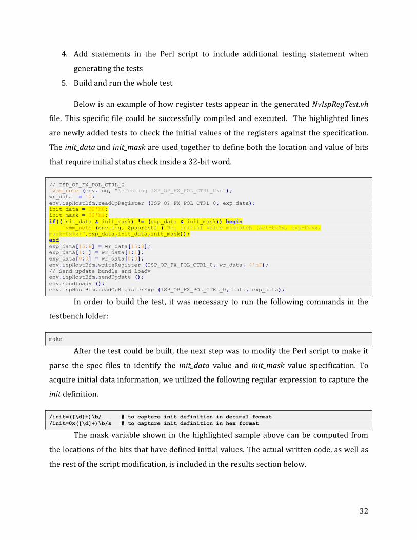
Below is an example of how register tests appear in the generated NvIspRegTest.vh
file. This specific file could be successfully compiled and executed. The highlighted lines
are newly added tests to check the initial values of the registers against the specification.
The init_data and init_mask are used together to define both the location and value of bits
that require initial status check inside a 32-bit word.
// ISP_OP_FX_POL_CTRL_0
`vmm_note (env.log, "\nTesting ISP_OP_FX_POL_CTRL_0\n");
wr_data = '0;
env.ispHostBfm.readOpRegister (ISP_OP_FX_POL_CTRL_0, exp_data);
init_data = 32'h0;
init_mask = 32'h1;
if((init_data & init_mask) != (exp_data & init_mask)) begin
`vmm_note (env.log, $psprintf ("Reg initial value mismatch (act=0x%x, exp=0x%x,
mask=0x%x)",exp_data,init_data,init_mask));
end
exp_data[15:8] = wr_data[15:8];
exp_data[1:1] = wr_data[1:1];
exp_data[0:0] = wr_data[0:0];
env.ispHostBfm.writeRegister (ISP_OP_FX_POL_CTRL_0, wr_data, 4'hF);
// Send update bundle and loadv
env.ispHostBfm.sendUpdate ();
env.sendLoadV ();
env.ispHostBfm.readOpRegisterExp (ISP_OP_FX_POL_CTRL_0, data, exp_data);
In order to build the test, it was necessary to run the following commands in the
testbench folder:
make
After the test could be built, the next step was to modify the Perl script to make it
parse the spec files to identify the init_data value and init_mask value specification. To
acquire initial data information, we utilized the following regular expression to capture the
init definition.
/init=([\d]+)\b/ # to capture init definition in decimal format
/init=0x([\d]+)\b/s # to capture init definition in hex format
The mask variable shown in the highlighted sample above can be computed from
the locations of the bits that have defined initial values. The actual written code, as well as
the rest of the script modification, is included in the results section below.

33
5.4 Results
5.4.1 Modification of Perl Script
Among the many functions of the Perl scripts, two features are of our concern. First
is the spec file parse that convert the spec file into a hash structure. As shown in the
highlighted code snippet below, the added code enables the script to capture initial value
definitions in the spec files and store init_data and init_mask in the hash structure. Much of
the original code has been omitted to emphasize the changes. The full version of this
parse_spec_file function is located in Appendix A.
sub parse_spec_file {
# code here omitted
# found a range [max:min]
if ($line =~ /\s*(.*):(\d+|.*)([ \t]+)(\S+)([ \t]+)(\S+)/) {
next if ($1 eq "");
if ($debug) {
print "$1, $2, $4, $6\n";
}
$max = $1;
$min = $2;
$rws = $4;
$fld = $6;
if($line =~ /init=([\d]+)\b/) {
$init = $1;
}
elsif ($line =~ /init=0x([\d]+)\b/s){
$init = hex($1);
}
else {
$init = undef;
}
# just single bit instead of range
} elsif ($line =~ /[ \t]+(\S+)[ \t]+(\S+)([ \t]+)(\S+)/) {
next if ($1 eq "");
if ($debug) {
print "$1, $2, $4\n";
}
$max = $1;
$min = $1;
$rws = $2;
$fld = $4;
if($line =~ /init=([\d]+)\b/) {
$init = $1;
}
elsif ($line =~ /init=0x([\d]+)\b/s){
$init = hex($1);
}
else {
$init = undef;
}
} else {
next;
}
# more code omitted here
if(defined($init)) {
my $mask = 0;
foreach my $bit (int($min)..int($max)) {
34
$mask |= (1 << $bit);
}
if(!exists($class->{$reg_name}->{INIT_MASK})) {
$class->{$reg_name}->{INIT_MASK} = 0; # bits in reg that has initial value in HEX
}
if(!exists($class->{$reg_name}->{INIT_DATA})) {
$class->{$reg_name}->{INIT_DATA} = 0; # initial value of bits in register in HEX
}
$class->{$reg_name}->{INIT_MASK} |= $mask;
$class->{$reg_name}->{INIT_DATA} |= ($init & $mask) << $min;
}
# code omitted here
}
The second feature is the test code generation part that outputs the codes. The
modifications are shown below with much of the original code omitted. This is wrapped
inside a condition to make sure the tests only appear when necessary.
if($test eq "All 0's" && $class_spec->{$register}->{INIT_MASK} gt 0) {
my $init_data = sprintf("%x",$class_spec->{$register}->{INIT_DATA});
my $init_mask = sprintf("%x",$class_spec->{$register}->{INIT_MASK});
print FILE " init_data = 32'h${init_data};
init_mask = 32'h${init_mask};
if((init_data & init_mask) != (exp_data & init_mask)) begin
`vmm_note (env.log, \$psprintf (\"Reg initial value mismatch (act=0x%x, exp=0x%x,
mask=0x%x)\",exp_data,init_data,init_mask));
end\n";
}
5.4.2 Generated Tests
The Perl script could now generate the tests without error. For each of the registers
that have initial value defined, there is now a test for it. This satisfies the goal of this task.
Since each of the tests is similar to the manually added one in the methodology, and the
whole test file itself is very large, the generated test file is not shown here.
The generated tests were compiled without error and executed smoothly. It
reported a list of 24 mismatches shown in Appendix B and we reported this list to the ISP
team.
6.0 SPECIAL EFFECT SUBUNIT VERIFICATION
This part of the project involved adding register initial value test functionality for
the register read and write test. This test enables NVIDIA engineers to identify problems
with registers and makes sure the values in these registers after reset conform to the
specification. NVIDIA engineers will fix issues found in the test run and can run these tests
in future regressions to verify the register values.Random Test for FX Subunit
35
6.1 Introduction
Inside TEGRA’s ISP unit, there are several subunits, including the Special Effect
subunit. This section includes the methodology and results of verifying the functionality
this subunit by running simulation tests. Also discussed are some code and function
coverage test results to measure test comprehensiveness.
6.2 Important Concepts
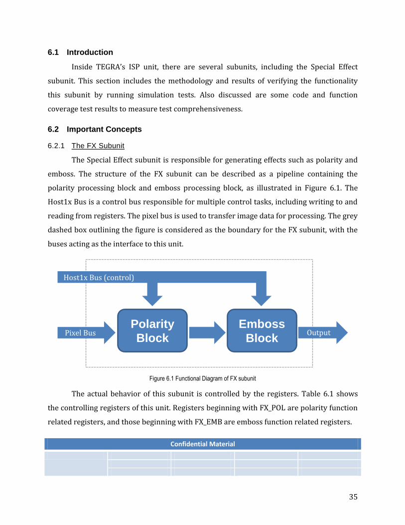
6.2.1 The FX Subunit
The Special Effect subunit is responsible for generating effects such as polarity and
emboss. The structure of the FX subunit can be described as a pipeline containing the
polarity processing block and emboss processing block, as illustrated in Figure 6.1. The
Host1x Bus is a control bus responsible for multiple control tasks, including writing to and
reading from registers. The pixel bus is used to transfer image data for processing. The grey
dashed box outlining the figure is considered as the boundary for the FX subunit, with the
buses acting as the interface to this unit.
Figure 6.1 Functional Diagram of FX subunit
The actual behavior of this subunit is controlled by the registers. Table 6.1 shows
the controlling registers of this unit. Registers beginning with FX_POL are polarity function
related registers, and those beginning with FX_EMB are emboss function related registers.
Confidential Material
Polarity
Block
Emboss
Block
Host1x Bus (control)
Pixel Bus Output
36
Table 6.1 FX Subunit Register Specification [12]
6.2.2 Testbench
The testing infrastructure built by NVIDIA employees, known as the test bench, has
a considerable amount of functionality. It is a collection of scripts and executables that
carry out simulation tests and other jobs. The test bench is a large structure and it is
necessary only to focus on specific portions of it, shown in Figure 6.2.
Figure 6.2 FX random test and related files
The files with an ‘x’ in the extension will be processed by the in-house VIVA program
before actually being compiled. Similar to the previous section, this structure is sufficient to
reveal the file relationship for a developer.
On the left side in the above figure, the class in fxRandom.svx inherits the
NvIspMasterRandom class, which acts as a framework to run the random tests. The
fxRandom.svx is responsible for filling this framework by selecting information, such as
Inherited By
Instantiated By
Included By Included
By
Included By
NvIspRegDist.svix *
NvIspMasterRandom.svx *
NvIspCustomConstraints.svix
NvHost1xIspOpRegs.svix
../stim/random/fxRandom.svx +
NvHost1xIspOpFxRegs.svx
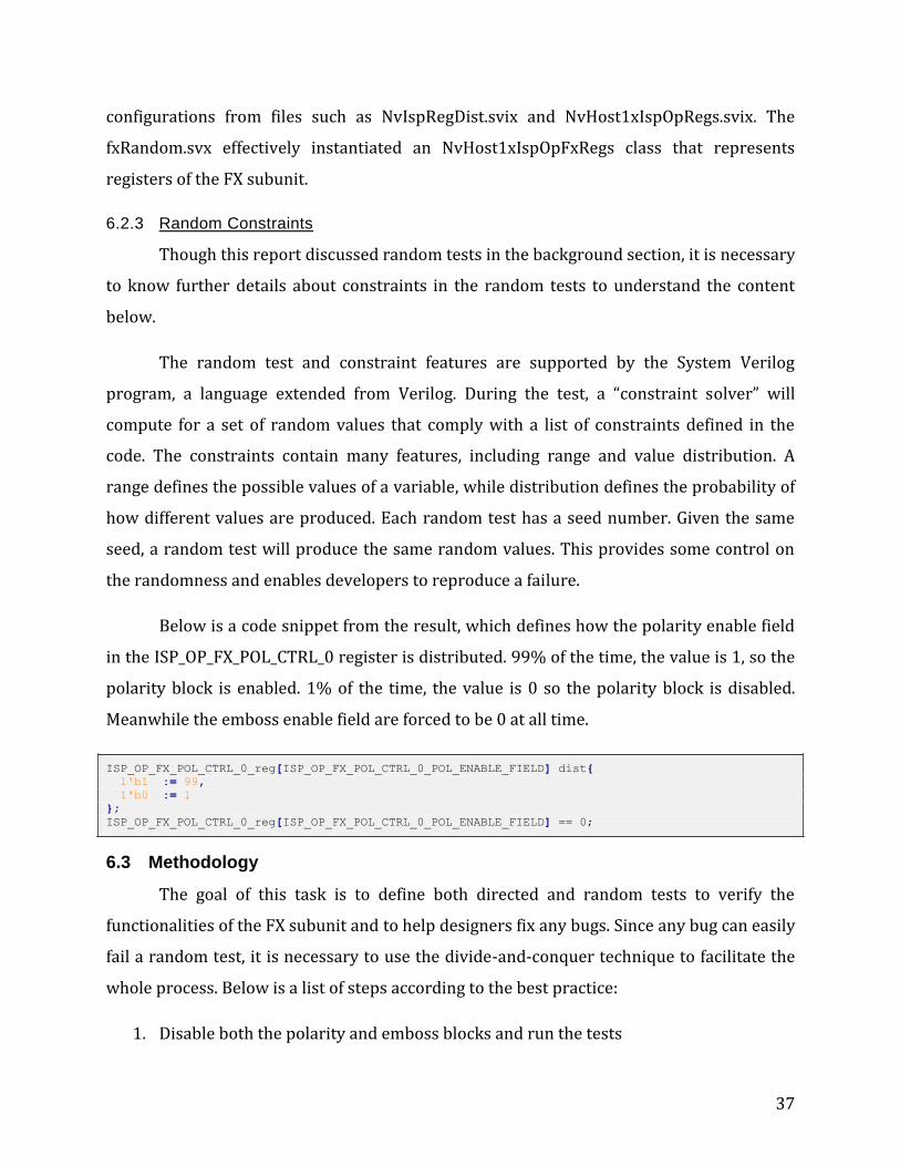
37
configurations from files such as NvIspRegDist.svix and NvHost1xIspOpRegs.svix. The
fxRandom.svx effectively instantiated an NvHost1xIspOpFxRegs class that represents
registers of the FX subunit.
6.2.3 Random Constraints
Though this report discussed random tests in the background section, it is necessary
to know further details about constraints in the random tests to understand the content
below.
The random test and constraint features are supported by the System Verilog
program, a language extended from Verilog. During the test, a “constraint solver” will
compute for a set of random values that comply with a list of constraints defined in the
code. The constraints contain many features, including range and value distribution. A
range defines the possible values of a variable, while distribution defines the probability of
how different values are produced. Each random test has a seed number. Given the same
seed, a random test will produce the same random values. This provides some control on
the randomness and enables developers to reproduce a failure.
Below is a code snippet from the result, which defines how the polarity enable field
in the ISP_OP_FX_POL_CTRL_0 register is distributed. 99% of the time, the value is 1, so the
polarity block is enabled. 1% of the time, the value is 0 so the polarity block is disabled.
Meanwhile the emboss enable field are forced to be 0 at all time.
ISP_OP_FX_POL_CTRL_0_reg[ISP_OP_FX_POL_CTRL_0_POL_ENABLE_FIELD] dist{
1'b1 := 99,
1'b0 := 1
};
ISP_OP_FX_POL_CTRL_0_reg[ISP_OP_FX_POL_CTRL_0_POL_ENABLE_FIELD] == 0;
6.3 Methodology
The goal of this task is to define both directed and random tests to verify the
functionalities of the FX subunit and to help designers fix any bugs. Since any bug can easily
fail a random test, it is necessary to use the divide-and-conquer technique to facilitate the
whole process. Below is a list of steps according to the best practice:
1. Disable both the polarity and emboss blocks and run the tests
38
2. Enable only the polarity block with simple register values
3. Report failure to the designer and wait for a fix
4. Repeat 2 and 3 with more complex values until most tests pass
5. Do step 2-4 on the emboss block
6. Formalize random constraints and create basic test
7. Add random tests to the daily regression test list
8. Run coverage report and refine constraints to improve coverage if possible
To do step 2 or step 6, files need to be modified or added. The files that required
modifications are denoted with an asterisk in Figure 6.2, while the newly added files are
denoted with a plus sign. Therefore, step 2 or step 6 can be broken down into several sub
procedures.
1. Create fxRandoms class in fxRandoms.svx file that inherits the
NvIspMasterRandom class.
2. Modify the NvIspMasterRandom.svx file to support the configuration specified in
fxRandoms.
3. Modify the NvIspRegDist.svx file to specify the constraints used by the fxRandoms
class.
In order to create a class called fxRandoms, we added the fxRandoms.svx file to the
.../stim/random folder. Since most of the test logic was inherited from the class in the
NvIspMasterRandom.svx file, it is quite simple (shown below). This piece of code tests the
FX unit with one small 50px by 50px frame. This file utilized several macros, such as
`isp_unitrandom_begin(test_name) but the details are beyond the scope of this project.
`isp_unitrandom_begin(fxRandoms)
xBarCfg = "fx";
regDistCfg = "fx";
minHeight = 50;
maxHeight = 50;
minWidth = 50;
maxWidth = 50;
frCnt = 1;
frGroup = 1;
`isp_unitrandom_end
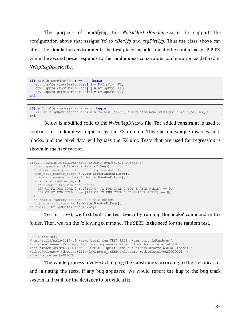
39
The purpose of modifying the NvIspMasterRandom.svx is to support the
configuration above that assigns ‘fx’ to xBarCfg and regDistCfg. Thus the class above can
affect the simulation environment. The first piece excludes most other units except ISP FX,
while the second piece responds to the randomness constraints configuration as defined in
NvIspRegDist.svx file.
if(xBarCfg.compare("fx") == 0 ) begin
env.ispCfg.crossBarSources[1] = NvIspCfg::FX;
env.ispCfg.crossBarSources[2] = NvIspCfg::XAB;
env.ispCfg.crossBarSources[3] = NvIspCfg::VI;
end
if(regDistCfg.compare("fx") == 0) begin
NvHost1xIspOpFxRegs::override_with_new ("@%*", NvIspMasterRandomFxRegs::this_type, log);
end
Below is modified code to the NvIspRegDist.svx file. The added constraint is used to
control the randomness required by the FX random. This specific sample disables both
blocks, and the pixel data will bypass the FX unit. Tests that are used for regression is
shown in the next section.
class NvIspMasterRandomFxRegs extends NvHost1xIspOpFxRegs;
`vmm_typename (NvIspMasterRandomFxRegs);
// Predefined macros for defining vmm_data functions
`vmm_data_member_begin (NvIspMasterRandomFxRegs);
`vmm_data_member_end (NvIspMasterRandomFxRegs);
constraint custom_regs {
// Disable the POL and Emboss
ISP_OP_FX_POL_CTRL_0_reg[ISP_OP_FX_POL_CTRL_0_POL_ENABLE_FIELD] == 0;
ISP_OP_FX_EMB_CTRL_0_reg[ISP_OP_FX_EMB_CTRL_0_EB_ENABLE_FIELD] == 0;
}
// Enable factory pattern for this object
`vmm_class_factory (NvIspMasterRandomFxRegs);
endclass : NvIspMasterRandomFxRegs
To run a test, we first built the test bench by running the ‘make’ command in the
folder. Then, we ran the following command. The SEED is the seed for the random test.
SEED=235467894
/home/utils/make-3.82/bin/make local_run TEST_ARGS="+vmm_test=fxRandoms \
+coverage_name=fxRandoms$SEED +vmm_log_nowarn_at_200 +vmm_log_nofatal_at_1000 \
+ntb_random_seed=$SEED +ENABLE_CMODEL +quiet +vmm_out_dir=fxRandoms_$SEED +fsdb=1 \
+debugFrGroup=0 +debussy+file=fxRandoms_$SEED/fxRandoms +debugLevel=0x80000001 \
+vmm_log_default=DEBUG"
The whole process involved changing the constraints according to the specification
and initiating the tests. If any bug appeared, we would report the bug to the bug track
system and wait for the designer to provide a fix.
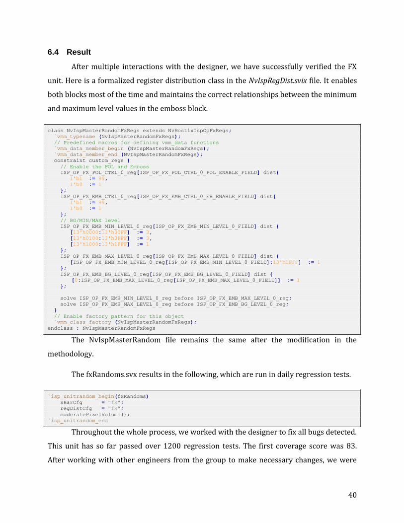
40
6.4 Result
After multiple interactions with the designer, we have successfully verified the FX
unit. Here is a formalized register distribution class in the NvIspRegDist.svix file. It enables
both blocks most of the time and maintains the correct relationships between the minimum
and maximum level values in the emboss block.
class NvIspMasterRandomFxRegs extends NvHost1xIspOpFxRegs;
`vmm_typename (NvIspMasterRandomFxRegs);
// Predefined macros for defining vmm_data functions
`vmm_data_member_begin (NvIspMasterRandomFxRegs);
`vmm_data_member_end (NvIspMasterRandomFxRegs);
constraint custom_regs {
// Enable the POL and Emboss
ISP_OP_FX_POL_CTRL_0_reg[ISP_OP_FX_POL_CTRL_0_POL_ENABLE_FIELD] dist{
1'b1 := 99,
1'b0 := 1
};
ISP_OP_FX_EMB_CTRL_0_reg[ISP_OP_FX_EMB_CTRL_0_EB_ENABLE_FIELD] dist{
1'b1 := 99,
1'b0 := 1
};
// BG/MIN/MAX level
ISP_OP_FX_EMB_MIN_LEVEL_0_reg[ISP_OP_FX_EMB_MIN_LEVEL_0_FIELD] dist {
[13'h0000:13'h00FF] := 3,
[13'h0100:13'h0FFF] := 3,
[13'h1000:13'h1FFF] := 1
};
ISP_OP_FX_EMB_MAX_LEVEL_0_reg[ISP_OP_FX_EMB_MAX_LEVEL_0_FIELD] dist {
[ISP_OP_FX_EMB_MIN_LEVEL_0_reg[ISP_OP_FX_EMB_MIN_LEVEL_0_FIELD]:13'h1FFF] := 1
};
ISP_OP_FX_EMB_BG_LEVEL_0_reg[ISP_OP_FX_EMB_BG_LEVEL_0_FIELD] dist {
[0:ISP_OP_FX_EMB_MAX_LEVEL_0_reg[ISP_OP_FX_EMB_MAX_LEVEL_0_FIELD]] := 1
};
solve ISP_OP_FX_EMB_MIN_LEVEL_0_reg before ISP_OP_FX_EMB_MAX_LEVEL_0_reg;
solve ISP_OP_FX_EMB_MAX_LEVEL_0_reg before ISP_OP_FX_EMB_BG_LEVEL_0_reg;
}
// Enable factory pattern for this object
`vmm_class_factory (NvIspMasterRandomFxRegs);
endclass : NvIspMasterRandomFxRegs
The NvIspMasterRandom file remains the same after the modification in the
methodology.
The fxRandoms.svx results in the following, which are run in daily regression tests.
`isp_unitrandom_begin(fxRandoms)
xBarCfg = "fx";
regDistCfg = "fx";
moderatePixelVolume();
`isp_unitrandom_end
Throughout the whole process, we worked with the designer to fix all bugs detected.
This unit has so far passed over 1200 regression tests. The first coverage score was 83.
After working with other engineers from the group to make necessary changes, we were
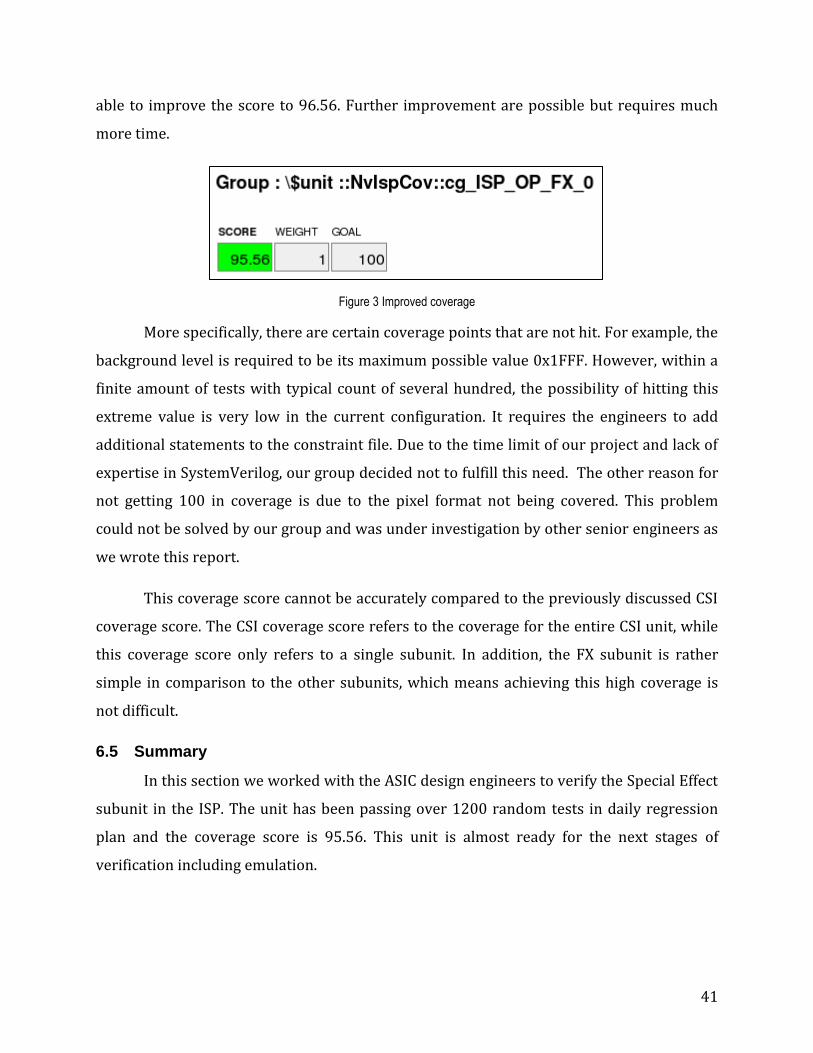
41
able to improve the score to 96.56. Further improvement are possible but requires much
more time.
Figure 3 Improved coverage
More specifically, there are certain coverage points that are not hit. For example, the
background level is required to be its maximum possible value 0x1FFF. However, within a
finite amount of tests with typical count of several hundred, the possibility of hitting this
extreme value is very low in the current configuration. It requires the engineers to add
additional statements to the constraint file. Due to the time limit of our project and lack of
expertise in SystemVerilog, our group decided not to fulfill this need. The other reason for
not getting 100 in coverage is due to the pixel format not being covered. This problem
could not be solved by our group and was under investigation by other senior engineers as
we wrote this report.
This coverage score cannot be accurately compared to the previously discussed CSI
coverage score. The CSI coverage score refers to the coverage for the entire CSI unit, while
this coverage score only refers to a single subunit. In addition, the FX subunit is rather
simple in comparison to the other subunits, which means achieving this high coverage is
not difficult.
6.5 Summary
In this section we worked with the ASIC design engineers to verify the Special Effect
subunit in the ISP. The unit has been passing over 1200 random tests in daily regression
plan and the coverage score is 95.56. This unit is almost ready for the next stages of
verification including emulation.
42
7.0 CONCLUSION
Our team completed several Tegra ISP verification tasks while working at NVIDIA,
including CSI verification, ISP verification, and power flow verification. All three
verification tasks are integral parts of the ISP architecture. The CSI and ISP are two very
significant and important modules, while power flow concerns the ISP architecture in its
entirety. The verification work that we have performed has aided NVIDIA’s engineers,
allowing the overall ISP verification process to be that much simpler for them. In
completing these tasks, our project team has accomplished the overall goal of this project,
which is to aid in the verification process of Tegra’s next generation ISP.
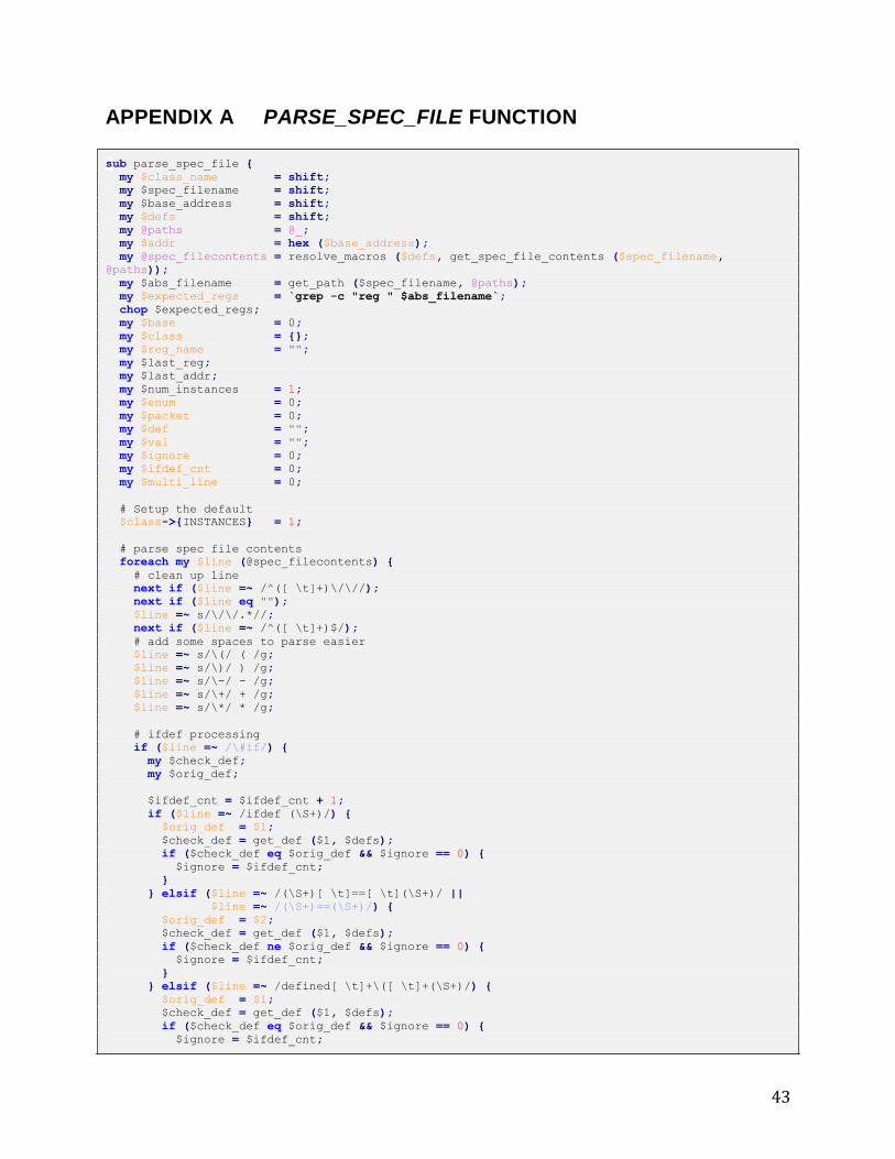
43
APPENDIX A PARSE_SPEC_FILE FUNCTION
sub parse_spec_file {
my $class_name = shift;
my $spec_filename = shift;
my $base_address = shift;
my $defs = shift;
my @paths = @_;
my $addr = hex ($base_address);
my @spec_filecontents = resolve_macros ($defs, get_spec_file_contents ($spec_filename,
@paths));
my $abs_filename = get_path ($spec_filename, @paths);
my $expected_regs = `grep -c "reg " $abs_filename`;
chop $expected_regs;
my $base = 0;
my $class = {};
my $reg_name = "";
my $last_reg;
my $last_addr;
my $num_instances = 1;
my $enum = 0;
my $packet = 0;
my $def = "";
my $val = "";
my $ignore = 0;
my $ifdef_cnt = 0;
my $multi_line = 0;
# Setup the default
$class->{INSTANCES} = 1;
# parse spec file contents
foreach my $line (@spec_filecontents) {
# clean up line
next if ($line =~ /^([ \t]+)\/\//);
next if ($line eq "");
$line =~ s/\/\/.*//;
next if ($line =~ /^([ \t]+)$/);
# add some spaces to parse easier
$line =~ s/\(/ ( /g;
$line =~ s/\)/ ) /g;
$line =~ s/\-/ - /g;
$line =~ s/\+/ + /g;
$line =~ s/\*/ * /g;
# ifdef processing
if ($line =~ /\#if/) {
my $check_def;
my $orig_def;
$ifdef_cnt = $ifdef_cnt + 1;
if ($line =~ /ifdef (\S+)/) {
$orig_def = $1;
$check_def = get_def ($1, $defs);
if ($check_def eq $orig_def && $ignore == 0) {
$ignore = $ifdef_cnt;
}
} elsif ($line =~ /(\S+)[ \t]==[ \t](\S+)/ ||
$line =~ /(\S+)==(\S+)/) {
$orig_def = $2;
$check_def = get_def ($1, $defs);
if ($check_def ne $orig_def && $ignore == 0) {
$ignore = $ifdef_cnt;
}
} elsif ($line =~ /defined[ \t]+\([ \t]+(\S+)/) {
$orig_def = $1;
$check_def = get_def ($1, $defs);
if ($check_def eq $orig_def && $ignore == 0) {
$ignore = $ifdef_cnt;
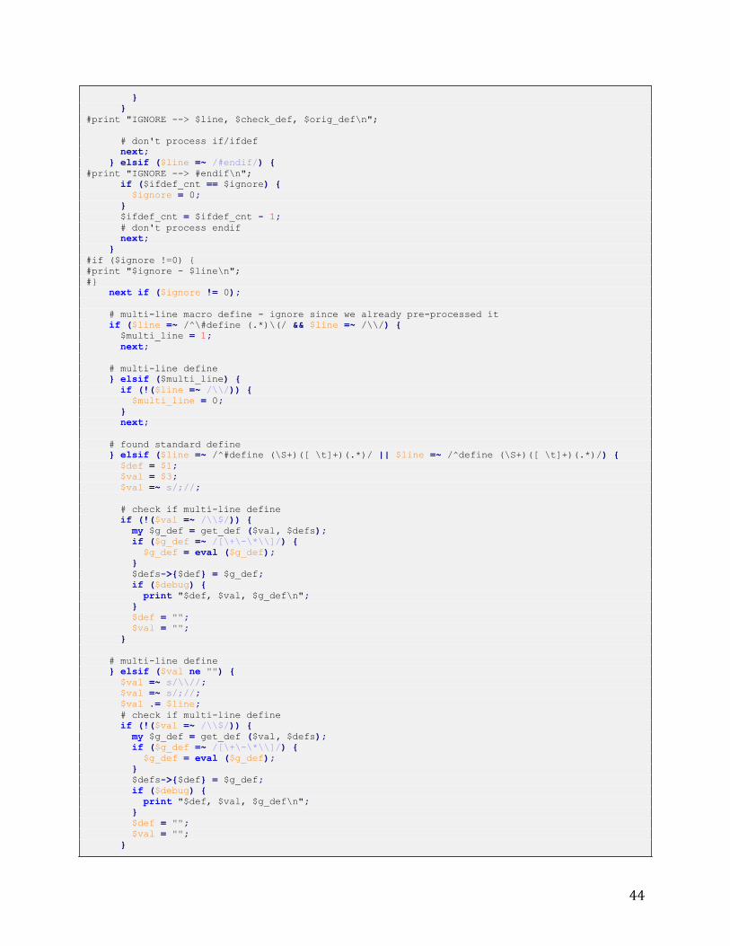
44
}
}
#print "IGNORE --> $line, $check_def, $orig_def\n";
# don't process if/ifdef
next;
} elsif ($line =~ /#endif/) {
#print "IGNORE --> #endif\n";
if ($ifdef_cnt == $ignore) {
$ignore = 0;
}
$ifdef_cnt = $ifdef_cnt - 1;
# don't process endif
next;
}
#if ($ignore !=0) {
#print "$ignore - $line\n";
#}
next if ($ignore != 0);
# multi-line macro define - ignore since we already pre-processed it
if ($line =~ /^\#define (.*)\(/ && $line =~ /\\/) {
$multi_line = 1;
next;
# multi-line define
} elsif ($multi_line) {
if (!($line =~ /\\/)) {
$multi_line = 0;
}
next;
# found standard define
} elsif ($line =~ /^#define (\S+)([ \t]+)(.*)/ || $line =~ /^define (\S+)([ \t]+)(.*)/) {
$def = $1;
$val = $3;
$val =~ s/;//;
# check if multi-line define
if (!($val =~ /\\$/)) {
my $g_def = get_def ($val, $defs);
if ($g_def =~ /[\+\-\*\\]/) {
$g_def = eval ($g_def);
}
$defs->{$def} = $g_def;
if ($debug) {
print "$def, $val, $g_def\n";
}
$def = "";
$val = "";
}
# multi-line define
} elsif ($val ne "") {
$val =~ s/\\//;
$val =~ s/;//;
$val .= $line;
# check if multi-line define
if (!($val =~ /\\$/)) {
my $g_def = get_def ($val, $defs);
if ($g_def =~ /[\+\-\*\\]/) {
$g_def = eval ($g_def);
}
$defs->{$def} = $g_def;
if ($debug) {
print "$def, $val, $g_def\n";
}
$def = "";
$val = "";
}
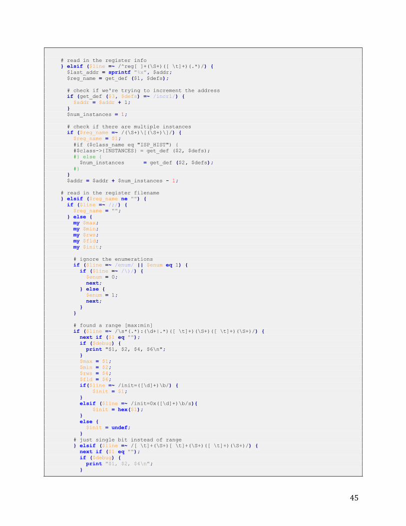
45
# read in the register info
} elsif ($line =~ /^reg[ ]+(\S+)([ \t]+)(.*)/) {
$last_addr = sprintf "%x", $addr;
$reg_name = get_def ($1, $defs);
# check if we're trying to increment the address
if (get_def ($3, $defs) =~ /incr1/) {
$addr = $addr + 1;
}
$num_instances = 1;
# check if there are multiple instances
if ($reg_name =~ /(\S+)\[(\S+)\]/) {
$reg_name = $1;
#if ($class_name eq "ISP_HIST") {
#$class->{INSTANCES} = get_def ($2, $defs);
#} else {
$num_instances = get_def ($2, $defs);
#}
}
$addr = $addr + $num_instances - 1;
# read in the register filename
} elsif ($reg_name ne "") {
if ($line =~ /;/) {
$reg_name = "";
} else {
my $max;
my $min;
my $rws;
my $fld;
my $init;
# ignore the enumerations
if ($line =~ /enum/ || $enum eq 1) {
if ($line =~ /\)/) {
$enum = 0;
next;
} else {
$enum = 1;
next;
}
}
# found a range [max:min]
if ($line =~ /\s*(.*):(\d+|.*)([ \t]+)(\S+)([ \t]+)(\S+)/) {
next if ($1 eq "");
if ($debug) {
print "$1, $2, $4, $6\n";
}
$max = $1;
$min = $2;
$rws = $4;
$fld = $6;
if($line =~ /init=([\d]+)\b/) {
$init = $1;
}
elsif ($line =~ /init=0x([\d]+)\b/s){
$init = hex($1);
}
else {
$init = undef;
}
# just single bit instead of range
} elsif ($line =~ /[ \t]+(\S+)[ \t]+(\S+)([ \t]+)(\S+)/) {
next if ($1 eq "");
if ($debug) {
print "$1, $2, $4\n";
}
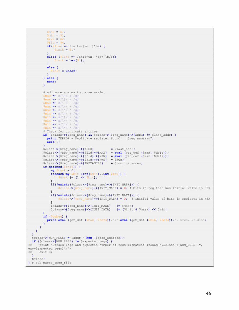
46
$max = $1;
$min = $1;
$rws = $2;
$fld = $4;
if($line =~ /init=([\d]+)\b/) {
$init = $1;
}
elsif ($line =~ /init=0x([\d]+)\b/s){
$init = hex($1);
}
else {
$init = undef;
}
} else {
next;
}
# add some spaces to parse easier
$max =~ s/\(/ ( /g;
$max =~ s/\)/ ) /g;
$max =~ s/\-/ - /g;
$max =~ s/\+/ + /g;
$max =~ s/\*/ * /g;
$min =~ s/\(/ ( /g;
$min =~ s/\)/ ) /g;
$min =~ s/\-/ - /g;
$min =~ s/\+/ + /g;
$min =~ s/\*/ * /g;
# Check for duplicate entries
if ($class->{$reg_name} && $class->{$reg_name}->{ADDR} != $last_addr) {
print "ERROR - Duplicate register found! ($reg_name)\n";
exit 1;
}
$class->{$reg_name}->{ADDR} = $last_addr;
$class->{$reg_name}->{$fld}->{MAX} = eval (get_def ($max, $defs));
$class->{$reg_name}->{$fld}->{MIN} = eval (get_def ($min, $defs));
$class->{$reg_name}->{$fld}->{RWS} = $rws;
$class->{$reg_name}->{INSTANCES} = $num_instances;
if(defined($init)) {
my $mask = 0;
foreach my $bit (int($min)..int($max)) {
$mask |= (1 << $bit);
}
if(!exists($class->{$reg_name}->{INIT_MASK})) {
$class->{$reg_name}->{INIT_MASK} = 0; # bits in reg that has initial value in HEX
}
if(!exists($class->{$reg_name}->{INIT_DATA})) {
$class->{$reg_name}->{INIT_DATA} = 0; # initial value of bits in register in HEX
}
$class->{$reg_name}->{INIT_MASK} |= $mask;
$class->{$reg_name}->{INIT_DATA} |= ($init & $mask) << $min;
}
if ($debug) {
print eval (get_def ($max, $defs)).":".eval (get_def ($min, $defs)).", $rws, $fld\n";
}
}
}
}
$class->{NUM_REGS} = $addr - hex ($base_address);
if ($class->{NUM_REGS} != $expected_regs) {
## print "Parsed regs and expected number of regs mismatch! (found=".$class->{NUM_REGS}.",
exp=$expected_regs)\n";
## exit 0;
}
$class;
} # sub parse_spec_file
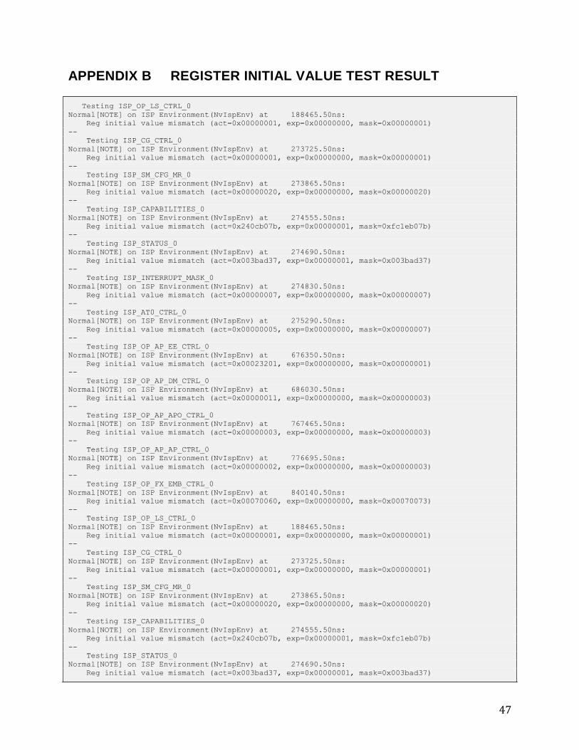
47
APPENDIX B REGISTER INITIAL VALUE TEST RESULT
Testing ISP_OP_LS_CTRL_0
Normal[NOTE] on ISP Environment(NvIspEnv) at 188465.50ns:
Reg initial value mismatch (act=0x00000001, exp=0x00000000, mask=0x00000001)
--
Testing ISP_CG_CTRL_0
Normal[NOTE] on ISP Environment(NvIspEnv) at 273725.50ns:
Reg initial value mismatch (act=0x00000001, exp=0x00000000, mask=0x00000001)
--
Testing ISP_SM_CFG_MR_0
Normal[NOTE] on ISP Environment(NvIspEnv) at 273865.50ns:
Reg initial value mismatch (act=0x00000020, exp=0x00000000, mask=0x00000020)
--
Testing ISP_CAPABILITIES_0
Normal[NOTE] on ISP Environment(NvIspEnv) at 274555.50ns:
Reg initial value mismatch (act=0x240cb07b, exp=0x00000001, mask=0xfc1eb07b)
--
Testing ISP_STATUS_0
Normal[NOTE] on ISP Environment(NvIspEnv) at 274690.50ns:
Reg initial value mismatch (act=0x003bad37, exp=0x00000001, mask=0x003bad37)
--
Testing ISP_INTERRUPT_MASK_0
Normal[NOTE] on ISP Environment(NvIspEnv) at 274830.50ns:
Reg initial value mismatch (act=0x00000007, exp=0x00000000, mask=0x00000007)
--
Testing ISP_AT0_CTRL_0
Normal[NOTE] on ISP Environment(NvIspEnv) at 275290.50ns:
Reg initial value mismatch (act=0x00000005, exp=0x00000000, mask=0x00000007)
--
Testing ISP_OP_AP_EE_CTRL_0
Normal[NOTE] on ISP Environment(NvIspEnv) at 676350.50ns:
Reg initial value mismatch (act=0x00023201, exp=0x00000000, mask=0x00000001)
--
Testing ISP_OP_AP_DM_CTRL_0
Normal[NOTE] on ISP Environment(NvIspEnv) at 686030.50ns:
Reg initial value mismatch (act=0x00000011, exp=0x00000000, mask=0x00000003)
--
Testing ISP_OP_AP_APO_CTRL_0
Normal[NOTE] on ISP Environment(NvIspEnv) at 767465.50ns:
Reg initial value mismatch (act=0x00000003, exp=0x00000000, mask=0x00000003)
--
Testing ISP_OP_AP_AP_CTRL_0
Normal[NOTE] on ISP Environment(NvIspEnv) at 776695.50ns:
Reg initial value mismatch (act=0x00000002, exp=0x00000000, mask=0x00000003)
--
Testing ISP_OP_FX_EMB_CTRL_0
Normal[NOTE] on ISP Environment(NvIspEnv) at 840140.50ns:
Reg initial value mismatch (act=0x00070060, exp=0x00000000, mask=0x00070073)
--
Testing ISP_OP_LS_CTRL_0
Normal[NOTE] on ISP Environment(NvIspEnv) at 188465.50ns:
Reg initial value mismatch (act=0x00000001, exp=0x00000000, mask=0x00000001)
--
Testing ISP_CG_CTRL_0
Normal[NOTE] on ISP Environment(NvIspEnv) at 273725.50ns:
Reg initial value mismatch (act=0x00000001, exp=0x00000000, mask=0x00000001)
--
Testing ISP_SM_CFG_MR_0
Normal[NOTE] on ISP Environment(NvIspEnv) at 273865.50ns:
Reg initial value mismatch (act=0x00000020, exp=0x00000000, mask=0x00000020)
--
Testing ISP_CAPABILITIES_0
Normal[NOTE] on ISP Environment(NvIspEnv) at 274555.50ns:
Reg initial value mismatch (act=0x240cb07b, exp=0x00000001, mask=0xfc1eb07b)
--
Testing ISP_STATUS_0
Normal[NOTE] on ISP Environment(NvIspEnv) at 274690.50ns:
Reg initial value mismatch (act=0x003bad37, exp=0x00000001, mask=0x003bad37)
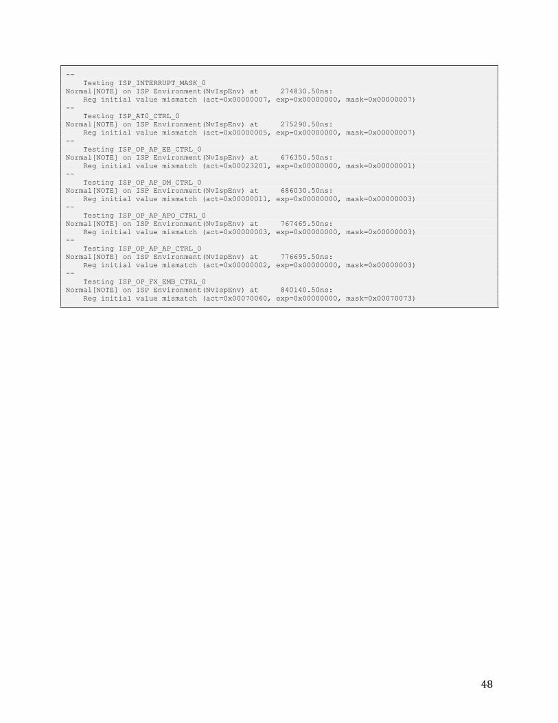
48
--
Testing ISP_INTERRUPT_MASK_0
Normal[NOTE] on ISP Environment(NvIspEnv) at 274830.50ns:
Reg initial value mismatch (act=0x00000007, exp=0x00000000, mask=0x00000007)
--
Testing ISP_AT0_CTRL_0
Normal[NOTE] on ISP Environment(NvIspEnv) at 275290.50ns:
Reg initial value mismatch (act=0x00000005, exp=0x00000000, mask=0x00000007)
--
Testing ISP_OP_AP_EE_CTRL_0
Normal[NOTE] on ISP Environment(NvIspEnv) at 676350.50ns:
Reg initial value mismatch (act=0x00023201, exp=0x00000000, mask=0x00000001)
--
Testing ISP_OP_AP_DM_CTRL_0
Normal[NOTE] on ISP Environment(NvIspEnv) at 686030.50ns:
Reg initial value mismatch (act=0x00000011, exp=0x00000000, mask=0x00000003)
--
Testing ISP_OP_AP_APO_CTRL_0
Normal[NOTE] on ISP Environment(NvIspEnv) at 767465.50ns:
Reg initial value mismatch (act=0x00000003, exp=0x00000000, mask=0x00000003)
--
Testing ISP_OP_AP_AP_CTRL_0
Normal[NOTE] on ISP Environment(NvIspEnv) at 776695.50ns:
Reg initial value mismatch (act=0x00000002, exp=0x00000000, mask=0x00000003)
--
Testing ISP_OP_FX_EMB_CTRL_0
Normal[NOTE] on ISP Environment(NvIspEnv) at 840140.50ns:
Reg initial value mismatch (act=0x00070060, exp=0x00000000, mask=0x00070073)
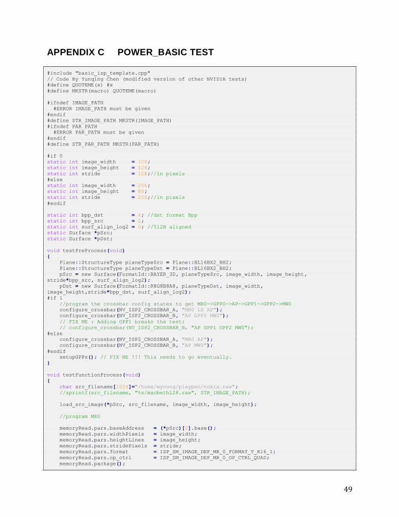
49
APPENDIX C POWER_BASIC TEST
#include "basic_isp_template.cpp"
// Code By Yunqing Chen (modified version of other NVIDIA tests)
#define QUOTEME(x) #x
#define MKSTR(macro) QUOTEME(macro)
#ifndef IMAGE_PATH
#ERROR IMAGE_PATH must be given
#endif
#define STR_IMAGE_PATH MKSTR(IMAGE_PATH)
#ifndef PAR_PATH
#ERROR PAR_PATH must be given
#endif
#define STR_PAR_PATH MKSTR(PAR_PATH)
#if 0
static int image_width = 128;
static int image_height = 128;
static int stride = 128;//in pixels
#else
static int image_width = 256;
static int image_height = 80;
static int stride = 256;//in pixels
#endif
static int bpp_dst = 4; //dst format Bpp
static int bpp_src = 2;
static int surf_align_log2 = 9; //512B aligned
static Surface *pSrc;
static Surface *pDst;
void testPreProcess(void)
{
Plane::StructureType planeTypeSrc = Plane::BL16BX2_BH2;
Plane::StructureType planeTypeDst = Plane::BL16BX2_BH2;
pSrc = new Surface(FormatId::BAYER_3D, planeTypeSrc, image_width, image_height,
stride*bpp_src, surf_align_log2);
pDst = new Surface(FormatId::R8G8B8A8, planeTypeDst, image_width,
image_height,stride*bpp_dst, surf_align_log2);
#if 1
//program the crossbar config states to get MR0->GPP0->AP->GPP1->GPP2->MW0
configure_crossbar(NV_ISP2_CROSSBAR_A, "MR0 LS AP");
configure_crossbar(NV_ISP2_CROSSBAR_B, "AP GPP0 MW0");
// FIX ME : Adding GPP1 breaks the test:
// configure_crossbar(NV_ISP2_CROSSBAR_B, "AP GPP1 GPP2 MW0");
#else
configure_crossbar(NV_ISP2_CROSSBAR_A, "MR0 AP");
configure_crossbar(NV_ISP2_CROSSBAR_B, "AP MW0");
#endif
setupGPPs(); // FIX ME !!! This needs to go eventually.
}
void testFunctionProcess(void)
{
char src_filename[1024]="/home/wyoung/playpen/nokia.raw";
//sprintf(src_filename, "%s/macbeth128.raw", STR_IMAGE_PATH);
load_src_image(*pSrc, src_filename, image_width, image_height);
//program MR0
memoryRead.pars.baseAddress = (*pSrc)[0].base();
memoryRead.pars.widthPixels = image_width;
memoryRead.pars.heightLines = image_height;
memoryRead.pars.stridePixels = stride;
memoryRead.pars.format = ISP_SM_IMAGE_DEF_MR_0_FORMAT_T_R16_I;
memoryRead.pars.op_ctrl = ISP_SM_IMAGE_DEF_MR_0_OP_CTRL_QUAD;
memoryRead.package();
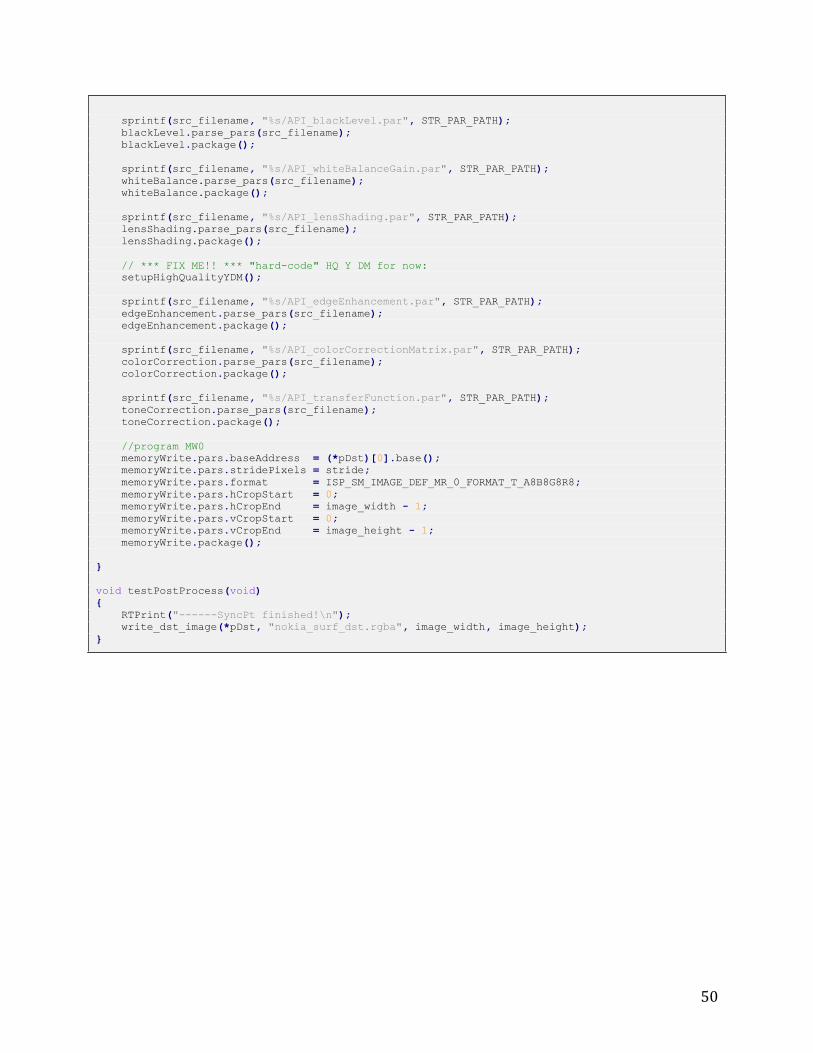
50
sprintf(src_filename, "%s/API_blackLevel.par", STR_PAR_PATH);
blackLevel.parse_pars(src_filename);
blackLevel.package();
sprintf(src_filename, "%s/API_whiteBalanceGain.par", STR_PAR_PATH);
whiteBalance.parse_pars(src_filename);
whiteBalance.package();
sprintf(src_filename, "%s/API_lensShading.par", STR_PAR_PATH);
lensShading.parse_pars(src_filename);
lensShading.package();
// *** FIX ME!! *** "hard-code" HQ Y DM for now:
setupHighQualityYDM();
sprintf(src_filename, "%s/API_edgeEnhancement.par", STR_PAR_PATH);
edgeEnhancement.parse_pars(src_filename);
edgeEnhancement.package();
sprintf(src_filename, "%s/API_colorCorrectionMatrix.par", STR_PAR_PATH);
colorCorrection.parse_pars(src_filename);
colorCorrection.package();
sprintf(src_filename, "%s/API_transferFunction.par", STR_PAR_PATH);
toneCorrection.parse_pars(src_filename);
toneCorrection.package();
//program MW0
memoryWrite.pars.baseAddress = (*pDst)[0].base();
memoryWrite.pars.stridePixels = stride;
memoryWrite.pars.format = ISP_SM_IMAGE_DEF_MR_0_FORMAT_T_A8B8G8R8;
memoryWrite.pars.hCropStart = 0;
memoryWrite.pars.hCropEnd = image_width - 1;
memoryWrite.pars.vCropStart = 0;
memoryWrite.pars.vCropEnd = image_height - 1;
memoryWrite.package();
}
void testPostProcess(void)
{
RTPrint("------SyncPt finished!\n");
write_dst_image(*pDst, "nokia_surf_dst.rgba", image_width, image_height);
}
51
BIBLIOGRAPHY
[1] Nvidia Corporation, "Corporate Milestones," 2011. [Online]. Available: http://www.nvidia.com/page/corporate_timeline.html. [Accessed 8 Nov 2011].
[2] Nvidia Corporation, "CFO Commentary on Second Quarter 2012 Results," 2011. [Online]. Available: http://phx.corporate-ir.net/External.File?item=UGFyZW50SUQ9MTAzNzQxfENoaWxkSUQ9LTF8VHlwZT0z&t=1. [Accessed 09 11 2011].
[3] N. Corporation, "Tegra Roadmap," February 2011. [Online]. Available: http://blogs.nvidia.com/2011/02/tegra-roadmap-revealed-next-chip-worlds-first-quadcore-mobile-processor/. [Accessed 15 November 2011].
[4] NVIDIA Corporation, "NVIDIA Tegra APX Series," [Online]. Available: http://www.nvidia.com/object/product_tegra_apx_us.html. [Accessed 15 November 2011].
[5] R. Cheng, "NVIDIA CEO Sees Tenfold Growth In Mobile-Chip Biz," CNET, 6 September 2011. [Online]. Available: http://news.cnet.com/8301-1035_3-20102167-94/nvidia-ceo-sees-tenfold-growth-in-mobile-chip-biz/. [Accessed 15 November 2011].
[6] NVIDIA Corporation, "New NVIDIA Tegra Processor Powers The Tablet Revolution," [Online]. Available: http://www.nvidia.com/object/io_1262837617533.html. [Accessed 15 November 2011].
[7] NVIDIA Corporation, "NVIDIA Tegra FAQ," [Online]. Available: http://www.nvidia.com/docs/IO/55043/NVIDIA_Tegra_FAQ_External.pdf. [Accessed 15 November 2011].
[8] NVIDIA Corporation, "NVIDIA Tegra: Tiny Computer Packs Massive Punch!," [Online]. Available: http://phx.corporate-ir.net/phoenix.zhtml?c=116466&p=irol-newsArticle&ID=1161234&highlight=. [Accessed 15 November 2011].
[9] NVIDIA Corporation, "NVIDIA Tegra 2," [Online]. Available: http://www.nvidia.com/object/tegra-2.html. [Accessed 15 November 2011].
[10] MIPI Alliance, "Camera Interface Specification," 2010. [Online]. Available: http://www.mipi.org/specifications/camera-interface. [Accessed 7 February 2010].
[11] B. Aldrich, J. Gupta and W. Young, "T124 Camera Serial Interface Internal Architecture Specification," 2012.
[12] W. Young, T124 Internal Architecture Specification, 2011.
[13] J. Kim, "WMP Verification/ RunTest API," NVIDIA, 2009. [Online]. Available: https://wiki.nvidia.com/wmpwiki/index.php/WMP_Verification/RunTest_API. [Accessed 5 March 2012].
[14] J. Reiley, "GPU Power/Power Regression Flow," 2011. [Online]. Available: https://wiki.nvidia.com/gpuhwdept/index.php/GPU_Power/Power_Regression_Flow. [Accessed 13 February 2012].
[15] S. Cornett, "Minimum Acceptable Code Coverage," Bullseye Testing Technology, 2011. [Online]. Available: http://www.bullseye.com/minimum.html. [Accessed 15 February 2012].
[16] P. Johnson, "Testing and Code Coverage," [Online]. Available: http://www.pjcj.net/testing_and_code_coverage/paper.html. [Accessed 15 February 2012].