practical manufacturing testing of 802.11 ofdm … … · · 2018-03-08practical manufacturing...
TRANSCRIPT
Practical Manufacturing Testing of 80211 OFDM Wireless Devices
WHITEPAPER
copy 2012 LitePoint A Teradyne Company All rights reserved
Practical Manufacturing Testing of Bluetooth Wireless Devices 1
Table of ContentsPreface 2 Who Should Use This Guide 2 What This Guide Contains 2Chapter 1 Summary 3Chapter 2 Introduction to IEEE 80211 OFDM 4 21 OFDM Modulation 4 22 OFDM Coding Rates and Data Rates 6 23 OFDM Packets 7Chapter 3 Transmit Measurements 8 31 Transmit Power Measurements 8 Transmit Average Power 8 Transmit Peak Power 8 Channel Power 9 Power vs Time 9 Packet-to-Packet Power Variation 9 32 Transmit Frequency Measurements 10 Frequency Error (Transmit Center Frequency Tolerance) 10 Clock Error 11 Frequency Settling (Start of Packet) 11 33 Transmit Frequency Measurements 12 Spectral Mask 12 Spectral Flatness 14 Transmit Center Frequency Leakage 14 Complimentary Cumulative Density Function (CCDF) 15 34 Transmit Modulation Measurements 16 Constellation Diagram 16 Error Vector Magnitude (EVM) 17 35 IQ Imbalance Measurements 19 IQ Gain and Phase Mismatch 19Chapter 4 Receive Measurements 21 Receive Packet Error Rate (Receive-PER) 21 Sensitivity 21 Maximum Input Level 22 Channel Rejection 23 Received Channel Power Indicator (RCPI) 24Chapter 5 Miscellaneous Measurements 26 RxTx Turnaround Time 26 Current Consumption 26 MAC Address 27Chapter 6 LitePoint Offerings for 80211 OFDM Testing 29 61 IQflexIQview 29 62 IQ2010 29 63 IQfact Software Solutions 29Appendix A11048576TP Identifiers 30
Practical Manufacturing Testing of Bluetooth Wireless Devices 2
PrefaceThe Practical Manufacturing Testing of 80211 OFDM Wireless Devices handbook provides an introduction to the production testing of 80211 OFDM-compliant handsets
The preface includes the following topics
bull Who should use this guide
bull What this guide contains
Who Should Use This GuideThe Practical Manufacturing Testing of 80211 OFDM Wireless Devices handbook is intended for test engineers and other technical personnel who intend to learn about testing of 80211 OFDM-compliant handsets
What This Guide ContainsThis document is divided into six chapters and an appendix and includes the following topics
Chapter 1 Introduction to this document
Chapter 2 Introduction to 80211 OFDM
Chapter 3 Transmit measurements
Chapter 4 Receive measurements
Chapter 5 Miscellaneous measurements
Chapter 6 LitePoint Offerings for 80211 OFDM Testing
Appendix A1 Test Purpose (TP) identifiers
Practical Manufacturing Testing of Bluetooth Wireless Devices 3
Chapter 1 Summary WiFi a technology that builds on IEEE 80211 standards is now becoming a common feature in many everyday devices including desktop and portable PCs game consoles more recently cellular handsets TVs home entertainment components and set-top boxes The advantages of WiFi for these and many more categories of commercial devices are numerous For example in cellular handsets WiFi offers a means to offload traffic that is negatively impacting cellular voice performance and is expected to be the key driver to mass consumer adoption of VoIP Thanks to these and many more advantages WiFi handset shipments have experienced strong growth over the past years a growth that is projected to continue in 2010 and beyond
While the technology for the mass production of WiFi devices is well established the manufacturers of these devices are faced with the challenge of testing for 80211 quality and reliability in a production-line environment where cost considerations are paramount
This document is intended to help manufacturers by offering an introduction to production testing of 80211 devices In particular it describes testing of OFDM 80211 which is becoming the standard over the DSSS 80211 PHY-layer amendment with a focus on OFDM 80211n which has required manufacturers of WiFi devices to meet tighter specifications with respect to the previous OFDM 80211ag amendments
After providing a brief description of OFDM 80211 modulation techniques data rates and packets this document presents information on the measurements traditionally used in a production line to assess the minimum requirements for WiFi devices which are then distributed in the marketplace The significance of each of these measurements and guidelines on how to set up the measurement procedure and interpret the results is also provided
Practical Manufacturing Testing of Bluetooth Wireless Devices 4
Chapter 2 Introduction to to IEEE 80211 OFDMIEEE 80211 is a set of standards defining a wireless communication system in the GHz range The original 80211 standard and subsequent ldquoamendmentsrdquo are created and maintained by the IEEE LANMAN Standards Committee (IEEE 802) and include several over-the-air modulation techniques that use the same basic protocol
The most popular modulation technique is Orthogonal Frequency Division Multiplexing (OFDM) defined for by the 80211a amendment in the 5 GHz band The 80211a standard was released in 1999 and uses the same data link layer protocol and frame format as the original standard In 2003 the use of OFDM technique was extended to the 24 GHz band with the release of the 80211g amendment 80211g was backward-compatible with the preexisting 80211b which occupies the same band but is based on Direct Sequence Spread Spectrum (DSSS) modulation and thus is not discussed in this document
The newest standard that makes use of OFDM is 80211n (in both the 24 GHz band and the 5 GHz band) which improves upon the previous 80211 standards by adding Multiple-Input Multiple-Output (MIMO) and other newer features The IEEE has approved the amendment in October 2009 yet chipsets and devices conforming to a 2007 draft of the 80211n proposal were made commercially available by several wireless companies prior to the final ratification
80211n chipsets and devices offer higher bandwidth as well as improved security and quality of service as a consequence this recent amendment has quickly become the technology of choice for many emerging multi-media applications including but not limited to game consoles smart phones Mobile Internet Devices (MIDs) Wi-Fi access points routers and broadband gateways that integrate modem and Wi-Fi features
Compared to the legacy devices IEEE requires manufacturers of 80211n devices to meet tighter specifications in order to support 80211nrsquos primary focus to improve throughput Given the technological progresses that have occurred since 2003 when the 80211g amendment was ratified manufacturers of legacy devices should also refer to the latest specifications if they want to keep their legacy devices competitive in the marketplace and to minimize the likelihood of coexistence problems with 80211n devices
In light of the recent changes and future trends in 80211 OFDM WiFi development this document focuses on the specifications described in the latest IEEE amendment (known as 80211n Specification or Amendment 5 Enhancement for Higher Throughput) While MIMO technology is an important part of the 80211n standard recently the most impressive growth has been seen in Single-Input Single-Output (SISO) OFDM 80211n wireless-enabled portable devices therefore this document is dedicated to testing such devices in a manufacturing environment
This chapter includes the following sections
21 OFDM Modulation
22 OFDM Coding Rates and Data Rates
23 OFDM Packets
21 Bluetooth Modulation and Data RatesIn the OFDM technique the usable bandwidth is divided into a large number of smaller bandwidths or ldquosubcarriersrdquo The high-speed information is then divided onto these multiple lower-speed signals which are transmitted simultaneously on different frequencies in parallel The resulting low-data-rate carriers are more tolerant of fading because of multiple reflections OFDM modulation is characterized by high peak-to-average power ratio (PAPR) in time and a power distribution that resembles white Gaussian noise
Prior to the release of the 80211n amendment 80211 OFDM was based on only 52 (26x2) carriers with 3125 kHz spacing defining about a 168 MHz bandwidth in a 20 MHz channel The OFDM format before the 80211n amendment is known today as Legacy Mode and is shown in Figure 1-a The recent amendment builds on previous 80211 standards by increasing the number of carriers and by adding 40 MHz channels to the physical layer This is accomplished in a number of modes
bull High-Throughput (HT) Mixed Mode
bull In Mixed Mode HT20 the 20 MHz channel is created by increasing the number of carriers from 52 to 56 in the HT portion as shown in Figure 1-b The legacy portion of the preamble still has 52 carriers
Practical Manufacturing Testing of Bluetooth Wireless Devices 5
bull In Mixed Mode HT40 the 40 MHz channel is created by using two adjacent 20 MHz channels with a total of 114 (57x2) carriers in the data portion as shown in Figure 1-c The legacy portion of the preamble has a total of only 104 carriers (52x2) The broadcast and other control frames are sent in legacy 20 MHz channels with 26x2 carriers to allow the legacy devices to inter-operate as well
bull High-Throughput (HT) Greenfield Mode
bull In Greenfield Mode also available in HT20 and HT40 the number of carriers is as defined in Mixed Mode1 The main difference between Mixed Mode and Greenfield Mode is that the latter has no legacy preamble that is there is no provision to allow a legacy device to understand the full transmission
A description of the structure of the PLCP2 protocol data unit in each mode is provided in Chapter 23
Each carrier is modulated by BPSK QPSK QAM16 or QAM64 modulation depending on the specific 80211 PHY layer samendments and data rate Pilots always use BPSK with a known pattern
26 Carriers10MHz
26 Carriers10MHz
Figure 1-a Carrier Structure in LegacyNon-HT Mode 20 MHz Channel
28 Carriers10MHz
28 Carriers10MHz
57 Carriers20MHz
57 Carriers20MHz
Figure 1-b Carrier Structure in Mixed Mode and Greenfield Mode 20 MHz Channel(In Mixed HT20 the legacy portion of the preamble has 26x2 carriers in Greenfield HT20 there is no legacy preamble)
Figure 1-c Carrier Structure in Mixed Mode and Greenfield Mode 40 MHz Channel(In Mixed HT40 the legacy portion of the preamble has 52x2 carriers in Greenfield HT40 there is no legacy preamble)
1 With the exception of the HT Signal Field (HT-SIG) see Chapter 23
2 Physical Layer Convergence Procedure
Practical Manufacturing Testing of Bluetooth Wireless Devices 6
22 OFDM Coding Rates and Data RatesIn LegacyNon-HT mode the 80211ag modulation scheme is used Here the data rate varies depending on the specific modulation format and coding rate (R) as shown in Table 1 The symbol duration is 4 μs equivalent to 250000 symbols The actual symbol is 32 μs the remaining 800 ns being guard interval (GI also called cyclic prefix) between symbols3 The spectral nulls are at integer multiples of 132 μs that is at integer multiples of the carrier spacing (3125 kHz)
The data is coded to improve performance reliability and handling of bit errors
Modulation Coding Rate (R) Data Rates
BPSK 12 6 Mbps
BPSK 34 9 Mbps
QPSK 12 12 Mbps
QPSK 34 18 Mbps
QAM16 12 24 Mbps
QAM16 34 36 Mbps
OFQAM64 23 48 Mbps
QAM64 34 54 Mbps
Table 1 Modulation Coding Rate and Data Rate in 80211ag devices (20 MHz channel spacing)
For 80211n communications a continuous decision-making process is used based on the feedback from the receiver about the channel conditions to adjust the transmit modulation Given the conditions the system will change the modulation rate to provide the best compromise between data rate and error rate for the payload In addition 80211n provides many more combinations than 80211ag to allow for transmission using multiple streams and coding The complexity of 80211n rate adaptation gives rise to the concept of Modulation Coding Scheme (MCS) which includes variables such as the number of spatial streams modulation and the data rate on each stream During communication the optimum MCS is negotiated based on channel conditions There are 76 MCS types specified in the 80211n Specification document Table 2 shows the modulation scheme (and corresponding data rate) used in the MCS with single spatial stream The values are reported both with 800 ns GI which is the legacy mode as well as the default mode for 80211n devices and with 400 ns GI which is an optional mode for 80211n devices
MCS ModulationCoding Rate (R)
Data Rate [Mbps]GI = 800 ns
Data Rate [Mbps]GI = 400 ns
20 MHz 40 MHz 20 MHz 40 MHz
0 BPSK 12 65 135 72 15
1 QPSK 12 13 27 144 30
2 QPSK 34 195 405 217 45
3 QAM16 12 26 54 289 60
4 QAM16 34 39 81 433 90
5 QAM64 23 52 108 578 120
6 QAM64 34 585 1215 650 135
7 QAM64 56 65 135 722 150
32 BPSK 12 6 67
Table 2 Modulation Coding Rate and Data Rate per MCS in single stream 80211 devices
3 The guard interval that is part of each OFDM symbol is a period of time that is used to minimize intersymbol interference
Practical Manufacturing Testing of Bluetooth Wireless Devices 7
23 OFDM Packets The 80211n Specification introduces the definition of the HT OFDM PHY which is based on the OFDM PHY defined in the previous amendment with extensibility up to four spatial streams for operation in 20 MHz bandwidth and with the addition of one to four spatial streams for operation in 40 MHz bandwidth
In the context of the HT PHY the structure of the PLCP protocol data unit (PPDU) is defined and can be one of the following
bull In Non-HT Format (mandatory) packets are structured exactly as in the previous amendment to ensure compatibility with legacy 80211ag devices
bull In HT-Mixed Format (mandatory) packets contain a non-HT preamble compatible with legacy devices to enable detection of the PPDU and acquisition of carrier frequency and timing by both HT and legacy devices The rest of the packet however cannot be decoded by legacy devices
bull In HT-Greenfield Format (optional) packets do not contain a non-HT compatible part
In the HT-Mixed Format the non-HT portion of the preamble contains a Legacy Short Training Field (L-STF) and a Legacy Long Training Field (L-LTF) which are defined exactly as the legacy OFDM 80211 Short Training Sequence (STS) and Long Training Sequence (LTS) respectively
bull The L-STF is for packet detection Automatic Gain Control (AGC) coarse frequency-offset correction The L-STF is 8 μs long (two OFDM symbols) does not contain channel coding and is not scrambled
bull The L-LTF is for channel estimation fine frequency-offset correction and symbol timing The L-LTF is 8 μs long (two OFDM symbols) does not contain channel coding and is not scrambled
To keep the PAPR of both the L-STF and the L-LTF in 40 MHz transmission mode comparable to that of the 20 MHz transmission mode the upper sub-channels (sub-carriers 6-58) are phase rotated by +90ordm To enable proper synchronization with the legacy devices the sub-carriers at plusmn32 in 40 MHz (which are the DC sub-carriers for the legacy 20 MHz transmission) are both nulled in the L-LTF
In addition to the L-STF and L-LTF the non-HT portion of the HT-Mixed Format also includes the legacy-compatible Signal Field (LSIG) defined in previous amendments
bull The L-SIG is used to communicate rate and length information It is 4 μs long (one OFDM symbol) and it is encoded interleaved and mapped
The 80211n Specification introduces the definition of the HT Signal Field (HT-SIG) contained in the HT portion of the preamble in the HT-Mixed format
bull The HT-SIG consists of two OFDM symbols and is used to carry information required to interpret the HT packet formats such as the index into the MCS table (see Table 2) and the GI length The HT-SIG is encoded interleaved and mapped
HT-SIG symbols are BPSK modulated in which the constellation of the data tones is rotated by 90ordm relative to the legacy signal field Following the HT-SIG Field are the HT-STF and HT-LTF meant to improve communications in a MIMO system
In the HT-Greenfield format all of the non-HT fields are omitted from the preamble The specific HT fields used are
bull The HT-GF-STF for AGC convergence timing acquisition and coarse frequency acquisition
bull One or several HT-LTFs provided as a way for the receiver to estimate the channel between each spatial mapper input and receive chain The initial HT-LTFs (HT-DLTFs) are necessary for demodulation of the HT-Data portion of the PPDU and are followed for sounding packets only by optional HT-LTFs (HT-ELTFs) to sound extra dimensions of the MIMO channel
bull The HT-SIG which provides all the information required to interpret the HT packet format
Practical Manufacturing Testing of Bluetooth Wireless Devices 8
Chapter 3 Transmit MeasurementsThis chapter describes the measurements performed during an OFDM signal transmission The most commonly used OFDM transmit measurements can be grouped as follows
31 Transmit Power Measurements
32 Transmit Frequency Measurements
33 Transmit Spectral Measurements
34 Transmit Modulation Measurements
35 IQ Imbalance Measurements
31 Transmit Power Measurements Transmit Power Measurements for the 80211 specification include the following
bull Transmit Average Power
bull Transmit Peak Power
bull Channel Power
bull Power vs Time
bull Packet-to-Packet Power Variation
The objective of these tests is to verify the transmit power level If the power is too low performance in a noisy environment is affected if it is too high battery life is compromised and interference issues may arise Also transmit power must be kept within the limit specified by regulations specific to each country Power variations are also tested as they can compromise the quality of the transmission
Transmit Average Power
What is it Transmit Average Power is the average power of complete data capture (in dBm) performed with or without removal of any gap between packets
Why is it important No IEEE Transmit Average Power limit exists IEEE requires that chipsets and devices meet the regulatory specifications in each country of operation While the specifications in the US limit peak power in some regions such as Europe the applicable standard requires that the Average Power be measured corrected for duty cycle and compared to the applicable limit
How is it measured Transmit Average Power is usually measured over a complete data capture with or without removal of any gap between packets
Where is it tested Testing Transmit Average Power is clearly relevant to manufacturing as most devices are specified by transmit power
Transmit Peak Power
What is itTransmit Peak Power is the maximum transmit power of the DUT (in dBm) usually measured over the entire capture
Why is it importantSimilar to the Transmit Average Power IEEE does not specify a Transmit Peak Power limit and demands that chipsets and devices comply with the regulatory specifications in each country of operation The regulatory standards most widely used for 80211 devices in various countries are as follows
bull USAmdashFCC Part 15 Subpart E EN 301 893 and EN 300 328
Practical Manufacturing Testing of Bluetooth Wireless Devices 9
bull EuropemdashCEPT ECC DEC (04) 08 ETSI EN301 893
bull JapanmdashMIC Equipment Ordinance (EO) for Regulating Radio Equipment Articles 7 4920 4921a
How is it measuredPeak transmit power is usually measured over the transmission pulse duration of the device and averaged across symbols This averaging must include only time intervals during which the transmitter is operating at its maximum power and must not include any time intervals during which the transmitter is off or is transmitting at a reduced power level
Where is it testedTransmit Peak Power is difficult to measure because a very high bandwidth power meter is needed Yet testing Transmit Peak Power is relevant to manufacturing because it provides information about compression in the transmitter and therefore about the device performance
Channel Power
What is itChannel Power is a measure of the transmitted power in a selected channel over the preamble and the entire received frame
Why is it importantMaximum Channel Power regulations are in place in several countries worldwide In addition IEEE puts a limit to Adjacent Channel Power (ACP) defined as the amount of signal power that leaks into adjacent channels located above and below a desired channel
How is it measuredSeveral methods to measure the Channel Power exist Generally the measure is obtained by integrating the power contributions from all frequencies in the time-domain at a specified bandwidth (BW) Channel Power is not frequency-selective that is it does not discriminate for the presence of signals at frequencies other than the desired ones (ie harmonics spurious)
Where is it testedTesting Channel Power is relevant to manufacturing in countries defining PowerMHz such as for example in Japan
Power vs Time
What is itA Power vs Time plot shows the instantaneous signal power versus time
Why is it importantSome wireless standards specify a mask and the signalrsquos instantaneous power versus time waveform must conform to this specification The mask is typically specified during the ramp-up and ramp-down transient of the signal
How is it measuredPower vs Time is measured and plotted as the time envelope of transmit power within the specified bandwidth (BW) Channel Power is the integral result of this envelope As such Power vs Time is not frequency-selective
Where is it testedTesting Power vs Time is relevant to manufacturing typically power cannot change thought the packet or the constellation moves away from the defined point in L-LTF This shift is usually captured by EVM unless amplitude tracking is enabled LitePoint WiFi testersrsquo GUI allows measuring Power vs Time
Packet-to-Packet Power Variation
What is itPacket-to-Packet Power Variation is defined as the average peak- or RMS-power ratio between packets
Why is it importantThe maximum power of each packet of information may degrade in time due to heating of the transmitter components or drift Usually the power control loop substantially reduces the heating and drift a malfunctioning or poorly-performing power control loop will result in higher Packet-to-Packet Power Variation This variation can affect the signal quality Usually it is desirable that the Packet-to-Packet Power Variation be less than 1 dB within a specified number of packets (typically a bundle of 25 packets) as
Practical Manufacturing Testing of Bluetooth Wireless Devices 10
indicated in Figure 2
How is it measuredPacket-to-Packet Power Variation is measured in the time-domain and may depend on data and on time Several methods exist based on which measure of power within a packet is considered This is either packet average power or peak power whatever the method it is important that the data dependence be eliminated by the measurement procedure
Where is it testedTesting Packet-to-Packet Power Variation is relevant to manufacturing LitePoint recommends to measure packet average power since packet peak power will vary significantly with data contents The test should be performed only after the power control loop has settled Finally the test should always be performed across multiple packets to ensure that the loop is stable its result will be meaningless otherwise
Figure 2 Packet-to-Packet Power Variation (indicated by the arrow) measured across a number of packets
32 Transmit Frequency MeasurementsTransmit Frequency Measurements for 80211 OFDM include
bull Frequency Error (Transmit Center Frequency Tolerance)
bull Clock Error
bull Frequency Settling (Start of Packet)
These tests verify frequency accuracy of the transmitter Frequency accuracy is a critical parameter in a wireless communication system since it ensures that the receiver of the transmitted signal is able to recover the information contained in it In addition precise frequency accuracy minimizes interference in multi-user systems
Frequency Error (Transmit Center Frequency Tolerance)
What is itA Frequency Error measures the difference (misalignment) between the carrier frequency generated by the reference oscillators at the transmitter and the expected carrier frequency
Why is it importantTypically the baseband processor can handle significant frequency error without significant effect if at least minimal phase tracking is activated If phase tracking is completely deactivated OFDM systems are sensitive to frequency errors4 Here a Frequency Error results in a shift of the frequency domain symbols relative to the receiverrsquos which can lead to inter-subcarrier interference and a deteriorated quality of the channel estimation Hence especially for OFDM systems it is important that the reference oscillator frequency (or local oscillator frequency in Sigma Delta PLLs) is close to the desired frequency
IEEE specifies that the transmit center frequency error shall be plusmn20 PPM maximum for the 5 GHz band and plusmn 25 ppm maximum for the 24 GHz band Typical values of Frequency Error however are well below 5 PPM IEEE also specifies that the transmit center frequency and symbol clock frequency be derived from the same reference oscillator (locked) This means that the error in PPM for the carrier and the symbol timing are the same
4 Contrary to DSSS systems which are instead robust to frequency errors
Practical Manufacturing Testing of Bluetooth Wireless Devices 11
How is it measuredA Frequency Error can be verified by analyzing an 80211 signal from the DUT It is often measured from the time-domain signal however it can also be measured using frequency-domain samples Typically Frequency Error is measured based on short and long training sequence (preamble)
Where is it testedTesting Frequency Error is clearly relevant to manufacturing Meeting the required Frequency Error specifications ensures the accuracy of the crystal and is important to ensure interoperability
Clock Error
What is itA Clock Error is the sampling clock difference at the transmitter and receiver IEEE requires that the transmit center frequency and the symbol clock frequency for all transmit antennas shall be derived from the same reference oscillator hence the specifications for the Clock Error and for the Transmit Center Frequency Tolerance are the same
Why is it importantA sampling Clock Error introduces a phase rotation that depends on the carrier and on the symbol index Clock Errors in the absence of frequency errors normally occur in systems which use a Sigma Delta PLL to change the center frequency of the local oscillator rather than a reference crystal Also a Clock Error can result if the Analog-to-Digital Converter (ADC) and Voltage Controlled Oscillator (VCO) run each on a separate crystal although modern architectures tend to avoid this approach precisely because of this issue5 IEEE specifies that the Clock Error shall be plusmn20 PPM maximum for the 5 GHz band and plusmn 25 PPM maximum for the 24 GHz band
How is it measuredIn principle the measurement is performed during the pilot tracking period using frequency- and time-dependent phase rotation measurements on the pilots in frequency domain In practice testing Clock Error during the entire duration of the packet ensures that more accurate and repeatable results are obtained It is important to consider that most baseband processors implement symbol tracking which compensates for clock errors For this reason the test system should have the option to enable symbol tracking and measure the actual degradation to be expected by the specific DUT With a single crystal this is generally not an issue but will require a long packet hence a long test time
Where is it testedIf the Frequency Error is measured testing Clock Error may not be relevant to manufacturing
Frequency Settling (Start of Packet)
What is itFrequency Settling is defined as the time required for the architecture to reach a stable frequency error
Why is it importantWhen the DUT powers up the current drawn by the device can push either the crystal or the local oscillator Typically if the frequency recovers fast the local oscillator is being pushed a slower recovery may indicate that the reference crystal is being pushed
How is it measuredThe Frequency Settling should be calculated at the start of packet
Where is it testedTesting Frequency Settling is relevant to manufacturing since it provides a measure of decoupling of the power supply With Greenfield packets the time required for Frequency Settling may even affect the EVM Typically the Frequency Error should be fully settled at the end of the L-STF as it defines the channel estimate For this reason LitePoint uses the L-STF to estimate the Frequency Error and calculate the Frequency Settling parameter (Figure 3 shows the Frequency Error during both the L-STF and the L-LTF)
5 Also IEEE specifies that the different transmit chain center frequencies (LO) and each transmit chain symbol clock frequency shall all be derived from the same reference oscillator
Practical Manufacturing Testing of Bluetooth Wireless Devices 12
Freq
Err
or d
urin
g fir
st 1
6 us
ec [k
Hz]
100
80
60
40
20
0
-20
0 5 10 15
Time [us]
Figure 3 Frequency Error at the start of packet
33 Transmit Frequency MeasurementsTransmit Frequency Measurements for 80211 OFDM include
bull Spectral Mask
bull Spectral Flatness
bull Transmit Center Frequency Leakage
bull Complimentary Cumulative Density Function (CCDF)
These measurements verify conformity of the distribution of signal power to the specification as well as compliance to regulatory limits In addition they provide information on common types of distortions that can affect the signal
Spectral Mask
What is itA Spectral Mask describes the distribution of signal power across each channel
Why is it importantIEEE defines the permitted distribution of signal power for each 80211 layer amendment and to which the measured Spectral Mask must be compared
bull When transmitting in a 20 MHz channel the transmitted spectrum must have a 0 dBr6 bandwidth not exceeding 18 MHz ndash20 dBr at 11 MHz frequency offset ndash28 dBr at 20 MHz frequency offset and the maximum of ndash45 dBr and ndash53 dBmMHz at 30 MHz frequency offset and above7 The transmitted distribution of power of the transmitted signal must fall within the Spectral Mask shown in Figure 4-a
bull When transmitting in a 40 MHz channel the transmitted spectrum must have a 0 dBr bandwidth not exceeding 38 MHz ndash20 dBr at 21 MHz frequency offset ndash28 dBr at 40 MHz offset and the maximum of ndash45 dBr and ndash56 dBmMHz at 60 MHz frequency offset and above The transmitted distribution of power of the transmitted signal must fall within the Spectral Mask shown in Figure 4-b
6 dB relative to the maximum spectral density of the signal
7 In Japan requirements vary slightly
Practical Manufacturing Testing of Bluetooth Wireless Devices 13
For DSSS systems measuring the spectral mask is the dominant requirement and usually sufficient however it cannot be used to estimate the Error Vector Magnitude (EVM see 34) since noise and IQ impairments are masked Therefore it is not sufficient to measure the signal quality in OFDM systems Yet the Spectral Mask can be and is often used as a diagnostic tool to determine whether some types of distortions are present in the signal One common cause of such distortion is compression Compression results from increased transmit power in the transmitter and causes spectral regrowth which in turn may lead to signal sidebands approaching the mask limit In addition an improperly configured baseband signal also creates unwanted sidebands in an OFDM signal Finally these sidebands may jam and compromise the signal quality in adjacent channels Another reason why measuring the Spectral Mask can be important is that some implementations deliberately increase transmit power at lower data rate at which the mask can be violated even though the minimum EVM requirement is met (typically this violation may happen at data rates lower than 24 Mbits)
How is it measuredA Spectral Mask is obtained from a measurement of the Power Spectral Density (PSD) of the device that is from the distribution of the transmit signal power in frequency The measurements are made using a 100 kHz resolution bandwidth and a 30 kHz video bandwidth Usually it is recommended to check if the Spectral Mask is met for all channelsmdashor at least the most likely worst channel Most likely the worst case scenario will exist at the channel with highest output power or where the signal is most compressed
Assuming that the chip scales power with the data rate the EVM usually limits the spectral mask at high bit rates so there is no need to check the mask on the contrary at lower bit rates the EVM is relaxed and the spectral mask will be the limiting factor Normally the test is performed by increasing the gain at lower bit rates by a predefined number However checking the spectral mask for modulations yielding the highest output power is advisable For many chipsets the bit rates from 6 Mbits to 18 Mbits use the same output power and the spectral mask limits the transmit power for these solutions
For OFDM Spectral Mask there are no distinct points where the mask will be violated and therefore the full plot must be checked This can easily be done by analyzing the captured spectral plot against the Spectral Mask specified by IEEE
Where is it testedTesting Spectral Mask is relevant to manufacturing as it provides a comprehensive picture of the transmitterrsquos spectral performance and ensures that neighboring channels will not suffer interference due to a ldquonoisyrdquo device In some solutions LitePoint provides a measure for the worst-case percentage difference between the Spectral Mask defined by IEEE standards and the measured Spectral Mask
Freq [MHz]-30 -20 -11 -9 9 11 20 300
0 dBr
PSD
-20 dBr
-28 dBr
-45 dBr
Figure 4-a IEEE 80211 Spectral mask for 80211 20 MHz channel
Practical Manufacturing Testing of Bluetooth Wireless Devices 14
Freq [MHz]60402119-19-21-40-60 0
0 dBr
PSD
-20 dBr
-28 dBr
-45 dBr
Figure 4-b IEEE 80211 Spectral mask for 80211 40 MHz channel
Spectral Flatness
What is itSpectral Flatness is defined as the geometric mean of the power spectrum divided by the arithmetic mean of the power spectrum
Why is it importantSpectral Flatness is a measure of the deviation in power in all spectral bands
bull For OFDM systems in a 20 MHz channel and in corresponding 20 MHz transmission in a 40 MHz channel IEEE requires that the average energy of the constellations in each of the subcarriers ndash16 to ndash1 and +1 to +16 deviate no more than plusmn 2 dB from their average energy The average energy in each of the subcarriersndash28 to ndash17 and +17 to +28 instead must deviate no more than +2ndash4 dB from that of subcarriers ndash16 to ndash1 and +1 to +16
bull In a 40 MHz transmission8 the average energy of the constellations in each of the subcarriers ndash42 to ndash2 and +2 to +42 must deviate no more than plusmn 2 dB from their average energy The average energy of the constellations in each of the subcarriers ndash43 to ndash58 and +43 to +58 must deviate no more than +2ndash4 dB from the average energy of subcarriers ndash42 to ndash2 and +2 to +42
How is it measuredSpectral Flatness is derived from the channel estimate obtained from the HT-LTF(s) It is measured during the channel estimation phase of the burst with all carriers active but after the start of a normal burst
Where is it testedTesting Spectral Flatness is relevant to manufacturing It ensures that power is spread out evenly over the channel which could be compromised by the output filter performance
Transmit Center Frequency Leakage
What is itDC offset can affect certain transmitter implementations in the up-converter path and usually causes carrier leakage Such leakage manifests itself in a receiver as energy in the transmit center frequency hence the name Transmit Center Frequency Leakage
8 Excluding PPDUs in MCS 32 format and non‐HT duplicate format
Practical Manufacturing Testing of Bluetooth Wireless Devices 15
Why is it importantThe carrier leakage produces a CW tone at the carrier frequency (as shown in Figure 5) and if it is too large it can introduce significant problems for the system When too large it can make the transmitter transmit significant power at the beginning and end of the packet where the power amplifier is active but the base band produces no modulation For OFDM signals no information exists at the carrier frequency so one only need to make sure the carrier leakage does not saturate the receiver9 Obviously efficiency-conscious designs will look at very small DC offset as a very desirable characteristic of the DUT Often OFDM-based receiver systems utilize some way to calibrate out or remove the carrier leakage
IEEE mandates that the transmitter center frequency leakage does not exceed ndash15 dB relative to overall transmitted power (or equivalently +2 dB relative to the average energy of the rest of the subcarriers) for transmission in a 20 MHz channel width
For transmissions in a 40 MHz channel width the center frequency leakage must not exceed ndash20 dB relative to overall transmitted power (or equivalently 0 dB relative to the average energy of the rest of the subcarriers)
For upper or lower 20 MHz transmissions in a 40 MHz channel the center frequency leakage (center of a 40 MHz channel) must not exceed ndash17 dB relative to overall transmitted power (or equivalently 0 dB relative to the average energy of the rest of the subcarriers)
How is it measuredTesting Transmit Center Frequency Leakage is relatively easy in OFDM systems No special transmit signal is needed The leakage can be measured as part of any valid OFDM signal from the channel estimate that is in turn derived from the L-LTF
Where is it testedTesting Transmit Center Frequency Leakage in OFDM devices is generally not critical to manufacturing DSSS devices are generally much more sensitive to Leakage hence meeting the Leakage requirement for the 80211b standard (which makes use of DSSS modulation) typically ensures that the requirement is met also for OFDM-based standards
Figure 5 Effect of a DC offset (or LO leakage) on the Power Spectral Density (PSD)
Complimentary Cumulative Density Function (CCDF)
What is itCCDF is a method used to characterize the peak power statistics of a digitally modulated signal CCDF links a percentage probability to a power level
Why is it importantMeasuring the CCDF is a simple and effective method of determining the nonlinear characteristics of a transmitter This measurement indicates how often the observed signal reaches or exceeds a specific level Comparison of measured values and theoretical reference values (which can be determined for OFDM) not only yields information on the nonlinear response of all types of active elements but it does so without the need to transmit complex test sequences
9 For DSSS signals signal energy exists at the carrier frequency so it cannot easily be removed Carrier leakage will result in a DC component in the receiver which can shift the constellation
Practical Manufacturing Testing of Bluetooth Wireless Devices 16
How is it measuredIn this measurement an instrument with time-gating capability is used to select only the active portion of the burst (if time gating were not used the periods when the burst is off would reduce the average power calculation) The measurement is made over several bursts for improved accuracy The CCDF which is simply the more common cumulative distribution function (CDF) subtracted from 10 shows the number of decibels above the average power on the horizontal axis and percent probability on vertical axis
Where is it testedTesting CCDF is typically not performed in manufacturing It may be relevant for quality assurance or design verification
34 Transmit Modulation MeasurementsTransmit Modulation Measurements include the following
bull Constellation Diagram
bull Error Vector Magnitude (EVM)
These tests provide critical information on the types of distortion in the entire transmit chain that can affect the signal quality
Constellation Diagram
What is itThe Constellation Diagram is a representation of a signal modulated by a digital modulation scheme The plots in Figure 6 show typical constellations for an OFDM signal The green constellation points represent the information from the pilot subcarriers the red constellation points the data on the subcarriers
Why is it importantThe diagram is useful to identify some types of corruption in signal quality Some common types of corruption are IQ gain and phase mismatch symbol clock error group delay phase noise and compression Each of these types of corruption has a specific effect on the QAM constellation symbols which makes it possible to identify them Some illustrative examples are provided in Section 35 (on IQ Imbalance Measurements)
How is it measuredEach position in a QAM constellation grid represents a particular IQ symbol state To obtain a QAM Constellation Diagram the transmit signal from the DUT is captured and digitized and the symbols demodulated by the testerrsquos Vector Signal Analyzer The average power of each of these symbols is then plotted on the QAM constellation grid
Where is it testedTesting Constellation Diagram is typically not performed in manufacturing The information carried by the diagram is aggregated by the EVM value
Practical Manufacturing Testing of Bluetooth Wireless Devices 17
Figure 6 Typical QAM constellations for a OFDM based signal with BPSK (top left) QPSK (top right) QAM16 (bottom left) or QAM64 (bottom
right) modulation
Error Vector Magnitude (EVM)
What is itThe EVM is a measure of the deviation of the actual constellation points from the ideal error-free locations in the constellation diagram (in RMS or dB) Also known as Transmit Constellation Error the RMS error is averaged over subcarriers OFDM frames and packets
Why is it importantEVM schematically shown in Figure 7 is a measure of the transmit quality in that it provides an indication of the sum of the effects that various imperfections in the device implementation have on the transmit symbols Typical imperfections are compression dynamic range IQ errors interference and phase noise
EVM is a statistical quantity obtained from a distribution of errors that include both deterministic and non-deterministic imperfections (as shown in Figure 8) Completely deterministic and non-varying imperfections would simply shift the signal from its ideal location non-deterministic imperfections such as inter-symbol interference and noise instead are shown by repeated measurements as varying randomly about the ideal location defining an error cloud Compression10 and phase noise are typically the main contributors to EVM which is typically well below -30 dB depending on the modulation format EVM is also allowed to degrade with data rate less stringent EVM at lower data rates enable higher transmit power when lowering data rate
10 Especially for modern designs compression is often dominating as these devices often limit the peak-to-average-power (PAP) to enable predistortion
Practical Manufacturing Testing of Bluetooth Wireless Devices 18
Table 3 shows the maximum EVM for legacy devices and for 80211n11 devices In 80211n EVM requirements are stricter because the noise from each radio will add noise to the other(s) in the system further degrading performance and EVM (a higher signal-to-noise ratio (SNR) is required to obtain the higher data rate and 80211n requires approximately 3 dB higher SNR than legacy abg devices)
How is it measuredThe test is performed by instrumentation capable of converting the transmitted signals into a stream of complex samples at 40 Msamples or more with sufficient accuracy in terms of IQ amplitude and phase balance dc offsets phase noise and analog-todigital quantization noise (ie the test receiver must be higher in performance than the DUT)
EVM performance should be verified at all transmit power levels and measured over multiple symbols as average of the EVM for each symbol EVM is not a fixed number and capture-to-capture variation exists that gives EVM a statistical distribution across symbols Also EVM shows a dependency on the analysis options (such as Phase Tracking Channel Estimate Symbol Timing Tracking Frequency Sync and Amplitude Tracking) Because analysis parameters can improve EVM they should be chosen carefully IEEE mandates that the test is performed over at least 20 frames (Nf) each frame being at least 16 OFDM symbols long Random data is to be used for the symbols
Where is it testedTesting EVM is relevant to manufacturing If performed according to IEEE specification EVM measurement can be time consuming especially for the lower bit-rate modulation schemes However EVM measurements are important and are usually performed to verify the modulation accuracy of the OFDM transmitter (EVM provides a succinct ldquoone numberrdquo summary of a transmitterrsquos quality)
V
Q
I
Measured Symbol Location
PHASE ERROR (t)
Ideal (t)
Error (t)
Actual
(t) Ideal Symbol Location
Carrier Leakage
(∆I)2 + (∆Q)2
VEVM()=
ERRORVECTOR
MAGNITUDE (t)
MAGNITUDE ERROR (t)
Theta
Figure 7 Graphical representation of EVM
11 The same requirements apply to both 20 MHz channels and 40 MHz channels
Practical Manufacturing Testing of Bluetooth Wireless Devices 19
EVM (dB)
Per
cent
age
40
35
30
25
20
15
10
5
0-25 -25 -26 -26 -26 -26 -27 -27 -27 -27 -28 -28 -28 -28 -29 -29 -29 -29 -30 -30 -30
Figure 8 Statistical distribution of EVM values
Data Rate [Mbps] Coding Rate (R)EVM (dB) for legacy devices
EVM (dB) for 80211n devices
BPSK 12 -5 -5
BPSK 34 -8 -8
QPSK 12 -10 -10
QPSK 34 -13 -13
16-QAM 12 -16 -16
16-QAM 34 -19 -19
64-QAM 23 -22 -22
64-QAM 34 -25 -25
64-QAM 56 -- -28
Table 3 Maximum EVM versus data rate for OFDM 80211ag legacy devices and 80211n devices
35 IQ Imbalance MeasurementsIQ Imbalance Measurements include IQ gain mismatch and IQ phase mismatch In this chapter they are described jointly since both their origin and test procedures are usually very similar
IQ Gain and Phase Mismatch
What is itGain Mismatch originates from the two baseband modulation input signals (I and Q) having an amplitude difference at the upconverter Phase (or Quadrature) Mismatch occurs when the two modulated baseband signals are not 100 in quadrature (90deg) when being up converted by the up-converter
Why is it importantIQ mismatch (or imbalance) is a key front-end effect for OFDM systems Typical sources of IQ imbalance are differential parasitic capacitances and inductances along the PCB traces component variations baseband or RF IC design variations
A difference in gain or phase between the I and Q signals will cause a distortion of the constellation resulting in reduced EVM An inspection of the constellation diagram can give an indication of the dominant mismatch for example the lateral separation
Practical Manufacturing Testing of Bluetooth Wireless Devices 20
of the pilot tone and the twisted nature of the constellation is an indication of a phase mismatch Typically both gain and phase mismatches will exist and both will contribute to EVM degradation making it difficult to appreciate each contribution Hence it may be desirable to measure these parameters directly to understand the source of the impaired EVM Usually less than lt 2 gain mismatch and less than lt |2| degree phase mismatch are desirable
Figure 9 shows the effect of IQ mismatches on a OFDM-based QAM16 constellation diagram
How is it measuredThe measurement is similar to that described for EVM IQ gain and phase mismatch are ideally expressed in and degrees respectively as well as contribution to EVM
Where is it testedTesting IQ Gain and Phase Mismatch is relevant to manufacturing even though the effect of the mismatch is captured by the EVM With LitePoint testing solutions IQ Mismatch is measured automatically and its contribution to EVM is indicated
Figure 9 Effect on the OFDM based QAM16 constellation of IQ gain mismatch (left) IQ phase mismatch (middle) and combined IQ imbalance (right)
Practical Manufacturing Testing of Bluetooth Wireless Devices 21
Chapter 4 Receive MeasurementsThis chapter describes the measurements performed during an OFDM signal reception The most typical measurements in a production-line testing facility include
bull Receive Packet Error Rate (Receive-PER)
bull Sensitivity
bull Maximum Input Level
bull Channel Rejection
bull Receive Channel Power Indicator (RCPI)
Receive Packet Error Rate (Receive-PER)
What is itReceive Packet Error Rate (Receive-PER) is the number of incorrectly received data packets divided by the number of transmitted packets (sent by the test set)
Why is it importantTesting Receive-PER at a given level ensures that the receiver is robust to noise interference distortion and other factors that might affect communication at that level The Receive-PER typically degrades at both very low and very high signal power Figure 10 shows a typical curve of Receive-PER performance versus the power of the signal at the input of the receiver The lowest and highest power levels of the receiver at which the receive-PER degrades to a specified value are the Sensitivity and Maximum Input Power (described later) respectively Receive-PER is very similar to Bit Error Rate (BER) yet much easier to measure
How is it performedTypically a signal generator sends a predefined number of packets at a specified power level Most receivers can simply measure the number of good packets received hence when the number of sent packets is known it is easy to calculate the PER by requesting the DUT for the number of received packets In principle PER should be measured over the entire input power level range
Where is it testedTesting Receive-PER is relevant to manufacturing Measuring PER over the entire input power level range is usually timeconsuming and generally not necessary in manufacturing For this reason LitePoint typically recommends determining PER at only the sensitivity level
Figure 10 Simplified plot of Receive-PER versus the power of the signal at the input of the receiver
Sensitivity
What is itSensitivity is the minimum level of signal detected by the receiver to guarantee that a specified maximum receive packet error rate be met
Practical Manufacturing Testing of Bluetooth Wireless Devices 22
Why is it importantSensitivity is an important figure of merit when the receiver is in a region with very low intensity signals It provides indirect information on the noise level of the architecture
IEEE specifies the Sensitivity levels that must be demonstrated at different modulations and data rates shown in Table 4 for both legacy devices (20 MHz channel up to R=34 with 64-QAM modulation) and 80211n devices
How is it performedThe Sensitivity of the receiver is traditionally tested by the use of a golden unit and attenuators In this test a packet or a frame is sent a predetermined number of times IEEE specifies the 80211n packet to contain 4096 bytes and the measurement be taken at the antenna connectors as average power per receive antenna
The manufacturer should be aware that the turbo code option12 available in 80211n devices yields a lower PER that is it improves sensitivity performance (the sensitivity is 3-4 dB higher than with non-turbo) As a result of this a device may pass the sensitivity test if turbo code is employed and fail otherwise If the DUT supports both turbo and non-turbo codes LitePoint recommends that the latter is used during Sensitivity testing
Where is it testedTesting Sensitivity is not relevant to manufacturing since the test time can be long However testing a few DUTs at random in a manufacturing environment can be useful to identify quality issues Moreover testing at a single rate and frequency can be desirable as it allows tracking of the noise figure from device to device
Modulation Coding Rate (R)Sensitivity (dB)20MHz ChannelLegacy 80211 ag
Sensitivity (dB)20MHz Channel80211n
Sensitivity (dB)40MHz Channel80211n
BPSK 12 -82 -82 -79
BPSK 34 -81 -- --
QPSK 12 -79 -79 -76
QPSK 34 -77 -77 -74
16-QAM 12 -74 -74 -71
16-QAM 34 -70 -70 -67
64-QAM 23 -66 -66 -63
64-QAM 34 -65 -65 -62
64-QAM 56 -- -64 -61
Table 4 Minimum Sensitivity at different data rates for 80211ag legacy devices and 80211n devices (both 20 MHz Channel and 40 MHz Channel applies to MCSs 0ndash31 800 ns GI) Frame length 1000 packets 1000 bytespacket
Maximum Input Level
What is itMaximum Input Level is the maximum level of signal detected by the receiver to guarantee that a specified maximum receive packet error rate be met (see Figure 10)
Why is it importantMaximum Input Level is an important figure of merit when the receiver is very near an access point If the power level is too high the device can be deemed faulty by the user while it is simply working outside of its normal operating range
12 Turbo code is a form of error correcting relying on soft iterative decoding to achieve high coding gains In the past years Its advantages led to adoption in several recent digital communication standards
Practical Manufacturing Testing of Bluetooth Wireless Devices 23
IEEE specifies that a maximum Receive-PER of 10 must be achieved for a maximum input level of ndash30 dBm in the 5 GHz band and ndash20 dBm in the 24 GHz band for 80211n devices13 measured for any baseband modulation
How is it performedThe measurement procedure is very similar to that described to obtain the receiverrsquos Sensitivity A frame length of 1000 packets should be used for testing
Where is it testedTesting Maximum Input Level is relevant to manufacturing if tested as a PER measurement at a fixed predefined level
Channel Rejection
What is itChannel Rejection describes the ability to receive a wanted signal while strong interfering signals are present at a different channel It is specified as the power difference between the interfering channel and the desired channel
Depending on the position of the interfering signals this performance parameter is known as Adjacent Channel Rejection (the unwanted signals are in the channels adjacent to the wanted signal14) or Nonadjacent Channel Rejection (the unwanted signals are two or more channels away)
Why is it importantInterference with signals other than the wanted one may affect the ability of the device to receive a wanted modulated signal without exceeding a given degradation
IEEE specifies that one must meet a PER less than 10 at a power of the interfering signal (relative to the power of the desired signal) equal to the Channel Rejection values in Table 5 Note that the minimum Channel Rejection will vary with the modulation and data rate as well as with the channel width
How is it performedThe measurement procedure is similar to that described to obtain the receiverrsquos Sensitivity The test is performed by initially setting the wanted signalrsquos strength 3 dB above the rate-dependent sensitivity level (specified in Table 4) Then the PER is calculated while raising the power of the interfering signals until 10 PER is met in the presence of strong interfering signals as follows
bull For all transmissions in a 20 MHz channel width the adjacent channel center frequencies should be separated by 20 MHz when operating in the 5 GHz band and by 25 MHz in the 24 GHz band
bull For all transmissions in a 40 MHz channel width the adjacent channel center frequencies should be separated by 40 MHz
bull For all transmissions in a 20 MHz channel width in the 5 GHz band the nonadjacent channel center frequencies should be separated by 40 MHz or more
bull For all transmissions in a 40 MHz channel width in the 5 GHz band the nonadjacent channel center frequencies shall be separated by 80 MHz or more
The power difference between the interfering and the wanted channel when 10 PER is met is the corresponding Channel Rejection result
Note that the Nonadjacent Channel Rejection for transmissions in a 20 MHz or 40 MHz channel width is applicable only to 5 GHz band In all tests the interfering signal in the adjacent channel is a conformant OFDM signal unsynchronized with the signal in the channel under test and with a minimum duty cycle of 50
13 For legacy devices in the 24 GHz band Maximum Input Level specifications are less strict
14 Adjacent Channel is defined as the non-overlapping channel which is at least 25 MHz separated from the wanted signal
Practical Manufacturing Testing of Bluetooth Wireless Devices 24
Where is it testedTesting Channel Rejection is typically not performed in manufacturing (it is important during the product development phase)
Modulation Coding Rate (R)Adjacent ChRejection (dB)
Nonadjacent ChRejection (dB)
BPSK 12 16 32
BPSK 34 15 31
QPSK 12 13 29
QPSK 34 11 27
16-QAM 12 8 24
16-QAM 34 4 20
64-QAM 23 0 16
64-QAM 34 -1 15
64-QAM 56 -2 (11n only) -4 (11n only)
Table 5 Minimum Channel Rejection at different modulations and coding rates Frame length 1000 packets 1000 bytespacket For 80211n devices levels apply to MCSs 0ndash31 800 ns GI
Received Channel Power Indicator (RCPI)
What is itReceived Channel Power Indicator (RCPI) is a measure of the received RF power in the selected channel at the front end of the receiver This measurement of the received signal power is usually expressed in arbitrary units15
Why is it importantRCPI determines the amount of radio energy in the channel Compared to other measurement it does not provide any indication of the signal quality Yet it is a relatively simple measurement to obtain
IEEE specifies that the RCPI is a monotonically increasing logarithmic function of the received power level defined in dBm The allowed values for the RCPI parameter consist each of an 8 bit value in the range from 0 through 220 with indicated values rounded to the nearest 05 dB as follows
bull 0 Power lt ndash110 dBm
bull 1 Power = ndash1095 dBm
bull 2 Power = ndash1090 dBm
and so on up to
bull 220 Power gt 0 dBm
bull 221ndash254 reserved
bull 255 Measurement not available where RCPI is calculated as (Power in dBm +110)2 for 0 dBm gt Power gt ndash110 dBm (20-90) RCPI should equal the received RF power within an accuracy of plusmn 5 dB within the specified dynamic range of the receiver The received RF power is determined assuming a receiver noise equivalent bandwidth equal to the channel width multiplied by 11
15 A similar but not identical metric is the RSSI (Received Signal Strength Indication) which also aims to provide some level of classification of the received signal RSSI is acquired during the preamble stage of receiving an 80211 frame and has (for the most part) been replaced with RCPI in the past years
Practical Manufacturing Testing of Bluetooth Wireless Devices 25
How is it performedThe RCPI level is retrieved as reported by the DUT after a known packet level is used at the input IEEE requires that this parameter is measured over the data portion of the received frame and it is reported as the average of the power in all active receive chains If the RCPI level is higher than a threshold value the performance is considered satisfactory The DUT often requires a minimum number of packets to average RCPI over to compensate for signal power fluctuations due to fading
Where is it testedTesting RCPI is typically not relevant to manufacturing It may be relevant for testing UMA devices
Practical Manufacturing Testing of Bluetooth Wireless Devices 26
Chapter 5 Miscellaneous Measurements This chapter describes measurements other than the ones necessary to test of the transmitter and receiver performance The most useful measurements may vary depending on the particular device yet the most commonly used ones are as follows
bull RxTx Turnaround Time
bull Current Consumption
bull MAC Address
RxTx Turnaround Time
What is itRxTx Turnaround Time (or Timing) is defined as the time (in microseconds) that the PHY requires to change from receiving to transmitting the start of the first symbol
Why is it importantAccording to the Specification document RxTx Turnaround Time is the result of several contributions first a delay occurs when the MAC layer communicates with the PLCP through the PHY service access point in addition the RxTx switch needs time to change status finally the power amplifier needs time to ramp on Slow RxTx Turnaround Time may be an indication of a MAC performance issue or of production defects hence verifying the correct dynamic behavior of the DUT during turnaround can be important
RxTx Turnaround Time is a component of the Short Interframe Space (SIFS) which is the time interval between the last symbol of a data frame and its acknowledgment IEEE specifies the SIFS to be 10 μs when the DUT operates in the 24 GHz band and 16 μs when in the 5 GHz band
Equally of interest to the manufacturer can be the time that the PHY requires to complete the opposite action that is to change from transmitting to receiving This time is known simply as Delay
How is it performedTypically in a manufacturing environment the duration of the SIFS can be measured in order to verify the correct dynamic behavior of the DUT from receiving to transmitting To do so the tester sends a data frame to the DUT The DUT sends an acknowledgment (ACK) of frame received back to the tester The tester detects the ACK and measures SIFS as the interval between the end of the data frame and the start of the ACK
Estimating the Delay is also possible In this case after receiving an ACK from the DUT the tester waits for an interval of time equal to the desired delay and then sends a new data frame The dynamic behavior of the DUT from transmitting to receiving is verified if this second data frame is correctly received
Where is it testedTesting TxRx Turnaround Time is typically tested on random devices in the manufacturing phase When the test is performed generally the goal is to verify the correct dynamic behavior of the DUT To this goal LitePointrsquos testers based on multi-packet technology can measure SIFS and estimate the delay
Current Consumption
What is itCurrent Consumption measures the amount of current (hence power) drawn by the DUT during operation
Why is it importantCurrent Consumption measurements can be difficult to perform as a current meter is usually relatively slow Therefore one would need to force the DUT into modes where it is continuously transmitting receiving in standby and in sleep mode This may not be needed as current measurement during production testing does not need to be provided in detail It is primarily intended to find shorts or other notable current consumption scenarios that clearly indicate failures in the DUT
In many production setups this measurement is completely omitted In others it can be of vital importance or can be useful to eg
Practical Manufacturing Testing of Bluetooth Wireless Devices 27
optimize DUT performance in a power-constrained environment In this case the Current Consumption measurement should be included as part of the output power calibration process such that the output power is limited to a level where the overall current consumption is within a given limit
How is it performedA current meter is used to monitor the Current Consumption during the operation of the device Ideally the information on the Current Consumption is synchronized with the different modes of operation of the DUT
Where is it testedTesting Current Consumption is relevant to manufacturing and generally performed with an external meter
MAC Address
What is itThe final step of WiFi production is to write the MAC Address to the DUT which is typically stored in an EEPROM Testing MAC Address is verifying that this operation is performed correctly
Why is it importantNetworking regulations specify that each WiFi device is given a unique MAC address During the life of the device the MAC header of each of the packets sent and received must contain the MAC address If the MAC address is not stored (or if it is written incorrectly) in the DUT the device will not be able to communicate with other devices in the network
How is it performedA waveform is created with the desired MAC address loaded in the testerrsquos Vector Signal Generator and sent to the DUT If the DUT replies with an Acknowledgment (ACK) it is detected by the testerrsquos Vector Signal Analyzer and the DUT passes the test In alternative the tester can analyze a packet transmitted by the DUT in order to decode the source MAC address
Where is it testedAs all devices require a MAC address this step is critical in manufacturing
Practical Manufacturing Testing of Bluetooth Wireless Devices 28
Chapter 6 LitePoint Offerings for 80211 OFDM TestingLitePoint products include a combination of hardwaresoftware platforms graphical user interfaces (GUI) and chipset-specific calibration and test application programs In manufacturing the hardware platform and chipset-specific calibration and test programs are optimized to find any manufacturing defects Combined with support expertise these products are key elements of LitePointrsquos test system solutions
Figure 11 shows a LitePoint tester in a typical module test setup LitePoint offerings for 80211 OFDM testing include IQflexIQview and IQ2010 The turn-key application programs for manufacturing are developed in LitePointrsquos IQfact software environment
61 IQflexIQviewThe LitePoint IQflexIQview one-box tester is an all-in-one customizable manufacturing test instrument designed specifically to meet the production test needs of 80211 In addition it supports testing of MIMO WLAN and Bluetoothreg The tester ensures highconsistency production tests while minimizing manufacturing cost The rack-mountable test instrument integrates the functionality of a power meter and a spectrum analyzer with a Vector Signal Analyzer (VSA) and a Vector Signal Generator (VSG) The instrument includes the latest vector-based signal analysis and modulation software technology Easily integrated into an automated test program IQflexIQview provides fast passfail or parametric test results
62 IQ2010LitePointrsquos IQ2010 standard model comes ready to test four popular radios and standards ndash WiFi GPS FM and Bluetooth As needs dictate WiMAX and NFC can be added in the field via a software licensing key IQ2010 keeps the signals isolated to offer parallel testing which cuts test time For example a WiFi and GPS test can occur simultaneously with inconsequential interaction In addition the IQ2010rsquos specialized Sequence-Based Test (SBT) circuits can minimize DUTcontroller communications by initiating a particular sequence of signals in a continuous flow and completing multiple test steps in a single capture and analysis step In essence the tester and DUT are directly communicating
63 IQfact Software SolutionsIQfact Manufacturing Test Software is optimized for the most popular chipsets The test programs are a result of LitePointrsquos partnership with the leading chipset manufacturers and offer a quick easy and cost-effective way to develop and test chipsetspecific solutions IQfact test programs run on LitePoint manufacturing test platforms to provide high-volume production testing The software contains a flexible operator interface a test suite with calibration and verification procedures all tailored for the manufacturing requirements of specific chipset-based wireless products
PC
PSU
Figure 11 Typical module test setup based on a LitePoint tester (PSU is the Power Supply for the DUT)
Practical Manufacturing Testing of Bluetooth Wireless Devices 29
Appendix A11048576TP IdentifiersIncluded in this section is for each test described in this document the corresponding Test Purpose (TP) identifiers described in the Specification documents (IEEE Std 80211trade-2007 and IEEE Std 80211ntrade-2009) References to additional documentation when appropriate are provided
Test TP Identifier 80211 Test Spec Additional References
Transmit Average Power 203213FCC CFR47ETSI EN 301 389-1MIC EO 4920 4921
Transmit Peak Power 203213FCC CFR47ETSI EN 301 389-1MIC EO 4920 4921
Channel Power
Power vs Time
Packet-to-Packet Power Variation
Frequency Error (Transmit Center Frequency Tolerance)20321417394
Clock Error20321617395
Frequency Settling (Start of Packet)
Spectral Mask 203211
Spectral Flatness203212173962
Complimentary Cumulative Density Function (CCDF)
Constellation Diagram
Transmit Center Frequency Leakage2032172173961
Error Vector Magnitude (EVM)20321732032174173963
IQ Gain and Phase Mismatch
Receive Packet Error Rate (Receive-PER)
Sensitivity203221173101
Maximum Input Level203224173104
Channel Rejection
203222203223173102173103
Received Channel Power Indicator (RCPI) 203226
RxTx Turnaround Time17442044
Current Consumption
MAC Address
Practical Manufacturing Testing of Bluetooth Wireless Devices 30
Copyright copy 2012 LitePoint A Teradyne Company
All rights reserved
DISCLAIMERLitePoint Corporation reserves the right to make this product available for sale and make changes in specifications and other information contained in this document without prior notice LitePoint Corporation makes no warranty of any kind with regards to this material including but not limited to the implied warranties of merchantability and fitness for a particular purpose LitePoint shall not be liable for errors contained herein or for material or consequential damages in connection with the furnishing performance or use of this material
No part of this manual may be reproduced or transmitted in any form or by any means without the written permission of LitePoint Corporation Contact your local sales representative for latest information and availability The information furnished by LitePoint Corporation is believed to be accurate and reliable However no responsibility
CONTACT INFORMATIONLitePoint Corporation575 Maude CourtSunnyvale CA 94085-2803United States of America Telephone +14084565000Facsimile +14084560106
LITEPOINT TECHNICAL SUPPORTwwwlitepointcomsupportTelephone +14084565000Available weekdays 8am to 6pmPacific Standard TimeE-mail supportlitepointcom
Doc 1075-0407-001July 2012 Rev 1
TRADEMARKSLitePoint and the LitePoint logoIQxstream IQview IQflex IQnxn and IQmax are registered trademarks and IQnxnplus IQsignal IQwave IQfact IQcheck IQdebug IQmeasure IQtestIQexpress IQturbo IQultra IQxel IQ2015 IQ2012 IQ201X IQ2011 IQ2011q IQ2010 TrueChannel and TrueCable are trademarks of LitePoint Corporation Microsoft Windows is a registered trademark of Microsoft Corporation in the United States and or other countries All trademarks or registered trademarks are owned by their respective owners
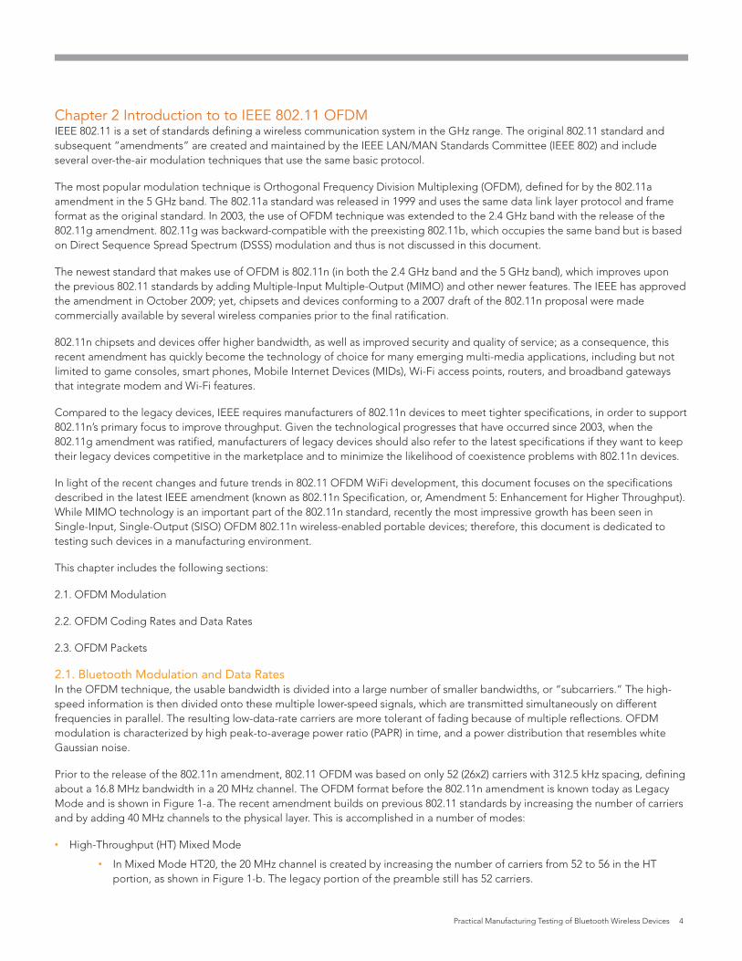
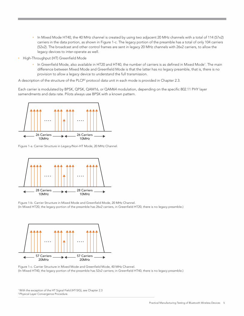
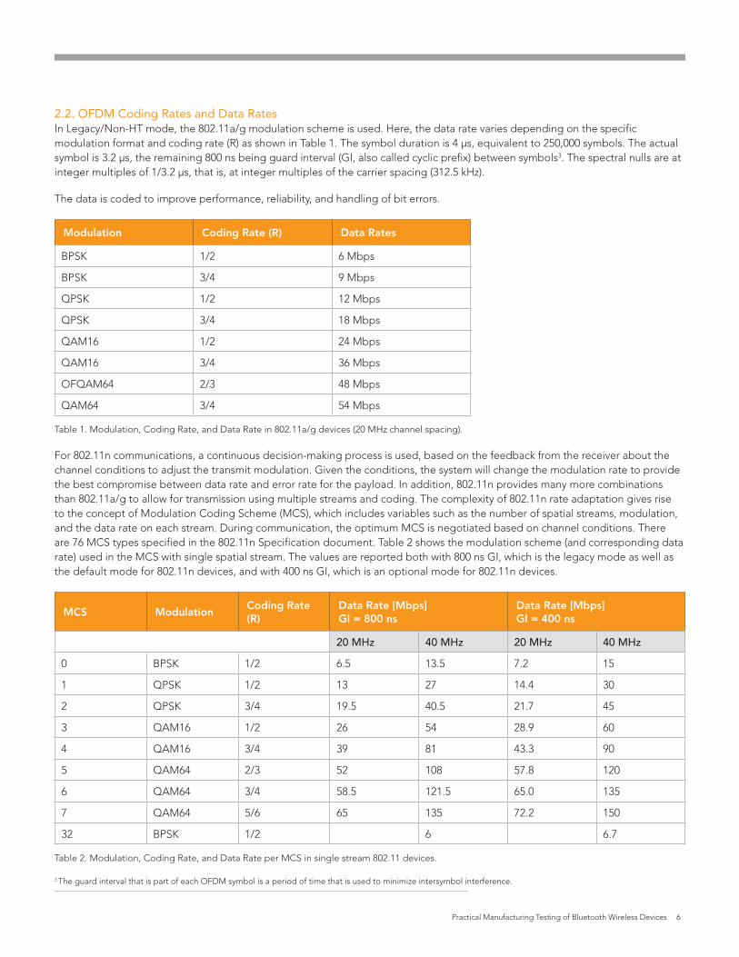
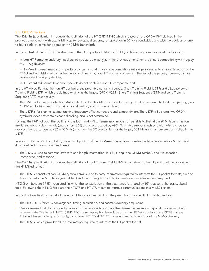
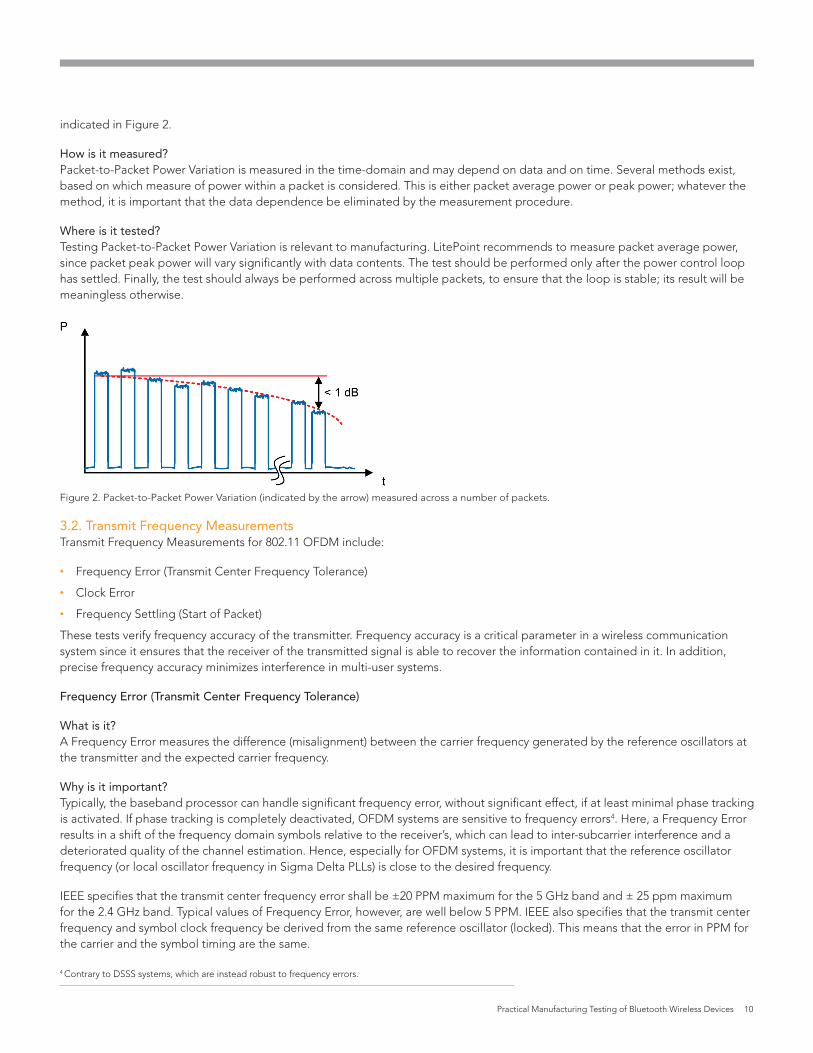
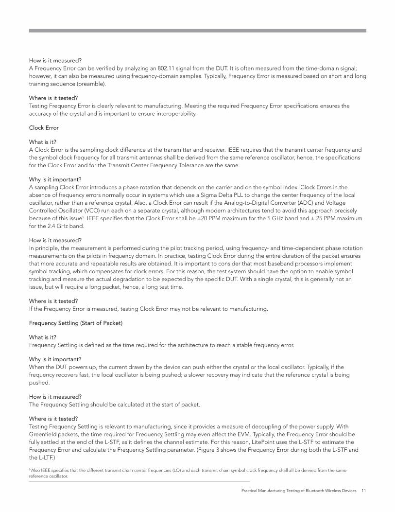
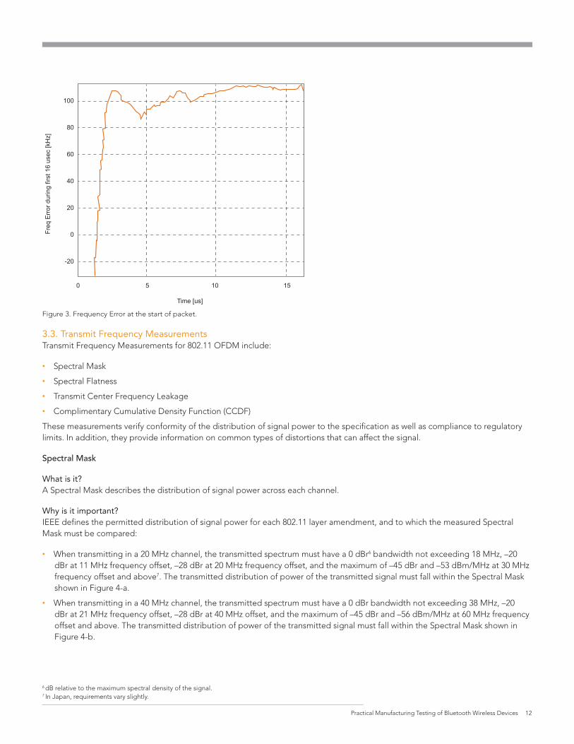
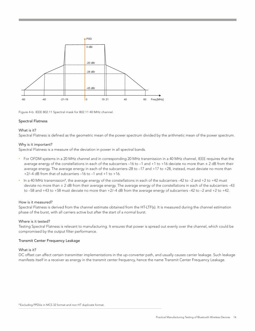
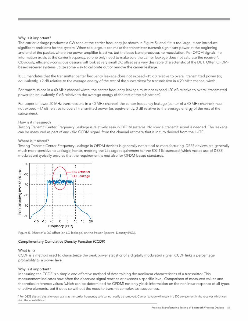
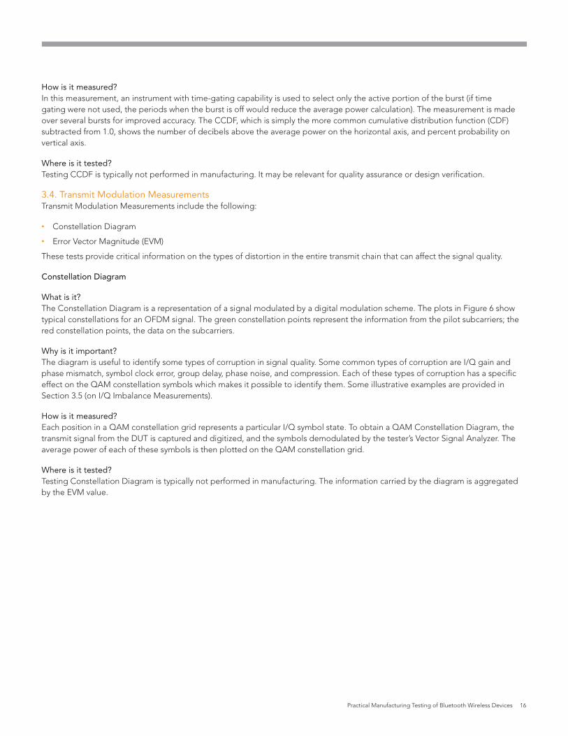
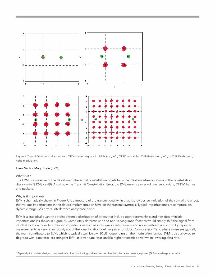
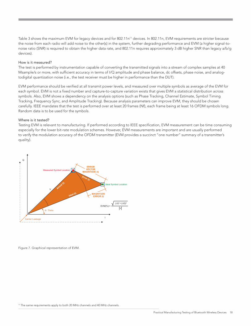
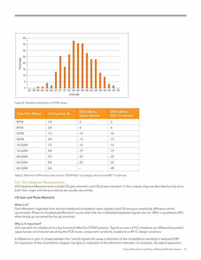
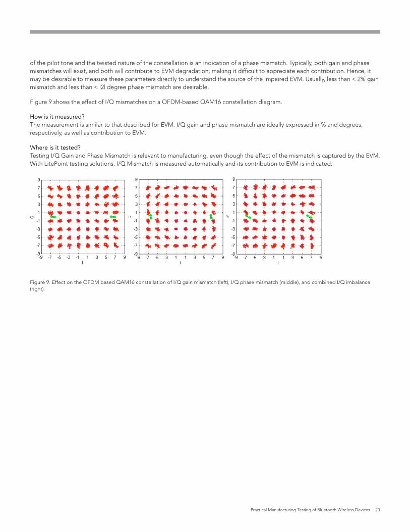
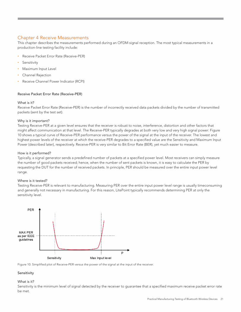
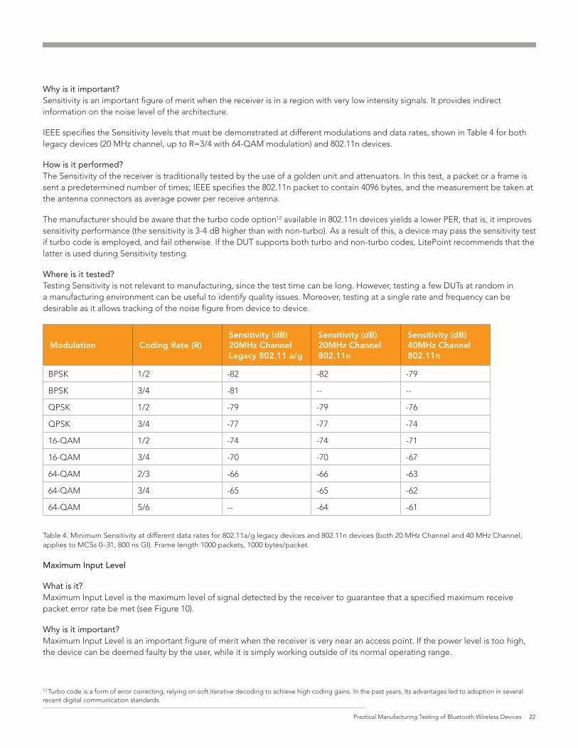
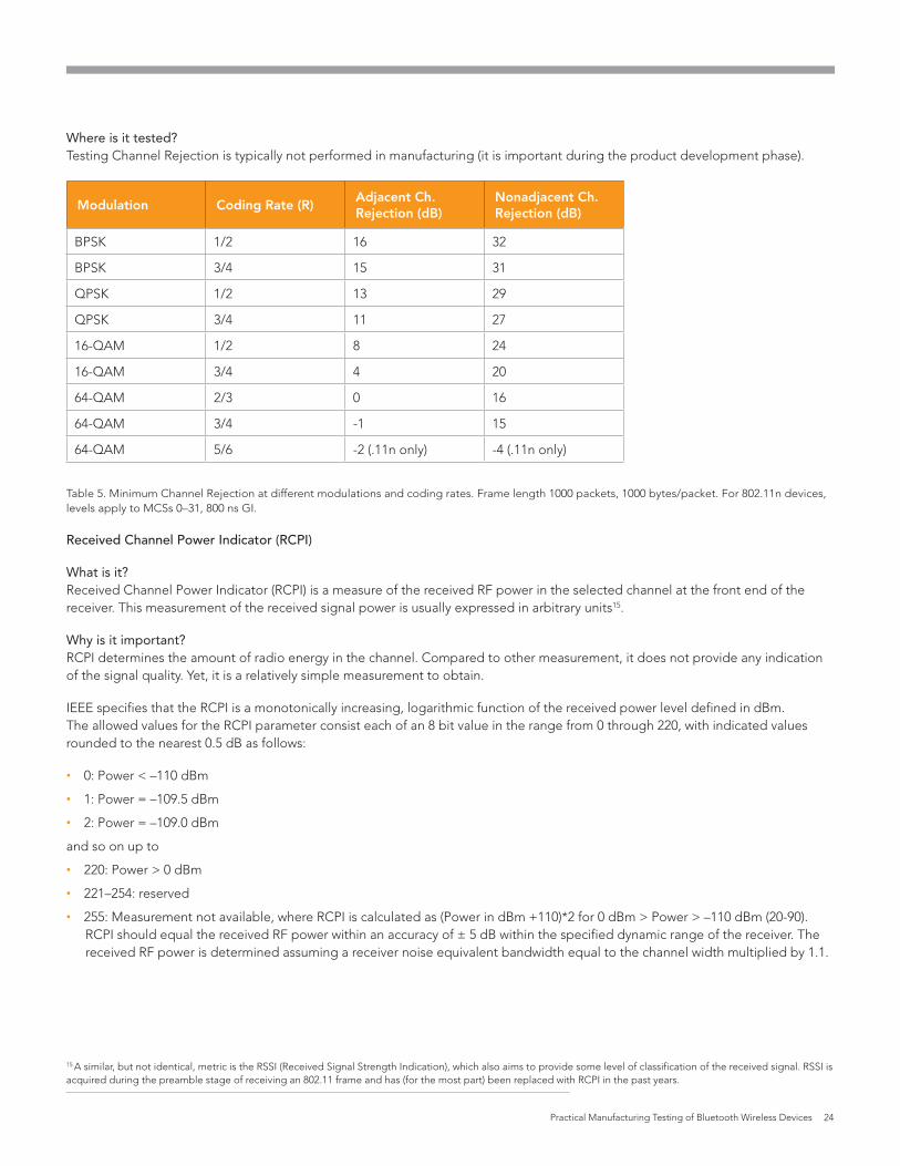
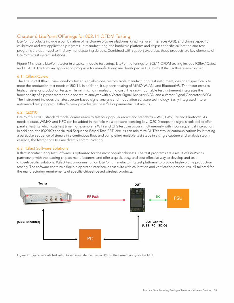
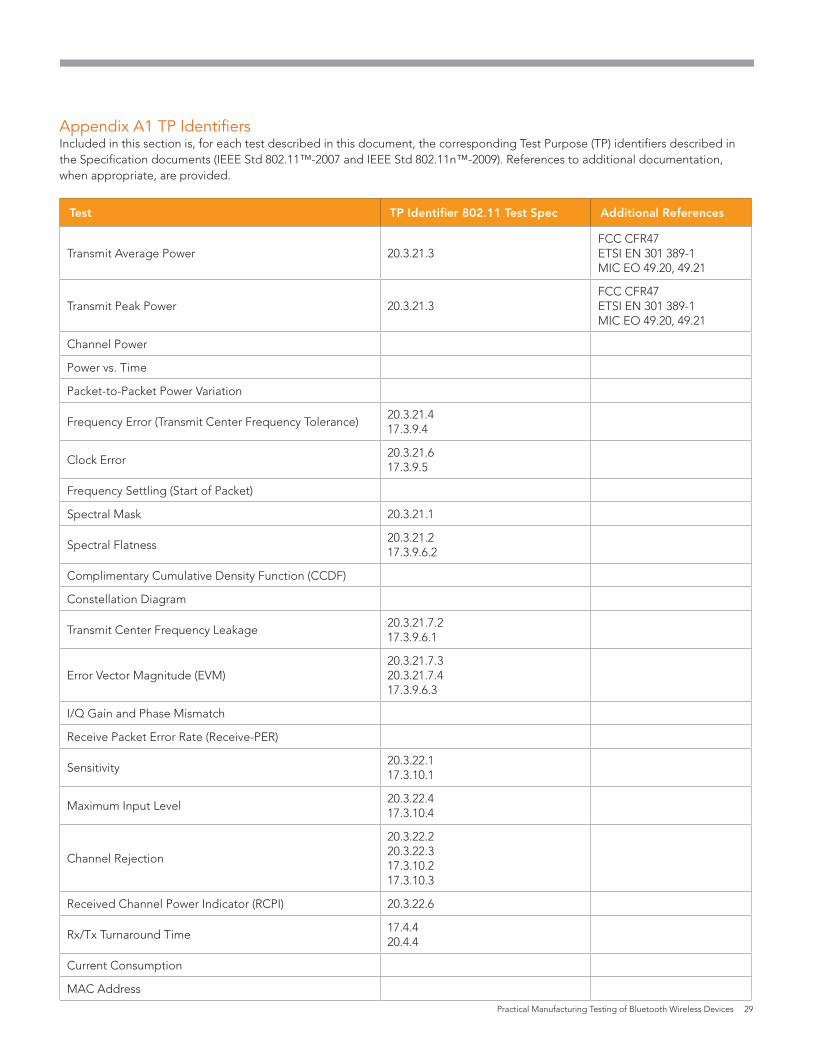