powering the i.mx6 dual/quad with tps65911 power …
TRANSCRIPT
TIDA-00621 - Test Report Powering the i.MX6 Dual/Quad with TPS65911 Power Management IC 1
Copyright © 2015, Texas Instruments Incorporated
TIDA-00621 Test Report
Powering the i.MX6 Dual/Quad with TPS65911 Power Management IC
TI Designs
TI Designs provide the foundation that you need including methodology, testing and design files to quickly evaluate and customize the system. TI Designs help you accelerate your time to market.
Design Resources
TIDA-00621 Design Folder
TPS65911 Product Folder
TPS65911 Designs Tools Folder
Report Contents
Block Diagram: TPS65911 / i.MX6
Efficiency Curves
Load Regulation Curves
Output Ripple Voltage
Load Transients
Start-Up Sequence
Design Considerations
Feature Applications
Factory Automation
Motor Control
Smart Grid
Solar Inverters
Description
TIDA-00621 utilizes a power management integrated circuit (PMIC) for supplying a Freescale® i.MX6 SoC in a DDR3 application. This design showcases the TPS65911 as an all-in-one IC used to supply the rails needed for powering the i.MX6 SoC, with available regulators for system peripherals. The TPS65911 offers simple, flexibile output voltages and sequencing. The voltages on the DC/DC converters can be adjusted over i2c once the device has entered the active state, allowing for individual regulator customization.
Ask The Analog Experts WEBENCH® Design Center
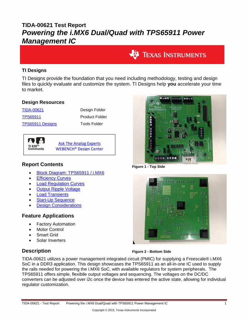
Figure 1 - Top Side
Figure 2 - Bottom Side
www.ti.com
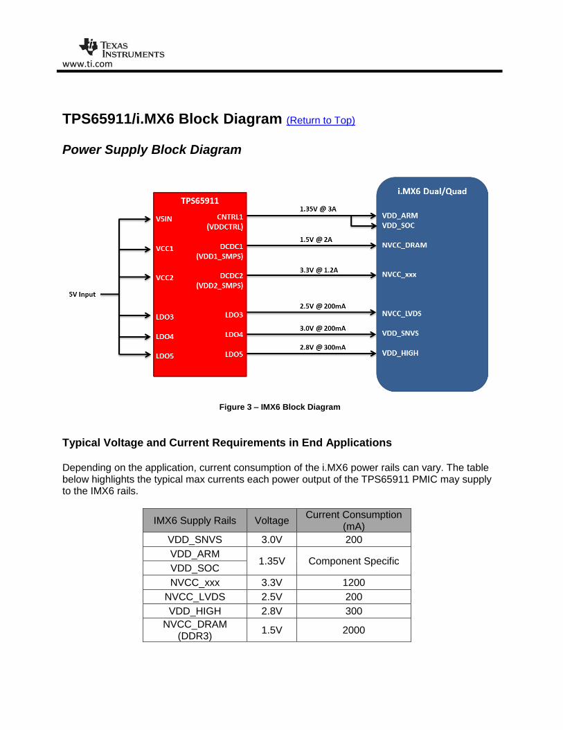
TPS65911/i.MX6 Block Diagram (Return to Top) Power Supply Block Diagram
Figure 3 – IMX6 Block Diagram
Typical Voltage and Current Requirements in End Applications Depending on the application, current consumption of the i.MX6 power rails can vary. The table below highlights the typical max currents each power output of the TPS65911 PMIC may supply to the IMX6 rails.
IMX6 Supply Rails Voltage Current Consumption
(mA)
VDD_SNVS 3.0V 200
VDD_ARM 1.35V Component Specific
VDD_SOC
NVCC_xxx 3.3V 1200
NVCC_LVDS 2.5V 200
VDD_HIGH 2.8V 300
NVCC_DRAM (DDR3)
1.5V 2000
www.ti.com
TIDA-00621 – Test Report Powering the i.MX6 Dual/Quad with TPS65911 Power Management IC 3
Copyright © 2015, Texas Instruments Incorporated
Note: NVCC_LVDS powers the pre-drivers for the DDR I/O pins, and must be powered even when LVDS is not used. The maximum current consumption of a design will vary depending on the specific application.
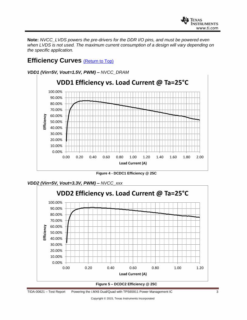
Efficiency Curves (Return to Top) VDD1 (Vin=5V, Vout=1.5V, PWM) – NVCC_DRAM
Figure 4 - DCDC1 Efficiency @ 25C
VDD2 (Vin=5V, Vout=3.3V, PWM) – NVCC_xxx
Figure 5 – DCDC2 Efficiency @ 25C
0.00%
10.00%
20.00%
30.00%
40.00%
50.00%
60.00%
70.00%
80.00%
90.00%
100.00%
0.00 0.20 0.40 0.60 0.80 1.00 1.20 1.40 1.60 1.80 2.00
Effi
cie
ncy
Load Current (A)
VDD1 Efficiency vs. Load Current @ Ta=25°C
0.00%
10.00%
20.00%
30.00%
40.00%
50.00%
60.00%
70.00%
80.00%
90.00%
100.00%
0.00 0.20 0.40 0.60 0.80 1.00 1.20
Effi
cie
ncy
Load Current (A)
VDD2 Efficiency vs. Load Current @ Ta=25°C
www.ti.com
TIDA-00621 – Test Report Powering the i.MX6 Dual/Quad with TPS65911 Power Management IC 4
Copyright © 2015, Texas Instruments Incorporated
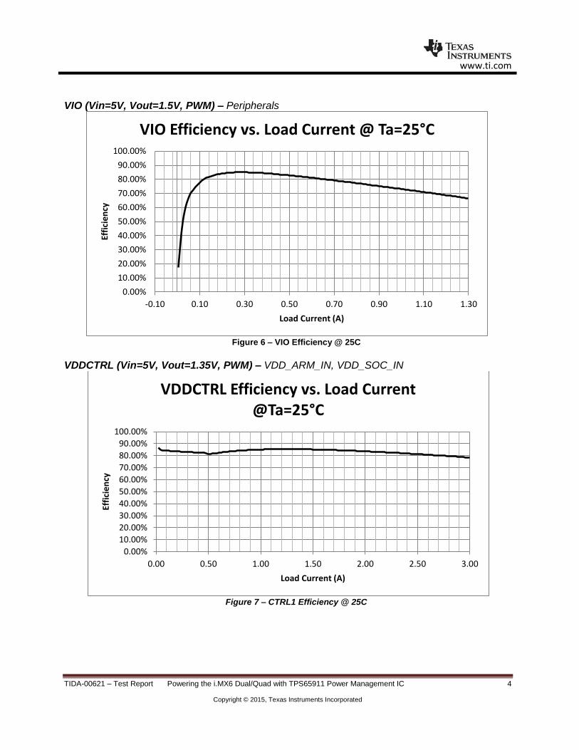
VIO (Vin=5V, Vout=1.5V, PWM) – Peripherals
Figure 6 – VIO Efficiency @ 25C
VDDCTRL (Vin=5V, Vout=1.35V, PWM) – VDD_ARM_IN, VDD_SOC_IN
Figure 7 – CTRL1 Efficiency @ 25C
0.00%
10.00%
20.00%
30.00%
40.00%
50.00%
60.00%
70.00%
80.00%
90.00%
100.00%
-0.10 0.10 0.30 0.50 0.70 0.90 1.10 1.30
Effi
cie
ncy
Load Current (A)
VIO Efficiency vs. Load Current @ Ta=25°C
0.00%
10.00%
20.00%
30.00%
40.00%
50.00%
60.00%
70.00%
80.00%
90.00%
100.00%
0.00 0.50 1.00 1.50 2.00 2.50 3.00
Effi
cie
ncy
Load Current (A)
VDDCTRL Efficiency vs. Load Current @Ta=25°C
www.ti.com
TIDA-00621 – Test Report Powering the i.MX6 Dual/Quad with TPS65911 Power Management IC 5
Copyright © 2015, Texas Instruments Incorporated
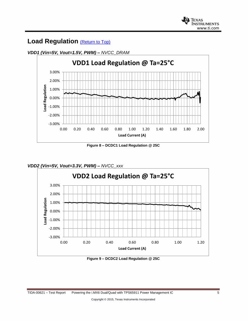
Load Regulation (Return to Top)
VDD1 (Vin=5V, Vout=1.5V, PWM) – NVCC_DRAM
Figure 8 – DCDC1 Load Regulation @ 25C
VDD2 (Vin=5V, Vout=3.3V, PWM) – NVCC_xxx
Figure 9 – DCDC2 Load Regulation @ 25C
-3.00%
-2.00%
-1.00%
0.00%
1.00%
2.00%
3.00%
0.00 0.20 0.40 0.60 0.80 1.00 1.20 1.40 1.60 1.80 2.00
Load
Re
gula
tio
n
Load Current (A)
VDD1 Load Regulation @ Ta=25°C
-3.00%
-2.00%
-1.00%
0.00%
1.00%
2.00%
3.00%
0.00 0.20 0.40 0.60 0.80 1.00 1.20
Load
Re
gula
tio
n
Load Current (A)
VDD2 Load Regulation @ Ta=25°C

www.ti.com
TIDA-00621 – Test Report Powering the i.MX6 Dual/Quad with TPS65911 Power Management IC 6
Copyright © 2015, Texas Instruments Incorporated
VIO (Vin=5V, Vout=1.5V, PWM) – Peripherals
Figure 10 – VIO Load Regulation @ 25C
VDDCTRL (Vin=5V, Vout=1.35V, PWM) – VDD_ARM_IN, VDD_SOC_IN
Figure 11 – CTRL1 Load Regulation @ 25C
-3.00%
-2.00%
-1.00%
0.00%
1.00%
2.00%
3.00%
0.00 0.20 0.40 0.60 0.80 1.00 1.20
Load
Re
gula
tio
n
Load Current (A)
VIO Load Regulation @ Ta=25°C
-3.00%
-2.00%
-1.00%
0.00%
1.00%
2.00%
3.00%
0.00 0.50 1.00 1.50 2.00 2.50 3.00
Load
Re
gula
tio
n
Load Current (A)
VDDCTRL Load Regulation
www.ti.com
TIDA-00621 – Test Report Powering the i.MX6 Dual/Quad with TPS65911 Power Management IC 7
Copyright © 2015, Texas Instruments Incorporated
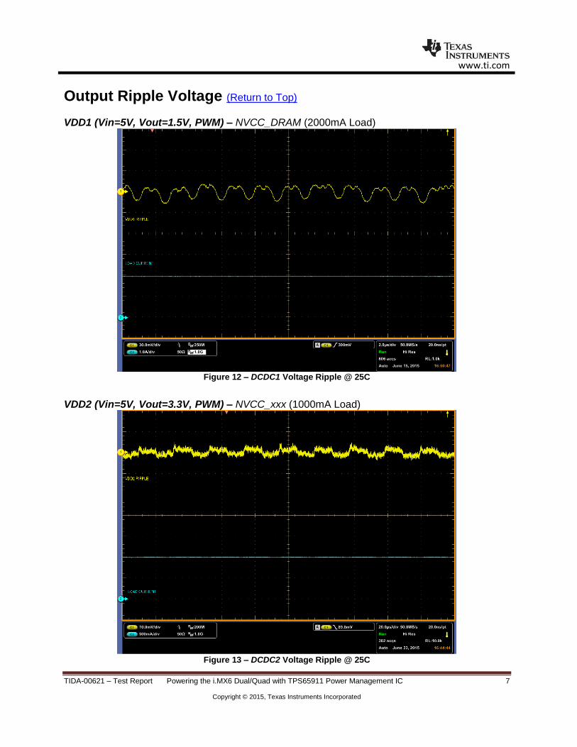
Output Ripple Voltage (Return to Top)
VDD1 (Vin=5V, Vout=1.5V, PWM) – NVCC_DRAM (2000mA Load)
Figure 12 – DCDC1 Voltage Ripple @ 25C
VDD2 (Vin=5V, Vout=3.3V, PWM) – NVCC_xxx (1000mA Load)
Figure 13 – DCDC2 Voltage Ripple @ 25C
www.ti.com
TIDA-00621 – Test Report Powering the i.MX6 Dual/Quad with TPS65911 Power Management IC 8
Copyright © 2015, Texas Instruments Incorporated
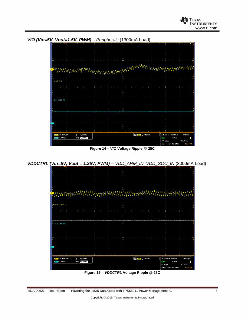
VIO (Vin=5V, Vout=1.5V, PWM) – Peripherals (1300mA Load)
Figure 14 – VIO Voltage Ripple @ 25C
VDDCTRL (Vin=5V, Vout = 1.35V, PWM) – VDD_ARM_IN, VDD_SOC_IN (3000mA Load)
Figure 15 – VDDCTRL Voltage Ripple @ 25C
www.ti.com
TIDA-00621 – Test Report Powering the i.MX6 Dual/Quad with TPS65911 Power Management IC 9
Copyright © 2015, Texas Instruments Incorporated
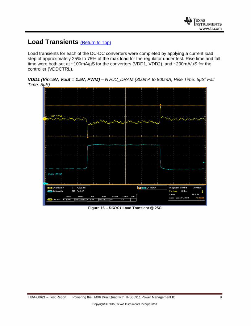
Load Transients (Return to Top)
Load transients for each of the DC-DC converters were completed by applying a current load step of approximately 25% to 75% of the max load for the regulator under test. Rise time and fall time were both set at ~100mA/µS for the converters (VDD1, VDD2), and ~200mA/µS for the controller (VDDCTRL). VDD1 (Vin=5V, Vout = 1.5V, PWM) – NVCC_DRAM (300mA to 800mA, Rise Time: 5µS; Fall Time: 5µS)
Figure 16 – DCDC1 Load Transient @ 25C

www.ti.com
TIDA-00621 – Test Report Powering the i.MX6 Dual/Quad with TPS65911 Power Management IC 10
Copyright © 2015, Texas Instruments Incorporated
VDD2 (Vin=5V, Vout = 3.3V, PWM) – NVCC_xxx (300mA to 800mA, Rise Time: 5µS; Fall Time: 5µS)
Figure 17 – DCDC2 Load Transient @ 25C
VIO (Vin=5V, Vout = 1.5V, PWM) – Peripherals (300mA to 800mA, Rise Time: 5µS; Fall Time: 5µS)
Figure 18 – VIO Load Transient @ 25C

www.ti.com
TIDA-00621 – Test Report Powering the i.MX6 Dual/Quad with TPS65911 Power Management IC 11
Copyright © 2015, Texas Instruments Incorporated
VDDCTRL (Vin=5V, Vout = 1.35V, PWM) – VDD_ARM_IN, VDD_SOC_IN (800mA to 2000mA, Rise Time: 5µS; Fall Time: 5µS)
Figure 19 – VDDCTRL Load Transient @ 25C
www.ti.com
TIDA-00621 – Test Report Powering the i.MX6 Dual/Quad with TPS65911 Power Management IC 12
Copyright © 2015, Texas Instruments Incorporated
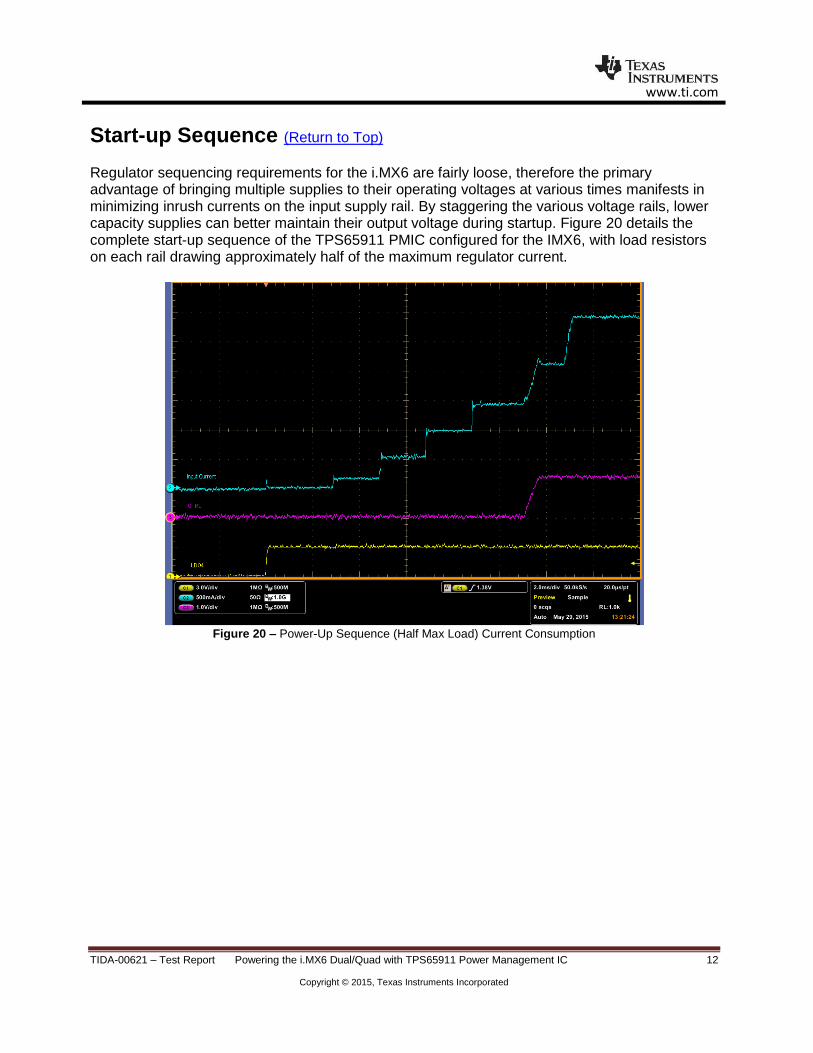
Start-up Sequence (Return to Top)
Regulator sequencing requirements for the i.MX6 are fairly loose, therefore the primary advantage of bringing multiple supplies to their operating voltages at various times manifests in minimizing inrush currents on the input supply rail. By staggering the various voltage rails, lower capacity supplies can better maintain their output voltage during startup. Figure 20 details the complete start-up sequence of the TPS65911 PMIC configured for the IMX6, with load resistors on each rail drawing approximately half of the maximum regulator current.
Figure 20 – Power-Up Sequence (Half Max Load) Current Consumption

www.ti.com
TIDA-00621 – Test Report Powering the i.MX6 Dual/Quad with TPS65911 Power Management IC 13
Copyright © 2015, Texas Instruments Incorporated
Figure 21 – Power-Up Sequence (No Load) Voltage Waveforms
(LDO4_3.0V, LDO5_2.8V, VDD2_3.3V, LDO2_1.5V)
Figure 22 – Power-Up Sequence (No Load) Voltage Waveforms
(LDO6_3.3V, LDO7_3.3V, LDO1_1.8V, LDO3_2.5V)
www.ti.com
TIDA-00621 – Test Report Powering the i.MX6 Dual/Quad with TPS65911 Power Management IC 14
Copyright © 2015, Texas Instruments Incorporated
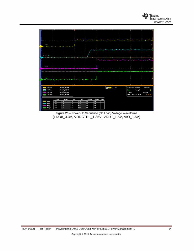
Figure 23 – Power-Up Sequence (No Load) Voltage Waveforms
(LDO8_3.3V, VDDCTRL_1.35V, VDD1_1.5V, VIO_1.5V)
www.ti.com
TIDA-00621 – Test Report Powering the i.MX6 Dual/Quad with TPS65911 Power Management IC 15
Copyright © 2015, Texas Instruments Incorporated
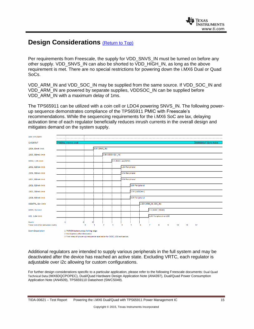
Design Considerations (Return to Top)
Per requirements from Freescale, the supply for VDD_SNVS_IN must be turned on before any other supply. VDD_SNVS_IN can also be shorted to VDD_HIGH_IN, as long as the above requirement is met. There are no special restrictions for powering down the i.MX6 Dual or Quad SoCs. VDD_ARM_IN and VDD_SOC_IN may be supplied from the same source. If VDD_SOC_IN and VDD_ARM_IN are powered by separate supplies, VDDSOC_IN can be supplied before VDD_ARM_IN with a maximum delay of 1ms. The TPS65911 can be utilized with a coin cell or LDO4 powering SNVS_IN. The following power-up sequence demonstrates compliance of the TPS65911 PMIC with Freescale’s recommendations. While the sequencing requirements for the i.MX6 SoC are lax, delaying activation time of each regulator beneficially reduces inrush currents in the overall design and mitigates demand on the system supply.
Additional regulators are intended to supply various peripherals in the full system and may be deactivated after the device has reached an active state. Excluding VRTC, each regulator is adjustable over i2c allowing for custom configurations. For further design considerations specific to a particular application, please refer to the following Freescale documents: Dual Quad Technical Data (IMX6DQCPOPEC), Dual/Quad Hardware Design Application Note (AN4397), Dual/Quad Power Consumption
Application Note (AN4509), TPS659110 Datasheet (SWCS049).
www.ti.com
TIDA-00621 – Test Report Powering the i.MX6 Dual/Quad with TPS65911 Power Management IC 16
Copyright © 2015, Texas Instruments Incorporated
IMPORTANT NOTICE FOR TI REFERENCE DESIGNS
Texas Instruments Incorporated ("TI") reference designs are solely intended to assist designers (“Buyers”) who are developing systems thatincorporate TI semiconductor products (also referred to herein as “components”). Buyer understands and agrees that Buyer remainsresponsible for using its independent analysis, evaluation and judgment in designing Buyer’s systems and products.TI reference designs have been created using standard laboratory conditions and engineering practices. TI has not conducted anytesting other than that specifically described in the published documentation for a particular reference design. TI may makecorrections, enhancements, improvements and other changes to its reference designs.Buyers are authorized to use TI reference designs with the TI component(s) identified in each particular reference design and to modify thereference design in the development of their end products. HOWEVER, NO OTHER LICENSE, EXPRESS OR IMPLIED, BY ESTOPPELOR OTHERWISE TO ANY OTHER TI INTELLECTUAL PROPERTY RIGHT, AND NO LICENSE TO ANY THIRD PARTY TECHNOLOGYOR INTELLECTUAL PROPERTY RIGHT, IS GRANTED HEREIN, including but not limited to any patent right, copyright, mask work right,or other intellectual property right relating to any combination, machine, or process in which TI components or services are used.Information published by TI regarding third-party products or services does not constitute a license to use such products or services, or awarranty or endorsement thereof. Use of such information may require a license from a third party under the patents or other intellectualproperty of the third party, or a license from TI under the patents or other intellectual property of TI.TI REFERENCE DESIGNS ARE PROVIDED "AS IS". TI MAKES NO WARRANTIES OR REPRESENTATIONS WITH REGARD TO THEREFERENCE DESIGNS OR USE OF THE REFERENCE DESIGNS, EXPRESS, IMPLIED OR STATUTORY, INCLUDING ACCURACY ORCOMPLETENESS. TI DISCLAIMS ANY WARRANTY OF TITLE AND ANY IMPLIED WARRANTIES OF MERCHANTABILITY, FITNESSFOR A PARTICULAR PURPOSE, QUIET ENJOYMENT, QUIET POSSESSION, AND NON-INFRINGEMENT OF ANY THIRD PARTYINTELLECTUAL PROPERTY RIGHTS WITH REGARD TO TI REFERENCE DESIGNS OR USE THEREOF. TI SHALL NOT BE LIABLEFOR AND SHALL NOT DEFEND OR INDEMNIFY BUYERS AGAINST ANY THIRD PARTY INFRINGEMENT CLAIM THAT RELATES TOOR IS BASED ON A COMBINATION OF COMPONENTS PROVIDED IN A TI REFERENCE DESIGN. IN NO EVENT SHALL TI BELIABLE FOR ANY ACTUAL, SPECIAL, INCIDENTAL, CONSEQUENTIAL OR INDIRECT DAMAGES, HOWEVER CAUSED, ON ANYTHEORY OF LIABILITY AND WHETHER OR NOT TI HAS BEEN ADVISED OF THE POSSIBILITY OF SUCH DAMAGES, ARISING INANY WAY OUT OF TI REFERENCE DESIGNS OR BUYER’S USE OF TI REFERENCE DESIGNS.TI reserves the right to make corrections, enhancements, improvements and other changes to its semiconductor products and services perJESD46, latest issue, and to discontinue any product or service per JESD48, latest issue. Buyers should obtain the latest relevantinformation before placing orders and should verify that such information is current and complete. All semiconductor products are soldsubject to TI’s terms and conditions of sale supplied at the time of order acknowledgment.TI warrants performance of its components to the specifications applicable at the time of sale, in accordance with the warranty in TI’s termsand conditions of sale of semiconductor products. Testing and other quality control techniques for TI components are used to the extent TIdeems necessary to support this warranty. Except where mandated by applicable law, testing of all parameters of each component is notnecessarily performed.TI assumes no liability for applications assistance or the design of Buyers’ products. Buyers are responsible for their products andapplications using TI components. To minimize the risks associated with Buyers’ products and applications, Buyers should provideadequate design and operating safeguards.Reproduction of significant portions of TI information in TI data books, data sheets or reference designs is permissible only if reproduction iswithout alteration and is accompanied by all associated warranties, conditions, limitations, and notices. TI is not responsible or liable forsuch altered documentation. Information of third parties may be subject to additional restrictions.Buyer acknowledges and agrees that it is solely responsible for compliance with all legal, regulatory and safety-related requirementsconcerning its products, and any use of TI components in its applications, notwithstanding any applications-related information or supportthat may be provided by TI. Buyer represents and agrees that it has all the necessary expertise to create and implement safeguards thatanticipate dangerous failures, monitor failures and their consequences, lessen the likelihood of dangerous failures and take appropriateremedial actions. Buyer will fully indemnify TI and its representatives against any damages arising out of the use of any TI components inBuyer’s safety-critical applications.In some cases, TI components may be promoted specifically to facilitate safety-related applications. With such components, TI’s goal is tohelp enable customers to design and create their own end-product solutions that meet applicable functional safety standards andrequirements. Nonetheless, such components are subject to these terms.No TI components are authorized for use in FDA Class III (or similar life-critical medical equipment) unless authorized officers of the partieshave executed an agreement specifically governing such use.Only those TI components that TI has specifically designated as military grade or “enhanced plastic” are designed and intended for use inmilitary/aerospace applications or environments. Buyer acknowledges and agrees that any military or aerospace use of TI components thathave not been so designated is solely at Buyer's risk, and Buyer is solely responsible for compliance with all legal and regulatoryrequirements in connection with such use.TI has specifically designated certain components as meeting ISO/TS16949 requirements, mainly for automotive use. In any case of use ofnon-designated products, TI will not be responsible for any failure to meet ISO/TS16949.IMPORTANT NOTICE
Mailing Address: Texas Instruments, Post Office Box 655303, Dallas, Texas 75265Copyright © 2015, Texas Instruments Incorporated