power supplies for led drivingdl.booktolearn.com/ebooks2/engineering/electrical/... ·...
TRANSCRIPT


Power Supplies for LED Driving
Elsevier US PLD Prelims H8341 14 2 2008 Page:1 Trim:7.5�9.25 in

Elsevier US PLD Prelims H8341 14 2 2008 Page:2 Trim:7.5�9.25 in

Power Supplies for LED Driving
Steve Winder
AMSTERDAM • BOSTON • HEIDELBERG • LONDON
NEW YORK • OXFORD • PARIS • SAN DIEGO
SAN FRANCISCO • SINGAPORE • SYDNEY • TOKYO
Newnes is an imprint of Elsevier
Elsevier US PLD Prelims H8341 14 2 2008 Page:3 Trim:7.5�9.25 in

Newnes is an imprint of Elsevier
30 Corporate Drive, Suite 400, Burlington, MA 01803, USA
Linacre House, Jordan Hill, Oxford OX2 8DP, UK
Copyright � 2008 by Elsevier Inc. All rights reserved.
No part of this publication may be reproduced, stored in a retrieval system, or
transmitted in any form or by any means, electronic, mechanical, photocopying,
recording, or otherwise, without the prior written permission of the publisher.
Permissions may be sought directly from Elsevier’s Science & Technology Rights
Department in Oxford, UK: phone: (þ44) 1865 843830, fax: (þ44) 1865 853333,
E-mail: [email protected]. You may also complete your request online
via the Elsevier homepage (http://elsevier.com), by selecting ‘‘Support & Contact’’
then ‘‘Copyright and Permission’’ and then ‘‘Obtaining Permissions.’’
Recognizing the importance of preserving what has been written, Elsevier prints its
books on acid-free paper whenever possible.
Library of Congress Cataloging-in-Publication Data
Application submitted
British Library Cataloguing-in-Publication Data
A catalogue record for this book is available from the British Library.
ISBN: 978-0-7506-8341-8
For information on all Newnes publications
visit our Web site at www.books.elsevier.com
Printed in the United States of America
08 09 10 11 12 13 10 9 8 7 6 5 4 3 2 1
Working together to grow libraries in developing countries
www.elsevier.com | www.bookaid.org | www.sabre.org
Elsevier US PLD Prelims H8341 14 2 2008 Page:4 Trim:7.5�9.25 in

Table of Contents
Preface ..................................................................................................... ix
Chapter 1: Introduction ................................................................................11.1 Objectives and General Approach ............................................................. 11.2 Description of Contents ............................................................................. 2
Chapter 2: Characteristics of LEDs................................................................72.1 Applications for LEDs ............................................................................... 82.2 Light Measure .......................................................................................... 122.3 Equivalent Circuit to an LED.................................................................. 132.4 Voltage Drop Versus Color and Current ................................................. 142.5 Common Mistakes ................................................................................... 15
Chapter 3: Driving LEDs ............................................................................173.1 Voltage Source ......................................................................................... 173.2 Current Source ......................................................................................... 243.3 Testing LED Drivers ................................................................................ 293.4 Common Mistakes ................................................................................... 303.5 Conclusions .............................................................................................. 31
Chapter 4: Linear Power Supplies................................................................334.1 Introduction ............................................................................................. 334.2 Advantages and Disadvantages................................................................ 374.3 Limitations ............................................................................................... 374.4 Common Errors in Designing Linear LED Drivers................................. 37
Chapter 5: Buck-Based LED Drivers............................................................395.1 An Example Buck Converter Control IC................................................. 405.2 Buck Circuits for DC Applications .......................................................... 415.3 Buck Circuits for AC Input...................................................................... 46
Elsevier US PLD Prelims H8341 14 2 2008 Page:5 Trim:7.5�9.25 in
www.newnespress.com

5.4 Buck Circuits Powered by an AC Phase Dimmer.................................... 525.5 Common Errors in AC Input Buck Circuits............................................ 545.6 Double Buck ............................................................................................ 555.7 Hysteretic Buck........................................................................................ 59
Chapter 6: Boost Converters .......................................................................616.1 Boost Converter Operating Modes .......................................................... 626.2 HV9912 Boost Controller ........................................................................ 636.3 Design of a Continuous Conduction Mode Boost LED Driver .............. 676.4 Design of a Discontinuous Conduction Mode Boost LED Driver.......... 836.5 Common Mistakes ................................................................................... 986.6 Conclusions.............................................................................................. 98
Chapter 7: Boost-Buck Converter ................................................................997.1 The Cuk Converter ................................................................................ 1007.2 SEPIC Buck-Boost Converters .............................................................. 1317.3 Buck-Boost Topology ............................................................................ 1397.4 Common Mistakes in Boost-Buck Circuits............................................ 1397.5 Conclusions............................................................................................ 140
Chapter 8: LED Drivers with Power Factor Correction ................................1418.1 Power Factor Correction ....................................................................... 1418.2 Bi-Bred................................................................................................... 1428.3 Buck-Boost-Buck (BBB) ........................................................................ 1448.4 Common Mistakes with PFC Circuits ................................................... 1478.5 Conclusions............................................................................................ 147
Chapter 9: Fly-Back Converters.................................................................1499.1 Two Winding Fly-Back.......................................................................... 1509.2 Three Winding Fly-Back........................................................................ 1539.3 Single Winding Fly-Back (Buck-Boost) ................................................. 158
Chapter 10: Essentials of Switching Power Supplies.....................................16110.1 Linear Regulators .................................................................................. 16110.2 Switching Regulators ............................................................................. 162
Chapter 11: Selecting Components for LED Drivers ....................................17511.1 Discrete Semiconductors........................................................................ 17511.2 Passive Components .............................................................................. 18211.3 The Printed Circuit Board (PCB) .......................................................... 19111.4 Operational Amplifiers and Comparators ............................................. 193
Elsevier US PLD Prelims H8341 14 2 2008 Page:6 Trim:7.5�9.25 in
www.newnespress.com
vi Table of Contents

Chapter 12: Magnetic Materials for Inductors and Transformers ..................19512.1 Ferrite Cores .......................................................................................... 19712.2 Iron Dust Cores ..................................................................................... 19712.3 Special Cores.......................................................................................... 19812.4 Core Shapes and Sizes ........................................................................... 19812.5 Magnetic Saturation .............................................................................. 19912.6 Copper Losses........................................................................................ 200
Chapter 13: EMI and EMC Issues .............................................................20313.1 EMI Standards ...................................................................................... 20413.2 Good EMI Design Techniques .............................................................. 20513.3 EMC Standards ..................................................................................... 21413.4 EMC Practices ....................................................................................... 215
Chapter 14: Thermal Considerations..........................................................21714.1 Efficiency and Power Loss..................................................................... 21714.2 Calculating Temperature ....................................................................... 21814.3 Handling Heat – Cooling Techniques.................................................... 220
Chapter 15: Safety Issues .........................................................................22515.1 AC Mains Isolation ............................................................................... 22515.2 Circuit Breakers ..................................................................................... 22615.3 Creepage Distance ................................................................................. 22615.4 Capacitor Ratings .................................................................................. 22615.5 Low Voltage Operation ......................................................................... 227
Bibliography ...........................................................................................229Index .....................................................................................................231Author Biography.....................................................................................233
Elsevier US PLD Prelims H8341 14 2 2008 Page:7 Trim:7.5�9.25 in
www.newnespress.com
Table of Contents vii

Elsevier US PLD Prelims H8341 14 2 2008 Page:8 Trim:7.5�9.25 in

Preface
The LED has been available for many years now, initially as a red colored indicator.
Later, yellow/amber, green and finally blue colored LEDs became available, which
triggered an explosion in applications. Applications included traffic lights, vehicle
lights and wall-washes (mood lighting). Recently blue colored LEDs have been
combined with yellow phosphor to create white light. The amount of light available
from LEDs has also increased steadily, and now power levels of 1W, 3W and 5W are
fairly common.
Driving a single LED, or a long string of LEDs connected in series, has relatively few
problems when the current is low (may be 20mA). High current LEDs are tougher to
drive, requiring 350mA, 700mA, 1 A or higher. Of course, a simple linear regulator
could be used if power dissipation was not an issue, or a simple resistor if current
regulation is not critical. However, in most applications, an efficient switching
regulator is used. A switching regulator is essential if the LED string voltage is higher
than the supply voltage, or if the supply voltage has wide variation. But switching
means that electro-magnetic interference (EMI) has to be considered too.
This book describes a number of LED driving methods. The main aims of this book
are: (1) to show suitable types of LED driver topologies for given applications; (2) to
work through some examples; and (3) to avoid some of the mistakes that some
engineers make when creating their own designs. However, the content is not
exhaustive and further reading in some peripheral topics will be necessary.
Significant data to create this book have been drawn from the datasheets, application
notes, training material and discussions provided by my colleagues in Supertex,
particularly Rohit Tirumala and Alex Mednik.
Steve Winder, 2007.
Elsevier US PLD Prelims H8341 14 2 2008 Page:9 Trim:7.5�9.25 in
www.newnespress.com

C H A P T E R 1
Introduction
As a field applications engineer for one of the pioneering developers of integrated circuits
for driving power LEDs, I meet many potential customers who have little or no idea of
how to drive an LED properly. The older type of LED requiring a 20mA supply can be
abused to some extent. However, power requirements have been increasing; current
ratings of 30mA, 50mA, 100mA, 350mA and higher are becoming common. There are
several manufacturers that produce power levels up to 20W, and more; these higher
powers use LED chip arrays. If a power LED is abused, it tends to die very quickly.
Power LEDs are being used in increasing numbers; in channel lighting (signage), traffic
lights, street lights, automotive, mood lighting (colour changing ‘wall wash’), theatre
lighting for steps and emergency exits. Names such as HB-LEDs (high bright) and
UB-LEDs (ultra-bright) are becoming meaningless as the power levels continue to rise.
This book will cover all types of LED drivers, from low power to UB-LEDs and beyond.
Is power LED driving simple? No, not usually. In a few cases a linear regulator can be
used, which is simple, but most cases require a switching power supply with a constant
current output. Linear driving is inefficient and generates far too much heat. With a
switching supply, the main issues are EMI and efficiency, and of course cost. The problem
is to produce a design that meets legal requirements and is efficient, with minimal cost.
1.1 Objectives and General Approach
The approach of this book will be very practical, although some theory is introduced
when necessary for understanding of later chapters. It is important to understand the
characteristics of components before they can be used effectively.
www.newnespress.com

In most chapters, I will include a section called ‘Common Errors’. This section will
highlight errors that engineers have made, and how these can be avoided, with the
hope that readers will not make the same mistakes. It is said that people learn from
their mistakes, but it is also true that we can learn from the mistakes of others. Our
own mistakes are more memorable, but also more costly!
Usually the first problem for a designer is to choose between different topologies.
When is a buck preferred to a buck-boost or a boost? Why is a Cuk boost-buck better
than a fly-back type? This book will cover these topics at the beginning of the
switching supplies section.
Power supply design equations will be given and example designs of practical supplies
will be worked through. With switching power supplies, equations are needed to
make the correct component choice; a wrong component can make a poor power
supply and require a lot of corrective action. Power LEDs generate a lot of heat in a
small area, which makes thermal management difficult, so an adjacent power supply
should be efficient and not add too much heating effect.
The implications of changing the calculated component values into standard values,
which is more practical, will be discussed. In many cases, customers want to use
standard off-the-shelf parts, because of ease of purchase and cost. Calculations rarely
produce a standard value, so a compromise has to be made. In some cases the
difference is negligible. In others it may be better to choose a higher (or lower) value.
All component value changes will introduce some ‘error’ in the final result.
Having proven worked examples in the book will help the reader to understand the
design process: the order in which the design progresses. It will also show how the
calculated component value compares with the actual value used, and will include a
description of why the choice was made.
1.2 Description of Contents
In Chapter 2, the description of some LED applications will show the breadth of the
LED driving subject and how LEDs’ physical characteristics can be used to an
advantage. It is also important to understand the characteristics of LEDs in order to
understand how to drive them properly. One of the characteristics is colour; an LED
emits a very narrow band of wavelengths so the colour is fairly pure. The LED color
determines the different voltage drop across the LED while it is conducting, and I will
2 Chapter 1
www.newnespress.com

show how that varies with the current level. But the current level determines the light
output level: higher currents give higher luminosity from a given LED. The light
output has the characteristic of intensity and the amount of beam spreading.
Chapter 3 will show that there are several ways to drive LEDs. Because most electronic
circuits have traditionally been driven by a voltage source, it is natural for designers to
continue this custom when driving an LED. The trouble is that this is not a good match
for the LED power requirement. A constant current load needs a constant voltage source,
but a constant voltage load (which is what an LED is) needs a constant current supply.
So, if we have a constant voltage supply, we need to have some form of current
control in series with the LED. With a series resistor or active regulator circuit we are
trying to create a constant current supply. In fact, a short circuit in any part of the
circuit could lead to a catastrophic failure so we may have to provide some
protection. Detecting an LED failure is possible using a current monitoring circuit.
This could also be used to detect an open circuit. Instead of having a constant voltage
supply, followed by a current limiter, it seems sensible to just use a constant current
supply! There are some merits of using both constant voltage supply and a current
regulator, which will be described in Chapter 4.
Chapter 3 continues describing features of constant current circuit. If we have a constant
current source, we may have to provide some voltage limiting arrangement, just in case
the load is disconnected. Open circuit protection can take many forms. A failure (short)
would make no difference to the current level, so voltage monitoring would be a
preferred failure detection mechanism. If the circuit failed open the voltage would rise up
to the level of the open circuit protection limit, which could also be detected.
Chapter 4 describes linear power supplies, which can be as simple as a voltage
regulator configured for constant current. Advantages include no EMI generation, so
no filtering is required. The main disadvantage is heat dissipation and the limitation
of having to ensure that the load voltage is lower than the supply voltage; this leads to
a further disadvantage of only allowing a limited supply voltage range.
Chapter 5 describes the most basic of switching LED drivers: the buck converter.
The buck converter drives an output that has a lower voltage than the input; it is a
step-down topology. The reader will be taken through the design process, followed by
an example design.
Chapter 6 describes boost converters. These are used in many applications including
LCD backlights for television, and computer and satellite navigation display screens.
Introduction 3
www.newnespress.com

The boost converter drives an output that has a higher voltage than the input; it is
a step-up topology. The reader will be taken through the design process, followed
by an example design, for both continuous mode and discontinuous mode drivers.
Chapter 7 describes boost-buck converters. These have the ability to drive a load that
is either higher or lower voltage compared to the input. However, this type of
converter is less efficient than a simple buck or boost converter.
Chapter 8 describes specialist converters: buck-boost and buck (BBB), and Bi-Bred.
These converters are intended for AC input applications, such as traffic lights, street
lights and general lighting. They combine power factor correction with constant
current output, but in many cases can be designed without electrolytic capacitors and
so are useful for high reliability applications. This extra functionality does come at a
cost – the efficiency is much lower than a standard off-line buck converter.
Chapter 9 describes fly-back converters. This chapter describes simple switching
circuits that can be used for constant voltage or constant current output. The use of
two windings or more in an inductor permits isolation of the output. A single winding
inductor is a non-isolated buck-boost circuit that is sometimes used for driving
LEDs, although the Cuk and SEPIC generally produce less EMI (at the cost of an
additional inductor).
Chapter 10 covers topics that are essential when considering a switch mode power
supply. The most suitable topology for an application will be discussed. The
advantages, disadvantages and limitations of each type will be analyzed in terms of
supply voltage range and the ability to perform PFC (power factor correction).
Discussion will include snubber techniques for reducing EMI and improving
efficiency, limiting switch-on surges using either in-rush current limiters or soft-start
techniques.
Chapter 11 describes electronic components for power supplies. The best component
is not always an obvious choice. There are so many different types of switching
elements: MOSFETs, power bipolar transistors and diodes, each with characteristics
that affect overall power supply performance. Current sensing can be achieved using
resistors or transformers, but the type of resistor or transformer is important;
similarly with the choice of capacitors and filter components.
Magnetic components are often a mystery for many electronic engineers, and these
will be briefly described in Chapter 12. First, there are different materials: ferrite
cores, iron dust cores and special material cores. Then there are different core shapes
4 Chapter 1
www.newnespress.com

and sizes. One of the most important physical characteristics from a power supply
design point of view is magnetisation and avoiding magnetic saturation.
EMI and EMC issues are the subjects of Chapter 13. It is a legally binding
requirement that equipment should meet EMI standards. Good EMI design
techniques can reduce the need for filtering and shielding, so it makes sense to
carefully consider this in order to reduce the cost and size of the power supply.
Meeting EMC standards is also a legal requirement in many cases. It is no use having
an otherwise excellent circuit that is destroyed by externally produced interference. In
many areas, EMC practices are compatible with EMI practices.
Chapter 14 discusses thermal issues for both the LEDs and the LED driver. The LED
driver has issues of efficiency and power loss. The LED itself dissipates most of the
energy it receives (volts times amps) as heat: very little energy is radiated as light,
although manufacturers are improving products all the time. Handling the heat by
using cooling techniques is a largely mechanical process, using a metal heatsink and
sometimes airflow to remove the heat energy. Calculating the temperature is
important because there are operating temperature limits for all semiconductors.
Another legal requirement is safety, which is covered in Chapter 15. The product
must not injure people when it is operating. This is related to the operating voltage
and some designers try to keep below SELV (safety extra low voltage) limits for this
reason. When the equipment is powered from the AC mains supply, the issues of
isolation, circuit breakers and creepage distances must be considered.
Introduction 5
www.newnespress.com

C H A P T E R 2
Characteristics of LEDs
Most semiconductors are made by doping silicon with a material that creates free
negative charge (N-type), or free positive charge (P-type). The fixed atoms have
positive and negative charge, respectively. At the junction of these two materials,
the free charges combine and this creates a narrow region devoid of free charge.
This ‘intrinsic region’ now has the positive and negative charge of the fixed atoms,
which opposes any further free charge combination. In effect, there is an energy
barrier created; we have a diode junction.
In order for a P-N junction to conduct, we must make the P-type material
more positive than the N-type. This forces more positive charge into the
P-type material and more negative charge into the N-type material. Conduction
takes place when (in silicon) there is about 0.7V potential difference across
the P-N junction. This potential difference gives electrons enough energy to
conduct.
An LED is also made from a P-N junction, but silicon is unsuitable because
the energy barrier is too low. The first LEDs were made from gallium arsenide
(GaAs) and produced infrared light at about 905 nm. The reason for producing
this color is the energy difference between the conduction band and the lowest
energy level (valence band) in GaAs. When a voltage is applied across the LED,
electrons are given enough energy to jump into the conduction band and
current flows. When an electron loses energy and falls back into the low
energy state (the valence band), a photon (light) is often emitted.
See Figure 2.1.
www.newnespress.com

2.1 Applications for LEDs
Soon new semiconductor materials were developed and gallium arsenide phosphide
(GaAsP) was used to make LEDs. The energy gap in GaAsP material is higher than
GaAs, so the light wavelength is shorter. These LEDs produced a red color light and
were first just used as indicators. The most typical application was to show that
equipment was powered, or that some feature such as ‘stereo’ was active in a radio. In
fact it was mainly consumer products like radios, tape recorders and music systems
that used red LEDs in large numbers.
When yellow and green LEDs became available, the number of applications
increased. Now the color could change, to give additional information, or could
indicate more urgent alarms. For example, green=OK, yellow= requires attention,
red= faulty. Most important was the ability to have LED lamps in traffic lights.
One characteristic of the light from an LED is that it occupies a narrow spectrum
about 20 nm wide; the color is fairly pure. By contrast, a semiconductor laser used for
telecommunications occupies a spectrum about 2 nm wide. The very narrow
spectrum of a laser is important because, when used with optical fiber systems, the
narrow spectral width allows a wide system bandwidth. In general-purpose LED
applications, the spectral width has very little effect.
Another important characteristic of LED light is that current is converted into light
(photons). This means that doubling the current doubles the light amplitude. So
Electron migration
N
P
Hole Migration
Radiative transitions
Non-radiative Transitions
Figure 2.1: Band Diagram of P-N Junction Semiconductors.
8 Chapter 2
www.newnespress.com

dimming lights by lowering the current is possible. It should be noted that the
specified wavelength emitted by an LED is at a certain current; the wavelength will
change a little if the current is higher or lower than the specified current. Dimming by
pulse width modulation (PWM) is a viable alternative used by many people. PWM
dimming uses a signal, typical frequency 100Hz–1000Hz, to turn the LED on and
off. The pulse width is reduced to dim the light, or increased to brighten the light.
The ‘holy grail’ was blue LEDs, which are made from indium gallium nitride
(InGaN). When adding colored light, red, green and blue make light that appears
white to the human eye. The reason for only ‘appearing’ white is that the eye has
receptors (cones) that detect red, green and blue. There are big gaps in the color
spectrum, but the eye does not notice. White LEDs are sometimes made using blue
LEDs with a yellow phosphor dot over the emitting surface. The yellow phosphor
creates a wide spectrum and, when combined with the blue, appears white.
An interesting application for blue LEDs is in dentistry. Illuminating modern
resins used in tooth filling materials with blue light will harden the resin. The 465 nm
wavelength has been found to be close to optimum for this application, although the
intensity of the light must be high enough to penetrate through the resin.
Some interesting applications rely on the purity of the LED color. The illumination
of fresh food is better with LEDs, because they emit no ultraviolet light.
Photographic dark rooms can use colors where film is insensitive – traditionally dark
rooms have been illuminated by red colored incandescent lamps. Even traffic lights
must emit a limited range of colors, which are specified in national standards.
It should be noted that the color of an LED would change as the LED’s temperature
changes. The temperature can change due to ambient conditions, such as being
housed adjacent to hot machinery, or due to internal heating of the LED due to the
amount of current flowing through it. The only way to control ambient temperature
is to add a cooling fan, or by placing the LED away from the source of heat.
Mounting the LED on a good heatsink can control internal heating.
The early LEDs were all rated at 20mA and the forward voltage drop was about 2V
for red, higher for other colors; later low current LEDs were created that operated
from a 2mA source. Over time the current rating of LEDs has increased, so that
30mA, 50mA and even 100mA are fairly common. Lumileds was created by HP and
Philips in 1999 and produced the first 350mA LED. Now there are a number of
power LED manufacturers, rated at 350mA, 700mA, 1A and higher. Power LEDs
Characteristics of LEDs 9
www.newnespress.com

are being used in increasing numbers; in channel lighting (signage), traffic lights,
street lights, automotive, mood lighting (color changing ‘wall wash’), and also in
theaters for lighting steps and emergency exits.
Channel lighting is so called because the LEDs are mounted in a channel; see
Figure 2.2. Typically this channel is used to form letters, for illuminated company
name signs. In the past, channel lighting used cold-cathode or fluorescent tubes, but
these had reliability problems. Health and safety legislation, like the RoHS Directive,
banned some materials like mercury that is used in the construction of cold-cathode
tubes. So, to cope with the shapes and environmental conditions, the most viable
technology is LED lighting.
ChannelledSignage
LED Lightingmodulesinside channel
PowerSupply
Figure 2.2: Channel Lighting.
10 Chapter 2
www.newnespress.com

Traffic lights have used low power LEDs for some years, but now some manufacturers
are using a few high power LEDs instead. One problem with traffic lights is controlling
the wavelength of the yellow (amber) light. Yellow LEDs suffer from a greater
wavelength shift than other colors, and this can cause them to operate outside their
permitted spectral range. Another problem is making them fail-safe – authorities
permit some degree of failure, but if more than 20% of the LEDs fail, the entire lamp
must be shut down and a fault reported to maintenance teams.
High ambient temperatures inside the lamp housing can lead to LED driver failures.
This is particularly true if the LED driver circuit contains electrolytic capacitors,
which vent when hot and eventually lose their capacitance. Some novel LED drivers
have been developed that do not need electrolytic capacitors and can operate for
several years at high temperatures. Failing LED drivers can give LED lights a bad
name – why have LEDs that can work for over 100,000 hours if the LED driver fails
after 10,000 hours’ operation?
Street lights have been built using medium and high power LEDs. Although this
would seem to be a simple application, high ambient temperatures and relatively high
power LEDs can give rise to driver problems. In some cases, white and yellow LEDs
are used together to create a ‘warm-white’ light. The problem with white LEDs, made
using a blue LED and a yellow phosphor, is that the high blue content produces a
‘cold-white’ light.
Automotive lighting has many applications; internal lights, headlights, stoplights,
daylight running lights (DRL), rear fog lights, reversing lights, etc. The greatest
problem with automotive applications is that the EMI specifications demand
extremely low levels of emissions, which are difficult to meet with a switching circuit.
Linear drivers are sometimes used if the efficiency is not a critical requirement.
Connecting a linear driver to the metal body of the vehicle can be used to dissipate the
heat generated.
Automotive stoplights using LEDs have a significant safety advantage over those
using filament lamps. The time from current flow to light output in an LED is
measured in nanoseconds. In a filament lamp the response time is about 300ms. At
60 mph (100 km/h), a vehicle travels 1 mile (1.6 km) per minute, or 88 feet per second.
In 300ms, a car will travel over 26 feet (8meters). Stopping 300ms sooner, having
seen the previous car’s brake lights earlier, could avoid death or injury. Also, LED
brake lights are less likely to fail.
Characteristics of LEDs 11
www.newnespress.com

Mood lighting is an effect caused by changing the color of a surface and uses human
psychology to control people’s feelings. It is used in medical facilities to calm patients,
and on aircraft to relax (or wake up!) passengers. Generally mood lighting systems
use red, green and blue (RGB) LEDs in a ‘wall wash’ projector to create any color in
the spectrum. Other applications for these RGB systems include disco lights!
Backlighting displays, such as flat screen televisions, also use RGB LED arrays to create
a ‘white’ light. In this case the color changes little – ideally not at all. However, a control
system is required to carefully control the amount of red, green and blue, to create the
exact mix for accurate television reproduction. Cold cathode tubes are sometimes used to
backlight computer screens, but here the exact color is not important.
2.2 Light Measure
The total light flux is measured in units of lumens. The lumen is the photometric
equivalent of 1 watt, weighted to match the normal human eye response. At 555nm, in
the green-yellow part of the spectrum where the eye is most responsive, 1W= 683 lumen.
The term candela is also used. This is the light produced by a lamp, radiating in all
directions equally, to produce 1 lumen per steradian. As an equation, 1 cd= 1 lm/sr.
1 luxor1 lm/m2
1 cd
1 meter radius
1 m2
Figure 2.3: Light Measurement.
12 Chapter 2
www.newnespress.com

A steradian has a projected area of 1 square meter, at a distance of 1 meter from the light
source. The light from a 1cd source, at meter distance, is 1 lux, or 1 lm/m2, see Figure 2.3.
Light emission efficiency (luminous efficacy) from LEDs is described in terms of
lumens per watt. There is some competition between LED manufacturers to get the
highest luminous efficacy, but when comparing results it is important to make a note
of the electrical power levels used. It is easier to make an efficient 20mA LED, than
an efficient 700mA LED.
2.3 Equivalent Circuit to an LED
An LED can be described as a constant voltage load. The voltage drop depends on
the internal energy barrier required for the photons of light to be emitted, as
described earlier. This energy barrier depends on the color; thus the voltage drop
depends on the color. Will every red LED have the same voltage drop? No, because
production variations will mean that the wavelength (color) will not be the same, and
thus the voltage drop will have differences. The peak wavelength has typically a
�10% variation.
If there are temperature differences between two LEDs, this will give a color change
and hence differences in voltage drop. As the temperature rises, it is easier for
electrons to cross the energy barrier. Thus the voltage drop reduces by approximately
2mV per degree as the temperature rises.
Since the semiconductor material is not a perfect conductor, some resistance is in series
with this constant voltage load, see Figure 2.4. This means that the voltage drop will
increase with current. The ESR (equivalent series resistance) of a low power 20mA LED
is about 20 ohms, but a 1W 350mA LED has an ESR of about 1–2 ohm (depending on
the semiconductor material used). The ESR is roughly inversely proportional to the
current rating of the LED. The ESR will have production variations too.
The ESR can be calculated by measuring the increase in forward voltage drop divided
by the increase in current. For example, if the forward voltage drop increases by from
3.5V to 3.55V (a 50mV increase) when the forward current goes from 10mA to
20mA (a 10mA increase), the ESR will be 50mV/10mA= 5 ohms.
In Figure 2.4, the Zener diode is shown as a perfect device. In reality, Zener diodes
also have ESR, which can be higher than the ESR of an LED. For initial testing of an
LED driver, a 5 W, 3.9V Zener diode can be used to replace the (white) LED. If the
Characteristics of LEDs 13
www.newnespress.com

driver is not working as planned the Zener diode may be destroyed, but this is far less
costly than destroying a power LED. Since the Zener diode does not emit light, the
test engineer will not be dazzled.
2.4 Voltage Drop Versus Color and Current
The graph in Figure 2.5 shows how the forward voltage drop depends on the light
color and on the LED current. At the point where conduction begins, the forward
LED
Equivalent Circuit(Perfect Zener diode)
Figure 2.4: Equivalent Circuit for an LED.
Vf1 Voltage, Vf
SlopedV/di = R
red
yello
wgr
een
blueCurrent, If
Typical Forward Voltage, Vf
Red = 2 VBlue = 3.5 V
Figure 2.5: Forward Voltage Drop Versus Color and Current.
14 Chapter 2
www.newnespress.com

voltage drop, Vf, is about 2V for a red LED and about 3.5V for a blue LED. The
exact voltage drop depends on the manufacturer, because of different dopant
materials and wavelengths. The voltage drop at a particular current will also
depend on initial Vf, but also on the ESR.
2.5 Common Mistakes
The most common mistake is to base a design on the typical forward voltage drop
of the LED, Vf typ. This includes connecting strings of LEDs in parallel, with the
assumption that the forward voltage drops are equal and the current will share
equally between the two or more strings. In fact, the tolerance on the forward voltage
drop is very high. For example, a 1W white Luxeon Star has a typical Vf = 3.42V,
but the minimum voltage is 2.79V and the maximum is 3.99V. This is over �15%tolerance on the forward voltage drop!
Characteristics of LEDs 15
www.newnespress.com

C H A P T E R 3
Driving LEDs
3.1 Voltage Source
We have seen in Chapter 2 that an LED behaves like a constant voltage load with low
equivalent series resistance (ESR). This behavior is like a Zener diode – in fact Zener
diodes make a good test load, rather than using expensive high power LEDs!
Driving a constant voltage load from a constant voltage supply is very difficult,
because it is only the difference between the supply voltage and the load voltage that
is dropped across the ESR. But the ESR is very low value, so the voltage drop will
also be low. A slight variation in the supply voltage, or the load voltage, will cause
a very large change in current; see curve A in Figure 3.1.
If the variation in supply voltage and forward knee voltage (Vf ) is known, the
variation is current can be calculated. Remember that there are variations in LED
Curve ACurrent, If Curve B
SlopedV/di = ESR + REXT
SlopedV/di = ESR
Voltage, VSUPPLY
Figure 3.1: LED Current Versus Supply Voltage.
www.newnespress.com

voltage drop due to manufacturing tolerances and operating temperature. Most
supply voltages from a regulated supply have a 5% tolerance, but from unregulated
supplies like automotive power, the tolerance is far greater.
IMIN ¼VSOURCE MIN � VF MAX
ESR
IMAX ¼VSOURCE MAX � VF MIN
ESR
These equations assume that ESR is constant. In practice, the Vf and voltage drop
across ESR are combined, since manufacturers quote the voltage drop at a certain
forward current. The actual Vf can be determined from graphs, or measured.
If there is a large difference between the source and load voltage, and a high ESR,
there is very little difference between the maximum and minimum LED current. This
may be perfectly adequate for low current LEDs, up to 50mA. However, in high
power LED circuits, a large voltage drop across a series resistor will be inefficient and
may cause heat dissipation problems. Also, the ESR of LEDs is lower as the power
rating increases. A standard 20mA LEDmay have an ESR of 20 ohms, but a 350mA
LED will have an ESR of 1–2 ohms typically. Thus a 1V difference in supply voltage
could increase the LED current by 1A in a power LED. Even in low current LEDs,
the proportional change in current can be high.
3.1.1 Passive Current Control
Although the LED voltage drop shifts the curve of the graph to the right, the slope of
the graph is just due to the ESR. Low current loads can have a relatively high value
resistance added in series, in order to reduce the slope of the current versus voltage
graph; see curve B in Figure 3.1.
With a series resistor added we are able to calculate the variation in current, provided
that the variation in supply voltage and load voltage is known. In the equations
below, the load voltage includes the voltage drop across ESR, at the rated current,
so only the external resistor value is needed.
IMIN ¼VSOURCE MIN � VLOAD MAX
REXT
IMAX ¼VSOURCE MAX � VLOAD MIN
REXT
18 Chapter 3
www.newnespress.com

As an example, let us drive from an automotive supply; this is a nominal 13.5V,
but for this exercise we can set the limits at 12V to 16V. Let us select a red LED for
tail-lights (Lumileds Superflux HPWA-DDOO), with a forward voltage drop of
2.19V to 3.03V at 70mA forward current. Choosing to connect two LEDs in series,
with a series resistor, we have a typical voltage drop of 5V. So the typical voltage
drop at 70mA needs to be 8.5V; this means that the series resistor should be
121.43 ohms. The nearest standard value resistor is 120 ohms, rated at 1W since we
will have a typical power dissipation of 588mW.
IMIN ¼VSOURCE MIN � VLOAD MAX
REXT¼ 12� 6:06
120¼ 49:5mA
IMAX ¼VSOURCE MAX � VLOAD MIN
REXT¼ 16� 4:38
120¼ 96:83mA
At the high limit of source voltage, the LED is overdriven by 38%. But there is almost
a 2:1 ratio between IMAX and IMIN, so if we increase R by 38% the worst case current
levels are 70mA maximum, but only 35.78mA minimum.
In the previous calculations, the voltage drop across ESR (0.672V) was included in the
minimum and maximum load voltage values, so we ignored ESR. From the
manufacturer’s data sheet of the Lumileds HPWA-DDOO LED, graphs show that the
ESR is about 9.6 ohms. Suppose we now want to operate at a lower current. Using
the same example, but operating with a typical LED current of 50mA, we must
modify the results. Now the voltage at the current knee is Vf = 1.518V to 2.358V.
With a typical 13.5V supply and 50mA, the value for Vf is 1.828V. The total
resistance needed is 196.88 ohms, but we already have 9.6 ohms ESR. An external
resistor value of 180 ohms is the nearest preferred value for a current of 50mA.
IMIN ¼VSOURCE MIN � VLOAD MAX
ESRþ REXT¼ 12� 4:716
189:6¼ 38:42mA
IMAX ¼VSOURCE MAX � VLOAD MIN
ESRþ REXT¼ 16� 3:036
29:6¼ 61:85mA
The series resistor has a higher value, so the variation in current is reduced to 1.6:1
ratio. The maximum current is now below the LED current rating of 70mA.
Unless the LEDs are matched (or ‘binned’) to ensure the same forward voltage drop,
the current through one string could be considerably different from the current
through another.
Driving LEDs 19
www.newnespress.com

When multiple LEDs are used to provide lighting for an application, they are
frequently connected in an array, consisting of parallel strings of series connected
LEDs. Since the LED strings are in parallel, the voltage source for all strings is the
same. However, due to variations in forward voltage for each LED, the total voltage
drop of each string differs from the other strings in the array. The forward voltage
also depends on the ambient temperature. To ensure uniform light output for all
LEDs, equal current should be designed to flow through each string of LEDs.
The traditional way is to connect a current limiting resistor in series with each string
and power all the strings using a single voltage source. A substantial voltage needs to
be dropped across the resistor to ensure that the current will stay in the desired range
in the presence of temperature and device-to-device voltage variations. This method
is inexpensive, but suffers from power inefficiency and heat dissipation. It also
requires a stable voltage source.
A better way of powering the LED array is to regulate the total current through all
the strings and devise a means to divide that total current equally among the LED
strings. This is active current control and is the subject of the next subsection.
3.1.2 Active Current Control
Since a series resistor is not a good current control method, especially when the supply
voltage has a wide tolerance, we will now look at active current control. Active current
control uses transistors and feedback to regulate the current. Here we will only
consider limiting LED current when the energy is supplied from a voltage source;
driving LEDs using energy from current sources will be discussed in Section 3.2.
A current limiter has certain functional elements: a regulating device such as a
MOSFET or bipolar transistor; a current sensor such as a low value resistor; and
some feedback (with or without gain) from the current sensor to the regulating
device. Figure 3.2 shows these functions.
The simplest current limiter is a depletion modeMOSFET; it has three terminals called
gate, drain and source. Conduction of the drain-source channel is controlled from the
gate-source voltage, like any other MOSFET. However, unlike an enhancement
MOSFET, a depletion mode MOSFET is ‘normally-on’ so current flows when the
gate-source voltage is zero. As the gate voltage becomes negative with respect to the
source, the device turns off, see Figure 3.3. A typical pinch-off voltage is –2.5 V.
20 Chapter 3
www.newnespress.com

A current limiting circuit with a depletion mode MOSFET uses a resistor in series
with the source to sense the current (see Figure 3.4). The gate is connected to the
negative supply (0V). As current flows through the resistor, the voltage drop across it
Current
V+
V–
Feedback
CurrentSense
Load
Limiter
Figure 3.2: Current Limiter Functions.
s
dg
+V
V
0 V
I
Id
VTHVgs
Figure 3.3: Depletion MOSFET Characteristics.
Driving LEDs 21
www.newnespress.com

increases. The voltage at the MOSFET source increases in potential compared to the
0V rail and the MOSFET gate. In other words, compared to the MOSFET source,
the gate becomes more negative. At a certain point, when the voltage drop
approaches the MOSFET pinch-off voltage, the MOSFET will tend to turn off and
thus regulate the current.
The main drawback of using depletion-mode MOSFETs is that the gate threshold
voltage (Vth) has a wide tolerance. A device with a typical Vth of –2.5V will have
threshold range of –1.5V to –3.5V. However, the advantage is that high drain-source
breakdown voltages are possible and so a limiter designed using a depletion-mode
MOSFET can protect against short transients (longer periods of high voltage would
tend to overheat the MOSFET).
A simple integrated current limiter is a voltage regulator in the place of the
depletion-mode MOSFET, as shown in Figure 3.5. This uses an internal voltage
reference and so tends to be quite accurate. The disadvantage is that there is a
minimum dropout voltage of about 3V. This circuit can be used for current sink or
current source regulation, depending on whether the load is connected to the positive
or negative supply rail.
The LM317 has a feedback pin called ‘REF’, and this controls the regulation of the
current. When the voltage drop across the resistor tries to exceed 1.25V, the current
through the LM317 is reduced until the output terminal (OUT) is reduced below 1.25V.
If accurate current limiters are used, parallel strings of LEDs can be connected to the
same voltage source and then each string will have approximately the same current.
s
dg
+V
0 V
I
Figure 3.4: Depletion MOSFET Current Limiter.
22 Chapter 3
www.newnespress.com

With the same current flowing through each LED, the light produced will be almost
the same for each LED and thus no ‘bright spots’ will be seen in the LED array.
The current limiters described here are purely to show how LEDs can be driven from
a constant voltage supply. Further linear regulators are described in Chapter 4.
Switching regulators are described in Chapters 5–10.
3.1.3 Short Circuit Protection
The current limiting circuits described in the previous subsection will provide automatic
short circuit protection. If the LED goes short circuit, a higher voltage will be placed
across the current limiter. Power dissipation is the main issue that needs to be addressed.
If the power dissipation cannot be tolerated when the load goes short circuit, a
voltage monitoring circuit will be needed. When a higher than expected voltage is
placed across the current limiter, the current must be reduced to protect the circuit.
In the LM317 circuit previously described, the regulator itself has thermal shutdown.
3.1.4 Detecting Failures
If we have a short circuit condition in the LEDs, the voltage across the current limiter
will increase. We can use this change to detect a failure. In the circuit shown in
V+
V–
Load
Load
LM317
LM317
IN
Current
OUT
IN
OUT
ADJ
ADJ
Figure 3.5: Linear Regulator as Current Limiter.
Driving LEDs 23
www.newnespress.com

Figure 3.6, a 10V Zener diode is used in series with the base of an NPN transistor.
When the voltage at the ‘IN’ terminal of the LM317 reaches about 11V, the Zener
diode conducts and turns on the transistor. This pulls the ‘FAILURE’ line to 0V and
indicates a short circuit across the LEDs.
3.2 Current Source
Since an LED behaves like a constant voltage load, it can be directly connected to a
current source. The voltage across the LED, or string of LEDs, will be determined by
the characteristics of the LEDs used. A pure current source will not limit the voltage,
so care must be taken to provide some limit; this will be covered in more detail in the
next subsection.
If the current source produces much more current than the LED requires,
current-sharing circuits will be required. The simplest of these is a current mirror,
which shares the current equally between strings based on the current flowing
through the primary string.
Figure 3.7 shows a simple current mirror. The basic principle relies on the fact that
matched transistors will have the same collector current if their base-emitter junctions
have the same voltage across them. By connecting all the bases and all the emitters
Load
V+
V–
LM317
IN
OUT
ADJ
10 V+5 V
0 V
FAILURE
Figure 3.6: Shorted Load Indication.
24 Chapter 3
www.newnespress.com

together, every base-emitter junction voltage must be equal and therefore every
collector current must be equal.
The primary LED string is the one that controls the current through the other
strings. Since the collector and base of transistor Q1 are connected, the transistor
will be fully conducting until the collector voltage falls low enough for the base-
emitter current to limit. Other transistors (Q2 to Qn) have their base connections
joined to Q1, and will conduct exactly the same collector current as Q1 since the
transistors are matched. The total current through Q1 to Qn will equal the current
source limit.
The voltage drop across the LEDs in the primary string must be higher than any
other string in order for the current mirror to work correctly. In the slave strings,
some voltage will be dropped across the collector-emitter junction of the transistors
Q2 –Qn. The slave circuits adjust the current by raising or lowering this surplus
voltage drop across the transistor.
3.2.1 Self-Adjusting Current Sharing Circuit
As an alternative, the current sharing circuit shown in Figure 3.8 automatically
adjusts for string voltage.
V+
PrimaryString
–
MaximumVoltageDrop
V–MATCHED NPN
Q1 Q2 Q3 Qn
Figure 3.7: Current Mirror.
Driving LEDs 25
www.newnespress.com

Assuming that the LED array is driven from a current source, there will be equal
current division among all connected branches. If any branch is open due to either
a failure or no connection by design, the total current will divide evenly among
the connected branches. Unlike the simple current mirror, this one automatically
adjusts for the maximum expected voltage difference between strings of LEDs, which
is a function of the number of LEDs in the string and the type of LED used. The
components must be able to dissipate the heat generated by the sum of each string
current and the headroom voltage drop across the regulator for that string.
In high reliability applications, the failure of a single LED should not materially
affect the total light output. The use of the current divider will help the situation.
When an LED fails short, the voltage of the string containing the shorted LED will
have less voltage. The current divider will accommodate the change in voltage and
still distribute the current equally. When the failed LED string opens, the current
divider will automatically redistribute the total current among the remaining strings,
thus maintaining the light output. In this application, an extra diode string can be
added for redundancy, so that any single failure will not cause the remaining LEDs
to operate in an over-current condition.
BIAS BUS
TRANSISTOR BASE BUS
1 K1 K
51 R 51 R
D1 HEADROOM ADJUST one or more diodes in series
51 R 51 R
1 K
D1
1 K
Figure 3.8: Self-Adjusting Current Sharing Circuit.
26 Chapter 3
www.newnespress.com

Equality of current division among the branches is dependent on the close matching
of the transistors, which are in close vicinity (ideally a single package with several
matched transistors). When any of the transistors saturate due to large variation of
the string voltages, equal current division will be lost.
Diodes connected to each collector detect the voltage of each branch. The highest
branch voltage (corresponding to the LED string with the lowest forward voltage) is
used to bias the transistors in the linear operating region. The cathode of each diode
is connected to a common ‘bias bus’.
To accommodate variations in string voltages and keep the current divider transistors
from saturation, diodes are connected between the ‘bias bus’ and the ‘transistor base
bus’. More than one external diode can be used to accommodate large voltage
variations. If the string voltage variation is less than one diode drop, the two buses
can be joined.
When a branch is not connected, there will be higher base current flowing in the
associated regulating transistor. This could interfere with the current division in
the connected branches, so a resistor (about 1 kohm) is connected from the
‘transistor base bus’ to each transistor base to ensure correct operation of the
overall circuit.
3.2.2 Voltage Limiting
In theory, the output voltage of a constant current driver is not limited. The voltage
will be the product of the current and load resistance in the case of a linear load. In the
case of an LED load, the voltage limit will depend on the number of LEDs in a string.
In practice, there will be a maximum output voltage, because components in the
current source will break down eventually. Limiting the LED string voltage is
necessary to prevent circuit damage and the voltage level will depend on the
particular circuit.
Safety regulations will be covered in Chapter 10, but Underwriters Laboratories (UL)
Class 2 and Safety Electrical Low Voltage (SELV) requirements limit any potential to
60V DC, or 42.4V AC, so equipment designed to meet these requirements should
consider both mains supply isolation (if applicable) and output voltage limiting. The
number of LEDs in a string will be restricted in this case, so that the total string
voltage remains below 60V.
Driving LEDs 27
www.newnespress.com

3.2.3 Open Circuit Protection
Some constant current drivers, especially switching boost converters, will produce
a sufficiently high voltage to destroy the driver circuit. For these types of driver
a shutdown mechanism is required. Using a Zener diode to give feedback when the
output voltage exceeds a certain limit is the standard method. Some over-voltage
detectors within integrated circuits (ICs) have a latched output, requiring the power
supply to be turned off and then on again before LED driver functions are enabled.
Other circuits will auto-restart when the open circuit condition is removed (i.e. when
the LEDs are reconnected).
Some ICs have an over-voltage detector (internal comparator) that disables the LED
driver circuit when the voltage at the input exceeds the reference voltage. A potential
divider comprising two resistors is usually used to scale down the output voltage to
the reference voltage level.
3.2.4 Detecting LED Failures
In a constant current circuit, a failure of an LED can mean that either a whole string
is off (open circuit LED) or a single LED is off (short circuit LED).
In the case of an open circuit LED, the load is removed and so the output voltage from
the current source rises. This rise in voltage can be detected and used to signal a failure.
In circuits where over-voltage protection is fitted, this can be used to indicate a failure.
If a current mirror is used to drive an array of LEDs with a number of strings, the
result of an open circuit LED will depend on which string the LED is located. In a
basic current mirror, as shown in Figure 3.7, a failure in the primary string will cause
all the LEDs to have no current flow and not be lit. Detection of the rise in output
voltage would be a solution. However, if the failure were in a secondary string, there
would be higher current flowing in the other strings and the output voltage would not
rise very much (only due to the extra current flowing through the ESR). The voltage
at the transistor collector of the broken string would fall to zero since there is no
connection to the positive supply, and this could be detected.
Another technique, for low current LEDs, is to connect the LED of an opto-
coupler in series with the LED string. A basic opto-coupler has an LED and a photo-
transistor in the same package. Current through the opto-coupler LED causes the
photo-transistor to conduct. Thus when current is flowing through the LED string
28 Chapter 3
www.newnespress.com

and the opto-coupler’s internal LED, the photo-transistor is conducting. If the string
goes open-circuit, there is no current through the opto-coupler’s LED and the photo-
transistor does not conduct.
3.3 Testing LED Drivers
Although testing an LED driver with the actual LED load is necessary, it is wise to use
a dummy load first. There are two main reasons for this: (1) cost of an LED, especially
high power devices, can be greater than the driver circuit; and (2) operating high
brightness LEDs for a long time under test conditions can cause eye strain and temporary
sight impairment (if LEDs viewed at close range). A further reason is that some dummy
loads can be set to limit the current and so enable fault-finding to be made easier.
3.3.1 Zener Diodes as a Dummy Load
Figure 3.9 shows how Zener diodes can be used as a dummy load. This is the simplest
and cheapest load. The 1N5334B is a 3.6V, 5W Zener diode (3.6V typical at 350mA).
This is not the perfect dummy load. This reverse voltage is slightly higher than the
typical forward voltage of 3.42V of a Lumileds ‘Luxeon Star’ 1 W LED. The 1N5334B
has a dynamic impedance of 2.5 ohms, which is higher than the Luxeon Star’s 1 ohm
impedance. The impedance will have an effect on some switching LED drivers that have
a feedback loop. For simple buck circuits, the impedance only has a small effect.
An active load is more precise. A constant voltage load will have (in theory at least)
zero impedance, so simply adding a small value series resistor will give the correct
4 × 1N5334B = 4 × 1 W LED
=
Figure 3.9: Zener Diode Dummy Load.
Driving LEDs 29
www.newnespress.com

impedance. Commercial active loads can be set to have constant current or constant
voltage – a constant voltage setting is required to simulate an LED load.
A constant voltage load built using a low cost discrete solution is shown in Figure 3.10.
This is a self-powered load and so can be isolated from ground. The Zener diode can be
selected to give the desired voltage (add 0.7V for the emitter-base junction of the
transistor). The transistor should be a power device, mounted on a heatsink.
The circuit is Figure 3.10 has low impedance. Although the Zener diode does have
a few ohms impedance, the current through it is very small and the effect of the
transistor is to reduce the impedance by a factor equal to the gain HFE. Suppose the
transistor HFE= 50 at 1 A and the Zener diode impedance Zd = 3 ohms. Changing
the collector current from 500 mA to 1A will cause the base current to rise from
10mA to 20mA. A 10mA change in current through the Zener diode will cause
30mV voltage rise. This change at the transistor collector is equivalent to an
impedance of 30mV/0.5 A= 0.06 ohm. In other words, the circuit impedance is equal
to the Zener diode impedance divided by the transistor gain.
An impedance of 0.06 ohm is unrealistically low, but a power resistor can be added
in series to give the desired load impedance. Because of the potentially high load
current, both the transistor and series resistor should be rated for high power.
The transistor should be mounted on a large heatsink.
3.4 Common Mistakes
The most common mistake is to use expensive high power LEDs when testing a
prototype circuit. Instead, 3.6 V, 5 WZener diodes should be used in place of each LED.
Only once the circuit has been tested under all conditions should LEDs be used.
2N3055
R
Vz
Figure 3.10: Active Dummy Load.
30 Chapter 3
www.newnespress.com

3.5 Conclusions
A voltage regulated LED driver is preferred when there are a number of LED
modules that can be connected in parallel. Each module will have its own linear
current regulator. An example would be channel lighting, as used in shop name
boards.
A current regulated LED driver is preferred when it is desirable to have a number
of LEDs connected in series. A series connection ensures that all the LEDs have the
same current flowing through them and the light output will be approximately equal.
A switching driver with constant current output is the favored option when driving
high power LEDs, for reasons of efficiency. An efficiency of 75–90% can be achieved.
If a constant voltage source were used, the LEDs would also need a high current
linear regulator in series, which is very inefficient and would increase heat dissipation
problems.
Driving LEDs 31
www.newnespress.com

C H A P T E R 4
Linear Power Supplies
4.1 Introduction
Linear power supplies for driving LEDs are preferred for a number of reasons. The
complete absence of any EMI radiation is one important technical reason. Lowest
cost is an important commercial reason. However, they also have disadvantages: in
some applications they have low efficiency and hence the introduction of thermal
problems; in other applications, such as when powered from the AC mains supply,
they have the disadvantage of large size.
4.1.1 Voltage Regulators
Many voltage regulators are based on the LM317 originally from National
Semiconductor, but which is now made by a number of manufacturers. Inside
the LM317 are: (1) a power switch, which is an NPN transistor; (2) a voltage
reference set to produce 1.25V and (3) an operational amplifier (op-amp) to
control the power switch, as shown in Figure 4.1. The op-amp tries to keep the
voltage at the output equal to the voltage at the adjust (ADJ) pin minus the
reference voltage.
To produce a certain output voltage, a feedback resistor is connected from the output
(OUT) to the ADJ pin and a sink resistor is connected from the ADJ pin to ground,
thus creating a potential divider. Usually the feedback resistor is set to 240 ohms, in
order to draw a minimum of 5mA from the regulator and help to maintain stability.
www.newnespress.com

A capacitor on the output terminal also helps with stability. The output voltage is
given by the equation:
VOUT ¼ 1:25 � 1þ R2
R1þ IADJ � R2
Note, IADJ = 100mA, worst case.
Variations of the LM317 regulator include fixed positive voltage versions (LM78xx)
and negative voltage versions (LM79xx), where ‘xx’ indicates the voltage; i.e.
LM7805 is a +5V 1A regulator.
The LM317 and its variants need a minimum input to output voltage difference to
operate correctly. This is typically in the range 1V to 3V, depending on the
current through the regulator (higher current requires a higher voltage differential).
This input to output voltage difference is equal to the voltage across the internal
constant current generator, since the OUT pin is at the same potential as the voltage
reference.
Low dropout voltage regulators use a PNP transistor as the power switch, with the
emitter connected to the IN terminal and the collector connected to the OUT
terminal, see Figure 4.2. They also have a ground pin that enables an internal
reference voltage to be generated independent of the input to output voltage
differential. A dropout voltage of less than 1V is possible.
IN OUT
R2
R1ADJ
+
–
LM317
Figure 4.1: LM317 Regulator.
34 Chapter 4
www.newnespress.com

4.1.2 Voltage Regulators as Current Source or Sink
In Figure 4.3 are shown two circuits using a voltage regulator as a current limiter, one
is configured as a current source and the other as a current sink.
As previously described, the LM317 regulates when there is +1.25V between the OUT
and ADJ pins. In Figure 4.3, a current sense resistor (R1) is connected between the
OUT and ADJ pins. Current flowing through R1 will produce a voltage drop, with the
+
–
INPUT OUTPUT
GROUND
LP2950
Figure 4.2: Low Dropout Voltage Regulator.
Load
Load
CURRENT SINK CURRENT SOURCE
LM317
LM317
ADJ
ADJ
R1
IN
V+
V–
OUT
OUT
IN
R1
Figure 4.3: Constant Current Circuits Using the LM317.
Linear Power Supplies 35
www.newnespress.com

OUT pin becoming more positive than the ADJ pin. When the voltage drop across
R1 reaches 1.25 V, the LM317 will regulate the current. Thus the current limit is
I ¼ 1:25
R1.
4.1.3 Constant Current Circuits
There are many constant current circuits; some using integrated circuits, some using
discrete components, and others using a combination of both ICs and discrete
devices. In this subsection, we will examine some examples of each type.
A simple constant current sink uses an op-amp with an input voltage range that
extends to the negative rail, as shown in Figure 4.4. In order to set the current level, a
voltage reference is required. The voltage drop across a current sensing resistor is
compared to the reference voltage and the op-amp output voltage rises or falls to
control the current. The voltage reference can be a temperature compensated
precision reference, or a Zener diode. A Zener diode generally has a smallest
temperature coefficient and lowest dynamic impedance at a breakdown voltage
of 6.2V.
+5 V
33K
1K2
3V9 3K3
0 V
350 mVLMV321
+
–
350 mA
VN3205
1 ohm
Figure 4.4: Constant Current Sink Using Op-amp.
36 Chapter 4
www.newnespress.com

4.2 Advantages and Disadvantages
The advantage of linear power supplies is that they produce no EMI radiation. This
advantage cannot be overstated.
A switching power supply may appear to have few components, but this does not
take into account the EMI filtering and screening. These additional circuits can double
the overall cost of the LED driver. If the LEDs are distributed, such as in channel
lighting where there is no opportunity to shield any EMI, both common mode and
differential filtering are required. And common mode chokes are expensive!
One disadvantage of a linear LED driver can be low efficiency, which is the ratio
of the LED voltage to the supply voltage. The efficiency is low only if the supply
voltage is somewhat higher than the LED voltage. In these cases, poor inefficiency
causes the introduction of thermal problems. A heatsink may be required, which is
bulky and moderately expensive. It should be noted that where the supply voltage is
only a little higher than the LED voltage, the efficiency of a circuit using linear
regulator could be higher than one using a switching regulator.
Linear mains powered LED drivers have the disadvantage of large size, because a step-
down transformer is almost always required (unless the LED string voltage is very near
to the peak AC supply voltage). A 50Hz or 60Hz mains transformer is bulky and
heavy. Smoothing capacitors after the bridge rectifier are also very bulky. The
efficiency will vary as the AC supply voltage rises and falls over a long period, because
the difference between the rectified voltage and the LED string voltage will change.
4.3 Limitations
The main limitation of a linear supply is that the LED voltage will always be
lower than the supply voltage. Linear voltage and current sources cannot boost the
output voltage so that the output is higher than the input. Where the output
voltage could be higher than the input voltage a switching regulator is necessary.
These will be discussed in the next few chapters.
4.4 Common Errors in Designing Linear LED Drivers
The most common error is to ignore the power dissipation. Power dissipation is
simply the voltage drop across the regulator multiplied by the current through it.
Linear Power Supplies 37
www.newnespress.com

If the voltage drop is high, the current must be limited to stay within the device
package power dissipation limits. A surface mount D-PAK package may be limited
to about 1W, even when there is some copper area soldered to the tab terminal.
Heatsinks are now available for surface mount packages, which eases the problem.
Another error is to ignore the start-up conditions. The voltage rating of the regulator
must be high enough to allow for the output being connected to 0V (ground). This is
because at start-up, the output capacitor will be uncharged and thus at 0V. Only after
operating for a short period does the output capacitor charge, which reduces the
voltage drop across the regulator. The voltage rating of the regulator should always
be greater than the maximum input voltage expected.
38 Chapter 4
www.newnespress.com

C H A P T E R 5
Buck-Based LED Drivers
The first switching LED driver that we will study is the buck converter. The buck
converter is the simplest of the switching drivers, and is a step-down converter for
applications where the load voltage is never more than about 85% of the supply
voltage. The limit of about 85% is due to switching delays in the control system. In a
buck converter circuit, a power MOSFET is usually used to switch the supply voltage
across an inductor and LED load connected in series. The inductor is used to store
energy when the MOSFET is turned on; this energy is then used to provide current
for the LED when the MOSFET is turned off. A diode across the LED and inductor
circuit provides a return path for the current during the MOSFET off time. A simple
schematic is shown in Figure 5.1.
CONTROLLER
V+ SUPPLY
CIRCULATING CURRENT(MOSFET OFF)
CURRENT(MOSFET ON)
Q1
L1
D1
350 mA LED
Figure 5.1: Buck LED Driver.
www.newnespress.com

Buck converters are an attractive choice for LED drivers in offline and in low voltage
applications as they can produce a constant LED current at very high efficiencies.
A peak-current-controlled buck converter can give reasonable LED current variation
over a wide range of input and LED voltages and needs no design effort in feedback
control design. Coupled with the fact that these converters can be designed to operate
at above 90% efficiencies, the buck-based driver becomes an attractive solution to
drive high brightness LEDs.
5.1 An Example Buck Converter Control IC
The Supertex HV9910B integrated circuit was designed especially for LED driving. It
is a good example of a low cost, low component count solution to implement the
continuous mode buck converter (the IC itself needs just three additional components
to operate). Linear or PWM dimming can also be easily implemented using the IC.
A diagram of the HV9910B is shown in Figure 5.2.
S
VIN
VDD
LD
PWM_D
100 k
7.5 V
OSC Rosc
GATE
CS
GND
HV9910
–
+CM
–
+CM
250 mV
RQ
Reg
Figure 5.2: Supertex HV9910B.
40 Chapter 5
www.newnespress.com

The HV9910B has two current sense threshold voltages – an internally set 250mV
and an external voltage at the LD pin. The actual threshold voltage used during
switching will be the lower of the two. The low value of sense voltage allows the use of
low resistor values for the current sense, which means high efficiency.
The HV9910B IC operates down to 8V input, which is required for some automobile
applications, and can accept a maximum of 450V input, which makes it ideal for
offline applications. The IC has an internal regulator that supplies 7.5V to power to
the IC’s internal circuits from the input voltage, eliminating the need for an external
low voltage power supply. The IC is capable of driving the external MOSFET
directly, without the need for additional driver circuitry.
5.2 Buck Circuits for DC Applications
For DC applications, the schematic shown in Figure 5.3 can be used.
8RT
10–30 V DC
C1
D1
L1
350 mA LED
470 µH
Q1VN3205N8
R20,62R
R1100K
10BQ060
1
6
5
7 4
2
3
4.7 µF
C32,2 µF 10 V
VDD
PWM_D
LD
GND
GATE
CS
HV9910
VIN
Figure 5.3: Buck Converter for DC Applications.
Buck-Based LED Drivers 41
www.newnespress.com

5.2.1 Target Specification
Input voltage= 10V–30V
LED string voltage= 4–8V
LED current= 350mA
Expected efficiency= 90%
5.2.2 Choosing the Switching Frequency and Resistor (R1)
The switching frequency determines the size of the inductor L1. A larger switching
frequency will result in a smaller inductor, but will increase the switching losses in
the circuit. A typical switching frequency for low input voltage applications is
fs= 150kHz, which is a good compromise. From the HV9910B datasheet, the timing
resistor between theRTpin and ground that is needed to achieve this frequency is 150k�.
However, in this case, the minimum input voltage is only 80% of the maximum output
voltage. In a buck converter, the duty cycle of the MOSFET switch (proportion of the
time that the switch is turned on), is given byD= VOUT
VINand will also be 80%.However, in
continuous conduction mode, instability will result when the duty cycle goes over 50%.
To prevent instability, it is necessary to operate in constant off-time mode. This is
achieved with the HV9910B circuit by connecting the timing resistor between the RT pin
and the gate pin. The timing circuit only charges an internal capacitor when the timing
resistor is connected to 0V; the gate pin is at 0V when the MOSFET is turned off. Thus
the off-time is constant, so the switching frequency varies as the load voltage changes.
If we choose a timing resistor that gives a constant off-time of say 5ms, with an 80%
duty cycle the on-time will be 20ms. The switching frequency will be 40 kHz. At the
other extreme, with a 30V supply and a 4V load, the duty cycle will be just 13.33%,
so the on-time will be 767 ns. Now the switching frequency is 173.4 kHz. The average
switching frequency will be about 100 kHz, so we can base the selection of other
components on this. The timing resistor to give 5ms off-time will be 100 k�.
5.2.3 Choosing the Input Capacitor (C1)
An electrolytic capacitor is good to hold the voltage, but the large ESR of these
capacitors makes it unsuitable to absorb the high frequency ripple current generated
by the buck converter. Thus, metallized polypropylene capacitors or ceramic
42 Chapter 5
www.newnespress.com

capacitors in parallel are needed to absorb the high frequency ripple current. The
required high frequency capacitance can be computed as
C1 ¼ Io�TOFF
0:05�Vminð Þ
In this design example, the high frequency capacitance required is about 4.7mF 50V.
This capacitor should be located close to the inductor L1 and MOSFET switch
Q1, to keep the high frequency loop current within a small area on the PCB. In
practice, two such capacitors with a small inductor between them (to make a PI filter)
are needed to limit EMI emissions.
5.2.4 Choosing the Inductor (L1)
The inductor value we use depends on the allowed level of ripple current in the LEDs.
Assume that –15% ripple (a total of 30%) is acceptable in the LED current.
The familiar equation for an inductor is E ¼ L� didt . Considering the time when
the MOSFET switch is off, so that the inductor is supplying energy to the LEDs,
E ¼ VLED ¼ Vo,max ¼ L� didt . Another way of writing this is L ¼ Vo,max� dt
di . Here,
di is the ripple current= 0.3� Io,max and dt is the off-time.
Then, the inductor L1 can be computed at the rectified value of the nominal input
voltage as
L1 ¼ Vo,max�TOFF
0:3�Io,max
In this example,L1= 380mH and the nearest standard value is 470mH. Since this value is
a little higher than the calculated value, the ripple current will be less than 30%.
The peak current rating of the inductor will be 350mA plus 15% ripple:
ip ¼ 0:35� 1:15 ¼ 0:4A:
The RMS current through the inductor will be the same as the average current
(i.e. 350mA).
Buck-Based LED Drivers 43
www.newnespress.com

5.2.5 Choosing the MOSFET (Q1) and Diode (D2)
The peak voltage seen by the MOSFET is equal to the maximum input voltage. Using
a 50% safety rating,VFET¼ 1:5�30V¼ 45V
The maximum RMS current through the MOSFET depends on the maximum duty
cycle, which is 80% in our example. Hence, the current rating of the MOSFET is
IFET � Io,max � 0:8 ¼ 0:28A:
Typically a MOSFET with about three times the current is chosen to minimize the
resistive losses in the switch. For this application, choose a 50V, >1A MOSFET;
a suitable device is a Supertex part, VN3205N8, rated at 50V 1.5 A.
The peak voltage rating of the diode is the same as the MOSFET. Hence,
Vdiode¼VFET¼ 45V
The average current through the diode under worst case conditions (minimum duty
cycle) is
Idiode¼ 0:87� Io,max¼ 0:305A
Choose a 60 V, 1A Schottky diode. The International Rectifier 10BQ060 is a suitable
type.
5.2.6 Choosing the Sense Resistor (R2)
The sense resistor value is given by
R2 ¼ 0:25
1:15� Io,max
This is true if the internal voltage threshold of 0.25V is being used. Otherwise,
substitute the voltage at the LD pin instead of the 0.25V into the equation. Note
that the current limit is set to 15% above the maximum required current, due to
the total 30% ripple specified.
44 Chapter 5
www.newnespress.com

For this design, R2= 0.625�. The nearest standard value is R2= 0.62 �.
If a standard value is not close to the value calculated, or if a lower power
dissipation in the sense resistor is required (perhaps to increase efficiency), a
potential divider can be connected to the LD pin to set it at a lower voltage. Say
we want to use a 0.47� resistor; then we would scale the 0.25V at the LD pin by
0.47/0.625= 0.752, so that it becomes 188mV.
Note that capacitor C3 is a bypass capacitor for holding up the HV9910B internal
supply VDD during MOSFET switching, when high frequency current pulses are
required for charging the gate. A typical value for C3 of 2.2mF, 16V is recommended,
although in this design the MOSFET gate charge is very low, so a 1mF, 16V can be
used instead.
5.2.7 Common Errors in Low Voltage Buck Design
1. Using an inductor that has too high inductance.
Although increasing the inductor value may seem to be the answer to reduce
current ripple, it actually causes problems because the current does not fall
enough between switching cycles for proper control by the controller IC. The
voltage seen across the current sense resistor at switch-on will be almost at the
current sense comparator reference voltage. At switch-on there will be a
current surge, caused by the flywheel diode reverse current and the current
through the inductor’s parasitic capacitance. The smallest current surge will
create a voltage spike across the current sense resistor and hence the current
sense comparator will trip. This means that the MOSFET will switch off
almost immediately after switch-on.
A typical switching pattern is one proper switching cycle, where energy is
stored in the inductor, followed by one short switching pulse. This switching
pulse provides very little energy to the inductor, but generates high switching
losses. The result is a less efficient circuit that could suffer from overheating
and EMI problems.
2. Using the wrong type of flywheel diode.
A Schottky diode has a low forward voltage drop, which will give low power
dissipation. However, in low duty cycle applications the LED current is
flowing in the flywheel diode most of the time. A forward voltage of say 0.45V
Buck-Based LED Drivers 45
www.newnespress.com

at 350mA results in 157.5mW conduction losses, so an SMA size package
works well, but for higher current applications a large SMB or SMC package
should be considered. Note that the forward voltage drop of Schottky diodes
increases with their current rating, so a 30V Schottky has much lower Vf than
a 100V Schottky.
5.3 Buck Circuits for AC Input
I will now discuss the design of a buck-based LED driver using the HV9910B with
the help of an AC mains input application example. The same procedure can be used
to design LED drivers with other input voltage ranges. The schematic is shown in
Figure 5.4.
Designs for an AC input have two problem areas to address. In addition to
considering the LED driving aspects, we must also consider the low frequency and,
usually, high voltage supply. Because we are applying a low frequency sinusoidal
high voltage supply, high value input capacitors are needed to hold up the supply
GATE
V+
C2
D1L14,7 mH
350 mA LED
Q1STD2NM60T4
R20,62RR1
470K
UF40051
6
74
2
5
83
330 nFC133uF
NTC
230 VAC
Live
C32,2uF 10 V
VDD
LDCS
PWM_D
GNDRosc
HV9910
VIN
+
Figure 5.4: Universal Mains Input Buck Circuit.
46 Chapter 5
www.newnespress.com

voltage during the cusps between each half-cycle of the input. Applying high voltage
across high value capacitors creates a large inrush current that can cause damage, so
an inrush limiter (negative temperature coefficient thermistor) is required.
5.3.1 Target Specification
Input voltage= 90V to 265V AC (nominal 230V AC)
LED string voltage= 20–40V
LED current= 350mA
Expected efficiency= 90%
5.3.2 Choosing the Switching Frequency and Resistor (R1)
The switching frequency determines the size of the inductor L1. A larger switching
frequency will result in a smaller inductor, but will increase the switching losses in
the circuit. A typical switching frequency for high input voltage applications is
fs = 80 kHz, which is a good compromise. From the HV9910B datasheet, the timing
resistor needed to achieve this is 470 k�.
5.3.3 Choosing the Input Diode Bridge (D1) and theThermistor (NTC)
The voltage rating of the diode bridge will depend on the maximum value of the input
voltage. A 1.5 multiplication factor gives a 50% safety margin.
Vbridge ¼ 1:5�ffiffiffi2p� Vmax,ac
� �¼ 562V
The current rating will depend on the highest average current drawn by the
converter, which is at minimum input voltage (DC level, allowing for a ‘droop’
across the input capacitor between the AC line voltage peaks) and at maximum
output power. The minimum input voltage must be more than half the maximum
LED string voltage, to make sure that the duty cycle stays below 50% and thus
remains stable. For this example, the minimum rectified voltage should be
Buck-Based LED Drivers 47
www.newnespress.com

Vmin,dc ¼ 2� Vo,max ¼ 80V:
Ibridge ¼Vo,max � Io,max
Vmin,dc � �¼ 14
72¼ 0:194A
For this design, using a 230V AC supply, choose a 600V 1A diode bridge.
The thermistor should limit the inrush current to not more than five times the
steady state current, assuming maximum voltage is applied. The required cold
resistance is:
Rcold ¼ffiffiffi2p� Vmax,ac
5� Ibridge
This gives us a 380� resistance at 25�C. The calculations suggest that we choose athermistor whose resistance is around 380� and RMS current greater than 0.2A, but
in practice a 120� thermistor rated at 1A would suffice.
5.3.4 Choosing the Input Capacitors (C1 and C2)
The first design criterion to meet is that the maximum LED string voltage must be
less than half the minimum input voltage. This is to satisfy the stability requirements
when operating at a constant switching frequency. As we have already seen, the
minimum rectified voltage should be
Vmin,dc¼ 2� Vo,max ¼ 80V
The hold-up capacitor required at the output of the diode bridge will have to be
calculated at the minimum AC input voltage. The capacitor can be calculated as
C1 � Vo,max � Io,max
2� V2min,ac � V2
min,dc
� �� � � freq
In this example,
C1 � 26:45mF
48 Chapter 5
www.newnespress.com

The voltage rating of the capacitor should be more than the peak input voltage.
Vmax,cap �ffiffiffi2p� Vmax,ac
) Vmax,cap � 375V
Choose a 450V, 33mF electrolytic capacitor.
The electrolytic capacitor is good to hold the voltage, but the large ESR of these
capacitors makes it unsuitable to absorb the high frequency ripple current generated
by the buck converter. Thus, a metallized polypropylene capacitor is needed in
parallel with the electrolytic capacitor to absorb the high frequency ripple current.
The required high frequency capacitance can be computed as
C2 ¼ Io,max � 0:25
fs � 0:05� Vmin,dcð Þ
In this design example, the high frequency capacitance required is about
0.33mF, 400V. This capacitor should be located close to the inductor L1 and
MOSFET switch Q1, to keep the high frequency loop current within a small
area on the PCB.
5.3.5 Choosing the Inductor (L1)
The inductor value we use depends on the allowed level of ripple current in the LEDs.
Assume that –15% ripple (a total of 30%) is acceptable in the LED current.
The familiar equation for an inductor is E ¼ L� didt : Considering the time when
the MOSFET switch is off, so that the inductor is supplying energy to the
LEDs, E¼VLED¼Vo,max¼L� didt : Another way of writing this is L¼Vo,max� dt
di .
Here, di is the ripple current= 0.3� Io,max and dt is the off-time dt ¼1� Vo,maxffiffi
2p�Vac,nom
� �fs
.
Note, a buck circuit duty cycle is given by D ¼ Vout
Vin, so the off-time is dt ¼ 1�Dð Þ
fs.
Then, the inductor L1 can be computed at the rectified value of the nominal input
voltage as
L1 ¼Vo,max � 1� Vo,maxffiffi
2p�Vac,nom
� �0:3� Io,max � fs
Buck-Based LED Drivers 49
www.newnespress.com

In this example, L1= 4.2mH. The nearest standard value is 4.7 mH. Since this value
is a little higher than the calculated value, the ripple current will be less than 30%.
The peak current rating of the inductor will be 350mA plus 15% ripple:
Ip ¼ 0:35� 1:15 ¼ 0:4A
The RMS current through the inductor will be the same as the average current
(i.e. 350mA).
Note that with a large inductance value, the parasitic capacitance across the coil
could be significant and will affect switching losses.
5.3.6 Choosing the MOSFET (Q1) and Diode (D2)
The peak voltage seen by the MOSFET is equal to the maximum input voltage. Using
a 50% safety rating,
VFET ¼ 1:5�ffiffiffi2p� 265
� �¼ 562V
The maximum RMS current through the MOSFET depends on the maximum duty
cycle, which is 50% by design. Hence, the current rating of the MOSFET is
IFET � Io,max�ffiffiffiffiffiffiffi0:5p
¼ 0:247A
Typically a MOSFET with about three times the current is chosen to minimize the
resistive losses in the switch. For this application, choose a 600V, >1A MOSFET; a
suitable device is an ST part, STD2NM60, rated at 600V 2 A. This MOSFET has
2.8 � on-resistance. With 350mA being passed up to 50% of the time, the conduction
losses will be 171mW.
Although a MOSFET with lower on-resistance could be used to reduce the
conduction losses, the switching losses, which are caused by parasitic capacitance
and diode reverse recovery current, will then be higher. The diode D2 passes current
in the reverse direction for a short period: imagine a mechanical value that is passing
a fluid – when the pressure reverses it takes a short time for the valve to close and
shut off the reverse flow. The analogy can be applied to diodes, because they have free
electrons in their conduction band that have to be swept out by the reverse potential
before current flow stops. Each time the MOSFET turns on, a current spike passes
50 Chapter 5
www.newnespress.com

through the MOSFET, but the current is limited by the MOSFET current rating, so a
lower current rating can reduce the switching losses.
The peak voltage rating of the diode is the same as the MOSFET. Hence,
Vdiode ¼ VFET ¼ 562V
The average current through the diode is
Idiode ¼ 0:5� Io,max ¼ 0:175A
Choose a 600V, 1A ultra-fast diode. The UF4005 is a low cost ultra-fast type, but for
greatest efficiency a faster diode like STTH1R06 should be used. If we assume a
forward voltage drop of 1V at 350mA, the conduction loss will be less than 350mW
at low duty cycles. The switching loss could be higher that this value, but is less of a
problem in faster diodes because the reverse conduction is for a shorter time period.
5.3.7 Choosing the Sense Resistor (R2)
The sense resistor value is given by
R2 ¼ 0:25
1:15� Io,max
This is true if the internal voltage threshold of 0.25V is being used. Otherwise,
substitute the voltage at the LD pin instead of the 0.25V into the equation. A lower
voltage could be applied to the LD pin to enable a convenient value of R2 to be used,
as described earlier.
For this design, R2= 0.625�. The nearest standard value is R2= 0.62�.
Note that capacitor C3 is a bypass capacitor for holding up the HV9910B internal
supply VDD during MOSFET switching, when high frequency current pulses are
required for charging the gate. A typical value for C3 of 2.2mF, 16V is recommended,
although for AC applications smaller capacitors as low as 0.1mF have been used
successfully. The switching frequency tends to be lower and so the MOSFET gate
current requirements are low. Also with a higher voltage on the input supply pin, the
voltage drop across the internal regulator during MOSFET switching is unlikely to
cause under-voltage drop out.
Buck-Based LED Drivers 51
www.newnespress.com

5.4 Buck Circuits Powered by an AC Phase Dimmer
An LED driver powered by an AC phase dimmer needs special additional circuits.
These additional circuits are required because of the phase dimmer circuit. Phase
dimmers usually use a triac activated by a passive phase shift circuit. Because of
switching transients, which would otherwise cause serious EMI problems, the triac is
bypassed by a capacitor (typically 10 nF) and has an inductor in series with its output.
The phase dimmer circuit is shown in Figure 5.5.
The input of an inactive LED driver is high impedance, with a large capacitor on
the DC side of the bridge rectifier. The capacitor across the triac allows a small
current to flow through the bridge rectifier and the smoothing capacitor starts to
charge. When the voltage builds up, the LED driver will try to operate. The result
is an occasional flicker of the LED.
What is required is a discharge circuit, to keep the smoothing capacitor voltage
below that required to start the LED driver. A 390� resistor was found to keep
the smoothing capacitor voltage below 5V. To prevent high power loss when
the circuit is active, a simple voltage detector can be used to disconnect the
390� resistor when a voltage above about 8V is detected. This circuit is shown
in Figure 5.6.
47K 220K 62 nF
BR100
TRIAC
47 nF
0.1 mH
Figure 5.5: Phase Dimmer Circuit.
52 Chapter 5
www.newnespress.com

The triac needs to see a load. Once a triac is triggered, it is the load current that
keeps it switched on; the triac is a self-sustaining switch. However, an LED driver
provides no load until the input voltage has risen above the LED voltage, and it takes
a little time for this current to be stable at a sufficiently high level to keep the triac
turned on. For this reason, an additional load must be switched across the LED
driver input at low voltages.
Tests have shown that a 2K2� resistor works as a triac load and that it should
remain in circuit until the supply voltage has risen to about 100V, but should then be
switched off until the rising edge of the next half-wave. A latching circuit to provide
this function is shown in Figure 5.7.
These circuits can be combined. The voltage detector for the smoothing capacitor
discharge circuit can also be used to provide an enable signal for the LED driver
DC RAIL
+AC INPUT
1N4006 1N4006
390R
+9 V
47KVN2460N3
VN0106N3
220K
100K7V57V5
Figure 5.6: Smoothing Capacitor Discharge Circuit.
Buck-Based LED Drivers 53
www.newnespress.com

(PWM input). Thus when the triac is off, the LED driver is also off. The combined
circuit is shown in Figure 5.8.
5.5 Common Errors in AC Input Buck Circuits
The most common error is trying to drive a single LED from the AC mains supply.
The duty cycle is Vout/Vin, so for universal AC input 90V to 265V AC, the rectified
voltage is about 100V to 375V. The worst case is the higher voltage; consider driving
a white LED with 3.5V forward voltage. The duty cycle will be 3.5/375= 0.9333%
duty cycle. If the switching frequency is 50 kHz, with 0.02 ms second period, the
MOSFET on-time will be just 186 ns. This time is too short for the current sense
DC RAIL
+AC INPUT
1N4006 1N4006
330K
2K21 W
1N4148
+9 V47K
VN2460N3 VN0106N3
220K
100K
100 V
7V57V5
Figure 5.7: Additional Load Switch.
54 Chapter 5
www.newnespress.com

circuit to react; it needs to be at least 300 ns. Operating at 20 kHz will give an on-time
of 466 ns, which is close to the limit for accurate control. A double buck may be
needed (see next section).
Another error is not taking into account the parasitic capacitance of the inductor
windings and the reverse current in the flywheel diode. These factors can be ignored
in low voltage DC applications, but not in AC applications where the rectified supply
is high voltage. The current peak through the MOSFET can be high enough to trip
the current sense circuit, resulting in erratic switching. An RC filter between the
current sense resistor and the current sense input of the integrated circuit may be
necessary. A 2.2 k� series resistor followed by a 100 pF shunt capacitor to ground
should be sufficient.
5.6 Double Buck
The double buck is an unusual design, as shown in Figure 5.9. It uses one
MOSFET switch, but two inductors (L2 and L3) in series. Diodes steer the current
in L2, which must operate in discontinuous conduction mode (DCM) for correct
operation.
GATE
V+C2330 nF
D1L14,7 mH
350 mA LED
Q1STD2NM60T4
R20,62R
R1
470K
UF40051
6
74
2
5
83
C133uF
+
NTC
220K
C3
9V1
+9 V
VDD
LD CS
PWM_D
GNDRosc
HV9910
VIN
1N4006
100 nFX2
100 nFX2
1N4006
390R
+9 V
47KVN2460N3
VN0106N3
220K
7V57V5
330K
2K21 W 1N4148
+9 V47K
VN2460N3 VN0106N3
220K
100K
100V
7V57V5
Figure 5.8: Complete Phase Dimmable LED Driver.
Buck-Based LED Drivers 55
www.newnespress.com

The double buck is used when the output voltage is very low and the input voltage is
high. An example is driving a single power LED from an AC supply line. A single
buck stage cannot work easily because the on-time of the buck converter is too small,
unless a very low switching frequency is used.
Assume the maximum duty cycle, Dmax, is less than 0.5; also assume that the first
stage (L2) is in boundary conduction mode (BCM) at Dmax. Boundary conduction
mode means that the current through the inductor only just falls to zero and the next
switching cycle begins.
Vinmin ¼Vo
Dmax2
Or transposed, this becomes:
Dmax ¼ffiffiffiffiffiffiffiffiffiffiffiffiffiVo
Vinmin
r
This assumes that L2 is in BCM and L3 is in continuous conduction mode (CCM); at
the minimum operating input voltage (Vinmin).
GATE
C247 nF C3
470 nF
D3
L30.33 mH
350 mA LED
Q1STD2NM60T4
R20,56R
R1470K
BYD57J
D136 V
D2BYD57J
D4BYD57J
1
6
74
2
5
83
C147 nF
L10.1 mHV+
+
L22 mH
230 VAC
Live
C32,2uF 10 V
VDD
LDCS
PWM_D
GNDRosc
HV9910
VIN
Figure 5.9: Double Buck.
56 Chapter 5
www.newnespress.com

The storage capacitor voltage at Vinmin and Dmax is given by the equation:
Vcmin¼Vinmin �Dmin
The peak current through the input stage inductor, at Vinmin equals:
IL2 pk ¼ 2 � IL2 avg
¼ 2 � Vo � IoVcmin
Thus the primary stage inductor L2 has a value given by:
L2 ¼ Vinmin � Vcminð Þ �Dmax � Ts
IL2 pk
The transfer ratio for a DCM buck converter (where R is load resistor seen by the
converter) is given by:
Vc
Vin¼ 2
1þffiffiffiffiffiffiffiffiffiffiffiffiffiffiffiffiffiffiffiffiffiffiffiffiffiffi1þ 8�L2
R�Ts �D2
q
The resistor R seen by the first stage (and assuming second stage is in CCM) is
given by:
R ¼ Vc2
Po
) R�D2 ¼ Vc �Dð Þ2
Po¼ Vo
2
Po
Combining the previous two equations (which turn out to be a constant):
Vc
Vin¼ K ¼ 2
1þffiffiffiffiffiffiffiffiffiffiffiffiffiffiffiffiffiffiffiffiffiffiffiffiffiffi1þ 8�L2�Po
Ts�Vo2
q
We find that D is inversely proportional to Vin:
D ¼ Vo
Vc¼ Vo
K�Vin
Buck-Based LED Drivers 57
www.newnespress.com

And we can now show that the peak inductor current through L2 is a constant
over the operating input voltage:
Setting D=K0/Vin, K0=Vo/K
K0 is a constant, since Vo is constant.
iL2,pk ¼Vin � Vcð Þ �D� Ts
L2
¼Vin � 1� Kð Þ � K0
Vin� Ts
L1
¼ 1� Kð Þ � K0 � Ts
L2
We can now define the average input voltage as the maximum input voltage
ðffiffiffi2p
VacmaxÞ and the minimum operating input voltage:
Vin avg ¼ðVinmax þ VinminÞ
2
The storage capacitor value is computed based on 10% voltage ripple on the
capacitor at Vin min and Dmax:
C ¼ 0:5 � IL2 pk � ð1�DmaxÞ � Ts
0:1 � Vcmin
The voltage across the storage capacitor, with average voltage input, is given by:
Cc avg ¼ K � Vin avg
We can now compute the average duty cycle (at average input voltage):
Davg ¼Vo
Vcavg
Computing the value of L3:
L3 ¼ ðVc avg � VoÞ �Davg � Ts
DIL3
58 Chapter 5
www.newnespress.com

5.7 Hysteretic Buck
As an alternative to the peak current control buck, hysteretic control can be used.
This uses a fast comparator to drive the MOSFET switch. The input to the
comparator is a high side current sense circuit, where the voltage across a resistor
in the positive power feed to the LED load is monitored. This is shown in
Figure 5.10.
The MOSFET is turned on when the current level is at or below a minimum reference
voltage. The MOSFET is turned off when the current is at or above a maximum
reference voltage. This is shown in Figure 5.11. By this method, the average LED
current remains constant, regardless of changes in the supply voltage or LED
forward voltage.
VIN Rcs
Comparator
MOSFETSwitch+
–
LED L
Flywheel Diode
Figure 5.10: Hysteretic Current Control Circuit.
Vcs (high)
Vcs (Low)
Vcs (Average)
Vcs
Figure 5.11: Current Sense Voltage (Current in LED Load).
Buck-Based LED Drivers 59
www.newnespress.com

The current level is set by a suitable resistor value, given by:
RSENSE ¼1
2�VCSðhighÞ þ VCSðlowÞ� �
ILED
In words, the average current sense voltage (midway between the high and low levels)
divided by the average LED current required. The datasheet of the hysteretic
controller being used will give the upper and lower current sense voltage levels that
the comparator uses.
60 Chapter 5
www.newnespress.com

C H A P T E R 6
Boost Converters
Boost converters (see Figure 6.1) are ideal for LED driver applications where the
LED string voltage is greater than the input voltage. Normally, a boost converter would
only be used when the output voltage minimum is about 1.5 times the input voltage.
• The converter can easily be designed to operate at efficiencies greater than 90%.
• Both the MOSFET and LED string are connected to a common ground. This
simplifies sensing of the LED current, unlike the buck converter where we
have to choose either a high side MOSFET driver or a high side current
sensor.
• The input current can be continuous, which makes it easy to filter the input
ripple current and thus easier to meet any required conducted EMI standards.
CONTROLLER
V+
Cin
L1 D1
Cout
Q1
Figure 6.1: Simplified Boost Converter Circuit.
www.newnespress.com

Boost converters have some disadvantages, especially when used as LED drivers,
due to the low dynamic impedance of the LED string.
• The output current of the boost converter is a pulsed waveform. Thus,
a large output capacitor is required to reduce the ripple in the LED current.
• The large output capacitor makes PWM dimming more challenging. Turning
the boost converter on and off to achieve PWM dimming means the capacitor
will have to be charged and discharged every PWM dimming cycle. This
increases the rise and fall times of the LED current.
• Open loop control of the boost converter to control the LED current (as in the
case of an HV9910-based buck control) is not possible. Closed loop is required to
stabilize the converter. This also complicates PWM dimming, since the controller
will have to have a large bandwidth to achieve the required response times.
• There is no control over the output current during the output short circuit
conditions. There is a path from the input to the output via a diode and
inductor, so turning off the switching MOSFET will have no effect on the
short circuit current.
• There will be a surge of current into the LEDs if an input voltage transient
raises the input voltage above the LED string voltage. If the surge current is
high enough, the LEDs will be damaged.
6.1 Boost Converter Operating Modes
A boost converter can be operated in two modes – either continuous conduction mode
(CCM) or discontinuous conduction mode (DCM). The mode of operation of the
boost converter is determined by the waveform of the inductor current. Figure 6.2(a) is
the inductor current waveform for a CCM boost converter whereas Figure 6.2(b) is the
inductor current waveform for a DCM boost converter.
The CCM boost converter is used when the maximum step-up ratio (ratio of output
voltage to input voltage) is less than or equal to six. If larger boost ratios are required,
the DCM boost converter is used. However, in discontinuous conduction mode, the
inductor current has large peak values, which increases the core losses in the inductor.
Thus DCM boost converters are typically less efficient than CCM boost converters,
can create more EMI problems and are usually limited to lower power levels.
62 Chapter 6
www.newnespress.com

6.2 HV9912 Boost Controller
Supertex’sHV9912 integrated circuit is a closed-loop, peak current controlled, switch-mode
converter LED driver. The HV9912 has built-in features to overcome the disadvantages of
the boost converter. In particular, it features a disconnect MOSFET driver output. The
externalMOSFETdriven fromthis output canbeused todisconnect theLEDstringsduring
short circuit, or input over-voltage, conditions. This disconnectMOSFET is alsousedby the
HV9912 to dramatically improve the PWM dimming response of the converter (see PWM
Dimming section).TheLinearTechnologyLTC3783has similar functionality, although this
part operates from a low voltage supply (6–16V input).
The most significant functions within the HV9912 are shown in Figure 6.3.
The internal high voltage regulator in the HV9912 provides a regulated 7.75V VDD
from a 9–90V input, which is used to power the IC. This voltage range is good for
most boost applications, but the IC can also be used in buck and SEPIC circuits when
accurate current control is required. In a high voltage buck application, a Zener diode
could be added in series with the input to allow an even higher operating voltage, or
to reduce the power dissipated by the IC.
The VDD pin of the IC can be overdriven (if necessary) with an external voltage
source fed through a low voltage (>10V), low current diode. The diode will help to
IL
IL
t
t
(a) Continuous Conduction Mode
(b) Dis-continuous Conduction Mode
Figure 6.2: Inductor Current CCM and DCM.
Boost Converters 63
www.newnespress.com

prevent damage to the HV9912 if the external voltage becomes less than the internally
regulated voltage. The maximum steady state voltage that can be applied to the
HV9912 VDD pin is 12V (with a transient voltage rating of 13.5V). Allowing for the
diode forward voltage drop a 12V±5% power supply would be ideal.
The HV9912 includes a buffered 1.25V, 2% accurate reference voltage. This reference
voltage can be used to set the current reference level as well as the input current limit
level, by connecting potential divider networks between the REF pin and the IREF and
CLIM pins. This reference is also used internally to set the over-voltage set point.
Using an external resistor, we can set the oscillator timing of the HV9912. If the resistor is
connected between the RT andGNDpins, the converter operates in a constant frequency
mode, whereas if it is connected between the RT and GATE pins, the converter operates
in a constant off-time mode (slope compensation is not necessary to stabilize the
Reg Reg
HV9912
POR
OSC
SS
R
GNDGM
2
Vref
POR HICCUP/DIMMING
PWM_D
FAULT
GATE
RT
SYNC
7.75 V 1.25 VREF
GND
OVP
COMP
CSCM
CM–
+
CM–
+
CM–
+
–
+
–
+
VDD
VIN
CLIM
FDBKIREF
S
13R
RQ
Figure 6.3: HV9912 Internal Structure (Simplified).
64 Chapter 6
www.newnespress.com

converter operating in a constant off-time). In both cases, the clock period or off-time can
be set to any value between 2.8ms to 40ms using the equation given in Section 6.3.12.
Multiple HV9912 ICs can be synchronized to a single switching frequency by
connecting the SYNC pins of all the ICs together. This is sometimes necessary in RGB
lighting systems, or when EMI filters are designed to remove a certain frequency.
Closed loop control is achieved by connecting the output current sense signal to the
FDBK pin and the current reference signal to the IREF pin. The HV9912 tries to keep
the feedback signal equal to the voltage on the IREF pin. If the feedback is too high,
indicating that the current is above the required level, theMOSFET switching is stopped.
When the feedback falls below the voltage at the IREF pin, switching is started again.
The compensation network is connected to the COMP pin (output of the
transconductance op-amp). What is not shown in Figure 6.3 is that the output of the
amplifier has a switch controlled by the PWMdimming signal.When the PWMdimming
signal is low, this switch disconnects the output of the amplifier. Thus, the capacitor(s) in
the compensation network hold the voltagewhile the PWMsignal is low.When the PWM
dimming signal goes high again, the compensation network is reconnected to the
amplifier. This ensures that the converter starts at the correct operating point and a very
good PWM dimming response is obtained without having to design a fast controller.
The FAULT pin is used to drive an external disconnect MOSFET (see Figure 6.4).
During the start-up of the HV9912, the FAULT pin is held low and once the IC starts
up the pin is pulled high. This connects the LEDs in the circuit and the boost
Cin
CONTROLLER
FAULT
DisconnectMOSFET
V+ L1 D1
Cout
Q1
Figure 6.4: Disconnect MOSFET.
Boost Converters 65
www.newnespress.com

converter powers up the LEDs. In case of an output over-voltage condition or an
output short circuit condition, the FAULT pin is pulled low and an external
MOSFET switched off to disconnect the LEDs.
The FAULT pin is also controlled by the PWM dimming signal, so that the pin is
high when the PWM dimming signal is high and vice versa. This disconnects the
LEDs and makes sure that the output capacitor does not have to be charged/
discharged every PWM dimming cycle. The PWM dimming input to the FAULT
pin and the output of the protection circuitry are logically AND’ed to make sure that
the protection circuit overrides the PWM input to the FAULT pin.
Output short circuit protection is provided by a comparator that triggers when the
output current sense voltage (at the FDBK pin) is twice that of the reference voltage
(at the IREF pin). The output over voltage protection is activated when the voltage at the
OVPpin exceeds 5V. Both these fault signals are fed into the hiccup control. The output of
this hiccup control turns off both the GATE pin and the FAULT pin when a fault
condition occurs. Once the IC goes into the fault mode, either by an output over-voltage
conditionor a short circuit, the hiccup control is activated.The hiccup control turns off the
gate drives to both MOSFETs. At the same time, a timer is started to keep the output
turned off for a short period (determined by the capacitance on the COMPpin). Once this
time period elapses, the HV9912 attempts to restart. If the fault condition persists, the
output is turned off again and the timer is reset. This repeats until the fault condition has
been removed and the HV99112 returns to normal operation.
Linear dimming is achieved by varying the voltage level at the IREF pin. This can be done
either with a potentiometer from the REF pin or from an external voltage source and a
resistor divider. This allows the current to be linearly dimmed.However, aminimumoutput
voltage limit has been deliberately added to the output of theGMamplifier, to prevent false
triggering of the fault condition that could otherwise place if very lowvoltages are applied to
the IREF pin. This output voltage limit restricts the linear dimming range to about 10:1.
The features included in the HV9912 help achieve a very fast PWM dimming response
in spite of the shortcomings of the boost converter. The PWM dimming signal controls
three nodes in the IC.
• Gate signal to the switching MOSFET
• Gate signal to the disconnect MOSFET
• Output connection of the transconductance op-amp
66 Chapter 6
www.newnespress.com

When PWMD is high, the gates of both the switching MOSFET and the
disconnect MOSFET are enabled. At the same time, the output of the
transconductance op-amp is connected to the compensation network. This
allows the boost converter to operate normally.
When PWMD goes low, the GATE of the switching MOSFET is disabled to stop
energy transfer from the input to the output. However, this does not prevent the
output capacitor from discharging into the LEDs causing a large decay time for the
LED current. This discharge of the capacitor also means that when the circuit
restarts, the output capacitor has to charge again, causing an increase in the rise time
of the LED current. This problem becomes more prominent with larger output
capacitors. Thus, it is important to prevent the discharge of the output capacitor.
This is done by turning off the disconnect MOSFET. This causes the LED current to
fall to zero almost instantaneously. Since the output capacitor does not discharge,
there is no necessity to charge the capacitor when PWMD goes high. This enables a
very fast rise time as well.
So what happens if our controller does not have a switch on the output of the
feedback amplifier? When PWMD goes low, the output current goes to zero. This
means that the feedback amplifier sees a very large error signal across its input
terminals, which would cause the voltage across the compensation capacitor to
increase to the positive rail. Thus, when the PWMD signal goes high again, the large
voltage across the compensation network, which dictates the peak inductor current
value, will cause a large spike in the LED current. The current will come back into
regulation depending on the speed of the controller.
The HV9912 disconnects the output of the amplifier from the compensation
network when PWMD goes low, which helps to keep the voltage at the
compensation unchanged. Thus, when PWMD goes high again, the circuit will
already be at the steady state condition, eliminating the large turn-on spike in the
LED current.
6.3 Design of a Continuous Conduction Mode BoostLED Driver
As a reminder, continuous conduction mode is valid when the output voltage is
between 1.5 and 6 times the input voltage.
Boost Converters 67
www.newnespress.com

6.3.1 Design Specification
Input voltage range= 22–26V
LED string voltage range= 40–70V
LED current= 350mA
LED current ripple= 10% (35mA)
LED string dynamic impedance= 18 ohms
Desired efficiency >90%
6.3.2 Typical Circuit
A typical boost converter circuit is shown in Figure 6.5.
C1
RT
R-slope
R5
R8
R9
VIN
RT
SC
REF GATE
HV9912
FAULT
FDBK
CS
PWM_D
SYNC
IREF
CLIM
COMP
VDD
GND
OVP
R7
R1
Q1
Q2
R2
R3
R6R4
C2 C3 LED
LED
Vout+D1L1
Vin +
Figure 6.5: Continuous Mode Boost Converter.
68 Chapter 6
www.newnespress.com

6.3.3 Selecting the Switching Frequency (fs)
For low voltage applications (output voltage< 100V), and moderate power levels
(<30W), a switching frequency of fs = 200 kHz is a good compromise between
switching power loss and size of the components. At higher voltage or power levels,
the switching frequency might have to be reduced to lower the switching losses in the
external MOSFET.
6.3.4 Computing the Maximum Duty Cycle (Dmax)
The maximum duty cycle of operation can be computed as
Dmax ¼ 1� �min � Vinmin
Vomax
¼ 0:717
Note: If Dmax = 0.85, the step-up ratio is too large. The converter cannot operate in
continuous conduction mode and has to be operated in discontinuous conduction
mode to achieve the required step-up ratio.
6.3.5 Computing the Maximum Inductor Current (Iin max)
The maximum input current is
Iinmax ¼Vomax � Iomax
�min � Vinmin
¼ 1:24A
6.3.6 Computing the Input Inductor Value (L1)
The input inductor can be computed by assuming a 25% peak-to-peak ripple in the
inductor current at minimum input voltage.
L1 ¼ Vinmin �Dmax
0:25 � Iinmax � fs¼ 254mH
Boost Converters 69
www.newnespress.com

Choose a standard 330mH inductor. To achieve 90% efficiency at the minimum
input voltage, the power loss in the inductor has to be limited to around 2–3% of
the total output power. Using a 3% loss in the inductor
Pind ¼ 0:03 � Vomax � Iomax
¼ 0:735W
Assuming an 80–20% split in the inductor losses between resistive and core losses, the
DC resistance of the chosen inductor has to be less than
DCR <0:8 � Pind
Iinmax2
) DCR < 0:38�
The saturation current of the inductor has to be at least 20% higher than its
peak current; otherwise the core losses will be too great.
Isat ¼ 1:2 � Iinmax � 1þ 0:25
2
� �
¼ 1:7A
Thus L1 is a 330mH inductor with a DC resistance about 0.38� and a saturation
current greater than 1.7A.
Note: Choosing an inductor with an RMS current rating equal to Iinmax would also yield
acceptable results, although meeting the minimum efficiency requirement might not be
possible.
6.3.7 Choosing the Switching MOSFET (Q1)
The maximum voltage across the MOSFET in a boost converter is equal to the
output voltage. Using a 20% overhead to account to switching spikes, the minimum
voltage rating of the MOSFET has to be
VFET ¼ 1:2 � Vomax
¼ 84V
70 Chapter 6
www.newnespress.com

The RMS current through the MOSFET is
IFET � Iin max �ffiffiffiffiffiffiffiffiffiffiffiDmax
p¼ 1:05A
To get the best performance from the converter, the MOSFET chosen has to have a
current rating about three times the MOSFET RMS current with minimum gate
charge Qg. The higher current rating gives low conduction losses, even at high silicon
junction temperatures (resistance increases with temperature). It is recommended
that for designs with the HV9912, the gate charge of the chosen MOSFET be less
than 25 nC.
The switching device chosen for this application is a 100V, 4.5A MOSFET with a
Qg of 11 nC.
6.3.8 Choosing the Switching Diode (D1)
The voltage rating of the diode is the same as the voltage rating of the MOSFET
(100V). The average current through the diode is equal to the maximum output
current (350 mA). Although the average current through the diode is only 350mA,
the diode carries the full input current Iinmax for short durations of time. Thus, it is a
better design approach to choose the current rating of the diode somewhere in
between the maximum input current and the average output current (preferably
closer to the maximum input current). Thus, for this design, the diode chosen is a
100V, 1A Schottky diode.
6.3.9 Choosing the Output Capacitor (Co)
The value of the output capacitor Co (labeled C3 in Figure 5.8) depends on the
dynamic resistance of the LED, the ripple current desired in the LED string and the
LED current. In designs using the HV9912, a larger output capacitor (lower output
current ripple) will yield better PWM dimming results. The capacitor required to
filter the current appropriately will be designed by considering the fundamental
component of the diode current only.
Boost Converters 71
www.newnespress.com

The output stage of the boost converter is modeled in Figure 6.6, where the LEDs are
modeled as a constant voltage load with series dynamic impedance.
The output impedance (parallel combination of RLED and Co) is driven by the diode
current. The waveform of the capacitor current in steady state is shown in Figure 6.7;
the capacitor is charged during the off-time, as the energy stored in the inductor is
transferred to the capacitor. While the MOSFET is turned on and energy is being
stored in the inductor, the capacitor is discharged by the load.
Using the 10% peak-to-peak current ripple given in the design parameters table, the
maximum voltage ripple across the LED string has to be
Dvp�p ¼ DIo � RLED
¼ 0:63V
Icap
Idiode
I Co
VJ
+
RLED
Figure 6.6: Model of Boost Converter Output.
Icap
Time
Figure 6.7: Charge and Discharge Cycle of Output Capacitor.
72 Chapter 6
www.newnespress.com

Assuming a constant discharging current of 350mA when the switch is ON, the
equation for the voltage across the capacitor can be written as
Iomax ¼ Co �Dvp�p
Dmax � Ts
Substituting values into the above equation, we can calculate the value for Co.
Co ¼Iomax �Dmax
Dvp�p � fs¼ 1:99mF
The RMS current through the capacitor can be given by
Irms ¼ffiffiffiffiffiffiffiffiffiffiffiffiffiffiffiffiffiffiffiffiffiffiffiffiffiffiffiffiffiffiffiffiffiffiffiffiffiffiffiffiffiffiffiffiffiffiffiffiffiffiffiffiffiffiffiffiffiffiffiffiffiffiffiffiffiffiffiffiffiffiffiffiffiffiffiffiffiffiffiffiffiffiffiffiffiffiffiffiffiffiffiDmax � Iomax
2 þ ð1�DmaxÞ � ðIinmax � IomaxÞ2q
¼ 0:56A
In this case, a parallel combination of two 1mF, 100V metal polypropylene
capacitors is chosen.
Note: The proper types of capacitors to use are either metal film capacitors or ceramic
capacitors, since they are capable of carrying this high ripple current. Although ceramic
capacitors are smaller in size and capable of carrying the ripple current, they cause a lot of
audible noise during PWM dimming since they have a piezo-electric effect. Also, high
value ceramic capacitors are normally only rated up to 50V. Thus metal polypropylene
(or any other metal film) capacitors are the ideal choice for LED drivers if PWM
dimming is required.
6.3.10 Choosing the Disconnect MOSFET (Q2)
The disconnect MOSFET should have the same voltage rating as the switching
MOSFETQ1. The on-state resistance of the MOSFET at room temperature (Ron,25C)
has to be chosen based on a 1% power loss in Q2 at full load current. Thus,
Ron,25C ¼0:01 � Vomax
Iomax � 1:4¼ 1:43�
Boost Converters 73
www.newnespress.com

The 1.4 multiplication factor is included to account for the increase in the
on-resistance due to rise in junction temperature. In this case, a MOSFET with
high gate charge, Qg, can be chosen if desired (as it is not switching regularly). A high
Qg MOSFET will slow down the turn-on and turn-off times. In this case, the
MOSFET chosen is a 100V, 0.7�, SOT-89 MOSFET with a Qg of 5 nC.
6.3.11 Choosing the Input Capacitors (C1 and C2)
The values of input capacitors C1 and C2 have to be calculated to meet closed loop
stability requirements. The connection from the power source to the boost converter
circuit will have some resistance, Rsource, and some inductance, Lsource. These feed
across the input capacitors (C1 and C2) and so form an LC resonant circuit. To
prevent interference with the control loop, the resonant frequency should be arranged
to be 40% or less of the switching frequency.
How do we determine the inductance Lsource? A pair of 22AWG connecting wires
1 foot (30 cm) long will have an inductance of about 1mH. This is a good starting
point. If necessary, the wires can be twisted together to reduce the inductance.
With a 200kHz switching frequency, the resonant frequency should be less than 80kHz.
CIN �1
2 � p � fLCð Þ2 �LSOURCE
¼ 3:95mF
C1 ¼ C2 ¼ 2:2 mF, 50V ceramic:
The magnitude of the reflected converter impedance at the LC resonant frequency is
given by:
REQ ¼ð1�DMAXÞ2 � RLED
REQ ¼ð1� 0:717Þ2 � 18REQ ¼ 1:4416�
RSOURCE,MAX ¼ 1:44�
6.3.12 Choosing the Timing Resistor (RT)
The HV9912 oscillator has an 18 pF capacitor charged by a current mirror circuit.
An external timing resistor RT provides a reference current for the current mirror.
When RT is connected to 0 V, current flows and the timing process begins. When
74 Chapter 6
www.newnespress.com

charged to a certain voltage, the RS flip-flop is set, the capacitor is discharged, and
the timing process starts again. The timing resistor value can be calculated by using
the equation:
1
fs� RT � 18 pF
In this case, for a constant 200 kHz switching frequency, the timing resistor value
works out to 274 k�. This resistor needs to be connected between the RT pin and
GND as shown in the typical circuit.
6.3.13 Choosing the Two Current Sense Resistors (R1 and R2)
The value of output current sense resistor R2 is calculated to limit its power
dissipation to about 0.15 W, so that a 1/4W resistor can be used. Using this
criterion,
R2 ¼ 0:15W
Io max2
¼ 1:22�
In this case, the resistor chosen is a 1.24�, 1/4 W, 1% resistor.
The MOSFET current sense resistor R1 is calculated by limiting the voltage across
the resistor to about 250mV at maximum input current.
R1 ¼ 0:25
1:125 � Iinmax
¼ 0:18�
The power dissipated in this resistor is
PR1 ¼ IFET2 � R1
¼ 0:2W
Thus, the chosen current sense resistor is a 0.18�, 1/2 W, 1% resistor.
Boost Converters 75
www.newnespress.com

6.3.14 Selecting the Current Reference Resistors (R3 and R4)
The voltage at the current reference pin IREF can be set either by using the
reference voltage provided at the REF pin (through a voltage divider) or with an
external voltage source. In the present design, it is assumed that the voltage at
the IREF pin is set using a voltage divider from the REF pin. The current
reference resistors R3 and R4 can be computed using the following two
equations:
R3þ R4 ¼ 1:25V
50mA¼ 25 k�
1:25V
R3þ R4� R4 ¼ Iomax � R2
For this design, the values of the two resistors can be computed to be
Rr2 ¼ 8:68 k�, 1=8W, 1%
Rr1 ¼ 16:32 k�, 1=8W, 1%
6.3.15 Programming the Slope Compensation (Rslope and R7)
Since the boost inductor being designed is operating at constant frequency,
slope compensation is required to ensure the stability of the converter. The slope
added to the current sense signal has to be one-half the maximum down slope
of the inductor current to ensure stability of the peak current mode control
scheme for all operating conditions. This can easily be achieved by the proper
selection of the two slope compensation resistors Rslope and R7.
For the present design, the down slope of the inductor current is
DS ¼ Vo max � Vin min
L
¼ 0:145A=ms
76 Chapter 6
www.newnespress.com

The programming resistors can then be calculated as
Rslope ¼10 � R7 � fs
DSðA=�sÞ � 106 � R1
Assuming R7= 1 k�,
Rslope ¼10 � 1k � 200k
0:2682 � 106 � 0:15¼ 76:62 k�
Note: The maximum current that can be sourced out of the SC pin is limited to
100mA. This limits the minimum value of the Rslope resistor to 25 k�. If the equation
for slope compensation produces a value Rslope less than this value, then R7 would have
to be increased accordingly. It is recommended that Rslope be chosen in the range
25 k�–50 k�.
Based on this recommendation, the calculated values can be scaled by 0.51. The selected
resistor values are
R7 ¼ 510, 1=8 W, 1%
Rslope ¼ 39k, 1=8W, 1%
6.3.16 Setting the Inductor Current Limit (R5 and R6)
The inductor current limit value depends on two factors – the maximum inductor
current and the slope compensation signal added to the sensed current. Another
resistor divider, connected to the REF pin, sets this current limit. The voltage at the
CLIM pin can be computed as
VCLIM � 1:35 � Iinmax � R1þ4:5 � R7Rslope
This equation assumes that the current limit level is set at about 120% of the
maximum inductor current Iinmax and that the operating duty cycle is at 90%
(maximum for the HV9912).
Boost Converters 77
www.newnespress.com

For this design,
VCLIM ¼ 1:35 � 1:24 � 0:18þ 4:5 � 51039k
¼ 0:36V
We need a potential divider to give 0.36V from a 1.25V reference. Using a maximum
current sourced out of the REF pin of 50mA the two resistors in series should
be >25 k�, and can be calculated as:
R5 ¼ 20k, 1=8W, 1%
R6 ¼ 8:06k, 1=8W, 1%
Note: It is recommended that no capacitor be connected at the CLIM pin.
6.3.17 Capacitors at VDD and REF Pins
It is recommended that bypass capacitors be connected to both VDD and REF
pins. For the VDD pin, the capacitor used is a 1mF ceramic chip capacitor. If the
design uses switching MOSFETs that have a high gate charge (Qg> 15 nC), the
capacitor at the VDD pin should be increased to 2.2 mF.
For the REF pin, the capacitor used is a 0.1mF ceramic chip capacitor.
6.3.18 Setting the Over-Voltage Trip Point (R8 and R9)
The over-voltage trip point can be set at a voltage 15% higher than the maximum
steady state voltage. Using a 20% margin, the maximum output voltage during open
LED condition will be
Vopen ¼ 1:2 � Vomax
¼ 84V
78 Chapter 6
www.newnespress.com

Then, the resistors that set the over-voltage set point can be computed as
R8 ¼Vopen � 5� �2
0:1
¼ 64 k�
The above equation will allow us to select a 1/8W resistor by limiting the power
dissipation in the resistor.
R9 ¼ R8
Vopen � 5� � � 5V
¼ 3:95 k�
The closest 1% resistor values are
R8 ¼ 68k, 1=8W, 1%
R9 ¼ 3:9k, 1=8W, 1%
Note: The actual over-voltage point will vary from the desired point by ±5% due
to the variation in the reference (see datasheet). For this design, it varies from 80V
to 88.2V.
6.3.19 Designing the Compensation Network
The compensation needed to stabilize the converter could be either a Type-I circuit
(a simple integrator) or a Type-II circuit (an integrator with an additional pole-zero
pair). The type of the compensation circuit required will be dependent on the phase of
the power stage at the crossover frequency.
The loop gain of the closed loop system is given by
Loop Gain ¼ Rs � Gm � ZcðsÞ �1
15� 1
Rcs� GpsðsÞ
Where Gm is the transconductance of the op-amp (435mA/V), Zc(s) is the impedance
of the compensation network, and Gps(s) is the transfer function of the power stage.
Please note that although the resistors give a 1:14 ratio, the overall effect when
including the diode drop is effectively 1:15.
Boost Converters 79
www.newnespress.com

For the continuous conduction mode boost converter in peak current control mode
and for frequencies less than one tenth of the switching frequency, the power stage
transfer function is given by
GpsðsÞ ¼1�Dmaxð Þ
2�1� s � L1
1�Dmaxð Þ2 �RLED
1þ s � RLED � Co
2
For the present design, choose a crossover frequency 0.01*fs, fc = 2 kHz. The
low crossover frequency will result in large values for Cc and Cz, which will indirectly
provide a soft-start for the circuit. Since the HV9912 does not depend on the speed of
the controller circuit for the PWM dimming response, the low crossover frequency
will not have an adverse effect on the PWM dimming rise and fall times.
GpsðsÞ ¼0:283
2�1� s � 330 � 10
�6
0:283ð Þ2�18
1þ s � 18 � 2 � 10�6
2
GpsðsÞ ¼ 0:1415 � 1� s � 2:28912 � 10�41þ s � 1:8 � 10�5
Substituting s= i � (2p � fc), where fc = 2 kHz, s= i � 12566.
GpsðsÞ ¼ 0:1415 � 1� i � 2:87661þ i � 0:226188
At this frequency, the magnitude and frequency of the power stage transfer function
(obtained by substituting s= i � (2p � fc) in the previous equation) are
GpsðsÞ�� ����
fc¼ 2kHz¼ Aps ¼ 0:40996
ffGpsðsÞ��fc¼ 2kHz
¼ �ps ¼ �83:57�
80 Chapter 6
www.newnespress.com

To get a phase margin of about �= 45� (the recommended phase margin range is
45�–60�), the phase boost required will be
�boost ¼ �m � �ps � 90�
¼ 38:57�
Based on the value of the phase boost required, the type of compensation can be
determined.
�boost 0� ) Type � I controller
0� �boost 90� ) Type� II controller
90� �boost 180� ) Type� III controller
Type-III controllers are usually not required to compensate an HV9912-based boost
LED driver and thus will not be discussed here.
The implementations for the Type-I and Type-II systems for use with the HV9912 are
given in Table 6.1.
Designing with Type-I controllers is simple – adjust Cc so that the magnitude of the
loop gain equals 1 at the crossover frequency. For the present design, however, we
Table 6.1: Compensation Networks.
Type Circuit diagram Transfer function
I
COMP
Cc ZcðsÞ ¼1
sCc
II
COMP
Cc
Cz
Rz
ZcðsÞ ¼1
sðCc þ CzÞ� 1þ s � Rz � Cz
1þ s � Cz � Cc
Cz þ Cc� Rz
Boost Converters 81
www.newnespress.com

need to use a Type-II controller. The equations needed to design the Type-II
controller are given below:
K ¼ tan
�45� þ �boost
2
�
¼ 2:077
!z ¼1
Rz � Cz¼ 2 � p � fc
K
¼ 6050 rad=sec
!p ¼Cz þ Cp
Cz � Cp � Rz¼ 2 � p � fcð Þ � K
¼ 26100 rad=sec
One more equation can be obtained by equating the magnitude of the loop gain to
1 at the crossover frequency.
Rs � Gm �1
2 � p � fc � Cz þ Ccð Þ �ffiffiffiffiffiffiffiffiffiffiffiffiffiffi1þ K2pffiffiffiffiffiffiffiffiffiffiffiffiffiffiffiffiffiffiffiffiffiffiffi1þ 1=Kð Þ2
q0B@
1CA� 1
15� 1
Rcs� Aps ¼ 1
C z þ Cc ¼ 10 nF
Cc ¼ ðCz þ CcÞ �!z
!p
¼ 2:32 nF
Cz ¼ 7:68 nF
Rz ¼1
!z � Cz
¼ 21:522 k�Choose
Cc ¼ 2:2 nF, 50V,C0Gcapacitor
Cz = 6.8 nF, 50V, C0G capacitor
Rz = 22.0k, 1/8V, 1% resistor
82 Chapter 6
www.newnespress.com

6.3.20 Output Clamping Circuit
One problem encountered with a continuous mode boost converter, when operating
with Vout < 2�Vin, is L-C resonance between the inductor and Cout. Clamping the
output to the input by a diode from Vin to Vout can prevent this resonance. This diode
is shown as D2 in Figure 6.8 Diode D2 can be a standard recovery time diode like
1N4002; this type of diode is better at handling surge currents that could be present at
switch-on.
This completes the design of the HV9912-based boost converter operating in
continuous conduction mode.
6.4 Design of a Discontinuous Conduction ModeBoost LED Driver
As a reminder, discontinuous mode is used when the output voltage is more than
six times the input voltage.
C1
C6
C7C5
C10
R2
R11
R88
13
15
9
1411
16
5
3
12
2
4
10
6
7
R1
R3
VIN
RT
SC
REF GATE
HV9912
FAULT
FDBK
CS
PWM_D
SYNC
IREF
CLIM
COMP
VDD
GND
OVP
R5
R14
R6
Q2
C11
Q1
R10
R12
R9R13
C2 C4 LED
LED
Vout+D1
D2
L1
1
Vin +
Figure 6.8: Boost Converter with Clamping Diode.
Boost Converters 83
www.newnespress.com

6.4.1 Design Specification
Input voltage range= 9–16V
LED string voltage range= 30–70V
(Note, with 9V input and 70V output, the Vo/Vin ratio is approximately 7.8)
LED current= 100mA
LED current ripple= 10% (10mA)
LED dynamic impedance= 55 ohms
Efficiency> 85%
6.4.2 Typical Circuit
A typical circuit for a discontinuous mode boost converter, using the HV9912 IC
identical to the continuous mode circuit shown in Figure 6.5, but repeated here for
convenience, in Figure 6.9.
6.4.3 Selecting the Switching Frequency (fs)
For low voltage applications (output voltage< 100V), and moderate power levels
(<30W), a switching frequency of fs = 200 kHz is a good compromise between
switching power loss and size of the components. At higher voltage or power levels,
the switching frequency might have to be reduced to lower the switching losses in the
external MOSFET.
6.4.4 Computing the Maximum Inductor Current (Iin max)
The maximum input current is
Iinmax ¼Vomax � Iomax
�min � Vinmin
¼ 0:915A
84 Chapter 6
www.newnespress.com

6.4.5 Computing the Input Inductor Value (L1)
Assuming that the sum of the on-time of the switch and the on-time of the diode is
95% of the total switching time period at Vinmin,
L1 � iLpk �1
Vinminþ 1
Vomax � Vinmin
� �¼ 0:95
fs
¼ 4:75ms
where iLPk is the peak input current (see Figure 6.10).
Vin/L1 controls the rate at which current increases and the rising period is
determined by the on-time of the MOSFET, which is the duty cycle multiplied by
the switching period. The rate of fall is controlled by (Vo�Vin)/L1 and the falling
period is the time that the diode is conducting.
C1
RT
R-slope
R5
R8
R9
VIN
RT
SC
REF GATE
HV9912
FAULT
FDBK
CS
PWM_D
SYNC
IREF
CLIM
COMP
VDD
GND
OVP
R7
R1
Q1
Q2
R2
R3
R6R4
C2 C3 LED
LED
Vout+D1L1
Vin +
Figure 6.9: Discontinuous Mode Boost Converter.
Boost Converters 85
www.newnespress.com
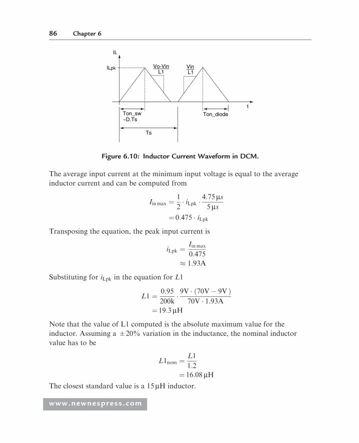
The average input current at the minimum input voltage is equal to the average
inductor current and can be computed from
Iinmax ¼1
2� iLpk �
4:75ms5ms
¼ 0:475 � iLpkTransposing the equation, the peak input current is
iLpk ¼Iinmax
0:475
� 1:93A
Substituting for iLpk in the equation for L1
L1 ¼ 0:95
200k� 9V � 70V� 9Vð Þ
70V � 1:93A¼ 19:3mH
Note that the value of L1 computed is the absolute maximum value for the
inductor. Assuming a ±20% variation in the inductance, the nominal inductor
value has to be
L1nom ¼L1
1:2
¼ 16:08mHThe closest standard value is a 15mH inductor.
IL
ILpk Vo-Vin
Ton_sw~D.Ts
Ton_diode
t
Ts
L1VinL1
Figure 6.10: Inductor Current Waveform in DCM.
86 Chapter 6
www.newnespress.com

The RMS current through the inductor is
ILrms ¼ iLpk �ffiffiffiffiffiffiffi0:9
3
r
¼ 1:057A
Choose a 15 mH inductor (±20% tolerance). A custom inductor would work best for
this application given the large swings in the inductor flux. However, if a standard
value inductor is preferred, the saturation current rating of the inductor should be
at least 1.5 times the peak current computed, to keep the core losses to an acceptable
value.
The inductor chosen in this case is a 15mH inductor with an RMS current rating of
1.4A and a saturation current rating of 3A.
6.4.6 Computing the On and Off Times of the Converter
The on-time of the switch can be computed as
ton sw ¼L1nom � iLpk
Vinmin
¼ 3:22ms
The on-time of the diode is
ton diode ¼L1nom � iLpk
Vomax � Vinmin
¼ 467 ns
The maximum duty cycle can then be computed as
Dmax ¼ ton sw � fs¼ 0:644
The diode conduction time ratio can be expressed as
D1 ¼ ton diode � fs¼ 0:0934
Boost Converters 87
www.newnespress.com

6.4.7 Choosing the Switching MOSFET (Q1)
The maximum voltage across the MOSFET in a boost converter is equal to the
output voltage. Using a 20% overhead to account for switching spikes, the minimum
voltage rating of the MOSFET has to be
VFET ¼ 1:2 � Vomax
¼ 84V
The RMS current through the MOSFET is
IFET � iLpk �ffiffiffiffiffiffiffiffiffiffiffiDmax
3
r
¼ 0:895A
To get the best performance from the converter, the MOSFET chosen has to have a
current rating about three times the MOSFET RMS current with minimum gate
charge Qg. It is recommended that for designs with the HV9912, the gate charge of
the chosen MOSFET be less than 25 nC.
The MOSFET chosen for this application is a 100V, 4.5A MOSFET with a Qg of
11 nC.
6.4.8 Choosing the Switching Diode (D1)
The voltage rating of the diode is the same as the voltage rating of the MOSFET
(100V). The average current through the diode is equal to the maximum output current
(350mA). Although the average current through the diode is only 350mA, the peak
current through the diode is equal to iLpk. Thus, it is a better design approach to choose
the current rating of the diode somewhere in between the peak input current and the
average output current (preferably closer to the peak input current). Thus, for this
design, the diode chosen is a 100V, 2A Schottky diode.
6.4.9 Choosing the Output Capacitor (Co)
The value of the output capacitor depends on the dynamic resistance of the LED
string as well as the ripple current desired in the LED string. In designs using
the HV9912, a larger output capacitor (lower output current ripple) will yield
88 Chapter 6
www.newnespress.com

better PWM dimming results. The capacitor required to filter the current
appropriately will be designed by considering the fundamental component of the
diode current only.
The output stage of the boost converter is modeled in Figure 6.11, where the LEDs
are modeled as a constant voltage load with series dynamic impedance.
The waveform of the capacitor current in steady state is shown in Figure 6.12.
Using the 10% peak-to-peak current ripple given in the design parameters table,
the maximum voltage ripple across the LED string has to be
Dvp�p ¼ DIo � RLED
¼ 0:55V
Icap
Idiode
I Co
VJ
+
RLED
Figure 6.11: Model of Boost Converter Output.
Icap
Time
Figure 6.12: Output Capacitor Current.
Boost Converters 89
www.newnespress.com

Assuming a constant discharging current of 350 mA when the diode current is
zero, the equation for the voltage across the capacitor can be written as
Iomax ¼ Co �Dvp�p
Dmax � Ts
Substituting values into the above equation,
Co ¼Iomax �Dmax
Dvp�p � fs¼ 0:585mF
The RMS current through the capacitor can be given by
Irms ¼ffiffiffiffiffiffiffiffiffiffiffiffiffiffiffiffiffiffiffiffiffiffiffiffiffiffiffiffiffiffiffiffiffiffiffiffiffiffiffiffiffiffiffiffiffiffiffiffiffiffiffiffiffiffiffiffiffiffiffiffiffiffiffiffiffiffiffiffiffiffiffiffiffiffiffiffiffiffiffi1�D1ð Þ � Iomax
2 þD1
3� ðiLpk � IomaxÞ2
r
¼ 0:34A
In this case, a parallel combination of two 1mF, 100V metal polypropylene
capacitors is chosen.
Note: The proper type of capacitor to use is either metal film capacitors or ceramic
capacitors, since they are capable of carrying this high ripple current. Although ceramic
capacitors are smaller in size and capable of carrying the ripple current, they cause a lot of
audible noise during PWM dimming. High value ceramic capacitors are usually limited to
50V rating. Thus metal polypropylene (or any other metal film) capacitors are the ideal
choice for LED drivers if PWM dimming is required.
6.4.10 Choose the Disconnect MOSFET (Q2)
The disconnect MOSFET should have the same voltage rating as the switching
MOSFET Q1. The on-state resistance of the MOSFET at room temperature
(Ron,25C) has to be calculated based on a 1% power loss inQ2 at full load current. Thus,
Ron,25C ¼0:01 � Vomax
Iomax � 1:4¼ 5�
The 1.4 multiplication factor is included to account for the increase in the
on-resistance due to rise in junction temperature. In this case, a high Qg MOSFET
90 Chapter 6
www.newnespress.com

can be chosen if desired (as it is not switching regularly), but a high Qg MOSFET will
slow down the turn-on and turn-off times (which might be allowable based on PWM
dimming frequency). In this case, the MOSFET chosen is a 100V, 0.7�, SOT-23
MOSFET with a Qg of 2.9 nC.
6.4.11 Choosing the Input Capacitors (C1 and C2)
The values of input capacitors C1 and C2 have to be calculated to meet closed loop
stability requirements. The connection from the power source to the boost converter
circuit will have some resistance, Rsource, and some inductance, Lsource. These feed
across the input capacitors (C1 and C2) and so form an LC resonant circuit. To
prevent interference with the control loop, the resonant frequency should be arranged
to be 40% or less of the switching frequency.
A pair of 22AWG connecting wires 1 foot (30 cm) long will have an inductance of
about 1mH. This is a good starting point. If necessary, the wires can be twisted
together to reduce the inductance.
With a 200 kHz switching frequency, the resonant frequency should be less than
80 kHz.
CIN �1
2 � p � fLCð Þ2�LSOURCE
¼ 3:95mF
C1 ¼ C2 ¼ 2:2mF, 50 V ceramic:
The maximum source impedance is found using:
M ¼ VO,MAX
VIN,MIN¼ 70
9¼ 7:778
RSOURCE,MAX ¼M� 1
M2 � ðM� 2Þ � RLED ¼ 1:404�
6.4.12 Choosing the Timing Resistor (RT)
The HV9912 oscillator has an 18 pF capacitor charged by a current mirror circuit.
An external timing resistor RT provides a reference current for the current mirror.
Boost Converters 91
www.newnespress.com

When RT is connected to 0 V, current flows and the timing process begins. When
charged to a certain voltage, the RS flip-flop is set, the capacitor is discharged, and
the timing process starts again. The timing resistor can be calculated by using the
following equation:
1
fs� RT � 18pF
In this case, for a constant 200 kHz switching frequency, the timing resistor value
works out to 274 k�. This resistor needs to be connected between the RT pin and
GND as shown in the typical circuit.
6.4.13 Choosing the Two Current Sense Resistors (R1 and R2)
The value of the output current sense resistor R2 can be calculated by limiting its
voltage drop to below 0.4 V. Using this criterion,
R2 ¼ 0:4V
Iomax
¼ 4�
The power dissipation will be 0.4 V*Io max = 0.04 W. In this case, the resistor chosen
is a 3.9�, 1/8 W, 1% resistor.
The MOSFET current sense resistor R1 is calculated by limiting the voltage across
the resistor to about 250mV at maximum input current.
R1 ¼ 0:25
iLpk
¼ 0:12�
The power dissipated in this resistor is
PR1 ¼ IFET2 � R1
¼ 0:096W
Thus, the chosen current sense resistor is a 0.12�, 1/4 W, 1% resistor.
92 Chapter 6
www.newnespress.com

6.4.14 Selecting the Current Reference Resistors (R3 and R4)
The voltage at the current reference pin IREF can be set either by using the reference
voltage provided at the REF pin (through a voltage divider) or with an external
voltage source. In the present design, it is assumed that the voltage at the IREF pin is
set using a voltage divider from the REF pin. The current reference resistors R3 and
R4 can be computed using the following two equations:
R3þ R4 ¼ 1:25V
50mA 25 k�
1:25V
R3þ R4� R4 ¼ Iomax � R2 ¼ 0:1 � 3:9 ¼ 0:39V
For this design, the values of the two resistors can be computed to be
R3 ¼ 19:1 k�, 1=8W, 1%
R4 ¼ 8:66 k�, 1=8W, 1%
6.4.15 Setting the Inductor Current Limit (R5 and R6)
The inductor current limit value depends on two factors – the maximum inductor
current and the slope compensation signal added to the sensed current. Another
resistor divider from the REF pin (R5 and R6) is connected to the CLIM pin and
sets the maximum inductor current. The voltage at the CLIM pin can be
computed as
VCLIM � 1:2 � iIpk � R1
This equation assumes that the current limit level is set at about 120% of the
maximum inductor current Iinmax.
For this design,
VCLIM ¼ 1:2 � 1:93 � 0:12� 0:278V
Boost Converters 93
www.newnespress.com

Using a maximum current sourced out of REF pin of 50 mA, the two resistors can be
calculated as
R5 ¼ 20k, 1=8W, 1%
R6 ¼ 6:04k, 1=8W, 1%
No capacitor should be connected at the CLIM pin, because this will affect the circuit
at start-up.
6.4.16 Capacitors at VDD and REF Pins
It is recommended that bypass capacitors be connected to both VDD and REF pins.
For the VDD pin, the capacitor used should be a 10V ceramic chip capacitor. For low
power designs, a 1mF is adequate. If the design uses high gate charge switching
MOSFETs (Qg> 15 nC), the capacitor at the VDD pin should be increased to 2.2mF.
For the REF pin, the capacitor used is a 0.1mF ceramic chip capacitor.
6.4.17 Setting the Over-Voltage Trip Point (R8 and R9)
The over-voltage trip point can be set at a voltage 15% higher than the maximum
steady state voltage. Using a 15% margin, the maximum output voltage during open
LED condition will be
Vopen ¼ 1:15 � Vomax
¼ 80:5V
Then, the resistors that set the over-voltage set point can be computed as
R8 ¼Vopen � 5� �2
0:1
¼ 57 k�
The above equation will allow us to select a 1/8W resistor by limiting the power
dissipation in the resistor.
R9 ¼ R8
Vopen � 5� � � 1:25V
¼ 3:77 k�
94 Chapter 6
www.newnespress.com

The closest 1% resistor values are
R8 ¼ 56:2k, 1=8W, 1%
R9 ¼ 3:74k, 1=8W, 1%
Note: The actual over-voltage point will vary from the desired point by ±5% due to
the variation in the reference (see datasheet). For this design, it varies from 76.67V
to 84.52V.
6.4.18 Designing the Compensation Network
The compensation needed to stabilize the converter could be either a Type-I circuit
(a simple integrator) or a Type-II circuit (an integrator with an additional pole-zero
pair). The type of the compensation circuit required will be dependent on the phase of
the power stage at the crossover frequency.
The loop gain of the closed loop system is given by
Loop Gain ¼ Rs � Gm � ZcðsÞ �1
15� 1
Rcs� GpsðsÞ
Where Gm is the transconductance of the op-amp (435 mA/V), Zc(s) is the impedance
of the compensation network, and Gps(s) is the transfer function of the power stage.
Please note that although the resistors give a 1:14 ratio, the overall effect when
including the diode drop is effectively 1:15.
To compute the transfer function for the discontinuous conduction mode boost
converter in peak current control mode, we need to define a couple of factors.
M ¼ Vomax � Iomax
Vomax � Iomax � 0:5 � L1nom � iLpk2 � fs
M ¼ 70 � 0:170 � 0:1� 0:5 � 15 � 10�6 � 1:932 � 200 � 103
M ¼ 7
1:41265¼ 4:9552
GR ¼M� 1
2 �M� 1¼ 3:95522
8:9104¼ 0:4439
Boost Converters 95
www.newnespress.com

For frequencies less than one tenth of the switching frequency, the power stage
transfer function is given by
GpsðsÞ ¼ 2 � Iomax
iLpk� GR
1þ s � RLED � Co � GR
GpsðsÞ ¼ 2 � 0:11:93� 0:4439
1þ s � 55 � 2 � 10�6 � 0:4439 ¼0:4439
1þ s � 48:829 � 10�6
For the present design, choose a crossover frequency 0.01 fs, or fc = 2 kHz. The low
crossover frequency will result in large values for CC and CZ, which will indirectly
provide a soft start for the circuit. Since the HV9912 does not depend on the speed of
the controller circuit for the PWM dimming response, the low crossover frequency
will not have an adverse effect on the PWM dimming rise and fall times. By
substituting s= i � (2p � fc)= i � 12566 into the transfer function, we get:
GpsðsÞ ¼0:046
1þ s � 0:6136
The magnitude and frequency of the power stage transfer function are:
GpsðsÞ�� ����
fc¼2kHz¼ Aps ¼ 0:039
ffGpsðsÞ��fc¼2kHz
¼ �ps ¼ �31:5�
To get a phase margin of about �m = 45� (the recommended phase margin range is
45�–60�), the phase boost required will be
�boost ¼�m � �ps � 90�
¼ 45� þ 31:5� � 90�
¼ �13:5�
Based on the value of the phase boost required, the type of compensation can be
determined.
�boost 0� ) Type� I controller
0� �boost 90� ) Type� II controller
90� �boost 180� ) Type� III controller
96 Chapter 6
www.newnespress.com

Type-III controllers are usually not required to compensate a HV9912-based boost
LED driver and thus will not be discussed here. The implementations for the
Type-I and Type-II systems for use with the HV9912 are given in Table 6.2.
For the present design, a simple Type-I controller will suffice. All that is needed is
to adjust the gain of the loop gain to be 1 at the crossover frequency.
One more equation can be obtained by equating the magnitude of the loop gain to
1 at the crossover frequency.
R2 � Gm �1
2 � p � fc � Cc
� �� 115� 1R1� Aps ¼ 1
Transposing, we get:
CC ¼ R2 � Gm �1
2 � p � fc
� �� 115� 1R1� Aps
CC ¼ 3:9 � 435 � 10�6 � 1
12566
� �� 115� 1
0:12� 0:039 ¼ 2:92 nF
Choose a CC = 3.3 nF, 50V, C0G capacitor
This completes our DCM boost converter design.
Table 6.2: Compensation Networks.
Type Circuit diagram Transfer function
I
COMP
CcZcðsÞ ¼
1
sCc
II
COMP
Cc
Cz
Rz
ZcðsÞ ¼1
sðCc þ CzÞ� 1þ s � Rz � Cz
1þ s � Cz � Cc
Cz þ Cc� Rz
Boost Converters 97
www.newnespress.com

6.5 Common Mistakes
1. The most common mistake is not having adequate over-voltage protection
at the output. If the LEDs are disconnected while the circuit is operating,
the output voltage will rise until components start to break down.
The over-voltage limit set at the output of the boost converter should be
lower than the breakdown voltage of any component connected across it.
2. Testing the circuit with a short string of LEDs. The forward voltage drop
may be lower than the supply voltage, and in this case there is little to prevent
the LEDs being destroyed by the high current that will flow.
6.6 Conclusions
Boost converters are used when the minimum output voltage is at least 1.5 times the
input voltage. Continuous conduction mode should be used when the output voltage
is a maximum of six times the input voltage. Discontinuous conduction mode is
necessary if the output voltage is more than six times the input voltage. The EMI
produced by a discontinuous mode boost converter is higher than for a continuous
conduction mode boost converter of similar power output.
98 Chapter 6
www.newnespress.com

C H A P T E R 7
Boost-Buck Converter
A boost-buck converter is a single-switch converter, which consists of a cascade of a
boost converter followed by a buck converter. The power train of typical boost-buck
circuit topology (used as an LED driver) is shown in Figure 7.1.
The converter has many advantages:
• The converter can both boost and buck the input voltage. Thus, it is ideal for
cases where the output LED string voltage can be either above or below the
input voltage during operation. This condition is most common in automotive
applications, or when a customer wants a single driver design to cover a wide
range of voltage supply and load conditions.
VIN
L1 L2 VO–
+ Vc – IL2IL1
VO+
C1
Q1D1
+–
Figure 7.1: Boost-Buck (Cuk) Power Train.
www.newnespress.com

• The converter has inductors on both the input and output sides. Operating both
stages in continuous conduction mode (CCM) will enable continuous currents
in both inductors with low current ripple, which would greatly reduce the filter
capacitor requirements at both input and output. Continuous input current
would also help greatly in meeting conducted EMI standards at the input.
• All the switching nodes in the circuit are isolated between the two inductors.
The input and output nodes are relatively quiet. This will minimize the
radiated EMI from the converter. With proper layout and design, the
converter can easily meet radiated EMI standards.
• One of the advantages of the boost-buck converter is the capacitive isolation.
The failure of the switching transistor will short the input and not affect the
output. Thus, the LEDs are protected from failure of the MOSFET.
• The two inductors L1 and L2 can be coupled together on one core. When
coupled on a single core, the ripple in the inductor current from one side can be
transferred completely to another side (ripple cancellation technique). This
would allow, for example, the input ripple to be transferred completely to the
output side making it very easy for the converter to meet conducted EMI
standards.
7.1 The Cuk Converter
In spite of the many advantages of the Cuk converter, a couple of significant
disadvantages exist which prevent its widespread use.
• The converter is difficult to stabilize. Complex compensation circuitry is often
needed to make the converter operate properly. This compensation also tends
to slow down the response of the converter, which inhibits the PWM dimming
capability of the converter (essential for LEDs).
• An output current controlled boost-buck converter tends to have an
uncontrolled and undamped resonance due to an L-C pair (L1 and C1). The
resonance of L1 and C1 leads to excessive voltages across the capacitor, which
can damage the circuit.
The damping ofL1 andC1 can easily be achieved by adding a dampingR-C circuit across
C1. However, the problem of compensating the circuit so that it is stable is more complex.
100 Chapter 7
www.newnespress.com

The Supertex HV9930 solves the problem of compensation and achieving a fast
PWM dimming response by using hysteretic current mode control. This uses fast
comparators to control a MOSFET gate by setting upper and lower limits, which
ensures fast response and accurate current levels. However, a simple hysteretic
current mode control would not work, as the converter would not be able to start up.
To overcome this problem, the HV9930 has two hysteretic current mode controllers –
one for the input current and another for the output current.
During start-up, the input hysteretic controller dominates and the converter is in
input current limit mode. The MOSFET turns on and the input current rises until
the input current limit is reached, it then turns off so that the input current drops
until a lower current limit is reached. This cycle continues until the output current
has built up to the required value and the output hysteretic controller can take over.
The output current is then maintained between the set upper and lower current limits.
Unlike peak current mode controller, hysteretic control ensures that the average
output current remains constant under a wide range of input and output voltage
conditions.
The hysteretic approach will also help in limiting the input current during start-up
(thus providing soft-start); also current is limited in the case of an output overload or
input under-voltage condition. Three resistors (for each of the two hysteretic
controllers) are required to set both the current ripple and the average current, which
enables a simple controller design. Thus six resistors determine the input and output
performance.
This section will detail the operation of the boost-buck converter and the design
of an HV9930-based converter. The design example is specifically designed for
automotive applications, but it can also be applied for any DC/DC applications. At
the time of writing, there is only one other device with the same functionality as the
HV9930, which is the AT9933. The AT9933 has an automotive temperature
specification (up to 125�C operation), whereas the HV9930 has an industrial
temperature range.
7.1.1 Operation of a Cuk Boost-Buck Converter
The diagram of the power train for a Cuk boost-buck converter was shown
previously, in Figure 7.1.
Boost-Buck Converter 101
www.newnespress.com

In steady state, the average voltages across both L1 and L2 are zero. Thus, the
voltage, Vc, across the middle capacitor C1 is equal to the sum of the input and
output voltages.
Vc ¼ Vin þ Vo
When switch Q1 is turned on, the currents in both inductors start ramping up
(see Figure 7.2).
L1diL1dt¼ Vin
L2diL2dt¼ Vc � Vo ¼ Vin
When switch Q1 is turned off, the currents in both inductors start ramping down (see
Figure 7.3).
VIN
L1 L2 VO–
+ Vc –
IL2IL1
VO+
C1
+–
Figure 7.2: Cuk Circuit, MOSFET On.
VIN
L1 L2 VO–
+ Vc –
IL2IL1
VO+
C1
+–
Figure 7.3: Cuk Circuit, MOSFET Off.
102 Chapter 7
www.newnespress.com

L1diL1dt¼ Vin � Vc ¼ �Vo
L2diL2dt¼ �Vo
Assuming that the switch is ON for a duty cycle D and using the fact that, in steady
state, the total volt-seconds applied across any inductor is zero, we get
Vin � Dð Þ ¼ Vo � 1�Dð Þ
) Vo
Vin¼ D
1�D
Thus, the voltage transfer function obtained for the boost-buck converter will give
buck operation for D< 0.5 and boost operation for D > 0.5. The steady state
waveforms for the converter are shown in Figure 7.4.
The maximum voltage seen by Q1 and D1 is equal to the voltage across the
capacitor C1.
VQ1 ¼ VD1 ¼ Vc
The standard boost-buck converter is modified, by adding three additional
components, for proper operation of the HV9930 (see Figure 7.5).
A damping circuit Rd-Cd has been added to damp the L1-C1 pair. These additional
components stabilize the circuit.
An input diode (D2) has been added. This diode is necessary for PWM dimming
operation (in case of automobile applications, this could be the reverse polarity
protection diode). This diode helps to prevent capacitors C1 and Cd from discharging
when the gate signals for Q1 are turned off. Thus, when the HV9930 is enabled, the
steady state output current level will be reached quickly.
7.1.2 Hysteretic Control of the Boost-Buck Converter
Hysteretic control refers to the control scheme where the controlled variable (in this
case, the inductor current iL2) is maintained between pre-set upper and lower
boundaries. As previously shown in Figure 7.4, the inductor current ramps up at a
Boost-Buck Converter 103
www.newnespress.com

rate of Vin/L2 when the switch is ON and ramps down at a rate of �Vo/L2 when
the switch is OFF. Thus, the hysteretic control scheme turns the switch OFF when the
inductor current reaches the upper limit and turns the switch ON when it reaches
the lower limit.
The average current in inductor L2 is then set at the average of the upper and lower
thresholds. The ON and OFF times (and thus the switching frequency) vary as the
input and output voltages change to maintain the inductor current levels. However,
GATE
HI
0
VIN
–Vo
t
t
t
t
t
Iin
–Io
VL1,VL 2
IL1,IL 2
Ic
Vc
0
0
0
0
Figure 7.4: Cuk Converter Steady State Waveforms.
104 Chapter 7
www.newnespress.com

in any practical implementation of hysteretic control, there will be comparator delays
involved. The switch will not turn ON and OFF at the instant the inductor current
hits the limits, but after a small delay time, as illustrated in Figure 7.6.
7.1.3 The Effects of Delay in Hysteretic Control
This delay time introduces two unwanted effects:
• It alters the average output current value. For example, if the delay on the
down slope of the inductor current is more than the delay on the up slope,
then the average current value decreases.
• It decreases the switching frequency, which may make it more difficult for the
circuit to meet EMI regulations.
Turn-on Delay
Desired Io
Actual Io
Turn-off Delay
Figure 7.6: Current in the Output Inductor L2.
VIN
L1D2 L2 VO–
Cd+
RdIL 2IL1
VO+
C1
Q1D1
+–
Figure 7.5: Modified Boost-Buck Circuit.
Boost-Buck Converter 105
www.newnespress.com

These effects will have to be taken into consideration when choosing the output
inductor value and the setting the current limits.
Assume a peak-to-peak current ripple setting of Dio (using the programming
resistors) and a desired average current lo. A hysteretic current controlled boost-buck
converter acts as a constant-off-time converter as long as the output voltage is fixed,
and the off-time is theoretically independent of the input voltage. Thus, the converter
is designed assuming a constant off-time Toff (the method to determine the off-time
will be discussed later).
For the HV9930, as long as the switching frequencies are less than 150 kHz, these
delay times have a negligible effect and can be ignored. In these cases, the output
inductor can be determined by
L2 ¼Vo � Toff
Dio
If the inductor chosen is significantly different from the computed value, the actual
off-time Toff,ac can be recomputed using the same equation.
However, in automotive applications, it is advantageous to set the switching
frequency of the converter below 150 kHz or in the range between 300 kHz and
530 kHz. This will place the fundamental frequency of the conducted and radiated
EMI outside of the restricted bands making it easier for the converter to pass
automotive EMI regulations. In cases where the switching frequency is more than
300 kHz, the delay times cannot be neglected and have to be accounted for in the
calculations. Figure 7.7 illustrates the output inductor current waveform and the
various rise and fall times.
From this figure,
Toff ¼Tf1 þ Tf2 þ Tf
¼ Vin
Vo� Tr þ Tf 2 þ Tf
The desired output current ripple Dio and the down-slope of the inductor current
m2 determine Tf 2. The delay times of the HV9930 determine Tr and Tf. For the
HV9930, the delay time of the comparators is related to the overdrive voltage
106 Chapter 7
www.newnespress.com

(voltage difference between the two input terminals of the current sense comparator)
applied as
Tdelay �Kffiffiffiffiffiffiffiffiffiffiffiffiffiffiffiffiffiffiffiffiffi
m � 0:1=Dio3
q
Where ‘m’ is the rising or falling slope of the inductor current.
Tr ¼6mffiffiffiffiffiffiffiffiffiffiffiffiffiffiffiffi
Vin � 0:1Dio
3
s �ffiffiffiffiffiffiL2
3p
¼ K1 �ffiffiffiffiffiffiL2
3p
Tf 2 ¼Dio �L2
Vo¼ K2 �L2
Tf ¼6mffiffiffiffiffiffiffiffiffiffiffiffiffiffiffiffiVo � 0:1
Dio3
s �ffiffiffiffiffiffiL2
3p
¼ K3 �ffiffiffiffiffiffiL2
3p
To find the value of L2 using the time delay equations above results in a cubic
equation. This cubic has one real root and two complex roots. The inductor value is
the real root of the cubic raised to the third power.
–m2 = –VoL2
Tf 2
Tf1
Tr
Toff
Tf
m1 =
ΔIoΔIo, ac
VinL2
Figure 7.7: Hysteretic Control with Comparator Delays.
Boost-Buck Converter 107
www.newnespress.com

a ¼ K2
b ¼ Vin
Vo� K1 þ K3
c ¼ Toff
D ¼ 12 �ffiffiffi3p�ffiffiffiffiffiffiffiffiffiffiffiffiffiffiffiffiffiffiffiffiffiffiffiffiffiffiffiffiffiffiffiffiffiffiffi4 � b3 þ 27 � a � c2
a
r
L2 ¼1
6 � a 108 � cþ Dð Þ � a2" #1=3
� 2 � b
108 � cþ Dð Þ � a2h i1=3
8>>><>>>:
9>>>=>>>;
3
The actual off-time Toff,ac can be computed by substituting the chosen inductor value
back into the equations for Tr, Tf and Tf2, to get Tr,ac, Tf,ac and Tf 2,ac.
Toff;ac ¼Tf 1,ac þ Tf 2,ac þ Tf;ac
¼ Vin
Vo� Tr,ac þ Tf 2,ac þ Tf,ac
The actual ripple in the inductor current Dio,ac is
Dio,ac ¼Vo � Toff,ac
L2
7.1.4 Stability of the Boost-Buck Converter
The single-switch boost-buck converter can be considered as separate boost and buck
converters (in that order), which are cascaded, and both switches being driven with
the same signal (see Figure 7.8).
108 Chapter 7
www.newnespress.com

The relationships between the voltages in the system are
Vc
Vin¼ 1
1�Dðboost converterÞ
Vo
Vc¼ D ðbuck converterÞ
The capacitor voltage Vc and the input/output relationship can both be derived using
the above equations
Vo
Vin¼ Vo
Vc� Vc
Vin¼ D
1�D
Vc ¼Vin
1�D¼ Vin
1� Vo=Vc
) Vc ¼ Vo þ Vin
For the purposes of designing the damping network, it is easier to visualize the
converter in its two-switch format of Figure 7.7 rather than as the single-switch Cuk
converter. Hence, for the remainder of this section, the cascaded converter will be
used to derive the equations.
VIN
L1 D1A L2
C1+
Q1B
IL 2IL1VO+
VO–
Q1AD1B
+–
Figure 7.8: Boost-Buck Converter.
Boost-Buck Converter 109
www.newnespress.com

In hysteretic control of the boost-buck converter using the HV9930, the
output buck stage is controlled and the input boost stage is uncontrolled. An
equivalent schematic of the HV9930 controlled boost-buck converter is shown in
Figure 7.9.
The hysteretic control of the buck stage ensures that the output current iL2 is
constant under all input transient conditions. So, for the purposes of average
modeling, the load seen by the capacitor C1 can be modeled as a current source
equal to d � lo, where d is the instantaneous duty cycle and lo is the constant output
current. The continuous conduction mode buck stage also imposes one more
constraint:
Vo ¼ d � vc
where d and vc are the time dependent duty cycle and capacitor voltage and Vo is the
constant output voltage. For the system to be stable, it is necessary that the control
system will act to reduce any disturbance in capacitor voltage.
The loop gain of the system for a boost-buck converter without damping has a
negative phase margin (i.e. the phase is less than �180� when the magnitude crosses
0 dB). This is due to the undamped LC pole-pair and causes the system to be unstable.
Thus, any disturbance to the capacitor voltage will get amplified and keep increasing till
VIN
L1 D1A L2
C1+
Q1B
IL 2IL1VO+
VO–
REF
Q1AD1B
+–
+
–
Figure 7.9: Boost-Buck Controller.
110 Chapter 7
www.newnespress.com

the components breakdown. When testing the circuit, if it is close to becoming unstable,
the switching frequency rises and falls with a low frequency beat and a low frequency
ripple in the average output current can be seen.
The addition of R-C damping of this undamped pole pair can stabilize the system and
make sure that the disturbance input is properly damped. Also, the presence of Cd
ensures that Rd will not see the DC component of the voltage Vc across it, reducing
the power dissipated in the damping resistor (Cd blocks the DC component of the
voltage).
Assuming Cd >> C1, the loop gain transfer function of the R-C damped boost-buck
converter can be derived as
GðsÞHðsÞ ¼ D
1�D�
1þ s � Rd � Cdð Þ � 1� s � D
1�Dð Þ2� L1 � Io
Vo
!
1þ s � Rd � C1ð Þ � 1þ s � Rd � Cdþ s2 � L1 � Cdð1�DÞ2
!
Thus, the loop has a DC gain of D/(1�D) and includes:
1. Damping (and ESR) zero at !Z ¼ 1Rd �Cd :
2. RHP zero at !RHP ¼ 1�Dð Þ2D � Vo
L1 � Io .
3. Complex double pole with natural resonant frequency !o ¼ 1�DffiffiffiffiffiffiffiffiffiffiffiL1 �Cdp and
damping factor � ¼ 1�Dð Þ �Rd �ffiffiffiffiffiCdL1
q.
4. High frequency pole at !P ¼ 1Rd �C1 :
In order to achieve stable loop, the 0 dB crossing (!c) must be placed such that
!c<<!RHP and !c<<!p. The latter condition is easily met by selecting Cd >>C1.
We can easily obtain approximate values of Cd and Rd for the case of !c>>!o. This
condition is usually met for the worst-case calculations at minimum input voltage,
since the DC gain is the highest at this condition. Set !c =!RHP/N, where N>> 1.
Then !o can be approximately calculated from
!O¼ !
C�ffiffiffiffiffiffiffiffiffiffiffiffi1�D
D
r¼ !RHP
N�ffiffiffiffiffiffiffiffiffiffiffiffi1�D
D
r
Boost-Buck Converter 111
www.newnespress.com

Substituting for !o and !RHP in (21) gives the equation for computing Cd:
Cd ¼ N2 �D3
1�Dð Þ3L1 � I
O
2
VO2
Selecting Rd such that !z =!c results in a good phase margin with minimum power
dissipation. Then, using equations for !z and !RHP gives a solution for Rd.
Rd ¼ N �D1�Dð Þ2
L1 � IO
Cd � VO
Using the equations above, the approximate values for the damping network can be
computed using the following equations:
Cd ¼ 9 � D
1�D
� �3
�L1 � IoVo
� �2
Rd ¼ 3 �D1�Dð Þ2
� L1 � IoCd � Vo
Note that the damping resistor value includes the ESR of the damping capacitor. In
many cases, the damping capacitor is chosen to be an electrolytic capacitor, which
will have a significant ESR (sometimes a few ohms). In such cases, the damping
resistor can be reduced accordingly.
7.1.5 Dimming Ratio Using PWM Dimming
The linearity in the dimming ratio achievable with the boost-buck depends on both
the switching frequency and the PWM dimming frequency.
For a converter designed to operate at a minimum switching frequency of 300 kHz,
one switching time period equals 3.33ms. This is the minimum on-time of the PWM
dimming cycle. At a PWM dimming frequency of 200Hz (5ms period), 3.33 msequals a minimum duty cycle of 0.067%. This corresponds to a 1:1500 dimming
range. However, the same converter being PWM dimmed at 1 kHz (1ms time
period) will have a minimum duty ratio of 0.33% or a PWM dimming range
of 1:300.
112 Chapter 7
www.newnespress.com

If the minimum on-time of the PWM dimming cycle is less than the switching time
period, the LED current will not reach its final value. Hence the average current will
be less. Thus, the LEDs will dim, but there will be a loss of linearity between the
average LED current and the duty cycle of the PWM input.
7.1.6 Design of the Boost-Buck Converter with HV9930
Specification
Input voltage: 9–16V (13.5V typical)
Transient voltage: 42V (clamped load dump rating)
Reverse polarity protection: 14V
Output voltage: 28V maximum
Output current: 350mA
LED resistance: 5.6 ohms
Estimated efficiencies: 72% minimum, 82% maximum (80% typical)
These efficiency values do not take into account the power loss in the reverse blocking
diode. A Schottky diode will drop about Vd = 0.5V across it and thus will dissipate
power in the range 0.4–0.6W. This diode voltage drop will be taken into account
while designing the converter.
The efficiency values used in this design are typical values for the given input
voltages and output power level. Higher efficiencies can be obtained at lower
input current levels (i.e. higher input voltages): the efficiency drop at lower input
voltages is due to conduction losses caused by the correspondingly larger input
currents. The efficiency values will depend on the operating conditions and,
except in very high power designs, these values can be used as a good
approximation.
Efficiencies higher than 85% can easily be achieved with the HV9930 controlled
Cuk converter if the operating frequency is kept below 150 kHz. However, because
of automotive EMI requirements, the higher efficiencies are traded off for higher
switching frequencies (which increase switching losses in the system).
Boost-Buck Converter 113
www.newnespress.com

Consider a boost-buck converter circuit as shown in Figure 7.10.
Switching Frequency at Minimum Input Voltage
Although the HV9930 is a variable frequency IC, the selection of the minimum
switching frequency is important. In the case of automotive converters, designing
with a switching frequency in the range between 300 kHz and 530 kHz would avoid
the restricted radio broadcast bands and make it easier to meet the conducted and
radiated EMI specifications. So, for this application we choose a minimum switching
frequency of 300 kHz (which occurs at minimum input voltage).
Calculating the Duty Cycle
The switch duty cycle will have to be computed at the minimum input voltage.
Dmax ¼1
1þ �min� Vin,min � Vdð ÞVo
¼ 0:821
Vin GATE GNDVDD
CS2REF
PWM
CS1
1
2
5
34
8
6
7HV9930
C2 C3
Q1
L1D2VIN+
VIN–
Cin
Rcs1 Rcs2
Rs2b
Rs2a
Co
VO–
VO+
D3
L2C1
Cd+ Rd
D1
Rs1
PWM
Rref1 Rref2
Figure 7.10: Boost-Buck Converter Using HV9930.
114 Chapter 7
www.newnespress.com

Calculating the Input Current
The input current level at the minimum input voltage should be calculated first,
because this gives the highest current level. The value obtained will be used to work
out the current ratings of the various components.
Iin,max ¼Vo � Io
�min � Vin,min � Vdð Þ¼ 1:601A
Calculating the Output Inductor
The first step is to compute the off-time. The off-time of the converter can be
calculated as
Toff ¼1�Dmax
fs,min
¼ 598 ns
Assuming a 25% peak-to-peak ripple in the output current ðDio¼ 87:5mAÞ, andaccounting for the diode drop in the input voltage by substituting Vin,min�Vd in
place of Vin, yields
598 ns ¼ 0:887m �ffiffiffiffiffiffiL2
3p
þ 3:125m � L2 þ 1:89m �ffiffiffiffiffiffiL2
3p
Solving for L2 gives
L2 ¼ 0:052ð Þ3¼ 145mH
The closest standard value is a 150mH, 0.35A RMS, and 0.4A saturation inductor.
Since the inductance value is different from the computed value, the actual off-time
will also change as
Toff,ac ¼ 2:777m �ffiffiffiffiffiffiffiffiffiffiL2,ac
3p
þ 3:125m � L2,ac
¼ 616 ns
Boost-Buck Converter 115
www.newnespress.com

The actual ripple in the output current is given by
Dio,ac ¼Vo � Toff,ac
L2,ac
¼ 0:115A
Note that although the ripple in the output current was assumed to be about 25% (or
87.5mA), the actual ripple is almost double that value. This increase in the ripple is
due to the delays of the comparators. A capacitor will be required at the output of the
converter (across the LEDs) to reduce the ripple to the desired level. This capacitor
will be very small, as the switching frequencies are large, but the capacitor will also
help to reduce output EMI. Large output capacitors are to be avoided in applications
that use PWM dimming, because the stored charge will reduce the dimming ratio that
can be obtained.
It is also useful to calculate the ripple overshoot and undershoot beyond the
programmed limits. This will help determine how the average current changes
due to the delays.
Diover ¼Vo
L2,ac� Vin,min � Vd
Vo� K1
� ��ffiffiffiffiffiffiffiffiffiffiL2,ac
3p
¼ 8:3mA
Diunder ¼Vo
L2,ac� K3 �
ffiffiffiffiffiffiffiffiffiffiL2,ac
3p
¼ 19mA
Thus, the average output current will be reduced from the set value by about
10.7mA.
In most cases, due to the inductor values available, the actual off-time will differ
from the computed value significantly. Thus, it is better to use the actual value of the
off-time calculated in order to work out the rest of the component values.
If the switching frequency is less than 150 kHz, the equation L2 ¼ Vo �Toff
Dio can be used
to calculate the output inductance (L2) value, simplifying the procedure greatly.
116 Chapter 7
www.newnespress.com

Calculating the Input Inductor
We can assume a 15% peak-to-peak ripple in the input current at minimum input
voltage (this low input ripple will minimize the input filtering capacitance needed).
The off-time previously calculated can be used to find the value of the input inductor.
L1 ¼Vo � Toff,ac
0:15 � Iin,max
¼ 72mH
The closest standard value inductor is an 82mH inductor. The current rating of this
inductor will be decided in the final stages after the input current limit has been set.
The peak-to-peak ripple in the input current is
DIin ¼Vo � Toff,ac
L1,ac
¼ 0:21A
Calculating the Value of the Middle Capacitor (C1)
Assuming a 10% ripple across the capacitor at minimum input voltage
(Dvc ¼ 0:1 � Vin,min � Vd þ Voð Þ ¼ 3:65 V ), capacitor C1 can be calculated as
C1 ¼Iin,max � Toff,ac
Dvc¼ 0:257mF
Irms,C1 ¼ffiffiffiffiffiffiffiffiffiffiffiffiffiffiffiffiffiffiffiffiffiffiffiffiffiffiffiffiffiffiffiffiffiffiffiffiffiffiffiffiffiffiffiffiffiffiffiffiffiffiffiffiffiffiffiffiffiffiffiffiffiffiffiI 2in,max � 1�Dmaxð Þ þ I 2o �Dmax
q¼ 0:72 A
The voltage rating and type of this capacitor have to be chosen carefully. This
capacitor carries both the input current and the output current. Thus, to prevent
excessive losses and overheating of the capacitor, it must have a very low ESR.
Ceramic capacitors are an ideal choice for this application due to their low ESR and
high transient voltage limit. If a ceramic capacitor cannot be used for reasons of
Boost-Buck Converter 117
www.newnespress.com

cost or availability, a plastic film capacitor such as PET can be used instead, although
these are considerably bulkier.
The maximum steady state voltage across the capacitor is 44V (= 28 Vþ 16 V), and the
maximum transient voltage across the capacitorVc,max is 70V (= 28 Vþ 42 V). Ceramic
capacitors can easily withstand up to 2.5 times their voltage rating for the duration of
the load dump voltage. Also, the actual capacitance value of these capacitors reduces
based on the bias voltage applied. Ceramic capacitor types X7R and X5R are more
stable and the capacitance drop is not more than 20% at full rated voltage.
Thus, a 0.22mF, 50V X7R ceramic chip capacitor can be selected.
Choosing the Switching Transistor (Q1)
The peak voltage across the MOSFET Q1 is 70 V. Assuming a 30% overhead on the
voltage rating to account for leakage inductance spikes, the MOSFET voltage needs
to be at least
VFET ¼ 1:3 � Vc,max
¼ 91V
The RMS current through the MOSFET will be at maximum level at low input
voltage (higher current levels and maximum duty cycle). The maximum RMS current
through the MOSFET is
IFET,max ¼ Iin,max þ Ioð Þ �ffiffiffiffiffiffiffiffiffiffiffiDmax
p¼ 1:77A
A typical choice for the MOSFET is to pick one whose current rating is about three
times the maximum RMS current. Choose FDS3692 from Fairchild Semiconductors
(100V, 4.5A, 50m� N-channel MOSFET). Note that the current rating is normally
quoted at 25�C; the current rating reduces as the temperature rises.
The total gate charge Qg of the chosen MOSFET is a maximum of 15 nC. It is
recommended that the MOSFET total gate charge should not exceed 20 nC, as the
large switching times will cause increased switching losses. A higher gate charge
would be allowable if the switching frequency can be reduced appropriately.
118 Chapter 7
www.newnespress.com

A resistor in series with the MOSFET gate reduces EMI by slowing down the turn-on
time. Current transients are limited when the MOSFET turns on slowly, but this
reduces efficiency. A PNP transistor to discharge the MOSFET gate helps to
minimize the reduction in efficiency without significantly increasing EMI.
Choosing the Switching Diode
The maximum voltage rating of the diode D2 is the same as the MOSFET voltage
rating. The average current through the diode is equal to the output current.
Idiode¼ Io¼ 350mA
Although the average current of the diode is only 350mA, the actual switching
current through the diode goes as high as 1.95A (Iin,maxþ Io). (Note: the calculations
were for 360mA, to allow for 10 mA drop because of delays, but the actual average
current is 350mA.) A 500mA diode will be able to carry the 1.79A current safely, but
the voltage drop at such high current levels would be extremely large, increasing the
power dissipation. Thus, we need to choose a diode whose current rating is at least
1A. A 100V, 2A Schottky diode would be a good choice. Choosing a voltage rating
significantly higher than required is not a good idea, since generally the forward
voltage drop increases as the reverse voltage rating increases and this causes higher
conduction losses.
Choosing the Input Diode
The input diode serves two purposes:
1. It protects the circuit from a reverse polarity connection at the input.
2. It helps in PWM dimming of the circuit by preventing C1 from discharging
when the HV9930 is turned off.
The current rating of the device should be at least equal to Iin,max. The voltage rating
of the device should be more than the reverse input voltage rating. A higher current
rating often gives a lower forward voltage drop. In this case, a 30BQ015 (15V, 3A
Schottky diode) would be a good choice.
Boost-Buck Converter 119
www.newnespress.com

If neither reverse protection or PWM dimming is required, removing the input diode
from the LED driver circuit will increase the input supply voltage at the converter, which
will slightly increase the efficiency and slightly reduce the maximum input current.
Calculating the Input Capacitance
Some capacitance is required on the input side to filter the input current. This
capacitance is mainly responsible for reducing the 2nd harmonic of the input current
ripple (which in this case falls in the AM radio band). According to the SAE J1113
specifications, the peak limit for narrowband emissions in this range is 50 dBmV to
meet Class 3 at an input voltage of 13+ 0.5V. Assuming a saw tooth waveform for
the input current as a conservative approximation, the RMS value of the 2nd
harmonic component of the input current (Iin,2) can be computed as
Iin,2 ¼DIin
2 �ffiffiffi2p� p¼ 0:024 A
The switching frequency of the converter at 13V input can be computed as
Dnom ¼1
1þ �nom � Vin,nom � Vdð ÞVo
¼ 1
1þ 0:8 � 13:5� 0:5ð Þ28
¼ 0:73
fs,nom ¼1�Dnom
Toff,ac
¼ 414 kHz
Cin ¼Iin,2
4 � p � fs,nom � 10�6 � 1050=20
¼ 14:6mF
Choose a parallel combination of three 4.7mF, 25V, X7R ceramic capacitors.
120 Chapter 7
www.newnespress.com

Calculating the Output Capacitance
The output capacitance is required to reduce the LED current ripple from 115mA to
DILED= 70mA (20% peak to peak ripple) can be approximately calculated by using only
the first harmonic in the inductor current. A 70mA peak-to-peak ripple in the LED
results in a 392mV (Dvo= DlLED �RLED) peak-to-peak ripple voltage. Then
Dvo2¼ 8
p2� DiL2
2
� �� RLEDffiffiffiffiffiffiffiffiffiffiffiffiffiffiffiffiffiffiffiffiffiffiffiffiffiffiffiffiffiffiffiffiffiffiffiffiffiffiffiffiffiffiffiffiffiffiffiffiffiffiffiffiffiffiffiffiffiffiffi
1þ 2 � p � fs,min � RLED � Coð Þ2q
The output capacitance required can then be calculated from this
Co ¼
ffiffiffiffiffiffiffiffiffiffiffiffiffiffiffiffiffiffiffiffiffiffiffiffiffiffiffiffiffiffiffiffiffiffiffiffiffiffiffiffiffiffiffiffiffiffi16 � RLED
p2� DiL2
Dvo
� �2
�1
s
2 � p � fs,min � RLED
¼ 0:178mF
Use a 0.22mF, 35V ceramic capacitor.
Calculating the Theoretical Switching Frequency Variation
The maximum and minimum frequencies (using steady state voltage conditions) can
be now be worked out:
fs,min ¼1� 1
1þ �min � Vin,min � Vdð Þ=Vo
Toff,ac
¼ 291 kHz
fs,max ¼1� 1
1þ �max � Vin,max � Vdð Þ=Vo
Toff,ac
¼ 506 kHz
The theoretical frequency variation for this design is 398 kHz + 27%.
Boost-Buck Converter 121
www.newnespress.com

Design of the Damping Circuit
The values for the damping network can be calculated as follows
Cd ¼ 9 � Dmax
1�Dmax
� �3
�L1,ac �IoVo
� �2
¼ 11mF
Rd ¼ 3 �Dmax
1�Dmaxð Þ2� L1,ac � IoCd � Vo
¼ 7:16�
The power dissipated in Rd can be computed as
PRd ¼Dvc2
12 � Rd
¼ 3:652
12 � 7:16 ¼ 0:155W
The RMS current through the damping capacitor will be
iCd ¼Dvc
2 �ffiffiffi3p� Rd
¼ 0:147A
Choose a 10mF, 50V electrolytic capacitor that can allow at least 150mA RMS
current. An example would be EEVFK1H100P from Panasonic (10mF, 50V, Size D).
This capacitor has about a 1� ESR, so Rd can be reduced to about 6.2�.
Internal Voltage Regulator of the HV9930
The HV9930 includes a built-in 8–200V linear regulator. This regulator supplies the
power to the IC. This regulator can be connected at either one of two nodes on the
circuit as shown in Figure 7.11.
In the normal case, when the input voltage is always greater than 8V, the VIN pin of
the IC can be connected to the cathode of the input protection diode (as shown in
122 Chapter 7
www.newnespress.com

Figure 7.11A). If reverse protection is not provided, the VIN pin can be connected
directly to the positive supply.
In conditions where the converter needs to operate at voltages lower than 8V,
once the converter is running (as in the case of cold-crank operation), the VIN
pin of the HV9930 can be connected as shown in Figure 7.11B. In this case, the drain
of the MOSFET is at VinþVo, and hence even if the input voltage drops below
8V, the IC will still be functioning. However, in this case, more hold-up capacitance
will be required at the VDD pin to supply the power to the IC when the MOSFET
is ON.
In both cases, a 2.2mF or greater value ceramic capacitor is recommended at the
VDD pin.
Internal Voltage Reference
The HV9930 includes an internal 1.25V (+3%) reference. This reference can be used
to set the current thresholds for the input and output hysteretic comparators. It is
recommended that this pin be bypassed with at least a 0.1mF ceramic capacitor.
(A) (B)
Vin GATE GNDVDD
CS2REF
PWM
CS1
1 36
HV9930
C2
Q1
L1D2VIN+
Vin GATE GNDVDD
CS2REF
PWM
CS1
1 36
HV9930
C2
Q1
D2VIN+
L1
Figure 7.11: Connection Points for VIN.
Boost-Buck Converter 123
www.newnespress.com

Programming the Hysteretic Controllers and Over Voltage Protection
The input and output current levels for the hysteretic controllers are set by means of
three resistors for each current – one current sense resistor and two divider resistors.
The equations governing the resistors are the same for both the input and output
sides and are given as
Rs
Rref¼
0:05 � DiIþ 0:1
1:2 � DiI� 0:1
Rcs ¼1:2 � Rs
Rref� 0:05
I
These equations assume that the 1.25V reference provided by the HV9930 is used to
set the current. In cases where linear dimming of the LEDs is required, it is
recommended that the input current thresholds be based on the 1.25V reference and
the output current thresholds are modified using the variable input voltage available.
In such a case, assuming the maximum external voltage VLD as the reference, the
above two equations can be modified as
Rs
Rref¼
0:05 � DiIþ 0:1
VLD � 0:05ð Þ � DiI� 0:1
Rcs ¼VLD � 0:05ð Þ � Rs
Rref� 0:05
I
In this design example, it is assumed that linear dimming is not required and the
1.25V reference is used for both the input and output programming.
Note: The HV9930 cannot operate the boost-buck converter in the discontinuous
conduction mode. The minimum external voltage is given by
VLD ¼ 0:1 � Rref 2 þ Rs2
Rs2:
124 Chapter 7
www.newnespress.com

The programming of the output side is also linked to the over-voltage protection. The
boost-buck converter is not inherently programmed against open LED conditions, so
external protection is required. This is achieved by adding Zener diode D3, and by
splitting the resistor Rs2 into two parts – Rs2a and Rs2b. In normal operation, the
inductor current will flow only through Rcs2 and the voltage drop across Rcs2 is
sensed through Rs2a and Rs2b in series.
When there is an open LED condition, the inductor current will flow through
diode D3. This will then clamp the output to the Zener breakdown voltage. However,
since the diode cannot take the full design current, the current level has to be reduced
to more manageable levels. During open LED conditions, the current will flow
though both Rcs2 and Rs2a. Thus, the effective current sense resistor seen by the IC is
Rcs2þRs2a and the voltage drop across both of these will be sensed through Rs2b.
This, in effect, will reduce the programmed current level and thus prevent the high
LED currents from flowing into the Zener diode.
Choosing the Output Side Resistors
For the output current, Io = 0.36A (to compensate for the 10 mA drop due to the
delay times) and Dlo = 87.5 mA. Note that we are using the values assumed and not
the actual values computed for the ripple current. Using these values in the above
equations,
Rs2a þ Rs2b
Rref 2¼ 0:534
Rcs2 ¼ 1:64�
PRcs2 ¼ 0:352 � 1:64 ¼ 0:2W
Before we complete the design of the output side, we also have to design the over-
voltage protection. For this application, choose a 33V Zener diode. This is the voltage
at which the output will clamp in case of an open LED condition. For a 350mW diode,
the maximum current rating at 33V works out to about 10mA. Using a 5 mA current
level during open LED conditions, and assuming the same Rs/Rref ratio,
Rs2a þ Rcs2 ¼ 120�
Boost-Buck Converter 125
www.newnespress.com

Choose the following values for the resistors:
Rcs2 ¼ 1:65�, 1=4W, 1%
Rref 2 ¼ 10 k�, 1=8W, 1%
Rs2a ¼ 100�, 1=8W, 1%
Rs2b ¼ 5:23 k�, 1=8W, 1%
Design of the Input Side Resistors
For the input side, we first have to determine the input current level for limiting.
This current level is dictated by the fact the input comparator must not interfere with
the operation of the circuit, even at minimum input voltage.
The peak of the input current at minimum input voltage will be
Iin,pk ¼ Iin,max þDIin2
¼ 1:706A
Assuming a 30% peak-to-peak ripple when the converter is in input current limit
mode, the minimum value of the input current will be
Ilim,min ¼ 0:85 � Iin,lim
We need to ensure that Ilim,min> Iin,pk for proper operation of the circuit. Assuming a
5% safely factor, i.e.,
Ilim,min ¼ 1:05 � Iin,pk
We can compute the input current limit to be Iin,lim = 2.1 A. Allowing for a 30%
peak-to-peak ripple, we can calculate
Rs1
Rref1¼ 0:442
Rcs1 ¼ 0:228�
PRcs1 ¼ I2in,lim � Rcs1¼1W
126 Chapter 7
www.newnespress.com

This power dissipation is a maximum value, which occurs only at minimum input
voltage. At a nominal input voltage of 13.5V, we can compute the input current using
the nominal values for the efficiency and the input voltage.
Iin,nom ¼28 � 0:35
0:8 � 13:5� 0:5ð Þ¼ 0:942A
PRcs1 ¼ 0:9422 � 0:228 ¼ 0:2W
Thus, at nominal input voltage, the power dissipation reduces by about five times to a
reasonable 0.2 W.
Choose the following values for the resistors:
Rcs1 ¼ parallel combination of three 0:68�, 1=2W, 5% resistors
Rref 1 ¼ 10 k�, 1=8W, 1%
Rs1 ¼ 4:42 k�, 1=8W, 1%
Input Inductor Current Rating
The maximum current through the input inductor is Ilim,max ¼ 1:15 � Iin,lim ¼ 2:4A:
Thus, the saturation current rating of the inductor has to be at least 2.5 A.
If the converter is going to be in input current limit for extended periods of time,
the RMS current rating needs to be 2 A, else a 1.5A RMS current rating will be
adequate.
Improving Efficiency
The input current sense resistor can be reduced in value, which gives reduced
power dissipation (loss). To allow this, it is necessary to add an extra resistor (RA)
between the anode of the flywheel diode and the current sense input of the HV9930
(AT9933). This resistor allows a reduction in the hysteresis required by the input
comparator. The additional resistor is shown in Figure 7.12.
In Figure 7.12, RS1 =R4, RREF1 =R7, and RCS1 = the parallel combination R1//R3.
Boost-Buck Converter 127
www.newnespress.com

Consider the circuit during the period when the MOSFET is ON, so that the input
current through L1 is increasing by DIIN/2, until it reaches IIN,LIMþDIIN/2. With the
MOSFET turned ON, the positive side of the capacitor C1 is grounded and the other
side of C1, which is connected to resistor RA, is at potential �VC1. Note that the
potential�VC1,NOM =VIN,NOMþVO. The voltage reference for the comparator input
at CS1 is 0V. Now consider the node at CS1 in terms of current flow; CS1 is high
impedance input, so the sum of currents equal zero:
VREF
R7¼ VC1,NOM
RAþ
IIN,LIM þDIIN2
� �� R1==R3
R4
Now consider the circuit when the MOSFET is OFF. Now the flywheel diode D3 is
conducting, so the negative side of capacitor C1 is grounded (the small forward
voltage of the diode can be ignored). With the MOSFET turned OFF, the voltage
reference for the comparator input at CS1 is 100mV.
Vin GATE GNDVDD
CS2REF
PWM
CS1
1
2
5
34
8
6
7HV9930
C9 C8
Q3
Q2
L2
RA
D1VIN+
VIN–
C2–C4
R1//R3
R5
R8//R12
R10
R9
C10
VO–
VO+
Load
D5
L3C1
C5+ R2
D3
R4
PWM
R7 R11
Figure 7.12: Modification of the Cuk Circuit.
128 Chapter 7
www.newnespress.com

VREF � 0:1V
R7¼ 0:1V
RAþ0:1Vþ IIN,LIM �
DIIN2
� �� R1==R3
R4
Since R4 is a very large value and the voltage across it is small, we can ignore its effect
to simplify the calculations:
VREF � 0:1V
R7¼
0:1Vþ IIN,LIM �DIIN2
� �� R1==R3
R4
We can thus ignore the addition of RA during the period that the MOSFET is turned
OFF. Clearly, the value of R1//R3 can be reduced if the current IIN,LIM � DIIN2
� �can
be increased, or if R4 can be decreased, or both.
The maximum current sense voltage occurs when the MOSFET is first turned ON.
VSENSE,MAX ¼ IIN,LIM þDIIN2
� �� R1==R3
This is a function of the voltage across the capacitor C1. If we take another look at
the equation for current flow when the MOSFET is turned ON:
VREF
R7¼ VC1,NOM
RAþ
IIN,LIM þDIIN2
� �� R1==R3
R4
In a Cuk topology, VC1 =VINþVOUT. At start-up, VOUT = 0V, so
VC1,MIN= VIN,MIN. The highest input current occurs at VIN,MIN.
VREF
R7¼ VIN,MIN
RAþ
IIN,LIM þDIIN2
� �� R1==R3
R4
If we set the maximum current IIN,LIM þ DIIN2
� �in the modified circuit to be equal to
the inductor L1 saturation current, ISAT, we get
VREF
R7¼ VIN,MIN
RAþ ISAT � R1==R3
R4
Boost-Buck Converter 129
www.newnespress.com

In practice we start with the design of an unmodified circuit, so IIN,LIM þ DIIN2
� �are
the values calculated before the addition of RA is considered. In the modified circuit,
ISAT (of L1) must be much higher than these values in order to gain the loss reduction
benefit, which gives a higher input ripple at start-up.
RA ¼VIN;NOM þ VOUT
� �� VIN,MIN � IIN,LIM þ DIINð Þ
ISAT
VREF1
R7� 1� IIN,LIM þ DIINð Þ
ISAT
� �
R4ðmodÞ ¼ 0:1V
VREF1 � 0:1V
R7� IIN,LIM � DIINð Þ
ISAT� VREF1
R7� VIN,MIN
RA
� �
R1==R3ðmodÞ ¼ R4ðmodÞISAT
� VREF1
R7� VIN,MIN
RA
� �
VREF1 = 1.25V in the standard configuration.
Meeting Conducted and Radiated EMI
Due to the nature of the boost-buck converter, it is easy to meet conducted and
radiated EMI specifications. A few precautions need to be taken during design and
PCB layout to be able to meet the EMI standards.
1. In some cases, when the input current ripple is too large or the switching
frequency of the converter is above 150 kHz, it might not be possible to meet
the conducted EMI standards using only capacitors at the input. In such
cases, an input PI filter might be required to filter the low frequency
harmonics.
2. Shielded inductors or toroidal inductors should always be preferred over
unshielded inductors. These inductors will minimize radiated magnetic fields.
3. During layout, the IC andMOSFET ground connection should be connected
to a copper plane on one of the PCB layers with the copper plane extending
under the inductors.
4. The loop consisting of Q1, C1 and D1 should be as small as possible. This
would help greatly in the meeting the high frequency EMI specifications.
130 Chapter 7
www.newnespress.com

5. The length of the trace from GATE output of the HV9930 to the GATE of
the MOSFET should be as small as possible, with the source of the MOSFET
and the GND of the HV9930 being connected to the GND plane. A low
value resistor (10–47 ohms) in series with GATE connection will slow down
the switching edges and greatly reduce EMI, although this will cause
efficiency to decrease slightly. A PNP transistor to discharge the gate quickly
helps to limit the decrease in efficiency, without adding any significant EMI.
6. An R-C damping network might be necessary across diode D1 to reduce
ringing due to the undamped junction capacitance of the diode.
This concludes the Cuk converter design. We can now consider a closely related
circuit; the SEPIC.
7.2 SEPIC Buck-Boost Converters
The abbreviation SEPIC comes from the description Single Ended Primary
Inductance Converter. A SEPIC is a boost-buck converter, like a Cuk, so its input
voltage range can overlap the output voltage. SEPIC circuits can be designed for
constant voltage or constant current output.
The SEPIC topology has been known for some time, but only recently has there
been a revival in its application because: (a) it needs low ESR capacitors and these are
now widely available and (b) it can be used to create AC input power supplies with
power-factor correction that are used to meet worldwide EMI standards.
In automotive and portable applications, batteries are used as a power source for
DC/DC converters. A 12V supply used in automotive applications can have a wide
range of terminal voltage, typically 9V to 16V during normal operation using a lead-
acid battery, but can go as low as 6.5V during cold-crank and as high as 90V during
load-dump (when the battery is disconnected). The peak voltage is usually clamped to
about 40V, using a voltage dependent resistor to absorb the energy.
Lithium batteries have been very successful in portable applications, thanks mostly to
their impressive energy density. A single lithium cell provides an open voltage of 4.2V
when fully charged, and replaces up to three of the alternative NiCd or NiMH cells.
During discharge the cell still retains some energy down to 2.7V. This input voltage
range can be both above and below the output of many DC/DC converters and so
discounts the possibility of using boost or buck converters.
Boost-Buck Converter 131
www.newnespress.com

International standards for power supplies rated above 75W require power-factor
correction (PFC). Having a good power factor means that the current waveform from
the AC line is sinusoidal and in phase with the voltage. Most PFC circuits use a simple
step-up converter as the input stage, implying that the input stage output must exceed
the peak value of the input waveform. In Europe AC inputs of 190–265V RMS are
found, which impose an output of at least 375V, forcing the following converters to
work with elevated input voltages. Typically a PFC input stage has a 400V output.
By using a SEPIC topology, which has a boost-buck topology, the boost section
provides PFC and the buck section produces a lower output voltage. This provides a
compact and efficient design. It provides the required output level even if the peak
input voltage is higher.
7.2.1 Basic SEPIC Equations
The boost or step-up topology, as shown in Figure 7.13, is the basis for the
SEPIC converter. The boost-converter principle is well understood: first, switch Q1
conducts during the on-period, TON, which increases the current in L1 and thus
increases the magnetic energy stored there. Second, the switch stops conducting
during the off-period, TOFF, but the current through L1 cannot change abruptly – it
continues to flow, but now through diode D1 and into Cout. The current through L1
decreases slowly as the stored magnetic energy decreases. Capacitor Cout filters the
current pulse that was generated by L1 when Q1 turned off.
The diode D1 has to switch very quickly, so a diode with a short reverse recovery
time (Trr less than 75 ns) is needed. In cases where Vout is relatively low, the
Vin
CONTROLLER
L1 D1
Q1
Cout
Vout
Cin
Figure 7.13: This Boost-Converter Topology is the Basis for SEPICPower-Supply Circuits.
132 Chapter 7
www.newnespress.com
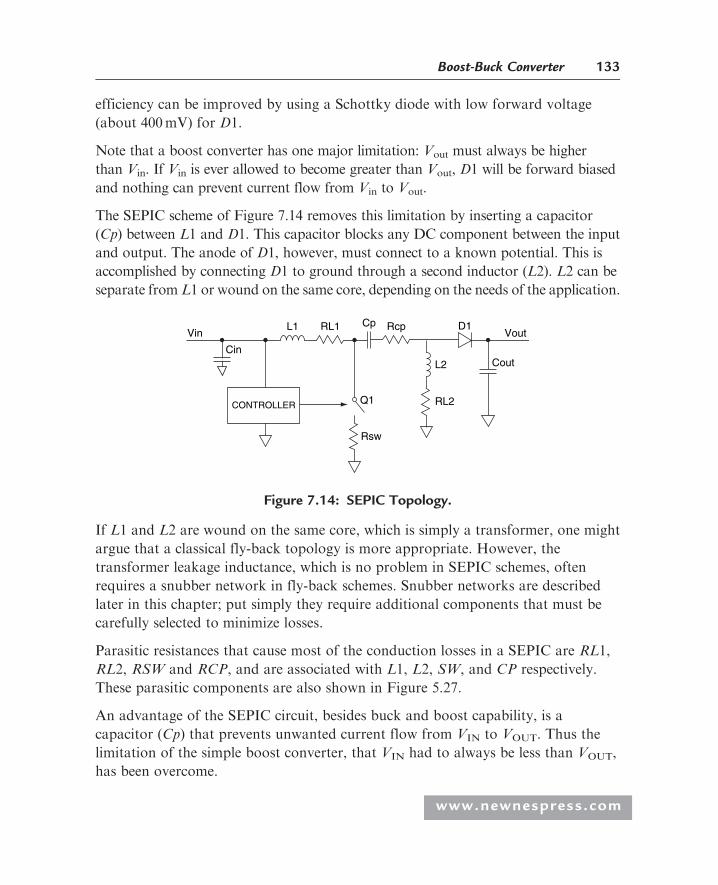
efficiency can be improved by using a Schottky diode with low forward voltage
(about 400mV) for D1.
Note that a boost converter has one major limitation: Vout must always be higher
than Vin. If Vin is ever allowed to become greater than Vout, D1 will be forward biased
and nothing can prevent current flow from Vin to Vout.
The SEPIC scheme of Figure 7.14 removes this limitation by inserting a capacitor
(Cp) between L1 and D1. This capacitor blocks any DC component between the input
and output. The anode of D1, however, must connect to a known potential. This is
accomplished by connecting D1 to ground through a second inductor (L2). L2 can be
separate from L1 or wound on the same core, depending on the needs of the application.
If L1 and L2 are wound on the same core, which is simply a transformer, one might
argue that a classical fly-back topology is more appropriate. However, the
transformer leakage inductance, which is no problem in SEPIC schemes, often
requires a snubber network in fly-back schemes. Snubber networks are described
later in this chapter; put simply they require additional components that must be
carefully selected to minimize losses.
Parasitic resistances that cause most of the conduction losses in a SEPIC are RL1,
RL2, RSW and RCP, and are associated with L1, L2, SW, and CP respectively.
These parasitic components are also shown in Figure 5.27.
An advantage of the SEPIC circuit, besides buck and boost capability, is a
capacitor (Cp) that prevents unwanted current flow from VIN to VOUT. Thus the
limitation of the simple boost converter, that VIN had to always be less than VOUT,
has been overcome.
Vin
CONTROLLER
L1 D1RL1 RcpCp
L2
RL2
Rsw
Q1
Cout
Vout
Cin
Figure 7.14: SEPIC Topology.
Boost-Buck Converter 133
www.newnespress.com

Though it has very few elements, the operation of a SEPIC converter is not so
simple to describe by equations; some assumptions have to be made. First, assume
that the values of current and voltage ripple are small with respect to the DC
components. Second, assume that at equilibrium there is no DC voltage across the
two inductances L1 and L2 (neglecting the voltage drop across their parasitic
resistances). By using these assumptions, Cp sees a DC potential of Vin at one
side (through L1) and ground on the other side (through L2). The DC voltage
across Cp is:
VCPðmeanÞ ¼ VIN
The period of one switching cycle is T= 1/frequency. The portion of T for which
switch Q1 is closed is the duty cycle, D, and the remaining part of the period
is thus 1�D. Because the mean voltage across L1 equals zero during steady state
conditions, the voltage seen by L1 during D *T (i.e. the MOSFET ‘ON’ period) is
exactly compensated by the voltage seen by L1 during (1�D) *T (i.e. the MOSFET
‘OFF’ period):
D � T � VIN ¼ 1�Dð Þ � T � ðVOUT þ VD þ VCP � VINÞ
Where VD is the forward voltage drop of D1 for a direct current of (IL1þ IL2), and
VCP is equal to VIN. Simplifying this we get:
D � T � VIN ¼ 1�Dð Þ � T � ðVOUT þ VDÞ
Transposing this, we get:
ðVOUT þ VDÞVIN
¼ D
1�D¼ Ai
Ai is called the amplification factor, where ‘i’ represents the ideal case for which
parasitic resistances are null. Neglecting VD with respect to VOUT (as a first
approximation), we see that the ratio of VOUT to VIN can be greater than or less
than 1, depending on the value of D (with equality obtained for D= 0.5).
134 Chapter 7
www.newnespress.com

The more accurate expression Aa (amplification, actual) accounts for parasitic
resistances in the circuit:
Aa ¼ VOUT þ VD þ IOUT � ðAi � Rcpþ RL2ÞVIN � Ai � IOUT � ðRL1þ RswÞ � Rsw � IOUT
This formula allows computation of the minimum, typical and maximum
amplification factors for Vin (Aamin, Aatyp, and Aamax). The formula is recursive
(‘Aaxxx’ appears in both the result and the expression), but a few iterative
calculations lead to the solution. The expression neglects switching losses due to the
switch Q1 and reverse recovery current in D1. Those losses are usually negligible,
especially if Q1 is a fast MOSFET and its drain-voltage swing (VinþVoutþVd)
remains under 30V.
In some cases, you should also account for losses due to the reverse recovery
current of D1, and for core losses due to high-level swings in stored magnetic energy.
You can extrapolate the corresponding values of D:
D¼Aa=ð1þ AaÞ
Or more generally:
Dxxx¼ Aaxxx=ð1þ AaxxxÞ, where xxx is min, typ or max:
The DC current through Cp is zero, so the mean output current can only be
supplied by L2:
IOUT ¼ IL2
The power-dissipation requirement for L2 is eased, because the mean current into
L2 always equals IOUT and does not depend on variations of VIN.
To calculate the current into L1 (IL1), we can use the fact that no DC current can
flow through Cp. Thus, the coulomb charge flowing during D *T is perfectly
balanced by an opposite coulomb charge during (1�D) *T. When the switch is
closed (for an interval D �T ) the potential at the switch node is fixed at 0V. Since
the capacitor Cp was previously charged to voltage Vin, the anode of D1 will now
Boost-Buck Converter 135
www.newnespress.com

have a potential of �VIN, which reverse-biases D1. Current through Cp is then
IL2. When the switch is open during (1�D) *T, current IL2 flows through D1
while IL1 flows through Cp:
D � T � IL2 ¼ 1�Dð Þ � T � IL1Knowing that IL2 = IOUT,
IL1¼ Aa xxx � IOUT
Input power equals output power divided by efficiency, so IL1 depends strongly on
VIN. For a given output power, IL1 increases if VIN decreases. Knowing that IL2(and hence IOUT) flows into Cp during D*T, we choose Cp so that its ripple delta
Vcp is a very small fraction of Vcp (gamma= 1% to 5%). The worst case occurs when
Vin is minimal.
Cp i IOUT �Dmin � Tgamma � VIN MIN
By using a high switching frequency, small multi-layer ceramic capacitors can be
used for Cp. However, ensure that Cp is able to sustain the power dissipation (Pcp)
due to its own internal equivalent series resistance (Rcp):
Pcp ¼ Aa min � Rcp � IOUT2
The MOSFET switch drain-to-source resistance, in series with a current sense
resistor for limiting the maximum current, is given by the term Rsw. This incurs the
following loss:
Psw ¼ Aa min � ð1þ Aa minÞ � Rsw � IOUT2
Losses PRL1 and PRL2, due to the internal resistances of L1 and L2, are easily
calculated:
PRL1 ¼ Aa min2 � RL1 � IOUT2
PRL2 ¼ RL2 � IOUT2
When calculating the loss due to D1, the average power loss is due to the output
current and the forward voltage drop of D1:
PD1 ¼ VD � IOUT
136 Chapter 7
www.newnespress.com

L1 is chosen so its total current ripple (DIL1) is a fraction (b = 20% to 50%) of IL1.
The worst case for b occurs when VIN is at maximum, because DIL1 is at maximum
when IL1 is at minimum. Assuming b = 0.5:
L1 min ¼ 2 � T � 1�Dmaxð Þ � VIN MAX
IOUT
Choose a standard value nearest to that calculated for L1, and make sure its
saturation current meets the following condition:
IL1 SAT ii IL1 þ 0:5 � DIL1 ¼Aa min �IOUT þ 0:5 � T �Dmin �VIN MIN
L1
The calculation for L2 is similar to that for L1:
L2 min ¼ 2 � T �Dmax � VIN MAX
IOUT
IL2 SAT ii IL2 þ 0:5 � DI2 ¼ IOUT þ 0:5 � T �Dmax � VIN MAX
L2
If L1 and L2 are wound on the same core, you must choose the larger of the two
calculated inductor values. Using a single core, the two windings should be bifilar
(twisted around each other before being wound on the core) and thus will have the
same number of turns and the same inductance values. Otherwise, voltages across
the two windings will differ and Cp will act as a short circuit to the difference. If the
winding voltages are identical, they generate equal and additive current gradients.
In other words, there will be mutual inductance of equal value in both windings.
Thus, the inductance measured across each isolated winding (when there is nothing
connected to the other winding) should equal only half of the value calculated for
L1 and L2.
Because no great potential difference exists between the two windings, you can save
costs by winding them together in the same operation. If the windings’ cross-sections
are equivalent, the resistive losses will differ because their currents (IL1 and IL2) differ.
Total loss, however, is lowest when losses are distributed equally between the two
windings, so it is useful to set each winding’s cross-section according to the current it
carries. This is particularly easy to do when the windings consist of insulated strands
Boost-Buck Converter 137
www.newnespress.com

of wire (Litz) for counteracting the skin effect. Finally, the core size is chosen to
accommodate a saturation current much greater than (IL1þIL2 þ DIL1) at thehighest core temperature anticipated.
The purpose of the output capacitor (COUT) is to average the current pulses
supplied by D1 during TOFF. The capacitor must be able to handle high-level
repetitive surge currents with low ESR and low self-inductance. Fortunately,
ceramic and plastic film capacitors meet these requirements. The minimum value
for COUT is determined by the amount of ripple (DVOUT) that can be tolerated:
COUT �Aa min �IOUT �Dmin �T
DVOUT
The actual value of the output capacitor may need to be much larger than that
calculated using the above equation, especially if the load current is composed of high
energy pulses. The input capacitor can be very small, thanks to the filtering properties
of the SEPIC topology. Usually, CIN can be one tenth the value of COUT:
CIN¼COUT=10
Overall efficiency � can be predicted from VIN and Aa. The result can be
misleading, because it doesn’t account for the switch-transition losses or core
losses and the real efficiency could be much lower:
� ¼ VOUT=AaVIN
Finally, the switch SW and diode D1 should be rated for breakdown voltages with a
15% margin:
VDSðswitchÞ > 1:15ðVOUT þ VD þ VINÞ
VRðdiodeÞ > 1:15ðVOUT þ VINÞ
Example
Let VIN = 50� 150V and VOUT = 15V at 1A maximum. Let us operate at 200 kHz
switching frequency, so that T= 5ms. Now VOUT
VIN¼ D
1�D , so Dmax = 0.231 and
Dmin = 0.091.
L1min ¼ 2Tð1�DmaxÞVIN MAX=IOUT
138 Chapter 7
www.newnespress.com

L1min ¼ 10�5 � 0:769 � 150=1 ¼ 1:15mH, letL1 ¼ 1:5mH
L2min ¼ 2TDmaxVIN MAX=IOUT
L2min ¼ 10�5 � 0:231 � 150=1 ¼ 0:347mH, letL2 ¼ 0:47mH
Cp> IOUT �DminT=ðgamma � VIN MINÞ
Cp > 1 � 0:091 � 2 � 10�5=ð0:05 � 50Þ ¼ 728 nF, let Cp ¼ 1mF:
Now Dxxx¼ Aaxxx=ð1þ AaxxxÞ, where xxx is min, typ or max. So Aamin occurs at
Dmin ¼ 0:091 and Aamin ¼ 0:1:
COUT � Aa min � IOUT �Dmin � T =DVOUT
COUT > 0:1 � 1 � 0:091 � 2 � 10�5=0:1:COUT >> 1:82mF: LetCOUT ¼ 100mF:CIN>COUT=10: LetCIN¼ 10mF:
So, the fundamental component values have been calculated. Now what remains for
the designer is the choice of suitable (and available) parts.
7.3 Buck-Boost Topology
Unlike the boost-buck circuits used by the Cuk and SEPIC topologies, the buck-
boost uses a single inductor. It is a fly-back circuit and hence will be covered in
Chapter 9.
7.4 Common Mistakes in Boost-Buck Circuits
Boost-buck circuits operate with both inductors in continuous conduction mode.
Hence the inductor should be chosen with a value higher than that calculated, to allow
for tolerances and for saturation effects (the inductance falls with increasing current).
Calculate the value, add 20%, and then pick the next highest standard value.
Current ratings of inductors are given for a certain temperature rise in the core,
typically 40�C. So if temperature rise is an issue, pick a component with a higher
current rating.
Boost-Buck Converter 139
www.newnespress.com

7.5 Conclusions
The boost-buck is an ideal topology where the LED load voltage can be higher or
lower than the supply voltage. It should also be used when the supply voltage is no
more than 20% difference (worst case) from the LED load voltage. So if the LED
voltage (maximum) is 20V and the supply voltage (minimum) is 23V, the difference is
3V, and 3/20= 0.15 or 15%, so a Cuk or SEPIC should be used. If the supply voltage
is more than 20% higher, use a buck topology. If the supply voltage is more than
20% lower, use a boost topology. The boost-buck is less efficient compared to buck
or boost topologies.
140 Chapter 7
www.newnespress.com

C H A P T E R 8
LED Drivers with Power FactorCorrection
8.1 Power Factor Correction
Power factor correction, or PFC, is a term used with AC mains powered circuits.
A good power factor is when the AC current is in phase with the AC voltage. A pure
resistive load has a power factor of 1, but active loads tend to have power factors
closer to 0.5, unless special measures are taken to ‘correct’ this.
The most common power factor correction circuit is a boost converter. The AC line
voltage is boosted to about 400V and the amplitude of the current pulses into a
storage capacitor is arranged to be sinusoidal. This is achieved by switching the
current on for short but constant periods: as the supply voltage rises and falls, so does
the amplitude of the current. A typical PFC circuit is shown in Figure 8.1.
A simple alternative is to use a fly-back supply. It is common to switch the
primary current off when a certain current level is reached, but this leads to constant
average current. To give a good power factor, the primary current should be switched
with a constant ‘on-time’, so that the current amplitude rises and falls in phase with
the supply voltage. The secondary current will rise and fall at double the AC line
frequency and so a large secondary capacitor is required to absorb this ripple, to
prevent significant ripple in the output voltage.
Driving an LED from a power factor corrected supply usually requires a simple
buck converter, since the voltage source tends to be very high (about 400 V).
However, alternative solutions exist; these are the Bi-Bred and the Buck-
Boost-Buck (BBB).
www.newnespress.com

8.2 Bi-Bred
The Bi-Bred is very similar to the Cuk boost-buck that we described in the previous
chapter, see Figure 8.2.
The main difference between the Cuk and the Bi-Bred is that, in a Bi-Bred, the input
inductor is in discontinuous conduction mode (DCM) and operation of the output
stage is in continuous conduction mode (CCM). The energy stored in each inductor is
proportional to the inductance value. This means that in the design, the input
inductor L1 must have a small enough energy stored to ensure that conduction stops
before the end of each cycle. This means that the input inductor value must be
relatively small. The output inductor L2 must have large enough energy stored (large
inductance value) so that the current only falls to about 85% of its nominal value at
the end of each switching cycle.
When power is first applied, MOSFETM1 is off and waiting for the first clock signal
to trigger the gate drive pulse. At this time the storage capacitor C3 immediately
begins to charge from the supply voltage through D1 and L1, although the voltage
will not rise very high because, when the MOSFET M1 switches on, the charging
current is redirected to the 0V rail. With M1 conducting, current continues to rise in
R31M
R6470K
D5C1010 nF
D418 V
R968K
C11470 nF
800uH
C12 470 nF
IC1L6562
R1022K
8
3
6 4
C910 nF
0 V
C710uF
C610uF
R513K
R216K2
R110R47
R20470K
R19510K
C1347uF450 V
D2STTH2L06U
7R14
M1
1
R14100R
R7470K
R31M
C51uF
Figure 8.1: PFC Circuit.
142 Chapter 8
www.newnespress.com

amplitude through the inductor L1 until the voltage drop across R2 is sufficient for the
internal comparator inside the HV9931 to trigger, which turns M1 off. Now the input
circuit acts like a boost converter because the current through L1 cannot change
immediately and it charges C3 to a high voltage.
The energy in C3 is used to drive current through the LED load the next time that M1
switches on. The current rises in inductor L2 and the load until the voltage drop across
resistor R7 is sufficient to trip a second internal comparator and turn M1 off again. The
current flow through L2 passes through D2 to keep current flowing in the LED load.
Notice that the current sense resistor is not in this path, because the current level
measurement is not required until theMOSFET turns on again; this minimizes power loss.
The output of the Bi-Bred is configured as a buck stage. Energy is supplied from a bulk
storage capacitor, C3, with sufficiently large capacitance to provide a more or less
constant supply voltage over an AC line cycle period. A constant capacitor voltage
supplying power to the buck stage means a constant switch duty cycle when it is driving
the LED load. The Bi-Bred draws a more or less sinusoidal AC line input current when
driven from a switch operating at constant duty cycle, hence a large capacitance value
for C3 helps to produce a good power factor.
D1C2
C1R9
M1
R7
R3
C6R6
D2C12(optional)
Q1R2
R1
RTR4
R5 PWM
GNDGATEVIN
CS1CS2HV9931
VDD PWM
C3+ L2L1 OUT
Load
Figure 8.2: Bi-Bred Circuit.
LED Drivers with Power Factor Correction 143
www.newnespress.com

The duty cycle of the switching is given by VO
VI¼ D
1�D.
Or put another way, D ¼ VO
VIþVO. So if Vin = 350V and Vo = 3.5V (a typical white
LED), D ¼ 3:5350þ3:5 ¼ 3:5
353:5 ¼ 0:99%. This is close to the 1% expected duty cycle for a
simple buck converter and can be difficult to switch properly. This means that a
Bi-Bred is not really suitable for driving short LED strings.
8.3 Buck-Boost-Buck (BBB)
The Buck-Boost-Buck (BBB) is a proprietary circuit, patented by Supertex, and is
illustrated in Figure 8.3. It resembles the Bi-Bred in some respects, except for two
current steering diodes D1 and D2.
Like the Bi-Bred, the input inductor is in discontinuous conduction mode (DCM)
and operation of the output stage is in continuous conduction mode (CCM). The
energy stored in each inductor is proportional to the inductance value. This means
C2
C1
C3+
C12
R2
R9
R10
RT GATE GND
CS2
R4
R5 C6R11
R3
R8
M1
PWM
PWMVDDCS1
VIN HV9931
Q1
L1
D2 L2 OUT
Load
D1
D3
D4
Figure 8.3: Buck-Boost-Buck Circuit.
144 Chapter 8
www.newnespress.com

that in the design, the input inductor L1 must have a small enough energy stored to
ensure that conduction stops before the end of each cycle. This means that the input
inductor value must be relatively small. The output inductor L2 must have large
enough energy stored (large inductance value) so that the current only falls to about
85% of its nominal value at the end of each switching cycle.
When power is first applied, MOSFETM1 is off and waiting for the first clock signal
to trigger the gate drive pulse. At this time, the storage capacitor C3 is not charged.
With M1 conducting, current begins to rise in amplitude through the inductor L1
until the voltage drop across R2 is sufficient for the internal comparator inside the
HV9931 to trigger, which turns M1 off. Now the input circuit is in flywheel mode,
because the current through L1 cannot change immediately and it charges C3 to a
moderately high voltage. The voltage is typically midway between the input and
output voltage levels.
The energy in C3 is used to drive current through D2, L2 and the LED load the next
time that M1 switches on. The current rises in inductor L2 and the load until the
voltage drop across resistor R8 is sufficient to trip a second internal comparator and
turn M1 off again. The current flow through L2 passes through D2 to keep current
flowing in the LED load. Notice that, like in the Bi-Bred, the current sense resistor is
not in this path, because the current level measurement is not required until the
MOSFET turns on again; this minimizes power loss.
The output of the Buck-Boost-Buck (BBB) is the buck stage. Energy is supplied from
a bulk storage capacitor, C3, with sufficiently large capacitance to provide a more or
less constant supply voltage over an AC line cycle period. A constant capacitor
voltage supplying power to the buck stage means a constant switch duty cycle when it
is driving the LED load. The BBB draws a more or less sinusoidal AC line input
current when driven from a switch operating at constant duty cycle, hence a large
capacitance value for C3 helps to produce a good power factor.
In practice there is a limit to the value of C3, particularly if plastic film capacitors are
used. This means that there will be some voltage ripple across C3, at a frequency
double that of the AC line (i.e. 120Hz when driven from a 60Hz line). The effect of
this ripple voltage is to generate second harmonic signals in the input current, which
reduces the power factor. By adding a simple circuit, the second harmonic can be
reduced; the MOSFET off-time is modulated by the ripple voltage and this acts like
negative feedback to reduce the second harmonic. The additional circuits are given in
Figure 8.4.
LED Drivers with Power Factor Correction 145
www.newnespress.com

When MOSFET M1 is conducting, the voltage across C3 is applied to C11, which
charges C5. Between each switching cycle, resistor R7 discharges capacitor C5. The
ripple voltage across C3 will modulate the average voltage across C5. Capacitor C7
acts as a DC block, to allow just the modulation across C5, rather than any DC level,
to vary the MOSFET off-time. As the voltage across C5 rises and falls, current
through R6 rises and falls, thus shortening or lengthening the off-time.
The duty cycle of the switching in a BBB converter is given by VO
VI¼ D2
1�D .
Or put another way, D ¼ �VO�ffiffiffiffiffiffiffiffiffiffiffiffiffiffiffiffiffiffiffiffiffiffiffiV 2
Oþ 4 �VI �VO
p2 �VI
. So if Vin = 350V and Vo = 3.5V
(a typical white LED), D ¼ �3:5�70700 ¼ 66:5700 ¼ 9:5%. This is a considerably greater duty
cycle than the Bi-Bred or the buck converter with a similar low voltage load. This
means that the BBB converter is most suitable for driving short LED strings.
C2
M1
Q1
R9D3
D6
D7
C7R6
R11
D8
RT
HV9931
GATE GND
CS2
PWM
PWMR5
R4
VDDCS1
VIN
D9
D10 R1
R3
R8
R7
C5
R10
C1
D4
D1
L1 C3
D2 L2
C11C12
D5
Load
–
+
+
OUT (negative)
C6
Figure 8.4: Buck-Boost-Buck with Harmonic Reduction.
146 Chapter 8
www.newnespress.com

8.4 Common Mistakes with PFC Circuits
The most common mistake is to use a standard inductor for L1. Inductors are
sized for their magnetic saturation level and for resistive heating. Thus an inductor
may be specified as I(av)= 500mA, I(sat)= 400mA. This inductor can pass 500 mA
with a temperature rise of, say, 40�C. It can pass 400mA before the inductance
is reduced by, say, 10%. If this inductor were used in a PFC stage with a peak current
of 400mA it would overheat. Using an inductor with a much higher saturation
current rating will be necessary, to give a reasonably low temperature rise during
operation.
Inductor manufacturers do not normally specify magnetizing losses. The magnetic
saturation levels are material dependent; the maximum flux density of ferrite is
usually 200mT, other materials can be higher. So when designing a ferrite-based
inductor, a manufacturer will make his design based on this level. When considering
magnetizing losses, a flux density of about 50mT would be a better choice for a
ferrite-based inductor.
8.5 Conclusions
Detailed design analysis has not been given for the PFC circuits. This chapter has
been intended to show readers some options and point out limitations. For example,
driving a single LED would require a Buck-Boost-Buck circuit, but longer strings can
be driven from a Bi-Bred or a PFC stage followed by a buck converter.
Application notes from ST Microelectronics and Supertex cover the PFC, Bi-Bred
and Buck-Boost-Buck circuits in detail. These are proprietary and specialized
solutions that are still evolving; interested readers should consult these application
notes for the latest designs.
LED Drivers with Power Factor Correction 147
www.newnespress.com

C H A P T E R 9
Fly-Back Converters
A traditional fly-back converter uses an inductor with at least two windings (really,
this is a transformer). Consider two windings; one is the primary, which is connected
to the input power supply and a switch to ground; the other is the secondary, which
is connected to the load. The circuit is arranged so that magnetic energy is stored in
the inductor during the time that the switch is on, when current increases in the
primary winding. When the switch is off, the magnetic energy is released by current
flowing out of the secondary winding. This is shown in Figure 9.1.
The energy release is the ‘fly-back’, so called because in early television sets with a
cathode ray tube, a transformer winding was used to deflect the electron beam back
to the starting point on the screen. The electron beam had to ‘fly back’ quickly after
completing a scan across the screen, to avoid missing the next line of data to be
displayed.
Fly-back power supplies are relatively easy to design, but are more suited to constant
voltage outputs. This is because the energy is stored in bursts, in a large reservoir
capacitor, and controlling the average voltage across the capacitor can be achieved
with simple feedback.
Driving an isolated LED load is then possible if the secondary winding is
isolated from the primary winding. Some general-purpose applications can use
simple current limit techniques in the primary winding to control the output
current from the secondary winding. An opto-coupler will be required, to maintain
isolation between primary and secondary, if accurate control of the output current
is required.
www.newnespress.com

Some fly-back converters use an inductor with a single winding. These are buck-
boost controllers and are an alternative to the boost-buck converters like Cuk and
SEPIC types that were discussed in Chapter 7. Clearly, isolation is not possible with
this type of converter.
9.1 Two Winding Fly-Back
A schematic of a typical fly-back circuit for driving LEDs is shown in Figure 9.2.
The dot alongside the transformer winding indicates the start of the winding. In
this case the start is connected to the MOSFET drain, which alternates between a
ground connection and open circuit. The voltage at the drain, and hence the
winding start point, varies considerably during switching. Conversely, the outer
layer (end of the winding) is at a fixed high voltage and tends to screen the inner
layers, which reduces radiated EMI.
LOAD
V+
Primary current
t
IPRI
ISEC
E
t
t
Secondary current
Stored magnetic energy
Figure 9.1: Fly-Back Principle.
150 Chapter 9
www.newnespress.com

The secondary winding start point is connected to the output diode, which prevents
conduction when theMOSFET is on. The start point of the secondary is connected to the
outputdiode,but theendpoint is connected togroundand this tends to screen the secondary
winding for minimal EMI radiation. Energy that is stored during theMOSFET on-time is
released during the off-time, by current flowing through the output diode and into the load.
Calculation of the transformer characteristics, like inductance value and primary
to secondary turns ratio, are very important in the design. In order for complete power
transfer from the primary to secondary, the volt-seconds must be equal. The equation is:
VPRI � TON
NPRI¼ VSEC � TOFF
NSEC
9.1.1 Fly-Back Example
Let us make an isolated 3W lamp by connecting three white power LEDs in series.
Suppose we have a primary voltage of 48V, an on-time of 5 microseconds, and
the primary to secondary turns ratio is 1:0.1. If we are driving a 10V LED load, the
1A 800 V
VDDVIN
GT
CS
HV9910NG
LD
RT
PWM
GND
5
9
14330K
2K7100 pF 1
13
4
8
10M
IRFBG20
BYV26C
220uF 100 nF
LuxeonStar X3
1
22uF 100 nF
UF4006
200 V1 W12
2,2uF
Figure 9.2: Fly-Back Circuit for LEDs.
Fly-Back Converters 151
www.newnespress.com

off-time will be 240/100 microseconds (2.4ms). Thus the switching period must be
greater than 12.4ms in order to allow complete removal of the magnetic energy in the
transformer core. A switching frequency of below 65 kHz will be satisfactory, say
60 kHz to give some margin.
With 60 kHz switching, the period will be 16.667ms. If the average output current is350mA, the average in 2.4ms will be 2.43 A. Since this current decays linearly from
the transformer winding, the peak secondary current will be double this: 4.86A. The
secondary inductance will be E ¼ �L � didt .
L ¼ E � dtdi¼ 10 � 2:4 � 10
�6
4:86¼ 4:94mH
Since the primary has ten times the turns of the secondary, the primary inductance
will be 100 times that of the secondary (the turns ratio,N, is squared). In other words,
the primary inductance will be 494mH.
Most current-mode power supplies control the switching so that the MOSFET turns
off when a certain peak current is reached in the primary winding. Since the peak
current in the secondary is 4.86A and the turns ratio is 10:1, we need a peak primary
current of 486mA. [Check: E ¼ �L � didt , soE=494 * 10�6* 0.486/(5 * 10�6)= 48V].
The problem with the design that we have is that the LED current will change if
the LED voltage changes, because we have based our design on a certain output
voltage. Actually this gives a constant power output, assuming a constant
voltage input, which is fine for non-critical designs. But what if the input voltage
changes?
A higher input voltage will mean that the current limit will be reached in a shorter
time. This means that the duty cycle will be reduced and hence the number of volt-
seconds on the primary will be unchanged. In practice, inherent delays in the current
sense comparator will cause the input current to ‘overshoot’ the reference level. This
overshoot increases with increasing input voltage, this is because the delay is constant
but the rate of current rise is increasing with input voltage. Compensation of this
overshoot can be achieved by connecting a resistor between the supply voltage rail
and the current sense pin. This resistor injects a small DC bias that increases with
increasing supply voltage and thus triggers the comparator earlier as the supply
voltage rises.
152 Chapter 9
www.newnespress.com

The 1:0.1 turns ratio and 10V output used in the above example cause a reflected
voltage of 100V in the primary winding when the secondary conduction takes
place. This reflected voltage adds to the supply voltage, so a MOSFET with a
200V or higher voltage rating is required when powering this circuit from a 48V
supply.
The design example does not allow for efficiency. In practice a fly-back converter has
about 90% efficiency, so the input current must be increased by about 10% to allow
for this.
If we were designing a constant voltage circuit, we would allow the peak primary
current to be higher than that given in the example. This margin allows for the input
voltage variations. We would then use feedback from the output to control the
switching, to reduce the power in the primary, as necessary.
9.2 Three Winding Fly-Back
Some fly-back power supplies use a third winding, called a bootstrap or auxiliary
winding, as shown if Figure 9.3. This is used to power the control IC, once the circuit
is operating. The bootstrap winding has the same orientation as the secondary
winding and the voltage is simply determined by the turns ratio of the bootstrap
compared to the secondary. In our example of a 10V output from the secondary, the
bootstrap could have the same number of turns and thus give (approximately) 10V
for the powering the control IC.
At start-up, there is no power available from the bootstrap winding, so a start-up
regulator is required. Example start-up regulators are the LR645 and the LR8
from Supertex; these give a low voltage, low current output from an input with a
voltage as high as 450V. Once the bootstrap produces power, the start-up regulator
turns off. The HV9120 shown in Figure 9.3 has a start-up regulator built-in.
9.2.1 Design Rules for a Fly-Back Converter
This section gives design rules for a fly-back converter based on either turns ratio
selection determined by the maximum duty cycle allowed (case 1), or by the optimum
turns ratio based on the maximum working voltage of the MOSFET switch (case 2).
In case 1, a design based on the maximum duty cycle (at the lowest input voltage)
Fly-Back Converters 153
www.newnespress.com

allows the widest input voltage range. In case 2, a design based on the maximum
voltage across the MOSFET allows a potentially lower cost solution. Alternatively, a
fly-back design based on an already available transformer with a known (and fixed)
turns ratio may be considered.
The transfer function of a fly-back converter is:
VO
VI¼ D
ð1�DÞ �N
So the duty cycle can be found by transposing the equation:
VO � 1�Dð Þ ¼ VI �D �N
VO ¼ VI �D �Nþ VO �D ¼ D � ðVI �Nþ VOÞ
D ¼ VO
ðVI �NÞ þ VO
D2
C2
0 V+20 to 300 V
C1
0 V
8
96
5
15
C3
1471
10 16
IC1HV9120
R3 C5 C6
R4
D3
R5R11
R8R13
ZD1TL431
6N135IC2
R10
R2
R1
COM
+5 V
C8
C7
R12
R7
11 16
R6
D1
C4
R9
M1
Figure 9.3: Fly-Back Using a Three-Winding Transformer.
154 Chapter 9
www.newnespress.com

Case 1: Turns Ratio Based on Maximum Duty Cycle
Given the minimum input voltage VI_MIN, output voltage VO and maximum duty
cycle DMAX, the turns ratio N can be calculated:
N ¼ VO � 1�DMAXð ÞVI MIN �DMAX
DMAX is typically chosen as 45% (0.45) for a PWM controller with a maximum 49%
duty cycle. WithDMAX< 50%, the system is inherently stable and there is no complex
compensation required.
If we take the earlier example of 48V input (say, 46V minimum), 10V output (add
0.6V for the output diode) and allow 45% duty cycle, we get:
N ¼ 10:6 � 0:55ð Þ46 � 0:45 ¼ 0:282
This is the minimum value. A transformer with a convenient turns ratio of 1:0.33 (3:1)
could be used. The maximum duty cycle would then be:
D ¼ VO
ðVI �NÞ þ VO
10:6
ð15:33þ 10:6Þ ¼ 0:41 ð41%Þ
Case 2: Turns Ratio Based on Maximum Switch Voltage
The output voltage across the secondary winding is induced into the primary and
magnified by the turns ratio N. This was illustrated at the beginning of this chapter,
when a 10V output caused 100V to be induced into the primary winding of a 1:0.1
turns ratio transformer. Considering that the supply voltage was only 48 V, this
forced us to use a 200V MOSFET as the primary switch. The aim here is to minimise
the MOSFET switch operating voltage requirement.
Because the voltage reflected into the primary often has some ringing, a snubber circuit is
used to limit the voltage across the primary winding. Ringing is due to resonance
between the MOSFET drain capacitance, parasitic capacitance in the circuit and
parasitic inductance of the transformer primary. Parasitic inductance in the transformer
is often referred to as ‘leakage inductance’ because it is the proportion of the primary
inductance that is not coupled into the secondary, so the magnetic field ‘leaks out’.
Fly-Back Converters 155
www.newnespress.com

A Zener diode is sometimes used as a snubber. The voltage across the Zener diode
will be greater than the voltage induced into the primary from the secondary (output)
voltage, otherwise power dissipation and losses will both be very high.
VO ¼ N � ðVSW � VZ � VIN MAXÞ
In order to find the secondary winding voltage, the forward voltage drop of the
output diode, VF, must be added to the output voltage.
N ¼ VO þ VF
ðVSW � VZ � VIN MAXÞ
As a safety margin,ðVSW � VZ � VIN MAXÞ � 10V.
In the example we used earlier, with 48V input, we could have used a 100V switch
and a 33V Zener diode. The output is 10V, so allowing for VF this becomes 10.6V
across the secondary winding:
N ¼ 10þ 0:6
ð100� 33� 48Þ ¼10:6
19¼ 0:558
We could use a transformer with 1:0.5 turns ratio (N= 0.5). The primary voltage
induced from the secondary winding will be 21.2V, which is below the Zener diode
voltage by 11.8V, which is a reasonable margin to minimise power dissipation. The
peak voltage across the MOSFET drain will be limited to 48Vþ 33V= 81V.
With a turns ratio of 1:0.5, the maximum duty cycle with a 46V minimum input
voltage will be:
D ¼ VO
ðVI �NÞ þ VO¼ 10:6
23þ 10:6¼ 0:315 ð31:5%Þ
Inductance Calculations
Now we have the turns ratio (by either means described above) and the maximum
duty cycle, we can now determine the inductance and switching current. Let us use
case 1, with 41% as the maximum duty cycle.
PIN ¼POUT
�
156 Chapter 9
www.newnespress.com

The output power is 10V � 0.35 A= 3.5W and the efficiency can be guessed at as
being 85%. The input power is then 4.12W. The input current at minimum input
voltage is then:
IAV ¼PIN
VIN¼ 4:12
46¼ 0:09A
IPK ¼2 � IAV
DMAX
At 46 Vin and 41% duty cycle:
IPK ¼2 � 0:090:41
¼ 0:439A
With 60 kHz switching, the period will be 16.667 ms. With a 41% duty cycle, the switch
on-time will be 6.835ms. So we need the primary current to rise by 439mA in 6.835ms.
LPRI ¼VIN � dt
dI¼ 46 � 6:835 � 10�6
0:439¼ 716mH
The secondary has 1/3 the number of turns compared to the primary, so the
inductance of the secondary will be 1/9, or 79.55mH.
The other design parameter for the transformer is the size and AL factor of the ferrite
core. In a fly-back transformer an air gap between the two halves of the ferrite core
are necessary to prevent magnetic saturation, as the air gap increases, the AL factor
reduces. The flux density (B) will depend on the cross-sectional area of the core (Ac),
given in square meters. Suppose in this case we have some E20 cores available from
Ferroxcube. For E20/10/6 cores, the core cross-sectional area is 32mm2. So
Ac= 32 * 10�6 m2. The number of turns can be calculated, based on the design
parameters above and using B= 200mT as the maximum flux density:
N ¼ LPRI � IPKAC � BMAX
ðturnsÞ
N1 ¼ 716 � 10�6 � 0:43932 � 10�6 � 0:2 ¼ 49
AL ¼LPRI
N12¼ 716 � 10�6
2401¼ 298 nH
Fly-Back Converters 157
www.newnespress.com

Refer to core manufacturer’s specifications and choose a core with a lower AL value
(larger gap) than calculated using the above equation. A suitable core (3C90 material,
160 mm air gap) has an AL value of 250 nH. The number of turns can then be
calculated as:
N ¼ffiffiffiffiffiffiL
AL
r, when L is expressed in nH: Thus 716 mH ¼ 716,000 nH:
NPRI = 54 (rounding up to the next highest value). This quite conveniently gives the
secondary turns as NSEC = 18, since it is 1/3.
9.3 Single Winding Fly-Back (Buck-Boost)
In the buck-boost converter, a single inductor winding is used for the primary and
secondary. This is shown in Figure 9.4.
Current is forced through the inductor by a MOSFET connecting the inductor across
the power supply rail. The current level rises almost linearly with time. At a
predetermined current level, the MOSFET is turned off and the current is forced to
flow through a diode to charge the output capacitor and drive the load. The
current in the inductor falls back to zero and so discharges the energy stored in the
LED
LED
V+
C2
5KC3
38 R1
R2
Q1
D1
C4
2
4
7
5150K
6
1
C1 L1
VINVDD
PWM_D
HV9910LD
RoscGND
GATE
CS
Figure 9.4: Buck-Boost Converter.
158 Chapter 9
www.newnespress.com

magnetic core. Like the two-winding fly-back, the single winding fly-back can be
calculated from the number of volt-seconds on the charge cycle equalling the
number of volt-seconds on the discharge cycle.
The duty cycle of a buck-boost converter (continuous conduction mode) is given by
the equation:
VO
VI¼ D
1�D
VO � 1�Dð Þ ¼ VI �D
VO ¼ VI �Dþ VO �D ¼ D � ðVI þ VOÞ
D ¼ VO
VI þ VO
So, if we have Vin = 24V and Vout =30 V, D= 30/54 = 0.555.
In practice we want discontinuous conduction mode, because continuous conduction
mode is difficult to stabilise. This means that the inductor current falls to zero at the
end of each cycle. So, assume we want 350mA output and 100 kHz switching
frequency. The period is 10ms, so the on-time is 5.55ms and the off-time is 4.45ms.During the off-time, the current in the inductor falls linearly from a peak level
to zero. To average 350mA output, the average current during the off-time must
be 350=0:445mA ¼ 786:5mA, so the peak current must be double this, or 1.573 A.
This means that during the on-time, the current must rise from zero to 1.573 A.
The voltage from the power supply is 24V, so using the familiar equation:
E ¼ �L � didt
L ¼ E � dtdi¼ 24 � 5:55 � 10
�6
1:573¼ 84:67mH
In practice there should be some dead time allowed, when the inductor carries no
current, to ensure discontinuous conduction mode. This dead time is to allow for
power supply tolerances, inductor tolerances, etc. Too much dead time means that
the peak current is higher and this reduces the efficiency of the power supply.
Fly-Back Converters 159
www.newnespress.com

Suppose we allow 25% tolerance, so that the on-time is 4.44ms; this will reduce theinductance by 25%.
L ¼ E � dtdi¼ 24 � 4:44 � 10
�6
1:573¼ 68mH
The off-time will be reduced unless the peak current is increased in proportion.
E ¼ �L � didt
�30 ¼ 68 � 10�6 � di
4:45 � 10�6
di ¼ �30 � 4:45 � 10�6
68 � 10�6 ¼ 1:963A
Increasing the peak current by 25% gives the desired result. The peak current is set by
the value of current sense resistor between the MOSFET source and ground.
160 Chapter 9
www.newnespress.com

C H A P T E R 1 0
Essentials of Switching Power Supplies
This chapter will examine the advantages and disadvantages of the various driver
techniques, which have already been described. The issues of efficiency, EMI, cost
and other requirements that are additional to the basic function of the LED
driver.
10.1 Linear Regulators
In Chapter 4 we saw how the use of linear regulators caused a heat dissipation
problem because of low efficiency. A linear LED driver is generally less efficient
than a switching driver. Sometimes a linear driver can be more efficient. For
example, if you have a 12V power source and three LEDs each having a 3.5V
forward drop, by connecting them in series the total drop is 10.5V. The efficiency
of a linear driver, dropping only 1.5V will be 87.5%. It would be difficult for a
switching LED driver to achieve this level of efficiency. And there is no EMI to be
filtered.
On the other hand, driving one LED from a 12V supply would give an
efficiency of 3.5/12= 29% with a linear LED driver. Here a buck switcher
would give closer to 90% efficiency. See Figure 10.1. Efficiency is important
where heat dissipation must be minimized. Otherwise cost usually takes
precedence and the cost of a switching regulator with EMI filters would be
somewhat higher.
www.newnespress.com

10.2 Switching Regulators
In Chapters 5 to 9 we looked at switching regulators, which have much higher
efficiency, but can generate electro-magnetic interference (EMI) which has to be
suppressed by careful circuit board design, screening and filtering. The EMI reducing
techniques are described in Chapter 13.
Although Supertex’s LED driver integrated circuits are used in examples, similar
drivers from other manufacturers can also be used. For example, the Linear
Technology LTC3783 has similar functions to the Supertex HV9912. The National
Semiconductor LM5020 is a buck controller, like the HV9910B. However, Supertex
devices have an internal high voltage regulator, which makes them more versatile.
Switching power supplies have the disadvantage of producing electromagnetic
interference (EMI). EMI must be limited, to prevent interference with other
systems. This is a legal requirement and product cannot be sold unless the
equipment meets the standards laid down in law. Details of EMI techniques are
given in Chapter 13.
Conversely, where EMI requirements are very demanding, such as medical and
automotive applications, linear LED driver techniques can be used instead.
12 V
CL2
(A) <30% Efficient (B) >90% Efficient
0 V
12 V
8.5 V
3.5 V
6VDD
VIN
RTHV9910
PWM_D
LD
CS
GATE
GND
5
8
4
2
7
3
1
Figure 10.1: Linear vs Switching Solutions.
162 Chapter 10
www.newnespress.com

Of course the efficiency may suffer, and so a heatsink will be needed, but this is
sometimes very much better than trying to make a switching circuit in terms of cost
and physical size.
10.2.1 Buck Regulator Considerations
In Chapter 5 we first looked at the simplest switching regulator, the buck converter.
In a buck circuit the load voltage must be less than 85% of the supply voltage,
otherwise the output becomes difficult to control. Buck circuits are used for mains
powered LED drivers, when driving a long string of LEDs. Buck circuits are also
used where the input supply voltage is relatively low, say in a 12V DC automotive
application, but where just one LED is being driven.
Buck regulators can be very efficient, maybe 90–95%, especially if the load is a long
string of LEDs with a moderately high forward voltage (i.e. high duty cycle). This is
because the power dissipation in the flywheel diode is a smaller proportion of the
total power because the flywheel diode only conducts during the MOSFET off-time,
which is a smaller proportion of the total switching cycle. The MOSFET dissipates
power during the on-time, when it is conducting, but the voltage drop across the
MOSFET switch is usually much lower than the forward drop of a fast rectifier.
In order to operate correctly there must be some ripple in the output current. The
output current needs to reduce enough to allow the current sense comparators to be
reset. The output ripple current DIO is normally designed to be 20–30% of IO; the
output current falls far enough in each cycle so that noise in the current sense
comparator has little effect. If the ripple current is below 10% of IO, the switching of
the MOSFET can be erratic. The output current in the LED string (IO) is given by the
equation:
IO ¼VTH
RSENSE� 1
2� DIO
Here VTH is the current sense comparator threshold, and RSENSE is the current sense
resistor. The ripple current can introduce a peak-to-average error in the output current
setting that needs to be accounted for. When the constant off-time control technique is
used, the ripple current is nearly independent of the input supply voltage variation.
Therefore, the output current will remain unaffected by the varying input voltage.
Essentials of Switching Power Supplies 163
www.newnespress.com

Adding a filter capacitor across the LED string can reduce the output current ripple,
thus allowing a lower inductor value or an apparently more ‘constant’ current. This
capacitor reduces EMI at the output by providing a bypass path for any switching
current spikes, which may also improve the LED lifetime. However, keep in mind
that the peak-to-average current error is affected by the variation of the MOSFET
off-time, TOFF. Therefore, the initial output current accuracy might be sacrificed with
large ripple current levels in the inductor.
Another important aspect of designing an LED driver is related to certain parasitic
elements of the circuit, including distributed coil capacitance of the inductor CL,
junction capacitance CJ, and reverse recovery of the flywheel diode, capacitance of
the printed circuit board traces CPCB and output capacitance CDRAIN of the
MOSFET. These parasitic elements affect the efficiency of the switching converter
because they cause switching losses. These parasitic elements are shown in
Figure 10.2.
Cj, junctioncapacitance
DG
PCBtracecapacitance
MOSFETdrain-sourcecapacitance
RC Filter(limits turn-oncurrent spike)
Parasiticwindingcapacitance
RG8
4
HV9910NG
IrrReverseRecoveryCurrent
Figure 10.2: Parasitic Elements.
164 Chapter 10
www.newnespress.com

Parasitic elements could potentially cause false triggering of the LED driver IC’s
current sense comparator, especially if an RC filter is not fitted between the
MOSFET source and the current sense (CS) pin. Minimizing parasitic elements is
essential for efficient and reliable operation of the buck converter.
Coil capacitance of inductors is typically provided in the manufacturer’s data books
either directly or in terms of the self-resonant frequency (SRF).
SRF ¼ 1=ð2�ffiffiffiffiffiffiffiffiffiffiffiffiffiL � CL
pÞ;
Here L is the inductance value, and CL is the coil capacitance. Charging and
discharging this capacitance every switching cycle causes high current spikes in the
LED string. Therefore, connecting a small capacitor CO (�10 nF) across the LEDstring is recommended to bypass these spikes, as mentioned earlier.
Using an ultra-fast rectifier flywheel diode is recommended to achieve high
efficiency and reduce the risk of false triggering of the current sense comparator.
When the MOSFET turns on the diode changes from forward conduction to off
(reverse bias), but this cannot happen immediately because charges have to move
inside the semiconductor material, which takes time. There is always a reverse
recovery current flowing in the opposite direction for a short period, TRR. Using
diodes with shorter reverse recovery time, TRR, and lower junction capacitance CJ
improves performance. The reverse voltage rating VR of the diode must be
greater than the maximum input voltage of the LED lamp. The forward voltage-
drop of diodes with very fast recovery times is sometimes relatively high and can
lead to high conduction losses, so also consider this when making a diode
selection.
The total parasitic capacitance present at the DRAIN output of the MOSFET can be
calculated as:
CP ¼ CDRAIN þ CPCB þ CL þ CJ
When the switch turns on, the total parasitic capacitance CP is discharged into the
DRAIN output of the MOSFET. The discharge current is limited to the MOSFET
saturation current, so MOSFETs with a high on-resistance and a lower saturation
current can sometimes produce lower overall losses. This is especially true if the duty
cycle is small, because the switch is conducting for a small proportion of the time and
Essentials of Switching Power Supplies 165
www.newnespress.com

hence the conduction losses will not be significant. Note that the saturation current in
a MOSFET becomes lower at increased junction temperature.
The duration of the leading edge current spike can be estimated as:
TSPIKE ¼VIN � CP
ISATþ trr
In order to avoid false triggering of the current sense comparator, CP must be
minimized in accordance with the following expression:
CP <ISAT � TBLANKðMINÞ � trr
� �VINðMAXÞ
The factor TBLANK(MIN) is the minimum blanking time, which depends on the control
IC and is in the order of 300 ns. When the MOSFET gate drive is activated, the
control IC disables the current sense input for this time period, to avoid false
triggering from the switch-on current surge, previously described. The factor
VIN(MAX ) is the maximum instantaneous input voltage.
Discharging the parasitic capacitance CP into the DRAIN output of the MOSFET is
responsible for the bulk of the switching power loss. It can be estimated using the
following equation:
PSWITCH ¼CPVIN
2
2þ VINISAT � trr
� ��FS
where FS is the switching frequency, ISAT is the saturated DRAIN current of the
MOSFET. The switching loss is the greatest at the maximum input voltage.
The switching frequency of a buck converter having constant off-time operation is
given by the following:
FS ¼VIN � ��1�VO
VIN � TOFF
where � is the efficiency of the power converter. This value for FS based on typical
values for VIN and VO can be used in the previous equation if a value of constant
switching frequency is not available.
166 Chapter 10
www.newnespress.com

The switching power loss associated with turn-off transitions of the DRAIN output
can be disregarded. Due to the large amount of parasitic capacitance connected to
this switching node, the turn-off transition occurs essentially at zero voltage.
Conduction power loss in the MOSFET can be calculated as
PCOND ¼ D � IO2 � RON
where D=VO/�VIN is the duty ratio and RON is the ON resistance.
Buck Converter AC Input Stage
An off-line LED driver requires a bridge rectifier and input filter; selecting an input
filter is critical to obtaining good EMI.
We may use an aluminum electrolytic capacitor after the bridge rectifier, in order to
prevent interruptions of the LED current at zero crossings of the input voltage (the cusps
in the rectified sine-wave, or haversine,waveform).As a ‘rule of thumb’, 2� 3mFper each
watt of the input power is required. An electrolytic capacitor is often used and has the
added ability of being able to absorb voltage surges that may be present on the AC line.
Large values of input capacitorwill cause unacceptably high current surgeswhenpower is
first applied. These current surges can damage the electrolytic capacitor, reducing its life
expectancy, and also damage the switch or electrical connectors at the AC line. Inrush
current limiters, usually a negative temperature coefficient (NTC) thermistor rated for
high current, are often connected in series with the AC line to prevent the current surge.
An inductor in series with the supply rail, after the input capacitor, is needed to present
high impedance to switching frequency signals, as shown in Figure 10.3. The current
rating of this inductor needs to be higher than the expected current level in normal
operation. The value of the inductor depends on the level of signal attenuation required,
when combined with the input capacitor shunt impedance, to meet the EMI standards in
force.
The impedance of an inductor is given by: XL = 2 �p �FS �L, so if we needed 200 ohms
impedance at 100 kHz to give us our desired attenuation, L= 0.318mH. A 330mHfilter inductor could be used.
A capacitor connected between the switching side of the filter inductor and ground,
albeit of small value, is necessary in order to ensure low impedance to the high
Essentials of Switching Power Supplies 167
www.newnespress.com

frequency switching currents of the converter. As a rule of thumb, this capacitor
should be approximately 0.1–0.2 mF/W of LED output power. A 100 nF capacitor
can be used in a circuit that drives a single 1W LED.
10.2.2 Boost Regulator Considerations
The output voltage in a boost circuit must always be higher than the input voltage by
about 20% or more, and this was discussed in Chapter 6. Ignoring PFC applications, a
boost converter driving LEDs will always be powered from a low voltage DC supply.
For example, the backlight in a cell phone with a color LCD display usually employs
low cost white light LEDs. A boost regulator is used in this application to drive a
string of 20mA LEDs from a 3–4V battery.
As another example, in flat-screen television backlighting high power red, blue and
green (RGB) LEDs are used to create a white light that exactly matches the LCD and
produces true colors. In this application a boost converter powered from a 12V or
24V DC supply is used to drive many 350mA LEDs connected in series, with a
forward voltage in the range 40–80V.
Boost regulators should always be provided with over-voltage protection, in case the
LED load is disconnected. Otherwise the output voltage will continue to rise and
eventually cause component breakdown. In Safety Electrical Low Voltage (SELV)
systems, the output voltage would normally be kept below 42V.
HighImpedanceXL
ACInput
LowImpedanceXC
Attenuation of Switching Signals
Low Impedancepath for switchingcurrent
Figure 10.3: Input Filter Functions.
168 Chapter 10
www.newnespress.com

10.2.3 Boost-Buck Regulator Considerations
To operate in an environment where the input voltage could be higher or lower than
the output voltage, a buck-boost (or boost-buck) circuit is necessary. Boost-buck
circuits were described in Chapter 7. The situation of having a load voltage range that
overlaps the supply voltage range is commonly found in automotive applications.
The battery voltage rises and falls with a large variation, as the engine speed and
battery conditions change.
The two types of converters often found in boost-buck applications are known as
SEPIC and Cuk. These converters are similar, but the Cuk converter has an inverted
output, which means that the LED anode is connected to the ground rail. Like boost
converters, over-voltage protection should be provided to prevent excessively high
voltage in case of an open-load condition.
Because there are inductors in series with the input and the output, and both operate
in continuous conduction mode (CCM), high frequency signals at the central node
where the switching takes place are automatically filtered. Shunt capacitors across
the input and output strengthen this filtering, and provide a low impedance path for
the circulating currents. Consequently, Cuk and SEPIC circuits require minimal
external filtering. Sometimes common mode chokes are added at the input side, to
reduce the radiated signals from the whole circuit. Common mode chokes are only
required on the output side if the length of wire to the LED load is more than about
0.5m long.
10.2.4 Circuits with Power Factor Correction
Power factor is an indication of the relative phase of the power line voltage and the
power line current. A power factor of 1 indicates that the voltage and current are
in-phase and have low harmonic content. A power factor of 0 indicates that the
voltage and current are 90 degrees out-of-phase.
In semiconductor circuits powered from the AC mains, a bridge rectifier converts the
AC power into DC. The current through the bridge rectifier tends to occur close to
the peak voltage, as shown in Figure 10.4, because charging of a large smoothing
capacitor takes place each half cycle. These short charging current pulses at the crest
of each input cycle cause the power factor to be typically in the 0.3–0.6 range. Power
factor correction is an active or passive circuit designed to correct phase errors and
Essentials of Switching Power Supplies 169
www.newnespress.com

reduce harmonics, and make the power factor closer to 1. Power factor correction
(PFC) is required in higher power LED drivers.
A circuit having a good power factor, approaching 1, has an input current that has
low harmonic content with a wave shape that closely follows the sinusoidal input
voltage. Circuits that provide a good power factor were described in Chapter 8.
10.2.5 Fly-Back Converter Considerations
Transformer coupled switching regulators can be designed for a very wide range of
supply and output voltages. The most common is a fly-back converter, although
forward converters are also popular in higher power applications. Fly-back
converters were described in Chapter 9.
Fly-back converters allow an isolated LED driver design with about 90%
efficiency, but have added cost and complexity. If a wide tolerance can be accepted
for the current regulation, a simpler and cheaper circuit can be built. High
accuracy requires isolated feedback, usually via an opto-coupler and employing an
adjustable shunt regulator such as a TL431 or similar, along with a few passive
components.
Fly-back converters have the advantage of stepping up or down the output voltage
compared with the supply (buck-boost). This also applies to the single winding
inductor version, although since the same winding is used for the primary and
secondary side, the turns ratio is 1:1 and the design specification are more restricted
than for a two-winding inductor. A single winding inductor is usually much lower
cost.
V
l
Figure 10.4: Active Circuit AC Input Current.
170 Chapter 10
www.newnespress.com

A fly-back, by definition, is a discontinuous conduction mode converter; energy is
taken from the power supply in the first step and then transferred to the output in the
second step, as shown in Figure 10.5. This means that EMI must be carefully filtered
at both the input and output. The output requires a large storage capacitor to
maintain current flow in the LEDs when the converter is on the first step. Dimming
the LED light by pulse width modulation (PWM) of the current is very difficult
because the stored energy in the capacitor tries to maintain current flow; thus only a
modest dimming range is possible.
1A 800 V
22 μF
220 μF 100 nF
BYV26CT1 Luxeon
star X3100 nF
UF4006
200 V1 W
10 M
VINVDD
GT
RT14
5
4
8
1
12
2.2 μF
13
9PWM
GND
LD
330 K
100 pF2K7
IRFBG20
1HV9910NG
CS
T1 Current flow
I
I
Input current
Output current
t
t
Figure 10.5: Discontinuous Fly-Back Current.
Essentials of Switching Power Supplies 171
www.newnespress.com

10.2.6 Inrush Limiters
Because almost all circuits have decoupling capacitors, when a power source is
connected there will be an inrush current. This current can be very high, causing
temporary heating in the capacitor and possible damage to switch contacts or
components connected in series. Inrush current limiting using passive or active
components can be provided to reduce this risk.
For AC mains applications, an NTC thermistor designed to carry high current is
often used. In the active state, the flowing current warms the thermistor and hence the
resistance falls to a low level to reduce losses. See Figure 10.6.
For DC applications, an active inrush limiter is more common because the losses can
be minimized during normal operation, when inrush limiting is not needed. This is
shown in Figure 10.7.
I
t
IF
IC
VC
t
NTC33R
ACInput
C122 μF400 V
IF
VC
IC
+
Figure 10.6: NTC Inrush Circuit.
172 Chapter 10
www.newnespress.com

10.2.7 Soft-Start Techniques
Some applications need the input current to be controlled, to prevent high current
spikes when power is first applied. This could be to reduce damage to switch contacts
by the risk of sparking. Clearly the inrush techniques just described could be used,
but sometimes it is necessary to control the output power instead.
For example, a circuit for driving one or two power LEDs from the AC mains
could use a double-buck topology. But typical applications for this circuit are
inside lamp housings, where an electrolytic capacitor cannot be used because of
short lifetime or physical size. But using a polyester film capacitor means that the
voltage dips between switching cycles; since the output power is normally constant,
this means that the input current will peak as the input voltage dips. The peaks in
input current give rise to considerable EMI and mean that the power factor is very
poor. If the output current was controlled, i.e. reduced as the supply voltage
dipped, the input current would remain constant when switching. The addition of
a Zener diode in series with the supply to the controller IC would further improve
the power factor.
Soft-start can also be implemented by connecting an RC filter to the analogue
dimming input (e.g. linear dimming pin of HV9910B). The current level starts low
+48 V
Vpp
Vnn
1 nF
0 V
I
IF
V
t t
VCIC
HV101Gate VC C LOAD
IC
IF
220 pF
1KΩ
Figure 10.7: Active Inrush Circuit.
Essentials of Switching Power Supplies 173
www.newnespress.com

and grows as the capacitor charges. Clearly a method of discharging this capacitor
is needed when the power to the IC is disconnected – a diode to the Vdd could be
used to reduce the discharge time, see Figure 10.8.
8
C1
350 mA LED
D110BQ060
L1470 μH
4.7 μF
Q1VN3205N8
R20,62R
R1
100K
1
6
7
5
4
23
C32,2 μF 10 V
VDD
PWM_D
LD
DR
C GND
GATE
CS
HV9910
VIN
RT
10–30 V DC
Figure 10.8: Soft-Start with HV9910B.
174 Chapter 10
www.newnespress.com

C H A P T E R 1 1
Selecting Components for LED Drivers
This chapter will be very practical in orientation. It will describe how different
materials and component types can affect the performance of LED drivers. This will be
detailed, showing how the physical construction of components could have an effect.
11.1 Discrete Semiconductors
Atoms of materials have a core (nucleus) of positively charged proton and uncharged
neutrons. They have negatively charged electrons orbiting around this nucleus, like
planets around the Sun. When atoms combine, they share electrons in their outer
orbit (the valence band). Lighter atoms, like silicon, are most stable when there are
eight electrons in their outer orbit. Semiconductors are (usually) made from silicon,
which has four electrons in its outer orbit.
The addition of a small amount of material (dopant) with either three or five electrons
in their atom’s outer orbit can create an imbalance because, when combined with the
four electrons of silicon, there are either seven or nine electrons in the outer orbit.
When doped with material having three electrons in the valence band (boron (B),
aluminium (Al), gallium (Ga) or indium (In)), the resultant outer orbit has seven
electrons and a ‘hole’ where an electron is missing. This hole appears as a free positive
charge and is called P-type semiconductor. This is shown in Figure 11.1, diagram A.
When doped with material having five electrons in the valence band (phosphorous (P),
arsenic (As) or antimony (Sb)), the resultant outer orbit has nine electrons which
means that there is a ‘free’ negatively charged electron and the material is called
N-type semiconductor. This is shown in Figure 11.1, diagram B.
www.newnespress.com

When P-type and N-type semiconductor form a junction, the free electrons and
holes combine and are destroyed. The fixed nuclei have a net negative and positive
charge, respectively, and thus repel the combination of further free electrons and
holes. Thus there is an energy barrier created; we have a diode junction. This is
shown in Figure 11.2.
In order for a P-N junction to conduct, we must make the P-type material more
positive than the N-type. This forces more positive charge into the P-type material
and more negative charge into the N-type material. Conduction takes place when
(in silicon) there is about 0.7V potential difference across the P-N junction. This
potential difference gives electrons enough energy to conduct.
Free Electron(N-type)
DIAGRAM B
15+
P
14+
Si
13+
Al
14+
Si
DIAGRAM A
Free Hole(P-Type)
Figure 11.1: P-Type and N-Type Semiconductors.
176 Chapter 11
www.newnespress.com

11.1.1 MOSFETs
Metal oxide silicon field effect transistors (MOSFETs) are used as electronic switches
in switching and linear LED driver circuits. They operate by using the ‘field effect’ in
semiconductors; where an electric field attracts or repels free electrons in doped
silicon. A MOSFET has three terminals – gate, drain and source; a fourth ‘body’
terminal is internally connected to the source. A diagram showing the physical
construction of the MOSFET is shown in Figure 11.3.
Notice that the source and body are connected together by the metallized contact at
the source. Also notice that there is a parasitic diode due to the P-type material of the
body and the N-type material of the drain. This parasitic diode is reverse biased
normally, because the drain is more positive than the body (and source), so does not
need to be considered in all applications.
SOURCEGATE
DRAIN
Gate-Source Voltage = 0 VDrain-Body P-N Junctionis Reverse Bias (non-conducting)
Gate-Source Voltage = 10 V,N-type Channel Createdby Positive Gate Charge
SOURCE
N-type N-type
P-type Material P-type Material
N-type N-type
GATEDRAIN
Figure 11.3: N-Channel MOSFET Construction.
P-type N-type
PositiveCharge
NegativeCharge
– – – – –
– – – – –
– – – – –
– – – – –
+ + + + +
+ + + + +
+ + + + +
+ + + + +
Figure 11.2: P-N Junction Diode.
Selecting Components for LED Drivers 177
www.newnespress.com

To create a conducting channel in the body of the MOSFET requires a certain
amount of gate potential. MOSFETs are specified with a certain gate threshold
voltage, usually at the point where the drain current reaches 1mA, but this varies
between manufacturers. Because the gate-body isolation is a dielectric, gate-source
and gate-drain capacitance values are usually found in the datasheet.
Typical gate thresholds are in the range 4V to 7V; however, a number of ‘logic-level’
devices are now available. A ‘logic-level’ device is defined as one that switches fully
on at Vgs equal to 5V; this means that the gate threshold is typically about 2V.
So-called ‘standard devices’ are defined as being fully switched on at Vgs equal to
10V. A logic-level device can also be operated with Vgs equal to 10V or higher,
in which case the on-resistance is lower. Many logic level devices have a higher
gate capacitance compared to standard devices, for a comparable saturation
current rating.
MOSFETs have two current ratings – peak current and continuous current.
Continuous current ratings depend on the on-resistance of the MOSFET and are
based purely on thermal considerations. Peak current ratings are the maximum
current that is able to flow. When designing a switching LED driver circuit, the
circuit current is pulsed and so the peak current rating is important. However, note
that this current is normally quoted at 25�C; at 100�C the peak current is about
half this value. As a rule of thumb, always use a MOSFET that has a peak current
rating that is three times the value needed in the application.
When the MOSFET is connected to a load, but turned off, the drain is at high
voltage. When the gate voltage rises, the MOSFET turns on and the drain voltage
falls close to the ground (0V) potential. The gate-drain capacitance thus sees a large
voltage fall on the drain side and a slight rise on the gate side. At the gate pin, the
gate-drain capacitance appears to be much larger than it really is; this is known as the
Miller effect, named after the engineer who discovered this phenomenen. Figure 11.4
shows the parasitic capacitance in a simple MOSFET circuit.
Instead of considering the gate-drain capacitance and the gate-source capacitance, we
can consider the gate charge. This is the total charge needed to turn the MOSFET
on. In switching circuits, the gate charge is most significant and is usually quoted in
nano-coulombs (nC). The average gate current is given by the equation:
IG ¼ QG � FSW
178 Chapter 11
www.newnespress.com

The average current into the LED driver IC will be a small quiescent current plus the
product of gate charge and switching frequency.
I ¼ IQ þQG � FSW
This is important when calculating the power dissipation in a MOSFET driver
circuit. The power dissipation will be V_Supply * I, where I is the current calculated
using the gate charge.
11.1.2 Bipolar Transistors
Bipolar transistors are used in switching and linear LED driver circuits. They operate
by a current magnification effect; the collector-emitter current is a multiple of the
base-emitter current. The base-emitter voltage is about 0.7V, being the voltage drop
of a forward biased P-N junction. There is some base-emitter resistance, so the
forward voltage drop will increase slightly with base current.
Matched transistors can be very useful, particularly in current mirror circuits. A current
mirror is one where two or more branches carry identical currents; the current in one
branch depends on the current in another, hence the ‘mirror’. Transistors do not have to
Cgd
Cgs
SOURCE
DRAIN
LOAD
V_Supply
Qg ~ C*(Vgs + ΔVds)
VgsVds
GATE
Figure 11.4: MOSFET Circuit with Parasitic Capacitance.
Selecting Components for LED Drivers 179
www.newnespress.com

be matched to make a current mirror. Transistors of the same type have very similar
characteristics, so by adding a low value resistor between the emitter and ground any
variation in the base-emitter voltage (Vbe) is negligible; see Figure 11.5.
V+
PrimaryString–MaximumVoltageDrop
PrimaryString–MaximumVoltageDrop
MATCHED NPN
Q1 Q2 Q3 Qn
V+
V–
V–NON-MATCHED NPN
Q1 Q2 Q3 Qn
Figure 11.5: Current Mirror Circuits.
180 Chapter 11
www.newnespress.com

11.1.3 Diodes
There are many different diodes (rectifiers). Important parameters include: reverse
breakdown voltage, forward current rating (average and peak), forward voltage
drop, reverse recovery time and reverse leakage current.
Schottky diodes have the lowest forward voltage drop and the shortest reverse
recovery time, but they are more expensive than standard diodes and generally
have a limited reverse breakdown voltage range, although the company Cree has
recently introduced high voltage Schottky diodes. Instead of a P-type and N-type
semiconductor junction, the Schottky diode has an N-type semiconductor and
metal junction. Reverse leakage is higher than in most P-N junction diodes.
They are used for many applications, including reverse polarity protection and as
flywheel diodes in low voltage switching circuits. Note that the forward voltage
drop across a Schottky junction tends to increase with diode voltage rating, so
use the lowest voltage rating suitable to keep the conduction losses to a
minimum.
Diodes are sometimes labeled by their reverse recovery time. When the voltage
across a diode is suddenly reversed, an initial current flow will occur in the reverse
direction. Reverse recovery time (Trr) is the time taken to stop conducting when the
diode is reverse biased. The labels fast, ultra-fast and hyper-fast are sometimes given.
A standard rectifier diode like 1N4007 has a typical reverse recovery time of
30 microseconds, but an ultra-fast version UF4007 has Trr= 75 ns, which is about
500 times faster. More recent devices are much faster, for example the STTH1R06
600V 1A rectifier with Trr� 30 ns.
Shorter reverse recovery times cause lower switching losses. This is because the
reverse current often flows through the MOSFET switch when the voltage across the
MOSFET is high, so the less time when this happens gives lower losses. However,
a ‘snappy’ diode can sometimes generate radio interference (EMI). In some
applications a ‘soft-recovery’ diode should be used, where the turn-off speed in the
reverse biased condition is fast but at a controlled rate of change.
In flyback power supplies, an RC snubber circuit is placed across the primary
winding to prevent very high voltages when the MOSFET switch turns off. This
snubber often has a medium speed diode in series so that the diode is still conducting
for a period and allows any ringing current to flow through the RC network and
thus decay quickly.
Selecting Components for LED Drivers 181
www.newnespress.com

11.1.4 Voltage Clamping Devices
Voltage clamping devices are used to limit the voltage across a circuit, as part of a
voltage regulator or a transient suppressor. These devices are typically semiconductors:
Zener diodes, Transorb suppressors or voltage dependent resistors (VDRs).
Zener diodes behave like regular diodes in the forward conducting direction, but
break down and conduct at a defined voltage in the reverse direction. Low
voltage Zener diodes rated below 6V have a soft knee in their current versus voltage
graph; the conduction increases gradually. High voltage Zener diodes (avalanche
diodes), rated above about 6V, have a sharp knee and conduction increases very
rapidly. Zener diodes can exhibit some noise when breaking down and are often used
with a small capacitor in parallel to reduce this effect.
Transorb suppressors are like Zener diodes but are designed to handle high current
peaks. Transorbs can be uni-directional or bi-directional and rated from low
voltage �5V up to several hundred volts. A Transorb designed for 275V AC
operation will limit the peak surge voltage to below 600V, even at high transient
current levels.
A voltage dependent resistor (VDR) has high resistance at low voltage and low
resistance at high voltage. Thus conduction increases gradually as the voltage across
it increases. A VDR can absorb high surge energy; the devices are often rated in
joules rather than watts, because the surge energy is short lived. A VDR rated at 275V
AC will break down and limit the voltage to about 710V at high transient current
levels.
11.2 Passive Components
11.2.1 Capacitors
In an LED driver, the key function of a capacitor (symbol C) is energy storage. There
are two types of storage, slow storage and fast storage.
Slow storage is required across the DC terminals of a bridge rectifier, when the
LED driver is powered from a low frequency AC supply. The purpose of this storage
is to supply energy to the LED driver between the peaks of the AC voltage, which
is twice every cycle. The AC frequency is typically 50–60Hz, although 400Hz is
182 Chapter 11
www.newnespress.com

used in some aircraft, so the capacitor must supply energy and hold up the supply
for as long as 10ms.
For slow storage, an aluminium electrolytic capacitor is often used because it has
a high energy storage density (they take up less space for an equivalent amount of
storage, compared to other dielectric types). These capacitors are made using
aluminium foil with a wet dielectric material. Because of this construction, they
cannot be used in a high temperature environment for long periods; the dielectric
dries out and the capacitor eventually fails.
Fast storage is required in switching driver circuits, where the switching frequency is
often in the range 50–500 kHz. The energy only has to be stored for a short time, as
short as a few microseconds, so the main characteristic of the capacitor for this
function is to have the ability to store and discharge energy quickly. This means low
self-inductance (high self-resonant frequency). Surface mount components generally
have lower self-inductance because they have no added lead inductance. Typically,
the capacitors used for fast storage are ceramic or plastic film types.
Capacitors are constructed from two conducting surfaces (known as plates) separated
by an insulator (known as a dielectric). The metal plates are made from a thin metal
film that has been deposited onto the insulation material. The dielectric can be a
number of materials including ceramic, mica and plastic film. The capacitor type is
usually known by the dielectric, thus there are ‘(aluminium) electrolytic’ capacitors,
‘ceramic’ capacitors, ‘polyester’ capacitors, etc.
Ceramic and mica capacitors are made using flat dielectric sheets; the simplest
construction uses just one insulating layer with a conducting plate on either side.
Mica capacitors are very rarely used, but ceramic are fairly common. Higher valued
devices use several insulating layers with interleaving layers of metal film. The metal
film layers are bonded alternatively to side A, side B, side A, side B, etc.
Plastic film capacitors, such as polyester, polypropylene, polycarbonate, etc., use
two layers of metallized plastic film. One form of construction is identical to that
of ceramic capacitors, where flat sheets of metallized film are used. This type of
construction is often found in surface mount polyester capacitors.
Another form of construction for plastic film capacitors uses rolled films. Two
metallized layers are placed one above the other and then rolled, so that the two
conductors spiral around each other with insulating layers in between. The films are
laterally offset from one another so that the conductor of ‘side A’ protrudes from one
Selecting Components for LED Drivers 183
www.newnespress.com

side, and the conductor of ‘side B’ protrudes from the other side (this technique is
sometimes known as extended foil). It is then relatively easy to bond lead wires to the
ends of the resulting cylindrical body. The rolled form of construction provides a
metal film around the body of the capacitor; this can be connected to earth or the
‘earthy’ side of a circuit to reduce external electric field pickup. The outer foil
connection is marked on the case of some film capacitors.
A capacitor’s behaviour is not ideal. Capacitors are formed from two conducting
layers separated by an insulator. Every capacitor will have some series inductance;
this is due to the plate conductors and the lead wires attached to them. This self-
inductance can be a problem at frequencies close to the self-resonant frequency, and
above. Each capacitor will also have series resistance due to both the conductors
and the dielectric of the insulator, this is known as equivalent series resistance or ESR.
The ESR will create losses. An equivalent circuit for a capacitor is shown in
Figure 11.6.
Generally, ESR and self-inductance is more of a problem with aluminium or tantalum
electrolytic capacitors. These types of capacitors are normally used to decouple power
supplies. Digital circuit designers have long since become accustomed to connecting
10nF ceramic capacitors across tantalum devices used for power supply decoupling.
This is because the higher value tantalum capacitor absorbs low frequency transient
currents, while the ceramic absorbs the high frequency transient currents.
Dissipation factor (DF) and loss tangent are terms used to describe the effect of ESR.
The value of DF is given by the equation:
Loss tangent ¼ DF ¼ ESR
Xc
where Xc is the capacitor’s reactance at some specific frequency. This is the tangent of
the angle between the reactance vector Xc, and the impedance vector (Xc+ESR),
where the ESR vector is at right angles to the reactance vector.
L ESR C
Figure 11.6: Capacitor Equivalent Circuit.
184 Chapter 11
www.newnespress.com

One of the most notable problems with capacitors is self-resonance. Self-resonance
occurs due to the device construction: leads are inductors (albeit low value) and
wound capacitors can have some inductance because the currents circulate through
the capacitor’s plates. Consider the self-resonant frequency of capacitors, of various
dielectrics, having a lead length of 2.5mm (or 0.1 inch): a 10 nF disc ceramic has a
self-resonance of about 20MHz; the same value of polyester or polycarbonate
capacitor also has a self-resonance of about 20MHz.
A rough idea of the self-resonant frequency can be found by calculating the
inductance of a component lead. For example, a 0.5mm diameter lead that is 5mm
long (2.5mm for each end of the component) has an inductance of 2.94 nH in free
space. When combined with a 1 nF capacitor, the self-resonant frequency is
calculated to be about 93MHz. Replacing the 1 nF capacitor in previous
calculations with a 10 nF capacitor, results in the self-resonant frequency falling to
29MHz.
Earlier, I wrote that the self-resonant frequency of a 10 nF capacitor with 2.5mm
leads was about 20MHz, not 29MHz. The reason for the discrepancy between the
calculated frequency and the actual frequency is that inductance in the plates was not
taken into account. Adding the inductance of the plates gives a lower self-resonant
frequency. As the value of the capacitor increases, the inductance of its plates also
increases and so does the discrepancy between the calculated and the actual
self-resonant frequency.
For small value capacitors of less than 1 nF the self-resonant frequency can be
approximately calculated by the following equations: fR ¼ 12�ffiffiffiffiffiLCp , where L is the lead
inductance. For a wire in free space, L ¼ 0:0002bf½ln 2ba Þ� � 0:75gmH�
, where a equals
the lead radius and b equals the lead length. All dimensions are in millimeters (mm)
and the inductance is in mH.
Using the formulae, if a= 0.25mm (0.5mm diameter) and b= 5mm (2.5mm each
leg), the inductance is 2.94� 10�3 mH. This is 2.94 nH. When substituted into the
frequency equation, with a 1 nF capacitor, the self-resonant frequency is calculated to
be 92.8MHz.
Surface mount capacitors are in common use now because of their small size. In the
past they were often used for high frequency circuits because there is no lead
inductance to worry about. This reduction in inductance has benefits for switching
power supplies too; where fast pulse rise and fall times are needed. The most popular
Selecting Components for LED Drivers 185
www.newnespress.com

type of surface mount capacitor is the multi-layer ceramic; its conducting plates
are planar and interleaved – they have very little inductance. Some conventional
leaded ceramic capacitors are surface mount devices with wire leads attached. They
are usually dipped in epoxy resin or similar before having their capacitance value and
voltage rating marked on the outside.
Ceramic capacitors generally have a temperature coefficient that is zero or negative.
The terms NP0 or C0G are used to describe ceramic capacitors with a zero
temperature coefficient (NP0=Negative Positive Zero). Other ceramic dielectrics are
described by the temperature coefficient; N750 describes a dielectric that has a
negative temperature coefficient of �750 ppm/�C. More exotic dielectrics are X7R
and Y5U, which have a higher dielectric coefficient and are used to make capacitors
with high capacitance values. The X7R and Y5U capacitors have a wide tolerance on
the component value.
Apart from NP0/C0G capacitors, ceramic capacitors exhibit a piezo-electric effect.
A high voltage AC signal can generate acoustic noise. The acoustic output increases
with physical size, so a surface mount 1206 size capacitor will generate more noise
than a 0805 capacitor in the same circuit. The piezo-electric effect will also cause the
capacitance value to change with applied voltage.
Polystyrene and polypropylene capacitors have a negative temperature coefficient
that fortunately closely matches the positive temperature coefficient of a ferrite-cored
inductor. They are thus ideal for making LC filters. Unfortunately, with these
dielectrics, capacitors tend to be physically large for a given capacitance value.
Polyester and polycarbonate capacitors are very common. Polyester capacitors are
the worst in that they have a poor power factor (high ESR) and a poor (and positive)
temperature coefficient. Polyester capacitors are popular because they have a high
capacitance density (high capacitance value devices are small). Polycarbonate
capacitors have a better power factor and a slightly positive temperature coefficient.
Another useful feature of polycarbonate capacitors is that they are ‘self-healing’: in
the event of an insulation breakdown due to over-voltage stress, the device will return
to its non-conducting state, rather than become short circuit.
Capacitors used across the AC mains supply must be rated X2. For universal AC
input, 275V AC X2 rating is normally used. These capacitors are available in
polyester and polypropylene, and 100 nF is a typical value found across the supply
connections. This capacitor reduces EMI emissions and absorbs fast transient surges
186 Chapter 11
www.newnespress.com

from the mains supply. In a typical application, a voltage dependent resistor (VDR,
or varistor) is connected in parallel.
Capacitors from each AC power line to ground (earth) are sometimes used and
must be 250V AC Y2 rated. These capacitors typically have a dielectric of ceramic,
polyester or polypropylene. Capacitance values are readily available in the range
1 nF to 47 nF. A value of 2.2 nF is commonly found in power supply designs.
11.2.2 Inductors
This section will describe ‘off-the-shelf ’ inductors and transformers. Details of
custom-made components will be covered in Chapter 12.
Inductors (symbol L) are used to store energy in switching LED driver circuits.
A length of wire creates inductance, but winding insulated wire into a coil can
magnify this; the wire is normally soft copper covered with a thin plastic film. The
magnetic field produced by a wire then couples to adjacent wires; the inductance is
proportional to the number of turns squared.
Although a simple coil creates inductance, if a magnetic material is placed within the
coil the inductance increases considerably. The coil can be wound around a short
ferrite or iron-dust rod to increase their inductance, but with this type of core a
magnetic field will radiate and may cause interference (EMI). The advantage of this
type of inductor is that the saturation current level is very high, considering the
inductor size. A typical application for this type of inductor is in the power filter at
the input of an LED driver. Many low value inductors look like wire ended resistors,
with colored bands marking their inductance value.
Alternatively, the coil can be wound around a toroidal (doughnut)-shaped ferrite or
iron-dust core. The toroidal shape keeps the magnetic field contained. Some toroidal
materials have a distributed air gap, in which case the saturation current is very high.
Toroidal inductor winding is not easy, and so these types of inductors can be more
expensive than their bobbin wound counterparts.
As surface mount devices, shielded bobbin cores are popular. The coil is wound on a
bobbin, within a closed ferrite material. These are low cost and small physical size,
with the option of surface mount construction. The central ferrite core inside the coil
often has an air gap to increase the saturation current rating, although this reduces
the inductance value.
Selecting Components for LED Drivers 187
www.newnespress.com

An inductor’s behaviour is to oppose any change in the current flowing through it.
This is because the energy stored in an inductor is given by E ¼ 12LI
2. To change the
current instantly through an inductor would take infinite power. If we ignore physical
imperfections due to the construction of an inductor, when a voltage is applied across
it the current will increase linearly. If a load is then applied across the inductor, the
current falls linearly. If we alternately switch the voltage source and the load across
the inductor, the current will rise and fall, but remain fairly constant.
Inductors can be used to filter the power supply lines in switching LED drivers.
Because of their energy storage characteristics, they tend to oppose any change in
current, so they present high impedance to unwanted interference. Combined with
capacitors that are low impedance to unwanted interference, the resulting ‘T’ or ‘PI’
filter considerably reduces the amplitude of high frequency signals.
Inductors can be a source of many problems. High value inductors are bulky. This is
because they are usually made up from tens or hundreds of turns of enameled copper
wire that is wound on a ferrite core. The windings capacitively couple to each other,
which effectively introduces a parallel capacitor across the coil. This capacitance
causes switching losses in power supplies, or poor filtering in supply input filters.
Above the self-resonant frequency, the impedance of the inductor falls due to the
capacitive reactance dominating.
Inductors also possess some series resistance due to the intrinsic resistance of the
copper wire used. This resistance will cause losses in the power supply and thus limit
the efficiency. Heating effects due to this resistance can cause problems. Choosing an
inductor for the correct inductance value, without considering the ESR and self-
resonant frequency will give poor results.
Magnetizing (core) losses are also present and are due to the energy required to make
the magnetic fields in the core to align with each other. In a switching circuit these losses
are continuous and can cause core heating. These losses increase rapidly if
themagnetisation is forced to operate outside its linear region. The presence of an air gap
in inductor and transformer cores makes them suitable for high magnetic saturation
levels. Transformer cores that have no air gap and are prone to saturate easily.
The saturation current (Isat) quoted by manufacturers is usually at the point where
the inductance drops by 10%. If the current drops to or near zero each switching
cycle, the peak current should be kept well below the saturation level (I suggest
Imax = 0.5 * Isat, but preferably 0.25 * Isat). Take care, because sometimes the
188 Chapter 11
www.newnespress.com

current rating given by manufacturers is the DC current that causes a certain amount
of heating, due to the winding resistance; the saturation current could be a lower
current value. Some manufacturers quote a saturation current at the point where the
inductance has fallen to 60% of the zero current value.
Sometimes an inductor data sheet will give a ‘Q’ value at a certain frequency. This is
the voltage or current magnification value in a tuned circuit. It indicates the
equivalent series resistance of an inductor, Q ¼ !LR , which is more accurate than the
DC resistance measurement. This is because of the ‘skin effect’.
The ‘skin effect’ raises the resistance of wire at high frequencies. The effect is due
to an inductive force concentrated at the center of the wire, which forces the
electrons to travel down the outside surface (hence ‘skin’ effect). This can be a
serious problem for inductors working at a few hundred kHz, and is alleviated by
the use of multiple stands of insulated copper wire, twisted together. Originally, the
wire strands were covered overall with a cotton braid and called Litz wire. This is
the type of wire used to make ferrite rod antennas for radios working in the low and
medium frequency range (LF and MF). It comprises several strands of enameled
copper wire inside a cotton braid. This wire has a lower skin effect because the
current is shared down each of the strands; the surface area of all the strands
combined is considerably larger than the equivalent diameter of the solid copper
wire.
Off-the-shelf transformers are available with double or multiple windings, with or
without an air gap in the magnetic core. Fly-back power supplies, including isolated
LED driver circuits, use gapped cores; the air gap allows high magnetic flux density
within the core – the energy is stored and then released. A forward converter is a
popular power supply topology, which uses ungapped cores because magnetic energy
is not stored in the core – it is immediately transferred to the secondary winding.
Forward converter power supplies are rarely used in LED driving.
Transformers with multiple windings are used to create a step-up or step-down
primary-to-secondary turns ratio. This allows the duty cycle of the switching circuit
to set within a certain range. Very small duty cycles less than 5% should be avoided,
because of the difficulty in controlling the switching (due to delays in the system).
Duty cycles greater than 50% can cause instability unless external compensation
circuits are added. In some cases, such as where the input voltage range is very wide,
a wide range of duty cycle may be unavoidable.
Selecting Components for LED Drivers 189
www.newnespress.com

Another reason for an additional winding is to create a ‘bootstrap’. A bootstrap
circuit creates a power supply for the switching circuit, typically in the range 8–15V.
The switching circuit will be powered from the main power source initially, but this
can be inefficient if the power source is high voltage. Once switching starts, the
voltage developed on the bootstrap winding can be used to self-power the switching
circuit. Suppose the device needs 2mA to operate, when powered from a 300V DC
supply it will dissipate 600mW, but when powered from a bootstrap winding at, say,
10V it will only dissipate 20mW.
11.2.3 Resistors
There are several types of resistor. Wire wound devices are rarely used and would not
normally be placed in a circuit that carried high switching current because they have
a high self-inductance. They are used at the AC power input of some power supplies
to provide some impedance for fast transients and surges. Carbon composition
resistors tend to be noisy and have a poor temperature coefficient, but are good in
switching power circuits because of their low inductance construction. They are
constructed using carbon particles set in a clay rod and the resistance depends on the
surface area of the touching particles. Carbon film and metal film devices are most
common; surface mount film devices are usually thick film construction.
Carbon film resistors are low noise devices with a negative temperature coefficient.
Component tolerances of 1% and 5% are standard, although 0.1% are available albeit
more expensive. Through-hole resistors are constructed by applying a carbon film
onto a ceramic rod, and then cutting a spiral gap in the film to increase the resistance.
The spiral conductor is actually a lossy inductor. Surface mount devices have a
carbon film applied to one side of a ceramic layer and a laser is used to cut across
the film to alter the resistance. The short length of carbon film has very little inductance.
Metal film resistors have a lower noise than carbon film types, and a lower
temperature coefficient. Component tolerances of 1% are standard, although
precision devices in an E96 range of values with 0.1% tolerance and 15 ppm
temperature coefficient are available at a higher cost. These resistors are constructed
by applying a number of metal film layers, of different metals, to a ceramic former to
achieve the correct resistance and a low temperature coefficient. In through-hole
resistors, a spiral gap is sometime cut around the metal film to increase the resistance
value and this increases the inductance slightly.
190 Chapter 11
www.newnespress.com

All conductors have some series inductance, simply due to having a certain length. This
is typically 6 nH per centimeter. In fact some high frequency circuits just use a thin wire
bond to form an inductor. Resistors are conductors and therefore have inductance too.
Some types have more inductance than others. Even a thick-film surface mount resistor
has inductance, although of considerably lower value than other types. Wire wound
resistors have a significant inductance because of their construction, when a wire is
wound into a coil its inductance increases in proportion to the number of turns
squared. Carbon or metal film resistors that have had a spiral gap cut through their
surface will have more inductance than a carbon composition type. All through-hole
components also have some inductance due to the wire leads at either end.
Resistors also have capacitance. The two ends have a certain cross-sectional area
and are spaced a certain distance apart, separated by a ceramic dielectric. This
capacitance is small, typically 0.2 pF, so has little effect in an LED driver circuit
operating up to 1MHz. At high radio frequencies and at a high impedance circuit
node this capacitance can be significant.
11.3 The Printed Circuit Board (PCB)
Regulations on the use of tin-lead solder have come into force for most applications,
for human health reasons. The notable exceptions are military and (ironically)
medical applications, although these will be forced to change due to the lack of RoHS
lead-free components. Heavy metals and carcinogenic materials will not be allowed in
electronic products, including IC packages. This means that soldering profiles have to
change – higher temperatures are needed for lead-free solder.
The circuit board on which the components are connected is important at high
frequencies and for surface mount circuits. At high frequencies, for example,
capacitance between tracks can cause a lower resonance frequency in a tuned circuit.
Surface mount circuits can have reliability problems due to thermal expansion of
the circuit board; components firmly attached to the tracks with solder can be
stressed if they do not have the same thermal expansion. There are several types of
board, with FR4 (fibreglass insulator) being the most common.
Through-hole construction is becoming less common, due to the reduced availability
of through-hole components. For slow speed circuit prototypes they are ideal for
fault finding and fast construction. For high speed circuits and production, surface
mount construction gives better performance and lower cost.
Selecting Components for LED Drivers 191
www.newnespress.com

11.3.1 Through-Hole PCBs
It is usual for an RF or high speed digital circuit to have an earth plane on the printed
circuit board (PCB) component side. In many cases, an LED driver can be considered
as a high speed digital circuit.
The earth plane serves two purposes; it screens the components from tracks passing
underneath, and it provides part of a low loss transmission line. By using FR4 board
in a standard thickness of 1.6mm, 50 ohm transmission lines can be created by
making the printed circuit tracks 2.5mm wide. A transmission line is formed between
the earth plane and the track.
The technique of providing an earth plane on high speed PCBs may cause
problems when an inductor is placed on the board, because of the capacitive coupling
between the ends of the inductor and the earth plane. This capacitance forms a
parallel tuned circuit with the inductance and may cause the filter to be detuned.
One solution is to remove the earth plane from the area below the inductor. An
alternative solution is to mount the inductor on spacers above the board, so
reducing the capacitance.
11.3.2 Surface Mount PCBs
Surface mount components are used extensively in LED driver circuits. Ceramic
capacitors are common but can be damaged by stress due to circuit board expansion.
One method of minimizing this problem is to use physically small devices: devices
larger than 1812 (0.18� 0.12 inches) should be avoided.
Ceramic capacitors should be protected with a moisture resistant coating. If moisture
is absorbed into the ceramic material, the capacitance value will change. Moisture
can also be absorbed into plastic packages, so a conformal coating over the whole
board is preferred. Some consideration should be given to storage of components;
metallized sealed bags should be used, perhaps with desiccant material. This will
prevent moisture being trapped into an assembled board and avert the risk of damage
during soldering (as the moisture boils off).
Through-hole PCBs have plated through-holes that are 1mm or larger in
diameter. Surface mount boards do not need holes large enough for component
leads; hence they tend to be smaller in diameter. Metallized ‘via’ holes 0.3mm in
diameter are common (used to connect two tracks rather than for component leads).
192 Chapter 11
www.newnespress.com

A problem with via holes arises when the board is heated. Glass and epoxy board,
e.g. FR4 type, has a high coefficient of expansion at temperatures above 125�C. Above
125�C the board goes through its glass transition temperature and its coefficient of
expansion is greater than normal; Z axis expansion increases the thickness of the
board, and can cause fractures between the tracks and the via hole pads.
Soldering causes a problem due to the heat applied to the board; in wave soldering
the board is heated to about 300�C, which is way above the glass transition
temperature. To reduce the problem of ‘via-hole’ damage, all plated through-holes
should have a wall thickness of 35mm or more. Temperature cycling of completed
boards also causes problems.
On the surface, there is a temperature coefficient mismatch between components and
the board. Leadless chip carrier (LCC) devices have an expansion coefficient of
6 ppm/�C, but for the board it is 14 ppm/�C (below the glass transition temperature)
in the X-Y plane. Above the glass transition temperature the PCB has a coefficient of
expansion of 50 ppm/�C. Again, temperature cycling strains the solder joints and can
lead to failure. A small gull-wing IC does not have a problem in this respect, because
the leads can bend slightly.
Printed circuit boards built on aluminium sheet are often used with power LEDs.
They can also be used for higher power LED driver circuits. Traditionally, copper
clad invar has been used within some PCBs to restrain expansion and to distribute
heat. This should be used with polyamide boards, rather than glass and epoxy
types.
Solder resist can be used to restrain solder, but this can create large blobs on the lead
or pad area. Surface mount ICs use smaller packages than conventional leaded
devices, and thin tracks of solder resist between the pads are not practical.
PCBs that have a fine track pitch sometimes have 0.05mm gold plating. If the gold is
thicker it causes embrittlement. Gold or nickel plating gives a flat surface and makes
surface mount component placing easier.
11.4 Operational Amplifiers and Comparators
The operational amplifier has DC characteristics that may change with temperature,
but those most affected are the DC offset, bias current, etc. The AC characteristics
are less affected by temperature.
Selecting Components for LED Drivers 193
www.newnespress.com

The greatest problem is that the op-amp is not ideal. The ideal op-amp has infinite
input impedance, zero output impedance and a flat frequency response with linear
phase. Most practical op-amps have very high input impedance and this does not
cause us many problems. The output impedance is not zero, and can be up to about
100�. This is not often a problem because negative feedback is used to limit the gain
of the op-amp, and this also makes the effective output impedance close to zero.
There is, however, an assumption that the gain-bandwidth of the op-amp is far higher
than that required by the circuit. If the gain-bandwidth product limit is approached,
the output impedance rises.
If the op-amp has insufficient gain-bandwidth product, excessive phase shifts occur
and the circuit can show peaking in the frequency response. Gains of 20 dB close to
the cut-off frequency can occur unless care is taken in the design. A good frequency
response can be obtained by utilizing an op-amp that has a gain-bandwidth product
many times that of the circuit’s bandwidth. A rule-of-thumb value is 10 to 100 times
the bandwidth.
Comparators are used in many LED drivers to detect the current level in a sense
resistor. Comparators can be described as an op-amp with a digital output; they
compare two voltages on their input and set the output high or low depending on
whether the non-inverting input is higher or lower than the inverting input. Often
a comparator has some inbuilt hysteresis to prevent jitter when the two inputs are
at or near the same potential.
One weakness of a comparator is that they invariably have some input offset voltage;
this results in an error in the switching and limits the minimum voltage that can be
used for a reference. For example, the current sense comparator in the HV9910B
LED driver has an offset of about 10mV, and the maximum threshold for
switching is 250mV, so the threshold range is 10–250mV, and could potentially
give a dimming range of over 20:1. In practice, operation at the low voltage end of
the range would be very noisy and a minimum threshold voltage of about 25mV is
recommended.
It is possible to build a comparator by using an op-amp with positive feedback.
However, the output stage has been designed as a linear circuit and the slew rate
is slower than a comparator’s output.
194 Chapter 11
www.newnespress.com

C H A P T E R 1 2
Magnetic Materials for Inductorsand Transformers
Standard off-the-shelf transformers and inductors were described in Chapter 11. This
chapter will describe magnetic materials and techniques for constructing custom
transformers and inductors. The primary design requirement is to minimise losses,
but to do this we have to consider copper losses, core losses, magnetic saturation, size
and construction. Since this book is about designing LED drivers, only the basics of
magnetic materials will be given here. For more detail, the reader should consult
specialist books on the subject.
An inductor can be made from a coil of wire, wound on a bobbin, and surrounded by
a soft magnetic core material. By soft, the meaning is that magnetisation is easy and
demagnetisation occurs when the magnetising force is removed. A hard magnetic
core is like a permanent magnet; it has high ‘remnance’ (magnetic field remaining
once the magnetising force has been removed). Most magnetic materials have some
remnance and the field strength required to return the magnetic flux to zero, to
overcome this remnance, is called the ‘coercivity’. On a graph showing magnetic flux
versus field strength, the curve follows an italic ‘S’ shape. But when the magnetic field
is reversed, the flux does not follow the same curve; it needs more field strength (more
energy) to return to the same point and thus forms a ‘fat S’ shape. The fatter the S,
the higher the magnetising losses.
The core can be rectangular or cylindrical in cross-section with two halves that
separate to allow the bobbin to be inserted. When the inductor is assembled, two
www.newnespress.com

spring-steel clips (or adhesive) hold the two halves of the core together. This form of
inductor is suitable for values of a few micro-henries up to about one henry.
The advantage of making a custom inductor is that they can be made to almost any
value. Remembering that inductance is proportional to the number of turns squared,
the number of turns required is given by the simple formula: N ¼ffiffiffiffiffiffiffiffiffiffiLðnHÞAL
q:Here L is the
required inductance in nano-henries and AL is the core’s inductance factor (nano-
henries per turn). Each core type has anAL value determined by the core manufacturer,
which will be given in the manufacturer’s datasheet or catalogue. The AL factor is
the inductance, in nano-henries, that will be produced for a single turn of wire.
The core’s AL value is related to the permeability of the magnetic material used.
Different magnetic materials are used, depending on the frequency at which the inductor
is operating. If a particular AL value is required, it can be obtained by removing some
of the magnetic material from the center of the core, thus creating an air gap. Note: an
air gap in the center of the core, rather than in the outer material, reduces the emission of
magnetic fields because the outer material behaves like a shield. The air gap has a
lower permeability than the ferrite material, so increasing the gap reduces the overall AL
value. A typical core gap is 0.1 to 0.5mm, although it may be larger or smaller depending
on the magnetic material permeability and the required AL value. The larger the air gap,
the higher the magnetizing force that be achieved without saturating the core.
The presence of an air gap in inductor and transformer cores makes them suitable for
high magnetic saturation levels. An example application for this is inductors in power
factor correction (PFC) circuits, which have a discontinuous magnetising force. In PFC
circuits, the current is switched on and off at high frequency with zero current flow
between each pulse. The amplitude of the current pulse is made to rise and fall in
proportion to the instantaneous AC voltage, so the average current is sinusoidal. Thus
the power factor is close to unity (true sine wave).
Transformer cores that have no air gap are prone to saturate easily; their AL is
normally far higher than an inductor core made from a similar magnetic material, but
with an air gap. Gapless inductor cores are often used in forward converters, in which
the secondary current flows at the same time as the primary current. In a forward
converter, there is no stored energy in the transformer.
If the coupling between windings must be very close, bifilar winding is often used.
A bifilar winding has two insulated strands of wire twisted together before winding.
196 Chapter 12
www.newnespress.com

Trifilar and higher order windings use multiple strands. However, if high voltage
insulation is required between the windings, bifilar techniques cannot be used (unless
special winding wire with high voltage insulation is available, e.g. Rubadue wire).
Sometimes multiple winding strands are used to reduce the equivalent series
resistance, because at high switching frequencies the skin effect must be considered.
Remember that the skin effect forces current to flow through the outside surface
of a conductor, so if insulated strands are used the effective surface area is very
large. A type of winding wire with multiple twisted strands is called Litz wire; each
strand has a thin polymer film surrounding the conductor, for insulation.
12.1 Ferrite Cores
Ferrite cores are available in many shapes and material types. These cores are
quite brittle and can break if dropped or struck with a hard object. Ferrite is usually
a compound made from magnesium and zinc, or from nickel and zinc. Most ferrites
have very poor electrical conductivity, which limits any eddy currents in the core.
Nickel-zinc ferrites are used in inductors intended for EMI filters, because they
have high losses at high frequency – the core absorbs most of the energy above
20MHz, up to about 1GHz.
Manganese-zinc cores have losses that rise above 10MHz, but have little effect on
signals above 80MHz. This characteristic makes them almost useless for EMI
filtering.
Manufacturers’ data should be studied for details of the switching losses and
optimum switching frequency. Ferrite is less effective at very low or very high
frequencies. Generally, frequencies in the range 10 kHz to 1MHz are suitable for
ferrite cores.
12.2 Iron Dust Cores
Iron dust cores (also called iron powder cores) are sometimes often made toroidal
(doughnut) shaped. The iron dust is ferrous oxide and is mixed with clay-like
slurry, which sets when baked. The result is ceramic material with soft-magnetic
properties and with high magnetic saturation levels.
Magnetic Materials for Inductors and Transformers 197
www.newnespress.com

These cores are good for switching frequencies up to about 400 kHz. From about
10MHz up to 20MHz, the core is very lossy. Above 20MHz the core has little effect
and so cannot be used in EMI filtering applications.
12.3 Special Cores
Proprietary compounds are used to make special cores. An example is MPP
(molypermalloy powder). This has the ability to operate with high flux density of
typically 800mT, rather than 200mT of conventional ferrite cores.
Molypermalloy powder (MPP) cores are distributed air gap toroidal cores made from
a 79% nickel, 17% iron and 4% molybdenum alloy powder for the lowest core losses
of any powder core material.
MPP cores possess many outstanding magnetic characteristics, such as high electrical
resistance (thus, low eddy current losses), low hysteresis (magnetizing) losses,
excellent inductance stability after high DC magnetization or under high DC bias
conditions and minimal inductance shift when subject to flux densities up to
2000 gauss (200mT) under AC conditions.
12.4 Core Shapes and Sizes
For custom inductors and transformers, E-cores are popular. An E-core has two
halves that look like a capital E. The center segment is designed to pass through
the middle of a bobbin on which the windings are wound. This center segment can
be machined to create an air gap, as shown in Figure 12.1, to allow high magnetic
flux without saturation of the core.
Variations on E-cores are EF and EFD cores. The EFD core is shaped so that the
center segment is thinner than the main body of the core, so that the bobbin has a
rectangular cross-section, rather than square.
Pot-cores have a round body with a central spigot, so that a round bobbin drops
inside the cavity. However, the area on the circuit board is essentially square. This
means that the ferrite core has less material and does not provide the maximum
use of the space. These cores are rarely used except in a tuned filter, when an
adjuster is provided in the central spigot.
198 Chapter 12
www.newnespress.com

Toroidal (doughnut-shaped) cores are good from an EMI point of view, because
the magnetic field is fairly well kept in the ferrite core; there are no ‘corners’ in the
core where magnetic flux is prone to leak out. However, toroids are difficult to
wind, since the wire must loop many times through the central hole. Special coil
winders are available for toroidal cores. Magnetic saturation can be a problem, so
MPP and iron powder tend to be used because they have the ability to carry a
high flux density. A toroidal core is shown in Figure 12.2.
12.5 Magnetic Saturation
Magnetizing (core) losses are also present and are due to the energy required to make
the magnetic fields in the core to align with each other. In a switching circuit these
losses are continuous and can cause core heating. These losses increase rapidly if
Two core halves push togetheraround bobbin
Bobbin locatedbetween core-halves
Face machined tocreate air-gap whencore halves joined
Figure 12.1: E-Core.
Figure 12.2: Toroidal Core.
Magnetic Materials for Inductors and Transformers 199
www.newnespress.com

the magnetization is forced to operate outside its linear region. Generally, the
magnetic flux density should be limited to about 200mT (200Weber/m2).
If an inductor or transformer has a large discontinuous current flow, as in certain
fly-back transformers and input inductors, the magnetic flux density may need to
be lower than 200mT. Ferrite core manufacturers recommend that flux variation
due to ripple current or discontinuous mode operation should be limited to 50mT.
Inductors requiring the ability to handle high levels of flux variation sometimes
use special cores with low losses at high flux density, in which flux levels much
greater than 50mT are used. This allows a much smaller inductor size.
The flux density is given by the equation: B ¼ L INAe : Here, L is the inductance, I is
the peak current, N is the number of turns and Ae is the effective core area. The
inductance and peak current are calculated in the design of the LED driver circuit.
We do not know the core area or the number of turns at this stage, but through
iteration we can find something suitable.
The approach for choosing a suitable core is to select a core with a known effective
area (Ae value), find the number of turns, and then calculate the maximum AL value
that can be used with that size core. The number of turns can be found by transposing
the previous equation: N ¼ L IBAe . The equation for the maximum AL value is:
AL ðmaxÞ ¼ L � 109N2 .
Cores are usually available with standard AL sizes. If a core is available with a
slightly lower AL value than the maximum previously calculated, it should be selected
and then a new value for the number of turns should be used, N1 ¼ L IBAe . However, if
a lower AL value is not available, a larger core size with a higher Ae value should be
selected and the above process repeated. A simple spreadsheet can be created to make
this process quick and simple.
12.6 Copper Losses
Copper loss is the term used to describe the energy dissipated by resistance in the wire
used to wind a coil. In 99.9% of cases this wire will be made of copper, whose
resistivity at 20�C is about 1.73� 10�8 ohm meter. However, coils often have to
operate above room temperature and will be heated by the operating losses in any
case. The wire resistance at any temperature can be estimated from Table 12.1,
developed by Mullard (now Philips).
200 Chapter 12
www.newnespress.com

Unfortunately, the resistance of wire also increases as the frequency of signals passing
through it increases. The phenomenon of the ‘skin effect’ is when the magnetic field
caused by the current flow tends to force the electrons to flow down the outside of the
wire. An alternating magnetic field produced by the current in the wire induces an
electric field, strongest at the center of the wire, which repels the electrons and forces
them to the outside surface of the wire. Thus changes in current produces a force that
opposes those changes, which is inductance on a small scale.
The skin depth is given in Table 12.2.
Fortunately, Terman has created a formula for a wire gauge (in millimeters) where
the skin effect increases resistance by 10%, which is a nominal limit that allows
reasonable losses:
D ¼ 200ffiffiffiFp millimeters
Table 12.1: Wire Resistance Versus Temperature.
Temperature Multiplying factor
20�C 1
40�C 1.079
60�C 1.157
80�C 1.236
100�C 1.314
Table 12.2: Skin Depth Versus Frequency.
Frequency Skin depth
50 Hz 9.36 mm
1 kHz 2.09 mm
100 kHz 0.209 mm
1 MHz 0.0662 mm
10 MHz 0.0209 mm
Magnetic Materials for Inductors and Transformers 201
www.newnespress.com

For example, suppose we are operating at 100 kHz, then D= 0.63mm. Using a larger
diameter wire than this does not give very much benefit, because the current will not
be carried in the center of the wire. In fact, in an LED driver (or any PWM power
supply) there are harmonics at many times the switching frequency. In the case above,
a significant proportion of the signal will have a frequency of 300 kHz.
In some cases, it is necessary to suffer higher copper losses that desirable, in order to
have a transformer of a reasonable size. The use of Litz wire may be justified
(although it is expensive) if low copper loss is essential at high switching frequency.
202 Chapter 12
www.newnespress.com

C H A P T E R 1 3
EMI and EMC Issues
The first two questions regarding EMI and EMC are: what is the difference between
EMI and EMC? And which standards apply? Subsequent questions relate to how
equipment can be made to meet the standards. Of course, meeting the standards often
costs money (filter components, screening and suppressors) so the aim is to just meet
the standards with a small safety margin.
EMI is electro-magnetic interference. This is the amount of radiation emitted by some
equipment when it is operating. EMI is caused by emissions in the radio spectrum, which
not only interfere with radio systems but also can cause other equipment to malfunction.
One example is interference from portable radio transmitters like CB radios and cell
phones; when used near a gasoline station, the pump can indicate the wrong amount
being delivered. An often seen warning notice at a gasoline station says ‘using a radio
transmitter can cause a fire’, but in reality the most likely effect is to cause an error in the
fuel measurement. I did hear a story that CB radio users could reset the fuel counters by
an appropriately timed transmission, but maybe this was just wishful thinking!
So what is EMC? This is electro-magnetic compatibility, and is a measure of how
good a system is at rejecting interference from others. Medical systems have a high
immunity requirement, because the consequences of a failure are death or injury. Any
system connected to the AC mains power line must be immune to transient surges;
the degree of immunity depends on the application. Power meters connected to lines
where they enter a building are subject to the highest potential surges, so they have
very high immunity requirements. Internal lighting and domestic appliances have
very much lower immunity requirements.
www.newnespress.com

Before we look at EMI and EMC standards, and the design techniques used to meet
them, it is important that we understand signals. Fourier analysis shows that any signal
that is not a pure sine wave can be considered as a fundamental signal plus higher
frequency harmonics, which are a multiple of the fundamental frequency. For example,
a square wave with a 50/50 duty cycle has a fundamental signal at the switching
frequency plus a 3rd harmonic of 1/3 amplitude, plus a 5th harmonic at 1/5 amplitude,
plus a 7th harmonic at 1/7 amplitude, etc. If the signal is not 50/50 duty cycle, or if
the switching edges have some slope (as all practical signals do), then there will be
both odd and even harmonics present and the amplitude of harmonics will be less
predictable. Typically, this is like the signal across a MOSFET switch in an LED
driver circuit.
13.1 EMI Standards
13.1.1 AC Mains Connected LED Drivers
Any LED driver connected to AC mains supply has to meet the limited specified
in harmonic current emissions standard IEC/EN 61000-3-2. Within this standard
there are several classes and the one related to lighting is Class C. The harmonic
emission limits specified in IEC/EN 61000-3-2, Ed. 2: 2000, up to the 40th harmonic,
are listed in Table 13.1.
Conducted emission limits in the 150 kHz to 30MHz frequency range are specified in
the standard IEC/EN 61000-6-3.
Table 13.1
Harmonic order ‘N’ Maximum current, Class C(percentage of fundamental current)
2 2%
3 (30� Power factor) %
4–40 (even) Not specified
5 10%
7 7%
9 5%
11–39 (odd) 3%
204 Chapter 13
www.newnespress.com

13.1.2 General Requirements for all Equipment
All LED drivers have to meet the radiated emissions standards. The standard is IEC/
EN 61000-6-3, which covers the frequency range 30MHz to 1GHz. This standard
uses limits previously set by CISPR22 in the USA and by the European Norm
EN55022. The limits given in CISPR22 and EN55022 standards were intended for
computers and communications related equipment, but these have been adopted as
generic limits for all electronic products, including lighting.
The emission levels to meet EN55022/CISPR22 Class B are 30 dBmV/m in the
frequency range 30MHz to 200MHz. From 200MHz to 1GHz the emission level
increases to 37 dBmV/m. These are the signal levels measured at a range of 10meters
from the equipment under test (EUT). Since the signal power is proportional to 1/R2;
for example, at 1 meter from the EUT the emission limit will be 20 dB higher
(100 times the power), at 50 dBmV/m and 57 dBmV/m, respectively.
13.2 Good EMI Design Techniques
It is important to look at the circuit diagram and determine where the possible
sources of EMI are located. This should happen before the printed circuit board
(PCB) is designed. The center point for EMI sources must be the MOSFET switch.
This turns on very quickly and so has sharp edges with high frequency content. When
looking at the circuit schematic, consider the effect of high frequencies (1–200MHz).
At very high frequencies, an inductor that was thought to block AC signals suddenly
behaves like a capacitor that passes AC signals very easily. Similarly, a capacitor
thought to have a low impedance characteristic behaves like an inductor at very high
frequency; a good example of this is an electrolytic capacitor. So, check the
component datasheets and look at the frequency response curves showing impedance
versus frequency; see where the resonant frequency is – you will be surprised!
13.2.1 Buck Circuit Example
Let us take a look at a simple buck circuit to see where the EMI can arise. Figure 13.1
shows a typical buck circuit. The integrated circuit is a PWM controller. Internally, a
clock signal triggers a latch, causing the gate drive output to be activated. The MOSFET
Q1 turns on and the current increases at a fairly constant rate, due to the inductance
of L1. When the CS pin is raised above 250mV, due to current in R2, the internal
EMI and EMC Issues 205
www.newnespress.com

latch is reset and the gate drive output is disabled. The MOSFET Q1 turns off but
current continues to flow in the LED and inductor due to the flywheel diodeD1. When
used in a buck circuit, this IC maintains an almost constant current in the LED.
When the gate pin of the HV9910B outputs a voltage of 7.5V, the MOSFET Q1
turns on causing current to flow thorough the inductor L1 and the LED. The drain
voltage is very low, just a small voltage due to the current flowing in the drain-source
channel of Q1 and in the current sense resistor R2. When Q1 turns off, current
through the inductor cannot stop so it flows through the flywheel diode D1.
When D1 conducts, the drain of Q1 is clamped to the positive supply rail. So the
voltage waveform on the MOSFET drain is a rectangular wave. The fast rising and
falling edges create a broad spectrum of harmonics.
Current flows are shown in Figure 13.2. Analysis shows that the gate current flows
from ground, through Vdd supply capacitor C4, through the IC and out of the gate
drive pin, through the gate and current sense resistor and back to ground. Analysis
of the LED current gives a path from ground, through the decoupling capacitors
C1 and C2, through the LED and inductor, through Q1 and the current sense
resistor R2, and back to ground. Both currents have fast rising and falling edges.
Not shown is the current that flows through the flywheel diode D1. There is a forward
current when Q1 is off, due the energy stored in the inductor, which keeps the LED
current flowing. There is also a momentary reverse current that flows when Q1 first
8
C1 C2 C3 LEDD1
L1
Q1
R2
R1
1
6
7
54
23
C4
VDD
PWM_D
LD
GND
GATE
CS
HV9910
VIN
Rosc
V+
Figure 13.1: Buck Circuit.
206 Chapter 13
www.newnespress.com

turns on. This reverse current flows for a short time (typically 75ns or less) and creates
a current spike that can cause false current sense triggering at the integrated circuit.
A small part of this current is due to the junction capacitance, but the main part
is reverse recovery current.
Reverse recovery current is caused by a diode junction that has a forward current and
is then subject to a sudden reverse polarity. The free electrons in the junction take
some time to clear and thus create a depletion region inside the silicon. In a buck
circuit, the flywheel diode is in forward conduction when Q1 first turns on and so has
an associated reverse recovery current.
The choice of capacitors in the circuit is important. Capacitor C2 must have low
impedance at high frequency, for handling the high frequency current to the power
switching circuit. The capacitor dielectric could be ceramic for low voltage supplies,
or metalized plastic film such as polyester.
The capacitor C3 across the LED terminals carries the high frequency signals due to
the capacitance of the inductor windings. The inductor winding capacitance is simply
due to insulated wires being wound over each other in a coil. Some inductors have
more self-capacitance than others, due to differences in construction. The capacitor
C3 must withstand the voltage across the LED, or the supply voltage if there is a
chance that the LED could be disconnected. It must be low impedance and able to
carry high frequency signals. A typical value is 100 nF.
V+
HV9910VDD
LD
PWM_D
GND
VIN
Rosc
GATE
CS
LEDC3C2D1
C1
C4
6
7
5
3
L1
V drain
TimeR1
R2
Q14
2
8
1
Figure 13.2: Buck Circuit Current Flows.
EMI and EMC Issues 207
www.newnespress.com

The VDD capacitor C4 should be a ceramic dielectric type, value typically 2.2mF.This can be a low voltage type; a 16V rating is commonly used.
We briefly mentioned the inductor L1. We discussed the interwinding capacitance,
which affects performance by causing current spikes when Q1 turns on. But the
magnetic field must be considered too; a shielded inductor or a toroidal construction
should be used to minimize radiating magnetic fields.
When considering filters, we need to raise the impedance of the current path into the
power source by adding an inductor L2; this is shown in Figure 13.3. A small
capacitor C5 on the power source side of L2 shunts any small signals that manage to
pass through L2. Basically adding L2 and C5 creates a low-pass filter to attenuate
(reduce) and high frequency signals from the switching element Q1.
If a filter has been added, but emissions are too high, consider placing a resistor in
series with the MOSFET gate. A value in the range 10 ohms to 100 ohms is likely to
be sufficient. The resistor slows down the gate charging when switching on and
switching off, so the high voltage switching now has sloped edges that has fewer high
frequency harmonics.
The paths for the switching currents must be kept short and compact when laying
out a printed circuit board (PCB). If components cannot be co-located, so the path
length is a little longer than desired, a return path should be placed alongside to
8
C1 C2 C3 LEDD1
L1
Q1
R2
R1
1
6
7
54
23
C4
VDD
PWM_D
LD
GND
GATE
CS
HV9910
VIN
Rosc
C5
L 2 V+V+
Figure 13.3: Buck Circuit with Filter.
208 Chapter 13
www.newnespress.com

ensure that the magnetic field from the current loop is minimized. Using the circuit
schematic of Figure 13.3, we can look at the PCB design. In Figure 13.4, the track
layout of the bottom layer is shown.
Notice how the ground connection goes from C5 to C1 and then on to C2 before
reaching the ground plane. By avoiding the direct connection between the ground
plane and C1, the current flow is steered in the direction we want. High frequency
signals are taken from the grounded side of C2, which is low impedance at high
frequency. The capacitors C5 and C1 hold up the input voltage during the cusps of
the rectified AC input and are not intended to supply the high frequency current
pulses needed for the LED load.
Figure 13.5 shows the tracks on the PCB component side. The positive supply from
the bridge rectifier BR1 flows to C5 and onto filter inductor L2. From the other side
of L2, it passes to C1 and then C2. Notice that the C2 connection is a node where
C2
C5
C1
D1 Drain
Q1
L1+V
L2
I
+
Figure 13.4: PCB Bottom Layer.
C2BR1
AC in
C5
C1
D1 Drain
Q1
L1+V
L2
I
+
Figure 13.5: PCB Top Layer.
EMI and EMC Issues 209
www.newnespress.com

current also returns from the cathode of D1. Thus the high frequency flywheel
current loop is from Q1 drain, through diode D1 and back to ground via C2; this
is in a small area to keep the impedance low and EMI radiation to a minimum.
As with the ground connection, the high frequency current path is kept away from
the low frequency current flowing into capacitors C5 and C1.
Figure 13.6 shows both sides of the circuit board overlaid. Notice that the earth
plane is below the drain area of Q1 and inductor L1. Both Q1 and L1 have high
frequency, high voltage switching, and a ground plane below helps to reduce the
radiation from this area by screening underneath and making the node low
impedance. Of course the capacitive coupling adds to the switching losses, but
this cannot be avoided.
13.2.2 Cuk Circuit Example
A Cuk circuit is a boost-buck converter that performs well in a DC input application.
An example of a Cuk circuit is given in Figure 13.7.
As with the buck circuit already described, and any other switching circuit, the aim in
printed circuit board design is to keep the switching currents flowing in as small a
loop as possible. An earth plane under the main switching elements will also help
reduce radiation.
Radiation couples easily into free space when the impedance of the signal source is
similar (the impedance of free space is 377ohms). Dipole antennas radiate and receive
signals easily because their metallic elements are resonant at the transmit frequency and
C2BR1
AC in
C5
C1
D1 Drain
Q1
L1+V
L2
I
+
Figure 13.6: PCB Top and Bottom Layers.
210 Chapter 13
www.newnespress.com

thus high impedance at the ends of the elements. Similarly, if the circuit area containing
the high voltage switching signals is high impedance it will radiate interference. An
earth plane under the circuit lowers the impedance and reduces radiation. The PCB
designer should take this into account when designing the circuit board.
High frequency emissions are caused by the fast rising and falling edges of the
MOSFET drain voltage. These can be reduced in amplitude by slowing down the
switching of the MOSFET. Not only does this reduce high frequency emissions, it
also reduces high frequency ringing that is caused by the drain-gate capacitance
resonating with stray circuit inductance. A resistor (R5) has been connected in series
with the gate; this slows the rise-time of the gate drive signal as the MOSFET gate
capacitance charges (the resistor and gate form a low-pass RC filter). Slowing the
MOSFET switching speed reduces the efficiency of the LED driver circuit, but saves
the cost of additional filters.
Filtering the input power connections is likely to be required. Figure 13.8 gives an
example of a filter needed to meet demanding automotive specifications.
I will now describe the input filter, starting at the input of the switching circuit and
working outwards towards the power source.
Vin GATE GNDVDD
CS2REF
PWM
CS1
1
2
5
34
8
6
7HV9930
C9 C8
Q3
L2D1VIN+
VIN–
C2–C4
R1//R3
R5
R8//R12
R10
R9
C10 Load
VO–
VO+
D5
L3C1
C5+ R2
D3
R4
PWM
R7 R11
Figure 13.7: Basic Cuk Circuit.
EMI and EMC Issues 211
www.newnespress.com

Capacitors C3 and C4 provide the high frequency current source; these are
ceramic capacitors and have very little high frequency ripple across them.
Inductor L1 and capacitor C2 form a low pass filter for any ripple that appears
across C3 and C4.
The circuit ground is not the same as the supply ground, because two parallel resistors
R1 and R3 break the ground connection. This means that a path for any high
frequency signals is needed from the positive input to both the circuit ground and the
supply ground. The path to circuit ground is provided by C20. This small value
ceramic capacitor does not affect current sensing at the switching frequency. The path
to supply ground is provided by C2, which is a high value ceramic capacitor.
Stray coupling from the LED driver circuit to ground can create a common mode
signal that is present equally on positive and negative inputs. This means that a
differential capacitor, like C2, has no effect since the voltage is the same on both sides
of the capacitor and no current flows through it. For this type of signal, a common
mode inductor (choke) is required.
A common mode inductor L4 has two windings on a common magnetic core.
Differential currents produce opposing magnetic fields, so the result is no net
inductance. Common mode currents produce magnetic fields that add together and
thus have a high inductance. A common mode signal will present high impedance to
common mode signals and reduce radiation.
Vin GATE GNDVDD
CS2REF
PWM
CS1
1
2
5
34
8
6
7HV9930
C9 C8
Q3
L2D1VIN+
VIN–
C3–C4C2C1110 nF
C2010 nF
47 uHL1
SH-3027.5 uH
L4A
L4B
R1//R3
R5
R8//R12
R10
R9
C10 Load
VO–
VO+
D5
L3C1
C5+ R2
D3
R4
PWM
R7 R11
Figure 13.8: Input Filter.
212 Chapter 13
www.newnespress.com

Finally, a small value ceramic capacitor C11 is connected differentially across the
power supply input to provide a low impedance path at the higher frequencies. I will
now discuss the output filter, shown in Figure 13.9.
The output may need a filter, particularly when there is a considerable wire length
between the driver and the LED load. If the distance is very short, the only
filter needed is a differential capacitor (C10) across the load. Distances greater than
10 cm (4 inches) can cause common mode signals to be created due to stray coupling
between the LED and ground. Thus we may require a common mode inductor, L5,
and a second differential capacitor C23. Small value ceramic capacitors C21 and C21
provide a shunt path to circuit ground for high frequency signals developed across L3
and the parallel current sense resistors R8 and R12.
As well as a ground plane on the circuit board to reduce the impedance of the
switching circuits at high frequency, a screen over the components may be needed.
The position of such a screen is shown in Figure 13.10.
The screen over the switching area, and an earth plane underneath, provides a
metal enclosure that stops EMI radiation. However, there will always be some
leakage due to signals being carried outside the enclosure by connections to the
remainder of the circuit. Even the PWM control wire will radiate unless a simple
RC filter is added to it.
Vin GATE GNDVDD
CS2REF
PWM
CS1
1
2
5
34
8
6
7HV9930
C9 C8
Q3
L2D1VIN+
VIN–
C2–C4
R1//R3
R5
R8//R12
R10
R9
C10 C23
C211nF
220 nF 100 nF
C22
L5B
1 nF
25uH, 1A
Load
VO–
VO+
D5
L3C1
C5+
R2
D3
R4
PWM
R7 R11
L5A
Figure 13.9: Output Filter.
EMI and EMC Issues 213
www.newnespress.com

13.3 EMC Standards
The EMC performance is often automatically assured by the EMI precautions
previously described. If radio frequency signals cannot get out of some equipment, they
cannot get in either. However, ESD (electro-static discharge) and surge immunity are
two areas that are not taken into account in EMI practices.
People generate high electrostatic voltages during normal activities, such aswalking across
a carpet or opening a plastic envelope. A charged person touching electrical equipment
can cause damage ormalfunction. Thus equipmentmust be protected against high voltage
discharge. Testing is carried out as specified in IEC/EN 61000-4-2 using an ESD gun. The
standard voltage levels are 4kV for a contact discharge and 8kV for an air discharge.
Any equipment connected to the AC mains supply must withstand surge pulses, as
specified in IEC/EN 61000-4-5. Each surge pulse has an open circuit rise time of 1.2msand a fall time of 50ms. In domestic equipment, the peak surge voltage is 1kV, which is
added to the AC mains supply. In addition, 2kV surges are applied between the inputs
and ground (earth). The test pulses are positive and negative, and are applied at 0, 90,
180 and 270 degree phases of the AC mains voltage.
Another form of surge test is the fast transient burst (FTB), as specified in IEC/EN
61000-4-4. This comprises –2kV pulses with a rise time of 5 ns and 50% decay at 50ns.
Vin GATE GNDVDD
CS2REF
PWM
CS1
1
2
5
34
8
6
7HV9930
C9 C8
Q3
L2
SCREEN AROUND SWITCHING AREA
D1VIN+
VIN–
C2–C4
R1//R3
R5
R8//R12
R10
R9
C10 Load
VO–
VO+
D5
L3C1
C5+
R2
D3
R4
PWM
R7 R11
Figure 13.10: Screen.
214 Chapter 13
www.newnespress.com

These pulses are repeated at a 5 kHz rate (200 microseconds between pulses), for
15ms. There are 75 pulses in each burst, and the bursts are repeated every 300ms, for
1 minute. Testing is usually carried out by first applying –250V bursts, then –500V,then –1 kV and then finally –2 kV.
13.4 EMC Practices
Equipment connected to AC mains power lines must be surge tested. The surges
are applied, which are added to the normal AC voltage, at times to coincide with
different phases of the AC line. The source impedance of the surge test pulse
generator is a nominal 50 ohms. The energy in surge pulses can be absorbed or
reflected to limit its damaging effects in the equipment under test. Absorbing the
energy in surge pulses is the most common method of preventing damage.
A varistor, which is a voltage dependent resistor made from a metal oxide, is commonly
used to absorb energy by clamping the voltage. In a varistor rated at 275V AC, the
clamping voltage is typically 710V, although conduction begins at about 430V. The
amount of energy absorbed in a varistor depends on its physical size. A varistor is
usually wire ended and disc shaped; the diameter of the disc is related to the maximum
energy (usually given in joules). For example, a 9mm disc varistor from Epcos that is
rated for 275V AC has a transient energy rating of 21 joules and a peak current rating
of 1200 amps.
Another energy absorbing device is a transient voltage suppressor (TVS or
TransZorbTM). This device is a Zener diodemade in silicon and has a stronger clamping
action. These are available with either bi-directional or uni-directional breakdown. In
AC systems a bi-directional breakdown is required, but in automotive and other DC
applications, a uni-directional breakdown is sufficient. TransZorb devices are usually
rated in peak power (watts); 600W and 1500W devices are commonly available.
The oldest technology, and still sometimes used, is the gas discharge tube (GDT). This
has a glass tube filled with inert gas and metal electrodes at either end. When the voltage
across the electrodes is high enough, the gas ionizes and conducts to clamp the voltage.
A plastic film capacitor is often connected across the AC line (typically 100nF,
275V AC X2 rated). This not only helps to reduce EMI emissions and susceptibility,
it also helps to absorb some of the energy in surge pulses. Surge suppressors take
some time to respond to impulse voltages; so fast transients can sometimes pass with
little loss and can cause damage.
EMI and EMC Issues 215
www.newnespress.com

Many systems have a large electrolytic capacitor across the power rails, after a bridge
rectifier. This capacitor will absorb surge energy; however, electrolytic capacitor
construction results in some inductance that will have high reactance to fast rising
surge pulses. A plastic film capacitor connected in parallel with the electrolytic
capacitor will help to absorb high frequency energy. A clamping device such as a
varistor directly across the AC line is still a good idea because it limits the surge
before it reaches the bridge rectifier.
A fuse should be fitted to every piece of equipment powered from the AC mains
supply. This provides a means of limiting energy into an anti-surge device, like a
varistor. When a high-energy surge causes the varistor to break down, the fuse will
blow. Some people fit a high power wire-wound resistor between the AC line and the
varistor, to limit the current from surges and prevent burnout of the varistor.
When laying out a PCB, the spacing between tracks should be carefully considered.
The breakdown voltage of an air gap is about 1 kV per mm, so at the potentially high
voltage input of a power supply, sufficient gap should be allowed. An air gap of
3.2mm is the minimum to prevent breakdown and a potential fire hazard. On a PCB
the gap between conductors is known as the creepage distance. The air gap from a live
part of the circuit to any other parts of the enclosure is known as the clearance
distance.
Integrated circuits that can be powered directly from the rectified AC supply
usually have ‘no connect’ or NC pins adjacent to the high voltage pin. This is
designed to give a suitable creepage distance. Where no gap exists, a slot can be
cut in the PCB, or the contact pins can be coated with a conformal coating or a
resin to increase the insulation.
216 Chapter 13
www.newnespress.com

C H A P T E R 1 4
Thermal Considerations
14.1 Efficiency and Power Loss
People sometime refer to LEDs as being a cold light source. This is true in the sense
that an element is not heated to thousands of degrees Celsius in order to produce
light. However, LEDs do indeed generate heat and this has been the cause of failure
of several designs. As a first approximation, the heat generated is voltage drop
multiplied by current flow. A white LED with a 3.5V drop at 350mA will produce
about 1.225W of heat. Actually the emission of photons (light) will reduce this power
a little, but it is better to design a larger heatsink to be on the safe side.
Power LEDs should always be mounted on a heatsink. For example, a traffic light
using six or seven 1W LEDs could be mounted alongside the driver electronics on a
6 inch diameter circular PCB. A heatsink could be mounted on the backside of the
PCB for removing heat from both the LEDs and the driver circuit. Since traffic lights
may have to work in high ambient temperatures, a good thermal conductivity is
required; electrolytic capacitors in the driver circuit should be avoided in this case, for
long-term reliability.
When designing analog or switching power sources, we discuss efficiency. This is the
ratio power out/power in, and is usually expressed as a percentage. What designers
sometimes overlook is that input power minus output power equals power loss in the
LED driver circuit; see Figure 14.1. Loss in the driver must be dissipated as heat. A
switching LED driver with 90% efficiency, driving a 10W load will require an input
power of 10W/0.8= 11.1W. This means that 1.1W is power loss and must be
dissipated in the LED driver.
www.newnespress.com

14.2 Calculating Temperature
The temperature of a device can be calculated using simple ‘Ohm’s law’ type
mathematics. Temperature can be seen as being equivalent to a voltage. Thermal
resistance can be equated to electrical resistance. Heat flow (watts) can be regarded as
the equivalent to electrical current, see Figure 14.2.
Like electrical resistance, thermal resistances can be added when connected in series
(see Figure 14.3). Consider a TO-220 package mounted onto an aluminum heatsink.
The thermal resistance between the silicon die and the package, added to the thermal
POWERIN
HEAT &LIGHTHEAT
11.1 WFROMSUPPLY
10 WLOAD
LED DRIVEREFFICIENCY= 90%
POWERLOSS
POWEROUT
Figure 14.1: Power Loss in Driver Circuit.
HEAT(Q)
CURRENT(I)
T
Thermal Resistance (θ)
R
V
V = I * R
T = Q * θ
Figure 14.2: Electrical Equivalent Calculations.
218 Chapter 14
www.newnespress.com

resistance of the package to heatsink interface and the thermal resistance of the
heatsink to air interface, can all be added to find the total thermal resistance from the
silicon junction to air.
Thermal resistance is given as degrees kelvin per watt of heat flow and has symbol u.
(Note, a 1 degree kelvin temperature rise= 1 degree Celsius temperature rise.) The
end points of the resistance are given as subscripts; for example, from junction to
case, the thermal resistance is labelled as uJC. For example, let uJC = 1.2K/W,
uCH = 0.1K/W, and uHA = 2.4K/W (I have given my own notation H= heatsink), so
the case to heatsink resistance is 0.1K/W. When the device is dissipating 10W, with a
total thermal resistance of 3.7K/W, the silicon junction temperature will be 37 degree
hotter than the ambient temperature. If the ambient temperature is 25�C, the siliconjunction will be raised to 62�C.
Like electrical resistance, having parallel thermal resistance paths reduces the overall
resistance (see Figure 14.4). Two paths, each of 2K/W, will create an effect single
path of 1K/W. This makes calculation of the exact temperature more difficult, since
thermal paths are not as obvious as electrical paths. However, for a first
approximation calculating the temperature drop along obvious thermal paths will
give a sufficiently accurate result. Less obvious thermal paths usually have much
higher thermal resistance and have little effect on the temperature.
Because parallel paths reduce the thermal resistance, in general a large surface area can
dissipate heat much better than a small area. Conversely, a small surface area cannot
HEAT
TEMPERATURE
CURRENT
R1 R2 R3
θ1
θ = θ1 + θ2 + θ3
VOLTAGE
R = R1 + R2 + R3
θ2 θ3
Figure 14.3: Thermal Resistances in Series.
Thermal Considerations 219
www.newnespress.com

dissipate a lot of heat. For this reason, a small driver is rarely able to drive a high power
load; remember this when the marketing department asks you to design a smaller driver!
Semiconductor component manufacturers usually specify the minimum and maximum
junction operating temperatures for their devices. It is usual for the temperature range to
be�40�C toþ125�C, but this is not the ambient temperature.Commercial device ambient
temperature ratings are 0�C to 70�C, industrial device ratings are�40�C toþ85�C.Military and automotive devices are rated for ambient temperatures of�55�C toþ125�C,but these require special processing of the silicon material and packaging to achieve
aþ150�C junction operating temperature and hence are usually more expensive.
Component manufacturers also specify power dissipation (usually based on 25�Cambient temperature). Most manufacturers also provide thermal resistance
information in their datasheets and some provide notes on heatsink requirements,
which can be very useful to designers.
14.3 Handling Heat – Cooling Techniques
Heat must be dissipated somehow. If there is high thermal resistance from the source,
the source temperature will rise until sufficient heat is dissipated (or until components
are destroyed). High temperatures will reduce the reliability of components, so
HEAT
θ1
θ2
TEMPERATURE
θ1 * θ2θ = θ1 + θ2
CURRENT
VOLTAGE
R1
R2R =
R1 * R2R1 + R2
Figure 14.4: Thermal Resistances in Parallel.
220 Chapter 14
www.newnespress.com

temperatures should be reduced somehow. One obvious cooling technique is to reduce
the thermal resistance, and thus dissipate heat easier, by using a heatsink. This is fine
if the heat is all generated in one place (like in a MOSFET or a voltage regulator).
Surface mounted power MOSFETs are usually in a D-PAK or D2-PAK housing,
which have a tab for dissipating heat. However, this means that the tab must be
soldered to a copper surface area on the component side of the PCB, or otherwise a
surface mount heatsink is required, see Figure 14.5. A surface area of one square inch
(25mm� 25mm) on a standard FR4 fiberglass board can give a thermal resistance of
uJA = 30K/A with a D-PAK device. Surface mount heatsinks are sometimes made
from tinned brass and are soldered to the PCB, either side of the MOSFET body.
These reduce the thermal resistance to about uJA = 15K/A.
Through-hole MOSFETs in a TO-220 package can be fitted to various heatsinks with
a wide range of sizes. A small heatsink can be fitted, supported by the MOSFET pins
or bolted onto the PCB through the TO-220 tab. Larger heatsinks could increase
parasitic capacitance and cause an increase in switching losses, but this can be
prevented if the heatsink is connected to the ground plane. Grounding the heatsink
also prevents undue EMI radiation, but the MOSFET should be electrically isolated
from the heatsink using a thermal conducting pad (made from a flexible material to
give a large surface contact). Switching losses will be due to the capacitance between
the MOSFET drain (tab) and the heatsink.
Even where electrical isolation between the MOSFET and heatsink is not required, a
thermally conductive pad or paste is a very good idea. This is because the surface of the
MOSFET tab and the heatsink surface are not smooth. Without the thermally
DRAIN TABSOLDEREDTO PCB
SURFACE MOUNTHEATSINK
SOLDER
COPPER AREAON PCB(DRAIN)
SOURCEPAD
GATEPAD
D-PAKMOSFET
Figure 14.5: Surface Mount Heatsink.
Thermal Considerations 221
www.newnespress.com

conductive pad or paste, the actual area where good contact can be made is just a small
fraction of the surface available. Micro-cavities between the two surfaces create air
pockets that have high thermal resistance, see Figure 14.6. The thermally conductive
pad or paste fills these cavities to create a uniform surface with low thermal resistance.
When several devices on a circuit board generate the heat, a solution could be to use a
fan to blow air across the circuit board. Cooler air from outside the equipment can be
blown over warm components to reduce their temperature. Airflow will reduce the
effective thermal resistance of the air interface.
Careful placing of cooling fans can make a big difference to the performance. Large
objects like electrolytic capacitors will tend to block the flow andmay steer the cooling air
away fromareas of the PCB. If the air flows in the direction of heatsink fins, it will bemore
effective. Air flowing across the fins will only cool the front and rear fins, see Figure 14.7.
TO-220 PACKAGE
HEATSINK
AIR POCKETS(UNPOLISHED SURFACE)
Figure 14.6: Thermal Resistance Created by Air Pockets.
AIR FLOW BYPASSES INNER FINS
AIR FLOWS BETWEEN THE FINS
Figure 14.7: Fan Cooling of Heatsinks.
222 Chapter 14
www.newnespress.com

If mounting a fan at the top of equipment make sure that the air flows upwards,
with the fan blowing air outwards, so that the fan aids the natural buoyancy of the
hot air. Fans mounted in the side of equipment are much more effective if two
fans are used, one on either side of the enclosure. In a wide enclosure, both fans
could be mounted on the rear panel; one fan should blow in and the other should
blow out so that air circulates around the components inside.
Fans do have a reliability issue, so consider adding a fail-safe mechanism in case the
fan fails to operate. A fail-safe mechanism should monitor the temperature of
sensitive components on the circuit board. Driving the LEDs at a lower power or
turning them off when the temperature rises too high may be a solution.
Thermal Considerations 223
www.newnespress.com

C H A P T E R 1 5
Safety Issues
This chapter discusses electrical safety and readers are advised to obtain the
latest requirements from their regulatory body or safety consultant. The
information here is to show that many topics must be considered, rather than as a
reference for design work. Optical safety is a concern, but it is outside the scope of
this book and readers are advised to consult technical data supplied by LED
manufacturers.
15.1 AC Mains Isolation
Safety isolation can only be achieved with a transformer. This transformer can be
placed on the AC mains supply, or as part of the switching regulator circuit.
Transformer isolation on the AC mains supply is bulky because the AC signal is
operating at 50Hz or 60Hz.
Conversely, a transformer that isolates the output of a switching regulator can be
very small because it is operating at the switching regulator frequency of
typically 50 kHz or more. If accurate current control is needed, additional
electronics to control the LED current is needed and some form of isolated feedback
is required.
For products connected to AC mains supplies, 1500V RMS (50Hz or 60Hz)
isolation is usually required. Products for medical applications usually require a
higher isolation voltage; LED lamps are sometimes found in operating theatres and
in other medical applications.
www.newnespress.com

15.2 Circuit Breakers
In the event of an over-current, the most common circuit breaker is a fuse. This is
basically a piece of wire that is heated by the current flow. The wire eventually melts,
thus breaking the circuit. Sometimes two wires are joined by solder, one wire being a
weak spring; as the heat softens the solder joint sufficiently the spring wire pulls the
joint apart. Fuses tend to be slow and are rated so that a current twice the normal
load may be needed to blow the fuse.
Electronic circuit breakers are also available. These usually latch in the off state when
a fault is detected, so cycling the power supply off and on again is generally required.
Tyco produce a fuse that becomes high impedance when an over-current is detected,
due to the current’s heating effect, but then remake the electrical connection once the
fuse has cooled down.
15.3 Creepage Distance
In most electrical circuits connected to the AC mains supply, creepage distance is a
concern. The concern is two-fold: electrocution or fire – for example, a loose piece of
solder could short out a pin carrying high voltage to another low voltage point in the
circuit; or moisture and dust could bridge the gap and allow a current to flow. In
either example, the current may not be high enough to blow the fuse, but could be
lethal to the user through electrocution or toxic smoke inhalation.
The requirements for creepage distance depend upon the application. Some devices
have ‘no connect’ (NC) pins between high and low voltage pins, so that a small piece
of solder cannot bridge any two points. I have seen customers cut a slot in their circuit
board to allow them to reduce the overall circuit board size. The creepage distance in
air is much less than the creepage distance on a PCB. One way around this is to apply
conformal coating, usually a silicone-based elastomer or a polyurethane varnish.
15.4 Capacitor Ratings
Capacitors connected across the AC line must be ‘X-rated’, usually X2. These tend to
be more expensive than standard capacitors, because they are rated to withstand
voltage surges. The typical DC operating voltage of X2 capacitors is 760V, whereas
226 Chapter 15
www.newnespress.com

the maximum DC level normally expected from a rectified 265V AC supply is 375V.
Polyester or polypropylene (MKP) is the usual dielectric in X2 capacitors.
Capacitors connected from the AC line to earth must be ‘Y-rated’, usually Y2. The
typical DC operating voltage of Y2 capacitors is 1500V. These capacitors normally
have low capacitance (say 2.2 nF) and are usually made with a ceramic or
polypropylene dielectric.
After the bridge rectifier, standard capacitors, rated at 400V or 450V are used. Since
these are not rated for operation above their nominal working voltage, they are often
smaller and lower cost compared to X2 capacitors. For this reason some engineers will
place the EMI filter after the bridge rectifier. An EMI filter before the bridge rectifier
will tend to prevent voltage surges from reaching more sensitive components and is
thus preferred. It will also reduce transients from the bridge rectifier, caused by sudden
changes in current flow as capacitors on the DC side of the bridge are charged.
15.5 Low Voltage Operation
The UL1310 Class 2 regulations and the European EN60950 safety standard (also
known as IEC 60950) are generally applicable to any electronic circuit. The EN60950
standard was originally intended for information technology equipment (i.e. computers
and associated hardware) but, since it is one of the few ‘harmonized’ standards that
have been agreed by all of Europe and many other countries in the world, it has been
used as a reference for most safety regulations. If equipment complies with EN60950, it
is deemed that due diligence has been performed in legal cases of alleged neglect.
The European Low Voltage Directive (LVD) is a safety regulation in Europe that
covers all products operating from voltages of 50–1000V AC and 75–1500V DC.
There is a further ‘catch-all’ General Product Safety Directive. These directives
require a CE mark to be placed on all goods offered for sale. But to get permission to
use the CE mark they must comply with safety standards like EN60950. Note that
sub-modules do not require CE marking, but the overall equipment does. Clearly
sub-modules ought to be safe to operate and not so high in EMI that the final
equipment cannot easily pass testing, otherwise the equipment assembler may decide
to look elsewhere for his sub-modules!
To ease the burden in safety testing, many people ensure that their products operate
at low voltage. The SELV (safety extra low voltage) requirements are that no
Safety Issues 227
www.newnespress.com

touchable conducting parts have a voltage (relative to ground, or across any two
points) above 60V DC, or 42.4V peak/30V RMS AC. For example, a DC powered
(boost-buck) Cuk converter, with 24V DC input must not have an output above
36V. This is because the Cuk produces an inverted output, so the difference between
the input and the output is the two voltages added together.
An AC mains powered LED lamp must be isolated to meet these regulations – in
addition to the output voltage being limited to 60V if the electrical connections are
‘touchable’. If the equipment has an isolated cover, this is not enough to ignore the
voltage limit since the user could remove the cover. However, the voltage limit can be
ignored if the cover has a micro-switch to disable the equipment in the event of the
cover being removed. A double-fault (cover broken or removed and micro-switch
broken or disabled) has to occur before the user can touch a potentially lethal
voltage.
228 Chapter 15
www.newnespress.com

Bibliography
1. Brown, Marty. 2001. Power Supply Cookbook. Woburn MA: Newnes.
2. Pressman, Abraham I. 1998. Switching Power Supply Design. New York: McGraw-Hill.
3. Billings, Keith. 1999. Switch-Mode Power Supply Handbook. New York: McGraw-Hill.
4. Harrison, Linden T. 2005. Current Sources & Voltage References. Burlington
MA: Newnes.
5. Zukauskas, Arturas, Shur, Michael S. and Gaska, Remis. 2002. Introduction to Solid
State Lighting. New York: Wiley Interscience.
6. Kervill, Gregg. 1998. Practical Guide to the Low Voltage Directive. Oxford: Newnes.
7. Rall, Bernhard, Zenkner, Heinz and Gerfer, Alexander. 2006. Trilogy of Inductors.
Waldenburg Germany: Wurth Elektronik/Swiridoff Verlag.
8. Texas Instruments. 2001. Magnetics Design Handbook. Dallas TX: Texas Instruments
Incorporated.
9. Montrose, Mark I. and Nakauchi, Edward M. 2004. Testing for EMC Compliance.
New York: Wiley Interscience.
10. Montrose, Mark I. 2000. Printed Circuit Board Design Techniques for EMC Compliance.
New York: Wiley Interscience.
11. Lenk, John D. 1995. Simplified Design of Switching Power Supplies. Newton
MA: Butterworth-Heinemann.
12. Williams, Tim. 2001. EMC for Product Designers. Meeting the European Directive.
Oxford: Newnes.
13. O’Hara, Martin. 1998. EMC at Component and PCB Level. Oxford: Newnes.
14. Mednik, Alexander and Tirumala, Rohit. 2006. Supertex Application Notes: AN-H48,
AN-H50, AN-H55 and AN-H58. Sunnyvale CA: Supertex Inc. www.supertex.com.
www.newnespress.com

Index
AC Input, 46–60, 167–68
Active current control, 20–4,172–73
Automotive lighting, 11, 19
Backlight, 12, 168Bi-bred, 142–44Bifilar, 137, 196–97
Bipolar transistor, 119, 131,179–80
Blanking time, 166
Bobbin, 187Boost, 61–98, 168Boost-buck, 169
Buck, 39–60, 163–68Buck-boost, 139, 169Buck-Boost & Buck (BBB),
144–46
Capacitor, 42–3, 45, 48–9,182–87, 226–27
Carbon film, 190Ceramic, 183–86, 227Channel lighting, 10
Circuit breaker, 226Clamping circuit, 83Color, 9, 14–5Common-mode choke, 169,
212–13Comparator, 193–94Compensation network, 65,
79–82, 100–01Constant current, 36, 164Constant off-time, 42, 64–5
Continuous conduction mode
(CCM), 42, 62–3, 67,99–100
Copper losses, 189, 200–02Core losses, 147, 188, 195
Creepage distance, 216, 226Cuk converter, 100–30, 169Current limiter, 20–3
Current mirror, 24–7, 179–80Current sense, 20–1, 44–5,
75, 163
Current sink, 22–3, 35–6Current source, 22–5, 35–6
Delay, 104–08Depletion MOSFET, 22–4Detecting failures, 23–4, 28–9Dimming ratio, 66, 194
Diodes, 44–6, 50–1, 71, 165–66,181–82
Discontinuous conduction
mode (DCM), 62–3,84–6, 171
Dissipation factor, 184
Double buck, 55–8Dummy load, 29–30Duty cycle, 42, 69, 87, 153–56,
144, 146
E-core, 198–99Efficiency, 33, 217–18
Electrolytic capacitor, 182–83Electromagnetic compatibility
(EMC), 203–04, 214–16
Electromagnetic interference
(EMI), 33, 37, 43, 61,100, 116, 119, 130–31,162–63, 167–68, 181,188, 203–14
Energy gap, 8, 176Energy storage, 188Equivalent circuit (to a LED),
13–4Equivalent series resistance
(ESR), 17–8, 184
Failure detection, 28–9, 65–6Fans, 222–23
Feedback, 65Ferrite, 147, 157–58, 197Filter, 55, 167–68, 208Flyback, 139, 149–60, 170–71,
189–90Forward voltage drop,
14–5, 17–8
Gain bandwidth, 194Gas discharge, 215
Gate charge, 71, 74, 78, 178–79Gate drive, 51, 66–7, 71, 74,
177–78, 211
Harmonics, 120, 145–46,204, 206
Heat, 217–23
Heatsink, 220–23Hysteretic controller, 59–60,
101–08
www.newnespress.com

Inductor, 43, 49–50, 187–90Input offset voltage, 194Inrush current, 48, 167, 192
Iron dust core, 197–98Isolation, 225, 228
Leading edge blanking, 166LED equivalent circuit, 13–4Light flux, 12
Linear dimming, 40–1, 66Linear regulator, 22–4, 33–6Litz wire, 137–38, 189, 197
Loss tangent, 184Low voltage, 227–28
Magnetising losses, 188–89,
199–200Metal film, 190Molypermalloy powder (MPP)
core, 198Mood lighting, 12MOSFET, 20–2, 44, 50–1,
164–65, 177–79
NTC thermistor, 48, 167,172–73
N-type, 7, 175–77
Open circuit protection, 28,
78–9, 125–26Operational amplifier, 193–94Opto-coupler, 149
Oscillator frequency, 47, 64–5,69, 106
Over voltage protection, 27–8,
78–9, 125–26Overshoot, 152
Parallel LEDs, 20
Parasitic elements, 164–67Passive current control, 18–20Peak current control, 40, 101
Phase dimmer, 52–4Piezo electric effect, 186Plastic film, 183–87
P-N Junction, 7–8, 164–65Polycarbonate, 183–87Polyester, 183–87, 227
Polypropylene, 73, 183–87, 227Polystyrene, 186Pot-core, 198
Power factor, 141, 169–70Power factor correction (PFC),
132, 141–47, 169–70
Power loss, 217–23Printed circuit board (PCB),
164, 191–93, 208–10P-type, 7, 175–77
Pulse width modulation(PWM), 9
PWM dimming, 40, 62, 66–7,
112–13, 199–20
Recovery time, 165–66, 181
Resistor, 190–91Resonant frequency, 185Ripple current, 71–3, 88–90,
116, 163–64
Safety, 27, 168, 216, 225–28Saturation current, 147, 157,
188–89Safety extra low voltage
(SELV), 168
Screen, 213–14Schottky diode, 45–6, 119, 181Single ended primary induc-
tance converter (SEPIC),131–39, 169
Self-resonance, 185Semiconductor, 175–77
Series LEDs, 20Short circuit protection, 23Skin effect, 189, 197, 201–02
Slope compensation, 76–7Snubber, 155–56Soft-start, 173–74
Soldering, 193Stability, 62, 103, 159Step up and down, 139, 169
Step-down, 39–40, 163–68Step-up, 61–98, 168Streetlights, 11
Surface mount, 185–87,192, 221
Switching frequency, 42,
64–5, 69, 106, 113–14,197–99
Synchronization, 65
Temperature, 178, 191–93,218–20
Temperature coefficient, 193,
200–01Testing LED drivers, 29–30Thermal resistance, 218–20
Thermistor, 48, 167, 172–73Through-hole, 192Toroidal, 187, 199Traffic lights, 11, 217
Transformer, 189–90Transorb suppressors, 182
Ultra-fast diodes, 181
Voltage dependent resistor
(VDR), 182, 187, 215Voltage drop, 14–5, 17–8Voltage limiting, 27–8
Voltage regulator, 22–4, 33–6Voltage source, 17–24
Wire-wound, 190
Zener diodes, 13–4, 29–30,36, 182
232 Index
www.newnespress.com

Author Biography
Steve Winder is now a European Field Applications Engineer for Supertex Inc.
Steve works alongside design engineers throughout Europe to design circuits using
components made by Supertex, a US-based manufacturer of high voltage MOSFETs
and CMOS ICs. A large part of his time is spent helping customers with LED driving
applications.
Prior to joining Supertex in 2002, Steve was for many years a team leader at British
Telecom research laboratories. Here he designed analogue circuits for wideband
transmission systems, mostly high frequency, and designed many active and passive
filters.
Steve holds bachelor’s and master’s degrees. He is a Chartered Electrical Engineer
and a member of the Institute of Engineering and Technology (IET), based in
London, England.
www.newnespress.com