power quality improvement of distributed generation integrated ne
TRANSCRIPT

Dublin Institute of TechnologyARROW@DIT
Doctoral Engineering
2013-01-01
Power Quality Improvement of DistributedGeneration Integrated Network with UnifiedPower Quality Conditioner.Shafiuzzaman Khan KhademDublin Institute of Technology, [email protected]
Follow this and additional works at: http://arrow.dit.ie/engdocPart of the Electrical and Electronics Commons
This Theses, Ph.D is brought to you for free and open access by theEngineering at ARROW@DIT. It has been accepted for inclusion inDoctoral by an authorized administrator of ARROW@DIT. For moreinformation, please contact [email protected], [email protected].
This work is licensed under a Creative Commons Attribution-Noncommercial-Share Alike 3.0 License
Recommended CitationKhadem, K. S. "Power Quality Improvement of Distributed Generation Integrated Network with Unified Power Quality Conditioner."Thesis submitted for the Degree of Doctor of Philosophy to the Dublin Institute of Technology, January 2013.

Power Quality Improvement of Distributed Generation
Integrated Network with Unified Power Quality Conditioner
MD. SHAFIUZZAMAN KHAN KHADEM, BSc, MSc
A thesis submitted for the Degree of Doctor of Philosophy
to the Dublin Institute of Technology
Under the supervision of
Dr Malabika Basu and Dr Michael Conlon
School of Electrical Engineering Systems,
Dublin Institute of Technology,
Republic of Ireland
January 2013

Dedicated to my Late Parents Wife and Children

i
Abstract
With the increased penetration of small scale renewable energy sources in the
electrical distribution network, maintenance or improvement of power quality has
become more critical than ever where the level of voltage and current harmonics or
disturbances can vary widely. For this reason, Custom Power Devices (CPDs) such as
the Unified Power Quality Conditioner (UPQC) can be the most appropriate solution for
enhancing the dynamic performance of the distribution network, where accurate prior
knowledge may not be available. Therefore, the main objective of the present research
is to investigate the (i) placement (ii) integration (iii) capacity enhancement and (iv) real
time control of the Unified Power Quality Conditioner (UPQC) to improve the power
quality (PQ) of a distributed generation (DG) network connected to the grid or
microgrid. The following developments have been achieved through this PhD research;
(i) Placement of UPQC in DG network
A proper placement of a UPQC has been identified in a DG integrated grid
connected microgrid network, together with the feedback sensors to cope with the
bidirectional power flow without compromising the power quality controlling features.
In the presence of DG sources and a UPQC in an active distribution network, the
following issues have been analysed;
(a) the placement of a UPQC and its sensors in the network,
(b) impact of the sensor placement on the UPQC control to perform the specified task,
(c) performance of UPQC with bi-directional power flow in the network and
(d) the advantages of DG inverter in the presence of UPQC
Depending on the location and integration technique of DG sources as well as locating
of the UPQC sensors which is based on its control technique, a new placement
arrangement and integration method of the UPQC at the point of common coupling
(PCC) have been identified.
ii
(ii) UPQCμG - a new integration method
A new integration method of the UPQC has been developed: that can help the
DGs to deliver quality power in the case of islanding and help to reintegrate with the
grid seamlessly postfault. Islanding detection and reconnection techniques, together
with associated control schemes, have featured in the conventional UPQC system.
Hence, it is termed UPQCG. The advantages of the proposed UPQCG configuration
and integration system are to compensate voltage interruptions in addition to voltage
sags/swells, and harmonic and reactive power compensation in the interconnected
mode. The DG Inverter with storage supplies the active fundamental power only and the
shunt part of the UPQC compensates the reactive and harmonic power of the load
during both interconnected and islanding mode. Therefore, the system can work both in
interconnected and islanded mode. The advantage of the DG Inverter is that it does not
require to be disconnected during the islanded mode and hence the islanding detection
and reconnection technique need no longer be a part of the inverter. In all conditions,
the DG Inverter only provides the active power to the load and grid. Thus it reduces the
control complexity of the DG inverter as well as improves the PQ of the microgrid.
(iii) Capacity enhancement
A novel method of capacity enhancement and operational flexibility of the UPQC
at a distribution network level has been proposed, providing modularity and redundancy
for better efficiency and reliability. For high current compensation at a low voltage
distribution level, multiple Shunt APF units in modular and distributed mode, connected
with a common dc linked capacitor, can be a solution to develop a Distributed UPQC
(D-UPQC). This novel method is proposed here for the D-UPQC system where the
multiple shunt APF units are based on hysteresis current control and operated in a
power sharing mode. The related design and control issues are also discussed.

iii
(iv) Design and control
Implementation of the proposed integration and capacity enhancement methods,
and the modification in design with an advanced and real time control strategy have
been developed. As a part of design and integration, issues including capacity
enhancement and operational flexibility, the detailed switching dynamics with a
parameter selection procedure for the APFsh unit has been studied. Active power loss
associated with the design parameters has also been analyzed as a rating requirement of
the shunt APF unit. Control methods for parallel operation of multiple APF units are
also discussed. Due to the common DC link, a circulating current could flow within the
APF units. In the case of hysteresis control with multiple APF units, the design issues
have been discussed for the proper selection of design parameters to reduce the
circulating current flow.
The required active distribution network has been designed in MATLAB using
SimPowerSystems and RT-LAB tools. A real-time simulation environment in a SIL
(software-in-loop) configuration with a hardware synchronization mode, has been
developed using the real-time simulator from OPAL-RT. The performance of the
proposed UPQCµG and D-UPQC method have been tested in real-time.

iv
I certify that this thesis which I now submit for examination for the award of the Degree
of Doctor of Philosophy, is entirely my own work and has not been taken from the work
of others save and to the extent that such work has been cited and acknowledged within
the text of my work.
This thesis was prepared according to the regulations for postgraduate study by research
of the Dublin Institute of Technology and has not been submitted in whole or in part for
an award in any other Institute or University.
The work reported on in this thesis conforms to the principles and requirements of the
Institute's guidelines for ethics in research.
The Institute has permission to keep, to lend or to copy this thesis in whole or in part, on
condition that any such use of the material of the thesis be duly acknowledged.
Signature__________________________________ Date ________________________
Candidate

v
Acknowledgements
All praise to almighty Allah who has given me the opportunity to carry out the
research work successfully for the award of the Degree of Doctor of Philosophy. I
express my sincere gratitude also to all of those people who directly and indirectly
helped me for the completion of this task. This PhD thesis constitutes the work that I
have carried out at the School of Electrical Engineering Systems, Dublin Institute of
Technology, Ireland.
I take this opportunity to express my deep sense of gratitude to my research
supervisors Dr Malabika Basu and Dr Michael Conlon for their inspiring and
stimulating guidance, invaluable thought provoking suggestions, constant
encouragement and unceasing enthusiasm at every stage of this research work.
I thank all of the members of Dublin Institute of Technology, and in particular
Dr Eugene Coyle, Dr Jayanti N Ganesh, Mr Michael Farrell and Mr Kevin Gaughan, for
their permanent support during my stay in Ireland.
Many thanks to my colleagues Nasif Shams, Dr Moin Hanif, Dr Umakant
Dwivedi, Lubna Mariam, Benish K Paelly for their valuable suggestions, excellent
cooperation and encouragement during the course of my PhD work.
I also wish to thank Mr Terence Kelly, Mr Michael Feeney and Mr Finbarr
O'Meara for their help in carrying out experimental work.
Finally, I would like to extend my deepest gratitude and personal thanks to those
closest to me. In particular, I am extremely grateful to my wife Lubna Mariam for
tolerating my long hours of absence from home, for her sacrifice, patience and excellent
cooperation during the entire period of this research work. Her loving, caring and
sacrificing attitude has been the driving force in this endeavour and, no words of thanks
are enough.

vi
Abbreviations
APF _ Active Power Filter
CPD – Custom Power Device
CSI _ Current Source Inverter
DAFS _ Distributed Active Filter System
DG _ Distributed Generation
DFIG _ Double-Fed Induction Generator
DSP – Digital Signal Processor
DSTATCOM – Distribution Static Compensator
D-UPQC _ Distributed Unified Power Quality Conditioner
DVR – Dynamic Voltage Restorer
EMC _ Electromagnetic Compatibility
EPS – Electric Power System
EU _ European Union
FLL _ Frequency Locked Loop
GTO _ Gate Turn Off Thyristor
HIL – Hardware-in-Loop
HPF – High Pass Filter
HDS _ Harmonic Detection Sensors
IGBT – Insulated Gate Bipolar Transistor
IEEE – Institute of Electrical Engineers
IEC – International Electrotechnical Commission
LPF – Low Pass Filter
PCC – Point of Common Coupling
PI – Proportional Integral
PLL – Phase Lock Loop
PQ _ Power Quality
PWM – Pulse Width Modulation
RCP – Rapid Control Prototype
SIL – Software-in-Loop
SPWM – Sinusoidal Pulse Width Modulation
SSB – Solid-state Breaker
STATCOM – Static Compensator
THD – Total Harmonic Distortion

vii
TDD – Total Demand Distortion
UPQC – Unified Power Quality Conditioner
UPS – Uninterruptible Power Supply
VSI – Voltage Source Inverter

viii
Table of Content
Abstract..............................................................................................................................i
Acknowledgements...........................................................................................................v
Abbreviations...................................................................................................................vi
List of Figures................................................................................................................xiii
List of Tables..................................................................................................................xix
List of Symbols...............................................................................................................xx
Chapter 1 - Introduction ................................................................................................ 1
1.1 Background ............................................................................................................. 1
1.1.1 Distributed Generation (DG) and Microgrid (µGrid) ....................................... 2
1.1.2 Power Quality (PQ) issues in DG or Microgrid (µGrid) system ...................... 3
1.1.2.1 Solar photovoltaic (PV) system ............................................................ 4
1.1.2.2 Wind energy system .............................................................................. 5
1.1.2.3 Anti-islanding ........................................................................................ 6
1.1.3 Cost of PQ and mitigation techniques .............................................................. 7
1.1.4 Custom Power Devices (CPDs) ........................................................................ 8
1.1.5 Real-time performance study .......................................................................... 11
1.2 Research Objectives .............................................................................................. 12
1.3 Research Contribution ........................................................................................... 13
1.4 Outline of the Thesis ............................................................................................. 17
Chapter 2 - Design and Control Strategies of Custom Power Devices..................... 19
2.1 Introduction ........................................................................................................... 19
2.2 Design of Shunt Active Power Filter (APFsh) ....................................................... 20
2.2.1 Working principle ........................................................................................... 22
2.2.2 Switching dynamics ........................................................................................ 26
2.2.3 Calculation of design parameters .................................................................... 28
2.2.3.1 Switching frequencies (fsw) ................................................................. 28
2.2.3.2 Interfacing inductor (Lsh) .................................................................... 30
2.2.3.3 Hysteresis band (h) .............................................................................. 31
2.2.3.4 DC link voltage (Vdc) .......................................................................... 31
2.2.3.5 DC link capacitor (Cdc) ....................................................................... 32
2.3 Design of Series Active Power Filter (APFse) ....................................................... 33
2.3.1 Injection transformer....................................................................................... 34
2.3.2 Interfacing inductor / Low pass filter (LPF) ................................................... 34
2.3.3 DC link capacitor and energy storage device ................................................. 36

ix
2.4 Design of Unified Power Quality Conditioner (UPQC) ....................................... 36
2.5 Control Strategies .................................................................................................. 37
2.5.1 Shunt Active Power Filter (APFsh) ................................................................. 38
2.5.2 Series Active Power Filter (APFse) ................................................................. 40
2.5.3 Unified Power Quality Conditioner (UPQC) ................................................. 41
2.6 Selection of design parameters for a 3-ph, 3-wire APFsh ...................................... 44
2.6.1 Selection of hysteresis band, h ........................................................................ 47
2.6.2 Limit on the Ishmax ........................................................................................... 48
2.6.3 Selection of Vdc ............................................................................................... 50
2.6.4 Selection of Cdc ............................................................................................... 51
2.6.5 Verification of switching dynamics and frequencies ...................................... 52
2.7 Conclusion ............................................................................................................. 54
Chapter 3 - Integration and Placement of UPQC in DG Integrated Network ........ 56
3.1 Introduction ........................................................................................................... 56
3.2 Integration of UPQC ............................................................................................. 57
3.2.1 (DG – UPQC)DC-linked ...................................................................................... 57
3.2.2 (UPQC – DG)Separated ....................................................................................... 58
3.2.3 Cost analysis ................................................................................................... 59
3.3 Interconnection of DG Source with Electric Power Systems ................................ 60
3.4 Placement of UPQC in DG Network..................................................................... 66
3.4.1 Placement of UPQC and its current feedback sensors .................................... 67
3.4.1.1 Position 1 ............................................................................................. 67
3.4.1.2 Position 2 ............................................................................................. 68
3.4.1.3 Position 3 ............................................................................................. 69
3.4.1.4 Position 4 ............................................................................................. 69
3.4.2 Impact on UPQC control ................................................................................ 69
3.4.2.1 Generation of reference current .......................................................... 72
3.4.2.2 Harmonic current compensation ......................................................... 74
3.4.2.3 THD at PCC1 ...................................................................................... 76
3.4.2.4 TDD at PCC1 ...................................................................................... 77
3.4.3 Performance of UPQC with bi-directional power flow .................................. 79
3.4.4 Advantages of DG sources/µGrid systems ..................................................... 84
3.5 Conclusion ............................................................................................................. 84
Chapter 4 - Parallel Operation of Inverters and Active Power Filters in
Distributed Generation Systems .................................................................................. 85
4.1 Introduction ........................................................................................................... 85
4.2 Principle of Parallel Operation of Inverter ............................................................ 86
x
4.3 Control Strategies in Parallel Operation of Inverter .............................................. 88
4.3.1 Active load sharing / current distribution ....................................................... 89
4.3.2 Droop control .................................................................................................. 90
4.3.3 Outcomes ........................................................................................................ 91
4.4 Working Principle of Droop Control Method ....................................................... 92
4.5 Control Strategies in Parallel Operation of APF ................................................... 95
4.5.1 Frequency splitting (FS) / Centre mode control (CMC) ................................. 96
4.5.2 Power splitting (PS) / Distributed control (DC) ............................................. 97
4.5.3 Capacity limitation control (CLC) / Master – Slave control (MSC) .............. 98
4.5.4 THD based cooperative control .................................................................... 104
4.5.5 Droop control for APF .................................................................................. 105
4.5.5.1 Voltage harmonics control ................................................................ 105
4.5.5.2 Current harmonics control ................................................................ 106
4.5.5.3 Droop control for multiple parallel APF ........................................... 106
4.6 Conclusion ........................................................................................................... 108
Chapter 5 - UPQCµG - A New Proposal for Integration of UPQC in DG Connected
Microgrid or Microgeneration Network ................................................................... 110
5.1 Introduction ......................................................................................................... 110
5.1.1 UPQCμG-I ...................................................................................................... 111
5.1.2 UPQCμG-IR .................................................................................................... 112
5.2 Working Principle ............................................................................................... 113
5.2.1 Interconnected mode ..................................................................................... 113
5.2.2 Islanded mode ............................................................................................... 115
5.3 Design Issue and Rating Selection ...................................................................... 117
5.3.1 Shunt APF (APFsh) ....................................................................................... 118
5.3.2 Series APF (APFse) ....................................................................................... 119
5.3.3 DC link capacitor .......................................................................................... 122
5.4 Controller Design ................................................................................................ 123
5.4.1 Positive Sequence Detection (PSD) .............................................................. 126
5.4.2 Series APF Control (APFseC) ...................................................................... 126
5.4.3 Shunt APF Control (APFshC) ...................................................................... 126
5.4.4 Islanding Detection (IsD).............................................................................. 127
5.4.5 Synchronization and Re-connection (SynRec) ............................................. 132
5.4.5.1 SynRec for UPQCμG-I ........................................................................ 133
5.4.5.2 SynRec for UPQCμG-IR .................................................................... 134
5.5 Simulation Study - UPQCμG-I .............................................................................. 137
5.5.1 Interconnected Mode .................................................................................... 141
5.5.1.1 Forward-flow mode ........................................................................... 141

xi
5.5.1.2 Reverse-flow mode ........................................................................... 142
5.5.2 Islanded Mode............................................................................................... 144
5.5.3 Reconnection ................................................................................................ 146
5.5.4 Power Flow ................................................................................................... 148
5.6 Simulation Study - UPQCμG-IR ............................................................................ 149
5.6.1 Interconnection mode ................................................................................... 152
5.6.1.1 Forward-flow mode ........................................................................... 152
5.6.1.2 Reverse-flow mode ........................................................................... 153
5.6.2 Islanded Mode............................................................................................... 155
5.6.3 Reconnection ................................................................................................ 156
5.6.4 Power Flow ................................................................................................... 159
5.7 Hardware Results ................................................................................................ 159
5.7.1 Interconnected mode ..................................................................................... 160
5.8 Conclusion ........................................................................................................... 168
Chapter 6 - Distributed UPQC - A Way to Enhance Capacity and Acheive
Flexibility ..................................................................................................................... 169
6.1 Introduction ......................................................................................................... 169
6.2 Centralised and Distributed Systems ................................................................... 170
6.2.1 Limitations of centralized system (APF) ...................................................... 170
6.2.2 Distributed/Multi-unit parallel approach ...................................................... 170
6.3 Capacity enhancement techniques ....................................................................... 171
6.4 Distributed - UPQC (D-UPQC) .......................................................................... 173
6.4.1 Design Issues ................................................................................................ 174
6.4.1.1 APFse ................................................................................................. 176
6.4.1.2 APFsh ................................................................................................. 178
6.4.1.3 DC link Capacitor ............................................................................. 180
6.4.2 Control issues ................................................................................................ 180
6.4.2.1 Model for circulating current (CC) flow ........................................... 181
6.4.2.2 Control issues for the circulating current (CC) flow ......................... 185
6.4.2.3 Selection of control method for APFsh units ..................................... 186
6.4.2.4 Control of switches ........................................................................... 186
6.4.3 Simulation Study........................................................................................... 186
6.4.4 Hardware Results .......................................................................................... 195
6.5 Conclusion ........................................................................................................... 195
Chapter 7 - Conclusions and Future Work .............................................................. 198
7.1 Conclusions ......................................................................................................... 198
7.2 Future works ........................................................................................................ 201

xii
Reference .................................................................................................................... 202
Appendix1 ................................................................................................................... 213
Appendix2 ................................................................................................................... 215
List of Publication ...................................................................................................... 227

xiii
List of Figures
Fig 1.1 A Typical DG connected distribution system with μGrid .................................... 3
Fig 1.2 General structure of grid-connected PV system ................................................... 5
Fig 1.3 Different types of wind energy system ................................................................. 5
Fig 1.4 Extrapolation of PQ cost to EU economy in LPQI surveyed sectors [21] ........... 8
Fig 1.5 System configuration of (a) DSTATCOM and (b) DVR ..................................... 9
Fig 1.6 System configuration of UPQC .......................................................................... 10
Fig 1.7 Real-time simulation structure in SIL configuration (a) software synchronization
and (b) hardware synchronization mode ......................................................................... 12
Fig 2.1 a) Voltage source and b) Current source Shunt Active Power Filter [26] .......... 21
Fig 2.2 (a) A 3-phase 3-wire power system with APFsh; (b) Power transfer from APFsh
to the PCC ....................................................................................................................... 22
Fig 2.3 Power tetrahedron diagram for APFsh ................................................................ 24
Fig 2.4 Compensating power exchange between the Grid and shunt APF and the phase
leg representation for Phase A. ....................................................................................... 26
Fig 2.5 Vector diagrams clarifying the working principle of shunt APF system ........... 26
Fig 2.6 Switching dynamics of a hysteresis based current controller ............................. 27
Fig 2.7 a) Switching configuration of VSI and output waveform for (a,b) 1-phase, 1-leg;
(c,d) 1-phase, H-bridge and (e,f) 3-phase 3-leg .............................................................. 30
Fig 2.8 a) Distribution system with fault and b) vector diagram of voltage sag with
phase jump and the used definition of pre-sag, sag and missing voltage ....................... 33
Fig 2.9 Placement of LPF in APFse ................................................................................ 35
Fig 2.10 Equivalent circuit of single phase series APF .................................................. 36
Fig 2.11 Block diagram of Synchronous Detection Method........................................... 39
Fig 2.12 Block diagram of d-q synchronous frame method............................................ 39
Fig 2.13 Functional block diagram of the UPQC controller ........................................... 43
Fig 2.14 Positive sequence detection [26]....................................................................... 43
Fig 2.15 PWM voltage control with minor feedback control loops ................................ 43
Fig 2.16 A 3-ph, 3-wire D-STATCOM connected to the grid and load at PCC ............. 45
Fig 2.17 (a) Relation between Actual VSI rating (Svsi-h), Rsh and Ish; (b) corresponding
loss of inverter ................................................................................................................. 46
Fig 2.18 Design parameters selection procedure for APFsh ............................................ 47
Fig 2.19 Selection of h to maintain THDIs within IEEE standard. .................................. 48
Fig 2.20 (a) Relation between fswmax and Lsh for the variation of m and Ishmax; (b) Relation
between Ishmax and Lsh for the variation of m and h. ........................................................ 49

xiv
Fig 2.21 THDIs (%) for different values of m, obtained from simulation result for a
system to compensate Ishmax = 10 to 20A using hysteresis band, h as a) 5%, b) 10% and
c) 20% ............................................................................................................................. 50
Fig 2.22 Reduction of Ploss with the increase of fswmax while the other parameters are
constant ........................................................................................................................... 51
Fig 2.23 Relation between z and S to calculate the Cdc for m = 1.8 and 2.0 ................... 52
Fig 2.24 (a) One complete cycle of an APF in compensating mode, (b) showing the
values of design related parameters to calculate the maximum switching frequencies ,
fswmax and c) one of the minimum frequency, fswmin at close to 90 deg of supply voltage
condition .......................................................................................................................... 53
Fig 3.1UPQC with DG connected to the DC link ........................................................... 58
Fig 3.2 (DG-UPQC)DC-linked System operation concept (a) Interconnected mode; (b)
Islanding mode [75] ........................................................................................................ 58
Fig 3.3 Grid connected wind energy system with UPQC ............................................... 59
Fig 3.4 Interconnection of DG sources with EPS and PCC ........................................... 61
Fig 3.5 Distributed Generation (DG) Integrated Network .............................................. 63
Fig 3.6 Waveforms of the when
......................................................................................................................................... 63
Fig 3.7 Effect of on the calculation of THD at different points. ............................. 65
Fig 3.8 Waveforms of the when varies from (0 to 2)
of and ...................................................................................... 65
Fig 3.9 Placement of UPQC in DG integrated network .................................................. 68
Fig 3.10Generation of (a) source voltage reference and (b) control of series part of
UPQC .............................................................................................................................. 70
Fig 3.11Performance of UPQC during voltage sag in position 2 ................................... 71
Fig 3.12 Generation of reference current in (a) FB and (b) FF mode for shunt part of
UPQC .............................................................................................................................. 73
Fig 3.13 Hysteresis control to generate the gate pulses for shunt part of UPQC ............ 74
Fig 3.14 Generation of Reference Current in Position1 - (a) FB and (b) FF sensor; in
Position 2 - (c) FB and (d) FF sensor; in Position 3 - (e) FB and (f) FF sensor; in
Position 4 - (g) FB and (h) FF sensor. ............................................................................. 75
Fig 3.15 Harmonic Current compensation in Position1 - (a) FB and (b) FF mode; in
Position 2 - (c) FB and (d) FF mode; in Position 3 - (e) FB and (f) FF mode; in Position
4 - (g) FB and (h) FF mode. ............................................................................................ 76

xv
Fig 3.16 THD @ ipcc1 for all position and control of UPQC in presence of DG source.
Lower part of each figure is the zoomed-in-version of the upper shaded part. .............. 78
Fig 3.17 TDD for all position and control of UPQC in presence of DG source. ............ 79
Fig 3.18 Performance of UPQC in reverse current flow (γ > 1) and FF mode for (a)
Position 1 and (b) Position 2 with direct control; ........................................................... 80
Fig 3.19 Performance of UPQC in reverse current flow (γ > 1) and FF mode for (a)
Position 1 and (b) Position 2 with indirect control ......................................................... 81
Fig 3.20 Performance of UPQC in reverse current flow ( ) with dynamic
change of and FF mode for (a) Position 1 and (b) Position 2 with direct control .. 82
Fig 3.21 Performance of UPQC in reverse current flow ( ) with dynamic
change of and FF mode for (a) Position 1 and (b) Position 2 with indirect control 83
Fig 4.1 Equivalent circuit of parallel inverter connected to the grid .............................. 86
Fig 4.2 Circulating current flow between the parallel inverters...................................... 87
Fig 4.3 a) Regenerative control structure to avoid dc-link overvoltage / to prevent
circulating current; b) passive control using isolation transformer ................................. 88
Fig 4.4 Inverter connected to the grid (droop control) .................................................... 94
Fig 4.5 Static droop characteristics ................................................................................. 94
Fig 4.6 A simple block diagram of P/Q droop controller .............................................. 94
Fig 4.7 a) Centre Mode Control Technique; b) Reference Current Generation technique
......................................................................................................................................... 97
Fig 4.8 a) Distribute Control Technique; b) Reference Current Generation technique .. 98
Fig 4.9 a) Capacity Limitation Control Technique; b) Reference Current Generation
technique ......................................................................................................................... 99
Fig 4.10 Parallel inverters with common dc link capacitor .......................................... 100
Fig 4.11 Parallel operation of APF with a combination of central control and capacity
limitation ....................................................................................................................... 101
Fig 4.12 Parallel operation of APFs with different feeder ............................................ 101
Fig 4.13 a) A radial power distribution system with active power filter; b) a simple
control circuit of the shunt APF as a voltage harmonic compensator........................... 102
Fig 4.14 Block diagram of cooperative control ............................................................ 104
Fig 4.15 Droop characteristics between G – Q ............................................................. 105
Fig 4.16 Distributed APFs System ................................................................................ 107
Fig 4.17 A Dynamic tuning of THD for DAFS. ........................................................... 108
Fig 5.1 Integration technique of the proposed UPQCμG ............................................... 114

xvi
Fig 5.2 Working principle of (a) UPQCµG-I and (b) UPQCµG-IR in interconnected
mode .............................................................................................................................. 115
Fig 5.3 Working principle of (a) UPQCµG-I and (b) UPQCµG-IR in islanded mode . 116
Fig 5.4 Fundamental frequency representation of proposed system ............................. 117
Fig 5.5 Simple phasor diagram of UPQCμG when (a) no DG and (b) with
DG and (c) no DG and (d) with DG and ............... 118
Fig 5.6 Phasor diagram of UPQC during in phase voltage sag compensation ............. 119
Fig 5.7 Phasor diagram for active power exchanges in the proposed system (a) in
absence of DG source and (b) in presence of DG source and / or storage .................... 120
Fig 5.8 Relation between source current, load current and k for voltage sag
compensation................................................................................................................. 121
Fig 5.9 Block diagram of proposed UPQCμG a) Controller, b) UPQCμG-I - Control
method and .................................................................................................................... 125
Fig 5.10 Positive Sequence detection and Reference source voltage generation ......... 126
Fig 5.11 Generation of reference voltage for series VSI and Series APF control ........ 127
Fig 5.12 Generation of reference current for shunt VSI and Shunt APF control ......... 127
Fig 5.13 Non-detection Zone ....................................................................................... 129
Fig 5.14 Islanding detection algorithm ......................................................................... 131
Fig 5.15 Development of Islanding detection method in simulink ............................... 131
Fig 5.16 Synchronization method for reconnection and signal generation: (a) in DG
inverter .......................................................................................................................... 134
Fig 5.17 (a) Relation between Vs, Vpcc and Vsag and the point of zero-crossing; (b)
relation between acceptable limit of θsag-max for possible voltage sag (k) during
reconnection .................................................................................................................. 136
Fig 5.18 Logical condition for reconnection method .................................................... 137
Fig 5.19 Development of reconnection method in MATLAB ...................................... 137
Fig 5.20 Switching positions during the operation from 0 to 2 sec. ............................. 139
Fig 5.21 Complete performance of UPQCμG-I during interconnected and islanded mode,
(a) voltage waveform and (b) current waveforms at difference conditions and positions
in the network. ............................................................................................................... 140
Fig 5.22 Performance of the proposed UPQCμG; a) series APF and b) shunt APF; from
0.2 to 0.6 sec during interconnected and forward flow mode. ...................................... 142
Fig 5.23 Performance of the proposed UPQCμG; a) series APF and b) shunt APF; during
interconnected and reverse flow mode. ......................................................................... 143

xvii
Fig 5.24 Performance of the proposed UPQCμG; (a) switching condition; b) series APF;
c) shunt APF during islanded mode. ............................................................................. 145
Fig 5.25 Condition of different signals for reconnection process based on Fig 5.19. .. 147
Fig 5.26 Performance of the proposed UPQC during reconnection, (a) series APF, (b)
shunt APF ...................................................................................................................... 147
Fig 5.27 Power flow during the simulation time........................................................... 148
Fig 5.28 Switching positions during the operation from 0 to 2 sec. ............................. 150
Fig 5.29 Complete performance of UPQCμG-I during interconnected and islanded mode,
(a) voltage waveform and (b) current waveforms at difference conditions and positions
in the network. ............................................................................................................... 151
Fig 5.30 Performance of the proposed UPQCμG; a) series APF and b) shunt APF; from
0.2 to 0.6 sec during interconnected and forward flow mode. ...................................... 153
Fig 5.31 Performance of the proposed UPQCμG; a) series APF and b) shunt APF; during
interconnected and reverse flow mode. ......................................................................... 154
Fig 5.32 Performance of the proposed UPQCμG; a) switching condition, b) shunt APF
and (c) series APF; during islanded mode. ................................................................... 156
Fig 5.33 Condition of different signals for reconnection process based on Fig 5.19. .. 158
Fig 5.34 Performance of the proposed UPQC during reconnection, (a) series APF, (b)
shunt APF ...................................................................................................................... 158
Fig 5.35 Power flow during the simulation time........................................................... 159
Fig 5.36 Performance of APFse ; (a, c, e) ; (b, d, f) when
APFsh is off .................................................................................................................... 160
Fig 5.37 Performance of APFse in forward flow condition (a) compensating voltage sag
(40%), (b) during pre-sag and (c) post -sag condition .................................................. 162
Fig 5.38 Performance of APFse in reverse flow condition (a) compensating voltage sag
(40%), (b) during pre-sag and (c) post -sag condition .................................................. 163
Fig 5.39 Performance of APFse in forward flow condition (a) compensating voltage sag
(80%), (b) during pre-sag and (c) post -sag condition .................................................. 164
Fig 5.40 Performance of APFse in reverse flow condition (a) compensating voltage sag
(80%), (b) during pre-sag and (c) post -sag condition .................................................. 165
Fig 5.41 Performance of APFse in forward-reverse flow condition and compensating
voltage sag (80%) (a) dynamic change of (b) increasing: forward-reverse, (c)
decreasing: reverse-forward flow........................................................................... 166
Fig 5.42 Performance of APFsh (a) during , (b) forward flow (c) reverse flow
mode. ............................................................................................................................. 167

xviii
Fig 6.1 Multi-level Converter based UPQC .................................................................. 172
Fig 6.2 Series transformer-less Multi-module H-bridge ............................................... 172
Fig 6.3 Modular approach of UPQC based on power cells........................................... 172
Fig 6.4 Configuration of the proposed Distributed UPQC (D-UPQC) ......................... 174
Fig 6.5 Working diagram of the D-UPQC with an electrical network ......................... 175
Fig 6.6 Equivalent electrical circuit of the system shown in Fig 7.5 ............................ 175
Fig 6.7 Tetrahedron diagram of the load current and the compensating part of the APFsh
units ............................................................................................................................... 175
Fig 6.8 Compensating capacity of APFsh for the D-UPQC when Vsag = 0; .................. 177
Fig 6.9 Compensating capacity of APFsh for the D-UPQC when Vsag = kVs ................ 177
Fig 6.10 Compensating strategy of APFsh units for the D-UPQC ................................ 179
Fig 6.11 Single line diagram of a 3ph 2 units APFsh with common DC-link presenting
CC flow ......................................................................................................................... 181
Fig 6.12 Possible mode of operation between two APF units to calculate circulating
current ........................................................................................................................... 183
Fig 6.13 Circulating current flow when 3 APF units work in parallel .......................... 184
Fig 6.14 Performance of APFsh for the cases (A1 - A5) and the corresponding CC flow
....................................................................................................................................... 189
Fig 6.15 Performance of APFsh for the cases (B1 - B5) and the corresponding CC flow
....................................................................................................................................... 191
Fig 6.16 CC flow for the cases C and D ....................................................................... 192
Fig 6.17 ZSCC comparison between the cases for (a) A3, A4, A5 and for (b) A6, A7,
A8 .................................................................................................................................. 193
Fig 6.18 FFT analysis for the cases (a) A6, (b) A7 and (c) A8. .................................... 194
Fig 6.19 Performance of APFsh units in D-UPQC for the cases (a) A6, (b) A7 and (c)
A8 .................................................................................................................................. 196
Fig 6.20 ZSCC flow for the cases of (a) A6, (b) A7 and (c) A8 ................................... 197

xix
List of Tables
Table 1.1 - Categories of PQ Problems ............................................................................. 4
Table 1.2 PQ problems related to DG systems ................................................................. 7
Table 2.1 Initial maximum limit for some of the design parameters .............................. 45
Table 2.2 Values of Ishmax and Lsh for different Vdc condition at fswmax = 20kHz ............. 49
Table 2.3 Design parameters of a Shunt APF for the verification study of switching
frequencies ...................................................................................................................... 54
Table 3.1 Comparative analysis of integration techniques of UPQC in DG system ...... 59
Table 3.2 Maximum harmonic current distortion [IEEE 1547, IEEE 519] .................... 61
Table 3.3 When ; UPQC is not working ................................. 63
Table 3.4 Overall DG network parameters for the simulation ........................................ 67
Table 3.5 Required Current Sensors ............................................................................... 72
Table 3.6 Impact of UPQC sensors and DG source on reference current generation ..... 74
Table 3.7 When UPQC is working; ; ...................................... 77
Table 4.1 Output impedance impact over power flow controllability [104]................... 95
Table 4.2 Comparative analysis of parallel APFs controlling scheme with topologies 103
Table 5.1 DG response to abnormal utility conditions [6, 8] ........................................ 129
Table 5.2 Typical characteristics of electrical grid voltage phenomena [IEEE 1159-
1995] ............................................................................................................................. 130
Table 5.3 Synchronization parameter limits for synchronous interconnection to an EPS
[8] .................................................................................................................................. 133
Table 5.4 Overall network parameters for the simulation............................................. 138
Table 5.5 Timeline of the Operating Conditions .......................................................... 138
Table 5.6 Timeline of the Operating Conditions .......................................................... 149
Table 6.1Advantages and disadvantages of different capacity enhancement techniques
....................................................................................................................................... 173
Table 6.2 A: and .. 187
Table 6.3 B: and
.................................................................................................... 189
Table 6.4 C: ; and
.................................................................................................... 191
Table 6.5 D: ; and
.................................................................................................... 191

xx
List of Symbols
,s gv v Instantaneous Source / supply Voltage
si Instantaneous Source / supply Current
, , ,p P q Q Instantaneous active and reactive powers
p , q Average active and reactive powers (dc values)
p~ , q~ Ripple active and reactive powers (ac values)
v , v Voltages in the α-β frame
i , i Currents in the α-β frame
di , qi Currents in synchronous reference frame
tV Voltage at the point of common coupling (PCC) in vector form
lv Instantaneous load voltage
shv Instantaneous voltage injected by the series active filter
tv Instantaneous voltage at the PCC
refsi , Supply reference current
,sh refi Shunt active filter reference current
dcC DC link capacitor
ma Amplitude modulation ratio
dcV dc link voltage
refdcV , Reference dc link voltage
shQ Single-phase Reactive Power
shL Shunt Interfacing Inductor
H Hysteresis band
E1 Inverter Output Voltage
f Grid frequency [Hz]
gZ Magnitude of the grid impedance [Ω]
g Grid impedance angle [deg]
ω Angular frequency of the output voltage [rad/s]
ω∗ Reference angular frequency [rad/s]
ωc Cut-off angular frequency [rad/s]

xxi
ωo Resonant frequency [rad/s]
m Phase droop coefficient
n Amplitude droop coefficient
1
Chapter 1
Introduction
1.1 Background
Centralized power generation systems are facing the twin constraints of shortage
of fossil fuel and the need to reduce emissions. Therefore, emphasis has increased on
distributed generation (DG) networks with integration of renewable energy systems into
the grid or on isolated microgrids (μGrid). This leads to energy efficiency and
reduction in emissions. This can also reduce the long transmission line electrical power
losses. With the increase of renewable energy penetration in the grid, power quality
(PQ) challenges of the medium to low voltage power distribution system is becoming a
major area of interest. Most of the integration of renewable energy systems to the grid
takes place with the aid of power electronics converters. The main purpose of the power
electronic converters is to integrate the DG to the grid in compliance with PQ standards.
However, high frequency switching of inverters can inject additional harmonics to the
systems, creating major PQ problems if not implemented properly. On the other hand,
Custom Power Devices (CPD) such as STATCOM (Static compensator), DVR
(Dynamic Voltage Restorer) and UPQC (Unified Power Quality Conditioner) are the
latest development of interfacing devices between the distribution supply (grid) and
consumer appliances. This class of equipment is designed to overcome voltage/current
disturbances and improve the power quality by compensating the reactive and harmonic
power generated or absorbed by the load. Therefore, the aim of the present research to

2
explore the power quality improvement of distributed generation integrated networks
with a unified power quality conditioner.
The rest of this section describes briefly the related issues of this research includes
DG and microgrids, power quality problems, mitigation techniques, CPDs and real-time
simulation. The remainder of this chapter is outlined as follow: Research objectives are
described in section 1.2 which is followed by the research contribution in section 1.3.
Section 1.4 is the details of the structure and content of the remaining chapters.
1.1.1 Distributed Generation (DG) and Microgrid (µGrid)
Distributed generation (DG) is the term often used to describe small-scale
electricity generation, but there is no consensus on how DG should be defined. In some
cases, DG is defined on the basis of the voltage level, whereas elsewhere the definition
is based on the principle that DG is connected to circuits from which consumer loads
are supplied directly. Usually DG is classified according to its different types and
operating technologies. A detailed description of the types, technologies, applications,
advantages and disadvantages of every available resource and technology is given in
[1].
Fig 1.1 shows a typical DG connected μGrid system. Some of the benefits of this
system are pointed out in [1, 2]. Although the benefits of DG includes voltage support,
diversification of power sources, reduction in transmission and distribution losses and
improved reliability, PQ problems are also of growing concern. Solar and wind energy
are the most promising DG sources and their penetration level in the grid is also on the
rise. Therefore, the study here is limited to the PQ disturbances due to solar and wind
energy systems connected to the grid or μGrid system.

3
Fig 1.1 A Typical DG connected distribution system with μGrid
1.1.2 Power Quality (PQ) issues in DG or Microgrid (µGrid) system
Approximately 70 to 80% of all PQ related problems can be attributed to faulty
connections and/or wiring [2]. Power frequency disturbances, electromagnetic
interference, transients, harmonics and low power factor are the other categories of PQ
problems (shown in Table 1.1) that are related to the source of supply and types of load
[3]. Among these events, harmonics are the most dominant. The effects of harmonics on
PQ are specially described in [2, 5]. According to the IEEE, harmonics in the power
system should be limited in two ways; limit the harmonic current that a user can inject
into the utility system at the point of common coupling (PCC) or limit the harmonic
voltage that the utility can supply to any customer at the PCC. Details of these limits
can be found in [5]. The IEC (International Electro-technical Commission) and the EU
uses the term EMC (Electromagnetic Compatibility) which is “the ability of an
equipment or system to function satisfactorily in its electromagnetic environment
without introducing intolerable electromagnetic disturbances to anything in that
environment” [6,7]. Again, the DG interconnection standards are to be followed when
considering PQ, protection and stability issues [8]. Among the DG sources, PQ issues

4
related to solar and wind energy systems are the major concerns here. Therefore, a brief
discussion has been introduced here.
Table 1.1 - Categories of PQ Problems
Power Freq
Disturbance
Electro-Magnetic
Interference
Transient Harmonics Electrostatic
Discharge
Power
Factor (PF)
i. Low Freq
phenomena
ii. Produce
Voltage sag
/ swell
i. High freq
phenomena
ii. Interaction
between electric
and magnetic field
i. Fast, short-
duration event
ii. Produce
distortion like
notch, impulse
i. Low freq
phenomena
ii. Produce
waveform
distortion
i. Current flow with
different potentials
ii. Caused by direct
current or induced
electrostatic field
i. Low PF
causes
equipment
damage
1.1.2.1 Solar photovoltaic (PV) system
Though the output of a PV panel depends on solar intensity and cloud cover, the
PQ problems depend not only on irradiation but also on the overall performance of the
solar photovoltaic system. This includes the PV modules, the filtering and the inverter
controlling mechanism. Studies presented in [9], show that the short fluctuation of
irradiance and cloud cover play an important role for low-voltage distribution grids with
high penetration of PV. Concerning DG, voltage disturbances can cause the
disconnection of inverters from the grid and therefore result in loss of energy supplied.
Also, consideration of the long term performance of grid-connected PV systems shows
a remarkable degradation of efficiency due to the variation of the source and
performance of the inverter [10].
The general block diagram of a grid connected PV system is shown in Fig 1.2.
Centralized or decentralized operation of PV systems can also be used and the overview
of these PV-Inverter-Grid connection topologies along with their advantages and
disadvantages are discussed in [10].
These power electronics converters, together with the operation of non-linear
appliances, inject harmonics to the grid. In addition to the voltage fluctuation due to
irradiation changes, cloud cover or shading effects can make the PV system unstable in

5
terms of grid connection. Therefore, this needs to be considered in the controller design
for the inverter [11-14].
Fig 1.2 General structure of grid-connected PV system
1.1.2.2 Wind energy system
Fig 1.3 shows a simplified representation of some of the common types of wind energy
systems. From the design perspective, some configurations involve the generators being
directly connected to the grid through a dedicated transformer while others incorporate
power electronic interfaces. Recent analysis and study [15] shows that the impact of the
yaw error and horizontal wind shear on the power (torque) and voltage oscillations is
more severe than the effects due to the tower shadow and vertical wind shear.
GearBox
SCIG
WRIG
WRIG
IG/SG
VAR
Control
DC-AC
AC-DC-AC
Control
GRIDIG – Induction Generator
SG – Synchronous Generator
WRIG – Wounded Rotor IG
SCIG – Squirrel Cage IG
Fig 1.3 Different types of wind energy system

6
A literature survey [16] of the new grid codes adopted for wind power integration
has identified the problems of integrating large amounts of wind energy to the electric
grid. It suggests that new wind farms must be able to provide voltage and reactive
power control, frequency control and fault ride-through capability in order to maintain
system stability. An overview of the developed controllers for the converter of grid
connected system has also been discussed in [17] and showed that the DFIG has now
the most efficient design for the regulation of reactive power and the adjustment of
angular velocity to maximize the output power efficiency. However, the drawbacks of
converter-based systems are harmonic distortions injected into the system.
1.1.2.3 Anti-islanding
Anti-islanding is one of the important issues for grid-connected DG systems. A
major challenge for the islanding operation and control schemes is the protection
coordination of distribution systems with bidirectional flows of fault current. This is
unlike the conventional over-current protection for radial systems with unidirectional
flow of fault current. Therefore extensive research has been carried out and an overview
of the existing protection techniques with islanding operation and control, for
preventing disconnection of DGs during loss of grid, has been discussed in [18].
In terms of DG connected grid or μGrid systems, however, DG integration
includes some level of power electronics to improve controllability and operating range.
Whatever connection configuration is used, each DG system itself has an effect on the
PQ of the distribution or transmission system. These PQ problems related to the most
commonly used DG systems (solar, wind, hydro and diesel) are given in Table 1.2 [19].
Here it shows that wind energy systems can potentially introduce higher PQ problems
than the other forms of generation level. Diesel generator goes a superior perform but
has highest green house gas emissions.

7
Table 1.2 PQ problems related to DG systems
1.1.3 Cost of PQ and mitigation techniques
The impacts of power quality are usually divided into three broad categories:
direct, indirect and social. The detail of these impacts has been described in [20]. A
recent survey [21] reported PQ costs for EU-25 countries exceeds €150bn where
industry accounts for over 90% of this wastage. Dips and short interruptions account for
almost 60% of the overall cost to industry and 57% for the total sample. Fig 1.4 shows
the PQ costs for the EU-25 countries by sector. At the same time it is necessary to
consider the impact of DG in terms of the cost of power quality. In [22], a method to
evaluate the dip and interruption costs due to DG into the grid has been proposed.
There are two ways to mitigate the effects of power quality problems - either from
the customer side or from the utility side. The first approach is called load conditioning,
which ensures that the equipment is less sensitive to power disturbances, allowing
operation even under significant voltage distortion. The other solution is to install line
conditioning systems that suppress or counteract the power system disturbances. Several
devices including flywheels, super-capacitors and other energy storage systems,
constant voltage transformers, noise filters, isolation transformers, transient voltage
surge suppressors, harmonic filters are used for the mitigation of specific PQ problems.
Custom power devices (CPD) such as STATCOM, DVR and UPQC are capable of

8
mitigating multiple PQ problems associated with utility distribution and end user
appliances.
Fig 1.4 Extrapolation of PQ cost to EU economy in LPQI surveyed sectors [21]
1.1.4 Custom Power Devices (CPDs)
The Custom Power (CP) concept was first introduced by N.G. Hingorani in 1995
[23]. Custom Power embraces a family of power electronic devices, or a toolbox, which
is applicable to distribution systems to provide power quality solutions. This technology
has been made possible due to the widespread availability of cost effective high power
semiconductor devices such as GTO (gate turn-off thyristor) and IGBT (insulated-gate
bipolar transistor), low cost microprocessors or microcontrollers and techniques
developed in the area of power electronics.
DSTATCOM (Distribution STATCOM) is a shunt-connected custom power
device specially designed for power factor correction, current harmonics filtering, and

9
load balancing. It can also be used for voltage regulation at a distribution bus level [24].
It is often referred to as a shunt or parallel active power filter (APFsh) and it consists of a
voltage or a current source PWM converter, as shown in Fig 1.5(a). It operates as a
current controlled, voltage source and compensates current harmonics by injecting the
harmonic components generated by the load but phase shifted by 180 degrees.
The DVR is a series-connected custom power device to protect sensitive loads
from supply side disturbances (except outages). It can also act as a series active power
filter (APFse), isolating the source from harmonics generated on the load side. It consists
of a voltage-source PWM converter equipped with a dc capacitor and connected in
series with the utility supply voltage through a low pass filter (LPF) and a coupling
transformer [25] as shown in Fig 1.5(b). This device injects a set of controllable ac
voltages in series and in synchronism with the distribution feeder voltages such that the
load-side voltage is restored to the desired amplitude and waveform, even when the
source voltage is unbalanced or distorted.
(a) (b)
Fig 1.5 System configuration of (a) DSTATCOM and (b) DVR
UPQC is the integration of series and shunt active filters, connected back-to-
back on the dc side and sharing a common DC capacitor [26] as shown in Fig 1.6. The

10
series component of the UPQC is responsible for mitigation of the supply side
disturbances: voltage sags/swells, flicker, voltage unbalance and harmonics. It inserts
voltages so as to maintain the load voltages at a desired level; balanced and distortion
free. The shunt component is responsible for mitigating the current quality problems
caused by the consumer: poor power factor, load harmonic currents, load unbalance etc.
It injects currents in the ac system such that the source currents become balanced
sinusoids and in phase with the source voltages.
Fig 1.6 System configuration of UPQC
Recent trends in the power generation and distribution system shows that the
penetration level of DG into the grid has increased considerably. End user appliances
are becoming more sensitive to power quality conditions. Extensive research on CPDs
for the mitigation of PQ problems is also being carried out. CPDs can find significant
application in integrating solar and wind energy sources to the grid. They play an
important role in the concept of the custom power park in delivering quality power at
various levels.

11
1.1.5 Real-time performance study
With the advancement of technology, real-time performance of any system can be
observed using a real-time simulator. Instead of developing the complete actual system
at full capacity, either the controller/system can be modelled in software or can be built
in hardware or can be a combination of both. In real-time simulation, the accuracy of
the computations depends upon the precise dynamic representation of the system and
the processing time to produce the results. In fact, the processing time at a given time-
step must be shorter than the real clock time duration. Real-time simulators are typically
used in three different application categories [27]:
(i) Rapid Control Prototype (RCP): Here the controller is implemented using a real-time
simulator and is connected to the physical plant.
(ii) Hardware-in-Loop (HIL): In that case, a physical controller is connected to a virtual
plant executed on a real-time simulator, instead of to a physical plant.
(iii) Software-in-loop (SIL): Here, both the controller and the plant can be simulated in
real-time in the same simulator. In that case, the simulator must be more powerful. SIL
can also be a combination of RCP and HIL.
Fig 1.7 shows the real-time simulation structure in a SIL configuration used to
develop the real-time environment by OPAL-RT. With the combination of MATLAB
SPS (Sim Power System) from MATHWORKS and the RT-LAB toolbox from OPAL-
RT, the real-time model of the power system and controller is developed for the real-
time simulator. The developed model is then re-arranged to Master (SM_ ) and Slave
(SS_ ) subsystems to obtain the real performance virtually in Console (SC_ ), as shown
in Fig 1.7(a), or through the real scope, as shown in Fig 1.7(b). The hardware
synchronization mode can also be used for RCP/HIL or a combination with SIL.

12
(a)
(b)
Fig 1.7 Real-time simulation structure in SIL configuration (a) software synchronization and (b) hardware
synchronization mode
1.2 Research Objectives
With the increased penetration of small scale renewables in the electrical
distribution network, maintaining or improving power quality has become more critical
than ever where the level of voltage and current harmonics or disturbances can vary

13
widely. For this reason, Custom Power Devices (CPDs) such as the Unified Power
Quality Conditioner (UPQC) can be the most appropriate solution for the dynamic
performances of the distribution network, where prior knowledge of disturbances may
not be accurately known.
Therefore, the main objective of the present research is to investigate
(i) the placement
(ii) integration
(iii) capacity enhancement and
(iv) real time control
of the Unified Power Quality Conditioner (UPQC) to improve the power quality (PQ) of
a distributed generation (DG) network connected to the grid or microgrid (μGrid).
1.3 Research Contribution
The research work described here to achieve the objectives mentioned in the
previous section has led to the following contribution and developments;
(i) Literature review dealing with the following
Power quality issues related to DG integrated network
Design and control of Custom Power Devices (CPDs)
Application of CPDs in a DG network
Parallel operation of Inverter and APF
Placement and Integration of UPQC in the DG network
Capacity extension of UPQC
(ii) Design of D-STATCOM / Shunt APF
The switching dynamics of a 3-phase, 3-wire (3-leg) D-STATCOM / Shunt
Active Power Filter (APF) with hysteresis band, current controller has been studied.

14
The interdependence among the design parameters and their effects on the loss
calculation has also been studied. Extensive calculation and simulation work have been
performed for a 3-phase, 3-wire STATCOM. To demonstrate the performance, this
analysis has been applied to a 400VL-L distribution system, to study the effects of design
parameter selection and their role on power loss calculation. Simulated and calculated
results are presented in graphical mode to facilitate the display and selection of the
important design parameters for different switching frequencies, together with their
associated losses and kVA ratings. The procedure can be followed to design the
parameters for other topologies, like 3-phase, 4-wire or single phase systems.
(iii) Placement and Control of UPQC in DG integrated network
In a DG integrated electrical distribution system, DG sources can be connected
to the electric power system as micro-generation (μGen) or in a μGrid arrangement to
supply the active power to the grid and/or load. A DG converter should also be capable
of detecting the unintentional islanding or grid voltage disturbances to be
islanded/disconnected. UPQC as a Custom Power Device is introduced at the PCC to (i)
prevent propagation the current harmonics generated by the non-linear loads towards
the grid, (ii) maintain the voltage and current THD at PCC within the IEEE limits and
(iii) compensate the grid voltage sag / swell to provide a balance and stable voltage at
the PCC. In the presence of DG sources and a UPQC in an active distribution network,
the following issues have been analysed;
(a) the placement of UPQC and its feedback sensors in the network,
(b) impact on the control method of UPQC,
(c) performance of the UPQC with bi-directional power flow in the network and
(d) the privilege of DG system in the presence of UPQC
Depending on the location and integration technique of DG sources, as well as the
location of the UPQC sensors which is based on its control technique, a new placement

15
arrangement at the point of common coupling (PCC) and integration method of UPQC
has been identified.
(iv) UPQCμG - a new integration method
To extend the operational flexibility of DG inverter and to improve the power
quality in grid connected DG based μGrid/μGen system, a new hierarchical control
method and integration technique of UPQC have been proposed here. μGrid / μGen
system (with or without storage), the load and the shunt part of the UPQC (shunt APF)
are placed at or after the PCC. The series part of the UPQC (series APF) is placed
before the PCC and in series with the grid. The UPQC current sensor, for reactive and
harmonic power compensation, measure only the load current. Islanding detection and
reconnection techniques are introduced in the normal UPQC and hence it is termed as
UPQCμG. Depending upon the control strategy and integration technique, the operation
of UPQCμG can be of two types;
A. UPQCμG-I
UPQC compensates voltage interruptions in addition to voltage sags/swells,
harmonic and reactive power compensation in the interconnected mode.
Therefore, the DG inverter can still be connected to the system during the
voltage sag/interrupt condition. Thus it extends the operational flexibility of DG
inverter in μGrid/μGen system (referred to as μG).
The shunt part of the UPQC compensates the reactive and harmonic (QH) power
of the load in islanding mode. Therefore, primary control is based on the
functionality of the series and shunt part of UPQC.
Islanding detection technique is introduced in the UPQC as a secondary control.
Therefore, DG inverter can remove the islanding detection technique from its
control system.

16
Both in current and voltage control mode, μG system is required to provide only
the active power to the load. Therefore, it can reduce the control complexity of
the inverter.
Only the grid resynchronization/reconnection method needs to be the part of
control of μG.
B. UPQCμG-IR
In addition to the previous method and technique, the reconnection method is
also the part of UPQC and hence the UPQCμG-IR has the total control of
islanding operation and reconnection for a smooth operation of μG with a high
quality power service.
The system can even work in the presence of a phase difference (within limit)
between the grid and μG.
For both cases, a communication between the UPQC and μG is required for secondary
control.
(v) D-UPQC: A way to enhance capacity and achieve flexibility
In high power applications, the filtering task cannot be performed for the whole
spectrum of harmonics by using a single converter due to the limitations on switching
frequency and power rating of the semiconductor devices. The relative power loss of the
APF unit is also high. Therefore, compensating the reactive harmonic components to
improve the power quality of the DG integrated system as well as avoiding the large
capacity centralised APF, multiple Shunt APF units in distributed (parallel) modular
mode and connected with a common dc linked capacitor can be a solution (termed the
Distributed UPQC or D-UPQC). Due to the common DC link between the parallel APF
units, a zero sequence circulating current (ZSCC) could flow. Reduction of ZSCC by
selecting the appropriate design parameters for hysteresis based current controller is one
of the key issue to the development of D-UPQC and this issue has been discussed here.

17
(vi) Real-time control
An active distribution network has been designed in MATLAB using
SimPowerSystems. A real-time simulation environment, in SIL configuration with
hardware synchronization mode, has been developed using RT-LAB from OPAL-RT
which is powered by Intel Core 2 Quad, 2.66 GHz speed with a total of 8 Core system.
The performance of the proposed UPQCμG and D-UPQC in the distribution network
have then been analyzed in the real-time environment.
1.4 Outline of the Thesis
This research report is divided into seven chapters.
Chapter One
The first chapter contains a brief introduction on DG and Microgrid, including the PQ
issues related to DG/microgrid and the PQ cost and mitigation technique using CPDs.
Chapter Two
As the design and control are important parts of the present research, the second chapter
deals with these issues of CPDs. Switching dynamics of shunt APF, selection of design
parameters and associated power loss have been analyzed. The control methods of the
UPQC have been reviewed.
Chapter Three
Placement issues of presently available UPQC in DG integrated networks and
integration techniques with capacity enhancement are reviewed in chapter three.
Simulation has been performed to analyze the placement issues.
Chapter Four
Parallel operation of shunt the APF and Inverter is very important for the proposed
capacity enhancement of D-UPQC in an active distribution network. Therefore, the

18
fourth chapter reviews the parallel operation strategies of DG Inverters as well as APFs
in active load sharing or distributed conditions.
Chapter Five
The fifth chapter describes the integration method and control of the proposed UPQCμG.
Simulation results show the details of the performance study. Real-time performance is
also observed in SIL configuration using real-time simulator from OPAL-RT.
Chapter Six
The design and control strategy of the proposed D-UPQC for capacity enhancement and
operational flexibility has been introduced in chapter six. The proposal has been verified
through some simulation studies. Real-time performance is also observed in SIL
configuration using real-time simulator from OPAL-RT.
Chapter Seven
The conclusions of this research work are presented in the final chapter. Future work is
also proposed.

19
Chapter 2
Design and Control Strategies of Custom Power Devices
2.1 Introduction
As the UPQC is a back-to-back combination of series and shunt APF and is
directly connected to a dc link capacitor, both the design and controlling mechanism of
the APF in terms of the series and parallel connection are very important. Therefore, to
achieve a better solution for the design of UPQC and the controlling method, an
extensive review of previous research papers has been conducted. The design procedure
and the control mechanism for both the series and shunt APF are described briefly. The
selected control method of the UPQC has then been discussed.
This chapter is organized as follow: Section 2.2 deals with the design issues of
shunt APF part of a UPQC where the emphasis has been given on (i) derivation of
equations for harmonic and reactive power calculation based on working principle and
tetrahedron phasor diagram, (ii) study of switching dynamics and (iii) calculation of
design parameters. Design part of the series APF is discussed in section 2.3 which is
followed by the design of UPQC in section 2.4. Control strategies have been discussed
in section 2.5. Finally an example procedure has been described for the selection of
design parameters of APFsh associating with the active power loss in section 2.6.

20
2.2 Design of Shunt Active Power Filter (APFsh)
To date, more than hundred research papers on APF and UPQC have been
published in international journals and presented at conferences. Most of the papers
surveyed are based on a specific control mechanism. Some of them deal with the basic
design configuration for single/three phase, three or four wire power distribution
system. The design configuration of these filters depends on the type of converter,
topology, number of phases, interfacing inductor, DC link capacitor and switching
frequency. Further details of these classifications can be found in [28-30]. Detailed
discussion on classification is beyond the scope of this study. The aim of this chapter is
to organize the overall design procedure for the most commonly used hysteresis current
control based shunt APF (APFsh) system and to discuss the critical issues that should be
taken into design consideration while choosing the specific controlling method.
The basic configuration of the Shunt APF has already been given in Section 1.1.4
of the previous Chapter. Generally its compensating functionality consists of two main
blocks: Converter (power processing) and Active Filter Controller (signal processing)
[29-31].
As there are two types of passive energy storage devices (capacitor and inductor),
converters are also classified as two types. For the current source APFsh (CAPFsh), the
inductor acts as the energy storage device whereas the capacitor is the storage device in
the voltage source APFsh (VAPFsh). Compared to the CAPFsh, the VAPFsh (hereafter,
referred as APFsh) is less expensive, lighter, with higher efficiency of operation, low
cost and easier to control [32-34]. Moreover, the IGBT modules that are now available
are more suitable for the voltage-source converter (VSC) because of the connected free-
wheeling diode in anti-parallel with each IGBT. This means that the IGBT does not
need to provide the capability of reverse-blocking in itself, thus bringing more
flexibility to device design in a compromise between conducting and switching losses

21
and short-circuit capability than the reverse-blocking IGBT. On the other hand, the
current-source converter (CSC) requires either series connection of a traditional IGBT
and a reverse-blocking diode as shown in Figure 2.1(b), or the reverse-blocking IGBT
that leads to more complicated device design and fabrication, and slightly worse device
characteristics than the traditional IGBT without reverse-blocking capability [26]. In
fact, almost all active filters that have been put into practical applications have adopted
the voltage-source PWM converter equipped with the DC capacitor as the power circuit.
More details of the comparison can also be found in [26, 32].
(a) (b)
Fig 2.1 a) Voltage source and b) Current source Shunt Active Power Filter [26]
Whatever the converter types, topologies or number of phases, there are some basic and
most important components/parameters that are needed to be properly designed to
compensate unbalanced and non-linear loads. These are;
i. DC link voltage
ii. DC storage capacitor
iii. Interfacing inductor
iv. Hysteresis band
v. Switching frequency of the PWM inverter
An isolation transformer is also used in the H-bridge VSI topology for load
compensation [35] to provide the isolation between the inverter legs and for short circuit

22
protection of the DC storage capacitor due to the switching in different inverter legs. It
prevents the compensator from supplying DC load current. In addition of these, another
capacitor is sometimes used as a passive filter to minimize the ripple effect due to PWM
switching. The value of this capacitor depends on the order of the required cancellation
of harmonic frequency component [36, 37]. Digital filtering in the controlling
mechanism is one of the processes to overcome this problem [37]. Passive filters can
also be combined with active power filters to improve the power quality of the supply
by reducing the THD below 1% [38]. The basic algorithm for determining the passive
filter components for harmonic power compensation has been described in [39].
2.2.1 Working principle
Fig 2.2(a) shows a simple 3-phase 3-wire power system with APFsh. The purpose
of a APFsh is to compensate the reactive and harmonic power of non-linear loads so that
harmonics from the load current are not injected into the grid. Thus the THDIs is
minimized and the grid current is kept in phase with the grid voltage. To achieve this,
the power transfer from the APFsh to the PCC, as shown in Fig 2.2(b), is performed in a
controlled manner so that .
(a) (b)
Fig 2.2 (a) A 3-phase 3-wire power system with APFsh; (b) Power transfer from APFsh to the PCC

23
Therefore, the injected current of the APFsh can be written as;
(2.1)
The voltage will be;
(2.2)
Injected power at the PCC can be obtained as;
(2.3)
where,
Subsequently, this transferred power can be divided into its fundamental and harmonic
components. The components can be given as;
(2.4)
where,
This can be reflected in the power tetrahedron diagram [26], as shown in Fig 2.3.
Therefore, from (2.3 and 2.4), putting the values of A and B, it can be written as;
(2.5)
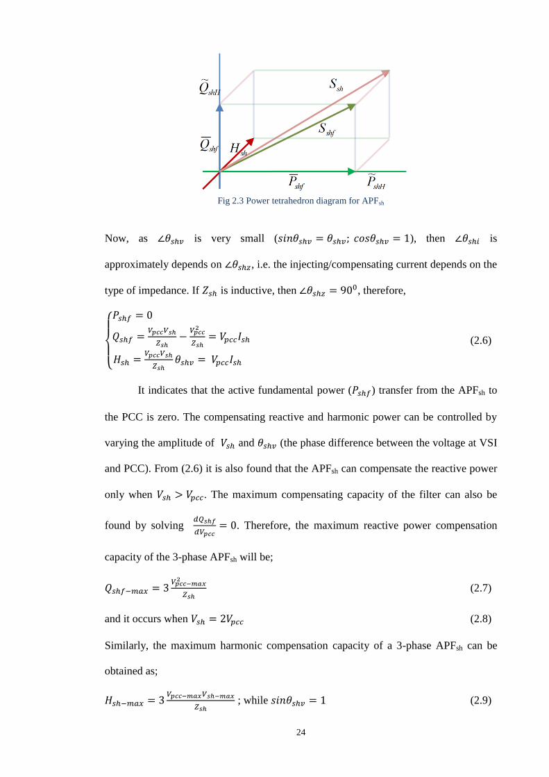
24
Fig 2.3 Power tetrahedron diagram for APFsh
Now, as is very small ( ), then is
approximately depends on , i.e. the injecting/compensating current depends on the
type of impedance. If is inductive, then , therefore,
(2.6)
It indicates that the active fundamental power ( ) transfer from the APFsh to
the PCC is zero. The compensating reactive and harmonic power can be controlled by
varying the amplitude of and (the phase difference between the voltage at VSI
and PCC). From (2.6) it is also found that the APFsh can compensate the reactive power
only when . The maximum compensating capacity of the filter can also be
found by solving
. Therefore, the maximum reactive power compensation
capacity of the 3-phase APFsh will be;
(2.7)
and it occurs when (2.8)
Similarly, the maximum harmonic compensation capacity of a 3-phase APFsh can be
obtained as;
; while (2.9)

25
Therefore, (2.7) or (2.9) can be used to calculate the maximum reactive or harmonic
compensation capacity of a 3-phase APFsh.
The main VSI rating for the reactive and harmonic power compensation of the APFsh
can be written as;
(2.10)
where Ploss is the total active power loss of the APFsh during its compensation task
which includes conduction loss of interfacing inductor, transformer (if any), VSI and
switching loss of VSI. The value of conduction and switching losses of VSI mainly
depends on the DC voltage source of the switches, current flow and energy transfer
during the on-off condition and the switching frequency [43]. If the overall impedance
of the APF system is considered as ( , then the will be;
(2.11)
where Ish is the rms value of the compensating current, Rsh represents the conduction
and switching losses per phase of the VSI and the isolation transformer (if any) [34].
For circuit simplicity and to describe the compensating power exchange mechanism
between the APF and grid PCC, a working diagram of phase A is shown in Fig 2.4,
where Sw represents the switch of the switching devices. When , switch S1
conducts and a leading current flows from the APF to the PCC. In this case, the APF
operates in capacitive mode and reactive power Q is generated by the APF. Similarly,
results in a lagging current in the conducting switch S4. In that case, the
APF operates in inductive mode and hence reactive power is absorbed by the APF. Both
of the conditions can be represented as an Inverter and Rectifier mode of operation
respectively if the VSI of the APF deals with active power exchange [40]. When
, the reactive power becomes zero. The vector diagrams in Fig 2.5 also

26
clarify the basic working principle and power exchange between the grid and shunt
APF. According to Kirchhoff’s voltage law, the basic equations for the capacitive mode
can be derived as;
(2.12)
Fig 2.4 Compensating power exchange between the Grid and shunt APF and the phase leg representation
for Phase A.
Fig 2.5 Vector diagrams clarifying the working principle of shunt APF system
2.2.2 Switching dynamics
Because of its simplicity of implementation, fast response, enhanced system
stability and increased reliability [39, 41], a hysteresis band current controller is
generally used to control the actual compensating current (ish) at the PCC by tracking
the desired reference current. Fig 2.6 represents the switching dynamics for one phase
of the APFsh. It also shows how the compensating current (ish) tracks the reference

27
current (ishref) within the hysteresis band limit (h). For H-bridge single phase system, the
detailed switching dynamics has been studied in [34]. Similar approach can be
implemented here for single / three phase system and can be generalized with respect to
.
Fig 2.6 Switching dynamics of a hysteresis based current controller
The switching on and off time for Sw1 or Sw4 can be found as [34];
(2.13)
where, and
These ( ) values are negligible for a smooth variation of reference current [34]
and it occurs when switching frequency is high or close to its maximum. During
low/minimum switching frequencies the variation of reference current could be high
and then it may be required to consider in case of minimum switching frequency
calculation. The general equation for the switching frequency can be written as;

28
(2.14)
2.2.3 Calculation of design parameters
For simplicity, the following section will discuss the procedure for harmonic
current compensation. A similar procedure can be followed for reactive current
compensation. As the value is calculated from and of the APFsh,
(which depends on the Vsh, Ish, Lsh and fsw) to compensate specific harmonics, the
maximum limit of these values should be considered to determine the maximum
acceptable as well as Again, from the study of switching dynamics it
is found that the switching frequency is very much dependent on the Vpcc, Vsh and Ish, Lsh
and h. Therefore, the proper value and selection procedure of these parameters are very
important to determine the capacity of the APFsh to perform its required tasks. Based on
the working principle and on the power flow and switching dynamics study, the
following steps describe the procedure and criteria for the selection of design
parameters.
2.2.3.1 Switching frequencies (fsw)
Considering that and are negligible for smooth varying reference current
and high frequency conditions, the switching frequency (2.14) can be simplified as;
(2.15)
where, . The solution of this equation to derive the maximum
(fswmax), minimum (fswmin) and zero-crossing (fswzero) switching frequency has been
explained in [34] and can be found as;
(2.16)

29
(2.17)
(2.18)
(2.19)
Over a complete cycle, the switching frequency and compensating current (ish)
also vary. The maximum compensating current can be found where ( ) is
maximum and this can be explained from (2.1) and Fig 2.4. That is, when is near to
0 (zero), Ish should be maximum. Therefore, it is clear that the maximum switching
frequency, fswmax should occur at or near the zero crossing condition (depending on the
reactive and harmonic components of the load current). Also, at this point, hon and hoff
both are negligible compared to 2h. Equation (2.16) should then be modified as;
(2.20)
where represents the value of at or near the zero crossing condition.
Similarly ish should be minimum where ( ) is minimum. Here, the switching
frequency will also be minimum. At that condition, the values hon and hoff should be
comparable to 2h and will have an effect on calculating the minimum switching
frequency, fswmin. Therefore, equations (2.18) and (2.19) may not give the accurate result
and hence the general equation (2.15) should be used to calculate the other switching
frequencies.
The relation between the and for single and three phase VSI can simply
be obtained from [39], as shown in Fig 2.7. Therefore, (2.20) can be used to calculate
the for single or three phase system. Thus it can be written as;
(2.21)

30
Fig 2.7 a) Switching configuration of VSI and output waveform for (a,b) 1-phase, 1-leg; (c,d) 1-phase, H-
bridge and (e,f) 3-phase 3-leg
2.2.3.2 Interfacing inductor (Lsh)
The derived methods in [35-38] for calculating the value of Lsh are mainly based
on a fixed frequency PWM converter with an assumption that the ripple current
attenuation or peak compensation current and the maximum harmonic voltage also are
known. The value of Lsh can also be calculated from (2.6) where the value of Hsh, Vsh
and Ish should be pre-determined.
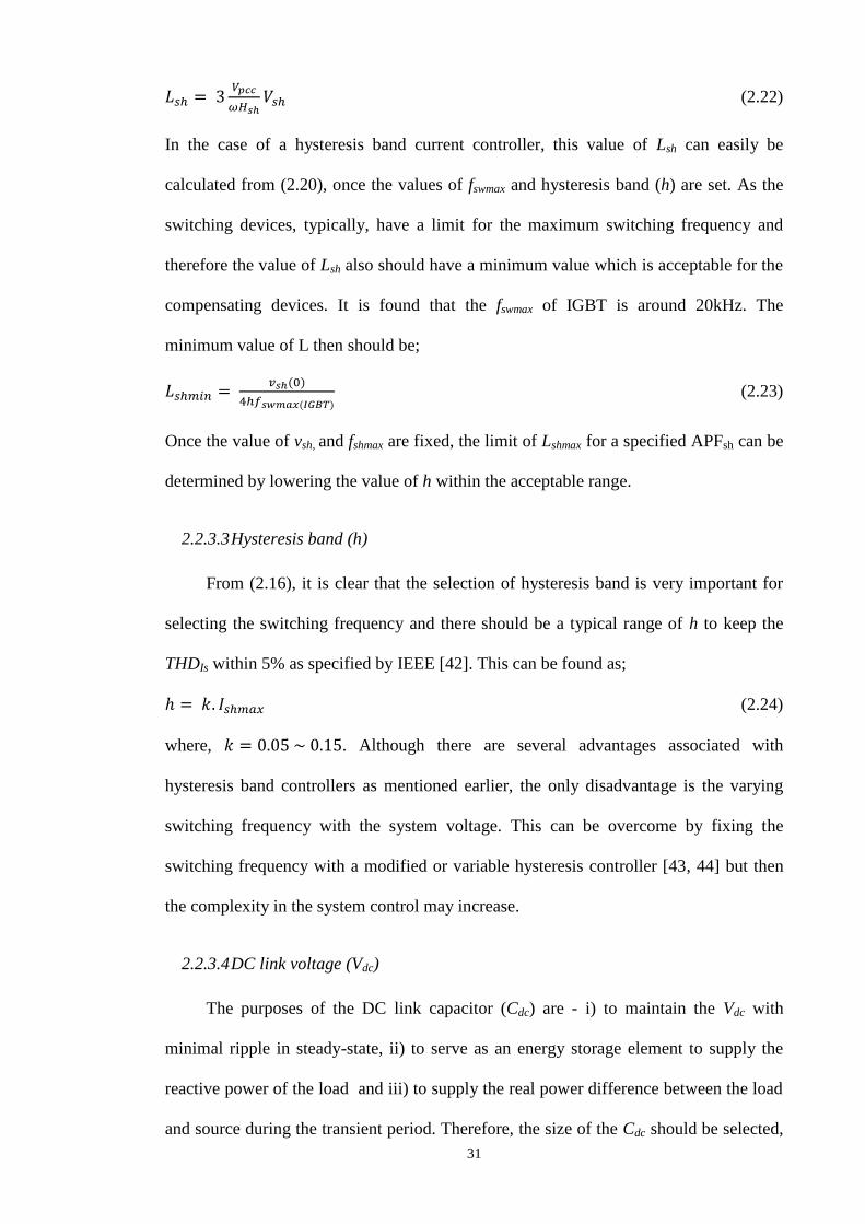
31
(2.22)
In the case of a hysteresis band current controller, this value of Lsh can easily be
calculated from (2.20), once the values of fswmax and hysteresis band (h) are set. As the
switching devices, typically, have a limit for the maximum switching frequency and
therefore the value of Lsh also should have a minimum value which is acceptable for the
compensating devices. It is found that the fswmax of IGBT is around 20kHz. The
minimum value of L then should be;
(2.23)
Once the value of vsh, and fshmax are fixed, the limit of Lshmax for a specified APFsh can be
determined by lowering the value of h within the acceptable range.
2.2.3.3 Hysteresis band (h)
From (2.16), it is clear that the selection of hysteresis band is very important for
selecting the switching frequency and there should be a typical range of h to keep the
THDIs within 5% as specified by IEEE [42]. This can be found as;
(2.24)
where, . Although there are several advantages associated with
hysteresis band controllers as mentioned earlier, the only disadvantage is the varying
switching frequency with the system voltage. This can be overcome by fixing the
switching frequency with a modified or variable hysteresis controller [43, 44] but then
the complexity in the system control may increase.
2.2.3.4 DC link voltage (Vdc)
The purposes of the DC link capacitor (Cdc) are - i) to maintain the Vdc with
minimal ripple in steady-state, ii) to serve as an energy storage element to supply the
reactive power of the load and iii) to supply the real power difference between the load
and source during the transient period. Therefore, the size of the Cdc should be selected,
32
and the controller should be designed in such a way, that the APF can compensate the
real power difference for a short transient period (typically a number of msec.) after
which the controller should be able to adjust the reference current. Thus the Vdc can be
maintained at a reference value.
Depending on the topology, different methods or approaches have been presented
in [35–38, 43] to develop the relation between Vpcc, Vsh and Vdc. For a 3-ph, 3-leg
system, considering the amplitude modulation factor, ma=1, the minimum value of Vdc
should be at least equal to [35], or [36-38], or greater then
[43]. Based on this information, the minimum value of Vdc can be derived
as;
(2.25)
Although the higher Vdc does not have much impact of current THD, it can
increase the voltage THD at the PCC and thus degrade the quality of the source voltage
[45]. Therefore, lowering the difference between Vpcc and Vsh will improve the system
performance and stability of the voltage at PCC.
2.2.3.5 DC link capacitor (Cdc)
As an energy storage element, the DC link capacitor should be capable of
performing all the functions described in the DC link voltage section. And in general,
the energy handling capacity determines the size of the capacitor. The basic equation
can be written as;
(2.26)
where S is the power required to be i) compensated during the steady state condition
[46], or ii) supplied to the load during the transient condition [34, 46], or iii) absorbed
due to the load change during the transient condition [34], or iv) compensated in DVR
mode during voltage sag/swell conditions [47]. T is the required time period for one

33
complete cycle, n is the number of cycles for energy transfer and z is the percentage of
Vdc to replace the Vdcmax and Vdcmin, the maximum and minimum allowable Vdc
respectively to perform the specific task. For a specific system, it is better to consider
the higher value of Cdc so that it can handle all of the above conditions. It also helps to
get a better transient response and lower the steady-state ripple.
2.3 Design of Series Active Power Filter (APFse)
The purpose of the Series APF is to compensate the voltage disturbance such as
sag/swell, flicker, voltage unbalance. Voltage sag/swell, the most commonly occurring
PQ problems, are usually caused by a short-circuit current flowing into a fault and can
be illustrated in a simplified model as shown in Fig 2.8. The magnitude and phase of the
voltage dip at the Point of Common Coupling (PCC) are determined by the fault and
supply impedances, using the following equation [48]:
(2.27)
(2.28)
Where Vsag is the voltage during the sag at the PCC, is the impedance
between the PCC and the fault, and is the source impedance at PCC and
the source voltage VS.
Zs
Zp
Sensitive Load
PCC
Vsag
Vpre-sag
Vm
issi
ng
f sag
(a) (b)
Fig 2.8 a) Distribution system with fault and b) vector diagram of voltage sag with phase jump and the
used definition of pre-sag, sag and missing voltage

34
Though the connection topology differs and mainly depends on the injection
transformer and half or H-bridge or multi-level inverter connection, there are some
basic parameters that should be calculated/chosen properly for the design of series APF.
Details of the topologies and their basic comparison, which is beyond the scope of this
study, can be found in [49]. The parameters that are needed to be designed properly to
compensate the voltage disturbance are as follow;
i. Injecting transformer
ii. Interfacing inductor / low pass filter
iii. DC link capacitor and storage device
2.3.1 Injection transformer
The basic function of the injection transformer is to increase the voltage supplied
by the filtered VSI output to the desired level while isolating the DVR circuit from the
distribution network. The transformer winding ratio is pre-determined according to the
voltage required in the secondary side of the transformer which is generally kept equal
to the supply voltage to allow the DVR to compensate the full supply voltage sag [50].
The turns ratio of the transformer can be determined from the following design concept:
If the DVR has the capability of compensating for a voltage-sag depth up to X% in a
single-phase sag, then the compensating voltage Vsag in each phase can be found as
follows [51]:
(2.29)
The maximum output voltage of the PWM inverter is:
(2.30)
2.3.2 Interfacing inductor / Low pass filter (LPF)
Low pass passive filters including the interfacing inductor are used to convert the
PWM inverted pulse waveform into a sinusoidal waveform. This is achieved by
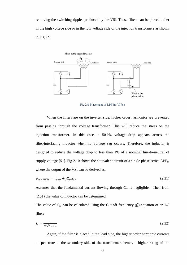
35
removing the switching ripples produced by the VSI. These filters can be placed either
in the high voltage side or in the low voltage side of the injection transformers as shown
in Fig 2.9.
Fig 2.9 Placement of LPF in APFse
When the filters are on the inverter side, higher order harmonics are prevented
from passing through the voltage transformer. This will reduce the stress on the
injection transformer. In this case, a 50-Hz voltage drop appears across the
filter/interfacing inductor when no voltage sag occurs. Therefore, the inductor is
designed to reduce the voltage drop to less than 1% of a nominal line-to-neutral of
supply voltage [51]. Fig 2.10 shows the equivalent circuit of a single phase series APFse
where the output of the VSI can be derived as;
(2.31)
Assumes that the fundamental current flowing through Cse is negligible. Then from
(2.31) the value of inductor can be determined.
The value of Cse can be calculated using the Cut-off frequency (fc) equation of an LC
filter;
(2.32)
Again, if the filter is placed in the load side, the higher order harmonic currents
do penetrate to the secondary side of the transformer, hence, a higher rating of the

36
transformer is necessary [52]. However the leakage reactance of the transformer can be
used as a part of the filter, which will be helpful in tuning the filter.
Fig 2.10 Equivalent circuit of single phase series APF
2.3.3 DC link capacitor and energy storage device
An energy storage device is used to supply the real power requirement for
compensation during a voltage sag. Flywheels, Lead acid batteries, Superconducting
magnetic energy storage (SMES) and Super-Capacitors can be used as energy storage
devices.
As the DC link capacitor is between the series and shunt APF for the design of
UPQC, the calculation is the same as in the case of shunt APF.
2.4 Design of Unified Power Quality Conditioner (UPQC)
Two possible ways of connecting the UPQC to the point of common coupling
(PCC) are discussed in [24]:
Right-shunt UPQC: The APFsh is connected to the load side and the series to
the supply side;
Left-shunt UPQC: The APFsh is connected to the supply side and the series
component to the load side.
Comparing the characteristics of these two configurations, the right-shunt UPQC
has the advantages over the left-shunt UPQC in terms of operation (i) in zero power

37
injection/absorption mode, (ii) to make the power factor unity at the load terminal, (iii)
to supply the entire load reactive power requirement. It also has been shown that the dc
capacitor control of the right-shunt UPQC structure is simpler. Thus, it can be
concluded that the right-shunt UPQC is more advantageous.
Once the design parameters for the series and shunt APF are defined, the complete
UPQC system is derived with a combination of these two APF. As the required active
power for voltage sag compensation will be provided by the DC link capacitor through
the APFsh, a DC link voltage control method then should be derived for this purpose. A
12-kVA DSP controlled laboratory prototype UPQC has been designed and installed at
the DIT Lab [41].
2.5 Control Strategies
The control strategy is at the heart of the any compensating device. Generation of
appropriate switching patterns or gating signals with reference to command the
compensating signals determines the control strategy of any compensating devices. In
general, it is implemented in three stages [29];
i. Signal conditioning - sensing of essential voltage or current signal for
referencing and implementation of control algorithm. These voltage or current
signals could be on the supply side, the load side or on the compensating side.
Voltage signals are sensed using either power transformers or Hall-effect voltage
sensors or isolation amplifiers whereas current signals are sensed by current
transformer or Hall-effect current sensors. Analog or digital filters are
sometimes used to eliminate noise from the sensing parameters.
ii. Derivation of compensating signals – derivation of compensating or reference
voltage/current signals depend on the control method and APF configurations. It
is the most important part of the control strategies. It also affects on the rating as

38
well as the transient and steady-state performance of the device. Two methods
are used to generate the compensating command: frequency and time domain.
In the frequency domain, the compensating signal is extracted from the
source/load signal by application of the Fourier analysis. The device switching
frequency is maintained at a value greater than twice of the highest
compensating harmonic frequency for effective compensation.
Compensation in the time domain is based on the instantaneous derivation of
compensating commands in the form of voltage or current signals. Control
method level on instantaneous p-q theory, synchronous d-q reference frame,
synchronous detection, flux-based controller, notch filter, PI controller, sliding-
mode controller, genetic algorithm, neural network are the most popular in the
time domain.
iii. Generation of gate signal - using PWM, Space Vector Modulation, Hysteresis
Band, Sliding-mode, Dead-beat control or Fuzzy or neural based control
technique.
The control can be carried out using discrete analog and digital devices or
advanced microelectronics such as microcontroller or microprocessors.
2.5.1 Shunt Active Power Filter (APFsh)
Removing the fundamental part or extraction of harmonic content from non-linear
harmonic current to generate the reference current for harmonic power compensation of
APFsh using high pass (HPF) or low pass filters (LPF) are a simple part of the control
technique. However both methods have a high error in the phase and magnitude of the
harmonics calculation [28]. In addition, HPF is sensitive to high frequency noise.
In synchronous detection method, the three-phase currents are assumed to be
balanced after compensation, as shown in Fig 2.11. The method is useful for reactive
power compensation, current imbalance and mitigation of harmonic current [53].

39
Pow
er C
alcu
lati
on
LPFPdc
2 L a
sa t
Vx
V V
2 L b
sb t
Vx
V V
2 L c
sc t
Vx
V V
ILabc
VLabc
P
Isa
Isb
Isc
t sa sb scV V V V
Fig 2.11 Block diagram of Synchronous Detection Method
The synchronous fundamental d-q frame method is derived from the space vector
transformation of input signal in a-b-c coordinate to the rotational orthogonal d-q
coordinate by means of the Park Transformation. Fig 2.12 shows the block diagram of
the synchronous d-q frame method for harmonic current compensation [54]. This
method is further improved to detect the desired harmonic frequency for compensation
[55].
2 2cos cos cos
3 323 2 2
sin sin sin
.. ...
.. ...3 3
a
d
b
q
c
ii
ii
i
abc to dq
ILabc
LPF dq-abcIs,abc
PLL
Fig 2.12 Block diagram of d-q synchronous frame method
But the problem associated with these methods is to detect and compensate the
per phase harmonic component. Therefore, any disturbance or distortion in the supply
side could degrade the performance of the system. The d-q transformation needs also a
phase-lock-loop (PLL) circuit to synchronize the transformation with the line frequency
and phase.
The p-q theory [26] is based on a set of time domain instantaneous powers that
can be applied to three phase systems with or without a neutral wire for generic voltage

40
and current waveforms. Thus, it is valid in the steady state as well as in the transient
state. This theory always considers the three phase system as a single unit by
transforming voltages and currents from the abc to 0 coordinates and not a
superposition or sum of three single phase circuits. Details of this theory is given in
Appendix 1. This p-q theory works properly when the three-phase system is balanced
[56]. In [57], a simple modification is proposed by implementing a Phase Lock Loop
(PLL) to develop a generalised single-phase p-q theory that can be utilised under the
condition of distorted utility voltage.
2.5.2 Series Active Power Filter (APFse)
The APFse is controlled to inject the appropriate voltage between the point of
common coupling (PCC) and load, such that the load voltages become balanced,
distortion free and have the desired magnitude. Theoretically the injected voltages can
be of any arbitrary magnitude and angle. However, the power flow and device rating are
important issues that have to be considered when determining the magnitude and the
angle of the injected voltage [3]. In the case of the UPQC, the implementation of the
APFse can be done in two ways [58] depending on the angle of the injected voltage: thus
the system is termed as UPQC-Q and UPQC-P. In the first case (UPQC-Q) the injected
voltage is maintained 90o in advance with respect to the supply current, so that the
series compensator consumes no active power in steady state. In the second case
(UPQC-P) the injected voltage is in phase with both the supply voltage and current, so
that the series compensator consumes only active power, which is delivered by the
shunt compensator through the dc link. A detailed analysis of UPQC rating under
different control strategies together with their advantages and disadvantages are
presented in [58 - 60]. In the case of UPQC-Q the series compensator requires
additional capacity, while the shunt compensator VA rating is reduced as the active
power consumption of the series compensator is minimised and it also compensates for

41
a part of the load reactive power demand. In the UPQC-P case the series compensator
does not compensate for any part of the reactive power demand of the load, and it has to
be entirely compensated by the shunt compensator. Also the shunt compensator must
provide the active power injected by the series compensator. Thus, in this case the VA
rating of the shunt compensator increases, but that of the series compensator decreases.
It can be concluded that the UPQC-Q and UPQC-P are two extreme cases and finding
the optimum solution which is located in between is preferable. An analysis for
optimisation of the converter rating is presented in [61-63] and an approximate sub-
optimal control strategy for UPQC minimum losses operation is proposed.
Comparing the techniques for calculating the reference voltage of the series
compensator, it is found that the UPQC-P algorithm has the simplest implementation
and involves very little computation [64]. In the UPQC-P case the voltage rating of the
series compensator is considerably reduced. Therefore, the UPQC-P control strategy has
been used in the UPQC simulation model. For simplicity, only the case of a three-phase,
three-wire system has been considered here.
2.5.3 Unified Power Quality Conditioner (UPQC)
The integrated controller of the APFse and APFsh of the UPQC realizes an
instantaneous algorithm to provide the compensating voltage reference v*C, as well as
the compensating current reference i*C to be synthesized by the controllers.
The functional block diagram of the UPQC controller is illustrated in Fig 2.13.
Generation of compensating voltage and current for Series and Shunt APF is based on
the instantaneous p-q theory. In addition, it is shown in Fig 2.13 that the UPQC
controller requires a positive-sequence detector, a PWM voltage controller for voltage
compensation, a hysteresis current controller for reactive harmonic current
compensation and a dc-link voltage regulator.

42
The phase voltages at the load terminal consists mainly of the positive sequence
component (V+1), but can be unbalanced (containing negative- and zero sequence
components at fundamental frequency), and can also contain harmonics from any
sequence component. The detection of the fundamental positive-sequence component of
vsa, vsb, and vsc is necessary in the sinusoidal current control strategy. Fig 2.14 shows the
method to detect the fundamental positive sequence of the source voltage [26].
The PWM voltage controller should allow the series active filter to generate
compensating voltages according to their references v*Ca, v*Cb, and v*Cc, which can
vary widely in frequency and amplitude. Therefore, conventional sine-PWM techniques
(SPWM) may not be appropriate due to their inherent amplitude attenuation [65].
Further, the filter (RLC) circuit at the ac output of the PWM converter may cause phase
displacements in the compensating voltages vca, vcb, and vcc. Therefore, feedback control
loops are implemented to minimize possible deviations between the reference and actual
values generated at the primary sides of the series transformers. The proposed PWM
voltage control [26] is given in Fig 2.15.
Different current-control techniques are applied for tracking the reference current:
sampled error control, hysteresis band control, sliding mode controller, linear quadratic
regulator, deadbeat controller, pole shift controller [24]. From the number of dedicated
papers, the hysteresis control appears to be the most preferable for shunt active filter
applications. The hysteresis control method has simpler implementation, enhanced
system stability, increased reliability and response speed [24, 64, 66]. Therefore, in the
UPQC simulation model a hysteresis controller has been used. The advantages of using
a hysteresis controller are mentioned below.

43
Fig 2.13 Functional block diagram of the UPQC controller
Fig 2.14 Positive sequence detection [26]
Fig 2.15 PWM voltage control with minor feedback control loops

44
2.6 Selection of design parameters for a 3-ph, 3-wire APFsh
This section deals with some simulation study and calculation for the proper
selection of design parameters. As an example, the initial target of maximum harmonic
compensating current, Ishmax, has been set at 100A which requires an APFsh of 48.8 kVA
rated capacity (Hsh) in a 400V(L-L) distribution system. Again the Svsi-h of the
compensator depends on the Hsh and Ploss which are associated with the Vsh, Ish and Rsh
in (2.6) and (2.11). These are also related to the rating of the switching device and other
design parameters including fsw, h and Vdc, in (2.17 - 2.26). Therefore a wide range of
values of Ishmax, h, Lsh, Rsh and Vdc has been chosen to calculate the Ploss and Svsi-h and to
perform the simulation study to observe the performance of the selected appropriate
design components. The connection topology and switching configuration of a 3-ph, 3-
wire APFsh together with the chosen parameters range is shown in Fig 2.16.
Fig 2.17(a) shows how the actual VSIrating ( ) increases with the value of
for a specific Ishmax. The actual compensating power of the APF, Hsh can be calculated
from (2.6) and in the Fig 2.17(a) it is represented when Rsh is zero. Though Rsh is
related with the design parameters, in some research articles the value of Rsh was
considered to be between 0 and 2Ω [67 - 74]. For example, to compensate 48.8 kVA of
Hload, the required Svsi-h will be 49.0 kVA, if a value of 0.3 Ω for Rsh is used as shown in
Fig 2.17(a) (point A). The VSI rating will be increased upto 57.7 kVA, if Rsh is assumed
to be 2Ω. This is shown as point B in Fig. 2.17(a). The corresponding active power loss
Ploss as a ratio (%) of (Ploss / Svsi-h) for the unit is shown in Fig 2.17(b). For Rsh = 0.3 Ω,
the actual Ploss is 4.5 kW, calculated from (2.11). In terms of ratio it is around 9.2% of
the VSI rating which is reflected as point A in Fig 2.17(b). Point B in Fig 2.17(b) shows
the corresponding ratio for the point B in Fig 2.17(a), which is around 52%. Therefore it
would be better to lower the Rsh value. Considering the ratio of 10% as a loss, it is clear
that a value of Rsh up to 0.3 Ω would be an acceptable selection for a 49kVA (Ishmax =

45
100A) compensator. the shaded part of the Fig 2.17(b) also reflects the possible limits
of Ishmax for possible Rsh values that can be considered between 10% ratio and 1Ω.
Fig 2.16 A 3-ph, 3-wire D-STATCOM connected to the grid and load at PCC
Again from the switching dynamics study (2.16), it is found that the fsw depends
on the system parameters such as Vdc or Vsh, h, Lsh, Vpcc, Ish and Rsh. Practically, the
maximum switching frequency depends on the type of power switching devices.
Generally, IGBT switches are preferred in most of the power electronics devices at
distribution level due to their fast switching speed, low switching power losses and high
power handling capability. With these above stated constraints, the initial limit for some
of the parameters was fixed to design a shunt APF which has been given in Table 2.1.
The remainder of the component selection has been carried out based on these
parameters.
Table 2.1 Initial maximum limit for some of the design parameters
Parameters Value (Initial Maximum Limit)
Qload 49kVA
Vpcc(L-L) 400V
Ishmax 100A
fswmax 20kHz
Rsh 1Ω
Ploss 10%

46
(a)
(b)
Fig 2.17 (a) Relation between Actual VSI rating (Svsi-h), Rsh and Ish; (b) corresponding loss of inverter
A series of simulation studies and other calculations have been performed based
on the design procedure, as shown in Fig 2.18, to select the best values of h and Vdc
which are further required to set the value of Lsh and to determine the limit of Ish and Hsh
and VSIrating to operate the APFsh within its loss limit or with maximum efficiency.
Critical design decisions are then verified against the derived procedure in Section 2.2
and described in the following section.
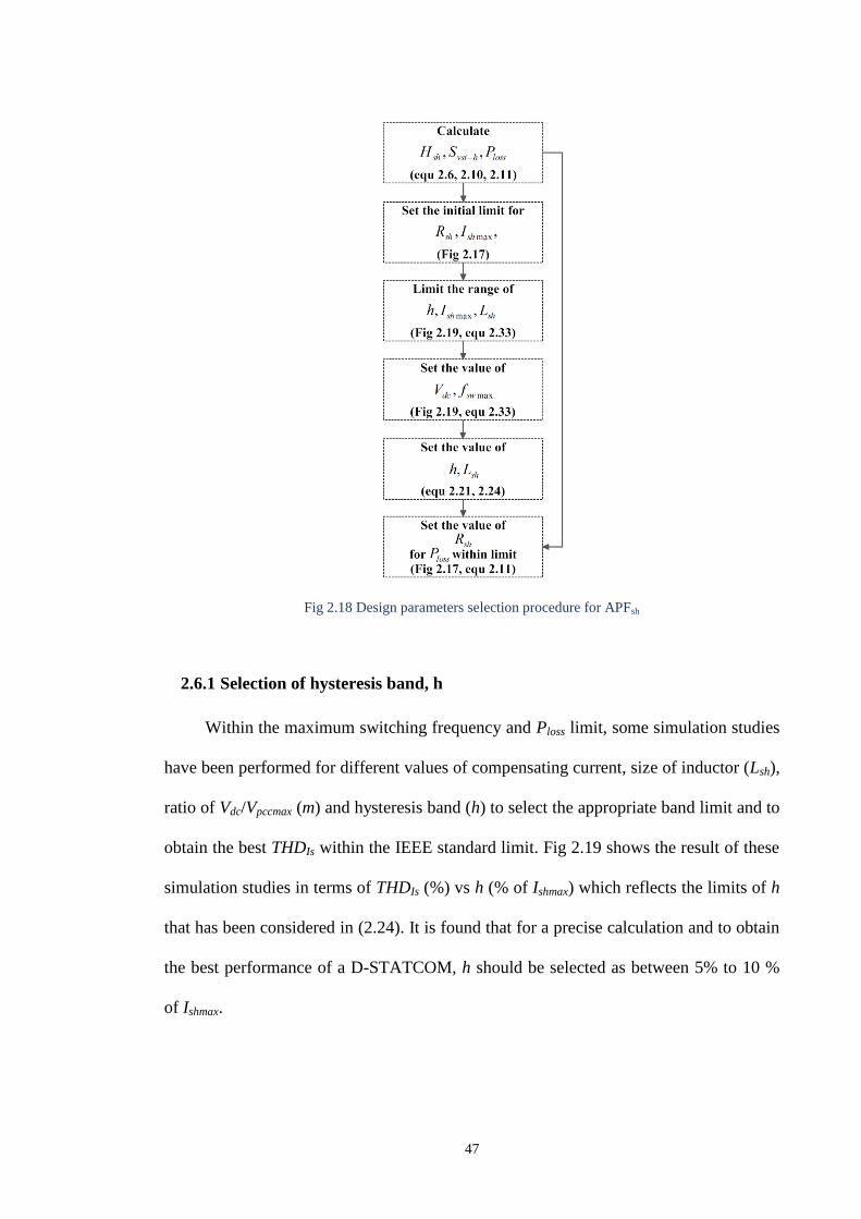
47
Fig 2.18 Design parameters selection procedure for APFsh
2.6.1 Selection of hysteresis band, h
Within the maximum switching frequency and Ploss limit, some simulation studies
have been performed for different values of compensating current, size of inductor (Lsh),
ratio of Vdc/Vpccmax (m) and hysteresis band (h) to select the appropriate band limit and to
obtain the best THDIs within the IEEE standard limit. Fig 2.19 shows the result of these
simulation studies in terms of THDIs (%) vs h (% of Ishmax) which reflects the limits of h
that has been considered in (2.24). It is found that for a precise calculation and to obtain
the best performance of a D-STATCOM, h should be selected as between 5% to 10 %
of Ishmax.

48
Fig 2.19 Selection of h to maintain THDIs within IEEE standard.
2.6.2 Limit on the Ishmax
The relation between fswmax and Ishmax can be derived, from (2.21) and (2.24), as
follow;
(2.33)
It shows that for a constant value of Ishmax the maximum switching frequency increases
with the decrease of Lsh. Again the size limit of Lsh can be increased with the increase of
m (Vdc/Vpccmax) and Ishmax. For a fixed value of Lsh and fswmax, the limit of Ishmax can also
be increased by reducing h. Fig 2.20(a) shows how the switching frequency increases
with the decrease of Lsh and increase of m. For Ishmax = 10A, it is found that a minimum
2mH of Lsh should be used with h = 10% of Ishmax and m = 1.4 to keep the fswmax within
the IGBT switching limit (20kHz), shown in point A. Within this 20kHz, the limit of
Ishmax can also be increased up to 40A (as shown in the shaded part of Fig 2.20(a) by
reducing the Lsh to 1mH, at point B) or up to 200A, at point C (as shown in the shaded
part of Fig 2.20(b) by reducing the Lsh to 0.5mH, h = 5% and increasing m to 3.6). But
in these cases (B and C), there will be a high level of power loss in the VSI unit and the
voltage THD at PCC will also increase due to the higher Vdc (high m) [45]. Therefore,
after fixing fswmax (20kHz) and h (10%), the Ishmax has been calculated for different Lsh
and m values which are given in Table 2.2.

49
(a)
(b)
Fig 2.20 (a) Relation between fswmax and Lsh for the variation of m and Ishmax; (b) Relation between Ishmax
and Lsh for the variation of m and h.
Table 2.2 Values of Ishmax and Lsh for different Vdc condition at fswmax = 20kHz
fsw = 20K m
h =10% 1.2 1.4 1.6 1.8 2 2.4 2.8 3.2 3.6 4
Lsh (mH) Ishmax (A)
0.1 162.6 189.7 216.8 244.0 271.1 325.3 379.5 433.7 487.9 542.1
0.5 32.5 37.9 43.4 48.8 54.2 65.1 75.9 86.7 97.6 108.4
1 16.3 19.0 21.7 24.4 27.1 32.5 37.9 43.4 48.8 54.2
2 8.1 9.5 10.8 12.2 13.6 16.3 19.0 21.7 24.4 27.1
4 4.1 4.7 5.4 6.1 6.8 8.1 9.5 10.8 12.2 13.6
6 2.7 3.2 3.6 4.1 4.5 5.4 6.3 7.2 8.1 9.0
8 2.0 2.4 2.7 3.0 3.4 4.1 4.7 5.4 6.1 6.8
10 1.6 1.9 2.2 2.4 2.7 3.3 3.8 4.3 4.9 5.4
12 1.4 1.6 1.8 2.0 2.3 2.7 3.2 3.6 4.1 4.5
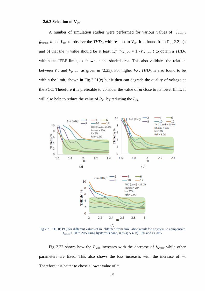
50
2.6.3 Selection of Vdc
A number of simulation studies were performed for various values of Ishmax,
fswmax, h and Lsh to observe the THDIs with respect to Vdc. It is found from Fig 2.21 (a
and b) that the m value should be at least 1.7 (Vdc,min = 1.7Vpccmax ) to obtain a THDIs
within the IEEE limit, as shown in the shaded area. This also validates the relation
between Vdc and Vpccmax as given in (2.25). For higher Vdc, THDIs is also found to be
within the limit, shown in Fig 2.21(c) but it then can degrade the quality of voltage at
the PCC. Therefore it is preferable to consider the value of m close to its lower limit. It
will also help to reduce the value of Rsh by reducing the Lsh.
(a) (b)
(c)
Fig 2.21 THDIs (%) for different values of m, obtained from simulation result for a system to compensate
Ishmax = 10 to 20A using hysteresis band, h as a) 5%, b) 10% and c) 20%
Fig 2.22 shows how the Ploss increases with the decrease of fswmax while other
parameters are fixed. This also shows the loss increases with the increase of m.
Therefore it is better to chose a lower value of m.

51
Once the values of m, fsw and Ishmax are fixed, then the values of h and Lsh can be
set. Lower the value of Lsh will help to reduce the Rsh. The value of Rsh is set from Fig
2.17 for a fixed value of Svsi-h and Ploss within the limit. It is difficult to calculate the
switching loss. Therefore, the resistance value (act as a loss emulator) should be low, as
it is responsible for conduction loss (transformer + inductor).
Fig 2.22 Reduction of Ploss with the increase of fswmax while the other parameters are constant
2.6.4 Selection of Cdc
From the general equation (2.26) it is found that the value of Cdc depends on the
purposes of the DC link capacitor, as described in section 2.2, the required level of
power (S) to be compensated/transferred, the number of cycles (n) and the allowable
change of Vdc (z). Once the value of Vdc (or m) and the number n are fixed, Cdc only
depends on S and z. Fig 2.23 shows the relation between z and S with respect to Cdc. For
example, if a compensator is allowed to transfer 20kVA of load power during the
transient condition and the task is completed within a half cycle (n = 0.5) with an

52
allowable change in Vdc of 10%, then the required capacity of Cdc will be around
3000F for m = 1.8, point A, which is further reduced to 2500F for m = 2.
Fig 2.23 Relation between z and S to calculate the Cdc for m = 1.8 and 2.0
2.6.5 Verification of switching dynamics and frequencies
As discussed, the design parameters of the APFsh are related to the switching
frequency, fsw as well as the hysteresis band, h and Vdc. The switching mechanism has
been studied and verified with the derived equations in the previous Section 2.2. Table
2.3 shows the design parameters for a specific compensator that has been chosen to
investigate the switching dynamics and to determine the switching frequency. Fig
2.24(a) shows the Vpcc, Vsh, Is, Ish, Iload and Sw1 for phase A when the shunt APF is
operating. It is clear that the fswmax occurs near the zero crossing condition where Vpcc is
close to zero and Vsh is 1/3 of Vdc. The variation of Ishref during one on-and-off time
period (hon and hoff) of gate Sw1 is also negligible compared to 2h (in Fig 2.6).
Otherwise, the effect of these values on the calculation of fswmax is negligible. Fig
2.24(b) shows that the system has been designed for fswmax = 15kHz which can simply be
calculated using (2.13, 2.14) and by neglecting hon and hoff . If the values are compared
with that in (2.16), fswmax is found to be the same.

53
a)
b)
c)
Fig 2.24 (a) One complete cycle of an APF in compensating mode, (b) showing the values of design
related parameters to calculate the maximum switching frequencies , fswmax and c) one of the minimum
frequency, fswmin at close to 90 deg of supply voltage condition

54
Table 2.3 Design parameters of a Shunt APF for the verification study of switching frequencies
Component Parameters Values Supply Voltage 230 Vrms, 50 Hz DC link Voltage 600 V
DC storage Capacitor 2200 µF
Interface Inductor 1.666 mH, 1Ω
Hysteresis band (h) 2 Amp
Maximum Compensating Shunt Current 30 Amp
Similarly fswmin1 occurs where Ish is close to zero (in Fig 2.24a). At this point, Vpcc goes
to its positive peak and Vsh = 2/3 of Vdc. hon can be calculated as 0.77A and hoff is 0.64
(from 2.13). Putting these values in (2.14), the fswmin1 is calculated as 10.7kHz whereas
neglecting the values of hon and hoff in the calculation gives a value of 12.1kHz. This
makes a significant difference in the actual simulated fswmin condition, though it does not
have any impact on selection the design parameters.
2.7 Conclusion
Both the design and controlling mechanism for 3-phase 3-wire series and shunt
APF system has been reviewed and discussed here as a part of the design and control of
a complete UPQC system that can minimize the disturbance of supply voltage as well as
cancel the reactive and harmonic part of the load current.
Switching dynamics has been studied to develop the relation between the design
parameters and the switching frequencies. This is also verified by simulation. Power
losses due to conduction and switching are also co-related with the design parameters
and maximum switching frequency. A design parameter selection procedure with an
example has been described here by initially setting a maximum switching frequency
and loss limit. The best choice of hysteresis band and the minimum value of DC link
voltage are set by carrying out extensive simulation to maintain the source current THD
within the IEEE limit. Variation of these parameters to design the other components and
associated losses are also calculated. A Shunt APF system with a wide range of design
parameters has been simulated and the results are shown to compare the design

55
parameters with their associated power losses and the required kVA rating. This
procedure can be generalized to design the parameters for other topologies of APFsh
system and would be useful for practical design and development of APF and UPQC.

56
Chapter 3
Integration and Placement of UPQC in DG Integrated
Networks
3.1 Introduction
Implementation of Custom Power Devices (CPD) such as UPQC in DG or
microgrid systems to improve the power quality is gaining greater importance [75-79].
This chapter deals with the review and analysis of research work that has been
completed to date on the integration and placement of UPQC in DG integrated
networks. Emphasis has been placed on integration techniques of UPQC in DG or
microgrid system together with their advantages and disadvantages. The number of DG
systems such as Photovoltaic and Wind Energy Systems are now penetrating more into
the grid or microgrid at the same time the number of non-linear loads are also
increasing. Therefore, in the presence of DG sources and UPQC in an active distribution
network, the following issues have been analysed;
(a) the placement of UPQC and its sensors in the network,
(b) impact of the sensor placement on the UPQC control method,
(c) performance of UPQC with bi-directional power flow in the network and
(d) the advantages of DG inverter in the presence of UPQC
The rest of the chapter discusses the following issues: Section 3.2 deals with the
presently available integration techniques of UPQC and DG in a network. The technical
standard and other requirements for DG integration in the Electric Power System (EPS)
together with the effects of DG integration in terms of Total Harmonic Distortion

57
(THD) and Total Demand Distortion (TDD) are discussed in section 3.3. This is
followed by the placement of UPQC in the network and the related issues are identified
and discussed in Section 3.4. Conclusions are made in Section 3.5
3.2 Integration of UPQC
Recent reports [75-81] show that significant research and development has been
carried out on the application of UPQC to DG integrated networks. As the UPQC can
compensate for almost all existing PQ problems in the transmission and distribution
grid, integration of a UPQC in the distributed generation network can be multipurpose.
As part of the integration of UPQC in DG systems, research has been carried out on the
following two techniques: DC-Linked and Separated DG-UPQC systems.
3.2.1 (DG – UPQC)DC-linked
A structure has been proposed in [75-79], as shown in Fig 3.1, where DG sources
are connected to a DC link in the UPQC as an energy source. This configuration works
both in interconnected and islanded modes (shown in Fig 3.2). In the interconnected
mode, DG provides power to the source and loads whereas in the islanded mode, DG
(within its power rating) supplies power to the load only. In addition, UPQC has the
ability to inject power using DG to sensitive loads during source voltage interruption.
The advantage of this system is voltage interruption compensation and active power
injection to the grid in addition to the other normal UPQC abilities. The system’s
functionality may be compromised if the DG resources are not sufficient during the
voltage interruption. Economical operation of the system can also be achieved by proper
control of the active power transfer between the supply and DG source through a series
APF [78]. The proposed system can also reduce the investment cost by nearly one fifth
if the UPQC and DG are used separately [79].
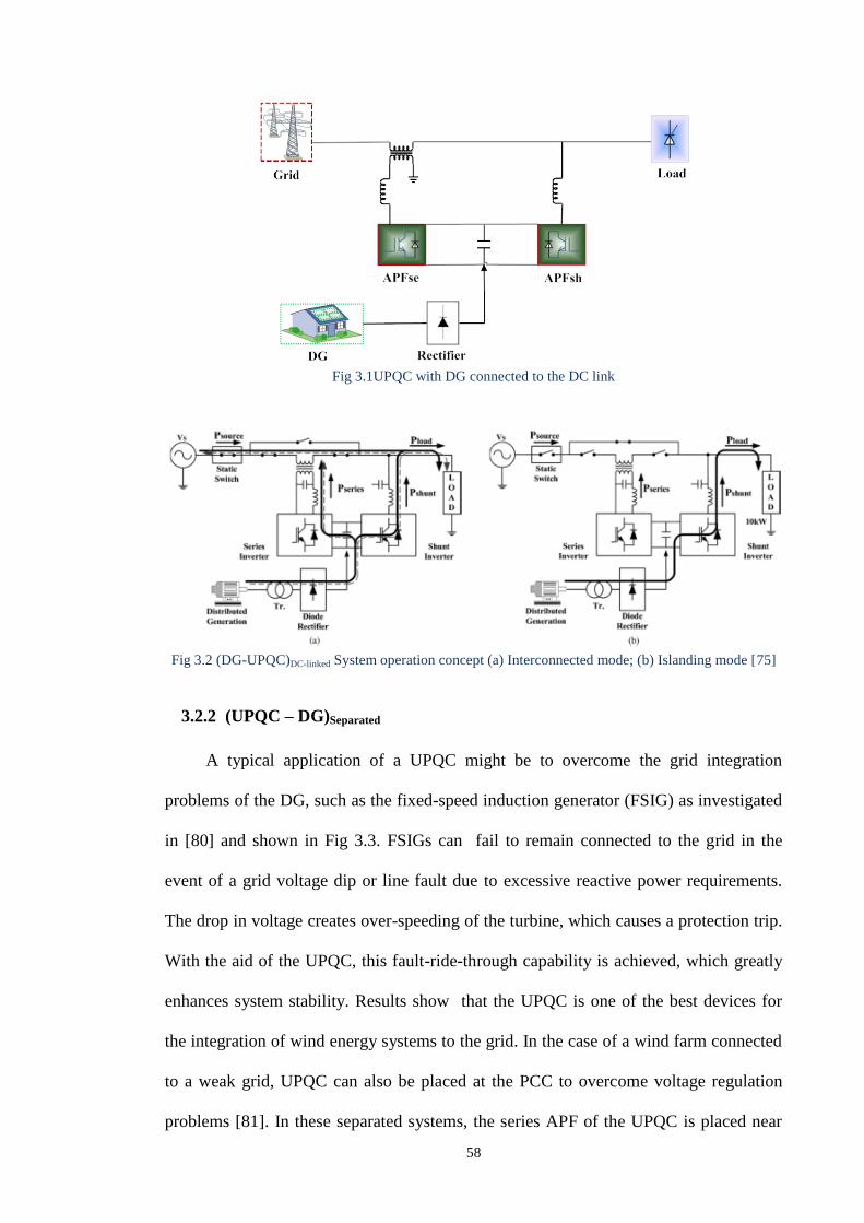
58
Fig 3.1UPQC with DG connected to the DC link
Fig 3.2 (DG-UPQC)DC-linked System operation concept (a) Interconnected mode; (b) Islanding mode [75]
3.2.2 (UPQC – DG)Separated
A typical application of a UPQC might be to overcome the grid integration
problems of the DG, such as the fixed-speed induction generator (FSIG) as investigated
in [80] and shown in Fig 3.3. FSIGs can fail to remain connected to the grid in the
event of a grid voltage dip or line fault due to excessive reactive power requirements.
The drop in voltage creates over-speeding of the turbine, which causes a protection trip.
With the aid of the UPQC, this fault-ride-through capability is achieved, which greatly
enhances system stability. Results show that the UPQC is one of the best devices for
the integration of wind energy systems to the grid. In the case of a wind farm connected
to a weak grid, UPQC can also be placed at the PCC to overcome voltage regulation
problems [81]. In these separated systems, the series APF of the UPQC is placed near

59
the DG side to conduct the voltage regulation by injecting the voltage in phase with
PCC voltage. This type of UPQC is referred to as left shunt UPQC [24]. Based on that
research study, in addition to the normal functionality of UPQC, some of the other
advantages and disadvantages are identified and these are given in Table 3.1 [19].
Fig 3.3 Grid connected wind energy system with UPQC
Table 3.1 Comparative analysis of integration techniques of UPQC in DG system
Technique Advantages Disadvantages
(DG-UPQC)DC-linked
i. Compensate voltage
interruption
ii. Operation in islanding
mode – possible
iii. Active power transfer
during grid connected or
microgrid mode – possible
iv. System cost for PQ
improvement - reduced
(remove DG Inverter)
i. Control complexity – high
ii. Capacity enhancement in
multi-level or multi-module
mode – difficult
(UPQC-DG)Separated
i. Capacity enhancement in
multi-level or multi-module
mode - easy
ii. Control – easy
iii. Active power transfer
during grid connected mode -
possible
i. Voltage interruption – may
not be possible
ii. Operation in islanding
mode – may not be possible
iii. System cost - high
3.2.3 Cost analysis
In terms of required components, it is clear that the (DG-UPQC)DC-linked does not
require the grid connecting interfacing converter and thus the cost will be less. The
60
purpose of the DG inverter / grid-tie inverter is already carried out by the APFsh in the
UPQC system. On the other hand in the (DG-UPQC)separated system two complete units
of UPQC and DG unit are required along with the interfacing converter. Therefore, the
additional grid-tie inverter cost makes it costlier than the previous topology. A
comparative analysis of investment cost and economical saving of separated and
combined UPQC–DG (Wind Energy System) has been carried out in [79] based on the
component cost values in [82]. It is found that, depending on the ratings, the combined
(DG-UPQC)DC-linked system can reduce the cost up to one fifth of the separate system.
3.3 Interconnection of DG Source with Electric Power Systems
The nonlinear characteristics of power electronics devices and loads on the power
system can be modelled as current sources that inject harmonic currents into the system.
Voltage distortion occurs as a result of these currents which cause nonlinear voltage
drops across the power system. Due to the increasing application of power electronics
equipment such as converters which connect DG sources into the grid or microgrid, this
harmonic distortion becomes a growing concern for many customers and for the overall
power system. The levels of this distortion can be characterized and quantified by the
complete harmonic spectrum magnitude as the total harmonic distortion (THD). But this
can often be misleading. For example, many adjustable speed drives exhibit high THD
values for the input current when they are operating at very light loads. Though the
magnitude of harmonic current is low, its relative distortion is high. A similar problem
occurs at the point of common coupling (PCC) when DG sources are connected with the
electric power system (EPS) at the distribution level. Here, load harmonics remain
constant but the actual supply current from the grid is relatively low and thus the THD
at the PCC becomes high. To handle this concern for characterizing harmonic currents
in a consistent fashion, IEEE introduced another term, the total demand distortion

61
(TDD). This term is the same as the THD except that the distortion is expressed as a
percent of some rated load current rather than as a percent of the fundamental current
magnitude. Guidelines for harmonic current and voltage distortion levels on distribution
and transmission circuits are provided in [5].
According to the IEEE Standard 1547 [8], the PCC is defined as; “The Point of
Common Coupling (PCC) with the consumer/utility interface is the closest point on the
utility side of the customer's service where another utility customer is or could be
supplied. The ownership of any apparatus such as a transformer that the utility might
provide in the customer’s system is immaterial to the definition of the PCC.” Fig 3.4
shows the interconnection of DG sources with the EPS and the PCC. The PCC is where
harmonic limits are assessed and prevented to propagate from one customer to another.
When the DG is connected, harmonic current injection, by the DG unit and the non-
linear load, into the Area EPS at the PCC shall not exceed the limits as given in Table
3.2. The harmonic current injections shall be exclusive of any harmonic currents due to
harmonic voltage distortion present in the Area EPS without the DG connected.
Fig 3.4 Interconnection of DG sources with EPS and PCC
Table 3.2 Maximum harmonic current distortion [IEEE 1547, IEEE 519]
Individual
harmonic
order, h
h < 11 11< h<17 17<h<23 23<h<35 35 ≤ h TDD
Percent (%) 4.0 2.0 1.5 0.6 0.3 5.0

62
Mathematically, THD and TDD can be calculated as;
(3.1)
(3.2)
where I is the rms value, f is the fundamental component.
According to [8], DG interconnection system shall detect the unintentional
islanding and cease to energize the islanded area within two seconds of the formation of
an islanding condition. One of the reasons for this is that the controller of the grid-tie
DG inverter is designed to provide only pure active power to the load and grid in the
interconnected mode.
Fig 3.5 shows an example of interconnection of DG sources as a micro-generation
(μGen) or microgrid (μGrid) with the distribution network. Assuming that the DG
source provides the active power to the grid and all the harmonics are injected by the
non-linear harmonic load (load1). The position of the current sensors are also shown to
measure the THD and TDD for different level of DG injected current ( ).
For the study, two types of DG integration systems (μGrid and μGen) with harmonic
(load1) and reactive (load2) load have been considered, where the current fundamentals
are Iload1max = 207 A and Iload2max = 97 A. The relation between the DG supply and load
demand is given as;
(3.3)
Measuring points for in the network are also shown in
Fig 3.5. Fig 3.6 shows the initial waveforms at the measuring points and the
corresponding THD / TDD values are given in Table 3.3 when both DG sources are not
operating. It is to be noted that the THD and TDD are same when DG or any other
source is not present in the network. THD at and are also same as is

63
zero. THD at shows lower than that at and it occurs as a resultant effect due to
the reactive and harmonic loads with different ratings.
Fig 3.5 Distributed Generation (DG) Integrated Network
Table 3.3 When ; UPQC is not working
Sensors
THD / TDD (%) 17.88 0.20 25.8 25.8
Fig 3.6 Waveforms of the when
Assuming that the DG sources are providing pure fundamental current (i.e.
without harmonics), Fig 3.7 shows the effect of the supply current of DG sources on

64
the measurement of THD values for four conditions at different points in the network.
The four conditions are;
(a) Both the DG sources and loads are active
(b) Load2 is inactive
(c) DG1 is inactive
(d) DG2 is inactive.
For all cases, the simulated system has been run for 1 sec. γ is considered to range
from 0 to 2, which means the DG units supply from zero up to double of the load
fundamental current. It is found that, in Fig 3.7(a), the measured THD at PCC1 becomes
maximum when the DG1 supplies the load fundamentals ( ). The reason is that at
the point the sensor senses only the harmonics of the load current and net fundamental
( ) becomes close to zero. But in reality, the DG unit does not
supply any harmonics to the PCC and the measured TDD remains unchanged. The peak
of the grid ( ) THD may change the position when the load2 or DG2 (μGen) is
inactive, as shown in Fig 3.7(b and d). When DG1 (μGrid) is off, then the grid THD
also increases and the peak value depends on the condition of the load
(reactive/harmonic) and the supply of DG2, as shown in Fig 3.7(c). Fig 3.8 shows the
corresponding waveforms at the measuring points when . It is also found that
the DG1 or load1 does not have any impact on the THD at PCC2. Therefore, measuring
THD at PCC1 and grid source, when the DG units are running, will provide false
information and thus could affect the maintenance of PQ levels for the location.

65
Fig 3.7 Effect of on the calculation of THD at different points.
Fig 3.8 Waveforms of the when varies from (0 to 2) of and

66
3.4 Placement of UPQC in DG Network
In a DG integrated electrical distribution system, DG sources (i) can be connected
to the electric power system as a μGen or in a μGrid condition, (ii) have to supply the
active power to the grid and/or load and (ii) should be capable of detecting the
unintentional islanding or grid voltage disturbances and then be disconnected and (iv)
then have to supply the active and reactive power depending on the load demand. The
UPQC as a Custom Power Device is introduced at the PCC (i) to prevent the grid and
other loads from the current harmonics generated by the non-linear loads, (ii) to
maintain the voltage and current THD at PCC within the IEEE limits and (iii)
compensate the grid voltage sag / swell to provide a balance and stable voltage at the
PCC. In the presence of DG sources the following situations require critical
considerations;
(a) the placement of UPQC and its current feedback sensors,
(b) impact of sensor placement on the UPQC control method,
(c) performance of UPQC with the bi-directional power flow in the network and
(d) the privilege/advantage of DG source in presence of UPQC
This will enable the proper placement of UPQC in a DG integrated network. These
issues are discussed in the following sections of this Chapter.
For a better understanding, a DG integrated network as shown in Fig 3.5 has been
designed and simulated in MATLAB. Design parameters for the UPQC also have been
calculated based on the grid and load information which are given in Table 3.4. DG
sources are considered to be supplying the fundamental active power. Therefore,
harmonics introduced by the DG inverters are not added in the simulation and the
analysis. The supplied DG power has been increased in every 0.2 sec interval by putting
successive values of γ = 0, 0.5, 1.0, 1.5 and 2.0 in (3.3).

67
Table 3.4 Overall DG network parameters for the simulation
Section Parameter Value / phase
Grid (3 phase) Voltage ( ) 230 Vrms
Line Frequency ( ) 50 Hz
Load1 (μGrid) Load Current ( ) 151 Arms
Reactive + Harmonic Current 71 Arms
Load2 (μGen) Load current ( ) 71 Arms
UPQC DC link Voltage ( ) 600 V
Series Inductance ( ) 0.3 mH
Series Transformer ( ) 1:1
Switching frequency ( ) 10 kHz
Max Sag Compensation ( ) 50%
Shunt Inductance ( ) 0.42 mH
Hysteresis band (h) 7.5 A
Switching frequency ( ) 16 kHz
Max Compensating Current ( ) 100 Amax
DG DG current ( ) Equ (3.3)
3.4.1 Placement of UPQC and its current feedback sensors
In general, a UPQC can be placed before or after the DG unit in an integrated
network. The arrangement can be;
(i) PCC-UPQC-DG-Load or
(ii) PCC-DG-UPQC-Load.
The placement of the UPQC feedback voltage and current sensors depend on its
control methods and techniques. Therefore, the placement of UPQC can be made in four
ways which are given below in Fig 3.9 where represent the sensing current
of the UPQC in feedback and feedforward mode respectively. The actual sensing
current of for all these positions are also shown in Fig 3.9. Without the loss
of generality, for the rest of the study, analysis and discussion, is assumed to be
zero.
3.4.1.1 Position 1
In this position, the UPQC is placed between the PCC and the DG system.
Depending on the control mechanism, the placement of sensors is also shown there. In

68
this case, sensing of load current will be difficult if it is placed in a micro-generation
system (μGen). The sensor in the PCC1 ( ) will also give the current difference
between the source ( ), DG ( ) and compensating current ( ) rather than the actual
load current ( ).
;
Position 1
Position 2
;
Position 3
;
Position 4
Fig 3.9 Placement of UPQC in DG integrated network
3.4.1.2 Position 2
In this position, both the sensors will not sense the real load current. Sensing of
load current will be difficult if DG unit is not removed or switched off. Otherwise an
additional sensor may be required to measure the to get the actual load information.
In this case UPQC can be placed both in a μGen or μGrid system.

69
3.4.1.3 Position 3
In this case, the UPQC and the sensors are placed after the DG source. Hence, the
sensor will measure the real load current. UPQC will also not sense any disturbance
or changes in supply current due to the DG placement. UPQC will not require to
measure the for its own control. This is the most common placement of the UPQC
reported in the literature.
3.4.1.4 Position 4
As far as sensing current is concerned, this case is the same as Position 1. The
only difference is that the DG source is connected before the UPQC at PCC1.
3.4.2 Impact on UPQC control
It is already mentioned that, in general, the series part of the UPQC is responsible
for the compensation of voltage disturbances including sag/swell and to accomplish the
task it will sense the voltage waveform at the PCC1. As the DG converter needs to
synchronize with the grid for a reliable connection and to transfer the active power to
the load and/or grid, the voltage at the PCC and the DG converter should be the same in
magnitude. Thus the sensing voltage for UPQC does not have any impact on the
generation of the reference signal for voltage compensation. In the case of the active
power transfer during sag compensation, APFse of the UPQC will sense only the
which is the same for Position 1, 2 and 4. Therefore, the response of the UPQC during
sag compensation will be the same for these positions. In Position 3, DG will have no
impact on UPQC for sag compensation. Fig 3.10 shows the basic block diagram of the
reference voltage generation using positive sequence detection and the control of the
series part of the UPQC. Details of this method can be obtained from [26, 74]. Fig 3.11
shows the waveforms at different points for the Position 2 during the supply voltage sag
which was applied from 0.04 to 0.4 sec. At the same time, DG current ( ) was
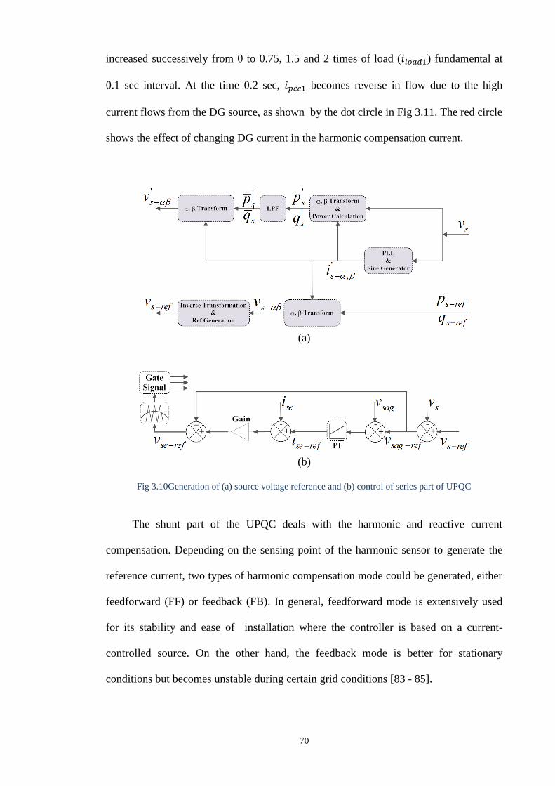
70
increased successively from 0 to 0.75, 1.5 and 2 times of load ( ) fundamental at
0.1 sec interval. At the time 0.2 sec, becomes reverse in flow due to the high
current flows from the DG source, as shown by the dot circle in Fig 3.11. The red circle
shows the effect of changing DG current in the harmonic compensation current.
(a)
(b)
Fig 3.10Generation of (a) source voltage reference and (b) control of series part of UPQC
The shunt part of the UPQC deals with the harmonic and reactive current
compensation. Depending on the sensing point of the harmonic sensor to generate the
reference current, two types of harmonic compensation mode could be generated, either
feedforward (FF) or feedback (FB). In general, feedforward mode is extensively used
for its stability and ease of installation where the controller is based on a current-
controlled source. On the other hand, the feedback mode is better for stationary
conditions but becomes unstable during certain grid conditions [83 - 85].

71
Fig 3.11Performance of UPQC during voltage sag in position 2
In terms of the control method, the shunt part of the UPQC can perform its
compensation task directly or indirectly [57, 86]. In the case of direct control, the
controller generates the reference current for the harmonic and reactive components
based on the sensing point and then controls the shunt current of the UPQC to perform
compensation at a desired level. For indirect control, the reference current is generated
based on the active or fundamental component at the sensing point and then the UPQC
operates or controls its shunt part in such a way that the current at the supply side or at
the PCC becomes sinusoidal and in phase with the voltage.
To understand the impact on UPQC control of the placement of UPQC and its
sensors for reference current generation, a common reference current generation method
and current controller have been chosen here for direct and indirect control using
feedback and feedforward compensating modes, which are shown in Fig 3.12 and 3.13.
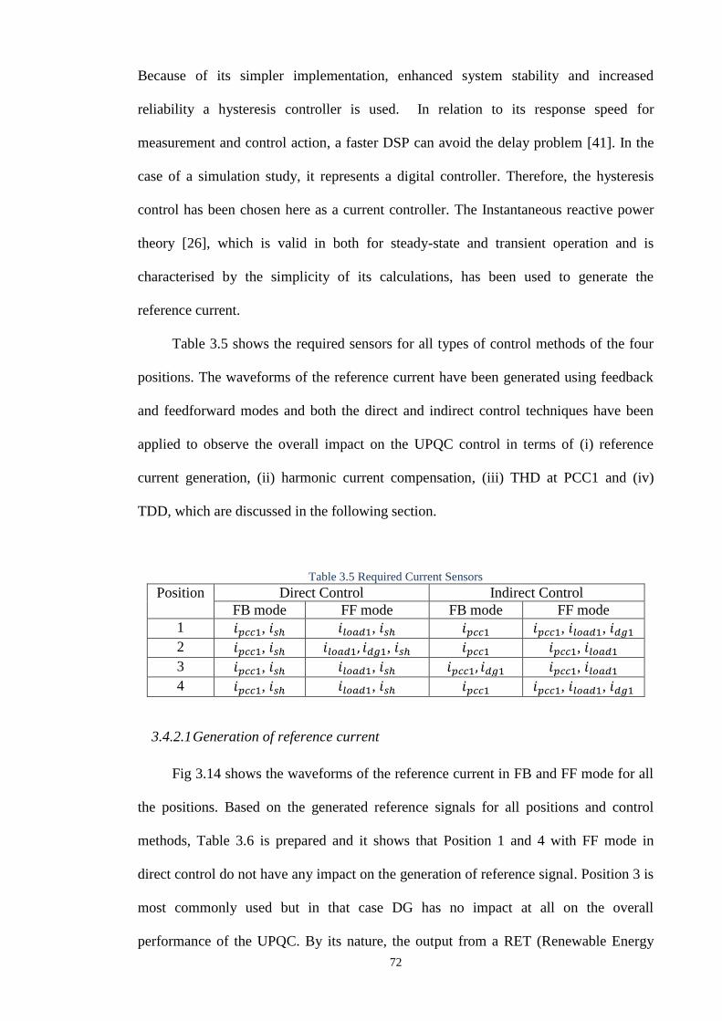
72
Because of its simpler implementation, enhanced system stability and increased
reliability a hysteresis controller is used. In relation to its response speed for
measurement and control action, a faster DSP can avoid the delay problem [41]. In the
case of a simulation study, it represents a digital controller. Therefore, the hysteresis
control has been chosen here as a current controller. The Instantaneous reactive power
theory [26], which is valid in both for steady-state and transient operation and is
characterised by the simplicity of its calculations, has been used to generate the
reference current.
Table 3.5 shows the required sensors for all types of control methods of the four
positions. The waveforms of the reference current have been generated using feedback
and feedforward modes and both the direct and indirect control techniques have been
applied to observe the overall impact on the UPQC control in terms of (i) reference
current generation, (ii) harmonic current compensation, (iii) THD at PCC1 and (iv)
TDD, which are discussed in the following section.
Table 3.5 Required Current Sensors
Position Direct Control Indirect Control
FB mode FF mode FB mode FF mode
1 , , , ,
2 , , ,
3 , , ,
4 , , , ,
3.4.2.1 Generation of reference current
Fig 3.14 shows the waveforms of the reference current in FB and FF mode for all
the positions. Based on the generated reference signals for all positions and control
methods, Table 3.6 is prepared and it shows that Position 1 and 4 with FF mode in
direct control do not have any impact on the generation of reference signal. Position 3 is
most commonly used but in that case DG has no impact at all on the overall
performance of the UPQC. By its nature, the output from a RET (Renewable Energy

73
Technology) based μGrid / µGen system is uncontrollable and therefore generation of a
reference current and control will be affected for the other positions (1 and 4 in FB
mode and 2 in FB and FF mode) and control methods. Thus it will have an impact on
the performance of UPQC.
(a)
(b)
Fig 3.12 Generation of reference current in (a) FB and (b) FF mode for shunt part of UPQC

74
Fig 3.13 Hysteresis control to generate the gate pulses for shunt part of UPQC
3.4.2.2 Harmonic current compensation
Fig 3.15 shows the respective harmonic current compensation based on the
generated reference current shown in Fig 3.14. Both, Fig 3.14 and 3.15, show how the
placement of the DG source, the UPQC and its sensors affects the performance of the
UPQC. Apart from position 3, the placement of the DG source/UPQC has an impact on
both direct and indirect control in the FB mode. The reason for this is because the FB
sensor for these positions measures the current difference between the load and DG
source rather than the actual load current. Therefore, the sensing current and generating
reference current are always varying with the DG input. In these cases, the UPQC
controller should have a better dynamic/transient performance. The main advantage of
these positions with the FB mode is that the UPQC can compensate the current
harmonics (if any) generated by the DG converter.
Table 3.6 Impact of UPQC sensors and DG source on reference current generation
Position Direct Control Indirect Control
FB mode FF mode FB mode FF mode
1 X
2
3 X X X X
4 X

75
(a)
(b)
(c)
(d)
(e)
(f)
(g)
(h)
Fig 3.14 Generation of Reference Current in Position1 - (a) FB and (b) FF sensor; in Position 2 - (c) FB
and (d) FF sensor; in Position 3 - (e) FB and (f) FF sensor; in Position 4 - (g) FB and (h) FF sensor.

76
(a)
(b)
(c)
(d)
(e)
(f)
(g)
(h)
Fig 3.15 Harmonic Current compensation in Position1 - (a) FB and (b) FF mode; in Position 2 - (c) FB
and (d) FF mode; in Position 3 - (e) FB and (f) FF mode; in Position 4 - (g) FB and (h) FF mode.
3.4.2.3 THD at PCC1
Table 3.7 shows the performance of the UPQC in terms of THD / TDD (%) at
when no DG sources are connected to the system. In that case, only one position
for the UPQC exists. Both the direct and indirect control with FB and FF mode shows
almost the same performance in terms of reactive and harmonic current compensation.

77
In the presence of a DG source, the measured THD@ipcc1 is shown in Fig 3.16 where
the DG input has been increased step by step up to a level equal to twice the load
fundamentals. The shaded portion in the upper part of each figure is presented as a
zoomed-in-version in the lower part of the respective figures. Results (in terms of THD)
indicate that the FB mode can be better than the FF mode. But, as already mentioned,
the FB mode becomes unstable during certain grid conditions and conventional supply
current detection [31, 85]. This performance can be improved by introducing a closed-
loop compensation method for selected line current harmonics which is proposed in
[83]. But, still there is a possibility of unstable grid conditions due to the presence of a
DG source (DG output is not constant) after the UPQC. Therefore, the FF mode can be
a better option for the selection of the position. In that case, position1 and 2 with FF
mode will be the best choice.
The other finding is that in the presence of a DG source and for any position and
mode of control, the UPQC helps to keep the THD level within 5% (as required by the
harmonic standards) except for the period when γ is within the range (0.5 to 1.5). This is
reflected in the shaded portions (zoomed-in-version) of the Fig 3.16. Therefore, the
μGrid designer needs to maintain this condition while designing a system.
Table 3.7 When UPQC is working; ;
Direct Control Indirect Control
THD / TDD (%) FB Mode FF Mode FB Mode FF Mode
@ 2.8 2.7 2.8 2.7
3.4.2.4 TDD at PCC1
Like THD, TDD measurement also depends on the sensor position. But for some
positions it gives the real value of the harmonic contents. For example, in the case of
Position 1, the FF sensor will sense the real load current and thus it can calculate the
real load fundamentals to calculate the TDD. Thus, for this mode, TDD will reflect the

78
real condition of harmonics for any value of γ, as shown in Fig 3.17. For FB sensor,
TDD will be same as THD. Similarly, for position 2 and 3, TDD and THD are same.
Position 4 will show the results as shown for position 1. Therefore, instead of THD, it is
better to measure TDD for such a DG integrated network with a power quality
compensator.
Position 1
Position 2
Position 3
Position 4
Fig 3.16 THD @ ipcc1 for all position and control of UPQC in presence of DG source. Lower part of
each figure is the zoomed-in-version of the upper shaded part.

79
Position 1
Position 2
Position 3
Position 4
Fig 3.17 TDD for all position and control of UPQC in presence of DG source.
3.4.3 Performance of UPQC with bi-directional power flow
The UPQC will observe bi-directional power flow only when the DG source is
placed after the UPQC. This will happen only for Position 1 and 2. Fig 3.18 - 3.21 show
the performance of the UPQC in FF mode during reverse current flow due to the
condition that and the dynamic change of . It is observed that for all the cases
the response of the UPQC in position 1 with FF mode (a) is better than the position 2
(b). In terms of harmonic current compensation (THD value) as shown in Fig 3.16,
direct control gives a better performance than indirect control.

80
(a)
(b)
Fig 3.18 Performance of UPQC in reverse current flow (γ > 1) and FF mode for (a) Position 1 and (b)
Position 2 with direct control;

81
(a)
(b)
Fig 3.19 Performance of UPQC in reverse current flow (γ > 1) and FF mode for (a) Position 1 and (b)
Position 2 with indirect control

82
(a)
(b)
Fig 3.20 Performance of UPQC in reverse current flow ( ) with dynamic change of and FF
mode for (a) Position 1 and (b) Position 2 with direct control

83
(a)
(b)
Fig 3.21 Performance of UPQC in reverse current flow ( ) with dynamic change of and FF
mode for (a) Position 1 and (b) Position 2 with indirect control

84
3.4.4 Advantages of DG sources/µGrid systems
In terms of the DG source, it is better to place the DG source after the UPQC and
therefore Positions 1 and 2 are preferable. This will have the following advantages;
(i) UPQC can compensate the voltage/current distortion generated by the DG source,
and therefore the grid can be shielded from any disturbance created by the DG
source/µGrid.
(ii) DG converter will not be exported to any grid voltage sag/swell or unbalance
conditions and therefore will be safe from grid faults.
(iii) μGrid system can achieve some operational flexibility by exchanging the sag/swell,
islanding and reconnection information between the UPQC and DG converters.
3.5 Conclusion
Based on the study and analysis for the placement of UPQC in DG connected
μGrid/μGen network, it can be concluded that the network arrangement of PCC-UPQC-
DG-Load (Position 1 and 2) can be a better choice for the overall performance of a
UPQC and DG connected grid network. In terms of sensor placement, control and
performance study (THD/TDD measurement at PCC), Position 1 gives the better result
than that in Position 2. While designing a system, μGrid designer needs to maintain the
condition that the measured current THD at PCC will be higher than the IEEE / EU
limit while DG in connected to the network and provides 0.5 to 1.5 times of the load
fundamental current. In the case of bi-directional power flow, Position 1 with direct
control shows the better performance than indirect control. Finally, in a DG connected
μGrid/μGen system, strategic positioning of UPQC can provide some control flexibility
for DG inverters for islanding detection and reconnection. This scope is further explored
in Chapter 5.

85
Chapter 4
Parallel Operation of Inverters and Active Power Filters in
Distributed Generation Systems
4.1 Introduction
It is now more common to have grid connected inverters facilitating distributed
generation (DG) or in microgrid systems. In some cases, grid connected inverters may
extend the energy availability, increase the energy security and improve the system
reliability. The power quality, at all time, is a matter of concern. DG inverters may
introduce more harmonics into the grid. On the other hand, in microgrids or DG
systems, load demands are also increasing. Therefore, to cope up with the increasing
load demand, multiple low power inverters are on the rise instead of large capacity
centralised inverters. Different controlling mechanism and topologies are available in
handling the difficulties of parallel operation of inverters either in active load sharing or
distributed mode. Research has also been carried out on parallel operation of shunt APF
in active load sharing or distributed mode. Therefore, a technical review on parallel
operation of power electronics inverter and APF for load sharing conditions in a
distributed generation (DG) network has been carried out here.
This chapter is organized as follows: in Section 4.2, the principle of parallel
operation of inverters with their possible problems is discussed. Active load sharing and
a droop control method for parallel operation of inverters are presented in brief in
Section 4.3. It is found that droop control is very suitable for both DG and off-grid
conditions. Section 4.4 deals with the working principle of the droop control method.

86
Control strategies for parallel operation of APF are presented broadly in Section 4.5.
Finally, concluding remarks are made in Section 4.6.
4.2 Principle of Parallel Operation of Inverter
Balance between generated and consumed real (P) and reactive (Q) power
indicates the stable operation of a power system. Therefore, implementing effective
control over P and Q is very important from the operational and control points of view.
The real (P1) and reactive (Q1) power transferred between the inverter and common bus
or grid can be explained [87] from the following diagram, Figure 4.1
Inverter
2 2E f
2E
Inverter
1 1E f
1E
Load
,1,1
,1,1
gg
gL
ZR
jX
Ig,2,2
,2,2
,2g
gg
LZ
RjX
Ig,1
Iin
v,1
Iin
v,2
0gV
Fig 4.1 Equivalent circuit of parallel inverter connected to the grid
2
1 1 1
1 ,1 1 ,1
,1 ,1 ,1
coscos sin sin
g g g
g g
g g g
EV V EVP
Z Z Z
f f
(4.1)
2
1 1 1
1 ,1 1 ,1
,1 ,1 ,1
cossin sin cos
g g g
g g
g g g
EV V EVQ
Z Z Z
f f
(4.2)
Here P1 and Q1 are the transferred real and reactive power from the inverter, E1. For
only real power transfer, Vg and E should have the same amplitude but with a different
phase. The different amplitude with same phase will give a reactive power circulation.

87
When both differ, it causes real and reactive power flow. Control of frequency
dynamically controls the power angle and hence, the real power flows. As the output
impedance of the inverter is very low, a small change in f could result in a very large
imbalance in the active power flow [28]. For parallel operation, the output voltage of all
inverters must be kept strictly in phase in order to guarantee equality of the output
active power for the corresponding inverters. Reactive currents can circulate between
inverters if their output voltage magnitudes differ from each other, as shown in Figure
4.2, which can overload the inverters unnecessarily.
Inverter
Load
1 2~Ic I I
Inverter
I1 I2
Fig 4.2 Circulating current flow between the parallel inverters
To suppress the circulating current and prevent the dc-link overvoltage, an
isolation transformer can be used as a passive control [88 - 90] but then the size of the
transformer for high power application could be a problem. Some active methods are
also described in [91 - 104] and most of these are based on PWM control. A simple
protective control algorithm has also been proposed in [94], Figure 4.3, where the
regeneration protection concept based on the rising dc-link voltage is considered. If Vdc
is greater than Vdcref, the battery converter stops delivering power from the battery side.
Here a proportional controller detects the error signal of the dc-link voltage.

88
Inverter
Load
Inverter
I1 I2
+-
VdcrefP regulator
X
Sine Ref
GeneratorSin
e Ref V
alue
Inverter Inverter
I1 I2
Load
Fig 4.3 a) Regenerative control structure to avoid dc-link overvoltage / to prevent circulating current; b)
passive control using isolation transformer
4.3 Control Strategies in Parallel Operation of Inverter
Distributed generation (DG) systems, either connected to or off the grid, may have
more than one inverter acting in parallel. Therefore in distributed Uninterruptible Power
Supply (UPS) systems, the parallel operation of a voltage source inverter with other
inverters or with the grid, are sensitive to disturbances from the load or other sources
and can easily be damaged by over-current. Hence, careful attention should be given to
system design and the control method of parallel operating inverters. Several control
methods are proposed and discussed in [89, 93 - 112]. Two or more inverters operating
in parallel must achieve the following features: 1) amplitude, frequency and phase
synchronization among the output voltages of inverters, 2) proper current distribution
according to the capacities, 3) flexibility and 4) hot-swap ability at any operating time
[105].
The purpose of active power filters (APF) with its multiple configurations differ
from inverter operation, but as the inverter is also a part of the active power filter, the
controlling methods of inverters and APF in parallel operation could have some
similarities. Therefore the details of controlling methods are described in the APF
section. Some of the outcomes of recent research on parallel operation of inverters are
given below. The conventional control strategies for the parallel-connected inverters can

89
be classified into two types; active load sharing/current distribution and droop/wireless
control.
4.3.1 Active load sharing / current distribution
The object of the active current distribution control is to generate a reference
current for each parallel-connected inverter and it can be subdivided into;
i) Central Limit Control (CLC)
ii) Master-Slave Control (MSC)
iii) Average Current Sharing (ACS) / Distributed Logical Control (DLC)
iv) Circular Chain Control (3C)
In CLC mode, all the modules should have the same configuration and each
module tracks the average current of all the modules to achieve an equal current
distribution [94]. Perfect and equal current distribution can be achieved by using DSP-
based control for the voltage and current controller and by tracking the averaged
inductor current of the inverters. Thus the system stability and robustness can be
improved [106]
In the MSC method, one inverter is specified as the master, and all others as the
slaves. The master inverter supplies a reference current to the slave inverters. Thus the
master module is responsible for the output voltage regulation [107]. In such a system,
if the master module fails, the system will shut down and this is a major drawback. This
can be partially overcome by introducing a separate current-controlled PWM inverter
unit to generate the distributing current nearly independently for the slave inverters.
Hence, precise current division between the inverters are very much important. This
strategy is easy to implement in the parallel operation of UPS [108]. In other cases,
another module can take the role of master in the event of a main master unit failure.
The control scheme can be of dedicated, rotary or high-crest current type [109].

90
In the MSC and CLC methods, the output currents of all parallel-connected
inverters must be collected, and the number of parallel-connected inverters must be pre-
known. If one of the parallel-connected inverters fails, the parallel-connected system
will fail. This problem can be overcome by the DLC mode where redundancy is also
achievable.
In the ACS/DLC mode, an individual control circuit is used for each inverter. The
current control mode is used to control its output current and to trace the same average
reference current. When a defect is found in any module, others can still operate in
parallel [107 - 110]. It can also be used as a power-sharing technique where each
inverter controls the active and reactive power flow in order to match the average active
power of the system [105].
In 3C mode, the successive module tracks the current of the previous module to achieve
an equal current distribution, and the first module tracks the last one to form a circular
chain connection. The output voltage and current of each inverter can also be varied and
internally controlled to achieve a fast dynamic response [103, 109]. A coordinate
control strategy for different load sharing controls can be applied to eliminate the
circulating currents due to unbalance of parallel inverters [103].
4.3.2 Droop control
The droop control method for the parallel-connected inverters can avoid the
communication of the reference current. It is also defined as Wireless Control (WC)
with no interconnection between the inverters. In this case, inverters are generally
operated in the voltage-mode of control and the phase and amplitude of the inverter’s
output voltage are the control parameters. This control is defined in such a way that the
amplitude and frequency of the reference voltage signal will droop as the load current
increases and these droops are used to allow independent inverters to share the load in
proportion to their capacities [110]. This technique is then improved for non-linear

91
loads where harmonic components can be shared properly [111]. The load sharing is
also affected by the line impedance [112, 113]. The impact of line impedance on
reactive power sharing in the conventional frequency/voltage droop concept is further
enhanced in [114 - 116 ] to make the controller ideally suited for distributed ac power
supply systems.
4.3.3 Outcomes
A detailed review and performance comparison that has been presented in [114]
which shows that within active load sharing control schemes, current-sharing control is
good for output voltage regulation and harmonic current control. However it requires
high speed communications. Active power sharing requires low bandwidth
communication for active and reactive power sharing, but the harmonic power sharing
is poor and therefore sharing non-linear loads with a high crest factor is a problem.
Active synchronization is also a major problem for both the schemes.
Within the active load sharing scheme, the centralized and the master-slave
controller need a main inverter module to be set as the central control unit and this
would lower the system reliability. Modularity and redundancy are very low for both of
the controllers. For the average current sharing/distributed logic controller, although
there is no central controller and thus has higher modularity, it requires a current sharing
control loop to manage the transient and stability problems. The circular current control
strategies require more communication between each of the inverters as well as a
circular path for current distribution. This is suitable when forming an ac power ring.
In general, though the active current distribution control method is perfect for well
balanced current distribution, the inter-communication process of the generated
reference current of parallel-connected inverters can be susceptible to interference, and
thus the system reliability will be degraded. In addition, the communication of the
92
reference current among the parallel-connected inverters is difficult in some
applications such as distributed generation systems.
On the other hand, droop control or the wireless control with no interconnection
lines could be more useful for both active load sharing or in distributed generation
networks connected to the grid or off-grid. Some improvement in control has also been
achieved to overcome its limitations, such as poor transient response. Hot-swap
operation is another benefit of the droop control method. Low sensitivity to line
impedance unbalances and harmonic power sharing capability are the other advantages
of a droop controller.
4.4 Working Principle of Droop Control Method
The idea of the droop control method in the parallel operation of an inverter or
APF is to control the system without interconnection between units. Inverters can be
placed in different locations within the microgrid or DG system. In that case, the droop
control method is very effective for the inverters where active and reactive power flow
predominantly depends on power angle/frequency and the output voltage amplitude of
the inverters. Here, inverters are generally operated in the voltage-mode control and the
phase and amplitude of the inverter’s output voltage are the control parameters. The
controller is defined in such a way that the amplitude and frequency of the reference
voltage signal will droop as the load current increases. It should be noted that the
conventional voltage and frequency droop methods of achieving load sharing have a
slow and often oscillating transient response.
An inverter connected to the common bus through a decoupling impedance is
shown in Figure 4.4. Usually the inverter output impedance is highly inductive, and
hence, the active and reactive powers drawn to the bus can be expressed from equation
4.1 and 4.2 as [87];

93
sinEV
PX
f (4.3)
2cosEV VQ
X
f (4.4)
where X is the output reactance of an inverter, f is the phase angle between the output
voltage of the inverter and the voltage of the common bus, and E &V are the amplitude
of the output voltage of the inverter and the grid/load voltage, respectively. From the
above equations, it is found that the active power is predominantly dependent on the
power anglef , while the reactive power mostly depends on the output-voltage
amplitude E. Consequently, most of the wireless-control of paralleled-inverters uses the
conventional droop method, which introduces the following droops in the amplitude E
and the angular frequency of the inverter output voltage [110];
*
0( )i im P P (4.5)
*
0( )i iE E n Q Q (4.6)
being * and *E are the output voltage angular frequency and amplitude at no load, and
m and n are the droop coefficients for the frequency and amplitude, respectively. P0i, Pi
& Q0i, Qi represent the power rating and actual power output for active and reactive
power respectively. If droop coefficients are increased, then good power sharing is
achieved at the expense of degrading the voltage regulation, which can be acceptable if,
for instance, the frequency and amplitude deviations ( and E ) are mostly at 2%
and 5%, respectively [115].
The output impedance angle θ determines the droop control law, as shown in
Table 4.1. Fig. 4.5 shows the droop control functions depending on the output
impedance. The controller gains m and n are chosen as a function of the nominal values

94
of P and Q, and the maximum allowed deviations in frequency ω and amplitude E
(Table 4.I). Fig. 4.6 shows a simple block diagram of a droop controller.
Inverter
I
Z
Ef
0Vg
SP
jQ
Fig 4.4 Inverter connected to the grid (droop control)
*
* mP
nomPP
E
E*E
*E E nQ
nomQ QnomQ
*
*E E nP
nomPP
E
E*E
* mQ
nomQ QnomQ
Fig 4.5 Static droop characteristics
Power CalculationI
V
P
Q
+-
+-
P*
Q*
m
n - E*+
* s in ( )V E t f
f
*V
Fig 4.6 A simple block diagram of P/Q droop controller

95
Table 4.1 Output impedance impact over power flow controllability [104]
Output Impedance
(Z) Z jX (inductive: 090 ) Z R (resistive: 00
Active Power (P) sin
EV EVP
X Xf f
2cos( )
EV V VP E V
R R
f
Reactive Power (Q) 2cos( )
EV V VQ E V
X X
f sin
EV EVQ
R Rf f
Frequency droop
()
* mP * mQ
Amplitude droop
(E)
*E E nQ *E E nP
m nomP
2 nomQ
n 2 nom
EQ
nom
EP
4.5 Control Strategies in Parallel Operation of APF
Like inverters and UPS, Custom Power Devices (CPD) are finding greater
applications as interfacing and compensating devices in the distributed generation
system for power quality improvement as well as storing energy to work as a back-up
UPS system during islanded mode of operation. The power rating and switching
frequency of active power filter (APF) converters are determined by the magnitude of
harmonic currents and required filter bandwidth. In high power applications, the
filtering task cannot be performed for the whole spectrum of harmonics by using a
single converter due to the limitations on switching frequency and power rating of the
semiconductor devices. Therefore, to handle a larger portion of load power, increasing
its capacity is essential. The solutions suggested in the literature to this typical design
problem of APFs are a hybrid configuration, which reduces converter power rating;
step-down transformer, which usually increases the cost; series or parallel connection of
switching devices, which results in more complex gate drives; multilevel inverter,
which reduces voltage rating of the switches; or splitting filtering on the spectrum range
among a number of APF. The approaches with multiple inverters have already been
demonstrated to be very effective for increasing the capacity.

96
The concept and a design analysis with experimental validation of a multi-module
parallelable three-phase active power filter (centre mode) has been proposed first in
[117] to solve the problems of capacity enlargement and load unbalance compensation
encountered by the shunt APF with a three-arm topology. But the disadvantage of the
proposed method was that the malfunction of any inverter will cause erroneous
compensation due to the generation of a current command which is not independent to
other inverters. Therefore another proposal was made by the same author in [118] with a
capacity limitation technique. In that case, APFs are connected in a cascade mode which
shows the advantages of high flexibility, reliability due to no control interconnection
and reduced power capacity demand of APFs. But the disadvantage was that one APF
treats other APFs on its load side as a part of its load. The third approach has been
proposed in [119] which is based on power splitting. An overview of these techniques
has been given below and present research outcomes along with the advantages and
disadvantages of these techniques are also described later.
4.5.1 Frequency splitting (FS) / Centre mode control (CMC)
A central control unit is used to measure the total harmonic components and then
each APF is assigned to compensate a specific harmonic component. Therefore it
requires the minimum number of harmonic detection sensors, shown in Figure 4.7(a). It
can also be referred to as concentrated control. The technique for reference current
generation has been presented in Figure 4.7(b). If the sensing load current is Li then the
harmonic current will be, 1Lh L Li i i where 1Li is the fundamental component of the
load current and h is the number of harmonic components. In this mode, if there are 2
APFs working in parallel and one is responsible for reactive power compensation, then
the other one will compensate the harmonics [88, 120].
The operational advantage is that the APF module which deals with the higher
order harmonics should have the higher switching frequency. Since the harmonic
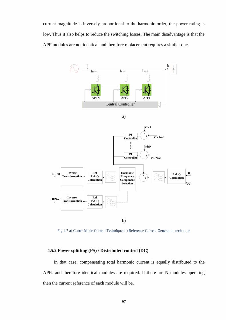
97
current magnitude is inversely proportional to the harmonic order, the power rating is
low. Thus it also helps to reduce the switching losses. The main disadvantage is that the
APF modules are not identical and therefore replacement requires a similar one.
Is IL
APF1
IF1
APF2
IF2
APFN
IFN
Central Controller
a)
P & Q
Calculation
Vs
Ref
P & Q
Calculation
Inverse
TransformationIF1ref
-+
IFNref
IL
Vdc1ref
Vdc1
-+
PI
Controller
VdcN
-+
PI
Controller VdcNref
Ref
P & Q
Calculation
Inverse
Transformation
Harmonic
Frequency
Component
Selection
b)
Fig 4.7 a) Centre Mode Control Technique; b) Reference Current Generation technique
4.5.2 Power splitting (PS) / Distributed control (DC)
In that case, compensating total harmonic current is equally distributed to the
APFs and therefore identical modules are required. If there are N modules operating
then the current reference of each module will be,

98
LhFN
iI
N (4.7)
Since it maintains interconnection between the inverters, the number of sensors are also
higher than the central control mode, shown in Figure 4.8(a). The reference current
generation technique has been depicted in Figure 4.8(b). The main advantage is its ease
of maintenance and installation. It is clear that in both central and distributed control
systems, the reference current of each APF result from the same P&Q calculating
algorithm block and therefore all the APFs maintain interconnection control. Hence a
fault in any communication or malfunctioning of any APF can cause the system to halt.
Is IL
APF1
IF1
APF2
IF2
APFN
IFN
a)
P & Q
Calculation
Vs
Vdc1ref
Vdc1
-+
PI
Controller
VdcN
-+
PI
Controller VdcNref
Ref
P & Q
Calculation
Inverse
Transformation
&
Current
Distribution
-+
IFNref
IL
1/N
IF1ref
b)
Fig 4.8 a) Distribute Control Technique; b) Reference Current Generation technique
4.5.3 Capacity limitation control (CLC) / Master – Slave control (MSC)
In this mode, each APF compensates harmonic current according to its power
rating. Each APF are independent and sense the current at the up/downstream side of
the node and therefore the maximum number of sensors are required, Figure 4.9(a).

99
Each APF only has to compensate the harmonic component left by the previous APF on
its load side. Therefore generation of reference current for each APF requires separate
P&Q calculation as shown in Figure 4.9(b). The rating of each APF module is defined
as;
max
3
2dc FP V I (4.8)
In general, APF near the load has higher capacity and the lowest bandwidth. As
the APFs are not identical and work independently therefore power capacity
enlargement is easier and the system reliability is also high. Also there is no central
control and no information sharing between the APFs. Poor dynamic characteristics is
the main disadvantage of this mode. But for steady-state conditions, CLC and PS show
a better performance than the FS [121].
IsN IL
APF1
IF1
APF2
IF2
APFN
IFN
Is2 Is1
a)
P & Q
Calculation
Vs
Ref
P & Q
Calculation
Inverse
TransformationIF1ref -+
IFNref
IL
Vdc1ref
Vdc1
-+
PI
Controller
Ref
P & Q
Calculation
Inverse
Transformation
VdcN
-+
PI
Controller VdcNref
P & Q
Calculation
Vs
-+
IS(N-1)
b)
Fig 4.9 a) Capacity Limitation Control Technique; b) Reference Current Generation technique
Furthermore, a common dc link capacitor can be used for parallel inverters, shown
in Figure 4.10, to reduce the system cost [122], but it then raises the hardware design

100
and control complexity due to the zero sequence current circulation between the
inverters [123].
IsN IL
APF1
IF1
APF2
IF2
APFN
IFN
Is2 Is1
Fig 4.10 Parallel inverters with common dc link capacitor
A new modular based APF controlled strategy with a combination of central
control and master-slave mode has been proposed in [124] where each APF can operate
independently and compensate the load harmonic current according to its own capacity.
The output current of each APF is optimized in such a way that the APF with large
capacity compensates more current and the one with small capacity compensates less
current. In this way, the feasibility and security of modular APF can be guaranteed.
Figure 4.11 shows the new control strategy where the total harmonic compensating
current, IF = IF1 + IF2 + ….+ IFN. Here,
1 1 2 2; ;..........;F F F F FN N FI K I I K I I K I (4.9)
and
1
rN rNN N
FNrefrj
j
I IK
II
(4.10)
where, rI and FNrefI represent the rated current and the compensating current reference
of the selected APF.

101
Is IL
APF1
IF1
APF2
IF2
APFN
IFN
Central Controller
IF = Ih
K1K2KN
Fig 4.11 Parallel operation of APF with a combination of central control and capacity limitation
Controlling strategies are applicable only for the active load sharing mode when
multiple APFs are placing close to each other either at the point of common coupling or
close to a large capacity load. When these APFs are working in different feeders or deal
with individual loads, (Figure 4.12), then no other controlling mechanism is needed
even though they are seen to be in parallel operation [125].
Load
APF1
APF2
Load
Load
Load
Fig 4.12 Parallel operation of APFs with different feeder
Depending on the placement of the harmonic current sensor, there could be two
types of harmonic compensation loops for dual shunt APF in parallel mode, either
feedforward or feedback [123, 83, 126]. In general, feedforward topology is extensively
used for its good stability characteristics and easy installation where the controlling
method is based on a current-controlled source. On the other hand, feedback control is
better for stationary conditions but become unstable during unknown grid conditions. A
combination of both controllers for two parallel APF rather than a single unit gives a
better compensating result for both low and high order harmonics and it also stable for

102
grid operation [126]. A comparative analysis with advantages and disadvantages of
these techniques with topologies has been presented in the Table 4.2.
All the above approaches are for harmonic current compensation which is the
primary function of the parallel APF. Shunt APF can also be used as a compensator for
voltage harmonics from the grid/DG source/load. Therefore, controlling of parallel APF
for voltage harmonic compensation in a distribution line is another important issue. To
detect the harmonic voltages, the active filter is characterized as behaving like a resistor
for harmonic frequencies [127 - 129]. A cooperative controller based on voltage THD is
proposed in [130] for parallel operation of multiple APF in a radial distribution feeder.
A radial power distribution system with active power filter for voltage harmonic
mitigation is shown in Fig. 4.13. The real-time communications among the APF units
are required to coordinate the operations, which is overcome by introducing droop
control method [131, 132].
Feeder 1
Feeder 2
Feeder 3APF2 APF1
a)
GF
dq
transform
PLL
circuit
HPFs
va
vb
vc
vd
vq
dV
qV
Inverse
TransformationI*f,a
I*f,b
I*f,c
,h aV
,h bV
,h cV
cos
sin
t
t
t
b)
Fig 4.13 a) A radial power distribution system with active power filter; b) a simple control circuit of the
shunt APF as a voltage harmonic compensator

103
Table 4.2 Comparative analysis of parallel APFs controlling scheme with topologies
Harmonic Compensation Loop CS Advantages Disadvantages Is IL
APF1
IF2
APF2
IF1
Feed back Feed back
MSC i. compensate damping resonance
(due to grid and filtering capacitor at the load side)
ii. better transient response in steady state condition
iii. reliable and redundant
i. HDS - 4, thus increase the hardware complexity
ii. unstable for unknown grid condition
Is IL
APF1
IF2
APF2
IF1
Feed back Feed back
FS / PS i. HDS - 3, thus reduces the hardware design complexity
ii. reduce switching losses, if two inverters operate at different
frequency
iii. good for load sharing between the filters
i. design for reference current selection is critical;
both inverters should be rated at same nominal
power.
ii. unstable for unknown grid condition
iii. requires identical replacement
Feed forward
Is IL
APF1
IF2
APF2
IF1
Feed forward
MSC i. does not depend on the voltage harmonic distortion
ii. Good stability
i. HDS - 4, thus increase the hardware complexity
ii. load sharing between the filters is difficult
Is IL
APF1
IF2
APF2
IF1
Feed forward Feed forward
FS / PS i. HDS - 3, thus reduces the hardware design complexity
ii. easy maintenance and installation
iii. good for load sharing between the filters
i. design for reference current selection is critical;
both inverters should be rated at same nominal
power.
Is IL
APF1
IF2
APF2
IF1
Feed forwardFeed back
MSC i. harmonic compensation is better than that of the above four
configuration
i. HDS - 4, thus increase the hardware complexity
Feed forward
Is IL
APF1
IF2
APF2
IF1
Feed back
FS / PS /
MSC
i. harmonic compensation is better then all other configurations.
ii. HDS - 3, thus reduces the hardware design complexity
iii. reduce the line current ripple if the inverters have the same
switching frequency
i. redundancy is possible in load sharing mode but
may not be cost-effective.
ii. higher rated power for APF2 is required for load
sharing condition
CS – Controlling Scheme; HDS – Harmonic Detection Sensors

104
4.5.4 THD based cooperative control
The study in [128] shows that installation of an active or passive filter on a long-
distance power distribution feeder may result in a certain phenomenon: voltage
harmonics are mitigated at the point of installation, whereas they are magnified on other
buses where no filter is connected and the phenomenon is termed as whack-a-mole.
(The problem might be resolved at one location but re-appears elsewhere.) This voltage
harmonic distortion can be damped by introducing an active filter at the end of a radial
feeder [128, 130, 131]. The active filter detects voltage harmonics, hV at the point of
installation, and then injects a compensating current, FI as follows:
.F F hI G V (4.11)
where GF is the control gain/conductance of the active filter. An automatic gain
adjustment was also proposed in [131] to damp out harmonic propagation without
considering the circuit parameters of the distribution feeder.
The purpose of cooperative control is to reduce the values of voltage THD over
balancing the compensating currents. At first, THD controller is used to reduce the THD
at the installation bus of one active filter to be lower than a specified value. Then the
current controller generates equal compensating currents for the APFs. Thus the
cooperative controller makes a significant contribution to reduce the required current
rating of each active filter. Figure 4.14 shows a block diagram of cooperative control to
reduce the voltage THD.
THDref
THD 1
-
+
THD
ControllerTHD 2
-
+
Current
Balancing
Controller
GF1
GF2
Fig 4.14 Block diagram of cooperative control

105
4.5.5 Droop control for APF
It is already mentioned that droop characteristics relate the output phase angle of
the inverter with active power and the output phase voltage with reactive power flow.
The function of the APF is to compensate harmonic load current. The APF can also be
used to control voltage harmonics at the point of installation. Therefore, the droop
control can be implemented for both purposes of the APF. The basics of these controls
are briefly described below;
4.5.5.1 Voltage harmonics control
Using a high pass filter (HPF), Vh can be extracted from the supply voltage and
then IFref is generated. The final voltage command, FV is calculated as [132] and the
PWM then generates the corresponding gating signals.
( )FF Fref F s
LV I I V
T
(4.12)
where LF is the interfacing inductor and T is the sampling period of the controller. A
droop relationship between the GF and the VA consumption, FQ of the APF can be
derived as;
0 0.( )F F F FG G n Q Q (4.13)
where G0 is the rated conductance, Fn is the slope of the droop equation and 0FQ is the
rated capacity of the APF. The value of Fn is determined by the VA rating of the APF
to ensure the sharing of filtering workload in proportion with the capacity of the each
APF. The droop relation between the G and Q is also depicted in Figure 4.15.
G
Q
G0
GF
Q0 QF Fig 4.15 Droop characteristics between G – Q

106
4.5.5.2 Current harmonics control
To work as a harmonic current compensator, the APF current should deal with the
node voltage, LV or voltage at the point of installation. In that case, the injected
compensating current will be,
.F F LI G V (4.14)
The droop relation will be based on the conductance and non-fundamental power, hFQ
of the APF and this can be derived as [133];
0 0.( )F F hF hFG G n Q Q (4.15)
where 0hFQ is the rated non-fundamental power of the APF. Non-fundamental power
can be calculated as;
2 2
1hF F FQ Q Q (4.16)
.F F FQ V I (4.17)
here, VF is the output phase voltage of APF.
4.5.5.3 Droop control for multiple parallel APF
When multiple APFs with different ratings are used to compensate the reactive
and harmonic components in a distributed environment then the control should be based
on locally available information. In that case, the droop controller can be effectively
used for harmonic voltage and current compensation which is similar to the adjustment
of fundamental voltage amplitude and frequency. Here, the droop coefficient values
have to be adjusted according to the following relationships [108, 134];
1 10 2 20 0. . ............ .i in Q n Q n Q (4.18)
The relation between the VA of the APF and rated capacity can also be expressed as;
1
10 0
i
i
Q Q (4.19)

107
Using the droop characteristic to share the current of a certain harmonic frequency has
also been presented in [134]. The main advantages of droop control for multiple parallel
APFs is that it can be used either when the APFs are in close position at the point of
installation [128, 130, 131] or in distributed mode with no interconnection between each
other [133].
APFs in a distributed mode can be termed as Distributed Active Filter System
(DAFS). Figure 4.16 shows the DAFS system where multiple APFs are installed at
different locations of the distribution line.
APF1APF2
Fig 4.16 Distributed APFs System
The filtering capacity of the APFs is further improved by introducing a dynamic
tuning method in the DAFS [131], Figure 4.17, where the voltage THD at the
installation point of each APFs is used to dynamically adjust the VA capacity and the
slope of droop characteristic. Here, the APFs can dynamically adjust their filtering
capability in response to increasing or decreasing of nonlinear loads in the system to
maintain the voltage distortion at the allowable level. A discrete frequency tuning active
filter is also proposed in [132] to suppress power system harmonics effectively. Here,
the active filter operates as a variable conductance for each individual harmonic
frequency. Each harmonic conductance is dynamically adjusted according to the
corresponding harmonic voltage distortion of the active filter at the installation point in
response to an increase or decrease of nonlinear loads or variation of resonant frequency
in the power system.

108
APF1
IF1
APF2
IF2
APFN
IFN
dq
transform
HPFsVabc,n
vd
vq
dV
qV
Inverse
Transformation
,h abcV
THD
Dynamic TuningTHD*
Droop Controller
Q0
VAR
calculationQF
Current
Regulator
V*fabc,n
PWM
GF
Fig 4.17 A Dynamic tuning of THD for DAFS.
4.6 Conclusion
In this section, the control strategies of parallel operation of DG inverters are
initially described. Techniques for harmonic voltage and current compensation using
APFs in parallel mode are also presented. From the inverter control strategies it is found
that active load sharing control techniques have some limitations and control to
overcome these problems is complicated due to the inter-communication between the
inverters. Active load sharing techniques for parallel operation of a fixed number of
inverters can be better due to their robust control but expansion of capacity due to the
additional load may not be easy. On the other hand, droop control seems better for most
purposes. Research indicates that most efforts are being put on droop control technique
due to its capacity expansion flexibility, independent inverters, hot-swap facilities etc.
In the case of APFs in parallel operation, active harmonic load sharing techniques
become more complicated due to the placement of harmonic current sensors or
compensation topology. A comparative summary table has been given and it is found
that a combination of feed-forward and feedback topology gives better results. For

109
multiple APF, these controller designs will be more difficult. Therefore, research efforts
have concentrated more on the droop control method. Implementing the basic ideas of
droop control for parallel inverter operation, placement and controlling of APF has been
advanced to Distributed Active Filter Systems which is very much suitable for
distributed generation integration on a network or off-grid operation.

110
Chapter 5
UPQCG - A new proposal for integration of UPQC in
DG connected Micro-grid or Micro-generation
network
5.1 Introduction
As a part of the integration of the UPQC in a DG system, research to date has
been carried out on two techniques; i) (DG-UPQC)DC-linked [73-78, 135-138] and ii)
(DG-UPQC)Separated [79-81, 139, 140]. The advantages and disadvantages of these
configurations are given details in [19]. The main disadvantages for both of the
configurations are i) the control complexity for active power transfer, ii) inability to
provide harmonic and reactive power compensation during the islanded mode and iii)
difficulty in the capacity enhancement in multi-level or multi-module mode.
According to IEEE standard 1547-2003, interconnecting distributed resources
with electric power systems (EPS), DG interconnection systems shall detect the
unintentional islanding and cease to energize the islanded area within two seconds of
the formation of an island [8]. One of the reasons is that the controller of the grid-tie
DG inverter is designed to provide only the active power to the load and grid in the
interconnected mode. For a seamless power transfer between the grid-connected
operation and islanded mode, that is transfer between the current and voltage control
modes of operation along with the robustness against the islanding detection and
reconnection delays, research on hybrid control inverter is underway [141, 142]. Clearly
this will further increase the control complexity of the inverter. However, the DG

111
inverter needs to be disconnected or to change its control strategy to work in the
islanding mode after detecting the unintentional islanding.
To extend the operational flexibility of the DG inverter and to improve the power
quality in grid connected DG based μGrid/μGen systems, a new hierarchical control
method and integration technique of UPQC have been proposed here. The μGrid/μGen
system (with or without storage), the load and shunt part of the UPQC (APFsh) will be
placed at or after the PCC. The series part of the UPQC (APFse) will be placed before
the PCC and in series with the grid. The UPQC current sensor, for reactive and
harmonic power compensation, will measure only the load current. Islanding detection
and reconnection techniques are introduced in the normal UPQC and hence is termed
UPQCμG. Depending upon the control strategy and integration technique, the operation
of UPQCμG can be of two types;
5.1.1 UPQCμG-I
UPQC will compensate voltage interruptions in addition to voltage sags/swells,
harmonic and reactive power compensation in the interconnected mode.
Therefore, the DG inverter can still be connected to the system during the
voltage sag/interrupt condition. Thus it will extend the operational flexibility of
the DG inverter/μGrid/μGen system (hereafter referred as μG).
The shunt part of the UPQC will also compensate the reactive and harmonic
(QH) power of the load in islanded mode. Therefore, primary control will be
based on the functionality of the series and shunt part of the UPQC.
An islanding detection technique is introduced in the UPQC as a secondary
control. Thus it will reduce the area of NDZ (non-detection zone) to be islanded.
Therefore, the DG inverter will then be more flexible to be islanded. Otherwise,
the DG inverter can remove the islanding detection technique from its control
system.

112
Both in the current and voltage control modes, the μG system will provide only
the active power to the load. Therefore, it can reduce the control complexity of
the inverter.
Only the grid resynchronization/reconnection method will be part of the control
of the μG.
5.1.2 UPQCμG-IR
In addition to the previous method and technique, the reconnection method will
also be part of the UPQC and hence the UPQCμG-IR will have to totally control
the islanding operation and reconnection for a seamless operation of μG with a
high quality power service.
The system can even work in the presence of a phase jump or a phase difference
(within limit) between the grid and μG.
For both cases, a communication between the UPQC and μG is required for secondary
control. Fig 5.1 shows the integration technique of the proposed UPQCμG.
The remainder of this Chapter has been organized as follows. The working
principle/procedure of the proposed system is described in section 5.2. Based on the
working principle, some of the design issues and rating selection have been discussed in
section 5.3. Section 5.4 discusses the control method and technique in detail for all the
elements of the UPQCμG. The proposed control method and integration techniques have
been verified by simulation using RT-LAB tools and simulation for UPQCμG-I is
discussed in section 5.5 which is followed by simulation for UPQCμG-IR in section 5.6 .
Section 5.7 shows real-time results by partial hardware test using real-time simulator in
SIL (hardware synchronization) mode.

113
5.2 Working Principle
The integration method of the proposed UPQCG to a DG connected micro-grid
or micro-generation is presented in Fig 5.1. For both of the proposed systems, the DG
system with or without storage can be connected in parallel to the grid, load and shunt
APF part of the UPQC at or after the PCC. The series APF part of the UPQC will be
placed before the PCC. Both the systems can work in interconnected and islanded
modes. But as one can detect islanding only (UPQCµG-I) and the other can detect
islanding and reconnect also (UPQCµG-IR), the working principle and control method
have some differences. The working principle for both of the configurations is given
below.
5.2.1 Interconnected mode
In this mode, as shown in Fig 5.2, the following will happen.
i. The DG source will deliver only the fundamental active power to the grid, storage and
load.
ii. The shunt APF will compensate the reactive and harmonic (QH) power of the non-
linear load to keep the THD at the PCC within the IEEE standard limit.
iii. Voltage sag/swell or interruption can be compensated by the active power from the
grid through the series APF. Therefore, the DG converter will not sense any kind of
voltage disturbance at the PCC and hence will remain connected during the voltage
sag/swell condition.
iv. Islanding detection during the grid failure will be a part of the UPQC and hence the
series APF will be deactivated and disconnected from the system, if islanding occurs.
The power transfer between the grid, UPQCG and µG, during the interconnected mode,
can be represented as;
(5.1)

114
(5.2)
where P, Q and H represent active, reactive and harmonic power.
(a)
(b)
Fig 5.1 Integration technique of the proposed UPQCμG

115
(a)
(b)
Fig 5.2 Working principle of (a) UPQCµG-I and (b) UPQCµG-IR in interconnected mode
5.2.2 Islanded mode
In this case, as shown in Fig 5.3, the following will occur.
i. The series APF will be disconnected during the grid failure and DG inverter will
remain connected and maintain the required voltage at PCC.
ii. The shunt APF will still compensate the non-active power of the non-linear load to
provide or maintain undistorted current at PCC for other linear loads (if any).
iii. Therefore, DG inverter (with storage) will deliver only the active power and hence
does not need to be disconnected from the system.

116
iv. The series APF will be reconnected once the grid power is available.
The power transfer between the microgrid and UPQCG, during the islanded mode, can
be represented as;
(5.3)
(5.4)
(a)
(b)
Fig 5.3 Working principle of (a) UPQCµG-I and (b) UPQCµG-IR in islanded mode

117
5.3 Design Issue and Rating Selection
From Fig 5.1, it is clear that the UPQCµG-I requires four switches whereas
UPQCµG-IR needs only two. As the synchronization and reconnection control are part of
the DG inverter, after synchronization the inverter is directly reconnected (through S4
and S1) to the grid and then sends an activation signal to UPQCµG-I to prepare for
reconnection. After a suitable time, series APF of UPQCµG-I reconnects through S2 and
S3 (by deactivated S4). Details of the switching mechanism is discussed in the control
method section. Due to the full control of islanding detection and reconnection after a
grid failure, UPQCµG-IR uses only two switches for its operation.
The fundamental frequency representation of the proposed system is shown in Fig
5.4 and the relations are derived in (5.5, 5.6). According to the functionality/working
principle, both of the proposed UPQCµG should be able to work during interruption,
compensate sag/swell up to a certain level and then islanded. The shunt APF will
always have to compensate QH power of the load. Therefore, design and rating
selection for the shunt and series APF and series transformer together with the sizing of
DC link capacitor/storage system are very important. These are discussed below.
Fig 5.4 Fundamental frequency representation of proposed system

118
(5.5)
(5.6)
For proper operation and under any condition, and assuming
, the phasor diagram of the proposed system is shown in Fig 5.5.
(a) (b)
(c) (d)
Fig 5.5 Simple phasor diagram of UPQCμG when (a) no DG and (b) with DG and
(c) no DG and (d) with DG and
5.3.1 Shunt APF (APFsh)
It is shown in Fig 5.5 that for any condition shunt APF will compensate the
reactive and harmonic power of the load by injecting Ish in quadrature to the Is. When a
voltage sag appears in the supply side, series APF compensates the sag by injecting the
required voltage to maintain the constant voltage and zero phase at PCC. To complete
the task, series APF draws additional current from the source, in phase to the Vs. This

119
can further change the phase angle of the load, which has an effect on Ish, as shown
in Fig 5.6. In this case,
(5.7)
(5.8)
This ultimately increases the current at PCC and thus creates a VA loading impact on
the shunt APF.
Fig 5.6 Phasor diagram of UPQC during in phase voltage sag compensation
5.3.2 Series APF (APFse)
The series APF always appears in series with the load. In the proposed integration
technique when no energy is available from the DG unit and shunt the APF
compensates the reactive and harmonic part of the load current, the active fundamental
part of the load current flows through the series APF. Therefore, the APF must have at
least the same current rating as the active load fundamental requirement,
(5.9)
From Fig 5.5 (c and d), the general equation for voltage sag compensation by the series
APF can be written as;
(5.10)

120
The voltage rating of the series APF should be equal to the highest value of the injected
sag voltage, thus,
(5.11)
Assume k is the fraction of Vs that appears as a voltage sag, and
.
Therefore the VA rating of the series APF will be,
(5.12)
Fig 5.7 shows the phasor diagram for active power exchanges in the proposed
system. From Fig 5.5 and 5.7, the active power transfer through the series APF can be
calculated for the worse case when Pdg = 0;
(5.13)
Under stable and in-phase operating conditions, assume that , and then
(5.14)
(a)
(b)
Fig 5.7 Phasor diagram for active power exchanges in the proposed system (a) in absence of DG source
and (b) in presence of DG source and / or storage

121
Therefore, during voltage sag compensation, the required source current that will be
transferred through the series transformer of the APFse (shown in Fig 5.6) can be
calculated as,
(5.15)
Thus the size and VA rating of the series transformer depends on the amount of sag to
be compensated. Fig 5.8 shows how the source current increases with the value of k.
Fig 5.8 Relation between source current, load current and k for voltage sag compensation
Based on (10 - 15), and for a given value of k, there can be of multiple solutions
for Vsag, Is' and PAPFse. Control strategies are based on the minimization of the energy
exchange during compensation, even to zero or by reducing the voltage rating [51, 61,
143 - 147].
The voltage rating of the series APF is an important design parameter, as it
determines some other characteristics, such as compensating range, the need to include
(and size of) energy storage devices, and the overall size of the series transformer.
Again, losses tend to increase if the voltage rating of the series APF is increased.
Therefore, the voltage injection capability should be chosen as low as necessary in order
to reduce equipment cost and standby losses.

122
5.3.3 DC link capacitor
According to the working principle of the proposed UPQCµG, the series APF
should be able to work during ahigh sag/swell condition and even in the case of an
interruption (depending on the interruption time) before it goes to islanding mode. At
this stage, the DC link capacitor should be able i) to maintain the DC voltage with
minimal ripple in the steady state, ii) to serve as an energy storage element to supply the
reactive power of the load as a compensation and iii) to supply the real power difference
between the load and source during the sag/swell or interruption period. Therefore, the
size of the DC side capacitor should be selected, and the controller should be designed
in such a way, that the series active filter can compensate the real power difference for a
short period (typically a number of msec.) and by this time the controller should be able
to adjust the reference current. Thus Vdc can be maintained at a reference value.
In general, the energy handling capacity determines the size of the capacitor. The
basic equation can be written as;
(5.16)
where S is the power required to be i) compensated during the steady state condition, ii)
supplied to the load during the transient condition and iii) compensated active power
during voltage sag/swell condition, as explained in Chapter 2 (section 2.2.3). For a
specific system, it is better to consider the higher value of Cdc so that it can handle all of
the above conditions. It also helps to get a better transient response and lower the
steady-state ripples. For the proposed system, the required capacitor size will be;
(5.17)
where Sload is the total P, Q and H power of the load.
It indicates that the size of the capacitor can be adjusted by the selection of
interrupt cycles for which the series APF will compensate. One of the purposes of the
proposed integration technique of the UPQCμG into the µG system is to maintain

123
smooth power supply during sag/swell or interruption and extend the flexibility of the
DG inverter operation during the interconnected and islanded modes. For the supply
continuity the DG storage system has also been introduced. Therefore a DC link
connection between the capacitor and the DG storage has been proposed for the system.
It will help to reduce the size of the capacitor and provide power during the
sag/interrupt condition. Therefore, the source current will maintain the required load
current active component and the additional current will be provided by the DG inverter
or storage, as shown in Fig 5.7(b). Thus it will ultimately help to reduce the rating of the
series APF converter.
5.4 Controller Design
The block diagram of the proposed UPQCG Controller is shown in Fig 5.9. It has
the same basic functionality as the UPQC controller except for the additional islanding
detection and reconnection capabilities. It was already mentioned that a communication
channel between the proposed UPQCμG and the µG is required for the detection of
islanding and reconnection where islanding detection is a part of the UPQC. The
detection and reconnection functions (for UPQCμG-IR) are based on the
sag/swell/interrupt/supply failure conditions. This task is performed in Level 2
(secondary control) of the hierarchical control [148]. Level 1 deals with the primary
control of the series and shunt APF to perform their basic functions in the
interconnected and the islanded mode. Also note that, the control strategy is the same
for both of the proposed UPQC devices. The only difference is in the SμG-R signal
generation. In UPQCμG-I, this signal is generated by the μG controller and then received
by the UPQC to be acted upon. On the other hand, in the UPQCμG-IR, this signal is
generated by the UPQC and is sent to the μG to be active/change its control strategy to
operate in the interconnected mode. The overall control strategy is to improve the power

124
quality during interconnected and islanded modes. This involves detecting islanding and
then ensuring that the DG inverter remains connected and supplying active power to the
load. This reduces the control complexity of the inverter as well as the power failure
possibility in the islanded mode. The five main elements of the proposed UPQCG
Controller are;
a. Positive Sequence Detection (PSD)
b. Series APF Control (APFseC)
c. Shunt APF Control (APFshC)
d. Islanding Detection (IsD)
e. Synchronization and Re-connection (SynRec)
The details of control structures are given in the following sections.
(a)

125
(b)
(c)
Fig 5.9 Block diagram of proposed UPQCμG a) Controller, b) UPQCμG-I - Control method and
c) UPQCμG-IR - Control method

126
5.4.1 Positive Sequence Detection (PSD)
The positive-sequence detector determines instantaneously and accurately the
amplitude, frequency and phase angle of the fundamental positive sequence component
of the voltage at the measurment point. Fig 5.10 shows the basic block diagram of the
positive sequence detection and reference voltage generation for the series part of the
UPQC. Details of this method can be obtained from the Instantaneous Reactive Power
Theory (IRP) [26]. The generated then determines the reference of sag/swell
for compensation. This reference is also used to detect the islanding condition.
Fig 5.10 Positive Sequence detection and Reference source voltage generation
5.4.2 Series APF Control (APFseC)
The purpose of the series APF is to compensate unwanted voltage components at
the PCC (i.e., everything apart from the fundamental positive sequence component).
Therefore, the controller receives the generated positive sequence reference voltage
from the PSD and then generates the required compensating voltage based on the block
diagram shown in Fig 5.11.
5.4.3 Shunt APF Control (APFshC)
The shunt APF deals with the reactive and harmonic current of the load side and
prevents these current components being injected into the grid or PCC so that the other
loads do not sense any current related disturbance at the PCC. The basic block diagram

127
to generate the reference compensating current together with the compensator control is
shown in Fig 5.12. Because of its simpler implementation, enhanced system stability,
increased reliability and response speed, hysteresis control [24, 41] has been chosen
here as a current controller. (A PWM based current controller can also be used.) The
IRP theory [26], which is valid for both the steady-state and transient operation and is
characterised by relatively simple computation, has been used to generate the reference
current. Here Ploss has been considered as a power loss due to the overall system and
VSI operation [75] which should be compensated to maintain the dc-link voltage during
operation of the series inverter.
Fig 5.11 Generation of reference voltage for series VSI and Series APF control
Fig 5.12 Generation of reference current for shunt VSI and Shunt APF control
5.4.4 Islanding Detection (IsD)
In order to ensure the reliable and safe transfer of electrical energy to the grid and
load during the interconnected mode, all DG systems should comply with a series of
standard requirements given in the international regulations such as [149];

128
IEEE 929-2000 : Recommended Practice for Utility Interface of PV systems
IEEE 1547-2003 : Standard for Interconnecting Distributed Resources with
Electric Power Systems
IEC 61727 : Characteristics of Utility Interface
VDE 0126-1-1 Safety
IEC 61000 Electromagnetic Compatibility
EN 50160 Public Distribution Voltage Quality
Particularly in low power DG systems, the anti-islanding detection is essential. It
is clear that the DG inverter should detect the islanding and then cease to energize the
area within 2 sec. For any other voltage disturbance at the PCC, the maximum trip time
is also defined and is given in Table 5.1. In the case of a high power DG system, such as
a wind farm, the requirement is different. In these cases the connection during a grid
fault should be maintained. Considering the future trends towards the smart microgrid
operation in connection with the distribution grid, the capability of (i) maintaining
connection during grid fault condition, (ii) automatically detecting the islanded
condition and (iii) reconnecting after the grid fault should be an important feature of the
autonomous microgrid system. In that case, the placement of series APF in the proposed
integration method of the system will play an important role by extending the
operational flexibility of the DG inverter in the μG system. Several active and passive
methods have been developed and studied to detect the islanding condition [142, 149 -
155]. In general, islanding is detected by measuring the voltage amplitude, phase and
frequency of the source and comparing these with some standard values (Table 5.1).
The accuracy of measurement and detection are improved by the development from
simple the PLL (Phase locked loop) to SOGI-PLL (Second Order Generalized
Integrator PLL) [149], DQ-PLL [156, 157], FLL (Frequency locked loop) [158], SOGI-
FLL [159 ], DSOGI-FLL [160]. The reliability of these methods can be represented by

129
the proper selection of a non-detection zone (NDZ), as shown in Fig 5.13, which is
defined by the power mismatch space at the PCC where the islanding is not detectable
[149].
Fig 5.13 Non-detection Zone
However, in addition to the islanding detection, changing the controlling strategy
from current to voltage control may result in serious voltage deviations and it becomes
severe when the islanding detection is delayed in the case of hierarchical control [172].
Therefore seamless voltage transfer control between the grid-connected and isolated
controlled modes is very important [142, 173]. Both indirect and direct current control
techniques are proposed in [142, 172, 173 - 175] to mitigate the voltage transients in
transition mode. These controllers increase the control complexity of the µG converters.
Table 5.1 DG response to abnormal utility conditions [6, 8]
Voltage at PCC Clearing Time (sec)
V < 50% 0.16
50% < V < 88% 2.00
88% < V < 110% Normal Operation
110% < V < 120% 1.00
120% < V 0.16
Frequency at PCC
< 49.5 Hz 0.16
49.5 - 50.5 Hz Normal Operation
> 50.5 Hz 0.16
In the case of power quality problems, the typical characteristics of electrical grid
voltage phenomena is shown in Table 5.2. It is reported in [161] that more than 95% of

130
voltage sags can be compensated by injecting a voltage of up to 60% of the nominal
voltage, with a maximum duration of 30 cycles. Therefore, based on the previous
discussion on islanding detection requirement and sag/swell or other voltage
disturbance compensation, an algorithm for the proposed UPQCμG-I can be developed to
detect the grid fault or failure using the reference from the PSD signal. As the series
APF takes the responsibility for compensating sag/swell/voltage unbalance / frequency
disturbances (depending on the controller), islanding detection is quite flexible and
simple for the proposed system.
Table 5.2 Typical characteristics of electrical grid voltage phenomena [IEEE 1159-1995]
Category Typical Duration Typical Voltage magnitude
Short Duration - sag / swell 0.5 - 30 cycles 0.1 - 0.9 pu / 1.1 - 1.8 pu
Interruption 3sec - 1 minute < 0.1 pu
Long Duration - under /
over voltage
> 1 minute 0.8 - 0.9 pu / 1.1 - 1.2 pu
Fig 5.14 shows the algorithm (with an example) that has been used to detect the
islanding condition to operate the UPQCμG-I in the islanded mode. As the voltage at
PCC is taken here as the reference and it is always in phase with the source and the DG
converter (in UPQCµG-I), the difference between the Vpcc-ref (pu) and Vs (pu) is .
This error is then compared with the pre-set values (0.1 to 0.9) and a waiting period (n
=1 to 50 cycle) is used to determine the sag/interrupt/islanding condition. In this
example, (i) if is less than or equal to 0.6, then 60% sag will be compensated for
up to 50 cycles; (ii) if is between 0.6 to 0.9, then compensation will be for 30
cycles; (iii) otherwise ( ) it will be interrupt/black out for islanding after
1 cycle. The algorithm is simple and can be adjusted for any time length and Verror
condition. Thus the flexibility of time for compensating the sag can be achieved before
islanding. As the seamless voltage transfer from grid connected to isolated mode is one
of the critical tasks in transition period, the transfer will be completed at the zero

131
crossing position of the APFse. Therefore, no voltage fluctuation or abrupt conditions
will occur. Development of this algorithm in MATLAB-Simulink is shown in Fig 5.15.
The other advantage is that, this islanding detection and reconnection method have been
carried out as a secondary control in Level 2, i.e. these can also be added in standard
UPQC system as an additional block to convert it to UPQCμG.
Fig 5.14 Islanding detection algorithm
Fig 5.15 Development of Islanding detection method in simulink
132
5.4.5 Synchronization and Re-connection (SynRec)
When a problem (sag/interrupt) occurs at the main grid, the usual practice is that
the µGrid/µGen should be disconnected and operated in an island mode, supplying the
local demand either totally or partially. In that case, the DG Inverter needs to change its
control strategy. Once the grid system is restored, the µGrid/µGen may be reconnected
to the main grid and return to its pre-disturbance condition. Normally a re-closer is used
as a protection device to disconnect the system against high current faults or absence of
power in the grid system and reconnect when the grid becomes stable. The main
problem occurs when the re-closer is closed after a delay. If both the utility grid and
µGrid/µGen system are not synchronized, a high current flows, causing surges and
power oscillation, which can trip the re-closer again. Some of the results due to this
problem has been discussed and analyzed in [162 - 164]. This can be minimized by the
coordinated operation between the two system (utility and µGrid/µGen).
A smooth connection can be achieved when the difference between the voltage
magnitude, phase and frequency of the two buses are minimized or close to zero. It is
also defined as parallelization of two synchronous systems. With some additional
control, if a perfect parallelization is reached, no power flow will be observed at the re-
closer immediately after its operation [164]. In an autonomous μG system, DG
converter is generally synchronized with the grid voltage to avoid hard transients [165,
166]. Once the DG is synchronized with the grid, the DG inverter is connected back to
the PCC. The parameter limits for synchronous reconnection are also given in Table
5.3. The seamless reconnection also depends on the accuracy and performance of the
synchronization method. This method is started by simple PLL and improved to SRF-
PLL [167], DDSRF-PLL [168], positive sequenced SRF-PLL [169], DPLL [170]. A
serious requirement of these PLL schemes is to synchronize the system during phase
jump conditions which can be overcome by SOGI-FLL [160], power PLL [171]. This

133
synchronization can also be done remotely [162]. This may require a major investment
to develop the communication system.
Table 5.3 Synchronization parameter limits for synchronous interconnection to an EPS [8]
DG Rating
(kVA)
Frequency
Difference
(Hz)
Voltage
Difference
(%)
Phase angle
difference
(deg)
0 - 500 0.3 10 20
> 500 - 1500 0.2 5 15
> 1500 - 10000 0.1 3 10
5.4.5.1 SynRec for UPQCμG-I
In the case of the UPQCμG-I, the synchronization for reconnection is done by the
DG converter. Once the voltage magnitude, phase angle and frequency differences are
within the pre-defined range or are close to zero, then reconnection is made through S4
and S1 as shown in Fig 5.3. The μG control system then sends a signal SμG-R to the
UPQCµG. The Series APF is then activated and switches S2 and S3 are reconnected to
the system by deactivating S4. This switching transition is controlled and performed at
a zero crossing condition of Vs. As an example, Fig 5.16(a) shows a simple
synchronization method for reconnection and SμG-R is the signal generated by the DG
inverter. This signal is activated when the phase difference between the utility (Vs) and
PCC are within 2 deg in phase and corresponding voltage amplitude difference is within
11.24V. These are observed at a zero crossing of Vs. 5.16(b) shows the reconnection
method of series APF for the UPQCμG-I. The activated SμG-R signal is taken from the μG
and passed through a S-R Flip Flop to generate the active signal (Swsesyn) for APFse at
the Vs zero crossing condition. This Swsesyn signal is then XOR to the Swse (as shown
in Fig 5.15) to generate the real activation signal for the APFse.

134
(a)
(b)
Fig 5.16 Synchronization method for reconnection and signal generation: (a) in DG inverter
(b) in UPQCμG-I
5.4.5.2 SynRec for UPQCμG-IR
In case of UPQCμG-IR, reconnection is performed by the the APFse of the UPQC.
As the method of islanding detection and reconnection are within the control capability
of the proposed UPQCμG-IR, in this case switches S1 and S4 can be omitted. Moreover,
due to the control of sag/swell by the APFse, this UPQCμG-IR has the advantage of
reconnection even in case of phase jump or phase difference (up to a certain limit)
between the voltage of the utility and at the PCC. This obviously increases the
operational flexibility of the proposed μG system with high power quality. The phase
difference limit depends on the rating of the APFse and the level of Vsag-max required for
compensation. This limit can be calculated from Fig 5.5(c) and (5.10, 5.11). Assuming
that the possible Vsag-max = Vs = Vpcc, the θsag-max can be found as;
(5.18)

135
Note that, in islanding detection algorithm, Verror is calculated from the per unit
value of the voltage at the PCC and the source (as shown in Fig 5.14). And the Vsag-ref is
calculated from (Vpcc-ref - Vs) as shown in Fig 5.11 and 5.12. Therefore, the reconnection
is possible at this phase difference.
On the other hand, if Vsag-ref is considered as the Verror, then according to the
islanding detection algorithm, Vsag-max will be allowed for up to 0.6 sec and then the
system will be re-islanded after 50 cycles. Therefore, when there is a phase difference
between the utility and PCC, the allowed Vsag-max should not go beyond the sag
compensation limit (0.6Vs). In that case, the θsag-max will have a limit and can be
calculated from (5.10),
(5.19)
(5.20)
The relation for the phase difference and magnitude between Vs, Vpcc and Vsag are
also depicted in Fig 5.17. It also shows the zero-crossing point of the Vsag-ref depending
upon the phase. This zero-crossing detection also indicates the point at which the
instantaneous voltage difference between the utility and the PCC becomes zero.
Detection of this zero-crossing point and activation of the switches S2 and S3 at the
same time are the key control of this reconnection method for a seamless transfer from
the off-grid to the on-grid condition as well as changing the controller of the DG
inverter from voltage to current control mode.
The reconnection method is shown in Fig 5.18. Conditions for reconnection are
set as; (i) assuming the phase difference between the utility grid and DG unit should be
within θsag-max, (ii) the instantaneous value of the two bus voltages becomes equal and
(iii) these should occur at the zero crossing condition. Once the utility grid supply is
available after a blackout, a synchronization pulse (Sw4syn, as shown in Fig 5.15) is
enabled to start synchronization. A simple logic sequence is then created, based on the

136
condition shown in Fig 5.18, to generate the active pulse for S2 and S3 to return the
system in the interconnected mode. The development of the logical condition in
MATLAB-Simulink is shown in Fig 5.19.
It is to be noted that, once the proposed UPQCμG-IR reconnects the system with
phase/voltage difference between the grid and PCC, then the UPQCμG-IR has to supply
the active power to maintain the gap which is not desirable.
(a)
(b) Fig 5.17 (a) Relation between Vs, Vpcc and Vsag and the point of zero-crossing; (b) relation between
acceptable limit of θsag-max for possible voltage sag (k) during reconnection
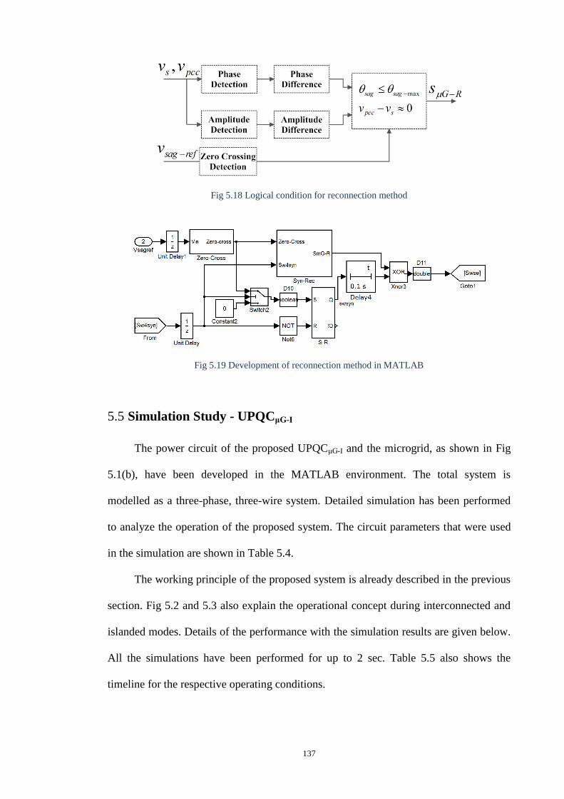
137
Fig 5.18 Logical condition for reconnection method
Fig 5.19 Development of reconnection method in MATLAB
5.5 Simulation Study - UPQCμG-I
The power circuit of the proposed UPQCμG-I and the microgrid, as shown in Fig
5.1(b), have been developed in the MATLAB environment. The total system is
modelled as a three-phase, three-wire system. Detailed simulation has been performed
to analyze the operation of the proposed system. The circuit parameters that were used
in the simulation are shown in Table 5.4.
The working principle of the proposed system is already described in the previous
section. Fig 5.2 and 5.3 also explain the operational concept during interconnected and
islanded modes. Details of the performance with the simulation results are given below.
All the simulations have been performed for up to 2 sec. Table 5.5 also shows the
timeline for the respective operating conditions.

138
Table 5.4 Overall network parameters for the simulation
Section Parameter Value / phase
Grid (3 phase) Voltage (rms) 230VL-N
Line Frequency 50Hz
Load (μGrid) Load current (max) 200A
Harmonic Current (max) 100A
UPQC DC link Voltage 600 V
Series Inductance 0.15 mH
Series Transformer 1:1
Switching frequency 10 kHz
Max Sag Compensation 100%
Shunt Inductance 0.42 mH
Hysteresis band 7.5 A
Switching frequency 16 kHz
Max Compensating Current 100 A
Table 5.5 Timeline of the Operating Conditions
The operating positions (0 for open and 1 for close) of the switches during the
operation are very important in detecting the islanded, synchronization, reconnection
and interconnected modes. These positions depend on the magnitude and time length of
Verror (as shown in Fig 5.14 and 5.15) and the Sw4syn switch (as shown in Fig 5.15).
Based on the algorithm for islanding detection and the reconnection method, Fig 5.20
shows the switch positions during the operation from 0 to 2 sec where both the
interconnected and islanded modes are observed. Fig 5.21 shows the performance of the
proposed UPQCµG for voltage sag compensation, as shown in Fig 5.21(a) and harmonic
current compensation, as shown in Fig 5.21(b) along with the islanding detection,
performance in islanded condition based on the Table 5.5 and Fig 5.20. Performance

139
during the reverse current flow due to the high penetration of DG is also shown by the
red circle in Fig 5.21(b). Details of the synchronization condition and reconnection
process are discussed in a later section. Performance of the proposed UPQCµG during
interconnected and islanded mode has been discussed below. Generally waveforms are
shown for phase A only.
Fig 5.20 Switching positions during the operation from 0 to 2 sec.

140
(a)
(b)
Fig 5.21 Complete performance of UPQCμG-I during interconnected and islanded mode, (a) voltage
waveform and (b) current waveforms at difference conditions and positions in the network.

141
5.5.1 Interconnected Mode
Depending on the power availability, the DG source can supply power to the load
and grid, and therefore by-directional power flow can occur. Hence, the performance of
the proposed UPQC should be observed in both cases. For a better understanding,
according to the direction of power flow, operation in the interconnected mode can be
divided into two parts: (i) forward-flow mode and (ii) reverse-flow mode.
5.5.1.1 Forward-flow mode
In this case, the available DG power is less than the required load demand.
Therefore, the utility grid supplies the rest of the power to the load which is not met by
the DG supply. Depending on the microgrid energy management and control strategy,
the DG storage system can be charged through utility and/or DG units. Fig 5.22 shows
the initial condition from 0.2 to 0.6 sec of the simulation study where the voltage sag
and interruption events occurs and are used to study the performance of the UPQC. Fig
5.22(a) shows the output waveforms of the voltage in different branches of the proposed
system, whereas current waveforms are shown in Fig 5.22(b). A 50% sag is applied at
0.3 sec, 90% at 0.5 sec and then at 1.2 sec the utility is disconnected. In general, the
APFse can also compensate the voltage distortion, created by the utility, at the PCC.
Therefore, this advantage can also be implemented in the series APF control part of the
proposed system. Fig 5.22(a) shows the performance of the series APF part of the
proposed UPQC in maintaining the constant and stable load voltage. Fig 5.22(b) shows
the performance of the shunt APF part in compensating the reactive and harmonic
current generated by the load. This compensation helps the UPQC system to maintain
the grid current THD level within the IEEE limit. As is mentioned in the timeline table,
the DG unit supplies 0.5Iloadf (half of load fundamental in current control mode) during
this time frame. Therefore the remainder of the current is supplied by the utility grid and
storage. During a 90% sag condition, the total power for the load demand is still met by

142
the µG system and the utility where the storage system provides the power for sag
compensation through the DC link.
(a)
(b) Fig 5.22 Performance of the proposed UPQCμG; a) series APF and b) shunt APF; from 0.2 to 0.6 sec
during interconnected and forward flow mode.
5.5.1.2 Reverse-flow mode
When the available DG power becomes higher than the required load demand, the
extra energy is transferred to the grid and storage and this is termed the reverse-flow
mode. At this stage, the grid current becomes out of phase with the grid voltage or the

143
voltage at the PCC. Fig 5.23 shows the performance of the UPQC when DG current
becomes 1.5 times of the load fundamental at 1.75 sec and a 30% sag is also applied at
1.85 sec.
(a)
(b) Fig 5.23 Performance of the proposed UPQCμG; a) series APF and b) shunt APF; during interconnected
and reverse flow mode.
In this case, the performance of the shunt APF remains the same even when the
utility current becomes out of phase, as shown by the red circle in Fig 5.23(b). Fig

144
5.23(a) shows that the series APF performs voltage sag compensation during the reverse
flow mode also.
5.5.2 Islanded Mode
It was mentioned earlier that a 90% sag compensation has been introduced at 0.5
sec of the simulation time period. According to the islanding detection method, the
series APF compensates the sag for up to 0.6 sec (30 cycles) and then the system goes
into islanded mode. A utility disconnection is applied at 1.11 sec just after completing
the 30 cycle count and then detecting the zero crossing of Vsag-ref where S1, S2 and S3
are opened. This is depicted in Fig 5.20 and 5.24. At disconnection, the system
immediately operates in an isolated microgrid condition. At this stage, if the available
DG power is lower than the load demand, the additional required power is supplied by
the storage. If the DG power is higher than the load, then the additional power goes to
the storage. The shunt APF still performs the compensation of reactive and harmonic
power. Therefore, DG converter does not need to be disconnected or change the control
strategy (supplying only the fundamental active power) to supply power to the load.
Fig 5.24 shows the performance of the proposed UPQC during 1.0 to 1.2 sec
where the islanding is detected just immediately after 1.1 sec at zero crossing detection.
The islanding mode is observed between 1.11 and 1.405 sec. During this period the
APFse is disconnected, as shown in Fig 5. 24(b) where Vsag = 0, utility current become
zero, as shown in Fig 5.24(c). The APFsh continues to operate, as shown in Fig 24(c),
and the load demand is met by the DG with the storage unit.

145
(a)
(b)
(c)
Fig 5.24 Performance of the proposed UPQCμG; (a) switching condition; b) series APF; c) shunt APF
during islanded mode.

146
5.5.3 Reconnection
One of the most important parts of the proposed UPQCµG is the reconnection
process. This has to occur without disconnecting the DG units or changing its control
strategy during isolated or grid connected μGrid/μGen operating conditions. Fig 5.25
shows the different signals for the reconnection process based on the algorithm and
developed method showed in Fig 5.18 and 5.19. To check the performance of the
reconnection process for the worst condition, the utility grid (Vs) is powered on at 1.405
sec where the magnitude is at a maximum, as shown by the red circle in Fig 5.26(a).
Immediately, the Sw4syn pulse is activated and the reconnection algorithm starts
generating active pulses as the phase and amplitude differences start to be within the
required limits. Zero crossing detection is also shown. The DG unit sends a
reconnection signal to the UPQC unit. Based on the logic given in Fig 5.19, the actual
switch S1 is activated at 1.43 sec and the Vsag starts operation, as shown by the red
circle in Fig 5.26(a). S2 and S3 are activated after the synchronization by the DG unit.
S4 is disconnected simultaneously at 1.44 sec. This simple algorithm with a combined
logic gate ensures the utility connects with the µGrid smoothly after the utility system is
restored.
Fig 5.26(a) shows that the series APF unit is immediately reactivated when the
grid voltage is available at 1.405 sec but it starts operation when the S2 and S3 switches
are closed at 1.43 sec. It is expected that, according to the smooth reclosing condition,
no power flow will occur at the point of reclosing. The switching is carried out
successfully within the limiting condition as shown in Fig 5.26(b). The circle at 1.43 sec
for Idg and Is in Fig 5.26(b) indicates the smooth transition from islanded to
interconnected mode. DG inverter also changes its control from voltage to current
control mode but only transfers the active fundamental current. The performance of the
APFsh is also uninterrupted during the transition period.

147
Fig 5.25 Condition of different signals for reconnection process based on Fig 5.19.
(a)
(b)
Fig 5.26 Performance of the proposed UPQC during reconnection, (a) series APF, (b) shunt APF

148
5.5.4 Power Flow
The power flow diagram is shown in Fig 5.27 for the complete simulation time
where the green line represent the active power (P) and red line (dash) for reactive and
harmonic power (QH). This also validates the operation and performance of the APFse
and APFsh part of the proposed UPQCµG-I along with the islanding detection and
reconnection.
Fig 5.27 Power flow during the simulation time

149
5.6 Simulation Study - UPQCμG-IR
The working principle of the proposed system is already described in the previous
section. Fig 5.2 and 5.3 also explain the operational concept during interconnected and
islanded mode. Details of the performance with the simulation results are given below.
All the simulations have been performed for up to 2 sec. Table 5.6 also shows the
timeline for the respective operating conditions.
It is to be noted that, operation-wise, the simulation and performance of the
UPQCµG-I and UPQCµG-IR are the same for the cases of forward flow, reverse flow
mode and up to the islanded condition with islanding detection. These are repeated here
for the UPQCµG-IR. The difference will be observed in the case of reconnection mode.
Table 5.6 Timeline of the Operating Conditions
The operating positions (0 for open and 1 for close) of the switches during the
operation are very important in detecting the islanded, synchronization, reconnection
and interconnected modes. These positions depend on the magnitude and time length of
Verror (as shown in Fig 5.14 and 5.15) and the Sw4syn, SμG-R switches (as shown in Fig
5.15, 5.17). Based on the algorithm for islanding detection and the reconnection
method, Fig 5.28 shows the switch positions during the operation from 0 to 2 sec where
both the interconnected and islanded modes are observed. Fig 5.29 shows the
performance of the proposed UPQC based on the Table 5.6 and Fig 5.28. A 40 degree
phase shift of the utility supply (Vs and Is) is applied during the reconnection process.

150
Though the voltage magnitudes at the utility and the PCC are the same, a voltage sag
appears due to the phase difference between them. Therefore, in that position the
proposed UPQCµG-IR reconnects the system starting with voltage sag compensation, as
shown in Fig 5.29(a). Reverse current flow also occurs (when the DG supplies more
than the required load fundamental) during the voltage sag compensation, as shown by
the circle in Fig 5.29(b). Details of the synchronization condition and the reconnection
process are discussed in a later section. Performance of the proposed UPQCµG during
interconnected and islanded mode has been discussed below. Generally waveforms are
shown for phase A only.
Fig 5.28 Switching positions during the operation from 0 to 2 sec.

151
(a)
(b) Fig 5.29 Complete performance of UPQCμG-I during interconnected and islanded mode, (a) voltage
waveform and (b) current waveforms at difference conditions and positions in the network.

152
5.6.1 Interconnection mode
Depending on the power availability, the DG source can supply power to the load
and grid, and therefore by-directional power flow can occur. Hence, the performance of
the proposed UPQC should be observed in both cases. For a better understanding,
according to the direction of power flow, operation in the interconnected mode can be
divided into two parts: (i) forward-flow mode and (ii) reverse-flow mode.
5.6.1.1 Forward-flow mode
In this case, the available DG power is less than the required load demand.
Therefore, the utility grid supplies the rest of the power to the load which is not met by
the DG supply. Depending on the microgrid energy management and control strategy,
the DG storage system can be charged through the utility and/or the DG units. Fig 5.30
shows the initial condition from 0.2 to 0.6 sec of the simulation study where the voltage
sag and interruption events occur and are used to study the performance of the UPQC.
Fig 5.30(a) shows the output waveforms of the voltage in different branches of the
proposed system, whereas the current waveforms are shown in Fig 5.30(b). A 50% sag
is applied at 0.3 sec, 90% at 0.5 sec and then at 1.2 sec the utility is disconnected. In
general, the series APF can also compensate the voltage distortion, created by the
utility, at the PCC. Therefore, this advantage can also be implemented in the series APF
control part of the proposed system. The other advantage of this configuration is that the
shunt APF can compensate the voltage distortion created by the DG converters. Fig
5.30(a) shows the performance of the series APF part of the proposed UPQC in
maintaining the constant and stable load voltage. Fig 5.30(b) shows the performance of
the shunt APF part in compensating the reactive and harmonic current generated by the
load. This compensation helps the UPQC system to maintain the grid current THD level
within the IEEE limit. As is mentioned in the timeline table, the DG unit supplies
0.5Iloadf (half of load fundamental in current control mode) during this time frame.

153
Therefore the remainder of the current is supplied by the utility grid and storage. During
a 90% sag condition, supply from the DG unit and the utility remains unchanged and
the storage system provides the power for sag compensation (through the DC link)
which is reflected in Fig 5.30(b).
(a)
(b)
Fig 5.30 Performance of the proposed UPQCμG; a) series APF and b) shunt APF; from 0.2 to 0.6 sec
during interconnected and forward flow mode.
5.6.1.2 Reverse-flow mode
At this stage, the grid current becomes out of phase with the grid voltage or the
voltage at the PCC. Fig 5.31 shows the performance of the UPQC when the DG current

154
becomes 1.5 times of the load fundamental at 1.75 sec and a 40% sag already exists
after reconnection at 1.41 sec. In this case, the performance of the shunt APF remains
the same even when the utility current becomes out of phase, as shown in Fig 5.31(b).
Fig 5.31(a) shows that the series APF performs voltage sag compensation during the
reverse flow mode also.
(a)
(b)
Fig 5.31 Performance of the proposed UPQCμG; a) series APF and b) shunt APF; during interconnected
and reverse flow mode.

155
5.6.2 Islanded Mode
It was mentioned earlier that a 90% sag compensation has been introduced at 0.5
sec. According to the islanding detection method, the series APF compensates the sag
for up to 0.6 sec (30 cycles) and then the system goes into islanding mode. A utility
disconnection is applied at 1.1 sec just after completing the 30 cycle count and then
detecting the zero crossing of Vsag-ref (at 1.11) where S2 and S3 are opened. This is
depicted in Fig 5.28 and 5.32(a). At disconnection, the system immediately operates in
an isolated microgrid condition. At this stage, if the available DG power is lower than
the load demand, the additional required power is supplied by the storage. If the DG
power is higher than the load, then the additional power goes to the storage. The shunt
APF still performs the compensation of reactive and harmonic power. Therefore, the
DG converter does not need to be disconnected or change the control strategy
(supplying only fundamental active power) to supply power to the load.
Fig 5.32 shows the performance of the proposed UPQC during 1.0 to 1.2 sec
where the islanding is detected just immediately after 1.1 sec at zero crossing detection.
The islanding mode is observed between 1.11 and 1.40 sec. During this period the series
APF is disconnected, as shown in Fig 5.32(c) where Vsag = 0, and the utility current
become zero, as shown in Fig 5.32(b). The shunt APF continues to operate, as shown in
Fig 5.32(b), and the load demand is met by the DG with the storage unit.
(a)

156
(b)
(c)
Fig 5.32 Performance of the proposed UPQCμG; a) switching condition, b) shunt APF and (c) series APF;
during islanded mode.
5.6.3 Reconnection
One of the most important parts of the proposed UPQCµG-IR is the reconnection
process. This has to occur without disconnecting the DG units or changing its current
control strategy during isolated or grid connected μGrid / μGen operating conditions.
Fig 5.33 shows the different signals for the reconnection process based on the algorithm

157
and developed method showed in Fig 5.18 and 5.19. To check the performance of the
reconnection process for the worse condition, the utility grid (Vs) is powered on at 1.40
sec with a 40 degree out of phase from the PCC. Immediately, the Sw4syn pulse is
activated and the reconnection algorithm starts generating active pulses as the phase and
amplitude differences are within the required limits. Zero crossing detection is also
shown. UPQC unit sends a reconnection signal to the DG unit. Based on the logic given
in Fig 5.19, the actual switch S2 and S3 are activated at 1.405 and 1.415 sec
respectively. This simple algorithm with a combined logic gate ensures the utility
connects with the µGrid smoothly after the utility system is restored.
Fig 5.34(a) shows that the series APF unit is immediately reactivated and starts
operation when the grid voltage is available and S3 is connected at 1.405 sec, as shown
by the circle in Vsag waveform. The power transfer starts when the S2 is closed at 1.415
sec, as shown in Fig 5.34(b). It is expected that, according to the smooth reclosing
condition, no power flow will occur at the point of reclosing. The switching is carried
out successfully within the limiting condition as shown in Fig 5.34(b). The circle at
1.415 sec for Idg and Is in Fig 5.34(b) indicates the smooth transition from islanded to
interconnected mode. The DG inverter also changes its control from voltage to current
control mode but only transfers active fundamental current. The performance of APFsh
is also uninterrupted during the transition period.

158
Fig 5.33 Condition of different signals for reconnection process based on Fig 5.19.
(a)
(b)
Fig 5.34 Performance of the proposed UPQC during reconnection, (a) series APF, (b) shunt APF

159
5.6.4 Power Flow
The power flow diagram is shown in Fig 5.35 for the complete simulation time
where the green line represents the active power (P) and red line (dash) for reactive and
harmonic power (QH). This also validates the operation and performance of the APFse
and APFsh part of the proposed UPQCµG-I along with the islanding detection and
reconnection.
Fig 5.35 Power flow during the simulation time
5.7 Hardware Results
Due to the limitations of hardware facilities as well as the existing real-time
simulators capabilities, real-time test of the proposed UPQCμG is performed partially.
The performance of the APFse and APFsh of the UPQCμG is obtained during
interconnected and islanded mode. All the tests are performed in SIL (software-in-loop)
configuration using hardware synchronized mode, as discussed in Chapter 1 (section
1.1.5). Details of the simulation and set up are given in Appendix 2.

160
5.7.1 Interconnected mode
Fig 5.36 shows the performance of APFse during the voltage sag (40%) condition
where are presented. The performance is obtained when the
APFsh is not working and the system is in a steady-state condition. For measurement,
the system is stepped down by 100, i.e., each division of the scope represents the value (
x 100) in the original system. For current, 1V = 100A.
(a) (b)
(c) (d)
(e) (f)
Fig 5.36 Performance of APFse ; (a, c, e) ; (b, d, f) when APFsh is off

161
Fig 5.36(a, c, e) shows the condition of utility voltage, current and load current
during voltage sag compensation in forward flow mode. Fig 5.36(b, d, f) shows the
voltage sag compensation during reverse flow mode where the utility current becomes
out of phase.
Fig 5.37 shows the dynamic response of the APFse for voltage sag (40%)
compensation. Fig 5.37(a) shows a complete response between the sag occurrence and
normal condition of the utility supply. Voltage at PCC is maintained constant. Fig
5.37(a) and (b) show the response of APFse during pre-sag and post-sag condition. This
performance is observed at forward flow condition, where . Similar
performance is obtained for the APFse in reverse flow condition where, .
The result is shown in Fig 5.38.
Although the APFse has been designed for 100% sag condition, due to the
hardware limitations and the capabilities available to the existing real-time simulator,
the performance of APFse was further obtained for 80% voltage sag compensation. The
results are shown in Fig 5.39 and 5.40. Fig 5.39 shows the performance during forward
flow condition, whereas Fig 5.40 shows the results in the reverse flow condition.
Fig 5.41 shows the performance in forward-reverse flow condition during a
voltage sag (80%) compensation. The performance is obtained with the dynamic change
of DG current ( ). From forward to reverse flow is created by increasing during
the sag compensation, as shown in Fig 5.41(b). Performance in reverse conditions is
also shown in Fig 5.41(c).
Fig 5.42 shows the performance of the APFsh in interconnected mode. In this case,
the values of APFsh are stepped down by 10. Fig 5.42(a) shows the harmonic current
compensation when the DG supply is zero. Fig 5.42(b) shows the performance in
forward flow mode whereas Fig 5.42(c) represents the results for reverse flow mode.

162
(a)
(b)
(c)
Fig 5.37 Performance of APFse in forward flow condition (a) compensating voltage sag (40%), (b) during
pre-sag and (c) post -sag condition

163
(a)
(b)
(c)
Fig 5.38 Performance of APFse in reverse flow condition (a) compensating voltage sag (40%), (b) during
pre-sag and (c) post -sag condition

164
(a)
(b)
(c)
Fig 5.39 Performance of APFse in forward flow condition (a) compensating voltage sag (80%), (b) during
pre-sag and (c) post -sag condition

165
(a)
(b)
(c)
Fig 5.40 Performance of APFse in reverse flow condition (a) compensating voltage sag (80%), (b) during
pre-sag and (c) post -sag condition

166
(a)
(b)
(c)
Fig 5.41 Performance of APFse in forward-reverse flow condition and compensating voltage sag (80%)
(a) dynamic change of (b) increasing: forward-reverse, (c) decreasing: reverse-forward flow

167
(a)
(b)
(c)
Fig 5.42 Performance of APFsh (a) during , (b) forward flow (c) reverse flow mode.

168
5.8 Conclusion
This chapter describes the working principle, operation and performance of the
proposed UPQCμG in the grid connected microgrid condition. The simulation has been
performed in MATLAB and the results show that the proposed system can compensate
the voltage disturbance at the PCC, the reactive and harmonic current compensation of
the load that could inject at the PCC during the interconnected mode. The DG current
does not have any effect in degrading the performance of the system in the
interconnected reverse-flow mode. During the islanded mode, the DG converter also
only supplies the active power to the load and the shunt APF performs the reactive and
harmonic power compensation. Therefore, the grid-tie DG converter does not need to be
disconnected or change its control strategy to keep the microgrid operating during the
islanding detection and operation in islanded mode. The proposed UPQCμG thus will
reduce the control complexity of the grid-tie converter and improve the power quality of
a grid connected μGrid or μGen system.

169
Chapter 6
Distributed UPQC (D-UPQC): A way to enhance
capacity and achieve flexibility
6.1 Introduction
In high power applications, the filtering task cannot be performed for the whole
spectrum of harmonics by using a single converter due to the limitations on switching
frequency and power rating of the semiconductor devices. Therefore, compensating the
reactive harmonic components to improve the power quality of the DG integrated
system as well as to avoid the large capacity centralised APF, has meant that parallel
operation of multiple low power APF units is increasing. Like APF, UPQC can also be
placed at the PCC or at a high voltage distribution line as a part of a DG integrated
network or in microgrid system to work both in interconnected or islanded mode.
The UPQC units developed so far for capacity expansion is mainly for medium or
high voltage distribution lines where both the current and voltage are high. Therefore, it
may be easier to use these multi-level or multi-modular type UPQC systems [59,60,176-
181]. But these configurations may not be suitable for low voltage distribution lines
where the 3-phase voltage (typically 400VL-L) is low, but the required compensating
current is comparatively high (100A or more). In that case, multi-level or module type
series APF may not be required. But for high current compensation, multiple Shunt APF
units in a distributed (parallel) mode and connected with a common dc linked capacitor
can be a solution in developing a Distributed UPQC (D-UPQC).

170
This chapter deals with the following sections. Limitations of the centralised
system and the advantages of distributed approach are discussed in section 6.2. Section
6.3 describes the review of the UPQC capacity enhancement techniques. The new
proposal of capacity enhancement, D-UPQC, is described in Section 6.4. Section 6.5
deals with the simulation study and real-time performance of the proposed system and
the conclusions are made in Section 6.6.
6.2 Centralised and Distributed Systems
6.2.1 Limitations of centralized system (APF)
One large unit is required to compensate the reactive and harmonic power
arising from all critical loads rather than the specified loads.
Impractical for some applications because of its high initial cost,
Difficulties in installation due to large size and weight
Single-point-of-failure reduces its reliability.
High relative cost for achieving redundancy and increasing the capacity with
expansion of the load.
6.2.2 Distributed/Multi-unit parallel approach
In a distributed approach, many separate APF units operate in parallel. APF
units are placed flexibly in the system to form a critical network.
Highly reliable because of redundancy and also easy to achieve this redundancy
Highly flexible and easy to increase the capacity when the load increases
User-friendly in terms of maintenance

171
6.3 Capacity enhancement techniques
At this place, capacity enhancement is achieved by using Multi-level/module
topologies to reach the higher power levels. These options are as follows:
i. Multi-level converter based UPQC
ii. Multi-module converter based UPQC
iii. Multi-module (power cell) unit based UPQC
A multi-level converter is proposed to increase the converter operation voltage,
avoiding the series connection of switching elements. However, the multilevel converter
is complex to form the output voltage and requires an excessive number of back-
connection diodes or flying capacitors [59] or cascade converters [176]. A basic form of
a multi-level UPQC is shown in Fig 6.1.
A multi-module H-bridge UPQC can also be connected to the distribution system
without series injection transformers. It has the flexibility in expanding the operation
voltage by increasing the number of H-bridge modules [177], as shown in Fig 6.2. Here
each phase consists of several pairs of H-bridge modules isolated through a single-phase
multi-winding transformer.
These Multi-module techniques [59,60,176-179] allow the symmetrical
distribution of the load power among the components of the topology, but the classical
design procedure must be modified or refined to ensure the power cell components
should be within its maximum ratings. Therefore, a new design procedure of UPQC
with a feature of extending capacity based on a modular approach is presented in
[180,181], shown in Fig 6.3, where H-bridge power cells are added in each single phase
arrangement depending on the required compensating power. Some advantages and
disadvantages are also outlined in Table 6.1.

172
Fig 6.1 Multi-level Converter based UPQC
Fig 6.2 Series transformer-less Multi-module H-bridge
Fig 6.3 Modular approach of UPQC based on power cells

173
Table 6.1Advantages and disadvantages of different capacity enhancement techniques
Type of UPQC Advantages Disadvantages
Multi-level
Converter based
i. High voltage and current can be
achieved
ii. Can be developed in different
ways – diode clamp / flying
capacitor / cascade inverter based
i. Voltage unbalance could occur between the
different levels
ii. Requires excessive number of diode /
flying capacitor / inverter
iii. Central control is required and it is
complicated
iv. Conduction loss is high
v. Capacity expansion is difficult
vi. Centralized approach
Multi-modular
transformer-less
i. No series transformer is required,
thus reduces the cost
ii. Capacity expansion is easier than
multi-level converter
iii. Redundancy is possible
i. It requires high number of switching
devices to enhance the capacity
ii. Central control is required
iii. Conduction loss and switching loss also
high
iv. Due to symmetrical distribution of the load
power among the H-bridge inverters, modules
may not work at its maximum rating
Multi-modular
(power cell)
i. power cell topology helps the unit
to work at its maximum rating
ii. Capacity expansion is easier
iii. Redundancy is possible
iv. Central and distributed controls
are possible
v. Conduction loss can be reduced
i. Number of H-bridge switching device
increases, thus increase the switching loss
ii. Transformer for each shunt part of the
power cell could increase the loss as well as
make the system bulky
iii. Additional single shunt unit may not be
included if compensating current increases
6.4 Distributed - UPQC (D-UPQC)
Capacity enhancement of UPQC can be achieved using multi-level or multi-
module and central control mode. However, the flexibility of the UPQC to increase its
capacity in future and to cope up with the increased load demand at a low voltage
distribution level has not been achieved. Fig 6.4 shows the proposed configuration of a
modular D-UPQC where a single unit of series APFse and multiple units of shunt APFsh
are placed in a distributed approach. The connection between the series and shunt part
of the UPQC is maintained through a DC link capacitor.
The main advantage of the proposed system is that the APFsh units can be
controlled to compensate (i) the reactive and harmonic current individually according to
their capacity, or (ii) the combined reactive and harmonic current can be shared among
the APFsh units. Therefore, the installed APFsh units can be switched on or the

174
additional APFsh units can be integrated into the D-UPQC system according to the
requirement of the compensating current. Thus the capacity enhancement and flexibility
of the proposed UPQC operation can be achieved. It is to be noted that, for any system,
there is a limit up to which the capacity enhancement is possible. For the proposed D-
UPQC, the capacity enhancement limit and the possible flexibility have been described
in the design issues in section 6.4.1.
Fig 6.4 Configuration of the proposed Distributed UPQC (D-UPQC)
6.4.1 Design Issues
Fig 6.5 shows the working diagram of the proposed modular D-UPQC with
electrical network and Fig 6.6 shows the equivalent electrical circuit of the system
assuming that the reactive part of the load current will be compensated by the APFsh1
and the harmonic part will be equally divided and compensated by the rest of the APFsh
units. Here f, p, q and h represent the fundamental, active, reactive and harmonic part of
the respective parameters. Fig 6.7 shows the tetrahedron diagram of the load current and
it also reflects the amount and components of the load current that will be compensated
by the APFsh units of the proposed D-UPQC. Thus the source will provide the active
fundamental part of the load current in phase with the voltage to maintain the unity
power factor at the PCC and the THDIpcc will be kept within the IEEE limit.

175
Fig 6.5 Working diagram of the D-UPQC with an electrical network
Fig 6.6 Equivalent electrical circuit of the system shown in Fig 7.5
Fig 6.7 Tetrahedron diagram of the load current and the compensating part of the APFsh units
The integration of APFsh as a part of the possible capacity enhancement and
achievable flexibility in operation of D-UPQC is mainly dependent on the rating of

176
APFse or the size of the series transformer. Therefore the design issues related to the
APFse and APFsh are discussed below.
6.4.1.1 APFse
Rating selection procedure of the APFse was already discussed in section 5.3.2 for
a UPQC when it is integrated to a DG connected microgrid system. In general, the full
load current flows through the series transformer of the APFse when APFsh is inactive.
As the APFsh units compensate the reactive and harmonic part of the load current,, the
minimum current rating of the APFse should be equal to the load active fundamental
current (5.9), as shown in Fig 6.8. The voltage rating of the APFse should be equal to the
highest value of the injected sag voltage (5.11). If k is the fraction of Vs that will appear
as a voltage sag, then the required source current that will be transferred through the
series transformer of the APFse (shown in Fig 5.6 and Fig 6.9) can be calculated as
(5.15). This source current will be the current rating of APFse to compensate the k
amount of voltage sag. Therefore,
(6.1)
(6.2)
The current carrying capacity of the series transformer will be;
(6.3)
where represents the amount of fundamental current that is required to maintain the
operation of the UPQC. It is reflected as a in the control method. Therefore, this
will be the maximum rating for the APFse as shown in Fig 6.9. It also indicates
the maximum limit of the active fundamental component of the load current that can be
used in the network followed by the UPQC.
The sag compensation strategy by can create an additional VA loading effect on
the APFsh control also [61]. This can be minimized by introducing a direct link between

177
the DC capacitor and the storage system (if the proposed D-UPQC is placed in a μGrid
system), as discussed in 5.3.
Fig 6.8 Compensating capacity of APFsh for the D-UPQC when Vsag = 0;
Fig 6.9 Compensating capacity of APFsh for the D-UPQC when Vsag = kVs

178
6.4.1.2 APFsh
According to the tetrahedron diagram of the load current shown in Fig 6.7.
; here, and
; here, and
In stable operating conditions, when no voltage sag appears in the network, the
APFsh units compensate the reactive and harmonic parts of the load current. According
to Fig 6.7, the load current is composed of active, reactive and harmonic components.
The source supplies the active load fundamental ( ) and through the
series transformer. Both the source and APFse do not deal with the reactive and
harmonic part of the load. Therefore, and are not directly related to the
selection of maximum current rating of the APFsh ( and ). The size of
the series transformer actually imposes the limit of maximum that can be used for
the operation of UPQC. The possible maximum can be found from (6.3) as;
while
Again, the depends on the rating of APFsh and can be related as;
; where is a fraction of
Therefore, the possible to integrate in the UPQC system and to compensate
the reactive and harmonic components of the load current ( ), as
shown in the Fig 6.8 can be written as;
; while (6.4)
This rating can further be increased when the UPQC will have the capacity of voltage
sag compensation, as shown in Fig 6.9.

179
The flexibility can be achieved by integrating multiple APFsh units in the
proposed D-UPQC system. Depending upon the control strategy, the APFsh units can be
switched on and off to compensate the required current up to the maximum level. By
turning off the additional APFsh units, the modular D-UPQC can avail of lower
switching losses and retain high efficiency performance when the load VAR demands
are low. For example, as shown in Fig 6.10, the load has been changed from to
(where ; ; and ). Then, if the rating of
APFsh1 ( ) is smaller than the , APFsh2 will be switched on. Similar approachs
can be implemented for the harmonic current compensation separately or in
combination with reactive compensation. These are mainly dependent on the
implemented control strategy. Thus instead of design of a normal single unit UPQC, the
proposed modular D-UPQC can be designed to maximize the efficiency. It will also
work with a higher performance and reduced power loss.
Fig 6.10 Compensating strategy of APFsh units for the D-UPQC
180
Therefore, in the case of a D-UPQC system, the current rating of the APFsh units
can be found as;
(6.5)
While,
(6.6)
While,
6.4.1.3 DC link Capacitor
In general, the energy handling capacity determines the size of the capacitor. The
basics for the selection of capacitor size has already been described in sections 2.2.3.5
and 5.3.3. The size of the capacitor will increase when (i) the number of APFsh units (or
the reactive and harmonic current compensation capacity) increases and/or (ii) the
required voltage sag compensation capacity is increased. If the proposed D-UPQC is
placed in a DG connected μGrid network, the storage system of the μGrid can be
connected directly to the DC link as discussed in 5.3.3. This will also reduce the control
complexity of the UPQC.
6.4.2 Control issues
Like UPQC, the proposed D-UPQC also ha controllers for the APFse and APFsh
units. The control of APFse is the same as the normal UPQC and has already been
discussed in 2.5.2 and 5.3.2. The control strategy for multiple parallel APF units has
also been described in 4.6. For most of the control methods the APF units are controlled
with a separate DC link capacitor. In the proposed D-UPQC, due to the DC link
between the APFsh units, a circulating current (CC) could flow among the filter units.
Control of this flow can be part of the control of multiple APFsh units with a common
DC link. Therefore, the following sections will be discussed (i) the derivation model for

181
circulating current flow, (ii) the control issues for the circulating current flow, (ii) the
selection of control method for APFsh units and (iv) the control of switches.
6.4.2.1 Model for circulating current (CC) flow
The working principle of an APF unit in parallel (shunt) to the load to compensate
the reactive and harmonic current has already been discussed in section 2.2.1.
Depending upon the switching condition, there are two possible modes of operation:
capacitive mode (where the current flows from the capacitor) and inductive mode (the
current flows towards the capacitor). During compensation, each APF unit completes
one capacitive and one inductive mode of operation in a single switching cycle. When
multiple APF units work in a current sharing mode, there could be four possible modes
of operation: (i) capacitive-capacitive, (ii) inductive-inductive, (iii) capacitive-inductive
and (iv) inductive-capacitive. As an example, Fig 6.11 shows a single line diagram of a
3-phase system where 2 APF units with a common dc link are working together in
parallel operation mode. Here, represents the circulating current flow between the
APF units. It is to be noted that, in the case of a 3-phase system this circulating current
flow exists as a zero sequence harmonics in the zero sequence current flow when a
circulating loop is created within the APFsh units and hence it is termed zero sequence
circualting current (ZSCC) flow. In general these harmonics are (3+n*6) order, where n
= 0, 1, 2 ....
Fig 6.11 Single line diagram of a 3ph 2 units APFsh with common DC-link presenting CC flow

182
For simplicity, derivation of CC flow has been carried out on a per phase a basis.
Fig 6.12 shows the possible mode of operation between the APF units (1 phase) where
sh-i and sh-c represent the corresponding inductive and capacitive mode respectively.
From Fig 6.12 (a and b), during the capacitive mode, the current flow can be obtained
as;
while ; here is
the ducy cycle, i.e, the 2 APF ac voltages are equal.
Similarly, Fig 6.12 (c and d) shows that when both the APF units work in
inductive mode during its switching cycle, the resulting current flows can be found as;
while ;
If there is a differnce in any of the parameters, such as switching frequency,
current sharing, interfacing inductor, hysteresis band (in case of hysteresis current
controller) then the APF units can operate in inductive-capacitive or capacitive-
inductive mode. In these cases, CC will flow and these are reflected in Fig 6.12 (e - h).
From Fig 6.12(e and f), the circulating current flow in capacitive-inductive mode can be
obtained as;
; while
Similarly, the circulating current flow for inductive-capacitive mode is;
; while
Therefore, in general, the equation for the CC flow can be written as;
(6.7)
where for capacitive mode and for inductive mode.

183
Fig 6.12 Possible mode of operation between two APF units to calculate circulating current
The possible maximum value for CC can be obtained as;
(6.8)
For 3-phase system, the ZSCC can be found as;
(6.9)
where and are the zero sequence component of the APFsh units.

184
This is also confirmed in [182] for shunt APF topology analysis based on a parallel
interleaved inverter. It is also similar to the rectifier analysis in [90].
In most of the research articles, derivation or CC cancellation has been carried out
for two inverters or APF units [90, 104, 182, 183]. But none of these discuss the cases
when more than 2 APF/inverter units are integrated. Based on the previous analysis, it
can be shown that if more than 2 APF units are connected in parallel then the additional
units will work in either capacitive or inductive mode also and will be parallel to any of
the other units as shown in Fig 6.13. In these cases additional circulating current flow
loops will form. The CC flow for these loops can also be derived in similar way as
found in (6.7).
Moreover, the control methods discussed in the literature are mainly for PWM
based control system. None of them discuss the CC flow issues for the parallel
operation of APFs based on hysteresis control. Therefore, an attempt has been made
here to discuss the issues related to hysteresis control.
Fig 6.13 Circulating current flow when 3 APF units work in parallel

185
6.4.2.2 Control issues for the circulating current (CC) flow
There are mainly two ways to eliminate or reduce the CC flow: (i) breaking the
route of CC flow by introducing physical devices such as an isolation transformer or
common mode inductor or (ii) by proper control methods. These are reviewed in section
4.2. From the derivation of CC flow it is found that the CC value depends on (i) the
duty cycle ( ) or switching frequency ( ), DC link voltage ( ) and the interfacing
inductor ( ) of the APF units. Therefore, before going to select the control method for
multiple APFsh units with a common dc link, some design consideration should be made
to reduce the CC flow. The design options that can be implemented to reduce the CC
flow are;
i. Decrease the : According to the design criteria of single/3-phase APFsh system
there is a minimum value of that has to be maintained to compensate the reactive
and harmonic current.
ii. As the
, reduce the and decreasing the difference between the or
will reduce CC flow.
iii. Reduced will further increase the (in the case of hysteresis current control)
and it will then in turn reduce the circulating current flow. But increased will reduce
the VAR rating of APFsh.
It is also clear from the derivation that the CC flow does not directly depend on
the compensating current rating of the APFsh units. Therefore, once the current or VAR
rating of APFsh is fixed, the design components ( and ) should be chosen in such
a way so that the is possibly high and the difference between the APFsh units are
as low as possible. In that case, introducing the common mode inductor in the APFsh
units can be a better choice. Implementation of a CC control method in the APFsh
control strategy will further reduce the CC flow. But it will then increase the control
complexity.

186
6.4.2.3 Selection of control method for APFsh units
With the control issues of the CC flow in mind, selection of a control strategy for
the APFsh units should be made. Different control strategies for parallel operation of
multiple APF units were reviewed in section 4.6. In general, control can be based on
active current sharing where the compensating power/current can be divided equally or
up to the compensating capacity of the APF units. Another prominent control is droop
control where information exchange between the APF units is required. For simplicity,
a current sharing (power splitting) method based on hysteresis current control has been
chosen for the remainder of the analysis.
6.4.2.4 Control of switches
The control of switches mainly depends on the control method for the APF units.
In the case of the current sharing method, the switching can be determined by current
sharing (equally distributed) or a capacity limitation technique. As for example, if ,
, and are the rms values of APF compensating current,
reference compensating current, rated current and the switching reference current for
ON/OFF condition, then,
for thecurrent sharing technique where
and
for the capacity limitation technique
6.4.3 Simulation Study
An electrical power system including D-UPQC, as shown in Fig 6.5, has been
modelled in MATLAB using RT-LAB (real-time simulation) tools to observe the
performance in the real-time environment. Within the available facilities, the proposed
system is then partially tested in SIL with the hardware synchronization mode which is
similar to hardware-in-loop (HIL) test.

187
In depth information on parallel operation of multiple APFsh based on hysteresis
current controller is not available yet, specially in the case of CC flow. Therefore, in the
present work, the objective is to reduce the CC flow based on the design options
mentioned in 6.4.2.2. Two units of APFsh have been modelled here to operate in power
sharing mode. In terms of sharing following proportions have been chosen:
(A) and ; each APFsh compensates
half of the load reactive and harmonic components.
(B) and ;
(C) ; and
(D) ; and
In the case of a hysteresis current control based APFsh, according to the selection
of design parameters for APFsh, described in 2.2.3 and the control issues of CC flow, the
CC flow can be reduced by the proper selection of the design components including ,
, h and . As the is fixed, variation of other components has been made here to
analyze the reduction of CC flow. Results and discussion are given below.
Table 6.2 shows the parameters that have been considered for the proportion A.
Corresponding results have been given in Fig 6.14 and discussed below.
Table 6.2 A: and
Frequency
(kHz)
Cases
/
(mH)
h1 / h2
(A)
THD@Ipcc
(%)
A1 0.625 / 0.625 5 / 5 2.57
A2 1.25 / 1.25 2.5 / 2.5 2.02
A3 1.25 / 0.625 2.5 / 5 1.74
A4 1.25 / 1.25 2.5 / 3.75 1.67
A5 1.25 / 1.875 2.5 / 2.5 2.35
A6 1.67 / 0.625 2.5 / 5 2.88
A7 1.67 / 1.25 2.5 / 3.75 2.82
A8 1.67 / 1.875 2.5 / 2.5 3.76

188
(A1a) (A1b)
(A2a) (A2b)
(A3a) (A3b)
(A4a) (A4b)

189
(A5a) (A5b)
Fig 6.14 Performance of APFsh for the cases (A1 - A5) and the corresponding CC flow
Fig 6.14 shows the performance study of the two APFsh units in power sharing
mode for the cases (A1 - A5) where each of the units compensates half of the load
reactive and harmonic components. For the cases (A1-A3), the switching frequency of
both units was equal and the variations have been made for . Cases A1 and
A2 show that the possible CC flow can be zero when , i.e,
both the APFsh units are identical. Although the rating and of each unit are the same,
ZSCC can flow as shown in case A3. This happens due to the difference in design
parameters and h. Cases A4 and A5 shows the results for different .
For both the cases, ZSCC flows. A comparison with A3, A4 and A5, A5 shows better
results in the reduction of ZSCC flow. It is due to the higher values of and lower
values of h, though the parameter is different.
Table 6.3 shows the parameters that have been considered for the proportion B.
Corresponding results have been given in Fig 6.15 and discussed below.
Table 6.3 B: and
Frequency
(kHz)
Cases
/
(mH)
H1 / h2
(A)
THD@Ipcc
(%)
B1 0.835 / 2.5 3.75 / 1.25 1.74
B2 0.418 / 1.25 7.5 / 2.5 1.81
B3 0.835 / 1.25 3.75 / 2.5 2.25
B4 0.835 / 1.87 3.75 / 2.5 2.25
B5 0.835 / 3.74 3.75 / 1.25 2.33

190
(B1a) (B1b)
(B2a) (B2b)
(B3a) (B3b)
(B4a) (B4b)

191
(B5a) (B5b)
Fig 6.15 Performance of APFsh for the cases (B1 - B5) and the corresponding CC flow
Fig 6.15 shows that for all the cases, ZSCC flows. Even though the values are
different, the reduced ZSCC flow occurs in the case of B5 where the values for are
high and h are low compare to other cases. The worse case occurs for B2 where is
low and h is high.
Tables 6.4 and 6.5 show the parameters for the cases C and D where the sharing
proportion is different than that for A and B. For both the cases, values of are kept
low wheres the values for h are high. In both cases, are the same. And the same
components has been chosen for D where the compensating current is two times higher
than that of case C.
Table 6.4 C: ; and
Frequency
(kHz)
Cases
/
(mH)
H1 / h2
(A)
THD@Ipcc
(%)
C1 0.625 / 0.625 5 / 5 2.65
Table 6.5 D: ; and
Frequency
(kHz)
Cases
/
(mH)
H1 / h2
(A)
THD@Ipcc
(%)
D1 0.625 / 0.625 5 / 5 2.12

192
Fig 6.16 shows the performances for the cases of C and D in terms of ZSCC flow.
In both cases, ZSCC flow is the same even though for case D, APFsh units are
compensating higher current than that of C. These results indicate that the ZSCC flow
does not depends on the amount of compensating current. These ZSCC flows are higher
than that for A and B and this is due to the lower values of .
(C1) (D1) Fig 6.16 CC flow for the cases C and D
Finally, a comparison has been made for the ZSCC between the (A3 - A5) and
(A6 - A8) cases, as shown in Fig 6.17. For A3, the is the same for both APFsh units,
whereas for A4 and A5 it is different. But the values of are comparatively higher for
A5. Therefore, within A3 to A5, the ZSCC flow is comparatively lower in the case of
A5, as shown in Fig 6.17(a).
For the cases A6 - A8, the switching frequency ( ) of APFsh1 is reduced and
therefore the value of increases. At the same time, the frequency difference between
APFsh units are also reduced. The performance of the D-UPQC in terms of ZSCC flow
for these cases is reflected in Fig 6.17(b). This shows that ZSCC flow can further be
reduced by reducing the (to increase the value of ) and the difference between
the of the APFsh units. The reduction of zero sequence harmonics content for the
cases (A6 - A8) are also shown in Fig 6.18 where it shows that the magnitude of zero

193
sequence harmonics is reduced gradually for the cases from A6 to A8. This also
confirms the outcome as shown in Fig 6.17.
(a)
(b)
Fig 6.17 ZSCC comparison between the cases for (a) A3, A4, A5 and for (b) A6, A7, A8
But it also has to be kept in mind that increasing could increase the active power
loss of the APFsh units (as discussed in Chapter 2, section 2.6) as well as increase the
THD at the PCC, as given in Table 6.2. Therefore, in terms of design criteria for the
selection of APFsh units to place in a D-UPQC system, one should consider the higher
values of and lower the difference between of the APFsh units with care about
THD.

194
(a)
(b)
(c)
Fig 6.18 FFT analysis for the cases (a) A6, (b) A7 and (c) A8.
195
6.4.4 Hardware Results
Real-time tests have been performed for some of the analysis in SIL configuration
(hardware synchronization mode). Fig 6.19 shows the results for the cases A6, A7 and
A8 where both the APFsh units are compensating harmonic current in a power sharing
mode. The waveform of the utility current ( ) contains fewer harmonics for A7
compared to A6 and A8. This happens because of the moderate value of and h for
A7 compared to that of A6 ( is too low) and A8 ( is too high). Therefore, the
THD value is also reduced.
For the case of A8, although the THD increases, ZSCC is reduced. Fig 6.20 shows
the ZSCC flow for these (A6 - A8) cases and it clearly depicts the gradual reduction of
ZSCC from A6 to A8. It is also clear from Fig 6.20 that a considerable amount of ZSCC
can be reduced by proper selection of design parameters for the APFsh units to operate
in load sharing mode. Thus it validates the simulation, analysis of the performance and
ZSCC flow study.
6.5 Conclusion
Capacity enhancement and operation flexibility are two of the important
limitations of the centralized UPQC unit when placed in a DG integrated network,
especially in the low voltage distribution level where the compensating current could be
high. Therefore, a proposal has been made here to develop the modular based
Distributed UPQC (D-UPQC) where multiple APFsh units can operate in parallel. This
can be controlled in an active load sharing mode (inter-communication is required) or in
droop control mode. The most important part is common the DC link between the APF
units. Therefore, a circulating current could flow. In the case of a hysteresis current
controller based multiple APFsh units in load sharing mode, this CC control is not yet
achieved. One of the difficulties of this CC flow control or reduction is the variable

196
switching frequency of the APFsh units. By proper selection of design parameters, this
CC flow can be reduced in an acceptable level.
(a)
(b)
(c)
Fig 6.19 Performance of APFsh units in D-UPQC for the cases (a) A6, (b) A7 and (c) A8
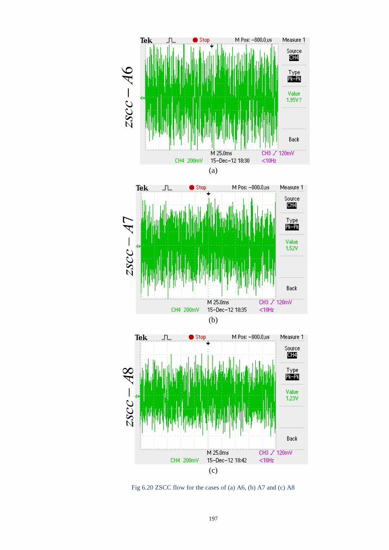
197
(a)
(b)
(c)
Fig 6.20 ZSCC flow for the cases of (a) A6, (b) A7 and (c) A8

198
Chapter 7
Conclusions and Future Work
7.1 Conclusions
The main objective of this research was to investigate the (i) placement (ii)
integration (iii) capacity enhancement and (iv) real time control of the Unified Power
Quality Conditioner (UPQC) to improve the power quality (PQ) of a distributed
generation (DG) network connected to the grid or microgrid. The following
developments have been achieved through this PhD research.
With the increased penetration of small scale renewable energy sources in the
electrical distribution network, maintaining or improvement of power quality has
become more critical than ever where the level of voltage and current harmonics or
disturbances can vary widely. For this reason, Custom Power Devices (CPDs) such as
the Unified Power Quality Conditioner (UPQC) can be the most appropriate solution for
the dynamic performances of the distribution network, where prior knowledge of
disturbances may not be accurately known. The UPQC is introduced at the PCC (a) to
prevent propagation of the current harmonics generated by the non-linear loads into the
grid, (b) to maintain the voltage and current THD at the PCC within the IEEE and IEC
limits and (c) compensate the grid voltage sag/swell to provide a balanced and stable
voltage at the PCC. In the presence of DG sources and the UPQC in an active
distribution network, (A) the placement of UPQC and its sensors in the network, (B) its
impact on the control method to perform the specified task, (C) its performance with bi-

199
directional power flow in the network and (D) the advantages of DG inverter in the
presence of UPQC issues have been analysed. Depending on the location and
integration technique of DG sources, the proper placement of UPQC has been identified
in the DG integrated grid connected microgrid network together with the feedback
sensors to cope with the bidirectional power flow without compromising the power
quality controlling features.
A new integration method of UPQC has been developed that can help the DGs
to deliver quality power in the case of islanding. It can also help to reintegrate with the
grid seamlessly post fault. In the proposed new integration method, the DG Inverter
(with or without storage) and the load and shunt part of the UPQC have been placed at
or after the PCC and in parallel to the grid. The series part of the UPQC have been
placed before the PCC and in series with the grid. Islanding detection and reconnection
techniques together with the associated control have been introduced to the existing
UPQC. Hence, this configuration is termed UPQCG. The control function has been
performed with a hierarchical approach. The control method for islanding detection and
reconnection is placed in the secondary level. Thus the additional control part can be
placed in a conventional UPQC to improve its performance to a UPQCG. The
advantages of the proposed UPQCG configuration and associated integration system
over the normal UPQC are to compensate voltage interruptions in addition to voltage
sags/swells, and harmonic and reactive power compensation in the interconnected
mode. The DG Inverter with storage then supplies the active fundamental power only
and the shunt part of the UPQC compensates the reactive and harmonic power of the
load in islanding mode. Therefore, the integrated system works both in interconnected
and islanded mode. The other advantage is that the DG Inverter is not required to be
disconnected during islanded mode and hence the islanding detection and reconnection
need no longer be a part of the inverter. In all conditions, DG Inverter only provides the
200
active power to the load and grid. Thus it reduces the control complexity of the DG
inverter as well as improving the PQ of the microgrid.
In the case of high power applications in low voltage distribution levels, the
filtering task cannot be performed for the whole spectrum of harmonics by using a
single converter due to the limitations on switching frequency and power rating of the
semiconductor devices. The relative power loss of the APF unit is also high. Therefore,
compensating the reactive harmonic components to improve the power quality of the
DG integrated system as well as to avoid the large capacity centralised APF, parallel
operation of multiple low power APF units in modular and distributed way are
desirable. A novel method of capacity enhancement along with the operational
flexibility of the UPQC in distribution level has been proposed, providing modularity
and redundancy for better efficiency and reliability. This is termed Distributed-UPQC
(D-UPQC). Here, multiple Shunt APF units in distributed (parallel) mode have been
placed and connected with a common dc linked capacitor. In that case, the issue of
circulating current flow arises. Control or reduction of circulating current flow in the
case of hysteresis current control, where switching frequency varies, may be
complicated. This flow can be reduced by proper selection of design parameters.
Therefore, the design issues have been discussed here.
As a part of design and capacity enhancement, detailed switching dynamics with
a parameter selection procedure of shunt APF units has been studied. Power flow
between the shunt APF unit and the PCC has been derived and equations for reactive
and harmonic current compensation capacity has been acquired. Active power loss
associated with the design parameters has also been analyzed as a rating requirement of
the shunt APF unit. In the case of hysteresis control with multiple APF units, the design
issues have been discussed for the proper selection of design parameters to reduce the
circulating current flow.

201
Implementation of the proposed integration and capacity enhancement methods,
and the modification in design with an advanced and real time control strategy have
been developed. The performance of the proposed UPQC (UPQCµG and D-UPQC) in an
active DG integrated microgird network has been studied. The distribution network has
been developed by RT-LAB tools and the whole system has been tested in real-time
simulation in SIL configuration with a hardware synchronization mode from the OPAL-
RT real time environment.
7.2 Future works
There are several important points which need to be investigated but could not be
included in the scope of this research work. Thus, during this research, the following
issues have been identified as possible topics of work in future in this area:
1. This research can be extended to investigate the case of 3-phase, 4-wire systems.
2. The proposed integration technique of UPQCµG along with the control of islanding
detection and reconnection techniques can be tested with real controllable hardware
switches as a validation of their effectiveness in the next step.
3. A control method should be developed to reduce the circulating current flow in D-
UPQC system based on hysteresis current control.
4. A droop control method can be developed for reactive and harmonic current
compensation for implementation in a D-UPQC system. The independent operation of a
droop control based APFsh can further increase the operational flexibility of the
proposed D-UPQC.
5. The proposed D-UPQC can be integrated as D-UPQCµG to check the performance of
the system in DG integrated microgrid system.

202
References
[1] S Chowdhury, S P Chowdhury and P Crossley , Microgrids and Active Distribution
Networks, 1st Edition, IET, UK, 2009
[2] S M Halpin, L L Grigsby, The Electric Power Engineering Handbook, CRC Press, 2001
[3] C Sankaran, Power Quality, CRC Press, 2002
[4] R D Henderson, P J Rose, Harmonics: The Effects On Power Quality And Transformers,
IEEE Trans Industry Appl, vol 30(3), 1994, pp 528 - 532
[5] IEEE Std 519-1992, IEEE Recommended Practices and Requirements for Harmonic Control
in Electrical Power Systems, 1992
[6] International Electrotechnical Vocabulary (IEV) – Chapter 121: Electromagnetism, IEC 600
50-121 Std., Available: http://www.electropedia.org.
[7] C Marshman, M Tyndall, EMC and EMF Regulatory Issues for the Power Industry, CIRED,
2009
[8] IEEE 1547, IEEE Standard for Interconnecting Distributed Resources with Electric Power
Systems, 2003
[9] G Chicco, J Schlabbach, F Spertino, Experimental assessment of the waveform distortion in
grid-connected photovoltaic installations, Solar Energy, vol. 83, 2009, pp 1026–1039
[10] J D Mondol, Y Yohanis, M Smyth, B Norton, Long term performance analysis of a grid
connected photovoltaic system in Northern Ireland, ECM, 2006, vol. 47, pp. 2925–2947
[11] H Fechner, R Bründlinger, B Bletterie, Power quality and safety aspects for grid
connection of Photovoltaic Systems, 2005,
http://www.arsenal.ac.at/downloads/Publikationen/2005/Power Quality and Safety Aspects.pdf
[12] F Blaabjerg, Z Chen, S B Kjaer, Power Electronics as Efficient Interface in Dispersed
Power Generation Systems, IEEE Trans. on PE, 2004, Vol. 19(4), pp 184 – 1194
[13] R Teodorescu, F Blaabjerg M Liserre, U Borup, A New Control Structure for Grid-
Connected PV Inverters with Zero Steady- State Error and Selective Harmonic Compensation,
IEEE PESC 2004, pp 1742 – 1747
[14] X Yuan, W Merk, H Stemmler, J Allmeling, Stationary Frame Generalized Integrators for
Current Control of Active Power Filters with Zero Steady-State Error for Current Harmonics of
Concern Under Unbalanced and Distorted Operating Conditions, IEEE Trans. on Ind. App.,
2002, vol. 38(2), pp.523 – 532
[15] R Fadaeinedjad, G Moschopoulos, M Moallem, The Impact of Tower Shadow, Yaw Error,
and Wind Shears on Power Quality in a Wind–Diesel System, IEEE Trans Energy Conv, 2009,
Vol. 24(1), pp 102 – 111

203
[16] I M de Alegrıa, J Andreu, J L Martın, P Ibanez, J L Villate, H Camblong, Connection
requirements for wind farms: A survey on technical requierements and regulation, Renewable
and Sustainable Energy Reviews, 2007, vol. 11, 1858–1872
[17] F Blaabjerg, R Teodorescu, M Liserre, A V. Timbus, Overview of Control and Grid
S7nchronization for Distributed Power Generation Systems, IEEE Trns Indust Elect, 2006, Vol.
53(5), pp 1398 – 1409
[18] S.P. Chowdhurya, S. Chowdhurya, P.A. Crossleyb, Islanding protection of active
distribution networks with renewable distributed generators: A comprehensive survey, EPSR,
2009, vol 79, pp. 984–992
[19] S. K. Khadem, M Basu and M F Conlon, UPQC for Power Quality Improvement in DG
Integrated Smart Grid Network – A Review, International Journal of Emerging Electric Power
Systems, Vol. 13(1), 2012, Art 3
[20] A Baggini, Handbook of Power Quality, John Wiley & Sons Ltd, UK(2008), pp. 545 - 546
[21] J Manson, R Targosz, European Power Quality Survey Report, 2008, pp. 3 - 15
[22] L Yufeng, Evaluation of dip and interruption costs for a distribution system with
distributed generations, ICHQP 2008.
[23] N G Hingorani, Introducing custom power, IEEE Spectrum, 1995, vol. 32(6), pp. 41-48.
[24] A Ghosh and G Ledwich, Power quality enhancement using custom power devices, Kluwer
Academic, 2002
[25] A Ghosh, Compensation of Distribution System Voltage Using DVR, IEEE Trans on
power delivery, 2002, vol. 17(4), pp. 1030 - 1036
[26] H Akagi, E H Watanabe and M Aredes, Instantaneous Power Theory and Applications to
Power Conditioning. Piscataway, NJ: IEEE Press, 2007
[27] P Venne, J N Paquin, J Bélanger, The What, Where and Why of Real-Time Simulation,
PES general meeting, 2010, pp. 37 - 49
[28] A Emadi, A Nasiri and S B Bekiarov, Uninterruptible Power supplies And Active filters,
CRC Press LLC, 2005
[29] B Singh, K A Haddad and A Chandra, A Review of Active Filters for Power Quality
Improvement, IEEE Trans Industrial Electronics, Vol. 46(5), 1999, pp. 960 – 971
[30] B singh, R Saha, A Chandra, K Al-Haddad, Static synchrounous compensators
(STATCOM): a review, IET Power Electron, vol 2(4), 2009, pp. 297-324
[31] H Akagi, New Trends in Active Filters, EPE Conference, vol. 1, 1995, pp. 17– 26
[32] L Benchaita, A Salemnia, A comparison of voltage source and current source shunt active
filter by simulation and experimentation, IEEE Trans PS, 1999, 14 (2), pp. 642 – 647
[33] A Ghosh and A Joshi, The use of instantaneous symmetrical components for balancing a
delta connected load and power factor correction, EPSR, vol. 54, 2000, pp. 67–74

204
[34] M K Mishra, K Karthikeyan, An investigation on design and switching dynamics of
voltage source inverter to compensate unbalanced and non-linear loads, IEEE Trans. Ind
Electron, Vol. 56 (8), 2009, pp 2802 - 2810
[35] M Rastogi, R Naik, N Mohan, A comparative evaluation of harmonic reduction techniques
in three-phase utility interface of power electronic loads, IEEE Trans Ind Appl, Vol. 30(5),
1994, pp. 1149 – 1155
[36] S J Chiang, J M Chang, Design and Implementation of the parallelable active power filter,
IEEE PES Conference, vol. 1, 1999, pp. 406-411.
[37] S K Jain, P Agrawal, H O Gupta, Fuzzy logic controlled shunt activepower filter for power
quality improvement, IEE Proc. Electr. Power Appl. Vol. 149(5), 2002, pp. 317 - 328
[38] G K Singh, A K Singh, R Mitra, A simple fuzzy logic based robust active power filter for
harmonics minimization under random load variation, EPSR, Vol 77 (8), 2007, pp. 1101-1111
[39] M H Rashid, Power Electronics Handbook: devices, circuits, and applications, Elsevier,
2007
[40] J Arrillaga, Y Liu, and N R Watson, Self-Commutating Conversion, in Flexible Power
Transmission: The HVDC Options, John Wiley & Sons, Ltd, Chichester, UK, 2007
[41] I Axente, J N Ganesh, M Basu, M F Conlon, K Gaughan, A 12-kVA DSP-Controlled
Laboratory Prototype UPQC Capable of Mitigating Unbalance in Source Voltage and Load
Current , IEEE Trans Power Electronics, Vol. 25(6), 2010, pp. 1471 - 1479
[42] IEEE std 519-1992, IEEE Recommended Practices and Requirements for Harmonic
Control in Electrical Power Systems, 1993
[43] F Liu and A I Maswood, A novel variable hysteresis band current control of three-phase
three-level unity PF rectifier with constant switching frequency, IEEE Trans. Power Electron.,
vol. 21(6), 2006, pp. 1727–1734
[44] N Belhaouchet, L Rahmani, S Begag, A novel adaptive HBCC technique for three-phase
shunt APF, EPSR, Vol. 79, 2009, pp. 1097–1104
[45] S Ponnaluri, A Brickwedde, Generalized System Design of Active Filters, PESC, vol. 3,
2001, pp. 1414 – 1419
[46] K Chatterjee, B G Fernandes, G K Dubey, An Instantaneous Reactive Volt–Ampere
Compensator and Harmonic Suppressor System, IEEE Trans Power Electron, Vol. 14 (2), 1999,
pp. 381 – 392
[47] H Akagi, Y Kanazawa, A Nabae, Instantaneous Reactive Power Compensators Comprising
Switching Devices without Energy Storage Components, IEEE Trans Ind Appl, Vol. 20 (3),
1984, pp. 625 – 630
[48] M H Bollen. Fast assessment methods for Voltage Sags in Distribution Systems, IEEE
Trans Ind App, Vol. 32(6) 1996, pp. 1414 – 1423.
[49] J G Nielsen, Design and Control of a Dynamic Voltage Restorer, 2002, Aalborg
University, Denmark

205
[50] C Zhan, V K Ramachandaramurthy, A Arulampalam, C Fitzer, S Kromlidis, Mike Barnes
and N Jenkins , Dynamic Voltage Restorer Based on Voltage-Space-Vector PWM Control,
IEEE Trans Ind Appl, Vol. 37(6), 2001, pp. 1855- 1863
[51] T Jimichi, H Fujita, H Akagi, Design and Experimentation of a Dynamic Voltage Restorer
Capable of Significantly Reducing an Energy-Storage Element, IEEE Trans Ind App., Vol.
44(3), 2008, pp. 817 - 825
[52] F.A.L. Jowder, Design and analysis of dynamic voltage restorer for deep voltage sag and
harmonic compensation, IET Gener. Transm. Distrib., 2009, Vol. 3(6), pp. 547–560
[53] C L Chen, C E Lin and C L Huang, Reactive and harmonic current compensation for
unbalanced three-phase systems using the synchronous detection method, EPSR, Vol. 26, 1993,
pp. 163-170.
[54] S Bhattacharya, D M Divan and B B Banerjee, Active filter solutions for utility interface,
IEEE ISIE Conf, 1995, pp. 1–11
[55] S Bhattacharya, T M Frank, D M Divan, B Banerjee, Active filter system implementation,
IEEE Trans. Ind Appl, Vol. 4 (5), 1998, pp. 47 – 63.
[56] Jou H, Performance comparison of the three-phase active-power-filter algorithms
Generation, IEE T&D Conf, Vol. 142 (6), 1995, pp. 646–652
[57] V Khadkikar, A Chandra1, B N Singh, Generalised single-phase p-q theory for active
power filtering: simulation and DSP-based experimental investigation, IET Power Electron.,
2009, Vol. 2, No. 1, pp. 67–78
[58] M Basu, S P Das, G K Dubey, Comparative evaluation of two models of UPQC for
suitable interface to enhance power quality, EPSR, Vol. 77, 2007, pp. 821 – 830
[59] J Lai, F Z Peng, Multilevel converters-a new breed of power converters, IEEE Trans Ind
Appl, Vol. 32(3), 1996, pp. 509 - 517
[60] J A Munoz, J R Espinoza, Design of a Modular UPQC Configuration Integrating a
Components Economical Analysis, IEEE Trans PD, Vol. 24(4), 2009, pp. 1763-1772.
[61] M Basu, S P Das, G K Dubey, Investigation on the performance of UPQC-Q for voltage
sag mitigation and power quality improvement at a critical load point, IET Gen Trans and Dist,
vol.2(3), 2008, pp.414-423.
[62] M Basu, M Farrell, M F Conlon, K Gaughan, E Coyle, Optimal Control Strategy of UPQC
for Minimum Operational Losses, UPEC, 2004.
[63] M Basu, M F Conlon, K Gaughan, Converter Rating Optimasation of a Unified Power
Quality Conditioner, UPEC, 2005.
[64] I Axente, Unified Power Quality Conditioner: Protection and Performance Enhancement,
PhD Thesis, DIT, Ireland, 2008
[65] M Boost, P D Ziogas, State of the Art PWM Techniques: A Critical Evaluation, IEEE-
PESC, 1986, pp. 425– 433.

206
[66] S M Muyeen, T Murata, J Tamura, M H Ali, Application of STATCOM/BESS for wind
power smoothening and hydrogen generation, EPSR, 2009, vol. 79, pp 365–373
[67] H H Kuo, S N Yeh and J C Hwang, Novel analytical model for design and implementation
of three-phase active power filter controller, Elec. Power Appl. Vol. 148(4), 2001, pp. 369 -383
[68] S K. Jain, P Agrawal and H O Gupta, Fuzzy logic controlled shunt active power filter for
power quality improvement, IEE proc Elect Power Appl. vol 149 (5), 2002, pp. 317 - 328
[69] M Ucar, E Ozdemir, Control of a 3-phase 4-leg active power filter under non-ideal mains
voltage condition, Electric Power Systems Research, Vol. 78, 2008, pp. 58–73
[70] A Ghosh, G Ledwich, Load Compensating DSTATCOM in Weak AC Systems, IEEE
Trans Power Delivery, Vol. 18 (4), 2003, pp. 1302 - 1309
[71] M Cirrincione, M Pucci, G Vitale A Miraoui, Current Harmonic Compensation by a
Single-Phase Shunt Active Power Filter Controlled by Adaptive Neural Filtering, IEEE Trans
Ind Electron, Vol. 56 (8), 2009, pp. 3128 - 3143
[72] J Miret, L García, M Castilla, J Matas and J M Guerrero, Design of an Analog Quasi-
Steady-State Nonlinear Current-Mode Controller for Single-Phase Active Power Filter, IEEE
Trans Ind Electron, Vol. 56 (12), 2009, pp. 4872 - 4881
[73] B S Chen and Y Hsu, An Analytical Approach to Harmonic Analysis and Controller
Design of a STATCOM, IEEE Trans Power Delivery, Vol. 22 (1), 2007, pp. 423 - 432
[74] M K. Mishra, A Joshi and A Ghosh, Control Schemes for Equalization of Capacitor
Voltages in Neutral Clamped Shunt Compensator, IEEE Trans Power Delivery, Vol. 18 (2),
2003, pp. 538 - 544
[75] B Han, B Bae, H Kim, S Baek, Combined Operation of Unified Power Quality Conditioner
with Distributed Generation, IEEE Trans Power Delivery, vol. 21(1), 2006, pp. 330 – 338
[76] G S Reddy, Feasibility analysis of DGSC-UPQC, Int Journal Research and Reviews in
Applied Sciences, vol 4(1), 2010, pp. 32-47
[77] M Hosseinpour, M Rezapour, S Torabzade, Combined operation of Unifier Power Quality
Conditioner and Photovoltaic Array, Journal of Applied Sciences, vol 9(4), 2009, pp 680-688
[78] M A Emran, M Forghani, M Abedi, G B Gharehpetian, Combined Operation of UPQC and
Fuel Cell with Common DC Bus, Int Conf Renewable Energy and Power Quality, 2008
[79] M Hosseinpour, A Yazdian, M Hohamadian, J Kazempour, Desing and Simulation of
UPQC to Improve Power Quality and Transfer Wind Energy to Grid, Jour of Applied Sciences,
2008, vol. 8(21), pp. 3770 – 3782.
[80] N G Jayanti, M Basu, M. F. Conlon and K. Gaughan, Rating requirements of the unified
power quality conditioner to integrate the fixed speed induction generator-type wind generation
to the grid, IET Renewable Power Generation, vol. 3(2), 2009, pp. 133-143
[81] M F Farias, P E Battaiotto, M G Cendoya, Wind Farm to Weak-Grid connection using
UPQC Custom Power Device, Int Conf on Industrial Technology, 2010, pp. 1745 – 1750

207
[82] J K Kaldellis, K A Kavadias, Cost-benefit analysis of remote hybrid wind-diesel power
stations: Case study Aegean Sea Islands, Energy Policy, vol 35, 2007, pp. 1525-1538
[83] P. Mattavelli, A closed-loop selective harmonic compensation for active filters, IEEE
Trans. Ind. Appl. 37(1) (2001), pp. 81–89
[84] L Asiminoaei, E Aeloiza, J Kim, P H Enjeti, F Blaabjerg, L Moran, S Sul, Parallel
Interleaved Inverters for Reactive Power and Harmonic Compensation, PESC, (2006), pp.1-7
[85] L Asiminoaei, C. Lascu, Performance Improvement of Shunt Active Power Filter With
Dual Parallel Topology, IEEE Trans Power Electronics 22(1) (2007), pp. 247-259.
[86] B Singh, K Al-Haddad, Chandra, A, A new control approach to three-phase active filter for
harmonics and reactive power compensation, Power Systems, IEEE Transactions on , vol.13,
no.1, pp.133-138, Feb 1998
[87] A. R. Bergen, Power Systems Analysis. Englewood Cliffs, Prentice- Hall, NJ, 1986
[88] T. Kawabata and S. Higashino, Parallel operation of voltage source inverters, IEEE Trans.
Ind. Appl. 24(2) (1988), pp.281-287
[88] M Basu, S P Das and G K Dubey, Parallel converter scheme for high-power active power
filters, IEE Proc. Electr. Power Appl. 151(4) (2004), pp. 460 – 466
[89] C Rech and J R Pinheiro, Line current harmonics reduction in multipulse connection of
asymmetrically loaded rectifiers, IEEE Trans. Ind. Electron. 52(3) (2005), pp. 640–652
[90] Z Ye, D Boroyevich, J Y Choi and F C Lee, Control of circulating current in parallel three-
phase boost rectifiers, IEEE APEC (2000), pp. 506–512.
[91] C T Pan and Y H Liao, Modeling and coordinate control of circulating currents in parallel
three-phase boost rectifiers, IEEE Trans. Ind. Electron. 54(2) (2007), pp. 825–838
[92] M Baumann and J W Kolar, Parallel Connection of Two Three-Phase Three-Switch Buck-
Type Unity-Power-Factor Rectifier Systems With DC-Link Current Balancing, IEEE Trans Ind
Electron 54(6) (2007), pp 3042 – 3053
[93] H P Glauser, M Keller, A Plüs, M Schwab and R Scherwey, New inverter module with
digital control for parallel operation, IEEE TELES Conf (2000), pp. 265–269
[94] J. Holtz and K. H. Werner, Multi-inverter UPS system with redundant load sharing control,
IEEE Trans. Ind. Electron., 37(6) (1990), pp.506-513
[95] C Jiann-Fuh and C. C Lung, Combination voltage-controlled and current-controlled PWM
inverters for UPS parallel operation, IEEE Trans PE 10(5) (1995), pp. 547-558.
[96] H Hanaoka, M. Nagai, Development of a novel parallel redundant UPS,
Telecommunications Energy Conference (2003), pp. 493 - 498
[97] W Tsai-Fu, C. Yu-Kai, 3C strategy for inverters in parallel operation achieving an equal
current distribution, IEEE Trans Ind Elect 47(2) (2000), pp. 273-281
[98] K Siri, C Q Lee, T F Wu, Current distribution control schemes for parallel connected
converter modules Part II: Central-limit control, IEEE Trans. A E Sys. 28 (1992), pp. 841–851
208
[99] C Yu-Kai, W Yu-En, ACSS for paralleled multi-inverter systems with DSP based robust
controls, IEEE Trans A E Sys, Vol. 39(3) (2003), pp. 1002-1015
[100] K Siri, T F Wu, C Q Lee, Current distribution control schemes for parallel connected
converter modules Part I: Master-slave control, IEEE Trans. A E. Syst. 28 (1992), pp. 829–840
[101] Ching-Tsai Pan, Yi-Hung Liao, Modeling and Coordinate Control of Circulating Currents
in Parallel Three-Phase Boost Rectifiers, IEEE Trans Ind Elec , vol.54, no.2, pp.825-838, 2007
[102] Di Zhang, Fei Wang, Burgos R, Boroyevich, D, Common-Mode Circulating Current
Control of Paralleled Interleaved Three-Phase Two-Level Voltage-Source Converters With
Discontinuous Space-Vector Modulation, IEEE Trans PE, vol.26, no.12, pp.3925-3935, 2011
[103] C T Pan, Y Liao, Modelling and Control of Circulating Currents for Parallel Three-Phase
Boost Rectifiers With Different Load Sharing, IEEE Trans IE, vol.55(7), pp.2776-2785, 2008
[104] Chen, T P, Circulating zero-sequence current control of parallel three-phase inverters,
Electric Power Applications, vol.153, no.2, pp. 282- 288, 2006
[105] Y Pei, G Jiang, X Yang and Z Wang, Auto-master–slave control technique of parallel
inverters in distributed AC power systems and UPS, IEEE PES Conf, 2004, pp. 2050–2053
[106] D Shanxu, M Yu, X Jian, K Yong and C Jian, Parallel operation control technique of
voltage source inverters in UPS, PEDS Conf, 1999, pp. 883 - 887
[107] X Sun, Y S Lee and D Xu, Modelling, analysis, and implementation of parallel multi-
inverter system with instantaneous average-current-sharing scheme, IEEE Trans. Power
Electron. 18(3) (2003), pp. 844–856.
[108] Y J Cheng and E K K Sng, A novel communication strategy for decentralized control of
paralleled multi-inverter systems, IEEE Trans. Power Electron. 21(1) (2006), pp. 148–156
[109] J Tao, H Lin, J Zhang and J Ying, A novel load sharing control technique for paralleled
inverters, IEEE PES Conf. (2003), pp. 1432–1437.
[110] M. C. Chandorkar, D. M. Divan, and R. Adapa, Control of parallel connected inverters in
standalone ac supply systems, IEEE Trans. Ind. Appl. 29 (1993), pp. 136–143
[111] A. Tuladhar, H. Jin, T. Unger, and K. Mauch, Parallel operation of single phase inverters
with no control interconnections, IEEE APEC (1997), pp. 94–100.
[112] A Tuladhar, H Unger, K Mauch, Control of Parallel Inverters in Distributed AC Power
Systems with consideration of line impedance effect, IEEE Trans IA, 36(1), 2000, pp. 131-138
[113] L Corradini, M Corradin, P Mattavelli, F Polo, Analysis of Parallel Operation of
Uninterruptible Power Supplies Loaded Through Long Wiring Cables, IEEE Trans PE, Vol.
25(4), 2010, pp. 1046-1054
[114] J M Guerrero, L. Hang, Control of Distributed Uninterruptible Power Supply Systems,
IEEE Trans Industrial Electronics 55(8) (2008), pp. 2845-2859.
[115] J Guerrero, L Vicuna, A wireless controller to enhance dynamic performance of parallel
inverters in distributed generation systems, IEEE Trans PE, vol. 19(5), 2004, pp. 1205-1213

209
[116] J M Guerrero, M. J. Matas, Wireless-Control Strategy for Parallel Operation of
Distributed-Generation Inverters, IEEE Trans Ind Elect 53(5) (2006), pp. 1461-1470
[117] S J Chiang and J M Chang, Design and implementation of the parallelable active power
filter, IEEE PES Conference 1 (1999), pp 406 – 411
[118] S J Chiang and J. M. Chang, Parallel operation of shunt active power filters with capacity
limitation control, IEEE Trans. Aerospace and Electronic Systems 37(4) (2001), pp.1312-1320
[119] Y. Abdelli, M. Machoum, and M.S. Khoor, Control of a multimodule parallelable three-
phase active power filters, Int Conf on Harmonics and Quality of Power (2004), pp.543-548.
[120] E C dos Santos, C B Jacobina and A M Maciel, Parallel connection of two shunt active
power filters with losses optimization, APEC 1 (2010), pp. 1191 – 1196
[121] T Surgevil, K Vardar and E Akpnar, Analysis of Shunt Active Power Filters Using
PSCAD for Parallel Operation, (2009), pp. 263 - 267
[122] H Akagi and K Nabae, Control strategy of active power filters using multiple voltage
source PWM converters, IEEE Trans. Ind. Appl. l(3) (1985), pp. 460–466
[123] L Asiminoaei, E Aeloiza, J Kim, P H Enjeti, F Blaabjerg, L Moran, S Sul, Parallel
Interleaved Inverters for Reactive Power and Harmonic Compensation, PESC, (2006), pp.1-7
[124] Xueliang Wei, Ke Dai, Xin Fang, Pan Geng, Fang Luo, Yong Kang, Parallel Control of
Three-Phase Three-Wire Shunt Active Power Filters, IPEMC 2 (2006), pp. 1 -5
[125] R Pregitzer, J Pinto, G Sepulveda, M Joao A Fonso and L Joao, Parallel Association of
Shunt Active Power Filters, ISIE (2007) pp. 2493 - 2498
[126] L Asiminoaei, C. Lascu, Performance Improvement of Shunt Active Power Filter With
Dual Parallel Topology, IEEE Trans Power Electronics 22(1) (2007), pp. 247-259.
[127] H Akagi, H Fujita, K Wada, A shunt active filter based on voltage detection for harmonic
termination of a radial power distribution line, IEEE Trans. IA, vol. 35(3) (1999), pp. 638–645
[128] K Wada, H Akagi, Considerations of a shunt active filter based on voltage detection for
installation on a long distribution feeder, IEEE Trans. IA, vol.38(4), 2002, pp. 1123–1130
[129] P. Jintakosonwit, H. Akagi, H. Fujita, and S. Ogasawara, Implementation and
performance of automatic gain adjustment in a shunt active filter for harmonic damping
throughout a power distribution system, IEEE Trans. PE. Vol. 17(3) (2002), pp. 438–447
[130] P. Jintakosonwit, H. Fujita, H. Akagi, and S. Ogasawara, Implementation and
performance of cooperative control of shunt active filters for harmonic damping throughout a
power distribution system, IEEE Trans. Ind. Appl. 39(2) (2003), pp. 556–564.
[131] Po-Tai Cheng, Tzung-Lin Lee, Distributed Active Filter Systems (DAFSs): A New
Approach to Power System Harmonics, IEEE Trans Ind Appl 42(5) (2006), pp. 1301 - 1309
[132] Tzung-Lin Lee, Po-Tai Cheng, H Akagi, H Fujita, A Dynamic Tuning Method for
Distributed Active Filter Systems, IEEE Trans Ind Appl 44(2) (2008), pp. 612 - 623
[133] Falahi, G.; Mokhtari, H., Performance Improvement of Parallel Active Power Filters
Using Droop Control Method, APPEEC (2009), pp 1- 4

210
[134] U Borup, F Blaabjerg, P N. Enjeti, Sharing of Nonlinear Load in Parallel-Connected
Three-Phase Converters, IEEE trans Ind Appl, 37(6) (2001), pp. 1817 - 1823
[135] S W Park , I Y Chung , J H Choi , S I Moon and J E Kim, Control schemes of the
inverter-interfaced multi-functional dispersed generation, PES meeting, pp.1924 -1929, 2003
[136] R. Mastromauro , M. Liserre and A. Dell, Single-phase grid-connected photovoltaic
systems with power quality conditioner functionality, Power Electron. Appl., pp.1 -11 2007
[137] M Davari , H Yazdanpanahi, G Gharehpetian, Modelling the combination of UPQC and
photovoltaic arrays with multi-input single-output DC-DC converter, PS Conf, pp.1 -7 2009
[138] H Toodeji , S Fathi, G Gharehpetian, Power management and performance improvement
in integrated system of variable speed wind turbine and UPQC, ICCEP, pp.609 -614, 2009
[139] P Paul, I Raglend, T Prakash, Universal Power Line Manager for wind turbine generator
connected with strong grid, ICONRAEeCE, 2011, pp.448-453
[140] Ali Ajami, Mehdi Armaghan, Fixed speed wind farm operation improvement using
current-source converter based UPQC, ECM, Vol 58, 2012, Pages 10-18,
[141] Xiaoxiao Yu; Khambadkone, A.M.; Huanhuan Wang; Terence, S, Control of Parallel-
Connected Power Converters for Low-Voltage Microgrid—Part I: A Hybrid Control
Architecture, IEEE Trans PE , vol.25 (12), 2010, pp.2962-2970
[142] A Kahrobaeian, Y Mohamed, Interactive distributed generation interface for flexible
microgrid operation in smart distribution systems, IEEE Trans SE , vol.3(2), pp.295-305, 2012
[143] J Nielsen, F Blaabjerg, N Mohan, Control Strategies for DynamicVoltage Restorer
Compensating Voltage Sags With Phase Jump, APEC, 2001, vol. 2, pp. 1267–1273
[144] D. M. Vilathgamuwa and R. Perera, Voltage sag compensation with energy optimized
dynamic voltage restorer, IEEE Trans. Power Del., vol. 18, no. 3, pp. 928–936, Jul. 2003
[145] S Choi, J Li, D Vilathgamuwa, A generalized voltage compensation strategy for
mitigating the impacts of voltage sags/swells, IEEE Trans. PD, vol. 20(3), pp. 2289–2297, 2005.
[146] M Banaei, S Mohammadi, G Gharean, Verification of a new control strategy for dynamic
voltage restorer by simulation, Sim Model. Prac Theory, vol. 14(2), pp. 112–125, 2006.
[147] Moradlou, M Karshenas, Design Strategy for Optimum Rating Selection of Interline
DVR, IEEE Trans PD, vol.26, no.1, pp.242-249, Jan. 2011
[148] J M Guerrero, J Vasquez, J Matas, M Castilla, Hierarchical Control of Droop-Controlled
AC and DC Microgrids—A General Approach Toward Standardization, IEEE Trans Industrial
Electronics, vol.58, no.1, pp.158-172, Jan. 2011
[149] R Teodorescu, M Liserre, P Rodríguez, Grid Converters for Photovoltaic and Wind Power
Systems, 1st Ed, Wiley IEEE, 2011
[150] D. Velasco, C.L. Trujillo, G. Garcerá, E. Figueres, Review of anti-islanding techniques in
distributed generators, Renewable and Sustainable Energy Reviews, Volume 14, Issue 6,
August 2010, Pages 1608-1614

211
[151] Bahrani, B.; Karimi, H.; Iravani, R.; , "Nondetection Zone Assessment of an Active
Islanding Detection Method and its Experimental Evaluation," Power Delivery, IEEE
Transactions on , vol.26, no.2, pp.517-525, April 2011
[152] J Rocabert, G Azevedo, J M Guerrero, P Rodr guez, Intelligent Connection Agent for
Three-Phase Grid-Connected Microgrids, IEEE Trans PE , vol.26 (10), pp.2993-3005, 2011
[153] I Balaguer, Q Lei, S Yang; F Z Peng, Control for Grid-Connected and Intentional
Islanding Operations of Distributed Power Generation,Industrial Electronics, IEEE
Transactions on , vol.58, no.1, pp.147-157, Jan. 2011
[154] Bloemink, J.; Iravani, M.R.; , "Control of a Multiple Source Microgrid With Built-in
Islanding Detection and Current Limiting," Power Delivery, IEEE Transactions on , vol.27,
no.4, pp.2122-2132, Oct. 2012
[155] D Dong, T Thacker, R Burgos, F Wang, G Skutt, Modes of Operation and System-Level
Control of Single-Phase Bidirectional PWM Converter for Microgrid Systems, IEEE Trans
Smart Grid, vol.3, no.1, pp.93-104, March 2012
[156] T. Thacker, F. Wang, R. Burgos, and D. Boroyevich, Islanding detection using a
coordinate transformation based phase-locked loop, IEEE PESC, 2007, pp. 1151–1156.
[157] S.-K. Kim, J.-H. Jeon, J.-B. Ahn, B. Lee, and S.-H. Kwon, Frequency shift acceleration
control for anti-islanding of a distributed-generation inverter, IEEE Trans. Ind. Electron., vol.
57, no. 2, pp. 494–504, Feb. 2010.
[158] P. Rodriguez, A. Luna, M. Ciobotaru, R. Teodorescu, and F. Blaabjerg, Advanced grid
synchronization system for power converters under unbalanced and distorted operating
conditions, IEEE Ind. Electron., Nov. 2006, pp. 5173–5178.
[159] P. Rodr´ıguez, A. Luna, I. Candela, R. Mujal, R. Teodorescu, and F. Blaabjerg,
“Multiresonant frequency-locked loop for grid synchronization of power converters under
distorted grid conditions,” IEEE Trans. Ind. Electron., vol. 58, no. 1, pp. 127–138, Jan. 2011.
[160] P Rodr guez, A Luna, I E Otadui, R Teodorescu, F Blaabjerg, A Stationary Reference
Frame Grid Synchronization System for Three-Phase Grid-Connected Power Converters Under
Adverse Grid Conditions, IEEE Trans PE, vol.27, no.1, pp.99-112, Jan. 2012
[161] M Brenna, R Faranda, A New Proposal for Power Quality and Custom Power
Improvement: OPEN UPQC, IEEE Trans Power Delivery, Vol. 24(4), 2009, pp. 2107-2116
[162] T Assis, G Taranto, Automatic Reconnection From Intentional Islanding Based on
Remote Sensing of Voltage and Frequency Signals, Smart Grid, IEEE Trans, article in press
[163] Karegar, H.K.; Nateghi, A. New method for reconnection of islanded wind turbines to
grid, PECon, pp.617-621, 2010
[164] Redfern, M A; Shang, W T; O'Gorman, R; Auto-reclose for remote breakers in networks
containing distributed generators, DSPS, pp.1-5, 2010
[165] G. Iwanski and W. Koczara, “DFIG-based power generation system with UPS function
for variable-speed applications,” IEEE Trans. Ind. Elect., vol. 55, no. 8, pp. 3047–3054, 2008.

212
[166] D. N. Gaonkar, G. N. Pillai, and R. N. Patel, “Seamless transfer of microturbine
generation system operation between grid-connected and islanding modes,” Electr. Power
Compon. Syst., vol. 37, no. 2, pp. 174–188, Feb. 2009.
[167] S. Chung, “A phase tracking system for three phase utility interface inverters,” IEEE
Trans. Power Electron., vol. 15, no. 3, pp. 431–438, May 2000.
[168] P Rodriguez, J Pou, R Burgos, D Boroyevich, Decoupled double synchronous reference
frame PLL for power converters control, IEEE Trans PE, vol. 22(2), pp. 584– 592, Mar. 2007
[169] M Karimi, R Iravani, A method for synchronization of power electronic converters in
polluted and variable-frequency environments, IEEE Trans PS, vol.19(3), pp. 1263–1270, 2004.
[170] H. Geng, D. Xu, B. Wu, A novel hardware based all digital phaselocked- loop applied to
grid-connected power converters, IEEE Trans. IE., vol. 58, no. 5, pp. 1737–1745, 2010
[171] S Golestan, F Freijedo, J Guerrero, Design and tuning of a modified power-based PLL for
single-phase grid-connected power conditioning systems, IEEE Trans PE, vol.27(8), pp.3639-
3650, 2012
[172] H. Kim, T. Yu, S. Choi, Indirect current control algorithm for utility interactive inverters
in distributed generation systems, IEEE Trans. PE, vol. 23(3), pp. 1342–1347, May 2008.
[173] Z Yao, L Xiao, Y Yan, Seamless transfer of single-phase grid interactive inverters
between grid connected and stand-alone modes, IEEE Trans. PE,vol.25(6), pp.1597–1603, 2010
[174] F Gao, R Iravani, A control strategy for a distributed generation unit in grid-connected
and autonomous modes of operation, IEEE Trans. PD, vol. 23, no. 2, pp. 850–859, Apr. 2008.
[175] Y Mohamed, A Radwan, Hierarchical control system for robust micro-grid operation and
seamless mode-transfer in distribution systems, IEEE Trans. SG, vol. 2(2), pp. 352–362, 2011
[176] F Z Peng, J W McKeever and D J Adams, A Power Line Conditioner Using Cascade
Multilevel Inverters for Distribution Systems, IEEE Trans IA, Vol 34(6), 1998, pp. 1293 – 1298
[177] B. Han, B. Bae, S. Baek and G. Jang, New Configuration of UPQC for Medium-Voltage
Application, IEEE Trans Power Delivery, Vol. 21(3), 2006, pp. 1438 – 1444
[178] B. Han, S. Baek, H. Kim, and G. Karady, Dynamic characteristic analysis of SSSC based
on multibridge inverter, IEEE Trans. Power Del. Vol. 17(2), 2002, pp. 623–629
[179] B.M. Han and P. Mattavelli, Operation analysis of novel UPFC based on 3-level half-
bridge modules, IEEE Power Tech Conf., Jun. 2003, vol. 4, pp. 307–312.
[180] J A Munoz, J R Espinoza, Design of a Modular UPQC Configuration Integrating a
Components Economical Analysis, IEEE Trans PD, Vol. 24(4), 2009, pp. 1763-1772.
[181] J Muñoz, J Espinoza, C Morán, E Espinosa, D Sbárbaro, Design of a Discrete-Time
Linear Control Strategy for a Multi-Cell UPQC, IEEE Trans IE, 2011
[182] L Asiminoaei, E Aeloiza, P Enjeti, F Blaabjerg, Shunt Active-Power-Filter Topology
Based on Parallel Interleaved Inverters, IEEE Trans IE, vol.55(3), pp.1175-1189, 2008
[183] T P Chen , Zero-Sequence Circulating Current Reduction Method for Parallel HEPWM
Inverters Between AC Bus and DC Bus, IEEE Trans IE, vol.59(1), pp.290-300, 2012

213
Appendix 1
Instantaneous Reactive Power Theory
The current and voltage of a three phase four wire system can be converted into the
system (Clarke transformation) using the following equations:
0
. .. ..
. ..
1 1 1
2 2 2
2 1 11
3 2 2
3 30
2.
2
a
b
c
v v
v v
v v
(A1.1)
0
. .. ..
. ..
1 1 1
2 2 2
2 1 11
3 2 2
3 30
2.
2
a
b
c
i i
i i
i i
(A1.2)
Therefore,
0 0 0...0...
...
0
0 ...
. .0 .
p v i
p v v i
q iv v
(A1.3)
where is the instantaneous zero-sequence power, p is the instantaneous real power,
and q is the instantaneous imaginary power - are defined from the instantaneous phase
voltages and line currents on the 0 axes.
The advantage of applying the 0 transformation is to separate zero-sequence
components from the abc phase components. i0 can be eliminated as the zero-sequence
current does not exist in a three phase three-wire system.. Again, v0 can be eliminated if

214
the three-phase voltages are balanced in a four-wire system, where no zero-sequence
voltage is present.
The active and reactive power can be decomposed into two parts - AC and DC.
The DC part ( ,p q ) resulted from the fundamental current and voltage and the AC part (
,p q ) resulted from the harmonics.
p p p (A1.4)
q q q (A1.5)
The supply reference currents for harmonic power cancellation then can be
determined by the DC values of p and q. If harmonic and reactive both current
compensation is required, the reference current should be based on the DC value active
power only. Therefore, in the latter case;
*
2 2*
..
.....
1
0
v vi p
v vv vi
(A1.6)
where * denotes the reference value. Therefore, the reference values for the active filter
will be:
* *
,AF Li i i (A1.7)
* *
,AF Li i i (A1.8)
and the abc reference values for the active filter can be determined by the inverse
transform of abc;
*
*
*
*
*
..... ...........
.....
..
1 0
2 1 3
3 22
1 3
22
aAF
AF
bAF
AF
cAF
ii
ii
i
(A1.9)

215
Appendix 2
A2.1 MATLAB simulation of UPQCµG

216
A2.2 Islanding and Reconnection method in MATLAB for UPQCµG

217
A2.3 RT simulation of UPQCµG
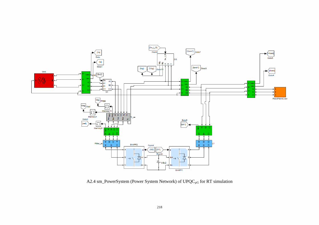
218
A2.4 sm_PowerSystem (Power System Network) of UPQCµG for RT simulation

219
A2.5 ss_measure of UPQCµG for RT simulation

220
A 2.6 ss_PSD of UPQCµG for RT simulation
A2.7 ss_seAPF block of UPQCµG for RT simulation

221
A2.8 ss_shAPF of of UPQCµG for RT simulation

222
A2.9 D-UPQC simulation blocks in RT LAB

223
A2.10 sm_PowerSystem of D-UPQC

224
A2.11 Data acquisition system for D-UPQC

225
A2.12 Control block of D-UPQC

226
A2.13 Real-time simulator (OPAL-RT) setup for SIL configuration

227
Publication
(1) S K Khadem, M Basu and M F Conlon, UPQC for Power Quality Improvement in DG
Integrated Smart Grid Network – A Review, International Journal of Emerging Electric Power
Systems, Vol. 13(1), 2012, Article 3
(2) S K Khadem, M Basu and M F Conlon, Parallel Operation of Inverters and Active Power
Filters in Distributed Generation System - a Review, Renewable and Sustainable Energy
Reviews, Vol. 15(9), 2011, pp. 5155– 5168
(3) S K Khadem, M Basu and M F Conlon, Integration of UPQC for Power Quality
Improvement in Distributed Generation Network – A Review, ISGT Europe 2011,
Manchester UK, Dec 2011
(4) S K Khadem, M. Basu and M F Conlon, A review of parallel operation of active power
filters in the distributed generation system, EPE 2011, Vol. 1, pp.1-10, Aug 2011
(5) S K Khadem, M Basu and M Conlon, Power Quality in Grid connected Renewable
Energy Systems: Role of Custom Power Devices, ICREPQ, Spain, Mar 2010
In Progress:
(6) S K Khadem, M Basu and M Conlon, Harmonic Power Compensation Capacity of Shunt
APF and its relationship to Design Parameters.
(7) S K Khadem, M Basu and M Conlon, Critical Issues on Placement of UPQC in DG
integrated Network
(8) S K Khadem, M Basu and M Conlon, UPQCµG - A new proposal for integration of UPQC
in DG connected Micro-grid or Micro-generation network
(9) S K Khadem, M Basu and M Conlon, D-UPQC - A new proposal for capacity
enhancement of UPQC in DG connected Micro-grid network