power management from texas instruments inc. dc/dc dc/dc dc/dc 24v/ 48v/ few 100v think ‘power...
TRANSCRIPT
Akermann Electronic BG JSCPower Management from Texas Instruments Inc.
Module 3: Power Management
Part II: MOSFET and IGBT Drivers
• Purpose, Basic Functions, Benefits
• Replacing discrete Gate Drivers (NPN/PNP Totem pole) with Gate Driver ICs
• Key Spec/Parameters
• Types of Gate Drivers
• Examples
1
12.October.2017 - Technical seminar
180
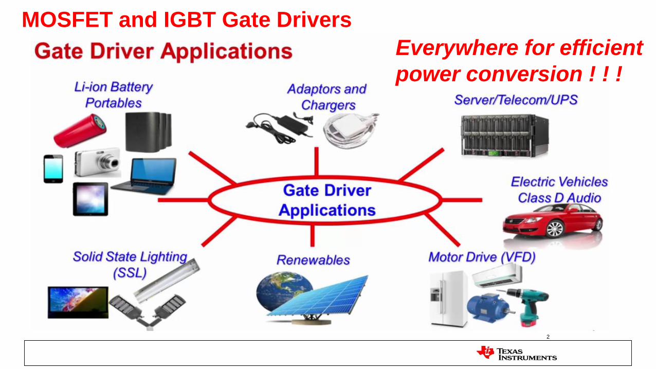
MOSFET and IGBT Gate Drivers
2
Everywhere for efficient
power conversion ! ! !
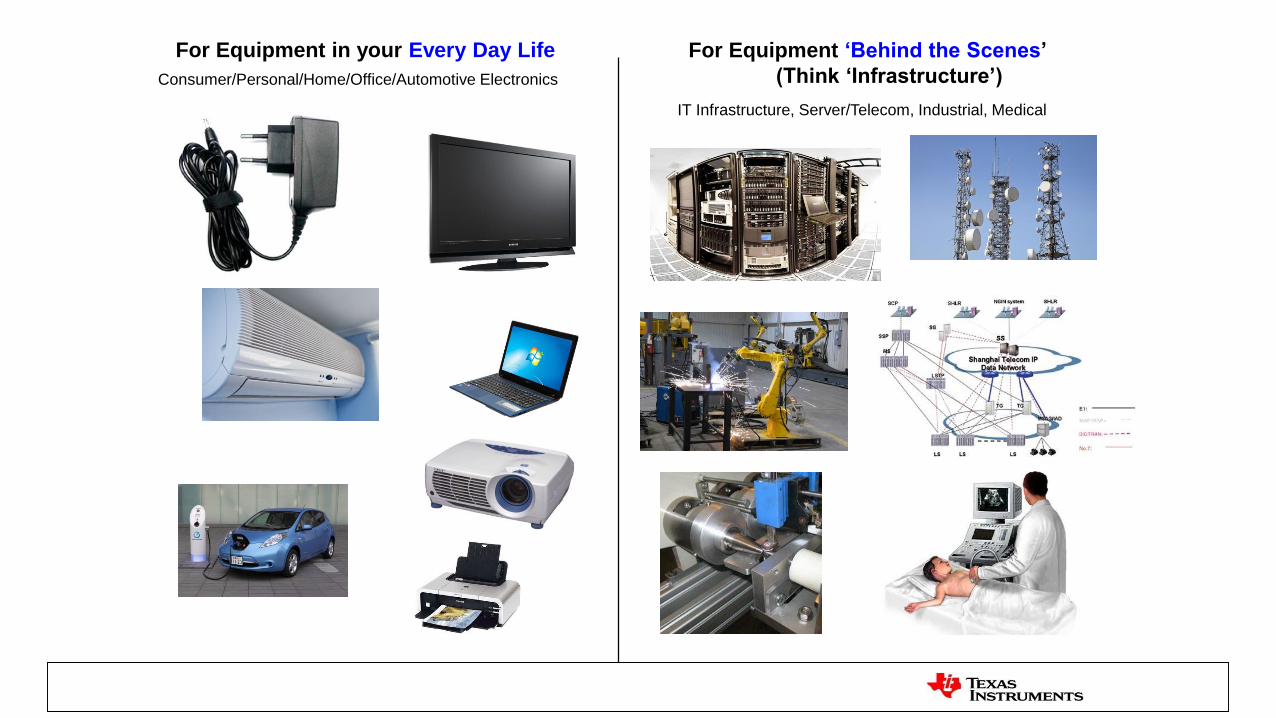
For Equipment in your Every Day Life For Equipment ‘Behind the Scenes’
(Think ‘Infrastructure’)
IT Infrastructure, Server/Telecom, Industrial, Medical
Consumer/Personal/Home/Office/Automotive Electronics
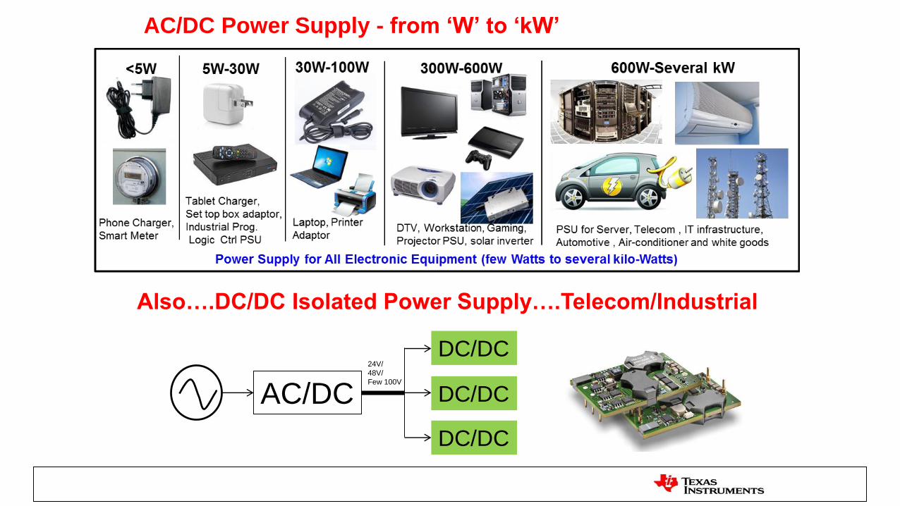
AC/DC Power Supply - from ‘W’ to ‘kW’
Also….DC/DC Isolated Power Supply….Telecom/Industrial
AC/DC
DC/DC
DC/DC
DC/DC
24V/
48V/
Few 100V
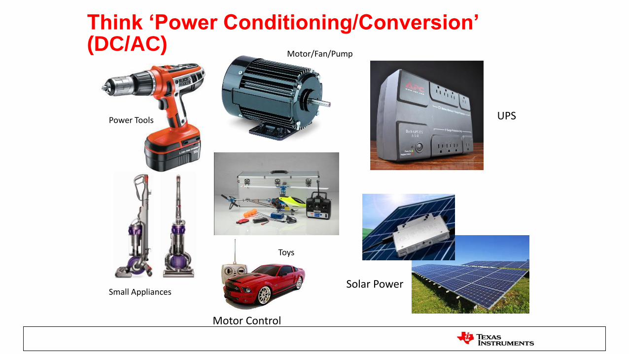
Think ‘Power Conditioning/Conversion’(DC/AC)
Motor Control
Solar Power
UPS
Toys
Motor/Fan/Pump
Power Tools
Small Appliances
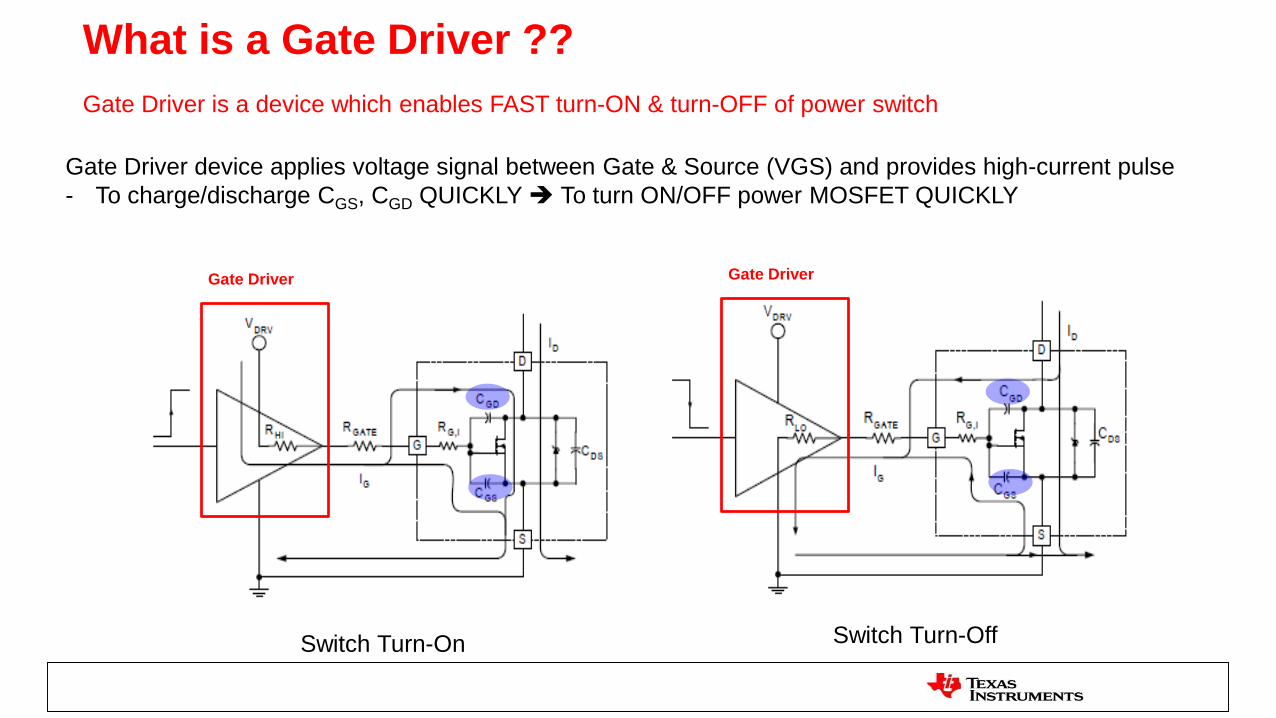
What is a Gate Driver ??
Gate Driver is a device which enables FAST turn-ON & turn-OFF of power switch
Gate Driver device applies voltage signal between Gate & Source (VGS) and provides high-current pulse
- To charge/discharge CGS, CGD QUICKLY To turn ON/OFF power MOSFET QUICKLY
Gate Driver Gate Driver
Switch Turn-On Switch Turn-Off

Gate Driver IC – Basic Function
• IN signal – from controller, can be logic level
• Output (OUT pin) of Gate Driver changes state based on Input (IN) signal
• OUT signal High Level (ON state) ~ VDD
• OUT signal in Low Level (OFF state) ~ GND
Input Signal Gate Driver Output Signal
ON
OFFOFF
Controller
Turn
ON
Turn
OFF
Output
Current
Pulse
Charge
Discharge
• High-current pulse delivered by OUT pin for power MOSFET turn ON/OFF
• Charging current = Source Current
• Discharging current = Sink Current
8
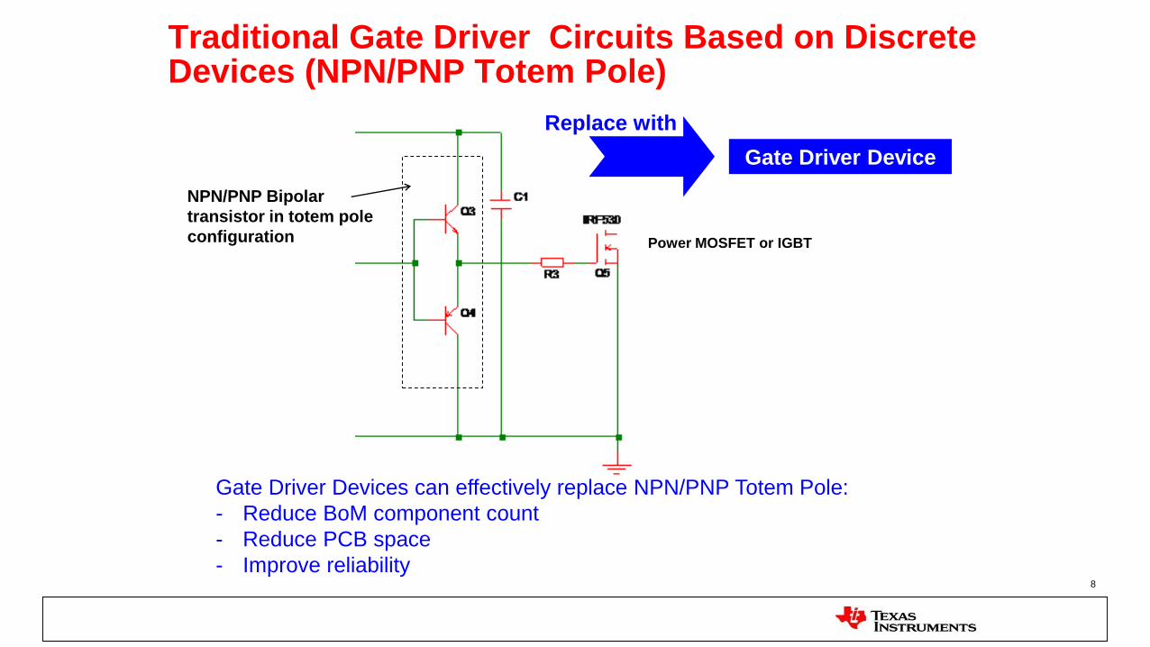
Traditional Gate Driver Circuits Based on Discrete Devices (NPN/PNP Totem Pole)
NPN/PNP Bipolar
transistor in totem pole
configuration
Replace with
Power MOSFET or IGBT
Gate Driver Devices can effectively replace NPN/PNP Totem Pole:
- Reduce BoM component count
- Reduce PCB space
- Improve reliability
Gate Driver Device
9
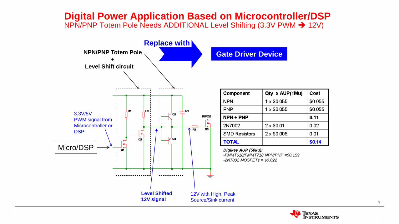
Digital Power Application Based on Microcontroller/DSPNPN/PNP Totem Pole Needs ADDITIONAL Level Shifting (3.3V PWM 12V)
3.3V/5V
PWM signal from
Microcontroller or
DSP
Level Shifted
12V signal
NPN/PNP Totem Pole
+
Replace with
Digikey AUP (50ku):
-FMMT618/FMMT718 NPN/PNP =$0.159
-2N7002 MOSFETs = $0.022
Gate Driver Device
Level Shift circuit
12V with High, Peak
Source/Sink current
Micro/DSP
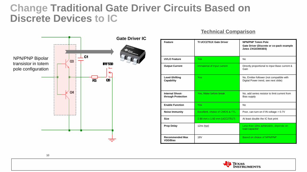
Change Traditional Gate Driver Circuits Based on Discrete Devices to IC
10
NPN/PNP Bipolar
transistor in totem
pole configuration
Gate Driver ICFeature TI UCC2751X Gate Driver NPN/PNP Totem Pole
Gate Driver (Discrete or co-pack example
Zetex ZXGD3003E6)
UVLO Feature Yes No
Output Current Immaterial of Input current Directly proportional to input Base current &
Gain
Level-Shifting
Capability
Yes No, Emitter follower (not compatible with
Digital Power trend, see next slide)
Internal Shoot-
through Protection
Yes, Make before break No, add series resistor to limit current from
Bias supply
Enable Function Yes No
Noise Immunity Excellent, choice of CMOS & TTL Poor, can turn-on if IN voltage > 0.7V
Size 2.90 mm x 1.60 mm (UCC27517) At least double the IC foot print
Prop Delay 12ns (typ) Less than 10ns achievable, depends on
load capacitor
Recommended Max
VDD/Bias
18V Based on choice of NPN/PNP
Technical Comparison
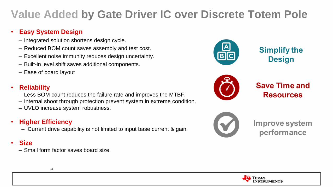
Value Added by Gate Driver IC over Discrete Totem Pole
11
• Easy System Design
– Integrated solution shortens design cycle.
– Reduced BOM count saves assembly and test cost.
– Excellent noise immunity reduces design uncertainty.
– Built-in level shift saves additional components.
– Ease of board layout
• Reliability– Less BOM count reduces the failure rate and improves the MTBF.
– Internal shoot through protection prevent system in extreme condition.
– UVLO increase system robustness.
• Higher Efficiency– Current drive capability is not limited to input base current & gain.
• Size– Small form factor saves board size.
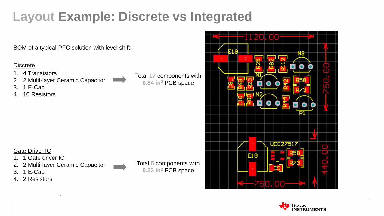
Layout Example: Discrete vs Integrated
12
BOM of a typical PFC solution with level shift:
Discrete
1. 4 Transistors
2. 2 Multi-layer Ceramic Capacitor
3. 1 E-Cap
4. 10 Resistors
Gate Driver IC
1. 1 Gate driver IC
2. 2 Multi-layer Ceramic Capacitor
3. 1 E-Cap
4. 2 Resistors
Total 17 components with
0.84 in2 PCB space
Total 5 components with
0.33 in2 PCB space

Types of Gate Drivers

2 Types of Gate Drivers – Based on Switch Position or Arrangement
Low Side Drivers
Used to Drive GND
referenced switches
High side-Low Side Drivers
Used to Drive 2 switches
connected in Bridge Arrangement
High side
Low side
Gate
Driver
Low side
Gate
Driver
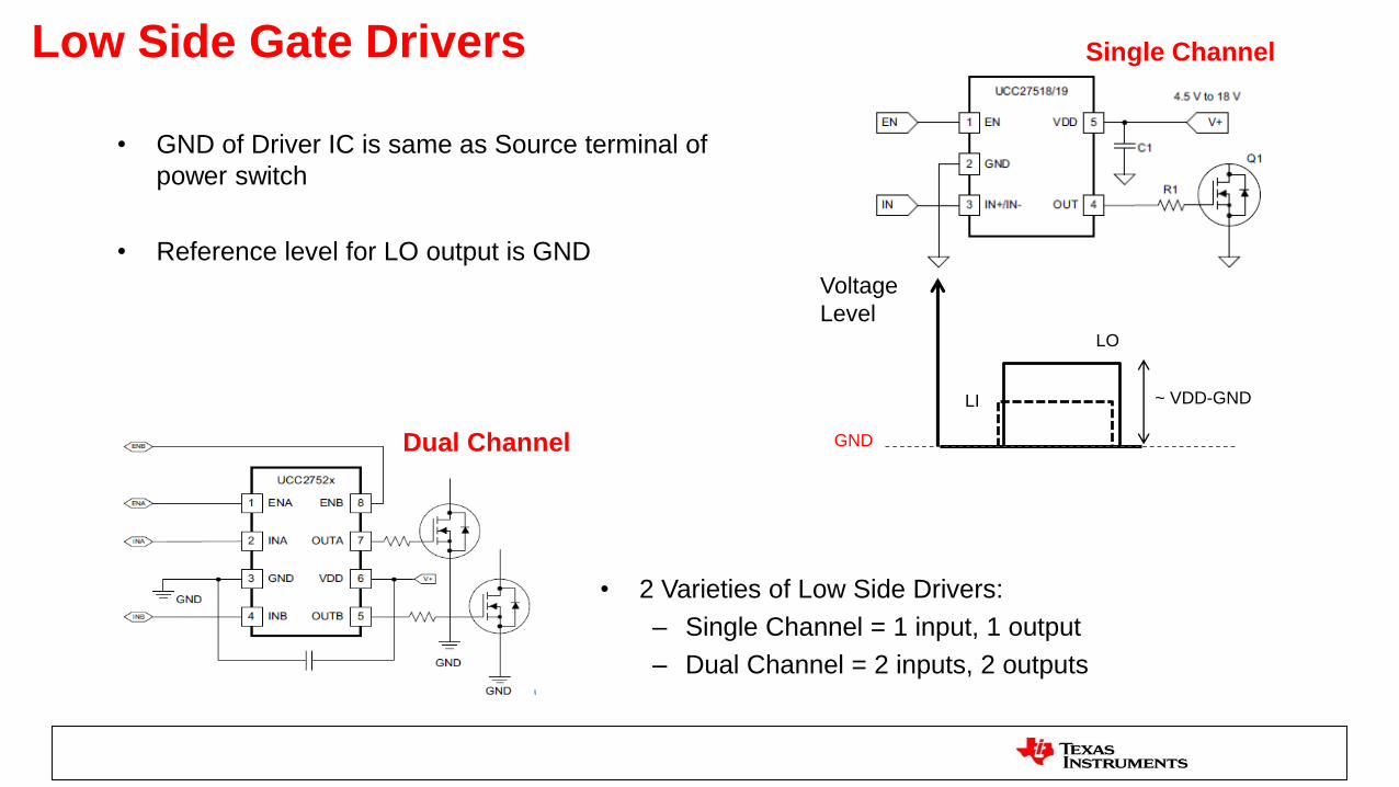
Low Side Gate Drivers
• GND of Driver IC is same as Source terminal of
power switch
• Reference level for LO output is GND
Voltage
Level
LI
LO
GND
~ VDD-GND
Dual Channel
• 2 Varieties of Low Side Drivers:
– Single Channel = 1 input, 1 output
– Dual Channel = 2 inputs, 2 outputs
Single Channel
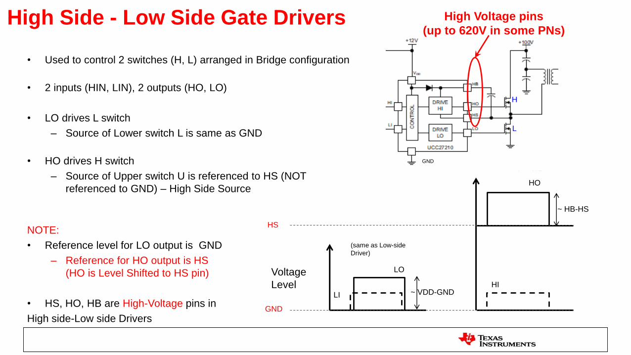
• Used to control 2 switches (H, L) arranged in Bridge configuration
• 2 inputs (HIN, LIN), 2 outputs (HO, LO)
• LO drives L switch
– Source of Lower switch L is same as GND
• HO drives H switch
– Source of Upper switch U is referenced to HS (NOT
referenced to GND) – High Side Source
High Side - Low Side Gate Drivers
H
L
GND
Voltage
Level
GND
HS
LI
LO
HI
HO
~ VDD-GND
~ HB-HS
(same as Low-side
Driver)
NOTE:
• Reference level for LO output is GND
– Reference for HO output is HS
(HO is Level Shifted to HS pin)
• HS, HO, HB are High-Voltage pins in
High side-Low side Drivers
High Voltage pins
(up to 620V in some PNs)
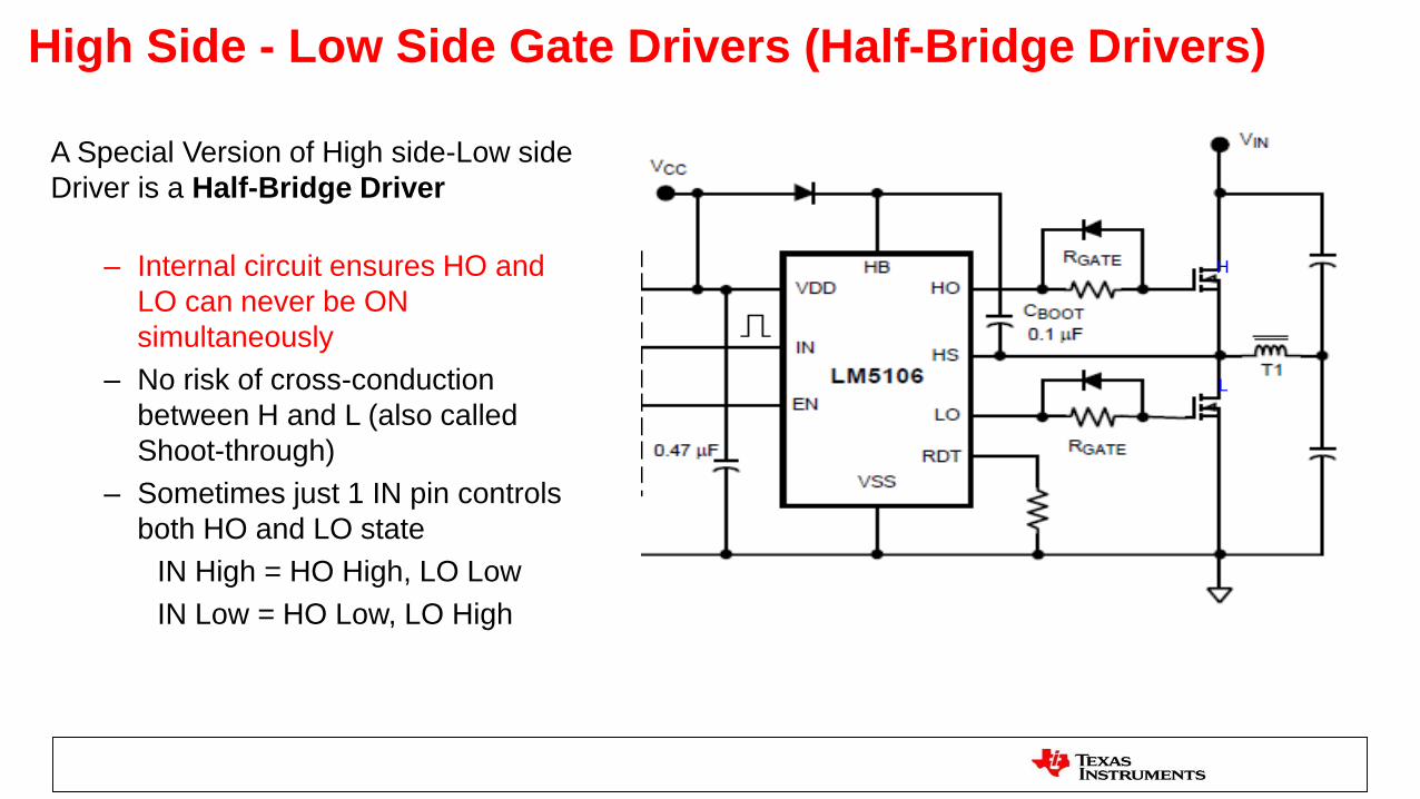
A Special Version of High side-Low side
Driver is a Half-Bridge Driver
– Internal circuit ensures HO and
LO can never be ON
simultaneously
– No risk of cross-conduction
between H and L (also called
Shoot-through)
– Sometimes just 1 IN pin controls
both HO and LO state
IN High = HO High, LO Low
IN Low = HO Low, LO High
H
L
High Side - Low Side Gate Drivers (Half-Bridge Drivers)
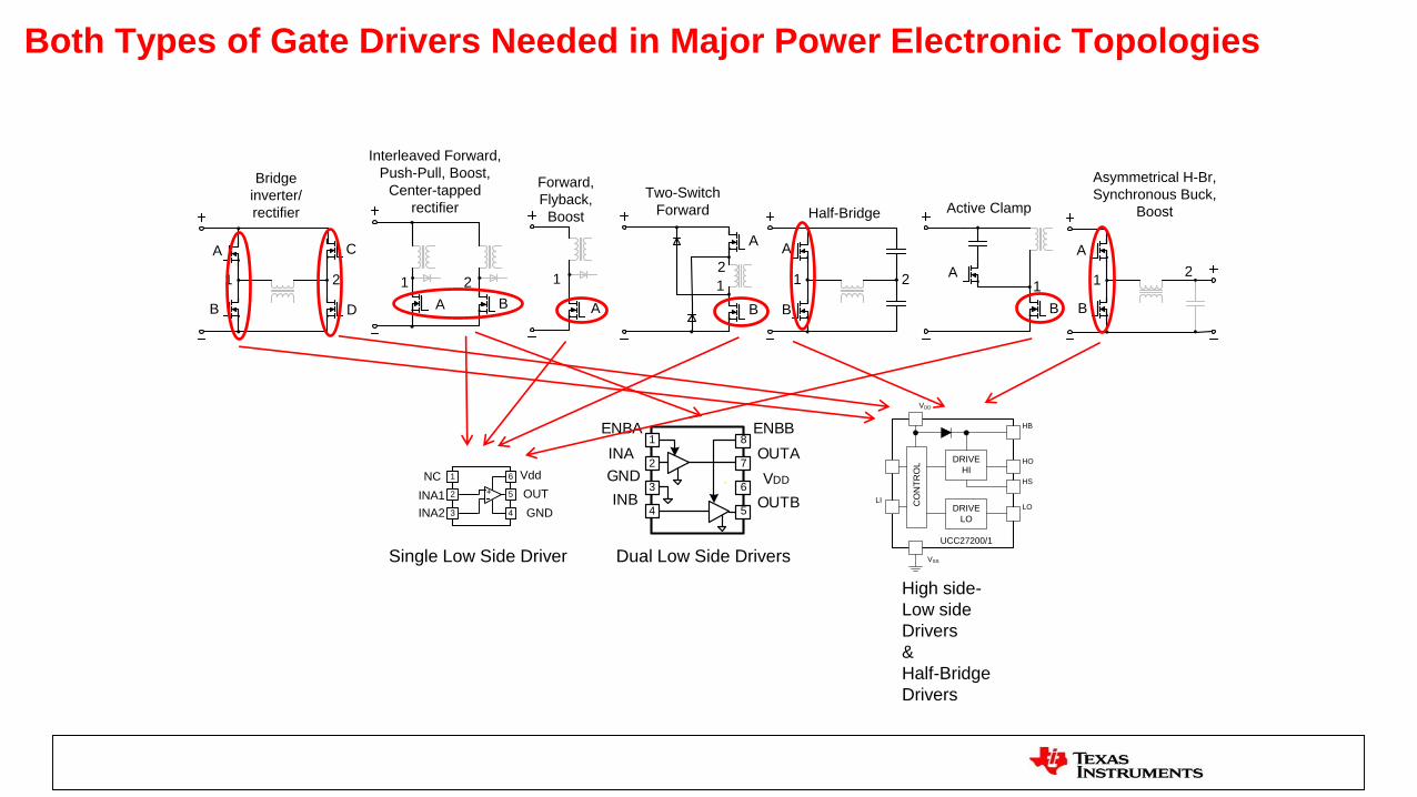
Both Types of Gate Drivers Needed in Major Power Electronic Topologies
A
D
C
B
21
Bridge
inverter/
rectifier
A
B
21
Half-Bridge
A
1
Forward,
Flyback,
Boost
A
B
21
Asymmetrical H-Br,
Synchronous Buck,
Boost
A
B
1
Active Clamp
A
B
Two-Switch
Forward
2
1
A B
2
Interleaved Forward,
Push-Pull, Boost,
Center-tapped
rectifier
1
VDD
ENBB
OUTAINA1
2
3
4 5
6
7
OUTB
GND
ENBA
INB
8
CO
NT
RO
L
DRIVE
LO
DRIVE
HI
VDD
UCC27200/1
VSS
LI
HB
HO
HS
LOGND
OUT
INA2
1
2
3 4
5
6 Vdd
INA1 +-
NC
Single Low Side Driver Dual Low Side Drivers
High side-
Low side
Drivers
&
Half-Bridge
Drivers

Key Parameters for LOW SIDE Gate Drivers
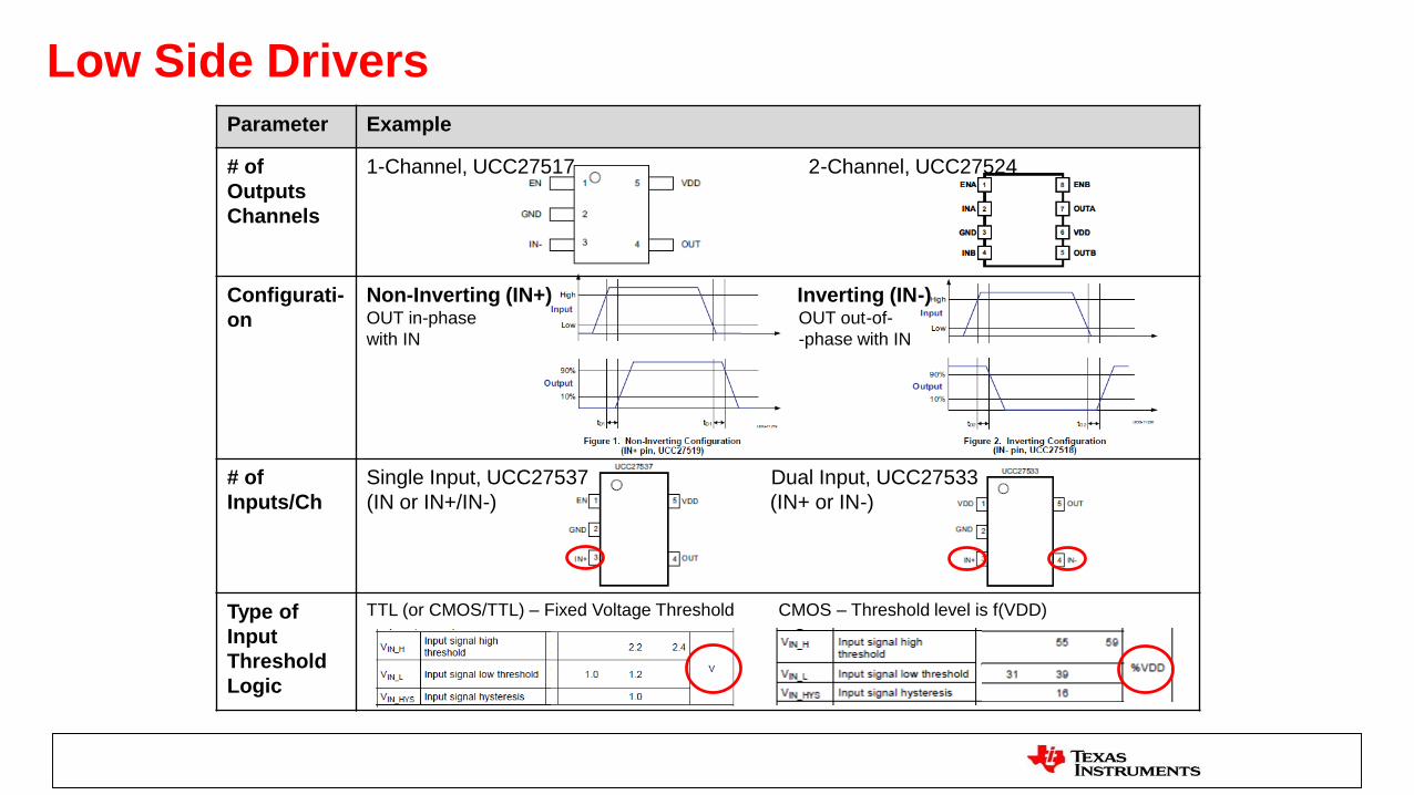
Low Side DriversParameter Example
# of
Outputs
Channels
1-Channel, UCC27517 2-Channel, UCC27524
Configurati-
on
Non-Inverting (IN+) Inverting (IN-)OUT in-phase OUT out-of-
with IN -phase with IN
# of
Inputs/Ch
Single Input, UCC27537 Dual Input, UCC27533
(IN or IN+/IN-) (IN+ or IN-)
Type of
Input
Threshold
Logic
TTL (or CMOS/TTL) – Fixed Voltage Threshold CMOS – Threshold level is f(VDD)
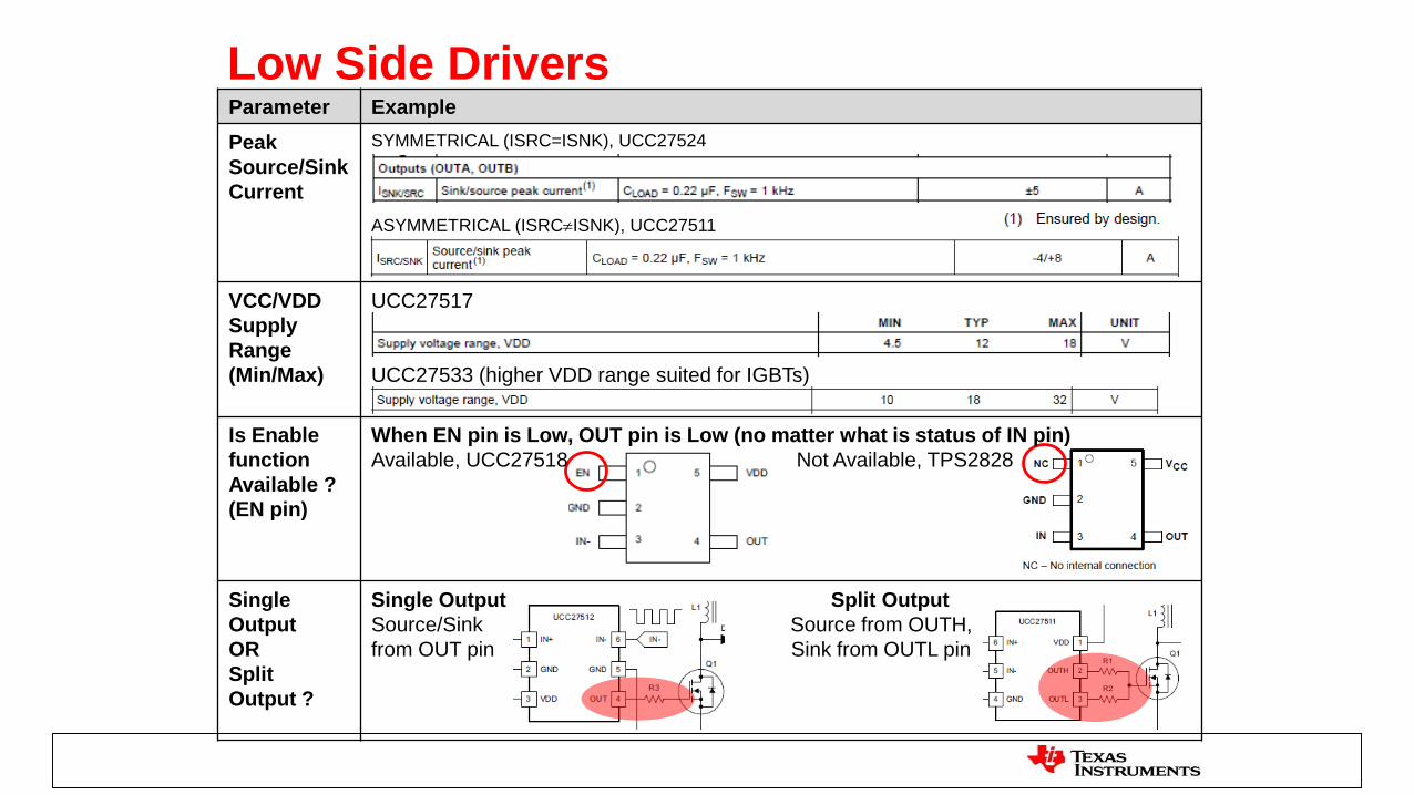
Low Side DriversParameter Example
Peak
Source/Sink
Current
SYMMETRICAL (ISRC=ISNK), UCC27524
ASYMMETRICAL (ISRCISNK), UCC27511
VCC/VDD
Supply
Range
(Min/Max)
UCC27517
UCC27533 (higher VDD range suited for IGBTs)
Is Enable
function
Available ?
(EN pin)
When EN pin is Low, OUT pin is Low (no matter what is status of IN pin)
Available, UCC27518 Not Available, TPS2828
Single
Output
OR
Split
Output ?
Single Output Split Output
Source/Sink Source from OUTH,
from OUT pin Sink from OUTL pin
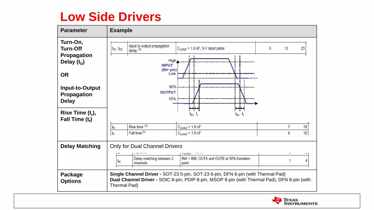
Low Side DriversParameter Example
Turn-On,
Turn-Off
Propagation
Delay (tD)
OR
Input-to-Output
Propagation
Delay
Rise Time (tr),
Fall Time (tf)
Delay Matching Only for Dual Channel Drivers
Package
Options
Single Channel Driver - SOT-23 5-pin, SOT-23 6-pin, DFN 6-pin (with Thermal Pad)
Dual Channel Driver - SOIC 8-pin, PDIP 8-pin, MSOP 8-pin (with Thermal Pad), DFN 8-pin (with
Thermal Pad)
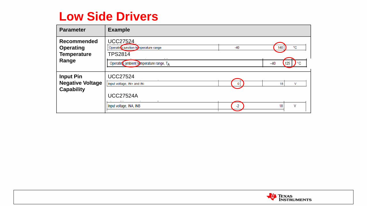
Low Side DriversParameter Example
Recommended
Operating
Temperature
Range
UCC27524
TPS2814
Input Pin
Negative Voltage
Capability
UCC27524
UCC27524A

Key Parameters for HIGH SIDE-LOW SIDE Gate Drivers
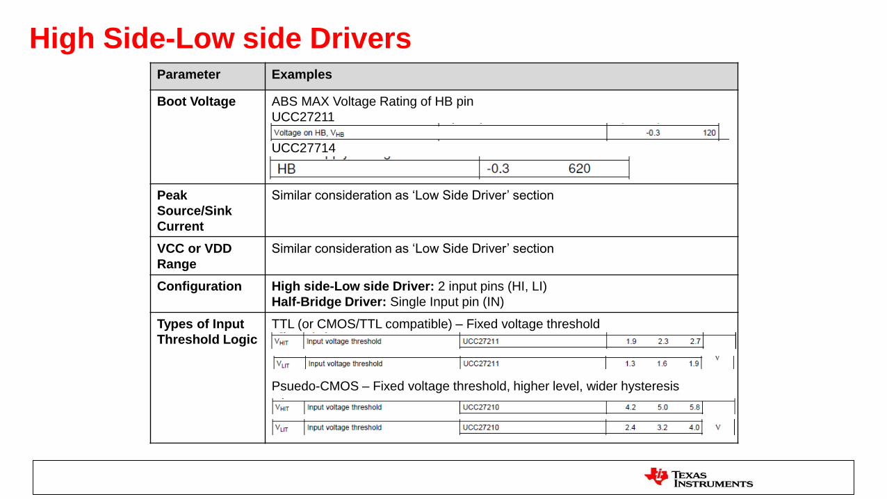
High Side-Low side DriversParameter Examples
Boot Voltage ABS MAX Voltage Rating of HB pin
UCC27211
UCC27714
Peak
Source/Sink
Current
Similar consideration as ‘Low Side Driver’ section
VCC or VDD
Range
Similar consideration as ‘Low Side Driver’ section
Configuration High side-Low side Driver: 2 input pins (HI, LI)
Half-Bridge Driver: Single Input pin (IN)
Types of Input
Threshold Logic
TTL (or CMOS/TTL compatible) – Fixed voltage threshold
Psuedo-CMOS – Fixed voltage threshold, higher level, wider hysteresis

High Side-Low side DriversParameter Examples
Is Bootstrap
Diode
integrated
inside Driver
Integrated inside device Not integrated inside device
Voltage Slew
Rate on HS
Propagation
Delay
Similar consideration as ‘Low Side Driver’ section
Rise/Fall time Similar consideration as ‘Low Side Driver’ section
Delay Matching Similar consideration as ‘Low Side Driver’ section
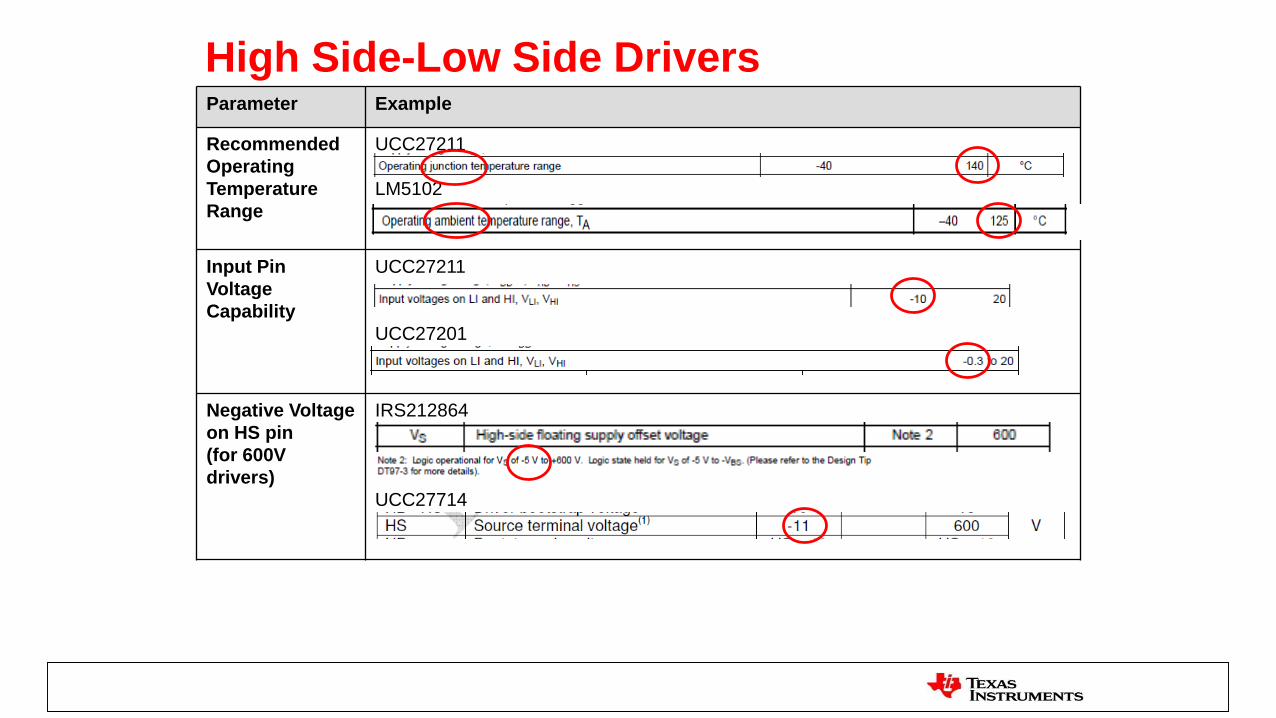
High Side-Low Side DriversParameter Example
Recommended
Operating
Temperature
Range
UCC27211
LM5102
Input Pin
Voltage
Capability
UCC27211
UCC27201
Negative Voltage
on HS pin
(for 600V
drivers)
IRS212864
UCC27714
EXAMPLEsof Gate Driver Usage inDifferent Application Schematics
1
channel
Gate
Driver
1
channel
Gate
Driver
PFC
Controller
2-
Channel
Gate
Driver
PFC
Controller
2-
Channel
Gate
Driver
2-phase
PFC
1-phase
PFC
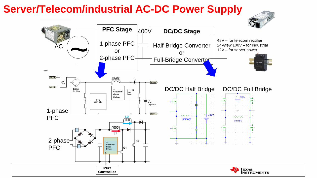
Server/Telecom/industrial AC-DC Power Supply
PFC Stage
1-phase PFC
or
2-phase PFC
DC/DC Stage
Half-Bridge Converter
or
Full-Bridge Converter~AC
400V
48V – for telecom rectifier
24V/few 100V – for industrial
12V – for server power
DC/DC Half Bridge DC/DC Full Bridge

2
channel
Gate
Driver
2
channel
Gate
Driver
Example of PARALLELED Switches - PFC
1
channel
Gate
Driver
1
channel
Gate
Driver
1
channel
Gate
Driver
1
channel
Gate
Driver
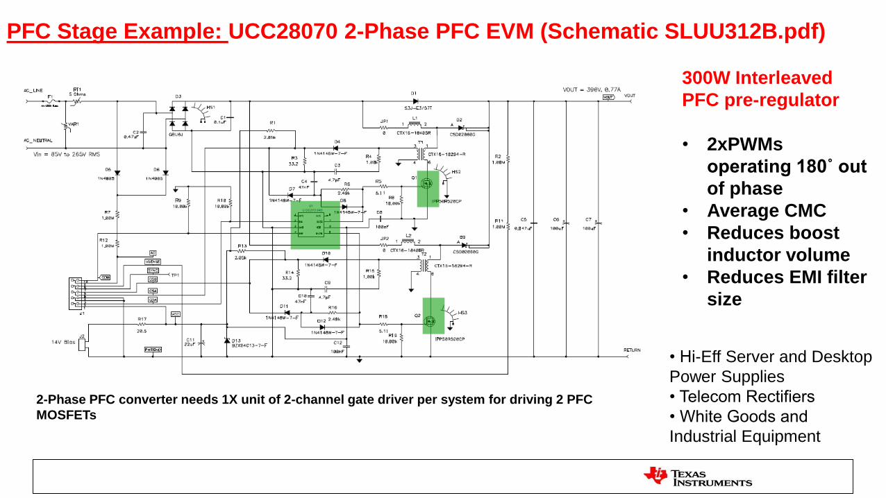
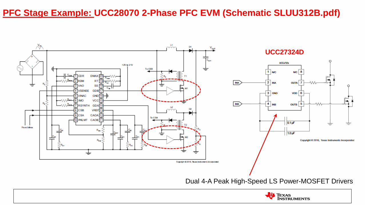
PFC Stage Example: UCC28070 2-Phase PFC EVM (Schematic SLUU312B.pdf)
2-Phase PFC converter needs 1X unit of 2-channel gate driver per system for driving 2 PFC
MOSFETs
300W Interleaved
PFC pre-regulator
• 2xPWMs
operating 180˚ out
of phase
• Average CMC
• Reduces boost
inductor volume
• Reduces EMI filter
size
• Hi-Eff Server and Desktop
Power Supplies
• Telecom Rectifiers
• White Goods and
Industrial Equipment
PFC Stage Example: UCC28070 2-Phase PFC EVM (Schematic SLUU312B.pdf)
Dual 4-A Peak High-Speed LS Power-MOSFET Drivers
UCC27324D

PFC Stage Example: UCC28070 2-Phase PFC EVM (Schematic SLUU312B.pdf)
Simplified Four-Phase
Application Diagram
Using
2 x UCC28070 DevicesVOUT
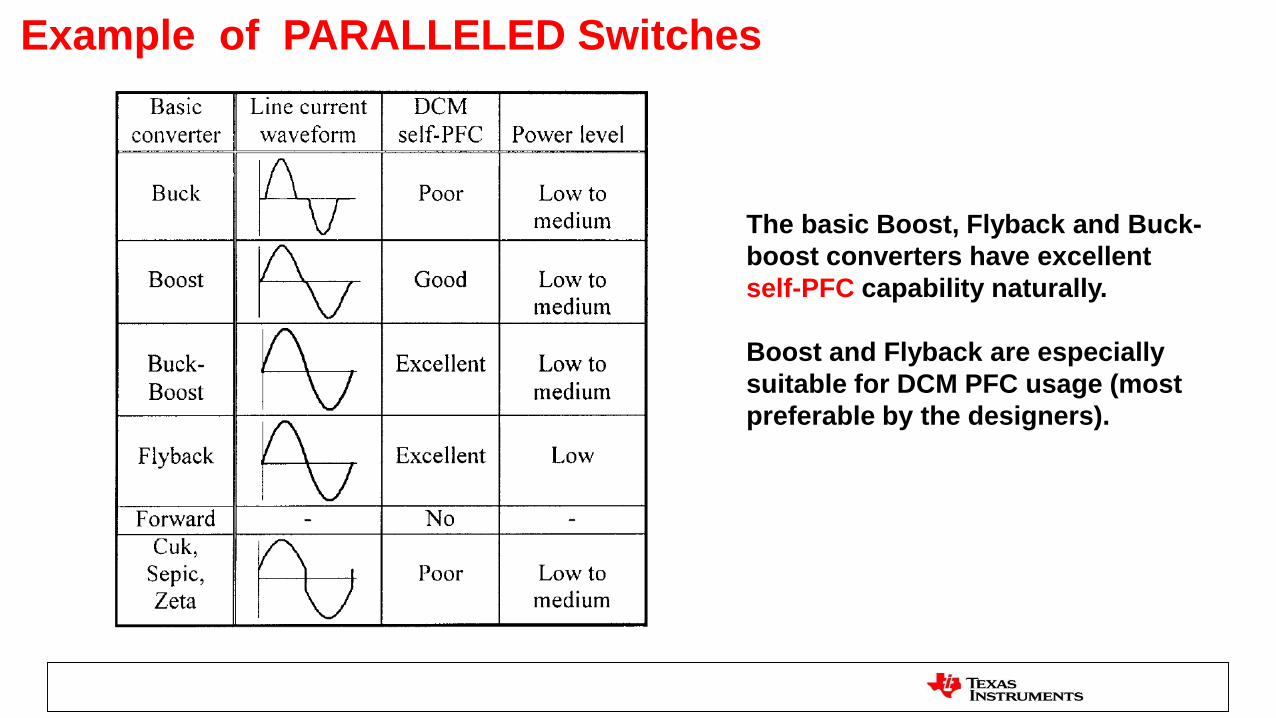
Example of PARALLELED Switches
The basic Boost, Flyback and Buck-
boost converters have excellent
self-PFC capability naturally.
Boost and Flyback are especially
suitable for DCM PFC usage (most
preferable by the designers).
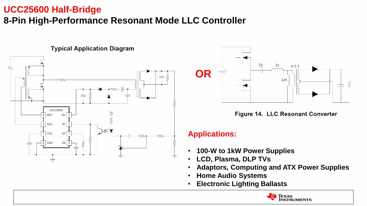
UCC25600 Half-Bridge
8-Pin High-Performance Resonant Mode LLC Controller
OR
Applications:
• 100-W to 1kW Power Supplies
• LCD, Plasma, DLP TVs
• Adaptors, Computing and ATX Power Supplies
• Home Audio Systems
• Electronic Lighting Ballasts

UCC25600 Half-Bridge (Schematic SLUR403.pdf)
Replace NPN/PNP Totem
Pole with Gate Driver
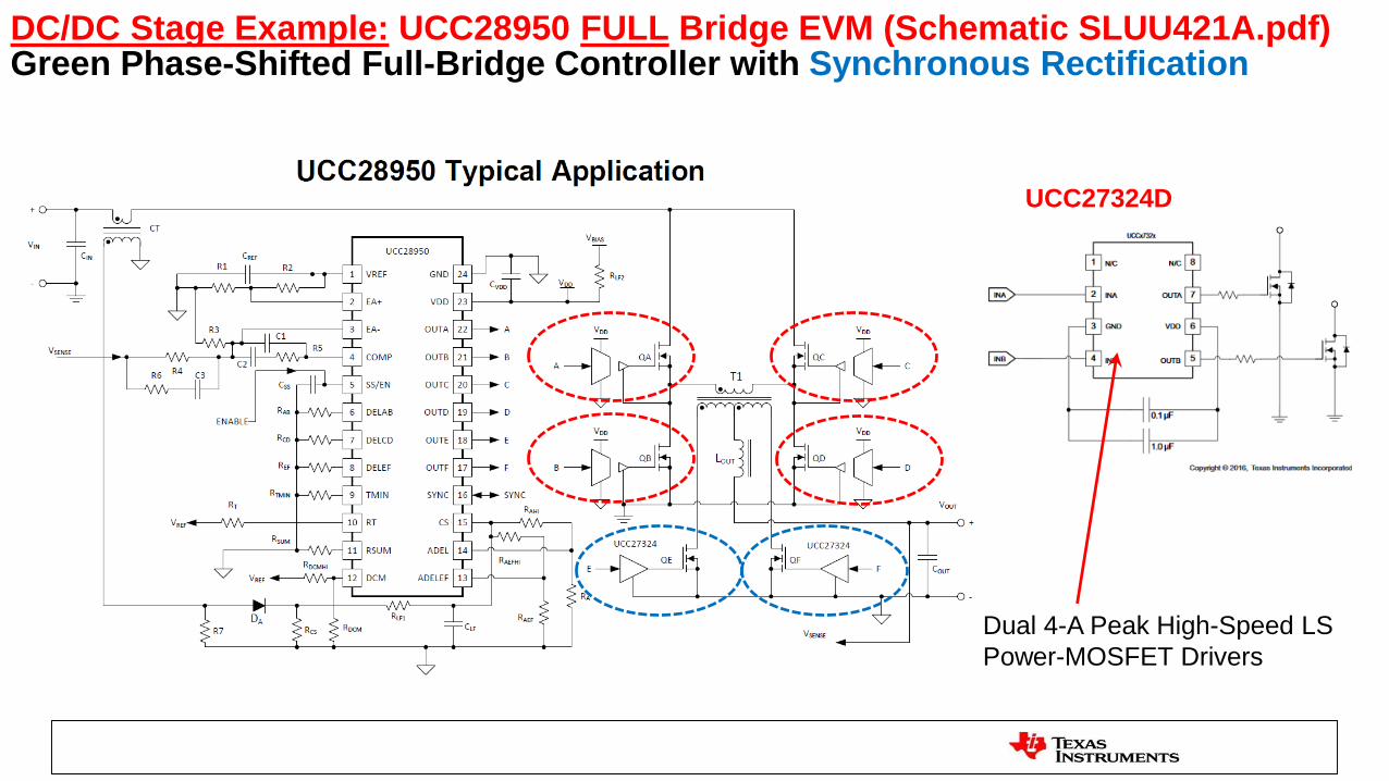
DC/DC Stage Example: UCC28950 FULL Bridge EVM (Schematic SLUU421A.pdf)Green Phase-Shifted Full-Bridge Controller with Synchronous Rectification
Dual 4-A Peak High-Speed LS
Power-MOSFET Drivers
UCC27324D

DC/DC Stage Example: UCC28950 FULL Bridge EVM (Schematic SLUU421A.pdf)
2-Channel Gate Driver for SR MOSFET
2-Channel Gate Driver for
Gate Drive Transformer
2-Channel Gate Driver for
Gate Drive Transformer
Gate Drive
Transformer
(for sending signal)
Main Power
Transformer
(for sending power)
Current Sensing
Transformer
(for sensing current)
Green Phase-Shifted Full-Bridge Controller With
Synchronous Rectification• 390VDC In / 12VDC Out
• 2A INPUT / 50A OUTPUT
POUT = 600W
• Sync rectification
(Secondary side)
=> High Eff
• Phase-Shifted Full-Bridge
Converters
• Datacom, Telecom, and
Wireless Base-Station
Power
• Server, Power Supplies
• Industrial Power Systems
• High-Density Power
Architectures
• Solar Inverters, and Electric
VehiclesFULL Bridge converter needs 3X units of 2-channel gate driver per system
- 2X units for 2 Gate Drive Transformers
- 1X Units for 2 SR MOSFETs
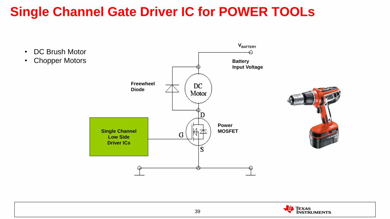
39
Single Channel Gate Driver IC for POWER TOOLs
Freewheel
Diode
Single Channel
Low Side
Driver ICs
VBATTERY
Battery
Input Voltage
Power
MOSFET
• DC Brush Motor
• Chopper Motors

High side-Low side Gate Driver IC in Bridge-type Motors
High side-Low
side
Gate Driver ICPower
MOSFET
Power
MOSFET
Battery Voltage
Battery Voltage
High side-Low
side
Gate Driver IC
High side-Low
side Gate
Driver IC
Gate Driver in 3-Phase Inverter Motors
41
Low
Side
Gate
Driver
IC
1-ph
or
2-ph
PFC
IC*
PMSM
AC Induction
3X
700V
Half-Bridge
Gate
Driver
IC
15V Bias
Supply
Generation
Block
C/
DSP
*In newer architectures, PFC control function is delivered by C/DSP, eliminating need for a discrete analog PFC controller
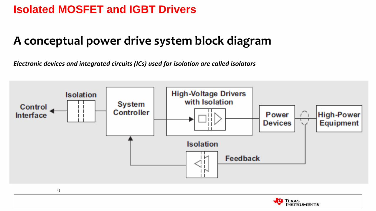
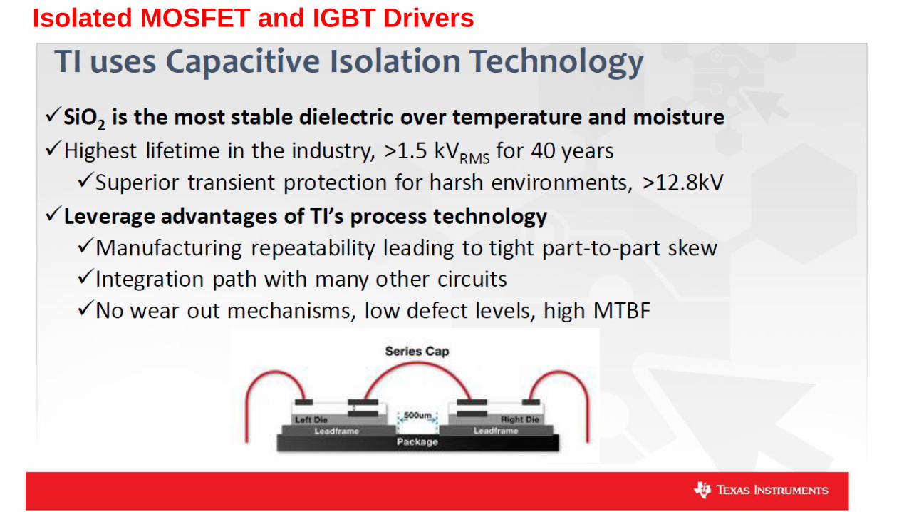
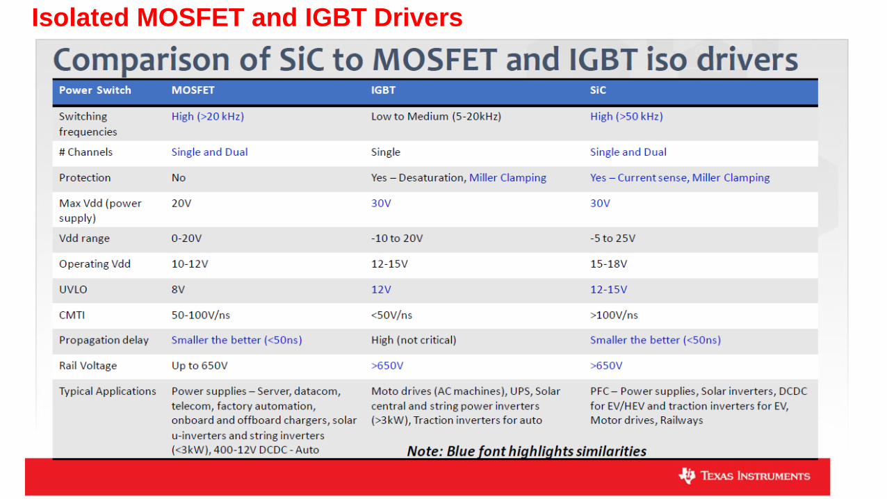
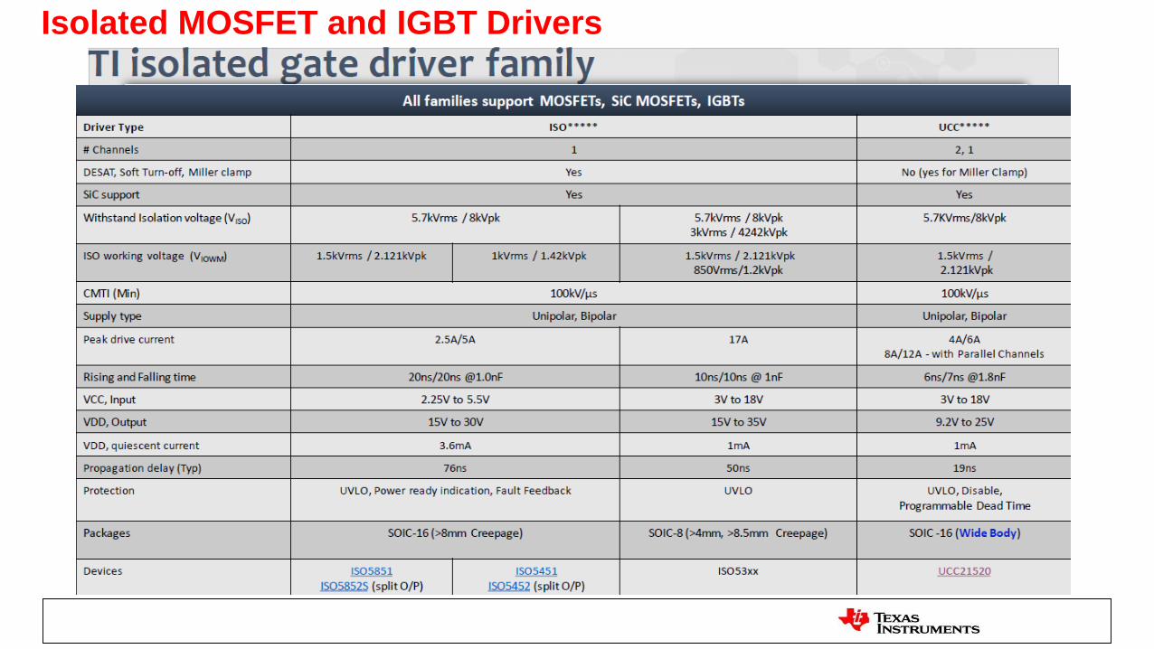
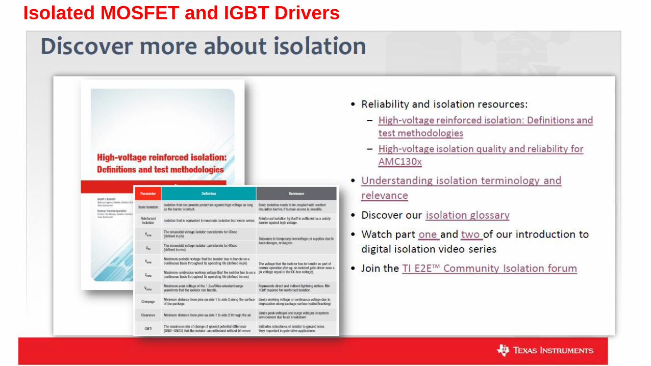
Isolated MOSFET and IGBT Drivers
42
A conceptual power drive system block diagram
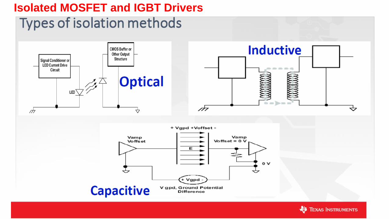
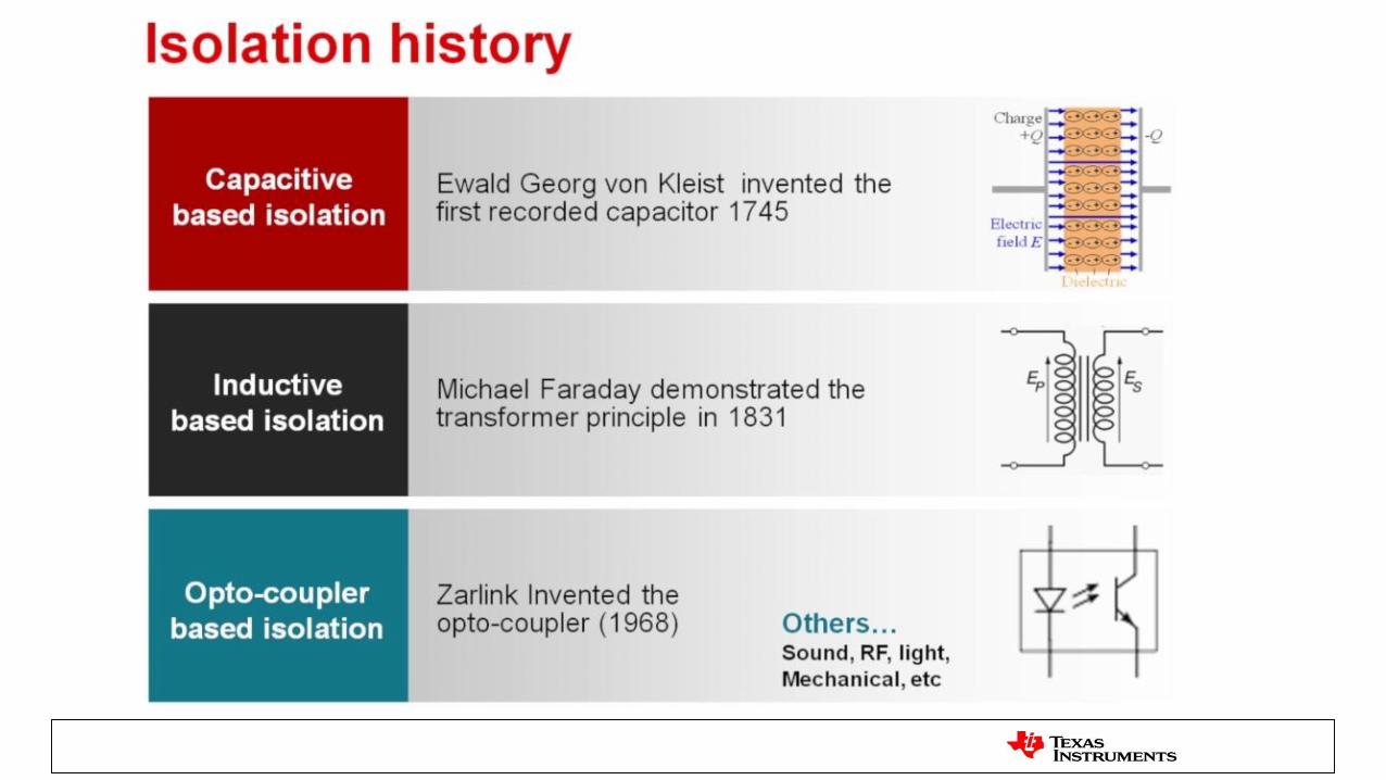
Electronic devices and integrated circuits (ICs) used for isolation are called isolators
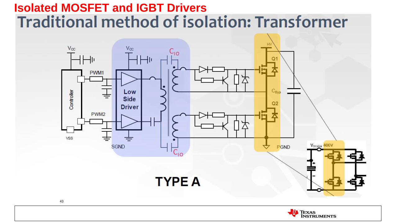
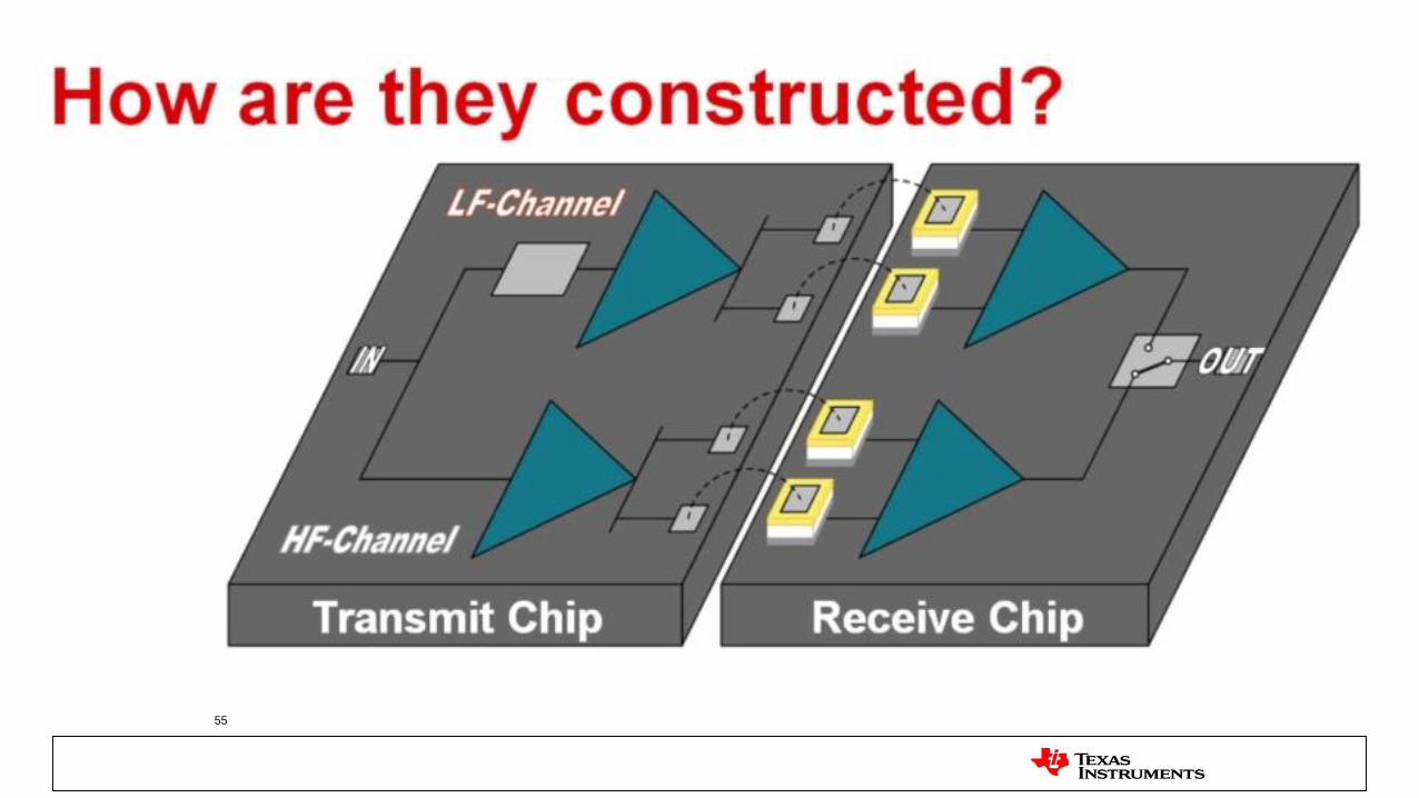
Isolated MOSFET and IGBT Drivers
43
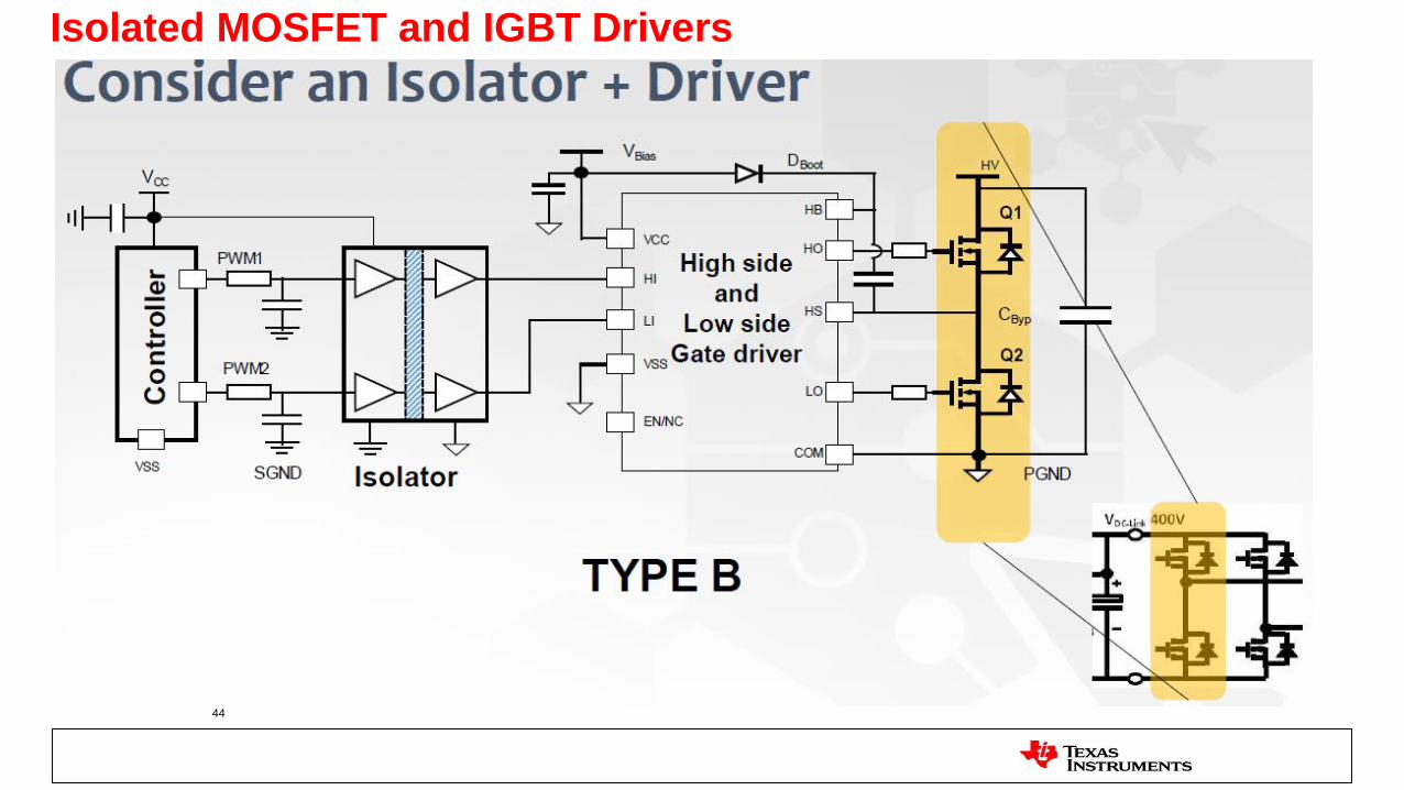
Isolated MOSFET and IGBT Drivers
44

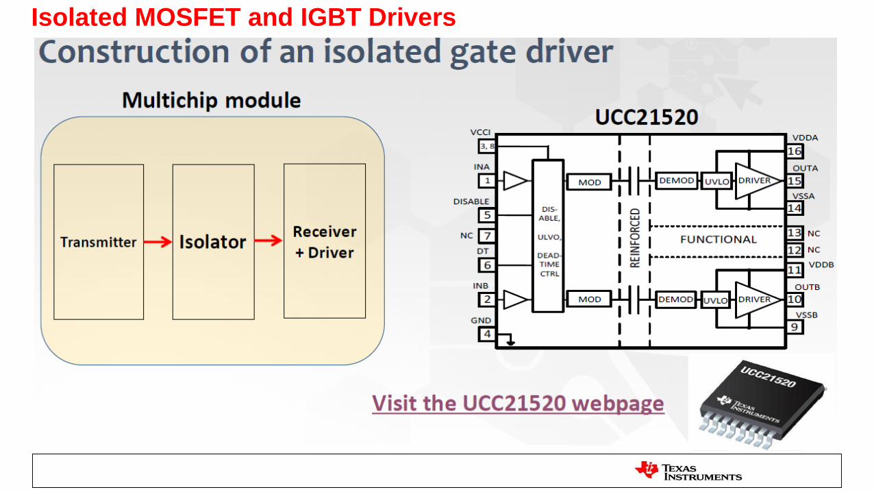
Isolated MOSFET and IGBT Drivers
45

Isolated MOSFET and IGBT Drivers
46
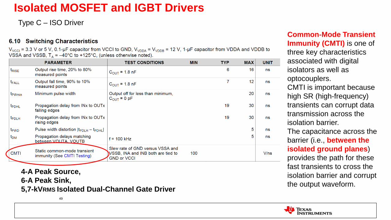
( CMTI – Common-Mode Transient Immunity )
Isolated MOSFET and IGBT Drivers
47
Isolated MOSFET and IGBT Drivers
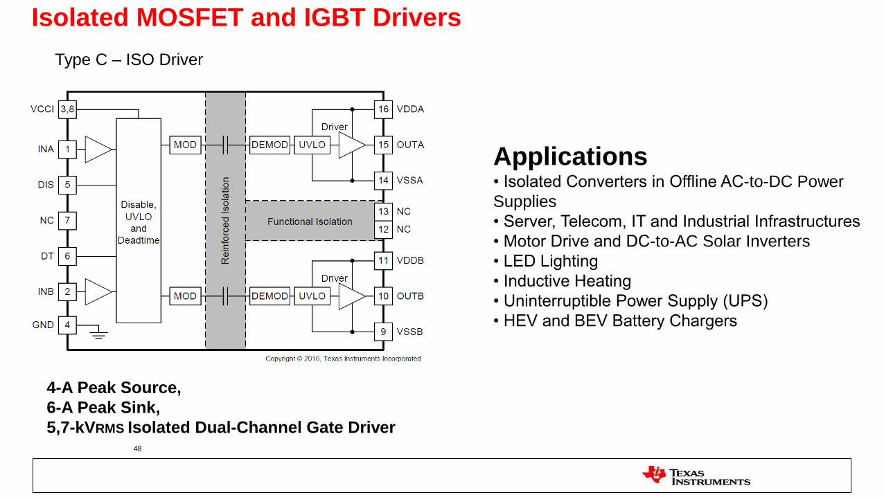
48
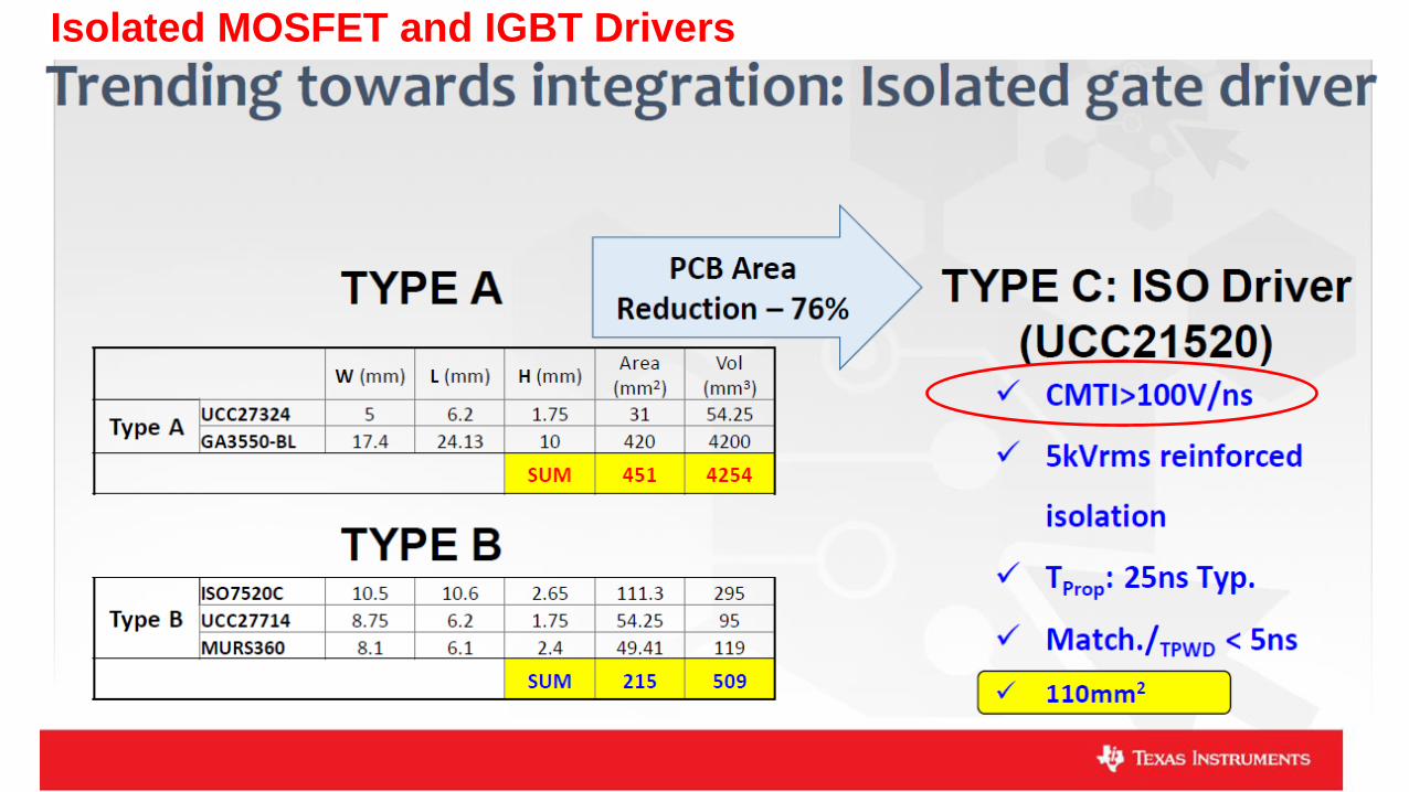
Type C – ISO Driver
4-A Peak Source,
6-A Peak Sink,
5,7-kVRMS Isolated Dual-Channel Gate Driver
Applications• Isolated Converters in Offline AC-to-DC Power
Supplies
• Server, Telecom, IT and Industrial Infrastructures
• Motor Drive and DC-to-AC Solar Inverters
• LED Lighting
• Inductive Heating
• Uninterruptible Power Supply (UPS)
• HEV and BEV Battery Chargers
Isolated MOSFET and IGBT Drivers
49
Type C – ISO Driver
4-A Peak Source,
6-A Peak Sink,
5,7-kVRMS Isolated Dual-Channel Gate Driver
Common‐Mode Transient
Immunity (CMTI) is one of
three key characteristics
associated with digital
isolators as well as
optocouplers.
CMTI is important because
high SR (high‐frequency)
transients can corrupt data
transmission across the
isolation barrier.
The capacitance across the
barrier (i.e., between the
isolated ground planes)
provides the path for these
fast transients to cross the
isolation barrier and corrupt
the output waveform.
Isolated MOSFET and IGBT Drivers
50
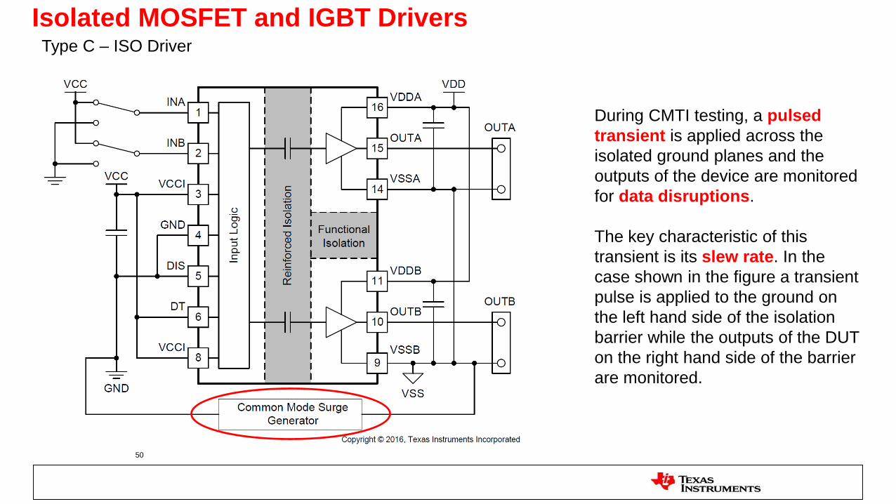
Type C – ISO Driver
During CMTI testing, a pulsed
transient is applied across the
isolated ground planes and the
outputs of the device are monitored
for data disruptions.
The key characteristic of this
transient is its slew rate. In the
case shown in the figure a transient
pulse is applied to the ground on
the left hand side of the isolation
barrier while the outputs of the DUT
on the right hand side of the barrier
are monitored.
Isolated MOSFET and IGBT Drivers
51
Isolated MOSFET and IGBT Drivers
52
53
Isolated MOSFET and IGBT Drivers
54
55

Isolated MOSFET and IGBT Drivers
56

Isolated MOSFET and IGBT Drivers
57
Isolated MOSFET and IGBT Drivers
58
Isolated MOSFET and IGBT Drivers
59
Isolated MOSFET and IGBT Drivers
60
Isolated MOSFET and IGBT Drivers
61