power electronics system thermal design · rps • apec 2011 corporate research & development...
TRANSCRIPT

RPS • APEC 2011 Corporate Research & Development Packaging Technology
Power Electronics System Thermal Design
Roger Stout, P.E. Research Scientist

Corporate R&D: Packaging Technology 1 APEC 2011 Power Electronics System Thermal Design (RPS)
Course outline • Part I: (90 minutes)
– Introduction (30 minutes) – Characterization Techniques (60 minutes)
>> 30 minute BREAK << • Part II: (45 minutes)
– Linear Superposition – Theory (7 minutes) – The Reciprocity Theorem (6 minutes) – A Detailed Example and its Implications (6 minutes) – Controlling the Matrix (6 minutes) – Building a System Model (20 minutes)
• Part III: (35 minutes) – Thermal Runaway – Theory (15 minutes) – Thermal Runaway – Practice #1 (7 minutes) – Thermal Runaway – Practice #2 (13 minutes)
• Quick demos (10 minutes, time permitting)

Corporate R&D: Packaging Technology 2 APEC 2011 Power Electronics System Thermal Design (RPS)
Can this device handle 2 W?

Corporate R&D: Packaging Technology 3 APEC 2011 Power Electronics System Thermal Design (RPS)
“Junction” temperature?
Historically, for discrete devices, the junction was literally the essential “pn” junction of the device. This is still true for basic rectifiers, bipolar transistors, and many other devices.
More generally, however, by “junction” these days we mean
simply the hottest place in the device (which will be somewhere on the silicon).
As we move to complex devices where different parts of the silicon do different jobs at different times, the exact location
gets to be somewhat tricky to identify. But we’re still interested in the hottest spot.

Corporate R&D: Packaging Technology 4 APEC 2011 Power Electronics System Thermal Design (RPS)
Thermal-electrical analogy
temperature <=> voltage
power <=> current
Δtemp/power <=> resistance
energy/degree <=> capacitance

Corporate R&D: Packaging Technology 5 APEC 2011 Power Electronics System Thermal Design (RPS)
adJAJ TPT +⋅= θ
What’s wrong with theta-JA?
d
aJJA P
TT −=θ
d
tabJJtab P
TT −=Ψ
tabdJtabJ TPT +⋅Ψ=
2

Corporate R&D: Packaging Technology 6 APEC 2011 Power Electronics System Thermal Design (RPS)
Theta-JA vs. copper area

Corporate R&D: Packaging Technology 7 APEC 2011 Power Electronics System Thermal Design (RPS)
An example of a device with two different “Max Power” ratings
• Suppose a datasheet says: – Tjmax = 150°C – θJA = 100°C/W – Pd = 1.25W (Tamb=25°C)
• But it also says: – ΨJL = 25°C/W – Pd = 3.0W (TL=75°C)
Where’s the “inconsistency”?
1501252525.1*10025
=+=+
15075753*2575=+=
+

Corporate R&D: Packaging Technology 8 APEC 2011 Power Electronics System Thermal Design (RPS)
Not 75°C !!
Where’s the inconsistency?
What’s TL?
25°C/W (ΨJL)
100°C/W (θJA)
TJ =150°C
TA =25°C
(try about 119°C)
…¾ of the way from ambient to Tj

Corporate R&D: Packaging Technology 9 APEC 2011 Power Electronics System Thermal Design (RPS)
Why is ON’s SOT-23 thermal number so much worse than the other guy’s?
• ON – SOT-23 package – 60x60 die – Solder D/A – Copper leadframe – Min-pad board – Still air
• some other guy – SOT-23 package – 20x20 die – Epoxy D/A – Alloy 42 leadframe – 1” x 2oz spreader – Big fan

Corporate R&D: Packaging Technology 10 APEC 2011 Power Electronics System Thermal Design (RPS)
Theta (θ) vs. Psi (Ψ)
• JEDEC <http://www.jedec.org/> terminology – ZθJX , RθJA older terms ref JESD23-3, 23-4 – θJA ref JESD 51, 51-1 – θJMA ref JESD 51-6 – ΨJT, ΨTA ref JESD 51-2 – ΨJB, ΨBA ref JESD 51-6, 51-8 – RθJB ref JESD 51-8 – Great overview, all terms: JESD 51-12

Corporate R&D: Packaging Technology 11 APEC 2011 Power Electronics System Thermal Design (RPS)
“Theta” (Greek letter θ)
Ty
We know actual heat flowing along path of interest
true “thermal resistance”
path
yxxy q
TT −=θ
Tx
Corporate R&D: Packaging Technology 12 APEC 2011 Power Electronics System Thermal Design (RPS)
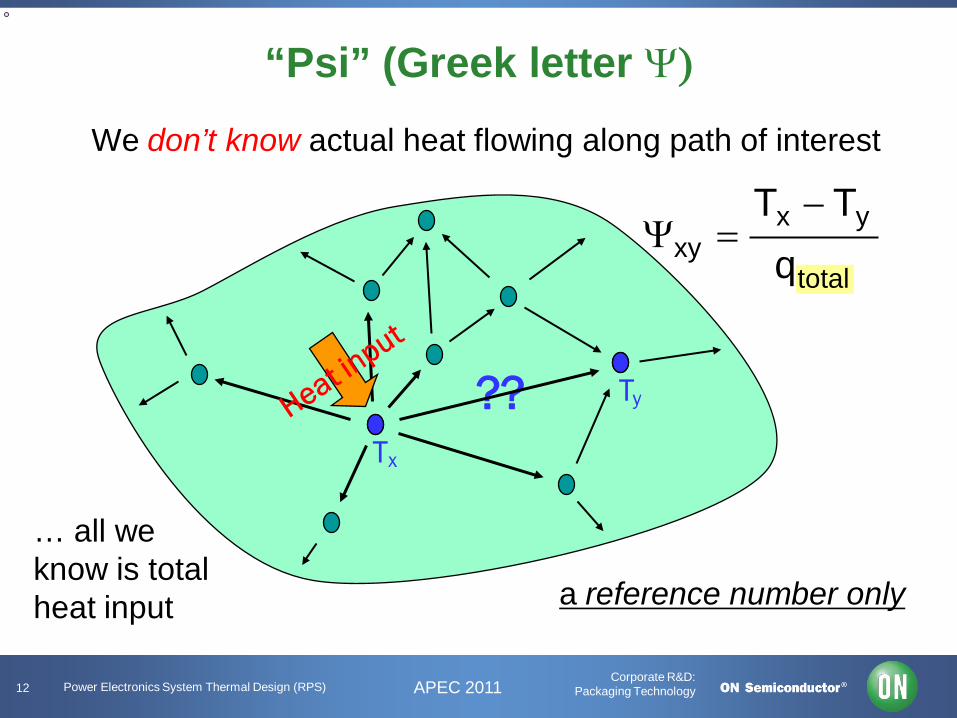
“Psi” (Greek letter Ψ)
Tx
Ty ??
We don’t know actual heat flowing along path of interest
… all we know is total heat input
total
yxxy q
TT −=Ψ
a reference number only

Corporate R&D: Packaging Technology 13 APEC 2011 Power Electronics System Thermal Design (RPS)
Fundamental ideas
• Heat flows from higher temperature to lower temperature
• The bigger the temperature difference, the more heat that flows
• Three modes of heat transfer – Conduction (solids, fluids with no motion) – Convection (fluids in motion) – Radiation (it just happens)

Corporate R&D: Packaging Technology 14 APEC 2011 Power Electronics System Thermal Design (RPS)
Common fallacy
• Basic idea: – “thermal resistance” is an intrinsic property of a package
• Flaws in idea: – there is no isothermal “surface”, so you can’t define a
“case” temperature • Plastic body (especially) has big gradients
– different leads are at different temperatures – multiple, parallel thermal paths out of package

Corporate R&D: Packaging Technology 15 APEC 2011 Power Electronics System Thermal Design (RPS)
Back in the good old days ...
metal can – might be a fair approximation of
an “isothermal” surface
axial leaded device - only two leads, at least the heat path is fairly
well defined

Corporate R&D: Packaging Technology 16 APEC 2011 Power Electronics System Thermal Design (RPS)
Which lead? Where on case?

Corporate R&D: Packaging Technology 17 APEC 2011 Power Electronics System Thermal Design (RPS)
silicon
die attach
wire/clip
flag/leadframe
case
circuit board
convection
60% 10%
20%
10%
“Archetypal” package

Corporate R&D: Packaging Technology 18 APEC 2011 Power Electronics System Thermal Design (RPS)
Basic variations on a theme …
optional heatsink
mold compound/
case
flag/leadframe
application board
silicon
die attach
wire/clip
optional heatsink
optional “case”
application board
silicon die
attach
optional underfill
pads/balls
add an external heatsink … flip the die over …
40%
20%
60%
20% 20% 40%

Corporate R&D: Packaging Technology 19 APEC 2011 Power Electronics System Thermal Design (RPS)
A bare “flip chip”
90%
10%

Corporate R&D: Packaging Technology 20 APEC 2011 Power Electronics System Thermal Design (RPS)
OH of GPM 1C25W50
C/W2.1
2
°==
°=Ψ −
c
d
tabJ
TP
air stillC25W5.1
C/W8.0
°==
°=Ψ −
c
d
tabJ
TP
Same ref, different values

Corporate R&D: Packaging Technology 21 APEC 2011 Power Electronics System Thermal Design (RPS)
21
43
3
RRRR1
R
++
+=
0
10
20
30
40
50
60
1 10 100 1000board
rstnc. [C/W]
psi-JC - var brd onlypsi-JC - var airflow
43
21
1
RRRR1
R
++
+=
4321 RR1
RR1
1
++
+
=
Even when it’s constant, it’s not!
0100200300400500600700800900
1000
1 10 100 1000board
rstnc. [C/W]
thetaJA - var brd onlythetaJA - var airflow
0
5
10
15
20
25
1 10 100 1000board
rstnc. [C/W]
psi-JL - var brd onlypsi-JL - var airflow
theta-JA
psi-JT
psi-JL
R1 (path down to board)
constant at 20
R2 (board resistance) vary
from 1 to 1000
R3 (path through case top) constant at 80
R4 (case to air path resistance) constant at 500, or 20x R2
TC TL
Tj
Tamb
total
LJJL Q
TT −=Ψ total
CJJT Q
TT −=Ψ
total
ambJJA Q
TT −=θ
package environment
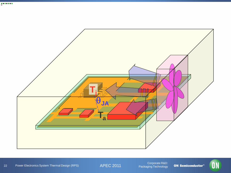
Corporate R&D: Packaging Technology 22 APEC 2011 Power Electronics System Thermal Design (RPS)
Ta
Tj θJA
Corporate R&D: Packaging Technology 23 APEC 2011 Power Electronics System Thermal Design (RPS)
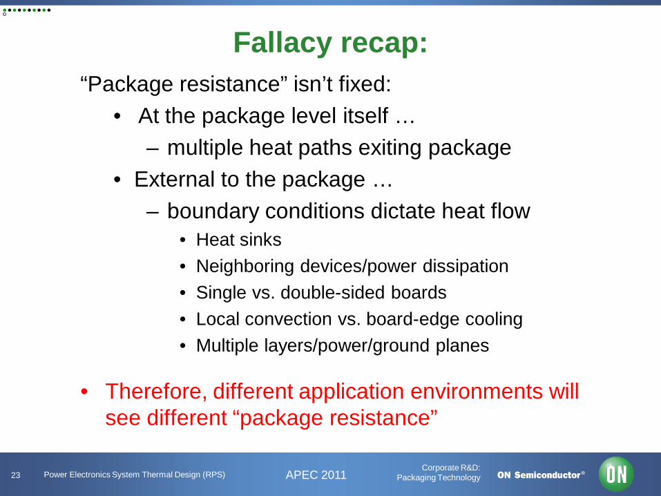
• Therefore, different application environments will see different “package resistance”
“Package resistance” isn’t fixed: • At the package level itself …
– multiple heat paths exiting package • External to the package …
– boundary conditions dictate heat flow • Heat sinks • Neighboring devices/power dissipation • Single vs. double-sided boards • Local convection vs. board-edge cooling • Multiple layers/power/ground planes
Fallacy recap:
Corporate R&D: Packaging Technology 24 APEC 2011 Power Electronics System Thermal Design (RPS)
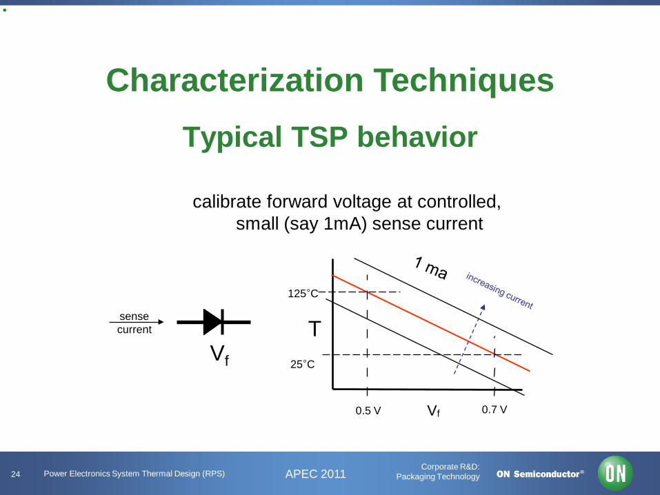
Characterization Techniques
Characterization Techniques Typical TSP behavior
Vf
Vf
T
125°C
25°C
0.7 V 0.5 V
sense current
calibrate forward voltage at controlled, small (say 1mA) sense current

Corporate R&D: Packaging Technology 25 APEC 2011 Power Electronics System Thermal Design (RPS)
DUT
true const. current supply
(1 mA typical)
DUT
10KΩ
If V f -0.7V, then I-1mA
10.7V
How to measure Tj
OR
approximate const. current supply

Corporate R&D: Packaging Technology 26 APEC 2011 Power Electronics System Thermal Design (RPS)
DUT
10KΩ heating power supply
10.7V 10.7V
DUT
10KΩ heating power supply
10.7V
How to heat
OR
sample current is off while heating current on sample current is always on

Corporate R&D: Packaging Technology 27 APEC 2011 Power Electronics System Thermal Design (RPS)
0.90 W 0.70 W 0.64 W
The importance of 4-wire measurements
Power supply
+(1.00 V)
-(0 V)
1 A
0.18 V 0.82 V
0.95 V 0.05 V 0.85 V 0.15 V
Output = 1 W

Corporate R&D: Packaging Technology 28 APEC 2011 Power Electronics System Thermal Design (RPS)
Which raises an interesting question:
0.3 W
Power supply
+(1.00 V)
-(0 V)
3 A
0.45 V 0.55 V
0.98 V 0.02 V
Output = 3 W
Is this a fair characterization of a low-Rds-on device?
1.3 W 1.3 W

Corporate R&D: Packaging Technology 29 APEC 2011 Power Electronics System Thermal Design (RPS)
Bipolar transistor
• TSP is Vce at designated “constant” current
• Heating is through Vce • Choose a base current that
permits adequate heating
bias supply
TSP=Vce bias resistor
TSP supply
switch
heating supply
10KΩ

Corporate R&D: Packaging Technology 30 APEC 2011 Power Electronics System Thermal Design (RPS)
Schottky diode
• TSP is forward voltage at “low” current • Voltages are typically very small (especially as
temperature goes up) • Highly non-linear, though maybe better as TSP
current increases; because voltage is low, higher TSP current may be acceptable
• Heating current will be large

Corporate R&D: Packaging Technology 31 APEC 2011 Power Electronics System Thermal Design (RPS)
MOSFET / TMOS
• Typically, use reverse bias “back body diode” for both TSP and for heating
• May need to tie gate to source (or drain) for reliable TSP characteristic
TSP=Vsd
TSP supply
switch
heating supply
10KΩ
+
-

Corporate R&D: Packaging Technology 32 APEC 2011 Power Electronics System Thermal Design (RPS)
+
MOSFET / TMOS method 2
• If you have fast switches and stable supplies
• Forward bias everything and use two different gate voltages
TSP=Vds
TSP supply
close switch to heat
heating supply
10KΩ
-
+
-
V-gate for
heating -
V-gate for
measure
+
close switch to heat
close switch to measure

Corporate R&D: Packaging Technology 33 APEC 2011 Power Electronics System Thermal Design (RPS)
RF MOS
• They exist to amplify high frequencies (i.e. noise)!
TSP supply
close switch to heat
heating supply
10KΩ
-
+ V-gate
for heating
-
+
close switch to heat
close switch to measure
• Feedback resistors may keep them in DC
+
-
TSP = body diode
TSP supply

Corporate R&D: Packaging Technology 34 APEC 2011 Power Electronics System Thermal Design (RPS)
IGBT
• Drain-source channel used for both TSP and heating
• Find a gate voltage which “turns on” the drain-source channel enough for heating purposes
• Use same gate voltage, but typically low TSP current for temperature measurement TSP=Vds
gate voltage
TSP supply
switch
heating supply
10KΩ
Corporate R&D: Packaging Technology 35 APEC 2011 Power Electronics System Thermal Design (RPS)
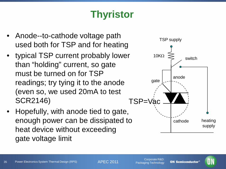
Thyristor
• Anode--to-cathode voltage path used both for TSP and for heating
• typical TSP current probably lower than “holding” current, so gate must be turned on for TSP readings; try tying it to the anode (even so, we used 20mA to test SCR2146)
• Hopefully, with anode tied to gate, enough power can be dissipated to heat device without exceeding gate voltage limit
TSP supply
switch 10KΩ
heating supply
TSP=Vac
cathode
anode gate

Corporate R&D: Packaging Technology 36 APEC 2011 Power Electronics System Thermal Design (RPS)
Logic and analog
• Find any TSP you can – ESD diodes on inputs or outputs – Body diodes somewhere
• Heat wherever you can – High voltage limits on Vcc, Vee, whatever – Body diodes or output drivers – Live loads on outputs
• (be very careful how you measure power!)

Corporate R&D: Packaging Technology 37 APEC 2011 Power Electronics System Thermal Design (RPS)
Heating curve method vs.
cooling curve method
Corporate R&D: Packaging Technology 38 APEC 2011 Power Electronics System Thermal Design (RPS)
DUT
10KΩ heating power supply
10.7V
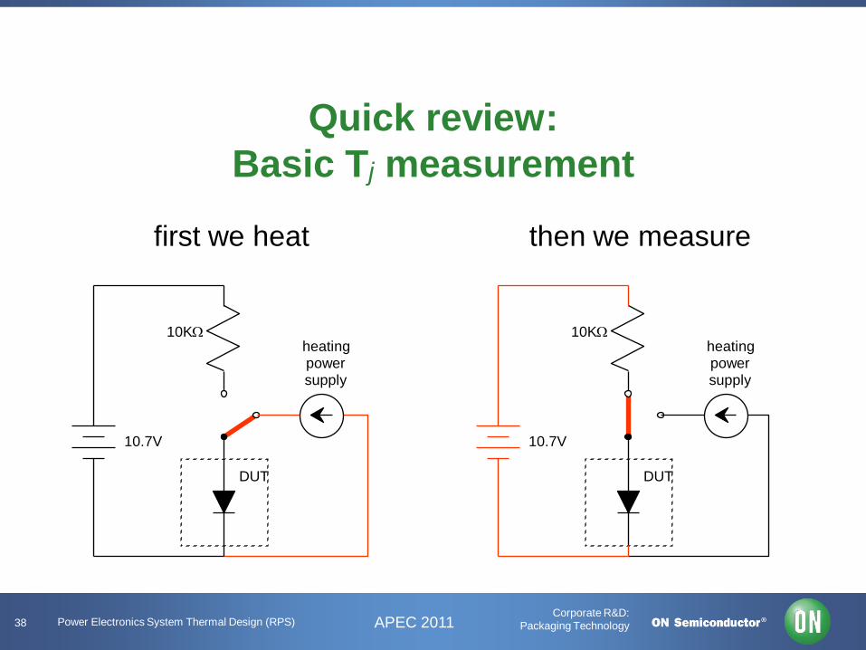
Quick review: Basic Tj measurement
DUT
10KΩ heating power supply
10.7V
first we heat then we measure

Corporate R&D: Packaging Technology 39 APEC 2011 Power Electronics System Thermal Design (RPS)
Question
• What happens when you switch from “heat” to “measure”?
Answer: stuff changes
• More specifically, the junction starts to cool down

Corporate R&D: Packaging Technology 40 APEC 2011 Power Electronics System Thermal Design (RPS)
V f
V f
T
125°C
25°C
.7V .5V
calibrate forward voltage @ 1mA sense current
pow
er-o
ff co
olin
g
high-current heating
measurements
convert cooling volts to
temperature
Basic “heating curve” transient method vo
ltage
curr
ent
1 ma
stea
dy s
tate
reac
hed
Tem
pera
ture
Time
pow
er-o
ff co
olin
g
high-current heating
pow
er-o
ff co
olin
g
high-current heating
pow
er-o
ff co
olin
g
high-current heating
measured temperatures

Corporate R&D: Packaging Technology 41 APEC 2011 Power Electronics System Thermal Design (RPS)
pow
er-o
ff co
olin
g
high-current heating
volta
ge
curr
ent
1 ma
Tem
pera
ture
Time
pow
er-o
ff co
olin
g
high-current heating
pow
er-o
ff co
olin
g
high-current heating
pow
er-o
ff co
olin
g
high-current heating
measured temperatures
Heating curve method #2
Time

Corporate R&D: Packaging Technology 42 APEC 2011 Power Electronics System Thermal Design (RPS)
Basic “cooling curve”
transient method V f
V f
T
125°C
25°C
.7V .5V
calibrate forward voltage @ 1mA sense current power-off
cooling high-
current heating
volta
ge
curr
ent
1 ma
measurements
heating period
transient cooling period (data taken)
stea
dy s
tate
reac
hed
Tem
pera
ture
Time
convert cooling volts to
temperature
Tem
pera
ture
Time (from start of cooling)
subtract cooling curve from peak temperature to obtain “heating” curve equivalent

Corporate R&D: Packaging Technology 43 APEC 2011 Power Electronics System Thermal Design (RPS)
• Heating vs. cooling – Physics is symmetric, as long as the material
and system properties are independent of temperature
Whoa! … that last step there …
cooling

Corporate R&D: Packaging Technology 44 APEC 2011 Power Electronics System Thermal Design (RPS)
Heating vs. cooling symmetry
(all the same curves, flipped
vertically)
flag
lead
back of board
edge of board
Start of (constant) power off
junction
Start of constant power input (“step heating”)
cooling

Corporate R&D: Packaging Technology 45 APEC 2011 Power Electronics System Thermal Design (RPS)
A (perhaps) subtle point …
• For a theoretically valid cooling curve, you must begin at true thermal equilibrium (not uniform temperature, but steady state)
• So whatever your θJA, max power is limited to:
JA
j TTpower
θambientmax −
=
cooling
Corporate R&D: Packaging Technology 46 APEC 2011 Power Electronics System Thermal Design (RPS)
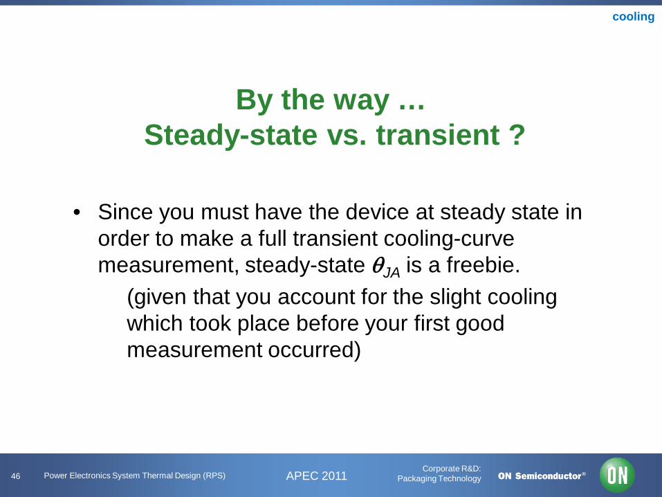
By the way … Steady-state vs. transient ?
• Since you must have the device at steady state in order to make a full transient cooling-curve measurement, steady-state θJA is a freebie.
(given that you account for the slight cooling which took place before your first good measurement occurred)
cooling

Corporate R&D: Packaging Technology 47 APEC 2011 Power Electronics System Thermal Design (RPS)
Effect of power on heating curve
< steady-state max power
Tj-max
Tamb
steady-state max power
2x steady-state power 6x steady-state power
24x steady-state power
3x steady-state power
time
junc
tion
tem
pera
ture
heating

Corporate R&D: Packaging Technology 48 APEC 2011 Power Electronics System Thermal Design (RPS)
Some initial uncertainty
heating period transient cooling period (data taken)
stea
dy s
tate
reac
hed
Tem
pera
ture
Time
power-off cooling
high-current heating
but once we’re past the “uncertain” range, all the rest of the points are “good”
a few initial points may be uncertain
cooling

Corporate R&D: Packaging Technology 49 APEC 2011 Power Electronics System Thermal Design (RPS)
Heating vs. cooling tradeoffs
starting temperature
heating power
temperature of fastest data
error control
HEATING
ambient
limited by tester
closer to ambient
all points similar error
COOLING
?
limited to steady-state
closer to Tj-max
error limited to first few points

Corporate R&D: Packaging Technology 50 APEC 2011 Power Electronics System Thermal Design (RPS)
• Varying the air speed is mainly varying the heat loss from the test board surface area, not from the package itself
• You just keep re-measuring your board’s characteristics
Still air vs. moving air
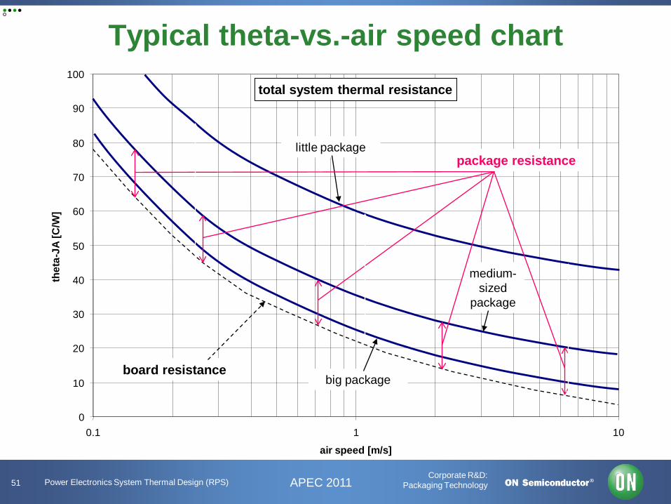
Corporate R&D: Packaging Technology 51 APEC 2011 Power Electronics System Thermal Design (RPS)
total system thermal resistance
0
10
20
30
40
50
60
70
80
90
100
0.1 1 10
air speed [m/s]
thet
a-JA
[C/W
]
little package
big package
medium-sized
package
board resistance
package resistance
Typical theta-vs.-air speed chart

Corporate R&D: Packaging Technology 52 APEC 2011 Power Electronics System Thermal Design (RPS)
• Min-pad board
• 1” heat spreader board
• You’re mainly characterizing how copper area affects every package and board, not how a particular package depends on copper area
Different boards

Corporate R&D: Packaging Technology 53 APEC 2011 Power Electronics System Thermal Design (RPS)
Typical thermal test board types
Min-pad board Minimum metal area to attach device (plus traces to get signals and power in and out)
1-inch-pad board Device at center of 1”x1” metal area (typically 1-oz Cu); divided into sections based on lead count

Corporate R&D: Packaging Technology 54 APEC 2011 Power Electronics System Thermal Design (RPS)
1" pad vs min-pad
0
50
100
150
200
250
300
350
0 100 200 300 400 500 600 700
min pad thetaJA (C/W)
1" p
ad th
etaJ
A (C
/W)
overall linear fit is:1" value = [0.51*(min-pad value) - 7]
SMBSMA & Pow ermite
Micro 8
TSOP-6(AL42)SOT-23
SOD-123
TSOP-6
SOD-123
SOT-23
SOD-323
SOT-23
SOD-123
Top Can
D2pak & TO220
Top Can
Dpak
SO-8SOT-223
TSOP-6SO-8
SMC
Source:Un-derated thermal data from old PPD database
Roger Stout 5/2

Corporate R&D: Packaging Technology 55 APEC 2011 Power Electronics System Thermal Design (RPS)
0
20
40
60
80
100
120
0 0.01 0.02 0.03 0.04 0.05
thet
a-B
A [C
/W]
copper radius [m]
board thermal resistance vs. copper radius0.042 m radius board2 oz copper spreader
curve parameter is heat source radius [m]0.00100.00200.00300.00400.0050

Corporate R&D: Packaging Technology 56 APEC 2011 Power Electronics System Thermal Design (RPS)
0
20
40
60
80
100
120
140
160
180
200
0 0.01 0.02 0.03 0.04 0.05
thet
a-B
A [C
/W]
copper radius [m]
board thermal resistance0.005 m radius heat source
2 oz copper spreadercurve parameter is board radius [m]
0.00420.00850.01270.01690.02120.02540.02960.03390.03810.0423

Corporate R&D: Packaging Technology 57 APEC 2011 Power Electronics System Thermal Design (RPS)
Standard coldplate testing
• “infinite” heatsink (that really isn’t) for measuring theta-JC on high-power devices
• If both power and coldplate temperature are independently controlled, “two parameter” compact models may be created

Corporate R&D: Packaging Technology 58 APEC 2011 Power Electronics System Thermal Design (RPS)
Standard coldplate testing
• Detailed design and placement of “case” TC can have significant effect on measured value
TC in 0.025” well, 0.025” from surface
DUT
.375”
.75”
Vleer pin assy
2.0”
TC on Vleer pin measures temperature at interface
Liquid Coolant Flow

Corporate R&D: Packaging Technology 59 APEC 2011 Power Electronics System Thermal Design (RPS)
2-parameter data reduction
heat in, Q
R1
R2
T1
Tj
T2
21 QQQ +=
)()( 22
11
11 TTR
TTR
Q jj −+−=
bxmxmy ++= 2211
)( 111
11 TTxR
m j −==0≡b
)( 222
21 TTxR
m j −==
where:
heat up, Q1
heat down, Q2
This has the form of a two-variable linear equation:

Corporate R&D: Packaging Technology 60 APEC 2011 Power Electronics System Thermal Design (RPS)
A “single coldplate” test
Rja
Rjc
Ta
Tj
Tc
ambient
coldplate -20.00
0.00
20.00
40.00
60.00
80.00
100.00
120.00
-20.00 0.00 20.00 40.00 60.00 80.00 100.00
∆Tja (¡C)
∆Tj
c (¡
C)
Increasing Power, Chuck HeldColdNo Power, Chuck TemperatureIncreased
Tc coldplate
Tj Ta

Corporate R&D: Packaging Technology 61 APEC 2011 Power Electronics System Thermal Design (RPS)
A “single coldplate” test, package down
-20.00
0.00
20.00
40.00
60.00
80.00
100.00
120.00
-10.00 0.00 10.00 20.00 30.00 40.00 50.00 60.00∆Tjb (¡C)
∆T
jc (
¡C)
Increasing Power, Chuck HeldColdNo Power, Chuck TemperatureIncreased
Rjb
Rjc
Tb
Tj
Tc
ambient
coldplate
Rba
Ta
Tj Tb Ta
coldplate Tc

Corporate R&D: Packaging Technology 62 APEC 2011 Power Electronics System Thermal Design (RPS)
Linear superposition
Linear superposition
• What is it? – The total response of a point within the system,
to excitations at all points of the system, is the sum of the individual responses to each excitation taken independently.
• When does it apply? – The system must be “linear” – in brief, all
responses must be proportional to all excitations.
• When would you use it? – When you have multiple heat sources (that is,
all the time!)
Corporate R&D: Packaging Technology 63 APEC 2011 Power Electronics System Thermal Design (RPS)
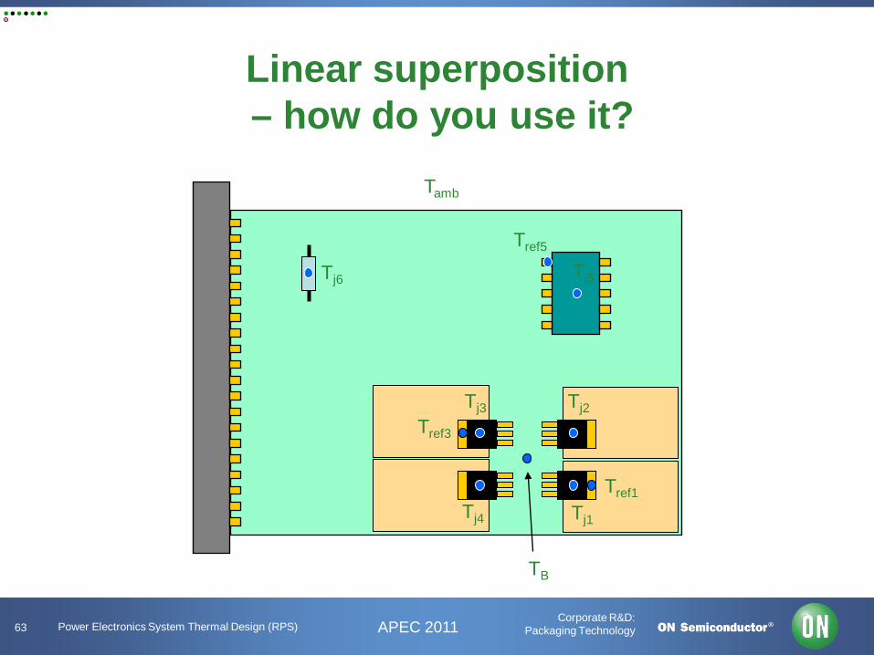
Linear superposition – how do you use it?
Tj3 Tj2
Tj1 Tj4
Tj5 Tj6
Tref1
Tref5
Tref3
TB
Tamb

Corporate R&D: Packaging Technology 64 APEC 2011 Power Electronics System Thermal Design (RPS)
a
nJnAnn
nAJ
nAJ
jn
j
j
T
q
T
TT
+
ΨΨ
ΨΨΨΨ
=
2
1
21
2221
1121
2
1
θ
θθ
theta matrix assembled from simplified subsystems
junction temperature
vector
power input vector
board interactions self-heating terms
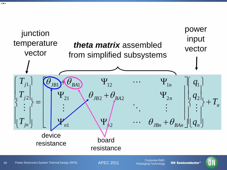
Corporate R&D: Packaging Technology 65 APEC 2011 Power Electronics System Thermal Design (RPS)
a
nBAnJBnnn
nBAJB
nBAJB
jn
j
j
T
q
T
TT
+
+ΨΨ
Ψ+ΨΨΨ+
=
2
1
21
22221
11211
2
1
θθ
θθθθ
theta matrix assembled from simplified subsystems
junction temperature
vector
power input vector
device resistance board
resistance

Corporate R&D: Packaging Technology 66 APEC 2011 Power Electronics System Thermal Design (RPS)
visualizing theta and psi
(idle heat source “x”)
thermal ground
measurements here are s
Ψ
xAΨyAΨ
AJ1θ
BJ1θ
BAθ
θmeasurements
here are s
(idle heat source “y”)
heat in here

Corporate R&D: Packaging Technology 67 APEC 2011 Power Electronics System Thermal Design (RPS)
ΨΨΨΨΨΨΨΨΨΨΨΨΨ
=
∆∆∆∆∆
⋅⋅⋅ 3
2
1
321
312111
321
23212
13121
1
2
1
qqq
TTTTT
BBB
LLL
xxx
JA
JA
BA
AL
xA
j
j
θθ
one column for each heat source
junction temperature
vector power input
vector
one row for each
heat source
one row for each temperature location of interest
theta matrix doesn’t have to be square
(why is this Ψ and not θ?)

Corporate R&D: Packaging Technology 68 APEC 2011 Power Electronics System Thermal Design (RPS)
The Reciprocity Theorem
“… the reciprocity theorem is not one with many obvious uses. Nevertheless, it is an elegant theorem and seems to be one that every educated man is expected to know.”1[1]
[1] H. Skilling, Electric Networks, pg. 249, John Wiley and Sons, 1974

Corporate R&D: Packaging Technology 69 APEC 2011 Power Electronics System Thermal Design (RPS)
Electrical reciprocity
5 V +
-
? V +
- 0.3 V
-
+
2 A 0.3 V -
+ I
V -
+

Corporate R&D: Packaging Technology 70 APEC 2011 Power Electronics System Thermal Design (RPS)
Thermal reciprocity
heat input here
same response
here response
here

Corporate R&D: Packaging Technology 71 APEC 2011 Power Electronics System Thermal Design (RPS)
Another thermal reciprocity example
heat input here
same response
here
response here
(s)
(s)
(r)
(r)

Corporate R&D: Packaging Technology 72 APEC 2011 Power Electronics System Thermal Design (RPS)
When does reciprocity NOT Apply?
A D
C airflow
Heat in at “A” will raise temperature of “C” more than heat in at “C” will raise temperature of “A”
• Upwind and downwind in forced-convection dominated applications
“B” and “D” may still be roughly reciprocal
B

Corporate R&D: Packaging Technology 73 APEC 2011 Power Electronics System Thermal Design (RPS)
(square part of) matrix is symmetric
75 65 55 60 22 10
65 71 60 55 25 11
55 60 65 61 21 15
60 55 61 73 18 11
22 25 21 18 125 14
10 11 15 11 14 180
73 65 55 59 22 10
55 60 63 61 21 15
20 24 14 19 95 15
65 63 62 63 21 12
J1
J2
J3
J4
J5
J6
R1
R3
R5
B
rows are the response locations
columns are the heat sources

Corporate R&D: Packaging Technology 74 APEC 2011 Power Electronics System Thermal Design (RPS)
Superposition example
Tj3=85.5 Tj2=96.5
Tj1=107.5 Tj4=91.0
Tj5=49.2 Tj6=36.0
Tref1=105.3
Tref5=47.0
Tref3=85.5
TB=96.5
Tamb=25
Device 1 heated, 1.1 W

Corporate R&D: Packaging Technology 75 APEC 2011 Power Electronics System Thermal Design (RPS)
Reduce the data
θj1A 75
Ψ j2A 65
Ψ j3A 55
Ψ j4A 60
Ψ j5A 22
Ψ j6A 10
Ψ r1A 73
Ψ r3A 55
Ψ r5A 20
Ψ BA 65
7511
255107qTT
1
amb1jA1j =
−=
−=
..θ
6511
25596qTT
1
amb2jA2j =
−=
−=Ψ
..
6511
25596qTT
1
ambBBA =
−=
−=Ψ
..

Corporate R&D: Packaging Technology 76 APEC 2011 Power Electronics System Thermal Design (RPS)
Device 2 heated, 1.2 W
Tj3=97.0 Tj2=110.2
Tj1=103.0 Tj4=91.0
Tj5=55.0 Tj6=38.2
Tref1=103.0
Tref5=53.8
Tref3=97.0
TB=100.6
Tamb=25
Ψj1A 65
θ j2A 71
Ψ j3A 60
Ψ j4A 55
Ψ j5A 25
Ψ j6A 11
Ψ r1A 65
Ψ r3A 60
Ψ r5A 24
Ψ BA 63

Corporate R&D: Packaging Technology 77 APEC 2011 Power Electronics System Thermal Design (RPS)
Device 3 heated, 1.3 W
Tj3=109.5 Tj2=103.0
Tj1=96.5 Tj4=104.3
Tj5=52.3 Tj6=44.5
Tref1=96.5
Tref5=43.2
Tref3=106.9
TB=105.6
Tamb=25 Ψj1A 55
Ψ j2A 60
θ j3A 65
Ψ j4A 61
Ψ j5A 21
Ψ j6A 15
Ψ r1A 55
Ψ r3A 63
Ψ r5A 14
Ψ BA 62

Corporate R&D: Packaging Technology 78 APEC 2011 Power Electronics System Thermal Design (RPS)
Device 4 heated, 1.1 W
Tj3=92.1 Tj2=85.5
Tj1=91.0 Tj4=105.3
Tj5=44.8 Tj6=37.1
Tref1=89.9
Tref5=45.9
Tref3=92.1
TB=94.3
Tamb=25 Ψj1A 60
Ψ j2A 55
Ψ j3A 61
θ j4A 73
Ψ j5A 18
Ψ j6A 11
Ψ r1A 59
Ψ r3A 61
Ψ r5A 19
Ψ BA 63

Corporate R&D: Packaging Technology 79 APEC 2011 Power Electronics System Thermal Design (RPS)
Device 5 heated, 0.7 W
Tj3=39.7 Tj2=42.5
Tj1=40.4 Tj4=37.6
Tj5=112.5 Tj6=34.8
Tref1=40.4
Tref5=91.5
Tref3=39.7
TB=39.7
Tamb=25 Ψj1A 22
Ψ j2A 25
Ψ j3A 21
Ψ j4A 18
θ j5A 125
Ψ j6A 14
Ψ r1A 22
Ψ r3A 21
Ψ r5A 95
Ψ BA 21

Corporate R&D: Packaging Technology 80 APEC 2011 Power Electronics System Thermal Design (RPS)
Device 6 heated, 0.5 W
Tj3=32.5 Tj2=30.5
Tj1=30.0 Tj4=30.5
Tj5=32.0 Tj6=115.0
Tref1=30.0
Tref5=32.5
Tref3=32.5
TB=31.0
Tamb=25 Ψj1A 10
Ψ j2A 11
Ψ j3A 15
Ψ j4A 11
Ψ j5A 14
θ j6A 180
Ψ r1A 10
Ψ r3A 15
Ψ r5A 15
Ψ BA 12

Corporate R&D: Packaging Technology 81 APEC 2011 Power Electronics System Thermal Design (RPS)
Collect the θ/Ψ values
75 65 55 60 22 10
65 71 60 55 25 11
55 60 65 61 21 15
60 55 61 73 18 11
22 25 21 18 125 14
10 11 15 11 14 180
73 65 55 59 22 10
55 60 63 61 21 15
20 24 14 19 95 15
65 63 62 63 21 12
J1
J2
J3
J4
J5
J6
R1
R3
R5
B
rows are the response locations
columns are the heat sources

Corporate R&D: Packaging Technology 82 APEC 2011 Power Electronics System Thermal Design (RPS)
Now apply actual power
Tj3=134.9 Tj2=140.1
Tj1=140.0 Tj4=135.8
Tj5=124.7 Tj6=139.1
Tref1=138.8
Tref5=106.3
Tref3=134.1
TB=139.1
Tamb=25
Qj1 .4
Q j2 .4
Q j3 .4
Q j4 .4
Q j5 .5
Q j6 .2
Actual power in application

Corporate R&D: Packaging Technology 83 APEC 2011 Power Electronics System Thermal Design (RPS)
Compute some effective θ/Ψ values
Take Tj1, for instance. Remember when it was heated all alone, we calculated its self-heating theta-JA like this:
7511
255107qTT
1
amb1jA1j =
−=
−=
..θ
28840
25140qTT
1
amb1jA1j =
−=
−=
.θ
Now let’s see: ≠

Corporate R&D: Packaging Technology 84 APEC 2011 Power Electronics System Thermal Design (RPS)
And that’s not just a single aberration!
Self heating
θ j1A 288 vs. 75
θ j2A 288 vs. 71
θ j3A 274 vs. 65
θ j4A 277 vs. 73
θ j5A 199 vs. 125
θ j6A 309 vs. 180
Junction to Board
Ψj1-B 2.2 vs. 10.0
Ψj2-B 2.5 vs. 8.0
Ψj3-B -10.5 vs. 3.0
Ψj4-B -8.3 vs. 10.0
Junction to Reference
Ψj1-R1 3.0 vs. 2.0
Ψj3-R3 2.0 vs. 2.0
Ψj5-R5 36.8 vs. 30.0 3.8x
4.1x
4.2x
3.8x
1.6x
1.7x
1.5x
1.0x
1.2x
0.2x
0.3x
-3.5x
-0.8x

Corporate R&D: Packaging Technology 85 APEC 2011 Power Electronics System Thermal Design (RPS)
Is the moral clear?
• You simply cannot use published theta-JA values for devices in your real system, even if those values are perfectly accurate and correct as reported on the datasheet and you know the exact specifications of the test conditions.
• Not unless your actual application is identical to the manufacturer’s test board – and uses just that one device all by itself.

Corporate R&D: Packaging Technology 86 APEC 2011 Power Electronics System Thermal Design (RPS)
ann12121A1J1j TqqqT +Ψ+Ψ+= θ
a
n
2
1
JnAn2n1
n2A2J12
n112A1J
jn
2j
1j
T
q
T
TT
+
ΨΨ
ΨΨΨΨ
=
θ
θθ
So is it really this bad? Only sort-of. Let’s revisit the math for one device …
a
n
2nn11A1J1j TqqT +Ψ+= ∑θ
“effective” ambient

Corporate R&D: Packaging Technology 87 APEC 2011 Power Electronics System Thermal Design (RPS)
a1A1J1j TqT += θ
power, q
Ta junction temperature , TJ1
Ta’ junction temperature , TJ1
′+=
+Ψ+= ∑
a1A1J
a
n
2nn11A1J1j
Tq
TqqT
θ
θ
Ta
shift in effective ambient
Device in a system
still the same slope
1
θJ1A
1
θJ1A
Isolated device
A graphical view

Corporate R&D: Packaging Technology 88 APEC 2011 Power Electronics System Thermal Design (RPS)
What about that “system” theta we saw earlier that was so different?
junction temperature
power
Ta’
1
θJ1A
Ta
the “system” theta-JA
the isolated-device theta-JA ∑Ψ
n
2nn1 q
1
θJ1A*
device #1 power/temperature perturbations will fall on this line
NOT this one q1
TJ1

Corporate R&D: Packaging Technology 89 APEC 2011 Power Electronics System Thermal Design (RPS)
when Q1 is zero, both of these will be
zero
a
n
2iii11j1aj1 TQQT +⋅Ψ+⋅= ∑
=
)(θ
How does effective ambient relate to board temperature?
temperature rise, board to J1
“system” slope for isolated device
temperature rise, ambient to board
a1a1B1B1j TQQ ′+⋅+⋅= θθ
aa1BB1j TTT ′+∆+∆=
a1B1aj1B TQ ′+⋅+= )( θθ
if any of these are non-zero, will be higher than aT′ aT
when Q1 is not zero, both of these will be non-zero
effective ambient

Corporate R&D: Packaging Technology 90 APEC 2011 Power Electronics System Thermal Design (RPS)
How to harness this math in Excel®
Controlling the matrix

Corporate R&D: Packaging Technology 91 APEC 2011 Power Electronics System Thermal Design (RPS)
3x3 theta matrix, 3x1 power vector Excel® math
theta matrix
power vector
Matrix MULTiply
=array formula notation
array reference to theta matrix
array reference to power vector
obtained by using Ctrl-Shift-Enter rather than ordinary Enter
multi-cell placement of array formula

Corporate R&D: Packaging Technology 92 APEC 2011 Power Electronics System Thermal Design (RPS)
7x3 theta matrix, 3x1 power vector Excel® math
array formula now occupies 7 cells
theta matrix is no longer square – # of columns still must equal
# of rows of power vector
don’t forget to use Ctrl-Shift-Enter to invoke array formula notation
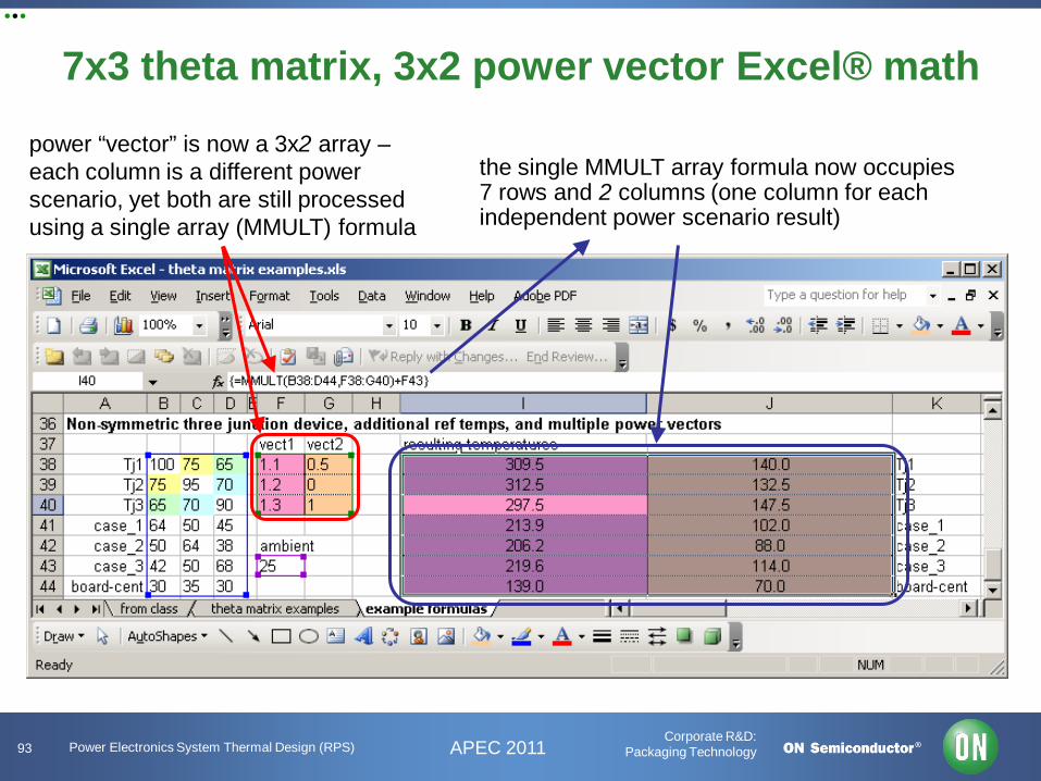
Corporate R&D: Packaging Technology 93 APEC 2011 Power Electronics System Thermal Design (RPS)
7x3 theta matrix, 3x2 power vector Excel® math
the single MMULT array formula now occupies 7 rows and 2 columns (one column for each independent power scenario result)
power “vector” is now a 3x2 array – each column is a different power scenario, yet both are still processed using a single array (MMULT) formula

Corporate R&D: Packaging Technology 94 APEC 2011 Power Electronics System Thermal Design (RPS)
Temperature direct contributions and totals
0
20
40
60
80
100
120
J1 J2 J3 J4 J5 J6 R1 R3 R5 B
result location
tem
pera
ture
rise
[C],
each
sou
rce
J1 at 0.4 W J2 at 0.4 W J3 at 0.4 WJ4 at 0.4 W J5 at 0.5 W J6 at 0.2 W
0
20
40
60
80
100
120
J1 J2 J3 J4 J5 J6 R1 R3 R5 B
result location
tem
pera
ture
rise
[C] s
um o
f sou
rces
J1 at 0.4 W J2 at 0.4 W J3 at 0.4 WJ4 at 0.4 W J5 at 0.5 W J6 at 0.2 W

Corporate R&D: Packaging Technology 95 APEC 2011 Power Electronics System Thermal Design (RPS)
Normalized responses at each location due to each source
0
20
40
60
80
100
120
140
160
180
200
J1 J2 J3 J4 J5 J6 R1 R3 R5 Bresponse location
norm
aliz
ed re
spon
se [C
/W],
each
sou
rce J1 at 1 W
J2 at 1 WJ3 at 1 WJ4 at 1 WJ5 at 1 WJ6 at 1 W

Corporate R&D: Packaging Technology 96 APEC 2011 Power Electronics System Thermal Design (RPS)
Some useful formulas
• conduction resistance…………..………
• convection resistance…………...………
• thermal capacitance……………...……..
• characteristic time…………………..…. – (dominated by 1-D conduction)
• characteristic time……………………... – (dominated by 1-D convection)
• short-time 1-D transient response……...
R = Lk ⋅ A
R = 1h ⋅ A
C = ρcpV
τ =ρcpL2
k
τ =ρcpL
h
∆T = QA
2πρcpk
t

Corporate R&D: Packaging Technology 97 APEC 2011 Power Electronics System Thermal Design (RPS)
Terms used in preceding formulas • L - thermal path length • A - thermal path cross-sectional area • k - thermal conductivity • ρ - density • cp - heat capacity • α - thermal diffusivity • η - thermal effusivity • h - convection heat-transfer “film coefficient”) • ∆T - junction temperature rise • Q - heating power • t - time since heat was first applied
η = ρcpk
α =k
ρcp

Corporate R&D: Packaging Technology 98 APEC 2011 Power Electronics System Thermal Design (RPS)
mainly package
materials/conduction effects
mainly local application board conduction effects
mainly environmental convection and radiation effects
When do these effects enter?
time
junc
tion
tem
pera
ture
typical heating curve for device on FR-4
board in still-air
hundreds of seconds
a second or so
tens of seconds

Corporate R&D: Packaging Technology 99 APEC 2011 Power Electronics System Thermal Design (RPS)
if
then and
R⇒
R2≈
R4≈

Corporate R&D: Packaging Technology 100 APEC 2011 Power Electronics System Thermal Design (RPS)
Cylindrical and spherical conduction (through radial thickness) resistance
formulas
Lkrr
R
Lkrr
R
i
o
i
o
⋅⋅
=
⋅⋅
=
π
π
2
ln
ln
• L – cylinder length • ri – inner radius • ro – outer radius
where
Half-cylinder
Full cylinder krrR
krrR
oi
oi
⋅
−=
⋅
−=
π
π
4
11
2
11
Hemisphere Full sphere
[included angle] [solid angle]

Corporate R&D: Packaging Technology 101 APEC 2011 Power Electronics System Thermal Design (RPS)
• The device and system are equally important to get right
Predicting the temperature of high power components
• The system is probably more important than the device
Predicting the temperature of low power components

Corporate R&D: Packaging Technology 102 APEC 2011 Power Electronics System Thermal Design (RPS)
Using the previous board example …
75 65 55 60 22 10
65 71 60 55 25 11
55 60 65 61 21 15
60 55 61 73 18 11
22 25 21 18 125 14
10 11 15 11 14 180
73 65 55 59 22 10
55 60 63 61 21 15
20 24 14 19 95 15
65 63 62 63 21 12
J1
J2
J3
J4
J5
J6
R1
R3
R5
B
Qj1 0.5
Q j2 0.5
Q j3 0.5
Q j4 0.5
Q j5 0.2
Q j6 0.02
power vector
theta array
Corporate R&D: Packaging Technology 103 APEC 2011 Power Electronics System Thermal Design (RPS)
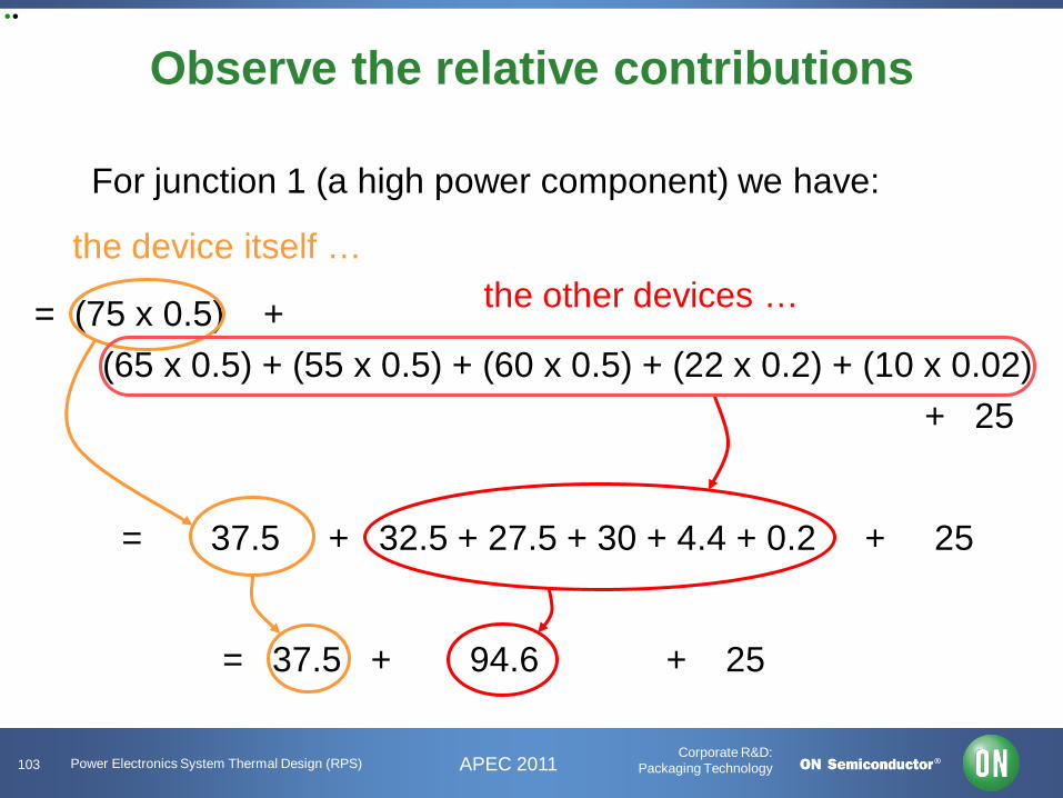
Observe the relative contributions
= (75 x 0.5) + (65 x 0.5) + (55 x 0.5) + (60 x 0.5) + (22 x 0.2) + (10 x 0.02) + 25
For junction 1 (a high power component) we have:
= 37.5 + 32.5 + 27.5 + 30 + 4.4 + 0.2 + 25
= 37.5 + 94.6 + 25
the device itself … the other devices …

Corporate R&D: Packaging Technology 104 APEC 2011 Power Electronics System Thermal Design (RPS)
Relative contributions to ∆TJ6
= (10 x 0.5) + (11 x 0.5) + (15 x 0.5) + (11 x 0.5) + (14 x 0.2) + (180 x 0.02) + 25
= 5.0 + 5.5 + 7.5 + 5.5 + 2.8 + 3.6 + 25
= 26.3 + 3.6 + 25
the device itself …
the other devices …

Corporate R&D: Packaging Technology 105 APEC 2011 Power Electronics System Thermal Design (RPS)
Thermal runaway
Thermal runaway • Non-linear power vs. junction temperature device
characteristic
• System thermal resistance isn’t low enough to shed small perturbations

Corporate R&D: Packaging Technology 106 APEC 2011 Power Electronics System Thermal Design (RPS)
A linear thermal cooling system
xJxJ TQT +⋅= θ
Jx
xJ TTQθ−
=
JxdTdQ
θ1
=
junction temperature as function of power, theta, and ground
… solving for power
sensitivity (slope) of power with respect to temperature

Corporate R&D: Packaging Technology 107 APEC 2011 Power Electronics System Thermal Design (RPS)
power
junction temperature
Q
Tx TJ
device line
system line
tendency to cool
tendency to heat
Effect of device line slope on system stability

Corporate R&D: Packaging Technology 108 APEC 2011 Power Electronics System Thermal Design (RPS)
system cannot be successfully
powered up
system temperature cannot be maintained
Operating points of thermal system when device line has negative second derivative power
junction temperature
Q2
Tx TJ2
power goes up with increasing temperature
device line
system line
the stable (that is, real) operating point
an unachievable operating point
tendency to cool
tendency to heat
tendency to cool
Q1
TJ1
but rate of increase falls with increase (negative second derivative)

Corporate R&D: Packaging Technology 109 APEC 2011 Power Electronics System Thermal Design (RPS)
even turning the device on destroys it
any perturbation will cause runaway
Operating points of thermal system when device line has positive second derivative
power
junction temperature
Q
Tx TJ
power goes up with increasing temperature, but rate of increase rises with increase (positive second derivative)
device line
system line
the stable (that is, real) operating point
an unachievable operating point
tendency to cool
tendency to heat
tendency to heat
Corporate R&D: Packaging Technology 110 APEC 2011 Power Electronics System Thermal Design (RPS)
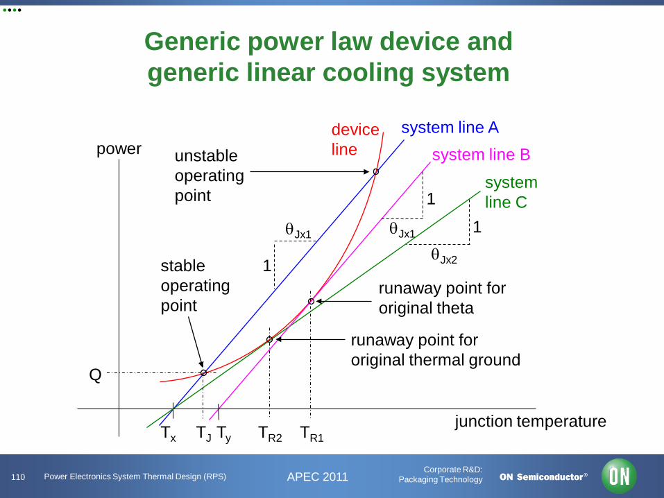
Generic power law device and generic linear cooling system
power
junction temperature Tx
device line unstable
operating point
system line B
Ty
stable operating point
runaway point for original theta
runaway point for original thermal ground
system line C
1
θJx1 θJx1
1
1 θJx2
system line A
TR2 TR1
Q
TJ

Corporate R&D: Packaging Technology 111 APEC 2011 Power Electronics System Thermal Design (RPS)
Let’s see how it works
device operating
curve
25°C/W system
stable operating
point
unstable operating point
10°C/W system
NO operating
point!
40°C/W system
0.0
0.4
0.8
1.2
1.6
2.0
20 40 60 80 100 Junction Temperature [C]
Dev
ice
Pow
er D
issi
patio
n [W
]

Corporate R&D: Packaging Technology 112 APEC 2011 Power Electronics System Thermal Design (RPS)
Unfortunate coincidence of terms!
xay =
xey =
IVQ ⋅=
a mathematical “power law” device power
an “exponential” power law (base is e)

Corporate R&D: Packaging Technology 113 APEC 2011 Power Electronics System Thermal Design (RPS)
Definition of power law device
10T
o 2II =
( )
== 210T
o10T2
o eIeII lnln
λT
oeII =
−=
21
21
II
TT
lnλ
λλT
o
T
oR eQeIVQ ==
λλ
To eQ
dTdQ
= λ
λ
T
2o
2
2eQ
dTQd
=
rule of thumb for leakage; 2x increase for every 10°C for constant voltage, power does
the same
1st and 2nd derivatives
both always positive
defining:

Corporate R&D: Packaging Technology 114 APEC 2011 Power Electronics System Thermal Design (RPS)
The mathematical essence
Jx
xTTQθ−
=
λT
oeQQ =
λθ
λ xT
oJxe
Qk
−
=
zekz =
System line
Power law device line
λxTTz −
=
QeQ1q
xT
o
=
−λ
Non-dimensionalizing
temperature
power
where:
zeq =(power law device)
kzq =
Leads to:
(system)
Eliminating q:

Corporate R&D: Packaging Technology 115 APEC 2011 Power Electronics System Thermal Design (RPS)
Perfect runaway transformed
1zz 0T =−
ez
at point of tangency, slope equals height
zT 1 z0
k=ez
λxTTz −
=zT 1 z0
k=ez
zT 1 z0
k=ez
zT 1 z0
k=ez

Corporate R&D: Packaging Technology 116 APEC 2011 Power Electronics System Thermal Design (RPS)
Transforming the nominal system
ez
at point of tangency, slope equals height
1
k=e
“operating” points
k > e (2 intersections)
k < e (no intersections)
nominal system line A

Corporate R&D: Packaging Technology 117 APEC 2011 Power Electronics System Thermal Design (RPS)
Everything transformed
non-dimensional power
device line
unstable, non-operating point
stable operating point
system line A
zR2
runaway point for original theta
runaway point for original thermal ground
system line B
system line C
non-dimensional temperature zR1
k1
1 zx1
k2
1
)( 1R1 kz ln=1kz 1x1 −= )(ln 1z 2R =
ek2 =
k1 1
q=k1z
q=k1(z-zx1)
q=k2z
q=ez

Corporate R&D: Packaging Technology 118 APEC 2011 Power Electronics System Thermal Design (RPS)
“Perfect runaway” results in original terms
=
o1Jx1R Q
Tθ
λλ ln
λθ
λλ −
=
o1Jx1x Q
T ln
+−
=1T
o2Jx
x
eQ
λλθ
λ+= x2R TT
runaway temperature based on original slope
max ambient that goes with it
runaway temperature based on original ambient
system resistance that goes with it

Corporate R&D: Packaging Technology 119 APEC 2011 Power Electronics System Thermal Design (RPS)
The “operating” points
ez
“operating” points
1
kz
szs ekz =
uzu ekz =
sz uz
stable
unstable
Corporate R&D: Packaging Technology 120 APEC 2011 Power Electronics System Thermal Design (RPS)
Newton’s method for the intersections
i
i
1i
z11
zek
z−
=+
ln
)()(
i
ii1i zF
zFzz
′−
−=+
zkz =ln
kzzzF ln−=)(
For k/e ranging between 1.01 and 1000, convergence is to a dozen significant digits in fewer than 10 iterations.
zekz =
eke
1k1zo
⋅== this initial guess
converges to lower, stable point
+==
ek1kzo lnln
this initial guess converges to upper,
unstable point
z11zF −=′ )(

Corporate R&D: Packaging Technology 121 APEC 2011 Power Electronics System Thermal Design (RPS)
And the intersection points come from …
stablexstable zTT ⋅+= λ
find the non-dimensional intersections first, then
unstablexunstable zTT ⋅+= λ

Corporate R&D: Packaging Technology 122 APEC 2011 Power Electronics System Thermal Design (RPS)
A paradox
junction
thermal ground
50°C/W
lead
100°C/W
100°C
75°C
25°C
0.5 W
thermal runaway, based on θJx=150°C/W,
calculated to be at 125°C
junction
thermal ground
50°C/W
lead
0.2°C/W
100°C
75°C
74.9°C
0.5 W
thermal runaway, based on θJx=50.2°C/W, calculated to be at 150°C
identical
Case A Case B

Corporate R&D: Packaging Technology 123 APEC 2011 Power Electronics System Thermal Design (RPS)
100 + 5.02 °C
75 + 0.02 °C 75 + 10 °C
100 + 15 °C
Paradox lost
junction
50°C/W
lead
100°C/W
(fixed) 25°C
junction
50°C/W
lead
0.2°C/W
(fixed) 74.9°C
Case A Case B
raise the power by 0.1 W and see what happens 0.5 + 0.1 W 0.5 + 0.1 W

Corporate R&D: Packaging Technology 124 APEC 2011 Power Electronics System Thermal Design (RPS)
Illustrating the paradox
100°C 25°C 74.9°C
common nominal operating point
0.5 W
Case A
Case B device line

Corporate R&D: Packaging Technology 125 APEC 2011 Power Electronics System Thermal Design (RPS)
[°C] 17.9 17.8
[W] 9.4E-5 1.02E-3
Real datasheet example
Vr [V] 12 40
Tmax [°C] 125 125
Tref [°C] 75 75
Itmax [A] 8.50E-3 2.80E-2
Itref [A] 5.20E-4 1.70E-3
λoQ
the device power curve parameters @12V @40V
−=
ref
ref
II
TT
max
max
lnλ
oR0 IVQ =λλrefT
tref
T
t0 eIeII−−
==max
max
λT
0eII =
14.42
10==
)(ln
rule of thumb gave us:
† MBRS140T3
raw device data†

Corporate R&D: Packaging Technology 126 APEC 2011 Power Electronics System Thermal Design (RPS)
1.609
83.5
101.3
[°C] 17.9 17.8
[W] 9.4E-5 1.02E-3
(compare to unity) 10.6 0.97
given theta
max [°C] 117.2 74.4
[°C] 135.1 92.2
given ambient
max [°C/W] 1055 96.6
[°C] 92.9 92.8
Runaway analysis in nominal system
Vr [V] 12 40
Tmax [°C] 125 125
Tref [°C] 75 75
Itmax [A] 8.50E-3 2.80E-2
Itref [A] 5.20E-4 1.70E-3
λoQ
ek
xT
1RT
2Jxθ
2RT
3120z .=
raw device data†
computed results @12V @40V @40V
3152z .=
These translate into: a stable operating point at 80.6°C (and 0.09 W), an unstable point at 116.3°C (0.69 W)
1001Jx =θ 601Jx =θ
75Tx =1T
oJx
x
eQe
k −−
= λθ
λ
† MBRS140T3

Corporate R&D: Packaging Technology 127 APEC 2011 Power Electronics System Thermal Design (RPS)
HTRB example
• Bidirectional Thyristor in reliability stress test (High Temperature Reverse Bias)
• Goal is life tests at elevated temperature (say 125°C)
• Problem is, they don’t last very long, and if junction temperature is anything like the chamber temperature, they appear to fail way too early good!
G MT1
MT2
40 kΩ
640 V
-
HTRB test circuit
+
*Special acknowledgements to Dave Billings and Geoff Garcia for their contributions to this project

Corporate R&D: Packaging Technology 128 APEC 2011 Power Electronics System Thermal Design (RPS)
HTRB data - sockets without heatsinks
0
20
40
60
80
100
120
140
160
180
200
0 2000 4000 6000 8000 10000 12000
test time [s]
Hea
tsin
k (ta
b) te
mpe
ratu
re [d
egC
]
DUT T1DUT T2DUT T3DUT T4DUT T5DUT T6DUT T7DUT T8DUT T9DUT T10
HTRB DUT tab temperature vs. test time
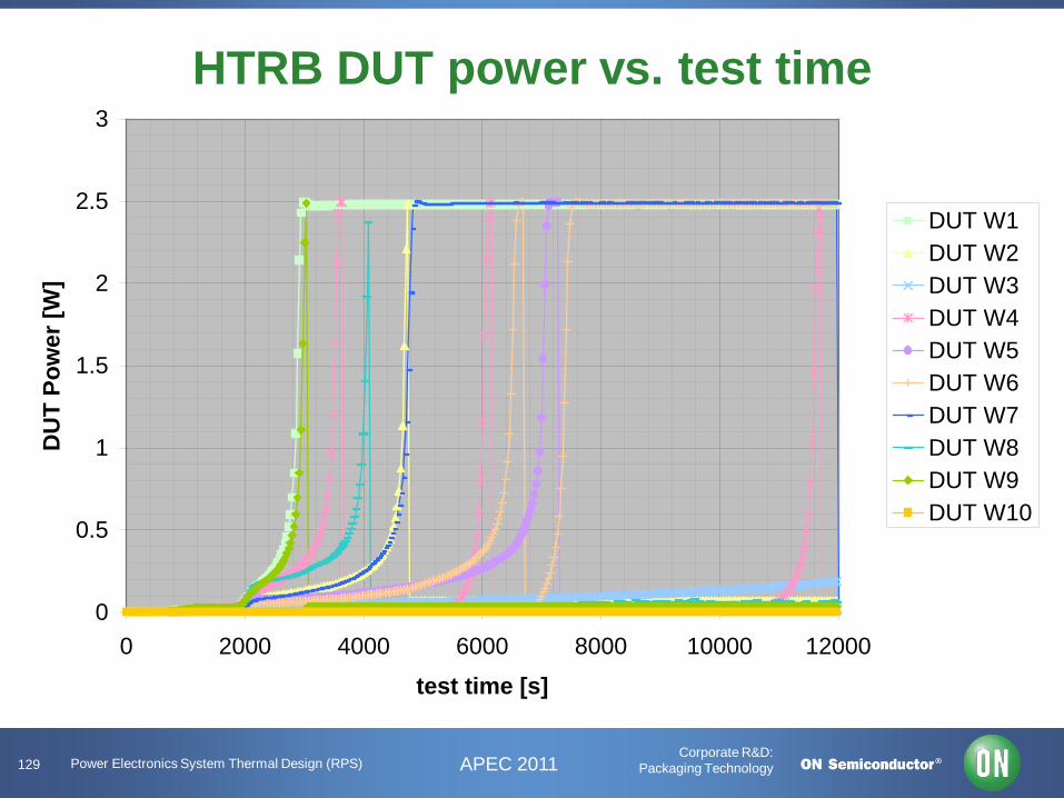
Corporate R&D: Packaging Technology 129 APEC 2011 Power Electronics System Thermal Design (RPS)
HTRB data - sockets without heatsinks
0
0.5
1
1.5
2
2.5
3
0 2000 4000 6000 8000 10000 12000
test time [s]
DU
T Po
wer
[W]
DUT W1DUT W2DUT W3DUT W4DUT W5DUT W6DUT W7DUT W8DUT W9DUT W10
HTRB DUT power vs. test time

Corporate R&D: Packaging Technology 130 APEC 2011 Power Electronics System Thermal Design (RPS)
HTRB example

Corporate R&D: Packaging Technology 131 APEC 2011 Power Electronics System Thermal Design (RPS)
Quick calculations from datasheet
JAdaJ PTT θ⋅+=
)( 40000640 IIPd ⋅−⋅=
• At room temp, if IDRM is 5 uA, then Pd is about zero (≈3mW), and TJ should thus equal chamber set point.
• At 85°C, IDRM is about 0.1-0.2mA, thus Pd is on the order of 0.1W, so depending on theta-JA, TJ could be several degrees hotter than chamber set point (note, however, that TJ will still be well within 1°C of heatsink temperature, THS)
• HOWEVER, at 125°C, if IDRM is 2mA, then Pd will be in excess of 1W. Depending on theta-JA, TJ could be 30-60°C above chamber set point (though still within a couple of degrees of heatsink temperature, if known).
G MT1
MT2
40 kΩ
640 V
-
HTRB test circuit
+
HSJdHSJ PTT −⋅+= θor

Corporate R&D: Packaging Technology 132 APEC 2011 Power Electronics System Thermal Design (RPS)
Calculations based on actual measurements
JAdaJ PTT θ⋅+=
1000senseVI =
• At room temp, IDRM (via Vsense) is 0.2uA, thus Pd is about zero (≈0.1mW), and TJ should thus equal chamber set point.
• At 85°C, IDRM is about 0.1-0.2mA, thus Pd is on the order of 0.1W, so depending on theta-JA, TJ could be several degrees hotter than chamber set point (note, however, that TJ will still be well within 1°C of heatsink temperature, THS)
• At 125°C, IDRM is 2-3mA; Pd could be as high as 1.5W
• Max current observed was nearly 8mA (for Pd of 2.5W), and estimated TJ of 170°C just prior to device failure.
G MT1
MT2
40 kΩ
640 V
-
Modified HTRB test circuit
-
+
1 kΩ Vsense
+
HSJdHSJ PTT −⋅+= θor
)( 41000640 IIPd ⋅−⋅=
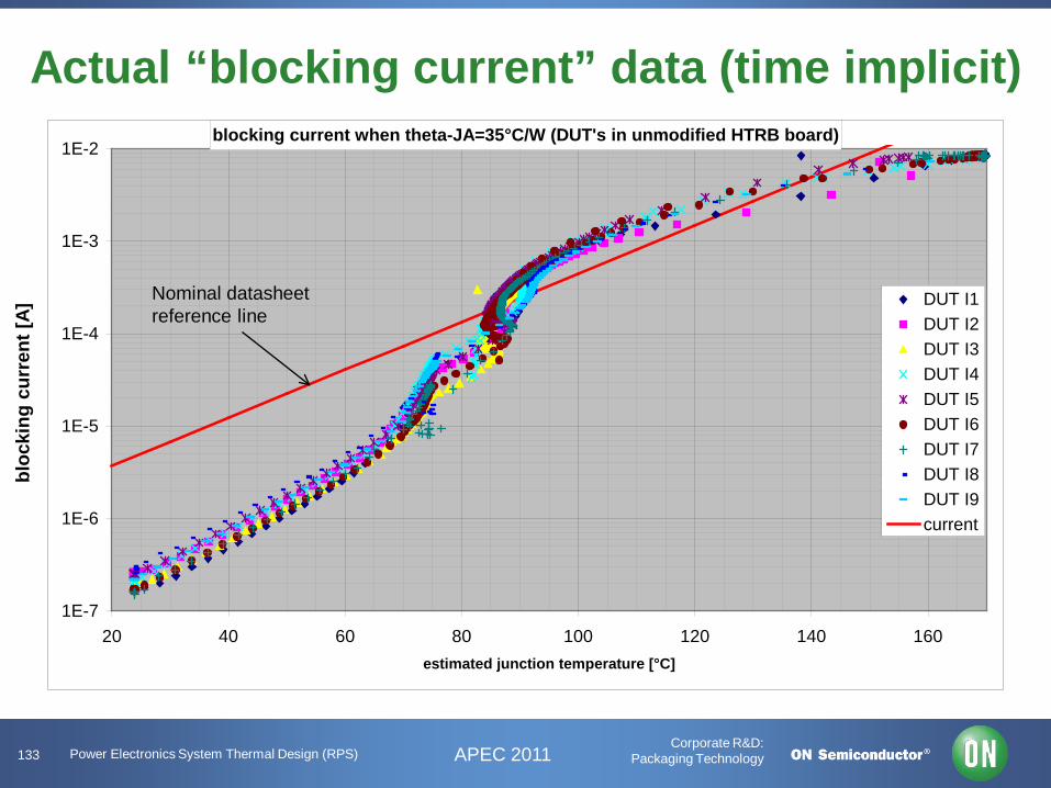
Corporate R&D: Packaging Technology 133 APEC 2011 Power Electronics System Thermal Design (RPS)
Actual “blocking current” data (time implicit) blocking current when theta-JA=35°C/W (DUT's in unmodified HTRB board)
1E-7
1E-6
1E-5
1E-4
1E-3
1E-2
20 40 60 80 100 120 140 160estimated junction temperature [°C]
DUT I1DUT I2DUT I3DUT I4DUT I5DUT I6DUT I7DUT I8DUT I9current
bloc
king
cur
rent
[A] Nominal datasheet
reference line

Corporate R&D: Packaging Technology 134 APEC 2011 Power Electronics System Thermal Design (RPS)
Actual “blocking Pd” data (time implicit) blocking Pd when theta-JA=35°C/W (DUT's in unmodified HTRB board)
1E-4
1E-3
1E-2
1E-1
1E+0
1E+1
20 40 60 80 100 120 140 160estimated junction temperature [°C]
DUT W1DUT W2DUT W3DUT W4DUT W5DUT W6DUT W7DUT W8DUT W9power
Dev
ice
P d [W
]
Nominal datasheet reference line

Corporate R&D: Packaging Technology 135 APEC 2011 Power Electronics System Thermal Design (RPS)
Power vs. temperature (linear scales)
0
0.5
1
1.5
2
2.5
20 30 40 50 60 70 80 90 100 110 120 130
estimated junction temperature [°C]
Pd [W
]
DUT W1DUT W2DUT W3DUT W4DUT W5DUT W6DUT W7DUT W8DUT W9
37ºC/W system 10ºC/W
system
4ºC/W system

Corporate R&D: Packaging Technology 136 APEC 2011 Power Electronics System Thermal Design (RPS)
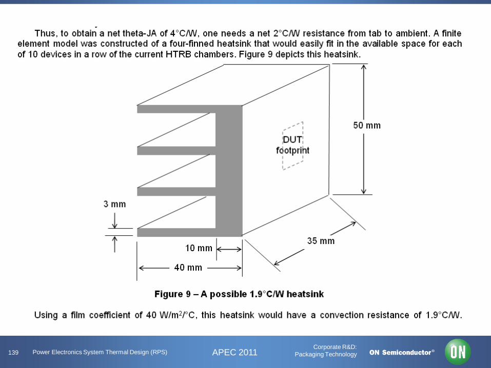
Proof-of-concept modified HTRB fixture After observing a number of device failures at unacceptably short times and under what would have been expected to be junction temperatures well below the maximum rated temperature, the hypothesis of “thermal runaway” in the chamber became the favored explanation of the failures. If true, then lowering the theta-JA of the devices should provide some margin for avoiding the problem. Consequently, crude heatsinks were constructed from some handy copper test panels and attached to each of nine additional test specimens.

Corporate R&D: Packaging Technology 137 APEC 2011 Power Electronics System Thermal Design (RPS)
I vs. temperature on better heatsinks blocking current when theta-JA=10°C/W (using external 12°C/W heatsink)
1E-7
1E-6
1E-5
1E-4
1E-3
1E-2
20 40 60 80 100 120 140 160estimated junction temperature [°C]
DUT I1DUT I2DUT I3DUT I4DUT I5DUT I6DUT I7DUT I8DUT I9bl
ocki
ng c
urre
nt [A
]
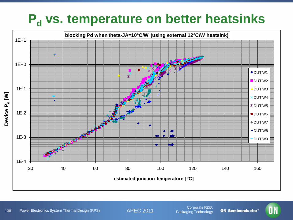
Corporate R&D: Packaging Technology 138 APEC 2011 Power Electronics System Thermal Design (RPS)
1E-4
1E-3
1E-2
1E-1
1E+0
1E+1
20 40 60 80 100 120 140 160
estimated junction temperature [°C]
blocking Pd when theta-JA=10°C/W (using external 12°C/W heatsink)
DUT W1
DUT W2
DUT W3
DUT W4
DUT W5
DUT W6
DUT W7
DUT W8
DUT W9
Pd vs. temperature on better heatsinks D
evic
e P d
[W]
Corporate R&D: Packaging Technology 139 APEC 2011 Power Electronics System Thermal Design (RPS)

Corporate R&D: Packaging Technology 140 APEC 2011 Power Electronics System Thermal Design (RPS)
What if multiple devices on heatsink? • Each device heats its neighbors to varying
degrees, depending on distance
• This adds background heat, that is, it raises the “effective ambient” of each device

Corporate R&D: Packaging Technology 141 APEC 2011 Power Electronics System Thermal Design (RPS)
0.0
0.4
0.8
1.2
1.6
2.0
20 40 60 80 100 Junction Temperature [C]
Dev
ice
Pow
er D
issi
patio
n [W
]
Graphically, background heat does this
device operating
curve
25°C/W system
system with “background heating” of
other devices
real runaway margin
( )∑≠
⋅ji
iij Qψ
what you thought
was your margin

Corporate R&D: Packaging Technology 142 APEC 2011 Power Electronics System Thermal Design (RPS)
Math and Electrical References 1. M. Abramowitz, I. Stegun (eds), Handbook of
Mathematical Functions, Dover Publications, Inc., 9th Printing, Dec. 1972
2. S.D. Senturia, B.D. Wedlock, Electronic Circuits and Applications, John Wiley & Sons, 1975
3. M.F. Gardner & J.L. Barnes, Transients in Linear Systems (Studied by the Laplace Transformation), Vol. I, John Wiley and Sons, 1942
4. R.S. Muller, T.I. Kamins, Device Electronics for Integrated Circuits, 2nd Ed., John Wiley & Sons, 1986
5. Ben Nobel, Applied Linear Algebra, Prentice Hall, 1969
6. H.H. Skilling, Electric Networks, John Wiley and Sons, 1974
7. L. Weinberg, Network Analysis and Synthesis, McGraw Hill Book Company, Inc., 1962
8. H. Wayland, Complex Variables Applied in Science and Engineering, Van Nostrand Reinhold Company
Thermal Textbooks & References 9. H.S. Carslaw & J.C. Jaeger, Conduction of Heat In
Solids, Oxford Press, 1959 10. E.R.G. Eckert & R.M. Drake Jr., Heat and Mass
Transfer, McGraw Hill, 1959 11. J.P. Holman, Heat Transfer, 3rd Ed., McGraw Hill,
1972 12. J. VanSant, Conduction Heat Transfer Solutions,
Lawrence Livermore National Laboratory, Livermore, CA, 1980
569: “Transient Thermal Resistance - General Data and its Use,” May 2003
1083: “Basic Thermal Management of Power Semiconductors,” October 2003
1570: “Basic Semiconductor Thermal Management,” January 2004 8044: “Single-Channel 1206A ChipFET™ Power MOSFET
Recommended Pad Pattern and Thermal Performance,” December 2005
8072: “Thermal Analysis and Reliability of WIRE BONDED ECL,” April 2006
8080: “TSOP vs. SC70 Leadless Package Thermal Performance,” January 2004
8199: “Thermal Stability of MOSFETs,” August 2005 8214: “General Thermal Transient RC Networks ,” April 2006 8215: “Semiconductor Package Thermal Characterization,” April
2006 8216: “Minimizing Scatter in Experimental Data Sets,” April 2006 8217: “What's Wrong with %Error in Junction Temperature,” April
2006 8218: “How to Extend a Thermal-RC-Network Model,” April 2006 8219: “How to Generate Square Wave, Constant Duty Cycle,
Thermal Transient Response Curves,” April 2006 8220: “How To Use Thermal Data Found in Data Sheets,” April
2006 8221: “Thermal RC Ladder Networks,” April 2006 8222: “Predicting the Effect of Circuit Boards on Semiconductor
Package Thermal Performance,” April 2006 8223: “Predicting Thermal Runaway,” April 2006
Thermal-Related Applications Notes available at http://www.onsemi.com/pub/Collateral/ANxxxx-D.PDF