power electronics prof. b. g. fernandes department of...
TRANSCRIPT

1
Power Electronics
Prof. B. G. Fernandes
Department of Electrical Engineering
Indian Institute of Technology, Bombay
Lecture - 4
Hello, in my last class I told you some of the very important applications of power electronics and some of the significant events in the history of power electronics till 1957, the year in which silicon controlled rectifier or thyristor was invented. As I go long, of course I will tell you the other significant events and we started discussing about the power semiconductor devices. I told you that power semiconductor devices are heart and soul of power electronic equipment. These are used as switches that means when they are on, we need to operate them in saturation and when they are off, we need to operate in: sorry, when they are off, they are in cut off region. There are three types of switches. One is an uncontrolled switch, uncontrolled because whether a switch is on or off it depends on the circuit operating conditions. Say, diode for example and there is a semi controlled switch. A silicon controlled rectifier or thyristor is a semi controlled switch because it can be turned on by supplying some current to the gate or to the control terminal. But then, having turned on the device, you cannot turn it off using the gate. Now, the SCR which is conducting, it turns off depending upon the circuit condition. If the current becomes zero in the circuit, thyristor will turn off and third one is a controlled switch. It can either turn it on or off using the control terminal. Say bipolar junction transistor, by supplying a base current, you can turn it on. You make ib is equal to zero, base current zero, transistor turns off. Now we will study the various devices in detail.

2
(Refer Sl
First onethe class then it islow poweas the poand whenideal chathan the the charathe curremode, VA
Now as lbreak doapplied a230 voltsshould beis a passi But thenthat is flthan VBD
to be desacross thstate lossmagnitudto mountsignal dio
lide Time: 3
e is diode, a eleven, ano
s said to be ier diode, it c
ower rating in the diode iaracteristics arated and it
acteristics ofent that is limAK is negativ
long as the aown, diode wacross the dios, so negative higher thanive one.
, if the appliowing, then
D and you arestructive. It ihe diode. I ws or the conde of Vf andt the diode oode, it would
:47)
two terminaode and cathoin forward bcould be, VA
increases. Sais on, all of uare along thcan block a
f a non ideal mited by theve.
applied voltawill block thode should bve peak is gn 230 into ro
ied voltage in the device e not able tois going to b
will call it as nduction los
d Ia say, if it on a heat sinkd not need to
al device. Aode. So if Vbias mode anAK could be oay, for a powus know thae y axis. Tha negative vdiode. May
e load. This
age is less thhat voltage.be less than Vgoing to be oot 2, if you
is higher thawill get da
o control the be destructivVf and Ia is
ss is given is higher thak. Invariablo or generall
All of us knoVAK, voltage nd diode staof the order ower diode it
at current in at is, it can coltage, it cabe, a cut in is forward
han VBD, seeIn other w
VBD, we nee230 into rooare using in
an VBD and iamaged. Rem
current thatve. So, durinthe current by Vf into an a certain ly power dioly is not mou
ow, we have across the d
arts conductiof 0.7 volts ot could be othe circuit iscarry any cu
annot a blockvoltage sombiased and
e VBD is thiswords, the med to ensure tot 2. So, the
n a single pha
if you are nmember, if tt is flowing tng on state,that is flowiIa that depevalue, you n
odes are mouunted on a he
been studyidiode VAK, shing. So for aor so and thif the order os limited by urrent assumk positive vo
mewhere at tthis is durin
s point, breamaxim revers
that. Say, the voltage ratase circuit as
not able to cothe applied vthrough the there is a fiing through ending uponneed to go inunted on a heat sink.
ing may be hould be poa silicon diois value incrof 1.5 volts the load. Se
ming which ioltage. Thesthis point andng reverse b
ak down, junse voltage thhe input voltating of the dssuming that
ontrol the cuvoltage is hdiode, it is gnite voltage the diode. Sn Vf and Ia
n for or you heat sink. A
since sitive
ode, a reases or so
ee the s less se are d this
biased
nction hat is age is diode t load
urrent higher going drop
So, on . The need
small

3
Now, all the off st (Refer Sl
See, whedependinzero but because tand to getime to refrom thisflowing i So, trr is this currecharge. Nthis is a lcharge. Tassumingrecovery See, evenSo if therole or inreverse ranode. Sit may h
of us know tate, the diod
lide Time: 8
en the currenng upon the
the diode cthe minorityet neutralizeecombine ans point, the in the revers
the time froent is the leNow, what islinear one. I The area of g this to be charge, they
n the current circuit in wn other worrecovery curee this curre
have to flow
the on statede, the way i
:25)
nt in the cirinput voltag
continuous ty carriers theed. I will repnd that takesfirst zero cre direction.
om this pointeakage curres the reverseam just dete
f this shadeda triangle o
y are very im
t has becomewhich the frerds trr will drrent, it is flent is flowin
w through ot
e behavior oft turns off is
rcuit, of couge or so currto conduct. ey require a peat, the mins place in therossing to saSo, the maxi
t to say 0.25nt which is
e recovery chermining thed part is noone, area of mportant, two
e zero it contequency of odetermine thlowing in th
ng from cathother switche
f the diode.s a bit import
urse this is trent starts foA reverse ccertain time
nority carriee time trr. trray 25% of thimum value
of irr. I am very small
harge? It is e area of the
othing but irr
the triangleo important
tinuous to cooperation is he upper frehe opposite ode to anode
es. Those sw
Now, in thetant. Why so
the current tollowing. Atcurrent startse to recombrs which are
r is the reverhe maximumof current in
assuming thand this is the area of
e triangle to rr, is a peake. So, reversparameters.
onduct for overy high, t
equency of odirection, ite so either it
witches have
e power eleco, I will tell y
that is flowit this point, s flowing ti
bine with thee there they rse recovery m value of thn the reverse
hat this pointthe charge, this plot. I afind out the
k into trr divse recovery Why are the
r goes to offthis trr will poperation ant is flowing t has to flowe their own
ctronics circuyou.
ing in the ccurrent becll, say trr, th
e opposite chrequire a cetime. It is a
he current the direction is
t is 0.25 of rreverse reco
am assumingreverse reco
vided by 2. time and reey important
fset only afteplay an impond this qrr o
from cathow to the sour
current car
uit, in
circuit comes hat is harge ertain a time hat is s irr.
rr and overy g that overy I am
everse t?
er trr. ortant or the ode to rce or rrying
4
capacity.current. (Refer Sl
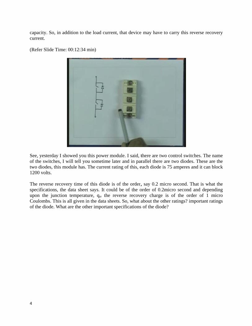
See, yestof the swtwo diod1200 vol The revespecificaupon theCoulombof the dio
So, in addi
lide Time: 00
terday I showwitches, I wildes, this modts.
erse recoveryations, the dae junction tbs. This is alode. What ar
tion to the l
0:12:34 min
wed you thisll tell you so
dule has. The
y time of thiata sheet saytemperature,l given in thre the other i
oad current,
n)
s power modometime latee current rati
is diode is oys. It could qrr the rev
he data sheetimportant sp
that device
dule. I said, ter and in paring of this, e
of the order,be of the o
verse recoves. So, what a
pecifications
may have t
there are tworallel there aeach diode is
, say 0.2 miorder of 0.2mery charge about the oth of the diode
to carry this
o control sware two diods 75 amperes
cro second. micro seconis of the oher ratings? e?
reverse reco
witches. The ndes. These ars and it can b
That is whand and depenorder of 1 mimportant ra
overy
name re the block
at the nding micro atings
5
(Refer Sl
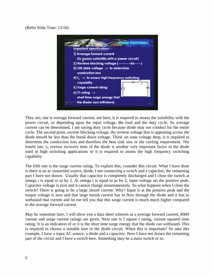
They arepower cicurrent ccycle. Thdiode shodeterminfourth onused in capability The fifthis there ispart I havomega t Capacitoswitch? Toutput vowithstandto the ave May be scurrent arating. It is requireexample,part of th
lide Time: 13
; one is averircuit, so decan be determhe second poould be less
ne the condune, trr revershigh switchy.
h one is the ss an ac sinusve not drawnis equal to pr voltage is zThere is goioltage is zerd that currenerage forwar
sometime latand surge cu
is an indicaed to choose, I have a inphe circuit and
3:56)
rage forwardepending upomined, I am oint, reverse
than the breuction loss ase recovery hing applicat
surge currensoidal sourcen. Usually tpi by 2. At ozero and it cing to be a lro and that lnt and let merd current.
ter, I will shurrent ratingation of or it e a suitable put AC sourcd I have a sw
d current, seon the inpusaying dutyblocking voeak down vond thereforetime of the tions or it i
nt rating. To e, diode. I amthat capacitoomega t is e
cannot changlarge inrush large inrush e tell you th
how you a das are given.is the short fuse in the
ce, a diode awitch here. S
e here, it is r
ut voltage, thy cycle becauoltage, the reoltage. Thirde the heat sidiode is ano
is required
explain thism connectingor is compleequal to pi bge instantane
current. Whcurrent has
at this surge
ata sheet whNext one i
time surge ediode circu
and a capacitSomething m
required to ahe load anduse diode mverse voltagd, on state vink size or tother very ito assess th
s, consider thg a switch a
etely discharby 2, input veously. So why? Input is to flow thr
e current is m
herein as a avs I square t energy that t
uit. When thtor. Now I h
may be a main
assess the sud the duty cymay not condge that is appvoltage dropthe cooling rimportant fahe high freq
his circuit. Wand a capacitrged and I clvoltage set t
what happensat the posit
rough the dimuch much
verage forwarating, curr
the diode canhis is importhave not drawn switch or s
uitability witycle. So av
duct for the epearing acrosp, it is requirrequirement
actor in the dquency switc
What I have tor, the remalose the switthe positive s when I clostive peak anode and it hhigher comp
ard current,rent squaredn withstand.ant? So takewn the remaso.
th the erage entire ss the red to . The diode ching
done aining tch at peak. se the
nd the has to pared
RMS d time . This e this
aining

6
Assume that I am closing the switch at omega t is equal to pi by 2 or in the positive peak. Capacitor is totally discharged, in other words there is a short circuit here. Capacitor voltage cannot change instantaneously. Voltage at this point is instantaneous value is at the peak and we have closed the switch at that time. What happens? A large surge current will flow because voltage across the capacitor cannot change instantaneously. It was zero just prior to closing the switch. This is at the peak, you have closed the switch. A large surge current will flow and diode should be able to withstand this surge current which is higher than the average current rating. So that is about the diodes, the so called uncontrolled switch. Now, what are the various types of diodes? The first one is a rectifier diode or a slow diode. They are suitable for line frequency application, so you want to rectify the input AC which is 50 hertz. So you can use the conventional slow diodes or rectifier diodes. The reverse recovery time is generally is not specified, they are basically slow diodes. So, the maximum rating is of order of 6kv, the diode can block as high as 6kv and current rating is of the order of 4500 amperes are available. I will repeat, diode which can carry say, 4500 amperes of current and can block 6kv, they are available. These are conventional rectifier diodes or slow diodes. There is second type the one known as the fast recovery diodes. Fast recovery diodes, these are generally used in high frequency application. Sometime later in the course, we will find that fast recovery diode should be used in the circuit. You cannot use the conventional rectifier diodes. So, the rating is of the order of say 6kv and current of the order of 1.1 kilo ampere. They are available in the market, 6kv it can block and current ratings, 1.1 kilo amperes and the reverse recovery time could be of the order of say, 0.1micro second, could be. I am not saying that 6kv 1.1 kilo diode, has a reverse recovery time of 1.1micro second, no. The reverse recovery time of a fast recovery diode could be of the order of say, 0.1micro second. Just now, example which I showed you is of the order of 0.2micro seconds. The third one is the short key diodes. What are the features? They have a very low on state voltage drop basically these are only majority carriers. Current only due to majority carriers but then the voltage rating is low. Maximum voltage rating is of the order of 100 volts or so and current is of the order of 300 amperes and the last one, the fourth one is what is known as the silicon carbide diode.

7
(Refer Sl
They havwhat I tolow powinfluencecarbide dproblem?diodes. Tsummariz Just comcontrolledevice; aare connesignal is
lide Time: 00
ve ultra low pld you. Ther
wer loss, ultre on the swdiode. Ultra l? Why are The limitatizes.
ming to the d rectifier.
anode, cathoected in serieapplied with
0:22:53 min
power loss. refore on staa fast switch
witching behlow power lthey not veon is they
second typeThe momende and gate.es in the powh respect to t
n)
See, Schottkate power loshing behavio
havior, looksoss, ultra fas
ery popular?are very ex
e of switchent I said sem. Anode andwer circuit athe cathode,
ky diode hasss also is lowor, very fasts like we arst switching ? You find xpensive. Th
es, semi conmi controlle
d cathode, thnd the gate csay somethi
s a very low w but silicont diodes, higre etching abehavior, honly silicon
he process i
ntrolled swied device, ihey form thecurrent is suing like this.
on state voltn carbide dioghly reliablealmost every
highly reliabln diodes nois also very
itch, a thyriit has to be e power circuupplied with .
tage drop. Tode, it has ane, no temperything in sile and what
ot silicon cay expensive,
istor or a sia three ele
uit terminal,respect to or
hat is n ultra rature ilicon is the
arbide , that
ilicon ement , they r gate

8
(Refer Sl
Our sourthyristor be turnedcathode. first P is (Refer Sl
N2 or thidoped. I doped. N
lide Time: 25
rce, as I havediode with d on using There are 4 anode, N is
lide Time: 26
is layer is vwill call thi
N1 is the thick
5:09)
e shown youa small gatepositive galayers say, Pcathode and
6:36)
very thin andis as P2, thiskest of all, t
u, a AC soure line here, aate current IP N P N andd the gate is c
d it is highl layer is thic
this N is a th
rce, a load ananode, cathodIG or contro
d therefore thconnected to
y doped. Thcker than thhickest of all
nd a thyristode and gate
ol signal is here are threeo this P. This
his N layer his or thickerl and it is le
or. So, this iand can be applied wit
e junctions Js is the gate.
is very thinr than N and
ess doped. H
s the symbocontrolled oth respect toJ1, J2 J3. P N
n and it is hd it is less h
Highly doped
l of a or can o the P N;
highly highly d, less

9
highly dosame as tand a ververy lowtransistor Base emvoltage insignal diblock is vhigh reve Now whforward anode to device shcurrent wwhat hap (Refer Sl
I said VA
battery. Nforward bjunction Now, whVAK is nebiased. SVAK is ne
oped, less dthis P, slightry thin layer
w breakdownr.
mitter junction either direode, you nevery low, veerse voltage,
hat are the vbiased and cathode is v
hould be fowill flow thrppens in forw
lide Time: 30
AK is positiveN is negativebiased, J3 is J2 is reverse
hat happens egative, somSee, when Vegative, J1 an
doped. Dopintly thicker anr, this P is re
n voltage in
on in a transction, in the
eed to applyery small. It , cannot supp
various charathe current very small, t
orward biaserough the deward blockin
0:40)
e, see look he, so definiteforward biabiased. So t
when the demething similVAK is positivnd J3 are rev
ng level is vnd less highlelatively higeither direct
sistor is ligh sense it can
y a 0.7voltscannot blockport a very h
acteristics wis zero, thethe device ised, VAK is pevice. So, thng mode? Th
here, VAK is pely J1 is forwased and J2 ithe entire vo
evices in revlar to the diove, J1 and J3
erse biased a
very low in ly doped. Soghly doped ation, someth
htly low, ven block a verto the base k a very highhigh reverse
when VAK is device currs said to be positive, a vis mode is k
here are three
positive. Soward biased ais reverse biltage appear
verse biasedode, VAK is n3 are forwardand J2 is forw
this and a vo, therefore Jand slightly hing similar
ery highly dry low voltagto turn it o
h voltage. Sovoltage.
positive? Inrent or the in forward b
very small cknown as foe junctions J
P is connectand J3 is forwiased. So, inrs across J2.
d mode? Whnegative, at td bias and Jward biased.
very thick laJ3, see N is vthicker. So, to base emi
doped. So, ige. In the cla
on and revero, therefore
n other worcurrent that blocking mocurrent equaorward blockJ1 J 2 J 3.
ted to, as saiward biased. n the forward
hen the juncthat time J1 a
J2 is reverse .
ayer and thisvery highly d
junction J3
itter junction
it cannot bloass, may be rse voltage iJ3 cannot su
rds, the devit is flowing ode. I will real to the leaking mode. N
id, positive oJunction J m
d blocking m
tion is, wheand J3 are rebiased and w
s P is doped has a
n in a
ock a small it can
upport
ice is from
epeat, akage Now,
of the minus mode,
en the everse when

10
In the foacross J2
Now, whcannot suwhen it i (Refer S
Now I wtransistorthis and ttransistorforms a N Now howcollector of T2 antransistorsame as charactersimilar tothat applas VBR. In the foyou the dQ1or P tothe devicJunction
orward blockor J2 should
hen at the devupport a highs reverse bia
Slide Time: 3
will show yor analogy. Sethis. Say, N1
r. See here, PNPN transist
w do I inteof T2, NPN.d this is ther inter connebase of NP
ristics, I wilo that of a died voltage i
rward bias mdevice is in o Q2. Assumce is forward
J1 and J3 ar
king mode, block the vo
vice in reverh reverse voased, entire v
33:10)
ou the charaee, I told you1, N1, P2, P2. NP1, N1 and Ptor. See here
rconnect T1
. Base of T1
e gate termiect them. BaPN. So, thisll explain todiode, almostis less than V
mode, if the forward bloce that you ar
d biased. Whe forward b
since J1 andoltage in therse bias modltage becausvoltage shou
acteristics. Bu there are 4Now, what isP2. This is P2
e, NPN trans
and T2? Bis same as c
inal. So, thease of PNP is is anode, t you now. It similar. VB
VBR. Same th
current is vcking mode,re not supply
hen the deviciased and J2
d J3 are forwe forward blode, J1 and J3 ase N2 is very uld be blocke
Before that 4 layers, P1 Ns this? Say, h, a PNP tranistor.
Base of PNPcollector of Tere is a PNPis same as ththis is cathoIn the reverBR, reverse bhing, for dio
very small th, again it is ying any gatce is forward2 is reverse b
rward biasedocking modeare reversed
y thin and it ied by J1.
maybe, I wN1 P2 N2. Nowhere P1, N1 a
nsistor and ag
P transistor,T2 and collecP transistor,he collector ode, this is rse bias modbreak over vode I called
hat is equal stable that cte current, asd biased J1 anbiased. So,
d, the entiree, remember
d biased. Butis highly dop
will try to shw, what I wiand P2. Now gain here I h
say, base octor of T1 is
PNP, NPNof NPN, cogate and h
de, charactervoltage, so yas VBD and
to the leakacorresponds s of now thend J3 are alsowhen it is i
e voltage apr. t I told you thped. So, ther
how you theill do is, I withis forms a
have N1, P2, N
of T1 is samsame as the
N transistor,ollector of PNhere are the ristics are al
you should enhere I am ca
age current, Ito P to Q or
e gate is openo forward bin forward b
ppears
hat J3
refore
e two ill cut a PNP N2. It
me as e base NPN
NP is SCR
lmost nsure alling
I told r P to n and iased. biased

11
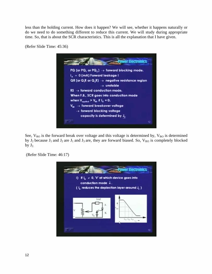
mode the entire voltage J2 blocks and in case the applied voltage is higher than the break down voltage of the junction J2, device goes into conduction mode. I will repeat, I assume that gate current is 0 and if the applied voltage is higher than VBO, see here VBO with IG is equal to 0. VBO that is break over, forward break over, what happens? Device goes into conduction mode. But then how does it go? In what is the path that does it takes? I told you that just prior to device goes into conduction mode, the voltage is may be, approximately equal to VBO. It is high the moment the device goes into conduction mode. The voltage will drop to a very low value. It could be of the order of say 1.5 volts or so 1.5 to 1, 2 volts. Till 0 to VBO, current that is flowing is very small. It is equal to the forward leakage current. Once the device is in conduction mode, current is limited by the load. Now, what path does it takes? It was blocking a relatively higher voltage, the moment it goes to conduction mode voltage drops to a very low value, the paths taken by this is this. I have shown this is to be dotted one. Why did I show this to be a dotted? Why it is not firm like P to Q? Why it is not firm? This is because this region is an unstable region. Why it is unstable? because it is a negative resistance region. See, voltage is falling, current is increasing, the slope of this line is negative resistance region. So, it is unstable and it goes to, see, RS is the forward conduction mode, current, the operating point here depends only on the load and now see, there is a third element what is known as a gate and therefore by supplying the gate current it should be able to trigger the device. So, definitely with the finite gate current, the voltage at which it goes to conduction mode should reduce. So see, as the gate current increases, the voltage at which device goes into conduction mode also drops. IG0, so voltage applied should be higher than VBO forward break over, VBO is forward break over. So, with the finite IG1, device goes into conduction mode at a relatively lower voltage and if I increase IG further, it goes to conduction mode somewhere at this point, say PQ for 0 IG, P1Q1 for some IG1 which is less than IG2 and for that the path is PQ2 and once the device current is higher than the latching current, gate has no control. So I will repeat, by supplying a positive gate current, device goes into a conduction mode and by supplying a gate current the voltage at which device goes into conduction mode also reduces. But then, the gate signal should be present till the current through the device is higher than the latching current. The device should be able to latch, till then gate signal should be present and having gone into conduction mode, the gate has no control. You can withdraw or you can make IG is equal to 0. In fact, it is advantageous to make IG is equal to 0. Why? Gate has no control, if there is a constant IG flowing, definitely there is going to be a dissipation in that junction. So, in a way, it is an advantageous to make IG is equal to 0. Once the current through the device is higher than the latching, because having gone into conduction mode if the current is higher than the latching, gate has no control and you can withdraw the gate signal. But then to turn the device off, current through the device should fall to a value which is less than the holding current. Somewhere here, see here, IH is the holding current. So, to turn off the device, I will repeat, the current that is flowing through the device should fall to a value which is
12
less thando we netime. So, (Refer Sl
See, VBO
by J2 becby J2.
(Refer S
the holdingeed to do so that is abou
lide Time: 45
O is the forwcause J1 and
Slide Time: 4
g current. Hoomething difut the SCR ch
5:36)
ard break ovJ2 are J1 and
46:17)
ow does it hfferent to reharacteristic
ver voltage ad J3 are, they
appen? Weduce this cu
cs. This is all
and this volty are forwar
will see, whurrent. We wl the explana
tage is determrd biased. So
hether it hapwill study duation that I h
mined by, Vo, VBO is com
ppens naturaluring approp
have given.
VBO is determmpletely blo
lly or priate
mined ocked

13
Now hercircuit, I through tvarying i So, as IG
voltage, voltage abecause Ireduces t
Now howtransistortransistoranalogy, thyristor? (Refer Sl
See, for aIE is the divided bis a comm Now, foranode cuam callinabout forIK, the ccurrent, g
re, I have juam just clo
the device, thin this resisto
G increases, tthis voltage
at which devIG, the gate cthe depletion
w do we anar analogy? r and there ican we find
? Answer is
lide Time: 00
any transistoemitter curr
by IE and whmon equatio
r this transisturrent IA. So,ng ICBO1 is tr T2? Now, fathode curregain of T2 int
st shown yosing the swihis load curror to vary th
the voltage ae is determinvice goes intcurrent reducn layer aroun
alyze the prI just showis an NPN trd out or canyes, I will ex
0:48:38 min
or collector crent, alpha ishat is ICBO?n IC is equal
tor T1 transis, therefore IC
he leakage cfor T2, IE, T2
ent IK. So, tto IK plus IC
ou the plot oitch till the drent higher the current tha
at VBO with ned by juncto conductioces the deplend the junctio
rocess by whwed you PN
ransistor andn we or is ixplain to you
n)
current IC is s the commo? It is the lel to alpha int
stor, what is C1 is equal tocurrent of cois a NPN tratherefore IC2
BO2.
of the variatdevice goes han the latchat is flowing
very low vaction J2 itselon mode reduetion layer aon J2.
hich the devNPN is equiv
d they are init possible tou now.
given by alpon base currakage currento IE plus ICB
IE emitter cuo alpha into ollector to bansistor whe2 is equal to
tion of VBO
into conduching, then I c
g through the
alue of IG is lf. Above auces. So, it
around J2. I w
vice goes invalent to 2 nterconnecteo understand
pha into IE prent gain, it nt of the col
BO.
urrent? EmitIA because
base junctionereas T1 is a o alpha two
with IG. So,ction motor can open the
e gate circuit
almost the a certain valgoes on redwill repeat, t
nto conductiotransistors,
ed. Now, usid the turn o
plus ICBO. Cois approxim
llector base j
tter current iIE is equal tn of transistPNP transis
o, the gain o
here is a sior till the cue switch andt.
same. This ilue, this VB
ducing, why?the gate curr
on mode us there is a ing this tranon process o
ollector curremately equal
junction. So
is nothing buto IA, plus IC
tor T1. Now,stor. IE is equof common
imple urrent d I am
is the O the ? It is rent it
ing 2 PNP
sistor of the
ent IC, to IC
o, this
ut the CBO1. I , how ual to
base

14
(Refer Sl
Now, weIE1? IE1 isbase currshowed ySo, I wilwill add plus ICBO
(Refer Sl
lide Time: 5
e all know ths equal to IA
rent of transiyou in the bell add up thothem up. W
O1 plus ICBO2.
lide Time: 52
1:06)
hat IE, emitteA itself, anodistor T1? Baeginning, baose 2 equati
What do I get?
2:34)
er current is de current. Ese current ofse of T1 and ons. Which? IC1 plus IC
collector cuEmitter curref transistor Tcollector ofare the 2 eq
C2 is equal to
urrent plus IB
ent of T1 is aT1 is same asf T2, they arequations? Tho alpha one i
B, base curreanode currens collector cue same, they hese are the into IA plus
ent. Now, whnt and what iurrent of T2,
are tied togetwo equatio
alpha two in
hat is is IB1, , IC2. I ether. ons, I nto IK

15
So, here is the equation I have written, as simple as IC2. Now, substitute here, IC here is IC1 itself for transistor T1, IB is IB for T1 is IC2. So, IC1 plus IC2 is equal to IA. So, these are the 2 current IC1 plus IC2 should be equal to IA, a PNP transistor that is equal to alpha one into IA plus whatever that equation we are adding to. What about for transistor T2? Listen to me carefully, here what is IE? That is IK itself. It is IB2, base current plus IC2.This current, IB2 plus IC2. Now, if there is finite IG, what is base current? Base current is IG plus IC1 plus IC2 is equal to I emitter, IE2 that is equal to IK. See, I will repeat, emitter current of T2 is this current, base current plus collector current. Now what is base current? You apply KCL at this point for finite IG, IB2 is equal to IC1 plus IG. So, therefore cathode current is IC1 plus IG plus IC2. Now we all ready found that IC1 plus IC2 is equal to IA for this transistor. IC1 plus IC2 is equal to IA. So, therefore IK is equal to IA plus IG. Now, you substitute this value in this equation, IA is equal to alpha one into IA1 plus CBO1 plus this equation and what do I get? I get this equation, IA is equal to alpha two into IG plus ICBO1 plus ICBO2 divided by 1 minus alpha one plus alpha two. So, I have an expression here for anode current in terms of gate current, the leakage current of collector to base junction and common base current. Now using this expression, how to understand the turn on process of the thyristor? We will do it in our next class. Thank you.