power electronic devices - politecnico di...
TRANSCRIPT

IPower Electronic Devices
1 Power Electronics Kaushik Rajashekara, Sohail Anwar, Vrej Barkhordarian,Alex Q. HuangOverview • Diodes • Schottky Diodes • Thyristors • Power Bipolar JunctionTransistors • MOSFETs • General Power Semiconductor Switch Requirements • GateTurn-Off Thyristors • Insulated Gate Bipolar Transistors • Gate-Commutated Thyristorsand Other Hard-Driven GTOs • Comparison Testing of Switches
© 2002 by CRC Press LLC

1Power Electronics
1.1 OverviewThyristor and Triac • Gate Turn-Off Thyristor • Reverse-Conducting Thyristor (RCT) and Asymmetrical Silicon-Controlled Rectifier (ASCR) • Power Transistor • Power MOSFET • Insulated-Gate Bipolar Transistor (IGBT) •MOS-Controlled Thyristor (MCT)
1.2 DiodesCharacteristics • Principal Ratings for Diodes • Rectifier Circuits • Testing a Power Diode • Protection of Power Diodes
1.3 Schottky DiodesCharacteristics • Data Specifications • Testing of Schottky Diodes
1.4 ThyristorsThe Basics of Silicon-Controlled Rectifiers (SCR) •Characteristics • SCR Turn-Off Circuits • SCR Ratings • The DIAC • The Triac • The Silicon-Controlled Switch • The Gate Turn-Off Thyristor • Data Sheet for a Typical Thyristor
1.5 Power Bipolar Junction TransistorsThe Volt-Ampere Characteristics of a BJT • BJT Biasing • BJT Power Losses • BJT Testing • BJT Protection
1.6 MOSFETsStatic Characteristics • Dynamic Characteristics • Applications
1.7 General Power Semiconductor SwitchRequirements
1.8 Gate Turn-Off ThyristorsGTO Forward Conduction • GTO Turn-Off and Forward Blocking • Practical GTO Turn-Off Operation • Dynamic Avalanche • Non-Uniform Turn-Off Process among GTO Cells • Summary
1.9 Insulated Gate Bipolar TransistorsIGBT Structure and Operation
1.10 Gate-Commutated Thyristors and OtherHard-Driven GTOsUnity Gain Turn-Off Operation • Hard-Driven GTOs
1.11 Comparison Testing of SwitchesPulse Tester Used for Characterization • Devices Used for Comparison • Unity Gain Verification • Gate Drive Circuits • Forward Conduction Loss Characterization •Switching Tests • Discussion • Comparison Conclusions
Kaushik RajashekaraDelphi Automotive Systems
Sohail AnwarPennsylvania State University
Vrej BarkhordarianInternational Rectifier
Alex Q. HuangVirginia Polytechnic Institute and State University
© 2002 by CRC Press LLC

1.1 Overview
Kaushik Rajashekara
The modern age of power electronics began with the introduction of thyristors in the late 1950s. Now thereare several types of power devices available for high-power and high-frequency applications. The mostnotable power devices are gate turn-off thyristors, power Darlington transistors, power MOSFETs, andinsulated-gate bipolar transistors (IGBTs). Power semiconductor devices are the most important functionalelements in all power conversion applications. The power devices are mainly used as switches to convertpower from one form to another. They are used in motor control systems, uninterrupted power supplies,high-voltage DC transmission, power supplies, induction heating, and in many other power conversionapplications. A review of the basic characteristics of these power devices is presented in this section.
Thyristor and Triac
The thyristor, also called a silicon-controlled rectifier (SCR), is basically a four-layer three-junction pnpndevice. It has three terminals: anode, cathode, and gate. The device is turned on by applying a short pulseacross the gate and cathode. Once the device turns on, the gate loses its control to turn off the device.The turn-off is achieved by applying a reverse voltage across the anode and cathode. The thyristor symboland its volt–ampere characteristics are shown in Fig. 1.1. There are basically two classifications ofthyristors: converter grade and inverter grade. The difference between a converter-grade and an inverter-grade thyristor is the low turn-off time (on the order of a few microseconds) for the latter. The converter-grade thyristors are slow type and are used in natural commutation (or phase-controlled) applications.
FIGURE 1.1 (a) Thyristor symbol and (b) volt–ampere characteristics. (From Bose, B.K., Modern Power Electronics:Evaluation, Technology, and Applications, p. 5. © 1992 IEEE. With permission.)
© 2002 by CRC Press LLC

Inverter-grade thyristors are used in forced commutation applications such as DC-DC choppers andDC-AC inverters. The inverter-grade thyristors are turned off by forcing the current to zero using anexternal commutation circuit. This requires additional commutating components, thus resulting inadditional losses in the inverter.
Thyristors are highly rugged devices in terms of transient currents, di/dt, and dv/dt capability. Theforward voltage drop in thyristors is about 1.5 to 2 V, and even at higher currents of the order of 1000 A,it seldom exceeds 3 V. While the forward voltage determines the on-state power loss of the device at anygiven current, the switching power loss becomes a dominating factor affecting the device junctiontemperature at high operating frequencies. Because of this, the maximum switching frequencies possibleusing thyristors are limited in comparison with other power devices considered in this section.
Thyristors have I2t withstand capability and can be protected by fuses. The nonrepetitive surge current
capability for thyristors is about 10 times their rated root mean square (rms) current. They must be protectedby snubber networks for dv/dt and di/dt effects. If the specified dv/dt is exceeded, thyristors may startconducting without applying a gate pulse. In DC-to-AC conversion applications, it is necessary to use anantiparallel diode of similar rating across each main thyristor. Thyristors are available up to 6000 V, 3500 A.
A triac is functionally a pair of converter-grade thyristors connected in antiparallel. The triac symboland volt–ampere characteristics are shown in Fig. 1.2. Because of the integration, the triac has poor reapplieddv/dt, poor gate current sensitivity at turn-on, and longer turn-off time. Triacs are mainly used in phasecontrol applications such as in AC regulators for lighting and fan control and in solid-state AC relays.
Gate Turn-Off Thyristor
The GTO is a power switching device that can be turned on by a short pulse of gate current and turnedoff by a reverse gate pulse. This reverse gate current amplitude is dependent on the anode current to beturned off. Hence there is no need for an external commutation circuit to turn it off. Because turn-offis provided by bypassing carriers directly to the gate circuit, its turn-off time is short, thus giving it morecapability for high-frequency operation than thyristors. The GTO symbol and turn-off characteristicsare shown in Fig. 1.3.
GTOs have the I2t withstand capability and hence can be protected by semiconductor fuses. For reliable
operation of GTOs, the critical aspects are proper design of the gate turn-off circuit and the snubbercircuit. A GTO has a poor turn-off current gain of the order of 4 to 5. For example, a 2000-A peak currentGTO may require as high as 500 A of reverse gate current. Also, a GTO has the tendency to latch attemperatures above 125°C. GTOs are available up to about 4500 V, 2500 A.
FIGURE 1.2 (a) Triac symbol and (b) volt–ampere characteristics. (From Bose, B.K., Modern Power Electronics:Evaluation, Technology, and Applications, p. 5. © 1992 IEEE. With permission.)
© 2002 by CRC Press LLC

Reverse-Conducting Thyristor (RCT) and AsymmetricalSilicon-Controlled Rectifier (ASCR)
Normally in inverter applications, a diode in antiparallel is connected to the thyristor for commu-tation/freewheeling purposes. In RCTs, the diode is integrated with a fast switching thyristor in asingle silicon chip. Thus, the number of power devices could be reduced. This integration bringsforth a substantial improvement of the static and dynamic characteristics as well as its overall circuitperformance.
The RCTs are designed mainly for specific applications such as traction drives. The antiparalleldiode limits the reverse voltage across the thyristor to 1 to 2 V. Also, because of the reverse recoverybehavior of the diodes, the thyristor may see very high reapplied dv/dt when the diode recovers from itsreverse voltage. This necessitates use of large RC snubber networks to suppress voltage transients. As therange of application of thyristors and diodes extends into higher frequencies, their reverse recovery chargebecomes increasingly important. High reverse recovery charge results in high power dissipation duringswitching.
The ASCR has similar forward blocking capability to an inverter-grade thyristor, but it has a limitedreverse blocking (about 20 to 30 V) capability. It has an on-state voltage drop of about 25% less than aninverter-grade thyristor of a similar rating. The ASCR features a fast turn-off time; thus it can work ata higher frequency than an SCR. Since the turn-off time is down by a factor of nearly 2, the size of thecommutating components can be halved. Because of this, the switching losses will also be low.
Gate-assisted turn-off techniques are used to even further reduce the turn-off time of an ASCR. Theapplication of a negative voltage to the gate during turn-off helps to evacuate stored charge in the deviceand aids the recovery mechanisms. This will, in effect, reduce the turn-off time by a factor of up to 2over the conventional device.
FIGURE 1.3 (a) GTO symbol and (b) turn-off characteristics. (From Bose, B.K., Modern Power Electronics: Eval-uation, Technology, and Applications, p. 5. © 1992 IEEE. With permission.)
© 2002 by CRC Press LLC

Power Transistor
Power transistors are used in applications ranging from a few to several hundred kilowatts and switchingfrequencies up to about 10 kHz. Power transistors used in power conversion applications are generallynpn type. The power transistor is turned on by supplying sufficient base current, and this base drive hasto be maintained throughout its conduction period. It is turned off by removing the base drive andmaking the base voltage slightly negative (within –VBE(max)). The saturation voltage of the device isnormally 0.5 to 2.5 V and increases as the current increases. Hence, the on-state losses increase morethan proportionately with current. The transistor off-state losses are much lower than the on-state lossesbecause the leakage current of the device is of the order of a few milliamperes. Because of relatively largerswitching times, the switching loss significantly increases with switching frequency. Power transistors canblock only forward voltages. The reverse peak voltage rating of these devices is as low as 5 to 10 V.
Power transistors do not have I2t withstand capability. In other words, they can absorb only very little
energy before breakdown. Therefore, they cannot be protected by semiconductor fuses, and thus anelectronic protection method has to be used.
To eliminate high base current requirements, Darlington configurations are commonly used. They areavailable in monolithic or in isolated packages. The basic Darlington configuration is shown schematicallyin Fig. 1.4. The Darlington configuration presents a specific advantage in that it can considerably increasethe current switched by the transistor for a given base drive. The VCE(sat) for the Darlington is generallymore than that of a single transistor of similar rating with corresponding increase in on-state power loss.During switching, the reverse-biased collector junction may show hot-spot breakdown effects that arespecified by reverse-bias safe operating area (RBSOA) and forward-bias safe operating area (FBSOA).Modern devices with highly interdigited emitter base geometry force more uniform current distributionand therefore considerably improve secondary breakdown effects. Normally, a well-designed switchingaid network constrains the device operation well within the SOAs.
Power MOSFET
Power MOSFETs are marketed by different manufacturers with differences in internal geometry and withdifferent names such as MegaMOS, HEXFET, SIPMOS, and TMOS. They have unique features that makethem potentially attractive for switching applications. They are essentially voltage-driven rather thancurrent-driven devices, unlike bipolar transistors.
The gate of a MOSFET is isolated electrically from the source by a layer of silicon oxide. The gatedraws only a minute leakage current on the order of nanoamperes. Hence, the gate drive circuit is simpleand power loss in the gate control circuit is practically negligible. Although in steady state the gate drawsvirtually no current, this is not so under transient conditions. The gate-to-source and gate-to-drain
FIGURE 1.4 A two-stage Darlington transistor with bypass diode. (From Bose, B.K., Modern Power Electronics:Evaluation, Technology, and Applications, p. 6. © 1992 IEEE. With permission.)
© 2002 by CRC Press LLC

capacitances have to be charged and discharged appropriately to obtain the desired switching speed, andthe drive circuit must have a sufficiently low output impedance to supply the required charging anddischarging currents. The circuit symbol of a power MOSFET is shown in Fig. 1.5.
Power MOSFETs are majority carrier devices, and there is no minority carrier storage time. Hence,they have exceptionally fast rise and fall times. They are essentially resistive devices when turned on,while bipolar transistors present a more or less constant VCE(sat) over the normal operating range. Powerdissipation in MOSFETs is Id
2RDS(on), and in bipolars it is ICVCE(sat). At low currents, therefore, a power
MOSFET may have a lower conduction loss than a comparable bipolar device, but at higher currents,the conduction loss will exceed that of bipolars. Also, the RDS(on) increases with temperature.
An important feature of a power MOSFET is the absence of a secondary breakdown effect, which ispresent in a bipolar transistor, and as a result, it has an extremely rugged switching performance. InMOSFETs, RDS(on) increases with temperature, and thus the current is automatically diverted away fromthe hot spot. The drain body junction appears as an antiparallel diode between source and drain. Thus,power MOSFETs will not support voltage in the reverse direction. Although this inverse diode is relativelyfast, it is slow by comparison with the MOSFET. Recent devices have the diode recovery time as low as100 ns. Since MOSFETs cannot be protected by fuses, an electronic protection technique has to be used.
With the advancement in MOS technology, ruggedized MOSFETs are replacing the conventionalMOSFETs. The need to ruggedize power MOSFETs is related to device reliability. If a MOSFET is operatingwithin its specification range at all times, its chances for failing catastrophically are minimal. However,if its absolute maximum rating is exceeded, failure probability increases dramatically. Under actualoperating conditions, a MOSFET may be subjected to transients—either externally from the power bussupplying the circuit or from the circuit itself due, for example, to inductive kicks going beyond theabsolute maximum ratings. Such conditions are likely in almost every application, and in most cases arebeyond a designer’s control. Rugged devices are made to be more tolerant for overvoltage transients.Ruggedness is the ability of a MOSFET to operate in an environment of dynamic electrical stresses,without activating any of the parasitic bipolar junction transistors. The rugged device can withstandhigher levels of diode recovery dv/dt and static dv/dt.
Insulated-Gate Bipolar Transistor (IGBT)
The IGBT has the high input impedance and high-speed characteristics of a MOSFET with the conductivitycharacteristic (low saturation voltage) of a bipolar transistor. The IGBT is turned on by applying a positivevoltage between the gate and emitter and, as in the MOSFET, it is turned off by making the gate signalzero or slightly negative. The IGBT has a much lower voltage drop than a MOSFET of similar ratings.
FIGURE 1.5 Power MOSFET circuit symbol. (From Bose, B.K., Modern Power Electronics: Evaluation, Technology,and Applications, p. 7. © 1992 IEEE. With permission.)
© 2002 by CRC Press LLC

The structure of an IGBT is more like a thyristor and MOSFET. For a given IGBT, there is a critical value ofcollector current that will cause a large enough voltage drop to activate the thyristor. Hence, the devicemanufacturer specifies the peak allowable collector current that can flow without latch-up occurring. Thereis also a corresponding gate source voltage that permits this current to flow that should not be exceeded.
Like the power MOSFET, the IGBT does not exhibit the secondary breakdown phenomenon commonto bipolar transistors. However, care should be taken not to exceed the maximum power dissipation andspecified maximum junction temperature of the device under all conditions for guaranteed reliableoperation. The on-state voltage of the IGBT is heavily dependent on the gate voltage. To obtain a lowon-state voltage, a sufficiently high gate voltage must be applied.
In general, IGBTs can be classified as punch-through (PT) and nonpunch-through (NPT) structures, asshown in Fig. 1.6. In the PT IGBT, an N
+ buffer layer is normally introduced between the P
+ substrate and
the N− epitaxial layer, so that the whole N
− drift region is depleted when the device is blocking the off-state
voltage, and the electrical field shape inside the N− drift region is close to a rectangular shape. Because a
shorter N− region can be used in the punch-through IGBT, a better trade-off between the forward voltage
drop and turn-off time can be achieved. PT IGBTs are available up to about 1200 V.High-voltage IGBTs are realized through a nonpunch-through process. The devices are built on an N
−
wafer substrate which serves as the N− base drift region. Experimental NPT IGBTs of up to about 4 kV
have been reported in the literature. NPT IGBTs are more robust than PT IGBTs, particularly under shortcircuit conditions. But NPT IGBTs have a higher forward voltage drop than the PT IGBTs.
The PT IGBTs cannot be as easily paralleled as MOSFETs. The factors that inhibit current sharing ofparallel-connected IGBTs are (1) on-state current unbalance, caused by VCE(sat) distribution and maincircuit wiring resistance distribution, and (2) current unbalance at turn-on and turn-off, caused by theswitching time difference of the parallel connected devices and circuit wiring inductance distribution.The NPT IGBTs can be paralleled because of their positive temperature coefficient property.
FIGURE 1.6 (a) Nonpunch-through IGBT, (b) punch-through IGBT, (c) IGBT equivalent circuit.
© 2002 by CRC Press LLC

MOS-Controlled Thyristor (MCT)
The MCT is a new type of power semiconductor device that combines the capabilities of thyristor voltageand current with MOS gated turn-on and turn-off. It is a high-power, high-frequency, low-conductiondrop and a rugged device, which is more likely to be used in the future for medium and high powerapplications. A cross-sectional structure of a p-type MCT with its circuit schematic is shown in Fig. 1.7.The MCT has a thyristor type structure with three junctions and pnpn layers between the anode andcathode. In a practical MCT, about 100,000 cells similar to the one shown are paralleled to achieve thedesired current rating. MCT is turned on by a negative voltage pulse at the gate with respect to the anode,and is turned off by a positive voltage pulse.
The MCT was announced by the General Electric R&D Center on November 30, 1988. HarrisSemiconductor Corporation has developed two generations of p-MCTs. Gen-1 p-MCTs are available at65 A/1000 V and 75 A/600 V with peak controllable current of 120 A. Gen-2 p-MCTs are being developedat similar current and voltage ratings, with much improved turn-on capability and switching speed.The reason for developing a p-MCT is the fact that the current density that can be turned off is twoor three times higher than that of an n-MCT; but n-MCTs are the ones needed for many practicalapplications.
The advantage of an MCT over IGBT is its low forward voltage drop. n-type MCTs will be expected tohave a similar forward voltage drop, but with an improved reverse bias safe operating area and switchingspeed. MCTs have relatively low switching times and storage time. The MCT is capable of high currentdensities and blocking voltages in both directions. Since the power gain of an MCT is extremely high, itcould be driven directly from logic gates. An MCT has high di/dt (of the order of 2500 A/µs) and highdv/dt (of the order of 20,000 V/µs) capability.
The MCT, because of its superior characteristics, shows a tremendous possibility for applications suchas motor drives, uninterrupted power supplies, static VAR compensators, and high power active powerline conditioners.
The current and future power semiconductor devices developmental direction is shown in Fig. 1.8.High-temperature operation capability and low forward voltage drop operation can be obtained if siliconis replaced by silicon carbide material for producing power devices. The silicon carbide has a higher bandgap than silicon. Hence, higher breakdown voltage devices could be developed. Silicon carbide deviceshave excellent switching characteristics and stable blocking voltages at higher temperatures. But the siliconcarbide devices are still in the very early stages of development.
FIGURE 1.7 Typical cell cross section and circuit schematic for P-MCT. (From Harris Semiconductor, User’s Guideof MOS Controlled Thyristor. With permission.)
© 2002 by CRC Press LLC

References
Bose, B.K., Modern Power Electronics: Evaluation, Technology, and Applications, IEEE Press, New York, 1992.Harris Semiconductor, User’s Guide of MOS Controlled Thyristor.Huang, A.Q., Recent developments of power semiconductor devices, in VPEC Seminar Proceedings,
September 1995, 1–9.Mohan, N. and T. Undeland, Power Electronics: Converters, Applications, and Design, John Wiley & Sons,
New York, 1995.Wojslawowicz, J., Ruggedized transistors emerging as power MOSFET standard-bearers, Power Technics
Magazine, January 1988, 29–32.
Further Information
Bird, B.M. and K.G. King, An Introduction to Power Electronics, Wiley-Interscience, New York, 1984.Sittig, R. and P. Roggwiller, Semiconductor Devices for Power Conditioning, Plenum, New York, 1982.Temple, V.A.K., Advances in MOS controlled thyristor technology and capability, Power Conversion,
544–554, Oct. 1989.Williams, B.W., Power Electronics, Devices, Drivers and Applications, John Wiley, New York, 1987.
1.2 Diodes
Sohail Anwar
Power diodes play an important role in power electronics circuits. They are mainly used as uncontrolledrectifiers to convert single-phase or three-phase AC voltage to DC. They are also used to provide a pathfor the current flow in inductive loads. Typical types of semiconductor materials used to construct diodesare silicon and germanium. Power diodes are usually constructed using silicon because silicon diodes canoperate at higher current and at higher junction temperatures than germanium diodes. The symbol for asemiconductor diode is given in Fig. 1.9. The terminal voltage and current are represented as Vd and Id,respectively. Figure 1.10 shows the structure of a diode. It has an anode (A) terminal and a cathode (K)terminal. The diode is constructed by joining together two pieces of semiconductor material—a p-typeand an n-type—to form a pn-junction. When the anode terminal is positive with respect to the cathodeterminal, the pn-junction becomes forward-biased and the diode conducts current with a relatively lowvoltage drop. When the cathode terminal is positive with respect to the anode terminal, the pn-junctionbecomes reverse-biased and the current flow is blocked. The arrow on the diode symbol in Fig. 1.9 showsthe direction of conventional current flow when the diode conducts.
FIGURE 1.8 Current and future power semiconductor devices development direction. (From Huang, A.Q., Recentdevelopments of power semiconductor devices, VPEC Seminar Proceedings, pp. 1–9. With permission.)
© 2002 by CRC Press LLC

Characteristics
The voltage-current characteristics of a diode are shown in Fig. 1.11. Inthe forward region, the diode starts conducting as the anode voltage isincreased with respect to the cathode. The voltage where the current startsto increase rapidly is called the knee voltage of the diode. For a silicondiode, the knee voltage is approximately 0.7 V. Above the knee voltage,small increases in the diode voltage produce large increases in the diodecurrent. If the diode current is too large, excessive heat will be generated,which can destroy the diode. When the diode is reverse-biased, diodecurrent is very small for all values of reverse voltage less than the diodebreakdown voltage. At breakdown, the diode current increases rapidlyfor small increases in diode voltage.
Principal Ratings for Diodes
Figures 1.12 and 1.13 show typical data sheets for power diodes.
Maximum Average Forward Current
The maximum average forward current (If(avg)max) is the current a diodecan safely handle when forward biased. Power diodes are available inratings from a few amperes to several hundred amperes. For example,the power diode D6 described in the data specification sheet (Fig 1.12)can handle up to 6 A in the forward direction when used as a rectifier.
Peak Inverse Voltage
The peak inverse voltage (PIV) of a diode is the maximum reverse voltagethat can be connected across a diode without breakdown. The peakinverse voltage is also called peak reverse voltage or reverse breakdownvoltage. The PIV ratings of power diodes extend from a few volts toseveral thousand volts. For example, the power diode D6 has a PIV ratingof up to 1600 V, as shown in Fig. 1.12.
FIGURE 1.11 Diode voltage-current characteristic.
FIGURE 1.9 Diode symbol.
Id
Vd
+
_
A
K
FIGURE 1.10 Diode structure.
Id
Vd
+
_
A
K
PN
© 2002 by CRC Press LLC

FIGURE 1.12 Diode data sheet—ratings. (From USHA, India. With permission.)
© 2002 by CRC Press LLC
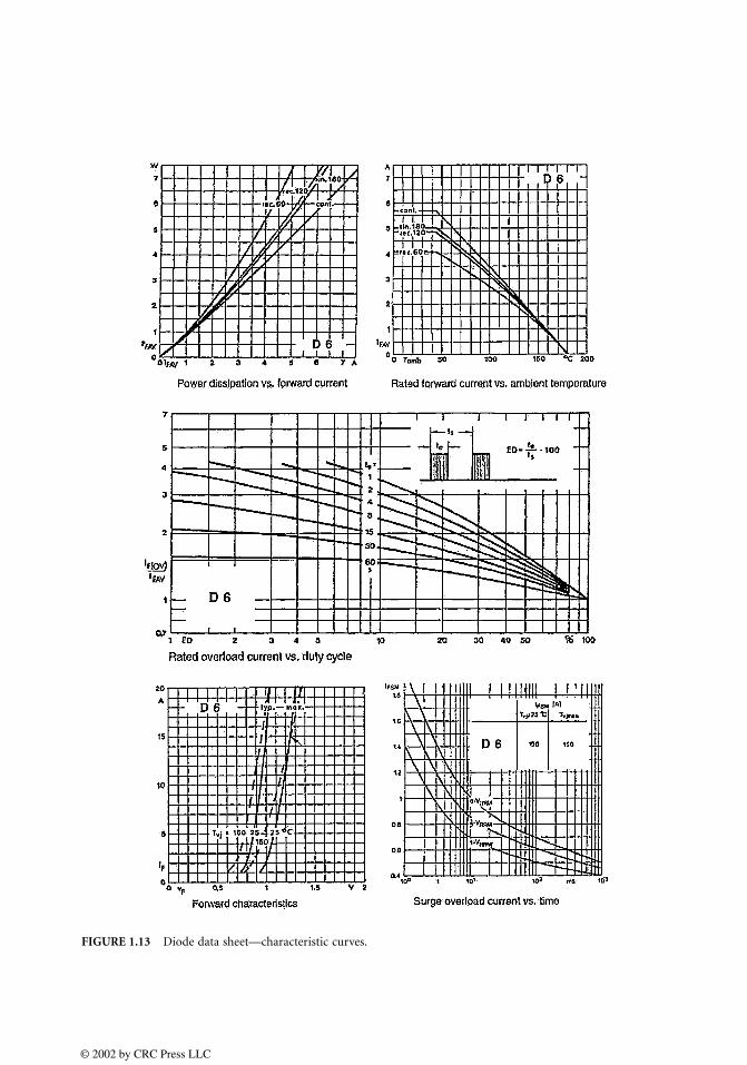
FIGURE 1.13 Diode data sheet—characteristic curves.
© 2002 by CRC Press LLC

Maximum Surge Current
The IFSM (forward surge maximum) rating is the maximum current that the diode can handle as anoccasional transient or from a circuit fault. The IFSM rating for the power diode D6 is up to 190 A, asshown in Fig 1.12.
Maximum Junction Temperature
This parameter defines the maximum junction temperature that a diode can withstand without failure.The maximum junction temperature for the power diode D6 is 180°C.
Rectifier Circuits
Rectifier circuits produce a DC voltage or current from an AC source. The diode is an essential componentof these circuits. Figure 1.14 shows a half-wave rectifier circuit using a diode. During the positive halfcycle of the source voltage, the diode is forward-biased and conducts for vs(t) > Ef. The value of Ef forgermanium is 0.2 V and for silicon it is 0.7 V. During the negative half cycle of vs(t) , the diode is reverse-biased and does not conduct. The voltage vL(t) across the load RL is shown in Fig. 1.15.
The half-wave rectifier circuit produces a pulsating direct current that uses only the positive half cycleof the source voltage. The full-wave rectifier shown in Fig. 1.16 uses both half cycles of source voltage.During the positive half cycle of vs(t), diodes D1 and D2 are forward-biased and conduct. Diodes D3 andD4 are reverse-biased and do not conduct. During the negative half cycle of vs(t), diodes D1 and D2 arereverse-biased and do not conduct, whereas diodes D3 and D4 are forward-biased and conduct. Thevoltage vL(t) across the load RL is shown in Fig. 1.17.
FIGURE 1.14 Basic circuit for half-wave rectifier.
FIGURE 1.15 Input and output voltage waveforms for the circuit in Fig. 1.14.
V
V
© 2002 by CRC Press LLC

Testing a Power Diode
An ohmmeter can be used to test power diodes. The ohmmeter is connected so that the diode is forward-biased. This should give a low resistance reading. Reversing the ohmmeter leads should give a very highresistance or even an infinite reading. A very low resistance reading in both directions indicates a shorteddiode. A high resistance reading in both directions indicates an open diode.
Protection of Power Diodes
A power diode must be protected against over current, over voltage, and transients.When a diode is reverse-biased, it acts like an open circuit. If the reverse bias voltage exceeds the breakdown
voltage, a large current flow results. With this high voltage and large current, power dissipation at thediode junction may exceed its maximum value, destroying the diode. For the diode protection, it is ausual practice to choose a diode with a peak reverse voltage rating that is 1.2 times higher than theexpected voltage during normal operating conditions.
Current ratings for diodes are based on the maximum junction temperatures. As a safety precaution,it is recommended that the diode current be kept below this rated value. Electrical transients can causehigher-than-normal voltages across a diode. To protect a diode from the transients, an RC series circuitmay be connected across the diode to reduce the rate of change of voltage.
FIGURE 1.16 Basic circuit for full-wave rectifier.
FIGURE 1.17 Input and output voltage waveforms for the circuit in Fig. 1.16.
D1
D2D3
D4
(t)s
Iload
V
V
© 2002 by CRC Press LLC

1.3 Schottky Diodes
Sohail Anwar
Bonding a metal, such as aluminum or platinum, to n-type silicon forms a Schottky diode. The Schottkydiode is often used in integrated circuits for high-speed switching applications. An example of a high-speed switching application is a detector at microwave frequencies. The Schottky diode has a voltage-current characteristic similar to that of a silicon pn-junction diode. The Schottky is a subgroup of the TTLfamily and is designed to reduce the propagation delay time of the standard TTL IC chips. The constructionof the Schottky diode is shown in Fig. 1.18a, and its symbol is shown in Fig. 1.18b.
Characteristics
The low-noise characteristics of the Schottky diode make it ideal for application in power monitors oflow-level radio frequency, detectors for high frequency, and Doppler radar mixers. One of the mainadvantages of the Schottky barrier diode is its low forward voltage drop compared with that of a silicondiode. In the reverse direction, both the breakdown voltage and the capacitance of a Schottky barrier diodebehave very much like those of a one-sided step junction. In the one-sided step junction, the dopinglevel of the semiconductor determines the breakdown voltage. Because of the finite radius at the edgesof the diode and because of its sensitivity to surface cleanliness, the breakdown voltage is always somewhatlower than theoretical predictions.
Data Specifications
The data specification sheet for a DSS 20-0015B power Schottky diode is provided as an example inFigs. 1.19 and 1.20. Specifications will vary depending on the application and model of Schottky diode.
Testing of Schottky Diodes
Two ways of testing the diodes use either a voltmeter or a digital multimeter. The voltmeter should beset to the low resistance scale. A single diode or rectifier should read a low resistance, typically, 2/3 scalefrom the resistance in the forward direction. In the reverse direction, the resistance should be nearlyinfinite. It should not read near 0 Ω in the shorted or open directions. The diode will result in a higher
FIGURE 1.18 Diagram (a) and symbol (b) of the Schottky diode.
K
AA K
p-type substrate
SiO2
Metallic
n-type
n +
(a) (b)
© 2002 by CRC Press LLC

FIGURE 1.19 Data specification sheet for a DSS 20-00105B power Schottky diode (front). (Courtesy of IXYS.)
Power Schottky Rectifier
Features¥ International standard package
Very low VF
Extremely low switching lossesLow IRM-valuesEpoxy meets UL 94V-0
ApplicationsRectifiers in switch mode powersupplies (SMPS)Free wheeling diode in low voltageconverters
AdvantagesHigh reliability circuit operationLow voltage peaks for reducedprotection circuitsLow noise switchingLow losses
Dimensions see outlines.pdf
Pulse test: Pulse Width = 5 ms, Duty Cycle < 2.0 %Data according to IEC 60747 and per diode unless otherwise specified
IXYS reserves the right to change limits, Conditions and dimensions.
A C
C
A
TO-220 AC
C (TAB)
A = Anode, C = Cathode , TAB = Cathode
Symbol Conditions Maximum Ratings
IFRMS 35 AIFAVM TC = 135 C; rectangular, d = 0.5 20 A
IFSM TVJ = 45¡C; tp = 10 ms (50 Hz), sine 350 A
EAS IAS = tbd A; L = 180 H; T VJ = 25¡C; non repetitive tbd mJ
IAR VA =1.5 VRRM typ.; f=10 kHz; repetitive tbd A
(dv/dt)cr tbd V/ s
TVJ -55...+150 CTVJM 150 CTstg -55...+150 C
Ptot TC = 25 C 9 0 W
Md mounting torque 0.4...0.6 Nm
Weight typical 2 g
IFAV = 20 AVRRM = 15 VVF = 0.33 V
VRSM VRRM Type
V V
15 15 DSS 20-0015B
Symbol Conditions Characteristic Valuestyp. max.
IR TVJ = 25¡C VR = VRRM 10 mATVJ = 100¡C VR = VRRM 200 mA
VF IF = 20 A; TVJ = 125¡C 0.33 VIF = 20 A; TVJ = 25¡C 0.45 VIF = 40 A; TVJ = 125¡C 0.43 V
RthJC 1.4 K/WRthCH 0.5 K/W
Preliminary Data
© 2002 by CRC Press LLC

scale reading of resistance as a result of its lower voltage drop. What is being measured is the resistanceat a particular low current point; it is not the actual resistance in a power rectifier circuit.
The digital multimeter will usually have a diode test mode. When using this mode, a silicon diodeshould read between 0.5 to 0.8 V in the forward direction and open in the reverse direction. A germaniumdiode will be in the range of 0.2 to 0.4 V in the forward direction. By using the normal resistance range,these diodes will usually show open for any semiconductor junction since the voltmeter does not applyenough voltage to reach the value of the forward drop.
FIGURE 1.20 Data specification sheet for a DSS 20-00105B power Schottky diode (reverse).
0.0 0.2 0.4 0.61
10
100
0 2 4 6 8 10 12 140.1
1
10
100
1000
5 15 250 10 200
2
4
6
8
10
12
14
0.0001 0.001 0.01 0.1 1 100.01
0.1
1
0 40 80 120 1600
10
20
30
40
IF(AV)
TC
¡CIF(AV)
ts
K/W
00 10000
tP
0 2 4 6 8 10 12 14100
1000
10000
CTIR
IF
A
VFVR VR
V
pF
V
mA
A
P(AV)
W
ZthJC
V
Single Pulse
2
DSS 20-0015B
A
s
TVJ=150¡C
125¡C
100¡C
75¡C
25¡C
TVJ =
150¡C125¡C25¡C
TVJ= 25¡C
d=0.5
d =DC0.50.330.250.170.08
0.08
D=0.5
0.17
DC
50¡C
0.330.25
Fig. 3 Typ. junction capacitance CT
versus reverse voltage VR
Fig. 2 Typ. value of reverse current IR
versus reverse voltage VR
Fig. 1 Maximum forward voltagedrop characteristics
Fig. 4 Average forward current IF(AV)
versus case temperature TC
Fig. 5 Forward power losscharacteristics
30 10 100 10100
1000
10000
IFSM
A
© 2002 by CRC Press LLC

1.4 Thyristors
Sohail Anwar
Thyristors are four-layer pnpn power semiconductor devices. These devices switch between conductingand nonconducting states in response to a control signal. Thyristors are used in timing circuits, AC motorspeed control, light dimmers, and switching circuits. Small thyristors are also used as pulse sources forlarge thyristors. The thyristor family includes the silicon-controlled rectifier (SCR), the DIAC, the Triac,the silicon-controlled switch (SCS), and the gate turn-off thyristor (GTO).
The Basics of Silicon-Controlled Rectifiers (SCR)
The SCR is the most commonly used electrical power controller. An SCR is sometimes called a pnpndiode because it conducts electrical current in only one direction. Figure 1.21a shows the SCR symbol.It has three terminals: the anode (A), the cathode (K), and the gate (G). The anode and the cathodeare the power terminals and the gate is the control terminal. The structure of an SCR is shown inFig. 1.21b.
When the SCR is forward-biased, that is, when the anode of an SCR is made more positive with respectto the cathode, the two outermost pn-junctions are forward-biased. The middle pn-junction is reverse-biased and the current cannot flow. If a small gate current is now applied, it forward-biases the middle pn-junction and allows a much larger current to flow through the device. The SCR stays ON even if the gatecurrent is removed. SCR shutoff occurs only when the anode current becomes less than a level called theholding current (IH).
Characteristics
The volt-ampere characteristic of an SCR is shown in Fig. 1.22. If the forward bias is increased to theforward breakover voltage, VFBO, the SCR turns ON. The value of forward breakover voltage is controlledby the gate current IG. If the gate-cathode pn-junction is forward-biased, the SCR is turned ON at a lowerbreakover voltage than with the gate open. As shown in Fig. 1.22, the breakover voltage decreases withan increase in the gate current. At a low gate current, the SCR turns ON at a lower forward anode voltage.At a higher gate current, the SCR turns ON at a still lower value of forward anode voltage.
When the SCR is reverse-biased, there is a small reverse leakage current (IR). If the reverse bias isincreased until the voltage reaches the reverse breakdown voltage (V(BR)R), the reverse current will increasesharply. If the current is not limited to a safe value, the SCR may be destroyed.
FIGURE 1.21 (a) The SCR symbol; (b) the SCR structure.
G
K
A
(anode)
(cathode)
(gate)
(a) (b)
© 2002 by CRC Press LLC

SCR Turn-Off Circuits
If an SCR is forward-biased and a gate signal is applied, the device turns ON. Once the anode current isabove IH, the gate loses control. The only way to turn OFF the SCR is to make the anode terminal negativewith respect to the cathode or to decrease the anode current below IH. The process of SCR turnoff is calledcommutation. Figure 1.23 shows an SCR commutation circuit. This type of commutation method is called
FIGURE 1.22 SCR characteristics.
FIGURE 1.23 An SCR turn-off circuit.
Holding current (I )
+ I
+ V
Forward conduction
region (on state)
Forward blocking
region (off state)
Forward breakover
voltage (VFBO) Reverse blockingregion
Reverse leakage
current (IR)
Maximum reverse
voltage (V(BR)R)
Reverse breakdown
I > I > I
G2I I G1 G0I
G2 G1 G0A
A- I
A K- V
H
AK
© 2002 by CRC Press LLC

AC line commutation. The load current IL flows during the positive half cycle of the source voltage. TheSCR is reverse-biased during the negative half cycle of the source voltage. With a zero gate current, theSCR will turn OFF if the turn-off time of the SCR is less than the duration of the half cycle.
SCR Ratings
A data sheet for a typical thyristor follows this section and includes the following information:
Surge Current Rating (IFM)—The surge current rating (IFM) of an SCR is the peak anode current anSCR can handle for a short duration.
Latching Current (IL)—A minimum anode current must flow through the SCR in order for it to stayON initially after the gate signal is removed. This current is called the latching current (IL).
Holding Current (IH)—After the SCR is latched on, a certain minimum value of anode current isneeded to maintain conduction. If the anode current is reduced below this minimum value, theSCR will turn OFF.
Peak Repetitive Reverse Voltage (VRRM)—The maximum instantaneous voltage that an SCR can with-stand, without breakdown, in the reverse direction.
Peak Repetitive Forward Blocking Voltage (VDRM)—The maximum instantaneous voltage that the SCRcan block in the forward direction. If the VDRM rating is exceeded, the SCR will conduct withouta gate voltage.
Nonrepetitive Peak Reverse Voltage (VRSM)—The maximum transient reverse voltage that the SCR canwithstand.
Maximum Gate Trigger Current (IGTM)—The maximum DC gate current allowed to turn the SCR ON.Minimum Gate Trigger Voltage (VGT)—The minimum DC gate-to-cathode voltage required to trigger
the SCR.Minimum Gate Trigger Current (IGT)—The minimum DC gate current necessary to turn the SCR ON.
The DIAC
A DIAC is a three-layer, low-voltage, low-current semiconductor switch. The DIAC symbol is shown inFig. 1.24a. The DIAC structure is shown in Fig. 1.24b. The DIAC can be switched from the OFF to theON state for either polarity of applied voltage.
The volt-ampere characteristic of a DIAC is shown in Fig. 1.25. When Anode 1 is made more positivethan Anode 2, a small leakage current flows until the breakover voltage VBO is reached. Beyond VBO, the
FIGURE 1.24 (a) The DIAC symbol; (b) the DIAC structure.
A node 1
A node 2
(a)
N
P
P
N
N
Anode 2
Anode 1
1
2
2
1
3
(b)
© 2002 by CRC Press LLC

DIAC will conduct. When Anode 2 is made more positive relative to Anode 1, a similar phenomenonoccurs. The breakover voltages for the DIAC are almost the same in magnitude in either direction. DIACsare commonly used to trigger larger thyristors such as SCRs and Triacs.
The Triac
The Triac is a three-terminal semiconductor switch. It is triggered into conduction in both the forwardand the reverse directions by a gate signal in a manner similar to the action of an SCR. The Triac symbolis shown in Fig. 1.26a and the Triac structure is shown in Fig. 1.26b.
The volt-ampere characteristic of the Triac is shown in Fig. 1.27. The breakover voltage of the Triaccan be controlled by the application of a positive or negative signal to the gate. As the magnitude ofthe gate signal increases, the breakover voltage decreases. Once the Triac is in the ON state, the gatesignal can be removed and the Triac will remain ON until the main current falls below the holdingcurrent (IH) value.
The Silicon-Controlled Switch
The SCS is a four-layer pnpn device. The SCS symbol is shown in Fig. 1.28a and the SCS structure isshown in Fig. 1.28b. The SCS has two gates labeled as the anode gate (AG) and the cathode gate (KG).An SCS can be turned ON by the application of a negative gate pulse at the anode gate. When the SCSis in the ON state, it can be turned OFF by the application of a positive pulse at the anode gate or anegative pulse at the cathode gate.
FIGURE 1.25 The DIAC characteristics.
FIGURE 1.26 (a) The Triac symbol; (b) the Triac structure.
I
VBOV
BOVBRI
BRI
M T 2
G
M T1
(a)
N
P
P
N
N
N
N
Gate MT2
MT1
(b)
© 2002 by CRC Press LLC

The Gate Turn-Off Thyristor
The GTO is a power semiconductor switch that turns ON by a positive gate signal. It can be turned OFFby a negative gate signal. The GTO symbol is shown in Fig. 1.29a and the GTO structure is shown inFig. 1.29b. The GTO voltage and current ratings are lower than those of SCRs. The GTO turn-off timeis lower than that of SCR. The turn-on time is the same as that of an SCR.
Data Sheet for a Typical Thyristor
Figures 1.30 to 1.35 are the data sheets for a typical thyristor.
FIGURE 1.27 The Triac characteristics.
FIGURE 1.28 (a) The SCS symbol; (b) the SCS structure.
FIGURE 1.29 (a) The GTO symbol; (b) the GTO structure.
I
V
BRV HI
BRVHI
Main Terminal 2(negative)
Main Terminal(positive)
A
K
AG
KG
(a)
Anode (A)
Cathode (K)
Anode Gate(AG)
Cathode Gate(KG)
(b)
A
K
G
(a)
Anode
Cathode
Gate
(b)
© 2002 by CRC Press LLC

FIGURE 1.30 Page 1 of a data sheet for a typical thyristor. (From Philips Semiconductors. With permission.)
© 2002 by CRC Press LLC

© 2002 by CRC Press LLC
FIGURE 1.31 Page 2 of a data sheet for a typical thyristor. (From Philips Semiconductors. With permission.)

FIGURE 1.32 Page 3 of a data sheet for a typical thyristor. (From Philips Semiconductors. With permission.)
© 2002 by CRC Press LLC

FIGURE 1.33 Page 4 of a data sheet for a typical thyristor. (From Philips Semiconductors. With permission.)
© 2002 by CRC Press LLC
© 2002 by CRC Press LLC
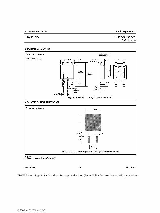
FIGURE 1.34 Page 5 of a data sheet for a typical thyristor. (From Philips Semiconductors. With permission.)

1.5 Power Bipolar Junction Transistors
Sohail Anwar
Power bipolar junction transistors (BJTs) play a vital role in power circuits. Like most other power devices,power transistors are generally constructed using silicon. The use of silicon allows operation of a BJT athigher currents and junction temperatures, which leads to the use of power transistors in AC applicationswhere ranges of up to several hundred kilowatts are essential.
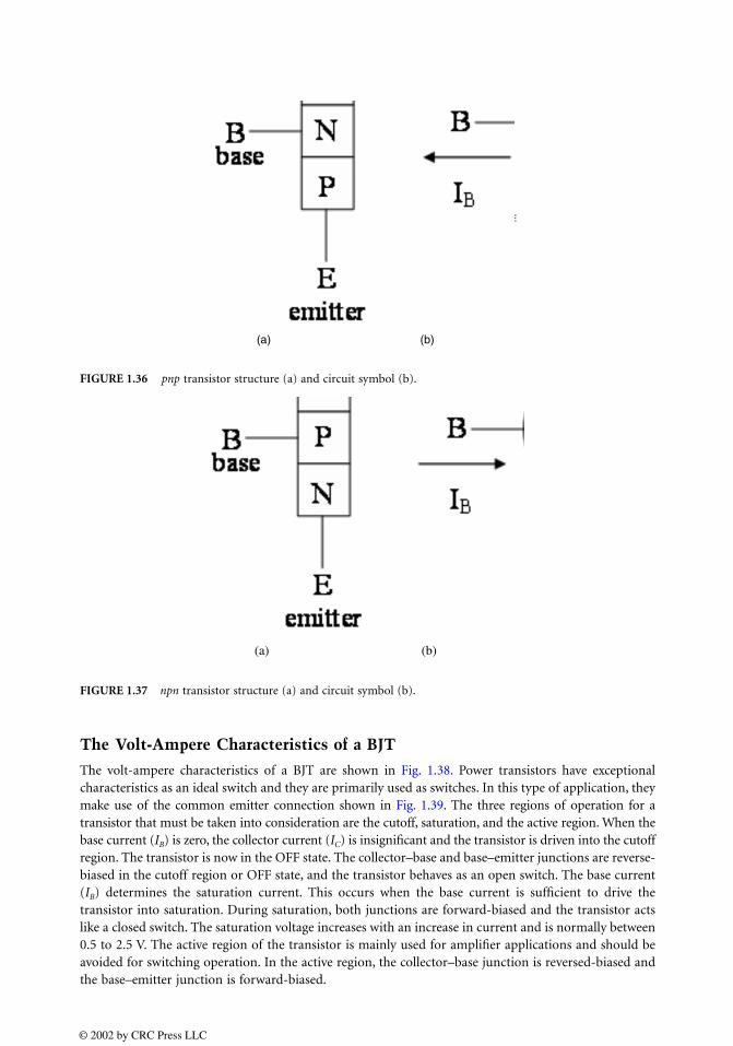
The power transistor is part of a family of three-layer devices. The three layers or terminals of a transistorare the base, the collector, and the emitter. Effectively, the transistor is equivalent to having two pn-diodejunctions stacked in opposite directions to each other. The two types of a transistor are termed npn andpnp. The npn-type transistor has a higher current-to-voltage rating than the pnp and is preferred for mostpower conversion applications. The easiest way to distinguish an npn-type transistor from a pnp-type isby virtue of the schematic or circuit symbol. The pnp type has an arrowhead on the emitter that pointstoward the base. Figure 1.36 shows the structure and the symbol of a pnp-type transistor. The npn-typetransistor has an arrowhead pointing away from the base. Figure 1.37 shows the structure and the symbolof an npn-type transistor.
When used as a switch, the transistor controls the power from the source to the load by supplying sufficientbase current. This small current from the driving circuit through the base–emitter, which must be maintained,turns on the collector—emitter path. Removing the current from the base–emitter path and making the basevoltage slightly negative turns off the switch. Even though the base–emitter path may only utilize a smallamount of current, the collector–emitter path is capable of carrying a much higher current.
FIGURE 1.35 Page 6 of a data sheet for a typical thyristor. (From Philips Semiconductors. With permission.)
© 2002 by CRC Press LLC
The Volt-Ampere Characteristics of a BJT
The volt-ampere characteristics of a BJT are shown in Fig. 1.38. Power transistors have exceptionalcharacteristics as an ideal switch and they are primarily used as switches. In this type of application, theymake use of the common emitter connection shown in Fig. 1.39. The three regions of operation for atransistor that must be taken into consideration are the cutoff, saturation, and the active region. When thebase current (IB) is zero, the collector current (IC) is insignificant and the transistor is driven into the cutoffregion. The transistor is now in the OFF state. The collector–base and base–emitter junctions are reverse-biased in the cutoff region or OFF state, and the transistor behaves as an open switch. The base current(IB) determines the saturation current. This occurs when the base current is sufficient to drive thetransistor into saturation. During saturation, both junctions are forward-biased and the transistor actslike a closed switch. The saturation voltage increases with an increase in current and is normally between0.5 to 2.5 V. The active region of the transistor is mainly used for amplifier applications and should beavoided for switching operation. In the active region, the collector–base junction is reversed-biased andthe base–emitter junction is forward-biased.
FIGURE 1.36 pnp transistor structure (a) and circuit symbol (b).
FIGURE 1.37 npn transistor structure (a) and circuit symbol (b).
Collector
Base
Emitter
(a) (b)
P
N
P
E
B
C
B
C
E
IC
+
VCE
--
lE
IB
Collector
Base
Emitter
(a) (b)
© 2002 by CRC Press LLC

BJT Biasing
When a transistor is used as a switch, the control circuit provides the necessary base current. The currentof the base determines the ON or OFF state of the transistor switch. The collector and the emitter of thetransistor form the power terminals of the switch.
The DC load line represents all of the possible operating points of a transistor and is shown in Fig. 1.40.The operating point is where the load line and the base current intersect and is determined by the valuesof VCC and RC .
In the ON state, the ideal operating point occurs when the collector current IC is equal to VCC /RC andVCE is zero. The actual operating point occurs when the load line intersects the base current at the saturationpoint. This occurs when the base current equals the saturation current or IB = IB(sat). At this point, thecollector current is maximum and the transistor has a small voltage drop across the collector–emitterterminals called the saturation voltage VCE(sat).
In the OFF state, or cutoff point, the ideal operating point occurs when the collector current IC is zeroand the collector–emitter voltage VCE is equal to the supply voltage VCC. The actual operating point, inthe OFF state, occurs when the load line intersects the base current (IB = 0). At the cutoff point, thecollector current is the leakage current. By applying Kirchoff ’s voltage law around the output loop, thecollector–emitter voltage (VCE) can be found.
The operating points between the saturation and cutoff constitute the active region. When operatingin the active region, high power dissipation occurs due to the relatively high values of collector current
FIGURE 1.38 BJT V-I characteristic.
FIGURE 1.39 Biasing of a transistor.
Saturation voltage Vce(sat)
ActiveRegion
Saturation (ON)
Cutoff (OFF) Leakagecurrent
Ic
Vce
© 2002 by CRC Press LLC

IC and collector–emitter voltage VCE. For satisfactory operation, a slightly higher than minimum basecurrent will ensure a saturated ON state and will result in reduced turn-on time and power dissipation.
BJT Power Losses
The four types of transistor power losses are the ON-state and OFF-state losses and turn-ON and turn-OFFswitching loss. OFF-state transistor losses are much lower than ON-state losses since the leakage currentof the device is within a few milliamps. Essentially, when a transistor is in the off state, whatever thevalue of collector–emitter voltage, there is no collector current. Switching losses depend on switchingfrequency. The highest possible switching frequency of the transistor is limited by the losses due to therate of switching. In other words, the higher the switching frequency, the more power loss in the transistor.
BJT Testing
Testing of the state of a transistors can be done with a multimeter. When a transistor is forward-biased,the base–collector and base–emitter regions should have a low resistance. When reverse-biased, the base–collector and base–emitter regions should have a high resistance. When testing the resistance betweenthe collector and the emitter, the resistance reading should result in a much higher than forward biasbase–collector and base–emitter resistance. However, faulty power transistors can appear shorted whenmeasuring resistance across the collector and emitter, but still pass both junction tests.
BJT Protection
Transistors must be protected against high currents and voltages to prevent damage to the device. Since theyare able to absorb very little energy before breakdown, semiconductor fuses cannot protect them. Thermalconditions are vitally important and can occur during high-frequency switching. Some of the mostcommon types of BJT protection are overcurrent and overvoltage protection. Electronic protectiontechniques are also frequently used to provide needed protection for transistors.
Overcurrent protection turns the transistor OFF when the collector–emitter voltage and collectorcurrent reach a preset value. When the transistor is in the ON state, an increase in collector–emittervoltage causes an increase in the collector current and therefore an increase in junction temperature.Since the BJT has a negative temperature coefficient, the increase in temperature causes a decrease inresistance and results in an even higher collector current. This condition, called positive feedback, couldeventually lead to thermal runaway and destroy the transistor. One such method of overcurrent protectionlimits the base current during an external fault. With the base current limited, the device current will belimited at the saturation point, with respect to the base current, and the device will hold some value ofthe voltage. This feature turns the transistor off without being damaged and is used for providing
FIGURE 1.40 DC load line.
Saturation (ON)
© 2002 by CRC Press LLC

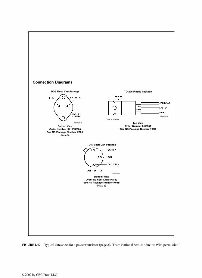
FIGURE 1.41 Typical data sheet for a power transistor (page 1). (From National Semiconductor. With permission.)
LM195/LM395Ultra Reliable Power TransistorsGeneral DescriptionThe LM195/LM395 are fast, monolithic power integrated cir-cuits with complete overload protection. These devices,which act as high gain power transistors, have included onthe chip, current limiting, power limiting, and thermal over-load protection making them virtually impossible to destroyfrom any type of overload. In the standard TO-3 transistorpower package, the LM195 will deliver load currents in ex-cess of 1.0A and can switch 40V in 500 ns.
The inclusion of thermal limiting, a feature not easily avail-able in discrete designs, provides virtually absolute protec-tion against overload. Excessive power dissipation or inad-equate heat sinking causes the thermal limiting circuitry toturn off the device preventing excessive heating.
The LM195 offers a significant increase in reliability as wellas simplifying power circuitry. In some applications, whereprotection is unusually difficult, such as switching regulators,lamp or solenoid drivers where normal power dissipation islow, the LM195 is especially advantageous.
The LM195 is easy to use and only a few precautions needbe observed. Excessive collector to emitter voltage can de-stroy the LM195 as with any power transistor. When the de-vice is used as an emitter follower with low source imped-
ance, it is necessary to insert a 5.0k resistor in series withthe base lead to prevent possible emitter follower oscilla-tions. Although the device is usually stable as an emitter fol-lower, the resistor eliminates the possibility of trouble withoutdegrading performance. Finally, since it has good high fre-quency response, supply bypassing is recommended.
For low-power applications (under 100 mA), refer to theLP395 Ultra Reliable Power Transistor.
The LM195/LM395 are available in the standard TO-3, KovarTO-5, and TO-220 packages. The LM195 is rated for opera-tion from 55 C to +150 C and the LM395 from 0 C to+125 C.
Featuresn Internal thermal limitingn Greater than 1.0A output currentn 3.0 A typical base currentn 500 ns switching timen 2.0V saturationn Base can be driven up to 40V without damagen Directly interfaces with CMOS or TTLn 100% electrical burn-in
Simplified Circuit
DS006009-1
1.0 Amp Lamp Flasher
DS006009-16
July 2000
LM195/LM
395U
ltraR
eliableP
ower
Transistors
© 2002 by CRC Press LLC
© 2002 by CRC Press LLC
FIGURE 1.42 Typical data sheet for a power transistor (page 2). (From National Semiconductor. With permission.)
Connection Diagrams
TO-3 Metal Can Package
DS006009-2
Bottom ViewOrder Number LM195K/883
See NS Package Number K02A(Note 5)
TO-220 Plastic Package
DS006009-3
Case is Emitter
Top ViewOrder Number LM395T
See NS Package Number T03B
TO-5 Metal Can Package
DS006009-4
Bottom ViewOrder Number LM195H/883
See NS Package Number H03B(Note 5)

© 2002 by CRC Press LLC
FIGURE 1.43 Typical data sheet for a power transistor (page 3). (From National Semiconductor. With permission.)
Absolute Maximum Ratings (Note 1)
If Military/Aerospace specified devices are required,please contact the National Semiconductor Sales Office/Distributors for availability and specifications.
Collector to Emitter VoltageLM195 42VLM395 36V
Collector to Base VoltageLM195 42VLM395 36V
Base to Emitter Voltage (Forward)LM195LM395
42V36V
Base to Emitter Voltage (Reverse) 20VCollector Current Internally LimitedPower Dissipation Internally LimitedOperating Temperature Range
LM195 55 C to +150 CLM395 0 C to +125 C
Storage Temperature Range 65 C to +150 CLead Temperature
(Soldering, 10 sec.) 260 C
Preconditioning100% Burn-In In Thermal Limit
Electrical Characteristics(Note 2)
Parameter Conditions LM195 LM395 Units
Min Typ Max Min Typ Max
Collector-Emitter Operating Voltage IQ ≤ IC ≤ IMAX 42 36 V
(Note 4)
Base to Emitter Breakdown Voltage 0 ≤ VCE ≤ VCEMAX 42 36 60 V
Collector Current
TO-3, TO-220 VCE ≤ 15V 1.2 2.2 1.0 2.2 A
TO-5 VCE ≤ 7.0V 1.2 1.8 1.0 1.8 A
Saturation Voltage IC ≤ 1.0A, TA = 25 C 1.8 2.0 1.8 2.2 V
Base Current 0 ≤ IC ≤ IMAX 3.0 5.0 3.0 10 A0 ≤ VCE ≤ VCEMAX
Quiescent Current (IQ) Vbe = 02.0 5.0 2.0 10 mA
0 ≤ VCE ≤ VCEMAX
Base to Emitter Voltage IC = 1.0A, TA = +25 C 0.9 0.9 V
Switching Time VCE = 36V, RL = 36Ω,500 500 ns
TA = 25 C
Thermal Resistance Junction to TO-3 Package (K) 2.3 3.0 2.3 3.0 C/W
Case (Note 3) TO-5 Package (H) 12 15 12 15 C/W
TO-220 Package (T) 4 6 C/W
Note 1: »AbsoluteMaximum Ratings…indicate limits beyond which damage to the device may occur. Operating Ratings indicate conditions for which the device isfunctional, but do not guarantee specific performance limits.
Note 2: Unless otherwise specified, these specifications apply for 55 C ≤ Tj ≤ +150 C for the LM195 and 0 C ≤ +125 C for the LM395.
Note 3: Without a heat sink, the thermal resistance of the TO-5 package is about +150 C/W, while that of the TO-3 package is +35 C/W.
Note 4: Selected devices with higher breakdown available.
Note 5: Refer to RETS195H and RETS195K drawings of military LM195H and LM195K versions for specifications.

© 2002 by CRC Press LLC
FIGURE 1.44 Typical data sheet for a power transistor (page 4). (From National Semiconductor. With permission.)
Typical Performance Characteristics (for K and T Packages)
Collector Characteristics
DS006009-33
Short Circuit Current
DS006009-34
Bias Current
DS006009-35
Quiescent Current
DS006009-36
Base Emitter Voltage
DS006009-37
Base Current
DS006009-38
Saturation Voltage
DS006009-39
Response Time
DS006009-40
Response Time
DS006009-41

© 2002 by CRC Press LLC
FIGURE 1.45 Typical data sheet for a power transistor (page 5). (From National Semiconductor. With permission.)
Typical Performance Characteristics (for K and T Packages) (Continued)
10V Transfer Function
DS006009-7
36V Transfer Function
DS006009-8
Transconductance
DS006009-9
Small Signal FrequencyResponse
DS006009-10

© 2002 by CRC Press LLC
FIGURE 1.46 Typical data sheet for a power transistor (page 6). (From National Semiconductor. With permission.)
Schematic Diagram
DS
0060
09-1
1

© 2002 by CRC Press LLC
FIGURE 1.47 Typical data sheet for a power transistor (page 7). (From National Semiconductor. With permission.)
Typical Applications
1.0 Amp Voltage Follower
DS006009-12
*Solid Tantalum
Power PNP
DS006009-13
*Protects against excessive base drive** Needed for stability
Time Delay
DS006009-14
1.0 MHz Oscillator
DS006009-15

© 2002 by CRC Press LLC
FIGURE 1.48 Typical data sheet for a power transistor (page 8). (From National Semiconductor. With permission.)
Typical Applications (Continued)
1.0 Amp Negative Regulator
DS006009-17
†Solid Tantalum
1.0 Amp Positive Voltage Regulator
DS006009-18
†Solid Tantalum

© 2002 by CRC Press LLC
FIGURE 1.49 Typical data sheet for a power transistor (page 9). (From National Semiconductor. With permission.)
Typical Applications (Continued)
Fast Optically Isolated Switch
DS006009-19
Optically Isolated Power Transistor
DS006009-20
CMOS or TTL Lamp Interface
DS006009-21
Two Terminal Current Limiter
DS006009-22
40V Switch
DS006009-23
*Drive Voltage 0V to ≥ 10V ≤ 42V
6.0V Shunt Regulator with Crowbar
DS006009-24
Two Terminal 100 mA Current Regulator
DS006009-25

© 2002 by CRC Press LLC
FIGURE 1.50 Typical data sheet for a power transistor (page 10). (From National Semiconductor. With permission.)
Typical Applications (Continued)
Low Level Power Switch
DS006009-26
Turn ON = 350 mVTurn OFF = 200 mV
Power One-Shot
DS006009-27
T = R1CR2 = 3R1R2 ≤ 82k
Emitter Follower
DS006009-28
*Need for Stability
High Input Impedance AC Emitter Follower
DS006009-29
Fast Follower
DS006009-30
*Prevents storage with fast fall time square wave drive

© 2002 by CRC Press LLC
FIGURE 1.51 Typical data sheet for a power transistor (page 11). (From National Semiconductor. With permission.)
Typical Applications (Continued)
Power Op Amp
DS006009-31
*Adjust for 50 mA quiescent current†Solid Tantalum
6.0 Amp Variable Output Switching Regulator
DS006009-32
*Sixty turns wound on Arnold Type A-083081-2 core.** Four devices in parallel†Solid tantalum

© 2002 by CRC Press LLC
FIGURE 1.52 Typical data sheet for a power transistor (page 12). (From National Semiconductor. With permission.)
Physical Dimensions inches (millimeters) unless otherwise noted
TO-5 Metal Can PackageOrder Number LM195H/883NS Package Number H03B
TO-3 Metal Can PackageOrder Number LM195K/883NS Package Number K02A

protection in low power converters by limiting the current during an external fault. Other methods ofovercurrent protection for more severe faults use a shorting switch, or shunt switch, in parallel with thetransistor. When a fault is detected, an external circuit activates the parallel shorting switch, providingan alternate path for the fault current.
Overvoltage protection is used to protect a transistor from high voltages. When a transistor is in theOFF state, high collector-base reverse–bias voltages can cause avalanche breakdown. Avalanche break-down occurs when the reverse voltage exceeds the reverse voltage limit of the collector–base region. Highcollector–base reverse-bias voltages can easily damage the transistor. One simple method to ensureovercurrent protection of a transistor is to connect an antiparallel diode across the transistor.
Most power transistors are unable to block reverse voltages in excess of 20 V. Reverse voltages caneasily damage the transistor and therefore they should not be used in AC control applications withouta reverse shunting diode connected between the emitter and the collector.
A typical data sheet for a power transistor is provided in Figs. 1.41 through 1.53.
FIGURE 1.53 Typical data sheet for a power transistor (page 13). (From National Semiconductor. With permission.)
Physical Dimensions inches (millimeters) unless otherwise noted (Continued)
LIFE SUPPORT POLICY
NATIONAL'S PRODUCTS ARE NOT AUTHORIZED FOR USE AS CRITICAL COMPONENTS IN LIFE SUPPORTDEVICES OR SYSTEMS WITHOUT THE EXPRESS WRITTEN APPROVAL OF THE PRESIDENT AND GENERALCOUNSEL OF NATIONAL SEMICONDUCTOR CORPORATION. As used herein:
1. Life support devices or systems are devices orsystems which, (a) are intended for surgical implantinto the body, or (b) support or sustain life, andwhose failure to perform when properly used inaccordance with instructions for use provided in thelabeling, can be reasonably expected to result in asignificant injury to the user.
2. A critical component is any component of a lifesupport device or system whose failure to performcan be reasonably expected to cause the failure ofthe life support device or system, or to affect its
safety
or effectiveness.
National SemiconductorCorporationAmericasTel: 1-800-272-9959Fax: 1-800-737-7018Email: [email protected]
National SemiconductorEurope
Fax: +49 (0) 180-530 85 86Email: [email protected]
Deutsch Tel: +49 (0) 69 9508 6208English Tel: +44 (0) 870 24 0 2171FranÕais Tel: +33 (0) 1 41 91 8790
National SemiconductorAsia Pacific CustomerResponse GroupTel: 65-2544466Fax: 65-2504466Email: [email protected]
National SemiconductorJapan Ltd.Tel: 81-3-5639-7560Fax: 81-3-5639-7507
www.national.com
TO-220 Plastic PackageOrder Number LM395T
NS Package Number T03B
National does not assume any responsibility for use of any circuitry described, no circuit patent licenses are implied and National reserves the right at any time without notice to change said circuitry and specifications.
© 2002 by CRC Press LLC

1.6 MOSFETs
Vrej Barkhordarian
The metal-oxide-semiconductor field-effect transistor (MOSFET) is the most commonly used activedevice in very large scale integrated (VLSI) circuits. Figure 1.54 shows the device schematic, current-voltage characteristics, transfer characteristics and device symbol for a MOSFET. It is a lateral device andthough very suitable for integration into integrated circuits, it has severe limitations at high power levels.The power MOSFET design is based on the original field-effect transistor and, since its invention in theearly 1970s, has gone through several evolutionary steps. The processing of power MOSFETs is verysimilar to that of today’s VLSI circuits although the device geometry is significantly different from the
FIGURE 1.54 (a) Schematic diagram, (b) current-voltage characteristics, (c) transfer characteristics, and (d) devicesymbol for an n-channel enhancement mode MOSFET.
Sourcecontact
Fieldoxide
Gateoxide
Draincontact
p-Substrate
Gatemetallization
n+ Drainn+ Source
Channel
(a)
(b)
(d)
(c)
00
00
D
G
S
SB(Channel orsubstrate)
tox
lD lD
lD
VDS
VGS = Vτ
VGS > Vτ
i
Vτ VGS
© 2002 by CRC Press LLC

design used in these circuits. Power MOSFETs are commonly used as switches in power electronicapplications.
The invention of the power MOSFET was partly driven by the limitations of bipolar power transistorswhich, until recently, were the devices of choice in power electronics applications. Although it is notpossible to define absolutely the operating boundaries of a power device, we will loosely refer to thepower device as any device that is capable of switching at least 1A. The bipolar power transistor is acurrent-controlled device and a large base drive current as high as one fifth of the collector current isrequired to keep the device in the on state. Also, higher reverse base drive currents are required to obtainfast turn-off. Despite the very advanced state of manufacturability and lower costs of bipolar powertransistors, these limitations have made the base drive circuit design more complicated and hence moreexpensive. There are two further limitations to the bipolar power transistor. First, both electrons andholes contribute to conduction in BJTs. Presence of holes with their higher carrier lifetime causes theswitching speed to be several orders of magnitude slower than for a power MOSFET of similar size andvoltage rating. Secondly, the BJTs suffer from thermal runaway. The forward voltage drop of a BJTdecreases with increasing temperature causing diversion of current to a single device when several devicesare paralleled. Power MOSFETs, on the other hand, are majority carrier devices with no minority carrierinjection. They are superior to the BJTs in high-frequency applications where switching power losses areimportant and can withstand simultaneous application of high current and voltage without undergoingdestructive failure due to second breakdown. Power MOSFETs can also be paralleled easily since theforward voltage drop increases with increasing temperature, ensuring an even distribution of currentamong all components. However, at high breakdown voltages (>∼200V) the on-state voltage drop of thepower MOSFET becomes higher than that of a similar size bipolar device with a similar voltage rating,making it more attractive to use the bipolar power transistor at the expense of worse high-frequencyperformance. Figure 1.55 shows the present current-voltage limitations of power MOSFETs and BJTs.New materials, structures and processing techniques are expected to push these limits out over time. Arelatively new device which combines the high-frequency advantages of the MOSFET with the low on-state voltage drop of high voltage BJTs is the insulated-gate-bipolar transistor (IGBT).
FIGURE 1.55 Current-voltage limitations of MOSFETs and BJTs.
2000
1500
1000
500
01 10 100 1000
Maximum current (A)
MOS
Bipolartransistors
Hol
doff
volta
ge (
V)
© 2002 by CRC Press LLC

MOSFETs used in integrated circuits are lateral devices with gate, source and drain all on the top ofthe device and with current flow taking place in a path parallel to the surface. Although this design lendsitself to integration, it is not suitable for discrete power device applications due to large distances requiredbetween source and drain in order to maintain isolation. Having all three terminals as the upper surfacemakes the metallization and isolation of terminals more complicated from the processing point of view.The vertical double diffused MOSFET solves this problem by using the substrate of the device as thedrain terminal. Figure 1.56 shows the schematic diagram and the circuit symbol for an n-channel powerMOSFET. When a positive bias greater than the threshold voltage is applied to the gate, the siliconsurface in the channel region is inverted and a current starts to flow between the source and drain. Forgate voltages of less than V+ no surface inversion occurs in the channel and the device remains in the off-state. The current in this device flows horizontally along the inverted channel first and then verticallybetween the drain and source. The term “double-diffused” refers to the two consecutive ion implantationsteps using the poly as a mask. For an n-channel device, the regions formed by double implant andsubsequent diffusion are first p-type to define the channel and then n-type to define the source. The p-body implant is performed in a separate step. The terms “body drift” and “body-drain” diodes are usedinterchangeably to denote the p-n junction formed by this p-body implant and the drift region.
Figure 1.57 shows the physical origin of the parasitic components in an n-channel power MOSFET.The parasitic JFET appearing between the two body implants restricts current flow when the depletion
FIGURE 1.56 Schematic diagram for an n-channel power MOSFET and the device symbol.
FIGURE 1.57 The origin of parasitic components for a power MOSFET.
Source Gateoxide
Polysilicongate Source
metallization
p+ Body Region
p+ substrate(100)
n− epilayer
n+ n+p+
G
D
S
DrainDrainmetallization
Channelsp
Drift Region
Metal
LTOCGS2
CDS
p−
n− n−
n− epilayer
n− substrate
CGS1
RB
CGD
Cgsm
REPI
RCh
BJT
JFET
© 2002 by CRC Press LLC

widths of the two adjacent body diodes extend into the drift region with increasing drain voltage.Poly line-width and the epi layer resistivity under the poly are two important design parameters forminimizing the JFET effect. The parasitic BJT can make the device susceptible to unwanted device turn-on and premature breakdown. The base resistance RB has to be minimized through careful design of thedoping and distance under the source region. These two components and the parasitic resistances arediscussed further in the next sections. There are several parasitic capacitances associated with the powerMOSFET as shown in Fig. 1.57. CGS is the capacitance due to the overlap of the source and the channelregions by the polysilicon gate and is independent of applied voltage. GGD is made up of two parts. Thefirst part is the capacitance associated with the overlap of the polysilicon gate and the silicon underneathin the JFET region. The second part is the capacitance associated with the depletion region immediatelyunder the gate. CGD is a nonlinear function of voltage and is discussed further in the “Dynamic Charac-teristics” section. Finally, CDS is the capacitance associated with the body-drift diode and varies inverselywith the square root of the drain-source bias.
There are currently two designs of power MOSFETs. These are usually referred to as the planar andthe trench designs. The planar design has already been introduced in the schematics of Figs. 1.56 and1.57. Two variations of the trench power MOSFET are shown in Fig. 1.58. The V-groove device isfabricated by etching a groove in the silicon after the double diffusion step. The use of an anisotropicetch results in the sides of the groove to be at an angle of 54.7° to the surface of the wafer. Etching stopswhen the groove sides, which are planes, reach each other. The gate oxide and gate poly or metallizationare then grown in the groove followed by the source metallization. Current crowding at the apex of theV-groove reduces current handling capability. In a truncated V-groove design, the anisotropic etch isstopped before this point is reached. The trench technology has the advantage of higher cell density butis more difficult to manufacture compared with the planar device.
Static Characteristics
One of the important features of the power MOSFET is the very high input impedance which simplifiesthe gate drive circuitry and reduces cost. It is a voltage-controlled device with to gate current flow duringoperation. Figure 1.59 shows I–V characteristics of an enhancement mode (normally off) power MOSFET.Data sheets contain typical graphs which can be used to determine if the device is in the fully on stateor in the constant-current region for a given value of gate bias and drain current. Temperature effect onthreshold voltage (about 6 mV/C reduction) and the difference between typical values of parameters andthe maximums should be taken into account.
FIGURE 1.58 Schematic diagram of (a) V-groove trench MOSFET showing the current crowding at the apex and(b) truncated V-groove design.
S G S
Electron flow
D
(a)
Source Source
Gateoxide
Gate
p
Oxide
Channel
Drain
n- epilayer
n+
n+ substrate(100)
(b)
© 2002 by CRC Press LLC

Breakdown Voltage
This is the drain voltage at which the reverse-biased body-drift diode breaks down and a significantcurrent starts to flow between the source and drain by the avalanche multiplication process, while thegate and source are shorted together. Breakdown voltage, BVDSS, is normally measured at a drain currentof 250 µA. For drain voltages below BVDSS and with no bias on the gate, no channel is formed under thegate at the surface and the drain voltage is entirely supported by the reverse-biased body-drift pn junction.There are two related phenomena which can occur in poorly designed and processed devices. These arepunch-through and reach-through.
Punch-through is observed when the depletion region on the source side of the body-drift pn-junctionreaches the source region at drain voltages below the rated avalanche voltage of the device. This providesa current path between source and drain and causes a soft breakdown characteristic as shown in Fig. 1.60.The leakage current flowing between source and drain is denoted by IDSS. Careful selection and optimizationof the doping profile used in the fabrication of a power MOSFET is therefore very important. Figure 1.61shows a typical diffusion profile for a power MOSFET. The surface concentration of the body diffusion andthe channel length (distance between the two pn-junctions formed by the source diffusion and the channeldiffusion) will determine whether punch-through will occur or not. There are trade-offs to be made betweenon-resistance Rdson which requires shorter channel lengths and punch-through avoidance which requireslonger channel lengths. An approximate equation giving the depletion region width as a function of silicon
FIGURE 1.59 Current-voltage characteristics of a power MOSFET.
0 5 10 15
DRAIN VOLTAGE (VOLTS)
1
2
3
4
IDS vs VDS LOCUS
5
GATEVOLTAGE
6
7
0
5
10
15
20
25
NO
RM
ALI
ZE
D D
RA
IN C
UR
RE
NT
(LIN
EA
R R
EG
ION
)
(SAT
UR
ATIO
N)
RE
GIO
N
© 2002 by CRC Press LLC

background doping is given by:
(1.1)
where s is semiconductor permittivity, K is Boltzmann’s constant, T is temperature in K, q is electroniccharge, NA is background doping, and ni is the intrinsic carrier density.
FIGURE 1.60 Breakdown characteristics of a power MOSFET showing the ideal (sharp) and nonideal (soft)behaviors.
FIGURE 1.61 Typical doping profile of a power MOSFET, in a direction parallel to the device surface. Thresholdvoltage is determined by the peak carrier concentration in the channel region.
ID
BVDSS VDS
Soft
Sharp
Source ChannelDrain driftregion
0 1 2
Distance along channel (µm)
Epilayer
Surface region
Along carrier path
(n-)
n+
1026
1025
1024
1023
1022
1021
1020
n
p
Dop
ing
conc
entr
atio
n (m
-3)
W4sKT
q2NA
---------------NA
ni
------ln≈
© 2002 by CRC Press LLC

Also, higher channel implant dose is beneficial from the punch-through point of view since depletionwidth will be smaller, but the Rdson will suffer through reduced carrier mobility. The design of the dopingprofile involves choosing channel and source implant doses, diffusion times and temperatures that givea designed threshold voltage while simultaneously minimizing Rdson and IDSS. Optimizing these perfor-mance parameters with manufacturability in mind is one of the challenges of power MOSFET design.
The reach-through phenomenon, on the other hand, occurs when the depletion region on the driftside of the body-drift pn-junction reaches the epilayer-substrate interface before avalanching takes placein the epi. Once the depletion edge enters the high carrier concentration substrate, a further increase indrain voltage will cause the electric field to quickly reach the critical value of 2 × 10
5 V/cm at which
avalanching begins.Other factors that affect the breakdown voltage of power MOSFETs for a given epitaxial layer include
termination design, cell spacing (poly line width) and curvature of the body diode depletion region inthe epi which is a function of diffusion depth. Power MOSFETs are designed such that avalanchebreakdown occurs in the active area first.
On-Resistance
The on-state resistance of a power MOSFET is made up of several components as shown in Fig. 1.62.
(1.2)
where
Rsource = source diffusion resistanceRch = channel resistanceRA = accumulation resistanceRJ = the “JFET” component-resistance of the region between the two body regionsRD = drift region resistanceRsub = the substrate resistance; wafers with resistivities of up to 20 mΩ-cm are used for high-voltage
devices and less than 5 mΩ-cm for low-voltage devicesRwcml = sum of bond wire resistance, contact resistance between the source and drain metallization
and the silicon, metallization resistance, and leadframe contributions; these are normallynegligible in high-voltage devices but can become significant in low-voltage devices
FIGURE 1.62 The origin of the internal resistances in a power MOSFET.
SOURCE
GATE
N+ SUBSTRATE
DRAIN
Rsub
RSOURCERCH
RJ
RA P-BASE
N+
RD
Rdson Rsource Rch RA RJ RD Rsub Rwcml+ + + + + +=
© 2002 by CRC Press LLC

Figure 1.63 shows the relative importance of each of the components to Rdson over the voltage spectrum.As can be seen, at high voltages the Rdson is dominated by epi resistance and the JFET component. Thiscomponent is higher in high-voltage devices due to the higher resistivity or lower background carrierconcentration in the epi. At lower voltages, the Rdson is dominated by the channel resistance and thecontributions from the metal to semiconductor contact, metallization, bond wires, and leadframe. Thesubstrate contribution becomes more significant for lower breakdown voltage devices.
TransconductanceThis parameter is a measure of the sensitivity of drain current to changes in gate-source bias and isdefined as:
(1.3)
i.e., the gradient of the Id vs. Vgs graph. In the saturation region, gfs is given by:
(1.4)
This parameter is normally quoted for a Vgs that gives a drain current equal to about one half of themaximum current rating value and for a VDS that ensures operation in the constant current region. Withmobility µ fixed for a given semiconductor, the design parameters influencing transconductance of aMOSFET are gate width W, channel length L, and gate oxide thickness tox and hence Cox. Gate width is thetotal polysilicon gate perimeter of the cellular structure and increases in proportion to the active area asthe cell density increases. The cell density has increased over the years from around half a million per squareinch in 1980 to around 8 million for planar MOSFETs and around 12 million for the trench technology atthe present time. The limiting factor for even higher cell densities is the photolithography process controland resolution which allows contacts to be made to the source metallization in the center of the cells.
FIGURE 1.63 Relative contributions to Rdson in devices with different voltage ratings.
Voltage Rating:
Packaging
Metallization
Source
Channel
JFETregion
Epitaxiallayer
Substrate
50 V 100 V 500 V
Rwcml
RCh
REPI
gfs
∆ID
∆Vgs
----------- Vds constant=
gfs µCoxWL----- Vgs Vth–( )=
© 2002 by CRC Press LLC

Reduced channel length is beneficial to both gfs and on-resistance, with punch-through as a trade-off.The lower limit of this length is set by the ability to control the double-diffusion process and is around1 to 2 µm today. Finally, reductions in gate oxide thickness give higher Cox and higher gfs. The reductionin oxide thickness will reduce Vth unless channel implant dose is increased which in turn will cause a higherRdson. Ultimately, the lower limit of tox is set by the maximum gate-source voltage rating. This is ±30 V forhigh-voltage devices and ±20 V for lower-voltage logic-level devices used in portable electronic applications.
Threshold VoltageThis is defined as the minimum gate electrode bias required to strongly invert the surface under the polyand form a conducting channel between the source and the drain regions. Vth is usually measured at adrain-source current of 250 µA. A value of 2 to 4 V for high-voltage devices with thicker gate oxides andlogic-compatible values of 1 to 2 V for lower-voltage devices with thinner gate oxides are common. Withpower MOSFETs finding increasing use in portable electronics and wireless communications wherebattery power is at a premium, the trend is toward lower values of Rdson and Vth. Gate oxide quality andintegrity become major issues as the gate oxide thickness is reduced to achieve lower Vth. An approx-imate expression for Vth is given by:
(1.5)
where ox and tox are oxide permittivity and thickness and the other parameters are defined in Eq. (1.1).Processing methods used and their influence on the chemistry of the silicon surface have pronounced
effects on Vth. Fixed and mobile surface and interface charges as well as charges in the gate oxide act tochange the value of Vth from the intended value. Therefore, control of these charges in the process isnecessary for obtaining consistent Vth values in production. Also, the presence of mobile charges awayfrom the gate oxide and oxide/silicon interface may find their way to the device surface over the lifetimeof the device and cause a gradual shift in Vth. For example, sodium ions in the low-temperature oxide(LTO) or in the metallization can cause a shift in Vth by changing the charge distribution at the interface.Accelerated life-tests are used by manufacturers to evaluate new processes and also to monitor Vth shiftin production. Monitoring and control of contamination in the clean room equipment are routinelycarried out by capacitance-voltage measurements of test diodes.
In real devices, Vth is altered by the unequal metal and semiconductor work functions. Denoting thebarrier height between the metal and silicon oxide as φB, the work function difference is given by:
(1.6)
where ψB is the potential difference between the intrinsic and Fermi levels in the semiconductor; χ andχo are the semiconductor and oxide electron affinities and Eg is the semiconductor band-gap energy.
Taking into account this effect and also the various fixed and mobile charges that may alter the valueof Vth from that given above, the expression for Vth becomes:
(1.7)
where
Qs = surface charge, which is a function of surface potential and determines channel conductivityQss = interface state charge (typically 10
10 to 10
12 cm
−2); caused by dangling bonds at the semiconductor
surface, these can charge and discharge with changes in the surface potentialQI = charge due to mobile ions in the oxideQFC = fixed surface charge at the silicon–oxide interface
Vth
4sKTNA NA/ni( )lnox/tox( )
----------------------------------------------------- 2KTq
----------- NA/ni( )ln+≈
qφms qφB qχo qχ Eg /2 qψB+ +( )–+=
Vth φms 2ψB
Qs Qss QI QFC+ + +Cax
----------------------------------------------- –+=
© 2002 by CRC Press LLC

It is worth mentioning that the success of silicon devices lies partly in the low density of these interfacestates which is due to the existence of native oxide in silicon as opposed to other semiconductors suchas GaAs where such a native oxide does not exist and oxide layers have to be deposited with several ordersof magnitude higher interface state densities.
Diode Forward Voltage (VF or VSD)This is the guaranteed maximum forward drop of the body-drain diode at a specified value of sourcecurrent. Figure 1.64 shows a typical I–V characteristic for this diode at two temperatures. p-Channeldevices have higher values of VF due to the higher contact resistance between metal and p-silicon comparedwith n-type silicon. Maximum values of 1.6 V for high-voltage devices (>100 V) and values of 1.0 V forlow-voltage devices (<100 V) are common.
Power DissipationThe maximum allowable power dissipation which will raise the die temperature to the maximum allow-able when the case temperature is held at 25°C is an important parameter and is given by:
(1.8)
where Tjmax is the maximum allowable temperature of the pn junction in the device (normally 150 or175°C) and RthJC is the junction to cause thermal impedance of the device.
Dynamic Characteristics
Switching and Transient Response
When the MOSFET is used as a switch, its basic function is to control the drain current by the gatevoltage. Figure 1.65 shows the transfer characteristics and an equivalent circuit model often used for theanalysis of MOSFET switching performance. For a detailed discussion of this topic see Chapter 4 in Grantand Gower (1989). The following is a summary of the important points.
The switching performance of a device is determined by the time required to establish voltage changesacross capacitances and current changes in inductances. RG is the distributed resistance of the gate andis approximately inversely proportional to active area. Values of around 20 Ω-mm
2 are common for the
FIGURE 1.64 Typical source-drain (body) diode forward voltage characteristics.
100
10
1
0.10.0 0.5 1.0 1.5 2.0 2.5
VSD, Source-to-Drain Voltage (V)
I SD, R
ever
se D
rain
Cur
rent
(A
)
VGS = 0V
TJ = 25oC
TJ = 150oC
Pd
Tjmax 25–RthJC
----------------------- =
© 2002 by CRC Press LLC

product of RG and active area for polysilicon gates. LS and LD are source and drain lead inductances andare around a few tens of nH. The physical origin of the capacitances CGS , CGD , and CDS were discussedin the introduction of this chapter regarding the device schematic shown in Fig. 1.57. The typical valuesof input (Ciss), output (Coss), and reverse transfer (Crss) capacitances given in the data sheets are used bycircuit designers as a starting point in determining circuit component values. The data sheet capacitancesare defined in terms of the equivalent circuit capacitances as:
The gate-to-drain capacitance CGD is a nonlinear function of voltage and is the most important parametersince it provides a feedback loop between the output and the input of the circuit. CGD is also called the
FIGURE 1.65 (a) Transfer characteristics and (b) an equivalent circuit diagram showing the MOSFET parasiticcomponents that have the greatest effect on switching speed.
ID
VGS
LD
ID
LS
CGD
CDS
CGS
RG
slope = gfs
(a)
(b)
D
G′G Body-drain
diode
D′
S′
S
Ciss CGS CGD, CDS shorted+=Crss CGD=Coss CDS CGD+=
© 2002 by CRC Press LLC

Miller capacitance since it causes the total dynamic input capacitance to become greater than the sumof the static capacitances.
Figure 1.66 shows a typical switching time test circuit. Also shown are the components of the rise andfall times with reference to the VGS and VDS waveforms. Turn-on delay, td(on), is the time taken to chargethe input capacitance of the device before drain current conduction can start. Similarly, turn-off delaytd(off) is the time taken to discharge the capacitance after the gate is switched off.
Gate Charge
Although input capacitance values are useful, they do not provide accurate results when comparing theswitching performances of two devices from different manufacturers. Effects of device size and transcon-ductance make such comparisons more difficult. A more useful parameter from the circuit design pointof view is the gate charge rather than capacitance. Most manufacturers include both parameters on theirdata sheets. Figure 1.67 shows a typical gate charge waveform and the test circuit. When the gate isconnected to the supply voltage, VGS starts to increase until it reaches Vth, at which point the drain currentstarts to flow and the CGS starts to charge. During the period t1 to t2, CGS continues to charge, the gatevoltage continues to rise and the drain current rises proportionally. At time t2, CGS is completely chargedand the drain current reaches the predetermined current ID and stays constant while the drain voltagestarts to fall. With reference to the equivalent circuit model of the MOSFET shown in Fig. 1.67, it canbe seen that with CGS fully charged at t2, VGS becomes constant and the drive current starts to charge theMiller capacitance CGD. This continues until time t3. Note that the charge time for the Miller capacitance islarger than that for the gate to source capacitance CGS, due to the rapidly changing drain voltage betweent2 ant t3 (current = C dV/dt). Once both of the capacitances CGS and CGD are fully charged, the gate voltage
FIGURE 1.66 Switching time test circuit and resulting VGS and VDS waveforms.
td(on) tr
RG
−10 V
Pulse Width <_ 1µsDuty Factor <_ 0.1%
VGS
VDS
RD
VDD
td(off) tfVGS
VDS
10%
90%
D.U.T.
−+
© 2002 by CRC Press LLC

VGS starts increasing again until it reaches the supply voltage at time t4. The gate charge (QGS + QGD)corresponding to time t3 is the bare minimum charge required to switch the device on. Good circuitdesign practice dictates the use of a higher gate voltage than the bare minimum required for switchingand therefore the gate charge used in the calculations is QG corresponding to t4.
The advantage of using gate charge is that the designer can easily calculate the amount of current requiredfrom the drive circuit to switch the device on in a desired length of time; since Q = CV and I = C dV/dtthen Q = time × current. For example, a device with a gate charge of 20 nC can be turned on in 20 µs if acurrent of 1 mA is supplied to the gate or it can turn on in 20 ns if the gate current is increased to 1 A.These simple calculations would not have been possible with input capacitance values.
dV/dt Capability
This is also called the peak diode recovery and is defined as the maximum rate of rise of drain-sourcevoltage allowed. If this rate is exceeded then the voltage across the gate-source terminals may becomehigher than the threshold voltage of the device, forcing the device into the current conduction mode and
FIGURE 1.67 (a) Gate charge test circuit and (b) resulting gate and drain waveforms.
VDD
ID
ID
TEST CIRCUIT
CDG
CGS
OGDOGS
VG
VG(TH)
VDDID
'0 '1 '2 '3 '4
SS
D
G
D
(a)
(b)
GATEVOLTAGE
DRAINVOLTAGE DRAIN CURRENT
WAVEFORM
© 2002 by CRC Press LLC

under certain conditions a catastrophic failure may occur. There are two possible mechanisms by which adV/dt induced turn-on may take place. Figure 1.68 shows the equivalent circuit model of a power MOSFET,including the parasitic BJT. The first mechanism of dv/dt induced turn-on becomes active through thefeedback action of the gate-drain capacitance CGD. When a voltage ramp appears across the drain andsource terminals of the device, a current I1 flows through the gate resistance RG by means of the gate-drain capacitance CGD. RG is the total gate resistance in the circuit and the voltage drop across it is given by:
(1.9)
When the gate voltage VGS exceeds the threshold voltage of the device Vth, the device is forced intoconduction. The dV/dt capability for this mechanism is thus set by:
(1.10)
It is clear that low Vth devices are more prone to dV/dt turn-on. The negative temperature coefficient ofVth is of special importance in applications where high-temperature environments are present. Also, gatecircuit impedance has to be chosen carefully in order to avoid this effect. CGD is an internal deviceparameter and is determined by the overlap area between poly gate and silicon and gate oxide thickness.Higher gate oxide thicknesses reduce CGD and also increase Vth, both advantageous to dV/dt rating, aslong as the higher Vth is acceptable in the application.
The second mechanism for the dV/dt turn-on in MOSFETs is through the parasitic BJT as shown inFig. 1.69. The capacitance associated with the depletion region of the body diode extending into the driftregion is denoted as CDB and appears between the base of the BJT and the drain of the MOSFET. Thiscapacitance gives rise to a current I2 which flows through the base resistance RB when a voltage rampappears across the drain-source terminals. With analogy to the first mechanism, the dV/dt capability ofthis mechanism is given by:
(1.11)
FIGURE 1.68 Equivalent circuit model of a power MOSFET showing the two possible mechanisms for dV/dt-induced turn-on. (From Baliga, B. J., Modern Power Devices, © 1987 John Wiley & Sons, Inc., New York. Reprintedby permission of John Wiley & Sons, Inc.)
DRAIN
SOURCE
D
S
I1
I2
CGD CDB
RB
CGS
RG
G
NPNBIPOLAR
TRANSISTOR
APPLIEDRAMP
VOLTAGE
VGS I1RG=
RGCGDdVdt--------
=
dVdt--------
Vth
RGCGD
----------------=
dVdt--------
VBE
RBCDB
---------------=
© 2002 by CRC Press LLC

If the voltage that develops across RB is greater than about 0.7 V, then the base–emitter junction is forward-biased and the parasitic BJT is turned on. Under the conditions of high dV/dt and large values of RB, the break-down voltage of the MOSFET will be limited to that of the open-base breakdown voltage of the BJT. Ifthe applied drain voltage is greater than the open-base breakdown voltage, then the MOSFET will enteravalanche and may be destroyed if the current is not limited externally.
Increasing dV/dt capability therefore requires reducing the base resistance RB by increasing the bodyregion doping and reducing the distance the current I2 has to flow laterally before it is collected by thesource metallization. As in the first mode, the BJT related dV/dt capability becomes worse at highertemperatures since RB increases and VBE decreases with increasing temperature.
Applications
The following are two of the major markets where power MOSFETs are finding increasing applicationsas either logic-controlled or analog switches.
Portable Electronics and Wireless Communication
With the recent advances in the portable electronic products, low Rdson, logic level surface mount powerMOSFET are experiencing explosive demand. A portable computer, for example, uses power MOSFETsin the AC-DC converters, the DC-DC converters and voltage regulators, load management switches,battery charger circuitry, and reverse battery protection. Required features of MOSFETs in these appli-cations are small size, low power dissipation, and low on-resistance for extended battery life. Reductionof both conduction and switching losses are important considerations in the design of MOSFETs aimedat this market.
Automotive
Mechanical contact breakers have mostly been replaced by semiconductor devices in ignition circuits inmodern cars. A suitable semiconductor device must be capable of blocking high voltages in a severeenvironment where line voltage surges are common due to the opening and closing of switches and theconnection and disconnection of inductive loads during maintenance and loose connections. Bipolartransistors with their susceptibility to secondary breakdown are not suited whereas power MOSFETs withavalanche capability are ideally suited. Voltage transients are clamped by the avalanching of the MOSFETwithout the need to use any external protection circuits.
FIGURE 1.69 Physical origin of the parasitic BJT components that may cause dV/dt-induced turn-on in powerMOSFET. (From Baliga, B. J., Modern Power Devices, © 1987 John Wiley & Sons, Inc., New York. Reprinted bypermission of John Wiley & Sons, Inc.)
SOURCE
N+
LN+
RS
CDB
A
DRAIN
GATE
© 2002 by CRC Press LLC

In 12-V battery vehicles the most commonly used MOSFETs are rated at 50 or 60 V breakdown volt-ages. The significant guard-banding is necessary in order to avoid device failure due to the alternatorproducing high voltages after shedding a heavy load.
The other features of power MOSFETs which make them suitable for the automotive applications are highdV/dt ratings, high-temperature performance, ruggedness and high reliability. Logic level, surface mountdevices with low Rdson have recently found application in this field. The smaller footprint of surface mountsoffers space savings and the lower Rdson does away with the need to parallel devices to reduce on-resistance.This in turn translates into fewer device counts and heat-sinks which lowers the overall cost.
In addition to ignition control, power MOSFETs are used in anti-lock brake (ABS) systems, electronicpower steering (EPS) systems, air bags, electronic suspension, and numerous motor control applicationssuch as power windows, power seats, radiator fan, wipers, fuel pump, etc.
References
Baliga, B.J. 1987. Modern Power Devices, John Wiley & Sons, New York.Grant, D.A. and Gower, I. 1989. Power MOSFETs—Theory and Applications, John Wiley & Sons, New York.International Rectifier, 1995, HEXFET Power MOSFET Designer’s Manual—Application Notes and Reli-
ability Data, International Rectifier, El Segundo, CA.Oxner, E.S. 1982. Power FETs and Their Applications, Prentice-Hall, Englewood Cliffs, NJ.Sze, S.M. 1981. Physics of Semiconductor Devices, John Wiley & Sons, New York.
1.7 General Power Semiconductor Switch Requirements
Alex Q. Huang
A power semiconductor switch is a component that can either conduct a current when it is commandedON or block a voltage when it is commanded OFF through a control. This change of conductivity ismade possible in a semiconductor by specially arranged device structures that control the carrier trans-portation. The time that it takes to change the conductivity is also reduced to the microsecond levelcompared with the millisecond level of a mechanical switch. By employing this kind of switch, a properlydesigned electrical system can control the flow of electric energy, shaping the electricity into desiredforms.
Parameters describing the performance of a power conversion system include reliability, efficiency,size, and cost. The power switch plays an important role in determining these system-level performances[1]. To facilitate the analysis, a simple buck converter shown in Fig. 1.70a (buck converter) and 1.70b(its switching waveforms) is used as an example. There are two switches SW and DF in the circuit. Thepurpose of this circuit is to deliver energy from a power source with a higher voltage VCC to the loadwith a lower voltage VO requirement. When the power switch SW is on, the energy is delivered from thesource VCC through switch SW, inductor L to the load. When the output voltage is high enough, thisenergy link will be shut down by turning off SW. Energies stored in L and CO will maintain the loadvoltage. The typical circuit waveforms are depicted in Figs. 1.70a and b its switching waveforms. Thecircuit has four different operating modes: (1) (t0–t1) SW off and DF on; (2) (t1–t3) SW turn-on and DF
turn-off; (3) (t3–t4) SW on and DF off; (4) (t4–t6) SW turn-off and DF turn-on.Generally, the following parameters are important for a semiconductor switch designed for power
conversion applications:
1. Maximum current carrying capability2. Maximum voltage blocking capability3. Forward voltage drop during ON and its temperature dependency4. Leakage current during OFF5. Thermal capability
© 2002 by CRC Press LLC

6. Switching transition times during both turn-on and turn-off7. Capability to stand dV/dt when the switch is OFF or during turn-off8. Capability to stand dI/dt when the switch is ON or during turn-on9. Controllable dI/dt or dV/dt capability during switching transition
10. Ability to withstand both high current and voltage simultaneously11. Switching losses12. Control power requirement and control circuit complexity
The above items can be further divided into three categories: static, dynamic, and control parameters.Items 1 to 5 relate to the static performance of a switch. Both current and voltage ratings describe thepower handling capability of a switch. For a certain application, devices with higher current and voltageratings are more robust to transient overcurrent and voltage due to switching transitions or circuit faults,increasing the system level reliability. For the buck converter, the nominal current of SW when it is on
FIGURE 1.70 (a) Buck converter and (b) its switching waveforms.
Control
IL
ISW
VSW
VD
ID
V CC
t1
IL
IL
V CC
t2 t3 t4 t5 t6
Switch turn-onDiode turn-off
Switch turn-offDiode turn-on
t0
(a)
(b)
Vcc
SWVSW
ISW
ID
LV0
IL
DF CO RL
VD
+
+ −
−
© 2002 by CRC Press LLC

is equal to the current of the output inductor. However, SW will experience higher peak current duringthe turn-on period between t2 and t3 due to diode DF reverse recovery. When the load RL is shorted orDF is fail shorted, SW will observe a much higher fault current.
Lower forward voltage drop and leakage current lead to a lower power loss, which is good from theenergy efficiency and the thermal management point of view. Between t0 and t1, SW is on and its powerdissipation is (ILVF), where VF is the forward voltage drop of SW. Between t3 and t4, SW is off and its powerdissipation is (VCCILKG), where ILKG is the leakage current of SW. Good thermal capability, which refers tothe thermal resistance from the device to ambient and the maximum temperature the device can withstand,allows the device to operate at its full power rating instead of being limited by the thermal management.
Items 6 to 11 are related to the dynamic performance of a switch. Short transition times are requiredto increase the switching frequency and reduce the switching loss. The latter is caused by the overlap ofcurrent and voltage on the switch. For the buck converter, the turn-on transition time of SW is (t3 − t1)and the turn-off transition time is (t6 − t4). The current/voltage of the switch overlaps; hence, its switchinglosses are approximately proportional to the switching times. Item 7 describes the external dV/dt immu-nity of the device. In a system, the switch is generally exposed to a complex electromagnetic environment.However, the state and the operation of the switch should only be controlled by its control commandinstead of the environment. When the switch is in the OFF state or during turn-off operation, the switchshould stay OFF or continue its turn-off process no matter what the external dV/dt across its anode andcathode (or collector/emitter) is. Similarly, there is a dI/dt requirement when the switch is ON or duringthe turn-on transition. Devices with a large cell size such as the gate turn-off (GTO) thyristor have lowerdI/dt limitations because of the longer time required for uniform current distribution.
While a good switch should be able to withstand severe dynamic voltage and current changes, it shouldalso be able to provide the system with an acceptable electromagnetic noise. This requires the controllabledI/dt and dV/dt capabilities from the switch [2]. A typical turn-on operation of a switch in a powerconversion system is associated with a turn-off process of another switch (or diode). The dI/dt is generallydetermined by the turn-on switch and shared by the turn-off switch, which may not be able to withstandthe high dI/dt. For example, a diode has a turn-off problem and high turn-off dI/dt may overstress it.In the buck converter, the turn-off of the diode DF is accompanied with the turn-on of SW startingfrom t1. The falling dI/dt of the DF of the is equal to that of rising dI/dt of the SW. After t2, DF enters itsreverse recovery process, experiencing its highest instant power before its current finally goes to zero.To protect these associated devices effectively, the maximum turn-on dI/dt should be limited. Similarly,a typical turn-off operation of a switch in a power conversion circuit is associated with a turn-on processof another switch (or diode). The dV/dt is generally determined by the turn-off switch and shared by theturn-on switch, which may not be able to withstand the high dV/dt. The maximum dV/dt of the activeswitch should be limited to protect the associated switches. Both dV/dt and dI/dt controls normally requirea device to possess a forward-biased safe operation area (FBSOA) [3]. The FBSOA defines a maximum V−I region in which the device can be commanded to operate with simultaneous high voltage and current.The device current can be controlled through its gate (or base) and the length of the operation is onlylimited by its thermal limitation. Devices with FBSOA normally have an active region in which the devicecurrent is determined by the control signal level, as is shown in Fig. 1.71. It should be noted, however,that dI/dt control in practice means slowing down the transient process and increasing the turn-on loss.
During a typical inductive turn-off process, the voltage of a switch will rise and its current will decrease.During the transition, the device observes both high voltage and high current simultaneously. Figure 1.72depicts the typical voltage–current trajectory of an inductive turn-off process as is the case in the buckcircuit shown in Figs. 1.70a and b, between t4 and t6 in time domain. The current of the device staysconstant while its voltage rises. Its current begins to decrease once its voltage reaches its nominal value.The voltage spike is caused by the dI/dt and stray inductance in the current commutation loop. On theI–V plane of the device, the curve that defines the maximum voltage and current boundary within whichthe device can turn off safely, is referred to as the reverse-biased safe operation area (RBSOA) [4] of thedevice. Obviously, the RBSOA of a device should be larger than all its possible turn-off I–V trajectories.Devices without a large enough RBSOA need an external circuit (such as an auxiliary soft-switching circuit
© 2002 by CRC Press LLC

or a dV/dt snubber) to shape their turn-off I–V trajectories to a smaller one to ensure safe turn-offoperation. Devices with turn-off snubbers can therefore survive with a much smaller RBSOA. However,a dV/dt snubber increases the component count of the system, hence the system’s size and cost. The turn-off operation conducted without the help of a snubber is called snubberless turn-off or hard turn-off,whereas a process with the help of a snubber is called snubbered turn-off.
During the turn-on transition, a switch will also observe both high voltage and high current simul-taneously. Figure 1.73 depicts the typical voltage–current trajectory of an inductive turn-on process asis the case in the buck circuit shown in Fig. 1.70 between t1 and t3 in time domain. The voltage of thedevice stays constant while its current increases until it hits the nominal current level of the device. Thecurrent overshoot is due to the reverse recovery of an associated diode (or a switch). A device withouta large enough FBSOA needs an external snubber circuit to help its I–V trajectory, as is shown in Fig.1.73. The stress on the device can be significantly reduced with the turn-on snubber. However, a turn-on snubber circuit also increases the component count, size, and cost of a system.
FIGURE 1.71 Forward I–V characteristic of a device and its FBSOA (shaded area) definition. The control of thedevice may be current or voltage.
FIGURE 1.72 Turn-off I–V trajectories of a device under typical inductive load condition with and without a turn-off snubber.
V
I
IG1 (or VG1 )
IG2 (or VG2
)
IG3 (or VG3 )
IG4 (or VG4 ) or beyond
V
I
VNOM
INOM
without snubber
with snubber
© 2002 by CRC Press LLC

Item 10 defines the capability of a switch to withstand high instant power. However, this capabilityduring turn-on and turn-off will be different for a semiconductor device because of the difference infree carrier distribution. RBSOA is mostly used to describe the turn-off capability of a device, whileFBSOA is used to measure its turn-on capability. FBSOA, as implied by its name, is also used to measurethe ability of a device to withstand high voltage and high current under DC and short-circuit conditions.
A load short circuit is a threat to the device that is ON or is turning on in a typical circuit. A temporaryload short can introduce an extremely high current that generates high instant power dissipation, leadingto the failure of the switch. To effectively protect the switch under a short-circuit condition, the abilityto limit its maximum current at a given DC voltage is required. In this case, the peak instant power is(VCCILIM), whereas for a device without this ability it is ( /r), where VCC is the DC voltage, ILIM is themaximum current limitation of the device, and r is the effective resistance of a device while it is ON.Since r is normally low in a practical device, the instant power of a device under a load short circuitwithout the maximum current limitation is much higher. Figure 1.74 shows the I−V characteristics duringthe ON state for devices with or without the self-current limitation capability.
FIGURE 1.73 Turn-on I–V trajectories of a device under a typical inductive load condition.
FIGURE 1.74 Forward I–V characteristics of two types of devices with and without self-current limiting capability.
V
I
VNOM
INOM
without snubber
with snubber
V
I
ILIM
device without current limiting capability
device with current limiting capability
INOM
VCC2
© 2002 by CRC Press LLC

The ability of a switch to limit its maximum current regardless of the voltage applied is an effectivemethod to limit its instant power. A device with FBSOA capability normally has self-current limitingcapability and, hence, can survive a short-circuit fault for a short time as determined by its thermallimitation [5].
References
1. M. Nishihara, Power electronics diversity, presented at IPEC ’90, 1990, 21–28.2. R. Chokhawala et al., Gate drive considerations for IGBT modules, presented at IAS ’92, 1992,
1186–1195.3. B.J. Baliga, Trends in power semiconductor devices, Electron Devices IEEE Trans., 43(10) 1717–1731,
1996.4. D.Y. Chen, G. Carpenter, and F.C. Lee, RBSOA characterization of GTO devices, in PESC ’93 Record,
24th Annual IEEE 1993, 489–495.5. H.C. Eckel et al., Optimization of the turn-off performance of IGBT at over current and short circuit
current, in 5th European Conference on Power Electronics and Application Rec., 1993, 317–322.
1.8 Gate Turn-Off Thyristors
Alex Q. Huang
The first power semiconductor switch that was put in use was the silicon controllable rectifier (SCR) [1]invented in 1950s. The SCR is a latch-up device with only two stable states: ON and OFF. It does nothave FBSOA. It can be switched from OFF to ON by issuing a command in the form of a small gate-triggering current. This will initiate a positive-feedback process that will eventually turn the device on.The SCR has a good trade-off between its forward voltage drop and blocking voltage because of the strongconductivity modulation provided by the injections of both electrons and holes. Moreover, the structureof an SCR is very simple from a manufacturing point of view because its gate can be placed at one smallregion. The size of a single SCR can therefore be easily expanded to increase the current capability of thedevice without too many processing problems. There are 8.0 kA/10.0 kV SCRs commercially availablethat use a 6-in. silicon wafer for current conduction. However, SCRs cannot be turned off through theirgate controls.
Because of the limitation of the turn-off controllability of the SCR, the gate turn-off (GTO) thyristor[2] was subsequently developed. As its name denotes, a GTO is a device that can be turned off throughits gate control. Its basic structure is very similar to that of an SCR. However, many gate fingers are placedin the GTO surrounding its cathode. During a turn-off operation, the latch-up mechanism can be brokenthrough the gate control. A GTO is thus a device with full gate control and similar high current–voltagerating of an SCR. To date, the GTO has the highest power rating and the best trade-off between theblocking voltage and the conduction loss of any fully controllable switch. However, the dynamic perfor-mance of GTOs is poor. A GTO is slow in both turn-on and turn-off. It lacks FBSOA and has poorRBSOA so it requires snubbers to control dV/dt during the turn-off transition and dI/dt during turn-ontransition.
The GTO thyristor was one of the very first power semiconductor switches with full gate control. Ithas served many power applications ranging from low power (below 100 W) in its early years to highpower up to hundreds of megawatts. A state-of-the-art GTO can be fabricated on a silicon wafer as bigas 6 in. and can be rated up to 6.0 kA and 6.0 kV [3]. This rating is much higher than the ratings of anyother fully controllable devices.
The GTO static parameters are excellent: low conduction loss due to its double-sided minority carrierinjection, high blocking voltage, and low cost due to its fabrication on a large single wafer. However, itsdynamic performance is poor. The requirements of a dV/dt snubber during turn-off operation, a dI/dt
© 2002 by CRC Press LLC

snubber during turn-on operation, and minimum on and off times make the GTO difficult to use. Toimprove the dynamic performance of the GTO while keeping its good static performance, a betterunderstanding of the mechanism of the GTO is necessary. In this section, the basic operating principleof the GTO, its advantages and disadvantages, and the mechanism that determines its performance aresummarized and discussed. A new gate-driving concept, namely, unity-gain turn-off, is then introduced.The advantages of this special driving method are analyzed and discussed. Finally, all known approachesthat make use of this special driving technique are summarized.
GTO Forward Conduction
Figure 1.75a illustrates the cell structure and the doping profile of a typical high power GTO. Figure 1.75bshows the two-transistor GTO model; and Fig. 1.75c is a photograph of a 4-in. GTO along with its gatelead. The structure is a three-terminal, four-layer pnpn structure with a lightly doped n
− voltage-blocking
layer in the center [4]. The electrode on the external p+ layer is called the anode where the current
normally flows into the device. The electrode on the external n+ layer is called the cathode from where
the current normally flows out. The electrode on the internal p layer (p-base) is called the gate, whichis used for control.
The operating principle of a GTO can be understood through its equivalent circuit model shown inFig. 1.75b. The pnp transistor represents the top three layers of the GTO, whereas the npn transistor
FIGURE 1.75 (a) GTO cell structure and its doping profile; (b) The two-transistor GTO model; (c) a photographof a 4-in. GTO along with its gate lead.
P+
N-
PN+
Anode
Gate
Cathode
IA
IGIK
J1
J2
J3
Doping Profile
P+
N-
P
N+
anode
gate
cathode
(a)
(b)
(c)
© 2002 by CRC Press LLC
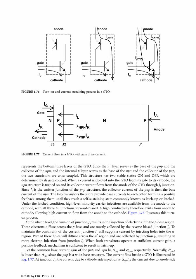
represents the bottom three layers of the GTO. Since the n− layer serves as the base of the pnp and the
collector of the npn, and the internal p layer serves as the base of the npn and the collector of the pnp,the two transistors are cross-coupled. This structure has two stable states: ON and OFF, which aredetermined by its gate control. When a current is injected into the GTO from its gate to its cathode, thenpn structure is turned on and its collector current flows from the anode of the GTO through J1 junction.Since J1 is the emitter junction of the pnp structure, the collector current of the pnp is then the basecurrent of the npn. The two transistors therefore provide base currents to each other, forming a positivefeedback among them until they reach a self-sustaining state commonly known as latch-up or latched.Under the latched condition, high-level minority carrier injections are available from the anode to thecathode, with all three pn junctions forward-biased. A high conductivity therefore exists from anode tocathode, allowing high current to flow from the anode to the cathode. Figure 1.76 illustrates this turn-on process.
At the silicon level, the turn-on of junction J3 results in the injection of electrons into the p-base region.These electrons diffuse across the p-base and are mostly collected by the reverse biased junction J2. Tomaintain the continuity of the current, junction J1 will supply a current by injecting holes into the n
−
region. Part of these holes will diffuse across the n− region and are collected by junction J2, resulting in
more electron injection from junction J3. When both transistors operate at sufficient current gain, apositive feedback mechanism is sufficient to result in latch-up.
Let the common base current gain of the pnp and npn be αpnp and αnpn, respectively. Normally, αpnpP
is lower than αnpn since the pnp is a wide-base structure. The current flow inside a GTO is illustrated inFig. 1.77. At junction J2, the current due to cathode side injection is αnpnIK; the current due to anode side
FIGURE 1.76 Turn-on and current-sustaining process in a GTO.
FIGURE 1.77 Current flow in a GTO with gate drive current.
© 2002 by CRC Press LLC

injection is αpnpIA; and the leakage current is IL. According to Kirchhoff ’s law,
(1.12)
and
(1.13)
Combining these equations,
(1.14)
This equation shows that the thyristor structure can sustain its anode current by itself once the sumof the common base current gain (αpnp + αnpn) of both transistors is approaching unity. For a GTO, αnpn
is designed low and is normally depending on IG to ensure its gate turn-off capability. This will bediscussed later. With this self-sustaining capability, the gate of a GTO does not need to supply a lot ofcurrent and does not need to be very close to its cathode as is necessary in a bipolar junction transistor(BJT) design. The dimension of a typical GTO cell shown in Fig. 1.75 is 100 to 150 µm wide. This isvery large compared with the micron and/or even submicron process used for modern MOSFETs andinsulated gate bipolar transistors (IGBTs). The large cell size design is cost-effective and makes it possibleto fabricate large single-die devices to boost their current capability. A state-of-the-art GTO die is as largeas 6-in. in diameter with a turn-off current capability of up to 6.0 kA [3]. Figure 1.75c shows a largeGTO fabricated by ABB. The GTO shown is fabricated on a 4-in. silicon wafer consisting of thousandsof cells like the one shown in Fig. 1.75 and packaged in a so-called press-pack or hockey-puck package.
The large cell structure in the GTO introduces a current spreading problem during the turn-ontransition of a GTO. When a gate current is injected, the turn-on occurs first in the vicinity of the gatecontact. The conduction area then spreads across the rest of the cathode area. This can be characterizedby a propagation velocity called the spreading velocity [5]. Experimental measurements [6] have showna typical spreading velocity of 5000 cm/s. This velocity also depends on the GTO design parameters, thegate turn-on injection current, and its dIG/dt.
Because of this spreading velocity, it takes time for the whole GTO cell to turn on. To avoid overstressingthe part of the cell that is turned on first, the increasing rate of the anode current should be limited. Thissets the maximum turn-on dI/dt limitation for a GTO.
The major advantages of the GTO are its low forward voltage drop and high-voltage blocking capability.These can be understood as the major benefits of its double-side minority carrier injection mechanism.For high-voltage GTO, a thick and lightly doped n-base is needed (see Fig. 1.75). The forward voltagedrop in this case is mainly determined by the resistive voltage drop in the voltage-blocking region whereminority carriers play an important role.
Figure 1.78a shows the minority carrier distribution in the n− region of a GTO and Fig. 1.78b shows
the case of an IGBT (see Section 1.9). For the same blocking voltage design, their n− regions should have
similar thickness and doping. Since there is only one transistor in the IGBT structure, minority carrierscan only be injected from one side; therefore, the conductivity modulation in the n
− region is weaker
than that of the GTO. In the GTO, since there are two transistors, minority carriers can be injected fromboth ends, making a more uniform plasma distribution in the whole area. For a 4.5-kV state-of-the-artGTO, its forward voltage drop at a current density of 50 A/cm
2 can be as low as 2.0 V [7] if a constant
gate current injection presents. Figure 1.79 shows the on-state characteristics of a state-of-the-art GTOmanufactured by ABB [7]. The forward voltage drop at 2000 A is only about 1.5 V for this 4.5-kV GTO.This result is typical of a low conduction loss GTO.
IA αpnpIA αnpnIK IL+ +=
IA IK IG–=
IA (αpnpIG IL)/+ (1 αpnp αnpn)––=
© 2002 by CRC Press LLC

GTO Turn-Off and Forward Blocking
If the GTO gate is pulling out current from the GTO, the current injection into the npn base will bereduced. Once this is reduced below a certain level, the collector current of the npn, and hence the basecurrent of the pnp, will also decrease, leading to the reduced pnp collector current. This will furtherreduce the base current of the npn since it is the difference between the collector current of the pnp andthe gate pullout current. This positive-feedback process will eventually turn off the GTO.
Figure 1.80 shows the current flow inside the GTO when its gate is pulling out current to turn off thedevice. The base drive current required to maintain current conduction in the npn transistor is (1 − αnpn)IK.The base drive current available to the npn transistor in this case is (αpnpIA − IG). Thus, the condition to turnoff the GTO through the gate control is given by:
(1.15)
Since
(1.16)
the condition to turn off the GTO is
(1.17)
FIGURE 1.78 On-state minority carrier distribution in the voltage blocking region for (a) GTO and (b) IGBT.
anode
gate
cathode
anode
gate
cathode
p Plasma level p
n+
+
current
ano
decath
od
e
ga
te
p n- p+
current
gate
co
llec
tor
emitter
n+
(a) (b)
αpnpIA IG– (1 αnpn)IK–<
IK IA IG–=
IG
(αpnp αnpn 1)–+αnpn
--------------------------------------- IA>
© 2002 by CRC Press LLC

The ratio of the anode current to the gate current at which level a GTO is turned off is defined as theturn-off gain. From Eq. (1.17), the maximum turn-off gain [4] can be expressed as:
(1.18)
A large turn-off gain is normally desirable to reduce the current requirements of the gate driver. Alower (αpnp + αnpn) value is necessary to ensure a reasonable turn-off gain. It is also important to pointout that αnpn in Eq. 1.18 is not a constant; normally it decreases when gate current IG increases.
When a GTO is OFF, its junction J2 is reverse-biased and can support a high voltage applied betweenits anode and cathode, as shown in Fig. 1.81a. If the junction J3 is reverse-biased or shorted by the gate
FIGURE 1.79 On-state characteristics of 5SGT 40L4502, a 4-kA, 4.5-kV GTO from ABB.
FIGURE 1.80 Current flow inside the GTO when its gate is pulling out current.
PN
Anode
Cathode
Gate
J3 J2 J1
IA
IK
IG
αPNPIA
αNPNIK
ILN P
βm
IA
IG
----≡αnpn
αpnp αnpn 1–+----------------------------------=
© 2002 by CRC Press LLC

driver, the maximum forward blocking voltage BVAK of the GTO is determined by the avalanche breakdowncapability of the pnp transistor under the open-base condition [8]. This voltage can be expressed as:
(1.19)
where αpnp is the common base current gain of the pnp structure at low current levels; n is an empiricalconstant, and BVJ2 is the avalanche breakdown voltage of the pn-junction J2. Since this pnp has a widebase structure, its common base current gain αpnp is low compared with a normal bipolar transistor.Thus, the forward voltage blocking capability BVAK of a GTO is very close to the breakdown voltageof junction J2.
A GTO can also block a reverse voltage by its junction J1, as shown in Fig. 1.81b. When the junctionJ3 is gated off, the reverse voltage blocking capability is similarly determined by the avalanche breakdownof the pnp structure under the open-base condition. A GTO with both forward and reverse blockingcapability is called symmetric blocking GTO. Most GTOs manufactured today, however, are asymmetricGTOs because the reverse blocking capability is not utilized (J1 junction not designed to support highreverse voltage) or cannot be utilized because of other design requirements, such as the need to introduceanode-short at junction J1 to speed the turn-off.
FIGURE 1.81 Electric field profile when a GTO is blocking forward (a) and reverse voltage (b).
Em
Anode
∆xCathode
Gate
- +VAK
J3J2
J1
E-field
Em
Anode
∆xCathode
Gate
+ -VAK
J3 J2 J1
E-field
(a)
(b)
PN N P
PN N P
BVAK (1 αpnp)1/n– BVj2=
© 2002 by CRC Press LLC

Practical GTO Turn-Off Operation
The turn-off capability of a GTO is limited dominantly by a non-uniform current distribution (also calledcurrent filamentation) problem during turn-off transient. This causes current to concentrate to a few GTOcells and destroy the device with the high power stress. Furthermore, the current filamentation is believedto be initiated by the dynamic avalanche (see next section) in an inhomogeneous, large-area GTO.
A GTO normally requires a dV/dt snubber circuit to conduct actual turn-off operation under highvoltage and high current condition. This is because a large current GTO turn-off will fail without sucha dV/dt snubber as a result of its small RBSOA. This small RBSOA is caused by a non-uniform currentdistribution or current filamentation problem in the GTO.
Figure 1.82 shows a practical setup in which a typical dV/dt snubber formed by DS, RS, and CS is used,and Fig. 1.83 shows a typical GTO turn-off characteristic under snubbered condition. Before t0, the GTO isON, so a current is built up in the load inductor LL and the device under test (DUT). The anode current IA
FIGURE 1.82 (a) The turn-off circuit of a GTO with a typical RCD dV/dt snubber. (b) Typical GTO gate drivecircuit with a large gate inductance LG.
DUT
VDC Cs
Ds RsLL IA
VAK
IG
DF
di/dt snubber
Lstray
LI
DIRI
dv/dt snubber
-+
VOFF
LG
>300nH
18V
GTO
P
N
P
N
IA
IKIG
VOFF
SW
(a)
(b)
© 2002 by CRC Press LLC

is approximately equal to the cathode current IK because the gate current IG is negligible. Starting fromtime t0, a negative voltage VOFF is applied to the gate of the GTO. The gate current IG then decreaseslinearly at a rate determined by the applied negative turn-off gate voltage VOFF and the gate lead strayinductance LG. At t1, the device could not maintain the latch any longer so the anode current begins todecay. The current from the load inductor is diverted to the dV/dt snubber path. At t2, when the anodecurrent observes its maximum dI/dt, the anode voltage shows a spike due to the stray inductance LS inthe dV/dt snubber path. At t3, the anode current enters its tail stage. At t4, the anode voltage reaches the DClink voltage so the freewheeling diode DF will be conducting. The energy in the stray inductance in theloop of power supply, freewheeling diode, and the dV/dt snubber is released to the snubber capacitor,causing another voltage peak. The anode voltage dip between t4 and t5 is due to the reverse recovery ofthe dV/dt snubber diode DS. The turn-off trajectory of a GTO with a dV/dt snubber is significantlyreduced, as shown in Fig. 1.72 (see Section 1.7 on General Power Semiconductor Switch Requirements).
Dynamic Avalanche
Under a high electric field, an avalanche process occurs within the silicon. The static critical electric fieldis a function of the doping profile. The lower the doping, the lower the critical avalanche electric field.The static avalanche voltage of a single side abrupt pn-junction is determined by both the critical electricfield and the depletion region width.
While the reverse-biased junction conducts high current, as is the case of a GTO turn-off with orwithout a dV/dt snubber, the avalanche voltage decreases significantly because of the existence of carriersin the depletion region. This process is called dynamic avalanche [9]. Figure 1.84 shows the cross sectionof a pnp transistor under both current and voltage stress. A GTO turn-off with a dV/dt snubber entersthe pnp conduction mode between t2 and t3, as shown in Fig. 1.82. Assuming carriers in the depletionregion are moving at their saturation speed, then both the anode current density and the anode–cathodevoltage can be expressed as:
(1.20)
(1.21)
(1.22)
where p is hole density in the depletion region, EC is the critical electric field causing avalanche breakdown,and vS is the saturation velocity of holes. In the depletion region, holes are the only carriers. In the presenceof holes in the depletion region, the charge density in the depletion region is higher compared with thecase without the current, so the peak electric field is also higher at the same width of the depletion region.
FIGURE 1.83 Typical GTO turn-off characteristics under dV/dt snubber condition.
JA qpvs=
VAK EmWE/2=
(εsEC2 )/2qp≈ (εsEC
2 )/(JA/vs)=
© 2002 by CRC Press LLC

At the point when dynamic avalanche happens, the power density of the device, which is the productof both the current and the voltage applied on the device, can thus be expressed as:
(1.23)
which is about 200 to 300 kW/cm2 for silicon.
The onset of dynamic avalanche itself is not a stable condition because the generated carrier is notsufficient to maintain the current. Hence it is not a failure condition from the point of view of the physicsof the device. The dynamic avalanche is, however, widely regarded as the failure mechanism of the GTObecause it will initiate a non-uniform current distribution among large-wafer-size GTOs. The currentcrowding or current filament formed after the onset of dynamic avalanche is enough to destroy the deviceat one location in the form of a melted spot [10].
Non-Uniform Turn-Off Process among GTO Cells
For a high-power GTO, the experimentally obtained instant turn-off power it can withstand is far belowthe value set by the dynamic avalanche breakdown shown in Eq. (1.21). So a GTO needs help from adV/dt snubber to shape its turn-off I–V trajectory, as is shown in Fig. 1.72, and to lower the maximumaverage instant power the external circuit can apply. Non-uniform current distribution or current filament[10] among GTO cells during the turn-off operation accounts for this limitation. The current filament canbe formed at the beginning of the turn-off due to differences in storage times or caused by the onset ofthe dynamic avalanche during the turn-off when the voltage and current are both high [11].
Current Filamentation Caused by Storage Time Difference
The non-uniform turn-off process can be understood by considering two GTO cells in parallel, as isshown in Figs. 1.85 and 1.87. The two cells are identical except for their storage time. This storage timedifference is considered unavoidable in high-current GTOs because of differences in carrier lifetime,wafer thickness, and doping. Although only two cells are shown, GTO1 can represent a group of slowercells whereas GTO2 represents a group of faster cells. The turn-off process starts from t0. Since it has ashorter storage time, GTO2 turns off earlier at t1. The current originally shared by GTO2 is nowtransferred to GTO1. At t2, GTO1 is turned off at twice its previous current. Turn-off failure can happenif its current at t2 exceeds the maximum turn-off capability of GTO1. This can easily be the case whenthe number of faster cells is much larger than the number of slower cells. This type of failure typicallyoccurs at the very beginning of the GTO turn-off before voltage rises and is caused by a rapid formationof current filament due to storage time difference.
What makes this type of failure likely is that there is also a positive feedback mechanism that will furtherincrease the storage time difference, as shown in Fig. 1.86. At higher current density, the common-base
FIGURE 1.84 Dynamic avalanche in the blocking junction of a pnp structure.
JAVAK εsvsEC2 /2=
© 2002 by CRC Press LLC

current gains of both transistors in GTO1 increase. Thus, its turn-off gain becomes even lower accordingto Eq. (1.16), requiring more gate current for turn-off, hence increasing its storage time. Consideringthat the typical storage time of a high-current GTO is in the range of 20 µs, there is enough time for thedangerous current filament to form.
Current Filamentation Caused by Onset of Dynamic Avalanche
Even if the above-discussed failure did not occur because GTO1 is beginning to turn off before the currentfilament density is too high, another failure mechanism can exist. At t2, where both current and voltageare high, GTO1 is subject to much higher instant power stress than that of GTO2. The dynamic avalanchecould then occur first at GTO1 and initiate another positive feedback that will further increase the localizedcurrent density (hence the name current filament) and enable the relatch of GTO1. Dynamic avalanchein a few cells can be viewed as an effective increase in the conductivity of those cells. If the number of slowercells is much smaller than that of faster cells, the current density in GTO1 can then become extremelyhigh. This process can occur very quickly around t2 with the area of the current filament smaller andsmaller and the current density higher and higher (due to positive feedback). The excessive energy
FIGURE 1.85 Current crowding among two GTO cells as a result of their storage time difference.
FIGURE 1.86 Positive feedback mechanism enhances the storage time difference and pushes the current filamentinto the slowest cell.
ts1>ts2 Ia2 Ia1 Ic1 emitter injection
to GTO1
Store morecharges in GTO1ts1
Positive feedback
© 2002 by CRC Press LLC

dissipated on the stressed cells can cause permanent failure because the temperature can be very high.After the device failure, a GTO device loses its blocking capability and behaves resistively.
It can therefore be concluded that the combination of storage time differences and the onset ofpossible localized dynamic avalanche makes the turn-off capability of a GTO small. Practical RBSOAsof high-power GTOs are below the 50 kW/cm
2 power constant line. This low limitation mandates the
use of a dV/dt snubber. Even with a dV/dt snubber, GTO failure can still occur if the instant power istoo high at t2 and exceeds the RBSOA limit of the GTO at that time instance. The voltage spike at t2
can be reduced by minimizing the stray inductance of the dV/dt snubber. The size of the snubber (Cs
value) is typically between 3 to 6 µF. The disadvantages of using a dV/dt snubber are the increased countand size of the components, its high-energy loss, and its increased thermal management requirementto cool resistor Rs.
The concerns of non-uniform current distribution also mandate a minimum on-time rating for GTOsto ensure that conduction current is uniformly distributed in the ON state before a turn-off can beperformed. Minimum off-time is also a commonly used rating for the GTO to guarantee the tail currentof the GTO is completely gone and the GTO cells are all in the OFF state.
Summary
Advantages of the GTO include:
1. High current–voltage capability2. Low conduction loss3. Low cost
Disadvantages
1. Non-uniform turn-off—poor RBSOA and dV/dt snubber required2. Non-uniform turn-on—dI/dt snubber required3. Current control—high gating power4. Long switching time—long storage time, minimum on-time and off-time requirements5. No current limitation capability (FBSOA)
FIGURE 1.87 Semiconductor level analysis of the non-uniform turn-off process. The shaded region representsstored charge (plasma) in the GTO.
P
N
P
N
P
N
P
N
Ia
IcIg
t0Ia
P
N
P
N
P
N
P
N
IcIg
t1Ia
P
N
P
N
P
N
P
N
IcIg
t2
Ia
P
N
P
N
P
N
P
N
IcIg
t4Ia
P
N
P
N
P
N
P
N
IcIg
t3Ia
P
N
P
N
P
N
P
N
IcIg
t5
Ia1 Ia2
Ia1=Ia2 Ia1 Ia2 Ia1< Ia2
Ia1<<Ia2Ia1 Ia2Ia1 Ia2
≈
≈≈
© 2002 by CRC Press LLC
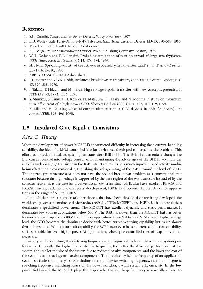
References
1. S.K. Gandhi, Semiconductor Power Devices, Wiley, New York, 1977.2. E.D. Wolley, Gate Turn-Off in P-N-P-N devices, IEEE Trans. Electron Devices, ED-13, 590–597, 1966.3. Mitsubishi GTO FG6000AU-120D data sheet.4. B.J. Baliga, Power Semiconductor Devices, PWS Publishing Company, Boston, 1996.5. W.H. Dodson and R.L. Longini, Probed determination of turn-on spread of large area thyristors,
IEEE Trans. Electron Devices, ED-13, 478–484, 1966.6. H.J. Ruhl, Spreading velocity of the active area boundary in a thyristor, IEEE Trans. Electron Devices,
ED-17, 672–680, 1970.7. ABB GTO 5SGT 40L4502 data sheet.8. P.L. Hower and V.G.K. Reddi, Avalanche breakdown in transistors, IEEE Trans. Electron Devices, ED-
17, 320–335, 1970.9. I. Takata, T. Hikichi, and M. Inoue, High voltage bipolar transistor with new concepts, presented at
IEEE IAS ’92, 1992, 1126–1134.10. Y. Shimizu, S. Kimura, H. Kozaka, N. Matsuura, T. Tanaka, and N. Monma, A study on maximum
turn-off current of a high-power GTO, Electron Devices, IEEE Trans., 462, 413–419, 1999.11. K. Lilja and H. Gruning, Onset of current filamentation in GTO devices, in PESC ’90 Record, 21st
Annual IEEE, 398–406, 1990.
1.9 Insulated Gate Bipolar Transistors
Alex Q. Huang
When the development of power MOSFETs encountered difficulty in increasing their current-handlingcapability, the idea of a MOS-controlled bipolar device was developed to overcome the problem. Thiseffort led to today’s insulated gate bipolar transistor (IGBT) [1]. The IGBT fundamentally changes theBJT current control into voltage control while maintaining the advantages of the BJT. In addition, theuse of a wide-base pnp transistor in the IGBT structure results in a much inproved conductivity modu-lation effect than a conventional BJT, pushing the voltage rating of the IGBT toward the level of GTOs.The internal pnp structure also does not have the second breakdown problem as a conventional npnstructure because the high voltage is supported by the base region of the pnp transistor instead of by thecollector region as is the case for a conventional npn transistor. IGBTs also have excellent RBSOA andFRSOA. Having undergone several years’ development, IGBTs have become the best device for applica-tions in the range of 600 to 3000 V.
Although there are a number of other devices that have been developed or are being developed, theworkhorse power semiconductor devices today are SCRs, GTOs, MOSFETs, and IGBTs. Each of these devicesdominates a specialized power arena. The MOSFET has excellent dynamic and static performance. Itdominates low voltage applications below 600 V. The IGBT is slower than the MOSFET but has betterforward voltage drop above 600 V. It dominates applications from 600 to 3000 V. At an even higher voltagelevel, the GTO becomes the dominant device with better current-carrying capability but much slowerdynamic response. Without turn-off capability, the SCR has an even better current conduction capability,so it is suitable for even higher power AC applications where gate-controlled turn-off capability is notnecessary.
For a typical application, the switching frequency is an important index in determining system per-formance. Generally, the higher the switching frequency, the better the dynamic performance of thesystem, the smaller the size of the system due to reduced passive components, and the lower the cost ofthe system due to savings on passive components. The practical switching frequency of an applicationsystem is a trade-off of many issues including maximum device switching frequency, maximum magneticswitching frequency, switching losses of the power switches, overall system efficiency, etc. In the lowpower field where the MOSFET plays the major role, the switching frequency is normally subject to
© 2002 by CRC Press LLC

system efficiency and/or magnetic considerations instead of device limitations. In the medium powerfield, where the IGBT plays the major role, the situation changes. At the lower end, the limitation of thedevice does not dominate since the lower-rating IGBT is normally fast enough. However, when the powerrating is higher, the IGBT switching speed decreases and the switching losses increase significantly. Thepractical switching frequency is thus subject to the limitation of the device. When the power level moveseven higher, the GTO is the only available device. Since it has several tens of microseconds switchingtime, significant turn-off, and dV/dt snubber loss, the GTO is traditionally the limitation of the switchingfrequency of the system.
The above trend shows that when the power level moves higher, power semiconductor devices limitthe maximum system switching frequency, hence the performance of the system, especially at the GTOlevel. To meet the increasing demand for better performance in high-power systems, many efforts havebeen made to improve the performance of high-power semiconductor devices. Among them, one effortis to push the IGBT toward higher power ratings based on the module concept. With its good dynamicperformance, high-power systems equipped with IGBTs can operate at a much higher switching frequencyand have many benefits compared with a conventional GTO system. The state-of-the-art IGBT rating iscurrently 3.3 kV/1.2 kA [2], which is at the low end of that of the GTO.
IGBT Structure and Operation
The name insulated gate bipolar transistor sterns from its operation based on an internal interactionbetween an insulated-gate FET (IGFET) and a bipolar transistor. It has previously been called an IGT(insulated-gate transistor), an IGR (insulated-gate rectifier), a COMFET (conductivity-modulated field-effect transistor), a GEMFET (gain-enhanced MOSFET), a BiFET (bipolar FET), and an injector FET.IGBTs have been successfully used since they were first demonstrated in 1982 and are currently the mostwidely used power semiconductor switches with applications from several kilowatts to a few megawatts.
A cross section of the planar junction–based IGBT structure introduced in the 1980s is shown inFig. 1.88a. The IGBT structure is similar to that of a planar power MOSFET except the difference in thesubstrate doping type. The fabrication of the IGBT therefore is almost the same as a power MOSFET.This has made its manufacture relatively easy immediately after conception, and its ratings have grownat a rapid pace as a result of the ability to scale up both the current and the blocking voltage ratings.Today, the largest single-chip IGBT can carry about 100 A and block more than 3000 V. Larger currentIGBTs are also introduced by paralleling more IGBT chips in a single package. These IGBTs are alsocalled IGBT modules. Figure 1.89 shows a photograph of a 1200-A, 3300-V IGBT module fabricated byMitsubishi.
FIGURE 1.88 (a) Cross section of the IGBT structure and (b) equivalent circuit for the IGBT.
collectorcollector
gate
PR
N drift
gate
n+
P+
emitter emitter
P substrate+J
1
J2
parasitic thyristor
PNP
NPN
a b
© 2002 by CRC Press LLC

The equivalent circuit for the IGBT, shown in Fig. 1.88b, consists of a wide-base pnp bipolar transistordriven by a short-channel MOSFET. Notice the main current path for the IGBT is not through the pnptransistor but through the indicated path. In the IGBT structure, when a positive bias voltage larger thanthe threshold voltage of the DMOS channel is applied to the gate electrode, an inversion layer is formedalong the p-base surface of the DMOS, and the DMOS channel is turned ON. Also an accumulationlayer of electrons is formed at the surface of the n region below the gate. When a positive bias is appliedto the collector, electrons flow from the n
+ emitter contact via the DMOS channel and the accumulation
layer into the n− drift region. This provides the base drive current for the vertical pnp transistor in the
IGBT structure. Since the emitter junction (J1) for this bipolar transistor is forward-biased, the p+ region
injects holes into the n− base region. When the positive bias on the collector terminal of the IGBT is
increased, the injected hole concentration increases and reduces the resistance of the n− drift region.
Consequently, the IGBT can operate at much higher current densities than the VDMOS even when it isdesigned to support high blocking voltages.
As long as the gate bias is sufficiently large to produce a strong inversion layer and an accumulationlayer of electrons at the n
− base region surface, the IGBT forward conduction characteristic resembles
that of a pin diode. Therefore, the IGBT can also be considered a pin diode in series with a MOSFET.Electron injections are provided by the accumulation layer electrons beneath the gate and between theadjacent p-body regions. However, not all injected holes recombine with these electrons; instead, someof the holes are collected by the p-body region, which acts as the collector region of the parasitic pnptransistor. IGBT design for low conduction drop requires minimizing the parasitic pnp transistor currentand maximizing the pin current that maximizes the conductivity modulation.
However, if the DMOS channel becomes pinched off and the electron current saturates, the hole currentalso saturates because of the saturation of the base drive current for the pnp transistor. Consequently, thedevice operates with current saturation in its active region with a gate-controlled output current. Thiscurrent saturation characteristic is useful for applications in which the device is required to sustain ashort-circuit condition.
When the gate voltage is lower than the threshold voltage of the DMOS, the inversion layer cannotsustain and the electron current via the DMOS channel is terminated. The IGBT then operates in the
FIGURE 1.89 Photograph of a 1200-A, 3300-V IGBT module in which 24 1-cm2 IGBT dies are paralleled together
by wire bonds.
© 2002 by CRC Press LLC

forward blocking mode. A large voltage can then be supported by the reverse-biased p-base/n-driftjunction (J2). Figure 1.90 shows a typical output characteristic of the IGBT.
The IGBT was the first commercially successful device based upon combining the physics of MOS-gatecontrol with bipolar current conduction. Due to the injection of a high concentration of holes from thep
+ substrate into the n
− drift, the conductivity of the long n
− region is modulated and the IGBT exhibits
pin diodelike on-state characteristics with a low forward voltage drop. Thus, the IGBT exhibits excellentcurrent-carrying characteristics with forward conduction current densities 20 times higher than that ofa power MOSFET and five times greater than that of a bipolar transistor operating at a current gain of 10.Since the input signal for the IGBT is a voltage applied to the MOS-gate, the IGBT has the high inputimpedance of the power MOSFET and can be classified as a voltage-controlled device. However, unlikethe power MOSFET, the switching speed of the IGBT is limited by the time taken to remove the storedcharges in the drift region due to the injection of holes during on-state current conduction. The turn-off time for the IGBT is dictated by the conduction modulation of the drift region and the minoritycarrier lifetime. The frontier is specified dominantly by the current gain of the wide-base pnp transistor,and the latter can be controlled by a lifetime control process, such as electron irradiation. Although thelifetime control process can be successful in reducing the turn-off time, it was found that there was atrade-off between the on-state voltage drop (conduction loss) and the turn-off time (switching loss). Ashorter minority carrier lifetime makes the switching loss of the IGBT lower, but the shorter minoritycarrier lifetime also results in a higher conduction loss.
One of the problems encountered when operating the IGBT at high current levels has been the latch-upof the parasitic pnpn thyristor structure inherent in the device structure. Latch-up of this thyristor canoccur, causing losses of gate-controlled current conduction. Since the current gains of the npn and pnptransistors increase with increasing temperature, the latching current decreases with increasing temper-ature. This effect is also aggravated by an increase in the resistance of the p-base with temperature dueto a decrease in the mobility of holes. Many methods have been explored to suppress the latch-up of theparasitic thyristor, such as the use of a deep p
+ diffusion, a shallow p
+ diffusion, or a self-aligned sidewall
diffusion of n+ emitter. State-of-the-art IGBTs have basically solved this problem, and latch-up does not
occur for all gate voltages applied. These IGBTs therefore exhibit close to square FBSOA.Traditionally, IGBTs are fabricated on a lightly doped epitaxial substrate, such as the one shown in
Fig. 1.88a. Because of the difficulty of growing the lightly doped epitaxial layer, the breakdown voltageof this type of IGBT is limited to below 1000 V. To benefit from such a design, an n buffer layer is normallyintroduced between the p
+ substrate and the n
− epitaxial layer, so that the whole n
− drift region is depleted
when the device is blocking the off-state voltage, and the electric field shape within the n− drift region
is close to rectangular. This type of design is referred to as Punch-Through IGBT (PT IGBT), as shownin Fig. 1.91a. The PT structure allows it to support the same forward blocking voltage with about halfthe thickness of the n
− base region of the pnp transistor, resulting in a greatly improved trade-off rela-
tionship between the forward voltage drop and the turn-off time. Thus, the PT structure together withlifetime control is preferred for IGBTs with forward blocking capabilities of up to 1200 V.
FIGURE 1.90 Output characteristics of the IGBT.
forwardcharacteristics
reversecharacteristics
VCE
ICE
VG
© 2002 by CRC Press LLC

For higher blocking voltages, the thickness of the drift region becomes too large for cost-effectiveepitaxial growth. Another type of design, the Non-Punch-Through IGBT (NPT IGBT, as shown inFig. 1.91b), is gaining popularity. In the NPT IGBTs, devices are built on an n
− wafer substrate that
serves as the n− base drift region. The collector is implanted from the backside of the wafer after proper
wafer thinning, and no field stopping n buffer layer is applied to the NPT IGBT. In this concept, theshape of the electric field is triangular in the forward blocking state, which makes a longer n
− base region
necessary to achieve the same breakdown voltage as compared with the PT IGBT. However, the NPTIGBT offers some advantages over the PT IGBT. For example, the injection efficiency from the collectorside can be controlled (due to the use of implanted p
+ region) and devices with voltage ratings as high
as 4 kV can be realized. Further, by optimizing the emitter efficiency of carriers from the p+ collector
layer and the transport factor of carriers in the n− base, the trade-off between the forward voltage drop
and the turn-off time for the NPT IGBT can be improved to become similar to that of the PT type IGBTwithout lifetime control.
Generally speaking, the current tail in the NPT IGBT is longer than the PT IGBT, but the NPT IGBTis more robust than the PT IGBT, particularly under a short-circuit condition. The trench gate IGBT(UMOS-gate IGBT) structure is shown in Fig 1.91c. With the UMOS structure in place of the DMOSgate structure in the IGBT, the channel density is greatly increased and the JFET region is eliminated. Inaddition, the electron-hole concentration is enhanced at the bottom of the trench because an accumu-lation layer forms. This creates a catenary-type carrier distribution profile (see Fig. 1.91) in the IGBT,which resembles that obtained in a thyristor or pin diode. These improvements lead to a large reductionin the on-state voltage drop until it approaches that of a pin diode, hence approaching the theoreticallimit of a silicon device. The latching current density of the UMOS IGBT structure is superior to that ofthe DMOS structure. This is attributed to the improved hole current flow path in the UMOS structure.As shown in Fig. 1.90c, the hole current flow can take place along a vertical trajectory in the UMOSstructure, whereas in the DMOS structure hole current flow occurs below the n
+ emitter in the lateral
direction. The resistance for the hole current that causes the latch-up is determined only by the depthof the n
+ emitter region. A shallow p
+ layer can be used, as shown in the figure, to reduce this resistance.
As a consequence, the RBSOA of the UMOS IGBT structure is superior to that of the DMOS IGBTstructure. Further, because of a very strong percentage of electron current flow in the trench gate IGBT,the turn-off speed of the trench-based IGBT is generally faster than the DMOS-based IGBT. It can beanticipated that trench gate IGBTs will replace the DMOS IGBT structures in the future.
FIGURE 1.91 (a) PT IGBT structure, (b) NPT IGBT structure, and (c) UMOS gate PT IGBT structure.
collector
gate
P
N drift
n+
P+
emitter
N buffer layerp substrate+
collector
gate
P
N drift (substrate)
n+
P+
emitter
p layer+ collector
gateP base
N drift
n+
emitter
N buffer layerp substrate+
P+
a b c
© 2002 by CRC Press LLC

References
1. Baliga, B.J., Adler, M.S., Love, R.P., Gray, P.V., and Zommer, N., The insulated gate transistor: a newthree terminal MOS controlled bipolar power device, IEEE Trans. Electron Devices, ED-31, 821–828,1984.
2. Brunner, H., Hier, T., Porst, A., and Spanke, R., 3300V IGBT module for traction application, in EPEConf. Rec., 1056–1059, 1995.
1.10 Gate-Commutated Thyristors and Other Hard-Driven GTOs
Alex Q. Huang
Unity Gain Turn-Off Operation
Traditional GTO Gate Drive Circuit
Traditional GTOs are generally designed with a turn-off gain of 3 to 5. This is the result of trade-offsbetween the performances of the GTO and the current (hence power) requirement its gate drive circuit.Figure 1.92b shows the typical turn-off gate drive circuitry for a traditional GTO. A negative turn-offvoltage source VOFF is connected to the GTO gate–cathode junction J3 through the turn-off control switchSW. Since both sides of the junction J3 are highly doped, its breakdown voltage BVGC is practically about20 V and can hardly be increased. The turn-off voltage VOFF is selected below the junction J3 breakdownvoltage to avoid constant breakdown of this junction when the GTO is in the off state. To turn off the GTO,switch SW is turned on so the negative turn-off voltage VOFF is applied on the GTO gate–cathode junction.The current originally flowing through the cathode is then diverted to the gate, causing cathode currentIK to decrease and the gate current to increase. Because of the existence of the GTO gate lead strayinductance LG, which is practically on the order of several hundreds of nanohenry determined by thelead structure and length, the cathode current will decrease linearly and the gate current will increaselinearly. This current commutation rate is thus given by:
(1.24)
FIGURE 1.92 Typical turn-off characteristics of a GTO.
dIG/dt VOFF/LG=
Ia
Ic
Ig
Va
t0 t1 t2 t3 t4 t5 t6
© 2002 by CRC Press LLC
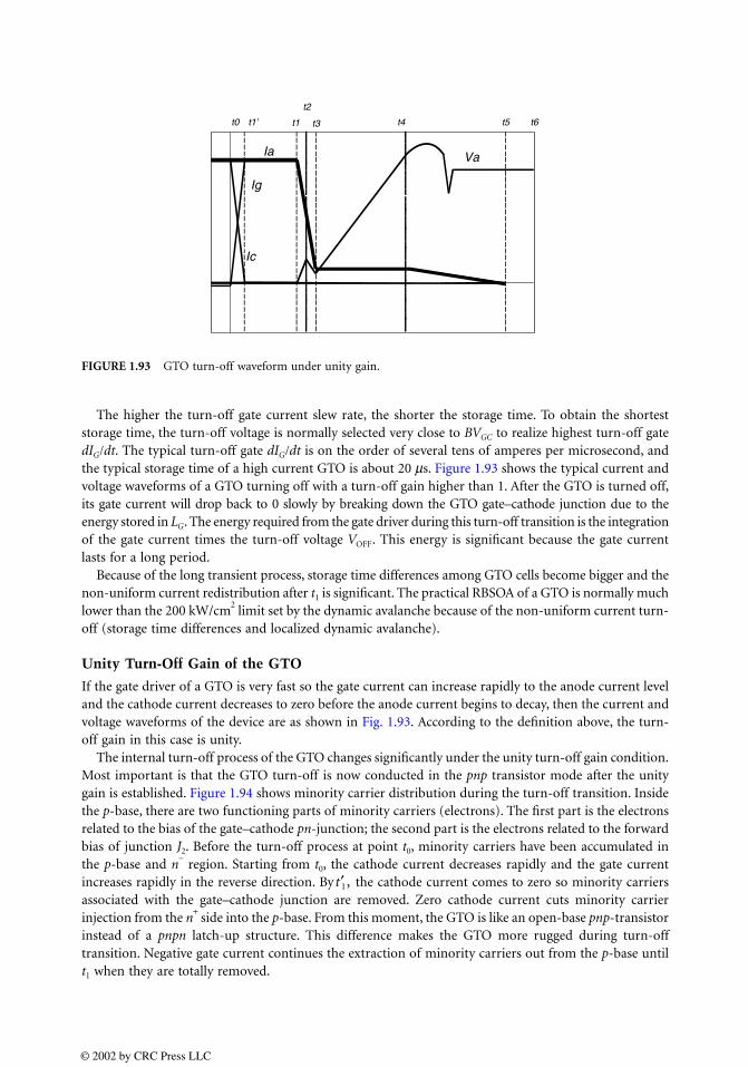
The higher the turn-off gate current slew rate, the shorter the storage time. To obtain the shorteststorage time, the turn-off voltage is normally selected very close to BVGC to realize highest turn-off gatedIG/dt. The typical turn-off gate dIG/dt is on the order of several tens of amperes per microsecond, andthe typical storage time of a high current GTO is about 20 µs. Figure 1.93 shows the typical current andvoltage waveforms of a GTO turning off with a turn-off gain higher than 1. After the GTO is turned off,its gate current will drop back to 0 slowly by breaking down the GTO gate–cathode junction due to theenergy stored in LG. The energy required from the gate driver during this turn-off transition is the integrationof the gate current times the turn-off voltage VOFF. This energy is significant because the gate currentlasts for a long period.
Because of the long transient process, storage time differences among GTO cells become bigger and thenon-uniform current redistribution after t1 is significant. The practical RBSOA of a GTO is normally muchlower than the 200 kW/cm
2 limit set by the dynamic avalanche because of the non-uniform current turn-
off (storage time differences and localized dynamic avalanche).
Unity Turn-Off Gain of the GTO
If the gate driver of a GTO is very fast so the gate current can increase rapidly to the anode current leveland the cathode current decreases to zero before the anode current begins to decay, then the current andvoltage waveforms of the device are as shown in Fig. 1.93. According to the definition above, the turn-off gain in this case is unity.
The internal turn-off process of the GTO changes significantly under the unity turn-off gain condition.Most important is that the GTO turn-off is now conducted in the pnp transistor mode after the unitygain is established. Figure 1.94 shows minority carrier distribution during the turn-off transition. Insidethe p-base, there are two functioning parts of minority carriers (electrons). The first part is the electronsrelated to the bias of the gate–cathode pn-junction; the second part is the electrons related to the forwardbias of junction J2. Before the turn-off process at point t0, minority carriers have been accumulated inthe p-base and n
− region. Starting from t0, the cathode current decreases rapidly and the gate current
increases rapidly in the reverse direction. By the cathode current comes to zero so minority carriersassociated with the gate–cathode junction are removed. Zero cathode current cuts minority carrierinjection from the n
+ side into the p-base. From this moment, the GTO is like an open-base pnp-transistor
instead of a pnpn latch-up structure. This difference makes the GTO more rugged during turn-offtransition. Negative gate current continues the extraction of minority carriers out from the p-base untilt1 when they are totally removed.
FIGURE 1.93 GTO turn-off waveform under unity gain.
Ia
Ic
Ig
Va
t0 t1
t2
t3 t4 t5 t6t1’
t′1,
© 2002 by CRC Press LLC

Advantages of Unity Gain Turn-Off
With unity turn-off gain, the storage time of a GTO is significantly reduced. The storage time in this caseis the time required to remove minority carriers in the p-base. In the normal GTO case, the gate currentis much less than the anode current so the removal speed is slow. Furthermore, the cathode current isnot reduced to zero so minority carrier injection continues during the whole storage phase. With unityturn-off gain, the gate current is as high as the anode current, leading to a rapid carrier removing speed.Also, the cathode current is reduced to zero, hence instantly stopping the minority carrier injection intothe p-base. Generally, the storage time of a GTO under unity turn-off gain is about 1 µs compared withthat of about 20 µs in a normal GTO case with high turn-off gain.
Another important performance improvement with unity gain turn-off is in the RBSOA. As isanalyzed above, the GTO current tends to crowd toward the cell with a longer storage time. This process
FIGURE 1.94 Internal process of a GTO under unity gain turn-off.
FIGURE 1.95 Turn-off waveforms of GTO cells under unity gain turn-off condition.
t0 t1
t3t4
P
N-
P
N+
Ia
IgIc
P
N-
P
N+
Ia
IgIc
P
N-
P
N+
Ia
IgIc
P
N-
P
N+
Ia
IgIc
Ia ≈ Ic Ic=0
Ic=0Ic=0
J1
J2
J3
P
N
P
N
ANODE
P
N
P
N
CATHODE
GATE
GTO1 GTO2
tS1 > tS2
(a)
Ia1
Ia2
t0 t2t1 t3 t4 t5
Va
(b)
© 2002 by CRC Press LLC
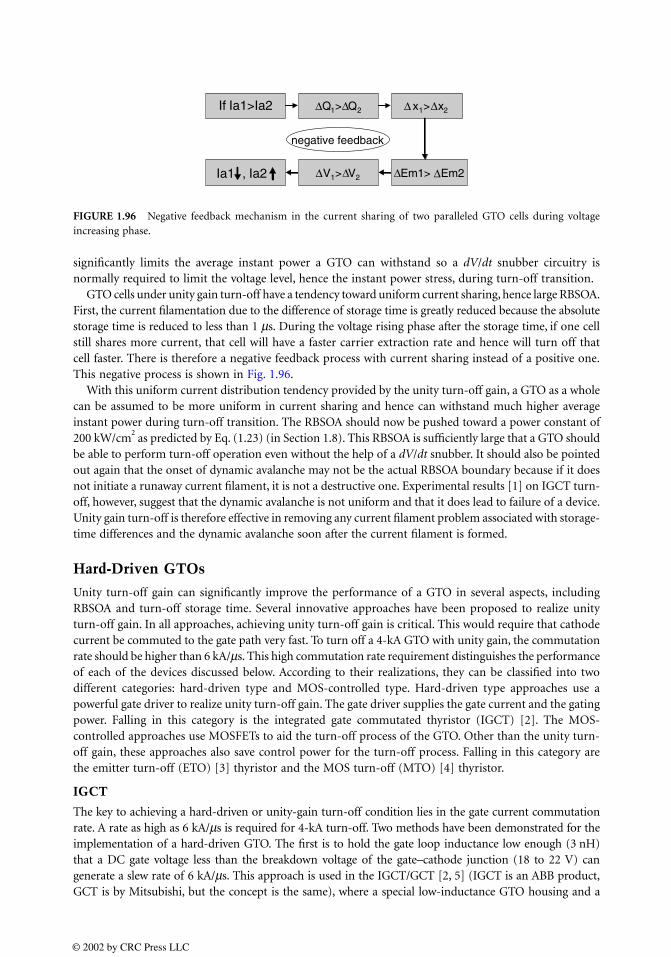
significantly limits the average instant power a GTO can withstand so a dV/dt snubber circuitry isnormally required to limit the voltage level, hence the instant power stress, during turn-off transition.
GTO cells under unity gain turn-off have a tendency toward uniform current sharing, hence large RBSOA.First, the current filamentation due to the difference of storage time is greatly reduced because the absolutestorage time is reduced to less than 1 µs. During the voltage rising phase after the storage time, if one cellstill shares more current, that cell will have a faster carrier extraction rate and hence will turn off thatcell faster. There is therefore a negative feedback process with current sharing instead of a positive one.This negative process is shown in Fig. 1.96.
With this uniform current distribution tendency provided by the unity turn-off gain, a GTO as a wholecan be assumed to be more uniform in current sharing and hence can withstand much higher averageinstant power during turn-off transition. The RBSOA should now be pushed toward a power constant of200 kW/cm
2 as predicted by Eq. (1.23) (in Section 1.8). This RBSOA is sufficiently large that a GTO should
be able to perform turn-off operation even without the help of a dV/dt snubber. It should also be pointedout again that the onset of dynamic avalanche may not be the actual RBSOA boundary because if it doesnot initiate a runaway current filament, it is not a destructive one. Experimental results [1] on IGCT turn-off, however, suggest that the dynamic avalanche is not uniform and that it does lead to failure of a device.Unity gain turn-off is therefore effective in removing any current filament problem associated with storage-time differences and the dynamic avalanche soon after the current filament is formed.
Hard-Driven GTOs
Unity turn-off gain can significantly improve the performance of a GTO in several aspects, includingRBSOA and turn-off storage time. Several innovative approaches have been proposed to realize unityturn-off gain. In all approaches, achieving unity turn-off gain is critical. This would require that cathodecurrent be commuted to the gate path very fast. To turn off a 4-kA GTO with unity gain, the commutationrate should be higher than 6 kA/µs. This high commutation rate requirement distinguishes the performanceof each of the devices discussed below. According to their realizations, they can be classified into twodifferent categories: hard-driven type and MOS-controlled type. Hard-driven type approaches use apowerful gate driver to realize unity turn-off gain. The gate driver supplies the gate current and the gatingpower. Falling in this category is the integrated gate commutated thyristor (IGCT) [2]. The MOS-controlled approaches use MOSFETs to aid the turn-off process of the GTO. Other than the unity turn-off gain, these approaches also save control power for the turn-off process. Falling in this category arethe emitter turn-off (ETO) [3] thyristor and the MOS turn-off (MTO) [4] thyristor.
IGCT
The key to achieving a hard-driven or unity-gain turn-off condition lies in the gate current commutationrate. A rate as high as 6 kA/µs is required for 4-kA turn-off. Two methods have been demonstrated for theimplementation of a hard-driven GTO. The first is to hold the gate loop inductance low enough (3 nH)that a DC gate voltage less than the breakdown voltage of the gate–cathode junction (18 to 22 V) cangenerate a slew rate of 6 kA/µs. This approach is used in the IGCT/GCT [2, 5] (IGCT is an ABB product,GCT is by Mitsubishi, but the concept is the same), where a special low-inductance GTO housing and a
FIGURE 1.96 Negative feedback mechanism in the current sharing of two paralleled GTO cells during voltageincreasing phase.
If Ia1>Ia2 Q1> Q2 x1> x2
Em1> Em2Ia1 , Ia2
negative feedback
∆V1> V2∆ ∆ ∆
∆ ∆ ∆ ∆
© 2002 by CRC Press LLC

carefully designed gate driver meet this requirement. The power consumption by the GCT driver is greatlyreduced compared with that of a conventional GTO driver, since the gate current is present for a muchshorter period of time [6]. Figure 1.97 shows the external view of the two commercially available GCTs.
The key disadvantage of the GCT approach is the high cost associated with the low-inductance housingdesign for the GTO and the low inductance and high current design for the gate driver.
MTO
Figure 1.98a shows the turn-off principle of a MTO™ [4, 7] developed by Silicon Power Corporation.The MTO device packages a number of low-voltage MOSFETs within a normal GTO device housing toform a current path that is in parallel with the emitter junction of the GTO. Therefore, the MTO looks
FIGURE 1.97 GCT operation principle and two GCTs developed by Mitsubishi and ABB. (Photographs courtesyof Mitsubishi (top) and ABB (bottom).)
LG ≤ 3nH
20 V
- +
GCT LG<3 Driver
Mitsubishi 4kA / 4.5 kV GCT
ABB 4 kA / 4.5 kV IGCT
© 2002 by CRC Press LLC

just like a conventional GTO from the outside. The turn-off is initiated by turning on the MOSFET thatshorts the GTO emitter junction. MTO, like the ETO, is therefore a MOS turn-off device requiring verylittle turn-off gate power. To achieve a high gate current commutation rate, very low gate inductance(<0.1 nH) is required.
Because of the use of the hybrid approach, a prototype 500-A, 4500-V device is available from SPCO.The major problem for the MTO, however, is still the limitation of the RBSOA [7]. This is becausethe gate current commutation rate is determined by the packaged gate inductance, which has to bereduced to below 0.1 nH. There are three reasons for this. First, in the MTO the commutation rate isdetermined by
(1.25)
Second, the resistive voltage in the GTO p-base region and the MOSFET determines the peak gate currentthat can be commutated:
(1.26)
FIGURE 1.98 MTO equivalent circuit (a) and 500-A/4.5-kV MTO with gate driver (b) developed by Silicon PowerCorp. (Photograph courtesy of Silicon Power Corp.)
(a)
L 10nH
Q
(b)
dIG
dt--------
max
0.7LG
-------≤
IGmax
0.7RMOS Rp-base+-------------------------------≤
© 2002 by CRC Press LLC

Third, since there is no reverse bias voltage applied to the GTO emitter junction in the MTO, it is veryeasy to become latched again. Snubberless turn-off capability of the MTO is therefore lower than theGCT and ETO.
ETO
The method to achieve unity gain in the ETO thyristor is to insert an additional switch in series withthe cathode of the GTO. The cathode of the GTO is the emitter of the internal npn transistor, so theseries switch is referred to as the emitter switch and the new device is termed ETO. Turning off the emitterswitch generates a high transient voltage long enough to commutate the emitter current to the gate patheven with a higher parasitic inductance present. Because of this higher tolerance for parasitic inductance,conventional GTOs can be used in the ETO. An additional switch is connected to the gate of the GTO,and is complementary to the emitter switch. These switches are implemented with many paralleled low-voltage, high-current MOSFETs to minimize the additional conduction loss due to the emitter switch.The typical value for the conduction loss due to the series switch is 0.2 V at the average GTO currentrating. The turn-off driving power for the ETO is negligible, since the turn-off is purely due to theremoval of a MOSFET gate signal. The ETO in many aspects is similar to the IGBT. For example, theturn-off mechanism used in IGBT is also an emitter turn-off, and the IGBT always turns off in the ruggedpnp transistor mode.
Figure 1.99 shows the equivalent circuit and hardware photograph of the developed 4-kA, 6-kV ETOby Virginia Tech. Other lower current rating ETOs have also been demonstrated by Virginia Tech. Becauseof the use of hybrid approach based on conventional GTO, ETO devices have clear advantages in termsof cost and gate drive power requirement over GCTs. ETO devices also have two other advantages whencompared with the GCT. One is its feasibility of having a FBSOA [3, 8], and the other is its simplicityin overcurrent protection [8].
Conclusions
These newly developed GTOs (IGCT, MTO, and ETO) all utilize the unity gain turn-off concept andhave dramatically improved performance compared with conventional GTOs. Quantitative comparisonsof these devices are provided in a separate section on high-power IGBTs (Section 1.9).
FIGURE 1.99 ETO equivalent circuit (a) and a 4-kA/6-kV ETO (b). An ETO gate driver is also shown.
© 2002 by CRC Press LLC

References
1. I. Takata, M. Bessho, K. Koyanagi, M. Akamatsu, K. Satoh, K. Kurachi, and T. Nakagawa, Snubberlessturn-off capability of four-inch 4.5k V GCT thyristor, presented at IEEE International Symposiumon Power Semiconductor Devices and Ics, 1998, 177–180.
2. P.K. Steimer, H.E. Gruning, J. Werninger, E. Carrol, S. Klaka, and S. Linder, IGCT—a new emergingtechnology for high power, low cost inverters, presented at IEEE Industry Applications Society AnnualMeeting, New Orleans, Louisiana, Oct. 5–9, 1997, 1592–1599.
3. Y. Li, A.Q. Huang, and F.C. Lee, Introducing the emitter turn-off thyristor, presented at 1998 IEEEIndustry Applications Society 33rd Annual Meeting, 1998, 860–864.
4. D.E. Piccone, R.W. De Doncker, J.A. Barrow, and W.H. Tobin, The MTO thyristor—a new high powerbipolar MOS thyristor, presented at IEEE Industry Applications Society 31st Annual Meeting, Oct.6–10, 1996, 1472–1473.
5. E.R. Motto and M. Yamamoto, New High Power Semiconductors: High Voltage IGBTs and GCTs, inPCIM’98 Power Electronics Conference Proceedings, 1998, 296–302.
6. Mitsubishi GCT FGC4000BX-90DS data sheet.7. A.Q. Huang, Y. Li, K. Motto, and B. Zhang, MTO thyristor—an efficient replacement for standard
GTO, presented at IEEE Industry Applications Society 34th Annual Meeting, 1990, 364–372.8. Y. Li, A.Q. Huang, and K. Motto, Experimental and numerical study of the emitter turn-off thyristor
(ETO), IEEE Trans. Power Electron., May 2000.
1.11 Comparison Testing of Switches
Alex Q. Huang
Pulse Tester Used for Characterization
In a typical power device dynamic test, the device under test (DUT) is initially off, and the high-voltagecapacitor bank is charged to set the voltage the DUT will experience during switching. A typical pulsetester is shown in Fig. 1.100 and a typical waveform of the test is shown in Fig. 1.101. The so-calleddouble pulse testing will capture one device turn-on event and one device turn-off event. The double-pulse test consists of the following complete events:
t0–t1: At time t0, the control system initiates a pulse to the gate driver for the DUT. The DUT turnson and the high voltage capacitor bank charges the load inductor. After the current reachesthe desired value at t1, the DUT gate driver is commanded to turn off.
t1–t2: From time t1 to t2, no changes to the device are seen. During this time, referred to as thestorage time, internal processes in the device initiate the turn-off process.
FIGURE 1.100 Pulse tester schematic diagram.
© 2002 by CRC Press LLC

t2–t3: At time t2, the anode voltage begins to rise, as the turn-off process has begun. The freewheelingdiode is still reverse-biased so the current cannot yet begin to fall.
t3–t4: At time t3, the anode voltage reaches the bus voltage and the main device current begins tofall. The current that had been flowing through the DUT is commutated into the freewheelingdiode. This is the highest stress interval of the turn-off transition, as the current and voltageare simultaneously high during this interval
t4–t5: At time t4, the main current fall is completed and the current tail phase begins. The currenttail continues until t5. At this point the device can be said to have completed the turn-off process.
t5–t6: During this time, the dI/dt snubber resistor carries the current, inducing additional voltagestress on the main DUT. The snubber inductor is charging during this time, and becomescharged at t6. The snubber diode then goes through a reverse-recovery process.
t6–t7: During this time, the DUT is off and blocking a voltage equal to the input capacitor voltage.The current is still freewheeling through the load inductor and the freewheeling diode. Thiscurrent will continue to circulate for a long time because the only energy dissipation is dueto the conduction voltage of the freewheeling diode.
t7–t2: At this time, the controller initiates the second pulse to test the turn-on of the device. Nothingexternal occurs until t8, which is the end of the turn-on delay time.
t8–t9: During this time, the load current begins to commutate into the DUT from the freewheelingdiode. The dI/dt snubber inductor determines the rate of current transfer.
t9–t10: At time t9, the load inductor current is completely commutated into the DUT and out of thefreewheeling diode. The freewheeling diode undergoes reverse recovery during this periodand releases a significant amount of reverse current into the DUT. It is important that theDUT have fully switched on by now or the diode recovery current will induce large power loss.
FIGURE 1.101 Double-pulse tester waveforms.
© 2002 by CRC Press LLC

t10–t11: During this time, the device is on and the current is rising because of the input voltage dividedby the load inductance. This is equivalent to the interval t0–t1 from the first pulse. The samesequence will continue for the turn-off of the second pulse as that for the first pulse.
The current through the device under test is measured with a precision current shunt in series withthe cathode (or emitter for an IGBT). All delay times are defined with respect to the actual gate of thedevice, so gate driver internal delays are not included. Conventionally, fall time is defined as when thecurrent decreases from 90% of its initial value to 10%, but a different definition is used here. For the high-voltage devices, the current tail value can be greater than 10% of the initial current value, so it isunreasonable to include this time in the fall time. Therefore, the definition used here is that the fall timeends and the tail time begins when the current slope visibly changes. This is physically justified because forall three devices the current tail means that the main turn-off process is complete and the open-base pnptransistor is removing the remaining carriers. A sample waveform is shown in Fig. 1.102. Current tail timeis defined from the end of the current fall time until the anode/collector current decreases to 1% of theinitial current.
Devices Used for Comparison
To compare these various semiconductor technologies, two IGBTs, an IGCT, a GCT, and three ETOswere used [1]. One IGBT and the GCT are made by Mitsubishi, and the ETOs have been developed byresearchers at Virginia Tech. The other IGBT is made by EUPEC, and the IGCT is from ABB. The IGBTs,CM1200HA-66H and FZ1200R33KF2, are rated for 1200 A (DC) and 3300 V, and are packaged in plasticmodules 14 by 19 cm in size. The IGCT and the GCT are both 4500-V devices, which are rated for 4000 Amaximum controllable current. The first ETO used, ETO4060s, is rated for 6000 V and 4000 A controllablecurrent, and is based on a Toshiba GTO. The IGCT, the GCT, and the ETO4060s are packaged in 93-mmpress-packs and, with gate drivers, have a maximum width of around 20 cm. The second ETO used,ETO1045s, is a small (53-mm) device rated for 4500 V and 1000 A. This ETO is based on a WestcodeGTO. The ETO1045s is obviously of a lower rating than the GCT and IGCT, but it uses a fast conventionalGTO, whereas the ETO4060s is based on a GTO designed for about 300 Hz. One final device used is anewly designed ETO, the ETO4045A, which is based on an ABB GTO similar to the thyristor used in theIGCT. The average current ratings for the IGCT, GCT, ETO4045A, and ETO4060s are 1200 A, whereasthe ETO1045 is suitable for about 450 A average. When the switching losses of the IGBT and a safe
FIGURE 1.102 Switching time definition waveform.
© 2002 by CRC Press LLC

temperature margin are considered, the average operating current for this device should be between 600and 800 A. Figure 1.103 shows most of the devices tested.
One significant difficulty in comparing this type of device is that the ratings, and even the ratingssystem, are different for the different devices. For GTO-based devices, the current ratings are the peakcontrollable current, whereas IGBTs use a DC current rating. The IGBTs tested have a controllable currentrating of twice the DC rating, which translates to a 2400 A rating in the GTO system. These IGBTs consistof many small dies in parallel, giving a net current density much smaller than that of the GTO-baseddevicess. The rms current for the IGCT, the GCT, and the ETO4045A is about 1800 A, and the RMScurrent rating of the ETO 4060 is about 1600 A, although the devices have the same average rating (1200 A)from the manufacturers.
Unity Gain Verification
Because of the strict requirements on the gate loop stray inductance for the IGCT and the ETO, it is verydifficult to insert a current probe directly to monitor the gate current. Fortunately, the unity gain of theIGCT and the ETO can be verified by observing easily probed voltage signals. It is critical for theperformance of these devices that unity gain has been achieved, so some effort is made to verify unitygain and predict the maximum current that can be turned off while maintaining the hard-drivencondition.
In the case of the IGCT, monitoring the gate-to-cathode voltage at the terminals of the IGCT thyristorcan show the unity gain. When the gate voltage becomes −20 V, which is equal to the power supply in
FIGURE 1.103 Clockwise from top left: ETO4060, EUPEC HVIGBT, Mitsubishi HVIGBT, ABB IGCT, MitsubishiGCT. (Photograph courtesy of Mitsubishi.)
© 2002 by CRC Press LLC

the gate driver, then clearly no voltage drop is occurring across the parasitic gate inductance. This inturn implies that dIG/dt is zero, so the gate current has completed commutation. A typical GCT waveformshowing the gate voltage is shown in Fig. 1.104. The inside of the GCT driver box is shown in Fig. 1.105.
Unity gain of the ETO can be verified by observing the drain-to-source voltage of the series switch.When the current is commutating, the voltage across this switch quickly rises to the breakdown voltageof the MOSFETs (60 V). When the voltage across this switch begins to fall, then the net cathode currentof the GTO is negative, which discharges the output capacitors of the MOSFETs. Therefore, the ETOunity gain corresponds to the falling edge of the emitter switch voltage. A turn-off waveform showingthe ETO emitter switch voltage is shown in Fig. 1.106.
Based on the unity gain observation, the rate of current commutation for the devices can be estimatedby dividing the anode current by the time required for unity gain. This method yields a lower resultthan truly occurs because the total current commutated is slightly greater than the anode current dueto a reverse recovery effect of the gate to cathode pn-junction. Even with this conservative estimation
FIGURE 1.104 GCT unity gain.
FIGURE 1.105 Mitsubishi GCT gate driver. (Photograph courtesy of Mitsubishi.)
© 2002 by CRC Press LLC
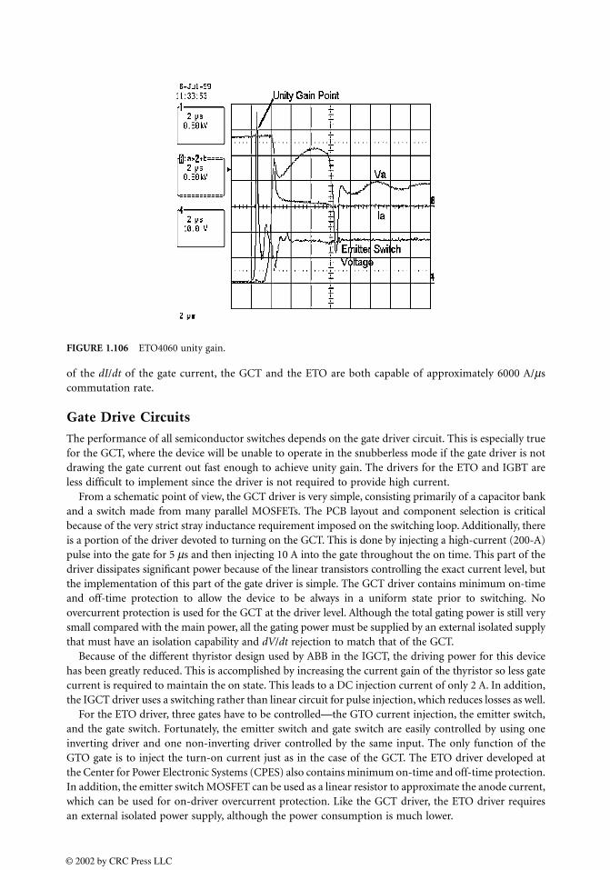
of the dI/dt of the gate current, the GCT and the ETO are both capable of approximately 6000 A/µscommutation rate.
Gate Drive Circuits
The performance of all semiconductor switches depends on the gate driver circuit. This is especially truefor the GCT, where the device will be unable to operate in the snubberless mode if the gate driver is notdrawing the gate current out fast enough to achieve unity gain. The drivers for the ETO and IGBT areless difficult to implement since the driver is not required to provide high current.
From a schematic point of view, the GCT driver is very simple, consisting primarily of a capacitor bankand a switch made from many parallel MOSFETs. The PCB layout and component selection is criticalbecause of the very strict stray inductance requirement imposed on the switching loop. Additionally, thereis a portion of the driver devoted to turning on the GCT. This is done by injecting a high-current (200-A)pulse into the gate for 5 µs and then injecting 10 A into the gate throughout the on time. This part of thedriver dissipates significant power because of the linear transistors controlling the exact current level, butthe implementation of this part of the gate driver is simple. The GCT driver contains minimum on-timeand off-time protection to allow the device to be always in a uniform state prior to switching. Noovercurrent protection is used for the GCT at the driver level. Although the total gating power is still verysmall compared with the main power, all the gating power must be supplied by an external isolated supplythat must have an isolation capability and dV/dt rejection to match that of the GCT.
Because of the different thyristor design used by ABB in the IGCT, the driving power for this devicehas been greatly reduced. This is accomplished by increasing the current gain of the thyristor so less gatecurrent is required to maintain the on state. This leads to a DC injection current of only 2 A. In addition,the IGCT driver uses a switching rather than linear circuit for pulse injection, which reduces losses as well.
For the ETO driver, three gates have to be controlled—the GTO current injection, the emitter switch,and the gate switch. Fortunately, the emitter switch and gate switch are easily controlled by using oneinverting driver and one non-inverting driver controlled by the same input. The only function of theGTO gate is to inject the turn-on current just as in the case of the GCT. The ETO driver developed atthe Center for Power Electronic Systems (CPES) also contains minimum on-time and off-time protection.In addition, the emitter switch MOSFET can be used as a linear resistor to approximate the anode current,which can be used for on-driver overcurrent protection. Like the GCT driver, the ETO driver requiresan external isolated power supply, although the power consumption is much lower.
FIGURE 1.106 ETO4060 unity gain.
© 2002 by CRC Press LLC

The IGBT driver is very easy to implement, since it has only a single MOS-gate to control. The peakgate current for the tested IGBT is about 10 A, which flows for about 2 µs at every switching event. TheIGBT driver can be used to control actively the dI/dt and dV/dt of the collector, but this feature was notimplemented for this test. Information about active driver techniques can be found in many papers suchas Lee et al. [2]. The IGBT driver implements an overcurrent protection by means of desaturationdetection. IGBT drivers consume so little power that commercial DC-DC converter modules can be usedto provide the isolation internally for the high-side switch.
Forward Conduction Loss Characterization
The forward current vs. voltage characteristics for all of these devices can be found easily. As can be seenfrom Fig. 1.107, the thyristors have a clear advantage in conduction loss over the IGBT, even thoughtheir active die area is less than that of the IGBT. If the relationship between breakdown voltage andconduction loss is found, the advantage of the latching devices becomes even greater. The 4.5-kV thyristorshave the lowest conduction loss, followed by the 6-kV thyristor, and then the IGBT are the worst evenif the loss is not normalized to die area. The ABB transparent anode and punch-through base design showan advantage in the forward conduction test, as the higher gain allows the device to latch into an extremelylow loss conduction mode. This holds true for the ABB IGCT as well as for the ETO4045A, which isbased on an ABB GTO with the same transparent anode and punch-through base design.
Switching Tests
Switching performance of high-power devices has been greatly enhanced by the hard-driven GTOs andthe HVIGBTs appearing to challenge the slow GTO technology. Typical operation frequencies of thehigh-power GTOs range from line frequency (50/60 Hz) to a high of about 500 Hz. In contrast, theHVIGBT can be operated at up to 1500 Hz, and the hard-driven GTOs can operate at 1 kHz or more.This increase in frequency leads to dramatically reduced filters and lower distortion in the typical inverterapplications.
To evaluate the performance of these devices, they were operated with DC voltages of 1.5 and 2 kVon the pulse tester without any turn-off snubbers. The limiting factor in the amount of current thatcould be switched off safely was the clamping diode used to limit the voltage spike on the switch. Duringreverse recovery, the voltage across this diode approaches its breakdown (4.5 kV) at the same time theanode (or collector for IGBTs) voltage of the device under test approaches zero, as circled in Fig. 1.108.For the GCT and the ETOs, no reverse voltage was acceptable because of the lack of either reverse
FIGURE 1.107 Forward conduction voltage.
© 2002 by CRC Press LLC

conduction capability (such as an antiparallel diode) or reverse voltage blocking capability. GTO-baseddevices can achieve reverse voltage blocking easily, but these tested GTOs are anode-shorted types, whichtrade away the reverse blocking capability for better switching performance, especially in the currenttail phase. The ABB design uses a transparent anode rather than anode shorts, which also eliminates thereverse blocking capability. The transparent anode technology makes the current gain of the device changeas a function of the current flowing so that it will have a high gain at low current and a lower gain athigh current. The switching losses for each device were calculated by first multiplying the voltage acrossthe device by the current being conducted, and then integrating this instantaneous power during theswitching time to find the switching loss. The results of the switching loss tests were compared for theIGBT, the GCT, and the ETOs. These results are shown for a 2-kV bus in Fig. 1.109.
As expected, the IGBT holds the advantage in this test with the lowest turn-off loss overall. Surprisingly,the loss of the GCT and the ETO1045 is only marginally higher than the IGBT loss. The primary advantageof the IGBT in switching loss is in the initial voltage rising phase, which occurs much faster than in thethyristors. This is because the MOSFET channel in the IGBT can turn off faster than the npn transistor
FIGURE 1.108 Typical turn-off waveform.
FIGURE 1.109 A 2-kV snubberless switching loss.
© 2002 by CRC Press LLC

in the GTOs, and the channel is better distributed through the IGBT than are the gates of the GTOs.The amount of carrier stored in the GTOs is also higher than in the IGBT, resulting in slower dV/dt. Itis not surprising that the ultrahigh-voltage ETO4060 has significantly more switching loss than the lower-voltage devices. The probable reasons for the high switching loss of this device are a high carrier lifetimein the GTO, a strong pnp transistor, which can maintain the current longer with the base open, and aGTO design optimized for low-frequency, high-power operation. The theory of hard-driven GTOspredicts no improvement in turn-off loss when compared with traditionally driven GTOs, only animproved safe operating area and higher speed. This shows that the GCT is very well optimized forperformance as well as for a low internal inductance. The transparent anode of the ABB IGCT proved adisadvantage in this test, as switching times and switching losses were noticeably worse than with theanode-shorted devices.
As can be seen in Fig. 1.110, the switching times for all of these devices are short and very consistent.The ETOs and the GCT have long storage times at very low current levels, but the storage time is veryconsistent at 600 A and beyond. The current fall times for all devices characterized except the IGCT arearound 250 ns and are essentially independent of the current being switched, as shown in Fig. 1.111. TheIGCT has a very long current fall time at low current levels, although the speed improves at highercurrents. The IGCT tail has a very large magnitude, which again shows that the anode-shorted structureof the GCT and the ETOs offers advantages in this area.
FIGURE 1.110 Storage (or delay) time comparison.
FIGURE 1.111 Fall time comparison.
© 2002 by CRC Press LLC

Because of the large (10 µH) turn-on inductor, the turn-on loss for all devices is negligible. All thethyristors hold a very slight advantage over the IGBT in terms of voltage fall time at turn-on, but the currentis so low during this time that there is no significant difference in loss. It must be noted that the IGBT canbe operated without the turn-on snubber at the expense of significantly increased switching loss, but doingso requires a more complex gate driver design. This is due to the ability of the IGBT to control the exactcollector current by operating in the linear region. The GCT completely lacks this operating mode. Theo-retical analysis predicts the existence of this forward-biased Safe Operating Area for the ETO [3], but noexperimental verification has been performed except at low current [4]. For current tail comparison, thetail current was examined on a very high resolution (10 A/div) to see all the effects. Immediately after themain current fall, the tail current decreases rapidly for all the devices tested. However, the current tail cantake a long time to finish decreasing to zero after this initial fast fall. The detail of the GCT current tail isshown in Fig. 1.112 after turning off 1200 A. The current tail can indicate the strength of the pnp transistorwithin an IGBT or a GTO. The long tail observed for the ETO4060 indicates a stronger pnp, which helpsreduce the conduction losses. The GCT demonstrates the shortest current tail of all of the devices tested,which is further evidence of the very good internal design. The drawback of this performance is that theeffective current gain of the GCT is reduced, thus requiring more DC gate current injection during con-duction. The IGBT and the ETO1045 have only slightly worse current tails than the GCT.
Traditionally, the GTO switching frequencies were limited by the times required for the GTO tocomplete the switching transitions. In particular, a very long minimum off-time had to be observed dueto some parts of the GTO remaining latched for more than 100 µs. The devices tested here all have veryfast switching times, but the switching loss is rather high because of the very large currents and voltagesconsidered. Therefore, the switching frequency is thermally limited by the switching loss. Soft switchingtechniques may allow these devices to achieve much higher operating frequencies (∼10 kHz) if theswitching loss can be reduced.
Discussion
Packaging technology is very different for the IGBT modules compared with GTO packaging. The IGBTmodules use many parallel dies, which are wire-bonded and housed in a plastic module. Since a GTOcan be fabricated on a single wafer, press-pack (“hockey-puck”) housings are utilized. The reliabilityrecord for the press-pack devices is much higher than wire-bond modules, largely due to a better tolerance
FIGURE 1.112 GCT current tail detail.
© 2002 by CRC Press LLC

for thermal cycling. Additionally, the press-pack allows double-sided cooling to lower the thermal imped-ance. However, the IGBT achieves similar thermal impedance overall because of the much larger die areaand the consequently large baseplate. The IGBT baseplate is electrically isolated from the heat sink, butthe press-pack heat sinks are directly connected to the anode and cathode terminals. As a result, liquid-cooled systems with press-pack devices must rely on oil or deionized water to prevent the coolant fromconducting current. The main advantage of the IGBT module is its ease of use, with the isolated baseplateleading to easy heat-sinking. The collector and emitter terminals are conveniently located for connectionto a laminated busbar to reduce the parasitic inductance and hence the voltage spike. Additionally, theIGBT module does not require any external mechanical clamp for mounting, as the press-pack housingrequires. The reliability of the press-pack is a key issue, and this package is preferred for many applicationswhere long life is necessary.
Although failures are obviously unwanted, the characteristics of the device after a failure should beconsidered. This can make a big difference in how much damage is done to the rest of a system and howdifficult repair will be. After a failure, any of these devices will become short-circuited. The current willthen increase until either all the energy available has been consumed or an external circuit acts to stopthe fault current. For the wire-bond IGBT, all the current will concentrate into the die that broke down.This will usually destroy the wire bonds for that die as a result of the huge current flowing. After failure,the IGBT can become an open circuit. This is a very dangerous condition for series-connected devicesor multilevel converters, as the voltage will no longer be shared, thus exposing the other devices in thechain to the risk of overvoltage [5]. The press-pack devices will remain shorted since the die is directlyconnected with the metal contacts. There is some concern about the wire-bond MOSFETs in the ETOemitter and gate switches, although no failure of these MOSFETs has yet been seen even after destructionof the GTO. Another issue related to the packaging is explosion damage. The press-pack is very strong,and as a result explosions are very unlikely in this type of package. Plastic modules can easily shatter thehousing, which leads to damage to nearby components.
As previously mentioned, an IGBT can actively control the collector voltage and current during theswitching events. This feature of the device can lead to reduced EMI as well as elimination of the dI/dt(turn-on) snubber. However, elimination of this snubber in high-power, quasi-zero impedance source(voltage-fed) converters may not be desirable because of the other benefits the snubber offers. Theseinclude elimination of damage due to cross-conduction of bridge switches (“shoot-through”), or loadshort-circuiting, and improved fault management. If the rate of rise of current in a fault condition iscontrolled, a fast device such as the (I)GCT, ETO, or IGBT can respond in time to turn off the faultcurrent with the semiconductor switches. For GTO systems, the GTO could not respond in time tointerrupt a fault current, so the protection commonly used was to turn all the bridge switches on andwait for fuses to open. The ability of the ETO and IGBT to automatically detect and respond to overcur-rents enhances the safe operation of high-power systems. In addition, the IGBT can self-limit the currentthat will be conducted, so operation within the switching capability of the device’s can be ensured.Thyristor devices will conduct an extremely high surge current that is much higher than their interruptingcapability, which requires control logic to prevent the devices from switching off during this time.
Comparison Conclusions
As can be seen from the switching times, all of the devices tested here offer very fast switching timesrelative to their power ratings. In addition, even the worst conduction loss from the IGBT is still acceptablewhen compared with the blocking voltage. For very high power systems, the IGCT, the GCT, theETO4045A, and the ETO4060s are capable of handling extremely high power levels. The GCT is veryfast for its high rating, and the only drawback is the difficult to construct gate driver and its powerconsumption. The ABB IGCT and the ETO4045A trade away switching loss to reduce driver power andconduction loss, so these devices are particularly suited to advanced topologies that reduce the necessaryswitching frequency or to soft-switching applications that can reduce the switching loss. The ETO4060offers very high ratings with minimal driving power, even though the switching is not quite as good as
© 2002 by CRC Press LLC

the GCT; however, it is better than the IGCT. The IGBT offers the best switching speed and loss of anyof the devices tested and the simplest drive. However, the GCT and small ETO are amazingly close tothe IGBT in switching loss considering their latching nature and nearly 50% higher voltage rating. Theperformance of all devices tested here is very good, especially compared with the conventional GTOapplications.
References
1. K. Motto, Y. Li, and A.Q. Huang, Comparison of the state-of-the-art in high power IGBTs, IGCTs,and ETOs, in Conf. Rec. IEEE-APEC, 2000, 1129–1136.
2. H.-G. Lee, Y.-H. Lee, B.-S. Suh, and D.-S. Hyun, An improved gate control scheme for snubberlessoperation of high power IGBTs, in Conf. Rec. IEEE-IAS, 1997, 975–982.
3. Y. Li, A.Q. Huang, and K. Motto, Experimental and numerical study of the Emitter Turn-Off thyristor(ETO), IEEE Trans. Power Electron., 15(3), 2000, 561–574.
4. Z. Xu, Y. Bai, Y. Li, and A.Q. Huang, Experimental demonstration of the forward biased safe operationarea of the emitter turn-off thyristor, in Proc. CPES-VT Seminar, 2000, 448–455.
5. S. Bernet, R. Teichmann, A. Zuckerberger, and P. Steimer, Comparison of high power IGBTs and harddriven GTOs for high power inverters, in Conf. Rec. IEEE-APEC, 1998, 711–718.
© 2002 by CRC Press LLC