power dissipation tradeoffs in analog front end … dissipation tradeoffs in analog front end...
TRANSCRIPT

Power dissipation tradeoffs in analog front end electronics for 2D detectors
Paul O’Connor BNL

BES Detector Workshop Paul O'Connor BNL August 3, 2012 2
On-detector power density limited by cooling capacity
STAR TPC
PHX MVD
PHX PAD
M'pix2
EXAFS
PET
XAMPS1
barcode
LHC pixels
MAPS
LSST
DEPFET2DEPFET1
gamma cam
1E-2
1E-1
1E+0
1E+1
1E+2
1E+3
1E+4
1E+5
1E+6
1E+7
STAR TPC
PHX MVD
PHX PAD
DEPFET1
M'pix2
gamma c
am
EXAFSPET
XAMPS1
barco
de
LHC pi
xels
DEPFET2
MAPSLS
ST1998 2000 2002 2004 2006 2008Year
pixe
ls/c
m2
STAR TPC
PHX MVD
PHX PAD
M'pix2
EXAFS
PET
XAMPS1
barcode
LHC pixels
MAPS
LSST
DEPFET2DEPFET1
gamma cam
1E-2
1E-1
1E+0
1E+1
1E+2
1E+3
1E+4
1E+5
1E+6
1E+7
STAR TPC
PHX MVD
PHX PAD
DEPFET1
M'pix2
gamma c
am
EXAFSPET
XAMPS1
barco
de
LHC pi
xels
DEPFET2
MAPSLS
ST1998 2000 2002 2004 2006 2008
STAR TPC
PHX MVD
PHX PAD
M'pix2
EXAFS
PET
XAMPS1
barcode
LHC pixels
MAPS
LSST
DEPFET2DEPFET1
gamma cam
1E-2
1E-1
1E+0
1E+1
1E+2
1E+3
1E+4
1E+5
1E+6
1E+7
STAR TPC
PHX MVD
PHX PAD
DEPFET1
M'pix2
gamma c
am
EXAFSPET
XAMPS1
barco
de
LHC pi
xels
DEPFET2
MAPSLS
ST1998 2000 2002 2004 2006 2008Year
pixe
ls/c
m2
Pixel density trend
Thermal impedances
Limit of natural convection with 10° C temp. rise
Forced liquid cooling required
Power density limit Temp (K)
Leakage Speed
Noise
Temperature dependences
BES Detector Workshop Paul O'Connor BNL August 3, 2012 3
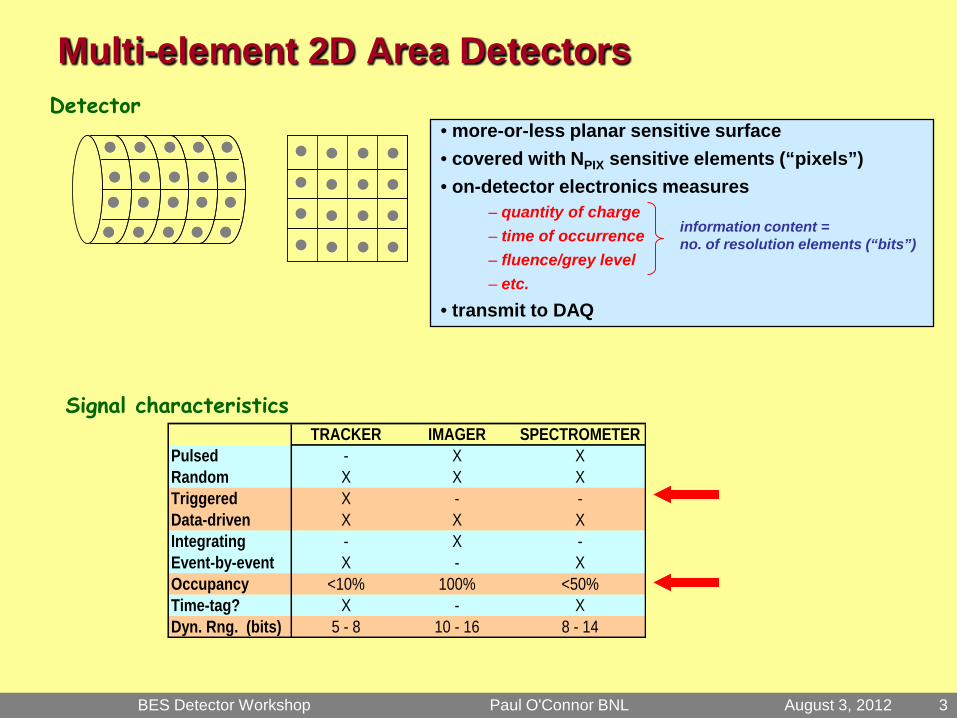
Multi-element 2D Area Detectors Detector
• more-or-less planar sensitive surface • covered with NPIX sensitive elements (“pixels”) • on-detector electronics measures
– quantity of charge – time of occurrence – fluence/grey level – etc.
• transmit to DAQ
TRACKER IMAGER SPECTROMETERPulsed - X XRandom X X XTriggered X - -Data-driven X X XIntegrating - X -Event-by-event X - XOccupancy <10% 100% <50%Time-tag? X - XDyn. Rng. (bits) 5 - 8 10 - 16 8 - 14
information content = no. of resolution elements (“bits”)
Signal characteristics
BES Detector Workshop Paul O'Connor BNL August 3, 2012 4
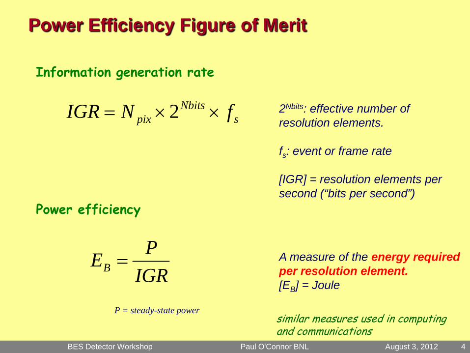
Power Efficiency Figure of Merit
Information generation rate
sNbits
pix fNIGR ××= 2 2Nbits: effective number of resolution elements. fs: event or frame rate [IGR] = resolution elements per second (“bits per second”)
Power efficiency
IGRPEB = A measure of the energy required
per resolution element. [EB] = Joule
similar measures used in computing and communications
P = steady-state power

BES Detector Workshop Paul O'Connor BNL August 3, 2012 5
Signal chain
preamp filter analog feature extraction/ analog memory
ADC DSP off-detector driver
detector can transfer charge/voltage/current
Nchan=1
matrix switch per pixel
Nchan=Ncol
wirebond
bump bond (hybrid) monolithic
Nchan=Npix
tileable
optional multiplexing
electronics organization
power to sustain IGR independent of parallel or serial organization
BES Detector Workshop Paul O'Connor BNL August 3, 2012 6
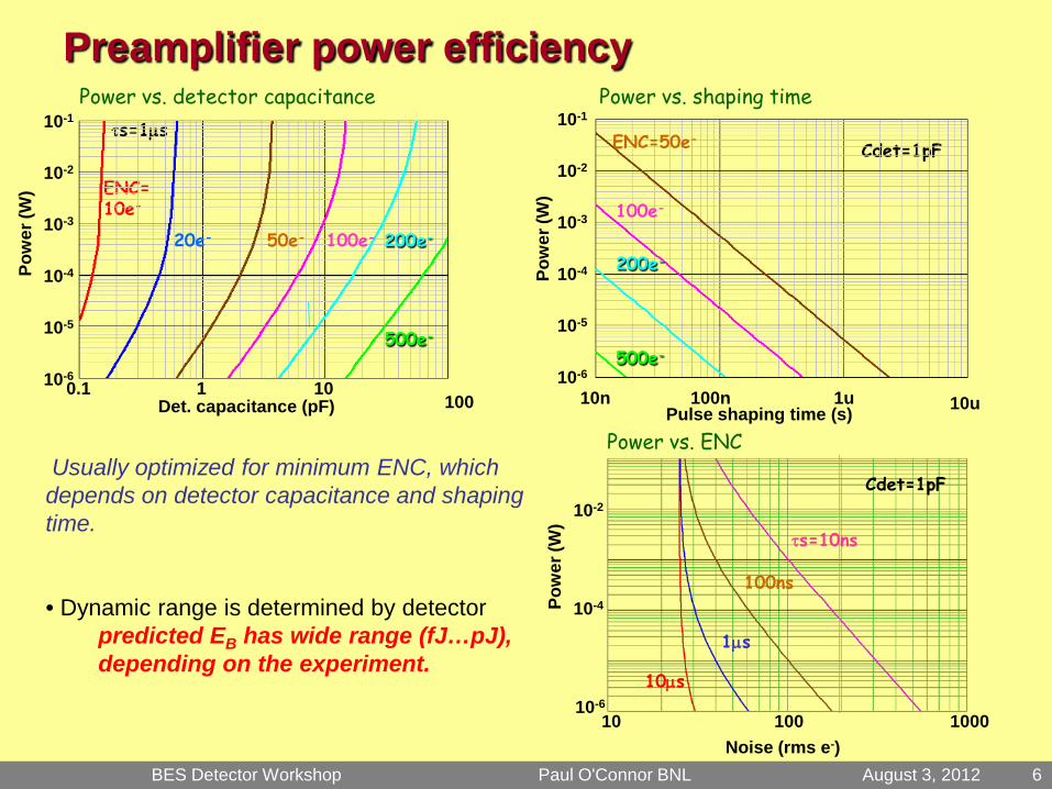
Preamplifier power efficiency Power vs. detector capacitance
• Dynamic range is determined by detector predicted EB has wide range (fJ…pJ), depending on the experiment.
Noise (rms e-) 10 100 1000
Pow
er (W
)
10-6
10-4
10-2
10µs
τs=10ns
100ns
1µs
Power vs. ENC
Cdet=1pF Usually optimized for minimum ENC, which depends on detector capacitance and shaping time.
100
Pow
er (W
)
10-6
Det. capacitance (pF) 0.1 1 10
ENC= 10e-
τs=1µs
10-5
10-4
10-3
10-2
10-1
20e- 50e- 100e- 200e-
500e-
Pow
er (W
)
10n Pulse shaping time (s)
100n 1u 10u
Cdet=1pF
10-6
10-5
10-4
10-3
10-2
10-1
ENC=50e-
100e-
200e-
500e-
Power vs. shaping time
BES Detector Workshop Paul O'Connor BNL August 3, 2012 7
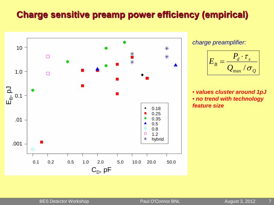
Charge sensitive preamp power efficiency (empirical)
0.1 0.2 0.5 1.0 2.0 5.0 10.0 20.0 50.0
0.180.250.350.50.81.2hybrid
EB, p
J
CD, pF
1.0
.001
.01
0.1
10
• values cluster around 1pJ • no trend with technology feature size
charge preamplifier:
Q
sdB Q
PEσ
τ/max
⋅=
BES Detector Workshop Paul O'Connor BNL August 3, 2012 8
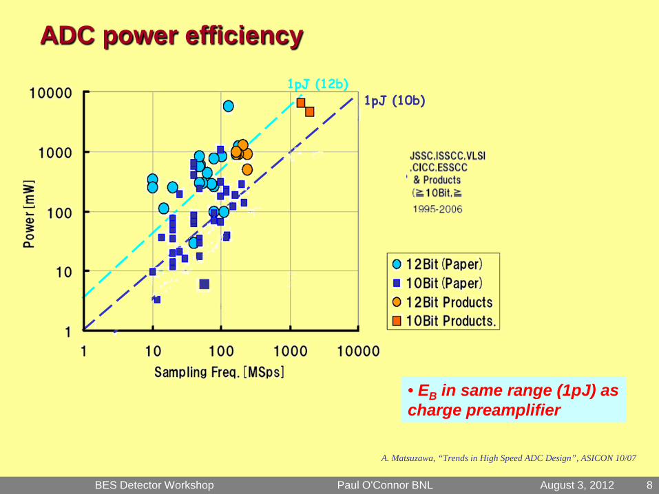
ADC power efficiency
1pJ (12b) 1pJ (10b)
A. Matsuzawa, “Trends in High Speed ADC Design”, ASICON 10/07
• EB in same range (1pJ) as charge preamplifier

BES Detector Workshop Paul O'Connor BNL August 3, 2012 9
Signal chain components EB compared • Expresses the power cost of achieving SNR and speed • Useful rules of thumb during design partitioning
Typical Best
1.5pJ 0.005pJ
1pJ 0.05pJ
20pJ 7.5pJ
charge amplifier:
Q
pdB Q
PE
στ/max
⋅=
ADC:
sENOB
dB f
PE⋅
=2
off-chip serial link:
bit
dB f
PE =note: pJ = mW/Mbps
BES Detector Workshop Paul O'Connor BNL August 3, 2012 10
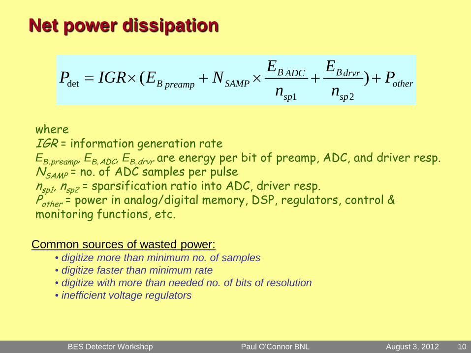
Net power dissipation
othersp
drvrB
sp
ADCBSAMPpreampB P
nE
nE
NEIGRP ++×+×= )(21
det
where IGR = information generation rate EB,preamp, EB,ADC, EB,drvr are energy per bit of preamp, ADC, and driver resp. NSAMP = no. of ADC samples per pulse nsp1, nsp2 = sparsification ratio into ADC, driver resp. Pother = power in analog/digital memory, DSP, regulators, control & monitoring functions, etc.
Common sources of wasted power: • digitize more than minimum no. of samples • digitize faster than minimum rate • digitize with more than needed no. of bits of resolution • inefficient voltage regulators

BES Detector Workshop Paul O'Connor BNL August 3, 2012 11
Examples: Trackers
RatCAP tomograph
32-channel RatCAP ASIC 0.18um CMOS
image of conscious rat brain
24-channel ASIC preamp/shaper
sampling/digitizing board
ALICE pixel (CERN)
RatCAP (BNL)
LEGS TPC (BNL)
ATLAS CSC (BNL)
Area
Pixels
Rate
DR
IGR
P
1.7
8000
2M
150
3.0e12
0.8
15
380
2M
3200
6.4e9
1.5
1000
8000
700K
1.3e5
8.7e10
16
1e4
1000
2.4e7
960
2.3e10
250
cm2
-
cps/fps
-
s-1
W
BES Detector Workshop Paul O'Connor BNL August 3, 2012 12
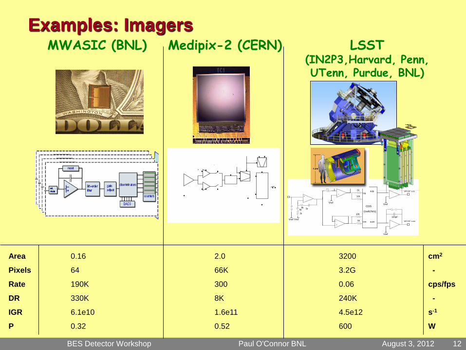
Examples: Imagers MWASIC (BNL)
"diff DSI" outp
+
-
5K
+
-5K
Vref Vref
Vref
5K100pF
Vref
5K
inp
inm
outp
"diff DSI" outm
100pF
Vref
outm
2p8p
10K
10K
+
-
CDS
(switches)2k
8k
Medipix-2 (CERN) LSST (IN2P3,Harvard, Penn, UTenn, Purdue, BNL)
Area
Pixels
Rate
DR
IGR
P
0.16
64
190K
330K
6.1e10
0.32
2.0
66K
300
8K
1.6e11
0.52
3200
3.2G
0.06
240K
4.5e12
600
cm2
-
cps/fps
-
s-1
W

BES Detector Workshop Paul O'Connor BNL August 3, 2012 13
Examples: Spectrometers
Analog Residual Output
Digital OutputA-D
mux
serialreadout
controllerSlot Control (SC)CLOCKS
configuration registers
SERIAL INTERFACE
BIAS16
CP Channels 16COLUMNS INPUT
Thr. Global DAC
RST
Auxiliary Output Controller
A-Dmux
Test Pulser
316
Analog Residual Output
Digital OutputA-D
mux16
CP Channels 16COLUMNS INPUTA-Dmux
316
Analog Residual Output
Digital OutputA-D
mux16
CP Channels 16COLUMNS INPUTA-Dmux
316
Analog Residual Output
Digital OutputA-D
mux16
CP Channels 16COLUMNS INPUTA-Dmux
316
16
16
16
16
Analog Residual Output
Digital OutputA-D
mux
serialreadout
controllerSlot Control (SC)CLOCKS
configuration registers
SERIAL INTERFACE
BIAS16
CP Channels 16COLUMNS INPUT
Thr. Global DAC
RST
Auxiliary Output Controller
Auxiliary Output Controller
A-DmuxA-Dmux
Test PulserTest Pulser
316
Analog Residual Output
Digital OutputA-D
mux16
CP Channels 16COLUMNS INPUTA-DmuxA-Dmux
316
Analog Residual Output
Digital OutputA-D
mux16
CP Channels 16COLUMNS INPUTA-DmuxA-Dmux
316
Analog Residual Output
Digital OutputA-D
mux16
CP Channels 16COLUMNS INPUTA-DmuxA-Dmux
316
16
16
16
16
BES Detector Workshop Paul O'Connor BNL August 3, 2012 14
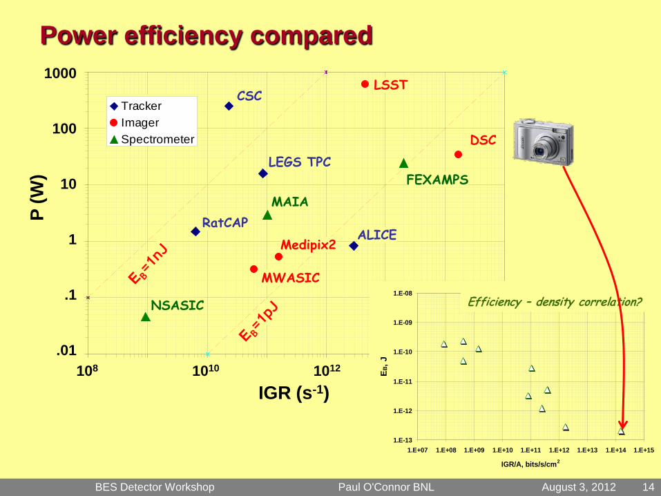
TrackerImagerSpectrometer
Power efficiency compared
108 1010 1012 1014 .01
1
100
.1
10
1000 CSC
LEGS TPC
RatCAP ALICE
MAIA
NSASIC
FEXAMPS
LSST
MWASIC
Medipix2
DSC
IGR (s-1)
P (W
)
1.E-13
1.E-12
1.E-11
1.E-10
1.E-09
1.E-08
1.E+07 1.E+08 1.E+09 1.E+10 1.E+11 1.E+12 1.E+13 1.E+14 1.E+15
IGR/A, bits/s/cm2
E B, J
Efficiency – density correlation?
BES Detector Workshop Paul O'Connor BNL August 3, 2012 15
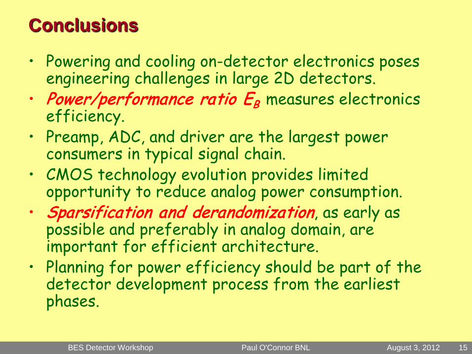
Conclusions
• Powering and cooling on-detector electronics poses engineering challenges in large 2D detectors.
• Power/performance ratio EB measures electronics efficiency.
• Preamp, ADC, and driver are the largest power consumers in typical signal chain.
• CMOS technology evolution provides limited opportunity to reduce analog power consumption.
• Sparsification and derandomization, as early as possible and preferably in analog domain, are important for efficient architecture.
• Planning for power efficiency should be part of the detector development process from the earliest phases.
BES Detector Workshop Paul O'Connor BNL August 3, 2012 16
THE END
BES Detector Workshop Paul O'Connor BNL August 3, 2012 17
REFERENCES • P. O'Connor; Low Noise CMOS Signal Processing IC for Interpolating Cathode Strip Chambers; BNL 61085;
IEEE Trans. Nucl. Sci. NS-42 (1995) 824-829. • P. O'Connor and G.De Geronimo; Prospects for charge sensitive amplifiers in scaled CMOS; Nucl. Instrum. &
Meth. A484 (2002) 713-725. • G. De Geronimo, P. O'Connor, A. Kandasamy; Analog peak detector and derandomizer for high rate
spectroscopy; IEEE Trans. Nucl. Sci. 49 (2002) 1769-1773. • P. O’Connor , G. De Geronimo and A. Kandasamy, Amplitude and Time Measurement ASIC with analog
derandomization, Nucl. Instrum. & Meth. A505 (2003), 352 – 357. • G. De Geronimo, P. O’Connor, MOSFET Optimization in deep submicron CMOS technology for charge
amplifiers, IEEE Trans. Nucl. Sci. 52 (2005), 3223 – 3232. • B. Yu et al., A GEM based TPC for the LEGS experiment, 2005 IEEE Nucl. Sciences Symposium Conference
Record, 924 – 928. • P. O’Connor, Future Trends in Microelectronics - Impact on Detector Readout, International Symposium on
Detector Development, April 3 – 6 2006, SLAC http://www.slac.stanford.edu/econf/C0604032/proceedings.htm#twelve
• J-F. Pratte et al., Front-end electronics for the RatCAP mobile animal PET scanner, IEEE Trans. Nucl. Sci. 51 (2004), 1318-1323.
• G. De Geronimo, A. Dragone, J. Grosholz, P. O’Connor, E. Vernon, ASIC With multiple energy discrimination for high-rate photon counting applications, IEEE Trans. Nucl. Sci. 54 (2007), 303 – 312.
• M. Campbell, PS Applications, Joint Workshop on Detector Development for Future Photon Science and Particle Physics Experiments, DESY, Oct. 14, 2008, https://indico.desy.de/materialDisplay.py?contribId=7&sessionId=2&materialId=slides&confId=1036
• D.P. Siddons, Detector R&D for NSLS-II, X-ray Photon Correlation Spectroscopy & Microbeam SAXS at NSLS-II Workshop, Jan. 11, 2008, http://www.bnl.gov/nsls2/workshops/docs/XPCS/XPCS_Siddons.pdf
• G. De Geronimo et al., Front-end ASIC for high resolution X-ray spectrometers, IEEE Trans. Nucl. Sci. 55 (2008), 1604 – 1609.
• G. Haller, N. Van Bakel, Two dimensional detectors for LUSI science, LCLS FAC Oct 2007, http://silicondetector.org/download/attachments/9175610/Haller-FAC-LUSI--Detectors-10-07-v1.ppt?version=1
• A. Dragone, J-F. Pratte, P. Rehak, G. Carini, R. Herbst, P. O’Connor, D.P. Siddons, XAMPS detector readout ASIC for LCLS, 2008 IEEE Nucl. Sci. Symposium Conference Record, N44-8 (2008).
• http://www.google.com/corporate/datacenters/measuring.html
BES Detector Workshop Paul O'Connor BNL August 3, 2012 18
BACKUPS

BES Detector Workshop Paul O'Connor BNL August 3, 2012 19
Outline
• 2D area detectors • Optimizing power/performance
– Device and Circuit Level – System level
• Examples

BES Detector Workshop Paul O'Connor BNL August 3, 2012 20
Input transistor (M1) optimization
• Optimize for total (white + 1/f) series noise: – adjust W,L while holding Id and tp constant
• Correct modeling of weak, moderate, and strong inversion (EKV model): – dependence of gm, Cg, γ on operating point
• Low-frequency noise: – dependence on Lg
– spectral dependence • Predict result of scaling to new technologies
P. O’Connor, Proc. FEE2003 Snowmass G. De Geronimo, P. O’Connor, TNS52(6),3223 (2005)

BES Detector Workshop Paul O'Connor BNL August 3, 2012 21
Preamplifier power efficiency N
oise
(rm
s e-
)
10
100
1000
Det. capacitance (pF) 0.1 1 10
P=1µW
P=10mW
τs=1µs
Equivalent Noise Charge vs. detector capacitance and shaping time
Noi
se (r
ms
e-)
10
100
1000
10n Pulse shaping time (s)
100n 1u 10u
Cdet=1pF P=1µW
P=10mW • Dynamic range is determined by detector predicted EB has wide range (fJ…pJ), depending on the experiment.
Noise (rms e-)
10 100 1000 Po
wer
(W)
10-6
10-4
10-2
10µs
τs=10ns
100ns
1µs
Power vs. ENC
Cdet=1pF
Usually optimized for minimum ENC, which depends on detector capacitance and shaping time.
BES Detector Workshop Paul O'Connor BNL August 3, 2012 22
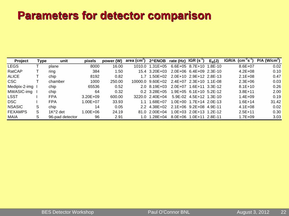
Parameters for detector comparison
Project Type unit pixels power (W) area (cm2) 2^ENOB rate (Hz) IGR (s-1) EB(J) IGR/A (cm-2s-1) P/A (W/cm2)LEGS T plane 8000 16.00 1010.0 1.31E+05 6.6E+05 8.7E+10 1.8E-10 8.6E+07 0.02RatCAP T ring 384 1.50 15.4 3.20E+03 2.0E+06 6.4E+09 2.3E-10 4.2E+08 0.10ALICE T chip 8192 0.82 1.7 1.50E+02 2.0E+10 2.9E+12 2.8E-13 2.1E+08 0.47CSC T chamber 1000 250.00 10000.0 9.60E+02 2.4E+07 2.3E+10 1.1E-08 2.3E+06 0.03Medipix-2-img I chip 65536 0.52 2.0 8.19E+03 2.0E+07 1.6E+11 3.3E-12 8.1E+10 0.26MWASIC-img I chip 64 0.32 0.2 3.28E+05 1.9E+05 6.1E+10 5.2E-12 3.8E+11 2.00LSST I FPA 3.20E+09 600.00 3220.0 2.40E+04 5.9E-02 4.5E+12 1.3E-10 1.4E+09 0.19DSC I FPA 1.00E+07 33.93 1.1 1.68E+07 1.0E+00 1.7E+14 2.0E-13 1.6E+14 31.42NSASIC S chip 14 0.05 2.2 4.38E+02 2.1E+06 9.2E+08 4.9E-11 4.1E+08 0.02FEXAMPS S 1K^2 det 1.00E+06 24.19 81.0 2.00E+04 1.0E+03 2.0E+13 1.2E-12 2.5E+11 0.30MAIA S 96-pad detector 96 2.91 1.0 1.28E+04 8.0E+06 1.0E+11 2.8E-11 1.7E+09 3.03
BES Detector Workshop Paul O'Connor BNL August 3, 2012 23
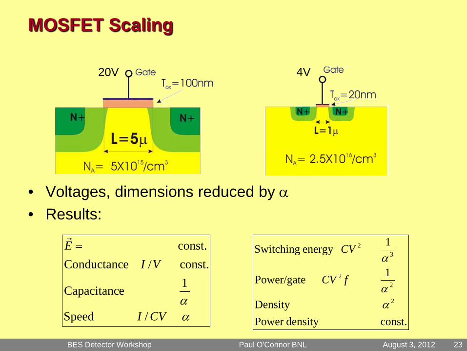
MOSFET Scaling
• Voltages, dimensions reduced by α • Results:
αα
/ Speed
1 eCapacitanc
const. / eConductancconst.
CVI
VIE =
const. density Power Density
1 Power/gate
1 energy Switching
2
22
32
αα
α
fCV
CV
20V 4V
BES Detector Workshop Paul O'Connor BNL August 3, 2012 24
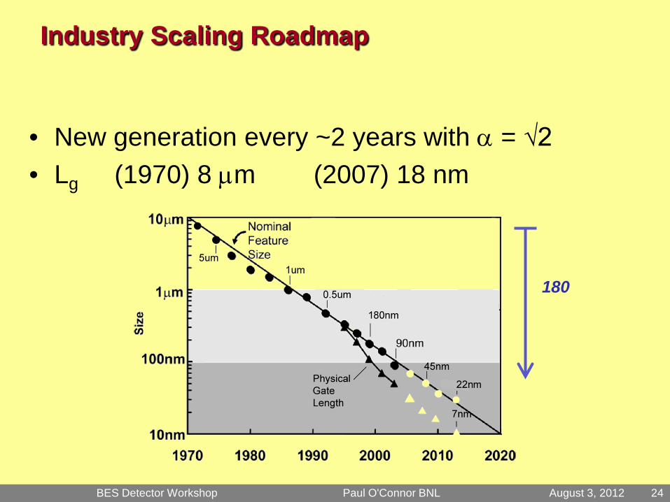
Industry Scaling Roadmap
• New generation every ~2 years with α = √2 • Lg (1970) 8 µm (2007) 18 nm
180

BES Detector Workshop Paul O'Connor BNL August 3, 2012 25
Can Scaling Continue? • Until 180nm node:
– follow classical scaling with α = √2 – 2.8X performance per generation
• Now: – thermal voltage prevents further voltage
scaling – continue (super) scaling Lg – VDD, VTH have stopped scaling
• Gate density and speed continue to scale • Increase of E, conductance • Switching energy decreases only by 1/α
not 1/α3
• Power density increase ~ α • Static power from leakage, gate tunneling
make power problem worse
BES Detector Workshop Paul O'Connor BNL August 3, 2012 26
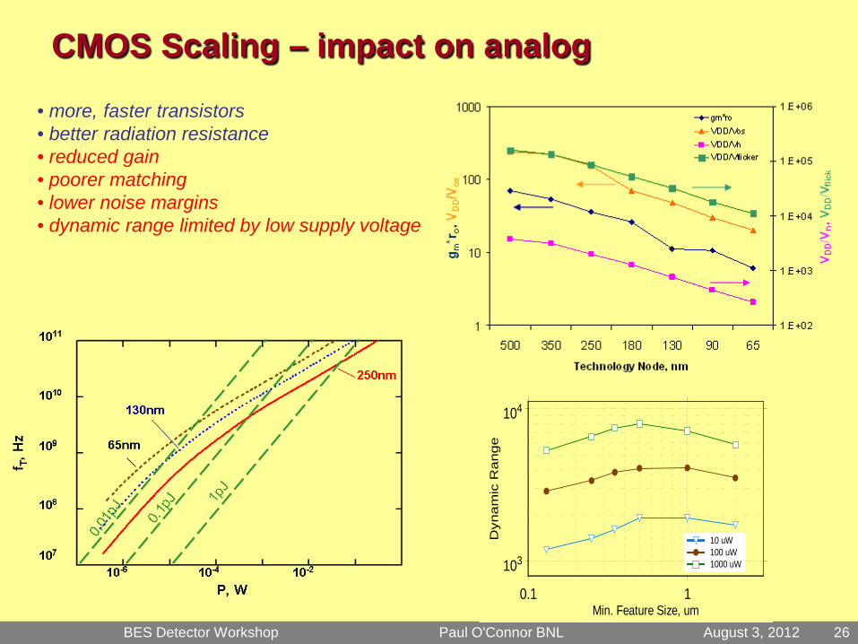
CMOS Scaling – impact on analog • more, faster transistors • better radiation resistance • reduced gain • poorer matching • lower noise margins • dynamic range limited by low supply voltage
0.1 1Min. Feature Size, um
103
104
Dyn
am
ic R
an
ge
10 uW100 uW1000 uW

BES Detector Workshop Paul O'Connor BNL August 3, 2012 27
Mixed-signal chips
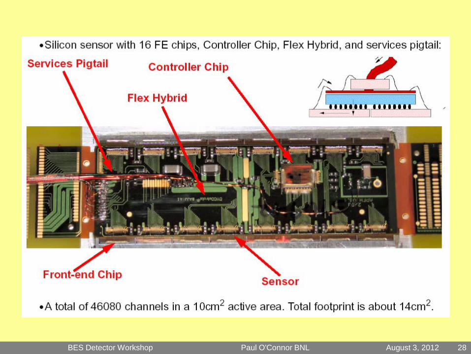
BES Detector Workshop Paul O'Connor BNL August 3, 2012 28