post-compensation of nonlinear distortions of 64-qam
TRANSCRIPT

Post-Compensation of Nonlinear Distortions of 64-QAM Signals in a Semiconductor Based Wavelength Converter Benoît Filion, An T. Nguyen, Leslie A. Rusch, and Sophie LaRochelle
Journal of Lightwave Technology, (Volume 33, Issue 15) (2015)
Doi: 10.1109/JLT.2015.2436812
http://ieeexplore.ieee.org/document/7112081/?arnumber=7112081
© 2016 IEEE. Personal use of this material is permitted. Permission from IEEE must be obtained for all other uses, in any current or future media, including reprinting/republishing this material for advertising or promotional purposes, creating new collective works, for resale or redistribution to servers or lists, or reuse of any copyrighted component of this work in other works.

Abstract— We experimentally investigate post-compensation of
nonlinear distortions induced by a wavelength converter (WC) based
on four-wave mixing in a semiconductor optical amplifier. The
technique exploits a low-complexity digital filter-based back-
propagation (DFBP) method. We perform post-compensation of
nonlinear distortions following single stage wavelength conversion of
5 Gbaud 64- quadrature amplitude modulation (QAM). We examine
the DFBP performances in the presence of a degraded optical signal-
to-noise ratio at the WC input and we explore the WC optimal
operating conditions. Also, we experimentally demonstrate for the first
time in the literature dual stage wavelength conversion of QAM
signals, in particular, 5 Gbaud 64-QAM, and show that bit error rate
below hard-decision forward error correction threshold is only possible
with post-compensation of nonlinear distortions. These results are of
importance for the development of wavelength routed networks
requiring successive wavelength conversion stages to enhance routing
capabilities.
Index Terms—Advanced modulation formats, coherent
detection, four-wave mixing, optical wavelength conversion,
quadrature amplitude modulation, semiconductor optical
amplifiers.
I. INTRODUCTION
Wavelength converters (WCs) are essential building blocks
enabling future all-optical wavelength routed networks with
sub-wavelength granularity switching such as optical burst
switching (OBS) and optical packet switching (OPS). In these
networks, the wavelength dimension is used not only for
routing, but also for contention resolution, i.e., when two input
signals sharing the same wavelength are destined to the same
optical fiber. Wavelength-based contention resolution is the
most effective technique as it does not incur additional latency
while maintaining the shortest path or minimum hop distance
[1]. Furthermore, OBS and OPS technology have also been
proposed for data centers [2], [3].
Coherent systems using advanced modulation formats
together with digital signal processing have recently been
adopted in optical communication systems to provide increased
spectral efficiency. While coherent detection is already
established as the technology of choice in long haul
communication systems, as component cost decline this
This work was supported by Natural Sciences and Engineering Research
Council (NSERC) of Canada and by the Canada Research Chair APTECS.
The authors are with the Department of Electrical and Computer Engineering and the Center for Optics, Photonics and Lasers (COPL),
technology is expected to enter metropolitan area networks and
access networks. Due to the shorter reach of such networks, the
use of highly spectrally efficient advanced modulation formats
such as M-ary quadrature amplitude modulation (QAM), from
16-QAM up to 64-QAM, will greatly enhance their capacity
[4]. Coherent systems further enables flexible and agile
transparent networks that adapt parameters such as data rate,
frequency spacing and modulation format according to desired
reach and volume of traffic [4]–[7]. In this context, thorough
investigation and optimization of wavelength converters for
advanced modulation formats is needed in order to enable
future all-optical wavelength routed networks.
Four-wave mixing (FWM) in semiconductor optical
amplifiers (SOAs) is an efficient and practical wavelength
conversion mechanism because of its compactness, low pump
powers, high conversion efficiency (CE) and transparency to
modulation formats [8]. Regarding phase-modulated formats,
we showed in [9] that a careful optimization of the signal and
pump power is required to tradeoff the benefits of a high
conversion efficiency and the penalties created by induced
nonlinearities during the FWM process. Using two-pumps,
wavelength conversion covering the whole C-band is possible
as demonstrated in [9].
In reference [10], we 1) introduced for the first time the
digital filter-based back-propagation (DFBP) method for the
compensation of nonlinear distortions introduced by SOA WCs
of phase (QAM) modulated signals; 2) investigated the
approach through numerical simulations and verified, through
these calculations, the required sampling rate to implement the
filter; and 3) validated all the results through experimental
measurements. The experimental measurements were done in a
very simple single stage scenario and with ideal optical signal-
to-noise ratio (OSNR) at the input of the WC (>35 dB). The
only parameter that was swept was the input signal power.
In this paper, we address the issue of compensation of
nonlinear distortions of 64-QAM signals when the input OSNR
is degraded, for example by amplified spontaneous emission
(ASE) accumulated during successive optical amplifications or
wavelength conversion. This is an important issue for future
applications in wavelength routed networks cascading several
wavelength conversion stages. The main contribution of this
paper is to investigate how DFBP techniques can improve the
performance of the WC in the presence of a noisy signal and to
Université Laval, Pavillon d’Optique-Photonique, 2375 de la Terrasse,
Québec (QC) G1V 0A6, Canada (e-mail: [email protected]).
Post-Compensation of Nonlinear Distortions of
64-QAM Signals in a Semiconductor Based
Wavelength Converter Benoît Filion, Graduate Student Member, IEEE, An T. Nguyen, Graduate Student Member, IEEE,
Leslie A. Rusch, Fellow, IEEE, and Sophie LaRochelle, Fellow, OSA, Senior Member, IEEE
Copyright (c) 2015 IEEE. Personal use is permitted. For any other purposes, permission must be obtained from the IEEE by emailing [email protected].

determine its optimal operating conditions. More specifically,
we 1) experimentally demonstrate performance improvement
that can be achieved by using DFBP when the input OSNR is
degraded to 25 dB; 2) sweep both signal power and received
OSNR experimentally to identify the optimal operating
conditions of the SOA WC; 3) show that DFBP can allow the
pump power to be reduced from 10 dBm to 5 dBm without bit
error rate (BER) penalty; and 4) perform for the first time to our
knowledge two successive wavelength conversions on a 64-
QAM signal; and 5) show how DFBP can help to improve the
robustness of the cascaded system, for example with respect to
variations in signal power and link loss.
This paper is organized as follows. In section II, we briefly
present the equations required to implement DFBP. In section
III, we describe the experimental setups. We present the
experimental results of 5 Gbaud 64-QAM single stage
wavelength conversion in section IV and the experimental
results of dual stage wavelength conversion follow in section V.
II. DIGITAL FILTER-BASED BACK-PROPAGATION
FWM in a SOA is achieved by simultaneously injecting at its
input one continuous wave (CW) signal, called the pump,
together with the data modulated signal to be converted. The
gain and the refractive index of the amplifier are then modulated
at the frequency detuning Ω, defined as the optical frequency
separation between the signal and the pump [8]. A new optical
field, the conjugate, is generated during the propagation within
the SOA.
The post-compensation technique is based on a small-signal
analysis of the SOA dynamic rate equation governing nearly
degenerate FWM, in which only the carrier density modulation
is considered. In this section, we introduce the necessary
equations and discuss the physical parameters needed for the
DFBP implementation (the complete analysis can be found in
[10]).
The optical field at the input of the SOA, 𝐸𝑖𝑛, consists of a
pump 𝐸𝑝 centered at 𝜔𝑝, and a modulated, weaker signal 𝐸𝑠
centered at 𝜔𝑠 leading to
, .j t
in p s p sE t E E t e (1)
Under small-signal analysis [11], the equation for the
conjugate field 𝐸𝑐 at the SOA output is given by
*
1
22 ,s
jh t
c pF t E E tE t e
(2)
where
2 2
1
1
1,
2.
s
sat p sh t
sat
h te
e j
jF t
P E E
P
t
(3)
In (2) and (3), ℎ(𝑡) is the integrated gain, α is the linewidth
enhancement factor, 𝜏𝑠 is the carrier lifetime and 𝑃𝑠𝑎𝑡 is the
saturation power. We note that ℎ(𝑡) represents the baseband
part of the integrated gain, including sidebands located at the
frequency detuning . The rate equation governing the
dynamics of ℎ(𝑡) is given by
2 2
01
p s
s s sat
h tE E th t h h t
t Pe
. (4)
where ℎ0 is the small-signal integrated gain. As seen in (2), the
temporal variation of ℎ(𝑡) induces nonlinear distortions on the
conjugate 𝐸𝑐(𝑡). To solve (4) for a given input power, we write
the gain as its mean value plus a zero-average perturbation term,
i.e., ℎ(𝑡) = ℎ̅ + 𝛿ℎ(𝑡). Since the instantaneous input signal
power |𝐸𝑠(𝑡)|2 is unknown at the receiver, we find an estimate
|�̂�𝑠(𝑡)|2 with the knowledge of Ec(t) at the receiver and (2)
leading to
2
2
2
22
ˆ
p
c
sh t
E t
F E
E t
e
. (5)
Under the small-signal approximation (𝛿ℎ(𝑡) ≪ ℎ̅) and
replacing |𝐸𝑠(𝑡)|2 by |�̂�𝑠(𝑡)|2 in (4), we find that the SOA acts
as a low-pass filter according to
ch t K m t p t (6)
where 𝐾 is given by
1
1
h
h h
p c
eK
e p e p
, (7)
�̅�𝑝 and �̅�𝑐 are the average pump and conjugate power defined
in (9) below, while 𝑚(𝑡) is a single-pole low-pass filter with
time constant
1
s
eff h h
p ce p e p
. (8)
In (6)-(8), we normalized the input powers by the SOA
saturation power, 𝑃𝑠𝑎𝑡. We apply the same definition for the
average component and time varying parts, noting that the
pump has constant power we write |𝐸𝑝|2
𝑃𝑠𝑎𝑡⁄ = �̅�𝑝 and for the
conjugate
2
22 2
c
c c
sat p
c
E tp p p
P F Et t
. (9)
Taking the Laplace transform of 𝐾 ∙ 𝑚(𝑡) and applying the
bilinear transform [12] leads to the following discrete impulse
response of the digital filter
Copyright (c) 2015 IEEE. Personal use is permitted. For any other purposes, permission must be obtained from the IEEE by emailing [email protected].

1 1 c ch n B h n C p n C p n (10)
where 𝑥[𝑛] ≅ 𝑥(𝑛Δ𝑡) for any continuous waveform 𝑥(𝑡), Δ𝑡 is
the sampling time,
1 2
1 2
eff
eff
tB
t
, (11)
and
1 2 eff
KC
t
. (12)
Finally, the post compensated conjugate �̂�𝑐(𝑡) is obtained
with
1
2ˆj
h h t
c cE t E t e
. (13)
With the knowledge of 𝐸𝑐(𝑡) at the receiver, a digital filter
(equations (10) to (12)) can be implemented to post-compensate
the conjugate. Further details on the implementation including
the block diagram of the algorithm can be found in [10]. As
described in Appendix A, the use of this post-compensation
technique requires the characterization of only a few standard
SOA parameters including 𝛼, 𝑃𝑠𝑎𝑡 , 𝜏𝑠 and the small signal gain
𝐺0 = 𝑒𝑥𝑝(ℎ0).
III. EXPERIMENTAL SETUP
The experimental setup is presented in Fig. 1(a). A tunable
laser at 𝜆𝑠 = 1549.3 nm (1548.4 nm for the dual-stage
wavelength conversion experiments) is modulated by an in-
phase/quadrature Mach-Zehnder modulator (IQ-MZM). The
IQ-MZM is driven by a digital to analog converter (DAC) with
3 bits resolution that is in turn driven by 3-level data streams of
27 − 1, 211 − 1 and 220 − 1 pseudo-random-bit-sequences. A
phase shifter is used to decorrelate the data streams in order to
generate the in-phase and quadrature components. The
modulator output is fed into a variable optical attenuator
(VOA1) and a erbium-doped fiber amplifier (EDFA1) followed
by a Gaussian shaped optical filter (OF1) with 1 nm bandwidth
tuned at 𝜆𝑠 , a polarization controller (PC), a VOA (VOA2) and
then into the WC. The signal OSNR, measured over a
bandwidth of 0.1 nm, is adjusted by varying the attenuation
(VOA1) and the gain of the EDFA (EDFA1).
After wavelength conversion, the FWM term, i.e., the
conjugate, goes directly to the pre-amplifier. The conjugate
power at the input of the coherent receiver (CRx) is kept fixed
at −6 dBm for all wavelength conversion experiments and
coherently detected using a tunable laser at 𝜆𝑙𝑜 as local
oscillator (LO). The noise loading stage is composed of an
EDFA (EDFA3) followed by an OF (OF3), with identical shape
(Gaussian) and bandwidth (0.7 nm) as the pre-amplified
receiver OF (OF2), and a VOA (VOA3). The filtered ASE noise
coming from the EDFA (EDFA3) is combined with the
conjugate with a 2×1 coupler. The OSNR at the input of the
pre-amplified receiver is set by adjusting the VOA (VOA3) of
the noise loading stage while the conjugate power remains
Single stage WC output
Dual stage WC output
PC
EDFA4
SOA1
OF4
EDFA5
PC
EDFA6
2x1
λp1 λp2
2x1 SOA2
OF5
VOA2λsPC
EDFA1
λlo
OF1 OF2
EDFA3
VOA3OF3
VOA4VOA1
2x1
Noise loading stage
EDFA2
Pre-amplified receiver
(a)
(b)
IQ
MZM
BGP
Wavelength
ConverterCRx
RTO
+
Offline
DSP
λc1λc2
Fig. 1 Block diagram of a) the experimental setup and b) the wavelength converter.
Copyright (c) 2015 IEEE. Personal use is permitted. For any other purposes, permission must be obtained from the IEEE by emailing [email protected].
always fixed. Finally, the coherently detected signal is sampled
by a real time oscilloscope (RTO) at 80 GSa/s with a 30 GHz
electrical bandwidth. Note that in the experiments, ∆𝑡 in
equations (11) and (12) corresponds to the sampling rate of the
RTO (∆𝑡 = 1/80 GHz = 12.5 ps).
In the digital signal processing stage, we first apply the DFBP
algorithm. The required SOA parameters, i.e., ℎ0, 𝑃𝑠𝑎𝑡 , 𝛼 and
𝜏𝑠, are extracted from experimental measurements as presented
in Appendix A. Next, we apply a 2nd order super Gaussian low-
pass filter, performed resampling, timing recovery and
frequency offset compensation (FOC) using the estimator
suggested in [13]. Following the FOC, a decision-directed
equalizer based on the Wiener-Hopf equations (WHDD-EQ)
[14] and a decision-aided maximum likelihood algorithm is
used for phase recovery [15]. We applied, for a second time, a
WHDD-EQ to further equalize with the more reliable decisions
following phase recovery. Finally, hard-threshold decision is
performed on I and Q individually, we count the errors and
estimate BER.
The block diagrams of the WC is shown Fig. 1(b). A tunable
laser delivering the pump at 𝜆𝑝1 = 1549 nm (1548.1 nm for the
dual-stage wavelength conversion experiments1) is amplified
by an EDFA (EDFA4) and followed by a PC. The signal and
the pump are combined using a 21 coupler injected into a
nonlinear SOA (SOA1) (SOA1117/CIP) operating over the C-
band (1528 nm to 1562 nm) with 20 dB small-signal gain, 9
dBm output saturation power and < 1 dB polarization dependent
gain. Two isolators (not shown in Fig. 1(b) are used before and
after the SOA to suppress back reflections. The conjugate at 𝜆𝑐1
is filtered with a programmable OF (OF4) (WaveShaper
1000S/Finisar). The optical filter (OF4) is Gaussian shaped and
its bandwidth carefully chosen to obtain the best compromise
between pump power suppression and conjugate power
transmission. For the dual stage wavelength conversion
experiments, the conjugate at 𝜆𝑐1 = 1548.7 nm (1547.8 nm for
the dual-stage wavelength conversion experiments) is amplified
by an EDFA (EDFA5) in order to compensate for the
1 Because the single pump experiments and the dual pump experiments
were not done at the same time, slightly different signal wavelengths were used for each experiments. This wavelength difference (0.9 nm) is small
conversion efficiency and the insertion loss of the first WC
stage. The output of the EDFA (EDFA5) is then combined with
a pump at 𝜆𝑝2 = 1547.5 nm and fed into the second WC to
generate the second conjugate at 𝜆𝑐2 = 1547.2 nm. The
components in the second WC stage (EDFA5, SOA2 and OF5)
are all duplicates of the first WC stage. The wavelength
detuning is Ω = 0.3 nm for both the first WC stage (𝜆𝑠 − 𝜆𝑝1)
and the second WC stage (𝜆𝑐1 − 𝜆𝑝2).
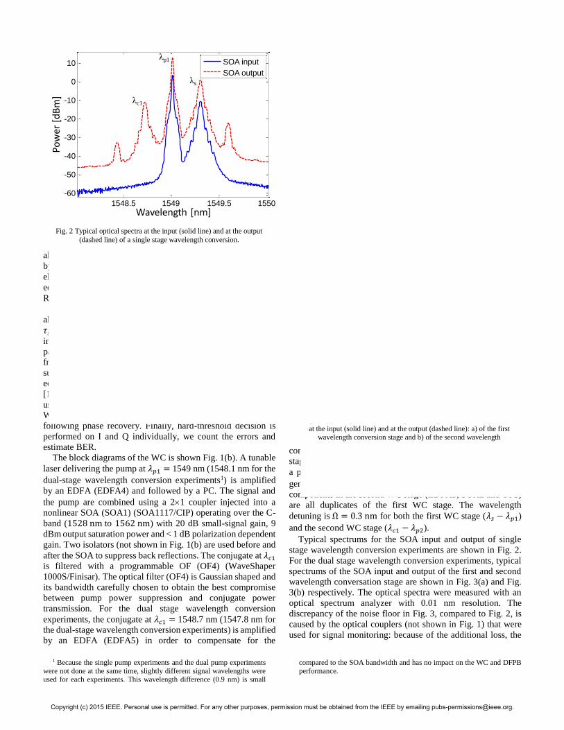
Typical spectrums for the SOA input and output of single
stage wavelength conversion experiments are shown in Fig. 2.
For the dual stage wavelength conversion experiments, typical
spectrums of the SOA input and output of the first and second
wavelength conversation stage are shown in Fig. 3(a) and Fig.
3(b) respectively. The optical spectra were measured with an
optical spectrum analyzer with 0.01 nm resolution. The
discrepancy of the noise floor in Fig. 3, compared to Fig. 2, is
caused by the optical couplers (not shown in Fig. 1) that were
used for signal monitoring: because of the additional loss, the
compared to the SOA bandwidth and has no impact on the WC and DFPB
performance.
(a)
(b)
1547 1547.5 1548 1548.5
-50
-40
-30
-20
-10
0
10
Wavelength [nm]
Pow
er
[dB
m]
SOA input
SOA output
1547 1547.5 1548 1548.5
-50
-40
-30
-20
-10
0
10
Wavelength [nm]
Pow
er
[dB
m]
SOA input
SOA output
λp1
λs
λp2
λc1
λc1
λc2
Wavelength [nm]
Po
we
r [d
Bm
]
Wavelength [nm]
Po
we
r [d
Bm
]
Fig. 3 Typical spectra for dual stage wavelength conversion experiment
at the input (solid line) and at the output (dashed line): a) of the first
wavelength conversion stage and b) of the second wavelength conversion stage.
1548.5 1549 1549.5 1550
-60
-50
-40
-30
-20
-10
0
10
Wavelength [nm]
Pow
er
[dB
m]
SOA input
SOA output
λp1
λs
λc1
Wavelength [nm]
Po
wer
[d
Bm
]
Fig. 2 Typical optical spectra at the input (solid line) and at the output
(dashed line) of a single stage wavelength conversion.
Copyright (c) 2015 IEEE. Personal use is permitted. For any other purposes, permission must be obtained from the IEEE by emailing [email protected].

ASE noise lies under the noise floor of the optical spectrum
analyzer. Considering the relatively low baud rate (5 Gbaud)
and the wavelength spacing (0.3 nm) used in our experiments,
the impact of CE non-uniformity is negligible.
IV. SINGLE STAGE WAVELENGTH CONVERSION
A. DFBP robustness against ASE noise
We compare the measured error vector magnitude (EVM)
and BER as a function of the OSNR at the receiver for different
operating conditions, i.e., input pump and signal power, before
and after DFBP. In order to investigate the robustness of the
DFBP technique against ASE noise, we also measured the
EVM and BER for a degraded OSNR at the input of the WC.
Note that the EVM is displayed in the form of differential EVM,
∆EVM, defined as the difference between the measured EVM
before and after post-compensation using DFBP. As for the
BER measurements, separate BER curves are shown before and
after DFBP.
Measurements in Fig. 4 were done with an input OSNR of 35
dB. The pump power was either 5 dBm or 10 dBm and the input
signal power varied between -2 dBm to -12 dBm. The received
OSNR was swept between 18 dB to 28 dB. Note that for the
reminder of the paper the term OSNR will refer to the OSNR at
the coherent receiver, while OSRNin represents the OSNR at the
input of the SOA. As previously demonstrated in [10], more
nonlinearities are induced on the conjugate during the FWM
process as the injected pump power decreases and/or the input
signal increases. Thus, we expect the EVM improvement due
to the application of the DFBP technique to be more significant
in such conditions. By comparing Fig. 4(a) (𝑃𝑝 = 5 dBm) to Fig.
4(b) (𝑃𝑝 = 10 dBm), we effectively observe this behavior: for
the same input signal power value, ∆EVM is always higher with
𝑃𝑝 = 5 dBm compared to 𝑃𝑝 = 10 dBm. Additionally, for either
∆EVM plot (Fig. 4(a) or Fig. 4(b)), we see the best ∆EVM for
the strongest signals, and worst ∆EVM for the weakest signals.
We note that ∆EVM tends to slightly degrade for lower OSNR
as the conjugate becomes more limited by the ASE noise. For
instance, for 𝑃𝑝 = 5 dBm and 𝑃𝑠 = -2 dBm, ∆EVM= 2.7% with
28 dB OSNR while ∆EVM= 1.3% with 18 dB OSNR (see Fig.
4(a)).
BER measurements are presented Fig. 4(c) and Fig. 4(d) for
a pump power of 5 dBm and 10 dBm, respectively. Solid lines
represent BER before DFBP, while dashed lines show
improved BER after DFBP. BER results are presented only for
input signal powers where BER fell below the hard decision
forward error correction (FEC) threshold of 2×10⁻³ [16] (either
before or after DFBP). After post-compensation, the BER is
18 20 22 24 26 280
0.5
1
1.5
2
2.5
3
3.5
4
4.5
OSNR [dB]
E
VM
[%
]
18 20 22 24 26 280
0.5
1
1.5
2
2.5
3
3.5
4
4.5
OSNR [dB]
E
VM
[%
]
Ps = -12 dBm
Ps = -10 dBm
Ps = -8 dBm
Ps = -6 dBm
Ps = -4 dBm
Ps = -2 dBm
18 20 22 24 26 28
10-4
10-3
10-2
10-1
OSNR [dB]
BE
R
18 20 22 24 26 28
10-4
10-3
10-2
10-1
OSNR [dB]
BE
R
Pp = 10 dBm
OSNRin = 35 dB
Pp = 5 dBm
OSNRin = 35 dB
Pp = 5 dBm
OSNRin = 35 dB
Pp = 10 dBm
OSNRin = 35 dB
a) b)
c) d)
FEC
OSNR [dB]
OSNR [dB]
OSNR [dB]
FEC
ΔEV
M [
%]
BER
BER
OSNR [dB]
ΔEV
M [
%]
Fig. 4 Measured differential EVM (ΔEVM) and BER, before DFBP (solid lines) and after DFBP (dashed lines), as a function of the received OSNR of 5 Gbaud 64-QAM single stage wavelength conversion for an input OSNR of 35dB with received constellations examples: a) ΔEVM for a pump power of 5 dBm b)
ΔEVM for a pump power of 5 dBm c) BER for a pump power of 5 dBm and d) BER for a pump power of 10 dBm.
Copyright (c) 2015 IEEE. Personal use is permitted. For any other purposes, permission must be obtained from the IEEE by emailing [email protected].

significantly improved: with 𝑃𝑝 = 5 dBm (Fig. 4(c)), BER
below the FEC threshold is obtained only for a signal power up
to -12 dBm before DFBP, while it is obtained up to -6 dBm after
DFBP. Interestingly, the signal power procuring the best
performance changes after DFBP; for instance, in Fig. 4(c), the
optimal signal power is -12 dBm before DFBP and -10 dBm
after DFBP. This is caused by the tradeoff between the
nonlinearities and ASE noise at the receiver and is discussed in
details in the next section. By comparing the best case before
DFBP (𝑃𝑠 = -12 dBm) and after DFBP (𝑃𝑠 = -10 dBm), the
OSNR improvement at the FEC threshold after DFBP is ~3.2
dB. With 𝑃𝑝 = 10 dBm (Fig. 4(d)), BER below the FEC is
obtained with a signal power up to -6 dBm before DFBP and up
to -2 dBm after DFBP. Before DFBP, the best performance is
obtained with 𝑃𝑠 = -10 dBm and with 𝑃𝑠 = -6 dBm / 𝑃𝑠 = -8
dBm after DFBP, with an OSNR improvement at the FEC
threshold of ~0.8 dB. We note that, before DFBP, there is ~2.2
dB in OSNR penalty with 𝑃𝑠 = -6 dBm compared to 𝑃𝑠 = -8
dBm while they exhibit the same performance after DFBP,
meaning that the additional nonlinearities with the higher signal
power have been compensated. As with the EVM
measurements, at either pump power we observe slightly
degraded DFBP performance for lower OSNR. Examples of
received constellations before and after DFBP are shown for
𝑃𝑝 = 5 dBm and 𝑃𝑝 = 10 dBm in Fig. 5(a) and Fig. 5(b)
respectively.
The experimental results with a degraded input OSNR of 25
dB are shown in Fig. 6: ∆EVM for a pump power of 5 dBm
(Fig. 6(a)) and 10 dBm (Fig. 6(b)), BER before (solid lines) and
after (dashed lines) DFBP for a pump power of 5 dBm (Fig.
6(c)) and 10 dBm (Fig. 6(d)). These results confirm that the
DFBP post-compensation technique still provide performance
improvement in the presence of a noisy signal at the WC input.
Even though ∆EVM is, in general, slightly lower compared to
the case of OSRNin = 35 dB (see Fig. 6(a) and Fig. 6(b)), as can
be explained by the limitations imposed by the ASE noise on
the conjugate, the BER improvement remains (see Fig. 6(c) and
Fig. 6(d)). In Fig. 6(c), with 𝑃𝑝 = 5 dBm, BER below the FEC
threshold is obtained only for 𝑃𝑠 = -12 dBm before DFBP and
up to 𝑃𝑠 = -6 dBm after DFBP. In that context, the optimal
signal power is the same before and after DFBP, i.e., 𝑃𝑠 = -12
dBm, with ~1.8 dB OSNR improvement after DFBP. In Fig.
6(d), with 𝑃𝑝 = 10 dBm, BER below the FEC threshold is
obtained up to 𝑃𝑠 = -6 dBm before DFBP and up to 𝑃𝑠 = -2
dBm after DFBP. ~0.8 dB OSNR improvement is obtained after
DFBP (𝑃𝑠 = -8 dBm) at the FEC threshold compared to before
DFBP (𝑃𝑠 = -10 dBm). Examples of received constellations
before and after DFBP are shown for 𝑃𝑝 = 5 dBm and 𝑃𝑝 = 10
dBm in Fig. 7(a) and Fig. 7(b) respectively.
B. WC optimal operating condition
We investigate the optimal operating conditions of the WC,
i.e., input pump and signal power. For advanced modulation
formats, we found that the optimal operating conditions depend
on the amount of loss between the WC and the receiver. Indeed,
the OSNR at the CRx depends on the conjugate power since the
EDFA gain at the pre-amplifier input (EDFA2 in Fig. 1(a)) is
adjusted to keep a fixed power at the CRx. However, in [17],
we showed that there is a tradeoff between the received OSNR
and the nonlinear distortions. Optimizing the pump power for
maximum CE, defined as the ratio of conjugate power to the
input signal power, does not translate into an optimal EVM:
better CE exhibits higher OSNR at the CRx, as less gain is
needed at the pre-amplified receiver, but also leads to more
nonlinear distortions induced during the wavelength conversion
process. Note that our optimization here is limited to two input
pump power values, i.e., 5 dBm and 10 dBm. These values were
chosen in order to investigate the tradeoff between the received
Pp = 5 dBm
Ps = -8 dBm
Pp = 5 dBm
Ps = -6 dBm
Pp = 5 dBm
Ps = -4 dBm
Pp = 10 dBm
Ps = -8 dBm
Pp = 10 dBm
Ps = -6 dBm
Pp = 10 dBm
Ps = -4 dBm
EVM = 4.21%
BER = 1.9x10⁻³
EVM = 4.8%
BER = 8.5x10⁻³EVM = 5.66%
BER = 3.9x10⁻²
EVM = 3.64%
BER = 1.8x10⁻³
EVM = 3.67%
BER = 2.1x10⁻³
EVM = 3.95%
BER = 8.3x10⁻³
EVM = 3.38%
BER =9.2x10⁻⁵EVM = 3.42%
BER = 1.1x10⁻³
EVM = 3.63%
BER = 4.4x10⁻³
EVM = 3.26%
BER = 7.1x10⁻⁵
EVM = 3.34%
BER = 7.3x10⁻⁵
EVM = 3.47%
BER = 1.2x10⁻⁴
BeforeDFBP
BeforeDFBP
AfterDFBP
AfterDFBP
a) b)
Fig. 5 Constellation examples before DFBP and after DFBP of 5 Gbaud 64-QAM single stage wavelength conversion for an input OSNR of 35dB: a) for a pump
power of 5 dBm and b) for a pump power of 10 dBm.
Copyright (c) 2015 IEEE. Personal use is permitted. For any other purposes, permission must be obtained from the IEEE by emailing [email protected].

Pp = 5 dBm
Ps = -8 dBm
Pp = 5 dBm
Ps = -4 dBm
Pp = 10 dBm
Ps = -8 dBm
Pp = 10 dBm
Ps = -6 dBm
Pp = 10 dBm
Ps = -4 dBm
Pp = 5 dBm
Ps = -6 dBm
BeforeDFBP
AfterDFBP
AfterDFBP
BeforeDFBP
EVM = 4.82%
BER = 2.7x10⁻³EVM = 5.21%
BER = 7.4x10⁻³
EVM = 5.98%
BER = 3.3x10⁻²
EVM = 3.97%
BER = 2.9x10⁻³
EVM = 4%
BER = 3.3x10⁻³
EVM = 4.38%
BER = 1.3x10⁻³
EVM = 4.42%
BER =8.8x10⁻⁴
EVM = 4.38%
BER = 9.9x10⁻⁴
EVM = 4.57%
BER = 2x10⁻³
EVM = 3.78%
BER = 1.5x10⁻⁴
EVM = 3.86%
BER = 2.1x10⁻⁴
EVM = 3.47%
BER = 2.5x10⁻⁴
a) b)
Fig. 7 Constellation examples before DFBP and after DFBP of 5 Gbaud 64-QAM single stage wavelength conversion for an input OSNR of 25dB: a) for a pump
power of 5 dBm and b) for a pump power of 10 dBm.
18 20 22 24 26 280
0.5
1
1.5
2
2.5
3
3.5
OSNR [dB]
E
VM
[%
]
18 20 22 24 26 280
0.5
1
1.5
2
2.5
3
3.5
OSNR [dB]
E
VM
[%
]
Ps = -12 dBm
Ps = -10 dBm
Ps = -8 dBm
Ps = -6 dBm
Ps = -4 dBm
Ps = -2 dBm
18 20 22 24 26 28
10-3
10-2
OSNR [dB]
B
ER
18 20 22 24 26 28
10-3
10-2
OSNR [dB]
B
ER
Pp = 10 dBm
OSNRin = 25 dB
Pp = 5 dBm
OSNRin = 25 dB
Pp = 10 dBm
OSNRin = 25 dB
Pp = 5 dBm
OSNRin = 25 dB
a) b)
c) d)
FEC
OSNR [dB]
OSNR [dB]
OSNR [dB]
FEC
ΔEV
M [
%]
BER
BER
OSNR [dB]
ΔEV
M [
%]
18 20 22 24 26 280
0.5
1
1.5
2
2.5
3
3.5
OSNR [dB]
E
VM
[%
]
18 20 22 24 26 280
0.5
1
1.5
2
2.5
3
3.5
OSNR [dB]
E
VM
[%
]
Ps = -12 dBm
Ps = -10 dBm
Ps = -8 dBm
Ps = -6 dBm
Ps = -4 dBm
Ps = -2 dBm
18 20 22 24 26 28
10-3
10-2
OSNR [dB]
B
ER
18 20 22 24 26 28
10-3
10-2
OSNR [dB]
B
ER
Pp = 10 dBm
OSNRin
= 25 dB
Pp = 5 dBm
OSNRin = 25 dB
Pp = 10 dBm
OSNRin = 25 dB
Pp = 5 dBm
OSNRin
= 25 dB
Fig. 6 Measured differential EVM (ΔEVM) and BER, before DFBP (solid lines) and after DFBP (dashed lines), as a function of the received OSNR of 5 Gbaud
64-QAM single stage wavelength conversion for an input OSNR of 25dB with received constellations examples: a) ΔEVM for a pump power of 5 dBm b)
ΔEVM for a pump power of 5 dBm c) BER for a pump power of 5 dBm and d) BER for a pump power of 10 dBm.
Copyright (c) 2015 IEEE. Personal use is permitted. For any other purposes, permission must be obtained from the IEEE by emailing [email protected].

OSNR and the nonlinear distortions, as shown later in this
section. Although for this purpose these two pump power
values were sufficient, a full WC operating condition
optimization would require a complete sweep of pump power
values. The measured CE as a function of the WC operating
conditions, with an input OSNR of 35 dB, is shown in Fig. 8:
the inset shows an example of CE measurements as a function
of the input pump power for an input signal power of -4 dBm.
Injecting more signal power at the WC input, to obtain better
OSNR at the CRx, also comes with a cost of increased
conjugate nonlinearities. Finally, the loss following the WC,
which may come from either insertion loss from optical
components or simply propagation loss, will further limit the
received OSNR. Consequently, optimizing the WC operating
condition must take into account the link loss that will impact
the tradeoff between OSNR and nonlinearities.
As discussed in section II, we measured the EVM and BER
as a function of the OSNR while keeping the conjugate power
fixed at the CRx with a noise loading technique (see Fig. 1(a)).
Using these experimental results, we can predict the EVM and
BER as a function of the loss after the WC. We use a well-
known EDFA model, described in [18], to calculate the
degraded OSNR at the receiver in the link displayed in Fig. 9.
With this model, we can therefore transform the received
OSNR into an equivalent link loss.
Fig. 10 illustrates the differences in the optimal operating
conditions when using DFBP: we show the measured EVM
with 35 dB input OSNR with equivalent link loss of 0 dB (Fig.
10(a)), 7 dB (Fig. 10(b)) and 14 dB (Fig. 10(c)). Without
DFBP, when using a low pump power 𝑃𝑝 = 5 dBm, the
converted signal EVM at the coherent receiver is mostly limited
by the nonlinearities. Thus, a low optimal signal power at the
WC input (𝑃𝑠 = −10 dBm in Fig. 10(a), Fig. 10(b) and Fig.
10(c)) is the optimal choice as it minimizes the nonlinearities
induced inside the WC. However, after DFBP, the ideal tradeoff
between OSNR and nonlinearities changes and the optimal
signal power at the WC input tends to shift towards increasing
values. In other words, using the post-compensation technique,
we can inject more signal power at the WC input and thus obtain
better OSNR at the coherent receiver without the additional
penalty coming from the nonlinearities. For instance, the
optimal signal power becomes 𝑃𝑠 = −6 dBm with 𝑃𝑝 = 5 dBm
for a 14 dB link loss as seen in Fig. 10(c). Because of the
reduced CE with a higher pump power 𝑃𝑝 = 10 dBm, the
change of the optimal WC operating condition after DFBP is
already observed for a minimal link loss (0 dB) as it shifts from
𝑃𝑠 = −10 dBm to 𝑃𝑠 = −6 dBm (see Fig. 10(a)). Furthermore,
the EVM worsen when the input signal power is below 𝑃𝑠 =−10 dBm, also for the same reason.
CRx
RTO+
Offline DSP
Pre-amplified receiver
λlo
OF VOA
Wavelength Converter
EDFALink Loss
Tx
Fig. 9 Equivalent experiment setup for the EVM and BER measurements as a
function of the loss after wavelength conversion.
-12 -10 -8 -6 -4 -2
-6
-5
-4
-3
-2
-1
0
1
2
Input Signal Power [dBm]
Convers
ion E
ffic
iency [
dB
]
-5 0 5 10
-7
-5
-3
Input Pump Power [dBm]
Co
nvers
ion
Eff
icie
ncy [
dB
]
Pp = 5dBm
Pp = 10dBm
Ps = -4 dBm
Input Signal Power [dBm]
Co
nve
rsio
n E
ffic
ien
cy[d
B]
Fig. 8 Measured conversion efficiency of 5 Gbaud 64-QAM single stage
wavelength conversion with 35 dB input OSNR. The inset shows the
conversion efficiency as a function of the input pump power for an input signal power of -4 dBm.
-12 -10 -8 -6 -4 -23
4
5
6
7
8
9
10
11
Input Signal Power [dBm]
EV
M [
%]
-12 -10 -8 -6 -4 -23
4
5
6
7
8
9
10
11
Input Signal Power [dBm]
EV
M [
%]
-12 -10 -8 -6 -4 -23
4
5
6
7
8
9
10
11
Input Signal Power [dBm]
EV
M [
%]
SOA output / Pp = 5dBm
After DFBP / Pp = 5dBm
SOA output / Pp = 10dBm
After DFBP / Pp = 10dBm
Link Loss = 7 dBOSNR
in = 35 dB
Link Loss = 0 dBOSNR
in = 35 dB
Link Loss = 14 dBOSNR
in = 35 dB
a) b) c)
Input Signal Power [dBm]
EVM
[%
]
Input Signal Power [dBm] Input Signal Power [dBm]
EVM
[%
]
EVM
[%
]
Fig. 10 Measured EVM as a function of the input signal power of 5 Gbaud 64-QAM single stage wavelength conversion with 35 dB input OSNR for a link loss of a) 0 dB b) 7 dB and c) 14 dB. The EVM is shown before and after application of the DFBP post-compensation technique.
Copyright (c) 2015 IEEE. Personal use is permitted. For any other purposes, permission must be obtained from the IEEE by emailing [email protected].

Fig. 11 shows the optimal EVM, i.e. with the optimal signal
power for a pump power 𝑃𝑝 = 5 dBm and 𝑃𝑝 = 10 dBm, as a
function of the link loss with 35 dB input OSNR and 25 dB
input OSNR in Fig. 11 (a) and Fig. 11(b) respectively. With 35
dB input OSNR before DFBP (see Fig. 11(a)), the best EVM is
always obtained with 𝑃𝑝 = 10 dBm , the lower OSNR being the
main limiting factor compared to nonlinearities.
While there is a clear advantage of going with a pump power
of 𝑃𝑝 = 10 dBm before DFBP, both pump power values offer
similar performance after DFBP. Our DFBP technique not only
significantly improve the EVM, it also reduces the pump power
requirement of the WC. Energy efficiency is a major concern in
the design of future optical networks [19]: lower pump power
may reduce the overall energy consumption and furthermore
reduce the cost of the optical pump sources.
Fig. 11(b) shows the optimal EVM with 25 dB OSNR at the
WC input. Because of the presence of the noisier signal at the
WC input, the beneficial impact coming from the higher CE
with 𝑃𝑝 = 5 dBm is less significant. Thus, the optimal EVM is
always obtained with 𝑃𝑝 = 10 dBm before and after DFBP.
Finally, Fig. 12 shows the measured BER as a function of the
equivalent link loss for several operating conditions with 35 dB
and 25 dB input OSNR in Fig. 12(a) and Fig. 12(b) respectively.
For clarity in Fig. 12, only the operating conditions leading to
an optimal BER for a particular link loss value (before and after
DFBP) are shown and, unless stated in otherwise, the pump
power is always 10 dBm. With 35 dB input OSNR (see Fig.
12(a)), a BER below 1 × 10⁻⁴ is only achievable with our
proposed DFBP technique, with a pump power 𝑃𝑝 = 10 dBm
and an input signal power 𝑃𝑠 = −6 dBm. Furthermore,
assuming a standard hard-decision forward error correction
threshold (FEC) of 2 × 10⁻³, we obtain as much as 2.9 dB link
loss gain after DFBP. Significant BER improvement is also
0 5 10 15 20
3.5
4
4.5
5
5.5
6
6.5
7
Link Loss [dB]
EV
M [
%]
SOA output / Pp = 5dBm
After DFBP / Pp = 5dBm
SOA output / Pp = 10dBm
After DFBP / Pp = 10dBm
0 5 10 15 20
3.5
4
4.5
5
5.5
6
6.5
7
Link Loss [dB]
EV
M [
%]
OSNRin = 35 dB
OSNRin = 25 dB
a)
b)
EVM
[%
]EV
M [
%]
Link Loss [dB]
Link Loss [dB]
Fig. 11 Measured EVM with an optimal input signal power as a function
of the link loss of 5 Gbaud 64QAM single stage wavelength conversion before and after application of the DFBP post-compensation technique
with (a) 35 dB input OSNR and (b) 25 dB input OSNR.
(b)(a)
0 5 10 15 20
10-4
10-3
10-2
10-1
Link Loss [dB]
BE
R
SOA output \ Ps = -10dBm
SOA output \ Ps = -8dBm
SOA output \ Ps = -6dBm
After DFBP \ Ps = -6dBm
After DFBP \ Ps = -4dBm
After DFBP \ Ps = -6dBm
0 5 10 15 20
10-4
10-3
10-2
10-1
Link Loss [dB]
BE
R
SOA output \ Ps = -10dBm
SOA output \ Ps = -8dBm
SOA output \ Ps = -6dBm
After DFBP \ Ps = -8dBm
After DFBP \ Ps = -6dBm
After DFBP \ Ps = -2dBm
𝑃𝑝 = 5 dBm
BER
BER
Link Loss [dB] Link Loss [dB]
Fig. 12 Measured BER as a function of the link loss of 5 Gbaud 64QAM single stage wavelength conversion with (a) 35 dB input OSNR and (b) 25dB input OSNR.
Copyright (c) 2015 IEEE. Personal use is permitted. For any other purposes, permission must be obtained from the IEEE by emailing [email protected].

achievable after DFBP with 25 dB input OSNR (see Fig. 12(b)).
For instance, we obtain 2.7 dB link loss gain for a BER of 2 ×10⁻³.
V. DUAL STAGE WAVELENGTH CONVERSION
In this section we investigated the performance of a cascade
of SOA WCs and examined the applicability of DFBP in this
scenario. More specifically, we performed dual stage
wavelength conversion of 5 Gbaud 64-QAM with 35 dB input
OSNR. In these experiments, the two WC stages have the same
operating conditions, i.e., input pump and signal power. To
have the same signal power as the first WC stage input at the
second WC stage input, the output of the first stage WC is
amplified by an EDFA (EDFA5 in Fig. 1(b)) in order to
compensate for the negative CE and the insertion losses of the
optical filter (OF4 in (b)) and the 2×1 optical coupler used for
the coupling with the pump. The signal at the second stage SOA
input (SOA2 in Fig. 1(b)) shows a degraded OSNRin not only
because of the noise figure of the first WC, but also because of
EDFA5. This configurations shows the importance for the post-
compensation technique to compensate nonlinearities even in
the presence of signals with degraded OSNR. In section III, we
showed that the proposed DFBP technique still improves
significantly the EVM and BER with 25 dB input OSNR (see
Fig. 6).
Fig. 13 displays the experimental results for 5 Gbaud 64-
QAM dual stage wavelength conversion with 35 dB input
OSNR. Fig. 13(a) shows the optimal EVM, i.e., with the
optimal input signal power, for pump power of 𝑃𝑝 = 5 dBm and
𝑃𝑝 = 10 dBm as a function of the link loss after the second WC.
The EVM for all input signal power values is shown for the
particular cases of 0 dB, 4 dB and 8 dB link loss in Fig. 13(b),
Fig. 13(c) and Fig. 13(d) respectively. All graphs display the
EVM obtained without and with the use of DFBP. In Fig. 13(a),
the EVM improvement after DFBP ranges from 0.5% to 0.8%
depending on the WC operating condition. The crossing point
where the optimal pump power shifts from 𝑃𝑝 = 10 dBm to
𝑃𝑝 = 5 dBm is 7 dB, both before and after DFBP. For the single
stage wavelength conversion experiments with 35 dB input
OSNR (see Fig. 11(a)), the crossing point was much higher,
occurring at 22 dB before DFBP and 14 dB after DFBP.
Because of the accumulated ASE noise in the cascaded WCs
configuration, optimizing the WCs operating condition for
maximum CE, even at the expense of additional nonlinearities,
is the better solution even for low link loss value. This further
justifies the utilization of a post-compensation technique of the
nonlinear distortions induced by the WCs such as the one
presented here.
Fig. 14 shows the measured BER as a function of the link
loss for several operating conditions with 35 dB input OSNR.
As in the previous section (see Fig. 12), only the operating
conditions leading to an optimal BER, without and with DFBP
to compensate nonlinear distortions, are shown and unless
stated otherwise, the pump power is always 10 dBm. For the
dual stage wavelength conversion experiment, a BER below the
hard-decision FEC threshold of 2 × 10⁻³ is achievable only
-12 -10 -8 -6 -4 -24
5
6
7
8
Input Signal Power [dBm]
EV
M [
%]
-12 -10 -8 -6 -4 -24
5
6
7
8
Input Signal Power [dBm]
EV
M [
%]
-12 -10 -8 -6 -4 -24
5
6
7
8
Input Signal Power [dBm]
EV
M [
%]
0 2 4 6 8 10 12 14
4.5
5
5.5
6
6.5
7
7.5
Link Loss [dB]
EV
M [
%]
SOA output / Pp = 5dBm
SOA output / Pp = 10dBm
After DFBP / Pp = 5dBm
After DFBP / Pp = 10dBm
Link Loss = 0 dBOSNR
in = 35 dB
Link Loss = 4 dBOSNR
in = 35 dB
Link Loss = 8 dBOSNR
in = 35 dB
a)
b) c) d)
Input Signal Power [dBm]
EVM
[%
]
Input Signal Power [dBm] Input Signal Power [dBm]
EVM
[%
]
EVM
[%
]
EVM
[%
]
Link Loss [dB]
Fig. 13 a) Measured EVM with an optimal input signal power as a function of the link loss of 5 Gbaud 64QAM dual stage wavelength conversion. Measured
EVM as a function of the input signal power for a link loss of a) 0 dB b) 4 dB and c) 8 dB. The EVM is shown before and after application of the DFBP post-compensation technique.
Copyright (c) 2015 IEEE. Personal use is permitted. For any other purposes, permission must be obtained from the IEEE by emailing [email protected].

after DFBP up to 5 dB link loss indicating that the use of post-
compensation technique is essential to obtain good system
performance. However, a cascade of two wavelength
conversion stages would be possible without post-
compensation if we were to use a soft-decision FEC with a
threshold of 2.4 × 10⁻² [20]. Even in this context, performance
is still significantly improved by the use of DFBP as shown by
the 4.3 dB gain in the link loss budget.
VI. CONCLUSION
We experimentally investigated the performance of a novel
low-complexity digital filter-based back-propagation technique
to compensate the nonlinear distortions induced by a SOA-
based WC when the input signal presents degraded OSNR. Our
study specifically targets advanced modulation formats that are
more susceptible to phase noise and, although we present
representative results obtained with 64-QAM, we also
demonstrated that the DFBP, while not presented here, is also
effective with 16-QAM. We showed that this post-
compensation technique improves the performance and reduces
pump requirements of 5 Gbaud 64-QAM single stage
wavelength conversion. We also investigated the operating
condition of the WC and found that the optimal input pump
power and signal power vary depending on the link following
the WC. This optimization results from the tradeoff between the
OSNR of the received signal and the nonlinearities induced by
the WC. As the losses increase, it is preferable to optimize the
pump power for maximum conversion efficiency, at the cost of
additional nonlinear distortions of the wavelength converted
signal. In this context, the use of the DFBP technique proves to
be even more advantageous. Finally, we performed, for the first
time to our knowledge, dual stage conversion wavelength 5
Gbaud 64-QAM. The experimental results show that a BER
below hard-decision FEC threshold is only achievable with
post-compensation of the nonlinear distortions. The reach and
capabilities of WCs based on FWM in a SOA for advanced
modulation format can thus be significantly improved with the
help digital signal processing techniques. Furthermore, the use
of such techniques should increase the number of possible
cascaded WC stages in a wavelength-routed optical network.
APPENDIX A
SOA PARAMETERS EXTRACTION
In order to extract the static parameters of the SOA, i.e., the
small-signal gain 𝐺0 = 𝑒𝑥𝑝(ℎ0) and the saturation power 𝑃𝑠𝑎𝑡
of the SOA, we performed static gain versus input power
measurements. The SOA bias current and temperature were
controlled at 500 mA and 25 ℃ respectively. Fig. 15 illustrates
the measured and fitted static gain versus SOA input power.
The linewidth enhancement factor 𝛼, the carrier lifetime 𝜏𝑠
were extracted directly by minimizing the EVM after DFBP
with the experimental measurements of section IV. The
extracted SOA parameters are shown in Table I.
Table I. Extracted SOA parameters
Symbol Parameter Value
(𝑷𝒑 = 𝟓 𝐝𝐁𝐦)
Value
(𝑷𝒑 = 𝟏𝟎 𝐝𝐁𝐦)
𝐺0 Unsaturated
gain 30 dB 30 dB
𝛼 Linewidth
enhancement
factor 1.5 1.5
𝑃𝑠𝑎𝑡 Saturation
power 10 dBm 10 dBm
𝜏𝑠 Carrier lifetime 90 ps 130 ps
The effective carrier lifetime 𝜏𝑠 has a different value for 𝑃𝑝 =
5 dBm and 𝑃𝑝 = 10 dBm since it is function of the carrier
density inside the SOA [21]. We note that a coarse estimation
of the SOA parameters is sufficient to ensure good performance
of the DFBP scheme.
REFERENCES
[1] S. J. Ben Yoo, “Optical Packet and Burst Switching Technologies for the
Future Photonic Internet,” J. Lightw. Technol., vol. 24, no. 12, pp. 4468–
4492, Dec. 2006.
Fig. 15 Measured and least-squares fit of the static gain versus SOA input
power.
-25 -20 -15 -10 -5 0 5 10
10
15
20
25
30
Pin
[dB]
Ga
in [
dB
]
Measured
Fitted
0 5 10 15
10-3
10-2
10-1
Link Loss [dB]
BE
R
SOA output \ Ps = -10dBm
SOA output \ Ps = -8dBm
After DFBP \ Ps = -6dBm
After DFBP \ Ps = -4dBm
𝑃𝑝 = 5 dBm
BER
Link Loss [dB]
Fig. 14 Measured BER as a function of the link loss of 5 Gbaud 64-QAM
dual stage wavelength conversion.
Copyright (c) 2015 IEEE. Personal use is permitted. For any other purposes, permission must be obtained from the IEEE by emailing [email protected].

[2] L. Xu, W. Zhang, H. L. R. Lira, M. Lipson, and K. Bergman, “A hybrid
optical packet and wavelength selective switching platform for high-performance data center networks,” Opt. Express, vol. 19, no. 24, p.
24258, Nov. 2011.
[3] Q. Xu, H. Rastegarfar, Y. Ben M’Sallem, A. Leon-Garcia, S. LaRochelle, and L. A. Rusch, “Analysis of Large-Scale Multi-Stage All-
Optical Packet Switching Routers,” J. Opt. Commun. Netw., vol. 4, no.
5, p. 412, Apr. 2012. [4] C. Rottondi, M. Tornatore, and G. Gavioli, “Optical ring metro networks
with flexible Grid and distance-adaptive optical coherent transceivers,”
Bell Labs Tech. J., vol. 18, no. 3, pp. 95–110, Dec. 2013. [5] P. Layec, A. Morea, F. Vacondio, O. Rival, and J.-C. Antona, “Elastic
optical networks: The global evolution to software configurable optical
networks,” Bell Labs Tech. J., vol. 18, no. 3, pp. 133–151, Dec. 2013. [6] C. Tremblay, A. Enriquez-Castillo, M. P. Belanger, and F. Gagnon,
“Filterless WDM optical core networks based on coherent systems,” in
2011 13th International Conference on Transparent Optical Networks, Jun. 2011, pp. 1–4.
[7] Q. Zhuge, M. Morsy-Osman, X. Xu, M. Chagnon, M. Qiu, and D. V.
Plant, “Spectral Efficiency-Adaptive Optical Transmission Using Time Domain Hybrid QAM for Agile Optical Networks,” J. Lightw. Technol.,
vol. 31, no. 15, pp. 2621–2628, Aug. 2013.
[8] A. Mecozzi, S. Scotti, A. D’Ottavi, E. Iannone, and P. Spano, “Four-
wave mixing in traveling-wave semiconductor amplifiers,” IEEE J.
Quantum Electron., vol. 31, no. 4, pp. 689–699, Apr. 1995.
[9] B. Filion, W. C. Ng, A. T. Nguyen, L. A. Rusch, and S. Larochelle, “Wideband wavelength conversion of 16 Gbaud 16-QAM and 5 Gbaud
64-QAM signals in a semiconductor optical amplifier.,” Opt. Express, vol. 21, no. 17, pp. 19825–33, Aug. 2013.
[10] B. Filion, A. Nguyen, L. Rusch, and S. LaRochelle, “Digital Post-
Compensation of Nonlinear Distortions in Wavelength Conversion Based on Four-Wave-Mixing in a Semiconductor Optical Amplifier,” J.
Lightw. Technol., vol. 33, no. 15, pp. 3254–3264, May 2015.
[11] M. Shtaif and G. Eisenstein, “Analytical solution of wave mixing between short optical pulses in a semiconductor optical amplifier,” Appl.
Phys. Lett., vol. 66, no. 12, p. 1458, May 1995.
[12] M. C. Jeruchim, P. Balaban, and K.Sam Shanmnugan, Simulation of Communication Systems : Modeling, Methodology , and Thechniques.
2002.
[13] M. Selmi, Y. Jaouen, and P. Ciblat, “Accurate digital frequency offset estimator for coherent PolMux QAM transmission systems,” in Optical
Communication, 2009. ECOC ’09. 35th European Conference on, Sep.
2009, pp. 1–2. [14] J. G. Proakis and D. K. Manolakis, Digital Signal Processing:
Principles, Algorithms and Applications (3rd Edition). Prentice Hall,
1995. [15] S. Zhang, C. Yu, P. Y. Kam, and J. Chen, “Parallel Implementation of
Decision-Aided Maximum-Likelihood Phase Estimation in Coherent M
-ary Phase-Shift Keying Systems,” IEEE Photonics Technol. Lett., vol. 21, no. 19, pp. 1471–1473, Oct. 2009.
[16] P. J. Winzer, A. H. Gnauck, C. R. Doerr, M. Magarini, and L. L. Buhl,
“Spectrally Efficient Long-Haul Optical Networking Using 112-Gb/s Polarization-Multiplexed 16-QAM,” J. Lightw. Technol., vol. 28, no. 4,
pp. 547–556, Feb. 2010.
[17] B. Filion, W. C. Ng, A. T. Nguyen, L. A. Rusch, and S. Larochelle, “Wideband wavelength conversion of 16 Gbaud 16-QAM and 5 Gbaud
64-QAM signals in a semiconductor optical amplifier.,” Opt. Express,
vol. 21, no. 17, pp. 19825–33, Aug. 2013. [18] G. P. Agrawal, Fiber-Optic Communication Systems, 3rd ed. New York,
2002.
[19] S. J. Ben Yoo, “Energy Efficiency in the Future Internet: The Role of
Optical Packet Switching and Optical-Label Switching,” IEEE J. Sel.
Top. Quantum Electron., vol. 17, no. 2, pp. 406–418, Mar. 2011.
[20] W.-R. Peng, T. Tsuritani, and I. Morita, “Transmission of High-Baud PDM-64QAM Signals,” J. Lightw. Technol., vol. 31, no. 13, pp. 2146–
2162, Jul. 2013.
[21] M. J. Connelly, “Wideband semiconductor optical amplifier steady-state numerical model,” IEEE J. Quantum Electron., vol. 37, no. 3, pp. 439–
447, Mar. 2001.
Benoît Filion was born in 1983. He received the B.S. degree in 2009 and M.S.
degree in 2011 in electrical engineering from Université Laval in Canada. He is currently pursuing the Ph.D. in electrical engineering at Université Laval.
An T. Nguyen was born in 1982. He received the B.S. degree in physics in 2003 and M.S. degree in electronics engineering in 2007 from University of
Science – Vietnam National University (VNU) in Ho Chi Minh City, Vietnam.
From 2008 to 2011, he was pursuing his Ph.D. degree in optical telecommunications at the Centro di Eccellenza per l'Ingegneria
dell'Informazione, della Comunicazione e della Percezione (CEIICP) of Scuola
Superioré Sant’Anna, Pisa, Italy. His research topics involved ultra-fast (640Gbps and beyond) OTDM subsystems, multifunctional hybrid add/drop
node for OTDM and WDM integration, all-optical wavelength and modulation
format converter, ultrafast packet switching and photonic digital processing circuits. From 2012 to 2015, he was a post-doc at the Centre d’Optique,
Photonique et Laser (COPL), Université Laval, Québec, Canada. His projects
focus on optical coherent detection systems with higher-order modulation formats, OFDM-over-fiber and full-duplex wireless-fiber interfacing. He is
currently with Infinera Corp., California, United States, as a test developing
engineer for new generations of photonic integrated circuit employed in coherent long-haul and metro communication systems.
Leslie Ann Rusch (S'91-M'94-SM'00-F'10) received the B.S.E.E. degree (with
honors) from the California Institute of Technology, Pasadena, in 1980 and the
M.A. and Ph.D. degrees in electrical engineering from Princeton University,
Princeton, NJ, in 1992 and 1994, respectively. Dr. Rusch has experience in defense, industrial and academic
communications research. She was a communications project engineer for the Department of Defense from 1980-1990. While on leave from Université Laval,
she spent two years (2001-2002) at Intel Corporation creating and managing a
group researching new wireless technologies. She is currently a Professor in the Department of Electrical and Computer Engineering at Université Laval, QC,
Canada, performing research on wireless and optical communications. She is a
member of the Centre for Optics, Photonics, and Lasers (COPL) at Université Laval. Prof. Rusch's research interests include digital signal processing for
coherent detection in optical communications, spatial multiplexing using orbital
angular momentum modes in fiber, radio over fiber and OFDM for passive optical networks; and in wireless communications, optimization of the
optical/wireless interface in emerging cloud based computing networks, optical
pulse shaping for high-bit rate ultrawide-band (UWB) systems, and implantable medical sensors with high bit rate UWB telemetry.
Dr. Rusch is recipient of the IEEE Canada J. M. Ham Award for Graduate
Supervision. Prof. Rusch has published over 100 journal articles in international journals (90\% IEEE/IEE) with wide readership, and contributed to over 140
conferences. Her articles have been cited over 3800 times per Google Scholar.
Sophie LaRochelle (M'00) received a Bachelor's degree in engineering physics
from Université Laval, Canada, in 1987; and a Ph.D. degree in optics from the
University of Arizona, USA, in 1992. From 1992 to 1996, she was a Research Scientist at the Defense Research
and Development Canada - Valcartier, where she worked on electro-optical
systems. She is now a professor at the Department of Electrical and Computer Engineering, Université Laval, where she holds a Canada Research Chair (Tier
1) in Advanced Photonics Technologies for Communications. Her current
research activities are focused on active and passive components for optical communication systems including silicon photonic devices, Bragg gratings
filters, multi-wavelength and pulsed fiber lasers. Other research interests
include optical fibers and amplifiers for spatial division multiplexing, all-optical signal processing and routing, and transmission of radio-over-fiber
signals including UWB and GPS.
Dr. LaRochelle is an IEEE senior member and an OSA Fellow.
Copyright (c) 2015 IEEE. Personal use is permitted. For any other purposes, permission must be obtained from the IEEE by emailing [email protected].