positronium formation in porous materials for …
TRANSCRIPT

LISA MARX
POSITRONIUM FORMATION IN
POROUS MATERIALS FOR
ANTIHYDROGEN PRODUCTION
Test of detectors and targets
Master Thesis
Graz University of Technology
Institute of Materials Physics
Supervisor: Univ.-Prof.Dr. Roland Wurschum (TU Graz)
In cooperation with the AEgIS positron group/ CERN
Co-Supervisor: Dr. Sebastiano Mariazzi (CERN)
Graz, March 2016

This document is set in Palatino, compiled with pdfLATEX2e and Biber.
The LATEX template from Karl Voit is based on KOMA script and can be found
online: https://github.com/novoid/LaTeX-KOMA-template

Lisa Marx 2015
Statutory Declaration
I declare that I have authored this thesis independently, that I have not used
other than the declared sources/resources, and that I have explicitly marked
all material which has been quoted either literally or by content from the used
sources.
Graz,
Date Signature
Eidesstattliche Erklarung1
Ich erklare an Eides statt, dass ich die vorliegende Arbeit selbststandig verfasst,
andere als die angegebenen Quellen/Hilfsmittel nicht benutzt, und die den be-
nutzten Quellen wortlich und inhaltlich entnommenen Stellen als solche kenntlich
gemacht habe.
Graz, am
Datum Unterschrift
1Beschluss der Curricula-Kommission fur Bachelor-, Master- und Diplomstudien vom10.11.2008; Genehmigung des Senates am 1.12.2008
iii
Abstract
To be the first to measure the effect of the earths gravitational force on antihydro-
gen atoms, the AEgIS collaboration (Antimatter Experiment: Gravity, Interferom-
etry, Spectroscopy) at CERN is working on the realization of a cold antihydrogen
beam, by mixing a cold antiproton plasma with Rydberg excited positronium
and transporting the formed antihydrogen atoms via Stark-acceleration towards
a moire deflectometer to detect the displacement of the antihydrogen beam
caused by gravity. This master thesis focuses on the production of positronium
for antihydrogen production.
To test different positron/positronium converters used for Ps production in the
AEgIS positron system, one part of the measurements was conducted at the
VEPAS (Variable Energy Positron Annihilations Spectroscopy) slow positron
beam in Como. Two different silicon-based samples with different nanochannel
orientation and doping were measured via positronium spectroscopy. A Ps frac-
tion of 50% was obtained for the p-type(111) sample and fraction of 5% for the
n-type(100) sample. The high positronium yield marks the p-type(111) sample as
a well suitable positron/positronium converter.
In addition initial tests of two diesel particulate filter samples were conducted.
These samples were provided by the AVL (Anstalt fur Verbrennungskraftmaschi-
nen List) in Graz, consisting of a Nickel substrate with and without a deposited
carbon layer and were examined through Doppler Broadening spectroscopy and
positronium spectroscopy.
Secondly, the e+/Ps converters were tested in the AEgIS positron system via
SSPALS (Single shot positron annihilation lifetime spectroscopy). Three different
silicon based positronium targets with nanochannels were compared, namely
a p-type (111) and n-type (100) sample, identical to the samples measured by

Lisa Marx 2015
Doppler broadening, and a p-type (100) sample. No positronium emission could
be measured for the n-type(100) sample, for the p-type(100) sample a positronium
lifetime of 111±1 ns was measured and for the p-type(111) target the lifetime
amounts to 142±1 ns. These results are consistent with the measurements made
at the VEPAS laboratory in Como and highlight the p-type(111) sample as the
most suitable target for positronium production.
To supply positrons for positronium production, the systematic optimization of
the AEgIS positron apparatus was necessary. Therefore, a buncher for positron
compression was included and the most suitable detector for positronium detec-
tion was investigated. The positron beam diameter could be compressed to one
third of the initial value and a well suitable detector (PbWO4 scintillator coupled
to a R11265-100 PMT) for positronium detection was determined.
v

Abstract
Um den Effekt des Erdgravitationsfeldes auf Antiwasserstoffatome zu messen,
arbeitet die AEgIS Kollaboration (Antimatter Experiment: Gravity, Interferome-
try, Spectroscopy) am CERN an der Realisierung eines kalten Antiwasserstoff-
strahls durch Mixen eines kalten Antiproton-Plasmas mit Rydberg-angeregtem
Positronium und Transport der erzeugten Antiwasserstoffatome uber Stark-
Beschleunigung auf ein Moire-Deflektometer. Ziel ist es, die Verschiebung des
Antiwasserstoffstrahls durch die Gravitation zu detektieren. Der Schwerpunkt
dieser Masterarbeit ist die Herstellung von Positronium fur die Produktion von
Antiwasserstoff.
Um verschiedene Positron/Positroniumkonverter fur die Positroniumproduktion
am AEgIS Positronensystem zu testen, wurde ein Teil der Messungen am VEPAS
(Variable Energy Positron Annihilations Spectroscopy) slow-positron-Strahl in
Como/Italien durchgefuhrt. Zwei unterschiedliche Silizium-basierte Proben mit
unterschiedlicher Channel-Orientierung und Dotierung wurden mittels Positro-
niumspektroskopie untersucht. Ein Positronium-Anteil von 50% wurde fur die
p-Typ(111) Probe gemessen und ein Anteil von 5% fur die n-Typ(100) Probe. Die
hohe Positroniumausbeute macht das p-Typ(111) Target zu einem gut geeigneten
Positronen/Positronium Konverter.
Des weiteren wurden erste Tests zweier Dieselfilterproben durchgefuhrt. Die
Proben wurden von der AVL (Anstalt fur Verbrennungskraftmaschinen List) in
Graz zur Verfugung gestellt und bestanden aus einem Nickel-Substrat mit und
ohne aufgebrachter Rußschicht. Die Messungen wurden mittels Dopplerverbre-
iterungsspektroskopie und Positroniumspektroskopie durchgefuhrt.
Ferner wurden die e+/Ps Konverter am AEgIS-Positronensystem via SSPALS
(Single shot positron annihilation lifetime spectroscopy) getestet. Drei unter-
schiedliche Silizium-basierte Proben mit Nanochannels wurden verglichen, eine

Lisa Marx 2015
p-Typ(111) Probe und eine n-Typ(100) Probe, identisch zu den mittels Doppler-
Verbreiterung vermessenen Proben. Zusatzlich wurde ein p-Typ(100) Target
getestet. Fur die n-Typ(100) Probe konnte keine Positronium-Emission gemessen
werden, fur die p-Typ(100) Probe wurde eine Positronium-Lebensdauer von
111±1 ns ermittelt und fur das p-Typ(111) Target ergab die Lebensdauer 142±1
ns. Diese Ergebnisse stimmen mit den am VEPAS-Labor in Como durchgefuhrten
Messungen uberein und heben die p-Typ(111) Probe als bestgeeignetes Target
hervor.
Um Positronen zur Positroniumproduktion zur Verfugung zu stellen war eine Op-
timierung des AEgIS Positronensystems notwendig. Ein Buncher zur Positronen-
Kompression wurde installiert. Des weiteren wurde der bestgeeignete Detektor
zur Detektion von Positronium ermittelt. Der Positronenbeam-Durchmesser kon-
nte zu einem Drittel des Ausgangswertes komprimiert werden und ein gut
geeigneter Detektor (PbWO4 Szintillator gekoppelt mit einem R11265-100 PMT)
zur Detektion von Positronium wurde ermittelt.
vii

Contents
1 Fundamentals 3
1.1 Antimatter . . . . . . . . . . . . . . . . . . . . . . . . . . . . . . . . . 3
1.1.1 Positrons . . . . . . . . . . . . . . . . . . . . . . . . . . . . . . 4
1.2 Positron Sources and Positron Moderation . . . . . . . . . . . . . . 7
1.2.1 Sources . . . . . . . . . . . . . . . . . . . . . . . . . . . . . . . 7
1.2.2 Moderators . . . . . . . . . . . . . . . . . . . . . . . . . . . . 7
1.3 Trapping and Cooling of Positrons . . . . . . . . . . . . . . . . . . . 9
1.4 Positronium . . . . . . . . . . . . . . . . . . . . . . . . . . . . . . . . 10
1.5 Detectors . . . . . . . . . . . . . . . . . . . . . . . . . . . . . . . . . . 12
1.5.1 Plastic or Crystal Scintillators . . . . . . . . . . . . . . . . . . 13
1.5.2 Cherenkov Radiators . . . . . . . . . . . . . . . . . . . . . . . 14
1.5.3 Multi-Channel Plate and Phosphor Screen . . . . . . . . . . 15
1.5.4 Semiconductor Detector . . . . . . . . . . . . . . . . . . . . . 16
1.6 Measuring methods of e+e−-annihilation . . . . . . . . . . . . . . . 16
1.6.1 Positron annihilation lifetime spectroscopy . . . . . . . . . . 16
1.6.2 PALS with pulsed e+ beam . . . . . . . . . . . . . . . . . . . 17
1.6.3 Doppler Broadening Spectroscopy . . . . . . . . . . . . . . . 18
1.6.4 Ortho-Positronium Spectroscopy . . . . . . . . . . . . . . . . 20
1.7 Laser excitation . . . . . . . . . . . . . . . . . . . . . . . . . . . . . . 22
2 Experimental Setup 23
2.1 CERN and the AEgIS-Experiment . . . . . . . . . . . . . . . . . . . 23
2.1.1 Production of antihydrogen . . . . . . . . . . . . . . . . . . . 24
2.1.2 Overview of the AEgIS Main Magnets Region . . . . . . . . 25
2.2 The AEgIS-Positron system . . . . . . . . . . . . . . . . . . . . . . . 26
2.2.1 System Overview . . . . . . . . . . . . . . . . . . . . . . . . . 27

Contents Lisa Marx 2015
2.2.2 22Na Source and Solid Neon Moderator . . . . . . . . . . . 29
2.2.3 Positron Trap . . . . . . . . . . . . . . . . . . . . . . . . . . . 31
2.2.4 Accumulator . . . . . . . . . . . . . . . . . . . . . . . . . . . 33
2.2.5 Buncher . . . . . . . . . . . . . . . . . . . . . . . . . . . . . . 34
2.2.6 Detection of Positrons/Positronium and System Calibrations 35
2.3 The AEgIS Laser System . . . . . . . . . . . . . . . . . . . . . . . . . 40
2.3.1 Detection of excited Positronium Atoms . . . . . . . . . . . 41
2.4 VEPAS Slow Positron Beam Experiment in Como . . . . . . . . . . 43
2.4.1 22Na-Source, Tungsten-Moderator and e+-Transport . . . . 43
2.4.2 Detectors . . . . . . . . . . . . . . . . . . . . . . . . . . . . . . 44
2.4.3 Data Analysis . . . . . . . . . . . . . . . . . . . . . . . . . . . 45
2.5 Positronium Targets . . . . . . . . . . . . . . . . . . . . . . . . . . . 47
2.5.1 Silicon Targets . . . . . . . . . . . . . . . . . . . . . . . . . . . 47
2.5.2 Diesel Particulate Filter Samples (AVL) . . . . . . . . . . . . 49
3 Results 51
3.1 Comparison of different detectors for SSPALS . . . . . . . . . . . . 51
3.2 Implementation of a buncher in the AEgIS Positron System . . . . 56
3.3 Comparison of different Targets for Positronium Production . . . . 63
3.3.1 SEM-Measurements of the Positronium Targets . . . . . . . 63
3.3.2 Measurements at the VEPAS Laboratory/Como . . . . . . . 66
3.3.3 Measurements at the AEgIS Experiment (CERN) . . . . . . 73
4 Evaluation and Outlook 76
4.1 Future Work . . . . . . . . . . . . . . . . . . . . . . . . . . . . . . . . 78
5 Abreviations 80
6 Acknowledgments 82
Bibliography 83
ix

Introduction and Motivation
At CERN (French: Conseil Europeen pour la Recherche Nucleaire), physicists and
engineers operate the largest particle physics laboratory in the world.
Antimatter is the subject of science fiction, but antimatter is also the subject
of reality. When antimatter meets matter, they immediately dissolve into pure
energy. [1] According to theory, in the big bang equal amounts of matter and
antimatter should have been created. When matter and antimatter come into con-
tact they annihilate, leaving nothing but a flash of energy behind. So in principle,
none of us and nothing around us should exist. But we do and as far as we can
tell right now, it is only because, there was one extra matter particle for every
billion matter-antimatter pairs. To explain this asymmetry, different experiments
all around the world were founded and are working on shedding light on the
matter-antimatter imbalance.
The principle goal of the AEgIS (Antihydrogen Experiment: Gravity, Interferom-
etry, Spectroscopy) experiment at the European laboratory for particle physics
(CERN) is the production of an antihydrogen beam for investigating matter-
antimatter gravitational interaction. [2]
Even though the principle of universality of free fall (or Weak Equivalence
principle)[3] has been tested with very high precision for matter, the behaviour of
antiparticles in the earth’s gravitational field has never directly been measured.
Therefore, the goal is to produce low energy (E < meV) antihydrogen atoms for
high-resolution spectroscopic comparisons with hydrogen as a test of baryogene-
sis asymmetries 1 and charge-parity-time asymmetry 2. These antihydrogen atoms
1The hypothetical processes that implicates an imbalance between baryons and antibaryonsproduced in the very early universe. The baryonic matter that exists today is what is left after thebaryonic matter-antimatter annihilations at the beginning of the universe.
2A violation of the conservation of charge, parity and time. [4]

Contents Lisa Marx 2015
will be produced using the Antiproton Decelerator (AD) at CERN providing
antiprotons and a 22Na radioactive source to procure positrons which are then
used for positronium production.
Figure 0.1: The AEgIS experiment and part of the AEgIS collaboration
This thesis focuses on the AEgIS positron system and the testing of different
targets for the formation of positronium. Single shot positron annihilation life-
time spectroscopy (SSPALS) was used to study different positron/positronium
converters with a high positronium yield. To create a high number of positronium
atoms it was necessary to maximize the number of positrons that arrive at the
target and to improve the positron beam properties by optimizing the system.
Different assisting tasks were carried out during the work at the AEgIS system,
like handling the cryogenic maintenance for the cooling of the magnets with
Nitrogen and liquid Helium and the operation of a 10 ton overhead crane in the
AD hall.
In cooperation between CERN and the AVL (Anstalt fur Verbrennungskraft-
maschinen List), diesel particulate filter samples with a carbon layer were char-
acterized. Measurements were performed at one of the VEPAS groups, part of
the AEgIS-Collaboration in Como/Italy, using Doppler Broadening Spectroscopy
and positronium spectroscopy for the investigations of the different positronium
targets and diesel particulate filter samples.
2
1 Fundamentals
1.1 Antimatter
In 1928 Paul Dirac predicted the positron by combining quantum theory and
special relativity to describe the behaviour of an electron moving at relativistic
speeds. He found that for every particle there exists a corresponding antiparticle,
exactly matching the particle but with opposite charge. This equation won him
the Nobel prize later on but also opened the door to a completely new chapter in
physics: The subject of Antimatter studies.
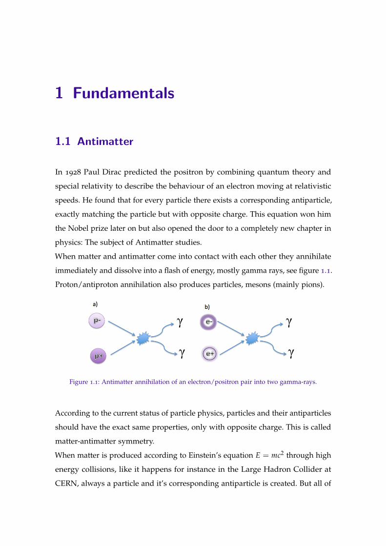
When matter and antimatter come into contact with each other they annihilate
immediately and dissolve into a flash of energy, mostly gamma rays, see figure 1.1.
Proton/antiproton annihilation also produces particles, mesons (mainly pions).
Figure 1.1: Antimatter annihilation of an electron/positron pair into two gamma-rays.
According to the current status of particle physics, particles and their antiparticles
should have the exact same properties, only with opposite charge. This is called
matter-antimatter symmetry.
When matter is produced according to Einstein’s equation E = mc2 through high
energy collisions, like it happens for instance in the Large Hadron Collider at
CERN, always a particle and it’s corresponding antiparticle is created. But all of

1.1 Antimatter Lisa Marx 2015
the above mentioned facts lead to the question of the whereabouts of antimatter
in our universe. If in the Big Bang the same amounts of matter and antimatter
were created, what happened to all the antimatter since then? There are several
possible answers to this question which are currently investigated. For instance,
regions of the universe where antimatter dominates are searched for at the
Alpha Magnetic Spectrometer (CERN) at the International Space Station and the
presence of an electric dipole moment in fundamental particles is studied at the
Advanced Cold Molecule Electron collaboration at Harvard. Another competing
hypothesis is the difference in the effect of gravitation on matter and antimatter
which is investigated at the AEgIS experiment at CERN. For historical reasons,
the matter-antimatter asymmetry in the Universe is called baryon asymmetry, the
production of the matter excess is called baryogenesis, see [5].
In cosmic rays, positrons and antiprotons have been observed. The biggest anti-
matter atom artificially produced so far is the antihelium atom, but more complex
antimatter was never observed until now.
Antimatter is hard to produce and even harder to keep since it has a very limited
lifetime and has to be kept in magnetic and electric traps to prevent it from
annihilating with the matter around it.
1.1.1 Positrons
The positron (positive electron) representing the antiparticle of the electron, is a
subatomic particle with positive charge and within experimental limits, with the
same mass and magnitude of charge as the electron. The positron was the first
of the antiparticles to be discovered by Carl David Anderson in cloud-chamber
studies of the composition of cosmic rays in 1932. The discovery of the positron
explained a theoretical aspect of electrons predicted by the Dirac wave equation
in 1928.
Even though positrons are stable in vacuum, they quickly react with the electrons
of ordinary matter by annihilation and production of gamma radiation.
4

1.1 Antimatter Lisa Marx 2015
The most common annihilation reaction is:
e+ + e− → 2γ (1.1)
If both, the annihilating electron and positron involved, are at rest, all resulting
gamma rays will be emitted with an energy of 511 keV, which corresponds to the
mass of the positron or electron at rest. [6]
Positron interactions in matter
A very important feature of positrons is that they are distinguishable from elec-
trons. It is not possible to follow the diffusion history of a particular electron
implanted in a target, since it disappears in the sea of identical electrons in the
solid. When following positrons on the other hand, each positron annihilation can
be detected. It is possible to measure the influence of different material properties,
such as impurities and defects and their distributions and spatial changes in
composition like layered structures.
Due to their positive charge, positrons are able to take part in many processes that
are not possible for electrons: They can be trapped in lattice defects with negative
charge, in open-volume defects and impurities. Also, the positron work function
provides a repulsive surface-dipole contribution to the electron work function
and is therefore negative for many materials. For this reason, the positrons are
emitted from the surfaces of these materials and end up in the vacuum, or are
trapped in large open volume defects.
Positrons are also able to bind an electron to form an exotic atom called Positron-
ium. This hydrogen like atom can not exist in metals, due to the large number of
electrons but it can exist inside of insulators and can be emitted from the surface
of any kind of material.
Due to the antimatter nature of the positron, different spectroscopy methods
have been developed which can not be achieved by using electrons. This methods
5

1.1 Antimatter Lisa Marx 2015
use the reemission of positrons from surfaces, the formation of positronium and
additionally the annihilation of positrons with electrons in different materials.
For the last point, the energy and angular distribution of the produced gamma
rays can be used to obtain information about the environment of the annihilated
positron. Also the annihilation rate indicates the structure of the probed material,
through investigating whether the positron can diffuse freely or is caught in a
defect or impurity. [7]
In graph 1.2 a schematic summary of the different interactions of positrons with
matter can be seen.
Figure 1.2: Possible positron interactions in matter
Relevant for this thesis are the annihilations from trapped states, where in large
defects there is a possibility of Positronium formation, which can either annihilate
inside the defect or in the case of open porosity it can propagate to the surface
and reach the vacuum. On the way to the surface the Ps-atoms lose energy
6

1.2 Positron Sources and Positron Moderation Lisa Marx 2015
through collisions with the pore walls. Also relevant are the diffusion processes,
where both thermalized and non-thermalized positrons can reach the surface
from which they are either emitted as positrons or, by binding an electron, as Ps.
[8]
1.2 Positron Sources and Positron Moderation
1.2.1 Sources
In general there are two different methods for positron production: Pair pro-
duction (for more information see [7]) and radioactive decay. The method used
during the work for this thesis is the production through radioactive decay:
Positrons are emitted in the positive beta decay of proton-rich/neutron-deficient
radioactive nuclei. Generating positrons through radioactive decay is more cost
efficient and more easily conducted than through the process of pair production.
For most long term experiments a 22Na source is used, as is done in the AEgIS
and Como positron experiments. 22Na offers an acceptable compromise between
cost per Bq and half-life (2.6 years). 58Co is used for experiments which need high
beam intensity over short periods of time. It has a half-life of 71 days and offers a
much higher activity for the same price as 22Na does. [9] The decays of certain
short-lived particles, like the positive muon are also positron sources. Positrons
produced from man-made radioactive sources are used in medical diagnosis for
a technique known as positron emission tomography (PET). [7]
1.2.2 Moderators
For experiments with slow positron beams, it is necessary to convert the fast e+
provided by the source at various energies into mono-energetic slow positrons.
This is executed through the use of moderators and discussed in this chapter.
7

1.2 Positron Sources and Positron Moderation Lisa Marx 2015
The work function of positrons in different materials holds valuable information
about the material itself and is due to its dependency on temperature and
intrinsic stress an interesting property to study. In order to extract a positron
from the surface of a material, an ionisation energy is necessary, where the
minimal required energy is given by the work function. Suitable materials for
positron moderation are typically (with the exception of rare gas solid moderators)
characterized by their negative positron work function Φ+ which is given in many
solids.[13]
Positron Moderation
Typically positrons with a kinetic energy of a few eV are required for optimal
transfer of e+ to the trap, see section 1.3. This is most commonly achieved by
using e+ moderators placed directly after the positron source.
The most commonly used moderator is made out of a thin tungsten foil (or other
metal foil made of single or polycrystalline materials 5) with a few µm thickness,
with as little defects as possible to keep the positrons from being trapped. To get
rid of contamination and defects in the moderator material, an in-situ annealing
procedure at high temperatures is necessary for most foils. [10] A moderation
efficiency of 3× 10⁻³ could be achieved with a single crystal moderator foil
made of W. [11] A single crystal tungsten foil in a (100) orientation is used in the
continuous positron beam of the VEPAS positron laboratory in Como.
A very high efficiency type of moderator is obtained by depositing a thin layer of
krypton or neon on a carrier foil at low temperatures. [12]. These rare gas solid
moderators have a small, positive work function, allowing only positrons with
a kinetic energy larger than the workfunction to be emitted from the surface.
Rare gas solid moderators show a slow thermalization process for e+, which
leads to a larger energy spread of emitted positrons when compared to metal
5Polycrystalline materials are substantially cheaper and easier to produce than single crystalmoderators. Since they contain grain boundaries and defects, a large quantity of the positrons aretrapped in the material and can not reach the surface.
8

1.3 Trapping and Cooling of Positrons Lisa Marx 2015
foil moderators. This is compensated by the much higher efficiency of solid gas
moderators. The very high efficiency of 10−2 has so far not been completely
explained but is suspected to be due to a drift caused by an internal electric field,
affecting the motion of the positrons.[13] For this type of moderator, a thin film
of gas is frozen onto the source holder and can be renewed by evaporating the
old layer and growing a new one. This process requires cryogenic appliances
and vacuum systems. [7] A solid neon moderator is used in the AEgIS positron
system at CERN.
Another possibility for future positron moderation is the use of a field assisted
moderator made of SiC, the only known semiconductor with a negative work
function. [14]
1.3 Trapping and Cooling of Positrons
Unlike for some experiments like the Doppler Broadening technique where a
relatively small number of positrons arriving on the target directly from the source
suffices, a much larger number of positrons is required for other experiments.
This can be achieved through using a stronger positron source, which is often
quite complicated, expensive and which only allows the increase to a certain
extend. Therefore, an accumulator is used between the source and target region,
which uses electric and magnetic fields to trap positrons. The basic principle is to
collect the positrons from the continuous source and to store them for a certain
time. Then all the collected positrons are released in a single positron dump.
Since the positron beam forms a none-neutral compressed plasma (with non zero
total charge) it can not be confined for an infinite time due to experimentally
caused asymmetries in the electric and magnetic field. Therefore, the plasma
expands radially and axially which has a negative influence on the positron
lifetime. This can be counteracted by the use of Penning traps and the Rotating
Wall technique.[15] These techniques don’t only enable compression but also
9

1.4 Positronium Lisa Marx 2015
cooling of the positron plasma. The trap used in the AEgIS-experiment is called a
Penning-Malmberg trap.
The rotating wall principle improves the positron lifetime significantly and re-
duces the dimensions of the positron cloud, though not all the mechanisms for
the rotating wall technique have been completely understood up to this point.
1.4 Positronium
Figure 1.3: Positronium-Atom: The bound state of a positron and an electron
Positronium (Ps) is the quasi-stable bound system of an electron and its antiparti-
cle the positron (e+) and forms a purely leptonic atom (exotic atom), see figure
1.3. It was discovered by Deutsch in 1951 and has since then been the subject of
many experimental and theoretical investigations.[16]
In vacuum and in its ground state (n=1), Ps can exist in two configurations,
depending on the spin orientation of the e+ and e−:
• Parapositronium (p-Ps) in the singlet state (total spin 0, formation proba-
bility 1/4). In vacuum p-Ps decays into 2 γ-rays with an energy of 511 keV
each and with a mean lifetime of 125 ps.
10
1.4 Positronium Lisa Marx 2015
• Orthopositronium (o-Ps) in the triplet state (total spin 1, formation probabil-
ity 3/4). O-Ps decays into 3 γ-rays with a total energy of 1022 keV, which is
randomly divided between the 3 photons and with a mean lifetime of 142
ns.
Ps can be created by implanting positrons with an energy of a few keV into
a particular solid target. [17] Due to its relatively long lifetime, o-Ps formed
in materials with a network of connected open-volume defects can diffuse for
hundreds of nanometers and eventually reach the surface where it can be emitted
into the vacuum. [18]
There are two distinctive processes for positronium formation: Bulk formation
and surface formation:
Ps Bulk Formation
In the case of Ps bulk formation in porous materials, the formation of Positronium
is energetically more favorable than for the positron to stay as a separate particle.
The formed Ps atom can annihilate or diffuse back to the surface and can be
emitted due to a negative work function.
The positronium formed in the bulk diffuses in the material and if not trapped in
voids or defects, can be emitted from the surface into the vacuum. [19]
Ps Surface Formation
When positrons leave the surface of a material they can bind to an electron and
be emitted into the vacuum as positronium with a relatively high energy of a few
eV.
Positronium formation in metals, semiconductor and insulators
The formation of Positronium depends on the target material and differs for
metals, semiconductors and insulators due to their different densities of free
electrons.
11

1.5 Detectors Lisa Marx 2015
For metals, no formation of Ps in the bulk is possible, due to their high density of
free electrons. This decreases the binding energy, to a level where Ps formation is
no longer possible. The free electrons in the metal screen the Coulomb attraction
between the positrons and any single electron. Due to a high number of surface
states in metals, the probability for surface formation of Ps is higher.
For insulators, positronium is mostly formed in the bulk by thermalised positrons
due to a low density of free electrons but this also lowers the cross section for
an interaction between the positron and electron. Due to a longer thermalization
time for positrons in insulators, a fraction of the positrons with sufficiently high
kinetic energy can reach the surface by diffusion and form positronium even
though there are only few surface states in which the Ps could form.
The Positronium conversion yield is especially high for SiO2 with 72% in the
bulk and 12% on the surface and may currently be the best known positron-
positronium converter. [19]
1.5 Detectors
The detection of positrons and positronium is achieved through the detection of
γ-rays, that are emitted during the annihilation process. In the AEgIS Positron
system, a variety of detectors were used in the course of this thesis, to measure
positron and positronium annihilations and to assess beam characteristics. There-
fore several photon detectors (scintillating material) coupled to photo multiplier
tubes or photo diodes were used, tested and compared. The spatial dimensions
of the beam spot were characterized with an MCP (Microchannel Plate) assembly.
In the VEPAS positron system a high-precision germanium detector was used for
the detection of γ-rays.
12

1.5 Detectors Lisa Marx 2015
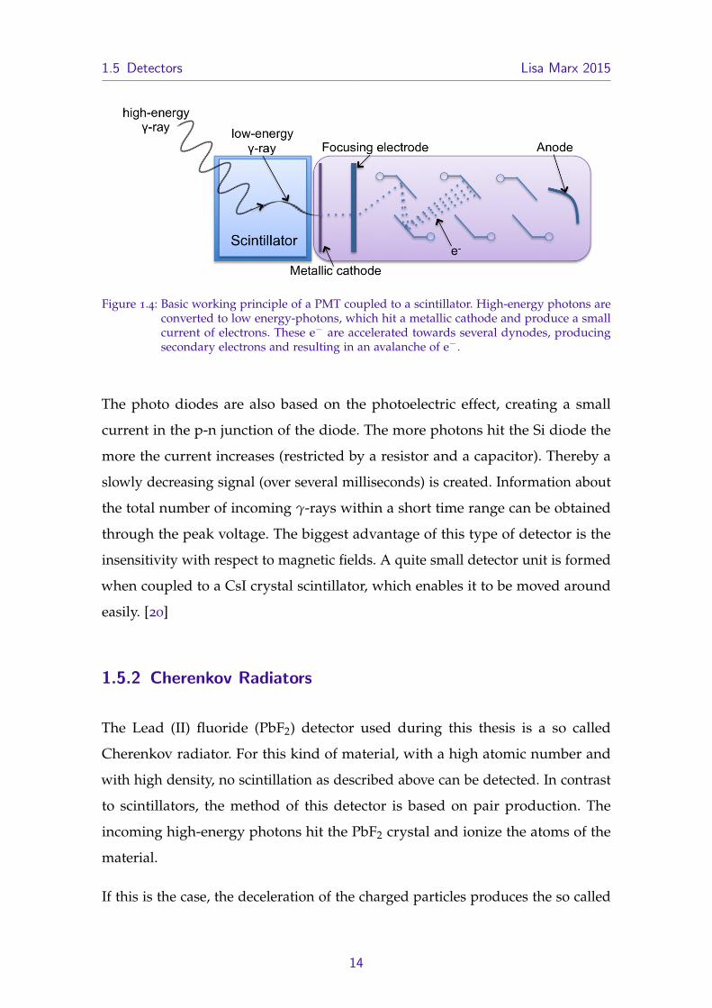
1.5.1 Plastic or Crystal Scintillators
These radiation detectors are made up of two main components: The radiation
converter and the detector. The converters are scintillating materials like a CsI
crystal or a plastic scintillator, both of which are used in the AEgIS positron
system. The electrons in the scintillator material are excited by the incoming
high-energy photons and reemit this surplus energy when returning to their
ground state in the form of low-energy photons (visible light). Depending on
the material the above described process can take a few nanoseconds to tens of
nanoseconds. Each incoming photon with enough energy is converted without
additional filters added. Therefore it is necessary to place the detector close to
the target with proper shielding to reduce the background noise and to perform
a calibration for absolute numbers.
Different crystals can be used and can generally be divided into two groups:
Inorganic (CsI, PbWO4) and organic (Plastic). The inorganic crystals have a
slower re-emission time than Plastic scintillators and are therefore slower but
offer a higher quantum efficiency, with nearly every incoming high-energy photon
producing many emitted low-energy photons. Some plastic scintillators show
delayed fluorescence, resulting in an afterglow of the measured signal and a
second component in the signal that is several tens of ns long. They show a low
efficiency due to their low material density, causing many gamma rays to go
through the detector without causing scintillation.
The converted low energy photons are then detected by a photo multiplier tube
(PMT) or photo diode. Their functional principle is based on the photoelectric
effect, transforming the incoming low-energy photons provided by the scintillator
into electrons inside of a metallic photo cathode. The electrons are then acceler-
ated by a high voltage towards several dynodes, producing secondary electrons
and thereby amplifying the signal. This process requires tens of nanoseconds,
producing a signal with a pulse width of a few ns. The produced voltage signal
is proportional to the energy and number of incoming photons, see figure 1.4.
13
1.5 Detectors Lisa Marx 2015
Figure 1.4: Basic working principle of a PMT coupled to a scintillator. High-energy photons areconverted to low energy-photons, which hit a metallic cathode and produce a smallcurrent of electrons. These e− are accelerated towards several dynodes, producingsecondary electrons and resulting in an avalanche of e−.
The photo diodes are also based on the photoelectric effect, creating a small
current in the p-n junction of the diode. The more photons hit the Si diode the
more the current increases (restricted by a resistor and a capacitor). Thereby a
slowly decreasing signal (over several milliseconds) is created. Information about
the total number of incoming γ-rays within a short time range can be obtained
through the peak voltage. The biggest advantage of this type of detector is the
insensitivity with respect to magnetic fields. A quite small detector unit is formed
when coupled to a CsI crystal scintillator, which enables it to be moved around
easily. [20]
1.5.2 Cherenkov Radiators
The Lead (II) fluoride (PbF2) detector used during this thesis is a so called
Cherenkov radiator. For this kind of material, with a high atomic number and
with high density, no scintillation as described above can be detected. In contrast
to scintillators, the method of this detector is based on pair production. The
incoming high-energy photons hit the PbF2 crystal and ionize the atoms of the
material.
If this is the case, the deceleration of the charged particles produces the so called
14

1.5 Detectors Lisa Marx 2015
Cherenkov light. The disadvantages of using these Cherenkov radiation based
detectors, is the requirement for high-energy photons as input. Nevertheless it
is possible to detect lower energy γ-rays, but the produced free electrons will
consequently also have lower energy and only little Cherenkov light will be
produced. Also the Cherenkov crystals exhibit a much lower quantum efficiency
as compared to scintillating materials, since only a few photons are emitted
for each incoming photon. In spite of this disadvantage the PbF2 crystal based
detector is still a suitable choice for positronium lifetime spectroscopy, see chapter
3.1. It offers an improved signal-to-noise ratio for the detection of positrons due to
the property of only detecting high-energy photons. Because Cherenkov light is
emitted instantaneously, they possess a very good temporal resolution. The PbF2
Cherenkov radiator is, just like the scintillators, coupled to a PMT to enhance the
low output. [21]
1.5.3 Multi-Channel Plate and Phosphor Screen
For beam characterization, a multi-channel plate (MCP) coupled to a phosphorous
screen can be used. The working principle of the MCP is similar to that of the
PMT, secondary e− are used for amplification.
It is made of angled channeltrons with a diameter of a few µm. This small
channels are placed side by side to form the MCP and are made of a material
with high resistivity, emitting secondary e− when hit by the positron annihilation
photons. By applying a high voltage, the electrons are accelerated toward the
end of the channels. Due to the angle of the channeltrons, the e− eventually
hit the walls of the channels, producing more secondary electrons, working as
an amplifier for the signal. The electrons are further accelerated towards onto
the phosphor screen, exciting the material and emitting light which can then be
imaged by a CCD-camera. [22]
15

1.6 Measuring methods of e+e−-annihilation Lisa Marx 2015
1.5.4 Semiconductor Detector
Like the above described photo diode, a semiconductor detector consists of a
semiconductor usually made of Silicon or Germanium to measure the incom-
ing photons of positron electron annihilation events. The high-energy photons
generate charge carriers inside of the detector material, producing electrons and
holes. An applied electric field accelerates electrons and holes to the electrodes,
creating a pulse that can be measured. A fixed energy is required to create an
electron-hole pair and does not depend on the energy of the incoming photons.
Therefore the signal is proportional to the number of incoming photons.
In this thesis a high-purity Germanium detector is used, cooled with liquid nitro-
gen. Intrinsic Germanium at these low temperatures has an empty conduction
band and consequently a high resistivity. When a photon hits the detector, a
number of e− proportional to the energy of the incoming photon is transported
to the valence band. These kind of detectors offer an excellent energy resolution
for γ-rays, superior to scintillators discussed above. [23]
1.6 Measuring methods of e+e−-annihilation
In order to observe positrons and positronium, different techniques are used,
based on detecting γ-rays produced through annihilation. The Single-Shot Positron
Lifetime Spectroscopy technique was used for the measurements at the AEgIS
positron system at CERN, the Doppler Broadening technique and positronium
spectroscopy were used at the VEPAS system in Como.
1.6.1 Positron annihilation lifetime spectroscopy
Positron annihilation lifetime spectroscopy (PALS) is the most commonly used
technique for the measurement of positrons inside of different materials, also pro-
16

1.6 Measuring methods of e+e−-annihilation Lisa Marx 2015
viding information about positronium formation. When a positron is implanted
into a material with a certain energy, it diffuses through the material, thermalizes
and eventually annihilates with an electron inside the sample. A photon with
an energy of about 511 keV is emitted. Single positrons are implanted into the
sample and the annihilation time is measured with respect to a start signal. This
is repeated until good statistical values are reached. Positron annihilations can be
distinguished from ortho-positronium annihilations due to the elongated lifetime
of the Ps-atoms. Usually, a gamma ray emitted simultaneously with the positron
by the radioactive source is used as a start signal. The lifetime can be calculated
based on this signal and the annihilation signal recorded by the detector. The
lifetime depends on the investigated material and is proportional to its electronic
density. The e+ can get trapped in open volumes, like vacancies or cavities, and
prolong the measured lifetime. The positron lifetime component increases with
the size of the free volume and the intensity is proportional to the concentration
of open volumes. [24]
1.6.2 PALS with pulsed e+ beam
PALS with a pulsed positron beam, quoted in the following as Single-Shot
Positron Lifetime Spectroscopy (SSPALS) is a similar technique as PALS discussed
above, but involving the simultaneous presence of many positrons in the target,
which is achieved through a pulsed positron beam. As a consequence it offers a
much shorter collection time and is more suitable for depth profiling. Moreover
it offers the possibility to study the simultaneous production of many Ps atoms,
their interaction and their laser excitation. A disadvantage is the typically worse
time resolution and the more complex experimental setup which is necessary to
produce positron pulses and dump them with very accurate timing. For SSPALS
a large bunch of positrons hits the target at the same time, with the dump of the
positron cloud acting as the start signal. Like the PALS method, SSPALS offers
the possibility to measure in different depths of the sample and study defects in
different layers.
17

1.6 Measuring methods of e+e−-annihilation Lisa Marx 2015
1.6.3 Doppler Broadening Spectroscopy
The Doppler Broadening Method is based on the detection of annihilation gamma
rays and calculating the momentum of the electrons from the energy distribution
of these photons, see figure 1.5. The momentum offers information about the
electronic structure of the sample and the embedded defects of the material.
Doppler Broadening spectroscopy can be performed with the sample placed
directly in front of a radioactive source or, as was done for the measurements
of this thesis, by using a continuous slow positron beam. When a positron
annihilates with an electron of the material, a Doppler shift of the emitted
photon can be measured due to the momentum of the electron involved in the
annihilation process. The momentum of the positron can be neglected due to the
thermalization process it experienced before the annihilation.
Figure 1.5: Schematic representation of an annihilation event of a e+ and an e−, giving rise to two511 keV photons in two opposite directions.The recorded signal is Doppler-sensitiveto the longitudinal momentum of the electron, the momentum of the thermalizedpositron can be neglected. The annihilation energy of 511 keV gets Doppler shiftedby an amount E. Since many annihilation events are measured, the energy line isbroadened due to the different Doppler shifts along the annihilation direction.
For the non-relativistic consideration the energy shift amounts to:
∆E =c2
pL (1.2)
pL . . . Longitudinal component of the electron momentum
c . . . speed of light
The energy peak of the annihilated γ-rays is broadened around 511 keV due
to the different momenta of the electrons inside the material, with which the
positrons annihilate. Low momentum electrons (valence electrons) produce a
18
1.6 Measuring methods of e+e−-annihilation Lisa Marx 2015
small energy shift, high momentum electrons (core electrons) produce a large
energy shift.
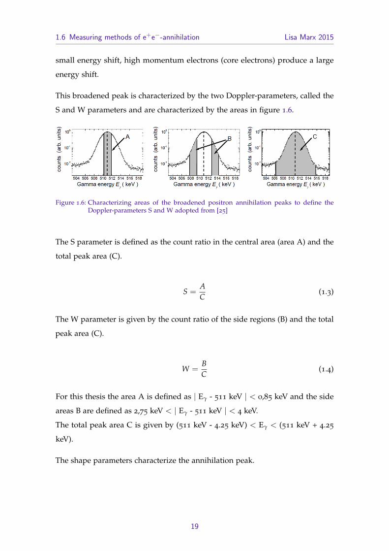
This broadened peak is characterized by the two Doppler-parameters, called the
S and W parameters and are characterized by the areas in figure 1.6.
Figure 1.6: Characterizing areas of the broadened positron annihilation peaks to define theDoppler-parameters S and W adopted from [25]
The S parameter is defined as the count ratio in the central area (area A) and the
total peak area (C).
S =AC
(1.3)
The W parameter is given by the count ratio of the side regions (B) and the total
peak area (C).
W =BC
(1.4)
For this thesis the area A is defined as | Eγ - 511 keV | < 0,85 keV and the side
areas B are defined as 2,75 keV < | Eγ - 511 keV | < 4 keV.
The total peak area C is given by (511 keV - 4.25 keV) < Eγ < (511 keV + 4.25
keV).
The shape parameters characterize the annihilation peak.
19
1.6 Measuring methods of e+e−-annihilation Lisa Marx 2015
For a narrow annihilation peak, a high value of the S parameter is obtained.
In this case positrons annihilate with low momentum electrons (valence e−).
In open-volume defects there are more valence electrons than core electrons,
annihilations of positrons trapped in these defects lead to a high value of the
S parameter, then in materials with no defects. For a broad annihilation peak,
a high value of the W parameter is obtained, the positrons annihilate mainly
with high momentum electrons (core e−). The sensitivity to open-volume defects
makes Doppler Broadening spectroscopy a suitable tool to study defects in
different materials and at varying depths of the material by changing the positron
implantation energy. This enables the production of defect depth profiles of the
investigated sample.[25] The advantage of Doppler broadening spectroscopy is
that only the annihilation γ ray has to be measured, the measurement of a start
signal is not necessary, therefore the method is faster.
The physical information contained in the parameter S(E) is obtained via fit pro-
grams. It uses the experimental values of the S parameter at the different positron
implantation energies. The program used in this thesis is called VEPFIT.[26] It is
based on the numeric resolution of the stationary diffusion equation and allows
to evaluate the different properties of the investigated sample, like different
materials, porous structures etc. The positron diffusion length can be determined
as well as information on the inner boundaries.
1.6.4 Ortho-Positronium Spectroscopy
Ortho-Positronium Spectroscopy offers information about the average size and
distribution of pores and their connectivity to the vacuum. For this technique the
annihilations between an electron and a positron forming positronium are used.
When o-Ps is formed, the annihilation process occurs into 3 γ-rays as opposed to
2 γ-rays for para-positronium formation. The emitted photons involved in the
annihilation of o-Ps have an energy between 0 - 511 kV and result in an energy
distribution illustrated in figure 1.7.
20

1.6 Measuring methods of e+e−-annihilation Lisa Marx 2015
Figure 1.7: Positronium annihilation spectrum: Valley area containing 3 γ annihilations (AV) andpeak area containing 2 γ annihilations (AP), for the definition of the R parameteradopted from [27]
It consists of a valley area (AV) and a peak area (AP), their ratio gives the so
called R parameter.
R =AV
AP(1.5)
For this thesis, the valley area was defined between an energy of 350 keV < Eγ <
500 keV and the peak area at an energy of (511 keV - 4.25 keV) < Eγ < (511 keV +
4.25 keV)
It is not easy to determine the total o-Ps yield, since both pick-off 2γ annihilation
of o-Ps and annihilation of p-Ps can contribute to the 511 keV peak. Pick-off
annihilation is a process where the positron bound in the positronium atom,
doesn’t annihilate with the bound electron with parallel spin, but annihilates
with an other electron of the material with anti-parallel spin. The Ps atom then
annihilates into 2 γ-rays instead of three and contributes to the peak area instead
of the valley area, with a lifetime reduced to para-Ps lifetime compared to ns for
3 γ annihilation. Only upon escaping of the Ps atom from the surface, there is no
possibility for pick-off annihilation and all o-Ps atoms annihilate into 3 γ-rays.
21

1.7 Laser excitation Lisa Marx 2015
Therefore, on the surface the total o-Ps fraction F3γ can be calculated without
losses from pick-off annihilation, see chapter 3.3.2.
1.7 Laser excitation
To prolong the lifetime for anithydrogen production, the positronium atoms are
excited to Rydberg levels. Rydberg states are electronically excited states with a
quantum number of n>10 and can be compared to the excited states of hydrogen
atoms, replacing the proton of the hydrogen core with a positron. The excited
stages are reached with the help of a short laser pulse in the order of ns, exciting
the produced Ps atoms at emission into the vacuum.
The required energy to excite Ps atoms to Rydberg levels from the ground state is
approximately 6.7 eV. With the current technologies it is not possible to directly
excite Ps from the ground state to Rydberg states, since a UV laser with a
wavelength of about 180 nm would be needed. Instead it is achieved in two steps,
exciting positronium with two laser pulses with different wavelengths.
The produced Ps-atoms are therefore excited to lower excited states (n=2 or n=3)
by a UV laser and then excited further to Rydberg states by an IR laser. The Ps
Rydberg excitation has been achieved by Cassidy and co. [28], the transition over
the n=3 state was first achieved by the AEgIS collaboration during the time of
this thesis and was submitted to be published in October 2015. [29]
The excitation process is achieved by means of absorption of incoming photons
of the UV laser beam, by the o-Ps atoms.
o− Ps + γUV → o− Ps∗ (1.6)
22
2 Experimental Setup
This chapter discusses the experimental setups of the facilities used for the
measurements conducted during this thesis.The experimental work took place
at the AEgIS experiment and at the slow positron beam of the VEPAS group in
Como/Italy. Described are the individual elements and different modules for e+
and Ps experiments and the surrounding apparatus.
2.1 CERN and the AEgIS-Experiment
The AEgIS collaboration was founded in 2007 and is the successor of an earlier
antimatter experiment called ATHENA, whose goal was the production of anti-
hydrogen. The main objective of the AEgIS experiment is the direct measurement
of the effect of the earths gravitational acceleration on antimatter, more precisely
on antihydrogen. Currently the experiment is working on the production of
antihydrogen and is still in the starting phase of its discoveries. The AEgIS collab-
oration is divided into small groups focusing on different parts of the experiment
and all combining their expertise when the experiment is running. It is located
at the CERN facilities in Geneva/Switzerland, in the Antiproton-Decelerator-
Hall, where AEgIS and other antimatter experiments receive antiprotons from
the antiproton-decelerator ring. The AEgIS-Experimental-Setup consists of three
main parts:
• The main magnets region with the purpose of antihydrogen production and
gravitational measurements.
• The Positron system, with the purpose of providing a positron beam to an
experimental chamber or to the main magnets region.

2.1 CERN and the AEgIS-Experiment Lisa Marx 2015
• The laser system for Rydberg excitation of positronium delivering laser
pulses to the main magnets region and the positron system.
2.1.1 Production of antihydrogen
The concept for the measurement of the effect of the earths gravitational accelera-
tion on antihydrogen is outlined in figure 2.1.
Figure 2.1: Outline of the basic principle for the measurement of the effect of gravity on antihy-drogen at the AEgIS experiment. A e+ bunch is directed onto a e+/Ps converter, theformed positronium is excited to Rydberg states through a 2-step laser system. ThePs∗ atoms and antiprotons are combined to form H∗ and formed into an H∗ beam.[30]
The first step is the production of positronium by injecting positrons into the main
magnets region and guiding them onto a special porous Silicon target where they
form positronium.
The Ps-atoms are then excited to Rydberg states by a laser system and combined
with the antiprotons from the antimatter decelerator. Thereby excited anithydro-
gen atoms are formed through charge-exchange reactions between the p and
Rydberg-excited Ps and can then be accelerated through an electric field via
24
2.1 CERN and the AEgIS-Experiment Lisa Marx 2015
Stark acceleration. An H beam is obtained, which finally passes through a moire
deflectometer to measure the effect of gravity on the antihydrogen atoms by
measuring their vertical displacement after the pass-through.
This deflectometer is made up of successive gratings, followed by a detector
sensitive to the position of the H (e.g. pixel detectors).
Because the diameter of the apertures of the gratings exceed the de Broglie wave-
length of the antihydrogen atoms, an interference pattern is formed by the atoms
crossing through the gratings. [30]
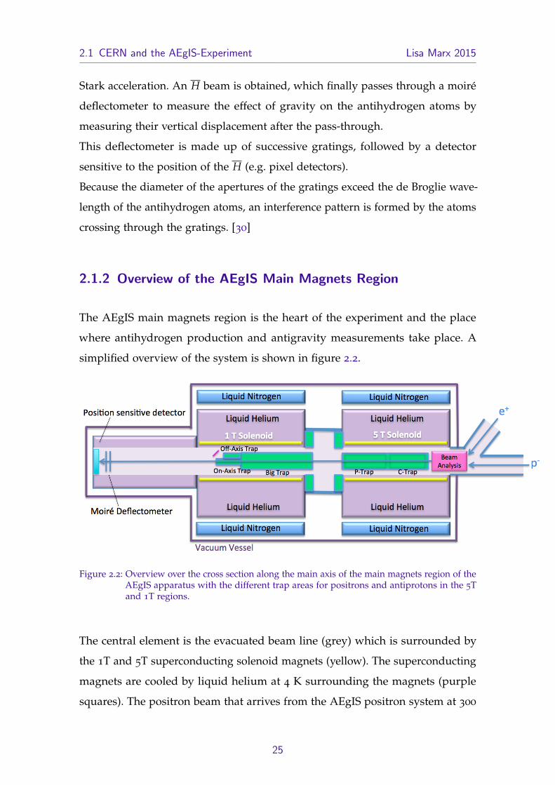
2.1.2 Overview of the AEgIS Main Magnets Region
The AEgIS main magnets region is the heart of the experiment and the place
where antihydrogen production and antigravity measurements take place. A
simplified overview of the system is shown in figure 2.2.
Figure 2.2: Overview over the cross section along the main axis of the main magnets region of theAEgIS apparatus with the different trap areas for positrons and antiprotons in the 5Tand 1T regions.
The central element is the evacuated beam line (grey) which is surrounded by
the 1T and 5T superconducting solenoid magnets (yellow). The superconducting
magnets are cooled by liquid helium at 4 K surrounding the magnets (purple
squares). The positron beam that arrives from the AEgIS positron system at 300
25

2.2 The AEgIS-Positron system Lisa Marx 2015
eV and the antiprotons arriving from the AD-Hall at 5 MeV enter the system and
pass on into the 5T magnet used for catching and accumulating antiprotons and
positrons. Since much lower magnetic fields are desired for particle manipulation
and for the gravity measurement, antiprotons and e+ are then transported into
the 1T trap where they are compressed longitudinally and radially.
A positronium target is mounted at the end of the Off-Axis trap (pink) towards
which the positron cloud will be accelerated to create Ps and be excited by a laser
system to Rydberg states. In the final area, a moire deflectometer [31] will be
installed in the near future coupled with a position sensitive detector to measure
the vertical displacement of antihydrogen.[32]
2.2 The AEgIS-Positron system
The AEgIS positron system is the main focus of this thesis and will be discussed
in detail in this chapter. The different components of the system will be described,
as well as their operational principles, a basic overview is shown in figure 2.3.
Figure 2.3: Schematic of the basic components of the AEgIS positron system and their arrange-ment. Detailed descriptions of the individual components can be found below.
26

2.2 The AEgIS-Positron system Lisa Marx 2015
2.2.1 System Overview
High vacuum conditions are necessary to be upheld inside the whole system,
which is achieved through the use of a sequence of vacuum pumps (roughing,
cryogenic and ion pumps). The different sections of the system are connected
through pneumatic valves and can be separated when turning it off.
The positron system can roughly be divided into four parts:
• Source
• Accumulator
• Buncher
• Experimental chamber (Ps test chamber)
For antihydrogen production the positrons are transported to the main magnets
region located downstairs, but the Ps test chamber was installed above the main
system for additional measurements like the test of positronium targets and
laser excitation in a potentially zero magnetic field environment. To transport
positrons, electric and magnetic fields are used. To avoid overheating, all coils
are water-cooled. To guide the e+ into the main magnets region, an angle shaped
solenoid is used to bend the positron beam. Prior to the entrance of the Ps test
chamber the guiding system is switched from magnetic to electric to enable a zero
magnetic field environment in the experimental chamber. Each element in figure
2.4, starting from the source on the right to the positron/positronium converter
on the left will be described in detail below.
27

2.2 The AEgIS-Positron system Lisa Marx 2015
Figure 2.4: Overview over the the AEgIS positron system and its main components
28

2.2 The AEgIS-Positron system Lisa Marx 2015
2.2.2 22Na Source and Solid Neon Moderator
Since positrons are very light particles, they are sensitive to outer magnetic fields
along the positron transfer line, especially around the source area. Therefore
the magnetic field along the AEgIS positron system was measured at 4 different
points and as a consequence µ-metal shielding was installed. This was done by
the author during the time of this master thesis in the group of S.Mariazzi.
The positron source used at AEgIS is a 22Na source. With a half-lifetime of 2.6
years for 22Na and an initial activity of 21 mCi in 2011 the current activity level
can be calculated to approximately 10 mCi or 370 MBq. In 89% of all decay events
positrons are emitted, which amounts to approximately 3.3 ∗ 108 e+ emitted per
second. The complete source system was produced by First Point Scientific Inc.,
except for the 22Na itself which was provided by a South African company called
iThemba.
The β decay process is described as follows:
22Na −→ 22Ne + e+ + γ (2.1)
The sodium source is embedded in walls made of tantalum, which due to its high
atomic number is well suited, as it reflects the e+. As a result of this setup, the
positrons that form the beam are only the ones emitted towards the moderator
or the ones that are backscattered in this direction. The complete source area is
located inside of a lead shield for radiation protection, see figure 2.5.
The source is located in the vertex of a copper cup where a solid neon moderator
is deposited. During this procedure the pressure in the source area is at 10−9 mbar,
at which the neon gas solidifies at a temperature of 10 K. The moderator efficiency
given by the manufacturing company First Point Scientific Inc. lies at 2, 5 · 10−3.
Only a small fraction of positrons emitted towards the trap are moderated, due to
the wide band gap of the neon moderator. Therefore a tungsten block is installed
29

2.2 The AEgIS-Positron system Lisa Marx 2015
Figure 2.5: Layout of the e+ source of the AEgIS positron system. The sodium is mounted ontantalum coated titanium holder. It is positioned inside an elkonite rod, which iselectrically isolated by a sapphire washer and can be cooled down to approximately7K. [33]
between the source and the trap that closes off the beamline. Two coils with
opposite polarity produce a magnetic field to guide the positrons in the right
energy range around the tungsten obstacle. Through this method the e+ with
the wrong energies can be filtered out and the tungsten block also functions
as a shield for gamma radiation coming from the source. The growing of a
new moderator is automated and controlled through a LabVIEW program. This
process takes approximately 40 minutes and is outlined below: The coldhead is
switched off and the temperature increased to 25 K evaporating the solid neon
layer on the copper cup, the excessive gas is exhausted via a roughing pump. The
chamber is cooled down to 8.8K and new neon gas is injected. Due to the low
temperatures it solidifies on the surface of the source. After an annealing time at
9.3K for 15 minutes for the removal of defects, the coldhead reaches 7K again.
Because of the characteristics of the moderator the positron system is not used
directly after growing a new moderator, to ensure a stable number of positrons
for experiments continuing over several hours.
In the past the AEgIS experimental zone has proven to be a strongly magnetic
environment both through AEgIS internal magnetic fields, and fields from the
surrounding experiments. Since positrons are very sensitive and easily influenced,
30
2.2 The AEgIS-Positron system Lisa Marx 2015
shielding of the system, especially the source area, was necessary to obtain stable
beam conditions throughout the measurements. Below the source a strong dipole
magnet is located, stearing the antiprotons from the AD into the AEgIS main
magnets region. When this magnet is turned on, severe positron losses were
recorded. Therefore, during this thesis, extensive measurements of the magnetic
environment of the AEgIS experimental zone were conducted. Subsequently
a µ-metal shield was installed around the entire source area and the saddle
coil, which has also proven to be sensitive to changes in the magnetic field. CsI
detectors were installed along the beam line to be able to quickly locate the area
along the beamline where the positrons are lost.
2.2.3 Positron Trap
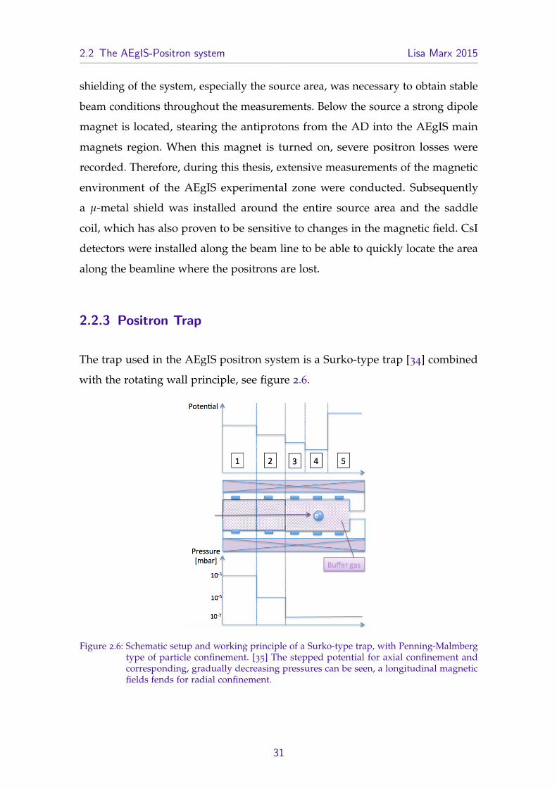
The trap used in the AEgIS positron system is a Surko-type trap [34] combined
with the rotating wall principle, see figure 2.6.
Figure 2.6: Schematic setup and working principle of a Surko-type trap, with Penning-Malmbergtype of particle confinement. [35] The stepped potential for axial confinement andcorresponding, gradually decreasing pressures can be seen, a longitudinal magneticfields fends for radial confinement.
31

2.2 The AEgIS-Positron system Lisa Marx 2015
In the trap the e+ arriving in a continuous positron beam from the source are
collected and formed into an e+ pulse. The trap is kept at a pressure of 10−10
mbar of and at 10−4 mbar during working mode, by the combination of a cryo
and roughing pump. The enhanced pressure during operation arises from the
buffer gas injection of 0.5 sccm/min of nitrogen and 0.03 sccm/min of carbon
dioxide. Inside the trap a confining magnetic field of 0.07 T is used. Storage is
achieved through six electrodes setting the step potentials and is modified in 3
stages with a reaction time in the order of 100 µs.
Figure 2.7: Outline of the positron storage process in the trap. The e+ arrive from the source onthe left and enter the trap in the filling stage. They loose energy through the buffergas and are stopped by the Gate electrode (G). In the storage stage the e+ are trappedbetween 2
nd and Gate electrode. In the dump stage e+ are released into the directionof the accumulator.
The whole process takes 0.15 s and forms one positron pulse which is then
transported to the accumulator. In the first stage e+ enter the trap area, the inlet
electrode (I) is set to a low potential to allow an easy entry of positrons from the
source. Through inelastic collisions with the atoms of the buffer gas, they quickly
lose energy and are stopped by the gate electrode (G) which is set at a high
potential. Depending on their energy the e+ are trapped between the 2nd and 3rd
electrode. In the 2nd stage the potentials of these two electrodes are increased,
creating a trapped positron pulse between the 2nd and gate electrode. In the
3rd and last stage the gate potential is lowered quickly, releasing the positrons
into the direction of the accumulator. The transfer is done via magnetic transport
32

2.2 The AEgIS-Positron system Lisa Marx 2015
and achieved through a pair of coils and a permanent magnet to correct small
misalignments.
2.2.4 Accumulator
From the trap the positrons are guided into another Surko-type trap combined
with a rotating wall called the accumulator, with 6,5 e+ pulses per second
containing some 104 positrons, depending on the source intensity (declared by
First Point Scientific Inc. and can be calculated from the positrons exiting the trap
and considering the losses during the trapping process). In the accumulator the
positron pulses from the trap are collected and compressed. The e+ pulses can be
released, when needed. Instead of a stepped potential, the 21 electrodes of the
accumulator form a harmonic potential well which leads to efficient cooling of
the positrons. As the cooling process takes place, the size of e+ cloud is decreased
longitudinally. Every 0.15 s a new positron pulse is added and up to several
hundred positron pulses can be collected this way, offering a high number of
accumulated e+. The process of accumulating positrons is outlined in figure 2.8
and is done in 3 stages:
Figure 2.8: Outline of the positron storage process in the accumulator. In the Inlet (filling) stagee+ pulses are arriving from the trap, in the accumulation (storage) stage the positronsare stored cooled and compressed and in the dumping stage they are released into thetransferline in the direction of the Ps test chamber.
33

2.2 The AEgIS-Positron system Lisa Marx 2015
In the Inlet stage the positrons are admitted into the accumulator by lowering
the inlet potential for every arriving pulse. In the Accumulation stage the e+
are trapped in the harmonic potential and cooled through collisions with buffer
gas atoms. The cooling efficiency is dependent on the number of positrons and
decreases with the number of pulses accumulated. The number of positrons
increases with the storage time, it is limited by the positron lifetime inside the
accumulator. The last stage is the Dumping stage which is triggered by a signal to
release the accumulated positrons from the accumulator into the transfer line.
After being dumped from the accumulator the positrons are transported via mag-
netic and electrostatic transport to the main magnets region or to the experimental
chamber.
2.2.5 Buncher
The installation and implementation of the buncher was done by the author
during the time of this thesis in the group of S. Mariazzi. As a part of the
electrostatic transport a buncher has been installed to reduce the time spread of
the positron bunch and accelerate them further towards the main magnets region.
This bunching method previously has been used in other positron systems [36]
and has shown a notable compression of the positron beam. The buncher of
the AEgIS positron system is shielded by a µ-metal electrode, that marks the
transition between magnetic and electrostatic transport (figure 2.9).
A parabolic potential between the first and last electrode is used to accelerate
positrons arriving later (end of the cloud) more strongly than the ones arriving
early (closer to the Ps test chamber), which reduces the time spread of the bunch.
After the positrons pass through the buncher they reach the experimental cham-
ber, where they are guided onto a a positron/positronium converter. The basic
setup of the Ps test chamber can be seen in figure 2.9.
The positronium target is mounted on an actuator which is positioned perpen-
dicular to the beam line (perpendicular to the drawing plane at the position of
34

2.2 The AEgIS-Positron system Lisa Marx 2015
Figure 2.9: Outline of the buncher installed in the AEgIS positron system. The buncher is embed-ded into the positron transferline ending in the experimental chamber. The transportchanges from magnetic to electrostatic at the µ metal coil after which the positronsenter the buncher from the left of the graph. They are accelerated and compressedand are guided into the Ps test chamber where they hit the positronium target.
the target). Up to three different samples can be fixed to it and the actuator can
be removed from the beam line, for measurements with the MCP in the back of
the chamber. Additionally the actuator can be positioned so that the e+ hit the
sample holder made of aluminium for background measurements.
Above the target a photon detector is placed for positron measurements, a
viewport on the side of the experiment was installed for laser excitation of the
produced positronium atoms.
The coils installed around the experiment produce a magnetic field inside of the
main magnets region ranging between 2-300 Gauss for measurements in different
magnetic environments.
2.2.6 Detection of Positrons/Positronium and System
Calibrations
Several different detectors and detection methods are used inside the positron
system to monitor the beam along the beam line and the experiments inside the
Ps test chamber. In this chapter the function and position of these detectors are
described. The different detectors of the Ps test chamber were installed and tested
35

2.2 The AEgIS-Positron system Lisa Marx 2015
by the author of this thesis in the group of S. Mariazzi.
Positron detection along the transferline
To monitor the beam along the beam line, two CsI photon converters coupled to
a PMT are placed above the saddle coil (between the source and the trap) and
behind the trap, see figure 2.3. These fast detectors permit to optimize the settings
of the system between these two points by closing a vacuum valve after the trap
and measuring the positron annihilations. The positron transfer is optimized with
the lowest possible positron annihilation signal at the saddle coil and highest
annihilation signal around the trap. Two CsI converters coupled to photodiodes
are used for analysis of the bunched positron beam after the accumulator. The
advantage of the photodiodes is that they are not sensitive to magnetic fields and
their amplitude is proportional to the number of positrons contained in the dump
but they are slower compared to the CsI-PMT couplings. The CsI-Photodiode
couplings can be moved along the outer surface of the equipment due to their
small size.
Positron/Positronium Detection in the Test Chamber
Other types of scintillators are also coupled to a PMT and installed above the ex-
perimental chamber in a cylindrical inlet about 3 cm from the target to maximize
the solid angle, see figure 2.9. This setup is used to detect positron annihilations
inside the experimental chamber and obtain life time spectra via SSPALS for
positronium detection.
Different photon converters namely a Pilot U plastic scintillator (Height: 38 mm,
diameter: 25 mm) and a crystal scintillator (Height: 20 mm, square base: 25 mm)
made of PbWO4 have been tested subsequently. A more detailed description of
the detectors is given in chapter 1.5. Shielding is necessary for these scintillators,
36

2.2 The AEgIS-Positron system Lisa Marx 2015
since they detect photons at a range of different energies including stray photons
from the experiment and cosmic radiation.
A PbF2 Cherenkov radiator (Height: 60 mm, diameter: 20 mm) has also been
used for a part of the measurements. The photon converters are coupled to a
PMT H3378 and R11265-100 by Hamamatsu. The signal coming from the PMT is
divided by a beam splitter (50 Ohm Mini-Circuits ZFRSC-2050B+) and sent to
an oscilloscope (Tektronix TDS5054B, bandwidth: 500 MHz, resistance: 50 Ohm)
[37]. The first channel with a gain of 1 V/div (vertical scale) is used to acquire the
initial high-intensity signal peak of the annihilating e+, the second channel with
a gain of 100 mV/div records the low-intensity signal after the peak to reduce
noise levels. The data acquired from the oscilloscope is automatically transferred
to a computer and the two signals are combined to form SSPALS spectra.
A multi-channel plate (MCP) coupled to a phosphor screen is placed behind
the target in order to characterize the e+ beam and to obtain information about
the geometry and intensity of the positron bunch reaching the MCP. The light
emitted by the phosphor screen is imaged by a Hamamatsu ORCA-R2 digital
CCD camera, model C10600-10B installed outside of the main magnets region
behind the screen.
Calibration of the positron system
Both the CsI-Photodiode and CsI-PMT detectors have been calibrated to correlate
the output signal to the number of annihilating positrons.
Calibration of the CsI-PMT: The first calibration has been done during the
construction of the e+ line and is necessary not only to receive a relative signal
but to obtain the total number of positrons from the signal amplitude. The CsI-
PMT was calibrated with a 22Na source, that is not part of the AEgIS experiment.
The total number of positrons emitted from the source was estimated and the
detector was placed at a defined distance and solid angle from the source. The
37

2.2 The AEgIS-Positron system Lisa Marx 2015
obtained signal then corresponds to the number of positrons estimated for this
specific distance and angle. The calibration was confirmed using a 133Cs source
and the same experimental method as described above.
Determination of transport and trapping efficiency: Later, the AEgIS 22Na
positron source was used with an activity of 21 mCi at the time of the cali-
bration. The calibrated CsI-PMT was placed along the positron beam line before
the trap in a specific distance behind a phosphor screen installed specifically
for this purpose, see figure 2.9. All electrodes inside the trap were switched off
and no buffer gas was injected, the positrons arriving from the trap are forced
to annihilate on the screen. With the known number of positrons emitted from
the source, the transport efficiency for positrons is calculated to ∼ 3· 10−3, which
implies nearly perfect positron transport when compared to the moderator ef-
ficiency, see chapter 2.2.2. Since the number of positrons arriving at the trap
was known (2.3·106 e+/s), the phosphorus screen was also calibrated and the
correspondence between intensity of luminescence and number of positrons
was obtained. The trapping efficiency was determined to 14% compared to 17%
declared by the manufacturer First Point Scientific, then determined using the
calibrated phosphor screen.
Calibration of the CsI-Photodiodes and determination of accumulator effi-
ciency: The CsI photodiodes were also calibrated using this setup and were
placed in certain distance from the phosphor screen before the target and at a
specified solid angle, see figure 2.9 .
The accumulator efficiency was obtained through a calibrated CsI-photodiode
with the same solid angle used for the calibration mentioned above placing it
before and after the accumulator for comparison. No significant losses could be
measured which suggests high efficiency of the accumulator. When 1000 pulses
are accumulated with 1.1 ∗ 104 positrons per pulse, 1.1 ∗ 107 positrons can be
expected at the exit of the accumulator which is supported by experimental
results. Losses are negligible small, because very few annihilations with residual
38

2.2 The AEgIS-Positron system Lisa Marx 2015
gas atoms and the walls are expected due to the structure of the accumulator.
The number of detected positrons is linear, for a doubled number of e+, a signal
of double height will be obtained, up to the level where the lifetime of positrons
in the accumulator starts to saturate the curve, see figure 2.10.
Figure 2.10: Signal amplitude over the number of pulses collected in the accumulator. The linearbehavior of the detector is shown, for a doubled number of positrons a doubled signalis obtained. The saturation starting at around 2000 pulses suggests a misalignment ofthe accumulator. Due to this misalignment no optimal compression of the positronbunch can be achieved and from a certain number of e+, annihilations with the wallsof the accumulator occur.
The read out of the CsI detectors can be achieved directly over LabVIEW programs
controlling the system. This offers an overview of positron annihilations along the
entire positron system by moving the CsI detectors. 5 more of these detectors have
been ordered to be installed along the experiment to provide instant access to
information about positron losses at all relevant points of the system. The positron
dump from the accumulator is also controlled through a LabVIEW program,
which additionally offers an overview of all vacuum pump states, pressures
and temperatures. If any of the monitored values deviates from its normal state,
a warning appears inside of the program and an error message is sent to the
users.
39

2.3 The AEgIS Laser System Lisa Marx 2015
2.3 The AEgIS Laser System
For antihydrogen production in the AEgIS experiment positronium atoms and
antiprotons will be combined.
Ps∗ + p −→ H∗ + e− (2.2)
Unlike in other similar experiments producing antihydrogen, the AEgIS experi-
ment plans to use this method instead of simply mixing positrons and antiprotons.
Working with positronium offers advantages over using isolated positrons: The
positronium atoms can be excited to Rydberg levels, which permits the pro-
duction of Rydberg excited anithydrogen atoms. Due to the dependence of the
positronium lifetime on the quantum number n, proportional to n3, the lifetime of
Ps can be significantly increased through the laser excitation. Positronium atoms
in Rydberg states also exhibit a large cross section for antihydrogen production
with antiprotons in the order of 10−8 cm2, because the cross section is expected
to be proportional to n4. [2] A further advantage is the possibility to produce
very cold antihydrogen atoms in the order of 25-80 m/s, since less energy is
introduced by mixing antiprotons with the neutral positronium atoms. Moreover,
from antihydrogen produced in a Rydberg state, antihydrogen beams can be
generated by using electric field gradients in the main magnets region.
The Rydberg excitation described in chapter 1.7 has so far been successfully
tested in the main magnets region and is carried out in two essential steps: In the
first step the Ps-atoms are excited into the n=3 state and in the second further
to Rydberg states of n>20. The transition energy from the groundstate to the
Rydberg state is greater than 6 eV. This high transition energy requires a two step
laser excitation, since lasers with an energy of more than 6 eV do not exist yet.
The Ps excitation to Rydberg levels was previously achieved by other experiments
through exciting to the n=2 state and then to n>20, but the excitation through
the n=3 level has never been performed so far. The excitation beyond over n=3
40

2.3 The AEgIS Laser System Lisa Marx 2015
requires less power, therefore Rydberg excitation is favoured over ionization of the
Ps atoms. When positronium is ionized the electron and positron are separated
and the e+ quickly annihilates. With the n=3 transition, ionization and the fast
decay of the n=2 level is avoided.
For Ps excitation to the n=3 state a wavelength of 205 nm is needed, to further
excite to Rydberg levels a wavelength of approximately 1670 nm is required
depending on the number of the Rydberg level. This is achieved through two
separate laser pulses, starting with a UV-laser pulse tunable between 204 and 206
nm with a pulse time length of 1.5 ns, a bandwidth of 150 GHz and an energy
of 60 µJ. The second laser pulse, an IR-laser pulse with a length of 4 ns and an
energy up to 55 mJ, excites the Ps atoms from n=3 to Rydberg levels. A scheme
of the laser excitation process can be seen in figure 2.11. Both laser pulses are
created by a Q-switched Nd:Yag laser.
The laser pulses are superimposed in space and time and transported to the
experimental chamber by the same optical system. A separate transport system is
implemented for transport to the main magnets region. A paper about Ps excita-
tion to the n=3 state was submitted for publication by the AEgIS collaboration
during the time of this thesis. [29] See [38] for a detailed description of the AEgIS
laser system.
2.3.1 Detection of excited Positronium Atoms
The n=3 Ps∗ atoms can be detected via magnetic quenching of the excited state
or by photo ionization of the excited positronium atoms using a dedicated laser
pulse. Magnetic quenching denotes the fact that a magnetic field induces a decay
of the s=1 excited state of the Ps atoms to the s=0 ground state. This para-Ps
ground state is associated with a much shorter lifetime of 125 ps, compared to
142 ns for non-excited ortho-positronium atoms that are not quenched. By means
of photo ionization, the bond between the e− and e+ in the n=3 excited Ps∗ states
is broken, which gives rise to quick e+ annihilation, i.e., a reduced e+ lifetime.
41
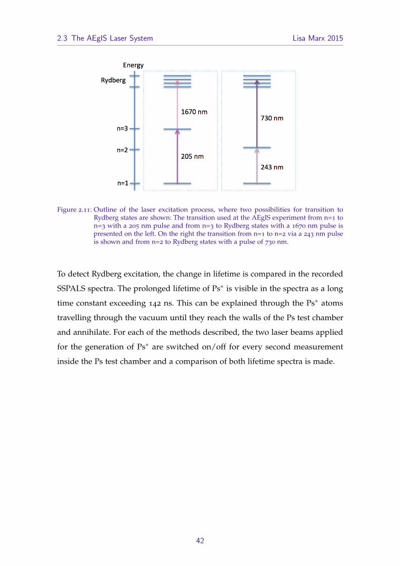
2.3 The AEgIS Laser System Lisa Marx 2015
Figure 2.11: Outline of the laser excitation process, where two possibilities for transition toRydberg states are shown: The transition used at the AEgIS experiment from n=1 ton=3 with a 205 nm pulse and from n=3 to Rydberg states with a 1670 nm pulse ispresented on the left. On the right the transition from n=1 to n=2 via a 243 nm pulseis shown and from n=2 to Rydberg states with a pulse of 730 nm.
To detect Rydberg excitation, the change in lifetime is compared in the recorded
SSPALS spectra. The prolonged lifetime of Ps∗ is visible in the spectra as a long
time constant exceeding 142 ns. This can be explained through the Ps∗ atoms
travelling through the vacuum until they reach the walls of the Ps test chamber
and annihilate. For each of the methods described, the two laser beams applied
for the generation of Ps∗ are switched on/off for every second measurement
inside the Ps test chamber and a comparison of both lifetime spectra is made.
42
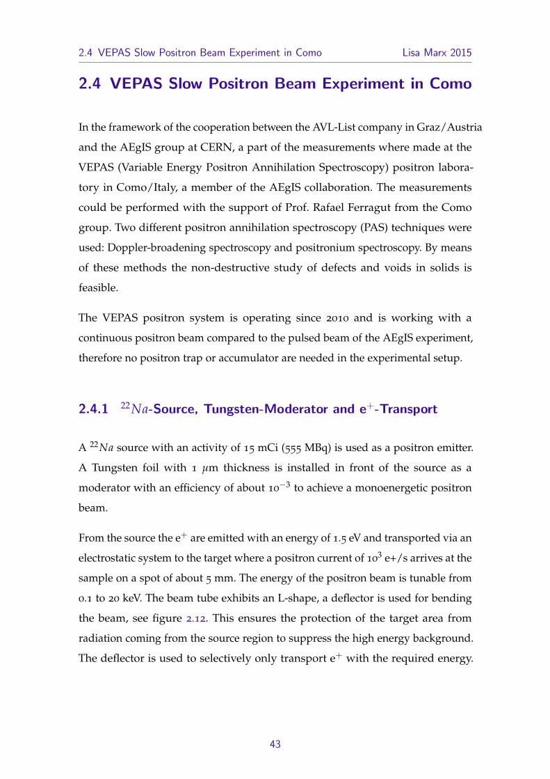
2.4 VEPAS Slow Positron Beam Experiment in Como Lisa Marx 2015
2.4 VEPAS Slow Positron Beam Experiment in Como
In the framework of the cooperation between the AVL-List company in Graz/Austria
and the AEgIS group at CERN, a part of the measurements where made at the
VEPAS (Variable Energy Positron Annihilation Spectroscopy) positron labora-
tory in Como/Italy, a member of the AEgIS collaboration. The measurements
could be performed with the support of Prof. Rafael Ferragut from the Como
group. Two different positron annihilation spectroscopy (PAS) techniques were
used: Doppler-broadening spectroscopy and positronium spectroscopy. By means
of these methods the non-destructive study of defects and voids in solids is
feasible.
The VEPAS positron system is operating since 2010 and is working with a
continuous positron beam compared to the pulsed beam of the AEgIS experiment,
therefore no positron trap or accumulator are needed in the experimental setup.
2.4.1 22Na-Source, Tungsten-Moderator and e+-Transport
A 22Na source with an activity of 15 mCi (555 MBq) is used as a positron emitter.
A Tungsten foil with 1 µm thickness is installed in front of the source as a
moderator with an efficiency of about 10−3 to achieve a monoenergetic positron
beam.
From the source the e+ are emitted with an energy of 1.5 eV and transported via an
electrostatic system to the target where a positron current of 103 e+/s arrives at the
sample on a spot of about 5 mm. The energy of the positron beam is tunable from
0.1 to 20 keV. The beam tube exhibits an L-shape, a deflector is used for bending
the beam, see figure 2.12. This ensures the protection of the target area from
radiation coming from the source region to suppress the high energy background.
The deflector is used to selectively only transport e+ with the required energy.
43

2.4 VEPAS Slow Positron Beam Experiment in Como Lisa Marx 2015
For energy tuning and focusing of the beamspot, electrostatic tubular lenses are
installed along the beamline at specifically determined potentials.
Figure 2.12: Schematic diagram of the experimental set-up of the electrostatic slow-positron beam.The positrons are provided by the 22Na source and pass through the moderator fromwhere they are transported to the target area via electrostatic transport.
The implantation energies can be varied between 0.1 keV and 17 keV. To measure
samples at different implantation energies and implantation depths an automated
energy scan is implemented. The target region is kept in a high vacuum of about
10−9 mbar and offers a variable target temperature of 10 - 1100 K. The slow
positron beam has been calibrated for positronium fraction measurements.
2.4.2 Detectors
The system is equipped with Ge detectors for momentum distribution measure-
ments, which can be operated in both single and coincidence mode.
44
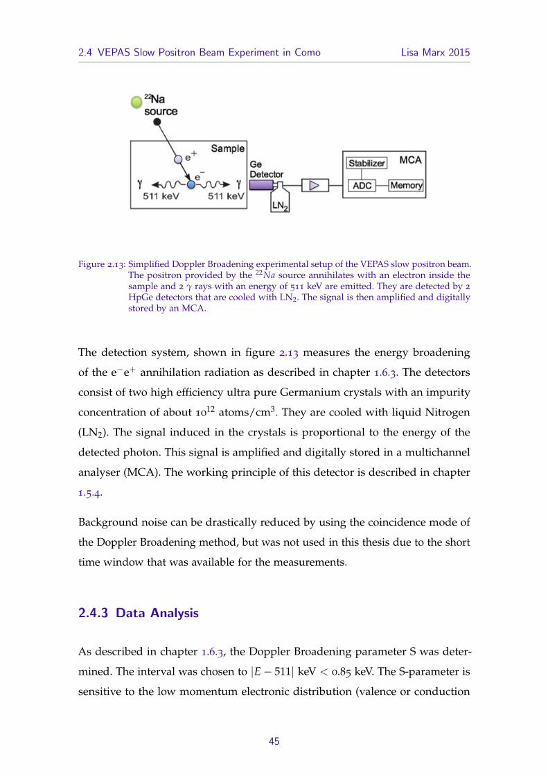
2.4 VEPAS Slow Positron Beam Experiment in Como Lisa Marx 2015
Figure 2.13: Simplified Doppler Broadening experimental setup of the VEPAS slow positron beam.The positron provided by the 22Na source annihilates with an electron inside thesample and 2 γ rays with an energy of 511 keV are emitted. They are detected by 2
HpGe detectors that are cooled with LN2. The signal is then amplified and digitallystored by an MCA.
The detection system, shown in figure 2.13 measures the energy broadening
of the e−e+ annihilation radiation as described in chapter 1.6.3. The detectors
consist of two high efficiency ultra pure Germanium crystals with an impurity
concentration of about 1012 atoms/cm3. They are cooled with liquid Nitrogen
(LN2). The signal induced in the crystals is proportional to the energy of the
detected photon. This signal is amplified and digitally stored in a multichannel
analyser (MCA). The working principle of this detector is described in chapter
1.5.4.
Background noise can be drastically reduced by using the coincidence mode of
the Doppler Broadening method, but was not used in this thesis due to the short
time window that was available for the measurements.
2.4.3 Data Analysis
As described in chapter 1.6.3, the Doppler Broadening parameter S was deter-
mined. The interval was chosen to |E− 511| keV < 0.85 keV. The S-parameter is
sensitive to the low momentum electronic distribution (valence or conduction
45
2.4 VEPAS Slow Positron Beam Experiment in Como Lisa Marx 2015
band electrons) and to the annihilations of para-Ps annihiliations. The S-parameter
is numerically deducted from the energy spectrum by means of a fit program.
Measurements were made in dependence of implantation energy. The data analy-
sis was performed with Origin and MATLAB based program (VEPFIT) developed
at the VEPAS positron laboratory. [26] The program VEPFIT is based on the
numeric solution of the stationary diffusion equation and allows to detect the
presence of layers with different characteristics (different structures and mate-
rials). In addition, information on the boundaries of different layers and the
diffusion length L+ can be determined.
With the above described apparatus it is also possible to detect ortho-positronium
atoms by means of the 3γ annihilation (see chapter 1.6.4). The oPs fraction F3γ vs.
the energy of the incident positrons can be calculated by means of a semi-linear
fitting procedure using VEPFIT, see figure 1.7.
The measuring data taken from both Germanium detectors were imported into the
Origin program and subsequently averaged. The error values of the annihilation
peak were obtained through the Poisson-distribution.
δR =
√RA,B√
2(2.3)
δR... Error for R
RA,B... Error of the single detectors A and B
46

2.5 Positronium Targets Lisa Marx 2015
2.5 Positronium Targets
In this chapter the different targets that were tested during this thesis are de-
scribed in detail. The production method and positronium formation process will
be outlined.
2.5.1 Silicon Targets
All samples tested in the AEgIS positron system are made out of silicon and
are designed in order to work in reflection mode, emitting positronium back
along the direction of the incoming positron beam. These targets are used due to
their easy manufacturing process and their well known functionality. The silicon
targets were partly produced by the author during the time of this thesis in the
group of S. Mariazzi.
To allow for positronium formation, nanochannels are etched into the surface of
silicon wafers. This is done through electrochemical etching. The characteristics of
the produced e+/Ps converters depend on the concentration and type of doping
of the Silicon wafer (n- or p-type silicon). The doping defines their resistivity and
therefore the etching current and the duration of the etching process.
The samples are placed in 75 ml of the etching fluid, made of 47 ml of 48%
hydrofluoric acid (HF) and 28 ml of ethanol. An etching current of 10 mA is
applied to the solution using two electrodes and is applied for 15 minutes. In the
last step the samples are heated to 100C, creating a layer of SiO2 on the surface
of the nanochannels. This process is repeated several times to reach the desired
size of the nanochannels.
Three different samples with different crystal orientation and type of doping
were used. The properties of pores as density, diameter and length depend on the
anodization conditions like HF concentration, etching current, silicon type and
47

2.5 Positronium Targets Lisa Marx 2015
resistivity and anodization duration. The production of targets for this thesis aims
at maximizing the yield of o-Ps. This depends on the ratio between the volume
of the inner silicon pillar and the surface silica layer, and on the pore size. [39]
A p-type(100) sample and a p-type(111) sample, each with a resistivity 0.15-0.21
Ω/cm, as well as an n-type(100) sample with a resistivity 0.1-1.0 Ω/cm were
used. The p-type(100) target was produced in 2014, while the other two samples
were made during the course of this thesis. The p-type(111) target the dimensions
of the nanochannels are estimated to 6-8 nm in diameter with a depth of 1-2 µm.
The same dimensions are expected for the p-type(100) target, since both p-type
samples have the same resistivity. For the p-type(100) target, previously made
SEM measurements are available. [39] Since the resistivity of the n-type sample is
not very well known, the dimensions of the nanochannels and the etching rate
can not be estimated in the same way as for the p-type samples.
The process of positrons entering the sample is shown in Figure 2.14. The target is
Figure 2.14: Simplified overview of the Ps formation process inside of the nanochanneled Si-targets. Positrons hit the target, thermalize and diffuse into the silicon wafer andform Ps in the SiO2 layer coating the channels. The Ps atoms then diffuse back to thesurface whilst cooling though collisions with the channel walls.
48
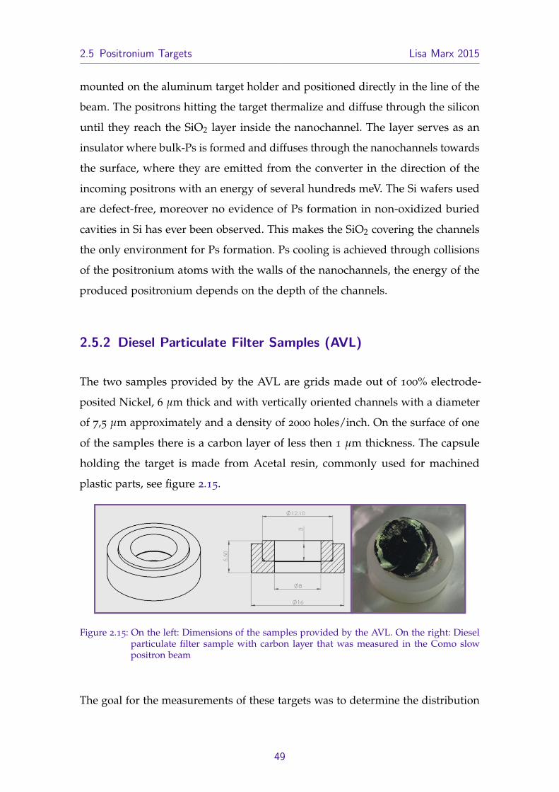
2.5 Positronium Targets Lisa Marx 2015
mounted on the aluminum target holder and positioned directly in the line of the
beam. The positrons hitting the target thermalize and diffuse through the silicon
until they reach the SiO2 layer inside the nanochannel. The layer serves as an
insulator where bulk-Ps is formed and diffuses through the nanochannels towards
the surface, where they are emitted from the converter in the direction of the
incoming positrons with an energy of several hundreds meV. The Si wafers used
are defect-free, moreover no evidence of Ps formation in non-oxidized buried
cavities in Si has ever been observed. This makes the SiO2 covering the channels
the only environment for Ps formation. Ps cooling is achieved through collisions
of the positronium atoms with the walls of the nanochannels, the energy of the
produced positronium depends on the depth of the channels.
2.5.2 Diesel Particulate Filter Samples (AVL)
The two samples provided by the AVL are grids made out of 100% electrode-
posited Nickel, 6 µm thick and with vertically oriented channels with a diameter
of 7,5 µm approximately and a density of 2000 holes/inch. On the surface of one
of the samples there is a carbon layer of less then 1 µm thickness. The capsule
holding the target is made from Acetal resin, commonly used for machined
plastic parts, see figure 2.15.
Figure 2.15: On the left: Dimensions of the samples provided by the AVL. On the right: Dieselparticulate filter sample with carbon layer that was measured in the Como slowpositron beam
The goal for the measurements of these targets was to determine the distribution
49

2.5 Positronium Targets Lisa Marx 2015
of the carbon layer on the surface of the Nickel grid and primarily its penetration
into the channels.
Since it is well known that positronium can be emitted from the surface of metallic
samples hit by low-energy positrons, the diesel particulate filter substrate made of
Nickel is a potential candidate as a e+/Ps converter. Nickel has a negative positron
workfunction of 0.1 eV [40]. For a Ni(100) sample (with carbon contamination on
the surface held below < 10 at.%), the positronium work function was determined
to ΦNi= -2,63 ± 0,26 eV. [41]
50

3 Results
During the time of this thesis the AEgIS positron system was optimized, updated
and fully automated. Some of these optimizations are pointed out in the following
section.
In addition to the measurements conducted at the AEgIS experiment at CERN,
an investigation of Ps-targets and samples provided by AVL company was
performed.
3.1 Comparison of different detectors for SSPALS
To obtain the best possible SSPALS spectra, generated by positron annihilation in
the Ps test chamber, different detectors were tested, using an Al target where no
Ps is formed and a target with strong Ps formation (p-type(111) Si described in the
section 3.3). The measurements were conducted to achieve a comparison of the
different detectors available for the AEgIS positron system and to select the most
suitable one for Ps detection. All spectra were obtained by averaging over 10 or
20 measurements and normalized to the prompt peak. The spectra were acquired
by implanting up to 107 positrons in the target. The logarithmic representation
accentuates the part of the curve following the peak, which highlights positronium
formation.
Firstly, as a comparison, a R11265-100 PMT and a H3378 PMT coupled to a plastic
scintillator were tested. The results are shown in figure 3.1.
The e+ lifetime spectrum obtained with the R11265-100 PMT shows a low level
of noise and shows a continuous decrease after the peak. The spectrum recorded

3.1 Comparison of different detectors for SSPALS Lisa Marx 2015
Figure 3.1: Comparison of a a R11265-100 PMT (dark purple curve) and a H3378 PMT (lightpurple curve) coupled to a plastic scintillator for positron annihilation signals onthe aluminium target holder. The curves are an average of 20 measurements andnormalized to the prompt peak. The signal of the H3378 PMT is cut off after 650 nsdue to the settings on the oscilloscope during these measurements.
using the H3378 PMT shows a much higher noise level after the peak and pro-
nounced irregularities of the falling slope. These irregularities are reproducible
and are always at the same position with the same magnitude. Therefore, back-
ground noise producing these peaks can be excluded and these irregularities are
accredited to an internal property of the PMT.
Due to the result of these measurements, the H3378 PMT was no longer used
during this thesis. For all further measurements and the comparison of the photon
converters, the R11265-100 PMT was used due to its superior performance.
Furthermore, three different scintillator materials were tested: A plastic scintillator,
a PbF2 Cherenkov radiator and a PbWO4 scintillator were tested and compared,
52
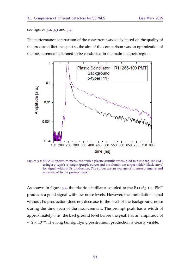
3.1 Comparison of different detectors for SSPALS Lisa Marx 2015
see figures 3.2, 3.3 and 3.4.
The performance comparison of the converters was solely based on the quality of
the produced lifetime spectra, the aim of the comparison was an optimization of
the measurements planned to be conducted in the main magnets region.
Figure 3.2: SSPALS spectrum measured with a plastic scintillator coupled to a R11265-100 PMTusing a p-type(111) target (purple curve) and the aluminium target holder (black curve)for signal without Ps production. The curves are an average of 10 measurements andnormalized to the prompt peak.
As shown in figure 3.2, the plastic scintillator coupled to the R11265-100 PMT
produces a good signal with low noise levels. However, the annihilation signal
without Ps production does not decrease to the level of the background noise
during the time span of the measurement. The prompt peak has a width of
approximately 9 ns, the background level before the peak has an amplitude of
∼ 2× 10⁻⁴. The long tail signifying positronium production is clearly visible.
53
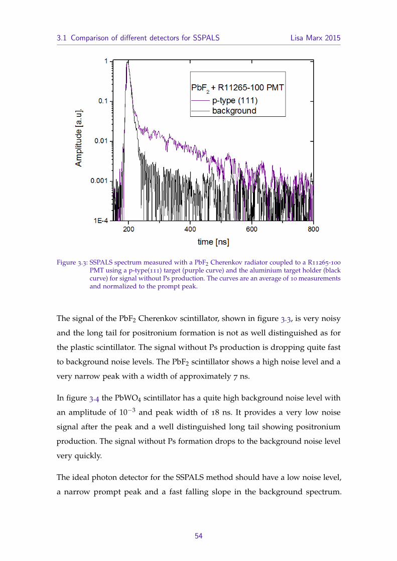
3.1 Comparison of different detectors for SSPALS Lisa Marx 2015
Figure 3.3: SSPALS spectrum measured with a PbF2 Cherenkov radiator coupled to a R11265-100
PMT using a p-type(111) target (purple curve) and the aluminium target holder (blackcurve) for signal without Ps production. The curves are an average of 10 measurementsand normalized to the prompt peak.
The signal of the PbF2 Cherenkov scintillator, shown in figure 3.3, is very noisy
and the long tail for positronium formation is not as well distinguished as for
the plastic scintillator. The signal without Ps production is dropping quite fast
to background noise levels. The PbF2 scintillator shows a high noise level and a
very narrow peak with a width of approximately 7 ns.
In figure 3.4 the PbWO4 scintillator has a quite high background noise level with
an amplitude of 10−3 and peak width of 18 ns. It provides a very low noise
signal after the peak and a well distinguished long tail showing positronium
production. The signal without Ps formation drops to the background noise level
very quickly.
The ideal photon detector for the SSPALS method should have a low noise level,
a narrow prompt peak and a fast falling slope in the background spectrum.
54
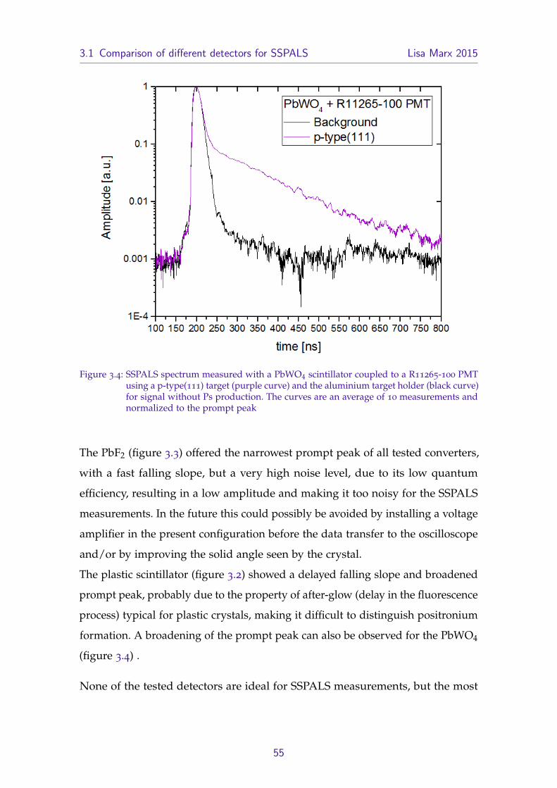
3.1 Comparison of different detectors for SSPALS Lisa Marx 2015
Figure 3.4: SSPALS spectrum measured with a PbWO4 scintillator coupled to a R11265-100 PMTusing a p-type(111) target (purple curve) and the aluminium target holder (black curve)for signal without Ps production. The curves are an average of 10 measurements andnormalized to the prompt peak
The PbF2 (figure 3.3) offered the narrowest prompt peak of all tested converters,
with a fast falling slope, but a very high noise level, due to its low quantum
efficiency, resulting in a low amplitude and making it too noisy for the SSPALS
measurements. In the future this could possibly be avoided by installing a voltage
amplifier in the present configuration before the data transfer to the oscilloscope
and/or by improving the solid angle seen by the crystal.
The plastic scintillator (figure 3.2) showed a delayed falling slope and broadened
prompt peak, probably due to the property of after-glow (delay in the fluorescence
process) typical for plastic crystals, making it difficult to distinguish positronium
formation. A broadening of the prompt peak can also be observed for the PbWO4
(figure 3.4) .
None of the tested detectors are ideal for SSPALS measurements, but the most
55

3.2 Implementation of a buncher in the AEgIS Positron System Lisa Marx 2015
suitable detector to investigate positronium formation and compare different
e+/Ps converters, fitting the requirements of the AEgIS positron system best,
was decided to be the PbWO4 detector, due to its very low noise signal after
the peak, a well distinguished long tail showing positronium production and a
fast falling slope to the background signal. The PbWO4 was used for all further
measurements of positronium targets and for laser excitation.
3.2 Implementation of a buncher in the AEgIS
Positron System
The implementation of a buncher in the positron system was done during the
time of this thesis and the results were published in Nuclear Instruments and
Methods in Physics Research Section B: Beam Interactions with Materials and
Atoms, in the course of this work, with L. Marx being a co-author. [42]
The buncher was introduced into the positron system to reduce the time spread
of the positron pulse supplied from the accumulator. The basic working principle
was described in chapter 2.2.5.
The buncher consists of 25 electrodes, forming a parabolic potential up to 10 kV
between the first and last electrode, accelerating positrons arriving later (end of
cloud) more strongly that the ones arriving early (closer to the Ps test chamber).
This reduces the time spread of the bunch. The parabolic function has a variable
amplitude and is superimposed to a tunable bias to accelerate the positrons
towards the target, see figure 3.5. The combined high voltage pulse has a pulse
duration of 30 ns and a rise time of 2-3 ns.
The time shape of the buncher potential was recorded at the entrance of the
buncher and is shown in figure 3.6.
56

3.2 Implementation of a buncher in the AEgIS Positron System Lisa Marx 2015
Figure 3.5: Scheme of the parabolic potential superimposed on a high voltage potential of thepositron buncher for reduction of the time spread of the positron cloud and e+
acceleration. In the graph the positrons enter the buncher from the left. When thebuncher is turned on with the right timing (i.e. the whole e+ pulse is inside of thebuncher) the positrons entering last are accelerated more strongly than the positronsentering first.
The implementation of the buncher required a lot of different tests and measure-
ments, which were the tasks conducted by the author of this thesis in the group
of S. Mariazzi.
The first step was to correctly time the dump from the accumulator to the switch-
on of the buncher. It was achieved through a digital delay generator (Stanford
Research Systems DG 645). With a length of the buncher of 40 cm and a length of
about 20 cm for the positron bunch, the velocity of e+ is limited to an energy not
exceeding 100 eV for optimized compression. Due to the delays from the trigger
of the digital delay generator and from the electronics of the buncher and the
accumulator, the timing of the buncher switch-on is very important and has to
be executed very precisely. An activation too early would lead to a reflection of
the positrons on the first electrode of the buncher and a belated activation would
result in only a fraction of positrons being accelerated or nor effect at all. To find
57

3.2 Implementation of a buncher in the AEgIS Positron System Lisa Marx 2015
Figure 3.6: Measured shape of the high voltage pulse used for compression of an e+ pulse intime and space, as a function of time. The signal was acquired at the entrance of thebuncher and measured using a Magnelab CT-C1.0 current transformer
the optimum delay time, the signal amplitude of positrons in the main magnets
region was measured as a function of the switch-on time, see Figure 3.7.
The peak lies at approximately 20 ns, which signifies the proper delay-time after
the positron dump from the accumulator. If the buncher is turned on too early,
with a time delay of t< 10 ns the positrons are reflected completely towards
the accumulator and no signal can be recorded in the experimental chamber.
For a time delay of 10< t <20 ns the e+ bunch is partly cut off, with a signal
amplitude of around 40 mV corresponding to approximately 106 positrons hitting
the target. For longer delay times the signal amplitude decreases again, due to
bad compression. The number of positrons reaching the target does not change
but they are distributed over a longer time window, causing a decreased peak
amplitude. With a delay of about 20 ns, the signal amplitude is almost three times
higher, reaching a value of around 110 mV, corresponding to approximately 107
positrons reaching the target.
These results could be confirmed by recording the FWHM of the annihilation
signal as a function of the time delay. A broadening of the e+-lifetime spectrum,
58

3.2 Implementation of a buncher in the AEgIS Positron System Lisa Marx 2015
Figure 3.7: Signal amplitude, proportional to the number of positrons annihilating on the alu-minium target holder as a function of the delay time of the buncher switch-on afterthe e+ pulse has been dumped from the accumulator. The signal was obtained usinga PbF2 Cherenkov radiator coupled to a R11265-100 PMT with 1000 pulses from theaccumulator and a positron implantation energy of 3,3 kV. Some error bars are notvisible, since they are smaller than the size of the squares signifying the data points.
caused by the widening of the beam pulse was observed as is shown in 3.8.
For optimal bunching a delay time of 18-25 ns is used. For a time delay of less
than 18 ns the results are not relevant since only a fraction of positrons or no
positrons at all reach the target, which leads to more narrow annihilation peak
due to the diminished number of e+. For a delay time of more than 40 ns the
positron bunch is not or only partially compressed, since the e+ pass through
without being influenced by the buncher. For a delay time of ∼ 20 ns a minimum
FWHM of 7-9 ns is achieved.
59

3.2 Implementation of a buncher in the AEgIS Positron System Lisa Marx 2015
Figure 3.8: FWHM of the e+-lifetime spectrum in dependence of the delay time of the buncher.Each data point is averaged over 5 measurements, the error bars were calculatedthrough the standard deviation method.
Figure 3.9 demonstrates the effect of beam bunching by means of comparison
with a spectrum recorded without bunching. The signal width of ∼ 21 ns without
buncher could be compressed to ∼ 7 ns when the buncher is turned on with the
right time delay.
In addition to optimizing the delay time of the buncher, a microchannel plate
(MCP) assembly (Hamamatsu F2222–21P25 + Phosphor Screen P46), placed 1 cm
behind the target, was used for the characterization of the positron spot size at
the target position, see figure 2.9. By removing the sample holder, the positrons
could be dumped directly onto the MCP. By means of combining a phosphor
screen and a charge-coupled device (CCD) camera, the positron pulse can be
imaged and recorded. This image can be seen in figure 3.10.
Figure 3.10 (a) was recorded with electrostatic transport used for guiding e+
and without a magnetic field in the target region, figure 3.10 (b) shows the
60

3.2 Implementation of a buncher in the AEgIS Positron System Lisa Marx 2015
Figure 3.9: Comparison of the FWHM of the positron pulse with the buncher switched on (darkcurve, time delay of 20 ns) and with the buncher switched off (light curve).
corresponding intensity distribution with a beam spot diameter of less than 4
mm.
An estimate of the transport efficiency of e+ along the buncher amounted to
∼ 30 % which was obtained by placing a calibrated CsI detector coupled to
photodiodes at the entrance and exit of the buncher. The spot recorded in figure
3.10 (a) contains 107 annihilation events when 3×10
7 e+ are dumped from the
accumulator.
Measurements of the magnetic field in the target region were obtained with a
3D Hall sensor and showed a field of less than 1.8 Gauss parallel to the beam
and less than 0.5 Gauss in the direction perpendicular to the beam. To conduct
experiments in a specific magnetic environment, two coils were installed in the
target area, able to generate a magnetic field up to 300 Gauss, parallel to the e+
beam. For a field larger than 150 Gauss, a positive effect on the e+ extraction
from the buncher can be observed, about 40% of positrons dumped from the
61

3.2 Implementation of a buncher in the AEgIS Positron System Lisa Marx 2015
Figure 3.10: Image of the positron beam spot acquired with an MCP assembly and CCD camera,without a magnetic field in the target region and a positron energy of 3.3 keV: (a)shows the radial distribution of e+ and (b) the corresponding intensity distribution.A beam spot diameter of less than 4 mm was obtained.
accumulator reach the target, which means an improvement of approximately
10%.
Figure 3.11: Image of the positron beam spot acquired with an MCP assembly and CCD camera,with a magnetic field of 250 Gauss in the target region and a positron energy of3.3 keV: (a) shows the radial distribution of e+ and (b) the corresponding intensitydistribution. A beam spot diameter of less than 5 mm was obtained.
Figure 3.11 (a) shows the characterization of the positron beam on the MCP with
62

3.3 Comparison of different Targets for Positronium Production Lisa Marx 2015
a 250 Gauss magnetic field in the target area and the corresponding intensity
distribution in 3.11 (b), with a beam spot diameter of approximately 5 mm. In
this configuration about 1.2×10⁷ positrons reach the target when 3×10
7 positrons
are dumped from the accumulator. [42]
The largest positron losses occur due to switching between magnetic and electro-
static transport at the entrance of the buncher. This was tested by measuring e+
annihilation signals at different points of the transfer line.
In summary, an improvement in signal amplitude could be obtained from 40 mV
before the implementation of the buncher to 110 mV after the implementation; in
addition, a compression in time of the positron bunch from 21 ns to 7 ns could be
achieved. A higher transport efficiency of e+ from the accumulator was recorded
for a magnetic field of more than 150 Gauss in the target region.
3.3 Comparison of different Targets for Positronium
Production
To find the most suitable positron-positronium converters for the AEgIS experi-
ment and for antihydrogen production in the future, the targets were analysed
using scanning electron microscopy(SEM) and first measurements for target
suitability were conducted at the slow positron beam in Como. Different silicon
based targets where tested in the Ps test chamber of the AEgIS positron system
at CERN.
3.3.1 SEM-Measurements of the Positronium Targets
Two nanochanneled silicon Ps-targets of the AEgIS positron group, namely a
p-type(111) and n-type(100) sample, were examined at a nanometer scale with
a ZEISS scanning electron microscope (SEM) at CERN. The results can be seen
63

3.3 Comparison of different Targets for Positronium Production Lisa Marx 2015
in figure 3.12 and figure 3.13 and are consistent with the results of the SSPALS
measurements, see below 3.3.3.
Figure 3.12: Images created with a scanning electron microscope for the n-type(100) sample (a)and the p-type(111) sample (b). The samples were measured perpendicular to thesurface with a working distance of 2 mm and a voltage of 2 kV. The lighter areasrepresent the silicon wafer, the dark patches indicate the nanochannels producedduring the etching process. A clear difference in channel size and homogeneityis visible. The p-type(111) sample shows small and regular channels while the n-type(100) sample exhibits a variety of different channel sizes an shapes, with a muchlower overall number of channels.
64

3.3 Comparison of different Targets for Positronium Production Lisa Marx 2015
Figure 3.13: Images created with a scanning electron microscope for the n-type(100) sample(a) and the p-type(111) sample (b). The samples were manually broken in half tomeasure the profile of the sample and the depth of the channels. The measurementwas obtained at a working distance of 2.9 mm and a voltage of 3 kV. The p-type(111)sample shows a clear layer effected by the etching process (between the green lines)with a width of about 860 nm, adjoining to the homogeneous silicon wafer on theright hand side of the image. The lighter areas of the image represent the SiO2 layer.The n-type(100) sample on the other hand, shows no clear boundaries and the visiblechannels appear very large and irregular.
A clear difference can be the seen between the n-type(100) and p-type(111)
samples from both viewpoints. The channels of the n-type sample are irregular,
65

3.3 Comparison of different Targets for Positronium Production Lisa Marx 2015
both in their size and their distribution. The channels of the p-type sample are
significantly smaller, constant in size and regularly distributed. The images in
side-face view, have to be interpreted with care, since the breaking process is not
well controlled. In contrast to the n-type sample the p-type sample shows a clear
SiO2 layer in the side-face view and channels reaching approximately 860 nm into
the wafer, which yields the base for the high positronium yield for this sample,,
see 3.3.2. Only few and irregular channels can be seen for the n-type sample in
figure 3.13 a) with no clear SiO2 (lighter areas), which is in accordance with the
very low positronium yield that was measured for this sample. This is probably
due to the etching process, that might not be as well suited for the resistivity of
the n-type samples, see chapter 2.5.1.
3.3.2 Measurements at the VEPAS Laboratory/Como
In the framework of the cooperation between the AVL in Graz/Austria and the
AEgIS group at CERN, a part of the measurements for the characterization of
samples for Ps production were made at the VEPAS (Variable Energy Positron An-
nihilation Spectroscopy) positron laboratory in Como/Italy. Two different positron
annihilation spectroscopy (PAS) techniques were used: Doppler-broadening spec-
troscopy and positronium spectroscopy. The measurements should serve as a test
for the suitability of the investigation method.
The measurements were obtained in two runs of 1000 s per implantation energy
varying between 0,1 and 17 keV for each sample. The Data-Analysis tool used
to process the obtained data was the Origin and Matlab based program VEP-
FIT and described in the previous chapter 1.6.3. Measurements of the Doppler
Broadening parameter S and the positronium fraction F3γ vs. the energy of the
incident positrons were analysed by means of a semi-linear fitting procedure.
A background measurement was obtained for 70000 s with 0,03 counts/s com-
pared to 5 counts/s for the positron annihilation signal. This results in a peak to
background ratio of P/B=170.
66
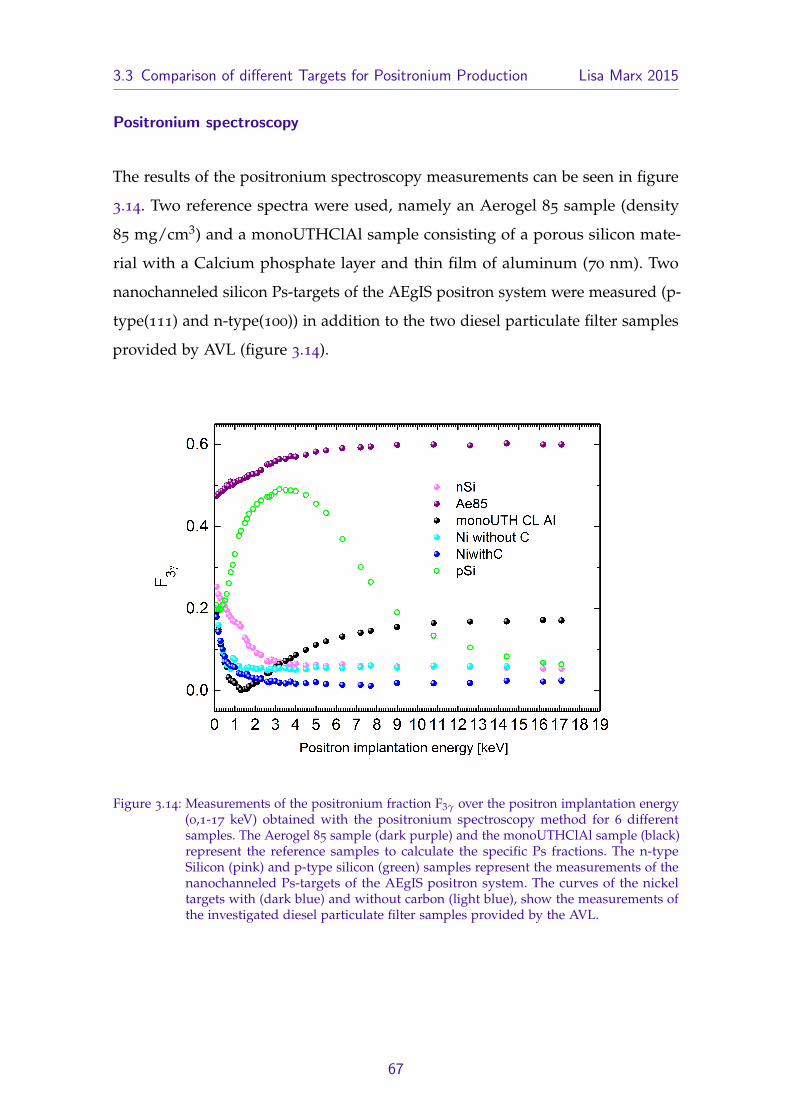
3.3 Comparison of different Targets for Positronium Production Lisa Marx 2015
Positronium spectroscopy
The results of the positronium spectroscopy measurements can be seen in figure
3.14. Two reference spectra were used, namely an Aerogel 85 sample (density
85 mg/cm3) and a monoUTHClAl sample consisting of a porous silicon mate-
rial with a Calcium phosphate layer and thin film of aluminum (70 nm). Two
nanochanneled silicon Ps-targets of the AEgIS positron system were measured (p-
type(111) and n-type(100)) in addition to the two diesel particulate filter samples
provided by AVL (figure 3.14).
Figure 3.14: Measurements of the positronium fraction F3γ over the positron implantation energy(0,1-17 keV) obtained with the positronium spectroscopy method for 6 differentsamples. The Aerogel 85 sample (dark purple) and the monoUTHClAl sample (black)represent the reference samples to calculate the specific Ps fractions. The n-typeSilicon (pink) and p-type silicon (green) samples represent the measurements of thenanochanneled Ps-targets of the AEgIS positron system. The curves of the nickeltargets with (dark blue) and without carbon (light blue), show the measurements ofthe investigated diesel particulate filter samples provided by the AVL.
67

3.3 Comparison of different Targets for Positronium Production Lisa Marx 2015
The Positronium fraction F3γ was calculated using the following equation:
F3γ = [1 + β× (R1 − RR− R0
)]−1 (3.1)
• F3γ . . . Ps formation fraction
• β . . . Corresponds to a globally used parameter obtained by the ratio of the
peak areas for 0% (P0) and 100% (P1) positronium production. β = p1p0
= 0.44
is obtained after background subtraction. It is not as strongly dependent on
the apparatus, environment and material as R0 or R1 and can therefore be
used globally.
• R . . . Measured R-parameter value for the examined sample at a certain
implantation energy
• R0 . . . R-parameter which corresponds to the value for 0% Ps production.
R0 . . . is calculated from the lowest point of a reference spectrum of a
porous silicon material with a Calcium phosphate layer and thin film of
aluminium (70 nm)) (see figure 3.14) which provides a very low Ps yield.
Due to physical properties, the R0-value does not precisely represent 0 %
of positronium production but a very low value between 1%− 3%, which
introduces a small error. R0 depends on the density of the detector material.
• R1 . . . R-parameter value corresponding to 100% Ps production, can in
reverse be calculated from the above equation by inserting R0 from above
and R60% which is obtained from the average of the five highest values of
the reference spectrum from an Aerogel 85 target (density ρ= 85 mg/cm3),
which has a known Ps3γ annihilation rate of approximately 60%. R1 would
correspond to the measurement of a Germanium target at 1000 K for 100%
Ps yield [43] and amounts to R1= 2,4805 for the measurements discussed
here.
A high positronium yield was measured for the p-type(111) sample with a peak at
around 3,5 keV, in comparison to a very low Ps production rate for the n-type(100)
sample. This is in accordance to the results obtained at the AEgIS positron system
and the SEM-measurements described above.
68

3.3 Comparison of different Targets for Positronium Production Lisa Marx 2015
As expected, the pure nickel sample without carbon is very uniform, a very low
F3γ rate can be seen. The measurement of the nickel sample with carbon layer
shows the same uniform curve but with a consistently lower F3γ value. For a
pure nickel sample, no significant Ps production is expected. The obtained signal
could stem from Ps production on the sample surface that is suppressed by the
carbon layer for the second sample. To confirm this assumption and find out
more about the samples, further measurements are necessary, including higher
statistics and the modification of the sample through the removal of the carbon
layer. This would be of interest due to how little is known about the deposition
process of the nickel substrate and the application of the carbon layer.
For the p-type(111) silicon sample a value F3γ ≈ 50% is calculated from the
peak value at around 3,5 keV. At the same energy a positronium fraction of only
F3γ ≈ 5% was calculated for the n-type(100) sample, which is supported by the
results obtained using scanning electron microscopy in chapter 3.3.1.
The goal of the measurements of different targets, was to test the suitability
of the different sampleswith respect to e+/Ps conversion for the production of
positronium for the AEgIS experiment. This leads to the following conclusion:
1. High Ps formation could be observed in the p-type(111) sample.
2. Low Ps formation was evidenced in the n-type(100) sample.
3. No Ps formation was observed in the diesel particulate filter samples.
4. Further investigations are needed to fully characterize the last set of samples.
Doppler Broadening Spectroscopy and Defect Depth Profiling of Diesel
particulate filter samples
For numerical analysis of the defect depth profiles, pre-information about the sam-
ple and the positron implantation profile is needed. The profile is obtained from
Monte-Carlo simulations and from experimental results of Doppler-Broadening
spectroscopy by means of the VEPFIT program (see chapter 2).
69

3.3 Comparison of different Targets for Positronium Production Lisa Marx 2015
For the diesel particulate filter samples the density of the nickel substrate was
calculated from the known density of nickel ρ = 8,908 g/cm3 at 20C. Taking
into account the density reduction due to the open channels, with the known
dimensions of the open channels in the substrate (7.5 µm channels with 2000
holes/inch 1) the density of the particulate filter sample could be calculated. A
density of ρ= 6,468 g/cm3 was obtained, which is about 72.6% of the density of
pure nickel.
The diffusion length for the pure nickel sample was obtained through VEPFIT:
d=170 nm, for an S-parameter of S = 0.4748 and an implantation energy of 8 keV
(figure 3.14). The carbon layer depends on the production method, it is made up
of amorphous carbon (information provided by the AVL) which has a density of ρ
= 1,8-2,1 g/cm3. Therefore a value of ρ = 1,95 g/cm3 was used for the calculations
of the depth profile. For modelling, a trilayer structure is assumed, consisting of
a pure carbon layer, a potential interface and the porous nickel layer, which can
be considered as basically infinite due to its thickness of 6 µm, see figure 3.15.
Figure 3.15: Composition of the Ni sample (Ni, density ρ3), with Carbon layer (C, density ρ1,thickness d1). The best fit was obtained by including an thin interface (I, density ρ12,thickness d2).
The mean implantation depth profile provides thickness estimations of the differ-
ent layers with each implantation energy corresponding to a certain implantation
1Information provided by AVL
70

3.3 Comparison of different Targets for Positronium Production Lisa Marx 2015
depth of positrons (8 keV corresponds to about 500 nm). Another assumption
had to be made about the density of the potential interface which had to lie in
the range of ρ = 1,95-6,5 g/cm3, i.e., between the values of the nickel substrate
and the carbon layer. A value ρ ≈ 4,2 g/cm3 was chosen.
The measured S-parameters for both samples obtained from the measurements
through VEPFIT can be seen in figure 3.16.
Figure 3.16: S-parameters over the positron implantation energy (0.1-17 keV) obtained throughDoppler-Broadening spectroscopy of a nickel sample with (blue curve) and without(turquoise curve) carbon layer with the corresponding fits calculated with VEPFIT,assuming the existence of three different layers. The fit was chosen as the mostsuitable fit through a Chi-squared test.
For the pure nickel sample the S-parameter continually decreases in the direction
of the bulk showing a clear distinction compared to the sample with the added
carbon layer. With a third layer being included, the model of the defect depth
profile is closest to the experimental reality, but it is not a proof of the existence of
the interface, since the interface is not clearly visible, see figure 3.16. The interface
71

3.3 Comparison of different Targets for Positronium Production Lisa Marx 2015
becomes notable in the analysis through the step in the fit of the depth profile.
The existence of the step is not clear in the context of statistics. This suggests an
interface of a width no wider than 2 nm. A Chi-squared test was used to compare
the experimental results with the model values to determine the goodness of the
fit. It showed that the inclusion of an interface provided the better fit.
A mean diffusion length of LC = 44±2 nm was estimated, which suggests a
carbon layer containing few pores only. This is symptomatic of a film of good
quality and little defects. The thickness of the carbon film was calculated to dC =
620±20 nm.
Without numerical constraints interface of about dI = 10 nm was calculated,
which is probably overestimated, since this would correspond to a significant
layer thickness of about 100 atoms. Since interface is not clearly visible in the
measurements, the thickness of the interface was fixed to dI = 2 nm in the VEPFIT
program yielding a mean diffusion length of LI = 0,04 nm. This represents a
diffusion length very close to zero and indicates that the interface contains a high
amount of e+-trapping centres.
For an interface thickness of dI = 4-5 nm, a diffusion length of LI = 40 nm was
obtained.
The parameters obtained for the pure Ni were used as fixed parameters for the
Ni-layer when analysing the C-coated sample. This assumption however, requires
that the C-layer does not influence the Ni-substrate, which is not known.
Different densities for the interface were tested, since this density is completely
unknown:
ρ = 2,1 g/cm3 (assuming that the density of carbon is higher) which led to no
change in the model.
ρ = 5,5 g/cm3 which led to a small change in the diffusion length from LI = 44
nm to LI = 47 nm.
ρ = 1,6 g/cm3 (interface density even lower than that of carbon) yields a diffusion
length of LI = 46 nm. These analyses show that the mean diffusion length slightly
decreases with reducing the interface density.
72

3.3 Comparison of different Targets for Positronium Production Lisa Marx 2015
It becomes evident that more information about the samples is required in order
to make more accurate fits and to perform further investigations.
3.3.3 Measurements at the AEgIS Experiment (CERN)
The measurements were made using the PbWO4 detector coupled to the Hama-
matsu R11265-100 PMT, due its superior suitability proven in chapter 3.1. The
measurements were done by single shot positronium annihilation lifetime spec-
troscopy (SSPALS). Three different porous Si samples were tested, made from
p-type(111), p-type(100) and n-type(100) Si. The spectra are shown in figure 3.17.
Each curve is an average of 10 measurements, the curves have been normalized
to the prompt peak. As a reference for the assessment of the background a e+
lifetime spectrum was measured using an Al sample holder which exhibits no Ps
formation.
The rapid decrease of the time signal quite similar to that of a reference sam-
ple, indicates that there is no significant Ps formation and annihilation in the
porous sample made from n-type Si. The curves of the p-type samples show a
considerably higher signal and slower decrease after the e+ annihilation peak
and reach the background noise level after approximately 400 ns. This long tail
can be attributed to o-Ps formation, with a lifetime of ∼ 142 ns in vacuum. The
p-type(111) sample shows a slightly higher signal compared to the p-type(100)
sample, which suggests a better positronium production rate. For this reason this
sample was used for all later experiments including laser excitation of the created
Ps atoms.
The lifetime of the created Ps atoms could extracted from the spectra by fitting
them with an exponential decay function, see equation 3.2.
N(t) = N0e−tτPs + A (3.2)
73

3.3 Comparison of different Targets for Positronium Production Lisa Marx 2015
Figure 3.17: SSPALS spectra measured with a PbWO4 scintillator coupled to a R11265-100 PMTcomparing nanochanneled silicon targets: A p-type(111) (purple curve), a p-type(100)(pink curve) and a n-type(100) (blue curve) target. For background measurements(black curve) the aluminum target holder was used. The curves are an average of 10
measurements and normalized to the prompt peak.
t. . . Time passed since start of Ps formation
N(t). . . Number of Ps atoms at the time t
N0 . . . Initial number of Ps atoms
τPs . . . Lifetime of Ps atoms
A . . . Constant Term
The characteristic lifetime τPS denotes the time constant after which the number
of positronium atoms has decreased to 1e . For the lifetime measurements the
background measurement was substracted from the SSPALS spectra and fitted
with the exponential decay from equation 3.2. A lifetime of τPS = 142.8± 1(stat)
ns was obtained for the p-type(111) sample by fitting one of the spectra, see
figure 3.18. A lifetime of τPS = 111± 1(stat) ns was obtained for the p-type(100)
74
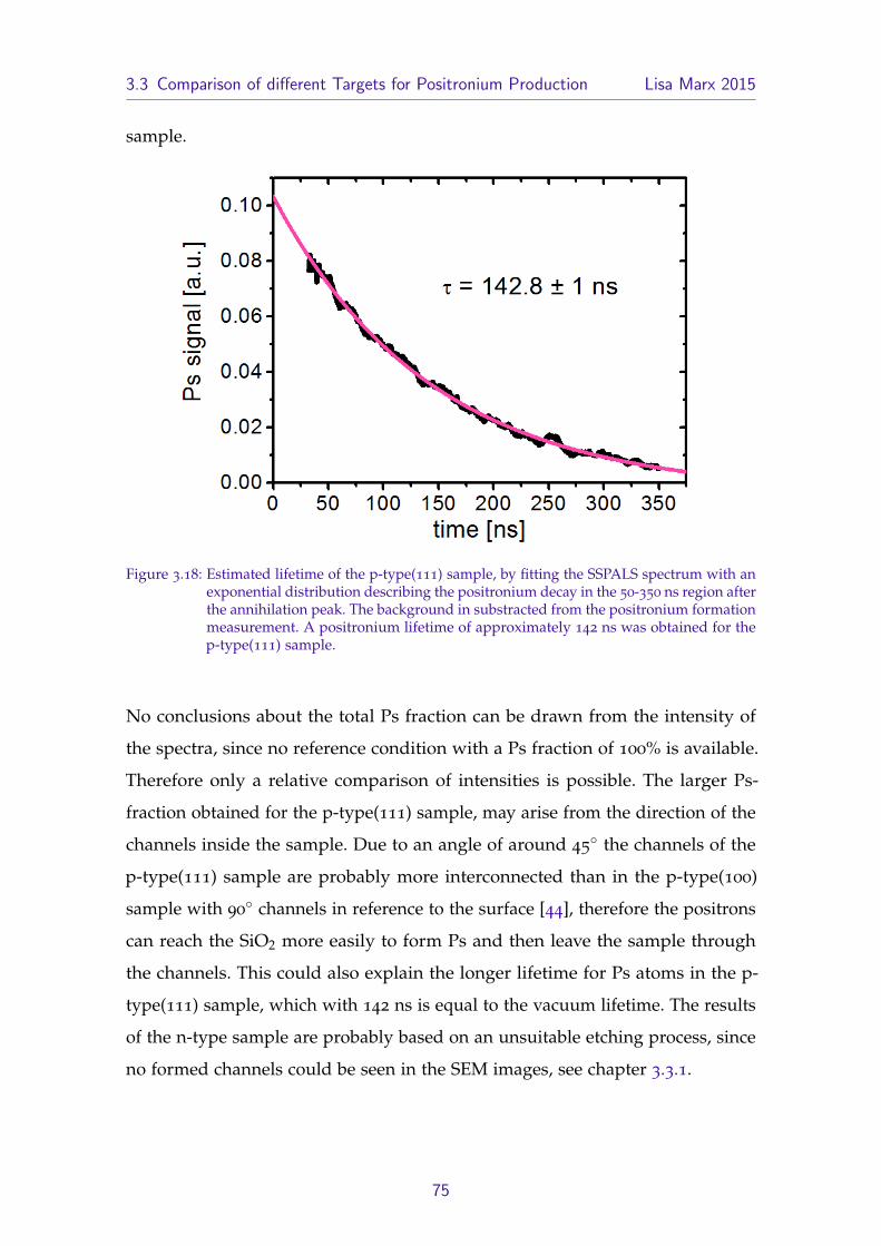
3.3 Comparison of different Targets for Positronium Production Lisa Marx 2015
sample.
Figure 3.18: Estimated lifetime of the p-type(111) sample, by fitting the SSPALS spectrum with anexponential distribution describing the positronium decay in the 50-350 ns region afterthe annihilation peak. The background in substracted from the positronium formationmeasurement. A positronium lifetime of approximately 142 ns was obtained for thep-type(111) sample.
No conclusions about the total Ps fraction can be drawn from the intensity of
the spectra, since no reference condition with a Ps fraction of 100% is available.
Therefore only a relative comparison of intensities is possible. The larger Ps-
fraction obtained for the p-type(111) sample, may arise from the direction of the
channels inside the sample. Due to an angle of around 45 the channels of the
p-type(111) sample are probably more interconnected than in the p-type(100)
sample with 90 channels in reference to the surface [44], therefore the positrons
can reach the SiO2 more easily to form Ps and then leave the sample through
the channels. This could also explain the longer lifetime for Ps atoms in the p-
type(111) sample, which with 142 ns is equal to the vacuum lifetime. The results
of the n-type sample are probably based on an unsuitable etching process, since
no formed channels could be seen in the SEM images, see chapter 3.3.1.
75

4 Evaluation and Outlook
The principle goal of this thesis was the optimization of the AEgIS positron
system, to supply Rydberg excited Ps∗ atoms for the production of antihydrogen
and subsequently for the measurement of the earth’s gravitational acceleration
on these antimatter atoms.
• Comparison of different detectors:
To optimize the obtained SSPALS signal, a R11265-100 PMT and a H3378
PMT coupled to a plastic scintillator were compared. The R11265-100 PMT
was chosen for all further measurements, because the corresponding SSPALS
spectrum exhibits a low level of noise and a continuous curve with a stable
descending flank of the time spectrum.
As photon converter, a plastic scintillator, a PbF2 Cherenkov radiator and a
PbWO4 scintillator were tested and compared. The most suitable converter,
fitting the requirements of the AEgIS positron system best, was decided
to be the PbWO4 detector, due to its very low noise signal after the peak,
a well distinguished long tail showing positronium production and a fast
falling slope to the background signal. The PbWO4 was used for all further
measurements of positronium targets and for laser excitation.
• Implementation of a Buncher in the positron system:
A signal width of ∼ 21 ns was measured without using the buncher, which
was compressed to ∼ 7 ns when the buncher was turned on with the
right time delay. This results in a positron cloud with a signal time spread
much smaller then the lifetime of positronium, making it easier to detect
Ps formation and making possible experiments of Ps spectroscopy using
SSPALS. A change in signal amplitude was measured from 40 mV before
the implementation of the buncher to 110 mV after the implementation. This

4 Evaluation and Outlook Lisa Marx 2015
optimization is due to the compression of the beam and a higher number of
positrons in the area of the prompt peak.
Part of the measurements have been performed at the VEPAS laboratory in
Como, using a slow positron beam to investigate two silicon based e+/Ps con-
verters with nanochannels namely a p-type(111) sample and an n-type(100)
positron/positronium converter, as well as the diesel particulate filter samples
provided by the AVL company to find the most suitable target for Ps produc-
tion.
• Silicon based samples:
A high positronium yield was measured for the p-type(111) sample with a
peak at an implantation energy of around 3,5 keV, in comparison to a very
low Ps production rate for the n-type(100) sample. For the Ps fraction of the
p-type(111) silicon sample, a F3γ of 50% is obtained from the peak value at
around 3,5 keV. At the same energy a positronium fraction of only F3γ ≈ 5%
was calculated for the n-type(100) sample.
• Diesel particulate filter samples:
Positronium Spectroscopy:
The pure nickel sample without carbon is very uniform, a very low F3γ rate
can be seen. The measurement of the nickel sample with carbon layer shows
the same uniform curve but with a consistently lower F3γ value.
Doppler Broadening Spectroscopy:
The best fit for the obtained S(E) could be made with the assumption of an
interface between the nickel substrate and the carbon layer.
A mean e+ diffusion length in the carbon layer of LC=44±2 nm was mea-
sured, which suggested a carbon film of good quality and little defects. The
thickness of the carbon film was calculated to dC=620±20 nm.
To make more accurate predications, additional information about the com-
position of the sample and the deposition method of the carbon layer is
needed.
77

4.1 Future Work Lisa Marx 2015
Based on the results of the measurements mentioned above two silicon based
p-type targets and one n-type target were investigated in the Ps test chamber of
the AEgIS positron system.
• Comparison of Positron/Positronium converters:
In a relative comparison of three different Si-based targets with SiO2
coated nanochannels and with different channel orientations (p-type(111),
p-type(100) and n-type(100)) the p-type(111) sample was found to provide
the highest o-Ps fraction with the highest Ps lifetime of approximately 142
ns and was used for all further measurements. Also from the results ob-
tained at the VEPAS positron system, the p-type(111) Si was identified as
the best e+ converter.
4.1 Future Work
For the future, further optimization and modification of the Ps system will be nec-
essary to achieve a more stable positron beam and a higher number of positrons
in the Ps test chamber.
A new 22Na will be installed in the near future, which will help to raise the
number of positrons in the experimental chamber. A complete µ-metal shielding
of the positron system has been installed in the meanwhile in order to protect
the apparatus from magnetic fields from the AEgIS central region and other
experiments in the AD hall.
Colder positronium will be needed to form cold antihydrogen for the gravity mea-
surements. Therefore different techniques for positronium cooling are planned
including a higher implantation energy of e+ together with a larger implantation
depth, the use of different targets and the installation of a cryostat, planned in the
area of the Ps test chamber. Laser excitation of the produced Ps atoms is currently
in progress; it was not discussed in this thesis but it uses the progresses achieved
here. Additional measurements for Ps laser excitation via n=3 to Rydberg levels
78

4.1 Future Work Lisa Marx 2015
were proposed for the near future and have partly already been performed during
the completion of this work. For antihydrogen production, a e+/Ps converter in
transmission mode will be developed and tested in the Ps test chamber, which is
planned to be included in the AEgIS central region during the next years.
For the cooperation between the AEgIS collaboration at CERN and the AVL in
Graz more measurements will be necessary to confirm the preliminary interpre-
tations and assumptions, including higher statistics and the modification of the
sample through the removal of the carbon layer. This modification would be of
great interest since little is known about the production process of the nickel
substrate and the deposition of the carbon layer. New samples will be supplied
by the AVL in winter 2015/2016 and with more detailed information about their
composition and production methods, interesting and promising measurements
can be expected for the future.
79

5 Abreviations
AD – Antiproton Decelerator
ALPHA– Antihydrogen, Laser, Physics, Apparatus
AEgIS – Antimatter Experiment: Gravity Interferometry Spectroscopy
AVL - Anstalt fur Verbrennungskraftmaschinen List
CERN - European Organization for Nuclear Research
e+ - Positron
FWHM – Full Width Half Maximum
H - Antihydrogen
H∗ - Excited Anithydrogen
HV – High Voltage
LINAC - Linear Accelerator
MCA - Multichannel Analyzer
MCP – Multichannel Plate

5 Abreviations Lisa Marx 2015
p+ - Proton
p - Antiproton
Ps – Positronium
Ps* – Rydberg state Positronium
o-Ps – Ortho Positronium
p-Ps – Para Positronium
PMT – Photomultiplier Tube
PAS - Positron Annihilation Spectroscopy
PALS – Positron Annihilation Lifetime Spectroscopy
PS - Proton Synchrotron
RW – Rotating Wall
SSPALS – Single Shot Positron Annihilation Lifetime Spectroscopy
VEPAS - Variable Energy Positron Annihilations Spectroscopy
WEP - Weak Equivalence Principle
81
6 Acknowledgments
This thesis was written for the Master of Science degree at the Technical Uni-
versity of Graz, at the Institute for Materials Physics under the supervision of
Univ.-Prof. Dr.rer.nat Roland Wurschum in 2015.
Foremost, I would like to express my sincere gratitude to my advisor Prof. Roland
Wurschum for his guidance during the time of my master thesis, his insightful
comments and suggestions for improvement.
The measurement data was obtained at the positron system of the AEgIS experi-
ment at CERN.
I would like to thank Dr. Michael Doser for sparking my interest in antimatter
physics and providing me with this great opportunity to join the AEgIS group as
a technical student.
I would also like to express my sincere gratitude to Dr. Sebastiano Mariazzi, the
Guru of the positron system, for his patience and support during my year in the
AEgIS positron group and for all the shared knowledge.
A special thank you also to MSc. Benjamin Rienacker and Dr. Stefan Haider,
who where always open for a discussion, were fun to be around and had all the
answers.
I would like to thank my fellow labmates Laura Resch, Ola Forslund and Ine Jer-
nelv and the members of the AEgIS collaboration for the stimulating discussions,
for night shifts spend working together, and for all the fun we have had during
this year. Part of the measurements were conducted at the VEPAS laboratory
in Como and I am very grateful to Prof. Dr. Rafael Ferragut for making these
measurements possible and providing his time and expertise.
Last but not the least, I would like to thank my mum and dad, for always sup-
porting me and believing in me throughout my studies and my life in general.

Bibliography
[1] G ai Baur, G Boero, A Brauksiepe, A Buzzo, W Eyrich, R Geyer, D Grzonka,
J Hauffe, K Kilian, M LoVetere, et al. Production of antihydrogen. Physics
Letters B, 368(3):251–258, 1996.
[2] G Yu Drobychev, U Gendotti, I Boscolo, H Walters, M Buchner, Andre Rubbia,
MK Oberthaler, P Nedelec, S Zavatarelli, C Carraro, et al. Proposal for the
aegis experiment at the cern antiproton decelerator (antimatter experiment:
Gravity, interferometry, spectroscopy). Technical report, 2007.
[3] RJ Hughes. The equivalence principle. Contemporary Physics, 34(4):177–191,
1993.
[4] Don Colladay and V Alan Kostelecky. Cpt violation and the standard model.
Physical Review D, 55(11):6760, 1997.
[5] Antonio Riotto and Mark Trodden. Recent progress in baryogenesis. arXiv
preprint hep-ph/9901362, 1999.
[6] Michael Charlton and John W Humberston. Positron physics, volume 11.
Cambridge University Press, 2001.
[7] Paul G Coleman. Positron beams and their applications. World Scientific, 2000.
[8] Peter J Schultz and Kelvin G Lynn. Interaction of positron beams with
surfaces, thin films, and interfaces. Reviews of Modern Physics, 60(3):701, 1988.
[9] PG Coleman, L Albrecht, KO Jensen, and AB Walker. Positron backscattering
from elemental solids. Journal of Physics: Condensed Matter, 4(50):10311, 1992.

Bibliography Lisa Marx 2015
[10] William H Cherry. Secondary electron emission produced from surfaces by
positron bombardment. Publication: PhD thesis, Princeton University, Source:
Dissertation Abstracts International, Volume: 19-08., 1958.
[11] A Vehanen, KG Lynn, Peter J Schultz, and M Eldrup. Improved slow-
positron yield using a single crystal tungsten moderator. Applied Physics A,
32(3):163–167, 1983.
[12] R Khatri, M Charlton, P Sferlazzo, KG Lynn, AP Mills Jr, and LO Roellig.
Improvement of rare-gas solid moderators by using conical geometry. Applied
Physics Letters, 57(22):2374–2376, 1990.
[13] A Po Mills Jr and EM Gullikson. Solid neon moderator for producing slow
positrons. Applied Physics Letters, 49(17):1121–1123, 1986.
[14] J Stormer, A Goodyear, W Anwand, G Brauer, PG Coleman, and
W Triftshauser. Silicon carbide: a new positron moderator. Journal of Physics:
Condensed Matter, 8(7):L89, 1996.
[15] Lowell S Brown and Gerald Gabrielse. Geonium theory: Physics of a single
electron or ion in a penning trap. Reviews of Modern Physics, 58(1):233, 1986.
[16] Martin Deutsch. Evidence for the formation of positronium in gases. Physical
Review, 82(3):455, 1951.
[17] Stephan Berko and Hugh N Pendleton. Positronium. Annual Review of
Nuclear and Particle Science, 30(1):543–581, 1980.
[18] Mihail P Petkov, Marc H Weber, Kelvin G Lynn, and Kenneth P Rodbell.
Porosity characterization by beam-based three-photon positron annihilation
spectroscopy. Applied Physics Letters, 79(23):3884–3886, 2001.
[19] R Ferragut, A Calloni, A Dupasquier, G Consolati, F Quasso, MG Gi-
ammarchi, D Trezzi, W Egger, L Ravelli, MP Petkov, et al. Positronium
formation in porous materials for antihydrogen production. In Journal of
Physics: Conference Series, volume 225, page 012007. IOP Publishing, 2010.
84

Bibliography Lisa Marx 2015
[20] Alessandro Bettini. Introduction to elementary particle physics. Cambridge
University Press, 2014.
[21] DB Cassidy and AP Mills. A fast detector for single-shot positron anni-
hilation lifetime spectroscopy. Nuclear Instruments and Methods in Physics
Research Section A: Accelerators, Spectrometers, Detectors and Associated Equip-
ment, 580(3):1338–1343, 2007.
[22] Joseph Ladislas Wiza. Microchannel plate detectors. Nuclear Instruments and
Methods, 162(1):587–601, 1979.
[23] Glenn F Knoll. Radiation detection and measurement. John Wiley & Sons, 2010.
[24] RW Siegel. Positron annihilation spectroscopy. Annual Review of Materials
Science, 10(1):393–425, 1980.
[25] S. Mariazzi. Application of Positron Spectroscopy for defect Charasterization. PhD
thesis, University of Trento, 2012.
[26] A Van Veen, H Schut, J De Vries, RA Hakvoort, and MR Ijpma. Analysis
of positron profiling data by means of vepfit. In 4th International workshop
on: Slow-positron beam techniques for solids and surfaces, volume 218, pages
171–198. AIP Publishing, 1991.
[27] Courtesy of the VEPAS group.
[28] DB Cassidy, TH Hisakado, HWK Tom, and AP Mills Jr. Efficient production
of rydberg positronium. Physical review letters, 108(4):043401, 2012.
[29] S Aghion, S Mariazzi, L Marx, et al. Laser excitation of the n= 3 level of
positronium. Submitted, 2015.
[30] A Kellerbauer, M Amoretti, AS Belov, G Bonomi, I Boscolo, RS Brusa,
Matthias Buchner, VM Byakov, L Cabaret, C Canali, et al. Proposed antimat-
ter gravity measurement with an antihydrogen beam. Nuclear Instruments
and Methods in Physics Research Section B: Beam Interactions with Materials and
Atoms, 266(3):351–356, 2008.
85
Bibliography Lisa Marx 2015
[31] Stefano Aghion, O Ahlen, C Amsler, A Ariga, T Ariga, AS Belov, K Berggren,
G Bonomi, P Braunig, J Bremer, et al. A moire deflectometer for antimatter.
Nature communications, 5, 2014.
[32] S Aghion, O Ahlen, C Amsler, A Ariga, T Ariga, AS Belov, G Bonomi,
P Braunig, J Bremer, RS Brusa, et al. Prospects for measuring the gravitational
free-fall of antihydrogen with emulsion detectors. Journal of Instrumentation,
8(08):P08013, 2013.
[33] MJ Collier, LV Jorgensen, OI Meshkov, DP van der Werf, and M Charlton.
Development and testing of a positron accumulator for antihydrogen pro-
duction. In AIP Conference Proceedings, pages 13–18. IOP INSTITUTE OF
PHYSICS PUBLISHING LTD, 1999.
[34] Clifford M Surko, M Leventhal, and A Passner. Positron plasma in the
laboratory. Physical Review Letters, 62(8):901, 1989.
[35] Jay Harrison Hartley. High-field penning-malmberg trap: confinement prop-
erties and use in positron accumulation. Technical report, Lawrence Liver-
more National Lab., CA (United States), 1997.
[36] DB Cassidy, SHM Deng, RG Greaves, and AP Mills Jr. Accumulator for
the production of intense positron pulses. Review of scientific instruments,
77(7):073106, 2006.
[37] Tektronix. Digital Phosphor Oscilloscope Data Sheet, 2010.
[38] R. Caravita. Laser apparatus for exciting positronium in aegis positronium
spectroscopy experiment. Master’s thesis, University of Milan, 2012.
[39] S Mariazzi, P Bettotti, S Larcheri, L Toniutti, and RS Brusa. High positronium
yield and emission into the vacuum from oxidized tunable nanochannels in
silicon. Physical Review B, 81(23):235418, 2010.
[40] FJ Himpsel, JA Knapp, JA VanVechten, and DE Eastman. Quantum pho-
toyield of diamond (111) stable negative-affinity emitter. Physical Review B,
20(2):624, 1979.
86

Bibliography Lisa Marx 2015
[41] RH Howell, IJ Rosenberg, MJ Fluss, RE Goldberg, and RB Laughlin. Positro-
nium time-of-flight spectroscopy of dissimilar metals. Physical Review B,
35(10):5303, 1987.
[42] S Aghion, S Mariazzi, L Marx, et al. Positron bunching and electrostatic
transport system for the production and emission of dense positronium
clouds into vacuum. Nuclear Instruments and Methods in Physics Research
Section B: Beam Interactions with Materials and Atoms, 362:86–92, 2015.
[43] Søren L Andersen, Rasmus R Johansen, Jakob B Overgaard, Johan K
Mortensen, Kristoffer K Andersen, Heine D Thomsen, Mikkel D Lund,
Jacques Chevallier, Helge Knudsen, and Ulrik I Uggerhøj. Positronium
formation from porous silica in backscattering and transmission geometries.
The European Physical Journal D, 68(5):1–6, 2014.
[44] Allen P Mills Jr. Positronium formation at surfaces. Physical Review Letters,
41(26):1828, 1978.
87