positive feedforward control design for stabilization of a ... · positive feedforward control...
TRANSCRIPT
University of South CarolinaScholar Commons
Theses and Dissertations
2016
Positive Feedforward Control Design ForStabilization Of A Single-Bus DC PowerDistribution System Using An ImprovedImpedance Identification TechniqueSilvia ArrúaUniversity of South Carolina
Follow this and additional works at: http://scholarcommons.sc.edu/etd
Part of the Electrical and Computer Engineering Commons
This Open Access Thesis is brought to you for free and open access by Scholar Commons. It has been accepted for inclusion in Theses and Dissertationsby an authorized administrator of Scholar Commons. For more information, please contact [email protected].
Recommended CitationArrúa, S.(2016). Positive Feedforward Control Design For Stabilization Of A Single-Bus DC Power Distribution System Using An ImprovedImpedance Identification Technique. (Master's thesis). Retrieved from http://scholarcommons.sc.edu/etd/3840

POSITIVE FEEDFORWARD CONTROL DESIGN FOR STABILIZATION OF A SINGLE-
BUS DC POWER DISTRIBUTION SYSTEM USING AN IMPROVED IMPEDANCE
IDENTIFICATION TECHNIQUE
by
Silvia Arrúa
Bachelor of Science
National University of Asuncion, 2012
Submitted in Partial Fulfillment of the Requirements
For the Degree of Master of Science in
Electrical Engineering
College of Engineering and Computing
University of South Carolina
2016
Accepted by:
Enrico Santi, Director of Thesis
Andrea Benigni, Reader
Paul Allen Miller, Vice Provost and Interim Dean of Graduate Studies

ii
© Copyright by Silvia Arrua, 2016
All Rights Reserved.

iii
ACKNOWLEDGEMENTS
First, I would like to acknowledge my academic advisor Dr. Enrico Santi for his
guidance and support during my first years as a graduate student and with whom I will
continue working throughout my doctoral studies. I am pleased to be part of his group
where I am continuously learning about different research areas.
Also, I would like to thank Dr. Andrea Benigni for his time and dedication as a
part of my thesis committee.

iv
ABSTRACT
Due to recent advances in power electronics technology, DC power distribution
systems offer distinct advantages over traditional AC systems for many applications such
as electric vehicles, more electric aircrafts and industrial applications. For example, for
the All-Electric ship proposed by the U.S. Navy the preferred design option is the
adoption of a Medium Voltage DC power distribution system, due to the high power level
required on board and the highly dynamic nature of the electric loads.
These DC power distribution systems consist of generation units, energy storage
systems and different loads connected to one or more DC busses through switching
power converters, providing numerous advantages in performance and efficiency.
However, the growth of such systems comes with new challenges in the design and
control areas. One problem is the potential instability caused by the interaction among
feedback-controlled converters connected to the same DC bus.
Many criteria have been developed in the past to evaluate system stability.
Additionally, passive or active solutions can be implemented to improve stability
margins. One previously proposed solution is to implement Positive Feed-Forward (PFF)
control in the load-side converter; with this technique it is possible to introduce a virtual
damping impedance at the DC bus. A recently proposed design approach for PFF control
is based on the Passivity Based Stability Criterion (PBSC), which analyzes passivity of
the overall bus impedance to determine whether the system is stable or unstable.

v
However, since the PBSC does not provide direct information about system’s
dynamic performance, the PFF control design based on PBSC might lead to lightly
damped systems. Therefore, a disturbance in the system may result in long-lasting lightly
damped bus voltage oscillations. Moreover, in order to study the system dynamic
performance it is necessary to know the bus impedance. A method has been proposed that
uses digital network analyzer techniques and an additional converter that acts as a source
for current injection to perturb the bus.
The present work provides original contributions in this area. First of all, the
effect of the dominant poles of the bus impedance on the system dynamic performance is
analyzed. A new closed-form design procedure is proposed for PFF control based on the
desired location of these dominant poles that ensures a desired dynamic response with
appropriate damping.
Regarding bus impedance identification using a switching converter for
perturbation injection, a new technique is proposed that eliminates the need for an
external converter to provide the excitation. The technique combines measurements
performed by existing converters to reconstruct the overall bus impedance. Additionally,
an improved perturbation technique utilizes multiple injections to eliminate the problems
of injected disturbance rejection by the converter feedback loop at low frequency and the
problem of attenuation due to reduced loop gain at high frequencies.
The proposed methods are validated using time domain simulations, in which the
bus impedance of a single-bus DC power distribution system is estimated and then
utilized for the design of a PFF controller to improve the dynamic characteristics.

vi
TABLE OF CONTENTS
ACKNOWLEDGEMENTS ............................................................................................... iii
ABSTRACT ....................................................................................................................... iv
LIST OF FIGURES ......................................................................................................... viii
LIST OF SYMBOLS ......................................................................................................... xi
LIST OF ABBREVIATIONS .......................................................................................... xiii
CHAPTER 1: INTRODUCTION ............................................................................................. 1
1.1. DC power distribution systems ............................................................................ 1
1.2. State of the art on stability analysis of DC power distribution systems ............... 5
1.3. Positive Feed-Forward Control ............................................................................ 8
1.4. Impedance Identification .................................................................................... 10
1.5. Research Objectives ........................................................................................... 11
1.6. Contributions ...................................................................................................... 12
CHAPTER 2: MODELLING AND STABILITY ANALYSIS ..................................................... 13
2.1. Unterminated small-signal modelling ................................................................ 13
2.2. Stability analysis ................................................................................................ 19
2.3. An illustrative example and simulation .............................................................. 22

vii
CHAPTER 3: POSITIVE FEED-FORWARD CONTROL .......................................................... 29
3.1. Principle of PFF control ..................................................................................... 29
3.2. The design of the PFF control ............................................................................ 32
3.3. An illustrative example and simulation .............................................................. 37
3.4. A decentralized implementation of PFF control ................................................ 43
CHAPTER 4: SYSTEM IDENTIFICATION ............................................................................ 46
4.1. Cross-correlation method ................................................................................... 46
4.2. Maximum length Pseudo-Random Binary Sequences (PRBS) ......................... 48
4.3. Simplifications of the cross-correlation method ................................................ 50
4.4. On-line impedance estimation using a double PRBS signal injection ............... 52
4.5. An illustrative example and simulation .............................................................. 55
4.6. Design of PFF control ........................................................................................ 64
CHAPTER 5: CONCLUSIONS AND FUTURE WORK ............................................................ 67
5.1. Conclusions ........................................................................................................ 67
5.2. Future Work ....................................................................................................... 68
REFERENCES ................................................................................................................. 69

viii
LIST OF FIGURES
Figure 1.1. Simplified MVCD system diagram. ................................................................. 3
Figure 1.2. Negative incremental input impedance due to CPL. ........................................ 4
Figure 1.3. Interconnection of source and load subsystems. .............................................. 5
Figure 1.4. (a) Single bus DC power distribution system, (b) equivalent source and load
subsystems network, (c) equivalent 1-port network. .......................................................... 7
Figure 1.5. PRBS injection for bus impedance measurement .......................................... 11
Figure 2.1. Small-signal model of an unterminated buck converter ................................. 14
Figure 2.2. Unterminated small-signal two-port model .................................................... 15
Figure 2.3. Reduced block diagram for (a) open-loop operation, (b) inductor current
feedback control, (c) output voltage feedback control. ..................................................... 17
Figure 2.4. Small-signal model of a single bus DC system. ............................................. 20
Figure 2.5. Equivalent source and load interacting subsystems representation using
(a) circuital model and (b) block diagram ......................................................................... 20
Figure 2.6. DC system with a source buck converter and two load buck converters. ...... 22
Figure 2.7. Bus impedance Bode plot. .............................................................................. 25
Figure 2.8. Poles and zeros of the bus impedance. ........................................................... 26
Figure 2.9. Nyquist plot of the minor loop gain TMLG = ZS/ZL. ...................................... 27
Figure 2.10. Time domain simulation results in correspondence with a step in V2ref. ..... 28
Figure 3.1. PFF control block diagram. ............................................................................ 30
Figure 3.2. Unterminated small-signal model with PFF control. ..................................... 32

ix
Figure 3.3. Interacting subsystems representation with PFF control: (a) circuital model,
(b) reduced circuital model and (c) block diagram. .......................................................... 33
Figure 3.4. Bus impedance Bode plot, with PFF control. ................................................. 38
Figure 3.5. Poles and zeros of the bus impedance, with PFF control. .............................. 39
Figure 3.6. Improvement in the time domain simulation results with PFF control. ......... 40
Figure 3.7. Bode plot of the input voltage-to-output voltage transfer function. ............... 41
Figure 3.8. Feedback loop gain of BuckLOAD1. .................................................................. 42
Figure 3.9. Feedback loop gain of BuckLOAD2. .................................................................. 42
Figure 3.10. Poles and zeros of the bus impedance under FB control (blue)
and FFFB (red). ................................................................................................................. 43
Figure 3.11. Bus impedance under PFF control. .............................................................. 44
Figure 3.12. Time domain simulation results for scenarios (a), (b) and (c). .................... 45
Figure 4.1. Linear time-invariant system .......................................................................... 47
Figure 4.2. PRBS signal .................................................................................................... 49
Figure 4.3. Impedance measurement ................................................................................ 52
Figure 4.4. Single PRBS injection in the duty cycle signal for impedance estimation .... 53
Figure 4.5. Single PRBS injection in the FB reference signal for impedance estimation 54
Figure 4.6. Double injection of the PRBS signal for impedance estimation .................... 55
Figure 4.7. Bus current waveform .................................................................................... 56
Figure 4.8. Schematic representation of Test 1 ................................................................. 57
Figure 4.9. Schematic representation of Test 2 ................................................................. 58
Figure 4.10. Schematic representation of Test 3............................................................... 58
Figure 4.11. Test 1: Impedance identification results (dots) compared to
the analytic expression (solid line) using (a) single PRBS injection and
(b) double PRBS injection ................................................................................................ 60

x
Figure 4.12. Test 2: Impedance identification results (dots) compared to
the analytic expression (solid line) using (a) single PRBS injection and
(b) double PRBS injection ................................................................................................ 60
Figure 4.13. Test 3: Impedance identification results (dots) compared to
the analytic expression (solid line) using (a) single PRBS injection and
(b) double PRBS injection ................................................................................................ 61
Figure 4.14. Estimated bus impedance (dots) compared to the analytic
transfer function (solid)..................................................................................................... 62
Figure 4.15. Zbus estimated (dots) and logarithmically thinned subset (x mark) ............. 63
Figure 4.16. Parametric model of Zbus (dash) compared to the analytic model (solid). .. 64
Figure 4.17. Design of the damping impedance using the analytic model (blue) and the
parametric model (red). ..................................................................................................... 65
Figure 4.18. Time domain simulation results with the implementation of PFF control
obtained from the estimation of Zbus. ............................................................................... 66
Figure 5.1. Online tuning scheme. .................................................................................... 68

xi
LIST OF SYMBOLS
𝑇𝑀𝐿𝐺 Minor Loop Gain
𝑍𝑏𝑢𝑠 Bus impedance
𝑍𝑑𝑎𝑚𝑝 Damping impedance
𝑍𝑏𝑢𝑠_𝐹𝐹 Bus impedance with Positive Feedforward control
𝑣𝑔 Small-signal input voltage
𝑣𝑏𝑢𝑠 Small-signal bus voltage
𝑣 Small-signal output voltage
𝑖𝑙𝑜𝑎𝑑 Small-signal load current
𝑑 Small-signal duty cycle
𝑖 Small-signal input current
𝑖𝐿 Small-signal inductor current
𝑖𝑐 Small-signal inductor current reference
𝑣𝑟𝑒𝑓 Small-signal output voltage reference
𝑍𝑖𝑛 Input impedance transfer function
𝐺𝑖𝑔𝑖 Load current to input current transfer function
𝐺𝑖𝑔𝑑 Duty cycle to input current transfer function
𝐺𝑖𝑔𝑐 Control variable to input current transfer function under feedback control
𝐺𝑣𝑔 Input voltage to output voltage transfer function
𝑍𝑜𝑢𝑡 Output impedance transfer function

xii
𝐺𝑣𝑑 Duty cycle to output voltage transfer function
𝐺𝑣𝑐 Control variable to output voltage transfer function under feedback control
𝐺𝑖𝐿𝑔 Input voltage to inductor current transfer function
𝐺𝑖𝐿𝑖 Load current to inductor current transfer function
𝐺𝑖𝐿𝑑 Duty cycle to inductor current transfer function
𝐺𝐼 Inductor current feedback controller transfer function
𝐺𝑉 Output voltage feedback controller transfer function
𝑇𝐹𝐵 Feedback loop gain
𝑓𝑐 Crossover frequency
𝑃𝑀 Phase margin
𝜉 Damping factor
𝑄 Quality factor
𝐺𝐶𝐹𝐹 Feedforward controller transfer function
𝑇𝐹𝐹 Feedforward gain
𝐷,𝐷′ Duty cycle and complementary duty cycle
𝐿, 𝐶, 𝑅 Inductance, capacitance and resistance

xiii
LIST OF ABBREVIATIONS
AC .......................................................................................................... Alternating Current
AES ............................................................................................................. All Electric Ship
CM .................................................................................... Current Mode Feedback Control
CPL ..................................................................................................... Constant Power Load
DC .................................................................................................................. Direct Current
DFT ........................................................................................... Discrete Fourier Transform
ESAC .......................................................................... Energy Source Analysis Consortium
FB .............................................................................................................. Feedback Control
FFT ................................................................................................... Fast Fourier Transform
MVDC ................................................................................ Medium Voltage Direct Current
OL ......................................................................................................................... Open loop
PBSC .............................................................................. Passivity Based Stability Criterion
PFF ...................................................................................................... Positive Feedforward
PRBS ............................................................................... Pseudo Random Binary Sequence
RHP ............................................................................................................. Right Half Plane
ZID ................................................................................................ Impedance Identification

1
CHAPTER 1
INTRODUCTION
This introductory chapter discusses the issues related to stability in DC Power
Distribution Systems and its effects on the normal operation of such systems. The
following sections provide a literature review of stability analysis and methods that were
proposed to improve stability margins, as well as a review of impedance identification
techniques which will be used for the design of a stabilizer controller. Finally, the
objectives and contributions of this work are stated.
1.1. DC Power Distribution Systems
The development of power semiconductor devices provided several advantages
for DC power distribution systems over traditional AC systems [1], especially in
applications were high efficiency and reduced size and weight are critical, for example in
the avionic field where the concept of the more electric aircraft has been developed.
Another application where the use of DC distribution systems is a main focus of
research is the All-Electric Ship (AES) proposed by the U.S. Navy, where power
electronics has a big impact on system performance, enabling the possibility to
effectively control the power flow in the system [2].
In conventional mechanically propelled ships the electrical power system played a
limited role. DC power distribution was used for low power applications and AC power
distribution for higher power levels.

2
The introduction of power electronic converters for marine applications has led to
a revolution in the onboard power system design starting from the use of electric
propulsion, providing several advantages such as better dynamic response and lower
vibrations, among others.
Furthermore, the concept of the All-Electric Ship, offers unprecedented
advantages from the point of view of efficiency and flexibility of operation.
With the introduction of power electronics, the DC power distribution system has
become a competitive alternative, allowing a simplified connection and disconnection of
different types and sizes of generators and storage devices, elimination of large
transformers and voltage droop due to reactive power, reduction of fuel consumption and
elimination of phase angle synchronization requirement in case of multiple generators.
The capability of power electronics to control and interrupt current also lead to a
reduction of size and ratings of switchgears.
The adoption of voltage higher than 1kV is necessary due to the high power levels
required in modern All-Electric Ships, leading to the Medium Voltage DC (MVDC)
distribution shown in Figure 1.1. This type of onboard distribution system integrates
several groups of power sources, energy storage systems and loads, all connected to the
main DC bus through power electronic converters.

3
Figure 1.1. Simplified MVCD system diagram.
The use of DC systems is not limited to the specific applications mentioned;
actually, there has been an increase exploitation of the capabilities of DC power systems,
integrating them with the already existent AC grid, resulting in a safer, more reliable,
flexible and controllable power grid.
With the development of renewable generation and energy storage, DC
interconnection grids are being installed for residential and industrial purposes, due to its
advantages, incorporating three kinds of power distribution systems: full AC, full DC and
hybrid AC-DC systems [3].
AC Generator
TurbineAC/DC
Converter
DC/DC Converter
Energy Storage
==
Auxiliary AC Generator
Diesel Motor
Drive Inverter
Radar Load
==
Port Propulsion
==
~~
~~
==
==
Bus transfer
=~~~~
==
= UPS Batteries
LV AC Load
LV DC Load
Pulse charging circuit
==
Starboard Propulsion
Motor
=~~
Pulsed Load

4
The growth of DC systems creates new challenges. In particular the subsequent
increase number of interconnected power electronic devices, as shown in Figure 1.1,
affects systems dynamics. Although each converter is designed to be standalone stable,
the interaction among converters becomes an issue and is the cause of potential system
instability because of the Constant Power Load (CPL) effect [4], related to the interaction
among the feedback loops of the various switching converters.
Switching power converters with a tight output voltage regulation behave as
constant power loads (𝑃 = 𝑉𝐼 = 𝑐𝑜𝑛𝑠𝑡𝑎𝑛𝑡) at the input terminals, so the input
impedance has a negative incremental resistance characteristic (𝑑𝑉/𝑑𝐼 < 0), even though
its instantaneous impedance is always positive (𝑉/𝐼 > 0), as shown in Figure 1.2 [5].
When interacting with a source impedance at the input ports of the switching converter,
under certain conditions the net bus impedance can become a negative resistor and
oscillation will occur [4].
Figure 1.2. Negative incremental input impedance due to CPL.
V
I
V.I = Constant
ΔV/ΔI <0ΔV
ΔI

5
1.2. State of the art on stability analysis of DC power distribution systems
In the stability analysis, DC systems can be considered as consisting of a source
subsystem and load subsystem connected to a main DC bus, as shown in Figure 1.3.
Figure 1.3. Interconnection of source and load subsystems.
Consider the simple case of a system composed by two converters, the source
converter stablishes the bus voltage and the load converter feeds a load at a different
voltage level.
Each converter has its own input-to-output transfer function determined from the
small-signal characteristics. The input-to-output transfer function of the cascaded system
is:
𝐺 =𝑣𝑜𝑢𝑡𝑣𝑖𝑛
= 𝐺𝑆𝐺𝐿𝑍𝑖𝑛𝐿
𝑍𝑖𝑛𝐿 + 𝑍𝑜𝑢𝑡𝑆= 𝐺𝑆𝐺𝐿
1
1 + 𝑇𝑀𝐿𝐺
(1.1)
Where 𝑇𝑀𝐿𝐺 = 𝑍𝑜𝑢𝑡𝑠/𝑍𝑖𝑛𝐿 is called the Minor Loop Gain.
If the converters are designed to be standalone stable, the stability of the cascaded
system depends on 𝑇𝑀𝐿𝐺. The Nyquist criterion provides a necessary and sufficient
𝑖𝑛 𝑜𝑢𝑡 𝐺𝑆 =𝑏𝑢𝑠𝑖𝑛
𝐺𝐿 =𝑜𝑢𝑡𝑏𝑢𝑠
+
𝑏𝑢𝑠
-
𝑍𝑜𝑢𝑡 𝑆 𝑍𝑖𝑛 𝐿
Source Load

6
condition for stability: the system in (1.1) is stable if and only if the Nyquist contour of
𝑇𝑀𝐿𝐺 does not encircle the (−1,0) point [6].
In [4], the addition of line input filters to feedback-controlled switching
converters with negative input resistance at low frequencies is analyzed. Design
inequalities are proposed to ensure system stability and that the converter properties are
essentially unaffected by the addition of the input filter. In particular (1.2) is proposed as
a sufficient condition (small loop gain) to satisfy the Nyquist criterion for stability.
‖𝑇𝑀𝐿𝐺‖ = ‖𝑍𝑜𝑢𝑡𝑆𝑍𝑖𝑛𝐿
‖ ≪ 1
(1.2)
Although (1.2) ensures stability, it may result in a conservative design. A lot of
work has been done to establish sufficient conditions for stability defining forbidden
regions for the Nyquist contour of 𝑇𝑀𝐿𝐺 in the s-plane, like the Gain Margin and Phase
Margin criterion, the Opposing Argument Criterion, the Energy Source Analysis
Consortium (ESAC) Criterion, and the Three Step Impedance Criterion. A review of
these criteria is provided in [6].
All minor-loop-gain based stability criteria impose stability conditions on the
load-impedance/source-impedance ratio and define specifications for the load impedance
for a given source impedance, or vice-versa. They implicitly assume a given power flow
direction, which may be considered as a disadvantage in cases where the role of source
and load vary during converter operation, like for example in energy storage subsystems.
The recently proposed Passivity Based Stability Criterion (PBSC) [7] analyzes
passivity of the bus impedance on a single-bus DC power distribution like in Figure
1.4(a); the given system can be reduced to an equivalent source subsystem and load

7
subsystem network (Figure 1.4(b)), and then to an equivalent 1-port network (Figure
1.4(c)).
The resulting bus impedance is the parallel combination of all converters
impedances seen from the DC bus.
𝑍𝑏𝑢𝑠 = 𝑍𝑆1//𝑍𝑆2//…//𝑍𝑆𝑛//𝑍𝐿1//…//𝑍𝐿𝑚
(1.3)
Figure 1.4. (a) Single bus DC power distribution system, (b) equivalent source and
load subsystems network, (c) equivalent 1-port network.
For the time invariant 1-port network of Figure 1.4(c) to be passive the following
conditions must be satisfied:
a) 𝑍𝑏𝑢𝑠(𝑠) has no right half plane (RHP) poles, and
b) 𝑍𝑏𝑢𝑠(𝑠) has a Nyquist contour which wholly lies in the closed RHP, implying
that the phase of 𝑍𝑏𝑢𝑠(𝑠) must be between −90° and 90° at all frequencies
A passive network is also stable; therefore, the PBSC is a sufficient condition for
stability of the overall system. Notice that this is a sufficient but not necessary condition;
a stable system is not necessarily passive at all frequencies.
Converter1
Convertern
Convertern+1
Converterm
SourceSubsystem
LoadSubsystem
Z1
Zn
Zn+1
Zm
ZS ZL
Zbus
(a)
(b)
Zbus
1-portNetwork
Zbus
(c)

8
In [8] a practical PBSC is proposed, based on the passivity condition of 𝑍𝑏𝑢𝑠(𝑠)
in a limited range of frequencies around the resonant frequency of the system.
The main advantages of the PBSC over the minor loop gain based stability criteria
are that it can easily handle multiple interconnected converters and inversion of power
flow direction, the bus impedance online measurement is easy to implement, and it can
lead to the design of virtual damping impedances to improve system stability. However,
it does not provide direct information about the dynamic performance of the system.
1.3. Positive Feed-Forward Control
Passive and active methods are proposed in the literature for stability
improvement. Passive approaches consist in the use of resistive, capacitive and inductive
components in the DC link between the source and load subsystems, which can be
relatively easy to implement but may cause significant power dissipation.
Active approaches can be divided in two categories: a power buffer can be added
between source and load subsystems, decoupling them; or a modification of the control
scheme of the source and/or load converter can be implemented. On the one hand, the
second approach is usually more economical, since it does not require an additional
power stage. On the other hand, the implementation of active methods can be very
complex and sometimes cause a conflict with other control objectives.
Use of Positive Feed-Forward (PFF) control as an active approach for stability
improvement is presented in [8] [9] [10] [11]. The PFF control actively introduces a
virtual damping impedance 𝑍𝑑𝑎𝑚𝑝 at the input ports of the switching power converter
where it is implemented, as shown later in Chapter 3. By proper design of this damping
impedance, the system can be stabilized [8].

9
1.3.1. PFF control design based on the PBSC
A method for designing PFF control is proposed in [8] based on the desired
passivity condition of the bus impedance of a single-bus power distribution system. The
objective of the controller is to modify the overall bus impedance only in a frequency
range around the resonant frequency like in (1.4), by introducing a virtual damping
impedance 𝑍𝑑𝑎𝑚𝑝 using PFF control.
1
𝑍𝑏𝑢𝑠_𝐹𝐹=
1
𝑍𝑏𝑢𝑠+
1
𝑍𝑑𝑎𝑚𝑝
1
𝑍𝑏𝑢𝑠_𝐹𝐹=
1
𝑍𝑏𝑢𝑠 at low frequencies
1
𝑍𝑑𝑎𝑚𝑝 at 𝜔 = 𝜔𝑟𝑒𝑠
1
𝑍𝑏𝑢𝑠 at high frequencies
(1.4)
𝑍𝑑𝑎𝑚𝑝 is designed to dominate at the resonant frequency 𝜔𝑟𝑒𝑠 so that the passivity
condition is met −90° < 𝑎𝑟𝑔[𝑍𝑏𝑢𝑠𝐹𝐹(𝑗𝜔𝑟𝑒𝑠)] < 90°, while leaving the bus impedance
unchanged at low and high frequencies.
The procedure starts from the choice of a desired crossover frequency for the load
subsystem, which means desired output performance, in presence of source impedance
and PFF control.
In order to obtain good passivation effect, the chosen crossover frequency has to
be smaller than the resonant frequency of the system. If a good tradeoff between stability
improvement, determined by the passivity condition, and output performance is obtained,
the procedure is complete, otherwise it has to be iterated starting from the choice of a

10
different crossover frequency. This method was proven to provide a stabilizing effect on
DC systems, however, if the objective of the controller is to provide the system with a
certain damping level for bus oscillations, the process becomes iterative and different
crossover frequencies have to be chosen until a good dynamic performance is reached.
1.4. Impedance Identification
Power systems parameters vary over time due to load changes, system
reconfiguration, component aging, failure, and so on. These variations affect the
impedances of the source and load subsystems as seen from the DC bus.
System identification is a very powerful technique that allows on-line estimation
of systems’ parameters; obtaining input/output impedances of power converters
connected to a specific DC bus and the overall bus impedance are particularly important
for stability analysis purpose.
An extension to the cross-correlation method of switching converter
identification, allowing online monitoring of Thévenin source equivalents and load
impedances is presented in [12] [13]. The method implements a Pseudo Random Binary
Sequence (PRBS) test signal as a white noise approximation and the impedances are
obtained by measuring voltages and currents variations. In [14] an additional converter is
used as a current source to perturb the bus in order to measure the overall bus impedance
of the equivalent 1-port network as in Figure 1.5.

11
Figure 1.5. PRBS injection for bus impedance measurement
The parametric model is obtained from the non-parametric frequency response
data by using the method of Least Squares Fitting. A logarithmic thinning process is
proposed in [14] to enforce equal fitting priority across the frequency range of interest
and to reduce the computational requirements of the numerical fitting algorithm.
When using feedback-controlled converters for system identification, the point of
injection of the PRBS signal is of significant importance for the accuracy of the
measurements, since the feedback loop causes a rejection of disturbances at low
frequencies.
1.5. Research Objectives
The general objectives of this work are:
- To improve the dynamic performance of DC power distribution systems by
implementing a stabilizer controller that will ensure specific dynamic
characteristics,
- To increase the accuracy of online, non-parametric impedance identification
for a wide range of frequencies, and
Equivalent 1-port
network
Zbus
Converter for Current Injection
PRBS Test signal
𝑏𝑢𝑠
+
-
𝑖𝑛𝑗

12
- To eliminate the need of additional converters in the estimation of the bus
impedance of DC power distribution systems.
1.6. Contributions
The main contributions consist of:
- A design method for Positive Feed-Forward control using a closed-form
procedure, based on the desired damping for bus oscillations,
- An improved perturbation technique using multiple injections to increase the
identification accuracy, and
- Bus impedance identification combining measurements from existing
converters.

13
CHAPTER 2
MODELLING AND STABILITY ANALYSIS
This chapter describes the general procedure to obtain a small-signal model of a
DC power distribution system. The procedure is then applied to a DC power system to
investigate its dynamic performance based on the analysis of the bus impedance transfer
function and time domain simulations.
2.1. Unterminated small-signal modelling
A methodology that provides flexibility for modelling a large DC power
distribution system is proposed in [15], based on the small-signal representation of
unterminated power converters. This technique will be used to obtain an analytic model
of a single-bus DC power distribution system, allowing the analysis of the effect of the
bus impedance transfer function in the dynamic characteristic of such system.
An unterminated buck converter, part of a larger system, and its corresponding
averaged small-signal ac model for continuous conduction mode are shown in Figure 2.1
as an example. The small-signal model is obtained by perturbation and linearization
around the steady state operating point [16].

14
Figure 2.1. Small-signal model of an unterminated buck converter
The small-signal model of Figure 2.1 is equivalently represented as a two-port
network like in Figure 2.2, where the input variables are perturbations on input voltage
𝑣𝑔, on load current 𝑖𝑙𝑜𝑎𝑑 and on duty cycle , and the output variables are the output
voltage 𝑣 and the input current 𝑖.
L
C+Vg
-
+V-
Iop
Load Subsystem
Source Subsystem
Ig
+-
L
C𝑔
𝑔
𝐼𝐿 𝐷𝐿 𝐷𝑔
𝑉𝑔
+
−
𝑙𝑜𝑎𝑑
𝐿
IL
Averaged Small-Signal Model

15
Figure 2.2. Unterminated small-signal two-port model
The expression (2.1) relates the input and output variables of the small-signal
model. OL stands for open loop operation of the converter. For control purposes is
desirable to obtain the inductor current 𝑖𝐿 as an output variable.
[
𝑖𝑣𝑖𝐿
] = [
1/𝑍𝑖𝑛𝑂𝐿 𝐺𝑖𝑔𝑖
𝑂𝐿 𝐺𝑖𝑔𝑑𝑂𝐿
𝐺𝑣𝑔𝑂𝐿 −𝑍𝑜𝑢𝑡
𝑂𝐿 𝐺𝑣𝑑𝑂𝐿
𝐺𝑖𝐿𝑔𝑂𝐿 𝐺𝑖𝐿𝑖
𝑂𝐿 𝐺𝑖𝐿𝑑𝑂𝐿
] ∙ [
𝑣𝑔𝑖𝑙𝑜𝑎𝑑
]
(2.1)
The following table presents the transfer functions in (2.1) and Figure 2.2 for the
cases of a buck, boost and buck-boost converter. In these expressions, the steady-state
capacitor voltage V, inductor current IL, duty cycle D and the complement of the duty
cycle D’=1-D are considered.
+
-
+-
+-
𝑍𝑖𝑛𝑂𝐿
𝐺𝑖𝑔𝑖𝑂𝐿𝑖𝑙𝑜𝑎𝑑 𝐺𝑖𝑔𝑑
𝑂𝐿
𝐺𝑣𝑔𝑂𝐿 𝑔
𝐺𝑣𝑐𝑂𝐿
𝑍𝑜𝑢𝑡𝑂𝐿 𝑔
𝑔
𝑙𝑜𝑎𝑑
+
-

16
Table 2.1. Open-loop unterminated transfer functions.
Buck Boost Buck-Boost
1/𝑍𝑖𝑛𝑂𝐿(𝑠) 𝐷2
𝐶𝑠
𝐿𝐶𝑠2 + 1
1
𝐷′2𝑠𝐶
𝐿𝐶𝐷′2
𝑠2 + 1
𝐷2
𝐷′2𝑠𝐶
𝐿𝐶𝐷′2
𝑠2 + 1
𝐺𝑖𝑔𝑖𝑂𝐿(𝑠)
𝐷
𝐿𝐶𝑠2 + 1
1
𝐷′
1
𝐿𝐶𝐷′2
𝑠2 + 1 −
𝐷
𝐷′
1
𝐿𝐶𝐷′2
𝑠2 + 1
𝐺𝑖𝑔𝑑𝑂𝐿 (𝑠) 𝐼𝐿 + 𝑉
𝐶𝑠
𝐿𝐶𝑠2 + 1
1
𝐷′2𝑉𝐶𝑠 + 𝐷′𝐼𝐿𝐿𝐶𝐷′2
𝑠2 + 1 𝐼𝐿 +
1
𝐷′2𝐷′𝐷𝐼𝐿 − 𝑉𝐶𝑠
𝐿𝐶𝐷′2
𝑠2 + 1
𝐺𝑣𝑔𝑂𝐿(𝑠)
𝐷
𝐿𝐶𝑠2 + 1
1
𝐷′
1
𝐿𝐶𝐷′2
𝑠2 + 1 −
𝐷
𝐷′
1
1 + 𝑠2𝐿𝐶𝐷′2
𝑍𝑜𝑢𝑡𝑂𝐿 (𝑠)
𝐿𝑠
𝐿𝐶𝑠2 + 1
1
𝐷′2𝑠𝐿
𝐿𝐶𝐷′2
𝑠2 + 1
1
𝐷′2𝑠𝐿
1 + 𝑠2𝐿𝐶𝐷′2
𝐺𝑣𝑑𝑂𝐿(𝑠)
𝑉
𝐷
1
𝐿𝐶𝑠2 + 1
1
𝐷′2𝐷′𝑉 − 𝐿𝐼𝐿𝑠
𝐿𝐶𝐷′2
𝑠2 + 1
𝑉
𝐷′𝐷
1
1 + 𝑠2𝐿𝐶𝐷′2
𝐺𝑖𝐿𝑔𝑂𝐿 (𝑠) 𝐷
𝐶𝑠
𝐿𝐶𝑠2 + 1
1
𝐷′2𝑠𝐶
𝐿𝐶𝐷′2
𝑠2 + 1
𝐷
𝐷′2𝑠𝐶
𝐿𝐶𝐷′2
𝑠2 + 1
𝐺𝑖𝐿𝑖𝑂𝐿(𝑠)
1
𝐿𝐶𝑠2 + 1
1
𝐷′
1
𝐿𝐶𝐷′2
𝑠2 + 1 −
1
𝐷′
1
𝐿𝐶𝐷′2
𝑠2 + 1
𝐺𝑖𝐿𝑑𝑂𝐿 (𝑠)
𝑉
𝐷
𝐶𝑠
𝐿𝐶𝑠2 + 1
1
𝐷′2𝑉𝐶𝑠 + 𝐷′𝐼𝐿𝐿𝐶𝐷′2
𝑠2 + 1
1
𝐷𝐷′2𝐷′𝐷𝐼𝐿 − 𝑉𝐶𝑠
𝐿𝐶𝐷′2
𝑠2 + 1
A multi-loop negative feedback control is considered in this work in order to
achieve a desired output behavior; an inner loop is designed to regulate the inductor

17
current and an outer loop is designed to regulate the output voltage; the control scheme is
shown in Figure 2.3. The design of the feedback control is done to obtain a certain phase
and gain margins and for a specific power level (operating point) of the standalone
converter.
Figure 2.3. Reduced block diagram for (a) open-loop operation, (b) inductor current
feedback control, (c) output voltage feedback control.
With the inductor current feedback, the relation between inputs and outputs is
(2.2), notice that the inductor current is not included as an output anymore.
[𝑖𝑣] = [
1/𝑍𝑖𝑛𝐶𝑀 𝐺𝑖𝑔𝑖
𝐶𝑀 𝐺𝑖𝑔𝑐𝐶𝑀
𝐺𝑣𝑔𝐶𝑀 −𝑍𝑜𝑢𝑡
𝐶𝑀 𝐺𝑣𝑐𝐶𝑀] ∙ [
𝑣𝑔𝑖𝑙𝑜𝑎𝑑𝑖𝑐
]
(2.2)
The transfer functions in (2.2) are given by:
(a) (b)
(c)
𝑣𝑔
𝑖𝑙𝑜𝑎𝑑
𝑖
𝑣
𝑖𝐿
𝑣𝑔
𝑖𝑙𝑜𝑎𝑑
𝑖
𝑣
𝑖𝐿
𝐺𝐼 𝑖𝑐
𝑣𝑔
𝑖𝑙𝑜𝑎𝑑
𝑖𝑐
𝑖
𝑣
𝐺𝑉 𝑣𝑟𝑒𝑓
[
1/𝑍𝑖𝑛𝑂𝐿 𝐺𝑖𝑔𝑖
𝑂𝐿 𝐺𝑖𝑔𝑑𝑂𝐿
𝐺𝑣𝑔𝑂𝐿 −𝑍𝑜𝑢𝑡
𝑂𝐿 𝐺𝑣𝑑𝑂𝐿
𝐺𝑖𝐿𝑔𝑂𝐿 𝐺𝑖𝐿𝑖
𝑂𝐿 𝐺𝑖𝐿𝑑𝑂𝐿
] [
1/𝑍𝑖𝑛𝑂𝐿 𝐺𝑖𝑔𝑖
𝑂𝐿 𝐺𝑖𝑔𝑑𝑂𝐿
𝐺𝑣𝑔𝑂𝐿 −𝑍𝑜𝑢𝑡
𝑂𝐿 𝐺𝑣𝑑𝑂𝐿
𝐺𝑖𝐿𝑔𝑂𝐿 𝐺𝑖𝐿𝑖
𝑂𝐿 𝐺𝑖𝐿𝑑𝑂𝐿
]
[1/𝑍𝑖𝑛
𝐶𝑀 𝐺𝑖𝑔𝑖𝐶𝑀 𝐺𝑖𝑔𝑐
𝐶𝑀
𝐺𝑣𝑔𝐶𝑀 −𝑍𝑜𝑢𝑡
𝐶𝑀 𝐺𝑣𝑐𝐶𝑀]
++-
+-

18
1
𝑍𝑖𝑛𝐶𝑀 =
1
𝑍𝑖𝑛𝑂𝐿 −
𝐺𝑖𝑔𝑑𝑂𝐿 𝐺𝑖𝐿𝑔
𝑂𝐿
𝐺𝑖𝐿𝑑𝑂𝐿
𝑇𝑃𝐼𝑇𝑃𝐼 + 1
(2.3)
𝐺𝑖𝑔𝑖𝐶𝑀 = 𝐺𝑖𝑔𝑖
𝑂𝐿 −𝐺𝑖𝑔𝑑𝑂𝐿 𝐺𝑖𝐿𝑖
𝑂𝐿
𝐺𝑖𝐿𝑑𝑂𝐿
𝑇𝑃𝐼𝑇𝑃𝐼 + 1
(2.4)
𝐺𝑖𝑔𝑐𝐶𝑀 =
𝐺𝑖𝑔𝑑𝑂𝐿
𝐺𝑖𝐿𝑑𝑂𝐿
𝑇𝑃𝐼𝑇𝑃𝐼 + 1
(2.5)
𝐺𝑣𝑔𝐶𝑀 = 𝐺𝑣𝑔
𝑂𝐿 −𝐺𝑣𝑑𝑂𝐿𝐺𝑖𝐿𝑔
𝑂𝐿
𝐺𝑖𝐿𝑑𝑂𝐿
𝑇𝑃𝐼𝑇𝑃𝐼 + 1
(2.6)
𝑍𝑜𝑢𝑡𝐶𝑀 = 𝑍𝑜𝑢𝑡
𝑂𝐿 +𝐺𝑣𝑑𝑂𝐿𝐺𝑖𝐿𝑖
𝑂𝐿
𝐺𝑖𝐿𝑑𝑂𝐿
𝑇𝑃𝐼𝑇𝑃𝐼 + 1
(2.7)
𝐺𝑣𝑐𝐶𝑀 =
𝐺𝑣𝑑𝑂𝐿
𝐺𝑖𝐿𝑑𝑂𝐿
𝑇𝑃𝐼𝑇𝑃𝐼 + 1
(2.8)
Where 𝑇𝑃𝐼 is the current mode feedback loop gain given by:
𝑇𝑃𝐼 = 𝐺𝐼𝐺𝑖𝐿𝑑𝑂𝐿
(2.9)
As a last step the output voltage feedback is included, so the model becomes
(2.10), and the closed loop transfer functions are given by (2.11) to (2.16).
[𝑖𝑣] = [
1
𝑍𝑖𝑛𝐹𝐵 𝐺𝑖𝑔𝑖
𝐹𝐵 𝐺𝑖𝑔𝑐𝐹𝐵
𝐺𝑣𝑔𝐹𝐵 −𝑍𝑜𝑢𝑡
𝐹𝐵 𝐺𝑣𝑐𝐹𝐵
] ∙ [
𝑣𝑔𝑖𝑙𝑜𝑎𝑑𝑣𝑟𝑒𝑓
]
(2.10)
1
𝑍𝑖𝑛𝐹𝐵 =
1
𝑍𝑖𝑛𝐶𝑀 −
𝐺𝑖𝑔𝑐𝐶𝑀𝐺𝑣𝑔
𝐶𝑀
𝐺𝑣𝑐𝐶𝑀
𝑇𝐹𝐵𝑇𝐹𝐵 + 1
(2.11)

19
𝐺𝑖𝑔𝑖𝐹𝐵 = 𝐺𝑖𝑔𝑖
𝐶𝑀 +𝐺𝑖𝑔𝑐𝐶𝑀𝑍𝑜𝑢𝑡
𝐶𝑀
𝐺𝑣𝑐𝐶𝑀
𝑇𝐹𝐵𝑇𝐹𝐵 + 1
(2.12)
𝐺𝑖𝑔𝑐𝐹𝐵 =
𝐺𝑖𝑔𝑐𝐶𝑀
𝐺𝑣𝑐𝐶𝑀
𝑇𝐹𝐵𝑇𝐹𝐵 + 1
(2.13)
𝐺𝑣𝑔𝐹𝐵 =
𝐺𝑣𝑔𝐶𝑀
𝑇𝐹𝐵 + 1
(2.14)
𝑍𝑜𝑢𝑡𝐹𝐵 =
𝑧𝑜𝑢𝑡𝐶𝑀
𝑇𝐹𝐵 + 1
(2.15)
𝐺𝑣𝑐𝐹𝐵 =
𝑇𝐹𝐵𝑇𝐹𝐵 + 1
(2.16)
In these expressions 𝑇𝐹𝐵 is the voltage feedback loop gain given by (2.17), which
will determine the output performance of the converter
𝑇𝐹𝐵 = 𝐺𝑉𝐺𝑣𝑐𝐶𝑀
(2.17)
2.2. Stability analysis
The representation of a large DC power distribution system can be built using the
unterminated model [14]. Considering a single-bus DC system consisting of a source
converter that controls the bus voltage and a load subsystem made of two converters
terminated with generic impedances, the representation is shown in Figure 2.4 where is
a generic control variable, therefore the model can be considered open loop or feedback
controlled.

20
Figure 2.4. Small-signal model of a single bus DC system.
Figure 2.5(a) is a simplified representation of the cascaded system that is also
equivalent to the block diagram in Figure 2.5(b). In these figures the source and load
subsystems are represented using the Thévenin equivalent and the Norton equivalent
respectively.
(a) (b)
Figure 2.5. Equivalent source and load interacting subsystems representation using
(a) circuital model and (b) block diagram
+
-
𝑏𝑢𝑠
𝑏𝑢𝑠
Source Subsystem
+
-
+-
+-
𝑍𝑖𝑛𝑆
𝐺𝑖𝑔𝑖𝑆 𝑏𝑢𝑠 𝐺𝑖𝑔𝑐
𝑆 𝑠
𝐺𝑣𝑔𝑆 𝑔
𝐺𝑣𝑐𝑆 𝑠
𝑍𝑜𝑢𝑡𝑆 𝑔
𝑔 +-
+-
𝑍𝑙𝑜𝑎𝑑 1
𝐺𝑖𝑔𝑖𝐿1 𝑙𝑜𝑎 𝑑1
𝐺𝑖𝑔𝑐𝐿1 1
𝐺𝑣𝑔𝐿1𝑏𝑢𝑠
𝐺𝑣𝑐𝐿11
𝑍𝑜𝑢𝑡𝐿1 𝑔1
𝑙𝑜𝑎𝑑 1
+
-
1 𝑍𝑖𝑛𝐿1
+-
+-
𝑍𝑙𝑜𝑎𝑑 2
𝐺𝑖𝑔𝑖𝐿2 𝑙𝑜𝑎𝑑 2
𝐺𝑖𝑔𝑐𝐿2 2
𝐺𝑣𝑔𝐿2𝑏𝑢𝑠
𝐺𝑣𝑐𝐿22
𝑍𝑜𝑢𝑡𝐿2 𝑔2
𝑖𝑙𝑜𝑎𝑑 2
+
-
2 𝑍𝑖𝑛𝐿2
Load Subsystem
𝑍𝑜𝑢𝑡𝑠 𝑍𝑖𝑛
𝐿
+-
+
-
𝑍𝑜𝑢𝑡𝑆
𝑍𝑖𝑛𝐿 𝑗 𝑏𝑢𝑠
𝑏𝑢𝑠
𝐿
𝑍𝑜𝑢𝑡𝑆
𝑗
1/𝑍𝑖𝑛𝐿
+ ++
- 𝐿

21
A review of the classical study on the stability of interacting subsystems is
provided in [8] using the representation from Figure 2.5.
For the analysis, it is assumed that the load subsystem is designed to be
standalone stable, meaning that the load current is stable when powered from an ideal
source.
The feedback system in Figure 2.5(b) is internally stable if and only if the
transfer function matrix (2.18) is exponentially stable [16]:
[𝑖𝐿𝑣𝑏𝑢𝑠
] =
[ 𝑍𝑜𝑢𝑡𝑆
𝑍𝑖𝑛𝐿
1
1 +𝑍𝑜𝑢𝑡𝑆
𝑍𝑖𝑛𝐿
1
𝑍𝑖𝑛𝐿
1
1 +𝑍𝑜𝑢𝑡𝑆
𝑍𝑖𝑛𝐿
𝑍𝑜𝑢𝑡𝑆
1 +𝑍𝑜𝑢𝑡𝑆
𝑍𝑖𝑛𝐿
1
1 +𝑍𝑜𝑢𝑡𝑆
𝑍𝑖𝑛𝐿 ]
∙ [ 𝑗 ]
(2.18)
According to this definition each of the four transfer functions in (2.18) must be
exponentially stable. If 𝑍𝑜𝑢𝑡𝑆 and 1/𝑍𝑖𝑛
𝐿 are both unstable, then it is necessary to check all
four of these transfer functions. However, if at least one of them is stable this condition
can be alleviated. Since 1/𝑍𝑖𝑛𝐿 is assumed to be stable, the feedback system in Figure
2.5(b) is internally stable if and only if the third term of the matrix (2.18) is exponentially
stable. This term resembles the bus impedance transfer function given by (2.19).
𝑍𝑏𝑢𝑠 =𝑍𝑜𝑢𝑡𝑆
1 +𝑍𝑜𝑢𝑡𝑆
𝑍𝑖𝑛𝐿
(2.19)
In conclusion, exponential stability of 𝑍𝑏𝑢𝑠(𝑠) implies internal stability of the
interacting system in Figure 2.4 providing that the load subsystem is standalone stable.

22
Also comparing (2.19) with (1.1), the dominant poles of the bus impedance will
determine the dynamics of the cascaded system.
2.3. An illustrative example and simulation
As an illustrative example, the dc system shown in Figure 2.6 is considered; a
source buck converter “BuckSOURCE” with input voltage Vin = 200 V, regulates the voltage
of a main DC bus to Vbus = 100 V. Two buck converters, “BuckLOAD1” and “BuckLOAD2”,
are connected to the DC bus and feed resistive loads at different voltage levels. The
figure shows the values of the power stage components and the switching frequency is 20
kHz. A multi-loop control scheme is implemented, consisting in an inner current loop and
an outer voltage loop PI control strategy. The current and voltage feedbacks are designed
according to the specifications given in Table 2.. The regulated output voltages are
54.77V for “BuckLOAD1” and 41.23V for “BuckLOAD2”.
Figure 2.6. DC system with a source buck converter and two load buck converters.
Vg
Ibus
Cs=50pF
L1=1mH
C1=90pF
+
Vbus
-
R1=10Ω
Ls=3mH
L2=1mH
C2=90pF R2=2Ω
BuckSOURCE
+
V1
-
+
V2
-
Ig1
Ig2
Ig Iload1
Iload2
BuckLOAD1
BuckLOAD1

23
Table 2.2. Feedback control design specifications.
Current Feedback Voltage Feedback
𝐵𝑢𝑐𝑘𝑠𝑜𝑢𝑟𝑐𝑒 𝑓𝑐𝐼 = 1𝑘𝐻𝑧
𝑃𝑀𝐼 = 80°
𝑓𝑐𝑉 = 0.25𝑘𝐻𝑧
𝑃𝑀𝑉 = 80°
𝐵𝑢𝑐𝑘𝐿𝑜𝑎𝑑1 𝑓𝑐𝐼 = 1𝑘𝐻𝑧
𝑃𝑀𝐼 = 80°
𝑓𝑐𝑉 = 0.1𝑘𝐻𝑧
𝑃𝑀𝑉 = 80°
𝐵𝑢𝑐𝑘𝐿𝑜𝑎𝑑2 𝑓𝑐𝐼 = 1𝑘𝐻𝑧
𝑃𝑀𝐼 = 80°
𝑓𝑐𝑉 = 0.1𝑘𝐻𝑧
𝑃𝑀𝑉 = 80°
The small-signal model of the cascaded system given in Figure 2.4 is described
by the equations in (2.20).
𝑖 =
1
𝑍𝑖𝑛𝑠𝐹𝐵 𝑣𝑔 + 𝐺𝑖𝑔𝑖𝑠
𝐹𝐵 𝑖𝑏𝑢𝑠 + 𝐺𝑖𝑔𝑐𝑠𝐹𝐵 𝑣𝑟𝑒𝑓
𝑣𝑏𝑢𝑠 = 𝐺𝑣𝑔𝑠𝐹𝐵 𝑣𝑔 − 𝑍𝑜𝑢𝑡𝑠
𝐹𝐵 𝑖𝑏𝑢𝑠 + 𝐺𝑣𝑐𝑠𝐹𝐵𝑣𝑟𝑒𝑓
𝑖𝑏𝑢𝑠 = 𝑖1 + 𝑖2
𝑖1 =
1
𝑍𝑖𝑛1𝐹𝐵 𝑣𝑏𝑢𝑠 + 𝐺𝑖𝑔𝑖1
𝐹𝐵 𝑖𝑙𝑜𝑎𝑑1 + 𝐺𝑖𝑔𝑐1𝐹𝐵 𝑣1𝑟𝑒𝑓
𝑣1 = 𝐺𝑣𝑔1𝐹𝐵 𝑣𝑏𝑢𝑠 − 𝑍𝑜𝑢𝑡1
𝐹𝐵 𝑖𝑙𝑜𝑎𝑑1 + 𝐺𝑣𝑐1𝐹𝐵𝑣1𝑟𝑒𝑓
𝑖𝑙𝑜𝑎𝑑1 =𝑣1𝑅1

24
𝑖2 =
1
𝑍𝑖𝑛2𝐹𝐵 𝑣𝑏𝑢𝑠 + 𝐺𝑖𝑔𝑖2
𝐹𝐵 𝑖𝑙𝑜𝑎𝑑2 + 𝐺𝑖𝑔𝑐2𝐹𝐵 𝑣2𝑟𝑒𝑓
𝑣2 = 𝐺𝑣𝑔2𝐹𝐵 𝑣𝑏𝑢𝑠 − 𝑍𝑜𝑢𝑡2
𝐹𝐵 𝑖𝑙𝑜𝑎𝑑2 + 𝐺𝑣𝑐2𝐹𝐵𝑣2𝑟𝑒𝑓
𝑖𝑙𝑜𝑎𝑑2 =𝑣2𝑅2
(2.20)
The load input impedances seen from the DC bus are given by (2.21) and (2.22)
due to the resistors 𝑅1 and 𝑅2.
1
𝑍𝑖𝑛𝐿1
T =
1
𝑍𝑖𝑛1𝐹𝐵 +
𝐺𝑖𝑔𝑖1𝐹𝐵 𝐺𝑣𝑔1
𝐹𝐵
𝑅1 + 𝑍𝑜𝑢𝑡1𝐹𝐵
(2.21)
1
𝑍𝑖𝑛𝐿2
T =
1
𝑍𝑖𝑛2𝐹𝐵 +
𝐺𝑖𝑔𝑖2𝐹𝐵 𝐺𝑣𝑔2
𝐹𝐵
𝑅2 + 𝑍𝑜𝑢𝑡2𝐹𝐵
(2.22)
The degradation of the stability margin of the system caused by the interaction
between source and the load subsystems will be analyzed by determining the bus
impedance. A step in the reference voltage of BuckLOAD2 is applied in a time domain
simulation to examine the dynamic performance.
In Figure 2.7, the source output impedance is compared to the input impedance of
the load subsystem which corresponds to 𝑍𝑖𝑛𝐿1
𝑇 in parallel with 𝑍𝑖𝑛
𝐿2𝑇. The solid line
corresponds to the bus impedance, built by the parallel combination of the source output
impedance and the load subsystem input impedance as:
1
𝑍𝑏𝑢𝑠=
1
𝑍𝑜𝑢𝑡𝑆
+1
𝑍𝑖𝑛𝐿1
T +
1
𝑍𝑖𝑛𝐿2
T
(2.23)

25
Figure 2.7. Bus impedance Bode plot.
The Bode plot of Figure 2.7 reveals that the bus impedance 𝑍𝑏𝑢𝑠(𝑠) follows the
source output impedance everywhere except around the range of frequencies where the
source and load impedances are comparable in magnitude.
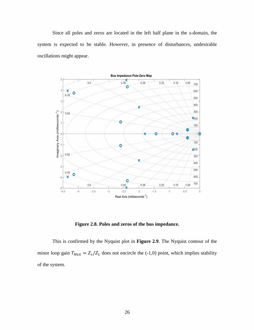
The resonance peak of 𝑍𝑏𝑢𝑠(𝑠) is at 234 Hz; Figure 2.8 shows that the bus
impedance has a pair of poles at this frequency with low damping factor of ζ = 0.153,
which also corresponds to a quality factor |𝑄|𝑑𝐵 = 10.29 𝑑𝐵.
26
Since all poles and zeros are located in the left half plane in the s-domain, the
system is expected to be stable. However, in presence of disturbances, undesirable
oscillations might appear.
Figure 2.8. Poles and zeros of the bus impedance.
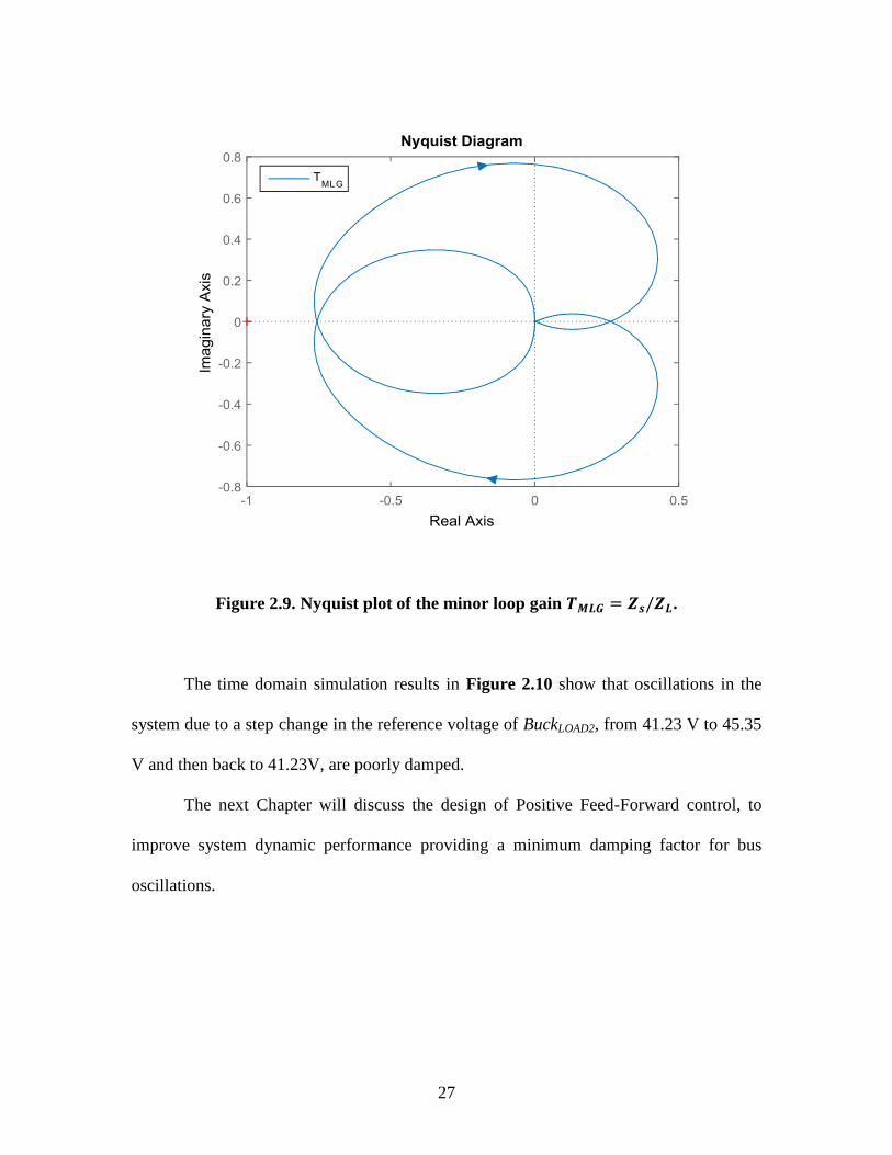
This is confirmed by the Nyquist plot in Figure 2.9. The Nyquist contour of the
minor loop gain 𝑇𝑀𝐿𝐺 = 𝑍𝑠/𝑍𝐿 does not encircle the (-1,0) point, which implies stability
of the system.
27
Figure 2.9. Nyquist plot of the minor loop gain 𝑻𝑴𝑳𝑮 = 𝒁𝒔/𝒁𝑳.
The time domain simulation results in Figure 2.10 show that oscillations in the
system due to a step change in the reference voltage of BuckLOAD2, from 41.23 V to 45.35
V and then back to 41.23V, are poorly damped.
The next Chapter will discuss the design of Positive Feed-Forward control, to
improve system dynamic performance providing a minimum damping factor for bus
oscillations.

28
Figure 2.10. Time domain simulation results in correspondence with a step in 𝑽𝟐𝒓𝒆𝒇.

29
CHAPTER 3
POSITIVE FEED-FORWARD CONTROL
This section introduces the principle of Positive Feed-Forward Control (PFF) and
a new approach for the design of the feed-forward gain based on the desired damping for
oscillations in DC power distribution system. The approach is validated using frequency
domain and time domain simulations results.
3.1. Principle of PFF control
Positive Feed-Forward control is proposed in [8] [9] [10] [11] as an alternative
active damping approach to improve the stability of a feedback-controlled switching
converter system, which is degraded due to source subsystem interaction.
The scheme is shown in Figure 3.1; a positive feed-forward loop is included in
combination with the already existing negative feedback for output regulation. The effect
of the positive feed-forward loop is the introduction of a virtual damping impedance at
the input ports of the converter.
The main advantage of this approach is that it does not require hardware
modification of the physical system and it provides the possibility of online tuning for an
adaptive control implementation.

30
Figure 3.1. PFF control block diagram.
Substitution of (3.1) into (2.2) results in the closed loop small-signal model (3.2)
for the combined feed-forward and feedback control of Figure 3.1.
𝑖𝑐 = (𝑣𝑔 − 𝑣𝑔𝑟𝑒𝑓)𝐺𝑐𝐹𝐹 + (𝑣𝑟𝑒𝑓 − 𝑣)𝐺𝑐𝐹𝐵
(3.1)
[𝑖𝑣] = [
1
𝑍𝑖𝑛𝐹𝐹𝐹𝐵 𝐺𝑖𝑔𝑖
𝐹𝐹𝐹𝐵 𝐺𝑖𝑔𝑐1𝐹𝐹𝐹𝐵
𝐺𝑣𝑔𝐹𝐹𝐹𝐵 −𝑍𝑜𝑢𝑡
𝐹𝐹𝐹𝐵 𝐺𝑣𝑐1𝐹𝐹𝐹𝐵
𝐺𝑖𝑔𝑐2𝐹𝐹𝐹𝐵
𝐺𝑣𝑐2𝐹𝐹𝐹𝐵
] [𝑣𝑔 𝑖𝑙𝑜𝑎𝑑 𝑣𝑟𝑒𝑓 𝑣𝑔𝑟𝑒𝑓]𝑇
(3.2)
The transfer functions in (3.2) are given by (3.3)-(3.10).
1
𝑍𝑖𝑛𝐹𝐹𝐹𝐵 =
1
𝑍𝑖𝑛𝐹𝐵 +
1
𝑍𝑑𝑎𝑚𝑝
(3.3)
𝐺𝑖𝑔𝑖𝐹𝐹𝐹𝐵 = 𝐺𝑖𝑔𝑖
𝐹𝐵
(3.4)
𝑣𝑔
𝑖𝑙𝑜𝑎𝑑
𝑖𝑐
𝑖
𝑣
c
load
g
CM
vd
CM
out
CM
vg
CM
igd
CM
igi
CM
ing
i
i
v
GZG
GGZ
v
i
ˆ
ˆ
ˆ/1
ˆ
ˆ
𝐺𝐹𝐵 𝑣𝑟𝑒𝑓 +
-
𝐺𝐹𝐹
++
𝑣𝑔𝑟𝑒𝑓
+-

31
𝐺𝑖𝑔𝑐1𝐹𝐹𝐹𝐵 = 𝐺𝑖𝑔𝑐
𝐹𝐵
(3.5)
𝐺𝑖𝑔𝑐2𝐹𝐹𝐹𝐵 = −
1
𝑍𝑑𝑎𝑚𝑝
(3.6)
𝐺𝑣𝑔𝐹𝐹𝐹𝐵 = 𝐺𝑣𝑔
𝐹𝐵 +𝐺𝑣𝑐𝐶𝑀
𝐺𝑖𝑔𝑐𝐶𝑀
1
𝑍𝑑𝑎𝑚𝑝
(3.7)
𝑍𝑜𝑢𝑡𝐹𝐹𝐹𝐵 = 𝑍𝑜𝑢𝑡
𝐹𝐵
(3.8)
𝐺𝑣𝑐1𝐹𝐹𝐹𝐵 = 𝐺𝑣𝑐
𝐹𝐵
(3.9)
𝐺𝑣𝑐2𝐹𝐹𝐹𝐵 = −
𝐺𝑣𝑐𝐶𝑀
𝐺𝑖𝑔𝑐𝐶𝑀
1
𝑍𝑑𝑎𝑚𝑝
(3.10)
From equation (3.3) it can be verified that the effect of the positive feed-forward
loop is to add a virtual damping impedance at the input port of the converter, in parallel
with the existing input impedance under feedback control only. The expression for the
damping impedance is given in (3.11), where 𝑇𝐹𝐹 is the feed-forward loop given in
(3.12).
𝑍𝑑𝑎𝑚𝑝 =𝑇𝐹𝐵 + 1
𝑇𝐹𝐹
(3.11)
𝑇𝐹𝐹 = 𝐺𝐶𝐹𝐹𝐺𝑖𝑔𝑐𝑃𝐼
(3.12)

32
This virtual impedance can be designed in a way that the overall system meets
certain dynamic specifications, like a desired damping factor, and from (3.12) the feed-
forward gain 𝐺𝐶𝐹𝐹 can be determined for the implementation of PFF control.
There is some trade off that has to be made according to the specific application
for which the converter is utilized; equation (3.7) shows that the input-to-output voltage
transfer function, also called audio susceptibility, is degraded with the implementation of
PFF control.
Summarizing, Figure 3.2 shows the effects of PFF control on the two port hybrid
g-parameter unterminated model developed in the previous chapter. Note that usually
𝑣𝑔𝑟𝑒𝑓 = 0, since the goal of the PFF control is to stabilize the bus voltage.
Figure 3.2. Unterminated small-signal model with PFF control.
3.2. The design of the PFF control
A new approach for the design of PFF control based on the desired dynamic
characteristics of the system is presented in this section.
+
-
+-
+-
𝑍𝑖𝑛𝐹𝐵 𝑍𝑑𝑎𝑚𝑝
𝐺𝑖𝑔𝑖𝐹𝐵 𝑙𝑜𝑎𝑑 𝐺𝑖𝑔𝑐
𝐹𝐵 𝑟𝑒𝑓 𝑣𝑔𝑟𝑒𝑓𝑍𝑑𝑎𝑚𝑝
-+
𝐺𝑣𝑔𝐹𝐵 +
𝐺𝑣𝑐𝐶𝑀
𝐺𝑖𝑔𝑐𝐶𝑀
1
𝑍𝑑𝑎𝑚𝑝 𝑔
𝐺𝑣𝑐𝐹𝐵 𝑟𝑒𝑓
𝐺𝑣𝑐𝐶𝑀
𝐺𝑖𝑔𝑐𝐶𝑀 𝑔𝑟𝑒𝑓
𝑍𝑜𝑢𝑡𝐹𝐵
𝑔
𝑔
𝑙𝑜𝑎𝑑
+
-

33
It was shown that the effect of PFF control is to introduce a virtual damping
impedance Zdamp at the input port of the converter. Figure 3.3 (a) is obtained by
considering the interacting system of Section 2.2, including the damping impedance and a
current injection at the DC bus for estimation of the bus impedance. In Figure 3.3 (b), the
bus impedance Zbus represents the parallel combination of the source output impedance
and the load input impedance under feedback control only.
(a) (b)
(c)
Figure 3.3. Interacting subsystems representation with PFF control: (a) circuital
model, (b) reduced circuital model and (c) block diagram.
The expression for the new overall bus impedance under feedback and feed-
forward control is obtained by determining the current injection-to-bus voltage transfer
+
-
𝑍𝑜𝑢𝑡𝑆
𝑍𝑖𝑛𝐿 𝑖𝑛𝑗
𝑏𝑢𝑠 𝑍𝑑𝑎𝑚𝑝
+
-
𝑍𝑏𝑢𝑠 𝑖𝑛𝑗 𝑏𝑢𝑠
𝑍𝑑𝑎𝑚𝑝
𝑍𝑏𝑢𝑠 𝑖𝑛𝑗
1
𝑍𝑑𝑎𝑚𝑝
+
-
𝑏𝑢𝑠

34
function given in (3.13), which resembles the closed loop transfer function of a negative
feedback control system where the forward gain is the original bus impedance and the
feedback gain is the damping admittance, as shown in Figure 3.3 (c). 𝑍𝑑𝑎𝑚𝑝 can be
designed based on the desired location of the dominant poles of (3.13).
𝑍𝑏𝑢𝑠𝐹𝐹 =𝑍𝑏𝑢𝑠
1 +𝑍𝑏𝑢𝑠𝑍𝑑𝑎𝑚𝑝
(3.13)
If we wish to have a pair of dominant poles 𝑠𝑟1,2 at the resonant frequency 𝜔𝑟𝑒𝑠
with minimum damping factor ζ𝑚𝑖𝑛
; 𝑠𝑟 given by (3.14) must satisfy the characteristic
equation of (3.13). This can be obtained by imposing the magnitude and phase conditions
on (3.15) and (3.16) [17].
𝑠𝑟 = −𝜔𝑟𝑒𝑠ζ𝑚𝑖𝑛± 𝑗𝜔𝑟𝑒𝑠√1 − ζ
𝑚𝑖𝑛2
(3.14)
|𝑍𝑏𝑢𝑠(𝑠𝑟)
𝑍𝑑𝑎𝑚𝑝(𝑠𝑟)| = 1
(3.15)
𝑎𝑟𝑔 𝑍𝑏𝑢𝑠(𝑠𝑟)
𝑍𝑑𝑎𝑚𝑝(𝑠𝑟) = ±𝜋
(3.16)
A passive 𝑅𝑑 − 𝐿𝑑 − 𝐶𝑑 parallel damping will be considered as the desired
damping impedance so that the bus impedance is only modified in a certain frequency
range around the resonant frequency.

35
The general expression for the damping impedance in the s-domain is given in
(3.17), where the resonant frequency 𝜔𝑑, the Q-factor and the characteristic impedance
𝑍0 are the three unknowns.
𝑍𝑑𝑎𝑚𝑝(s) = 𝑅𝑑 + 𝑠𝐿𝑑 +1
𝑠𝐶𝑑= 𝑍0
𝑠2
𝜔𝑑2 +
𝑠𝜔𝑑𝑄𝑑
+ 1
𝑠𝜔𝑑
(3.17)
𝜔𝑑 =1
√𝐿𝑑𝐶𝑑
(3.18)
𝑄𝑑 =1
𝑅𝑑√𝐿𝑑𝐶𝑑
(3.19)
𝑍0 = √𝐿𝑑𝐶𝑑
=1
𝜔𝑑𝐶𝑑= 𝜔𝑑𝐿𝑑
(3.20)
The Q-factor for 𝑍𝑑𝑎𝑚𝑝 is chosen to be 𝑄𝑑 = 0.5 (damping factor ζ𝑑= 1) to
avoid the appearance of additional resonances, then the expression for 𝑍𝑑𝑎𝑚𝑝 can be
rearrange as in (3.21).
𝑍𝑑𝑎𝑚𝑝(s) = 𝑍𝑜
1 + 2𝑠𝜔𝑑
+𝑠2
𝜔𝑑2
𝑠𝜔𝑑
=𝑍0𝜔𝑑
(𝜔𝑑 + 𝑠)2
𝑠
(3.21)
From the phase condition given in (3.16) the angle in (3.22) is obtained as
follows:

36
𝑎𝑟𝑔(𝑍𝑏𝑢𝑠(𝑠𝑟)) − 𝑎𝑟𝑔 (𝑍𝑑𝑎𝑚𝑝(𝑠𝑟)) = 𝜋
𝑎𝑟𝑔(𝑍𝑏𝑢𝑠(𝑠𝑟)) − 2𝑎𝑟𝑔(𝜔𝑑 + 𝑠𝑟) + 𝑎𝑟𝑔(𝑠𝑟) = 𝜋
𝜑 = 𝑎𝑟𝑔(𝜔𝑑 + 𝑠𝑟) =𝑎𝑟𝑔(𝑍𝑏𝑢𝑠(𝑠𝑟)) + 𝑎𝑟𝑔(𝑠𝑟) − 𝜋
2
(3.22)
Also,
𝜑 = 𝑎𝑟𝑔(𝜔𝑑 + 𝑠𝑟) = 𝑡𝑎𝑛−1
(
𝜔𝑟𝑒𝑠√1 − ζ
𝑚𝑖𝑛2
𝜔𝑑 − 𝜔𝑟𝑒𝑠ζ𝑚𝑖𝑛
)
(3.23)
Combining (3.22) and (3.23), the frequency 𝜔𝑑 is obtained.
𝜔𝑑 = 𝜉𝑚𝑖𝑛𝜔𝑟𝑒𝑠 +𝜔𝑟𝑒𝑠√1 − ζ
𝑚𝑖𝑛2
𝑡𝑎𝑛𝜑
(3.24)
From the amplitude condition in (3.15) the value of 𝑍0 is found to be:
𝑍0 = 𝜔𝑑
|𝑍𝑏𝑢𝑠(𝑠𝑟)||𝑠𝑟|
|𝜔𝑑 + 𝑠𝑟|2
=𝜔𝑑𝜔𝑟𝑒𝑠
𝜔𝑑2 + 𝜔𝑟𝑒𝑠
2 − 2𝜔𝑑𝜔𝑟𝑒𝑠휁𝑚𝑖𝑛
|𝑍𝑏𝑢𝑠(𝑠𝑟)|
(3.25)
The inductance 𝐿𝑑, capacitance 𝐶𝑑 and resistance 𝑅𝑑 are then determined as:
𝐿𝑑 =𝑍0𝜔𝑑
𝐶𝑑 =1
𝐿𝑑𝜔𝑑2 𝑅𝑑 =
𝑍0𝑄𝑑
(3.26)

37
3.3. An illustrative example and simulation
In this section, the proposed method will be utilized to improve the damping of
the DC system introduced in Section 2.3, in which BuckSOURCE regulates the DC bus
voltage and BuckLOAD1 and BuckLOAD2 feed resistive loads at different voltage levels.
The design procedure starts with the choice of the desired location of the
dominant poles of the bus impedance; considering that the minimum damping factor
ζ𝑚𝑖𝑛
= 0.5 is desired at the resonant frequency 𝜔𝑟𝑒𝑠 = 234 𝐻𝑧, the corresponding
desired dominant poles given by (3.14) are:
𝑠𝑟 = 2𝜋 × 234𝐻𝑧 [−0.5 ± 𝑗√3
2]
(3.27)
The magnitude and phase of the bus impedance evaluated at 𝑠𝑟 are:
|𝑍𝑏𝑢𝑠(𝑠𝑟)| = 10.13𝛺
𝑎𝑟𝑔(𝑍𝑏𝑢𝑠(𝑠𝑟)) = 219.34°
(3.28)
From the conditions (3.15) and (3.16), the magnitude and the phase of the
damping impedance must be:
|𝑍𝑑𝑎𝑚𝑝(𝑠𝑟)| = |𝑍𝑏𝑢𝑠(𝑠𝑟)| = 10.13𝛺
a𝑟𝑔 (𝑍𝑑𝑎𝑚𝑝(𝑠𝑟)) = 𝑎𝑟𝑔(𝑍𝑏𝑢𝑠(𝑠𝑟)) − 180° = 39.34°
(3.29)
And from equations (3.23) to (3.26) the components of the parallel damping
impedance are found to be:

38
𝑅𝑑 = 17.2Ω 𝐿𝑑 = 9𝑚𝐻 𝐶𝑑 = 120𝜇𝐹
(3.30)
Figure 3.4 shows the new bus impedance when PFF control is implemented on
BuckLOAD1. Compared to the original bus impedance the resonant peak is reduced. The
dominant poles at 234 Hz have damping factor ζ𝑚𝑖𝑛
= 0.5, as shown in Figure 3.5.
With the addition of the PFF control, the number of zeros and poles of the bus
impedance is increased by two, due to the zeros of the added damping impedance.
Figure 3.4. Bus impedance Bode plot, with PFF control.

39
Figure 3.5. Poles and zeros of the bus impedance, with PFF control.
The time domain simulation results, in Figure 3.6, show the improvement on the
damping factor of the DC system, significantly reducing the oscillations after a step
change in the reference voltage of BuckLOAD2.

40
Figure 3.6. Improvement in the time domain simulation results with PFF control.
As it was stated previously, the tradeoff in the application of Positive Feed-
Forward control is that the input-to-output voltage transfer function is degraded at low
frequency, as shown in Figure 3.7.

41
Figure 3.7. Bode plot of the input voltage-to-output voltage transfer function.
Another important aspect of cascaded systems is the degradation of the feedback
loop gain shown in Figure 3.8 and Figure 3.9, which affects the output performance of
the converters. It can be noticed that Positive Feed-Forward control also has a negative
effect on the loop gain reducing the phase margin for which the voltage feedback control
was designed originally.

42
Figure 3.8. Feedback loop gain of BuckLOAD1.
Figure 3.9. Feedback loop gain of BuckLOAD2.
43
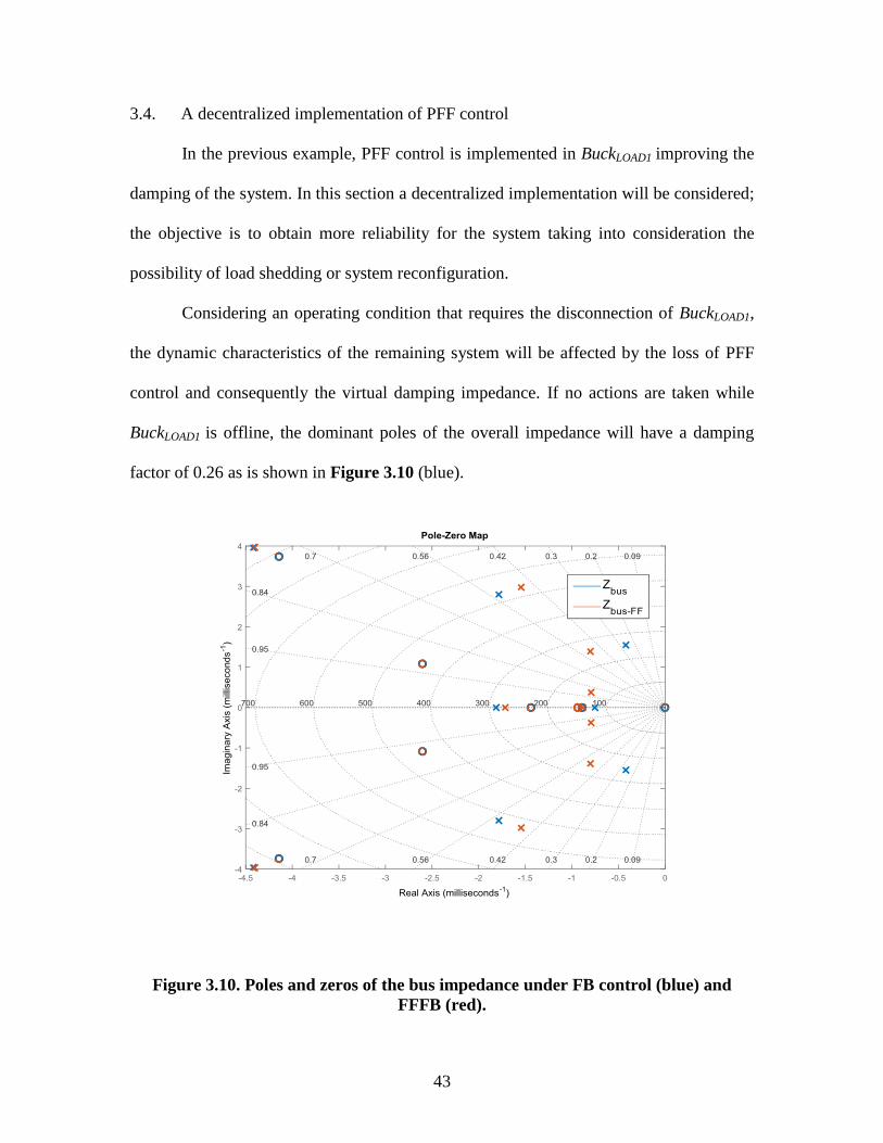
3.4. A decentralized implementation of PFF control
In the previous example, PFF control is implemented in BuckLOAD1 improving the
damping of the system. In this section a decentralized implementation will be considered;
the objective is to obtain more reliability for the system taking into consideration the
possibility of load shedding or system reconfiguration.
Considering an operating condition that requires the disconnection of BuckLOAD1,
the dynamic characteristics of the remaining system will be affected by the loss of PFF
control and consequently the virtual damping impedance. If no actions are taken while
BuckLOAD1 is offline, the dominant poles of the overall impedance will have a damping
factor of 0.26 as is shown in Figure 3.10 (blue).
Figure 3.10. Poles and zeros of the bus impedance under FB control (blue) and
FFFB (red).

44
For the remaining system, the required damping impedance that will maintain the
minimum damping factor of 0.5, can be found following the closed-form design
procedure proposed in the previous section. The parameters of the parallel damping
impedance are found to be:
𝑅𝑑2 = 23.84𝛺 𝐿𝑑2 = 12.72𝑚𝐻 𝐶𝑑2 = 89.52𝜇𝐹
By transferring the PFF control to BuckLOAD2 with the updated feed-forward gain,
the dominant poles of the overall bus impedance are moved farther away from the
imaginary axis, achieving a damping factor of 0.5 at the resonant frequency. The
improvement in the location of the dominant poles can be verified in Figure 3.10 and the
effect on the resonant peak of the bus impedance is shown in Figure 3.11.
Figure 3.11. Bus impedance under PFF control.

45
Figure 3.12 shows time domain simulation results; a step change in the reference
voltage of BuckLOAD2 is applied for three different scenarios:
a) BuckLOAD1 and BuckLOAD2 in service and the PFF control is implemented in
BuckLOAD1
b) BuckLOAD1 is out of service and no PFF control is implemented in the
remaining system
c) BuckLOAD1 is out of service and the PFF control is transferred from
BuckLOAD1 to BuckLOAD2.
From this result, it is evident that an adaptive implementation of the PFF control
based on the most updated model of the system guarantees that the dynamic performance
will remain as specified.
Figure 3.12. Time domain simulation results for scenarios (a), (b) and (c).

46
CHAPTER 4
SYSTEM IDENTIFICATION
System identification is a very powerful technique that allows on-line estimation
of systems’ parameters; in particular we are interested in obtaining input/output
impedances of power converters connected to a specific DC bus and the overall bus
impedance for stability analysis purposes. In the following chapter a review of the state of
the art for wideband impedance identification is presented, followed by a proposed
method to improve the estimation accuracy and a technique to obtain the bus impedance
performing local measurements on each converter.
4.1. Cross-correlation method
In this section we review the cross-correlation method which measures the
similarity between two signals [18] and that has been applied for system identification of
power converters with digital control to estimate control-to-output transfer functions [19]
[20] [21] [14] and network impedances [12] [13].
In steady-state for small signal disturbances, a digitally controlled power
converter can be considered as a linear time-invariant discrete-time system, where the
sampled system is represented as:
𝑦[𝑛] = ∑ℎ[𝑘]𝑢[𝑛 − 𝑘]
∞
𝑘=1
+ 𝑣[𝑛]
(4.1)

47
In (4.1) 𝑦[𝑛] is the sampled output signal, 𝑢[𝑛] the input digital control signal,
ℎ[𝑛] is the discrete-time system impulse response and 𝑣[𝑛] represents disturbances such
as switching noise, measurement error, quantization noise, etc. as shown in Figure 4.1.
Figure 4.1. Linear time-invariant system
The cross-correlation of the input and output signals is:
𝑅𝑢𝑦[𝑚] = ∑𝑢[𝑛]𝑦[𝑛 + 𝑚]
∞
𝑛=1
= ∑ℎ[𝑛]𝑅𝑢𝑢[𝑚 − 𝑛]
∞
𝑛=1
+ 𝑅𝑢𝑣[𝑚]
(4.2)
where 𝑅𝑢𝑢[𝑚] is the auto-correlation of the input signal and 𝑅𝑢𝑣[𝑚] is the input-
to-disturbance cross-correlation.
The relations in (4.3) hold when white noise is used as input, which is a random
signal with constant power spectral density.
SystemInput u[m]
Disturbance v[m]
Output y[m]

48
𝑅𝑢𝑢[𝑚] = 𝛿[𝑚]
𝑅𝑢𝑣[𝑚] = 0
(4.3)
It follows that ideally the auto-correlation of the input is a delta function and the
cross-correlation of white noise input with disturbances is zero. Under these conditions
(4.2) reduces to (4.4) and the cross-correlation of the input and output signals gives the
discrete time system impulse response.
𝑅𝑢𝑦[𝑚] = ℎ[𝑚]
(4.4)
The input to output transfer function in the frequency domain can be derived by
applying Discrete Fourier Transform (DFT). For a given finite-duration sequence 𝑥[𝑛] of
length N, so that 𝑥[𝑛] = 0 for 𝑛 < 0 and 𝑛 ≥ 𝑁, the DFT is defined as in (4.5).
𝑋(𝑘) = ∑ 𝑥[𝑛]𝑒−𝑗2𝜋𝑘𝑛/𝑁𝑁−1
𝑛=0
, 𝑘 = 0,1, … ,𝑁 − 1
(4.5)
So the input-to-output transfer function can be found from (4.6).
𝐻(𝑘) = 𝐷𝐹𝑇𝑅𝑢𝑦[𝑚] = ∑ 𝑅𝑢𝑦[𝑛]𝑒−𝑗2𝜋𝑘𝑛/𝑁
𝑁−1
𝑛=0
, 𝑘 = 0,1, … ,𝑁 − 1
(4.6)
4.2. Maximum length Pseudo-Random Binary Sequences (PRBS)
The analysis above requires the use of white noise as input perturbation. An
infinite-bandwidth white noise signal is a purely theoretical construction and the
bandwidth is limited in practice by the mechanism of noise generation. A random signal

49
is considered white noise if it presents a flat spectrum over the range of frequencies of
interest.
In this context an approximation of white noise can be accomplished in digitally
controlled converters by using a maximum length Pseudo Random Binary Sequence
(PRBS) signal as input perturbation.
A PRBS signal is a series of width modulated rectangular pulses as shown in
Figure 4.2. This signal, while appearing random, is in fact a periodic and deterministic
signal, which implies that the sequence can be repeated and its output can be determined
when the initial conditions and the sequence generation scheme are specified.
Figure 4.2. PRBS signal
The PRBS signal can be generated by a shift register with feedback. The two
variables that have to be defined in the generation of a maximum length PRBS signal are
the period length, determined by the number of shift register bits, and the frequency band
which depends on the sequence length and the sample frequency.

50
An N-bit register will generate a PRBS of length L given in (4.7), the lower and
upper limits of the bandwidth are given in (4.8), where T is the clock period of the shift
register and 𝑓𝑠 is the converter switching frequency.
𝐿 = 2𝑁 − 1
(4.7)
𝑓𝑙𝑜𝑤𝑒𝑟 =
1
𝐿 × 𝑇
𝑓𝑢𝑝𝑝𝑒𝑟 =𝑓𝑠2
(4.8)
A given power converter cannot be controlled beyond the Nyquist frequency,
which is half of the switching frequency 𝑓𝑠; it follows that, in order to obtain the highest
possible bandwidth, the bit period has to be chosen equal to the inverse of 𝑓𝑠 as in (4.9).
𝑇 =1
𝑓𝑠
(4.9)
4.3. Simplifications of the cross-correlation method
In order to save time domain cross-correlation calculations, simplifications to the
existing methodology are proposed in [22] so that almost all calculations are made in the
frequency domain.
Given two sequences 𝑥1[𝑛] and 𝑥2[𝑛] of length N, with DFT given in (4.10)
and (4.11). From the properties of the DFT it is known that the product of 𝑋1(𝑘) and
𝑋2(𝑘) is equivalent to the DFT of the circular convolution of the two sequences in the
time domain as shown in (4.12) [18].

51
𝑋1(𝑘) = ∑ 𝑥1[𝑛]𝑒−𝑗2𝜋𝑛𝑘𝑁
𝑁−1
𝑛=0
, 𝑘 = 0,1, … ,𝑁 − 1
(4.10)
𝑋2(𝑘) = ∑ 𝑥2[𝑛]𝑒−𝑗2𝜋𝑛𝑘𝑁
𝑁−1
𝑛=0
, 𝑘 = 0,1, … ,𝑁 − 1
(4.11)
𝑋3(𝑘) = 𝑋1(𝑘)𝑋2(𝑘) → 𝑥3[𝑚] = ∑ 𝑥1[𝑛]𝑥2[𝑚 − 𝑛]𝑁 , 𝑚 = 0,1, … ,𝑁 − 1
𝑁−1
𝑛=0
(4.12)
This property can be applied to the results in (4.4) and (4.6); so that when the
input is white noise (4.14) is obtained.
𝐷𝐹𝑇𝑅𝑢𝑦[𝑚] = 𝐷𝐹𝑇𝑢[𝑛]𝐷𝐹𝑇𝑦[𝑛]
(4.13)
𝐻(𝑘) = 𝐷𝐹𝑇𝑢[𝑛]𝐷𝐹𝑇𝑦[𝑛]
(4.14)
The circularity that arises from the property (4.12) eliminates the necessity of
padding the sampled data with zeros; which was previously done by applying a Gaussian
window [21]. Also, by utilizing the Fast Fourier Transform (FFT) method the required
computational calculations can be reduced significantly.
When the desired result is the impedance looking outwards from a power
converter as impedance Z in Figure 4.3, the simplification in (4.15) can be made so that
the input excitation cancels out and by taking the ratio of the voltage and current DFTs a
finite set of values of 𝑍(𝑗𝜔) can be found.

52
𝑍(𝑗𝜔) =𝐺𝑢𝑣(𝑗𝜔)
𝐺𝑢𝑖(𝑗𝜔)=𝐷𝐹𝑇𝑢[𝑛]𝐷𝐹𝑇𝑣[𝑛]
𝐷𝐹𝑇𝑢[𝑛]𝐷𝐹𝑇𝑖[𝑛]=𝐷𝐹𝑇𝑣[𝑛]
𝐷𝐹𝑇𝑖[𝑛]
(4.15)
Figure 4.3. Impedance measurement
Additionally, when a non-ideal white noise is used to excite the system, from
(4.2) it is possible to find the input-to-output transfer function as in (4.16).
𝐺𝑢𝑦(𝑗𝜔) =𝐷𝐹𝑇𝑅𝑢𝑦[𝑛]
𝐷𝐹𝑇𝑅𝑢𝑢[𝑛]=𝐷𝐹𝑇𝑦[𝑛]
𝐷𝐹𝑇𝑢[𝑛]
(4.16)
This reduces the non-ideality introduced by the use of PRBS signal as an
approximation of white noise and also corrects the results for colored noise if used
instead of white noise.
4.4. On-line impedance estimation using a double PRBS signal injection
In previous works [12] [13] [21], the injection of the PRBS signal was done as
shown in Figure 4.4 in order to directly perturb the duty cycle signal. The impedance
Switching Power
Converter
Z
PWMDuty Cicle
+V-
PRBS
I

53
looking out from the converter can then obtained from (4.15) by measuring the
corresponding voltages and currents.
Figure 4.4. Single PRBS injection in the duty cycle signal for impedance estimation
In case of feedback-controlled converters like in Figure 4.4, the perturbation is
attenuated at low frequencies by the factor 1/𝑇(𝑠), where 𝑇(𝑠) represents the feedback
loop gain of the converter under test. As an example, the effect of the feedback in the
perturbation-to-output voltage transfer function is given in (4.17).
𝑣2𝑃𝑅𝐵𝑆
=𝐺𝑣𝑑
1 + 𝑇(𝑗𝜔)≈
𝐺𝑣𝑑𝑇(𝑗𝜔)
𝑎𝑡 𝑙𝑜𝑤 𝑓𝑟𝑒𝑞𝑢𝑒𝑛𝑐𝑖𝑒𝑠 𝑤ℎ𝑒𝑟𝑒 |𝑇(𝑗𝜔)| ≫ 1
𝐺𝑣𝑑 𝑎𝑡 ℎ𝑖𝑔ℎ 𝑓𝑟𝑒𝑞𝑢𝑒𝑛𝑐𝑖𝑒𝑠 𝑤ℎ𝑒𝑟𝑒 |𝑇(𝑗𝜔)| ≪ 1
(4.17)
The feedback attenuates the disturbance introduced by the PRBS signal at low
frequencies, where the loop gain is large.
Converter under test
Z2PWM
Gc Vref
+V2-
PRBS
I2
+V1-
I1
Z1

54
If on the other hand, the perturbation is applied in the reference signal of the FB
loop like in Figure 4.5, the low frequency identification is expected to be more accurate.
However, the signal gets attenuated at higher frequencies by the loop gain 𝑇(𝑠). The
effect of the feedback in the perturbation-to-output voltage transfer function for this case
is given in.(4.18).
𝑣2𝑃𝑅𝐵𝑆
=𝑇(𝑗𝜔)
1 + 𝑇(𝑗𝜔)≈
1 𝑎𝑡 𝑙𝑜𝑤 𝑓𝑟𝑒𝑞𝑢𝑒𝑛𝑐𝑖𝑒𝑠 𝑤ℎ𝑒𝑟𝑒 |𝑇(𝑗𝜔)| ≫ 1
𝑇(𝑗𝜔) 𝑎𝑡 ℎ𝑖𝑔ℎ 𝑓𝑟𝑒𝑞𝑢𝑒𝑛𝑐𝑖𝑒𝑠 𝑤ℎ𝑒𝑟𝑒 |𝑇(𝑗𝜔)| ≪ 1
(4.18)
Figure 4.5. Single PRBS injection in the FB reference signal for impedance
estimation
Since the input/output impedances of power converters vary across the frequency
range of operation, it is important to obtain an accurate estimation both at low and high
frequencies.
In order to improve the wideband impedance identification, a double injection of
the PRBS signal as shown in Figure 4.6 is proposed. K1 and K2 are proper gains to
ensure that the amplitude of the perturbations on the one hand is not too small and on the
Converter under test
Z2
PWM Gc Vref
+V2-
PRBS
I2
+V1-
I1
Z1

55
other hand it does not causes that voltage and current levels exceed 10% of their nominal
values in order to avoid large disturbances. In this configuration the perturbation applied
to the reference signal dominates at low frequencies, while the perturbation applied to the
duty cycle signal dominates at higher frequencies.
Figure 4.6. Double injection of the PRBS signal for impedance estimation
4.5. An illustrative example and simulation
A 14-bit PRBS signal is used to perform impedance identification in the system
introduced in Section 2.3; the signal has period T = 0.05 ms which is also the switching
period of the converters.
The upper and lower frequency limits can be obtained as shown in Section 4.2:
N = 14 bits
L = 2N − 1 = 16383
flower =20 kHz
L= 1.22 Hz
Converter under test
Z2
+V2-
I2
+V1-
I1
Z1PWM
Gc Vref
PRBSK1K2

56
fupper = fN = 10 kHz
One of the difficulties in estimating the impedances is that for certain converters
the bus current is a discontinuous signal that changes in amplitude and is also modulated,
as shown in Figure 4.7. The change in the modulation is problematic, because the
sampling should be fast enough to capture the perturbations induced by the injection of
the PRBS.
Figure 4.7. Bus current waveform
In simulation it is possible to sample at a high rate but in practice this is limited
by the capability of Analog-to-Digital Converters (ADC). The sampling frequency of the
bus voltage and current signals is chosen to be 𝑓𝑠𝑎𝑚𝑝𝑙𝑒 = 2 𝑀𝐻𝑧, so that 100 points are
obtained in each switching period.
In order to avoid aliasing effect an analog filter is also included to attenuate high
frequency noise above the Nyquist frequency.
To build the bus impedance of the DC system introduced in Section 2.3 using the
existing power converters, it is necessary to make a test on each converter and measure
Ibus
t
Switching Period Ts

57
the impedance of the equivalent network seen from the converter under test. The three
cases are depicted in Figure 4.8, Figure 4.9 and Figure 4.10; these tests have the
advantage that in each case, the measurements can be done locally in the converter under
test.
Figure 4.8. Schematic representation of Test 1
𝐵𝑢𝑐𝑘𝑠𝑜𝑢𝑟𝑐𝑒 𝐵𝑢𝑐𝑘𝐿𝑜𝑎𝑑 1
𝐵𝑢𝑐𝑘𝐿𝑜𝑎𝑑 2
Test signal
Equivalent NetworkTest 1
𝑍𝑡𝑒𝑠𝑡 1

58
Figure 4.9. Schematic representation of Test 2
Figure 4.10. Schematic representation of Test 3
The measured impedances are given in (4.19)-(4.21).
1
𝑍𝑡𝑒𝑠𝑡1=
1
𝑍𝑜𝑢𝑡𝑆 +
1
𝑍𝑖𝑛𝐿2
𝑇
(4.19)
𝐵𝑢𝑐𝑘𝑠𝑜𝑢𝑟𝑐𝑒 𝐵𝑢𝑐𝑘𝐿𝑜𝑎𝑑 1
𝐵𝑢𝑐𝑘𝐿𝑜𝑎𝑑 2
Test signal
Equivalent NetworkTest 2
𝑍𝑡𝑒𝑠𝑡 2
𝐵𝑢𝑐𝑘𝑠𝑜𝑢𝑟𝑐𝑒 𝐵𝑢𝑐𝑘𝐿𝑜𝑎𝑑 1
𝐵𝑢𝑐𝑘𝐿𝑜𝑎𝑑 2
Test signal
Equivalent NetworkTest 3
𝑍𝑡𝑒𝑠𝑡 3

59
1
𝑍𝑡𝑒𝑠𝑡2=
1
𝑍𝑜𝑢𝑡𝑆 +
1
𝑍𝑖𝑛𝐿1
𝑇
(4.20)
1
𝑍𝑡𝑒𝑠𝑡3=
1
𝑍𝑖𝑛𝐿1
𝑇
+1
𝑍𝑖𝑛𝐿2
𝑇
(4.21)
The bus impedance can now be estimated from the parametric models as in
(4.22), which can be used in the design of the Positive Feed-Forward Control.
1
𝑍𝑏𝑢𝑠=1
2[
1
𝑍𝑡𝑒𝑠𝑡1+
1
𝑍𝑡𝑒𝑠𝑡2+
1
𝑍𝑡𝑒𝑠𝑡3]
(4.22)
The impedance identification results from Test 1, Test 2 and Test 3 are shown in
Figure 4.11, Figure 4.12 and Figure 4.13 respectively, in which the results for single
and double injection of the PRBS signal are compared to the analytic impedance transfer
functions, presenting improvement in the accuracy especially at low frequencies as
expected.

60
(a)
(b)
Figure 4.11. Test 1: Impedance identification results (dots) compared to the analytic
expression (solid line) using (a) single PRBS injection and (b) double PRBS injection
(a)
(b)
Figure 4.12. Test 2: Impedance identification results (dots) compared to the analytic
expression (solid line) using (a) single PRBS injection and (b) double PRBS injection

61
(a)
(b)
Figure 4.13. Test 3: Impedance identification results (dots) compared to the analytic
expression (solid line) using (a) single PRBS injection and (b) double PRBS injection
The bus impedance is constructed as in (4.22) and shown in Figure 4.14 where is
compared to the analytic transfer function. A good matching between the estimation and
the analytic transfer function is obtained for the frequency range of interest. The
identification process gives a finite set of points that represent the non-parametric
frequency response. A parametric model of the bus impedance can be obtained by
implementing the method of least squares fitting [23].

62
Figure 4.14. Estimated bus impedance (dots) compared to the analytic transfer
function (solid)
A subset of logarithmically spaced data points, shown in Figure 4.15, is utilized
in the fitting process in order to enforce equal fitting priority across the frequency range
of the measured impedance as seen in the Bode plot with its logarithmic x-axis [14]. This
reduces the computational effort in the numerical fitting algorithm.

63
Figure 4.15. 𝒁𝒃𝒖𝒔 estimated (dots) and logarithmically thinned subset (x mark)
The method of least squares fitting consists in adjusting the coefficients of a
candidate transfer function 𝑍𝑐𝑎𝑛𝑑𝑖𝑑𝑎𝑡𝑒(𝑠) that minimizes the cost function defined by
(4.23).
𝐽𝑊𝐿𝑆 =1
2∑(휀𝑘)
2
𝑘
(4.23)
Where 휀 is the error between the candidate transfer function and the measured
frequency response.
휀𝑘=𝑍𝑐𝑎𝑛𝑑𝑖𝑑𝑎𝑡𝑒(𝑗𝜔𝑘) − 𝑍(𝑗𝜔𝑘)
(4.24)

64
The parametric model of the bus impedance in Figure 4.16 is obtained from the
nonparametric complex frequency response. The result is in good agreement with the
analytic transfer function, validating the identification process.
Figure 4.16. Parametric model of 𝒁𝒃𝒖𝒔 (dash) compared to the analytic model
(solid).
4.6. Design of PFF control
Following the approach presented in Section 3.2., the damping impedance that
will provide the system with a minimum damping factor of ζ𝑚𝑖𝑛
= 0.5 is determined
from the estimation of the bus impedance.

65
Figure 4.17 shows a comparison between the damping impedance obtained from
the analytic and parametric models of the bus impedance, giving similar results.
Figure 4.17. Design of the damping impedance using the analytic model (blue) and
the parametric model (red).
The time domain simulation results are shown in the following figure, where the
Positive Feed-Forward control designed from the parametric model is implemented in
BuckLOAD1. The results show well-damped oscillations in correspondence to a step change
in the reference voltage of BuckLOAD2.

66
Figure 4.18. Time domain simulation results with the implementation of PFF
control obtained from the estimation of 𝒁𝒃𝒖𝒔.

67
CHAPTER 5
CONCLUSIONS AND FUTURE WORK
5.1. Conclusions
The main motivation of this work were the issues related to instability in DC
Power Distribution Systems caused by the interaction among switching power converters
and the necessity for estimating the bus impedance using system identification
techniques.
Positive Feed-Forward control is an active approach for improvement of stability
margins; it can be designed to place the dominant poles of a DC system bus impedance in
a specified location with a desired damping factor. This is important because, as shown in
Chapter 2, the bus impedance affects the dynamic response of the system.
Wideband impedance identification is improved by performing double injection
of a Pseudo Random Binary Sequence signal as proposed in Chapter 4, allowing a more
accurate estimation of the impedance looking out from the converter under test. The
significance of the proposed technique is that it can be implemented to estimate the bus
impedance by performing local measurements on each converter without the necessity of
extra measurement equipment, constituting a low cost solution.

68
5.2. Future Work
5.2.1. Online tuning
One of the advantages of the proposed Positive Feed-Forward control design is
that it allows the design of a virtual damping impedance to improve stability margins and
dynamic characteristics based on measurements obtained from impedance identification
techniques.
The impedance identification can be implemented to keep track of the bus
impedance variations, which can be used for online tuning of the PFF control based on
the most updated estimation of the bus impedance. Particularly this can be performed in
the case of load shedding presented in Chapter 2, in which it was shown to be necessary
to transfer the PFF control from a disconnected converter to an active converter with a
new damping impedance in order to maintain the good dynamic response of the
remaining system. A possible adaptive control scheme is shown in Figure 5.1.
Figure 5.1. Online tuning scheme.
5.2.2. Experimental Validation
The impedance identification and the implementation of the PFF control was
proven to improve the systems dynamics through time domain simulations. It is left as a
future task to perform the experimental validation of the proposed method.
Disable LoadSystem
IdentificationAdaptive PFF Transfer PFF
Tests measurements

69
REFERENCES
[1] IEEE Recommended Practice for 1 kV to 35 kV Medium-Voltage DC Power
Systems on Ships, 2010, pp. 1-54.
[2] M. Cupelli, F. Ponci, G. Sulligoi, A. Vicenzutti, C. Edrington, T. El-Mezyani and A.
Monti, "Power flow control and network stability in an all-electric ship,"
Proceedings of the IEEE, vol. 103, no. 12, pp. 2355 - 2380.
[3] Q. Zhou and D. Yuan, "Prediction on Future DC Power System," IEEE 6th
International Power Electronics and Motion Control Conference, pp. 1192 - 1195,
2009.
[4] R. Middlebrook, "Input filter considerations in design and application of switching
regulators," Proc. IEEE Ind. Appl. Soc. Annual Meeting, pp. 366-382, 1979.
[5] A. Emadi, A. Khaligh, C. Rivetta and G. Williamson, "Constant power loads and
negative impedance instability in automotive systems: definition, modelling,
stability, and control of power electronic converters and motor drives," IEEE
Transaction on Vehicular Technology , vol. 55, no. 4, pp. 1112 - 1125, 2006.
[6] A. Riccobono and E. Santi, "Comprehensive Review of Stability Criteria for DC
Power Distribution Systems," IEEE Transactions on Industrial Applications, vol. 50,
no. 5, pp. 3525 - 3535, 2014.
[7] A. Riccobono and E. Santi, "A novel Passivity-Base Stability Criterion (PBSC) for
switching converter DC distribution systems," 27th Annual IEEE Applied Power
Electronics Conference and Exposition , pp. 2560 - 2567, 2012.
[8] A. Riccobono, "Stabilizing controller design for a DC power distribution system
using a passivity-based stability criterion," in Ph.D. dissertation, University of South
Carolina, Columbia, SC, 2013.
[9] A. Riccobono and E. Santi, "Positive feed-forward control of three-phase voltage
source inverter for dc input bus stabilization with experimental validation," IEEE
Transactions on Industry Applications , vol. 49, no. 1, pp. 168-177, 2013.

70
[10] H. Cho and E. Santi, "Modelling and stability analysis in multi-converter systems
including positive feedforward control," 34th Annual Conference of IEEE Industrial
Electronics, pp. 839 - 844, 2008.
[11] H. Cho and E. Santi, "Modelling, control and stability analysis of a converter in
multi-converter systems including positive feedforward control," Ph.D. dissertation,
University of South Carolina, 2009.
[12] A. Barkley and E. Santi, "Online monitoring of network impedances using digital
network analyzer techniques," Twenty-Fourth Annual IEEE Applied Power
Electronics Conference and Exposition, pp. 440 - 446, 2009.
[13] D. Martin, E. Santi and A. Barkley, "Wide bandwidth system identificaiton of AC
system impedances by applying perturbations to an existing converter," 2011 IEEE
Energy Conversion Congress and Exposition, pp. 2549 - 2556, 2011.
[14] J. Siegers, S. Arrua and E. Santi, "Stabilizing controller design for multi-bus MVDC
distribution systems using a passivity based stability criterion and positive feed-
forward control," in IEEE Energy Conversion Congress and Exposition, Montreal,
2015.
[15] A. Barkley, "Online identification, monitoring and control of a DC/DC converter
system using digital network analyzer techniques," PhD Dissertation, University of
South Carolina, 2005.
[16] R. Erickson and D. Maksimovic, Fundamentals of Power Electronics, Springer,
2001.
[17] J. Maciejowski, Multivariable Feedback Design, Addison-Wesley, 1989.
[18] G. Franklin, J. D. Powell and A. Emami-Naeini, Feedback Control of Dynamic
Systems, US: Addison-Wesley, 1995.
[19] J. Proakis and D. Manolakis, "The Discrete Fourier Transform: Its properties and
applications," in Digital Signal Processing, Pearson, 4th Edition, pp. 464-472.
[20] B. Miao , R. Zane and D. Maksimovic, "A modified cross-correlation method for
system identification of power converters with digital control," 35th Annual IEEE
Power Electronics Specialists Conference, pp. 3728-3733, 2004.
[21] B. Miao, R. Zane and D. Maksimovic, "System identification of power converters
with digital control through cross-correlation methods," IEEE Transactions on

71
Power Electronics, vol. 20, no. 5, pp. 1093-1099, 2005.
[22] A. Barkley and E. Santi, "Improved online identification of a dc-dc converter and its
control loop gain using cross-correlation methods," IEEE Transactions on Power
Electronics, vol. 24, no. 8, pp. 2021-2031, 2009.
[23] D. Martin, "Applications of power electronics converter based wideband system
identification in grid tied AC power systems," in Ph.D. dissertation, University of
South Carolina. Columbia, SC, 2012.
[24] K. Astrom and B. Wittenmark, Computer-Controlled Systems, Dover, 2014.
[25] X. Zhang and X. Ruan, "Adaptive active capacitor converter for improving stability
of cascaded dc power supply system," IEEE Transactions on Power Electronics,
vol. 28, no. 4, pp. 1807 - 1816, April 2013.