polymorphic chip multiprocessor architecture … · over the last several years uniprocessor...
TRANSCRIPT

POLYMORPHIC CHIP MULTIPROCESSOR ARCHITECTURE
A DISSERTATION
SUBMITTED TO THE DEPARTMENT OF ELECTRICAL ENGINEERING
AND THE COMMITTEE ON GRADUATE STUDIES
OF STANFORD UNIVERSITY
IN PARTIAL FULFILLMENT OF THE REQUIREMENTS FOR THE DEGREE OF
DOCTOR OF PHILOSOPHY
Alexandre Solomatnikov
December 2008
ii
© Copyright by Alexandre Solomatnikov 2009
All Rights Reserved
iii
I certify that I have read this dissertation and that in my opinion it is fully adequate, in scope and quality, as dissertation for the degree of Doctor of Philosophy.
__________________________________ Mark A. Horowitz (Principal Advisor)
I certify that I have read this dissertation and that in my opinion it is fully adequate, in scope and quality, as dissertation for the degree of Doctor of Philosophy.
__________________________________ Christos Kozyrakis
I certify that I have read this dissertation and that in my opinion it is fully adequate, in scope and quality, as dissertation for the degree of Doctor of Philosophy.
__________________________________ Stephen Richardson
Approved for the University Committee on Graduate Studies
__________________________________

iv
v
ABSTRACT
Over the last several years uniprocessor performance scaling slowed significantly
because of power dissipation limits and the exhausted benefits of deeper pipelining and
instruction-level parallelism. To continue scaling performance, microprocessor designers
switched to Chip Multi-Processors (CMP). Now the key issue for continued performance
scaling is the development of parallel software applications that can exploit their
performance potential. Because the development of such applications using traditional
shared memory programming models is difficult, researchers have proposed new parallel
programming models such as streaming and transactions. While these models are
attractive for certain types of applications they are likely to co-exist with existing shared
memory applications.
We designed a polymorphic Chip Multi-Processor architecture, called Smart Memories,
which can be configured to work in any of these three programming models. The design
of the Smart Memories architecture is based on the observation that the difference
between these programming models is in the semantics of memory operations. Thus, the
focus of the Smart Memories project was on the design of a reconfigurable memory
system. All memory systems have the same fundamental hardware resources such as data
storage and interconnect. They differ in the control logic and how the control state
associated with the data is manipulated. The Smart Memories architecture combines
reconfigurable memory blocks, which have data storage and metadata bits used for
control state, and programmable protocol controllers, to map shared memory, streaming,
and transactional models with little overhead. Our results show that the Smart Memories
architecture achieves good performance scalability. We also designed a test chip which is
an implementation of Smart Memories architecture. It contains eight Tensilica processors
vi
and the reconfigurable memory system. The dominant overhead was from the use of
flops to create some of the specialized memory structures that we required. Since
previous work has shown this overhead can be made small, our test-chip confirmed that
hardware overhead for reconfigurability would be modest.
This thesis describes the polymorphic Smart Memories architecture and how three
different models—shared memory, streaming and transactions—can be mapped onto it,
and presents performance evaluation results for applications written for these three
models.
We found that the flexibility of the Smart Memories architecture has other benefits in
addition to better performance. It helped to simplify and optimize complex software
runtime systems such as Stream Virtual Machine or transactional runtime, and can be
used for various semantic extensions of a particular programming model. For example,
we implemented fast synchronization operations in the shared memory mode which
utilize metadata bits associated with data word for fine-grain locks.

vii
ACKNOWLEDGMENTS
During my years at Stanford, I had an opportunity to work with many wonderful people.
This work would not be possible without their generous support.
Firstly, I am very grateful to my advisor, Mark Horowitz, for giving me the opportunity
to work with him. His technical expertise, dedication, immense patience, and availability
to students made him a great advisor.
I would like to thank my orals and reading committee members, Bill Dally, Christos
Kozyrakis, Steve Richardson and Balaji Prabhakar, who provided insightful comments on
my research. I have been a student in several of their classes at Stanford that greatly
enhanced my understanding of many areas of research.
My research would not have been possible without the technical and administrative
support provided by Charlie Orgish, Joe Little, Greg Watson, Taru Fisher, Penny
Chumley, and Teresa Lynn.
I would also like to thank DARPA for their financial support.
Mark Horowitz’s VLSI group has been a friendly and interesting environment. Smart
Memories team was also a great group to be apart of. I am especially thankful to Amin
Firoozshahian who was my officemate for many years and one of the key members of
Smart Memories project team. Through Smart Memories project I had a chance to work
with great people such as, Ofer Shacham, Zain Asgar, Megan Wachs, Don Stark,
Francois Labonte, Jacob Chang, Kyle Kelley, Vicky Wong, Jacob Leverich, Birdy
Amrutur and others. This work has benefited greatly from their help and expertise.
I am very thankful to people at Tensilica, Chris Rowen, Dror Maydan, Bill Huffman,
Nenad Nedeljkovic, David Heine, Ding-Kai Chen, Junjie Gu, Himanshu Sanghavi, Nupur

viii
Andrews, Chris Benson and others, who tolerated my questions and requests for so many
years. This work would not have been possible without access to Tensilica’s technology
and support.
I am also very thankful to all my friends for their moral support. They have made my
experience at Stanford more enjoyable and memorable.
Finally, I’d like to thank my wife Marina for her love, support and encouragement.
ix
TABLE OF CONTENTS
List of Tables .................................................................................................................... xii
List of Figures .................................................................................................................. xiii
Chapter 1: Introduction ........................................................................................................1
Chapter 2: Architectural Trends...........................................................................................3
2.1 Processor Performance and Microarchitecture Trends ............................................3
2.2 Chip Multiprocessors ...............................................................................................8
2.3 Parallel Memory Models..........................................................................................9
2.3.1 Shared Memory Model with Cache Coherence ............................................10
2.3.2 Streaming Memory Model............................................................................12
2.3.3 Transactional Memory Model.......................................................................14
2.4 The Case for A Polymorphic Chip Multi-Processor..............................................19
Chapter 3: Smart Memories Architecture ..........................................................................22
3.1 Overall Architecture...............................................................................................22
3.2 Processor ................................................................................................................25
3.2.1 Interfacing the Tensilica Processor to Smart Memories ...............................26
3.2.2 Special Memory Access Instructions............................................................28
3.2.3 Pipelining Issues Related to Special Memory Instructions...........................29
3.2.4 Pre-Defined Options and VLIW Processor Extensions ................................31
3.3 Memory Mat ..........................................................................................................32
3.4 Tile .........................................................................................................................35
3.4.1 Interface Logic ..............................................................................................37
3.4.2 Crossbar ........................................................................................................40
3.4.3 Statistics and Debugging Unit ......................................................................41
3.4.4 Tile Timing ...................................................................................................42
3.4.5 Tile Reconfigurability Overhead ..................................................................43
x
3.5 Quad.......................................................................................................................45
3.5.1 Protocol Controller........................................................................................47
3.5.2 Example of Protocol Controller Operation ...................................................54
3.5.3 Related Work and Discussion of Protocol Controller Design ......................54
3.6 On-Chip Network...................................................................................................55
3.7 Memory Controller ................................................................................................58
3.8 Smart Memories Test Chip ....................................................................................62
3.9 Summary ................................................................................................................64
Chapter 4: Shared Memory................................................................................................65
4.1 Hardware Configuration ........................................................................................65
4.2 Fast Fine-Grain Synchronization ...........................................................................68
4.3 Evaluation ..............................................................................................................70
4.3.1 Performance of Fast Fine-Grain Synchronization Operations......................73
4.3.2 MPEG-2 Encoder..........................................................................................75
4.4 Conclusions............................................................................................................81
Chapter 5: Streaming .........................................................................................................82
5.1 Hardware Configuration ........................................................................................82
5.2 Direct Memory Access Channels...........................................................................85
5.3 Runtime..................................................................................................................86
5.3.1 Stream Virtual Machine................................................................................87
5.3.2 Pthreads Runtime for Streaming...................................................................91
5.4 Evaluation ..............................................................................................................93
5.4.1 Application Case Study: 179.art ...................................................................99
5.5 Conclusions..........................................................................................................104
Chapter 6: Transactions ...................................................................................................106
6.1 Transational Functionality ...................................................................................106
6.2 Hardware Configuration ......................................................................................108
6.3 TCC Optimization................................................................................................113
6.4 TCC Runtime .......................................................................................................115

xi
6.4.1 Arbitration for commit................................................................................115
6.4.2 Hardware Overflow ....................................................................................116
6.4.3 Processor State Recovery from Violation...................................................117
6.5 Evaluation ............................................................................................................119
6.6 Possible Extensions and Optimizations ...............................................................124
6.7 Conclusions..........................................................................................................125
Chapter 7: Conclusions and Future Directions ................................................................127
7.1 Future Directions .................................................................................................128
Appendix A: Special Memory Instructions .....................................................................129
Appendix B: 179.art Streaming Optimizations................................................................131
Appendix C: TCC Application Programming Interface ..................................................135
Appendix D: Using A Register Windows Mechanism for Processor State
Checkpointing ............................................................................................................137
Bibliography ....................................................................................................................140
xii
LIST OF TABLES
Number Page
Table 3.1: Tile area breakdown after logic synthesis ........................................................45
Table 3.2: Virtual channel assignment...............................................................................57
Table 3.3: Smart Memories test chip details......................................................................63
Table 3.4: Smart Memories test chip area breakdown.......................................................64
Table 4.1: Shared memory applications.............................................................................70
Table 4.2: Shared memory kernels ....................................................................................70
Table 4.3: System configuration parameters .....................................................................71
Table 5.1: Streaming Applications ....................................................................................94
Table 6.1: Characteristics of Smart Memories transactional mode .................................119
Table 6.2: Percentage of TCC buffered loads and stores.................................................124

xiii
LIST OF FIGURES
Number Page
Figure 2.1: Integer Application Performance (SPECint2006).............................................4
Figure 2.2: Floating Point Application Performance (SPECfp2006) ..................................5
Figure 2.3: Microprocessor Clock Frequency (MHz)..........................................................6
Figure 2.4: Clock Cycle in FO4...........................................................................................7
Figure 2.5: Microprocessor Power Dissipation (W) ............................................................7
Figure 2.6: Normalized Energy per Instruction vs Normalized Performance .....................9
Figure 3.1: Smart Memories Architecture .........................................................................23
Figure 3.2: Xtensa Processor Interfaces.............................................................................27
Figure 3.3: Processor Interfaces to Smart Memories.........................................................28
Figure 3.4: Processor Pipeline ...........................................................................................30
Figure 3.5: Memory operation pipeline: a) without interlocks; b) with interlocks............31
Figure 3.6: Memory mat ....................................................................................................33
Figure 3.7: Tile...................................................................................................................36
Figure 3.8: Tile pipeline.....................................................................................................43
Figure 3.9: Tile layout after place&route ..........................................................................44
Figure 3.10: Quad ..............................................................................................................46
Figure 3.11: Protocol Controller block diagram................................................................48
Figure 3.12: D-Unit............................................................................................................51
Figure 3.13: Example of cache miss processing................................................................54
Figure 3.14: Flit Payload Formats .....................................................................................56
Figure 3.15: Memory Controller........................................................................................59
Figure 3.16: Smart Memories test chip die........................................................................63
Figure 4.1: Example of cached configuration....................................................................66
Figure 4.2: Hierarchical cache coherence..........................................................................67
Figure 4.3: Shared memory application speedups .............................................................72
Figure 4.4: Shared memory kernel speedups.....................................................................73
Figure 4.5: mp3d performance with and without locking..................................................75
Figure 4.6: MPEG-2 encoder speedups for different cache configurations.......................78
Figure 4.7: Instruction miss rate for different cache configurations (%)...........................79
Figure 4.8: Instruction fetch stalls for different cache configurations (%)........................79
Figure 4.9: Number of out-of-Quad fetch misses (millions) .............................................80
Figure 4.10: Average fetch latency (cycles) ......................................................................81
Figure 5.1: Example of streaming configuration ...............................................................83
Figure 5.2: Alternative streaming configuration................................................................84
Figure 5.3: SVM compiler flow for Smart Memories .......................................................87
Figure 5.4: SVM mapping on Smart Memories.................................................................90
Figure 5.5: Performance scaling of streaming applications...............................................95
Figure 5.6: Off-chip bandwidth utilization ........................................................................96
Figure 5.7: Cycle breakdown for 179.art ...........................................................................96
Figure 5.8: Performance scaling of streaming applications with 4MB L2 cache..............98
Figure 5.9: Cycle breakdown for 179.art with 4 MB L2 cache .........................................99
Figure 5.10: 179.art speedups ..........................................................................................100
Figure 5.11: 179.art off-chip memory traffic...................................................................101
Figure 5.12: 179.art off-chip memory utilization ............................................................102
Figure 5.13: 179.art data cache miss rate.........................................................................103
Figure 6.1: Example of TCC configuration .....................................................................110
Figure 6.2: Performance scaling of TCC applications.....................................................120
Figure 6.3: Cycle breakdown for barnes..........................................................................121
Figure 6.4: Cycle breakdown for mp3d ...........................................................................122
Figure 6.5: Cycle breakdown for fmm.............................................................................122
Figure 6.6: Percentage of violated transactions ...............................................................123
xiv

CHAPTER 1: INTRODUCTION
For a long time microprocessor designers focused on improving the performance of
sequential applications on single processor machines, achieving annual performance
growth rate of over 50% [1]. This phenomenal performance growth relied on three main
factors: exploiting instruction-level parallelism (ILP), decreasing the number of “gates”
in each clock cycle by building faster functional units and longer instruction pipelines,
and using the faster transistors provided by CMOS technology scaling [2, 3].
Unfortunately, the first two factors have reached their limit. As a result of this and
limitations such as wire delay and slowly changing memory latency, single processor
performance growth slowed down dramatically [1-5]. In addition, increasing complexity
and deeper pipelining reduce the power efficiency of high-end microprocessors [6, 7].
These trends led researchers and industry towards parallel systems on a chip [8-22].
Parallel systems can efficiently exploit the growing number of transistors provided by
continuing technology scaling [2, 4, 5].
Programmers must re-write application software to realize the benefits of these parallel
systems on a chip. Since traditional parallel programming models such as shared memory
and message passing are not easy to use [23-24], researchers have proposed a number of
new programming models. Two of the most popular today are streaming [25-28] and
transactions [29-32]. Although these new programming models are effective for some
applications, they are not universal and the traditional shared memory model is still being
used. Also, new programming models are still evolving as researchers refine their APIs
[36-39].
The goal of the Stanford Smart Memories project is to design a flexible architecture that
can support several programming models and a wide range of applications. Since
processors are fundamentally flexible – their operation is set by the code they run – our
1

2
focus was on making the memory system as flexible as the processors. We designed a
coarse-grain architecture that uses reconfigurable memory blocks [40, 41] and a
programmable protocol controller to provide the flexible memory system. Memory
blocks have additional meta-data bits and can be configured to work as various memory
structures, such as cache memory or local scratchpad, for a particular programming
model or application. The protocol controller can be programmed to support different
memory protocols, like cache coherence or transactional coherence and consistency
(TCC) [32].
This thesis describes the polymorphic Smart Memories architecture and how three
different models—shared memory, streaming and transactions—can be mapped onto it,
and presents performance evaluation results for applications written for these three
models. In addition, this thesis discusses other benefits of reconfigurability such as
optimization of complex software runtime systems and semantic extensions.
The next chapter discusses microprocessor design trends, why the industry switched to
chip multi-processors, reviews multi-processor programming models and makes the case
for reconfigurable, polymorphic chip multi-processors architecture. Chapter 3 describes
the design of polymorphic Smart Memories architecture and the design of Smart
Memories test chip. Next three chapters show how three different programming models
can be mapped onto Smart Memories architecture and how reconfigurability can be used
for semantic extensions and implementation of complex software runtime systems.
Chapter 7 presents conclusions of this thesis.

3
CHAPTER 2: ARCHITECTURAL TRENDS
To better understand the transition to chip multiprocessors (CMP), this chapter begins by
reviewing historical processor performance trends, and how these improvements were
generated. During the early 2000’s power became an important limit, and further
improvement in performance required more energy efficient computation. The data on
prior processor design clearly shows that achieving the highest performance is not energy
efficient – two processors running at half the performance dissipate much less power then
one processor. Thus parallel processors allow one to continue to scale chip level
performance, but gives rise to another difficult issue: generating parallel code to run on
these machines.
Parallel application development is known to be a difficult problem. While there have
been many attempts to create compilers that can parallelize old non-numeric code [42,
43], researchers are also exploring new computational models that are explicitly or
implicitly parallel. This chapter also explores some of these programming models to
better understand their requirements on the computing hardware. Since it seems likely
that each of these programming models will exist in some form in the future, this chapter
makes a case for a polymorphic chip multiprocessor architecture which can be configured
to support the three described programming models as well as hybrid models, making it
suitable for broad range of applications.
2.1 PROCESSOR PERFORMANCE AND MICROARCHITECTURE TRENDS
Microprocessor performance initially grew exponentially at the rate of more than 50%
per year, as shown in Figure 2.1 and Figure 2.2 using SPEC 2006 benchmark [48, 49]

4
results1. This phenomenal performance growth continued for 16 years; however, it then
slowed down significantly [1].
0.01
0.10
1.00
10.00
100.00
88 90 92 94 96 98 00 02 04 06 08
Year of Introduction
intel 486intel pentiumintel pentium 2intel pentium 3intel pentium 4intel itaniumAlpha 21064Alpha 21164Alpha 21264SparcSuperSparcSparc 64-bitMipsHP PAPower PCAMD K6AMD K7AMD x86-64IBM PowerIntel Core 2AMD Opteron
Figure 2.1: Integer Application Performance (SPECint2006)
To achieve such growth, microprocessor designers exploited instruction level parallelism
(ILP) to increase the number of instructions per cycle (IPC) [1-3] and steadily increased
processor clock frequency (Figure 2.3).
There is little instruction level parallelism left that can be exploited efficiently to improve
performance [1, 2]. In fact, microprocessor architects confront a complex trade-off
between making more complicated processors to increase IPC and increasing clock
frequency through deeper pipelining at the cost of reduced IPC [3].
1 For older processors, SPEC2006 numbers were estimated from older versions of SPEC
benchmark using scaling factors.

5
0.001
0.010
0.100
1.000
10.000
100.000
88 90 92 94 96 98 00 02 04 06 08
Year of Introduction
intel 486intel pentiumintel pentium 2intel pentium 3intel pentium 4intel itaniumAlpha 21064Alpha 21164Alpha 21264SparcSuperSparcSparc 64-bitMipsHP PAPower PCAMD K6AMD K7AMD x86-64IBM PowerIntel Core 2AMD Opteron
Figure 2.2: Floating Point Application Performance (SPECfp2006)
Increases in clock frequency were possible because of deeper pipelining and
improvements in transistor speed due to CMOS technology scaling. To separate the effect
of technology scaling, processor clock cycle time can be characterized using the
technology-independent delay metric of fanout-of-four delay (FO4), which is defined as
the delay of one inverter driving four equally sized inverters [50, 51]. Figure 2.4 shows
estimates of microprocessor clock cycle time expressed in terms of FO4. Clock cycle
time decreased, from 60-90 FO4 in 1988 to 12-25 in 2003-2004, mainly because of
deeper pipelines. Further decrease in clock cycle time measured in FO4 are unlikely
because it is yielding less and less performance improvement while increasing power
dissipation, complexity and cost of design [2, 3]. As a result clock frequency doesn’t
grow as fast as before (Figure 2.3).

6
10
100
1000
10000
88 90 92 94 96 98 00 02 04 06 08Year of Introduction
intel 386intel 486intel pentiumintel pentium 2intel pentium 3intel pentium 4intel itaniumAlpha 21064Alpha 21164Alpha 21264SparcSuperSparcSparc64MipsHP PAPower PCAMD K6AMD K7AMD x86-64Intel Pentium DIntel Core 2 DuoIntel XeonSun NiagaraIBM PowerAMD
Figure 2.3: Microprocessor Clock Frequency (MHz)
The only remaining factor driving uniprocessor performance is improving transistor
switching speed due to CMOS technology scaling. However, as processor designs
became power and wire limited, it is harder to use faster transistors to design faster
uniprocessors [2]. As a result clock frequency and processor performance doesn’t scale as
fast as before (Figure 2.1, Figure 2.2, Figure 2.3).
Also, processor power dissipation increased because of both higher complexity and
higher clock frequency, and eventually reached the limit for air-cooled chips (Figure 2.5).
These trends caused a switch towards chip multiprocessors (CMP) or multi-core
microprocessors.

7
0
10
20
30
40
50
60
70
80
90
100
88 90 92 94 96 98 00 02 04 06 08Year of Introduction
intel 386intel 486intel pentiumintel pentium 2intel pentium 3intel pentium 4intel itaniumAlpha 21064Alpha 21164Alpha 21264SparcSuperSparcSparc 64-bitMipsHP PAPower PCAMD K6AMD K7AMD x86-64Intel Pentium DIntel Core 2 DuoIntel XeonSun NiagaraIBM PowerAMD
Figure 2.4: Clock Cycle in FO4
1
10
100
1000
88 90 92 94 96 98 00 02 04 06 08Year of Introduction
intel 386intel 486intel pentiumintel pentium 2intel pentium 3intel pentium 4intel itaniumAlpha 21064Alpha 21164Alpha 21264SparcSuperSparcSparc 64-bitMipsHP PAPower PCAMD K6AMD K7AMD x86-64Intel Pentium DIntel Core 2 DuoIntel XeonSun NiagaraIBM PowerAMD
Figure 2.5: Microprocessor Power Dissipation (W)

8
2.2 CHIP MULTIPROCESSORS
Performance of CMPs can potentially scale with the number of the processors or cores on
the die without re-design of individual processors. Therefore, the same processor design
with small modifications can be used across multiple generations of product, amortizing
the cost of design and verification.
Also, scaling CMP performance does not require an increase in energy dissipation per
instruction; on the contrary, CMP performance can be increased simultaneously with a
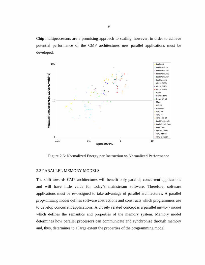
reduction in energy spent per instruction. Figure 2.6 shows, for single processors, how
energy per instruction increases with performance. On this graph, energy dissipation and
performance are both normalized with respect to technology and supply voltage.
Similarly, examination of Intel microprocessor design data from i486 to Pentium 4
showed that power dissipation scales as performance1.73 after factoring out technology
improvements [52]. Thus, Intel Pentium 4 is approximately 6 times faster than i486 in the
same technology but consumes 23 times more power [52] which means Pentium 4 spends
approximately 4 times more energy per instruction.
By using a less aggressive processor design it is possible to reduce energy dissipation per
instruction and at the same time use multiple processors to scale overall chip
performance. This approach can thus use a growing number of transistors per chip to
scale performance while staying within the limit of air-cooling [2].
The switch to chip multiprocessors also helps to reduce the effect of wire delays, which is
growing relative to gate delay [2, 8, 9]. Each processor in a CMP is small relative to the
total chip area, and wire length within a processor is short compared to the die size. Inter-
processor communication still requires long global wires; however, the latency of inter-
processor communication is less critical for performance in a multi-processor system than
latency between units within a single processor. Also, these long wires can be pipelined
and thus don’t affect clock cycle time and performance of an individual processor in a
CMP.
9
Chip multiprocessors are a promising approach to scaling, however, in order to achieve
potential performance of the CMP architectures new parallel applications must be
developed.
1
10
100
0.01 0.1 1 10Spec2006*L
Wat
ts/(N
umC
ores
*Spe
c200
6*L*
Vdd^
2)
Intel 486Intel PentiumIntel Pentium 2Intel Pentium 3Intel Pentium 4Intel ItaniumAlpha 21064Alpha 21164Alpha 21264SparcSuperSparcSparc 64-bitMipsHP PAPower PCAMD K6AMD K7AMD x86-64Intel Pentium DIntel Core 2 DuoIntel XeonIBM POWERAMD AthlonAMD Opteron
Figure 2.6: Normalized Energy per Instruction vs Normalized Performance
2.3 PARALLEL MEMORY MODELS
The shift towards CMP architectures will benefit only parallel, concurrent applications
and will have little value for today’s mainstream software. Therefore, software
applications must be re-designed to take advantage of parallel architectures. A parallel
programming model defines software abstractions and constructs which programmers use
to develop concurrent applications. A closely related concept is a parallel memory model
which defines the semantics and properties of the memory system. Memory model
determines how parallel processors can communicate and synchronize through memory
and, thus, determines to a large extent the properties of the programming model.
10
A large portion of existing parallel applications were developed using a multi-threaded
shared memory model. Existing concurrent applications such as web-servers are mostly
server-side applications which have abundant parallelism. Multi-threaded model fits well
these applications because they asynchronously handle many independent request
streams [23]. Also, multiple threads in such applications share no or little data or use
abstract data store, such as a database which supports highly concurrent access to
structured data [23]. Still, developing and scaling server-side applications can be a
challenging task.
As chip multi-processors become mainstream even in desktop computers, parallel
software needs to be developed for different application domains that do not necessarily
have the same properties as server-side applications. A conventional multi-threaded,
shared memory model might be inappropriate for these applications because it has too
much non-determinism [24]. Researchers have proposed new programming and memory
models such as streaming and transactional memory to help with parallel application
development. The rest of this section reviews these three parallel memory models and the
issues associated with them.
2.3.1 SHARED MEMORY MODEL WITH CACHE COHERENCE
In cache-coherent shared memory systems, only off-chip DRAM memory is directly
addressable by all processors. Because off-chip memory is slow compared to the
processor, fast on-chip cache memories are used to store the most frequently used data
and to reduce the average access latency. Cache management is performed by hardware
and does not require software intervention. As a processor performs loads and stores,
hardware attempts to capture the working set of the application by exploiting spatial and
temporal locality. If the data requested by the processor is not in the cache, the controller
replaces the cache line least likely to be used in the future with the appropriate data block
fetched from DRAM.

11
Software threads running on different processors communicate with each other implicitly
by writing and reading shared memory. Since several caches can have copies of the same
cache line, hardware must guarantee cache coherence, i.e. all copies of the cache line
must be consistent. Hardware implementations of cache coherence typically follow an
invalidation protocol: a processor is only allowed to modify an exclusive private copy of
the cache line, and all other copies must be invalidated before a write. Invalidation is
performed by sending “read-for-ownership” requests to other caches. A common
optimization is to use cache coherence protocols such as MESI
(Modified/Exclusive/Shared/Invalid), which reduce the number of cases where remote
cache lookups are necessary.
To resolve races between processors for the same cache line, requests must be serialized.
In small-scale shared memory systems serialization is performed by a shared bus or ring,
which broadcasts every cache miss request to all processors. The processor that wins bus
arbitration receives the requested cache line first. Bus-based cache coherent systems are
called also symmetric multi-processors (SMP) because any processor can access any
main memory location, with the same average latency.
High latency and increased contention make the bus a bottleneck for large multiprocessor
systems. Distributed shared memory (DSM) systems eliminate this bottleneck by
physically distributing both processors and memories, which then communicate via an
interconnection network. Directories associated with DRAM memory blocks perform
coherence serialization. Directory-based cache coherence protocols try to minimize
communication by keeping track of cache line sharing in the directories and sending
invalidation requests only to processors that previously requested the cache line. DSM
systems are also called non-uniform memory access (NUMA) architectures because
average access latency depends on processor and memory location. Development of high-
performance applications for NUMA systems can be significantly more complicated
because programmers need to pay attention to where the data is located and where the
computation is performed.

12
In comparison with traditional multiprocessor systems, chip multiprocessors have
different design constraints. On one hand, chip multiprocessors have significantly higher
interconnect bandwidth and lower communication latencies than traditional multi-chip
multiprocessors. This implies that the efficient design points for CMPs are likely to be
different from those for traditional SMP and DSM systems. Also, even applications with
a non-trivial amount of data sharing and communication can perform and scale
reasonably well. On the other hand, power dissipation is a major design constraint for
modern CMPs; low power is consequently one of the main goals of cache coherence
design.
To improve performance and increase concurrency, multiprocessor systems try to overlap
and re-order cache miss refills. This raises the question of a memory consistency model:
what event ordering does hardware guarantee [53]? Sequential consistency guarantees
that accesses from each individual processor appear in program order, and that the result
of execution is the same as if all accesses from all processors were executed in some
sequential order [54]. Relaxed consistency models give hardware more freedom to re-
order memory operations but require programmers to annotate application code with
synchronization or memory barrier instructions to insure proper memory access ordering.
To synchronize execution of parallel threads and to avoid data races, programmers use
synchronization primitives such as locks and barriers. Implementation of locks and
barriers requires support for atomic read-modify-write operations, e.g. compare-and-swap
or load-linked/store-conditional. Parallel application programming interfaces (API) such
as POSIX threads (Pthreads) [55] and ANL macros [56] define application level
synchronization primitives directly used by the programmers in the code.
2.3.2 STREAMING MEMORY MODEL
Many current performance limited applications operate on large amounts of data, where
the same functions are applied to each data item. One can view these applications as

13
having a stream of data that passes through a computational kernel that produces another
stream of data.
Researchers have proposed several stream programming languages, including
StreamC/KernelC [26], StreamIt [28], Brook GPU [58], Sequoia [59], and CUDA [60].
These languages differ in their level of abstraction but they share some basic concepts.
Streaming computation must be divided into a set of kernels, i.e. functions that cannot
access arbitrary global state. Inputs and outputs of the kernel are called streams and must
be specified explicitly as kernel arguments. Stream access patterns are typically
restricted. Another important concept is reduction variables, which allow a kernel to do
calculations involving all elements of the input stream, such as the stream’s summation.
Restrictions on data usage in kernels allow streaming compilers to determine
computation and input data per element of the output stream, to parallelize kernels across
multiple processing elements, and to schedule all data movements explicitly. In addition,
the compiler optimizes the streaming application by splitting or merging kernels for
balance loading, to fit all required kernel data into local scratchpads, or to minimize data
communication through producer-consumer locality. The complier also tries to overlap
computation and communication by performing stream scheduling: DMA transfers run
during kernel computation, which is equivalent to macroscopic prefetching.
To develop a common streaming compiler infrastructure, the stream virtual machine
(SVM) abstraction has been proposed [61-63]. SVM gives high-level optimizing
compilers for stream languages a common intermediate representation.
To support this type of application, in streaming architectures fast on-chip storage is
organized as directly addressable memories called scratchpads, local stores, or stream
register files [11, 16, 27]. Data movement within chip and between scratchpads and off-
chip memory is performed by direct memory access (DMA) engines, which are directly
controlled by application software. As a result, software is responsible for managing and

14
optimizing all aspects of communication: location, granularity, allocation and
replacement policies, and the number of copies. Stream applications have simple and
predictable data flow, so all data communication can be scheduled in advance and
completely overlapped with computation, thus hiding communication latency.
Since data movements are managed explicitly by software, complicated hardware for
coherence and consistency is not necessary. The hardware architecture only must support
DMA transfers between local scratchpads and off-chip memory.2 Processors can access
their local scratchpads as FIFO queues or as randomly indexed memories [57].
Streaming is similar to message-passing applied in the context of CMP design. However,
there are several important differences between streaming and traditional message-
passing in clusters and massively parallel systems. In streaming, the user level software
manages communication and its overhead is low. Message data is placed at the memory
closest to the processor, not the farthest away. Also, software has to take into account the
limited size of local scratchpads. Since communication between processors happens
within a chip, the latency is low and the bandwidth is high. Finally, software manages
both the communication between processors and the communication between processor
scratchpads and off-chip memory.
2.3.3 TRANSACTIONAL MEMORY MODEL
The traditional shared memory programming model usually requires programmers to use
low-level primitives such as locks for thread synchronization. Locks are required to
guarantee mutual exclusion when multiple threads access shared data. However, locks are
hard to use and error-prone — especially when the programmer uses fine-grain locking
2 Some recent stream machines use caches for one of the processors, the control
processor. In these cases, while the local memory does not need to maintain coherence with the memory, the DMA often needs to be consistent with the control processor. Thus in the IBM Cell Processor the DMA engines are connected to a coherent bus and all DMA transfers are performed to coherent address space [16].

15
[34] to improve performance and scalability. Programming errors using locks can lead to
deadlock. Lock-based parallel applications can also suffer from priority inversion and
convoying [31]. These arise when subtle interaction between locks causes high priority
tasks to wait for lower priority tasks to complete.
Transactional memory was proposed as a new multiprocessor architecture and
programming model intended to make lock-free synchronization3 of shared data accesses
as efficient as conventional techniques based on locks [29-31]. The programmer must
annotate applications with start transaction/end transaction commands; the hardware
executes all instructions between these commands as a single atomic operation. A
transaction is essentially a user-defined atomic read-modify-write operation that can be
applied to multiple arbitrary words in memory. Other processors or threads can only
observe transaction state before or after execution; intermediate state is hidden. If a
transaction conflict is detected, such as one transaction updating a memory word read by
another transaction, one of the conflicting transactions must be re-executed.
The concept of transactions is similar to the transactions in database management systems
(DBMS). In DBMS, transactions provide the properties of atomicity, consistency,
isolation, and durability (ACID) [65]. Transactional memory provides the properties of
atomicity and isolation. Also, using transactional memory the programmer can guarantee
consistency according to the chosen data consistency model.
Transactions are useful not only because they simplify synchronization of accesses to
shared data but also because they make synchronization composable [66], i.e.
transactions can be correctly combined with other programming abstractions without
understanding of those other abstractions [35]. For example, a user transaction code can
call a library function that contains a transaction itself. The library function transaction
3 Lock-free shared data structures allow programmers to avoid problems associated with
locks [64]. This methodology requires only standard compare-and-swap instruction but introduces significant overheads and thus it is not widely used in practice.

16
would be subsumed by the outer transaction and the code would be executed correctly4.
Unlike transactions, locks are not composable: a library function with a lock might cause
deadlock.
Transactional memory implementations have to keep track of the transaction read-set, all
memory words read by the transaction, and the write-set, all memory words written by
the transaction. The read-set is used for conflict detection between transactions, while the
write-set is used to track speculative transaction changes, which will become visible after
transaction commit or will be dropped after transaction abort. Conflict detection can be
either pessimistic (eager) or optimistic (lazy). Pessimistic conflict detection checks every
individual read and write performed by the transaction to see if there is a collision with
another transaction. Such an approach allows early conflict detection but requires read
and write sets to be visible to all other transactions in the system. In the optimistic
approach, conflict detection is postponed until the transaction tries to commit.
Another design choice for transactional memory implementations is the type of version
management. In eager version management, the processor writes speculative data directly
into the memory as a transaction executes and keeps an undo log of the old values [68].
Eager conflict detection must be used to guarantee transaction atomicity with respect to
other transactions. Transaction commits are fast since all data is already in place but
aborts are slow because old data must be copied from the undo log. This approach is
preferable if aborts are rare but may introduce subtle complications such as weak
atomicity [69]: since transaction writes change the architectural state of the main memory
they might be visible to other threads that are executing non-transactional code.
4 Nesting of transactions can cause subtle performance issues. Closed-nested and open-
nested transactions were proposed to improve the performance of applications with nested transactions [67, 36, 37]. The effects of closed-nested transaction can be rolled back by a parent transaction, while the writes of open-nested transaction can not be undone after commit.

17
Lazy version management is another alternative, where the controller keeps speculative
writes in a separate structure until a transaction commits. In this case aborts are fast since
the state of the memory is not changed but the commits require more work. This
approach makes it easier to support strong atomicity: complete transaction isolation from
both transactions and non-transactional code executed by other threads [69].
Transactional memory implementations can be classified as hardware approaches (HTM)
[30-32, 68], software-only (STM) techniques [70], or mixed approaches. Two mixed
approaches have been proposed: hybrid transactional memory (HyTM) supports
transactional execution in hardware but falls back to software when hardware resources
are exceeded [71, 72, 20], while hardware-assisted STM (HaSTM) combines STM with
hardware support to accelerate STM implementations [73, 74].
In some proposed hardware transactional memory implementations, a separate
transactional or conventional data cache is used to keep track of transactional reads and
writes [31]. In this case, transactional support extends existing coherence protocols such
as MESI to detect collisions and enforce transaction atomicity. The key issues with such
approaches are arbitration between conflicting transactions and dealing with overflow of
hardware structures. Memory consistency is also an issue since application threads can
execute both transactional and non-transactional code.
Transactional coherence and consistency (TCC) is a transactional memory model in
which atomic transactions are always the basic unit of parallel work, communication, and
memory coherence and consistency [32]. Each of the parallel processors in a TCC model
continually executes transactions. Each transaction commits its writes to shared memory
only as an atomic block after arbitration for commit. Only one processor can commit at a
time by broadcasting its transactional writes to all other processors and to main memory.
Other processors check incoming commit information for read-write dependency
violations and restart their transactions if violations are detected. Instead of imposing
some order between individual memory accesses, TCC serializes transaction commits.

18
All accesses from an earlier committed transaction appear to happen before any memory
references from a later committing transaction, even if actual execution was performed in
an interleaved fashion. The TCC model guarantees strong atomicity because the TCC
application only consists of transactions. A simple approach to handle hardware overflow
in TCC model is to allow overflowing transaction to commit before reaching the commit
point in the application. Such a transaction must stall and arbitrate for a commit token.
Once it has the token, it is no longer speculative, and can commit its previously
speculative changes to free up hardware resources, and then continue execution. It can’t
release the commit token until it hits the next commit point in the application. All other
processors can not commit until the commit token is free. Clearly this serializes
execution, since only one thread can have the commit token at a time, but it does allow
overflows to be cleanly handled5.
A programmer using TCC divides an application into transactions, which will be
executed concurrently on different processors. The order of transaction commits can be
optionally specified. Such situations usually correspond to different phases of the
application, which would have been separated by synchronization barriers in a lock-based
model. To deal with such ordering requirements TCC has hardware-managed phase
numbers for each processor, which can be optionally incremented upon transaction
commit. Only transactions with the oldest phase number are allowed to commit at any
time.
An example of a transactional application programming interface (API) is OpenTM [38].
The goal of OpenTM is to provide a common programming interface for various
transactional memory architectures.
5 Another proposed approach is to switch to software transactional memory (STM) mode.
This approach is called virtualized transactional memory. Challenges associated with virtualization are discussed in [34].

19
2.4 THE CASE FOR A POLYMORPHIC CHIP MULTI-PROCESSOR
While new programming models such as streaming and transactional memory are
promising for certain application domains, they are not universal. Both models address
particular issues associated with the conventional multi-threaded shared memory model.
Specifically, the goal of streaming is to optimize the use of bandwidth and on-chip
memories for applications with highly predictable memory access patterns. The
streaming model strives to avoid inefficiencies resulting from the implicit nature of cache
operation and cache coherence by exposing memory and communication management
directly to software. However, this might be inappropriate for applications that have
complex, hard to predict memory access patterns. Moreover, in some cases stream
architecture with cache performs better than the same architecture without cache but with
sophisticated streaming software optimizations [75]. Also, sometimes application
developers emulate caches in software because they cannot find any other way to exploit
data locality [76].
Transactional memory is a promising approach for parallelization of applications with
complex data structures because it simplifies accesses to shared data, avoiding locks and
problems associated with them. However, transactional memory cannot solve all
synchronization issues, for example, in the case of coordination or sequencing of
independent tasks [35]. Also, it is not necessary for all applications, for example,
applications that fit well into streaming category. For streaming applications,
synchronization of shared data accesses is not the main issue and therefore transactional
memory mechanisms would be simply unnecessary.
Finally, the multi-threaded programming model with shared memory is still dominant
today especially in server-side application domain. The asynchronous nature of the multi-
threaded model is good match for server applications that must handle multiple
independent streams of requests [23].

20
All these considerations motivate the design of a polymorphic, reconfigurable chip multi-
processor architecture, called Smart Memories, which is described in this thesis. The
design of the Smart Memories architecture is based on the observation that the various
programming models differ only in the semantics of the memory system operation. For
example, from the processor point of view, a store operation is the same in the case of
cache coherent, streaming, or transactional memory system. However, from the memory
system point of view, the store semantics are quite different.
Processor microarchitecture is very important for achieving high performance but it can
vary significantly while memory system semantics and programming model can be
similar. For example, the Stanford Imagine architecture consists of SIMD processing
elements working in lockstep and controlled by the same VLIW instruction [12], while
the IBM Cell has multiple processors executing independent instruction streams [16]. Yet
both are stream architectures: both have software-managed on-chip memories and
explicit communication between on-chip and off-chip memories performed by software-
programmed DMA engines.
Thus, the focus of the Smart Memories architecture design is to develop a reconfigurable
memory system that can work as a shared memory system with cache coherence, or as a
streaming memory system, or as a transactional memory system. In addition, flexibility is
useful for semantic extensions, e.g. we have implemented fast fine-grain synchronization
operations in shared memory mode using the same resources of the reconfigurable
memory system (Section 4.2). These operations are useful for optimization of
applications with producer-consumer pattern. Also, flexibility of the memory system was
used to simplify and optimize complex software runtime systems such as Stream Virtual
Machine runtime (Section 5.3.1) or transactional runtime (Section 6.4). Finally, the Smart
Memories memory system resources can be configured to match the requirements of a
particular application, e.g. by increasing the size of the instruction cache (Section 4.3.2).
21
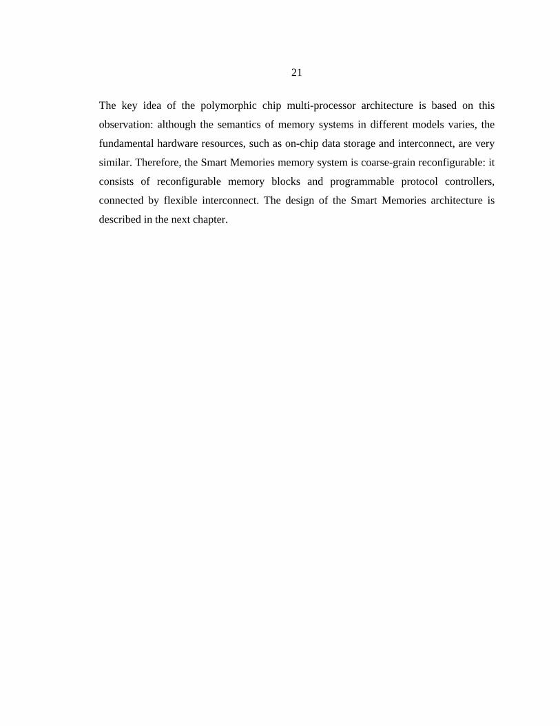
The key idea of the polymorphic chip multi-processor architecture is based on this
observation: although the semantics of memory systems in different models varies, the
fundamental hardware resources, such as on-chip data storage and interconnect, are very
similar. Therefore, the Smart Memories memory system is coarse-grain reconfigurable: it
consists of reconfigurable memory blocks and programmable protocol controllers,
connected by flexible interconnect. The design of the Smart Memories architecture is
described in the next chapter.

22
CHAPTER 3: SMART MEMORIES ARCHITECTURE
The goal of the Smart Memories architecture was to create a memory system that was as
programmable as the core processors, and could support a wide range of programming
models. In particular we ensured that the three models mentioned in the previous chapter,
cache coherent shared memory, streaming, and transactions could all be supported. This
chapter describes how we accomplished the programmable memory system, and how the
processors interacted with it. It begins by giving an overview of the architecture,
introducing the main hierarchical blocks used in the design. The chapter then goes into
more detail and describes the main building blocks used in the machine. Section 3.2
describes how we used the Tensilica processors to interface to our memory system.
Section 3.4 then describes how these processors are combined with flexible local
memories to form a Tile, which is followed by a description of how four Tiles are
grouped with a local memory controller/network interface unit to form a Quad. The final
sections then explain how the Quads are connected together through an on-chip network,
and to the memory controllers.
3.1 OVERALL ARCHITECTURE
Figure 3.1 shows a block diagram of the architecture, which consists of Tiles, each Tile
has two Tensilica processors, several reconfigurable memory blocks, and a crossbar
connecting them. Four adjacent Tiles form a Quad. Tiles in the Quad are connected to a
shared local memory Protocol Controller. Quads are connected to each other and to the
Memory Controllers using an on-chip interconnection network.
This modular, hierarchical structure of Smart Memories helps to accommodate VLSI
physical constraints such as wiring delay. Quads are connected to each other and to off-
chip interfaces only through an on-chip network that can be designed to use regular,

23
structured wires. Regular wire layout results in predictable wire length and well-
controlled electrical parameters that eliminate timing iterations and minimize cross-talk
noise. This allows the use of high-performance circuits with reduced latency and
increased bandwidth [77, 78]. Since there are no unstructured global wires spanning the
whole chip, wire delay has a small effect on clock frequency.
The modular structure of the Smart Memories architecture makes system scaling simple:
to increase the performance of the system the number of quads can be scaled up without
changing the architecture. The bandwidth of the on-chip mesh-like network will also
scale up as the number of quads increases.
Figure 3.1: Smart Memories Architecture
The memory system consists of three major reconfigurable blocks, highlighted in Figure
3.1: the Load/Store Unit, the Configurable Memory and the Protocol Controller. The
memory interface in each Tile (Load/Store Unit) coordinates accesses from processor
cores to local memories and allows reconfiguration of basic memory accesses. A basic
operation, such as a Store instruction, can treat a memory word differently in
transactional mode than in conventional cache coherent mode. The memory interface can
also broadcast accesses to a set of local memory blocks. For example, when accessing a
set-associative cache, the access request is concurrently sent to all the blocks forming the
cache ways. Its operation is described in more detail in Section 3.4.1.

24
The next configurable block in the memory system is the array of memory blocks. Each
memory block in a Tile is an array of data words, and associated metadata bits. It is these
metadata bits that makes the memory system flexible. Metadata bits store the status of
that data word and their state is considered in every memory access; an access to this
word can be discarded based on the status of these bits. For example, when mats are
configured as a cache, these bits are used to store the cache line state, and an access is
discarded if the status indicates that cache line is invalid. The metadata bits are dual
ported: they are updated atomically with each access to the data word. The update
functions are set by the configuration. A built-in comparator and a set of pointers allow
the mat to be used as tag storage (for cache) or as a FIFO. Mats are connected to each
other through an inter-mat network that communicates control information when the mats
are accessed as a group. While the hardware cost of reconfigurable memory blocks is
high in our standard-cell prototype, a full custom design of such memory blocks can be
quite efficient [40, 41].
The Protocol Controller is a reconfigurable control engine that can execute a sequence of
basic memory system operations to support the memory mats. These operations include
loading and storing data words (or cache lines) into mats, manipulating meta-data bits,
tracking outstanding requests from each Tile, and broadcasting data or control
information to Tiles within the Quad. The controller is connected to a network interface
port and can send and receive requests to/from other Quads or Memory Controllers.
Mapping a programming model to the Smart Memories architecture requires
configuration of Load/Store Unit, memory mats, Tile interconnect and Protocol
Controller. For example, when implementing a shared-memory model, memory mats are
configured as instruction and data caches, the Tile crossbar routes processor instruction
fetches, loads, and stores to the appropriate memory mats, and the Protocol Controller
acts as a cache coherence engine, which refills the caches and enforces coherence.

25
The remainder of this chapter describes the main units of the Smart Memories
architecture: processor, memory mat, Tile, Quad, on-chip network, and Memory
Controller.
3.2 PROCESSOR
The Tensilica processor [79, 80] was used for the Smart Memories processor. Tensilica’s
Xtensa Processor Generator automatically generates a synthesizable hardware description
for the user customized processor configuration. The base Xtensa architecture is a 32-bit
RISC instruction set architecture (ISA) with 24-bit instructions and a windowed general-
purpose register file. Register windows have 16 register each. The total number of
physical registers is 32 or 64.
The user can select pre-defined options such as a floating-point co-processor (FPU) and
can define custom instruction set extensions using the Tensilica Instruction Extension
language (TIE) [79, 80]. The TIE compiler generates a customized processor, taking care
of low-level implementation details such as pipeline interlocks, operand bypass logic, and
instruction encoding.
Using the TIE language designers can add registers, register files, and new instructions to
improve performance of the most critical parts of the application. Multiple operation
instruction formats can be defined using the Flexible Length Instruction eXtension
(FLIX) feature to further improve performance [81]. Another feature of the TIE language
is the ability to add user-defined processor interfaces such as simple input or output
wires, queues with buffers, and lookup device ports [81]. These interfaces can be used to
interconnect multiple processors or to connect a processor to other hardware units.
The base Xtensa ISA pipeline is either five or seven pipeline stages and has a user
selectable memory access latency of one or two cycles. Two-cycle memory latency
allows designers to achieve faster clock cycles or to relax timing constraints on memories

26
and wires. Although Tensilica provides many options for memory interfaces, these
interfaces cannot be used directly to connect the Tensilica processor to the rest of the
Smart Memories system, as explained further in the next subsection, which describes our
approach for interfacing the processor and the issues associated with it.
3.2.1 INTERFACING THE TENSILICA PROCESSOR TO SMART MEMORIES
Connecting Tensilica’s Xtensa processor to the reconfigurable memory system is
complicated because Tensilica interfaces were not designed for Smart Memories’ specific
needs. Although the Xtensa processor has interfaces to implement instruction and data
caches (Figure 3.2), these options do not support the functionality and flexibility
necessary for the Smart Memories architecture. For example, Xtensa caches do not
support cache coherence. Xtensa cache interfaces connect directly to SRAM arrays for
cache tags and data, and the processor already contains all the logic required for cache
management. As a result, it is impossible to modify the functionality of the Xtensa caches
or to re-use the same SRAM arrays for different memory structures like local
scratchpads.
In addition to simple load and store instructions, the Smart Memories architecture
supports several other memory operations such as synchronized loads and stores. These
memory operations can easily be added to the instruction set of the processor using the
TIE language but it is impossible to extend Xtensa interfaces to natively support such
instructions.

27
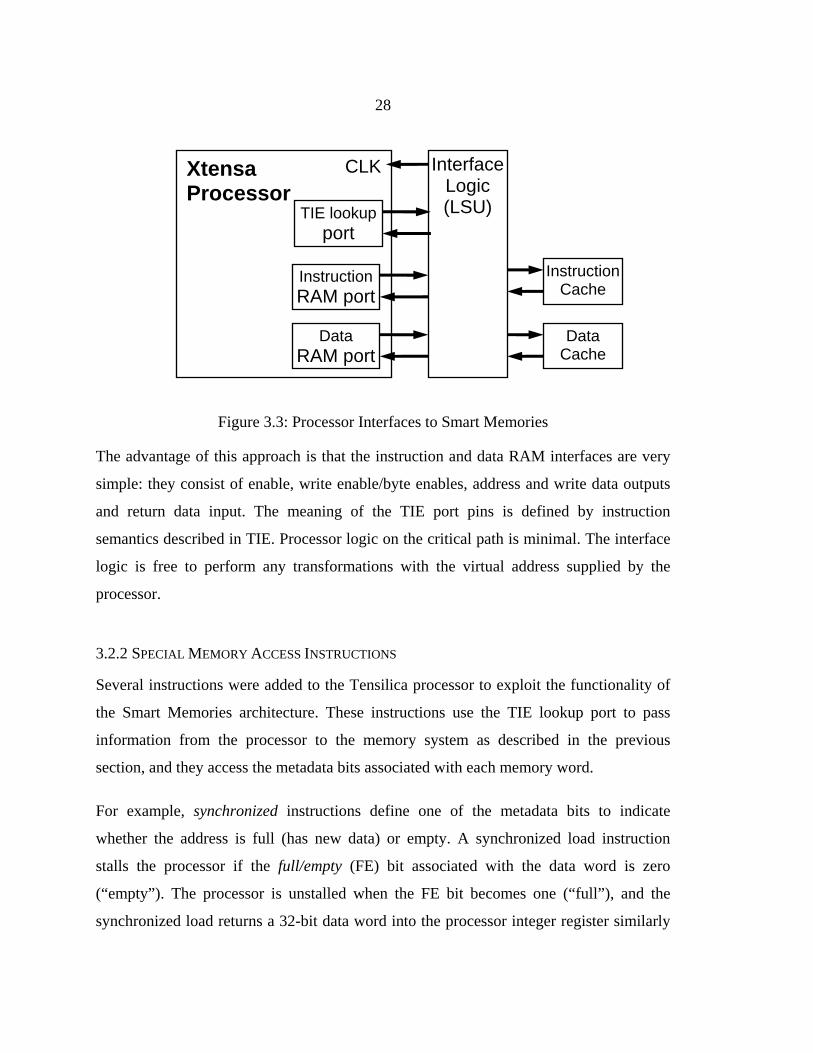
Shared Memories
Figure 3.2: Xtensa Processor Interfaces
Instead of cache interfaces we decided to use instruction and data RAM interfaces as
shown in Figure 3.3. In this, case instruction fetches, loads and stores are sent to interface
logic (Load Store Unit) that converts them into actual control signals for memory blocks
used in the current configuration. Special memory operations are sent to the interface
logic through the TIE lookup port, which has the same latency as the memory interfaces.
If the data for a processor access is ready in 2 cycles, the interface logic sends it to the
appropriate processor pins. If the reply data is not ready due to cache miss, arbitration
conflict or remote memory access, the interface logic stalls the processor clock until the
data is ready.
Xtensa
InstructionCache
InstructionRAM
InstructionROM
Data Cache
DataRAM
Data ROM
PIF
XLMI
Shared PeripheralsShared FIFOsQueue
TIE Queue InterruptsDevice TIE Port
TIE Lookup
Off-Chip Bus Interface
Memory On-Chip BusLookup Memory Device ProcessorMemory
ProcessorProcessorPeripheral
PeripheralPeripheral
28
InterfaceCLKXtensa Logic Processor (LSU)
Figure 3.3: Processor Interfaces to Smart Memories
The advantage of this approach is that the instruction and data RAM interfaces are very
simple: they consist of enable, write enable/byte enables, address and write data outputs
and return data input. The meaning of the TIE port pins is defined by instruction
semantics described in TIE. Processor logic on the critical path is minimal. The interface
logic is free to perform any transformations with the virtual address supplied by the
processor.
3.2.2 SPECIAL MEMORY ACCESS INSTRUCTIONS
Several instructions were added to the Tensilica processor to exploit the functionality of
the Smart Memories architecture. These instructions use the TIE lookup port to pass
information from the processor to the memory system as described in the previous
section, and they access the metadata bits associated with each memory word.
For example, synchronized instructions define one of the metadata bits to indicate
whether the address is full (has new data) or empty. A synchronized load instruction
stalls the processor if the full/empty (FE) bit associated with the data word is zero
(“empty”). The processor is unstalled when the FE bit becomes one (“full”), and the
synchronized load returns a 32-bit data word into the processor integer register similarly
InstructionRAM port
DataRAM port
Instruction Cache
TIE lookupport
Data Cache

29
to a conventional load instruction. The FE bit is atomically flipped back to zero during
the synchronized load execution.
A synchronized store instruction stalls the processor until the FE bit associated with the
data word is zero, and then it writes a 32-bit data word and flips FE bit to one.
A complete list of added memory instructions is in Appendix A.
3.2.3 PIPELINING ISSUES RELATED TO SPECIAL MEMORY INSTRUCTIONS
Adding special memory instructions to the architecture does add one complication.
Special load instructions can modify metadata bits, i.e. they can alter the architectural
state of the memory. Standard load instructions do not have side effects, i.e. they do not
alter the architectural state of the memory system, and therefore they can be executed by
the processor as many times as necessary. Loads might be reissued, for example, because
of processor exceptions as shown in Figure 3.4: loads are issued to the memory system at
the end of the E stage, load data is returned to the processor at the end of the M2 stage,
while the processor commit point is in the W stage, i.e. all processor exceptions are
resolved only in the W stage. Such resolution may ultimately result in re-execution of the
load instruction. Stores, by contrast, are issued only in the W stage after the commit
point.

30
commit point
F1 F2 D E M1 M2 W U1 U2
Figure 3.4: Processor Pipeline
Since it would be very difficult to undo side effects of special memory operations, they
are also issued after the commit point in W stage. The processor pipeline was extended
by 2 stages (U1 and U2 in Figure 3.4) to have the same 2 cycle latency for special load
instructions.
However, having different issue stages for different memory operations creates the
memory ordering problem illustrated in Figure 3.5a. A load following a special load in
the application code is seen by the memory system before the special load because it is
issued in the E stage. To prevent such re-ordering, we added pipeline interlocks between
special memory operations and ordinary loads and stores. An example of such an
interlock is shown in Figure 3.5b. The load is stalled in the D stage for 4 cycles to make
sure the memory system sees it 1 cycle after the previous special load. One extra empty
cycle is added between 2 consecutive operations to simplify memory system logic for the
case of synchronization stalls. This does not degrade performance significantly because
special loads are not executed as often as standard loads and the compiler can schedule
instructions to minimize the impact of extra pipeline interlocks.
load issue
load data
store/ custom op issue
fetch fetch custom issue data load
data
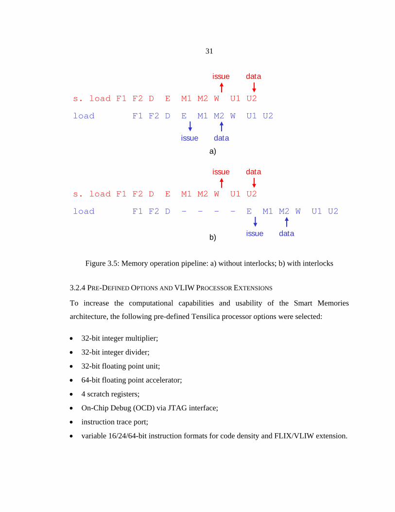
31
s. load F1 F2 D E M1 M2 W U1 U2
issue data
load F1 F2 D E M1 M2 W U1 U2
issue data
a)
dataissue
s. load F1 F2 D E M1 M2 W U1 U2
load F1 F2 D - - - - E M1 M2 W U1 U2
issue data b)
Figure 3.5: Memory operation pipeline: a) without interlocks; b) with interlocks
3.2.4 PRE-DEFINED OPTIONS AND VLIW PROCESSOR EXTENSIONS
To increase the computational capabilities and usability of the Smart Memories
architecture, the following pre-defined Tensilica processor options were selected:
• 32-bit integer multiplier;
• 32-bit integer divider;
• 32-bit floating point unit;
• 64-bit floating point accelerator;
• 4 scratch registers;
• On-Chip Debug (OCD) via JTAG interface;
• instruction trace port;
• variable 16/24/64-bit instruction formats for code density and FLIX/VLIW extension.

32
To further improve performance of the processor and utilization of the memory system,
we added two multi-instruction formats using FLIX/VLIW capability of Tensilica
system:
• {ANY; INT; FP};
• {ANY; INT; LIMITED INT};
where ANY means any type instruction, INT means integer instruction type (excluding
memory operations), FP means floating-point instruction type, LIMITED INT means a
small subset of integer instructions which requires at most 1 read and 1 write port.
The reason for this choice of instruction formats is the limitation of the Xtensa processor
generator: register file ports cannot be shared among different slots of FLIX/VLIW
format. For example, the FP multiply-add instruction requires 3 read and 1 write ports. If
such an operation could be present in 2 different slots, then the FP register file would
need to have at least 6 read and 2 write ports, even if 2 such operations are never put in
the same instruction. On the other hand, memory operations can only be allocated in slot
0 (ANY) and the common usage case is to have a memory operation and a compute
operation such as multiply-add in the same instruction. This means that it should be
possible to have FP operations in slots other than 0 but the number of such slots should
be minimal.
3.3 MEMORY MAT
A memory mat is the basic memory unit in the Smart Memories architecture. In addition
to storage, it can also perform simple logical operations on some of the stored bits.
Depending on the configuration, a memory mat can be used as simple local memory, as a
hardware FIFO, or as part of a cache for storing either tag or data. Each Tile has 16
memory mats, which are connected to processors and the outside world by a crossbar.

33
Figure 3.6 shows the internal structure of a memory mat. The main part is the data array
(or data core), which consists of 1024 32-bit words. A 4-bit mask input allows each byte
within the 32-word to be written independently. In addition to simple reads and writes,
the memory mat can also do compare operations on the accessed word using a 32-bit
comparator, which compares contents of the word with the data from the Data In input
and generates a Data Match output signal. The Data Match signal is sent out to the
processors over the crossbar as well as being passed to metadata array logic.
Figure 3.6: Memory mat
Write operations in the data array can be guarded or conditional. Such operations are
used for caches. For these operations, the data array receives two additional control bits,
34
Guard and Condition, and can decide to discard a write operation if either of the Guard or
Condition signals is not active. The Guard signal can be configured to be any function of
the IMCN_in inputs (which are described in the next section), while Condition can be
any function of the 6 control bits within the metadata array. For example the data storage
can discard a cache write operation if the tag mat reports a cache miss via the IMCN and
Guard signal.
The metadata array (or control core) is a 1024 entry 6-bit wide array (Figure 3.6). These 6
bits are called metadata bits or control bits associated with each 32-bit data word. The
metadata array is dual-ported: it can do a read and a write operation in the same cycle.
Thus, in addition to ordinary reads and writes, the metadata array can do atomic read-
modify-write operations on the control bits. A small programmable logic array (PLA)
block is used to perform the logic functions for read-modify-write operations. The read
address of the metadata array is the same as the mat input address. The write address can
either be the current input address or the address from the previous cycle when doing a
read-modify-write update. An internal forwarding logic bypasses write values to the read
port if a subsequent read operation goes to the same address that was written in the
previous cycle.
Similarly, metadata array operations can be guarded or conditional. The metadata array
can also perform a compare operation between stored meta-data and the Control In input
to generate a Total Match output signal. A 7-bit mask is used to determine which
metadata bits participate in the comparison and which are ignored. An extra MSB mask
bit is used to determine whether the metadata comparison result should be ANDed with
Data Match.
In addition to simple operations, the metadata array can perform column-wise gang write
operations on bits 0-2: a whole column can be set to one or zero in a single-cycle
operation. Also, one column of the array (bit 2) can do a conditional gang write
operation: bit 2 in each entry of the array can be written with one or zero, if bit 1 of the

35
same entry is set to one. These operations are used for transactional caches: all
transactional state can be flushed away in a single cycle (Section 6.2).
Each memory mat is equipped with a pair of pointers that allow it to be used as a
hardware FIFO (Figure 3.6). A FIFO select input determines whether the mat should use
the externally supplied “Address In” signal or use internal pointers to generate an address
for data and metadata arrays. These pointers are automatically incremented after each
access: read and compare operations increment the head pointer, while write operations
increment the tail pointer. Increment of the tail pointer can be guarded the same way that
a write operation is guarded: if the guard signal is not active, the pointer will not be
incremented. An example usage of a guarded increment is described in Section 6.2,
which explains the operation of a transactional cache.
The depth of the FIFO can also be controlled via a configuration register. Whenever the
size of the FIFO reaches the value of the depth register and another write to the FIFO is
attempted, the write operation is ignored and a FIFO Error output signal is asserted. The
same situation happens if a user tries to read an empty FIFO. Also, there is another
configuration register called the threshold register. When the size of the FIFO reaches the
threshold value, a separate FIFO Full output signal is asserted to let the requestor module
know that the FIFO is almost full.
3.4 TILE
The Smart Memories Tile unit, shown in Figure 3.7, consists of two Tensilica processors,
16 memory mats, a crossbar and interface logic unit (LSU) connecting processor and
memory mats, tile configuration register unit, Statistics and Debugging unit (SDU), and
two JTAG test access port (TAP) units. Memory mats are also interconnected through an
inter-mat communication network (IMCN), which can be configured to exchange
between mats a few bits of control information such as a tag comparison result.

36
Protocol Controller
Port 0
Protocol Controller
Port 1
Crossbar
Processor 0 Interface
Processor 1 Interface
To/From Protocol
Controller
Interface Logic (LSU)Instr Port Data Port Instr Port Data Port Stats
Debug (SDU)
Tile Config
Registers
Processor 0 Processor 1
Mat 0 Mat 1 Mat 14 Mat 15
IMCN
. . .
TAP 1TAP 0To/From Protocol
Controller JTAG unit
Figure 3.7: Tile

37
3.4.1 INTERFACE LOGIC
The interface logic (LSU) translates each processor memory request into a set of memory
mat operations executed in parallel. The virtual address issued by the processor is
translated into a physical address by a segment table. The segment table has four 256 MB
segments for instruction space (0x40000000-0x7FFFFFFF address range) and eight 256
MB segments for data space (0x80000000-0xFFFFFFFF address range). Segment
information is stored in the configuration registers. In addition to address translation,
segment settings also specify read/write permissions and what type of memory access the
processor request should be converted to. If a processor request violates segment
permissions, then the LSU raises a fatal non-maskable interrupt (NMI).
Depending on the segment, a processor memory operation can go to conventional data or
instruction cache, transactional cache, on-tile local memory, off-tile local memory, or off-
chip DRAM. For conventional cache access the LSU generates data and tag mat
operations according to the cache configuration and sends them to the crossbar. Since a
cache can be set-associative, the same operation might need to be sent to more than one
memory mat. To handle this case the LSU generates a memory mat mask that tells the
crossbar which mats should receive the operation.
Tag mats perform cache line address and state comparison using the built-in comparator
described in Section 3.3. The hit/miss result of the comparison (Total Match signal) is
sent to the appropriate data mats via the IMCN according to the cache configuration. The
data mats use this IMCN signal as a “Guard” for write operations. The same IMCN
signals are used to update most-recently-used (MRU) metadata bits in all tag mats. MRU
bits are used by the Quad Protocol Controller to implement a not-most-recently-used
cache line replacement policy.
Total Match signals are also sent via crossbar back to the LSU. The crossbar aggregates
Total Match signals from all tag mats and sends the result as a Hit/Miss signal back to the

38
LSU. Also, the crossbar uses Total Match signals to route the result of the read operation
from the appropriate data mat back to the LSU.
In the case of a cached load hit the LSU returns the data to the processor port. In the case
of a cache miss the LSU turns off the requesting processor clock and generates a cache
miss message which is placed into the queue to the Quad Protocol Controller port. The
LSU has 4 separate queues for Protocol Controller messages, one per processor port.
Each queue has 4 entries that buffer outstanding cache miss requests before they are
accepted by the Protocol Controller for processing. Thus, the LSU does not need to stall
the processor because of store misses, which can be non-blocking. Strict order between
cache miss requests in the same queue is enforced by the LSU logic to guarantee
program order of memory operations. The address of a later memory operation issued by
the same processor is compared to cache miss requests in the queue. If the address
matches, then the memory operation is sent directly to the queue, skipping the memory
mat access.
Every clock cycle the LSU performs arbitration among non-empty queues and sends one
request to the Quad Protocol Controller. The Protocol Controller arbitrates between the
four Tiles and starts processing 1 cache miss request per cycle. If the request does not
conflict with other requests currently being processed, then the Protocol Controller sends
an acknowledgement to the Tile LSU, which frees the corresponding entry in the queue.
Otherwise, the request is not acknowledged and blocks the queue.
When the request is processed, the Protocol Controller sends a reply to the LSU. The
reply for a load or instruction fetch miss contains data that the LSU sends to the processor
port. Replies for store misses are used by the LSU to keep track of outstanding memory
operations. If stores are configured to be blocking, then the LSU stalls the processor on a
store cache miss, and unstalls it only after receiving a reply from the Protocol Controller.
If stores are configured to be non-blocking, then the LSU uses a store miss counter to

39
keep track of outstanding stores. This is necessary to support memory barrier operations,
which stall the processor until all outstanding memory operations are complete.
Memory mats in the Tile can also be used as local, directly addressable memories
(Section 2.3.2). In such a case the memory segment that corresponds to the local memory
is configured to be uncached on-tile. The LSU generates a single memory mat access for
load or store to the local memory mat. Similarly, a segment can be uncached off-tile, i.e.
mapped to the local memory mats in another Tile or Quad. For memory operations to
such segments the LSU sends a message directly to the Protocol Controller. Also, an
uncached segment can be mapped to off-chip DRAM.
The LSU also supports FIFO load and store processor operations (Appendix A). FIFO
operations can be routed to an on-tile mat or to a mat in another Tile or Quad. Since a
FIFO operation can fail because of FIFO overflow or underflow, the LSU saves the FIFO
Error signal in a 32-bit shift register that is accessible by the processor. This allows the
processor to issue non-blocking back-to-back FIFO stores and to check for success up to
32 operations later.
In addition to ordinary loads and stores the processor can issue special memory
operations such as synchronized loads and stores (Section 3.2.2). Synchronized loads and
stores might stall the processor depending on the state of the metadata bits associated
with the data word. For such operations the LSU checks the value of the metadata
returned from the cache data mat or uncached memory mat and, if necessary, stalls the
processor and sends a sync miss message to the Protocol Controller just as in the case of a
cache miss.
The LSU also handles processor interrupts, which can be initiated by the Protocol
Controller, Statistics and Debugging unit (SDU), or by a write into a special
configuration register either by software or JTAG. Processor interrupts can be soft, i.e.
the LSU waits while the processor is stalled because of outstanding memory operations
40
and asserts processor interrupt pins. After a soft interrupt is handled, execution of an
application can be restarted transparently. If a hard interrupt is requested, the processor is
unstalled by the LSU even if there are outstanding memory operations. Only the Quad
Protocol Controller can initiate hard interrupts, because the Protocol Controller must then
cancel all outstanding cache and sync miss requests. Hard interrupts are not restartable,
i.e. execution of the application can not be restarted because there is no guarantee that the
application state is restored after return from the interrupt. Hard interrupts are required to
handle such events as transaction violation (Section 6.2).
3.4.2 CROSSBAR
The Tile crossbar routes mat accesses from the LSU and Protocol Controller ports
(Figure 3.7) to the memory mats. It also performs arbitration between two processors and
the Protocol Controller every cycle if there are conflicting accesses. If the processor loses
arbitration, then the LSU stalls the processor clock just like in the case of a cache miss
and re-tries the operation in the next cycle. The Protocol Controller has priority over
processors because it is simpler to stall the processor clock rather than to stall the
Protocol Controller pipeline. To simplify and to speed up arbitration, the crossbar does
not arbitrate between ports of the same processor. Some special memory instructions,
which read and write configuration state (Appendix A), can access any memory mat,
skipping segment table translation and permission checks. To avoid potential crossbar
conflicts and to simplify logic, whenever the LSU receives such an operation request
from the processor it asserts the IRamBusy input of the processor without stalling the
processor clock. This signal tells the processor that the instruction fetch was not
successful and should be re-tried in the next cycle.
Reads and writes to Tile configuration registers are also routed by the crossbar just like
memory mat accesses.

41
3.4.3 STATISTICS AND DEBUGGING UNIT
The Statistics and Debugging unit (SDU) counts different types of events such as the
number of certain types of operations (instruction fetches, loads, stores, etc.), number of
cache or sync misses, number of cycles between events, etc. The SDU can generate a
latency histogram for certain types of memory operations. Histogram state is stored in
one or two memory mats that can be dedicated for statistics. Similarly, the SDU can be
programmed to generate profile counts for certain types of events using one or two
memory mats as storage. Profile binning is determined by the bits of the processor
program counter (PC) or memory operations address, or by a combination of the two.
Also, the SDU can store a compressed processor instruction trace from the processor
trace port into the memory mats. To access memory mats the SDU has a dedicated
crossbar port.
The Tile configuration unit contains all SDU configuration state that is accessible to
software or through JTAG. Software running on the processor can start, stop and reset
statistics counters using raw loads and stores. Another way to control the SDU is to use
the spec_cmd instruction (Appendix A). The spec_cmd instruction is ignored by the LSU,
however, the SDU can be configured to start or to stop a counter whenever the processor
executes such an instruction. This instruction has very low overhead because it doesn’t
have any register operands and does not require any extra instructions to load register
values. It is used by transactional runtime to produce detailed execution cycle statistics
(Section 6.4).
The SDU can be programmed to generate a processor interrupt under certain conditions,
for example, when a counter overflows or reaches a programmed value. The SDU sends
an interrupt signal to the LSU, which asserts processor interrupt pins. This feature can be
used to handle counter overflow in software, to do sampling profiling, or for debugging
purposes, e.g. to interrupt a processor when there is a cache miss to a certain address.

42
The SDU can signal the LSU to stall the processor when the SDU needs extra cycles to
handle an event, e.g. when the profiling counter in the memory mat is incremented.
The Statistics and Debugging unit consists of:
• eight 64-bit event counters;
• 2 profiling counters;
• latency histogram block;
• processor trace block;
• shared comparator block:
- 8 event comparators;
- 6 program counter comparators;
- 4 address range comparators.
Each Tile has two Test Access Port (TAP) units connected to the processors. TAP units
are used for on-chip debug (OCD) functionality [82]. OCD allows a GDB debugger
running on a host PC to connect to the Tensilica processor via a JTAG port. Through
OCD, GDB can set a debug breakpoint or watchpoint, single step program execution,
execute a random instruction, or access processor registers.
3.4.4 TILE TIMING
Tile timing is determined by very tight timing constraints on the processor clock signal as
shown in Figure 3.8. The forward path for the memory operation data issued by the
processor goes through the flop in the interface logic and then through the flop in the
memory mat. In the reverse path, the output of the memory mat goes to the stall logic and
determines whether the processor clock should be stalled or not. To avoid glitches on the
processor clock, the output of the stall logic must go through a flop or latch clocked with
an inverted clock. The whole reverse path including memory mat, crossbar and stall logic
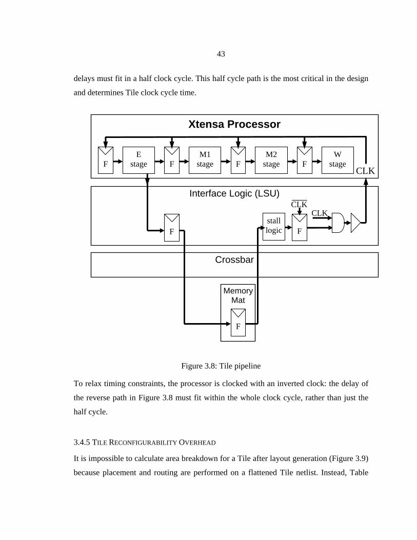
43
delays must fit in a half clock cycle. This half cycle path is the most critical in the design
and determines Tile clock cycle time.
Interface Logic (LSU)
CLK
MemoryMat
F E
stage M1
stage M2
stage W
stage F F F
F F
CLK
Crossbar
F
CLK stall logic
Xtensa Processor
Figure 3.8: Tile pipeline
To relax timing constraints, the processor is clocked with an inverted clock: the delay of
the reverse path in Figure 3.8 must fit within the whole clock cycle, rather than just the
half cycle.
3.4.5 TILE RECONFIGURABILITY OVERHEAD
It is impossible to calculate area breakdown for a Tile after layout generation (Figure 3.9)
because placement and routing are performed on a flattened Tile netlist. Instead, Table
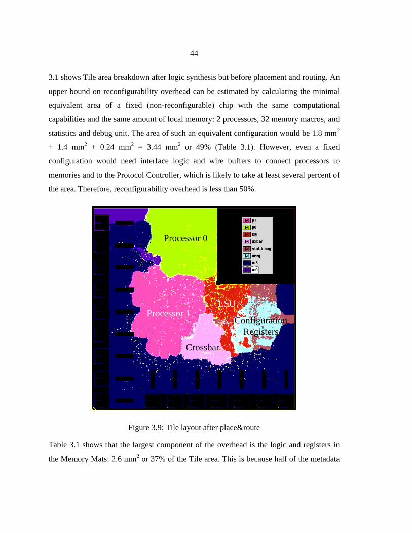
44
3.1 shows Tile area breakdown after logic synthesis but before placement and routing. An
upper bound on reconfigurability overhead can be estimated by calculating the minimal
equivalent area of a fixed (non-reconfigurable) chip with the same computational
capabilities and the same amount of local memory: 2 processors, 32 memory macros, and
statistics and debug unit. The area of such an equivalent configuration would be 1.8 mm2
+ 1.4 mm2 + 0.24 mm2 = 3.44 mm2 or 49% (Table 3.1). However, even a fixed
configuration would need interface logic and wire buffers to connect processors to
memories and to the Protocol Controller, which is likely to take at least several percent of
the area. Therefore, reconfigurability overhead is less than 50%.
Processor 0
LSU Processor 1
Configuration Registers
Crossbar
Figure 3.9: Tile layout after place&route
Table 3.1 shows that the largest component of the overhead is the logic and registers in
the Memory Mats: 2.6 mm2 or 37% of the Tile area. This is because half of the metadata

45
bits in the Memory Mats are implemented using flip-flops instead of more area efficient
memory macros. The reason for this is the required flexibility of metadata storage: to
support TCC mode, metadata bits must be gang writable (Section 6.2). This metadata
storage had to be implemented only using standard cells in ASIC design flow. However,
a full custom design can significantly reduce this overhead [40, 41].
Table 3.1: Tile area breakdown after logic synthesis
Module Area, mm2
% Logic, mm2
Registers, mm2
Memory macros, mm2
Tile 7.022 100.0 0.025 0.010 0.000 Protocol Controller interface 0.027 0.4 0.027 0.000 0.000 LSU 0.349 5.0 0.213 0.136 0.000 Memory Mats 4.045 46.9 1.397 1.233 1.414 Processor 0 0.899 12.8 0.639 0.260 0.000 Processor 1 0.911 13.0 0.651 0.260 0.000 Stats-Debug Unit 0.243 3.5 0.141 0.102 0.000 Configuration Registers 0.245 3.5 0.143 0.102 0.000 Crossbar 0.248 3.5 0.239 0.008 0.000
3.5 QUAD
A Smart Memories Quad consists of four Tiles and a shared configurable Protocol
Controller as shown in Figure 3.10. The Protocol Controller is connected to the Tile
crossbars and interface logic units (LSU). The Protocol Controller implements basic
cache functionality such as cache line refill and eviction as well as cache coherence
functions: cache-to-cache transfers within a Quad and off-Quad cache snoops.
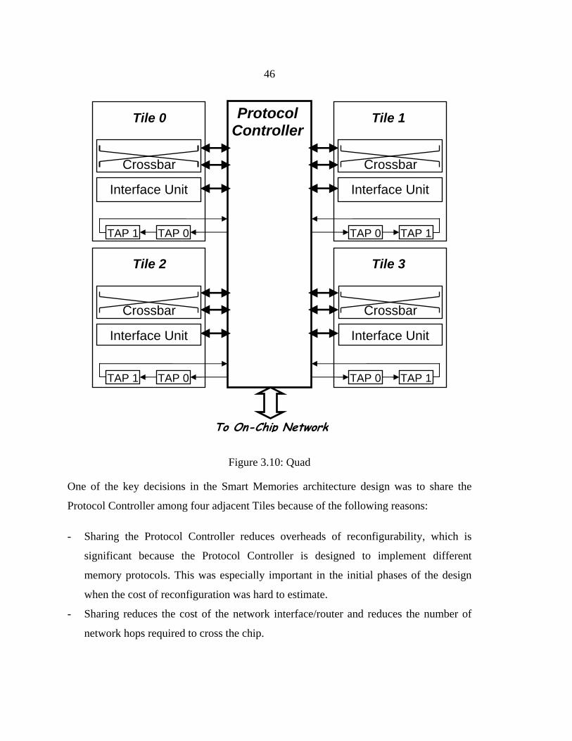
46
Figure 3.10: Quad
One of the key decisions in the Smart Memories architecture design was to share the
Protocol Controller among four adjacent Tiles because of the following reasons:
- Sharing the Protocol Controller reduces overheads of reconfigurability, which is
significant because the Protocol Controller is designed to implement different
memory protocols. This was especially important in the initial phases of the design
when the cost of reconfiguration was hard to estimate.
- Sharing reduces the cost of the network interface/router and reduces the number of
network hops required to cross the chip.
Interface Unit
Crossbar
Tile 0
Interface Unit
Crossbar
Tile 2
Tile 1
Interface Unit
Crossbar
Interface Unit
Crossbar
Tile 3
TAP 1 TAP 0
TAP 1 TAP 0
TAP 1 TAP 0
TAP 1 TAP 0
To On-Chip Network
Protocol Controller
47
- A single shared Protocol Controller simplifies intra-quad cache coherence
implementation because outstanding cache misses requests are tracked in a single
centralized hardware structure. There is no need for a coherent bus between Tiles.
3.5.1 PROTOCOL CONTROLLER
Instead of dedicated hardware for a specific memory protocol, the Protocol Controller
implements a set of primitive operations that can be combined and sequenced by a
configuration memory. A request from a Tile is translated into a sequence of primitives
specific to a given protocol.
These primitive operations are divided into four main categories:
- Tracking and serialization: in some memory protocols such as cache coherence,
memory requests issued to same addresses have to be serialized to satisfy protocol
requirements. The Protocol Controller performs request serialization because all
memory requests from all Tiles go through it. In addition, the Protocol Controller
keeps track of all outstanding memory requests from all processors in the Quad and
can merge several requests if possible.
- Control state checks and updates: for a protocol such as cache coherence, the control
state associated with the data needs to be read and updated according to the protocol
state transition rules. The Protocol Controller can access all four Tiles in the Quad
and can use metadata from them to determine how to process memory request.
- Data movements: data transfers between any two mats or two sets of mats regardless
of their location, and transfers over the network interface to other Quads or to off-
chip memory controllers.
- Communication: the Protocol Controller has interfaces to Tile LSUs and to other
Quads and memory controllers in the system.

48
Figure 3.11: Protocol Controller block diagram
As shown in Figure 3.11 several blocks of the Protocol Controller directly correspond to
the above classes of primitive operations: tracking unit (T-Unit), state update unit (S-
Unit), data movement unit (D-Unit), LSU and network interface units. There are also
special storage structures: miss status holding registers (MSHR) and similar registers for
uncached off-tile requests (USHR), and line buffers which are used as temporary storage
for data. In addition to these major functional units, the Protocol Controller has a few
extra units which are used for special operations: an interrupt unit, a configuration and
statistics unit, and a set of eight direct memory access (DMA) channels.
The Processor Interface unit connects to the Tile’s LSU units. Each cycle it arbitrates
between Tiles and selects 1 cache miss request and 1 uncached memory request, both of
which are passed to the T-Unit. Requests from the head of each LSU queue are buffered
internally inside the Processor Interface to avoid resending the same request from the
LSU to the Protocol Controller.

49
The T-Unit acts as the entry point to the Protocol Controller execution core: all
request/reply messages from processors, network interface and internal DMA channels
must go through the T-Unit. For each request, an entry in the appropriate tracking
structure is allocated and the request information is recorded, and then passed to the next
unit.
MSHRs are used to store processor cache miss information as well as coherence snoop
requests from Memory Controllers. The MSHR block has an associative lookup port that
allows the T-Unit to check conflicts between new cache misses and already outstanding
ones and enables optimizations such as request merging. USHRs are separate but similar
structures used to store information about a processor’s direct memory requests for any
locations outside of its own Tile. It also keeps information about outstanding DMA
transfers generated by DMA engines.
If no conflict with an already outstanding request is detected, the request is written into a
free MSHR or USHR during the next pipeline stage after associative lookup. If a request
cannot be accepted due to conflict or because the MSHR structure is full, the T-Unit
returns a negative acknowledgement (NACK) and the sending party must retry the
request later. If a reply for an outstanding request is received, the T-Unit reads
information for the request from an MSHR or a USHR and passes it to the next Protocol
Controller unit to complete processing.
The S-Unit reads and updates metadata state associated with the data, such as cache line
state, cache tags, etc. Its pipeline has four stages and a small output queue at the end. A
round robin arbiter at the input selects the next request to be processed by S-Unit.
The Access Generator block in the first stage of the pipeline generates all necessary
signals for memory mat access. It can generate two independent accesses to memory mats
and can access either a single Tile or all Tiles simultaneously; for example, when a cache
miss request is processed, the S-Unit can evict a line from the cache of the requesting

50
processor and simultaneously update the state of the cache line in other Tiles to enforce
cache coherence. Generated mat accesses are flopped and sent to memory mats in the
second stage. All the necessary control signals for memory mat access, i.e. data opcode,
metadata opcode, PLA opcode, masks, etc., are stored in a microcode memory inside the
access generator block, which is indexed by the type of the input request to the S-Unit,
and hence can be adjusted according to the memory protocol.
The Decision Block at the last stage of the pipeline receives the value of all metadata bits
read from memory mats as well as the Total Match and Data Match signals and
determines the next step in processing the request. For example, when serving a cache
miss request, if a copy of the line is found in another cache, a cache-to-cache transfer
request is sent to D-Unit. Or if the evicted cache turns out to be modified, a write back
request is generated. The decision is made by a ternary content-addressable memory
(TCAM) which matches collected state information to one of several predefined patterns
and generates up to 3 operations for the next processing step and identifies which
Protocol Controller units should perform them. The data and mask bits inside the TCAM
can be programmed according to the protocol.
A small output queue buffers requests before sending them to other units. The size of this
buffer is large enough to drain the S-Unit pipeline, so as to avoid pipeline stalls when a
memory mat access is in flight. The arbiter logic in front of the S-Unit pipeline always
checks the availability of buffer space in the output queue and does not accept new
requests if there is not enough free entries in the queue.
The D-Unit (Figure 3.12) also has an arbiter at the input that decides which request
should be accepted. The Dispatch Block determines which Tiles should be accessed as
part of request processing. Four Data Pipes associated with the four Tiles receive requests
from their input queues and send the results to their output queues. A small finite state
machine generates replies for processors.
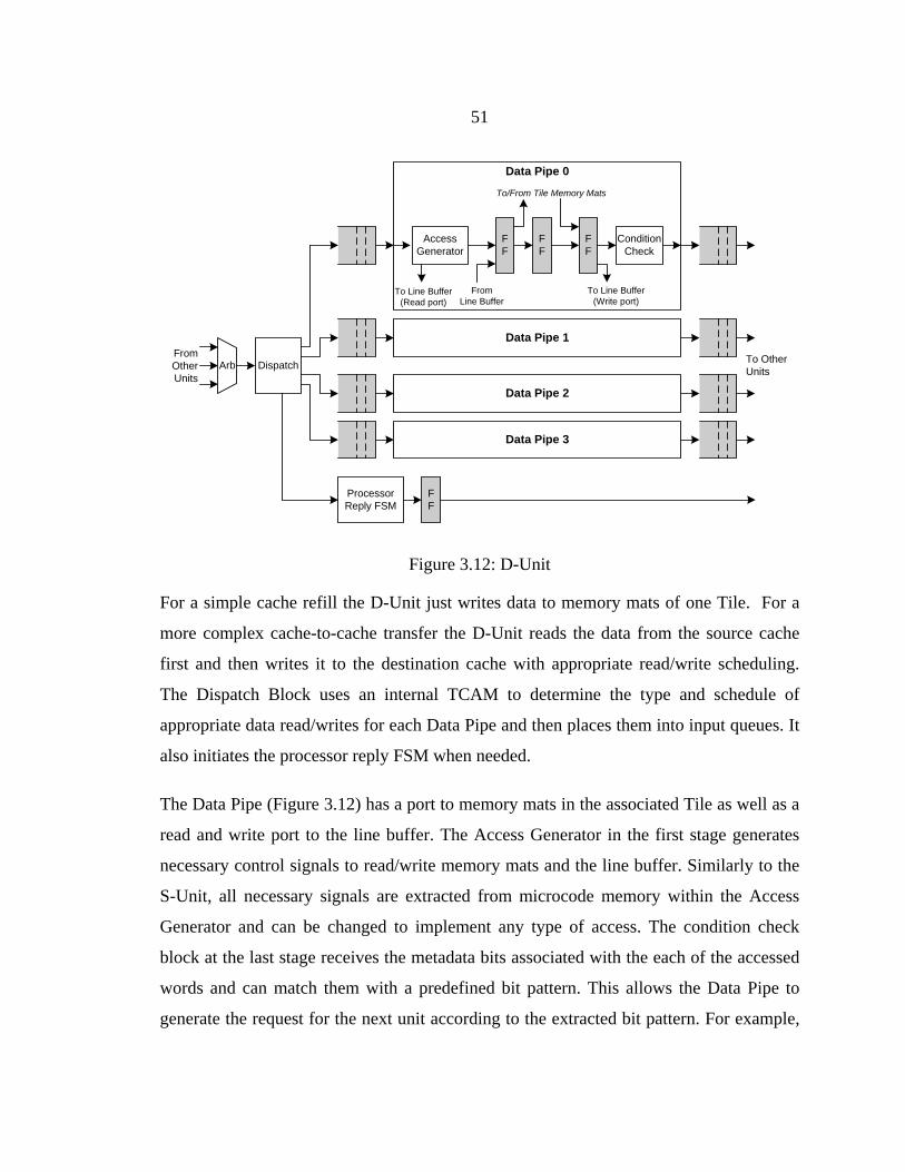
51
DispatchArbFrom Other Units
Data Pipe 1
Data Pipe 2
Data Pipe 3
Processor Reply FSM
FF
To Other Units
FF
Access Generator
FF
FF
Condition Check
To/From Tile Memory Mats
To Line Buffer (Read port)
FromLine Buffer
To Line Buffer (Write port)
Data Pipe 0
Figure 3.12: D-Unit
For a simple cache refill the D-Unit just writes data to memory mats of one Tile. For a
more complex cache-to-cache transfer the D-Unit reads the data from the source cache
first and then writes it to the destination cache with appropriate read/write scheduling.
The Dispatch Block uses an internal TCAM to determine the type and schedule of
appropriate data read/writes for each Data Pipe and then places them into input queues. It
also initiates the processor reply FSM when needed.
The Data Pipe (Figure 3.12) has a port to memory mats in the associated Tile as well as a
read and write port to the line buffer. The Access Generator in the first stage generates
necessary control signals to read/write memory mats and the line buffer. Similarly to the
S-Unit, all necessary signals are extracted from microcode memory within the Access
Generator and can be changed to implement any type of access. The condition check
block at the last stage receives the metadata bits associated with the each of the accessed
words and can match them with a predefined bit pattern. This allows the Data Pipe to
generate the request for the next unit according to the extracted bit pattern. For example,
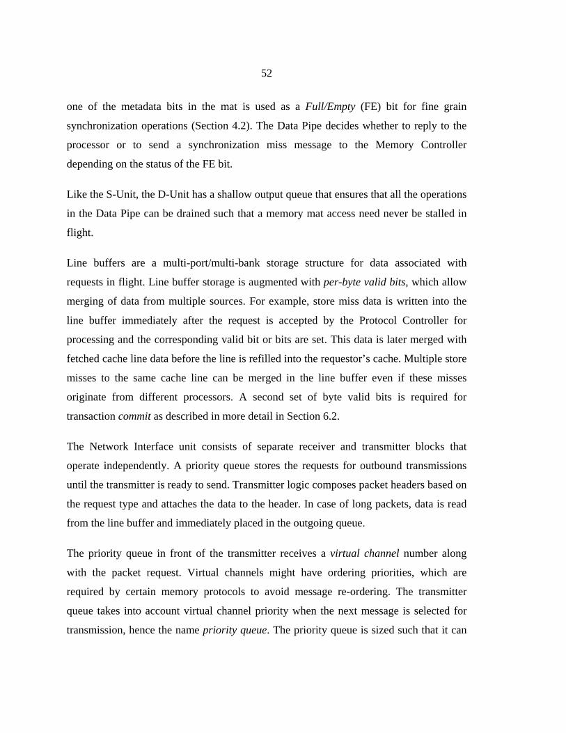
52
one of the metadata bits in the mat is used as a Full/Empty (FE) bit for fine grain
synchronization operations (Section 4.2). The Data Pipe decides whether to reply to the
processor or to send a synchronization miss message to the Memory Controller
depending on the status of the FE bit.
Like the S-Unit, the D-Unit has a shallow output queue that ensures that all the operations
in the Data Pipe can be drained such that a memory mat access need never be stalled in
flight.
Line buffers are a multi-port/multi-bank storage structure for data associated with
requests in flight. Line buffer storage is augmented with per-byte valid bits, which allow
merging of data from multiple sources. For example, store miss data is written into the
line buffer immediately after the request is accepted by the Protocol Controller for
processing and the corresponding valid bit or bits are set. This data is later merged with
fetched cache line data before the line is refilled into the requestor’s cache. Multiple store
misses to the same cache line can be merged in the line buffer even if these misses
originate from different processors. A second set of byte valid bits is required for
transaction commit as described in more detail in Section 6.2.
The Network Interface unit consists of separate receiver and transmitter blocks that
operate independently. A priority queue stores the requests for outbound transmissions
until the transmitter is ready to send. Transmitter logic composes packet headers based on
the request type and attaches the data to the header. In case of long packets, data is read
from the line buffer and immediately placed in the outgoing queue.
The priority queue in front of the transmitter receives a virtual channel number along
with the packet request. Virtual channels might have ordering priorities, which are
required by certain memory protocols to avoid message re-ordering. The transmitter
queue takes into account virtual channel priority when the next message is selected for
transmission, hence the name priority queue. The priority queue is sized such that it can

53
absorb and store all active requests within the execution core. This guarantees that all
active requests in the Protocol Controller that need to send out a packet can be safely
drained into the queue even when the outgoing link is blocked (due to back pressure, for
example). This is necessary to guarantee deadlock-free operation of the Protocol
Controller when it processes multiple requests simultaneously.
The network receiver block has eight buffers for different virtual channels. A decoder
detects the virtual channel of the received network data and places it in the appropriate
virtual channel buffer. After arbitration, the header of the selected packet is decoded and
a request is generated for an execution core based on the packet type. In the case of long
packets, data words are first written into the line buffer before the request is passed to the
execution core.
In addition to the execution part, the Protocol Controller has eight DMA channels, which
generate memory transfer requests that enter the execution part via the T-Unit. Channels
can do continuous copy, as well as strided and indexed gather/scatter operations. Each
DMA channel is a micro-coded engine that generates requests according to the loaded
microcode. This makes the DMA engine a very flexible request generator that can be
used by many applications. For example, after completion of a transfer, DMA channels
can generate interrupt requests for processors that are waiting for the transfer, or release a
lock variable on which processors are waiting. Another example is the use of DMA
channels to commit the speculative modifications of transactions (Section 6.2).
An Interrupt Unit (INT-Unit) connects the Protocol Controller to the interrupt interface of
each processor. A write into one of eight special registers inside this unit will generate an
interrupt for the corresponding processor. In addition, the INT-Unit implements a small
state machine to handle hard interrupts (Section 3.4.1, Section 6.2). This state machine
sends a cancel request to the execution part of the Protocol Controller to ensure that there
are no outstanding synchronization misses from a processor before processor interrupt is
raised and interrupt handler is executed.
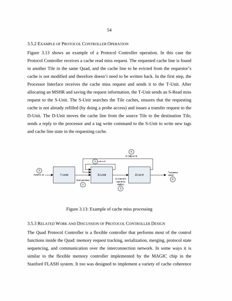
54
3.5.2 EXAMPLE OF PROTOCOL CONTROLLER OPERATION
Figure 3.13 shows an example of a Protocol Controller operation. In this case the
Protocol Controller receives a cache read miss request. The requested cache line is found
in another Tile in the same Quad, and the cache line to be evicted from the requestor’s
cache is not modified and therefore doesn’t need to be written back. In the first step, the
Processor Interface receives the cache miss request and sends it to the T-Unit. After
allocating an MSHR and saving the request information, the T-Unit sends an S-Read miss
request to the S-Unit. The S-Unit searches the Tile caches, ensures that the requesting
cache is not already refilled (by doing a probe access) and issues a transfer request to the
D-Unit. The D-Unit moves the cache line from the source Tile to the destination Tile,
sends a reply to the processor and a tag write command to the S-Unit to write new tags
and cache line state in the requesting cache.
Figure 3.13: Example of cache miss processing
3.5.3 RELATED WORK AND DISCUSSION OF PROTOCOL CONTROLLER DESIGN
The Quad Protocol Controller is a flexible controller that performs most of the control
functions inside the Quad: memory request tracking, serialization, merging, protocol state
sequencing, and communication over the interconnection network. In some ways it is
similar to the flexible memory controller implemented by the MAGIC chip in the
Stanford FLASH system. It too was designed to implement a variety of cache coherence

55
protocols as well as to support message passing protocols [83-85]. The MAGIC chip had
many similar hardware features: line buffers to store data, lookup tables to track
outstanding requests, additional control state associated with the data, and processor,
network and memory interfaces. In addition, MAGIC used a programmable processor
that executes message handlers to implement the logic of a particular cache coherence
protocol.
The main difference between MAGIC and the Smart Memories Protocol Controller is the
latency and message throughput that the designs can support. Since the Protocol
Controller is responsible for managing first level caches which are very latency sensitive
it is designed as a set of programmable finite state machines or pipelines that can often
initiate a new operation each cycle. In contrast, MAGIC is a separate chip and receives
cache miss requests from the processor’s off-chip bus, which makes the latency of
request processing less critical. This difference allows the Protocol Controller to be
shared among eight processors in a chip multi-processor while MAGIC is dedicated only
for one processor. As shown in [84] the occupancy of the MAGIC chip can be quite high
even though it processes requests for only one processor. Finally, combined with the
meta-data storage, the Protocol Controller provides significantly more flexibility in
memory system functionality allowing it to support such different programming and
memory models as shared memory, streaming and transactions.
3.6 ON-CHIP NETWORK
Because the Smart Memories architecture is designed to be scalable to a large number of
processors on a chip, it uses network-on-chip (NoC) to interconnect multiple Quads and
Memory Controllers. NoC is a promising approach for scalable on-chip interconnect [77].
This section describes the general interface from Smart Memories units to the NoC and
high-level requirements imposed by the architecture and memory protocols on the
interconnection network such as packet ordering and virtual channel priority. The Smart
Memories architecture does not specify other network parameters such as topology and
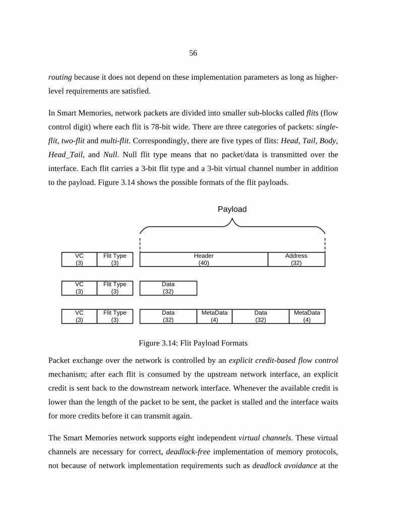
56
routing because it does not depend on these implementation parameters as long as higher-
level requirements are satisfied.
In Smart Memories, network packets are divided into smaller sub-blocks called flits (flow
control digit) where each flit is 78-bit wide. There are three categories of packets: single-
flit, two-flit and multi-flit. Correspondingly, there are five types of flits: Head, Tail, Body,
Head_Tail, and Null. Null flit type means that no packet/data is transmitted over the
interface. Each flit carries a 3-bit flit type and a 3-bit virtual channel number in addition
to the payload. Figure 3.14 shows the possible formats of the flit payloads.
VC(3)
Flit Type (3)
Header(40)
Address(32)
Data(32)
Data(32)
MetaData(4)
Data(32)
MetaData(4)
VC(3)
Flit Type (3)
VC(3)
Flit Type (3)
Payload
Figure 3.14: Flit Payload Formats
Packet exchange over the network is controlled by an explicit credit-based flow control
mechanism; after each flit is consumed by the upstream network interface, an explicit
credit is sent back to the downstream network interface. Whenever the available credit is
lower than the length of the packet to be sent, the packet is stalled and the interface waits
for more credits before it can transmit again.
The Smart Memories network supports eight independent virtual channels. These virtual
channels are necessary for correct, deadlock-free implementation of memory protocols,
not because of network implementation requirements such as deadlock avoidance at the
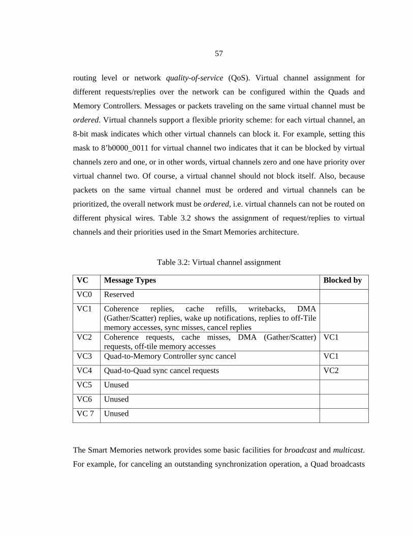
57
routing level or network quality-of-service (QoS). Virtual channel assignment for
different requests/replies over the network can be configured within the Quads and
Memory Controllers. Messages or packets traveling on the same virtual channel must be
ordered. Virtual channels support a flexible priority scheme: for each virtual channel, an
8-bit mask indicates which other virtual channels can block it. For example, setting this
mask to 8’b0000_0011 for virtual channel two indicates that it can be blocked by virtual
channels zero and one, or in other words, virtual channels zero and one have priority over
virtual channel two. Of course, a virtual channel should not block itself. Also, because
packets on the same virtual channel must be ordered and virtual channels can be
prioritized, the overall network must be ordered, i.e. virtual channels can not be routed on
different physical wires. Table 3.2 shows the assignment of request/replies to virtual
channels and their priorities used in the Smart Memories architecture.
Table 3.2: Virtual channel assignment
VC Message Types Blocked by
VC0 Reserved
VC1 Coherence replies, cache refills, writebacks, DMA (Gather/Scatter) replies, wake up notifications, replies to off-Tile memory accesses, sync misses, cancel replies
VC2 Coherence requests, cache misses, DMA (Gather/Scatter) requests, off-tile memory accesses
VC1
VC3 Quad-to-Memory Controller sync cancel VC1
VC4 Quad-to-Quad sync cancel requests VC2
VC5 Unused
VC6 Unused
VC 7 Unused
The Smart Memories network provides some basic facilities for broadcast and multicast.
For example, for canceling an outstanding synchronization operation, a Quad broadcasts

58
the cancel message to all Memory Controllers. To enforce coherence, a Memory
Controller sends a coherence message to all Quads except the one originating the cache
miss. The broadcast/multicast features of the network allow network interfaces to send
out a single request rather than generating separate requests for all desired destinations.
3.7 MEMORY CONTROLLER
The Memory Controller is an access point for the off-chip DRAM memory and it also
implements some functionality for memory protocols, for example, for cache coherence
between different Quads.
The Memory Controller communicates with Quads via an on-chip network. A Smart
Memories system can have more than one Memory Controller. In this case, each Memory
Controller handles a separate bank of off-chip memory and memory addresses are
interleaved among the Memory Controllers.
Since all Quads send requests to a Memory Controller, it serves as a serialization point
among them, which is necessary for correct implementation of memory protocols such as
coherence. Similar to a Quad’s Protocol Controller, the Memory Controller supports a set
of basic operations and it implements protocols via combinations of these operations.
The architecture of the Memory controller is shown in Figure 3.15. C-Req and C-Rep
(cached request and reply) units are dedicated to cache misses and coherence operations.
The U-Req/Rep unit handles DMA operations and uncached accesses to off-chip
memory. The Sync Unit stores synchronization misses and replays synchronization
operations whenever a wakeup notification is received.
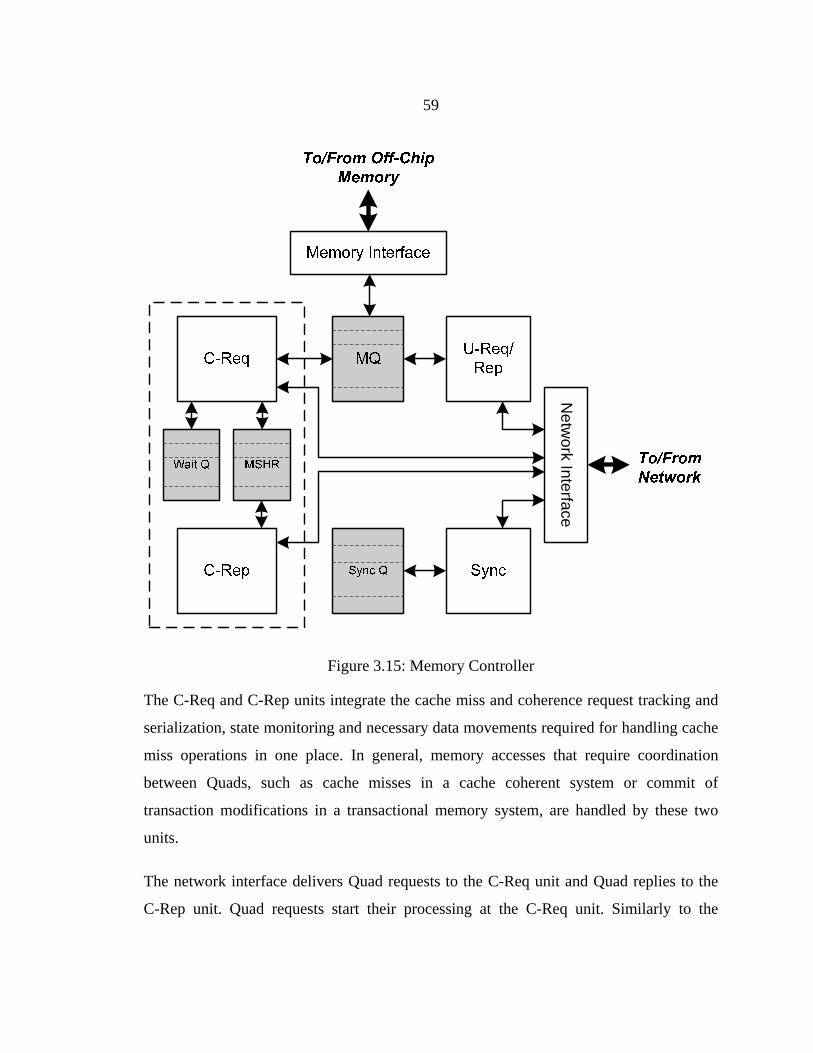
59
Netw
ork Interface
Figure 3.15: Memory Controller
The C-Req and C-Rep units integrate the cache miss and coherence request tracking and
serialization, state monitoring and necessary data movements required for handling cache
miss operations in one place. In general, memory accesses that require coordination
between Quads, such as cache misses in a cache coherent system or commit of
transaction modifications in a transactional memory system, are handled by these two
units.
The network interface delivers Quad requests to the C-Req unit and Quad replies to the
C-Rep unit. Quad requests start their processing at the C-Req unit. Similarly to the
60
Protocol Controller, each incoming request is first checked against outstanding requests
and is accepted only if there is no conflict. Outstanding request information is stored in
the Miss Status Holding Register (MSHR) structure, which has an associative lookup port
to perform an address conflict check. If no serialization is required and there is no
conflicting request already outstanding, an incoming request is accepted by C-Req and is
placed in the MSHR. In case of a collision, a request is placed in the Wait Queue
structure and is considered again when the colliding request in the MSHR completes.
When a memory request requires state information from other Quads or the state
information in other Quads has to be updated, the C-Req unit sends the appropriate
requests to other Quads via the network interface. For example without a directory
structure in the memory, in the case of a cache miss request, caches of other Quads have
to be searched to see if there is a modified copy of the cache line. Similarly, during
commit of the speculative transaction modifications, the data has to be broadcast to all
other running transactions. The network interface has the basic capability of broadcasting
or multicasting packets to multiple receivers and is discussed in Section 3.6. The C-Req
unit also communicates with the memory interface to initiate memory read/write
operations when necessary.
The C-Rep unit collects replies from Quads and updates the MSHR structure accordingly.
Replies from Quads might bring back memory blocks (e.g. cache lines) and are placed in
the line buffers associated with each MSHR entry. After the last reply is received, and
based on the collected state information, C-Rep decides how to proceed. In cases where a
memory block has to be returned to the requesting Quad (e.g., for a cache miss request),
it also decides whether to send the memory block received from main memory or the one
received from other Quads.
The U-Req/Rep unit handles direct accesses to main memory. It can perform single word
read/write operation on the memory (un-cached memory accesses from processors) or
block read/writes (DMA accesses from DMA channels). It has an interface to the
61
Memory Queue structure and places memory read/write operations in the queue after it
receives them from the network interface. After completion of the memory operation, it
asks the network interface to send back replies to the requesting Quad.
As discussed in the earlier sections, Smart Memories supports a fine-grain
synchronization protocol that allows processors to report unsuccessful synchronization
operations to Memory Controllers, also known as synchronization misses. When the state
of a synchronization location changes, a wakeup notification is sent to the Memory
Controller and the failing request is retried on behalf of the processor. The Sync Unit is in
charge of managing all the synchronization misses and replaying operations after wakeup
notifications are received.
Information about synchronization misses is stored in the Sync Queue structure. The
Sync Queue is sized such that there is at least one entry for each processor in the system6.
When a synchronization miss is received, its information is recorded in the Sync Queue.
When a wakeup notification is received for a specific address, the outstanding
synchronization miss on that address is removed from the Sync Queue and a replay
request is sent to the appropriate Quad to replay the synchronization operation.
The Sync Unit also handles cancel requests received by the network interface. A cancel
request erases a synchronization miss from a specific processor if it exists in the Sync
Queue. The Sync Unit invalidates the Sync Queue entry associated with the processor
and sends a Cancel Reply message back to the Quad that sent the Cancel request.
The network interface of the Memory Controller is essentially the same as the Protocol
Controller network interface, as discussed in Section 3.5.1. It has separate transmit and
receive blocks that are connected to input/output pins. It can send short and long packets
and has basic broadcast capabilities which are discussed in Section 3.6.
6 Since synchronization instructions are blocking, each processor can have at most one
synchronization miss outstanding
62
The memory interface is a generic 64-bit wide interface to the off-chip memory that is
operated by the Memory Queue structure. When one of the Memory Controller units
needs to access main memory, it places its read/write request into the Memory Queue and
the reply is returned to the issuing unit after the memory operation is complete. Requests
inside the queue are guaranteed to complete in the order in which they are placed in the
queue and are never re-ordered with respect to each other. Block read/write operations
are always broken into 64-bit wide operations by the issuing units and are then placed
inside the Memory Queue structure.
The Memory Controller can be optionally connected to the second level cache. In this
case, the Memory Controller tries to find the requested cache line in the second level
cache before sending a request to the off-chip DRAM. The second level cache can reduce
average access latency and required off-chip bandwidth. Note that there is no cache
coherence problem for second level caches if there is more than one Memory Controller
because Memory Controllers are address-interleaved and a particular cache line will
always be cached in the same second level cache bank.
3.8 SMART MEMORIES TEST CHIP
To evaluate a possible implementation of a polymorphic architecture, the Smart
Memories test chip was designed and fabricated using STMicroelectronics CMOS 90 nm
technology. It contains a single Quad, which has four Tiles with eight Tensilica
processors and a shared Protocol Controller (Figure 3.16). To reduce the area of the test
chip, the Memory Controller with DRAM interface is placed in an FPGA on a test board,
the Berkeley Emulation Engine 2 (BEE2) [110]. Up to four Smart Memories test chips
can be connected to four FPGAs on a BEE2 board, forming a 32-processor system.
The Smart Memories test chip was designed using standard cell ASIC design
methodology. Verilog RTL for all modules was synthesized by the Synopsys Design
Compiler, and was placed and routed by Synopsys IC Compiler. Physical characteristics
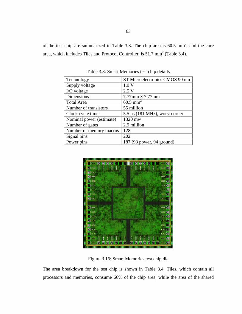
63
of the test chip are summarized in Table 3.3. The chip area is 60.5 mm2, and the core
area, which includes Tiles and Protocol Controller, is 51.7 mm2 (Table 3.4).
Table 3.3: Smart Memories test chip details
Technology ST Microelectronics CMOS 90 nm Supply voltage 1.0 V I/O voltage 2.5 V Dimensions 7.77mm × 7.77mm Total Area 60.5 mm2 Number of transistors 55 million Clock cycle time 5.5 ns (181 MHz), worst corner Nominal power (estimate) 1320 mw Number of gates 2.9 million Number of memory macros 128 Signal pins 202 Power pins 187 (93 power, 94 ground)
Figure 3.16: Smart Memories test chip die
The area breakdown for the test chip is shown in Table 3.4. Tiles, which contain all
processors and memories, consume 66% of the chip area, while the area of the shared

64
Protocol Controller is 12%. The percentage of overhead area (22%) would be smaller for
larger scale systems containing multiple Quads.
Table 3.4: Smart Memories test chip area breakdown
Module Area, mm2 %Tiles 40.0 66.1Protocol Controller 7.2 11.9Chip core 51.7 85.4Routing channels 4.5 7.5Pad ring 8.8 14.6Chip 60.5 100.0
3.9 SUMMARY
This chapter presented the design of the Smart Memories architecture, which leveraged
Tensilica processors allowing us to focus on the reconfigurable memory system. By
creating local memory storage containing metadata bits and a programmable local
memory controller we created a system that can support a wide number of memory
models including streaming, transactions and cache coherent threads. Based on this
architecture we created a test chip implementation with eight processors and evaluated
hardware overheads of reconfigurability. While the overheads in the current system are
high (slightly less than 50%) this is the result of using flops for building some of the
storage arrays the system requires. Since others have already demonstrated these
memories can be built with small overhead, the final overhead for configuration should
be much smaller. The next chapters show how three different programming models can
be mapped onto Smart Memories architecture.

65
CHAPTER 4: SHARED MEMORY
This chapter describes how a shared memory model with broadcast-based MESI cache
coherence protocol and relaxed memory consistency can be mapped onto the
reconfigurable Smart Memories architecture and presents performance evaluation results
showing good scaling for up to 32 processors. Also, the chapter discusses how the
flexibility of Smart Memories can be used to extend the shared memory model to provide
fast fine-grain synchronization operations, which are useful for optimization of
applications with producer-consumer patter. Finally, we describe how the flexibility of
the memory system can be used to adjust the cache configuration for the requirements of
a particular application.
4.1 HARDWARE CONFIGURATION
For the shared memory programming model (Section 2.3.1) the on-chip memory
resources of the Smart Memories architecture are used as instruction and data caches.
Figure 4.1 shows an example of a Tile configuration for shared memory mode. In this
case, memory mats inside the Tile are used as a 32 KB 2-way set-associative data cache
and a 16 KB 2-way set-associative instruction cache. Each way of the cache has its own
dedicated tag mat as highlighted in Figure 4.1. In this example, the processors share both
caches.
Each processor load or store generates 4 memory mat operations: 2 tag mat read-
compares and 2 data mat reads or writes (shown with bold arrows in Figure 4.1). These
operations are routed to the appropriate memory mats by the crossbar according to the
cache configuration. The Total Match (TM) outputs of the tag mats are used as Hit/Miss
signals for corresponding ways of the cache. These signals are routed through the IMCN
(Section 3.4) to the data mats to disable data mat operation in the case of cache miss.

66
Meta data bits in tag mats are used to store control the state of each cache line: valid (V),
exclusive (E), modified (M), reserved (R), and most-recently-used (MRU) bits. V, E and
M bits are used to indicate the coherence state of a cache line similarly to the
conventional MESI cache coherence protocol. The R bit is used by the Protocol
Controller to reserve a cache line for an outstanding cache miss refill request: after a
cache miss request is accepted for service, the Protocol Controller selects a candidate line
for eviction, performs a writeback if necessary, and sets the line state to reserved. A
processor request results in a cache miss if it tries to access a reserved cache line.
Data Cache Instruction Cache
Interface Logic
TileProcessor 0
Crossbar
Processor 1
Data
Data
Data
Data
Data
Data
Data
Data
Tag0
Tag1
Data
Data
Data
Data
Tag0
Tag1TM
TM
TM
TM
Figure 4.1: Example of cached configuration
The MRU bit is used to implement a not-most-recently-used eviction policy for set-
associative caches: for every cache hit the MRU bit is set in the cache way where the hit
was detected and reset for all other ways. When the Protocol Controller has to select a
candidate line for the eviction, it uses the MRU bit to detect which way of the cache was
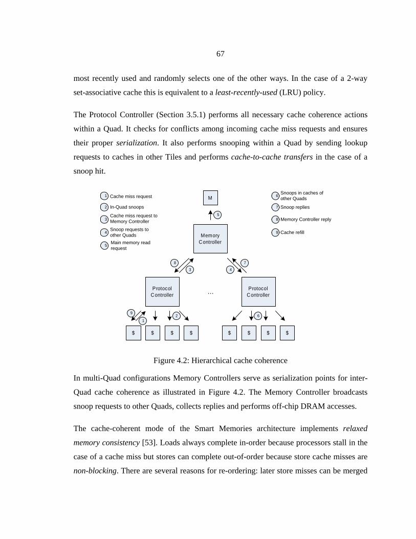
67
most recently used and randomly selects one of the other ways. In the case of a 2-way
set-associative cache this is equivalent to a least-recently-used (LRU) policy.
The Protocol Controller (Section 3.5.1) performs all necessary cache coherence actions
within a Quad. It checks for conflicts among incoming cache miss requests and ensures
their proper serialization. It also performs snooping within a Quad by sending lookup
requests to caches in other Tiles and performs cache-to-cache transfers in the case of a
snoop hit.
$$$$
Protocol Controller
$$$$
Protocol Controller
Memory Controller
12
3 4
6
78
9
...
M
5
1
2
Cache miss request
In-Quad snoops
3Cache miss request to Memory Controller
4 Snoop requests to other Quads
5 Main memory read request
6 Snoops in caches of other Quads
8
7 Snoop replies
Memory Controller reply
9 Cache refill
Figure 4.2: Hierarchical cache coherence
In multi-Quad configurations Memory Controllers serve as serialization points for inter-
Quad cache coherence as illustrated in Figure 4.2. The Memory Controller broadcasts
snoop requests to other Quads, collects replies and performs off-chip DRAM accesses.
The cache-coherent mode of the Smart Memories architecture implements relaxed
memory consistency [53]. Loads always complete in-order because processors stall in the
case of a cache miss but stores can complete out-of-order because store cache misses are
non-blocking. There are several reasons for re-ordering: later store misses can be merged
68
with an already outstanding request in an MSHR in the Protocol Controller or in the
Memory Controller or a later store miss can be serviced faster because its cache line is
found in a neighboring Tile. Thus, a memory barrier instruction must be used to enforce
of memory ordering: it stalls the processor until all outstanding memory operations issued
by the processor are completed.
The Smart Memories cache-coherent mode maintains the property of write atomicity [53]
because it uses an invalidation cache coherence protocol and there is no data forwarding
in the memory system.
4.2 FAST FINE-GRAIN SYNCHRONIZATION
The flexibility of the Smart Memories architecture can be used to extend semantics of
memory operations. For example, meta data bits in the Memory Mats can be used to
implement full/empty (FE) bits [86-94]. Full/empty bits are used as locks associated with
each data word to enable fine-grain producer-consumer synchronization. Tensilica
processors are extended with several memory instructions that use these bits:
Synchronized load stalls the processor if the FE bit associated with the corresponding
data word is empty (zero). When the FE bit is set to 1, the processor is unstalled and the
value of the data word is returned to the processor. After completion of a synchronized
load, the FE bit is atomically reset to 0. A synchronized load is essentially a combination
of a lock acquire with a conventional load.
Synchronized store stalls the processor if the FE bit associated with corresponding data
word is full (one); if the FE bit is 0, the processor is unstalled and the store data is written
into the data word. After completion of a synchronized store, the FE bit is atomically set
to 1. A synchronized store is essentially a combination of a conventional store and a lock
release.
Future load is similar to synchronized load but it does not change the value of the FE bit.
69
Reset load and set store are similar to synchronized load and store but they do not stall
the processor regardless of the state of the FE bit. These instructions are necessary for
initialization.
To implement synchronized memory operations in the Smart Memories architecture two
metadata bits in the data mats of the caches are used: full/empty (FE) and waiting (W)
bits. The FE bit is used as described above. Whenever a synchronized operation cannot
complete because of the state of the FE bit, interface logic in the Tile generates a
synchronization miss message which is sent to the Protocol Controller and then to the
Memory Controller. The Memory Controller serves as serialization point for
synchronization miss messages and keeps track of outstanding synchronization misses.
The W bit is set to indicate that there is synchronized operation waiting on this address.
When the FE bit is flipped for a data word that also has its W bit set, a wakeup message is
generated and sent to the Memory Controller. The Memory Controller checks if any
synchronization miss is outstanding for the same address and sends a replay message to
the originating Protocol Controller, which tries to re-execute the synchronization
operation in the same cache. If the state of the FE bit was changed between wakeup and
replay, then replay would not be completed and the synchronization miss would be sent
to the Memory Controller again. For correct operation, the synchronization misses and
wakeups must not be re-ordered within the memory system. This condition is ensured by
virtual channel assignment in the on-chip network (Section 3.6).
Synchronized memory operations work with cached data and therefore must interact
correctly with cache coherence. In the Smart Memories implementation, every
synchronized memory operation is treated as an operation requiring exclusive state of the
cache line. Therefore, before synchronized operation can be executed, the cache line must
be fetched or upgraded to exclusive state by the Protocol Controller. The same is also true
for replays of synchronization misses. Such an approach guarantees transparent execution
of synchronized memory operations.

70
4.3 EVALUATION
Several shared memory applications (Table 4.1) and kernels (Table 4.2) were used to
evaluate performance of shared memory mode of the Smart Memories architecture. All
benchmarks were compiled by the Tensilica optimizing compiler (XCC) with a –O3
option (highest optimization level) and a –ipa option (inter-procedural analysis).
Table 4.1: Shared memory applications
Name Source Runtime Comment mp3d SPLASH [95] ANL simulation of rarefied hypersonic flow barnes SPLASH-2 [96] ANL Barnes-Hut hierarchical N-body method fmm SPLASH-2 ANL N-body adaptive fast multi-pole method 179.art SPEC CFP2000 [97] pthreads image recognition/neural networks
parallelized for [44, 45] MPEG-2 encoder
pthreads parallelized for [44, 45]
Table 4.2: Shared memory kernels
Name Source Runtime Comment radix SPLASH-2 ANL integer radix sort kernel fft SPLASH-2 ANL complex 1-D FFT kernel lu SPLASH-2 ANL LU factorization kernel cholesky SPLASH-2 ANL blocked sparse Cholesky factorization
kernel bitonic sort pthreads developed and parallelized for [44, 45]
System configuration parameters used for simulation are shown in Table 4.3 (except for
MPEG-2 encoder, for which 8 KB data caches and 16 KB instruction caches were used,
as discussed in Section 4.3.2). Latency parameters for Protocol Controller, Memory
Controller, and network were back-annotated from the actual RTL design. To provide

71
sufficient off-chip memory bandwidth the number of Memory Controllers is equal to the
number of Quads.
Table 4.3: System configuration parameters
Parameter Value Comment Off-chip memory latency 100
cycles
Off-chip memory width 64 bits per Memory Controller Cache line size 32 bytes Network switch latency 4 cycles Network interface latency
5 cycles including message formation, buffering, arbitration, pipelining and wiring delay within Quad
Number of MSHRs 16 L1 cache latency 2 cycles L1 data cache size 16 KB per processor L1 instruction cache size 8 KB per processor
As shown in Figure 4.3 four out of five applications exhibit good performance scaling,
achieving speedups between 24 and 32 on a 32-processor configuration. The exception is
mp3d, which is limited by off-chip memory bandwidth. mp3d performance of 4 and 8-
proceessor configurations is almost identical: 2.66 vs. 2.78.

72
0
5
10
15
20
25
30
35
0 5 10 15 20 25 30
Number of processors
linear speedupmp3dbarnesfmm179.artmpeg2enc
Figure 4.3: Shared memory application speedups
Similarly to mp3d, performance scaling of three out of five kernels is limited by the
DRAM bandwidth (Figure 4.4a). Increase in off-chip bandwidth by doubling the number
of Memory Controllers per Quad results in significant performance improvement for
these applications as shown in Figure 4.4b. For example, the speedup of mp3d on a 32-
processor configuration improves from 10.8 to 18.3.

73
Figure 4.4: Shared memory kernel speedups
Another way to improve performance of memory intensive applications and kernels is to
add an on-chip second level cache between Memory Controllers and off-chip DRAM.
For these applications it would completely solve the problem; for more realistic
applications it would at least reduce the main memory bandwidth requirements.
4.3.1 PERFORMANCE OF FAST FINE-GRAIN SYNCHRONIZATION OPERATIONS
In order to evaluate the performance of fast fine-grain memory operations (Section 4.2),
mp3d (Section 4.3) was recompiled to use synchronized loads and stores for fine-grain
locking of space cell data structures. By default, these locks are compiled out, and the
accesses to these data structures cause data races. The reason for this is performance: in
conventional shared memory architectures, fine-grain locking is expensive. Since mp3d
performs randomized computation and reports results only after statistical averaging of
many steps of computation, the data races should not alter the results significantly [95].
a) 1 Memory Controller per Quad b) 2 Memory Controllers per Quad
0
5
10
15
20
25
30
0 10 20 30
Number of processors
linear speedup
0
5
10
15
20
25
30
0 10 20 30
Number of processors
linear speedupmp3d mp3dradix radixfft fftlu lucholesky choleskybitonic bitonic
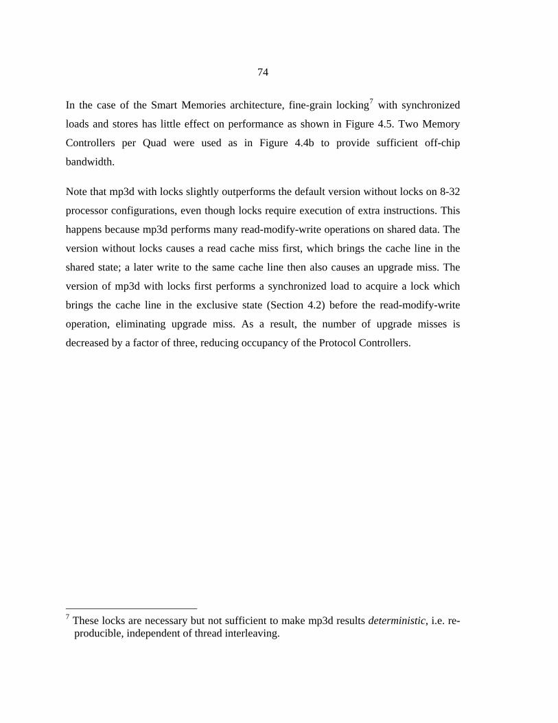
74
In the case of the Smart Memories architecture, fine-grain locking7 with synchronized
loads and stores has little effect on performance as shown in Figure 4.5. Two Memory
Controllers per Quad were used as in Figure 4.4b to provide sufficient off-chip
bandwidth.
Note that mp3d with locks slightly outperforms the default version without locks on 8-32
processor configurations, even though locks require execution of extra instructions. This
happens because mp3d performs many read-modify-write operations on shared data. The
version without locks causes a read cache miss first, which brings the cache line in the
shared state; a later write to the same cache line then also causes an upgrade miss. The
version of mp3d with locks first performs a synchronized load to acquire a lock which
brings the cache line in the exclusive state (Section 4.2) before the read-modify-write
operation, eliminating upgrade miss. As a result, the number of upgrade misses is
decreased by a factor of three, reducing occupancy of the Protocol Controllers.
7 These locks are necessary but not sufficient to make mp3d results deterministic, i.e. re-
producible, independent of thread interleaving.

75
0
5
10
15
20
25
30
0 10 20
Number of processors30
linear speedupno locklock
Figure 4.5: mp3d performance with and without locking
This comparison mp3d with and without fine-grain locking is an indication of how well
synchronized memory operations perform on the Smart Memories architecture. But to
realize the benefits of fast fine-grain synchronization, application software must be
redesigned. V. Wong redesigned several probabilistic inference algorithms with fine-
grain locking and showed that fast fine-grain locking can result in significant
performance improvements [99]. For example, a recursive conditioning algorithm can use
synchronized memory operations to cache and share intermediate computation results
between multiple threads to avoid re-computation. As a result, the recursive conditioning
algorithm with fine-grain synchronization and multiple hardware contexts [100, 101]
performs three times better than the original algorithm on a 32-processor configuration
[99].
4.3.2 MPEG-2 ENCODER
The MPEG-2 encoder is an interesting example of an application that presents
opportunities for performance optimization by both restructuring software and utilizing

76
capabilities of the reconfigurable memory system to fit cache configuration to the
demands of an optimized application.
The original parallel version of an MPEG-2 encoder by Li et al. [98] performs each stage
of the computation, i.e. Motion Estimation, DCT, Quantization, etc., on an entire video
frame before starting the next stage. Such structuring of the application results in a
significant data cache miss rate since the whole video frame typically does not fit into a
first level cache, especially for configurations with a small number of processors. Each
stage of encoding causes writeback of intermediate data, while the next stage has to
reload it from off-chip memory.
Alternatively, an MPEG-2 encoder can be parallelized at the macroblock level [44, 45].
Macroblocks are entirely data-parallel and dynamically assigned to cores using a task
queue. The code was restructured by hoisting the inner loops of several tasks (e.g. Motion
Estimation, DCT) into a single outer loop that calls each task in turn. All tasks are
executed on a single macroblock of a frame before moving to the next macroblock. This
allows one to condense a large temporary array into a small number of stack variables.
The improved producer-consumer locality reduced write-backs from first level caches by
60%. Furthermore, improving the parallel efficiency of the application became a simple
matter of scheduling a single data-parallel loop.
However, this streaming-inspired optimization can lead to a higher instruction cache miss
rate unless the code for all stages of the computation fits into the instruction cache. On
the other hand, the size of the data cache becomes less critical as long as it is large
enough to capture producer-consumer locality within one macroblock. Such
characteristics are quite different from characteristics of other shared memory
applications discussed in Section 4.3.
The reconfigurable Smart Memories architecture can exploit characteristics of the
MPEG-2 encoder to optimize performance by matching cache parameters to the

77
requirements of the applications. Figure 4.6 shows relative performance for five different
Tile cache configurations with the same amount of data storage:
1) two 8 KB instruction caches and a single 32 KB data cache (2 8K IC/1 32K DC);
2) two 8 KB instruction caches and two 16 KB data caches (2 8K IC/2 16K DC);
3) a single 16 KB instruction cache and a single 32 KB data cache (1 16K IC/1 32K DC);
4) two 16 KB instruction caches and a single 16 KB data cache (2 16K IC/1 16K DC);
5) two 16 KB instruction caches and two 8 KB data caches (2 16K IC/2 8K DC);
All speedups are normalized with respect to a single processor configuration with 16 KB
instruction and 8 KB data caches.
2 16K IC/2 8K DC configurations significantly outperform 2 8K IC/2 16K DC and 2 8K
IC/1 32K DC configurations because of fewer instruction cache misses (Figure 4.7).
Although the size of instruction cache differs only by a factor of two, the difference in
instruction cache miss rate is significant. As a result, the percentage of instruction fetch
stalls is high for configurations with an 8 KB instruction cache, as shown in Figure 4.8,
which significantly degrades performance.
Configurations with a shared instruction cache (1 16K IC/1 32K DC) also have low
instruction miss rates, however, they also suffer from instruction fetch stalls (Figure 4.8)
and have lower performance than configurations with private 16 KB instruction caches,
especially for low processor counts. The reason for this performance degradation is high
utilization of the shared instruction cache (e.g. 72% vs. 46% for private cache) and
additional fetch stalls due to conflicts between two processors in the Tile.
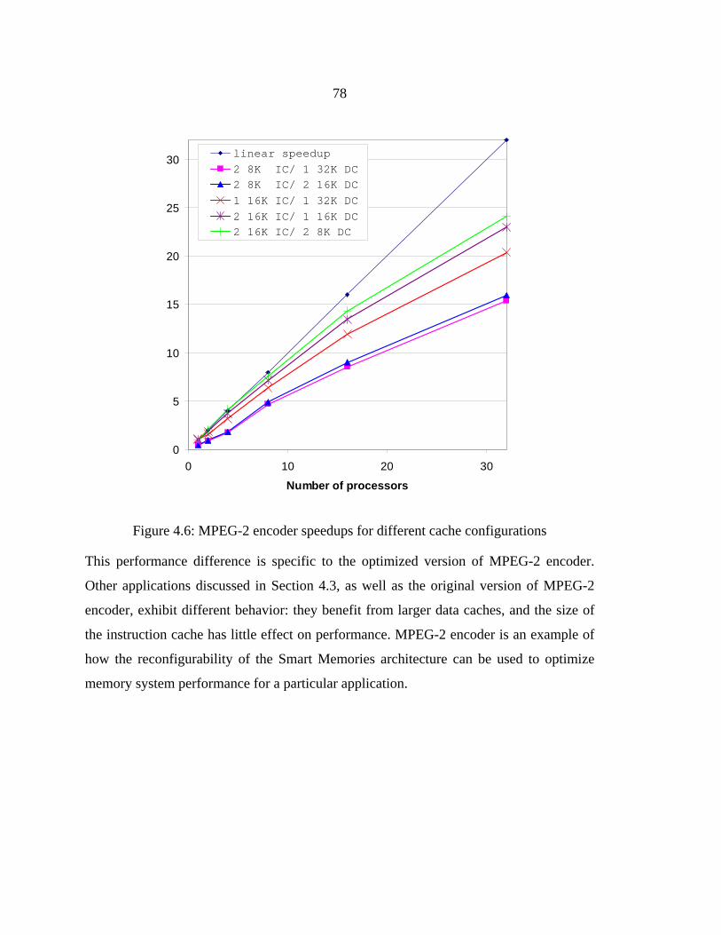
78
0
5
10
15
20
25
30
0 10 20
Number of processors30
linear speedup2 8K IC/ 1 32K DC2 8K IC/ 2 16K DC1 16K IC/ 1 32K DC2 16K IC/ 1 16K DC2 16K IC/ 2 8K DC
Figure 4.6: MPEG-2 encoder speedups for different cache configurations
This performance difference is specific to the optimized version of MPEG-2 encoder.
Other applications discussed in Section 4.3, as well as the original version of MPEG-2
encoder, exhibit different behavior: they benefit from larger data caches, and the size of
the instruction cache has little effect on performance. MPEG-2 encoder is an example of
how the reconfigurability of the Smart Memories architecture can be used to optimize
memory system performance for a particular application.

79
0
0.5
1
1.5
2
2.5
3
3.5
4
4.5
5
0 10 20
Number of processors30
2 8K IC/ 1 32K DC2 8K IC/ 2 16K DC1 16K IC/ 1 32K DC2 16K IC/ 1 16K DC2 16K IC/ 2 8K DC
Figure 4.7: Instruction miss rate for different cache configurations (%)
0
10
20
30
40
50
60
70
0 10 20
Number of processors30
2 8K IC/ 1 32K DC2 8K IC/ 2 16K DC1 16K IC/ 1 32K DC2 16K IC/ 1 16K DC2 16K IC/ 2 8K DC
Figure 4.8: Instruction fetch stalls for different cache configurations (%)
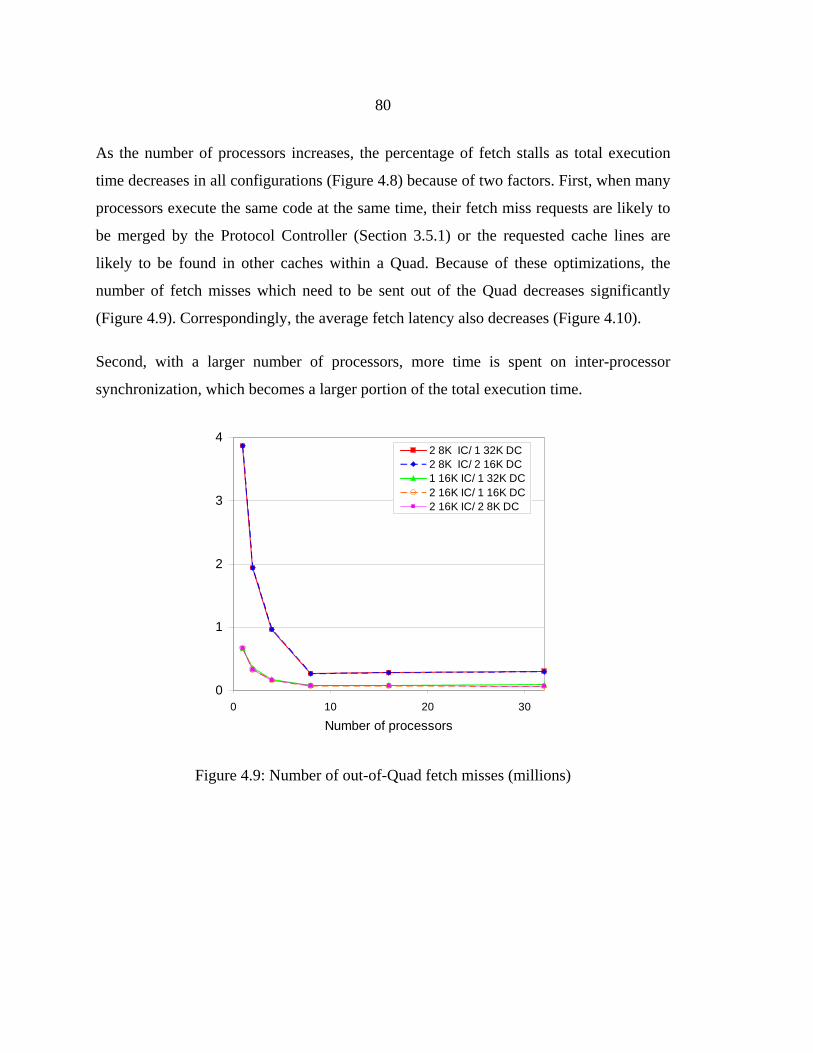
80
As the number of processors increases, the percentage of fetch stalls as total execution
time decreases in all configurations (Figure 4.8) because of two factors. First, when many
processors execute the same code at the same time, their fetch miss requests are likely to
be merged by the Protocol Controller (Section 3.5.1) or the requested cache lines are
likely to be found in other caches within a Quad. Because of these optimizations, the
number of fetch misses which need to be sent out of the Quad decreases significantly
(Figure 4.9). Correspondingly, the average fetch latency also decreases (Figure 4.10).
Second, with a larger number of processors, more time is spent on inter-processor
synchronization, which becomes a larger portion of the total execution time.
0
1
2
3
4
0 10 20
Number of processors30
2 8K IC/ 1 32K DC2 8K IC/ 2 16K DC1 16K IC/ 1 32K DC2 16K IC/ 1 16K DC2 16K IC/ 2 8K DC
Figure 4.9: Number of out-of-Quad fetch misses (millions)
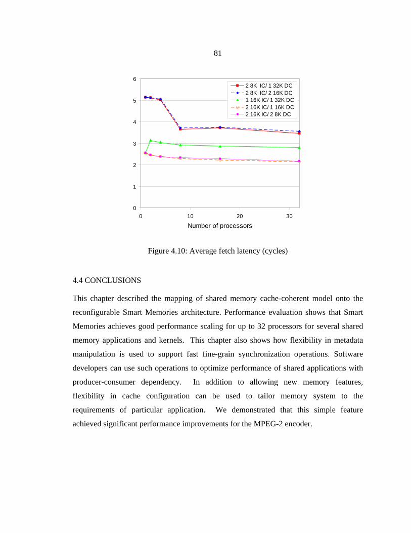
81
0
1
2
3
4
5
6
0 10 20
Number of processors30
2 8K IC/ 1 32K DC2 8K IC/ 2 16K DC1 16K IC/ 1 32K DC2 16K IC/ 1 16K DC2 16K IC/ 2 8K DC
Figure 4.10: Average fetch latency (cycles)
4.4 CONCLUSIONS
This chapter described the mapping of shared memory cache-coherent model onto the
reconfigurable Smart Memories architecture. Performance evaluation shows that Smart
Memories achieves good performance scaling for up to 32 processors for several shared
memory applications and kernels. This chapter also shows how flexibility in metadata
manipulation is used to support fast fine-grain synchronization operations. Software
developers can use such operations to optimize performance of shared applications with
producer-consumer dependency. In addition to allowing new memory features,
flexibility in cache configuration can be used to tailor memory system to the
requirements of particular application. We demonstrated that this simple feature
achieved significant performance improvements for the MPEG-2 encoder.

82
CHAPTER 5: STREAMING
This chapter describes the streaming mode of the Smart Memories architecture, which
implements the architectural concepts discussed in Section 2.3.2, that is software-
managed local memories and DMAs instead of the coherent caches used in conventional
shared memory systems. Then, we present implementations of software runtimes for
streaming, including a Stream Virtual Machine [61-63], showing how the flexibility of
the Smart Memories architecture is used to simplify and optimize a complex runtime
system. After that, we present performance evaluation results of the Smart Memories
streaming mode and compare it to shared memory mode, showing good performance
scaling. Finally, we take one of the benchmark applications, 179.art, and describe
tradeoffs between different methods of streaming emulation in shared memory mode.
5.1 HARDWARE CONFIGURATION
To support the stream programming model (Section 2.3.2), the memory mats inside the
Tile are configured as local, directly addressable memories (stream data mats in Figure
5.1). The corresponding memory segment (Section 3.4.1) in the Tile’s interface logic
(LSU) is configured to be on-tile, uncached. Loads or stores issued by the processors are
translated into simple read or write requests and routed to the appropriate single memory
mat. Thus, application software executed on the processors can directly access and
control the content of local memory mats. Similarly, processors can access memories in
other Tiles, Quads and off-chip DRAM, thus, streaming application software has
complete control over data allocation in different types of memories and movement of
data between different memories. However, for efficiency reasons it is better to move
data between on-chip and off-chip memories using the software-controlled DMA engines
as described in the next section.

83
Figure 5.1: Example of streaming configuration
One or more memory mats can be used for shared data (shared data mat in Figure 5.1).
Processors from other Tiles and Quads can access the shared data mat via their off-tile,
uncached memory segment. In this case, interface logic and Protocol Controllers route
memory accesses through crossbars and the on-chip network to the destination mat.
Shared data mats contain shared application state such as reduction variables, state for
synchronization primitives such as barriers, and control state for software runtime.
For synchronization between processors, application and runtime software can use
uncached synchronized loads and stores as in the case of cache coherent configurations
(Section 4.2). Uncached synchronized operations are executed directly on local memories
without causing any coherence activity, and therefore are more efficient.
For streaming mode, a few memory mats can be configured as a small instruction cache
as shown in Figure 5.1. Instruction caches typically perform very well for streaming
Interface Logic
Data Cache Instruction Cache
Processor 0
Crossbar
Processor 1
Data
Tile
Stream Data1
Stream Data0
Stream Data0
Shared Data
Stream Data0
TM
Tag0
Stream Data0
Data
Stream Data1
Data
Stream Data1
TM
Tag0
Stream Data1

84
applications because these applications are dominated by small, compute-intensive
kernels with a small instruction footprint.
Data Cache Instruction Cache Instruction Cache
Figure 5.2: Alternative streaming configuration
If a streaming application is well optimized, it may be able to completely hide memory
latency by overlapping DMA operations with computational kernels. In this case, a
shared instruction cache can become a bottleneck because of high utilization and conflicts
between the processors in the Tile. Therefore, it is more efficient to configure two private
instruction caches within a Tile (Figure 5.2), taking advantage of Smart Memories
reconfigurable architecture.
Finally, some of the data regions, such as thread stack data and read-only data, also
exhibit very good caching behavior. Configuring a small shared data cache as shown in
Figure 5.1 and Figure 5.2 for these data regions simplifies software because the
Interface Logic
Processor 0
Crossbar
Processor 1
Data
Tile
Stream Data1
Stream Data0
Stream Data0
Stream Data0
TM
Tag0
Data
Shared Data
Data
Stream Data1
TM
Tag0
Stream Data1
Data TM
Data Tag0

85
programmer does not need to worry about memory size issues for such data, e.g. stack
overflow.
5.2 DIRECT MEMORY ACCESS CHANNELS
Direct Memory Access (DMA) channels are included in the Quad Protocol Controller
(Section 3.5.1). DMA is used for bulk data transfers between Tile memory mats and off-
chip DRAM. Streaming applications can directly program DMA channels by writing into
control registers of the Protocol Controller.
The following types of DMA transfer are supported by the Smart Memories architecture:
1) copy of contiguous memory region (DMA_MOVE);
2) stride scatter (DMA_STR_SCATTER);
3) stride gather (DMA_STR_GATHER);
4) index scatter (DMA_IND_SCATTER);
5) index gather (DMA_IND_GATHER).
DMA transfers must satisfy several conditions:
- cache memories must not be a source or a destination;
- source or destination should be in the same Quad as the DMA channel;
- index array should be in the local memory mats in the same Quad as the DMA
channel;
- DMA channels work with physical addresses, no virtual-to-physical address
translation is supported;
- DMA channels can perform only simple read and write operations, synchronized
operations can not be executed;
- all addresses must be 32-bit word aligned, and the element size for stride and index
DMA must be a multiple of four bytes;
86
Upon completion of the transfer, the DMA channel can perform up to two extra stores to
signal the end of the transfer to the runtime or to the application. Each completion store
can:
- perform a simple write into a flag variable;
- perform a write into a memory mat configured as a FIFO;
- cause a processor interrupt by writing into a special interrupt register inside the
Protocol Contoller;
- perform a set store to set the full-empty bit and wake up a processor waiting on a
synchronized load.
Similarly to DMA data transfers, completion stores must write 32-bit words and cannot
write into caches.
5.3 RUNTIME
For streaming mode we developed two different runtime systems. One of them is called
Stream Virtual Machine [61-63]. It was used as an abstraction layer for high-level stream
compiler research [102-104].
The other runtime system is a steaming version of the Pthreads runtime which provides a
low level Application Programming Interface (API). Such an API gives programmer a lot
of flexibility and allows experimentation with streaming optimizations (an example is
described in Appendix B) when a high-level stream compiler is still not available. The
Pthreads runtime allowed us to manually develop and optimize several streaming
applications which were used for streaming mode performance evaluation and
comparison of streaming with shared memory model [44, 45].

87
5.3.1 STREAM VIRTUAL MACHINE
The Stream Virtual Machine (SVM) was proposed as an abstraction model and an
intermediate level API common for a variety of streaming architectures [61-63]. The goal
of SVM infrastructure development is to share a high-level stream compiler such as R-
Stream [102-104] among different streaming architectures.
SVM compiler flow for Smart Memories is shown in Figure 5.3. High-level compiler
(HLC, R-stream in Figure 5.3) inputs are 1) a stream application written in a high-level
language, such as C with Streams, and 2) an SVM abstract machine model. The HLC
performs parallelization and data blocking and generates SVM code, which is C code
with SVM API calls. The Low-level compiler (LLC, Tensilica compiler in Figure 5.3)
compiles SVM code to executable binary (“SM binaries”).
C with Streams
R-Stream Compiler
SVM machine model for SM
SVM code for SMSVM runtime for SM
Tensilica XCC Compiler
SM binaries
Smart Memories SM machine configuration
Figure 5.3: SVM compiler flow for Smart Memories
The SVM abstract machine model describes the key resources of the particular streaming
architecture and its specific configuration: computational resources, bandwidth of
interconnect and memories, sizes of local stream memories. This information allows the
88
HLC to decide how to partition computation and data. The SVM model has three threads
of control, one each for the control processor, the stream processor, and the DMA
engine. The Control processor orchestrates operation of the stream processor and DMA.
The Stream processor performs all computation and can also initiate DMA transfers. The
DMA engine does all transfers between off-chip main memory and local stream
memories.
The SVM API allows specification of dependencies between computational kernels
executed on the stream processor and DMA transfers. Some of these dependencies are
producer-consumer dependencies derived from the application code but others are related
to resource constraints like allocation of local memories [63]. The Control processor
dispatches operations to the stream processor and DMA according to dependencies
specified by the HLC.
The SVM API implementation for Smart Memories takes advantage of the flexibility of
its reconfigurable memory system [63]. An example of SVM mapping on Smart
Memories is shown in Figure 5.4. One of the processors is used as a control processor,
which uses instruction and data caches. One of the memory mats is used as uncached
local memory for synchronization with other processors and DMA engines. Other
processors are used as stream processors for computation. They use instruction cache and
local memory mats for stream data.
To simplify synchronization between control and stream processors and DMA, two
memory mats are used as FIFOs (Figure 5.4). One FIFO is used by the stream processors
to queue DMA requests sent to the control processor. To initiate a DMA transfer stream,
the processor first creates a data structure describing the required transfer, and then it
writes a pointer to this structure into a DMA request FIFO as a single data word.

89
Another FIFO is used by the DMA engines to signal to the control processor completion
of DMA transfers. Each DMA engine is programmed to write its ID to this DMA
completion FIFO at the end of each transfer.
The control processor manages all DMA engines and dependencies between DMA
transfers and computational kernels. It reads the DMA request FIFO and, if it is not
empty and there is an unused DMA engine, it starts a DMA transfer on that engine. The
control processor also reads the DMA completion FIFO to determine which DMA
transfer is completed and when the next operation can be initiated.
To avoid constant polling of the FIFO, an empty flag variable is used in the local memory
of the control processor. After reaching the end of both FIFOs the control processor
executes a synchronized load to this flag and stalls if it is empty. The DMA engine or the
stream processor performs a set store (Section 4.2) to the empty flag after writing into the
corresponding FIFO. The set store wakes up the control processor if it was waiting. After
wakeup, the control processor checks both FIFOs and processes queued DMA requests
and DMA completions.

90
Figure 5.4: SVM mapping on Smart Memories
Interface Logic
Control Processor
Instruction CacheData Cache
Crossbar
Stream Processor
Data
Tile 0
Stream Data
SVM Shared
Data
DMA request FIFO
DMA compl. FIFO
Tag0
SVM Local Data
Data
Stream Data
Data
Stream Data
Tag0
Stream Data
TM TM
Instruction Cache
Data Data Tag0 TM
Interface Logic
Stream Processor
Crossbar
Stream Processor
Data
Instruction CacheData Cache
Tile 1
Stream Data1
Stream Data0
Stream Data0
Stream Data0
Tag0
Stream Data0
Data
Stream Data1
Data
Stream Data1
Tag0
Stream Data1
TM TM
Instruction Cache
Data Data Tag0 TM
DMA
DMA
DMA
DMA
Protocol Controller

91
Synchronized memory operations and DMA flexibility allows the SVM runtime to avoid
FIFO polling or interrupts, which require at least 50 cycles to store processor state. Using
a memory mat as a hardware FIFO greatly simplifies and speeds up runtime software for
the control processor: instead of polling multiple entities or status variables in the
memory to figure out which units require attention, it has to read only two FIFOs. Also,
hardware FIFOs eliminate a lot of explicit software synchronization between stream and
control processors because both can rely on atomic FIFO read and write instructions.
F. Labonte showed that the SVM API can be implemented very efficiently on Smart
Memories [63]. The percentage of dynamically executed instructions due to SVM API
calls is less than 0.6% for the GMTI application [105] compiled with the R-Stream
compiler. More details and results on SVM and its implementation for Smart Memories
are presented in the cited paper [63].
5.3.2 PTHREADS RUNTIME FOR STREAMING
While the SVM approach is very promising for development of portable streaming
applications written in a high-level language, it depends on the availability and maturity
of a high-level stream compiler such as R-Stream [102-104]. Development of such
advanced compilers is still an area of active research and only a very limited set of
applications can be handled efficiently by the R-Stream compiler.
To evaluate streaming on a wider range of applications, a streaming version of the
POSIX threads (Pthreads) runtime [55] was developed. This runtime was used for a
comparison study of streaming and cache-coherent memory systems in a couple of papers
by Leverich et al [44, 45]. The programmer can use this runtime to parallelize an
application manually and convert it to a streaming version. This approach resembles the
StreamC/KernelC approach for stream application development [26] in that it requires the
programmer to use explicit hardware-specific constructs. However, Pthreads are much
92
more familiar to programmers and provide a lot more flexibility than the high-level
streaming language used as source for SVM runtime.
The main difference between conventional Pthreads and streaming Pthreads is in the
different types of memories explicitly supported by the runtime, and support for explicit
memory allocation and management. The thread stack and the read-only segment are
mapped to the data cache (Figure 5.1), which is not coherent. This means that automatic
local variables and arrays in the thread-stack segment cannot be shared. However, this is
viewed as bad software practice because the same location on the stack can be used for
different variables in different functions or even in different invocations of the same
function.
Shared variables must be global/static or heap variables, which are allocated to off-chip
main memory and are not cached. These locations can be safely shared among threads;
however, direct access to them is slow because of the absence of caching. The
recommended way to access these locations is through DMA transfer to Tile local
memory: the DMA engine can perform bulk data transfer very efficiently with the goal of
hiding the latency under concurrent computation.
Local memory mats are used for stream data (Figure 5.1), i.e. data fetched by DMA from
off-chip memory. The programmer can declare a variable or array to be allocated in local
memory using the __attribute__ ((section(".stream_buffer")))
construct of the GNU C compiler [106], which is also supported by the Tensilica XCC
compiler. Variables and arrays declared in this way are automatically allocated by the
compiler in the thread-local memory on Tile. A simple local memory heap is
implemented, which allows an application to dynamically allocate arrays in the local
memory during runtime. This is necessary for optimal local memory allocation, which
depends on the data size, the number of processors, and the size of local memory (Section
5.4.1).

93
Shared runtime data, synchronization locks and barriers, application reduction variables
and other shared data are allocated in the shared memory mat (Figure 5.1) using the
__attribute__ ((section(".shared_data"))) construct. Similarly, a
simple shared memory heap is implemented to support dynamic allocation of shared data
objects.
The stream Pthreads runtime provides programmers with a lot of flexibility. It can
explicitly emulate the SVM runtime by dedicating a single control processor to manage
DMA transfers. However, in many applications, such as investigated in Leverich et al
[44, 45], it is easier to dedicate a DMA engine per execution processor, so that each
processor can issue chained DMA transfer requests directly to the DMA engine and avoid
the overhead and complexity of frequent interaction with the DMA control processor. In
such cases simple synchronization primitives, e.g. synchronization barriers, are usually
sufficient because processors need to synchronize only at the boundaries of different
computation phases or for reduction computations.
5.4 EVALUATION
Several streaming applications were developed using the stream Pthreads runtime for a
comparison study of streaming and cache-coherent memory systems [44, 45]. This
section presents performance results for three of these applications (Table 5.1) and
compares their performance to shared memory versions of the same applications (Section
4.3). These applications were selected because they exhibit different memory
characteristics and different performance behaviors for streaming and cache-coherent
memory systems. Results for more applications are presented in the earlier paper [44, 45].
All benchmarks were compiled with the Tensilica optimizing compiler (XCC) using the
highest optimization options (–O3) and inter-procedural analysis (–ipa option).

94
Table 5.1: Streaming Applications
Name Source Comment 179.art SPEC CFP2000 [97] image recognition/neural networks Bitonic sort [44, 45] MPEG-2 encoder [44, 45] parallelization and stream optimizations are
described in Section 4.3.2
179.art is one of the benchmarks in the SPEC CFP2000 suite [97]. It is a neural network
simulator that is used to recognize objects in a thermal image. The application consists of
two parts: training the neural network and recognizing the learned images. Both parts are
very similar: they do data-parallel vector operations and reductions. Parallelization and
streaming optimization of 179.art are described in Appendix B. The performance of
shared memory and streaming versions is discussed in more detail in the next section.
Bitonic sort is an in-place sorting algorithm that is parallelized across sub-arrays of a
large input array. The processors first sort chunks of 4096 keys in parallel using
quicksort. Then, sorted chunks are merged or sorted until the full array is sorted. Bitonic
Sort retains full parallelism for the duration of the merge phase. Bitonic sort operates on
the list in situ [44, 45]. It is often the case that sub-lists are already moderately ordered
such that a large percentage of the elements don’t need to be swapped, and consequently
don’t need to be written back. The cache-based system naturally discovers this behavior,
while the streaming memory system writes the unmodified data back to main memory
anyway [44, 45].
Parallelization and optimization of the MPEG-2 encoder for shared memory is explained
in detail in Section 4.3.2. A streaming version of the MPEG-2 encoder uses a separate
thread, called a DMA helper thread, to manage DMA engines and DMA requests that are
queued by computational threads. For these experiments, a helper thread shared a
processor with one of the computational threads.

95
Speedup
0
10
20
30
40
50
0 10 20 30Number of processors
Speedup
0
10
20
30
40
50
0 10 20 30Number of processors
linear speedup linear speedup179.art STR 179.art STR179.art CC 179.art CCbitonic STR bitonic STRbitonic CC bitonic CCmpeg2enc STR mpeg2enc STRmpeg2enc CC mpeg2enc CC
Figure 5.5: Performance scaling of streaming applications
Figure 5.5 plots the scaling performance of shared memory (CC) and streaming versions
(STR) of our applications. The streaming version of 179.art outperforms the shared
memory version for all processor counts. Figure 5.7 shows processor execution cycle
breakdown for both versions of 179.art. All bars are normalized with respect to a shared
memory version running on a configuration with one Memory Controller per Quad. For
the streaming version, DMA wait cycles are part of sync stalls.
a) One Memory Controller per Quad b) Two Memory Controllers per Quad
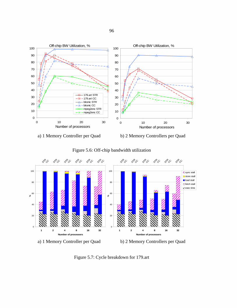
96
Off-chip BW Utilization, %
0
10
20
30
40
50
60
70
80
90
100
0 10 20 30Number of processors
179.art STR179.art CCbitonic STRbitonic CCmpeg2enc STRmpeg2enc CC
Off-chip BW Utilization, %
0
10
20
30
40
50
60
70
80
90
100
0 10 20Number of processors
30
Figure 5.6: Off-chip bandwidth utilization
Figure 5.7: Cycle breakdown for 179.art
a) 1 Memory Controller per Quad b) 2 Memory Controllers per Quad
0
20
40
60
80
100
1 2 4 8 16 32
Number of processors
%
STR CC STRCC STR CC STRCC STRCC STRCC
0
20
40
60
80
100
1 2 4 8 16 32
Number of processors
%
STR CC STRCC STR CC STRCC STRCC STRCC
sync stall
store stall
load stall
fetch stall
exec time
a) 1 Memory Controller per Quad b) 2 Memory Controllers per Quad

97
Increasing the off-chip memory bandwidth (by increasing the number of memory
controllers) also increases the streaming performance much more significantly (Figure
5.5b). For small processor counts (1-4) the streaming version of 179.art uses a higher
percentage of the available off-chip memory bandwidth (Figure 5.6); for larger processor
counts it moves a smaller amount of data to and from off-chip memory as described in
more detail in Section 5.4.1.
Bitonic sort shows the opposite result: the shared memory version outperforms streaming
significantly. As mentioned before, the shared memory version of bitonic sort avoids
writebacks of unmodified cache lines and therefore requires less off-chip bandwidth.
Both streaming and shared memory versions are limited by off-chip bandwidth (Figure
5.6a) and an increase in off-chip bandwidth (by doubling the number of Memory
Controllers per Quad) improves performance of both (Figure 5.5b), however, the
streaming version still has lower performance for all configurations with more than two
processors.
Streaming and shared memory versions of the MPEG-2 encoder perform similarly for up
to 16 processors (Figure 5.5). MPEG-2 encoder is a compute-intensive application and it
shows very good cache performance despite a large dataset. It exhibits good spatial or
temporal locality and has enough computation per data element to amortize the penalty
for any misses. Both caches and local memories capture data locality patterns equally
well. The MPEG-2 encoder is not limited by off-chip memory bandwidth (Figure 5.6)
and an increase in off-chip bandwidth does not change performance significantly (Figure
5.5b).
The streaming version executes more instructions because it has to program many
complex DMA transfers explicitly. Also, its instruction cache miss rate is slightly higher
for a 16 KB instruction cache because of the larger executable size (although in both
cases the instruction miss rate is less than 1%). As a result, the streaming version is
approximately 15% slower for 1-16 processors. In the case of the 32-processor

98
configuration, the streaming version is 27% slower because of increased overhead of
synchronization with a single shared DMA helper thread.
Speedup
0
5
10
15
20
25
30
35
40
0 10 20 30Number of processors
Speedup
0
5
10
15
20
25
30
35
40
0 10 20 30Number of processors
linear speedup linear speedup179.art STR 179.art STR179.art CC 179.art CCbitonic STR bitonic STRbitonic CC bitonic CCmpeg2enc STR mpeg2enc STRmpeg2enc CC mpeg2enc CC
Figure 5.8: Performance scaling of streaming applications with 4MB L2 cache
To explore the effect of a second level cache we repeated the same simulations for the
same configurations with a 4 MB second level cache. Performance results are shown in
Figure 5.8. As one might expect, with a large second level cache the effect of doubling
the number of Memory Controllers is negligible (Figure 5.8a versus Figure 5.8b). Also,
performance scaling of MPEG-2 encoder does not change significantly because this
application is not limited by the memory system.
The difference between streaming and shared memory versions of bitonic sort becomes
negligible because the entire dataset of this application fits within the second level cache.
However, this is only true for this particular dataset size. For larger datasets which do not
a) One Memory Controller per Quad b) Two Memory Controllers per Quad

99
fit within second level cache, or for a smaller second level cache, the performance
difference is the same as that which was shown in Figure 5.5.
In the case of 179.art, the streaming version still outperforms the shared memory version
even though the second level cache reduces the percentage of cache miss stalls
significantly (Figure 5.9) and the absolute execution time of the shared memory version
on a single processor decreases by a factor of approximately 2x. For a 32-processor
configuration, the streaming version also exhibits fewer synchronization stalls.
0
20
40
60
80
100
1 2 4 8 16 32
Number of processors
%
STRCC STRCC STR CC STR CC STRCC STR CC
sync stall
store stall
load stall
fetch stall
exec time
Figure 5.9: Cycle breakdown for 179.art with 4 MB L2 cache
5.4.1 APPLICATION CASE STUDY: 179.ART
This application is an interesting case because it is small enough for manual optimization,
parallelization, and conversion to streaming. At the same time it is a complete application
that is significantly more complex than simple computational kernels like FIR or FFT,

100
and it has more room for interesting performance optimizations. It can be used as a case
study to demonstrate various optimizations for both shared memory and streaming
versions, as well as how streaming optimization techniques can also be used in the shared
memory version [44, 45].
Speedup
0
10
20
30
40
50
0 10 20 30Number of processors
Figure 5.10: 179.art speedups
179.art optimizations include changing data layout, loop merging, elimination and
renaming of temporary arrays, and application-aware local memory allocation. These
techniques are described in more detail in Appendix B. The rest of this section analyzes
the reasons for the difference in performance between streaming and shared memory
a) 1 Memory Controller per Quad b) 2 Memory Controllers per Quad
Speedup
0
10
20
30
40
50
0 10 20 30Number of processors
linear speeduplinear speedupSTR x2 MCSTR
CC CC x2 MCCC+prefetch CC+prefetch x2 MCCC+dhwbi CC+dhwbi x2 MCCC+prefetch+dhwbi CC+prefetch+dhwbi x2 MC

101
versions of the application and discusses techniques that can be used to improve
performance of shared memory version by emulating streaming.
The streaming version has significantly better performance (STR vs. CC in Figure 5.10)
and moves a smaller amount of data to and from off-chip memory (STR vs CC in Figure
5.11) than the optimized shared memory version.
Off-chip Memory Traffic, MB
0
5
10
15
20
25
30
35
40
45
0 5 10 15 20 25 30Number of processors
STRCCCC+dhwbi
Figure 5.11: 179.art off-chip memory traffic
Shared memory performance for 179.art can be improved using hardware prefetching
[44, 45]. After splitting the f1_layer into several separate arrays, as described in
Appendix B, most of the accesses become sequential, making simple sequential
prefetching very effective. Data cache miss rates for the configurations with prefetching
(CC+prefetch in Figure 5.13) are significantly lower than for the configurations without
prefetching (CC in Figure 5.13). Prefetching significantly increases off-chip memory
bandwidth utilization (CC+prefetch vs CC in Figure 5.12). If off-chip memory bandwidth
is doubled, then prefetching becomes even more effective (Figure 5.13b).

102
Figure 5.12: 179.art off-chip memory utilization
For configurations with a large number of processors (32), prefetching has a smaller
effect because the data cache miss rate is relatively small even without prefetching. Also,
in this case each processor handles only a small part of the array and as a result initial
data cache misses consume more time.
Prefetching reduces the number of cache misses. However, a significant difference
remains in data locality, and as a result, there is a significant difference in the amount of
data moved between local memories or first level caches and off-chip memory (STR vs
CC and CC+prefetch in Figure 5.11). This difference also strongly affects energy
dissipation [44, 45]. To close this gap, streaming optimizations for local memories can be
emulated in the shared memory version of 179.art. Cache lines that correspond to data
structures that are not desirable to keep in cache, can be flushed from the cache using
a) 1 Memory Controller per Quad b) 2 Memory Controllers per Quad
Off-chip BW Utilization, %
0
10
20
30
40
50
60
70
80
90
100
0 10 20 30Number of processors
Off-chip BW Utilization, %
0
10
20
30
40
50
60
70
80
90
100
0 10 20 30Number of processors
STR STR x2 MCCC CC x2 MCCC+prefetch CC+prefetch x2 MCCC+dhwbi CC+dhwbi x2 MCCC+prefetch+dhwbi CC+prefetch+dhwbi x2 MC

103
cache control instructions such as data-hit-writeback-invalidate8 (DHWBI) in the
Tensilica ISA and in other instruction set architectures such as MIPS [107]. DHWBI is
safe to use because it doesn’t change the application-visible state of the memory system.
If the cache line is not present in the cache, DHWBI has no effect; if the line is present
but not dirty, then it is simply invalidated; if the line is dirty, then it is written back and
invalidated. For example, DHWBI can be used in yLoop (Appendix B) to flush cache
lines corresponding to the BUS matrix. Since matrix BUS is much larger than the cache
capacity, it is advantageous to flush cache lines corresponding to the BUS matrix to save
space for vector P. The DHWBI instruction is executed once per eight iterations of
yLoop.
Figure 5.13: 179.art data cache miss rate
This optimization partially eliminates cache pollution with data structures that are much
larger than first level cache capacity. As result, the data cache miss can be reduced
significantly, for example, for a 4-processor configuration, the miss rate decreases from
8 The Larrabee processor uses similar techniques to manage the content of caches and to
reduce cache misses due to streaming accesses [21].
Data Cache Miss Rate, %
0
1
2
3
4
5
6
7
0 10 20 30Number of processors
CCCC+prefetchCC+dhwbiCC+prefetch+dhwbi
Data Cache Miss Rate, %
0
1
2
3
4
5
6
7
0 10 20 30Number of processors
CC x2 MCCC+prefetch x2 MCCC+dhwbi x2 MCCC+prefetch+dhwbi x2 MC

104
approximately 5.5% to 4%, similarly to hardware prefetching (CC+dhwbi vs. CC in
Figure 5.13a). Moreover, in the case of limited off-chip memory bandwidth, the effects of
locality optimization and prefetching are additive (CC+prefetch+dhwbi vs CC in Figure
5.13a). Off-chip memory traffic for the 4-processor configuration also decreases
significantly and becomes comparable to the streaming version of the application
(CC+dhwbi vs. STR in Figure 5.11). Note that the cache coherent version with
prefetching and locality optimization outperforms the streaming version for 1-4 processor
configurations with increased off-chip memory bandwidth (Figure 5.10b).
For the 32-processor configuration, the effects of prefetching and locality optimization
are small because even without these optimizations the cache miss rate is relatively small
– approximately 2% (Figure 5.13), and off-chip bandwidth is not a limiting factor (Figure
5.12). The limiting factor for shared memory performance is synchronization stalls as
shown in Figure 5.7 and Figure 5.9.
5.5 CONCLUSIONS
This chapter described how a stream programming model can be mapped onto the
reconfigurable Smart Memories architecture. The flexibility of Smart Memories can be
effectively used to simplify and optimize implementation of a complex stream runtime
system such as the Stream Virtual Machine.
Our evaluation shows that some applications perform better in streaming mode while
others perform better in shared memory cache-coherent mode. This result supports the
idea of reconfigurable Smart Memories architecture that can work in both modes or in
hybrid mode (i.e. when part of memory resources are used as cache and part as software-
managed local memory). In contrast, for pure streaming architectures such as IBM Cell,
in some cases programmers must implement caching in software to achieve good
performance, e.g. Ray Tracer for the IBM Cell processor [76]. In these cases, pure stream
architectures have dual disadvantages: they are more complex to program and their

105
performance is worse because of the overheads of software caching. The reconfigurable
Smart Memories architecture gives application programmers flexibility to choose the
appropriate type of memory structure, simplifying software and improving performance.

CHAPTER 6: TRANSACTIONS
This chapter describes the implementation of the transactional memory mode of the
Smart Memories architecture. The chapter begins discussing the functionality required
for transactional memory and some high-level design decisions made during the mapping
of transactional memory. Then, it describes the hardware configuration and transactional
runtime, which takes advantage of the flexibility of the Smart Memories architecture. It
concludes by providing performance evaluation results.
6.1 TRANSATIONAL FUNCTIONALITY
The transactional memory model has a number of required features that are not present in
other memory systems:
1) A transactional memory system must checkpoint its state at the beginning of each
transaction. As a result, stores are speculative and must be buffered until transaction
commit, and processor state (integer and floating point register files, other registers)
must be saved at checkpoint.
2) Transaction’s speculative changes must be isolated from other transactions until
commit.
3) A transactional memory system must track read-write dependencies between
transactions. Thus, loads from shared data must be tracked.
4) A transactional memory system must be able to restore its state to the checkpoint and
to restart a transaction if a dependency violation is detected.
5) At transaction commit, speculative changes must become visible to the whole system.
6) If a transaction is violated, then all of its speculative changes must be discarded.
106

107
7) A transactional memory system must be able to arbitrate between transactions for
commit and ensure proper commit serialization9.
8) A transactional memory system must handle correctly overflow of hardware
structures.
9) A transactional memory system must guarantee forward progress, i.e. must avoid
deadlock and livelock.
These functional requirements are necessary for correct operation of transactional
memory (Section 2.3.3). Other properties of transactional memory systems depend on the
design decisions made by the architects, for example, pessimistic versus optimistic
conflict detection as discussed in Section 2.3.3. These design decisions affect
performance of transactional memory system for different applications10.
The Smart Memories architecture supports the transactional coherence and consistency
(TCC) model, which is one proposed implementation of transactional memory [32]. The
Smart Memories implementation of TCC is hybrid—part of the functionality is
performed by runtime software because otherwise it would require TCC specific
hardware structures or changes to the Tensilica processor that are not possible.
Specifically, arbitration for transaction commit, transaction overflow handling, and
processor state checkpointing are implemented in software.
The TCC system is guaranteed to make forward progress because it uses optimistic
conflict detection. Conflicts are detected only after one of the transactions wins
arbitration and performs commit, therefore, a transaction that causes other transactions to
restart will never need to restart itself. Livelock is not possible because at least one
transaction is making forward progress at any time.
9 Parallel transaction commit for non-conflicting transactions is also possible as proposed
in [108]. 10 Some of these design decisions affect implementation complexity with regard to subtle
properties such as strong atomicity, which is discussed in Section 2.3.3.
108
Smart Memories TCC mode handles hardware overflow by partial serialization of
transaction execution: an overflowing transaction arbitrates for a commit token, commits
the partially executed transaction to free hardware resources, and continues execution
without releasing the commit token. The commit token is released only when processor
reaches its natural transaction commit point in the application code. No other transaction
can commit before that11.
Note that a transactional memory system needs to buffer all stores during transaction
execution12, both to shared and private data, while only loads to shared data need to be
tracked for dependencies. This observation can be used to optimize transactional
performance using the flexibility of the Smart Memories architecture.
6.2 HARDWARE CONFIGURATION
As described in the previous section, transactional systems need to keep a lot of state for
correct operation, including dependency tracking information and buffered speculative
changes. Because of limited hardware resources and the expensive hardware operations
required, the Smart Memories architecture can execute only one transaction per Tile. As a
result, only one processor in a Tile runs actual application transactional code. This
processor is called execution processor. The other processor in a Tile, called support
processor, is used by the TCC runtime system to handle overflow. Also, it is impossible
to request a precise exception from outside of the Tensilica processor, i.e. it is not
possible to restart execution of the program from precisely the same instruction that
caused the overflow. Therefore, the memory system can only stall the execution
11 Virtualization of hardware transactional memory is another proposed alternative: if
hardware overflow is detected, a virtualized system can switch to software transactional memory (STM) mode. Challenges associated with virtualization are discussed in [34].
12 Other approaches are also conceivable. For example, private data can be checkpointed explicitly by software. However, such approach makes transactions’ semantics harder

109
processor in the case of an overflow and must use another processor to handle overflow
in software.
In TCC mode, the memory mats inside the Tile are used as a traditional cache for
instructions and a transactional cache for data (Figure 6.1). In addition to data and tag
mats, the transactional cache includes an address FIFO mat that saves addresses of stores
that must be committed at the end of transaction. Similar to streaming configurations
(Section 5.1), the TCC configuration also uses uncached, local memory mats to store
thread-private and shared runtime state.
Metadata bits in data mats are used for speculatively modified (SM) and speculatively
read (SR) bits. An SR bit is set by a load to track read dependency. The SM bit is set by
stores to avoid overwriting of speculatively modified data by other committing
transactions and to avoid false read dependency. Thus, if a processor reads an address
that was already modified by the transaction, then the SR bit is not set for loads to the
same address, because the transaction effectively created its own version of the data word
and that version should not be overwritten by other transactions.
Sub-word stores, i.e. byte and 16-bit stores, set both SR and SM bits to 1, i.e. they are
treated as read-modify-write operations because SR and SM bits can be set only per 32-
bit word. This can potentially cause unnecessary violations due to false sharing.
to understand, significantly complicates application development and introduces overhead.

110
Figure 6.1: Example of TCC configuration
Similarly, metadata bits in tag mats are also used for SM and SR bits. These bits are set to
1 whenever SM or SR bits are set within the same cache line. The SM bit in the tag mat is
used to reset the valid bit (V) for speculatively modified cache lines in case of violation.
This is performed by a conditional cache gang write instruction (Appendix A). This
instruction is translated by the LSU into metadata conditional gang writes for all tag mats
(Section 3.3).
Also, tag SM and SR bits are used by the Protocol Controller to determine cache lines
that cannot be evicted from the cache. Eviction of a cache line with SR or SM bit set to 1
would mean loss of dependency tracking state or loss of speculative modifications. If no
cache line can be evicted, then Protocol Controller sends an overflow interrupt to the
support processor in the Tile to initiate overflow handling by runtime software (Section
6.4).
Interface Logic
Transactional Data Cache Instruction Cache
Processor 0
Crossbar
Processor 1
Data
Tile
Data
Data
Data
Data
Data
Data
Data
Tag0
Tag1
Data
Shared Data
Data
Local Data
Tag0
FIFOTM
TM TM
111
During transaction commit or violation, all transactional control state, i.e. the SR/SM bits
in tag and data mats must be cleared. Such clearing is performed by the cache gang write
instruction (Appendix A). This instruction is translated by the LSU into metadata gang
writes for all tag and data mats (Section 3.3).
Similarly to a conventional cache, a load to a transactional cache causes the LSU to
generate tag and data mat accesses that are routed to appropriate mats by the crossbar
(Figure 4.1).
For a store to a transactional cache, the LSU, in addition to tag and data accesses,
generates a FIFO access that records a store address for transaction commit (Figure 6.1).
The IMCN is used to send a Total Match signal from the tag mat to the address FIFO mat
to avoid writing the FIFO in the case of a cache miss. Also, the SM bit is sent from the
data mat to the FIFO mat via the IMCN to avoid writing the same address to the FIFO
twice. The threshold register in address FIFO is set to be lower than the actual size of the
FIFO (1024 words) to raise the FIFO Full signal before the FIFO actually overflows. If
the LSU receives a FIFO Full signal after a transactional store, it sends a FIFO Full
message to the Protocol Controller, which sends an overflow interrupt to the support
processor just as in other cases.
To perform a commit, speculative changes made by a transaction must be broadcast to
other Tiles and Quads in the system and to the Memory Controllers. The broadcast is
performed by a DMA engine in the Protocol Controller. Control microcode of the DMA
engine is modified for this special mode of DMA transfer, which consists of three steps
for each address/word pair:
1) read the address from the FIFO;
2) read the data word from the transactional cache;
3) broadcast the address/data word pair.
112
Inside the Protocol Controller, each broadcast address/data pair goes through MSHR
lookup to check for collision with outstanding cache miss requests. If a conflict is
detected and the cache miss request is in the transient state, i.e. the cache line is being
copied to or from the line buffer, then the broadcast must be stalled. If a conflicting
request is not in a transient state, then the Protocol Controller updates the corresponding
line buffer with the committed data word. This update is complicated. For example,
suppose a store miss has valid data bytes in the line buffer, which corresponds to the
bytes written by the processor, and should not be overwritten by the commit, i.e. commit
data must be merged with miss data with priority given to the miss data. However, the
commit for the next transaction might write the same address again while the store miss
is still outstanding. Therefore, the commit must be able to overwrite previous commit
data but not overwrite store miss data. This requires extra byte valid bits in the line buffer
(Section 3.5.1) and logic that merges committed data with the data in the line buffer13.
After the MSHR lookup/line buffer update, the commit is sent to the transactional cache
of other Tiles and to other Quads through the network interface. The data word in the
cache is updated if the corresponding cache line is present and the SM bit is not set for
this word. The SR bit is returned back to the Protocol Controller and if it is set to 1, then
the Protocol Controller initiates a violation interrupt process.
Violation interrupt is a hard interrupt (Section 3.4.1), which must unstall the processor
even if the processor is stalled waiting on a synchronization instruction. Any outstanding
synchronization miss must be canceled to avoid dangling miss requests, which can cause
hardware resource leaks. Canceling outstanding requests is complicated because requests
can be in flight in the Protocol Controller or Memory Controller pipeline, network
buffers, etc. To ensure correct operation, cancel messages are sent on virtual channels
that have lower priority than virtual channels used by synchronization messages (Section
13 This problematic case of commit data overwrite by another commit was found only in
RTL simulation during design verification.
113
3.6), and go through the same pipeline stages as synchronization operations. Therefore,
when the Protocol Controller receives all cancel acknowledgement messages there are no
outstanding miss requests in the system from the processor being violated.
Hard interrupts are delayed by the interrupt FSM until all outstanding load and store
cache misses are completed, instead of trying to cancel such requests. This is possible
because, unlike synchronization operations, loads and stores cannot be stalled for an
unbounded number of cycles. This design decision simplifies the design and verification
of the system.
6.3 TCC OPTIMIZATION
A simple TCC model assumes that all speculative changes performed by the transaction
must be broadcast to the whole system. Such an approach simplifies programming model
for the application developer; however, it can also degrade performance because part of
the transaction writes are committed to thread-private data, e.g. the stack, which is never
shared with other threads/transactions. Unnecessary commit broadcasts can slow down
application execution because they have to be serialized and can be a performance
bottleneck for larger system. Also, unnecessary broadcasts waste energy.
In addition, loads to such thread-private data do not need to be tracked by the
transactional memory system because by definition they cannot cause transaction
violation. As a result, cache lines corresponding to such loads do not need to be locked
for the duration of the transaction and therefore the probability of overflow can be
reduced.
Smart Memories flexibility can be used to optimize the handling of such private data. We
define the TCC buffered memory segment as a segment in which loads are not tracked
and stores are buffered but not broadcast, i.e. this segment is not TCC coherent. Data can
be placed in the TCC buffered segment either by default through compiler memory map
114
settings, e.g. for stack and read-only data, or explicitly using the __attribute__
((section(".buffered_mem"))) construct of the GNU C compiler [106], which
is also supported by the Tensilica XCC compiler.
This approach is different from other approaches [36, 37], which introduce immediate
load, immediate store and idempotent immediate store instructions that are not tracked by
the transactional memory system (i.e. their addresses are not added to transaction read or
write-set). However, it is not obvious how to use such instructions: either the compiler
must be modified to generate application code with such instructions or the programmer
must explicitly use them in the application code. In contrast, the TCC buffered memory
segment approach does not require changes in the compiler or application. In addition, a
small change in the application source code (marking the data structure with an attribute
construct) results in even bigger performance improvement as shown in Section 6.5.
Also, a TCC buffered store is semantically different from the immediate store or
idempotent immediate store in [36, 37]: it is buffered by the memory system until
transaction commit and not propagated to the main memory.
To support the TCC buffered memory segment an extra metadata bit, called the Modified
(M), is used in the tag mat. A TCC buffered store sets the M bit to 1 along with the SM
bit. If the transaction is violated, then the cache line is invalidated by the conditional gang
write instruction because the SM bit is 1. During commit the SM bit is reset by the gang
write instruction but the M bit remains set to 1. When the next transaction performs a
TCC buffered store to the same cache line (M==1 and SM==0), a TCC writeback request
is generated by the Tile LSU and sent to the Protocol Controller. The Protocol Controller
writes back the cache line to the main memory or the second level of the cache,
effectively performing lazy, on-demand commit for the previous transaction and resets
the M bit. Thus, commit of TCC buffered stores is overlapped with the execution of the
next transaction and possibly with the commit broadcast of transactions executed on other
processors.

115
Loads to the TCC buffered memory segment do not set the SR bit, thus, avoiding locking
corresponding cache lines in the cache and reducing the probability of overflow.
6.4 TCC RUNTIME
The Smart Memories implementation of TCC supports several TCC API function calls
[32], as described in Appendix C.
The TCC runtime performs arbitration for transaction commit and handles transaction
overflow. Processor state checkpointing and recovery from violation is also performed in
software.
The execution processor in Tile 0 of Quad 0 is also used as a master processor, which
executes sequential parts of the application and sets up runtime data structures that are
shared by all processors in the system. Shared runtime data structures are placed in the
dedicated memory mat in Tile 0 of Quad 0 (Figure 6.1) because the master processor has
to access these data structures most frequently.
The shared data mat contains: barriers used to synchronize processors in the beginning
and at the end of the transactional loop execution; an array of locks used by the processor
to arbitrate for commit; data structures used to keep track of transaction phase numbers;
etc.
6.4.1 ARBITRATION FOR COMMIT
When a processor has to arbitrate for commit, it issues a synchronized store instruction to
the lock variable corresponding to its current phase number. This store tries to write its
processor ID. If no other processor is doing a commit and the processor phase number is
oldest, then the lock variable is set to empty and synchronized store succeeds, and the
processor starts its commit broadcast by writing into the DMA control register.
116
During the broadcast, the processor resets the SR and SM bits in the transactional cache,
checkpoints its own state, updates runtime state, etc. After completion of the broadcast
the processor releases the commit token by doing a synchronized load to the same lock
variable (if there are other processors with the same phase number) or to another lock
variable (the one that corresponds to the next active phase number). Thus, if the broadcast
is long enough, then instructions required for runtime updates are overlapped with
broadcast and software overhead of the commit is minimized.
Commit and other API calls are implemented as monolithic inline assembly blocks, hand
scheduled to use the minimum number of instructions and cycles. The most frequently
used call, TCC_Commit0(), uses only 19 instructions (not including instructions
required to checkpoint processor register files as described below). These assembly
blocks must be monolithic to prevent the compiler from inserting register spills in the
middle of commit or other API calls. Otherwise, such register spills are compiled into
stores to the thread stack, i.e. to the TCC buffered memory segment, which might cause
overflow and deadlock in the middle of commit code.
6.4.2 HARDWARE OVERFLOW
The TCC runtime must also handle hardware overflow, which is detected either if the
address FIFO threshold is reached or if no cache line can be evicted because of SR/SM
bits. Upon overflow, the Protocol Controller sends a soft interrupt to the support
processor in the same Tile, while at the same time the execution processor is blocked at
the Protocol Controller interface. The support processor checks whether the commit
token was already acquired by reading runtime state in the local data mat (Figure 6.1). If
not, then the support processor performs arbitration using a pointer saved by the
execution processor in its local data mat, initiates DMA commit broadcast and resets
SR/SM bits in the transactional cache. Also, it updates local runtime state to indicate that
the commit token was already acquired. At the end of the overflow interrupt handler the

117
support processor unblocks the execution processor by writing into the control register of
the Protocol Controller.
If a dependency violation is detected by the Protocol Controller, then both processors in
the Tile are interrupted with high-priority hard interrupts, i.e. the processors would be
unstalled even if they were blocked on synchronization operations. The support processor
must be hard interrupted because it may be stalled arbitrating for commit token. The
violation interrupt handler for the execution processor invalidates all speculatively
modified cache lines in the transactional cache, resets SR/SM bits and the address FIFO
and then returns to the checkpoint at the beginning of the transaction.
The TCC runtime code is complicated because it has to correctly handle multiple
simultaneous asynchronous events such as violation and overflow interrupts. Many
complex corner case bugs were discovered only during RTL verification simulations.
Fixes for these bugs required subtle changes in the runtime code.
6.4.3 PROCESSOR STATE RECOVERY FROM VIOLATION
To be able to restart execution of a speculative transaction after violation, all system state
must be saved at the beginning of the transaction. The memory system state can be
quickly restored to the check point because all speculative changes are buffered in the
transactional data cache and can be easily rolled back by invalidating cache lines using
gang write operations. Processor state must be checkpointed separately
Processor state consists of general purpose register files (integer and floating point) and
various control registers. One complication is that the processor state might be
checkpointed anywhere during application execution, including inside a function or even
recursive function calls, because the programmer can insert TCC_Commit() anywhere
in the application code. If TCC applications were compiled using Tensilica’s standard
windowed application binary interface (ABI), which relies on the register window
mechanism, then checkpointing would require saving the whole integer register file and

118
not just the current register window. This would be expensive from a performance point
of view and would significantly increase application size.
Instead, the Smart Memories implementation of TCC utilizes Tensilica’s optional non-
windowed ABI, which does not use register windows. In this case, the compiler can be
forced to spill general purpose registers into the stack memory at the transaction check
point using the asm volatile construct. After a checkpoint, the compiler inserts load
instructions to reload the values into the register files.
An alternative approach for windowed ABI is discussed in Appendix D; this alternative
approach, however, cannot be used for checkpoints inside subroutine calls.
The advantage of the non-windowed approach is that the compiler spills only live register
values, minimizing the number of extra load and store instructions. Temporary values
produced during transaction execution do not need to be spilled. The disadvantage of
spilling all live values is that some of them may be constant during the execution of the
transaction.
Spilled register values in the memory are check-pointed using the same mechanism as
other memory state. The only general purpose register that can not be check-pointed in
this way is the stack pointer register a1; we use a separate mechanism for the stack
pointer as well as for other processor control registers.
To save the state of the control registers we added three more registers and used one of
the optional scratch registers (MISC1):
• SPEC_PS – a copy of the PS (processor status) register;
• SPEC_RESTART_ADDR – the transaction restart address;
• SPEC_TERMINATE_ADDR – the address to jump to in case of execution abort;
• MISC1 – stack pointer.

119
To use these registers in interrupt handlers we added two special return-from-interrupt
instructions:
• SPEC_RFI_RESTART – return from interrupt to the address stored in
SPEC_RESTART_ADDR register, SPEC_PS register is copied atomically to PS;
• SPEC_RFI_TERMINATE – the same except that SPEC_TERMINATE_ADDR
register is used as the return address.
6.5 EVALUATION
Table 6.1 summarizes characteristics of the transactional mode of the Smart Memories
architecture. As in hardware transactional memory architectures (HTM) application loads
and stores are handled by hardware without any software overhead. The main difference
from HTM architectures is in handling transaction commit by software, which increases
commit overhead.
Table 6.1: Characteristics of Smart Memories transactional mode
Name Value Comment loads/stores 1 cycle no overhead compared to cache-coherent mode commit 19 instructions TCC_Commit0();
7 instructions are overlapped with DMA commit; 2 synchronized remote mat operations to acquire and to release commit token
processor register checkpoint
1 load and 1 store per live register
typical number of live register values is 5
DMA commit one 32-bit word per cycle
assuming no conflicts in caches, MSHRs, and network interface
violation interrupt 9 instructions
Three applications, barnes, mp3d and fmm from SPLASH and SPLASH-2 suites, were
used to evaluate the performance of the TCC mode of the Smart Memories architecture.

120
These applications were converted to use transactions instead of their original ANL
synchronization primitives [109]. All benchmarks were compiled with the Tensilica
optimizing compiler (XCC) using the highest optimization options (–O3) and inter-
procedural analysis enabled (–ipa option). For these experiments we used configurations
with 4 MB second level cache.
Performance scaling for TCC is shown in Figure 6.2. For comparison, speedups for
original cache coherent versions of the same applications are also shown in Figure 6.2
(designated as CC - dotted lines). All speedup numbers are normalized with respect to
execution time of TCC version running on a single Tile configuration.
Speedup
0
2
4
6
8
10
12
14
16
18
0 5 10 15
Number of processors
linear speedupbarnes TCCbarnes TCC nobufbarnes CCmp3d TCCmp3d TCC nobufmp3d CCfmm TCCfmm TCC nobuffmm CC
Figure 6.2: Performance scaling of TCC applications
On a single Tile configuration, all applications show similar performance slowdown in
the range of 13-20% with respect to the original shared memory code. The reason for this
slowdown is because the TCC version has to execute more instructions for TCC API calls
and to spill and re-load registers at processor state checkpoints.

121
0
20
40
60
80
100
120
140
160
180
1 2 4 8 16
%
CC TCC
TCC no
buf
CC TCC
TCC no
buf
CC TCC
TCC no
buf
CC TCC
TCC no
buf
CC TCC
TCC no
buf
overflow stallsync stallstore stallload stallfetch stallexec time
Figure 6.3: Cycle breakdown for barnes
As the number of processors increases, the performance of barnes continue to scale up, to
the 16-Tile configuration. However, for the 16-Tile configuration, stalls due to commit
arbitration and overflow increase the slowdown in comparison with the shared memory
version (sync and overflow stalls in Figure 6.3). This happens because of frequent
transaction commits, which were added to barnes code to minimize overflows.
On the other hand, the performance of mp3d and fmm doesn’t scale beyond 8 Tiles.
These applications also exhibit a significant percentage of synchronization stalls due to
frequent commit arbitration (Figure 6.4 and Figure 6.5). The performance of mp3d
suffers because of large number of violations: the percentage of violated transactions
increases with the number of Tiles, reaching as high as 40% in the 16-Tile configuration
(Figure 6.6). This is because mp3d performs a lot of reads and writes to shared data and,
in fact, the original shared memory version has data races that are successfully ignored
[95]. As the number of transactions executed in parallel increases, the probability of
transaction conflicts and violations also increases, leading to performance degradation.
The performance of fmm also suffers because it performs a large number of commits to
avoid overflows or to avoid deadlock on spin-locks.

122
0
20
40
60
80
100
120
1 2 4 8 16
%CC TC
CTC
C nobu
f
CC TCC
TCC no
buf
CC TCC
TCC no
buf
CC TCC
TCC no
buf
CC TCC
TCC no
buf
overflow stallsync stallstore stallload stallfetch stallexec time
Figure 6.4: Cycle breakdown for mp3d
0
20
40
60
80
100
120
1 2 4 8 16
%
CC TCC
TCC no
buf
CC TCC
TCC no
buf
CC TCC
TCC no
buf
CC TCC
TCC no
buf
CC TCC
TCC no
buf
overflow stallsync stallstore stallload stallfetch stallexec time
Figure 6.5: Cycle breakdown for fmm
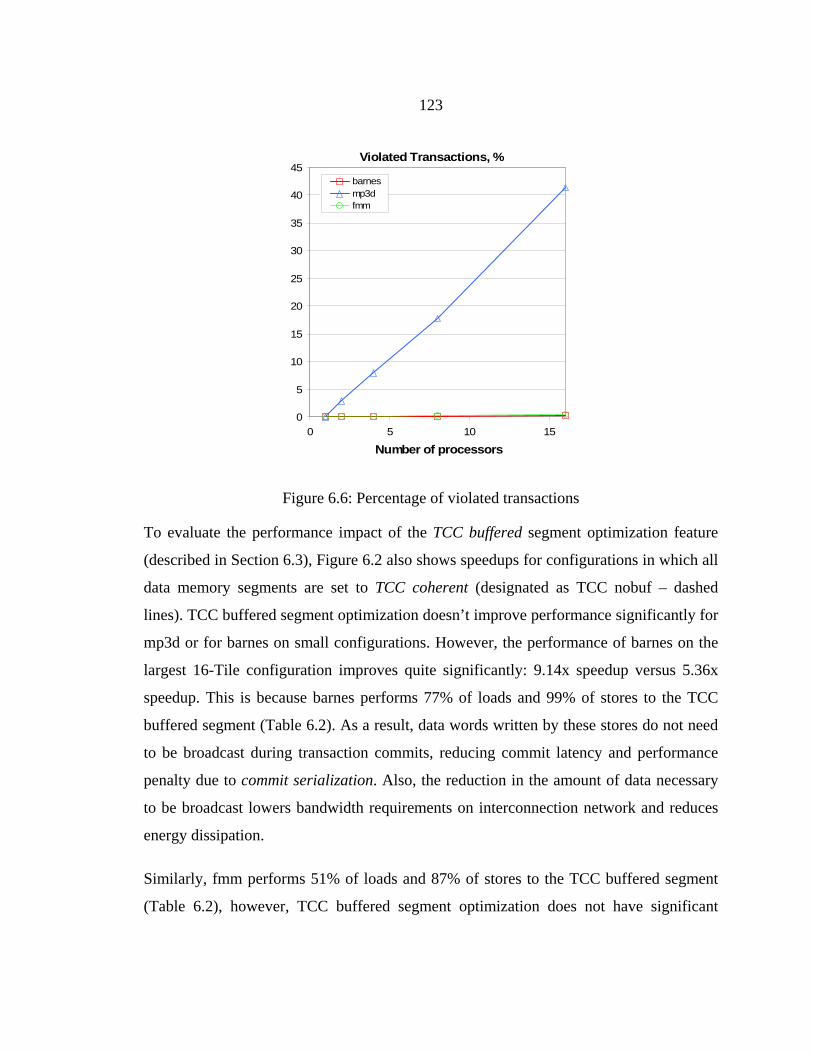
123
Violated Transactions, %
0
5
10
15
20
25
30
35
40
45
0 5 10 15
Number of processors
barnesmp3dfmm
Figure 6.6: Percentage of violated transactions
To evaluate the performance impact of the TCC buffered segment optimization feature
(described in Section 6.3), Figure 6.2 also shows speedups for configurations in which all
data memory segments are set to TCC coherent (designated as TCC nobuf – dashed
lines). TCC buffered segment optimization doesn’t improve performance significantly for
mp3d or for barnes on small configurations. However, the performance of barnes on the
largest 16-Tile configuration improves quite significantly: 9.14x speedup versus 5.36x
speedup. This is because barnes performs 77% of loads and 99% of stores to the TCC
buffered segment (Table 6.2). As a result, data words written by these stores do not need
to be broadcast during transaction commits, reducing commit latency and performance
penalty due to commit serialization. Also, the reduction in the amount of data necessary
to be broadcast lowers bandwidth requirements on interconnection network and reduces
energy dissipation.
Similarly, fmm performs 51% of loads and 87% of stores to the TCC buffered segment
(Table 6.2), however, TCC buffered segment optimization does not have significant
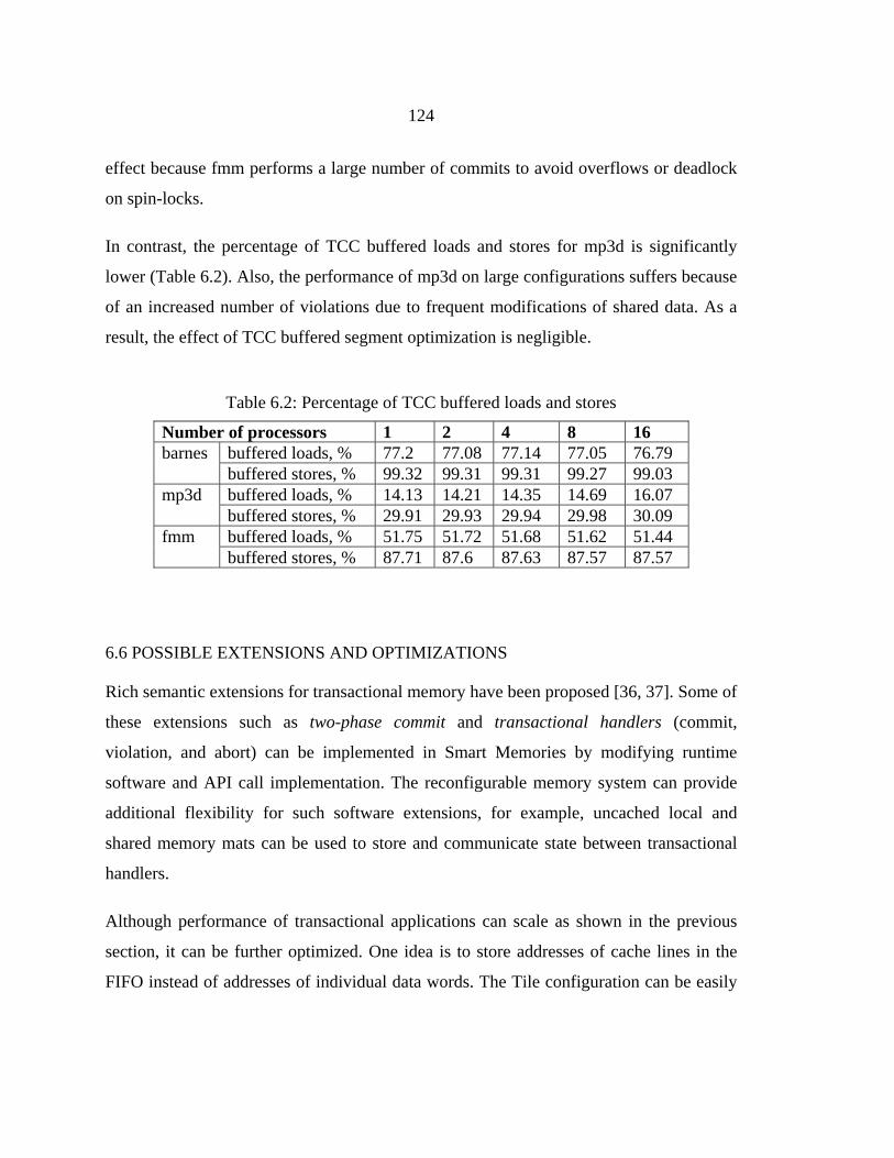
124
effect because fmm performs a large number of commits to avoid overflows or deadlock
on spin-locks.
In contrast, the percentage of TCC buffered loads and stores for mp3d is significantly
lower (Table 6.2). Also, the performance of mp3d on large configurations suffers because
of an increased number of violations due to frequent modifications of shared data. As a
result, the effect of TCC buffered segment optimization is negligible.
Table 6.2: Percentage of TCC buffered loads and stores
Number of processors 1 2 4 8 16 buffered loads, % 77.2 77.08 77.14 77.05 76.79 barnes buffered stores, % 99.32 99.31 99.31 99.27 99.03 buffered loads, % 14.13 14.21 14.35 14.69 16.07 mp3d buffered stores, % 29.91 29.93 29.94 29.98 30.09 buffered loads, % 51.75 51.72 51.68 51.62 51.44 fmm buffered stores, % 87.71 87.6 87.63 87.57 87.57
6.6 POSSIBLE EXTENSIONS AND OPTIMIZATIONS
Rich semantic extensions for transactional memory have been proposed [36, 37]. Some of
these extensions such as two-phase commit and transactional handlers (commit,
violation, and abort) can be implemented in Smart Memories by modifying runtime
software and API call implementation. The reconfigurable memory system can provide
additional flexibility for such software extensions, for example, uncached local and
shared memory mats can be used to store and communicate state between transactional
handlers.
Although performance of transactional applications can scale as shown in the previous
section, it can be further optimized. One idea is to store addresses of cache lines in the
FIFO instead of addresses of individual data words. The Tile configuration can be easily

125
adjusted to send cache line addresses and SM bits from the tag mat to the FIFO, thus
recording the unique address of each cache line modified by the transaction.
A more significant change is required in the Protocol Controller: it has to read the whole
cache line at once, determine which words were modified and merge them with
conflicting line buffers, update other transactional caches and check for violations. The
advantage of such an approach is faster commit if multiple words per cache line are
modified by the transaction.
Another idea for performance optimization is to implement a different transactional
model on the reconfigurable Smart Memories architecture. Instead of the TCC model of
“all transactions, all the time”, this new model would build on top of the shared memory
model with cache coherence. Transactions would be executed only when necessary to
modify shared data atomically. The motivation for this idea is based on the observation
that in many cases, applications do not need to run transactions all the time, and running
transactions can be expensive from a performance point of view. For example, barnes
(Section 6.5) spends most of the time reading shared data without updating it, however, it
has to perform frequent commits to avoid overflows.
In this model, the memory system would be configured to run with cache coherence but
could be switched into transactional mode by the application at the beginning of a
transaction. In transactional mode, the addresses of modified cache lines would be
recorded in the FIFO similarly to TCC. At commit time, the addresses from the FIFO can
be broadcast by the DMA to all other caches in the system to invalidate all copies of
modified cache lines and to detect conflicts with other transactions.
6.7 CONCLUSIONS
This chapter described how the transactional memory model is mapped to the Smart
Memories architecture. The flexibility of Smart Memories is used in two ways: 1)
126
memory mats configured as local memories are used to store the state of the transactional
runtime system, which greatly simplifies its implementation; 2) reconfigurability in
metadata handling is used for performance optimization, by lazily committing private
data. We feel that these examples are just a start. With further work, we will be able to
use the configurable memory system to continue to tune transactional memory
performance.

127
CHAPTER 7: CONCLUSIONS AND FUTURE DIRECTIONS
Due to slowdown in single processor performance growth there is a trend towards chip
multi-processors, which can deliver continuing performance scaling. However, these
promised performance gains depend on the availability of parallel applications.
Development of such applications is challenging and there is no agreement about a single
parallel programming model.
This dissertation described the design of the polymorphic reconfigurable Smart Memories
architecture, which supports three different models: shared memory with cache
coherence, streaming, and transactions. Smart Memories achieves good performance and
scalability for a variety of applications developed using three different programming
models. Flexibility in choosing a programming model is useful because of two reasons:
1) matching the programming model to the applications simplifies development;
2) choosing the right execution model improves performance, e.g. some applications
perform better in streaming mode than in shared memory mode or vice versa.
Also, the reconfigurability of Smart Memories can be used to implement the semantic
extensions of a particular programming model. For example, we added fast fine-grain
synchronization operations in shared memory mode, which are useful for applications
with a producer-consumer pattern.
The flexibility of the Smart Memories architecture is also useful for implementation of
complex software runtime systems such as the Stream Virtual Machine or the
transactional runtime. Such runtime systems use dedicated memory blocks to store
critical state to optimize performance and simplify synchronization.

128
These advantages of dynamic reconfiguration need to be weighed against the costs
incurred by this approach. The Smart Memories test chip implementation provided a
framework for this analysis. It showed that the reconfiguration overheads are relatively
large, increasing the area of each Tile by around 2x. This additional area was mostly
caused by our standard cell implementation of the metadata storage and would be
significantly smaller in full custom implementation.
7.1 FUTURE DIRECTIONS
The goal of the Smart Memories project was to design a general purpose flexible
architecture whose resources can configured in the most efficient way for a particular
application. Embedded system designers have to solve a similar problem of efficient
resource allocation and to generate an optimized custom design for a particular
application. This observation led us to the idea of the Chip Multi-Processor Generator
[46]. Such a generator presents to the designer an abstraction of a virtual flexible
architecture with very unconstrained resources. After configuration, the generator can
produce an optimized custom design for a particular application or a class of applications.
The Smart Memories architecture can serve as the basis for a virtual flexible architecture:
configuration of the memory system can be tailored to the requirements of a given
application as described in this thesis. After that, configuration can be fixed and unused
logic and resources can be optimized away. Processors can be extended with custom
functional units and register files using the capabilities of the Tensilica system.

129
APPENDIX A: SPECIAL MEMORY INSTRUCTIONS
Full list of memory instructions that were added to the Tensilica processor to exploit the
functionality of the Smart Memories architecture:
• synchronized load: stall if full/empty (FE) bit associated with data word is zero
(“empty”), unstall when the FE bit becomes one (“full), return data word to the
processor and atomically flip the FE bit to zero;
• synchronized store: stall if the FE bit is 1, unstall when it becomes 0, write data word
and atomically flip the FE bit to 1;
• future load: the same as synchronized load but the FE bit is not changed;
• reset load: reset FE bit to 0 and return data word to the processor without stalls
regardless of the state of the FE bit;
• set store: set FE bit to 1 and write data word without stalls;
• meta load: read the value of meta data bits associated with data word;
• meta store: write to meta data bits;
• raw load: read data word skipping virtual-to-physical address translation, i.e.
effective address calculated by the instruction is used as physical address directly;
• raw store: write data word skipping virtual-to-physical address translation;
• raw meta load: read metadata bits skipping virtual-to-physical address translation;
• raw meta store: write metadata bits skipping virtual-to-physical address translation;
• fifo load: read a value from a memory mat configured as a FIFO, FIFO status register
in the interface logic is updated with FIFO status information, i.e. whether FIFO was
empty;
• fifo store: store a value to a FIFO, FIFO status register is updated with FIFO status
information, i.e. whether FIFO was full;
130
• safe load: read a data word from the memory and ignore virtual-to-physical address
translation errors;
• memory barrier: stall the processor while there are outstanding memory operations,
i.e. non-blocking stores;
• hard interrupt acknowledgement: signal to the memory system that a hard interrupt
was received by the processor, this instruction is supposed to be used only inside
interrupt handler code;
• mat gang write: gang write all meta data bits in the memory mat, supported only for 3
meta data bits;
• conditional mat gang write: conditionally gang write all meta data bits in the memory
mat, supported only for one meta data bit;
• cache gang write: gang write all meta data bits in the data cache, supported only for 3
meta data bits;
• conditional cache gang write: conditionally gang write all meta data bits in the data
cache, supported only for one meta data bit;
• spec_cmd: functional NOP, used by statistics control.
131
APPENDIX B: 179.ART STREAMING OPTIMIZATIONS
179.art is one of the benchmarks in SPEC CFP2000 suite [97]. It is a neural network
simulator that is used to recognize objects in a thermal image. The application consists of
two parts: training the neural network and recognizing the learned images. Both parts are
very similar: they do data-parallel vector operations and reductions.
This application is an interesting case because it is small enough for manual optimization,
parallelization, and conversion to streaming version. At the same time it is a complete
application that is significantly more complex than simple computational kernels like FIR
or FFT, and it has more room for interesting performance optimizations. It can be used as
a case study to demonstrate various optimizations for both shared memory and streaming
versions, as well as how streaming optimization techniques can also be used in the shared
memory version [44, 45].
Figure B.1 shows a sequence of inner loops from 179.art’s train_match() function
(training part). Vectors or arrays of floating point numbers are labeled with capital letters
while scalar values are named using small letters. The size of vectors for the reference
data set is 10,000. BUS and TDS are big matrixes that are more than 10 times larger than
vectors. For example, wLoop iterates over elements of I and U vectors and produces a
vector W and a scalar tnorm which is a result of reduction calculation, i.e. sum of
squares of elements of W.
The original sequential version of this benchmark exhibits very low cache locality: the L1
cache miss rate is 35.5%. This is because the main data structure of the application called
f1_layer is an array of structures that group together elements of vectors I, U, W, X, V,
P, Q. As a result, consecutive elements of the same vector are not adjacent in the
memory.

132
Before After
Figure B.1: Inner loop sequence of train_match(): before and after optimization
We optimized the code by splitting f1_layer into several separate arrays of floating
point values each corresponding to different vector. This dramatically improved cache
locality and reduced cache miss rate to approximately 10% because now successive
wLoop
U I
xLoop
W tnorm
vLoop
X
uLoop
V tnorm
Q
xvLoop
U tnormP
upLoop
U
P
tnormP
Utresult BUS
y
yLoop
TDS
I U
wLoop
pLoop
U
P tresult
P
ttemp
TDS
yLoop
y
BUS
qLoop
Q

133
iteration of the inner loop access adjacent words in the same cache line14, exploiting
spatial data locality.
The code of train_match() can be further significantly optimized as shown in Figure
B.1 by merging loops (kernel fusion) and demoting arrays to scalars after loop merging.
For example, after merging xLoop and vLoop into xvLoop, X becomes a scalar, local
to xvLoop and does not need to be written into memory.
The memory footprint of the inner loops can be further reduced by renaming of
vectors/arrays to reuse the minimal number of arrays for temporary data. For example,
the same U vector can be used as input and output of wLoop. After all renaming
optimizations, only two such arrays, U and P, are necessary to store temporary data
between consecutive loops, as shown on the right side of Figure B.1.
All techniques discussed so far are applicable to sequential, multi-threaded shared
memory and streaming versions of 179.art and can be performed at the source code level
without the knowledge of details of a particular architecture or configuration. As a result,
the data cache miss rate in on a single processor configuration is reduced from 35% to
approximately 7%, while the execution time improves by a factor of 6.1. For the multi-
threaded version running on a 16-processor configuration, the cache miss rate improved
from 22% to approximately 2%, while execution time improved by a factor of 7.2 over
the original code. The hit rate is higher for the multi-processor configuration because the
same data set is partitioned across multiple caches.
The next stage of optimization is specific to the streaming architecture. Part of the local
memory inside each Tile is allocated for buffering data fetched by the DMA; however,
this occupies only a small portion of available local memory. Increasing the size of the
buffers beyond certain point doesn’t affect performance and in fact can decrease
performance because large chunks can cause granularity and load imbalance problems. In
14 Sun compiler can automatically perform this optimization.
134
case of 179.art DMA, the chunk size is set to 125 vector elements, which occupies only
500 bytes in the local memory. Given that kernels or loops operate on at most three
vectors and each vector requires double buffering, only about 3 KB of local memory is
necessary for stream/DMA data buffering.
The rest of the local memory can be used to store most frequently used data. As the
number of processors and the total size of local memory increases, a larger portion of the
working data set can be placed into local memories. For example, in a 2-processor
configuration, only the P vector is placed in the local memories, while in a 4 or 8-
processor configuration, U vector is also allocated locally. Also, even if the data structure
is too large it can be partially allocated in the local memory, e.g. only part of BUS matrix
is in the local memory for 16 or 32-processor configurations while the rest still has to be
fetched by DMA. By doing such application-aware local memory allocation rather than
oblivious hardware caching, locality can be further improved and off-chip memory traffic
is reduced. Of course, this optimization significantly complicates application source code
because optimized code can contain many slightly different versions of kernels/loops to
handle the different ways of allocating local memory.
Local memory allocation is similar to traditional register allocation in optimizing
compilers: the usage of fast small storage is optimized by allocating this storage to the
most frequently used data at each point of the application. However, in general it is a
more complicated problem than register allocation: size of arrays might be determined
only at runtime and optimal allocation might depend on total size of all local memories.
Another streaming optimization is moving DMA transfer from the beginning of the loop
into the end of the previous loop. For example, a DMA fetch of the P vector (right side of
Figure B.1) can be started at the end of wLoop instead of beginning of xvLoop. This
transformation allows overlapping communication of reduction variable tnorm and
processor synchronization at the end of wLoop with DMA transfer for the next loop.
135
APPENDIX C: TCC APPLICATION PROGRAMMING
INTERFACE
TCC_Loop(funcPtr,argPtr) – executes ordered transactional loop, i.e. iterations
of the loop are executed as transactions on different processors with sequential commit
order; the code of loop body should be separated into a function, pointed by funcPtr,
parameters can optionally be passed through a structure, pointed by argPtr. Parameter
structure must be declared as global variable or allocated on the heap.
TCC_LoopLabel(funcPtr) – executes inline ordered transactional loop, i.e. the
same loop body function can contain more than one transactional loop.
TCC_ULoop(funcPtr,argPtr) – executes unordered transactional loop, similar to
TCC_Loop().
TCC_ULoopLabel(funcPtr) – executes inline ordered transactional loop, similar to
TCC_LoopLabel().
TCC_LoopEnter() – synchronizes processors in the beginning of transactional loop
execution.
TCC_LoopExit() – synchronizes processors at the end of transactional loop
execution.
TCC_Commit(phaseInc) – perform transaction commit and start a new transaction
with phase number ([32], Section 2.3.3) equal to current phase number + phaseInc.
TCC_Commit0() – performance optimized version of TCC_Commit() for the most
frequent case.
136
TCC_UBARRIER() – transactional barrier: processors perform commit, wait until all
processors arrive to the barrier, and start new transactions. Transactional barrier is a
performance optimization construct which can be used to separate different phases of
application execution and minimize transaction violations.
int TCC_GetNumCpus() – returns the number of parallel processors executing
transactions.
int TCC_GetMyId()– returns unique processor ID in the range of 0…
TCC_GetNumCpus()-1.
An example of TCC API usage - simple histogram code using TCC unordered loop:
void mainX( int argc, char * argv[] ) { … TCC_ULoop( ¶llel_test_loop, NULL ); … } void parallel_test_loop( void * context ) { TCC_LoopEnter(); for (int i = TCC_GetMyId(); i < NUM_DATA; i+= TCC_GetNumCpus() ) { bin[A[i]-1]++; TCC_Commit(0); } TCC_LoopExit(); }
137
APPENDIX D: USING A REGISTER WINDOWS MECHANISM
FOR PROCESSOR STATE CHECKPOINTING
To checkpoint processor state in the beginning of speculative execution, previously
proposed thread-level speculation (TLS) architectures modify the register renaming
mechanism in out-of-order execution processors [111, 112] or utilize a shadow register
file [9]. It is possible to accomplish the needed checkpoint with little overhead and almost
no hardware support (no shadow registers) in a machine with register windows. In order
to explain the proposed approach, let’s consider an example of a windowed register file
that consists of 64 physical registers, divided into groups of four, with 16 register window
being visible at any time. Figure D.2a shows the two registers controlling the window
mechanism. Window Start has one bit per group of four registers, and indicates where a
register window starts. Window Base is a pointer to the beginning of the current window
in Window Start.
On each function call, as directed by the compiler, the register window shifts by 4, 8 or
12 registers (Figure D.2b). Register window overflow occurs when, after shifting,
Window Start has 1 within the current window (Figure D.2c). In this case, an exception
handler is invoked to spill the registers over to the memory.
When a context runs a speculative thread, register values can fall into one of the
following categories:
• constants, which are passed to the speculative thread and are not changed during the
execution;
• shared variables, which are modified by other threads and must be read from memory
before they are used for computation;
• temporary values, which are live only during the execution of this thread;

138
• privatized variables, such as loop induction variable or reduction variables.
The first three categories do not require to be saved at the start of speculative thread,
since they are not changed at all or are reloaded or recalculated. To simplify the violation
recovery process, we have forced privatized variables to go through memory as well: the
values are loaded at the start of the speculation and are saved back in the memory at the
end. Software overhead is typically quite small because speculative threads usually have
few privatized variables.
If a speculative thread does not contain any function calls, the register window will not
move during the execution of the speculative thread. As discussed, since the registers in
the active window do not change, the recovery process after mis-speculation is very
rapid, since no restoration of the register values is required. However, if there is a
function call in the speculative loop body, the register window will be shifted by the
function call. If a violation is detected while the thread is in the middle of the function
call, the state of the register window should be recovered correctly. For this purpose, two
instructions and a special register for each context are added to the processor for saving
and restoring Window Start and Window Base values atomically. In order to keep the
recovery operation simple and fast, the exception handler for the window overflow is also
modified to avoid spilling the registers when a context is speculative. This way, it is not
necessary to read back the spilled values into the register file in the case of violation; the
window exception handler is simply stalled until the thread becomes non-speculative and
can commit its changes to the memory system.
In comparison with shadow register file approach, our technique requires little extra
hardware: a special register per context to save values of Window Start and Window
Base, and two new instructions. In comparison with a purely software approach (which
takes tens to a hundred cycles), our technique is significantly faster: it requires one
instruction to save Window Start and Window Base and only a few store instructions for
privatized variables, since a typical speculative thread rarely has more than two

139
privatized variables. It should be noted that this checkpointing technique is not applicable
to non-windowed architectures such as MIPS, because function calls may overwrite any
register regardless of how it was used in the caller function.
0
0100000
CurrentWindow
00
Window Base
Window Start
0
0101000
CurrentWindow
00
Window Base
Window Start
0
0101010
CurrentWindow
10
Window Base
Window Start
WindowOverflow
a) Register windowmechanism
b) Register window shiftbecause of a function call
c) Window wrap-around(overflow)
Figure D.2: Register windows
140
BIBLIOGRAPHY
1. D. A. Patterson and J. L. Hennessy, “Computer Architecture: A Quantitative
Approach”, 4th edition, pp. 2-4, Morgan Kaufman, 2007.
2. M. Horowitz, W. Dally, “How Scaling Will Change Processor Architecture,” IEEE
International Solid States Circuits Conference (ISSCC) Digest of Technical Papers,
pp. 132-133, February 2004.
3. V. Agarwal, M.S. Hrishikesh, S. W. Keckler, D. Burger, “Clock rate versus IPC: The
end of the road for conventional microarchitectures,” in Proceedings of the
International Symposium Computer Architecture (ISCA), pp. 248-259, June 2000.
4. K. Olukotun, L. Hammond, “The Future of Microprocessors,” Queue, vol. 3, no. 7,
September 2005.
5. K. Olukotun, L. Hammond, J. Laudon, “Chip Multiprocessor Architecture:
Techniques to Improve Throughput and Latency,” Synthesis Lectures on Computer
Architecture, Morgan & Claypool, 2007.
6. V. Srinivasan, D. Brooks, M. Gschwind, P. Bose, V. Zyuban, P. N. Strenski and P. G.
Emma. “Optimizing pipelines for power and performance”, Proceedings of the
International Symposium on Microarchitecture (Micro), pp. 333-344, December
2002.

141
7. A. Hartstein, T. Puzak, “Optimum power/performance pipeline depth”, Proceedings
of the International Symposium on Microarchitecture (Micro), pp. 117- 125,
December 2003.
8. K. Olukotun, B. Nayfeh, L. Hammond, K. Wilson, and K. Chang, "The Case for a
Single-Chip Multiprocessor," Proceedings of International Conference on
Architectural Support for Programming Languages and Operating Systems
(ASPLOS), pp. 2-11, October 1996.
9. L. Hammond, B. Hubbert , M. Siu, M. Prabhu , M. Chen , and K. Olukotun, “The
Stanford Hydra CMP,” IEEE Micro Magazine, pp. 71-84, March-April 2000.
10. M. Taylor et al., “Evaluation of the Raw Microprocessor: An Exposed-Wire-Delay
Architecture for ILP and Streams,” ISCA, p. 2, June 2004.
11. J. H. Ahn , W. J. Dally , B. Khailany , U. J. Kapasi , A. Das, “Evaluating the Imagine
Stream Architecture,” ISCA, p. 14, June 2004.
12. B. Khailany et al., “A Programmable 512 GOPS Stream Processor for Signal, Image,
and Video Processing,” IEEE Journal Solid-State Circuits (JSSC), vol. 43, pp. 202-
213, January 2008.
13. C. Kozyrakis, D. Patterson, "Vector Vs Superscalar and VLIW Architectures for
Embedded Multimedia Benchmarks," Proceedings of the International Symposium on
Microarchitecture (Micro), pp. 283-293, December 2002.
14. L. Barroso et al., “Piranha: A Scalable Architecture Based on Single-Chip
Multiprocessing,” ISCA, pp. 282-293, June 2000.

142
15. P. Kongetira, K. Aingaran, K. Olukotun, "Niagara: A 32-Way Multithreaded Sparc
Processor," IEEE Micro Magazine, vol. 25, no. 2, pp. 21-29, March–April 2005.
16. D. Pham et al., “The Design and Implementation of a First-Generation CELL
Processor,” ISSCC, pp. 184-185, February 2005.
17. R. Kalla, B. Sinharoy, and J. M. Tendler, “IBM POWER5 Chip: A Dual-Core
Multithreaded Processor,” IEEE Micro Magazine, vol. 24, no. 2, pp. 40–47, March–
April 2004.
18. T. Takayanagi et al., “A Dual-Core 64b UltraSPARC Microprocessor for Dense
Server Applications,” ISSCC, pp. 58-59, February 2004.
19. N. Sakran et al., “The Implementation of the 65nm Dual-Core 64b Merom
Processor,” ISSCC, pp. 106-107, February 2007.
20. M. Tremblay and S. Chaudhry, “A Third-Generation 65nm 16-Core 32-Thread Plus
32-Ccout-Thread CMT SPARC Processor,” ISSCC, February 2008.
21. L Seiler, D Carmean, E Sprangle, T Forsyth, M, Abrash, P. Dubey, S. Junkins, A.
Lake, J. Sugerman, R, Cavin, R. Espasa, E. Grochowski, T. Juan, and P. Hanrahan,
“Larrabee: A Many-Core x86 Architecture for Visual Computing,” ACM
Transactions on Graphics (TOG), vol. 27, no. 3, August 2008.
22. D. Carmean, “Larrabee: A Many-Core x86 Architecture for Visual Computing,” Hot
Chips 20, August 2008.
23. H. Sutter and J. Larus, "Software and the Concurrency Revolution," ACM Queue, vol.
3, no. 7, 2005, pp. 54-62.
143
24. Edward A. Lee, “The Problem with Threads,” IEEE Computer, vol. 39, no. 5, pp. 33-
42, May 2006.
25. S. Rixner, W. J. Dally, U. J. Kapasi, B. Khailany, A. López-Lagunas , P. R. Mattson,
J. D. Owens, "A bandwidth-efficient architecture for media processing," Proceedings
of the International Symposium on Microarchitecture (Micro), pp. 3-13, November
1998.
26. B. Khailany et al., "Imagine: Media Processing with Streams," IEEE Micro
Magazine, vol. 21, no. 2, pp. 35-46, Mar.-Apr. 2001.
27. W. Lee et al., “Space-time scheduling of instruction-level parallelism on a raw
machine,” ASPLOS, pp. 46-57, October 1998
28. W. Thies, M. Karczmarek, and S. P. Amarasinghe, “StreamIt: A Language for
Streaming Applications,” Proceedings of the International Conference on Compiler
Construction, pp. 179-196, April 2002.
29. D. B. Lomet, “Process structuring, synchronization, and recovery using atomic
actions,” Proceedings of the ACM Conference on Language Design for Reliable
Software, p.128-137, March 1977.
30. T. Knight, “An An Architecture for Mostly Functional Languages,” Proceedings of
ACM Conference on LISP and Functional Programming, p.105-112, August 1986.
31. M. Herlihy and J.E.B. Moss, “Transactional Memory: Architectural Support for
Lock-Free Data Structures,” ISCA, pp. 289-300, 1993.
32. L. Hammond et al., “Transactional Memory Coherence and Consistency,” ISCA, pp.
102, June 2004.
144
33. J. Larus, R. Rajwar, “Transactional Memory,” Synthesis Lectures on Computer
Architecture, Morgan & Claypool, 2007.
34. T. Harris et al., "Transactional Memory: An Overview," IEEE Micro Magazine, vol.
27, no. 3, pp. 8-29, May-June 2007.
35. J. Larus and C. Kozyrakis, "Transactional Memory," Communications of the ACM,
vol. 51, no. 7, pp. 80-88, July 2008.
36. A. McDonald et al., "Architectural Semantics for Practical Transactional Memory,"
ISCA, June 2006.
37. A. McDonald et al., "Transactional Memory: The Hardware-Software Interface,"
IEEE Micro Magazine, vol. 27, no. 1, January/February 2007.
38. W. Baek et al., “The OpenTM Transactional Application Programming Interface,”
Proceedings of International Conference on Parallel Architecture and Compilation
Techniques (PACT), pp. 376-387, September 2007.
39. B. D. Carlstrom et al., "The ATOMOS Transactional Programming Language,"
Proceedings of the Conference on Programming Language Design and
Implementation (PLDI), June 2006.
40. K. Mai et al., “Architecture and Circuit Techniques for a Reconfigurable Memory
Block,” ISSCC, February 2004.
41. K. Mai, “Design and Analysis of Reconfigurable Memories,” PhD thesis, Stanford
University, June 2005.
42. E. Bugnion, J. M. Anderson, T. C. Mowry, M. Rosenblum, M. S. Lam, "Compiler-
Directed Page Coloring for Multiprocessors," ASPLOS, pp. 244–255, October 1996.

145
43. J. Steffan, T. Mowry, "The Potential for Using Thread-Level Data Speculation to
Facilitate Automatic Parallelization," HPCA, p.2, January 1998.
44. J. Leverich, H. Arakida, A. Solomatnikov, A. Firoozshahian, M. Horowitz, C.
Kozyrakis, “Comparing Memory Systems for Chip Multiprocessors”, ISCA, June
2007.
45. J. Leverich, H. Arakida, A. Solomatnikov, A. Firoozshahian, C. Kozyrakis,
“Comparative Evaluation of Memory Models for Chip Multiprocessors”, to appear in
ACM Transactions on Architecture and Code Optimization (TACO).
46. A. Solomatnikov, A. Firoozshahian, W. Qadeer, O. Shacham, K. Kelley, Z. Asgar, M.
Wachs, R. Hameed, and M. Horowitz, “Chip Multi-Processor Generator,”
Proceedings of the Design Automation Conference (DAC), June 2007.
47. M. Wehner, L. Oliker, J. Shalf, "Towards Ultra-High Resolution Models of Climate
and Weather," International Journal of High Performance Computing Applications
(IJHPCA), April, 2008.
48. J. L. Henning, “SPEC CPU2006 Benchmark Descriptions,” ACM SIGARCH
Computer Architecture News, vol. 34, no. 4, pp. 1-17, September 2006.
49. J. L. Henning, “SPEC CPU Suite Growth: An Historical Perspective,” ACM
SIGARCH Computer Architecture News, vol. 35, no. 1, March 2007.
50. D. Harris, R. Ho, G. Wei, and M. Horowitz, “The Fanout-of-4 Inverter Delay
Metric,” unpublished manuscript, http://www-vlsi.stanford.edu/papers/dh_vlsi_97.pdf
51. D. Harris and M. Horowitz, “Skew-tolerant domino circuits,” IEEE Journal Solid-
State Circuits (JSSC), vol. 32, pp. 1702-1711, November 1997.

146
52. E. Grochowski et al., "Best of Both Latency and Throughput," Proceedings of the
IEEE International Conference on Computer Design, 2004, pp. 236-243.
53. S. V. Adve and K. Gharachorloo, “Shared Memory Consistency Models: A Tutorial,”
IEEE Computer, 29(12), pp. 66–76, December 1996.
54. L. Lamport, “How to Make a Multiprocessor Computer That Correctly Executes
Multiprocess Programs,” IEEE Transactions on Computers, C-28(9), pp. 690–691,
September 1979.
55. B. Lewis and D. J. Berg, “Multithreaded Programming with Pthreads,” Prentice Hall,
1998.
56. E.L. Lusk and R.A. Overbeek, "Use of Monitors in FORTRAN: A Tutorial on the
Barrier, Self-scheduling DO-Loop, and Askfor Monitors," Tech. Report No. ANL-84-
51, Rev. 1, Argonne National Laboratory, June 1987.
57. N. Jayasena, “Memory Hierarchy Design for Stream Computing,” PhD thesis,
Stanford University, 2005.
58. I. Buck et al., "Brook for GPUs: Stream computing on graphics hardware," ACM
Transactions on Graphics, vol. 23, no. 3, August 2004, pp. 777–786.
59. K. Fatahalian et al., "Sequoia: Programming The Memory Hierarchy,"
Supercomputing Conference, November 2006.
60. I. Buck, “GPU Computing: Programming a Massively Parallel Processor,“
Proceedings of the International Symposium on Code Generation and Optimization,
pp. 17, March 11-14, 2007

147
61. F. Labonte et al., "The Stream Virtual Machine," PACT, pp. 267-277, September
2004.
62. P. Mattson et al., "Stream Virtual Machine and Two-Level Compilation Model for
Streaming Architectures and Languages," Proceedings of the International Workshop
on Languages and Runtimes, in conjunction with OOPSLA'04, October 2004.
63. F. Labonte, “A Stream Virtual Machine,” PhD thesis, Stanford University, June 2008.
64. M.P. Herlihy, " A Methodology for Implementing Highly Concurrent Data Objects,"
Proceedings of Symposium on Principles and Practice of Parallel Programming
(PPoPP), pp. 197–206, March 1990.
65. J. Gray, A. Reuter, “Transaction Processing: Concepts and Techniques,” Morgan
Kaufmann, 1993.
66. T. Harris, S. Marlow, S. Peyton-Jones, M. Herlihy, “Composable Memory
Transactions,” Proceedings of the ACM SIGPLAN Symposium on Principles and
Practice of Parallel Programming (PPoPP), June 2005.
67. E. Moss and T. Hosking. “Nested Transactional Memory: Model and Preliminary
Architecture Sketches,” In OOPSLA Workshop on Synchronization and Concurrency
in Object-Oriented Languages, Oct.ober 2005.
68. K.E. Moore et al., ‘‘LogTM: Log-Based Transactional Memory,’’ Proceedings of
International Symposium on High-Performance Computer Architecture (HPCA), pp.
254-265, 2006.

148
69. C. Blundell et al., ‘‘Deconstructing Transactional Semantics: The Subtleties of
Atomicity,” Workshop on Duplicating, Deconstructing, and Debunking (WDDD),
June 2005.
70. N. Shavit and D. Touitou, ‘‘Software Transactional Memory,’’ Proceedings
Symposium Principles of Distributed Computing (PODC), pp. 204-213, 1995.
71. P. Damron et al., ‘‘Hybrid Transactional Memory,’’ ASPLOS, pp. 336-346, 2006.
72. S. Kumar et al., ‘‘Hybrid Transactional Memory,’’ Proceedings of Symposium on
Principles and Practice of Parallel Programming (PPoPP), pp. 209-220, 2006.
73. B. Saha, A. Adl-Tabatabai, and Q. Jacobson, ‘‘Architectural Support for Software
Transactional Memory,’’ Micro, pp. 185-196, 2006.
74. A. Shriraman et al., “Hardware Acceleration of Software Transactional Memory,”
Proceedings of the ACM SIGPLAN Workshop on Languages, Compilers, and
Hardware Support for Transactional Computing, June 2006.
75. M. Erez et al., “Executing irregular scientific applications on stream architectures,"
Proceedings of the International Conference on Supercomputing, pp. 93 - 104, 2007.
76. C. Benthin, I. Wald, M. Scherbaum, H. Friedrich, “Ray Tracing on the CELL
Processor,” Proceedings of the IEEE Symposium on Interactive Ray Tracing, pp. 15–
23, 2006.
77. W. Dally and B. Towles, “Route Packets, Not Wires: On-Chip Interconnection
Networks,” Proceedings of the Design Automation Conference (DAC), June 2001.
78. R. Ho, K. Mai, M. Horowitz, “Efficient On-Chip Global Interconnects,” IEEE
Symposium on VLSI Circuits, June 2003.

149
79. R. Gonzalez, "Configurable and Extensible Processors Change System Design," Hot
Chips 11, 1999.
80. A. Wang, E. Killian, D. Maydan, C. Rowen, “Hardware/software instruction set
configurability for system-on-chip processors,” DAC, pp. 184-188, June 2001.
81. D. Jani, G. Ezer, J. Kim, "Long Words and Wide Ports: Reinventing the Configurable
Processor," Hot Chips 16, 2004.
82. “Tensilica On-Chip Debugging Guide”, Tensilica, 2007.
83. J. Kuskin, et al., “The Stanford FLASH Multiprocessor,” ISCA, pp. 302-313, April
1994.
84. M. Heinrich, et al., “The performance impact of flexibility in the Stanford FLASH
multiprocessor,” ASPLOS, pp. 274-285, October 1994.
85. J. Heinlein, et al., “Integration of Message Passing and Shared Memory in the
Stanford FLASH Multiprocessor,” ASPLOS, pp. 38-50, October 1994.
86. B.J. Smith, “A Pipelined, Shared Resource MIMD Computer,” Proceedings of
International Conference on Parallel Processing, pp. 6-8, 1978.
87. B. J. Smith, “Architecture and Applications of the HEP Multiprocessor Computer
System,” in SPIE: Real Time Signal Processing IV, vol. 298, January 1981, pp. 241-
248.
88. J. S. Kowalik, editor, “Parallel MIMD Computation: the HEP Supercomputer and Its
Applications,” MIT Press, 1985.
89. R. Alverson, et al., “The Tera Computer System”, Proceedings of the International
Conference on Supercomputing, pp. 1-6, June 1990.

150
90. A. Agarwal, B.-H. Lim, D. Kranz, J. Kubiatowicz, “APRIL: A Processor Architecture
for Multiprocessing,” ISCA, pp. 104-114, May 1990.
91. D. Kranz, B. H. Lim, A. Agarwal, “Low-Cost Support for Fine-Grain
Synchronization in Multiprocessors,” Technical Report: TM-470, Massachusetts
Institute of Technology, Cambridge, MA, 1992.
92. A. Agarwal, et al., “Sparcle: An Evolutionary Processor Design for Large-Scale
Multiprocessors,” IEEE Micro Magazine, vol. 13 no. 3, pp. 48-61, May 1993.
93. M. D. Noakes, D. A. Wallach, W. J. Dally, “The J-Machine Multicomputer: An
Architectural Evaluation,” ISCA, pp. 224-235, May 1993.
94. A. Agarwal, et al., “The MIT Alewife Machine: Architecture and Performance,”
ISCA, pp. 2-13, June 1995.
95. J. P, Singh, W.-D. Weber, A. Gupta, “SPLASH: Stanford parallel applications for
shared-memory,” ACM SIGARCH Computer Architecture News, vol. 20 no. 1, pp. 5-
44, March 1992.
96. S. C. Woo, M. Ohara, E. Torrie, J. P. Singh, A. Gupta, “The SPLASH-2 Programs:
Characterization and Methodological Considerations,” ISCA, pp. 24-36, June 1995.
97. SPEC (Standard Performance Evaluation Corporation) CP2000,
http://www.spec.org/cpu2000/CFP2000/, September 2000.
98. M. Li, et al., “ALP: Efficient Support for All Levels of Parallelism for Complex
Media Applications,” Technical Report UIUCDCS-R-2005-2605, UIUC CS, July
2005.

151
99. V. Wong, “Characterizing the Parallel Performance and Soft Error Resilience of
Probabilistic Inference Algorithms,” PhD thesis, Stanford University, September
2007.
100. J. Laudon, A. Gupta, M. Horowitz, “Architectural and Implementation Tradeoffs in
the Design of Multiple-Context Processors,” Technical Report CSL-TR-92-523,
Stanford University, May 1992.
101. J. Laudon, A. Gupta, M. Horowitz, “Interleaving: A Multithreading Technique
Targeting Multiprocessors and Workstations,” ASPLOS, pp. 308-318, October 1994.
102. Allen Leung, Benoit Meister, Eric Schweitz, Peter Szilagyi, David Wohlford, and
Richard Lethin, “R-Stream: High Level Optimization for PCA,” Technical report,
Reservoir Labs, 2006.
103. Richard Lethin, Allen Leung, Benoit Meister and Eric Schweitz, “R-Stream: A
Parametric High Level Compiler,” High Performance Embedded Computing
Workshop, 2006.
104. Reservoir Labs, “R-Stream - Streaming Compiler,” http://www.reservoir.com/r-
stream.php.
105. Albert Reuther, “Preliminary Design Review: GMTI Narrowband for the Basic PCA
Integrated Radar-Tracker Application,” Technical Report, MIT Lincoln Laboratory,
2003.
106. “GCC online documentation,” http://gcc.gnu.org/onlinedocs/gcc-4.0.0/gcc/Variable-
Attributes.html.
152
107. “MIPS32 Architecture For Programmers Volume II: The MIPS32 Instruction Set,”
MIPS Technologies, Inc., Revision 2.50, 2005.
108. H. Chafi et al., "A Scalable, Non-blocking Approach to Transactional Memory,"
HPCA, February 2007.
109. A. McDonald, J. Chung, H. Chafi, C. C. Minh, B. D. Carlstrom, L. Hammond, C.
Kozyrakis, and K. Olukotun, “Characterization of TCC on Chip-Multiprocessors,“
PACT, pp. 63-74, September 2005.
110. C. Chang, J. Wawrzynek, R.W. Brodersen, “BEE2: A High-End Reconfigurable
Computing System,” Design & Test of Computers, vol. 22, no. 2, pp. 114-125,
March/April 2005.
111. J. G. Steffan, et al., “A Scalable Approach to Thread-Level Speculation,” ISCA, June
2000.
112. M. Cintra, et al., “Architectural Support for Scalable Speculative Parallelization in
Shared-Memory Multiprocessors,” ISCA, June 2000.