poly-crystalline diamond (poly-c) technology and ...aslam/phd-thesis... · polycrystalline diamond...
TRANSCRIPT
POLY-CRYSTALLINE DIAMOND (POLY-C) TECHNOLOGY AND
PIEZORESISTIVE SENSOR APPLICATION FOR COCHLEAR PROSTHESIS
By
Yuxing Tang
A DISSERTATION
Submitted to Michigan State University
in partial fulfillment of the requirements for the degree of
DOCTOR OF PHILOSOPHY
Department of Electrical Engineering
2006

ABSTRACT
POLYCRYSTALLINE DIAMOND (POLY-C) TECHNOLOGY AND PIEZORESISTIVE SENSOR APPLICATION FOR COCHLEAR PROSTHESIS
By
Yuxing Tang
Polycrystalline diamond (poly-C), with high piezoresistivity and unique
mechanical, chemical and thermal properties, becomes a promising material for
piezoresistive sensor application in particular in harsh environments and high
temperature. However, due to the technology limitation and integration difficulty, the
application of poly-C is far from being a standard technology like silicon process, which
limited the mass production and commercialization of diamond based sensors.
The research of this dissertation developed several optimum poly-C technologies
for better integration with microsystems and analyzed the dependence of poly-C
piezoresistivity on film properties. Then, the application of poly-C piezoresistive sensor
was successfully demonstrated by integrating it into the silicon thin film cochlear implant
probe as the position sensor for its high piezoresistive gauge factor (GF).
A new diamond seeding method, spin-coating of diamond powder loaded water
(DPLW), was developed with uniform, nondestructive and repeatable high seeding
density (2x10¹⁰/cm2) on 4 inch oxidized wafer. Uniform poly-C growth, with less than
20% thickness variation, was realized on 4 inch size wafer using MPCVD method with 3
kW microwave power. Low-resistance contact between poly-C and titanium was realized
by adding a thin highly doped poly-C interlayer.
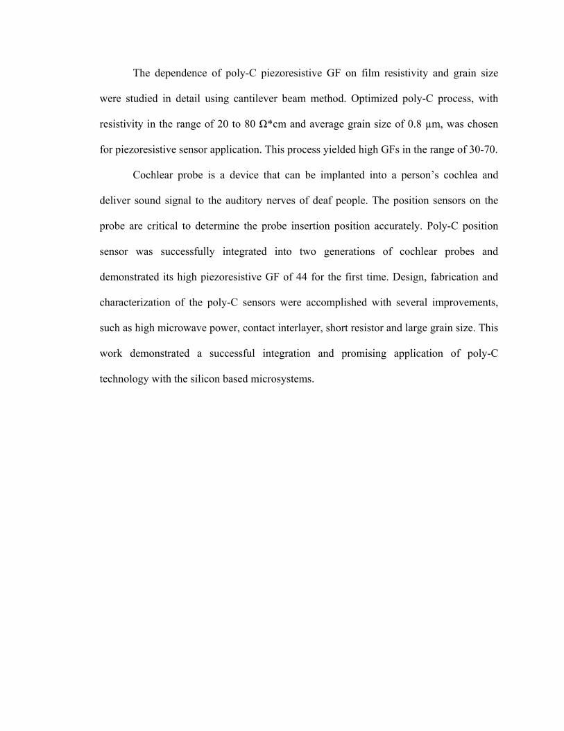
The dependence of poly-C piezoresistive GF on film resistivity and grain size
were studied in detail using cantilever beam method. Optimized poly-C process, with
resistivity in the range of 20 to 80 Ω*cm and average grain size of 0.8 µm, was chosen
for piezoresistive sensor application. This process yielded high GFs in the range of 30-70.
Cochlear probe is a device that can be implanted into a person’s cochlea and
deliver sound signal to the auditory nerves of deaf people. The position sensors on the
probe are critical to determine the probe insertion position accurately. Poly-C position
sensor was successfully integrated into two generations of cochlear probes and
demonstrated its high piezoresistive GF of 44 for the first time. Design, fabrication and
characterization of the poly-C sensors were accomplished with several improvements,
such as high microwave power, contact interlayer, short resistor and large grain size. This
work demonstrated a successful integration and promising application of poly-C
technology with the silicon based microsystems.

iv
To
my parents and my wife

v
ACKNOWLEDGMENTS
I would like to thank my whole family for their patience, understanding and
support during this study. I owe my greatest thanks to my parents for their hard work and
sacrifice so I can be where I am today. Special thanks go to my dear wife Niya Gu for her
understanding, support and sacrifice during the long time of study. Thanks also go to my
brothers, Huaxing and Jianxing, and all my other relatives for their encouragement.
I would like to thank my advisor, Dr. Dean Aslam, for his encouragement,
guidance and financial support throughout this research. I also thank my committee
members, Dr. Reinhard, Dr. Hogan, Dr. Naguib and especially Dr Kensall Wise for the
advice and support. Thanks go to the members of our research group for their help and
discussion in particular, Xiangwei, Nelson and Yang. Thanks also go to the faculties,
stuffs and friends of the WIMS center at University of Michigan who gave me great help
for the probe fabrication.
vi
TABLE OF CONTENTS
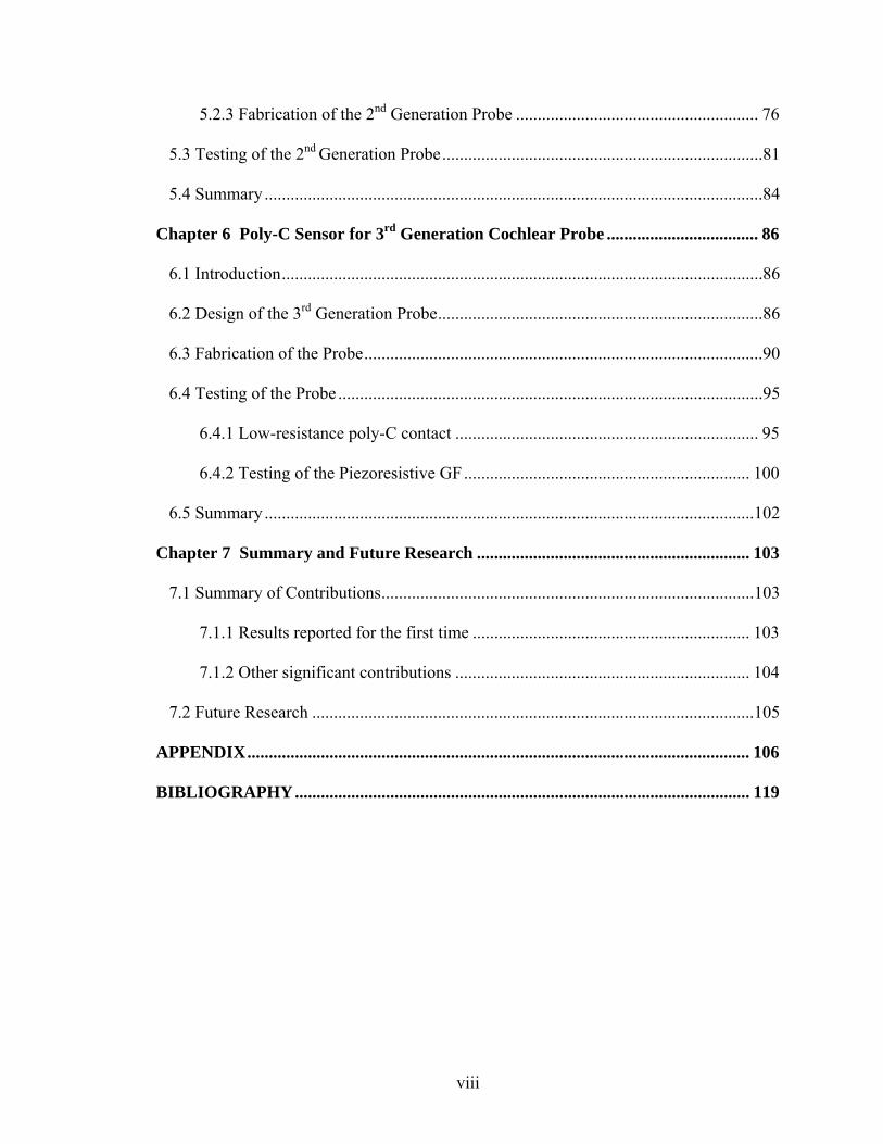
LIST OF TABLES ........................................................................................................... ix
LIST OF FIGURES .......................................................................................................... x
1 Research Motivation and Goals................................................................................... 1
1.1 Introduction.................................................................................................................1
1.2 Objective of this Work................................................................................................3
1.3 Overview of this Thesis ..............................................................................................6
Chapter 2 Background .................................................................................................... 7
2.1 Introduction.................................................................................................................7
2.2 Diamond Properties and Technologies .......................................................................7
2.2.1 Diamond Properties ......................................................................................... 7
2.2.2 Diamond Seeding............................................................................................. 9
2.2.3 Poly-C Growth ............................................................................................... 11
2.2.4 Poly-C Doping ............................................................................................... 14
2.2.5 Poly-C Metallization...................................................................................... 17
2.2.6 Poly-C Patterning........................................................................................... 18
2.3 Theory of Piezoresistivity .........................................................................................19
2.3.1 Definition of Gauge Factor ............................................................................ 19
2.3.2 Single Crystalline Materials........................................................................... 22
2.3.3 Polycrystalline Materials ............................................................................... 27
2.4 Diamond Piezoresistivity ..........................................................................................28
2.5 Cochlear Implant Probe ............................................................................................30
vii
2.6 Summary ...................................................................................................................33
Chapter 3 Poly-C Film Technologies ........................................................................... 35
3.1 Introduction...............................................................................................................35
3.2 Diamond Seeding......................................................................................................35
3.2.1 DPLW Spin-Coating...................................................................................... 36
3.2.2 Seeding Density and Uniformity ................................................................... 38
3.3 Film Growth Using MPCVD....................................................................................42
3.4 Doping and Surface Conductivity.............................................................................49
3.5 Metallization .............................................................................................................54
3.6 Patterning ..................................................................................................................57
3.7 Summary ...................................................................................................................60
Chapter 4 Testing of Poly-C Piezoresistivity............................................................... 61
4.1 Introduction...............................................................................................................61
4.2 The Cantilever Beam Method...................................................................................61
4.3 Sample Preparation ...................................................................................................64
4.4 Piezoresistive Results................................................................................................68
4.5 GF Dependence on the Film Properties ....................................................................70
4.6 Summary ...................................................................................................................71
Chapter 5 Poly-C Sensor for 2nd Generation Cochlear Probe................................... 72
5.1 Introduction...............................................................................................................72
5.2 Design and Fabrication of the Probe.........................................................................72
5.2.1 Technology for Poly-C Process Integration................................................... 72
5.2.2 Design of the 2nd Generation Probe ............................................................... 75
viii
5.2.3 Fabrication of the 2nd Generation Probe ........................................................ 76
5.3 Testing of the 2nd Generation Probe..........................................................................81
5.4 Summary ...................................................................................................................84
Chapter 6 Poly-C Sensor for 3rd Generation Cochlear Probe ................................... 86
6.1 Introduction...............................................................................................................86
6.2 Design of the 3rd Generation Probe...........................................................................86
6.3 Fabrication of the Probe............................................................................................90
6.4 Testing of the Probe ..................................................................................................95
6.4.1 Low-resistance poly-C contact ...................................................................... 95
6.4.2 Testing of the Piezoresistive GF.................................................................. 100
6.5 Summary .................................................................................................................102
Chapter 7 Summary and Future Research ............................................................... 103
7.1 Summary of Contributions......................................................................................103
7.1.1 Results reported for the first time ................................................................ 103
7.1.2 Other significant contributions .................................................................... 104
7.2 Future Research ......................................................................................................105
APPENDIX.................................................................................................................... 106
BIBLIOGRAPHY......................................................................................................... 119
ix
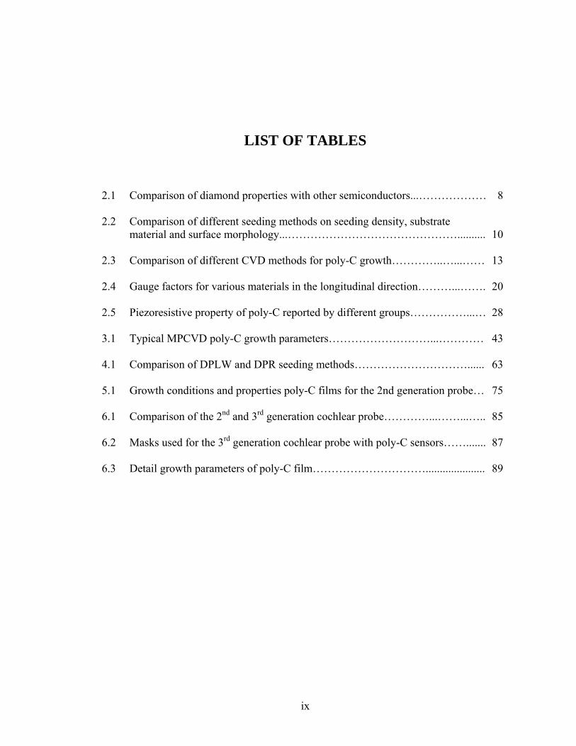
LIST OF TABLES
2.1 Comparison of diamond properties with other semiconductors...………………
8
2.2 Comparison of different seeding methods on seeding density, substrate material and surface morphology...………………………………………..........
10
2.3 Comparison of different CVD methods for poly-C growth…………..…...……
13
2.4 Gauge factors for various materials in the longitudinal direction………...…….
20
2.5 Piezoresistive property of poly-C reported by different groups……………...…
28
3.1 Typical MPCVD poly-C growth parameters………………………...…………
43
4.1 Comparison of DPLW and DPR seeding methods…………………………......
63
5.1 Growth conditions and properties poly-C films for the 2nd generation probe…
75
6.1 Comparison of the 2nd and 3rd generation cochlear probe…………...……...…..
85
6.2 Masks used for the 3rd generation cochlear probe with poly-C sensors…….......
87
6.3 Detail growth parameters of poly-C film………………………….....................
89
x
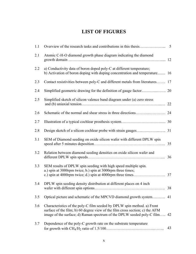
LIST OF FIGURES
1.1 Overview of the research tasks and contributions in this thesis………………...
5
2.1 Atomic C-H-O diamond growth phase diagram indicating the diamond growth domain ……………………………………………………………….....
12
2.2 a) Conductivity data of boron doped poly-C at different temperature; b) Activation of boron doping with doping concentration and temperature........
16
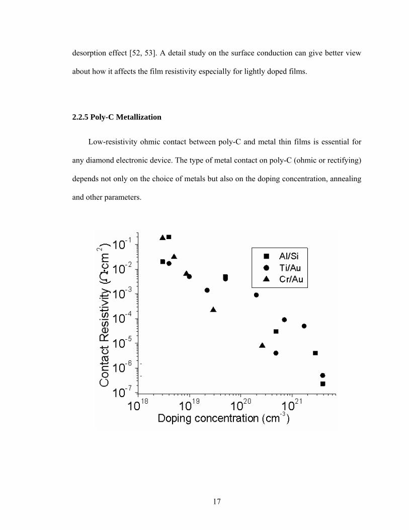
2.3 Contact resistivities between poly-C and different metals from literatures…….
17
2.4 Simplified geometric drawing for the definition of gauge factor.………...…….
20
2.5 Simplified sketch of silicon valence band diagram under (a) zero stress and (b) uniaxial tension……………………………………………………...…
22
2.6 Schematic of the normal and shear stress in three directions………...…………
24
2.7 Illustration of a typical cochlear prosthesis system…………………………......
30
2.8 Design sketch of a silicon cochlear probe with strain gauges…..…...……...…..
31
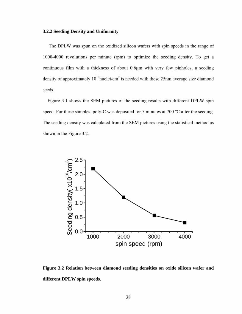
3.1 SEM of Diamond seeding on oxide silicon wafer with different DPLW spin speed after 5 minutes deposition……………………………………...…….......
35
3.2 Relation between diamond seeding densities on oxide silicon wafer and different DPLW spin speeds…………………………………………………....
36
3.3 SEM results of DPLW spin seeding with high speed multiple spin. a.) spin at 3000rpm twice; b.) spin at 3000rpm three times; c.) spin at 4000rpm twice; d.) spin at 4000rpm three times…………………….
37
3.4 DPLW spin seeding density distribution at different places on 4 inch wafer with different spin options……………………………………………….
38
3.5 Optical picture and schematic of the MPCVD diamond growth system……….
41
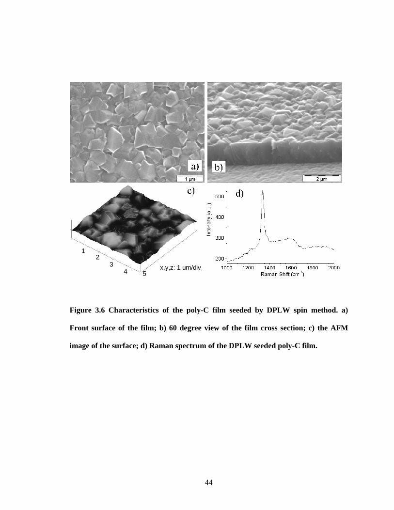
3.6 Characteristics of the poly-C film seeded by DPLW spin method. a) Front surface of the film; b) 60 degree view of the film cross section; c) the AFM image of the surface; d) Raman spectrum of the DPLW seeded poly-C film…..
42
3.7 Dependence of the poly-C growth rate on the substrate temperature for growth with CH4/H2 ratio of 1.5/100………………………………..……..
43

xi
3.8 AFM images of the poly-C film grown at 700 ºC on a 4 inch wafer…………...
45
3.9 Radial distributions of normalized poly-C film thickness at different deposition conditions and the Raman spectra of different samples………….....
46
3.10 Dependence of poly-C film conductivities on the doping levels……………….
48
3.11 As-grown and annealed conductivities of poly-C films (1µm) deposited at 700 ºC with different doping levels……………………………….…............
51
3.12 I-V curve of contact between poly-C film and Ti/Au film after anneal. Inset: the schematic of Kelvin Bridge for contact measurement……...………...…….
53
3.13 Resistivity dependence of the annealed contact resistivity between poly-C film and Ti/Au film………………………………….…………………
54
3.14 SEM images of poly-C structures prepared by the ECR plasma etch: a) the free standing poly-C finger structure and, b) single grain piezoresistor on large grain poly-C plate………...…………………...………...
57
4.1 Piezoresistive testing stage using cantilever beam method…..……….……......
60
4.2 Schematic diagram of the cantilever beam method used for piezoresistive measurement……………………………………...……………….....…………
61
4.3 SEM pictures of a) DPLW seeding; b) poly-C film (with thickness of 2 µm) seeded by DPLW; c) DPR seeding; d) poly-C film (with thickness of 2 µm) seeded by DPR………………………………………………………..…….......
64
4.4 Layout of the two masks (for poly-C and contact metal) designed for testing the piezoresistors………………………………………………………………..
65
4.5 a) SEM of the 400/20 µm piezoresistor with 4-contact; b) SEM of the Kelvin Bridge with gold wire bonding…………………………..………....
65
4.6 Relation between resistance change and strain for poly-C film prepared by the DPR seeding……………………………….….…………….…
66
4.7 Relations between the GF and the boron doped resistivity for both DPLW and DPR seeded poly-C films………………………………………….
67
5.1 Process flow for integrating poly-C sensor into Si-based microsystems…...…..
71
xii
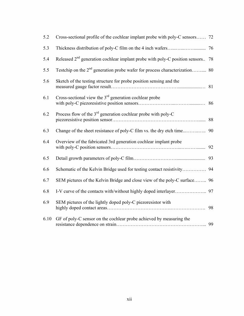
5.2 Cross-sectional profile of the cochlear implant probe with poly-C sensors……
72
5.3 Thickness distribution of poly-C film on the 4 inch wafers…...…...……..........
76
5.4 Released 2nd generation cochlear implant probe with poly-C position sensors..
78
5.5 Testchip on the 2nd generation probe wafer for process characterization……....
80
5.6 Sketch of the testing structure for probe position sensing and the measured gauge factor result……………………………………...................…
81
6.1 Cross-sectional view the 3rd generation cochlear probe with poly-C piezoresistive position sensors…………………...……….........…
86
6.2 Process flow of the 3rd generation cochlear probe with poly-C piezoresistive position sensor………………………………………………......
88
6.3 Change of the sheet resistance of poly-C film vs. the dry etch time...……..…..
90
6.4 Overview of the fabricated 3rd generation cochlear implant probe with poly-C position sensors……………………………………...….…….......
92
6.5 Detail growth parameters of poly-C film………………………........................
93
6.6 Schematic of the Kelvin Bridge used for testing contact resistivity……………
94
6.7 SEM pictures of the Kelvin Bridge and close view of the poly-C surface……..
96
6.8 I-V curve of the contacts with/without highly doped interlayer………………..
97
6.9 SEM pictures of the lightly doped poly-C piezoresistor with highly doped contact areas………………………………….………………….
98
6.10 GF of poly-C sensor on the cochlear probe achieved by measuring the resistance dependence on strain………………………………………………...
99
1
Chapter 1
Research Motivation and Goals
1.1 Introduction
The US market for sensor products (sensors, transducers and associated housings) is
projected to increase 15% per year from $5.9 billion in 2000 to $13.4 billion in 2006, and
the world market for sensors is expected to reach US $ 50-51 billion by 2008 [1]. The
North American market for silicon based piezoresistive pressure sensors stood at about
$284.6 million in 2001 [2]. Since the pressure sensors cannot be sealed in most situations,
the sensor material without passivation will be exposed to the environment. The
operation of silicon pressure sensors in chemically harsh, high temperature environments
is limited by leakage current and corrosion. Thus, the ultrahigh piezoresistivity and
chemical inertness of polycrystalline diamond (poly-C) thin film make it a promising
piezoresistive material better than silicon especially in harsh environment and high
temperature applications [3, 4].
The presence of unique sp3 C-C bonds in the diamond lattice leads to its unique
mechanical, chemical, optical and thermal properties not matched by any other known
material. Consequently, diamond becomes a unique material for a number of applications
including micro-electro-mechanical systems (MEMS) and wireless microsystem,
especially at high temperatures and in harsh environments. However, the difficulty to
2
fabricate the sp3 C-C bonds, which delayed the production of chemical vapor deposition
(CVD) of diamond, is now causing a delay in the development of a reliable and
economical diamond micro-fabrication technology that is compatible with conventional
microsystems/MEMS technologies.
A detail study and optimization of the poly-C film fabrication technologies,
including seeding, growing, doping and patterning, is needed for an optimum integration
with the silicon based microsystems.
The piezoresistive gauge factor (GF) of poly-C and related piezoresistive sensors
have been reported by several groups [3, 5-8] but with large variations in the
piezoresistive GF; typically in the ranges of 8 – 100 [5-7], 500 – 3200 [3] and 4000 [8]
for poly-C inter-grain, single crystal diamond and poly-C intra-grain, respectively.
Normally, the high GF values in the prior studies were achieved from films with
resistivities over 100 Ω*cm, which are impractical for sensor application due to the high
film resistances and high noise level. More research on the piezoresistivity of poly-C film
(in the doped region with resistivity from 10 to 100 Ω*cm) is needed to optimize the film
fabrication parameters for practical sensor applications.
In this work, poly-C films with their ultra-high piezoresistive sensitivity and
biocompatibility were chosen as the position sensors for the cochlear prosthesis project in
the Engineering Research Center for Wireless Integrated MicroSystems (WIMS ERC)
funded by National Science Foundation (NSF). Cochlear prostheses have been used as an
enabling technology to help deaf people in hearing by electrically stimulating the
auditory nerve cells with the implanted electrode. The position sensors are developed to
determine the placement of the cochlear electrode array within the cochlea both during

3
insertion and post-operation. Incorporating poly-C sensors into the probe fabrication
process and achieving high sensitivity will demonstrate a successful technology
integration and sensor application for poly-C thin film.
1.2 Objective of this Work
The goal of this work is to study the poly-C thin film technology and its
piezoresistivity for application as the position sensor in cochlear implant probe. It aims to
develop an optimum poly-C technology for high piezoresistivity and good integration
with silicon based microsystem. Then the application of poly-C piezoresistive sensor was
demonstrated by integrating poly-C into the cochlear probe as the position sensor. In a
summary, the goals of this dissertation research will focus on:
1) Fabricating and characterizing poly-C thin films on 4 inch oxidized silicon wafer
using IC-compatible processes. Developing and optimizing the crucial poly-C
technologies including seeding, growing, doping and patterning for the system
integration.
2) Studying the piezoresistivity of poly-C thin films prepared under different
parameters including grain size and doping levels. Optimizing the poly-C
fabrication condition to reach a compromise between high gauge factor and low
resistance for sensor application.
3) Integrating of the poly-C piezoresistive position sensor into the silicon based
cochlear implant probe and achieve good integration and high sensitivity.

4
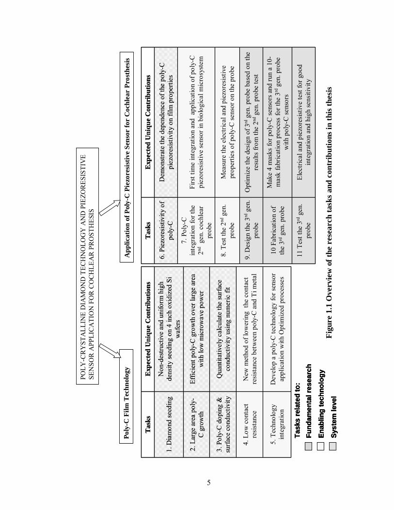
The major accomplishments and contributions to the scientific community
reported in this thesis were summarized in Figure 1.1. Based on the research strategy
of NSF, these contributions can be divided into three levels: fundamental research,
enabling technology and system level.
5
POLY
-CR
YST
ALL
INE
DIA
MO
ND
TEC
HN
OLO
GY
AN
D P
IEZO
RES
ISTI
VE
SEN
SOR
APP
LIC
ATI
ON
FO
R C
OC
HLE
AR
PR
OST
HES
IS
Poly
-C F
ilm T
echn
olog
yA
pplic
atio
n of
Pol
y-C
Pie
zore
sist
ive
Sens
or fo
r C
ochl
ear
Pros
thes
is
Figu
re 1
.1 O
verv
iew
of t
he r
esea
rch
task
s an
d co
ntri
butio
ns in
this
thes
is
Elec
trica
l and
pie
zore
sist
ive
test
for g
ood
inte
grat
ion
and
high
sens
itivi
ty11
Tes
t the
3rd
gen.
pr
obe
Mak
e 4
mas
ks fo
r pol
y-C
sens
ors a
nd ru
n a
10-
mas
k fa
bric
atio
n pr
oces
s fo
r the
3rd
gen.
pro
be
with
pol
y-C
sens
ors
10 F
abric
atio
n of
th
e 3rd
gen.
pro
be
Opt
imiz
e th
e de
sign
of 3
rdge
n. p
robe
bas
ed o
n th
e re
sults
from
the
2ndge
n. p
robe
test
9. D
esig
n th
e 3rd
gen.
pr
obe
Mea
sure
the
elec
tric
al a
nd p
iezo
resi
stiv
e pr
oper
ties o
f pol
y-C
sens
or o
n th
e pr
obe
8. T
est t
he 2
ndge
n.
prob
e
Firs
t tim
e in
tegr
atio
n an
d a
pplic
atio
n of
pol
y-C
pi
ezor
esist
ive
sens
or in
bio
logi
cal m
icro
syst
em
7. P
oly-
C in
tegr
atio
n fo
r the
2nd
gen.
coc
hlea
r pr
obe
Dem
onst
rate
the
depe
nden
ce o
f the
pol
y-C
pi
ezor
esist
ivity
on
film
pro
perti
es6.
Pie
zore
sist
ivity
of
poly
-C
Exp
ecte
d U
niqu
e C
ontr
ibut
ions
Tas
ks
Dev
elop
a p
oly-
C te
chno
logy
for s
enso
r ap
plic
atio
n w
ith O
ptim
ized
pro
cess
es5.
Tec
hnol
ogy
inte
grat
ion
New
met
hod
of lo
wer
ing
the
cont
act
resi
stan
ce b
etw
een
poly
-C a
nd T
i met
al
4. L
ow c
onta
ct
resi
stan
ce
Qua
ntita
tivel
y ca
lcul
ate
the
surf
ace
cond
uctiv
ity u
sing
num
eric
fit
3. P
oly-
C d
opin
g &
su
rfac
e co
nduc
tivity
Effic
ient
pol
y-C
gro
wth
ove
r lar
ge a
rea
with
low
mic
row
ave
pow
er2.
Lar
ge a
rea
poly
-C
gro
wth
Non
-des
truct
ive
and
unifo
rm h
igh
dens
ity se
edin
g on
4 in
ch o
xidi
zed
Si
waf
ers
1. D
iam
ond
seed
ing
Exp
ecte
d U
niqu
e C
ontr
ibut
ions
Tas
ks
Task
s re
late
d to
:Fu
ndam
enta
l res
earc
h
Enab
ling
tech
nolo
gy
Syst
em le
vel
Task
s re
late
d to
:Fu
ndam
enta
l res
earc
h
Enab
ling
tech
nolo
gy
Syst
em le
vel
Task
s re
late
d to
:Fu
ndam
enta
l res
earc
h
Enab
ling
tech
nolo
gy
Syst
em le
vel
Task
s re
late
d to
:Fu
ndam
enta
l res
earc
h
Enab
ling
tech
nolo
gy
Syst
em le
vel
6
1.3 Overview of this Thesis
This thesis presents the development and characterization of the technology of poly-C
piezoresistive position sensor and its integration with the silicon based cochlear implant
probe. Chapter 2 introduces the theory of piezoresistivity and the diamond
piezoresistivity. It also summarizes the previous work on fabrication technology of
polycrystalline diamond thin film. A brief introduction about the cochlear implant probe
is also presented. Chapter 3 talks about the poly-C thin film technology used for the
piezoresistive sensor devices. The details of poly-C film seeding, growing, doping and
patterning are presented with several unique contributions by this thesis research. Chapter
4 describes the measurement techniques and the equipment set up used for
piezoresistivity study. It discusses the measurement results of piezoresistive gauge factor
and its dependence on both the doping levels and film grain size. Then, in chapter 5, the
initial attempt of integrating diamond piezoresistive sensor into the 2nd generation
cochlear implant probe is discussed. Chapter 6 shows the detail design, fabrication and
testing of the optimum 3rd generation cochlear probe with poly-C sensors. Last chapter
summarizes the work and results of this dissertation and presents suggestions for future
related research.
7
Chapter 2
Background
2.1 Introduction
This chapter presents an introduction to the previous work on fabrication
technology of poly-C thin film such as seeding, growing, doping and patterning. It also
explains the piezoresistivity with mathematical derivation of the piezoresistive
coefficients and gauge factor. An overview of the recent progress in diamond
piezoresistive study and related sensors is given. A brief introduction to the concept of
the cochlear implant probe and its recent progress are presented also.
2.2 Diamond Properties and Technologies
2.2.1 Diamond Properties
Diamond is comprised of covalently bonded carbon atoms in a diamond cubic
crystal structure. In the diamond lattice, each carbon atom is bonded with its four
neighbor atoms using covalent bonds with hybrid sp3 atomic orbits that give it hardness
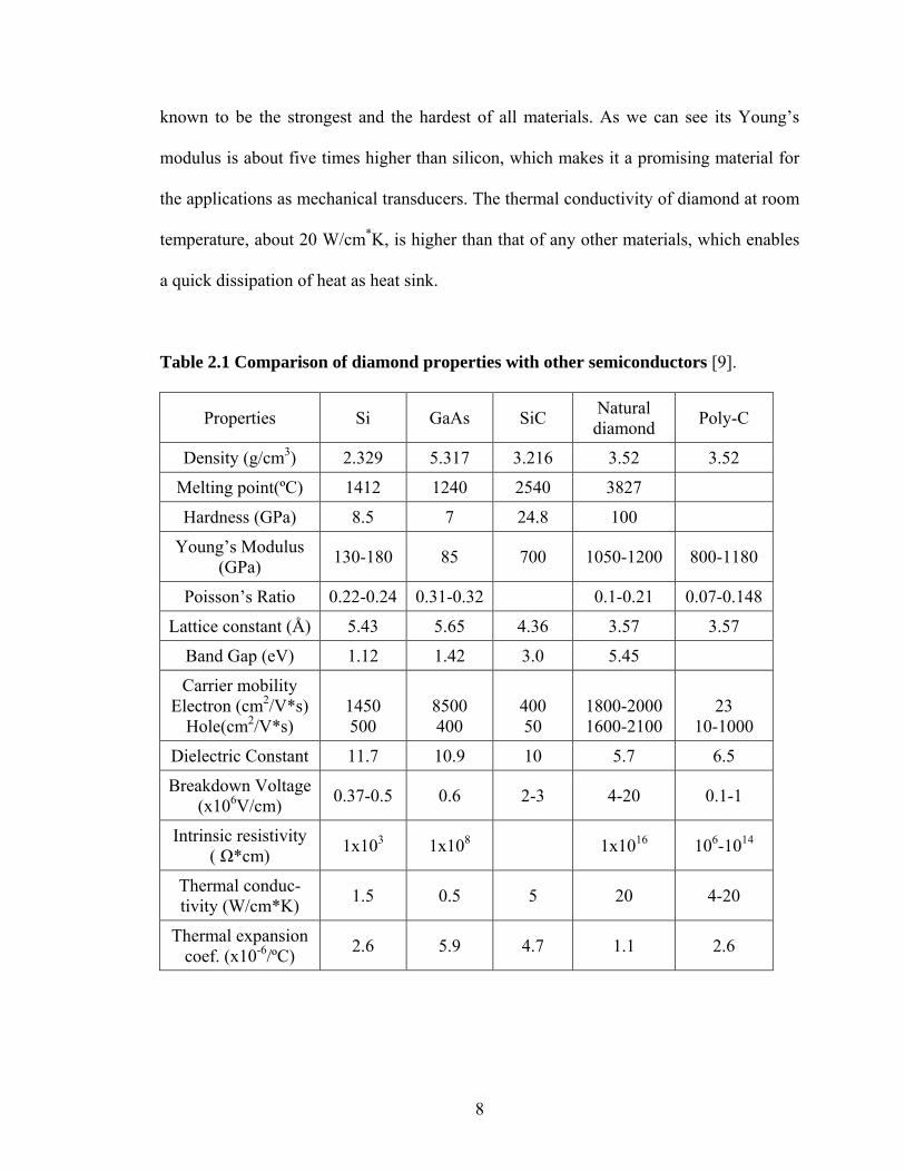
and strength. The properties of both natural diamond and poly-C are summarized and
compared with other semiconductor materials in Table 2.1. Diamond has long been
8
known to be the strongest and the hardest of all materials. As we can see its Young’s
modulus is about five times higher than silicon, which makes it a promising material for
the applications as mechanical transducers. The thermal conductivity of diamond at room
temperature, about 20 W/cm*K, is higher than that of any other materials, which enables
a quick dissipation of heat as heat sink.
Table 2.1 Comparison of diamond properties with other semiconductors [9].
Properties Si GaAs SiC Natural diamond Poly-C
Density (g/cm3) 2.329 5.317 3.216 3.52 3.52
Melting point(ºC) 1412 1240 2540 3827
Hardness (GPa) 8.5 7 24.8 100
Young’s Modulus (GPa) 130-180 85 700 1050-1200 800-1180
Poisson’s Ratio 0.22-0.24 0.31-0.32 0.1-0.21 0.07-0.148
Lattice constant (Å) 5.43 5.65 4.36 3.57 3.57
Band Gap (eV) 1.12 1.42 3.0 5.45
Carrier mobility Electron (cm2/V*s)
Hole(cm2/V*s)
1450 500
8500 400
400 50
1800-2000 1600-2100
23
10-1000
Dielectric Constant 11.7 10.9 10 5.7 6.5
Breakdown Voltage (x106V/cm) 0.37-0.5 0.6 2-3 4-20 0.1-1
Intrinsic resistivity ( Ω*cm) 1x10³ 1x10⁸ 1x10¹⁶ 106-1014
Thermal conduc-tivity (W/cm*K) 1.5 0.5 5 20 4-20
Thermal expansion coef. (x10-6/ºC) 2.6 5.9 4.7 1.1 2.6
9
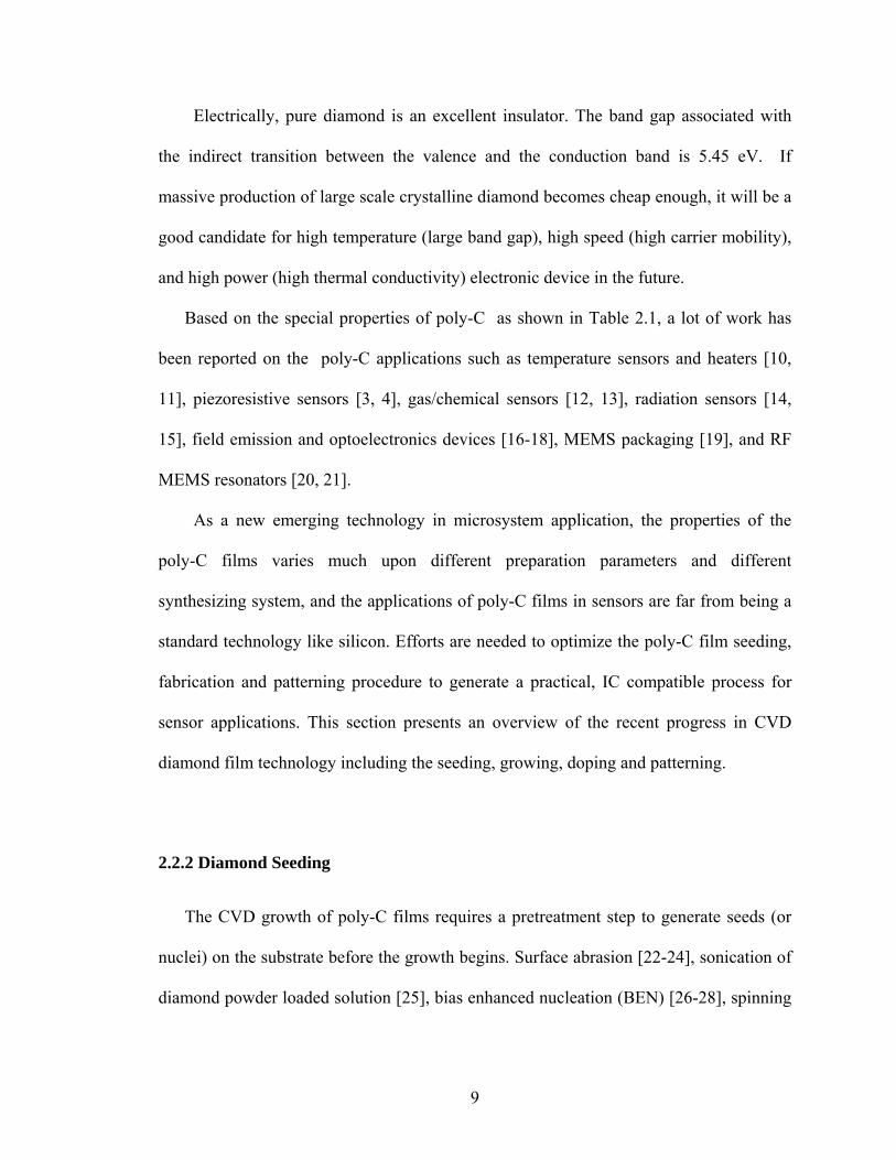
Electrically, pure diamond is an excellent insulator. The band gap associated with
the indirect transition between the valence and the conduction band is 5.45 eV. If
massive production of large scale crystalline diamond becomes cheap enough, it will be a
good candidate for high temperature (large band gap), high speed (high carrier mobility),
and high power (high thermal conductivity) electronic device in the future.
Based on the special properties of poly-C as shown in Table 2.1, a lot of work has
been reported on the poly-C applications such as temperature sensors and heaters [10,
11], piezoresistive sensors [3, 4], gas/chemical sensors [12, 13], radiation sensors [14,
15], field emission and optoelectronics devices [16-18], MEMS packaging [19], and RF
MEMS resonators [20, 21].
As a new emerging technology in microsystem application, the properties of the
poly-C films varies much upon different preparation parameters and different
synthesizing system, and the applications of poly-C films in sensors are far from being a
standard technology like silicon. Efforts are needed to optimize the poly-C film seeding,
fabrication and patterning procedure to generate a practical, IC compatible process for
sensor applications. This section presents an overview of the recent progress in CVD
diamond film technology including the seeding, growing, doping and patterning.
2.2.2 Diamond Seeding
The CVD growth of poly-C films requires a pretreatment step to generate seeds (or
nuclei) on the substrate before the growth begins. Surface abrasion [22-24], sonication of
diamond powder loaded solution [25], bias enhanced nucleation (BEN) [26-28], spinning
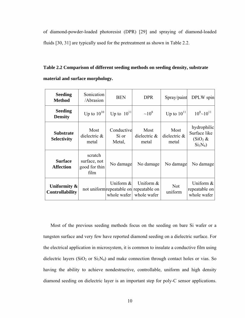
10
of diamond-powder-loaded photoresist (DPR) [29] and spraying of diamond-loaded
fluids [30, 31] are typically used for the pretreatment as shown in Table 2.2.
Table 2.2 Comparison of different seeding methods on seeding density, substrate
material and surface morphology.
Seeding Method
Sonication/Abrasion BEN DPR Spray/paint DPLW spin
Seeding Density Up to 1010 Up to 1011 ~108 Up to 1011 108~1011
Substrate Selectivity
Most dielectric &
metal
ConductiveSi or
Metal,
Most dielectric &
metal
Most dielectric &
metal
hydrophilic Surface like
(SiO2 & Si3N4)
Surface Affection
scratch surface, not
good for thin film
No damage No damage No damage No damage
Uniformity & Controllability not uniform
Uniform & repeatable on whole wafer
Uniform & repeatable on whole wafer
Not uniform
Uniform & repeatable on whole wafer
Most of the previous seeding methods focus on the seeding on bare Si wafer or a
tungsten surface and very few have reported diamond seeding on a dielectric surface. For
the electrical application in microsystem, it is common to insulate a conductive film using
dielectric layers (SiO2 or Si3N4) and make connection through contact holes or vias. So
having the ability to achieve nondestructive, controllable, uniform and high density
diamond seeding on dielectric layer is an important step for poly-C sensor applications.

11
The last column in Table 2.2 lists the new method we developed for seeding on dielectric
substrate, which will be discussed in Chapter 3.
2.2.3 Poly-C Growth
The growth of diamond by high pressure techniques was well established since the
1950s when GE researchers succeeded in transforming graphite to single crystalline
synthetic diamond [32]. Typically synthetic diamond is fabricated at temperatures around
4237 K and a pressure near 200 kbar. The high pressure high temperature (HPHT)
conditions make it costly and only suitable for production in the form of small pieces, grit
and powders.
Interest in diamond was renewed by successful CVD growth from hydrocarbon
mixtures in a lower pressure and temperature region. The CVD technique is based on
decomposition of carbon-containing precursor molecules (typically CH4) diluted in H2
gas. Addition of atomic hydrogen allowed for preferential etching of the sp2 bonding
(graphite) from the film and helped to yield high quality sp3 carbon structure (diamond).
Oxygen, in the form of O2, CO or CO2, has been added sometimes to get various film
properties. Bachmann and co-authors compiled numerous published CVD recipes and
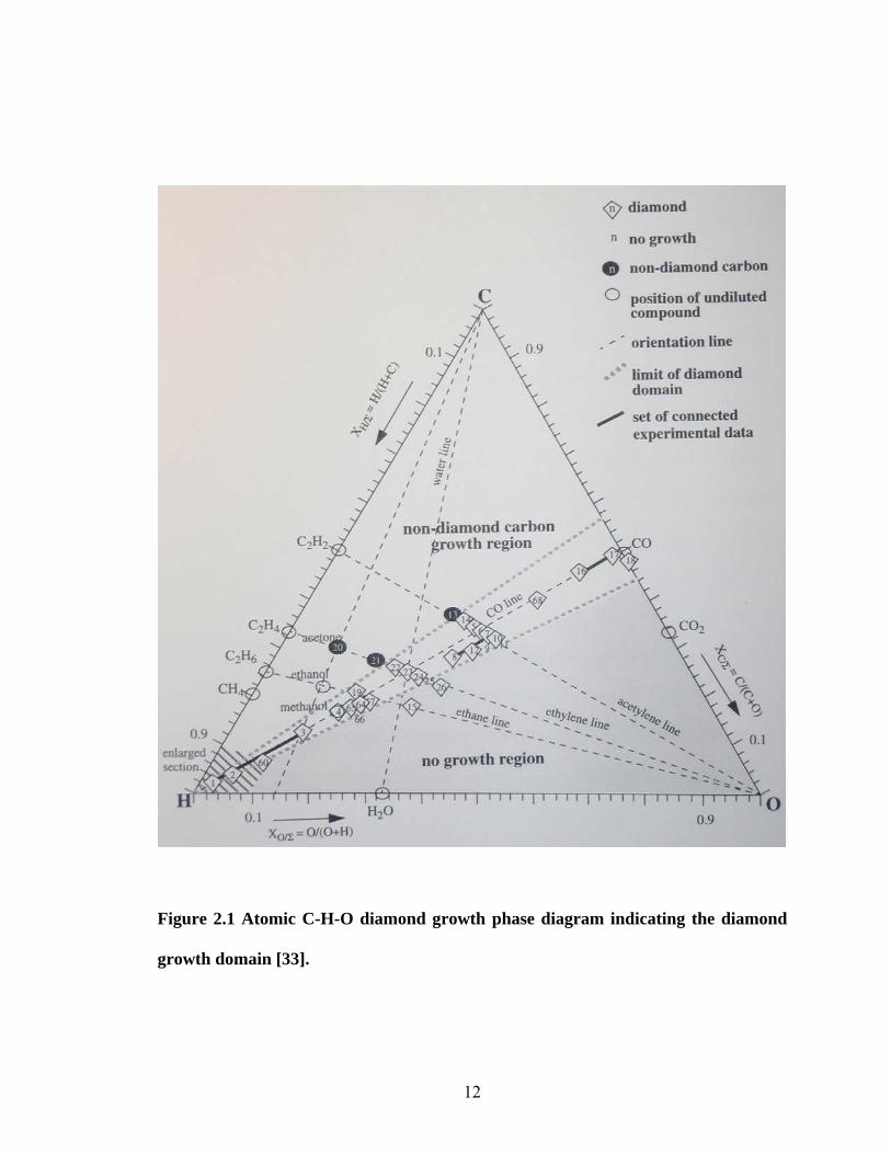
constructed the C/H/O phase diagram plotted in Figure 2.1 [33]. The diagram shows that
all successful diamond growth results appear within a well defined region.
12
Figure 2.1 Atomic C-H-O diamond growth phase diagram indicating the diamond
growth domain [33].
13
New developments in nanocrystalline diamond growth was recently reported by D.
M. Gruen from Argonne national Lab [34]. Most reports of the growth of these films
describe using a microwave plasma CVD reactor and gas mixture of 1%CH4 in Ar,
usually with addition of 1–5% H2. This method can produce films with much smaller
grain sizes (2-5 nm) and smoother surface than the regular hydrogen based growth.
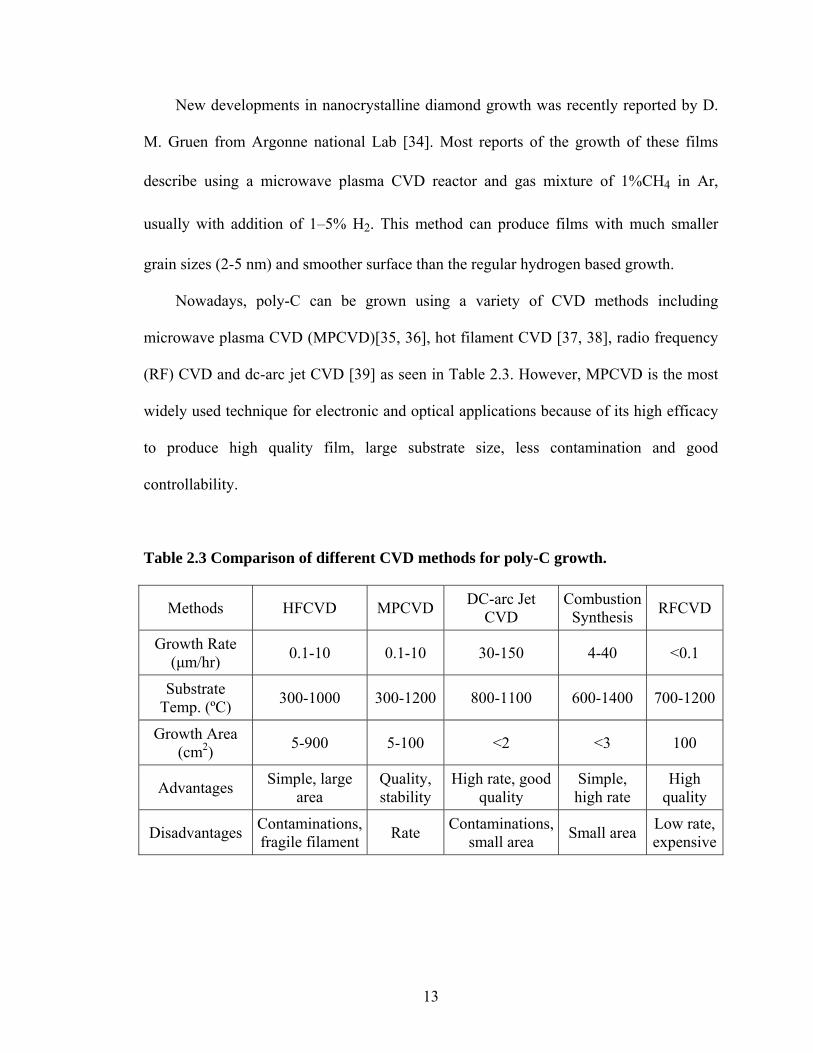
Nowadays, poly-C can be grown using a variety of CVD methods including
microwave plasma CVD (MPCVD)[35, 36], hot filament CVD [37, 38], radio frequency
(RF) CVD and dc-arc jet CVD [39] as seen in Table 2.3. However, MPCVD is the most
widely used technique for electronic and optical applications because of its high efficacy
to produce high quality film, large substrate size, less contamination and good
controllability.
Table 2.3 Comparison of different CVD methods for poly-C growth.
Methods HFCVD MPCVD DC-arc Jet CVD
Combustion Synthesis RFCVD
Growth Rate (μm/hr) 0.1-10 0.1-10 30-150 4-40 <0.1
Substrate Temp. (ºC) 300-1000 300-1200 800-1100 600-1400 700-1200
Growth Area (cm2) 5-900 5-100 <2 <3 100
Advantages Simple, large area
Quality, stability
High rate, good quality
Simple, high rate
High quality
Disadvantages Contaminations, fragile filament Rate Contaminations,
small area Small area Low rate, expensive

14
The reaction chamber in a typical microwave plasma system is composed of a quartz
tube which is placed inside the microwave chamber and a substrate holder which is
positioned inside the tube. A plasma of a carbon carrier gas and hydrogen mixtures, was
formed and diamond was deposited at a pressure of 10 -100 torr, a substrate temperature
of 600 – 1000 ºC, and methane concentrations of 0.2-5% in hydrogen.
Most of the MPCVD growths focus on the small size samples for lab test. Some
articles in the literatures reported the deposition of diamond on large scale substrates (4 to
6 inch) and discussed the microwave power, growth and uniformity. V.G. Ralchenko
reported a growth on 60mm substrate using a 5 kW microwave power with 10%
thickness variation [40]. Y. Ando et al reported a growth on 6 inch substrate with 30%
thickness variation using 15-60 kW microwave power [41]. Research on improving the
power efficiency and film uniformity on 4 inch substrate will be interesting for reducing
production cost.
2.2.4 Poly-C Doping
Accurate control of the doping level and resistivity is particularly important for poly-
C thin film electrical applications in sensors. Different boron containing compounds
typically used for p-type doping are pure boron powder [42], boron trioxide (B2O3) [43],
diborane (B2H6) [44, 45] and trimethylboron (B(OCH3)3, TMB) [46]. Although boron ion
implantation has been used for diamond doping [47, 48], its effectiveness has been
limited by the implant damages and very low diffusion ability of boron in poly-C [49]. In
situ doping with the trimethylboron has become a preferred source because the TMB gas,
diluted in hydrogen, is safer to use and more controllable than other boron compounds
15
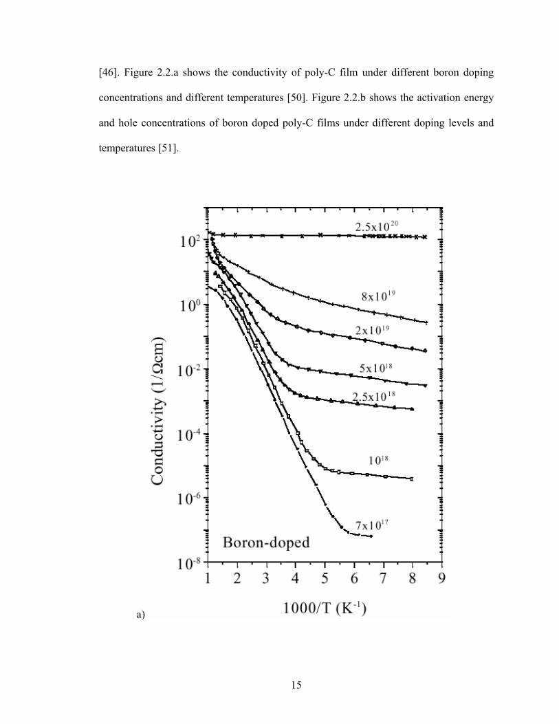
[46]. Figure 2.2.a shows the conductivity of poly-C film under different boron doping
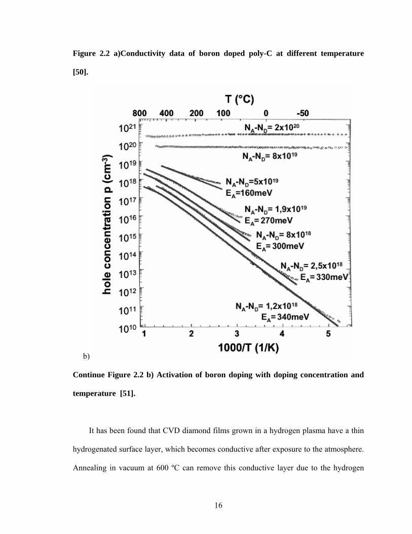
concentrations and different temperatures [50]. Figure 2.2.b shows the activation energy
and hole concentrations of boron doped poly-C films under different doping levels and
temperatures [51].
a)
16
Figure 2.2 a)Conductivity data of boron doped poly-C at different temperature
[50].
b)
Continue Figure 2.2 b) Activation of boron doping with doping concentration and
temperature [51].
It has been found that CVD diamond films grown in a hydrogen plasma have a thin
hydrogenated surface layer, which becomes conductive after exposure to the atmosphere.
Annealing in vacuum at 600 ºC can remove this conductive layer due to the hydrogen
17
desorption effect [52, 53]. A detail study on the surface conduction can give better view
about how it affects the film resistivity especially for lightly doped films.
2.2.5 Poly-C Metallization
Low-resistivity ohmic contact between poly-C and metal thin films is essential for
any diamond electronic device. The type of metal contact on poly-C (ohmic or rectifying)
depends not only on the choice of metals but also on the doping concentration, annealing
and other parameters.
18
Figure 2.3 Contact resistivities between poly-C and different metals from literatures
[54-57].
Titanium and chromium (with co-deposited gold on top of them to prevent oxidation)
are most widely used metals because they can form carbides with poly-C and yield good
conductivity after anneal. Werner et al. had demonstrated the Al (with 1% Si) film also
gave good contact with poly-C by forming silicon carbide [54]. For Ti/Au, Cr/Au and
Al/Si films, a vacuum annealing at 400 ºC to 600 ºC for 20 minutes is enough to achieve
stable ohmic contacts [58, 59]. Figure 2.3 shows the reported contact resistivity (also
known as specific contact resistance) as a function of poly-C doping levels from
literatures [54-57]. The contact resistivity is defined as the total contact resistance times
the size of contact area.
For the application as piezoresistor, it requires the poly-C film to be doped lightly
to get high piezoresistive sensitivity and contact resistance will become a problem in
these situations. More studies are needed for reducing the contact resistance for lightly
doped poly-C films.
2.2.6 Poly-C Patterning
For integrating poly-C devices into Si-based microsystems, patterning of poly-C films
using techniques consistent with silicon processing is required. As the wet etching poly-C
is impractical, the only patterning techniques are in-situ pattering and dry etching. The in-
situ patterning techniques rely on selective seeding which has been achieved using
different methods including diamond power-loaded photoresist (DPR) employing
19
standard lithography [29, 60], selective seeding using SiO2 as a mask [61, 62] and direct
spray writing [30]. However, in all these in-situ techniques, the lateral growth at the
pattern edges and, in some cases, growth on unwanted areas can pose serious problems
for small feature sizes. The dry etching of poly-C, which uses different active gas species
such as oxygen, argon, hydrogen, CF4 and SF6 with metal or SiO2 masks [63-65], seems
to be excellent choice for poly-C patterning. Most researches have used conventional
reactive ion etching (RIE) method where the gas species are excited by the RF power [65,
66]. Dry etching using electron cyclotron resonance (ECR) assisted microwave plasma at
low substrate temperatures and pressures has led to very clean structures with small
feature sizes and sharp edges [67, 68].
2.3 Theory of Piezoresistivity
2.3.1 Definition of Gauge Factor
The piezoresistive effect was first discovered in 1856 by Lord Kelvin using copper
and iron wires. The piezoresistive effect in semiconductors was found to be much larger
than metals by C. S. Smith in the mid 1950’s with germanium and silicon [69].
Piezoresistivity of a material is the dependence of electrical resistivity on strain and
normally is quantified by the gauge factor (GF). The GF of a material is defined as the
fractional change of resistance (ΔR/R) per unit strain ε. Typical gauge factors for various
materials in the longitudinal direction are shown in Table 2.4.
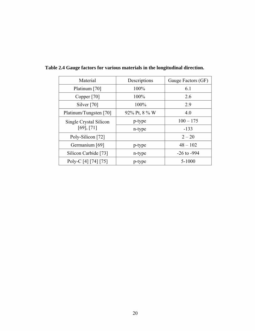
20
Table 2.4 Gauge factors for various materials in the longitudinal direction.
Material Descriptions Gauge Factors (GF) Platinum [70] 100% 6.1 Copper [70] 100% 2.6 Silver [70] 100% 2.9
Platinum/Tungsten [70] 92% Pt, 8 % W 4.0 p-type 100 – 175 Single Crystal Silicon
[69], [71] n-type -133 Poly-Silicon [72] 2 – 20 Germanium [69] p-type 48 – 102
Silicon Carbide [73] n-type -26 to -994 Poly-C [4] [74] [75] p-type 5-1000
21
F
FI
x
z
yL
AF
FI
x
z
y
F
FI
x
z
yL
A
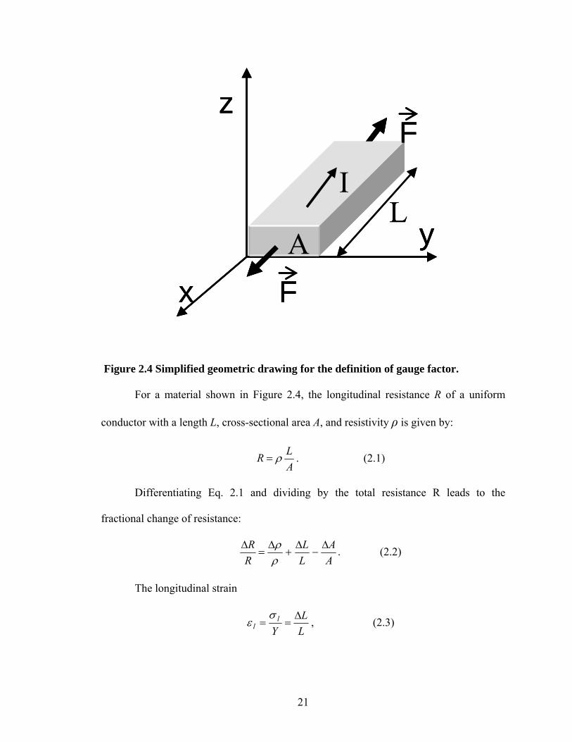
Figure 2.4 Simplified geometric drawing for the definition of gauge factor.
For a material shown in Figure 2.4, the longitudinal resistance R of a uniform
conductor with a length L, cross-sectional area A, and resistivity ρ is given by:
ALR ρ= . (2.1)
Differentiating Eq. 2.1 and dividing by the total resistance R leads to the
fractional change of resistance:
AA
LL
RR Δ
−Δ
+Δ
=Δ
ρρ . (2.2)
The longitudinal strain
LL
Yl
lΔ
==σ
ε , (2.3)

22
where lσ is longitudinal stress and Y is the Young’s Modules of the material. The gauge
factor in the longitudinal (strain is parallel to current) direction can be written as:
lll
ll
RdRGF ⎟⎟
⎠
⎞⎜⎜⎝
⎛ Δ++==
ρρ
ευ
ε121
)/(, (2.4)
where υ is the Poisson ratio. It can be seen from Eq. 2.4 that the strain sensitivity of any
material is due to two factors, i.e., (i) the change in the dimensions of the conductor, and
(ii) the change in resistivity.
For the transverse direction where the current flow is perpendicular to the strain
direction, the gauge factor can be written as [76]:
( ) 111−⎟⎟
⎠
⎞⎜⎜⎝
⎛ Δ=⎟
⎠⎞
⎜⎝⎛ Δ=
tlttt R
RGFερ
ρε
, (2.5)
For some semiconductor materials like silicon, silicon carbide or diamond, the GF
is much higher due to the strain dependence of the resistivity caused by energy band
deformation and the first two parts in Eq. 2.4 and the second part in Eq. 2.5 can be
ignored.
2.3.2 Single Crystalline Materials
For the single crystalline semiconductor like silicon and diamond, the piezoresistive
effect is anisotropic and the piezoresistivity need to be represented using the
piezoresistive coefficients. Silicon will be chosen as the example to explain the principle
of piezoresistivity in semiconductors [76].
23
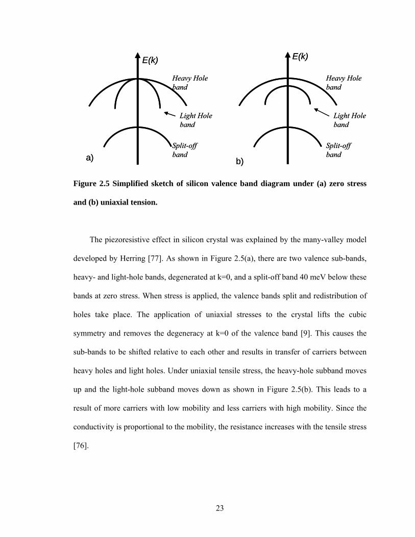
Heavy Hole band
E(k)E(k)
Light Hole band
Split-off band
Heavy Hole band
Light Hole band
Split-off banda) b)
Heavy Hole band
E(k)E(k)
Light Hole band
Split-off band
Heavy Hole band
Light Hole band
Split-off banda) b)
Figure 2.5 Simplified sketch of silicon valence band diagram under (a) zero stress
and (b) uniaxial tension.
The piezoresistive effect in silicon crystal was explained by the many-valley model
developed by Herring [77]. As shown in Figure 2.5(a), there are two valence sub-bands,
heavy- and light-hole bands, degenerated at k=0, and a split-off band 40 meV below these
bands at zero stress. When stress is applied, the valence bands split and redistribution of
holes take place. The application of uniaxial stresses to the crystal lifts the cubic
symmetry and removes the degeneracy at k=0 of the valence band [9]. This causes the
sub-bands to be shifted relative to each other and results in transfer of carriers between
heavy holes and light holes. Under uniaxial tensile stress, the heavy-hole subband moves
up and the light-hole subband moves down as shown in Figure 2.5(b). This leads to a
result of more carriers with low mobility and less carriers with high mobility. Since the
conductivity is proportional to the mobility, the resistance increases with the tensile stress
[76].
24
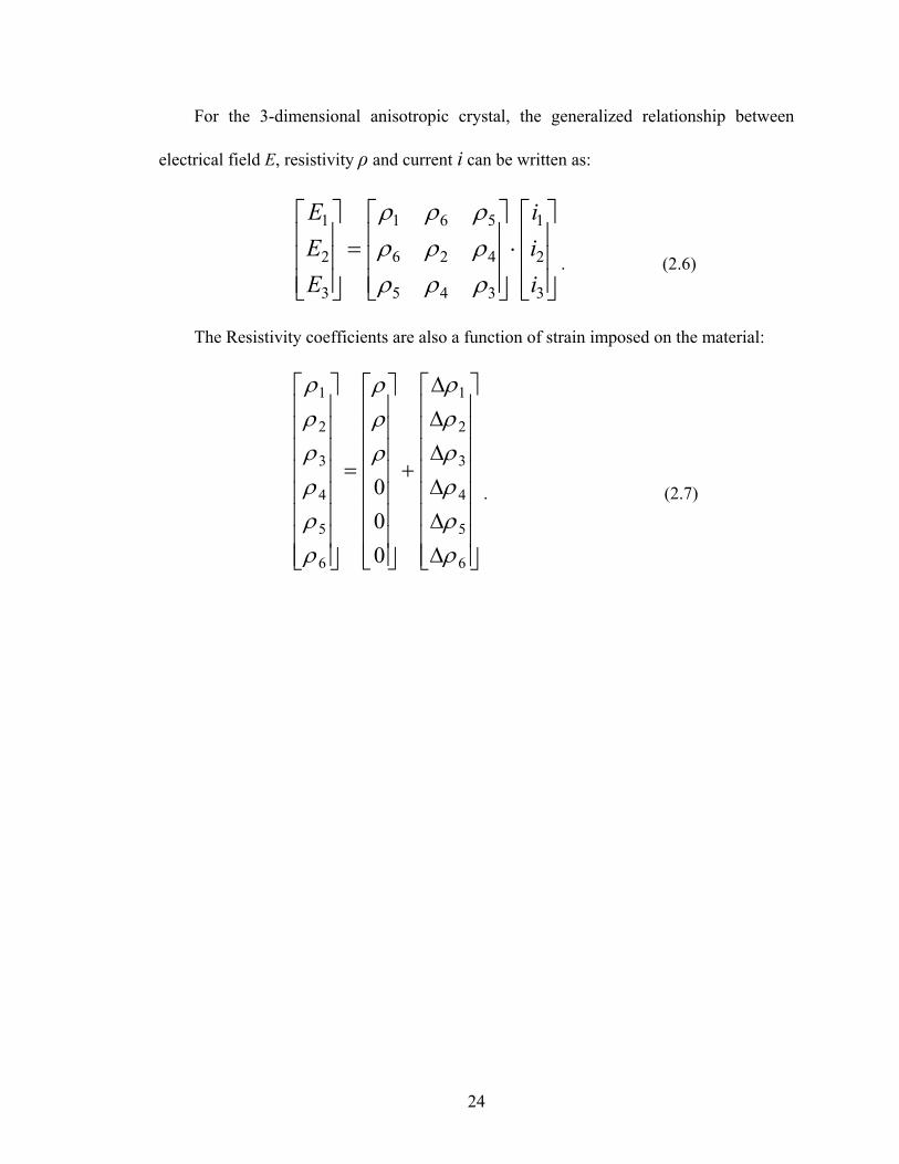
For the 3-dimensional anisotropic crystal, the generalized relationship between
electrical field E, resistivity ρ and current i can be written as:
⎥⎥⎥
⎦
⎤
⎢⎢⎢
⎣
⎡⋅⎥⎥⎥
⎦
⎤
⎢⎢⎢
⎣
⎡=
⎥⎥⎥
⎦
⎤
⎢⎢⎢
⎣
⎡
3
2
1
345
426
561
3
2
1
iii
EEE
ρρρρρρρρρ
. (2.6)
The Resistivity coefficients are also a function of strain imposed on the material:
⎥⎥⎥⎥⎥⎥⎥⎥
⎦
⎤
⎢⎢⎢⎢⎢⎢⎢⎢
⎣
⎡
ΔΔΔΔΔΔ
+
⎥⎥⎥⎥⎥⎥⎥⎥
⎦
⎤
⎢⎢⎢⎢⎢⎢⎢⎢
⎣
⎡
=
⎥⎥⎥⎥⎥⎥⎥⎥
⎦
⎤
⎢⎢⎢⎢⎢⎢⎢⎢
⎣
⎡
6
5
4
3
2
1
6
5
4
3
2
1
000
ρρρρρρ
ρρρ
ρρρρρρ
. (2.7)
25
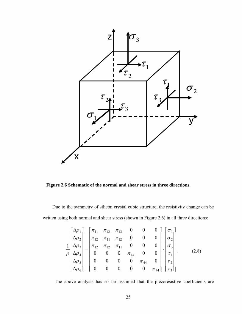
y
z
x
1σ2τ
1τ
1τ2τ
3τ3τ
3σ
2σ
y
z
x
1σ2τ
1τ
1τ2τ
3τ3τ
3σ
2σ
Figure 2.6 Schematic of the normal and shear stress in three directions.
Due to the symmetry of silicon crystal cubic structure, the resistivity change can be
written using both normal and shear stress (shown in Figure 2.6) in all three directions:
⎥⎥⎥⎥⎥⎥⎥⎥
⎦
⎤
⎢⎢⎢⎢⎢⎢⎢⎢
⎣
⎡
⋅
⎥⎥⎥⎥⎥⎥⎥⎥
⎦
⎤
⎢⎢⎢⎢⎢⎢⎢⎢
⎣
⎡
=
⎥⎥⎥⎥⎥⎥⎥⎥
⎦
⎤
⎢⎢⎢⎢⎢⎢⎢⎢
⎣
⎡
ΔΔΔΔΔΔ
3
2
1
3
2
1
44
44
44
111212
121112
121211
6
5
4
3
2
1
000000000000000000000000
1
τττσσσ
ππ
ππππππππππ
ρρρρρρ
ρ . (2.8)
The above analysis has so far assumed that the piezoresistive coefficients are

26
aligned to the primary axes of the crystal silicon. But in many instances the position of
piezoresistors may not coincide with the coordinate system. Therefore, we need to
develop a transformation between the old coordinate system (x, y, z) (i.e., the system that
is aligned to the Si crystal structure) and the new system (x*, y*, z*) (the system that is
aligned with the longitudinal direction of the piezoresistor):
⎥⎥⎥
⎦
⎤
⎢⎢⎢
⎣
⎡⋅
⎥⎥⎥
⎦
⎤
⎢⎢⎢
⎣
⎡=
⎥⎥⎥
⎦
⎤
⎢⎢⎢
⎣
⎡
zyx
nmlnmlnml
zyx
333
222
111
***
, (2.9)
where li, mi and ni (i=1,2,3) are the direction cosines of the transformation [78]. (l1, m1,
n1) is the set of direction cosines between the longitudinal resistor direction and the
crystal axis, and (l2, m2, n2) is the set of direction cosines between the transverse resistor
direction and the crystal axis.
For the longitudinal direction, the gauge factor can be written as
YGF lll
l περ
ρ=⎟⎟
⎠
⎞⎜⎜⎝
⎛ Δ=
1. (2.10)
The longitudinal piezoresistive coefficient πl equals to
( )( )21
21
21
21
21
2144121111 2 lnnmmll ++−−−= πππππ . (2.11)
For the transverse direction, the gauge factor can be written as
YtGF tt
t περ
ρ=⎟⎟
⎠
⎞⎜⎜⎝
⎛ Δ=
1. (2.12)
where the transverse piezoresistive coefficient equals to
( )( )22
21
22
21
22
2144121112 nnmmllt ++−−+= πππππ . (2.13)
27
2.3.3 Polycrystalline Materials
In general, the polycrystalline materials consist of crystalline grains interconnected
by grain boundaries. Grains are considered as small single crystals with the same lattice
and same energy band structure as single crystal silicon. The grain boundaries (GBs) are
composed of disordered atoms and contains a large number of defects and dangling
bonds which act as trapping states and/or segregation sites [79]. Trapping of holes
creates a potential barrier at the boundary and a depletion region into the grains.
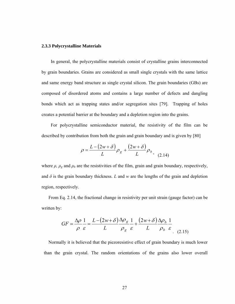
For polycrystalline semiconductor material, the resistivity of the film can be
described by contribution from both the grain and grain boundary and is given by [80]
( ) ( )bg L
wLwL ρδρδρ +
++−
=22
’ (2.14)
where ρ, ρg and ρb are the resistivities of the film, grain and grain boundary, respectively,
and δ is the grain boundary thickness. L and w are the lengths of the grain and depletion
region, respectively.
From Eq. 2.14, the fractional change in resistivity per unit strain (gauge factor) can be
written by:
( ) ( )ερ
ρδερ
ρδερ
ρ 12121
b
b
g
g
Lw
LwLGF Δ+
+Δ+−
=Δ
=. (2.15)
Normally it is believed that the piezoresistive effect of grain boundary is much lower
than the grain crystal. The random orientations of the grains also lower overall
28
piezoresistive effect of grain. This is consistent with the reported low GF of polysilicon
compared to single crystalline silicon.
2.4 Diamond Piezoresistivity
Interest for diamond piezoresistive sensors grew with the first quantitative study of
the piezoresistive gauge factor in homoepitaxial and polycrystalline diamond films [3].
Several groups have confirmed the observed large piezoresistive gauge factor for
different diamond films.
For synthetic crystalline diamond, the GF, extracted from the work of Latsa et, al,
was found to be higher than 103 [4]. The GF for homoepitaxial diamond, measured using
a boron doped type 2a film epoxy-glued on a stainless cantilever beam, was reported to
be at least 550, four times higher than the highest value of Si [4]. Sahli S. reported a high
GF of 4000 from the intra-grain measurement on large size grain (75 µm) poly-C plate
[8].
The piezoresistive property of poly-C was studied for different structures, doping
levels and temperatures using cantilever beam, three-point bending fixture and
differential pressure setups. Table 2.5 lists most data published on room temperature GF
for CVD diamond along with the corresponding sample specifications.
The effect of GBs on the electrical properties of poly-C has been addressed by
measuring and interpreting the effective electrical properties of CVD diamond. For the
boron doped CVD diamond films, frequency conduction measurements for different
doping levels showed activation energies in the range of 0.18 to 1.07 eV and identified
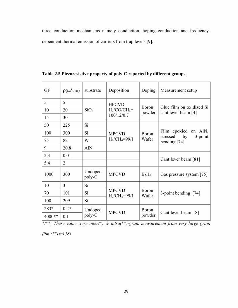
29
three conduction mechanisms namely conduction, hoping conduction and frequency-
dependent thermal emission of carriers from trap levels [9].
Table 2.5 Piezoresistive property of poly-C reported by different groups.
GF ρ(Ω*cm) substrate Deposition Doping Measurement setup
5 5 10 20 15 30
SiO2 HFCVD H2/CO/CH4= 100/12/0.7
Boron powder
Glue film on oxidized Si cantilever beam [4]
50 225 Si
100 300 Si 75 82 W 9 20.8 AlN
MPCVD H2/CH4=99/1
Boron Wafer
Film epoxied on AlN, stressed by 3-point bending [74]
2.3 0.01 5.4 2
Cantilever beam [81]
1000 300 Undoped poly-C MPCVD B2H6 Gas pressure system [75]
10 3 Si 70 101 Si
100 209 Si
MPCVD H2/CH4=99/1
Boron Wafer 3-point bending [74]
283* 0.27
4000** 0.1 Undoped poly-C MPCVD Boron
powder Cantilever beam [8]
*/**: These value were inter(*) & intra(**)-grain measurement from very large grain
film (75μm) [8]

30
Based on the samples with listed resistivity, GF increases with the resistivity. The
results also suggest that grain size, structure, substrate and processing may affect the
Piezoresistivity, however, there is no systematic study of the GF-grain size relation yet.
The results listed in Table 2.5 demonstrate the feasibility and confirm the high
sensitivity of boron doped poly-C piezoresistors. The current challenge for diamond
piezoresistors is to deliver stable, reliable and reproducible sensor under the reasonable
resistivity range and integrate them into the microsystems.
2.5 Cochlear Implant Probe
Cochlear prosthesis is a device that can be surgically implanted into a person's
cochlea to stimulate it to cause hearing. As shown in Figure 2.7, it consists of a tiny
receiver which is placed under the skin in the bony part behind the ear. The receiver
connects to a bundle of metal wire electrodes (usually 22 now), which are implanted into
the cochlea. A cochlear implant can be useful if the hearing loss is caused by problems
with the cochlea (usually damaged hair cells) or where the loss is caused by problems
with the middle ear that cannot be corrected. A person with a cochlear implant also wears
a hearing aid like device that has a microphone, a processor and a transducer. The
processor manipulates what the microphone hears and sends a signal to the transducer,
which is usually worn just behind the ear. The transducer changes the signal from an
electrical signal to an electromagnetic signal that can be received through the skin by the
implanted receiver.
31
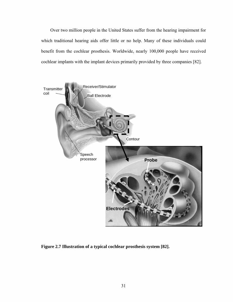
Over two million people in the United States suffer from the hearing impairment for
which traditional hearing aids offer little or no help. Many of these individuals could
benefit from the cochlear prosthesis. Worldwide, nearly 100,000 people have received
cochlear implants with the implant devices primarily provided by three companies [82].
Transmittercoil
Receiver/Stimulator
Ball Electrode
Contour
Probe
Electrodes
Speech processor
Transmittercoil
Receiver/Stimulator
Ball Electrode
Contour
Probe
Electrodes
Speech processor
Figure 2.7 Illustration of a typical cochlear prosthesis system [82].
32
In spite of considerable recent progress, several problems continue to plague present
implants. These include limited frequency range (due to the difficulties in achieving deep
insertion), limited pitch discrimination (due to the small number of wires that can be
accommodated in the cochlea (16-22)), and rather poor ability to distinguish individual
conversations in a crowded room. While cochlear implant users can often communicate
normally using the telephone, music is usually less than enjoyable. The surgical implant
procedure today is still performed blindly without benefit of position feedback. Currently,
no satisfactory non-invasive visualization technique exists for cochlear implants.
Conventional X-rays, CT scans, and phase-contrast radiography provide limited solutions
and are used primarily for pre-surgical or post-surgical evaluations [82]. While implants
use rather sophisticated electronics and are powered from an external speech processor by
inductive RF coupling, the wire electrode bundles are constructed largely by hand, are
limited in performance, and are relatively expensive [83].
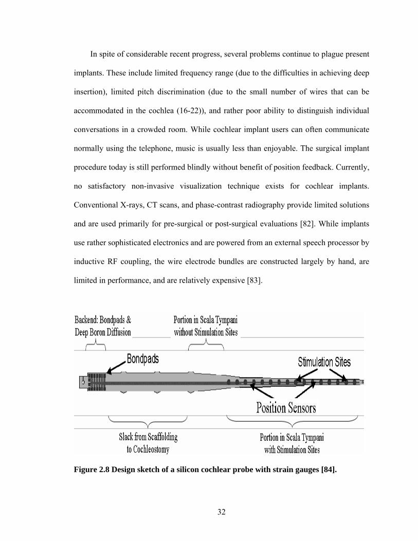
Figure 2.8 Design sketch of a silicon cochlear probe with strain gauges [84].
33
Thin-film silicon probe with electrode arrays [84] are being developed by researchers
in the NSF Engineering Research Center for Wireless Integrated Microsystems (WIMS
ERC), which was issued to University of Michigan, Michigan State University and
Michigan Tech University under the direction of Dr. Kensall D. Wise. These probes are
batch fabricated using bulk micromachining technology and aim to improve pitch
perception by increasing the number of stimulating sites to as many as 128. In order to
allow real-time visualization and accurate positioning of the arrays, a position-sensing
system, which consists of a distributed series of piezoresistors along the insertion part of
the cochlear probe, is being built into the arrays as shown in Figure 2.8. With the help of
the position sensors, the sites should ideally be implanted deeply within the cochlea and
should hug the interior wall of the scala tympani to minimize the distance to the
receptors, lower the stimulation thresholds, reduce implant power, and increase frequency
discrimination [83]. Due to the high piezoresistive sensitivity and biocompatibility, using
a poly-C piezoresistor will help to improve the performance of the positioning system.
Incorporating poly-C position sensors into the probe fabrication process and achieving
high sensitivity will demonstrate a successful technology integration and sensor
application for poly-C thin film.
2.6 Summary
This chapter reviews the poly-C thin film technology and the theory of
piezoresistivity. The principle of poly-C piezoresistivity and related sensors are

34
summarized. Although poly-C piezoresistive sensors have been successfully fabricated,
there still exists large scattering in the piezoresistive sensor response no real application
in a complicated microsystem. The introduction to cochlear implant probe leads to a
promising application of poly-C piezoresistive sensors in a silicon based cochlear implant
probe.
35
Chapter 3
Poly-C Film Technologies
3.1 Introduction
One part of the work in this thesis focuses on developing the poly-C technologies
that can lead to controllable high quality poly-C films for the sensor applications. This
chapter reports the poly-C film technologies used for fabrication with emphasis on the
new seeding method, the large area growth and the surface conductivity.
3.2 Diamond Seeding
For sensor applications, poly-C film needs to be grown on dielectric layer (SiO2 or
Si3N4). Controllable and non-destructive seeding method with high seeding density is
required on dielectric substrate for growing smooth, pinhole-free poly-C thin film.
Different seeding methods have been reviewed in Chapter 2. In this work, we developed
a new seeding method by spin-coating diamond power loaded water (DPLW) on the
samples. The goals of studying this new seeding method are:
36
i) Achieve controllable, repeatable, non-destructive and large scale (4 inch wafer)
seeding on a dielectric (SiO2 or Si3N4) surface using DPLW spin-coating.
ii) Study the relation between the seeding density and the spin speed.
iii) Study the relation between the seeding uniformity and the multiple-spin.
3.2.1 DPLW Spin-Coating
The diamond powder loaded water (DPLW) is hydrophilic on cleaned silicon dioxide
surface and can spread on it and form a uniform thin film on the SiO2 surface due to the
following two reasons: a). The surface tension between SiO2 and water (120mN/m) is
much larger than the water surface tension (72mN/m) [85], and b). The SiO2 surface
partly terminated with H and F atoms (caused by the HF etching) is favorable to water
due to the Coulomb attraction through high polarity of the Si-F bonding [86].
25 carat diamond powder, with an average size of 25nm, was mixed in 1000ml De-
Ionized (DI) water to create the DPLW. Polyether Polyol is used as suspension agent.
Ultrasonication was used to break the aggregated powders and improved the suspended
powder density in water.
The 4" silicon wafer, with an oxide layer of 300nm on top of it, was cleaned with
RCA procedure, which includes 10 minutes degrease clean (degrease solution includes
H2O2:NH4OH:H2O at a ratio of 1:1:5 at 50 ºC) and 10 minutes demetal clean (demetal
solution includes H2O2:HCl:H2O at a ratio of 2:1:8 at 50 ºC). Then the wafer was dipped
into the 5% HF water solution for 30 second, rinsed in DI water for 3 minutes and blown
dry by nitrogen gas.

37
After the clean procedure, the sample wafer was put on spinner, and DPLW with
25nm size powder was dropped on the wafer to form a thin and uniform film. The wafer
was spun at a specific speed for 30 second once the dropped DPLW covers the whole
wafer. Different spin speeds were tested to study the relation between seeding densities
and spin speeds. Multiple spin, which means repeating the DPLW spin procedure twice
or 3 times on same wafer at relatively high spin speed, was also be studied to improve the
seeding quality.
Figure 3.1 SEM of Diamond seeding on oxide silicon wafer with different DPLW
spin speed after 5 minutes growth.
38
3.2.2 Seeding Density and Uniformity
The DPLW was spun on the oxidized silicon wafers with spin speeds in the range of
1000-4000 revolutions per minute (rpm) to optimize the seeding density. To get a
continuous film with a thickness of about 0.6μm with very few pinholes, a seeding
density of approximately 1010nuclei/cm2 is needed with these 25nm average size diamond
seeds.
Figure 3.1 shows the SEM pictures of the seeding results with different DPLW spin
speed. For these samples, poly-C was deposited for 5 minutes at 700 ºC after the seeding.
The seeding density was calculated from the SEM pictures using the statistical method as
shown in the Figure 3.2.
1000 2000 3000 40000.0
0.5
1.0
1.5
2.0
2.5
Seed
ing
dens
ity( x
1010
/cm
2 )
spin speed (rpm)
Figure 3.2 Relation between diamond seeding densities on oxide silicon wafer and
different DPLW spin speeds.
39
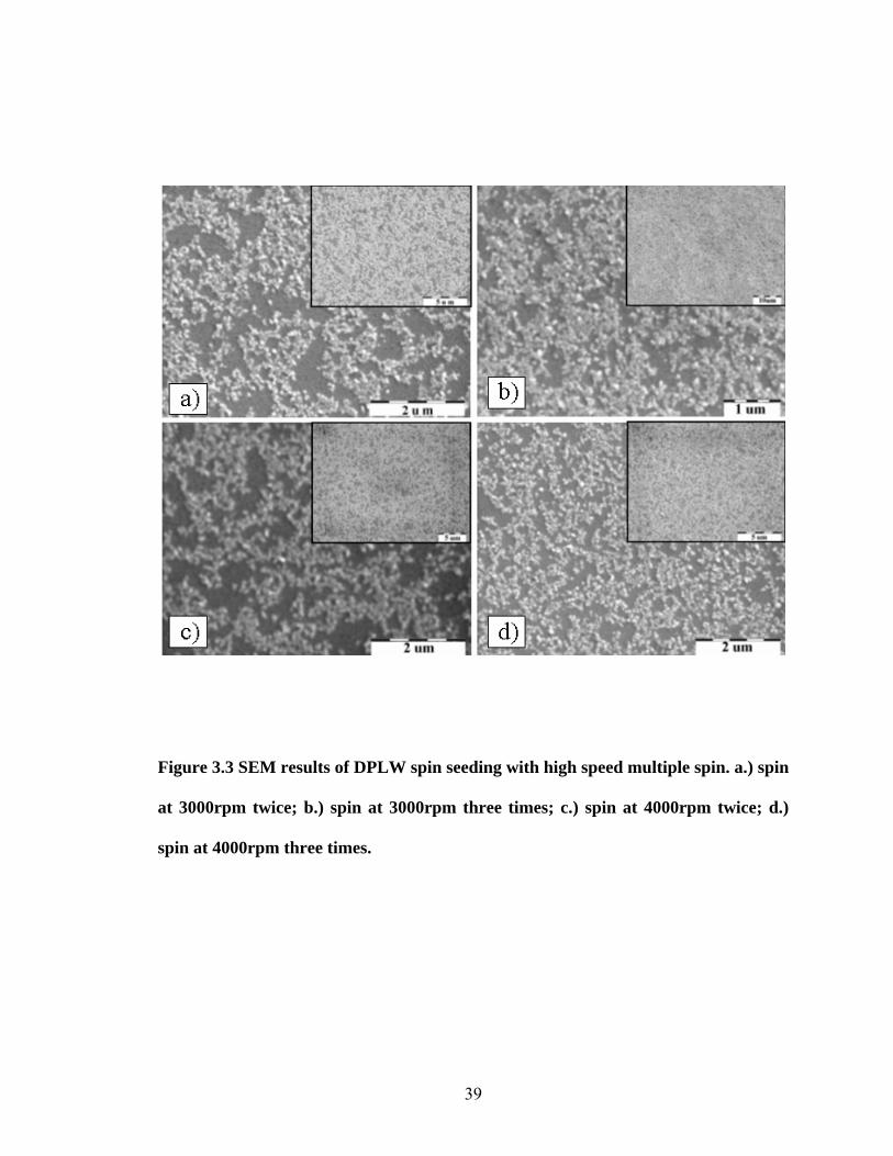
Figure 3.3 SEM results of DPLW spin seeding with high speed multiple spin. a.) spin
at 3000rpm twice; b.) spin at 3000rpm three times; c.) spin at 4000rpm twice; d.)
spin at 4000rpm three times.

40
Figure 3.4 DPLW spin seeding density distribution at different places on 4 inch
wafer with different spin options.
41
The SEM pictures in Figure 3.1 show that, at low spin speeds, spin seeding gave high
seeding densities but lots of the diamond powders aggregated together, which will reduce
the effective seeding density and weaken the adhesion force between the diamond film
and underneath silicon dioxide layer. At high spin speed, fewer particles aggregate
together and the dispersion is more uniform, but the seeding density is a little lower than
the expected value of 1010/cm2. Seeding at 3000 rpm will be a better compromise
between the low aggregation and high seeding density needed to grow high quality,
continuous poly-C film at the thickness of 0.6 µm. Experiments proved that the seeding
density is reciprocally related to the spin speed in a repeatable manner as shown in the
Figure 3.2.
The seeding uniformity was studied by checking the seeding density at different areas
on 4 inch oxidized wafers with different spin speeds. On each wafer, 5 spots were chosen
to measure the seeding density by using SEM images. These five spots are equally
distributed from wafer center to edge in a 1/2 inch separation. The results in Figure 3.4
showed that the seeding densities were uniform all over the 4 inch wafer even if the
rotating speed is different at different radius. This conclusion ensures getting a uniform
seeding on the whole 4 inch wafer and broadening the future applications of this method.
In summary, the high density (>1010 nuclei/cm2) and uniform diamond seeding was
achieved on 4 inch oxidized silicon wafer by the DPLW spin method. The DPLW
spinning method for diamond seeding on silicon dioxide, reported for the first time to our
knowledge, is a simple, economical, nondestructive and repeatable procedure compared
to BEN and surface scratching (Table 2.2). It can also be applied to other hydrophilic
42
dielectric thin film which is not fit for BEN and surface scratching. Combined with the
diamond dry etching technology, it can provide an IC compatible diamond thin film
deposition and pattern procedure, which will greatly extend the possible applications of
poly-C film in the sensors and MEMS area. From the multiple spin results, we can expect
that higher seeding density (like 1011 nuclei/cm2) can also be available with this method
by using smaller diamond powers, low spin speed and more spin times.
Another seeding method, the spin-coating of diamond loaded photoresist (DPR), was
also used in this research to achieve a low density seeding around 108 nuclei/cm2. DPR
seeding was developed at Michigan State University [29]. The diamond powder, with
particle size of 100 nm, was mixed with photoresist with a ratio of 800 mg powder per 80
ml PR.
3.3 Film Growth Using MPCVD
For the results reported in this work, a bell jar type MPCVD chamber (WavematTM
MPDR 313EHP) was used with 9 inch chamber diameter and 5 inch quartz bell jar
diameter. A 2.45 GHz, 5 kW microwave power supply (SairemTM, GMP60KSM) and a
large chamber size ensured the uniformity of the plasma and the poly-C deposition on 4
inch size. Figure 3.5 shows the optical picture and the schematic of the MPCVD system.
The sample wafer was heated by the plasma and its temperature was monitored by a
pyrometer. The typical deposition conditions are listed in the Table 3.1. Trimethylboron
(TMB) diluted in hydrogen (TMB/H2 = 0.1% in volume ratio) was introduced during the
poly-C growth environment for the in-situ boron doping.

43
Figure 3.5 Optical picture and schematic of the MPCVD diamond growth system .
44
21
34 5
x,y,z: 1 um/div2
1
34 5
x,y,z: 1 um/div
Figure 3.6 Characteristics of the poly-C film seeded by DPLW spin method. a)
Front surface of the film; b) 60 degree view of the film cross section; c) the AFM
image of the surface; d) Raman spectrum of the DPLW seeded poly-C film.

45
Table 3.1 Typical MPCVD poly-C growth parameters.
Samples #1 #2 #3
H2/CH4 Gas flow (sccm) 200/3 200/3 200/3
Microwave power (kW) 1.6 2.4 2.8
Gas pressure (torr) 22 35 43
Substrate temperature (ºC) 520 700 780
Growth rate (µm/hr) 0.1 0.2 0.3
Substrate Temperature ( )
Gro
wth
Rat
e (u
m/h
r)
Substrate Temperature ( )
Gro
wth
Rat
e (u
m/h
r)
Figure 3.7 Dependence of the poly-C growth rate on the substrate temperature for
growth with CH4/H2 ratio of 1.5/100.
46
Figure 3.6 shows the different characters of the poly-C film by SEM, AFM (atomic
force microscope) and Raman spectrum (green laser with a wavelength of 532 nm was
used as the light source). The poly-C film was grown using the #2 conditions from Table
3.1 with a thickness of 1.6 µm. The average grain size is about 0.6 µm, and average
surface roughness is 42 nm from the AFM image.
The relation between the film growth rate and the substrate temperature is shown in
Figure 3.7 for growth with CH4/H2 ratio of 1.5/100. Both the growth rate and substrate
temperature are referred to the center area of substrate with a diameter about 2 inches.
For the diamond growth in MPCVD chamber, the radial decrease of plasma
intensity causes the non-uniformity of film thickness on large area, which limits the
possible applications of diamond thin films. Different deposition parameters were tested
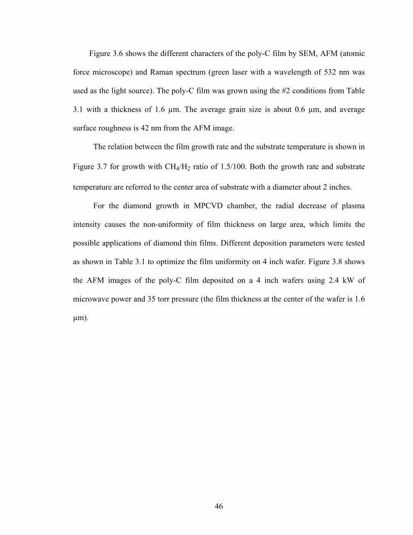
as shown in Table 3.1 to optimize the film uniformity on 4 inch wafer. Figure 3.8 shows
the AFM images of the poly-C film deposited on a 4 inch wafers using 2.4 kW of
microwave power and 35 torr pressure (the film thickness at the center of the wafer is 1.6
µm).
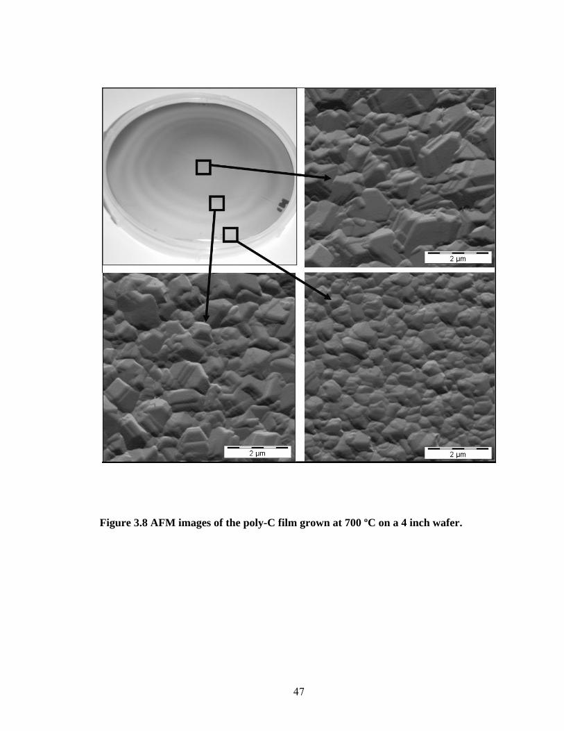
47
Figure 3.8 AFM images of the poly-C film grown at 700 ºC on a 4 inch wafer.
48
1200 1300 1400 1500
520C
780C
700C
Inte
nsity
(A.u
.)
Raman shift (cm-1)
780C
700C
520C
0.0 0.5 1.0 1.5 2.00.0
0.2
0.4
0.6
0.8
1.0N
orm
aliz
ed th
ickn
ess
Distance from 4 inch wafer center (inch)
1200 1300 1400 1500
520C
780C
700C
Inte
nsity
(A.u
.)
Raman shift (cm-1)
780C
700C
520C
0.0 0.5 1.0 1.5 2.00.0
0.2
0.4
0.6
0.8
1.0N
orm
aliz
ed th
ickn
ess
Distance from 4 inch wafer center (inch)
Figure 3.9 Radial distributions of normalized poly-C film thickness at different
deposition conditions and the Raman spectra of different samples.
The thickness variation over the 4 inch area of the wafer is shown in Figure 3.9 for
three samples with comparable thickness, but grown at different pressures and microwave
powers. The thickness of each sample is measured using the SEM method and
normalized to 1 for better comparison of the thickness variation along the radius. The
inset of Figure 3.9 shows the Raman spectra of the three different samples, which
demonstrated that the high growth temperature yielded better film quality.
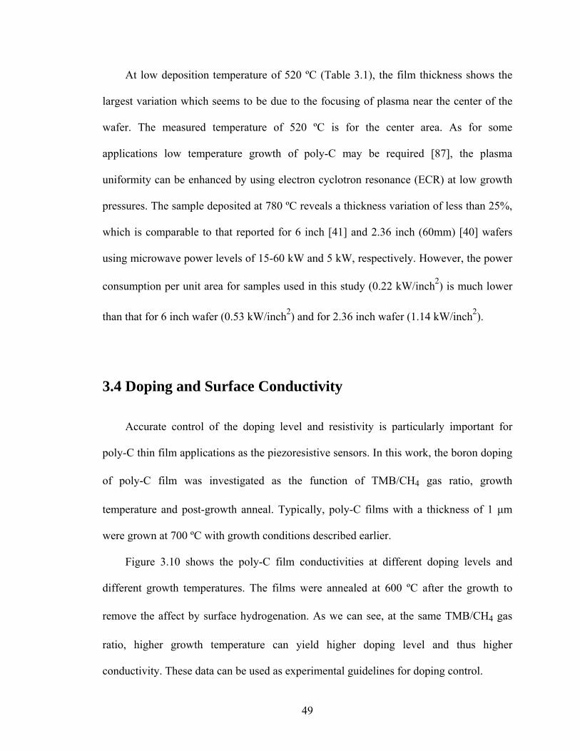
49
At low deposition temperature of 520 ºC (Table 3.1), the film thickness shows the
largest variation which seems to be due to the focusing of plasma near the center of the
wafer. The measured temperature of 520 ºC is for the center area. As for some
applications low temperature growth of poly-C may be required [87], the plasma
uniformity can be enhanced by using electron cyclotron resonance (ECR) at low growth
pressures. The sample deposited at 780 ºC reveals a thickness variation of less than 25%,
which is comparable to that reported for 6 inch [41] and 2.36 inch (60mm) [40] wafers
using microwave power levels of 15-60 kW and 5 kW, respectively. However, the power
consumption per unit area for samples used in this study (0.22 kW/inch2) is much lower
than that for 6 inch wafer (0.53 kW/inch2) and for 2.36 inch wafer (1.14 kW/inch2).
3.4 Doping and Surface Conductivity
Accurate control of the doping level and resistivity is particularly important for
poly-C thin film applications as the piezoresistive sensors. In this work, the boron doping
of poly-C film was investigated as the function of TMB/CH4 gas ratio, growth
temperature and post-growth anneal. Typically, poly-C films with a thickness of 1 μm
were grown at 700 ºC with growth conditions described earlier.
Figure 3.10 shows the poly-C film conductivities at different doping levels and
different growth temperatures. The films were annealed at 600 ºC after the growth to
remove the affect by surface hydrogenation. As we can see, at the same TMB/CH4 gas
ratio, higher growth temperature can yield higher doping level and thus higher
conductivity. These data can be used as experimental guidelines for doping control.

50
0 2 4 6 8 1010-3
10-2
10-1
100
101
102
103
Con
duct
ivity
(Ohm
-1*c
m-1)
TMB/CH4 ratio (x10-3)
400 oC 600 oC 800 oC
Figure 3.10 Dependence of poly-C film conductivities on the doping levels.
It has been found that CVD diamond films grown in hydrogen plasma have a thin
hydrogenated surface layer, which becomes conductive after exposure to the atmosphere.
Annealing at 600 ºC or a short time dry etch can remove this conductive layer hydrogen
desorption effect [52, 53]. In this work, the boron doping of poly-C film was investigated
as a function of TMB/CH4 gas ratio, deposition temperature and post-deposition anneal.
Typically, poly-C films with a thickness of 1 μm were grown at 700 ºC with growth
conditions described earlier. The poly-C films were annealed at 600 ºC for 20 minutes at
1x10⁻⁵ torr to remove the surface conductive layer by de-hydrogenation.
51
The actual data measured using the 4-probe method yield the sheet resistance
IVRsh ξ= , (3.1)
whereξ is the geometric coefficient dependent only on the sample size and shape.
If the thin film has only one conductive layer with known thickness t, the conductivity is
given by
tRsh
1=σ . (3.2)
Since the conductivity of the annealed film is only contributed by the poly-C bulk
layer, Eq. 3.2 becomes
bulkannealshbulkbulkanneal tR
11===
ρσσ . (3.3)
The as-grown poly-C film consists of two different conductive layers, the surface
and bulk, with thicknesses of tsurf and tbulk, respectively. The total resistance, Ras-grown of
parallel combination is given by
bulksurfgrownas RRR111
+=−
, (3.4)
where Rsurf and Rbulk are resistance of the surface layer and bulk layer, respectively.
SinceWLRR sh= (L/W is the Length/Width ratio), Eq. 3.4 can be represented in sheet
resistance as
bulkshsurfshgrownasshRRR
111+=
−
. (3.5)
Using Eq. 3.2, the relation between measured total sheet resistance and conductivity is
52
bulkbulksurfsurfgrownassh
ttR
σσ +=−
1. (3.6)
Since the thickness of surface layer is much less than the bulk layer: tsurf <<tbulk, the
conductivity for as-grown film grownas−σ can be defined as
( )surfbulkgrownasshgrownas ttR +
=−
−1σ
bulkbulk
surfsurf
bulkgrownasshtt
tRσσ +=≈
−
1 . (3.7)
Figure 3.11 shows the conductivities of as-grown and annealed poly-C films
calculated from Eq. 3.3 and 3.7 using the measured sheet resistances. The numerical fits
obtained using exponential functions with fractional power yield conductivities, grownas−σ
and annealσ , for as-grown and annealed films, respectively
( )56.04 5.264exp10677.4033.0 xgrownas ×××+= −−σ , (3.8)
( )56.04 5.264exp10677.4 xanneal ×××= −σ , (3.9)
where x is the TMB/CH4 gas ratio. Eq. 3.8 and 3.9 can be used as an empirical
guidance for doping estimation. Comparison of Eq. 3.7 and 3.8 reveals that surface layer
contributes a constant conductivity of
( ) 1033.0 −⋅Ω= cmtt
bulk
surfsurfσ . (3.10)
If the thickness of surface conductive layer is assumed to be 40nm [88], the
corresponding conductivity can be calculated as

53
( ) 1825.0401033.0 −⋅Ω=×= cm
nmm
surf
μσ . (3.11)
Eq. 3.11 demonstrates that the surface conductivity is independent of the doping
concentrations. The corresponding surface sheet resistance is 330 kΩ/sq.
Figure 3.11 As-grown and annealed conductivities of poly-C films (1µm) deposited
at 700 ºC with different doping levels.

54
Theoretically, the bulk conductivity can be written as
pAA
pbulk NkTEqqp μαμσσ ⎟
⎠⎞
⎜⎝⎛−=== exp2 , (3.12)
where q is the charge of electron, p is the hole concentration, NA is the concentration of
acceptors, α is the activation coefficient and EA is the activation energy. However,
theoretical explanation of the relation between the bulk conductivity and TMB/CH4 gas
ratio is not presented here due to the complicate situation of impurity incorporation from
gas phase into film, which is related to the growth temperature, pressure, gas flow rate
and etc. Combining the theoretical Eq. 3.12 and experimental Eq. 3.9, a tentative
expression for the acceptor concentration can be written as
⎟⎠⎞
⎜⎝⎛ ×+
×=
−56.0
45.264exp10677.4 x
kTE
qN A
pA αμ . (3.13)
Although EA, α and μp are all depended on x, Eq. 3.13 can be used as an expression
of the relation between the TMB/CH4 ratio and the acceptor concentration by using those
experimental data between NA~α and NA~EA [89].
3.5 Metallization
In this work, titanium was used for the poly-C metallization with co-deposited gold
for protection and wire bonding. Figure 3.12 shows a typical I-V curve of the ohmic
contact between poly-C and Ti/Au film at room temperature after annealing at 600 ºC in
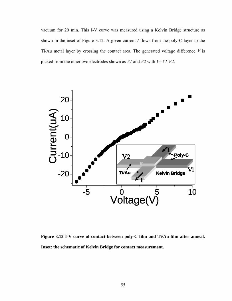
55
vacuum for 20 min. This I-V curve was measured using a Kelvin Bridge structure as
shown in the inset of Figure 3.12. A given current I flows from the poly-C layer to the
Ti/Au metal layer by crossing the contact area. The generated voltage difference V is
picked from the other two electrodes shown as V1 and V2 with V=V1-V2.
I
IV
V2
Kelvin BridgeTi/Au
Poly-C
1
I
IV
V2
Kelvin BridgeTi/Au
Poly-C
1
I
IV
V2
Kelvin BridgeTi/Au
Poly-C
1
I
IV
V2
Kelvin BridgeTi/Au
Poly-C
1-20
-10
0
10
20
-5 0 5 10Voltage(V)
Cur
rent
(uA
)
I
IV
V2
Kelvin BridgeTi/Au
Poly-C
1
I
IV
V2
Kelvin BridgeTi/Au
Poly-C
1
I
IV
V2
Kelvin BridgeTi/Au
Poly-C
1
I
IV
V2
Kelvin BridgeTi/Au
Poly-C
1-20
-10
0
10
20
-5 0 5 10Voltage(V)
Cur
rent
(uA
)
Figure 3.12 I-V curve of contact between poly-C film and Ti/Au film after anneal.
Inset: the schematic of Kelvin Bridge for contact measurement.
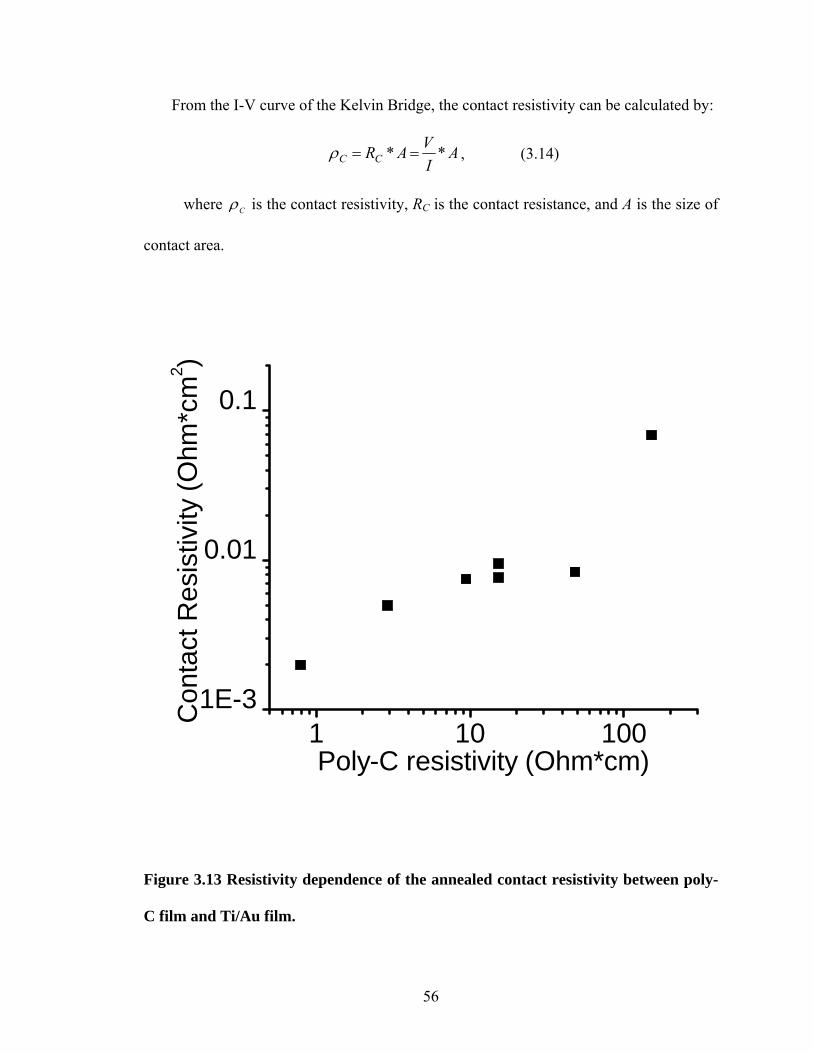
56
From the I-V curve of the Kelvin Bridge, the contact resistivity can be calculated by:
AIVARCC ** ==ρ , (3.14)
where Cρ is the contact resistivity, RC is the contact resistance, and A is the size of
contact area.
1 10 1001E-3
0.01
0.1
Con
tact
Res
istiv
ity (O
hm*c
m2 )
Poly-C resistivity (Ohm*cm)
Figure 3.13 Resistivity dependence of the annealed contact resistivity between poly-
C film and Ti/Au film.
57
The contact resistivity between poly-C (2 µm) and Ti/Au (300/2000 Å) was studied
by using poly-C samples with different doping levels. All samples are seeded with DPR
method and grown at 750 ºC. After the Kelvin Bridges are formed, the samples were
annealed at 600 ºC for 20 minutes in vacuum. Figure 3.13 shows the resistivity
dependence of the annealed contact resistivity between poly-C film and Ti/Au film.
3.6 Patterning
The dry etching of poly-C film was carried out in an ECR MPCVD chamber and
the plasma was generated by a 2.45 GHz, 1.5 KW (ASTeXTM) microwave power supply.
The outside magnetic bar array will make the electrons resonate in cyclotron shape to
increase the uniformity of the plasma. The inner diameter of the quartz dome is 13 inch
and the etching is uniform compare to the diamond deposition system. Coupled by two
capacitors and the matching network, the RF power will generate negative bias on the
substrate of etching sample holder, which is critical to the etching rate. The diamond will
not be etched without the bias. The RF power is about 50 - 100 W and the generated
negative bias is in the range of -50 V to -150 V. The O2, SF6 and Ar [63], with a flow
ratio of 28/2/2, were used as the reactive ion source for etching using a pressure in the
range of 4 - 8 militorr. With a rotary pump and turbo-molecular pump, the achievable
base vacuum is approximately 10-7 torr.
58
The positively ionized oxygen atoms are the main source for etching the diamond
atoms (sp3 carbon atomic bonding) under the negative substrate bias. The small amount
of SF6 and Ar will increase the uniformity of the etching process. Since alumina is very
stable and resistive compound, the oxygen plasma won’t etch Al much. So Al (there will
be a thin oxide layer on top of it in atmosphere) is the ideal mask for etching diamond,
which only have an etching rate about 1/13 of the etching rate of diamond [67].
A typical etch rate for poly-C is 50 -120 nm/min with a variation of less than 7%
over the 4 inch area of the wafer. Figure 3.14 shows SEM images of two poly-C
structures prepared by the ECR plasma etching. The first SEM shows a finger structure
with 1 µm thickness and 2 µm minimum feature size. The second SEM shows an intra-
grain p-type piezoresistor fabricated on an electrically-insulating 300-μm-thick large-
grain free-standing poly-C plate.
Sometimes the dry etching of poly-C can cause aluminum sputtering over some
areas of the diamond surface, especially for a long time etching which will cause
prominent heating of substrate. When this happens, the plasma can not attack the
diamond under the sputtered aluminum. As a result, one might end up getting “spikes”
around the patterned structure after the dry etching of diamond is completed in the rest of
the sample. This is called the grass effect as we can see from the Figure 3.14b. We had to
go through a more vigorous rinsing and clean process in order to eliminate those diamond
spikes from the sample [90].

59
a)
b)
Figure 3.14 SEM images of poly-C structures prepared by the ECR plasma etch: a)
the free standing poly-C finger structure and, b) single grain piezoresistor on large
grain poly-C plate.
60
3.7 Summary
In this chapter, several newly developed technologies were reported for the sensor
applications of poly-C film. The first time reported DPLW spin seeding method yielded
high density (2x10¹⁰/cm2), non-destructive and repeatable diamond seeding on 4 inch Si
wafer with dielectric surface. The Poly-C growth on 4 inch wafer was achieved in our
MPCVD system with less than 25% thickness variation using 2.8 kW microwave power
and 43 torr pressure. The poly-C surface conductivity, which was caused by the surface
hydrogenation, was quantitatively studied. The calculation shows that the surface
conductivity is about 0.825/Ω*cm and is independent to the doping level of poly-C film.
61
Chapter 4
Testing of Poly-C Piezoresistivity
4.1 Introduction
As shown in literature review, high piezoresistive effect of poly-C shows a
promising application as piezoresistive sensor. However, the reported piezoresistive
gauge factor of the poly-C films was in the range of 5 to 1000 with large variations.
Normally, those high GF values in the prior studies were achieved from films with
resistivities over 100 Ω*cm, which are impractical for sensor application due to the high
film resistances leading to high noise levels.
In this chapter, a cantilever beam method was used to study the piezoresistivity of
poly-C films. Poly-C thin films, with thicknesses about 2 µm and with different
resistivities, will be fabricated and tested to explore how the film properties affect the
piezoresistive GF. Two seeding method, DPLW and DPR, will be used to study the
relation between the GF and the film grain size.
4.2 The Cantilever Beam Method
For measuring the poly-C piezoresistive effect, it is necessary to apply longitudinal
mechanical strain to the piezoresistors. In order to apply this strain and measure the
62
resistance change, a testing stage for cantilever beam method was build as shown in
Figure 4.1. The silicon wafer, where the poly-C piezoresistor was grown, was diced into a
cantilever beam with a dimension about 60x10x0.5 mm3. As shown in Figure 4.1, the
cantilever beam was clamped between two metal plates and was fixed on the stage from
one end using four screws. The mechanical strain was applied on the beam by bending
the other end of the beam using a linear positioner. The bending of the beam was
measured using a movement gauge with a minimum scale of 0.001 inch. The resistor was
electrically connected to the testing instruments using wire bonding.
Figure 4.1 Piezoresistive testing stage using cantilever beam method.

63
b
l
ah
piezoresistor force
beamδ
Figure 4.2 Schematic diagram of the cantilever beam method used for piezoresistive
measurement.
The schematic of the cantilever beam testing setup is shown in Figure 4.2 with all
the parameters labeled in the figure. The piezoresistive sensor was fabricated on an
oxidized silicon wafer for electrical insulation purpose. Since the thickness of the poly-C
thin film resistor (normally less than 2 µm) is much smaller as compared with the
thickness of Si beam, h (normally 500-525µm), the strain of poly-C film, ε, is
approximately equal to the strain on the surface of cantilever beam. Bending the free end
of the beam through a distance of δ, the longitudinal strain of the poly-C film, ε, can be
calculated using the parameters h, l, a and b as shown in the Figure 4.2 [76, 90],
64
( ) δε ⎥⎦⎤
⎢⎣⎡ +−=
223
3bal
lh
. (4.1)
The strain calculated using Eq. 4.1 was verified by attaching a commercial metal
strain gauge on the beam and showed an error of less than 5%. The gauge factor of the
poly-C can be expressed as
( )( )
⎥⎦⎤
⎢⎣⎡ +−
−=⋅
−=
23
21
0
30
0
0
balhR
lRRR
RRGFδε , (4.2)
where R is the resistance with strain ε and R0 is the resistance at zero strain.
4.3 Sample Preparation
Poly-C films were prepared on the silicon cantilever beam using the technology
mentioned in Chapter 3. The silicon beam has a thin layer of SiO2 for electrical
insulation. Two different spin seeding methods, DPLW [57] and DPR [91], were used to
grow films with different morphologies result from different seeding densities. DPLW or
DPR was spin coated on the samples with a typical spin speed of 3000 rpm. Table 4.1
compares the two seeding methods in preparation conditions, seeding density and grown
film morphology.
65
Table 4.1 Comparison of DPLW and DPR seeding methods.
Seeding Method DPLW DPR
Mean diamond powder size (nm) 25 50
Carrier fluid Water Photoresist
Density (carats/liter) 40 12
Seeding density (cm-2) 1010 108 Ave. grain size (µm)
(film thickness is 2 µm) 0.3 0.8
Surface roughness (RMS) (nm) 30 46
Figure 4.3 shows, for both the DPLW and DPR methods, the SEM pictures before
and after the growth of poly-C films with thickness of 2 µm. The affect of seeding on the
piezoresistivity will be discussed late in section 4.4.
After the seeding procedure, the sample wafers were grown at temperature of 700
ºC with CH4/H2 flow rate of 1/100 sccm. The film thickness is about 2 µm with a growth
rate about 0.15 µm/hr. Trimethylboron was introduced during the growth for in-situ
boron doping and achieved resistivities from 0.05 Ω*cm to 70 Ω*cm. Samples were dry
etched and then coated with E-beam evaporated Ti/Au (300/2000 Å) film. After the
metallization, the samples were annealed at 600 ºC in vacuum (10-5 torr) for 30 minutes.
For studying the piezoresistivity, a mask set with two masks was designed for poly-C
layer and contact metal layer as shown in Figure 4.4. Different resistor sizes were
designed with length/width ratio from 500/20 µm to 50/200 µm. Two kind of metal
contacts, 4-contact and 2-contact, were used for the electrical connection. The 4-contact
method was used to avoid the affect of the sensor resistance by the contact resistance.
Testing structures such as contact chains, Kelvin Bridges and resistivity study were
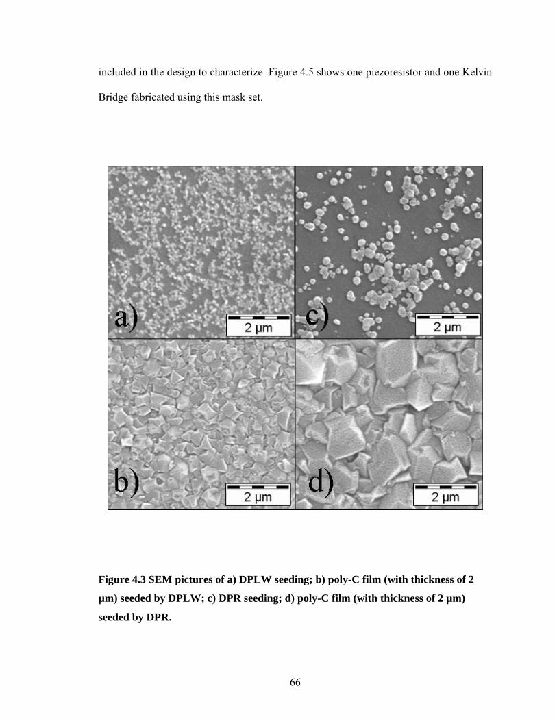
66
included in the design to characterize. Figure 4.5 shows one piezoresistor and one Kelvin
Bridge fabricated using this mask set.
Figure 4.3 SEM pictures of a) DPLW seeding; b) poly-C film (with thickness of 2
µm) seeded by DPLW; c) DPR seeding; d) poly-C film (with thickness of 2 µm)
seeded by DPR.
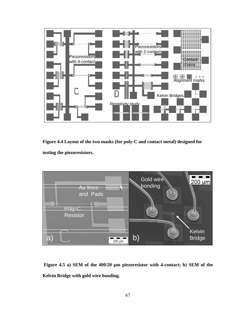
67
Piezoresistors with 4-contact
Piezoresistors with 2-contact
Contact chains
Alignment marks
Kelvin Bridges
Resistivity study
Piezoresistors with 4-contact
Piezoresistors with 2-contact
Contact chains
Alignment marks
Kelvin Bridges
Resistivity study
Figure 4.4 Layout of the two masks (for poly-C and contact metal) designed for
testing the piezoresistors.
Poly-C Resistor
Au lines and Pads
Gold wire bonding
Kelvin Bridgea) b)
Poly-C Resistor
Au lines and Pads
Gold wire bonding
Kelvin Bridgea) b)
Figure 4.5 a) SEM of the 400/20 µm piezoresistor with 4-contact; b) SEM of the
Kelvin Bridge with gold wire bonding.
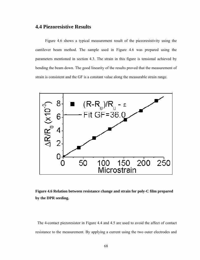
68
4.4 Piezoresistive Results
Figure 4.6 shows a typical measurement result of the piezoresistivity using the
cantilever beam method. The sample used in Figure 4.6 was prepared using the
parameters mentioned in section 4.3. The strain in this figure is tensional achieved by
bending the beam down. The good linearity of the results proved that the measurement of
strain is consistent and the GF is a constant value along the measurable strain range.
Figure 4.6 Relation between resistance change and strain for poly-C film prepared
by the DPR seeding.
The 4-contact piezoresistor in Figure 4.4 and 4.5 are used to avoid the affect of contact
resistance to the measurement. By applying a current using the two outer electrodes and
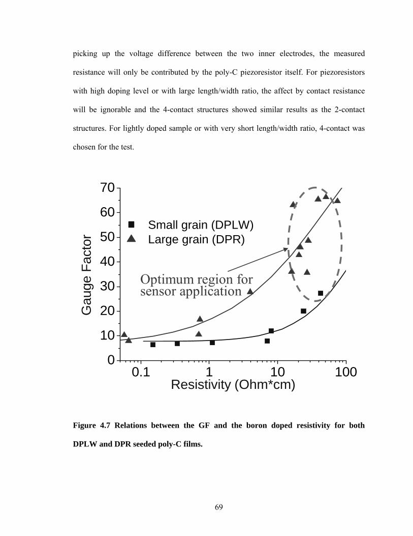
69
picking up the voltage difference between the two inner electrodes, the measured
resistance will only be contributed by the poly-C piezoresistor itself. For piezoresistors
with high doping level or with large length/width ratio, the affect by contact resistance
will be ignorable and the 4-contact structures showed similar results as the 2-contact
structures. For lightly doped sample or with very short length/width ratio, 4-contact was
chosen for the test.
0.1 1 10 1000
10
20
30
40
50
60
70
Small grain (DPLW) Large grain (DPR)
Gau
ge F
acto
r
Resistivity (Ohm*cm)
Optimum region for sensor application
0.1 1 10 1000
10
20
30
40
50
60
70
Small grain (DPLW) Large grain (DPR)
Gau
ge F
acto
r
Resistivity (Ohm*cm)
Optimum region for sensor application
Figure 4.7 Relations between the GF and the boron doped resistivity for both
DPLW and DPR seeded poly-C films.

70
To study the GF dependence on the film properties, a set of samples were prepared
with different doping resistivity varies from 0.05 to 100 Ω*cm. They are either seed by
DPLW or by DPR as mentioned in section 4.2. But all the samples were grown at 700 ºC
with film thicknesses about 2 µm. Figure 4.7 shows the measured GF results for all these
samples [92]. Discussion of the GF dependence is presented in the next section.
4.5 GF Dependence on the Film Properties
The dependence of GF on poly-C film resistivity is shown in Figure 4.7 for both
DPR and DPLW seeded films with thicknesses about 2 µm. The results show that, for
films with resistivity less than 1 Ω*cm, the GF values are around 6-15 and do not change
much with the resistivity and grain size. However, the GF increases substantially with
resistivity for films with large grain size (grain size of 0.8 µm by DPR seeding) and with
resistivities higher than 1 Ω*cm. The GF increases substantially for film with small grain
size (0.3 µm, DPLW seeding) if the film resistivity is higher than 10 Ω*cm.
For the same resistivity higher than 1 Ω*cm, the film with large grain size (0.8 µm
by DPR seeding) gives a GF about 2-3 times higher than that of film with small grain
sizes. This result is consistent with the reported GF of 283 from free standing diamond
sample with grains in 50 µm range [8]. The high GF values found in large grain films are
believed to be related to high sp3/sp2 ratios caused by lower densities of grain boundaries.
It is also known that high resistivity will cause large thermal noise and high contact
resistance [93], which will hinder the sensor application of poly-C films. By
comprehensively considering the GF, film thickness, roughness, resistivity and contact
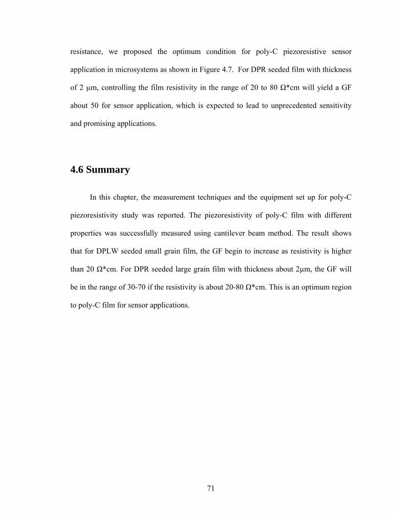
71
resistance, we proposed the optimum condition for poly-C piezoresistive sensor
application in microsystems as shown in Figure 4.7. For DPR seeded film with thickness
of 2 µm, controlling the film resistivity in the range of 20 to 80 Ω*cm will yield a GF
about 50 for sensor application, which is expected to lead to unprecedented sensitivity
and promising applications.
4.6 Summary
In this chapter, the measurement techniques and the equipment set up for poly-C
piezoresistivity study was reported. The piezoresistivity of poly-C film with different
properties was successfully measured using cantilever beam method. The result shows
that for DPLW seeded small grain film, the GF begin to increase as resistivity is higher
than 20 Ω*cm. For DPR seeded large grain film with thickness about 2µm, the GF will
be in the range of 30-70 if the resistivity is about 20-80 Ω*cm. This is an optimum region
to poly-C film for sensor applications.
72
Chapter 5
Poly-C Sensor for 2nd Generation Cochlear Probe
5.1 Introduction
Because of its high piezoresistive sensitivity, poly-C film was chosen as the
position sensor material for the cochlear implant probe for the WIMS center. The first
generation of the silicon thin film cochlear probe was reported by Dr. Wise’s group at
University of Michigan without the position sensors [84].
This chapter will report the first attempt of integrating the poly-C piezoresistive
sensors into the 2nd generation cochlear probe [94]. The design, fabrication and testing of
the probe with poly-C sensors will be discussed in detail.
5.2 Design and Fabrication of the Probe
5.2.1 Technology for Poly-C Process Integration
Integration is one of the important issues which limited the development and
application of poly-C thin film sensors because of the special seeding and deposition
requirements [95, 96]. A common procedure in integrated circuits (IC) process is
insulating the active layer (poly-Si or metals) with dielectric layers (like SiO2) both above
73
and below it, and making electrical connections through the contact holes [97]. Based on
the design of poly-C piezoresistive position sensors [98], we developed a poly-C thin film
fabrication process to integrate the poly-C technology into standard IC fabrication
process as shown in Figure 5.1.
DPLW or DPR spin seeding
Grow thin SiO2
Si substrate
Grow poly-C
Pattern Al as mask
Dry etch poly-C and remove mask
Coat SiO2 and open contacts
pattern metal as interconnection
DPLW or DPR spin seeding
Grow thin SiO2
Si substrate
Grow poly-C
Pattern Al as mask
Dry etch poly-C and remove mask
Coat SiO2 and open contacts
pattern metal as interconnection
Figure 5.1 Process flow for integrating poly-C sensor into Si-based microsystems.
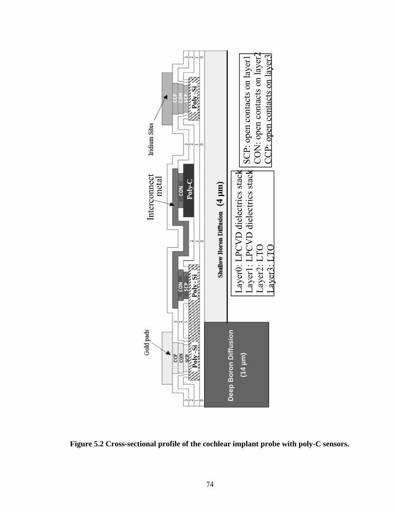
74
Poly-
C
Inte
rcon
nect
Poly-S
iPo
ly-Si
met
al
Poly-
C
Inte
rcon
nect
Poly
-Si
met
al
Poly
Si -Po
lySi -
Dee
p B
oron
Diff
usio
n
(14
µm)
(4 µ
m)
Laye
r0: L
PCV
D d
iele
ctric
s sta
ckLa
yer1
: LPC
VD
die
lect
rics s
tack
Laye
r2: L
TOLa
yer3
: LTO
Laye
r0: L
PCV
D d
iele
ctric
s sta
ckLa
yer1
: LPC
VD
die
lect
rics s
tack
Laye
r2: L
TOLa
yer3
: LTO
SCP:
ope
n co
ntac
ts o
n la
yer1
CO
N: o
pen
cont
acts
on
laye
r2C
CP:
ope
n co
ntac
ts o
n la
yer3
SCP:
ope
n co
ntac
ts o
n la
yer1
CO
N: o
pen
cont
acts
on
laye
r2C
CP:
ope
n co
ntac
ts o
n la
yer3
Poly-
C
Inte
rcon
nect
Poly-S
iPo
ly-Si
met
al
Poly-
C
Inte
rcon
nect
Poly
-Si
met
al
Poly
Si -Po
lySi -
Dee
p B
oron
Diff
usio
n
(14
µm)
(4 µ
m)
Laye
r0: L
PCV
D d
iele
ctric
s sta
ckLa
yer1
: LPC
VD
die
lect
rics s
tack
Laye
r2: L
TOLa
yer3
: LTO
Laye
r0: L
PCV
D d
iele
ctric
s sta
ckLa
yer1
: LPC
VD
die
lect
rics s
tack
Laye
r2: L
TOLa
yer3
: LTO
SCP:
ope
n co
ntac
ts o
n la
yer1
CO
N: o
pen
cont
acts
on
laye
r2C
CP:
ope
n co
ntac
ts o
n la
yer3
SCP:
ope
n co
ntac
ts o
n la
yer1
CO
N: o
pen
cont
acts
on
laye
r2C
CP:
ope
n co
ntac
ts o
n la
yer3
CON
SCP
CON
CCP
CON
SCP
Poly-
C
Inte
rcon
nect
Poly-S
iPo
ly-Si
met
al
Poly-
C
Inte
rcon
nect
Poly
-Si
met
al
Poly
Si -Po
lySi -
Dee
p B
oron
Diff
usio
n
(14
µm)
(4 µ
m)
Laye
r0: L
PCV
D d
iele
ctric
s sta
ckLa
yer1
: LPC
VD
die
lect
rics s
tack
Laye
r2: L
TOLa
yer3
: LTO
Laye
r0: L
PCV
D d
iele
ctric
s sta
ckLa
yer1
: LPC
VD
die
lect
rics s
tack
Laye
r2: L
TOLa
yer3
: LTO
SCP:
ope
n co
ntac
ts o
n la
yer1
CO
N: o
pen
cont
acts
on
laye
r2C
CP:
ope
n co
ntac
ts o
n la
yer3
SCP:
ope
n co
ntac
ts o
n la
yer1
CO
N: o
pen
cont
acts
on
laye
r2C
CP:
ope
n co
ntac
ts o
n la
yer3
Poly-
C
Inte
rcon
nect
Poly-S
iPo
ly-Si
met
al
Poly-
C
Inte
rcon
nect
Poly
-Si
met
al
Poly
Si -Po
lySi -
Dee
p B
oron
Diff
usio
n
(14
µm)
(4 µ
m)
Laye
r0: L
PCV
D d
iele
ctric
s sta
ckLa
yer1
: LPC
VD
die
lect
rics s
tack
Laye
r2: L
TOLa
yer3
: LTO
Laye
r0: L
PCV
D d
iele
ctric
s sta
ckLa
yer1
: LPC
VD
die
lect
rics s
tack
Laye
r2: L
TOLa
yer3
: LTO
SCP:
ope
n co
ntac
ts o
n la
yer1
CO
N: o
pen
cont
acts
on
laye
r2C
CP:
ope
n co
ntac
ts o
n la
yer3
SCP:
ope
n co
ntac
ts o
n la
yer1
CO
N: o
pen
cont
acts
on
laye
r2C
CP:
ope
n co
ntac
ts o
n la
yer3
CON
SCP
CON
CCP
CON
SCP
Figure 5.2 Cross-sectional profile of the cochlear implant probe with poly-C sensors.
75
The poly-C thin film will be seeded by DPLW or DPR and grown by MPCVD.
Patterned metal mask will be used to pattern the poly-C film by dry etch. The poly-C
deposition temperature can be varied between 400 ºC to 900 ºC depending on the
materials used underneath the poly-C. The process insulates the micron-scale continuous
poly-C films with dielectric layers both above and below it, and makes electrical
connections through the contact holes such as those found in common IC processes. This
method can protect the underneath materials during the diamond deposition and dry
etching steps. This process ensures the compatibility of poly-C film with the typical IC or
MEMS procedure and broadens the possible applications of poly-C thin films.
5.2.2 Design of the 2nd Generation Probe
The basic concept of the silicon thin film cochlear implant probe has been addressed
in section 2.5. In the design of the 2nd generation probe, both poly-Si and poly-C were
chosen as the position sensors for comparison. The design of the probe was mainly done
by Jianbai Wang based on previous experience from Dr. Wise’s group [83]. We
collaborated to integrate the poly-C sensor into the design by adding one more mask for
poly-C patterning. Figure 5.2 shows the detailed cross-sectional profile of the cochlear
probe with poly-C sensors. Both highly doped poly-Si and Ti/TiN/Al metal stack is used
as the interconnect lines. The iridium and gold are used as the stimulating sites and the
pad metal, respectively.
76
The length and width of the thin film probes are about 16 and 1.2 mm, respectively.
Adding the boron diffusion and top dielectrics, the thickness of the probe backend and
shank are about 16 µm and 6 µm, respectively. On each probe, there are eight straight
poly-C position sensors uniformly distributed along the shank of the probe and one
identical poly-C reference sensor located on the backend of the probe. The reference
sensor is connected with each of the position sensor in tandem to form half Wheatstone
bridges for testing the resistance change of position sensor [83]. The reference sensor has
the same dimension as the position sensor but will not be bent while the probe is bent
during the insertion. There are also one “U” shape tip sensor on the tip of the probe and
one identical reference sensor on the backend to detect the deformation of probe tip. For
comparison, the poly-C sensors have the same dimension as the poly-Si sensors. The
length/width for the straight position sensor and the tip sensor are 450/18 µm and
1000/18 µm, respectively. There are also some square wave shape side wall sensors and
corresponding reference sensor designed on some of the testing probes.
5.2.3 Fabrication of the 2nd Generation Probe
Figure 5.2 depicts all the layers created in the fabrication process. The fabrication
began with two boron etch-stop diffusions to define the profile of the probe. The thinner
probe shank (shallow boron diffusion, 4μm) is typically inserted into the cochlea, while
the thicker (shallow and deep boron diffusion, 14μm) backend remains outside to support
the electrical connections. A stress-compensated dielectric stack of SiO2/Si3N4/SiO2
(200/100/100 nm) was deposited by low-pressure chemical vapor deposition (LPCVD).
The conducting leads were defined using ion implanted poly-Si (600 nm) [84]. Another
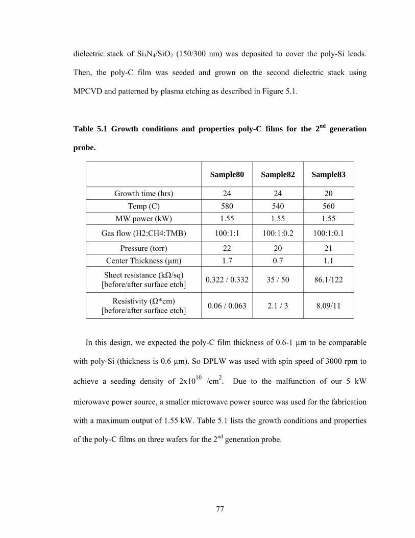
77
dielectric stack of Si3N4/SiO2 (150/300 nm) was deposited to cover the poly-Si leads.
Then, the poly-C film was seeded and grown on the second dielectric stack using
MPCVD and patterned by plasma etching as described in Figure 5.1.
Table 5.1 Growth conditions and properties poly-C films for the 2nd generation
probe.
Sample80 Sample82 Sample83
Growth time (hrs) 24 24 20 Temp (C) 580 540 560
MW power (kW) 1.55 1.55 1.55
Gas flow (H2:CH4:TMB) 100:1:1 100:1:0.2 100:1:0.1
Pressure (torr) 22 20 21 Center Thickness (µm) 1.7 0.7 1.1
Sheet resistance (kΩ/sq) [before/after surface etch] 0.322 / 0.332 35 / 50 86.1/122
Resistivity (Ω*cm) [before/after surface etch] 0.06 / 0.063 2.1 / 3 8.09/11
In this design, we expected the poly-C film thickness of 0.6-1 µm to be comparable
with poly-Si (thickness is 0.6 µm). So DPLW was used with spin speed of 3000 rpm to
achieve a seeding density of 2x10¹⁰ /cm2. Due to the malfunction of our 5 kW
microwave power source, a smaller microwave power source was used for the fabrication
with a maximum output of 1.55 kW. Table 5.1 lists the growth conditions and properties
of the poly-C films on three wafers for the 2nd generation probe.

78
Sample 83Sample 83
Figure 5.3 Thickness distribution of poly-C film on the 4 inch wafers.
Due to the ball shape of microwave plasma, the heating of wafer is not uniform. The
center temperature is higher than the edge temperature, which causes the diamond
deposition is not uniform on the 4 inch wafer. Because of the low microwave power, low

79
gas pressure is needed to match the power for better thickness uniformity. The poly-C
film thickness distributions were monitored and shown in Figure 5.3. On the 4 inch
wafers, the poly-C growths were mainly happened within the 2 inch areas and the films
are not continuous on the edge areas. After the growth, all films were treated with surface
etch (dry etch 30 second) to remove the surface conductive layer. The sheet resistances in
Table 5.1 were all measured from the center of wafer suing 4-probe method.
After the growth, the poly-C films were patterned into position sensors using dry
etch as described before. The poly-C sensors were then covered with low temperature
oxide (LTO) before a metal stack of Ti/TiN/Al was sputtered and patterned by a lift-off
process as interconnect between poly-C and poly-Si through contact holes. Iridium over
titanium is sputtered and patterned by lift-off to define the stimulating sites. Gold
bonding pads are formed on the back-end of probes in a similar manner. After this, the
dielectric stack, include all the oxide and nitride layers, was patterned into the shape of
probes. After finishing all the process steps on front side, the wafer was thinned from 500
µm to about 200 µm using HNA etch (HF:HNO3:Acetic acid=1:3:8). Then the thinned
wafer was etched using ethylene-diamine-pyrocatechol (EDP) etchant. With the boron
diffused etch stop, the probes were released in EDP and cleaned for future test.

80
Figure 5.4 Released 2nd generation cochlear implant probe with poly-C position
sensors.

81
Most of the process steps were done at Michigan Nanofabrication Facility (MNF)
at University of Michigan by Jianbai Wang and the technicians. The diamond seeding,
growth and patterning were finished at MSU lab. Due to the fabrication loss, only one
wafer (sample 82) was released at last. Figure 5.4 shows one of the released cochlear
probes from sample 82 with close-view of the different structures on the probe.
5.3 Testing of the 2nd Generation Probe
A testchip was fabricated on the same wafer with the implant probes to characterize
the properties and interaction of all films used in the probe. Figure 5.5 shows the testchip
used for film characterization and those labeled structures are all used for poly-C film
characterization.
Using the 4-contact resistors on the testchip, we measured the sheet resistances of the
poly-C resistors and found there are about 1-2.5 MΩ/sq, which is about 20-50 times
higher than the value measured from the wafer center before we patterned it. It was
believed that the discontinuity of poly-C film caused this resistance increase. Since this
designed is shared with other testing probe, we only had limited amount of poly-C probes
and most of the poly-C probes and testchips are located on the outer area of the 4 inch
wafer. The small microwave powder led to very little poly-C growth on the outer area, as
it can be seen from Figure 5.3, and caused this resistance increase.

82
Contact chain
Line width
TCR
Transmission lines
Kelvin bridges
Cross talk
Step coverage
Contact chain
Line width
TCR
Transmission lines
Kelvin bridges
Cross talk
Step coverage
Figure 5.5 Testchip on the 2nd generation probe wafer for process characterization.
The contact resistivity between poly-C and Ti/TiN/Al interconnect metal stack is
approximately 0.2 Ω*cm2. The dry etching of poly-C produced a minimum feature size
of 2 µm and showed reliable step coverage between 2 µm wide poly-C and metal layers.
The resistance of dielectric layers was more than 109 Ω ensuring an excellent insulation
for the poly-C films.
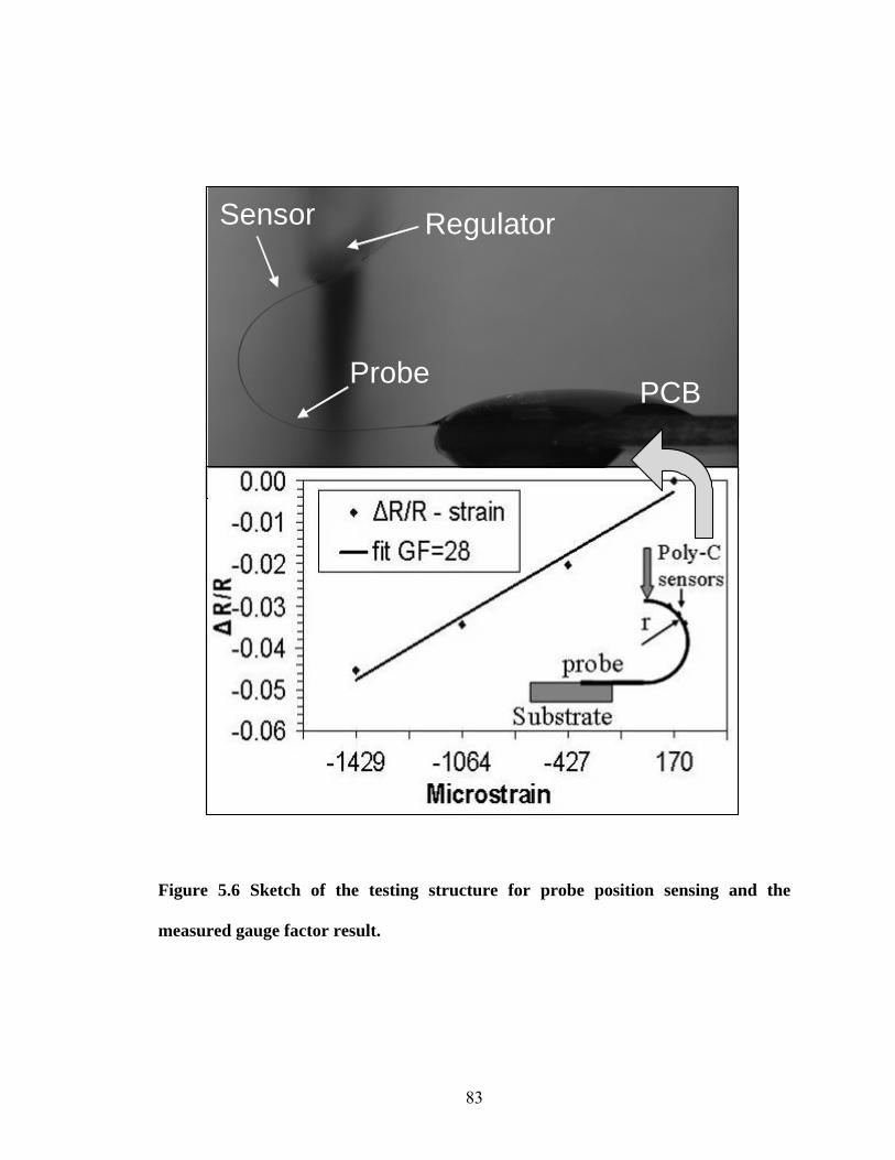
83
PCBProbe
Sensor Regulator
PCBProbe
Sensor Regulator
Figure 5.6 Sketch of the testing structure for probe position sensing and the
measured gauge factor result.
84
For measuring the GF of poly-C position sensors integrated on the cochlear probe, the
probe backend was glued on a printed circuit board (PCB) substrate and electrically
connected by gold wire bonding. Then the probe was bent to different curvatures using a
regulator as shown in Figure 5.6. The curvature was recorded using digital camera and
the corresponding radius was extracted from the stored image using geometric method.
For approximation, the probe can be treated approximately as a uniform beam with a
length of 1.6 cm and a thickness of 6 µm. The stain on poly-C sensor, ε, can be calculated
by:
ρρε
22/ hh==
, (5.1)
where h is the probe thickness and ρ is the radius of curvature. The GF was then
calculated using,
RhRRRRRGF ρ
ε)(2/)( 00 −
=−
=. (5.2)
A GF of 28 was achieved for a poly-C sensor on the cochlear probe as shown in
Figure 5.7. It’s higher than the GF of poly-Si.
5.4 Summary
A Si based thin film cochlear implant probe with poly-C piezoresistive position
sensors was designed and fabricated successfully. The optimized poly-C processes, with
seeding, growth, doping and etching, demonstrated a feasible integration with the bulk-
silicon based micro-fabrication technology although the power limitation caused the
85
discontinuity of poly-C film. A GF of 28 was achieved for one of the probe, which is
higher than the GF of poly-Si (12-18) position sensors fabricated in the same batch [83].
During the fabrication of the 2nd generation cochlear probe, we have not done
systematical study on the relation between GF and film properties. Further work will be
presented to improve the technology and process for better integration and high
sensitivity as we will see in the next chapter.
86
Chapter 6
Poly-C Sensor for 3rd Generation Cochlear Probe
6.1 Introduction
The 2nd generation poly-C probe showed a good startup and promising future for
the application of poly-C thin film although there are several issues that need to be
addressed. The major problem was the low microwave power, which led to discontinuity
of the poly-C film, as descried in Chapter 5. This increased the total resistance of the
piezoresistor to a value of 20-60 MΩ, which is difficult for the measuring system. Based
on the testing of the 2nd generation probe, a new design of poly-C sensor with the
cochlear probe is reported in this chapter as the 3rd generation probe.
6.2 Design of the 3rd Generation Probe
The design of the new probe is an upgrade from the 2nd generation probe with many
new improvements. The cross-sectional view of the 3rd generation probe is shown in
Figure 6.1. Table 6.1 summarized the problems existed in the 2nd generation probe and
proposed the solutions for those problems. As shown in Figure 3.9, high power and high
pressure, 2.8 kW and 43 torr, were used to achieve uniform growth on 4 inch wafer. As
discussed in chapter 4, to improve the piezoresistive sensitivity, large grain size and low
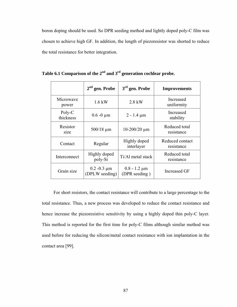
87
boron doping should be used. So DPR seeding method and lightly doped poly-C film was
chosen to achieve high GF. In addition, the length of piezoresistor was shorted to reduce
the total resistance for better integration.
Table 6.1 Comparison of the 2nd and 3rd generation cochlear probe.
2nd gen. Probe 3rd gen. Probe Improvements
Microwave power 1.6 kW 2.8 kW Increased
uniformity
Poly-C thickness 0.6 -0 µm 2 - 1.4 µm Increased
stability
Resistor size 500/18 µm 10-200/20 µm Reduced total
resistance
Contact Regular Highly doped interlayer
Reduced contact resistance
Interconnect Highly doped poly-Si Ti/Al metal stack Reduced total
resistance
Grain size 0.2 -0.3 µm (DPLW seeding)
0.8 - 1.2 µm (DPR seeding ) Increased GF
For short resistors, the contact resistance will contribute to a large percentage to the
total resistance. Thus, a new process was developed to reduce the contact resistance and
hence increase the piezoresistive sensitivity by using a highly doped thin poly-C layer.
This method is reported for the first time for poly-C films although similar method was
used before for reducing the silicon/metal contact resistance with ion implantation in the
contact area [99].

88
Laye
r0: L
PCV
D d
iele
ctric
s st
ack
La
yer1
: PEC
VD
oxi
de (a
bove
pol
y-C
) La
yer2
: PEC
VD
oxi
de (a
bove
met
al1)
Dee
p bo
ron
diff
usio
n fo
r bac
kend
Shal
low
bor
on d
iffus
ion
2 10
Hig
hly
dope
d po
ly-C
Inte
rcon
nect
met
alG
old
pad
Irid
ium
site
Ligh
tly d
oped
pol
y-C
Inte
rcon
nect
met
al
Figure 6.1 Cross-sectional view the 3rd generation cochlear probe with poly-C
piezoresistive position sensors.

89
Another difference between the 2nd and 3rd generation probes is that PECVD oxide
was used as the passivation layer in the new design due to the process availability,
although the previously used LTO has higher quality and coverage.
The mask design of the 3rd generation probe was done in collaboration with Jianbai
Wang. Table 6.2 listed all the masks used for the new design with poly-C sensors. The
first 6 masks in Table 6.2 were designed by Jianbai and shared by Jianbai (with poly-Si
sensors) and me (with poly-C sensors). I designed the last 4 masks in Table 6.2 to realize
the poly-C sensors on the probe.
Table 6.2 Masks used for the 3rd generation cochlear probe with poly-C sensors.
gds# Mask name Description
1 BDF: deep boron diffusion, define the probe backend
2 DEL: dielectrics pattering, define the probe profile
5 SHB: shallow boron diffusion, define the probe shank
6 GOL: sputtered gold pads
7 CON: Contact hole to metal1
8 IRD: Iridium stimulating site
21 DIA: poly-C sensor
23 HDC: Heavily doped poly-C for contact
24 PCC: Contact hole to poly-C
25 DCO2: metal1 for diamond sensor
For the design of the poly-C sensors using 4 masks, different dimensions were used for
the poly-C position sensors. The width of the sensors was 20 µm and the length was
designed as 5/10/20/50/200 µm for different probes.

90
6.3 Fabrication of the Probe
The detail fabrication processes of the 3rd generation cochlear probe with poly-C
position sensors are shown in Figure 6.2. The process is similar to that of 2nd generation
probe except those differences mentioned in previous section. The first three steps (deep
boron diffusion, shallow boron diffusion and dielectric deposition) were done by the
technicians of Michigan Nanofabrication Facility (MNF) and I finished all the remaining
steps at MNF except the poly-C growth and etching steps which were accomplished at
MSU. The detail process steps are listed in the appendix.
Mask involved
DielectricsDeposition
Mask involved
DielectricsDeposition
Deep Borondiffusion
(BDF)
Shallow BoronDiffusion(SHB)
LPCVD Dielectric0
Poly-C growth
and etch(DIA)
LTO deposition 1
Poly-C heavily doped for contact
(HDC)
Contact to Poly-C(PCC)
Metal1 Depositionand Lift -off
(DCO1)
LTO-2 patterning
(CON)
Iridium Sites(IRD)
Gold Pads(GOL)
LPCVD-0patterning
(DEL)
Backside dielectric etch
HNA wafer thinning
EDP release
LTO deposition 2
Deep Borondiffusion
(BDF)
Shallow BoronDiffusion(SHB)
LPCVD Dielectric 0
Poly-C growthEtch contact interlayer
(HDC)
PECVD Oxide 1
Etch poly-C piezoresistor
(DIA)
Contact to Poly-C(PCC)
Pattern Metal1 for interconnect
(DCO1)
Contact to metal1
(CON)
Iridium Sites(IRD)
Gold Pads(GOL)
LPCVD-0patterning
(DEL)
Backside dielectric etch
HNA wafer thinning
EDP / KOH release
PECVD Oxide 2
Mask involved
DielectricsDeposition
Mask involved
DielectricsDeposition
Deep Borondiffusion
(BDF)
Shallow BoronDiffusion(SHB)
LPCVD Dielectric0
Poly-C growth
and etch(DIA)
LTO deposition 1
Poly-C heavily doped for contact
(HDC)
Contact to Poly-C(PCC)
Metal1 Depositionand Lift -off
(DCO1)
LTO-2 patterning
(CON)
Iridium Sites(IRD)
Gold Pads(GOL)
LPCVD-0patterning
(DEL)
Backside dielectric etch
HNA wafer thinning
EDP release
LTO deposition 2
Deep Borondiffusion
(BDF)
Shallow BoronDiffusion(SHB)
LPCVD Dielectric 0
Poly-C growthEtch contact interlayer
(HDC)
PECVD Oxide 1
Etch poly-C piezoresistor
(DIA)
Contact to Poly-C(PCC)
Pattern Metal1 for interconnect
(DCO1)
Contact to metal1
(CON)
Iridium Sites(IRD)
Gold Pads(GOL)
LPCVD-0patterning
(DEL)
Backside dielectric etch
HNA wafer thinning
EDP / KOH release
PECVD Oxide 2
Figure 6.2 Process flow of the 3rd generation cochlear probe with poly-C
piezoresistive position sensor.
91
The lightly and highly doped poly-C film was grown on the dielectric stack by
PECVD with the parameters shown in Table 6.3. Dry etching of the poly-C films was
divided into two steps. The first step was used to define the contact areas by etching only
the highly doped top layer beyond the contact areas. The second step was patterning the
shape of the piezoresistors.
Table 6.3 Detail growth parameters of poly-C film.
Poly-C growth
H2/CH4 gas flow (sccm) 200/3
Trimethylboron doping (sccm) 0.2-2x10⁻³
Microwave power (kW) 2.8
Gas Pressure (torr) 43
Growth Temperature (ºC) 780
Film thickness (μm) : lightly/highly doped 1.5-2 / 0.1-0.3
Film resistivity (Ω*cm) : lightly/highly doped 25-150 / 0.01-0.05
To accurately control the etch depth, the sheet resistance of the poly-C film was
measured using a 4-probe station after every 30 second etch as shown in Figure 6.3. The
sheet resistance was calculated by measuring the voltage and current using the 4-probe
method as described by Eq. 3.1 and 3.2.

92
Highly doped poly-C
Lightly doped poly-CLightly doped poly-C
Etch Etch
Highly doped poly-C
Lightly doped poly-CLightly doped poly-C
Etch Etch
Figure 6.3 Change of the sheet resistance of poly-C film vs. the dry etch time.
93
As shown in Figure 6.3, after 4 minute etch, the resistance of poly-C film reach a
slow changing range which means the highly doped layer was totally removed. Measured
by a surface profilometer, the thicknesses of the lightly and highly doped layer are 0.2
and 1.8 μm, respectively. The etch rate is about 50 nm/min. So for the etched film, there
is only lightly doped layer with the resistivity, ρlignt, given by
cmcmsqktR lightetchedshlight ⋅Ω=××Ω=⋅= − 151108.1/840 4_ρ . (6.1)
For the film before etch, the conductivity is contributed from both highly and lightly
doped layers, but the contribution caused by the lightly doped layer is ignorable, so the
resistivity of highly doped layer, ρhigh equals
cmcmsqktR highunetchshhigh ⋅Ω=××Ω=⋅≈ − 0224.0102.0/12.1 4_ρ . (6.2)
So from the Eq. 6.1 and 6.2, the corresponding resistivities for lightly and highly
doped poly-C films are 0.0224 Ω*cm and 151 Ω*cm, respectively.
The poly-C sensors were then covered with 1μm PECVD SiO2 before Ti/TiN/Al
metal stack was sputtered and patterned as the interconnect lines for poly-C sensors.
Another PECVD oxide layer with thickness of 1μm was deposited to cover the metal
lines. The remaining steps were the same as those of 2nd generation probe (section 5.2.3).
Fig. 6.4 shows the detail views of the fabricated sample wafer and the cochlear probes
with poly-C position sensors.

94
Figure 6.4 Overview of the fabricated 3rd generation cochlear implant probe with
poly-C position sensors.
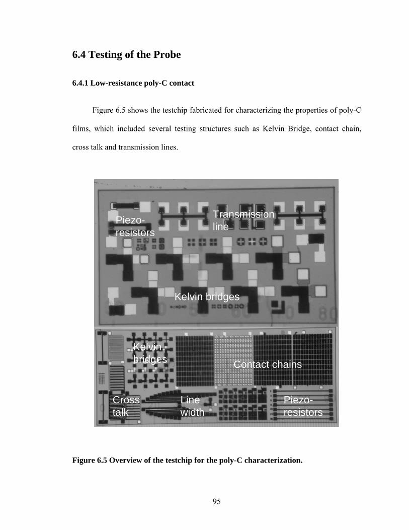
95
6.4 Testing of the Probe
6.4.1 Low-resistance poly-C contact
Figure 6.5 shows the testchip fabricated for characterizing the properties of poly-C
films, which included several testing structures such as Kelvin Bridge, contact chain,
cross talk and transmission lines.
Contact chains
Transmission line
Cross talk
Kelvin bridges
Line width
Piezo-resistors
Kelvin bridges
Piezo-resistors
Contact chains
Transmission line
Cross talk
Kelvin bridges
Line width
Piezo-resistors
Kelvin bridges
Piezo-resistors
Figure 6.5 Overview of the testchip for the poly-C characterization.

96
Kelvin Bridges with different contact sizes were used to test the contact resistance.
The contact size, equals the size of contact hole on SiO2, varies from 100, 400 to 1600
µm2.
Rc = (V1-V2)/I,
I
V2
Metal
Lightly doped poly-C
Highly doped poly-C
V1
I
ARCC *=ρA is size of contact area
Cross section
Highly doped poly-C
Metal
Lightly doped poly-C
Rc = (V1-V2)/I,
I
V2
Metal
Lightly doped poly-C
Highly doped poly-C
V1
I
ARCC *=ρA is size of contact area
Cross section
Highly doped poly-C
Metal
Lightly doped poly-C
Figure 6.6 Schematic of the Kelvin Bridge used for testing contact resistivity.
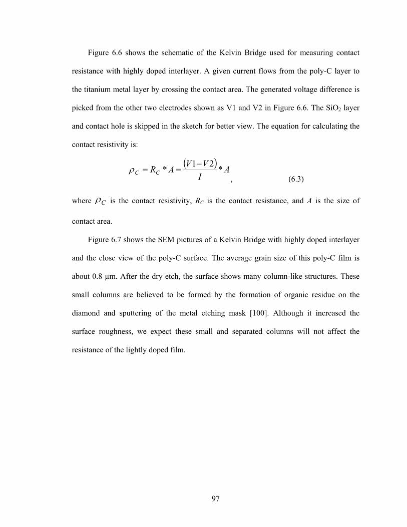
97
Figure 6.6 shows the schematic of the Kelvin Bridge used for measuring contact
resistance with highly doped interlayer. A given current flows from the poly-C layer to
the titanium metal layer by crossing the contact area. The generated voltage difference is
picked from the other two electrodes shown as V1 and V2 in Figure 6.6. The SiO2 layer
and contact hole is skipped in the sketch for better view. The equation for calculating the
contact resistivity is:
( ) AIVVARCC *21* −
==ρ, (6.3)
where Cρ is the contact resistivity, RC is the contact resistance, and A is the size of
contact area.
Figure 6.7 shows the SEM pictures of a Kelvin Bridge with highly doped interlayer
and the close view of the poly-C surface. The average grain size of this poly-C film is
about 0.8 µm. After the dry etch, the surface shows many column-like structures. These
small columns are believed to be formed by the formation of organic residue on the
diamond and sputtering of the metal etching mask [100]. Although it increased the
surface roughness, we expect these small and separated columns will not affect the
resistance of the lightly doped film.
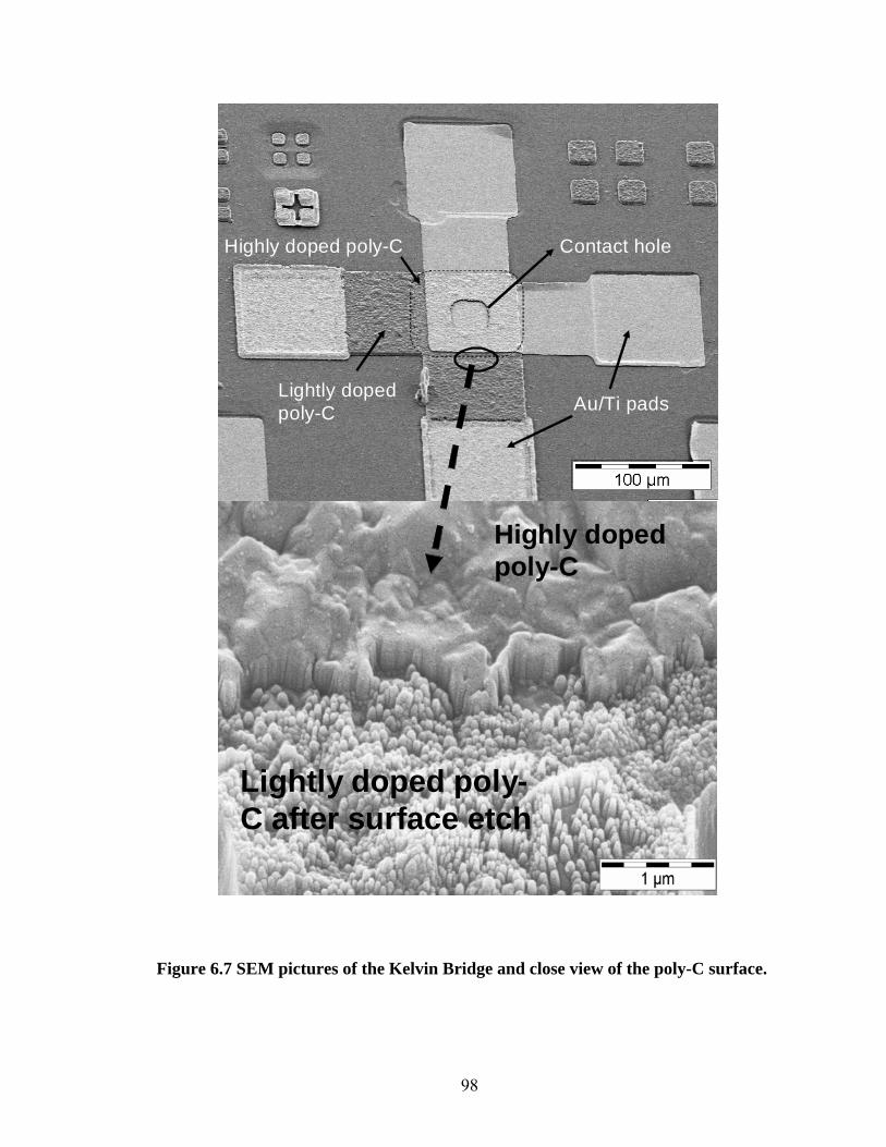
98
Au/Ti pads
Contact hole
Lightly doped poly-C
Highly doped poly-C
Au/Ti pads
Contact hole
Lightly doped poly-C
Highly doped poly-C
Highly doped poly-C
Lightly doped poly-C after surface etch
Au/Ti pads
Contact hole
Lightly doped poly-C
Highly doped poly-C
Au/Ti pads
Contact hole
Lightly doped poly-C
Highly doped poly-C
Highly doped poly-C
Lightly doped poly-C after surface etch
Figure 6.7 SEM pictures of the Kelvin Bridge and close view of the poly-C surface.

99
As shown in Figure 6.8, both type of contacts (with/without interlayer) show a linear
I-V relationship, which means the formation of ohmic contacts by forming titanium
carbide. For the films with resistivities of 0.022/151 Ω*cm for lightly and highly doped
layers, the average contact resistivities for the contact with/without highly doped
interlayer are 0.026/0.068 Ω*cm2, respectively. For the films with resistivities of
0.016/48 Ω*cm, the contact resistivities are 0.0028/0.0083 Ω*cm2 with/without
interlayer. The result shows that the highly doped interlayer can reduce the contact
resistances to about one third of the original values.
-100 -50 0 50 100-1.0
-0.5
0.0
0.5
1.0
Vol
tage
(V)
Curent(μA)
regular contact with intermediate layer
Figure 6.8 I-V curve of the contacts with/without highly doped interlayer.
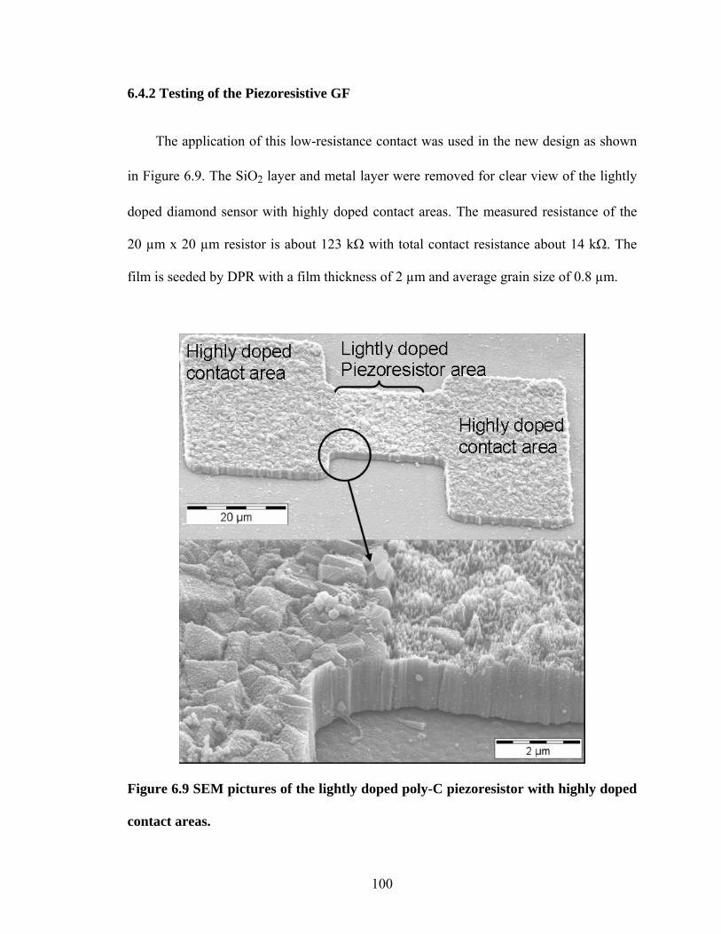
100
6.4.2 Testing of the Piezoresistive GF
The application of this low-resistance contact was used in the new design as shown
in Figure 6.9. The SiO2 layer and metal layer were removed for clear view of the lightly
doped diamond sensor with highly doped contact areas. The measured resistance of the
20 µm x 20 µm resistor is about 123 kΩ with total contact resistance about 14 kΩ. The
film is seeded by DPR with a film thickness of 2 µm and average grain size of 0.8 µm.
Figure 6.9 SEM pictures of the lightly doped poly-C piezoresistor with highly doped
contact areas.
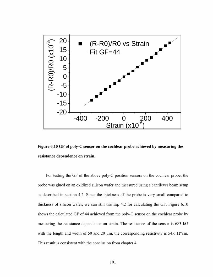
101
-400 -200 0 200 400-20-15-10-505
101520 (R-R0)/R0 vs Strain
Fit GF=44(R
-R0)
/R0
(x10
-3)
Strain (x10-6)
Figure 6.10 GF of poly-C sensor on the cochlear probe achieved by measuring the
resistance dependence on strain.
For testing the GF of the above poly-C position sensors on the cochlear probe, the
probe was glued on an oxidized silicon wafer and measured using a cantilever beam setup
as described in section 4.2. Since the thickness of the probe is very small compared to
thickness of silicon wafer, we can still use Eq. 4.2 for calculating the GF. Figure 6.10
shows the calculated GF of 44 achieved from the poly-C sensor on the cochlear probe by
measuring the resistance dependence on strain. The resistance of the sensor is 683 kΩ
with the length and width of 50 and 20 µm, the corresponding resistivity is 54.6 Ω*cm.
This result is consistent with the conclusion from chapter 4.

102
6.5 Summary
Based on previous studies, the 3rd generation cochlear probe with poly-C position
sensors were designed, fabricated and tested with several new improvements for
increasing the piezoresistive GF and compatibility with the Si-based technology. In-situ
doped poly-C film, with a thickness of 2 μm, were grown and patterned on the probe as
the piezoresistor. Low contact resistivity between poly-C and metal was achieved using a
highly doped poly-C thin interlayer. A piezoresistive gauge factor of 44 was achieved
from the poly-C sensor on the probe.
Test results shows that the poly-C process improvements, such as high microwave
power, contact interlayer, short resistor and large grain size, reduced the contact
resistance, total resistance and increased the GF and stability. This work demonstrated a
successful integration and promising application of poly-C technology with the silicon
based microsystems.
103
Chapter 7
Summary and Future Research
7.1 Summary of Contributions
7.1.1 Results reported for the first time
DPLW spin-coated seeding
DPLW spin-coating was developed as the new diamond seeding method which
can yield high density (2x10¹⁰/cm2), non-destructive and repeatable diamond seeding
on 4 inch Si wafer with dielectric surface. Dependence of seeding density on spin
speeds and repeat times were studied with proof of good uniformity over 4 inch wafer.
Low-resistance contact between poly-C and Metal
Low contact resistivity between poly-C and metal was achieved using a highly
doped poly-C thin interlayer. The contact areas were defined by etching only the
highly doped top layer beyond the contact areas. For same poly-C film and metal, this
new design yield a contact resistivity about one third of the value of regular contact.
Cochlear implant probe with poly-C piezoresistive position sensor

104
The poly-C piezoresistive position sensor was successfully integrated into two
generations of cochlear probes and demonstrated its high piezoresistive GF of 44.
Several improvements, such as high microwave power, contact interlayer, short
resistor and large grain size, were implemented in the 3rd generation design, which led
to low contact resistance, low total resistance and high GF.
7.1.2 Other significant contributions
Study of poly-C surface conductivity
The poly-C surface conductivity, which was caused by the surface hydrogenation,
was quantitatively studied by measuring the annealing caused change of sheet
resistance. The calculation shows that the surface conductivity is about 0.825 (Ω*cm)-1
and is independent to the doping level of poly-C films.
Poly-C gauge factor dependence on film resistivity and grain size
The GF dependence of poly-C on film doping and grain size was studied in detail by
using different doping levels and two seeding methods (DPLW and DPR). GF
increases prominently as the resistivities large than 10 Ω*cm, and at the same
resistivity level, the GF of film with grain size of 0.8 µm (DPR seeding) is about 3
times higher than that of the film with grain size of 0.3 µm (DW seeding).
Technology for poly-C process integration
105
An optimum poly-C process was developed which included DPLW seeding, dry
etching and metallization over SiO2 passivation. This process is IC compatible and
ensures the integration poly-C thin film with silicon based microsystems.
7.2 Future Research
Although this study improved the understanding of poly-C technology and
piezoresistivity, proved the application of poly-C sensor in cochlear probe, more work is
needed in the following areas in order to provide more promising applications for the
poly-C thin films:
i) Design interface circuit to test the probe for shape regeneration.
ii) Improve the poly-C equipment and process for better film quality.
iii) Evaluate the poly-C sensor reliability and noise level.
iv) Study the electrochemical and biological properties of poly-C thin film for
possible application as the electrode material in biomedical probe.

106
APPENDIX
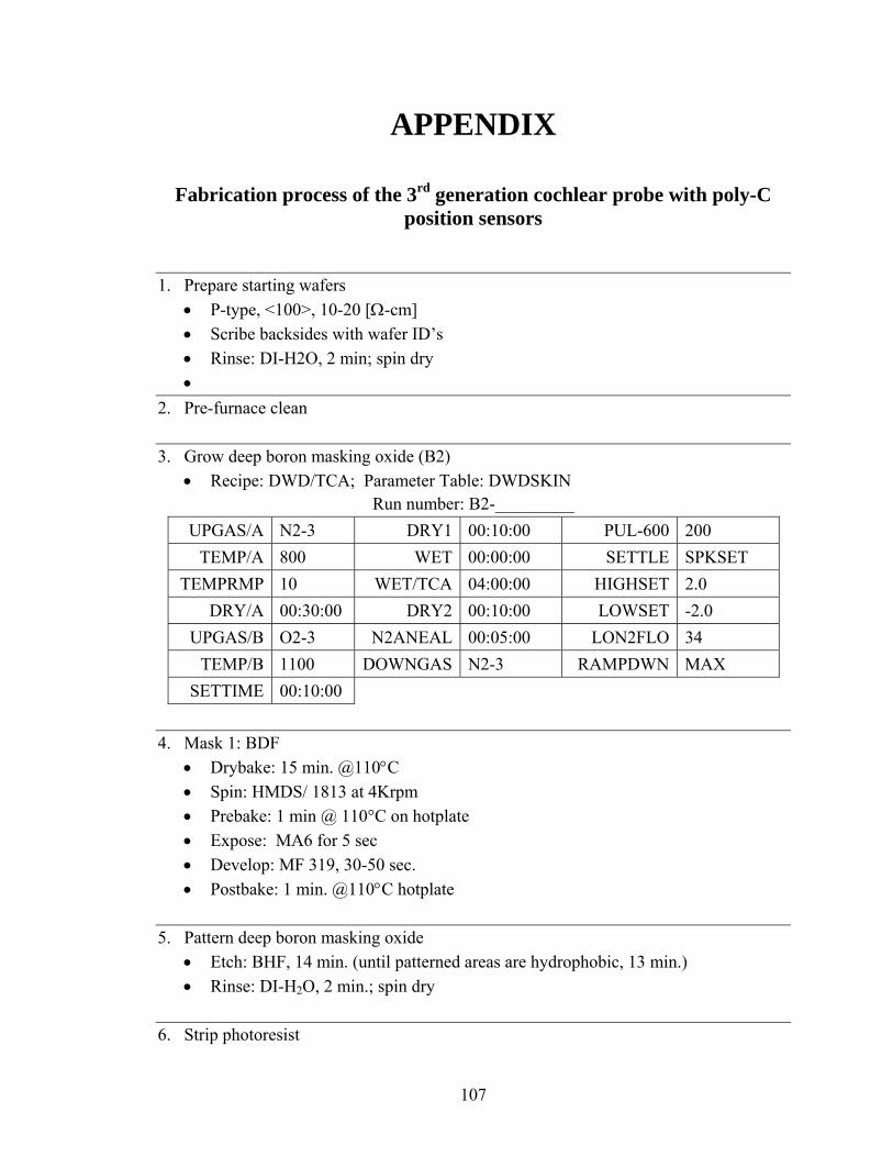
107
APPENDIX
Fabrication process of the 3rd generation cochlear probe with poly-C position sensors
1. Prepare starting wafers
• P-type, <100>, 10-20 [Ω-cm] • Scribe backsides with wafer ID’s • Rinse: DI-H2O, 2 min; spin dry •
2. Pre-furnace clean 3. Grow deep boron masking oxide (B2)
• Recipe: DWD/TCA; Parameter Table: DWDSKIN Run number: B2-_________
UPGAS/A N2-3 DRY1 00:10:00 PUL-600 200 TEMP/A 800 WET 00:00:00 SETTLE SPKSET
TEMPRMP 10 WET/TCA 04:00:00 HIGHSET 2.0 DRY/A 00:30:00 DRY2 00:10:00 LOWSET -2.0
UPGAS/B O2-3 N2ANEAL 00:05:00 LON2FLO 34 TEMP/B 1100 DOWNGAS N2-3 RAMPDWN MAX
SETTIME 00:10:00 4. Mask 1: BDF
• Drybake: 15 min. @110°C • Spin: HMDS/ 1813 at 4Krpm • Prebake: 1 min @ 110°C on hotplate • Expose: MA6 for 5 sec • Develop: MF 319, 30-50 sec. • Postbake: 1 min. @110°C hotplate
5. Pattern deep boron masking oxide • Etch: BHF, 14 min. (until patterned areas are hydrophobic, 13 min.) • Rinse: DI-H2O, 2 min.; spin dry
6. Strip photoresist

108
• Strip: PRS-2000 @65°C, 15 min. • Rinse: DI-H2O, 3 min.; spin dry • Etch: BHF, 12 sec. • Rinse: DI-H2O, 2 min.; spin dry (inspect for traces of resist!)
7. Pre-furnace clean • Clean one monitor; store in B1 for step 9
8. Deep boron diffusion (A2) • Recipe: BEDEP99; Parameter table: BORON99
Run number: A2-___________ TEMP 1175 LOO2FLOW 150 HIGHSET 2.0 SETTIME 00:10:00 DLUTTIME 00:10:00 LOWSET -2.0 DEPTIM 05:00:00 PUL-60 200
9. Drive-in and dilute boron glass (A4)
• Recipe: N2ANL/OX; Parameter table: N2ANL/OX • Add the bare Si monitor wafer previously stored in B1 to this run
Run number: A2-___________ UPGAS N2-3 ANLTIM
E05:00:00 N2ANEAL 00:05:00
DOWNGAS N2-3 TEMP2 1000 PUL-600 200 TEMP1 1175 DRY1 00:05:00 SETTLE SPKSET
TEMPRMP MAX WET 00:20:00 LOWSET -2.0 SETTLE 00:10:00 DRY2 00:05:00 HIGHSET 2.0
UPGAS2 N2-3
Required Monitor Data [ Expected thickness = 1500 Å] Location Top Center Left Right Bottom Average Thickness
10. Strip deep boron masking oxide
• Etch: HF:H2O 1:1, ____7____ min. ( until field/backsides are hydrophobic, ≅ 7 min.)
• Rinse: DI-H2O, 3 min.; spin dry
Checkpoint #1 Inspect for boron pitting. Discard wafers which do not pass QC check
109
11. Pre-furnace clean
• Clean 1 monitor for B2
12. Grow shallow boron diffusion (A4) • Recipe: DWDA1; Parameter Table: OXIDIZE
Run number: A4-_________ UPGAS/A N2-3 DRY1 00:10:00 PUL-600 200
DOWNGAS N2-3 WET 01:50:00 SETTLE SPKSET TEMP 1000 DRY2 00:10:00 HIGHSET 2.0
TEMPRAM MAX N2ANEAL 00:05:00 LOWSET -2.0 SETTIME 00:10:00
Required Monitor Data [ Expected thickness = 6,000 Å]
Location Top Center Left Right Bottom Average Thickness 13. Mask 2: SHB
• Drybake: 15 min. @110°C • Spin: HMDS/ 1813 @4Krpm • Prebake: 30 min. @ 90° • Expose:___13______ (MA6 ≅13 sec. EV420 ≅8 sec.) • Develop: MF 319, 1.1min. • Rinse: DI-H2O, 2 min.; spin dry • Postbake: 15 min. @110°C
14. Pattern shallow boron masking oxide • Etch: BHF, __6____ min. (until patterned areas are hydrophobic, ~6 min.) • Rinse: DI-H2O, 2 min.; spin dry
15. Strip photoresist • Strip: PRS-2000 @65°C, 15 min. • Rinse: DI-H2O, 3 min.; spin dry • Etch: BHF, 12 sec. • Rinse: DI-H2O, 2 min.; spin dry (inspect for traces of resist!)
16. Pre-furnace clean
110
17. Shallow boron diffusion (A2) • Recipe: BDEP99; Parameter table: BORON99
Run number: A2-___________ TEMP 1175 LOO2FLOW 150 HIGHSET 2.0 SETTIME 00:10:00 DLUTTIME 00:10:00 LOWSET -2.0 DEPTIM 00:15:00 PUL-60 200 18. Strip deep boron masking oxide
• Etch: HF:H2O 1:1, ____3____ min. ( until field/backsides are hydrophobic, ≅ 3 min.)
• Rinse: DI-H2O, 3 min.; spin dry
Checkpoint #2 Inspect for boron pitting. Discard wafers which do not pass QC check 19. Pre-furnace clean
• Clean 3 monitor; store 1 in B1 for step 20, 2 monitor for A4 & C4 20. Deposit LPCVD dielectrics (C4)
• Recipe: O2/NR/O2; Parameter table; CVD • Add one of the bare Si monitor wafers previously stored in B1 to this
Run number: C4-___________ Oxide 3000Å Nitride 1500 Å – Oxide 3000 Å
HTOTIM NITRTIM HTOTIM
21. Daimond seeding • Ultrasonic diamond powder loaded water (DW) for 30 minutes (average powder
size 25nm) • Dip wafer in 5% HF for 30 sec. • DI-H2O 2min, blow dry • Mount wafer on spinner and drop DW on • Spin at 2000rpm for 30 sec.
111
22. Growing CVD polycrystalline-diamond at MSU • Table of parameters for poly-C growth
CH4/H2 (sccm)
Trimethyl-boron (sccm)
Pressure ( torr )
Temp. (°C )
Time (hr)
Thickness( um )
Lightly doped 3/200 3e-4 45 740 18 1.8
Highly doped 3/200 1e-2 45 740 2.6 0.2
23. Mask for Ti film lift-off: HDC (for etching highly doped diamond)
• Spin HMDS 500 4 sec/4k 10 sec • Spin 5214 4 sec/4k 30 sec • Oven 90°C for 30 minutes • 1st exposure: 2-6sec MA 6 • Reversal Bake: Oven 102°C, 30 minutes • Flood Exposure 50 sec • Develop MIF319, 1 min (bath) • Rinse in DI-H2O, 5 min. spin dry
24. Deposit Ti film • Loaded into Enerjet Evaporator, pump down to 2*10-6 Torr (1 hr) • Evaporate 100 nm Ti
25. Lift off • Soak in Acetone over night with wafer in holder. Wafers face down • Ultrasound each wafer individually for a few sec the next morning • Rinse: DI-H2O, 5 min.; spin dry (inspect for flakes!)
26. Dry etching of highly doped diamond layer at MSU
• Diamond etching recipe:
O2/Ar/SF6 (sccm)
Pressure ( mtorr )
Microwave power (W)
RF power (W)
Substrate bias ( V )
Etch Rate ( nm/min )
Thickness Etched ( um )
30/2/2 4-6 400 100 -130 80-120 0.2 -0.3 • After each 30 second etch, check the change of sheet resistance using four-
probe method. Etch till the highly doped layer is totally removed
112
27. Strip Ti etching mask • Strip: 5% HF solution, 5 min. • Rinse: DI-H2O, 3 min.; spin dry
28. Mask for Ti film lift-off: DIA (for etching diamond sensor)
• Spin: HMDS/ 1827 @3Krpm • Prebake: 30 min. @ 90° • Expose:__17__ sec using MA6 • Develop: MF 319, 1.1min. • Rinse: DI-H2O, 2 min.; spin dry • Postbake: 30 min. @110°C
29. Deposit Ti film • Loaded into Enerjet Evaporator, pump down to 2*10-6 Torr (1 hr) • Evaporate 150 nm Ti
30. Lift off • Soak in Acetone over night with wafer in holder. Wafers face down • Ultrasound each wafer individually for a few sec the next morning • Rinse: DI-H2O, 5 min.; spin dry (inspect for flakes!)
31. Dry etching of both diamond layers at MSU
• Diamond etching recipe:
O2/Ar/SF6
(sccm)
Pressure
( mtorr )
Microwave
power (W)
RF
power
(W)
Substrate
bias ( V )
Etch Rate
( nm/min )
Thickness
Etched (
um )
30/2/2 4-6 400 100 -130 80-120 ~2
32. Strip Ti etching mask
• Strip: 5% HF solution, 5 min. • Rinse: DI-H2O, 3 min.; spin dry
33. LTO deposition ( furnace C2 ) • Deposit 10,000Å low temperature oxide at 425°C • Deposition rate: ~100Å/min

113
34. Mask for contact to diamond: PCC • Spin: HMDS/ 1813 @3Krpm • Prebake: 1 min. @ 110° on hotplate • Expose:__ 5-7__ sec using MA6 • Develop: MF 319, 50 sec. • Rinse: DI-H2O, 2 min.; spin dry • Postbake: 1 min. @110°C on hotplate
35. Etch LTO • Pad Etchant (expect ~3000Å/min) • Rinse: DI-H2O, 2 min.; spin dry
36. Strip photoresist • Strip: PRS-2000 @65°C, 15 min. • Rinse: DI-H2O, 3 min.; spin dry
37. Mask for interconnects: DCO2 • Spin: HMDS/ SPR220 @3Krpm • Prebake: 1.5 min. @ 110° on hotplate • Expose:__ 7__ sec using MA6 • Postbake: 1.5 min. @ 115° on hotplate • Develop: AZ300, 60 sec. • Rinse: DI-H2O, 2 min.; spin dry
38. Asher for descum 39. Sputter Interconnect Metal
• Rinse DI-H2O, 1 min. dip in BHF immediately • Etch: BHF, 20 sec. • Rinse: DI-H2O, 2 min.; spin dry • Drybake: 5 min. @110°C; load into sputtering chamber immediately • Pump down to 3*10-6 Torr (1.5 hrs) • Target #1, DC 550 W, 500 Å Ti _______ (10’ 40”) • Target #1, DC sputter 550W, 1200 Å TiN (N2 gas 13.5%): ______ (16’ 40”) • Target #3, DC 550 W, 800 Å Al (1% Si) _______ (4’ 20”) • Target #1, DC 550 W, 300 Å Ti _______ (6’ 40”) • Target #3, DC 550 W, 800 Å Al (1% Si) _______ (4’ 20”) • Target #1, DC 550 W, 300 Å Ti _______ (6’ 40”) • Target #3, DC 550 W, 800 Å Al (1% Si) _______ (4’ 20”)
114
• Target #1, DC 550 W, 300 Å Ti _______ (6’ 40”)
40. Lift off Option1 • Soak in Acetone over night with wafer in holder. Wafers face down. • Ultrasound each wafer individually for a few sec the next morning • Rinse: DI-H2O, 5 min.; spin dry (inspect for flakes!)
Option 2 • Liftoff: 1112A Remover @60-70°C, ≈10-15 min. • Punctuate with 1-2 min. intervals in ultrasonic bath • Rinse: DI-H2O, 5 min.; spin dry (inspect for flakes!)
41. LTO deposition ( furnace C2 ) • Deposit 10,000Å low temperature oxide at 425°C • Deposition rate: ~100Å/min
42. Mask of contact for both Ir and Au: CON • Spin: HMDS/ 1813 @3Krpm • Prebake: 1 min. @ 110° on hotplate • Expose:__ 5-7__ sec using MA6 • Develop: MF 319, 50 sec. • Rinse: DI-H2O, 2 min.; spin dry • Postbake: 1 min. @110°C on hotplate
43. Etch LTO • Pad Etchant • Careful control (expect ~3000Å/min) to avoid etching of underneath Al/Ti • Rinse: DI-H2O, 2 min.; spin dry
44. Strip photoresist • Strip: PRS-2000 @65°C, 15 min. • Rinse: DI-H2O, 3 min.; spin dry
45. Mask for patterning Ir stimulating site: IRD • Spin: HMDS/ SPR220 @3Krpm • Prebake: 1.5 min. @ 110° on hotplate • Expose:__ 7__ sec using MA6 • Postbake: 1.5 min. @ 115° on hotplate • Develop: AZ300, 60 sec.

115
• Rinse: DI-H2O, 2 min.; spin dry 46. Asher for descum 47. Sputter Ti/ Ir
• Rinse: DI-H2O, 2 min.; spin dry • Drybake: 5 min. @110°C; load into sputtering chamber immediately • Pump down to 5*10-6 Torr (1.5 hrs) • Target #2, RF sputter 500 Å Ti @700W, 7 mT Ar, (pre-sputter 2 min.), time
_______ (11’) • Target#3, DC sputter 3000Å Ir @1.0 A, 7 mT Ar, (pre-sputter 2 min.), time
_______ (21’45”)
48. Lift off • Soak in Acetone over night with wafer in holder. Wafers face down. • Ultrasound each wafer individually for a few sec the next morning • Rinse: DI-H2O, 5 min.; spin dry (inspect for flakes!)
49. Mask for patterning Au pads: GOL
• Spin: HMDS/ SPR220 @3Krpm • Prebake: 1.5 min. @ 110° on hotplate • Expose:__ 7__ sec using MA6 • Postbake: 1.5 min. @ 115° on hotplate • Develop: AZ300, 60 sec. • Rinse: DI-H2O, 2 min.; spin dry
50. Asher for descum
51. Sputter Cr/Au
• Rinse: DI-H2O, 2 min.; spin dry • Drybake: 5 min. @110°C; load into sputtering chamber immediately • Pump down to 5*10-6 Torr (1.5 hrs) • Target #2, RF sputter 500 Å Cr @800W, 7 mT Ar, (pre-sputter 2 min.), time
_______(6’15”) • Target#3, DC sputter 2000Å Au @0.5 A, 7 mT Ar, (pre-sputter 2 min.), time
_______(8’)
52. Pattern the profile of the probe on dielectric : DEL • Drybake: 15 min. @110°C
116
• Spin: HMDS/ 1827 @3Krpm • Prebake: 30 min. @ 90° • Expose: MA6 ≅55 sec or EV420 ≅29 sec. • Develop: MF 319, 1.1min. • Rinse: DI-H2O, 2 min.; spin dry • Postbake: 30 min. @110°C
53. RIE etch field using Semigroup RIE • Check current recipes for etch rates and times • Check thickness of all layer
Run number: ___________ Etch #1: Descum Etch #2: Oxide Etch#3 Nitride Gas/Flow O2 50 sccm CHF3 15 sccm CF4 20 sccm Gas/Flow CF4 15 sccm O2 1 sccm Pressure 300 mT 40 mT 100 mT Power 25 W 100 W 80 W Time 1 min. (~280 Å /min) (~100 Å /min)
49. Strip photoresist
• Strip: PRS-2000 @65°C, 15 min. • Rinse: DI-H2O, 3 min.; spin dry ( inspect for traces of resist)
50. Protect frontside • Spin: HMDS/1827 @ 3Krpm • Postbake: 15 min. @110°C
51. RIE etch backside (Semi Group) • Check current recipes for etch rates and times • Check thickness of all layer • Note: recipe for etching oxide can etch nitride also
Run number: ___________ Etch #2A: Oxide Gas/Flow CHF3 25 sccm Gas/Flow CF4 25 sccm Pressure 40 mT Power 100 W Time
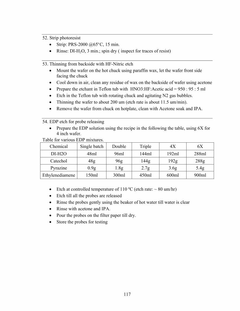
117
52. Strip photoresist
• Strip: PRS-2000 @65°C, 15 min. • Rinse: DI-H2O, 3 min.; spin dry ( inspect for traces of resist)
53. Thinning from backside with HF-Nitric etch • Mount the wafer on the hot chuck using paraffin wax, let the wafer front side
facing the chuck • Cool down in air, clean any residue of wax on the backside of wafer using acetone • Prepare the etchant in Teflon tub with HNO3:HF:Acetic acid = 950 : 95 : 5 ml • Etch in the Teflon tub with rotating chuck and agitating N2 gas bubbles. • Thinning the wafer to about 200 um (etch rate is about 11.5 um/min). • Remove the wafer from chuck on hotplate, clean with Acetone soak and IPA.
54. EDP etch for probe releasing
• Prepare the EDP solution using the recipe in the following the table, using 6X for 4 inch wafer.
Table for various EDP mixtures. Chemical Single batch Double Triple 4X 6X DI-H2O 48ml 96ml 144ml 192ml 288ml Catechol 48g 96g 144g 192g 288g Pyrazine 0.9g 1.8g 2.7g 3.6g 5.4g
Ethylenediamene 150ml 300ml 450ml 600ml 900ml • Etch at controlled temperature of 110 ºC (etch rate: ~ 80 um/hr) • Etch till all the probes are released • Rinse the probes gently using the beaker of hot water till water is clear • Rinse with acetone and IPA. • Pour the probes on the filter paper till dry. • Store the probes for testing

118
BIBLIOGRAPHY
119
BIBLIOGRAPHY
[1] P. Adrian, "SENSOR INDUSTRY DEVELOPMENTS AND TRENDS," Sensor
Business Digest, vol. pp. 2002.
[2] http://www.sensorsportal.com/HTML/Marketplace.htm, 2004.
[3] M. Aslam, I. Taher, A. Masood, M. A. Tamor and T. J. Potter, "Piezoresistivity in Vapor-Deposited Diamond Films," Applied Physics Letters, vol. 60, pp. 2923-2925, 1992.
[4] I. Taher, M. Aslam, M. A. Tamor, T. J. Potter and R. C. Elder, "Piezoresistive Microsensors Using P-Type CVD Diamond Films," Sensors and Actuators a-Physical, vol. 45, pp. 35-43, 1994.
[5] M. Werner and R. Locher, "Growth and application of undoped and doped diamond films," Reports on Progress in Physics, vol. 61, pp. 1665-1710, 1998.
[6] J. L. Davidson, W. P. Kang, Y. Gurbuz, K. C. Holmes, L. G. Davis, A. Wisitsora-at, et al., "Diamond as an active sensor material," Diamond and Related Materials, vol. 8, pp. 1741-1747, 1999.
[7] M. Adamschik, R. Muller, P. Gluche, A. Floter, W. Limmer, R. Sauer, et al., "Analysis of piezoresistive properties of CVD-diamond films on silicon," Diamond and Related Materials, vol. 10, pp. 1670-1675, 2001.
[8] S. Sahli and D. M. Aslam, "Ultra-high sensitivity intra-grain poly-diamond piezoresistors," Sensors and Actuators a-Physical, vol. 71, pp. 193-197, 1998.
[9] S. Sahli, Electronic Characterization and Fabrication of CVD Diamond Piezoresistive Pressure Sensors, Ph.D Dissertation, Michigan State University, 1997.
[10] G. S. Yang and D. M. Aslam, "Single-structure heater and temperature sensor using a p-type polycrystalline diamond resistor," IEEE Electron Device Letters, vol. 17, pp. 250-252, 1996.
120
[11] J. G. Ran, C. Q. Zheng, J. Ren and S. M. Hong, "Properties and Texture of B-Doped Diamond Films as Thermal Sensor," Diamond and Related Materials, vol. 2, pp. 793-796, 1993.
[12] W. P. Kang, Y. Gurbuz, J. L. Davidson and D. V. Kerns, "A New Hydrogen Sensor Using a Polycrystalline Diamond-Based Schottky Diode," Journal of the Electrochemical Society, vol. 141, pp. 2231-2234, 1994.
[13] Y. Gurbuz, W. P. Kang, J. L. Davidson, D. L. Kinser and D. V. Kerns, "Diamond microelectronic gas sensors," Sensors and Actuators B-Chemical, vol. 33, pp. 100-104, 1996.
[14] P. Bergonzo, F. Foulon, R. D. Marshall, C. Jany, A. Brambilla, R. D. McKeag, et al., "High collection efficiency CVD diamond alpha detectors," IEEE Transactions on Nuclear Science, vol. 45, pp. 370-373, 1998.
[15] M. Keil, W. Adam, E. Berdermann, P. Bergonzo, W. de Boer, F. Bogani, et al., "New results on diamond pixel sensors using ATLAS frontend electronics," Nuclear Instruments & Methods in Physics Research Section a-Accelerators Spectrometers Detectors and Associated Equipment, vol. 501, pp. 153-159, 2003.
[16] N. Kumar, H. Schmidt and C. G. Xie, "Diamond-Based Field-Emission Flat-Panel Displays," Solid State Technology, vol. 38, pp. 71-73, 1995.
[17] U. Kim and D. M. Aslam, "Field emission electroluminescence on diamond and carbon nanotube films," Journal of Vacuum Science & Technology B, vol. 21, pp. 1291-1296, 2003.
[18] D. Hong and M. Aslam, "Field-Emission from P-Type Polycrystalline Diamond Films," Journal of Vacuum Science & Technology B, vol. 13, pp. 427-430, 1995.
[19] X. W. Zhu, D. M. Aslam, Y. X. Tang, B. H. Stark and K. Najafi, "The fabrication of all-diamond packaging panels with built-in interconnects for wireless integrated microsystems," Journal of Microelectromechanical Systems, vol. 13, pp. 396-405, 2004.
[20] J. Wang, J. E. Butler, D. S. Y. Hsu and T.-C. Nguyen, "CVD polycrystalline diamond high-Q micromechanical resonators," The Fifteenth IEEE international conference on MEMS, vol. pp. 657, 2002.
[21] N. Sepulveda-Alancastro and D. M. Aslam, "Polycrystalline diamond technology for RFMEMS resonators," Microelectronic Engineering, vol. 73-74, pp. 435-440, 2004.

121
[22] A. A. Morrish and P. E. Pehrsson, "Effects of Surface Pretreatments on Nucleation and Growth of Diamond Films on a Variety of Substrates," Applied Physics Letters, vol. 59, pp. 417-419, 1991.
[23] L. Demuynck, J. C. Arnault, C. Speisser, R. Polini and F. LeNormand, "Mechanisms of CVD diamond nucleation and growth on mechanically scratched and virgin Si(100) surfaces," Diamond and Related Materials, vol. 6, pp. 235-239, 1997.
[24] P. A. Dennig, H. Shiomi, D. A. Stevenson and N. M. Johnson, "Influence of Substrate Treatments on Diamond Thin-Film Nucleation," Thin Solid Films, vol. 212, pp. 63-67, 1992.
[25] E. J. Bienk and S. S. Eskildsen, "The Effect of Surface Preparation on the Nucleation of Diamond on Silicon," Diamond and Related Materials, vol. 2, pp. 432-437, 1993.
[26] F. S. Lauten, Y. Shigesato and B. W. Sheldon, "Diamond Nucleation on Unscratched Sio2 Substrates," Applied Physics Letters, vol. 65, pp. 210-212, 1994.
[27] M. J. Chiang and M. H. Hon, "Positive dc bias-enhanced diamond nucleation with high CH4 concentration," Diamond and Related Materials, vol. 10, pp. 1470-1476, 2001.
[28] M. D. Irwin, C. G. Pantano, P. Gluche and E. Kohn, "Bias-enhanced nucleation of diamond on silicon dioxide," Applied Physics Letters, vol. 71, pp. 716-718, 1997.
[29] A. Masood, M. Aslam, M. A. Tamor and T. J. Potter, "Techniques for Patterning of CVD Diamond Films on Non-Diamond Substrates," Journal of the Electrochemical Society, vol. 138, pp. L67-L68, 1991.
[30] G. S. Yang, M. Aslam, K. P. Kuo, D. K. Reinhard and J. Asmussen, "Effect of Ultrahigh Nucleation Density on Diamond Growth at Different Growth-Rates and Temperatures," Journal of Vacuum Science & Technology B, vol. 13, pp. 1030-1036, 1995.
[31] A. P. Malshe, R. A. Beera, A. A. Khanolkar, W. D. Brown and H. A. Naseem, "Initial results of a novel pre-deposition seeding technique for achieving an ultra-high nucleation density for CVD diamond growth," Diamond and Related Materials, vol. 6, pp. 430-434, 1997.
122
[32] F. P. Bundy, H. T. Hall, H. M. STrong and R. H. Wentroff, "Man-made diamond," Nature, vol. 176, pp. 51-54, 1955.
[33] P. K. Bachmann, D. Leera and H. Lydtin, "Towards a General Concept of Diamond Chemical Vapour Deposition," Diamond and Related Materials, vol. 1, pp. 1-12, 1991.
[34] D. M. Gruen, P. C. Redfern, D. A. Horner, P. Zapol and L. A. Curtiss, "Theoretical studies on nanocrystalline diamond: Nucleation by dicarbon and electronic structure of planar defects," Journal of Physical Chemistry B, vol. 103, pp. 5459-5467, 1999.
[35] M. Kamo, Y. Sato and S. Sctaka, "(MPCVD of diamond)," Journal of Crystal Growth, vol. 62, pp. 642, 1983.
[36] B. R. Stoner, B. E. Williams, S. D. Wolter, K. Nishimura and J. T. Glass, "Insitu Growth-Rate Measurement and Nucleation Enhancement for Microwave Plasma Cvd of Diamond," Journal of Materials Research, vol. 7, pp. 257-260, 1992.
[37] S. Matsumoto, Y. Sato, M. Kamo and N. Setaka, "(HFCVD Diamond)," Japanese Journal of applied Physics, vol. 21, pp. 183, 1982.
[38] R. C. Hyer, M. Green, K. K. Mishra and S. C. Sharma, "Nucleation and Growth of Diamond in Hot Filament Assisted Chemical Vapor-Deposition," Journal of Materials Science Letters, vol. 10, pp. 515-518, 1991.
[39] A. Lettington and J. W. Steeds, "Thin Film Diamond," 1994.
[40] V. G. Ralchenko, A. A. Smolin, V. I. Konov, K. F. Sergeichev, I. A. Sychov, I. I. Vlasov, et al., Diamond and Related Materials, vol. 6, pp. 417, 1997.
[41] Y. Ando, Y. Yokota, T. Tachibana, A. Watanabe, Y. Nishibayashi, K. Kobashi, et al., Diamond and Related Materials, vol. 11, pp. 596, 2002.
[42] S. Sahli and D. M. Aslam, "Effect of postdeposition anneal on the resistivity of p-type polycrystalline diamond films," Applied Physics Letters, vol. 69, pp. 2051-2052, 1996.
[43] X. K. Zhang, J. G. Guo and Y. F. Yao, "Boron Doping of Diamond Films by B2o3 Vaporization," Physica Status Solidi a-Applied Research, vol. 133, pp. 377-383, 1992.

123
[44] J. Ruan, K. Kobashi and W. J. Choyke, "Effect of Oxygen on Boron Doping in Chemical Vapor-Deposition of Diamond as Deduced from Cathodoluminescence Studies," Applied Physics Letters, vol. 60, pp. 1884-1886, 1992.
[45] T. Takada, T. Fukunaga, K. Hayashi, Y. Yokota, T. Tachibana, K. Miyata, et al., "Boron-doped diamond thin film sensor for detection of various semiconductor manufacturing gases," Sensors and Actuators a-Physical, vol. 82, pp. 97-101, 2000.
[46] J. Cifre, J. Puigdollers, M. C. Polo and J. Esteve, "Trimethylboron Doping of Cvd Diamond Thin-Films," Diamond and Related Materials, vol. 3, pp. 628-631, 1994.
[47] J. F. Prins, "Ion-Implantation and Diamond - Some Recent Results on Growth and Doping," Thin Solid Films, vol. 212, pp. 11-18, 1992.
[48] J. F. Prins, "Implantation-doping of diamond with B+, C+, N+ and O+ ions using low temperature annealing," Diamond and Related Materials, vol. 11, pp. 612-617, 2002.
[49] R. Kalish, "Ion-implantation in diamond and diamond films: Doping, damage effects and their applications," Applied Surface Science, vol. 117, pp. 558-569, 1997.
[50] T. H. Borst and O. Weis, "boron-doped homoepitaxial Diamond layers: Fabrication, characterisation and electronic applications," phys. stat. sol. A, vol. 154, pp. 423, 1996.
[51] E. Kohn, W. Ebert, A. Aleksov, M. Adamschik and P. Schmid, "Diamond Technology for Electronics and MEMS Review of Status and Perspectives," 23rd Intern'l Conf. on Microelectronics, vol. 1, pp. 59, 2002.
[52] J. Ristein, M. Riedel, F. Maier, B. F. Mantel, M. Stammler and L. Ley, "Surface doping: a special feature of diamond," Journal of Physics-Condensed Matter, vol. 13, pp. 8979-8987, 2001.
[53] E. Snidero, D. Tromson, C. Mer, P. Bergonzo, J. S. Foord, C. Nebel, et al., "Influence of the postplasma process conditions on the surface conductivity of hydrogenated diamond surfaces," Journal of Applied Physics, vol. 93, pp. 2700-2704, 2003.
[54] M. Werner, O. Dorsch, H. U. Baerwind, A. Ersoy, E. Obermeier, C. Johnston, et al., "Very-Low Resistivity Al-Si Ohmic Contacts to Boron-Doped Polycrystalline Diamond Films," Diamond and Related Materials, vol. 3, pp. 983-985, 1994.
124
[55] M. Yokoba, Y. Koide, A. Otsuki, F. Ako, T. Oku and M. Murakami, "Carrier transport mechanism of Ohmic contact to p-type diamond," Journal of Applied Physics, vol. 81, pp. 6815-6821, 1997.
[56] C. A. Hewett, M. J. Taylor, J. R. Zeidler and M. W. Geis, "Specific Contact Resistance Measurements of Ohmic Contacts to Semiconducting Diamond," Journal of Applied Physics, vol. 77, pp. 755-760, 1995.
[57] Y. X. Tang and D. M. Aslam, "Technology of Polycrystalline Diamond Thin Films for Microsystems Applications," Journal of Vacuum Science & Technology B, vol. 23, pp. 1088, 2005.
[58] P. E. Viljoen, E. S. Lambers and P. H. Holloway, "Reaction between Diamond and Titanium for Ohmic Contact and Metallization Adhesion Layers," Journal of Vacuum Science & Technology B, vol. 12, pp. 2997-3005, 1994.
[59] T. Iwasaki, K. Okano, Y. Matsumae, E. Matsushima, H. Maekawa, H. Kiyota, et al., "Formation of Ohmic Contacts on Semiconducting Diamond Grown by Chemical-Vapor-Deposition," Diamond and Related Materials, vol. 3, pp. 30-34, 1994.
[60] S. Katsumata, Y. Oobuchi and T. Asano, "Patterning of Cvd Diamond Films by Seeding and Their Field-Emission Properties," Diamond and Related Materials, vol. 3, pp. 1296-1300, 1994.
[61] X. Jiang, E. Boettger, M. Paul and C. P. Klages, "Approach of Selective Nucleation and Epitaxy of Diamond Films on Si(100)," Applied Physics Letters, vol. 65, pp. 1519-1521, 1994.
[62] H. W. Liu, C. X. Gao, X. Li, C. X. Wang, Y. H. Han and G. T. Zou, "Selective deposition of diamond films on insulators by selective seeding with a double-layer mask," Diamond and Related Materials, vol. 10, pp. 1573-1577, 2001.
[63] O. Dorsch, M. Werner and E. Obermeier, "Dry-Etching of Undoped and Boron-Doped Polycrystalline Diamond Films," Diamond and Related Materials, vol. 4, pp. 456-459, 1995.
[64] M. Bernard, A. Deneuville, T. Lagarde, E. Treboux, J. Pelletier, P. Muret, et al., "Etching of p- and n-type doped monocrystalline diamond using an ECR oxygen plasma source," Diamond and Related Materials, vol. 11, pp. 828-832, 2002.
125
[65] C. Vivensang, L. FerlazzoManin, M. F. Ravet, G. Turban, F. Rousseaux and A. Gicquel, "Surface smoothing of diamond membranes by reactive ion etching process," Diamond and Related Materials, vol. 5, pp. 840-844, 1996.
[66] R. Otterbach and U. Hilleringmann, "Reactive ion etching of CVD-diamond for piezoresistive pressure sensors," Diamond and Related Materials, vol. 11, pp. 841-844, 2002.
[67] H. Shiomi, "Reactive ion etching of diamond in O-2 and CF4 plasma, and fabrication of porous diamond for field emitter cathodes," Japanese Journal of Applied Physics Part 1-Regular Papers Short Notes & Review Papers, vol. 36, pp. 7745-7748, 1997.
[68] F. Silva, R. S. Sussmann, F. Benedic and A. Gicquel, "Reactive ion etching of diamond using microwave assisted plasmas," Diamond and Related Materials, vol. 12, pp. 369-373, 2003.
[69] C. S. Smith, "Piezoresistance effect in germanium and silicon," Physical Review., vol. 94, pp. 22, 1954.
[70] G. C. Kucznski, "Effect of elastic strain on the electrical resisstance of metals," Physical Review, vol. 94, pp. 1954.
[71] F. Conti, B. Morten, C. Nobili and A. Taroni, "Piezoresistive Coefficients in Silicon Diffused Layers," Physica Status Solidi a-Applied Research, vol. 17, pp. K29-K31, 1973.
[72] Y. Onuma and K. Sekiya, "Piezoresistive Properties of Polycrystalline Silicon Thin-Film," Japanese Journal of Applied Physics, vol. 11, pp. 20-&, 1972.
[73] J. S. Shor, D. Goldstein and A. D. Kurtz, "Evaluation of β-SiC for sensors," IEEE Proceedings, Intl. Conf. on Solid-State Sensors and Actuators (Transducers'91), vol. pp. 912, 1991.
[74] D. R. Wur and J. L. Davidson, "Piezoresistivity of Polycrystalline Diamond Films," 1992 MRS meeting, vol. pp. 1992.
[75] M. Deguchi, N. Hase, M. Kitabatake, H. Kotera, S. Shima and H. Sakakima, "Piezoresistive properties of p-type CVD diamond films," Diamond Films and Technology, vol. 6, pp. 77-85, 1996.
[76] I. Taher, CVD Diamond Piezoresistive Microsensors, Ph.D. Dissertation, Michigan State University, 1994.
126
[77] C. Herring and E. Vogt, "Transport and deformation-potential theory for many-valley semiconductors with anisotropic scattering," Physical Review, vol. 101, pp. 944-961, 1956.
[78] R. N. Thurston, "Use of Semiconductor Transducers in Measuring Strain, Accelerations, and Displacemnts," Physical Acoustics, vol. 1, pp. 215, 1964.
[79] M. M. Mandurah, K. C. Saraswat, C. R. Helms and T. I. Kamins, "Dopant Segregation in Polycrystalline Silicon," Japanese Applied Physics, vol. 51, pp. 5755-5763, 1980.
[80] P. J. French, "Piezoresistance in polysilicon," Electronics Letter, vol. 24, pp. 999-1000, 1984.
[81] O. Dorsch, K. Holzner, M. Werner, E. Obermeier, R. E. Harper, C. Johnston, et al., "Piezoresistive Effect of Boron-Doped Diamond Thin-Films," Diamond and Related Materials, vol. 2, pp. 1096-1099, 1993.
[82] Cochlear Implant Program, University of Michigan, http://www.med.umich.edu/oto/ci/implant.htm.,
[83] J. Wang, M. Gulari, P. T. Bhatti, B. Y. Arcand, K. Beach, C. R. Friedrich, et al., "A Cochlear Electrode Array with Build-in Position Sensing," 18th IEEE Intl. Conf. on Micro Electro Mechanical Systems (MEMS 2005), vol. 2, pp. 786-789, 2005.
[84] P. T. Bhatti, B. Y. Arcand, J. Wang, N. V. Butala, C. R. Friedrich and K. D. Wise, "A High-Density Electrode Array for A Cochlear Prosthesis," IEEE Int. Conf. on Solid-State Sensors and Actuators (TRANSDUCERS'03), vol. 2, pp. 1750-1753, 2003.
[85] R. R. Thomas, F. B. Kaufman, J. T. Kirleis and R. A. Belsky, "Wettability of polished silicon oxide surfaces," Journal of the Electrochemical Society, vol. 143, pp. 643-648, 1996.
[86] S. Schelz, C. F. M. Borges, L. Martinu and M. Moisan, "Diamond nucleation enhancement by hydrofluoric acid etching of silicon substrate," Diamond and Related Materials, vol. 6, pp. 440-443, 1997.
[87] J. Stiegler, Y. vonKaenel, M. Cans and E. Blank, "Space filling by nucleation and growth in chemical vapor deposition of diamond," Journal of Materials Research, vol. 11, pp. 716-726, 1996.
127
[88] K. Hayashi, S. Yamanaka, H. Watanabe, T. Sekiguchi, H. Okushi and K. Kajimura, Journal of Applied Physics, vol. 81, pp. 744, 1997.
[89] T. H. Borst and O. Weis, "Electrical Characterization of homoepitaxial diamond films doped with B, P, Li and Na during crystal growth," Diamond and Related Materials, vol. 4, pp. 948, 1995.
[90] N. Sepulveda-Alancastro, Polycrystalline Diamond RF MEMS Resonator Techonology and Chracterization, Ph.D. Dissertation, Michgan State University, 2005.
[91] G. S. Yang and M. Aslam, "Ultrahigh Nucleation Density for Growth of Smooth Diamond Films," Applied Physics Letters, vol. 66, pp. 311-313, 1995.
[92] Y. X. Tang, D. M. Aslam, J. B. Wang and K. D. Wise, "Study of polycrystalline diamond piezoresistive position sensors for application in cochlear implant probe," Diamond and Related Materials, vol. 15, pp. 199-202, 2006.
[93] X. M. Yu, J. Thaysen, O. Hansen and A. Boisen, "Optimization of sensitivity and noise in piezoresistive cantilevers," Journal of Applied Physics, vol. 92, pp. 6296-6301, 2002.
[94] Y. X. Tang, D. M. Aslam, J. B. Wang and K. D. Wise, "Technology and Integration of Poly-Crystalline Diamond Piezoresistive Position Sensor for Cochlear Implant Probe," the 13th International Conference on Solid-State Sensors, Actuators and Microsystems (TRANSDUCERS '05), vol. 1, pp. 543-546, 2005.
[95] O. Auciello, J. Birrell, J. A. Carlisle, J. E. Gerbi, X. C. Xiao, B. Peng, et al., "Materials science and fabrication processes for a new MEMS technoloey based on ultrananocrystalline diamond thin films," Journal of Physics-Condensed Matter, vol. 16, pp. R539-R552, 2004.
[96] M. Adamschik, M. Hinz, C. Maier, P. Schmid, H. Seliger, E. P. Hofer, et al., "Diamond micro system for bio-chemistry," Diamond and Related Materials, vol. 10, pp. 722-730, 2001.
[97] J. Rabaey, "Digital Integrated circuits: A Design Perspective," vol. pp. 2003.
[98] Y. X. Tang, S. Sahli, D. M. Aslam, D. Merriam and K. D. Wise, "Poly-diamond inter-and intra-grain piezoresis ive position sensor design for WIMS," AICHE Annual Conference on Sensors, vol. pp. 186, 2002.
128
[99] J. H. Lee, J. Y. Lee, I. S. Yeo and S. K. Lee, "Lower sheet/contact resistance in shallower junction obtained by F+B mixed implant," Journal of Vacuum Science & Technology B, vol. 20, pp. 396-399, 2002.
[100] H. Shiomi, "Reactive Ion Etching of Diamond in O2 and CF4 plasma, and Fabrication of Porous Diamond for Field Emitter Cathodes," Japanese Journal of applied Physics, vol. 36, pp. 7745-7748, 1997.